Microsoft BT101 User Manual Revised Manual
Microsoft Mobile Oy Revised Manual
Contents
- 1. Manual
- 2. Revised Manual
Revised Manual

CONFIDENTIAL 02 November 2000
Exhibit 10 revision 0.1
FCC ID: OW3BT101
Applicant: Nokia Mobile Phones
Copyright
©
2000 Nokia Mobile Phones
1/11
INFORMATION - MANUAL
LRB-1 IS A BLUETOOTH TRANSCEIVER COMPONENT AND WILL ONLY BE USED BY NOKIA IN APPROPRIATE
PRODUCTS. THESE PRODUCTS WILL HAVE TO BE TESTED AGAIN FOR COMPLIANCE.
WARNING: USERS ANS INSTALLERS MUST USE ONLY THOSE ANTENNAS SPECIFIED BY NOKIA, TO
COMPLY WITH FCC'S R.F. EXPOSURE REQUIREMENTS TO AVOID EPOSING PERSONS TO HARMFUL R.F.
RADIATION. DO NOT SUBSTITUTE ANY SUPPLIED ANTENNA RECOMMENDED BY THE SUPPLIER. CONTACT
YOUR SUPPLIER FOR FURTHER INSTRUCTIONS.
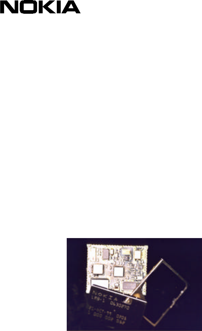
LRB-1 Nokia Bluetooth Tranceiver Component
- Preliminary Information -
Nov 2000 Confidential 2/11
LRB-1 Nokia Bluetooth Transceiver
Component
Product Features
q Complete stand-alone Class 2 Bluetooth transceiver system
q Including baseband controller, 2.45 GHz radio part and firmware up to HCI
q Bluetooth V 1.0 B compliant and pre-certified
q Suitable for both voice and data applications
q Point-to-Multipoint connection support
q Park, Hold and Sniff modes
q High speed UART and flexible PCM data interfaces
q Several programmable control interfaces plus ADC input
q Internal oscillators and power regulators
q Adjustable I/O voltages
q completely shielded and FCC approved
q Optimized size and form-factor: 23 x 19 x 2 mm3
WARNING : LRB-1 IS A BLUETOOTH TRANSCEIVER COMPONENT, WHICH HAVE BEEN TESTED WITH A
RECOMMENDED ANTENNA DESIGN AND SHOULD ONLY BE USED BY NOKIA IN APPROPRIATE PRODUCTS.
THESE PRODUCTS WILL HAVE TO BE TESTED AGAIN FOR COMPLIANCE. USERS ANS INSTALLERS MUST USE
ONLY THOSE ANTENNAS SPECIFIED BY NOKIA, TO COMPLY WITH FCC'S R.F. EXPOSURE REQUIREMENTS TO
AVOID EPOSING PERSONS TO HARMFUL R.F. RADIATION. DO NOT SUBSTITUTE ANY SUPPLIED ANTENNA
RECOMMENDED BY THE SUPPLIER. CONTACT YOUR SUPPLIER FOR FURTHER INSTRUCTIONS.

LRB-1 Nokia Bluetooth Tranceiver Component
- Preliminary Information -
Nov 2000 Confidential 3/11
Overview
The LRB-1 Nokia Bluetooth Tranceiver Component is a highly integrated multi-chip component which
represents a complete standalone Bluetooth transceiver system for short-range wireless applications. All
necessary components including the baseband controller, the radio part for the 2.45 GHz system and a
flash memory of 2 MBit are integrated on a single PCB using advanced flip chip interconnection
techniques. The Bluetooth Tranceiver Component is delivered with all needed firmware of the Bluetooth
protocol stack up to HCI which resides in the on-board flash memory. A traditional high-IF radio
architecture providing good sensitivity has been used.
LRB-1 Nokia Bluetooth Tranceiver Component
- Preliminary Information -
Nov 2000 Confidential 4/11
Block Diagram
2.4GHz
SAW 111MHz
BALUN
DEMOD-TANK
13MHz
RESETX
SLEEPX
OSCON
OSCON
32kHz
TCK
OSCON
TRST
OSCON
TDI
OSCON
TDO
OSCON
TMS
OSCON
WRX
OSCON
CSX
WRX
RDX
JTAG
5
DATA
16
ADDR
17
DBUSRF
3
RFDATA
2
BBCLK
VPP
OSCON
12
GPP
CENX
GPP0
GPP1
GPP2
GPP3
GPP4
GPP5
GPP6
GPP7
GPP8
GPP9
GPP10
GPP11
ADCIN
ADCREF
VDD
VAPPL
BBON
VBBEN
VCCADC
VBB
VCC
ADCREG
VCCVCO
GND
GND
GND
GND
OSCON
Radio
Baseband
Flash Memory
ANT
2
SPDT
DBUSRFCLK
OSCON
DBUSRFDA
OSCON
DBUSRFENX
OSCON
RFDATA1
OSCON
RFDATA2
OSCON
VIO
RDY
OSCON
TXON

LRB-1 Nokia Bluetooth Tranceiver Component
- Preliminary Information -
Nov 2000 Confidential 5/11
Functional Description
A. Key Components
The LRB-1 Nokia Bluetooth Transceiver Component consists of three integrated circuits plus a couple of
smaller active and passive passive components. All three chips are using state-of-the-art semiconductor
technologies and are mounted on the MCM substrate using flip-chip techniques:
q Baseband ASIC:
This chip, running at 1.8 V is a pure CMOS ASIC including the ARM7TDMIE microcontroller core,
embedded RAMs and the core logic for MIPS consuming Bluetooth tasks. Due to the fact that only
the MIPS consuming tasks are realized in hardware and that a central buffer RAM instead of
dedicated connection buffers are used, this approach has been proven to be flexible and future-proof.
q Radio ASIC:
The radio chip in BiCMOS technology works as the transceiver chip for the ISM band of 2400-2483
MHz which is used for Bluetooth transmission. Implemented on-chip function blocks include the PLL,
LNA, mixer and Gaussian modulator as well as 13 MHz crystal oscillator and all neded voltage
regulators.
q Flash Memory:
An industry-standard 16-bit wide 2 MBit Flash memory running at 1.8 V with an access time of 120
ns has been implemented on the LRB-1 module. Sectoring is used to allow also the storage of non-
volatile configuration information (e.g. BD address) on the device.
LRB-1 Nokia Bluetooth Tranceiver Component
- Preliminary Information -
Nov 2000 Confidential 6/11
B. Hardware Interfaces for Data
Two different hardware interfaces for link data are supported: A high-speed UART interface for data
applications and a 4-wire PCM interface for audio data. The main features of the interface imple-
mentations are as follows:
q UART Interface:
A full-duplex UART has been implemented on the LRB-1 module with programmable stopbit length
and parity check which supports a wide range of industry-standard baud rates up to 921.6 kBaud
using 7-times oversampling:
Baud Rate [bit/s] Baud Rate [bit/s] Baud Rate [bit/s]
7200 38400 230400
9600 57600 307200
14400 76800 460800
19200 115200 921600
28800 153600
q PCM Interface:
A standard 4-wire PCM interface with 8 kHz sample rate has been implemented for voice applications
using the LRB-1. This interface featuring a programmable PCMCLK frequency can be used in master
or slave mode using either linear PCM, A-law or µ-law coding. Using an embedded transcoder block
the voice encoding over the Bluetooth air interface can be A-law, µ-law or CVSD.

LRB-1 Nokia Bluetooth Tranceiver Component
- Preliminary Information -
Nov 2000 Confidential 7/11
C. Hardware Interfaces for Control
In order to allow a system integration approach of the LRB-1 Bluetooth Transceiver Component into
different customer applications without any overhead for interface logic, the control interface section of
the module has been designed with special regard to flexibility. Three different digital control interfaces
plus an embedded Analog-to-Digital converter can be used:
q I2C Interface:
To allow easy interfacing to possible system extensions (e.g. by the use of port expanders) the LRB-1
features a 2-wire I2C bus master realized in HW supporting both standard and fast mode with bit
rates of up to 1.3 MBit/s. Addressing can be either 7 bit or 10 bit.
q MicroWire Interface:
A standard 4-wire industry-standard serial bus has been is available to support one external Micro-
Wire slave (e.g. audio codec, EEPROM) with programmable word length of 1..32 bit. The clock fre-
quency is fixed to 500 kHz, the polarity of the corresponding chip select signal can be programmed.
q Programmable General-Purpose Ports (GPPs):
Up to 12 user-programmable general purpose ports can be flexibly used for other application-specific
hardware interfaces. Each port can be independantly programmed for input, output or bi-directional
data transmission, generating an interrupt and uses switchable pull-ups/pull-downs.
In order to limit the total number of pins the functionality of the GPPs is multiplexed with that of
other control and data interfaces according to the following table. Using an external application
voltage of 1.8 – 3.3 V the voltage level of the module pins can be adjusted to customer needs.
q Analog-to-Digital Converter:
One input of the embedded ADC with a resolution of 10 bit is available for application purposes.
LRB-1 Nokia Bluetooth Tranceiver Component
- Preliminary Information -
Nov 2000 Confidential 8/11
D. Power Supply
All needed regulators for generating the different module-internal supply voltages are embedded into the
radio ASIC, therefore the LRB-1 Bluetooth Transceiver Component only needs one power supply between
2.95 V and 5.2 V.
E. Antenna
The antenna pin should be connected to a 50Ω–antenna interface.
The Bluetooth Transceiver Component is designed to use a simple antenna with a nominal gain of 0 dBi
as the radiating element.
Recommended antenna design :
13
14
30
31
43
4460
GND
Feed lineShort circuit
Open circuit antenna element
19 mm for d = 0.5 mm
17 mm for d = 1mm
2 mm for d = 0.5 mm
1 mm for d = 1mm
2 mm
F. Software
The software which is delivered as object code together with the Bluetooth Transceiver Component
includes the lower layers of the Bluetooth SW stack – Link Controller (LC), Link Manager (LM) and Host
Controller Interface (HCI) together with a well-suited real-time operating system. Access from the host
to the different function blocks of the module is accomplished by Nokia-specific HCI extension
commands. This leads to a configurable firmware to support the customer-specific interface
configurations and applications.
LRB-1 Nokia Bluetooth Tranceiver Component
- Preliminary Information -
Nov 2000 Confidential 9/11
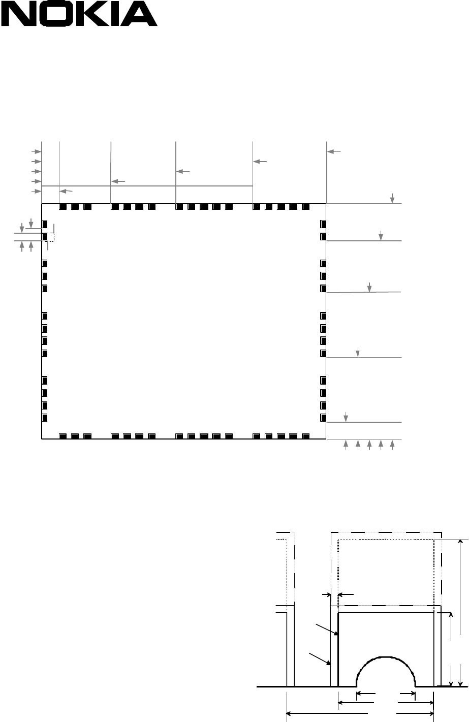
Package and Mechanical Dimensions
The following figures show the bottom view of the LRB-1 Bluetooth Transceiver Component, indicating
the location and dimension of the signal pads:
1
13
14 30
31
43
44
60
1.4±0.1
5.6±0.1
10.8±0.1
17.0±0.1
23.0±0.1
16.0
±
0.1
11.8
±
0.1
6.6
±
0.1
1.4
±
0.1
1.0
0.65
top: 0.5
19.0
±
0.1
FLASH
OLLIE2
STAN2
bottom: 1.2
400 um
650 um
500 um
1000 um
BOTTOM
TOP
1000 um
50 um
Pad
Soldermask
The figure on the right shows the detailed
module pad dimensions. The pads include
400 µm half-vias in order to achieve
proper solderability on the edge of the
PCB. The total height of the MCM
including shielding is 2.0mm+-0.1. It is
the sum of PCB-height (0.5mm), soldering
gap (0.05mm) and assembled shielding
components lid + frame (1.45mm).

LRB-1 Nokia Bluetooth Tranceiver Component
- Preliminary Information -
Nov 2000 Confidential 10/11
Packaging information
The Bluetooth Transceiver Component is packed after production and testing into tape&reel for delivery
protecting it from electrostatic discharge and mechanical shock.
Soldering
The LRB-1 Bluetooth Transceiver Component is designed for surface mounting.
The Bluetooth Transceiver Component withstands 2 reflow cycles for assembly on top or bottom side of
the host PCB.
The reflow-process should be a regular surface mount soldering profile ( full convection preferred ). The
rampup should not be higher than 3°C/s and with a peak temperature of 210 – 235°C for a maximum of
45 seconds.
LEGAL NOTICE
The maximum RF power output from the LRB-1 Bluetooth Transceiver Component is 0 dBm or about 1
milliwatt. The Bluetooth Transceiver Component is designed to use a simple antenna with a nominal gain
of 0 dBi as the radiating element.
The SAR limit would not be exceeded, even if the entire RF power output were absorbed by 1 gram of
tissue, which is not possible with a typical RF circuit. With a seperating distance of 20 cm the MPE limits
are well above the potential a 1 milliwatt device is capable of producing.
Depending on the product that the Bluetooth Transceiver Component is used with, the final device could
be subject to routine evaluation for RF exposure, either SAR limits or MPE limits.
LRB-1 Nokia Bluetooth Tranceiver Component
- Preliminary Information -
Nov 2000 Confidential 11/11
Electrical Specification
Operating Conditions
Symbol Parameter MIN TYP MAX Unit Comments
Tamb module ambient temperature range -25 25 +75 °C
VCC 1. Main power supply with
ADC regulator inside Radio ASIC in use 2.95 5.2 V
VAPPL Power supply for application interfaces 1.7 3.3 Vdigital supply voltage
for GPPs
VPP Flash programming supply 4.5
1.7 5.0 5.5 V
Vfast flash prog.
default
Frange Frequnecy range 2402 2483.5 MHz
Pin Rx dynamic range -70 -20 dBm at Antenna pad
Ppeak TX peak power 0.5 11.5 mW at Antenna pad
Notice
Nokia Mobile Phones Ltd
This document contains informations on products in the sampling and initial production phases of
development. Do not finalize a design with this information, as the specifications are subject to
change without notice.