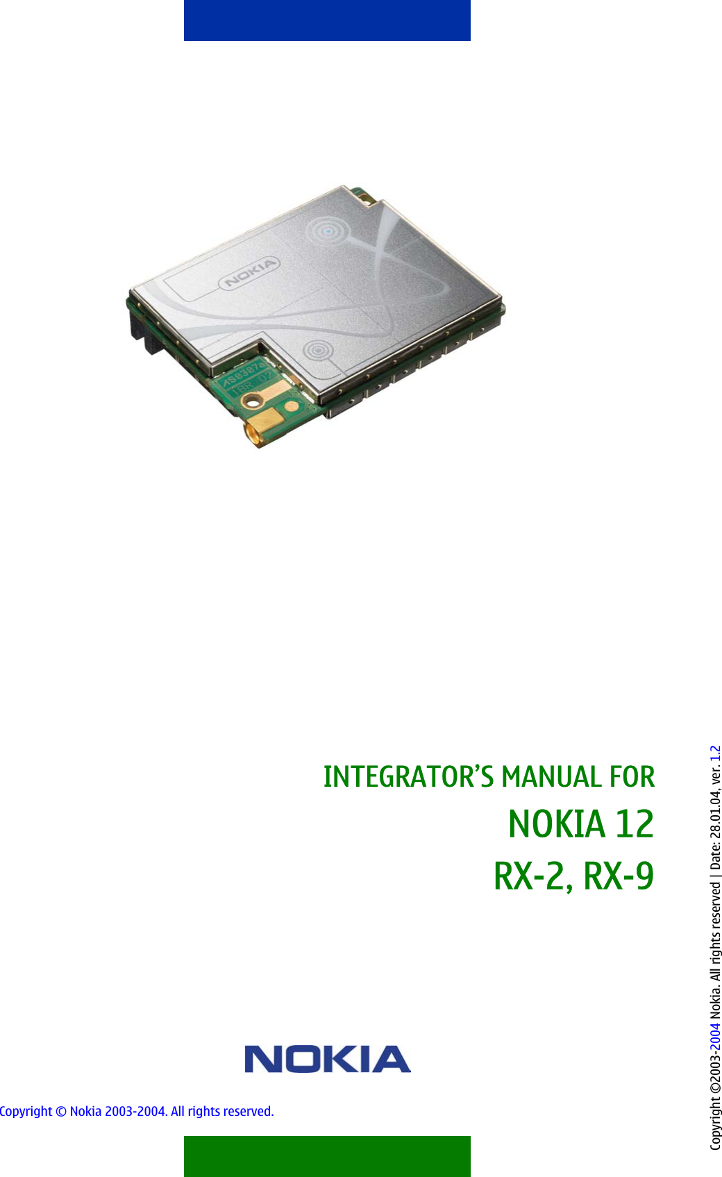
Microsoft RX-9 GSM/EGPRS 850/1900 M2M Module User Manual PRODUCT NAME E

Microsoft Mobile Oy GSM/EGPRS 850/1900 M2M Module PRODUCT NAME E

Manual

 Copyright ©2003-2004 Nokia. All rights reserved | Date: 28.01.04, ver. 1.2 INTEGRATOR’S MANUAL FOR NOKIA 12 RX-2, RX-9 Copyright © Nokia 2003-2004. All rights reserved.
 Contents 1. INTRODUCTION ...................................................................................................................................................1 2. MECHANICAL INTEGRATION .............................................................................................................................1 3. ELECTRICAL INTEGRATION................................................................................................................................3 3.1 M2M SYSTEM CONNECTOR........................................................................................................................3 3.1.1 ELECTRICAL CHARACTERISTICS............................................................................................................4 3.1.2 CONNECTOR PIN-OUT............................................................................................................................5 3.2 GROUNDING.............................................................................................................................................. 12 3.3 POWER SUPPLY........................................................................................................................................ 12 3.4 SERIAL COMMUNICATION....................................................................................................................... 13 3.4.1 AT COMMAND MODE........................................................................................................................... 13 3.4.2 M2M SYSTEM MODE............................................................................................................................ 13 3.5 SIM INTERFACE......................................................................................................................................... 13 3.6 AUDIO INTERFACE ................................................................................................................................... 14 3.6.1 ANALOG AUDIO.................................................................................................................................... 14 3.6.2 ANALOG AUDIO EXAMPLE.................................................................................................................. 16 3.6.3 ACOUSTIC ECHO ................................................................................................................................... 18 3.7 DIGITAL AUDIO......................................................................................................................................... 18 3.7.1 SIGN-EXTENDED LINEAR CODE......................................................................................................... 19 4. RF AND ANTENNA INTEGRATION ................................................................................................................. 20 4.1 ANTENNA INSTALLATION ...................................................................................................................... 20 5. TEST BOARD FOR THE NOKIA 12 .................................................................................................................. 21 5.1 POWERING ................................................................................................................................................ 21 5.2 SIM CARD READER ................................................................................................................................... 21 5.3 RS-232 CONVERTERS .............................................................................................................................. 22 5.4 AUDIO......................................................................................................................................................... 22 6. CERTIFICATIONS............................................................................................................................................... 24 6.1.1 RX-2: ...................................................................................................................................................... 25 6.1.2 RX-9 ....................................................................................................................................................... 25 6.2 TECHNICAL REQUIREMENTS................................................................................................................... 25 Copyright © Nokia 2003-2004. All rights reserved.
 6.2.1 SIM TESTING ........................................................................................................................................ 25 6.2.2 POWER SUPPLY ................................................................................................................................... 25 6.2.3 EMC/ESD AND SAFETY ........................................................................................................................ 25 6.2.4 RF TESTING........................................................................................................................................... 26 6.2.5 RF EXPOSURE ....................................................................................................................................... 26 6.2.6 OTHER TYPE APPROVAL ISSUES ....................................................................................................... 26   Legal Notice Copyright © 2003-2004 Nokia. All rights reserved. Reproduction, transfer, distribution or storage of part or all of the contents in this document in any form without the prior written permission of Nokia is prohibited. Nokia and Nokia Connecting People are registered trademarks of Nokia Corporation. Other product and company names mentioned herein may be trademarks or tradenames of their respective owners. Nokia operates a policy of continuous development. Nokia reserves the right to make changes and improvements to any of the products described in this document without prior notice. Under no circumstances shall Nokia be responsible for any loss of data or income or any special, incidental, consequential or indirect damages howsoever caused. The contents of this document are provided "as is". Except as required by applicable law, no warranties of any kind, either express or implied, including, but not limited to, the implied warranties of merchantability and fitness for a particular purpose, are made in relation to the accuracy, reliability or contents of this document. Nokia reserves the right to revise this document or withdraw it at any time without prior notice.  RX-9: FCC/INDUSTRY CANADA NOTICE Your device may cause TV or radio interference (for example, when using a telephone in close proximity to receiving equipment). The FCC or Industry Canada can require you to stop using your telephone if such interference cannot be eliminated. If you require assistance, contact your local service facility. This device complies with part 15 of the FCC rules. Operation is subject to the condition that this device does not cause harmful interference.  Copyright © Nokia 2003-2004. All rights reserved.
 References Ref 1.  Nokia 12 Product Specification Ref 2.  Nokia 12 AT Command List   Abbreviations API  Application Programming Interface AT  Attention Command Language ATK  Application Tool Kit BER  Basic Encoding Rule CDC Connected Device Configuration CE  Mark for a product that fulfils the EU safety and R&TTE requirements CHAP  Challenge Handshake Authentication Protocol CLDC Connected Limited Device Configuration CORBA  Common Object Request Broker Architecture CS Coding Scheme CSD Circuit Switched Data DCE  Data Circuit Terminating Equipment DTE  Data Terminal Equipment EDGE  Enhanced Data rates for Global Evolution EGPRS  Enhanced General Packet Radio Service EGSM Extended GSM EMC Electro-Magnetic Compatibility  EU European Union GCF GSM Certification Forum GGSN  Gateway GPRS Support Node GPRS  General Packet Radio Service GPS Global Positioning System GSM  Global System for Mobile Communication Hi-Z High Impedance HSCSD  High Speed Circuit Switched Data HW Hardware IMEI  International Mobile Station Equipment Identity Copyright © Nokia 2003-2004. All rights reserved.
 IMP Information Module Profile IP Internet Protocol ISDN  Integrated Services Digital Network ISO  International Organization for Standardization J2EE  Java 2 Enterprise Edition J2ME  Java 2 Micro Edition J2SE  Java 2 Standard Edition LOCI Local Information M2M Machine to machine MIDP  Mobile Information Device Profile MMCX  Miniature Microax Connector MSISDN  Mobile Subscriber International ISDN Number ORB  Object Request Broker OTA  Over The Air PC Personal Computer PCM  Pulse Code Modulation PIN  Personal Identification Number PP Point-to-Point PUK  PIN Unblocking Key   RF Radio Frequency RS232  Recommended Standard 232 Revision C RTC Real Time Clock RX-2  Type designation of Nokia 12 SIM  Subscriber Identity Module SMS  Short Message Service SMSC SMS Centre SW Software TCP  Transmission Control Protocol TLV  Type/Tag Length Value UDP User Datagram Protocol USSD  Unstructured Supplementary Service Data WMS Wireless Messaging Copyright © Nokia 2003-2004. All rights reserved.
 1. INTRODUCTION The Nokia 12 GSM connectivity module has been designed for M2M (machine-to-machine) applications and other wireless solutions. There are two versions of the Nokia 12: •  RX-2 dual-band GSM device supporting EDGE, GPRS, HSCSD, CSD, and SMS in EGSM 900/GSM 1800 MHz bands •  RX-9 dual band GSM device supporting EDGE, GPRS, CSD, SMS in GSM 850/GSM 1900 MHZ bands. The Nokia 12 can be used in several applications due to its three different operating modes. Simple I/O applications can be easily implemented using the Nokia 12 in the User control mode that offers message personalising, secure messaging, and timing functionality for SMS controlled I/O applications. Additional intelligence for I/O applications can easily be implemented with Java. In the AT command mode, the Nokia 12 can be used as a GSM modem that supports Java for creating extra intelligence. In modem use, all supported bearers are available, subject to network support.  The Nokia 12 is compatible with the Nokia M2M Platform. In the M2M system mode, the Nokia 12 communicates with the server application through the Nokia M2M Gateway, and all the compatible features of the Nokia 12 are available for developing a wide range of M2M applications.  In addition to these operating modes, the Nokia 12 has an integrated TCP/IP stack which enables direct GPRS or GSM data connection between a remote end application and a server application. Due to the integrated TCP/IP stack, the HTTP and Socket APIs of the Nokia 12 are available for application development.  In addition to the bearers and operating modes listed above, the Nokia 12 supports several Java APIs, location service for external GPS module integration, reliability features like AutoPIN, GSM encryption and security codes, reset mechanism and Nokia M2M Platform authentication. Java™ technology support enables upgrading the application software over the air, and smart messaging makes the installation flexible. GSM phase 2+ supplementary services enable developing voice applications.  Note that all data bearers as well as TCP/IP are dependent on network support. This document describes the main characteristics of the Nokia 12 and is intended to help the system integrator both integrate the Nokia 12 in an application and gain the correct approvals. Basic product information is available in Ref 1. 2. MECHANICAL INTEGRATION The Nokia 12 contains two holes for mounting screws. The screws can be used in mounting, but are not compulsory. The Nokia 12 has been tested according to the automotive standard DIN 72300-3. The module can be assembled to various applications without the screws. Copyright © Nokia 2003-2004. All rights reserved.   1/26
 The dimensions of the Nokia 12 are shown in Figure 1.   Figure 1 Physical dimensions of the Nokia 12 GSM module Copyright © Nokia 2003-2004. All rights reserved.   2/26
 3. ELECTRICAL INTEGRATION 3.1  M2M SYSTEM CONNECTOR All signals are routed through the M2M system connector, except the antenna, which is routed through the MMCX RF connector.  The M2M system connector is a 60-pin (2 rows, 30 per row) 1.27 mm pitch pin header connector. It has a frame that helps in the assembly and also holds the Nokia 12 firmly in position.  The possible mating connector is described in Table 1. Supplier  Part Number  Description SAMTEC SFMC-130-02-S-D Female connector. Board-to-board SAMTEC SFM-130-02-S-D Female connector. Board-to-board. With alignment mark. Table 1 Possible mating connectors for the application Parameter  Value Supply voltage  +4.2 V DC input voltage (any signal pin)  -0.5…5.5 V DC output source or sink current  (any I/O pin)  Operating temperature range  -25…+55 °C Storage temperature range  -40…+85 °C Table 2 Absolute maximum ratings The recommended operating conditions in Table 3 define the conditions for actual device and/or interface operation.           Copyright © Nokia 2003-2004. All rights reserved.   3/26
  Parameter  Value  Note Supply Voltage (VBB)  3.6…4.0 V (3.8V typical)  Voltage must never drop below the low limit Logic voltage (IO voltage)  1.8…5.0 V   DC output source or sink current (any I/O pin, user adjustable) 0…5 V  Upper limit depending on IO voltage Operating temperature range  - 10…+55 °C   Table 3 Recommended operating conditions 3.1.1 Electrical characteristics All digital outputs (1-9) are open drain outputs, and all pins have a 10 kohm pull-up resistor to IO voltage.   Parameter  Value Application load resistance  >100 kohm Application load capacitance  <100 pF High level output voltage (Io=-20uA)  0.67*IO voltage minimum Low level output voltage (Io=1mA)  0.4 V maximum Table 4 Digital output characteristics Analog inputs (AD1-3) have an input range of 2.7 V. All analog inputs have a 100 kohm pull-down resistor inside the module. AD channels are calibrated in production and calibrated range is from 0.03V to 2.77V Accuracy not guaranteed outside calibrated range. Parameter  Nominal Input impedance  100 kohm Input voltage range  0-2.8 V Resolution 10 bits Integral non-linearity +/- 6mV Differential non-linearity +/-9mV Temperature drift < 5mV Table 5 Analog input characteristics All digital inputs (4-11) are CMOS inputs, and all pins have a 10 kohm pull-up resistor to IO voltage.  Copyright © Nokia 2003-2004. All rights reserved.   4/26
     Parameter  Value Application driving impedance <100 ohm Low level input voltage (IO_Voltage 1.8-5V) 0.15 V max. High level input voltage (IO_Voltage 1.8-5V) 1.6V min. Table 6 Digital input characteristics Parameter  Nominal  Note Differential input voltage range for microphone input (MicP & MicN) 0.316 Vpp  2.0 Vpp maximum Microphone amplifier input resistor 50 kohm  30 kohm minimum Table 7 Microphone input characteristics Parameter  Nominal  Note Differential output voltage for earphone output (EARP&EARN) 0.316 Vpp  2.0 Vpp maximum Load resistance  1 kohm  30 ohm minimum Table 8 Earphone output characteristics The IO Voltage pin 52 selects the logic level of all digital outputs/inputs. The specifications of the digital audio interface are the same as the digital inputs and outputs specifications. All the M2M system connector pins can handle 4 kV ESD  (human body model).  3.1.2 Connector pin-out The odd number pins (1, 3, 5, 7…) are on one side of the connector and the even number pins (2, 4, 6, 8…) on the other side. Numbering and pin-out are shown in Figure 2 and Table 9.  Copyright © Nokia 2003-2004. All rights reserved.   5/26
    Figure 2 Pin numbering of the Nokia 12 M2M system connector  Name  Pin  Pin  Name VBB 1 2 GND VBB  3 4 GND VBB 5 6 GND VBB 7 8 GND VBB 9  10  GND NC 11 12 NC NC 13 14 NC MICP 15 16 EARP MICN 17 18 EARN AD3 19 20 AD2 PCMDCLK 21 22 PCMSCLK PCMTX 23 24 PCMRX RESET T 25 26 RESET A PORT1RX 27 28 MBUS PORT1TX 29 30 OUTPUT2 OUTPUT3 31 32 OUTPUT4 OUTPUT5 33 34 INPUT6 INPUT5 35 36 AD1 Copyright © Nokia 2003-2004. All rights reserved.   6/26
 BSI 37 38 PORT2RX PORT2TX 39 40 PORT2RTS PORT2CTS 41 42 OUTPUT8 INPUT8 43 44 OUTPUT9 SLEEPX 45 46 INPUT11 VSIM 47 48 SIMRST SIMCLK 49 50 SIMDATA SIMDET 51 52 IO VOLTAGE OUTPUT1/P3RX 53 54 INPUT4/P3TX INPUT10 55 56 INPUT7 OUTPUT6 57 58 OUTPUT7 INPUT9 59 60 NC Table 9 M2M system connector pin-out More detailed descriptions and usage of pins are shown in Table 10 and Table 11. Pin  Name  Description 1  VBB  Terminal Power. Voltage nominal 3.8 V, 3.6 V – 4.0 V, maximum current 2A peak. Regulated power input for the Nokia 12. All VBB pins must be connected together at the application end. The device end is not fuse-protected, so the application should provide sufficient overload protection. Current consumption can be as high as 2 amps peak when transmitting at full power. Average power consumption is about 500 mA at the maximum. The power supply should be designed according to this. If the operating voltage falls below 3.4 V, the device automatically shuts down. See chapter 3.3. 2  GND  Return ground for device power. These pins are used for device power (VBB) return ground. Connect to common ground. All GND pins must be connected at the application end. See chapter 3.2. 3 VBB  See PIN 1 4 GND  See PIN 2 5 VBB  See PIN 1 6 GND  See PIN 2 7 VBB  See PIN 1 8 GND  See PIN 2 9 VBB  See PIN 1 10 GND  See PIN 2 11 NC  Reserved Copyright © Nokia 2003-2004. All rights reserved.   7/26
 12 NC  Reserved 13 NC  Reserved 14 NC  Reserved 15  MICP  MICP is used with analog audio as differential positive input. The line is AC coupled at the device end. Frequency response is 300 Hz-3400 Hz. See chapter 3.6.1. 16  EARP  EARP is used with analog audio as differential positive output. Frequency response is 300 Hz-3400 Hz. See chapter 3.6.1. 17  MICN  MICN is used with analog audio as differential negative input. The line is AC coupled at the device end. Frequency response is 300 Hz-3400 Hz. See chapter 3.6.1. 18  EARN  EARN is used with analog audio as differential negative output. Frequency response is 300 Hz-3400 Hz. See chapter 3.6.1. 19  AD3  Input for 10 bit Analog to Digital converter. The application end must scale voltage level between 0 to 2.8 V 20 AD2  See PIN 19 21  PCMDCLK  PCMDCLK is a 512 kHz digital audio clock from the application module. For digital audio usage, refer to chapter 3.7. Logic level is set by the IO voltage pin (pin 52). See chapter 3.7. 22  PCMSCLK  PCMSCLK is one PCMDCLK cycle and repeats every 64 PCMDCLK cycles. Frame sync frequency is thus is 8 kHz. Logic level is set by the IO voltage pin (pin 52). See chapter 3.7. 23  PCMTX  Digital audio, transmit data from device to application. Logic level is set by the IO voltage pin (pin 52). See chapter 3.7. 24  PCMRX  Digital audio, received data from application to module. Logic level is set by the IO voltage pin (pin 52). See chapter 3.7. 25  RESET T  Reset input for module, active low. Module is reset when this line is low. Logic level is set by the IO voltage pin (pin 52). Minimum duration TBD. 26  RESET A  Reset output for application, active low. Reset goes high after xx ms of power-up. Logic level is set by the IO voltage pin (pin 52). 27  PORT1RX  PORT1 receive. PORT1RX is an asynchronous serial channel receive pin. Functionality otherwise as in pin 29, PORT1TX. Logic level is set by the IO voltage pin (pin 52). 28 MBUS  Nokia-specific test pin. Do not connect. 29  PORT1TX  PORT1 transmit. PORT1RX is an asynchronous serial channel transmit pin and can be used with pin28, FBUSRX to form a full duplex serial link. Pins 30-35 can be used to provide handshaking functions. Logic level is set by the IO voltage pin (pin52) 30  OUTPUT2  Digital output from device. Logic level is set by the IO voltage pin (pin 52). If the AT command mode is active, this pin is used as Data Carrier Detect output for Port 1. Copyright © Nokia 2003-2004. All rights reserved.   8/26
 31  OUTPUT3  Digital output from module. Logic level is set by the IO voltage pin (pin 52). If the AT command mode is active, this pin is used as Data Set Ready output for Port 1. 32  OUTPUT4  Digital output from module. Logic level is set by the IO voltage pin (pin 52). If the AT command mode is active, this pin is used as Clear To Send output for Port 1. 33  OUTPUT5  Digital output from module. Logic level is set by the IO voltage pin (pin 52). If the AT command mode is active, this pin is used as Ring Indicator output for Port 1. 34  INPUT6  Digital input to module. Logic level is set by the IO voltage pin (pin 52). If the AT command mode is active, this pin is used as Request To Send input for Port 1. 35  INPUT5  Digital input to module. Logic level is set by the IO voltage pin (pin 52). If the AT command mode is active, this pin is used as Data Terminal Ready input for Port 1 36  AD1  Input for 10 bit Analog to Digital converter. The application end must scale voltage level between 0 to 2.8 V. 37  BSI  Input for 10 bit Analog to Digital converter. The application end must scale voltage level between 0 to 2.8 V. 38  PORT2RX  PORT2 receive. PORT2RX is an asynchronous serial channel receive pin and is used with pin 39. Pins 40 and 41 provide handshaking signals for the UART. Logic level is set by the IO voltage pin (pin 52). 39  PORT2TX  PORT2 Transmit. PORT2RX is an asynchronous serial channel transmit pin and is used with pin 38. Pins 40 and 41 provide handshaking signals for the UART. Logic level is set by the IO voltage pin (pin 52). 40  PORT2RTS  Request To Send for PORT2. PORT2RTS provides handshaking signal for asynchronous communication between terminal and application module when using PORT2. Works together with pin 41. Logic level is set by the IO voltage pin (pin 52). 41  PORT2CTS  Clear to send for PORT2. PORT2CTS provides handshaking signal for asynchronous communication between terminal and application module when using PORT2. Works together with pin 40. Logic level is set by the IO voltage pin (pin 52). 42  OUTPUT8  Digital output to module. Logic level is set by the IO voltage pin (pin 52). 43  INPUT8  Digital input to module. Logic level is set by the IO voltage pin (pin 52). 44  OUTPUT9  Digital output to module. Logic level is set by the IO voltage pin (pin 52). 45  SLEEPX  Sleep indicator from module. When module is in the sleep mode, the level of this output pin is low, otherwise high. Logic level is set by the IO voltage pin (pin 52). 46 INPUT11 Digital input to module. Logic level is set by the IO voltage pin (pin 52). 47  VSIM  Operating voltage for SIM card, generated by module. See chapter 3.5. Copyright © Nokia 2003-2004. All rights reserved.   9/26
 48  SIMRST  Reset signal for SIM card, generated by module. See chapter 3.5. 49  SIMCLK  Clock signal for SIM card, generated by module. See chapter 3.5. 50  SIMDATA  Data line between SIM card and module. See chapter 3.5. 51  SIMDET  SIM card detection signal. See chapter 3.5. 52  IO VOLTAGE  Logic level for the application is set by this pin. Voltage must be 1.8 V - 5.0 V. See chapter 3.3. 53 OUTPUT1 / PORT3RX Digital output to module. Logic level is set by the IO voltage pin (pin 52). If PORT3 UART is used, this is receive signal.  Note: Direction changes if used as UART. 54 INPUT4 / PORT3TX Digital input to module. Logic level is set by the IO voltage pin (pin 52). If PORT3 UART is used, this is transmitter signal.  Note: Direction changes if used as UART. 55  INPUT10  Digital input to module. Logic level is set by the IO voltage pin (pin 52). 56  INPUT7  Digital input to module. Logic level is set by the IO voltage pin (pin 52). 57  OUTPUT6  Digital output to module. Logic level is set by the IO voltage pin (pin 52). 58  OUTPUT7  Digital output to module. Logic level is set by the IO voltage pin (pin 52). 59  INPUT9  Digital input to module. Logic level is set by the IO voltage pin (pin 52). 60 NC   Table 10 Pin descriptions  Logical pin name Physical pin number Ana-log read Digi-tal read Digi-tal write AT  User  M2M  Note OUTPUT1 53    x  x x Functions as P3RX, when serial port 3 in use OUTPUT2  30      x    x  x  DCD, when serial port 1 in use (=AT command mode, FBUS, Corba over D9) OUTPUT3  31      x    x  x  DSR, when serial port 1 in use (=AT command mode, FBUS, Corba over D9) OUTPUT4  32      x    x  x  CTS, when serial port 1 in use (=AT command mode, FBUS, Corba over D9) OUTPUT5  33      x    X  x  RI, when serial port 1 in use (=AT command mode, FBUS, Corba over D9) OUTPUT6 57      x x X x  Copyright © Nokia 2003-2004. All rights reserved.   10/26
 OUTPUT7 58      x x X x  OUTPUT8 42      x x X x  OUTPUT9 44      x x X x  INPUT11 46  x  x X x  INPUT4 54    x   x X x Functions as P3TX, when serial port 3 in use INPUT5 35   x   X x Functions as DTR, when serial port 1 in use (=AT command mode, FBUS, Corba over D9) INPUT6 34   x   X x Functions as RTS, when serial port 1 in use (=AT command mode, FBUS, Corba over D9) INPUT7 56    x   x X x  INPUT8 43    x   x X x  INPUT9 59    x   x X x  INPUT10 55    x   x X x  PCMDCLK 21     x X x Digital audio PCMTX 23     x X x Digital audio PCMSCLK 22     x X x Digital audio PCMRX 24     x X x Digital audio AD1  36  x   x X x  AD2  20  x   x X x  AD3  19  x   x X x  PORT2RX 38       x AM serial port PORT2TX 39       x AM serial port PORT2RTS 40       x AM serial port PORT2CTS 41       x AM serial port MIC+ 15     x x x Analog audio EAR+ 16     x x x Analog audio EAR-  17     x x x Analog audio MIC-  18     x x x Analog audio Table 11 Pin functionalities in different operating modes Copyright © Nokia 2003-2004. All rights reserved.   11/26
 3.2 GROUNDING There is only one common ground for the power supply and I/Os in the Nokia 12 GSM module. There are no separate analog/digital ground pins in the M2M system connector. All ground pins must be connected together at the application end. Grounding through screws is not allowed. The mounting screws must be isolated from the application ground. 3.3  POWER SUPPLY  The Nokia 12 GSM module is powered by an application. The operating voltage must not fall below the specification limit under any circumstances. The recommended operation conditions are shown in Table 3. For example, at full power, the TX can be up to 2 A, when current drawn from the power supply. There are no capacitors on the power supply line of the Nokia 12, so the application must provide sufficient filtering.  The power supply must be capable of supplying at least 3 W average power, but it is recommended that the power supply provides also the peak current. Otherwise a large capacitor bank is needed to compensate the voltage drop during transmit bursts.  The Nokia 12 does not have protection for over-voltage of current, so the application must be equipped with one if there is a possibility for over-voltage. The application should at least include a fuse. The ripple on the operating voltage must not exceed 100 mV and the voltage must never drop below 3.6 V during operation. The application must also produce IO voltage. The logic levels of digital inputs and outputs correspond to this IO voltage. IO voltage can be supplied from a linear regulator.    Figure 3 Example powering with simple DC/DC converter and linear regulator Copyright © Nokia 2003-2004. All rights reserved.   12/26
 3.4 SERIAL COMMUNICATION The Nokia 12 GSM module is accessible through three different asynchronous serial interfaces with different protocols. The pins provide one asynchronous channel with a simple handshaking capability.  The first asynchronous channel is provided by PORT1. This port can be used with full 8 signal RS-232 handshaking signals. The second asynchronous channel is provided by PORT2 with a simple handshaking capability (only RTS and CTS). The third asynchronous channel is provided by PORT3 with no hardware handshakes. The usage of ports can be configured with the Nokia 12 Configurator software. Nokia 12 Configurator is downloadable at www.forum.nokia.com free of charge.  Serial communication speeds for all serial ports can be selected between 9600 – 115 200 bps. 3.4.1 AT command mode PORT1 can be set to the AT command mode by setting a 68 kohm resistor between BSI (pin 37) and the ground. The Nokia 12 GSM module has to be re-started (power off/on) to identify the resistor.  The Nokia 12 provides all signals for the industry standard DB9 RS-232C connection. An external level converter is required. The Nokia 12 is DCE (Data Communication Equipment) and the application is DTE (Data Terminal Equipment). One possible method of implementing the level conversions is to use MAX3237 or an equivalent level converter IC. If BSI (pin 37) is left floating in the application, all PORT1 handshaking pins can be used as a general I/O. 3.4.2  M2M system mode PORT2 uses the M2M system protocol. PORT3 can also be used by the JAVA Imlet as a serial port or as digital input and output pins. 3.5 SIM INTERFACE All leads from the M2M system connector to the SIM card reader must be shorter than 15 cm, because the voltage drop and increasing capacitance will affect timing. Only an external component besides the SIM card reader is a bypass capacitor in the VSIM line (100 n recommended, as close as possible to the reader). The leads between the Nokia 12 M2M system connector and the SIM card reader must be protected against interferences. The striplines must be placed to the interlayers, never to the PWB overlayer. A possible SIM card reader supplier is shown in Table 12.  Copyright © Nokia 2003-2004. All rights reserved.   13/26
 Supplier  Part Number  Description Amphenol  M-C707_10M006_522_2  SIM reader with lid open indication switch Table 12 Possible SIM card reader supplier   755321DATA         NC         G ND CLK           RST         VSIMFigure 4 SIM connections The Nokia 12 GSM module supports 1.8 V and 3 V SIM cards. The Nokia 12 automatically sets the correct voltage for the SIM card used. The SIM card reader must have a switch that indicates when the SIM card is being removed, so that it can be shut down correctly by the Nokia 12. The switch must open when the card is removed or the lid is open. The Nokia 12 has a pull-up in the SIM detection line, so the application must connect the other end of the switch to the ground. 3.6 AUDIO INTERFACE 3.6.1 Analog Audio The M2M system connector gives possibilities to build different kind of audio applications around the Nokia12.  Copyright © Nokia 2003-2004. All rights reserved.   14/26
 The analog TX path (from the external application to the Nokia 12 GSM module) has a DC isolation inside the Nokia 12 with 100 nF capacitors, and these capacitors together with the microphone preamplifier input impedance form a 1st order high pass filter with 32 Hz roll off (-3 dB). Name  Symbol  Min  Type  Max  Units Differential input voltage range for microphone input (MicP & MicN)   0.316 2.0 VPP Microphone amplifier input resistor RMIC 30  50    kΩ Common mode voltage level  VCM  1.3  1.35  1.4  V Table 13 The earphone lines from the Nokia 12 GSM module are driven differentially to achieve the best possible audio quality, free of radio frequency noise. In the differential mode, positive output is driven from EarP and negative signal from EarN output.  Name  Test condition  Min  Type  Max  Units Output voltage swing in fully differential mode EarP to EarN    0.316  2  VPP Output resistance        1  Ω Load resistance  EarP to EarN (with dynamic transducer) 30   45 Ω Load resistance  EarP to EarN (with external audio circuitry) 1    kΩ Load capacitance  EarP to EarN (with external audio circuitry)    10 nF Common voltage level for Earphone output VCMEar 0.75 0.8 0.85 V Offset voltage    -50    50  mV Table 14 The following chapters give examples of using the audio properties of the Nokia 12 for voice communication purposes. The circuits presented here illustrate the connection methods. There are also other possibilities for using the Nokia 12 audio interface. The component values presented here are examples only; the customer can adjust the application-specific values to achieve the best performance for the application in use.  Copyright © Nokia 2003-2004. All rights reserved.   15/26
 3.6.2 Analog audio example Analog TX path: Due to the small audio signal level of the electret microphone, it is recommended to use a pre-amplifier for the microphone before connecting it to the Nokia 12 GSM module. The differential connection is strongly recommended to protect against RF noise. A microphone pre-amplifier with 20 dB input gain is recommended for reasonable uplink audio levels.  Microphone input: See Figure 5. MicPMicNVANAVANAVANAR1R2R3R4R6R7+-+-C1C2C3VANAR5  Figure 5 Single-ended microphone pre-amplifier Analog RX path: In voice applications, the Nokia 12 is able to drive an earphone application without external electronics. However, it is also possible to build a high volume loudspeaker application by using an external power amplifier with a high sensitivity loudspeaker. The following chapters show example circuits for both cases. Earphone application: An earphone can be connected to the Nokia 12 GSM module without external components. However, Figure 6 shows external components for EMC purposes to optimise audio quality and reliability. Copyright © Nokia 2003-2004. All rights reserved.   16/26
 R1R2L1C1 C2 J1 J2  Figure 6 Earphone application circuit The recommended earphone type is dynamic. The maximum allowed load for this application is 32 ohm. In the example circuit, L1 is the common mode choke for the suppression of common mode disturbance in the earphone lines. J1 and J2 are surge protector gaps for ESD protection. These can be replaced with varistor or any other state-of-the-art ESD protection component. C1 and C2 are used for RF noise filtering. R1 and R2 are used as an attenuator if the signal level from the Nokia 12 is too high for the application. These resistors can be replaced with linear potentiometers and thus get adjustable volume control for the earphone application. The following component list gives example values for the circuit: •  L1= 1000ohm@100MHz •  C1=C2=27pF •  R1=R2= Must be defined together with the sensitivity of the earphone External Audio Power amplifier: External audio power must be used if there is intent to drive low impedance load as loudspeaker. In Figure 7 an example connection circuit for differential audio boomer is shown. In this application only the connection interface to the Nokia 12 is presented. For more detailed information on the boomer connections and specification, see the boomer manufacturer application note. Copyright © Nokia 2003-2004. All rights reserved.   17/26
 Shutdown controlC1C2R1R3R6R5R2R4C4BiasDifferential AudioBoomerC3EarPEarN +-+-BypassVDDVDDVDD  Figure 7 Differential external power amplifier connection Refer to Audio Boomer Manufacturer and loudspeaker application notes for information on maximum safe ratings for selected components. Also keep in mind the limitation of Vdd to avoid overdriving the Audio Boomer and thus distorting the output signal unnecessarily.  3.6.3 Acoustic Echo Because in a GSM voice call the uplink and downlink audios are activated at the same time, use common sense when evaluating a suitable distance between the loudspeaker and the microphone. The acoustic echo canceller inside the Nokia 12 is tuned so that the optimum result is achieved with 20 cm or longer distance between the microphone and the speaker. It is also advisable to locate the microphone and the loudspeaker so that they are pointed away from each other to achieve the best possible double-talk performance. 3.7 DIGITAL AUDIO There is a PCM codec interface in the Nokia 12 for digital audio support. The digital audio interface supports sign-extended 13-bit linear code (total 16 bits are transmitted). Copyright © Nokia 2003-2004. All rights reserved.   18/26
 3.7.1 Sign-Extended Linear Code PCM (Pulse Code Modulation) digital audio data transmission between the Nokia 12 and the application is handled with four signals: PCMDCLK, PCMSCLK, PCMTX, and PCMRX. The format of the data transmission is sign-extended 13-bit linear code. Total of 16 bits are transmitted, and higher order bits must be sign-extended. Transmission of data commences after frame sync (PCMSCLK) rises high for one PCMDCLK clock cycle. After returning low, each data bit is transmitted on the falling edge of PCMDCLK. 15          14          13          12         11         10LSBMSBSign extended0LSBMSBSign extendedPCMDClkPCMSClkPCMTxDataPCMRxData  Figure 8 Both PCMDCLK and PCMSCLK must be provided by the application. PCMDCLK frequency is 512 kHz and PCMSCLK is repeated at 8 kHz, i.e. at every 64th clock cycle. All other but the 16 data bits following the frame sync are discarded. PCMDCLK has typical duty-cycle of 50 %; a variation of 5 % can be tolerated. For detailed timing, refer to Figure 9 and Table 15. Tcyc is the cycle time of the 512 kHz clock, that is 1.953 microseconds. The PCMSCLK rising edge must occur at the maximum of 8 ns after the PCMSCLK rising edge. The pulse width of the Frame Sync pulse should be one Data Clock cycle.     Figure 9 PCM Timing Diagram   Table 15 For example Motorola Type MC145483 Codec supports this coding format Copyright © Nokia 2003-2004. All rights reserved.   19/26
 4.  RF AND ANTENNA INTEGRATION There are two versions of the Nokia 12: •  RX-2 dual-band GSM device supporting EDGE, GPRS, HSCSD, CSD, and SMS in EGSM 900/GSM 1800 MHz bands •  RX-9 dual band GSM device supporting EDGE, GPRS, CSD, SMS in GSM 850/GSM 1900 MHZ bands. RX-2 12 RF requirements follow the ETSI EGSM900/GSM1800 phase2+ specifications. RX-9 12 RF requirements follow the ETSI GSM850/GSM1900 phase2+ specifications.  Parameter  Value  Description RF impedance  50 ohm   RF power  2W (class 4)    EGSM900 & GSM 850   1W (class 1)  GSM1800 & GSM 1900 Table 16 Nokia 12 RF specifications The RF signal from the Nokia 12 to an external antenna goes trough the MMCX connector.  An adapter cable between the MMCX connector and the antenna may be needed. Suitable connectors and cables are available for example from Amphenol, TYCO, and IMS Connector Systems. The Nokia 12 GSM module is certified with a Smarteq dual-band antenna (art no: 1140.26 for 900/1800MHz and 1140.27 for 850/1900MHz). Suitable antennas are available for example from Smarteq and Hirschmann. See also 6.2.5 RF Exposure. 4.1 ANTENNA INSTALLATION The antenna must be placed to a good RF field; a location where the signal strength is adequate. A hand-portable phone can be used to check the best location for the antenna. Electronic devices can cause interference, which affects the performance of the Nokia 12. Do not place the antenna close to electric devices or other antennas. If an additional cable is needed between the antenna and the Nokia 12, use low-loss cables (for example RG-58. Amphenol, Suhner, etc.) and connectors. Every additional cable, adapter, and connector increases the loss of signal power.  See also 6.2.5 RF Exposure.    Copyright © Nokia 2003-2004. All rights reserved.   20/26
 When designing the application, it is important to take care of RF emissions. Do not place any sensitive components or striplines near the antenna or the antenna connector.  5.  TEST BOARD FOR THE NOKIA 12  The test board is a hardware development tool for application developers and system integrators. It manages DC voltages, SIM card, I/O’s, and audios. You can measure several interfaces by pin headers, and the software interfaces of D9 connectors can be seen and handled. The device can be reset with the reset button on the test board PWB. The Nokia 12 has been type approved with this test board. 5.1 POWERING A 3A step down converter is used to produce module Vcc. Low ESR capacitors are used.  Figure 10 5.2  SIM CARD READER The SIM card reader is directly connected to the M2M system connector. The VSIM decoupling capacitor must be present in all designs.  Copyright © Nokia 2003-2004. All rights reserved.   21/26
  Figure 11 5.3 RS-232 CONVERTERS All three serial ports of the Nokia 12 are equipped with RS-232 level translators and D9 connector in the test board. If they are not used, there is a switch to set it in the Hi-Z mode. 5.4 AUDIO For testing analog audio, the test board includes a connector for the Nokia HSU-3 handset. HSU-3 can be purchased from Nokia dealers.   Copyright © Nokia 2003-2004. All rights reserved.   22/26
 Figure 12 Test board microphone amplifier The test board and its components are shown in Figure 13. Switch usage can be seen in  Figure 14.   Figure 13 Test board components Copyright © Nokia 2003-2004. All rights reserved.   23/26
  Figure 14 Switch usage in test board 6. CERTIFICATIONS The test house requires the following documentation from the application integrator for type approval tests: •  Hardware description  •  Schematics •  Block diagram •  PWB/component layout •  Bill of materials •  HW/SW versions used in tests. •  Summary of application •  User’s guide If the application HW or SW changes, the integrator is responsible for verifying the effect, and if needed, perform all required tests again in an accredited laboratory. Copyright © Nokia 2003-2004. All rights reserved.   24/26
 6.1.1 RX-2: The Nokia 12 GSM module is a CE marked device. In order to show compliance to R&TTE requirements, the integrator has to show that all the instructions in this document have been followed in the integration, and a declaration of conformity has been written. The final product must carry CE marking to show compliance with all the directives that are applicable to it. The numbers of all the Notified Bodies involved in every aspect of the conformity assessment must be shown next to the CE Marking with any additional marking that can be needed (e.g. Alert symbol for WLAN). The technical documentation explains the role of each Notified Body. If external elements are designed according to this document, only the following tests must be carried out in an accredited laboratory: •  EMC tests in all working modes (EN 301 489-1/7, TS 51.010) •  Safety (Europe: EN/IEC 60950) 6.1.2 RX-9 The Nokia 12 GSM module is an FCC equipment authorized device (47CFR 15, 22, 24). If external elements are designed according to this document, only the following tests must be carried out in an accredited laboratory: •  FCC equipment authorization (all applicable parts of 47CFR15) 6.2 TECHNICAL REQUIREMENTS 6.2.1 SIM testing SIM testing is not needed, because the SIM card reader is a passive component. In the implementation, SIM presence must follow the type approval conditions of the Nokia 12 GSM module. 6- or 8-pin SIM card readers may be used. 6.2.2 Power supply The power supply must be designed as advised in chapter 3.3. If this specification is exactly followed and fulfilled, the number of RF tests is minimized in the type approval process. If the power supply specification is not followed, the Nokia 12 type approval is not valid. 6.2.3 EMC/ESD and Safety EMC and safety tests according to GSM standards (EN 301 489-1/7, TS 51.020 and EN 60 950) are mandatory and must be completed by the application integrator. The integrator should guarantee overall ESD protection in the integrated application (EN 301 489).  Note: The test board is an ESD supersensitive device. Copyright © Nokia 2003-2004. All rights reserved.   25/26
 6.2.4 RF testing The antenna must be connected to the Nokia 12 GSM module as this document instructs. The antenna impedance has to be as specified in chapter 4. Further passive RF testing for the type approval is not required. Radiation performance is always the responsibility of the integrator. If the antenna specification is not followed, the Nokia 12 type approval is not valid. 6.2.5 RF Exposure In order to comply with the RF exposure requirements, install the antenna so that a minimum separation distance of 20 cm can be maintained between the antenna and all persons. If other antenna than the one in the sales package is used, it must be ensured that the maximum antenna gain of 3dBi is not exceeded. RX-2:  If the application does not provide a separation distance of at least 20 cm, the integrator must carry out all needed certifications. RX-9:  The Nokia 12 cannot be used in the applications that allow the separation distance between antenna and all persons to be less than 20 cm. 6.2.6  Other type approval issues Changes in the application software have no effect on type approval issues.  If the Nokia 12 software is updated, no type approval actions are required from the application integrator. All Nokia products are officially type approved.  Any changes to RF path are not allowed. Power supply instructions must be followed. RX-9:  Type label has the FCC ID number to indicate that RX-9 is FCC equipment authorized. If the application prevents the label from being visible, the application must be labelled so that it contains the text: “Contains FCC ID LJPRX-9”.    Copyright © Nokia 2003-2004. All rights reserved.   26/26

Navigation menu