Mitsubishi Electronics Digital Home Theater Server Qnucpu Users Manual User's (Function Explanation, Program Fundamentals)
QnUCPU to the manual 5f0c62ae-3154-4750-b924-eaffe9077da0
2015-02-09
: Mitsubishi-Electronics Mitsubishi-Electronics-Mitsubishi-Digital-Electronics-Home-Theater-Server-Qnucpu-Users-Manual-556715 mitsubishi-electronics-mitsubishi-digital-electronics-home-theater-server-qnucpu-users-manual-556715 mitsubishi-electronics pdf
Open the PDF directly: View PDF ![]() .
.
Page Count: 630 [warning: Documents this large are best viewed by clicking the View PDF Link!]
- SAFETY PRECAUTIONS
- CONDITIONS OF USE FOR THE PRODUCT
- REVISIONS
- INTRODUCTION
- CONTENTS
- MANUALS
- MANUAL PAGE ORGANIZATION
- GENERIC TERMS AND ABBREVIATIONS
- CHAPTER1 OVERVIEW
- CHAPTER2 SEQUENCE PROGRAMS
- CHAPTER3 CPU MODULE OPERATION
- CHAPTER4 ASSIGNMENT OF BASE UNIT AND I/O NUMBER
- CHAPTER5 MEMORIES AND FILES USED FOR CPU MODULE
- 5.1 Memories Used for CPU Module
- 5.1.1 Memory composition and storable data
- 5.1.2 Program memory
- 5.1.3 Program cache memory
- 5.1.4 Standard ROM
- 5.1.5 Standard RAM
- 5.1.6 Memory card
- 5.1.7 Writing to the Flash card by GX Developer
- 5.1.8 Operating the program in the memory card (boot operation)
- 5.1.9 Details of written files
- 5.1.10 Specifying valid parameters (parameter-valid drive setting)
- 5.2 Program File Structure
- 5.3 File Operations by GX Developer and Handling Precautions
- 5.1 Memories Used for CPU Module
- CHAPTER6 FUNCTIONS
- 6.1 Function List
- 6.2 Constant Scan
- 6.3 Latch Function
- 6.4 Output Mode at Operating Status Change (STOP to RUN)
- 6.5 Clock Function
- 6.6 Remote Operation
- 6.7 Q Series-compatible Module Input Response Time Selection (I/O Response Time)
- 6.8 Error Time Output Mode Setting
- 6.9 H/W Error Time PLC Operation Mode Setting
- 6.10 Intelligent Function Module Switch Setting
- 6.11 Monitor Function
- 6.12 Writing Programs While CPU Module is in RUN Status
- 6.13 Execution Time Measurement
- 6.14 Sampling Trace Function
- 6.15 Debug Function from Multiple GX Developers
- 6.16 Watchdog Timer (WDT)
- 6.17 Self-diagnostic Function
- 6.18 Error History
- 6.19 System Protection
- 6.20 System Display of CPU Module with GX Developer
- 6.21 LED Indication
- 6.22 Interrupt from Intelligent Function Module
- 6.23 Serial Communication Function
- 6.24 Service Processing
- 6.25 Initial Device Value
- 6.26 Battery Life-prolonging Function
- 6.27 Memory Check Function
- 6.28 Latch Data Backup to Standard ROM Function
- 6.29 Writing/Reading Device Data to/from Standard ROM
- 6.30 CPU Module Change Function with Memory Card
- 6.31 Module model name read
- 6.32 Module error collection
- CHAPTER7 COMMUNICATIONS WITH INTELLIGENT FUNCTION MODULE
- 7.1 Communications between CPU Module and Intelligent Function Module
- 7.1.1 Initial setting and auto refresh setting by GX Configurator
- 7.1.2 Initial setting by initial device value
- 7.1.3 Communications with the FROM and TO instructions
- 7.1.4 Communications using the intelligent function module device
- 7.1.5 Communications using the intelligent function module dedicated instruction
- 7.1 Communications between CPU Module and Intelligent Function Module
- CHAPTER8 PARAMETERS
- CHAPTER9 DEVICES
- 9.1 Device List
- 9.2 Internal User Device
- 9.2.1 Input (X)
- 9.2.2 Output (Y)
- 9.2.3 Internal relay (M)
- 9.2.4 Latch relay (L)
- 9.2.5 Annunciator (F)
- 9.2.6 Edge relay (V)
- 9.2.7 Link relay (B)
- 9.2.8 Link special relay (SB)
- 9.2.9 Step relay (S)
- 9.2.10 Timer (T)
- 9.2.11 Counter (C)
- 9.2.12 Data register (D)
- 9.2.13 Link register (W)
- 9.2.14 Link special register (SW)
- 9.3 Internal System Devices
- 9.4 Link Direct Device (J\)
- 9.5 Module Access Devices
- 9.6 Index Register (Z)/Standard Device Resister (Z)
- 9.7 File Register (R)
- 9.8 Extended Data Register (D) and Extended Link Register (W)
- 9.9 Nesting (N)
- 9.10 Pointer (P)
- 9.11 Interrupt Pointer(I)
- 9.12 Other Devices
- 9.13 Constants
- 9.14 Convenient Usage of Devices
- CHAPTER10 CPU MODULE PROCESSING TIME
- CHAPTER11 PROCEDURES FOR WRITING PROGRAM TO CPU MODULE
- CHAPTER12 SPECIAL RELAY LIST AND SPECIAL REGISTER LIST
- APPENDICES
- Appendix 1 List of Parameter Numbers
- Appendix 2 Functions Added or Changed by Version Upgrade
- Appendix 3 Method of Replacing Basic Model QCPU or High Performance Model QCPU with Universal Model QCPU
- Appendix 3.1 Replacement Precautions
- Appendix 3.2 Applicable devices and software
- Appendix 3.3 Instructions
- Appendix 3.4 Functions
- Appendix 3.4.1 Floating-point operation instructions
- Appendix 3.4.2 Error check processing for floating-point data comparison instructions
- Appendix 3.4.3 Range check processing for index-modified devices
- Appendix 3.4.4 Device latch function
- Appendix 3.4.5 File usability setting
- Appendix 3.4.6 Parameter-valid drive and boot file setting
- Appendix 3.4.7 External input/output forced on/off function
- Appendix 3.5 Special Relay and Special Register
- Appendix 4 Device Point Assignment Sheet
- INDEX
- Warranty
A - 1
SAFETY PRECAUTIONS
(Read these precautions before using this product.)
Before using this product, please read this manual and the relevant manuals carefully and pay full attention
to safety to handle the product correctly.
In this manual, the safety precautions are classified into two levels: " WARNING" and " CAUTION".
Under some circumstances, failure to observe the precautions given under " CAUTION" may lead to
serious consequences.
Make sure that the end users read this manual and then keep the manual in a safe place for future
reference.
WARNING
CAUTION
Indicates that incorrect handling may cause hazardous conditions,
resulting in death or severe injury.
Indicates that incorrect handling may cause hazardous conditions,
resulting in minor or moderate injury or property damage.
A - 2
[Design Precautions]
WARNING
Configure safety circuits external to the programmable controller to ensure that the entire system
operates safely even when a fault occurs in the external power supply or the programmable
controller. Failure to do so may result in an accident due to an incorrect output or malfunction.
(1) Configure external safety circuits, such as an emergency stop circuit, protection circuit, and
protective interlock circuit for forward/reverse operation or upper/lower limit positioning.
(2) The programmable controller stops its operation upon detection of the following status, and the
output status of the system will be as shown below.
All outputs may turn on when an error occurs in the part, such as I/O control part, where the CPU
module cannot detect any error. To ensure safety operation in such a case, provide a safety
mechanism or a fail-safe circuit external to the programmable controller. For a fail-safe circuit
example, refer to Chapter 10 LOADING AND INSTALLATION in the QCPU User's Manual
(Hardware Design, Maintenance and Inspection).
(3) Outputs may remain on or off due to a failure of an output module relay or transistor. Configure
an external circuit for monitoring output signals that could cause a serious accident.
Output
All outputs are turned off.
All outputs are held or turned off according to
the parameter setting.
Overcurrent or overvoltage protection of the power supply module
is activated.
The CPU module detects an error such as a watchdog timer error
by the self-diagnostic function.
Status
A - 3
[Design Precautions]
WARNING
In an output module, when a load current exceeding the rated current or an overcurrent caused by a
load short-circuit flows for a long time, it may cause smoke and fire. To prevent this, configure an
external safety circuit, such as a fuse.
Configure a circuit so that the programmable controller is turned on first and then the external power
supply.
If the external power supply is turned on first, an accident may occur due to an incorrect output or
malfunction.
For the operating status of each station after a communication failure, refer to relevant manuals for
the network.
Incorrect output or malfunction due to a communication failure may result in an accident.
When changing data of the running programmable controller from a peripheral connected to the
CPU module or from a personal computer connected to an intelligent function module, configure an
interlock circuit in the sequence program to ensure that the entire system will always operate safely.
For program modification and operating status change, read relevant manuals carefully and ensure
the safety before operation.
Especially, in the case of a control from an external device to a remote programmable controller,
immediate action cannot be taken for a problem on the programmable controller due to a
communication failure.
To prevent this, configure an interlock circuit in the sequence program, and determine corrective
actions to be taken between the external device and CPU module in case of a communication
failure.
CAUTION
Do not install the control lines or communication cables together with the main circuit lines or power
cables.
Keep a distance of 100mm (3.94 inches) or more between them.
Failure to do so may result in malfunction due to noise.
When a device such as a lamp, heater, or solenoid valve is controlled through an output module, a
large current (approximately ten times greater than normal) may flow when the output is turned from
off to on.
Take measures such as replacing the module with one having a sufficient current rating.

A - 4
[Installation Precautions]
CAUTION
Use the programmable controller in an environment that meets the general specifications in the
QCPU User's Manual (Hardware Design, Maintenance and Inspection).
Failure to do so may result in electric shock, fire, malfunction, or damage to or deterioration of the
product.
To mount the module, while pressing the module mounting lever located in the lower part of the
module, fully insert the module fixing projection(s) into the hole(s) in the base unit and press the
module until it snaps into place.
Incorrect mounting may cause malfunction, failure or drop of the module.
When using the programmable controller in an environment of frequent vibrations, fix the module
with a screw.
Tighten the screw within the specified torque range.
Undertightening can cause drop of the screw, short circuit or malfunction.
Overtightening can damage the screw and/or module, resulting in drop, short circuit, or malfunction.
When using an extension cable, connect it to the extension cable connector of the base unit securely.
Check the connection for looseness.
Poor contact may cause incorrect input or output.
When using a memory card, fully insert it into the memory card slot.
Check that it is inserted completely.
Poor contact may cause malfunction.
Shut off the external power supply for the system in all phases before mounting or removing the
module. Failure to do so may result in damage to the product.
A module can be replaced online (while power is on) on any MELSECNET/H remote I/O station or in
the system where a CPU module supporting the online module change function is used.
Note that there are restrictions on the modules that can be replaced online, and each module has its
predetermined replacement procedure.
For details, refer to the relevant sections in the QCPU User's Manual (Hardware Design,
Maintenance and Inspection) and in the manual for the corresponding module.
Do not directly touch any conductive part of the module.
Doing so can cause malfunction or failure of the module.
When using a Motion CPU module and modules designed for motion control, check that the
combinations of these modules are correct before applying power.
The modules may be damaged if the combination is incorrect.
For details, refer to the user's manual for the Motion CPU module.
A - 5
[Wiring Precautions]
WARNING
Shut off the external power supply for the system in all phases before wiring.
Failure to do so may result in electric shock or damage to the product.
After wiring, attach the included terminal cover to the module before turning it on for operation.
Failure to do so may result in electric shock.
CAUTION
Ground the FG and LG terminals to the protective ground conductor dedicated to the programmable
controller.
Failure to do so may result in electric shock or malfunction.
Use applicable solderless terminals and tighten them within the specified torque range. If any spade
solderless terminal is used, it may be disconnected when the terminal screw comes loose, resulting
in failure.
Check the rated voltage and terminal layout before wiring to the module, and connect the cables
correctly.
Connecting a power supply with a different voltage rating or incorrect wiring may cause a fire or
failure.
Connectors for external connection must be crimped or pressed with the tool specified by the
manufacturer, or must be correctly soldered.
Incomplete connections could result in short circuit, fire, or malfunction.
Tighten the terminal screw within the specified torque range.
Undertightening can cause short circuit, fire, or malfunction.
Overtightening can damage the screw and/or module, resulting in drop, short circuit, or malfunction.
Prevent foreign matter such as dust or wire chips from entering the module.
Such foreign matter can cause a fire, failure, or malfunction.
A - 6
[Wiring Precautions]
[Startup and Maintenance Precautions]
WARNING
A protective film is attached to the top of the module to prevent foreign matter, such as wire chips,
from entering the module during wiring.
Do not remove the film during wiring.
Remove it for heat dissipation before system operation.
Mitsubishi programmable controllers must be installed in control panels.
Connect the main power supply to the power supply module in the control panel through a relay
terminal block.
Wiring and replacement of a power supply module must be performed by maintenance personnel
who is familiar with protection against electric shock. (For wiring methods, refer to the QCPU User's
Manual (Hardware Design, Maintenance and Inspection)).
WARNING
Do not touch any terminal while power is on.
Doing so will cause electric shock.
Correctly connect the battery connector.
Do not charge, disassemble, heat, short-circuit, solder, or throw the battery into the fire.
Doing so will cause the battery to produce heat, explode, or ignite, resulting in injury and fire.
Shut off the external power supply for the system in all phases before cleaning the module or
retightening the terminal screws or module fixing screws.
Failure to do so may result in electric shock.
Undertightening the terminal screws can cause short circuit or malfunction.
Overtightening can damage the screw and/or module, resulting in drop, short circuit, or malfunction.

A - 7
[Startup and Maintenance Precautions]
CAUTION
Before performing online operations (especially, program modification, forced output, and operation
status change) for the running CPU module from the peripheral connected, read relevant manuals
carefully and ensure the safety.
Improper operation may damage machines or cause accidents.
Do not disassemble or modify the modules.
Doing so may cause failure, malfunction, injury, or a fire.
Use any radio communication device such as a cellular phone or PHS (Personal Handy-phone
System) more than 25cm (9.85 inches) away in all directions from the programmable controller.
Failure to do so may cause malfunction.
Shut off the external power supply for the system in all phases before mounting or removing the
module. Failure to do so may cause the module to fail or malfunction.
A module can be replaced online (while power is on) on any MELSECNET/H remote I/O station or in
the system where a CPU module supporting the online module change function is used.
Note that there are restrictions on the modules that can be replaced online, and each module has its
predetermined replacement procedure.
For details, refer to the relevant sections in the QCPU User's Manual (Hardware Design,
Maintenance and Inspection) and in the manual for the corresponding module.
After the first use of the product, do not mount/remove the module to/from the base unit, and the
terminal block to/from the module more than 50 times (IEC 61131-2 compliant) respectively.
Exceeding the limit of 50 times may cause malfunction.
Do not drop or apply shock to the battery to be installed in the module.
Doing so may damage the battery, causing the battery fluid to leak inside the battery.
If the battery is dropped or any shock is applied to it, dispose of it without using.
Before handling the module, touch a grounded metal object to discharge the static electricity from
the human body.
Failure to do so may cause the module to fail or malfunction.

A - 8
[Disposal Precautions]
[Transportation Precautions]
CAUTION
When disposing of this product, treat it as industrial waste.
When disposing of batteries, separate them from other wastes according to the local regulations.
(For details of the battery directive in EU member states, refer to the QCPU User's Manual
(Hardware Design, Maintenance and Inspection).)
CAUTION
When transporting lithium batteries, follow the transportation regulations.
(For details of the regulated models, refer to the QCPU User's Manual (Hardware Design,
Maintenance and Inspection).)

A - 9
CONDITIONS OF USE FOR THE PRODUCT
(1) Mitsubishi programmable controller ("the PRODUCT") shall be used in conditions;
i) where any problem, fault or failure occurring in the PRODUCT, if any, shall not lead to any major
or serious accident; and
ii) where the backup and fail-safe function are systematically or automatically provided outside of
the PRODUCT for the case of any problem, fault or failure occurring in the PRODUCT.
(2) The PRODUCT has been designed and manufactured for the purpose of being used in general
industries.
MITSUBISHI SHALL HAVE NO RESPONSIBILITY OR LIABILITY (INCLUDING, BUT NOT
LIMITED TO ANY AND ALL RESPONSIBILITY OR LIABILITY BASED ON CONTRACT,
WARRANTY, TORT, PRODUCT LIABILITY) FOR ANY INJURY OR DEATH TO PERSONS OR
LOSS OR DAMAGE TO PROPERTY CAUSED BY the PRODUCT THAT ARE OPERATED OR
USED IN APPLICATION NOT INTENDED OR EXCLUDED BY INSTRUCTIONS, PRECAUTIONS,
OR WARNING CONTAINED IN MITSUBISHI'S USER, INSTRUCTION AND/OR SAFETY
MANUALS, TECHNICAL BULLETINS AND GUIDELINES FOR the PRODUCT.
("Prohibited Application")
Prohibited Applications include, but not limited to, the use of the PRODUCT in;
• Nuclear Power Plants and any other power plants operated by Power companies, and/or any
other cases in which the public could be affected if any problem or fault occurs in the PRODUCT.
• Railway companies or Public service purposes, and/or any other cases in which establishment of
a special quality assurance system is required by the Purchaser or End User.
• Aircraft or Aerospace, Medical applications, Train equipment, transport equipment such as
Elevator and Escalator, Incineration and Fuel devices, Vehicles, Manned transportation,
Equipment for Recreation and Amusement, and Safety devices, handling of Nuclear or
Hazardous Materials or Chemicals, Mining and Drilling, and/or other applications where there is a
significant risk of injury to the public or property.
Notwithstanding the above, restrictions Mitsubishi may in its sole discretion, authorize use of the
PRODUCT in one or more of the Prohibited Applications, provided that the usage of the PRODUCT
is limited only for the specific applications agreed to by Mitsubishi and provided further that no
special quality assurance or fail-safe, redundant or other safety features which exceed the general
specifications of the PRODUCTs are required. For details, please contact the Mitsubishi
representative in your region.

A - 10
REVISIONS
*The manual number is given on the bottom left of the back cover.
Japanese manual version SH-080802-D
2008 MITSUBISHI ELECTRIC CORPORATION
Print date Manual number Revision
Dec., 2008 SH(NA)-080807ENG-A First edition
Mar., 2009 SH(NA)-080807ENG-B Revision because of function addition to Built-in Ethernet port QCPU (first five
digits of the serial number is "11012" or later)
Partial correction
SAFETY PRECAUTIONS, INTRODUCTION, MANUALS, MANUAL PAGE
ORGANIZATION, GENERIC TERMS AND ABBREVIATIONS, Section 1.3, 1.6,
2.2.2, 2.2.3, 2.3, 2.3.3, 2.3.4, 2.4, CHAPTER 3, Section 3.3, CHAPTER 4, Sec-
tion 4.1.2, 4.2.2, 4.2.3, 5.1.1, 5.1.3, 5.1.6, 5.1.7, 5.1.8, 5.1.10, 6.1, 6.3, 6.4, 6.5,
6.6.1, 6.6.5, 6.11.1, 6.11.3, 6.11.4, 6.12.1, 6.13.3, 6.14, 6.15, 6.15.1, 6.15.2,
6.16, 6.17, 6.18, 6.20, 6.28, 6.30, 7.1.2, 8.2, 8.3, 9.2, 9.2.5, 9.2.11, 9.7.4, 9.11,
9.14.2, 11.5, Appendix 1, Appendix 2, Appendix 3.1, Appendix 3.3.2, Appendix 4
Addition
Appendix 3.4.2
Jul., 2009 SH(NA)-080807ENG-C Revision because of function addition to the Universal model QCPU (first five
digits of the serial number is "11043" or later)
Partial correction
Section 5.1.1, 5.1.5, 5.3.3, 6.1, 6.18, 6.21.2, 6.28, 8.1, 9.2.10, 9.6.1, 10.1.3, 12.2,
Appendix 1, Appendix 2, Appendix 3.1.2, Appendix 3.2
Addition
Section 6.31, 6.32
Nov., 2009 SH(NA)-080807ENG-D Partial correction
SAFETY PRECAUTIONS, Section 4.2.2, 9.6.1, 9.7.4, Appendix 3.1.1,
Appendix 3.1.2
Addition
CONDITIONS OF USE FOR THE PRODUCT
This manual confers no industrial property rights or any rights of any other kind, nor does it confer any patent licenses. Mit-
subishi Electric Corporation cannot be held responsible for any problems involving industrial property rights which may occur
as a result of using the contents noted in this manual.
C

A - 11
INTRODUCTION
This manual describes the memory maps, functions, programs, I/O number assignment, and devices of the Universal model
QCPU.
Before using this product, please read this manual and the relevant manuals carefully and develop familiarity with the
functions and performance of the Q series programmable controller to handle the product correctly.
Relevant CPU module
Remark
This manual does not describe the specifications of the power supply modules, base units, extension cables, memory
cards, and batteries.
For details, refer to the following.
QCPU User's Manual (Hardware Design, Maintenance and Inspection)
For multiple CPU systems, refer to the following.
QCPU User's Manual (Multiple CPU System)
CPU module Model
Universal model QCPU
Q00UJCPU, Q00UCPU, Q01UCPU, Q02UCPU, Q03UD(E)CPU,
Q04UD(E)HCPU, Q06UD(E)HCPU, Q10UD(E)HCPU,
Q13UD(E)HCPU, Q20UD(E)HCPU, Q26UD(E)HCPU

CONTENTS
A - 12
CONTENTS
SAFETY PRECAUTIONS......................................................................................................................A - 1
CONDITIONS OF USE FOR THE PRODUCT ......................................................................................A - 9
REVISIONS ...........................................................................................................................................A - 10
INTRODUCTION ...................................................................................................................................A - 11
MANUALS .............................................................................................................................................A - 18
MANUAL PAGE ORGANIZATION.........................................................................................................A - 20
GENERIC TERMS AND ABBREVIATIONS ..........................................................................................A - 21
CHAPTER1 OVERVIEW 1-1 to 1-14
1.1 Processing Order in the CPU Module....................................................................................1 - 1
1.2 Storing and Executing Programs ...........................................................................................1 - 2
1.3 Structured Programming........................................................................................................1 - 3
1.4 Devices and Instructions Useful for Programming................................................................. 1 - 6
1.5 Features................................................................................................................................. 1 - 11
1.6 Checking Serial Number and Function Version ..................................................................... 1 - 13
CHAPTER2 SEQUENCE PROGRAMS 2-1 to 2-43
2.1 Sequence Program Overview................................................................................................2 - 1
2.2 Sequence Program Configuration..........................................................................................2 - 3
2.2.1 Main routine program ........................................................................................................2 - 4
2.2.2 Subroutine program ..........................................................................................................2 - 5
2.2.3 Interrupt program ..............................................................................................................2 - 6
2.3 Settings When Program is Divided ........................................................................................2 - 13
2.3.1 Initial execution type program ...........................................................................................2 - 17
2.3.2 Scan execution type program ...........................................................................................2 - 20
2.3.3 Stand-by type program......................................................................................................2 - 21
2.3.4 Fixed scan execution type program ..................................................................................2 - 26
2.3.5 Changing the program execution type ..............................................................................2 - 30
2.4 Data Used in Sequence Programs ........................................................................................2 - 32
2.4.1 BIN (Binary Code) .............................................................................................................2 - 35
2.4.2 HEX (Hexadecimal)...........................................................................................................2 - 37
2.4.3 BCD (Binary-coded Decimal) ............................................................................................2 - 38
2.4.4 Real number (Floating-point data).....................................................................................2 - 39
2.4.5 Character string data.........................................................................................................2 - 43
CHAPTER3 CPU MODULE OPERATION 3-1 to 3-14
3.1 Initial Processing.................................................................................................................... 3 - 1
3.2 I/O Refresh (Refresh Processing with Input/Output Modules)...............................................3 - 2
3.3 Program Operation ................................................................................................................ 3 - 2
3.4 END Processing..................................................................................................................... 3 - 2
3.5 Operation Processing in the RUN,STOP, or PAUSE Status .................................................. 3 - 3
3.6 Operation Processing during Momentary Power Failure ....................................................... 3 - 5
3.7 Data Clear Processing........................................................................................................... 3 - 6

A - 13
3.8 I/O Processing and Response Delay.....................................................................................3 - 8
3.8.1 Refresh mode....................................................................................................................3 - 9
3.8.2 Direct mode.......................................................................................................................3 - 12
CHAPTER4 ASSIGNMENT OF BASE UNIT AND I/O NUMBER 4-1 to 4-17
4.1 Base Unit Assignment............................................................................................................4 - 1
4.1.1 Base mode ........................................................................................................................4 - 1
4.1.2 Base unit assignment setting ............................................................................................4 - 2
4.2 I/O Number Assignment.........................................................................................................4 - 4
4.2.1 Concept of I/O number assignment ..................................................................................4 - 5
4.2.2 Setting I/O numbers ..........................................................................................................4 - 8
4.2.3 I/O number setting example ..............................................................................................4 - 13
4.2.4 Checking I/O numbers ......................................................................................................4 - 17
CHAPTER5 MEMORIES AND FILES USED FOR CPU MODULE 5-1 to 5-38
5.1 Memories Used for CPU Module ...........................................................................................5 - 1
5.1.1 Memory composition and storable data ............................................................................5 - 1
5.1.2 Program memory ..............................................................................................................5 - 5
5.1.3 Program cache memory....................................................................................................5 - 8
5.1.4 Standard ROM ..................................................................................................................5 - 11
5.1.5 Standard RAM ...................................................................................................................5 - 12
5.1.6 Memory card .....................................................................................................................5 - 14
5.1.7 Writing to the Flash card by GX Developer .......................................................................5 - 18
5.1.8 Operating the program in the memory card (boot operation)............................................5 - 23
5.1.9 Details of written files ........................................................................................................5 - 27
5.1.10 Specifying valid parameters (parameter-valid drive setting)..............................................5 - 28
5.2 Program File Structure........................................................................................................... 5 - 30
5.3 File Operations by GX Developer and Handling Precautions................................................5 - 32
5.3.1 File operations...................................................................................................................5 - 32
5.3.2 Precautions for handling files ............................................................................................5 - 33
5.3.3 File size .............................................................................................................................5 - 34
5.3.4 Units of file sizes ...............................................................................................................5 - 36
CHAPTER6 FUNCTIONS 6-1 to 6-165
6.1 Function List........................................................................................................................... 6 - 1
6.2 Constant Scan ....................................................................................................................... 6 - 4
6.3 Latch Function ....................................................................................................................... 6 - 7
6.4 Output Mode at Operating Status Change (STOP to RUN)................................................... 6 - 10
6.5 Clock Function ....................................................................................................................... 6 - 13
6.6 Remote Operation.................................................................................................................. 6 - 18
6.6.1 Remote RUN/STOP ..........................................................................................................6 - 18
6.6.2 Remote PAUSE.................................................................................................................6 - 21
6.6.3 Remote RESET.................................................................................................................6 - 23

A - 14
6.6.4 Remote latch clear ............................................................................................................6 - 25
6.6.5 Relationship between remote operation and RUN/STOP status of the CPU module .......6 - 26
6.7 Q Series-compatible Module Input Response Time Selection (I/O Response Time) ............ 6 - 27
6.8 Error Time Output Mode Setting ............................................................................................6 - 29
6.9 H/W Error Time PLC Operation Mode Setting .......................................................................6 - 30
6.10 Intelligent Function Module Switch Setting ............................................................................ 6 - 31
6.11 Monitor Function .................................................................................................................... 6 - 33
6.11.1 Monitor condition setting ...................................................................................................6 - 34
6.11.2 Local device monitor/test ..................................................................................................6 - 40
6.11.3 External input/output forced on/off ....................................................................................6 - 43
6.11.4 Executional conditioned device test ..................................................................................6 - 48
6.12 Writing Programs While CPU Module is in RUN Status.........................................................6 - 58
6.12.1 Online change (ladder mode)............................................................................................6 - 58
6.12.2 Online change (files) .........................................................................................................6 - 61
6.12.3 Precautions for online change...........................................................................................6 - 63
6.13 Execution Time Measurement ...............................................................................................6 - 69
6.13.1 Program monitor list ..........................................................................................................6 - 69
6.13.2 Interrupt program monitor list............................................................................................6 - 72
6.13.3 Scan time measurement ...................................................................................................6 - 73
6.14 Sampling Trace Function ....................................................................................................... 6 - 77
6.15 Debug Function from Multiple GX Developers....................................................................... 6 - 91
6.15.1 Simultaneous monitoring from multiple GX Developers function ......................................6 - 91
6.15.2 Online change function from multiple GX Developers ......................................................6 - 93
6.16 Watchdog Timer (WDT) ......................................................................................................... 6 - 95
6.17 Self-diagnostic Function......................................................................................................... 6 - 97
6.17.1 LEDs indicating errors.......................................................................................................6 - 104
6.17.2 Error clear .........................................................................................................................6 - 104
6.18 Error History........................................................................................................................... 6 - 105
6.19 System Protection.................................................................................................................. 6 - 106
6.19.1 Password registration........................................................................................................6 - 106
6.19.2 Remote password .............................................................................................................6 - 108
6.20 System Display of CPU Module with GX Developer..............................................................6 - 113
6.21 LED Indication........................................................................................................................ 6 - 116
6.21.1 Methods for turning off the LEDs.......................................................................................6 - 116
6.21.2 LED indication priority .......................................................................................................6 - 117
6.22 Interrupt from Intelligent Function Module ............................................................................. 6 - 119
6.23 Serial Communication Function.............................................................................................6 - 120
6.24 Service Processing ................................................................................................................ 6 - 128
6.24.1 Service processing setting ................................................................................................6 - 128
6.25 Initial Device Value................................................................................................................. 6 - 135
6.26 Battery Life-prolonging Function............................................................................................6 - 139
6.27 Memory Check Function........................................................................................................6 - 140
6.28 Latch Data Backup to Standard ROM Function .....................................................................6 - 141
6.29 Writing/Reading Device Data to/from Standard ROM ............................................................ 6 - 146
6.30 CPU Module Change Function with Memory Card ................................................................6 - 147
6.30.1 Backup function to memory card.......................................................................................6 - 149

A - 15
6.30.2 Backup data restoration function.......................................................................................6 - 157
6.31 Module model name read ......................................................................................................6 - 161
6.32 Module error collection...........................................................................................................6 - 162
CHAPTER7 COMMUNICATIONS WITH INTELLIGENT FUNCTION
MODULE 7-1 to 7-9
7.1 Communications between CPU Module and Intelligent Function Module ............................. 7 - 1
7.1.1 Initial setting and auto refresh setting by GX Configurator................................................7 - 2
7.1.2 Initial setting by initial device value ...................................................................................7 - 5
7.1.3 Communications with the FROM and TO instructions ......................................................7 - 5
7.1.4 Communications using the intelligent function module device ..........................................7 - 6
7.1.5 Communications using the intelligent function module dedicated instruction ...................7 - 8
CHAPTER8 PARAMETERS 8-1 to 8-26
8.1 PLC Parameters ....................................................................................................................8 - 2
8.2 Network Parameters ..............................................................................................................8 - 21
8.3 Remote Password.................................................................................................................. 8 - 26
CHAPTER9 DEVICES 9-1 to 9-94
9.1 Device List .............................................................................................................................9 - 1
9.2 Internal User Device .............................................................................................................. 9 - 3
9.2.1 Input (X) ............................................................................................................................9 - 6
9.2.2 Output (Y)..........................................................................................................................9 - 8
9.2.3 Internal relay (M) ...............................................................................................................9 - 9
9.2.4 Latch relay (L) ...................................................................................................................9 - 10
9.2.5 Annunciator (F) .................................................................................................................9 - 11
9.2.6 Edge relay (V) ...................................................................................................................9 - 15
9.2.7 Link relay (B) .....................................................................................................................9 - 16
9.2.8 Link special relay (SB) ......................................................................................................9 - 18
9.2.9 Step relay (S) ....................................................................................................................9 - 19
9.2.10 Timer (T)............................................................................................................................9 - 20
9.2.11 Counter (C) .......................................................................................................................9 - 27
9.2.12 Data register (D)................................................................................................................9 - 31
9.2.13 Link register (W)................................................................................................................9 - 32
9.2.14 Link special register (SW) .................................................................................................9 - 34
9.3 Internal System Devices ........................................................................................................ 9 - 35
9.3.1 Function devices (FX, FY, FD) ..........................................................................................9 - 35
9.3.2 Special relay (SM) .............................................................................................................9 - 38
9.3.3 Special register (SD) .........................................................................................................9 - 39
9.4 Link Direct Device (J\)............................................................................................................ 9 - 40
9.5 Module Access Devices......................................................................................................... 9 - 43
9.5.1 Intelligent function module device (U\G) ...........................................................................9 - 43
9.5.2 Cyclic transmission area device (U3En\G)........................................................................9 - 45

A - 16
9.6 Index Register (Z)/Standard Device Resister (Z) ...................................................................9 - 46
9.6.1 Index register (Z)...............................................................................................................9 - 46
9.6.2 Standard device register (Z)..............................................................................................9 - 48
9.6.3 Switching from the scan execution type program to the interrupt/fixed scan execution
type program....................................................................................................9 - 49
9.7 File Register (R)..................................................................................................................... 9 - 53
9.7.1 File register data storage location .....................................................................................9 - 54
9.7.2 File register size ................................................................................................................9 - 54
9.7.3 Differences in available accesses by storage memory .....................................................9 - 55
9.7.4 Registration procedure for the file register ........................................................................9 - 56
9.7.5 Specification methods of the file register...........................................................................9 - 61
9.7.6 Precautions for using the file register................................................................................9 - 62
9.8 Extended Data Register (D) and Extended Link Register (W)...............................................9 - 64
9.9 Nesting (N)............................................................................................................................ 9 - 70
9.10 Pointer (P).............................................................................................................................. 9 - 71
9.10.1 Local pointer.....................................................................................................................9 - 72
9.10.2 Common pointer................................................................................................................9 - 74
9.11 Interrupt Pointer(I)..................................................................................................................9 - 76
9.11.1 List of interrupt pointer numbers and interrupt factors ......................................................9 - 77
9.12 Other Devices ........................................................................................................................ 9 - 78
9.12.1 SFC block device (BL) ......................................................................................................9 - 78
9.12.2 Network No. specification device (J).................................................................................9 - 78
9.12.3 I/O No. specification device (U).........................................................................................9 - 79
9.12.4 Macro instruction argument device (VD)...........................................................................9 - 80
9.13 Constants............................................................................................................................... 9 - 81
9.13.1 Decimal constant (K).........................................................................................................9 - 81
9.13.2 Hexadecimal constant (H) .................................................................................................9 - 81
9.13.3 Real number (E)................................................................................................................9 - 82
9.13.4 Character string (" ")..........................................................................................................9 - 83
9.14 Convenient Usage of Devices................................................................................................9 - 84
9.14.1 Global device ....................................................................................................................9 - 84
9.14.2 Local device ......................................................................................................................9 - 85
CHAPTER10 CPU MODULE PROCESSING TIME 10-1 to 10-18
10.1 Scan Time..............................................................................................................................10 - 1
10.1.1 Scan time structure ...........................................................................................................10 - 1
10.1.2 Time required for each processing included in scan time .................................................10 - 2
10.1.3 Factors that increase the scan time ..................................................................................10 - 11
CHAPTER11 PROCEDURES FOR WRITING PROGRAM TO CPU
MODULE 11-1 to 11-10
11.1 Items to be Considered for Creating Programs .....................................................................11 - 1
11.2 Hardware Check .................................................................................................................... 11 - 3
11.3 Procedure for Writing One Program ......................................................................................11 - 5

A - 17
11.4 Procedure for Writing Multiple Programs ...............................................................................11 - 7
11.5 Procedure for Boot Operation................................................................................................11 - 10
CHAPTER12 SPECIAL RELAY LIST AND SPECIAL REGISTER LIST 12-1 to 12-78
12.1 SPECIAL RELAY LIST........................................................................................................... 12 - 1
12.2 SPECIAL REGISTER LIST....................................................................................................12 - 27
APPENDICES App-1 to App-72
Appendix 1 List of Parameter Numbers .........................................................................................App- 1
Appendix 2 Functions Added or Changed by Version Upgrade.....................................................App- 6
Appendix 3 Method of Replacing Basic Model QCPU or High Performance Model QCPU
with Universal Model QCPU ...............................................................................App- 8
Appendix 3.1 Replacement Precautions ........................................................................... App- 8
Appendix 3.1.1 Replacing Basic model QCPU with Universal model QCPU .......................App- 8
Appendix 3.1.2 Replacing High Performance model QCPU with Universal model QCPU ......App- 12
Appendix 3.2 Applicable devices and software .................................................................. App- 19
Appendix 3.3 Instructions ..............................................................................................App- 23
Appendix 3.3.1 Instructions not supported in the Universal model QCPU and replacing
methods ..........................................................................................App- 23
Appendix 3.3.2 Replacing programs using multiple CPU transmission dedicated
instructions ...................................................................................... App- 25
Appendix 3.3.3 Program replacement examples ...........................................................App- 26
Appendix 3.4 Functions.................................................................................................App- 40
Appendix 3.4.1 Floating-point operation instructions ...................................................... App- 40
Appendix 3.4.2 Error check processing for floating-point data comparison instructions .........App- 48
Appendix 3.4.3 Range check processing for index-modified devices ................................. App- 52
Appendix 3.4.4 Device latch function .......................................................................... App- 55
Appendix 3.4.5 File usability setting............................................................................ App- 57
Appendix 3.4.6 Parameter-valid drive and boot file setting ..............................................App- 60
Appendix 3.4.7 External input/output forced on/off function .............................................App- 63
Appendix 3.5 Special Relay and Special Register...............................................................App- 67
Appendix 3.5.1 Special relay list ................................................................................ App- 67
Appendix 3.5.2 Special register list.............................................................................App- 70
Appendix 4 Device Point Assignment Sheet..................................................................................App- 72
INDEX Index-1 to Index-4

A - 18
MANUALS
To understand the main specifications, functions, and usage of the CPU module, refer to the basic manuals.
Read other manuals as well when using a different type of CPU module and its functions.
Order each manual as needed, referring to the following list.
:Basic manual, :Other CPU module manuals
Manual name
< Manual number (model code) > Description Manual type
User's manual
QCPU User's Manual (Hardware Design,
Maintenance and Inspection)
< SH-080483ENG (13JR73) >
Specifications of the hardware (CPU modules, power
supply modules, base units, extension cables, and
memory cards), system maintenance and inspection,
troubleshooting, and error codes
QnUCPU User's Manual (Function
Explanation, Program Fundamentals)
< SH-080807ENG (13JZ27) >
Functions, methods, and devices for programming
QCPU User's Manual (Multiple CPU System)
< SH-080485ENG (13JR75) >
Information on multiple CPU system configuration
(system configuration, I/O numbers, communication
between CPU modules, and communication with the
input/output modules and intelligent function
modules)
QnUCPU User's Manual (Communication via
Built-in Ethernet Port)
< SH-080811ENG (13JZ29) >
Functions for the communication via built-in Ethernet
port of the CPU module
Programming manual
QCPU Programming Manual (Common
Instructions)
< SH-080809ENG (13JW10) >
How to use sequence instructions, basic instructions,
and application instructions
QCPU (Q Mode)/QnACPU Programming
Manual (SFC)
< SH-080041 (13JF60) >
System configuration, performance specifications,
functions, programming, debugging, and error codes
for SFC (MELSAP3) programs
QCPU (Q Mode) Programming Manual
(MELSAP-L)
< SH-080076 (13JF61) >
Programming methods, specifications, and functions
for SFC (MELSAP-L) programs
QCPU (Q Mode) Programming Manual
(Structured Text)
< SH-080366E (13JF68) >
Programming methods using structured languages
QCPU (Q Mode) / QnACPU Programming
Manual (PID Control Instructions)
< SH-080040 (13JF59) >
Dedicated instructions for PID control

A - 19
Other relevant manuals
Manual name Description
CC-Link IE Controller Network Reference
Manual
< SH-080668ENG (13JV16) >
Specifications, procedures and settings before system operation, parameter
setting, programming, and troubleshooting of the CC-Link IE controller
network module
Q Corresponding MELSECNET/H Network
System Reference Manual (PLC to PLC
network)
< SH-080049 (13JF92) >
Specifications, procedures and settings before system operation, parameter
setting, programming, and troubleshooting of a MELSECNET/H network
system (PLC to PLC network)
Q Corresponding MELSECNET/H Network
System Reference Manual (Remote I/O
network)
< SH-080124 (13JF96) >
Specifications, procedures and settings before system operation, parameter
setting, programming, and troubleshooting of a MELSECNET/H network
system (remote I/O network)
Q Corresponding Ethernet Interface Module
User's Manual (Basic)
< SH-080009 (13JL88) >
Specifications, procedures for data communication with external devices,
line connection (open/close), fixed buffer communication, random access
buffer communication, and troubleshooting of the Ethernet module
Q Corresponding Ethernet Interface Module
User's Manual (Application)
< SH-080010 (13JL89) >
E-mail function, programmable controller CPU status monitoring function,
communication via MELSECNET/H or MELSECNET/10, communication
using the data link instructions, and file transfer function (FTP server) of the
Ethernet module
CC-Link System Master/Local Module User's
Manual
< SH-080394E (13JR64) >
System configuration, performance specifications, functions, handling,
wiring, and troubleshooting of the QJ61BT11N
Q Corresponding Serial Communication
Module User's Manual (Basic)
< SH-080006 (13JL86) >
Overview, system configuration, specifications, procedures before
operation, basic data communication method with external devices,
maintenance and inspection, and troubleshooting for using the serial
communication module
Q Corresponding Serial Communication
Module User's Manual (Application)
< SH-080007 (13JL87) >
Special functions (specifications, usage, and settings and data
communication method with external devices of the serial communication
module
Q Corresponding MELSEC Communication
Protocol Reference Manual
< SH-080008 (13JF89) >
Communication method using the MC protocol, which reads/writes data to/
from the CPU module via the serial communication module or Ethernet
module
GX Developer Version 8 Operating Manual
< SH-080373E (13JU41) > Operating methods of GX Developer, such as programming and printout
A - 20
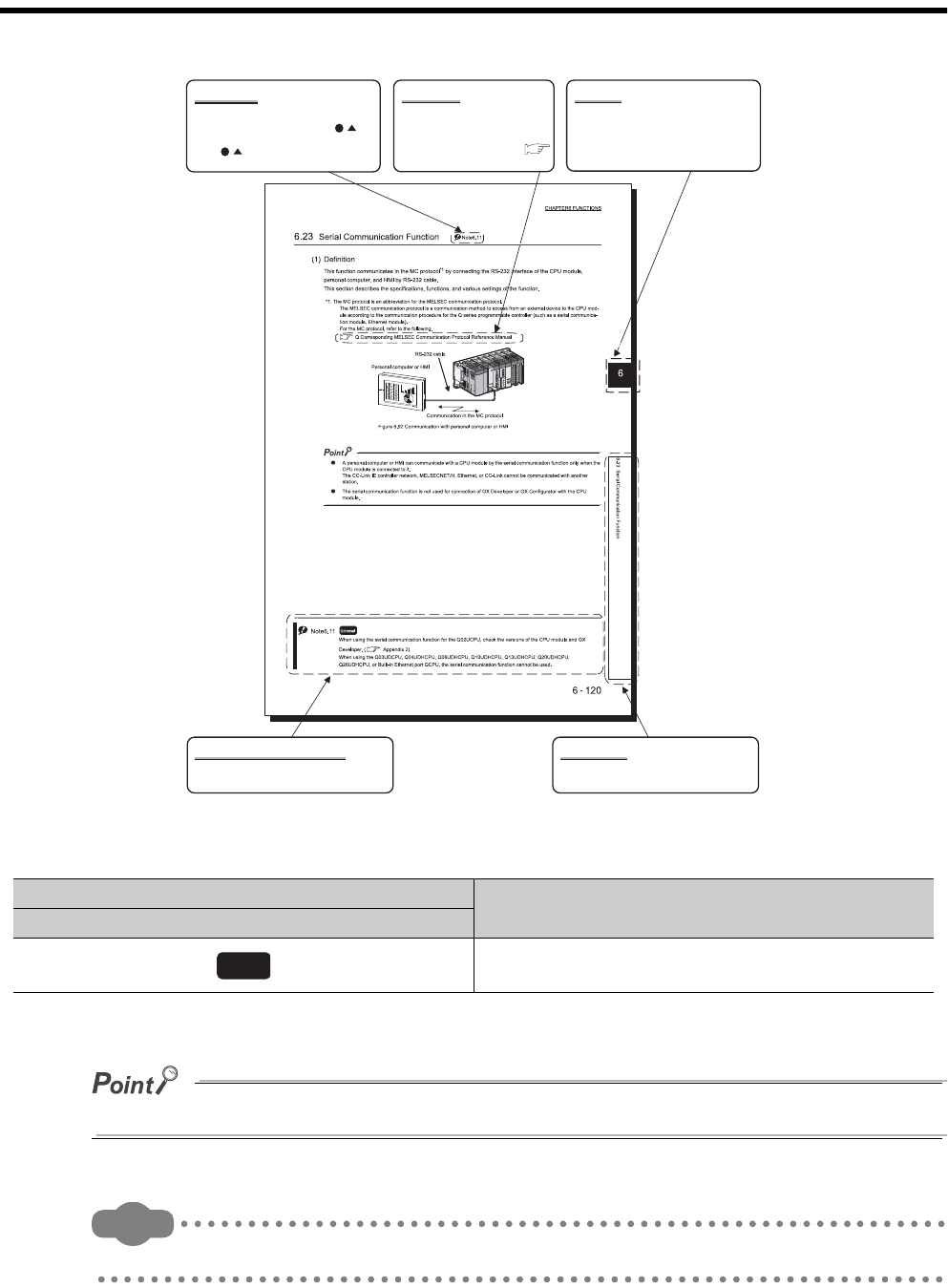
MANUAL PAGE ORGANIZATION
* cining page components, and differs from an actual page.
In addition, this manual uses the following types of explanations.
In addition to description of the page, notes or functions that require special attention are described here.
Remark
The reference related to the page or useful information are described here.
Icons Description
Universal model QCPU
Icons indicate that specifications described on the page
contain some precautions.
Note (detailed explanation)
ReferenceNote (icon)
The section in this manual or
another relevant manual that can
be referred to is shown with .
The chapter of the current page can be
easily identified by this indication on the
right side.
Chapter
The detailed note corresponding to each icon
is described.
Section title
The section number and title of the current
page can be easily identified.
The detailed explanation of "Note . " is
provided under the corresponding
"Note . " at the bottom of the page.
Universal
A - 21
GENERIC TERMS AND ABBREVIATIONS
Unless otherwise specified, this manual uses the following generic terms and abbreviations.
* indicates a part of the model or version.
(Example): Q33B, Q35B, Q38B, Q312B Q3 B
Generic term/abbreviation Description
Series
Q series Abbreviation for Mitsubishi MELSEC-Q series programmable controller
CPU module type
CPU module Generic term for the Universal model QCPU
Universal model QCPU
Generic term for the Q00UJCPU, Q00UCPU, Q01UCPU, Q02UCPU,
Q03UDCPU, Q04UDHCPU, Q06UDHCPU, Q10UDHCPU, Q13UDHCPU,
Q20UDHCPU, Q26UDHCPU, Q03UDECPU, Q04UDEHCPU, Q06UDEHCPU,
Q10UDEHCPU, Q13UDEHCPU, Q20UDEHCPU, and Q26UDEHCPU
Built-in Ethernet port QCPU Generic term for the Q03UDECPU, Q04UDEHCPU, Q06UDEHCPU,
Q10UDEHCPU, Q13UDEHCPU, Q20UDEHCPU, and Q26UDEHCPU
Motion CPU
Generic term for Mitsubishi motion controllers, Q172CPUN, Q173CPUN,
Q172HCPU, Q173HCPU, Q172CPUN-T, Q173CPUN-T, Q172HCPU-T,
Q173HCPU-T, Q172DCPU, and Q173DCPU
PC CPU module Generic term for MELSEC-Q series PC CPU module, PPC-CPU852(MS)-512,
manufactured by CONTEC Co., Ltd.
C Controller module Generic term for the Q06CCPU-V-H01, Q06CCPU-V, Q06CCPU-V-B, and
Q12DCCPU-V C Controller modules
CPU module model
QnUD(H)CPU Generic term for the Q03UDCPU, Q04UDHCPU, Q06UDHCPU, Q10UDHCPU,
Q13UDHCPU, Q20UDHCPU, and Q26UDHCPU
Base unit type
Base unit
Generic term for the main base unit, extension base unit, slim type main base
unit, redundant power main base unit, redundant power extension base unit, and
multiple CPU high speed main base unit
Main base unit Generic term for the Q3 B, Q3 SB, Q3 RB, and Q3 DB
Extension base unit Generic term for the Q5 B, Q6 B, and Q6 RB
Slim type main base unit Another name for the Q3 SB
Redundant power main base unit Another name for the Q3 RB
Redundant power extension base
unit Another name for the Q6 RB
Multiple CPU high speed main base
unit Another name for the Q3 DB
Base unit model
Q3 B Generic term for the Q33B, Q35B, Q38B, and Q312B main base units
Q3 SB Generic term for the Q32SB, Q33SB, and Q35SB slim type main base units
Q3 RB Another name for the Q38RB main base unit for redundant power supply system
Q3 DB Generic term for the Q38DB and Q312DB multiple CPU high speed main base
units
Q5 B Generic term for the Q52B and Q55B extension base units
Q6 B Generic term for the Q63B, Q65B, Q68B, and Q612B extension base units
Q6 RB Another name for the Q68RB extension base unit for redundant power supply
system

A - 22
Generic term/abbreviation Description
Power supply module
Power supply module Generic term for the Q series power supply module, slim type power supply
module, and redundant power supply module
Q series power supply module Generic term for the Q61P-A1, Q61P-A2, Q61P, Q61P-D, Q62P, Q63P, Q64P, and
Q64PN power supply modules
Slim type power supply module Abbreviation for the Q61SP slim type power supply module
Redundant power supply module Generic term for the Q63RP and Q64RP power supply modules for redundant
power supply
Network
MELSECNET/H Abbreviation for the MELSECNET/H network system
Ethernet Abbreviation for the Ethernet network system
CC-Link Abbreviation for the Control & Communication Link
Memory card
Memory card Generic term for the SRAM card, Flash card, and ATA card
SRAM card Generic term for the Q2MEM-1MBS, Q2MEM-2MBS, Q3MEM-4MBS, and
Q3MEM-8MBS SRAM cards
Flash card Generic term for the Q2MEM-2MBF and Q2MEM-4MBF Flash cards
ATA card Generic term for the Q2MEM-8MBA, Q2MEM-16MBA, and Q2MEM-32MBA ATA
cards
Others
GX Developer Product name for SW D5C-GPPW-E GPP function software package compatible
with the Q series
Extension cable Generic term for the QC05B, QC06B, QC12B, QC30B, QC50B, and QC100B
extension cables
Battery Generic term for the Q6BAT, Q7BAT, and Q8BAT CPU module batteries,
Q2MEM-BAT SRAM card battery, and Q3MEM-BAT SRAM card battery
GOT Generic term for Mitsubishi Graphic Operation Terminal, GOT-A*** series, GOT-F***
series, and GOT1000 series
CHAPTER1 OVERVIEW
1
2
3
4
5
6
7
8
1.1 Processing Order in the CPU Module
1 - 1
CHAPTER1 OVERVIEW
The CPU module performs sequence control by executing programs.
This chapter describes the processing order in the CPU module, locations where the created programs are stored, and
devices and instructions useful for programming.
1.1 Processing Order in the CPU Module
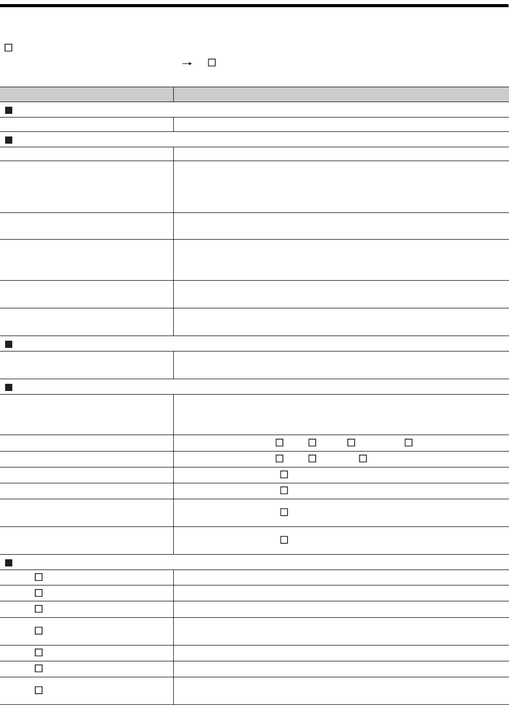
The CPU module performs processing in the following order.
(1) Initial processing ( Section 3.1)
The CPU module performs preprocessing required for program operations.
The preprocessing is performed only once when the module is powered on or reset.
(2) Refresh processing with input and output modules ( Section 3.2)
The CPU module takes on/off data from the input module or intelligent function module and outputs on/off data to
the output module or intelligent function module.
(3) Program operation processing ( Section 3.3)
The CPU module sequentially executes the program stored in the module from the step 0 to the END or FEND
instruction.
(4) END processing ( Section 3.4)
The CPU module performs refresh processing with network modules or communicates with external devices.
Figure 1.1 Processing order in the CPU module
Power-on or reset
Initial processing
Refresh processing with
input/output modules
Program operation processing
END processing
Scan time
1 - 2
1.2 Storing and Executing Programs
This section describes where to store and how to execute the programs in the CPU module.
(1) Programming
Programs are created with GX Developer.
For details of program configuration and execution conditions, refer to CHAPTER 2.
(2) Storing programs
Created programs and set parameters are stored in the following memories of the CPU module.
( Section 5.1)
• Program memory
• Standard ROM (parameters only)
• Memory card
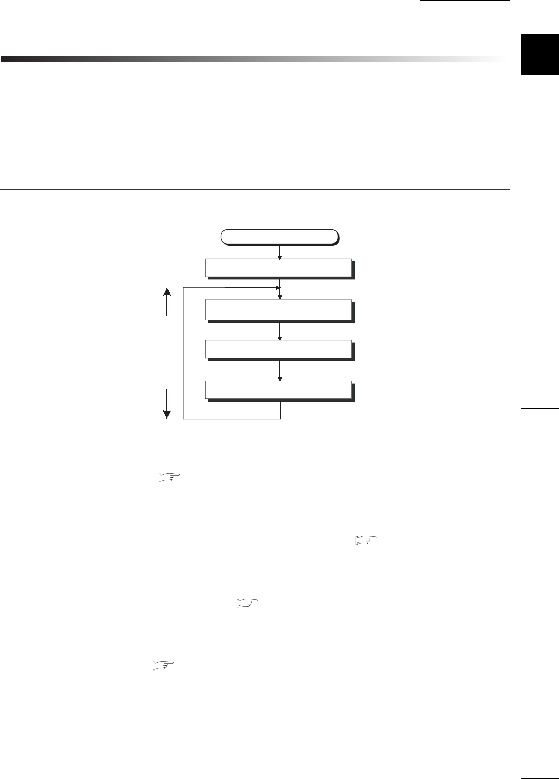
(3) Executing programs
The CPU module executes the programs stored in the program memory.
To execute the programs stored in a memory card, the programs need to be booted to the program memory
( Section 5.1.8) when the CPU module is powered off and then on or reset.
Figure 1.2 Executing programs
Figure 1.3 Executing programs stored in a memory card
CPU module
The CPU module executes
the programs stored here.
Program memory
Parameter
Program
Device comment
Initial device value
Comments are stored
separately from the program.
The CPU module executes the programs
booted from a memory card to here.
Program
memory
Device
comment
Parameter Program
Initial device
value
CPU moduleBoot
Memory card
CHAPTER1 OVERVIEW
1
2
3
4
5
6
7
8
1.3 Structured Programming
1 - 3
1.3 Structured Programming
The programs to be executed in the CPU module can be structured in the following two ways.
• In one program
• By dividing into multiple files
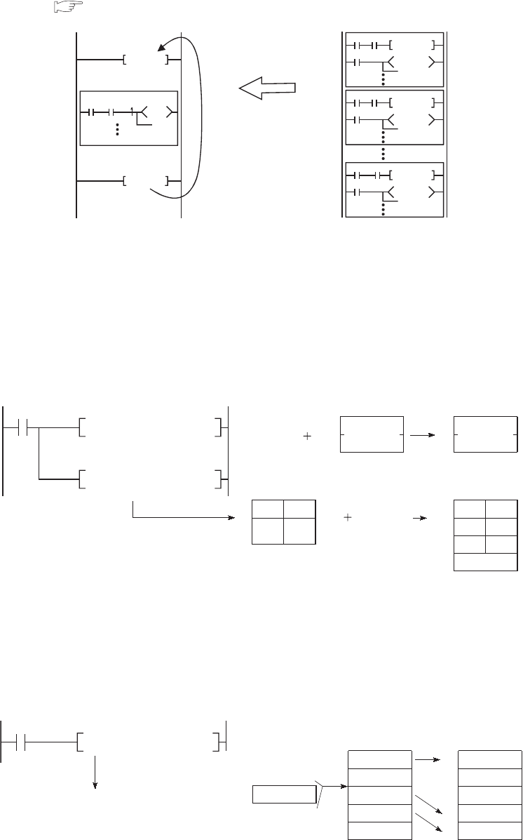
(1) Structuring in one program
Structured programming is available by creating one program as a collection of three program sections: main
routine program ( Section 2.2.1), subroutine program ( Section 2.2.2), and interrupt program
( Section 2.2.3).
Figure 1.4 Structuring in one program
P8
RET
RET
Y10
Y11
Y12
P1
END
FEND
CALL P1
IRET
I0
Main routine
program
Subroutine
program 1
Subroutine
program 2
Interrupt program
1 - 4
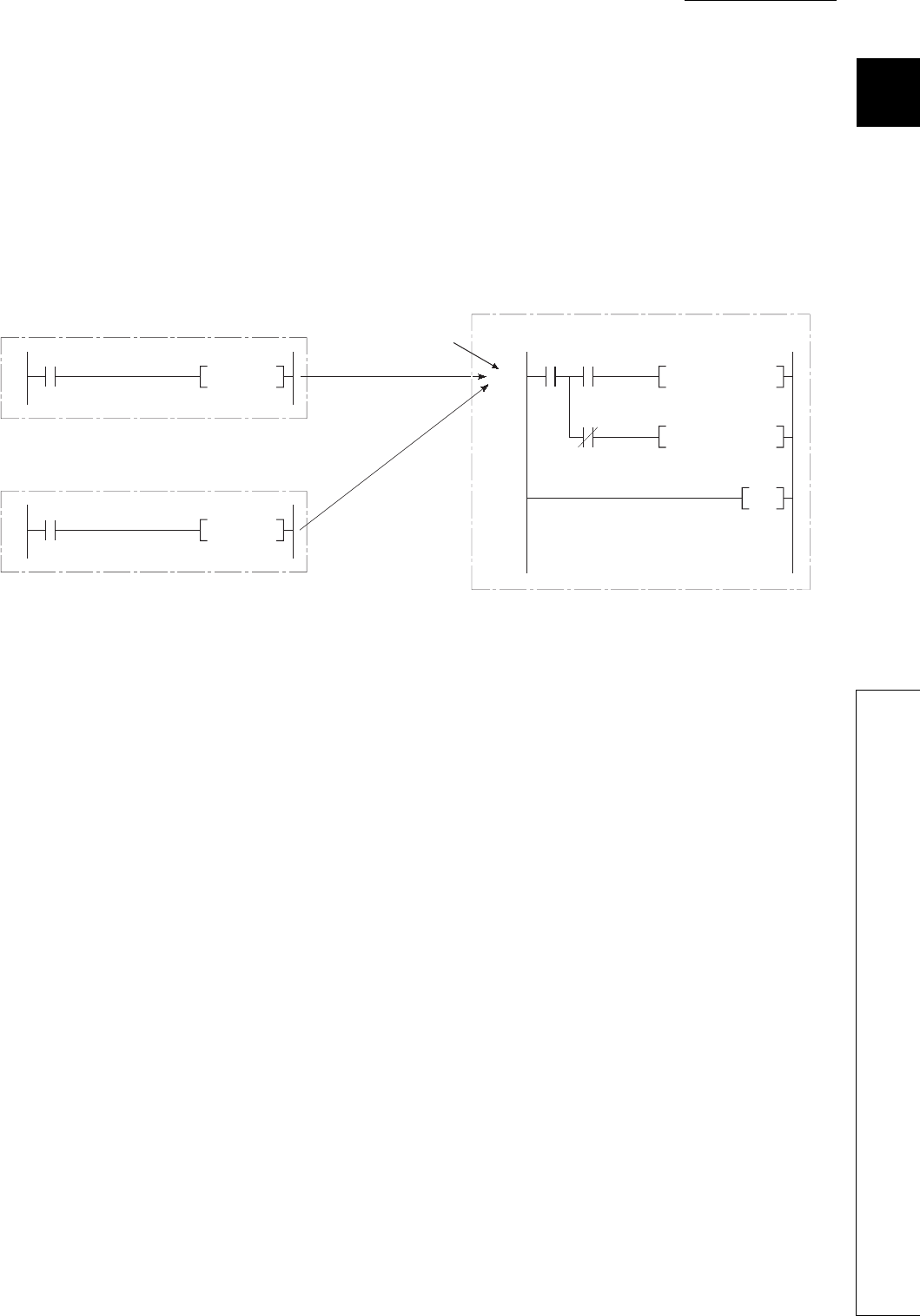
(2) Structuring by dividing into multiple files
A program is stored in a file.
Changing the file name allows the CPU module to store multiple programs.
Dividing into multiple files according to the processes or functions enables simultaneous programming by two or
more designers. Managing the files separately eases reuse and utilization to other programs.
Structured programming is efficient in this way because only the corresponding file needs to be modified or
debugged in case of change in the specifications.
(a) Dividing into multiple files according to the processes*1
*1: The processing contents divided according to the processes can further be divided and managed according to the
functions.
*2: The execution order can be set in the Program tab of the PLC parameter dialog box. ( Section 2.3(2)).
Figure 1.5 Structuring by dividing into multiple files
Figure 1.6 Dividing into multiple files according to the processes
GX Developer
CPU module
Multiple programs can be stored
by changing the file name.
File name: PARAM
Parameter Program Program
Device
comment
File name: ABC File name: ABC File name: DEF
Program memory/memory card
Program ACarrying in
Processing contents
are divided according
to the processes.
Program A to D will
be executed in the
specified order. *2
Manufacturing
Assembly
Carrying out
Program B
Program C
Program D
CHAPTER1 OVERVIEW
1
2
3
4
5
6
7
8
1.3 Structured Programming
1 - 5
(b) Dividing into multiple files according to the functions
*1: The execution order and conditions can be set in the Program tab of the PLC parameter dialog box. ( Section 2.3(2)).
Figure 1.7 Dividing into multiple files according to the functions
Program memory/memory card
Program A
Initial processing
Processing contents
are divided according
to the functions.
Main processing
Communication
processing
Error processing
Program B
Program C
Program D
The execution order and
conditions for program
A to D can be set. *1
1 - 6
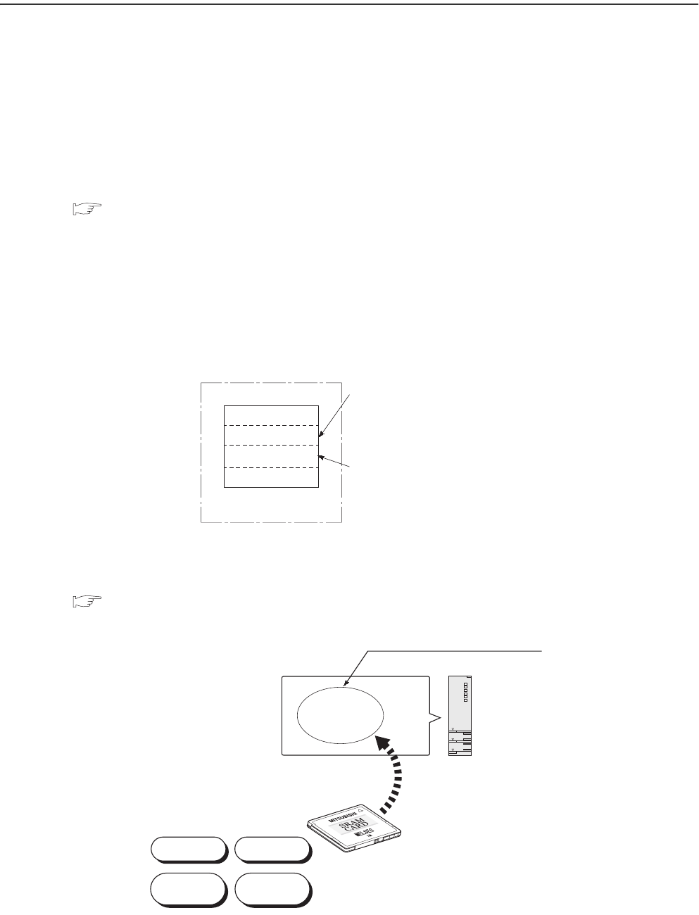
1.4 Devices and Instructions Useful for Programming
The CPU module is provided with devices and instructions useful for programming.
This section describes the outline of these devices and instructions.
(1) Various ways of device specification
(a) Using each bit of a word device as a contact or coil
By specifying a bit of a word device, the bit can be used as a contact or coil.
(b) Easy direct processing in units of one point
Use of the direct access input (DX ) and direct access output (DY ) enables easy direct processing (in units
of one point) in the program. ( Section 3.8.2)
(c) No input pulse conversion required by using a differential contact
Pulse conversion processing for inputs is no longer required with the use of a differential contacts ( and
).
Figure 1.8 Specifying a bit of a word device
Figure 1.9 Direct processing in units of one point
Figure 1.10 Use of a differential contact
D0.5
SET Y10
X0
SET D0.5
A bit-specified word device (turns on
(switches to 1) the 5th bit (b5) of D0.)
A bit-specified word device (turns on/off depending
on the on/off (1/0) status of the 5th bit (b5) of D0.)
M0 DX10
DY100
Direct access input
On/off data is output to the
output module when the
instruction is executed.
On/off data is input from
the input module when the
instruction is executed.
X0 X1
Y100
M0
X0
Y100
Y100
X1
Y100
Differential contact
On at the rising
edge of X0
M0
PLS
CHAPTER1 OVERVIEW
1
2
3
4
5
6
7
8
1.4 Devices and Instructions Useful for Programming
1 - 7
(d) Direct access to the buffer memory of the intelligent function module
The buffer memory of the intelligent function module can be used as a device area in a program.
( Section 9.5.1)
(e) Direct access to the link devices
The link devices (LX, LY, LB, LW, SB, or SW) in network modules can be directly accessed without
the refresh setting. ( Section 9.4)
Figure 1.11 Direct access to the buffer memory of the intelligent function module
Figure 1.12 Direct access to the link devices
X0
D0U4\G12
*1
+P
*1:U4\G12
The CPU module can read the
data in the buffer memory
address 12 of the Q64AD.
I/O number: X/Y40 to X/Y4F
Specifying the buffer
memory address
Specifying the I/O number of
the intelligent function module
Power supply module
CPU module
Input module (16 points)
Input module (16 points)
Input module (16 points)
Q64AD (16 points)
Q64AD (16 points)
Q62AD (16 points)
Output module (16 points)
Output module (16 points)
M0 J5\W12
The CPU module can directly read the data in the
link register (LW12) of the number 5 network module.
Network number 5
Specifying the
link register
Specifying the
network number
D0
J5\W12+P
Power supply module
CPU module
Input module (16 points)
Input module (16 points)
Q68AD (16 points)
Q68AD (16 points)
Q62AD (16 points)
Output module (16 points)
Output module (16 points)
QJ71LP21-25
1 - 8
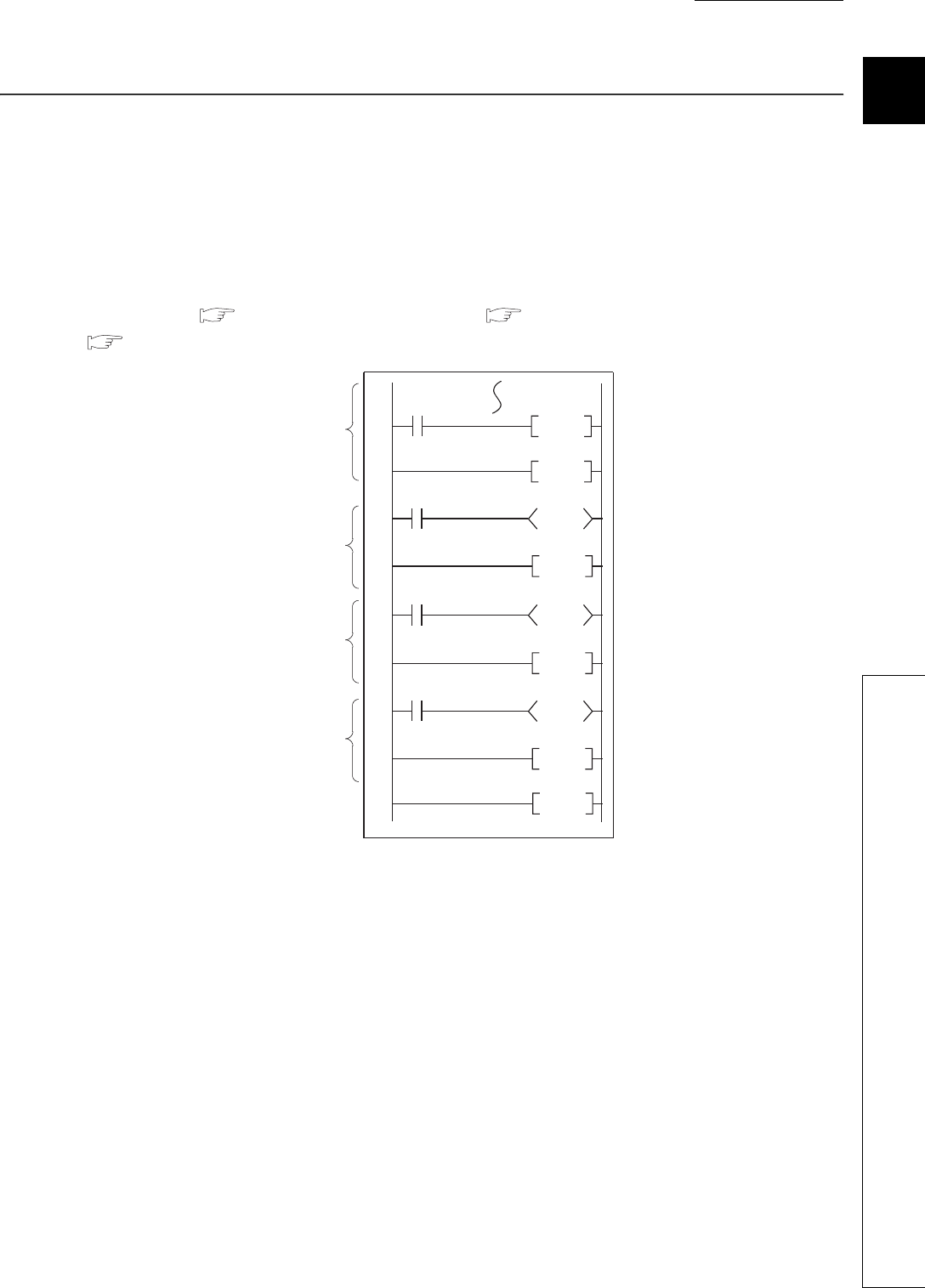
(2) Structural description of programs
Use of the index register and edge relay enables easy structured programming including the pulse conversion
processing. ( Section 9.2.6)
(3) Easy data processing
(a) Using real numbers and character string constants without conversion
Real numbers (floating-point data) and character string constants can be used without conversion for
programming.
*1: The NULL character represents "00H" (end of character strings).
(b) High-speed processing of bulk data
Extension of the data table operation instructions, such as the data table processing instruction, allows high-
speed processing of bulk data.
Figure 1.13 Structured programming including the pulse conversion processing
Figure 1.14 Using real numbers and character string constants
Figure 1.15 Data processing with the table processing instruction
X0 X1 PLS M0
M0 Y8
X10 X11 PLS M10
M10
Y18
X170 X171
PLS M170
M170
Y178
X0Z0 X1Z0
Y8Z2
FOR n
NEXT
V0Z1
Multiple number (n) of
similar programs can
be executed by one
description.
Real number addition instruction
Real number
data
X0
E+P E1.23 E1.23 E3.45 E4.68
D0 D0
D5 D10
D11
D12
D13
D6
"0" "Q" "CPU"
"2"
"0"
"C"
"U"
"Q"
"2"
"P"
D1
R0
R1
R0
$+P D5 "CPU" D10
Real number
data
Real number
data
Character string data link instruction
Character
string data
Character
string data
Character
string data
NULL
*1
NULL *1
X0
K2R0D0FINSP
R0
R1
R2
R3
3
10
20
30
R4
R0
R1
R2
R3
4
10
15
20
30R4
D0 15
Insertion
position
Instruction for inserting data
to the table
FIF0 table FIF0 table
Device
where the
data is
currently
stored
Device
where
the data
is to be
stored
CHAPTER1 OVERVIEW
1
2
3
4
5
6
7
8
1.4 Devices and Instructions Useful for Programming
1 - 9
(4) Flexible management of subroutine programs
(a) Subroutine program sharing
The number of steps in a program can be reduced by sharing subroutine programs.
In addition, creating and managing programs become easier.
Subroutine programs can be created within the same program and called. Subroutine programs in other
programs can also be called by using the common pointer.
Figure 1.16 Subroutine program sharing
R0K4X20
MOV
SM400
R0
K4X0MOV
RET
M0
M0
P1000
M10
P1000CALLP
0
M0
P1000CALLP
0
Program A
Program B
Calling P1000
Calling P1000
Common pointer
Always
on
Program C
Subroutine program
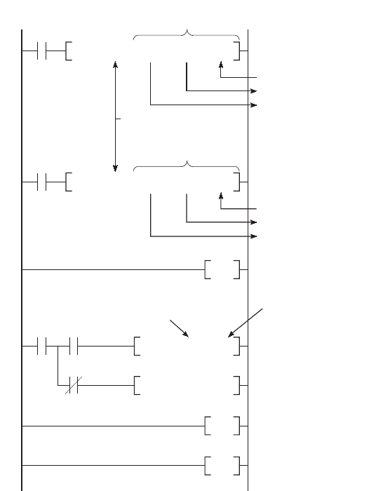
1 - 10
(b) Subroutine call instruction with argument passing
Subroutine program that is called more than one time can be created easily.
*1: For input and output conditions for an argument, refer to Section 9.3.1.
Figure 1.17 Calling subroutine program with argument passing
FD2FD1
MOV
SM400
FD2
FD0MOV
RET
FEND
END
M0
M0
M10
R10
K4X10W10
P0
CALLP
P0
100
0
Always
on
Argument from FD2 *1
Source data
Destination data
M0
R0
K4X0W0
P0
CALLP
Argument from FD2 *1
Argument to FD1
Argument to FD0
Argument to FD1
Argument to FD0
Argument specification
Argument specification
Subroutine program
specification
Main routine program
Subroutine program
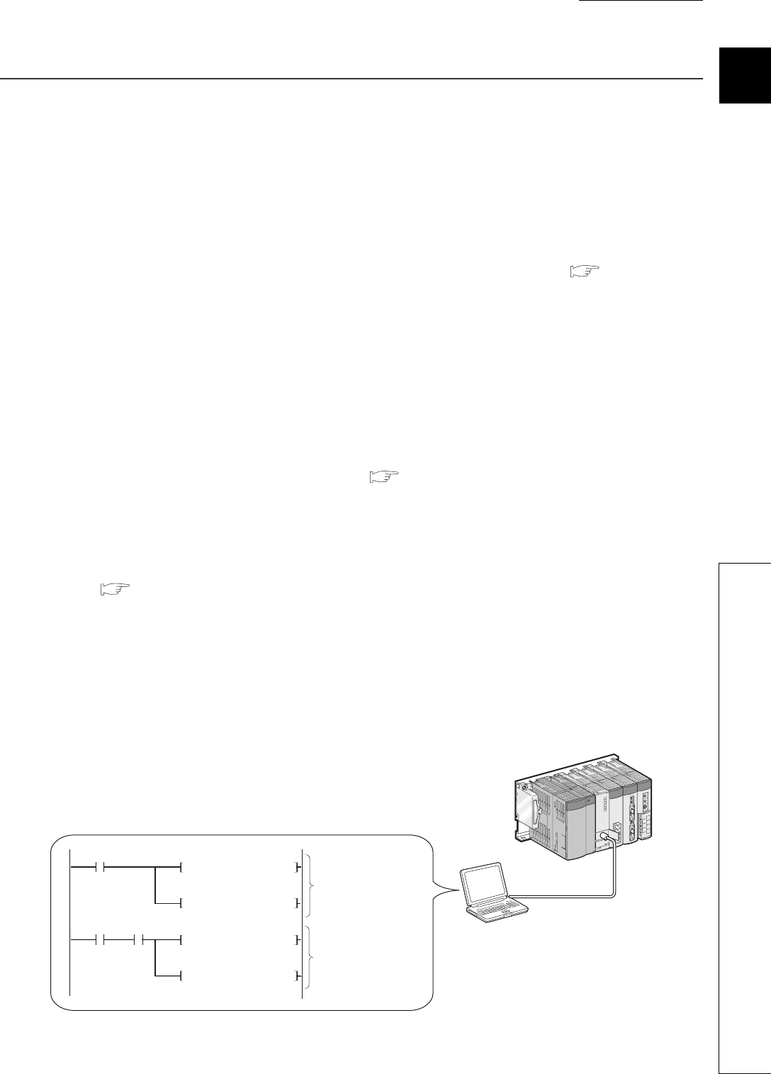
CHAPTER1 OVERVIEW
1
2
3
4
5
6
7
8
1.5 Features
1 - 11
1.5 Features
This section describes the features specific to the Universal model QCPU.
(1) High-speed processing more than ever
The processing time required for the basic instructions, floating-point operations, and accesses to the file register
becomes shorter than the existing Q series CPU modules.
Use of a standard device register (Z)*1 achieves high-speed processing between register operations (transfer
instruction).
*1: An index register used between register operations is designated as a standard device register.( Section 9.6.2)
(2) Large-capacity file register
The file register whose capacity is 640K points at maximum (4086K points at maximum when a memory card is
used)*2 can be set inside the CPU module.
*2: For the Q26UDHCPU and Q26UDEHCPU only
(3) Use of double-precision floating-point operation instructions
The double-precision floating-point operation instructions (64-bit instructions) are available as well as the existing
single-precision floating-point operation instructions. ( Section 2.4.4)
This enables more accurate analog control and positioning control.
(4) Using the file register area as the data register and link register
The file register (ZR) area can be used as an pseudo extended area*3 of the data register (D) and link register
(W). ( Section 9.8)
Programming using the extended data register (D) or extended link register (W) whose capacity is 640K points at
maximum (4086K points at maximum when a memory card is used)*4 is available in addition to the internal user
device.
*3: Extended areas of the data register (D) and link register (W) are called the extended data register (D) and extended link
register (W), respectively.
*4: For the Q26UDHCPU and Q26UDEHCPU only
Figure 1.18 Extended data register (D) and extended link register (W)
GX Developer
W10000.0
MOV D30000 W10200
B80
SET W10100.0
W0.0
MOV D0 W200
SET W100.0
Internal user devices
are used.
The extended data
register (D) and
extended link register
(W) are used.
1 - 12
(5) 32-bit index modification
Since the index modification range is expanded to 32 bits, index modification for the entire file register areas is
possible. ( Section 9.6.1)
(6) Communication via the built-in Ethernet port of the CPU module
The Built-in Ethernet port QCPU can communicate with MELSOFT, GOT, and external devices using the built-in
Ethernet port of the module.
QnUCPU User's Manual (Communication via Built-in Ethernet Port)
(7) Communication with the personal computer and HMI by the serial
communication function ( Section 6.23)
The Q00UJCPU, Q00UCPU, Q01UCPU, and Q02UCPU can communicate using the MELSEC communication
protocol (hereafter, MC protocol) by connecting a RS-232 interface and personal computer or HMI.
The CPU module functions are added at the update of serial number of CPU module or GX Developer version.
For functions added by the update, refer to Appendix 2.
Figure 1.19 32-bit index modification
Figure 1.20 Communication with the personal computer or HMI
K1042431 Z0DMOV
ZR0Z0 D0MOV
ZR0
ZR32767
ZR32768
File register in the serial
number access method
ZR1
ZR1042431
SM400
Use the index register (Z) when indexing the
file register (ZR) in the serial number access
method by 32 bits.
Applicable range
of existing index
modification
Applicable range of index modification
for the Universal model QCPU
Personal computer or HMI
RS-232 cable
Communication using the MC protocol
CHAPTER1 OVERVIEW
1
2
3
4
5
6
7
8
1.6 Checking Serial Number and Function Version
1 - 13
1.6 Checking Serial Number and Function Version
The serial number and function version of the CPU module can be checked on the rating plate, on the front of the
module, and on the System monitor screen in GX Developer.
(1) Checking on the rating plate
The rating plate is located on the side of the CPU module.
(2) Checking on the front of the module
The serial number on the rating plate is printed on the front (at the bottom) of the module. This applies only to the
CPU module manufactured in mid-September, 2007 or later.
Figure 1.21 Rating plate
Figure 1.22 Front of the module
Serial number (first five digits)
Relevant regulation
standards
Function version
BAT.
Q03UDCPU
RS-232
USB
MODE
RUN
ERR.
USER
BOOT
PULL
Serial number
1 - 14
(3) Checking on the System monitor (Product Information List) screen
To open the screen for checking the serial number and function version, select [Diagnostics] [System monitor]
and click the button in GX Developer.
On the same screen, the serial number and function version of intelligent function modules can also be checked.
[Serial number, function version, and product number]
• The serial number of the module is displayed in the "Serial No." column.
• The function version of the module is displayed in the "Ver." column.
• The serial number (product number) printed on the rating plate of the module is displayed in the "Product
No." column.
Note that "-" is displayed for the module that does not support the product number display.
The serial number displayed on the Product Information List screen of GX Developer may differ from that on the rating plate
and on the front of the module.
• The serial number on the rating plate and on the front of the module indicates the management information of the
product.
• The serial number displayed on the Product Information List screen indicates the functional information of the
product.
The functional information of the product will be updated when a function is added.
Figure 1.23 System monitor (Product Information List) screen
Product Inf. List...
Serial
number
Product
number
Function
version
CHAPTER2 SEQUENCE PROGRAMS
1
2
3
4
5
6
7
8
2.1 Sequence Program Overview
2 - 1
CHAPTER2 SEQUENCE PROGRAMS
2.1 Sequence Program Overview
(1) Definition
Sequence program is one of the programs that can be executed in the CPU module.
A sequence program consists of instructions, such as sequence instructions, basic instruction, and
application instruction.
Remark
For the instructions used in sequence programs, refer to the following.
QCPU Programming Manual (Common Instructions)
Figure 2.1 Sequence program
T0
X0
X1
X41
M0 K100
T0
Y30
BIN K4X10 D0
FROM H5 K0 D10 K1
Sequence instruction
Basic instruction
Application instruction
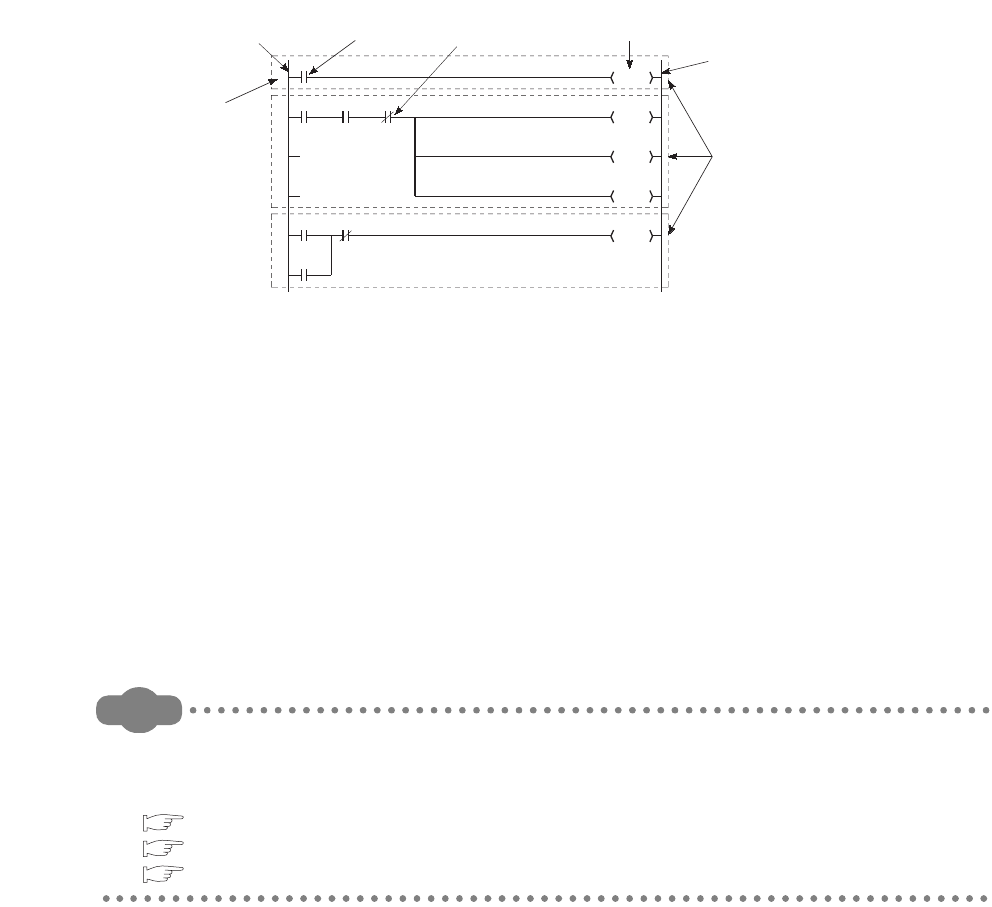
2 - 2
(2) Programming method
There are two programming modes for sequence programs.
• Ladder mode
• List mode
(a) Ladder mode
Ladder mode is a mode based on the concept of sequential control by relay circuits.
A program in ladder mode is similar to a schematic for a set of relay circuits. Programming in units
of ladder blocks is available.
A ladder block, which starts from the left rail and ends at the right rail, is the minimum unit for
operating sequence programs.
(b) List mode
List mode uses dedicated instructions for programming. The symbols, such as contacts and coils,
used in ladder mode are replaced with dedicated instructions.
The following instructions are used for normally open contacts, normally closed contacts, and coils.
• Normally open contact ••• LD, AND, OR
• Normally closed contact ••• LDI, ANI, ORI
• Coil ••• OUT
Remark
There are two other types of programs that can be executed in the CPU module: SFC programs and ST
programs.
For details, refer to the following.
QCPU (Q Mode)/QnACPU Programming Manual (SFC)
QCPU (Q Mode) Programming Manual (MELSAP-L)
QCPU (Q Mode) Programming Manual (Structured Text)
Figure 2.2 Ladder mode
Y21
Y22
Y23
Y24
Y20
Y24
0
2
8
Left rail
N/O
contact
N/C
contact Coil (output)
Right rail
Ladder block
Step number
* X0 to X5: Input, Y20 to Y24: Output
X0
X3
X4 X5
X1 X2

CHAPTER2 SEQUENCE PROGRAMS
1
2
3
4
5
6
7
8
2.2 Sequence Program Configuration
2 - 3
(3) Sequence program operation
A sequence program is sequentially operated from the step 0 to the END or FEND instruction.
In ladder mode, a sequence program is operated from left to right and top to bottom in a ladder block.
2.2 Sequence Program Configuration
Sequence programs are classified into the following three types.
• Main routine program
• Subroutine program
• Interrupt program
Figure 2.3 Comparison between ladder mode and list mode
Figure 2.4 Sequence program classification
X0 X1 X5 X6 X7
X2 X3
X4
Y10
0
10
END
0 LD X0
1 AND X1
2 LD X2
3 AND X3
4 ORB
5 OR X4
6 AND X5
7 AND X6
8 AND X7
9 OUT Y10
10 END
1) 2)
3)
6)
4)
5)
7) 8) 9) 10)
11)
0)
1)
2)
3)
4)
5)
6)
7)
8)
9)
10)
11)
[Ladder mode]
From left to right
From top
to bottom
* Program operations are executed in the
order of 1) to 11).
[List mode]
Program
operations are
sequentially
executed from
the step 0 to the
END instruction.
Step number
FEND
RET
IRET
END
P0
I0
File A
Main routine
program
Subroutine
program
Interrupt
program
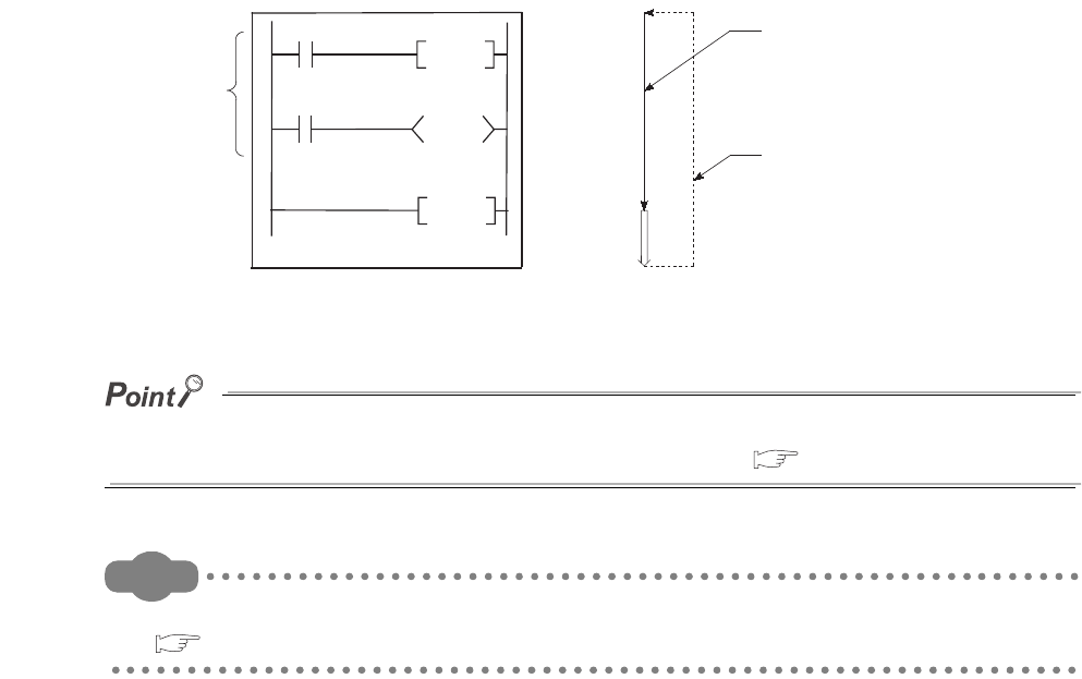
2 - 4
2.2.1 Main routine program
(1) Definition
Main routine program is an entire program from the step 0 to the END or FEND instruction.
(2) Program operation
A main routine program executes its operations from the step 0 to the END or FEND instruction and
then performs END processing.
After the END processing, the program restarts its operations from the step 0.
When multiple programs are executed, the main routine program operation after execution of the END or
FEND instruction varies depending on the preset execution conditions. ( Section 2.3.1)
Remark
For details of the END and FEND instructions, refer to the following.
QCPU Programming Manual (Common Instructions)
Figure 2.5 Main routine program
END/FEND
END/FEND
Main routine
program
Step 0
END
processing
Indicates execution of
the program.
The program operation
returns to the step 0.
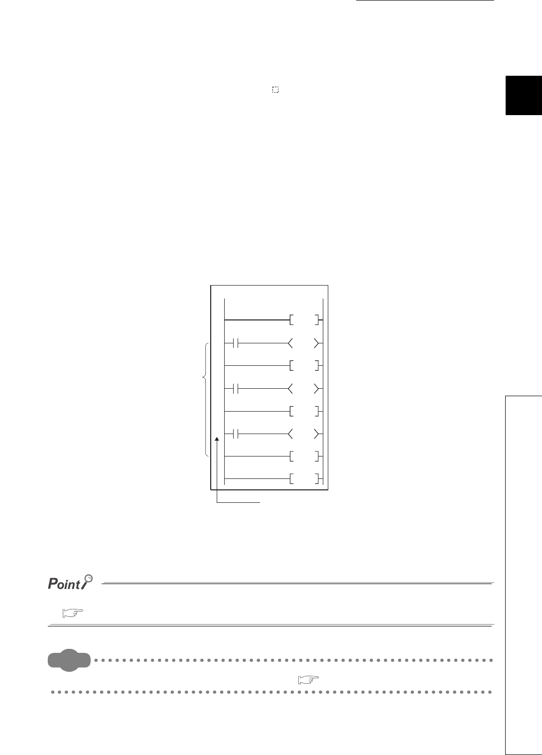
CHAPTER2 SEQUENCE PROGRAMS
1
2
3
4
5
6
7
8
2.2 Sequence Program Configuration
2.2.2 Subroutine program
2 - 5
2.2.2 Subroutine program
(1) Definition
Subroutine program is a program from a pointer (P ) to the RET instruction.
This program is executed only when it is called by a subroutine program call instruction (such as
CALL(P), FCALL(P)) from a main routine program.
(2) Application
• Programming a program which is executed two or more times in one scan as a subroutine
program can reduce the number of steps in the entire program.
• Programming a program which is executed only when a certain condition is satisfied as a
subroutine program can shorten the scan time.
(3) Programming of subroutine programs
Create subroutine programs between the FEND and END instructions in the main routine program.
*1: The pointer numbers do not need to be specified in asending order.
Subroutine programs can be managed as one separate program (stand-by type program).
( Section 2.2.3)
Remark
Subroutine programs can be configured with the nesting.( Section 9.9)
Figure 2.6 Programming location of subroutine programs
Program A
P0
FEND
RET
RET
RET
END
pointer
*1
Y10
Y11
Y12
P8
P1
Main routine
program
Subroutine
program
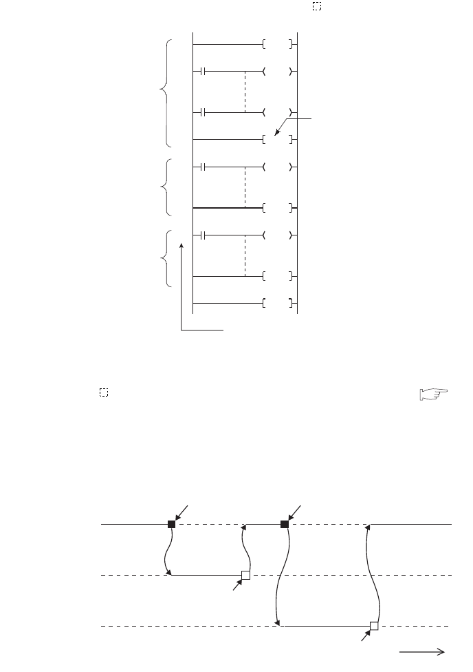
2 - 6
2.2.3 Interrupt program
(1) Definition
Interrupt program is a program from an interrupt pointer (I ) to the IRET instruction.
The interrupt pointer (I ) number varies depending on the interrupt factor. ( Section 9.11)
When an interrupt factor occurs, the interrupt program of the interrupt pointer number corresponding
to that factor is executed. (Interrupt programs are executed only when the corresponding interrupt
factor occurs.)
Figure 2.7 Interrupt program
Figure 2.8 Interrupt program execution timing
FEND
EI
IRET
IRET
END
I0
I29
Main routine
program
Interrupt
program (I0)
Interrupt
program (I29)
Indicates the end
of the main routine
program.
Interrupt pointer
Main routine
program
Interrupt
program (I0)
Interrupt
program (I29)
Execution Execution Execution
Execution
Execution
IRET
IRET
Occurrence of the
interrupt factor for I0
Occurrence of the
interrupt factor for I29
Time
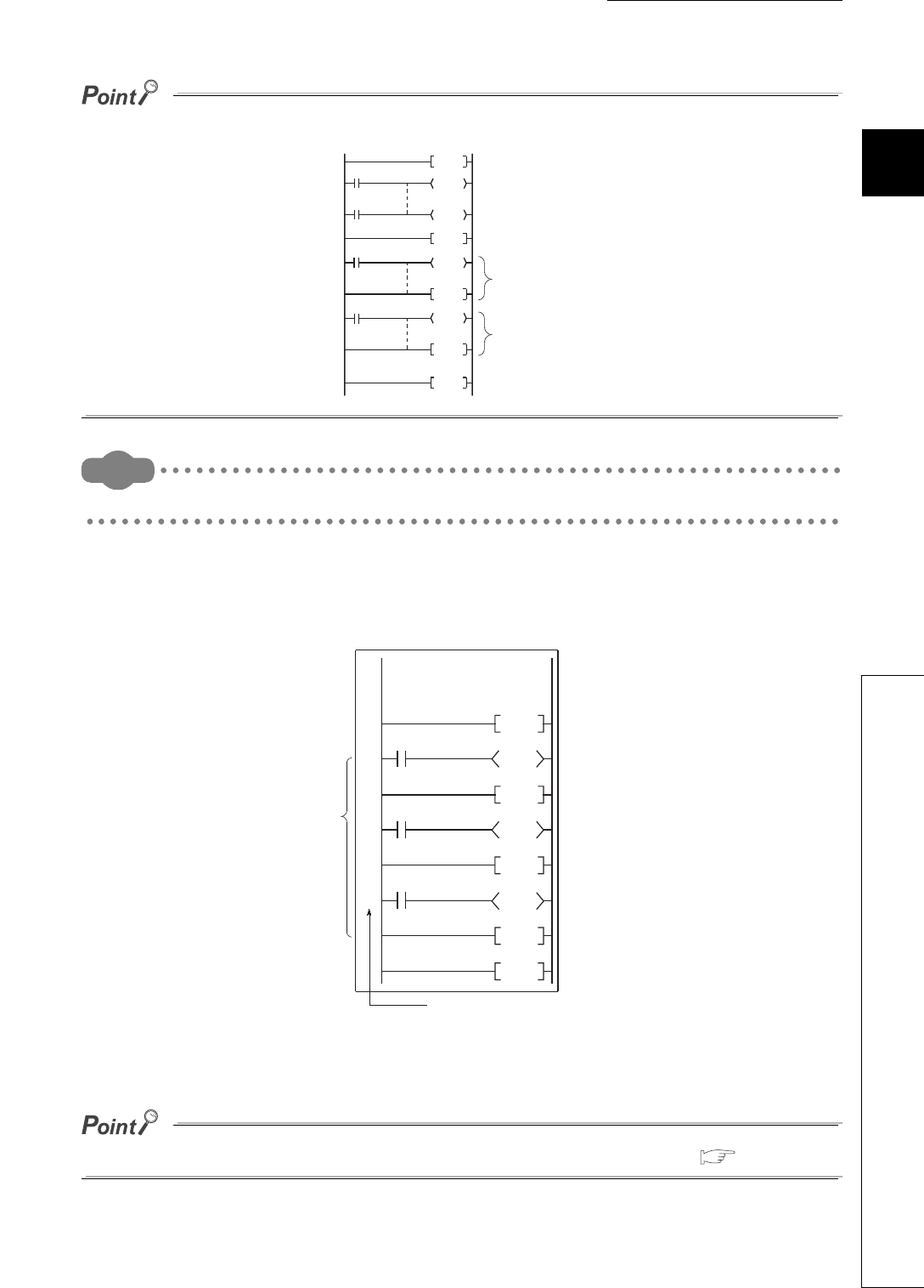
CHAPTER2 SEQUENCE PROGRAMS
1
2
3
4
5
6
7
8
2.2 Sequence Program Configuration
2.2.3 Interrupt program
2 - 7
Only one interrupt program can be created with one interrupt pointer number.
Remark
For details of the interrupt factors and interrupt pointers, refer to Section 9.11.
(2) Programming of interrupt programs
Create interrupt programs between the FEND and END instructions in the main routine program.
*1: The pointer numbers do not need to be specified in ascending order.
Interrupt programs can be managed as one separate program (stand-by type program). ( Section 2.3.3)
Figure 2.9 Programming location of interrupt programs
FEND
EI
IRET
IRET
END
I0
I29 Interrupt
program (I29)
Interrupt
program (I0)
Program A
I0
FEN
IRET
IRET
IRET
Y11
Y10
Y12
I32
I28
Interrupt
program
Interrupt pointer
*1
Main routine
program
END
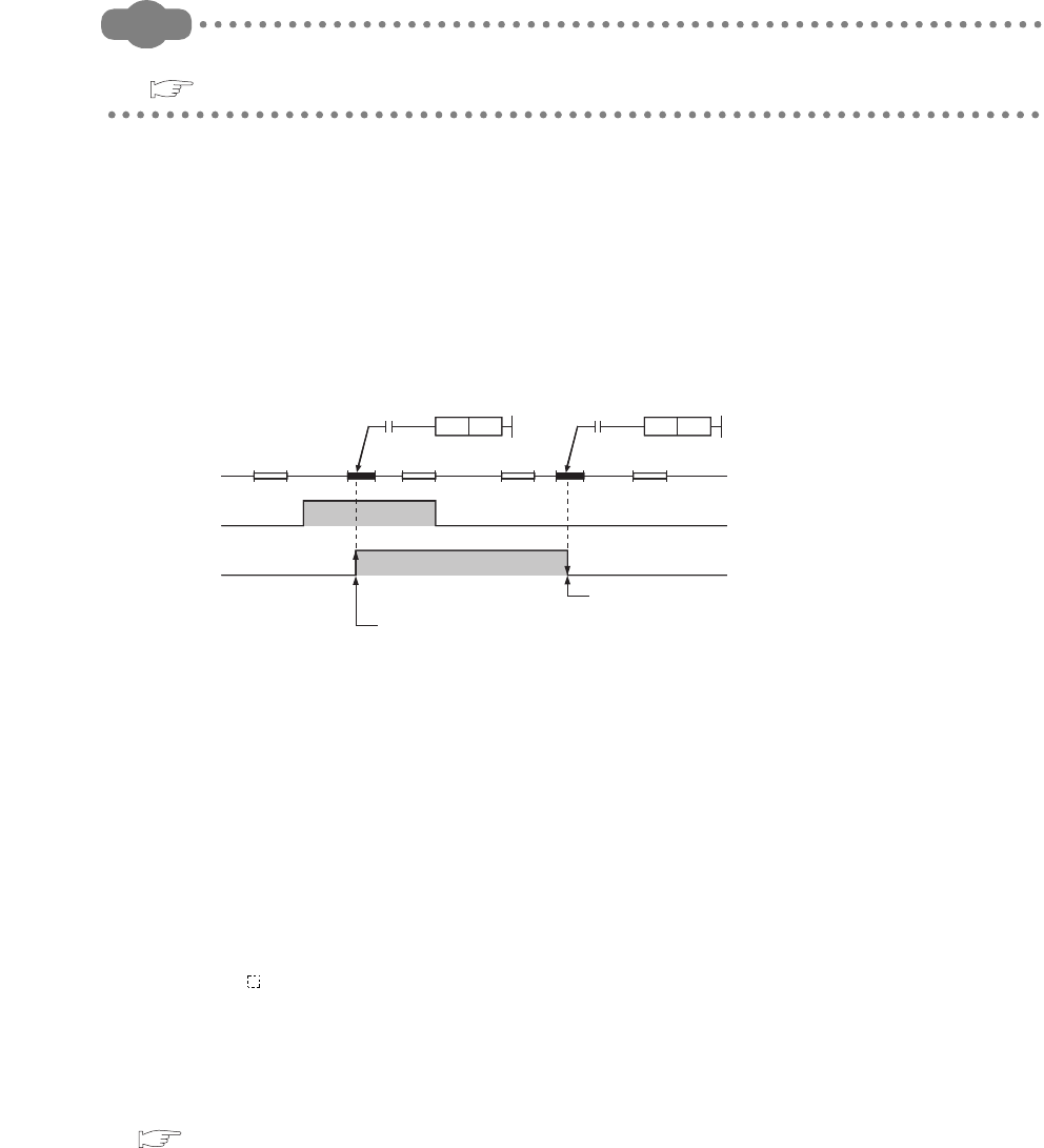
2 - 8
(a) Before executing an interrupt program
Before executing the interrupt programs of the interrupt pointers I0 to I15, I28 to I31, I45, and I50 to
I255, enable interrupts with the EI instruction.
Remark
For details of the EI instruction, refer to the following.
QCPU Programming Manual (Common Instructions)
(b) Restrictions on programming
1) PLS and PLF instructions
The PLS and PLF instructions perform off processing in the next scan of which the instruction is
executed.
Therefore, the device which is turned on by the instruction remains on until the same instruction is
reexecuted.
2) EI and DI instructions
During execution of an interrupt program, interrupts are disabled (DI) so that any other interrupt
processing will not be executed.
Do not execute the EI or DI instruction during interrupt program execution.
3) Timer (T) and counter (C)
Do not use the timer (T) and counter (C) in interrupt programs.
If more than one interrupts occur in one scan, the timer (T) and counter (C) in the interrupt
program cannot measure the time correctly.
The OUT C instruction status causes the counter (C) measure the number of interrupts
incorrectly.
4) Instructions not available in interrupt programs
Refer to sections corresponding to each instruction in the following.
QCPU Programming Manual (Common Instructions)
Figure 2.10 Device turned on by the PLS instruction in the interrupt program
X0OFF
ON
M0OFF
ON
0IO
IRET
ENDEND
0
END END
0
IO IRET
0
PLS M0
X0
PLS M0
X0
Turns off by executing the
PLS M0 instruction.
Turns on by executing the PLS M0 instruction at the rise of X0.
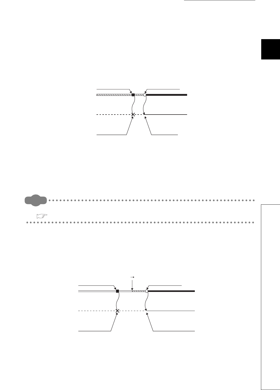
CHAPTER2 SEQUENCE PROGRAMS
1
2
3
4
5
6
7
8
2.2 Sequence Program Configuration
2.2.3 Interrupt program
2 - 9
(3) Operation when an interrupt factor occurs
There are restrictions on interrupt programs depending on the interrupt factor occurrence timing.
(a) When an interrupt factor occurs before the interrupt program execution status is enabled
The CPU module stores the interrupt factor occurred.
As soon as the interrupt program execution status is enabled, the CPU module executes the
interrupt program corresponding to the stored interrupt factor.
When the same interrupt factor occurs more than one time before the interrupt program execution
status is enabled, the interrupt factors of I0 to I15, I28 to I31, I45, I50 to I255, and fixed scan
execution type programs are stored only once.
Note that all interrupt factors occurred are discarded if they are masked by the IMASK instruction.
Remark
For details of the IMASK instruction, refer to the following.
QCPU Programming Manual (Common Instructions)
(b) When an interrupt factor occurs in the STOP or PAUSE status
The CPU module executes the interrupt program as soon as the interrupt program execution status is enabled
after the CPU module status is changed to RUN.
Figure 2.11 When an interrupt factor occurs before interrupts are enabled
Figure 2.12 When an interrupt factor occurs in the STOP or PAUSE status
Main routine
program
Interrupt
program
Interrupt factor
occurrence
Not executed because
the interrupt program
execution status is
disabled (DI).
Executed as soon as
the interrupt program
execution status
changes to enabled.
Interrupt
enabled (EI)
Execution
Main routine
program
Interrupt
program
Interrupt factor
occurrence
STOP/PAUSE
RUN
Not executed because
the CPU module is in
the STOP status.
Executed as soon as the interrupt
program execution status changes
to enabled after the CPU module
status is changed from
STOP/PAUSE to RUN.
Interrupt
enabled (EI)
Execution
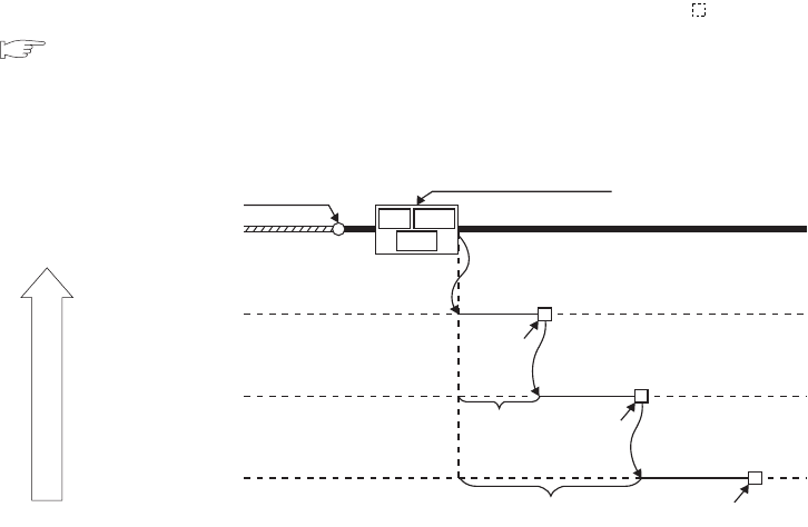
2 - 10
(c) When multiple interrupt factors occur simultaneously in the interrupt program execution
enabled status
The interrupt programs are executed in the order of interrupt pointers (I ) with high priority.
( Section 9.11.1)
Other interrupt programs have to wait until processing of the interrupt program being executed is
completed.
(d) When the same interrupt factor as that of the interrupt program being executed occurs
When the same interrupt factor as that of the interrupt program being executed occurs more than
one time before completion of interrupt program processing, the interrupt factors of I0 to I15, I45,
and I50 to I255 are stored only once, and then the interrupt program corresponding to each stored
interrupt factor is executed after completion of current interrupt program execution.
The interrupt factors of I28 to I31 and fixed scan execution type programs are all stored, and then all
the interrupt programs corresponding to interrupt factors are executed after completion of current
interrupt program execution.
Figure 2.13 When multiple interrupt factors occur simultaneously
Main routine
program
Interrupt
program (I50)
Interrupt
enabled (EI)
Simultaneous occurrence of
multiple interrupt factors
Execution
Execution
Execution
Interrupt
program (I100) Wait to be
processed
Wait to be processed
Interrupt
program (I150)
IRET
IRET
IRET
I50 I100
I150
Low
Priority
High
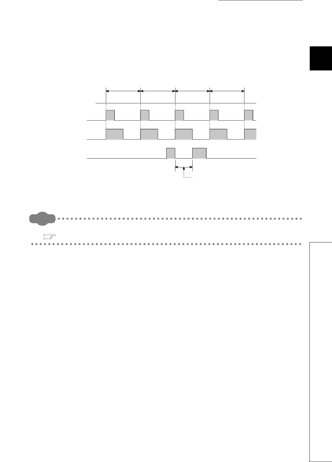
CHAPTER2 SEQUENCE PROGRAMS
1
2
3
4
5
6
7
8
2.2 Sequence Program Configuration
2.2.3 Interrupt program
2 - 11
(e) When an interrupt factor occurs during link refresh
The link refresh is suspended and an interrupt program is executed.
Even if the Block data assurance per station setting is enabled in the CC-Link IE controller network
or MELSECNET/H network, this setting does not work when a device set as a refresh target is used
in the interrupt program.
In the interrupt program, do not use any refresh target device.
Remark
For the Block data assurance per station setting, refer to the following.
Reference manual for each network module
(f) Interrupt during END processing
When the constant scan function is used and an interrupt factor occurs during the waiting time in
END processing, an interrupt program corresponding to the interrupt factor is executed.
(g) When an interrupt factor occurs during access to another module
When an interrupt factor occurs during access to another module (during service processing or instruction
processing), the interrupt program becomes standby status until the service processing or the instruction in
execution is completed.
To shorten the wait time of the interrupt, reduce the amount of data that access to other modules.
Figure 2.14 When an interrupt factor occurs during link refresh
10ms 10ms 10ms 10ms
Interrupt program
execution
Link refresh execution
Link refresh is suspended and
interrupt program is executed.
Interrupt factor

2 - 12
(4) Processing at program execution type change
When the program execution type is changed from the scan execution type to the interrupt, the CPU
module saves and restores the following data. ( Section 9.6.3)
• Data in the index register
• File register block number
Whether to save and restore the data above can be set in the PLC parameter dialog box.
If the data is not saved or restored, the overhead time of the corresponding interrupt program can be shortened.
( Section 10.1.2)
(5) Restrictions
(a) When the same device is used
During execution of an instruction in a main routine program, an interrupt program may be
executed, suspending the processing of the instruction being executed.
If the same device is used for the main routine program and interrupt program, device data may
become inconsistent. In this case, take the following measures to prevent device data
inconsistency.
1) Moving device data to another device
Do not directly specify the device where the data is written by the interrupt program in the main
routine program. Use the data in another device by moving the data with the transfer instruction.
2) Disabling interrupts with the DI instruction
Disable interrupts with the DI instruction if instructions that may cause inconvenience for the main
routine program are used.
However, interrupts do not occur during access to the device of the corresponding argument of the
instruction. For this reason, data inconsistency will not occur in units of arguments.
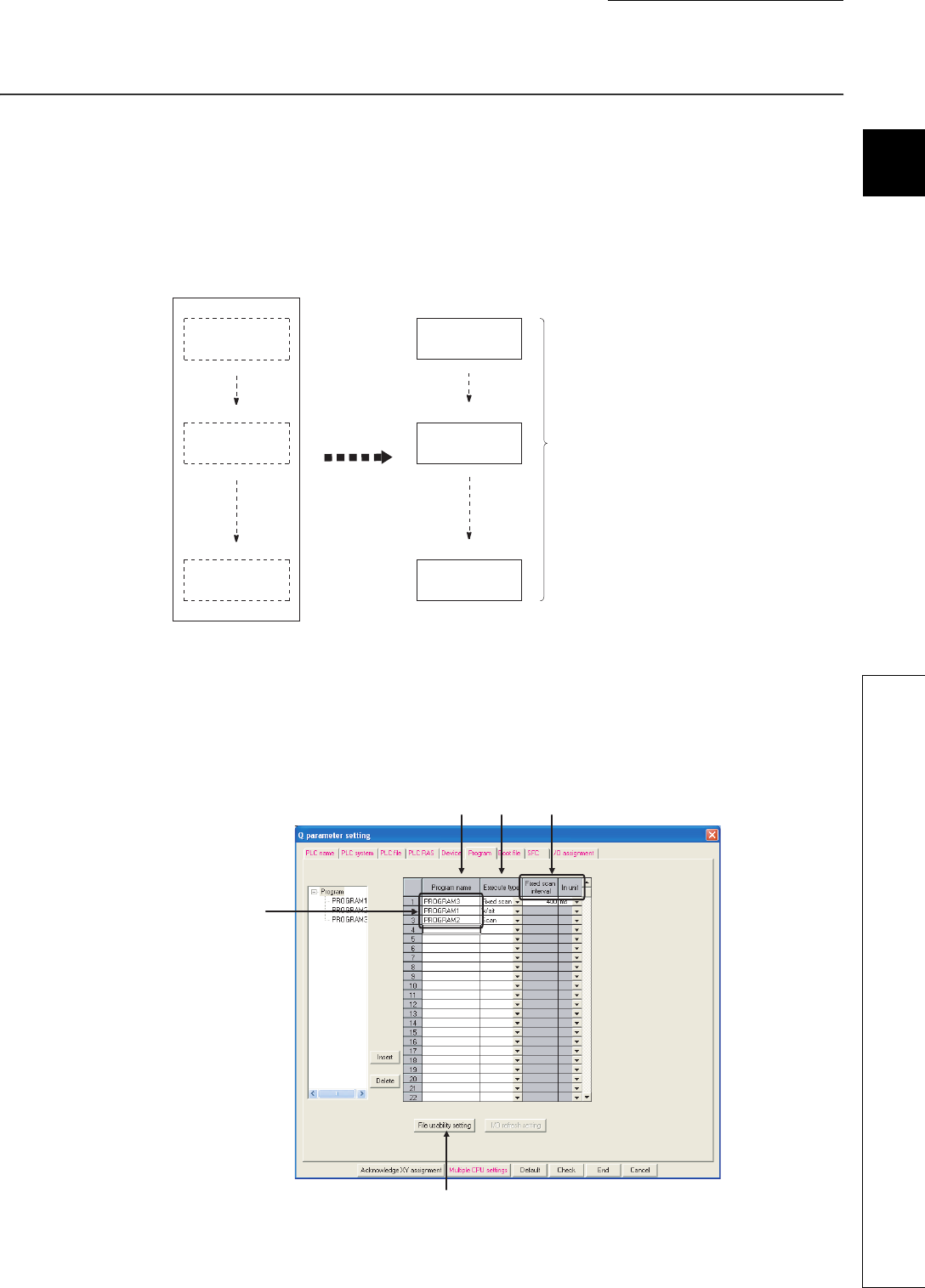
CHAPTER2 SEQUENCE PROGRAMS
1
2
3
4
5
6
7
8
2.3 Settings When Program is Divided
2 - 13
2.3 Settings When Program is Divided
When one sequence program is divided into multiple programs, execution conditions, such as executing a
program only once at start-up or executing a program at fixed intervals, can be set for each program.
(1) Control by multiple programs dividing one program
The CPU module can store multiple programs divided on the basis of each control unit.
This enables programming of one sequence program by two or more designers.
(2) Settings required for execution of multiple programs
To execute multiple programs in the CPU module, names (file names) and execution conditions of the
programs must be set.
Set them in the Program tab of the PLC parameter dialog box.
Figure 2.15 Control by multiple programs
Figure 2.16 Program setting
Control data A
Control by one program
Control data B
Control data C
Control data A
Control data B
Control data C
Program A
Program B
Program C
The programs divided on
the basis of each control
data are registered.
Divide one program
into multiple
programs.
(c)
(a) (b) (b) 4)
Programs are executed
according to the setting
order.

2 - 14
(a) Program name
Enter the name (file name) of the program to be executed in the CPU module.
(b) Execute type
Select an execution type of the program set under "Program name".
The CPU module executes programs whose execution type has been set here according to the
setting order.
1) Initial execution type ("Initial")
This program is executed only once when the CPU module is powered on or its status is switched
from STOP to RUN. ( Section 2.3.1)
2) Scan execution type ("Scan")
This program is executed once in every scan, starting in the next scan of which the initial
execution type program is executed and later. ( Section 2.3.2)
3) Stand-by type ("Wait")
This program is executed only when its execution is requested. ( Section 2.3.3)
4) Fixed scan execution type ("Fixed scan")
This program is executed at time intervals specified with fixed scan interval and unit.
( Section 2.3.4)
• Fixed scan interval ("Fixed scan interval")
Enter the execution interval of fixed scan execution type program.
The setting range varies depending on the setting unit.
•When the unit is "ms" : 0.5 to 999.5ms (in increments of 0.5ms)
•When the unit is "s" : 1 to 60s (in increments of 1s)
• Unit ("In unit")
Select the unit ("ms" or "s") of the fixed scan interval.
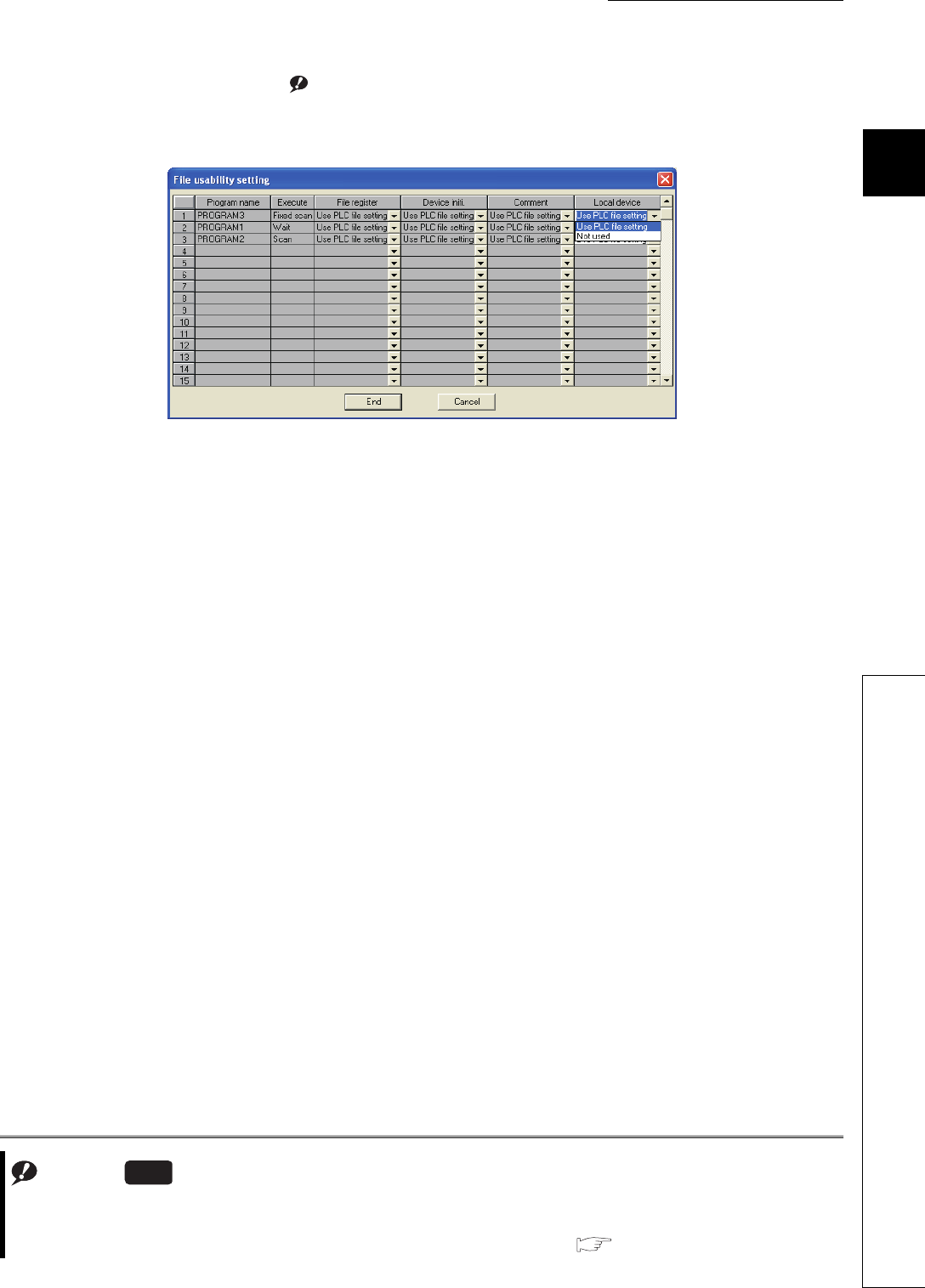
CHAPTER2 SEQUENCE PROGRAMS
1
2
3
4
5
6
7
8
2.3 Settings When Program is Divided
2 - 15
(c) File usability setting Note2.1Note1
For each program, determine whether to use the file specified for the local device in the PLC file tab
of the PLC parameter dialog box.
The default is set to "Use PLC file setting".
When "Not used" is selected, data in the local device is not saved or restored when the program
execution type is changed.
Note1
Figure 2.17 File usability setting
Note2.1
The Q00UJCPU does not support the file usability setting.
When using the file usability setting for the Q02UCPU, Q03UDCPU, Q04UDHCPU, Q06UDHCPU, Q13UDHCPU, or
Q26UDHCPU, check the versions of the CPU module and GX Developer. ( Appendix 2)
Universal
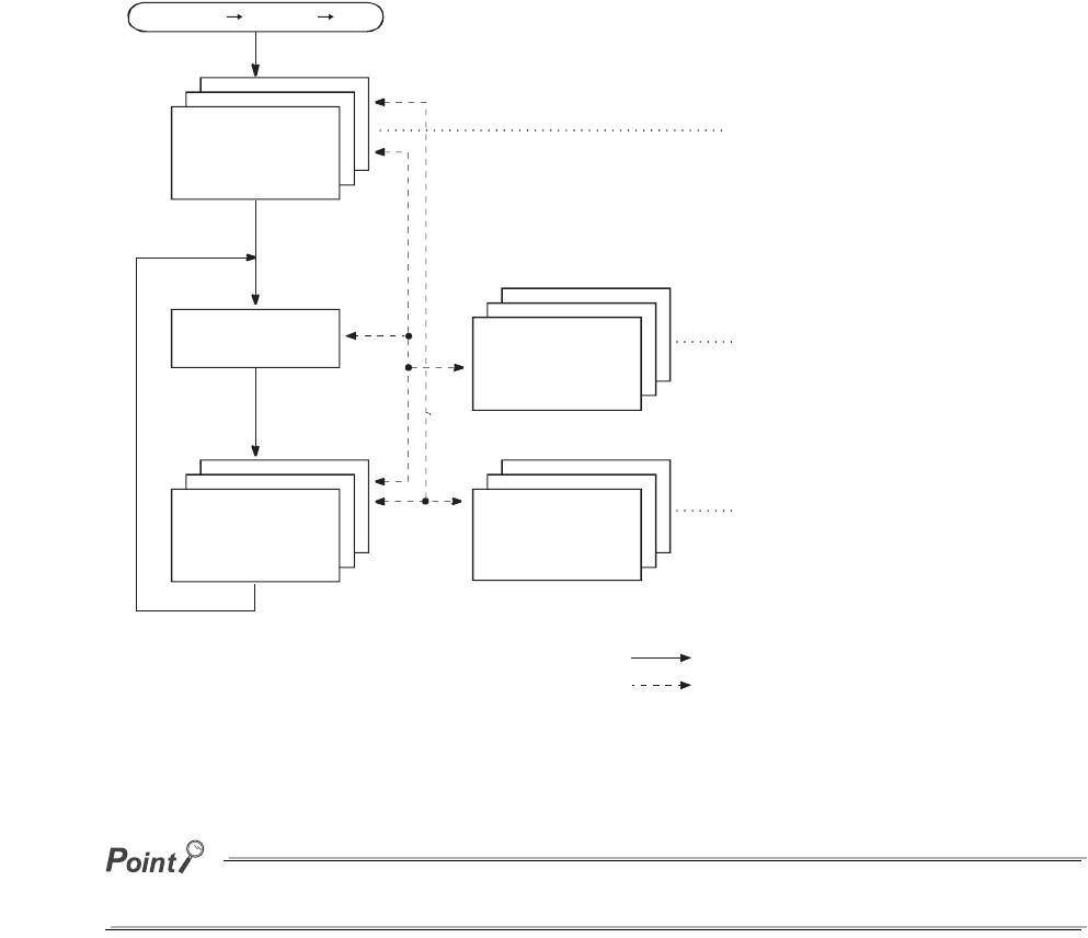
2 - 16
(3) Program sequence in the CPU module
Figure 2.18 shows the program sequence after the CPU module is powered on or its operating status is changed
from STOP to RUN.
Use initial execution type program, stand-by type program, and fixed scan execution type program as required.
Figure 2.18 Program sequence
Powered off on/STOP RUN
Initial execution
type program
Fixed scan
execution type
program
Scan execution
type program
Stand-by
type program
END processing
Executed only once when
the CPU module is powered
on or its status is switched
from STOP to RUN.
Executed at specified
time intervals.
Program execution sequence
Program execution when any
subroutine program or interrupt
program is called
Executed only when its
execution is requested.
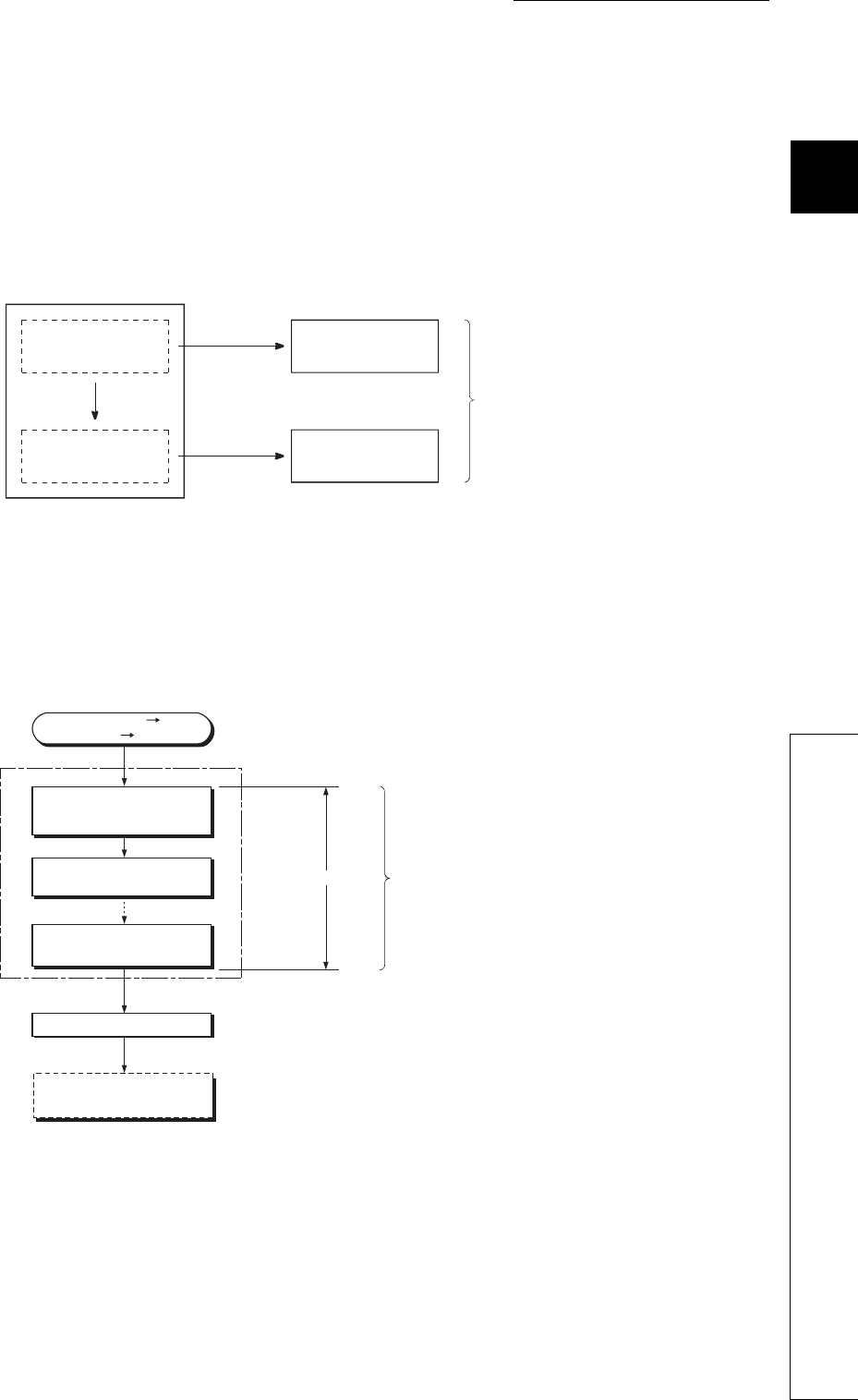
CHAPTER2 SEQUENCE PROGRAMS
1
2
3
4
5
6
7
8
2.3 Settings When Program is Divided
2.3.1 Initial execution type program
2 - 17
2.3.1 Initial execution type program
(1) Definition
Initial execution type program is executed only once when the CPU module is powered on or its
operating status is changed from STOP to RUN.
This type of program can be used as a program that need not be executed from the next scan and
later once it is executed, like initial processing to an intelligent function module.
(2) Processing
(a) Execution order
After completion of all the initial execution type program execution, END processing is performed.
In the next scan and later, scan execution type programs are executed.
Figure 2.19 When processing performed only once is separated as an initial execution type program
Figure 2.20 Execution order of the initial execution type programs
When an initial execution type program is used
Program A
Program B
Control by one program
Processing performed
only once
Processing performed
in every scan
Initial execution type
program
Scan execution type
program
One program can
be divided into two
programs.
Powered off on/
STOP RUN
Initial execution
type program A
Initial execution
type program B
Initial execution
type program n
END processing
1 scan
If there are multiple initial
execution type programs, the
CPU module executes them in
ascending order of the setting.
Scan execution type
program
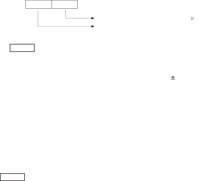
2 - 18
(b) Initial scan time
Initial scan time is the execution time of initial execution type program.
When multiple programs are executed, the initial scan time will be the time required for completing
all the initial execution type program execution.
1) Initial scan time storage location
The CPU module measures the initial scan time and stores it into the special register (SD522 and
SD523).
The initial scan time can be checked by monitoring SD522 and SD523.
If the stored values in SD522 and SD523 are 3 and 400 respectively, the initial scan
time is 3.4ms.
2) Accuracy and measurement of the initial scan time
Accuracy of the initial scan time stored in the special register is 0.1ms.
Even if the WDT instruction (instruction that resets the watchdog timer) is executed in the
sequence program, the measurement of the initial scan time continues.
3) Execution of an interrupt program or fixed scan execution type program
When an interrupt program or fixed scan execution type program is executed before completion of
the initial execution type program execution, the execution time of the executed program will be
added to the initial scan time.
(3) Precautions on programming
Initial execution type programs do not support the instructions that require several scans (instructions
with completion device).
SEND, RECV, and similar instructions
Figure 2.21 Initial scan time storage location
SD522 SD523
Stores the initial scan time. (unit: ms).
Stores the initial scan time of 1ms or less (unit: s).
Example
Example
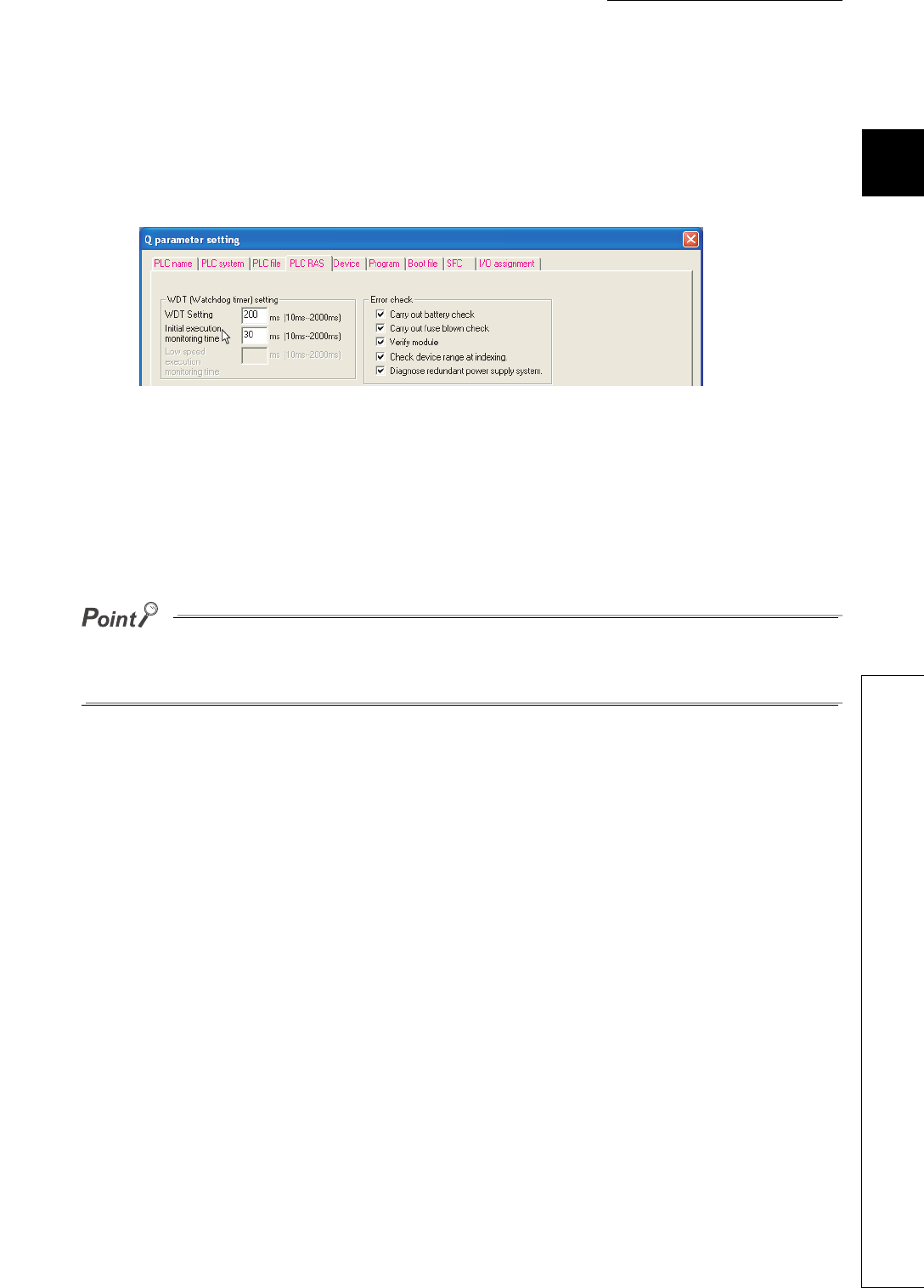
CHAPTER2 SEQUENCE PROGRAMS
1
2
3
4
5
6
7
8
2.3 Settings When Program is Divided
2.3.1 Initial execution type program
2 - 19
(4) Initial execution monitoring time setting
Initial execution monitoring time is a timer for monitoring initial scan time.
Set a time value in the PLC RAS tab of the PLC parameter dialog box.
The setting range is 10 to 2000ms (in increments of 10ms).
No default value is set.
(a) When the initial scan time exceeds the preset initial execution monitoring time
"WDT ERROR" occurs and the CPU module stops program operations.
Set a time value so that the initial execution monitoring time becomes longer than actual initial scan
time.
An error of the measurement value is 10ms for the initial execution monitoring time setting.
If the initial execution monitoring time (t) parameter is set to 10ms, "WDT ERROR" occurs when actual initial
scan time is within the range of 10ms < t < 20ms.
Figure 2.22 PLC RAS setting (Initial execution monitoring time)
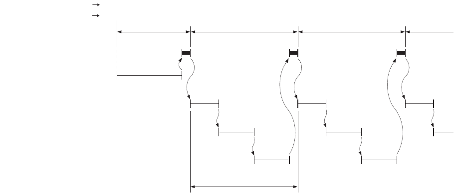
2 - 20
2.3.2 Scan execution type program
(1) Definition
Scan execution type program is executed once in every scan, starting in the next scan of which the
initial execution type program is executed and later.
(2) Processing
When multiple scan execution type programs are executed, the scan time will be the time required for
completing all the scan execution type program execution.
If an interrupt program or fixed scan execution type program is executed, execution time of the
executed program will be added to the scan time.
Figure 2.23 Execution order of the scan execution type programs
1st scan 2nd scan 3rd scan 4th scan
END processing
Initial execution type program
Scan execution type program A
Scan execution type program C
Scan execution type program B
0 END
0 END
0 END
0 END
0 END
0 END
0 END
0
Scan time
Power supply ON RUN
STOP RUN
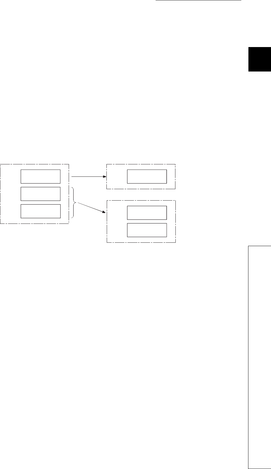
CHAPTER2 SEQUENCE PROGRAMS
1
2
3
4
5
6
7
8
2.3 Settings When Program is Divided
2.3.3 Stand-by type program
2 - 21
2.3.3 Stand-by type program
(1) Definition
Stand-by type program is executed only when its execution is requested.
This type of program can be changed to any desired execution type by a sequence program
instruction.
(2) Application
(a) Program library
Stand-by type program is used as a program library, a collection of subroutine programs and/or
interrupt programs, and managed separately from a main routine program.
Multiple subroutine programs and/or interrupt programs can be created and managed in a single
stand-by type program.
(b) Program type change
Stand-by type program is used to create and store programs available in all systems. Only required
programs will be executed.
For example, a program preset as a stand-by ("Wait") type program in the PLC parameter dialog
box can be changed to a scan execution type program and executed in the sequence program.
Figure 2.24 Program library using a stand-by type program
P100
I0
P100
I0
Scan execution type program Scan execution type program
Stand-by type program
Main routine
program
Main routine
program
Subroutine
program
Interrupt
program Subroutine
program
Interrupt
program
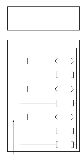
2 - 22
(3) Execution method
Execute stand-by type programs in either of the following methods.
• Create subroutine and/or interrupt programs in a stand-by type program and call them using a
pointer or when an interrupt occurs.
• Change a stand-by type program to any other execution type using instructions.
(a) Creating subroutine and/or interrupt programs in a single stand-by type program
When creating subroutine and/or interrupt programs in a single stand-by type program, start the
program from the step 0.
The FEND instruction used in creation of a subroutine or interrupt program is not required after a
main routine program.
Figure 2.25 Creating subroutine programs in a single stand-by type program
P508
RET
RET
Y10
RET
END
Y11
Y12
P500
P501
Program B (Stand-by type program)
Program A
Main routine
program
Use common pointer.
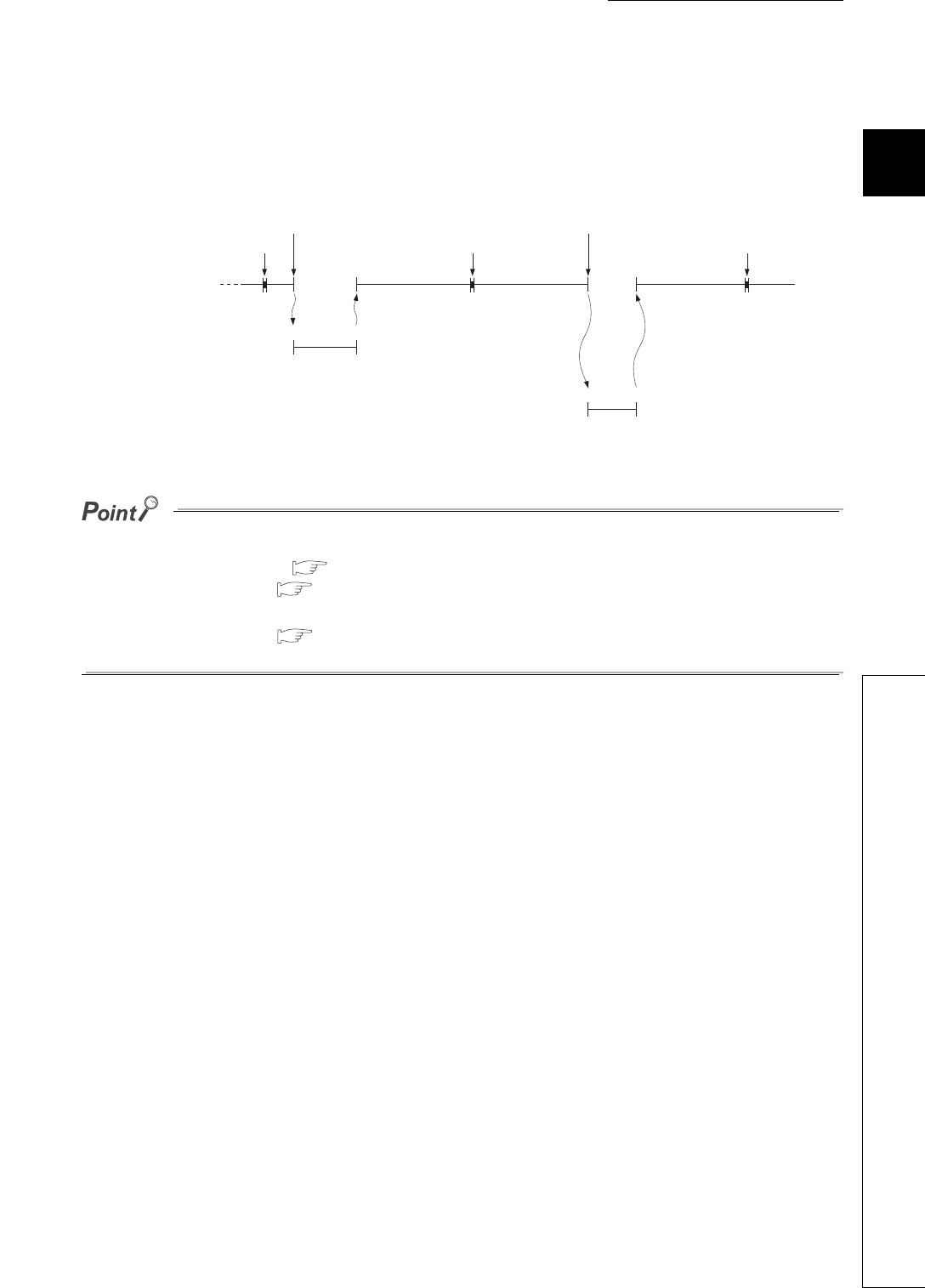
CHAPTER2 SEQUENCE PROGRAMS
1
2
3
4
5
6
7
8
2.3 Settings When Program is Divided
2.3.3 Stand-by type program
2 - 23
1) Executing a subroutine program and interrupt program in a stand-by type program
After execution of the stand-by type program, the CPU module reexecutes the program that called a program
in the stand-by type program.
Figure 2.26 shows the operation when the subroutine and interrupt programs in the stand-by type program
are executed.
●For restrictions on programming of subroutine and interrupt programs, refer to the following.
• Subroutine program: Section 2.2.2
• Interrupt program: Section 2.3.2
●Use common pointers. ( Section 9.10.2)
If local pointers are used, subroutine programs in a stand-by type program cannot be executed from any other program.
Figure 2.26 Operation when the subroutine and interrupt programs in the stand-by type program are executed
P100 RET
I0 IRET
END processing END processing END processing
CALL P100
instruction execution
Interrupt factor
occurrence
Subroutine program within
a stand-by type program
Interrupt program within a
stand-by type program
Main routine program
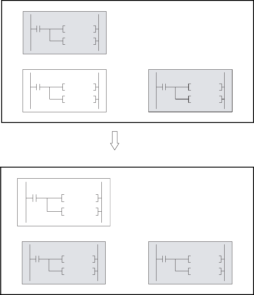
2 - 24
(b) Changing the program execution type using instructions
Use the PSCAN, PSTOP, or POFF instruction to change a program execution type.
1) Changing the execution type (in the case of scan execution type program)
• Set the programs "ABC" and "GHI" as scan execution type programs and the program "DEF" as a stand-
by type program.
• When the condition is established (the internal relay (M0) in Figure 2.27 turns on), the program "DEF" is
changed to a scan execution type program and the program "ABC" to a stand-by type program.
[Before execution of the PSCAN and PSTOP instructions]
[After execution of the PSCAN and PSTOP instructions]
Scan execution type program: ABC
• The PSCAN instruction changes the program "DEF" to
a scan execution type program.
• The PSTOP instruction changes the program "ABC" to
a stand-by type program.
Stand-by type program: DEF Scan execution type program: GHI
Stand-by type program: ABC
Scan execution type program: DEF Scan execution type program: GHI
Figure 2.27 Example of changing the execution type (in the case of scan execution type program)
PSCAN "DEF"
PSTOP "ABC"
MO
PSCAN "GHI"
PSTOP "DEF"
PSCAN "ABC"
PSTOP "GHI"
When M0 turns on
PSCAN
MO
"DEF"
PSTOP "ABC"
PSCAN "GHI"
PSTOP "DEF"
PSCAN "ABC"
PSTOP "GHI"

CHAPTER2 SEQUENCE PROGRAMS
1
2
3
4
5
6
7
8
2.3 Settings When Program is Divided
2.3.3 Stand-by type program
2 - 25
2) Execution type change timing
The program execution type is changed in END processing.
Therefore, the execution type will not be changed in the middle of program execution.
If different types are set to the same program in the same scan, the program will be changed to the type
specified by the last instruction executed.
*1: The programs "GHI" and "DEF" are executed in the order set in the Program tab of the PLC parameter dialog box.
(4) Precautions on programming
(a) Unavailable devices
Unavailable devices depend on the program type (subroutine program or interrupt program) or the execution
type changed by an instruction.
(b) Use of local devices
For execution of a subroutine program using a local device, refer to Section 9.14.2.
Figure 2.28 Execution type change timing
END processing END processing END processing
Program name
PSTOP "ABC"
execution
PSCAN "DEF"
execution
"DEF" is changed to a scan execution type
program and "ABC" is changed to a stand-by
type program.
"GHI" "GHI" "GHI"
"GHI" *1 "DEF" *1
"ABC"
2 - 26
2.3.4 Fixed scan execution type program
(1) Definition
Fixed scan execution type program is a program executed at specified time intervals.
This type of programs, unlike interrupt programs, can be interrupted in units of files without interrupt
pointers or the IRET instruction.
For the restrictions on programming, refer to Section 2.2.3(2)(b).
(The restrictions on programming are the same as those for interrupt programs.)
To execute a fixed scan execution type program, execute the EI instruction in the initial execution type program
or scan execution type program to enable interrupts.
Figure 2.29 Execution of a fixed scan execution type program
Fixed scan interval
END processing
Scan execution
type program
Fixed scan execution
type program
Condition
established
Condition
established
CHAPTER2 SEQUENCE PROGRAMS
1
2
3
4
5
6
7
8
2.3 Settings When Program is Divided
2.3.4 Fixed scan execution type program
2 - 27
(2) Processing
(a) When two or more fixed scan execution type programs exist
Each fixed scan execution type program is executed at specified time intervals.
If two or more fixed scan execution type programs reach the specified time at the same timing,
programs will be executed in ascending order of the numbers set in the Program tab of the PLC
parameter dialog box.
(b) When both fixed scan execution type program and interrupt program exist
When a fixed scan execution type program and an interrupt program (I28 to I31) reach the specified
time at the same timing, the interrupt program will be given priority.
(c) When the execution condition is established during link refresh
The link refresh is suspended and a fixed scan execution type program is executed.
Even if the Block data assurance per station setting is enabled in the CC-Link IE controller network or
MELSECNET/H network, this setting does not work when a device set as a refresh target is used in the fixed
scan execution type program.
In the fixed scan execution type program, do not use any refresh target device.
Remark
For the Block data assurance per station setting, refer to the following.
Reference manual for each network module
Figure 2.30 When the execution condition is established during link refresh
Interrupt factor
10ms 10ms 10ms 10ms
Fixed scan execution type
program execution
Link refresh execution
Link refresh is suspended and fixed scan
execution type program is executed.
2 - 28
(d) When the execution condition is established during END processing
When the execution condition is established during the waiting time of the constant scan execution
or the END instruction, a fixed scan execution type program is executed.
(3) Processing at program execution type change
For how to save and restore data in the index register when the program execution type is changed, refer to
Section 2.2.3(4). (The method is the same as that for interrupt programs.)
Figure 2.31 When the execution condition is established during the waiting time
Fixed scan interval
END processing
Scan execution
type program
Fixed scan execution
type program
*1: Waiting time
*2: If processing is not completed within the
waiting time, the scan time increases.
Condition
established
Constant scan
*2
*1
CHAPTER2 SEQUENCE PROGRAMS
1
2
3
4
5
6
7
8
2.3 Settings When Program is Divided
2.3.4 Fixed scan execution type program
2 - 29
(4) Precautions
(a) Execution interval of a fixed scan execution type program
Execution interval of a fixed scan execution type program may increase from the preset interval
depending on the time set for disabling interrupts by the DI instruction (interrupt disabled time).
If the interrupt disabled time by the DI instruction becomes too long, use an interrupt program by
fixed scan interrupt (I28 to I31) instead of a fixed scan execution type program.
*1: This is the highest common factor of execution interval set to multiple fixed scan execution type programs
When the condition 1) is satisfied, the actual execution interval of a fixed scan execution type
program may increase from the preset interval by the time shown in the expression below.
The following shows an example of the increase in execution time of a fixed scan execution type
program.
With the settings above, the condition 1) will be 0.5ms < 5ms.
The execution time of a fixed scan execution type program whose execution interval is set to 10ms
increases 100ms (5 0.5 10 = 100) at the most.
Highest common factor of fixed scan execution interval *1 < Interrupt disabled time ••• Condition 1)
•Fixed scan execution interval ••• 10ms, 5ms, 1ms, 0.5ms
•Highest common factor of fixed scan execution interval ••• 0.5ms
•Interrupt disabled time (DI) ••• 5ms
(Interrupt enabled time (EI) ••• less than 0.5ms)
Figure 2.32 Program execution and interrupt enabled/disabled status
Interrupt disabled time
Highst common factor of scan
execution interval
Fixed scan execution interval set to
the corresponding program
Example
Program execution
operation
Interrupt enabled/
disabled status Disabled Disabled Disabled
Enabled Enabled
Interrupt disabled time = 5ms Interrupt disabled time = 5ms
n scan n+1 scan
EI EI
END END
DI DI
Less than 0.5ms Less than 0.5ms
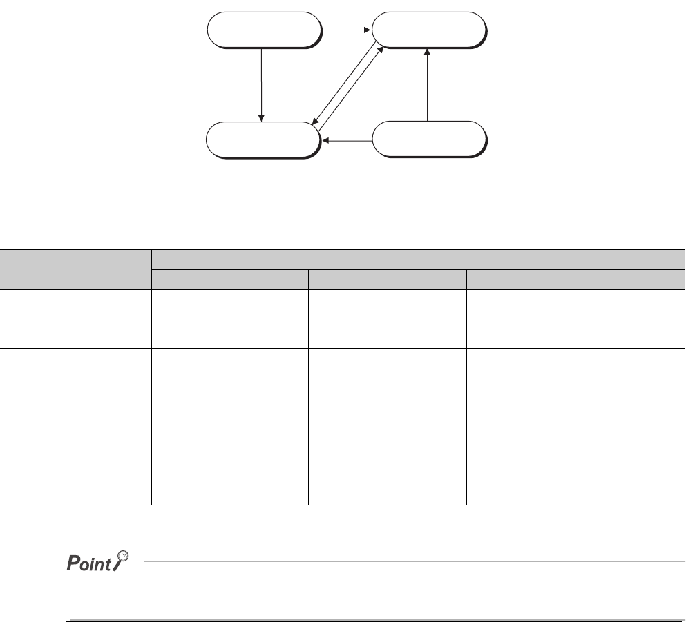
2 - 30
2.3.5 Changing the program execution type
(1) Changing the execution type using instructions
(a) Instructions used to change the execution type
The execution type of sequence programs can be changed using instructions even during
execution.
Use the PSCAN, PSTOP, or POFF instruction to change the execution type.
Once the fixed scan execution type program is changed to another execution type, the type cannot be returned
to the fixed scan execution type.
Figure 2.33 Pattern of execution type change
Table2.1 Timing of execution type change
Execution type before
change
Instruction
PSCAN PSTOP POFF
Scan execution type Remains unchanged. Changes to the stand-by
type.
Turns off outputs in the next scan.
Changes to the stand-by type in two
scans later.
Initial execution type Changes to the scan
execution type.
Changes to the stand-by
type.
Turns off outputs in the next scan.
Changes to the stand-by type in two
scans later.
Stand-by type Changes to the scan
execution type. Remains unchanged. No processing
Fixed scan execution
type
Changes to the scan
execution type.
Changes to the stand-by
type.
Turns off outputs in the next scan.
Changes to the stand-by type in two
scans later.
Initial execution
type program
Stand-by type
program
Fixed scan execution
type program
Scan execution
type program
PSCAN
instruction
PSCAN
instruction
PSCAN
instruction
PSTOP, POFF
instruction
PSTOP, POFF
instruction
PSTOP, POFF
instruction
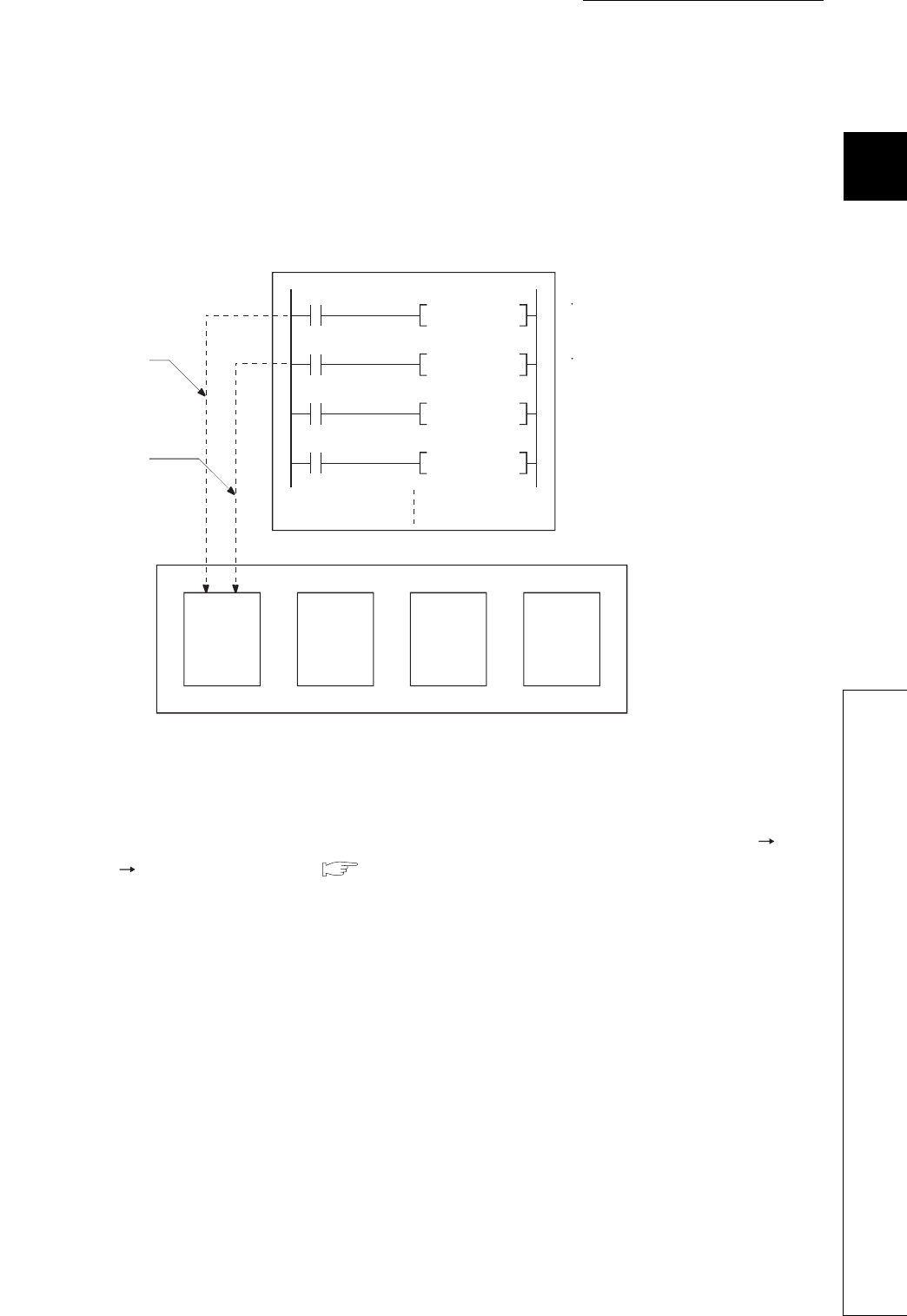
CHAPTER2 SEQUENCE PROGRAMS
1
2
3
4
5
6
7
8
2.3 Settings When Program is Divided
2.3.5 Changing the program execution type
2 - 31
(b) Execution type change example
In a control program, a stand-by type program matching the preset condition is changed to a scan
execution type program in the course of program execution.
An unused scan execution type program can also be changed to a stand-by type program.
Figure 2.34 shows the case where the execution type of the stand-by type programs "ABC", "DEF",
"GHI", and "JKL" are changed in the control program.
(2) Changing the execution type from the Program monitor list screen
The execution type of programs can be changed on the screen opened by selecting [Online]
[Monitor] [Program monitor list]. ( Section 6.13.1)
Figure 2.34 Execution type change example
PSCAN "ABC"
M0
PSTOP "ABC"
M1
PSCAN "DEF"
Control program
When M0 turns on, the
program "ABC" is
changed from a stand-by
type to a scan execution
type program.
When M1 turns on, the
program "ABC" is
changed from a scan
execution type to a
stand-by type program.
"DEF"
PSTOP
The PSCAN instruction
changes the program "ABC" to
a scan execution type program.
The PSTOP instruction changes
the program "ABC" to a stand-
by type program.
Stand-by
type
program
:ABC
Stand-by
type
program
:DEF
Stand-by
type
program
:GHI
Stand-by
type
program
:JKL

2 - 32
2.4 Data Used in Sequence Programs
The CPU module represents numeric and alphabetic data using two symbols (states): 0 (off) and 1 (on).
Data represented using these two symbols is called binary number (BIN).
The CPU module can also use hexadecimal (HEX) (each hexadecimal digit represents four binary bits), binary-coded
decimal (BCD), or real numbers.
Tabl e2. 2 shows the numeric representations of BIN, HEX, BCD, and DEC (decimal).
Table2.2 Numeric representations of BIN, HEX,BCD,and DEC
DEC (Decimal) HEX (Hexadecimal) BIN (Binary) BCD (Binary-coded decimal)
00 0 0
11 1 1
22 10 10
3 3 11 11
9 9 1001 1001
10 A 1010 1 0000
11 B 1011 1 0001
12 C 1100 1 0010
13 D 1101 1 0011
14 E 1110 1 0100
15 F 1111 1 0101
16 10 1 0000 1 0110
17 11 1 0001 1 0111
47 2F 10 1111 100 0111
32766 7FFE 0111 1111 1111 1110 -
32767 7FFF 0111 1111 1111 1111 -
-32768 8000 1000 0000 0000 0000 1000 0000 0000 0000
-32767 8001 1000 0000 0000 0001 1000 0000 0000 0001
-2 FFFE 1111 1111 1111 1110 -
-1 FFFF 1111 1111 1111 1111 -
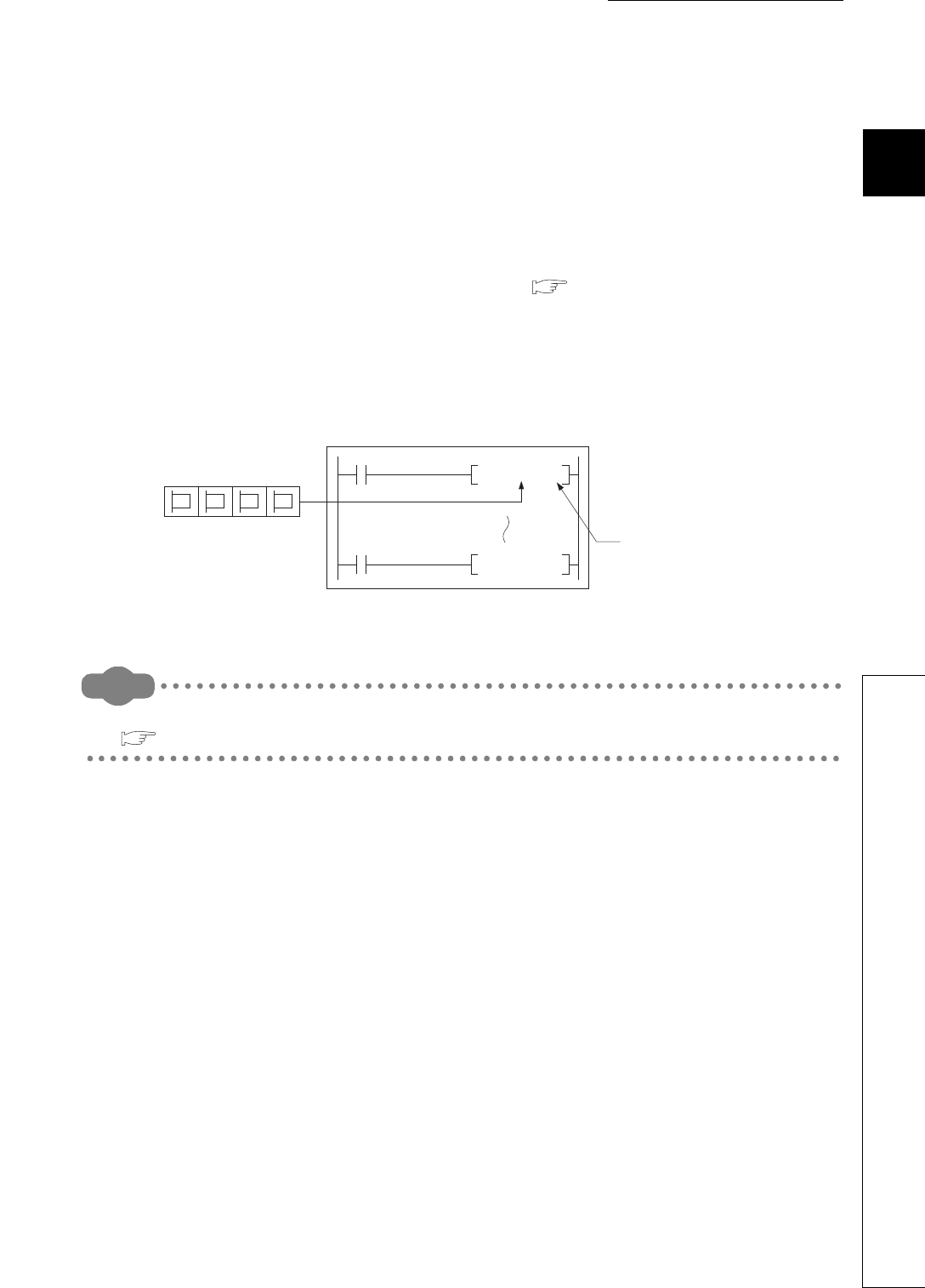
CHAPTER2 SEQUENCE PROGRAMS
1
2
3
4
5
6
7
8
2.4 Data Used in Sequence Programs
2 - 33
(1) Inputting numeric values externally to the CPU module
When setting a numeric value to the CPU module externally using a digital switch, BCD (binary-coded decimal)
can be used as DEC (decimal) by the method given in (b).
(a) Numeric values used inside the CPU module
The CPU module performs program operations in binary.
If the value set in binary-coded decimal is used without conversion, the CPU module performs program
operations regarding the set value as binary.
Therefore, the program operations are not performed correctly. ( (b) below)
(b) Using any numeric data regardless of the data type
To convert the data set in binary-coded decimal into binary, which can be used in the CPU module, use the BIN
instruction.
The BIN instruction allows the CPU module to use any external numeric data regardless of the data type.
Remark
For details of the BIN instruction, refer to the following.
QCPU Programming Manual (Common Instructions)
Figure 2.35 Inputting data from a digital switch to the CPU module
[Setting numeric data]
Digital switch
XF X0to
4321
CPU module
Input data in BCD.
BIN data
BINP K4X0 DO
BCD D5 K4Y30
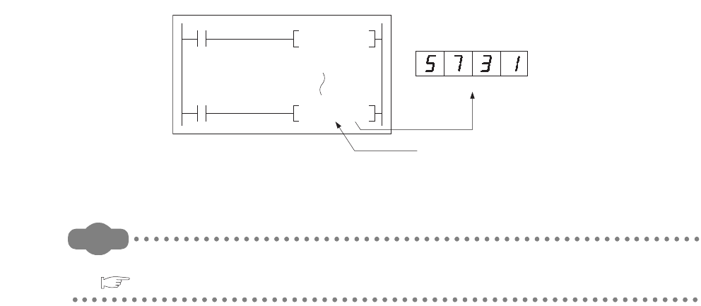
2 - 34
(2) Outputting numeric values externally from the CPU module
When externally displaying numeric values operated in the CPU module, a digital indicator can be used.
(a) Outputting numeric values
The CPU module performs program operations in binary.
If the binary values used in the CPU module are output to a digital indicator, the indicator does not show the
values correctly.
To convert the data set in binary into binary-coded decimal, which can be used in the external indicator, use the
BCD instruction.
The BCD instruction allows the external indicator to display values in decimal.
Remark
For details of the BCD instruction, refer to the following.
QCPU Programming Manual (Common Instructions)
Figure 2.36 Display of operation results in the CPU module by a digital indicator
[Setting numeric data]
Digital indicator
Y3F Y30to
CPU module
Output data
in BCD.
BIN data
BINP K4X0 DO
BCD D5 K4Y30

CHAPTER2 SEQUENCE PROGRAMS
1
2
3
4
5
6
7
8
2.4 Data Used in Sequence Programs
2.4.1 BIN (Binary Code)
2 - 35
2.4.1 BIN (Binary Code)
(1) Definition
Binary is a numeral system that represents numeric values using two symbols, 0 (off) and 1 (on).
Decimal notation uses the symbols 0 through 9. When the symbols for the first digit are exhausted (a
digit reaches 9), the next-higher digit (to the left) is incremented, and counting starts over at 0.
In binary notation, only the symbols 0 and 1 are used. After a digit reaches 1, an increment resets it to
0 and the next digit (to the left) is incremented. (The numeric value becomes 10, which is equal to 2 in
decimal.)
Table2.3 shows the numeric representations in BIN and DEC.
Table2.3 Numeric representations in BIN and DEC
DEC (Decimal) BIN (Binary)
0 0000
1 0001
2 0010
3 0011
4 0100
5 0101
60110
7 0111
8 1000
9 1001
10 1010
11 1011
Carry
Carry
Carry
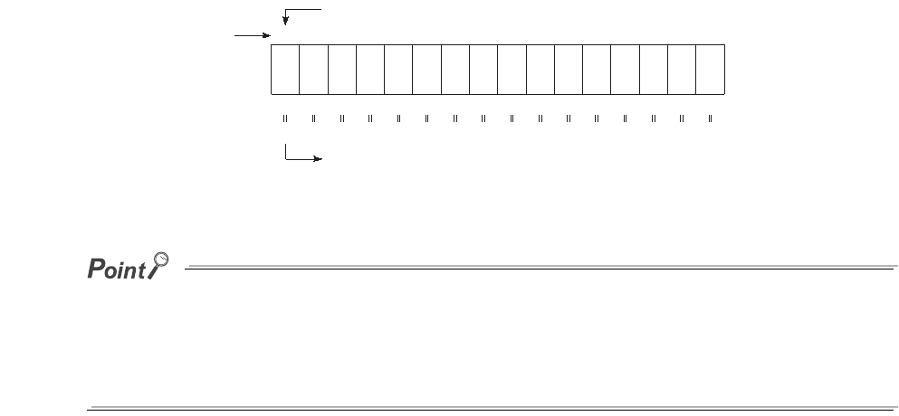
2 - 36
(2) Numeric representation in BIN
(a) Bit configuration of BIN used in the CPU module
Each register (such as the data register, link register) in the CPU module consists of 16 bits.
(b) Numeric data available in the CPU module
Each register in the CPU module can store numeric values in the range of -32768 to 32767.
Figure 2.37 shows the numeric representations for registers.
A numeric value of 2n is assigned for each bit of registers.
Note that an unsigned binary number (0 to 65535) cannot be used in the most significant bit position since the
most significant bit is a sign bit.
• The most significant bit is "0"...Positive
• The most significant bit is "1"...Negative
Figure 2.37 Numeric representations for registers in the CPU module
b15
8192
Bit name
Decimal value
Most significant bit (sign bit)
A value will be negative value when the most significant bit is "1".
16384
4096 2048 1024 512 256 128 64 32 16 8 4 2 1
-32768
215 214 213 212 211 210 29282726252423222120
b14 b13 b12 b11 b10 b9 b8 b7 b6 b5 b4 b3 b2 b1 b0
CHAPTER2 SEQUENCE PROGRAMS
1
2
3
4
5
6
7
8
2.4 Data Used in Sequence Programs
2.4.2 HEX (Hexadecimal)
2 - 37
2.4.2 HEX (Hexadecimal)
(1) Definition
Hexadecimal (HEX) is a numeral system that represents four binary bits as one digit.
With four binary bits, sixteen different numeric values, 0 to 15, can be represented.
Hexadecimal notation uses 16 symbols to represent numeric values 0 to 15 in one digit, the symbols 0
to 9 to represent values zero to nine, and AH to FH to represent values ten to fifteen. After a digit
reaches FH, the next-higher digit (to the left) is incremented.
ï\2.4 shows the numeric representations in BIN, HEX, and DEC.
(2) Numeric representation in HEX
Each register (such as the data register, link register) in the CPU module consists of 16 bits.
In the 16-bit configuration register, 0 to FFFFH can be specified in hexadecimal.
Table2.4 Numeric representations in BIN,HEX,and DEC
DEC (Decimal) HEX (Hexadecimal) BIN (Binary)
0 0 0
1 1 1
22 10
33 11
9 9 1001
10 A 1010
11 B 1011
12 C 1100
13 D 1101
14 E 1110
15 F 1111
16 10 1 0000
17 11 1 0001
47 2F 10 1111
Carry

2 - 38
2.4.3 BCD (Binary-coded Decimal)
(1) Definition
BCD is a numeral system that uses four binary bits to represent the decimal digits 0 through 9.
The difference from hexadecimal is that BCD does not use letters A to F.
Table2.5 shows the numeric representations in BIN, BCD, and DEC.
(2) Numeric representation in BCD
Each register (such as the data register, link register) in the CPU module consists of 16 bits.
Therefore, the numeric values can be stored in each register are those in the range between 0 to 9999 in BCD.
Table2.5 Numeric representations in BIN,BCD,and DEC
DEC (Decimal) BIN (Binary) BCD (Binary-coded Decimal)
0 0000 0
1 0001 1
20010 10
3 0011 11
4 0100 100
5 0101 101
6 0110 110
7 0111 111
8 1000 1000
9 1001 1001
10 1010 1 0000
11 1011 1 0001
12 1100 1 0010
Carry

CHAPTER2 SEQUENCE PROGRAMS
1
2
3
4
5
6
7
8
2.4 Data Used in Sequence Programs
2.4.4 Real number (Floating-point data)
2 - 39
2.4.4 Real number (Floating-point data)
There are two types of real number data: single-precision floating-point data and double-precision
floating-point data.
(1) Single-precision floating-point data
(a) Internal representation
Internal representation of real numbers used in the CPU module is given below.
Real number data can be represented as follows, using two word devices.
[Sign] 1. [Mantissa] 2[Exponent]
The bit configuration and the meaning of each bit are described below.
1) Sign
The most significant bit, b31, is the sign bit.
0: Positive
1: Negative
2) Exponent
The 8 bits, b23 to b30, represent the excess n of 2n.
The following shows the excess n according to the binary values in b23 to b30.
3) Mantissa
Each of the 23 bits, b0 to b22, represents the "XXXXXX..." portion when the data is represented in binary,
"1.XXXXXX...".
Figure 2.38 Bit configuration of real number data
Figure 2.39 Relation between the exponent and excess n
b31 b30 to b23 b22 to b16 b15 to b0
b31 b22 to b0
Mantissa (23 bits)
b30 to b23
Exponent (8 bits)
Sign
b23 to b30
n
FFH
Not used
FEH
127
FDH
126
00H
Not used
02H
-125
01H
-126
81H
2
80H
1
7FH
0
7EH
-1
2 - 40
(b) Calculation example
Calculation examples are shown below. (The "X" in (nnnnnn) x indicates the numeral system used.)
1) Storing "10"
(10)10 (1010)2 (1.010000..... 23)2
Sign: Positive 0
Exponent: 3 82H (10000010)2
Mantissa: (010 00000 00000 00000 00000)2
In this case, the value will be encoded as 41200000H.
2) Storing "0.75"
(0.75)10 (0.11)2 (1.100..... 2-1)2
Sign: Positive 0
Exponent: -1 7EH (01111110)2
Mantissa: (100 00000 00000 00000 00000)2
In this case, the value will be encoded as 3F400000H.
Values after the decimal point (in binary) is calculated as follows.
(0.1101)2
(0.1101)2 = 2-1 + 2-2 + 2-4 = 0.5 + 0.25 + 0.0625 = (0.8125)10
0.1101
The bit represents 2-1 The bit represents 2-2 The bit represents 2-3 The bit represents 2-4
Sign Exponent Mantissa
0 1 0 0 0 0 0 1 0 0 1 0 0 0 0 0 0 0 0 0 0 0 0 0 0 0 0 0 0 0 0 0
41 2 00000
0 0 1 1 1 1 1 1 0 1 0 0 0 0 0 0 0 0 0 0 0 0 0 0 0 0 0 0 0 0 0 0
3F4 00000
Sign Exponent Mantissa
Example

CHAPTER2 SEQUENCE PROGRAMS
1
2
3
4
5
6
7
8
2.4 Data Used in Sequence Programs
2.4.4 Real number (Floating-point data)
2 - 41
(2) Double-precision floating-point data
(a) Internal representation
Real number data used in the CPU module is internally represented as follows, using four word
devices.
[Sign] 1. [Mantissa] 2[Exponent]
The bit configuration and the meaning of each bit are described below.
1) Sign
The most significant bit, b63, is the sign bit.
0: Positive
1: Negative
2) Exponent
The 11 bits, b52 to b62, represent the excess n of 2n.
The following shows the excess n according to the binary values in b52 to b62.
3) Mantissa
Each of the 52 bits, b0 to b51, represents the "XXXXXX..." portion when the data is represented in binary,
"1.XXXXXX...".
Figure 2.40 Bit configuration of real number data
Figure 2.41 Relation between the exponent and excess n
b63 b62 to b52 b51 to b16 b15 to b0
b63 b0 to b51
Mantissa (52 bits)
b52 to b62
Exponent (11 bits)
Sign
b52 to b62
n
7FFH7FEH
1023
7FDH
1022
00H
Not usedNot used
02H
-1021
01H
-1022
400H
2
3FFH
1
3FEH
0
3FDH
-1
3FCH
-2
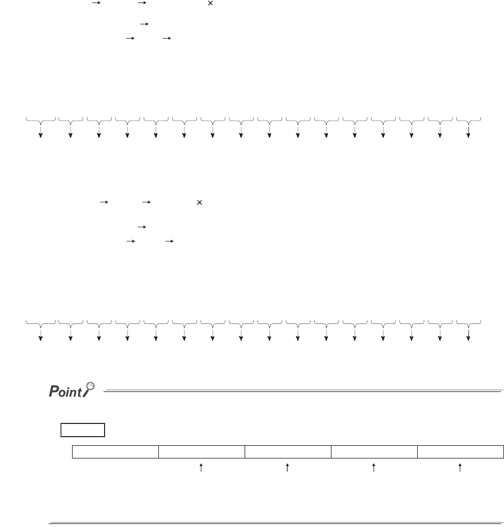
2 - 42
(b) Calculation example
Calculation examples are shown below. (The "X" in (nnnnnn) x indicates the numeral system used.)
1) Storing "10"
(10)10 (1010)2 (1.010000..... 23)2
Sign: Positive 0
Exponent: 3 401H (100 0000 0001)2
Mantissa: (0100 0000 0000 0000 0000 0000 0000 0000 0000 0000 0000 0000 0000)2
In this case, the value will be encoded as 4014000000000000H.
2) Storing "0.75"
(0.75)10 (0.11)2 (1.100..... 2-1)2
Sign: Positive 0
Exponent: -1 3FDH (011 1111 1101)2
Mantissa: (1000 0000 0000 0000 0000 0000 0000 0000 0000 0000 0000 0000 0000)2
In this case, the value will be encoded as 3FD8000000000000H.
Values after the decimal point (in binary) is calculated as follows.
(0.1101)2
(0.1101)2 = 2-1 + 2-2 + 2-4 = 0.5 + 0.25 + 0.0625 = (0.8125)10
0.1101
The bit represents 2-1 The bit represents 2-2 The bit represents 2-3 The bit represents 2-4
Sign Exponent Mantissa
0 100000000010100000000000000000000000000000000000000000000000000
4 014000000000000
Sign Exponent Mantissa
0 011111111011000000000000000000000000000000000000000000000000000
3 FD8000000000000
Example

CHAPTER2 SEQUENCE PROGRAMS
1
2
3
4
5
6
7
8
2.4 Data Used in Sequence Programs
2.4.5 Character string data
2 - 43
2.4.5 Character string data
(1) Definition
The CPU module uses ASCII code data.
(2) ASCII code character strings
Table 2.6 lists the ASCII code character strings.
"00H" (NULL code) in Table2.6 is used at the end of a character string as a terminator.
Table2.6 ASCII code character strings
b8 b7 b6 b5 b4 b3 b2 b1 Low
00000
0123456789ABCDEF
00011
00102
0
0
0113
0
1004
0
1015
1
0
1106
1
11
10
10
11
11
17
1
0008
1
1
0019
1
010A
1
011B
0
1
1
1
0
E
F
D
C
NULL (SP)
!
"
#
$
%
&
'
(
)
+
(Comma)
,
(Minus)
-
(Period)
z
(Under
line)
_
/
0
1
2
3
4
5
6
7
8
9
:
;
<
=
>
?
@
A
B
C
D
E
F
G
H
I
J
K
L
M
N
O
`
a
b
c
d
e
f
g
h
i
j
k
l
m
n
o
P
Q
R
S
T
U
V
W
X
Y
Z
[
\
]
^
p
q
r
s
t
u
v
w
x
y
z
{
|
}
0000000011111111
0000111100001111
0011001100110011
0101010101010101
Column
3 - 1
CHAPTER3 CPU MODULE OPERATION
This chapter describes operation of the CPU module.
3.1 Initial Processing
The CPU module performs preprocessing required for sequence program operations.
The preprocessing is executed only once when any of the operations described in Tabl e3.1 is performed to
the CPU module.
When initial processing is completed, the CPU module will be placed in the operation status set by the
RUN/STOP/RESET switch. ( Section 3.5)
: Performed, : Not performed
*1: The operation indicates that the status is changed back to RUN without resetting the module after any parameter or program was changed
in the STOP status.
(The RUN/STOP/RESET switch is set from STOP to RUN (the RUN LED will flash), then back to STOP and to RUN again.)
Note that the PLS P instruction (instruction for pulse conversion) may not be executed properly with the above operation. This is
because the previous information may not be inherited depending on the program changes.
If any parameter or program is changed in the STOP status, reset the CPU module using the RUN/STOP/RESET switch.
Table3.1 Initial processing list
Initial processing item
CPU module status
Powered-on Reset Changed from STOP to RUN *1
The I/O module initialization
Boot from a memory card
PLC parameter check
Multiple CPU system parameter consistency check
Initialization of devices outside the latch range
(bit device: off, word device: 0)
Automatic I/O number assignment of mounted modules
CC-Link IE controller network and MELSECNET/H
information setting
Intelligent function module switch setting
CC-Link information setting
Ethernet information setting
Initial device value setting
Serial communication function setting
RUN
RESET
STOP
RUN/STOP/RESET switch

CHAPTER3 CPU MODULE OPERATION
1
2
3
4
5
6
7
8
3.2 I/O Refresh (Refresh Processing with Input/Output Modules)
3 - 2
3.2 I/O Refresh (Refresh Processing with Input/Output Modules)
The CPU module performs the following before sequence program operations.
• On/off data input from the input module or intelligent function module to the CPU module
• On/off data output from the CPU module to the output module or intelligent function module
When the constant scan time is set, I/O refresh is performed after the constant scan waiting time has
elapsed. (I/O refresh is performed at each constant scan cycle.)
3.3 Program Operation
The CPU module sequentially executes the program stored in the module from the step 0 to the END or
FEND instruction.( CHAPTER 2)
3.4 END Processing
The CPU module performs refresh processing with network modules and communication with external
devices.
END processing includes the following.
• Refresh with network modules ( CHAPTER 10)
• Auto refresh with intelligent function module ( Section 7.1.1)
• Intelligent function module dedicated instruction processing ( CHAPTER 10)
• Device data latch processing ( Section 6.3, CHAPTER 10)
• Service processing ( Section 6.24, CHAPTER 10)
• Watchdog timer reset ( Section 6.16)
• Auto refresh between multiple CPU modules ( QCPU User's Manual (Multiple CPU System))
• Device data collection using the sampling trace function (only when trace point is set to every scan (after
END instruction execution)) ( Section 6.14)
• Self-diagnostics processing ( Section 6.17)
• Special relay/special register value setting (only for those that should be set during END processing)
( CHAPTER 12)
When the constant scan function ( Section 6.2) is used, the results of processing performed in
END processing are held for the period between after END processing is completed and until the
next scan starts.

3 - 3
3.5 Operation Processing in the RUN,STOP, or PAUSE Status
There are three types of operating status of the CPU module.
•RUN status
•STOP status
•PAUSE status
This section describes program operation processing in the CPU module based on its operating status.
(1) Operation processing in the RUN status
RUN status is a status where sequence program operations are repeatedly performed in a loop
between the step 0 and the END (FEND) instruction.
(a) Output status when entering the RUN status
The CPU module outputs either of the following according to the output mode parameter setting when its status
is changed to RUN. ( Section 6.4)
• Output (Y) status saved immediately before entering the STOP status
• Result of operations performed for one scan after entering the RUN status
(b) Processing time required before operations
The processing time required for the CPU module to start sequence program operations after its
operating status is changed from STOP to RUN varies depending on the system configuration and/
or parameter settings. (It takes one to three seconds normally.)
(2) Operation processing in the STOP status
STOP status is a status where sequence program operations are stopped by the RUN/STOP/RESET
switch or the remote STOP function ( Section 6.6.1).
The CPU module status will be changed to STOP when a stop error occurs.
(a) Output status when entering the STOP status
When entering the STOP status, the CPU module saves data in the output (Y) and turns off all
outputs.
The device memory other than that of the output (Y) will be held.
(3) Operation processing in the PAUSE status
PAUSE status is a status where sequence program operations are stopped by the remote PAUSE
function ( Section 6.6.2) after operations are performed for one scan, holding the output and
device memory status.

CHAPTER3 CPU MODULE OPERATION
1
2
3
4
5
6
7
8
3.5 Operation Processing in the RUN,STOP, or PAUSE Status
3 - 4
(4) Operation processing in the CPU module when switch operation is performed
The CPU module performs the following in any of the RUN, STOP, or PAUSE status.
• Refresh processing with I/O modules
• Refresh processing with network modules
• Auto refresh processing with intelligent function modules
• Self-diagnostics processing
• Service processing
• Intelligent function module dedicated instruction processing (completion processing only)
• Operation processing of Multiple CPU high speed transmission function
Even if the CPU module is in the STOP or PAUSE status, the following operations can be executed.
• I/O monitor or test operation from GX Developer
• Read/write data from/to external devices using the MC protocol
• Communication with other stations using CC-Link IE controller network or MELSECNET/H
• Communication with CC-Link remote stations
Table3.2 Operation processing when switch operation is performed
RUN/STOP
status
CPU module operation processing
Sequence program
operation
processing
External output
Device memory
M,L,S,T,C,D Y
RUN STOP
The CPU module
executes the program
until the END
instruction and stops.
The CPU module saves
the output (Y) status
immediately before its
status is changed to
STOP and turns off all the
outputs.
The CPU module holds the device
memory status immediately before its
status is changed to STOP.
The CPU module saves
the output (Y) status
immediately before its
status is changed to
STOP and turns off all the
outputs.
STOP RUN
The CPU module
executes the program
from the step 0.
The CPU module outputs
data according to the
output mode parameter
setting.
( Section 6.4)
The CPU module holds the device
memory status immediately before its
status is changed to STOP.
Note that the CPU module uses initial
device values if those values are
preset.
Local device data are cleared.
The CPU module outputs
data according to the
output mode parameter
setting.
( Section 6.4)

3 - 5
3.6 Operation Processing during Momentary Power Failure
When the input voltage supplied to the power supply module drops below the specified range, the CPU
module detects a momentary power failure and performs the following operation.
(1) When a momentary power failure occurs for a period shorter than the allowable power
failure time
The CPU module registers error data and suspends the operation processing.
The CPU module, however, continues measurement in the timer device and holds the output status.
(a) When resume start is specified for the SFC program
Data in the system is saved.
(b) When power is recovered after a momentary power failure
The CPU module restarts its operation processing.
(c) Watchdog timer (WDT) measurement during a momentary power failure
Even if operation processing is suspended due to a momentary power failure, the CPU module
continues the measurement of the watchdog timer (WDT).
For example, when the WDT setting of PLC parameter is 200ms and the scan time is 190ms, if a
momentary power failure occurs for 15ms, "WDT ERROR" occurs.
(2) When a momentary power failure occurs for a period longer than the allowable power
failure tim
The CPU module starts its operations initially.
Operation processing will be the same as that when any of the following is performed.
• Programmable controller is powered on.
• The CPU module is reset by the RUN/STOP/RESET switch.
• The CPU module is reset by GX Developer (the remote reset operation).
●In a redundant power supply system, the CPU module does not suspend its operations if a momentary
power failure occurs in either of the power supply modules. However, if a momentary power failure occurs
under the condition where the power is supplied to only one of the power supply modules, operations are
suspended.
●Information of a momentary power failure occurred in a redundant power supply system will be stored in
SM1782 to SM1783 and SD1782 to SD1783.
On the other hand, information of a momentary power failure occurred in a single power supply system
will be stored in SM53 and SD53. ( CHAPTER 12)
Figure 3.1 Operation processing during a momentary power failure
END
END
0
END
0
Momentary power
failure occurrence Power recovery
The CPU module suspends
its program operations.

CHAPTER3 CPU MODULE OPERATION
1
2
3
4
5
6
7
8
3.7 Data Clear Processing
3 - 6
3.7 Data Clear Processing
This section describes how to clear data in the CPU module and the setting required for the latch data
clear.
(1) Clearing data in the CPU module
Data in the CPU module are cleared when the reset operation (by the RUN/STOP/RESET switch or
by powering the module off and then on) is performed.
However, data in (a) below cannot be cleared by the reset operation.
(a) Data that cannot be cleared by the reset operation
• Data in the program memory
• Data in the standard ROM
• Data in a memory card
• Data in latch-specified devices ( (2) in this section)
• Data in the file register
(b) Clearing data that cannot be cleared by the reset operation
1) Data in the program memory
Data can be cleared by:
• selecting the "Clear program memory" checkbox in the Boot file tab of the PLC parameter
dialog box, or
• selecting [Online] [Delete PLC data] in GX Developer.
2) Data in the standard ROM
Data can be cleared automatically when the data is written to the standard ROM.
3) Data in a memory card
Data can be cleared by selecting [Online] [Delete PLC data] in GX Developer.
4) Data in latch-specified devices
Refer to (2) in this section.
5) Data in the file register
Data can be cleared by:
• resetting devices with the RST instruction,
• transferring K0 with the MOV or FMOV instruction, or
QCPU Programming Manual (Common Instructions)
• executing "Clear all file registers" from the screen opened by selecting [Online] [Clear PLC
memory] in GX Developer.

3 - 7
(2) Latch specification of devices
Set a latch range for each latch-target device in the Device tab of the PLC parameter dialog box.
( Section 6.3(5))
(a) Latch range setting
Two kinds of latch range can be set by GX Developer.
1) Latch clear operation enable range ("Latch (1) start/end")
Data in this latch range can be cleared with the remote latch clear operation.
2) Latch clear operation disable range ("Latch (2) start/end")
Data in this latch range cannot be cleared with the remote latch clear operation.
(b) Clearing device data set in the latch clear operation enable range
Clear data with the remote latch clear operation ( Section 6.6.4).
(c) Clearing device data set in latch clear operation disable range
Clear data by:
• resetting devices with the RST instruction,
• transferring K0 with the MOV or FMOV instruction, or
QCPU Programming Manual (Common Instructions)
• executing "Clear device’s whole memory (including latch)" from the screen opened by
selecting [Online] [Clear PLC memory] in GX Developer.
Latching devices increases the scan time.
When latching a device, consider the increase in the scan time. ( Section 10.1.2(9))
Remark
For the operation of GX Developer, refer to the following.
GX Developer Version 8 Operating Manual

CHAPTER3 CPU MODULE OPERATION
1
2
3
4
5
6
7
8
3.8 I/O Processing and Response Delay
3 - 8
3.8 I/O Processing and Response Delay
The CPU module performs I/O processing in the refresh mode.
Using the direct access input/output in a sequence program, however, allows the CPU module to perform
I/O processing in the direct mode at the time of each instruction execution.
This section describes these I/O processing modes of the CPU module and response delays.
(a) Refresh mode( Section 3.8.1)
Refresh mode is a mode for the CPU module to access input/output modules and perform I/O
processing collectively before the start of sequence program operations.
(b) Direct mode( Section 3.8.2)
Direct mode is a mode for the CPU module to access input/output modules and perform I/O
processing at the timing when each instruction is executed in a sequence program.
To access input/output modules in the direct mode, use the direct access input or direct access
output in a sequence program.
(1) Differences between refresh mode and direct mode
The direct mode directly accesses input/output modules at execution of an instruction. Therefore, data
input is faster than in refresh mode.
Processing time required for each instruction, however, is longer.
Tabl e3. 3 shows the availability of the refresh mode and the direct mode for each input and output.
Table3.3 Availability of modes
Item Refresh mode direct mode
Input/output modules Available Available
Input/output of intelligent function modules
Remote input/output in CC-Link IE controller network, MELSECNET/H, or CC-Link Available Not available
3 - 9
3.8.1 Refresh mode
(1) Definition
Refresh mode is a mode for the CPU module to access input/output modules and perform I/O
processing collectively before the start of sequence program operations.
(2) Input
On/off data of an input module are batch-input to the area for communication with the input module in
the CPU module before the start of sequence program operations.
The CPU module performs sequence program operations using the on/off data stored in the input (X)
device memory.
Figure 3.2 Refresh mode
Input module or
output module
Device memory
0X10
On/off
data
On/off data
Input of on/off data by
input refresh
Output of on/off data by
output refresh
CPU module
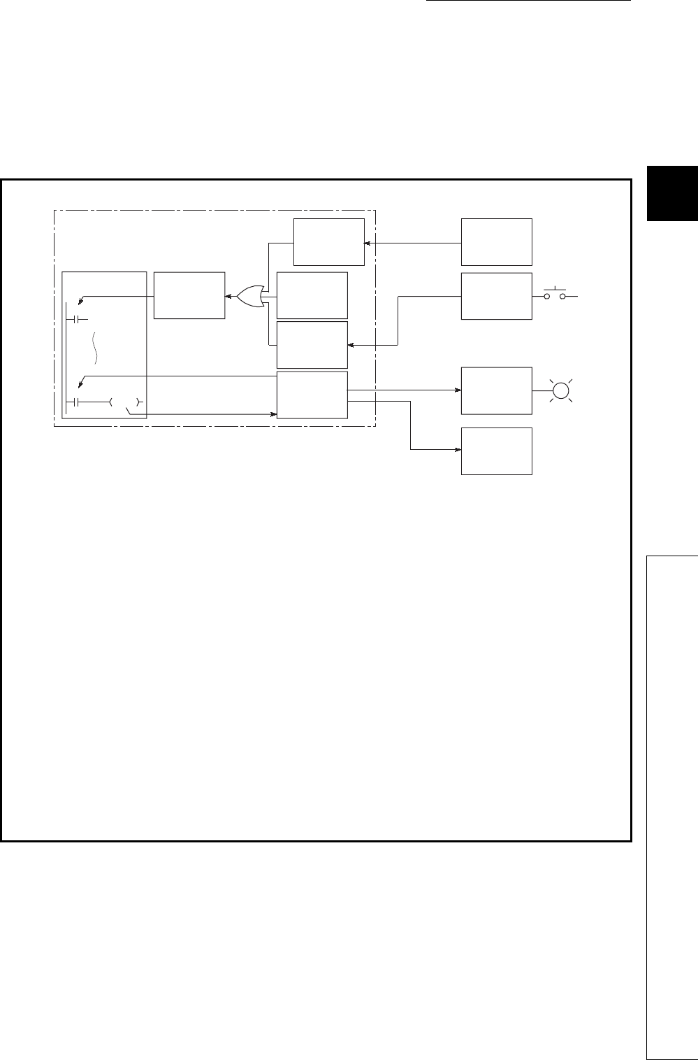
CHAPTER3 CPU MODULE OPERATION
1
2
3
4
5
6
7
8
3.8 I/O Processing and Response Delay
3.8.1 Refresh mode
3 - 10
(3) Output
The operation results of the sequence program is output to the output (Y) device memory in the CPU
module every time program operation is performed. Then, the CPU module batch-outputs the on/off
data in the output (Y) device memory to an output module before the start of sequence program
operations.
•Input refresh:
Before the start of sequence program operations, the CPU module batch-reads input data 1) from
an input module, performs a logical OR operation with data in the GX Developer input area or data
in the remote input refresh area, and then stores the result in the input (X) device memory.
•Output refresh:
Before the start of sequence program operations, the CPU module batch-outputs data in the output
(Y) device memory 2) to the output module.
•When a contact instruction for input is executed:
The CPU module reads input data 3) from the input (X) device memory and executes a sequence
program.
•When a contact instruction for output is executed:
The CPU module reads output data 4) from the output (Y) device memory and executes a sequence
program.
•When the OUT instruction for output is executed:
The CPU module stores the operation result of the sequence program 5) in the output (Y) device
memory.
Figure 3.3 I/O data flow in refresh mode
CPU module
CPU (operation
processing area)
3)
4) *3
5)
X0
Y22
Input (X)
device
memory
Input module
access area
Output (Y)
device
memory
Input
refresh
Network
module
Network
module
Input
module
1)
Output
refresh
2)
Remote
input refresh
area *1
GX Developer
input area *2
Y20
Output
module
3 - 11
*1: The remote input refresh area indicates the area to be used when auto refresh is set to the input (X) in the
CC-Link IE controller network, MELSECNET/H, or CC-Link.
Data in the remote input refresh area will be refreshed automatically during END processing.
*2: Data in the GX Developer input area can be turned on/off by the following operation.
•Test operation by GX Developer
•Writing data from a network module
*3: Data in the output (Y) device memory can be turned on/off by the following operation.
•Test operation by GX Developer
•Refresh via CC-Link IE controller network or MELSECNET/H
•Writing data from an external device using the MC protocol
•Auto refresh via CC-Link
(4) Response delay
An output response which corresponds to the status change in the input module delays for two scans
(maximum) depending on the on timing of an external contact.
Examples
Figure 3.4 Y5E turns on the earliest
Figure 3.5 Y5E turns on the latest
55 X5 Y5E A program that turns on the output
Y5E when the input X5 turns on.
Delay time
(Minimum 1 scan)
OFF
ON
0 END END00
: Input refresh
56
External contact
OFF
ON
X5
OFF
ON
Y5E
OFF
ON
External load
Devices in the
CPU module
: Output refresh
Delay time
(Maximum 2 scans)
OFF
ON
0 END END00
: Input refresh
56
External contact
OFF
ON
X5
OFF
ON
Y5E
OFF
ON
External load
Devices in the
CPU module
: Output refresh
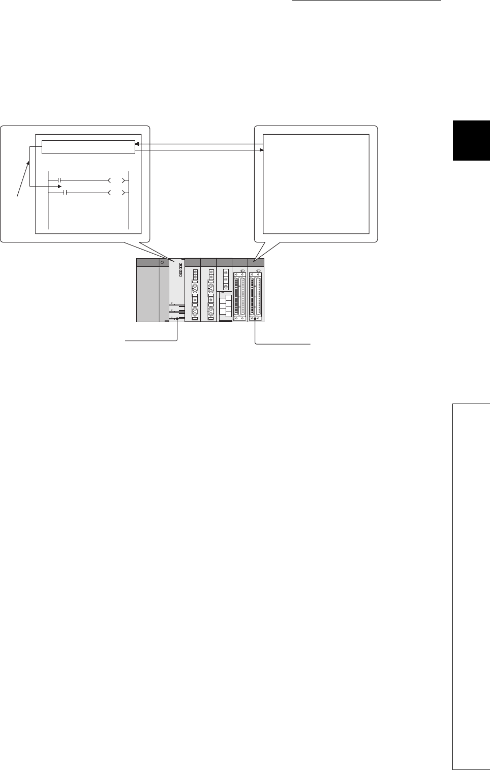
CHAPTER3 CPU MODULE OPERATION
1
2
3
4
5
6
7
8
3.8 I/O Processing and Response Delay
3.8.2 Direct mode
3 - 12
3.8.2 Direct mode
(1) Definition
The direct mode is a mode for the CPU module to access input/output modules and performs I/O
processing at the timing when each instruction is executed in a sequence program.
With this mode, the CPU module uses the direct access input (DX) and direct access output (DY) to
perform I/O processing.
Figure 3.6 Direct mode
Input module or
output module
CPU module
Device memory
0DX10
On/off
data
On/off data
Input of on/off data upon
instruction execution
Output of on/off data upon
instruction execution
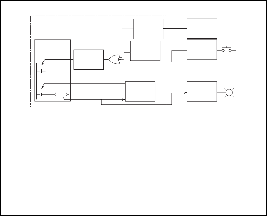
3 - 13
*1: The remote input refresh area indicates the area to be used when auto refresh is set to the input (X) in the
CC-Link IE controller network, MELSECNET/H, or CC-Link.
Data in the remote input refresh area will be refreshed automatically during END processing.
*2: Data in the GX Developer input area can be turned on/off by the following operation.
•Test operation by GX Developer
•Writing data from a network module
*3: Data in the output (Y) device memory can be turned on/off by the following operation.
•Test operation by GX Developer
•Refresh via CC-Link IE controller network or MELSECNET/H
•Writing data from an external device using the MC protocol
•Auto refresh via CC-Link
•When a contact instruction for input is executed:
The CPU module performs a logical OR operation between input data from the input module 1) and
input data in the GX Developer input area 2) or data in the remote input refresh area.
Then, the module stores the result in the input (X) device memory and executes a sequence
program using the stored result as input data 3).
•When a contact instruction for output is executed:
The CPU module reads output data 4) from the output (Y) device memory and executes a sequence
program.
•When the OUT instruction for output is executed:
The CPU module outputs the operation result of the sequence program 5) to the output module and
also stores the result in the output (Y) device memory.
Figure 3.7 I/O data flow in direct mode
CPU module
CPU (operation
processing area)
3)
4) *3
5)
DX0
Y20
Input (X)
device
memory
Output (Y)
device
memory
Network
module
Input
module
1)
2)
Remote
input refresh
area *1
GX
Developer
input area *2
DY25
Output
module
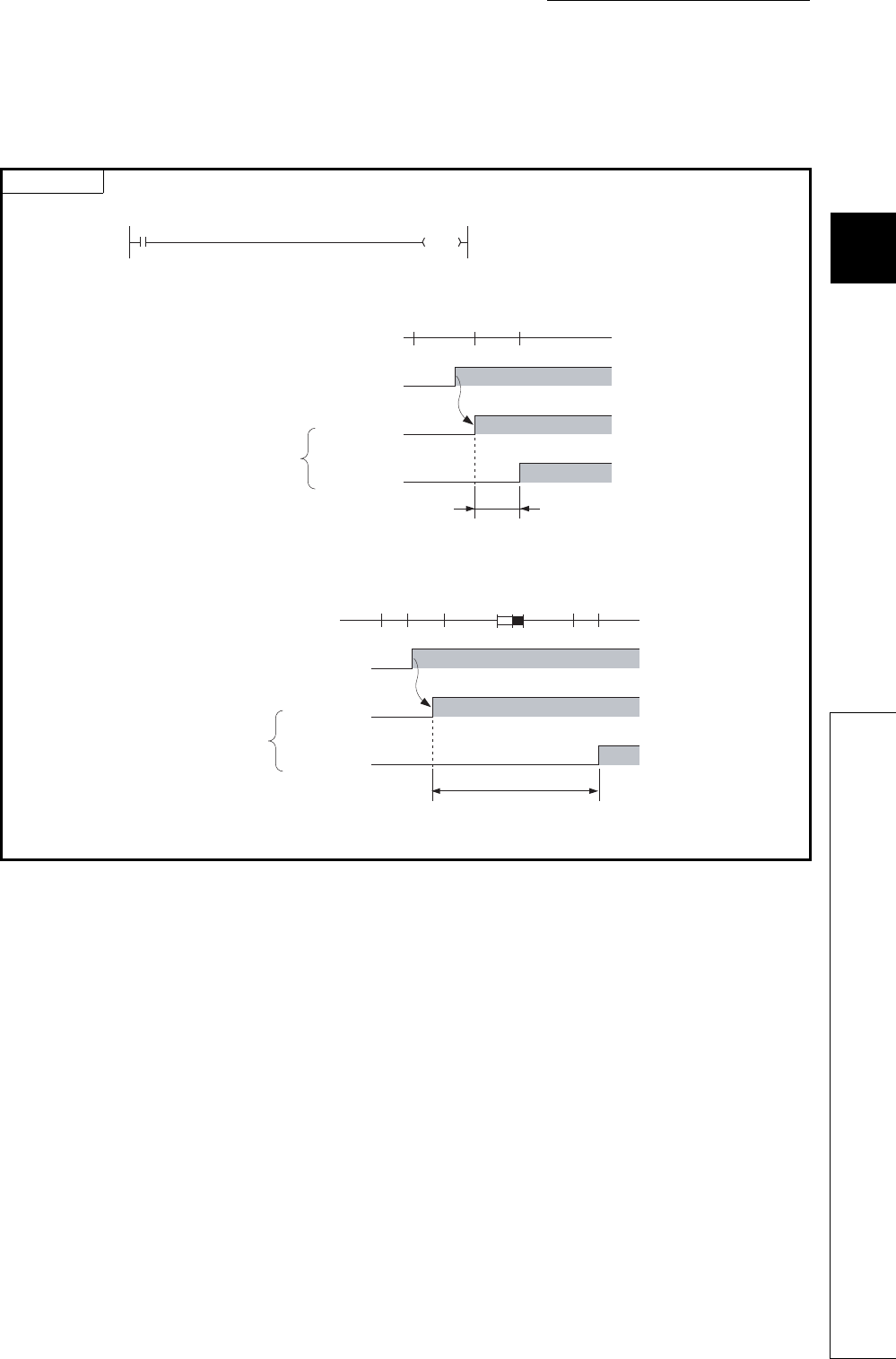
CHAPTER3 CPU MODULE OPERATION
1
2
3
4
5
6
7
8
3.8 I/O Processing and Response Delay
3.8.2 Direct mode
3 - 14
(2) Response delay
An output response which corresponds to the status change in the input module delays for one scan
(maximum) depending on the on timing of an external contact.
Examples
Figure 3.8 DY5E turns on the earliest
Figure 3.9 DY5E turns on the latest
55 DX5
DY5E A program that turns on the output
DY5E when the input DX5 turns on.
Delay time
OFF
ON
05556
External contact
OFF
ON
OFF
ON
DX5
(External
contact)
DY5E
(External
load)
Devices in the
CPU module
OFF
ON
055 56
External contact
OFF
ON
OFF
ON
DX5
(External
contact)
DY5E
(External
load)
Devices in the
CPU module
Delay time
(Maximum 1 scan)
END 0 55 56
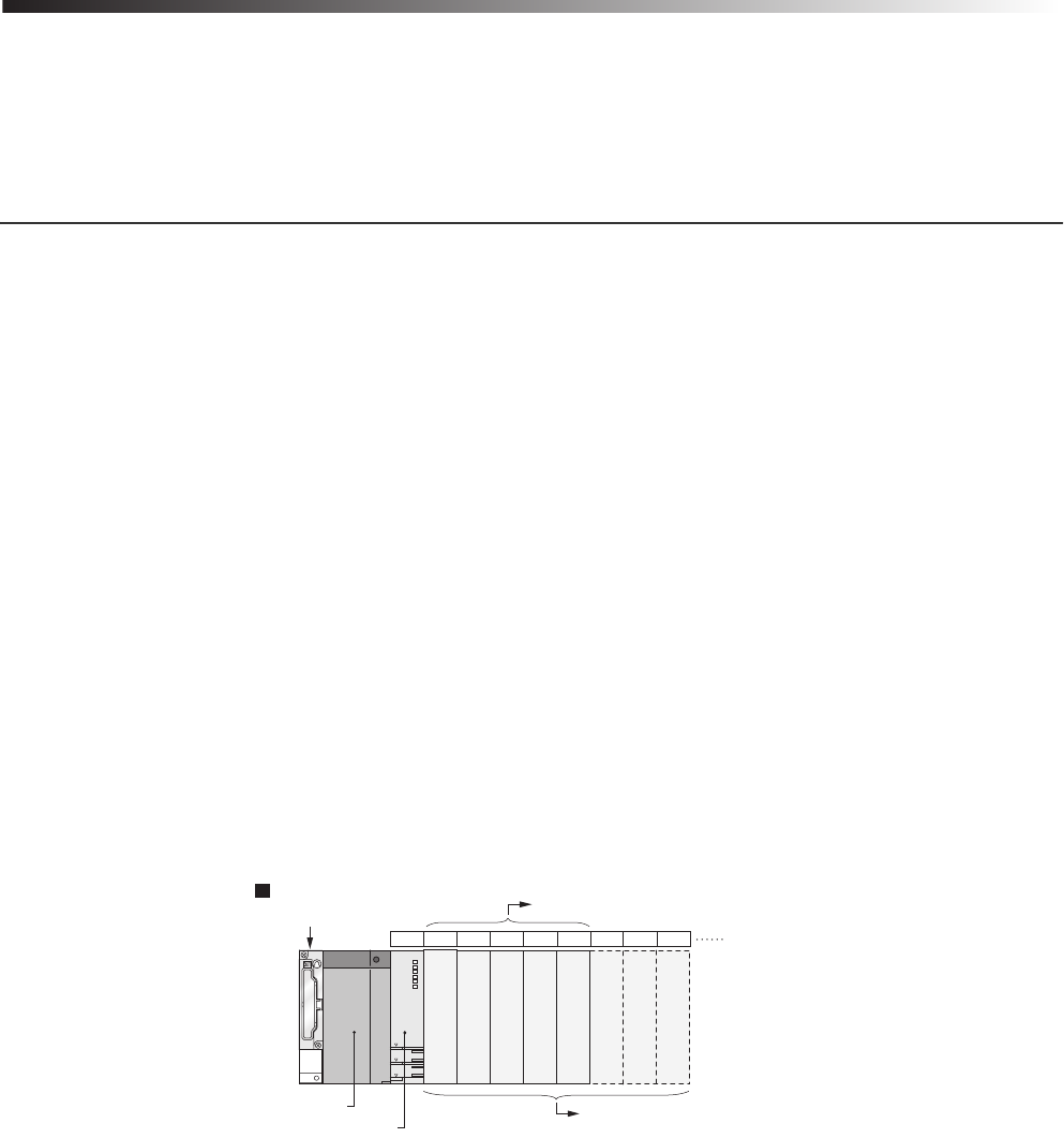
4 - 1
CHAPTER4 ASSIGNMENT OF BASE UNIT AND I/O
NUMBER
This chapter describes the base unit and I/O number assignment required for the CPU module to
communicate data with I/O modules and/or intelligent function modules.
4.1 Base Unit Assignment
4.1.1 Base mode
Use this mode when assigning the number of available slots to the main base unit and extension base units.
The following two modes are available.
• Auto mode
• Detail mode
(1) Auto mode
Use this mode when assigning the number of slots equal to that on the base unit used.
(2) Detail mode
Use the detail mode when assigning the number of slots for each base unit.
Any number of slots can be assigned irrespective of the actual number of slots on the base unit to be used.
(a) Setting the number of slots greater than the actual one
Slots are occupied by the number of slots set.
The slots after actually used ones are regarded as empty slots.
For example, three slots will be the empty slots when a 5-slot base unit is used and the number of available
slots are set to eight.
The number of points for the empty slots will be either value set on the PLC system tab, or on the I/O
assignment tab in the PLC parameter dialog box. (The default is 16 points.)
Figure 4.1 Setting the number of slots greater than the actual one
Number of slots set
CPU module
Q35B
Main base unit
Power supply
module
Actual number of slots
Slot numbe
r
CPU 0 1 2 3 4 5 6 7
Empty
Empty
Empty
4 - 2
CHAPTER4 ASSIGNMENT OF BASE UNIT AND I/O NUMBER
1
2
3
4
5
6
7
8
4.1 Base Unit Assignment
4.1.2 Base unit assignment setting
(b) Setting the number of slots smaller than the actual one
Set the smaller number than the actual number of slots when slots with no module mounted need not be
recognized.
For example, four slots from the right end of the base unit will be the prohibited slots when using a 12-slot base
unit and setting the number of available slots to eight. (Mounting a module on a prohibited slot causes
"SP.UNIT LAY ERR.".)
4.1.2 Base unit assignment setting
Set base units on the I/O assignment tab of the PLC parameter dialog box.
(1) Auto/Detail
Select the mode for the base unit assignment either from auto mode or detail mode.
(2) Base model name, Power model name, and Extension cable
Enter the model names of mounted base units, power supply modules, and extension cables to be used within 16
characters for user reference or when printing out parameters.
CPU modules do not use the entered model names.
Figure 4.2 Setting the number of slots smaller than the actual one
Figure 4.3 I/O assignment setting
CPU 0 1 2 3 4 5 6 7 8 9 10 11
Q312B
Main base unit
Power supply
module
CPU module Number of slots set Mounting a module will result in an error.
Slot numbe
r
Actual number of slots
Prohibited
Prohibited
Prohibited
Prohibited
(2) (3)
(4)
(1)

4 - 3
(3) Slots
When "Detail" is set, select the number of slots on the base unit to use from the following.
2 (2 slots), 3 (3 slots), 5 (5 slots), 8 (8 slots), 10 (10 slots), or 12 (12 slots)
(4) 8 Slot Default/12 Slot Default
When "Detail" is set, select either of these items for batch-setting the base units to the specified number of slots.
●In auto mode, when any extension base number is skipped at the setting using the base number setting connector, an
empty extension base cannot be reserved.
To reserve empty extension bases for future extension, select detail mode.
●In detail mode, set the number of slots to all base units used.
Failure to do so may result in incorrect I/O assignment setting.
4 - 4
CHAPTER4 ASSIGNMENT OF BASE UNIT AND I/O NUMBER
1
2
3
4
5
6
7
8
4.2 I/O Number Assignment
4.2 I/O Number Assignment
The I/O number indicates addresses used for sequence programs in the following cases.
• Input of on/off data to the CPU module
• Output of on/off data from the CPU module to the external device
(1) Input and output of on/off data
The input (X) is used to input on/off data to the CPU module, and the output (Y) is used to output on/
off data from the CPU module.
(2) I/O number representation
The I/O numbers are represented in hexadecimal.
When a 16-point I/O module is used, the I/O number for each slot will be 16 point-sequence number from 0
to F as shown in Figure 4.4.
"X" and "Y" is prefixed to the I/O number of input modules and the I/O number of output modules, respectively.
Figure 4.4 I/O numbers
CPU modulePower supply
For the case of input
module
For the case of
output module
16 input
points
16 input
points
16 input
points
16 output
points
16 output
points
XXXYY
XXXYY
01234
1234
F
0
0F0F0F0F00
000000000
4 - 5
4.2.1 Concept of I/O number assignment
The CPU module assigns I/O numbers at power on or reset, according to the I/O assignment setting.
(1) I/O number assignment
The Figure 4.5 shows an example of I/O number assignment to base units in the system where the CPU module
is mounted on the main base unit.
(a) Assignment order
For the main base unit, the I/O numbers are assigned to the modules from left to right in a
sequential order, starting from 0H assigned to the module on the right of the CPU module.
For extension base units, the I/O numbers are continued from the last number of the I/O number of
the main base unit.
(b) I/O number of each slot
Each slot on the base unit occupies I/O numbers by the number of I/O points of the mounted
modules.
Figure 4.5 I/O number assignment example
Number of I/O points
16 points 16 points 16 points 16 points 16 points
16 points 16 points 16 points 16 points 16 points 16 points 16 points 16 points
Q35B (5 slots occupied)
Q65B (5 slots occupied)
Q68B (8 slots occupied)
CPU 0 1 2 3 4
56789
10 11 12 13 14 15 16 17
Slot number
I/O number: assign the I/O points of each slot
Assignment order
Number of slot points
16 points 16 points 16 points 16 points 16 points
Assignment order
Number of slot points
Assignment order
Number of slot points
I/O number assignment order
X 0 to F : Inupt module
Y 0 to F :Output module
0 to F :Intelligent function module
X00 to 0F
X10 to 1F
X20 to 3F
X40 to 4F
50 to 8F
90 to AF
B0 to CF
D0 to EF
YF0 to FF
X110 to 11F
X120 to 12F
130 to 14F
150 to 16F
170 to 18F
Y190 to 19F
Y1A0 to 1AF
Y180 to 1BF
Vacancy (100 to 10F)
4 - 6
CHAPTER4 ASSIGNMENT OF BASE UNIT AND I/O NUMBER
1
2
3
4
5
6
7
8
4.2 I/O Number Assignment
4.2.1 Concept of I/O number assignment
(2) I/O assignment on a remote I/O stations
CPU module device input (X) and output (Y) can be assigned to I/O modules and intelligent function modules,
which allows to control the modules in the remote I/O system such as MELSECNET/H remote I/O network and
CC-Link.
Also, inputs (X) and outputs (Y) can be used for the refresh target (devices on the CPU module side) of the
MELSECNET/H module link I/O (LX and LY).
(a) I/O numbers available on remote I/O stations
When the input (X) and output (Y) of the CPU module are used for the I/O numbers in the remote
station, assign the I/O numbers later than those used for the I/O modules and intelligent function
modules on the CPU module side.
When X/Y0 to X/Y3FF (1024 points) are used for the I/O modules and intelligent function modules
on the CPU module side, X/Y400 and later can be used in the remote stations.
Figure 4.6 I/O number assignment on the remote station
MELSECNET/H remote I/O network
CC-Link moduleCPU module
MELSECNET/H module
X40 to 5F
X60 to 7F
Y80 to 9F
X500 to 51F
0 to F
0
X520 to 53F
X540 to 55F
X560 to 57F
580 to 59F
Remote
station
Remote
station
X to F
Y 0 to F
:
:
:
Inupt module
Output module
Intelligent function module
Example

4 - 7
(b) Precautions for using remote station I/O numbers
1) Setting for future extension
When the input (X) and output (Y) of the CPU module are used for the I/O numbers on the remote
station, consider future extension of I/O modules and/or intelligent function modules on the CPU
module side.
2) When MELSECNET/H and CC-Link are used
I/O numbers to the refresh target (CPU module side device) of MELSECNET/H and to the CC-Link
remote I/O system must be unique.
●When network parameter setting has not been made in the CC-Link system, X/Y 1000 to 17FF (2048 points) are
assigned to the CC-Link system master/local modules of lower numbers.
●There are no restrictions on the I/O number assignment order for the MELSECNET/H remote I/O networks, CC-Link, or
other networks.
●Space can be provided between the I/O area for MELSECNET/H remote I/O station and the I/O area for CC-Link
remote station.
Figure 4.7 Remote station I/O number assignment
X/Y0
X/Y3FF
X/Y400
X/Y4FF
X/Y500
X/Y1FFF
For MELSECNET/H
remote I/O station
Empty
Input/output (X/Y)
For future expansion
I/O numbers that can be used by remote stations
I/O numbers used by I/O modules/intelligent function
modules
When X/Y0 to 3FF (1024 points) are used by I/O modules and/or intelligent function
modules and X/Y400 to 4FF (256 points) are secured for future extension
For CC-Link remote
I/O station
to
to
to

4 - 8
CHAPTER4 ASSIGNMENT OF BASE UNIT AND I/O NUMBER
1
2
3
4
5
6
7
8
4.2 I/O Number Assignment
4.2.2 Setting I/O numbers
4.2.2 Setting I/O numbers
Set the I/O number on the I/O assignment tab.
(1) Purpose of I/O number assignment
(a) Reserving points for future module changes
The number of points can be flexibly set so that the I/O number modification can be avoided when
changing the current module to another in the future.
For example, 32 points can be assigned for future use to the slot where an input module with 16
points is currently mounted.
(b) Preventing I/O numbers from changing
The change in the I/O numbers can be prevented when an I/O module or intelligent function
module, whose occupied I/O points are other than 16, is removed due to failure.
(c) Changing the I/O numbers to those used in the program
When the I/O numbers used in the actual system differ from those in the designed program, the I/O
numbers of each module on the base unit can be changed to the ones in the designed program.
●If any of the I/O modules whose number of I/O points are other than 16 fails without I/O assignment setting, the I/O
numbers assigned following to the failed module may change, leading to a malfunction.For this reason, making the I/O
assignment setting is recommended.
●I/O assignment setting allows the following settings as well.
• Input response time (I/O response time) ( Section 6.7)
• Error time output mode ( Section 6.8)
• CPU module operation during a hardware error of intelligent function modules ( Section 6.9)
• Switch setting of intelligent function modules and interrupt modules( Section 6.10)
The I/O assignment is required for the input response time and switch settings.
4 - 9
(2) I/O assignment
The I/O assignment is set on the I/O assignment tab of the PLC parameter dialog box.
On the I/O assignment tab, the following items can be set for each slot on the base unit.
• "Type" (module type)
• "Points" (I/O points)
• "Start XY" (start I/O number)
For example, to change the I/O number of the specified slot, setting is allowed only to the number of points.
For other items that are not set, settings are completed based on the installation status of the base unit.
(a) Slot
The slot number and location of the slot are displayed.
When the base unit is set in Auto mode, the base unit number is indicated in "*", and the slot number is counted
from slot 0 of the main base unit.
Figure 4.8 I/O assignment
(a) (b) (c) (d) (e)

4 - 10
CHAPTER4 ASSIGNMENT OF BASE UNIT AND I/O NUMBER
1
2
3
4
5
6
7
8
4.2 I/O Number Assignment
4.2.2 Setting I/O numbers
(b) Type
Select the type of the mounted module from the followings:
• Empty (empty slot)
• Input (input module)
• Hi input (high-speed input module)
• Output (output module)
• I/O Mix (I/O combined module)
• Intelli. (intelligent function module)
• Interrupt (interrupt module)
If the type is not specified, the type of the actually mounted module is used.
(c) Type
Enter the model names of mounted modules within 16 characters.
CPU modules do not use entered model names. (Use the entered model names for user reference.)
(d) Points
When changing the number of I/O points for each slot, the selections are as follows.
0 points, 16 points, 32 points, 48 points, 64 points, 128 points, 256 points, 512 points, 1024 points
If the number of points is not selected, the points of the actually mounted module is used.
For empty slots, the points that are set on the PLC system tab of the PLC parameter dialog box is assigned.
(Default: 16 points)
(e) Start XY
When changing the I/O number for each slot, enter a new start I/O number.
If start XY is not specified for a slot, the I/O number continuing from the last number of the current
setting is assigned.

4 - 11
(3) Precautions
(a) Type setting
The type set to the I/O assignment tab must be the same as that of the mounted module.
Setting a different type may cause incorrect operation.
For the intelligent function module, the I/O points must also be the same in addition to the I/O assignment
setting.
Tabl e4. 1 shows the operations when the mounted module type differs from the one in the I/O
assignment tab.
(b) I/O points of slots
The number of I/O points for each slot selected in the I/O assignment tab is set in priority to those of mounted
modules.
1) When the preset number of I/O points is less than those of mounted I/O modules
The available points for the mounted I/O module will be decreased.
For example,when the number of I/O points is set to 16 points in the I/O assignment setting of PLC
parameter to the slot where a 32-point input module is mounted, the second half 16 points of the
32-point input module becomes unavailable.
2) When the preset number of I/O points exceeds those of mounted I/O modules
The exceeded number of points will not be used in I/O modules.
3) Last I/O number
Set the last I/O number within the I/O point range.
Failure to do so causes an error ("SP. UNIT LAY ERR."). ("***" is displayed as an I/O address on
the System monitor screen of GX Developer.)
Table4.1 Incorrect operation when the module type differs
Mounted module I/O assignment setting Result
Input module, output module,
I/O combined module
• Intelli.
• Interrupt Error (SP.UNIT.LAY.ERR.)
Intelligent function module
• Input
• Hi. input
•Output
• I/O combined
Error (SP.UNIT.LAY.ERR.)
Empty slot
• Input
• Hi. input
•Output
• I/O combined
• Intelli.
• Interrupt
Empty slot
All modules • Empty Empty slot
Other combinations -
Error does not occur but incorrect operation
may be caused.
Or, error (PARAMETER ERROR (error code:
3000)).
4 - 12
CHAPTER4 ASSIGNMENT OF BASE UNIT AND I/O NUMBER
1
2
3
4
5
6
7
8
4.2 I/O Number Assignment
4.2.2 Setting I/O numbers
(c) Start XY setting
When the start XY has not been entered, the CPU module automatically assigns it.The CPU module
automatically assigns the start XY if it is not set. For this reason, the start XY setting of each slot
may be duplicated with the one assigned by the CPU module in the case of 1) or 2) below.
1) Start XY values are not in the correct order.
2) Slots with and without the start XY setting (automatically assigned slot) are mixed
An example of start XY duplication is given in Figure 4.9 below.
Do not set duplicated start XY for each slot.
Duplication of start XY will result in an error ("SP. UNIT LAY ERR.").
Setting "Empty" and "0" to Type and Points respectively even occupies one slot.
To set on and after the specific slot unoccupied, set the number of slots in Detail mode. ( Section 4.1.1)
Figure 4.9 I/O assignment setting with start XY duplication
Figure 4.10 Start XY set by above (Figure 4.9) I/O assignment
32 points 32 points 32 points
012
X40 X20 X40
Number of I/O points
Slot number
Automatically assigned slot
Start XYs are overlapped
I/O number
X5F X3F X5F
Input module
Input module
Additional module
to to to
4 - 13
4.2.3 I/O number setting example
I/O number setting examples are provided as follows.
(1) Changing the number of points of an empty slot from 16 to 32
Reserve 32 points for the currently empty slot (Slot 3) so that the I/O numbers of Slot No. 4 and later
do not change when a 32-point input module is mounted there in the future.
(a) System configuration and I/O number assignment before I/O assignment using GX
Developer
Figure 4.11 I/O number assignment (Before changing points of the empty slot)
Q38B
Q68B
32 points
32 points 32 points 32 points 32 points 16 points 32 points 32 points 32 points
32 points 32 points 16 points 32 points 32 points 32 points 32 points
012 45673
X00 X20 X40 Y70 Y90 YB0 YD0
Number of I/O points
Slot number
I/O number
60
X1F X3F X5F Y8F YAF YCF YEF6F
8 9 10 12 13 14 1511
F0 110 130 170 Y18 Y1A Y1C150
10F 12F 14F 17F Y19 Y1B Y1D16F
Extension
1
Input module
Input module
Input module
to to to to to to to to
to to to to to to to to
Empty
Output module
Empty
Output module
Output module
Output module
Output module
Output module
Output module
Intelligent function
module
Intelligent function
module
Intelligent function
module
Intelligent function
module
4 - 14
CHAPTER4 ASSIGNMENT OF BASE UNIT AND I/O NUMBER
1
2
3
4
5
6
7
8
4.2 I/O Number Assignment
4.2.3 I/O number setting example
(b) I/O assignment
Select "32 points" for the number of I/O points of Slot 3 in the I/O assignment setting of PLC
parameter in GX Developer.
(c) I/O number assignment after the I/O assignment using GX Developer
Figure 4.12 I/O assignment setting (When changing points of Slot 3)
Figure 4.13 I/O numbers after I/O assignment (After changing points of the empty slot)
Select 32 points. (When
the type is not selected,
the type of the mounted
module will be set.)
Q38B
Q68B
Input module
Input module
Input module
Empty
Output module
Output module
Output module
Output module
32
points
32
points
32
points
32
points
32
points
32
points
32
points
32
points
32
points
32
points
32
points
32
points
32
points
32
points
32
points
32
points
012 45673
X00 X20 X40 Y80 YA0 YC0 YE0
Number of I/O
points
Slot number
I/O number
60
X1F X3F X5F Y9F YBF YDF YFF7F
Intelligent
function module
Intelligent
function module
Intelligent
function module
Intelligent
function module
Empty
Output module
Output module
Output module
8 9 10 12 13 14 1511
100
to to to to to to to to
to to to to to to to to
120 140 180 Y190 Y1B0 Y1D0160
11F 13F 15F 18F Y1AF Y1CF Y1EF17F
Extension
1
The number of I/O points is changed
from 16 points to 32 points.
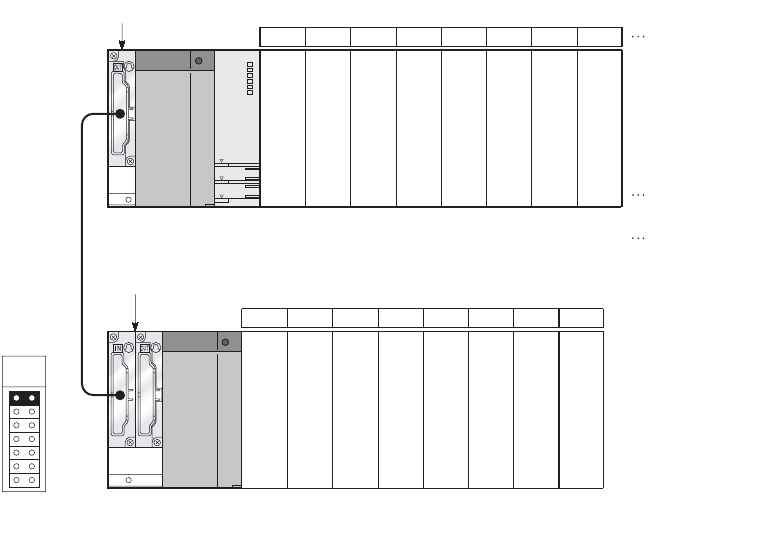
4 - 15
(2) Changing the I/O number of an empty slot
Change the I/O number of the currently empty slot (Slot 3) to X200 through 21F so that the I/O
numbers of Slot 4 and later do not change when a 32-point input module is mounted there in the
future.
(a) System configuration and I/O number assignment before the I/O assignment using
GX Developer
Figure 4.14 I/O number assignment (Before changing slot I/O numbers)
Extension
1
Q38B
Q68B
Input module
Input module
Input module
Empty
Output module
Output module
Output module
Output module
32
points
32
points
32
points
32
points
32
points
32
points
32
points
32
points
16
points
32
points
32
points
32
points
32
points
32
points
32
points
16
points
012 45673
X00
to
to to to to to to to to
to to to to to to to
X20 X40 Y70 Y90 YB0 YD0
Number of I/O
points
Slot number
I/O number
60
X1F X3F X5F Y8F YAF YCF YEF6F
Empty
Intelligent
function module
Intelligent
function module
Intelligent
function module
Intelligent
function module
Output module
Output module
Output module
8 9 10 12 13 14 1511
F0 110 130 170 Y180 Y1A0 Y1C0150
10F 12F 14F 17F Y19F Y1BF Y1DF16F
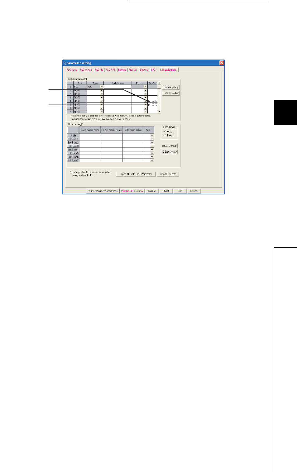
4 - 16
CHAPTER4 ASSIGNMENT OF BASE UNIT AND I/O NUMBER
1
2
3
4
5
6
7
8
4.2 I/O Number Assignment
4.2.3 I/O number setting example
(b) I/O assignment
Set "200" for the start XY of Slot 3 and "70" to Slot 4 in the I/O assignment setting of PLC parameter
in GX Developer.
Figure 4.15 I/O assignment setting (When changing I/O numbers of Slot 3)
Set "200" to start XY.
Set "70" to start XY.
(If not set, the I/O
number following the
slot 3 will be set.)
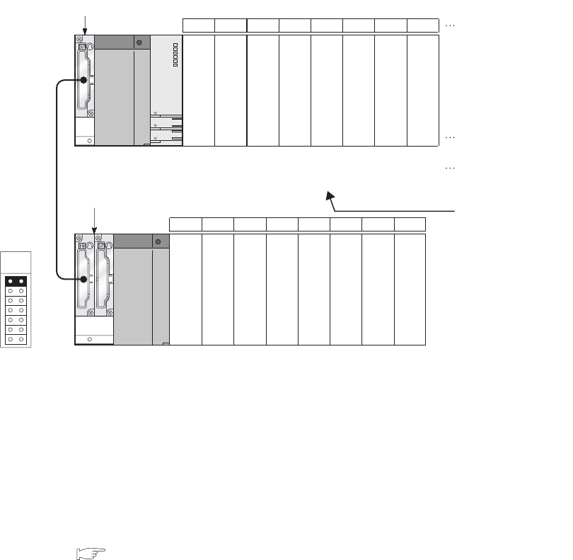
4 - 17
(c) I/O number assignment after the I/O assignment using GX Developer
4.2.4 Checking I/O numbers
Information of mounted modules and their I/O numbers can be checked on the System monitor screen of
GX Developer. ( Section 6.20)
Figure 4.16 I/O number assignment (After changing slot I/O numbers)
Q38B
Q68B
012 45673
X00 X20 X40 Y70 Y90 YB0 YD0X200
X1F X3F X5F Y8F YAF YCF YEFX21F
8 9 10 12 13 14 1511
F0 110 130 170 Y180 Y1A0 Y1C0150
10F 12F 14F 17F Y19F Y1BF Y1DF16F
32 points
32 points 32 points 32 points 32 points 16 points 32 points 32 points 32 points
32 points 32 points 32 points 32 points 32 points 32 points 32 points
Number of I/O points
Slot number
I/O number
Input module
Input module
Input module
Input module
to to to to to to to to
to to to to to to to to
Empty
Output module
Output module
Output module
Output module
Output module
Output module
Output module
Extension
1
Intelligent function
module
Intelligent function
module
Intelligent function
module
Intelligent function
module
The I/O number is not
changed.
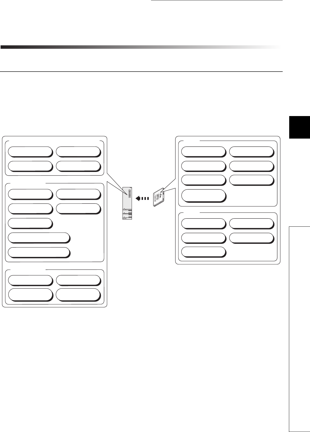
5 - 1
CHAPTER5 MEMORIES AND FILES USED FOR CPU MODULE
1
2
3
4
5
6
7
8
5.1 Memories Used for CPU Module
5.1.1 Memory composition and storable data
CHAPTER5 MEMORIES AND FILES USED FOR CPU
MODULE
5.1 Memories Used for CPU Module
5.1.1 Memory composition and storable data
This section describes the memories used for the Universal model QCPU and data that can be stored in
the memories.
(1) Memory composition
Figure 5.1 Memory composition of the Universal model QCPU
*1: The Q00UJCPU, Q00UCPU, and Q01UCPU cannot be used with a memory card.
*2: The Q00UJCPU does not have the standard RAM.
Standard ROM
Standard RAM
ROM
RAM
Program memory (program cache memory)
Parameter Program
Device comment Initial device value
Parameter Program
Device comment Initial device value
Parameter Program
Device comment Initial device value
Programmable controller
user data
File for data to be stored by the
latch data backup function
File used for the SP.DEVST and
S.DEVLD instructions
Sampling
trace file
Local device
Sampling
trace file
Local device
File register
Parameter Program
Device comment Initial device value
File register
File register
CPU module
Memory card*1
Module error
log file

5 - 2
(a) Program memory ( Section 5.1.2)
This memory is for storing programs and parameters for CPU module operation.
The CPU module transfers a program from the program memory to the program cache memory for operation.
( Section 5.1.3)
(b) Standard ROM ( Section 5.1.4)
This memory is for storing data such as parameters and programs.
(c) Standard RAM ( Section 5.1.5)
This memory is for using file registers, local devices, and sampling trace files without a memory card.
(d) Memory card ( Section 5.1.6)
This memory is for expansion of built-in memory in the CPU module.
Three types of memory cards are available: SRAM card, Flash card, and ATA card.
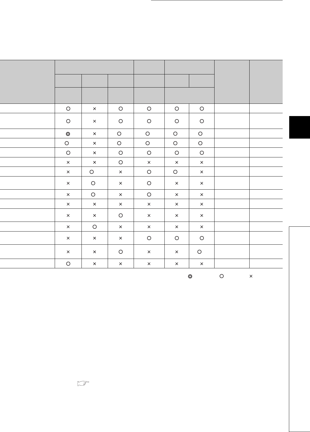
5 - 3
CHAPTER5 MEMORIES AND FILES USED FOR CPU MODULE
1
2
3
4
5
6
7
8
5.1 Memories Used for CPU Module
5.1.1 Memory composition and storable data
(2) Data that can be stored in each memory
Tabl e5. 1 provides the data that can be stored in each memory.
: Required, : Storable, : Not storable
*1: A drive number is used to specify a memory to be written/read by the external device using a sequence program or MC protocol.
Since the memory name is used to specify the target memory by GX Developer, the drive number needs not to be considered.
*2: Store the intelligent function module parameters in the same drive with the parameters.
When they are stored in different drives, the intelligent function module parameters do not become valid.
*3: A program stored in the standard ROM cannot be executed.
Store the program to the program memory before execution.
*4: To execute a program stored in the memory card, make the setting in the Boot file tab of the PLC parameter dialog box.
*5: The device comments cannot be read by instructions in a sequence program.
*6: Reading from a sequence program requires several scans.
*7: Only each one of file register, one local device, and/or sampling trace file can be stored in the standard RAM.
*8: For the number of storable file register points, refer to Section 9.7.
*9: A sequence program allows reading only. No data can be written from the sequence program.
*10: Data can be written or read with the following instructions.
•SP.FREAD (batch-reads data from the specified file in the memory card.)
•SP.FWRITE (batch-writes data to the specified file in the memory card.)
*11: Set an area used by the system. ( Section 5.1.2(2)(b))
Table5.1 Data that can be stored in each memory
Item
CPU module built-in memory Memory
card (RAM) Memory card (ROM)
File name and
extension Remarks
Program
memory
Standard
RAM
Standard
ROM SRAM card Flash card ATA
card
Drive 0
*1
Drive 3
*1
Drive 4
*1
Drive 1
*1
Drive 2
*1
Parameter PARAM.QPA 1 data/drive
Intelligent function
module parameter*2IPARAM.QPA 1 data/drive
Program *3 *4 *4 *4 ***.QPG -
Device comment *5 *6 *6 *6 *6 ***.QCD -
Initial device value ***.QDI -
Device data ***.QST -
File register *7*8 *9 ***.QDR -
Local device *7 ***.QDL 1 data/CPU
module
Sampling trace file *7 ***.QTD -
Error history data ***.QFD -
Device data storage file DEVSTORE.
QST -
Module error collection file IERRLOG.QIE -
Backup data file MEMBKUP0.
QBP -
Programmable controller
user data *10 ***.*** -
User setting system area*11 --
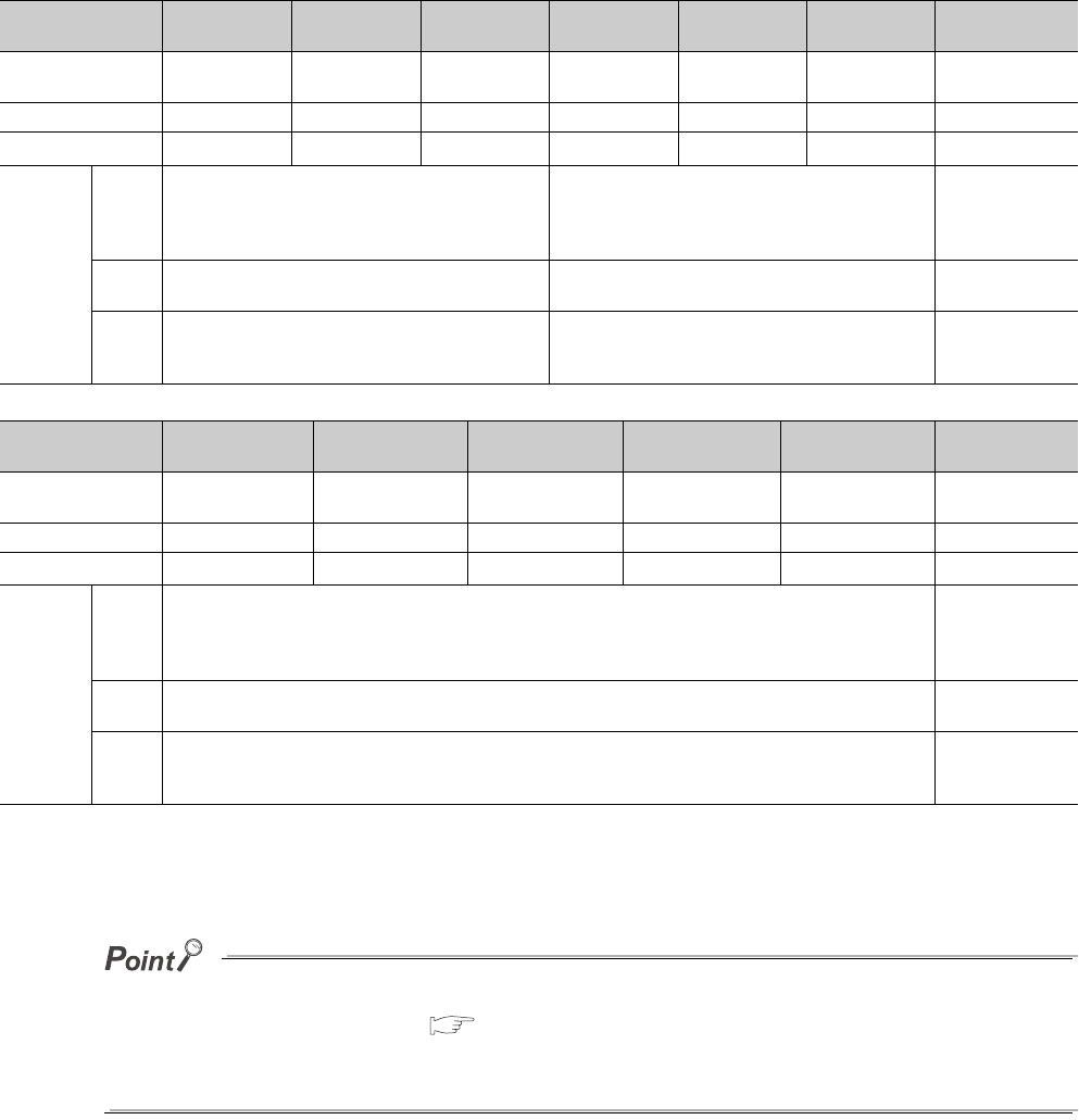
5 - 4
(3) Memory capacities and necessity of formatting
Table5.2 provides the memory capacities and necessity of formatting of each memory.
Format a memory requiring formatting by GX Developer beforehand.
*1: When the memory contents become indefinite in initial status or due to the end of battery life, the memory is automatically formatted after
the CPU module is powered off and then on or is reset.
●When files are written to each memory, the unit of stored file size depends on the target CPU
module and memory area.( Section 5.3.4)
●In memory capacity calculation, 1 step is equal to 4 bytes.
Table5.2 Memory capacities and necessity of formatting
Q00UJCPU Q00UCPU Q01UCPU Q02UCPU Q03UDCPU,
Q03UDECPU
Q04UDHCPU,
Q04UDEHCPU Formatting
Program memory 40K bytes
(10K steps)
40K bytes
(10K steps)
60K bytes
(15K steps)
80K bytes
(20K steps)
120K bytes
(30K steps)
160K bytes
(40K steps) Necessary
Standard ROM 256K bytes 512K bytes 512K bytes 512K bytes 1024K bytes 1024K bytes Unnecessary
Standard RAM - 128K bytes 128K bytes 128K bytes 192K bytes 256K bytes Necessary*1
Memory
card
SRAM
card -
Q2MEM-1MBS: 1M byte
Q2MEM-2MBS: 2M bytes
Q3MEM-4MBS: 4M bytes
Q3MEM-8MBS: 8M bytes
Necessary
(Use GX
Developer.)
Flash
card -Q2MEM-2MBF: 2M bytes
Q2MEM-4MBF: 4M bytes Unnecessary
ATA
card -
Q2MEM-8MBA: 8M bytes
Q2MEM-16MBA: 16M bytes
Q2MEM-32MBA: 32M bytes
Necessary
(Use GX
Developer.)
Q06UDHCPU,
Q06UDEHCPU
Q10UDHCPU,
Q10UDEHCPU
Q13UDHCPU,
Q13UDEHCPU
Q20UDHCPU,
Q20UDEHCPU
Q26UDHCPU,
Q26UDEHCPU Formatting
Program memory 240K bytes
(60K steps)
400K bytes
(100K steps)
520K bytes
(130K steps)
800K bytes
(200K steps)
1040K bytes
(260K steps) Necessary
Standard ROM 1024K bytes 2048K bytes 2048K bytes 4096K bytes 4096K bytes Unnecessary
Standard RAM 768K bytes 1024K bytes 1024K bytes 1280K bytes 1280K bytes Necessary*1
Memory
card
SRAM
card
Q2MEM-1MBS: 1M byte
Q2MEM-2MBS: 2M bytes
Q3MEM-4MBS: 4M bytes
Q3MEM-8MBS: 8M bytes
Necessary
(Use GX
Developer.)
Flash
card
Q2MEM-2MBF: 2M bytes
Q2MEM-4MBF: 4M bytes Unnecessary
ATA
card
Q2MEM-8MBA: 8M bytes
Q2MEM-16MBA: 16M bytes
Q2MEM-32MBA: 32M bytes
Necessary
(Use GX
Developer.)
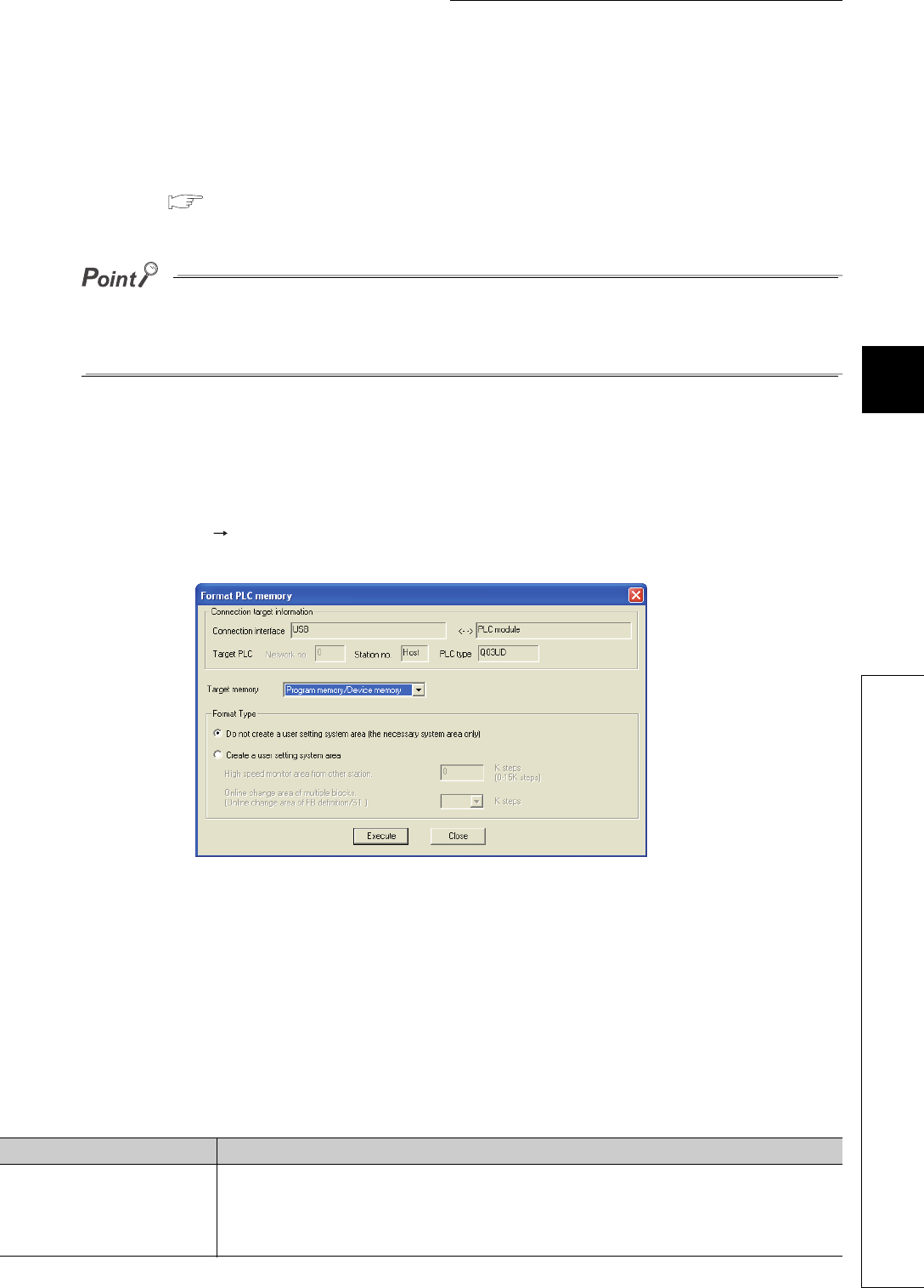
5 - 5
CHAPTER5 MEMORIES AND FILES USED FOR CPU MODULE
1
2
3
4
5
6
7
8
5.1 Memories Used for CPU Module
5.1.2 Program memory
5.1.2 Program memory
(1) Definition
This memory is for storing programs and parameters for CPU module operation.
The CPU module transfers a program from the program memory to the program cache memory for
operation. ( Section 5.1.3)
If the total size of data to be stored exceeds the program memory capacity:
• reduce the user setting system area, or
• transfer data other than programs to the standard ROM or memory card.
(2) Before using the program memory
Format the program memory by GX Developer.
(a) Formatting
Select [Online] [Format PLC memory] in GX Developer.
Select "Program memory/Device memory" in “Target memory”.
(b) Creating a user setting system area
When formatting a program memory, set the capacity of user setting system area.
1) Do not create a user setting system area (the necessary system area only)
The user setting system area is not created during formatting.
2) Create a user setting system area
The user setting system area is created during formatting.
Table5.3 provides the type of user setting system area.
Figure 5.2 Formatting the program memory
Table5.3 Type of user setting system area
System area Description
High speed monitor area from
other station.
Setting this area increases the monitoring speed in the GX Developer connected to such as
a serial communication module.
When using RS-232 and USB together with GX Developer, this area is used to register
monitor data from GX Developer connected to such as a serial communication module.
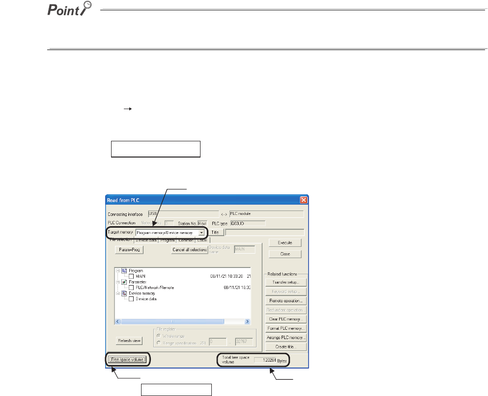
5 - 6
When a user setting system area is created, the available area reduces by the number of steps created in the
area.
(c) Checking the memory capacity after formatting
Select [Online] [Read from PLC] in GX Developer.
1) Select "Program memory/Device memory" in “Target memory” on the Read from PLC screen.
2) Click the button.
3) The memory capacity appears in “Total free space volume”.
Figure 5.3 Procedure for checking the memory capacity
Free space volume
1) Select the target memory.
2) Click the
Free space volume button.
3) The memory capacity
value is shown.
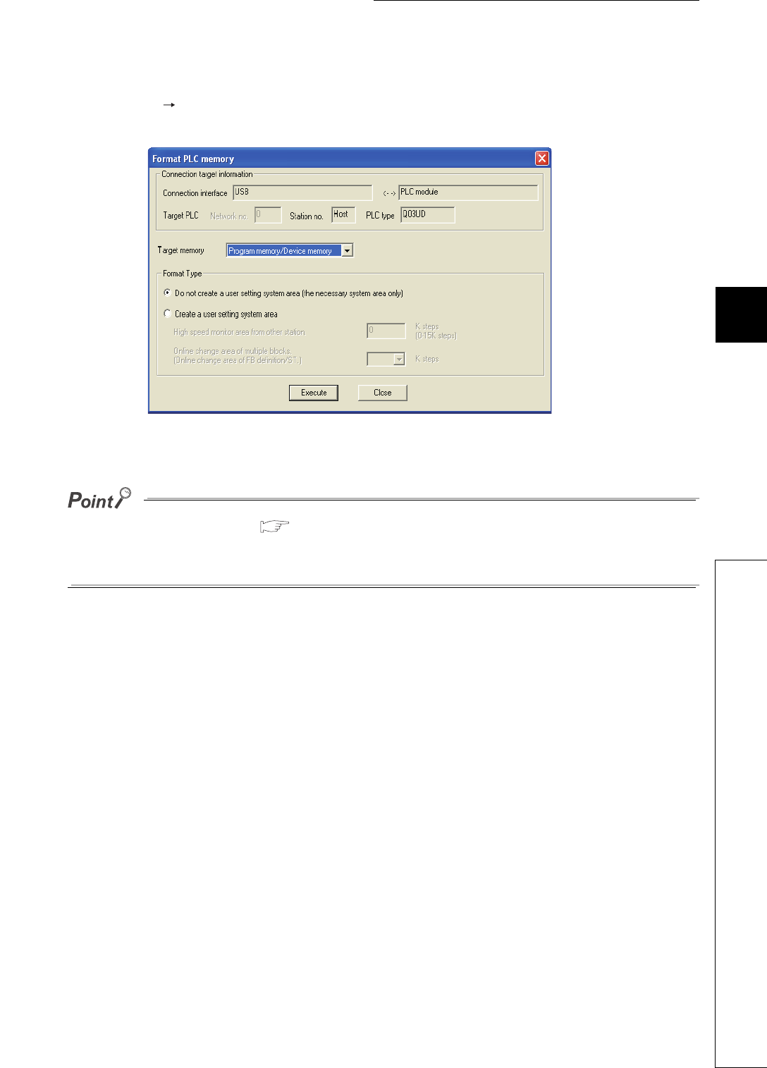
5 - 7
CHAPTER5 MEMORIES AND FILES USED FOR CPU MODULE
1
2
3
4
5
6
7
8
5.1 Memories Used for CPU Module
5.1.2 Program memory
(3) Writing to the program memory
Select [Online] [Write to PLC] in GX Developer.
Select "Program memory/Device memory" in “Target memory” on the Write to PLC screen.
The file size has its minimum unit. ( Section 5.3.4)
The occupied memory capacity may be greater than the actual file size.
Note that as the number of files increases, the difference between the occupied memory capacity and the actual file size
increases.
Figure 5.4 Write to PLC screen
5 - 8
5.1.3 Program cache memory
(1) Definition
This memory is for program operation.
The CPU module transfers a program from the program memory to the program cache memory for
operation.
The program is transferred during:
• initial processing after the CPU module is powered on, or
• initial processing after the CPU module is reset.
Figure 5.5 provides the flow of program operations.
Figure 5.5 Flow of program operation
<Drive 3>
Standard
RAM (SRAM)
Power-on/reset
Initial Processing
(transfers data in the
program memory to the
program cache memory.)
I/O module refresh
processing
Operation processing
of the program
END processing
<Drive 4>
Standard
ROM
(Flash ROM)
<Drive 0>
Program
memory
(Flash ROM)
Program
cache
memory
(SRAM)
2) Operation
processing
1) Transfer
Universal model QCPU
Multiple
CPU auto
refresh area
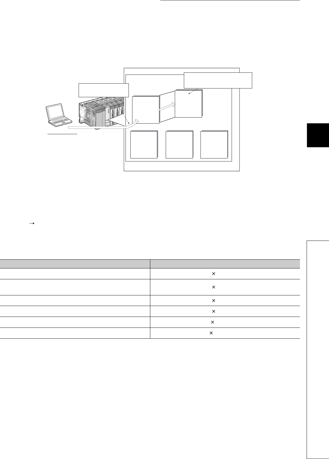
5 - 9
CHAPTER5 MEMORIES AND FILES USED FOR CPU MODULE
1
2
3
4
5
6
7
8
5.1 Memories Used for CPU Module
5.1.3 Program cache memory
(2) Writing a program
When writing data from GX Developer, programs and parameters are written to the program cache memory in the
CPU module. After the completion of the writing, the data are transferred to the program memory.
Figure 5.6 provides the flow of writing a program.
(3) Transferring data to the program memory by GX Developer
Data can also be batch-transferred from the program cache memory to the program memory by selecting [Online]
[Program memory batch transfer] in GX Developer.
Figure 5.4 provides the transfer time required when data are batch-transferred to the program memory while the
CPU module is in the RUN status.
Ts: scan time (s)
Figure 5.6 Flow of writing a program
Table5.4 Transfer time of program memory batch-transfer
CPU module Transfer time
Q00UJCPU, Q00UCPU, Q01UCPU, Q02UCPU Ts 320 + 4.8 (s)
Q03UDCPU, Q04UDHCPU, Q06UDHCPU, Q03UDECPU,
Q04UDEHCPU, Q06UDEHCPU Ts 260 + 4.7 (s)
Q10UDHCPU, Q10UDEHCPU Ts 439 + 6.2 (s)
Q13UDHCPU, Q13UDEHCPU Ts 600 + 8.0 (s)
Q20UDHCPU, Q20UDEHCPU Ts 839 + 11.4 (s)
Q26UDHCPU, Q26UDEHCPU Ts 1100 + 15.0 (s)
<Drive 3>
Standard
RAM
(SRAM)
<Drive 4>
<Drive 0>
Program
memory
(Flash ROM)
Program
cache
memory
(SRAM)
Universal model QCPU
GX Developer
1) Data are written to the program
cache memory once.
2) After data are written to the program
cache memory, the data are automatically
transferred to the program memory.
Multiple
CPU auto
refresh area
Standard
ROM
(Flash ROM)

5 - 10
(4) Checking status during data transfer to the program memory
The status during data transfer to the program memory can be checked either in the progress screen
of GX Developer or by the special relay and special register.
(a) Checking the status in the progress screen
Figure 5.7 provides the progress screen of GX Developer.
(b) Checking the status by the special relay and special register
The status can be checked by SM681 and SD681.
(5) Checking whether data are transferred to the program memory Note5.1Note1
Whether data are transferred from the program cache memory to the program memory can be
checked by SM165.
Figure 5.7 Screen showing status of data transfer to the program memory
Note1
Note5.1
When checking the transfer status to the program memory in the Q02UCPU, Q03UDCPU, Q04UDHCPU,
or Q06UDHCPU, check the versions of the CPU module and GX Developer. ( Appendix 2)
Universal
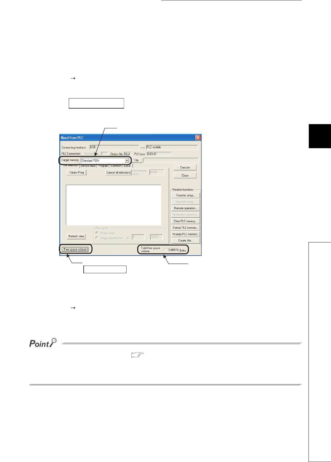
5 - 11
CHAPTER5 MEMORIES AND FILES USED FOR CPU MODULE
1
2
3
4
5
6
7
8
5.1 Memories Used for CPU Module
5.1.4 Standard ROM
5.1.4 Standard ROM
(1) Definition
This memory is for storing data such as parameters and programs.
(2) Checking the memory capacity
Select [Online] [Read from PLC] in GX Developer.
1) Select "Standard ROM" in “Target memory” on the Read from PLC screen.
2) Click the button.
3) The memory capacity appears in “Total free space volume”.
(3) Writing to the standard ROM
Select [Online] [Write to PLC] in GX Developer.
Select "Standard ROM" in “Target memory”.
The file size has its minimum unit. ( Section 5.3.4)
The occupied memory capacity may be greater than the actual file size.
Note that as the number of files increases, the difference between the occupied memory capacity
and the actual file size increases.
Figure 5.8 Procedure for checking the memory capacity
Free space volume
1) Select the target memory.
2) Click the
Free space volume button.
3) The memory capacity
value is shown.
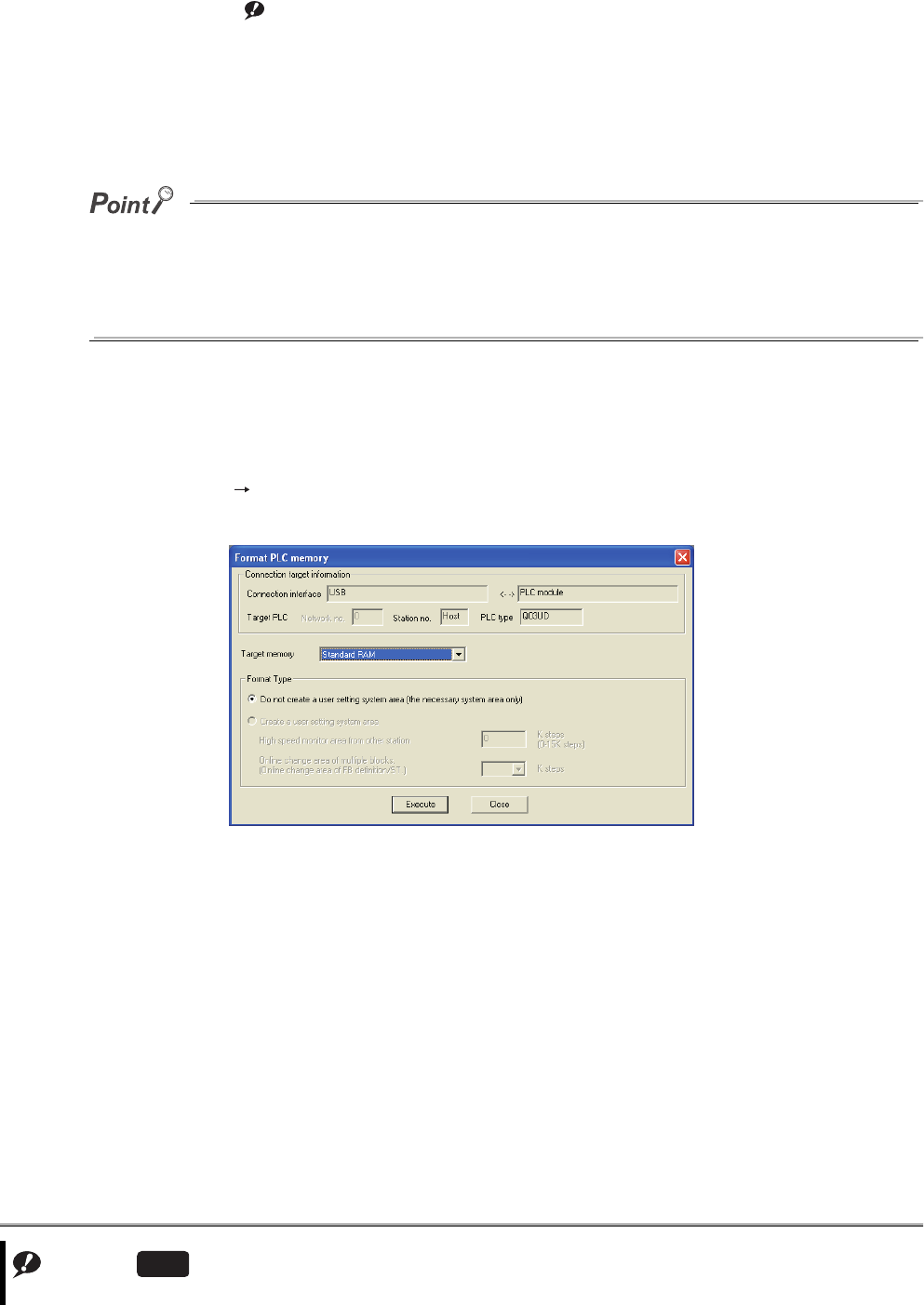
5 - 12
5.1.5 Standard RAM Note1
(1) Definition
This memory is for using file registers, local devices, and sampling trace files without a memory card.
Storing the file registers in the standard RAM allows fast access as data registers do.
The memory is also used for storing a module error collection file.
If the size of files to be stored exceeds the standard RAM capacity:
• store the files in the memory card, or
• reduce the number of points of the file register, local device, or sampling trace.
Note when file registers are stored in the memory card, the access speed will be slower than when they are
stored in the standard RAM.
(2) Before using the standard RAM
Format the standard RAM by GX Developer.
(a) Formatting
Select [Online] [Format PLC memory] in GX Developer.
Select "Standard RAM" in “Target memory”.
Note1
Figure 5.9 Formatting the standard RAM
Note5.2
Note5.2
The Q00UJCPU does not have the standard RAM.
Universal
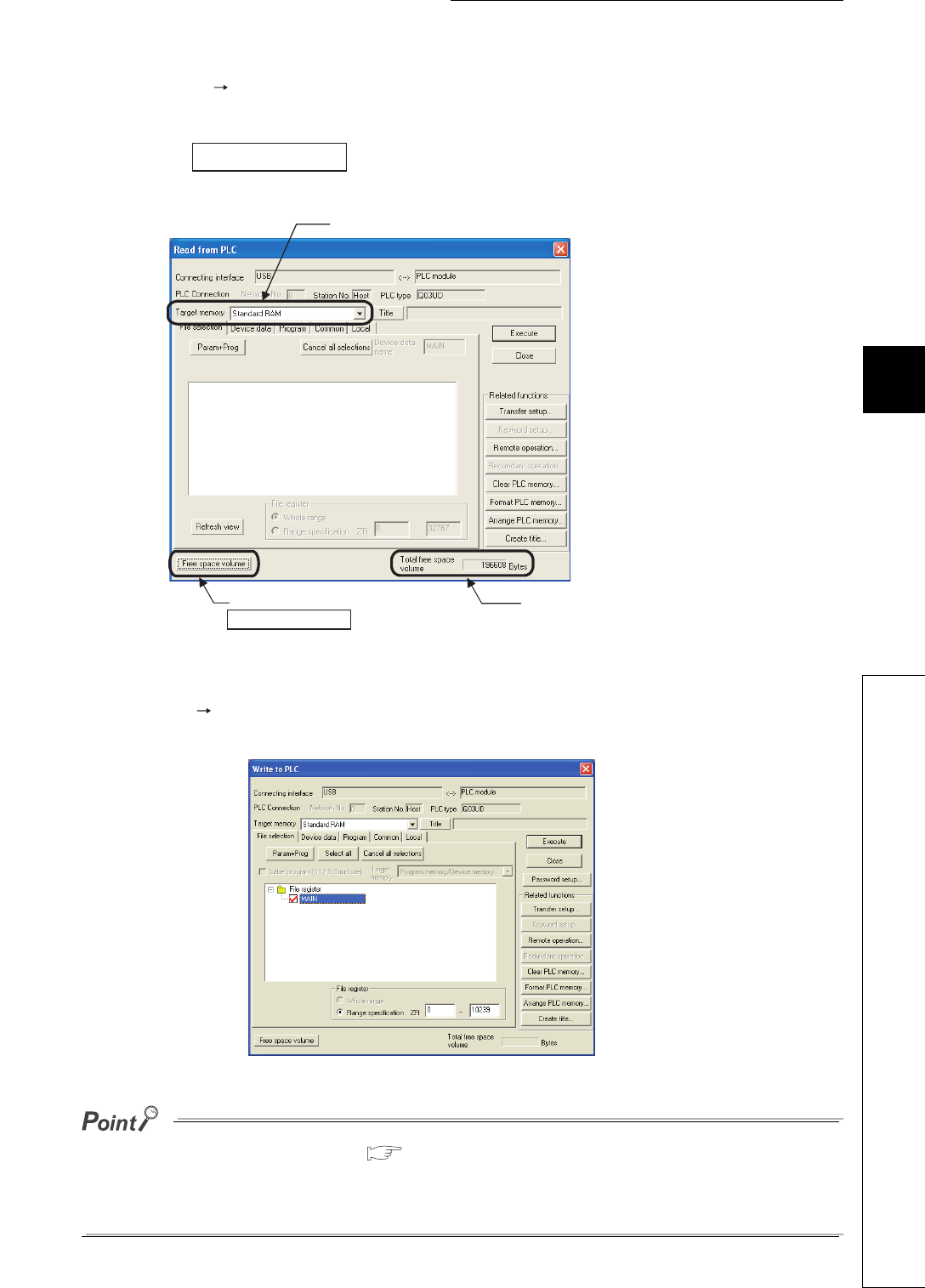
5 - 13
CHAPTER5 MEMORIES AND FILES USED FOR CPU MODULE
1
2
3
4
5
6
7
8
5.1 Memories Used for CPU Module
5.1.5 Standard RAM
(b) Checking the memory capacity after formatting
Select [Online] [Read from PLC] in GX Developer.
1) Select "Standard RAM" in “Target memory” on the Read from PLC screen.
2) Click the button.
3) The memory capacity appears in “Total free space volume”.
(3) Writing to the standard RAM
Select [Online] [Write to PLC] in GX Developer.
Select "Standard RAM" in “Target memory” on the Write to PLC screen.
The file size has its minimum unit. ( Section 5.3.4)
The occupied memory capacity may be greater than the actual file size.
Note that as the number of files increases, the difference between the occupied memory capacity
and the actual file size increases.
Figure 5.10 Procedure for checking the memory capacity
Figure 5.11 Write to PLC screen
Free space volume
1) Select the target memory.
2) Click the
Free space volume button.
3) The memory capacity
value is shown.

5 - 14
5.1.6 Memory card Note1
(1) Definition
This memory is for expansion of a memory in the CPU module.
The following three types are available:
•SRAM card
• Flash card
•ATA card
(a) SRAM card
File registers in the SRAM card can be written or read by the sequence program.
The SRAM card is used when:
• the number of file register points is greater than the standard RAM capacity, or
• the sampling trace function is used. ( Section 6.14)
When storing file registers to the SRAM card, the file registers can be written or read by the sequence program
up to 4086K points.
(b) Flash card
Write data by GX Developer and read it by the sequence program. (Data can be read only by the sequence
program.)
Use the Flash card when data are not changed.
File registers can be stored up to 2039K points.
(c) ATA card
This card is used for programmable controller user data (general-purpose data).
With the file access instruction (such as the SP. FWRITE instruction) in the sequence program, access the
programmable controller user data in the ATA card in CSV format/binary format.
Note1
Note5.3
Note5.3
The Q00UJCPU, Q00UCPU, and Q01UCPU cannot be used with a memory card.
Universal
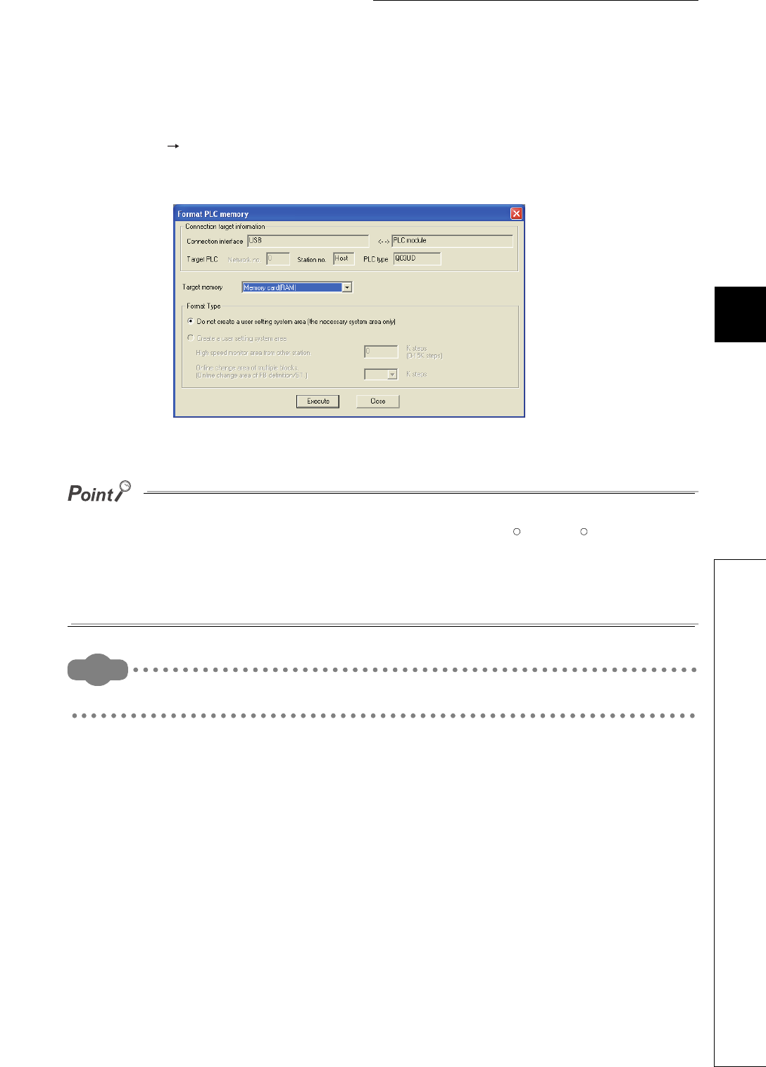
5 - 15
CHAPTER5 MEMORIES AND FILES USED FOR CPU MODULE
1
2
3
4
5
6
7
8
5.1 Memories Used for CPU Module
5.1.6 Memory card
(2) Before using the SRAM card or ATA card
Format the SRAM card or ATA card by GX Developer.
(a) Formatting
Select [Online] [Format PLC memory] in GX Developer.
• When formatting the SRAM card, select "Memory card (RAM)" in “Target memory”.
• When formatting the ATA card, select "Memory card (ROM)" in “Target memory”.
●Use only GX Developer to format the ATA card.
If formatting the ATA card by such as the formatting function of Microsoft Windows , the card may not
be used with the CPU module.
●
When formatting the SRAM card or ATA card, the memory card information area is automatically secured.
Therefore, the card capacity reduces by the area size.
Remark
Formatting is not required for the Flash card.
Figure 5.12 Formatting the SRAM card or ATA card
R R
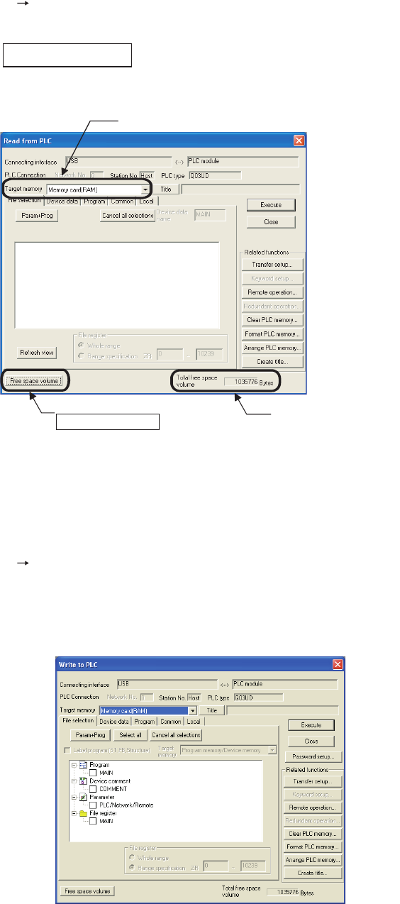
5 - 16
(b) Checking the memory capacity after formatting
Select [Online] [Read from PLC] in GX Developer.
1) Select "Memory card (RAM)" or "Memory card (ROM)" in “Target memory” on the Read from PLC screen.
2) Click the button.
3) The memory capacity appears in “Total free space volume”.
(3) Writing to the memory card
The following describes the operations before writing and the methods for writing.
(a) Writing to the SRAM card or the ATA card
Select [Online] [Write to PLC] in GX Developer.
• When writing data to the SRAM card, select "Memory card (RAM)" in “Target memory” on the Write to PLC
screen.
• When writing data to the ATA card, select "Memory card (ROM)" in “Target memory” on the Write to PLC
screen.
Figure 5.13 Procedure for checking the memory capacity
Figure 5.14 Write to PLC screen
Free space volume
1) Select the target memory.
2) Click the
Free space volume button.
3) The memory capacity
value is shown.

5 - 17
CHAPTER5 MEMORIES AND FILES USED FOR CPU MODULE
1
2
3
4
5
6
7
8
5.1 Memories Used for CPU Module
5.1.6 Memory card
(b) Writing to the Flash card
The following two methods are available.
• Writing by "Write the program memory to ROM" ( Section 5.1.7(1)(a))
• Writing by "Write to PLC (Flash ROM)” ( Section 5.1.7(1)(b))
The file size has its minimum unit. ( Section 5.3.4)
The occupied memory capacity may be greater than the actual file size.
Note that as the number of files increases, the difference between the occupied memory capacity and the
actual file size increases.
(4) How to use the program stored in the memory card
Boot the program stored in the memory card to the program memory before its execution.( Section 5.1.8)
5 - 18
5.1.7 Writing to the Flash card by GX Developer
(1) Methods for writing data to the Flash card and applications
Figure 5.15 provides the methods for writing data to the Flash card.
(a) Writing by “Write the program memory to ROM”
Data in the program memory are batch-written to the Flash card.
To batch-write the data, select [Online] [Write to PLC (Flash ROM)] [Write the program memory to ROM]
in GX Developer.
Use this method when:
• debugging the program in the program memory and writing the debugged program to the Flash card
without change for boot operation ( Section 5.1.8), or
• storing the data in the program memory to the Flash card without battery backup.
(b) Writing by “Write to PLC (Flash ROM)”
Files specified by GX Developer are batch-written to the Flash card.
To batch-write the files, select [Online] [Write to PLC (Flash ROM)] [Write to PLC (Flash ROM)] in GX
Developer.
Use this method when:
• storing parameters, initial device values, or device comments whose size exceeds the program memory
capacity to the Flash card, or
• using file registers storied in the Flash card.
Figure 5.15 Methods for writing data to the Flash card
Writing by "Write the program memory to ROM"
Program
memory
CPU module
GX Developer
Writing by "Write to PLC
(Flash ROM)"
5 - 19
CHAPTER5 MEMORIES AND FILES USED FOR CPU MODULE
1
2
3
4
5
6
7
8
5.1 Memories Used for CPU Module
5.1.7 Writing to the Flash card by GX Developer
(2) Writing to the Flash card
The following describes the operations before writing and the methods for writing.
(a) Before writing
Check the following.
1) Preparing files to be written
Writing a file to the Flash card automatically deletes all files stored in the Flash card.
Also write all files same as the stored files together.
2) Boot operation
When storing parameters to the Flash card at boot operation, make the boot file setting described in Section
5.1.8.
(b) Writing procedure
The following describes a procedure for writing a file to the Flash card.
1) Procedure for [Write the program memory to ROM] in GX Developer
• Select [Online] [Write to PLC (Flash ROM)] [Write the program memory to ROM].
• The program memory data into ROM screen appears.
• Select the memory to be written in "Target" to write the program memory file to the Flash card.
●When files are written by “Write the program memory to ROM”, the capacity of used target memory is equal to that of
used program memory.
To fully use the capacity of the target memory, write the files by “Write to PLC (Flash ROM)”.
●When writing data that cannot be stored to the program memory (file register) to the Flash card, write it by “Write to
PLC (Flash ROM)”.
Figure 5.16 Copy program memory data into ROM screen

5 - 20
2) Procedure using [Write to PLC (Flash ROM)] in GX Developer
• Select [Online] [Write to PLC (Flash ROM)] [Write to PLC (Flash ROM)].
• The Write to PLC (Flash ROM) screen appears.
• Select the target memory.
• Select a file to be written and write it to the Flash card.
(3) Adding or changing a file in the Flash card
Add or change the file by either of the following methods (stored files cannot be added or changed directly).
(a) When writing files using [Write the program memory to ROM] in GX Developer
• To read all files in the program memory, select [Online] [Read from PLC].
• Add or change the read files.
• Write the added or changed files to the program memory.
• Select [Online] [Write to PLC (Flash ROM)] [Write the program memory to ROM] and write the files to
the Flash card.
(b) When writing files using [Write to PLC (Flash ROM)] in GX Developer
• To read all files in the Flash card, select [Online] [Read from PLC].
• Add or change the read files.
• Select [Online] [Write to PLC (Flash ROM)] [Write to PLC (Flash ROM)] and write the files to the
Flash card.
Figure 5.17 Write to PLC (Flash ROM) screen
5 - 21
CHAPTER5 MEMORIES AND FILES USED FOR CPU MODULE
1
2
3
4
5
6
7
8
5.1 Memories Used for CPU Module
5.1.7 Writing to the Flash card by GX Developer
(4) Precautions
(a) Setting the communication time check period in GX Developer
Since writing a file to the Flash card takes time, set "Check at communication time" in GX Developer to 60
seconds or longer.
If the set time is short, GX Developer may time out.
(b) Writing a file from GX Developer in another station via CC-Link
Since writing a file to the Flash card takes time, make the CPU monitoring time setting (SW000A) of CC-Link to
60 seconds or longer.
(The default value of 90 seconds can be used.)
Remark
For settings of the communication time check period and CPU monitoring time, refer to the following.
GX Developer Version8 Operating Manual
Figure 5.18 Check at communication time setting
Figure 5.19 Writing a file from GX Developer in another station(via CC-Link)
GX Developer in another station
CPU module that writes
files to the Flash card
5 - 22
(c) Time required for “Write to PLC (Flash ROM)”
Using "Write to PLC (Flash ROM)” writes data to the entire space in the Flash card.
Therefore, even if a program having the small number of steps is written to the Flash card, the processing
takes time.
(Writing using the Q2MEM-4MBF at a communication speed of 115.2Kbps with an RS-232 interface requires
14 minutes.)
When writing data to the Flash card, increase the transmission speed or use an USB.
Communication time takes time when “Write to PLC (Flash ROM)” is executed from another station.
(d) Online change (Only “Write to PLC (Flash ROM)” can be used.)
“Write to PLC (Flash ROM)” can be executed during the RUN status except the following cases.
Execute “Write to PLC (Flash ROM)” after setting the RUN/STOP/RESET switch to STOP when:
1) File registers stored in the Flash card are used in the sequence program, or
2) although "Not used" is set to the file registers by the PLC parameter dialog box, they are used in the
sequence program.
If “Write to PLC (Flash ROM)” is executed during the RUN status in either above situations of 1) or 2), an error
may occur, resulting the CPU module to stop.
(e) Writing/reading data during execution of “Write to PLC (Flash ROM)”
While “Write to PLC (Flash ROM)” is executed, data cannot be read from/written to other modules.
Therefore, time-out may occur in other modules.
(f) When “Write to PLC (Flash ROM)” is executed during the STOP status
Do not set the RUN/STOP/RESET switch to RUN during the writing.
The CPU module may not enter the RUN status normally during execution of "Write to PLC (Flash ROM)".
Set the RUN/STOP/RESET switch to RUN after the writing.
5 - 23
CHAPTER5 MEMORIES AND FILES USED FOR CPU MODULE
1
2
3
4
5
6
7
8
5.1 Memories Used for CPU Module
5.1.8 Operating the program in the memory card (boot operation)
5.1.8 Operating the program in the memory card (boot operation)
This section describes methods for operating the program stored in the memory card.
(1) Operating the program in the memory card
To execute the boot operation, set the names of files to be booted in the Boot file tab of the PLC parameter dialog
box. ( (3) in this section, (4))
The program stored in the memory card, whose file name is specified in the Boot file tab, is booted with the
program memory after the CPU module is powered off and then on or is reset.
(2) Bootable files, transfer source, and transfer destination
Table Table5.5 provides the combinations of bootable file, transfer source, and transfer destination.
: Bootable, : Cannot be booted.
Figure 5.20 Boot operation
Table5.5 Combinations of bootable file, transfer source, and transfer destination
File name Transfer source Transfer destination
Program memory Standard ROM
Parameter
Memory card
Sequence program
Device comment
Initial device value
Label program
CPU module
Memory card
Boot
Program
memory
5 - 24
(3) Procedure before boot operation
The following explains the procedures to store the files to be booted in the memory card and then start boot
operation.
(a) Creating a program
Create a program.
(b) Boot file setting
Set the names of files to be booted to the program memory in the Boot file tab of the PLC parameter
dialog box.
(c) Mounting the memory card
Mount the memory card to the CPU module.
(d) Writing to the memory card
Write the parameters and programs set in the Boot file tab to the memory card.
(e) Executing the program
Set the RUN/STOP/RESET switch to RESET.
The BOOT LED turns on after a boot from the specified memory is completed.
(f) Checking whether a boot is normally completed
The following status indicates normal completion of boot operation.
• The BOOT LED turns on.
• The special relay (SM660) turns on.
• The data written to the transfer source memory and the data in the program memory are found the same
by verification made by selecting [Online] [Verify with PLC] in GX Developer.
Figure 5.21 Boot file tab

5 - 25
CHAPTER5 MEMORIES AND FILES USED FOR CPU MODULE
1
2
3
4
5
6
7
8
5.1 Memories Used for CPU Module
5.1.8 Operating the program in the memory card (boot operation)
(4) Operation for stopping boot operation
To stop boot operation and operate the CPU module by the parameters and program files written to the program
memory, perform the following operations.
1) Remove the memory card and write parameters without boot file setting to the program memory by
GX Developer.
2) Power on the programmable controller again or reset the CPU module.
(5) Boot operation precautions
(a) Storage location of parameters
• Store the parameters set in the Boot file tab of the PLC parameter dialog box to the memory card.
If the parameters set in the Boot file tab are stored in the program memory or standard ROM, the CPU
module ignores the parameter settings. ( Section 5.1.10)
• When both of the following status 1) and 2) occurs, the CPU module is not operated by the parameters in
the memory card, but by the parameters in the program memory.
1) There are parameters in the program memory.
2) The parameters in the memory card are not set in the Boot file tab.
(b) Online change in boot operation
1) Memory card (RAM)
When data are written to a program in the program memory in the RUN status ( Section 6.12), the
change can be updated to the program in the boot source memory card (RAM).
2) Memory card (ROM)
Even if a program in the program memory is written in the RUN status, the change is not updated to the
program in the boot source memory card (ROM).
Therefore, write the same file whose program was written to the program memory to the memory card (ROM)
by Write to PLC (Flash ROM). ( Section 5.1.7)
(c) Maximum number of settable boot files
Set the maximum number of settable boot files in the Boot file tab of the PLC parameter dialog box so that it
may be the same with the number of files storable to the program memory.
However, the number of boot files reduces by 1 when:
• a heading is set, or
• the parameters set in the Boot file tab of the PLC parameter dialog box and stored in the memory card is
booted.

5 - 26
(d) Boot operation when the ATA card is used
When data are booted from the ATA card, the processing time of maximum 200ms may be required per 1K step
(4K bytes).
(e) When data in the program memory are changed after the CPU module is powered off and
then on or is reset
If the program memory data are changed after the sequence program is written to the program memory and the
CPU module is powered off and then on or is reset, a boot operation may be active.
While the BOOT LED on the front of the CPU module is on, the boot operation is active. Refer to (4) in this
section and stop the boot operation.
(f) Size after a boot from the memory card
The size unit of a file stored in each memory differs between the memory card and the program memory.
( Section 5.3.4)
Therefore, note that files transferred from the memory card to the program memory differ in memory capacity
between before and after the transfer.
(g) Program written to the memory card
Set the programmable controller type (model name of the CPU module) for the program written to the memory
card (program set in the Boot file tab) and the model name of the CPU module to be booted to the same.
5 - 27
CHAPTER5 MEMORIES AND FILES USED FOR CPU MODULE
1
2
3
4
5
6
7
8
5.1 Memories Used for CPU Module
5.1.9 Details of written files
5.1.9 Details of written files
For each file written to the CPU module, its name, size, and created date and time set at the file creation are
appended.
The file is displayed on the Read from PLC screen, opened by selecting [Online] [Read from PLC] in GX Developer,
as shown below.
(a) File name
1) File name structure and file specification
Each file name is composed of a name (up to 8 characters in one byte/4 characters in double bytes) and an
extension (3 characters).
Create a file name with upper-case characters only.
An extension is automatically appended according to the type set when the file was created.
2) Characters that cannot be used for a file name
The following reserved words for Microsoft Windows cannot be used as a file name.
COM1 to COM9, PRN, LPT1 to LPT9, NULL, AUX, CLOCK$, CON
3) How to specify a file name in the sequence program
Since the sequence program is not case-sensitive, the file can be named by both upper-case and lower-case
characters.
*Both "ABC" and "abc" are treated as "ABC".
In double-byte characters, an upper-case character and lower-case character are distinguished. Name a file
by an upper-case character.
*"ABC" and "abc" are distinguished.
(b) Date and time
The date and time when a file was written to the CPU module is shown.
The date and time are appended according to the clock set on the GX Developer (personal computer) side.
(c) Size
The file size when the file was written from GX Developer to the CPU module is shown in units of bytes (To
display the latest data, select [Online] [Read from PLC] and click the button). At least 64
bytes (136 bytes for a program) are added to the file created by an user except a file register file.
( Section 5.3.3)
Figure 5.22 Displaying the details of a file
R R
Refresh view
5 - 28
5.1.10 Specifying valid parameters (parameter-valid drive setting)
Drives (memories) storing valid parameters are automatically specified by the system.
The valid parameters are determined by the priority of the drives where parameters are stored.
Settings by an user is unnecessary.
(1) Priority of the parameter-valid drives
Table5.6 provides the priority of the drives where parameters are stored.
Write parameters to be validated to the higher priority drives.
Figure 5.23 provides the operation flowchart for the CPU module to select parameter drives.
Table5.6 Priority of the drives
Priority Parameter drive
High
Low
1 Drive 0 (program memory)
2 Drive 1 (memory card RAM)
3 Drive 2 (memory card ROM)
4 Drive 3 (standard ROM)
Figure 5.23 Flowchart to specify drives storing parameters
Start
Are there the
parameters (boot file setting)
in the memory card?
No boot file setting
The boot file setting
is stored.
Boot data to the specified
transfer destination following the
boot file setting parameters in the
memory card (If the destination is
the program memory, the data
are also transferred to the
program cache memory).
Are there the
parameters in
the program
memory?
Yes (The parameters
are stored in the
program memory.)
Start the program by the
parameters in the program
memory.
End
No
No
(No parameters in the program memory)
Are there the
parameters in the
memory card?
Yes (The parameters
are stored in the
memory card.)
Start the program by the
parameters in the memory card.
(No parameters in the memory card)
Are there the
parameters in the
standard ROM?
Yes (The parameters
are stored in the
standard ROM.)
Start the programs by the
parameters in the standard ROM.
No (No parameters in
the standard ROM)
Error since parameters
are not stored
<The CPU module operates following concepts of the parameter-valid drive>

5 - 29
CHAPTER5 MEMORIES AND FILES USED FOR CPU MODULE
1
2
3
4
5
6
7
8
5.1 Memories Used for CPU Module
5.1.10 Specifying valid parameters (parameter-valid drive setting)
(2) When to determine valid parameters
The CPU module automatically searches for parameters in the following timing and operates by the settings of
the parameters stored in the drives when:
• the CPU module is powered off and then on, or
• it is reset.
When storing parameters by Write to PLC in GX Developer, the timing for validating the parameters depends on
the drive that stores the parameters.
(a) When parameters are stored to the drive different from the one that stores the parameters in
operation
The parameters are validated according to the priority set to the drive after the CPU module is powered off and
then on or is reset.
(b) When parameters are stored to the drive same as the one that stores the parameters in
operation
Only the setting made in the Device tab of the PLC parameter dialog box is validated after “Write to PLC” is
performed.
To validate all parameter settings, power off and then on or reset the CPU module.

5 - 30
5.2 Program File Structure
A program file consists of a file header, execution program, and reserved area for online change.
(1) Details of each structure
The capacity of the programs stored in the CPU module program memory is the total of above three areas.
(a) File header
This area stores the name, size, and created date of files.
The file header size ranges from 25 to 35 steps (100 to 140 bytes) depending on the setting made in the Device
tab of the PLC parameter dialog box (34 steps is set by default).
(b) Execution program
This area stores the created program.
(c) Reserved area for online change
This area is used when the number of steps is increased after writing data in the RUN status from GX
Developer.
When such operation is performed, the remaining reserved area for online change is shown.
1) Default
500 steps (2000 bytes) is set by default.
2) Setting change
To change the number of steps, select [Online] [Write to PLC] <<Program>> tab in GX Developer.
This setting can be made when data are written in the RUN status. ( Section 6.12.1)
Figure 5.24 Program file structure
Program file structure
File header
Execution program
34 steps
500 steps
(By default)
Reserved area for
online change
These areas are reserved in units
of file sizes. ( Section 5.3.4)
5 - 31
CHAPTER5 MEMORIES AND FILES USED FOR CPU MODULE
1
2
3
4
5
6
7
8
5.2 Program File Structure
(2) Displaying the program capacity on the GX Developer screen
During programming by GX Developer, the program size (total of the file header size and the number of steps in
the created program) is displayed by the number of steps as shown in Figure 5.25.
●The program size displayed during programming by GX Developer is the total of the file header and
execution program, and the capacity of the reserved area for online change (500 steps) is not included.
The size of program having the execution program area of 491 steps is displayed on the GX
Developer screen as shown below (The file header is fixed to 34 steps).
●Since files are stored in units of file sizes in the program memory, the program size displayed during
programming by GX Developer may differ from the program file size in the CPU module.
( Section 5.3.3)
Figure 5.25 Displaying the program size
Figure 5.26 File status displayed on the GX Developer screen
The program size is displayed.
Example
File header
Execution program
34 steps
491 steps
Display on the GX Developer screen:
34 steps + 491 steps = 525 steps

5 - 32
5.3 File Operations by GX Developer and Handling Precautions
5.3.1 File operations
Table5.7 shows the functions can be performed to files stored in the program memory, standard ROM, and memory
card by the online functions of GX Developer.
However, the executable operations depends on the password registration setting by GX Developer and CPU module
status (RUN/STOP).
: Executable, : Executable when entered password matches, : Cannot be executed
Table5.7 File operations executable from GX Developer
File operation Operation detail
Operability
While write
protection
password is set
to the file
While write/read
protection
password is set
to the file
While the CPU
module is in the
RUN status
Read from PLC Reads a file from the target memory.
Write to PLC
Writes a file to the program memory or
SRAM card.
Writes a file to the standard ROM.
Verify with PLC Verifies the file in the target memory and
the file of GX Developer.
Write the program memory to
ROM
Batch-writes files stored in the program
memory to the Flash card.
Write to PLC (Flash ROM) Batch-writes specified files from GX
Developer to the Flash card.
Format PLC memory Formats a memory.
Arrange PLC memory Rearranges files stored in a memory at
random.
Online change (ladder mode) Writes data changed in the ladder mode to
the program memory.

5 - 33
CHAPTER5 MEMORIES AND FILES USED FOR CPU MODULE
1
2
3
4
5
6
7
8
5.3 File Operations by GX Developer and Handling Precautions
5.3.2 Precautions for handling files
5.3.2 Precautions for handling files
(1) Power-off or reset at file operation
When the CPU module is powered off or reset at file operation, files in each memory are held (for a memory card,
when the CPU module where a memory card has been mounted before power-off is powered on).
When the programmable controller is powered off during an operation in which a file is moved, the data in operation are held
in the internal memory of the CPU module.
The held data are recovered at power-on.
To hold the internal memory data, battery backup is required.
(2) Concurrent writing from multiple GX Developers to one file
GX Developers other than the one writing data to a file cannot access the file until the writing ends.
Also, GX Developers other than the one accessing a file cannot write data to the file until the access ends.
Therefore, write data to one file from multiple GX Developers one by one.
(3) Concurrent access from multiple GX Developers to different files
Except the currently viewed GX Developer, maximum 10 GX Developers can access to different files in one CPU
module concurrently.
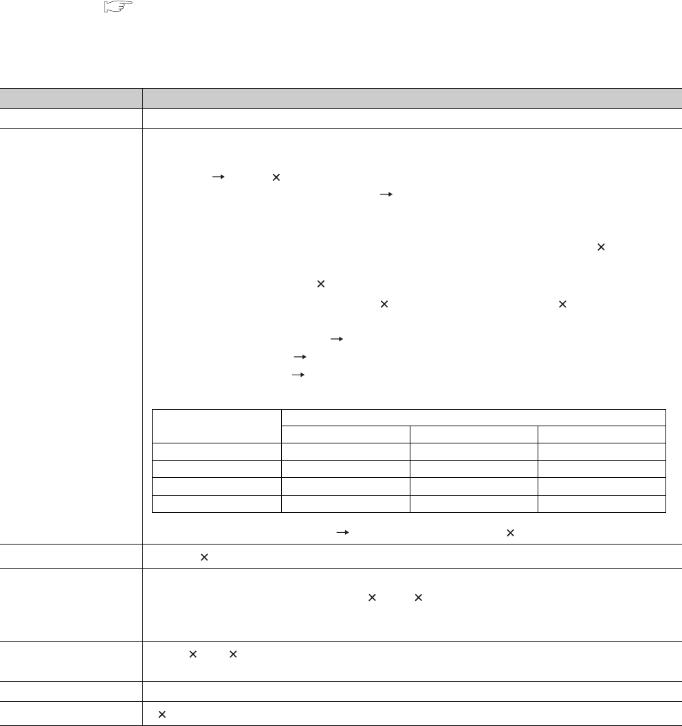
5 - 34
5.3.3 File size
The size of a file used for the CPU module depends on the file type.
When a file is written to the memory area, the unit of the stored file depends on the CPU module and memory area to
be written. ( Section 5.3.4)
When using the program memory, standard RAM, standard ROM, or memory card, calculate the rough size of each file
with reference to Table5.8.
(To the next page)
Table5.8 Calculation of file size
Function Rough file size (unit: Byte)
Drive heading 72
Parameter
Default: 464 (can be increased by parameter setting.)*1
Reference
Boot setting 84 + (18 (number of files))*2
• With CC-Link IE controller network setting
• 72 + (total parameter sizes of each module) + (size of the routing setting) + (size of the data link transfer
setting)
• Parameter size of each module: Up to 10368 (when only LB/LW(1) is set, 1826 + 16 (number of
refresh transfer points))
• Routing setting size: 6 + 8 (number of routing settings)
• Size of data link transfer setting: 6 + 12 (number of transfer settings) + 86 (number of modules)
• With the MELSECNET/H setting Increase up to 6180/module
• With the Ethernet setting Increase up to 922/module
• With the CC-Link setting Increase up to the values in the following table (The values indicate an
increment of each module).
• With the remote password setting 92 + (number of target modules 10), increase up to 172/module
Sequence program 148*3 + (4 ((number of steps) + (number of steps of reserved area for online change)))
Device comment
74 + 8 + (total comment data size of each device)
Comment data size per device = 10 + 10250 a + 40 b
• a: Quotient of ((number of device points)/256)
• b: remainder of ((number of device points/256))
Initial device value 66 + 44 n + 2 (total number of device points set to the initial device value) + 8
n: number of settings of the initial device value
User setting area Setting value at formatting (0 to 15K)
File register*6 2 (number of file register points)
CC-Link setting Mode setting
Ver.1 mode Ver.2 mode Ver.2 additional mode
1st module 550 bytes 572 bytes 624 bytes
2nd to 4th modules 536 bytes 558 bytes 610 bytes
5th module 550 bytes 566 bytes 618 bytes
6th to 8th modules 536 bytes 558 bytes 610 bytes
5 - 35
CHAPTER5 MEMORIES AND FILES USED FOR CPU MODULE
1
2
3
4
5
6
7
8
5.3 File Operations by GX Developer and Handling Precautions
5.3.3 File size
*1: The value is adjusted by the system so that the total bytes with the addition of the network parameter setting may be multiple of four.
*2: The value is adjusted by the system so that the bytes may be multiple of four.
*3: 148 is set by default (This value depends on the parameter setting).
*4: After the decimal point of a value found by the number of bit device points/16 is rounded up.
*5: For the Universal model QCPU, if the serial number (first five digits) is "10011" or earlier, apply the number of execution programs.
*6: The Q00UJCPU does not support this function.
*7: When using the index register as a local device for the Q03UDCPU, Q04UDHCPU, Q06UDHCPU, Q13UDHCPU, Q26UDHCPU, or
Built-in Ethernet port QCPU, check the versions of the CPU module and GX Developer.
( Appendix 2)
*8: When using the module error collection, check the versions of the CPU module and GX Works2.
( Appendix 2)
Remark
For calculation example of memory capacity, refer to Section 5.3.4.
Table5.8 Calculation of file size(continued)
Function Rough file capacity (unit: Byte)
Sampling trace file*6
362 + (number of word device points + number of bit device points) 12 + (N1 + N2 + N3 + number of
word device points 2 + (number of bit device points/16) 2) the number of traces (total number of
executions)*4
• Apply the following values to N1 to N3 according to the items set in "Trace additional information" of the
Trace condition settings screen. ( Section 6.14(4)(b))
N1: When "Time" is set, apply "4".
N2: When "Step no." is set, apply "10".
N3: When "Program name" is set, apply "8".
Device data backup file Setting value at formatting (2 to 1024K)
Module error collection file*8 76 + (64 (value set for the number of storable errors))
Local device*6
72 + 6 (set device type) + 2 ((total number of M and V points)/16 + (number of D points) + 18 (total
number of T, ST, and C points)/16)) (number of programs where local devices are used*5)
• M, V, D, T, ST, and C indicate the following set devices.
M: internal relay
V: edge relay
D: data register
T: timer
ST: retentive timer
C: counter
Z: index register*7

5 - 36
5.3.4 Units of file sizes
(1) Definition
When a file is written to the memory area, the unit of the stored file depends on the CPU module and memory
area to be written. This unit is referred to as a file size unit.
(a) File size unit for each memory area
The following table shows the file size unit depending on the CPU module and memory area to be written.
*1: The file size unit of the Flash card is applied when a file is written to the Flash card by [Online] [Write the program
memory to ROM] in GX Developer. ( Section 5.1.7(1)(a))
(b) File size unit for each memory card
*1: The file size unit of the Flash card is applied when:
•file is written to the Flash card by [Online] [Write to PLC (Flash ROM)] in GX Developer.
( Section 5.1.7(1)(b))
•file is written to the Flash card by GX Developer without accessing the CPU module
Table5.9 File size unit for each CPU module and memory area
CPU module model Memory area
Program memory, standard ROM, Flash card*1 Standard RAM
Q00UJCPU Program memory: 1 step/4 bytes
Standard ROM: 64 steps/256 bytes -
Q00UCPU, Q01UCPU Program memory: 1 step/4 bytes
Standard ROM: 128 steps/512 bytes
512 bytes
Q02UCPU, Q03UDCPU,
Q04UDHCPU,Q06UDHCPU,
Q03UDECPU, Q04UDEHCPU,
Q06UDEHCPU
Program memory: 1 step/4 bytes
Standard ROM, Flash card: 128 steps/512 bytes
Q10UDHCPU,Q10UDEHCPU,Q13U
DHCPU,Q13UDEHCPU
Program memory: 1 step/4 bytes
Standard ROM: 256 steps/1024 bytes
Flash card: 128 steps/512 bytes
Q20UDHCPU,Q20UDEHCPU,Q26U
DHCPU,Q26UDEHCPU
Program memory: 1 step/4 bytes
Standard ROM: 512 steps/2048 bytes
Flash card: 128 steps/512 bytes
Table5.10 File size unit for each memory card
Type Memory card model File size unit
(cluster size)
SRAM card
Q2MEM-1MBS 512 bytes
Q2MEM-2MBS 1024 bytes
Q3MEM-4MBS 1024 bytes
Q3MEM-8MBS 4096 bytes
Flash card*1 Q2MEM-2MBF 1024 bytes
Q2MEM-4MBF 1024 bytes
ATA card
Q2MEM-8MBA 4096 bytes
Q2MEM-16MBA 4096 bytes
Q2MEM-32MBA 2048 bytes

5 - 37
CHAPTER5 MEMORIES AND FILES USED FOR CPU MODULE
1
2
3
4
5
6
7
8
5.3 File Operations by GX Developer and Handling Precautions
5.3.4 Units of file sizes
(2) Calculation example of memory capacity
The following shows an calculation example of memory capacity when the parameters and sequence program
are written to the program memory.
(a) Conditions
1) CPU module to be written: Q26UDHCPU
2) Writing file
*1: For the file size, refer to (1)(a) in this section.
*2: This indicates the program size (file header + execution program) displayed on the GX Developer screen.
( Section 5.2)
3) Reserved area for online change: 500 steps/2000 bytes
(b) Memory capacity calculation
The memory capacity is calculated in units of file sizes of the CPU module to be written.
The file size unit of the Q26UDHCPU in this example is 1 step/4 bytes.( (1) in this section)
1) Calculation of parameter file size
Since the parameter file size is 464 bytes, 116 steps/464 bytes is occupied in the program memory.
Table5.11 File sizes
File name File size*1
PARAM.QPA (parameter file) 464 bytes
MAIN.QPG (sequence program) 525 steps/2100 bytes*2
Figure 5.27 Occupation in units of the file size (parameter file)
Parameter file
(464 bytes)
This file is stored in
units of file sizes
(1 step/4 bytes).
Program memory
capacity
<In program memory>
4 bytes
4 bytes
4 bytes
The parameter file
occupies 464 bytes
(116 steps).

5 - 38
2) Calculation of program size
The program size is found by the formula: sequence program size + reserved area for online change.
Since a program is stored in units of file sizes (1 step), only the amount equal to the program size is occupied.
3) Result
The calculation results of the memory capacities are as shown below.
Table5.12 Calculation results of memory capacities
File name File size Memory capacity
PARAM.QPA 464 bytes 116 steps (464 bytes)
MAIN.QPG
Sequence program size 525 steps
1025 steps (4100 bytes)
Reserved area for online
change 500 steps
Total 1025 steps
Total memory capacity 1141 steps (4564 bytes)

CHAPTER6 FUNCTIONS
1
2
3
4
5
6
7
8
6.1 Function List
6 - 1
CHAPTER6 FUNCTIONS
This chapter describes the functions of the Universal model QCPU.
6.1 Function List
Table6.1 lists the functions of the Universal model QCPU.
: Supported, : Partly supported, : Not supported
(To the next page)
Table6.1 Function list
Item Description Q00UJ
CPU
Q00UCPU,
Q01UCPU
Q02U
CPU
QnUD(H)
CPU
Built-in
Ethernet
port QCPU
Reference
Constant scan Executes a program in a set time interval
regardless of its scan time. Section 6.2
Latch function Holds the device data even at power OFF
or reset. Section 6.3
Output status selection
when the status changed
from STOP to RUN
Selects the output (Y) status (outputting
the same status prior to STOP or clearing
the status) when the CPU module status
is switched from STOP to RUN.
Section 6.4
Clock function Reads the internal clock data of the CPU
module to use it for time management. Section 6.5
Remote RUN/STOP Runs or stops the program operations in
the CPU module externally. Section 6.6.1
Remote PAUSE
Stops the program operations in the CPU
module externally, holding the status of
outputs (Y).
Section 6.6.2
Remote RESET Resets the CPU module externally when
the CPU module is in a STOP status. Section 6.6.3
Remote latch clear
Clears the latch data in the CPU module
when the CPU module is in a STOP
status.
Section 6.6.4
Input response time
selection
Selects input response time values for
the Q series-compatible input modules, I/
O combined modules, high-speed input
modules, and interrupt modules.
Section 6.7
Error time output mode
setting
Sets whether to clear or retain the output
to the Q series compatible output
modules, I/O combined modules,
intelligent function modules, and interrupt
modules at the time of a stop error of the
CPU module.
Section 6.8
H/W error time PLC
operation mode setting
Sets whether to stop or continue
operations in the CPU module when a
hardware error has occurred in an
intelligent function module or interrupt
module.
Section 6.9

6 - 2
: Supported, : Partly supported, : Not supported
(To the next page)
Table6.1 Function list (Continued)
Item Description Q00UJ
CPU
Q00UCPU,
Q01UCPU
Q02U
CPU
QnUD(H)
CPU
Built-in
Ethernet
port QCPU
Reference
Intelligent function module
switch setting
Makes settings for the intelligent
function modules and interrupt
modules. (Refer to manuals of
intelligent function modules and
interrupt modules for setting details.)
Section
6.10
Monitor function
Reads the status of programs and
devices in the CPU module by GX
Developer.
Section
6.11
Monitor condition setting
Specifies the monitoring timing of the
CPU module with device condition or
step number.
*1 *1 Section
6.11.1
Local device monitor/test
Monitors and/or tests the local
devices of the specified program by
GX Developer.
*1 Section
6.11.2
External input/output forced
on/off
Forcibly turns on/off the external
input/output of the CPU module by
GX Developer.
*1 *1 Section
6.11.3
Executional conditioned
device test
Changes a device value within the
specified step of a sequence
program.
*1 *1 Section
6.11.4
Online change Writes programs when the CPU
module is in the RUN status.
Section
6.12
Program monitor list
Displays the scan time and execution
status of the program being
executed.
Section
6.13.1
Interrupt program monitor list Displays the number of executions of
interrupt programs.
Section
6.13.2
Scan time measurement
Measures the execution time of the
area specified by the steps in a
program.
*1 *1 Section
6.13.3
Sampling trace function Continuously samples the specified
device data at a preset timing.
Section
6.14
Debug function from multiple
GX Developers
Enables simultaneous debugging by
multiple GX Developers.
Section
6.15
Watchdog timer
Monitors operational delays caused
by hardware failure or program error
of the CPU module.
Section
6.16
Self-diagnostic function Self-diagnoses the CPU module to
see whether an error exists or not.
Section
6.17
Error history Stores the result of self-diagnostics
to the memory as error history data.
Section
6.18
System protection
Prevents the programs from being
modified from GX Developer, serial
communication module, and
Ethernet module.
Section
6.19

CHAPTER6 FUNCTIONS
1
2
3
4
5
6
7
8
6.1 Function List
6 - 3
: Supported, : Partly supported, : Not supported
*1: Availability depends on the version of the CPU module. ( Appendix 2)
Table6.1 Function list (Continued)
Item Description Q00UJ
CPU
Q00UCPU,
Q01UCPU
Q02U
CPU
QnUD(H)
CPU
Built-in
Ethernet
port QCPU
Reference
Password registration
Prohibits writing/reading data to/from
each file in the CPU module using GX
Developer.
Section
6.19.1
Remote password
Prevents unauthorized access from
external devices such serial
communication module and Ethernet
module.
Section
6.19.2
System display Monitors the system configuration
using GX Developer.
Section
6.20
LED indication
Displays the operating status of the
CPU module with LEDs on the front
of the module.
Section
6.21
LED indication priority
Sets whether to indicate an error with
LED according to the priority of each
error.
Section
6.21.2
Interrupt from intelligent
function module
Executes an interrupt program at the
time of interrupt request from the
intelligent function module.
Section
6.22
Serial communication
function
Connects the RS-232 interface of the CPU
module and the personnel computer or
HMI with RS-232 cable and communicates
in the MC protocol.
*1 Section
6.23
Service processing setting
Specifies the service processing
count or time to be executed in END
processing.
Section
6.24.1
Initial device value
Registers data used in programs with
devices and the buffer memories of
the intelligent function modules and
special function modules without
programs.
Section
6.25
Battery life-prolonging
function
Prolongs a battery life by holding only
clock data in the battery.
Section
6.26
Memory check function
Checks whether data in the memories
of the CPU module are not changed
due to excessive electric noise.
Section
6.27
Latch data backup to
standard ROM function
Backs up latch data such as device
data and error history without using a
battery.
Section
6.28
Writing/reading device data
to/from standard ROM
Writes/reads device data to/from
standard ROM.
Section
6.29
CPU module change function
with memory card
Backs up data in the CPU module to a
memory card and restores the backup data
to another CPU module.
*1 *1 *1 Section
6.30
Module model name read*1 Reads the model name of a module on a
base unit.
Section
6.31
Module error collection*1
Collects errors occurred in the connected
intelligent function modules in the CPU
module.
Section
6.32
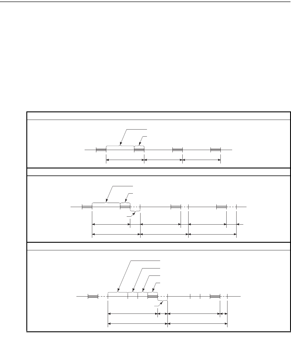
6 - 4
6.2 Constant Scan
(1) Definition
Scan time of the CPU module is not constant because the processing time varies depending on the
execution status of instructions used in a sequence program.
This function allows sequence programs to be executed repeatedly, maintaining its scan time
constant.
(2) Application
I/O refresh is performed before every sequence program execution.
This function is used to maintain I/O refresh intervals constant even if the execution time of each
sequence program differs.
Scan time without constant scan setting
Scan time with constant scan setting (7ms)
Scan time for multiple programs with constant scan setting (10ms)
Figure 6.1 Constant scan operation
END
5ms
0 END 0 END 0 END 0
6ms 5ms
Sequence program
END processing
END
5ms
0END 0
2ms
6ms
END 0
1ms
5ms
END 0
2ms
7ms7ms 7ms
Sequence program
END processing
Waiting time
8ms
2ms
10ms
9ms
1ms
10ms
Sequence program A
Sequence program B
Sequence program C
END processing
Waiting time
CHAPTER6 FUNCTIONS
1
2
3
4
5
6
7
8
6.2 Constant Scan
6 - 5
(3) Constant scan time setting
Set a constant scan time value in the PLC RAS tab of the PLC parameter dialog box.
The setting range is 0.5 to 2000ms (in increments of 0.5ms).
When not executing the constant scan function, leave the constant scan time setting box blank.
(a) Condition
The constant scan time needs to satisfy the following relational expression.
If the sequence program scan time is longer than the constant scan setting time, the CPU module
detects “PRG. TIME OVER” (error code: 5010).
In this case, the constant scan setting will be ignored and the sequence program scan time will be
applied.
If the sequence program scan time is longer than the WDT setting time, the CPU module detects
“WDT ERROR”.
In this case, the program execution will be stopped.
Figure 6.2 When the constant scan time is set to 10ms
(WDT setting time) > (Constant scan setting time) >
(Sequence program maximum scan time)
Figure 6.3 Operation when the scan time is longer than the constant scan setting time
Set a constant scan
time value here.
012 341234
00
1
END 0END
2341234
0END 0END
3.5ms 0.5ms
4ms 4ms
3.5ms 3.4ms 0.6ms
4ms5.3ms
5ms
0.5ms
Scan where the constant scan setting is not applied
Constant scan setting (4ms)
Constant
scan
Sequence
program

6 - 6
(4) Waiting time from when END processing is executed until next scan starts
Sequence program processing is stopped during the waiting time from when END processing of a
sequence program is executed until next scan starts.
(a) When an interrupt factor occurs during waiting time
Either of the following programs is executed.
• Interrupt program
• Fixed scan execution type program
(b) When a service processing parameter is set
The communication service processing with peripherals (such as GX Developer) and intelligent function
modules is enabled during the waiting time by setting a service processing parameter. ( Section 6.24.1)
(5) Constant scan accuracy
The constant scan accuracy is 0.01ms.
However, when any program indicated below is being executed, the constant scan time may increase.
(a) Interrupt program or fixed scan execution type program
Interrupts are disabled while an interrupt program or fixed scan execution type program is executed.
Even if the constant scan time runs out during execution of an interrupt program or fixed scan
execution type program, the constant scan cannot be finished.
In this case, the constant scan time may increase by the execution time of the program executed.

CHAPTER6 FUNCTIONS
1
2
3
4
5
6
7
8
6.3 Latch Function
6 - 7
6.3 Latch Function
(1) Definition
This function holds data in each device of the CPU module when:
• the CPU module is powered off and then on,
• the CPU module is reset, or
• power failure occurs exceeding the allowable momentary power failure time.
Data in each device of the CPU module is cleared and set back to its default (bit device: off, word
device: 0) without using the latch function.
(2) Application
This function is used to hold the data managed by sequential control and continue control operation
especially when the CPU module is powered off and then on.
(3) Program operation when the latch function is use
Program operation is the same, regardless of the latch status.
(4) Devices that can be latched
The following devices can be latched.(By default, only the latch relay is enabled for latch.)
• Latch relay (L)
• Link relay (B)
• Annunciator (F)
• Edge relay (V)
•Timer (T)
• Retentive timer (ST)
• Counter (C)
• Data register (D)
• Link register (W)
When the battery life-prolonging function ( Section 6.26) is set, the latch relay cannot be
latched.
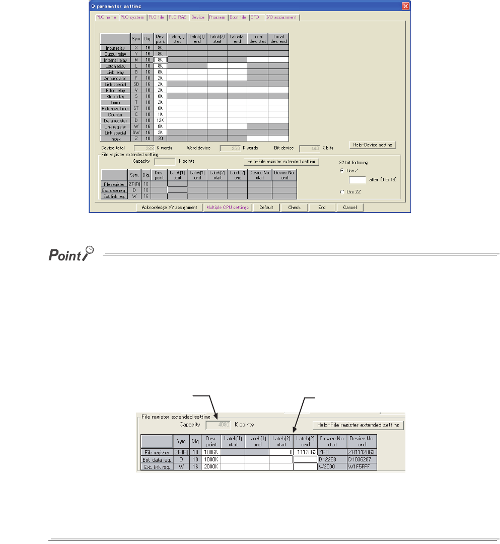
6 - 8
(5) Latch range setting
Set a latch range in the Device tab of the PLC parameter dialog box.
There are two types of latch range settings: the latch clear operation enable range setting (Latch (1))
and the latch clear operation disable range setting (Latch (2)).
The latch range of the file register (ZR), extended data register (D), and extended link register (W) can also be
set.
After selecting "Use the following file." and setting the capacity of the file register in the PLC file tab of the PLC
parameter dialog box, set a latch range of the file register (ZR), extended data register (D), and extended link
register (W). (For the extended data register (D) and extended link register (W), assign a part of the file register
area.)
If "Use the same file name as the program." is selected in the PLC file tab of the PLC parameter dialog box, a
latch range of the file register (ZR), extended data register (D), and extended link register (W) cannot be set.
(All data in the file register will be latched.)
The data outside the latch range will be cleared when the CPU module is powered off and then on or is reset.
When the file register file to be used is switched with the QDRSET instruction, the latch range setting of the file
register will be invalid.
After switching, regardless of the latch range setting, whole range of the file register will be latched.
Figure 6.4 Latch range setting
Figure 6.5 Latch range setting
The file register points set
in the PLC file tab is displayed. Set a latch range.

CHAPTER6 FUNCTIONS
1
2
3
4
5
6
7
8
6.3 Latch Function
6 - 9
(6) Device data latch method and influence on the scan time
Data latch processing is performed during END processing.
For this reason, the scan time increases.
Consider an influence on the scan time when latching devices. ( Section 10.1.2)
To shorten the scan time due to latch, minimize the number of latch points (latch (1) setting, latch (2) setting,
and latch relay (L)) as much as possible.
The number of latch points can be reduced by performing the following.
• Move data to be latched to the file register.
• Store device data that is less frequently updated in the standard ROM with the SP.DEVST instruction.
(The device data stored in the standard ROM can be read with the S(P).DEVLD instruction.)
QCPU Programming Manual (Common Instructions)
(7) Device data latch clear
Tabl e6. 2 shows the status of device data when the latch clear operation is performed.
*1: For the clearing method, refer to Section 3.7.
Data in the file register (R or ZR) will not be cleared by the latch clear operation.
To clear data in the file register (R or ZR), perform data clear operation by a sequence program or GX Developer.
( Section 9.7.3)
(8) Precautions
(a) When a local device or initial device value is specified
Device data cannot be latched even if the device has been latch-specified,
(b) Use of battery
Device data in the latch range are held with the battery installed to the CPU module.
• Even for the boot operation, the battery is required to latch device data.
• Note that if the battery connector is disconnected from the connector of the CPU module while
the power supply for the programmable controller is off, device data in the latch range will not
be held and will become undefined.
Table6.2 Status when the latch clear operation is performed
Latch setting Status of data
Device data without latch setting Cleared
Device data in the "Latch (1)" range Cleared
Device data in the "Latch (2)" range Held*1
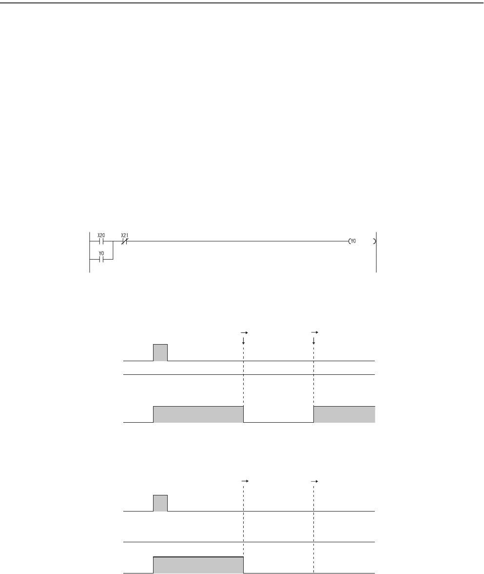
6 - 10
6.4 Output Mode at Operating Status Change (STOP to RUN)
(1) Definition
When the operating status is changed from RUN to STOP, the CPU module internally stores the
outputs (Y) in the RUN status and then turns off all the outputs (Y).
The status of the outputs (Y) when the operating status of the CPU module is changed back from
STOP to RUN can be selected from the following two options in the parameter setting in GX
Developer.
• Output the output (Y) status prior to STOP. (“Previous state”)
• Clear the output (Y) status. (“Recalculate (output is 1 scan later)”)
(2) Application
This function is used to determine the status of outputs (whether to resume the outputs from the
previous status or not) when the operating status is changed from STOP to RUN in the holding circuit.
• When outputting the output (Y) status prior to STOP
• When clearing the output (Y) status
Figure 6.6 Holding circuit
Figure 6.7 Timing chart when the parameter is set to "Previous state"
Figure 6.8 Timing chart when the parameter is set to "Recalculate (output is 1 scan later)"
Start
button
Stop
button
OFF
OFF
ON
ON
OFF
X21
Y0
X20
RUN STOP STOP RUN
OFF
OFF
ON
ON
OFF
X21
Y0
X20
RUN STOP STOP RUN
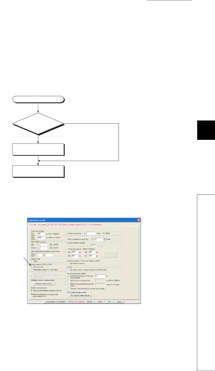
CHAPTER6 FUNCTIONS
1
2
3
4
5
6
7
8
6.4 Output Mode at Operating Status Change (STOP to RUN)
6 - 11
(3) Operation when the operating status is changed from STOP to RUN
(a) Previous state (Default)
The CPU module outputs the output (Y) status immediately before changing to the STOP status and
then performs sequence program operations.
(b) Recalculate (output is 1 scan later)
All outputs are turned off.
The CPU module outputs the output (Y) status after sequence program operations are completed.
For the operation of the CPU module when the output (Y) status is forcibly turned on in the STOP
status, refer to (5) in this section.
(4) Setting the output mode when the operating status is changed from STOP to RUN
Set the output mode when the operating status is changed from STOP to RUN in the PLC system tab
of the PLC parameter dialog box.
Figure 6.9 Operation when the operating status is changed from STOP to RUN
Figure 6.10 PLC system setting
Operating status change (STOP to RUN)
YES ("Previous state" is set.)
The output (Y) status immediately before
changed to the STOP status is output.
Sequence program operations
are performed.
Is "Previous state" set?
NO ("Recalculate (output is 1 scan later)" is set.)
Set the output
mode here.

6 - 12
(5) Precautions
Table6.3 shows the output status of the CPU module when the operating status is changed from STOP
to RUN after the outputs (Y) are forcibly turned on in the STOP status.
Table6.3 Output status when the operating status is changed from STOP to RUN after the output forced on operation is performed
Output mode ("Output mode at STOP to RUN") selected Output status
Previous state
The output status prior to STOP is output.
Even if the outputs are forcibly turned on, the on status is not held if
the output status prior to STOP was off.
Recalculate (output is 1 scan later) The on status is held and output.

CHAPTER6 FUNCTIONS
1
2
3
4
5
6
7
8
6.5 Clock Function
6 - 13
6.5 Clock Function
(1) Definition
This function reads the internal clock data of the CPU module by a sequence program and uses it for
time management.
The clock data is used for time management required for some functions in the system, such as storing date into
the error history.
Remark
The Built-in Ethernet port QCPU can set the time in the CPU module automatically by using the time setting function
(SNTP client).
QnUCPU User’s Manual (Communication via Built-in Ethernet Port)
(2) Clock operation at power off and momentary power failure
Clock operation continues by the internal battery of the CPU module even when the programmable
controller is powered off or power failure occurs exceeding the allowable momentary power failure
time.
(3) Clock data
Tabl e6. 4 shows the details of clock data, which is used internally in the CPU module.
Table6.4 Clock data details
Data name Description
Year Four digits (from 1980 to 2079)
Month 1 to 12
Day 1 to 31 (Automatic leap year detection)
Hour 0 to 23 (24 hours)
Minute 0 to 59
Second 0 to 59
Day of the week
0 Sunday
1 Monday
2 Tuesday
3 Wednesday
4 Thursday
5 Friday
6 Saturday
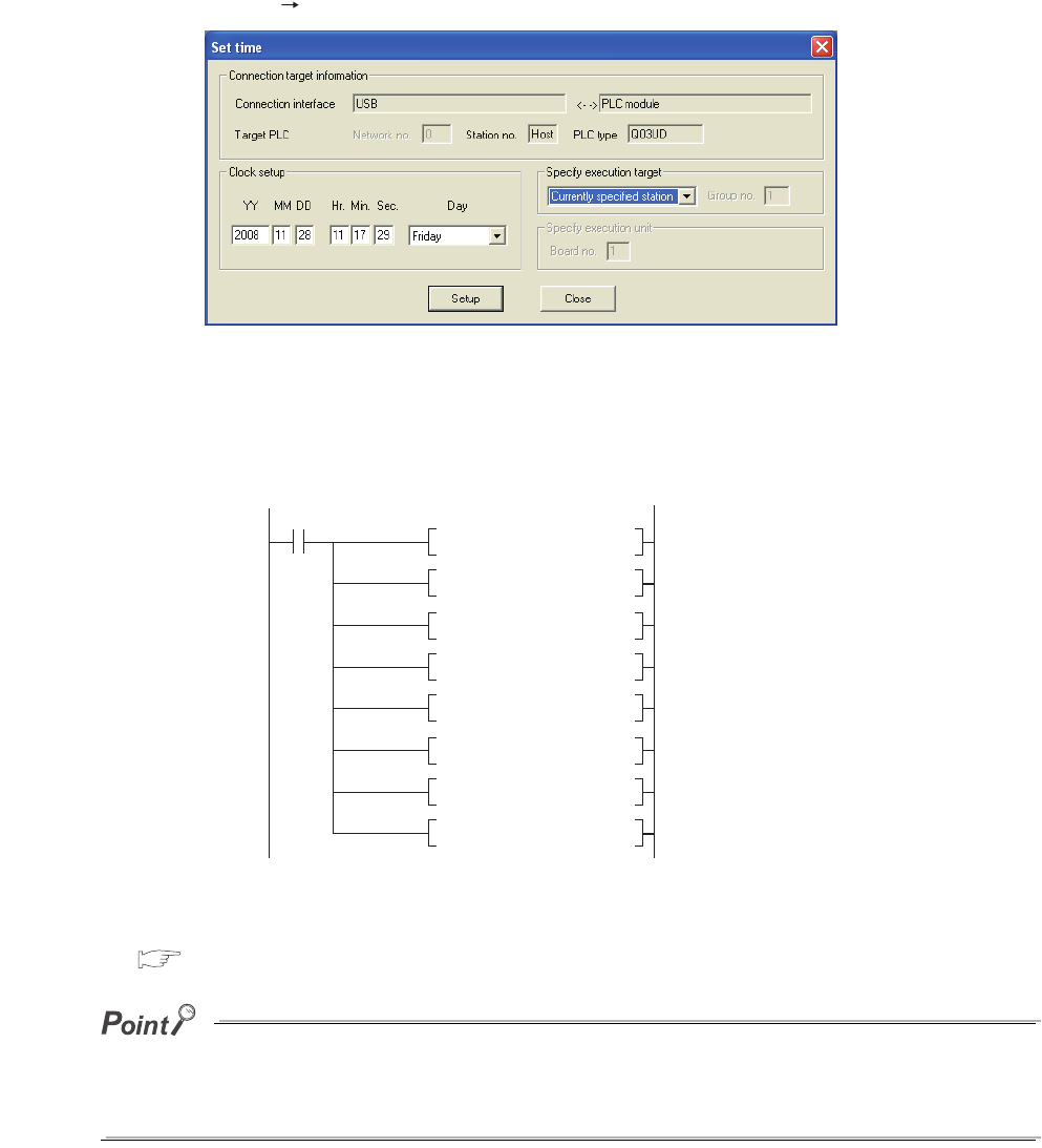
6 - 14
(4) Changing and reading clock data
(a) Changing clock data
Clock data can be changed either by GX Developer or a program.
1) Changing clock data by GX Developer
Select [Online] [Set time] to open the Set time screen and change the clock data.
2) Changing clock data by a program
Use the DATEWR instruction (instruction for writing clock data) to change the clock data.
Figure 6.12 shows a program for writing the set clock data to D0 to D6.
For details of the DATEWR instruction, refer to the following.
QCPU Programming Manual (Common Instructions)
●When clock data is changed, the clock of 1/1000 second is reset to 0.
●Year data settable by GX Developer is up to 2037.
Figure 6.11 Set time screen
Figure 6.12 Program example for writing clock data
Write request
0
X0
Year 1999
Month 8
Day 10
Hour 11
Minute 35
Second 24
Day of the week
Tuesday: 2
MOVP K1999 DO
MOVP K8 D1
MOVP D2
MOVP D3
MOVP D4
MOVP D5
MOVP D6
DATEWR DO
K10
K11
K35
K24
K2
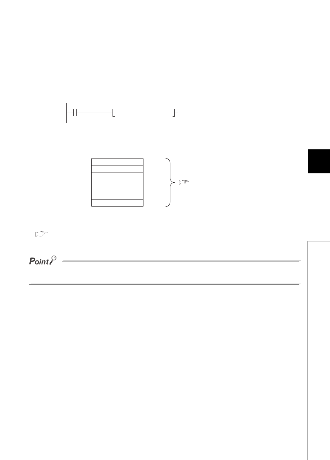
CHAPTER6 FUNCTIONS
1
2
3
4
5
6
7
8
6.5 Clock Function
6 - 15
(b) Reading clock data
To read clock data to the data register, use either of the following instructions in the program.
• DATERD (instruction for reading clock data)
• S(P).DATERD (instruction for reading extended clock data)
Figure 6.13 shows a program for storing the clock data read with the DATERD instruction to D10 to
D16.
*1: Figure 6.14 shows the clock data stored in D10 to D16.
For details of the DATERD and S(P).DATERD instructions, refer to the following.
QCPU Programming Manual (Common Instructions)
Clock data can also be written or read by the special relay (SM210 to SM213) and special register (SD210 to SD213).
For details of the special relay and special register, refer to CHAPTER 12.
Figure 6.13 Program example for storing clock data
Figure 6.14 Clock data stored
Read request
X1
DATERD D10 Stores clock data to D10
to D16.*1
D10
D11
D12
D13
D14
D15
D16
2004
4
1
11
35
24
2
Year (four digits)
Month
Date
Hour
Minute
Second
Day of the week
( (3) in this section)

6 - 16
(5) Precautions
(a) Initial clock data setting
No clock data is set at the factory.
Clock data is required for some functions of the CPU module used in the system, such as error
history storage, or for intelligent function modules.
Before using the CPU module for the first time, set the time correctly.
(b) Clock data correction
If a part of the clock data is corrected, rewrite the entire clock data to the CPU module.
(c) Clock data setting range
When changing clock data, write data within the range given in (3) in this section.
If data outside of clock range is written to the CPU module, the clock function does not operate normally.
However, the CPU module does not detect an error if the clock data is out of the range.
(d) Use for clock data of 1/1000 sec.
1) Function that clock data of 1/1000 sec. can be used
Only the following instructions can use the clock data of 1/1000 sec.
• S(P).DATERD
• S(P).DATE+
• S(P).DATE-
Other instructions cannot use the clock data of 1/1000 sec.
(Such as for reading data by SM/SD, storing the time of error occurrence as error history data, reading data
by GX Developer, or reading data by dedicated instructions of other modules.)
2) When clock data is changed
When clock data is changed by GX Developer or instructions (including dedicated instruction of other
modules), the clock of 1/1000 sec. is reset to 0.
Table6.5 Example of clock data
Write operation to the CPU module CPU module operation
February 30 Executed An error is not detected.
32 of month 13 Not executed
When the DATEWR instruction is executed, "OPERATION ERROR" (error
code: 4100) is detected.
When SM210 is turned on, SM211 turns on.

CHAPTER6 FUNCTIONS
1
2
3
4
5
6
7
8
6.5 Clock Function
6 - 17
(6) Clock data accuracy
Accuracy of the clock data varies depending on the ambient temperature as shown below.
(7) Clock data comparison
To compare clock data in a sequence program, read the clock data with the DATERD instruction (instruction for
reading clock data).
Since the DATERD instruction reads the year data in four digits, the data can be compared by the comparison
instruction without any modifications.
Table6.6 Clock data accuracy
Ambient temperature ( ) Accuracy (Day difference, S)
0 -2.96 to +3.74 (TYP.+1.42)
+ 25 -3.18 to +3.74 (TYP.+1.50)
+ 55 -13.20 to +2.12 (TYP.-3.54)

6 - 18
6.6 Remote Operation
Remote operation allows to change the operating status of the CPU module externally (by GX Developer
or external devices using the MC protocol, with link dedicated instructions of the CC-Link IE controller
network module or MELSECNET/H module, or using remote contacts).
There are four types of remote operations:
6.6.1 Remote RUN/STOP
(1) Definition
This operation changes the operating status of the CPU module externally to RUN or STOP, keeping
the RUN/STOP/RESET switch of the CPU module in the RUN position.
(2) Application
This operation is useful to run or stop the CPU module remotely when:
• the CPU module is inaccessible, or
• the CPU module is in a control panel.
(3) Program operation
The program operation will be as follows when the remote RUN/STOP operation is performed.
(a) Remote STOP
The CPU module executes a program until the END instruction and changes its operating status to
STOP.
(b) Remote RUN
The CPU module changes its operating status to RUN and executes a program from the step 0.
(The remote RUN operation must be performed to the CPU module whose operating status has
been changed to STOP by the remote STOP operation.)
• Remote RUN/STOP : Section 6.6.1
• Remote PAUSE : Section 6.6.2
• Remote RESET : Section 6.6.3
• Remote latch clear : Section 6.6.4

CHAPTER6 FUNCTIONS
1
2
3
4
5
6
7
8
6.6 Remote Operation
6.6.1 Remote RUN/STOP
6 - 19
(4) Executing method
There are three methods for performing the remote RUN/STOP operation.
• Using a RUN contact
• By GX Developer or an external device using the MC protocol
• With link dedicated instructions of the CC-Link IE controller network module or MELSECNET/H
module
(a) Using a RUN contact
Set a RUN contact in the PLC system tab of the PLC parameter dialog box.
The settable device range is X0 to 1FFF.
The remote RUN/STOP operation can be performed by turning on/off the set RUN contact.
• When the RUN contact is turned off, the CPU module status changes to RUN.
• When the RUN contact is turned on, the CPU module status changes to STOP.
(b) By GX Developer or an external device using the MC protocol
Select [Online] [Remote operation] in GX Developer.
To perform the remote RUN/STOP operation from an external device, use the MC protocol
command.
Q Corresponding MELSEC Communication Protocol Reference Manual
Figure 6.15 Remote RUN/STOP using a RUN contact
Figure 6.16 Remote RUN/STOP by GX Developer or an external device
END
Step 0 Step 0
RUN contact
RUN/STOP status
ON
END
STOP
OFF
RUN
0
STOP status
RUN/STOP status
ON
OFF
OFF
RUN
STOP
END
STOP status
ON
END
0
Step 0Step 0
Remote STOP
command
Remote RUN
command
GX Developer
or
External device

6 - 20
(c) With link dedicated instructions of the CC-Link IE controller network module or
MELSECNET/H module
The remote RUN/STOP operation by link dedicated instructions of the CC-Link IE controller network
module or MELSECNET/H module can change the RUN/STOP status of the CPU module.
For details, refer to the following.
Reference manual of each network module
(5) Precautions
Pay attention to the following since the STOP status is given priority over the RUN status.
(a) Timing of changing to the STOP status
The operating status of the CPU module is changed to STOP when the remote STOP operation is
performed from any one of the following: RUN contact, GX Developer, or an external device using
the MC protocol.
(b) When changing the status back to RUN
To change the operating status back to RUN after the CPU module status was changed to STOP by the remote
STOP operation, perform the remote RUN operation in the same order for the remote STOP operation.
●The definitions of the RUN/STOP status are described below.
• RUN status•••A status where sequence program operations are repeatedly performed in a loop between the step
0 and the END or FEND instruction.
• STOP status•••A status where sequence program operations are stopped. All outputs (Y) are turned off.
●After being reset, the operating status of the CPU module becomes the one set with the RUN/STOP/RESET switch.

CHAPTER6 FUNCTIONS
1
2
3
4
5
6
7
8
6.6 Remote Operation
6.6.2 Remote PAUSE
6 - 21
6.6.2 Remote PAUSE
(1) Definition
This operation changes the operating status of the CPU module externally to PAUSE, keeping the
RUN/STOP/RESET switch of the CPU module in the RUN position.
PAUSE status is a status where sequence program operations in the CPU module are stopped,
holding the status (on or off) of all outputs (Y).
(2) Application
This operation is useful, especially during the process control, to hold the on status of outputs (Y) even
after the operating status of the CPU module is switched from RUN to STOP.
(3) Executing method
There are two methods for performing the remote PAUSE operation.
• Using a PAUSE contact
• By GX Developer or an external device using the MC protocol
(a) Using a PAUSE contact
Set a PAUSE contact in the PLC system tab of the PLC parameter dialog box.
The settable device range is X0 to 1FFF.
• The PAUSE contact (SM204) turns on during END processing of the scan where both the
PAUSE contact and PAUSE enable coil (SM206) turn on.
The CPU module executes one more scan until the END instruction after the scan where the PAUSE
contact turns on, and then changes its operating status to PAUSE. In the PAUSE status, the program
operations are stopped.
• When the PAUSE contact or SM206 is turned off, the PAUSE status will be canceled and the
CPU module will restart the sequence program operation from the step 0.
Setting of only a PAUSE contact is not allowed.
When setting a PAUSE contact, set a RUN contact as well.
Figure 6.17 Remote PAUSE using a PAUSE contact
OFF
ON
0 END
PAUSE status
0END 00
END END
SM206 OFF
ON
SM204 OFF
ON
RUN/PAUSE
status
RUN RUN
PAUSE
PAUSE
contact
Turns on when the
PAUSE conditions
are established
6 - 22
(b) By GX Developer or an external device using the MC protocol
Select [Online] [Remote operation] in GX Developer.
To perform the remote PAUSE operation from an external device, use the MC protocol command.
Q Corresponding MELSEC Communication Protocol Reference Manual
• The PAUSE contact (SM204) turns on during END processing of the scan where the remote
PAUSE command is executed.
The CPU module executes one more scan until the END instruction after the scan where the PAUSE
contact turns on, and then changes its operating status to PAUSE. In the PAUSE status, the program
operations are stopped.
• Upon execution of the remote RUN command, the CPU module will restart the sequence
program operations from the step 0.
(4) Precautions
(a) When forcibly keeping output status
To forcibly keep the output status (on or off) in the PAUSE status, provide an interlock with the
PAUSE contact (SM204).
Figure 6.18 Remote PAUSE by GX Developer or an external device
Figure 6.19 Program example for forcibly keeping output status in the PAUSE status
Remote PAUSE
command
Remote RUN
command
SM204
OFF
OFF
OFF
ON
0
0
END
END
0
0
END
ON
ON
Turns on when the
PAUSE conditions
are established
PAUSE status
RUN/PAUSE
status
RUN RUN
PAUSE
M20
X0
M0
SM204
SM204
Y70
Y71
Y72
The on/off status of Y70 is determined by the
on/off status of M20 in the PAUSE status.
Y71 turns off in the PAUSE status.
Y72 turns on in the PAUSE status.
CHAPTER6 FUNCTIONS
1
2
3
4
5
6
7
8
6.6 Remote Operation
6.6.3 Remote RESET
6 - 23
6.6.3 Remote RESET
(1) Definition
This operation resets the CPU module externally when the CPU module is in the STOP status.
Even if the RUN/STOP/RESET switch is in the RUN position, this operation can be performed when
the module is stopped due to an error detected by the self-diagnostics function.
(2) Application
This operation is useful to reset the CPU module remotely when an error occurs in the CPU module
placed in an inaccessible location.
(3) Executing method
This operation can only be performed by GX Developer or an external device using the MC protocol.
• Select [Online] [Remote operation] in GX Developer.
• To perform the remote RESET operation from an external device, use the MC protocol command.
Q Corresponding MELSEC Communication Protocol Reference Manual
Before performing the remote RESET operation, select the "Allow" checkbox for the remote RESET operation
in the PLC system tab of the PLC parameter dialog box, and then write the parameter setting to the CPU
module.
Without the preset parameter setting, the operation cannot be performed.
Figure 6.20 Parameter setting required for the remote RESET operation
Select the checkbox
here to enable the
remote RESET
operation.

6 - 24
(4) Precautions
(a) Remote RESET in the RUN status
When the CPU module is in the RUN status, the remote RESET operation cannot be performed.
To perform the operation, change the operating status of the CPU module to STOP by the remote
STOP or similar operation.
(b) Status after reset processing
After reset processing of the remote RESET operation is completed, the CPU module will be placed
in the operating status set by the RUN/STOP/RESET switch.
If the RUN/STOP/RESET switch is set to STOP, the CPU module will be in the STOP status. If the
switch is set to RUN, the CPU module will be in the RUN status.
●If the remote RESET operation is performed to the CPU module which is stopped due to an error, note
that the CPU module will be placed in the operating status set by the RUN/STOP/RESET switch after
reset processing is completed.
●If the CPU module cannot be reset by the remote RESET operation from GX Developer, check that the
"Allow" checkbox for the remote RESET operation in the PLC system tab of the PLC parameter dialog box
is selected.
If the checkbox is not selected, the CPU module cannot be reset even after the remote RESET processing
from GX Developer is completed.
(c) When an error occurs due to noise
Note that the CPU module may not be reset by the remote RESET operation from GX Developer.
In this case, reset the CPU module using the RUN/STOP/RESET switch or power off and then on
the CPU module.

CHAPTER6 FUNCTIONS
1
2
3
4
5
6
7
8
6.6 Remote Operation
6.6.4 Remote latch clear
6 - 25
6.6.4 Remote latch clear
(1) Definition
This function resets the latched device data from GX Developer or an external device when the CPU
module is in the STOP status.
(2) Application
This function is useful in the following cases if used together with the remote RUN/STOP operation.
• When the CPU module is inaccessible
• To clear latched device data in the CPU module in a control panel externally
(3) Executing method
This operation can only be performed by GX Developer or an external device using the MC protocol.
• Select [Online] [Remote operation] in GX Developer.
• To execute the remote latch clear operation from an external device, use the MC protocol
command.
Q Corresponding MELSEC Communication Protocol Reference Manual
To perform the remote latch clear operation, follow the following steps.
1) Change the operating status of the CPU module to STOP by the remote STOP operation.
2) Clear the latched device data in the CPU module by the remote latch clear operation.
3) After remote latch clear processing is completed, perform the remote RUN operation to return the operating
status to RUN.
(4) Precautions
(a) Latch clear in the RUN status
The latch clear operation cannot be performed when the CPU module is in the RUN status.
(b) Latch clear enabled range
There are two kinds of latch range can be set in the Device tab of the PLC parameter dialog box: latch clear
operation enable and disable range.
Remote latch clear operation resets only the data set in the "Latch (1)" (latch clear operation enable range).
For the method for resetting the device data in the latch clear operation disable range, refer to Section
3.7(2)(c).
(c) Devices that are reset by the remote latch clear operation
Devices that are not latched are also reset when the remote latch clear operation is performed.

6 - 26
6.6.5 Relationship between remote operation and RUN/STOP status of the CPU
module
(1) Relationship between remote operation and RUN/STOP status of the CPU
module
Table6.7 shows the operating status of the CPU module according to the combination of remote operation and
RUN/STOP status.
*1: When performing the operation using a RUN contact, "RUN-PAUSE contact" must be set in the PLC system tab of the PLC
parameter dialog box.
*2: When performing the operation using a PAUSE contact, "RUN-PAUSE contact" must be set in the PLC system tab of the
PLC parameter dialog box.
In addition, the PAUSE enable coil (SM206) must be turned on.
*3: The "Allow" checkbox for the remote RESET operation must be selected in the PLC system tab of the PLC parameter
dialog box.
*4: The remote RESET and remote latch clear operations are enabled if the CPU module status is changed to STOP by the
remote STOP operation.
*5: The STOP status includes a case where the CPU module is stopped due to an error.
(2) Remote operations from a single GX Developer
When remote operations are performed from a single GX Developer, the operating status of the CPU module will
be the status of the last remote operation performed.
(3) Remote operations from multiple GX Developers
Any remote operation from other GX Developers via other stations cannot be performed to the CPU module
where remote operations are being performed from GX Developer connected.
To perform any remote operations from another GX Developer, cancel the remote operation by performing the
remote RUN operation from the same GX Developer that is performing the current remote operation.
For example, even if the remote STOP or RUN operation is performed from another GX Developer to the CPU
module where the remote PAUSE operation has been performed by GX Developer connected, the CPU module
remains in the PAUSE status.
Once after the remote RUN operation is performed from the same GX Developer that is performing the remote
PAUSE operation, remote operations from another GX Developer will be enabled.
Table6.7 Operating status of the CPU module
RUN/STOP status Remote operation
RUN*1 STOP PAUSE*2 RESET*3 Latch clear
RUN RUN STOP PAUSE Operation disabled*4 Operation disabled*4
STOP STOP STOP STOP RESET*5 Latch clear

CHAPTER6 FUNCTIONS
1
2
3
4
5
6
7
8
6.7 Q Series-compatible Module Input Response Time Selection (I/O Response Time)
6 - 27
6.7 Q Series-compatible Module Input Response Time Selection (I/O
Response Time)
(1) Definition
This function changes the input response time for each Q series-compatible module.
Tabl e6. 8 shows the modules available for input response time change and selectable time settings.
The Q series-compatible modules in the table above take in external inputs within the set time here.
Table6.8 Modules available for input response time change
Module name Type Settable time setting
Input module “Input” 1ms, 5ms, 10ms, 20ms, 70ms
(Default: 10ms)
I/O combined module “I/O Mix”
High-speed input module “Hi Input” 0.1ms, 0.2ms, 0.4ms, 0.6ms, 1ms
(Default: 0.2ms)
Interrupt module “Interrupt”
Figure 6.21 Input response time
OFF
OFF
ON
ON
External input
Q series-compatible module
Input response time
6 - 28
(2) Input response time setting
Set input response time values in the I/O assignment tab of the PLC parameter dialog box.
1) Make I/O assignment for the target module.
2) Click the button.
3) On the screen opened, select an input response time value (“I/O response time”).
(3) Precautions
(a) When input response time is shortened
The shorter the input response time is, the more the CPU module is susceptible to noise.
Consider the operating environment when setting input response time values.
(b) Enabling the setting
The input response time setting will be enabled when:
• the CPU module is powered off and then on, or
• the CPU module is reset.
Figure 6.22 Input response time setting
Detailed setting
1) Make I/O assignment. 2) Click the Detailed setting button. 3) Select the input response time.
CHAPTER6 FUNCTIONS
1
2
3
4
5
6
7
8
6.8 Error Time Output Mode Setting
6 - 29
6.8 Error Time Output Mode Setting
(1) Definition
This function determines the output mode (clear or hold) from the CPU module to the Q series-
compatible output modules, I/O combined modules, intelligent function modules, and/or interrupt
module when a stop error occurs in the CPU module.
(2) Error time output mode setting
Set the error time output mode in the I/O assignment tab of the PLC parameter dialog box.
1) Make I/O assignment for the target module.
2) Click the button.
3) On the screen opened, select "Clear" or "Hold". (Default: "Clear")
(3) Precautions
The error time output setting will be enabled when:
• the CPU module is powered off and then on, or
• the CPU module is reset.
Failure to perform either of the operations above after changing the error time output mode setting will
result in "PARAMETER ERROR" (error code: 3000).
Figure 6.23 Error time output mode setting
Detailed setting
3) Select "Clear" or "Hold" for
the error time output mode.
1) Make I/O assignment. 2) Click the Detailed setting button.
6 - 30
6.9 H/W Error Time PLC Operation Mode Setting
(1) Definition
This function determines the program operation mode (stop or continue) of the CPU module when a
hardware error occurs in an intelligent function module or interrupt module.
(2) H/W error time PLC operation mode setting
Set the H/W error time PLC operation mode in the I/O assignment tab of the PLC parameter dialog
box.
1) Make I/O assignment for the target module.
2) Click the button.
3) On the screen opened, select "Stop" or "Continue". (Default: "Stop")
(3) Precautions
The H/W error time PLC operation setting will be enabled when:
• the CPU module is powered off and then on, or
• the CPU module is reset.
Figure 6.24 H/W error time PLC operation setting
Detailed setting
3) Select "Stop" or "Continue" for
the H/W error time PLC operation mode.
1) Make I/O assignment. 2) Click the Detailed setting button.
CHAPTER6 FUNCTIONS
1
2
3
4
5
6
7
8
6.10 Intelligent Function Module Switch Setting
6 - 31
6.10 Intelligent Function Module Switch Setting
(1) Definition
This function sets the switches of each Q series-compatible intelligent function module and interrupt
module in GX Developer.
(2) Writing the switch settings
The switch settings will be written from the CPU module to each intelligent function module and
interrupt module when:
• the CPU module is powered off and then on, or
• the CPU module is reset.
Figure 6.25 Writing the switch settings to each intelligent function module
GX Developer
1) Write the
settings.
The settings are written when the CPU module
is powered off and then on or reset.
2)
6 - 32
(3) Switch settings
Set the switch details for each intelligent function module and interrupt module in the I/O assignment
tab of the PLC parameter dialog box.
1) Make I/O assignment for the target module.
2) Click the button.
3) Set the switch details for each module.
(4) Precautions
(a) Switch setting details of each module
For the switch setting details of each intelligent function module or interrupt module, refer to the
manual for the intelligent function module or interrupt module used.
(b) Enabling the setting
The switch settings of each intelligent function module or interrupt module will be enabled when:
• the CPU module is powered off and then on, or
• the CPU module is reset.
Figure 6.26 Switch settings
Switch setting
1) Make I/O assignment. 2) Click the Switch setting button.
Set the switch details of each intelligent
function module and interrupt module.
3)
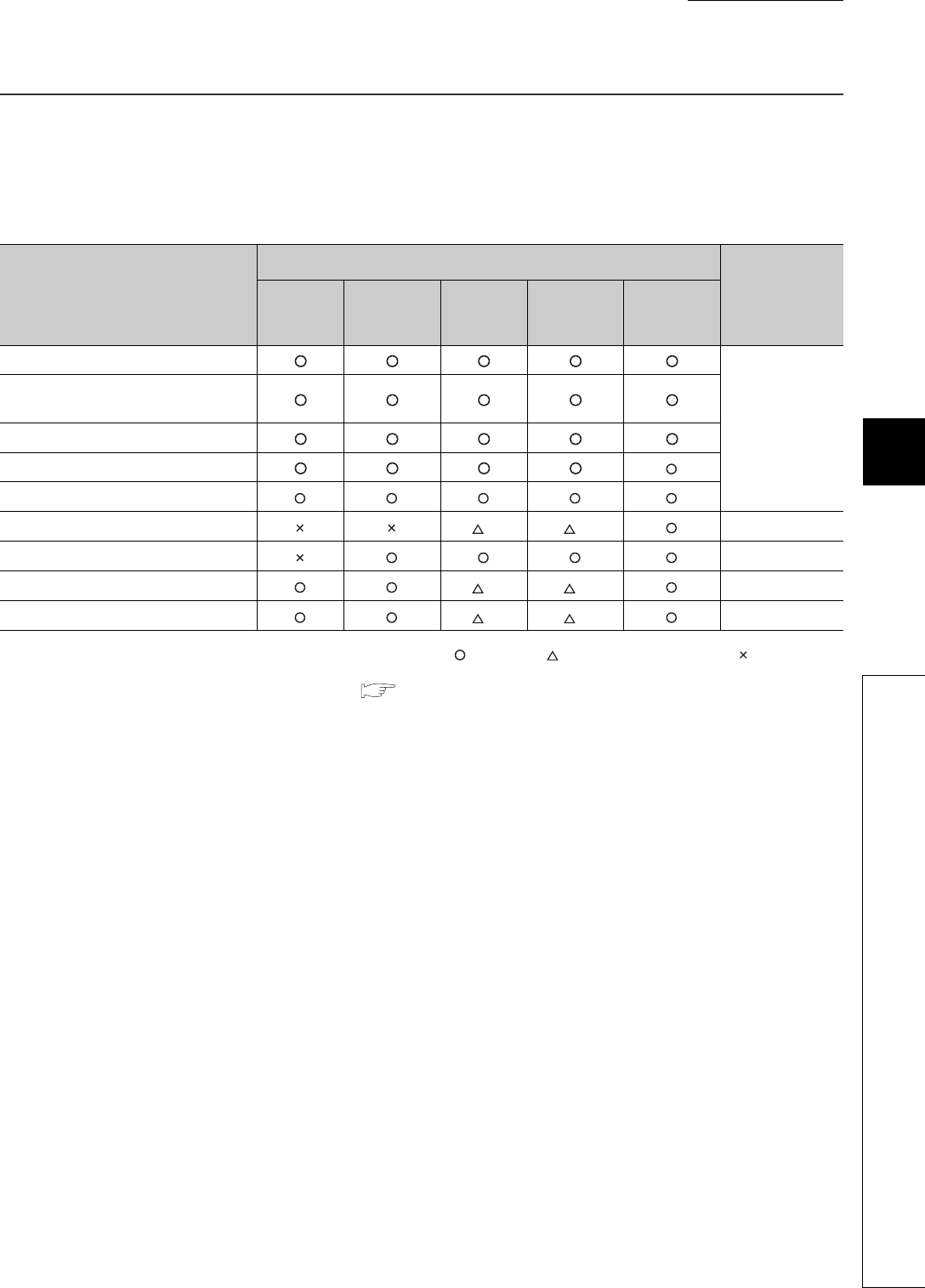
CHAPTER6 FUNCTIONS
1
2
3
4
5
6
7
8
6.11 Monitor Function
6 - 33
6.11 Monitor Function
(1) Definition
This function reads program and device data in the CPU module, and intelligent function module
status using GX Developer.
: Available, : Available with restrictions, : Not available
*1: Availability depends on the version of the CPU module. ( Appendix 2)
(2) Monitor request timing and displayed data
The CPU module processes monitor requests from GX Developer during END processing.
For this reason, the data in the CPU module at the time of END processing will be displayed in GX
Developer.
(3) Monitor with monitor condition settings
By setting the monitor condition in GX Developer during debugging, the program operation status in
the CPU module can be monitored under the specified condition.
Besides, the monitoring status under the specified condition can be held by setting the monitoring stop
condition.
(4) Local device monitor
If multiple programs are executed and local devices are used, data in local devices of each program
can also be monitored.
Table6.9 List of monitor functions and availability
Monitor function
Availability
Reference
Q00UJ
CPU
Q00UCPU,
Q01UCPU Q02UCPU QnUD(H)
CPU
Built-in
Ethernet
port QCPU
Ladder monitor
GX Developer
Version 8
Operating Manual
Device/buffer memory batch
monitor
Entry data monitor
Device test
Entry ladder monitor
Monitor condition setting *1 *1 Section 6.11.1
Local device monitor/test Section 6.11.2
External input/output forced on/off *1 *1 Section 6.11.3
Executional conditioned device test *1 *1 Section 6.11.4
6 - 34
6.11.1 Monitor condition setting
This function is used to monitor data in the CPU module under the specified condition.Note1
(1) Monitor condition setting for ladder monitor
Switch GX Developer into monitor mode.
Select [Online] [Monitor] [Monitor condition setup] to open the Monitor condition screen.
Set the condition as shown below to monitor data on the rising edge of Y70.
(a) When only a step number is specified
Monitor data is collected when the status immediately before execution of the specified step
becomes the specified status.
The following status can be specified.
• When the operation of the specified step changes from the non-execution status to the execution status: <-P->
• When the operation of the specified step changes from the execution status to the non-execution status: <-F->
• Always only when the operation of the specified step is in execution: <ON>
• Always only when the operation of the specified step is in non-execution: <OFF>
• Always regardless of the status of the operation of the specified step: <Always>
Note1
Figure 6.27 Monitor condition setting screen
Note6.1
Note6.1
The Q00UJCPU, Q00UCPU, and Q01UCPU do not support the monitor condition setting.
When setting monitor condition for the Q02UCPU, Q03UDCPU, Q04UDHCPU, Q06UDHCPU, Q13UDHCPU, or
Q26UDHCPU, check the versions of the CPU module and GX Developer. ( Appendix 2)
Universal
Select to use a device as
a monitor condition.
Select to use a step
number as a monitor
condition.
Monitoring starts
when the condition is
established.
(An operation status
when the condition
isestablished is
displayed.)

CHAPTER6 FUNCTIONS
1
2
3
4
5
6
7
8
6.11 Monitor Function
6.11.1 Monitor condition setting
6 - 35
●If a step between the AND/OR blocks is specified as a monitor condition, monitor data is collected when the status
previous to execution of the specified step is specified by the LD instruction.
The monitor timing depends on the step specified as a monitor condition.
The following shows examples of monitoring when the step 2 is on (Step No. [2] = <ON>).
• When the step 2 is connected by the AND instruction:
In Figure 6.28, the monitor execution condition is established when both X0 and X1 are on.
• When the step 2 is connected in the middle of the AND/OR block:
In Figure 6.29, the monitor execution condition is established when X1 turns on. (The on/off status of X0 does not
affect the establishment of the monitor execution condition.)
• If the start of a ladder block other than the step 0 is specified for the step number as a detailed condition, monitor
data is collected when the execution status of the instruction immediately before execution becomes the specified
status.
If (Step No. [2] = <ON>) is specified in the following ladder, monitor data is collected when OUT Y10 turns on.
●Be sure to set the condition of the step set as step No.0 to "Always".
Figure 6.28 When the step 2 is connected by the AND instruction
Figure 6.29 When the step 2 is connected in the middle of the AND/OR block
Figure 6.30 When the start of a ladder block other than the step 0 is specified for the step number
0X0 X1 X2
Ladder mode List mode
Y20
0LD XO
1 AND X1
2 AND X2
3 OUT Y2
Step 2
0Y20
X0 X1 X2
X3
0LD XO
1LD X1
2 AND X2
3OR X3
4 ANB
5 OUT Y20
Step 2
Ladder mode List mode
0Y10
X0
2Y11
X1
Ladder mode List mode
0LD XO
1 OUT Y10
2LD X1
3 OUT Y11
6 - 36
(b) When only a device is specified
Either word device or bit device can be specified.
1) When a word device is specified
Monitor data is collected when the current value of the specified word device becomes the specified value.
Enter the current value (in decimal or hexadecimal).
2) When a bit device is specified
Monitor data is collected when the execution status of the specified bit device becomes the specified status.
Select the execution condition (on the rising edge or falling edge).
(c) When a step number and device are specified
Monitor data is collected when the status previous to execution of the specified status or the status (current
value) of the specified bit device (word device) becomes the specified value.
When "Step No.[100]=<-P->, Word device [D1]=[K5]" is specified as an execution condition, a monitor execution condition is
established on the rising edge of the step 100 and also D1=5.
The monitor interval of GX Developer depends on the processing speed of GX Developer.
For the monitor execution conditions established at the interval shorter than the monitor interval of GX Developer, monitor is
executed only when the monitor execution condition is established at the monitor timing of GX Developer.
Figure 6.31 When the rising edge of the step 100 and D1=5 are specified
Figure 6.32 Monitor timing of GX Developer
X0 M0
Y20
Step 100
INC D1
X0
100 100 100 100
M0
Step No.
D1=5
Monitor timing
(CPU module)

CHAPTER6 FUNCTIONS
1
2
3
4
5
6
7
8
6.11 Monitor Function
6.11.1 Monitor condition setting
6 - 37
(2) Monitor stop condition setting
Set a monitor stop condition on the screen opened by selecting [Online] [Monitor] [Monitor stop condition
setup].
Set the condition as shown in Figure 6.33 to stop a monitor operation on the rising edged of Y71.
(a) When a device is specified
Either word device or bit device can be specified.
1) When a word device is specified
A monitor operation is stopped when the current value of the specified word device becomes the specified
value.
Enter the current value (in decimal, hexadecimal, 16-bit integer, 32-bit integer, or real number).
2) When a bit device is specified
A monitor operation is stopped when the execution status of the specified bit device becomes the specified
status.
Select the execution condition (on the rising edge or falling edge).
(b) When a step number is specified
A monitor operation is stopped when the execution status of the step specified as a monitor condition becomes
the specified status.
The following status can be specified.
• When the operation of the specified step changes from the non-execution status to the execution status:
<-P->
• When the operation of the specified step changes from the execution status to the non-execution status:
<-F->
• Always only when the operation of the specified step is in execution: <ON>
• Always only when the operation of the specified step is in non-execution: <OFF>
• Always regardless of the status of the operation of the specified step: <Always>
If a step number is not specified, a monitor operation is stopped after END processing of the CPU module.
Figure 6.33 Monitor stop condition screen

6 - 38
(3) Precautions
(a) Files to be monitored
When monitor conditions are set, GX Developer monitors the file displayed on the screen.
Select [Online] [Read from PLC] in GX Developer and read data from the CPU module so that the file name
in the CPU module to be monitored matches the file named displayed on the screen of GX Developer.
(b) No file register setting
If the file register is monitored when there is no file register used, "FFFFH" is displayed.
(c) Device assignment
For monitor operation, device assignment in the CPU module and GX Developer must be the same.
(d) Monitoring the buffer memory of an intelligent function module
When monitoring the buffer memory of an intelligent function module, the scan time increases for the same
reason for execution of the FROM/TO instructions.
(e) Monitoring by multiple users
When multiple users are performing monitoring at the same time, pay attention to the following.
• High speed monitor can be performed by increasing 1K step per monitor file of other stations in the system
area when formatting the program memory or setting a parameter in the Boot file tab of the PLC parameter
dialog box.
Up to 15 stations can be set as the station monitor file, but the program space will be reduced.
• If the monitor condition or monitor stop condition is set, only one user can perform monitoring.
(f) Setting a monitor stop condition
A monitor stop condition can be set only in the ladder monitor.
(g) Specifying the same device as a condition
When specifying the same device as a monitor condition or monitor stop condition, set the on/off status as well.
(h) Specifying a step number as a monitor condition
If an instruction in the specified step is not executed in such cases described below, the monitor condition will
not be established.
• The specified step is skipped with the CJ, SCJ, or JMP instruction.
• The specified step is the END instruction and never be executed because the FEND instruction also exists
in the program.

CHAPTER6 FUNCTIONS
1
2
3
4
5
6
7
8
6.11 Monitor Function
6.11.1 Monitor condition setting
6 - 39
(i) During monitor condition registration
Do not reset the CPU module while monitoring conditions are being registered.
(j) Monitor operation with monitor condition setting
When monitor operation with monitor condition setting is performed, other applications on the same personal
computer cannot execute any online function using the same route for the monitor operation. The following
applications must be noted.
• GX Developer
• Application using MX Component
• MX Sheet
If any online function is executed by other applications using the same route for the monitor operation, the
following situations may occur.
• No response is returned from the CPU module for the online function executed. (An online communication
function time-out occurs.)
• The CPU module detects an error (error code: 4109) for the online function executed.
• Even when the monitor condition is established in the CPU module, monitoring results cannot be updated
for the monitor operation with monitor condition setting.

6 - 40
6.11.2 Local device monitor/test
This operation is useful for debugging a program, monitoring local devices ( Section 9.14.2) in the program
monitored by GX Developer. Note1
(1) Monitoring a local device
Table6.10 shows the monitor operation when the CPU module executes three programs "A", "B", and "C" and D0
to D99 are set as a local device.
(Three programs are to be executed in the order of A B C (END processing) A B....)
Note1
Table6.10 Data displayed when three programs are executed
Setting Monitor device
D0 (Local device) D100 (Global device)
When the device is not set as
a local device D0 in the program "C" is monitored. D100 after the program "C" is executed is
monitored.
When the device is set as a
local device D0 in the displayed program is monitored. D100 after the program "C" is executed is
monitored.
Note6.2
Note6.2
The Q00UJCPU does not support the use of local devices.
Universal
CHAPTER6 FUNCTIONS
1
2
3
4
5
6
7
8
6.11 Monitor Function
6.11.2 Local device monitor/test
6 - 41
When local devices are set to be monitored and the program "B" is displayed for monitoring, the local device(s)
used in the program "B" can be monitored.
Figure 6.34 Local device monitor example
GX Developer
Local devices are set to be
monitored and the
program "B" is monitored.
The local device data of the
program B is displayed.
(Example)
If D0 to D99 are set as a local device,
D0=4 is displayed when X10 is on and
D99=8 is displayed when X11 is on.
X0
X1
X10
X11
X20
X21
MOVP K2 DO
MOVP K3 D99
MOVP K4 DO
MOVP K8 D99
MOVP K3 DO
MOVP K6 D99
Program: A
Program: B
Program: C
CPU module
Program execution (A B C)
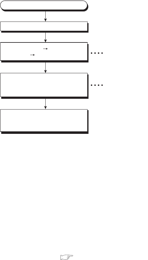
6 - 42
(2) Monitoring procedure
The following shows the local device monitoring procedure.
(3) Precautions
(a) Local devices that can be monitored/tested by a single GX Developer
A single GX Developer can monitor or test local devices in one program at a time.
Local devices in multiple programs cannot be monitored or tested simultaneously.
(b) Number of programs that can be monitored/tested
Local devices in 16 programs can be monitored or tested simultaneously from multiple GX Developers
connected to the RS-232 interface of the CPU module or the serial communication module.
(c) Monitoring local devices in a stand-by type program
When local devices in a stand-by type program are monitored, data in local devices are saved and restored.
For this reason, the scan time increases. ( Section 9.14.2)
(d) Monitoring local devices in a fixed scan execution type program
When local devices in a fixed scan execution type program are monitored, data in local devices cannot be
acquired and "0" is displayed.
Figure 6.35 Local device monitoring procedure
Select [Local device monitor]
from the monitor window.
The local device of the
displayed program is
monitored.
Setting of the local
device monitor
Switching to the
monitor mode
Select [Online]
[Monitor] [Monitor mode].
Display a program in ladder mode.
Connect a personal computer to the CPU module.
CHAPTER6 FUNCTIONS
1
2
3
4
5
6
7
8
6.11 Monitor Function
6.11.3 External input/output forced on/off
6 - 43
6.11.3 External input/output forced on/off
The external input/output can forcibly be turned on/off on the screen opened by selecting [Online] [Debug]
[Forced input output registration/cancellation] in GX Developer.Note1
The information registered for forced on/off can be cancelled by an operation from GX Developer.
(1) Input/output operation when a forced on/off operation is performed
There are three kinds of forced on/off operations: forced on ("Set forced ON"), forced off ("Set forced OFF"), and
forced on/off cancellation ("Cancel it").
Table6.11 shows the CPU module operation when a forced on/off operation is performed.
Note1
Figure 6.36 Forced input output registration/cancellation screen
Table6.11 Input/output operation when a forced on/off operation is performed
Operation Input (X) operation Output (Y) operation
Forced on/off
cancellation (no
operation)
The CPU module performs sequence program operations
using external inputs.
The CPU module outputs the results of sequence
program operations externally.
Forced on The CPU module performs sequence program operations
using inputs forcibly turned on.
The CPU module outputs "on" externally regardless of
the results of sequence program operations.
Forced off The CPU module performs sequence program operations
using inputs forcibly turned off.
The CPU module outputs "off" externally regardless of
the results of sequence program operations.
Note6.3
Note6.3
When performing an external input/output forced on/off operation for the Q02UCPU, Q03UDCPU, Q04UDHCPU,
Q06UDHCPU, Q13UDHCPU, or Q26UDHCPU, check the versions of the CPU module and GX Developer. (
Appendix 2)
Universal
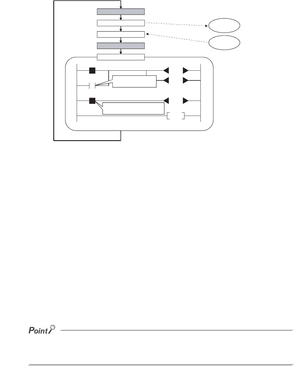
6 - 44
Figure 6.37 shows the input/output operation when a forced on/off operation is performed.
(2) Specifications
(a) CPU module status where input/output can forcibly be turned on/off
Forced on/off can be registered regardless of the operating status (RUN/STOP) of the CPU module.
Note, however, that only input can be forcibly turned on/off during a stop error.
The CPU module outputs on/off data only to Y device.
(b) Registerable devices
Forced on/of can be registered as many as the number of I/O device points in the CPU module.
(c) Target input/output
The following input/output are targeted for a forced on/off operation.
• Input(X) and output (Y) of modules mounted on the base unit
• Input(X) and output (Y) of the CPU module to be refreshed from LX/LY of a CC-Link IE controller network
or MELSECNET/H module
• Input(X) and output (Y) of the CPU module to be refreshed from RX/RY of a CC-Link module
When forcibly turning on/off the devices outside the above refresh ranges (for example, empty slots), only
input/output in the CPU module device memory are turned on/off and the results are not output externally.
In multiple CPU systems, inputs and outputs of control modules can forcibly turned on/off.
Even when inputs and outputs of non-control modules are registered for forced on/off, the input/output devices in other CPU
modules and inputs and outputs of modules controlled by other CPU modules cannot be forcibly turned on/off. (The input/
output devices in the host CPU module can forcibly turned on/off.)
Figure 6.37 Input/output operation when a forced on/off operation is performed
MO
XO
Y10
Y10
Y11
M1
END
Y10 device forced off
X0 device forced off
Y10 output
(off)
X0 input
(on)
External input is
forcibly turned off.
On the ladder block, Y10 appears to be on even
though a forced off operation is performed.
Output forced on/off operation
Input forced on/off operation
Output refresh
Input refresh
Program execution
External output
(Y10 off)
External input
(X0 on)

CHAPTER6 FUNCTIONS
1
2
3
4
5
6
7
8
6.11 Monitor Function
6.11.3 External input/output forced on/off
6 - 45
(d) Cancelling on/off registration data
The registered forced ON/OFF data can be canceled by GX Developer.
Once the registered data is canceled, the status of the forced on/off registered devices will be as follows.
Forced on/off setting can be cleared by:
• powering off and then on the CPU module,
• resetting the CPU module by the RUN/STOP/RESET switch, or
• resetting the CPU module by the remote RESET operation.
(e) External input/output forced on/off timing
Table6.13 shows the external input/output forced on/off timing.
Table6.12 Status of devices after forced on/off registration data is canceled
Forced on/off registered device Sequence program operations
(on/off) performed
Sequence program operations
(on/off) not performed
Input
Input from modules mounted on the base unit Uses the on/off status input from modules.
Input of the CPU module to be refreshed from LX
of a CC-Link IE controller network or
MELSECNET/H module
Used the on/off status refreshed via CC-Link IE controller network or
MELSECNET/H.
Input of the CPU module to be refreshed from
RX of a CC-Link module Uses the on/off status refreshed via CC-Link.
Input other than above (outside of the refresh
range)
Uses the results of sequence
program operations. Holds the forced on/off status.
Output
Output from modules mounted on the base unit
Outputs the results of sequence
program operations. Holds the registered on/off status.
Output of the CPU module to be refreshed from
LY of a CC-Link IE controller network or
MELSECNET/H module
Output of the CPU module to be refreshed from
RY of a CC-Link module
Output other than above (outside of the refresh
range)
Outputs the results of sequence
program operations. (The results
are not output externally.)
Holds the forced on/off status.
Table6.13 Forced on/off timing
Refresh area Input Output
Input and output of
modules mounted on the
base unit
• During END processing (input refresh)
• At execution of the COM instruction (input refresh)
• At execution of an instruction using direct access
input (DX) (LD, LDI, AND, ANI, OR, ORI, LDP, LDF,
ANDP, ANDF, ORP, ORF)
• At execution of the RFS or MTR instruction
• At execution of an instruction used for a system
interrupt (UDCNT1, UDCNT2, SPD)
• During END processing (output refresh)
• At execution of the COM instruction (output
refresh)
• At execution of an instruction using direct access
input (DX) (OUT, SET, DELTA, RST, PLS, PLF,
FF, MC, SFT)
• At execution of the RFS or MTR instruction
• At execution of an instruction used for a system
interrupt (PLSY, PWM)
Input and output of the CPU
module to be refreshed from
LX/LY of a CC-Link IE
controller network or
MELSECNET/H module
• During END processing (refresh via CC-Link IE controller network or MELSECNET/H)
• At execution of the COM instruction
• At execution of the ZCOM instruction
Input and output of the CPU
module to be refreshed from
RX/RY of a CC-Link module
• During END processing (auto refresh)
• At execution of the COM instruction (auto refresh)
• At execution of the ZCOM instruction (auto refresh)

6 - 46
(f) Number of registerable devices
Forced on/off can be registered for 32 devices in total.
(g) When output Y contact is used in a sequence program
On/off operations in a sequence program are given priority.
(h) Checking forced on/off registration status
Forced on/off execution status can be checked by:
• reading the forced on/off registration status by GX Developer,
• flashing of the MODE LED (green), (The MODE LED flashes in green when at least one forced on/off is
registered.) or
• the on status of the 1st bit in SD840 (Debug function usage).
●The MODE LED also flashes in green when the executional conditioned device test function is used.
To check the registration status using the MODE LED, check the status of the executional conditioned device test
function as well. ( Section 6.11.4)
●When using SD840 to check the registration or cancellation status, remind that SD840 is used to check the status of
the executional conditioned device test function as well.
(i) Forcibly turning input or output on/off from multiple GX Developers
Forced on/off can be registered to a single CPU module from multiple GX Developers connected via network.
In this case, the last registration will be effective.
For this reason, the forced on/off status which is different from the status actually registered in the CPU module
may be displayed on the screen of GX Developer that registered forced on/off earlier.
When the forced on/off registration is performed from multiple GX Developers, click the "Update status" button
to update the registered data and execute the function.
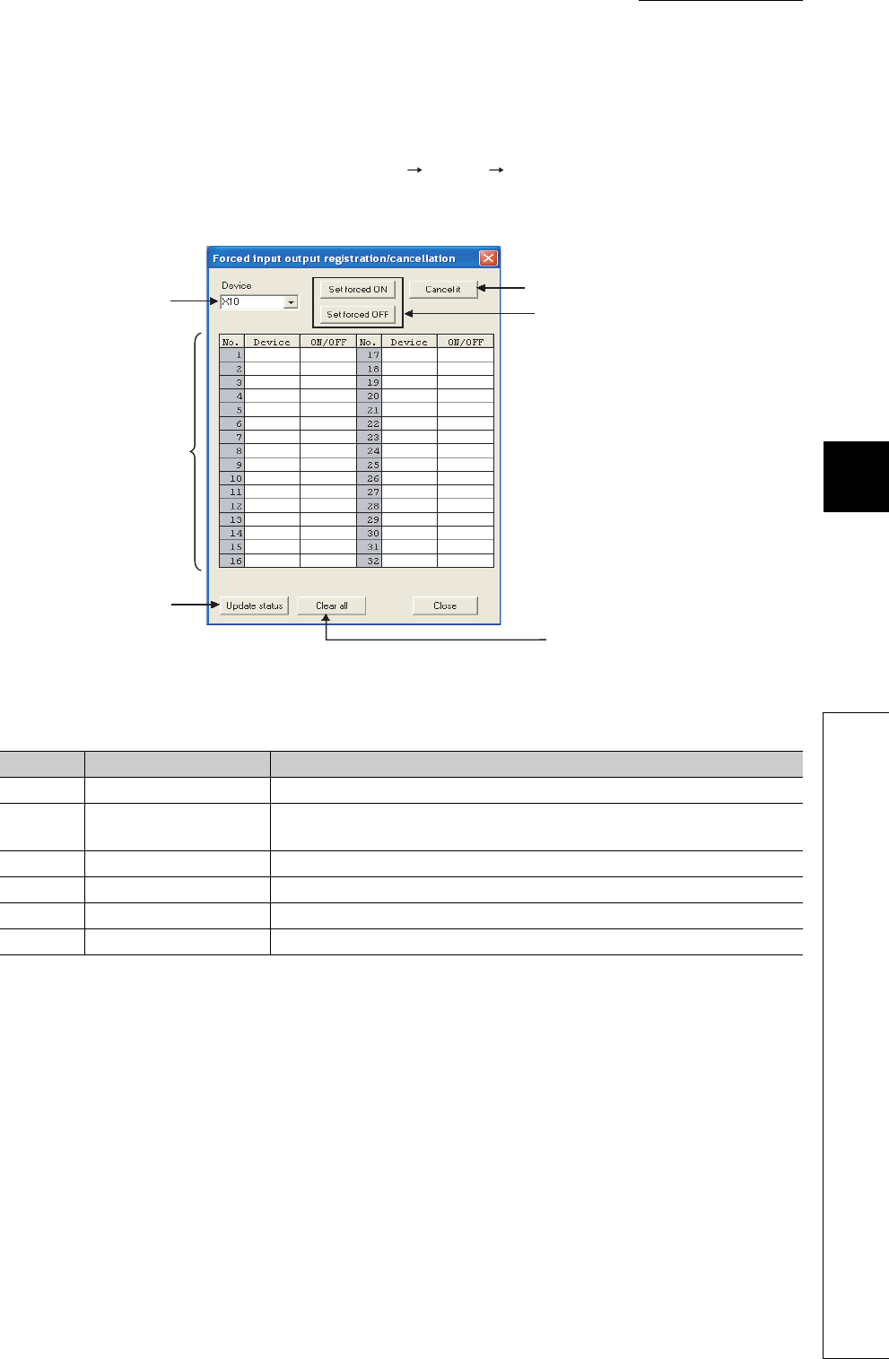
CHAPTER6 FUNCTIONS
1
2
3
4
5
6
7
8
6.11 Monitor Function
6.11.3 External input/output forced on/off
6 - 47
(3) Operating procedure
Operating procedure is described below.
• To register forced on/off for a device, select [Online] [Debug] [Forced input output registration/
cancellation] in GX Developer.
• On the screen opened, specify a device and click the "Set forced ON" or "Set forced OFF" button.
Figure 6.38 Forced input output registration/cancellation screen
Table6.14 Items on the Forced input output registration/cancellation screen
No. Item Description
1) Device Select the I/O number for which forced on/off is to be registered or cancelled.
2) Registration status display
area Displays the forced on/off registration status.
3) Update status Reads the forced on/off registration status from the CPU module.
4) Set forced ON/OFF Registers forced on/off for a device specified.
5) Cancel it Cancels forced on/off registered for the device specified.
6) Clear all Cancels all forced on/off registration.
1) 5)
4)
6)
3)
2)
6 - 48
6.11.4 Executional conditioned device test
This function changes a device value within the specified step of a program.Note1
This enables debugging of the specified ladder block without modifying the program.*1
*1: The executional conditioned device test is not available for the SFC program.
(1) Operation of the executional conditioned device test
A device value will be changed based on the registration data once after the executional conditioned device test
setting is registered.
The changed device value becomes effective in the ladder blocks of the specified step number and later.
Note that a device value is changed within the specified step regardless of an execution status of the instruction in
the specified step.
Note1
Figure 6.39 Operation of the executional conditioned device test
Figure 6.40 Operation example of the executional conditioned device test
Note6.4
Note6.4
When using the executional conditioned device test in the Q02UCPU, Q03UDCPU, Q04UDHCPU, Q06UDHCPU,
Q13UDHCPU, or Q26UDHCPU, check the versions of the CPU module and GX Developer.( Appendix 2)
Universal
GX Developer
Program name
Step No.
Device
Setting value
Execution timing
: MAIN
: 10
: M0
: ON
: Before executing instruction
Registration data
M0 is turned on.
Program: MAIN
<Program example> <Operation>
Processing LD M0
10 35
OFF
45
Changes the value in D0 to "35".
+ K10 D0
Value in D0
Value in M0
Executional conditioned device test which
sets "35" in D0 in this step is registered.
A device value is changed within the
specified step regardless of the value in M0.
List mode
Ladder mode
CHAPTER6 FUNCTIONS
1
2
3
4
5
6
7
8
6.11 Monitor Function
6.11.4 Executional conditioned device test
6 - 49
(2) Available devices and number of settable devices
*1: The extended data register (D) is included.
*2: The extended link register (W) is included.
(3) How to check the execution status
The execution status of registered executional conditioned device test can be checked in three different ways:
• By the flash of the MODE LED in green
• By the on status of the first bit of SD840 (Debug function usage)
• By the display on the screen for checking the registration status in GX Developer
( (4)(d) in this section)
●The MODE LED also flashes in green when the external input/output forced on/off function is used.
To check the execution status using the MODE LED, check the status of the external input/output forced on/off function
as well. ( Section 6.11.3)
●When using SD840 to check the execution status, remind that SD840 is used to check the status of the external input/
output forced on/off function as well.
Table6.15 Available devices and number of settable devices
Type Available device Number of settable
devices
Bit device X, Y, M, L, B, F, SB, V, SM, T (contact), ST (contact), C (contact), J \X, J \Y,
J \B, J \SB, FX, FY, DX, and DY
Up to 32 (in total)
Word device
T (current value), ST (current value), C (current value), D*1, SD, W*2, SW, R,
ZR, Z, U \G , U3E \G , J \W , J \SW , and FD
Digit-specified bit device:
X, Y, M, L, F, SM, V, B, SB, J \X, J \Y, J \B, and J \SB
Indirect specification (@D0): D, SD, W, SW, R, and ZR (devices specified with
@)
6 - 50
(4) Operating instructions
(a) Registering executional conditioned device test settings
Select the registration target step number on the program editing screen in GX Developer. Then, select
[Online] [Debug] [Executional conditioned device test] [Register executional conditioned device test].
*1: When a word device which is index-modified or indirectly-specified is set, only "16 bit integer" can be specified.
1) Multiple executional conditioned device test registrations for the same step
number
Multiple executional conditioned device test settings can be registered for one step number.
However, if multiple executional conditioned device test settings with same device name and same execution
timing are registered for the same step number, the registration data will be overwritten. (Even though the
same device is specified, if the execution timing differs, two settings can be registered for one step.)
Figure 6.41 Screen for registering executional conditioned device test settings
Table6.16 Items on the screen for registering executional conditioned device test settings
No. Item Setting range
For bit device For word device
1) Program name Name of a program registered in the CPU module
2) Step No. 0 to (Step number for the END instruction)
3) Device Device listed in (2) in this section
4) Execution timing Before executing instruction / After executing instruction
5) Setting value - (Not specified) Setting range corresponding to each data type
6) DEC / HEX - (Not specified) DEC (decimal) / HEX (hexadecimal)
7) Data type*1 - (Not specified) 16 bit integer / 32 bit integer / Real number (single
precision) / Real number (Double precision)
3)
5)
1)
2)
4)
6)
7)
Devices that executional conditioned device test settings
can be registered for the start step of the + instruction.
+ D0 D10 D20
CHAPTER6 FUNCTIONS
1
2
3
4
5
6
7
8
6.11 Monitor Function
6.11.4 Executional conditioned device test
6 - 51
●When setting a word device with a different data type, a device is regarded as the same device.
When a word device is set in the order of "D100 (16 bit integer)" and then "D100 (Real number (single
precision))", "D100 (Real number (single precision))" is registered.
●When setting a device with a different modification method (such as a bit-specified word device, digit-specified bit
device, or index-modified device), a device is regarded as a different device.
When a word device is set in the order of "D100.F" and then "D100Z0 (Real number (single precision)),
both devices are registered.
2) Step to be specified for executional conditioned device test registration
Any step number (0 to step number for the END instruction) in a sequence program can be specified.
Be sure to specify the start step of each instruction.
3) Execution timing
Timing of changing a device value can be specified. A device value can be changed either before or after an
instruction of the specified step is executed. Figure 6.42 shows the module operation based on the execution
timing.
Figure 6.42 CPU module operation based on execution timing
Example
Example
<Program example>
Ladder mode List mode
<Operation>
Execution timing CPU module operation
Before executing
an instruction of
step 101
After executing
an instruction
of step 101
Processing
LD M0
10 20 120
Changes the value in D0 to "20".
+ K100 D0
Value in D0
Processing
LD M0
10 110 20
Changes the value in D0 to "20".
+ K100 D0
Value in D0
Executional conditioned device test which
sets "20" in D0 in this step is registered.

6 - 52
Note that there may be a case where a device value will not be changed depending on the execution timing even
though the specified step is executed.
The following instructions need to be noted when registering executional conditioned device test settings.
• Instructions that do not change device values*1
A device value will not be changed by executing the excutional conditioned device test when the execution
timing has been set to "After executing instruction", specifying the step for instructions that do not execute
the next step, such as branch instructions.
*1: If the execution condition of an instruction is not satisfied, a device value will be changed based on the registration data.
Table6.17 lists the instructions that do not change device values.
• FOR/NEXT instructions
When the executional conditioned device test setting is registered specifying the step for the FOR or NEXT
instruction, timing of device value change is different from the timing when steps for other instructions are
specified.
Table6.18 shows the device value change timing based on the execution timing.
• END instruction
When the executional conditioned device test setting is registered specifying the step for the END
instruction, the execution timing is restricted to "Before executing instruction" only. If "After executing
instruction" is set, the CPU module returns a registration error to GX Developer.
Table6.17 Instructions that do not change device values
No. Classification Instruction Operation
1Stop STOP
• When the execution condition for an instruction
is satisfied
A device value will not be changed even when
the specified step is executed.
• When execution condition for an instruction is
not satisfied
A device value will be changed after the
specified step is executed.
2
Jump
CJ
3SCJ
4 GOEND
5 Repeat (Loop) BREAK(P)
6
Subroutine program call
CALL(P)
7 FCALL(P)
8 ECALL(P)
9 EFCALL(P)
10 XCALL
11 End FEND
A device value will not be changed even when the
specified step is executed.
12 Jump JMP
13 Return from subroutine program RET
14 Return from interrupt program IRET
Table6.18 Device value change timing when a step for the FOR or NEXT instruction is specified
Instruction of the specified step Execution timing setting
Before executing instruction After executing instruction
FOR Executed once before the start of loop
processing.
Executed once after the start of loop
processing. (Executed before the operation
of the program between the FOR and NEXT
instructions.)
NEXT
Executed every loop processing.
(Executed after the operation of the
program between the FOR and NEXT
instructions.)
Executed once after the start of loop
processing.
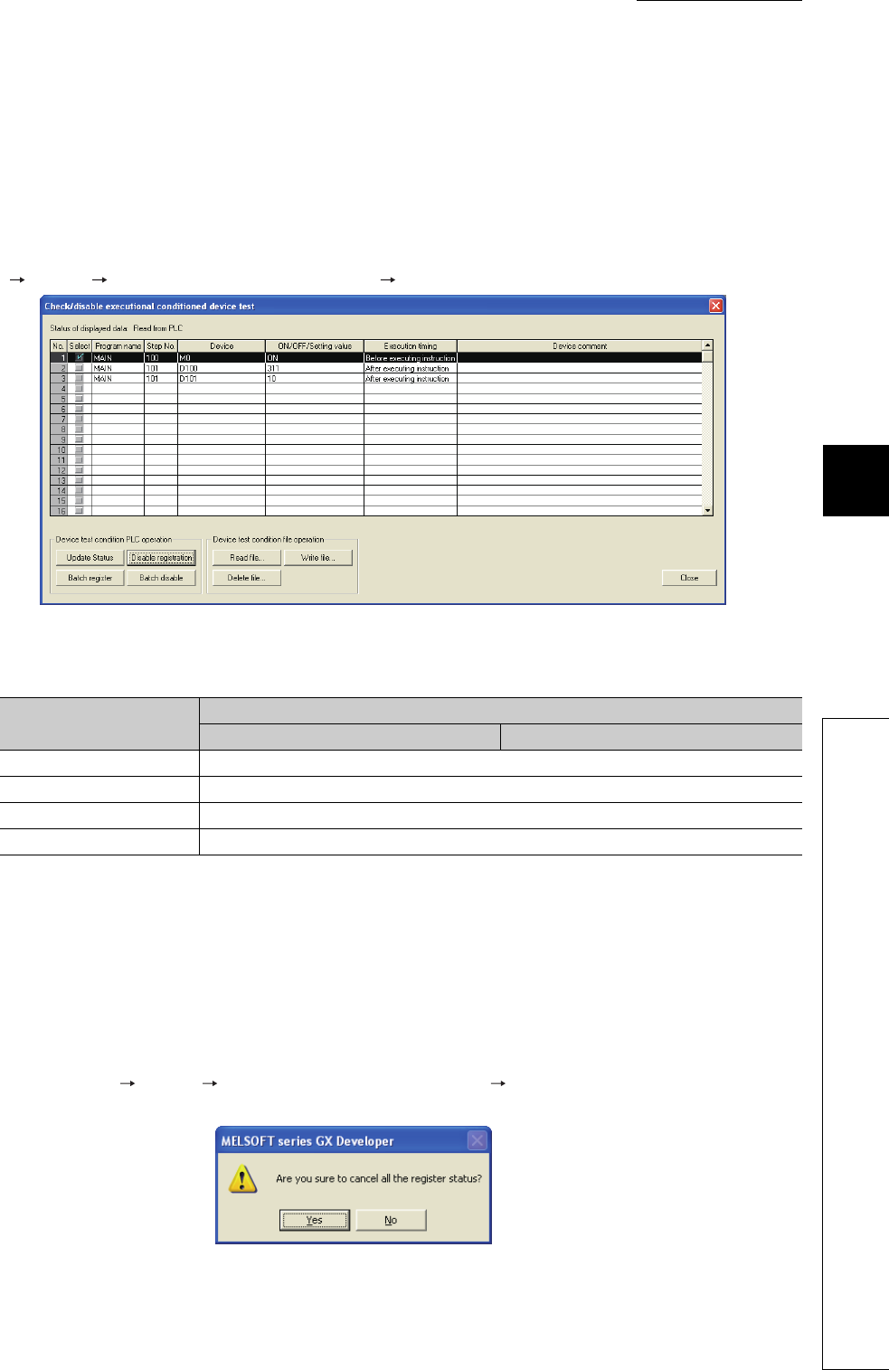
CHAPTER6 FUNCTIONS
1
2
3
4
5
6
7
8
6.11 Monitor Function
6.11.4 Executional conditioned device test
6 - 53
4) Number of settings that can be registered simultaneously in one scan
Eight executional conditioned device test settings can be registered into the CPU module simultaneously in
one scan.
When nine or more executional conditioned device test settings are to be registered simultaneously by
GX Developer, they will be registered over multiple scans.
(b) Disabling executional conditioned device test settings
Select the disabling target step number on the program editing screen in GX Developer. Then, select [Online]
[Debug] [Executional conditioned device test] [Check/disable executional conditioned device test].
1) Number of settings that can be disabled simultaneously in one scan
Eight executional conditioned device test settings can be disabled simultaneously in one scan.
When nine or more executional conditioned device test settings are to be disabled simultaneously by GX
Developer, they will be disabled over multiple scans.
(c) Batch-disabling executional conditioned device test settings
Select [Online] [Debug] [Executional conditioned device test] [Batch disable executional conditioned
device test] in GX Developer.
Figure 6.43 Screen for checking/disabling executional conditioned device test settings
Table6.19 Items on the screen for checking/disabling executional conditioned device test settings
Item Setting range
For bit device For word device
Program name Name of a program registered in the CPU module
Step No. 0 to (Step No. for the END instruction)
Device Device listed in (2) in this section
Execution timing Before executing instruction/After executing instruction
Figure 6.44 Screen for batch-disabling executional conditioned device test settings
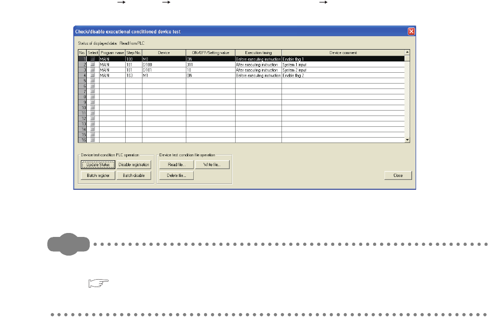
6 - 54
(d) Checking executional conditioned device test settings
Select [Online] [Debug] [Executional conditioned device test] [Check/disable executional conditioned
device test].
Remark
1. For the operating instruction of checking or disabling executional conditioned device test settings, refer to the
following.
GX Developer Version 8 Operating Manual
2. Usage of the executional conditioned device test can be checked in the special register (SD840).
(e) Cases where executional conditioned device test settings cannot be registered or
disabled
In the following cases, executional conditioned device test setting cannot be registered or disabled.
When multiple settings are to be registered, no setting can be registered if any of the settings applies to the
cases below.
1) Executional conditioned device test settings cannot be registered
• Specified program does not exist.
• Specified step does not exist.
• Specified device does not exist.
• The number of registered executional conditioned device test settings exceeds 32.
2) Executional conditioned device test settings cannot be disabled
• Specified program does not exist.
• Specified step does not exist.
• Specified device does not exist.
• No executional conditioned device test setting has been registered.
Figure 6.45 Screen for checking executional conditioned device test settings
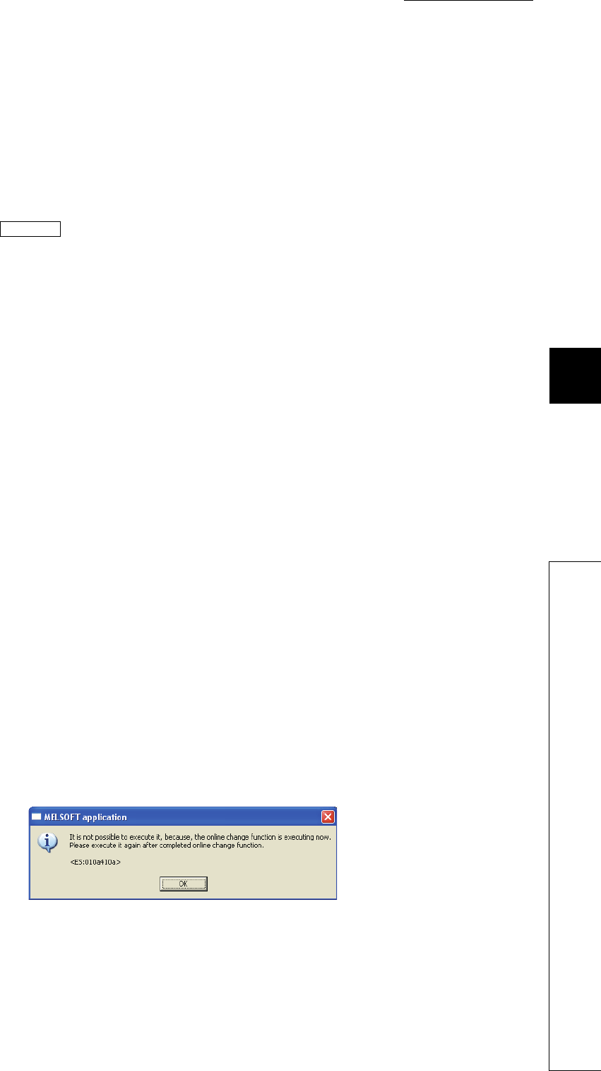
CHAPTER6 FUNCTIONS
1
2
3
4
5
6
7
8
6.11 Monitor Function
6.11.4 Executional conditioned device test
6 - 55
(5) Precautions
(a) Operations from multiple GX Developers
Executional conditioned device test setting can be registered in the same CPU module from multiple GX
Developers connected via network.
Note, however, that if multiple executional conditioned device test settings are registered with the same device
name in the same step, the registration data will be overwritten.
When registering executional conditioned device data setting from multiple GX Developers update the data first
by clicking the button, and then register the setting.
(b) Priority
If any of the following functions is set in the same step number that is specified by the executional conditioned
device test setting, the executional conditioned device test is given the priority to other functions.
• Monitor condition setting
• Sampling trace function (trace point)
• Sampling trace function (trigger point)
• Scan time measurement (start step)
• Scan time measurement (end step)
(c) Disabling executional conditioned device test settings
Executional conditioned device test setting can be disabled by any of the following operations, in addition to the
operation by GX Developer.
• Powering off and then on the CPU module
• Resetting the CPU module
• Writing program files to the program memory while the CPU module is in the STOP status
• Clearing the program memory while the CPU module is in the STOP status
• Formatting the program memory while the CPU module is in the STOP status
(d) Writing data to the running CPU module
The CPU module operation will be as follows if the executional conditioned device test and the online change
function are executed simultaneously.
1) When the executional conditioned device test is executed during execution of the
online change function
The online change function completes normally. However, the executional conditioned device test cannot be
executed.
The following message box will appear. Execute the executional conditioned device test again after the online
change has completed.
Figure 6.46 Message box (when the executional conditioned device test is executed during execution of the online change
function)
Read file
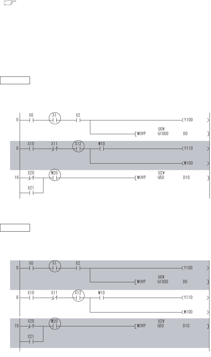
6 - 56
2) When the online change function is executed during execution of the executional
conditioned device test
The Online change function completes normally. If any executional conditioned device test setting has been
registered in the program to be changed online, the corresponding setting will be disabled.
( (5)(e) in this section)
(e) Online change of the CPU module with executional conditioned device test
registration
1) Online change (ladder mode)
If any executional conditioned device test setting has been registered in the ladder block to be changed
online, the CPU module disables the corresponding setting.
Example 1) Step numbers of registrations 1 to 3 are specified in the executional conditioned device test
settings. When the ladder block including the registration 2 is changed online, the registration 2 is
disabled during execution of the online change function.
Since the registrations 1 and 3 are not included in the change target program, they are not disabled.
Example 2) When multiple ladder blocks are to be changed online, ladder blocks between the change target
ladder blocks will be included in the change target.
For this reason, if the online change function is executed as shown in Figure 6.48, all registrations 1 to
3 are disabled.
Figure 6.47 Adding a ladder block online
Figure 6.48 Changing multiple ladder blocks online
Registration 1
Registration 2
Registration 3
*
The shaded area is the ladder block to be changed online.
Registration 1
Registration 2
Registration 3
*
The shaded area is the ladder block to be changed online.

CHAPTER6 FUNCTIONS
1
2
3
4
5
6
7
8
6.11 Monitor Function
6.11.4 Executional conditioned device test
6 - 57
Example 3) When a ladder block is to be added online, the executional conditioned device test setting
included in the ladder block followed after the added ladder block will be disabled.
For this reason, if the online change function is executed as shown in Figure 6.49, the registration 2 is
disabled.
2) Online change (files)
All executional conditioned device test settings registered to the program in the online change target file are
disabled.
(f) Precautions for specifying an index-modified device
If an index-modified device name is specified to register the executional conditioned device test setting, the
CPU module does not check whether the specified device is within the setting range.
If the index-modified device is out of the device range or on the boundary of devices, a device value will not be
changed within the specified step.
(g) Precautions for specifying an indirectly-specified device
If indirectly-specified device name is specified to register the executional conditioned device test setting, the
CPU module does not check whether the specified device is within the setting range.
If the indirectly-specified device is out of the device range or on the boundary of devices, a device value will not
be changed within the specified step.
(h) Precautions for specifying the file register
If the file register is specified to register the executional conditioned device test setting, the CPU module does
not check the file register file assignment and the file register number range.
A file register value will not be changed within the specified step in the following cases.
• The file register file is not assigned.
• The specified file register number is out of the file register range.
Figure 6.49 Adding a ladder block online
*
The shaded area is the ladder block to be changed online.
Registration 2
Registration 3
Registration 1
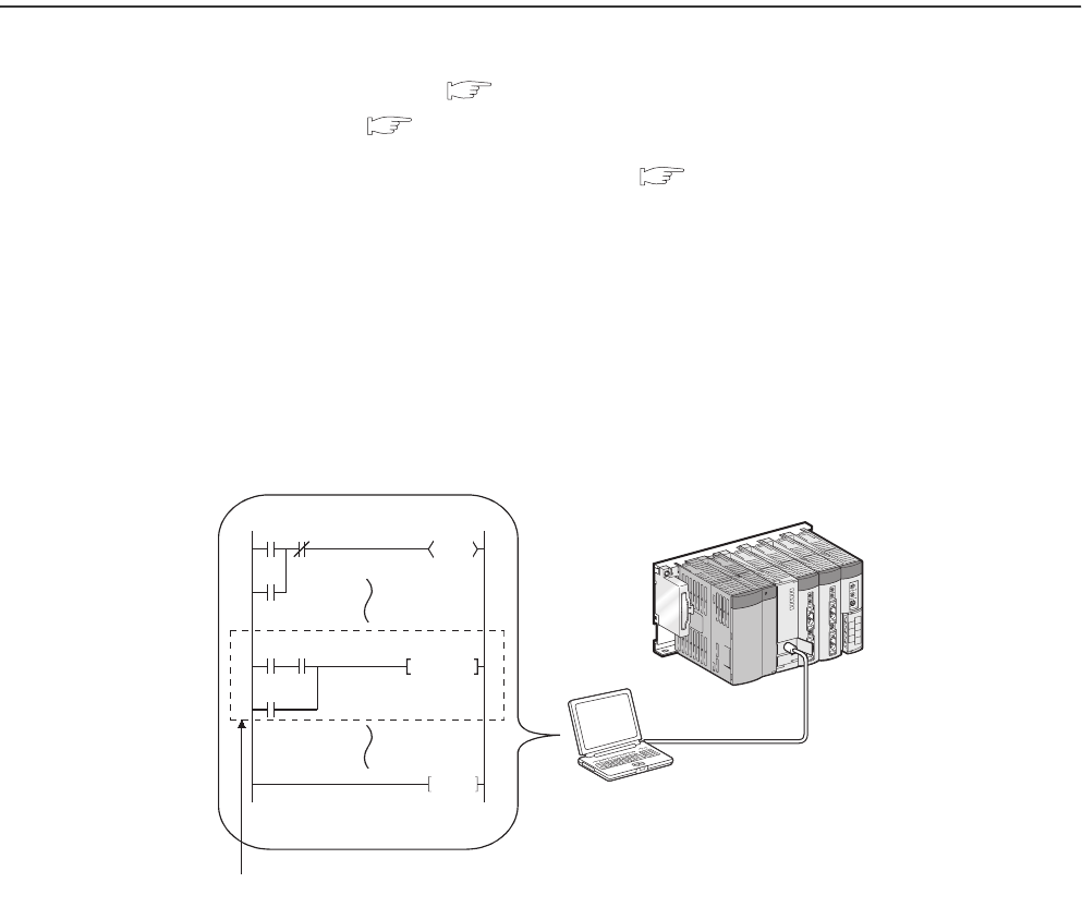
6 - 58
6.12 Writing Programs While CPU Module is in RUN Status
There are two ways of writing programs in the RUN status.
• Online change (ladder mode) : Section 6.12.1
• Online change (files) : Section 6.12.2
Data can also be written in the RUN status using a pointer. ( Section 6.15.2)
6.12.1 Online change (ladder mode)
(1) Definition
This function writes programs to the CPU module in the RUN status.
This function enables the program to be changed without stopping the program operation in the CPU
module.
Figure 6.50 Outline of online change (ladder mode)
GX Developer
Change a program with GX Developer and
write it to the CPU module in the RUN status.
END
X0 X2
X1
SET M10
Y30
X3 X4
X5
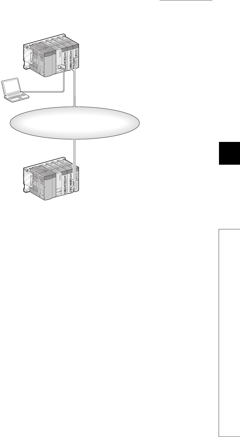
CHAPTER6 FUNCTIONS
1
2
3
4
5
6
7
8
6.12 Writing Programs While CPU Module is in RUN Status
6.12.1 Online change (ladder mode)
6 - 59
This function also can write programs by GX Developer connected to another station on the network.
(2) Memory for online change
A program cache memory (program memory) is available.
(3) Number of steps that can be batch-written by online change
Up to 512 steps can be batch-written.
Figure 6.51 Outline of online change via network
MELSECNET/H
PLC-to-PLC network
Change a program with GX Developer and
write it to the CPU module in the RUN status.
GX Developer
6 - 60
(4) Changing the reserved area for online change
A program file has an area designated as reserved area for online change to support the online
change that changes program file size.
The following provides precautions when changing the size of reserved area for online change.
(a) Size of a program file
The size of a program file is addition of created program size and reserved area for online change.
(b) When program file size is increased from the secured capacity
If the size secured for the program file (size including reserved area for online change) is exceeded after a
program is written in the RUN status, the reserved area for online change can be re-set before the writing if the
user memory area has space.
(c) Increase in the scan time
The scan time is increased when reserved area for online change is re-set when programs are written in the
RUN status.
For increase in the scan time, refer to Section 10.1.3.
(5) Operations prohibited when programs are written to the CPU module in the
RUN status, T/C setting value is changed, or data are transferred from a
program cache memory to a program memory
Refer to Section 6.12.3(2).
(6) Instructions that do not operate normally when programs are written to the
CPU module in the RUN status
Refer to Section 6.12.3(3).
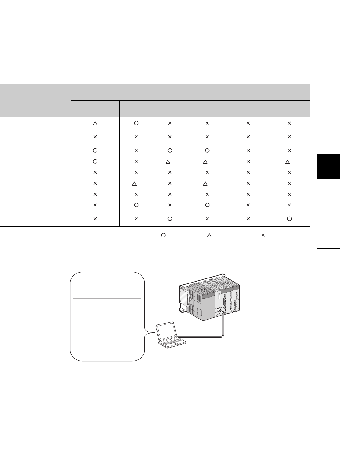
CHAPTER6 FUNCTIONS
1
2
3
4
5
6
7
8
6.12 Writing Programs While CPU Module is in RUN Status
6.12.2 Online change (files)
6 - 61
6.12.2 Online change (files)
(1) Definition
This function batch-writes files shown in Table 6.20 to the CPU module in the RUN status by online operation from
GX Developer.
: Can be written, : Partially restricted, : Cannot be written
*1: The file can be written if not being accessed by a sequence program.
Table6.20 Files that can be written to the CPU module in the RUN status
File name
CPU module built-in memory Memory card
(RAM) Memory card (ROM)
Program memory Standard
RAM
Standard
ROM SRAM card Flash card ATA card
Parameter
Intelligent function module
parameter
Program
Device comment *1 *1 *1
Initial device value
File register *1 *1
Local device
Sampling trace file
Programmable controller user
data
Figure 6.52 Outline of online change (files)
GX Developer
Writing of
program file A
Program file
A
6 - 62
(2) Availability
(a) For the Q00UJCPU,Q00UCPU,and Q01UCPU
The function cannot be performed in the following cases.
• A program memory does not have enough area for storing a program file to be written.
• A program memory stores the maximum number of files can be stored.
(b) For the Q02UCPU,QnUD(H)CPU, and Built-in Ethernet port QCPU
A file can be written to the CPU module in the RUN status regardless of space of a memory to be
written and the number of files to be stored.
(3) Increase in the scan time
The scan time increases when a program file is written to the CPU module in the RUN status.
For increase in the scan time, refer to Section 10.1.3.
(4) When a file is accessed by a sequence program instruction
An instruction in a program cannot access to the file being written to the CPU module in the RUN status. If
If doing so, the instruction will not be executed.
(5) Online change(files) from multiple locations
Do not simultaneously write files to one CPU module in the RUN status from multiple locations.
Doing so may delete program files.
(6) Online change (files) of SFC programs
SFC programs cannot be written in units of files to the CPU module in the RUN status.
(7) Operations prohibited when programs are written to the CPU module in the
RUN status, T/C setting value is changed, or data are transferred from a
program cache memory to a program memory
Refer to Section 6.12.3(2).
(8) Instructions that do not operate normally when files are written to the CPU
module in the RUN status
Refer to Section 6.12.3(3).

CHAPTER6 FUNCTIONS
1
2
3
4
5
6
7
8
6.12 Writing Programs While CPU Module is in RUN Status
6.12.3 Precautions for online change
6 - 63
6.12.3 Precautions for online change
The following shows precautions for online change.
(1) Online change during boot operation
When data are written to the CPU module in the RUN status during boot operation, the status of boot source
program is not changed.
(2) Operations prohibited when programs are written to the CPU module in the
RUN status, T/C setting value is changed, or data are transferred from a
program cache memory to a program memory
Do not perform the following operations.
(a) Power-off or reset
The following operations are not normally completed if they are performed during online change, TC setting
value change, or data transfer from the program cache memory to the program memory.
If performed, write the data to the CPU module again.
• Power-off
• Reset
(b) Operations from GX Developer
The following operations cannot be performed during online change, TC setting value change, or data transfer
from the program cache memory to the program memory. If performed, an error is displayed on GX Developer.
Perform the following operations after online change, TC setting value change, or data transfer from the
program cache memory to the program memory.
(Ladder mode, writing files during RUN, and function block)
TC setting value change
Data transfer to the program memory
• Online change (ladder mode), online change (files)
• TC setting value change
• Data transfer to the program memory
• Write to PLC (Flash ROM)
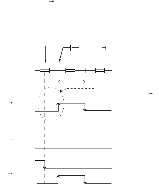
6 - 64
(3) Instructions do not operate normally during online change
When data are written to the CPU module in the RUN status, the following instructions do not operate normally.
• Fall instruction
• Rise instruction
• SCJ instruction
(a) Fall instruction
The fall instruction is executed when the instruction is in the data written to the CPU module in the RUN status,
even if the execution condition (on off) is not met.
For preventing the fall instruction execution during online change, refer to POINT in this section.
The corresponding fall instructions are LDF, ANDF, ORF, MEF, PLF, FCALLP, and EFCALLP.
Figure 6.53 Operation of the fall instruction
Completion of
online change
END
1 scan
END END00 0
OFF OFF
ON
OFF
OFF
OFF
OFF
OFF
OFF
ON
ON
ON
ON
ON
ON ON
ON OFF
X0 status
XO
MO
XO
MO
XO
MO
The fall instruction is executed
even if the execution condition is off off.
[ PLF MO ]
XO
AA
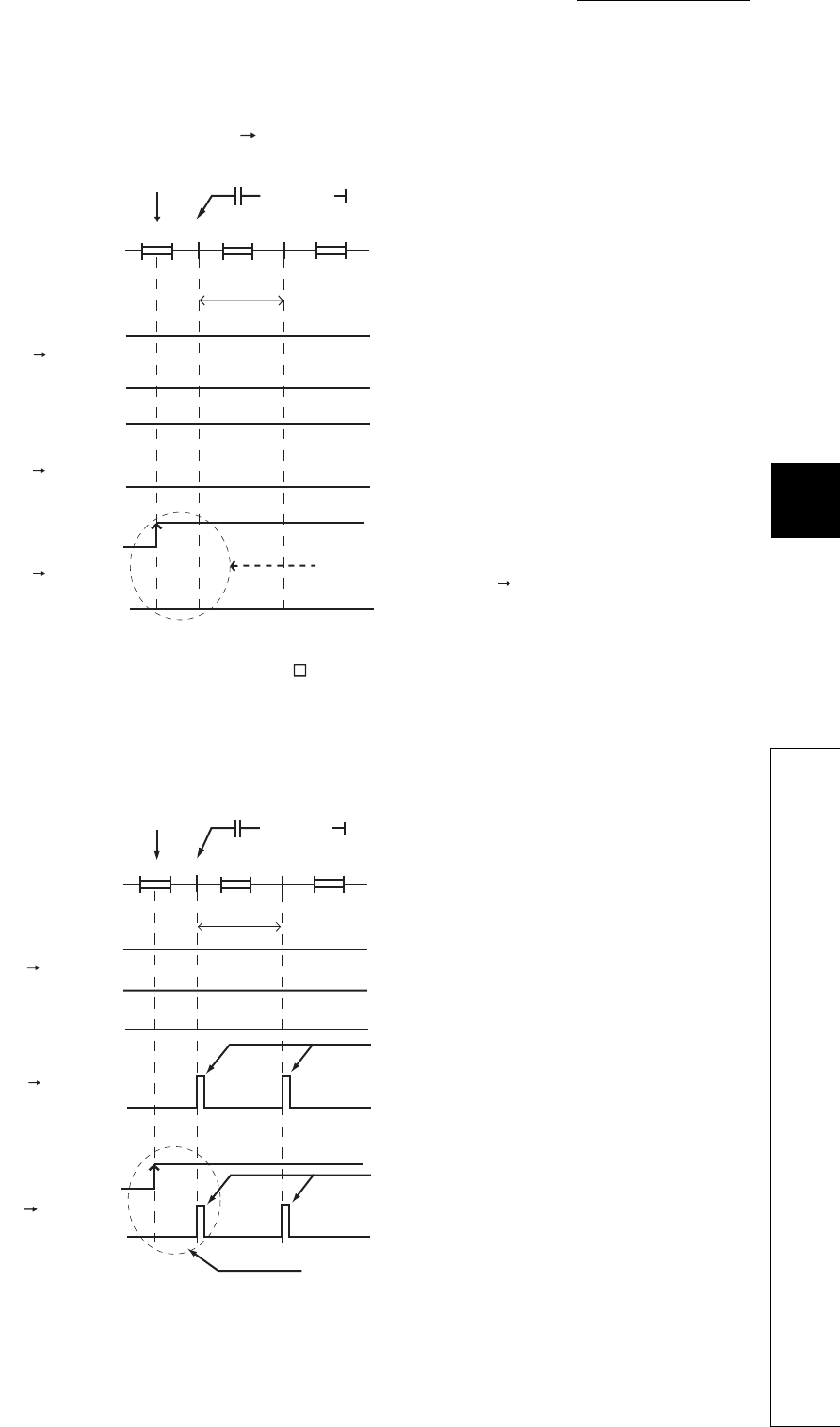
CHAPTER6 FUNCTIONS
1
2
3
4
5
6
7
8
6.12 Writing Programs While CPU Module is in RUN Status
6.12.3 Precautions for online change
6 - 65
(b) Rise instruction
The rise instruction is not executed when the instruction is in the data written to the CPU module in the RUN
status, even if the execution condition (off on) is met.
The corresponding rise instructions are PLS and P.
(c) SCJ instruction
When the SCJ instruction is in the data written to the CPU module in the RUN status and the execution
condition is on at completion of the writing, a jump to the specified pointer is made without a wait of one scan.
Figure 6.54 Operation of the rise instruction
Figure 6.55 Operation of the SCJ instruction
Completion of
online change
END
1 scan
END END00 0
OFF OFF
ON
OFF
OFF
OFF
OFF
OFF
OFF
ON
ON
ON
ON
ON
ON ON
X0 status
XO
MO
XO
MO
XO
MO
The rise instruction is not executed even
if the execution condition is off on.
[ PLS MO ]
XO
AA
ON OFF
Completion of
online change
END
1 scan
END END00 0
OFF OFF
ON ON
X0 status
[ SCJ PO ]
XO
AA
ON OFF
Jumps to the specified pointer.
Jumps to the specified pointer.
Jumps to the specified pointer
without waiting for one scan.
XO OFF
ON
SCJ
instruction
XO OFF
ON
SCJ
instruction
XO OFF
ON
SCJ
instruction
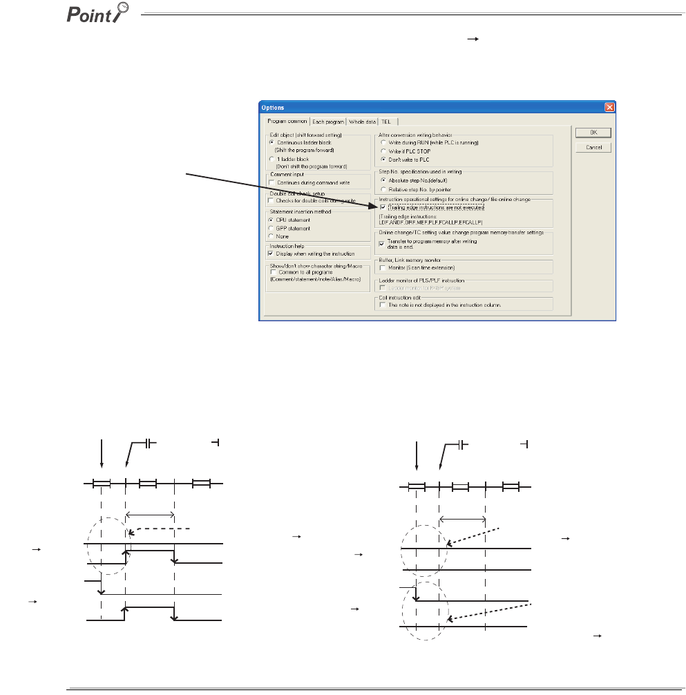
6 - 66
To avoid execution of the fall instruction even when the execution condition (on off) is not met after data are written to the
CPU module in the RUN status, select "Trailing edge instructions are not executed" in the Options screen in GX Developer.
The option is deselected by default.
Figure 6.57 shows operations of the fall instruction depending on the setting of "Trailing edge instructions are not executed"
in GX Developer.
Figure 6.56 Options screen
Figure 6.57 Operation comparison of the fall instruction
Selecting this option avoids
execution of the fall instruction
whose execution condition is "off".
Completion of
online change
END
1 scan
END END00 0
OFF OFF
ON
OFF
OFF
OFF
OFF
ON
ON
ON
ON OFF
X0 status
XO
MO
XO
MO
The fall instruction is executed
even if the execution condition is off off.
[ PLF MO ]
XO
AA
(a) Operation when deselecting "Trailing
edge instructions are not executed"
Completion of
online change
END
1 scan
END END00 0
OFF OFF
ON
OFF
OFF
OFF
OFF
ON
ON
ON
ON OFF
X0 status
XO
MO
XO
MO
The rise instruction is not
executed even if the execution
condition is off off.
[ PLF MO ]
XO
AA
(b) Operation when "Trailing edge instructions are not executed" is checked.
The fall instruction is not executed
when the timing of completion of
online change and execution
condition of on off are met.

CHAPTER6 FUNCTIONS
1
2
3
4
5
6
7
8
6.12 Writing Programs While CPU Module is in RUN Status
6.12.3 Precautions for online change
6 - 67
(4) Writing to the program memory during online change and T/C setting value
change
Contents changed due to online change and TC setting value change are automatically transferred to the
program memory simultaneously when the data are written to the program cache memory.
The time required for writing data to the CPU module in the RUN status and changing T/C setting value is
increased due to automatic transfer of the program memory by the time shown in Table6.21.
Ts: Scan time (s)
Since the number of writes to the program memory (Flash ROM) is limited (up to 100,000 times), set the
automatic transfer to the program memory to be disabled when data are written to the CPU module in the RUN
status and changing T/C setting value frequently.
Table6.21 Time increased due to automatic transfer of data to the program memory
CPU module Transfer time
Q00UJCPU,Q00UCPU,Q01UCPU,Q02UCPU Ts 320 + 4.8 (s)
Q03UDCPU,Q04UDHCPU,Q06UDHCPU,Q03UDECPU,
Q04UDEHCPU,Q06UDEHCPU Ts 260 + 4.7 (s)
Q10UDHCPU,Q10UDEHCPU Ts 439 + 6.2 (s)
Q13UDHCPU,Q13UDEHCPU Ts 600 + 8.0 (s)
Q20UDHCPU,Q20UDEHCPU Ts 839 + 11.4 (s)
Q26UDHCPU,Q26UDEHCPU Ts 1100 + 15.0 (s)
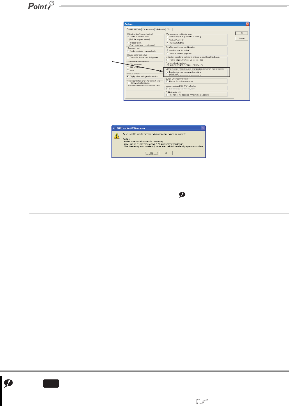
6 - 68
Automatic transfer to the program memory can be set to be disabled in the Options screen of GX Developer.
When the automatic transfer is set to be disabled, the following message appears after online change.
Selecting "Yes" transfers data to the program memory.
Selecting "No" does not transfer data to the program memory.
When selecting "No", execute "Program memory batch transfer" by GX Developer.Note1
Program transfer status can be checked by the special relay (SM165). Note6.5
When SM165 is on, the program memory batch transfer has not completed.
When SM165 is off, the program memory batch transfer has completed.
Figure 6.58 Online change/TC setting value change program memory transfer settings
Note1
Data are not automatically
transferred to the program
memory by deselecting
here.
Note6.5
When checking the batch transfer status to the program memory with the Q02UCPU,Q03UDCPU,Q04UDHCPU, or
Q06UDHCPU, check the versions of the CPU module and GX Developer.( Appendix 2)
Universal
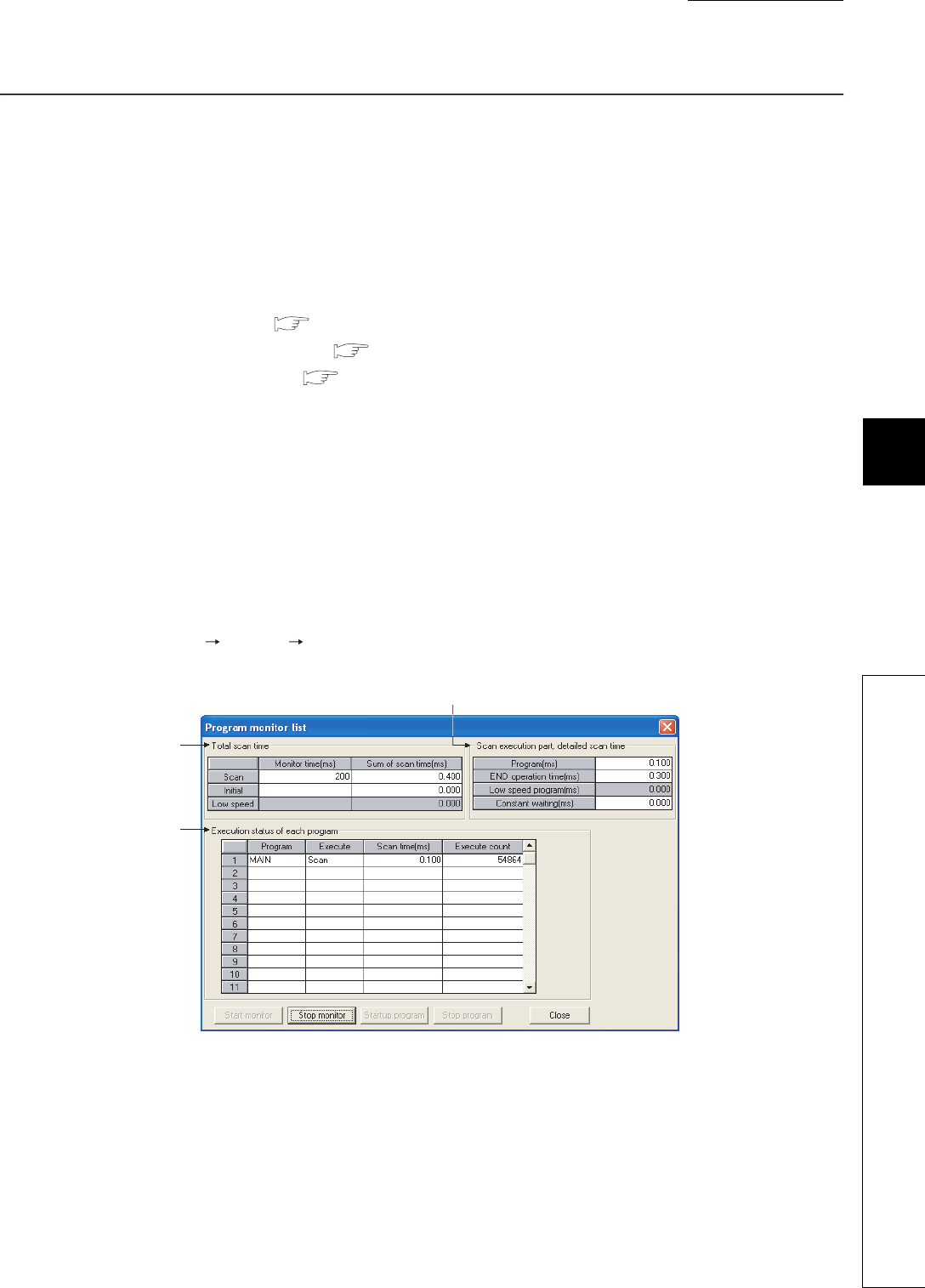
CHAPTER6 FUNCTIONS
1
2
3
4
5
6
7
8
6.13 Execution Time Measurement
6.13.1 Program monitor list
6 - 69
6.13 Execution Time Measurement
(1) Definition
This function displays the processing time of the program being executed.
(2) Applications and types
This function can be used to know the effect of processing time of each program on the total scan time when the
system is adjusted.
There are following three types.
• Program monitor list : Section 6.13.1
• Interrupt program list monitor : Section 6.13.2
• Scan time measurement : Section 6.13.3
6.13.1 Program monitor list
(1) Definition
This function displays the processing time of the program being executed.
The scan time, number of execution times, and processing time by item can be displayed for each program.
(2) Execution
Selecting [Online] [Monitor] [Program monitor list] displays the Program monitor list screen.*1
Figure 6.59 shows an example of executing the program monitor list.
*1: During execution of a fixed scan execution type program, the scan time of the fixed scan execution type program is not
displayed.
"-" is displayed in the Scan time column.
Figure 6.59 Program monitor list screen
(a)
(c)
(b)
6 - 70
(a) Total Scan Time
The monitoring time set in "WDT (Watchdog timer) setting" of the PLC RAS tab of the PLC parameter dialog
box and total scan time for each program type during execution by the CPU module are displayed.
1) Monitor time
The monitoring time of each program is displayed.
If the scan time exceeds this time, the CPU module detects ”WDT ERROR".
2) Sum of scan time
The total time of each item in "Scan execution part, detailed scan time" is displayed.
When constant scan time is set, the constant scan time is displayed.
(b) Scan execution part, detailed scan time
The details of the scan time are displayed.
1) Program
The total execution time of the scan execution type program is displayed.
2) END operation time
The END processing time is displayed.
3) Low speed program
Since a low-speed execution type program is not used "0.000" is displayed.
4) Constant waiting
The constant scan waiting time is displayed when the constant scan time is set.
(c) Execution status of each program
The execution status of a program selected at the program tab of the PLC parameter dialog box is displayed.
1) Program
The program name is displayed in the order set in the PLC parameter dialog box.
2) Execution
The program type set in the PLC parameter dialog box is displayed.
3) Scan time
The actual scan time (current value) is displayed.
When a program is in stop (standby) status, the scan time is displayed as 0.000 ms.
4) Execute count
The number of execution times of programs before monitoring is displayed, setting the measurement start as
"0". The number of execution times is displayed up to 65535 and returns to 0 when the 65536 is measured.
The execution times is held even when the program is stopped.

CHAPTER6 FUNCTIONS
1
2
3
4
5
6
7
8
6.13 Execution Time Measurement
6.13.1 Program monitor list
6 - 71
Remark
When the POFF instruction is executed, a non-execution processing is performed for one scan.
The number of execution times displayed is the addition of the execution times of the non-execution processing.
For details of the POFF instruction, refer to the following.
QCPU Programming Manual (Common Instructions)
(3) Program start and stop
Program cannot be started and stopped from the Program list monitor screen.
(4) Precautions
The scan time of a fixed scan execution type program is not displayed during its execution.
"-" is displayed in the Scan time column.
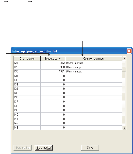
6 - 72
6.13.2 Interrupt program monitor list
(1) Definition
This function displays the number of executions of an interrupt program.
This function is used to check the execution status of the interrupt program.
(2) Execution
Selecting [Online] [Monitor] [Interrupt program monitor list] of GX Developer displays the Interrupt program
monitor list screen.
Figure Figure 6.60 shows an execution example of the interrupt program monitor list.
(a) Execute count
The number of executions of an interrupt program is displayed.
This function starts counting after the CPU module is in the RUN status.
When the counting reaches 65536 times, it is reset to 0.
(b) Common comment
Device comments created to an interrupt pointer is displayed.
Figure 6.60 Interrupt program monitor list screen
(a)
(b)

CHAPTER6 FUNCTIONS
1
2
3
4
5
6
7
8
6.13 Execution Time Measurement
6.13.3 Scan time measurement
6 - 73
6.13.3 Scan time measurement Note1
(1) Definition
This function displays the processing time of set program section during ladder monitoring.
The time required for the subroutine and interrupt programs can be measured.
(2) Range specification of scan time measurement
There are following two types for specifying a scan time measurement range.
• Setting on the ladder monitor screen
• Setting on the scan time measurement screen
(3) When the subroutine program call instruction is in the measurement range
When the subroutine program call instruction (CALL) is in the range of scan time measurement, the scan time
includes the time required for processing a subroutine program.
(4) When interrupt programs/fixed scan execution type programs are executed in
the scan time measurement range
The execution time of interrupt programs and fixed scan execution type programs are added.
Note1
Figure 6.61 When subroutine program is in measurement range
Note6.6
Note6.6
When using the scan time measurement for the Q02UCPU, Q03UDCPU,Q04UDHCPU,Q06UDHCPU,Q13UDHCPU,
and Q26UDHCPU, check the versions of CPU module and GX Developer.( Appendix 2)
Universal
Main
program
Subroutine
program
Measurement range
Measurement range
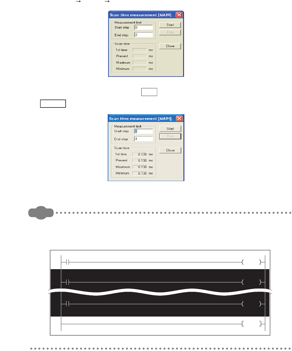
6 - 74
(5) Execution
Measure the scan time by the following procedure.
• Display the start of the ladder program where scan time is measured in GX Developer and set the monitor
mode.
• Select [Online] [Monitor] [Scan time measurement] to open the Scan time measurement screen.
• Enter the start and end steps and click the button.
When the start step is 52 and the end step is 105
Remark
When displaying the Scan time measurement screen after specifying the scan time measurement rage in the monitor
mode, the start and end steps are set in the specified range.
To specify the range, press the "Shift" key and click the mouse (The specified part is inverted).
Figure 6.62 Scan time measurement screen
Figure 6.63 Measurement range specification
Start
Example
Y20
M0
50
Y21
52
Y22
104
106 END
M1
M2
CHAPTER6 FUNCTIONS
1
2
3
4
5
6
7
8
6.13 Execution Time Measurement
6.13.3 Scan time measurement
6 - 75
(6) Precautions
(a) Measurement range setting
Set the measurement range so that "Start step < End step" is satisfied.
(b) Minimum unit of measurement time
The minimum unit of measurement time is 0.01ms.
If the measurement time is less than 0.01ms, 0.000ms is displayed.
(c) When between the FOR and NEXT instructions is specified
The execution time of one scan between the specified steps is displayed.
(d) When scan time cannot be measured
Scan time cannot be updated on the Scan time measurement screen in the following cases.
• When the branch instruction is specified the to end step
The JMP instruction is specified to the end step.
• When only the start step is executed
The specified end step is not executed by the JMP instruction.
Example
0
3
5
7
10
P0
End step: 6
Start step: 3
JMP P0
Example
0
3
5
7
10
12
13
P0
End step: 9
Start step: 3
JMP P0
END
The specified end step
is not executed due to
the JMP instruction.
6 - 76
• When the end step is executed before the start step
The start step is specified as the next step of the CALL instruction and the end step is
specified in a subroutine program executed by the CALL instruction.
• When the start step is executed continuously
Only the start step is specified between the FOR and NEXT instructions.
Example
0
3
5
6
9
P0
End step: 8
Start step: 3
FEND
CALL P0
RET
The start step is executed
after the end step due to the
CALL instruction.
Example
3
6
8
10
11
End step: 13
Start step: 8
FOR K2
NEXT
"The start step is executed
continuously since it is specified
between the FOR and NEXT
instructions."

CHAPTER6 FUNCTIONS
1
2
3
4
5
6
7
8
6.14 Sampling Trace Function
6 - 77
6.14 Sampling Trace Function
(1) Definition
This function samples the data of the specified device at a preset timing and at a preset interval
(sampling cycle), and then stores the trace results in the sampling trace file.Note1
(2) Application
This function is useful to check the change of the device data used in the program during debugging at
a preset timing.
In addition, this function is used to read the device data at trigger condition establishment.
(3) Sampling trace file
This file stores the trace setting necessary for executing the function and trace results.
Sampling trace file can be stored only in the Standard RAM or SRAM card. ( Section 5.1.1)
Note1
Note6.7
Note6.7
The Q00UJCPU does not support the sampling trace function.
Universal
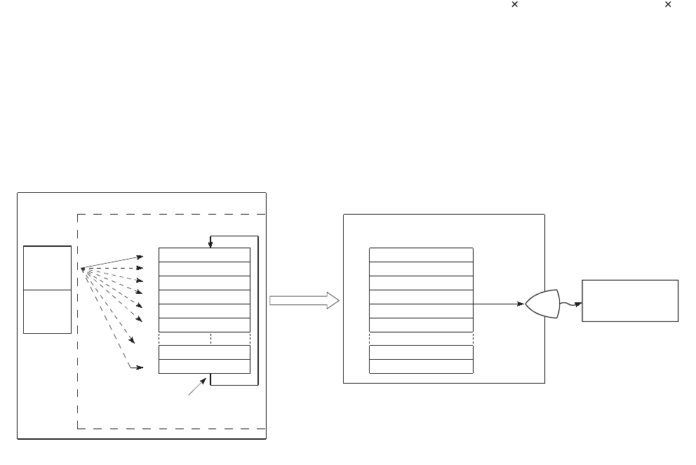
6 - 78
(4) Sampling trace operation
(a) Operation of the CPU module
When a sampling trace trigger is issued by GX Developer, the CPU module executes traces for the preset
number of times.
The number of traces will be a value of which the number of bytes for the sampling trace area divided by the
number of bytes of the specified device (N1 + N2 + N3 + word device points 2 + (bit device points/16)
2).*1 *2
*1: Round up the result of "bit device points/16" in the expression to the right of the decimal point.
*2: Add the following values to N1 to N3 according to the items selected under the trace additional information of the trace
condition setting.
•N1: When "Time(sec)" is selected, add "4".
•N2: When "Step no." is selected, add "10".
•N3: When "Program name" is selected, add "8".
*3: When the trigger is issued, the CPU module samples data for the preset number of times and latches the data in the
sampling trace area.
Figure 6.64 Sampling trace operation
CPU module
Standard RAM/memory card
*3
Specified
device data
Sampling trace area
Device
area
File
register
area
1st trace data
2nd trace data
3rd trace data
4th trace data
5th trace data
6th trace data
(n-1)th trace data
n th trace data
n-1
1
2
3
4
5
6
1
2
3
4
5
6
nn
n-1
When data is stored for n th time,
the next data overwrites the 1st data.
Read out the
trace data to
a peripheral.
Sampling trace area
The specified
number of trace
data sets is
displayed.
Sampling trace
GX Developer
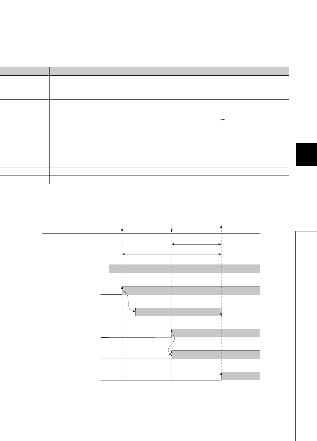
CHAPTER6 FUNCTIONS
1
2
3
4
5
6
7
8
6.14 Sampling Trace Function
6 - 79
(b) Operation of the special relay
1) When the sampling trace is executed normally
The execution status of the sampling trace can be checked in the special relay listed in Table6.22.
Figure 6.65 shows the operation flow chart of the special relay for sampling trace execution.
Table6.22 Execution status of the sampling trace
Number Name Description
SM800 Trace preparation Turns on when the trace setting in GX Developer is written to the CPU module.
The relay is used to check the sampling trace enable status.
SM801 Trace start Turns on when the sampling trace is started.
SM802 Trace execution in
progress
Turns on during sampling trace execution.
The relay is used to check the sampling trace execution status.
SM803 Trace trigger A trigger turns on upon the status change of the relay (off on).
SM804 After trace trigger
Turns on when any of the following condition is established.
• A trigger is issued by GX Developer.
• The TRACE instruction is executed.
• SM803 turns on.
• Detailed setting (Device and Step No.)
The relay is used to check the trigger condition establishment status.
SM805 Trace completed Turns on when the sampling trace is completed.
SM826 Trace error Turns on when an error occurs during sampling trace execution.
Figure 6.65 Operation flow chart of the special relay (for sampling trace execution)
Trace start requested
Trigger condition
established Trace completed
Number of traces after trigger
Total number of traces
SM80
SM801
(trace start)
SM802
(Trace execution in progress)
SM803
(Trace trigger)
SM804
(After trace trigger)
SM805
(Trace completed)
(trace ready)
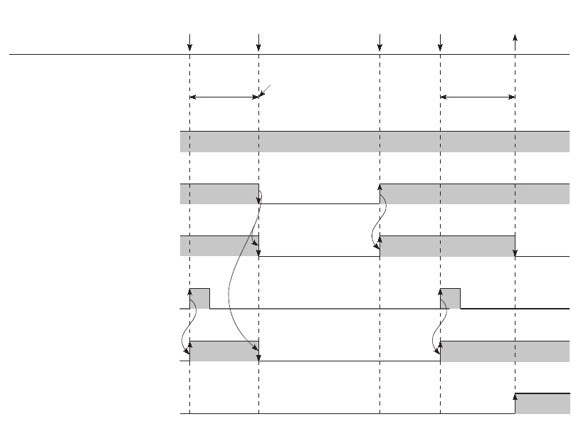
6 - 80
2) When the sampling trace is interrupted
If SM801 (Trace start) is turned off during sampling trace, execution of the sampling trace will be interrupted.
When the sampling trace is interrupted, the trace count is cleared.
The sampling trace restarts by turning on SM801.
*1: SM801 also turns off when the sampling trace is interrupted by GX Developer.
Figure 6.66 Operation flow chart of the special relay (for sampling trace interruption)
SM800
(Trace preparation)
SM801
(trace start)
SM802
(Trace execution in progress)
SM803
(Trace trigger)
SM804
(After trace trigger)
SM805
(Trace completed)
Trigger
executed
Trigger
executed
SM801
off
*1 SM801
on
Trace
completed
Number of
traces
after trigger
Number of
traces
after trigger
The trace count is cleared.
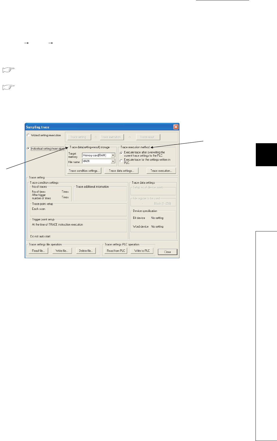
CHAPTER6 FUNCTIONS
1
2
3
4
5
6
7
8
6.14 Sampling Trace Function
6 - 81
(5) Operating procedure
Select [Online] [Trace] [Sampling trace...] in GX Developer.
On the screen opened, select the method for operating the sampling trace.
• "Wizard setting/execution"
( GX Developer Version 8 Operating Manual)
• "Individual setting/execution"
( (5)(a) in this section)
(a) Setting "Trace data (setting + result) storage" and "Trace execution method"
On the screen opened, set the trace data storage location and trace execution method.
1) Trace data (setting + result) storage
Select the memory for storing the trace data and the file for writing the trace conditions.
Select either "Standard RAM" or "Memory card (RAM)" for the target memory setting.
Trace results will be stored in the memory set here under the selected file name.
2) Trace execution method
Select either of the following trace execution method.
• "Execute trace after overwriting the current trace setting to the PLC":
The CPU module executes the sampling trace after the trace settings are overwritten to the existing
sampling trace file.
• "Execute trace for the settings written in PLC":
The CPU module executes the sampling trace with the trace settings in the sampling trace file selected
for "Trace data (setting + result) storage".
Figure 6.67 Sampling trace screen
2)
1)
6 - 82
(b) Setting trace conditions
Set trace conditions on the screen opened by clicking the button on the screen
shown in Figure 6.67.
On the Trace condition settings screen, set the following items.
• Number of traces ("No. of traces", "After trigger number of times")
• Trace point setting ("Trace point setup")
• Trigger point setting ("Trigger point setup")
• Additional information ("Trace additional informaton")
• Auto start setting ("Auto start trace")
1) No. of traces
There are two items need to be set: "No. of times" and "After trigger number of times".
• No. of times: Select the number of executions from the start to the end of sampling trace.
• After trigger number of times: Select the number of executions from the trigger point to the end of
sampling trace.
Set the numbers for each items within the following setting range.
("After trigger number of times") ("No. of times") (8192)
Figure 6.68 Trace condition settings screen
Figure 6.69 Relationship between two setting items
Trace condition setting
Trace started Trigger point Trace completed
Number of traces
after trigger
Total number of traces

CHAPTER6 FUNCTIONS
1
2
3
4
5
6
7
8
6.14 Sampling Trace Function
6 - 83
2) Trace point setup
Select the timing for collecting trace data from the items listed in Table6.23.
*1: The extended data register (D) is included.
*2: The extended link register (W) is included.
3) Trace additional information
Set the information added for each trace.
Select one or more items from the following. (If not necessary, do not select any item.)
• Time(sec.): Stores the time when the trace was executed.
• Step no.: Stores the step number where the trace was executed.
• Program name: Stores the program name where the trace was executed.
Table6.23 Trace point setup item
Item Description
Each scan Collects trace data during END processing of each scan.
Interval Collects trace data at specified time intervals.
Each multiple CPU high
speed communication
cycle*1
Collects trace data in a cycle of 0.88m specified time intervals.
Since data is collected at the timing of interrupt program (I45) execution, trace data can be collected only when
the following conditions are all satisfied.
• The multiple CPU high-speed main base unit (Q3 DB) is used.
• The multiple CPU system where two or more CPU modules are used and the multiple CPU high speed
transmission function is set.
• Interrupt pointer (I45) exists in a program.
• Interrupts are enabled and interrupt mask of I45 is cancelled.
Detail
A trace point (device and/or step number) needs to be set.
The following devices can be set as a trace point.
• Bit device: X(DX), Y(DY), M, L, F, SM, V, B, SB, T(contact), ST(contact), C(contact), FX, FY, J \X, J \Y,
J\B, J\SB, BL\S
• Word device: T(current value), ST(current value), C(current value), D*1, SD, W*2, SW, R, Z, ZR, FD, U \G,
J\W, J\SW, U3E\G
The following modifications are available for the above devices.
• Digit specification of bit device
• Bit specification of word device
• Indirect specification of word device
• Index modification
The setting method and trace data collection timing are same as those for the monitor condition setting in
Section 6.11.1.
If a device is set as a trace point, the timing when the word device value is changed can be selected as a data
collection timing.

6 - 84
4) Trigger point setup
Select the trigger point from the items listed in Table6.24.
*1: The extended data register (D) is included.
*2: The extended link register (W) is included.
5) Auto start trace Note6.8Note1
When the checkbox is selected, the sampling trace will be started automatically when:
• the CPU module is powered off and then on after the trace settings are written, or
• the CPU module status is changed from STOP to RUN.
When the CPU module is powered off and then on, reset, or the CPU module status is changed from STOP to RUN to
rewritten the sampling trace settings, the settings cannot be rewritten to the CPU module regardless of the status of SM829
(Forced registration specification of trace setting) if the trigger condition has already been established.
In this case, the CPU module will be in the status where the sampling trace setting registration has been canceled. SM800
(Trace preparation) turns off.
Table6.24 Trigger point setup item
Item Description
At the time of TRACE
instuction execution The time of execution of the TRACE instruction is set as a trigger.
At the time of trigger
operation
from GX Developer
The time when a trigger is issued by GX Developer is set as a trigger.
Detail
A trace point (device and/or step number) needs to be set.
The following devices can be set as a trace point.
• Bit device: X(DX), Y(DY), M, L, F, SM, V, B, SB, T(contact), ST(contact), C(contact), FX, FY
• Word device: T(current value), ST(current value), C(current value), D*1, SD, W*2, SW, R, ZR
The following modification is available for the above devices.
• Bit specification of word device
Indirectly-specified devices cannot be set.
The setting method and trace data collection timing are same as those for the monitor condition setting in
Section 6.11.1.
If a device is set as a trace point, the timing when the word device value is changed can be selected as a data
collection timing.
Note1
Note6.8
When using the sampling trace auto start function for the Q02UCPU, Q03UDCPU, Q04UDHCPU, Q06UDHCPU,
Q13UDHCPU, or Q26UDHCPU, check the versions of the CPU module and GX Developer. ( Appendix 2)
Universal
CHAPTER6 FUNCTIONS
1
2
3
4
5
6
7
8
6.14 Sampling Trace Function
6 - 85
(c) Setting trace data
Set trace data on the screen opened by clicking the button on the screen shown in
Figure 6.67.
Table6.25 shows the devices can be set as trace data.
*1: The extended data register (D) is included.
*2: The extended link register (W) is included.
Figure 6.70 Trace data settings screen
Table6.25 Devices can be set as trace data
Item Description
Bit device
The following bit devices can be set up to 50 points.
X, DX, Y, DY, M, L, F, SM, V, B, SB, T(contact), T(coil), ST(contact), ST(coil), C(contact),
C(coil), J \X, J \Y, J \B, J \SB, BL \S
Word device
The following word devices can be set up to 50 points.
T (current value), ST (current value), C (current value), D*1, SD, W*2,SW, R, Z, ZR,
U\G, J\W, J\SW, U3E\G
The following modifications are available for the above devices.
• Digit specification of bit device
• Bit specification of word device
• Index modification
Indirectly-specified devices cannot be set.
Trace data setting
6 - 86
(d) Writing the trace condition settings and trace data settings
Write the set trace conditions and trace data to the memory selected as a sampling trace file for "Trace data
(setting + result) storage".
Click the button on the screen shown in Figure 6.67 to write the settings.
When storing the sampling trace file into a memory card (SRAM card), more than one sampling trace files can be stored by
changing the file name.
For the standard RAM, only one sampling trace file can be stored.
When multiple sampling trace files are used, use the memory card (SRAM card).
(e) Executing the sampling trace
Click the button on the screen shown in Figure 6.67 to open the Execute sampling trace
screen.
Select an item shown in Table6.26 and click the button.
Figure 6.71 Execute sampling trace screen
Table6.26 Trace point setting
Item Description
Start trace Starts the function, and starts counting the number of sampling trace executions.
Stop trace
Stops the function, and clears the total sampling trace execution count and the
execution count after trigger.
(To restart the function, select "Start trace" again.)
Execute trigger
Executes a trigger, and starts counting the number of sampling trace executions after
trigger.
The function will be ended when the trace execution count after trigger reaches the
preset count.
Registry trace (For start trace from Program) Registers trace data when a program is executed.
Write to PLC
Trace execution
Execute
Displayed only when status
display is selected
CHAPTER6 FUNCTIONS
1
2
3
4
5
6
7
8
6.14 Sampling Trace Function
6 - 87
(f) Displaying trace results
Read trace results form the CPU module and display the data.
1) Click the button on the screen shown in Figure 6.71 to read trace results.
2) Click the button on the same screen to display the trace results read.
The trace results shows the on/off status of each bit device for every sampling cycle and the current value of
each word device.
Specified devices are read when the condition selected in "Trigger point setup" (trigger condition) is established.
Therefore, when devices are sampled in every scan and the sampling is finished by trigger operation from a peripheral, the
data is sampled twice because timing of the sampling is the same with that of the establishment of trigger condition.
Figure 6.72 Trace result screen
Figure 6.73 Trace result
Trace result PLC read
Trace result
Data when the trigger
conditions are satisfied. Data when trigger condition is met

6 - 88
(6) Method for clearing trace execution status
The trace execution status can be cleared by latch clear using the remote latch clear operation.
( Section 6.6.4)
To perform the sampling trace again after latch clear, select “Start trace” or “Registry trace”.
(7) Precautions
(a) Areas where sampling trace can be performed
The sampling trace can be performed from other stations on the network or serial communication module.
However, it cannot be performed from multiple devices simultaneously. It can be performed from one device to
the CPU module.
(b) Holding and clearing the trace setting
The trace setting (sampling trace file) registered with the CPU module is latched.
Even if the CPU module is powered off and then on or is reset, the sampling trace can be performed again with
the trace setting at registration.
However, the previous trace result cannot be read.
Also in the following cases, even when the trigger condition of the sampling trace is established, the latched
trace setting will be cleared since the condition is not recognized as the trigger condition (SM800 (Trace
preparation) turns off).
Register the trace setting again with GX Developer.
1) When selecting "Standard RAM" in "Target memory", configuring the setting that changes the local device
size in the standard RAM*1, writing parameters to the CPU module, and then performing any of the
following operations
• The CPU module is powered off and then on
• The CPU module is reset.
• The CPU module is set from STOP to RUN.
*1: The operation includes when a local device is created.
2) When selecting "Standard RAM" in "Target memory” and the sampling trace file is corrupt, either of the
following operations were performed.
• The CPU module is powered off and then on.
• The CPU module is reset.
To keep the trace result to the personal computer even after configuring the setting that changes the local device size,
perform the following operations.
• Click the button on the screen shown in Figure 6.71 to read the trace result to the
personal computer.
• Click the button on the screen shown in Figure 6.71 to display the trace result.
• Click the button on the screen shown in Figure 6.72 to save the trace result in CSV format.
Trace result PLC read
Trace result
Create CSV file

CHAPTER6 FUNCTIONS
1
2
3
4
5
6
7
8
6.14 Sampling Trace Function
6 - 89
3) When selecting "Memory card (RAM)" in "Target memory" while the SRAM card where the sampling trace
file has been registered is not mounted, either of the following operations were performed.
• The CPU module is powered off and then on.
• The CPU module is reset.
4) When selecting "Memory card (RAM)" in "Target memory" and the sampling trace file is corrupt, either of the
following operations were performed.
• The CPU module is powered off and then on.
• The CPU module is reset.
(c) Reading trace result in the STOP status
The trace result cannot be read while the CPU module is in the STOP status.
When reading the trace result, read it while the CPU module is in the RUN status.
(d) Sampling trace registration while the trigger condition is established
Even if the trigger condition is established, the sampling trace setting can be registered by the following
procedure.
1) Turn on SM829 (Forced registration specification of trace setting).
2) Select “Individual setting/execution” in the screen shown in Figure 6.67.
3) Click the button, select “Registry trace (For start trace from Program)”, and click the
button.
●When the sampling trace is registered by the procedures above (d) 1) to 3), start the sampling trace in status where the
trigger condition is not established.
If the trigger condition has been established when the sampling trace starts, the trigger may not be normally executed.
●When selecting "Wizard setting/execution" in the Sampling trace screen shown in (d) 2), and starting the sampling
trace, the trigger may not be normally executed, although the sampling trace setting can be registered.
(e) When a file register is selected as a specified device by the detail setting of trace
conditions
When a file register is selected as a specified device by the detail setting of trace point setting and trigger point
setting, do not change the block numbers of file register file and file register after trace registration.
Trace data may not be normally sampled.
(f) Trace point setting
When setting the trace point setting per each time or per multiple CPU high speed transmission cycle, pay
attention to the sampling interval and sampling processing time for one sampling since the sampling trace is
performed as interrupt processing.
If the sampling processing time for one sampling is long, “WDT ERROR” may be detected.
Trace execution
Execute
6 - 90
(g) Performing sampling trace during execution of another sampling trace
The first sampling trace is performed normally. The second sampling trace cannot be performed.
(h) Executing online change
When sampling trace and online change are performed simultaneously, they operate as follows.
1) Performing sampling trace during online change
• The trace point or trigger point is specified by the step number:
The online change is completed normally but the sampling trace is not performed.
• The trace point and trigger point are specified by except the step number:
Both the online change and sampling trace can be performed.
2) Performing online change during execution of sampling trace
• The trace point or trigger point is specified by the step number:
The sampling trace is suspended but the online change is normally performed.
• The trace point and trigger point are specified by except the step number:
Both the online change and sampling trace can be performed.
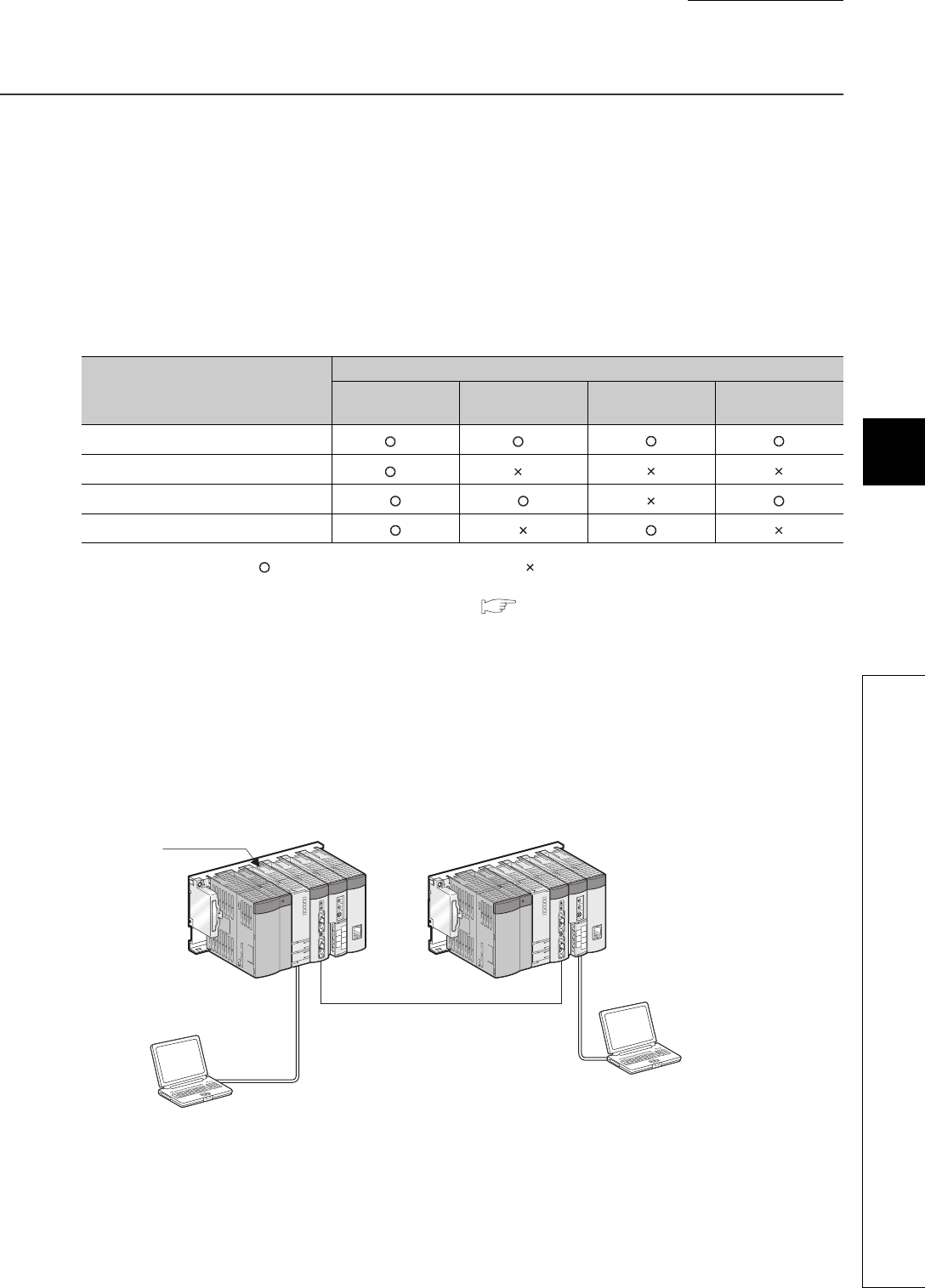
CHAPTER6 FUNCTIONS
1
2
3
4
5
6
7
8
6.15 Debug Function from Multiple GX Developers
6.15.1 Simultaneous monitoring from multiple GX Developers function
6 - 91
6.15 Debug Function from Multiple GX Developers
(1) Definition
This function allows debugs from multiple GX Developers connected to such as a CPU module or serial
communication module.
When files are divided according to the processes or functions, this function can be used when multiple
GX Developers debug different files.
(2) Description
Table6.27 shows combinations of the debug functions executable from multiple GX Developers.
: Can be performed simultaneously, : Can be performed from one GX Developer.
*1: Since only one GX Developer can set the monitor conditions ( Section 6.11.1), other GX Developers cannot set
them.
*2: The monitoring with monitor conditions and online change cannot be performed simultaneously.
*3: For how to perform Nonline change to a file from multiple GX Developers, refer to Section 6.15.2.
6.15.1 Simultaneous monitoring from multiple GX Developers function
(1) Definition
This function allows simultaneous monitoring from multiple GX Developers connected to such as a CPU module
or serial communication module.
Creating a user setting system area allows high-speed monitoring from multiple GX Developers (Setting a
monitoring file for the host station is unnecessary).
Table6.27 Combinations of the debug functions
Function in execution
Function executed later
Monitor Online change Execution time
measurement Sampling trace
Monitor *1 *2
Online change *2 *3
Scan measurement
Sampling trace
Figure 6.74 Simultaneous monitoring
GX Developer
GX Developer
Monitor target
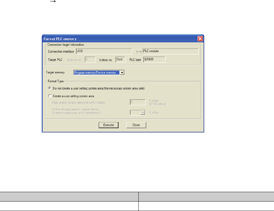
6 - 92
(2) Setting for simultaneous monitoring from multiple GX Developers
Create a user setting system area in the following procedure.
• Select [Online] [Format PLC memory] in GX Developer to open the screen shown in Figure 6.75.
• Select "Program memory/Device memory" in "Target Memory".
• Select "Create a user setting system area" in "Format Type".
• Set the number of steps for the system area (in increments of: 1K step).
Table6.28 shows the maximum number of steps settable in the system area.
1K step is available for a monitoring file from another station.
(3) Precautions
(a) Monitor condition setting
The monitor conditions can be set from one GX Developer.
(b) Necessity of system area setting
Although multiple GX Developers in other stations can simultaneously monitor a CPU module without the user
setting system area, the monitor speed will be slow.
Since the system area is set in the program memory, the area for storing programs reduces by the size of set
system area.
(c) The number of GX Developers for which high-speed monitoring can be set
The number of GX Developers that can simultaneously monitor a CPU module at high-speed is “the number of
user setting system areas (the number of K steps) + 1”.
For example, when user setting system area of 15K steps is created, maximum 16 GX Developers can
simultaneously monitor a CPU module at high-speed.
Figure 6.75 System area setting (when 1K step is set)
Table6.28 Maximum size of steps settable in the system area
Maximum size of settable step System area for monitoring from another station
Maximum 15K steps Maximum 15

CHAPTER6 FUNCTIONS
1
2
3
4
5
6
7
8
6.15 Debug Function from Multiple GX Developers
6.15.2 Online change function from multiple GX Developers
6 - 93
6.15.2 Online change function from multiple GX Developers
(1) Definition
This function allows multiple GX Developers to perform online change to one file or different files.
• Online change to one file:
Select "Relative step No. by pointer".
• Online change to different files:
• The writing can be executed without selecting "Relative step No. by pointer".
(2) Operating procedure for performing online change to one file
Select [Tools] [Options] <Program common> tab in GX Developer.
Set a pointer for online change beforehand.
Figure 6.76 Simultaneous online change from multiple GX Developers
Personal computer B
(GX Developer)
Personal computer A
(GX Developer)
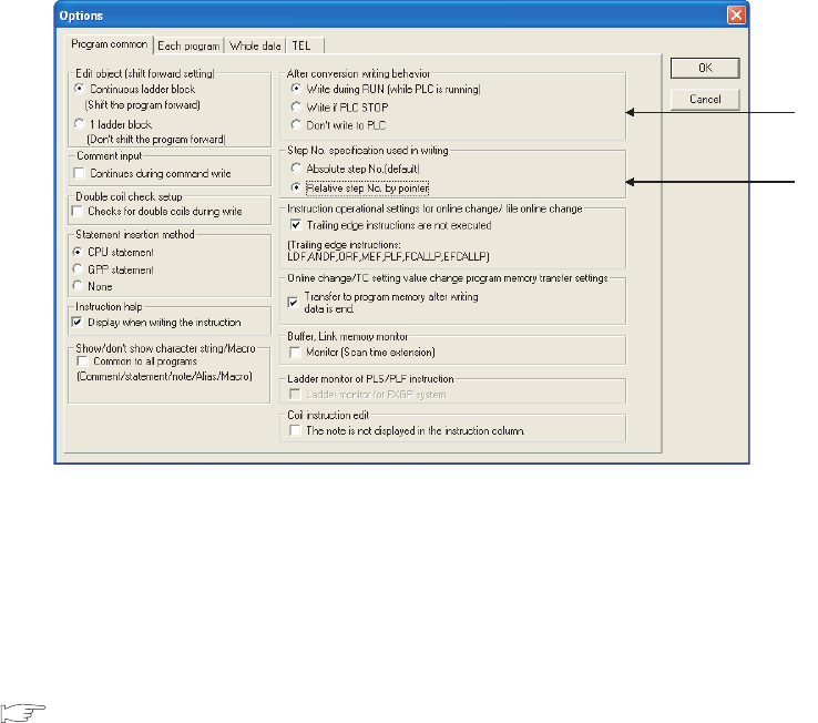
6 - 94
(a) Setting “After conversion writing behavior” and “Step No. specification used in writing”
Set them as follows:
1) Select "Write during RUN (while PLC is running)" in "After conversion writing behavior".
2) Select “Absolute step No. (default)” or “Relative step No. by pointer” in “Step No. specification used in
writing”.
(b) Performing online change
Display the ladder including the specified pointer and write the changed ladder during RUN.
(3) Precautions
Precautions for online change from multiple GX Developers are the same as those for usual Write during RUN
( Section 6.12.3).
Figure 6.77 Options screen
1)
2)

CHAPTER6 FUNCTIONS
1
2
3
4
5
6
7
8
6.16 Watchdog Timer (WDT)
6 - 95
6.16 Watchdog Timer (WDT)
(1) Definition
This function serves as an CPU module internal timer to detect errors of CPU module hardware and sequence
programs.
(2) Setting and resetting
(a) Setting
The watchdog timer setting can be changed in the PLC RAS setting of PLC parameter.
The default is set to 200ms.
The setting range is 10 to 2000ms (in increments of: 10ms).
(b) Reset
The CPU module resets the watchdog timer during END processing.
• The watchdog timer does not time up when the CPU module operates normally and the END/FEND
instruction is executed within the setting value of watchdog timer.
• The watchdog timer times up when the scan time of the sequence program is extended and the END/
FEND instruction could not be executed within the setting value of watchdog timer due to the hardware
failure of the CPU module or execution of an interrupt program/fixed scan execution type program.
(3) When the watchdog timer times up
“WDT ERROR” is detected and the following status occurs:
1) The CPU module turns off all outputs.
2) The RUN LED on the front of the CPU module turns off and the ERR. LED starts flashing.
3) SM1 turns on and the error codes 5000 and 5001 are stored in SD0.
(4) Precautions
(a) Watchdog timer error
An error is observed within the range of 0 to 10ms.
Set a watchdog timer while considering such an error.
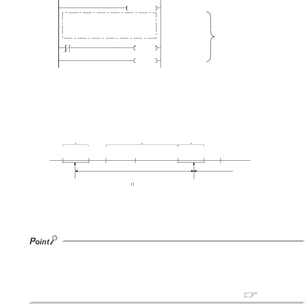
6 - 96
(b) Resetting a watchdog timer when a program is repeatedly executed between the FOR and
NEXT instructions
The watchdog timer can be reset by executing the WDT instruction in the sequence program.
To avoid the time up of watchdog timer while a program is repeatedly executed between the FOR and NEXT
instructions, reset the watchdog timer by the WDT instruction.
(c) Scan time when using the WDT instruction
The scan time value is not reset even if the watchdog timer is reset in the sequence program.
The scan time is measured up to the END instruction.
●A scan time is time required for the CPU module to operate the sequence program from step 0 and return
to the step 0 in the sequence program with the same file name.
●The scan time depends on the execution status of the following:
• Instructions used in the program
• Interrupt program and fixed scan execution type program
To keep the same scan time in every scan, use the constant scan function. ( Section 6.2)
Resetting watchdog timer when the a program is executed between the FOR and NEXT instructions
Figure 6.78 Resetting a watchdog timer when the program is executed between the FOR and NEXT instructions
Figure 6.79 Watchdog timer reset
FOR K1000
WDT
NEXT
Program repeatedly executed
WDT reset
Repeated in
1,000 times
MO
Internal processing time Sequence program
Internal
processing time
Scan execution
type program A
Scan execution
type program B
WDT reset
(CPU module internal
processing)
END 0 END
Scan execution
type program A
0
Scan time
WDT measurement time
Next scan time
WDT reset
(CPU module internal
processing)

CHAPTER6 FUNCTIONS
1
2
3
4
5
6
7
8
6.17 Self-diagnostic Function
6 - 97
6.17 Self-diagnostic Function
(1) Definition
This function allows the CPU module to diagnose itself to check for errors.
This function aims to preventive measures and prevention of malfunction of the CPU module.
(2) Self-diagnostic timing
When an error occurs at power-on or during the RUN or STOP status of the CPU module, the error is detected
and displayed by the self-diagnostic function, and the CPU module stops an operation.
Note that errors cannot be detected by the function depending on error status or an instruction executed.
When the operation is not stopped by the function, configure a safety circuit external to the programmable
controller so that the entire system operates safely.
(3) Checking errors
(a) LED status
When the CPU module detects an error, the ERR. LED turns on.
(b) Storage location of error information and error check
When the CPU module detects an error, the special relays (SM0, SM1) turn on and the error information (error
code) are stored in the special register (SD0).
When several errors are detected, the latest error code is stored in SD0.
Use the special relays and special register in a program as an interlock for the programmable controller and
mechanical system.
(4) Checking error history
To check the latest error code, select [Diagnostics] [PLC diagnostics] "Error log” in GX Developer.
The error data history are backed up using a battery even after the programmable controller is powered off.

6 - 98
(5) CPU module operation at error detection
(a) Mode at error detection
When an error is detected by the self-diagnostic function, the CPU module enters either of the following modes.
1) Mode that stops CPU module operation
When an error is detected, the CPU module stops an operation and turns off all external outputs of the
module set to "Clear" in "Error time output mode" in “Detailed setting” of the I/O assignment tab of the PLC
parameter dialog box (Outputs (Y) in the device memory are held).
Note that the external outputs of the module set to "Hold" in "Error time output mode" are held (Outputs (Y) in
the device memory are held).
2) Mode that continues CPU module operation
When an error is detected, the CPU module operates programs other than the one (instruction) where an
error occurred.
(b) Errors whether to continue or stop an operation can be selected
Whether to continue or stop an operation can be selected in the following errors.
1) Errors whether to continue or stop an operation can be selected in the PLC RAS tab of the
PLC parameter dialog box
• Computation error (including SFC program)
• Expanded command error (setting for future extension)
• Fuse blown
• Module verify error
• Intelligent module program execution error
• File access error
• Memory card operation error
• External power supply OFF (setting for future extension)
For example, when “Module verify error” is set to "Continue", an operation is continued from the I/O number
before an error.
For details of errors, refer to “Self-diagnostics list”. ( (7) in this section)
2) Error whether to continue or stop an operation can be selected in “Detailed setting” in the
I/O assignment tab of the PLC parameter dialog box
• Intelligent function module error

CHAPTER6 FUNCTIONS
1
2
3
4
5
6
7
8
6.17 Self-diagnostic Function
6 - 99
(6) Error check options
Whether to check the following errors or not can be selected in the PLC RAS tab of the PLC parameter dialog box
(All the options are selected (executed) by default).
1) Carry out battery check
2) Carry out fuse blown check
3) Verify module
4) Check device range at indexing.
5) Diagnose redundant power supply system. Note6.9Note1
Note1
Note6.9
When setting the diagnostic function of the redundant power supply system for the Q02UCPU,
Q03UDCPU, Q04UDHCPU, Q06UDHCPU, Q13UDHCPU, or Q26UDHCPU, check the versions of the
CPU module and GX Developer. ( Appendix 2)
Universal
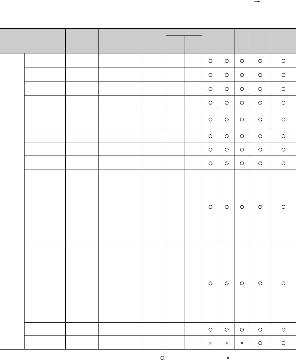
6 - 100
(7) Self-diagnostics list
The following table shows the self-diagnostics performed by the CPU module.
To check the error messages in the "Error message" column of Table6.29, select [Diagnostics] [PLC
diagnostics] of GX Developer.
: Self-diagnostics is performed. : Self-diagnostics is not performed.
(To the next page)
Table6.29 Self-diagnostics list
Diagnostics Error message Diagnostic timing
CPU
module
status
LED status
Q00UJ
CPU
Q00U
CPU,
Q01U
CPU
Q02U
CPU
QnUD(H)
CPU
Built-in
Ethernet
port QCPU
RUN ERR.
Hardware
failure
CPU error MAIN CPU
DOWN • Always Stop Off Flashi
ng
END instruction
not executed
END NOT
EXECUTE
• Execution of the
END instruction Stop Off Flashi
ng
SFC program
execution error
SFCP. END
ERROR
• Execution of a
SFC program Stop Off Flashi
ng
RAM check RAM ERROR • Power-on/reset Stop Off Flashi
ng
Operation circuit
check
OPE.CIRCUIT
ERR.
• Power-on/reset
• Execution of the
END instruction
Stop Off Flashi
ng
Fuse blown*1 *2 FUSE BREAK
OFF • Always Stop/
continue Off/on Flashi
ng/on
I/O interrupt error I/O INT.
ERROR
• Occurrence of an
interrupt Stop Off Flashi
ng
LAN controller
failure
LAN CTRL.
DOWN • Power-on/reset Stop Off Flashi
ng
Intelligent function
module error *1
SP.UNIT
DOWN
• Power-on/reset
• Execution of the
FROM/TO
instructions
• Execution of the
intelligent
function module
dedicated
instruction
• Execution of the
END instruction
Stop/
continue Off/on Flashi
ng/on
Control bus error CONTROL-
BUS ERR.
• Power-on
• Execution of
END processing
• Execution of the
FROM/TO
instructions
• Execution of the
intelligent
function module
dedicated
instruction
• Always
Stop Off Flashi
ng
Momentary power
failure AC/DC DOWN • Always Continue On Off
Multiple CPU high
speed bus error
MULTI-C.BUS
ERR. • Power-on/reset Stop Off Flashi
ng
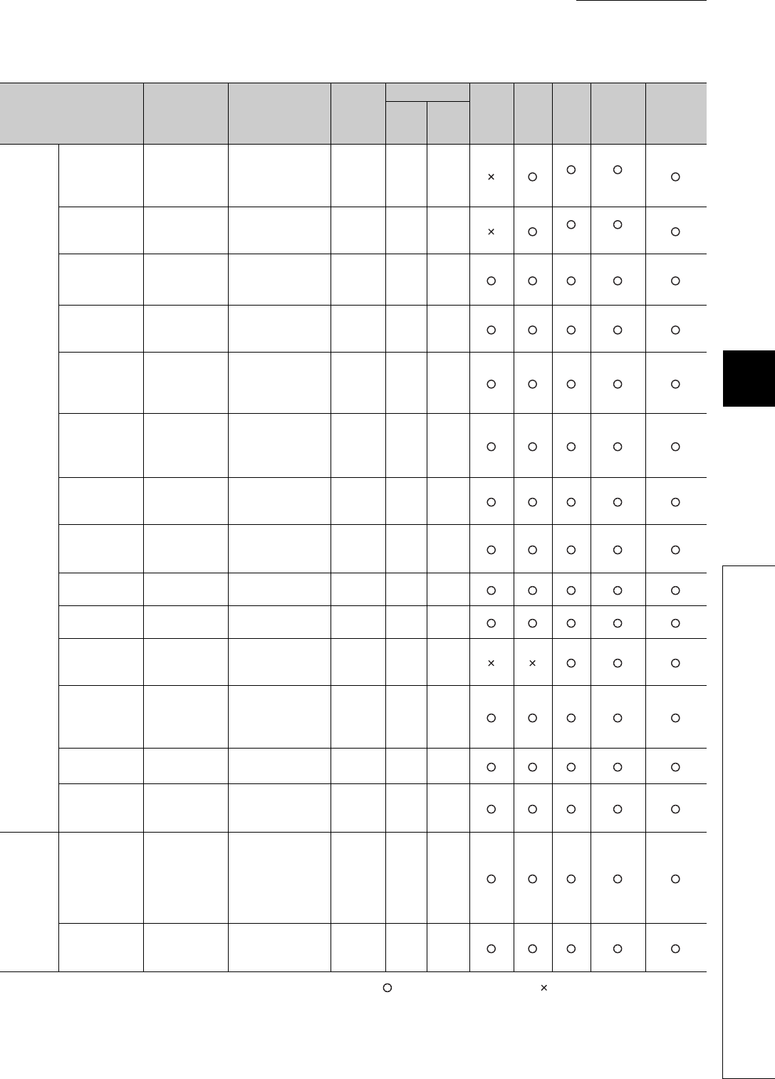
CHAPTER6 FUNCTIONS
1
2
3
4
5
6
7
8
6.17 Self-diagnostic Function
6 - 101
: Self-diagnostics is performed. : Self-diagnostics is not performed.
(To the next page)
Table6.29 Self-diagnostics list (continued)
Diagnostics Error message Diagnostic timing
CPU
module
status
LED status
Q00UJ
CPU
Q00U
CPU,
Q01U
CPU
Q02U
CPU
QnUD(H)
CPU
Built-in
Ethernet
port
QCPU
RUN ERR.
Handling
error
Voltage drop of
power supply for
redundant base
unit
SINGLE PS.
DOWN • Always Continue On On *5 *5
Redundant
power supply
module failure
SINGLE PS.
ERROR • Always Continue On On *5 *5
Module
verification*1*2
UNIT VERIFY
ERR.
• Execution of
the END
instruction
Stop/
continue Off/on Flashi
ng/on
Base
assignment
error
BASE LAY
ERROR • Power-on/reset Stop Off Flashi
ng
Intelligent
function module
assignment
error
SP.UNIT LAY
ERR.
• Power-on/reset
• Switching from
STOP to RUN
Stop Off Flashi
ng
Intelligent
program
execution
error*1
SP.UNIT
ERROR
• Execution of
the FROM/TO
instructions
Stop/
continue Off/on Flashi
ng/on
Intelligent
function module
version error
SP.UNIT
VER.ERR • Power-on/reset Stop Off Flashi
ng
No parameter MISSING
PARA.
• Power-on/reset
• Switching from
STOP to RUN
Stop Off Flashi
ng
Boot error BOOT ERROR • Power-on/reset Stop Off Flashi
ng
Backup error RESTORE
ERROR • Power-on/reset Stop Off Flashi
ng
Memory card
operation error*1
ICM.OPE.
ERROR
• Mounting/removal
of the memory
card
Stop/
continue Off/on Flashi
ng/on
File setting error FILE SET
ERROR
• Power-on/reset
• Writing to
programmable
controller
Stop Off Flashi
ng
File access
error*1
FILE OPE.
ERROR
• Execution of an
instruction
Stop/
continue Off/on Flashi
ng/on
Instruction
execution
disabled
CANëT
EXE.PRG.
• Power-on/reset
• Switching from
STOP to RUN
Stop Off Flashi
ng
Parameter
error
Parameter
setting check
PARAMETER
ERROR
• Power-on/reset
• Switching from
STOP to RUN
• Writing to
programmable
controller
Stop Off Flashi
ng
Link parameter
error
LINK
PARA.ERROR
• Power-on/reset
• Switching from
STOP to RUN
Stop Off Flashi
ng

6 - 102
: Self-diagnostics is performed. : Self-diagnostics is not performed
(To the next page)
Table6.29 Self-diagnostics list (continued)
Diagnostics Error message Diagnostic timing
CPU
module
status
LED status
Q00UJ
CPU
Q00U
CPU,
Q01U
CPU
Q02U
CPU
QnUD(H)
CPU
Built-in
Ethernet
port
QCPU
RUN ERR.
SFC parameter error SFC
PARA.ERROR
• Switching from
STOP to RUN
• Writing to
programmable
controller
Stop Off Flashi
ng
Intelligent function module
parameter error
SP.PARA.
ERROR • Power-on/reset Stop Off Flashi
ng
Password error REMOTE
PASS.ERR
• Power-on/reset
• Switching from
STOP to RU
Stop Off Flashi
ng
Instruction code check INSTRUCT.
CODE ERR
• Power-on/reset
• Switching from
STOP to RUN
• Execution of an
instruction
Stop Off Flashi
ng
No END instruction MISSING END
INS.
• Power-on/reset
• Switching from
STOP to RUN
Stop Off Flashi
ng
Pointer setting error
CANëT SET(P)
• Power-on/reset
• Switching from
STOP to RUN
Stop Off Flashi
ng
CANëT SET(I)
• Power-on/reset
• Switching from
STOP to RUN
Stop Off Flashi
ng
Program
error
Operation
error*1 *4
OPERATION
ERROR
• Execution of an
instruction
Stop/
continue Off/on Flashi
ng/on
FOR to NEXT
instructions
structure error
FOR NEXT
ERROR
• Execution of an
instruction Stop Off Flashi
ng
CALL to RET
instructions
structure error
CANëT
EXECUTE(P)
• Execution of an
instruction Stop Off Flashi
ng
Interrupt
program error
CANëT
EXECUTE(I)
• Execution of an
instruction Stop Off Flashi
ng
Instruction
execution
disabled
INST. FORMAT
ERR.
• Execution of an
instruction Stop Off Flashi
ng
Dedicated
instruction of
multiple CPU high
speed bus error
MULTI
COM.ERROR
• Execution of an
instruction Stop Off Flashi
ng
SFC block
configuration
error
CANëT
SET(BL)
• Switching from
STOP to RUN Stop Off Flashi
ng
SFC step
configuration
error
CANëT SET(S) • Switching from
STOP to RUN Stop Off Flashi
ng
SFC execution
error
SFC EXE.
ERROR
• Switching from
STOP to RUN Stop Off Flashi
ng
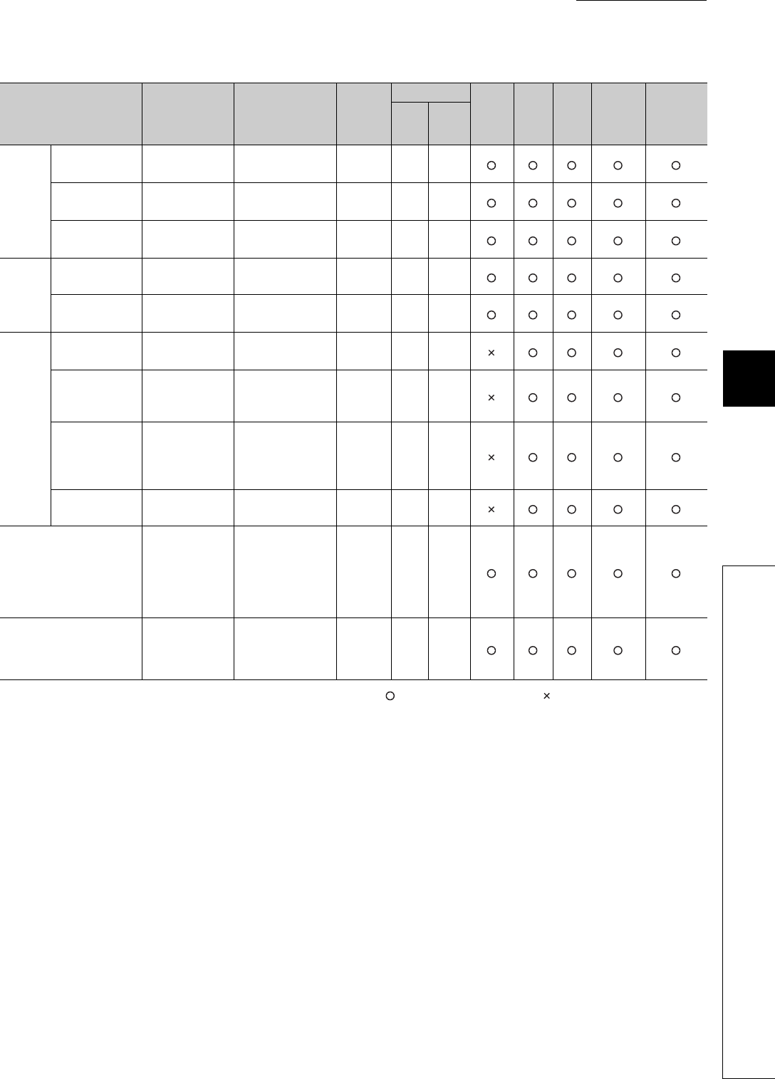
CHAPTER6 FUNCTIONS
1
2
3
4
5
6
7
8
6.17 Self-diagnostic Function
6 - 103
: Self-diagnostics is performed. : Self-diagnostics is not performed
*1: The operating status can be changed to "Continue" with the parameter setting of GX Developer The default is set to "Stop".
*2: This option can be set "not checked" (set "checked" by default) with the parameter setting of GX Developer. Also, this option is not
checked while SM251 is on.
*3: This option can be set "not checked" (set "checked" by default) with the parameter setting of GX Developer.
*4: This error includes an operation error when device range check is made at index modification.
*5: The CPU module having the serial number (first five digits) is "10042" or later can be diagnosed.
Table6.29 Self-diagnostics list (continued)
Diagnostics Error message Diagnostic timing
CPU
module
status
LED status
Q00UJ
CPU
Q00U
CPU,
Q01U
CPU
Q02U
CPU
QnUD(H)
CPU
Built-in
Ethernet
port
QCPU
RUN ERR.
Program
error
SFC syntax
error
SFCP. FORMAT
ERR.
• Switching from
STOP to RUN Stop Off Flashi
ng
SFC block
execution error
BLOCK
EXE.ERROR
• Execution of an
instruction Stop Off Flashi
ng
SFC step
execution error
STEP
EXE.ERROR
• Execution of an
instruction Stop Off Flashi
ng
CPU
error
Watchdog error
supervision WDT ERROR • Always Stop Off Flashi
ng
Program time-
out PRG.TIME OVER • Always Continue On On
Multiple
CPU
system
s error
Another CPU
major error
MULTI CPU
DOWN
• Always
• Power-on/reset Stop Off Flashi
ng
Multiple CPU
systems
execution error
MULTI
EXE.ERROR • Power-on/reset Stop Off Flashi
ng
Multiple CPU
systems
consistency
error
CPU LAY.
ERROR • Power-on/reset Stop Off Flashi
ng
Another CPU
minor error
MULTI CPU
ERROR • Always Continue On On
File diagnostic check INCORRECT
FILE
• Power-on/reset
• Switching from
STOP to RUN
• Writing to
programmable
controller
Stop Off Off
Annunciator check F**** • Execution of an
instruction Continue On
USER
LED
turns
on.

6 - 104
6.17.1 LEDs indicating errors
When an error occurs, the LEDs on the front of the CPU module turns on/flashes. ( Section 6.21)
6.17.2 Error clear
The CPU module can clear an error by a program if the error does not stop program operation.
(1) Procedures for error clear
Clear an error by the following procedures.
• Resolve the error cause.
• Store the code of the error to be cleared in the special register SD50.
• Turn off and then on the special relay SM50.
• The error is cleared.
(a) Procedures for error clear in case of multiple errors
When the latest error (error stored in the special register SD0) is cleared, error information stored in special
relays and special registers (SM0, SM1, SM5, SM16, SD0 to SD26) are cleared and therefore information on
errors that have not been cleared cannot be obtained from the special relays and spcial registers.
For errors that have not been cleared, obtain the past errors from the error history ( Section 6.18) and
clear the errors.
(2) Status after error clear
When the CPU module is recovered by clearing an error, the special relay, special register, and LEDs affected by
the error return to the status before the error.
If the same error occurs after clearing the error, it is logged in the error history again.
(3) Clear of annunciator
When multiple annunciators are detected, only the first detected "F"is cleared. ( Section 9.2.5)
●When an error is cleared by storing the code of the error to be cleared in SD50, the last digit of the code number is
ignored.
When the error code 2410, 2411, or 2412 occurs, clearing the error by storing 2412 in SD50 also clears
the error codes 2410 and 2411.
●If the CPU module is not an error cause, the error cannot be resolved by using the special relay (SM50) and special
register (SD50).
Since "SP. UNIT DOWN" indicates an error occurred to the Q bus, the error cannot be resolved by using
the special relay (SM50) and special register (SD50).
To resolve the error cause, refer to the following.
QCPU User's Manual (Hardware Design, Maintenance and Inspecting)
Example
Example

CHAPTER6 FUNCTIONS
1
2
3
4
5
6
7
8
6.18 Error History
6 - 105
6.18 Error History
This function stores an error detected by the self-diagnostic function and the detection time as an error history in a
memory.
Select [Diagnostics] [PLC diagnostics] of GX Developer to check the history.
The detection time is based on the clock in the CPU module. Make sure to set the correct time before the first use of the
CPU module. ( Section 6.5)
(1) Storage area
All stored logs are saved to the storage memory for error history of the CPU module.
*1: The memory is managed inside the system.
*2: When the number of storable logs are exceeded, the latest error log is stored by deletion of the oldest error log.
(2) How to clear error history
To clear the storage memory for error history and error history file, select [Diagnostics] [PLC diagnostics] in
GX Developer and click the button.
This method clears all data stored in the storage memory for error history of the CPU module and error history file
in a memory card.
Table6.30 Storage area for error history file
Storage area Number of storable logs
System memory in CPU module*1 Up to 100*2
Clear log

6 - 106
6.19 System Protection
The CPU module has protection functions (system protection) to prevent programs being modified by a third party
other than the designer with GX Developer or serial communication module.
*1: The Q00UJCPU, Q00UCPU, and Q01UCPU do not support the system protection in units of memory cards since they
cannot use the memory card.
6.19.1 Password registration
This function prohibits reading and writing data such as a programs and device comments in the CPU module with
GX Developer.
(1) Valid password range
The password can be registered with program, device comment, and initial device values files in the specified
memory (program memory, standard ROM, and memory card).
(2) Operations that can be prohibited
The following two operations can be prohibited.
• Reading and writing a file
• Writing a file
When a password has been registered with a file, GX Developer cannot operate the file unless entered password
does not match with the registered password.
Table6.31 System protection types
Protection target File that can be
protected Description Method Valid
timing Reference
In units of memory
cards*1 All files Prohibits writing to a
memory card.
Turn on the write protect
switch of a memory card. Always -
In units of files
• Program
• Device comment
• Initial device value
• Changes the attribute
for each file to either of
the following.
• Read/write (reading/
writing to programs)
prohibitation
• Write prohibitation
(operations regarding
writing such as writing
to programs and tests)
Make setting in the
Password registration
screen.
Always Section
6.19.1
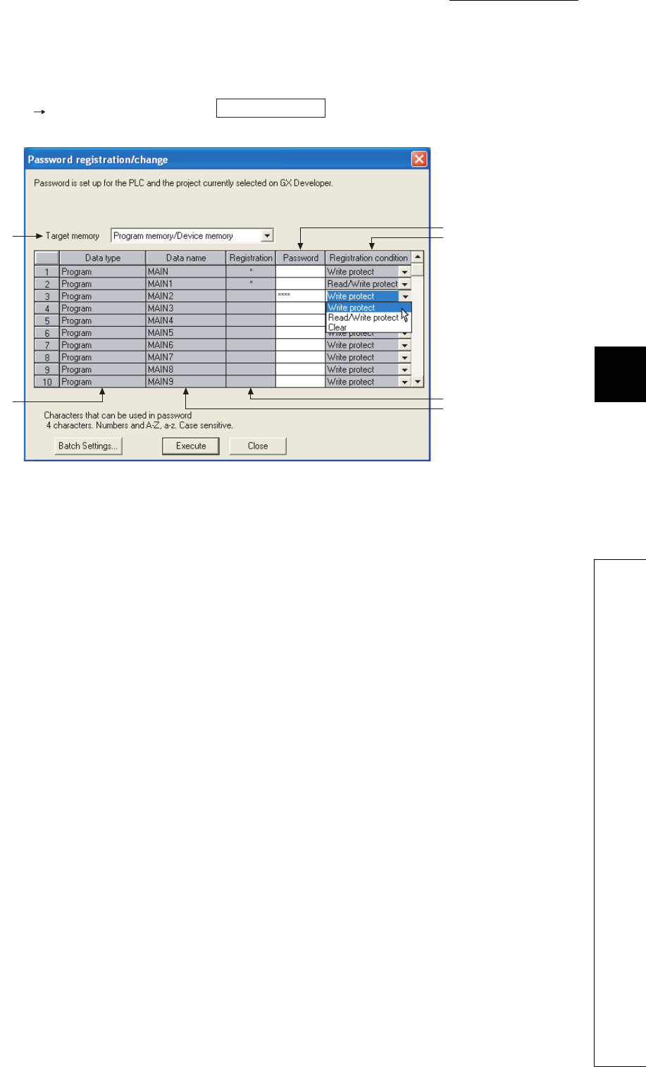
CHAPTER6 FUNCTIONS
1
2
3
4
5
6
7
8
6.19 System Protection
6.19.1 Password registration
6 - 107
(3) Setting method
Select [Online] [Password setup] or click the button on the Write to PLC screen in
GX Developer.
(a) Target memory
Select a memory storing a file where a password is to be registered.
(b) Data type
Displays the type of a file stored in the target memory.
(c) Data name
Displays the name of a file stored in the target memory.
(d) Registration
Displays "*" when a password has been set to the target file.
(e) Password
Enter current password or a password to be registered.
The Registration Condition column can be set after setting a password.
(f) Registration Condition
1) Write protect
Writing to a password-protected file is prohibited (reading is allowed).
2) Read/Write protect
Reading and writing to a password-protected file is prohibited.
3) Clear
The set password is cleared (entering the current password is necessary).
Figure 6.80 Password registration/change screen
Password setup
(a)
(e)
(f)
(d)
(c)
(b)

6 - 108
(4) Precautions
(a) Password management
A password registered with a file cannot be read from the file.
Forgetting the registered password disables the following operations.
• Program memory or memory card: Format PLC memory
• Standard ROM: Batch-writing
Make sure to record the registered password and store the recording paper.
(b) Operations that overwrite a file independent of the password registration setting
The following operations overwrite a file in the target drive (program memory, standard ROM) independent of
the password registration setting.
• Boot from a memory card
• Replacement of the CPU modules with a memory card (backup data restoration function)
6.19.2 Remote password
(1) Definition
This function prevents unauthorized remote access to the CPU module.
If a remote password has been set and the CPU module is remotely accessed, entering a remote password is
required.
(2) Settable modules and the number of settable modules
Table6.32 shows the modules for which the remote password can be set and the number of settable modules.
●The number of settable modules in the above table indicates the number of modules for which the remote password
can be set, not the number of mountable modules in the system using the CPU module.
●For the number of mountable modules in the system, refer to the following.
QCPU Userís Manual (Hardware Design, Maintenance and Inspection)
●For details of the remote password of each module, refer to the following.
Manual for each module
Table6.32 Settable modules and the number of settable modules
Settable module Number of settable modules
Ethernet module 4
Serial communication module 8
Modem interface module
Built-in Ethernet port QCPU 1
CHAPTER6 FUNCTIONS
1
2
3
4
5
6
7
8
6.19 System Protection
6.19.2 Remote password
6 - 109
(3) Flow from remote password setting to reflection of the password
Set a remote password ( (5) in this section) and then write it to the CPU module.
The remote password is transferred to the target module when the CPU module is powered off and then on or is
reset. ( (2) in this section)
Figure 6.81 Outline of a remote password
GX Developer
GX Developer
Transfers a remote
password to the
Ethernet module when
the CPU module is
powered off and then
on or is reset.
Checks the remote
password.
Sets,
changes, or
clears
the remote password and writes
the result to the CPU module.
Ethernet
Ethernet module
6 - 110
(4) Remote password lock/unlock
Unlock the remote password of a serial communication module via a modem or the Ethernet module via Ethernet.
When entered remote password matches with the registered password, the module can access the CPU module.
Figure 6.82 Outline of locking/unlocking a remote password with an Ethernet module
Ethernet module
GX Developer
Transfers a remote
password to the
Ethernet module when
the CPU module is
powered off and then
on or is reset.
Checks the remote
password.
GX Developer
Ethernet
Unlocks (releases) the remote password
and accesses the CPU module.
When a line is closed, the remote password is
locked.
CHAPTER6 FUNCTIONS
1
2
3
4
5
6
7
8
6.19 System Protection
6.19.2 Remote password
6 - 111
(5) Procedures for setting/changing/clearing a remote password
(a) Setting a remote password
• In the project data list of GX Developer, select [Parameter] [Remote pass].
• Connect GX Developer to the CPU module.
• Write a set remote password to the CPU module.
• In multiple CPU systems, write a remote password to the control CPU of the module to which the remote
password is to be set.
Figure 6.83 Remote password settings screen
Table6.33 Setting items on the Remote password settings screen
Item Description Setting range/option
Password settings Enter a remote password. Four characters or less (alphanumeric
characters, special symbols)
Password active
module settings
Model name Select a model name.
• QnUDE(H)CPU
• QJ71E71
• QJ71C24/CMO
Start X/Y Set the start address of the module. 0000H to 0FE0H
Detail - -
User connection No. Select user connection No. Connection 1 to Connection 16
System
connection
Auto open UDP port
Select a valid port of the remote
password. -
FTP transmission port
(TCP/IP)
GX Developer transmission
port (TCP/IP)
GX Developer transmission
port (UDP/IP)
HTTP port
Remote password setting
For the
QnUDE(H)CPU
or QJ71E71,
configure setting
in "Detail".

6 - 112
After setting a remote password, store the parameters to the valid drive ( Section 5.1.10).
(b) Changing a remote password
Change set password in the Remote password settings screen and write a new password to the CPU module.
(c) Clearing a remote password
• To delete set remote password, click the button in the Remote password settings screen.
• Write a remote password with GX Developer.
Clear
CHAPTER6 FUNCTIONS
1
2
3
4
5
6
7
8
6.20 System Display of CPU Module with GX Developer
6 - 113
6.20 System Display of CPU Module with GX Developer
When the CPU module is connected to GX Developer, this function can check the following items of the modules on
the base unit in the System Monitor screen.
• Installed status
• Parameter status
• Module’s Detailed Information
• Product information
(1) Installed status
The control CPU, model name, and the number of points of the modules on the selected base unit can be
checked.
"Unmounting" is displayed in the field of a number of slot where a module is not mounted.
The model name of a module on a slot to which "Empty" is set in the I/O assignment tab of the PLC parameter
dialog box is not displayed.
When using a redundant base unit, mounted status of the power supply module is also displayed.
Note6.10Note1
(2) Parameter status
The I/O number, type, and the number of points of the module on each slot of the selected base unit can be
displayed.
If the Parameter status displays "0" for an empty slot or assignment error, it indicates that the I/O assignment
setting of the PLC parameter dialog box and the mounted status differs. Therefore, change the I/O assignment
setting so that it may match with the mounted status.
When using a redundant base unit, mounted status of the power supply module is also displayed. Note6.10
Figure 6.84 System Monitor screen
Note1
(4)
(5)
(6)
(7)
(8)
(9)
(1)
(2)
(3)
Note6.10
Before monitoring the Q02UCPU, Q03UDCPU, Q04UDHCPU, Q06UDHCPU, Q13UDHCPU, or Q26UDHCPU, check
the versions of the CPU module and GX Developer.( Appendix 2)
Universal
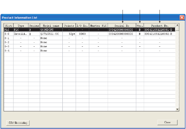
6 - 114
(3) Base
The status of the base unit and modules on the base unit can be checked.
When there is even one faulty module, the "Module" field color changes according to the status described at the
bottom of the screen.
(4) Mode
The mode cannot be selected since modules cannot be replaced online.
(5) Diagnostics
Click this button to check an error and status of the selected module.
(6) Module’s Detailed Information
Click this button to check the details of the selected module.
For details of the intelligent function module, refer to the manual for the intelligent function module used.
(7) Base Information
The "Overall Information" and "Base Information" can be checked.
(a) Overall Information
The number of base units and the number of modules on the base units can be checked.
(b) Base Information
The name, the number of slots, type, and the number of modules of the selected base unit can be checked.
(8) Product Inf. List
Individual information (Type, Series, Model name, Points, I/O No., Master PLC, Serial No., Ver., and Product No.)
of the mounted CPU module, I/O modules, and intelligent function module can be checked.
Figure 6.85 Product Information List screen
Serial
number
Product
number
Function
version
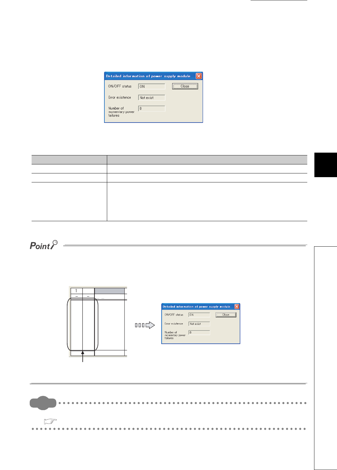
CHAPTER6 FUNCTIONS
1
2
3
4
5
6
7
8
6.20 System Display of CPU Module with GX Developer
6 - 115
(9) Detailed information of power supply module
This screen displays "ON/OFF status", "Error existence", and "Number of momentary power failures" of the power
supply module.
This screen can be displayed when using the power supply module supporting a redundant base unit and this
screen.
●In multiple CPU systems, the Detailed information of power supply module screen can be displayed:
• when GX Developer is connected to CPU No. 1, or
• when serial numbers (first five digits) of all CPU modules are "07032" or later.
●Double-clicking the area of power supply module in "Installed status" can also display the screen.
Remark
For details of the System Monitor screen of GX Developer, refer to the following.
GX Developer Version 8 Operating Manual
Figure 6.86 Detailed information of power supply module screen
Table6.34 Description of the Detailed information of power supply module screen
Item Description
ON/OFF status Displays the status of an input power supply to the redundant power supply module.
Error existence Displays whether a failure (error) occurs in the redundant power supply module.
Number of momentary power
failures
• When the redundant power supply module of redundant main base unit is selected
Displays the number of momentary power failures of the redundant power supply
module on the redundant main base unit (display range: 0 to 65535).
• When the redundant power supply module of redundant extension base unit is selected
Displays "-" and the number of momentary power failures is not counted.
Double-clicking this area displays the Detailed information
of power supply module screen.
Q03UDCPU
Powe
r su
pply
Powe
r su
pply
MasterPLC ->
2
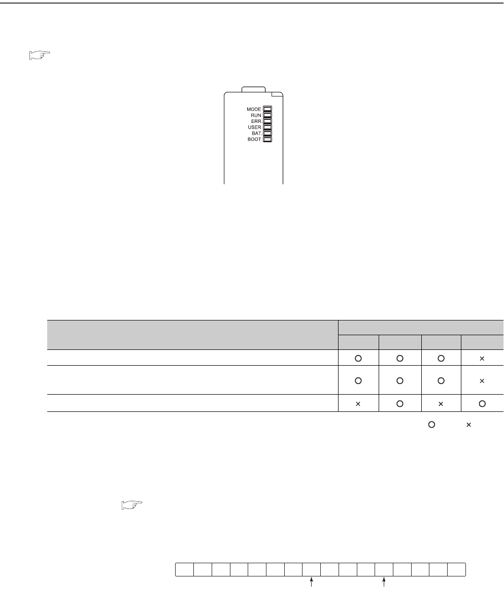
6 - 116
6.21 LED Indication
Operating status of the CPU module can be checked by the LEDs on the front of the CPU module.
For details of LED indications, refer to the following.
QCPU Userís Manual (Hardware Design, Maintenance and Inspection)
6.21.1 Methods for turning off the LEDs
(1) Methods
The LEDs can be turned off by the following operations (except for reset operation).
: Valid, : Invalid
*1: Description of special relays and special registers
Configure setting to turn off each LED as follows:
• Turning off both the Boot LED and USER LED: SD202 = 110H
• Turning off only the BOOT LED: SD202 = 100H
• Turning off only the USER LED: SD202 = 10H
Figure 6.87 LEDs on the front of the CPU module
Table6.35 Methods for turing off the LEDs
Method for turning off the LED Relevant LED
ERR. USER BAT. BOOT
Execute the LEDR instruction after resolving the error.
After resolving the error, clear the error by the special relay SM50 and special
register SD50*1 (operation continuation error only).
Turn off the LED by the special relay SM202 and special register SD202.*1
• SM50 : Clears an error of the error code stored in SD50 when the CPU module is powered off and then on.
•SD50
:
Stores an code of an error to be ccleared.
For details of error codes, refer to the following.
QCPU Userís Manual (Hardware Design, Maintenance and Inspection)
• SM202 : Turns off the LED corresponding to each bit of SD202 when the CPU module is powered off and then on.
• SD202 : Set an LED to be turned off.
Figure 6.88 Bit structure of the special register SD202
b15 b8 b4 b0
SD20 1/0 1/0
BOOT LED USER LED0: Not turn on.
1: Turns on.
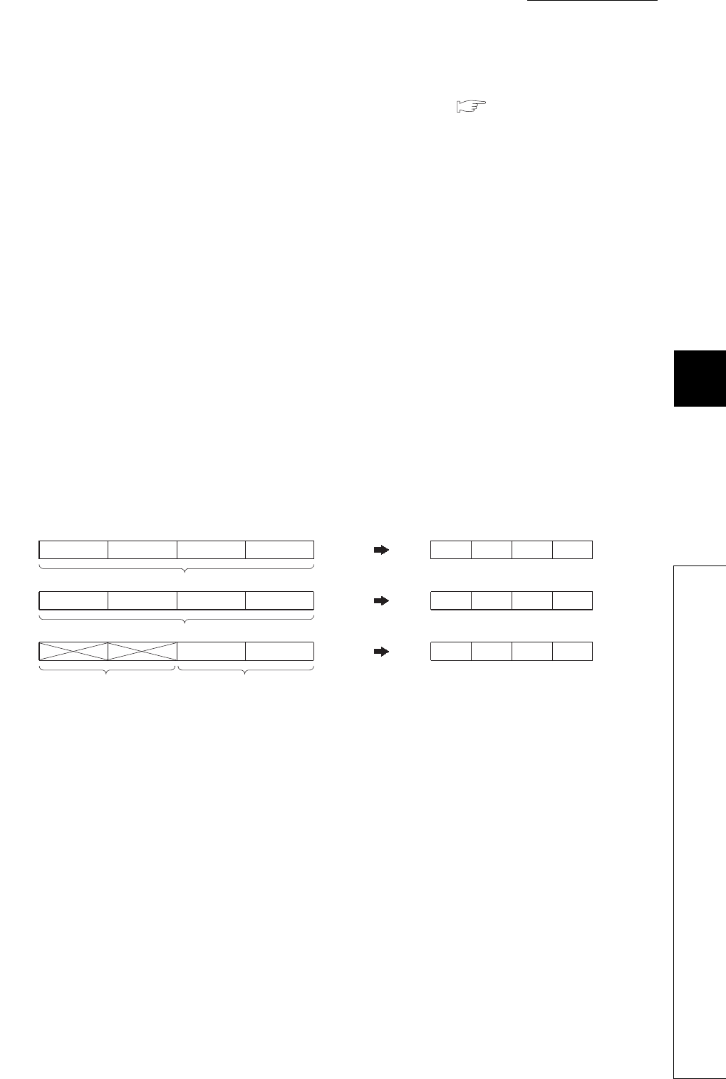
CHAPTER6 FUNCTIONS
1
2
3
4
5
6
7
8
6.21 LED Indication
6.21.2 LED indication priority
6 - 117
(2) Methods for not turning on the ERR. LED, USER LED, and BAT. LED
There is a priority in indications of the ERR.LED, USER LED, and BAT.LED. ( Section 6.21.2)
When an cause number of an LED is deleted in the priority, the LED will not turn on even if an error with the cause
number occurs.
6.21.2 LED indication priority
This section describes a priority for error messages stored in the LED display data (SD220 to SD227) in case of an
error.
(1) Displayed error messages and their priorities
In case of multiple errors, the error messages are displayed with the following conditions.
• A stop error is always set to the LED display data (SD220 to SD227).
• An operation continuation error is displayed according to the priority cause number described in this section.
Whether to indicate an error according to its priority using LED can be selected. (Set the priority using
special registers, SD207 to SD209.)
• When errors having the same priority occur simultaneously, the error detected first is displayed.
The priority is determined with the special registers SD207 to SD209 as follows.
Figure 6.89 Special registers and bit structure ragarding a priority
Priority 4 Priority 3
Factor number setting area
Priority 2 Priority 1
Priority 8 Priority 7 Priority 6 Priority 5
Priority 10 Priority 9
Factor number setting area
Factor number setting area
Default value of factor number
Ignored
SD207
15
SD208
SD209
12 11 8 7 430bits
SD207
SD208
SD209
to to to to 15 to 0bits
32
41
8765
00A9
6 - 118
(2) Priorities and cause numbers
The following table shows the description and priority of the cause numbers set to the special registers SD207 to
SD209.
*1: The Q00UJCPU, Q00UCPU, and Q01UCPU cannot display the error message.
*2: The Q00UJCPU cannot display the error message.
●To remain the LED off even in case of an error, set the cause number setting area (each 4 bits) of SD207 to SD209 that
stores the corresponding cause number to “0”.
To remain the ERR. LED off even when a fuse blown error is detected, set the cause number setting area
where the cause number “2" is stored to “0”.
Because the cause number "2" is not set, the ERR.LED remains off even if a fuse blown is detected.
In this case, even if another error with the cause number "2" (I/O module verification error or intelligent function module
verification error) is detected, the ERR.LED remains off.
●If “0” is set to the cause number setting area (setting that does not turn on the LED), SM0 (Diagnostic errors) and SM1
(Self-diagnostic error) turn on, and the error code is stored to SD0 (Diagnostic errors).
Table6.36 List of cause numbers and priorities
Priority Cause number
(hexadecimal) Displayed error message Remarks
1 1 • AC/DC DOWN • Power-off
22
• UNIT VERIFY ERR.
• FUSE BREAK OFF
• SP.UNIT ERROR
• SP.UNIT DOWN
• I/O module verification error
• Fuse blown
• Intelligent function module verification error
33
• OPERATION ERROR
• SFCP OPE.ERROR
• SFCP EXE.ERROR
• Operation error
• SFC instruction operation error
• SFC program execution error
44
• ICM.OPE.ERROR*1
• FILE OPE.ERROR
• Memory card operation error
• File access error
• FLASH ROM ERROR • Flash ROM access count over error
55
• PRG.TIME OVER • Constant scan setting time-out error
• MULTI CPU ERROR*2 • Another CPU error in multiple CPU systems
66 -
7 7 • Annunciator
88 -
9 9 • BATTERY ERROR
10 A -
Figure 6.90 Cause numbers stored in SD207 to SD209
Example
SD20 SD20 SD20
00A987654301
CHAPTER6 FUNCTIONS
1
2
3
4
5
6
7
8
6.22 Interrupt from Intelligent Function Module
6 - 119
6.22 Interrupt from Intelligent Function Module
The CPU module can execute an interrupt program (I ) by the interrupt request from the intelligent function module.
For example, the serial communication module can receive data by an interrupt program when the following data
communication functions are executed.
• Data reception during communication by nonprocedural protocol
• Data reception during communication by bidirectional protocol
Using an interrupt program enables a CPU module to receive data quickly.
(1) Setting an interrupt from the intelligent function module
To execute an interrupt program by an interrupt from the intelligent function module, select "Interrupt pointer
setting" in "Intelligent function module setting" of the PLC system tab in the PLC parameter dialog box.
Configure system setting at the intelligent function module is also required.
For execution of an interrupt program by an interrupt from the intelligent function module, refer to the following.
Manual for the intelligent function module used
Remark
For the numbers of interrupt pointers available for an interrupt from the intelligent function module, refer to Section 9.11.
Figure 6.91 Interrupt from a serial communication module
I
Serial communication
module
CPU module
Main program Main program
Issues an
interrupt.
Reception
Sends data.
FEND
BUFRCVS
SM400
External device to be communicated
Interrupt program
execution
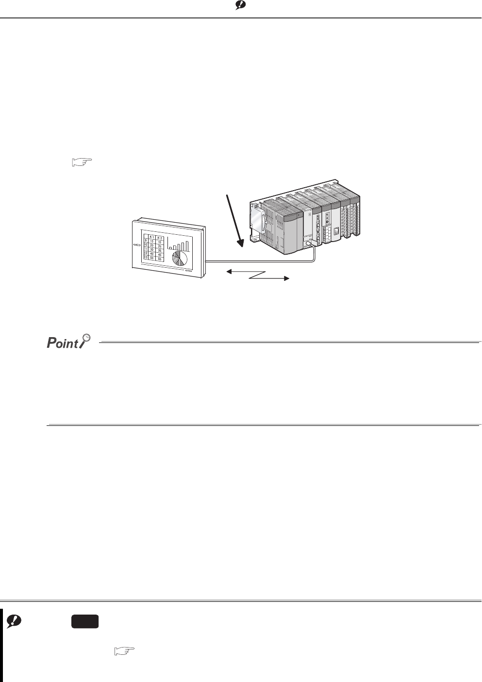
6 - 120
6.23 Serial Communication Function Note1
(1) Definition
This function communicates in the MC protocol*1 by connecting the RS-232 interface of the CPU module,
personal computer, and HMI by RS-232 cable.
This section describes the specifications, functions, and various settings of the function.
*1: The MC protocol is an abbreviation for the MELSEC communication protocol.
The MELSEC communication protocol is a communication method to access from an external device to the CPU
module according to the communication procedure for the Q series programmable controller (such as a serial
communication module, Ethernet module).
For the MC protocol, refer to the following.
Q Corresponding MELSEC Communication Protocol Reference Manual
●A personal computer or HMI can communicate with a CPU module by the serial communication function only when the
CPU module is connected to it.
The CC-Link IE controller network, MELSECNET/H, Ethernet, or CC-Link cannot be communicated with another
station.
●The serial communication function is not used for connection of GX Developer or GX Configurator with the CPU
module.
Note1
Figure 6.92 Communication with personal computer or HMI
Note6.11
Note6.11
When using the serial communication function for the Q02UCPU, check the versions of the CPU module and GX
Developer. ( Appendix 2)
When using the Q03UDCPU, Q04UDHCPU, Q06UDHCPU, Q10UDHCPU, Q13UDHCPU, Q20UDHCPU,
Q26UDHCPU, or Built-in Ethernet port QCPU, the serial communication function cannot be used.
Universal
Personal computer or HMI
RS-232 cable
Communication in the MC protocol

CHAPTER6 FUNCTIONS
1
2
3
4
5
6
7
8
6.23 Serial Communication Function
6 - 121
(2) Specifications
(a) Transmission specifications
Table6.37 shows the transmission specifications of RS-232 for the serial communication function of the CPU
module.
Check that the specifications of the personal computer and HMI match those of Table6.37 before using the
function.
*1: Can be set in the PLC parameter dialog box.
*2: Table6.38 shows the relationship between the MC protocol formats and frames.
: Available, : Unavailable
Table6.37 Transmission specifications of the serial communication function
Item Default Setting range
Communication method Full-duplex communication -
Synchronization method Asynchronous method -
Transmission speed*1 19.2kbps 9.6kbps, 19.2kbps, 38.4kbps, 57.6kbps, 115.2kbps
Data format
• Start bit: 1
• Data bit: 8
• Parity bit: Odd
• Stop bit: 1
-
MC protocol format*2
(automatic detection)
• Format 4 (ASCII)
• Format 5 (binary) -
Frame*2 • QnA-compatible 3C frame
• QnA-compatible 4C frame -
Transmission control DTR/DSR control -
Sum check*1 Checked Checked/not checked
Transmission wait time*1 No waiting time No waiting time, 10ms to 150ms (in increments of
10ms)
RUN write setting*1 Prohibited (deselected) Permit (checked), prohibited (deselected)
Overall cable distance 15m -
Table6.38 Relationship between the MC protocol formats and frames
Function Format 4 Format 5
Communication in ASCII code QnA-compatible 3C frame
QnA-compatible 4C frame
Communication in binary code QnA-compatible 4C frame
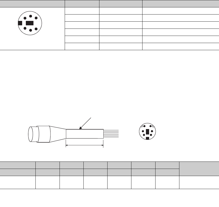
6 - 122
(b) RS-232 connector specifications
Table6.39 shows the specifications of the RS-232 connector for the CPU module.
(c) RS-232 cable
• The following RS-232 cable can be used for connecting the CPU module to the personal computer or HMI.
• QC30R2 (cable length: 3m)
• FMBKAZ1-*** (manufactured by Kuremo Electric Co., Ltd.)
• Cable with a Mini-DIN connector on one side and without connector on the other side
• *** indicates a cable length, which can be lengthened up to 15m in units of 0.1m.
Table6.39 RS-232 connector specifications
Appearance Pin number Signal Signal name
1 RD(RXD) Receive data
2 SD(TXD) Send data
3 SG Signal ground
4- -
5 DSR(DR) Data setting ready
6 DTR(ER) Data terminal ready
Pin number 1 2 3 4 5 6 Metal shell
Signal RD SD SG -DR ER
Wire core Red Black Green/
white - Yellow Brown Shield
Figure 6.93 Effective length and signal layout of RS-232 cable
Mini-DIN 6 pins
(female)
3
2
64
51
(CPU module side) FMBKAZ1-***
Effective length
3
2
65
1
4Signal layout of the
FMBKAZ1-*** connector
on CPU module side
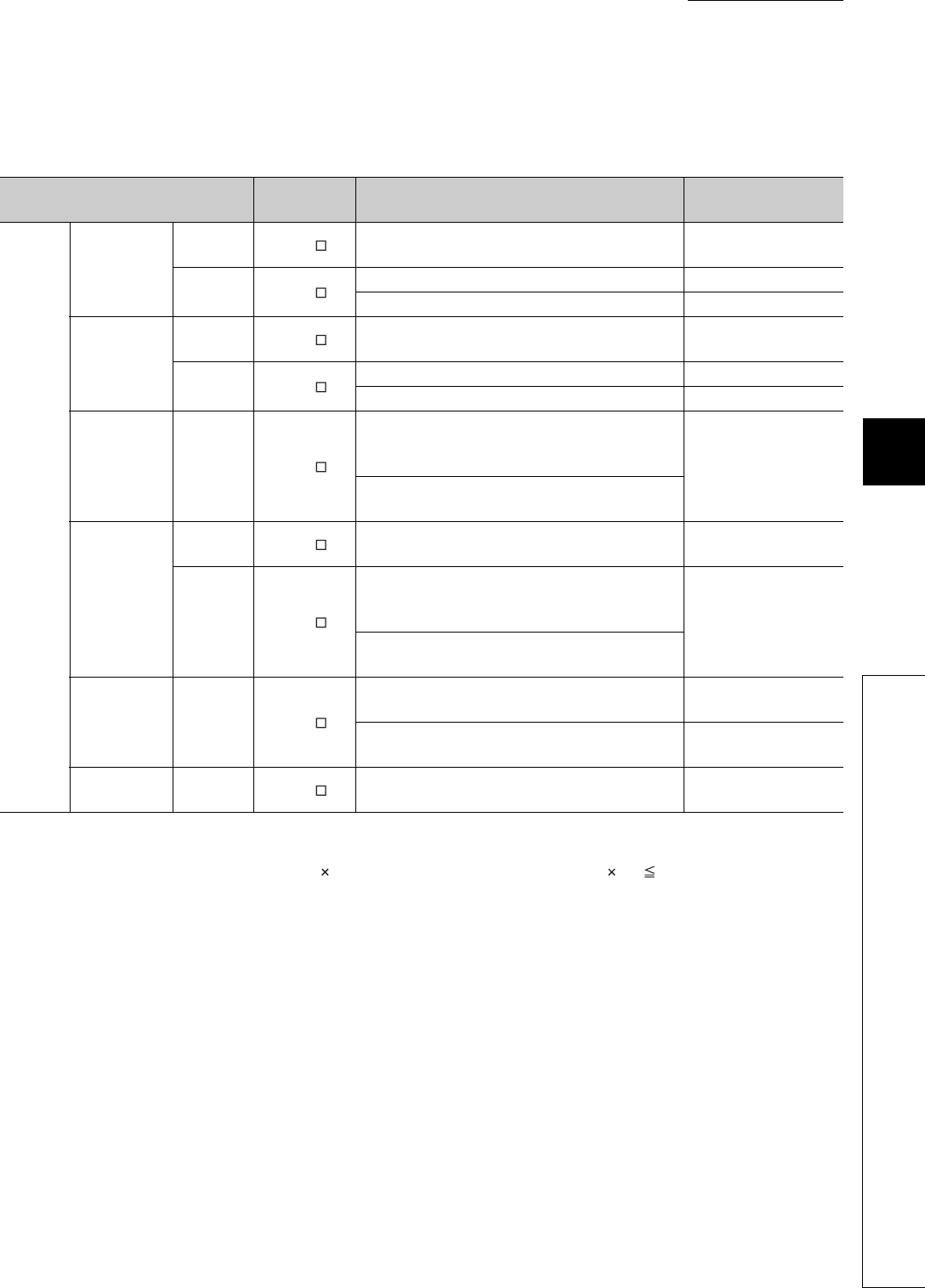
CHAPTER6 FUNCTIONS
1
2
3
4
5
6
7
8
6.23 Serial Communication Function
6 - 123
(3) Functions
Table6.40 shows the MC protocol commands that can be executed by the serial communication function.
*1: When writing data while the CPU module is in the RUN status, set "RUN write setting" to "Permit".
*2: Set the number of processing points within the range of the following calculation formula.
(number of word access points) 12 + (number of double word access points) 14 960
• One point of a bit device corresponds to 16 bits for word access or to 32 bits for double word access.
• One point of a word device corresponds to one word for word access or to two words for double word access.
Table6.40 MC protocol commands supported by the serial communication function
Function Command Processing Number of processing
points
Device
memory
Batch read
In units of
bits 0401(00 1) Reads bit devices in units of 1 point. ASCII: 3584 points
BIN: 7168 points
In units of
words 0401(00 0) Reads bit devices in units of 16 points. 480 words (7680 points)
Reads word devices in units of 1 point. 480 points
Batch write*1
In units of
bits 1401(00 1) Writes bit devices in units of 1 point. ASCII: 3584 points
BIN: 7168 points
In units of
words 1401(00 0) Writes bit devices in units of 16 points. 480 words (7680 points)
Writes word devices in units of 1 point. 480 points
Random read In units of
words 0403(00 0)
Reads bit devices in units of 16 points or 32 points
by specifying the device or device number at
random. 96 points
Reads word devices in units of 1 point or 2 points by
specifying the device or device number at random.
Test*1
(random write)
In units of
bits 1402(00 1) Sets/resets bit devices in units of 1 point by
specifying the device or device number at random. 94 points
In units of
words 1402(00 0)
Sets/resets bit devices in units of 16 points or 32
points by specifying the device or device number at
random. *2
Writes word devices in units of 1 point or 2 points by
specifying the device or device number at random.
Monitor
registration
In units of
words 0801(00 0)
Registers bit devices to be monitored in units of 16
points or 32 points. 96 points
Registers word devices to be monitored in units of 1
point or 2 points. 96 points
Monitor In units of
words 0802(00 0) Monitors devices registered for monitoring. Number of monitor
registration points
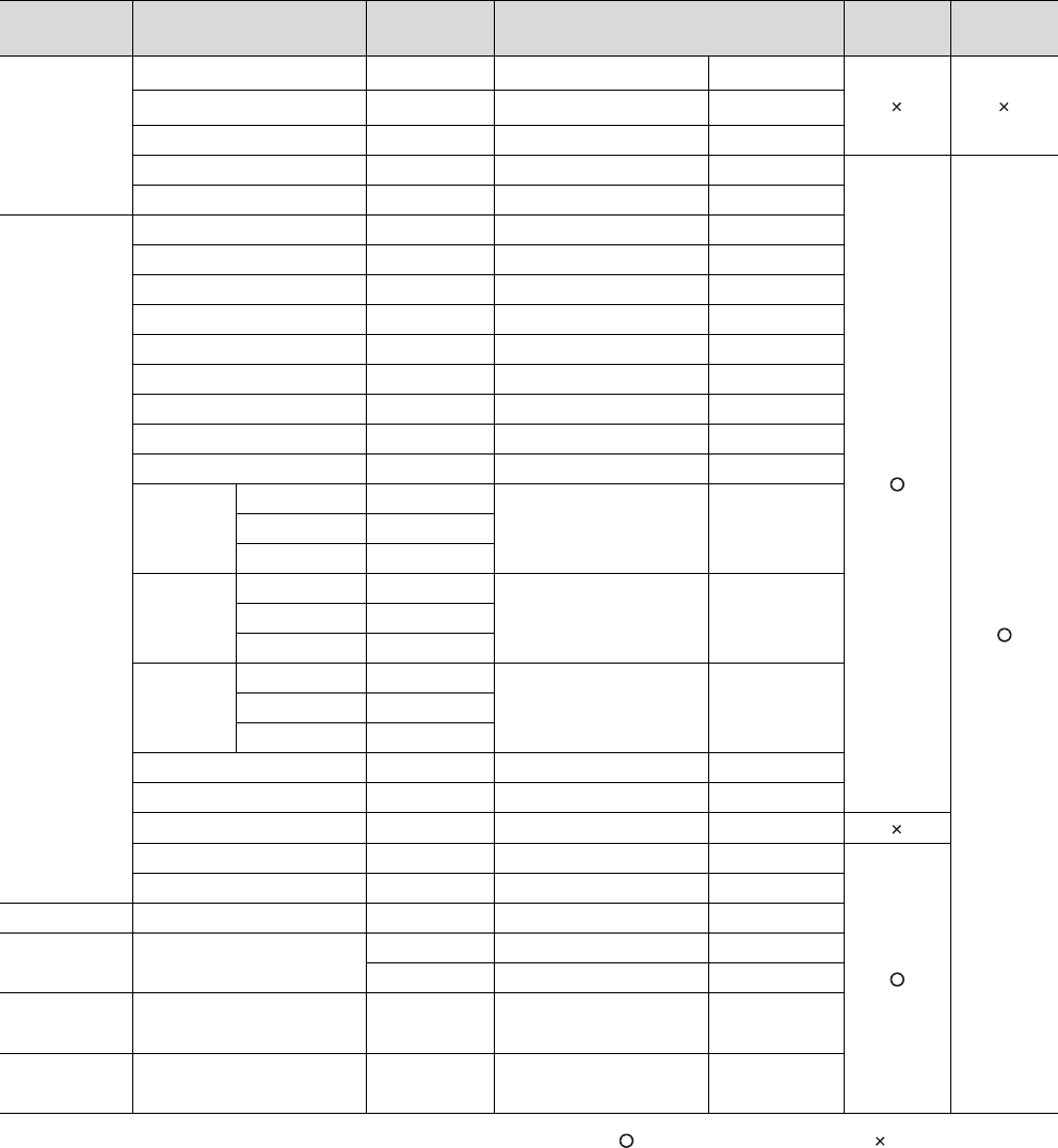
6 - 124
(4) Accessible devices
Table6.41 shows accessible devices by the serial communication function.
: Reading/writing are enabled. : Writing is prohibited.
*1: After changing the number of device points of the CPU module with GX Developer, use the devices within the new device number range.
Decimal and hexadecimal indicate whether a command specified for the MC protocol is decimal or hexadecimal.
*2: From 000005 to 00000F of FX and FY will be indefinite value.
*3: These registers are not supported by the Q00UJCPU.
Table6.41 Accessible devices by the serial communication function
Category Device Device code Device number range*1
(default value Write Read
Internal
system device
Function input FX*2 000000 to 00000F Hexadecimal
Function output FY*2 000000 to 00000F Hexadecimal
Function register FD 000000 to 000004 Decimal
Special relay SM 000000 to 002047 Decimal
Special register SD 000000 to 002047 Decimal
Internal user
device
Input X 000000 to 001FFF Hexadecimal
Output Y 000000 to 001FFF Hexadecimal
Internal relay M 000000 to 008191 Decimal
Latch relay L 000000 to 008191 Decimal
Annunciator F 000000 to 002047 Decimal
Edge relay V 000000 to 002047 Decimal
Link relay B 000000 to 001FFF Hexadecimal
Data register D 000000 to 012287 Decimal
Link register W 000000 to 001FFF Hexadecimal
Timer
Contact TS
000000 to 002047 DecimalCoil TC
Current value TN
Retentive
timer
Contact SS
000000 to 002047 DecimalCoil SC
Current value SN
Counter
Contact CS
000000 to 001023 DecimalCoil CC
Current value CN
Link special relay SB 000000 to 0007FF Hexadecimal
Link special register SW 000000 to 0007FF Hexadecimal
Step relay S 000000 to 008191 Decimal
Direct input DX 000000 to 000FFF Hexadecimal
Direct output DY 000000 to 000FFF Hexadecimal
Index register Index register Z 000000 to 000019 Decimal
File register*3 File register R 000000 to 032767 Decimal
ZR 000000 to 3FD7FF Hexadecimal
Extended data
register*3 Extended data register D 000000 to 093183 Decimal
Extended link
register*3 Extended link register W 000000 to 016BFF Hexadecimal
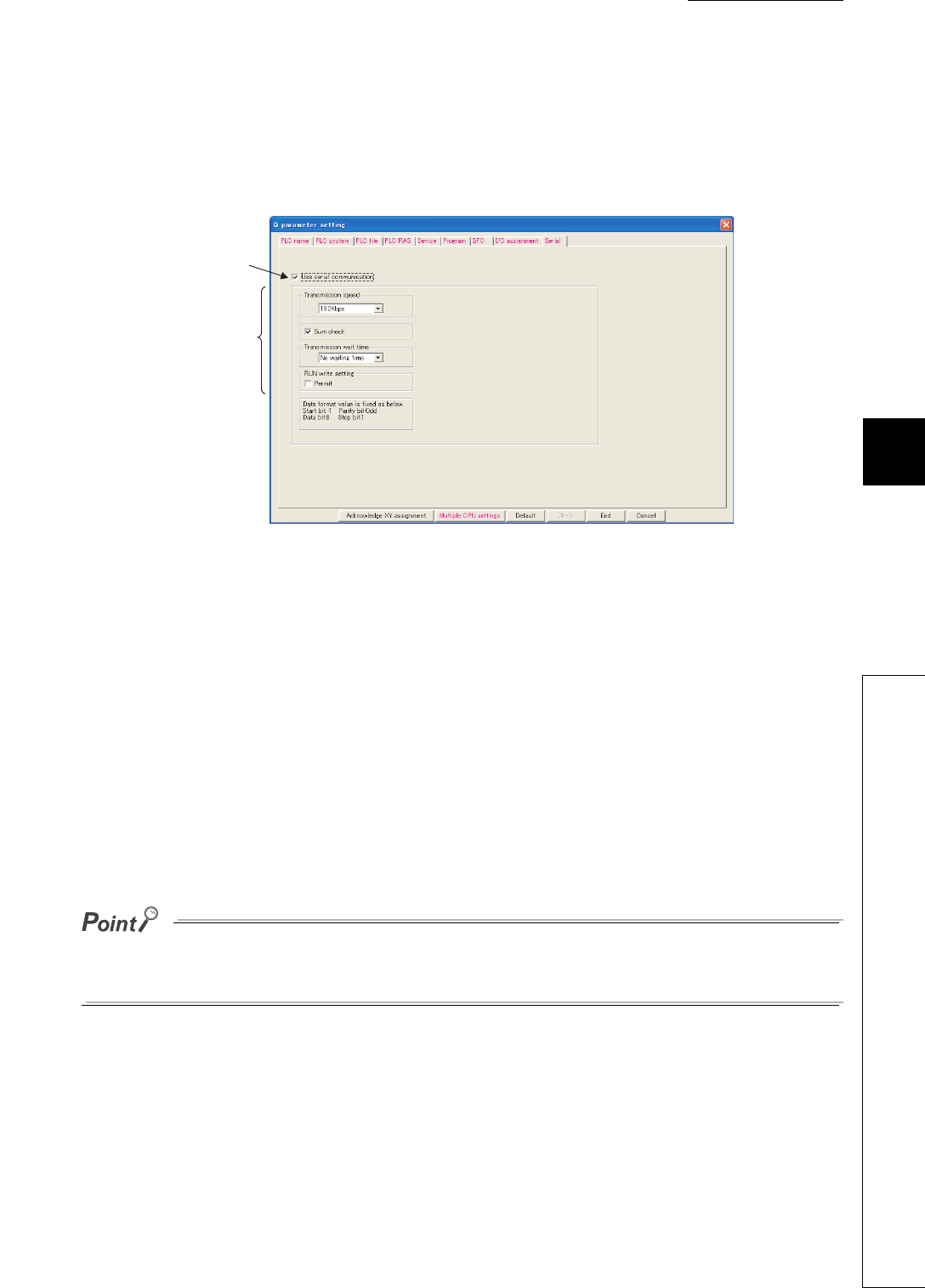
CHAPTER6 FUNCTIONS
1
2
3
4
5
6
7
8
6.23 Serial Communication Function
6 - 125
(5) Setting of transmission specifications
Set Transmission speed, Sum check, Transmission wait time, and Run write setting of the serial communication
function in the Serial tab of the PLC parameter dialog box.
• Select "Use serial communication" in communication with the personal computer or HMI.
• Set Transmission speed, Sum check, Transmission wait time, and Run write setting in the tab.
(6) Precautions
(a) Switching connection to GX Developer during communication with such as HMI
The CPU module can switch connection to GX Developer during communication with the personal computer or
HMI with the serial communication function.
However, the personal computer or HMI in communication by the serial communication function results in a
communication error.
For startup methods of the personal computer and HMI when they are reconnected to the CPU module, refer to
the manual for used device.
(b) Transmission speed set in the Transfer Setup screen
When "Use serial communication" is selected, the transmission speed set in the Transfer setup screen of GX
Developer is ignored.
The data set in the "Serial" tab is valid when:
• the CPU module is powered on, or
• the CPU module is reset.
Figure 6.94 Serial tab
Set Transmission speed, Sum
check, Transmission wait time,
and Run write setting.
Click here to use the serial
communication function.
6 - 126
(c) Communication error
If any of the following status is met, responses are not returned and therefore communication cannot be made.
Review the transmission frame.
1) The serial communication function is set not to be used.
2) Communication is made at different transmission speed and data format.
3) A frame to be sent has no correct starting end or terminal.
• 3C frame format 4: ENQ/CR + LF
• 4C frame format 4: ENQ/CR + LF
• 4C frame format 5*1: DLE+STX/DLE + ETX
*1: When "Sumcheck enable" is set, the sumcheck code is included.
4) The frame identification number of a frame to be sent is incorrect.
5) The number of transmission bytes is under the header part size.

CHAPTER6 FUNCTIONS
1
2
3
4
5
6
7
8
6.23 Serial Communication Function
6 - 127
(7) Error codes during communication with the serial communication function
Table6.42 shows the error codes, error description, and corrective actions sent from the CPU module to the
external device when an error occurs during communication with the serial communication function.
Table6.42 Error codes sent from the CPU module to external device
Error code
(hexadecimal) Error item Description Corrective action
4000H
-
Error detected by the CPU module
(error occurred by other than the serial
communication function)
Refer to the QCPU Userís Manual (Hardware Design,
Maintenance and Inspection), and take corrective action.
to
4FFFH
7155HUnregistered
monitor error
A monitor request was given before monitor
registration.
Give a monitor request after registering a device to be
monitored.
7157HRequest target
specification error
Other than the Q00UJCPU, Q00UCPU,
Q01UCPU, and Q02UCPU was selected as a
request module and route.
Check that the transmission message address is Q00UJCPU,
Q00UCPU, Q01UCPU, Q02UCPU, modify the setting and
communicate again.
7164HRequest data error The requested data or device specification
method is wrong.
Check the sent message/requested data of the external
device, correct it, and restart communication.
7167HDisabled during
RUN
A write command was specified while online
change is disabled. Enable the online change and restart communication.
7E40HCommand error A subcommand or a command that does not exist
is specified.
Check and correct the sent message of the external device
and restart communication.
7E41HData length error
The number of points specified for random write/
read exceeds the number of points enabled for
communication.
Check and correct the sent message of the external device
and restart communication.
7E42HData count error The requested number of points exceeds the
range of the command.
Check and correct the sent message of the external device
and restart communication.
7E43HDevice error
The device specified does not exist.
The device specified cannot be specified by the
corresponding command.
Check and correct the sent message of the external device
and restart communication.
7E47HContinuous
request error
The next request was received before the
response message was returned.
Do not give continuous requests from the external device.
Match the monitoring time of timer 1 with the time-out time of
the external device.
7F21HReceive header
section error
The command (frame) section specified is in error. Check and correct the sent message of the external device
and restart communication.
The ASCII code received cannot be converted
into binary.
7F22HCommand error The command or device specified does not exist. Check and correct the sent message of the external device
and restart communication.
7F23HMC protocol
message error
The data (such as ETX, CR+LF) specified after
the character part does not exist or in error.
Check and correct the sent message of the external device
and restart communication.
7F24HSumcheck error The calculated sumcheck does not match the
received sumcheck. Review the sumcheck of external device.
7F67HOverrun error The next data was received before the CPU
module completed receive processing.
Reduce the communication speed and restart communication.
Check the CPU module for momentary power failure.
(For the CPU module, use the special register SD53 to check.)
When an momentary power failure occurs, remove its cause.
7F68HFraming error The stop bit setting does not match. Match the setting of the CPU module with that of the external
device.
7F69HParity error The parity bit setting does not match. Match the setting of the CPU module with that of the external
device.

6 - 128
6.24 Service Processing
6.24.1 Service processing setting
(1) Definition
This function allows to set the time and the number of times of service processing performed at END processing
by parameters.
This function also improves the response of communication with a peripheral and restrains the increase of scan
time due to service processing.
This achieves the configuration of service processing environment optimum for the system.
The service processing refers to communication service processing with a peripheral (such as GX Developer) and intelligent
function modules. Link refresh processing such as CC-Link IE controller network module, MELSECNET/H module, and CC-
Link Safety system master/local module are not included.
Using the COM instruction enables service processing during program execution of same performance with
service processing at END processing. Therefore, the high-speed service processing response can be performed
even if the scan time is long.
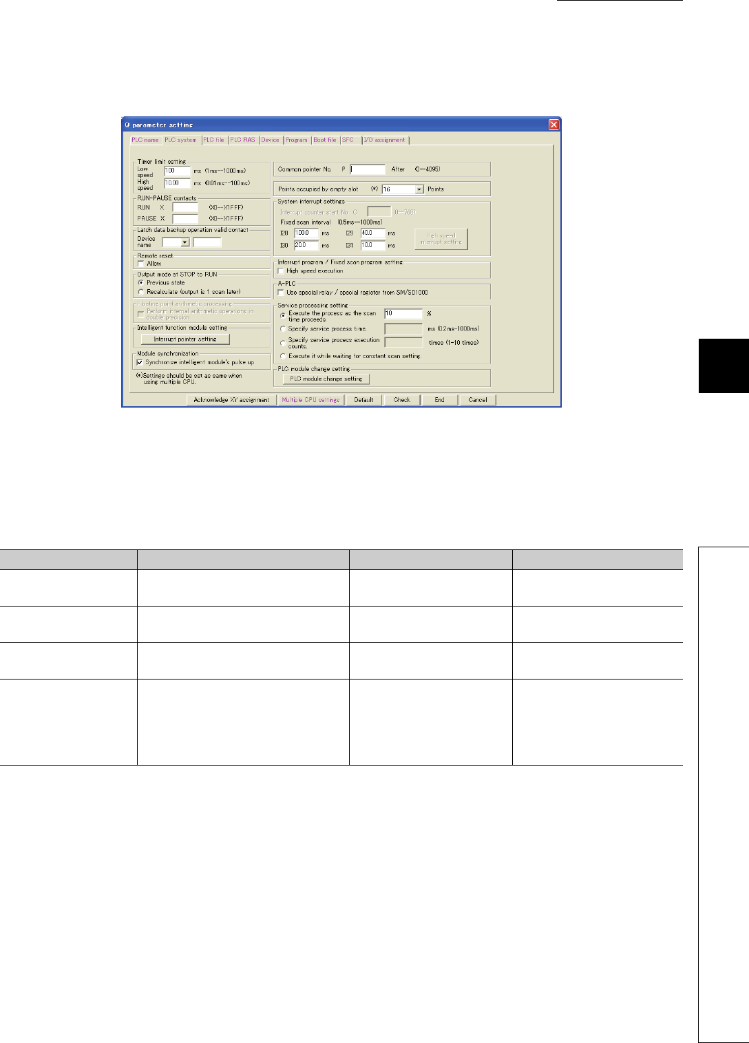
CHAPTER6 FUNCTIONS
1
2
3
4
5
6
7
8
6.24 Service Processing
6.24.1 Service processing setting
6 - 129
(2) Parameter setting
Set the parameters in the PLC system tab of the PLC parameter dialog box.
To perform the service processing, select any of the parameter items in Table6.43.
The setting value of deselected parameter cannot be entered (default: Execute the process as the scan time
proceeds. = 10%).
Figure 6.95 Parameter setting screen
Table6.43 Parameter items
Item Description Setting range Remarks
Execute the process as
the scan time proceeds.
Set the percentage of service processing
for one scan.
• Range: 1 to 99%
• Unit: 1% Default when selected =10%
Specify service process
time.
Set the time of service processing for one
scan.
• Range: 0.2ms to 1000ms
• Unit: 0.1ms Default when selected =0.2ms
Specify service process
execution counts.
Set the number of service processing for
one scan.
• Range: 1 to 10 times
• Unit: 1 time
Default when selected
=1 time
Execute it while waiting
for constant scan setting.
Set whether to perform service
processing during waiting time for
constant scan setting.
-
Even when the waiting time is
0.2ms or less, the service
processing time (0.2ms) will be
added to the scan time at service
processing execution.
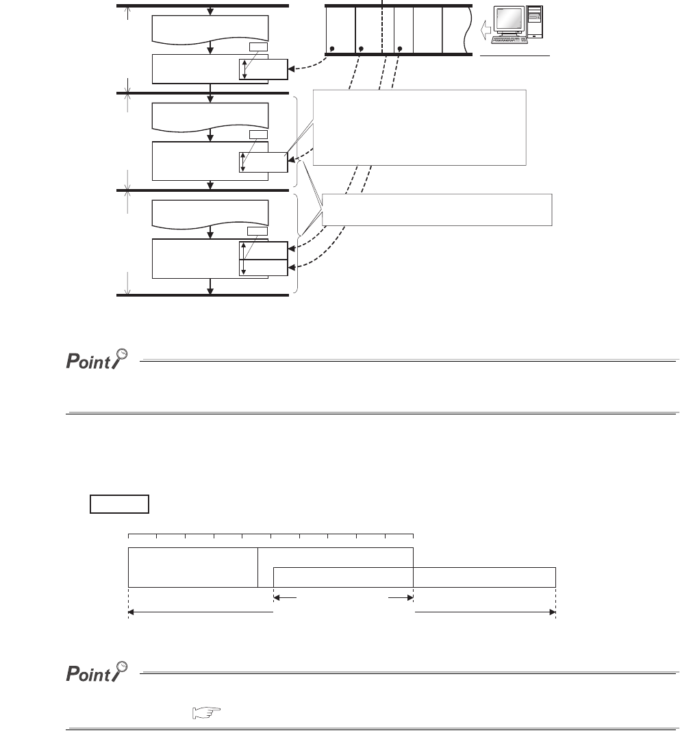
6 - 130
(3) Operations for service processing setting
Operations for each service processing setting is described below.
(a) Operation when "Execute the process as the scan time proceeds." is selected
1) Operation when 10% is set
If no request data for service processing exists, END processing speeds up by the request processing time. (The CPU
module does not wait for requests.)
2) Operation for constant scan setting
The calculation of the service processing time is a calculation of the percentage of the time excluding the
waiting time of the constant scan from the scan time, not a calculation of the percentage of the scan time.
Operation when 50% is set
When setting the constant scan, selecting "Execute it while waiting for constant scan setting." can perform the service
processing efficiently. ( (3)(d) in this section)
Figure 6.96 Operation when 10% is set
Figure 6.97 Operation for constant scan setting
Program execution
END processing
1st scan
(10ms)
Request 1
Program execution
END processing
2nd scan
(10ms)
Request 2-1
Program execution
END processing
3rd scan
(12ms)
Request 3
GX Developer
1ms
1ms
1.2ms
The service processing time depends on the
scan time (program execution time).
When the time required for processing
one request exceeds 10% of one scan
time, the service processing is suspended
and the request is processed at END
processing in the next scan.
Request 1
Request 2
Request 3
Request 4
Request 5
Request 2-2
Example
Program execution
END processing
Waiting time
Service processing
Scan time (constant scan setting)
0% 50% 100%
Service processing time
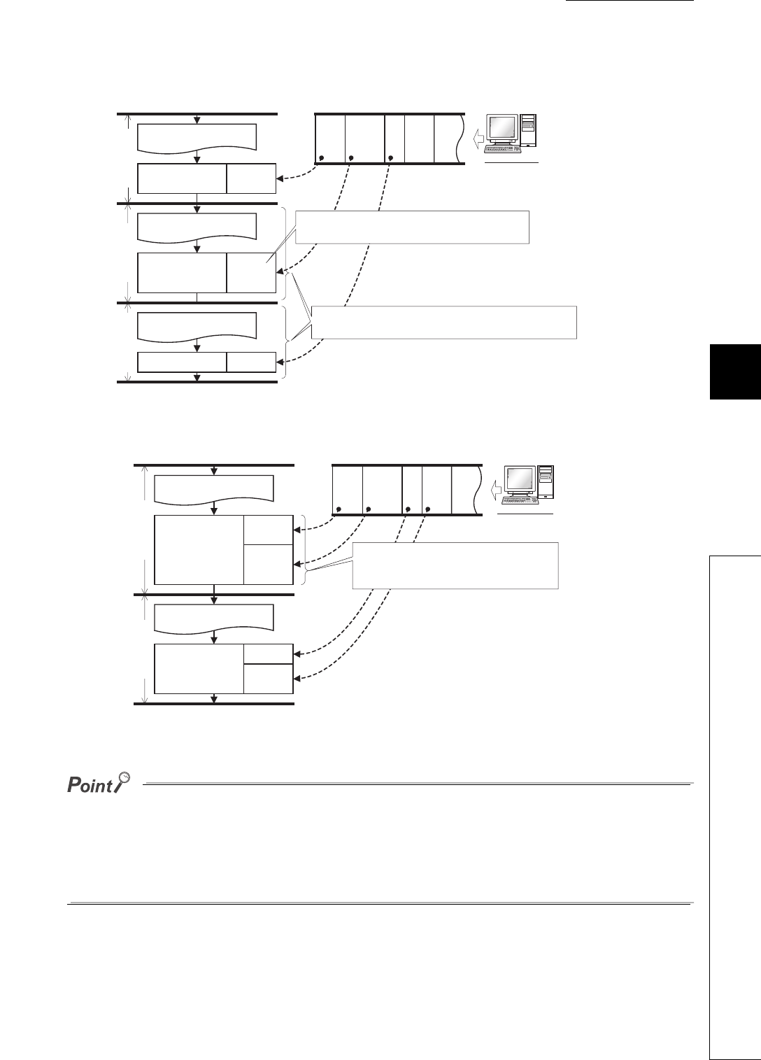
CHAPTER6 FUNCTIONS
1
2
3
4
5
6
7
8
6.24 Service Processing
6.24.1 Service processing setting
6 - 131
(b) Operation when "Specify service process execution counts." is selected
1) Operation when 1 time is set
2) Operation when 2 times is set
●When several devices are connected to one CPU module, each device requests service processing.
When the CPU module receives requests from several devices simultaneously, a single END processing can accept
several requests simultaneously if the service processing count is set to the number of connected devices. This
improves response performance. (Note that the scan time increases by the service processing time.)
●If no request data exists when setting the service processing count, END processing speeds up by the request
processing time. (The CPU module does not wait for requests.)
Figure 6.98 Operation when 1 time is set
Figure 6.99 Operation when 2 times is set
Program execution
END processing
1st scan
Request 1
Program execution
END processing
2nd scan
Request 2
Program execution
END processing
3rd scan
Request 3
GX Developer
Regardless of request data size, one request
is processed at one END processing.
Even if the program execution time are the same,
the scan time depends on service processing time.
Request 1
Request 2
Request 3
Request 4
Request 5
Program execution
END processing
1st scan
Request 1
Program execution
END processing
2nd scan
Request 2
Request 3
GX Developer
Request 4
Regardless of request data size,
two requests are processed at
one END processing.
Request 1
Request 2
Request 3
Request 4
Request 5
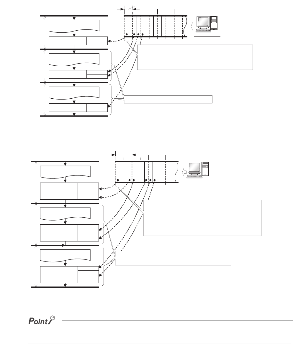
6 - 132
(c) Operation when "Specify service process time." is selected
1) Operation when 0.5ms is set
2) Operation when 1ms is set
If no request data exists when setting the service processing time, END processing speeds up by the request processing
time. (The CPU module does not wait for requests.)
Figure 6.100 Operation when 0.5ms is set
Figure 6.101 Operation when 1ms is set
Program execution
END processing
1st scan
Request 1
Program execution
END processing
2nd scan
GX Developer
Program execution
END processing
3rd scan
Request 1
Request 2
Request 2
0.5ms
When the time required for processing one request
exceeds the service processing time (0.5ms) , the
service processing is suspended and the processing
is performed at END processing in the next scan.
The scan time increases equally.
Request 1
Request 2
Request 3
Request 4
Request 5
Program execution
END processing
1st scan
Request 1
Program execution
END processing
2nd scan
GX Developer
Program execution
END processing
3rd scan
Request 2
Request 2
Request 3
1ms
Request 3
Request 4
Several requests are processed until the time exceeds
the specified service processing time (1ms).
When the time exceeds the specified service
processing time, the service processing is suspended
and the request is processed continuously at END
processing of next scan.
Although multiple processing is performed at
one END processing, the scan time increases equally.
Request 1
Request 2
Request 3
Request 4
Request 5
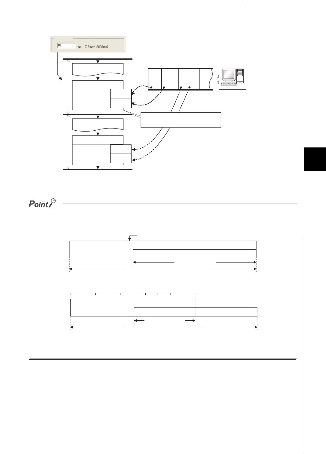
CHAPTER6 FUNCTIONS
1
2
3
4
5
6
7
8
6.24 Service Processing
6.24.1 Service processing setting
6 - 133
(d) Operation when "Execute it while waiting for constant scan setting." is selected
●When setting the constant scan, selecting "Execute it while waiting for constant scan setting." can perform the service
processing efficiently.
• When "Execute it while waiting for constant scan setting." is selected
• When "Execute the process as the scan time proceeds." is selected (50% is set.)
●Even when there is no waiting time, the service processing (0.2ms) is performed. Therefore, when the waiting time is
less than 0.2ms, the constant scan time may be exceeded.
Figure 6.102 Operation when "Execute it while waiting for constant scan setting." is selected
Program execution
Waiting time
END processing
Program execution
END processing
Constant scan
GX Developer
Request 1
Request 2
Request 3
Request 4
Waiting time
Constant scan
The service processing is performed
during waiting time.
Request 1
Request 4
Request 2
Request 3
Request 5
Constant scan
Program execution
END processing
Wait time
Service processing
Scan time (constant scan setting)
Service processing time
Program execution
END processing
Wait time
Service processing
Scan time (constant scan setting)
0% 50% 100%
Service processing time

6 - 134
(4) Precautions
The following describes precautions when the service processing setting is configured.
1) For the following functions, scan time will be increased longer than the specified time during service
processing even if the service processing time specification is set.
• Online change
• Change T/C setting
• Local device monitor
• Program memory backup
• Writing to/reading from a file register (The scan time will be increased when the write or read size is
large.)
• Writing to/reading from the buffer memory of the intelligent function module (The scan time will be
increased when the write or read size is large.)
• Access to a network module
a) Diagnostic functions (CC IE Control diagnostics, MELSECNET diagnostics, Ethernet diagnostics,
CC-Link/ CC-Link/LT diagnostics)
b)
Monitor function (Module access device, Link direct device)
2) Note that the scan time will be increased much longer if the CPU module receives multiple requests
simultaneously while the service processing count specification is set many.
3) When setting the service processing time much shorter than the scan time, the response performance of
service processing is extremely reduced. Set the service processing time with considering the time-out
time of a peripheral.
4) An error of -20 s to +30 s occurs between the actual processing time and the set service processing
time.
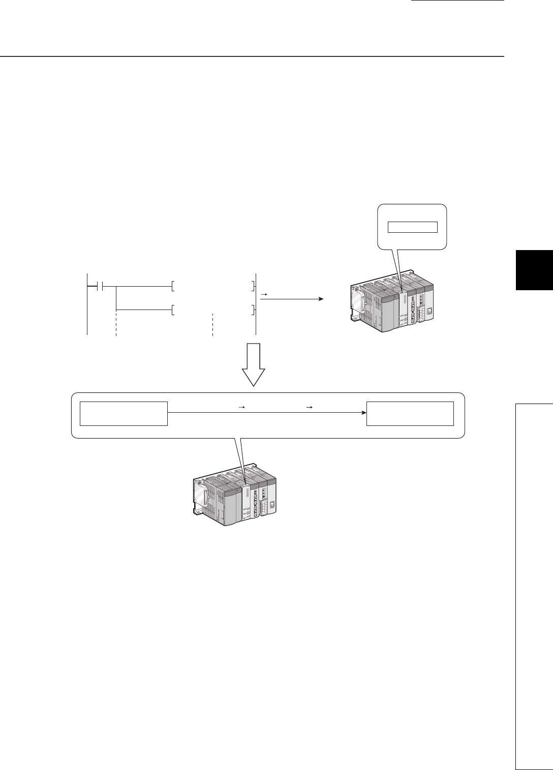
CHAPTER6 FUNCTIONS
1
2
3
4
5
6
7
8
6.25 Initial Device Value
6 - 135
6.25 Initial Device Value
(1) Definition
This function registers data used in a program to the device or the buffer memory of the intelligent function
module without a program.
(2) Application
Using an initial device value can omit device data setting program by initial processing program.
Figure 6.103 Data setting by initial program
MOV H100 D0
MOV H2020 D1
Power-on/STOP/RESET
RUN
Device memory
Initial device value
Device memory
At power-off on, reset, or STOP RUN
SM402
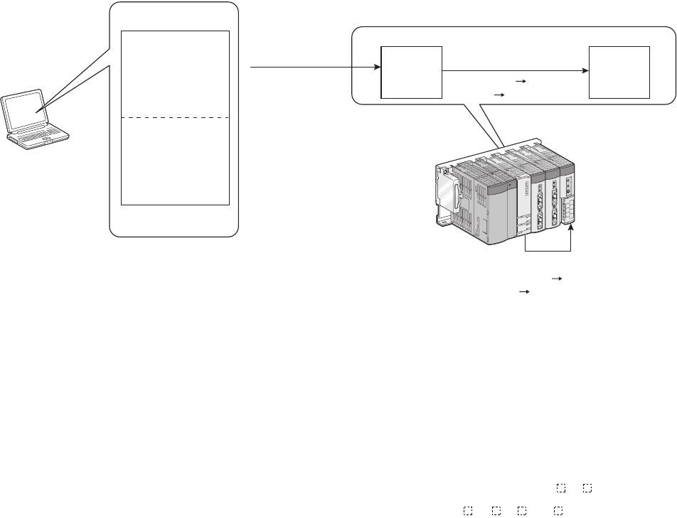
6 - 136
(3) Timing when initial device values are written to the specified device
The CPU module writes data in the specified initial device value file to the specified device or the buffer memory
of the intelligent function module when the CPU module is powered off and then on, is reset, or is set to the STOP
status and then the RUN status.
(4) Devices that can be used*1
The following shows devices that can be used for initial device value.
*1: For available ranges, refer to Section 9.1.
*2: The extended data register (D) is included.
*3: The extended link register (W) is included.
Figure 6.104 Flow of writing initial device value
• Current timer value (T) • Link special register (SW)
• Current retentive timer value
(ST) • File register (R)
• Current counter value (C) • File register (ZR)
• Data register (D)*2 • Intelligent function module device (U \G )
• Special register (SD) • Link direct device (J \W , J \SW )
• Link register (W)*3
Specified
device
Initial
device
value file (At power-off on, reset,
or STOP RUN)
Program memory
Setting of
initial device
value range
Setting of
initial device
value range
Writing of initial
device value
Writing of initial device value
(at power off on, reset, or
STOP RUN)
GX Developer
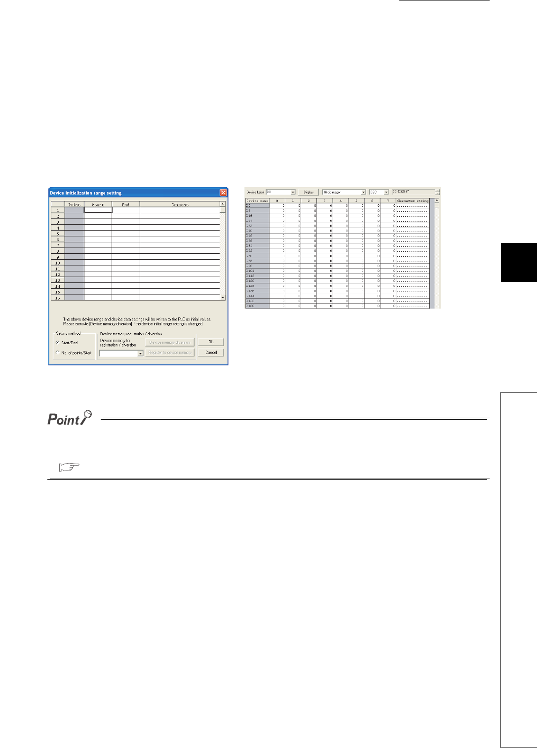
CHAPTER6 FUNCTIONS
1
2
3
4
5
6
7
8
6.25 Initial Device Value
6 - 137
(5) Procedures and settings for using initial device values
To use initial device values, create initial device value data with GX Developer beforehand, and store the data as
a initial device value file in the program memory, standard ROM, or memory card of the CPU module.
• Add an initial device value data to the project data list of GX Developer.
The Device initialization range setting screen appears. Set the initial device value range.
The number of settable points is up to 8000 points per range setting.
• Add device memory data in the project data list of GX Developer.
The device memory screen appears. Set the initial device value data within the initial device value range set
above.
When changing the setting on the Device initialization range setting screen, always execute "Device memory registration/
diversion".
For details of the "Device memory registration/diversion", refer to the following.
GX Developer Version 8 Operating Manual
Figure 6.105 Device initialization range setting screen and device memory screen
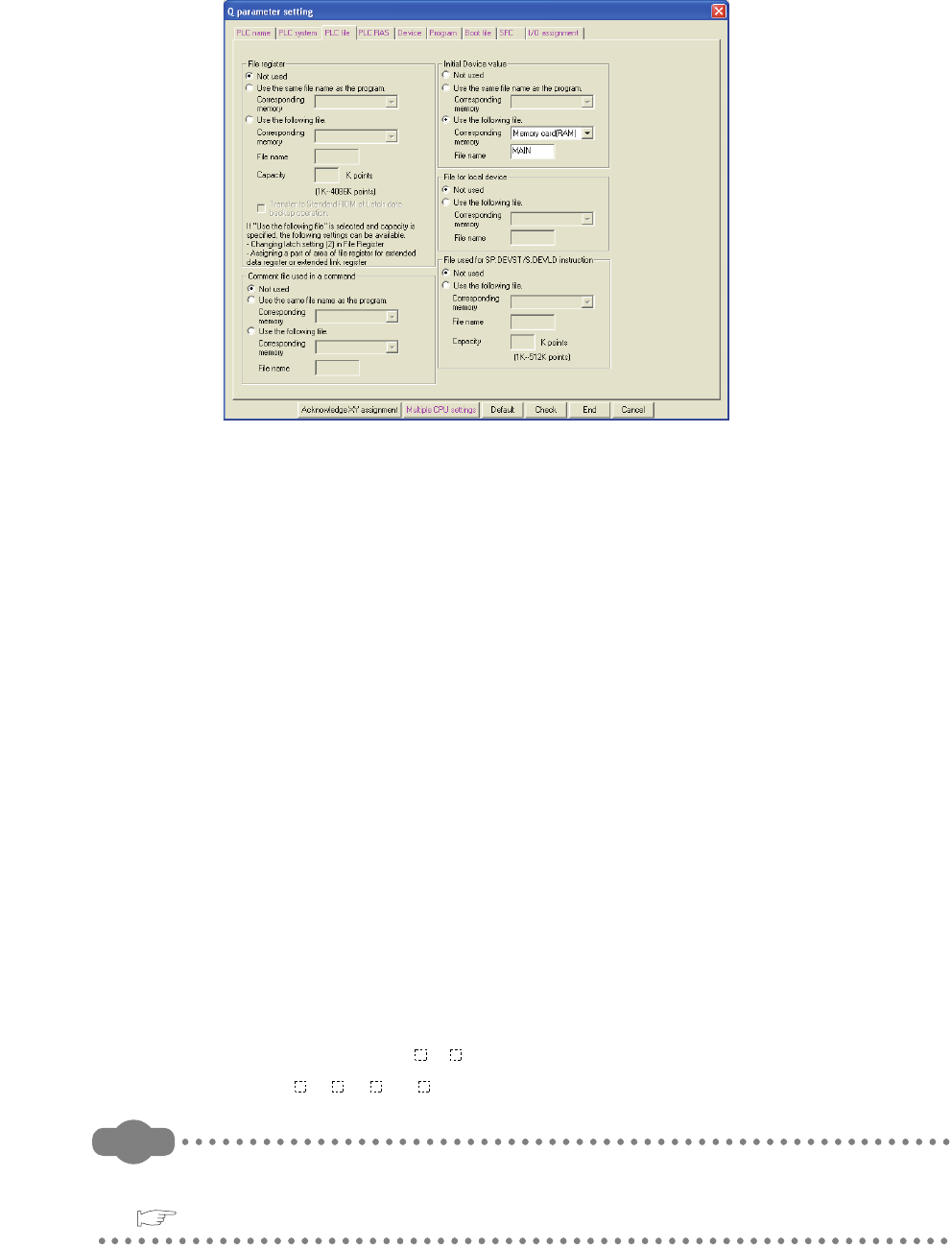
6 - 138
• Select the name of a file where the initial device value data are stored in the PLC file tab of the PLC
parameter dialog box.
• Write the set initial device value and parameters to the CPU module.
(6) Precautions
(a) When initial device value and latch range are overlapped
In that case, initial device value takes priority. Therefore, the latch range data will be overwritten to the initial
device value data after the CPU module is powered off and then on.
(b) Area disabling the initial device value setting when the CPU module is set from
STOP to RUN
The initial device value are also reflected when the CPU module is set from STOP to RUN.
For an area where an initial device value is not to be set when the CPU module is set from STOP to RUN (data
that are set when the CPU module is powered off and then on and changed by a program), the initial device
value cannot be used.
Use an instruction such as the MOV instruction in the main routine program so that the initial device values will
be set to the specified devices.
Use the TO instruction to write data to the buffer memory of the intelligent function module.
(c) Devices that require module synchronization setting
When setting the following devices in the Device initialization range setting screen, set "Module
synchronization" in the PLC system tab of the PLC parameter dialog box.
If the setting is not configured, the initial device values may not be set to the target module properly.
• Intelligent function module device (U \G )
• Link direct device (J \W , J \SW )
Remark
For details of the initial device value range setting, setting of the initial device value data, and writing of the initial device
values to the CPU module, refer to the following.
GX Developer Version 8 Operating Manual
Figure 6.106 PLC file tab
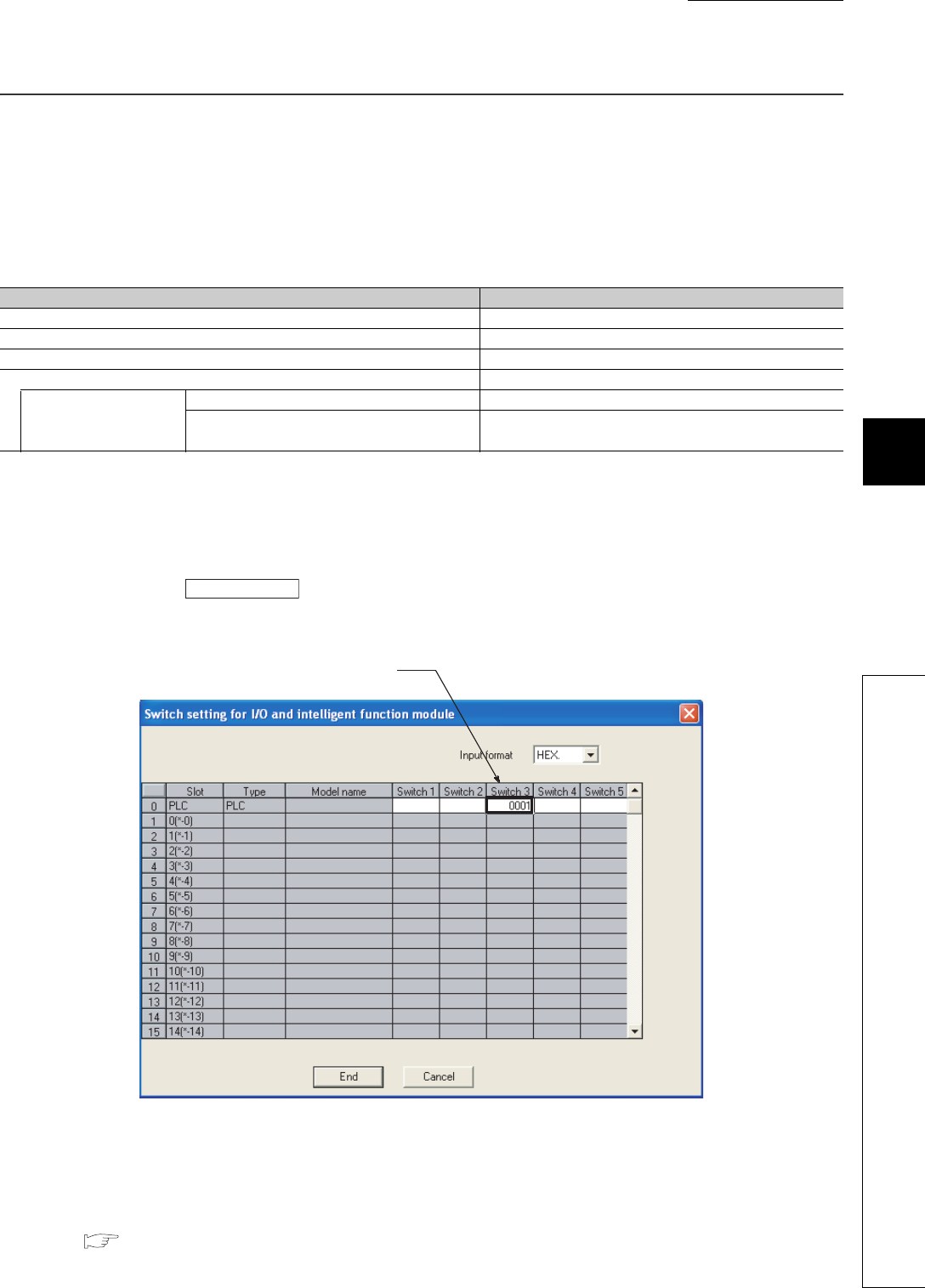
CHAPTER6 FUNCTIONS
1
2
3
4
5
6
7
8
6.26 Battery Life-prolonging Function
6 - 139
6.26 Battery Life-prolonging Function
(1) Definition
This function extends the life of battery installed in the CPU module by restricting data to be held by the battery to
clock data only.
This function initializes all data other than the clock data when the CPU module is powered off or is reset.
(2) Setting
Set the function in the I/O assignment tab of the PLC parameter dialog box.
1) Configure the I/O assignment setting.
2) Click the button.
3) Enter 0001H to the switch 3 of the slot where the CPU module is mounted (When entering the value to a slot
in another station, the value is ignored).
(3) Battery life
For the life of battery installed in the CPU module when the battery life-prolonging function is used, refer to the
following.
QCPU User's Manual (Hardware Design, Maintenance and Inspection)
Table6.44 Initialization details
Data held by a battery Description
Error history The number of error history data is initialized to zero.
Latch device (L) Cleared to zero.
Device in the latch range Cleared to zero.
Standard RAM Formatted (cleared to zero).
File register assigned to
the standard RAM
Set "Use the same file name as the program." A file is deleted.
Set "Use the following file". A file is deleted (A file is recreated at power-on or reset
(Data is cleared to zero.).)
Figure 6.107 Switch setting screen
Switch setting
Enter 0000H.

6 - 140
6.27 Memory Check Function
This function checks whether data in the memories of the CPU module are not changed due to such as excessive
electric noise.
Since the CPU module automatically checks a memory, setting for enabling this function is unnecessary.
This function does not require processing time.
(1) Data to be checked
(a) Program
The program during execution is compared with the user program written to the program memory.
If they do not match, a stop error, “RAM ERROR” (error code: 1160) is detected.
(b) Parameter
The parameters are compared with the ones written to the parameter-valid drive.
(c) Device memory
If the devices cannot be read, a stop error, “RAM ERROR” (error code: 1161) is detected.
(2) Execution timing
1) Program: At program execution
2) Parameter:
• When the CPU module is powered off and then on
• When the CPU module is reset
• When the CPU module is set from STOP to RUN after data are written to it
3) Device memory: When device data are read

CHAPTER6 FUNCTIONS
1
2
3
4
5
6
7
8
6.28 Latch Data Backup to Standard ROM Function
6 - 141
6.28 Latch Data Backup to Standard ROM Function
(1) Definition
This function holds (backs up) latch data, such as device data and error history, to the standard ROM without
using a battery when the system is stopped for a long period. This function helps to extend battery life.
Remark
When this function is performed, the battery life-prolonging function is enabled regardless of the parameter setting for the
battery life-prolonging function.
Also, the battery life-prolonging function is switched to be disabled after backup data are restored.
The setting status of the battery life-prolonging function can be checked by SD119 (battery life-prolonging factor).
For details of the battery life-prolonging function, refer to Section 6.26.
(2) Data to be backed up
Table6.45 shows data to be backed up.
*1: The data are backed up only when the Universal model QCPU having the serial number (first five digits) is "10042" or later is used.
Table6.45 Data to be backed up
Data to be backed up Description Remarks
Device data
• Internal user device (M, L, B, F, V, T, ST,
C, D, W)
• Index register (Z)/standard device
register (Z)
• File register (R, ZR)
• Extended data register (D)*1
• Extended link register (W)*1
The data of the file register, extended data
register (D), and extended link register (W) are
backed up only when the file register in the
standard RAM is used
Error history
Error history data immediately before the
latch data backup function to standard
ROM function is performed
-
Module error collection file Information on errors occurred in the
connected intelligent function modules
The data are backed up independent of the
setting of the module error collection.
SFC program continuation start
information
Information to start the SFC program
continuously -
Trace setting
(Sampling trace file)
Trace condition settings and Trace data
settings created by the sampling trace
function.
Data cannot be backed up in the following cases.
• Trace setting is made in a memory card.
• Trace setting is not registered with the CPU
module.
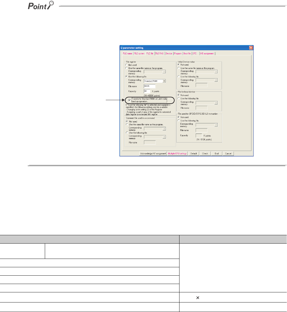
6 - 142
When backing up the data in the file register, extended data register (D), and extended link register (W), pay attention to the
following.
• The data are backed up only when the file register in the standard RAM is set to be used.
• Select "Transfer to Standard ROM at Latch data backup operation." on the PLC file tab of the PLC parameter
dialog box.
(3) File size for storing backup data
The system automatically creates storage file for backup data when the latch data backup function to standard
ROM is performed.
Table6.46 shows the size of storage file.
*1: The file size of the Q00UJCPU,Q00UCPU,Q01UCPU,and Q02UCPU is 87210 bytes.
*2: The size depends on the parameter setting.
*3: Storage files are created only when data in the file register, extended data register (D), and extended link register (W) are backed up.
*4: Storage files are created only when the trace registration has been made.
*5: The file size of the Q00UJCPU, Q00UCPU, and Q01UCPU is 89790 bytes and that of the Q02UCPU is 93630 bytes.
Figure 6.108 PLC file tab
Table6.46 Sizes of files to be stored
Data to be backed up File size
Device data Internal user device (M, L, B, F, V, T, ST, C, D, W)
Index register (Z)/standard device register (Z)
• Serial number (first five digits) is "11042" or
earlier: 110890 bytes*1
(When the default device assignment is set)*2
• Serial number (first five digits) is "11043" or
later: 117310 bytes*5
(When the default device assignment is set)*2
Error history
SFC program continuation start information
Module error collection file (stored in system memory.)
Module error collection file (stored in standard RAM.)
File register (R, ZR)*3, extended data register (D)*3, extended link register (W)*3 64 + 2 Number of file register points
ÉgTrace setting (sampling trace file)*4 16 + Sampling trace file size
Selecting this option
starts backup.
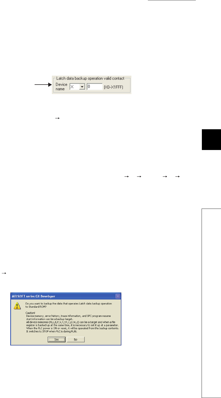
CHAPTER6 FUNCTIONS
1
2
3
4
5
6
7
8
6.28 Latch Data Backup to Standard ROM Function
6 - 143
(4) Execution method
(a) Execution by contacts
1) Setting method
Set "Latch data backup operation valid contact" in the PLC system tab of the PLC parameter dialog box
(Devices X, M, or B can be selected).
2) Execution method
Backup starts at the rise of a contact (off on).
After backup, the BAT.LED of the CPU module flashes (green), indicating that the CPU module is in the
standby status ready to be powered off.
3) Precautions
a)Since data to be backed up is the data when a contact is on (END processing), the CPU module will not
become the RUN status until the CPU module is powered on again or is reset after this operation.
b) Since the status of latch data backup start contact to the standard ROM is checked at execution of the
END instruction, data are not backed up even if a contact is turned on off on, or off on off in
one scan.
c) In the following cases, data are not backed up unless the latch data backup start contact to the standard
ROM is turned off and then on again.
• The latch data backup start contact to the standard ROM is set to X, and the CPU module is powered
off and then on or is reset after backup by turning off and then on the contact.
• The latch data backup start contact to the standard ROM is set to M or B, and data are backed up by
turning off and then on the contact.
(b) Execution by remote operation
1) Execution method
Select [Online] [Latch data backup operation] of GX Developer.
After backup, the BAT.LED of the CPU module flashes (green), indicating that the CPU module is in the
standby status ready to be powered off.
Data to be backed up is the data at the execution of remote operation.
Figure 6.109 Setting screen of latch data backup start contact to standard ROM
Figure 6.110 Remote operation execution screen
Specify a contact
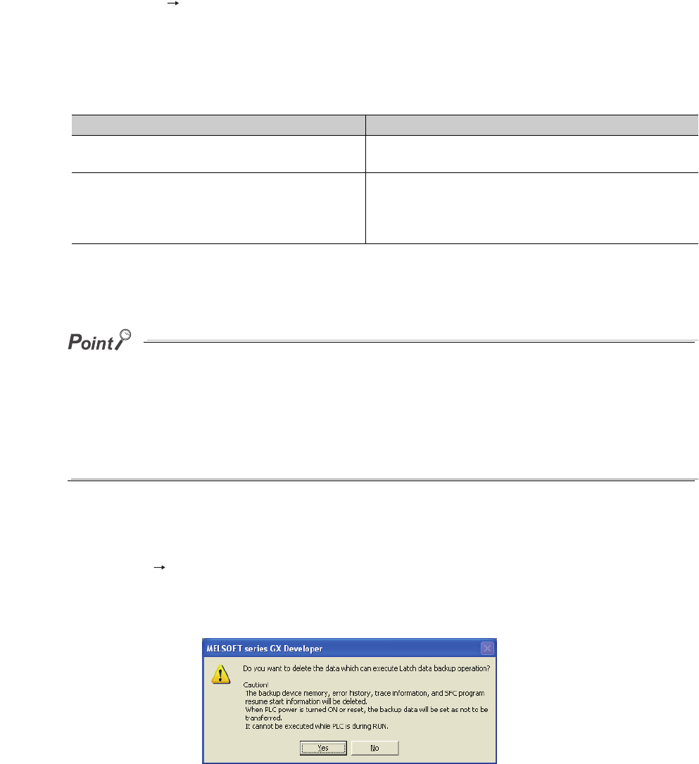
6 - 144
(5) Restoring backup data
The backup data is automatically restored by the following operations.
• At power-off on of the CPU module
•At reset
Whether to restore data once after backup or per above operation is set by SM676 (Specification of restore
repeated execution).
After backup data are restored, the BAT.LED on the CPU module turns on (green) for five seconds.
If the number of device points configured in the parameter setting and the number of device points at the time of backup are
different, "RESTORE ERROR" (error code: 2220) is detected when the backup data are restored, and data restoration is not
normally completed.
(Data will be restored again when the CPU module is powered off and then on or is reset in the next time.)
Perform any of the following operations to normally complete restoring data.
• Return the status of data when the parameters are backed up.
• Delete the backup data.
• Backup data again.
(6) Deleting backup data
Select [Online] [Latch data backup operation] of GX Developer (Set the CPU module to STOP since data
cannot be deleted in the RUN status).
Also, information of special registers (SD671 to SD675) can be initialized (cleared to 0) by deleting the backup
data.
Table6.47 Status of SM676 and restoration operation
Status of SM676 at backup operation Restoration operation
SM676 is off. Data are restored once when the CPU module is powered off
and then on or is reset after backup.
SM676 is on.
Data are restored whenever the CPU module is powered off and
then on or is reset after backup.
Data are repeatedly restored until the backup data are deleted or
the latch data are backed up next time.
Figure 6.111 Screen for deleting backup data

CHAPTER6 FUNCTIONS
1
2
3
4
5
6
7
8
6.28 Latch Data Backup to Standard ROM Function
6 - 145
(7) Checking with special relays and special registers
The status of execution of latch data backup to the standard ROM or restoration operation can be checked by
SM671, SM676, SD671 to SD679.
(8) Precautions
The following provides precautions for backing up latch data.
1) Do not power off or reset the CPU module during backup of latch data. If performed, "RESTORE ERROR"
(error code: 2221) is detected, and backup data is not restored (The backup data are deleted).
2) Even if the backup data exists, the initial device value has a priority over the backup data when the initial
device value is set.
Therefore, the device where the initial device value setting is configured is overwritten by the device data
of the initial device value after reflecting the backup data.
3) Even if the latch device or latch range setting is used, backup data has a priority. Therefore, even when data
of latch device and latch range setting are changed after backup, it is overwritten by data backed up when
the CPU module is powered off and then on or is reset.
4) Devices where local device range setting is configured are not backed up. They are initialized (cleared to 0)
when the CPU module is powered off and then on or is reset.
5) When the number of writes to the standard ROM exceeds 100,000 times ("FLASH ROM ERROR" (error
code: 1610) is detected), data may not be normally backed up.
6) Backup data cannot be deleted unless the data are deleted or the storage location memory (standard ROM)
for the backup data is formatted.
7) The following operations cannot be performed during latch data backup. Perform them after the backup
operation.
If performed, an error is displayed on the GX Developer screen.
• Format PLC memory (standard ROM only)
• Latch data backup by remote operation
• Online change (ladder mode, files, function block)
• Write the program memory to ROM
• Write to PLC (Flash ROM)
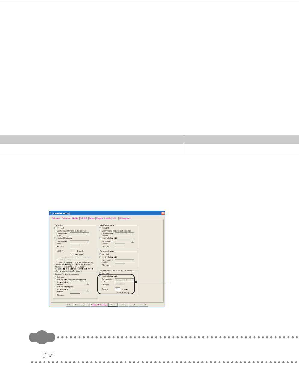
6 - 146
6.29 Writing/Reading Device Data to/from Standard ROM
(1) Definition
This function writes device data to the standard ROM.
Writing the fixed values for operation and operation results to the standard ROM can prevent losing data due to
low battery. Also, timing of writing to the standard ROM can be set by an instruction.
(2) Execution method
Device data are written to the standard ROM by the SP.DEVST instruction.
The device data written to the standard ROM is read to the specified device by the S(P).DEVLD instruction.
(3) Devices that can be written to the standard ROM
Table6.48 shows the devices whose data can be written to the standard ROM.
*1: The extended data register (D) is included.
*2: The extended link register (W) is included.
(4) Setting method
The area for storing the device data is set in the standard ROM by the PLC file tab of the PLC parameter dialog
box.
Remark
For details of the instructions, refer to the following.
QCPU Programming Manual (Common Instructions)
Table6.48 Devices that can be written to the standard ROM and storage location
Device Storage location
X,Y,M,L,B,F,V,T,ST,C,D*1,W*2,SM,SD,SB,SW,R,ZR Standard ROM(device data storage location)
Figure 6.112 Screen for setting a file for storing device data
Set a file size
(A file name is fixed to DEVSTORE).
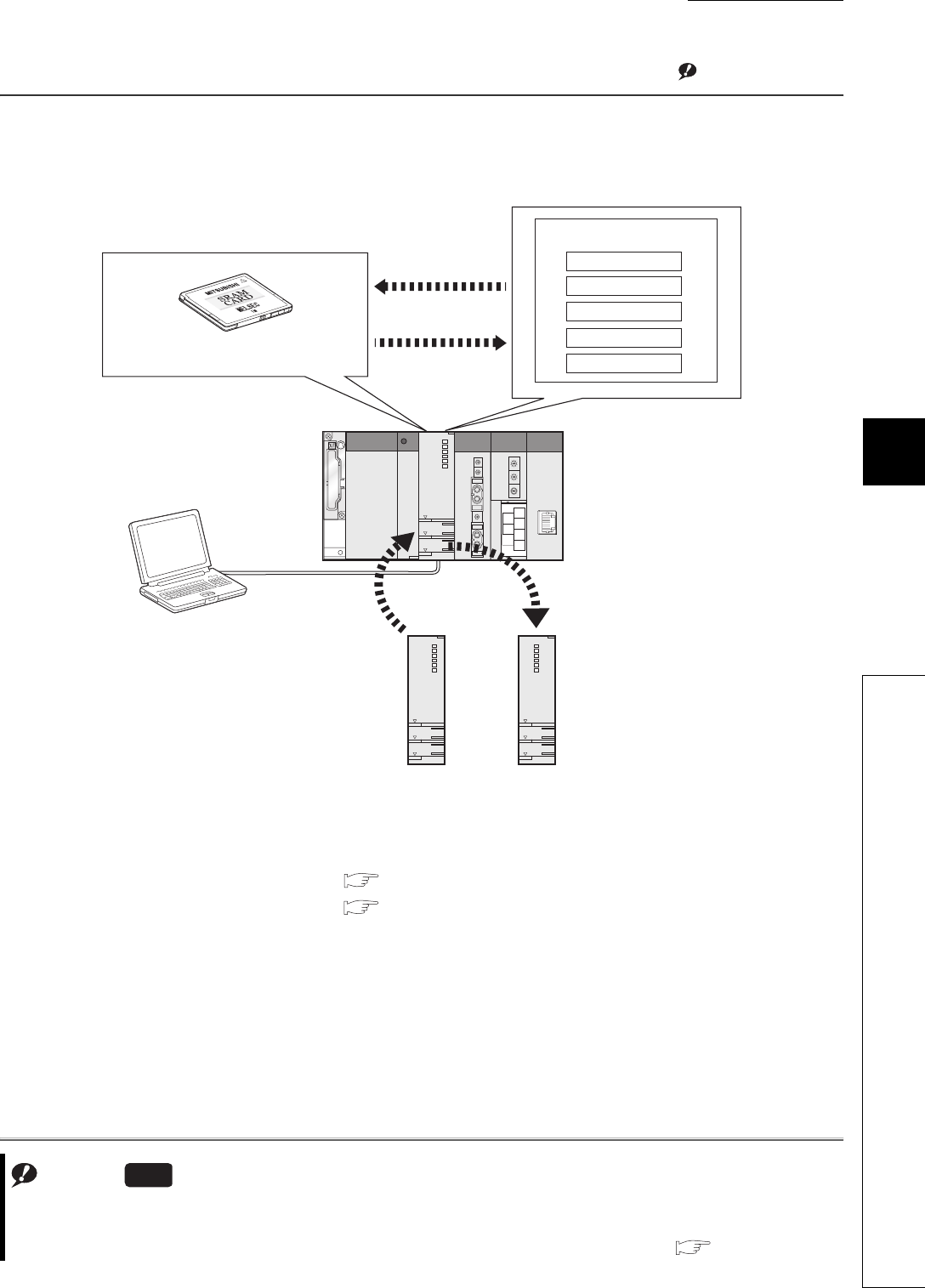
CHAPTER6 FUNCTIONS
1
2
3
4
5
6
7
8
6.30 CPU Module Change Function with Memory Card
6 - 147
6.30 CPU Module Change Function with Memory Card
(1) Definition
This function backs up data in the CPU module to a memory card and restores the backup data to another CPU
module.Note1
This function consists of the following two functions.
• Backup function to memory card: Section 6.30.1
• Backup data restoration function: Section 6.30.2
Figure 6.113 CPU module change function with memory card
Note1
Note6.12
GX Developer
Standard ROM
Standard RAM
Memory card for storing backup data
2) Changes the
CPU module.
3) Restores backup
data.
1) Backs up to a
memory card.
Universal model QCPU
Program memory
Device data
System data
Note6.12
The Q00UJCPU, Q00UCPU, and Q01UCPU do not support the CPU module change function with memory card.
When using the function for the Q02UCPU, Q03UDCPU, Q04UDHCPU, Q06UDHCPU, Q13UDHCPU, Q26UDHCPU,
or Built-in Ethernet port QCPU, check the versions of the CPU module and GX Developer. ( Appendix 2)
Universal
6 - 148
(2) Backup data file
After data are backed up, a backup data file "MEMBKUP0.QBP" is created in a memory card.
Only one backup data file can be stored to a memory card.
When data are backed up to a memory card containing a backup data file again, the stored backup data file is
overwritten. When a memory card contains another file, a backup data file can be stored in the memory card
without deleting the stored file.*1 *2
*1: After restoration, if the parameters are stored in the memory card but not in the CPU module, the CPU module operates by
the parameter settings in the memory card.
*2: When data are backed up to the Flash card, only a backup data file can be stored.
The backup data file can be deleted by "Delete PLC data” of GX Developer.
(3) Backup data
(a) Backup data selection
Table6.49 shows data to be backed up.
*1: Data in the program cache memory are backed up.
*2: Only the latch relay (L) and devices to which the latch range setting can be configured are backed up.
(b) Maximum backup data size
Table6.50 shows the maximum size of data that can be backed up.
(Unit: K byte)
The backup data size can be checked by the following methods.
• Execution screen of GX Developer ( Section 6.30.1(1)(b))
• SD698 and SD699( CHAPTER 12)*1
*1: Can check the data size after backup starts.
Table6.49 Data to be backed up
Backup data (drive) Description Backup selection by the user
Program memory (drive 0) All data in the program memory (drive 0) *1
Selectable
Standard RAM (drive 3) All data in the standard RAM (drive 3)
Standard ROM (drive 4) All data in the standard ROM (drive 4)
Device data*2 Internal user device
(M, L, B,F,V,T,ST,C,D,W) Not selectable
(Data are automatically backed up by the
system.)
System data Data managed by the system (such as error
history)
Table6.50 Maximum size of data that can be backed up
Backup target data (drive) Q02UCPU
Q03UD/
Q03UDE
CPU
Q04UDH/
Q04UDEH
CPU
Q06UDH/
Q06UDEH
CPU
Q10UDH/
Q10UDEH
CPU
Q13UDH/
Q13UDEH
CPU
Q20UDH/
Q20UDEH
CPU
Q26UDH/
Q26UDEH
CPU
Program memory (drive 0) 82 124 164 244 408 528 808 1048
Standard RAM (drive 3) 130 194 258 770 1026 1026 1282 1282
Standard ROM (drive 4) 516 1032 1032 1032 2056 2056 4104 4104
Device data 128 128 128 128 128 128 128 128
System data 4164646464646464
Total (maximum) 897 1542 1646 2238 3682 3682 6386 6626

CHAPTER6 FUNCTIONS
1
2
3
4
5
6
7
8
6.30 CPU Module Change Function with Memory Card
6.30.1 Backup function to memory card
6 - 149
6.30.1 Backup function to memory card
This function can save data in the CPU module to a memory card.
If a memory card is used in running system, data can be backed up by replacing the current memory card with the one
for storing a backup data.
(1) Methods
(a) Method with contacts
1) Setting
To back up data with contacts, turn on the device set in the “PLC module change setting“ screen in the PLC
system tab of the PLC parameter dialog box.
*1: The CPU module enters the STOP status at the rise of the backup start setup contact, the backup start contact cannot be turned on in the
sequence program.
*2: The backup start setup contact and backup start contact cannot be set to the same device.
*3: This indicates the default number of points. The setting range when the internal user device is set to the maximum number of points (60K
points) is M(0 to 61439) and B(0 to 0EFFF).
*4: If data to be backed up is deselected in "Backup target data", only device data and system data are backed up.
*5: The title is used for identifying backup data.
Settings for the title of the backup data stored in a memory card can be checked on the Delete PLC data screen of GX Developer.
Figure 6.114 PLC module change setting screen
Table6.51 Setting items
Item Description Setting range Default
Backup start setup
contact*1
At the rise of the selected device among the items
shown in the right column, backup is ready to start. Available devices*2
• X (0 to 1FFF)
• M (0 to 8191)*3
• B (0 to 1FFF)*3
-
Backup start contact
At the rise of the selected device among the items
shown in the right column, backup enters
execution status.
Backup target data Select data to be backed up stored in any of
memories shown in right column.*4
• Program memory (drive 0)
• Standard RAM (drive 3)
• Standard ROM (drive 4)
All drives are backed up.
Format memory card
before backup
Select whether to format a memory card before
backup.
Formatted
Not formatted Not formatted
Title setting*5 Set a title appended to backup data stored in a
memory card.
32 characters (16 in two-byte
characters)
Set the title of the current time.
(Example) If data are backed up at 12
p.m. on October 1, 2008,
"200810011200" is set.
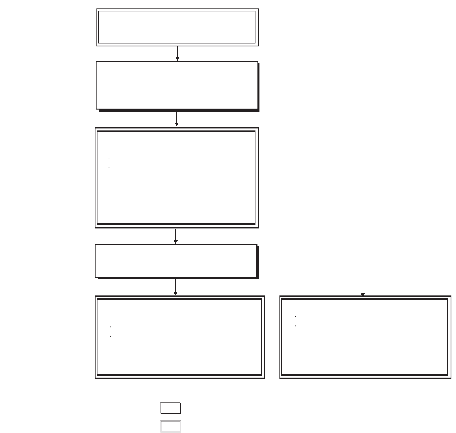
6 - 150
2) Operating procedure
Turn on in the order of the backup start setup contact and the backup start contact. Data are not backed up
when only the backup start contact is on.
*1: Since the SM691 (Backup start preparation status flag) is on, data can be backed up again by turning off and then on the
backup start contact.
Figure 6.115 Backup procedure using contacts
Turn on the backup start setup contact.
Preparation for backup:
1) Set the CPU module to the STOP status.
2) Stop an operation that uses a memory
card so that the card can be removed.
Back up data.
: Operation by the CPU module
: Operation by the user
Check the backup error*1.
Check the LEDs.
Check the special relay and special
register.
(a) SM691 is on.
(b) SD690 stores FFh.
(c) SD689 stores the error cause.
1) Check that the preparation for backup
is completed by the following methods.
Check the LEDs.
Check the special relay and special register.
(a) SM691 is on.
(b) SD690 stores 2h.
2) Remove the mounted memory card.
3) Mount a memory card for storing backup data.
4) Turn on the backup start setup contact.
Check that the backup is completed by
the following methods.
Check the LEDs.
Check the special relay and special
register.
(a) SM691 is on.
(b) SD690 stores 4h.
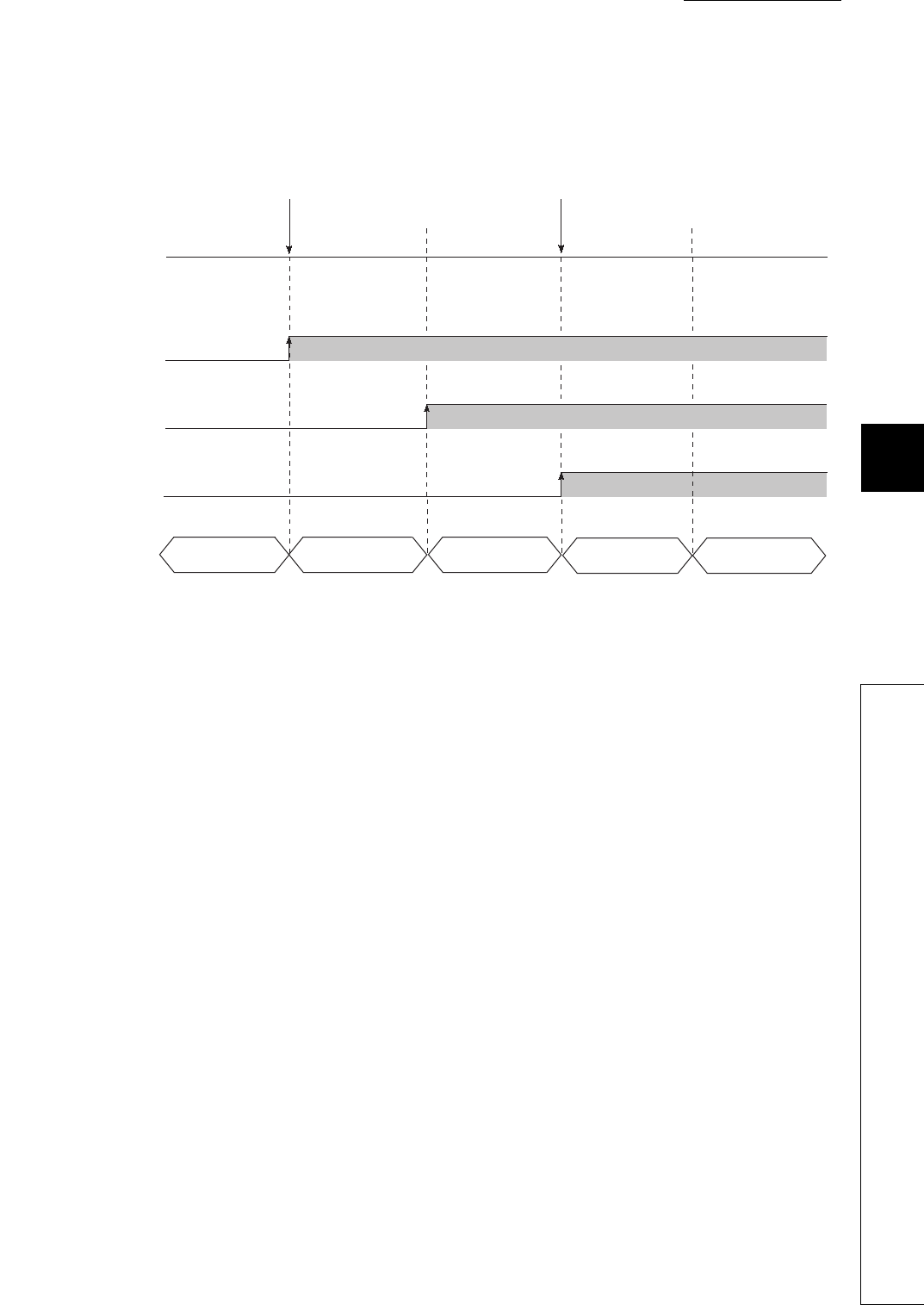
CHAPTER6 FUNCTIONS
1
2
3
4
5
6
7
8
6.30 CPU Module Change Function with Memory Card
6.30.1 Backup function to memory card
6 - 151
3) Operation of contacts
Operations of the backup start setup contact, backup start contact, SM691 (Backup start preparation status
flag), and SD690 (Backup status) at backup are shown in Figure 6.116.
If the backup start contact is turned on while the value in SD690 is 0H (Before backup start) or 1H (Backup
start prepared), data are not backed up.
If the backup start contact is on before the value in SD690 becomes 2H (Backup start preparation completed),
turning off and then on the backup start contact again while the value in SD690 is 2H (Backup start
preparation completed) starts backup.
Figure 6.116 Operation of contacts
ON
OFF
OFF
ON
012
34
OFF
ON
Backup start
setup contact
SM691
(Backup start
preparation status
flag)
Backup start
contact
SD690
(Backup status)
Backup start setup request from
GX Developer or the backup start
setup contact is turned on.
Backup start request from
GX Developer or the backup
start contact is turned on.
Before backup start
Backup start prepared
Backup start
preparation completed
Backup in execution
Backup completed
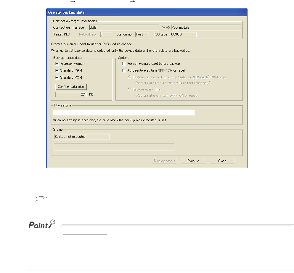
6 - 152
(b) Backup from GX Developer
Select [Online] [PLC module change] [Create backup data...].
For details of the operating procedure by the GX Developer wizard, refer to the following.
GX Developer Version 8 Operating Manual
Clicking the button on the screen shown in Figure 6.117 displays the size of backup data created at
backup.
Data size can be checked by GX Developer connected to the CPU module.
This function is available regardless of the operating status of the CPU module (RUN, STOP, PAUSE) or mounting status of
a memory card.
Figure 6.117 Create backup data screen
Confirm data size
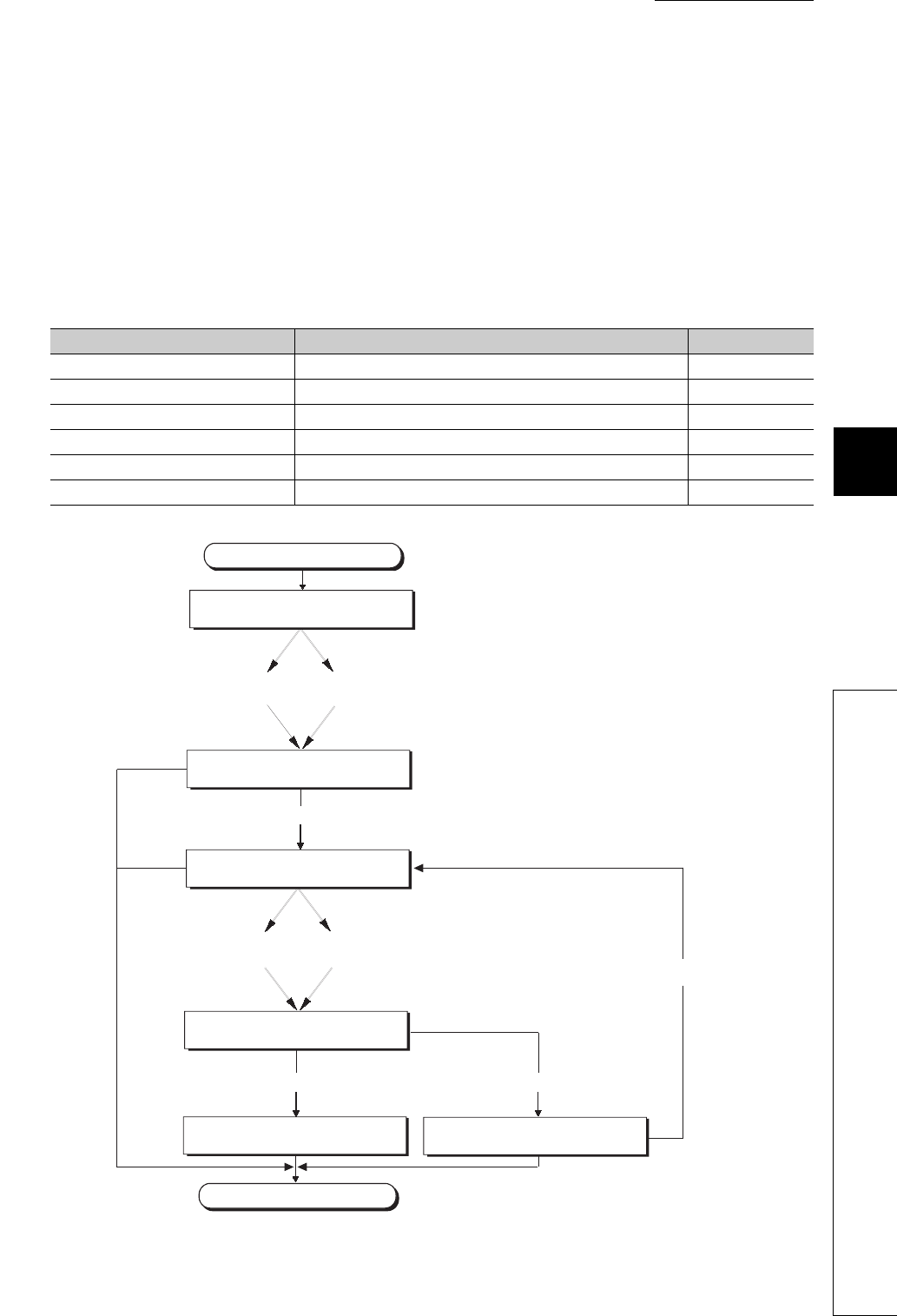
CHAPTER6 FUNCTIONS
1
2
3
4
5
6
7
8
6.30 CPU Module Change Function with Memory Card
6.30.1 Backup function to memory card
6 - 153
(2) Operations of backup to a memory card
(a) Mounting/removal of a memory card
In a system using a memory card, the memory card can be changed/removed after preparation for backup has
been completed (Turning on SM609 (Memory card remove/insert enable flag) is unnecessary).
After preparation for backup has been completed, the CPU module turns off SM604 (Memory card in-use flag).
(b) Status of backup to a memory card
Table6.52 shows backup status.
Table6.52 Backup status
Status Description Value in SD690
Before backup start Backup is not started. 0H
Backup start prepared A memory card can be mounted/removed. 1H
Backup start preparation completed Set data to be backed up. 2H
Backup in execution Backup is in execution. 3H
Backup completed Backup is normally completed. 4H
Backup error Backup failed due to an error. FFH
Figure 6.118 Flow of status change at backup
Start
Before backup start
Backup start prepared
Backup is ready to start.
Backup start preparation completed
Backup in execution
Backup to the memory card is completed.
Backup completed
End
Backup failed.
Backup error
Data are backed up again.
Backup start setup
request from
GX Developer
The backup start setup
contact is turned on.
Backup start request
from GX Developer
The backup start contact
is turned on.
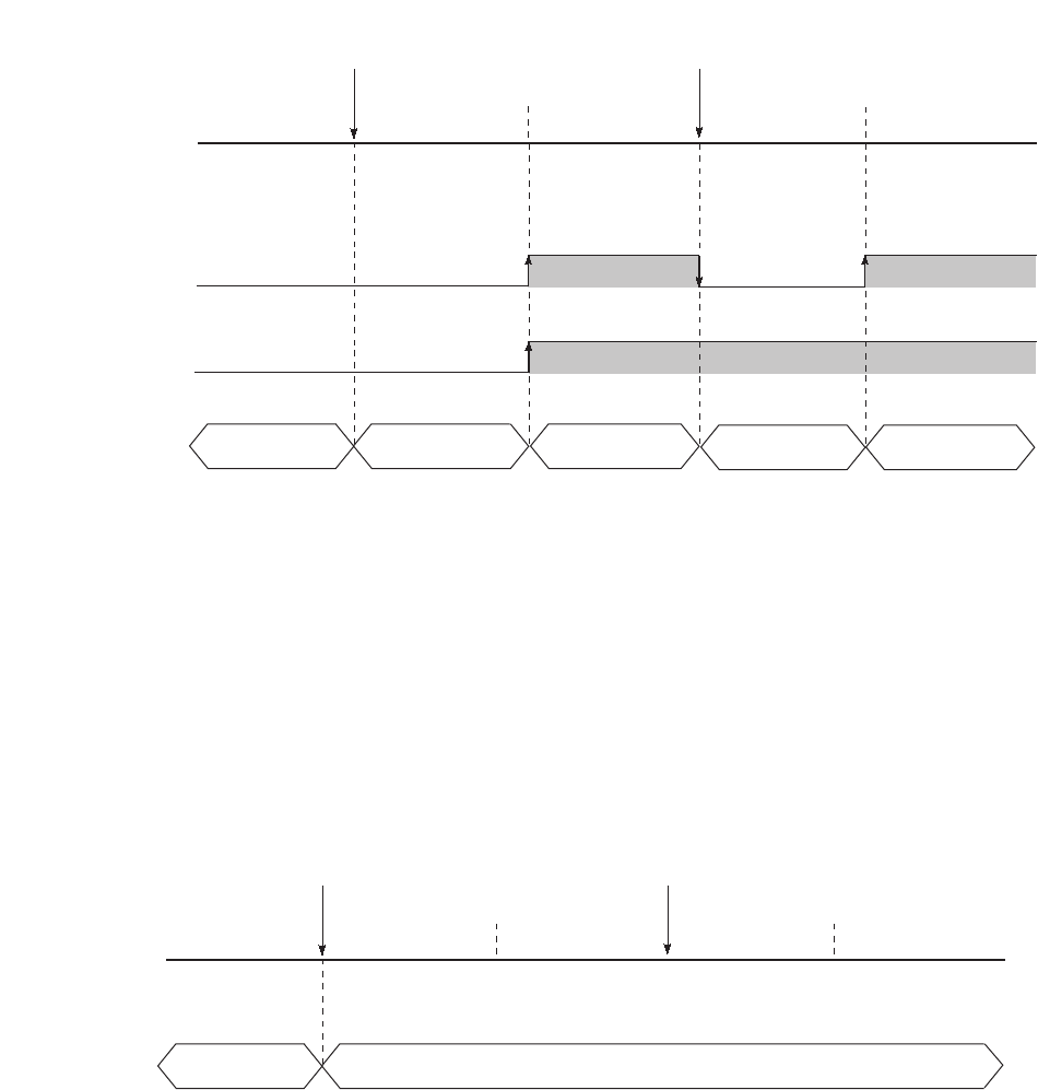
6 - 154
(c) Operations of special relays and special register*1
Figure 6.119 shows the operations of the SM609 (Memory card remove/insert enable flag), SM691 (Backup
start preparation status flag), and SD690 (Backup status).
*1: For details of the special relays and special register used for backup, refer to CHAPTER 12.
*2: This special relay is turned on/off by the system.
(d) Operating status of the CPU module
After END processing where the backup start setup request is accepted, the CPU module changes the
operating status to STOP at backup. Therefore, data can be backed up regardless of the operating status.
After backup, power off and then on the CPU module or reset the CPU module.(If the CPU module is not
powered off and then on or is not reset but set the RESET/STOP/RUN switch to RUN, the CPU module
remains in the STOP status).
*1: The status includes a stop error.
Figure 6.119 Special relays and special register at backup
Figure 6.120 Operating status of the CPU module at backup
ON
OFF
OFF
ON
012
34
Backup start setup request from
GX Developer or the backup
start setup contact is turned on.
Backup start request from
GX Developer or the backup
start contact is turned on.
Before backup start
Backup start prepared
Backup start
preparation completed
Backup in execution Backup completed
SM691
(Backup start
preparation
status flag)
SM609*2
(Memory card
remove/insert
enable flag)
SD690
(Backup status)
CPU operating
status
Backup start setup request from
GX Developer or the backup start
setup contact is turned on.
Backup start request from
GX Developer or the backup
start contact is turned on.
Before backup start
Backup start prepared
Backup start
preparation completed
Backup in execution
Backup completed
RUN/STOP*1
/PAUSE STOP*1
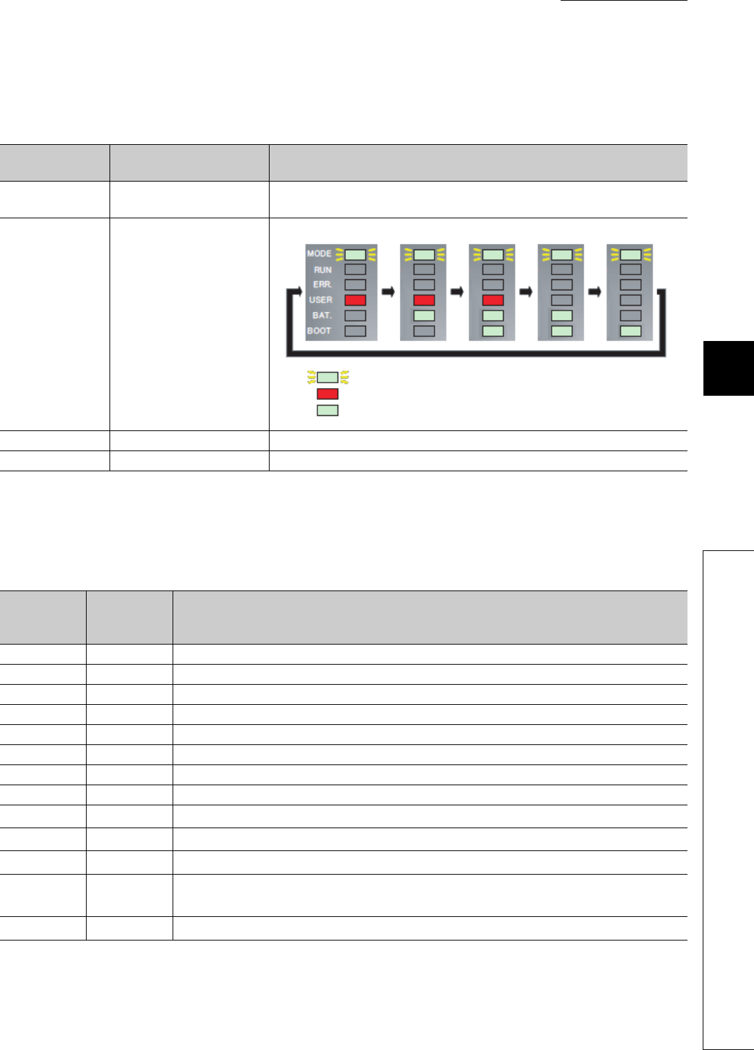
CHAPTER6 FUNCTIONS
1
2
3
4
5
6
7
8
6.30 CPU Module Change Function with Memory Card
6.30.1 Backup function to memory card
6 - 155
(3) LEDs indicating backup status
The LEDs on the front of the CPU module indicate backup status.
(4) Error cause of backup
When backup is not normally completed, an diagnostic error is not detected. In that case, the error cause is
stored in SD689(Backup error factor) and the error response is returned to GX Developer.
*1: Only when data are backed up with contacts
*2: Only when data are backed up from GX Developer
*3: Only when data area backed up from another boot source.
*4: Only when data area backed up from the same boot source.
Table6.53 LEDs indicating backup status
Value stored in
SD690 Backup status LED indication
2HBackup start preparation
completed MODE: Flash (green), BAT.: Flash (green)
3HBackup in execution
The color changes at intervals of 800ms as follows.
4HBackup completed MODE: Flash (green), BAT.: Flash (green), BOOT: Flash (green)
FFHBackup error MODE: Flash (green),USER: MODE: Flash (red), BAT.: Flash (green)
Table6.54 Error cause of restoration
Value stored
in SD689
Error
response
number
Error cause
100H- Restoration started while a memory card was not mounted.
200H- Size of data to be backed up exceeds the capacity of mounted memory card.
300H- Write protection has been set to the memory card.
400H- Writing to the memory card was not normally completed.
500H- Reading from a drive storing backup data was not normally completed (program memory read error).
503H- Reading from a drive storing backup data was not normally completed (standard RAM read error).
504H- Reading from a drive storing backup data was not normally completed (standard ROM read error).
510H- Reading from a drive storing backup data was not normally completed (system data read error).
600H*1 4335H*2 Backup preparation started while latch data were backed up to the standard ROM.
601H*1 410AH*2 Backup preparation started while data were written in the RUN status.
602H *1 4336H*2 Backup preparation started while a FTP client connected a FTP to the CPU module in FTP connection.
-4082H*3,
4330H*4 Backup preparation or backup started while another backup was in execution.
-4333H*2 Backup started while the CPU module was in "Before backup start" (SD690 = 0).
: Flashing (green)
: On (red)
: On (green)

6 - 156
(5) Functions that cannot be performed during backup
Table6.55 shows functions that cannot be performed during backup.
(6) Precautions
(a) Do not perform the following operations during backup.
• Mounting/removal of a memory card
• Power-off of the CPU module
• Reset
(b) Even if booting parameters backed up with contacts for the Universal model QCPU
having the serial number (first five digits) is "10101" or earlier, the system ignores
the parameters.
In this case, even if the backup start setup contact or backup start contact set by the
parameters is turned on, the operating status of the CPU module does not change (a
diagnostic error is not detected).
(c) After backup is ready to start, the following functions stop (do not resume the
operations even after the backup).
• Refresh of network modules
• Data link transfer
• Auto refresh of intelligent function modules
• Auto refresh of CPU shared memory
Table6.55 Functions that cannot be performed during backup
Category Function Category Function
Drive operation
Format PLC memory Trace Sampling trace registration
Write the program memory to ROM Remote operation Remote latch clear
Program memory batch transfer
File operation
Write to PLC
Arrange PLC memory Delete PLC data
Online change
Online change (ladder mode) Write PLC user data
Online change (files) Delete PLC user data
Online change (multiple blocks) Password registration
Change TC setting Latch data backup operation
Monitor Monitor condition setup FTP function For all operations and commands
Debug Executional conditioned device test
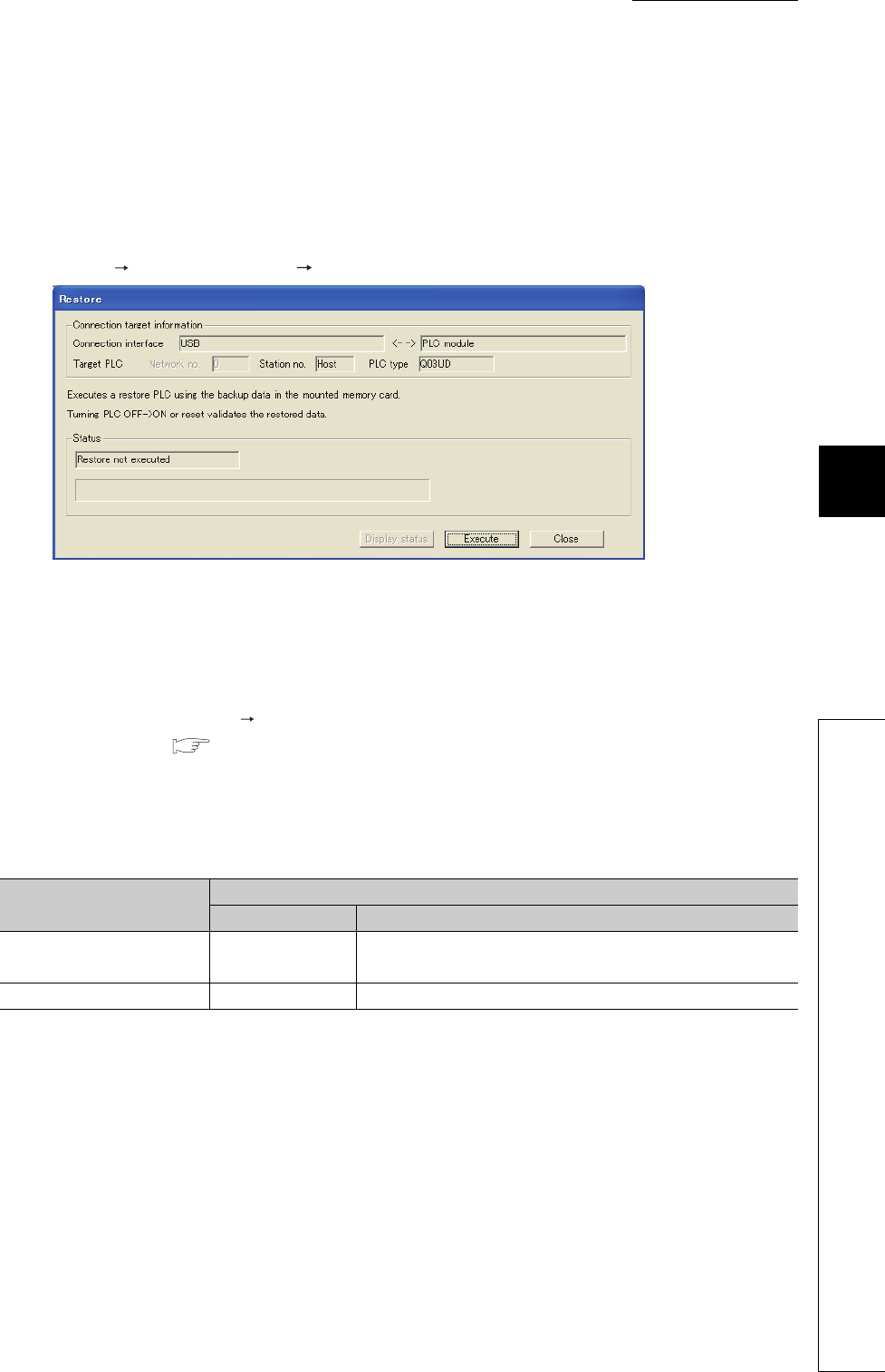
CHAPTER6 FUNCTIONS
1
2
3
4
5
6
7
8
6.30 CPU Module Change Function with Memory Card
6.30.2 Backup data restoration function
6 - 157
6.30.2 Backup data restoration function
This function restores data backed up to a memory card to the CPU module.
(1) Methods
(a) Restoration from GX Developer
Select [Online] [PLC module change] [Restore...].
After selecting "Execute" on the screen above and powering off and then on the CPU module or reset the CPU
module, the restored data become valid.
(b) Automatic restoration
Select ”Auto restore at turn OFF ON" in "PLC module change setting" in the PLC system tab of the PLC
parameter dialog box. ( Section 6.30.1(1)(a))
After data are backed up and the CPU module is powered off and then on or is reset, restoration automatically
starts.
Also, items shown in Table6.56 can be set by the option setting.
*1: This setting is valid only when backup data are stored to the ATA card or SRAM card.
Note if the write protect switch of the SRAM card is set to be valid (write protection), the setting does not
become valid and the data are restored even after the first time ("RESTORE ERROR" (error code: 2226)
occurs).
*2: When using the FLASH card, restoration can be performed even after the first time.
*3: Restoration after the first time can be performed from GX Developer.
Data are restored at initial processing after the CPU module is powered off and then on or is reset.
After restoration, powering off and then on the CPU module or resetting the CPU module again is not required
to change the operating status to the one set with the RUN/STOP/RESET switch.
If a memory card needs to be changed after restoration, turn on SM609 (Memory card remove/insert enable
flag) and change the memory card after SM600 (Memory card usable flags) turns off.
Figure 6.121 Restore screen
Table6.56 Option setting items
Option setting item The CPU module is powered off and then on or is reset
First time After the first time
Restore for the first time only
*1 *2 Restored Not restored (The CPU module operates the memory card as
usual.)*3
Restore every time Restored Restored
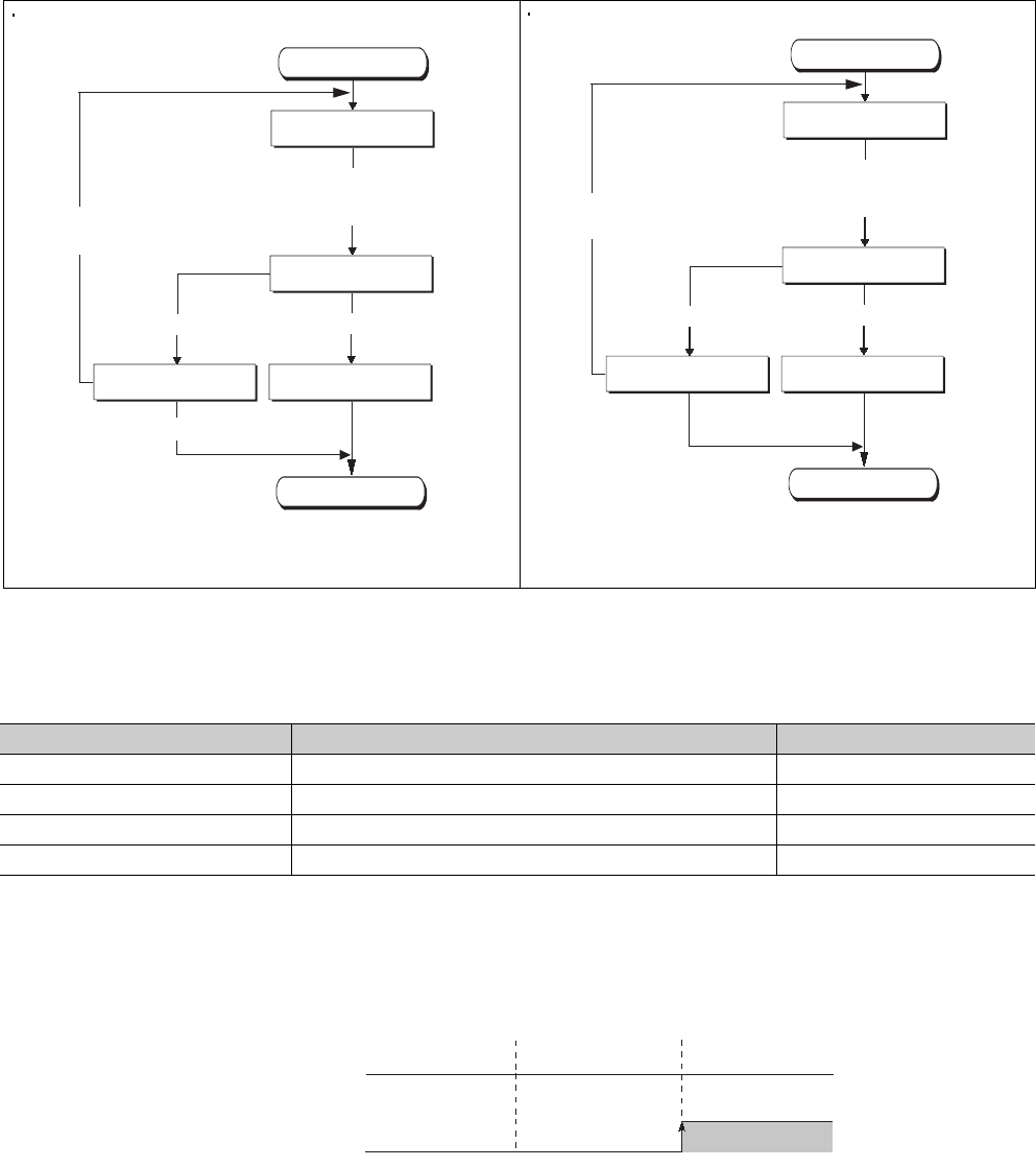
6 - 158
(2) Operation for restoring backup data
Figure 6.122 shows operation for restoration.
A value indicating restoration status is stored in SD693 (Restoration status).
(3) Operation of special relay and special register*1
Figure 6.123 shows the operation of SM692 (Restoration complete flag) at restoration.
*1: For details of special relays and special registers for restoration, refer to CHAPTER 12.
Restoration from GX Developer Automatic restoration
Figure 6.122 Operation for restoration
Table6.57 Status at restoration
Status Description Value stored in SD693
Before restoration start Restoration is not performed. 0H
Restoration in execution Restoration is in execution. 1H
Restoration completed Restoration is normally completed. 2H
Restoration error Restoration failed due to an error. FFH
Figure 6.123 Operation of the special relay
Start
End
Restoration is
performed again.
1: Before restoration start
Mount a memory card storing the
backup data to the CPU module and
restore the data with GX Developer.
Restoration failed.
4: Restoration error
Restoration is suspended.
2: Restoration in execution
Restoration is completed.
3: Restoration completed
After restoration, power off and then on the
CPU module or reset the CPU module.
Start
End
Restoration is
performed again.
Restoration failed.
4: Restoration error
1: Before restoration start
Mount a memory card storing the backup data
to the CPU module and power off and then on
the CPU module or reset the CPU module.
2: Restoration in execution
Restoration is completed.
3: Restoration completed
After restoration, the CPU module can continue operation.
Powering off and then on the CPU module or
resetting the CPU module is unnecessary.
Off
On
SM692
(Restoration
complete flag)
Before
restoration start
Restoration in
execution
Restoration
completed
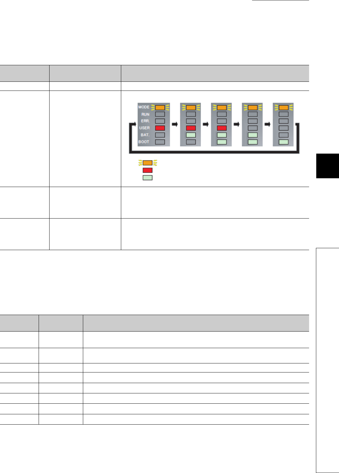
CHAPTER6 FUNCTIONS
1
2
3
4
5
6
7
8
6.30 CPU Module Change Function with Memory Card
6.30.2 Backup data restoration function
6 - 159
(4) LEDs indicating restoration status
The LEDs on the front of the CPU module indicate restoration status.
(5) Error cause of restoration
When restoration is not normally completed, an diagnostic error is not detected. In that case, the error cause is
stored in SD692 (Restoration error factor) and the error response is returned to GX Developer.
*1: Only when data are restored from GX Developer
Table6.58 LEDs indicating restoration status
Value stored in
SD693 Restoration status LED indication
0HBefore restoration start MODE: On (green)
1HRestoration in execution
The color changes at intervals of 800ms as follows.
2HRestoration completed
• Restoration from GX Developer
MODE: Flashing (orange), BAT.: Flashing (green), BOOT: Flashing (green)
• Automatic restoration
MODE:On (green)
FFHRestoration error
• Restoration from GX Developer
MODE:Flashing (orange), USER: Flashing (red),BAT.:Flashing (green)
• Automatic restoration
MODE:On (green), ERR: Flashing (red)
Table6.59 Error cause of restoration
Value stored
in SD692
Error response
number Error cause
800H-The CPU module where data are restored is different model with the one where the backup source
data are stored.
801H-• Backup data files do not match.
• Reading of backup data from a memory card was not normally completed.
810H- Writing of backup data to the restoration destination drive was not normally completed.
-4335H*1 Restoration started while latch data were backed up to the standard ROM.
-410AH*1 Restoration started while data were written in the RUN status.
-4336H*1 Restoration started while a FTP client connected a FTP to the CPU module in FTP connection.
-4330H*1 Restoration started while another restoration was in execution.
-41FEH*1 Restoration started while a memory card was not mounted.
: Flashing (orange)
: On (red)
: On (green)

6 - 160
When automatic restoration is not normally completed, “RESTORE ERROR” (error code: 2225 to 2227) is
detected.
Remark
For details of error codes, refer to the following.
QCPU User's Manual (Hardware Design, Maintenance and Inspection)
(6) Functions that cannot be performed during restoration
Functions that cannot be performed during restoration are the same as the ones that cannot be performed during
backup. ( Section 6.30.1(5))
(7) Precautions
(a) Do not perform the following operations during restoration.
• Mounting/removal of a memory card
• Power-off of the CPU module
• Reset
(b) Even if mounting a memory card storing backup data file to the Universal model
QCPU having the serial number (first five digits) is "10101" or earlier and powering
off and then on the CPU module or reset the CPU module, the system ignores the
backup data file and starts operation (a diagnostic error is not detected).
(c) Do not use a memory card where the boot file setting parameter is stored. If used,
data in the memory card are overwritten by the boot file setting even restoration is
performed.
(d) If restoration is started from GX Developer, the following functions stop (do not
resume the operations even after the restoration).
• Refresh of network modules
• Data link transfer
• Auto refresh of intelligent function modules
• Auto refresh of CPU shared memory
Table6.60 Error when automatic restoration is not normally completed
Error code Error message Error cause
2225
RESTORE ERROR
The CPU module where data are restored is different model with the one where the backup
source data are stored.
2226
• Backup data file is corrupt (The contents of backup data file do not match with the check
code).
• Reading of backup data from a memory card was not normally completed.
• The write protect switch of the SRAM card is valid (write protection), and therefore "Restore
for the first time only" cannot be set to valid.
2227 Writing of backup data to the restoration destination drive was not normally completed.
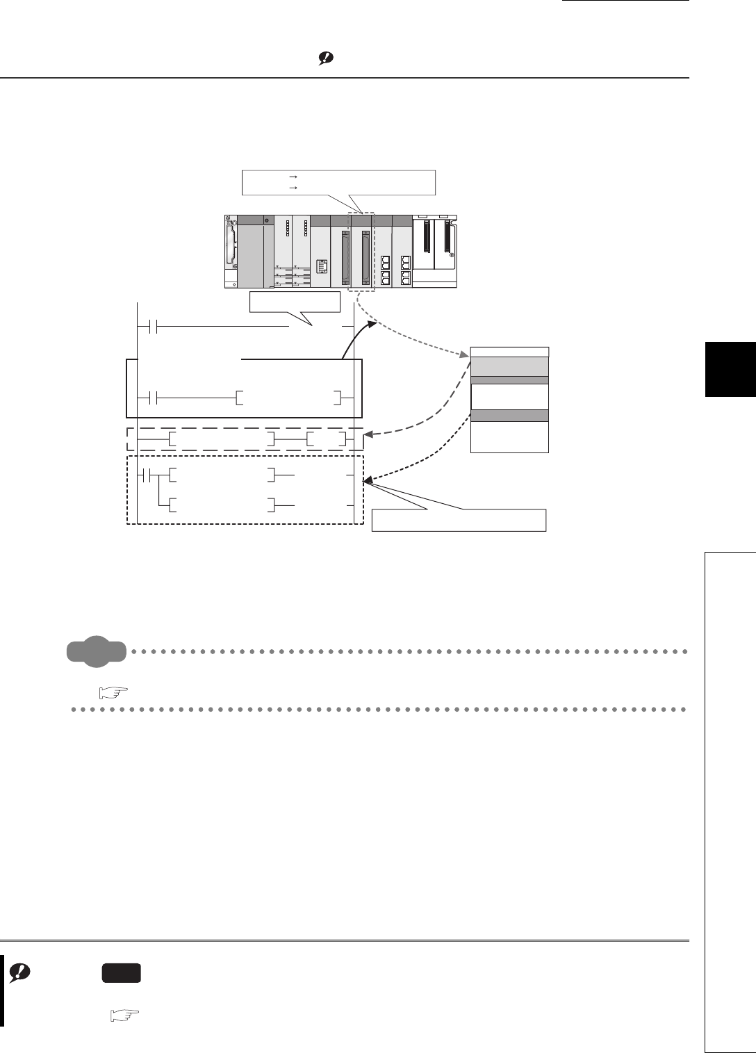
CHAPTER6 FUNCTIONS
1
2
3
4
5
6
7
8
6.31 Module model name read
6 - 161
6.31 Module model name read Note1
(1) Definition
This function reads the model name of a module on a base unit.
The mounted module is identified in a ladder program and processing according to the module can be performed.
(2) Execution method
Use the TYPERD instruction.
Remark
For details of the instruction, refer to the following.
QCPU Programming Manual (Common Instructions)
Note1
Figure 6.124 Operation of the module model name read
Note6.13
Note6.13
When using the module model name read function, check the versions of the CPU module and GX Developer.
( Appendix 2)
Universal
TYPERD
= D0 K0
$= D1 "QD75MH2"
$= D1 "QD75MH4"
SET MO
H4 D0
D0
D1
M0
QD75MH2 Processing 1 and 2 are performed.
QD75MH4 Processing 1 and 3 are performed.
Processing common to
the QD75M modules
Processing 1
Module model name read
Module model name read
instruction
Reads the module name of the specified module by the
instruction.
Processing 2
Processing 3
Checks the execution
result of the
instruction.
Reads the character string.
Identifies the mounted module and performs
processing according to the module.
Device memory
Execution result of
the instruction
Module model name
"QD75MH2"
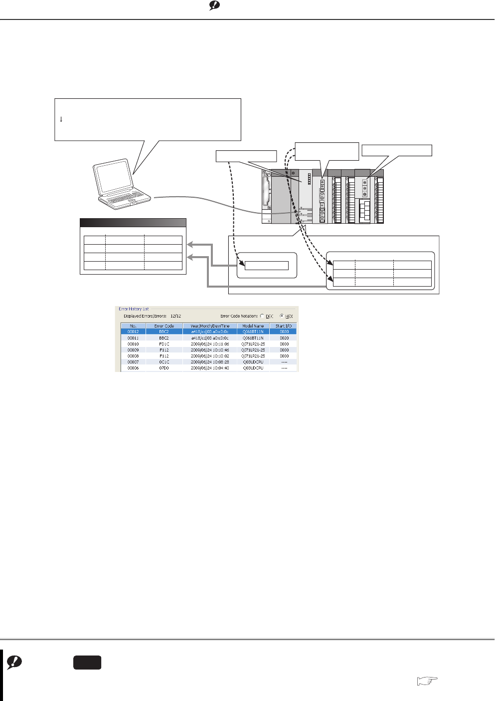
6 - 162
6.32 Module error collection Note1
(1) Definition
This function collects errors occurred in the connected intelligent function modules in the CPU module.
By storing the errors in a memory that can hold data in the event of a power failure, the errors can be held even
after power-off or reset.
(2) Supported modules
The CPU module collects errors occurred in the connected intelligent function modules*1.
The CPU module does not collect the errors of intelligent function modules on other stations in the network.
*1: Indicates intelligent function modules that support this function. For supported module versions, refer to the manual for
each module.
(3) Timing when module errors are collected
Module errors are not collected during execution of a program such as the COM instruction but collected in END
processing.
Note1
Figure 6.125 Operation of module error collection
Note6.14
Note6.14
When using the module error collection, check the versions of the CPU module and GX Works2. ( Appendix 2)
GX Developer cannot display module errors.
Universal
Error history display
19:29
19:33
19:34
19:35
Module A
CPU
Module B
Error A1
Error C1
Error B1
Error A2
Time Module in error Error code
Error history
(CPU module)
Module error log
Time Module in error Error code
19:29
19:34
19:36
ModuleA
ModuleB
ModuleA
Error A1
Error B1
Error A2
19:33 Error C1
CPU 19:29 Error A1 occurred!
19:36 Error A2 occurred!
19:34 Error B1 occurred!
Error history (CPU module) and error log (intelligent function module)
are displayed in one screen.
Errors that occurred in the entire system (base units) can be
monitored in reverse chronological order.
Error C1 occurred!
Module A Module B
Programming tool
Module A
[Example of screen display]
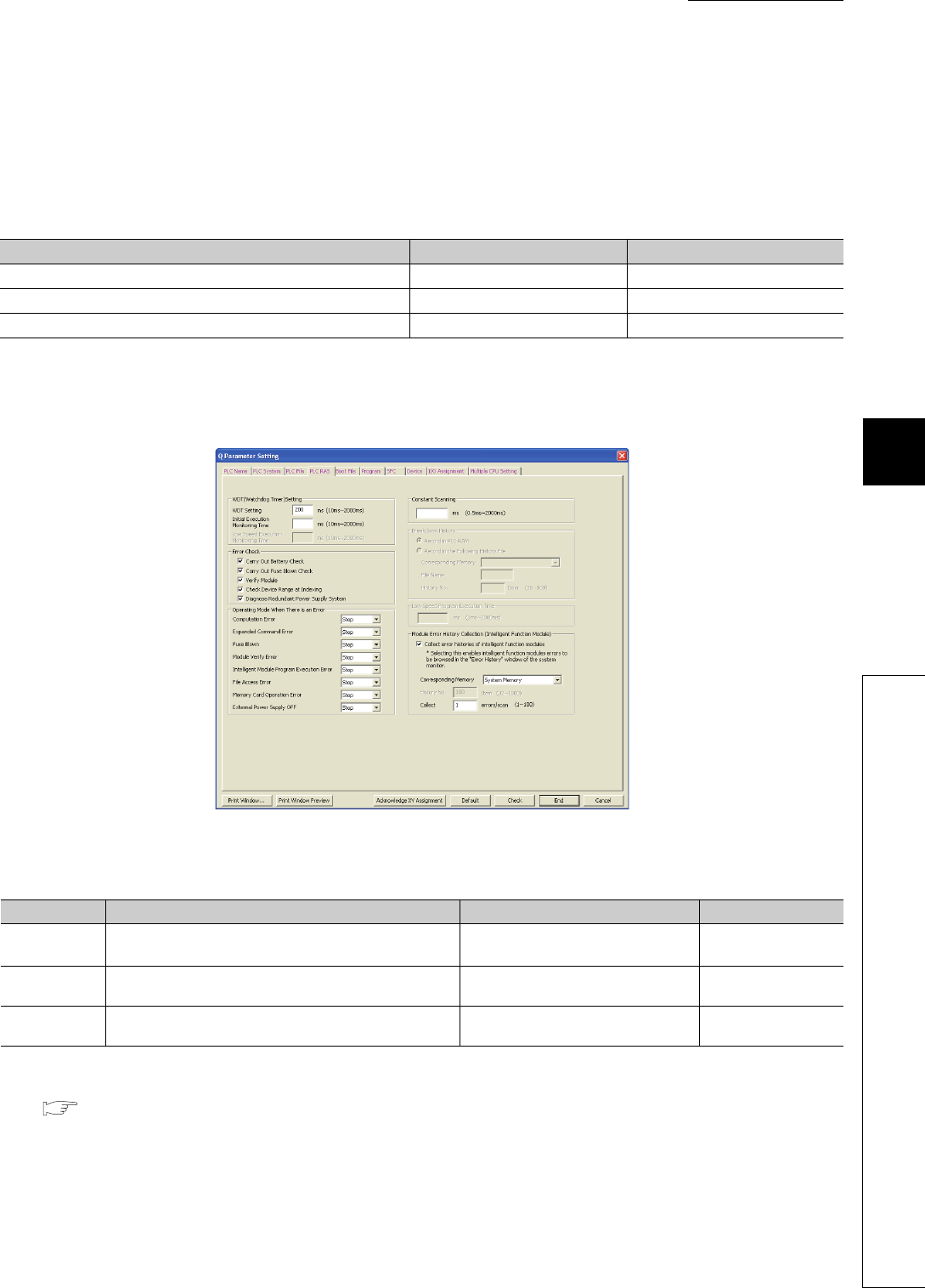
CHAPTER6 FUNCTIONS
1
2
3
4
5
6
7
8
6.32 Module error collection
6 - 163
(4) Storing module errors
The module errors can be stored either the system memory*1 or the standard RAM.
The errors are stored separately from error history (CPU module) data.
*1: The memory is managed inside the system.
(5) Setting method
Select "Collect error histories of intelligent function modules" in "Module Error History Collection (Intelligent
Function Module)" in the PLC RAS tab of the PLC parameter dialog box.
*1: When a sampling trace file is stored to the standard RAM, powering off and then on or resetting the CPU module will delete the file.
*2: The battery consumption may be increased.
QCPU User's Manual (Hardware Design, Maintenance and Inspection)
*3: If collected module errors are frequently lost, set a greater value to "Collection No.". The recommended value is the number of intelligent
function modules that support this function.
Parameter settings are enabled to the CPU module when:
• the CPU module is powered off and then on or
• the CPU module is reset.
Table6.61 Storage locations and the number of storable module errors
CPU module System memory Standard RAM
Q00UJCPU 40 (Fixed) -
Q00UCPU, Q01UCPU 40 (Fixed) 1000
Q02UCPU, QnUD(H)CPU, Built-in Ethernet port QCPU 100 (Fixed) 1000
Figure 6.126 PLC RAS
Table6.62 PLC RAS setting list
Item Description Setting range Default
Corresponding
Memory Select a storage location. • System Memory
• Standard RAM*1, *2 System Memory
History No. Set the number of collected errors only when the errors are
stored in the standard RAM. 32 to 1000 40/100
Collection No. Set the number of collected errors in one scan.*3 • Stored in system memory: 1 to 100
• Stored in standard RAM: 1 to 128 1
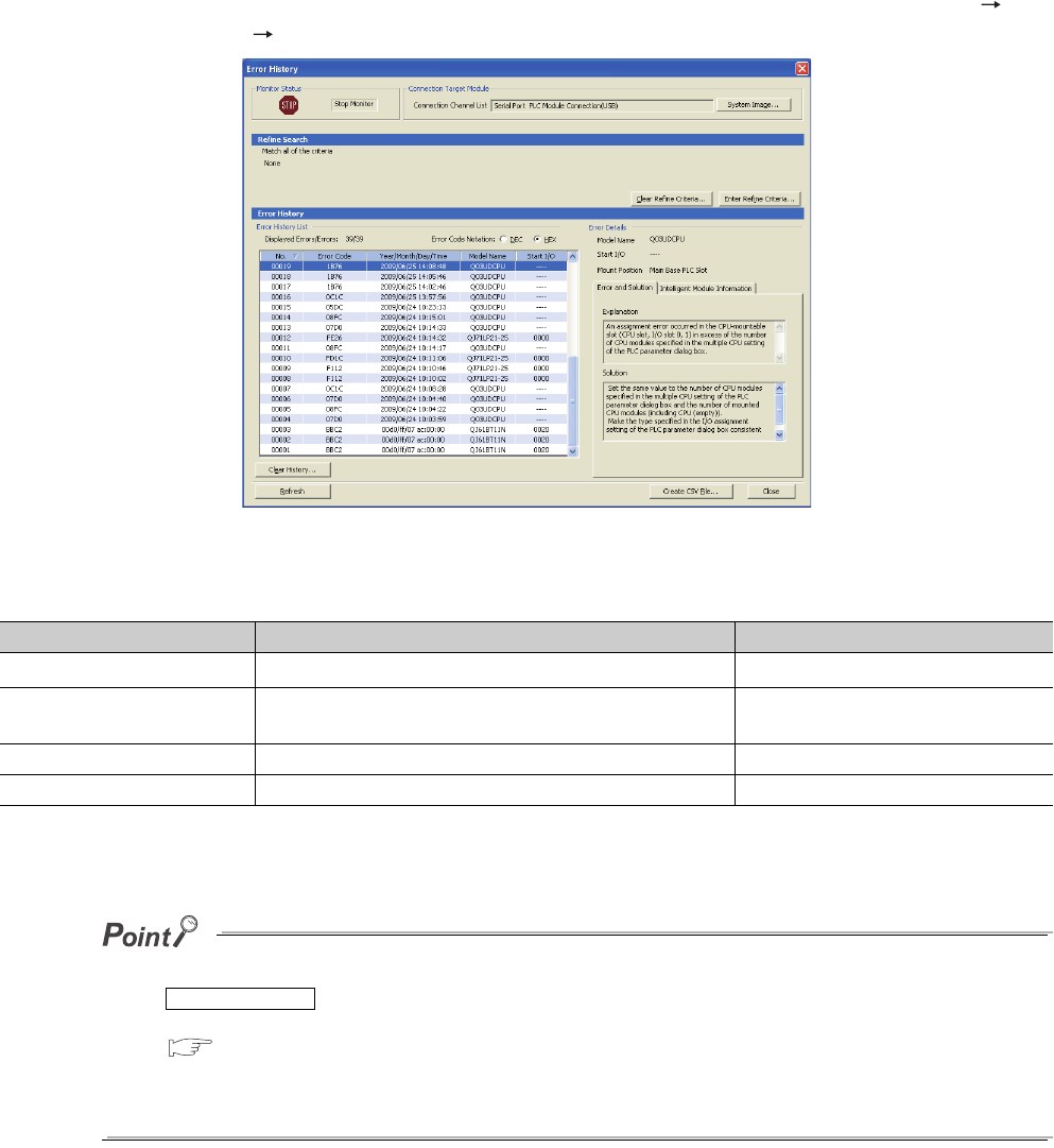
6 - 164
(6) Monitoring module errors
Collected module errors can be monitored in the Error History screen opened by selecting [Diagnostics]
[System Monitor] [System Error History] of GX Works2.
*1: For details of error codes, refer to the manual for the intelligent function module.
*2: If an error occurred during initial processing, its occurrence time may be stored as "0000/00/00 00:00:00" in the module
error collection file. In this case, the error is not displayed in correct order in Error History List.
●The Error History screen can be displayed by selecting a module figure in the System Monitor screen and clicking the
button.
In this case, only the errors of the selected module is displayed.
GX Works2 Version1 Operating Manual (Common)
●Errors are not displayed for modules that do not support the module error collection function.
●Errors may not be displayed when they occur successively.
Figure 6.127 Error History screen
Table6.63 Description of Error History List
Item Description Remarks
Error Code*1 Displays error code numbers. -
Year/Month/Day/Time*2 Displays the year, month, day, hour, minute, and second when
an error occurred.
The year can be displayed within the
range of 1980 to 2079.
Model Name Displays a module model name. -
Start I/O Displays the start I/O number of a module in error. -
Error History Detail
CHAPTER6 FUNCTIONS
1
2
3
4
5
6
7
8
6.32 Module error collection
6 - 165
(7) Clearing module error history
Clear module error history by clicking the in the Error History screen.
Note that error information on each intelligent function module displayed in the Module's Detailed Information
screen is not cleared.
The module error history is cleared when the standard RAM is formatted.
Note that a module error collection file cannot be deleted since it is automatically created after the CPU module is powered
off and then on or is reset. To delete the file, clear the setting and then format the standard RAM.
(8) Precautions
(a) Using the CPU module change function with memory card
Backing up or restoring data will stop collecting module errors.
Figure 6.128 Module's Detailed Information screen
Clear History
Error information displayed
here is not cleared.
7 - 1
CHAPTER7 COMMUNICATIONS WITH INTELLIGENT
FUNCTION MODULE
(1) Intelligent function module
The intelligent function module allows the CPU module to process analog quantity and high speed pulses that
cannot be processed by the I/O modules.
For example, the analog-digital conversion module, one of the intelligent function modules, uses analog quantity
by converting it into a digital value.
(2) Communication with intelligent function module
The intelligent function module is equipped with a memory (buffer memory) to store the data taken in from or
output to external devices.
The CPU modules writes or reads data to or from the buffer memory of the intelligent function module.
7.1 Communications between CPU Module and Intelligent Function
Module
The following table shows the communication methods between the CPU module and intelligent function modules and
the communication timing.
: Executed, -: Not executed
*1: Indicates the program that uses the intelligent function module device, FROM or TO instruction, or the intelligent function module
dedicated instruction.
*2: The RUN/STOP/RESET switch is set from STOP RUN (RUN LED flashes) STOP RUN.
●Data, such as initial settings used for communications with intelligent function module, are stored in the CPU module.
For the storage location, refer to Section 5.1.
●Power off and then on or reset the CPU module to make the initial setting configured in GX Configurator taken effect.
Table7.1 Communication methods with intelligent function module and the communication timing
Communication methods with intelligent
function module
Communication timing
Reference
Power off
on
CPU
module is
reset
STOP
RUN*2
Instruction
execution
END
processing
GX Configurator Initial setting - - Section 7.1.1
Auto refresh setting - - - -
Initial device value - - Section 7.1.2
FROM or TO instruction*1 - - - - Section 7.1.3
Intelligent function module device*1 - - - - Section 7.1.4
Intelligent function module dedicated instruction*1 - - - - Section 7.1.5
7 - 2
CHAPTER7 COMMUNICATIONS WITH INTELLIGENT FUNCTION MODULE
1
2
3
4
5
6
7
8
7.1 Communications between CPU Module and Intelligent Function Module
7.1.1 Initial setting and auto refresh setting by GX Configurator
7.1.1 Initial setting and auto refresh setting by GX Configurator
The initial setting and auto refresh setting can be made by adding in GX Configurator that is supported by the
intelligent function module to GX Developer.
After the initial and auto refresh settings, data can be read or written without creating a program for communications
with intelligent function modules.
(1) Starting GX Configurator
Select [Tools] [Intelligent function module utility] [Start] in GX Developer.
(2) Setting in GX Configurator
An example of initial setting and auto refresh setting for the A/D conversion module Q64AD is used in this section.
(a) Initial setting
The initial setting for the Q64AD offers the following four types.
• A/D conversion enable/disable setting
• Sampling process/averaging process setting
• Time/number of times specifying
• Average time/average number of times setting
Make the initial settings of the Q64AD in the Initial setting screen in GX Configurator as shown in Figure 7.1.
The initial setting data set in this screen are stored into the intelligent function module parameters of the CPU
module.
Figure 7.1 Initial setting screen
7 - 3
(b) Auto refresh setting
The CPU module devices for storing the following data can be set in the Auto refresh setting screen.
• Digital output of the Q64AD
• Maximum and minimum values of the Q64AD
• Error codes
Make auto refresh settings of the Q64AD in the Auto refresh setting screen in GX Configurator as shown in
Figure 7.2.
The auto refresh setting data set in this screen are stored into the intelligent function module parameters of the
CPU module.
Figure 7.2 Auto refresh setting screen
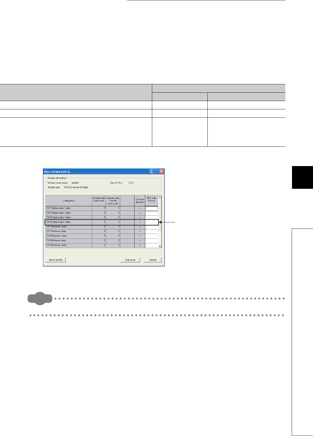
7 - 4
CHAPTER7 COMMUNICATIONS WITH INTELLIGENT FUNCTION MODULE
1
2
3
4
5
6
7
8
7.1 Communications between CPU Module and Intelligent Function Module
7.1.1 Initial setting and auto refresh setting by GX Configurator
(3) Limitation on the number of parameter settings
Limitations are placed on the number of parameters (initial setting and auto refresh setting) set in GX
Configurator.
When multiple intelligent function modules are mounted, make setting in GX Configurator so that the number of
parameter settings for all intelligent function modules may not exceed the limitation shown in Table7.2.
One line in the Auto refresh screen is counted as one parameter setting.
Remark
For details of GX Configurator, refer to the manual for the intelligent function module used.
Table7.2 Maximum number of parameters set in GX Configurator
CPU module Maximum number of parameter settings
Initial setting Auto refresh setting
Q00UJCPU, Q00UCPU, Q01UCPU 512 256
Q02UCPU 2048 1024
Q03UDCPU, Q04UDHCPU, Q06UDHCPU,
Q10UDHCPU, Q13UDHCPU, Q20UDHCPU, Q26UDHCPU,
Q03UDECPU, Q04UDEHCPU, Q06UDEHCPU,
Q10UDEHCPU, Q13UDEHCPU, Q20UDEHCPU, Q26UDEHCPU
4096 2048
Figure 7.3 Counting the number of parameter settings
This one line is counted as one
parameter setting.
Blanks are not counted.
Add the number of lines on
this screen to those of other
intelligent function modules.

7 - 5
7.1.2 Initial setting by initial device value
(1) Initial device value
Using an initial device value ( Section 6.25) allows the initial setting of the intelligent function module without
a program.
The set initial device values are written from the CPU module to the intelligent function module when the CPU
module is powered off and then on, is reset, or set from STOP to RUN.
(2) Setting initial device values
Use GX Developer to set the following.
• Set the device data of the intelligent function module ( Section 9.5.1) used as the initial device value to
the device memory.
• In the initial device value setting, specify the device range of the intelligent function module used as the initial
device value.
7.1.3 Communications with the FROM and TO instructions
The FROM instruction stores data read from the buffer memory of the intelligent function module to the specified
device.
The TO instruction writes data stored in the specified device to the buffer memory of the intelligent function module.
Remark
• For details of the FROM and TO instructions, refer to the following.
QCPU Programming Manual (Common Instructions)
• For details of the buffer memory of the intelligent function module, refer to the following.
Manual for the intelligent function module used

7 - 6
CHAPTER7 COMMUNICATIONS WITH INTELLIGENT FUNCTION MODULE
1
2
3
4
5
6
7
8
7.1 Communications between CPU Module and Intelligent Function Module
7.1.4 Communications using the intelligent function module device
7.1.4 Communications using the intelligent function module device
(1) Intelligent function module device
The intelligent function module device ( Section 9.5.1) represents the buffer memory of the intelligent
function module as one of the CPU module devices.
The data stored in the buffer memory of the intelligent function module can be treated by the sequence instruction
as well as the device memory.
A programming example is given below for the case where "100" is written to the buffer memory of an address 0
of the intelligent function module whose I/O number is X/Y20 to X/Y2F.
(2) Difference from the FROM and TO instructions
The intelligent function module device processes data read from the intelligent function module with one
instruction as the device can be treated as one of the CPU module devices.
A program example is given below for the case where data read from the intelligent function module are added
and then the result is stored in D2.
This reduces the number of steps in whole program.
The instruction processing time indicates the time required for instruction execution and accessing the intelligent
function module.
Figure 7.4 Use of the intelligent function module device
Figure 7.5 Application example of the intelligent function module device
MOV K100 U2\G0
Buffer memory address
I/O number X/Y20
+ U2\G0 D0 D2
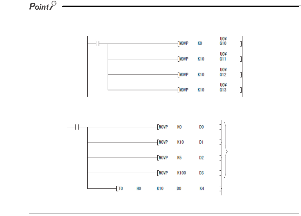
7 - 7
The intelligent function module device accesses the intelligent function module every time when an instruction is executed.
When writing or reading buffer memory data using multiple intelligent function module devices in a sequence program, write
or read the data with the FROM or TO instruction in one location of the program.
Figure 7.6 Writing using multiple intelligent function module devices
Figure 7.7 Writing using the TO instruction
Stores data in the
data register.
Writes data once
at this point.
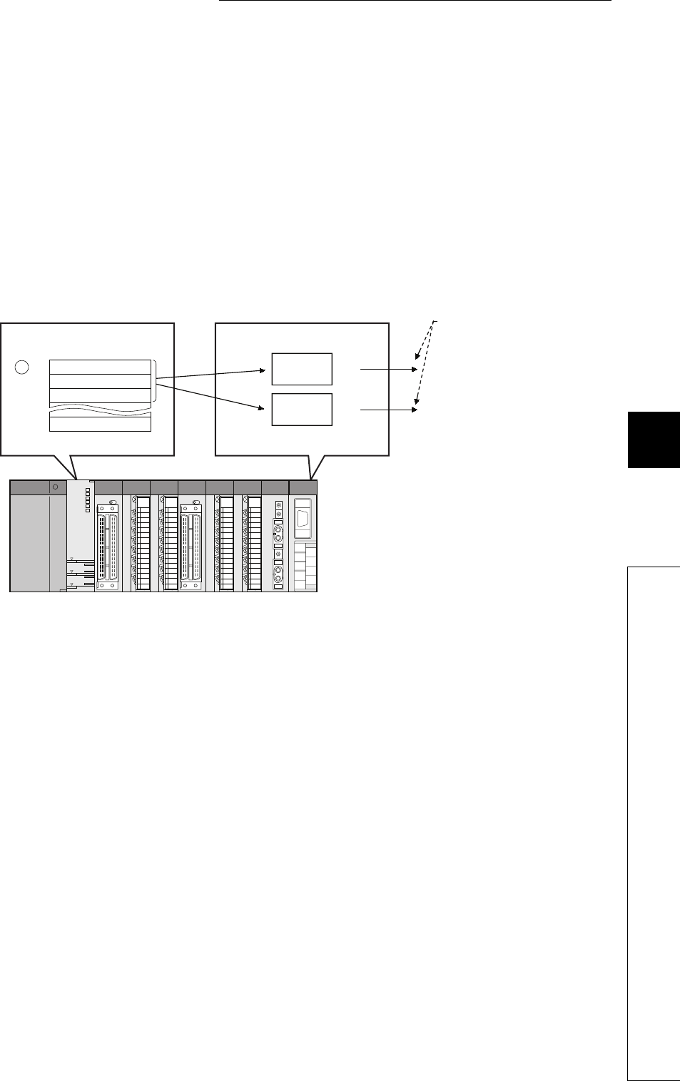
7 - 8
CHAPTER7 COMMUNICATIONS WITH INTELLIGENT FUNCTION MODULE
1
2
3
4
5
6
7
8
7.1 Communications between CPU Module and Intelligent Function Module
7.1.5 Communications using the intelligent function module dedicated instruction
7.1.5 Communications using the intelligent function module dedicated
instruction
(1) Intelligent function module dedicated instruction
This instruction enables easy programming for the use of functions of the intelligent function module.
(a) Example with the serial communication module dedicated instruction (OUTPUT
instruction)
The OUTPUT instruction allows communications with external device by nonprocedural protocol regardless of
the buffer memory address of the serial communication module.
[Transmission by the OUTPUT instruction]
(2) Processing of the intelligent function module dedicated instruction
Some of intelligent function module dedicated instructions can specify the completion device.
This completion device turns on for one scan when an instruction execution is completed.
When using multiple intelligent function module dedicated instructions to one intelligent function module, execute
the dedicated instructions one by one after the completion device turns on.
Figure 7.8 Communications with external devices using the OUTPUT instruction
b15 b0
to
S2
+0
+1
+2
CPU module Serial communication module
Channel
1
Channel
2
Send
Send
Set the used
channel in
control data.

7 - 9
(3) Precautions
(a) When the CPU module is set from RUN to STOP before the completion device turns
on
When a intelligent function module dedicated instruction is executed and the CPU module is set from RUN to
STOP before the completion device turns on, the completion device will not turn on until the CPU module is set
to RUN and then finishes one scan.
(b) Available range
The intelligent function module dedicated instructions are not applicable to the intelligent function modules
mounted on remote I/O stations of MELSECNET/H.
The instructions are applicable to the intelligent function modules mounted on the base unit or extension base
units.
Remark
For intelligent function module dedicated instructions and completion devices, refer to the following.
Manual for the intelligent function module used

8 - 1
CHAPTER8 PARAMETERS
1
2
3
4
5
6
7
8
CHAPTER8 PARAMETERS
This chapter describes the parameters required to be set for configuring a programmable controller system.
(1) Parameter types
The following parameters are provided for CPU module setting.
• PLC parameters ( Section 8.1)
These parameters are set when a programmable controller is used.
• Network parameters ( Section 8.2)
These parameters are set when a programmable controller module is used in combination with any of CC-
Link IE controller network modules, MELSECNET/H modules, Ethernet modules, and CC-Link modules.
• Remote password ( Section 8.3)
Parameters are set when the remote password function is used for an Ethernet module, serial
communication module, modem interface module, or Built-in Ethernet port QCPU.
(2) Parameter setting method
Use GX Developer.
For the setting details, refer to the following.
GX Developer Version 8 Operating Manual
Grayed-out (unselectable) parameter settings in GX Developer are not available since the corresponding function is not
supported.
Remark
Each parameter number shown in the tables in this chapter is stored in the special register (SD16 to SD26) when an error
occurs in parameter setting.
Identify the parameter error location from the parameter number.
For the list of the special register (SD16 to SD26), refer to CHAPTER 12.
For the parameter updating procedure, refer to CHAPTER 11.
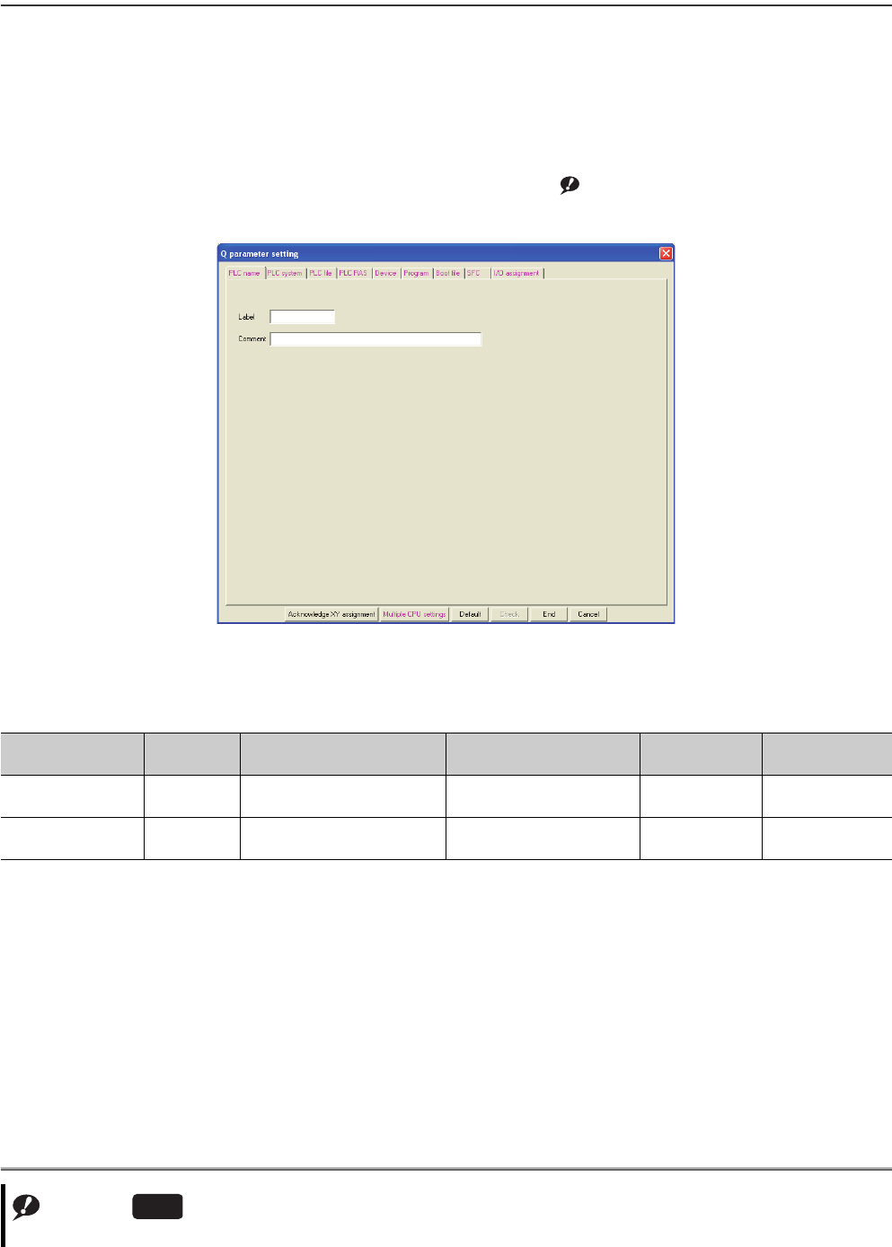
8 - 2
8.1 PLC Parameters
This section provides the list of PLC parameters and describes parameter details.
(1) PLC name
A label and a comment for the CPU module are set.
The settings will be displayed in the list for the find CPU function. Note8.1Note1
Note1
Figure 8.1 PLC name
Table8.1 PLC name setting list
Item Parameter
No. Description Setting range Default Reference
Label 0000H
Set a label (name, application) for
the CPU module. Up to 10 characters Blank -
Comment 0001H
Set a comment for the CPU
module label. Up to 64 characters Blank -
Note8.1
The Universal model QCPUs other than the Built-in Ethernet port QCPU do not support the find CPU function.
Universal
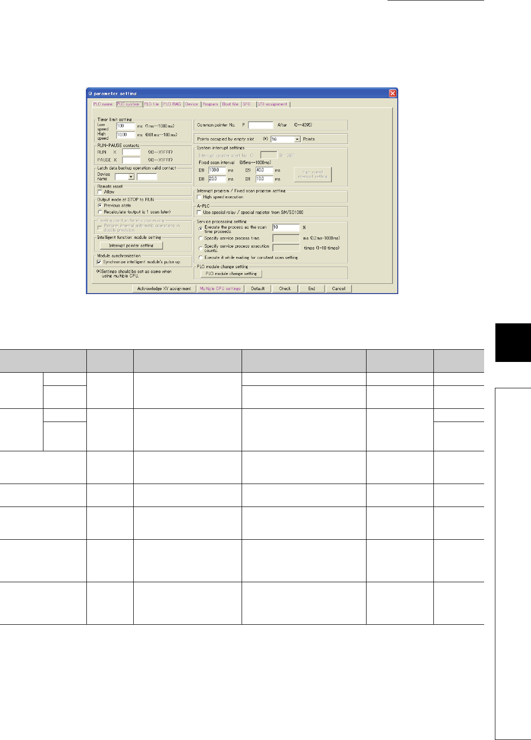
8 - 3
CHAPTER8 PARAMETERS
1
2
3
4
5
6
7
8
8.1 PLC Parameters
(2) PLC system
Parameters required for use of the CPU module are set.
(To the next page)
Figure 8.2 PLC system
Table8.2 PLC system setting list
Item Parameter
No. Description Setting range Default Reference
Timer limit
setting
Low speed
1000HSet the time limit for the low
speed timer or high speed timer.
1ms to 1000ms (in increments of 1ms) 100ms Section 9.2.10
High speed 0.01ms to 100.0ms (in increments of
0.01ms) 10.0ms Section 9.2.10
RUN-
PAUSE
contcts
RUN
1001H
Set the contacts that control RUN/
PAUSE of the CPU module.
Setting of only the PAUSE contact
is not allowed.
X0 to 1FFF Blank
Section 6.6.1
PAUSE Section 6.6.2
Latch data backup
operation valid contact 1014H
Set the valid contact device No.
for backup of latch data to the
standard ROM.
X, M, B Blank Section 6.28
Remote reset 1002H
Select whether to allow the
remote reset from GX Developer. Selected/deselected Deselected Section 6.6.3
Output mode at STOP to
RUN 1003H
Set the status of the outputs (Y)
when the operating status is
switched from STOP to RUN.
Previous state, Recalculate (output is 1
scan later) Previous state Section 6.4
Intelligent function module
setting (Interrupt pointer
setting)
100AH
Assign the interrupt pointers (I50
to I255) and set the start I/O
number and start SI number of
each intelligent function module.
• Start I/O No.
•Start SI No.
• I50 to 255
Blank Section 9.11
Module synchronization 100CH
Select whether to synchronize
CPU module startup with
intelligent function module
startup.
Selected/deselected Deselected -

8 - 4
Table8.2 PLC system setting list (continued)
Item Parameter
No. Description Setting range Default Reference
Common pointer No. 1005HSet the start number of common pointers. P0 to 4095 Blank Section 9.10.2
Points occupied by
empty slot 1007HSet the number of points for empty slots
on the main/extension base units.
0, 16, 32, 64, 128, 256, 512, or
1024 points 16 points Section 3.2.2
System
interrupt
settings
Fixed scan
interval (n:
28 to 31)
1008HSet each execution interval for the
interrupt pointers (I28 to I31).
0.5ms to 1000ms
(in increments of 0.5ms)
• I28: 100.0ms
• I29: 40.0ms
• I30: 20.0ms
• I31: 10.0ms
Section 9.11
Interrupt program/Fixed
scan program setting 1008H
Enable or disable high speed execution
of interrupt programs or fixed scan
execution type programs.
Selected/deselected Deselected Section 2.2.3,
2.3.4
Service processing
setting 1013H
Select any of the following options.
• Execute the process as the scan time
proceeds.
• Specify service process time.
• Specify service process execution
counts.
• Execute it while waiting for constant
scan time setting.
• 1 to 99% (in increments of
1%)
• 1 to 10 (in increments of 1
time)
• 0.2 to 1000ms (in increments
of 0.1ms)
•Blank
Execute the
process as the
scan time
proceeds.: 10%
Section 6.24.1
PLC module change
setting (PLC module
change setting)
1017H
Set items required when performing the
CPU module change with memory card
function.
• Backup start setup contact
• Backup start contact
• Backup target data
• Title setting
Blank Section 6.30
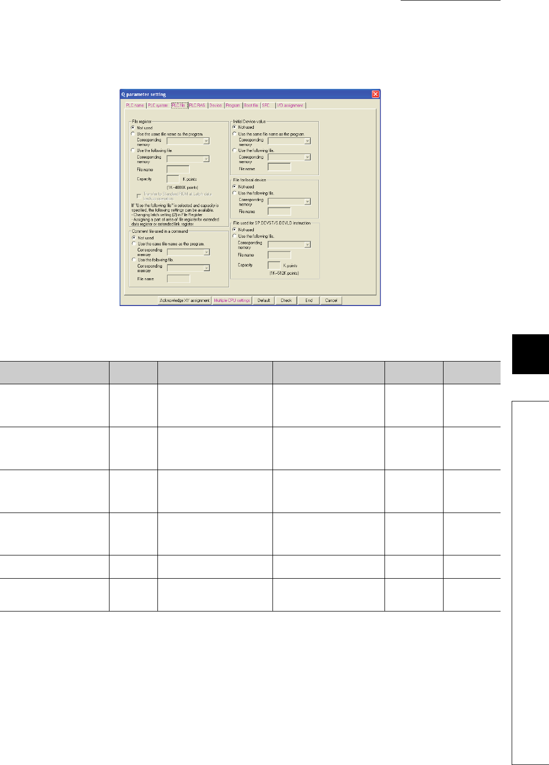
8 - 5
CHAPTER8 PARAMETERS
1
2
3
4
5
6
7
8
8.1 PLC Parameters
(3) PLC file
Parameters required for the files used in the CPU module are set.
*1: Not available for the Q00UJCPU.
Figure 8.3 PLC file
Table8.3 PLC file setting list
Item Parameter
No. Description Setting range Default Reference
File register*1 1100H
Set a file for the file register used in
the program.
• Not used
• Use the same file name as the
program.
• Use the following file.
Not used Section 9.7
Transfer to Standard ROM at
Latch data backup operation*1 1104H
Select whether to batch-transfer
the data in the file register at the
time of latch data backup to the
standard ROM.
Checked/unchecked Not selectable Section 6.27
Comment file used in a
command 1101H
Set a file for device comments
used in the program.
• Not used
• Use the same file name as the
program.
• Use the following file.
Not used -
Initial Device value 1102H
Set a file for initial values of the
devices used for the CPU module.
• Not used
• Use the same file name as the
program.
• Use the following file.
Not used Section 6.25
File for local device*1 1103H
Set a file for local devices used in
the program.
• Not used
• Use the following file. Not used Section 9.14.2
File use for SP.DEVST/S.DEVLD
instruction 1105H
Set a device data file used for
writing to or reading from the
standard ROM.
• Not used
• Use the following file. Not used Section 6.28
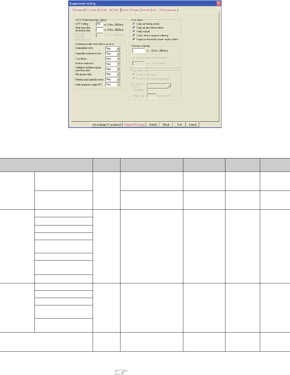
8 - 6
(4) PLC RAS (1)
Parameters required for performing the RAS functions are set.
*1: These items are provided for future expansion.
*2: When selecting this item for the Q02UCPU, Q03UDCPU, Q04UDHCPU, Q06UDHCPU, Q13UDHCPU, or Q26UDHCPU, check the
versions of the CPU module and GX Developer. ( Appendix 2)
*3: Not available for the Q00UJCPU, Q00UCPU, and Q01UCPU.
Figure 8.4 PLC RAS (1)
Table8.4 PLC RAS (1) setting list
Item Parameter
No. Description Setting range Default Reference
WDT
(Watchdog
timer) setting
WDT Setting
3000H
Set a watchdog timer value for
the CPU module.
10ms to 2000ms
(in increments of
10ms)
200ms Section 6.16
Initial execution monitoring
time
Set a watchdog timer value in
the case of using an initial
execution type program.
10ms to 2000ms
(in increments of
10ms)
Blank Section 2.3.1
Operating mode
when there is an
error
Computation error
3002H
Set the operation mode of the
CPU module when an error is
detected.
Stop/Continue Stop Section 6.17
Expanded command error*1
Fuse blown
Module verify error
Intelligent module program
execution error
File access error
Memory card operation
error*3
External power supply OFF*1
Error check
Carry out battery check
3001H
Enable or disable detection of
the specified error. Selected/deselected Deselected Section 6.17
Carry out fuse blown check
Verify module
Check device range at
indexing.
Diagnose redundant power
supply system.*2
Constant scanning 3003HSet a constant scan time value.
0.5ms to 2000ms
(in increments of
0.5ms)
Blank Section 6.2
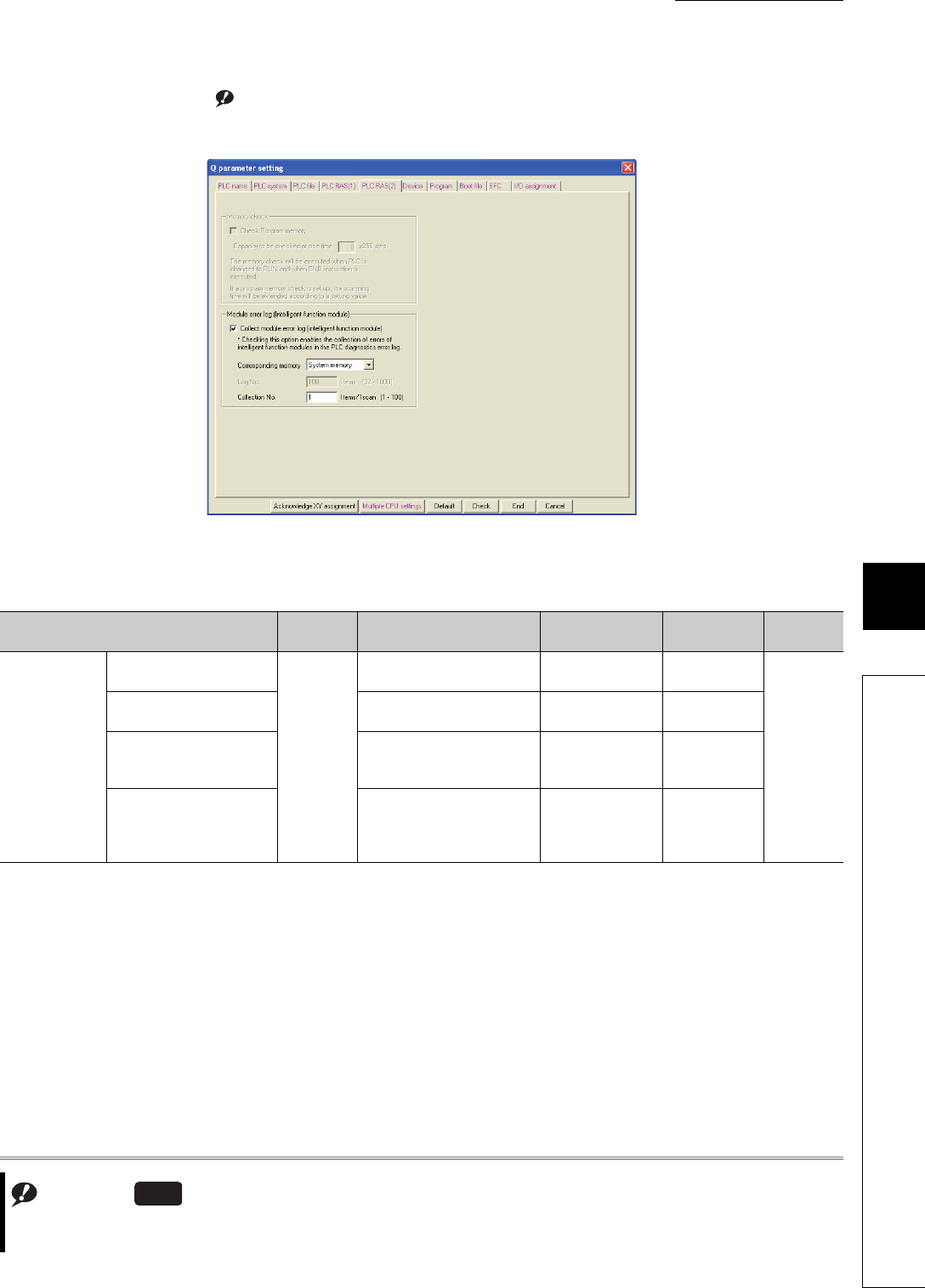
8 - 7
CHAPTER8 PARAMETERS
1
2
3
4
5
6
7
8
8.1 PLC Parameters
(5) PLC RAS (2) Note1
Parameters required for performing the RAS functions are set.
Note1
Figure 8.5 PLC RAS (2)
Table8.5 PLC RAS (2) setting list
Item Parameter
No. Description Setting range Default Reference
Module error log
(Intelligent
function module)
Collect module error log
(intelligent function module)
300AH
Set whether to collect module
errors. Selected/deselected Selected
Section 6.32
Corresponding memory Select a storage location. • System memory
• Standard RAM System memory
Log No.
Set the number of collected
errors only when the errors are
stored in the standard RAM.
32 to 1000 40/100
Collection No. Set the number of collected
errors in one scan.
• Stored in system
memory: 1 to 100
• Stored in standard
RAM: 1 to 128
1
Note8.2
Note8.2
The setting screen differs between GX Works2 and GX Developer. For the setting of the module error log function,
refer to Section 6.32(5)
Universal
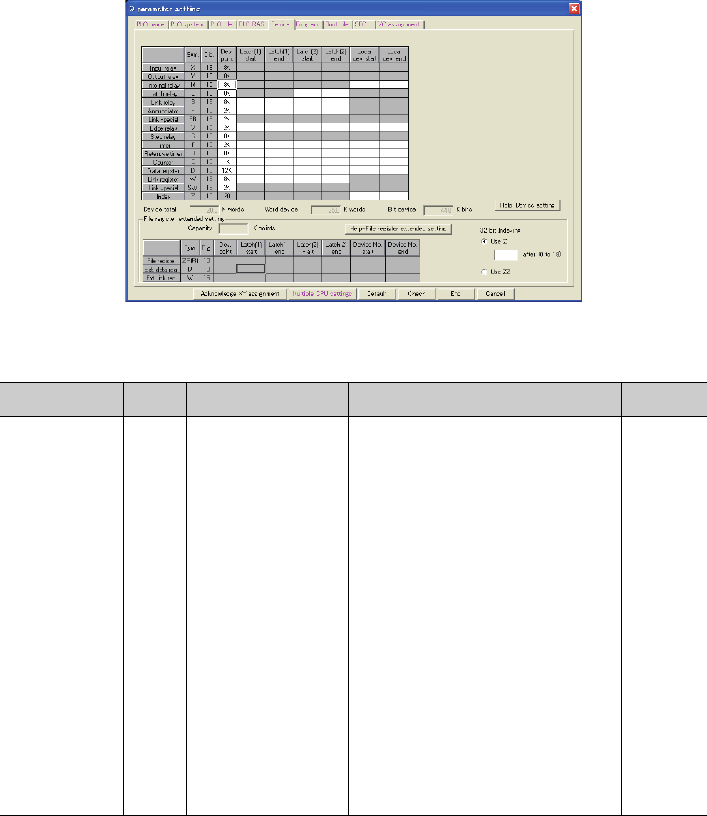
8 - 8
(6) Device
Number of points, latch range, and local device range are set for each device.
(To the next page)
Figure 8.6 Device
Table8.6 Device setting list
Item Parameter
No. Description Setting range Default Reference
Device points*1 2000H
Set the number of device points
that is appropriate to the system.
X (8K), Y (8K), and S (8K)*3 are fixed.
Setting is available within the range of
29K words in total, including the above
fixed points (1.5K words).
• One device: Up to 32K points
• Total bit device points: Up to 64K
points
•X: 8K
•Y: 8K
•M: 8K
•L: 8K
*2
•B: 8K
•F: 2K
•SB: 2K
•V: 2K
•S: 8K
*3
•T: 2K
•ST: 0K
•C: 1K
•D: 12K
•W: 8K
•SW: 2K
Section 9.1
Latch (1) start/end (Latch
clear valid)*2 2001H
Set a latch range (start and end
device numbers), which can be
cleared by remote latch clear
operation.
Setting is available for only one range
for each of B, F, V, T, ST, C, D, and W
devices.
Blank Section 3.4, 6.3
Latch (2) start/end (Latch
clear invalid)*2 2002H
Set a latch range (start and end
device numbers), which cannot be
cleared by remote latch clear
operation.
Setting is available for only one range
for each of L, B, F, V, T, ST, C, D, and W
devices.
Blank Section 3.4, 6.3
Local device start/end*6 2003H
Set a range (start and end device
numbers), which is used for a
local device.
Setting is available for only one range
for each of M, V, T, ST, C, D, and Z
devices.*5
Blank Section 9.14.2

8 - 9
CHAPTER8 PARAMETERS
1
2
3
4
5
6
7
8
8.1 PLC Parameters
*1: When changing the device points, new setting must not exceed the refresh ranges of network modules or the auto refresh ranges of
intelligent function modules.
If a new device point setting exceeds the corresponding device range, the data may be written to another device or an error may occur.
*2: When a device latch range is set, the scan time increases.
When latching a device, consider the increase in the scan time. ( Section 10.1.2)
*3: The points for the step relay (S) can be changed to 0 if the serial number (first five digits) of the Universal model QCPU is "10042" or later.
*4: Available only when the serial number (first five digits) of the Universal model QCPU is "10042" or later.
*5: When using the index register as a local device for the Q03UDCPU, Q04UDHCPU, Q06UDHCPU, Q13UDHCPU, Q26UDHCPU, or
Built-in Ethernet port QCPU, check the versions of the CPU module and GX Developer. ( Appendix 2)
*6: Not available for the Q00UJCPU.
Table8.6 Device setting list (continued)
Item Parameter
No. Description Setting range Default Reference
File register
extended
setting*6
Device points 2000H
Set points for the file register
(ZR), extended data register
(D), and extended link register
(W).
Point assignment to the file
register (ZR), extended data
register (D), or extended link
register (W). Assign part of the
points of the file register to the
extended data register and
extended link register.
Blank Section 9.1,
9.8
Latch (1) start/end
(Latch clear valid) 2004H
Set a latch range (start and
end device numbers), which
can be cleared by remote latch
clear operation.
Each latch range for the file
register (ZR), extended data
register (D), or extended link
register (W).
Blank Section 3.4,
6.3
Latch (2) start/end
(Latch clear invalid) 2005H
Set a latch range (start and
end device numbers), which
cannot be cleared by remote
latch clear operation.
Each latch range for the file
register (ZR), extended data
register (D), or extended link
register (W).
Blank Section 3.4,
6.3
32 bit Indexing*4 2000HSelect Z or ZZ device for 32-bit
indexing. Z0 to Z18 (when using Z device) Use Z
QCPU
Programmin
g Manual
(Common
Instructions)
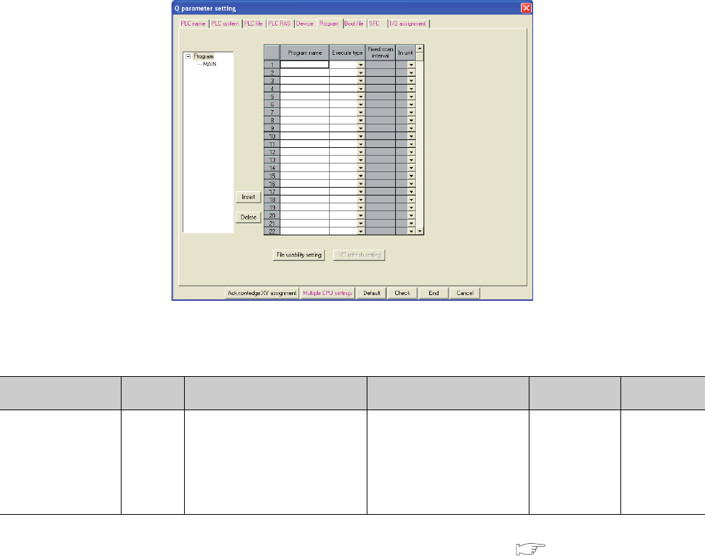
8 - 10
(7) Program
File names and execution types (execution conditions) are set for each program when two or more programs are
written to the CPU module.
*1: Available for local devices only.
When using the file usability setting, check the versions of the CPU module and GX Developer. ( Appendix 2)
The setting is not available for the Q00UJCPU.
Figure 8.7 Program
Table8.7 Program setting list
Item Parameter
No. Description Setting range Default Reference
Program setting 7000H
When writing two or more programs to
the CPU module, set a file name and
execution type (execution condition) of
each program.
Also, set a fixed scan interval
(execution interval of the fixed scan
execution type program).
• Program name
• Execute type (fixed scan
interval when the fixed scan
execution is selected)
• File usability setting*1
Blank Section 2.3
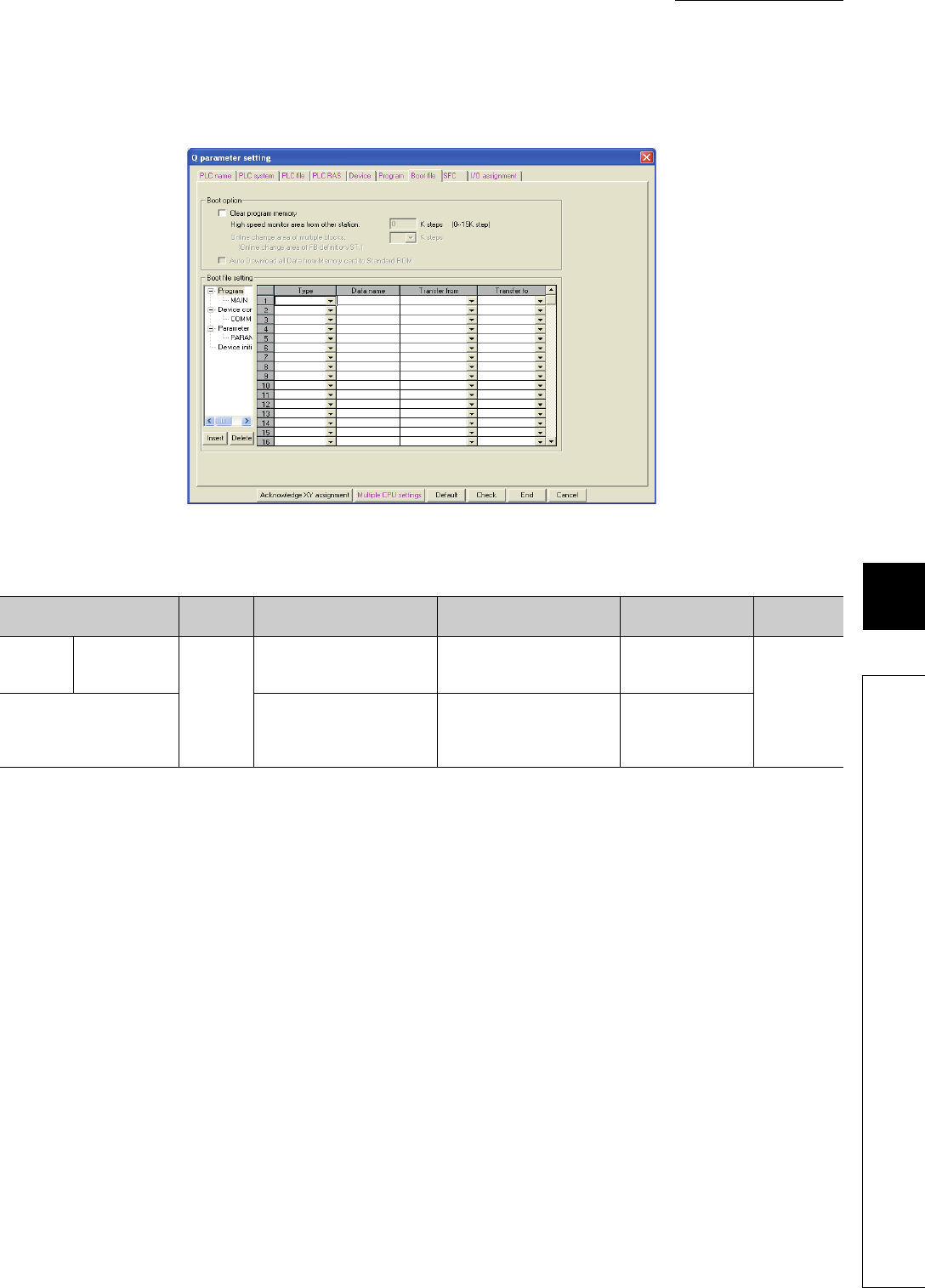
8 - 11
CHAPTER8 PARAMETERS
1
2
3
4
5
6
7
8
8.1 PLC Parameters
(8) Boot file
Parameters required for a boot from a memory card are set.
Figure 8.8 Boot file
Table8.8 Boot file setting list
Item Parameter
No. Description Setting range Default Reference
Boot option Clear program
memory
7000H
Select whether to clear the
program memory at the time of
boot.
Selected/deselected Deselected
Section 5.1.8
Boot file setting
Set the type and data name of
the boot file, and transfer source
drive for boot operation.
Type, "Data name, and Transfer
from (the transfer target drive
(Transfer to) is automatically set
in the program memory.)
Blank
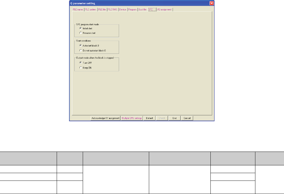
8 - 12
(9) SFC
The mode and conditions for starting an SFC program, and the output mode in the case of a block stop are set.
Figure 8.9 SFC
Table8.9 SFC setting list
Item Parameter
No. Description Setting range Default Reference
SFC program start mode 8002HSet the mode and conditions for
starring an SFC program, and also
set the output mode in case a
program block is stopped.
Refer to the QCPU (Q Mode)/
QnACPU Programming Manual
(SFC).
Initial start
-
Start conditions 8003HAutostart block 0
Output mode when the block
is stopped 8006HTurn OFF
8 - 13
CHAPTER8 PARAMETERS
1
2
3
4
5
6
7
8
8.1 PLC Parameters
(10)I/O assignment
The mounting status of each module in the system is set.
(To the next page)
Figure 8.10 I/O assignment
Table8.10 I/O assignment setting list
Item Parameter
No. Description Setting range Default Reference
I/O
Assignme
nt
Type
0400H
Set the type of the mounted module.
• CPU No.2 to No.4: No.n/Empty (Set
"CPU (Empty)" for the slot where no
CPU module is mounted.)
• Empty, Input, Hi input, Output,
Intelli., I/O mix, or Interrupt
Blank Section
4.2.2
Model name
Set the model name of the mounted
module. (Entered at user’s discretion.
Do not use the one for the CPU
module.)
Up to 16 characters
Points Set the number of points assigned to
each slot.
0, 16, 32, 48, 64, 128, 256, 512, or
1024 points
Start XY Set the start I/O number of each slot. 0H to FF0H
Base
setting
Base model
name
0401H
Set the model name of the main base
unit or extension base unit. (Entered at
user’s discretion. Do not use the one
for the CPU module.)
Up to 16 characters
Blank Section
4.1.2
Power model
name
Set the model name of the power
supply module on the main base unit
or extension base unit. (Entered at
user’s discretion. Do not use the one
for the CPU module.)
Up to 16 characters
Extension
cable
Set the extension cable name.
(Entered at user’s discretion. Do not
use the one for the CPU module.)
Up to 16 characters
Slots
Set the number of slots of the main
base unit or extension base unit.
This setting must be done for all base
units.
2, 3, 5, 8, 10, or 12

8 - 14
Table8.10 I/O assignment setting list (continued)
Item Parameter
No. Description Setting range Default Reference
Switch setting 0407H
Set various switches of an
intelligent function module.
Refer to the manual for the
intelligent function module used. Blank Section 6.10
Detailed
setting
Error time
output mode 0403H
Set whether to clear or hold the
output in case of a stop error in
the control CPU.
Clear/Hold Clear Section 6.8
H/W error
time PLC
operarion
mode
4004H
Set whether to stop or continue
the operarion of the control
CPU in case of a hardware
failure of the intelligent function
module.
Stop/Continue Stop Section 6.9
I/O response
time 0405H
Set a response time for the
input module, high-speed input
module, I/O combined module,
or interrupt module.
• Input or I/O mix: 1ms, 5ms,
10ms, 20ms, or 70ms
• Hi input or Interrupt: 0.1ms,
0.2ms, 0.4ms, 0.6ms, or 1ms
• Input or I/O mix:
10ms
• Hi input or Interrupt:
0.2ms
Section 6.7
Control PLC 0406H
Set the control CPU for the input/
output modules and intelligent
function module.
No.1, No.2, No.3, or No.4 No.1
QCPU User's
Manual (Multiple
CPU System)
8 - 15
CHAPTER8 PARAMETERS
1
2
3
4
5
6
7
8
8.1 PLC Parameters
(11) Serial Note8.3Note1
The transmission speed, sum check, transmission wait time, and RUN write setting for using the serial
communication function of the CPU module are set.
Note1
Figure 8.11 Serial
Table8.11 Serial setting list
Item Parameter
No. Description Setting range Default Reference
Use serial communication
100EH
Select the item when using the
serial communication function. Selected/deselected Deselected
Section 6.23
Transmission speed
Set a transmission speed for data
communication with the external
device.
9.6kbps, 19.2kbps, 38.4kbps,
57.6kbps, 115.2kbps 19.2kbps
Sum check
Set whether to add a sum check
code to a message sent or
received when using the serial
communication function,
according to the specifications of
the external device.
Selected/deselected Selected
Transmission wait time
Set a period of waiting time on the
Basic model QCPU side in case
the CPU module cannot receive
data immediately after the
external device sends data.
No waiting time/10ms to
150ms (in increments of
10ms)
No waiting time
RUN write setting
Enable or disable writing of data
from the external device to the
running CPU module.
Selected/deselected Deselected
Note8.3
When using the serial communication function for the Q02UCPU, check the versions of the CPU module and GX
Developer. ( Appendix 2)
The Q03UDCPU, Q04UDHCPU, Q06UDHCPU, Q10UDHCPU, Q13UDHCPU, Q20UDHCPU, Q26UDHCPU, and
Built-in Ethernet port QCPU do not support the serial communication function.
Universal
8 - 16
(12) Acknowledge XY assignment
The parameters set in the I/O assignment, Ethernet/CC IE/MELSECNET setting, and CC-Link setting can be
confirmed.
Figure 8.12 Acknowledge XY assignment
Table8.12 Acknowledge X/Y assignment list
Item Parameter
No. Description Setting range Default Reference
X/Y assignment -
The data set in the I/O assignment, Ethernet/CC IE/
MELSECNET setting, and CC-Link setting can be
checked.
---
8 - 17
CHAPTER8 PARAMETERS
1
2
3
4
5
6
7
8
8.1 PLC Parameters
(13) Multiple CPU settings Note8.4Note1
Parameters required for configuring a multiple CPU system are set.
(To the next page)
Note1
Figure 8.13 Multiple CPU settings
Table8.13 Multiple CPU setting list
Item Parameter
No. Description Setting range Default Reference
No. of PLC 0E00HSet the number of CPU modules used in a multiple
CPU system. 1 to 4 1
QCPU User's
Manual (Multiple
CPU System)
Host CPU
number*1 E00CH
Set a CPU number for which the multiple CPU
setting parameters are set. (Set the number of the
connected CPU module.)
PLC No.1 to No.4 Blank
Operating mode 0E01H
Select the multiple CPU system operation to be
performed in case a stop error occurs in any of
CPU No.2 to No.4.
When CPU No.1 results in a stop error, the multiple
CPU system stops. (Fixed)
Selected/
deselected All items selected
Multiple CPU
synchronous
startup setting*1
E00BH
Enable or disable synchronous startup of the CPU
modules on the multiple CPU system. Mp.1 to No.4 All items selected
Note8.4
The Q00UJCPU cannot be used in multiple CPU systems.
Universal

8 - 18
*1: Not available for the Q00UCPU, Q01UCPU, and Q02UCPU.
*2: SM, SD, SB, and SW are valid only when they are selected as send devices.
Table8.13 Multiple CPU setting list (continued)
Item Parameter
No. Description Setting range Default Reference
Online module change*1 E006H
Enable or disable the online
module change in the multiple
CPU system. (When enabled,
the CPU module cannot read
the I/O data outside the
specified group.)
Selected/deselected Deselected
QQCPU Userís
Manual (Multiple
CPU System)
I/O sharing when
using Multiple CPUs
All CPUs
can read all
inputs
0E04H
Select whether to read the
input data of the input modules
or intelligent function modules
controlled by another CPU.
Selected/deselected Deselected
All CPUs
can read all
outputs
Select whether to read the
output data of the output
modules controlled by another
CPU.
Selected/deselected Deselected
Multiple
CPU high
speed
transmiss
ion area
setting*1
CPU specific send
range E008H
Set the size of the multiple
CPU high-speed transmission
area that is assigned to each
CPU module of the multiple
CPU system.
Simple setting:
0 to 12K (in increments of 1K
points)
Advanced setting:
0 to 16K (in increments of
0.5K points)
3K points
Auto
refresh
setting
Refresh
setting
E009H
E00AH
Set an area range for data
communication performed with
the auto refresh function in the
user area of the multiple CPU
high-speed transmission area.
Available devices*2:
X, Y, M, L, B, D, W, R, ZR,
SM, SD, SB, and SW
-
Communication area setting
(refresh setting)
E002H
E003H
In the multiple CPU system,
data are transferred by auto
refresh among respective CPU
modules.
Set the devices to be written or
read and their points.
[Set starting devices for each
CPU]
Selected/deselected
Deselected
[CPU specific send range]
0 to 2048 points (in
increments of 2 points) per
CPU
Up to 8K points (8192 points)
per system
Blank
[PLC side device]
B, M, Y, D, W, R, or ZR
Occupies the device of the
points set for the send range
and starting from the
specified device number.
• One point in the send
range equals 16 points in
B, M, or Y.
• One point in the send
range equals one point in
D, W, R, or ZR.
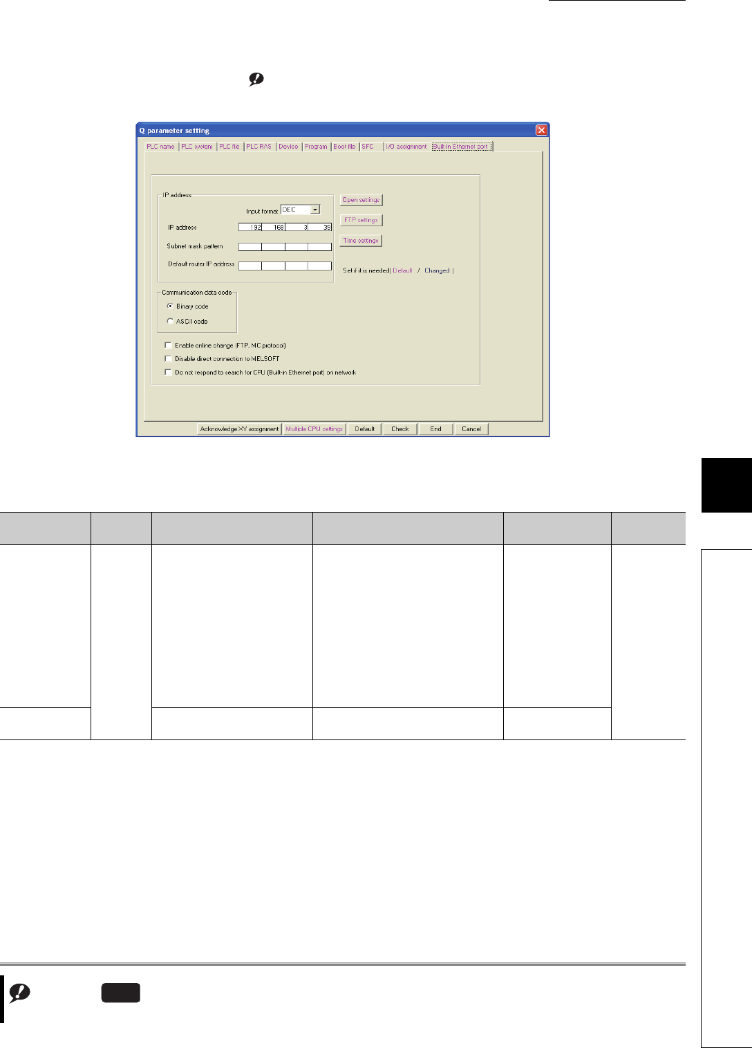
8 - 19
CHAPTER8 PARAMETERS
1
2
3
4
5
6
7
8
8.1 PLC Parameters
(14) Built-in Ethernet port Note8.5Note1
Parameters required for use of the built-in Ethernet port are set.
(To the next page)
Note1
Figure 8.14 Built-in Ethernet port
Table8.14 Built-in Ethernet port setting list
Item Parameter
No. Description Setting range Default Reference
IP address
1016H
• IP address:
Enter the IP address of the
QnUDE(H)CPU.
• Subnet mask pattern:
Enter the subnet mask pattern
when using a router.
• Default router IP address:
Enter the IP address of the
router.
• IP address:
0.0.0.1 to 223.255.255.254
(00000001H to 0DFFFFFFEH)
• Subnet mask pattern:
Blank or
192.0.0.0 to 255.255.255.252
(0C0000000H to 0FFFFFFFCH)
• Default router IP address:
Blank or
0.0.0.1 to 223.255.255.254
(00000001H to 0DFFFFFFEH)
• IP address:
192.168.3.39
• Subnet mask
pattern:
Blank
• Default router IP
address:
Blank
QnUCPU
Userís
Manual(Com
munication via
Built-in
Ethernet Port)
Communication
data code
Select the code for MC protocol
communication. Binary code/ASCII code Binary code
Note8.5
The Universal model QCPUs other than the Built-in Ethernet port QCPU are not equipped with any Ethernet port.
Universal

8 - 20
Table8.14 Built-in Ethernet port setting list (continued)
Item Parameter
No. Description Setting range Default Reference
Open settings
1016H
Set data when using MC protocol or
socket communication. -Blank
QnUCPU
Userís Manual
(Communicati
on via Built-in
Ethernet Port)
FTP settings Set data when using the file transfer
function (FTP). -Blank
Time settings Set data when using the time
setting function. -Blank
Enable online
change (FTP, MC
protocol)
Enable or disable writing data in
devices or files to the running CPU
module when MC protocol or FTP is
used.
Selected/deselected Deselected
Disable direct
connection to
MELSOFT
Enable or disable direct connection
to MELSOFT.
To enhance the security with the
remote password setting, check it to
disable it.
Selected/deselected Deselected
Do not respond to
search for CPU
(Built-in Ethernet
port) on network
Checking this box disables
response to the find CPU function
of the MELSOFT connection.
To enhance the security, check it to
disable this.
Selected/deselected Deselected

8 - 21
CHAPTER8 PARAMETERS
1
2
3
4
5
6
7
8
8.2 Network Parameters
8.2 Network Parameters
This section provides the list of network parameters and describes parameter details.
Symbols, M and N, used in the "Parameter No." column
M and N in "Parameter No." in this section denote the following:
• N: Indicates the module number.
• M: Indicates the network type.
Table8.15 For CC-Link IE controller network and MELSECNET/H ( (1), (2) in this section)
MNetwork type
1HCC IE Control (Control station), MELSECNET/H mode (Control station), MELSECNET/H
Extended mode (Control station), MELSECNET/10 mode (Control station)
2HCC IE Control (Normal station), MELSECNET/H mode (Normal station), MELSECNET/H
Extended mode (Normal station), MELSECNET/10 mode (Normal station)
5HMELSECNET/H (Remote master)
AHMELSECNET/H (Standby station)
BHMELSECNET/H mode multiplexed remote I/O network master station
DHMELSECNET/H mode multiplexed remote I/O network sub-master station
(when no parameter is set)
EHMELSECNET/H mode multiplexed remote I/O network sub-master station
(when parameters are set)
Table8.16 For CC-Link setting ( (4) in this section)
MNetwork type
0HMaster station
1HLocal station
2HStandby master station
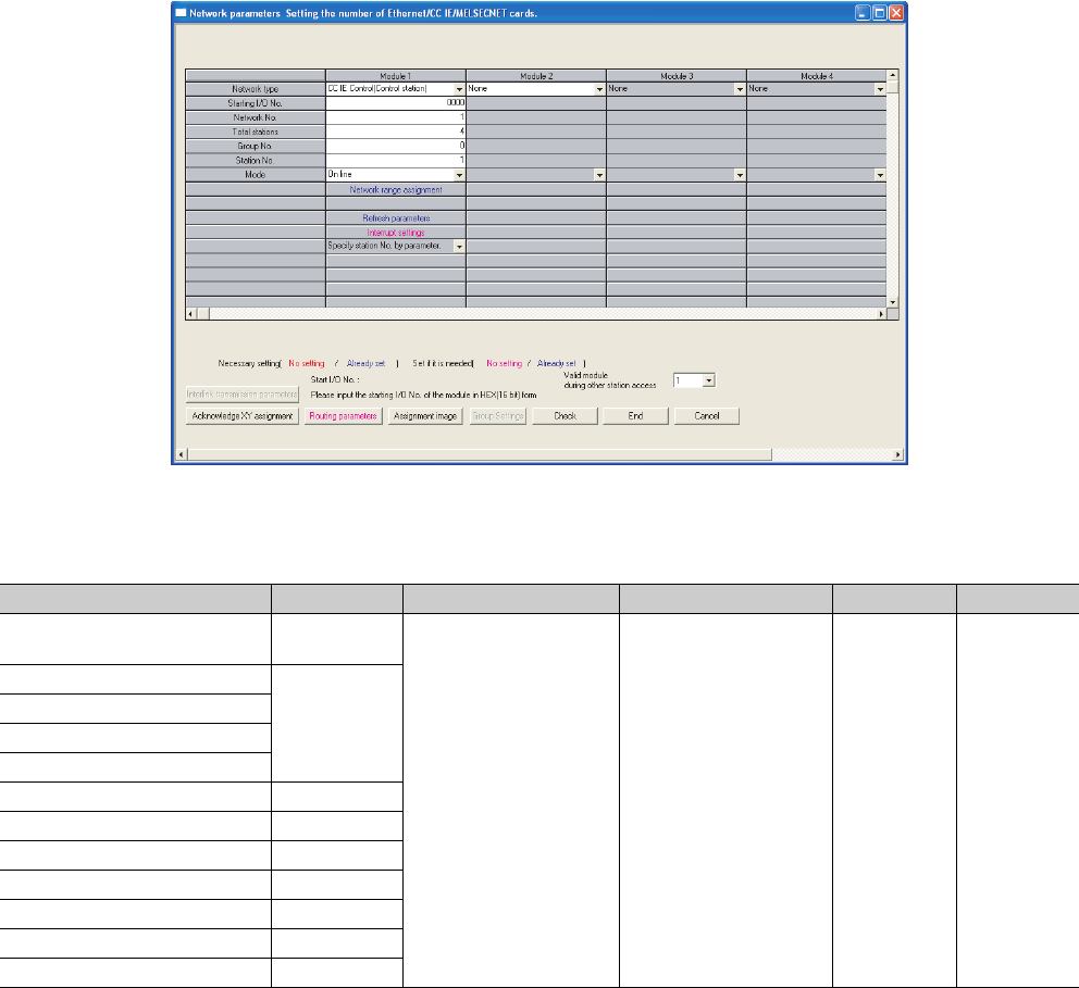
8 - 22
(1) CC-Link IE controller network setting
Network parameters for the CC-Link IE controller network are set.
Figure 8.15 Setting the number of Ethernet/CC IE/MELSECNET cards (CC-Link IE controller network setting)
Table8.17 CC-Link IE controller network setting list
Item Parameter No. Description Setting range Default Reference
Number of modules on CC-Link IE
controller network A000H
Set network parameters for
the CC-Link IE controller
network.
Refer to the manual for the
CC-Link IE controller
network.
--
Starting I/O No.
ANM0H
Network No.
Total stations
Station No.
Group No. 0AmnH
Mode ANM0H
Refresh parameters ANM1H
Common parameters ANM2H
Station inherent parameters ANM3H
Interlink transmission parameters A002H
Routing parameters 5003H
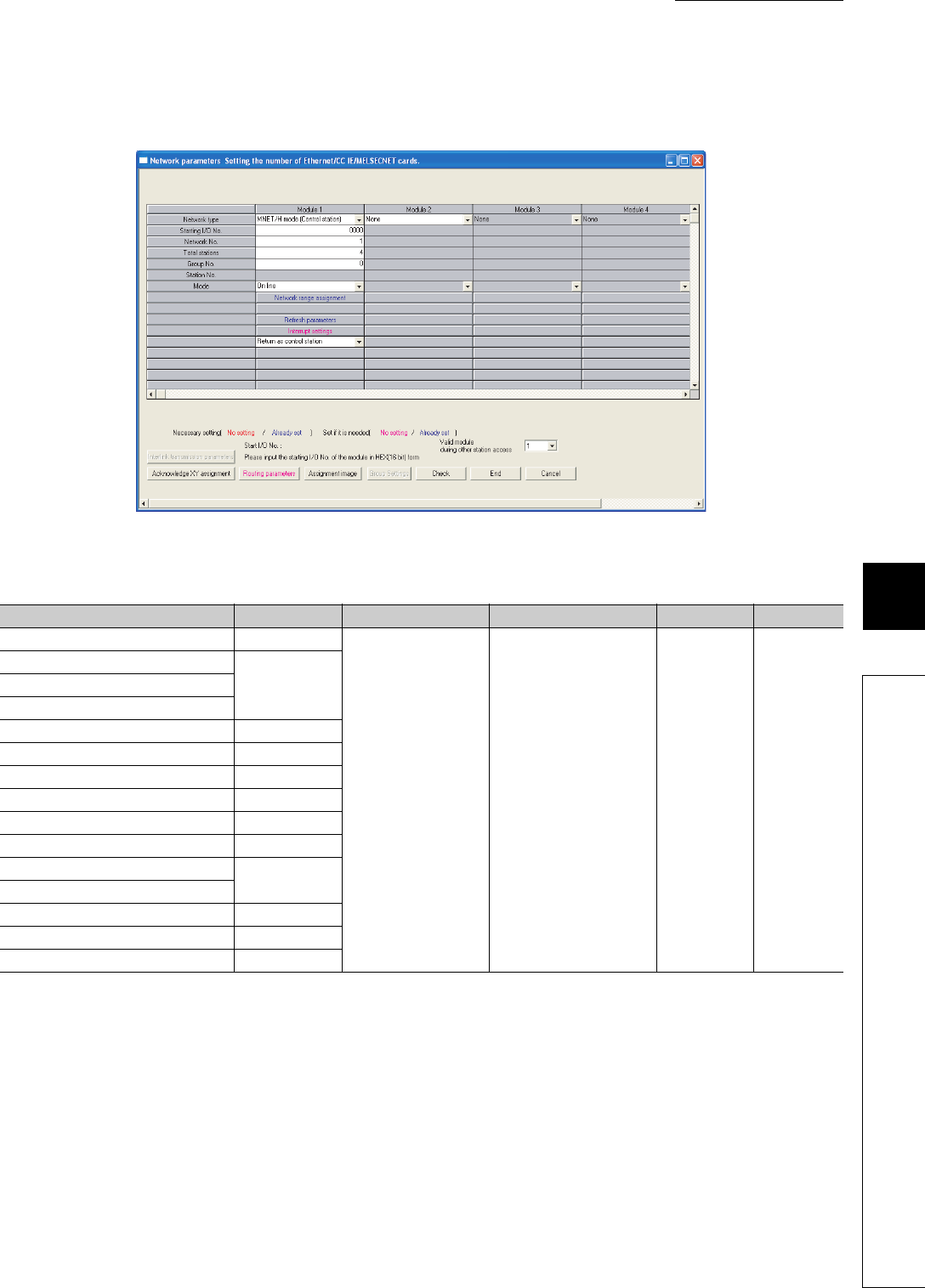
8 - 23
CHAPTER8 PARAMETERS
1
2
3
4
5
6
7
8
8.2 Network Parameters
(2) MELSECNET/H setting
Network parameters for MELSECNET/H are set.
Figure 8.16 Setting the number of Ethernet/CC IE/MELSECNET cards (MELSECNET/H setting)
Table8.18 MELSECNET/H setting list
Item Parameter No. Description Setting range Default Reference
Number of modules on MELSECNET/H 5000H
Set MELSECNET/H
network parameters.
Refer to the manual for the Q
series-compatible
MELSECNET/H.
--
Starting I/O No.
5NM0HNetwork No.
Total stations
Group No. 05mnH
Mode 5NM0H
Refresh parameters 5NM1H
Common parameters 5NM2H
Station inherent parameters 5NM3H
Common parameters 2 5NMAH
Station inherent parameters 2 5NMBH
Interrupt settings
Valid module during other station access 5001H
Interlink transmission parameters 5002H
Routing parameters 5003H
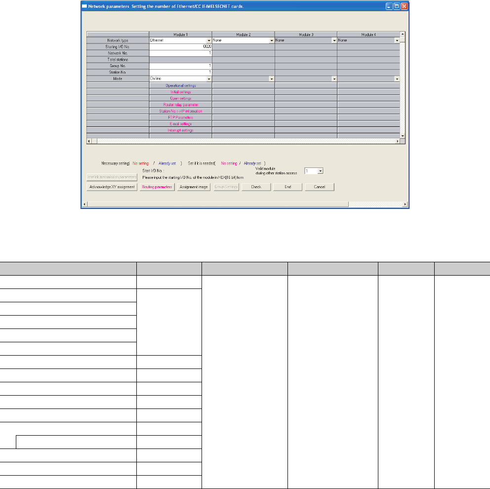
8 - 24
(3) Ethernet setting
Network parameters for Ethernet are set.
Figure 8.17 Setting the number of Ethernet/CC IE/MELSECNET cards (Ethernet setting)
Table8.19 Ethernet setting list
Item Parameter No. Description Setting range Default Reference
Number of modules on Ethernet 9000H
Set Ethernet network
parameters.
Refer to the manual for the
Q series-compatible
Ethernet.
--
Starting I/ONo.
9N00H
Network No.
Group No.
Station No.
Operational settings
Initial settings 9N01H
Open settings 9N02H
Router relay parameter 9N03H
Station No.<->IP information 9N05H
FTP Parameters 9N06H
E-mail settings 9N07H
News setting 9N08H
Interrupt settings 9N09H
Valid module during other station access 5001H
Routing parameter 9N04H
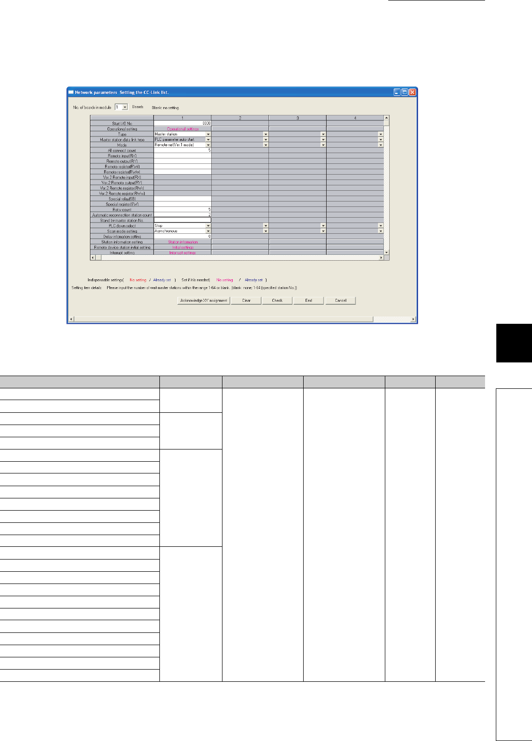
8 - 25
CHAPTER8 PARAMETERS
1
2
3
4
5
6
7
8
8.2 Network Parameters
(4) CC-Link setting
Parameters for CC-Link are set.
Figure 8.18 Setting the CC-Link list
Table8.20 CC-Link setting list
Item Parameter No. Description Setting range Default Reference
Number of modules C000H
Set CC-Link
parameters.
Refer to the manual for
CC-Link. --
Type
Start I/O No.
CNM2HOperational setting
All connect count
Remote input (RX)
CNM1H
Remote output (RY)
Remote register (RWr)
Remote register (RWw)
Ver.2 Remote input (RX)
Ver.2 Remote output (RY)
Ver.2 Remote register (RWr)
Ver.2 Remote register (RWw)
Special relay (SB)
CNM2H
Special register (SW)
Retry count
Automatic reconnection station count
Standby master station No.
PLC down select
Scan mode setting
Delay information setting
Station information setting
Remote device station initial setting
Interrupt setting
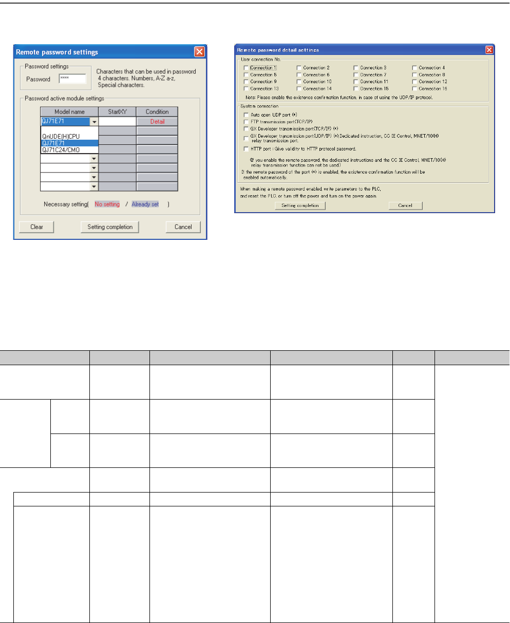
8 - 26
8.3 Remote Password
This section provides the list of parameters for use of remote password and describes parameter details.
A remote password is set for an Ethernet module, serial communication module, modem interface module,
or Built-in Ethernet port QCPU.
Figure 8.19 Remote password settings dialog box
Table8.21 Remote password setting list
Item Parameter No. Description Setting range Default Reference
Password settings - Enter a remote password.
Four characters or less
(alphanumeric characters, special
symbols)
-
• QnUDE(H)CPU:
QnUCPU User's
Manual
(Communication
via Built-in
Ethernet Port)
• QJ71E71:
Ethernet module
manual
• QJ71C24:
Serial
communication
module manual
• QJ71CMO:
Modem interface
module manual
Password
active
module
settings
Model
name -
Select a model name of the module
for which the remote password set
to the CPU module is checked.
• QnUDE(H)CPU
• QJ71E71
• QJ71C24/CMO
-
Start XY -
Set the start address of the module
for which the remote password is
checked.
0000H to 0FE0H-
Detail - Set details of the remote password
for the QJ71E71. --
User connection No. - Select user connection No. Connection 1 to Connection 16 -
System connection - Select a valid port of the remote
password for system connection.
Specify a valid port of the remote
password.
• Auto open UDP port
• FTP transmission port (TCP/IP)
• GX Developer transmission port
(TCP/IP)
• GX Developer transmission port
(UDP/IP), Dedicated instruction,
CC IE Control, MNET/10(H) relay
transmission port.
•HTTP port
-

CHAPTER9 DEVICES
9
2
3
4
5
6
7
8
9.1 Device List
9 - 1
CHAPTER9 DEVICES
This chapter describes the devices that can be used in the CPU module.
9.1 Device List
Table 9.1 lists the names and data ranges of the devices that can be used in the CPU module.
(To the next page)
Table9.1 Device list
Classification Type Device name Default Parameter-set
range Reference
Points Range
Internal user
device
Bit
device
Input 8192 X0 to X1FFF Hexadecimal
Can be changed
within 29K words *3
Section 9.2.1
Output 8192 Y0 to Y1FFF Hexadecimal Section 9.2.2
Internal relay 8192 M0 to M8191 Decimal Section 9.2.3
Latch relay 8192 L0 to L8191 Decimal Section 9.2.4
Annunciator 2048 F0 to F2047 Decimal Section 9.2.5
Edge relay 2048 V0 to V2047 Decimal Section 9.2.6
Step relay 8192 S0 to S511/block Decimal Section 9.2.9
Link relay 8192 B0 to B1FFF Hexadecimal Section 9.2.7
Link special relay 2048 SB0 to SB7FF Hexadecimal Section 9.2.8
Word
device
Timer*1 2048 T0 to T2047 Decimal Section 9.2.10
Retentive timer*1 0 (ST0 to ST2047) Decimal
Counter*1 1024 C0 to C1023 Decimal Section 9.2.11
Data register 12288 D0 to D12287 Decimal Section 9.2.12
Link register 8192 W0 to W1FFF Hexadecimal Section 9.2.13
Link special register 2048 SW0 to SW7FF Hexadecimal Section 9.2.14
Internal
system device
Bit
device
Function input 16 FX0 to FXF Hexadecimal
Cannot be changed
Section 9.3.1
Function output 16 FY0 to FYF Hexadecimal Section 9.3.1
Special relay 2048 SM0 to SM2047 Decimal Section 9.3.2
Word
device
Function register 5 FD0 to FD4 Decimal Section 9.3.1
Special register 2048 SD0 to SD2047 Decimal Section 9.3.2
Link direct
device
Bit
device
Link input 8192 Jn\X0 to Jn\X1FFF Hexadecimal
Cannot be changed Section 9.4
Link output 8192 Jn\Y0 to Jn\Y1FFF Hexadecimal
Link relay 16384 Jn\B0 to Jn\B3FFF Hexadecimal
Link special relay 512 Jn\SB0 to Jn\SB1FF Hexadecimal
Word
device
Link register 16384 Jn\W0 to Jn\W3FFF Hexadecimal
Link special register 512 Jn\SW0 to Jn\SW1FF Hexadecimal
Module access
device
Word
device
Intelligent function
module device 65536 Un\G0 to Un\G65535*2 Decimal Cannot be changed
Section 9.5
Cyclic transmission
area device *4 14336 U3En\G10000 to U3En\G24335 Decimal Can be changed
Index register
or standard
device register
Word
device
Index register or
standard device
register
20 Z0 to Z19 Decimal Cannot be changed Section 9.6
9 - 2
*1: For the timer, retentive timer, and counter, a bit device is used for contacts and coils, and a word device is used for a present value.
*2: The number of points that can be actually used varies depending on the intelligent function module.
For the number of buffer memory points, refer to the manual for the intelligent function module used.
*3: Can be changed in the Device tab of the PLC parameter dialog box (except the input, output, and step relay). The points for the step relay
can be changed to 0 if the serial number (first five digits) of the Universal model QCPU is "10042" or later. ( Section 9.2)
*4: Available only in multiple CPU systems.
*5: Up to 15 digits can be entered in GX Developer.
*6: Indicates the total number of points for the file register, extended data register (D), and extended link register (W).
*7: Not available for the Q00UJCPU.
*8: "512 points" for the Q00UJCPU, Q00UCPU, and Q01UCPU.
*9: "P0 to P511" for the Q00UJCPU, Q00UCPU, and Q01UCPU.
*10: "128 points" for the Q00UJCPU, Q00UCPU, and Q01UCPU.
*11: "I0 to I127" for the Q00UJCPU, Q00UCPU, and Q01UCPU.
*12: "BL0 to BL127" for the Q00UJCPU, Q00UCPU, and Q01UCPU.
*13: "U0 to UF" for the Q00UJCPU, "U0 to U3F" or "U3E0 to U3E3E2" for the Q00UCPU and Q01UCPU, and "U0 to U7F" or "U3E0 to
U3E3E2" for the Q02UCPU.
Table9.1 Device list (continued)
Classification Type Device name Default Parameter-set range Reference
Points Range
File register *7 Word
device File register 0 - -
0 to 4086K points
*6
Section 9.7
Extended data
register *7
Word
device Extended data register 0 - - Section 9.8
Extended link
register *7
Word
device Extended link register 0 - - Section 9.8
Nesting - Nesting 15 N0 to N14 Decimal Cannot be changed Section 9.9
Pointer - Pointer 4096 *8 P0 to P4095 *9 Decimal Cannot be changed Section 9.10
Interrupt pointer 256 *10 I0 to I255 *11 Decimal Section 9.11
Other
Bit device SFC block device 320 *10 BL0 to BL319 *12 Decimal
Cannot be changed
Section 9.12
-
Network No. specification
device 255 J1 to J255 Decimal Section 9.12.1
I/O No. specification
device -U0 to UFF, U3E0 to
U3E3E3 *13 Hexadecimal Section 9.12.3
Macro instruction
argument device -VD0 to VD Hexadecimal Section 9.12.4
Constant -
Decimal constant K-2147483648 to K2147483647 Section 9.13.1
Hexadecimal constant H0 to HFFFFFFFF Section 9.13.2
Real number constant
Single-precision floating-point data:
E 1.17549435 38 to E 3.40282347 + 38 Section 9.13.3
Double-precision floating-point data*5:
E 2.2250738585072014 308 to
E 1.7976931348623157 + 308
Section 9.13.3
Character string constant "ABC", "123" Section 9.13.4
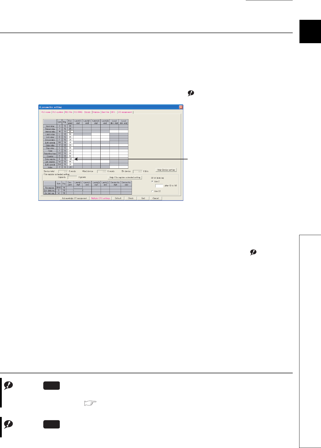
CHAPTER9 DEVICES
9
2
3
4
5
6
7
8
9.2 Internal User Device
9 - 3
9.2 Internal User Device
(1) Definition
Internal user devices can be used for various user applications.
(2) Points for internal user devices
The default values can be changed in the Device tab of the PLC parameter dialog box.
However, the points for the input (X), output (Y), and step relay (S) Note9.1 cannot be changed.Note1
When changing device points, note the following.
• Set each device in increments of 16 points.
• The maximum number of points for a bit device is 32K.
For an internal relay and link relay, the maximum number of points can be set up to 60K. Note9.2
• Up to 29K words can be set for total internal user devices.
• One point set for the timer, retentive timer, or counter must be regarded as two points (one for coil and one
for contact).
Figure 9.1 Device tab of the PLC parameter dialog box
Note1
Default
Most of the default device
points can be changed.
Note9.1
The points for the step relay (S) can be changed to 0 if the serial number (first five digits) of the Universal model QCPU
is "10042" or later. ( Section 9.2.9)
Universal
Note9.2
This applies to the Universal model QCPU when the first five digits of the serial No. is "10042" or later.
Universal

9 - 4
●When changing device points, the following refresh ranges must not exceed the corresponding
device ranges.
• Refresh range of network module
• Auto refresh range of intelligent function module
If device points are set exceeding the corresponding device range, data may be written to any other device or an error
may occur.
●The total number of points for the internal relay, latch relay, annunciator, edge relay, link relay,
link special relay, step relay, timer, retentive timer, and counter must be set within the following
range.
• Serial number (first five digits) of the Universal model QCPU is "10041" or earlier: Up to 64K points
• Serial number (first five digits) of the Universal model QCPU is "10042" or later: Not limited (Up to 29
words for internal user devices)
(3) Memory size
Set the internal user devices so that the following condition is satisfied.
(Bit device size) + (Timer, retentive timer, and counter sizes) + (Word device size) 29K words
(a) Bit device
For bit devices, 16 points are calculated as one word.
(b) Timer (T), retentive timer (ST), and counter (C)
For the timer (T), retentive timer (ST), and counter (C), 16 points are calculated as 18 words.
(c) Word device
For the data register (D), link register (W), and link special register (SW), 16 points are calculated as
16 words.
If the points for the internal user devices have been changed, the following files created with the
previous parameters can no longer be used.
• Sequence program files
• SFC program files
• ST program files
In such a case, read the above program files out from the CPU module to GX Developer, and then write them back again to
the CPU module.
16
(X+Y+M+L+B+F+SB+V+S)
(Bit device size) = Words
16
(Timer, retentive timer, or counter size) = (T+ST+C) 18 Words
16
(D+W+SW)
(Word device size) = 16 Words

CHAPTER9 DEVICES
9
2
3
4
5
6
7
8
9.2 Internal User Device
9 - 5
(4) Device point assignment example
Tabl e9. 2 shows a device point assignment example.
Tabl e9. 2 uses the same format as the device point assignment sheet shown in Appendix 4.
*1: The points are fixed for the system. (Cannot be changed)
The points for the step relay (S) can be changed to 0 if the Universal model QCPU whose serial number (first five digits) is "10042" or
later.
*2: Up to 32K points can be set for each device.
However, up to 60K points can be set for each device of the internal relay and link relay if the Universal model QCPU whose serial
number (first five digits) is "10042" or later,
*3: Enter the values multiplied (or divided) by the number shown in the Size (words) column.
Table9.2 Device point assignment example
Device name Symbol Numeric
notation
Number of device point *2 Restriction check
Points Range Size (words)*3 Points (bits)*2
Input relay*1 X Hexadecimal 8K (8192) X0000 to X1FFF /16 512 18192
Output relay*1 Y Hexadecimal 8K (8192) Y0000 to Y1FFF /16 512 18192
Internal relay M Decimal 16K (16384) M0 to M16383 /16 1024 116384
Latch relay L Decimal 4K (4096) L0 to L4095 /16 256 14096
Link relay B Hexadecimal 4K (4096) B0000 to B0FFF /16 256 14096
Annunciator F Decimal 1K (1024) F0 to F1023 /16 64 11024
Link special relay SB Hexadecimal 2K (2048) SB0000 to SB07FF /16 128 12048
Edge relay V Decimal 1K (1024) V0 to V1023 /16 64 11024
Step relay*1 S Decimal 8K (8192) S0 to S8191 /16 512 18192
Timer T Decimal 2K (2048) T0 to T2047 2304 24096
Retentive timer ST Decimal 2K (2048) ST0 to ST2047 2304 24096
Counter C Decimal 1K (1024) C0 to C1023 1152 22048
Data register D Decimal 14K (14336) D0 to D14335 114336 -
Link register W Hexadecimal 4K (4096) W0000 to W4095 14096 -
Link special register SW Hexadecimal 2K (2048) SW0000 to SW07FF 12048 -
Total 29568
(29696 or less)
63488
(65536 or less)
18
16
18
16
18
16
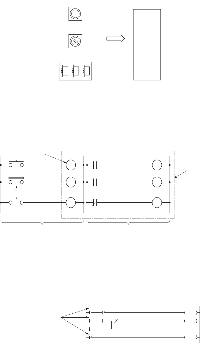
9 - 6
9.2.1 Input (X)
(1) Definition
The input (X) is used to send commands or data to the CPU module from external devices such as push-
button switches, selector switches, limit switches, and digital switches.
(2) Concept of input (X)
One input point is assumed to be a virtual relay Xn in the CPU module.
Programs use the normally open or closed contact of Xn.
(3) Allowable number of normally open or closed contacts
There are no restrictions on the number of normally open or closed contacts of Xn used in a program,
as long as the program capacity is not exceeded.
Figure 9.2 Commands from external devices to a CPU module
Figure 9.3 Concept of input (X)
Figure 9.4 Input (X) used in a program
123
Push-button switch
Selector switch
Digital switch
Input (X)
Sequence
operation
LS2
PB1
X0
X1
XF
PB16 XF
X1
X0
Virtual relay
Program
Input ladder (external device)
Programmable
controller
X0
Y21
X0
X0 Y20
Y21
Y23
X1
X2
X2
No restrictions on
the quantity used.

CHAPTER9 DEVICES
9
2
3
4
5
6
7
8
9.2 Internal User Device
9.2.1 Input (X)
9 - 7
●When debugging a program, the input (X) can be set to on or off by the following:
• Device test in GX Developer
• OUT Xn instruction
●The input (X) can also be used for the following.
• Refresh target device (CPU module side) of RX in CC-Link
• Refresh target device (CPU module side) of CC-Link IE controller network or MELSECNET/H
Figure 9.5 Input (X) on/off with the OUT Xn instruction
X1
OUTX1
ON/OFF command
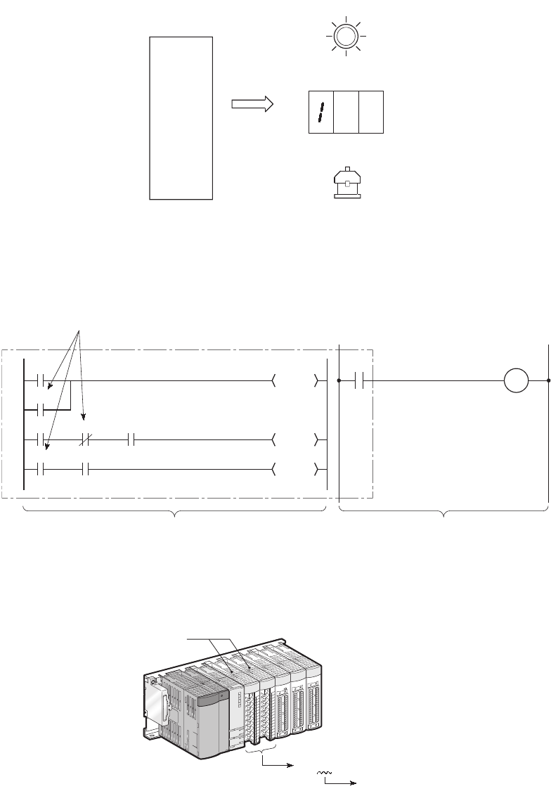
9 - 8
9.2.2 Output (Y)
(1) Definition
The output (Y) is used to output control results on programs to external devices such as signal lamps, digital
displays, electromagnetic switches (contactors), or solenoids.
Data can be output to the outside like using a normally open contact.
(2) Allowable number of normally open or closed contacts
There are no restrictions on the number of normally open or closed contacts of Yn used in a program,
as long as the program capacity is not exceeded.
(3) Using the output (Y) as the internal relay (M)
The output (Y) corresponding to the slots for input modules or empty slots can be utilized as the internal relay (M).
Figure 9.6 Output from a CPU module to external devices
Figure 9.7 Output (Y) used in a program
Figure 9.8 Using as the internal relay
Signal lamp
Digital display
Contactor
Output (Y)
Sequence
operation
M51
Y22
Y21
Y20
Y20
X0
X1
Y20
Y20
X3
X2
No restrictions on the quantity used.
Programmable
logic cont
Out ladder (external device)Program
Load
Input module
OUT Yn
Equivalent to
internal relay
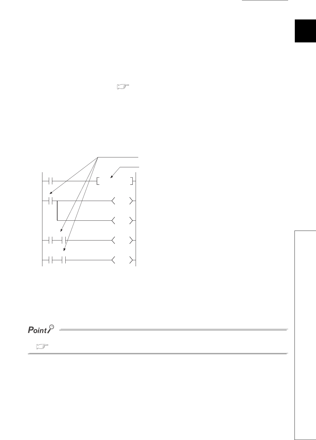
CHAPTER9 DEVICES
9
2
3
4
5
6
7
8
9.2 Internal User Device
9.2.3 Internal relay (M)
9 - 9
9.2.3 Internal relay (M)
(1) Definition
The internal relay (M) is a device for auxiliary relays used in the CPU module.
All of the internal relay are set to off in the following cases:
• When the CPU module is powered off and then on
• When the CPU module is reset
• When latch clear is executed ( Section 6.3)
(2) Latch (data retention during power failure)
The internal relay cannot be latched.
(3) Allowable number of normally open or closed contacts
There are no restrictions on the number of normally open or closed contacts used in a program, as
long as the program capacity is not exceeded.
(4) Method for external output
The output (Y) is used to output sequence program operation results to external devices.
Use the latch relay (L) when latch (data retention during power failure) is required.
( Section 9.2.4)
Figure 9.9 Internal relay (M) used in a program
X0
M0
TO
Y20
X1 M0
M100
X2 M0
M2047
SET M0
K20
No restrictions on the quantity used.
M0 is set to on when X0 turns on from off.
Internal relay (M0) can be set to on only for
use inside the CPU module, and not for
output to the outside.
The on/off information of M0 is output from the
output module to the external device.
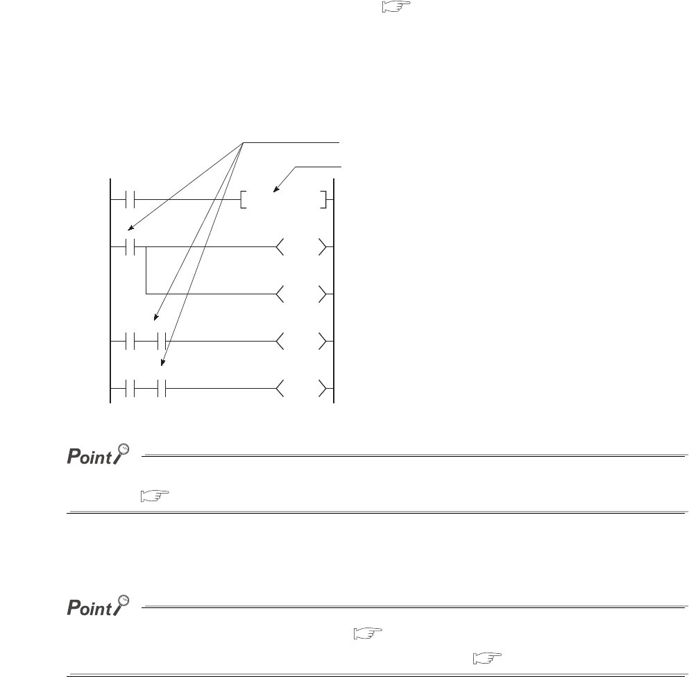
9 - 10
9.2.4 Latch relay (L)
(1) Definition
The latch relay (L) is a device for auxiliary relays that can be latched inside the CPU module.
Latch relay data are retained by batteries in the CPU module during power failure.
Operation results (on/off information) immediately before the following will be also retained.
• Powering off and then on the CPU module
• Resetting the CPU module
(2) Latch relay clear
The latch relay is turned off by the latch clear operation. ( Section 3.7)
However, the latch relay set in "Latch (2) start/end" in the Device tab of the PLC parameter dialog box
cannot be turned off even by the remote latch clear function.
(3) Allowable number of normally open or closed contacts
There are no restrictions on the number of normally open or closed contacts used in a program, as
long as the program capacity is not exceeded.
Scan time is prolonged when the latch relay (L) is used. Reducing the points of latch relay (L) can reduce the prolonging
scan time. ( Section 10.1.2)
(4) Method for external output
The output (Y) is used to output sequence program operation results to external devices.
●If latch is not required, use the internal relay (M). ( Section 9.2.3)
●The latch clear invalid area is set in the Device setting of PLC parameter. ( Section 6.3)
Figure 9.10 Latch relay
X0
L0
T0
Y20
X1 L0
L100
X2 L0
L2047
SET L0
K20
Latch relay (L0) can be set to on only for
use inside the CPU module, and not for
output to the outside.
No restrictions on the quantity used.
M0 is set to on when L0 turns on from off.
The on/off information of L0 is output from the
output module to the external device.
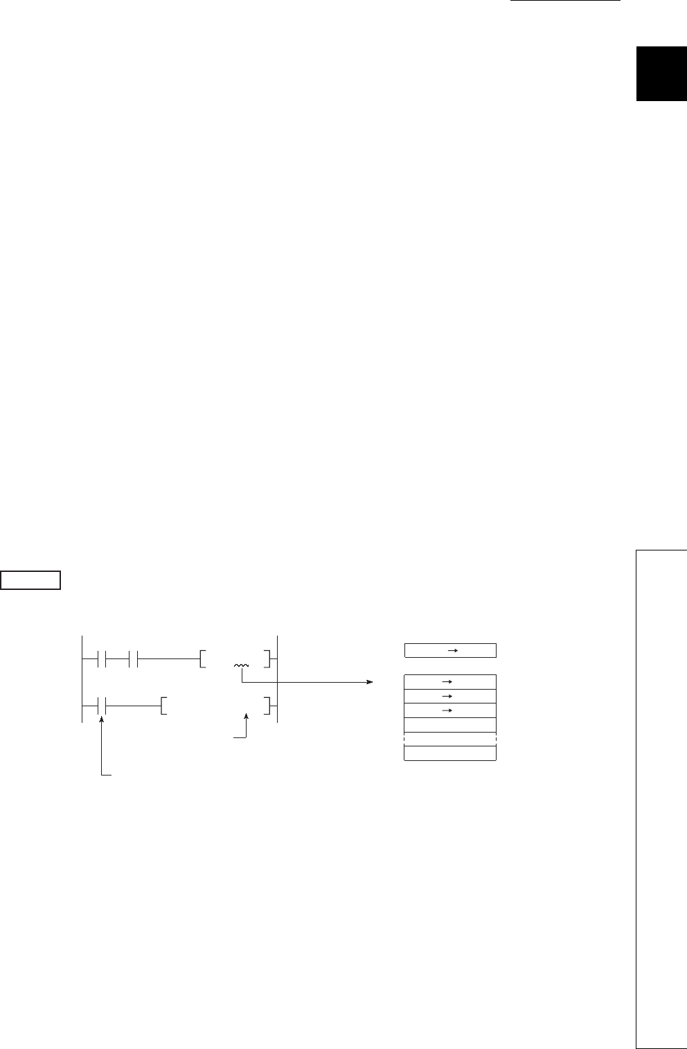
CHAPTER9 DEVICES
9
2
3
4
5
6
7
8
9.2 Internal User Device
9.2.5 Annunciator (F)
9 - 11
9.2.5 Annunciator (F)
(1) Definition
The annunciator (F) is an internal relay which can be effectively used in fault detection programs for user-created
system.
(2) Special relay and special register after annunciator ON
When the annunciator is turned on, the special relay (SM62) is set to on, and the numbers and
quantity of the annunciator numbers are stored in the special register (SD62 to SD79).
The annunciator number stored in SD62 is also registered in the error history area.
(3) Applications of the annunciator
Using the annunciator in a fault detection program allows check for a system fault and identification of
the fault (annunciator number) by monitoring the special register (SD62 to SD79) when the special
relay (SM62) turns on.
In this program, when annunciator (F5) is turned on, the corresponding annunciator number is output
to the outside.
(4) Allowable number of normally open or closed contacts
There are no restrictions on the number of normally open or closed contacts used in a program, as
long as the program capacity is not exceeded.
• Special relay : SM62 • • • Turns on even if only one of the annunciator number areas
is turned on.
• Special register : SD62 • • • Stores the number of the annunciator that was turned on
first.
SD63 • • • Stores the quantity of the annunciator number areas that are
on.
SD64 to
SD79
• • • Stores annunciator numbers in the order of turning on.
(The same annunciator number is stored in SD62 and
SD64.)
Figure 9.11 Detecting and saving the annunciator ON
Example
SD62
BCDP
SM62
SET F5
K4Y20
X0 X10 SM62
SD62
SD63
SD64
SD65
SD79
0
0
[Fault detection program]
Outputs No. of the
annunciator that turned on.
Annunciator ON detection
OFF ON
0 5
0 1
0 5
9 - 12
(5) Turning on the annunciator and processing
(a) Turning on the annunciator
The following instructions can be used.
1) SET F instruction
The SET F instruction can be used to turn on the annunciator only on the leading edge (off to on)
of an input condition.
Even if the input condition turns off, the annunciator is held on.
Using many annunciator numbers can shorten scan time more than using the OUT F instruction.
2) OUT F instruction
The OUT F instruction can be also used to turn on or off the annunciator. However, since the
processing is performed for every scan, the scan time is longer than the case of using the SET F
instruction.
In addition, execution of the RST F , LEDR, or BKRST instruction is required after the annunciator is turned
off with the OUT F instruction.
Therefore, use of the SET F instruction is recommended.
If the annunciator is turned on with any instruction other than SET F and OUT F (for example, the MOV instruction), the
same operation as the internal relay (M) is performed.
The ON information is not stored in SM62, and annunciator numbers are not stored in SD62 and SD64 to SD79.
(b) Processing after annunciator on
1) Data stored in the special register (SD62 to SD79)
• Turned-on annunciator numbers are stored in SD64 to SD79 in order.
• The annunciator number in SD64 is stored in SD62.
• SD63 value is incremented by "1".
2) Processing on the CPU
The USER LED on the front side turns on (red).
3) On/off setting for the LED
Whether to turn on the USER.LED or not when the annunciator is turned on can be set in the LED indication
setting. ( Section 6.21.2).
Figure 9.12 Processing after annunciator ON
0
0
0
0
0
0
0
SD62
SD63
SD64
SD65
SD66
SD67
SD79
50
1
50
0
0
0
0
50
2
50
25
0
0
0
50
3
50
25
1023
0
0
SET F50 SET F25 SET F1023
Up to 16 annunciator
numbers can be stored.

CHAPTER9 DEVICES
9
2
3
4
5
6
7
8
9.2 Internal User Device
9.2.5 Annunciator (F)
9 - 13
(6) Turning off the annunciator and processing
(a) Turning off the annunciator
The following instructions can be used.
1) RST F instruction
This is used to turn off the annunciator number that was turned on with the SET F instruction.
2) LEDR instruction
This is used to turn off the annunciator number stored in SD62 and SD64.
3) BKRST instruction
This is used to turn off all of the annunciator numbers within the specified range.
4) OUT F instruction
One annunciator number can be turned on or off with the same instruction.
However, even if an annunciator number is turned off with the OUT F instruction, the off processing
described in (6)(b) in this section is not performed.
If the annunciator is turned off with the OUT F instruction, execution of the RST F , LEDR, or BKRST
instruction is required.
• Turning off annunciator 5 (F5)
• Turning off all of the turned-on annunciator numbers
Remark
For details of each instruction, refer to the following.
QCPU Programming Manual (Common Instructions)
Figure 9.13 Example of turning off the annunciator
RST F5
Fault detection program
(Annunciator ON program)
Display reset input
Program that turns OFF
BKRSTP F0 K10
Fault detection program
(Annunciator ON program)
Display reset input
Program that turns
off F0 to F9.
9 - 14
(b) Processing after annunciator off
1) Data stored in the special register (SD62 to SD79) after execution of the LEDR instruction
• The annunciator number in SD64 is deleted, and the other annunciator numbers in the
register addressed SD65 and after are shifted accordingly.
• The annunciator number in SD64 is stored into SD62.
• SD63 value is decremented by "1".
• If the SD63 value is changed to "0", SM62 is turned off.
2) Data stored in the special register (SD62 to SD79) when the annunciator is turned off with
the RST F or BKRST instruction
• The annunciator number specified with the RST or BKRST instruction is deleted, and the
other annunciator numbers in the register addressed SD65 and after are shifted accordingly.
• If the existing annunciator number in SD64 is turned off, a new annunciator number stored in SD64 will
be stored in SD62.
• SD63 value is decremented by "1".
• If the SD63 value is changed to "0", SM62 is turned off.
3) LED indication
When all of the annunciator numbers in SD64 to SD79 turn off, the LED that was turned on by
turn-on of the annunciator will turn off. ( (5)(b) in this section)
If the LEDR instruction is executed while the annunciator is on and at the same time the operation continuation error that has
higher priority ( Section 6.21.1) than the annunciator has occurred, the LEDR instruction clears the higher priority
error. Because of this, the annunciator is not turned off by execution of the LEDR instruction.
To turn off the annunciator with the LEDR instruction, remove the error whose priority is higher than that of the annunciator.
Figure 9.14 Processing after annunciator OFF (when the LEDR instruction executed)
Figure 9.15 Processing after annunciator OFF (when the REST F instruction is executed)
0
0
0
0
0
0
0
SD62
SD63
SD64
SD65
SD66
SD67
SD79
50
1
50
0
0
0
0
50
2
50
25
0
0
0
50
3
50
25
1023
0
0
SET F50 SET F25 SET F1023
25
2
25
1023
0
0
0
LEDR
0
0
0
0
0
0
0
SD62
SD63
SD64
SD65
SD66
SD67
SD79
50
1
50
0
0
0
0
50
2
50
25
0
0
0
50
3
50
25
1023
0
0
SET F50 SET F25 SET F1023
50
2
50
1023
0
0
0
RST F25
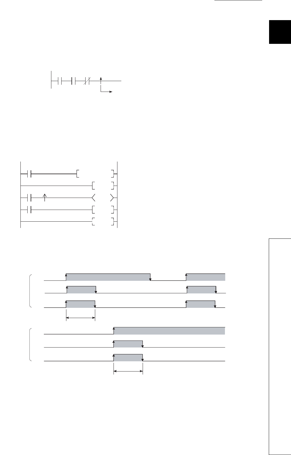
CHAPTER9 DEVICES
9
2
3
4
5
6
7
8
9.2 Internal User Device
9.2.6 Edge relay (V)
9 - 15
9.2.6 Edge relay (V)
(1) Definition
The edge relay (V) is a device in which the on/off information from the beginning of the ladder block.
Contacts only can be used. (Coils cannot be used).
(2) Applications of the edge relay
The edge relay can be utilized to detect the leading edge (off to on) in programs configured using
index modification.
*1: The on/off information for X0Z1 is stored in the V0Z1 edge relay.
For example, the on/off information of X0 is stored in V0, and that of X1 is stored in V1.
(3) Precautions
The edge relay of the same number cannot be set only once in a program.
Figure 9.16 Edge relay
Figure 9.17 Application example and timing chart of the edge relay
X0 X1 X10 V1
Stores on/off information of
X0, X1, and X10.
Returns to FOR instruction.
SM400
X0Z1 V0Z1
SM400
*1 *1
MOV KO Z1
FOR K10
M0Z1
INC Z1
NEXT
Clears index register (Z1).
Specifies the number of repeats (10 times).
Turns on M0Z1 1 scan,
followed by rise of X0Z1.
Increments index
register (Z1). (+1)
[Ladder example]
[Timing chart]
When Z1=0
When Z1=1
X0
M0
V0
X1
M1
V1
OFF
OFF
OFF
OFF
OFF
OFF
ON
ON
ON
ON
ON
ON
1 scan
1 scan
Turns on for 1 scan by rise of X1.
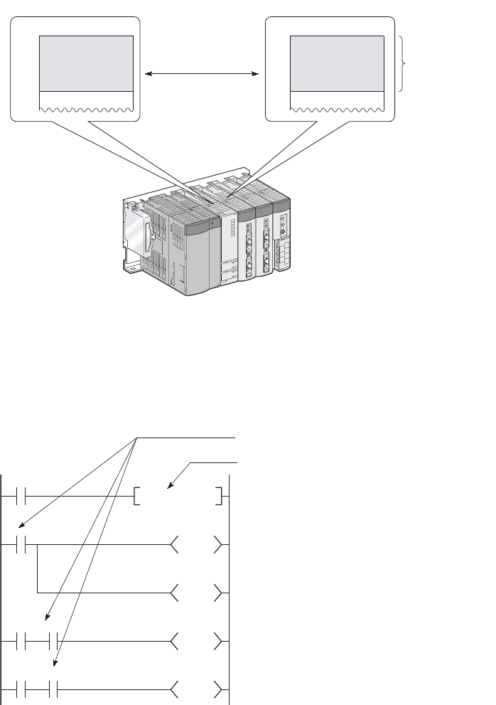
9 - 16
9.2.7 Link relay (B)
(1) Definition
The link relay (B) is a relay on the CPU module side, and it is used for refreshing the link relay (LB) data of
another module such as a MELECNET/H network module to the CPU module or refreshing the CPU
module data to the link relay (LB) of the MELECNET/H network module.
(2) Allowable number of normally open or closed contacts
There are no restrictions on the number of normally open or closed contacts used in a program, as
long as the program capacity is not exceeded.
Figure 9.18 Link refresh
Figure 9.19 Link relay
Link relayLink relay
B0 LB0
CPU module MELSECNET/H network module
Link refresh
setting range
Link refresh
X0
B0
T0
Y20
X1 B0
B100
X2 B0
B1FFF
SET B0
K20
No restrictions on the quantity used.
B0 is set to on when X0 turns on from off.
Link relay (B0) can be set to on only for use inside
the CPU module, and not for output to the
outside.
The on/off information of B0 is output from the
output module to the external device.

CHAPTER9 DEVICES
9
2
3
4
5
6
7
8
9.2 Internal User Device
9.2.7 Link relay (B)
9 - 17
(3) Using the link relay in the network system
Network parameters must be set.
The link relay range areas that is not set by network parameters (not used for a network system such as a
MELSECNET/H network) can be used as the internal relay or latch relay.
• Link relay range where no latch is performed••••••Internal relay
• Link relay range where latch is performed••••••••••Latch relay
• Although the points for the link relay in a CC-Link IE controller network module is 32768, the default for the link
relay in the CPU module is 8192 points.
• Although the points for the link relay in a MELSECNET/H network module is 16384, the default for the link relay in
the CPU module is 8192 points.
To use the link relay exceeding the above points, change the link relay points in the Device tab of the PLC parameter dialog
box.
Remark
For network parameters, refer to the following.
Reference manual for each network module

9 - 18
9.2.8 Link special relay (SB)
(1) Definition
The Link special relay (SB) is a relay that indicates various communication status and detected errors of
intelligent function modules such as CC-Link IE controller modules or MELSECNET/H network modules.
Each of this device area is turned on or off according to a factor occurred during data link.
The communication status and errors on the network can be confirmed by monitoring the link special relay (SB).
(2) Number of link special relay points
The points for the link special relay in the CPU module is 2048. (SB0 to SB7FF).
However, the points can be changed in the Device tab of the PLC parameter dialog box. ( Section 9.1)
To an intelligent function module that has a link special relay, such as a CC-Link IE controller module or
MELSECNET/H network module, 512 points are assigned.
Assigning the link special relay as shown in Figure 9.20 allows refresh of the CC-Link link special relay (SB) to the
link special relay (SB) of the CPU module.
Remark
For details of the link special relay, refer to the manual for an intelligent function module that has the link special relay.
Figure 9.20 Points of the link special relay
SB200
SB3FF
SB400
SB5FF
SB600
SB7FF
SB0
SB1FF
Link special relay
SB800
SB9FF
512
points
512
points
512
points
512
points
2560
points
512
points
For 1st network module
For 2nd network module
For 3rd network module
For 4th network module
For 1st CC-Link module

CHAPTER9 DEVICES
9
2
3
4
5
6
7
8
9.2 Internal User Device
9.2.9 Step relay (S)
9 - 19
9.2.9 Step relay (S)
This device is provided for SFC programs.
Because the step relay is a device exclusively used for SFC programs, it cannot be used as an internal relay in the sequence
program.
If used, an SFC error will occur, and the system may go down.
Remark
For use of the step relay, refer to the following.
QCPU (Q Mode)/QnACPU Programming Manual (SFC)

9 - 20
9.2.10 Timer (T)
(1) Definition
Time counting starts when a coil is turned on, and it times out and the contact turns on when the
current value reaches the set value.
The timer is of an incremental type.
(2) Timer types
Timers are mainly classified into the following two types.
1) Timer of which value is set to 0 when the coil is turned off.
2) Retentive timer that holds the current value even if the coil is turned off.
Also, low-speed and high-speed timers are included in timer 1), and low-speed and high-speed retentive timers
are included in timer 2).
(3) Specification of the timer
The same device is used for the low- and high-speed timers, and the type is determined according to the
instruction used.
For the OUT T0 instruction, the low-speed timer is specified, and for the OUTH T0 instruction, the
high-speed timer is specified.
The same device is used for the low- and high-speed retentive timers, and the type is determined according to the
instruction used.
For the OUT ST0 instruction, the low-speed retentive timer is specified, and for the OUTH ST0
instruction, the high-speed retentive timer is specified.
Figure 9.21 Timer types
Timer Timer
Retentive
timer
Low-speed timer
Low-speed retentive timer
High-speed timer
High-speed retentive timer
Example
Example
CHAPTER9 DEVICES
9
2
3
4
5
6
7
8
9.2 Internal User Device
9.2.10 Timer (T)
9 - 21
(4) Low-speed timer
(a) Definition
This type of timer measures time in increments of 1 to 1000ms.
The timer starts time measurement when its coil is turned on, and when it times out, the contact is
turned on. If the timer's coil is turned off, the current value is changed to "0" and the contact is
turned off.
(b) time increment setting
The time increment is set in the PLC system tab of the PLC parameter dialog box.
The default is 100ms, and it can be changed in increments of 1ms.
(5) High-speed timer
(a) Definition
This type of timer measures time in increments of 0.01 to 100ms.
The timer starts time measurement when its coil is turned on, and when it times out, the contact is
turned on. If the timer's coil is turned off, the current value is changed to "0" and the contact is
turned off.
(b) Time increment setting
The time increment is set in the PLC system tab of the PLC parameter dialog box.
The default is 10.0ms, and it can be changed in increments of 0.01ms.
Figure 9.22 Ladder example and timing chart of a low-speed timer
Figure 9.23 Ladder example and timing chart of a high-speed timer
X0
T0
K10
OFF
OFF
OFF
ON
ON
ON
X
0
[Ladder example]
[Timing chart]
When X0 is turned on, coil of T0 is turned on, and the
contact turns on after 1s. (when unit of the timer is set
to 100ms)
1s
T0 coil
T0 contact
X0 H K50
T200
High-speed timer indication
OFF
OFF
OFF
ON
ON
ON
X0
[Ladder example]
When X0 is turned on, coil of T200 is turned on, and the
contact turns on after 0.5s. (when unit of the timer is set
to 10ms)
[Timing chart]
0.5s
T200 coil
T200 contact
9 - 22
(6) Retentive timer
(a) Definition
This timer measures the period of time during which the coil is on.
The timer starts time measurement when its coil is turned on, and when it times out, the contact is
turned on. Even if the timer's coil is turned off, the current value and the on/off status of the contact
are retained.
When the coil is turned on again, the measurement restarts from the retained current value.
(b) Retentive timer clear
The current value and the contact off status can be cleared with the RST ST instruction.
(c) Time increment setting
The time increment is set in the same manner as the corresponding low- or high-speed timer.
• Low-speed retentive timer: Low-speed timer
• High-speed retentive timer: High-speed timer
To use a retentive timer, set the points for it in the Device tab of the PLC parameter dialog box.
Figure 9.24 Ladder example and timing chart of a retentive timer
X1
RST ST0
X0
ST0
K200
OFF
OFF
ON
ON
ON
X0
OFF
OFF
0to10
X1
150
ON
X0 ON time is measured for 20s when unit of
the timer is 100ms.
Retentive timer
When X1 is turned on, ST0 contact is reset
and the current value is cleared.
[Ladder example]
[Timing chart]
ST0 coil
RST ST0
instruction
Contact of
ST0
Current value
of ST0
15s 5s
Current value is held even
if the coil is turned off.
Contact remains on even if the coil is turned off. Instruction execution
151 to 200

CHAPTER9 DEVICES
9
2
3
4
5
6
7
8
9.2 Internal User Device
9.2.10 Timer (T)
9 - 23
(7) Timer processing and accuracy
(a) Processing
When the OUT T or OUT ST instruction is executed, the on/off switching of the timer coil, current
value update, and on/off switching of the contact are performed.
In the END processing, the current timer value is not updated and the contact is not turned on/off.
Figure 9.25 Processing at execution of the OUT T0 instruction
X0
T0
K10
END OUT TO END
[Processing at execution of OUT T0 instruction]
[Ladder example]
Sequence
program
Processing
Coil ON/OFF
Current value update
Contact ON/OFF
9 - 24
(b) Accuracy
The value obtained by the END instruction is added to the current value when the OUT T or OUT
ST instruction is executed.
The current value is not updated while the timer coil is off even if the OUT T or OUT ST instruction is
executed.
Accuracy of the timer response that is from reading input (X) to output the data is up to "2-scan time
+ timer limit setting".
Figure 9.26 Timer accuracy (in the case of 10ms)
X0
TO
HK8
211 121 121
23 23 23
OUT T0 OUT T0 OUT T0 OUT T0 OUT T0 OUT T0
2
ON
OFF
OFF
OFF
ON
ON
OFF
ON
323 2 3
[Ladder example]
[Current value update timing]
Program
External input
X0 of CPU module
Coil of T0
Contact of T0
10ms counting
Count at execution of
the END instruction
Current value 0+2=2 2+3=5 5+2=7 7+3=10
END
processing
END
processing
END
processing
END
processing
END
processing
END
processing
Accuracy from when the coil of the timer turns on until
when the contact of the timer turns on
- (1 scan time + timer limit setting) to (1 scan time)
Timing when the coil of the timer turns on
Input reading timing
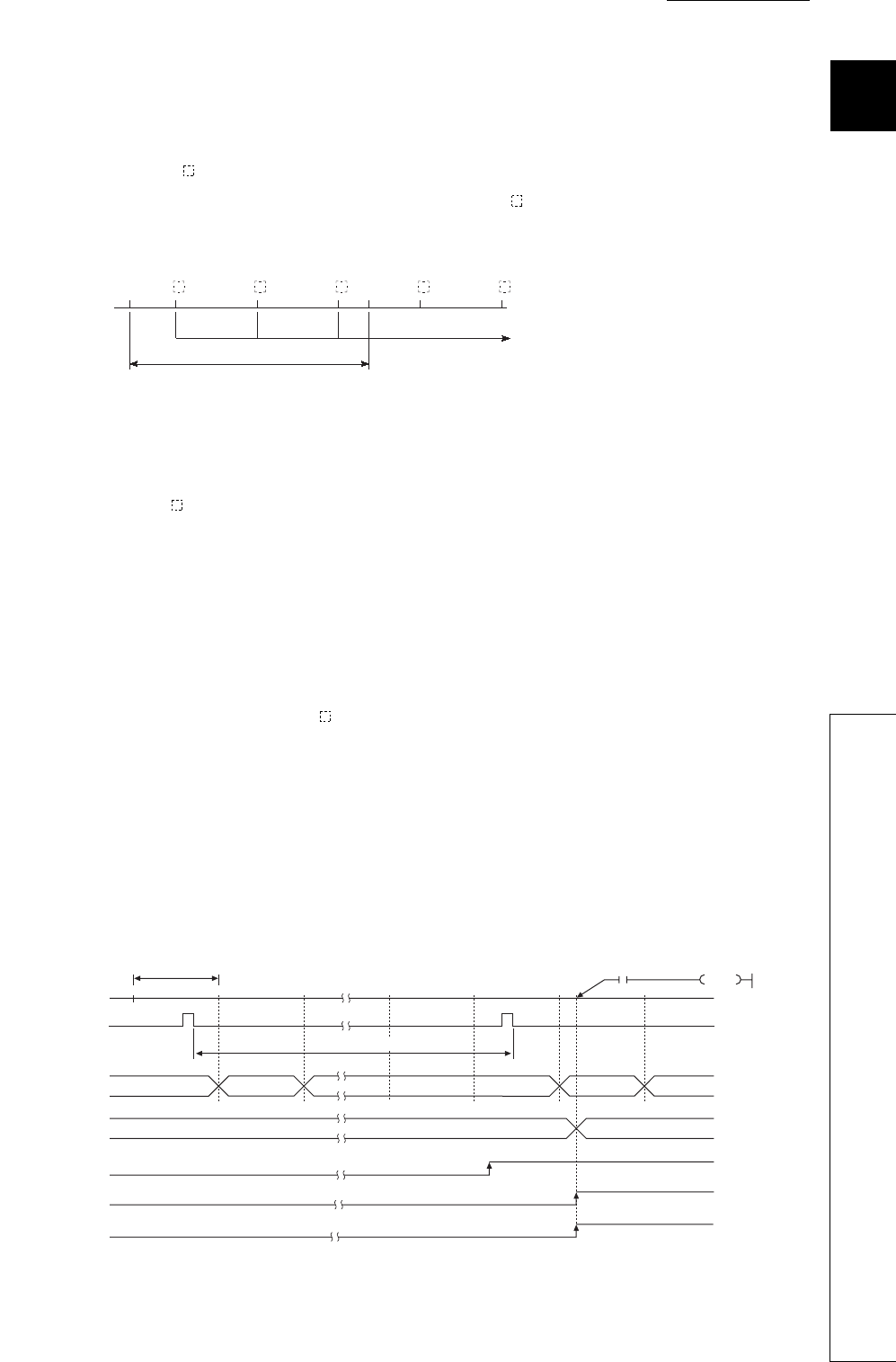
CHAPTER9 DEVICES
9
2
3
4
5
6
7
8
9.2 Internal User Device
9.2.10 Timer (T)
9 - 25
(8) Precautions for using timers
(a) Use of the same timer
Do not use the OUT T instruction that describes the same timer more than once within one scan.
If this occurs, the current timer value will be updated by each OUT T instruction execution, resulting in
incorrect time measurement.
(b) When the timer is not executed in every scan
While a coil of a timer (for example. T1) is on, do not make the OUT T1 instruction jumped to any other
part with another instruction such as CJ.
If jump of the OUT T instruction has occurred, the current timer value is not updated.
Also, if a timer exists in a subroutine program, execute a subroutine call including the OUT T1
instruction once in each scan while the coil of the timer (for example, T1) is on.
Failure to do so will not update the current timer value.
(c) Programs that cannot use timers
Timers cannot be used in interrupt programs and fixed scan execution programs.
(d) When the set value is 0
The contact turns on when the OUT T instruction is executed.
(e) When the set value is 1
When the timer limit setting value is greater than the scan time value, the count value of the timer
becomes 1 at execution of the END instruction in a scan where the count value reaches to the timer
limit setting value.
When the coil of the timer turns on in the scan next to the one where the count value becomes 1, the current
timer value becomes 1. In this case, the timer times up in the step and the contact turns on.
If the contact of the timer (setting value = 1) turns on in a short time, change the timer with small timer limit
setting value and set a greater value to the contact.
Figure 9.27 When the same timer is used
Figure 9.28 Operation when the set value is 1
END END
OUT
T
OUT
T
OUT
T
OUT
T
OUT
T
Current value is updated.
Sequence
program
1 scan
Scan time
END
010 1
1
0
0
OFF
ON
ON
ON
OFF
OFF
X0
Coil of T0
Contact of T0
END END END END END END
X0 K1
T0
Timer limit setting value
Count at execution
of the END instruction
Current timer value
Timer counting
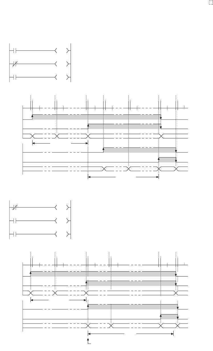
9 - 26
(f) When the set value is changed after time-out
Even if the set value is changed to a larger value after time-out of the timer, the timer remains timed-
out and does not start the operation.
(g) When using multiple timers
When using multiple timers to update the respective current values at execution of each OUT T instruction,
pay attention to the ladder sequence.
For example, to create an on/off ladder using two timers, refer to examples shown in Figure 9.29.
Figure 9.29 On/off ladder using two timers
T0
Measures for one second after T0 is turned on.
Coil of T1 is turned on one scan after T0 is turned on.
Coil of T1 is turned on within the same scan in which T0 was turned on.
Coil of T0
OUT T1
OFF
OFF
00 0 1
One second
One second
910 100
00 0 1 9 10 10 0
OFF
OFF
ON
ON
OFF
ON
OFF
OFF
OFF
ON
OUT T0
END processing END processing
END processing
END
processing
END
processing
END processing
OUT T1
OUT T0
OUT T1
OUT T0
OUT T1
OUT T0
OUT T1
OUT T0
OUT T1
OUT T0
OUT T1
OUT T0
END processing
Contact
of T0
Current
value of T0
Coil of T1
Contact
of T1
Current
value of T1
Measures for one second when T1 is off.
Alternates on and off every second.
K10
T1
T1 K10
T0
T0
M0
T1
OUT T0
OFF
OFF
00 0 1
One second
900ms
910 100
01 1 2 9 10 10 0
OFF
OFF
ON
ON
OFF
ON
OFF
OFF
OFF
ON
OUT T1
END processing
OUT T0
OUT T1
END processing
OUT T0
OUT T1
END processing
OUT T0
OUT T1
END processing
OUT T0
OUT T1
END
processing
OUT T0
OUT T1
END processing
Because the current value is updated in the scan where
T0 is timed out, the count starts from 1 or larger value.
K10
T0
T0 K10
T1
T0
M0
[Correct ladder example]
[Incorrect ladder example]
Measures for one second after T0 is turned on.
Measures for one second when T1 is off.
Alternates on and off every second.
Coil of T0
Contact
of T0
Current
value of T0
Coil of T1
Contact
of T1
Current
value of T1
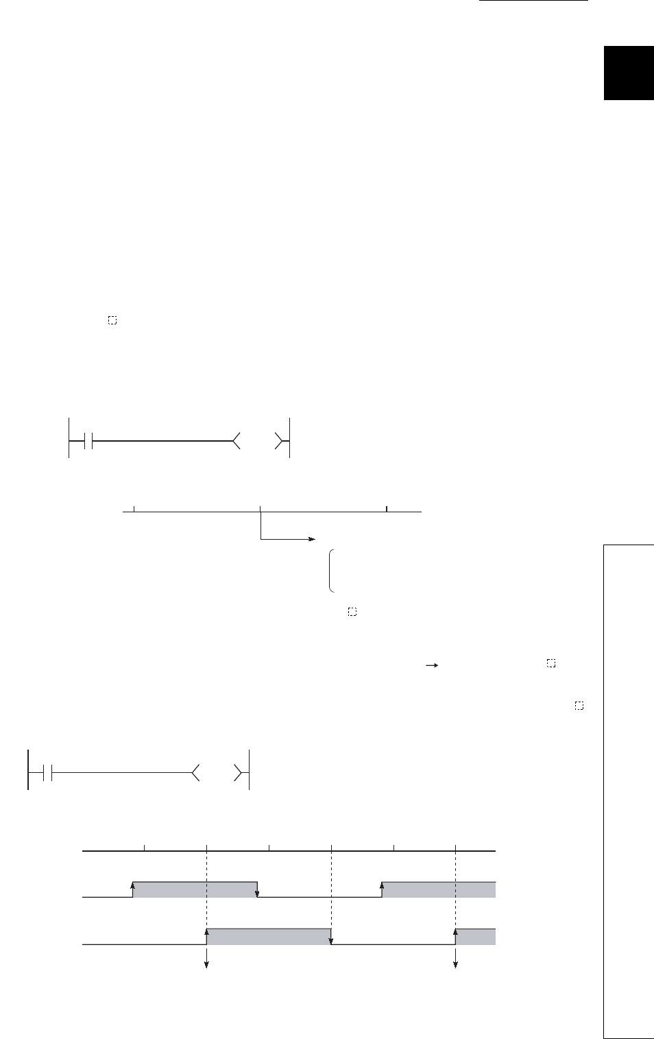
CHAPTER9 DEVICES
9
2
3
4
5
6
7
8
9.2 Internal User Device
9.2.11 Counter (C)
9 - 27
9.2.11 Counter (C)
(1) Definition
The counter (C) is a device that counts the number of rises for input conditions in sequence programs.
When the count value matches the set value, the counting stops and its contact is turned on.
The counter is of an incremental type.
(2) Counter types
Counters are mainly classified into the following two types.
• Counter that counts the number of rises for input conditions in sequence programs
• Interrupt counter that counts the number of interrupts occurred
(3) Counting
(a) When the OUT C instruction is executed
The coil of the counter is turned on/off, the current value is updated (the count value + 1), and the contact is
turned on.
In the END processing, the current counter value is not updated and the contact is not turned on.
(b) Current value update (count value + 1)
The current value is updated (count value + 1) at the leading edge (OFF ON) of the OUT C
instruction.
The current value is not updated while the coil is off, or when it remains on or turns off from on by the OUT C
instruction.
Figure 9.30 Execution and processing of the OUT C instruction
Figure 9.31 Current value update timing
X0
C0
K10
END OUT C0 END
[Ladder example]
Sequence
program
[Processing at OUT C0 Instruction (X0: OFF to ON)]
Coil ON/OFF
Current value update
Contact ON
Processing
X0
C0
K10
X0 OFF
OFF
ON
ON
END END ENDOUT C0 OUT C0 OUT C0
[Ladder example]
[Current value update timing]
Sequence
program
Coil C0
Current value
update
Current value
update
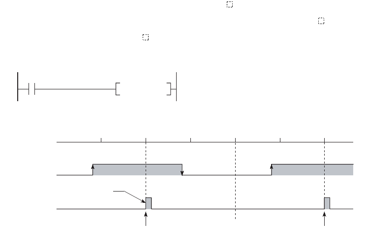
9 - 28
(c) Resetting the counter
The current counter value is not cleared even if the OUT C instruction is turned off.
To clear the current value and to turn off the contact of the counter, use the RST C instruction.
At the time of execution of the RST C instruction, the counter value is cleared, and the contact is also turned
off.
Figure 9.32 Resetting the counter
X0
RST C0
X0 OFF
OFF
ON
END END ENDRST C0 RST C0 RST C0
[Ladder example]
[Counter reset timing]
Sequence
program
Execution
Count value cleared,
the contact turned off
Count value cleared,
the contact turned off
RST C0
instruction
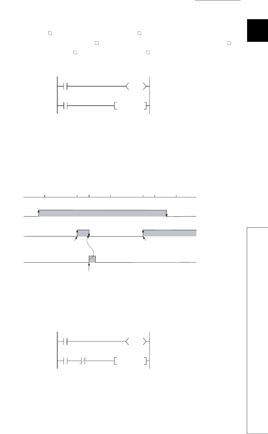
CHAPTER9 DEVICES
9
2
3
4
5
6
7
8
9.2 Internal User Device
9.2.11 Counter (C)
9 - 29
1) Precautions for resetting the counter
Execution of the RST C instruction also turns off the coil of C .
If the execution condition for the OUT C instruction is still ON after execution of the RST C
instruction, turn on the coil of C at execution of the OUT C instruction and update the current
value (count value + 1).
In the above ladder example, when M0 turns on from off, the coil of C0 turns on, updating the
current value.
When C0 reaches the preset value finally, the contact of C0 turns on, and execution of the RST C0
instruction clears the current value of C0. At this time, the coil of C0 also turns off.
If M0 is still on in the next scan, the current value is updated since the coil of C0 turns on from off
at execution of the OUT C0 instruction. (The current value is changed to 1.)
To prevent the above, it is recommended to add a normally closed contact of the OUT C0
instruction execution to the condition for the RST C0 instruction execution so that the coil of C0
does not turn off while the execution condition (M0) of the OUT C0 instruction is on.
Figure 9.33 Counter resetting ladder example
Figure 9.34 Current value update timing
Figure 9.35 Counter resetting ladder example (recommended)
C0
RST C0
M0
C0
K10
[Ladder example]
M0 OFF
OFF
ON
RST C0
OUT C0 END
RST C0 OFF
RST C0
OUT C0 ENDEND
ON
Sequence
program
Coil of C0
Current value
update, turning on
the contact
Turning off the
coil of C0
Current value is
updated since the coil
of C0 turns on from off.
Count value cleared, the contact turned off
C0
RST C0
M0
C0
K10
M0
[Modified ladder example]
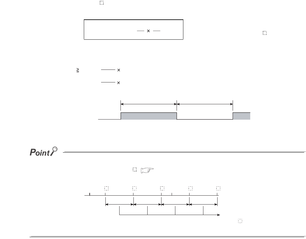
9 - 30
(d) Maximum counting speed
The counter can count only when the on/off time of the input condition is longer than the execution interval of
the corresponding OUT C instruction.
The maximum counting speed is calculated by the following expression:
*1: Duty (n) is the ON-OFF time ratio of count input signal, and is expressed as a percentage
value.
The maximum counting speed can be increased by placing multiple counters within one scan.
At this time, use the direct access input (DX )( Section 3.8.2) for the counter input signal.
(4) Precautions
(a) When counting processing is suspended
If an interrupt occurs during execution of the processing shown below, counting is suspended until the
execution of each processing is completed.
• Each instruction on the sequence program
• Interrupt program
• Fixed scan execution type program
Upon completion of the processing, the counting restarts.
However, if the same interrupt occurs again during each processing, these interrupts are counted as once.
n: Duty (%) *1
T: Execution interval of the OUT C instruction (sec)
Figure 9.36 Duty ratio
Figure 9.37 Ladder example for increasing the maximum counting speed
n
100 T
Maximum counting
speed (Cmax) [times/s]
1
=
OFF
ON
T1 T2
T2
T1
When T1 T2, n = 100%
100%When T1 < T2, n =
T1+T2
T1+T2
Count input signal
Execution interval of the
OUT C instruction
END END
OUT
C
OUT
C
OUT
C
OUT
C
OUT
C
Sequence
program

CHAPTER9 DEVICES
9
2
3
4
5
6
7
8
9.2 Internal User Device
9.2.12 Data register (D)
9 - 31
9.2.12 Data register (D)
(1) Definition
The data register (D) is a memory in which numeric data (-32768 to 32767, or 0000H to FFFFH) can be
stored.
(2) Bit structure of the data register
(a) Bit structure and read/write unit
One point of the data register consists of 16 bits, and data can be read or written in units of 16 bits.
Data register data are handled as signed data.
In the case of the hexadecimal notation, 0000H to FFFFH can be stored. However, because the most significant bit
represents a sign bit, decimal values that can be specified are -32768 to 32767.
(b) When using a 32-bit instruction for the data register
For a 32-bit instruction, two consecutive points of the data register (Dn and Dn+1) are the target of the
processing.
The lower 16 bits correspond to the data register number (Dn) specified in the sequence program,
and the higher 16 bits correspond to the specified data register number + 1.
When D12 is specified in the DMOV instruction, D12 represents the lower 16 bits and D13
represents the higher 16 bits.
Data of -2147483648 to 2147483647 or 0H to FFFFFFFFH can be stored in a two-point area of the data
register. (The most significant bit in a 32-bit structure is a sign bit.)
(3) Retention of stored data
The data stored in the data register are held until other different data are stored.
Note that the stored data are initialized when the CPU module is powered off or reset.
Figure 9.38 Bit structure of the data register
Figure 9.39 Data transfer with a 32-bit instruction and storage location
Dn
b15 to b0
Most significant bit represents a sign bit.
Example
K500000 D12
DMOV
D13 D12
Processing target: D12, D13
Upper 16 bits Lower 16 bits
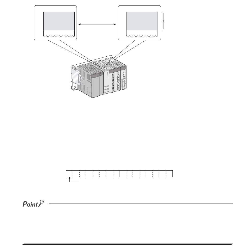
9 - 32
9.2.13 Link register (W)
(1) Definition
The link register (W) is a memory in the CPU module, which is refreshed with link register (LW) data of an
intelligent function module such as a MELSECNET/H network module.
In the link register, numeric data (-32768 to 32767, or 0000H to FFFFH) are stored.
(2) Bit structure of the link register
(a) Bit structure and read/write unit
One point of the link register consists of 16 bits, and data can be read or written in units of 16 bits.
●Link register data are handled as signed data.
In the case of the hexadecimal notation, 0000H to FFFFH can be stored. However, because the most significant bit
represents a sign bit, decimal values that can be specified are -32768 to 32767.
●The area range in the link register, which is not used for a MELSECNET/H network module, can be used as a data
register.
Figure 9.40 Link refresh
Figure 9.41 Bit structure of the link register
Link registerLink register
W0
LW0
CPU module MELSECNET/H network module
Link refresh
Link refresh
Wn
b15 to b0
setting range
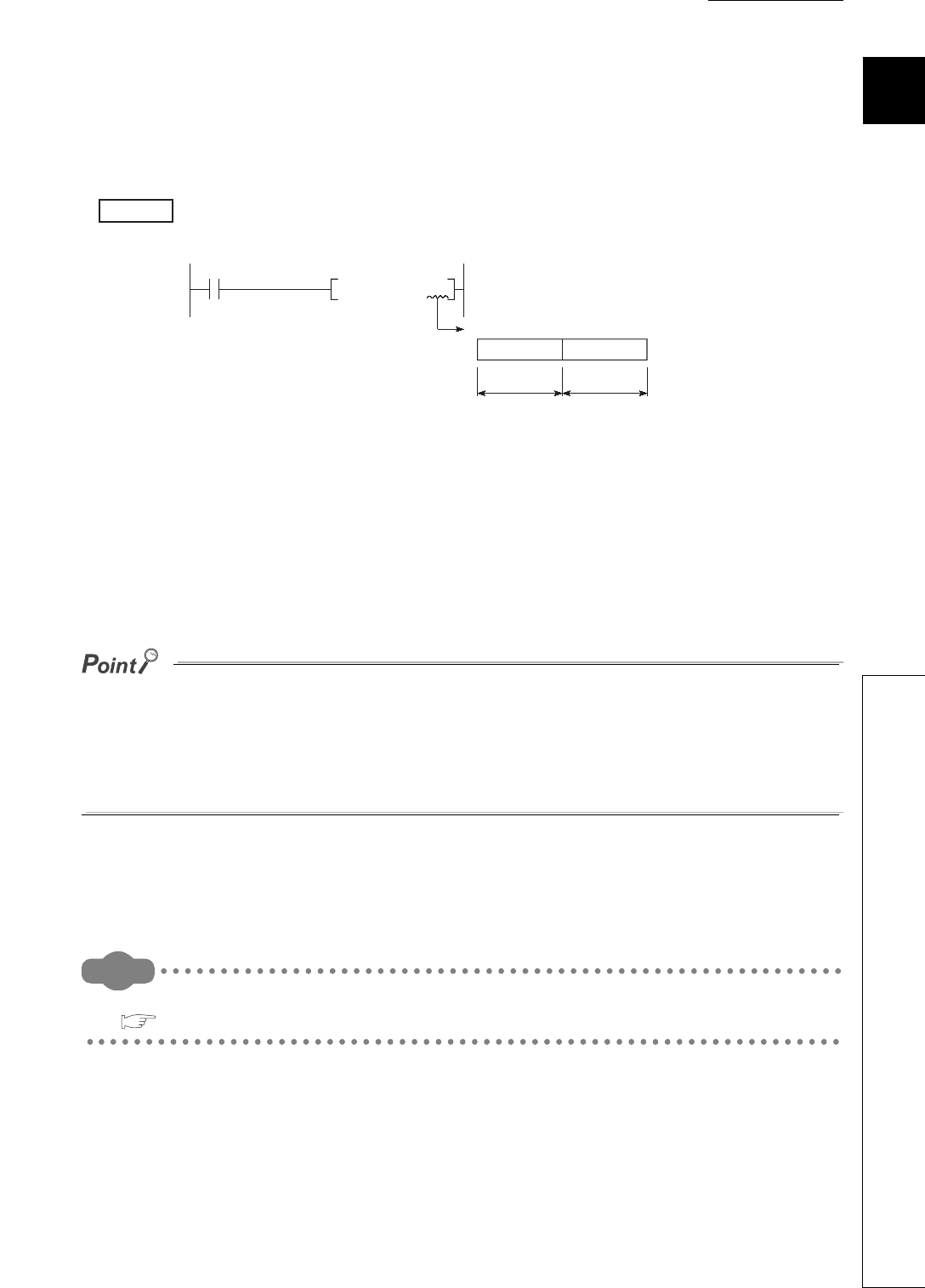
CHAPTER9 DEVICES
9
2
3
4
5
6
7
8
9.2 Internal User Device
9.2.13 Link register (W)
9 - 33
(b) When using a 32-bit instruction for the link register
For a 32-bit instruction, two consecutive points of the data register (Wn and Wn+1) are the target of the
processing.
The lower 16 bits correspond to the link register number (Wn) specified in the sequence program, and the
higher 16 bits correspond to the specified link register number + 1.
When W12 is specified in the DMOV instruction, W12 represents the lower 16 bits and D13
represents the higher 16 bits.
Data of -2147483648 to 2147483647 or 0H to FFFFFFFFH can be stored in a two-point area of the link register.
(The most significant bit in a 32-bit structure is a sign bit.)
(3) Retention of stored data
The data stored in the link register are held until other different data are stored.
Note that the stored data are initialized when the CPU module is powered off or reset.
• Although the number of points for the link register in a CC-Link IE controller network module is 131072 points, the
default value for the link register in the CPU module is 8192 points.
• Although the number of points for the link register of a MELSECNET/H network module is 16384 points, the
default value for the link register in the CPU module is 8192 points.
To use the link register exceeding the above points, change the link register points in the Device tab of the PLC parameter
dialog box in GX Developer or use a file register.
(4) Using the link register in a network system
Network parameters must be set.
The area range that is not set by network parameters can be used as a data register.
Remark
For the network parameters, refer to the following.
Reference manual for each network module
Figure 9.42 Data transfer with a 32-bit instruction and storage location
Example
K500000 W12DMOV
W13 W12
Processing target: W12, W13
Upper 16 bits Lower 16 bits

9 - 34
9.2.14 Link special register (SW)
(1) Definition
The link special register (SW) is used to store communication status data and error data of intelligent function
modules, such as CC-Link IE controller network modules and MELSECNET/H network modules.
Because the data link information is stored as numeric data, error locations and causes can be checked by
monitoring the link special register.
(2) Number of link special register points
The points for the link special register in the CPU module are 2048 (SW0 to SW7FF).
However, the number of points can be changed in the Device tab of the PLC parameter dialog box.
( Section 9.1)
The points for an intelligent function module such as a CC-Link IE controller network module or a MELSECNET/H
network module are 512.
By assigning it as shown in Figure 9.43, data of the link special register (SW) in a CC-Link module can be also
refreshed to the link special register (SW) in the CPU module.
Remark
For details of the link special register, refer to the manual for each intelligent function module that has the link special
register.
Figure 9.43 Points of the link special register
SW200
SW3FF
SW400
SW5FF
SW600
SW7FF
SW0
SW1FF
Link special register
For 1st network module
For 2nd network module
For 3rd network module
For 4th network module
SW800
SW9FF
For 1st CC-Link module
512
points
512
points
512
points
512
points
512
points
2560
points
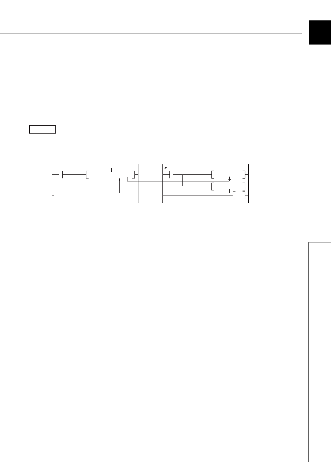
CHAPTER9 DEVICES
9
2
3
4
5
6
7
8
9.3 Internal System Devices
9.3.1 Function devices (FX, FY, FD)
9 - 35
9.3 Internal System Devices
Internal system devices are provided for system operations.
The allocations and sizes of internal system devices are fixed, and cannot be changed by the user.
9.3.1 Function devices (FX, FY, FD)
(1) Definition
Function devices are used in subroutine programs with argument passing.
Data are read or written between such subroutine programs and calling programs, using function devices.
When FX0, FY1, and FD2 are used in a subroutine program, and if X0, M0, and D0 are specified with
a subroutine program call instruction, on/off data of X0 and FY1 are passed to FX0 and M0 respectively, and
D0 data are passed to FD2.
(2) Applications of function devices
Because a device in each calling program can be determined by using a function device for subroutine programs,
the same subroutine program can be used without considering other calling programs.
(3) Types of function devices
The following three types of function devices are available.
• Function input (FX)
• Function output (FY)
• Function register (FD)
(a) Function input (FX)
• The function input is used to pass on/off data to a subroutine program.
• Bit data specified by a subroutine call instruction with argument passing are fetched into a subroutine
program and they are used for operations.
• All bit devices for the CPU module can be used.
Figure 9.44 Application example of function devices
Example
[Calling program] [Subroutine program]
X0
X0
CALLP0 M0 D0 P0
FX0
MOV FD2
SET
R0
RET
FY1

9 - 36
(b) Function output (FY)
• The function output is used for passing an operation result (on/off data) in a subroutine program to a
calling program.
• An operation result is stored in the device specified in the subroutine program with argument passing.
• All bit devices except for input devices of the CPU module (X and DX) can be used.
(c) Function register (FD)
• The function register is used for data writing or reading between a subroutine program and a calling
program.
• The CPU module auto-detects the input or output conditions of the function register.
Source data are input data of the subroutine program.
Destination data are output data from the subroutine program.
• The function register of one point can occupy up to four words.
Note that, however, the number of words used differs depending on the instruction in the subroutine
program.
1) A one-word instruction uses one word only.
2) two-word instruction uses two words.
3) At a destination using 32-bit multiplication or division, four words are used.
• Word devices of the CPU module can be used.
Figure 9.45 When the function register of one point occupies one word
Figure 9.46 When the function register of one point occupies two words
Figure 9.47 When the function register of one point occupies four words
CALLP P0 D0
MOV R0 FD0
P0
Data is stored in D0 (1 point).
CALLP P0 D0
DMOV R0 FD0
P0
Data are stored in D0 and D1 (2 points).
CALLP P0 D0
D* R0 R10 FD0
P0
Data are stored in D0 to D3 (4 points).

CHAPTER9 DEVICES
9
2
3
4
5
6
7
8
9.3 Internal System Devices
9.3.1 Function devices (FX, FY, FD)
9 - 37
In subroutine programs with argument passing, do not use any devices that are used by the function register.
If this occurs, function register values will not be normally passed to the calling program.
Remark
For use of function devices, refer to the following.
QCPU Programming Manual (Common Instructions)
Figure 9.48 Ladder example in which use of devices is not allowed in a subroutine program with argument passing
CALLP P0 D0
D* R0 R10 FD0
P0
MOV K0 D3
Since D0 to D3 are used for FD0,
D3 cannot be used in the
subroutine program.

9 - 38
9.3.2 Special relay (SM)
(1) Definition
The special relay (SM) is an internal relay of which details are specified inside the programmable controller, and
the CPU module status data are stored in this special relay.
(2) Special relay classifications
Table9.3 shows special relay classifications.
*1: Available only for the Q00UJCPU, Q00UCPU, Q01UCPU, and Q02UCPU. ( Section 6.23)
*2: Valid only when "Use special relay/special register from SM/SD1000" is selected in the PLC system tab of the PLC
parameter dialog box.
*3: Applicability differs depending on the CPU module version. ( Appendix 2)
Remark
For details of the special relay, refer to CHAPTER 12.
Table9.3 Special relay classification list
Classification Special relay
Diagnostics information SM0 to SM199
Serial communication function SM100 to SM115 *1
System information SM200 to SM399
System clocks and counters SM400 to SM499
Scan information, I/O refresh SM500 to SM599
Drive information SM600 to SM699
Instruction related SM700 to SM799
Debugging SM800 to SM899
Latch area SM900 to SM999
A QnA conversion compatibility SM1000 to SM1299 *2 *3
Redundant power supply module information SM1780 to SM1799*3

CHAPTER9 DEVICES
9
2
3
4
5
6
7
8
9.3 Internal System Devices
9.3.3 Special register (SD)
9 - 39
9.3.3 Special register (SD)
(1) Definition
The special register (SD) is an internal relay of which details are specified inside the programmable controller,
and the CPU module status data (such as error diagnostics or system information) are stored in this special
register.
(2) Special register classifications
Table9.4 shows special register classifications.
*1: Available only for the Q00UJCPU, Q00UCPU, Q01UCPU, and Q02UCPU. ( Section 6.23)
*2: Valid only when "Use special relay/special register from SM/SD1000" is selected in the PLC system tab of the PLC
parameter dialog box.
*3: Applicability differs depending on the CPU module version. ( Appendix 2)
Remark
For details of the special register, refer to CHAPTER 12.
Table9.4 Special register classification list
Classification Special register
Diagnostics information SD0 to SD199
Serial communication function SD100 to SD111*1
System information SD200 to SD399
System clocks and counters SD400 to SD499
Scan information SD500 to SD599
Drive information SD600 to SD699
Instruction related SD700 to SD799
Debugging SD800 to SD899
Latch area SD900 to SD929
Fuse blown module SD1300 to SD1399
Check of I/O modules SD1400 to SD1499
A QnA conversion compatibility SD1000 to SD1299 *2 *3
Redundant power supply module information SD1780 to SD1799 *3
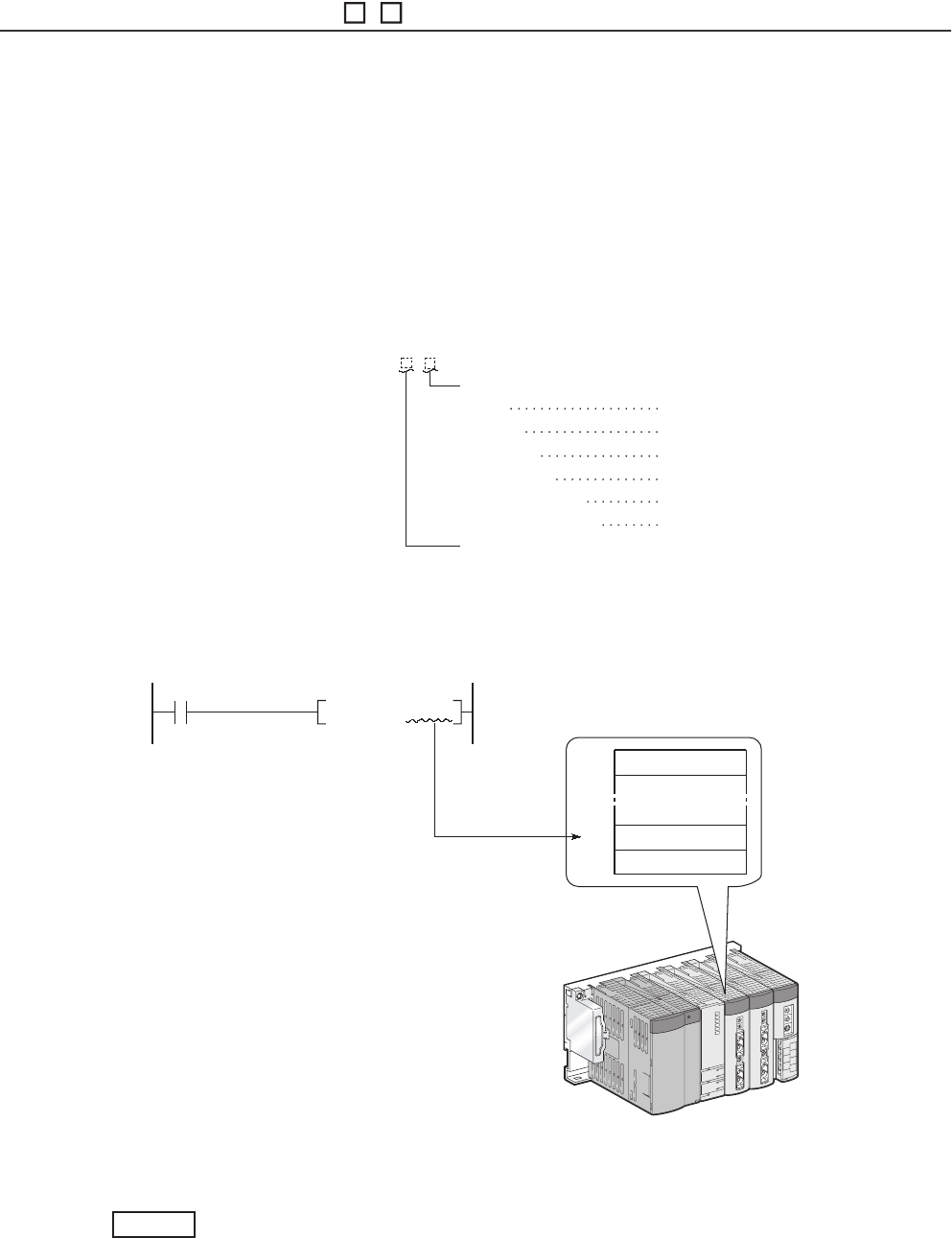
9 - 40
9.4 Link Direct Device (J \ )
(1) Definition
The link direct device is a device for direct access to the link device in a CC-Link IE controller network module or
MELSECNET/H network module.
The CPU module can directly write data to or read data from the link device in a CC-Link IE controller network
module or MELSECNET/H network module using sequence programs regardless of link refresh.
(2) Specification method and application example
(a) Specification method
Specify a network number and a device number.
(b) Application example
For link register 10 (W10) of network number 2, "J2\W10" must be used.
For a bit device (X, Y, B, or SB), the digit must be specified.
J1\K1X0, J10\K4B0
Figure 9.49 Specification method
Figure 9.50 Application example
Network number: 1 to 255
Input
Output
Link relay
Link register
Link special relay
Link special register
X0 to
Y0
to
B0
to
W0
to
SB0
to
SW0
to
Device No.
Specification method:J\
K100 J2\ W10
MOVP
LW 0
LW10
Network module of
network number 2
Example

CHAPTER9 DEVICES
9
2
3
4
5
6
7
8
9.4 Link Direct Device (J\)
9 - 41
(3) Specification range
A link device that is not set in the Network parameter dialog box can be specified.
(a) Writing
• The write range must be within the link device send range that is set by common parameters on Network
parameter setting dialog box, and it must be outside the refresh range set by network refresh parameters.
• Although writing can be done to a refresh range portion (specified by refresh parameters) within the link
device range, the link module's link device data will be overwritten when a refresh occurs.
When writing data by using a link direct device, write the same data to the relevant devices on the CPU
module side, which are set by refresh parameters.
[Refresh parameter settings]
1) Network number: 1
2) CPU module (W0 to W3F) Network module (LW0 to LW3F)
• If data are written to another station's write range using a link direct device, the data will be overwritten
with other data that are received from the corresponding station.
Figure 9.51 Write range of a link direct device
Figure 9.52 Writing to the link device set within the refresh range
LB 0B 0
Network moduleCPU module
Refresh range
Write range
Send range
Link range
MOV K100 W1
MOV K100
W0
W1
LW1
W1
MOV J1\W1
MOV J1\W1
W1
W1
"100" is written to network module
LW1 when a refresh occurs.
"100" is written to network module
LW1 when the MOV instruction is
executed.
[Sequence program]
[Writing timing]
CPU module Network module
Writing at
instruction
execution
Writing at instruction
execution
Writing by a refresh
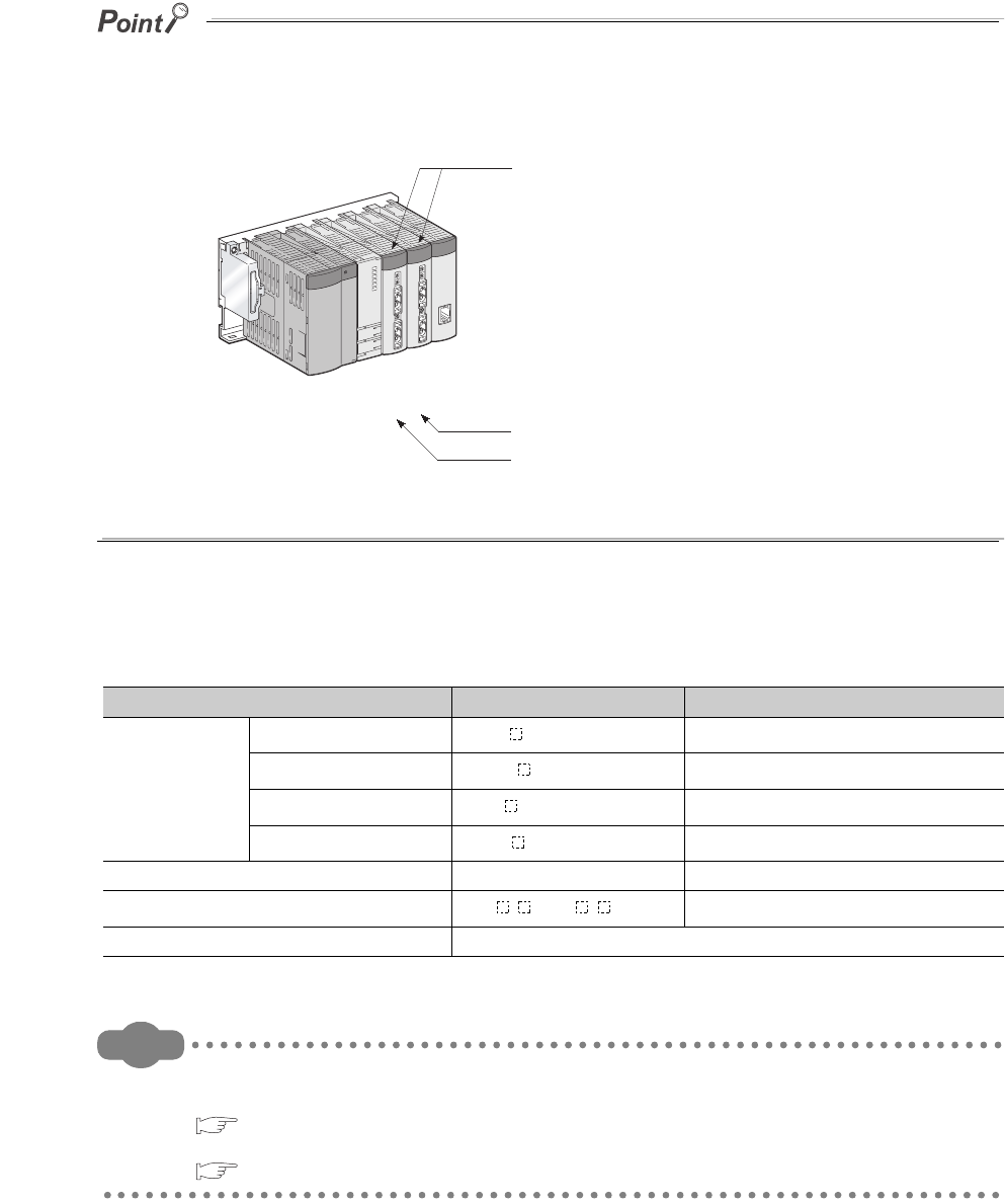
9 - 42
(b) Reading
The link device ranges of network modules can be read.
Writing or reading data by using a link direct device is allowed for only one network module that is on the same network.
If two or more network modules are mounted on the same network, a network module with the lowest slot number is the
target of writing or reading by the link direct device.
For example, if network modules set as station numbers 1 and 2 are mounted on network number 1 as shown in Figure 9.53,
station number 2 is the target of the link direct device.
(4) Differences between link direct devices and link refresh
Remark
For network parameters, common parameters, and network refresh parameters, refer to the following.
• Details:
Network manual for each network module
• Setting method:
GX Developer Version 8 Operating Manual
Figure 9.53 When two or more network module are mounted on the same network
Table9.5 Differences between link direct devices and link refresh
Item Link direct device Link refresh
Description on
programs
Link relay J \K4B0 or higher B0 or higher
Link register J \W0 or higher W0 or higher
Link special relay J \K4SB0 or higher SB0 or higher
Link special register J \SW0 or higher SW0 or higher
Number of steps 2 steps 1 step
Range of network module access J \ 0 to J \ 3FFF Range specified by refresh parameters
Guaranteed access data integrity Word (16-bit) units
Station
No.2
Station
No.1
Network No.1
Writing/reading using link direct devices not allowed
Writing/reading using link direct devices allowed
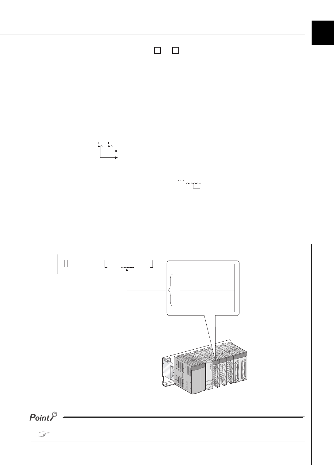
CHAPTER9 DEVICES
9
2
3
4
5
6
7
8
9.5 Module Access Devices
9.5.1 Intelligent function module device (U\G)
9 - 43
9.5 Module Access Devices
9.5.1 Intelligent function module device (U \G )
(1) Definition
The intelligent function module device allows direct access from the CPU module to the buffer memories of the
intelligent function modules which are mounted on the main and extension base units.
(2) Specification method and application example
(a) Specification method
Specify the I/O number and buffer memory address of the intelligent function module.
(b) Application example
When the Q64AD analog-digital converter module is mounted in the position of I/O number 020 (X/Y020 to X/
Y02F), to store digital output values of CH.1 to CH.4 into D0 to D3 accordingly, specify the device as shown in
Figure 9.54.
If the intelligent function module device is used, device comments can be attached to the buffer memory.
GX Developer Version 8 Operating Manual
Figure 9.54 Specification method
Figure 9.55 Application example
Specification method:
Buffer memory address (setting range: 0 to 65535 in decimal)
For X/Y1F0 X/Y1F0
Starting I/O number of intelligent function module
Setting : First 2 digits of starting I/O number expressed in 3 digits
* Setting range: 00H to FFH
Specification: 1F
U\G
D0
BMOV
Q64AD
12
13
11
14
K4
CH.1 Digital output value
CH.2 Digital output value
CH.3 Digital output value
CH.4 Digital output value
U2\G11
9 - 44
(3) Processing speed
The processing speed of the intelligent function module device is as follows:
• The processing speed of writing or reading using the intelligent function module device is slightly higher
compared with the case of using the FROM or TO instruction.
"MOV U2\G11 D0"
• When reading from the buffer memory of an intelligent function module and another processing with one
instruction, totalize the processing speed of the FROM or TO instruction and the other instruction.
"+ U2\G11 D0 D10"
Instead of using the intelligent function module device in the sequence program twice or more to write or read buffer memory
data, using the FROM or TO instruction once in one place can increase the processing speed.
Remark
1. For buffer memory addresses and applications, refer to the manual for each intelligent function module/special
function module.
2. For the FROM and TO instructions, refer to the following.
QCPU Programming Manual (Common Instructions)
Figure 9.56 Writing data using the intelligent function module device multiple times
Figure 9.57 Writing data using the TO instruction once in the program
Example
Example
Stores data in the
data register.
Writes data once
at this point.

CHAPTER9 DEVICES
9
2
3
4
5
6
7
8
9.5 Module Access Devices
9.5.2 Cyclic transmission area device (U3En\G)
9 - 45
9.5.2 Cyclic transmission area device (U3En\G )
(1) Definition
The cyclic transmission area device is used to access the CPU shared memory of each CPU module in a multiple
CPU system.
(2) Features
• The transfer speed is higher than the case of using the write (S.TO or TO) or read (FROM) instruction to the
CPU shared memory, resulting in reduced programing steps.
• Using the cyclic transmission area device allows bit manipulation.
• By setting device comments for the cyclic transmission area device, program readability is increased.
• Because information on the CPU shared memory can be directly specified as an argument of the instruction,
no interlock device is required.
(3) Specification method
Specify the I/O number of the CPU module and the CPU shared memory address.
Remark
For details of the cyclic transmission area device, refer to the following.
QCPU User's Manual (Multiple CPU System)
Figure 9.58 Specification method
Specification method:U3En\G
CPU shared memory (setting range: 0 to 4096, 10000 to 24335 in decimal)
Starting I/O number of the CPU module
Setting: First 3 digits of starting I/O number
CPU module mounting location:
* CPU slot (CPU No.1): 3E00
H
3E0
* Slot 0 (CPU No.2): 3E10
H
3E1
* Slot 1 (CPU No.3): 3E20
H
3E2
* Slot 2 (CPU No.4): 3E30
H
3E3
9 - 46
9.6 Index Register (Z)/Standard Device Resister (Z)
9.6.1 Index register (Z)
(1) Definition
The index register is used for indirect specification (index modification) in sequence programs.
Index modification uses one point of the index register.
The index register has 20 points (Z0 to Z19).
(2) Bit structure of the index register
(a) Bit structure and read/write unit
One point of the index register consists of 16 bits, and data can be read or written in units of 16 bits.
Index register data are handled as signed data.
In the case of the hexadecimal notation, 0000H to FFFFH can be stored. However, because the most significant bit
represents a sign bit, decimal values that can be specified are -32768 to 32767.
Figure 9.59 Index register
Figure 9.60 Bit structure of the index register
X0
K5 Z0
MOVP
SM400
D0Z
0K4Y30
BCD
Specify the index register
by one point (16 bits).
Zn
b15 to b0
Most significant bit represents a sign bit.
CHAPTER9 DEVICES
9
2
3
4
5
6
7
8
9.6 Index Register (Z)/Standard Device Resister (Z)
9.6.1 Index register (Z)
9 - 47
(b) When using the index register for a 32-bit instruction
The processing target is Zn and Zn+1.
The lower 16 bits correspond to the specified index register number (Zn), and the higher 16 bits correspond to
the specified index register number + 1.
When Z2 is specified in the DMOV instruction, Z2 represents the lower 16 bits and Z3 represents
the higher 16 bits. (The most significant bit in a 32-bit structure is a sign bit.)
(3) When using 32-bit index modification
For the file register (ZR), extended data register (D), extended link register (W) using the serial number access
method, 32-bit index modification using two points of the index register is available.
The following two kinds of methods can be used to specify the index register.
• Specify the range used for 32-bit index modification.
• Specify the 32-bit index modification using "ZZ". Note9.3Note1
Remark
For details and precautions of index modification using the index register, refer to the following.
QCPU Programming Manual (Common Instructions)
Figure 9.61 Data transfer with a 32-bit instruction and storage location
Note1
Example
D0 Z2
DMOV
Z3 Z2
Processing target:
Upper 16 bits Lower 16 bits
Note9.3
When specifying the 32-bit index modification using "ZZ" for the Q02UCPU, Q03UDCPU, Q04UDHCPU,
Q06UDHCPU, Q13UDHCPU, or Q26UDHCPU, check the versions of the CPU module and GX Developer.
( Appendix 2)
Universal

9 - 48
9.6.2 Standard device register (Z)
(1) Definition
By using the index register between register operations, operations can be executed at a higher speed.
The index register used in this case is called the standard device resister.
(2) Device number
Since the standard device register is the same device as the index register, pay attention not to use the same
device number when using the index modification.
Remark
For operation processing and processing time of the standard device register, refer to the following.
QCPU Programming Manual (Common Instructions)
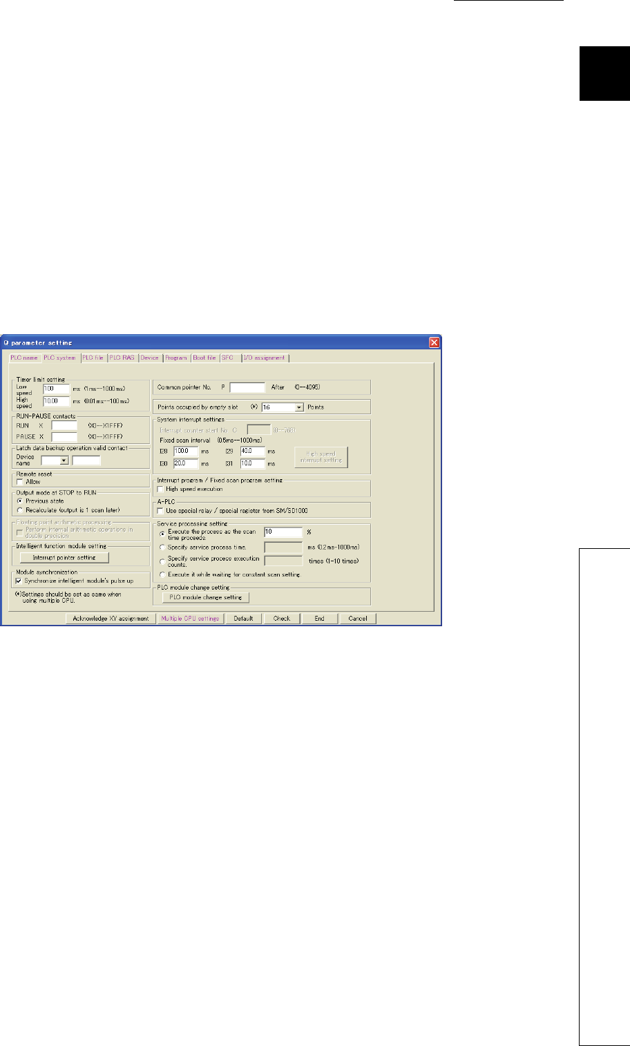
CHAPTER9 DEVICES
9
2
3
4
5
6
7
8
9.6 Index Register (Z)/Standard Device Resister (Z)
9.6.3 Switching from the scan execution type program to the interrupt/fixed scan execution type
program
9 - 49
9.6.3 Switching from the scan execution type program to the interrupt/fixed scan
execution type program
The CPU module performs the following when switching from the scan execution type program to the interrupt/
fixed scan execution type program.
• Saving and restoring the index register data
• Saving and restoring block numbers of the file register
(1) Setting for saving and restoration
Saving and restoration setting can be enabled in the PLC system tab of the PLC parameter dialog box.
To disable writing to the index register in the interrupt/fixed scan execution type program, select "High speed
execution" in the Interrupt program/Fixed scan program setting area.
If this setting is enabled, the program will switch faster than before.
Figure 9.62 Interrupt/fixed scan program setting
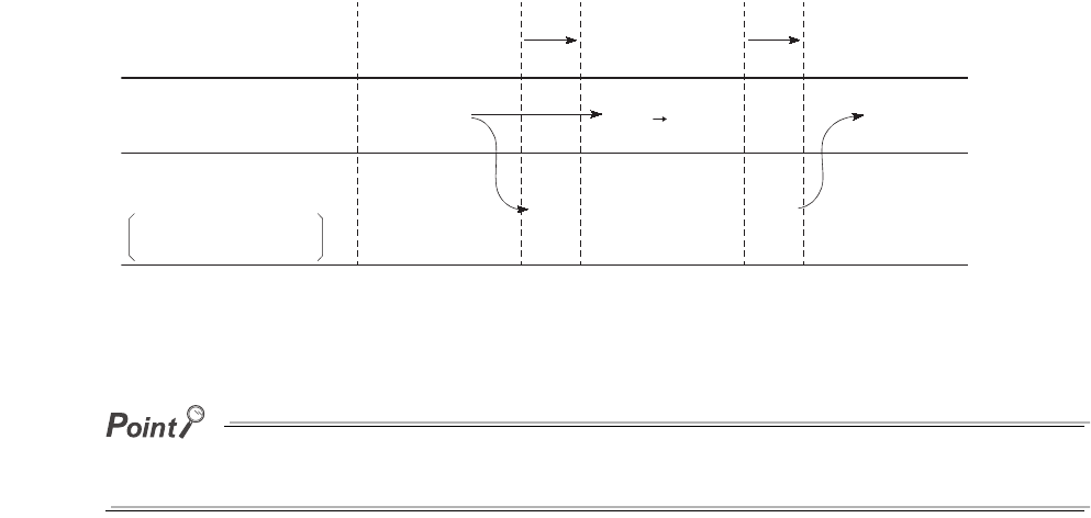
9 - 50
(2) Processing of the index register
(a) When "High-speed execution" is not selected
1) When switching from the scan execution type program to the interrupt/fixed scan
execution type program
The CPU module saves index register values in the scan execution type program, and passes them to the
interrupt/fixed scan execution type program.
2) When switching from the interrupt/fixed scan execution type program to the scan
execution type program
The CPU module restores the saved index register values.
*1: The Z0 value is changed to 3 in the interrupt program.
To pass index register values from the interrupt/fixed scan execution type program to the scan execution type program, use
word devices.
Figure 9.63 Saving and restoring index register data (when "High speed execution" is not selected)
Execution program
Z0=1 Z0=1 Z0=3*1
Z0=0 Z0=1
Passed
Switching
Saved
Restored
Restored
Z0=1 Z0=1 Z0=1
Z0=1
Save area of index register
Index register value
Scan execution
type program
Scan execution
type program
Interrupt/fixed scan
execution type
program
for scan execution
type program
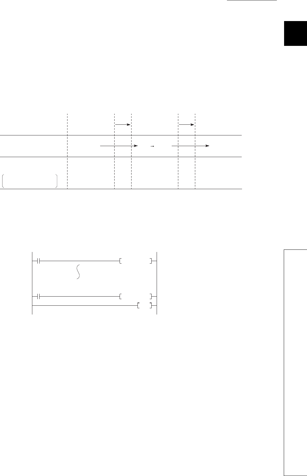
CHAPTER9 DEVICES
9
2
3
4
5
6
7
8
9.6 Index Register (Z)/Standard Device Resister (Z)
9.6.3 Switching from the scan execution type program to the interrupt/fixed scan execution type
program
9 - 51
(b) When "High-speed execution" is selected
1) When switching from the scan execution type program to the interrupt/fixed scan
execution type program
The CPU module does not save/restore any index register values.
2) When switching from the interrupt/fixed scan execution type program to the scan
execution type program
If data are written to the index register by the interrupt/fixed scan execution type program, the values of the
index register used in the scan execution type program will be corrupted.
*1: The Z0 value is changed to 3 in the interrupt program.
When writing data to the index register by the interrupt/fixed scan execution type program, use the ZPUSH or
ZPOP instruction to save and restore the data.
Figure 9.64 Saving and restoring index register data (when "High speed execution" is selected)
Figure 9.65 Writing data to the index register in the interrupt/fixed scan execution type program
Execution program
Z0=1
Z0=0
Switching
Restored
Passed Passed
Z0=0 Z0=0 Z0=0 Z0=0
Z0=3
Index register value
Save area of index register
for scan execution
type program
Scan execution
type program
Interrupt/fixed scan
execution type
program
Scan execution
type program
Z0=1 Z0=3 *1
ZPUSH D0
SM400
ZPOP D0
SM400
IRET
I0 Data in Z0 to Z15 are
stored in the area
addressed from D0.
Data in the area
addressed from D0 are
stored in Z0 to Z15.

9 - 52
(3) Processing of file register's block numbers
(a) When switching from the scan execution type program to the interrupt/fixed scan
execution type program
The CPU module saves the file register block numbers in the scan execution type program, and passes them
to the interrupt/fixed scan execution type program.
(b) When switching from the interrupt/fixed scan execution type program to the scan
execution type program
The CPU module restores the saved block numbers of the file register.
Figure 9.66 Saving and restoring file register's block numbers
[RSET K0]
Execution program
Save area
Switching Restored
Block 1
Restored
Block 1Block 1Block 1 Block 1Block 0
Block 1
Passed
Saved Block1 0
Block No. of
file register
Scan execution
type program
Scan execution
type program
Interrupt/fixed scan
execution type
program
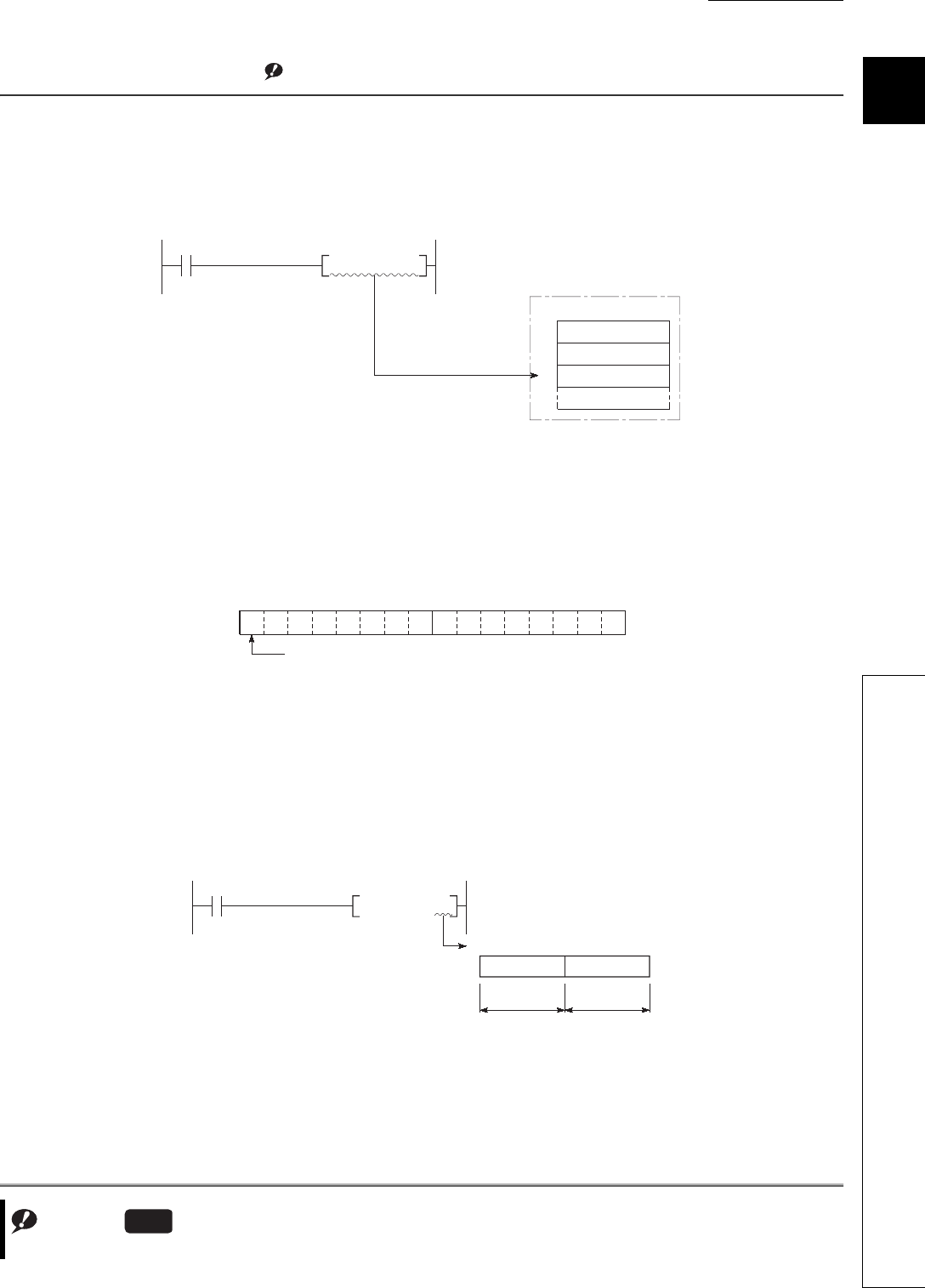
CHAPTER9 DEVICES
9
2
3
4
5
6
7
8
9.7 File Register (R)
9 - 53
9.7 File Register (R)
(1) Definition
The file register (R) is a device provided for extending the data register.
The file register can be used at the same processing speed as the data register.Note1
(2) Bit structure od the file register
(a) Bit structure and read/write unit
One point of the file register consists of 16 bits, and data can be read or written in units of 16 bits.
(b) When using a 32-bit instruction for the file register
The processing target is Rn and Rn+1.
The lower 16 bits correspond to the file register number (Rn) specified in the sequence program, and the
higher 16 bits correspond to the specified file register number + 1.
For example, when R2 is specified in the DMOV instruction, R2 represents the lower 16 bits and R3 represents
the higher 16 bits.
Data of -2147483648 to 2147483647 or 0H to FFFFFFFFH can be stored in a two-point area of the file register.
(The most significant bit in a 32-bit structure is a sign bit.)
Note1
Figure 9.67 Writing to the file register
Figure 9.68 Bit structure of the file register
Figure 9.69 Data transfer with a 32-bit instruction and storage location
Note9.4
Note9.4
The Q00UJCPU does not have the file register.
Universal
K100 R2MOV
100 is written to R2.
File register
R0
R1
R2
Rn
b15 to b0
Most significant bit represents a sign bit.
D0 R2
DMOV
R3
Upper 16 bits Lower 16 bits
R2
Processing target: R2, R3

9 - 54
(3) Clearing the file register
The file register contents are backed up by the battery built in the CPU module, and they are held if the CPU
module is powered off or reset.
(Not initialized even if the latch is cleared.*1)
*1: The latch range of the file register can be set in the Device tab of the PLC parameter dialog box. ( Section 6.3)
To initialize the file register contents, perform the data clear operation in the sequence program or GX Developer.
(a) When clearing by the sequence program
(b) When clearing by GX Developer
Select [Online] [Clear PLC memory] in GX Developer and clear the data by selecting "Clear all file registers".
9.7.1 File register data storage location
There are the following three kinds of memory media for storing file register data.
• Standard RAM
•SRAM card
• Flash card
9.7.2 File register size
(1) When using the standard RAM
The table below shows the maximum points of file register data that can be stored in the standard RAM.
Note that, however, if the standard RAM is used for an application other than file registers, available points are
decreased. ( Section 5.1.10)
Figure 9.70 Example of clearing the file register R0 to R999
Table9.6 File register size
CPU module Points
Q00UCPU, Q01UCPU, Q02UCPU 64K
Q03UDCPU, Q03UDECPU 96K
Q04UDHCPU, Q04UDEHCPU 128K
Q06UDHCPU, Q06UDEHCPU 384K
Q10UDHCPU, Q10UDEHCPU, Q13UDHCPU,
Q13UDEHCPU 512K
Q20UDHCPU, Q20UDEHCPU, Q26UDHCPU,
Q26UDEHCPU 640K
FMOV K0 R0 K1000
CHAPTER9 DEVICES
9
2
3
4
5
6
7
8
9.7 File Register (R)
9.7.3 Differences in available accesses by storage memory
9 - 55
(2) When using an SRAM card
Up to 4086K points can be stored in one file.
Since one block consists of 32K words, up to 128 blocks can be stored.
Note that the number of points or blocks that can be added depends on the size of the programs and device
comments stored in the memory card.
(3) When using a Flash card
Up to 2039K points can be stored in one file.
Since one block consists of 32K words, up to 64 blocks can be stored.
Note that the number of points or blocks that can be added depends on the memory card capacity and the size of
the programs and device comments stored in the memory card.
Remark
For the memory cards available for the CPU module, refer to Section 5.1.1.
9.7.3 Differences in available accesses by storage memory
Accesses available for the file register vary for each memory.
Table9.7 Differences in accesses available for the file register
Access Standard RAM SRAM card Flash card
Program writing
Program reading
Writing device memory to programmable controller
Reading device memory from programmable controller
Data
modification
Online test operation from GX Developer
Writing to programmable controller by GX Developer
Writing to programmable controller by GX Developer (flash ROM)
Batch write by a serial communication module
Device data writing from GOT1000 series
Random write command from GOT1000 series
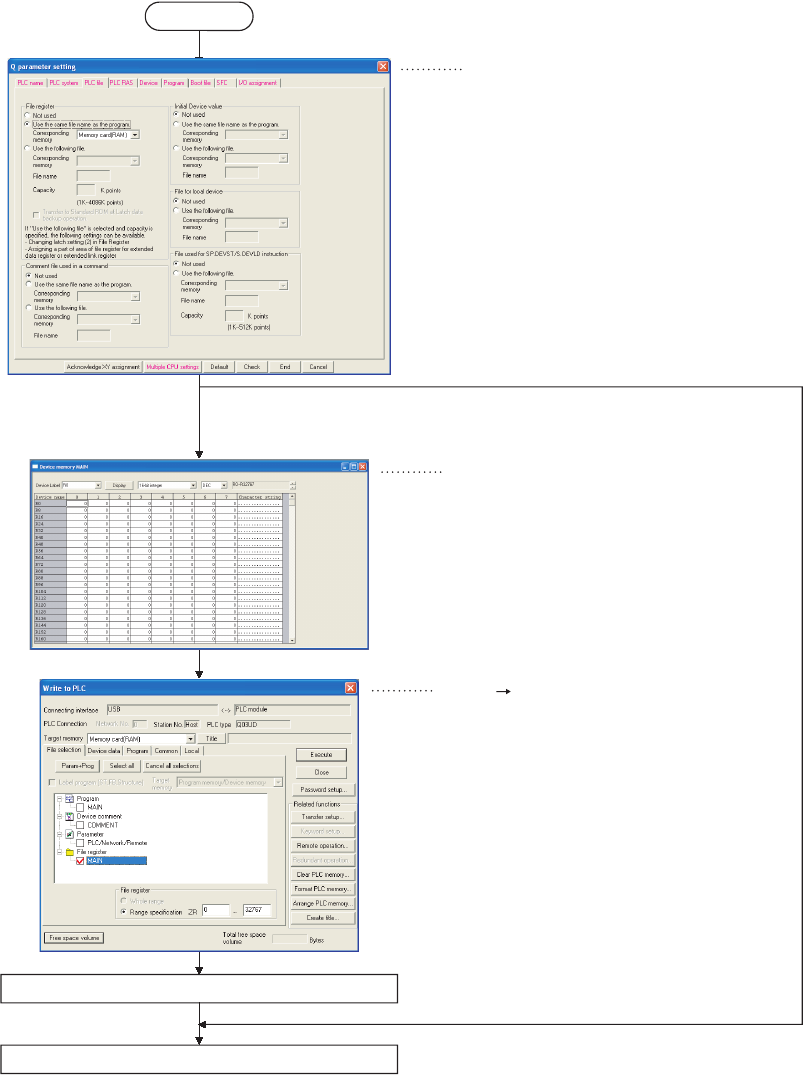
9 - 56
9.7.4 Registration procedure for the file register
To use a file register, register the file of the file register to the CPU module in the following steps.
Figure 9.71 Registration procedure for the file register
"PLC file" tab of the PLC parameter dialog box
File register setting
New "Device memory" window
Select "Use the following file."
Writing the file register
[Online] [Write to PLC]
Write parameters to the CPU module.
Write the file register to the CPU module.
Start
Setting a
file register
Select "Not used" or " Use the
same name as the program."
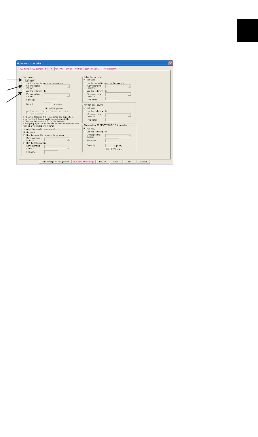
CHAPTER9 DEVICES
9
2
3
4
5
6
7
8
9.7 File Register (R)
9.7.4 Registration procedure for the file register
9 - 57
(1) Setting the file register
In the PLC file tab of the PLC parameter dialog box, specify the standard RAM or a memory card to use the file
register in the sequence program.
(a) Not used
Select this in the following cases.
• When not using any file register
• When specifying a file register used in the sequence program (the QDRSET instruction is used for
specification.)
Figure 9.72 File register setting
(a)
(b)
(c)
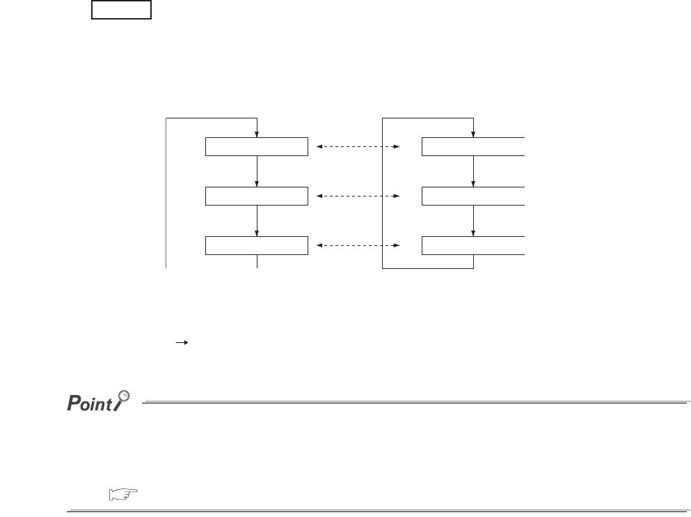
9 - 58
(b) Use the same file name as the program.
Select this when executing the file register with the same file name as the sequence program.
1) When the program is changed
The file name of the file register is automatically changed to the same name as the program.
This feature is useful if the file register is exclusively used for one program as a local device.
When each of file registers A to C has the same name with the corresponding one of the program
A to C, the operation is as described below.
• During execution of program A: Accessing file register A
• During execution of program B: Accessing file register B
• During execution of program C: Accessing file register C
2) Point setting for file registers
Select [Online] [Write to PLC] in GX Developer and set the number of file register points.
●Only one file register can be created in the standard RAM.
To create more than one, use a SRAM or Flash card.
●With some instructions, file registers set for respective programs cannot be specified.
For details, refer to the pages describing devices available for each instruction in the following manual.
QCPU Programming Manual (Common Instructions)
(c) Use the following file.
Select this when one file register is to be shared by all execution programs.
Specify "Corresponding memory", "File name", and "Capacity" and write these parameters to the CPU module
to create a file for the file register.
If the capacity is not specified, note the following.
• When the specified file register file is stored in the specified drive, the file is used. (The capacity is the
same as that of the stored file register file.)
• If the file register file with the specified file name is not found on the specified drive, "PARAMETER
ERROR" (error code: 3002) will occur.
• For use of an ATA card, "Memory card (ROM) cannot be selected for "Corresponding memory".
(File register data cannot be stored in ATA cards.)
Selecting "Memory card (ROM)"for "Corresponding memory" and writing the settings to the CPU module
will result in "PARAMETER ERROR" (error code: 3002).
Figure 9.73 When the program is changed
Example
Program A execution
Program B execution
Program C execution
Synchronized
Synchronized
Synchronized
RO
RO
RO
File register A
File register C
File register B
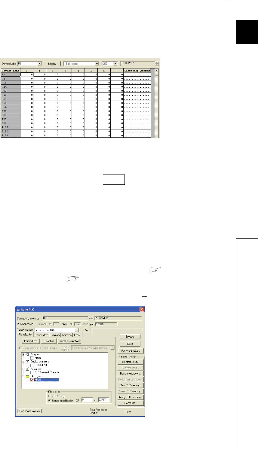
CHAPTER9 DEVICES
9
2
3
4
5
6
7
8
9.7 File Register (R)
9.7.4 Registration procedure for the file register
9 - 59
(2) File register setting
In a new device memory window, set data for the specified file register.
(a) Devices
Setting Rn (R0 in the case shown above)and clicking the button will display the file register list.
(b) Data setting
Enter data that are set for the file register.
This step is not needed when you specify only the capacity of file register.
(3) Registering the file register file to the CPU module
When either of the following is selected in the PLC file tab of the PLC parameter dialog box, the file register file
must be registered to the CPU module.
• Not used. (when specifying a file register used in the sequence program) ( (1)(a) in this section)
• Use the same name with the program. ( (1)(b) in this section)
File register files can be registered to the CPU module by selecting [Online] [Write to PLC] in GX Developer.
Figure 9.74 Device memory window
Figure 9.75 File register file registration
Display
9 - 60
(a) Target memory
Select the Standard RAM, Memory card (RAM), or Memory card (ROM) from this list box.
When using the same file name as that of the program, register the file register to the memory specified in the
PLC File tab of the PLC parameter dialog box.
(b) Selecting a file register file
By selecting a memory for the file register, file names of the set file registers are displayed. Select a file register
file.
(c) Setting the size and file name
Set the size of the file register and a file name of the file register file to be written to the CPU module (PLC-side
file name).
1) File register size of the CPU module
The file register size can be set in increments of one point.
Note that each file size is ensured in units of 256 points.
Even if a file register is not specified from ZR0, the created file will have an assignment from ZR0 to the last
number.
For example, if the write range of a file register is specified to be ZR1000 to ZR1791, the created file register
file will have an assignment from ZR0 to ZR1791.
However, because the data in ZR0 to ZR999 are unreliable, specify the file register from ZR0.
The size of the file register is checked in the units of 1K points. Therefore, the file register size must be
specified from R0 in the units of 1K points.
(d) Writing to the CPU module
The file register file of the specified points is registered to the specified memory of the CPU module.
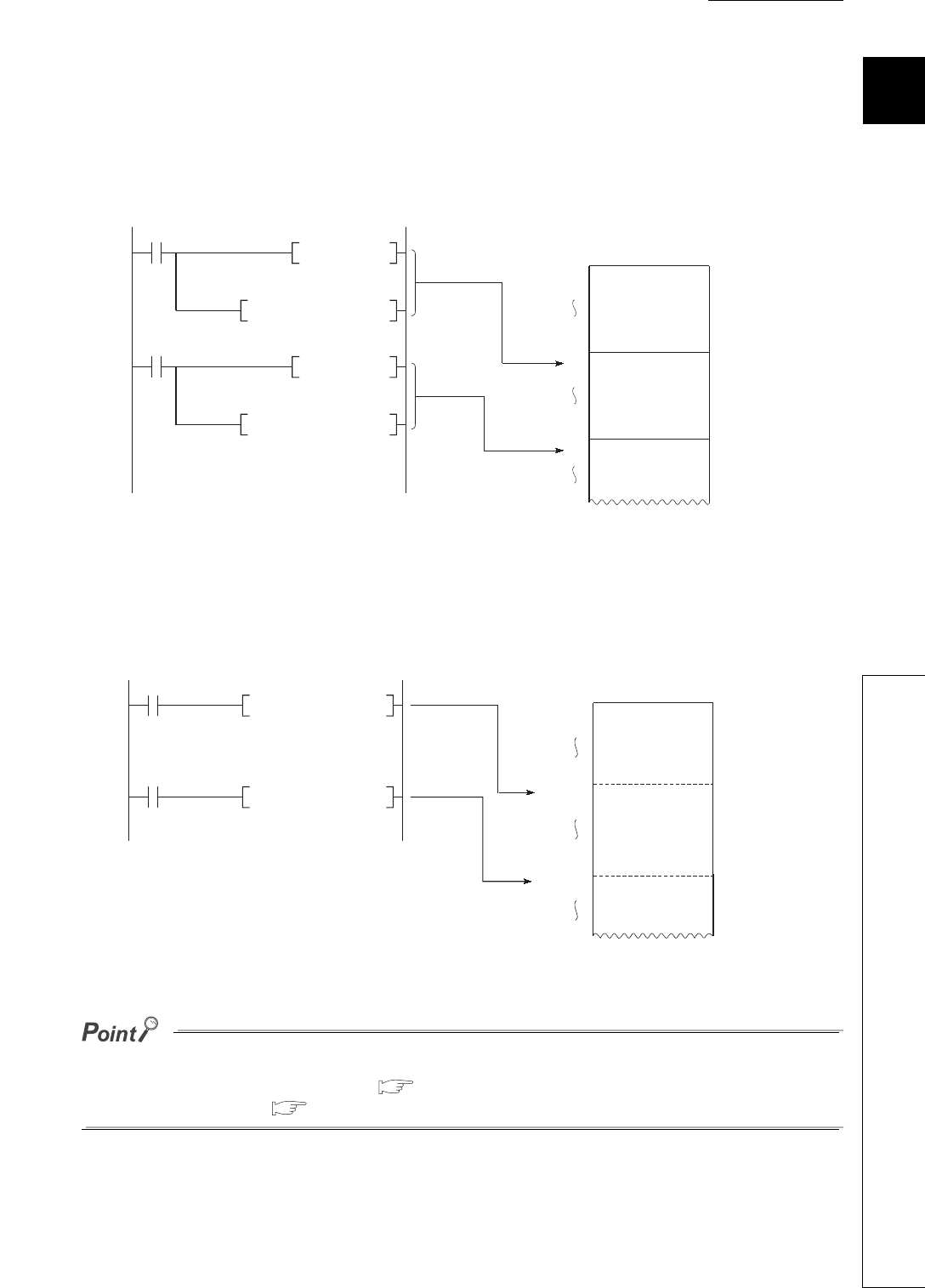
CHAPTER9 DEVICES
9
2
3
4
5
6
7
8
9.7 File Register (R)
9.7.5 Specification methods of the file register
9 - 61
9.7.5 Specification methods of the file register
(1) Block switching method
The file register points used are divided and specified in units of 32K points (R0 to R32767).
If multiple blocks are used, the desired block is specified with the block number in the RSET instruction.
Each block has a specification range of R0 to R32767.
(2) Serial number access method
A file register whose size is exceeding 32K points can be specified using consecutive device numbers.
Multiple blocks of a file register can be used as a continuous file register.
This kind of device is expressed as "ZR".
The block numbers and ZR device points that can be specified vary depending on the following.
• Storage location of the file register ( Section 9.7.1)
• File register size ( Section 9.7.2)
Figure 9.76 Block switching method
Figure 9.77 Serial number access method
D0 R0
MOV Block 0
Block 1
Block 2
D0 R0
MOV
R0
R0
RSET K1
RSET K2
R32767
R32767
R0
R0 specification
for block 1
R0 specification
for block 2
MOV DO ZR32768
MOV DO ZR65536
ZRO
ZR32767
ZR32768
ZR65535
ZR65536
(Block 0)
(Block 1)
(Block 2)

9 - 62
9.7.6 Precautions for using the file register
(1) No registration or use of an invalid file register number
(a) When the file of the file register has not been registered
Writing to or reading from the file register will result in "OPERATION ERROR" (error code: 4101).
(b) When writing to or reading from the file register exceeding the registered size
(points)
"OPERATION ERROR" (error code: 4101) will occur.
(2) File register size check
When writing to or reading from the file register, check the file register size so that data can be written or read
within the size (points) set for the CPU module.
(a) Checking the file register size
The file register size can be checked in the File register capacity area (SD647). *1
The file register size data in units of 1K points is stored in this SD647.
*1: If a file register file is switched to another, the size of the currently selected file register file is stored in SD647.
The remainder after dividing the file register size by 1K points is discarded.
To ensure an accurate "range of use" check, specify the file register setting in units of 1K points (1024 points).
(b) Checking timing
• In a program using any file register, check the file register size at step 0.
• After execution of the file register file switching instruction (QDRSET), check the file register size.
• Before executing the file register block switching instruction (RSET), confirm that space of 1K points or
more can be ensured after the switching.
(File register size) > [32K points (Switching block No) + {1K points]
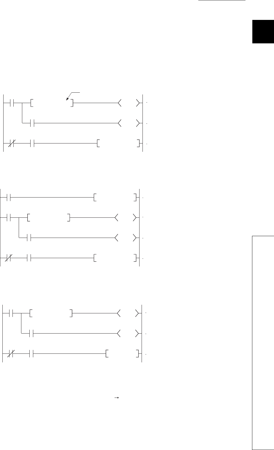
CHAPTER9 DEVICES
9
2
3
4
5
6
7
8
9.7 File Register (R)
9.7.6 Precautions for using the file register
9 - 63
(c) File register size checking procedure
• Check the file register size used for each sequence program.
• Check the total file register size set in SD647 on the sequence program to see if there are sufficient
number of points to be used or not.
[Program example 1]
The file register range of use is checked at the beginning of each program.
[Program example 2]
The file register range of use is checked after execution of the QDRSET instruction.
[Program example 3]
When a block is switched to another:
(3) Deleting a file register file
To delete an unnecessary file register file, select [Online] [Delete PLC data] in GX Developer.
Figure 9.78 Program examples of file register checking
SM400
M0
Y0
M0 Transfer command
M0
MOVP K4X20 R0
<SD647 K4
4K points specified
Final file register
range check
Writing to file
register
Alarm processing
SM400
M0
Y0
M0 Transfer command
M0
MOVP K4X20 R0
<SD647 K4
QDRSET "1:ABCD"
Final file register
range check
Changing file register to
ABCD of Drive 1
Writing to file
register
Alarm processing
SM400
M0
Y0
M0
Block switching
command
M0
RSET K1
<SD647 K33 Final file register
range check
Alarm processing
Switching to block 1
9 - 64
9.8 Extended Data Register (D) and Extended Link Register
(W)
(1) Definition
The extended data register (D) and extended link register (W) are devices for using the large-capacity file register
(ZR) area as an extended area of the data register (D) and link register (W). These devices can be programmed
as the data register (D) and link register (W) together with the file register (ZR) area.Note1
Note1
Figure 9.79 Operation of the extended data register (D) and extended link register (W)
Note9.5
Note9.5
For the Q00UJCPU, the extended data register (D) and extended link register (W) cannot be used.
For using them for the Q02UCPU, Q03UDCPU, Q04UDHCPU, Q06UDHCPU, Q13UDHCPU, Q26UDHCPU, and
Built-in Ethernet port QCPU, check the version of GX Developer. ( Appendix 2)
Universal
Device
Internal user device
File register file
Device numbers can be assigned to the
data register and extended data register
consecutively.
Extended data
register
Data register
Points for data
register
Points for
file
register
The file size is the total
points for the file
register, extended data
register, and extended
link register.
Points for
extended
data register
Points for
extended
link register
D0
ZR
D1228
D12287
D12288
ZR210943
D12288
D63487
M2000
D0
D63487
MO
MO K567 D1300
D10K123

CHAPTER9 DEVICES
9
2
3
4
5
6
7
8
9.8 Extended Data Register (D) and Extended Link Register (W)
9 - 65
(2) Device numbers
Device numbers for the extended data register (D) and extended link register (W) can be assigned consecutively
after those for the internal user devices, data register (D) and link register (W).
●Even though device numbers are consecutively assigned, there is no physical area contiguity between the data register
(D) (internal user device) and the extended data register (D), and between the link register (W) (internal user device)
and the extended link register (W).
To use them as one contiguous area, set the points for the data register (D) and link register (W) (internal user device)
to "0" in the Device tab of the PLC parameter dialog box, and use only the extended data register (D) and extended link
register (W).
●When using the file register (ZR), extended data register (D) and extended link register (W) with the auto refresh setting
enabled in GX Configurator, the points set in the File register extended setting in the Device tab of the PLC parameter
dialog box must not be exceeded.
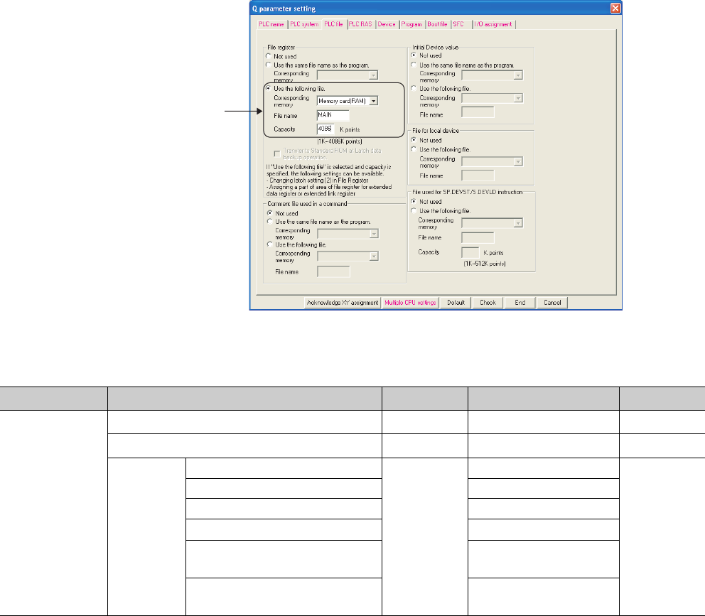
9 - 66
(3) Setting method
Since the extended data register (D) and extended link register (W) use the file register area, data must be set for
both the file register setting and the device setting.
(a) File register setting
Select "Use the following file." in the PLC file tab of the PLC parameter dialog box, and enter data in the boxes
indicated in Figure 9.80.
The "Use the same file name as the program." option is not selectable.
*1: The total points of the file register (ZR), extended data register (D), and extended link register (W).
*2: This is the maximum number of points when an SRAM card (8M bytes) is used.
*3: This is the maximum number of points when a Flash card (4M bytes) is used.
*4: For the Q00UCPU and Q01UCPU, no memory card can be used.
Figure 9.80 Dialog box for file register point setting
Table9.8 File register setting item list
Item Corresponding memory File name Capacity *1 Remarks
"Use the following
file"
Memory card (RAM) *4 Any name 1 to 4086K points *2 -
Memory card (ROM) *4 Any name 1 to 2039K points *3 Read only
Standard
RAM
Q00UCPU, Q01UCPU, Q02UCPU
Any name
1 to 64K points
-
Q03UDCPU, Q03UDECPU 1 to 96K points
Q04UDHCPU, Q04UDEHCPU 1 to 128K points
Q06UDHCPU, Q06UDEHCPU 1 to 384K points
Q10UDHCPU, Q10UDEHCPU,
Q13UDHCPU, Q13UDEHCPU 1 to 512K points
Q20UDHCPU, Q20UDEHCPU,
Q26UDHCPU, Q26UDEHCPU 1 to 640K points
Specify the target memory,
file name, and file size.
CHAPTER9 DEVICES
9
2
3
4
5
6
7
8
9.8 Extended Data Register (D) and Extended Link Register (W)
9 - 67
(b) Device setting
Set each number of points for the file register (ZR), extended data register (D), and extended link register (W)
in the File register extended setting in the Device tab of the PLC parameter dialog box.
Assign a part of the points set for the file register (ZR) in the PLC file tab to the extended data register (D) and
extended link register (W).
If data are to be latched, specify the latch range.
• Latch (2) of the file register (ZR)
• Latch (1) and (2) of the extended data register (D)
• Latch (1) and (2) of the extended link register (W)
Once the points for the extended data register (D) and extended link register (W) is set, areas for these devices
are reserved in the file register file.
Figure 9.81 File register extended setting
Figure 9.82 Areas for the extended data register (D) and extended link register (W)
Specify the latch range if data are to be latched.
Set these points so that the total is equal to the file
register size set in the PLC file tab.
The number of file register points set in the
PLC file tab is displayed.
Device
Internal user device
File register file
Extended data
register
Data register
Points for data
register
Points for
file
register Areas for the
extended data register
and extended link
register are reserved
in this order, after the
area for the file
register points.
Points for
extended
data register
Points for
extended
link register
D0
ZR
D1228
D12287
D12288
ZR1112063
D12288
D1036287
W2000
D0
D63487
Actual area

9 - 68
(4) Checking the points by the special register
The points for each of the file register (ZR), extended data register (D), and extended link register (W) can be
checked in the following special register areas.
• SD306, SD307: File register (ZR)
• SD308, SD309: Extended data register (D)
• SD310, SD311: Extended link register (W)
(5) Precautions
For use of the extended data register (D) and extended link register (W), pay attention to the following.
1) When the extended data register (D) and extended link register (W) are specified, the values of the
following items will be the same as those for the file register (ZR).
• Number of program steps
• Instruction processing time
• Processing time of auto refresh with network modules
• Processing time of auto refresh with intelligent function modules
• Processing time of auto refresh between CPU shared memories
2) The file register size cannot be changed in the RUN status.
3) The file register cannot be switched to another using the QDRSET instruction. ("OPERATION ERROR"
(error code: 4100))
4) Set the refresh ranges for the following auto refresh properly so that each refresh range does not cross over
the boundary between the internal user device and the extended data register (D) or extended link register
(W).
• Auto refresh with network modules
• Auto refresh with intelligent function modules
• Auto refresh between CPU shared memories
5) Set the following properly so that each specification does not cross over the boundary between the internal
user device and the extended data register (D) or extended link register (W).
• Index modification
• Indirect specification
• Specification for instructions that use block data *1
*1: Block data means the following:
•Data used in instructions, such as FMOV, BMOV, and BK+, which treat more than one word for operation.
•Control data, composed of two or more words, which are specified in instructions, such as SP.FWRITE and SP.FREAD.
•Data in a 32-bit or greater format (binary 32 bits, real number, indirect address of a device)
Remark
For details on the index modification and indirect specification with the extended data register (D) and extended link
register (W), refer to the following.
QCPU Programming Manual (Common Instructions)

CHAPTER9 DEVICES
9
2
3
4
5
6
7
8
9.8 Extended Data Register (D) and Extended Link Register (W)
9 - 69
6) To access the extended data register (D) or extended link register (W) from a module that does not support
the use of these devices, device numbers need to be specified with those of the file register (ZR).
Calculation formulas for obtaining device numbers of the file register (ZR) to be specified to access the
extended data register (D) and extended link register (W) and calculation examples are described below.
*1: Variables in the table indicate the following:
•ZRC: Points of the file register (ZR)
•EDZN: Device number of the file register (ZR) used to access the extended data register (D)
•EDN: Access target device number of the extended data register (D)
•DC: Points of the data register (D)
•EDC: Points of the extended data register (D)
•EWZN: Device number of the file register (ZR) used to access the extended link register (W)
•EWN: Access target device number of the extended link register (W) (hexadecimal)
•WC: Points of the link register (W)
[Calculation example]
•D
C: Points of the data register (D) ••• 12288 points
•W
C: Points of the link register (W) ••• 8192 points
•ZR
C: Points of the file register (ZR) ••• 2048 points
•ED
C: Points of the extended data register (D) ••• 2048 points
1) Device number of the file register (ZR) used to access D13000
EDZN = 2048 + (13000-12288) = 2760
2) Device number of the file register (ZR) used to access W2100
EWZN = 2048 + 2048 + (2100H - 8192) = 2048 + 2048 + (8448 - 8192) = 4352
Table9.9 Calculation formulas for obtaining device numbers of the file register (ZR) to be specified to access the extended data
register (D) and extended link register (W) *1
Item Calculation formula
Device number of the file register (ZR) used to access the extended data register (D) EDZN = ZRC + (EDN - DC )
Device number of the file register (ZR) used to access the extended link register (W) EWZN = ZRC + EDC +(EWN - WC )
Figure 9.83 Access to the extended data register (D) and extended link register (W)
Data register (D)
Link register (W)
Extended data register (D)
Extended link register (W)
File register (ZR)
ZR0
ZR2047
ZR2048
ZR2760
ZR4095
ZR4096
ZR4352
ZR6143
D0
W0
D12287
D12288
D13000
1)
2)
D14335
W1999
W2000
W2100
W27FF
9 - 70
9.9 Nesting (N)
(1) Definition
Nesting (N) is a device used in the master control instructions (MC and MCR instructions) to program operation
conditions in a nesting structure.
(2) Specification method using master control instructions
The master control instruction opens or closes a common ladder gate to switch the ladder of a sequence program
efficiently.
Specify the nesting (N) in ascending order (in order of N0 to N14), starting from the outside of the nesting
structure.
Remark
For use of the nesting, refer to the following.
QCPU Programming Manual (Common Instructions)
Figure 9.84 Programming example using the nesting
Executed when conditions
A and B are met.
Executed when conditions
A, B, and C are met.
Executed when conditions
A and B are met.
Executed when condition
A is met.
Executed when condition
A is met.
M15
N0
B
C
A
M15N0
MC
M16N1
MC
N2
MCR
N1
MCR
M17N2
MC
N0MCR
M16
N1
M17
N2
Designated in
ascending No. order
Designated in
descending No. order
Control
range of
nesting N0
Control
range of
nesting N1
Control
range of
nesting N2
Executed regardless of
conditions A, B, and C.
CHAPTER9 DEVICES
9
2
3
4
5
6
7
8
9.10 Pointer (P)
9 - 71
9.10 Pointer (P)
(1) Definition
The pointer (P) is a device used in jump instructions (CJ, SCJ, or JMP) or subroutine call instructions (such as
CALL).
(2) Applications
Pointers can be used in the following applications.
• Specification of the jump destination in a jump instruction (CJ, SCJ, or JMP) and a label (start address of the
jump destination)
• Specification of the call destination of a subroutine call instruction (CALL or CALLP) and a label (start
address of the subroutine program)
(3) Pointer types
There are the following two different pointer types.
• Local pointer ( Section 9.10.1):
The pointer used independently in each program
• Common pointer ( Section 9.10.2):
The pointer that can be called in all running programs by the subroutine call instruction.
(4) Number of available pointer points
The number of points available for the pointer is 4096.
Remark
For the jump instructions and subroutine call instructions, refer to the following.
QCPU Programming Manual (Common Instructions)
Figure 9.85 Program using a pointer
P0
CALL P0
FEND
RET
END
9 - 72
9.10.1 Local pointer
(1) Definition
The local pointer is a pointer that can be used independently in jump instructions and subroutine call instructions
in each program.
The same pointer number can be used in respective programs.
(2) Number of local pointer points
The local pointer can be divided for use of all the programs stored in the program memory.
The local pointer number ranges from P0 to the highest number of the local pointer in use. (The CPU module's
system computes the number of points used.)
Even if only P99 is used in a program, for example, the number of points used will be 100, which is from P0 to
P99.
For using the local pointer for several programs, use the pointers in ascending order starting from P0 in each
program.
The total is 600 points when the pointer is used as shown below.
Figure 9.86 Using the same pointer in respective programs (local pointer)
Figure 9.87 Concept of the local pointer points
Program BProgram A
P0P0
CALL P0
FEND
RET
END
CALL P0
FEND
RET
END
The same pointer
No. can be used.
Example
Program A
Using P0 to P99
100 points of
P0 to P99 occupied
Use of P0 to P99
occupies 100
points.
Use of P0
occupies 1 points.
300 points of
P0 to P299 occupied
200 points of
P0 to P199 occupied
Program B
Using P100 to
P199
Program C
Using P299 only
Total of 600 points are used.

CHAPTER9 DEVICES
9
2
3
4
5
6
7
8
9.10 Pointer (P)
9.10.1 Local pointer
9 - 73
(3) Precautions for using the local pointer
(a) Program where the local pointer is described
A jump from another program is not allowed.
jump instructions and sub-routine CALL instructions.
Use the ECALL instruction from another program when calling a subroutine program in a program file that
contains any local pointer.
(b) Total number of local pointer points
If the total number of pointers (in all programs) exceeds 4096 points, a "Pointer configuration error" (error code:
4020) occurs.
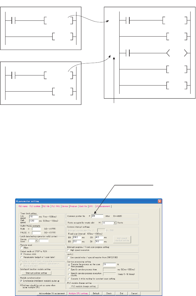
9 - 74
9.10.2 Common pointer
(1) Definition
The common pointer is used to call subroutine programs from all programs that are being executed.
(2) Common pointer range
In the PLC system tab of the PLC parameter dialog box, set the start number for the common pointer.
The common pointer range is from the specified pointer number to P4095.
However, the pointer number that can be entered here is a number higher than the total points used for the local
pointer.
If a total of 400 points are used in three programs (100 points in each of Program A and Program B, and 200
points in Program C), for example, P400 and higher numbers can be set for the common pointer.
Figure 9.88 Calling pointers in another program (common pointer)
Figure 9.89 Dialog box for setting the common pointer
Program A
FEND
CALL P204
Program C
P204
P205
CALL P0
RET
RET
END
Program B
FEND
CALL P205
Label
Set the start
number of the
common
pointer.

CHAPTER9 DEVICES
9
2
3
4
5
6
7
8
9.10 Pointer (P)
9.10.2 Common pointer
9 - 75
(3) Precautions
1) The same pointer number cannot be used as a label.
Doing so will result in a "Pointer configuration error" (error code: 4021).
2) If the total number of the local pointer points used in several programs exceeds the start number of the
common pointer, a "Pointer configuration error (error code: 4020) will occur.
The jump instructions are not capable of executing a jump to the common pointer in other programs.
Use the common pointer with subroutine call instructions only.
Figure 9.90 Concept of the common pointer range
Program A Program B Program C
Using P0 to P99 Using P0 to P99 Using
P0 to P199
100 points of
P0 to P99 occupied
100 points of
P0 to P99 occupied
Total of 400 points
are used.
200 points of
P0 to P199 occupied
P400 and higher numbers
can be used for the common pointer.
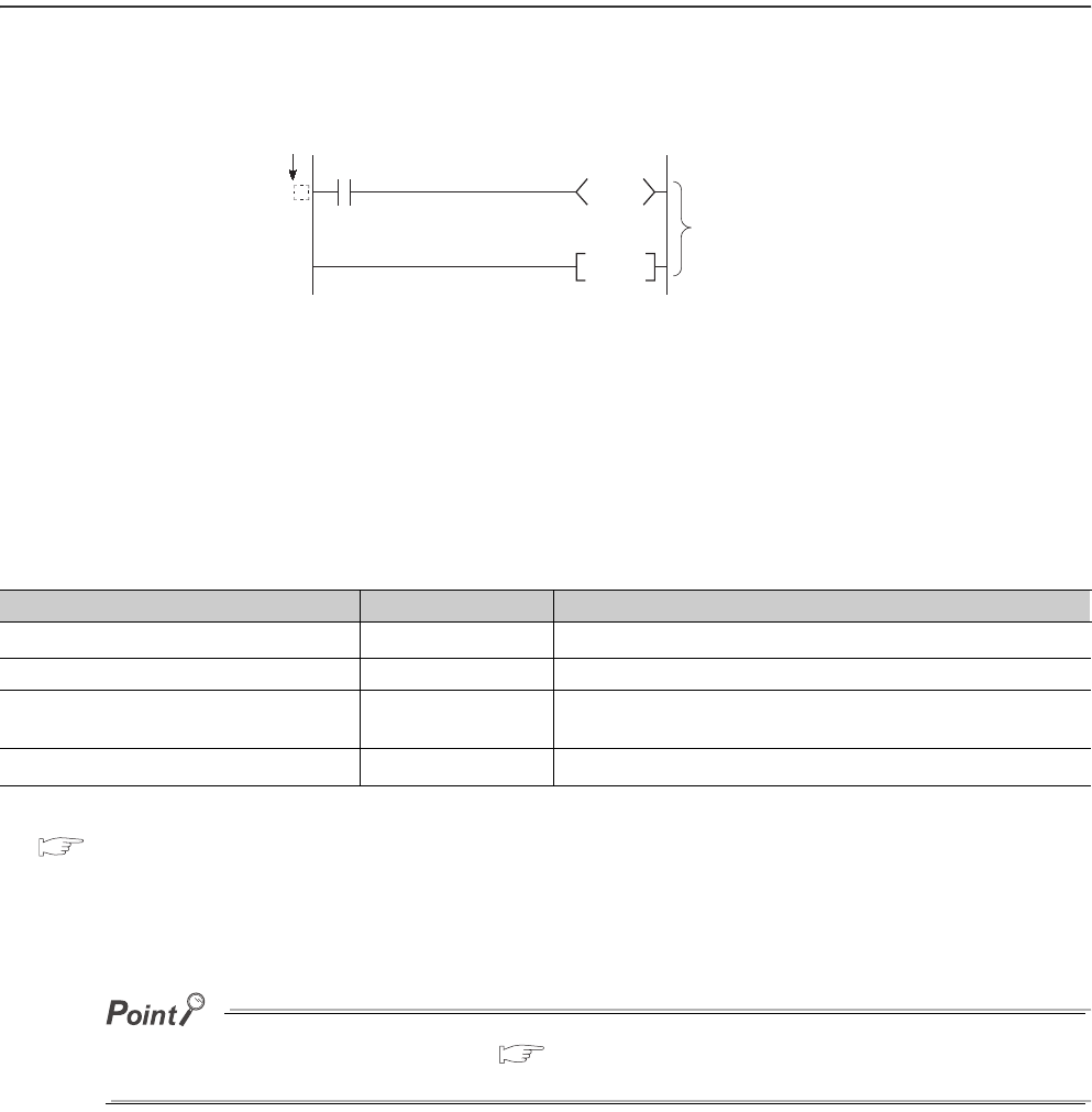
9 - 76
9.11 Interrupt Pointer(I)
(1) Definition
The interrupt pointer (I) is used as a label at the start of an interrupt program, and can be used in any programs.
(2) Number of available points
The number of points available for the interrupt pointer is 256 (I0 to I255).
(3) Interrupt factors
Interrupt factors are listed in Table9.10.
*1: For available interrupt modules, refer to the following.
QCPU User's Manual (Hardware Design, Maintenance and Inspection)
*2: Applicable when using the Universal model QCPU and motion controller that support the multiple CPU high speed transmission.
*3: This module can be a serial communication module, MELSECNET/H module, Ethernet module, or high-speed counter module.
For details, refer to the manual for each module.
To use the intelligent function module interrupt ( Section 6.22), the intelligent function module setting (interrupt pointer
setting) is required in the "PLC system" tab of the PLC parameter dialog box.
Figure 9.91 Interrupt pointer
Table9.10 Classification of interrupt factors
Interrupt factor Interrupt pointer No. Description
Interrupt by an interrupt module *1 I0 to I15 Interrupt input from an interrupt module
Interrupt by the internal timer I28 to I31 Fixed scan interrupt by the internal timer of the CPU module
Multiple CPU synchronous interrupt *2 I45 Fixed scan interrupt to execute synchronized control with the
operation cycle of a motion controller
Intelligent function module interrupt I50 to I255 Interrupt from an intelligent function module *3
Interrupt pointer (interrupt program label)
Interrupt program
IRET
I

CHAPTER9 DEVICES
9
2
3
4
5
6
7
8
9.11 Interrupt Pointer(I)
9.11.1 List of interrupt pointer numbers and interrupt factors
9 - 77
9.11.1 List of interrupt pointer numbers and interrupt factors
The list of interrupt pointer numbers and interrupt factors are shown below.
*1: The time-limit value of the internal timer is set by default.
In the PLC system tab of the PLC parameter dialog box, the value can be changed within the range of 0.5ms to 1000ms in increments
of 0.5ms.
*2: This is available for multiple CPU system configuration.
*3: To use the intelligent function module interrupt, the intelligent function module setting (interrupt pointer setting) is required in the PLC
system tab of the PLC parameter dialog box. (For interrupt from an intelligent function module, refer to Section 6.22.
*4: I50 has the highest priority (priority 22), and I255 has the lowest priority (priority 227).
*5: When an interrupt occurs, even if no interrupt pointer exists on the program, CANíT EXECUTE(I) (error code: 4220) does not occur.
Table9.11 List of interrupt pointer numbers and interrupt factors
I No. Interrupt factor Priority I No. Interrupt factor Priority
I0
Interrupt by
interrupt module
(QI60)
1st point 6
I32 to
I44 -N/A-
I1 2nd point 7
I2 3rd point 8
I3 4th point 9
I4 5th point 10
I5 6th point 11
I6 7th point 12
I7 8th point 13
I8 9th point 14
I9 10th point 15
I10 11th point 16
I11 12th point 17
I12 13th point 18
I13 14th point 19
I14 15th point 20 I45
*2 *5
Multiple CPU
synchronous
interrupt
0.88ms 1I15 16th point 21
I16 to
I27 -N/A-
I46 to
I49 -N/A-
I50 to
I255
Intelligent
function module
interrupt *3 *5/
Interrupt by
interrupt module
(QI60)
Specify the intelligent function
module or interrupt module (QI60)
with a parameter.
22 to 227
I28 *5
Interrupt by
internal timer *1
100ms 5
I29 *5 40ms 4
I30 *5 20ms 3
I31 *5 10ms 2
9 - 78
9.12 Other Devices
9.12.1 SFC block device (BL)
The SFC block is used to check that the specified block in the SFC program is activated.
Remark
For use of the SFC block device, refer to the following.
QCPU (Q Mode)/QnACPU Programming Manual (SFC)
9.12.2 Network No. specification device (J)
(1) Definition
The network No. specification device is used to specify the network number in the link dedicated instructions.
(2) Specification method
In the link dedicated instruction, this device is specified as shown in Figure 9.92.
Remark
For details of the link dedicated instructions, refer to the following.
Reference manual for each network module
Figure 9.92 How to use the network No. specification device
Jn
JP.READ S1 S2 S3 D
Instruction name
Network No. specification instruction
Network No. specification device
(n: network No.)

CHAPTER9 DEVICES
9
2
3
4
5
6
7
8
9.12 Other Devices
9.12.3 I/O No. specification device (U)
9 - 79
9.12.3 I/O No. specification device (U)
(1) Definition
The I/O No. specification device is used to specify I/O numbers in the intelligent function module dedicated
instructions.
(2) Specification method
In the intelligent function module dedicated instruction, this device is specified as shown in Figure 9.93.
Remark
For details of the intelligent function module dedicated instructions, refer to the following.
Manual for the intelligent function module used
Figure 9.93 How to use the I/O No. specification device
Un
GP.READ
S1 S2 S3 D
Instruction name
I/O No. specification instruction
I/O No. specification device
(n: I/O No.)
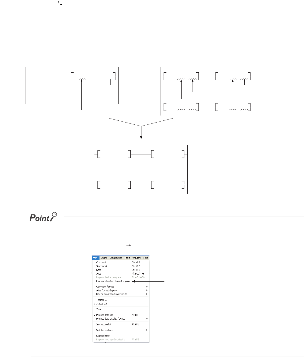
9 - 80
9.12.4 Macro instruction argument device (VD)
(1) Definition
The macro instruction argument device (VD) is used with ladders registered as macros.
When a VD setting is specified, the value is converted to the specified device when the macro instruction is
executed.
(2) Specification method
Among the devices used in the ladders registered as macros in GX Developer, specify a device used for VD.
When using macro instructions in the sequence program, specify devices that correspond to the macro instruction
argument devices used in the macro registration ladders in ascending order.
●With the macro instruction argument device, VD0 to VD9 can be used in one macro registration ladder.
●The GX Developer read mode provides an option to view a program in macro instruction format.
To change the display, select [View] [Display macro instruction format].
Figure 9.94 Macro instruction argument device specification
Figure 9.95 Setting for macro instruction display
Passing to VD2
VD0MOV VD2
VD0
> VD1
D0
M.MAX
D1 R0
Passing to VD1
Passing to VD0
VD1
MOV VD2
VD0
<= VD1
Command with the name of the ladder registered as a macro
Sequence program that actually runs in the CPU module
Sequence program Ladder registered as a macro (registration name: MAX)
D0MOV R0D0
>D1
D1
MOV R0
D0
<= D1
Macro instruction display switching

CHAPTER9 DEVICES
9
2
3
4
5
6
7
8
9.13 Constants
9.13.1 Decimal constant (K)
9 - 81
9.13 Constants
9.13.1 Decimal constant (K)
(1) Definition
The decimal constant (K) is used to specify decimal data in sequence programs.
Specify it as K (example: K1234) in sequence programs.
In the CPU module, data are stored in binary (BIN). ( Section 2.4.1)
(2) Specification range
The specification ranges for decimal constants are as follows:
• When using word data (16-bit data) •••••••••••••••••••••••••••••••• K-32768 to K32767
• When using 2-word data (32-bit data)•••••••••••••••••••••••••••••• K-2147483648 to K2147483647
The most significant bit represents a sign bit.
9.13.2 Hexadecimal constant (H)
(1) Definition
The hexadecimal constant (H) is a device for specifying hexadecimal or BCD data in sequence programs.
(For BCD data, each digit of a hexadeciml number is specified with 0 to 9.)
In sequence programs, specify it as H (example: H1234). ( Section 2.4.2)
(2) Specification range
The specification ranges for hexadecimal constants are as follows:
• When using word data (16-bit data) ••• H0 to HFFFF (For BCD data, H0 to H9999)
• When using 2-word data (32-bit data) ••• H0 to HFFFFFFFF (For BCD data, H0 to H99999999)
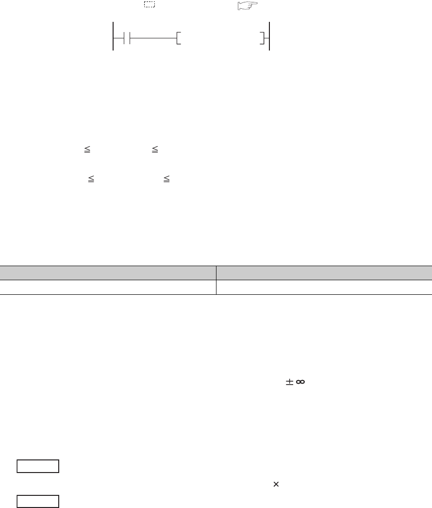
9 - 82
9.13.3 Real number (E)
(1) Definition
The real number (E) is a device used to specify real numbers in sequence programs.
In sequence programs, specify it as E (example: E1.234). ( Section 2.4.4)
(2) Specification range
(a) Real number setting range
• For single-precision floating-point data
-2128 < Device -2-126, 0, 2-126 Device < 2128
• For double-precision floating-point data
-21024 < Device -2-1022, 0, 2-1022 Device < 21024
(b) When an overflow or underflow has occurred
Table9.12 shows the operation of the CPU module when an overflow or underflow has occurred during
arithmetic operation.
(c) When a special value*1 is input
If operation is performed with input data that contains a special value, "OPERATION ERROR" (error code:
4140) occurs.
*1: The special values are -0, unnormalized numbers, nonnumeric characters, and .
(3) Specification method
Real numbers can be specified in sequence programs by the following expressions.
• Normal expression ••• A numeric value can be specified as it is.
10.2345 can be specified as E10.2345.
• Exponential expression ••• A numeric value is specified by (Value) 10n.
1234 is specified as E1.234 + 3.*1
*1: + 3 represents 103 in E1.234 + 3.
Figure 9.96 Real number specification
Table9.12 When an overflow or underflow has occurred
Overflow Underflow
OPERATION ERROR (error code: 4141) Turned to 0 without any error
X1
E1.234 D0EMOVP
Example
Example

CHAPTER9 DEVICES
9
2
3
4
5
6
7
8
9.13 Constants
9.13.4 Character string (" ")
9 - 83
9.13.4 Character string (" ")
(1) Definition
The character string is a device used to specify a character string in sequence program.
Characters enclosed in quotation marks (example: "ABCD1234") are specified.
(2) Available characters
All ASCII code characters can be used in character strings.
The CPU module distinguishes between upper and lower case characters.
(3) Number of specified characters
A string from the specified character to the NUL code (00H) is one unit.
Note that, however, up to 32 characters can be specified for an instruction using a character string, such as
$MOV.
9 - 84
9.14 Convenient Usage of Devices
When multiple programs are executed in the CPU module, each program can be executed independently by specifying
an internal user device as a local device.
Devices of the CPU module are classified into the following two types:
• Global device that can be shared by multiple programs that are being executed.
• Local device that is used independently for each program.
9.14.1 Global device
Programs being executed in the CPU module can share the global device.
Global device data are stored in the device memory of the CPU module, and can be shared by all programs.
Figure 9.97 Using a global device
Y12
M0
Program A
Y11
M0
Program B
M0 ON/OFF data
Device memory
Internal relay
ON/OFF
M0
M0 ON/OFF data
Global device can be shared by the programs that are being executed.
CPU module
CHAPTER9 DEVICES
9
2
3
4
5
6
7
8
9.14 Convenient Usage of Devices
9.14.2 Local device
9 - 85
●All of the devices that have not been set as local devices ( Section 9.14.2) are global devices.
●For execution of multiple programs, the range to be shared by all programs and the range to be used independently by
each program ( Section 9.14.2) must be specified in advance.
9.14.2 Local device
The local device is a device that can be used independently for each program.Note1
Using local devices allows programming of multiple independently-executed programs without considering other
programs.
Note that local device data can be stored in the standard RAM and a memory card (SRAM) only.
Figure 9.98 Range specification for a device
Note1
Figure 9.99 Using local devices
Example: Internal relay
M0
Shared by all programs
Used in program A
Used in program B
Used in program C
The range must be specified
for each program.
Note9.6
Note9.6
For the Q00UJCPU, local devices cannot be used.
Universal
Y12
M7000
Y11
M7000
ON/OFF
M7000
ON/OFF
M7000
If M7000 and higher portion is set as a local device, it can be separately used for each
program that is executing M7000 and higher portion.
Program B
Program A
ON/OFF data of M7000
ON/OFF data of M7000
For program A
For program B
Internal relay
Internal relay
Standard RAM/memory card
CPU module
9 - 86
(1) Devices that can be used as local devices
The following devices can be used as local devices.
• Internal relay (M)
• Edge relay (V)
• Timer (T, ST)
• Counter (C)
• Data register (D)
• Index register (Z) Note9.7Note1
(2) Saving and restoring a local device file
When some programs use a local device, respective local device file data in the standard RAM or a memory card
(SRAM) are exchanged with the device memory data of the CPU module after execution of each program.
For this reason, the scan time increases by the time spent for data exchange.
Remark
1. There are some instructions for which a local device cannot be specified.
For details, refer to the pages describing devices available for each instruction in the following manual.
QCPU Programming Manual (Common Instructions)
2. For the concept of the number of words used for the local devices, refer to Section 9.2.
Note1
Figure 9.100 Saving and restoring local device files
Note9.7
When using the index register as a local device for the Q02UCPU, Q03UDCPU, Q04UDHCPU, Q06UDHCPU,
Q13UDHCPU, Q26UDHCPU, and Built-in Ethernet port QCPU, check the versions of the CPU module and GX
Developer. ( Appendix 2)
Universal
Local device
Program A Program B Program C
Local device Local device
Restored Saved Restored Saved Restored
Sequence program
For
program A
For
program B
For
program C
For
program A
For
program B
For
program C
For
program A
For
program B
For
program C
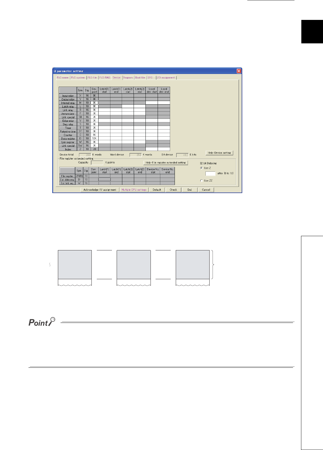
CHAPTER9 DEVICES
9
2
3
4
5
6
7
8
9.14 Convenient Usage of Devices
9.14.2 Local device
9 - 87
(3) Local device setting
(a) Setting the local device range
In the Device tab of the PLC parameter dialog box, set the range that is used as a local device.
Note that the local device range is common to all programs, and cannot be changed for each program.
For example, if a local device range is specified as M0 to M100, this range setting applies to all programs that
use the local device.
●The 32-bit index modification range must not overlap with the local device setting range of the index register.
If overlapped, 32-bit index modification values will be written over the local device values.
●When CPU module parameters which contains local device setting of the index register are read out from the GX
Developer that does not support the setting, all of the index register data will be read out as global device data.
Figure 9.101 Device
Figure 9.102 Local device range
Program A Program B Program C
M0
M100
Local
device
Local
device
Local
device
Locla device
range is
common to all
programs.
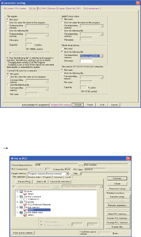
9 - 88
(b) Setting the drive and file name
After setting the local device range, set a memory for storing the local device file and a file name in the PLC file
tab of the PLC parameter dialog box.
(c) Writing the setting data
Write the data set in (a) and (b) to the CPU module.
Select [Online] [Write to PLC] in GX Developer.
Figure 9.103 PLC file
Figure 9.104 Device memory writing
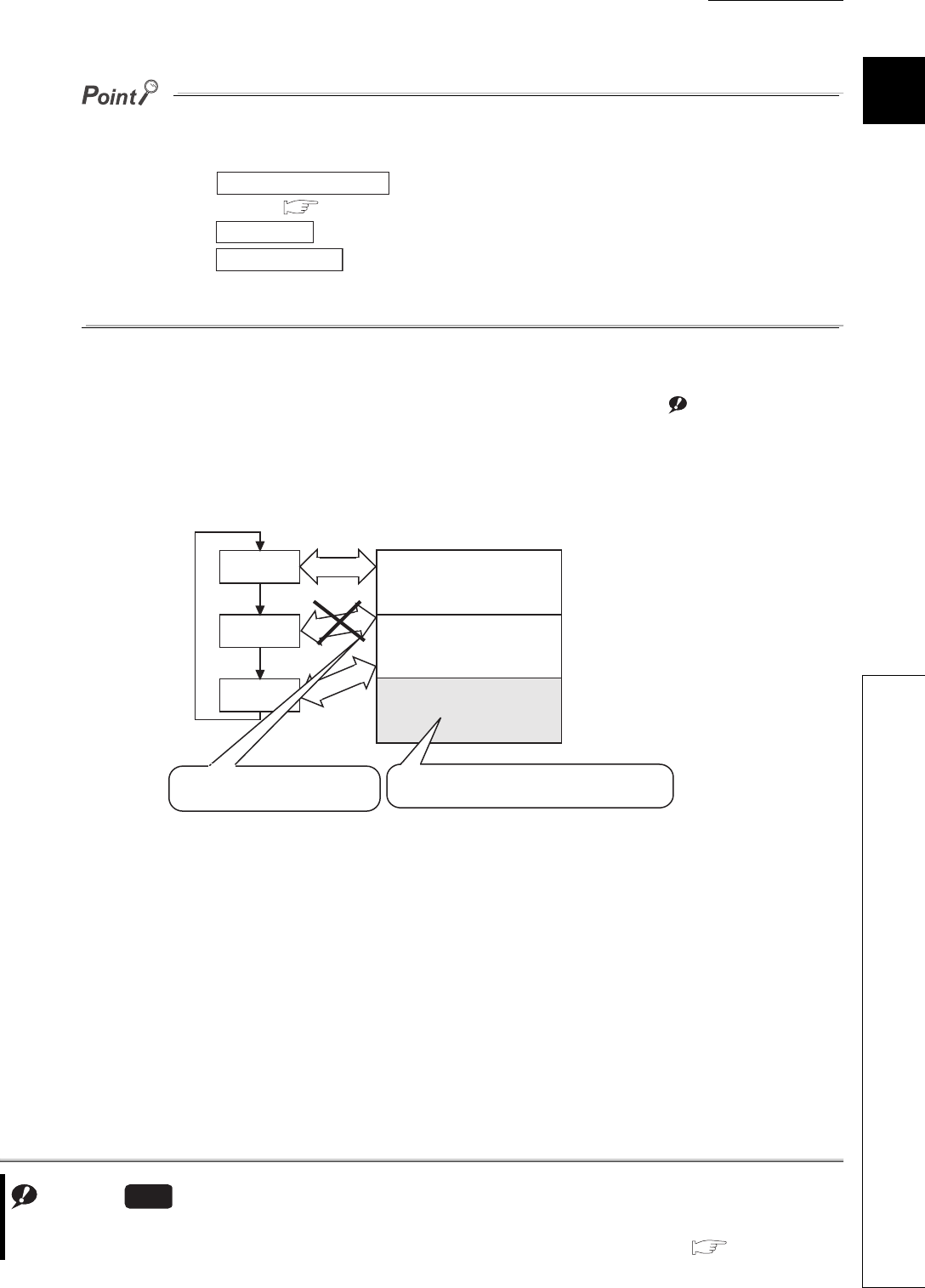
CHAPTER9 DEVICES
9
2
3
4
5
6
7
8
9.14 Convenient Usage of Devices
9.14.2 Local device
9 - 89
●If the size setting of the local device in the standard RAM is changed with a sampling trace file stored in the standard
RAM, the sampling trace file is cleared.
To save the trace results in your personal computer, perform the following operations.
1) Click the button on the Sampling trace dialog box to read the trace result into the
personal computer. ( Section 6.14(5)(e))
2) Click the button to display the trace result.
3) Click the button to store the trace results in CSV format.
●All of the devices that have not been set as local devices are global devices.
(4) Setting of whether to use a local device (for each program) Note9.8Note1
Use of the local device can be set for each program, and this function can reduce the scan time.
Also, since the area for saving and restoring data is not required for the programs not using a local device, the
local device file size can be reduced.
Note1
Figure 9.105 Save area configuration of a local device file
Trace result PLC read
Trace result
Create CSV file
Note9.8
For setting a local device for each program in the Q02UCPU, Q03UDCPU, Q04UDHCPU, Q06UDHCPU,
Q13UDHCPU, and Q26UDHCPU, check the versions of the CPU module and GX Developer. ( Appendix 2)
Universal
Program A
Program B
Program C
Program execution Local device file (.QDL)
Save/Restore
Save/Restore
Save/Restore
File size can be reduced since the saving or
restoring area for program B is not created.
For program A
For program C
Scan time decreases because saving
/restoring process is not performed.
9 - 90
(a) Setting method
In addition to the setting in (3) in this section, set the following.
Select the File usability setting button in the Program tab of the PLC parameter dialog box, and specify the
programs that use the local device.
(b) Precautions
1) Change of the local device
Do not change or refer to the local device in a program for which the local device is set to "Not used".
Even if the local device is changed in such a program, the changed data will not be held.
2) Conditions for creating a local device file
Creation of a local device file depends on the PLC parameter settings.
Table9.13 shows the conditions for creating a local device file.
: Created, : Not created
*1: Indicates the local device range setting in the Device tab.
Figure 9.106 File usability setting dialog box
Table9.13 Conditions for creating a local device file
PLC parameter setting File creation Error detection
PLC file setting Device setting*1 File usability setting
Set
Set Use PLC file setting -
Not used -
Not set Use PLC file setting -
Not used -
Not set
Set Use PLC file setting PARAMETER ERROR (error code: 3000)
Not used -
Not set Use PLC file setting -
Not used -
Click the
File usability setting button.
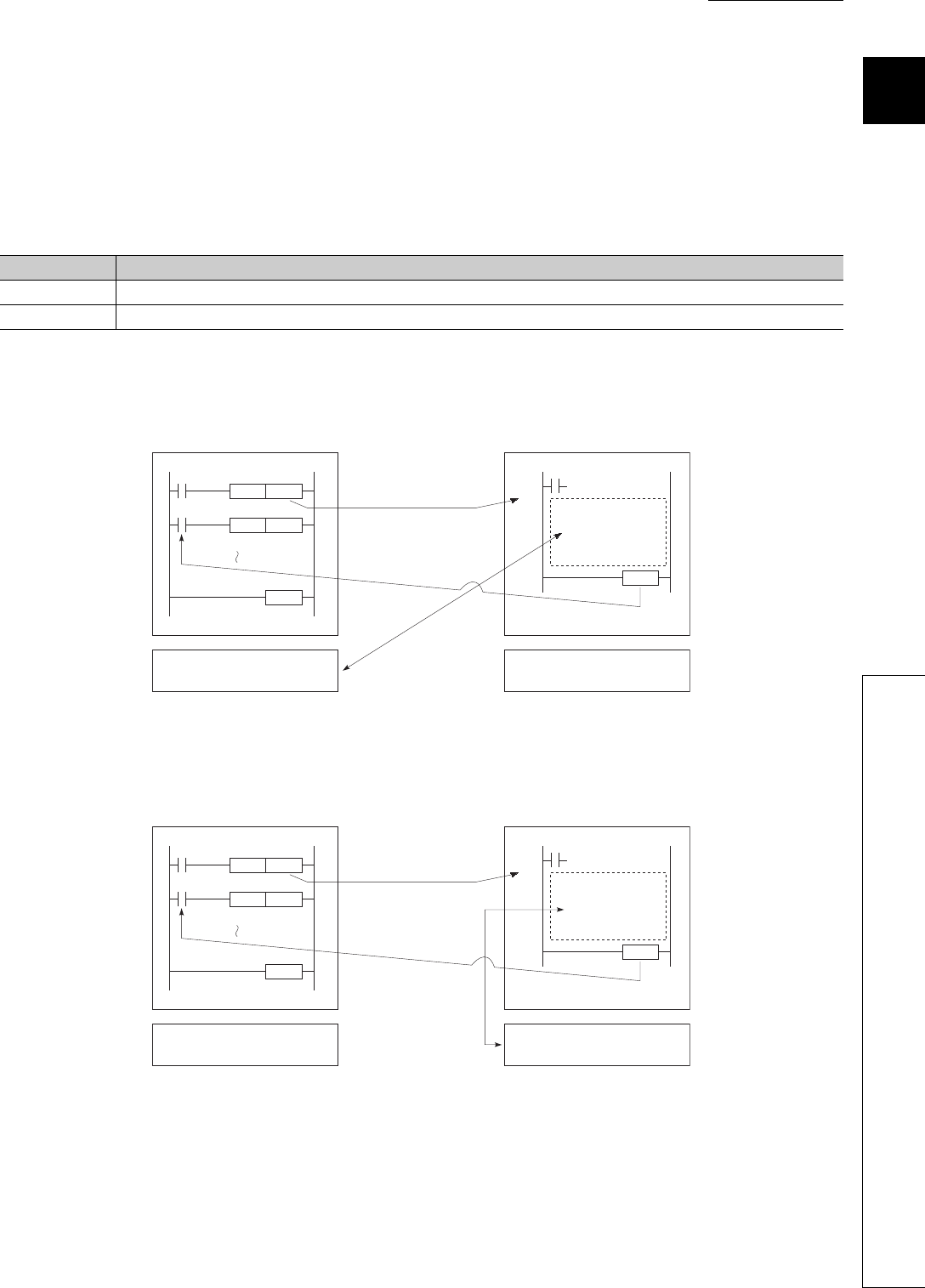
CHAPTER9 DEVICES
9
2
3
4
5
6
7
8
9.14 Convenient Usage of Devices
9.14.2 Local device
9 - 91
(5) Using the local device corresponding to the file where a subroutine program is
stored
When executing a subroutine program, you can utilize the local device corresponding to the file where the
subroutine program is stored.
Use of the relevant local device is set by ON/OFF of SM776.
(a) When SM776 is off
(b) When SM776 is on
Table9.14 Local device switching by ON/OFF of the special relay (SM776)
SM776 Operation
OFF Perform operations with the local device that corresponds to the source file of the subroutine program.
ON Perform operations with the local device that corresponds to the file where the subroutine program is stored.
Figure 9.107 When SM776 is off
Figure 9.108 When SM776 is on
X0
X2
P100
D0
CALL
INCP
END
RET
P100
Subroutine
program
Local device area for
file name, ABC
Local device area for
file name, DEF
File name: ABC File name: DEF
(Stand-by type program)
Execution of subroutine
program
Local device
writing/reading
X0
X2
P100
D0
CALL
INCP
END
RET
P100
Subroutine
program
Local device area for
file name, ABC
Local device area for
file name, DEF
Execution of subroutine
program
Local device
writing/reading
File name: ABC File name: DEF
(Stand-by type program)

9 - 92
(c) Precautions
• When SM776 is on, local device data are read out when a subroutine program is called, and the data are
saved after execution of the RET instruction.
Because of this, the scan time is increased if one subroutine program is executed with SM776 set to on.
• The on/off status of SM776 is set for each CPU module.
It cannot be set for each file.
• If the on/off status of SM776 is changed during sequence program execution, control is implemented
according to the information after the change.
Remark
For details of SM776, refer to CHAPTER 12.
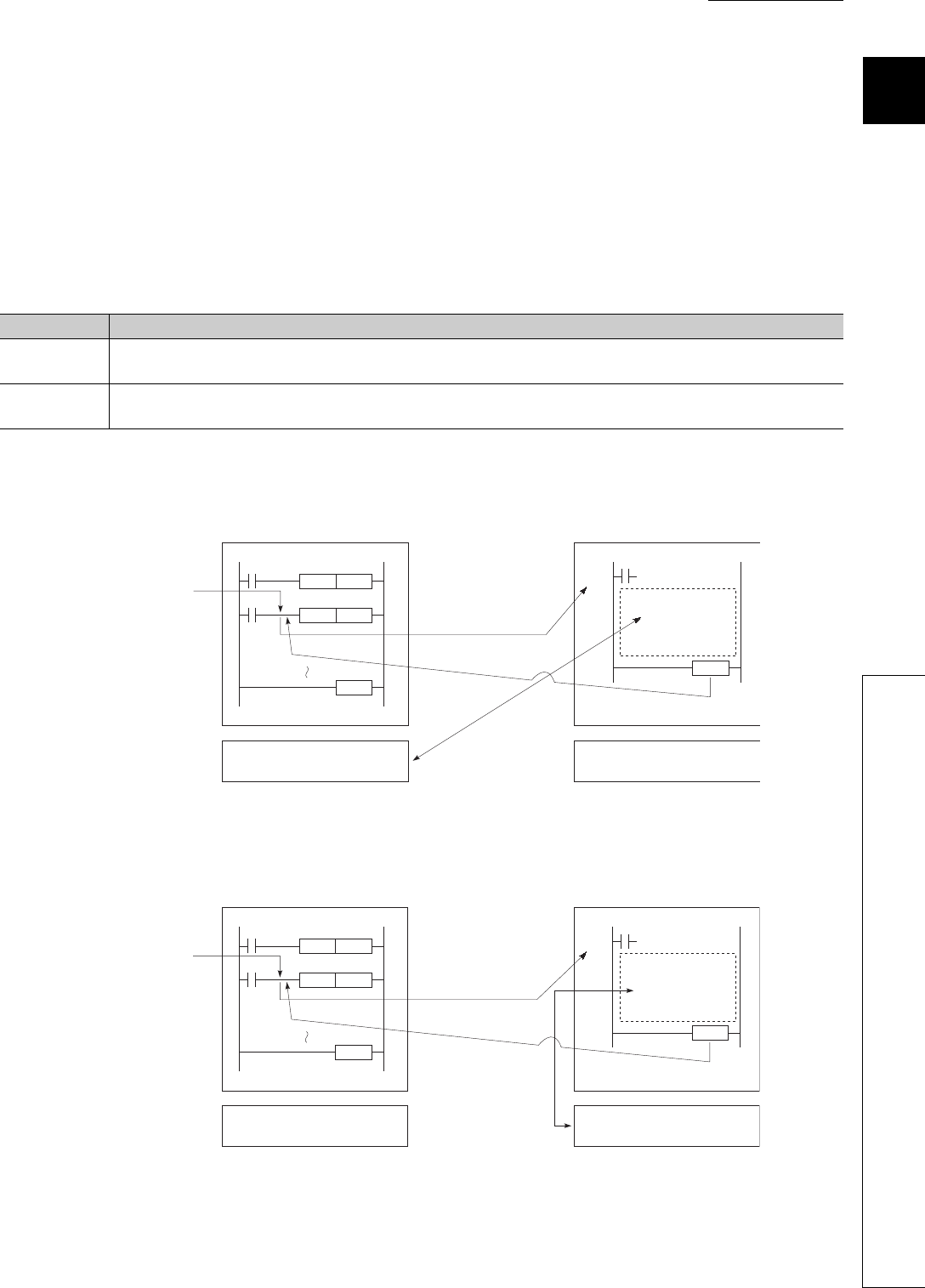
CHAPTER9 DEVICES
9
2
3
4
5
6
7
8
9.14 Convenient Usage of Devices
9.14.2 Local device
9 - 93
(6) When executing an interrupt/fixed scan execution type program
When executing an interrupt/fixed scan execution type program, you can utilize the local device corresponding to
the file where the program is stored.
Use of the relevant local device is set by ON/OFF of SM777. *1
*1: The index register set as the local device uses the local device area for the program executed before the interrupt/fixed
scan execution type program, regardless of the on/off status of SM777.
(a) When SM777 is off
(b) When SM777 is on
Table9.15 Local device switching by ON/OFF of the special relay (SM777)
SM777 Operation
OFF Perform operations with the local device that corresponds to the program executed before the interrupt/fixed scan
execution type program.
ON Perform operations with the local device that corresponds to the program file where the interrupt/fixed scan execution
type program is stored.
Figure 9.109 When SM777 is off
Figure 9.110 When SM777 is on
X0
X2
D1
D0
DECP
INCP
END
Interrupt occurred
IRET
I0
Interrupt program
Local device area for
file name, ABC
Local device area for
file name, DEF
File name: ABC File name: DEF
(Stand-by type program)
Execution of
interrupt program
Local device
writing/reading
X0
X2
D1
D0
DECP
INCP
END
Interrupt occurred
IRET
I0
Interrupt
program
Local device area for
file name, ABC
Local device area for
file name, DEF
File name: ABC File name: DEF
(Stand-by type program)
Execution of
interrupt program
Local device
writing/reading

9 - 94
(c) Precautions
• When SM777 is on, local device data are read out before execution of an interrupt/fixed scan execution
type program, and the data are saved after execution of the IRET instruction.
Because of this, the scan time is increased if one interrupt/fixed scan execution type program is executed
with SM777 set to on.
• The on/off status of SM777 is set for each CPU module.
It cannot be set for each file.
• If the on/off status of SM777 is changed during sequence program execution, control is implemented
according to the information after the change.
Remark
For details of SM777, refer to CHAPTER 12.
(7) Clearing local device data
Local device data is cleared by either of the following:
• When the CPU module is powered off and then on or is reset
• When the CPU module status is changed from STOP to RUN
Local device data cannot be cleared from GX Developer.
10 - 1
CHAPTER10 CPU MODULE PROCESSING TIME
1
10
3
4
5
6
7
8
10.1 Scan Time
10.1.1 Scan time structure
CHAPTER10 CPU MODULE PROCESSING TIME
This chapter describes the CPU module processing time.
10.1 Scan Time
This section describes the scan time structures and CPU module processing time.
10.1.1 Scan time structure
A CPU module sequentially performs the following processing in the RUN status.
Scan time is the time required for all processing and executions to be performed.
*1: End of a program indicates the timing when the END, GOEND, FEND, or STOP instruction is executed.
Figure 10.1 Scan time structure
STOP/PAUSE status
STOP/PAUSE
processing
NO
YES
Operating status check
RUN status
Common processing time
Instruction execution time
( )
( )
( )
( )
( )
( )
( )
Processing
in the RUN status
Program check
I/O refresh
Execution of the DUTY instruction in END processing
(no execution when the DUTY instruction is not used)
Program execution
End the program?
*1
Refresh via MELSECNET/H
Refresh via CC-Link IE controller network
Refresh via CC-Link
Refresh by the intelligent function module
parameters set in GX Configurator
Calendar update, error clear
Device data latch processing
Service processing
Processing during the constant scan waiting time
(no processing when the constant scan time is not set)
WDT reset, scan time calculation
Scan time
Common END processing time
I/O refresh time
Instruction execution time in END processing
Module refresh time
Function execution time
in END processing
Service processing time
Section 10.1.2(1)
Section 10.1.2(3)
Section 10.1.2(4)
Section 10.1.2(5)
Section 10.1.2(6)
Section 10.1.2(7)
Section 10.1.2(2)
10 - 2
(1) How to check scan time
The CPU module measures current, minimum, and maximum values of the scan time.
The scan time can be checked by monitoring the special register (SD520, SD521, and SD524 to SD527).
Accuracy of each stored scan time is 0.1ms.
If the stored values in SD520 and SD521 are 3 and 400 respectively, the scan time is 3.4ms.
10.1.2 Time required for each processing included in scan time
This section describes how to calculate the processing and execution time described in Section 10.1.1.
(1) I/O refresh time
The I/O refresh time is time required for refreshing I/O data to/from the following modules mounted on
the main base unit and extension base units.
• Input module
• Output module
• Intelligent function module
Calculation method
Use the following expression to calculate the I/O refresh time.
(I/O refresh time) = (number of input points/16) N1 + (number of output points/16) N2
For N1 and N2, refer to Table10.1.
Figure 10.2 Scan time storage location
Table10.1 I/O refresh time
CPU module Q3 B, Q3 SB, Q3 RB, Q3 DB Q5 B, Q6 B, Q6 RB
N1 N2 N1 N2
Q00UJCPU, Q00UCPU, Q01UCPU 1.8 s 1.0 s 2.6 s 1.9 s
Q02UCPU 1.5 s 1.1 s 2.4 s 1.9 s
Q03UDCPU, Q04UDHCPU,
Q06UDHCPU, Q10UDHCPU,
Q13UDHCPU, Q20UDHCPU,
Q26UDHCPU, Q03UDECPU,
Q04UDEHCPU, Q06UDEHCPU,
Q10UDEHCPU, Q13UDEHCPU,
Q20UDEHCPU, Q26UDEHCPU
1.5 s 1.0 s 2.3 s 1.8 s
Stores the scan time of 1ms or less (unit: s).
Stores the scan time. (unit: ms).
SD520
SD524
SD526
Current value
Minimum value
Maximum value
SD521
SD525
SD527
Example

10 - 3
CHAPTER10 CPU MODULE PROCESSING TIME
1
10
3
4
5
6
7
8
10.1 Scan Time
10.1.2 Time required for each processing included in scan time
(2) Instruction execution time in END processing
This is the processing time of the DUTY instruction in END processing.
The user timing clock (SM420 to 424 and SM430 to SM434) specified with the DUTY instruction is turned on/off
during the END processing.
(3) Instruction execution time
The instruction execution time is the time required for all instructions used in the program to be exe-
cuted.
Remark
For the processing time required for each instruction, refer to the following.
QCPU Programming Manual (Common Instructions)
Table10.2 Instruction execution time in END processing
CPU module Processing time in END processing
When set to 1 When set to 5
Q00UJCPU, Q00UCPU, Q01UCPU 0.0120ms 0.0140ms
Q02UCPU 0.0050ms 0.0550ms
Q03UDCPU, Q03UDECPU 0.0043ms 0.0046ms
Q04UDHCPU, Q06UDHCPU, Q10UDHCPU, Q13UDHCPU,
Q20UDHCPU, Q26UDHCPU, Q04UDEHCPU, Q06UDEHCPU,
Q10UDEHCPU, Q13UDEHCPU, Q20UDEHCPU, Q26UDEHCPU
0.0041ms 0.0045ms
10 - 4
(a) Overhead time at execution of interrupt and fixed scan execution type programs
When calculating instruction execution time, add the overhead time given in the following table to the instruc-
tion execution time, which is described in (3).
Two kinds of overhead time (pre-start and program-end) need to be added to interrupt programs.
*1: Indicates the value when the QI60 is mounted on the slot 0 of the main base unit.
Table10.3 Pre-start overhead time for interrupt programs
CPU module
Fixed scan interrupt
(I28 to I31)
Multiple CPU synchronous
interrupt (I45)
Interrupt*1 (I0 to I15) from QI60 or
interrupt (I50 to I127) from the
intelligent function module
Without
high-speed
start
With high-
speed start
Without
high-speed
start
With high-
speed start
Without high-
speed start
With high-speed
start
Q00UJCPU, Q00UCPU, Q01UCPU 55 s 35 s --- --- 76 s 55 s
Q02UCPU 48 s 17 s --- --- 60 s 31 s
Q03UDCPU, Q03UDECPU 47 s 17 s 46 s 16 s 54 s 22 s
Q04UDHCPU, Q06UDHCPU,
Q10UDHCPU, Q13UDHCPU,
Q20UDHCPU, Q26UDHCPU,
Q04UDEHCPU, Q06UDEHCPU,
Q10UDEHCPU, Q13UDEHCPU,
Q20UDEHCPU, Q26UDEHCPU
46 s 16 s 44 s 14 s 52 s 22 s
Table10.4 Program-end overhead time for interrupt programs
CPU module Without high-
speed start
With high-speed
start
Q00UJCPU, Q00UCPU, Q01UCPU 28 s15 s
Q02UCPU 26 s7 s
Q03UDCPU, Q03UDECPU 26 s7 s
Q04UDHCPU, Q06UDHCPU, Q10UDHCPU, Q13UDHCPU, Q20UDHCPU,
Q26UDHCPU, Q04UDEHCPU, Q06UDEHCPU, Q10UDEHCPU, Q13UDEHCPU,
Q20UDEHCPU, Q26UDEHCPU
26 s7 s
Table10.5 Overhead time for fixed scan execution type programs
CPU module Without high-
speed start
With high-speed
start
Q00UJCPU, Q00UCPU, Q01UCPU 92 s60 s
Q02UCPU 73 s25 s
Q03UDCPU, Q03UDECPU 73 s24 s
Q04UDHCPU, Q06UDHCPU, Q10UDHCPU, Q13UDHCPU, Q20UDHCPU,
Q26UDHCPU, Q04UDEHCPU, Q06UDEHCPU, Q10UDEHCPU, Q13UDEHCPU,
Q20UDEHCPU, Q26UDEHCPU
72 s23 s

10 - 5
CHAPTER10 CPU MODULE PROCESSING TIME
1
10
3
4
5
6
7
8
10.1 Scan Time
10.1.2 Time required for each processing included in scan time
1) Overhead time when local devices in the interrupt program are enabled
When SM777 (Enable/disable local device in interrupt program) is turned on, the time given in Table10.6 and
Table10.7 will be added to the overhead time given in Table10.3 and Table10.4.
Each n, N1, N2, and N3 in the table indicates the following:
• n: Number of local device points (unit: K words)
• N1: Number of devices that specified a local device
• N2: Number of word device points that specified a local device
• N3: Number of bit device points that specified a local device
Table10.6 When a local device file in the standard RAM is used
CPU module Additional time to the pre-start overhead time
for interrupt programs (Table10.3)
Additional time to the program-end overhead
time for interrupt programs (Table10.4)
Q00UCPU, Q01UCPU (13.2 N1) + (0.22 (N2 + (N3 16))) + 210 s (8 N1) + (0.23 (N2 + (N3 16))) + 30 s
Q02UCPU (13.2 N1) + (0.22 (N2 + (N3 16))) + 210 s (8 N1) + (0.22 (N2 + (N3 16))) + 30 s
Q03UDCPU, Q03UDECPU (8 N1) + (0.22 (N2 + (N3 16))) + 80 s (8 N1) + (0.22 (N2 + (N3 16))) + 20 s
Q04UDHCPU, Q06UDHCPU,
Q10UDHCPU, Q13UDHCPU,
Q20UDHCPU, Q26UDHCPU,
Q04UDEHCPU, Q06UDEHCPU,
Q10UDEHCPU, Q13UDEHCPU,
Q20UDEHCPU, Q26UDEHCPU
(8 N1) + (0.10 (N2 + (N3 16))) + 80 s (8 N1) + (0.10 (N2 + (N3 16))) + 20 s
Table10.7 When a local device file in a SRAM card is used
CPU module Additional time to the pre-start overhead time
for interrupt programs (Table 10.3)
Additional time to the program-end overhead
time for interrupt programs (Table 10.4)
Q02UCPU (16 N1) + (0.43 (N2 + (N3 16))) + 260 s (16 N1) + (0.43 (N2 + (N3 16))) + 60 s
Q03UDCPU, Q03UDECPU (12 N1) + (0.43 (N2 + (N3 16))) + 100 s (12 N1) + (0.43 (N2 + (N3 16))) + 20 s
Q04UDHCPU, Q06UDHCPU,
Q10UDHCPU, Q13UDHCPU,
Q20UDHCPU, Q26UDHCPU,
Q04UDEHCPU, Q06UDEHCPU,
Q10UDEHCPU, Q13UDEHCPU,
Q20UDEHCPU, Q26UDEHCPU
(12 N1) + (0.40 (N2 + (N3 16))) + 100 s (12 N1) + (0.40 (N2 + (N3 16))) + 20 s

10 - 6
(4) Module refresh time
Module refresh time is the total time required for the CPU module to refresh data with CC-Link IE con-
troller network, MELSECNET/H, and CC-Link modules.
(a) Refresh via CC-Link IE controller network
This is the time required for refreshing data between link devices in a CC-Link IE controller network
module and devices in the CPU module.
(b) Refresh via MELSECNET/H
This is the time required for refreshing data between link devices in a MELSECNET/H network
module and devices in the CPU module.
(c) Auto refresh via CC-Link
This is the time required for refreshing data between a CC-Link system master/local module and
CPU module.
Remark
For each refresh time, refer to the following.
Reference manual of each network module
10 - 7
CHAPTER10 CPU MODULE PROCESSING TIME
1
10
3
4
5
6
7
8
10.1 Scan Time
10.1.2 Time required for each processing included in scan time
(d) Auto refresh with an intelligent function module
This is the time required for refreshing data between the buffer memory of an intelligent function module and
devices in the CPU module.
Use intelligent function module utility package (GX Configurator) for auto refresh settings.
Calculation method
Use the following expression to calculate the auto refresh time with an intelligent function module.
(Refresh time) = KN1 + KN2 (number of refresh points)
For KN1 and KN2, use the values given in Table10.8 and Table10.9.
When the number of auto refresh points for the analog-digital converter module (Q64AD)
is 4 points (when the module is mounted on the Q26UDHCPU main base unit)
Table10.8 When an intelligent function module is mounted on the main base unit
CPU module KN1 KN2
Q00UJCPU, Q00UCPU, Q01UCPU 96.3 s 6.7 s
Q02UCPU 23 s 6 s
Q03UDCPU, Q03UDECPU 6 s 5 s
Q04UDHCPU, Q06UDHCPU, Q10UDHCPU, Q13UDHCPU, Q20UDHCPU,
Q26UDHCPU, Q04UDEHCPU, Q06UDEHCPU, Q10UDEHCPU, Q13UDEHCPU,
Q20UDEHCPU, Q26UDEHCPU
4 s 5 s
Table10.9 When an intelligent function module is mounted on the extension base unit
CPU module KN1 KN2
Q00UJCPU 79.7 s 8.9 s
Q00UCPU, Q01UCPU 79.7 s 8.1 s
Q02UCPU 45 s 7.0 s
Q03UDCPU, Q03UDECPU 7 s 6.0 s
Q04UDHCPU, Q06UDHCPU, Q10UDHCPU, Q13UDHCPU, Q20UDHCPU,
Q26UDHCPU, Q04UDEHCPU, Q06UDEHCPU, Q10UDEHCPU, Q13UDEHCPU,
Q20UDEHCPU, Q26UDEHCPU
5 s 6 s
0.029 (ms) = 0.005 + 0.006 4
Example

10 - 8
(5) Function execution time in END processing
This is the time required for updating calender or clearing error in END processing.
(a) Calendar update processing time
When the clock data set request (SM210 changes from off to on) or the clock data read request
(SM213 turns on) is issued, the processing time for changing or reading the clock data is required in
END processing.
(b) Error clear processing time
Upon the rising edge (changes from off to on) of SM50 (Error reset), the processing time for clearing the contin-
uation error stored in SD50 is required.
Table10.10 Calendar update processing time
CPU module
Processing time in END processing
When the clock data set
request is issued
When the clock data read
request is issued
Q00UJCPU, Q00UCPU, Q01UCPU 0.040ms 0.019ms
Q02UCPU 0.040ms 0.019ms
Q03UDCPU, Q04UDHCPU, Q06UDHCPU, Q10UDHCPU, Q13UDHCPU,
Q20UDHCPU, Q26UDHCPU, Q03UDECPU, Q04UDEHCPU,
Q06UDEHCPU, Q10UDEHCPU, Q13UDEHCPU, Q20UDEHCPU,
Q26UDEHCPU
0.011ms 0.004ms
Table10.11 Error clear processing time
CPU module
Processing time in END processing
When the error is cleared
(the one detected by the
annunciator)
When the error is cleared
Q00UJCPU, Q00UCPU, Q01UCPU 0.185ms 0.185ms
Q02UCPU 0.180ms 0.175ms
Q03UDCPU, Q03UDECPU 0.068ms 0.062ms
Q04UDHCPU, Q06UDHCPU, Q10UDHCPU, Q13UDHCPU,
Q20UDHCPU, Q26UDHCPU, Q04UDEHCPU, Q06UDEHCPU,
Q10UDEHCPU, Q13UDEHCPU, Q20UDEHCPU, Q26UDEHCPU
0.065ms 0.062ms
10 - 9
CHAPTER10 CPU MODULE PROCESSING TIME
1
10
3
4
5
6
7
8
10.1 Scan Time
10.1.2 Time required for each processing included in scan time
(6) Device data latch processing time
When the latch range is set in the Device tab of the PLC parameter dialog box*1 *2 *3, the processing
time shown in Table10.12 is required.
Each N1, N2, and N3 in the table indicates the following:
• N1: Number of devices specified to be latched (Count the latch range (1) and the latch
range (2) as different devices.)
• N2: Number of bit device points specified to be latched
• N3: Number of word device points specified to be latched
*1: When setting the latch range of the timer (T), retentive timer (ST), and counter (C), one point for word device and two points for bit device
are occupied per point.
*2: The case where the points are set for the latch relay (L) is included.
*3: The scan time will not increase if the latch range is set for the file register (R, ZR), extended data register (D), or extended link register
(W).
To shorten the scan time, minimize the number of latch points.
The number of latch points can be reduced by performing the following.
• Move data to be latched to the file register.
• Store device data that is updated less frequently to the standard ROM with the SP.DEVST instruction. (The device
data stored in the standard ROM can be read with the S(P).DEVLD instruction.)
QCPU Programming Manual (Common Instructions)
Table10.12 Processing time when the latch range is set
CPU module Processing time
Q00UJCPU, Q00UCPU, Q01UCPU (4.4 N1) + (0.12 (N2 16 + N3)) s
Q02UCPU (4.0 N1) + (0.12 (N2 16 + N3)) s
Q03UDCPU, Q03UDECPU (3.0 N1) + (0.12 (N2 16 + N3)) s
Q04UDHCPU, Q06UDHCPU, Q10UDHCPU, Q13UDHCPU, Q20UDHCPU,
Q26UDHCPU, Q04UDEHCPU, Q06UDEHCPU, Q10UDEHCPU, Q13UDEHCPU,
Q20UDEHCPU, Q26UDEHCPU
(3.0 N1) + (0.05 (N2 16 + N3)) s

10 - 10
(7) Service processing time
Service processing is the communication processing with GX Developer and external devices.
When monitoring device data, reading programs, and setting monitor conditions in GX Developer, the
processing time shown in Table10.13 or Table10.14 is required.
*1: The time in the table is for the case where the service processing count is set to one.
(8) Common processing time
The CPU module performs common processing by the system. The common processing time shown in
Table10.15 is required.
(9) Multiple CPU high speed transmission processing time
This is the processing time required for data transmission between the CPU modules when the multiple CPU high
speed transmission function is used.
For the multiple CPU high speed transmission processing time, refer to the following.
QCPU User's Manual (Multiple CPU System)
Table10.13 Processing time to monitor device data and read programs
CPU module
Processing time*1
Monitoring device
data (Data register: 32
points)
Reading programs
(10K step)
Q00UJCPU, Q00UCPU, Q01UCPU 1.60ms 3.70ms
Q02UCPU 1.00ms 1.55ms
Q03UDCPU, Q04UDHCPU, Q06UDHCPU, Q10UDHCPU, Q13UDHCPU,
Q20UDHCPU, Q26UDHCPU, Q03UDECPU, Q04UDEHCPU, Q06UDEHCPU,
Q10UDEHCPU, Q13UDEHCPU, Q20UDEHCPU, Q26UDEHCPU
0.35ms 0.95ms
Table10.14 Processing time to set monitor conditions
CPU module
Processing time
Specified step match Specified device
match
Q02UCPU 0.03ms 0.04ms
Q03UDCPU, Q04UDHCPU, Q06UDHCPU, Q10UDHCPU, Q13UDHCPU,
Q20UDHCPU, Q26UDHCPU, Q03UDECPU, Q04UDEHCPU, Q06UDEHCPU,
Q10UDEHCPU, Q13UDEHCPU, Q20UDEHCPU, Q26UDEHCPU
0.01ms 0.03ms
Table10.15 Common processing time
CPU module Processing time
Q00UJCPU, Q00UCPU, Q01UCPU 0.25ms
Q02UCPU 0.17ms
Q03UDCPU 0.12ms
Q04UDHCPU, Q06UDHCPU, Q10UDHCPU, Q13UDHCPU, Q20UDHCPU,
Q26UDHCPU 0.09ms
Q03UDECPU 0.21ms
Q04UDEHCPU, Q06UDEHCPU, Q10UDEHCPU, Q13UDEHCPU,
Q20UDEHCPU, Q26UDEHCPU 0.17ms

10 - 11
CHAPTER10 CPU MODULE PROCESSING TIME
1
10
3
4
5
6
7
8
10.1 Scan Time
10.1.3 Factors that increase the scan time
10.1.3 Factors that increase the scan time
When executing any of the functions or operations described in this section, add the given processing time
to the time value calculated in Section 10.1.2.
(1) Sampling trace
When the sampling trace function ( Section 6.14) is executed, the processing time shown in
Table10.16 is required.
Table10.16 Processing time (when 50 points of the internal relay (for bit device) and 50 points of the data register (for word device)
are set as sampling trace data)
CPU module Processing time
Standard RAM
Q00UCPU, Q01UCPU 0.12ms
Q02UCPU 0.09ms
Q03UDCPU, Q03UDECPU 0.07ms
Q04UDHCPU, Q06UDHCPU, Q10UDHCPU,
Q13UDHCPU, Q20UDHCPU, Q26UDHCPU,
Q04UDEHCPU, Q06UDEHCPU, Q10UDEHCPU,
Q13UDEHCPU, Q20UDEHCPU, Q26UDEHCPU
0.06ms
SRAM card
Q02UCPU 0.16ms
Q03UDCPU, Q03UDECPU 0.08ms
Q04UDHCPU, Q06UDHCPU, Q10UDHCPU,
Q13UDHCPU, Q20UDHCPU, Q26UDHCPU,
Q04UDEHCPU, Q06UDEHCPU, Q10UDEHCPU,
Q13UDEHCPU, Q20UDEHCPU, Q26UDEHCPU
0.06ms
10 - 12
(2) Use of local devices
When local devices are used, the processing time shown in Table10.17 is required.
Each n, N1, N2, and N3 in the table indicates the following:
• n: Number of programs using a local device*1
• N1: Number of devices that specified a local device
• N2: Number of word device points that specified a local device
• N3: Number of bit device points that specified a local device
*1: If the serial number (first five digits) of the Universal model QCPU is "10011" or earlier, "n" indicates the number of executed programs.
Table10.17 Processing time (when local devices are used)
CPU module Processing time
Standard RAM
Q00UCPU, Q01UCPU ((12.5 N1) + (0.24 (N2 + (N3 16))) + 170) n s
Q02UCPU ((12 N1) + (0.22 (N2 + (N3 16))) + 140) n s
Q03UDCPU, Q03UDECPU ((8 N1) + (0.22 (N2 + (N3 16))) + 50) n s
Q04UDHCPU, Q06UDHCPU, Q10UDHCPU,
Q13UDHCPU, Q20UDHCPU, Q26UDHCPU,
Q04UDEHCPU, Q06UDEHCPU, Q10UDEHCPU,
Q13UDEHCPU, Q20UDEHCPU, Q26UDEHCPU
((8 N1) + (0.10 (N2 + (N3 16))) + 50) n s
SRAM card
Q02UCPU ((16 N1) + (0.43 (N2 + (N3 16))) + 160) n s
Q03UDCPU, Q03UDECPU ((12 N1) + (0.43 (N2 + (N3 16))) + 60) n s
Q04UDHCPU, Q06UDHCPU, Q10UDHCPU,
Q13UDHCPU, Q20UDHCPU, Q26UDHCPU,
Q04UDEHCPU, Q06UDEHCPU, Q10UDEHCPU,
Q13UDEHCPU, Q20UDEHCPU, Q26UDEHCPU
((12 N1) + (0.40 (N2 + (N3 16))) + 60) n s

10 - 13
CHAPTER10 CPU MODULE PROCESSING TIME
1
10
3
4
5
6
7
8
10.1 Scan Time
10.1.3 Factors that increase the scan time
(a) When local devices in a subroutine program are enabled
When SM776 (Enable/disable local device at CALL) is turned on, the processing time shown in Table10.18 or
Table10.19 is required for each subroutine call.
Each n, N1, N2, and N3 in the table indicates the following:
• n: Number of local device points (unit: K words)
• N1: Number of devices that specified a local device
• N2: Number of word device points that specified a local device
• N3: Number of bit device points that specified a local device
Table10.18 Processing time (when a local device file in the standard RAM is used)
CPU module
Processing time when a
subroutine program in the same
file is called
Processing time when a subroutine program
in a different file is called
Q00UCPU, Q01UCPU 0.00 s (24 N1) + (0.73 (N2 + (N3 16))) + 280 s
Q02UCPU 0.00 s (24 N1) + (0.44 (N2 + (N3 16))) + 280 s
Q03UDCPU, Q03UDECPU 0.00 s (16 N1) + (0.44 (N2 + (N3 6))) + 100 s
Q04UDHCPU, Q06UDHCPU,
Q10UDHCPU, Q13UDHCPU,
Q20UDHCPU, Q26UDHCPU,
Q04UDEHCPU, Q06UDEHCPU,
Q10UDEHCPU, Q13UDEHCPU,
Q20UDEHCPU, Q26UDEHCPU
0.00 s (16 N1) + (0.20 (N2 + (N3 16))) + 100 s
Table10.19 Processing time (when a local device file in a SRAM card is used)
CPU module
Processing time when a
subroutine program in the same
file is called
Processing time when a subroutine program
in a different file is called
Q02UCPU 0.00 s (32 N1) + (0.86 (N2 + (N3 16))) + 320 s
Q03UDCPU, Q03UDECPU 0.00 s (24 N1) + (0.86 (N2 + (N3 16))) + 120 s
Q04UDHCPU, Q06UDHCPU,
Q10UDHCPU, Q13UDHCPU,
Q20UDHCPU, Q26UDHCPU,
Q04UDEHCPU, Q06UDEHCPU,
Q10UDEHCPU, Q13UDEHCPU,
Q20UDEHCPU, Q26UDEHCPU
0.00 s (24 N1) + (0.80 (N2 + (N3 16))) + 120 s
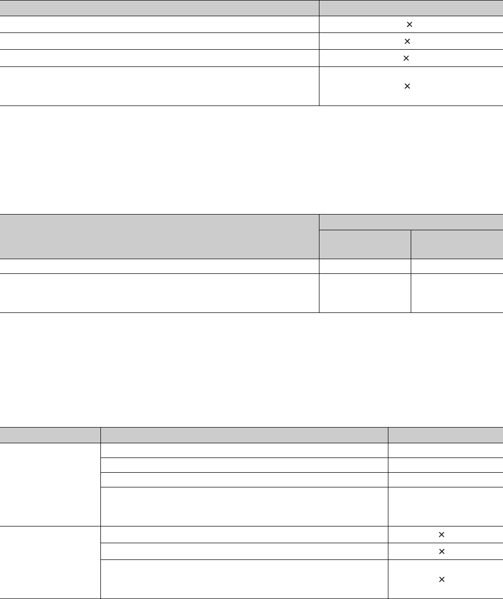
10 - 14
(3) Execution of multiple programs
When multiple programs are executed, the processing time shown in Table10.20 is required for each program.
*1: "n" indicates the number of program files.
(4) Removal and insertion of a memory card
When a memory card is removed or inserted, the processing time shown inTable10.21 is required only for one
scan where a memory card is removed or inserted.
(5) Use of the file register
When “Use the same file name as the program.” is selected in the PLC file tab of the PLC parameter
dialog box, the processing time shown in Table10.22 is required.
When “Use the following file.” is selected, the scan time will not be increased.
*1: "n" indicates the number of program files.
Table10.20 Processing time for each program (when multiple programs are executed)
CPU module Processing time
Q00UJCPU, Q00UCPU, Q01UCPU 0.053 n*1 ms
Q02UCPU 0.04 n*1 ms
Q03UDCPU, Q03UDECPU 0.02 n*1 ms
Q04UDHCPU, Q06UDHCPU, Q10UDHCPU, Q13UDHCPU, Q20UDHCPU,
Q26UDHCPU, Q04UDEHCPU, Q06UDEHCPU, Q10UDEHCPU, Q13UDEHCPU,
Q20UDEHCPU, Q26UDEHCPU
0.02 n*1 ms
Table10.21 Processing time (when a memory card is removed or inserted)
CPU module
Processing time
When a memory
card is inserted
When a memory
card is removed
Q02UCPU 0.7ms 0.2ms
Q03UDCPU, Q04UDHCPU, Q06UDHCPU, Q10UDHCPU, Q13UDHCPU,
Q20UDHCPU, Q26UDHCPU, Q03UDECPU, Q04UDEHCPU, Q06UDEHCPU,
Q10UDEHCPU, Q13UDEHCPU, Q20UDEHCPU, Q26UDEHCPU
0.6ms 0.1ms
Table10.22 Processing time (when the file register is used)
CPU module Processing time
Standard RAM
Q00UCPU, Q01UCPU 0.135ms
Q02UCPU 0.082ms
Q03UDCPU, Q03UDECPU 0.043ms
Q04UDHCPU, Q06UDHCPU, Q10UDHCPU, Q13UDHCPU, Q20UDHCPU,
Q26UDHCPU, Q04UDEHCPU, Q06UDEHCPU, Q10UDEHCPU,
Q13UDEHCPU, Q20UDEHCPU, Q26UDEHCPU
0.041ms
SRAM card
Q02UCPU 0.11 n*1 ms
Q03UDCPU, Q03UDECPU 0.06 n*1 ms
Q04UDHCPU, Q06UDHCPU, Q10UDHCPU, Q13UDHCPU, Q20UDHCPU,
Q26UDHCPU, Q04UDEHCPU, Q06UDEHCPU, Q10UDEHCPU,
Q13UDEHCPU, Q20UDEHCPU, Q26UDEHCPU
0.06 n*1 ms

10 - 15
CHAPTER10 CPU MODULE PROCESSING TIME
1
10
3
4
5
6
7
8
10.1 Scan Time
10.1.3 Factors that increase the scan time
(6) Online change
When data is written to the running CPU module, the processing time described below is required.
(a) Online change (ladder mode)
When a program in the running CPU module is changed in ladder mode, the processing time shown
in Table10.23 is required.*1
*1: The time in the table is for the case where the service processing count is set to one.
(b) Online change (files)
When a file is written to the running CPU module, the processing time shown in Table10.24 is
required. *1
*1: The time in the table is for the case where the service processing count is set to one.
Table10.23 Proceccing time (online change (ladder mode))
CPU module
Processing time
The reserved area for online change
is not changed.
The reserved area for online change
is re-set.
Q00UJCPU, Q00UCPU, Q01UCPU Up to 2.1ms Up to 2.1ms
Q02UCPU Up to 1.3ms Up to 1.3ms
Q03UDCPU, Q03UDECPU Up to 1.0ms Up to 1.0ms
Q04UDHCPU, Q06UDHCPU, Q10UDHCPU,
Q13UDHCPU, Q20UDHCPU, Q26UDHCPU,
Q04UDEHCPU, Q06UDEHCPU, Q10UDEHCPU,
Q13UDEHCPU, Q20UDEHCPU, Q26UDEHCPU
Up to 0.7ms Up to 0.7ms
Table10.24 Processing time (online change (files))
CPU module Processing time
Scan time = 2ms Scan time = 20ms
Q00UJCPU Up to 4.00ms Up to 6.20ms
Q00UCPU Up to 3.50ms Up to 5.80ms
Q01UCPU Up to 3.50ms Up to 5.60ms
Q02UCPU Up to 4.80ms Up to 4.80ms
Q03UDCPU, Q03UDECPU Up to 3.75ms Up to 3.75ms
Q04UDHCPU, Q06UDHCPU, Q10UDHCPU,
Q13UDHCPU, Q20UDHCPU, Q26UDHCPU,
Q04UDEHCPU, Q06UDEHCPU, Q10UDEHCPU,
Q13UDEHCPU, Q20UDEHCPU, Q26UDEHCPU
Up to 3.70ms Up to 3.70ms
10 - 16
(7) Non-group output status read
In multiple CPU systems, the scan time increases when “All CPUs can read all outputs” is selected in
the Multiple CPU settings screen of the PLC parameter dialog box.
(8) Scan time measurement
When the scan time is measured by GX Developer, the processing time shown in Table10.25 is required (
Section 6.13.3)
*1: The number of the branch instructions is a total of the following instructions, which are executed during the scan time measurement.
Pointer branch instruction : CJ, SCJ, JMP
Subroutine program call instruction: CALL(P), FCALL(P), ECALL(P), EFCALL(P), XCALL(P), RET
Figure 10.3 Multiple CPU settings screen
Table10.25 Processing time (when the scan time is measured)
CPU module Processing time
Q00UJCPU, Q00UCPU, Q01UCPU 179.5 + 5.8 number of branch instructions s*1
Q02UCPU 40.0 + 3.0 number of branch instructions s*1
Q03UDCPU, Q04UDHCPU, Q06UDHCPU, Q10UDHCPU, Q13UDHCPU,
Q20UDHCPU, Q26UDHCPU, Q03UDECPU, Q04UDEHCPU, Q06UDEHCPU,
Q10UDEHCPU, Q13UDEHCPU, Q20UDEHCPU, Q26UDEHCPU
40.0 + 1.5 number of branch instructions s*1
The scan time increases
when this parameter is set.
10 - 17
CHAPTER10 CPU MODULE PROCESSING TIME
1
10
3
4
5
6
7
8
10.1 Scan Time
10.1.3 Factors that increase the scan time
(9) Time taken to collect module errors
When using the module error collection, the scan time increases by the time found by the following calculation
formula.
Calculation formula
Collection time = N1 + N2 (Number of module errors collected in one scan)
The following table shows N1 and N2 values.
Table10.26 N1 values
CPU module Mounted base unit
Main base unit Extension base unit
Q00UJCPU 175 s 190 s
Q00UCPU, Q01UCPU 145 s 190 s
Q02UCPU 145 s 185 s
Q03UDCPU, Q04UDHCPU, Q06UDHCPU, Q10UDHCPU, Q13UDHCPU,
Q20UDHCPU, Q26UDHCPU, Q03UDECPU, Q04UDEHCPU, Q06UDEHCPU,
Q10UDEHCPU, Q13UDEHCPU, Q20UDEHCPU, Q26UDEHCPU
15 s 15 s
Table10.27 N2 values
CPU module Mounted base unit
Main base unit Extension base unit
Q00UJCPU, Q00UCPU, Q01UCPU 120 s 140 s
Q02UCPU 90 s 105 s
Q03UDCPU, Q04UDHCPU, Q06UDHCPU, Q10UDHCPU, Q13UDHCPU,
Q20UDHCPU, Q26UDHCPU, Q03UDECPU, Q04UDEHCPU, Q06UDEHCPU,
Q10UDEHCPU, Q13UDEHCPU, Q20UDEHCPU, Q26UDEHCPU
70 s 100 s
10 - 18
(10)Batch transfer of data to the program memory
When data in the program cache memory is batch-transferred to the program memory by GX Devel-
oper, the processing time shown in Table10.28 is required.*1
*1: The time in the table is for the case where the service processing count is set to one.
(11) Diagnostics of the redundant power supply system
When the "Diagnose redundant power supply system." is selected on the PLC RAS tab of the PLC
parameter dialog box, the processing time shown in Table10.29 is required.
*1: A power supply module failure indicates any of the following.
The redundant power supply module has failed.
Power for the redundant power supply module is turned off.
The redundant power supply module is not mounted.
Table10.28 Processing time (when data is batch-transferred to the program memory)
CPU module Processing time
Scan time = 2ms Scan time = 20ms
Q00UJCPU, Q00UCPU, Q01UCPU 1.90ms 4.90ms
Q02UCPU 1.55ms 4.50ms
Q03UDCPU, Q03UDECPU 1.10ms 3.65ms
Q04UDHCPU, Q06UDHCPU, Q10UDHCPU, Q13UDHCPU,
Q20UDHCPU, Q26UDHCPU, Q04UDEHCPU, Q06UDEHCPU,
Q10UDEHCPU, Q13UDEHCPU, Q20UDEHCPU, Q26UDEHCPU
1.05ms 3.65ms
Table10.29 Processing time (when the diagnostics for the redundant power supply system is enabled)
CPU module
Processing time
With a power supply module
failure*1
Without a power supply module
failure*1
Q00UCPU 125 s 165 s
Q01UCPU 125 s 135 s
Q02UCPU 90 s 90 s
Q03UDCPU, Q04UDHCPU, Q06UDHCPU, Q10UDHCPU,
Q13UDHCPU, Q20UDHCPU, Q26UDHCPU, Q03UDECPU,
Q04UDEHCPU, Q06UDEHCPU, Q10UDEHCPU, Q13UDEHCPU,
Q20UDEHCPU, Q26UDEHCPU
43 s 52 s

11 - 1
CHAPTER11 PROCEDURES FOR WRITING PROGRAM TO CPU MODULE
1
2
11
4
5
6
7
8
11.1 Items to be Considered for Creating Programs
CHAPTER11 PROCEDURES FOR WRITING PROGRAM TO
CPU MODULE
This chapter describes procedures for writing a program created by GX Developer to the CPU module.
Remark
For procedures for starting the CPU module, refer to the following.
QCPU User's Manual (Hardware Design, Maintenance and Inspection)
11.1 Items to be Considered for Creating Programs
To create a program, the number of device points, size, and file name of the program must be
predetermined.
(1) Program size
Check whether the total size of programs and parameters are within the program size executable in
the CPU module used. ( Section 5.3.3)
Table11.1 provides the program size executable in each CPU module.
Whether parameters are stored to the program memory, standard ROM, or memory card can be set.
If the program size above is required for only programs, store the parameters in the standard ROM or memory
card.
(2) Determining a unit for structuring the programs
When creating multiple programs, determine a unit (process/function) for structuring the programs.
(3) Setting the execution conditions for programs to be created
When executing multiple programs, set their execution conditions to each program. ( Section 2.3)
Without the setting, the programs cannot be executed.
Table11.1 Program size
CPU module Program size
Q00UJCPU, Q00UCPU 10K steps (40K bytes)
Q01UCPU 15K steps (60K bytes)
Q02UCPU 20K steps (80K bytes)
Q03UDCPU, Q03UDECPU 30K steps (120K bytes)
Q04UDHCPU, Q04UDEHCPU 40K steps (160K bytes)
Q06UDHCPU, Q06UDEHCPU 60K steps (240K bytes)
Q10UDHCPU, Q10UDEHCPU 100K steps (400K bytes)
Q13UDHCPU, Q13UDEHCPU 130K steps (520K bytes)
Q20UDHCPU, Q20UDEHCPU 200K steps (800K bytes)
Q26UDHCPU, Q26UDEHCPU 260K steps (1040K bytes)

11 - 2
(4) Setting the applications of devices and the number of device points
Consider the applications of devices and the number of device points used in the program.
( CHAPTER 9)
(5) Setting the initial device value
Set data necessary as an initial value to the device memory and the buffer memory of the intelligent
function module. ( Section 6.25)
(6) Setting boot operation
When storing a program to the memory card, execute the program after boot operation.
For boot operation, make the setting in the Boot file tab of the PLC parameter dialog box.
( Section 5.1.8, Section 5.1.10)
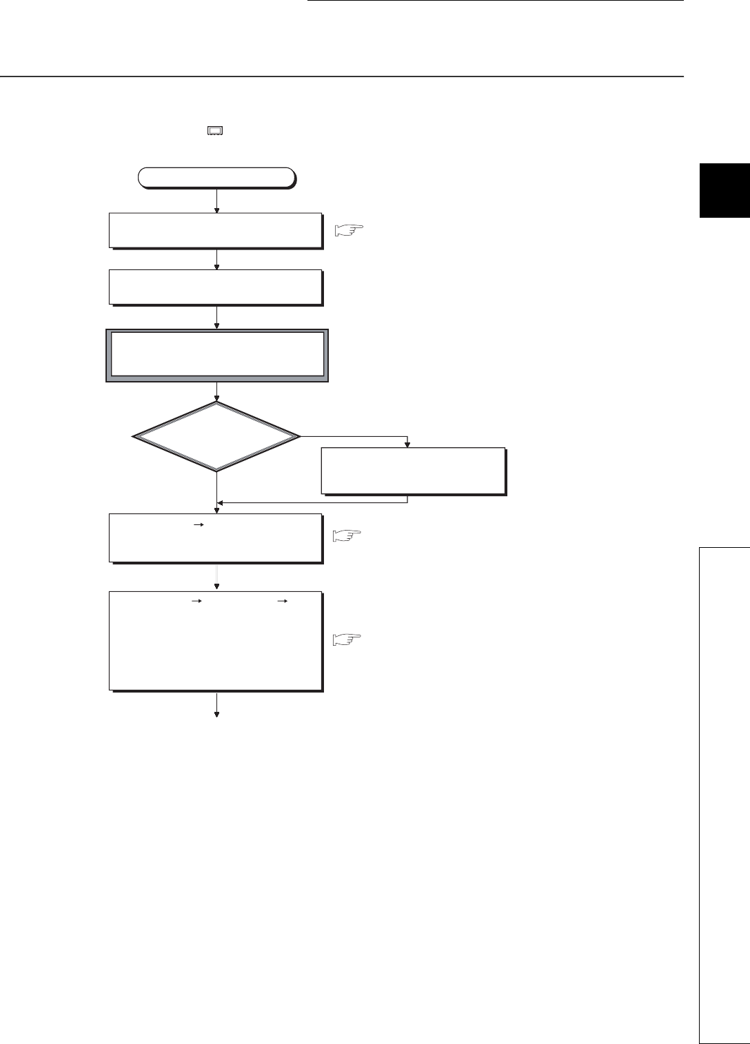
11 - 3
CHAPTER11 PROCEDURES FOR WRITING PROGRAM TO CPU MODULE
1
2
11
4
5
6
7
8
11.2 Hardware Check
11.2 Hardware Check
This section describes a procedure for checking hardware before writing a created program.
In the following procedure, indicates an operation on the CPU module side.
YES
NO
1)
Start
Check the special relays (SM51 and SM52)
and special registers (SD51 and SD52) and
replace the battery if required.
GX Developer Version 8 Operating Manual
GX Developer Version 8 Operating Manual
GX Developer Version 8 Operating Manual
Select [Online] [Write to PLC]
"Program memory/Device memory" for
"Target memory" in GX Developer and
write the parameters and program
(Write the PLC parameters and program
with the same settings immediately after
the project was created by GX Developer).
Start GX Developer and create a project.
Connect the personal computer to which
GX Developer is installed to the CPU module.
Set the RUN/STOP/RESET switch to
STOP and power on the programmable
controller (the ERR. LED turns on).
Is the BAT. LED on?
Select [Online] [Format PLC memory]
in GX Developer and format the program
memory.
11 - 4
Remark
For installation and mounting procedures of the CPU module, refer to the following.
QCPU User's Manual (Hardware Design, Maintenance and Inspection)
Figure 11.1 Hardware check flowchart
YES
YES
NO
NO
1)
To Section 11.3
Power off the programmable controller
and then on or reset the CPU module.
Set the RUN/STOP/RESET switch to RUN to
change the CPU module in the RUN status.
Is the RUN LED on?
Is the ERR. LED off?
Please consult your local Mitsubishi
service center or representative,
explaining a detailed description of
the problem.
Check the error cause in the System Monitor screen
displayed by selecting [Diagnostics] [System
Monitor] in GX Developer or in the "PLC diagnostics"
screen and remove the error.
QCPU User's Manual
(Hardware Design, Maintenance and Inspection)
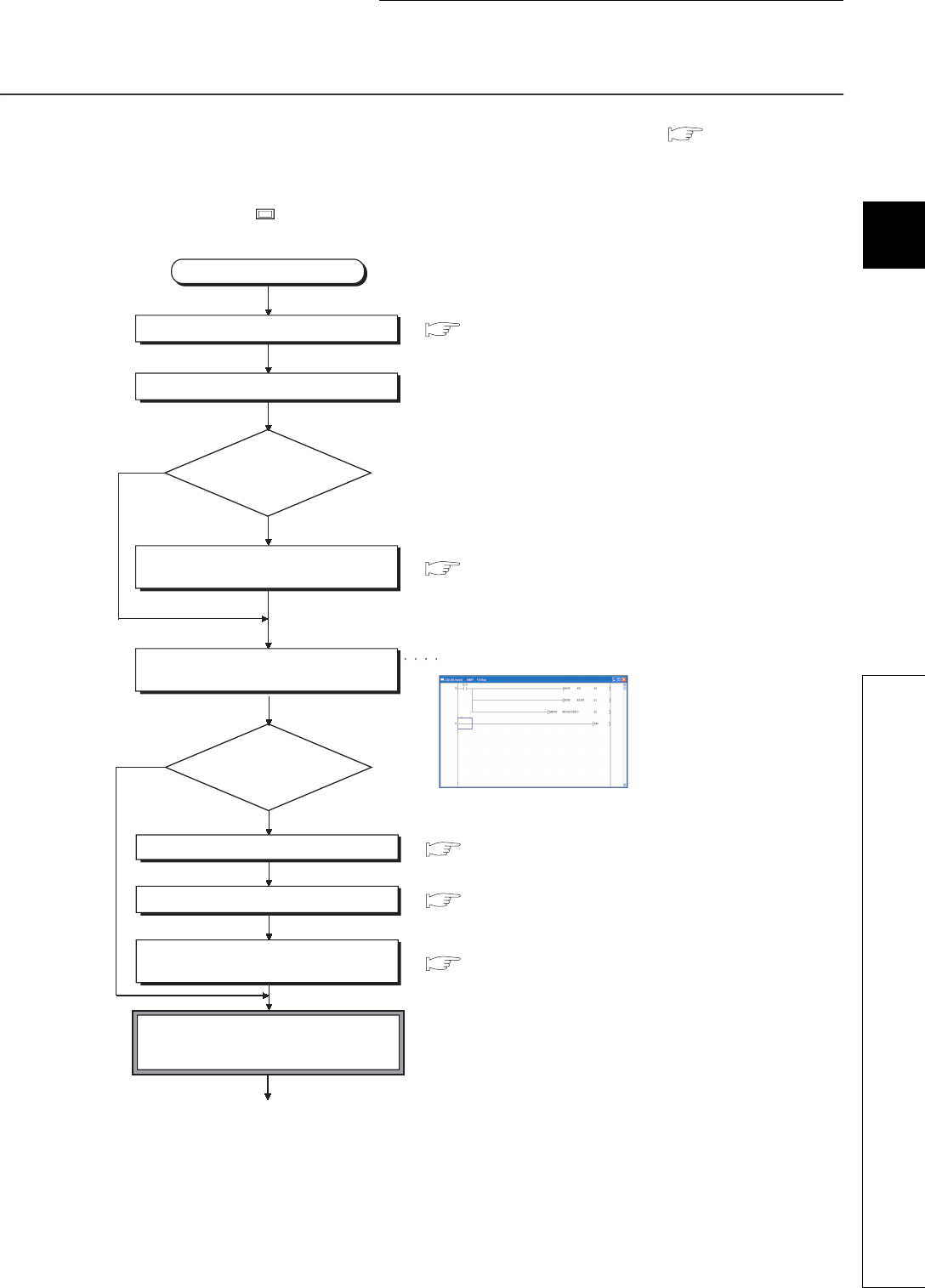
11 - 5
CHAPTER11 PROCEDURES FOR WRITING PROGRAM TO CPU MODULE
1
2
11
4
5
6
7
8
11.3 Procedure for Writing One Program
11.3 Procedure for Writing One Program
This section describes a procedure for writing a program to the program memory. ( Section 5.1.2)
Follow the procedure below and then the procedure provided in Section 11.5 before storing the program in
the memory card for boot operation.
In the following procedure, indicates an operation on the CPU module side.
YES
NO
1)
Section 6.25
Section 6.25
Section 6.25
Use the initial device value?
Set the device memory.
Set the initial device value range.
Set a file name for initial device value in the
PLC file tab of the PLC parameter dialog box.
Set the RUN/STOP/RESET switch to STOP
and power on the CPU module
(the ERR. LED turns on).
NO
YES
Start
Start GX Developer.
Set the project.
Change the number
of device points?
Change the number of device points in the
Device tab of the PLC parameter dialog box.
Create a program to be executed in the
CPU module.
GX Developer Version 8 Operating Manual
GX Developer Version 8 Operating Manual
Ladder (writing) screen
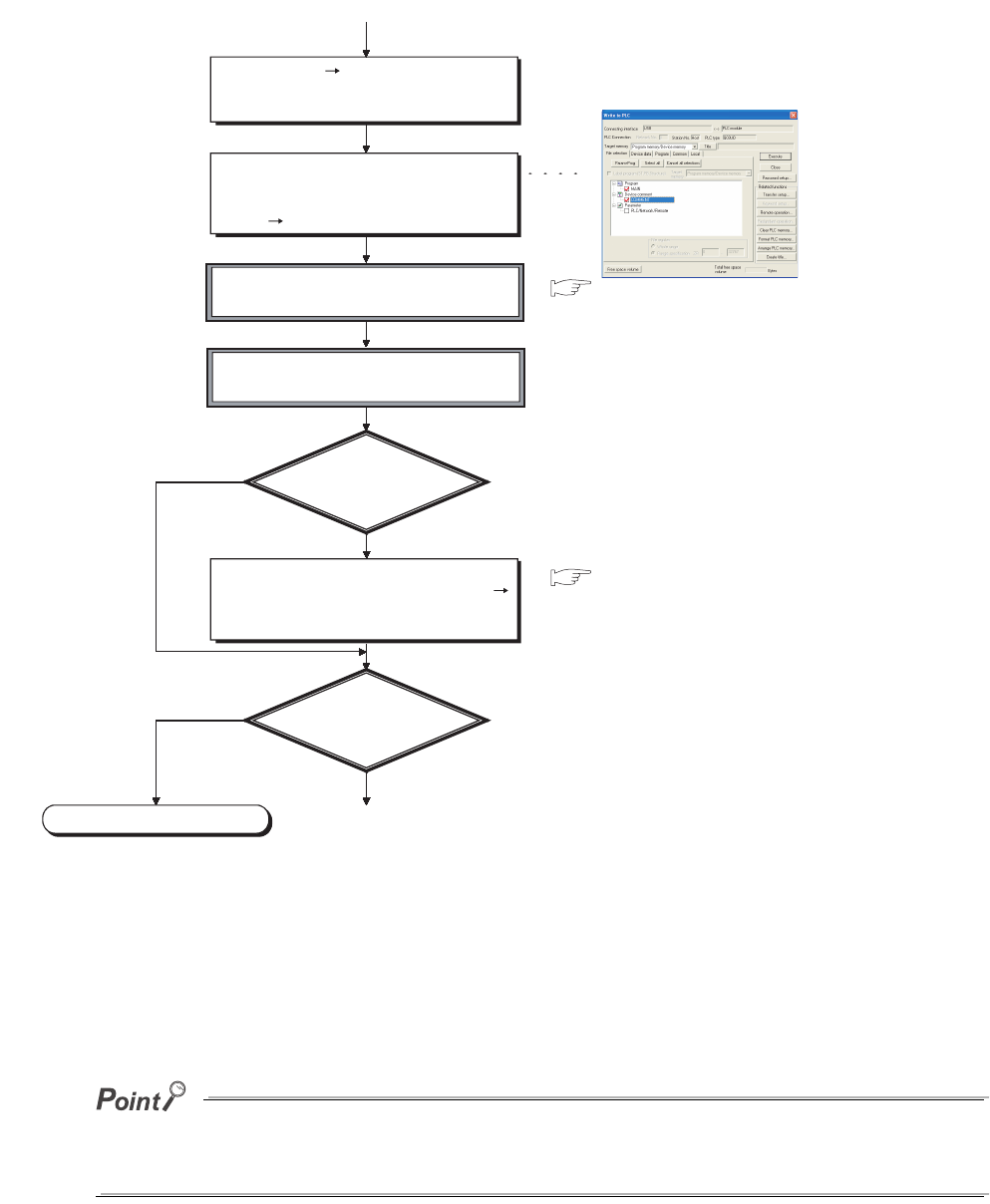
11 - 6
*1: When storing the file register and initial device value to the standard RAM or memory card (except the Flash card), format
the memory used.
*2: Write each data in the memory as shown below:
•Program:Program memory
•Parameter:Memory set in the parameter-valid drive
•Initial device value:Memory set in the PLC file tab of the PLC parameter dialog box
When the Universal model QCPU No.1 is the control CPU in the MELSECNET/H system, the Universal model QCPU can
communicate with the Universal model QCPU where MISSING PARA. has been detected via the MELSECNET/H (for the
network number 1 only).
Figure 11.2 Flowchart for writing one program
1)
YES
NO
YES
NO
To Section 11.5
Select [Online] [Format PLC memory]
in GX Developer and format the program
memory.
To write the parameters, created program, and
initial device value, make settings in the Write
to PLC screen displayed by selecting
[Online] [Write to PLC] in GX Developer.
Power off the programmable controller
and then on or reset the CPU module.
Set the RUN/STOP/RESET switch to RUN to
change the CPU module in the RUN status.
Is the ERR. LED on
the CPU module on
(flashing)?
Check the error cause in the System Monitor
screen displayed by selecting [Diagnostics]
[System Monitor] in GX Developer or in the
"PLC diagnostics" screen and remove the error.
Start boot operation?
QCPU User's Manual
(Hardware Design, Maintenance and Inspection)
QCPU User's Manual
(Hardware Design, Maintenance and Inspection)
Write to PLC screen
End
*2
*1
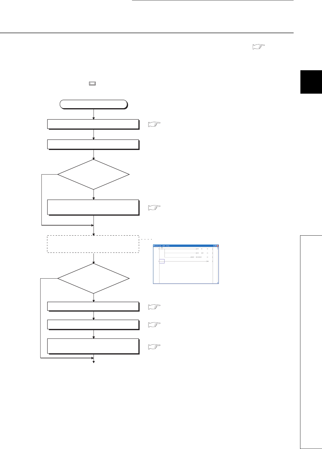
11 - 7
CHAPTER11 PROCEDURES FOR WRITING PROGRAM TO CPU MODULE
1
2
11
4
5
6
7
8
11.4 Procedure for Writing Multiple Programs
11.4 Procedure for Writing Multiple Programs
This section describes a procedure for writing multiple programs to the program memory. ( Section
5.1.2)
Follow the procedure below and then the procedure provided in Section 11.5 before storing the programs
in the memory card for boot operation.
In the following procedure, indicates an operation on the CPU module side.
Section 6.25
YES
NO
Section 6.25
Section 6.25
Use the initial device value?
Set the device memory.
Set the initial device value range.
Set a file name for initial device value in the
PLC file tab of the PLC parameter dialog box.
NO
YES
1)
Section 9.2
Start
Start GX Developer.
Set the project.
Change the number of
device points?
Change the number of device points in the
Device tab of the PLC parameter dialog box.
Create programs to be executed in the
CPU module.
Ladder (writing) screen
GX Developer Version 8 Operating Manual
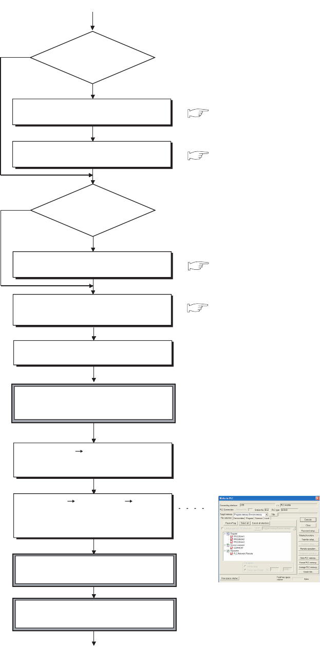
11 - 8
3)
Connect the personal computer to which GX
Developer is installed to the CPU module.
Select [Online] [Format PLC memory]
in GX Developer and format the program
memory.
*1
*2
Select [Online] [Write to PLC] "Program
memory/Device memory" for "Target memory"
in GX Developer and write the parameters
and created programs.
1)
Section 9.14.1
Section 9.14.1
YES
NO
Section 9.10
YES
NO
Section 2.3
Set local devices?
Set the local device range in the Device
tab of the PLC parameter dialog box.
Set a file name for the local devices in the
PLC file tab of the PLC parameter dialog box.
Use the common
pointers?
Set the start pointer number in the PLC
system tab of the PLC parameter dialog box.
Set the names and execution conditions of
programs to be executed in the Program
tab of the PLC parameter dialog box.
Set the RUN/STOP/RESET switch to
STOP and power on the CPU module
(the ERR. LED turns on).
Power off the programmable controller
and then on or reset the CPU module.
Set the RUN/STOP/RESET switch to RUN to
change the CPU module in the RUN status.
Write to PLC screen
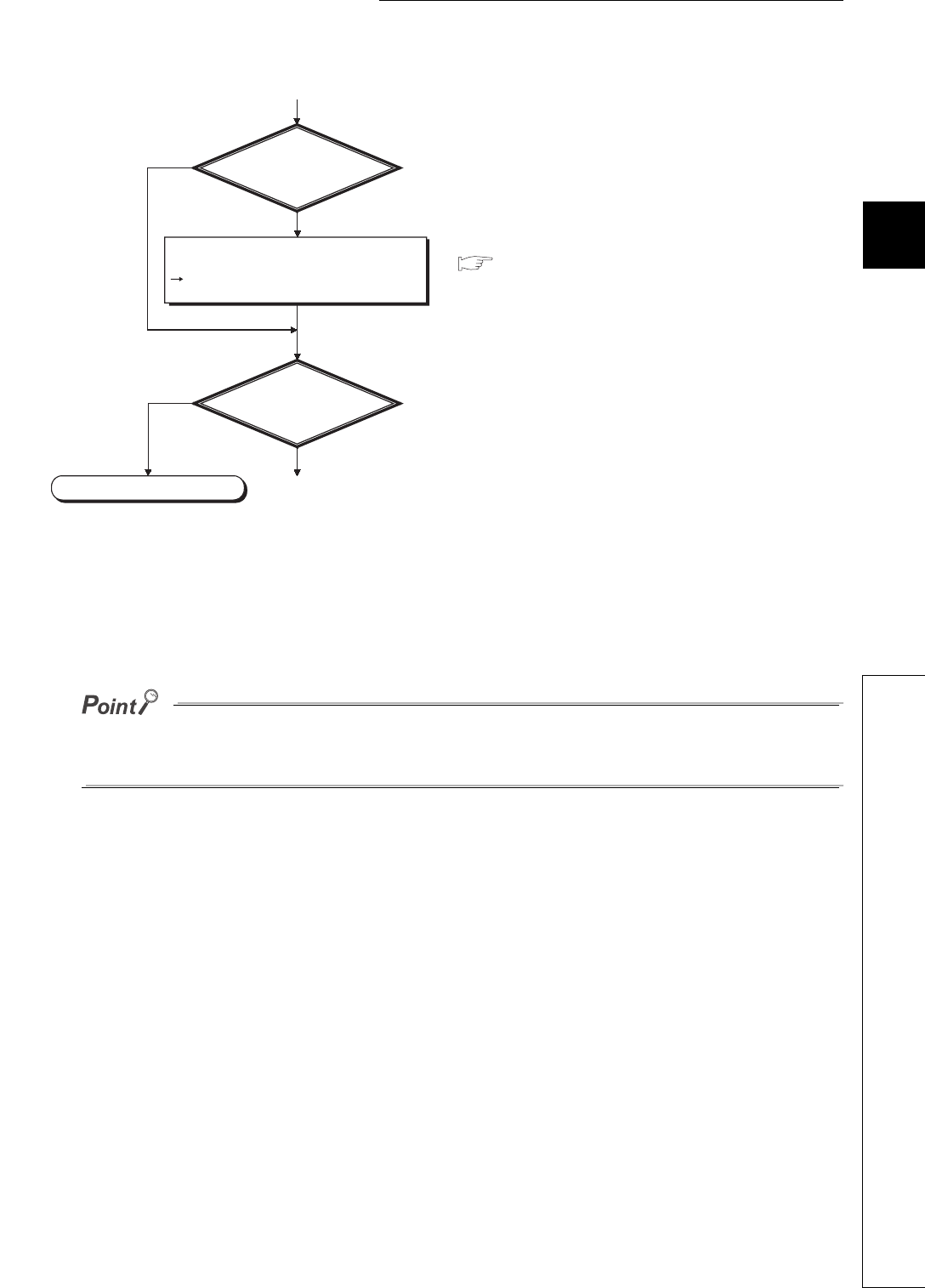
11 - 9
CHAPTER11 PROCEDURES FOR WRITING PROGRAM TO CPU MODULE
1
2
11
4
5
6
7
8
11.4 Procedure for Writing Multiple Programs
*1: When storing the file register and initial device value to the standard RAM or memory card (except the Flash card), format
the memory used.
*2: Write each data in the memory as shown below:
•Program:Program memory
•Parameter:Memory set in the parameter-valid drive
•Initial device value:Memory set in the PLC file tab of the PLC parameter dialog box
When the Universal model QCPU No.1 is the control CPU in the MELSECNET/H system, the Universal model QCPU can
communicate with the Universal model QCPU where MISSING PARA. has been detected via the MELSECNET/H (for the
network number 1 only).
Figure 11.3 Flowchart for writing multiple programs
NO
NO
3)
YES
To Section 11.5
YES
Is the ERR. LED
on the CPU module
on (flashing)?
QCPU User's Manual
(Hardware Design, Maintenance and Inspection)
Start boot operation?
End
Check the error cause in the System Monitor
screen displayed by selecting [Diagnostics]
[System Monitor] in GX Developer or in the
"PLC diagnostics" screen and remove the error.
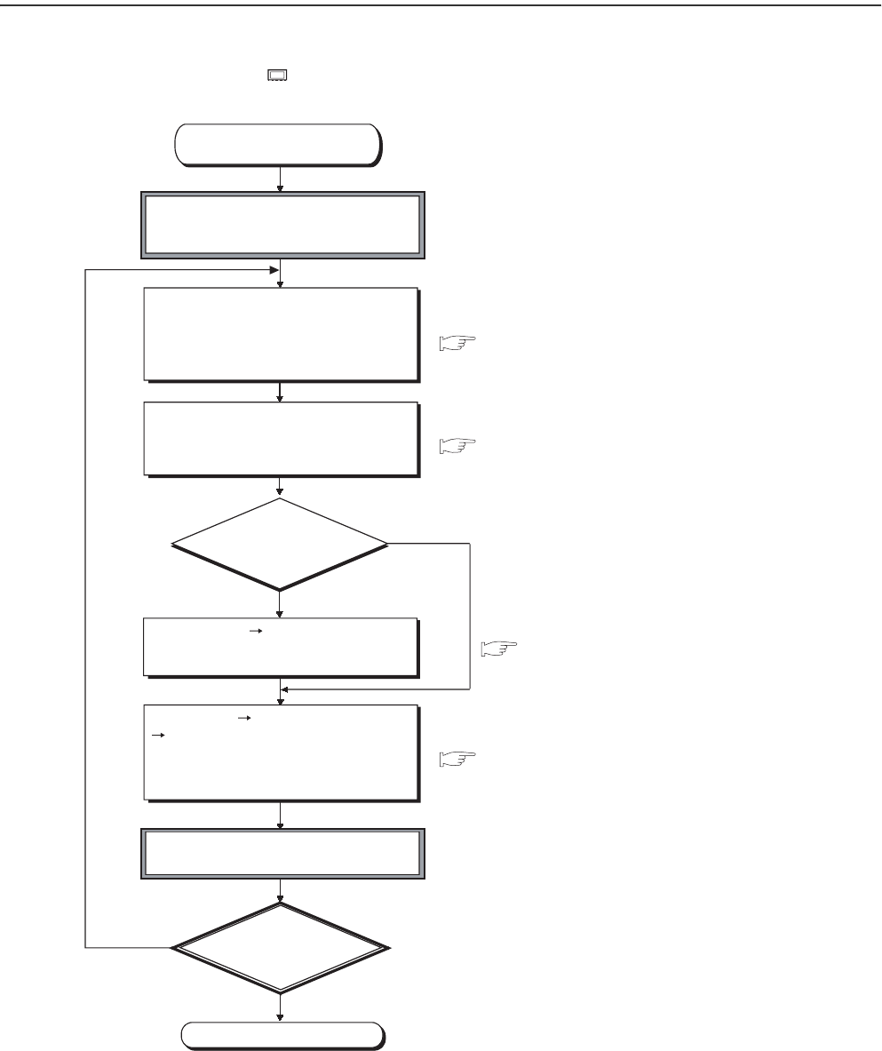
11 - 10
11.5 Procedure for Boot Operation
This section describes a procedure for boot operation.
In the following procedure, indicates an operation on the CPU module side.
Figure 11.4 Flowchart for boot operation
YES
NO
YES
NO
Section 5.1.8
Section 2.3
Section 5.1.7
Start (continued from
or )
If the RUN/STOP/RESET switch is in
RUN, set the switch to STOP.
Set the file name of parameters, a
program, devices, initial values and
device comments in the Boot file tab
of the PLC parameter dialog box.
Set the names and execution conditions of
programs to be executed in the Program tab
of the PLC parameter dialog box (This setting
is necessary when one program is written).
Use the memory
card (except the
Flash card)?
Select [Online] [Format PLC memory]
in GX Developer and format the
program memory.
Select [Online] [Write to PLC (Flash ROM)]
[Write to PLC (Flash ROM)] "Program
memory/Device memory" for "Target
memory" in GX Developer and write the
parameters and created programs.
Power off the programmable controller
and then on or reset the CPU module.
Is the BOOT LED on?
End
GX Developer Version 8 Operating Manual
Section 11.3 Section 11.4
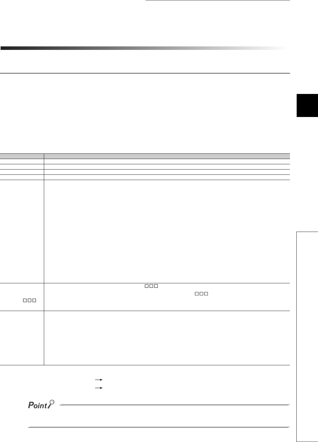
12 - 1
CHAPTER12 SPECIAL RELAY LIST AND SPECIAL REGISTER LIST
1
2
3
12
6
7
8
12.1 SPECIAL RELAY LIST
CHAPTER12 SPECIAL RELAY LIST AND SPECIAL REGIS-
TER LIST
12.1 SPECIAL RELAY LIST
Special relays, SM, are internal relays whose applications are fixed in the Programmable
Controller.
For this reason, they cannot be used by sequence programs in the same way as the normal
internal relays.
However, they can be turned ON or OFF as needed in order to control the CPU module.
The heading descriptions in the following special relay lists are shown in 3.1.
For details on the following items, refer to the following manuals:
• Networks Manual of the corresponding network module
• SFC QCPU(Q mode)/QnACPU Programming Manual (SFC)
Do not change the values of special relays set by the system with user program or device test operations.
Doing so may result in system downtime or communication fault.
Table12.1 Explanation of special relay list
Item Function of Item
Number • Indicates special relay number
Name • Indicates name of special relay
Meaning • Indicates contents of special relay
Explanation • Discusses contents of special relay in more detail
Set by
(When set)
• Indicates whether the relay is set by the system or user, and, if it is set by the system, when setting is performed.
<Set by>
S : Set by system
U : Set by user (sequence programs or test operations from GX Developer)
S/U : Set by both system and user
<When set>
Indicated only for registers set by system
Each END : Set during each END processing
Initial : Set only during initial processing (when power supply is turned ON, or when going from STOP
to RUN)
Status change : Set only when there is a change in status
Error : Set when error occurs
Instruction execution : Set when instruction is executed
Request : Set only when there is a user request (through SM, etc.)
System switching : Set when system switching is executed.
Corresponding
ACPU M9
• Indicates the corresponding special relay (M9 ) of the ACPU.
(When the contents are changed, the special relay is represented M9 format change. Incompatible with the
Q00J/Q00/Q01 and QnPRH.)
• New indicates the special relay newly added to the Q series CPU module.
Corresponding
CPU
Indicates the corresponding CPU module type name.
QCPU : Indicates all the Q series CPU modules.
Q00J/Q00/Q01 : Indicates the Basic model QCPU.
Qn(H) : Indicates the High Performance model QCPU.
QnPH : Indicates the Process CPU.
QnPRH : Indicates the Redundant CPU.
QnU : Indicates the Universal model QCPU
Each CPU module model name: Indicates the relevant specific CPU module. (Example: Q02U)

12 - 2
(1) Diagnostic Information
Table12.2 Special relay
Number Name Meaning Explanation Set by
(When Set)
Corres-
ponding
ACPU
M9
Corresponding
CPU
SM0 Diagnostic errors OFF : No error
ON : Error
• Turns ON if an error occurs as a result of diagnosis.
(Includes when an annunciator is ON, and when an
error is detected with CHK instruction)
• Remains ON even if the condition is restored to
normal thereafter.
S (Error) New
Qn(H)
QnPH
QnPRH
• Turns ON if an error occurs as a result of diagnosis.
(Includes when an annunciator is ON)
• Remains ON even if the condition is restored to
normal thereafter.
S (Error) New Q00J/Q00/Q01
QnU
SM1 Self-diagnostic error
OFF : No self-diagnosis
errors
ON : Self-diagnosis
• Turns ON if an error occurs as a result of diagnosis.
(Does not include when an annunciator is ON or
when an error is detected by the CHK instruction)
• Remains ON even if the condition is restored to
normal thereafter.
S (Error) M9008
Qn(H)
QnPH
QnPRH
• Turns ON if an error occurs as a result of diagnosis.
(Does not include when an annunciator is ON)
• Remains ON even if the condition is restored to
normal thereafter.
S (Error) New Q00J/Q00/Q01
QnU
SM5 Error common
information
OFF : No error common
information
ON : Error common
information
• When SM0 is ON, turns ON if there is error common
information S (Error) New
QCPU
SM16 Error individual
information
OFF : No error individual
information
ON : Error individual
information
• When SM0 is ON, turns ON if there is error individual
information S (Error) New
SM50 Error reset OFF ON: Error reset • Conducts error reset operation U New
SM51 Battery low latch OFF : Normal
ON : Battery low
• Turns ON if battery voltage at CPU module or
memory card drops below rated value.
• Remains ON even if the battery voltage returns to
normal thereafter.
• Synchronizes with the BAT. LED.
S (Error) M9007
Qn(H)
QnPH
QnPRH
QnU
• Turns ON if battery voltage at CPU module drops
below rated value.
• Remains ON even if the battery voltage returns to
normal thereafter.
• Synchronous with ERR. LED
S (Error) New Q00J/Q00/Q01
SM52 Battery low OFF : Normal
ON : Battery low
• Same as SM51, but turns OFF subsequently when
battery voltage returns to normal. S (Error) M9006
QCPU
SM53 AC/DC DOWN
detection
OFF : AC/DC DOWN not
detected
ON : AC/DC DOWN
detected
• Turns ON if an instantaneous power failure of within
20ms occurs during use of the AC power supply
module.
Reset when the power supply is switched OFF, then
ON. S (Error) M9005
• Turns ON if an instantaneous power failure of within
10ms occurs during use of the DC power supply
module.
Reset when the power supply is switched OFF, then
ON.

12 - 3
CHAPTER12 SPECIAL RELAY LIST AND SPECIAL REGISTER LIST
1
2
3
12
6
7
8
12.1 SPECIAL RELAY LIST
*6: The relevant modules are as follows:
• The Universal model QCPU whose serial number (first five digits) is "10012" or later.
• Q13UDHCPU, Q26UDHCPU
*7: The module whose first 5 digits of serial No. is "10102" or later.
Table12.2 Special relay
Number Name Meaning Explanation Set by
(When Set)
Corres-
ponding
ACPU
M9
Corresponding
CPU
SM56 Operation error OFF : Normal
ON : Operation error
• ON when operation error is generated
• Remains ON if the condition is restored to normal
thereafter.
S (Error) M9011
QCPU
SM60 Blown fuse detection
OFF : Normal
ON : Module with blown
fuse
• Turns ON if there is at least one output module
whose fuse has blown.
• Remains ON if the condition is restored to normal
thereafter.
• Blown fuse status is checked even for remote I/O
station output modules.
S (Error) M9000
SM61 I/O module verify error OFF : Normal
ON : Error
• Turns ON if the I/O module differs from the status
registered at power on.
• Remains ON if the condition is restored to normal
thereafter.
• I/O module verification is also conducted for remote
I/O station modules.
S (Error) M9002
SM62 Annunciator detection OFF : Not detected
ON : Detected • Goes ON if even one annunciator (F) goes ON. S (Instruction
execution) M9009
SM80 CHK detection OFF : Not detected
ON : Detected
• Goes ON if error is detected by CHK instruction.
• Remains ON if the condition is restored to normal
thereafter.
S (Instruction
execution) New
Qn(H)
QnPH
QnPRH
SM90
Startup of monitoring
timer for step transition
(Enabled only when
SFC program exists)
OFF : Not started(monitoring
timer reset)
ON : Started(monitoring
timer started)
Corresponds
to SD90
• Goes ON when measurement of
step transition monitoring timer is
commenced.
• Resets step transition monitoring
timer when it goes OFF.
U
M9108
Qn(H)
QnPH
QnPRH
SM91 Corresponds
to SD91 M9109
SM92 Corresponds
to SD92 M9110
SM93 Corresponds
to SD93 M9111
SM94 Corresponds
to SD94 M9112
SM95 Corresponds
to SD95 M9113
SM96 Corresponds
to SD96 M9114
SM97 Corresponds
to SD97 New
SM98 Corresponds
to SD98 New
SM99 Corresponds
to SD99 New
SM100 Serial communication
function using flag
OFF : Serial communication
function is not used.
ON : Serial communication
function is used.
• Stores the setting of whether the serial
communication function is used or not in the serial
communication setting parameter
S (Power-ON or
reset)
New
Q00/Q01
Q00UJ
Q00U
Q01U
Q02U*7
SM101 Communication
protocol status flag
OFF : GX Developer
ON : MC protocol
communication device
• Stores whether the device that is communicating via
the RS-232 interface is GX Developer or MC protocol
communication device
S (RS232
communication)
SM110 Protocol error OFF : Normal
ON : Abnormal
• Turns ON when an abnormal protocol was used to
make communication in the serial communication
function.
• Remains ON if the condition is restored to normal
thereafter
S (Error)
SM111 Communication status OFF : Normal
ON : Abnormal
• Turns ON when the mode used to make
communication was different from the setting in the
serial communication function.
• Remains ON if the condition is restored to normal
thereafter.
S (Error)
SM112 Error information clear ON : Cleared
• Turns ON when the error codes stored in SM110,
SM111, SD110 and SD111 are cleared. (Activated
when turned from OFF to ON)
U
SM113 Overrun error OFF : Normal
ON : Abnormal
• Turns ON when an overrun error occurred in the
serial communication error. S (Error)
SM114 Parity error OFF : Normal
ON : Abnormal
• Turns ON when a parity error occurred in the serial
communication error. S (Error)
SM115 Framing error OFF : Normal
ON : Abnormal
• Turns ON when a framing error occurred in the serial
communication error. S (Error)
SM165
Program memory
batch transfer
execution status
OFF : Completed
ON : Not being executed or
Not completed
• Turns ON when the data is written to the program
cache memory.
• Turns OFF when the program memory batch transfer
is completed.
• Remains ON if the program memory batch transfer is
not executed after the data is written to the program
cache memory.
S (When status
changed) New QnU*6

12 - 4
(2) System information
*5: The Universal model QCPU except the Q00UJCPU, Q00UCPU, Q01UCPU, and Q02UCPU.
*6: The relevant modules are as follows:
• The Universal model QCPU whose serial number (first five digits) is "10012" or later.
• Q13UDHCPU, Q26UDHCPU
*8: The Universal model QCPU except the Q00UJCPU.
Table12.3 Special relay
Number Name Meaning Explanation Set by
(When Set)
Corres-
ponding
ACPU
M9
Corresponding
CPU
SM202 LED OFF command OFF ON : LED OFF • When this relay goes from OFF to ON, the LEDs
corresponding to the individual bits at SD202 go off UNew
Qn(H)
QnPH
QnPRH
QnU
SM203 STOP contact STOP status • Goes ON at STOP status S (Status change) M9042
QCPU
SM204 PAUSE contact PAUSE status • Goes ON at PAUSE status S (Status change) M9041
SM206 PAUSE enable coil OFF : PAUSE disabled
ON : PAUSE enabled
• PAUSE status is entered if this relay is ON when the
PAUSE contact goes ON UM9040
SM210 Clock data set request OFF : Ignored
ON : Set request
• When this relay goes from OFF to ON and after END
instruction execution of subsequent scan, clock data
stored in SD210 to SD213 are written to the CPU
module.
UM9025
SM211 Clock data error OFF : No error
ON : Error
• ON when error is generated in clock data (SD210 to
SD213) value, and OFF if no error is detected. S (Request) M9026
SM213 Clock data read
request
OFF : Ignored
ON : Read request
• When this relay is ON, clock data is read to SD210 to
SD213 as BCD values. UM9028
SM220 CPU No.1 preparation
completed
OFF : CPU No.1 preparation
uncompleted
ON : CPU No.1 preparation
completed
Turned ON when access can be made to the CPU
module No.1 from the other CPU module at power-on
or reset operation. SM220 is used as interlock for
accessing the CPU module No.1 when the multiple
CPU synchronous setting is asynchronous.
S (When status
changed) New
QnU
SM221 CPU No.2 preparation
completed
OFF : CPU No.2 preparation
uncompleted
ON : CPU No.2 preparation
completed
Turned ON when access can be made to the CPU
module No.2 from the other CPU module at power-on
or reset operation. SM221 is used as interlock for
accessing the CPU module No.2 when the multiple
CPU synchronous setting is asynchronous. QnU*8
SM222 CPU No.3 preparation
completed
OFF : CPU No.3 preparation
uncompleted
ON : CPU No.3 preparation
completed
Turned ON when access can be made to the CPU
module No.3 from the other CPU module at power-on
or reset operation. SM222 is used as interlock for
accessing the CPU module No.3 when the multiple
CPU synchronous setting is asynchronous.
SM223 CPU No.4 preparation
completed
OFF : CPU No.4 preparation
uncompleted
ON : CPU No.4 preparation
completed
Turned ON when access can be made to the CPU
module No.4 from the other CPU module at power-on
or reset operation. SM223 is used as interlock for
accessing the CPU module No.4 when the multiple
CPU synchronous setting is asynchronous.
QnU*5
SM235 Online module change
flag
OFF : Online module change
is not in progress
ON : Online module change
in progress
• Turns on during online module change. (for host
CPU)
S (During online
module change) New
QnPH
SM236 Online module change
complete flag
OFF : Online module change
incomplete
ON : Online module change
complete
• Turns ON for one scan after online module change is
complete.
• This contact point can only be used by the scan
program. (for host CPU)
S (When online
module change is
complete)
New
SM237 Device range check
inhibit flag
OFF : Device range checked
ON : Device range not
checked
• Selects whether to check a device range during
execution of the BMOV, FMOV or DFMOV
instruction (only when the conditions for subset
processing are established).
UNew
QnU*6

12 - 5
CHAPTER12 SPECIAL RELAY LIST AND SPECIAL REGISTER LIST
1
2
3
12
6
7
8
12.1 SPECIAL RELAY LIST
*1: This applies to the CPU of function version B or later.
*2: The module whose first 5 digits of serial No. is "09012" or later.
*5: The Universal model QCPU except the Q00UJCPU, Q00UCPU, Q01UCPU, and Q02UCPU.
*6: The module whose first 5 digits of serial No. is "10042" or later.
*8: The Universal model QCPU except the Q00UJCPU.
Table12.3 Special relay
Number Name Meaning Explanation Set by
(When Set)
Corres-
ponding
ACPU
M9
Corresponding
CPU
SM240 No. 1 CPU reset flag
OFF : No. 1 CPU reset
cancel
ON : No. 1 CPU resetting
• Goes OFF when reset of the No. 1 CPU is canceled.
• Comes ON when the No. 1 CPU is resetting
(including the case where the CPU module is
removed from the base).
The other CPUs are also put in reset status.
S (Status change) New
Q00/Q01*1
Qn(H)*1
QnPH
QnU*8
SM241 No. 2 CPU reset flag
OFF : No. 2 CPU reset
cancel
ON : No. 2 CPU resetting
• Goes OFF when reset of the No. 2 CPU is canceled.
• Comes ON when the No. 2 CPU is resetting
(including the case where the CPU module is
removed from the base).
The other CPUs result in "MULTI CPU DOWN" (error
code: 7000).
SM242 No. 3 CPU reset flag
OFF : No. 3 CPU reset
cancel
ON : No. 3 CPU resetting
• Goes OFF when reset of the No. 3 CPU is canceled.
• Comes ON when the No. 3 CPU is resetting
(including the case where the CPU module is
removed from the base).
The other CPUs result in "MULTI CPU DOWN" (error
code: 7000).
SM243 No. 4 CPU reset flag
OFF : No. 4 CPU reset
cancel
ON : No. 4 CPU resetting
• Goes OFF when reset of the No. 4 CPU is canceled.
• Comes ON when the No. 4 CPU is resetting
(including the case where the CPU module is
removed from the base).
The other CPUs result in "MULTI CPU DOWN" (error
code: 7000).
Qn(H)*1
QnPH
QnU*5
SM244 No. 1 CPU error flag
OFF : No. 1 CPU normal
ON : No. 1 CPU during stop
error
• Goes OFF when the No. 1 CPU is normal (including
a continuation error).
• Comes ON when the No. 1 CPU is during a stop
error.
Q00/Q01*1
Qn(H)*1
QnPH
QnU*8
SM245 No. 2 CPU error flag
OFF : No. 2 CPU normal
ON : No. 2 CPU during stop
error
• Goes OFF when the No. 2 CPU is normal (including
a continuation error).
• Comes ON when the No. 2 CPU is during a stop
error.
SM246 No. 3 CPU error flag
OFF : No. 3 CPU normal
ON : No. 3 CPU during stop
error
• Goes OFF when the No. 3 CPU is normal (including
a continuation error).
• Comes ON when the No. 3 CPU is during a stop
error.
SM247 No. 4 CPU error flag
OFF : No. 4 CPU normal
ON : No. 4 CPU during stop
error
• Goes OFF when the No. 4 CPU is normal (including
a continuation error).
• Comes ON when the No. 4 CPU is during a stop
error
S (Status change) New
Qn(H)*1
QnPH
QnU*5
SM250 Max. loaded I/O read OFF : Ignored
ON : Read
• When this relay goes from OFF to ON, maximum
loaded I/O number is read to SD250. UNew
Qn(H)
QnPH
QnPRH
SM254 All stations refresh
command
OFF : Refresh arrival station
ON : Refresh all stations
• Effective for the batch refresh (also effective for the
low speed cyclic)
• Designate whether to receive arrival stations only or
to receive all slave stations in the MELSECNET/H.
UNew
• Designate whether to receive arrival stations only or
to receive all slave stations in the CC-Link IE
controller network .
Qn(H)*2
QnPH*6
QnPRH*6
• Effective for the batch refresh (also effective for the
low speed cyclic)
• Specify whether to receive only arrival station or all
stations in the MELSECNET/H or CC-Link IE
controller network.
QnU

12 - 6
*1: This applies to the CPU of function version B or later.
Table12.3 Special relay
Number Name Meaning Explanation Set by
(When Set)
Corres-
ponding
ACPU
M9
Corresponding
CPU
SM255
MELSECNET/10,
MELSECNET/H
module 1 information
OFF : Operative network
ON : Standby network
• Goes ON for standby network(If no designation has
been made concerning active or standby, active is
assumed.)
S (Initial) New
Qn(H)
QnPH
QnPRH
SM256 OFF : Reads
ON : Does not read
• For refresh from link to CPU module (B, W, etc.)
indicate whether to read from the link module. UNew
SM257 OFF : Writes
ON : Does not write
• For refresh from CPU module to link (B, W, etc.),
designate whether to write to the link module. UNew
SM260
MELSECNET/10,
MELSECNET/H
module 2 information
OFF : Operative network
ON : Standby network
• Goes ON for standby network
(If no designation has been made concerning active
or standby, active is assumed.)
S (Initial) New
SM261 OFF : Reads
ON : Does not read
• For refresh from link to CPU module (B, W, etc.)
indicate whether to read from the link module. UNew
SM262 OFF : Writes
ON : Does not write
• For refresh from CPU module to link (B, W, etc.),
designate whether to write to the link module. UNew
SM265
MELSECNET/10,
MELSECNET/H
module 3 information
OFF : Operative network
ON : Standby network
• Goes ON for standby network
(If no designation has been made concerning active
or standby, active is assumed.)
S (Initial) New
SM266 OFF : Reads
ON : Does not read
• For refresh from link to CPU module (B, W, etc.)
indicate whether to read from the link module. UNew
SM267 OFF : Writes
ON : Does not write
• For refresh from CPU module to link (B, W, etc.),
designate whether to write to the link module. UNew
SM270
MELSECNET/10,
MELSECNET/H
module 4 information
OFF : Operative network
ON : Standby network
• Goes ON for standby network
(If no designation has been made concerning active
or standby, active is assumed.)
S (Initial) New
SM271 OFF : Reads
ON : Does not read
• For refresh from link to CPU module (B, W, etc.)
indicate whether to read from the link module. UNew
SM272 OFF : Writes
ON : Does not write
• For refresh from CPU module to link (B, W, etc.),
designate whether to write to the link module. UNew
SM280 CC-Link error OFF : Normal
ON : Error
• Goes ON when a CC-Link error is detected in any of
the installed CC-Link module. Goes OFF when
normal operation is restored.
S (Status change) New
SM315
Communication
reserved time delay
enable/disable flag
OFF : Without delay
ON : With delay
• This flag is enabled when the time reserved for
communication processing is set in SD315.
• Turns ON to delay the END processing by the time
set in SD315 in order to perform communication
processing.
(The scan time increases by the period set in
SD315.)
• Turns OFF to perform the END processing without a
delay of the time set in SD315 when there is no
communication processing. (Defaults to OFF)
U New Q00J/Q00/Q01
SM320 Presence/absence of
SFC program
OFF : SFC program absent
ON : SFC program present
• Turns ON when an SFC program is registered.
• OFF when an SFC program is not registered. S (Initial) M9100
Q00J/Q00/Q01*1
Qn(H)
QnPH
QnPRH
QnU
SM321 Start/stop SFC
program
OFF : SFC program not
executed (stop)
ON : SFC program executed
(start)
• Initial value is set at the same value as SM320.
(Goes ON automatically if SFC program is present.)
• Turn this relay from ON to OFF to stop program
execution.
• Turn this relay from OFF to ON to resume program
execution.
S (Initial)/U M9101form
at change

12 - 7
CHAPTER12 SPECIAL RELAY LIST AND SPECIAL REGISTER LIST
1
2
3
12
6
7
8
12.1 SPECIAL RELAY LIST
*1: This applies to the CPU of function version B or later.
*3: The module whose first 5 digits of serial No. is "04122" or later.
*4: The module whose first 5 digits of serial No. is "07032" or later.
Table12.3 Special relay
Number Name Meaning Explanation Set by
(When Set)
Corres-
ponding
ACPU
M9
Corresponding
CPU
SM322 SFC program start
status
OFF : Initial start
ON : Resume start
• The SFC program starting mode in the SFC setting
of the PLC parameter dialog box is set as the initial
value.
AT initial start: OFF
At continued start: ON
S (Initial)/U M9102form
at change
Q00J/Q00/Q01*1
Qn(H)
QnPH
QnPRH
QnU
SM323
Presence/absence of
continuous transition
for entire block
OFF : Continuous transition
not effective
ON : Continuous transition
effective
Set the presence/absence of continuous transition for
the block where "Continuous transition bit" of the SFC
data device has not been set.
U M9103
SM324 Continuous transition
prevention flag
OFF : When transition is
executed
ON : When no transition
• OFF during operation in the continuous transition
mode or during continuous transition, and ON when
continuous transition is not executed.
• Always ON during operation in the no continuous
transition mode.
S (Instruction
execution) M9104
S (Status change) New
SM325 Output mode at block
stop
OFF : OFF
ON : Preserves
Select whether the coil outputs of the active steps are
held or not at the time of a block stop.
• As the initial value, the output mode at a block stop in
the parameter is OFF when the coil outputs are OFF,
and ON when the coil outputs are held.
• All coil outputs go OFF when this relay is OFF.
• Coil outputs are preserved when this relay is ON.
S (Initial)/U M9196
SM326 SFC device clear
mode
OFF : Clear device
ON : Preserves device
Selects the device status when the stopped CPU is run
after the sequence program or SFC program has been
modified when the SFC program exists.
UNew
SM327 Output during end step
execution
OFF : Hold step output
turned OFF (cleared)
ON : Hold step output held
Select the device status at the time of switching from
STOP to program write to RUN.(All devices except the
step relay)
S (Initial)/U New
Qn(H)
QnPH
QnPRH
QnU
UQ00J/Q00/Q01*1
SM328
Clear processing
mode when end step
is reached
OFF : Clear processing is
performed.
ON : Clear processing is not
performed.
Select whether clear processing will be performed or
not if active steps other than the ones being held exist
in the block when the end step is reached.?
• When this relay turns OFF, all active steps are
forcibly terminated to terminate the block.
• When this relay is ON, the execution of the block is
continued as-is.
• If active steps other than the ones being held do not
exist when the end step is reached, the steps being
held are terminated to terminate the block.
UNew
Q00J/Q00/Q01*1
QnU
SM330
Operation mode for
low speed execution
type program
OFF : Asynchronous mode
ON : Synchronous mode
Select whether the low speed execution type program
will be executed in the asynchronous mode or in the
synchronous mode.
• Asynchronous mode (this relay is turned OFF.)
Mode in which the operation of the low speed
execution type program is performed continuously
within the excess time.
• Synchronous mode (this relay is turned ON.)
Mode in which the operation of the low speed
execution type program is not performed
continuously and operation is performed from the
next scan if there is excess time.
UNew
Qn(H)
QnPH
SM331 Normal SFC program
execution status
OFF : Not executed
ON : Being executed
• Indicates whether the normal SFC program is being
executed or not.
• Used as an SFC control instruction execution
interlock. S (Status change) New
Qn(H)*3
QnPH*4
QnPRH
SM332
Program execution
management SFC
program execution
status
OFF : Not executed
ON : Being executed
• Indicates whether the program execution
management SFC program is being executed or not.
• Used as an SFC control instruction execution
interlock.
SM390 Access execution flag
ON indicates completion of
intelligent function module
access
• The status of the intelligent function module access
instruction executed immediately before is stored.
(This data is overwritten when the intelligent function
module access instruction is executed again.)
• Used by the user in a program as a completion bit.
S (Status change) New
Qn(H)
QnPH
QnPRH
SM391
GINT instruction
execution completion
flag
OFF : Not executed
ON : Execution completed
Indicates execution status of the S(P).GINT instruction.
• Turned OFF before the instruction is executed.
• Turned ON after the instruction is completed.
S (Instruction
execution) New QnU
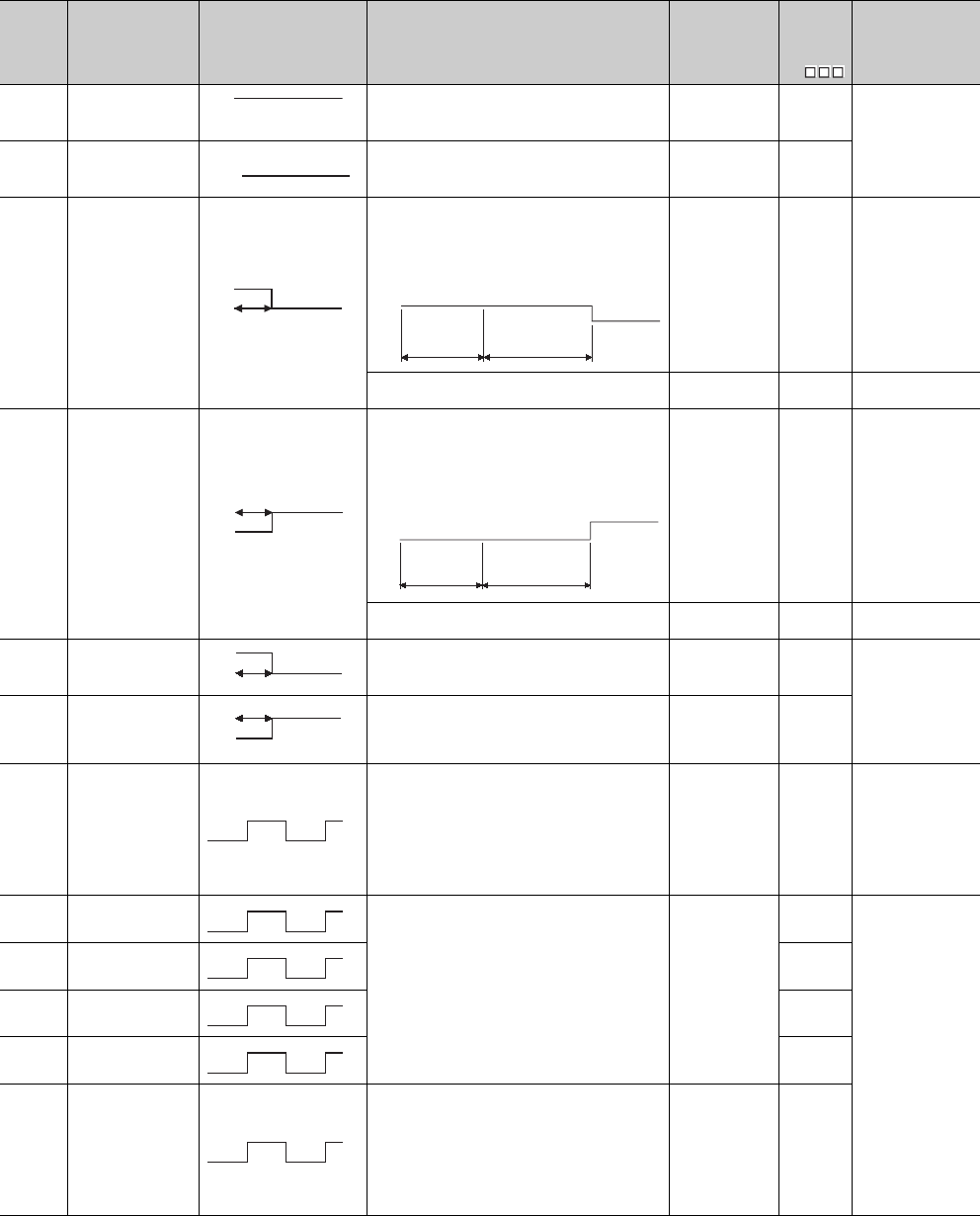
12 - 8
(3) System clocks/counters
Table12.4 Special relay
Number Name Meaning Explanation Set by
(When Set)
Corres-
ponding
ACPU
M9
Corresponding
CPU
SM400 Always ON • Normally is ON S (Every END
processing) M9036
QCPU
SM401 Always OFF • Normally is OFF S (Every END
processing) M9037
SM402 After RUN, ON for 1
scan only
• After RUN, ON for 1 scan only.
• This connection can be used for scan execution type
programs only.
• When an initial execution type program is used, this
relay turns OFF at the END processing of the scan
execution type program in the first scan after RUN. S (Every END
processing) M9038
Qn(H)
QnPH
QnPRH
QnU
• After RUN, ON for 1 scan only. S (Every END
processing) New Q00J/Q00/Q01
SM403 After RUN, OFF for 1
scan only
• After RUN, OFF for 1 scan only.
• This connection can be used for scan execution type
programs only.
• When an initial execution type program is used, this
relay turns OFF at the END processing of the scan
execution type program in the first scan after RUN. S (Every END
processing) M9039
Qn(H)
QnPH
QnPRH
QnU
• After RUN, OFF for 1 scan only. S (Every END
processing) New Q00J/Q00/Q01
SM404
Low speed execution
type programON for 1
scan only after RUN
• After RUN, ON for 1 scan only.
• This connection can be used for low speed execution type
programs only.
S (Every END
processing) New
Qn(H)
QnPH
SM405
Low speed execution
type programAfter
RUN, OFF for 1 scan
only
• After RUN, OFF for 1 scan only.
• This connection can be used for low speed execution type
programs only.
S (Every END
processing) New
SM409 0.01 second clock
• Repeatedly changes between ON and OFF at 5-ms
interval.
• When Programmable Controller power supply is
turned ON or a CPU module reset is performed,
goes from OFF to start.
(Note that the ON-OFF status changes when the
designated time has elapsed during the execution of
the program.)
S (Status change) New
Qn(H)
QnPH
QnPRH
QnU
SM410 0.1 second clock
• Repeatedly changes between ON and OFF at each
designated time interval.
• When Programmable Controller power supply is
turned ON or a CPU module reset is performed,
goes from OFF to start.
(Note that the ON-OFF status changes when the
designated time has elapsed during the execution of
the program.)
S (Status change)
M9030
QCPU
SM411 0.2 second clock M9031
SM412 1 second clock M9032
SM413 2 second clock M9033
SM414 2n second clock
• This relay alternates between ON and OFF at
intervals of the time (unit: s) specified in SD414.
• When Programmable Controller power supply is
turned ON or a CPU module reset is performed,
goes from OFF to start.
(Note that the ON-OFF status changes when the
designated time has elapsed during the execution of
the program.)
S (Status change) M9034form
at change
ON
OFF
ON
OFF
ON
OFF 1 scan ON
OFF 1 scan of scan
execution type
program
Initial
execution
type program
ON
OFF 1 scan
ON
OFF
1 scan of scan
execution type
program
Initial
execution
type program
ON
OFF 1 scan
ON
OFF 1 scan
0.005s
0.005s
0.05s
0.05s
0.1s
0.1s
0.5s
0.5s
1s
1s
ns
ns
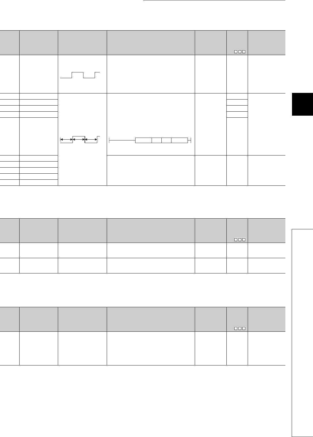
12 - 9
CHAPTER12 SPECIAL RELAY LIST AND SPECIAL REGISTER LIST
1
2
3
12
6
7
8
12.1 SPECIAL RELAY LIST
(4) Scan information
(5) I/O refresh
*1: This applies to the CPU of function version B or later.
Table12.4 Special relay
Number Name Meaning Explanation Set by
(When Set)
Corres-
ponding
ACPU
M9
Corresponding
CPU
SM415 2n (ms) clock
• This relay alternates between ON and OFF at
intervals of the time (unit: ms) specified in SD415.
• When Programmable Controller power supply is
turned ON or a CPU module reset is performed,
goes from OFF to start.
(Note that the ON-OFF status changes when the
designated time has elapsed during the execution of
the program.)
S (Status change) New
Qn(H)
QnPH
QnPRH
QnU
SM420 User timing clock No.0 • Relay repeats ON/OFF switching at fixed scan
intervals.
• When Programmable Controller power supply is
turned ON or a CPU module reset is performed,
goes from OFF to start.
(For the redundant CPU, however, this relay is
always OFF after system switching.)
• The ON/OFF intervals are set with the DUTY
instruction
n1: ON scan interval
n2: OFF scan interval
S (Every END
processing)
M9020
QCPU
SM421 User timing clock No.1 M9021
SM422 User timing clock No.2 M9022
SM423 User timing clock No.3 M9023
SM424 User timing clock No.4 M9024
SM430 User timing clock No.5
• For use with SM420 to SM424 low speed programs S (Every END
processing) New Qn(H)
QnPH
SM431 User timing clock No.6
SM432 User timing clock No.7
SM433 User timing clock No.8
SM434 User timing clock No.9
Table12.5 Special relay
Number Name Meaning Explanation Set by
(When Set)
Corres-
ponding
ACPU
M9
Corresponding
CPU
SM510 Low speed program
execution flag
OFF : Completed or not
executed
ON : Execution under way.
• Goes ON when low speed execution type program is
executed.
S (Every END
processing) New Qn(H)
QnPH
SM551 Reads module service
interval
OFF : Ignored
ON : Read
• When this relay goes from OFF to ON, the module
service interval designated by SD550 is read to
SD551 to SD552.
UNew
Qn(H)
QnPH
QnPRH
Table12.6 Special relay
Number Name Meaning Explanation Set by
(When Set)
Corres-
ponding
ACPU
M9
Corresponding
CPU
SM580 Program to program I/
O refresh
OFF : Not refreshed
ON : Refreshed
• When this special relay is turned ON, I/O refresh is
performed after execution of the first program, and
the next program is then executed.
When a sequence program and an SFC program are
to be executed, the sequence program is executed,
I/O refresh is performed, and the SFC program is
then executed.
UNew
Q00J/Q00/Q01*1
n(ms)
n(ms)
n1 scan
n2 scan n2 scan
DUTY n1 n2 SM420

12 - 10
(6) Memory cards
*1: The Universal model QCPU except the Q00UJCPU, Q00UCPU, and Q01UCPU.
*2: The Universal model QCPU except the Q00UJCPU.
Table12.7 Special relay
Number Name Meaning Explanation Set by
(When Set)
Corres-
ponding
ACPU
M9
Corresponding
CPU
SM600 Memory card usable
flags
OFF : Unusable
ON : Use enabled • ON when memory card is ready for use by user S (Status change) New
Qn(H)
QnPH
QnPRH
QnU*1
SM601 Memory card protect
flag
OFF : No protect
ON : Protect • Goes ON when memory card protect switch is ON S (Status change) New
SM602 Drive 1 flag OFF : No drive 1
ON : Drive 1 present • Turns ON when the mounted memory card is RAM S (Status change) New
SM603 Drive 2 flag OFF : No drive 2
ON : Drive 2 present • Turns ON when the mounted memory card is ROM S (Status change) New
SM604 Memory card in-use
flag
OFF : Not used
ON : In use • Goes ON when memory card is in use S (Status change) New
SM605 Memory card remove/
insert prohibit flag
OFF : Remove/insert enabled
ON : Remove/insert
prohibited
• Goes ON when memory card cannot be inserted or
removed UNew
SM609 Memory card remove/
insert enable flag
OFF : Remove/insert
prohibited
ON : Remove/insert enabled
• Turned ON by user to enable the removal/insertion
of memory card.
• Turned OFF by the system after the memory card is
removed.
• This contact can be used only when SM604 and
SM605 are OFF.
S/U New
SM620 Drive 3/4 usable flags OFF : Unusable
ON : Use enabled • Always ON S (Initial) New QCPU
SM622 Drive 3 flag OFF : No drive 3
ON : Drive 3 present • Always ON S (Initial) New
Q00J/Q00/Q01
Qn(H)
QnPH
QnPRH
QnU*2
SM623 Drive 4 flag OFF : No drive 4
ON : Drive 4 present • Always ON S (Initial) New QCPU
SM624 Drive 3/4 in-use flag OFF : Not used
ON : In use
• Goes ON when the file within Drive 3 (standard
RAM) or Drive 4 (standard ROM) is used. S (Status change) New
Qn(H)
QnPH
QnPRH
QnU
SM640 File register use OFF : File register not used
ON : File register in use • Goes ON when file register is in use S (Status change) New
Q00J/Q00/Q01
Qn(H)
QnPH
QnPRH
QnU*2

12 - 11
CHAPTER12 SPECIAL RELAY LIST AND SPECIAL REGISTER LIST
1
2
3
12
6
7
8
12.1 SPECIAL RELAY LIST
*1: The Universal model QCPU except the Q00UJCPU, Q00UCPU, and Q01UCPU.
*3: The modules whose serial number (first five digits) is "10102" or later are the relevant models. (Except the Q00UJCPU, Q00UCPU, and Q01UCPU)
Table12.7 Special relay
Number Name Meaning Explanation Set by
(When Set)
Corres-
ponding
ACPU
M9
Corresponding
CPU
SM650 Comment use OFF : File register not used
ON : File register in use • Goes ON when comment file is in use S (Status change) New
Qn(H)
QnPH
QnPRH
QnU
SM660 Boot operation
OFF : Internal memory
execution
ON : Boot operation in
progress
• Goes ON while boot operation is in process
• Goes OFF if boot designation switch is OFF S (Status change) New
Qn(H)
QnPH
QnPRH
OFF : Program memory
execution
ON : Boot operation in
progress
• Goes ON while boot operation is in process S (Status change) New Q00J/Q00/Q01
QnU*1
SM671
Latch data backup to
standard ROM
completion flag
OFF : Not completed
ON : Completed
• Turned ON when latch data backup to the standard
ROM is completed.
• Time when the latch data backup to the standard
ROM was performed is stored in SD672 or later.
S (Status change) New QnU
SM672
Memory card file
register access range
flag
OFF : Within access range
ON : Outside access range
• Goes ON when access is made to area outside the
range of file register of memory card(Set within END
processing.)
• Reset at user program
S/U New
Qn(H)
QnPH
QnPRH
SM675
Error completion of
latch data backup to
standard ROM
OFF : No Error
ON : Error
• Turned ON when data cannot be backuped to the
standard ROM by the latch data backup normally.
• Turned OFF when data is backuped to the standard
ROM by the latch data backup normally.
SNew
QnU
SM676
Specification of
restration repeated
execution
OFF : Not specified
ON : Specified
• If latch data backup is performed when SM676 is
ON, restore the data every time turning ON from
OFF the power supply from the next power-on.
• Delete the backuped latch data, or restore the data
every time turning ON from OFF the power supply
until the latch data backup operation will be executed
again.
UNew
SM680 Program memory write
error
OFF : Write error
ON : Write not executed/
normal
• Turns ON if a write error is detected at writing to
program memory (flash ROM).
Turns OFF by the write direction.
S (At write) New
SM681 Program memory
writing flag
OFF : During writing
ON : Write not executed
• Turns ON when writing to the program memory (flash
ROM) is in progress, and turns OFF when writing is
completed.
S (At write) New
SM682
Program memory
overwrite count error
flag
OFF : Overwrite count is
100,000 or more
ON : Overwrite count is less
than 100,000
• Turns ON when the overwrite count of program
memory (flash ROM) reaches 100,000. S (At write) New
SM685 Standard ROM write
error
OFF : Write error
ON : Write not executed/
normal
• Turns ON when write error is detected at writing to
standard ROM (flash ROM).
• Turns OFF by the write direction.
S (At write) New
SM686 Standard ROM writing
flag
OFF : During overwriting
ON : Overwrite not executed
• Turns ON when writing to the standard ROM (flash
ROM) is in progress, and turns OFF when writing is
completed.
S (At write) New
SM687
Standard ROM
overwrite count error
flag
OFF : Overwrite count is
100,000 or more
ON : Overwrite count is less
than 100,000
• Turns ON when the overwrite count of standard
ROM (flash ROM) reaches 100,000.
(It is necessary to change CPU module.)
S (At write) New
SM691 Backup start
preparation status flag
OFF : Backup start
preparation not
completed
ON : Backup start
preparation completed
Turns on when the backup start preparation is
completed. S (Status change) New
QnU*3
SM692 Restoration complete
flag
OFF : Restoration not
completed
ON : Restoration completed
Turns on when restoration of the backup data in the
memory card is completed. S (Status change) New

12 - 12
(7) Instruction-Related Special Relays
*1: The module whose first 5 digits of serial No. is "09042" or later.
*2: The relevant modules are as follows:
• The Universal model QCPU whose serial number (first five digits) is "10102" or later.
• Q00UJCPU, Q00UCPU, Q01UCPU
*3: The relevant modules are as follows:
• The Universal model QCPU whose serial number (first five digits) is "10102" or later.
• Q00UCPU, Q01UCPU
Table12.8 Special relay
Number Name Meaning Explanation Set by
(When Set)
Corres-
ponding
ACPU
M9
Corresponding
CPU
SM700 Carry flag OFF : Carry OFF
ON : Carry ON • Carry flag used in application instruction S (Instruction
execution) M9012 QCPU
SM701 Number of output
characters selection
Switching the number of
output characters and the
output pattern
• Used for the PR, PRC, BINDA, DBINDA, BINHA,
DBINHA, BCDDA, DBCDDA, or COMRD instruction UM9049
Qn(H)
QnPH
QnPRH
QnU
SM702 Search method OFF : Search next
ON : 2-part search
• Designates method to be used by search instruction.
• Data must be arranged for 2-part search. UNew
QCPUSM703 Sort order OFF : Ascending order
ON : Descending order
• The sort instruction is used to designate whether
data should be sorted in ascending order or in
descending order.
UNew
SM704 Block comparison OFF : Non-match found
ON : All match
• Goes ON when all data conditions have been met for
the BKCMP instruction.
S (Instruction
execution) New
• Goes ON when all data conditions have been met for
the DBKCMP instruction.
S (Instruction
execution) New
QnU*2
SM709
DT/TM instruction
improper data
detection flag
OFF : Improper data not
detected
ON : Improper data detected
Turns on when the data to be compared by the DT or
TM instruction is not recognized as date data or time
data, or the device (3 words) to be compared exceeds
the specified device range.
S (Instruction
execution) or U New
SM710 CHK instruction
priority ranking flag
OFF : Conditions priority
ON : Pattern priority
• Remains as originally set when OFF.
• CHK priorities updated when ON.
S (Instruction
execution) New
Qn(H)
QnPH
QnPRH
SM715 EI flag OFF : During DI
ON : During EI • ON when EI instruction is being executed. S (Instruction
execution) New QCPU
SM716
Block comparison
(Except an interrupt
program)
OFF : Mismatch found
ON : No mismatch
Turns on when all data conditions are confirmed that
they are met by the DBKCMP instruction.
(Initial execution type program, scan execution type
program, stand-by type program executed from initial
execution type program or scan execution type
program)
S (Instruction
execution) New
QnU*2
SM717 Block comparison
(Interrupt program)
OFF : Mismatch found
ON : No mismatch
Turns on when all data conditions are confirmed that
they are met by the DBKCMP instruction.
(Interrupt program, fixed scan execution type program,
stand-by type program executed from interrupt program
or fixed scan execution type program)
SM718
Block comparison
(Interrupt program
(I45))
OFF : Mismatch found
ON : No mismatch
Turns on when all data conditions are confirmed that
they are met by the DBKCMP instruction.
(Interrupt program (I45) or Stand-by type program
executed from interrupt program (I45))
QnU*3
SM720 Comment read
completion flag
OFF : Comment read not
completed
ON : Comment read
completed
• Turns on only during one scan when the processing
of the COMRD or PRC instruction is completed. S (Status change) New
Qn(H)
QnPH
• Turns on only during one scan when the processing
of the COMRD instruction is completed.
QnPRH
QnU
SM721 File being accessed OFF : File not accessed
ON : File being accessed
• Switches ON while a file is being accessed by the
SP. FWRITE, SP. FREAD, COMRD, PRC, or LEDC
instruction.
S (Status change) New
Qn(H)
QnPH
• Switches ON while a file is being accessed by the
SP. FWRITE, SP. FREAD, COMRD or LEDC
instruction.
Qn(H)
QnPH
QnPRH
• Switches ON while a file is being accessed by the
SP. FWRITE, SP. FREAD, COMRD or SP.DEVST
instruction.
QnU
• Turns ON while the ATA card or standard ROM is
being accessed. QnU*1
SM722 BIN/DBIN instruction
error disabling flag
OFF : Error detection
performed
ON : Error detection not
performed
• Turned ON when "OPERATION ERROR" is
suppressed for BIN or DBIN instruction. UNewQCPU

12 - 13
CHAPTER12 SPECIAL RELAY LIST AND SPECIAL REGISTER LIST
1
2
3
12
6
7
8
12.1 SPECIAL RELAY LIST
*1: The module whose first 5 digits of serial No. is "06082" or later.
*2: The module whose first 5 digits of serial No. is "07012" or later.
*3: The module whose first 5 digits of serial No. is "07032" or later.
*4: This applies to the CPU module of function version B or later.
*5: The module whose first 5 digits of serial No. is "04012" or later.
*6: The module whose first 5 digits of serial No. is "05032" or later.
*8: The relevant modules are as follows:
• The Universal model QCPU whose serial number (first five digits) is "10102" or later.
• Q00UJCPU, Q00UCPU, Q01UCPU
*9: The Universal model QCPU except the Q00UJCPU.
Table12.8 Special relay
Number Name Meaning Explanation Set by
(When Set)
Corres-
ponding
ACPU
M9
Corresponding
CPU
SM734
XCALL instruction
execution condition
designation
OFF : Not executed by
execution condition
risen
ON : Executed by execution
condition risen
• During OFF, XCALL instructions will not be executed
even if execution condition is risen.
• During ON, XCALL instructions will be executed
when execution condition is risen.
UNew
Qn(H)*1
SM735
SFC comment readout
instruction in
execution flag
OFF : SFC comment readout
instruction is
inactivated.
ON : SFC comment readout
instruction is
activating.
• Turns on the instructions, (S(P).SFCSCOMR) to
read the SFC step comments and (S(P).
SFCTCOMR) to read the SFC transition condition
comments.
S (status change) New
Qn(H)*2
QnPH*3
QnPRH*3
SM738 MSG instruction
reception flag
OFF : Instruction not
executed
ON : Instruction execution
• Goes ON when MSG instruction is executed S (Instruction
execution) New Qn(H)
QnPRH
SM750 Scaling instruction
search method setting
OFF : Search next
ON : 2-part search
Determines a search method when the scaling
instruction is executed. UNew
QnU*8
SM774
PID bumpless
processing
(for complete
derivative)
OFF : Matched
ON : Not matched
• Specifies whether to match the set value (SV) with
the process value (PV) or not in the manual mode. UNew
Q00J/Q00/Q01*4
Qn(H)
QnPRH
QnU
SM775
Selection of refresh
processing during
COM/CCOM
instruction execution
OFF : Performs link refresh
ON : Performs no link
refresh
• Select whether link refresh processing will be
performed or not when only communication with the
CPU module is made at the execution of the COM
instruction.
UNew
Q00J/Q00/Q01
Qn(H)
QnPH
OFF : Performs refresh
processes other than
an I/O refresh
ON : Performs refresh set
by SD778
• Select whether to perform refresh processes other
than an I/O refresh set by SD778 when the COM or
CCOM instruction is executed.
UNew
Q00J/Q00/Q01*4
Qn(H)*5
QnPH*3
QnPRH
QnU
SM776 Enable/disable local
device at CALL
OFF : Local device disabled
ON : Local device enabled
• Set whether the local device of the subroutine
program called at execution of the CALL instruction
is valid or invalid.
UNew
Qn(H)
QnPH
QnPRH
QnU*9
SM777
Enable/disable local
device in interrupt
program
OFF : Local device disabled
ON : Local device enabled
• Set whether the local device at execution of the
interrupt program is valid or invalid. UNew
SM794
PID bumpless
processing(for
incomplete derivative)
OFF : Matched
ON : Not matched
• Specifies whether to match the set value (SV) with
the process value (PV) or not in the manual mode. UNew
Q00J/Q00/Q01*4
Qn(H)*6
QnPRH
QnU

12 - 14
*7: The Universal model QCPU except the Q00UJCPU, Q00UCPU, Q01UCPU, and Q02UCPU.
(8) Debug
*1: The Universal model QCPU except the Q00UJCPU.
Table12.8 Special relay
Number Name Meaning Explanation Set by
(When Set)
Corres-
ponding
ACPU
M9
Corresponding
CPU
SM796
Block information
using multiple CPU
high-speed
transmission
dedicated instruction
(for CPU No.1)
OFF : Block is secured
ON : Block set by SD796
cannot be secured
• Turns ON when the number of the remaining blocks
of the dedicated instruction transmission area used
for the multiple CPU high-speed transmission
dedicated instruction(target CPU= CPU No.1) is less
than the number of blocks specified by SD796.
Turns ON at instruction execution. Turns OFF when
the empty area exists at END processing.
S (When
instruction/END
processing
executed)
New
QnU*7
SM797
Block information
using multiple CPU
high-speed
transmission
dedicated instruction
(for CPU No.2)
OFF : Block is secured
ON : Block set by SD797
cannot be secured
• Turns ON when the number of the remaining blocks
of the dedicated instruction transmission area used
for the multiple CPU high-speed transmission
dedicated instruction (target CPU= CPU No.2) is less
than the number of blocks specified by SD797.
Turns ON at instruction execution. Turns OFF when
the empty area exists at END processing.
S (When
instruction/END
processing
executed)
New
SM798
Block information
using multiple CPU
high-speed
transmission
dedicated instruction
(for CPU No.3)
OFF : Block is secured
ON : Block set by SD798
cannot be secured
• Turns ON when the number of the remaining blocks
of the dedicated instruction transmission area used
for the multiple CPU high-speed transmission
dedicated instruction (target CPU= CPU No.3) is less
than the number of blocks specified by SD798.
Turns ON at instruction execution. Turns OFF when
the empty area exists at END processing.
S (When
instruction/END
processing
executed)
New
SM799
Block information
using multiple CPU
high-speed
transmission
dedicated instruction
(for CPU No.4)
OFF : Block is secured
ON : Block set by SD799
cannot be secured
• Turns ON when the number of the remaining blocks
of the dedicated instruction transmission area used
for the multiple CPU high-speed transmission
dedicated instruction(target CPU= CPU No.4) is less
than the number of blocks specified by SD799.
Turns ON at instruction execution. Turns OFF when
the empty area exists at END processing.
S (When
instruction/END
processing
executed)
New
Table12.9 Special relay
Number Name Meaning Explanation Set by
(When Set)
Corres-
ponding
ACPU
M9
Corresponding
CPU
SM800 Trace preparation OFF : Not ready
ON : Ready
• Switches ON when the trace preparation is
completed S (Status change) New
Qn(H)
QnPH
QnPRH
QnU*1
SM801 Trace start OFF : Suspend
ON : Start
• Trace is started when this relay switches ON.
• Trace is suspended when this relay switches OFF.
(All related special Ms switches OFF.)
UM9047
SM802 Trace execution in
progress
OFF : Suspend
ON : Start • Switches ON during execution of trace. S (Status change) M9046
SM803 Trace trigger OFF ON: Start
• Trace is triggered when this relay switches from OFF
to ON. (Identical to TRACE instruction execution
status)
UM9044
SM804 After trace trigger OFF : Not after trigger
ON : After trigger • Switches ON after trace is triggered. S (Status change) New
SM805 Trace completed OFF : Not completed
ON : End • Switches ON at completion of trace S (Status change) M9043
SM826 Trace error OFF : Normal
ON : Errors • Switches ON if error occurs during execution of trace S (Status change) New
SM829
Forced registration
specification of trace
setting
ON : Forced registration
enabled
OFF : Forced registration
disabled
• Even when the trace condition or the trigger
condition is established, the sampling trace setting
can be set to the CPU module by turning SM829 ON
and registering the sampling trace setting by GX
Developer.
UNew
QnU*1

12 - 15
CHAPTER12 SPECIAL RELAY LIST AND SPECIAL REGISTER LIST
1
2
3
12
6
7
8
12.1 SPECIAL RELAY LIST
(9) A to Q conversion correspondences
Special relays SM1000 to SM1255 are the relays which correspond to ACPU special relays
M9000 to M9255 after A to Q conversion.
(However, the Basic model QCPU and Redundant CPU do not support the A to Q
conversion.)
These special relays are all set by the system, and cannot be set by the user program.
To turn them ON/OFF by the user program, change the special relays in the program into
those of QCPU.
However, some of SM1084 and SM1200 to SM1255 (corresponding to M9084 and M9200 to
M9255 before conversion) can be turned ON/OFF by the user program, if they could be
turned ON/OFF by the user program before conversion.For details on the ACPU special
relays, see the user's manuals for the individual CPUs, and MELSECNET or MELSECNET/
B Data Link System Reference Manuals
Check "Use special relay/special register from SM/SD1000" for "A-PLC" on the PLC system tab of PLC parameter in GX
Developer when the converted special relays are used with the High Performance model QCPU, Process CPU, and
Universal model QCPU.
When not using the converted special relays, uncheck "Use special relay/special register from SM/SD1000" to save the time
taken for processing special relays.
Remark
The following are additional explanations about the Special Relay for Modification column.
When a special relay for modification is provided, the device number should be changed to the provided QCPU special
relay.
When is provided, the converted special relay can be used for the device number.
When is provided, the device number does not work with QCPU.
*1: The relevant modules are as follows:
• The Universal model QCPU whose serial number (first five digits) is "10102" or later.
• Q00UJCPU, Q00UCPU, Q01UCPU
Table12.10 Special relay
ACPU
Special
Relay
Special
Relay after
Conversion
Special
Relay for
Modification
Name Meaning Details Corresponding
CPU
M9000 SM1000 –Fuse blown
OFF : Normal
ON : Module with blown
fuse
• Turned on when there is one or more output modules of
which fuse has been blown.
• Remains ON if the condition is restored to normal
thereafter.
• Output modules of remote I/O stations are also checked
fore fuse condition. Qn(H)
QnPH
QnU*1
M9002 SM1002 –I/O module verify
error
OFF : Normal
ON : Error
• Turned on if the status of I/O module is different form
entered status when power is turned on.
• Remains ON if the condition is restored to normal
thereafter.
• I/O module verification is done also to remote I/O station
modules.
• Reset is enabled only when special registers SD1116 to
SD1123 are reset.
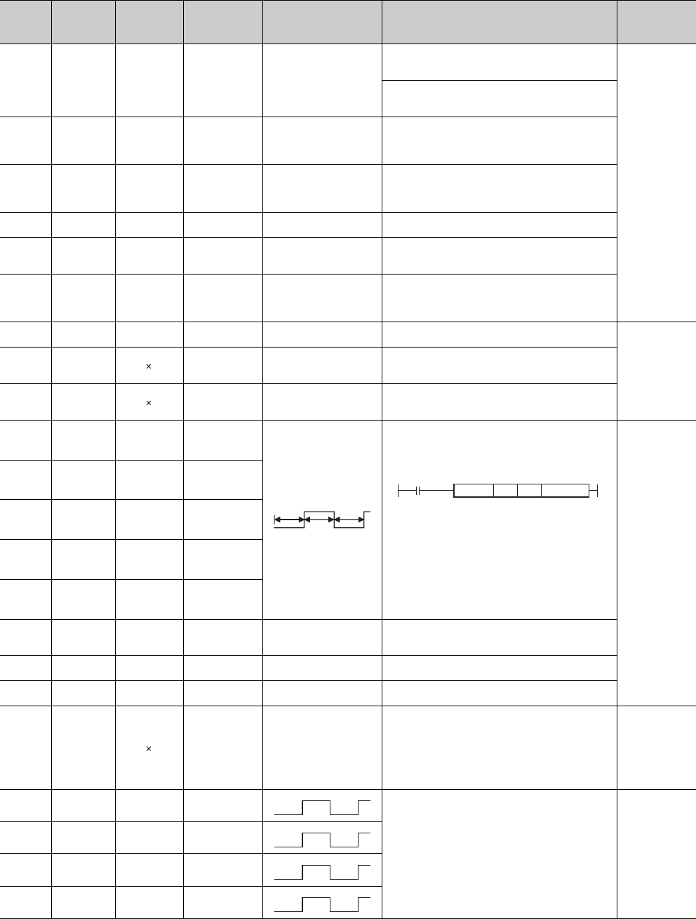
12 - 16
*1: The relevant modules are as follows:
• The Universal model QCPU whose serial number (first five digits) is "10102" or later.
• Q00UJCPU, Q00UCPU, Q01UCPU
Table12.11 Special relay
ACPU
Special
Relay
Special
Relay after
Conversion
Special
Relay for
Modification
Name Meaning Details Corresponding
CPU
M9005 SM1005 –AC DOWN
detection
OFF : AC DOWN not
detected
ON : AC DOWN detected
• Turns ON if an instantaneous power failure of within 20ms
occurs during use of the AC power supply module.
• Reset when the power supply is switched OFF, then ON.
Qn(H)
QnPH
QnU*1
• Turns ON if an instantaneous power failure of within 10ms
occurs during use of the DC power supply module.
• Reset when the power supply is switched OFF, then ON.
M9006 SM1006 –Battery low OFF : Normal
ON : Battery low
• Turns ON when the battery voltage drops to or below the
specified.
• Turns OFF when the battery voltage returns to normal
thereafter.
M9007 SM1007 –Battery low latch OFF : Normal
ON : Battery low
• Turns ON when the battery voltage drops to or below the
specified.
• Remains ON if the battery voltage returns to normal
thereafter.
M9008 SM1008 SM1 Self-diagnosis
error
OFF : No error
ON : Error
• Turned on when error is found as a result of self-
diagnosis.
M9009 SM1009 SM62 Annunciator
detection
OFF : No F number detected
ON : F number detected
• Turned on when OUT F of SET F instruction is
executed.
• Switched off when SD1124 data is cleared to zero.
M9011 SM1011 SM56 Operation error
flag
OFF : No error
ON : Error
• Turned on when operation error occurs during execution
of application instruction.
• Remains ON if the condition is restored to normal
thereafter.
M9012 SM1012 SM700 Carry flag OFF : Carry OFF
ON : Carry ON • Carry flag used in application instruction.
Qn(H)
QnPH
M9016 SM1016 Data memory clear
flag
OFF : lgnored
ON : Output claered
• Clears the data memory including the latch range (other
than special relays and special registers) in remote run
mode from computer, etc. when SM1016 is on.
M9017 SM1017 Data memory clear
flag
OFF : lgnored
ON : Output claered
• Clears the unlatched data memory (other than special
relays and special registers) in remote run mode from
computer, etc. when SM1017 is on.
M9020 SM1020 –User timing clock
No.0
• Relay which repeats on/off at intervals of predetermined
scan.
• When power is turned on or reset is per-formed, the clock
starts with off.
Set the intervals of on/off by DUTY instruction.
n1: ON scan interval
n2: OFF scan interval
* : If DUTY instruction, which specified from SM 1020 to
SM 1024 of User timing clock in programs other than
a program for a Universal model QCPU, changes the
programmable controller to the Universal model
QCPU, the special relays SM 420 to 424 will be
replaced.
(Universal model QCPUs cannot specify the special
relays from SM 1020 to SM1024.)
Qn(H)
QnPH
QnU*1
M9021 SM1021 –User timing clock
No.1
M9022 SM1022 –User timing clock
No.2
M9023 SM1023 –User timing clock
No.3
M9024 SM1024 –User timing clock
No.4
M9025 SM1025 –Clock data set
request
OFF : Ignored
ON : Set request present
used
• Writes the clock data stored in SD1025 to SD1028 to the
CPU module after the END instruction is executed in the
scan in which SM1025 turned from OFF to ON.
M9026 SM1026 –Clock data error OFF : No error
ON : Error • Switched on by clock data (SD1025 to SD1028) error
M9028 SM1028 –Clock data read
request
OFF : Ignored
ON : Read request
• Reads clock data to SD1025 to SD1028 in BCD when
SD1028 is on.
M9029 SM1029
Batch processing
of data
communications
requests
OFF : Batch processing not
conducted
ON : Batch processing
conducted
• The SM1029 relay is turned on using a sequence program
to process all data communication requests accepted
during one scan in the END processing of that scan.
• The batch processing of the data communication requests
can be turned on and off during running.
• The default is OFF (processed one at a time for each END
processing in the order in which data communication
requests are accepted).
Qn(H)
QnPH
M9030 SM1030 –0.1 second clock
• 0.1 second, 0.2 second, 1 second and 2 second, clocks
are generated.
• Not turned on or off per scan but turned on and off even
during scan if corresponding time has elapsed.
• Starts with off when Programmable Controller power
supply is turned on or CPU module reset is performed.
Qn(H)
QnPH
QnU*1
M9031 SM1031 –0.2 second clock
M9032 SM1032 –1 second clock
M9033 SM1033 –2 second clock
n1 scan
n2 scan n2 scan
DUTY n1 n2 SM1020
0.05s
0.05s
0.1s
0.1s
0.5s
0.5s
1s
1s

12 - 17
CHAPTER12 SPECIAL RELAY LIST AND SPECIAL REGISTER LIST
1
2
3
12
6
7
8
12.1 SPECIAL RELAY LIST
*1: The relevant modules are as follows:
• The Universal model QCPU whose serial number (first five digits) is "10102" or later.
• Q00UJCPU, Q00UCPU, Q01UCPU
*2: minute clock indicates the name of the special relay (M9034) of the ACPU.
Table12.11 Special relay
ACPU
Special
Relay
Special
Relay after
Conversion
Special
Relay for
Modification
Name Meaning Details Corresponding
CPU
M9034 SM1034 –2n minute clock(1
minute clock)*2
• Alternates between ON and OFF according to the
seconds specified at SD414. (Default: n = 30)
• Not turned on or off per scan but turned on and off even
during scan if corresponding time has elapsed.
• Starts with off when Programmable Controller power
supply is turned on or CPU module reset is performed.
Qn(H)
QnPH
QnU*1
M9036 SM1036 –Always ON
• Used as dummy contacts of initialization and application
instruction in sequence program.
• SM1038 and SM1037 are turned on and off without regard
to position of key switch on CPU module front. SM1038
and SM1039 are under the same condition as RUN status
except when the key switch is at STOP position, and
turned off and on. Switched off if the key switch is in STOP
position. SM1038 is on for one scan only and SM1039 is
off for one scan only if the key switch is not in STOP
position.
M9037 SM1037 –Always OFF
M9038 SM1038 –ON for 1 scan only
after RUN
M9039 SM1039 –
RUN flag(After
RUN, OFF for 1
scan only)
M9040 SM1040 SM206 PAUSE enable coil OFF : PAUSE disabled
ON : PAUSE enabled • When RUN key switch is at PAUSE position or pause
contact has turned on and if SM1040 is on, PAUSE mode
is set and SM1041 is turned on.
Qn(H)
QnPH
M9041 SM1041 SM204 PAUSE status
contact
OFF : PAUSE not in effect
ON : PAUSE in effect
Qn(H)
QnPH
QnU*1
M9042 SM1042 SM203 STOP status
contact
OFF : STOP not in effect
ON : STOP in effect
• Switched on when the RUN key switch or RUN/STOP
switch is in STOP position.
M9043 SM1043 SM805 Sampling trace
completed
OFF : Sampling trace in
progress
ON : Sampling trace
completed
• Turned on upon completion of sampling trace performed
the number of times preset by parameter after STRA
instruction is executed.
Reset when STRAR instruction is executed.
M9044 SM1044 SM803 Sampling trace
OFF ON Same as STRA
instruction
execution
ON OFF Same as STRAR
instruction
execution
• Turning on/off SM1044 can execute STRA/STRAR
instruction.
(SM1044 is forcibly turned on/off by a peripheral device.)
When switched from OFF to ON: STRA instruction
When switched from ON to OFF: STRAR instruction
The value stored in SD1044 is used as the condition for
the sampling trace.
At scanning, at time Time (10 ms unit)
Qn(H)
QnPH
M9045 SM1045 Watchdog timer
(WDT) reset
OFF : Does not reset WDT
ON : Resets WDT
• The SM1045 relay is turned on to reset the WDT when the
ZCOM instruction and data communication request batch
processing are executed (used when the scan time
exceeds 200 ms).
M9046 SM1046 SM802 Sampling trace OFF : Trace not in progress
ON : Trace in progress • Switched on during sampling trace.
Qn(H)
QnPH
QnU*1
M9047 SM1047 SM801 Sampling trace
preparations
OFF : Sampling trace
suspended
ON : Sampling trace started
• Sampling trace is not executed unless SM1047 is turned
ON.
Sampling trace is suspended when SM1047 goes OFF.
Qn(H)
QnPH
M9049 SM1049 SM701
Switching the
number of output
characters
OFF : Output until NULL
code encountered
ON : 16 characters output
• When SM1049 is OFF, characters up to NULL (00H) code
are output.
• When SM1049 is ON, ASCII codes of 16 characters are
output.
M9051 SM1051 CHG instruction
execution disable
OFF : Enabled
ON : Disable
• Switched ON to disable the CHG instruction.
• Switched ON when program transfer is requested.
Automatically switched OFF when transfer is complete.
M9052 SM1052 SEG instruction
switch
OFF : 7SEG segment display
ON : I/O partial refresh
• When SM1052 is ON, the SEG instruction is executed as
an I/O partial refresh instruction.
When SM1052 is OFF, the SEG instruction is executed as
a 7-SEG display instruction.
ns
ns
ON
OFF
ON
OFF
ON
OFF 1 scan
ON
OFF 1 scan

12 - 18
*3: The A8UPU/A8PUJ is not available for the QCPU/QnACPU.
Table12.11 Special relay
ACPU
Special
Relay
Special
Relay after
Conversion
Special
Relay for
Modification
Name Meaning Details Corresponding
CPU
M9056 SM1056 Main side P, I set
request
OFF : Other than when P, I
set being requested
ON : P, I set being
requested
• Provides P, I set request after transfer of the other
program (for example subprogram when main program is
being run) is complete during run. Automatically switched
off when P, I setting is complete.
Qn(H)
QnPH
M9057 SM1057 Sub side P, I set
request
OFF : Other than when P, I
set being requested
ON : P, I set being
requested
M9058 SM1058 Main side P, I set
completion
Momentarily ON at P, I set
completion • Turned ON once when the P, I set has been completed,
and then turned OFF again.
M9059 SM1059 Sub program P, I
set completion
Momentarily ON at P, I set
completion
M9060 SM1060 Sub program 2 P, I
set request
OFF : Other than when P, I
set being requested
ON : P, I set being
requested
• Provides P, I set request after transfer of the other
program (for example subprogram when main program is
being run) is complete during run. Automatically switched
off when P, I setting is complete.
M9061 SM1061 Sub program 3 P, I
set request
OFF : Other than when P, I
set being requested
ON : P, I set being
requested
M9070 SM1070
A8UPU/
A8PUJrequired
search time*3
OFF : Read time not
shortened
ON : Read time shortened
• Turned ON to shorten the search time in the A8UPU/
A8PUJ.
(In this case, the scan time is extended by 10 %.)
M9084 SM1084 Error check OFF : Error check executed
ON : No error check
It is set whether the error checks below are performed or not
when the END instruction is processed (to set the END
instruction processing time).
• Check for fuse blown.
• Check of battery
• Collation check of I/O module
M9091 SM1091 Operation error
details flag
OFF : No error
ON : Error
• Turns ON when the detail factor of the operation error is
stored into SD1091.
• Remains ON if the condition is restored to normal
thereafter.
M9100 SM1100 SM320 Presence/absence
of SFC program
OFF : SFC programs not
used
ON : SFC programs used
• Turned on if the SFC program is registered.
• Turned off if the SFC program is not registered.
M9101 SM1101 SM321 Start/stop SFC
program
OFF : SFC programs stop
ON : SFC programs start
• The value in SM1100 is set as the initial value.
(The relay automatically turns ON when the SFC program
is present.)
• When this relay turns from ON to OFF, execution of the
SFC program stops.
• When this relay turns from OFF to ON, execution of the
SFC program resumes.
M9102 SM1102 SM322 SFC program start
status
OFF : Initial start
ON : Resume start
• The SFC program start mode in the SFC setting of the
PLC parameter dialog box is set as the initial value.
At initial start: OFF
At continue start: ON

12 - 19
CHAPTER12 SPECIAL RELAY LIST AND SPECIAL REGISTER LIST
1
2
3
12
6
7
8
12.1 SPECIAL RELAY LIST
(10) QCPU with built-in Ethernet port
* 1: This applies to the Built-in Ethernet port QCPU.
Table12.11 Special relay
ACPU
Special
Relay
Special
Relay after
Conversion
Special
Relay for
Modification
Name Meaning Details Corresponding
CPU
M9103 SM1103 SM323
Presence/absence
of continuous
transition
OFF : Continuous transition
not effective
ON : Continuous transition
effective
• Set whether continuous transition will be performed for the
block where the "continuous transition bit" of the SFC
information device is not set.
Qn(H)
QnPH
M9104 SM1104 SM324
Continuous
transition
suspension flag
OFF : When transition is
completed
ON : When no transition
• OFF during operation in the continuous transition mode or
during continuous transition, and ON when continuous
transition is not executed.
• Always ON during operation in the no continuous
transition mode.
M9108 SM1108 SM90
Step transition
monitoring timer
start (equivalent of
SD90)
OFF : Monitoring timer reset
ON : Monitoring timer reset
start
• Turns ON when the measurement of the step transition
monitoring timer is started.
Turning this relay OFF resets the step transition
monitoring timer.
M9109 SM1109 SM91
Step transition
monitoring timer
start (equivalent of
SD91)
M9110 SM1110 SM92
Step transition
monitoring timer
start (equivalent of
SD92)
M9111 SM1111 SM93
Step transition
monitoring timer
start (equivalent of
SD93)
M9112 SM1112 SM94
Step transition
monitoring timer
start (equivalent of
SD94)
M9113 SM1113 SM95
Step transition
monitoring timer
start (equivalent of
SD95)
M9114 SM1114 SM96
Step transition
monitoring timer
start (equivalent of
SD96)
M9196 SM1196 SM325 Operation output
at block stop
OFF : Coil output OFF
ON : Coil output ON
• Selects the operation output when block stop is executed.
ON : Retains the ON/OFF status of the coil being used
by using operation output of the step being
executed at block stop.
OFF : All coil outputs are turned off. (Operation output
by the SET instruction is retained regardless of
the ON/OFF status of SM1196.)
M9197 SM1197
Switch between
blown fuse and I/O
verify error display
SM
1197
SM
1198
I/O numbers
to be
displayed
Switches I/O numbers in the fuse blow module storage
registers (SD1100 to SD1107) and I/O module verify error
storage registers (SD1116 to SD1123) according to the
combination of ON/OFF of the SM1197 and SM1198.
OFF OFF X/Y0 to 7F0
ON OFF X/Y800 to
FF0
M9198 SM1198
OFF ON X/Y1000 to
17F0
ON ON X/Y1800 to
1FF0
M9199 SM1199
Data recovery of
online sampling
trace/status latch
OFF : Data recovery disabled
ON : Data recovery enabled
• Recovers the setting data stored in the CPU module at
restart when sampling trace/status latch is executed.
• SM1199 should be ON to execute again. (Unnecessary
when writing the data again from peripheral devices.)
Table12.12 Special relay
Number Name Meaning Explanation Set by
(When Set)
Corres-
ponding
ACPU
M9
Corresponding
CPU
SM1270
Time setting function
(SNTP client)
execution
OFF : No time setting function
(SNTP client) execution
ON : Time setting function
(SNTP client) execution
Set this to ON when executing the time setting function
(SNTP client).
(Only when the time setting function is in "Use" with the
time setting parameter.)
UNew
QnU*1
SM1273 Remote password
mismatch count clear
OFF : Normal
ON : Clear
To clear the acumulated numeber (SD979 to 999) of
mismatched remote passwords, the setting SM1273 is
executed.
UNew

12 - 20
(11) Process control instructions
(12) For redundant systems (Host system CPU information *1)
SM1510 to SM1599 are only valid for redundant systems.
All off for standalone systems.
*1: The information of the host CPU module is stored.
Table12.13 Special relay
Number Name Meaning Explanation Set by
(When Set)
Corres-
ponding
ACPU
M9
Corresponding
CPU
SM1500 Hold mode OFF : No-hold
ON : Hold
• Specifies whether or not to hold the output value
when a range over occurs for the S.IN instruction
range check.
UNew
QnPH
QnPRH
SM1501 Hold mode OFF : No-hold
ON : Hold
• Specifies whether or not the output value is held
when a range over occurs for the S.OUT instruction
range check.
UNew
Table12.14 Special relay
Number Name Meaning Explanation Set by
(When Set)
Corres-
ponding
ACPU
M9
Corresponding
CPU
SM1510 Operation mode
OFF : Redundant system
backup mode, stand-
alone system
ON : Redundant system
separate mode
• Turns on when the operating mode is redundant
system separate. S (Each END) New
QnPRH
SM1511 System A identification
flag
• Distinguishes between system A and system B.
• The flag status does not change even if the tracking cable is disconnected.
S (Initial) New
SM1512 System B identification
flag
SM1513 Debug mode status
flag
OFF : Not in debug mode
ON : Debug mode
• Turns on when the redundant system operating
mode is set to debug mode. S (Initial) New
SM1515 Control system
judgment flag
• Indicates operation system status.
• The flag status does not change even if the tracking cable is disconnected.
S (Status change) New
SM1516 Standby system
judgment flag
SM1511
SM1512
ON
OFF
System A
OFF
System B
ON
OFF
OFF
When TRK. CABLE ERR.
(error code: 6210) occurs (Unknown)
SM1515
SM1516
ON
OFF
Control
system
OFF
Standby
system
ON
OFF
OFF
When TRK. CABLE ERR.
(error code: 6210) occurs (Unknown)

12 - 21
CHAPTER12 SPECIAL RELAY LIST AND SPECIAL REGISTER LIST
1
2
3
12
6
7
8
12.1 SPECIAL RELAY LIST
Table12.13 Special relay
Number Name Meaning Explanation Set by
(When Set)
Corres-
ponding
ACPU
M9
Corresponding
CPU
SM1517 CPU module startup
status
OFF : Power supply on
startup
ON : Operation system
switch start up
• Turns on when the CPU module is started up by the
system switching (switching from the standby system
to the control system). Remains OFF when the
standby system is switched to the control system by
a power-ON startup.
S (Status change) New
QnPRH
SM1518
Standby system to
control system
switching status flag
• Turns ON once switch between standby system to
control system, (ON for 1 scan only) occurs.
• This status flag can only be used for scan execution
type programs.
S (Each END) New
SM1519
Previous Control
System Identification
Flag
• On the last operation Control System was System
B,if power supply is supplied, or reset is released on
both SYSTEM together,After RUN, ON for 1 scan
only by System A side.
S (Each END) New
SM1520
Data tracking transfer
trigger specification
OFF : No trigger
ON : Trigger
SM1520 Block 1
• When data is transferred
based on the tracking
setting of the redundant
parameter dialog box, the
target block is specified
as trigger.
• When "Auto Tracking
block No.1" is enabled in
the tracking setting,
SM1520 is turned ON by
the system at power ON/
STOP to RUN. In other
cases, SM1520 to
SM1583 are turned ON
by the user.
S (initial)/U New
SM1521 SM1521 Block 2
SM1522 SM1522 Block 3
SM1523 SM1523 Block 4
SM1524 SM1524 Block 5
SM1525 SM1525 Block 6
SM1526 SM1526 Block 7
SM1527 SM1527 Block 8
SM1528 SM1528 Block 9
SM1529 SM1529 Block 10
SM1530 SM1530 Block 11
SM1531 SM1531 Block 12
SM1532 SM1532 Block 13
SM1533 SM1533 Block 14
SM1534 SM1534 Block 15
SM1535 SM1535 Block 16
SM1536 SM1536 Block 17
SM1537 SM1537 Block 18
SM1538 SM1538 Block 19
SM1539 SM1539 Block 20
SM1540 SM1540 Block 21
SM1541 SM1541 Block 22
SM1542 SM1542 Block 23
SM1543 SM1543 Block 24
SM1544 SM1544 Block 25
SM1545 SM1545 Block 26
SM1546 SM1546 Block 27
SM1547 SM1547 Block 28
SM1548 SM1548 Block 29
ON
OFF 1 scan
ON
OFF 1 scan

12 - 22
Table12.13 Special relay
Number Name Meaning Explanation Set by
(When Set)
Corres-
ponding
ACPU
M9
Corresponding
CPU
SM1549
Data tracking transfer
trigger specification
OFF : No trigger
ON : Trigger
SM1549 Block 30
• When data is transferred
based on the tracking
setting of the redundant
parameter dialog box, the
target block is specified
as trigger.
• When "Auto tracking
block No. 1" is enabled in
the tracking setting,
SM1520 is turned ON by
the system at power ON/
STOP to RUN. In other
cases, SM1520 to
SM1583 are turned ON
by the user.
S (initial)/U New
QnPRH
SM1550 SM1550 Block 31
SM1551 SM1551 Block 32
SM1552 SM1552 Block 33
SM1553 SM1553 Block 34
SM1554 SM1554 Block 35
SM1555 SM1555 Block 36
SM1556 SM1556 Block 37
SM1557 SM1557 Block 38
SM1558 SM1558 Block 39
SM1559 SM1559 Block 40
SM1560 SM1560 Block 41
SM1561 SM1561 Block 42
SM1562 SM1562 Block 43
SM1563 SM1563 Block 44
SM1564 SM1564 Block 45
SM1565 SM1565 Block 46
SM1566 SM1566 Block 47
SM1567 SM1567 Block 48
SM1568 SM1568 Block 49
SM1569 SM1569 Block 50
SM1570 SM1570 Block 51
SM1571 SM1571 Block 52
SM1572 SM1572 Block 53
SM1573 SM1573 Block 54
SM1574 SM1574 Block 55
SM1575 SM1575 Block 56
SM1576 SM1576 Block 57
SM1577 SM1577 Block 58
SM1578 SM1578 Block 59
SM1579 SM1579 Block 60
SM1580 SM1580 Block 61
SM1581 SM1581 Block 62
SM1582 SM1582 Block 63
SM1583 SM1583 Block 64
SM1590
System switching
enable/disable flag
from network module
OFF : System switching
request issuing module
absent
ON : System switching
request issuing module
present
• Turns ON when a system switching request is issued
from the network module. The module No. that
issued system switching can be checked by SD1590.
• Turns OFF when all bits of SD1590 are OFF.
S (Each END) New
SM1591
Standby system error
detection disable flag
at system switching
ON : Error is not detected by
new standby system at
system switching
OFF : Error is detected by
new standby system at
system switching
This flag is used to determine if the new standby station
detects 6210:STANDBY during system switching.
This applies to the following switching methods:
• System switching from GX Developer
• System switching using dedicated instruction
• System switching by the intelligent function module
UNew
SM1592 Enable/disable user
system switching
OFF : Disable user system
switching
ON : Enable user system
switching
• This flag enables system switching by the user from
GX Developer or by dedicated instruction.
(SP.CONTSW).
UNew

12 - 23
CHAPTER12 SPECIAL RELAY LIST AND SPECIAL REGISTER LIST
1
2
3
12
6
7
8
12.1 SPECIAL RELAY LIST
*2: The module whose first 5 digits of serial No. is “09012” or later.
(13) For redundant system (Other system CPU information *1)
SM1600 to SM1650 only valid for the CPU redundant system backup mode, so they cannot
be refreshed during the separate mode.
Either the backup mode or the separate mode is valid for the SM4651 to SM1699.
SM1600 to SM1699 are all turned off for stand-alone system.
*1 Stores other system CPU diagnostic information and system information.
*2 This shows the special relay(SM ) for the host system CPU.
Table12.13 Special relay
Number Name Meaning Explanation Set by
(When Set)
Corres-
ponding
ACPU
M9
Corresponding
CPU
SM1593
Setting to access
extension base unit of
standby system CPU
OFF : Error
ON : Ignored
Sets the operation for the case accessing buffer
memory of the intelligent function module mounted on
the extension base unit from the standby system CPU
in separate mode.
OFF : “OPERATION ERROR” (error code: 4112) will be
returned when accessing buffer memory of the
intelligent function module on the extension base
unit from the standby system CPU.
ON : No processing is performed when accessing
buffer memory of intelligent function module on
the extension base unit from the standby system
CPU.
U
New
QnPRH*2
SM1595 Memory copy to other
system start flag
OFF : Start memory copy
ON : No memory copy
initiated
• When SM1595 is turned from OFF to ON, memory
copy from control system to standby system starts.
Note that when SM1595 is turned from OFF to ON,
memory copy does not start if the I/O No. of the copy
destination (standby system CPU module: 3D1H) is
not stored in SD1595.
QnPRH
SM1596 Memory copy to other
system status flag
OFF : Memory copy not
executed
ON : Memory copy executed
• Turns on while memory is copied to other system.
• Turns off when memory copy execution has
completed.
S (Starting to
copy/finish)
SM1597
Memory copy to other
system completion
flag
OFF : Memory copy not
completed
ON : Memory copy
completed
• Turns on once the memory copying to the other
system has completed. S (finish)/U
New
SM1598
Copy contents of
standard ROM during
memory copy
OFF : Copy standard ROM
data
ON : Standard ROM data is
not copied
• If set to on by user, the standard ROM data is not
copied to the other system while memory copy is
executing.
U
Table12.14 Special relay
Number Name Meaning Explanation Set by
(When Set)
Corresp
onding
Host
SM
*2
Corresponding
CPU
SM1600 Other system error
flag
OFF : No error
ON : Error
• Turns on when an error occurs during redundant
system. Error check (Turns on single bit of SD1600.)
• Is off when no errors are present
S (Each END) –QnPRH
SM1610 Other system
diagnostics error
OFF : No error
ON : Error
• Turns on when a diagnostics error occurs. (Includes
error detection when annunciator is ON, and by CHK
instruction)
• Corresponds to status of SM0 at other system
S (Each END) SM0
QnPRH
SM1611 Other systems self
diagnostics error.
OFF : No self diagnostics
error occurred
ON : Self diagnostics error
occurred
• Turns on when a self diagnostics error occurs.
(Does not include error detection when annunciator
is ON, and by CHK instruction)
• Corresponds to status of SM1 at other system
S (Each END) SM1
SM1615 Other system common
error information
OFF : No common error
information present
ON : Common error
information present
• Turns on when there is common error information at
other system
• Corresponds to status of SM5 at other system
S (Each END) SM5
SM1626
Error individual
information for other
systems
OFF : No individual error
information present
ON : Individual error
information present
• Turns on when there is individual error information at
other system
• Corresponds to status of SM16 at other system
S (Each END) SM16
SM1649 Standby system
cancel error flag
OFF to ON:
Cancels error of standby
system
By turning this relay from OFF to ON, the continue error
that occurred in the standby system CPU module can
be canceled.
Use SD1649 to specify the error code of the error to be
canceled.
U–

12 - 24
(14) For redundant system (tracking)
Either the backup mode or the second mode is valid for SM1700 to SM1799.
All is turned off for stand-alone system.
Table12.15 Special relay
Number Name Meaning Explanation Set by
(When Set)
Corres-
ponding
ACPU
M9
Corresponding
CPU
SM1700 Transfer trigger
completion flag
OFF : Transfer not completed
ON : Transfer completed
• Turns on for one scan, once transfer of block 1 to
block 64 is completed. S (status change)
New QnPRH
SM1709
Manual system
switching disable/
enable setting during
online program
change redundant
tracking
ON : Manual system
switching enabled
(Disable canceled)
OFF : Manual system
switching disabled
(1) Turning this relay from OFF to ON enables
manual system switching during online program
change redundant tracking.
After the manual system switching disable status
is canceled, the system automatically turns off
SM1709.
(2) System switching due to any of the following
conditions is executed even during online
program change redundant tracking, regardless of
the status of this relay.
•Power off, reset, hardware failure, CPU stop error
(3) In either of the following statuses, the system
switching disable status can also be canceled by
this relay.
•Multiple-block online program change redundant
tracking execution status
•File batch online program change redundant
tracking execution status
S (When
executed)/U
SM1710
Transfer tracking data
during online program
change enable flag
OFF : No device tracking
ON : Transfer device
memory
(1) Set whether the tracking of the following data will
be executed or not during online program change
redundant tracking.
•Device memory
(Including SM/SD that will automatically execute
tracking)
•PIDINIT information, S.PIDINIT information, SFC
information
(2) SM1710 can be also used to set whether tracking
will be executed or not while online change of
multiple program blocks or batch of files is being
performed to ensure consistency of both systems.
(3) This SM is also transferred form control system
CPU module to standby system CPU module by
tracking data.
U

12 - 25
CHAPTER12 SPECIAL RELAY LIST AND SPECIAL REGISTER LIST
1
2
3
12
6
7
8
12.1 SPECIAL RELAY LIST
Table12.15 Special relay
Number Name Meaning Explanation Set by
(When Set)
Corres-
ponding
ACPU
M9
Corresponding
CPU
SM1712
Transfer trigger
completion flag
OFF : Transfer uncompleted
ON : Transfer completed
SM1712 Block 1
Turns ON only during one
scan when the transmission
of the corresponding block is
completed.
S (status change) New QnPRH
SM1713 SM1713 Block 2
SM1714 SM1714 Block 3
SM1715 SM1715 Block 4
SM1716 SM1716 Block 5
SM1717 SM1717 Block 6
SM1718 SM1718 Block 7
SM1719 SM1719 Block 8
SM1720 SM1720 Block 9
SM1721 SM1721 Block 10
SM1722 SM1722 Block 11
SM1723 SM1723 Block 12
SM1724 SM1724 Block 13
SM1725 SM1725 Block 14
SM1726 SM1726 Block 15
SM1727 SM1727 Block 16
SM1728 SM1728 Block 17
SM1729 SM1729 Block 18
SM1730 SM1730 Block 19
SM1731 SM1731 Block 20
SM1732 SM1732 Block 21
SM1733 SM1733 Block 22
SM1734 SM1734 Block 23
SM1735 SM1735 Block 24
SM1736 SM1736 Block 25
SM1737 SM1737 Block 26
SM1738 SM1738 Block 27
SM1739 SM1739 Block 28
SM1740 SM1740 Block 29
SM1741 SM1741 Block 30
SM1742 SM1742 Block 31
SM1743 SM1743 Block 32
SM1744 SM1744 Block 33
SM1745 SM1745 Block 34
SM1746 SM1746 Block 35
SM1747 SM1747 Block 36
SM1748 SM1748 Block 37
SM1749 SM1749 Block 38
SM1750 SM1750 Block 39
SM1751 SM1751 Block 40
SM1752 SM1752 Block 41
SM1753 SM1753 Block 42
SM1754 SM1754 Block 43
SM1755 SM1755 Block 44
SM1756 SM1756 Block 45
SM1757 SM1757 Block 46
SM1758 SM1758 Block 47
SM1759 SM1759 Block 48

12 - 26
(15) Redundant power supply module information
*1: The "power supply 1" indicates the redundant power supply module mounted on the POWER 1 slot of the redundant base unit (Q38RB/Q68RB/Q65WRB).
The "power supply 2" indicates the redundant power supply module mounted on the POWER 2 slot of the redundant base unit (Q38RB/Q68RB/Q65WRB).
*2: The module whose first 5 digits of serial No. is "04012" or later.
However, for the multiple CPU system configuration, this applies to all CPU modules whose first 5 digits of serial No. are "07032" or later.
*3: The module whose first 5 digits of serial No. is "10042" or later.
Table12.15 Special relay
Number Name Meaning Explanation Set by
(When Set)
Corres-
ponding
ACPU
M9
Corresponding
CPU
SM1760
Transfer trigger
completion flag
OFF : Transmission
uncompleted
ON : Transmission end
SM1760 Block 49
Turns ON only during one
scan when the transmission
of the corresponding block is
completed.
S (status change) New QnPRH
SM1761 SM1761 Block 50
SM1762 SM1762 Block 51
SM1763 SM1763 Block 52
SM1764 SM1764 Block 53
SM1765 SM1765 Block 54
SM1766 SM1766 Block 55
SM1767 SM1767 Block 56
SM1768 SM1768 Block 57
SM1769 SM1769 Block 58
SM1770 SM1770 Block 59
SM1771 SM1771 Block 60
SM1772 SM1772 Block 61
SM1773 SM1773 Block 62
SM1774 SM1774 Block 63
SM1775 SM1775 Block 64
Table12.16 Special relay
Number Name Meaning Explanation Set by
(When Set)
Corres-
ponding
ACPU
M9
Corresponding
CPU
SM1780 Power supply off
detection flag
OFF : No redundant power
supply module with
input power OFF
detected
ON : Redundant power
supply module with
input power OFF
detected
• Turns ON when one or more redundant power
supply modules with input power OFF are detected.
• Turns on if any of SD1780 bits is on.
• Turns off if all bits of SD1780 are off.
• Turns OFF when the main base unit is not the
redundant main base unit (Q38RB).
• When the multiple CPU system is configured, the
flags are stored only to the CPU No.1.
S (Each END)
New
Qn(H)*2
QnPH*2
QnPRH
QnU*3
SM1781 Power supply failure
detection flag
OFF : No faulty redundant
power supply module
detected
ON : Faulty redundant
power supply module
detected
• Turns ON when one or more faulty redundant power
supply modules are detected.
• Turns on if any of SD1781 bits is on.
• Turns off if all bits of SD1781 are off.
• Turns OFF when the main base unit is not the
redundant main base unit (Q38RB).
• When the multiple CPU system is configured, the
flags are stored only to the CPU No.1.
S (Each END)
SM1782
Momentary power
failure detection flag
for power supply 1 *1
OFF : No momentary power
failure detected
ON : Momentary power
failure detected
• Turns ON when a momentary power failure of the
input power supply to the power supply 1 or 2 is
detected one or more times. After turning ON,
remains ON even if the power supply recovers from
the momentary power failure.
• Turns OFF the flag (SM1782, SM1783) of the power
supply 1/2 when the CPU module starts.
• When the input power to one of the redundant power
supply modules turns OFF the corresponding flag
turns OFF.
• Turns OFF when the main base unit is not the
redundant main base unit (Q38RB).
• When the multiple CPU system is configured, the
flags are stored only to the CPU No.1.
S (Each END)
SM1783
Momentary power
failure detection flag
for power supply 2 *1
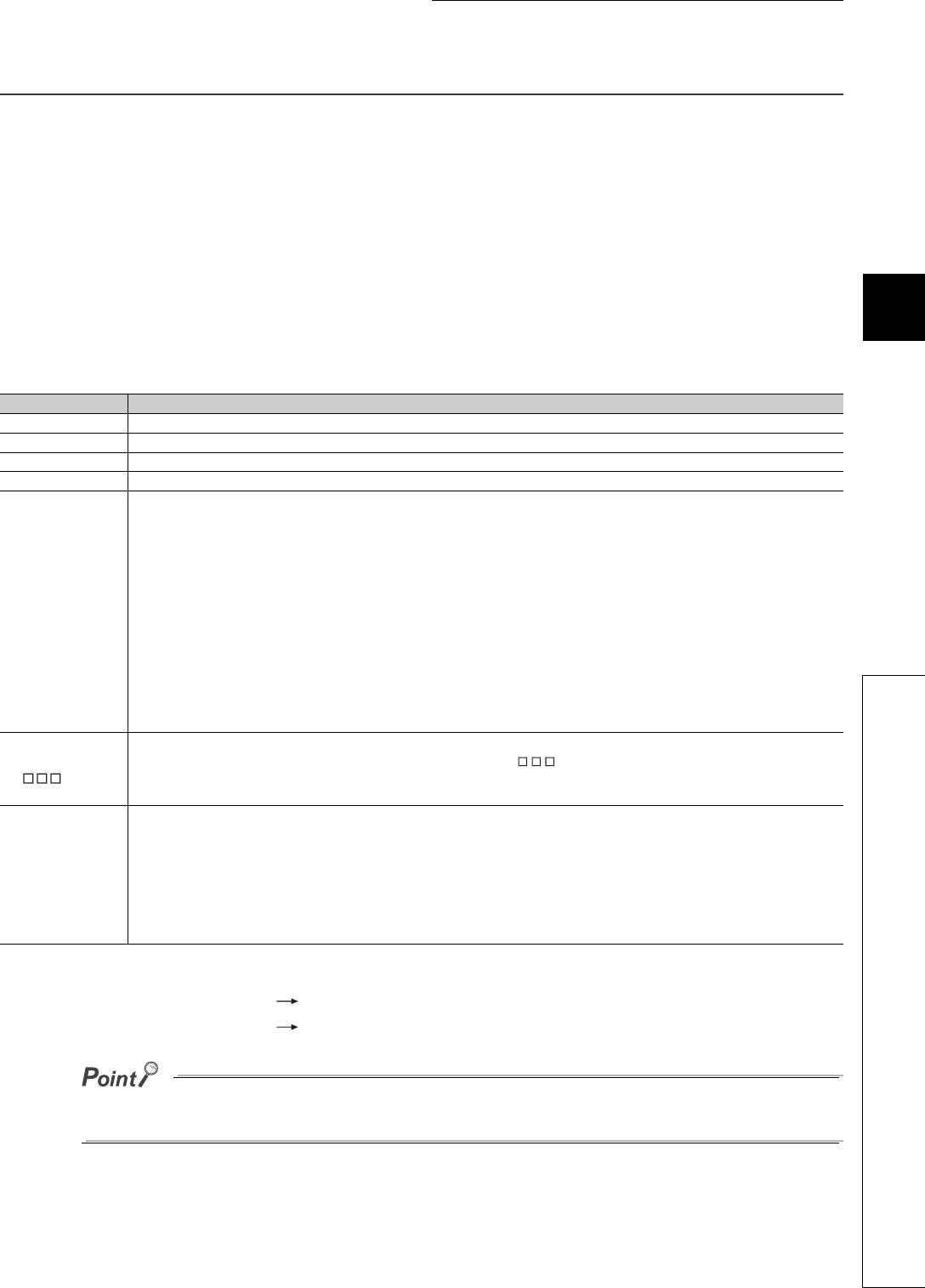
12 - 27
CHAPTER12 PECIAL RELAY LIST AND SPECIAL REGISTER LIST
1
2
3
12
6
7
8
12.2 SPECIAL REGISTER LIST
12.2 SPECIAL REGISTER LIST
The special registers, SD, are internal registers with fixed applications in the Programmable
Controller.
For this reason, it is not possible to use these registers in sequence programs in the same way
that normal registers are used.
However, data can be written as needed in order to control the CPU modules.
Data stored in the special registers are stored as BIN values if no special designation has been
made to the contrary.
The heading descriptions in the following special register lists are shown in 4.1.
For details on the following items, refer to the following manuals:
• Networks Manual of the corresponding network module
• SFC QCPU(Q mode)/QnACPU Programming Manual (SFC)
Do not change the values of special relays set by the system with user program or device test operations.
Doing so may result in system downtime or communication fault.
Table12.17 Descriptions of the special register lists headings
Item Function of Item
Number • Indicates special register number
Name • Indicates name of special register
Meaning • Indicates contents of special register
Explanation • Discusses contents of special register in more detail
Set by
(When set)
• Indicates whether the relay is set by the system or user, and, if it is set by the system, when setting is performed.
<Set by>
S : Set by system
U : Set by user (sequence programs or test operations from GX Developer)
S/U : Set by both system and user
<When set>
Indicated only for registers set by system
Each END : Set during each END processing
Initial : Set only during initial processing (when power supply is turned ON, or when going from STOP to RUN)
Status change : Set only when there is a change in status
Error : Set when error occurs
Instruction execution : Set when instruction is executed
Request : Set only when there is a user request (through SM, etc.)
System switching : Set when system switching is executed.
Corresponding ACPU
M9
• Indicates corresponding special register in ACPU
(When the contents are changed, the special register is represented D9 format change. Incompatible with the Q00J/Q00/Q01
and QnPRH.)
• New indicates the special register newly added to the Q series CPU module.
Corresponding CPU
Indicates the relevant CPU module.
QCPU : Indicates all the Q series CPU modules.
Q00J/Q00/Q01 : Indicates the Basic model QCPU.
Qn(H) : Indicates the High Performance model QCPU.
QnPH : Indicates the Process CPU.
QnPRH : Indicates the Redundant CPU.
QnU : Indicates the Universal model QCPU
Each CPU type name : Can be applied only to the specific CPU. (e.g. Q02U)

12 - 28
(1) Diagnostic Information
Table12.18 Special register
Number Name Meaning Explanation Set by
(When Set)
Corres-
ponding
ACPU
D9
Corresponding
CPU
SD0 Diagnostic
errors
Diagnosis error
code
• Error codes for errors found by diagnosis are stored as BIN data.
• Contents identical to latest fault history information. S (Error)
D9008
format
change
QCPU
SD1
Clock time for
diagnosis error
occurrence
Clock time for
diagnosis error
occurrence
• Year (last two digits) and month that SD0 data was updated is stored as
BCD 2-digit code.
S (Error) New
SD2
• The day and hour that SD0 was updated is stored as BCD 2-digit code.
SD3
• The minute and second that SD0 data was updated is stored as BCD 2-
digit code.
SD4
Error
information
categories
Error information
category code
Category codes which help indicate what type of information is being
stored in the common information areas (SD5 through SD15) and the
individual information areas (SD16 through SD26) are stored here.
The category code for judging the error information type is stored.
• The common information category codes store the following codes:
0 : No error
1: Unit/module No./ CPU No./Base No.*
2: File name/Drive name
3: Time (value set)
4: Program error location
5: System switching cause (for Redundant CPU only)
6: Reason(s) for tracking capacity excess error (specific to Redundant
CPU)
7: Base No./Power supply No. (The first 5 digits of serial number 10072
or higer are chosen for Universal model QCPU.)
8: Tracking transmission data classification (specific to Redundant CPU)
*: For a multiple CPU system that consists of the Basic model QCPU,
High Performance model QCPU, Process CPU, Universal model
QCPU the module number or CPU number is stored depending on the
error that occurred.
(Refer to the corresponding error code for which number has been
stored.)
CPU No. 1: 1, CPU No. 2: 2, CPU No. 3: 3, CPU No. 4: 4
• The individual information category codes store the following codes:
0: No error
1: (Empty)
2: File name/Drive name
3: Time (value actually measured)
4: Program error location
5: Parameter number
6: Annunciator number
7: CHK instruction failure No. (except for the Basic model QCPU and the
Universal model QCPU)
8: Reason(s) for system switching failure (specific to Redundant CPU)
12: File diagnostic information (specific to the Universal model QCPU)
13: Parameter No./CPU No. (specific to the Universal model QCPU)
S (Error) New
b15 b7 b0b8
to to
Year (0 to 99) Month (1 to 12)
(Example) October, 1995
9510H
b15 b7 b0b8
to to
Day (1 to 31) Hour (0 to 23)
(Example) 10 a.m. on 25th
2510H
b15 b7 b0b8to to
Minutes (0 to 59) Seconds (0 to 59)
(Example) 35 min. 48 sec.
3548
H
b15 b7 b0b8
to to
Individual information
category codes
Common information
category codes

12 - 29
CHAPTER12 PECIAL RELAY LIST AND SPECIAL REGISTER LIST
1
2
3
12
6
7
8
12.2 SPECIAL REGISTER LIST
Table12.18 Special register
Number Name Meaning Explanation Set by
(When Set)
Corres-
ponding
ACPU
D9
Corresponding
CPU
SD5
Error common
information
Error common
information
• Common information corresponding to the error codes (SD0) is stored
here.
• The following ten types of information are stored here:
• The error common information type can be judged by the "common infor-
mation category code" in SD4. (The values of the "common information
category code" stored in SD4 correspond to following 1) to 8).)
1) Slot No.
*1: For a multiple CPU system that consists of the Basic model QCPU, High
Performance model QCPU, Process CPU, Universal model QCPU, the
slot number or CPU number is stored depending on the error that
occurred.
Slot 0 in the multiple CPU system is the one on the slot on the right of the
rightmost CPU module.
(Refer to the corresponding error code for which number has been
stored.)
No. 1 CPU: 1, No. 2 CPU: 2, No. 3 CPU: 3, No. 4 CPU: 4
*2: If a fuse blown or I/O verify error occurred in the module loaded in the
MELSECNET/H remote I/O station, the network number is stored into the
upper 8 bits and the station number into the lower 8 bits.
Use the I/O No. to check the module where the fuse blown or I/O verify
error occurred.
*3: 255 is stored into SD5 of the Basic model QCPU when an instruction, etc.
has been executed for the module later than the one on the last slot
where a module can be mounted.
*4: Definitions of base No. and slot No.
<Base No.>
Value used to identify the base unit on which the CPU module has
been mounted. The following shows the definition of the base No.
<Slot No.>
Value used to identify the slot of each base unit and the module
mounted on that slot.
•The I/O slot 0 (slot on the right side of the CPU slot) of the main base
unit is defined as the slot of "Slot No. = 0".
•The slot Nos. are consecutively assigned to the slots of the base
units in order of the main base unit and extension base units 1 to 7.
•When the number of base unit slots has been set in the I/O
assignment setting of the PLC parameter dialog box, the slot Nos.
are assigned for only the number of set slots.
*5: When 0FFFFH is stored into SD6 (I/O No.), the I/O No. cannot be
identified due to overlapping I/O No., etc. in the I/O assignment setting of
the PLC parameter dialog box. Therefore, identify the error location using
SD5.
2) File name/Drive name
S (Error) New QCPU
SD6
SD7
SD8
SD9
SD10
SD11
SD12
SD13
SD14
SD15
1, 2, 3, 4
SD5
SD6
SD7
SD8
SD9
SD10
SD11
SD12
SD13
SD14
SD15
Number
Slot No./CPU No./Base No.
I/O No. 5
Meaning
(Empty)
0
1 to 7
Base No.
Indicates the main base unit mounted with the CPU
module.
Indicates the extension base unit. The stage
number setting made by the stage number setting
connector on the extension base unit is the base
No.
When stage number setting is extension 1:
Base No. = 1
when stage number setting is extension 7:
Base No. = 7
Definition
SD5
SD6
SD7
SD8
SD9
SD10
SD11
SD12
SD13
SD14
SD15
2EH(.)
6
ABCDEFGH. IJK
42H(B) 41H(A)
44H(D) 43H(C)
46H(F) 45H(E)
48H(H) 47H(G)
49H(I) 2EH(.)
4BH(K) 4AH(J)
b15 to b8 b7 to b0
Number Meaning
Drive
File name
(ASCII code: 8 characters)
Extension
(ASCII code: 3 characters)
(Empty)
(Example) File name =
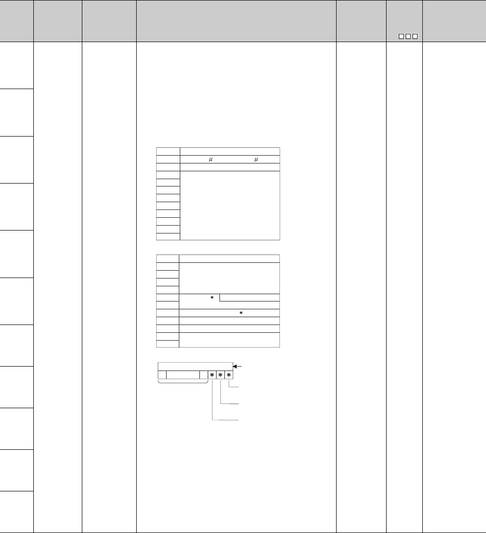
12 - 30
Table12.18 Special register
Number Name Meaning Explanation Set by
(When Set)
Corres-
ponding
ACPU
D9
Corresponding
CPU
SD5
Error common
information
Error common
information
3) Time (value set)
4) Program error location
*7 : Contents of pattern data
S (Error) New QCPU
SD6
SD7
SD8
SD9
SD10
SD11
SD12
SD13
SD14
SD15
SD5
SD6
SD7
SD8
SD9
SD10
SD11
SD12
SD13
SD14
SD15
Number Meaning
Time : 1 s units (0 to 999 s)
Time : 1ms units (0 to 65535ms)
(Empty)
SD5
SD6
SD7
SD8
SD9
SD10
SD11
SD12
SD13
SD14
SD15
6
7
Number Meaning
File name
(ASCII code: 8 characters)
Extension 2E
H
(.)
(ASCII code: 3 characters)
Pattern
Block No.
Step No./transition condition
Sequence step No. (L)
Sequence step No. (H)
0000 to
0123415 14 to
(Not used)
(Bit number)
SFC block designation present
(1)/absent (0)
SFC transition designation present
(1)/absent (0)
SFC step designation present
(1)/absent (0)
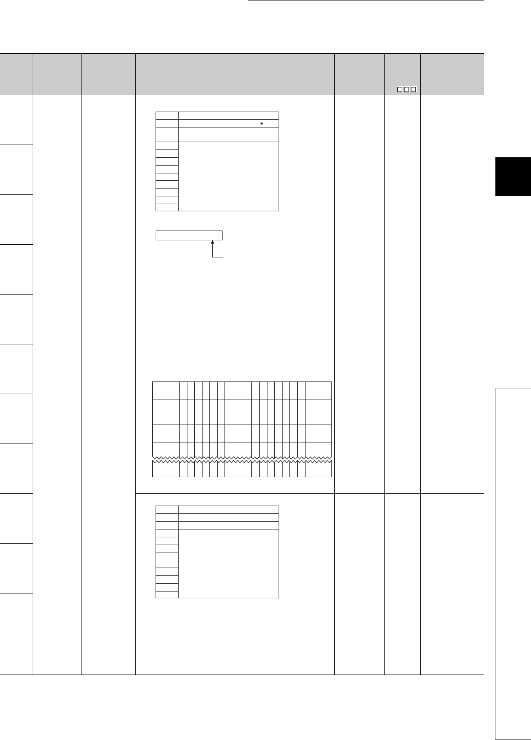
12 - 31
CHAPTER12 PECIAL RELAY LIST AND SPECIAL REGISTER LIST
1
2
3
12
6
7
8
12.2 SPECIAL REGISTER LIST
*1: The module whose first 5 digits of serial No. is "07032" or later.
*2: The module whose first 5 digits of serial No. is "10042" or later.
Table12.18 Special register
Number Name Meaning Explanation Set by
(When Set)
Corres-
ponding
ACPU
D9
Corresponding
CPU
SD5
Error common
information
Error common
information
5) Reason(s) for system switching
*13: Details of reason(s) for system switching
6) Reason(s) for tracking capacity excess error
The block No. when the data amount that can be tracked (100k) is
exceeded is indicated by the bit pattern of the corresponding special
relay.
S (Error) New QnPRH
SD6
SD7
SD8
SD9
SD10
SD11
SD12
SD13
7) Power supply No.
S (Error) New
Qn(H)*1
QnPH*1
QnPRH
QnU*2
SD14
SD15
SD5
SD6
SD7
SD8
SD9
SD10
SD11
SD12
SD13
SD14
SD15
Number Meaning
System switching condition 13
Control system switching
instruction argument
(Empty)
1 : Power-OFF, reset, hardware failure,
watchdog timer error
2 : Stop error
(except watchdog timer error)
3 : System switching request by
network module
16 : Control system switching instruction
17 : Control system switching request
from GX Developer
0 : No system switching condition
(default)
SD15
SD5
SD8
SD9
SD6
SD7
0 000000 0 0 0000000
1
(SM1535)
(Block16)
0
b15 b14
0
b13
0
b12
0
b11
0
b10
0
b9
1
(SM1528)
(Block9)
0
b8
1
(SM1520)
(Block1)
b0b7
0
b6
0
b5
0
b4
0
b3
0
b2
0
0 000000 0 0 0000000
0 000000 0 0 0000000
b1
1
(SM1583)
(Block64)
000000 0 0
1
(SM1568)
(Block49)
000000
0 000000 0 0 0000000
1: Power supply 1 fault
2: Power supply 2 fault
Redundant power supply module
mounted on POWER 1 slot of redundant
base unit (Q38RB, Q68RB, Q65WRB)
"Power
supply
module 1":
Redundant power supply module
mounted on POWER 2 slot of redundant
base unit (Q38RB, Q68RB, Q65WRB)
"Power
supply
module 2":
SD5
SD6
SD7
SD8
SD9
SD10
SD11
SD12
SD13
SD14
SD15
Number Meaning
Base No.
Power supply No.
(Empty)
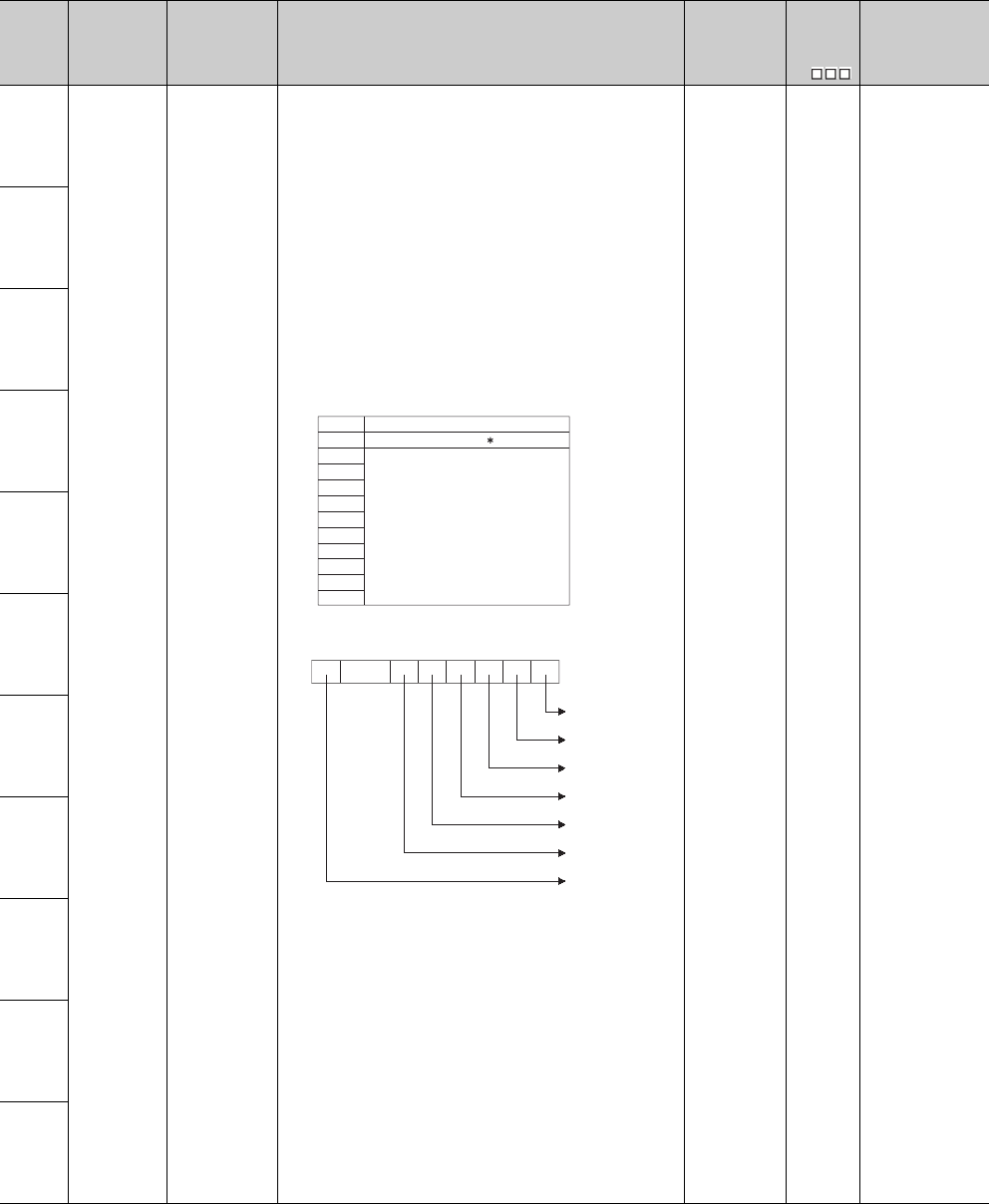
12 - 32
Table12.18 Special register
Number Name Meaning Explanation Set by
(When Set)
Corres-
ponding
ACPU
D9
Corresponding
CPU
SD5
Error common
information
Error common
information
8) Tracking transmission data classification
Stores the data classification during tracking.
*15: Details of data classification S (Error) New QnPRH
SD6
SD7
SD8
SD9
SD10
SD11
SD12
SD13
SD14
SD15
SD5
SD6
SD7
SD8
SD9
SD10
SD11
SD12
SD13
SD14
SD15
Number Meaning
Data type 15
(Empty)
b15 b5 b4 b3 b2 b1 b0tob14
0
b6 Each bit
Device data
Signal flow
PIDINIT/S. PIDINIT
instruction data
SFC execution data
System switching
request
Operation mode
change request
System data
0: Not sent
1: Being sent
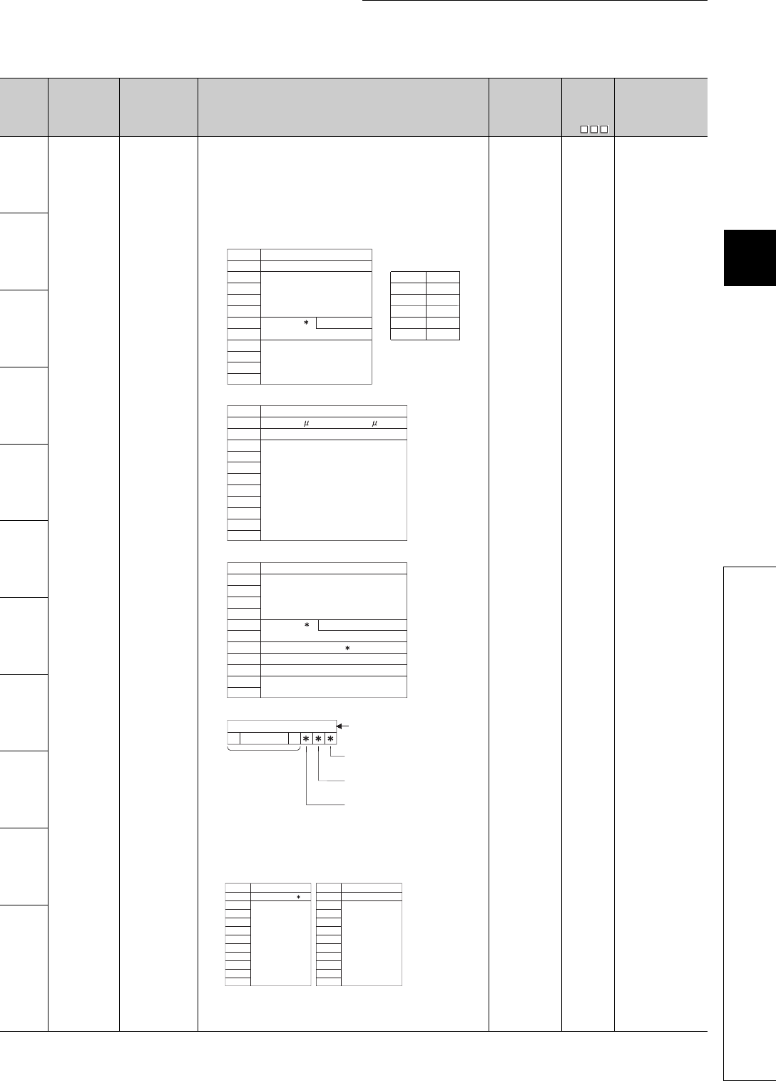
12 - 33
CHAPTER12 PECIAL RELAY LIST AND SPECIAL REGISTER LIST
1
2
3
12
6
7
8
12.2 SPECIAL REGISTER LIST
Table12.18 Special register
Number Name Meaning Explanation Set by
(When Set)
Corres-
ponding
ACPU
D9
Corresponding
CPU
SD16
Error individual
information
Error individual
information
• Individual information corresponding to error codes (SD0) is stored here.
• There are the following eight different types of information are stored.
• The error individual information type can be judged by the "individual
information category code" in SD4. (The values of the "individual infor-
mation category code" stored in SD4 correspond to following 1) to 8),
12), and 13).)
1) (Empty)
2) File name/Drive name
3) Time (value actually measured)
4) Program error location
*7 : Contents of pattern data
*16: For details of the parameter No., refer to the User's Manual
(Function Explanation, Program Fundamentals) of the CPU
module used.
S (Error) New QCPU
SD17
SD18
SD19
SD20
SD21
SD22
SD23
SD24
SD25
SD26
SD16
SD17
SD18
SD19
SD20
SD21
SD22
SD23
SD24
SD25
SD26
6
ABCDEFGH. IJK
42H(B) 41H(A)
44H(D) 43H(C)
46H(F) 45H(E)
48H(H) 47H(G)
49H(I) 2EH(.)
4BH(K) 4AH(J)
b15 to b8 b7 to b0
Number Meaning
Drive
File name
(ASCII code: 8 characters)
Extension 2EH(.)
(ASCII code: 3 characters)
(Empty)
(Example) File name =
SD16
SD17
SD18
SD19
SD20
SD21
SD22
SD23
SD24
SD25
SD26
Number Meaning
Time : 1 s units (0 to 999 s)
Time : 1ms units (0 to 65535ms)
(Empty)
SD16
SD17
SD18
SD19
SD20
SD21
SD22
SD23
SD24
SD25
SD26
Number Meaning
File name
(ASCII code: 8 characters)
Extension 6 2EH
(.)
(ASCII code: 3 characters)
Pattern 7
Block No.
Step No./transition No.
Sequence step No. (L)
Sequence step No. (H)
0000 to
0
12
3
4
15 14 to
(Not used)
(Bit number)
SFC block designation
present (1)/absent (0)
SFC step designation
present (1)/absent (0)
SFC transition designation
present (1)/absent (0)
SD16
SD17
SD18
SD19
SD20
SD21
SD22
SD23
SD24
SD25
SD26
SD16
SD17
SD18
SD19
SD20
SD21
SD22
SD23
SD24
SD25
SD26
Number Meaning Number Meaning
Parameter No. 16 No.
(Empty) (Empty)
Annunciator number /
CHK instruction
malfunction number
6)Parameter No.5)
7)

12 - 34
*6 : Extensions are shown below.
Table12.19 Extension name
SDn SDn+1 Extension
Name File Type
Higher 8 bits Lower 8 bits Higher 8 bits
51H50H41HQPA Parameters
51H50H47HQPG • Sequence program
• SFC program
51H43H44HQCD Device comment
51H44H49HQDI Initial device value
51H44H52HQDR File register
51H44H4CHQDL Local device
(Other than the Basic model QCPU)
51H54H44HQTD Sampling trace data
(Other than the Basic model QCPU)
51H46H44HQFD
Breakdown history data
(Other than the Basic model QCPU and
the Universal model QCPU)
51H53H54HQST SP.DEVST/S.DEVLD instruction file
(For Universal model QCPU only)

12 - 35
CHAPTER12 PECIAL RELAY LIST AND SPECIAL REGISTER LIST
1
2
3
12
6
7
8
12.2 SPECIAL REGISTER LIST
Table12.18 Special register
Number Name Meaning Explanation Set by
(When Set)
Corres-
ponding
ACPU
D9
Corresponding
CPU
SD26 Error individual
information
Error individual
information
8) Reason(s) for system switching failure
*14: Details of reason(s) for system switching failure
S (Error) New
QnPRH
12) File diagnostic information
13) Parameter No./CPU No. QnU
SD16
SD17
SD18
SD19
SD20
SD21
SD22
SD23
SD24
SD25
SD26
Number Meaning
System switching prohibition
condition 14
(Empty)
10 : Error detected by network
module of standby system
7 : Operation differs between two
systems (in backup mode only)
3 : Hardware failure, power OFF,
reset or watchdog timer error
occurring in control system
9 : Online program change
11 : System switching being executed
12 : Online module change in
progress
8 : During memory copy from control
system to standby system
6 : Standby system is in stop error
(except watchdog timer error)
4 : Preparing for tracking
5 : Time limit exceeded
2 : Hardware failure, power OFF,
reset or watchdog timer error
occurring in standby system
0 : Normal switching completion
(default)
1 : Tracking cable fault (cable
removal, cable fault, internal
circuit fault, hardware fault)
SD17
SD18
SD19
SD20
File name
(ASCll: 8 characters)
SD21
SD22
SD23
SD24
SD16 drive No.(L)
SD25
SD26
Failuer information (H)
Failure information 2
(CRC value that is read)
EXtension *6 2EH(.)
(ASCll; 3 characters)
Failure information 3
(CRC value that is calculated)
SD17
SD18
SD19
SD20
SD21
SD22
SD23
SD24
SD16
SD25
SD26
Parameter No.*16
(Empty)
Number Meaning
CPU No. (1 to 4)
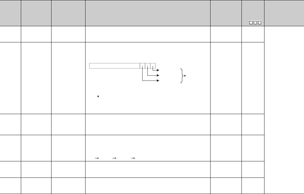
12 - 36
Table12.18 Special register
Number Name Meaning Explanation Set by
(When Set)
Corres-
ponding
ACPU
D9
Corresponding
CPU
SD50 Error reset
Error number that
performs error
reset
• Stores error number that performs error reset U New
QCPU
SD51 Battery low
latch
Bit pattern
indicating where
battery voltage
drop occurred
• All corresponding bits go 1(ON) when battery voltage drops.
• Subsequently, these remain 1(ON) even after battery voltage has been
returned to normal.
• In the alarm, data can be held within the time specified for battery low.
• The error indicates the complete discharge of the battery.
S (Error) New
SD52 Battery low
Bit pattern
indicating where
battery voltage
drop occurred
• Same configuration as SD51 above
• After the alarm is detected (ON), the alarm turns OFF by error detection
(ON). (For the Universal model QCPU only)
• Turns to 0 (OFF) when the battery voltage returns to normal thereafter.
S (Error) New
SD53 AC/DC DOWN
detection
Number of times
for AC/DC DOWN
detection
• Every time the input voltage falls to or below 85% (AC power)/65% (DC
power) of the rating during operation of the CPU module, the value is
incremented by 1 and stored in BIN code.
• The counter repeats increment and decrement of the value ;
0 32767 -32768 0
S (Error) D9005
SD60
Number of
module with
blown fuse
Number of module
with blown fuse
• Value stored here is the lowest station I/O number of the module with
the blown fuse. S (Error) D9000
SD61
I/O module
verify error
number
I/O module verify
error module
number
• The lowest I/O number of the module where the I/O module verification
number took place. S (Error) D9002
0
b3 b2 b1 b0
CPU error
1: This does not apply to Basic model QCPU.
alarm
error
b15 to
1
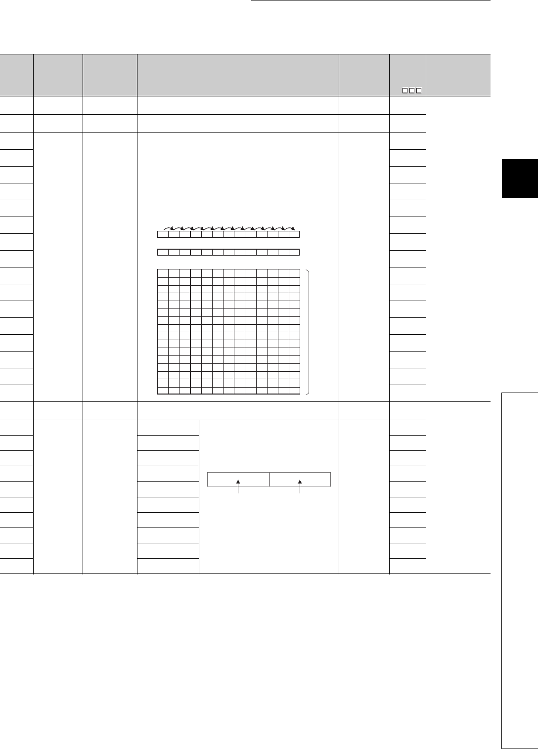
12 - 37
CHAPTER12 PECIAL RELAY LIST AND SPECIAL REGISTER LIST
1
2
3
12
6
7
8
12.2 SPECIAL REGISTER LIST
Table12.18 Special register
Number Name Meaning Explanation Set by
(When Set)
Corres-
ponding
ACPU
D9
Corresponding
CPU
SD62 Annunciator
number
Annunciator
number • The first annunciator number (F number) to be detected is stored here. S (Instruction
execution) D9009
QCPU
SD63 Number of
annunciators
Number of
annunciators • Stores the number of annunciators searched. S (Instruction
execution) D9124
SD64
Table of
detected
annunciator
numbers
Annunciator
detection number
When F goes ON due to OUT F or SET F instruction, the F numbers which
go progressively ON from SD64 through SD79 are registered.
The F numbers turned OFF by RST F instruction are deleted from SD64 -
SD79, and the F numbers stored after the deleted F numbers are shifted to
the preceding registers.
Execution of the LEDR instruction shifts the contents of SD64 to SD79 up
by one.
After 16 annunciators have been detected, detection of the 17th will not be
stored from SD64 through SD79.
S (Instruction
execution)
D9125
SD65 D9126
SD66 D9127
SD67 D9128
SD68 D9129
SD69 D9130
SD70 D9131
SD71 D9132
SD72 New
SD73 New
SD74 New
SD75 New
SD76 New
SD77 New
SD78 New
SD79 New
SD80 CHK number CHK number • Error codes detected by the CHK instruction are stored as BCD code. S (Instruction
execution) New
Qn(H)
QnPH
QnPRH
SD90
Step transition
monitoring timer
setting value
(Enabled only
when SFC
program exists)
F number for timer
set value and time
over error
Corresponds to
SM90 • Set the annunciator number (F number) that will
be turned ON when the step transition
monitoring timer setting or monitoring timeout
occurs.
• Turning ON any of SM90 to SM99 during an
active step starts the timer, and if the transition
condition next to the corresponding step is not
met within the timer time limit, the set
annunciator (F) turns ON.
U
D9108
SD91 Corresponds to
SM91 D9109
SD92 Corresponds to
SM92 D9110
SD93 Corresponds to
SM93 D9111
SD94 Corresponds to
SM94 D9112
SD95 Corresponds to
SM95 D9113
SD96 Corresponds to
SM96 D9114
SD97 Corresponds to
SM97 New
SD98 Corresponds to
SM98 New
SD99 Corresponds to
SM99 New
SD62 0 50 50 50 50 50 50 50 50 50 50 50 99 (Number
detected)
SD63 0 1 2 3 2 3 4 5 6789 8
0 505050505050505050505099SD64
SD65
SD66
SD67
SD68
SD69
SD70
SD71
SD72
SD73
SD74
SD75
SD76
SD77
SD78
SD79
0 0 25 25 99 99 99 99 99 99 99 99 15
0 0 0 99 0 15 15 15 15 15 15 15 70
0 0 0 0 0 0 70 70 70 70 70 70 65
0 0 0 0 0 0 0 65 65 65 65 65 38
0000000038383838
110
0 0 0 0 0 0 0 0 0 110 110 110 151
0 0 151
0
00000000 151
210
000000000 0 0210
0000000000 0 00
0000000000 0 00
0000000000 0 00
0000000000 0 00
0000000000 0 00
0000000000 0 00
0000000000 0 00
(Number of
annunciators
detected)
(Number
detected)
SET
F50
SET
F25
SET
F99
RST
F25
SET
F15
SET
F70
SET
F65
SET
F38
SET
F110
SET
F151
SET
F210 LEDR
b15 b7 b0b8
F number setting
(0 to 255)
Timer time limit
setting
(1 to 255s:
(1s units))
to to
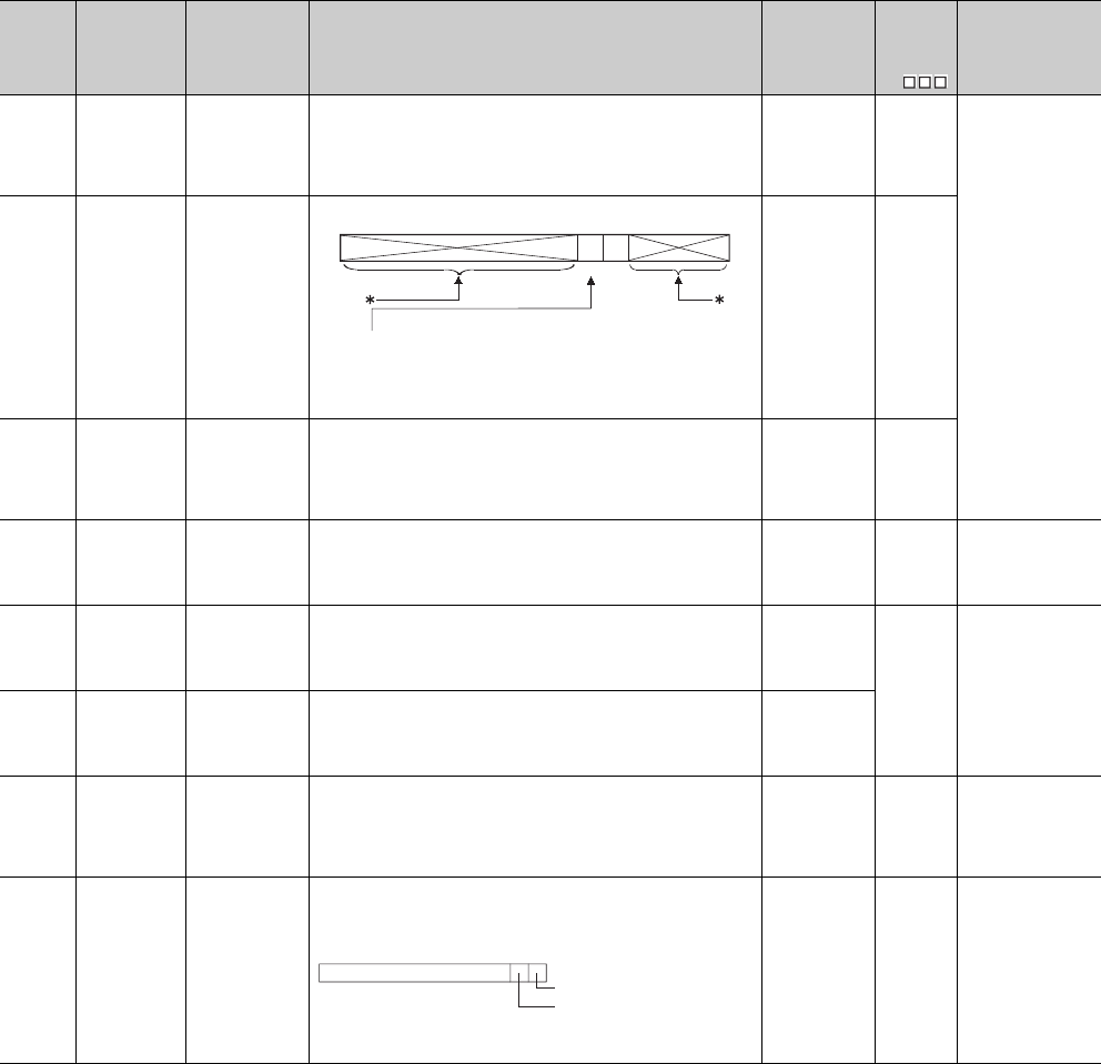
12 - 38
*3: This applies to Universal model QCPUs except for the Built-in Ethernet port QCPU.
*4: The module whose first 5 digits of serial No. is "10102" or later.
Table12.18 Special register
Number Name Meaning Explanation Set by
(When Set)
Corres-
ponding
ACPU
D9
Corresponding
CPU
SD100
Transmission
speed storage
area
Stores the
transmission
speed specified in
the serial
communication
setting.
96 : 9.6kbps, 192 : 19.2kbps, 384 : 38.4kbps,
576 : 57.6kbps, 1152 : 115.2kbps
S (Power-ON or
reset) New
Q00/Q01
Q00UJ
Q00U
Q01U
Q02U*4
SD101
Communication
setting storage
area
Stores the
communication
setting specified in
the serial
communication
setting.
* : Since the data is used by the system, it is undefined.
S (Power-ON or
reset) New
SD102
Transmission
wait time
storage area
Stores the
transmission wait
time specifed in
the serial
communication
setting.
0 : No waiting time
10 to 150: Waiting time (unit: ms)
Defaults to 0.
S (Power-ON or
reset) New
SD105
CH1
transmission
speed setting
(RS-232)
Stores the preset
transmission
speed when GX
Developer is
used.
96 : 9600bps, 192 : 19.2kbps, 384 : 38.4kbps,
576 : 57.6kbps, 1152 : 115.2kbps
*: Other than RS-232 connection holds the data at RS-232 connection.
(When disconnected, the default value is 1152.)
SNew
Qn(H)
QnPH
QnPRH
QnU*3
SD110
Data sending
result storage
area
Stores the data
sending result
when the serial
communication
function is used.
Stores the error code at the timeout sending data. S (Error)
New
Q00/Q01
Q00UJ
Q00U
Q01U
Q02U*4
SD111
Data receiving
result storage
area
Stores the data
receiving result
when the serial
communication
function is used.
Stores the error code at the time of receiving data. S (Error)
SD118
Amount of
battery
consumption
Amount of battery
consumption
Displays the current amount of battery consumption.
The value range:1 to 2(Q00UJCPU, Q00UCPU, Q01UCPU,
Q02UCPU, Q03UD(E)CPU, Q04UD(E)HCPU)
1 to 3(Q06UD(E)HCPU)
1 to 4(Q10UD(E)HCPU, Q20UD(E)HCPU,
Q13UD(E)HCPU, Q26UD(E)HCPU)
S (Status
change) New QnU*4
SD119
Battery life-
prolonging
factor
Battery life-
prolonging factor
Stores the factor which makes the battery life-prolonging function valid.
When SD119 is other than 0, the battery life-prolonging function is valid.
S (Status
change) New QnU
b0
to
b3b4b5b6
b15 to
Sumcheck presence
0: Absent
1: Present
0: Disabled
1: Enabled
Write during RUN setting
b0: CPU switch setting
0:No factor
1:Foctor
b1: Backup in execution by
latch data backup function
(to standard ROM)
b15 to
b2 b1 b0

12 - 39
CHAPTER12 PECIAL RELAY LIST AND SPECIAL REGISTER LIST
1
2
3
12
6
7
8
12.2 SPECIAL REGISTER LIST
Table12.18 Special register
Number Name Meaning Explanation Set by
(When Set)
Corres-
ponding
ACPU
D9
Corresponding
CPU
SD130
Fuse blown
module
Bit pattern in units
of 16 points,
indicating the
modules whose
fuses have blown
0: No blown fuse
1: Blown fuse
present
• The numbers of output modules whose fuses have blown are input as a
bit pattern (in units of 16 points).
(If the module numbers are set by parameter, the parameter-set
numbers are stored.)
• Not cleared even if the blown fuse is replaced with a new one.
This flag is cleared by error resetting operation
S (Error) New Q00J/Q00/Q01
SD131
SD132
SD133
SD134
SD135
SD136
SD137
SD150
I/O module
verify error
Bit pattern, in units
of 16 points,
indicating the
modules with
verify errors.
0: No I/O verify
errors
1: I/O verify error
present
• When I/O modules, of which data are different from those entered at
power-ON, have been detected, the I/O module numbers (in units of 16
points) are entered in bit pattern. (Preset I/O module numbers set in
parmeters when parameter setting has been performed.)
• Not cleared even if the blown fuse is replaced with a new one.
This flag is cleared by error resetting operation.
SD151
SD152
SD153
SD154
SD155
SD156
SD157
b15 b14 b13 b12 b11b10 b9 b8 b7 b6 b5 b4 b3 b2 b1 b0
0001
(YC0) 000 00000000
1
(Y80)
SD130
00
1
(Y1F0) 0 0 00000000
1
(Y1A0)
SD131 00
00 1
(Y7B0) 00000 000
SD137 0001
(Y730)
0
Indicates fuse blow.
b15 b14 b13 b12 b11 b10 b9 b8 b7 b6 b5 b4 b3 b2 b1 b0
000 000 0000000
SD150
00 0 00000000SD151 00
0 0 0000 000SD157 0000
Indicates an I/O module verify error.
00
00
00
1
()
X Y
7E0
1
()
X Y
0
1
()
X Y
190
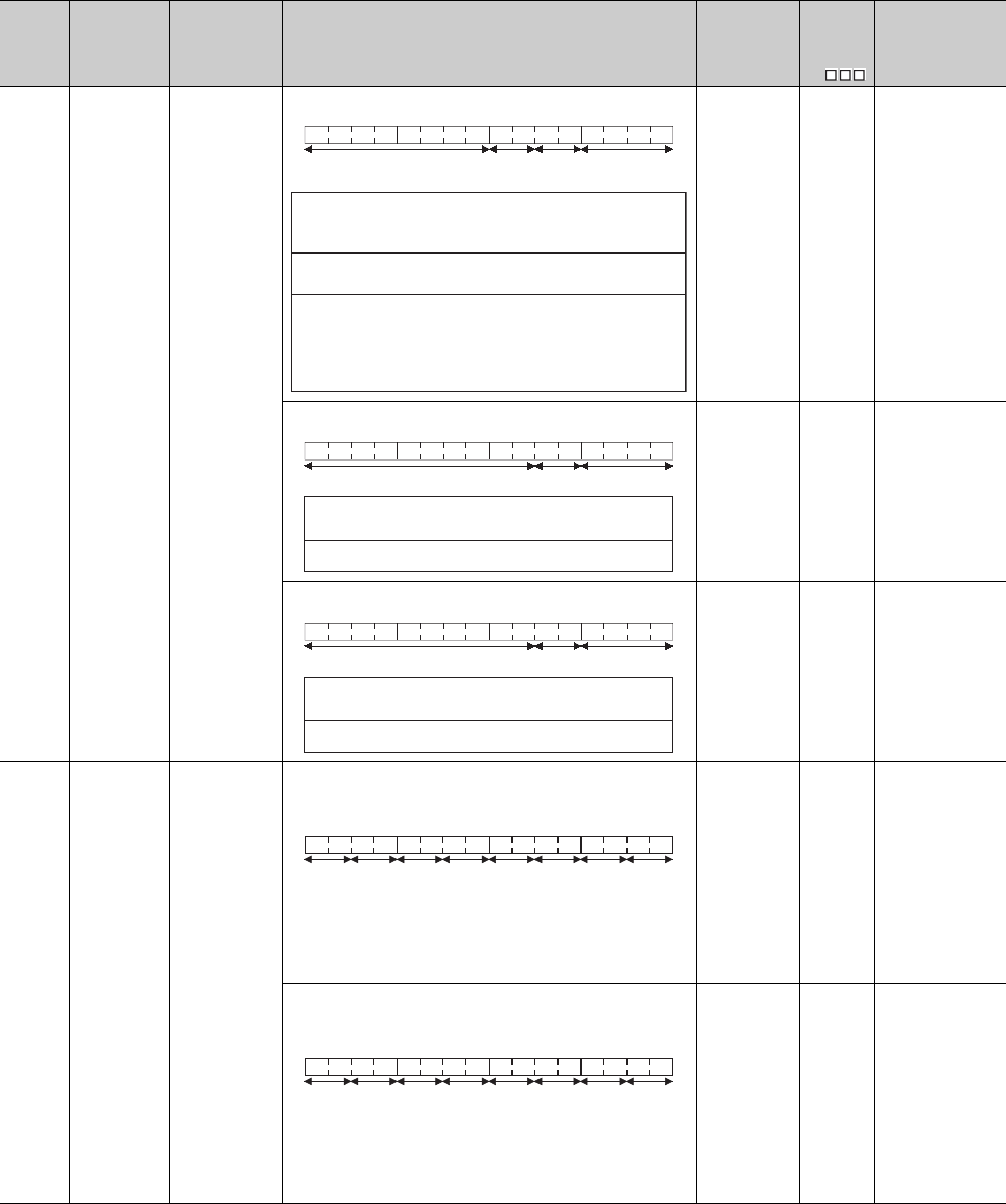
12 - 40
(2) System information
Table12.20 Special register
Number Name Meaning Explanation Set by
(When Set)
Corres-
ponding
ACPU
D9
Corresponding
CPU
SD200 Status of switch Status of CPU
switch
• The CPU switch status is stored in the following format:
S (Every END
processing) New Qn(H)
QnPH
QnPRH
• The CPU switch status is stored in the following format:
S (Every END
processing) New Q00J/Q00/Q01
• The CPU switch status is stored in the following format:
S (when RUN/
STOP/RESET
switch changed) New QnU
SD201 LED status Status of
CPU-LED
• The following bit patterns store the status of the LEDs on the CPU
module:
• 0 is off, 1 is on, and 2 is flicker.
1): RUN 5): BOOT
2): ERR. 6): Empty Mode bit pattern
3): USER 7): Empty 0: OFF 1: Green
4): BAT. 8): MODE 2: Orange
(The Basic model QCPU does not include 3) to 8).)
S (Status
change) New
Q00J/Q00/Q01
Qn(H)
QnPH
QnPRH
• The following bit patterns store the status of the LEDs on the CPU
module:
• 0 is off, 1 is on, and 2 is flicker.
1): RUN 5): BOOT
2): ERROR 6): Empty
3): USER 7): Empty
4): BAT. 8): MODE
(The Q00UJCPU, Q00UCPU, and Q01UCPU do not include 5).)
S (Status
change) New QnU
b15 b12 b11 b8 b7 b4 b3 b0
1)
2)
Empty
3)
to tototo
1): CPU switch status
0: RUN
1: STOP
2: L.CLR
2): Memory card
switch Always OFF
3): DIP switch
b8 through b12 correspond to
SW1 through SW5 of system
setting switch 1.
0: OFF, 1: ON.
b13 through b15 are empty.
b15 b8 b7 b4 b3 b0
1)2)
Empty
to to
to
1): 0: RUN
1: STOP
2):
CPU switch status
Memory card switch Always OFF
b15 b8 b7 b4 b3 b0
1)2)
Empty
to to
to
1): 0: RUN
1: STOP
2):
CPU switch status
Memory card switch Always OFF
b15 b12 b11 b8 b7 b4b3 b0
1)2)4) 3)5)6)8) 7)
to tototo
b15 b12 b11 b8 b7 b4b3 b0
1)2)4) 3)5)6)8) 7)
to tototo
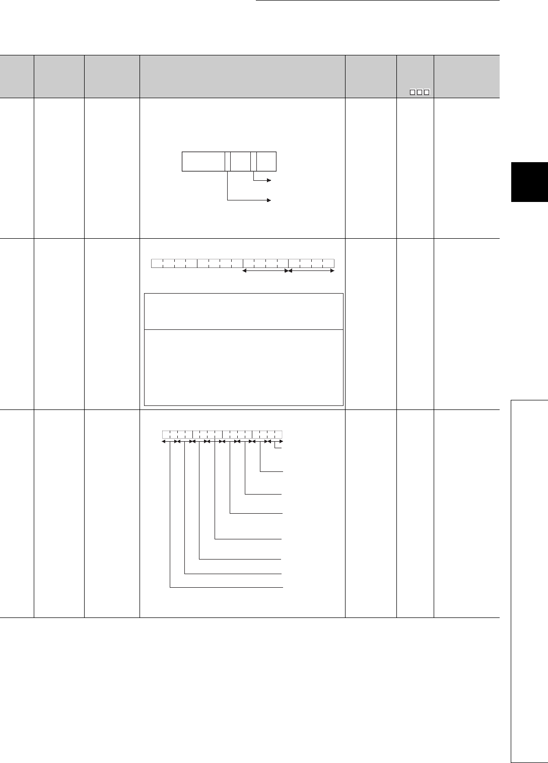
12 - 41
CHAPTER12 PECIAL RELAY LIST AND SPECIAL REGISTER LIST
1
2
3
12
6
7
8
12.2 SPECIAL REGISTER LIST
Table12.20 Special register
Number Name Meaning Explanation Set by
(When Set)
Corres-
ponding
ACPU
D9
Corresponding
CPU
SD202 LED off
command
Bit pattern of LED
that is turned off
• Specify the LEDs to be turned off using this register, and turn SM202
from OFF to ON to turn off the specified LEDs.
USER and BOOT can be specified as the LEDs to be turned off.
• Specify the LEDs to be turned off in the following bit pattern.
(Turned off at 1, not be turned off at 0.)
(The Q00UJCPU, Q00UCPU, and Q01UCPU cannot specify the BOOT
LED.)
UNew
Qn(H)
QnPH
QnPRH
QnU
SD203 Operating
status of CPU
Operating status
of CPU
• The CPU operating status is stored as indicated in the following figure:
S (Every END
processing)
D9015
format
change
QCPU
SD204 LED display
color
CPU-LED display
color
• The LED display color of the LED status shown in SD201 1) to 8).
(The Q00UJCPU, Q00UCPU, and Q01UCPU do not include 5).)
S (status
change) New QnU
b15 b8 b4 b0
USER
LED
BOOT
LED
Fixed
to 0
Fixed
to 0
Fixed
to 0
b15 b12 b11
b8 b7 b4 b3 b0
1)
to to to to
2)
1): Operating status
of CPU
0:
1:
2:
3:
2): STOP/PAUSE
cause
0:
1:
2:
3:
4: Error
RUN
STEP-RUN (For the QnACPU only)
STOP
PAUSE
Instruction in remote operation program
from RUN/STOP switch ("RUN/STOP/
RESET switch" for Basic model QCPU)
Remote contact
Remote operation from GX Developer/
serial communication, etc.
Internal program instruction
Note: Priority is
earliest first
b15 b12 b11 b8 b7 b4b3 b0
1)RUN LED
0: OFF
1: Green
2)ERROR LED
0: OFF
1: Red
3)USER LED
0: OFF
1: Red
4)BAT. LED
0: OFF
1: Yellow
2: Green
8)MODE LED
0: OFF
1: Green
5)BOOT LED
0: OFF
1: Green
6)Empty
7)Empty
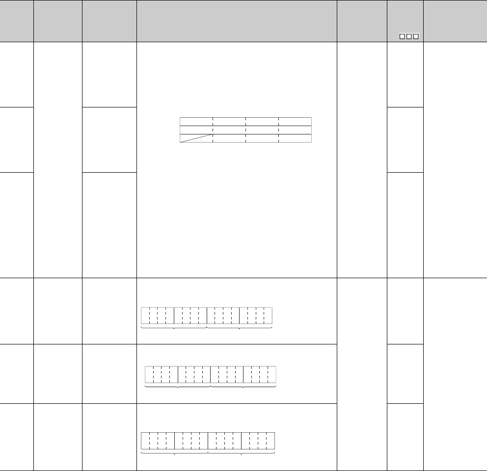
12 - 42
*9: Function version is B or later.
Table12.20 Special register
Number Name Meaning Explanation Set by
(When Set)
Corres-
ponding
ACPU
D9
Corresponding
CPU
SD207
LED display
priority ranking
Priorities 1 to 4
• When error is generated, the LED display (flicker) is made according to
the error number setting priorities.
(The Basic model QCPU supports only the annunciator (error item No.
7).
• The Universal model QCPU sets execution/non-execution of LED
display of the error corresponding to the each priority ranking when the
error occurs.
• The setting areas for priorities are as follows:
Default Value
SD207 = 4321H(0000H for Basic model QCPU)
SD208 = 8765H(0700H for Basic model QCPU)
(0765H for Redundant CPU)
SD209 = 00A9H(0000H for Basic model QCPU)
(0B09H for Redundant CPU)
• No display is made if "0" is set.
• In case of the Basic model QCPU, the ERR. LED turns ON when the
annunciator turns ON, if "7" has been set to either of priorities 1 to 11.
• In case of the Basic model QCPU, the ERR. LED does not turn ON
when the annumciator turns ON, if "7" has not been set to either of
priorities 1 to 11.
However, even if "0" has been set, information concerning CPU module
operation stop (including parameter settings) errors will be indicated by
the LEDs without conditions.
U
D9038
Q00J/ Q00/Q01*9
Qn(H)
QnPH
QnPRH
QnU
SD208 Priorities 5 to 8
D9039
format
change
SD209 Priorities 9 to 11 New
SD210 Clock data Clock data (year,
month)
• The year (last two digits) and month are stored as BCD code as shown
below:
S (Request)/U
D9025
QCPU
SD211 Clock data Clock data (day,
hour)
• The day and hour are stored as BCD code as shown below:
D9026
SD212 Clock data Clock data
(minute, second)
• The minutes and seconds (after the hour) are stored as BCD code as
shown below:
D9027
SD207
SD208
SD209
b15 b12
to
Priority 4
Priority 8
(Priority 11 is valid when Redundant CPU is used.)
b11 b8
to
Priority 3
Priority 7
b3 b0
to
Priority 1
Priority 5
Priority 9
b7 b4
to
Priority 2
Priority 6
Priority 10Priority 11
b15 b12to b11 b8
to b7 b4to b3 b0
to Example:
July, 1993
9307H
Year Month
b15 b12to b11 b8
to b7 b4to b3 b0
to
Day Hour
Example:
31st, 10 a.m.
3110H
b15 b12to b11 b8
to b7 b4to b3 b0
to Example:
35 min, 48 s
3548H
SecondSecondMinute
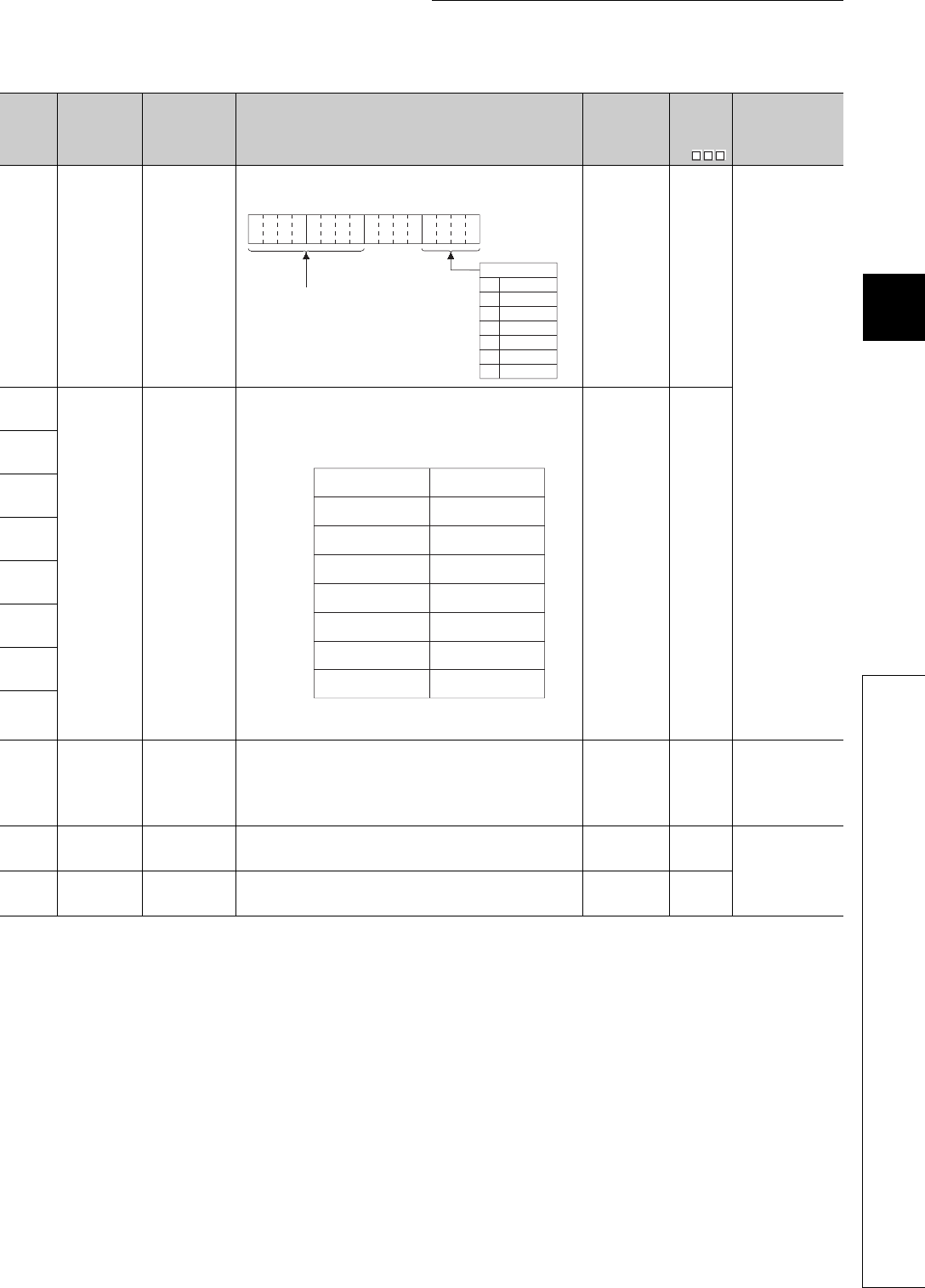
12 - 43
CHAPTER12 PECIAL RELAY LIST AND SPECIAL REGISTER LIST
1
2
3
12
6
7
8
12.2 SPECIAL REGISTER LIST
Table12.20 Special register
Number Name Meaning Explanation Set by
(When Set)
Corres-
ponding
ACPU
D9
Corresponding
CPU
SD213 Clock data
Clock data
(higher digits of
year, day of week)
• The year (first two digits) and the day of the week are stored as BCD
code as shown below.
S (Request)/U D9028
QCPU
SD220
LED display
data LED display data
• LED display ASCII data (16 characters) stored here.
(On the Basic model QCPU, the registers store the message (16
characters of ASCII data) at error occurrence (including annunciator
ON).
• The LED display device data at the time of CHK is not stored in the
Basic model QCPU and the Universal model QCPU.
S (When
changed) New
SD221
SD222
SD223
SD224
SD225
SD226
SD227
SD235
Module to which
online module
change is being
performed
The header I/O
number of the
module to which
online module
change is being
performed /10H
•10H is added to the value of the header I/O number of which the online
module change is being performed.
S (During online
module change) New QnPH
QnPRH
SD240 Base mode
0: Automatic
mode
1: Detail mode
• Stores the base mode. S (Initial) New
QCPU
SD241 Extension stage
number
0: Main base only
1 to 7: Extension
stage number
• Stores the maximum number of the extension bases being installed. S (Initial) New
b15
b12
to b11 b8
to b7 b4
to b3 b0
to
0
1
2
3
4
5
6
Example:
1993, Friday
1905H
Higher digits of year (19 or 20)
Sunday
Saturday
Friday
Thursday
Wednesday
Tuesday
Monday
Day of the week
SD220
SD221
SD222
SD223
SD224
SD225
SD226
SD227
b15 to b8 b7 to b0
15th character from
the right
16th character from
the right
13th character from
the right
14th character from
the right
11th character from
the right
12th character from
the right
9th character from
the right
10th character from
the right
7th character from
the right
8th character from
the right
5th character from
the right
6th character from
the right
3rd character from
the right
4th character from
the right
1st character from
the right
2nd character from
the right
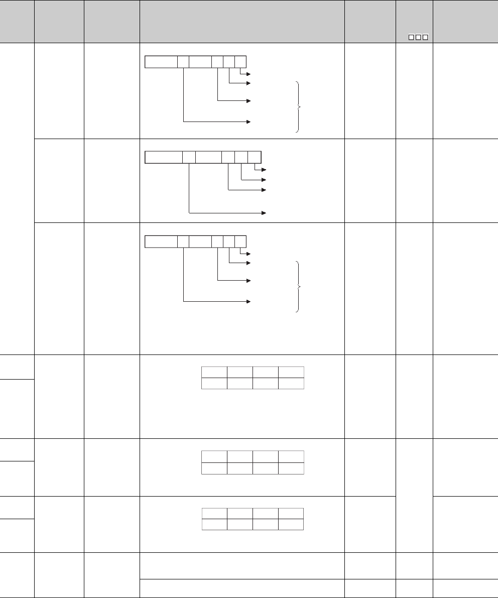
12 - 44
*9: Function version is B or later.
Table12.20 Special register
Number Name Meaning Explanation Set by
(When Set)
Corres-
ponding
ACPU
D9
Corresponding
CPU
SD242
A/Q base
differentiation
Base type
differentiation
0: QA**B is
installed
(A mode)
1: Q**B is installed
(Q mode)
S (Initial) New
Qn(H)
QnPH
QnPRH
Installed Q base
presence/
absence
Base type
differentiation
0: Base not
installed
1: Q**B is installed
S (Initial) New Q00J/Q00/Q01
Installed Q base
presence/
absence
Base type
differentiation
0: Base not
installed
1: Q**B is installed
• The bits from the third extension stage to the seventh extension stage
are fixed to "0" in the Q00UJCPU.
• The bits from the fifth extension stage to the seventh extension stage are
fixed to "0" in the Q00UCPU, Q01UCPU, and Q02UCPU.
S (Initial) New QnU
SD243
No. of base
slots No. of base slots • As shown above, each area stores the number of slots being installed.
• The bits from the third extension stage to the seventh extension stage
are fixed to "0" in the Q00UJCPU.
• The bits from the fifth extension stage to the seventh extension stage are
fixed to "0" in the Q00UCPU, Q01UCPU, and Q02UCPU.
S (Initial) New
Qn(H)
QnPH
QnPRH
QnU
SD244
SD243
No. of base
slots (Operation
status)
No. of base slots
• As shown above, each area stores the number of slots being installed.
(Number of set slots when parameter setting has been made)
S (Initial)
New
Q00J/Q00/Q01
SD244
SD245
No. of base
slots (Mounting
status)
No. of base slots
• As shown above, each area stores the number of module-mounted slots
of the base unit (actual number of slots of the installed base unit).
S (Initial) Q00J/Q00/Q01*9
SD246
SD250 Loaded
maximum I/O
Loaded maximum
I/O No.
• When SM250 goes from OFF to ON, the upper 2 digits of the final I/O
number plus 1 of the modules loaded are stored as BIN values.
S (Request
END) New
Qn(H)
QnPH
QnPRH
• The upper 2 digits of the final I/O number plus 1 of the modules loaded
are stored as BIN values. S (Initial) New Q00J/Q00/Q01
QnU
b0b1b2b7
to
Fixed to 0
Main base unit
1st extension
base
2nd extension
base
to
7th extension
base
Fixed to 0
when the
base is not
installed.
b0b1b2b4
Fixed to 0
Main base unit
1st extension base
2nd extension base
4th extension base
to
to
b0b1b2b7
to
Fixed to 0
Main base unit
1st extension
base
2nd extension
base
to
7th extension
base
Fixed to 0
when the
base is not
installed.
SD243
SD244
b15 to b12 b11 to b8 b7 to b4 b3 to b0
Extension
3Extension
2Main
Extension
1
Extension
7Extension
6Extension
4
Extension
5
SD243
SD244
b15 to b12 b11 to b8 b7 to b4 b3 to b0
Extension
3Extension
2Main
Extension
1
Fixed to
0Fixed to
0Extension
4
Fixed to
0
SD245
SD246
b15 to b12 b11 to b8 b7 to b4 b3 to b0
Extension
3Extension
2Main
Extension
1
Fixed to
0Fixed to
0Extension
4
Fixed to
0
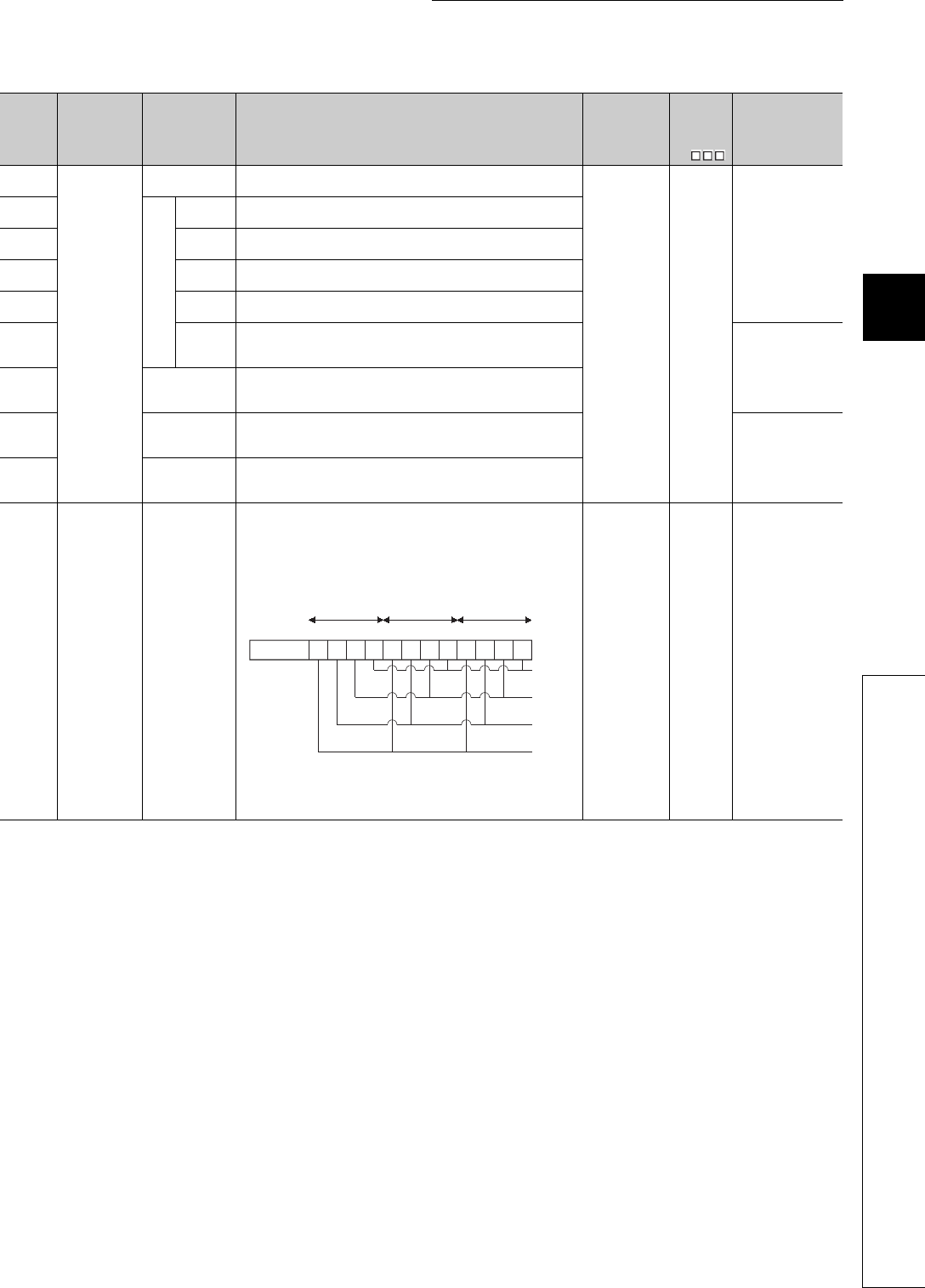
12 - 45
CHAPTER12 PECIAL RELAY LIST AND SPECIAL REGISTER LIST
1
2
3
12
6
7
8
12.2 SPECIAL REGISTER LIST
*10: The Universal model QCPU except the Q00UJCPU, Q00UCPU, and Q01UCPU.
*11: The Universal model QCPU except the Q00UJCPU, Q00UCPU, Q01UCPU, and Q02UCPU.
Table12.20 Special register
Number Name Meaning Explanation Set by
(When Set)
Corres-
ponding
ACPU
D9
Corresponding
CPU
SD254
MELSECNET/
10.
MELSECNET/H
information
Number of
modules installed
• Indicates the number of mounted MELSECNET/10 modules or
MELSECNET/H modules.
S (Initial) New
QCPU
SD255
Information from 1st module
I/O No. • Indicates I/O number of mounted MELSECNET/10 module or
MELSECNET/H module
SD256 Network
No.
• Indicates network No. of mounted MELSECNET/10 module or
MELSECNET/H module
SD257 Group
number
• Indicates group No. of mounted MELSECNET/10 module or
MELSECNET/H module
SD258 Station
No.
• Indicates station No. of mounted MELSECNET/10 module or
MELSECNET/H module
SD259
Standby
informa-
tion
• In the case of standby stations, the module number of the standby
station is stored. (1 to 4) Qn(H)
QnPH
QnPRH
QnU*10
SD260
to
SD264
Information from
2nd module • Configuration is identical to that for the first module.
SD265
to
SD269
Information from
3rd module • Configuration is identical to that for the first module. Qn(H)
QnPH
QnPRH
QnU*11
SD270
to
SD274
Information from
4th module • Configuration is identical to that for the first module.
SD280 CC-Link error Error detection
status
1) When Xn0 of the mounted CC-Link module turns ON, the bit of the
corresponding station turns to 1 (ON).
2) When either Xn1 or XnF of the mounted CC-Link module turns OFF, the
bit of the corresponding station turns to 1 (ON).
3) Turns to 1 (ON) when communication between the mounted CC-Link
module and CPU module cannot be made.
The above module Nos. n are in order of the head I/O numbers.
(However, the one where parameter setting has not been made is not
counted.)
S (Error) New
Qn(H)
QnPH
QnPRH
b0
3rd
module
4th
module
b3
b4
b7b8
b11b12
b15
Information
of 2)
Information
of 1)
to tototo
Information
of 3)
Empty
1st
module
2nd
module
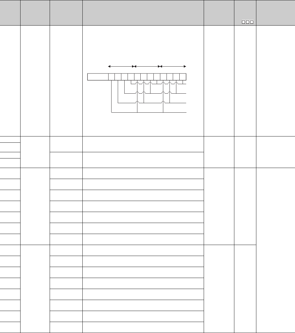
12 - 46
*14: The module whose first 5 digits of serial No. is "08032" or later.
*15: The module whose first 5 digits of serial No. is "09012" or later.
*16: The module whose first 5 digits of serial No. is "10042" or later.
Table12.20 Special register
Number Name Meaning Explanation Set by
(When Set)
Corres-
ponding
ACPU
D9
Corresponding
CPU
SD281 CC-Link error Error detection
status
1) When Xn0 of the mounted CC-Link module turns ON, the bit of the
corresponding station turns to 1 (ON).
2) When either Xn1 or XnF of the mounted CC-Link module turns OFF, the
bit of the corresponding station turns to 1 (ON).
3) Turns to 1 (ON) when communication between the mounted CC-Link
module and CPU module cannot be made.
The above module Nos. n are in order of the head I/O numbers.
(However, the one where parameter setting has not been made is not
counted.)
S (Error) New
Qn(H)*14
QnPH*14
QnPRH*15
SD286
Device
assignment
Points assigned to
M (for extension)
• The number of points assigned to M is stored with 32 bits.
• Even if the points assigned to M are 32k points or less, the points are
stored. S (Initial) New QnU*16
SD287
SD288 Points assigned to
B (for extension)
• The number of points assigned to B is stored with 32 bits.
• Even if the points assigned to B are 32k points or less, the points are
stored.
SD289
SD290
Device
assignment
(Same as
parameter
contents)
Number of points
assigned for X • Stores the number of points currently set for X devices
S (Initial) New
QCPU
SD291 Number of points
assigned for Y • Stores the number of points currently set for Y devices
SD292 Number of points
assigned for M • Stores the number of points currently set for M devices
SD293 Number of points
assigned for L • Stores the number of points currently set for L devices
SD294 Number of points
assigned for B • Stores the number of points currently set for B devices
SD295 Number of points
assigned for F • Stores the number of points currently set for F devices
SD296 Number of points
assigned for SB • Stores the number of points currently set for SB devices
SD297
Device
assignment
(Same as
parameter
contents)
Number of points
assigned for V • Stores the number of points currently set for V devices
S (Initial) New
SD298 Number of points
assigned for S • Stores the number of points currently set for S devices
SD299 Number of points
assigned for T • Stores the number of points currently set for T device
SD300 Number of points
assigned for ST • Stores the number of points currently set for ST devices
SD301 Number of points
assigned for C • Stores the number of points currently set for C devices
SD302 Number of points
assigned for D • Stores the number of points currently set for D devices
SD303 Number of points
assigned for W • Stores the number of points currently set for W devices
SD304 Number of points
assigned for SW • Stores the number of points currently set for SW devices
b0
7rd
module
8th
module
b3
b4
b7b8
b11b12
b15
Information
of 2)
Information
of 1)
to tototo
Information
of 3)
Empty
5st
module
6nd
module

12 - 47
CHAPTER12 PECIAL RELAY LIST AND SPECIAL REGISTER LIST
1
2
3
12
6
7
8
12.2 SPECIAL REGISTER LIST
*10: The Universal model QCPU except the Q00UJCPU, Q00UCPU, and Q01UCPU.
*11: The Universal model QCPU except the Q00UJCPU, Q00UCPU, Q01UCPU, and Q02UCPU.
*17: The Universal model QCPU except the Q00UJCPU.
Table12.20 Special register
Number Name Meaning Explanation Set by
(When Set)
Corres-
ponding
ACPU
D9
Corresponding
CPU
SD305
Device
assignment
(Index register)
16 bit modification
Number of points
assigned for Z
• Stores the number of points of index register (Z) to be modified in the
range of 16 bits.
(The assignment is set by the ZR device index modification setting
parameter.)
S (Initial) New QnU
SD306 Device
assignment
(Same as
parameter
contents)
Number of points
assigned for ZR
(for extension)
• Stores the number of ZR device points (except the number of points of
extended data register (D) and extended link register (W)). The number
of assignment points of ZR device is stored into this SD only when 1k
point or more is set to the extended data register (D) and extended link
register (W).
S (Initial) New QnU*17
SD307
SD308 Device
assignment
(assignment
including the
number of
points set to the
extended data
register (D) and
extended link
register (W))
Number of points
assigned for D (for
inside + for
extension)
• Stores the total number of points of the extended data register (D) and
data register in internal device memory area (stores the value in 32-bit
binary).
SD309
SD310 Number of points
assigned for W
(for inside + for
extension)
• Stores the total number of points of the extended link register (W) and
link register in internal device memory area (stores the value in 32-bit
binary).
SD311
SD315
Time reserved
for
communication
processing
Time reserved for
communication
processing
• Reserves the designated time for communication processing with GX
Developer or other units.
• The greater the value is designated, the shorter the response time for
communication with other devices (GX Developer, serial communication
units) becomes.
• If the designated value is out of the range above, it is processed that no
setting is made.
• Setting range: 1 to 100 ms
• Note that the scan time becomes longer by the designated time.
UNew
Q00J/Q00/Q01
Qn(H)
QnPH
QnPRH
SD340
Ethernet
information
No. of modules
installed • Indicates the number of mounted Ethernet module.
S (Initial) New
QCPU
SD341
Information of 1st module
I/O No. • Indicates I/O No. of mounted Ethernet module
SD342 Network
No. • Indicates network No. of mounted Ethernet module
SD343 Group No. • Indicates group No. of mounted Ethernet module
SD344 Station
No. • Indicates station No. of mounted Ethernet module
SD345 to
SD346 Empty
•Empty
(With QCPU, the Ethernet module IP address of the 1st module is stored
in buffer memory.) Qn(H)
QnPH
QnPRH
QnU*10
SD347 Empty
•Empty
(With QCPU, the Ethernet module error code of the 1st module is read
with the ERRRD instruction.)
SD348 to
SD354
Ethernet
information
Information from
2nd module • Configuration is identical to that for the first module.
S (Initial) New
SD355 to
SD361
Information from
3rd module • Configuration is identical to that for the first module. Qn(H)
QnPH
QnPRH
QnU*11
SD362 to
SD368
Information from
4th module • Configuration is identical to that for the first module.
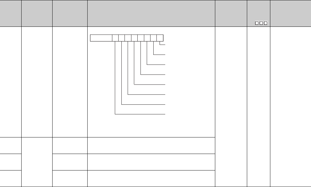
12 - 48
Table12.20 Special register
Number Name Meaning Explanation Set by
(When Set)
Corres-
ponding
ACPU
D9
Corresponding
CPU
SD380
Ethernet
instruction
reception status
Instruction
reception status of
1st module
S (Instruction
execution) New QnPRH
SD381
Ethernet
instruction
reception
status
Instruction
reception status of
2nd module
• Configuration is identical to that for the first module.
SD382
Instruction
reception status of
3rd module
• Configuration is identical to that for the first module.
SD383
Instruction
reception status of
4th module
• Configuration is identical to that for the first module.
b0b1b2b3b4b5b6b7b8b15
0
to
Instruction reception
status of channel 1
Instruction reception
status of channel 2
Instruction reception
status of channel 3
Instruction reception
status of channel 4
Instruction reception
status of channel 5
Instruction reception
status of channel 6
Instruction reception
status of channel 7
Instruction reception
status of channel 8
ON: Received (Channel is being used.)
OFF: Not received (Channel is not used.)
Not used
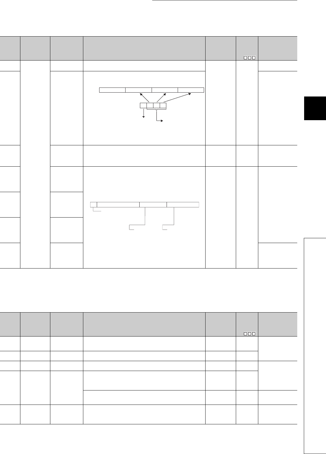
12 - 49
CHAPTER12 PECIAL RELAY LIST AND SPECIAL REGISTER LIST
1
2
3
12
6
7
8
12.2 SPECIAL REGISTER LIST
*9: Function version is B or later.
*11: The Universal model QCPU except the Q00UJCPU, Q00UCPU, Q01UCPU, and Q02UCPU.
*17: The Universal model QCPU except the Q00UJCPU.
(3) System clocks/counters
Table12.20 Special register
Number Name Meaning Explanation Set by
(When Set)
Corres-
ponding
ACPU
D9
Corresponding
CPU
SD393
Multiple CPU
system
information
Number of
multiple CPUs
• The number of CPU modules that comprise the multiple CPU system is
stored. (1 to 3, Empty also included)
S (Initial) New
Q00/Q01*9
QnU
SD394 CPU mounting
information
• The CPU module types of No. 1 CPU to 3 and whether the CPU
modules are mounted or not are stored.
Q00/Q01*9
SD395 Multiple CPU
number
• In a multiple CPU system configuration, the CPU number of the host
CPU is stored.
CPU No. 1: 1, CPU No. 2: 2, CPU No. 3: 3, CPU No. 4: 4
S (Initial) New
Q00/Q01*9
Qn(H)*9
QnPH
QnU
SD396 No. 1 CPU
operation status The operation information of each CPU No. is stored.
(The information on the number of multiple CPUs indicated in SD393 is
stored.)
S (END
processing
error)
New
Q00/Q01*9
QnU*17
SD397 No. 2 CPU
operation status
SD398 No. 3 CPU
operation status
SD399 No. 4 CPU
operation statu QnU*11
Table12.21 Special register
Number Name Meaning Explanation Set by
(When Set)
Corres-
ponding
ACPU
D9
Corresponding
CPU
SD412 1 second
counter
Number of counts
in 1-second units
• Following programmable controller CPU module RUN, 1 is added each
second
• Count repeats from 0 to 32767 to -32768 to 0
S (Status
change) D9022
QCPU
SD414 2n second clock
setting
2n second clock
units
• Stores value n of 2n second clock (Default is 30)
• Setting can be made between 1 and 32767 UNew
SD415 2nms clock
setting 2nms clock units • Stores value n of 2nms clock (Default is 30)
• Setting can be made between 1 and 32767 UNew Qn(H)
QnPH
QnPRH
QnU
SD420 Scan counter Number of counts
in each scan
• Incremented by 1 for each scan execution after the CPU module is set to
RUN.
(Not counted by the scan in an initial execution type program.)
• Count repeats from 0 to 32767 to -32768 to 0
S (Every END
processing) New
• Incremented by 1 for each scan execution after the CPU module is set to
RUN.
• Count repeats from 0 to 32767 to -32768 to 0
S (Every END
processing) New Q00J/Q00/Q01
SD430 Low speed scan
counter
Number of counts
in each scan
• Incremented by 1 for each scan execution after the CPU module is set to
RUN.
• Count repeats from 0 to 32767 to -32768 to 0
• Used only for low speed execution type programs
S (Every END
processing) New Qn(H)
QnPH
b15 b8 b7b12 b11 b4 b3 b0
Empty (0)
toto to
to
CPU No.2CPU No.3 CPU No.1
SD394
CPU module mounted or
not mounted
0: Not mounted
1: Mounted
CPU module type
0: PLC CPU
1: Motion CPU
2: PC CPU
b15 b8 b7 b4 b3 b0
to to
to
b14
Vacancy Classification Operation status
4: Initial
FH: Reset
FH: Reset
0: Normal
1: Minor fault
2: Medium fault
3: Major fault
0: RUN
2: STOP
3: PAUSE
mounted
0: Not mounted
1: Mounted

12 - 50
(4) Scan information
Table12.22 Special register
Number Name Meaning Explanation Set by
(When Set)
Corres-
ponding
ACPU
D9
Corresponding
CPU
SD500 Execution
program No.
Program No. in
execution
• Program number of program currently being executed is stored as BIN
value.
S (Status
change) New
Qn(H)
QnPH
QnPRH
QnU
SD510
Low speed
excution type
program No.
Low speed
execution type
program No. in
execution
• Program number of low speed excution type program No. currently
being executed is stored as BIN value.
• Enabled only when SM510 is ON.
S (Every END
processing) New Qn(H)
QnPH
SD520
Current scan
time
Current scan time
(in 1 ms units)
• The current scan time is stored into SD520 and SD521.
(Measurement is made in 100 s units. (For the Universal model QCPU,
in 1 s units.))
SD520: Stores the ms place. (Storage range: 0 to 65535)
SD521: Stores the s place. (Storage range: 0 to 900 (For the
Universal model QCPU, storage range is 0 to 999))
(Example) When the current scan time is 23.6ms, the following values are
stored.
SD520 = 23
SD521 = 600
S (Every END
processing)
D9018
format
change
QCPU
SD521 Current scan time
(in 100 s units)
S (Every END
processing) New
SD522
Initial scan time
Initial scan time
(in 1 ms units)
• Stores the scan time of an initial execution type program into SD522 and
SD523.
(Measurement is made in 100 s units. (For the Universal model QCPU,
in 1 s units.))
SD522: Stores the ms place. (Storage range: 0 to 65535)
SD523: Stores the s place. (Storage range: 0 to 900 (For the Universal
model QCPU, storage range is 0 to 999))
S (First END
processing) New
Qn(H)
QnPH
QnPRH
QnU
SD523 Initial scan time
(in 100 s units)
SD524
Minimum scan
time
Minimum scan
time (in 1 ms
units)
• Stores the minimum value of the scan time except that of an initial
execution type program into SD524 and SD525. (Measurement is made
in 100 s units. (For the Universal model QCPU, in 1 s units.))
SD524: Stores the ms place. (Storage range: 0 to 65535)
SD525: Stores the s place. (Storage range: 0 to 900 (For the Universal
model QCPU, storage range is 0 to 999))
S (Every END
processing)
D9017
format
change
SD525
Minimum scan
time (in 100 s
units)
S (Every END
processing) New
SD526
Maximum scan
time
Maximum scan
time (in 1 ms
units)
• Stores the maximum value of the scan time except that of an initial
execution type program into SD526 and SD527. (Measurement is made
in 100 s units. (For the Universal model QCPU, in 1 s units.))
SD526: Stores the ms place. (Storage range: 0 to 65535)
SD527: Stores the s place. (Storage range: 0 to 900 (For the Universal
model QCPU, storage range is 0 to 999))
S (Every END
processing)
D9019
format
change
SD527
Maximum scan
time (in 100 s
units)
New
SD528 Current scan
time for low
speed execution
type programs
Current scan time
(in 1 ms units)
• Stores the current scan time of a low speed execution type program into
SD528 and SD529.
(Measurement is made in 100 s units.)
SD528: Stores the ms place. (Storage range: 0 to 65535)
SD529: Stores the s place. (Storage range: 0 to 900)
S (Every END
processing) New
Qn(H)
QnPH
SD529 Current scan time
(in 100 s units)
SD532 Minimum scan
time for low
speed execution
type programs
Minimum scan
time (in 1 ms
units)
• Stores the minimum value of the scan time of a low speed execution
type program into SD532 and SD533.
(Measurement is made in 100 s units.)
SD532: Stores the ms place. (Storage range: 0 to 65535)
SD533: Stores the s place. (Storage range: 0 to 900)
S (Every END
processing) New
SD533
Minimum scan
time (in 100 s
units)
SD534 Maximum scan
time for low
speed execution
type programs
Maximum scan
time (in 1 ms
units)
• Stores the maximum value of the scan time except that of the first scan
of a low speed execution type program into SD534 and SD535.
(Measurement is made in 100 s units.)
SD534: Stores the ms place. (Storage range: 0 to 65535)
SD535: Stores the s place. (Storage range: 0 to 900)
S (Every END
processing) New
SD535
Maximum scan
time (in 100 s
units)
SD540
END processing
time
END processing
time (in 1 ms
units)
• Stores the time from the end of a scan execution type program to the
start of the next scan into SD540 and SD541.
(Measurement is made in 100 s units.(For the Universal model QCPU,
in 1 s units.))
SD540: Stores the ms place. (Storage range: 0 to 65535)
SD541: Stores the s place. (Storage range: 0 to 900) (Storage range: 0
to 900 (For the Universal model QCPU, storage range is 0 to 999))
S (Every END
processing) New
Qn(H)
QnPH
QnPRH
QnU
SD541
END processing
time (in 100 s
units)

12 - 51
CHAPTER12 PECIAL RELAY LIST AND SPECIAL REGISTER LIST
1
2
3
12
6
7
8
12.2 SPECIAL REGISTER LIST
Table12.22 Special register
Number Name Meaning Explanation Set by
(When Set)
Corres-
ponding
ACPU
D9
Corresponding
CPU
SD524
Minimum scan
time
Minimum scan
time (in 1 ms
units)
• Stores the minimum value of the scan time into SD524 and SD525.
(Measurement is made in 100 s units.)
SD524: Stores the ms place. (Storage range: 0 to 65535)
SD525: Stores the s place. (Storage range: 0 to 900)
S (Every END
processing)
New
Q00J/Q00/Q01
SD525
Minimum scan
time (in 100 s
units)
SD526
Maximum scan
time
Maximum scan
time (in 1 ms
units)
• Stores the maximum value of the scan time into SD526 and SD527.
(Measurement is made in 100 s units.)
SD526: Stores the ms place. (Storage range: 0 to 65535)
SD527: Stores the s place. (Storage range: 0 to 900)
S (Every END
processing)
SD527
Maximum scan
time (in 100 s
units)
SD540
END processing
time
END processing
time (in 1 ms
units)
• Stores the time from when the scan program ends until the next scan
starts into SD540 and SD541.
(Measurement is made in 100 s units.)
SD540: Stores the ms place. (Storage range: 0 to 65535)
SD541: Stores the s place. (Storage range: 0 to 900)
S (Every END
processing) New
SD541
END processing
time (in 100 s
units)
SD542
Constant scan
wait time
Constant scan
wait time (in 1 ms
units)
• Stores the wait time for constant scan setting into SD542 and SD543.
(Measurement is made in 100 s units. (For the Universal model QCPU,
in 1 s units.))
SD542: Stores the ms place. (Storage range: 0 to 65535)
SD543: Stores the s place. (Storage range: 0 to 900 (For the Universal
model QCPU, storage range is 0 to 999))
S (Every END
processing) New QCPU
SD543
Constant scan
wait time (in 100
s units)
SD544
Cumulative
execution time
for low speed
execution type
programs
Cumulative
execution time for
low speed
execution type
programs
(in 1 ms units)
• Stores the cumulative execution time of a low speed execution type
program into SD544 and SD545.
(Measurement is made in 100 s units.)
SD544: Stores the ms place. (Storage range: 0 to 65535)
SD545: Stores the s place. (Storage range: 0 to 900)
• Cleared to 0 after the end of one low speed scan.
S (Every END
processing) New
Qn(H)
QnPH
SD545
Cumulative
execution time for
low speed
execution type
programs
(in 100 s units)
SD546
Execution time
for low speed
execution type
programs
Execution time for
low speed
execution type
programs
(in 1 ms units)
• Stores the execution time of a low speed execution type program during
one scan into SD546 and SD547.
(Measurement is made in 100 s units.)
SD546: Stores the ms place. (Storage range: 0 to 65535)
SD547: Stores the s place. (Storage range: 0 to 900)
• Stored every scan.
S (Every END
processing) New
SD547
Execution time for
low speed
execution type
programs
(in 100 s units)
SD548
Scan execution
type program
execution time
Scan execution
type program
execution time (in
1 ms units)
• Stores the execution time of a scan execution type program during one
scan into SD548 and SD549.
(Measurement is made in 100 s units.)
SD548: Stores the ms place. (Storage range: 0 to 65535)
SD549: Stores the s place. (Storage range: 0 to 900)
• Stored every scan.
S (Every END
processing) New
Qn(H)
QnPH
QnPRH
SD549
Scan execution
type program
execution time (in
100 s units)
SD548
Scan program
execution time
Scan program
execution time
(in 1 ms units)
• Stores the execution time of a scan program during one scan into
SD548 and SD549.
(Measurement is made in 100 s units. (For the Universal model QCPU,
in 1 s units.))
SD548: Stores the ms place. (Storage range: 0 to 65535)
SD549: Stores the s place. (Storage range: 0 to 900 (For the Universal
model QCPU, storage range is 0 to 999))
• Stored every scan.
S (Every END
processing) New Q00J/Q00/Q01
QnU
SD549
Scan program
execution time
(in 100 s units)
SD550
Service interval
measurement
module
Unit/module No. • Sets I/O number for module that measures service interval. U New
Qn(H)
QnPH
QnPRH
SD551
Service interval
time
Module service
interval
(in 1 ms units)
• Stores the service interval for the module specified in SD550 into SD551
and SD552 when SM551 is turned ON.
(Measurement is made in 100 s units.)
SD551: Stores the ms place. (Storage range: 0 to 65535)
SD552: Stores the s place. (Storage range: 0 to 900)
S (Request) New
SD552
Module service
interval
(in 100 s units)
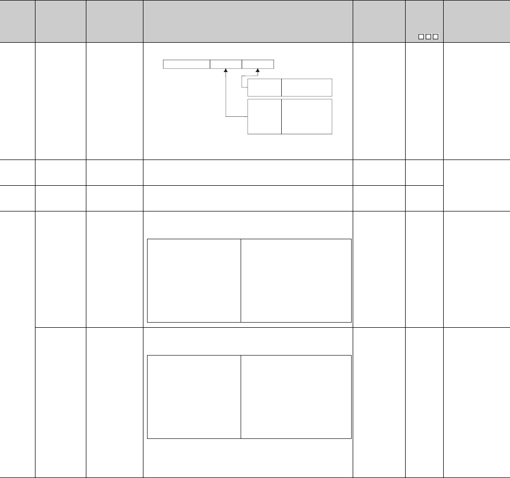
12 - 52
(5) Memory card
*1: When the Q2MEM-8MBA is used, value stored in the special register SD603 differs depending on the combination of the serial number of the High
Performance model QCPU and the manufacture control number of the ATA card.
For details, refer to QCPU User's Manual (Hardware Design, Maintenance and Inspection).
*2: The Universal model QCPU except the Q00UJCPU, Q00UCPU, and Q01UCPU.
Table12.23 Special register
Number Name Meaning Explanation Set by
(When Set)
Corres-
ponding
ACPU
D9
Corresponding
CPU
SD600 Memory card
typs Memory card typs
• Indicates the type of the memory card installed.
(The bits for the drive 1 (RAM) type and drive 2 (ROM) type are fixed to "0"
in the Q00UJCPU, Q00UCPU, and Q01UCPU.)
S (Initial and
card removal) New
Qn(H)
QnPH
QnPRH
QnU
SD602
Drive 1
(Memory card
RAM) capacity
Drive 1 capacity • Drive 1 capacity is stored in 1 k byte units.
• (Empty capacity after format is stored.)
S (Initial and
card removal) New Qn(H)
QnPH
QnPRH
QnU*2
SD603
Drive 2
(Memory card
ROM) capacity
Drive 2 capacity • Drive 2 capacity is stored in 1 k byte units.*1 S (Initial and
card removal) New
SD604
Memory card
use conditions
Memory card use
conditions
• The use conditions for memory card are stored as bit patterns .
(In use when ON)
• The significance of these bit patterns is indicated below:
S (Status
change) New
Qn(H)
QnPH
QnPRH
Memory card
use conditions
Memory card use
conditions
• The use conditions for memory card are stored as bit patterns .
(In use when ON)
• The significance of these bit patterns is indicated below:
*1: Turned ON at boot start and OFF at boot completion.
*2: Turned ON when reflection of device initial value is started and OFF
when reflection of device initial value is completed.
*3: The module whose first 5 digits of serial No. is "10102" or later.
S (Status
change) New QnU*2
b4 b3 b0
0
0: Does not exist
(1: SRAM)
b8 b7b15 to to to
Drive 1
(RAM) type
Drive 2 type
0: Does not exist
1: SRAM card
2: ATA card
3: Flash card
b0 : Boot operation (QBT)
b1 : Parameters (QPA)
b2 : Device comments (QCD)
b3 : Device initial value (QDI)
b4 : File register R (QDR)
b5 : Sampling trace (QTD)
b6 : Not used
b7 : Not used
b8 : Not used
b9 : CPU fault history (QFD)
b10 : Not used
b11 : Local device (QDL)
b12 : Not used
b13 : Not used
b14 : Not used
b15 : Not used
b0 : Boot operation (QBT)*1
b1 : Parameters (QPA)
b2 : Device comments (QCD)
b3 : Device initial value (QDI)*2
b4 : File register R (QDR)
b5 : Sampling trace (QTD)
b6 : Not used
b7 : Backup data (QBP)
b8 : Not used
b9 : Not used
b10 : Not used
b11 : Local device (QDL)
b12 : Not used
b13 : Not used
b14 : Not used
b15 : Not used
*3
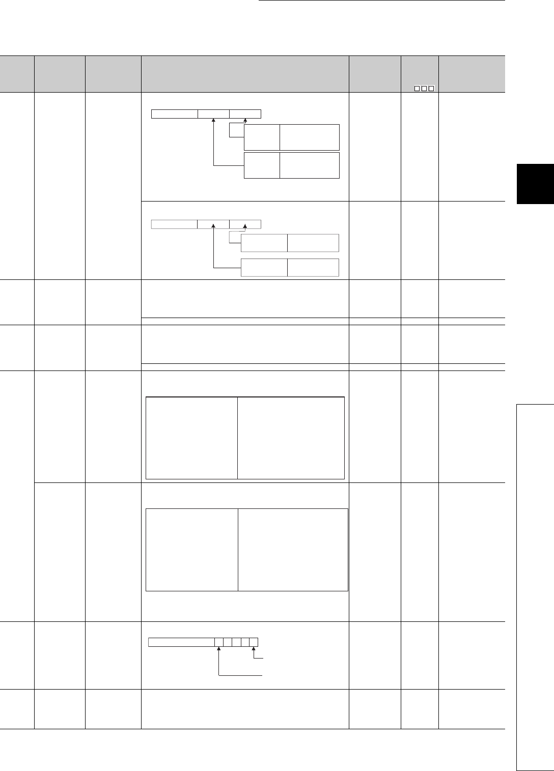
12 - 53
CHAPTER12 PECIAL RELAY LIST AND SPECIAL REGISTER LIST
1
2
3
12
6
7
8
12.2 SPECIAL REGISTER LIST
*3: The Universal model QCPU except the Q00UJCPU.
*10: On the Basic model QCPU, data is set at STOP to RUN or RSET instruction execution after parameter execution.
Table12.23 Special register
Number Name Meaning Explanation Set by
(When Set)
Corres-
ponding
ACPU
D9
Corresponding
CPU
SD620 Drive 3/4 typs Drive 3/4 typs
• Indicates the drive 3/4 type.
(The bits for the drive 3 (standard RAM) type is fixed to "0" in the
Q00UJCPU.)
S (Initial) New
Qn(H)
QnPH
QnPRH
QnU
• Indicates the drive 3/4 type.
S (Initial) New Q00J/Q00/Q01
SD622
Drive 3
(Standard RAM)
capacity
Drive 3 capacity
• Drive 3 capacity is stored in 1 k byte units.
(Empty capacity after format is stored.) S (Initial) New
Qn(H)
QnPH
QnPRH
QnU
• Drive 3 capacity is stored in 1k byte units. S (Initial) New Q00J/Q00/Q01
SD623
Drive 4
(Standard
ROM) capacity
Drive 4 capacity
• Drive 4 capacity is stored in 1 k byte units.
(Empty capacity after format is stored.) S (Initial) New
Qn(H)
QnPH
QnPRH
QnU
• Drive 4 capacity is stored in 1k byte units. S (Initial) New Q00J/Q00/Q01
SD624
Drive 3/4 use
conditions
Drive 3/4 use
conditions
• The conditions for usage for drive 3/4 are stored as bit patterns.
(In use when ON)
• The significance of these bit patterns is indicated below:
S (Status
change) New
Qn(H)
QnPH
QnPRH
Drive 3/4 use
conditions
Drive 3/4 use
conditions
• The conditions for usage for drive 3/4 are stored as bit patterns.
(In use when ON)
• The significance of these bit patterns is indicated below:
*1: Turned ON at boot start and OFF at boot completion.
*2: Supported by the modules having a serial number (first five digits)
"11043" or later.
S (Status
change) New QnU
SD624 Drive 3/4 use
conditions
Drive 3/4 use
conditions
• The conditions for usage for drive 3/4 are stored as bit patterns.
S (Status
change) New Q00J/Q00/Q01
SD640 File register
drive Drive number: • Stores drive number being used by file register S (Status
change) *10 New
Q00J/Q00/Q01
Qn(H)
QnPH
QnPRH
QnU*3
0
b7 b4b0
b15 b8
to to
Drive 3
(Standrd
RAM)
Fixed to 1
Drive 4
(Standrd
ROM)
Fixed to 3
b3 to
b4b3 b0
0
b8 b7b15 to toto
Drive 3
(Standard RAM)
Drive 4
(Standrd ROM)
0: Absent
1: Present
Fixed to
"3 (FLASH ROM)"
b0 : Boot operation (QBT)
b1 : Parameters (QPA)
b2 : Device comments (QCD)
b3 : Device initial value (QDI)
b4 : File register (QDR)
b5 : Sampling trace (QTD)
b6 : Not used
b7 : Not used
b8 : Not used
b9 : CPU fault history (QFD)
b10 : SFC trace (QTS)
b11 : Local device (QDL)
b12 : Not used
b13 : Not used
b14 : Not used
b15 : Not used
b0 : Not used
b1 : Parameters (QPA)
b2 : Device comments (QCD)
b3 : Device initial value (QDI)*1
b4 : File register (QDR)
b5 : Sampling trace (QTD)
b6 : Not used
b7 : Not used
b8 : Module error log *2
b9 : Not used
b10 : Not used
b11 : Local device (QDL)
b12 : Not used
b13 : Not used
b14 : Not used
b15 : Not used
0
b4b0
b15 to to
Boot operation (QBT)
0: Not used 1: In use
b5
00000
File register (QDR)
0: Not used 1: In use

12 - 54
*3: The Universal model QCPU except the Q00UJCPU.
*4: The Universal model QCPU except the Q00UJCPU, Q00UCPU, and Q01UCPU.
*10: On the Basic model QCPU, data is set at STOP to RUN or RSET instruction execution after parameter execution.
Table12.23 Special register
Number Name Meaning Explanation Set by
(When Set)
Corres-
ponding
ACPU
D9
Corresponding
CPU
SD641
File register file
name
File register file
name
• Stores file register file name (with extension) selected at parameters or
by use of QDRSET instruction as ASCII code.
S (Status
change) New
Qn(H)
QnPH
QnPRH
QnU*3
SD642
SD643
SD644
SD645
SD646
• Stores file register file name (MAIN.QDR) selected at parameters as
ASCII code.
S (Initial) New Q00J/Q00/Q01
SD647 File register
capacity
File register
capacity
• Stores the data capacity of the currently selected file register in 1 k word
units.
S (Status
change) New
Qn(H)
QnPH
QnPRH
QnU*3
S (Initial) Q00J/Q00/Q01
SD648 File register
block number
File register block
number • Stores the currently selected file register block number. S (Status
change) *10 D9035
Q00J/Q00/Q01
Qn(H)
QnPH
QnPRH
QnU*3
SD650 Comment drive Comment drive
number
• Stores the comment drive number selected at the parameters or by the
QCDSET instruction.
S (Status
change) New
Qn(H)
QnPH
QnPRH
QnU
SD651
Comment file
name
Comment file
name
• Stores the comment file name (with extension) selected at the
parameters or by the QCDSET instruction in ASCII code.
S (Status
change) New
SD652
SD653
SD654
SD655
SD656
SD660
Boot operation
designation file
Boot designation
file drive number
• Stores the drive number where the boot designation file (*.QBT) is being
stored. S (Initial) New
Qn(H)
QnPH
QnPRH
QnU*4
SD661
File name of boot
designation file
• Stores the file name of the boot designation file (*.QBT).
S (Initial) New
SD662
SD663
SD664
SD665
SD666
SD641
SD642
SD643
SD644
SD645
SD646
b15 to b8 b7 to b0
2nd character 1st character
4th character 3rd character
6th character 5th character
8th character 7th character
2EH(.)
2nd character of
the extension
1st character of
extension
3rd character of
the extension
SD641
SD642
SD643
SD644
SD645
SD646
b15 to b8 b7 to b0
2nd character (A) 1st character (M)
4th character (N) 3rd character (I)
6th character ( ) 5th character ( )
8th character ( ) 7th character ( )
2EH(.)
2nd character of
the extension (D)
1st character of
the extension (Q)
3rd character of
the extension (R)
SD651
SD652
SD653
SD654
SD655
SD656
b15 to b8 b7 to b0
2nd character 1st character
4th character 3rd character
6th character 5th character
8th character 7th character
2EH(.)
2nd character of
the extension
1st character of
the extension
3rd character of
the extension
SD661
SD662
SD663
SD664
SD665
SD666
b15 to b8 b7 to b0
2nd character 1st character
4th character 3rd character
6th character 5th character
8th character 7th character
2EH(.)
2nd character of
the extension
1st character of
the extension
3rd character of
the extension
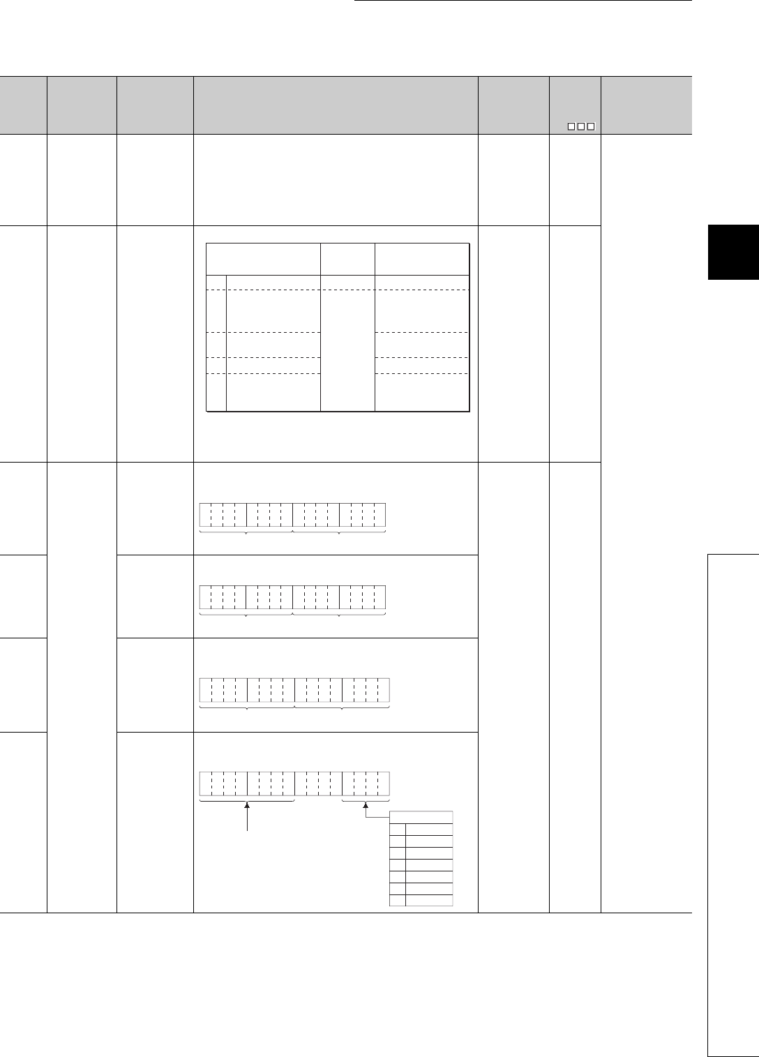
12 - 55
CHAPTER12 PECIAL RELAY LIST AND SPECIAL REGISTER LIST
1
2
3
12
6
7
8
12.2 SPECIAL REGISTER LIST
Table12.23 Special register
Number Name Meaning Explanation Set by
(When Set)
Corres-
ponding
ACPU
D9
Corresponding
CPU
SD670
Parameter
enable drive
information
Parameter enable
drive No.
• Stores information of parameter storage destination drive which is
enabled.
0: Drive 0 (Program memory)
1: Drive 1 (SRAM card)
2: Drive 2 (Flash card/ATA card)
4: Drive 4 (Standard ROM)
(Only drive 0 and drive 4 are valid in the Q00UJCPU, Q00UCPU, and
Q01UCPU.)
S (Initial) New
QnU
SD671
Status of latch
data backup
function
Status display
Indicates the status of the latch data backup function.
• "2 Restore ready completion" is a status immediately after restoring
data.
"3 Backup execution wait" is a status after turning power supply ON from
OFF at "2 Restore ready completion".
S (Status
change) New
SD672
Backup
information
Backup time (Year
and month)
• Stores the last 2 digits of year and month when backup is performed in
2-digit BCD code.
S (At write) New
SD673 Backup time (Day
and hour)
• Stores the day and hour when backup is performed in 2-digit BCD code.
SD674
Backup time
(Minute and
second)
• Stores the minute and second when backup is performed in 2-digit BCD
code.
SD675 Backup time (Year
and day of week)
• Stores the first 2 digits of year and day of week when backup is
performed in BCD code.
Presence/
absence of
backup data
0No backup data Absent Restoring not executed
1Restore ready
completion
Present
Restoring executed when
turning power supply
ON from OFF the
following time
2Restore execution
completion Restoring not executed
3 Backup execution wait Restoring not executed
4
Restore repeated
execution ready
completion
Restoring executed
when turning power
supply ON from OFF
Status
Restore operation at
turning power supply
ON from OFF
b15 b12to b11 b8
to b7 b4to b3 b0
to Example:
July, 1993
9307H
Year Month
b15 b12to b11 b8
to b7 b4to b3 b0
to
Day Hour
Example:
31st, 10 a.m.
3110H
b15 b12to b11 b8
to b7 b4to b3 b0
to Example:
35 min., 48 sec.
3548H
SecondSecondMinute
b15
b12
to b11 b8
to b7 b4
to b3 b0
to
0
1
2
3
4
5
6
Example:
1993, Friday
1905H
Higher digits of year (0 to 99)
Sunday
Saturday
Friday
Thursday
Wednesday
Tuesday
Monday
Day of the week
12 - 56
SD676
Backup data
restration
information
Restore time
(Year and month)
• Stores the last 2 digits of year and month when data is restored in 2-digit
BCD code.
S (Initial) New
QnU
SD677 Restore time (Day
and time)
• Stores the day and time when data is restored in 2-digit BCD code.
SD678
Restore time
(Minute and
second)
• Stores the minute and second when data is restored in 2-digit BCD
code.
SD679
Restore time
(Year and day of
week)
• Stores the first 2 digits of year and day of week when data is restored in
BCD code.
SD681
Program
memory write
(transfer) status
Write (transfer)
status display
(percentage)
Displays the status of writing (transferring) the program memory (flash
ROM) in percentage. (0 to 100%) "0" is set when the write direction is set. S (At write) New
SD682
Program
memory write
count index
Write count index
up to present
• Stores the index value for the number of write operations to the program
memory (flash ROM) up to the present in BIN 32-bit value.
When the index value exceeds 100 thousand times, "FLASH ROM
ERROR" (error code: 1610) occurs. (The index value is calculated even
when exceeding 100 thousand times.)
Note) The write count does not equal to the index value.(Since a flash
ROM write life is prolonged by the system, 1 is added to the write count
index when writing is performed twice or so.).
S (At write) New
SD683
SD686
Standard ROM
write (transfer)
status
Write (transfer)
status display (per-
centage)
Displays the status of writing (transferring) the standard ROM (flash ROM)
in percentage. (0 to 100%) "0" is set when the write direction is set. S (At write) New
SD687
Standard ROM
write count index
Write count index
up to present
• Stores the index value for the number of write operations to the standard
ROM (flash ROM) up to the present in BIN 32-bit value.
When the index value exceeds 100 thousand times, "FLASH ROM
ERROR" (error code: 1610) occurs. (The index value is calculated even
when exceeding 100 thousand times.)
Note) The write count does not equal to the index value. (Since a flash
ROM write life is prolonged by the system, 1 is added to the write count
index when the total write capacity after the previous count up reaches
about 1M byte.)
S (At write) New
SD688
SD689 Backup error
factor
Backup error
factor
Stores the factor of the error that occurred in the backup.
0H : No error
100H: Memory card not inserted
200H: Size of backup target data exceeded
300H: Memory card write inhibit setting
400H: Memory card write error
500H: Backup target data read error (from program memory)
503H: Backup target data read error (from standard RAM)
504H: Backup target data read error (from standard ROM)
510H: Backup target data read error (from system data)
S (Backup error
occurrence) New
QnU*1
SD690 Backup status Backup status
Stores the current backup status.
0 : Before backup start
1 : Backup start prepared
2 : Backup start preparation completed
3 : Backup in execution
4 : Backup completed
FF: Backup error
S (Status
change) New
*1: The module whose first 5 digits of serial No. is "10102" or later. (Except the Q00UJCPU, Q00UCPU, and Q01UCPU)
Number Name Meaning Explanation Set by
(When Set)
Corres-
ponding
ACPU
D9
Corresponding
CPU
b15 b12to b11 b8
to b7 b4to b3 b0
to Example:
July, 1993
9307H
Year Month
b15 b12to b11 b8
to b7 b4to b3 b0
to
Day Hour
Example:
31st, 10 a.m.
3110H
b15 b12to b11 b8
to b7 b4to b3 b0
to Example:
35 min., 48 sec.
3548H
SecondSecondMinute
b15
b12
to b11 b8
to b7 b4
to b3 b0
to
0
1
2
3
4
5
6
Example:
1993, Friday
1905H
Higher digits of year (0 to 99)
Sunday
Saturday
Friday
Thursday
Wednesday
Tuesday
Monday
Day of the week

12 - 57
CHAPTER12 PECIAL RELAY LIST AND SPECIAL REGISTER LIST
1
2
3
12
6
7
8
12.2 SPECIAL REGISTER LIST
SD691 Backup
execution status
Backup execution
status display
(Percentage)
• Displays the execution status of data backup to the memory card in
percentage (0 to 100%).
• "0" is set when the backup starts.
S (Status
change) New
QnU*1
SD692 Restoration error
factor
Factor of error
occurred in the
restoration
Stores the factor of an error that occurred in the restoration.
Each error factor is as follows:
800H: The CPU module model name is not matched.
801H: The file password is set only for the restoration destination data or is
not matched.
810H: The verified backup data file is not matched or the backup data read
failed.
S (Error
occurrence) New
SD693 Restoration
status
Current restoration
status
Stores the current restoration execution status.
Each error factor is as follows:
0 : Before restoration start
1 : Restoration in execution
2 : Restoration completed
FF: Restoration error
Sets "0" (Before restoring), however, when the restoration is completed
only during the automatic restoration.
S (Status
change) New
SD694 Restoration
execution status
Restoration
execution status
display
(Percentage)
• Displays the execution status of restoration to the CPU module in
percentage (0 to 100%).
• "0" is set before the restoration.
Sets "0" (Before restoring), however, when the restoration is completed
only during the automatic restoration.
S (Status
change) New
SD695
Specification of
writing to stan-
dard ROM
instruction count
Specification of
writing to standard
ROM instruction
count
• Specifies the maximum number of executions of the writing to standard
ROM instruction (SP.DEVST) to write to the standard ROM per day.
• When the number of executions of the writing to standard ROM
instruction exceeds the number of times set by SD695, “OPERATION
ERROR” (error code: 4113) occurs.
• The setting range for SD695 is 1 to 32767. If 0 or value outside the
range is set, “OPERATION ERROR” (error code: 4113) occurs at
execution of the writing to standard ROM instruction.
UNew QnU
SD696 Available
memory in
memory card
Available memory
in memory card
Stores the available memory in memory card. (Stores the value in 32-bit
binary.) S (Backup in
operation) New QnU*1
SD697
SD698 Backup data
capacity
Backup data
capacity Stores the backup data capacity. (Stores the value in 32-bit binary.)
SD699
*1: The module whose first 5 digits of serial No. is "10102" or later. (Except the Q00UJCPU, Q00UCPU, and Q01UCPU)
Number Name Meaning Explanation Set by
(When Set)
Corres-
ponding
ACPU
D9
Corresponding
CPU
12 - 58
(6) Instruction-Related Registers
Table12.24 Special register
Number Name Meaning Explanation Set by
(When Set)
Corres-
ponding
ACPU
D9
Corresponding
CPU
SD705
Mask pattern Mask pattern
• During block operations, turning SM705 ON makes it possible to use the
mask pattern being stored at SD705 (or at SD705 and SD706 if double
words are being used) to operate on all data in the block with the
masked values.
UNew
Q00J/Q00/Q01
Qn(H)
QnPH
QnPRH
SD706
SD715
IMASK
instruction mask
pattern
Mask pattern
• Patterns masked by use of the IMASK instruction are stored in the
following manner:
S (During
execution) New
QCPU
SD716
SD717
SD718
Accumulator Accumulator • For use as replacement for accumulators used in A series programs. S/U New
SD719
SD720
Program No.
designation for
PLOADP
instruction
Program No.
designation for
PLOADP
instruction
Stores the program number of the program to be loaded by the PLOADP
instruction when designated.
Designation range: 1 to 124
UNew Qn(H)
QnPH
SD738
Message
storage Message storage
• Stores the message designated by the MSG instruction.
S (During
execution) New QCPU
SD739
SD740
SD741
SD742
SD743
SD744
SD745
SD746
SD747
SD748
SD749
SD750
SD751
SD752
SD753
SD754
SD755
SD756
SD757
SD758
SD759
SD760
SD761
SD762
SD763
SD764
SD765
SD766
SD767
SD768
SD769
SD715
SD716
SD717
l15 l1l0
l31
l47
l17
l33
l16
l32
b15 b0
b1
to
to
to
SD738
SD739
SD740
SD741
SD742
SD743
b15 to b8 b7 to b0
SD744
SD745
SD746
SD747
SD748
SD749
SD750
SD751
SD752
SD753
SD754
SD755
SD756
SD757
SD758
SD759
SD760
SD761
SD762
SD763
SD764
SD765
SD766
SD767
SD768
SD769
2nd character 1st character
4th character 3rd character
6th character 5th character
8th character 7th character
10th character 9th character
12th character 11th character
14th character 13th character
16th character 15th character
18th character 17th character
20th character 19th character
22nd character 21st character
24th character 23rd character
26th character 25th character
28th character 27th character
30th character 29th character
32nd character 31st character
34th character 33rd character
36th character 35th character
38th character 37th character
40th character 39th character
42nd character 41st character
44th character 43rd character
46th character 45th character
48th character 47th character
50th character 49th character
52nd character 51st character
54th character 53rd character
56th character 55th character
58th character 57th character
60th character 59th character
62nd character 61st character
64th character 63rd character
12 - 59
CHAPTER12 PECIAL RELAY LIST AND SPECIAL REGISTER LIST
1
2
3
12
6
7
8
12.2 SPECIAL REGISTER LIST
*9: Function version is B or later.
*11: The module whose first 5 digits of serial No. is "04012" or later.
*12: The module whose first 5 digits of serial No. is "07032" or later.
*13: The module whose first 5 digits of serial No. is "09012" or later.
Table12.24 Special register
Number Name Meaning Explanation Set by
(When Set)
Corres-
ponding
ACPU
D9
Corresponding
CPU
SD774
to
SD775
PID limit setting
(for complete
derivative)
0: With limit
1: Without limit
• Specify the limit of each PID loop as shown below.
UNew
Qn(H)
QnPRH
QnU
SD774
PID limit setting
(for complete
derivative)
0: With limit
1: Without limit
• Specify the limit of each PID loop as shown below.
UNew
Q00J/Q00/Q01*9
SD778
Refresh
processing
selection when
the COM/
CCOM
instruction is
executed
b0 to b14:
0: Do not
refresh
1: Refresh
b15 bit
0: Communication
with CPU
module is
executed
1: Communication
withCPU
module is
nonexecuted
• Selects whether or not the data is refreshed when the COM instruction is
executed.
• Designation of SD778 is made valid when SM775 turns ON.
• Refresh between multiple CPUs by COM instruction is performed under
the following occasion.
Receiving operation from other device: b4 of SD778(refresh in the CPU
shared memory) is turned to 1.
Sending operation from host CPU : b15 of SD778(communication with
peripheral device is executed/nonexecuted) is turned to 0.
UNew
Q00J/Q00/Q01*9
Qn(H)*11
• Selects whether or not the data is refreshed when the COM instruction is
executed.
• Designation of SD778 is made valid when SM775 turns ON.
• Refresh between multiple CPUs by COM instruction is performed under
the following occasion.
Receiving operation from other device: b4 of SD778(refresh in the CPU
shared memory) is turned to 1.
Sending operation from host CPU : b15 of SD778(communication with
peripheral device is executed/nonexecuted) is turned to 0.
• When b2 (refresh of the CC-Link IE controller network and
MELSECNET/H) of SD778 is 1, the CC-Link IE controller network and
MELSECNET/H perform refresh.
Therefore, if there are many refresh points, processing time for the COM
instruction will be extended.
UNew
Qn(H)*13
QnPH*12
QnPRH
SD774
SD775
b15
to
to
Loop2
Loop18
Loop1
Loop17
b1 b0
Loop16
Loop32
SD774
b15
to
toto b1 b0b7b8
Loop8 Loop2 Loop1
b0b1b2b3b4b5b14b15
0
to
I/O refresh
CC-Link refresh
MELSECNET/H
refresh
Automatic refresh of
intelligent function
modules
Execution/non-
execution of
communication with
CPU module
Automatic refresh of
CPU shared memory
(Fixed to "0" for
Redundant CPU)
0/10/10/10/10/10/1
SD778
b0b1b2b3b4b5b6b14b15
0
to
I/O refresh
CC-Link refresh
CC-Link IE controller
network or
0/10/10/10/10/10/10/1
SD778
Automatic refresh of
intelligent function
modules
Execution/non-
execution of
communication with
CPU module
Reading input/output
from group outside
multiple CPU system
Auto refresh using the
multiple CPU high speed
transmission area of
multiple CPU system
MELSECNET/H refresh
12 - 60
*9: Function version is B or later.
*13: The module whose first 5 digits of serial No. is "09012" or later.
Table12.24 Special register
Number Name Meaning Explanation Set by
(When Set)
Corres-
ponding
ACPU
D9
Corresponding
CPU
SD778
Refresh
processing
selection when
the COM/
CCOM
instruction is
executed
b0 to b14:
0: Do not
refresh
1: Refresh
b15 bit
0: communication
with peripheral
device is
executed
1: communication
with peripheral
device is
nonexecuted
• Selects whether or not the data is refreshed when the COM, CCOM
instruction is executed.
• Designation of SD778 is made valid when SM775 turns ON.
UNew QnU
SD781
to
SD793
Mask pattern of
IMASK
instruction
Mask pattern
• Stores the mask patterns masked by the IMASK instruction as follows:
(The Q00UJCPU, Q00UCPU, and Q01UCPU cannot use the special
registers SD786 to SD793.)
S (During
execution) New
Qn(H)
QnPH
QnPRH
QnU
SD781
to
SD785
Mask pattern of
IMASK
instruction
Mask pattern
• Stores the mask patterns masked by the IMASK instruction as follows:
S (During
execution) New Q00J/Q00/Q01
SD794
to
SD795
PID limit setting
(for incomplete
derivative)
0: With limit
1: Without limit
• Specify the limit of each PID loop as shown below.
UNew
Qn(H)*13
QnPRH
QnU
SD794
PID limit setting
(for incomplete
derivative)
0: With limit
1: Without limit
• Specify the limit of each PID loop as shown below.
UNew
Q00J/Q00/Q01*9
b0b1b2b3b4b5b6b14b15
0
to
I/O refresh
CC-Link refresh
Refresh of
MELSECNET/H and
CC-Link IE controller
network
0/10/10/10/10/10/10/1
S
D778
Automatic refresh of
intelligent function
modules
Execution/non-
execution of
communication with
CPU module
Auto refresh using
QCPU standard area of
multiple CPU system and
reading input/output from
group outside.
Auto refresh using the
multiple CPU high speed
transmission area of
multiple CPU system
SD781
SD782
SD793
l63 l49l48
l79
l255
l65
l241
l64
l240
b15 b0
b1
to
to
to
to
to to
SD781
SD782
SD785
l63 l49l48
l79
l127
l65
l113
l64
l112
b15 b0b1
to
to
to
SD794
SD795
b15
to
to
b1 b0
Loop16
Loop32
Loop2
Loop18
Loop1
Loop17
SD794
b15
to
to b1 b0
b7b8
Loop8 Loop2 Loop1

12 - 61
CHAPTER12 PECIAL RELAY LIST AND SPECIAL REGISTER LIST
1
2
3
12
6
7
8
12.2 SPECIAL REGISTER LIST
*14: The Universal model QCPU except the Q00UJCPU, Q00UCPU, Q01UCPU, and Q02UCPU.
*15: The range is from 1 to 9 for the Q03UDCPU, Q04UDCPU, and Q06UDHCP whose first 5 digits of serial number is "10012" or earlier.
(Default: 2 Or when setting other than 1 to 9, the register operates as 9).
Table12.24 Special register
Number Name Meaning Explanation Set by
(When Set)
Corres-
ponding
ACPU
D9
Corresponding
CPU
SD796
Maximum
number of
blocks used for
the multiple
CPU high-
speed
transmission
dedicated
instruction
setting (for CPU
No.1)
Maximum number
of blocks range for
dedicated
instructions
Range: 1 to 7
(Default: 2 Or
when setting other
than 1 to 7, the
register operates
as 7).
• Specifies the maximum number of blocks used for the multiple CPU
high-speed transmission dedicated instruction (target CPU=CPU No.1).
When the dedicated instruction of Multiple CPU transmission is
executed to the CPU No.1, and the number of empty blocks of the
dedicated instruction transmission area is less than the setting value of
this register, SM796 is turned ON, which is used as the interlock signal
for consecutive execution of the dedicated instruction of Multiple CPU
transmission.
U (At 1 scan
after RUN) New
QnU*14*15
SD797
Maximum
number of
blocks used for
the multiple
CPU high-
speed
transmission
dedicated
instruction
setting (for CPU
No.2)
• Specifies the maximum number of blocks used for the multiple CPU
high-speed transmission dedicated instruction (target CPU=CPU No.2).
When the dedicated instruction of Multiple CPU transmission is
executed to the CPU No.2, and the number of empty blocks of the
dedicated instruction transmission area is less than the setting value of
this register, SM797 is turned ON, which is used as the interlock signal
for consecutive execution of the dedicated instruction of Multiple CPU
transmission.
U (At 1 scan
after RUN) New
SD798
Maximum
number of
blocks used for
the multiple
CPU high-
speed
transmission
dedicated
instruction
setting (for CPU
No.3)
• Specifies the maximum number of blocks used for the multiple CPU
high-speed transmission dedicated instruction (target CPU=CPU No.3).
When the dedicated instruction of Multiple CPU transmission is
executed to the CPU No.3, and the number of empty blocks of the
dedicated instruction transmission area is less than the setting value of
this register, SM798 is turned ON, which is used as the interlock signal
for consecutive execution of the dedicated instruction of Multiple CPU
transmission.
U (At 1 scan
after RUN) New
SD799
Maximum
number of
blocks used for
the multiple
CPU high-
speed
transmission
dedicated
instruction
setting (for CPU
No.4)
• Specifies the maximum number of blocks used for the multiple CPU
high-speed transmission dedicated instruction (target CPU=CPU No.4).
When the dedicated instruction of Multiple CPU transmission is
executed to the CPU No.4, and the number of empty blocks of the
dedicated instruction transmission area is less than the setting value of
this register, SM799 is turned ON, which is used as the interlock signal
for consecutive execution of the dedicated instruction of Multiple CPU
transmission.
U (At 1 scan
after RUN) New
12 - 62
(7) Debug
*1: The module whose first 5 digits of serial No. is "10042" or later.
(8) Redundant CPU information (host system CPU information*1)
*1: The host system CPU information is stored.
(9) Remote password count
*1: This applies to the Built-in Ethernet port QCPU.
Table12.25 Special register
Number Name Meaning Explanation Set by
(When Set)
Corres-
ponding
ACPU
D9
Corresponding
CPU
SD840 Debug function
usage
Debug function
usage
Stores the status of the debug function usage as shown below.
0: Forced ON/OFF for external I/O
1: Executional conditioned device test
2 to 15:Absent (0 fix)
(0: Not used, 1: Used)
S (Status
change) New QnU*1
Table12.26 Special register
Number Name Meaning Explanation Set by
(When Set)
Corres-
ponding
ACPU
D9
Corresponding
CPU
SD952
History of
memory copy
from control
system to
standby system
Latest status of
memory copy
from control
system to standby
system
Stores the completion status of the memory copy from control system to
standby system executed last.
1) Stores the same value as stored into SD1596 at normal completion/
abnormal completion of the memory copy from control system to
standby system.
2) Backed up for a power failure, this special register holds the status of
memory copy from control system to standby system executed last.
3) Cleared to 0 by latch clear operation.
S (Status
change) New QnPRH
Table12.27 Special register
Number Name Meaning Explanation Set by
(When Set)
Corres-
ponding
ACPU
D9
Corresponding
CPU
SD979
Direct
MELSOFT
connection
Count of unlock
processing
failures
Stores the count of unlock processing failures.
Range: 0 to FFFEH (FFFFH when the limit is exceeded)
S(Status
change) New QnU*1
SD980 to
SD995
Connection
1 to 16
SD998
MELSOFT
connection
using TCP port
SD999
FTP
communi
cation port
0
b15 b2to b1 b0
Executional conditioned
device test
Forced ON/OFF for
external I/O

12 - 63
CHAPTER12 PECIAL RELAY LIST AND SPECIAL REGISTER LIST
1
2
3
12
6
7
8
12.2 SPECIAL REGISTER LIST
(10) A to Q conversion
ACPU special registers D9000 to D9255 correspond to Q special registers SD1000 to
SD1255 after A to Q/QnA conversion.
(However, the Basic model QCPU and Redundant CPU do not support the A to Q
conversion.)
These special registers are all set by the system, and cannot be set by the user program.
To set data by the user program, correct the program for use of the QCPU special registers.
However, some of SD1200 to SD1255 (corresponding to D9200 to 9255 before conversion)
can be set by the user program if they could be set by the user program before conversion.
For details on the ACPU special registers, refer to the user's manual for the corresponding
CPU, and MELSECNET or MELSECNET/B Data Link System Reference Manuals.
Check "Use special relay/special register from SM/SD1000" for "A-PLC" on the PLC system tab of PLC parameter in GX
Developer when the converted special registers are used with the High Performance model QCPU, Process CPU, and
Universal model QCPU.
When not using the converted special registers, uncheck "Use special relay/special registers from SM/SD1000" to save the
time taken for processing special registers.
Remark
Supplemental explanation on "Special Register for Modification" column
For the device numbers for which a special register for modification is specified, modify it to the special register for
QCPU.
For the device numbers for which is specified, special register after conversion can be used.
Device numbers for which is specified do not function for QCPU.

12 - 64
*1: The relevant modules are as follows:
• The Universal model QCPU whose serial number (first five digits) is "10102" or later.
• Q00UJCPU, Q00UCPU, Q01UCPU
Table12.28 Special register
ACPU
Special
Register
Special
Register
after
Conversion
Special
Register for
Modification
Name Meaning Details Corresponding
CPU
D9000 SD1000 –Fuse blown Number of module
with blown fuse
• When fuse blown modules are detected, the first I/O number of the
lowest number of the detected modules is stored in hexadecimal.
(Example: When fuses of Y50 to 6F output modules have blown,
"50" is stored in hexadecimal)
To monitor the number by peripheral devices, perform monitor
operation given in hexadecimal.
(Cleared when all contents of SD1100 to SD1107 are reset to 0.)
• Fuse blow check is executed also to the output modules of remote
I/O stations.
Qn(H)
QnPH
QnU*1
D9001 SD1001 –Fuse blown Number of module
with blown fuse
• Stores the module numbers corresponding to setting switch
numbers or base slot numbers when fuse blow occurred.
• For the remote I/O station, the value of (module I/O No./10H) + 1 is
stored.
Qn(H)
QnPH
D9002 SD1002 –I/O module
verify error
I/O module verify
error module number
• If I/O modules, of which data are different from data entered, are
detected when the power is turned on, the first I/O number of the
lowest number unit among the detected units is stored in
hexadecimal. (Storing method is the same as that of SD1000.)
To monitor the number by peripheral devices, perform monitor
operation given in hexadecimal.
(Cleared when all contents of SD1116 to SD1123 are reset to 0.)
• I/O module verify check is executed also to the modules of remote
I/O terminals.
Qn(H)
QnPH
QnU*1
D9005 SD1005 –AC DOWN
counter
Number of times for
AC DOWN
• When the AC power supply module is used, 1 is added at
occurrence of an instantaneous power failure of within 20ms.
(The value is stored in BIN code.) It is reset when the power supply
is switched from OFF to ON.
Qn(H)
QnPH
QnU*1
• When the DC power supply module is used, 1 is added at
occurrence of an instantaneous power failure of within 10ms.
(The value is stored in BIN code.) It is reset when the power supply
is switched from OFF to ON.
Qn(H)
QnPH
QnU*1
D9008 SD1008 SD0 Self-diagnostic
error
Self-diagnostic error
number
• When error is found as a result of self-diagnosis, error number is
stored in BIN code.
Qn(H)
QnPH
QnU*1
AJ02 I/O moduleExtension base unit
Setting
switch
Stored
data Base unit
slot No.
Stored
data
0
1
2
3
4
5
6
7
0
1
2
3
4
5
6
7
0
1
2
3
4
5
6
7
12 - 65
CHAPTER12 PECIAL RELAY LIST AND SPECIAL REGISTER LIST
1
2
3
12
6
7
8
12.2 SPECIAL REGISTER LIST
*1: The relevant modules are as follows:
• The Universal model QCPU whose serial number (first five digits) is "10102" or later.
• Q00UJCPU, Q00UCPU, Q01UCPU
Table12.28 Special register
ACPU
Special
Register
Special
Register
after
Conversion
Special
Register for
Modification
Name Meaning Details Corresponding
CPU
D9009 SD1009 SD62 Annunciator
detection
F number at which
external failure has
occurred
• When one of F0 to 2047 is turned on by OUT F or
SET F instruction, the F number, which has been detected earliest
among the F numbers which have turned on, is stored in BIN code.
• SD1009 can be cleared by RST F or LEDR instruction.
If another F number has been detected, the clearing of SD1009
causes the next number to be stored in SD1009.
Qn(H)
QnPH
QnU*1
D9010 SD1010 Error step
Step number at which
operation error has
occurred.
• When operation error has occurred during execution of application
instruction, the step number, at which the error has occurred, is
stored in BIN code.
Thereafter, each time operation error occurs, the contents of
SD1010 are renewed.
Qn(H)
QnPH
D9011 SD1011 Error step
Step number at which
operation error has
occurred.
• When operation error has occurred during execution of application
instruction, the step number, at which the error has occurred, is
stored in BIN code. Since the step number is stored into SD1011
when SM1011 turns from OFF to ON, the data of SD1011 is not
updated unless SM1011 is cleared by a user program.
D9014 SD1014 I/O control
mode
I/O control mode
number
• The I/O control mode set is returned in any of the following
numbers:
0: Both input and output in direct mode
1: Input in refresh mode, output in direct mode
3: Both input and output in refresh mode
D9015 SD1015 SD203 Operating
status of CPU
Operating status of
CPU
• The operation status of CPU as shown below are stored in
SD1015.
*1: When the CPU mdoule is in RUN mode and SM1040 is off, the
CPU module remains in RUN mode if changed to PAUSE mode.
Qn(H)
QnPH
QnU*1
b15 b12
to b11 b8
to b7 b4
to b3 b0
to
0
1
2
RUN
PAUSE
STOP
Remote RUN/STOP
by parameter setting
0
1
2
RUN
PAUSE
STOP
Remote RUN/STOP
by computer 0
1
2
RUN
PAUSE
3STEP RUN
STOP
CPU key switch
0
1
Except below
Instruction
execution
Status in program
Remains the same in
remote RUN/STOP
mode.
STOP
11
1

12 - 66
*1: The relevant modules are as follows:
• The Universal model QCPU whose serial number (first five digits) is "10102" or later.
• Q00UJCPU, Q00UCPU, Q01UCPU
Table12.28 Special register
ACPU
Special
Register
Special
Register
after
Conversion
Special
Register for
Modification
Name Meaning Details Corresponding
CPU
D9016 SD1016 Program
number
0: Main program
(ROM)
1: Main program
(RAM)
2: Subprogram 1
(RAM)
3: Subprogram 2
(RAM)
4: Subprogram 3
(RAM)
5: Subprogram 1
(ROM)
6: Subprogram 2
(ROM)
7: Subprogram 3
(ROM)
8: Main program
(E2PROM)
9: Subprogram 1
(E2PROM)
A: Subprogram 2
(E2PROM)
B: Subprogram 3
(E2PROM)
• Indicates which sequence program is run presently. One value of 0
to B is stored in BIN code.
Qn(H)
QnPH
D9017 SD1017 SD524 Scan time Minimum scan time
(10 ms units)
• If scan time is smaller than the content of SD1017, the value is
newly stored at each END. Namely, the minimum value of scan
time is stored into SD1017 in BIN code. Qn(H)
QnPH
QnU*1
D9018 SD1018 SD520 Scan time Scan time
(10 ms units)
• At every END, the scan time is stored in BIN code and always
rewritten.
D9019 SD1019 SD526 Scan time Maximum scan time
(10 ms units)
• If scan time is larger than the content of SD1019, the value is newly
stored at each END. Namely, the maximum value of scan time is
stored into SD1019 in BIN code.
D9020 SD1020 Constant scan
Constant scan time
(User sets in 10 ms
units)
• Sets the interval between consecutive program starts in multiples
of 10 ms.
0 : No setting
1 to 200 : Set. Program is executed at intervals of (set
value) 10 ms.
Qn(H)
QnPH
D9021 SD1021 –Scan time Scan time
(1 ms units)
• At every END, the scan time is stored in BIN code and always
rewritten.
Qn(H)
QnPH
QnU*1
D9022 SD1022 SD412 1 second
counter Count in units of 1s.
• When the PC CPU starts running, it starts counting 1 every
second.
• It starts counting up from 0 to 32767, then down to -32768 and
then again up to 0. Counting repeats this routine.
D9025 SD1025 –Clock data Clock data
(year, month)
• The year (last two digits) and month are stored as BCD code as
shown below.
D9026 SD1026 –Clock data Clock data
(day, hour)
• The day and hour are stored as BCD code as shown below.
D9027 SD1027 –Clock data Clock data
(minute, second)
• The minute and second are stored as BCD code as shown below.
b15 b12to b11 b8
to b7 b4to b3 b0
to Example:
1987, July
H8707
Year Month
b15 b12to b11 b8
to b7 b4to b3 b0
to Example:
31st, 10 a.m.
H3110
Day Hour
b15 b12to b11 b8
to b7 b4to b3 b0
to Example:
35 min, 48 sec.
H3548
Minute Second
12 - 67
CHAPTER12 PECIAL RELAY LIST AND SPECIAL REGISTER LIST
1
2
3
12
6
7
8
12.2 SPECIAL REGISTER LIST
*1: The relevant modules are as follows:
• The Universal model QCPU whose serial number (first five digits) is "10102" or later.
• Q00UJCPU, Q00UCPU, Q01UCPU
Table12.28 Special register
ACPU
Special
Register
Special
Register
after
Conversion
Special
Register for
Modification
Name Meaning Details Corresponding
CPU
D9028 SD1028 –Clock data Clock data
(day of week)
• The day of the week is stored as BCD code as shown below.
Qn(H)
QnPH
QnU*1
D9035 SD1035 SD648 Extension file
register Use block No. • Stores the block No. of the extension file register being used in
BCD code.
D9036 SD1036
Extension file
registerfor
designation of
device number
Device number when
individual devices
from extension file
register are directly
accessed
• Designate the device number for the extension file register for
direct read and write in 2 words at SD1036 and SD1037 in BIN
data.
Use consecutive numbers beginning with R0 of block No. 1 to
designate device numbers.
Qn(H)
QnPH
D9037 SD1037
D9038 SD1038 SD207
LED display
priority ranking
Priorities 1 to 4
• Sets priority of ERROR LEDs which illuminate (or flicker) to
indicate errors with error code numbers.
• Configuration of the priority setting areas is as shown below.
• For details, refer to the applicable CPUs User's Manual and the
ACPU Programming manual (Fundamentals).
D9039 SD1039 SD208 Priorities 5 to 7
D9044 SD1044 For sampling
trace
Step or time during
sampling trace
• Turned on/off with a peripheral device.
When STRA or STRAR instruction is executed, the value stored in
SD1044 is used as the sampling trace condition.
At scanning--------0
At time--------------Time (10 msec unit)
The value is stored into SD1044 in BIN code.
D9049 SD1049 Work area for
SFC
Block number of
extension file register
• Stores the block number of the expansion file register which is
used as the work area for the execution of a SFC program in a
binary value.
• Stores "0" if an empty area of 16K bytes or smaller, which cannot
be expansion file register No. 1, is used or if SM320 is OFF.
D9050 SD1050 SFC program
error number
Error code generated
by SFC program
• Stores error code of errors occurred in the SFC program in BIN
code.
0 : No error
80: SFC program parameter error
81: SFC code error
82: Number of steps of simultaneous execution exceeded
83: Block start error
84: SFC program operation error
D9051 SD1051 Error block Block number where
error occurred
• Stores the block number in which an error occurred in the SFC
program in BIN code.
In the case of error 83 the starting block number is stored.
D9052 SD1052 Error step Step number where
error occurred
• Stores the step number, where error code 84 occurred in an SFC
program, in BIN value.
• Stores "0" when error code 80, 81 or 82 occurred.
• Stores the block stating step number when error code 83 occurs.
b15 b12
to b11 b8
to b7 b4
to b3 b0
to
0
1
2
3
4
5
6
H0005
Sunday
Saturday
Friday
Thursday
Wednesday
Tuesday
Monday
Day of the week
Example:
Friday
Always set "0"
Device No. (BIN data)
SD1037,SD1036
0
to
16383
16384
to
to
Extension file register
Block No.1
area
Block No.2
area
SD207
SD208
b15 b12 b11 b8 b7 b4b3 b0to to to to
Priority 4 Priority 3
Priority 7Priority 6
Priority 2
Priority 5
Priority 1
12 - 68
*1: The relevant modules are as follows:
• The Universal model QCPU whose serial number (first five digits) is "10102" or later.
• Q00UJCPU, Q00UCPU, Q01UCPU
Table12.28 Special register
ACPU
Special
Register
Special
Register
after
Conversion
Special
Register for
Modification
Name Meaning Details Corresponding
CPU
D9053 SD1053 Error transition
Transition condition
number where error
occurred
• Stores the transition condition number, where error code 84 occurred
in an SFC program, in BIN value.
Stores "0" when error code 80, 81, 82 or 83 occurred.
Qn(H)
QnPH
D9054 SD1054 Error sequence
step
Sequence step
number where error
occurred
• Stores the sequence step number of transfer condition and
operation output in which error 84 occurred in the SFC program in
BIN code.
D9055 SD1055 SD812
Status latch
execution step
number
Status latch step
• Stores the step number when status latch is executed.
• Stores the step number in a binary value if status latch is executed
in a main sequence program.
• Stores the block number and the step number if status latch is
executed in a SFC program.
D9072 SD1072
PLC
communication
check
Data check of serial
communication
module
• In the self-loopback test of the serial communication module, the
serial communication module writes/reads data automatically to
make communication checks.
Qn(H)
QnPH
D9085 SD1085
Register for
setting time
check value
1 s to 65535 s
• Sets the time check time of the data link instructions (ZNRD,
ZNWR) for the MELSECNET/10.
• Setting range : 1 s to 65535 s (1 to 65535)
• Setting unit : 1 s
• Default value : 10 s (If 0 has been set, default 10 s is applied) Qn(H)
QnPH
D9090 SD1090
Number of
special
functions
modules over
Number of special
functions modules
over
• For details, refer to the manual of each microcomputer program
package.
D9091 SD1091 Detailed error
code
Self-diagnosis
detailed error code • Stores the detail code of cause of an instruction error.
Qn(H)
QnPH
QnU*1
D9094 SD1094 SD251
Head I/O
number of I/O
module to be
replaced
Head I/O number of I/
O module to be
replaced
• Stores the first two digits of the head I/O number of the I/O module,
which will be dismounted/mounted online (with power on), in BIN
value.
Example) Input module X2F0 H2F
Qn(H)
QnPH
D9095 SD1095 SD200 DIP switch
information
DIP switch
information
• The DIP switch information of the CPU module is stored in the
following format.
0: OFF
1: ON
Qn(H)
QnPH
Lower 8 bits
Upper 8 bits
Block No.
(BIN)
Step No.
(BIN)
SW1
SW2
b0b1b2b3b4b5b15
SW3
SW4
SW5
D9095
to
0
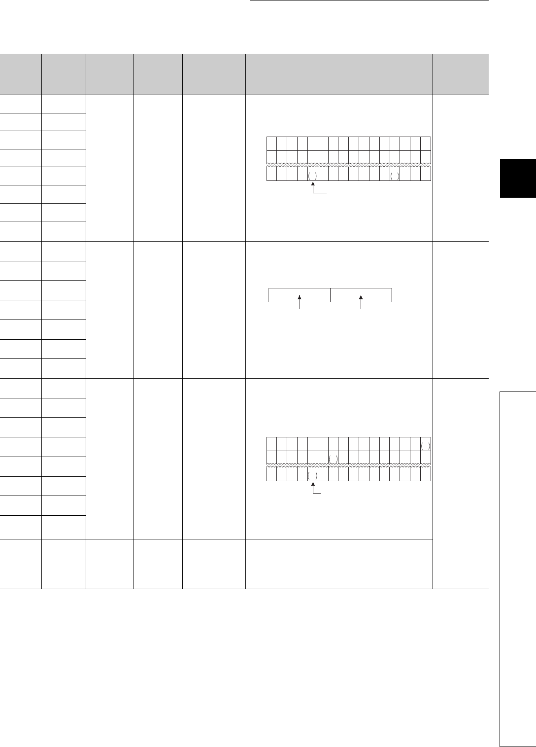
12 - 69
CHAPTER12 PECIAL RELAY LIST AND SPECIAL REGISTER LIST
1
2
3
12
6
7
8
12.2 SPECIAL REGISTER LIST
*1: The relevant modules are as follows:
• The Universal model QCPU whose serial number (first five digits) is "10102" or later.
• Q00UJCPU, Q00UCPU, Q01UCPU
Table12.28 Special register
ACPU
Special
Register
Special
Register
after
Conversion
Special
Register for
Modification
Name Meaning Details Corresponding
CPU
D9100 SD1100
–Fuse blown
module
Bit pattern in units of
16 points, indicating
the modules whose
fuses have blown
• Output module numbers (in units of 16 points), of which fuses have
blown, are entered in bit pattern. (Preset output module numbers
when parameter setting has been performed.)
• Fuse blow check is executed also to the output module of remote I/
O station.
(If normal status is restored, clear is not performed. Therefore, it is
required to perform clear by user program.)
Qn(H)
QnPH
QnU*1
D9101 SD1101
D9102 SD1102
D9103 SD1103
D9104 SD1104
D9105 SD1105
D9106 SD1106
D9107 SD1107
D9108 SD1108
–
Step transfer
monitoring timer
setting
Timer setting valve
and the F number at
time out
• Set the value of the step transition monitoring timer and the
annunciator number (F number) that will be turned ON when the
monitoring timer times out.
• By turning ON any of SM1108 to SM1114, the monitoring timer
starts. If the transition condition following a step which corresponds
to the timer is not established within set time, set annunciator (F) is
turned on.)
Qn(H)
QnPH
D9109 SD1109
D9110 SD1110
D9111 SD1111
D9112 SD1112
D9113 SD1113
D9114 SD1114
D9116 SD1116
–I/O module
verification error
Bit pattern, in units of
16 points, indicating
the modules with
verification errors.
• When I/O modules, of which data are different from those entered
at power-ON, have been detected, the I/O module numbers (in
units of 16 points) are entered in bit pattern. (Preset I/O module
numbers set in parmeters when parameter setting has been
performed.)
• I/O module verify check is executed also to remote I/O station
modules.
(If normal status is restored, clear is not performed. Therefore, it is
required to perform clear by user program.)
Qn(H)
QnPH
QnU*1
D9117 SD1117
D9118 SD1118
D9119 SD1119
D9120 SD1120
D9121 SD1121
D9122 SD1122
D9123 SD1123
D9124 SD1124 SD63
Number of
annuciator
detections
Number of annuciator
detections
• When one of F0 to 255 (F0 to 2047 for AuA and AnU) is turned on
by SET F instruction 1 is added to the contents of SD63. When
RST F or LEDR instruction is executed, 1 is subtracted from the
contents of SD63.
• Quantity, which has been turned on by SET F instruction is stored
into SD63 in BIN code. The value of SD63 is maximum 16.
b15 b14b13b12b11b10 b9 b8 b7 b6 b5 b4b3 b2 b1 b0
00000000
1
(Y80)
000
1
(YC0)
000
0000000000000000
00000000000000 1
Y7
B0
1
Y7
30
SD1100
SD1101
SD1107
Indicates fuse blow.
b15 b7 b0b8to to
(02 to 255)
F number setting Timer time limit setting
(1 to 255 s:(1 s units))
b15 b14b13b12b11b10 b9 b8 b7 b6 b5 b4b3 b2 b1 b0
0000000000000
000000000000000
00000000000000 1
XY
7B0
SD1116
SD1117
SD1123
1
XY
0
1
XY
190
0
00
Indicates an I/O module verify error.

12 - 70
*1: The relevant modules are as follows:
• The Universal model QCPU whose serial number (first five digits) is "10102" or later.
• Q00UJCPU, Q00UCPU, Q01UCPU
Table12.28 Special register
ACPU
Special
Register
Special
Register
after
Conversion
Special
Register for
Modification
Name Meaning Details Corresponding
CPU
D9125 SD1125 SD64
Annunciator
detection
number
Annunciator
detection number
• When any of F0 to 2047 is turned on by SET F instruction, the
annunciator numbers (F numbers) that are turned on in order are
registered into SD1125 to SD1132.
• The F number turned off by RST F instruction is erased from any of
SD1125 to SD1132, and the F numbers stored after the erased F
number are shifted to the preceding registerers.
By executing LEDR instruction, the contents of SD1125 to SD1132
are shifted upward by one.
When there are 8 annunciator detections, the 9th one is not stored
into SD1125 to SD1132 even if detected.
Qn(H)
QnPH
QnU*1
D9126 SD1126 SD65
D9127 SD1127 SD66
D9128 SD1128 SD67
D9129 SD1129 SD68
D9130 SD1130 SD69
D9131 SD1131 SD70
D9132 SD1132 SD71
0 505050505050505050505099
0
0 5050505050505050505099
025
25 99 99 99 99 99 99 99 99 15
123234567888
50
0
0 99 1515151515151570
00 0
0 70707070707065
00 000
0 656565656538
00 0000
0 38383838
110
00 0000
0
0 110 110 110 151
00 0000
0
0151 151 210
00 0000
0
0
00
SD1009
SD1124
SD1125
SD1126
SD1127
SD1128
SD1129
SD1130
SD1131
SD1132
SET
F50
SET
F25
SET
F99
RST
F25
SET
F15
SET
F70
SET
F65
SET
F38
SET
F110
SET
F151
SET
F210 LEDR
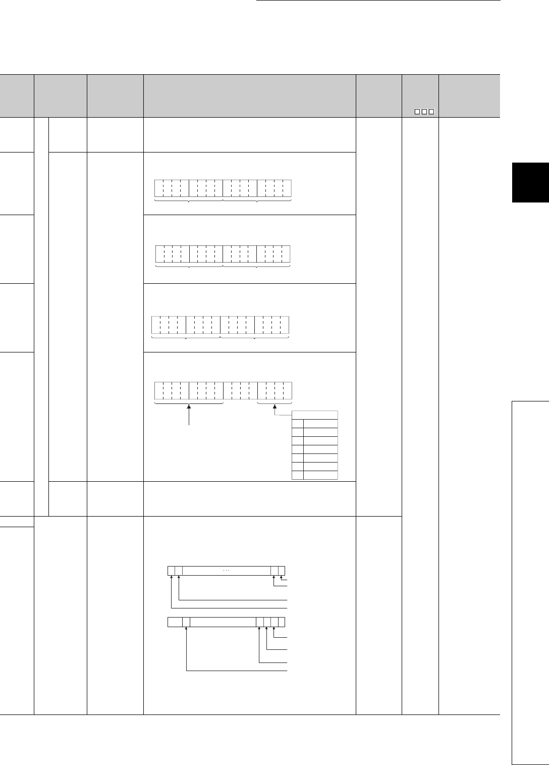
12 - 71
CHAPTER12 PECIAL RELAY LIST AND SPECIAL REGISTER LIST
1
2
3
12
6
7
8
12.2 SPECIAL REGISTER LIST
(11) QCPU with built-in Ethernet port
*1: This applies to the Built-in Ethernet port QCPU.
Table12.29 Special register
Number Name Meaning Explanation Set by
(When Set)
Corres-
ponding
ACPU
D9
Corresponding
CPU
SD1270
Time setting function
Operation
result
Stores
operationresult.
Stores the operation result of the time setting function.
0: Not executed
1: Success
FFFFH: Failure
S (status
change)
New QnU*1
SD1271
Execution
time
Stores time
acquired with time
setting function.
Stores years (last two digits of the Christian Era) and monthes by two digits of
BCD code.
SD1272
Stores dates and hours acquired with time setting function by two digits of
BCD code.
SD1273
Stores minutes and seconds acquired with time setting function by two digits
of BCD code.
SD1274
Stores years (first two digits of the Christian Era) and days acquierd with time
setting function.
SD1275
Required
response
time
Stores time
required for clock
time aquisition.
Stores time taken from transmission to SNTP server to clook time setup at
CPU.
Range: 0 to FFFEH (Unit: ms)
FFFFH when the above limit is exceeded.
SD1276
Forced
connection
invalidation
Specifies forced
connection
invalidation.
Specify this when a connection is to be invalidated forcibly on the user
program. If invalidation is specified for a connection, it stops communication
and does not respond. (When a remote password is used and frequent unlock
processing errors have occurred on a connection, this is useful for temporarily
inhibiting access to the connection.)
0: Valid (default)
1: Invalid
This register is to be invalidated if a socket communication is used as an
open system.
U
SD1277
b15 b12to b11 b8
to b7 b4to b3 b0
to
Example:
July, 1993
9307
H
Year Month
b15 b12to b11 b8
to b7 b4to b3 b0
to
Day Hour
Example:
31st, 10 a.m.
3110H
b15 b12to b11 b8
to b7 b4to b3 b0
to Example:
35 min., 48 sec.
3548H
SecondSecondMinute
b15
b12
to b11 b8
to b7 b4
to b3 b0
to
0
1
2
3
4
5
6
Example:
1993, Friday
1905H
Higher digits of year (0 to 99)
Sunday
Saturday
Friday
Thursday
Wednesday
Tuesday
Monday
Day of the week
b15b14b0b1
SD1276
Connection 1
Directconnection to
SD1277
MELSOFT communicatio
n
FTP communication port
to
b15b14 b13 b12 b4b3 b2 b1 b0
MELSOFT communicatio
n
000
to
Connection 16
Connection 15
Connection 2
port (UDP/IP)
port (TCP/IP)
MELSOFT
12 - 72
*2: The built-in Ethernet port QCPU whose serial number (first five digits) is "11012" or later is targeted.
Table12.30 Special register
Number Name Meaning Explanation Set by
(When Set)
Corres-
ponding
ACPU
D9
Corresponding
CPU
SD1282 Open completion
signal
Stores open
completion status
Open completion status of connections (whose open system is socket
communication) using socket communication functions is stored.
All bits corresponding to connections using any communications other than
the socket communication are fixed to "0".
0 : Open processing is not completed.
1 : Open processing is completed.
S (Status
change) New QnU*2
SD1284 Open request
signal
Stores open
request status
Open request status of connections using socket communication functions is
stored.
All bits corresponding to connections using any communications other than
the socket communication are fixed to "0".
0 : No open requests
1 : In open request
S (Status
change) New QnU*2
SD1286 Reception status
signal
Stores reception
status
Reception status of connections using socket communication functions is
stored.
All bits corresponding to connections using any communications other than
the socket communication are fixed to "0".
For TCP (Normal reception mode)
0 : Data have not been received.
1 : Data have been received.
For TCP (Fixed length reception mode)
0 : Data have not been received
,or received data size has not been reached to valid buffer size.
1 : Received data size has been reached to valid buffer size.
For UDP
0 : Data have not been received.
1 : Data have been received.
S (Status
change) New QnU*2
SD1288
Built-in Ethernet
port connection
status
Stores connection
status of built-in
Ethernet port
Connection status of built-in Ethernet port is stored.
It may take several seconds for the QCPU to determine whether to connect or
disconnect a built-in Ethernet port.
S (Status
change) New QnU*2
b15b14 b0b1
SD1282
Connection 1
to
to
Connection 16
Connection 15
Connection 2
b15b14 b0b1
SD1284
Connection 1
to
to
Connection 16
Connection 15
Connection 2
b15b14 b0b1
SD1286
Connection 1
to
to
Connection 16
Connection 15
Connection 2
b15 b11 b10
1/0
b9 b0
SD1288
to to
Connection status
0 : Not connected with or disconnected from hubs or devices.
1 : Connected to hubs or devices
12 - 73
CHAPTER12 PECIAL RELAY LIST AND SPECIAL REGISTER LIST
1
2
3
12
6
7
8
12.2 SPECIAL REGISTER LIST
(12) Fuse blown module
(13) I/O module verification
(14) Process control instructions
Table12.31 Special register
Number Name Meaning Explanation Set by
(When Set)
Corres-
ponding
ACPU
D9
Corresponding
CPU
SD1300
Fuse blown
module
Bit pattern in units
of 16 points,
indicating the
modules whose
fuses have blown
0 : No blown fuse
1 : Blown fuse
present
• The numbers of output modules whose fuses have blown are input as a
bit pattern (in units of 16 points).
(If the module numbers are set by parameter, the parameter-set
numbers are stored.)
• Also detects blown fuse condition at remote station output modules
• Not cleared even if the blown fuse is replaced with a new one.
This flag is cleared by error resetting operation.
S (Error)
D9100
Qn(H)
QnPH
QnPRH
QnU
SD1301 D9101
SD1302 D9102
SD1303 D9103
SD1304 D9104
SD1305 D9105
SD1306 D9106
SD1307 D9107
SD1308 New
SD1309
to
SD1330
New
SD1331 New
Table12.32 Special register
Number Name Meaning Explanation Set by
(When Set)
Corres-
ponding
ACPU
D9
Corresponding
CPU
SD1400
I/O module
verify error
Bit pattern, in units
of 16 points,
indicating the
modules with
verification errors.
0 : No I/O
verification
errors
1 : I/O verification
error present
• When the I/O modules whose I/O module information differs from that
registered at power-ON are detected, the numbers of those I/O modules
are entered in bit pattern.
(If the I/O numbers are set by parameter, the parameter-set numbers
are stored.)
• Also detects I/O module information.
• Not cleared even if the blown fuse is replaced with a new one.
This flag is cleared by error resetting operation.
S (Error)
D9116
Qn(H)
QnPH
QnPRH
QnU
SD1401 D9117
SD1402 D9118
SD1403 D9119
SD1404 D9120
SD1405 D9121
SD1406 D9122
SD1407 D9123
SD1408 New
SD1409
to
SD1430
New
SD1431 New
Table12.33 Special register
Number Name Meaning Explanation Set by
(When Set)
Corres-
ponding
ACPU
D9
Corresponding
CPU
SD1500
SD1501 Basic period Basic period tome
• Set the basic period (1 second units) use for the process control
instruction using floating point data. UNew
QnPH
SD1502
Process control
instruction detail
error code
Process control
instruction detail
error code
• Shows the detailed error contents for the error that occurred in the
process control instruction. S (Error) New
SD1503
Process control
instruction
generated error
location
Process control
instruction
generated error
location
• Shows the error process block that occurred in the process control
instruction. S (Error) New
SD1506
SD1507 Dummy device Dummy device • Used to specify dummy devices by a process control instruction. U New QnPH
QnPRH
SD1508
Function
availability
selection for
process control
instruction
b0
Bumpless function
availability setting
for the S.PIDP
instrunction
0: Enabled
1: Disabled
(Default: 0)
• Selects the availability (enabled/disabled) of the function for process
control instructions.
UNew QnPH
QnPRH
b15 b14b13b12 b11b10 b9 b8 b7 b6 b5 b4b3 b2 b1 b0
0001
(YC0) 000 00000000
1
(Y80)
SD1300
00
1
(Y1F0) 0000000000
1
(Y1A0)
SD1301 00
00
1
Y1F
B0 00000000SD1331 000
1
Y1F
30
0
Indicates fuse blow.
b15 b14b13 b12 b11 b10 b9 b8 b7 b6 b5 b4b3 b2 b1 b0
000 000 0000000SD1400
00 0 00000000SD1401 00
0 0 0000 000
SD1431 0000
Indicates an I/O module verify error.
00
00
00
1
X Y
0
1
X Y
190
1
X Y
1FE0
SD1501 SD1500Floating points data = SD1501 SD1500Floating point data =
b0b1b2b15 b14 to
0
0SD1508 0
1/0
Bumpless function
availability for the
S.PIDP instruction
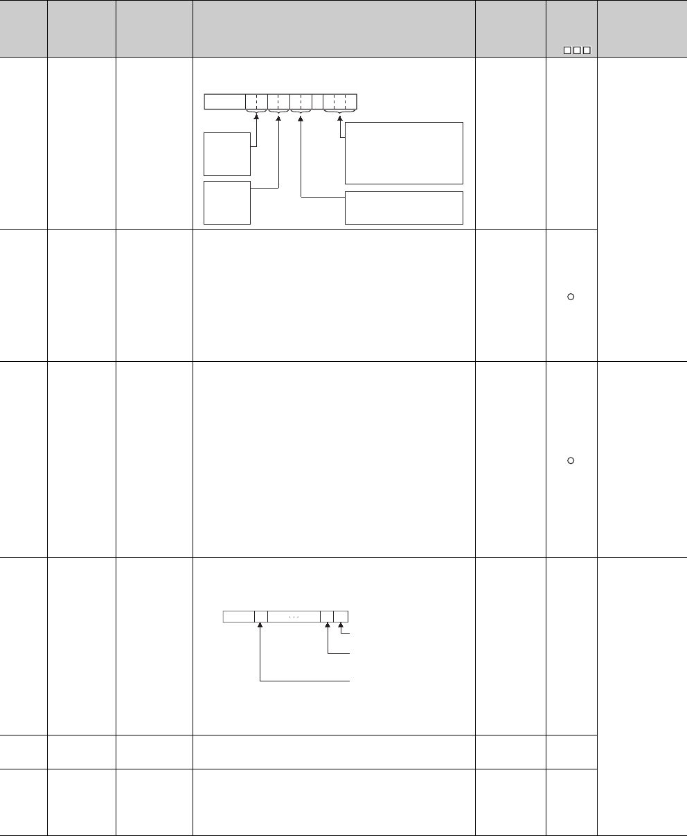
12 - 74
(15) For redundant systems (Host system CPU information *1)
SD1510 to SD1599 are only valid for redundant systems.
They are all set to 0 for stand-alone systems.
*1: The information of the host CPU module is stored.
Table12.34 Special register
Number Name Meaning Explanation Set by
(When Set)
Corres-
ponding
ACPU
D9
Corresponding
CPU
SD1585
Redundant
system LED
status
4 LED states
• BACKUP
• CONTROL
• SYSTEM A
• SYSTEM B
The LED status for BACKUP, CONTROL, SYSTEM A, SYSTEM B is
stored in the following format:
S (status
change) New
QnPRH
SD1588
Reason(s) for
system switch-
ing
Reason(s) for
system switching
that occurred in
host station
Stores the reason(s) for system switching on the host system.
The following values are stored corresponding to the methods for system
switching:
Initialized to 0 when the power supply is switched off and then on or the
RESET switch is set to the RESET position and then to the neutral
position.
0: Initial value (control system has not been switched)
1: Power off, Reset, H/W failure, WDT error,
2: CPU stop error (except WDT)
3: System switching request from network module
16: System switching dedicated instruction
17: System switching request from GX Developer
S (when
condition occurs)
SD1589
Reason(s) for
system
switching failure
conditions
Reason(s) for
system switching
failure No.
• Stores the reason(s) for system switching failure.
0: System switching normal (default)
1: Tracking cable is not connected , tracking cable error, FPGA circuit
failure.
2: H/W failure, power-OFF, Reset, WDT error on the standby system
3: H/W failure, power-OFF, Reset, WDT error on the Control system
4: Tracking data transfer initialization
5: Communication timeout
6: Serious error(except WDT error) on the Standby system
7: There is difference between both systems
(detected as Backup mode only)
8: During memory copy from control system to standby system
9: During online program change
10: During detection of intelligent function module failure on the standby
system
11: System switching being executed
• Resets to "0" when host system is powered on.
• Resets to "0" once system has been switched successfully.
S(when system
is switched) QnPRH
SD1590
Network module
head address,
which requested
system
switching
Network module
head address,
which requested
system switching
• Stores head address of network module which a system switch request
was initiated.
• Turns off automatically by system, after network error is reset by user.
• Please refer to SD1690 which stores the corresponding head address of
network module on other system.
S (Error/Status
change) New
QnPRH
SD1595
Memory copy
target I/O
number
Memory copy
target I/O number
• Stores the memory copy target I/O No.(Standby system CPU module:
3D1H) of before SM1595 is turned from OFF to ON. UNew
SD1596 Memory copy
status
Memory copy
status
• Stores the execution result of Memory copy function.
0 : Memory copy successfully completed
4241H: Standby system power supply off
4242H: Tracking cable is disconnected or is damaged
4247H: Memory copy function is being executed
4248H: Unsupported memory copy destination I/O Number
S (Status
change) New
b0tob2b3b4b5b6b7b8b10b9b15
00
to
SYSTEM B
0: Off
1: On
2: Flicker
SYSTEM A
0: Off
1: On
2: Flicker
CONTROL
0: Off
1: On
BACKUP
0: Off
1: On (red)
2:
3: On(green)
4: Flicker(green)
Flicker(red)
5: On (orange-yellow)
6: Flicker
(orange-yellow)
b1 b0b15 b11to to
00/1
0/10
Module 0:
Module 1:
Module11:
SD1590
Each bit
0:OFF
1:ON
to
CPU module is invalid
as it is 2-slot model.
Module on the right
side of the CPU module
Module at the
rightmost end of the
12-slot base (Q312B)
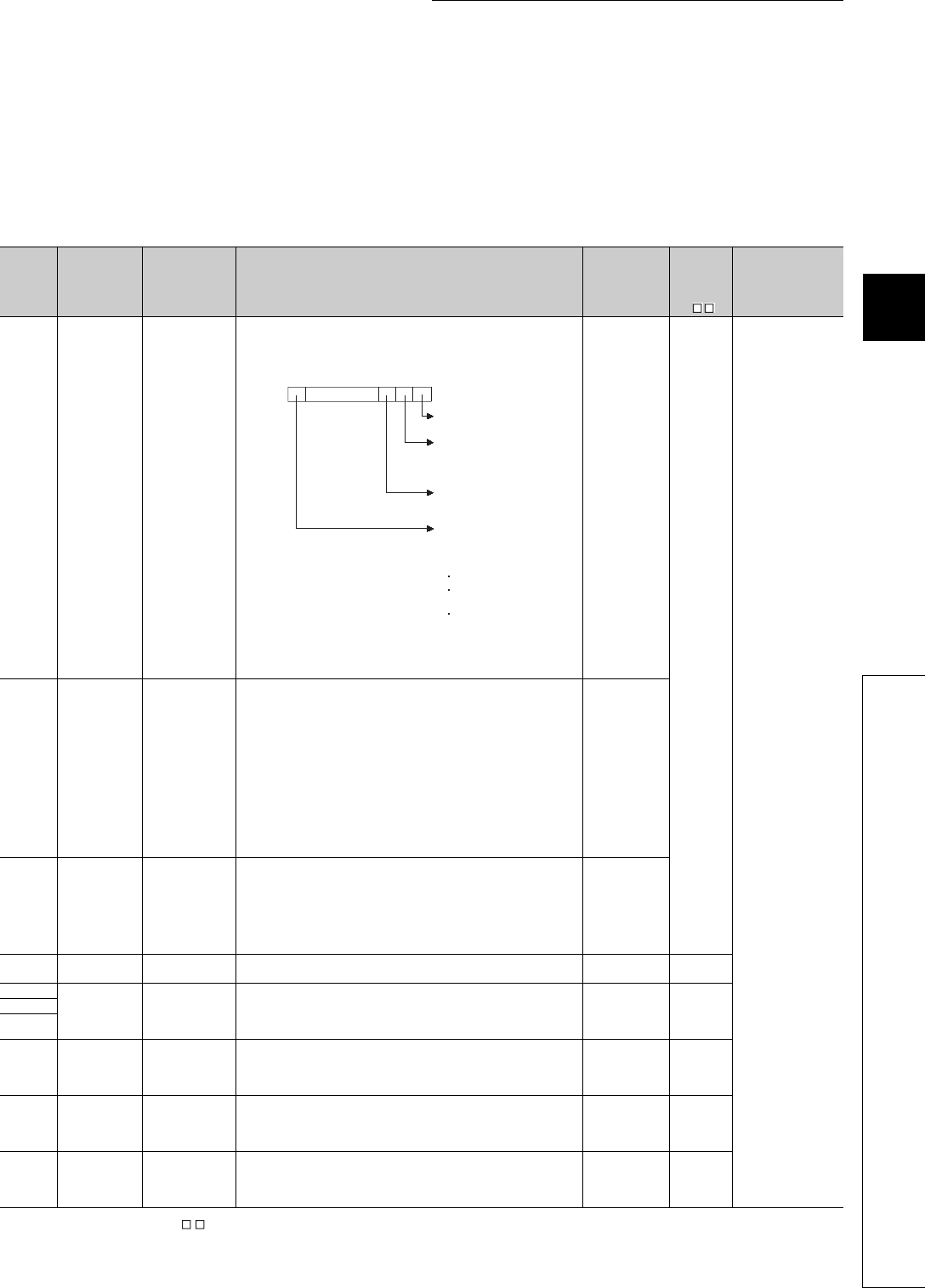
12 - 75
CHAPTER12 PECIAL RELAY LIST AND SPECIAL REGISTER LIST
1
2
3
12
6
7
8
12.2 SPECIAL REGISTER LIST
(16) For redundant systems (Other system CPU information *1)
SD1600 to SD1659 is only valid during the back up mode for redundant systems, and
refresh cannot be done when in the separate mode.
SD1651 to SD1699 are valid in either the backup mode or separate mode.
When a stand-alone system SD1600 to SD1699 are all 0.
*2: Shows the special register (SD ) for the host system CPU module.
Table12.35 Special register
Number Name Meaning Explanation Set by
(When Set)
Corres-
ponding
ACPU
SD *2
Corresponding
CPU
SD1600 System error
information
System error
information
• If an error is detected by the error check for redundant system, the
corresponding bit shown below turns ON. That bit turns OFF when the
error is cleared after that.
• If any of b0, b1, b2 and b15 is ON, the other bits are all OFF.
• In the debug mode, b0, b1, b2 and b15 are all OFF.
S(Every END)
–
QnPRH
SD1601
System
switching
results
System switching
results
Stores the reasons for system switching.
• Stores the reasons for system switching into SD1601 of both systems
when system switching occarred.
• Initialized to 0 at power OFF to ON/reset to unreset.
• The following shows values stored into this register.
0: Initial value (System switching has not occurred)
1: Power-OFF, Reset, H/W failure, WDT error,(*)
2: CPU stop error (except WDT)
3: System switching request by network module
16: System switching dedicated instruction
17: System switching request from GX Developer
*: When the system is switched by the power OFF/reset of the control
system, "1" is not stored into SD1601 of the new standby system.
S(when system
is switched)
SD1602
System
switching
dedicated
instruction
parameter
System switching
dedicated
instruction
parameter
• Stores the parameters for system switching dedicated instruction
SP.CONTSW.
(The parameters (SD1602) for SP.CONTSW are stored in both systems
A&B)
• SD1602 is only valid when "16" is stored in SD1601.
• This SD1602 is updated once system switch instruction SP.CONTSW is
activated.
S(when system
is switched)
SD1610 Other system
diagnostic error
Diagnostic error
code
• The error value sorted in BIN code.
• Stores SD0 of the other system CPU module S(Every END) SD0
SD1611 Other system
diagnostic error
occurrence
time
Diagnostic error
occurrence time
• Stores the date and time when diagnostics error occurred corresponding
to error code stored in SD1610.
• Data format is the same as SD1 to SD3.
• Also, stores the value to SD1 to SD3.
S(Every END) SD1 to
SD3
SD1612
SD1613
SD1614
Other system
error
information
category
Error information
category code
• Stores the category code corresponding to the error comment
information/individual information code.
• Data format is the same as SD4.
• Also, stores the value to SD4.
S(Every END) SD4
SD1615
to
SD1625
Other system
error common
information
Error common
information
• Stores the common information corresponding to the error code stored
in this system CPU.
• Data composition is the same as SD5 to SD15.
• Also, stores the value to SD5 to SD15.
S(Every END) SD5 to
SD15
SD1626
to
SD1636
Other system
error individual
information
Error individual
information
• Stores the individual information corresponding to the error code stored
in this system CPU.
• Data composition is the same as SD16 to SD26.
• Also, stores the value to SD16 to SD26.
S(Every END) SD16 to
SD26
b1 b0b15 b2
Fixed to 0
Tracking cable is not
connected or damaged
Each bit
0: OFF
1: ON
Power-OFF, reset,
watchdog timer error or
hardware failure occurred
in other system
Bit turns on when failing to
connect with other system.
The following causes are
shown below:
Tracking H/W failure
Host system WDT
error
Cannot recognize
other system therefore
causing error
SD1600
Other system stop error
(except watchdog timer
error)
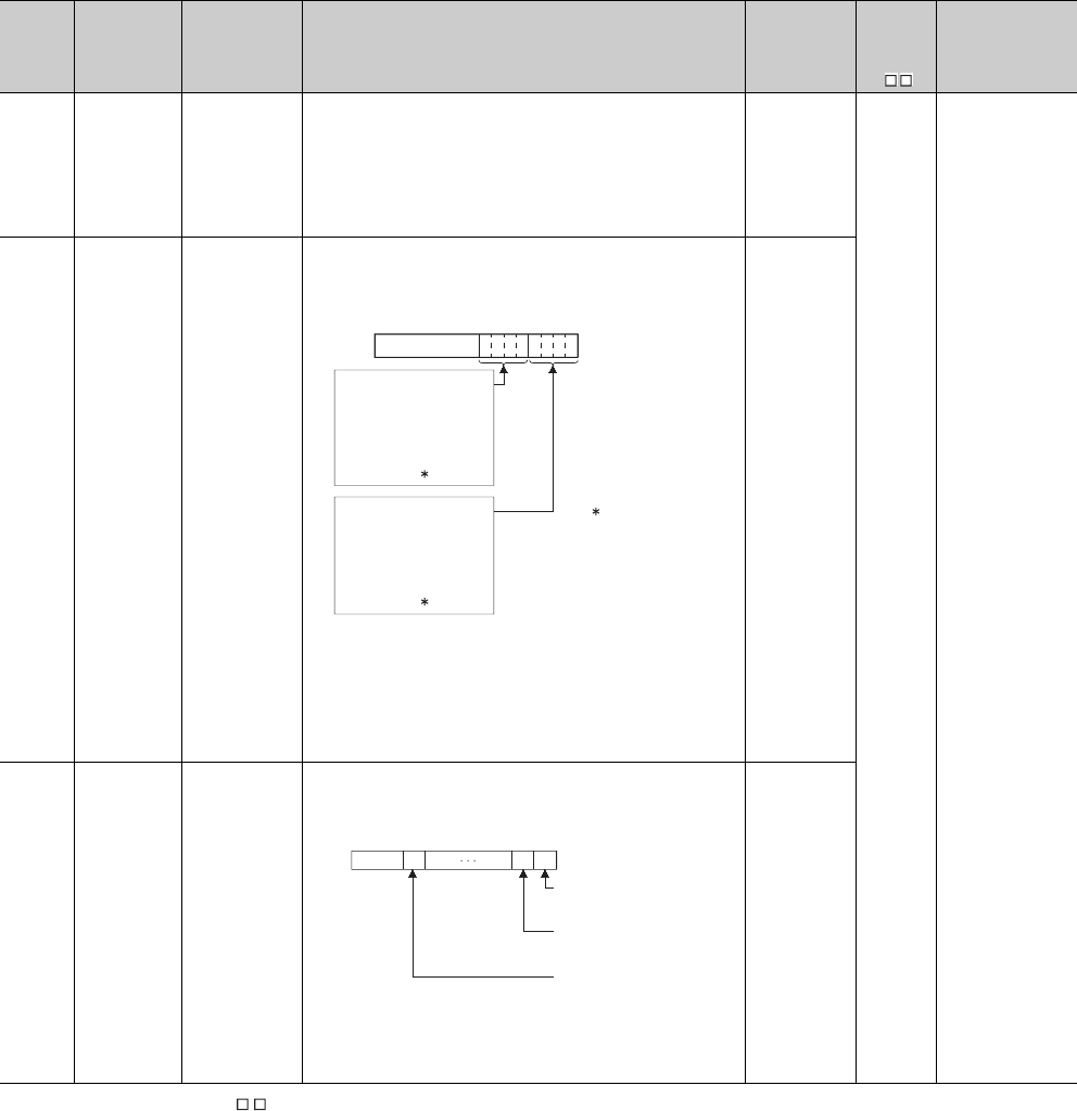
12 - 76
*2 : Shows the special register (SD ) for the host system CPU.
Table12.35 Special register
Number Name Meaning Explanation Set by
(When Set)
Corres-
ponding
ACPU
SD *2
Corresponding
CPU
SD1649
Standby system
error cancel
command
Error code of error
to be cleared
• Stores the error code of the error to be cleared by clearing a standby
system error.
• Stores the error code of the error to be cleared into this register and turn
SM1649 from OFF to ON to clear the standby system error.
• The value in the lowest digit (1 place) of the error code is ignored when
stored into this register.
(By storing 4100 in this register and resetting the error, errors 4100 to
4109 can be cleared.)
S(Every END)
–QnPRH
SD1650
Other system
operating
information
Other system
operating
information
Stores the operation information of the other system CPU module in the
following format.
"00FFH" I stored when a communication error occurs, or when in debug
mode.
Note : A communication error is caused by the following:.
• When the power supply is switched off, or when the other system is
reset.
• H/W error occurs on either of system A or B.
• WDT error occurs.
• Tracking cable is not connected.
• Tracking cable is disconnected or damaged.
S(Every END)
SD1690
Network module
head address,
which requested
system
switching on
host (control)
system
Network module
head address,
which requested
system switching
on host (control)
system
• Stores head address of network module which a system switch request
was initiated, using the following format.
• Turns off automatically by system, after network error is reset by user.
• Please refer to SD1590 which stores the corresponding head address of
network module on host system.
S(Every END)
0:No error
1:Continue error
2:Stop error
F:Communication with
other system
disabled
0:RUN
2:STOP
3:PAUSE
F:Communication with
other system
disabled
:Communication
with other system
disabled, debug
mode
b15 to tob8 b4b7 tob3 b0
0
SD1650
)
(
)
(
to
b1 b0
b15 b11to to
00/1
0/10
Module 0:CPU module is
invalid as it is 2-
slot model
Module 1:Module on the
right side of the
CPU module
Module11:Module at the
rightmost end of
the 12-slot base
(Q312B)
SD1690
Each bit
0:OFF
1:ON

12 - 77
CHAPTER12 PECIAL RELAY LIST AND SPECIAL REGISTER LIST
1
2
3
12
6
7
8
12.2 SPECIAL REGISTER LIST
(17) For redundant systems (Trucking)
SD1700 to SD1779 is valid only for redundant systems.
These are all 0 for stand-alone systems.
Table12.36 Special register
Number Name Meaning Explanation Set by
(When Set)
Corres-
ponding
ACPU
D9
Corresponding
CPU
SD1700 Tracking error
detection count
Tracking error
detection count
• When the tracking error is detected, count is added by one.
• The counter repeats an increment and decrement of the value; 0
32767 - 32768 0
S(Error)
New
QnPRH
SD1710
Waiting time for
online program
change
(standby
system)
Waiting time for
online program
change (standby
system)
• Set in seconds the waiting time of the standby system CPU module from
when online program change to the control system CPU module is
completed by the online program change for redundancy function until
the online program change to the standby system CPU module starts.
• If no online program change request is issued to the standby system
CPU module within the preset time after completion of the online
program change to the control system CPU module, both system CPU
modules judge it as the failure of the online program change for
redundancy. In this case, both system CPU modules resume the
consistency check between system A & B suspended during the online
program change. Also, the control system CPU module is set to accept a
new request of online program change for redundancy.
• When both systems are powered on, 90 seconds are set to SD1710 as
the default value.
• Set the value within the range 90 to 3600 seconds. When the setting is 0
to 89 seconds, it is regarded as 90 seconds for operation. If the setting is
outside the allowed range, it is regarded other than 0 to 3600 seconds
for operation.
• The waiting time for a start of online program change to the standby
system CPU module is checked according to the SD1710 setting during
online change of multiple blocks and online change of batch of files for
redundancy.
U/ S (Initial) QnPRH
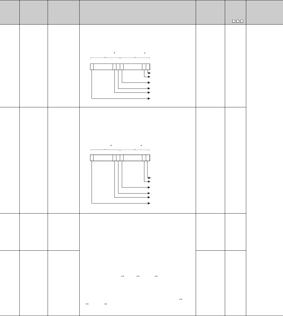
12 - 78
(18) Redundant power supply module information
SD1780 to SD1789 are valid only for a redundant power supply system.
The bits are all 0 for a singular power supply system.
*1: The "power supply 1" in dicates the redundant power supply module mounted on the POWER 1 slot of the redundant base unit (Q38RB/68RB/Q65WRB).
The "power supply 2" indicates the redundant power supply module mounted on the POWER 2 slot of the redundant base unit (Q38RB/68RB/Q65WRB).
*2: The module whose first 5 digits of serial No. is "07032" or later.
However, for the multiple CPU system configuration, this applies to all CPU modules whose first 5 digits of serial No. are "07032" or later.
*3: The module whose first 5 digits of serial No. is "10042" or later.
Table12.37 Special register
Number Name Meaning Explanation Set by
(When Set)
Corres-
ponding
ACPU
D9
Corresponding
CPU
SD1780
Power supply
off detection
status
Power supply off
detection status
• Stores the status of the redundant power supply module with input
power OFF in the following bit pattern.
• Stores 0 when the main base unit is not the redundant power main base
unit (Q38RB).
• When configuring multiple CPU, the status is stored to 1st CPU module.
S(Every END) New
Qn(H)*2
QnPH*2
QnPRH
QnU*3
SD1781
Power supply
failure detection
status
Power supply
failure detection
status
• Stores the failure detection status of the redundant power supply module
in the following bit pattern. (The corresponding bit is cleared to 0 when
the input power to the faulty redundant power supply module is switched
OFF after detection of the redundant power supply module failure.)
• Stores 0 when the main base unit is not the redundant power main base
unit (Q38RB).
• When configuring multiple CPU, the status is stored to 1st CPU module.
S(Every END) New
SD1782
Momentary
power failure
detection
counter for
power supply
1*1
Momentary power
failure detection
count for power
supply 1
• Counts the number of times of momentary power failure of the power
supply 1/2.
• Monitors the status of the power supply 1/ 2 mounted on the redundant
power main base unit (Q38RB) and counts the number of times of
momentary power failure.
Status of power supply 1/power supply 2 mounted on the redundant
extension base unit is not monitored.
• When the CPU module starts, the counter of the power supply 1/ 2 is
cleared to 0.
• If the input power to one of the redundant power supply modules is
turned OFF, the corresponding counter is cleared to 0.
The counter is incremented by 1 every time the momentary power failure of
the power supply 1/ 2 is detected.(The counter repeats increment and
decrement of the value; 0 32767 – 32768 0 (The system monitor
of GX Developer shows the counter within the range between 0 and 65535.
• Stores 0 when the main base unit is not the redundant power main base
unit (Q38RB).
• When configuring multiple CPU, the status is stored to 1st CPU module.
• The counter repeats increment and decrement of the value, 0 32767
– 32768 0
(The system monitor of GX Developer shows the counter within the
range between 0 and 65535.
S(Every END) New
SD1783
Momentary
power failure
detection
counter for
power supply
2*1
Momentary power
failure detection
count for power
supply 2
S(Every END) New
b0b7b8b15 toto
toto
Input power OFF
detection status of
power supply 2Each bit
0:Input power ON status/ No
redundant power supply
module
1:Input power OFF status
SD1780
Input power OFF
detection status of
power supply 1
11
b9 b1
Main base unit
Extension base unit 1st stage
Extension base unit 7th stage
Main base unit
Extension base unit 1st stage
Extension base unit 7th stage
:
:
Failure detection
status of power
supply 1
b0b7b8b15 toto
toto
Failure detection
status of power
supply 2Each bit
0:Redundant power supply
module failure not
detected/No redundant power
supply module
1:Redundant power supply
module failure detected
(Detectable for redundant
power supply module only)
SD1781
11
Main base unit
Extension base unit 1st stage
Extension base unit 7th stage
Main base unit
Extension base unit 1st stage
Extension base unit 7th stage
:
:
b9 b1

1
2
3
APPEN-
DIX
6
7
8
Appendix 1 List of Parameter Numbers
APPENDICES
App - 1
APPENDICES
Appendix 1 List of Parameter Numbers
Each parameter number will be stored in the special register (SD16 to SD26) when an error occurs in the
parameter settings.
TableApp.1 lists the parameter items and corresponding parameter numbers.
For explanation of M and N shown in the "Parameter No." column, refer to Section 8.2.
(To the next page)
TableApp.1 List of parameter numbers
Item Parameter No. Reference
Label 0000HSection 8.1(1)
Comment 0001H
I/O assignment
Type
0400HSection 4.2.2, 8.1 (9)
Model name
Points
Start XY (Start I/O number)
Base setting
Base model name
0401HSection 4.2.1, Section 8.1(10)
Power model name
Extension cable
Slots
Detailed setting
Error time output mode 0403HSection 6.8, Section 8.1(10)
I/O response time 0405HSection 6.8, Section 8.1(10)
Control PLC 0406H
Section 8.1 (9),
QCPU User’s Manual (Muitiple
CPU System)
No. of PLC 0E00H
Section 8.1 (12),
QCPU User’s Manual (Muitiple
CPU System)
Operating mode 0E01H
I/O sharing when using
Multiple CPUs
All CPUs can read all inputs 0E04H
All CPUs can read all outputs
Timer limit setting Low speed 1000HSection 8.1(2)
High speed
RUN-PAUSE contacts RUN 1001H
Section 6.6.1, Section 8.1(2)
PAUSE Section 6.6.2, Section 8.1(2)
Remote reset 1002HSection 6.6.3, Section 8.1(2)
Output mode at STOP to RUN 1003HSection 6.4, Section 8.1(2)
Common pointer No. 1005HSection 9.10.2, Section 8.1(2)
Points occupied by empty slot 1007HSection 4.4.2, Section 8.1(2)
Interrupt program/Fixed scan program setting 1008H
Section 2.2.3, 2.3.4, 8.1 (2)
System interrupt settings Fixed scan interval (n : 28 to 31) Section 8.1(2)
Intelligent function module setting (Interrupt pointer setting) 100AHSection 9.11, Section 8.1(2)
Module synchronization 100CHSection 8.1(2)

App - 2
(To the next page)
TableApp.1 List of parameter numbers (continued)
Item Parameter No. Reference
Use serial communication
100EHSection 6.23, Section
8.1(11)
Transmission speed
Sum check
Transmission wait time
RUN write setting
Service processing setting 1013HSection 6.24.1, Section
8.1(2)
Latch data backup operation valid contact 1014HSection 6.28, Section 8.1(2)
File register 1100HSection 9.7, Section 8.1(3)
Comment file used in a command 1101HSection 8.1(3)
Initial Device value 1102HSection 6.25, Section 8.1(3)
File for local device 1103HSection 9.14.2, Section
8.1(3)
Transfer to Standard ROM at Latch data backup operation 1104HSection 6.28, Section 8.1(3)
File used for SP.DEVST/S.DEVLD instruction 1105HSection 6.29, Section 8.1(6)
Device points 2000HSection 9.1, Section 8.1(6)
Latch (1) start/end 2001HSection 3.4, 6.3, Section
8.1(3)
Latch (2) start/end 2002H
Local device start/end 2003HSection 9.14.2, Section
8.1(6)
File register extended
setting
Device points 2000H
Section 9.8, Section 8.1(6)
Latch (1) start/end 2004H
Latch (2) start/end 2005H
32 bit Indexing 2000HSection 8.1(6)
WDT (watchdog timer)
setting
WDT setting
3000H
Section 6.16, Section 8.1(4)
Initial execution monitoring time Section 2.3.1, Section
8.1(4)
Error check
Carry out battery check
3001H
Section 6.17, Section 8.1(4)
Carry out fuse blown check
Verify module
Check device range at indexing
Diagnose redundant power supply system
Operating mode when
there is an error
Computation error
3002H
Expanded command error
Fuse blown
Module verify error
Intelligent module program execution error
File access error
Memory card operation error
External power supply OFF
Constant scanning 3003HSection 6.2, Section 8.1(4)
Module error collection setting 300AHSection 6.32, Section 8.1(5)
Detailed setting H/W error time PLC operation mode 4004HSection 6.9, Section 8.1(10)

1
2
3
APPEN-
DIX
6
7
8
Appendix 1 List of Parameter Numbers
APPENDICES
App - 3
(To the next page)
TableApp.1 List of parameter numbers (continued)
Item Parameter No. Reference
Number of modules on MELSECNET/H 5000H
Section 8.2(2)
Valid module during other station access 5001H
Interlink transmission parameters 5002H
Routing parameters 5003H
Starting I/O No.
5NM0HNetwork No.
Total stations
Mode 5NM0H
Refresh parameters 5NM1H
Common parameters 5NM2H
Station inherent parameters 5NM3H
Sub-master parameters 5NM5H
Common parameters 2 5NMAH
Station inherent parameters 2 5NMBH
Interrupt settings
Program 7000HSection 2.3, Section 8.1(7)
Boot option
Clear program memory
7000HSection 5.1.2, 5.1.8, Section
8.1(8)
Auto Download all Data from Memory card to
Standard ROM
Boot file setting
SFC program start mode 8002H
Section 8.1(9)Start conditions 8003H
Output mode when the block is stopped 8006H
Number of modules on Ethernet 9000H
Section 8.2(3)
Starting I/O No.
9N00H
Network No.
Group No.
Station No.
Operational settings
Initial settings 9N01H
Open settings 9N02H
Router relay parameter 9N03H
Station No.<->IP information 9N05H
FTP Parameters 9N06H
E-mail settings 9N07H
News setting 9N08H
Interrupt settings 9N09H
Routing parameters 9N04H

App - 4
(To the next page)
TableApp.1 List of parameter numbers (continued)
Item Parameter No. Reference
Number of modules on CC-Link IE controller network A000H
Section 8.2(1)
Interlink transmission parameters A002H
Routing parameters A003H
Starting I/O No.
ANM0H
Network No.
Total stations
Station No.
Mode ANM0H
Refresh parameters ANM1H
Common parameters ANM2H
Station inherent parameters ANM3H
Number of modules C000H
Section 8.2(4)
Remote input (RX)
CNM1H
Remote output (RY)
Remote register (RWr)
Remote register (RWw)
Ver.2 Remote input (RX)
Ver.2 Remote output (RY)
Ver.2 Remote register (RWr)
Ver.2 Remote register (RWw)
Special relay (SB)
Special register (SW)
Operational setting
CNM2H
All connect count
Retry count
Automatic reconnection station count
Standby master station No.
PLC down select
Scan mode setting
Delay information setting
Station information setting
Remote device station initial setting
Interrupt setting

1
2
3
APPEN-
DIX
6
7
8
Appendix 1 List of Parameter Numbers
APPENDICES
App - 5
TableApp.1 List of parameter numbers (continued)
Item Parameter No. Reference
Communication area setting (refresh setting) E002H,
E003H
Section 8.1 (12),
QCPU User’s Manual
(Muitiple CPU System)
Online module change E006H
Refresh parameter detailed device specification E007H
Multiple CPU high
speed transmission
area setting
CPU specific send range E008H
Auto refresh setting E009H
Multiple CPU synchronous startup setting E00BH
Host CPU number E00CH
App - 6
Appendix 2 Functions Added or Changed by Version Upgrade
The Universal model QCPU is upgraded when some functions are added or specifications are changed.
Therefore, the functions and specifications differdepending on the function version and serial number.
(1) Function added and supported CPU module and GX Developer versions
: Not related to GX Developer
TableApp.2 Functions added and supported CPU module and GX Developer versions
Function Function
version
First 5 digits of
serial No.
Supported GX
Developer
Use of the PC CPU module*1 ( QCPU User’s Manual (Multiple CPU
System))
B
"09072" or later
Setting of whether to use local device for each program ( Section 9.14.2)
"10012" or later
Version 8.62Q or
later
Program batch transfer execution status (SM165) ( Section 5.1.3)
Multiple CPU high speed transmission dedicated instruction*1 ( QCPU
Programming Manual (Common Instructions))
Amount of battery consumption display ( QCPU User's Manual (Hardware
Design, Maintenance and Inspection))
Bit device extension ( Section 9.2)
"10042" or later Version 8.68W or
later
Executional conditioned device test ( Section 6.11.4)
Auto start sampling trace function*1 ( Section 6.14)
CC-Link IE group cyclic transmission function ( CC-Link IE Controller
Network Reference Manual)
Scan time measurement ( Section 6.13.3)
External input/output forced on/off ( Section 6.11.3)
Monitor condition setting*1 ( Section 6.11.3)
Redundant power supply system-compatible *1 ( Section 6.20)
32-bit index modification using "ZZ" ( QCPU Programming Manual
(Common Instructions))
Extended data register (D) and extended link register (W)*1 *2 ( Section
9.8) "09042"or later *1 Version 8.70Y or
later
Serial Communication Function*1 ( Section 6.23)
"10102" or later
Version 8.78G or
later
CPU module change function with memory card*1 ( Section 6.30)
Local device setting of the index register *1 ( Section 9.14.2)
Communication using the A-compatible 1C/1E frame (MC protocol)*3 *4 (
Q Corresponding MELSEC Communication Protocol Reference Manual)
Socket communication function ( QnUCPU User's Manual
(Communication via Built-in Ethernet Port))*1 "11012" or later
Module model name read ( Section 6.31) "11043" or later
Version 8.82L or
later
Module error collection function ( Section 6.32) - *5

1
2
3
APPEN-
DIX
6
7
8
Appendix 2 Functions Added or Changed by Version Upgrade
APPENDICES
App - 7
*1: Some models do not support the function. For details, refer to the corresponding reference.
*2: Data of the extended data register (D) and extended link register (W) can be retained in the standard ROM by using the latch data backup
to standard ROM function ( Section 6.28) if the serial number (first five digits) of the Universal model QCPU is "10042" or later.
*3: Communication using the A-compatible 1E frame is available only via any Ethernet module.
If the module is connected to the built-in Ethernet port of the CPU module, this function is not available.
*4: Communication using the A-compatible 1C frame is available only via any serial communication module.
If the module is connected to the built-in RS-232 interface of the CPU module, this function is not available.
*5: Use GX Works2 of version 1.12N or later.

App - 8
Appendix 3 Method of Replacing Basic Model QCPU or High
Performance Model QCPU with Universal Model QCPU
Appendix 3.1 Replacement Precautions
This section describes precautions for replacing the Basic model QCPU or High Performance model QCPU with the
Universal model QCPU and the replacement methods.
Appendix 3.1.1 Replacing Basic model QCPU with Universal model QCPU
(1) System configuration
(2) Program
(To the next page)
TableApp.3 Precautions for replacement and replacement methods (System configuration)
Item Precautions Replacement method Reference
GOT GOT900 series cannot be connected. Use GOT1000 series. ---
Applicable products
and software
Products and software compatible with
the Universal model QCPU must be used.
Products need to be replaced for the
compatibility with the Universal model
QCPU and software need to be upgraded
for the communication with the Universal
model QCPU are described in Appendix
3.2.
Appendix 3.2
Multiple CPU system
To configure a multiple CPU system, CPU
modules compatible with the Universal
model QCPU must be used.
CPU modules compatible with the
Universal model QCPU are described in
Appendix 3.2.
Appendix 3.2
TableApp.4 Precautions for replacement and replacement methods (Program)
Item Precautions Replacement method Reference
Language and
instruction Some instructions are not supported.
Replace the instructions not supported in
the Universal model QCPU are described
in Appendix 3.3.
Appendix 3.3
Floating-point
operation
When using the floating-point data
comparison instructions, LDE ,
ANDE , ORE , LDED , ANDED ,
and ORED , if the comparison source
data are -0, nonnumeric, unnormalized
number, or , “OPERATION
ERROR” (error code: 4101) is detected.
( indicates one of the followings;
=,<>,<=,>=,<,>.)
When the floating-point data comparison
instructions are used, modify the program
as described in Appendix 3.4.2.
Section 2.4.4, Appendix
3.4.2
Device range check at
index modification
When a device number exceeds a setting
range due to index modification,
“OPERATION ERROR” (error code:
4101) is detected.
Deselect the "Check device range at
indexing" checkbox in the PLC RAS tab of
the PLC parameter dialog box so that
checking is not performed.
Section 6.17, Appendix
3.4.3

1
2
3
APPEN-
DIX
6
7
8
Appendix 3 Method of Replacing Basic Model QCPU or High Performance Model QCPU with Universal
Model QCPU
Appendix 3.1 Replacement Precautions
APPENDICES
App - 9
(To the next page)
TableApp.4 Precautions for replacement and replacement methods (Program) (Continued)
Item Precautions Replacement method Reference
Latch setting
If latch ranges of internal user devices are
specified, the processing time is added in
proportion to the device points set to be
latched.
The latch function of the Universal model
QCPU is enhanced.
(1) Large-capacity file register (R, ZR)
(2) Writing/reading device data to the
standard ROM (SP.DEVST and
S(P).DEVLD instructions)
(3) Latch range specification of internal
devices
Change the latch method to the method
described in (1) to (3) above according to
the application.
Section 6.3, Appendix
3.4.4
Interrupt counter Interrupt counter is not supported.
Check the numbers of executions for
interrupt programs on the Interrupt
program monitor list screen of GX
Developer.
Section 6.13.2, 9.2.11
SCJ instruction
When the SCJ instruction is used in the
Universal model QCPU, the AND SM400
(or NOP instruction) needs to be inserted
immediately before the SCJ instruction.
Insert the AND SM400 (or NOP
instruction) immediately before the SCJ
instruction when the SCJ instruction is
used.
Section 6.5.1 in the
QCPU Programming
Manual (Common
Instructions)
JP/GP.SREAD and JP/
GP.SWRITE
instructions
Use of the completion notification device
of the target station specified in D3 when
the SREAD and SWRITE instructions are
used is available. (The Basic model
QCPU ignores the device specified in
D3.)
To get the same operation as the Basic
model QCPU, omit D3 or use the READ
instruction instead of the SREAD instruc-
tion.
Section 8.3.2 in the
QCPU Programming
Manual (Common
Instructions)
ZPUSH instruction
The number of index registers is
increased to 20 for the Universal model
QCPU. The area for saving the data in the
index register with the ZPUSH instruction
is increased as well.
Increase the save area used for the
ZPUSH instruction as needed.
Section 7.18.8 in the
QCPU Programming
Manual (Common
Instructions)
Use of the annunciator
(SET F and OUT
F instructions)
When the annunciator is turned on by the
SET F or OUT F instruction, the
USER LED turns on.
(The ERR.LED does not turn on.)
--- ---
I/O refresh between
programs
I/O refresh between programs cannot be
executed.
Execute I/O refresh at the start or end of
each program with the RFS or COM
instruction.
(When the COM instruction is used, I/O
refresh to be executed can be specified in
SD778 by turning on SM774.)
---
SM/SD Usage of a part of the special relay and
special register is different.
Replace the corresponding special relay
and special register as described in
Appendix 3.5.
Appendix 3.5
Multiple CPU system
The start address for the user setting area
(auto refresh) in the CPU shared memory
is changed.
If the user setting area in the CPU shared
memory is specified in the program,
change the address for the user setting
area by performing an operation for
replacing a device in GX Developer.
(Example: "MOV D0 U3E0\G192"
"MOV D0U3E0\G2048")
---

App - 10
(3) Drive and file
(4) External communication (Service processing)
TableApp.4 Precautions for replacement and replacement methods (Program) (Continued)
Item Precautions Replacement method Reference
File register To use the file register, capacity setting is
required.
Set the capacity of the file register used in
the PLC file tab of the PLC parameter.
Section 8.1
SFC program
The following settings are required for
using SFC programs.
• Program setting (when both sequence
programs and SFC programs exist.)
• Common pointer No. setting (to exe-
cute the CALL instruction from SFC
programs)
• Set program details in the Program tab
of the PLC parameter dialog box.
• Enter a common pointer number in the
PLC system of the PLC parameter dia-
log box.
TableApp.5 Precautions for replacement and replacement methods (Drive and file)
Item Precautions Replacement method Reference
Boot file setting The boot file setting is not supported.
Since the Universal model QCPU holds
the data in the program memory even
when the battery voltage drops, the boot
file setting is not necessary.
Move files with the boot setting (from the
standard ROM to the program memory) to
the program memory.
Section 5.1.8
TableApp.6 Precautions for replacement and replacement methods (External communication (Service processing))
Item Precautions Replacement method Reference
Time reserved for
communication pro-
cessing
The time reserved for communication pro-
cessing (SM315/SD315) is not supported.
Set service processing time in the PLC
system tab of the PLC parameter dialog
box.
Section 6.24.1
MC protocol
The following commands cannot specify
monitoring conditions.
• Randomly reading data in units of word
(Command: 0403)
• Device memory monitoring (Command:
0801)
The applicable frame types are as follows:
• QnA-compatible 3C/4C frame
• QnA-compatible 3E frame
•4E frame
---
Q Corresponding
MELSEC
Communication
Protocol Reference
Manual

1
2
3
APPEN-
DIX
6
7
8
Appendix 3 Method of Replacing Basic Model QCPU or High Performance Model QCPU with Universal
Model QCPU
Appendix 3.1 Replacement Precautions
APPENDICES
App - 11
(5) Battery installation position
(6) Program size
TableApp.7 Precautions for replacement and replacement methods (Battery installation position)
Item Precautions Replacement method Reference
Battery installation
position
The battery replacement method is different.
The battery installation position varies
depending on the model.
• Q00JCPU, Q00CPU, Q01CPU
...On the front of the module.
• Q00UJCPU, Q00UCPU, Q01UCPU
...At the bottom of the module.
For the battery replacement method,
refer to the in the Reference column.
Section 7.2 in the
QCPU User's Manual
(Hardware Design,
Maintenance and
Inspection)
TableApp.8 Precautions for replacement and replacement methods (Program size)
Item Precautions Replacement method Reference
Program size
Data in the program memory of the Basic
model QCPU may exceed the size of the
program memory of the Universal model
QCPU.
Store parameter and device comment
files in the standard ROM. ---

App - 12
Appendix 3.1.2 Replacing High Performance model QCPU with Universal
model QCPU
(1) System configuration
*1: The serial number (first five digits) of the applicable module (Q02UCPU, Q03UDCPU, Q04UDHCPU, Q06UDHCPU, Q13UDHCPU, and
Q26UDHCPU) must be "10041" or earlier.
TableApp.9 Precautions for replacement and replacement methods (System configuration)
Item Precautions Replacement method Reference
Use of AnS/A series
module AnS/A series modules are not supported. Use Q series modules. ---
GOT GOT900 series cannot be connected. Use GOT1000 series. ---
Programming tool
connection
Applicable USB cables are different.
• High Performance model QCPU
... A-B type
• Universal model QCPU
... A-miniB type
Use USB cables of A-miniB type. Or, use
USB conversion adapters of B-miniB
type.
---
Applicable products
and software
Products and softwares compatible with
the Universal model QCPU must be used.
Products need to be replaced for the
compatibility with the Universal model
QCPU and software need to be upgraded
for the communication with the Universal
model QCPU are described in Appendix
3.2.
Appendix 3.2
Multiple CPU system
To configure a multiple CPU system, CPU
modules compatible with the Universal
model QCPU must be used.
CPU modules compatible with the
Universal model QCPU are described in
Appendix 3.2.
Appendix 3.2
In a multiple CPU system using the
Motion CPU, an existing auto refresh area
and user setting area cannot be used for
data communication with the Motion CPU.
For data communication with the Motion
CPU, use an auto refresh area and user
setting area in the multiple CPU high-
speed transmission area.
Chapter 4 in the QCPU
User's Manual (Multiple
CPU System)
Redundant power
supply system*1
In a redundant power supply system
using the Q38RB redundant power supply
main base unit and the Q68RB redundant
power supply extension base unit, the
status of the power supply module cannot
be stored in the special relay and special
register (SM1780 to SM1783/SD1780 to
SD1783). The status cannot be displayed
on the system monitor screen.
Check the status of the power supply
module by the LED on the front of the
module.
Section 5.3 in the
QCPU User's Manual
(Hardware Design,
Maintenance and
Inspection)
MELSECNET/H The simple dual-structured network
function is not supported. ---
Section 7.7 in the Q
Corresponding
MELSECNET/H
Network System
Reference Manual (PLC
to PLC network)

1
2
3
APPEN-
DIX
6
7
8
Appendix 3 Method of Replacing Basic Model QCPU or High Performance Model QCPU with Universal
Model QCPU
Appendix 3.1 Replacement Precautions
APPENDICES
App - 13
(2) Program
(To the next page)
TableApp.10 Precautions for replacement and replacement methods (Program)
Item Precautions Replacement method Reference
Language and
instruction Some instructions are not supported.
Replace the instructions not supported in
the Universal model QCPU are described
in Appendix 3.3.
Appendix 3.3
Floating-point
operation
The Universal model QCPU performs
program operations of floating-point data
in single precision.
Instructions for floating-point double-
precision operations are added for the
Universal model QCPU. Replace the
instructions if floating-point double-
precision operations ares required, as
described in Appendix 3.4.
Section 2.4.4, Appendix
3.4, Appendix 3.4.2
When using the floating-point data
comparison instructions, LDE ,
ANDE , ORE , LDED , ANDED ,
and ORED , if the comparison source
data are -0, nonnumeric, unnormalized
number, or , “OPERATION
ERROR “ (error code: 4101) is detected.
( indicates one of the followings;
=,<>,<=,>=,<,>.)
When the floating-point data comparison
instructions are used, modify the program
as described in Appendix 3.4.2.
Device range check at
index modification
When a device number exceeds a setting
range due to index modification,
“OPERATION ERROR” (error code:
4101) is detected.
Deselect the "Check device range at
indexing" checkbox in the PLC RAS tab of
the PLC parameter dialog box so that
checking is not performed.
Section 6.17, Appendix
3.4.3
Program execution
type
Low-speed execution type programs are
not supported.
Use scan execution type programs or
fixed scan execution type programs. Section 2.3
A program execution type cannot be
changed by remote operation.
Use instructions for switching program
execution types, such as PSTOP, POFF,
and PSCAN.
Section 2.3
Latch setting
If latch ranges of internal user devices are
specified, the processing time is added in
proportion to the device points set to be
latched. (For example, if 8K points are
latched for the latch relay (L), the
processing time of 28.6 s is required.)
The latch function of the Universal model
QCPU is enhanced.
(1) Large-capacity file register (R, ZR)
(2) Writing/reading device data to the
standard ROM (SP.DEVST and
S(P).DEVLD instructions)
(3) Latch range specification of internal
devices
Change the latch method to the method
described in (1) to (3) above according to
the application.
Section 6.3, Appendix
3.4.4

App - 14
* 1: Even the local device file usability setting is not available for the Q02UCPU, Q03UDCPU, Q04UDHCPU, and Q06UDHCPU if the serial
number (first five digits) is "10011" or earlier.
TableApp.9 Precautions for replacement and replacement methods (Program) (Continued)
Item Precautions Replacement method Reference
Interrupt program
The interrupt pointer (I49) for the high-
speed interrupt function is not supported.
Consider the use of interrupt pointers for
fixed scan interrupt (I28 to I31).
Section 6.13.2, 9.2.11
Interrupt counter is not supported.
Check the numbers of executions for
interrupt programs on the Interrupt
program monitor list screen of GX
Developer.
The interrupt pointers (I32 to I40) due to
an error are not supported. --- Section 9.11
SCJ instruction
When the SCJ instruction is used in the
Universal model QCPU, the AND SM400
(or NOP instruction) needs to be inserted
immediately before the SCJ instruction.
Insert the AND SM400 (or NOP
instruction) immediately before the SCJ
instruction when the SCJ instruction is
used.
Section 6.5.1 in the
QCPU Programming
Manual (Common
Instructions)
ZPUSH instruction
The number of index registers is
increased to 20 for the Universal model
QCPU. The area for saving the data in the
index register with the ZPUSH instruction
is increased as well.
Increase the save areas used for the
ZPUSH instruction as needed.
Section 7.18.8 in the
QCPU Programming
Manual (Common
Instructions)
File usability setting for
each program
The following file usability setting for each
program is not available.*1
• File register
• Initial device value
• Comment
When file usability is set, modify the
program as described in Appendix 3.4.
Section 2.3, Appendix
3.4.5
I/O refresh setting for
each program
I/O refresh setting for each program is not
available.
Use the RFS instruction if I/O refresh
setting for each program is required.
• Section 2.3
• QCPU Programming
Manual (Common
Instructions)
SM/SD
Usage of a part of the special relay and
special register is different.
Replace the corresponding special relay
and special register as described in
Appendix 3.5.
Appendix 3.5
A sereis-compatible special relay and
special register are not supported.
(SM1000 to SM1255/SD1000 to SD1255)
Using GX Developer, A series-compatible
special relay and special register can be
replaced with the Universal model QCPU-
compatible special relay and special
register. Note, however, that the ones
which are not compatible with the
Universal model QCPU are replaced with
SM1255 and SD1255. Modify programs
as needed.
Chapter 12
Processing time Scan time and each processing time are
different.
Modify programs as needed, checking the
processing timing. ---

1
2
3
APPEN-
DIX
6
7
8
Appendix 3 Method of Replacing Basic Model QCPU or High Performance Model QCPU with Universal
Model QCPU
Appendix 3.1 Replacement Precautions
APPENDICES
App - 15
(3) Drive and file
(4) External communication
*1: The serial number (first five digits) of the applicable module (Q02UCPU, Q03UDCPU, Q04UDHCPU, Q06UDHCPU, Q13UDHCPU, and
Q26UDHCPU) must be "10101" or earlier.
TableApp.11 Precautions for replacement and replacement methods (Drive and file)
Item Precautions Replacement method Reference
Boot file setting
Files in the standard ROM cannot be
booted to the program memory.
Since the Universal model QCPU holds
the data in the program memory even
when the battery voltage drops, the boot
file setting is not necessary.
Move files with the boot setting (from the
standard ROM to the program memory) to
the program memory.
Section 5.1.8, 5.1.10,
Appendix 3.4.6
Booting operation is different.
Replacement method when the
parameter-valid drive and the boot file
setting are set in the High Performance
model QCPU is described in Appendix
3.4.6.
Automatic all data write
from memory card to
standard ROM
The setting method of this function is
different.
In the Boot file tab of the PLC parameter
dialog box, select "standard ROM" for the
transfer destination. Note, however, that
the transfer destination of "program" is
fixed to "program memory". (Setting by
DIP switches is not necessary.)
Section 5.1.8
TableApp.12 Precautions for replacement and replacement methods (External communication)
Item Precautions Replacement method Reference
Module service interval
time read
The module service interval time cannot
be read. --- Section 6.24.1
MC protocol
The following frame types cannot be used
when accessing the Universal model
QCPU.*1
• A-compatible 1C frame
• A-compatible 1E frame
Use the frame types below.
• QnA-compatible 2C/3C/4C frame
• QnA-compatible 3E frame
•4E frame
Q Corresponding
MELSEC
Communication
Protocol Reference
Manual
The following commands cannot specify
monitoring conditions.
• Randomly reading data in units of word
(Command: 0403)
• Device memory monitoring (Command:
0801)
The applicable frame types are as follows:
• QnA-compatible 3C/4C frame
• QnA-compatible 3E frame
•4E frame
---

App - 16
(5) Diagnostic function
(6) Debugging
* 1: Scan time of each program can be checked on the Program monitor list screen.
* 2: Device test by GX Developer can be performed.
* 3: The serial number (first five digits) of the applicable module (Q02UCPU, Q03UDCPU, Q04UDHCPU, Q06UDHCPU, Q13UDHCPU, and
Q26UDHCPU) must be "10041" or earlier.
TableApp.13 Precautions for replacement and replacement methods (Diagnostic function)
Item Precautions Replacement method Reference
Error history Error history data cannot be stored in the
memory card.
The Universal model QCPU can store
history data by the number of storable
history data in a memory card (100) to the
system memory.
Section 6.18
LED indication priority
setting
LED indication priority cannot be set. Only
LED indication setting at error occurrence
is supported.
--- Section 6.21.2
TableApp.14 Precautions for replacement and replacement methods (Debugging)
Item Precautions Replacement method Reference
Monitor*3 The monitoring condition cannot be set.
Use the sampling trace function for
checking device data under the specified
monitoring condition. With this function,
changes of the specified device data can
be recorded at the following timings:
• at execution of the specified step
• on the rising/falling edge of bit devices
• when the value of word devices
coincide with the setting value
• at every specified time (settable range:
1 to 5000ms)
Section 6.11.1, 6.14
Scan time
measurement by GX
Developer*3
Time required for executing a part of the
program cannot be measured using the
scan time measurement function.*1
Calculate the time using instruction
processing time described in the manual.
• Section 6.13.3
• Appendix 1.4 in the
QCPU Programming
Manual (Common
Instructions)
External input/output
forced on/off*3
The external input/output forced on/off
function is not supported.*2
The function can be replaced with the
programs described in Appendix 3.4.7.
Note, however, that replacement method
described does not apply in the following
cases:
• Input and output targeted for forced on/
off are referred to or changed using the
direct input device (DX) and direct
output device (DY).
• Input and output targeted for forced on/
off are referred to or changed within an
interrupt program.
Section 6.11.3,
Appendix 3.4.7

1
2
3
APPEN-
DIX
6
7
8
Appendix 3 Method of Replacing Basic Model QCPU or High Performance Model QCPU with Universal
Model QCPU
Appendix 3.1 Replacement Precautions
APPENDICES
App - 17
(7) Switch on the front of the CPU module
TableApp.15 Precautions for replacement and replacement methods (Switch on the front of the CPU module)
Item Precautions Replacement method Reference
Switch on the front of
the CPU module
The operation method with the RESET/
RUN/STOP switch is modified.
The RESET/STOP/RUN switch of the
Universal model QCPU can be used for
the reset operation of the CPU module
and switching between the STOP and
RUN status.
Section 4.4 in the
QCPU User's Manual
(Hardware Design,
Maintenance and
Inspection)
Latch data cannot be cleared by the switch. To clear latch data, use the remote latch
clear operation of GX Developer.
Section 4.4 in the
QCPU User's Manual
(Hardware Design,
Maintenance and
Inspection)
The system protect cannot be set by the
switch.
Data in the files can be protected by
setting a password for each file.
Password for each file can be registered
with GX Developer.
Section 6.19
The parameter-valid drive setting is not
necessary.
The Universal model QCPU
automatically determines the parameter-
valid drive. Change the setting as
described in Appendix 3.4.5 when the
parameter-valid drive is set to other than
the program memory in the High
Performance model QCPU.
• Appendix 3.4.6
• Section 4.4 in the
QCPU User's Manual
(Hardware Design,
Maintenance and
Inspection)

App - 18
(8) SFC
TableApp.16 Precautions for replacement and replacement methods (SFC)
Item Precautions Replacement method Reference
Step transition
monitoring timer
The step transition monitoring timer is not
supported.
Change the program as described in
Appendix 3.1 in the manual in the
Reference column.
Section 4.6 and
Appendix 3.1 in the
QCPU (Q Mode)/
QnACPU Programming
Manual (SFC)
SFC operation mode
setting
The periodic execution block setting is not
supported.
Change the program as described in
Appendix 3.2 in the manual in the
Reference column.
Section 4.7.4 and
Appendix 3.2 in the
QCPU (Q Mode)/
QnACPU Programming
Manual (SFC)
An operation mode at double block START
cannot be selected. (Fixed to “WAIT”.) ---
Section 4.7.5 in the
QCPU (Q Mode)/
QnACPU Programming
Manual (SFC)
An operation mode at transition to active
step cannot be selected. (Fixed to
“TRANSFER”.)
---
Section 4.7.6 in the
QCPU (Q Mode)/
QnACPU Programming
Manual (SFC)
SFC program for
program execution
management
SFC programs for program execution
management are not supported. ---
Section 5.2.3 in the
QCPU (Q Mode)/
QnACPU Programming
Manual (SFC)
SFC control
instruction
Some SFC control instructions are not
supported.
SFC control instructions not supported in
the Universal model QCPU and
replacing methods are described in
Appendix 3.3.
• Appendix 3.3
• Section 4.4 in the
QCPU (Q Mode)/
QnACPU
Programming Manual
(SFC)
SFC comment
readout instruction
The following SFC comment readout
instructions are not supported.
• S(P).SFCSCOMR (SFC step comment
readout instruction)
• S(P).SFCTCOMR (SFC transition
condition comment readout instruction)
---
Section 4.8 in the
QCPU (Q Mode)/
QnACPU Programming
Manual (SFC)
Method of SFC
program change
SFC program files cannot be written to the
running CPU module. (Programs in SFC
Figure can be changed online.)
Write program data to the CPU module
after changing the Universal model
QCPU status to STOP.
Section 6.6 in the
QCPU (Q Mode)/
QnACPU Programming
Manual (SFC)
1
2
3
APPEN-
DIX
6
7
8
Appendix 3 Method of Replacing Basic Model QCPU or High Performance Model QCPU with Universal
Model QCPU
Appendix 3.2 Applicable devices and software
APPENDICES
App - 19
Appendix 3.2 Applicable devices and software
(1) Products need to be replaced for the compatibility with the Universal model QCPU
The following tables show products need to be replaced for the compatibility with the Universal model
QCPU. (As for products not listed in the tables below, replacement is not required.)
*1: The Universal model QCPU does not operate normally when the Web server module on which GX RemoteService-I is installed is used.
*2: The Universal model QCPU does not operate normally when a product not compatible with the Universal model QCPU is used.
*1: No restrictions on the board itself.
*1: No restrictions on GOT itself.
TableApp.17 Product need to be replaced (Communication module)
Product Model
Serial number (first five digits) of the product compatible with the Universal
model QCPU*2
Used with Q02U/Q03UD/Q04UDH/
Q06UDHCPU
Used with Q00UJ/Q00U/Q01UCPU/
Q10UDH/Q13UDH/Q20UDH/
Q26UDHCPU,
or Built-in Ethernet port QCPU
Web server module*1 • QJ71WS96 "09042" or later. "10012" or later.
MES interface module • QJ71MES96 "09042" or later. "10012" or later.
TableApp.18 Product need to be replaced (Personal computer board)
Product Model
Dedicated software package version compatible with the Universal model
QCPU*1
Used with Q02U/Q03UD/
Q04UDH/Q06UDHCPU
Used with Q13UDH/
Q26UDHCPU
Used with Q00UJ/Q00U/
Q01U/Q10UDH/
Q20UDHCPU, or Built-in
Ethernet port QCPU
CC-Link IE controller network
interface board
• Q80BD-J71GP21-SX
• Q80BD-J71GP21S-SX No restrictions Version 1.03D or later Version 1.06G or later
MELSECNET/H
interface board
SI/QSI/H-PCF
optical cable
• Q80BD-J71LP21-25
• Q80BD-J71LP21S-25 Version 15R or later Version 18U or later
Version 20W or later
• Q81BD-J71LP21-25 Version 19V or later Version 19V or later
GI optical cable • Q80BD-J71LP21G Version 15R or later Version 18U or later
Coaxial cable • Q80BD-J71BR11
CC-Link system master/local inter-
face board
• Q80BD-J61BT11N Version 1.02C or later Version 1.05F or later Version 1.07H or later
• Q81BD-J61BT11 Version 1.06G or later Version 1.06G or later
TableApp.19 Product need to be replaced (GOT)
Product Model
OS version provided with GT Designer2 compatible with the Universal model QCPU*1
Used with Q00UJ/
Q00U/Q01U/
Q10UDH/
Q20UDHCPU
Used with Q02U/
Q03UD/Q04UDH/
Q06UDHCPU
Used with
Q13UDH/
Q26UDHCPU
Used with Q03UDE/
Q04UDEH/Q06UDEH/
Q13UDEH/
Q26UDEHCPU
Used with
Q10UDEH/
Q20UDEHCPU
GOT1000
GT15 -
GT11 -
Version 2.91V or
later
Version 2.60N or
later
Version 2.76E or
later Version 2.81K or later Version 2.91V or
later
GT10 - Version 2.91V or
later
Version 2.76E or
later
Version 2.76E or
later --- ---

App - 20
*1: The serial number (first five digits) of the MELSECNET/H module must be "10042" or later if all conditions 1) to 4) described below are sat-
isfied.
1) A multiple CPU system including Built-in Ethernet port QCPU is configured.
2) GX Developer or GOT is connected to an Ethernet port of the Built-in Ethernet port QCPU.
3) GX Developer or GOT accesses the CPU module on another station via the MELSECNET/H module controlled by another CPU.
4) The access target on another station is A/QnA series CPU module.
TableApp.20 Product need to be replaced (Network module and serial communication module)
Product Model
Module version compatible with the Universal model QCPU
Used with Q00UJ/Q00U/Q01U/Q02U/
Q03UD/Q04UDH/Q06UDH/Q10UDH/
Q13UDH/Q20UDH/Q26UDHCPU
Used with Built-in Ethernet port QCPU
MELSECNET/H model
• QJ71LP21-25
• QJ71LP21S-25
• QJ71LP21G
• QJ71BR11
No restrictions
Some restrictions depending on use
conditions*1
Serial communication module
• QJ71C24N
• QJ71C24N-R2
• QJ71C24N-R4
Serial number (first five digits) "10042" or
later
Modem interface module • QJ71CMON

1
2
3
APPEN-
DIX
6
7
8
Appendix 3 Method of Replacing Basic Model QCPU or High Performance Model QCPU with Universal
Model QCPU
Appendix 3.2 Applicable devices and software
APPENDICES
App - 21
(2) CPU modules that can configure a multiple CPU system with the Universal model
QCPU
CPU modules that can configure a multiple CPU system with the Universal model QCPU are shown
below.
(a) For the QnUD(H)CPU or Built-in Ethernet port QCPU
(b) For the Q00UCPU, Q01UCPU, or Q02UCPU
TableApp.21 CPU module that can configure a multiple CPU system with the QnUD(H)CPU or Built-in Ethernet port QCPU
CPU module Model
Applicable version
Restrictions
Configured with
Q03UD/Q04UDH/
Q06UDHCPU
Configured with
Q13UDH/Q26UDH,
Q03UDE/Q04UDEH,
Q06UDEH/Q13UDEH/
Q26UDEHCPU
Configured with
Q10UDH/Q20UDH/
Q10UDEH/
Q20UDEHCPU
Motion CPU • Q172DCPU
• Q173DCPU No restrictions
Use only the multiple CPU
high-speed main base unit
(Q3 DB) as a main base
unit.
PC CPU module • PPC-CPU852(MS)
Driver S/W (PPC-
DRV-02) version
1.01 or later
Driver S/W (PPC-
DRV-02) version
1.02 or later
Driver S/W (PPC-
DRV-02) version
1.03 or later
---
C Controller module
• Q06CCPU-V
• Q06CCPU-V-B No restrictions Serial number (first five
digits) "10012" or later
Serial number (first five
digits) "10102" or later. ---
• Q12DCCPU-V No restrictions ---
High Performance
model QCPU
• Q02CPU
• Q02HCPU
• Q06HCPU
• Q12HCPU
• Q25HCPU
Function version B or later ---
Process CPU
• Q02PHCPU
• Q06PHCPU
• Q12PHCPU
• Q25PHCPU
No restrictions ---
TableApp.22 CPU module that can configure a multiple CPU system with Q00UCPU, Q01UCPU, or Q02UCPU
CPU module Model
Applicable version
Restrictions
Configured with Q00U/
Q01UCPU Configured with Q02UCPU
Motion CPU
• Q172CPUN(-T)
• Q173CPUN(-T)
• Q172HCPU(-T)
• Q173HCPU(-T)
No restrictions
The multiple CPU high-speed main base
unit (Q3 DB) cannot be used as a
main base unit.
PC CPU module • PPC-CPU852(MS) Driver S/W (PPC-DRV-
02) version 1.03 or later
Driver S/W (PPC-DRV-
02) version 1.01 or later ---
C Controller module
• Q06CCPU-V
• Q06CCPU-V-B
Serial number (first five
digits) "10102" or later No restrictions ---
• Q12DCCPU-V No restrictions ---
App - 22
(3) Software need to be upgraded for the compatibility with the Universal model QCPU
The following table shows software need to be upgraded for the communication with the Universal model QCPU.
(As for software not listed in the table below, version upgrade is not required.)
The latest version can be downloaded from the MELFANSweb.
*1: The software can be used by installing GX Developer Version 8.48A or later.
*2: The software can be used by installing GX Developer Version 8.62Q or later.
*3: The software can be used by installing GX Developer Version 8.68W or later.
*4: The software can be used by installing GX Developer Version 8.78G or later.
*5: GX Configurator-QP Version 2.29F can be used when connected via USB.
(4) Software not supported in the Universal model QCPU
The following table shows software not supported in the Universal model QCPU.
TableApp.23 Software need to be upgraded for the compatibility with the Universal model QCPU
Product Model
Version compatible with the Universal model QCPU
Used with Q02U/
Q03UD/Q04UDH/
Q06UDHCPU
Used with Q13UDH/
Q26UDHCPU
Used with Q03UDE/
Q04UDEH/Q06UDEH/
Q13UDEH/
Q26UDEHCPU
Used with Q00UJ/Q00U/
Q01U/Q10UDH/
Q20UDH/Q10UDEH/
Q20UDEHCPU
GX Developer SW8D5C-GPPW-E Version 8.48A or later Version 8.62Q or later Version 8.68W or later Version 8.78G or later
GX Configurator-AD SW2D5C-QADU-E Version 2.05F or later*1 Version 2.05F or later*2 Version 2.05F or later*3 Version 2.05F or later*4
GX Configurator-DA SW2D5C-QDAU-E Version 2.06G or later*1 Version 2.06G or later*2 Version 2.06G or later*3 Version 2.06G or later*4
GX Configurator-SC SW2D5C-QSCU-E Version 2.12N or later*1 Version 2.12N or later*2 Version 2.17T or later*3 Version 2.17T or later*4
GX Configurator-CT SW0D5C-QCTU-E Version 1.25AB or later*1 Version 1.25AB or later*2 Version 1.25AB or later*3 Version 1.25AB or later*4
GX Configurator-TI SW1D5C-QTIU-E Version 1.24AA or later*1 Version 1.24AA or later*2 Version 1.24AA or later*3 Version 1.24AA or later*4
GX Configurator-TC SW0D5C-QTCU-E Version 1.23Z or later*1 Version 1.23Z or later*2 Version 1.23Z or later*3 Version 1.23Z or later*4
GX Configurator-FL SW0D5C-QFLU-E Version 1.23Z or later*1 Version 1.23Z or later*2 Version 1.23Z or later*3 Version 1.23Z or later*4
GX Configurator-QP SW2D5C-QD75P-E Version 2.25B or later Version 2.29F or later Version 2.30G or later*5 Version 2.32J or later
GX Configurator-PT SW1D5C-QPTU-E Version 1.23Z or later*1 Version 1.23Z or later*2 Version 1.23Z or later*3 Version 1.23Z or later*4
GX Configurator-AS SW1D5C-QASU-E Version 1.21X or later*1 Version 1.21X or later*2 Version 1.21X or later*3 Version 1.21X or later*4
GX Configurator-MB SW1D5C-QMBU-E Version 1.08J or later*1 Version 1.08J or later*2 Version 1.08J or later*3 Version 1.08J or later*4
GX Configurator-DN SW1D5C-QDNU-E Version 1.23Z or later*1 Version 1.23Z or later*2 Version 1.24AA or later*3 Version 1.24AA or later*4
MX Component SW3D5C-ACT-E Version 3.09K or later Version 3.10L or later Version 3.11M or later Version 3.12N or later
GX Simulator SW7D5C-LLT-J Version 7.23Z or later*4 Version 7.23Z or later*4 Version 7.23Z or later*4 Version 7.23Z or later*4
TableApp.24 Software not supported in the Universal model QCPU
Product Model
GX Explorer SW D5C-EXP-E
GX Converter SW D5C-CNVW-E

1
2
3
APPEN-
DIX
6
7
8
Appendix 3 Method of Replacing Basic Model QCPU or High Performance Model QCPU with Universal
Model QCPU
Appendix 3.3 Instructions
APPENDICES
App - 23
Appendix 3.3 Instructions
Appendix 3.3.1 Instructions not supported in the Universal model QCPU
and replacing methods
The Universal model QCPU does not support instructions listed in the TableApp.24. and TableApp.25.
Instructions need to be replaced using replacing methods described in the tables. (If no instruction in the
list is used, replacement is not required.)
TableApp.25 Instructions not supported in the Universal model QCPU and replacing methods
Symbol Instruction Replacing method Reference
IX Index modification of entire
ladder Instructions can be replaced using a replacement program. Appendix 3.3.3 (1)
IXEND
IXDEV Modification value specification
in index modification of entire
ladder
Change the program so that the device offset values
specified by the IXSET instruction are directly set to the
index modification table using the MOV instruction.
Appendix 3.3.3 (2)
IXSET
PR Print ASCII code instruction
• It is recommended to use GOT as an ASCII code display
device. ASCII codes stored in devices are directly
displayed as characters on GOT.
• Instructions can be replaced using a replacement
program.
Appendix 3.3.3 (3)
PRC Print comment instruction
• It is recommended to use GOT as an ASCII code display
device.Device comments can be displayed on GOT.
• Comment data can be output to a display device in the
replacement program of the PR instruction after reading
data using the reading device comment data instruction
(COMRD(P)).
CHKST Specific format failure check
instruction Instructions can be replaced using a replacement program.
Appendix 3.3.3 (4)
CHK
CHKCIR Format change instruction for
CHK instruction
Failure detection ladder patterns can be changed in a
replacement program.
CHKEND
PLOW Program low-speed execution
registration instruction
• Use the PSCAN instruction instead of this instruction
when low-speed execution type programs are replaced
with scan execution type programs.
• No instruction can be used if low-speed execution type
programs are replaced with fixed scan execution type
programs.
---
PCHK Program execution status
check instruction
Check a program execution status on the Program monitor
list screen of GX Developer. For details, refer to Section
6.13.1 in this manual.
---
KEY Numerical key input instruction
• It is recommended to use GOT as a numeral input device.
• Instructions can be replaced using a replacement
program.
Appendix 3.3.3 (5)
PLOADP Load program from memory
card
Store all programs to be executed in the program memory.
The Universal model QCPU can neither add programs to
the program memory nor change them with other programs
during RUN. If the capacity of the program memory is not
enough, store parameters, device comments, and initial
device values in the program memory into the standard
ROM or a memory card instead.
---
PUNLOADP Unload program from memory
card
PSWAPP Load + Unload

App - 24
TableApp.26 SFC control instructions not supported in the Universal model QCPU and replacing methods
Symbol Instruction Replacing method
LD TRn
Forced transition check
instruction
When the programmable controller type is changed, these instructions are
converted into SM1255. Modify programs as needed.
AND TRn
OR TRn
LDI TRn
ANDI TRn
ORI TRn
LD BLm\TRn
AND BLm\TRn
OR BLm\TRn
LDI BLm\TRn
ANDI BLm\TRn
ORI BLm\TRn
SCHG(D) Active step change
instruction
Refer to Appendix 3 "Restrictions and replacing method of the Basic model QCPU
and Universal model QCPU" in the QCPU (Q Mode)/QnACPU Programming
Manual (SFC).
SET TRn
Transition control instruction
Refer to Appendix 3 "Restrictions and replacing method of the Basic model QCPU
and Universal model QCPU" in the QCPU (Q Mode)/QnACPU Programming
Manual (SFC).
SET BLm\TRn
RST TRn
RST BLm\TRn
BRSET(S) Block switching instruction When the programmable controller type is changed, these instructions are
converted into SM1255. Modify programs as needed.

1
2
3
APPEN-
DIX
6
7
8
Appendix 3 Method of Replacing Basic Model QCPU or High Performance Model QCPU with Universal
Model QCPU
Appendix 3.3 Instructions
APPENDICES
App - 25
Appendix 3.3.2 Replacing programs using multiple CPU transmission
dedicated instructions
(1) Replacing the module with the QnUD(H)CPU or Built-in Ethernet port QCPU
TableApp.26 shows instructions need to be replaced and corresponding alternative instructions. For
the specifications of each instruction, refer to the manuals for the Motion CPU.
(2) Replacing the module with the Q00UCPU, Q01UCPU, or Q02UCPU
The Q00UCPU, Q01UCPU, and Q02UCPU support the same multiple CPU transmission dedicated instructions
used in the Basic model QCPU.
The alternative instructions in TableApp.27 are not available for these CPU modules.
TableApp.27 SFC instructions not supported in the QnUD(H)CPU and Built-in Ethernet port QCPU and thier alternatives
Symbol Instruction description Symbol of alternative
instruction
S(P).DDWR Write other CPU device data into host CPU D(P).DDWR
S(P).DDRD Read other CPU device data into host CPU D(P).DDRD
S(P).SFCS Request of motion SFC program startup D(P).SFCS
S(P).SVST Request of servo program startup D(P).SVST
S(P).CHGA Current value change of halted axis/synchronized encoder/cam axis D(P).CHGA
S(P).CHGV Axis speed change during positioning and JOG operation D(P).CHGV
S(P).CHGT Torque control value change during operation and suspension in real mode D(P).CHGT
S(P).GINT Request of other CPU interrupt program startup D(P).GINT
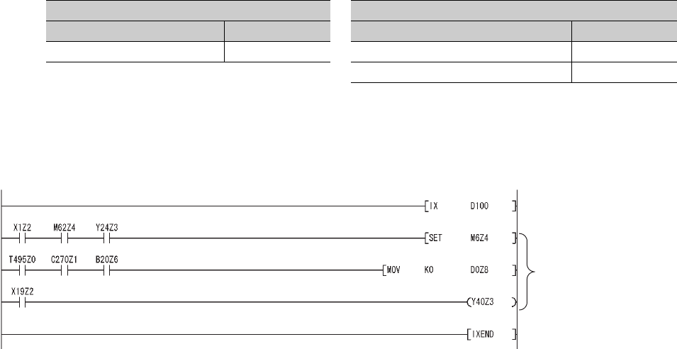
App - 26
Appendix 3.3.3 Program replacement examples
This section shows program replacement examples for the instructions of which replacement programs
are available in Appendix 3.3. (Skip this section if instructions listed in Appendix 3.3.1 are not used.)
(1) Replacement example of the IX and IXEND instructions
Since index registers are saved using the ZPUSH instruction, a 23-word index register save area is required.
(a) Example of device assignment
If the device numbers in the example above are used for other applications, assign unused device numbers
instead.
(b) Program before replacement
TableApp.28 Example of device assignment
Before replacement After replacement
Application Device Application Device
Index modification table D100 to D115 Index modification table D100 to D115
Index register save area D200 to D222
Figure App.1 Sample program
Modification target
(No change required)
The modification value set in the
index modification table is added.
1
2
3
APPEN-
DIX
6
7
8
Appendix 3 Method of Replacing Basic Model QCPU or High Performance Model QCPU with Universal
Model QCPU
Appendix 3.3 Instructions
APPENDICES
App - 27
(c) Program after replacement
• Replace the IX instruction with the ZPUSH instruction and the processing for setting the contents of index
modification table to index registers.
• Replace the IXEND instruction with the ZPOP instruction.
Figure App.2 Sample program
Current index register is
saved.
Contents of the index
modification table are
set to the index
registers Z0 to Z15.
Modification target
(No change required)
The saved index register is restored.
(Transition from the IXEND instruction)
Transition
from the IX
instruction
App - 28
(2) Replacement example of the IXDEV and IXSET instructions
Change the program so that the device offset value specified by the contacts between the IXDEV and the IXSET
instructions are directly set to the index modification table using the MOV instruction.
For the devices whose device offset value is not specified by the IXDEV and IXSET instructions, set the device
offset value to 0 in the program after replacement.
Figure App.3 shows how the device offset value is set in the program before and after replacement.
*1: Device numbers are represented in hexadecimal. Use hexadecimal constants (H ) when setting values in the index modi-
fication table.
*2: Start I/O numbers (U ) are represented in hexadecimal. Use hexadecimal constants (H ) when setting values in the
index modification table.
*3: Devices B, W, X, or Y can be specified following J\. . Set device numbers for B, W, X, and Y as device offset values of
each device in the index modification table.
For example, if "J10\Y220" is specified by the IXDEV and IXSET instructions, set "K10" in (D)+13 and "H220" in (D)+3 in
the replacement program. ((D) indicates the start device in the index modification table.)
Figure App.3 Device offset value specification and index modification table
IXSET
(D)+0
(D)+1
(D)+2
(D)+3
(D)+4
(D)+5
(D)+6
(D)+7
(D)+8
(D)+9
(D)+10
(D)+11
(D)+12
(D)+13
(D)+14
(D)+15
Index modification table
Start I/O number
Buffer memory address
Timer
Counter
Input *1
Output *1
Internal relay
Latch relay
Edge relay
Link relay *1
Data register
Link register *1
File register
Link direct device *3
Pointer
T
C
X
Y
M
L
V
B
D .XX
W .XX
R .XX
U \G .XX
J \B
ZR .XX
P
Device offset specification
Intelligent function
module device *2
File register
(through number)
1
2
3
APPEN-
DIX
6
7
8
Appendix 3 Method of Replacing Basic Model QCPU or High Performance Model QCPU with Universal
Model QCPU
Appendix 3.3 Instructions
APPENDICES
App - 29
(a) Program before replacement
(b) Program after replacement
Figure App.4 Sample program
Figure App.5 Sample program
The device offset values for input
(X), output (Y), internal relay (M),
data register (D), link register (W),
and pointer (P) are set to the index
modification table starting from D0.
The device offset values specified
by the IXDEV and IXSET
instructions are set to the index
modification table starting from D0.
App - 30
(3) Replacement example of the PR instruction
The number of output characters can be switched by the on/off status of SM701.
(a) Example of device assignment
If the device numbers in the example above are used for other applications, assign unused device numbers
instead.
(b) Program before replacement
TableApp.29 Example of device assignment
Before replacemen After replacement
Application Device Application Device
Output string D0 to D3 Output string D0 to D3
ASCII code output signal Y100 to Y107 ASCII code output signal Y100 to Y107
Strobe signal Y108 Strobe signal Y108
In-execution flag Y109 In-execution flag Y109
Output string storage address (BIN32) D20 to D21
Output string storage address (BIN32)
(Used for sub-routine programs and
interrupt programs)
D200 to D201
Number of output characters D202
Output module start Y number D203
Character extraction position D204
Number of extracted characters D205
String output status value D206
Result of string extraction by the MIDR
instruction D207
String output in-execution flag M200
For index modification Z0
Figure App.6 Sample program
The number of output strings is set
to variable. (Output until ASCII code
00H appears.)
The strings stored in D0 and later are
output from Y100 to Y108.

1
2
3
APPEN-
DIX
6
7
8
Appendix 3 Method of Replacing Basic Model QCPU or High Performance Model QCPU with Universal
Model QCPU
Appendix 3.3 Instructions
APPENDICES
App - 31
(c) Program after replacement
In the sequence program after replacement, three programs are required as shown below.
1) Main routine program
• Replace the PR instruction with the CALL instruction so that a subroutine program is called.
• Output string storage device ("D0" in the program below) cannot be specified directly with the CALL
instruction.
• Use the ADRSET instruction to acquire the indirect address for the CALL instruction.
• Y device ("Y100" in the program before replacement shown in (b)) cannot be specified directly as output
Y number with the CALL instruction. Specify the output Y number in integer.
• An interrupt program is used to output character codes via the output module. Enable the execution of
interrupt programs using the EI instruction.
Figure App.7 Program execution
Figure App.8 Sample program
FEND
RET
IRET
END
P1
I31
<After transition>
END
<Before transition>
Output strings and output string storage address are set.
Initial processing
The strings stored in D0 are output.
Main routine
program
Main routine
program
Subroutine
program
IInterrupt
program
The strings stored in D0 and
later are output from Y100 to
Y108.
An execution of interrupt program is
enabled.
App - 32
2) Subroutine program
• In the subroutine program, the data for outputting ASCII codes using a fixed scan interrupt program
(10ms) are set to work devices. Also, the flag for activating the processing in the fixed scan interrupt pro-
gram is turned on.
• Specify the following arguments for the subroutine program.
First argument Output string storage address (Input)
Second argument Output module start Y number (Input)
Figure App.9 Sample program
Data specified by the CALL(P)
arguments are saved.
Output string storage address
Number of output strings
Output module start number
Devices used for the string
output processing of the
interrupt program I31 are
initialized.
Yn0 to Yn7 (ASCII code),
Yn8 (strobe signal), and Yn9
(in-execution flag) are all
turned OFF.
The flag for activating the string
output processing in the interrupt
program is turned on.
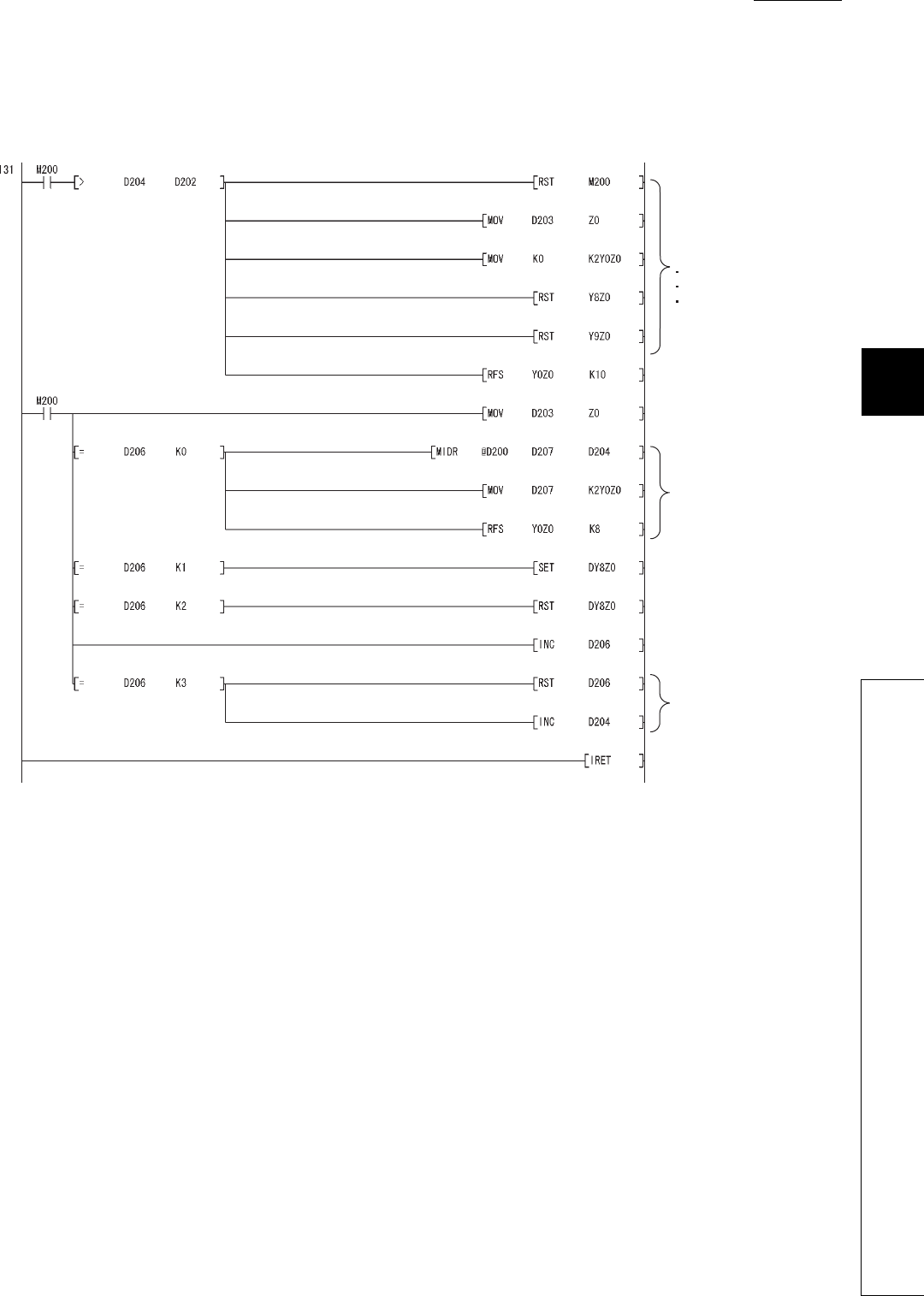
1
2
3
APPEN-
DIX
6
7
8
Appendix 3 Method of Replacing Basic Model QCPU or High Performance Model QCPU with Universal
Model QCPU
Appendix 3.3 Instructions
APPENDICES
App - 33
3) Interrupt program
The following processing is added to a fixed scan interrupt program (10ms).
The fixed scan interrupt program outputs ASCII codes from the output module and controls the strobe signal.
Figure App.10 Sample program
The following signals are
all turned off when all
strings are output.
Yn0 to Yn7 (ASCII code)
Yn8 (strobe signal)
Yn9 (in-execution flag)
Status 0:
One character is extracted
from the output string using
the MIDR instruction and
output to the Y module.
The strobe signal is turned
off for 10ms.
Status 1:
The strobe signal is turned on for
10ms.
Status 2:
The strobe signal is turned off
for 10ms.
The status value is incremented
by one.
Status 3:
The status value is returned
to 0 since the output
processing of one character
is completed. The next
character is extracted.
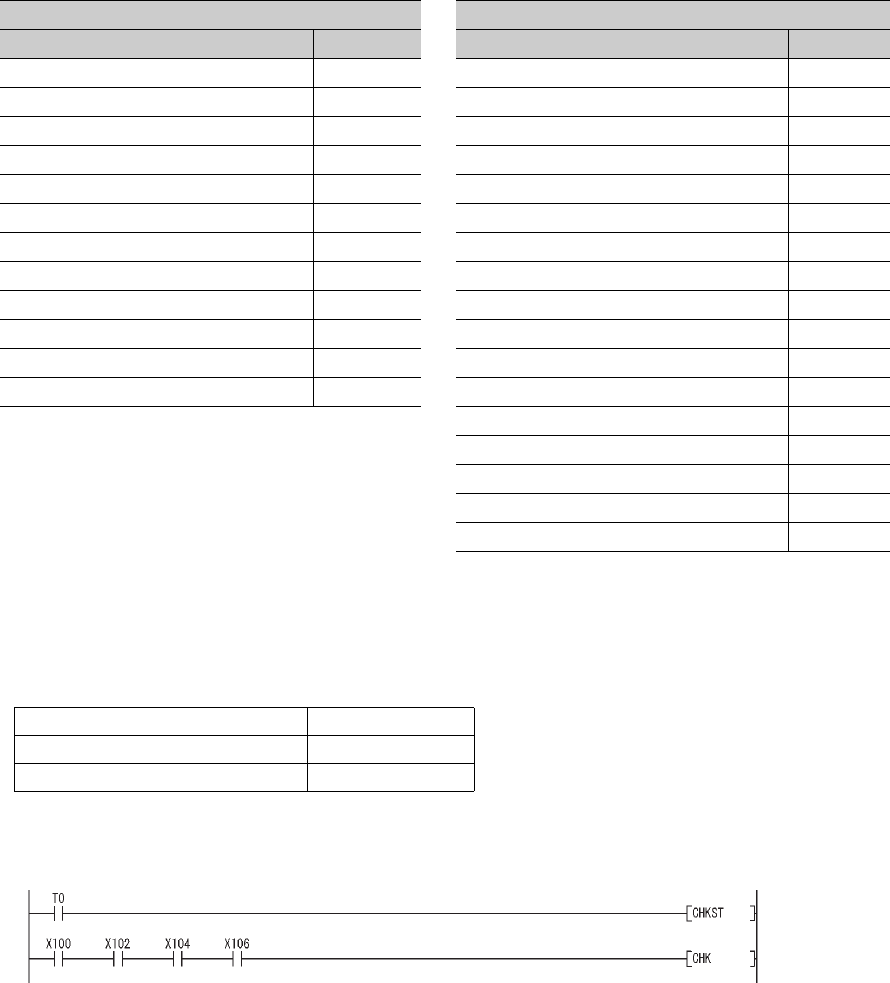
App - 34
(4) Replacement example of the CHKST and CHK instructions
In the example below, if the replacement program for the CHKST and CHK instructions detects a failure, a failure
number (contact number + coil number) is stored in D200 and the annunciator F200 is turned on.
(a) Example of device assignment
If the device numbers in the example above are used for other applications, assign unused device numbers
instead.
When the advance end detection sensor input performs a failure detection of Xn, assign device numbers for
the retract end detection sensor input and the failure detection output as described below.
(b) Program before replacement
TableApp.30 Example of device assignment
Before replacement After replacement
Application Device Application Device
Advance end detection sensor input 1 X100 Advance end detection sensor input 1 X100
Retract end detection sensor input 1 X101 Retract end detection sensor input 1 X101
Advance end detection sensor input 2 X10² Advance end detection sensor input 2 X10²
Retract end detection sensor input 2 X10³ Retract end detection sensor input 2 X10³
Advance end detection sensor input 3 X10⁴ Advance end detection sensor input 3 X10⁴
Retract end detection sensor input 3 X10⁵ Retract end detection sensor input 3 X10⁵
Advance end detection sensor input 4 X10⁶ Advance end detection sensor input 4 X10⁶
Retract end detection sensor input 4 X10⁷ Retract end detection sensor input 4 X10⁷
Failure detection output 1 Y100 Failure detection output 1 Y100
Failure detection output 2 Y102 Failure detection output 2 Y102
Failure detection output 3 Y104 Failure detection output 3 Y104
Failure detection output 4 Y106 Failure detection output 4 Y106
Coil number (failure type detected) D100
Contact number D101
Failure number D200
Failure detection display F200
For index modification Z0
Advance end detection sensor input Xn
Retract end detection sensor input Xn+1
Failure detection output Yn
Figure App.11 Sample program
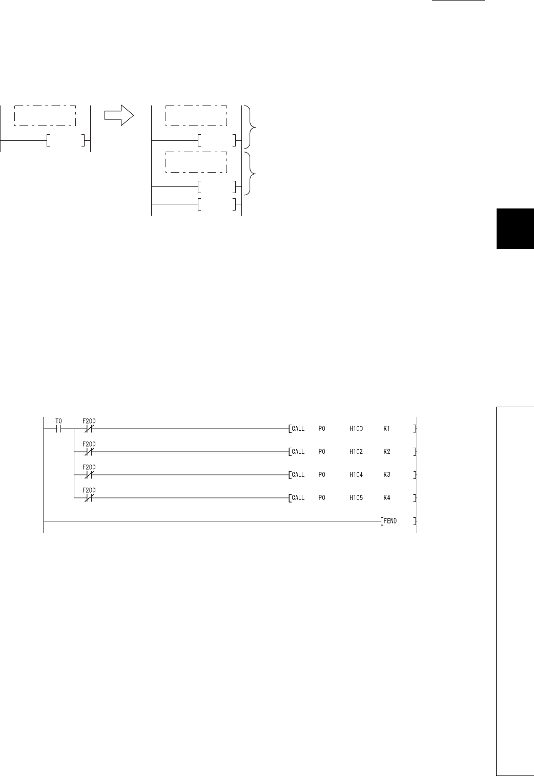
1
2
3
APPEN-
DIX
6
7
8
Appendix 3 Method of Replacing Basic Model QCPU or High Performance Model QCPU with Universal
Model QCPU
Appendix 3.3 Instructions
APPENDICES
App - 35
(c) Program after replacement
In the sequence program after replacement, two programs are required as shown below.
1) Main routine program
• Replace the CHKST and CHK instructions with the CALL instructions so that a subroutine program is
called.
• One CALL instruction is required for each device specified as check condition in front of the CHK
instruction. (In the program before replacement shown in (b), four CALL instructions need to be added
since there are four check conditions in front of the CHK instruction.)
• Device number and contact number of X devices (check condition) are specified in each CALL instruc-
tion.
• Contact number is used to display failure number when a failure is detected.
Figure App.12 Program execution
Figure App.13 Sample program
FEND
RET
END
<After transition>
END
<Before transition>
Initial processing
P0
Main routine
program
Main routine
program
Subroutine
program An failure status is checked, and if a failure is detected,
a failure number is stored in D200.
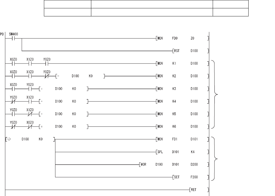
App - 36
2) Subroutine program
• In the subroutine program, an failure status is checked using a failure detection ladder pattern.
• If a failure is detected, a failure number is stored in D200 and the annunciator F200 is turned on.
• Specify the following arguments for the subroutine program.
(d) Replacement method when failure detection ladder patterns are changed by the CHKCIR and
CHKEND instructions
Failure detection ladder patterns can be changed in the subroutine program described in (c).
First argument Device number of X device targeted for failure check (Input)
Second argument Contact number of X device targeted for failure check (Input)
Figure App.14 Sample program
<Failure detection target>
If a failure is detected, the
coil number corresponding
to the failure type is set to
D100.
If a failure is detected, a
failure number is created
by combining the coil
number corresponding to
the failure type and the
contact number.
The annunciator is turned
on.
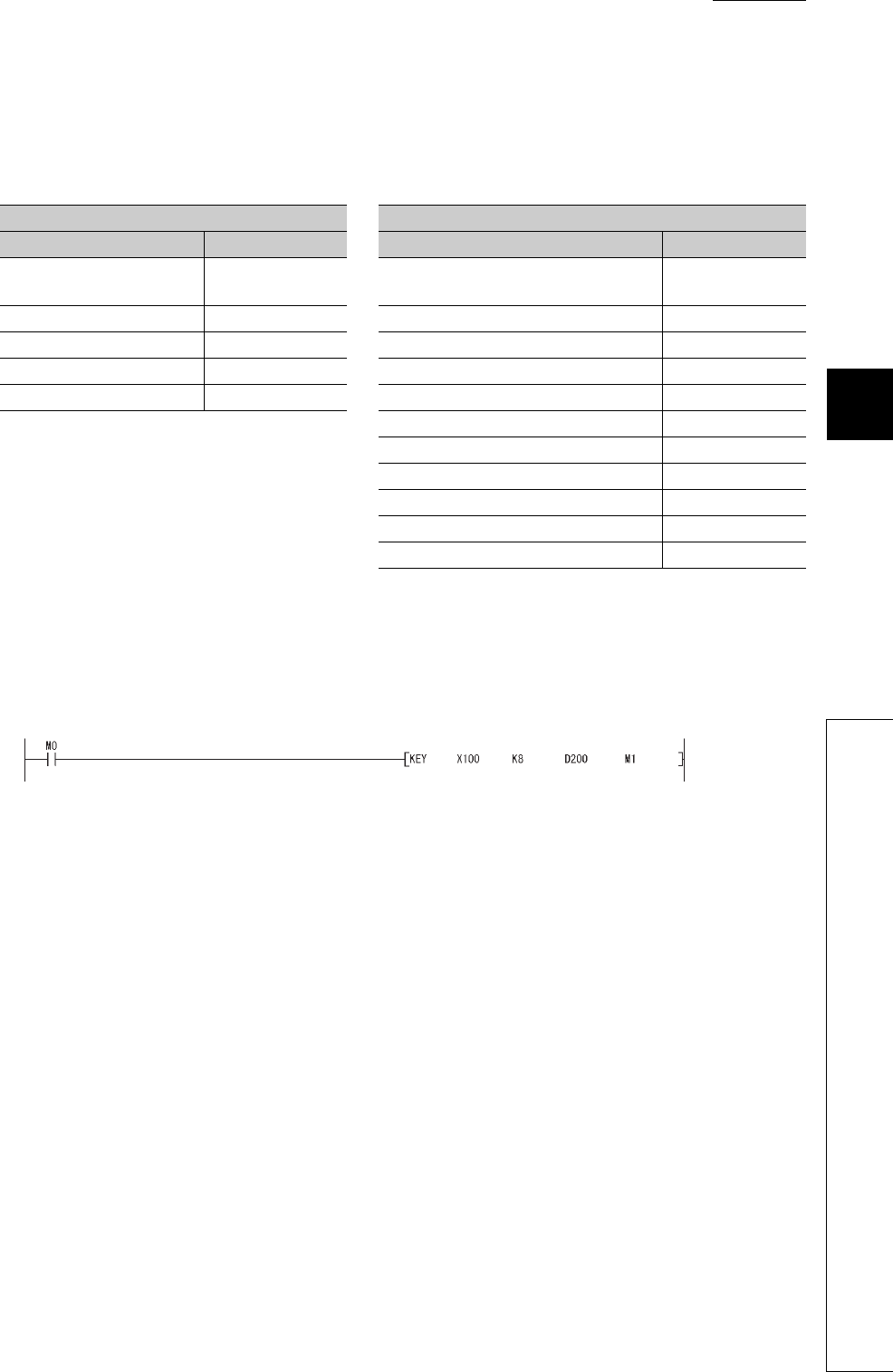
1
2
3
APPEN-
DIX
6
7
8
Appendix 3 Method of Replacing Basic Model QCPU or High Performance Model QCPU with Universal
Model QCPU
Appendix 3.3 Instructions
APPENDICES
App - 37
(5) Replacement example of the KEY instruction
(a) Example of device assignment
If the device numbers in the example above are used for other applications, assign unused device
numbers instead.
(b) Program before replacement
TableApp.31 Example of device assignment
Before replacemen After replacement
Application Device Application Device
Numeric input execution
instruction M0 Numeric input execution instruction M0
Input complete flag M1 Input complete flag M1
Input data area D200 to D203 Input data area D200 to D203
ASCII code input signal X100 to X107 ASCII code input signal X100 to X107
Strobe signal X108 Strobe signal X108
Input data area address (BIN32) D210 to D211
(Input data area + 0) address (BIN32) D212 to D213
(Input data area + 1) address (BIN32) D214 to D215
(Input data area + 2) address (BIN32) D216 to D217
For shifting input data D218
For converting input data D219 to D220
Figure App.15 Sample program
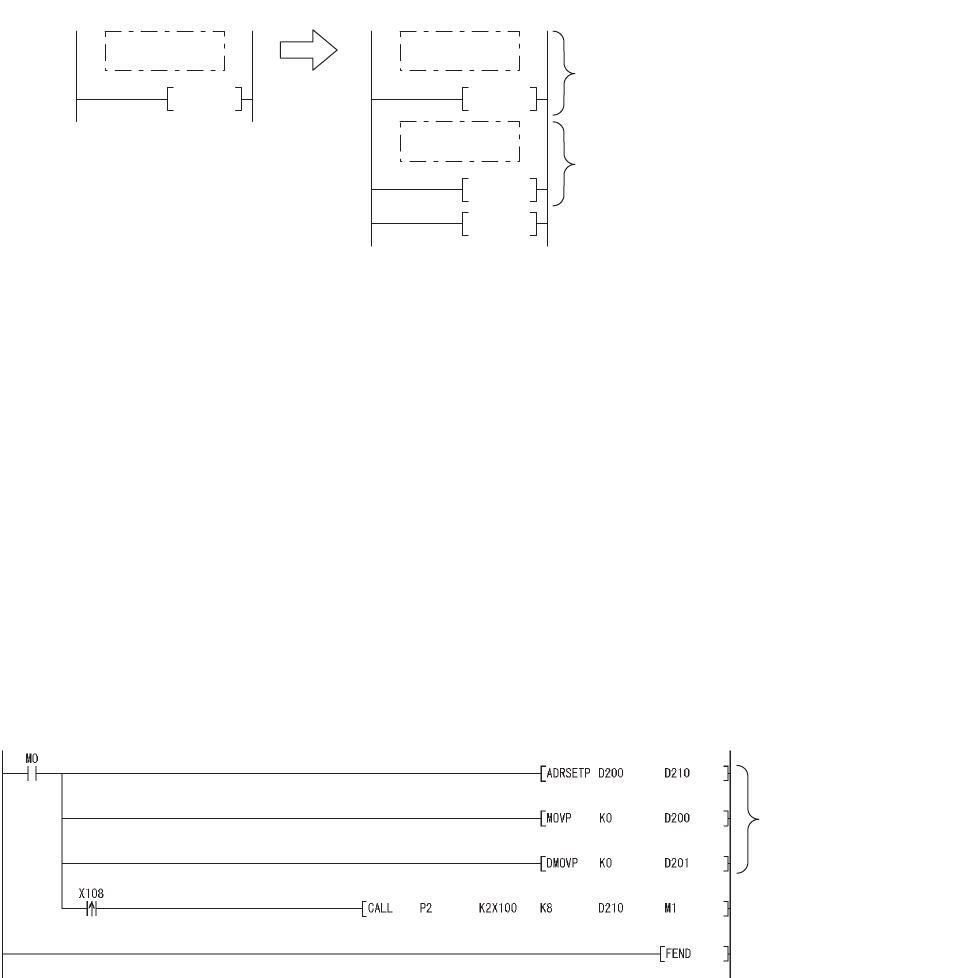
App - 38
(c) Program after replacement
In the sequence program after replacement, two programs are required as shown below.
1) Main routing program
• Set "0" in the input data area on the rising edge of the execution instruction ("M0" in the program below)
and initialize the program.
• Execute the CALL instruction on every rising edge of the strobe signal ("X108" in the program below) so
that a subroutine program is called.
• In the subroutine program, input codes are added to the input data area and the completion status is
checked.
• Pass the following data to the subroutine program at execution of the CALL instruction.
1) ASCII code input values from the input module (Xn0 to Xn7)
2) Number of digits to be input
3) Indirect address of the input data area (Use the ADRSET instruction to acquire the indirect
address for the input data area.)
4) Bit devices to be turned on when input is completed
Figure App.16 Program execution
Figure App.17 Sample program
FEND
RET
END
<After transition>
END
<Before transition>
Initial processing
ASCII code is added to the input data area.
P2
Main routine
program
Main routine
program
Subroutine
program
The input data area is initialized.
A subroutine program is called at
the rising edge of the strobe signal.
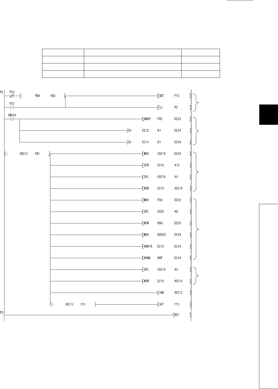
1
2
3
APPEN-
DIX
6
7
8
Appendix 3 Method of Replacing Basic Model QCPU or High Performance Model QCPU with Universal
Model QCPU
Appendix 3.3 Instructions
APPENDICES
App - 39
2) Subroutine program
• In the subroutine program, ASCII codes specified by an argument are added to the input data area and
the completion status is checked.
• Specify the following arguments for the subroutine program.
First argument ASCII code input from the input module (K2Xn) (Input)
Second argument Number of digits to be input (Input)
Third argument Indirect address of the input data area (Input)
Fourth argument Bit device to be turned on when input is completed (Output)
Figure App.18 Sample program
Numeric entry is ended when
the at-completion on signal is
on or 0DH is input.
Addresses of the input data
area are saved in the work
devices.
The 1st to 4th digit numerals
in (input data area +2) are
shifted for one digit to the left.
Numeral entered in ASCII code
is converted into one numeral
in BIN data using the HABIN
instruction.
The 5th to 8th digit numerals
in (input data area +1) are
shifted for one digit to the left
and the converted numeral is
set to the 8th digit.
The number of digits to be input
in (input data area +0) is
incremented by one.
The at-completion on signal
is turned on when the input
processing for specified digits
is completed.
App - 40
Appendix 3.4 Functions
Appendix 3.4.1 Floating-point operation instructions
(1) Differences between High Performance model QCPU and Universal model QCPU
(a) High Performance model QCPU
The High Performance model QCPU can perform only the single-precision floating-point operation
instructions. Note, however, that internal operation processing can be performed in double precision
by selecting the item shown below (default: selected).
(b) Universal model QCPU
The Universal model QCPU supports the double-precision floating-point operation instructions.
The operation can be performed either in single precision or double precision depending on the data. There-
fore, the "Perform internal arithmetic operations in double precision" item in the PLC system tab of the PLC
parameter dialog box cannot be selected.
Because of this new function, operation results (both in single precision and double precision) slightly differ
between the High Performance model QCPU and the Universal model QCPU if "Perform internal arithmetic
operations in double precision" is selected in the High Performance model QCPU.
If higher accuracy is required in floating-point operations, replace the floating-point operation instructions as
described in (4).
However, if six or less digits are used as significant digits for the floating-point operation instructions, replace-
ment is not necessary. The single-precision floating-point operation results in the Universal model QCPU can
be used as they are in the system. When not replacing instructions, make sure that it does not cause any prob-
lems in the system.
Figure App.19 PLC system tab
Selected by default.
1
2
3
APPEN-
DIX
6
7
8
Appendix 3 Method of Replacing Basic Model QCPU or High Performance Model QCPU with Universal
Model QCPU
Appendix 3.4 Functions
APPENDICES
App - 41
(2) Floating-point operation instructions for the Universal model QCPU
TableApp.30 lists floating-point operation instructions for the Universal model QCPU.
Specifications of the single-precision floating-point operation instructions are compatible with those for
the High Performance model QCPU.
Floating-point data can be converted mutually between single precision and double precision using
instructions in TableApp.33.
TableApp.32 List of floating-point operation instructions supported in the Universal model QCPU
Instruction name
Instruction symbol
Remarks
Single-precision
floating-point data
Double-precision
floating-point data
Comparison Floating-point data comparison
LDE LDED indicates one of
the followings;
<>,=,<,>,<=,>=
ANDE ANDED
ORE ORED
Data transfer Floating-point data transfer EMOV(P) EDMOV(P) ---
Four arithmetic
operation
Floating-point data addition E+(P) ED+(P)
---
Floating-point data subtraction E-(P) ED-(P)
Floating-point data multiplication E*(P) ED*(P)
Floating-point data division E/(P) ED/(P)
Data conversion
Conversion from BIN 16-bit data
to floating-point data FLT(P) FLTD(P)
---
Conversion from BIN 32-bit data
to floating-point data DFLT(P) DFLTD(P)
Conversion from floating-point
data to BIN 16-bit data INT(P) INTD(P)
Conversion from floating-point
data to BIN 32-bit data DINT(P) DINTD(P)
Floating-point sign inversion ENEG(P) EDNEG(P)
Special function
SIN operation SIN(P) SIND(P)
---
COS operation COS(P) COSD(P)
TAN operation TAN(P) TAND(P)
SIN-1 operation ASIN(P) ASIND(P)
COS-1 operation ACOS(P) ACOSD(P)
TAN-1operation ATAN(P) ATAND(P)
Conversion from angle to radian RAD(P) RADD(P)
Conversion from radian to angle DEG(P) DEGD(P)
Square root SQR(P) SQRD(P)
Exponential operation EXP(P) EXPD(P)
Natural logarithm operation LOG(P) LOGD(P)
TableApp.33 Floating-point data conversion instructions (single precision double precision)
Instruction name Instruction symbol
Single precision to double precision conversion ECON(P)
Double precision to single precision conversion EDCON(P)

App - 42
(3) Advantages and disadvantages when using the double-precision floating-point data of
the Universal model QCPU
TableApp.32 shows the advantages and disadvantages when executing the double-precision floating-point opera-
tion instructions in the Universal model QCPU.
If higher accuracy is required in floating-point operations, it is recommended to replace the instruc-
tions with the double-precision floating-point operation instructions.
*1: The processing speed of the double-precision floating-point operation instructions in the Universal model QCPU is higher
than that of floating-point operation instructions using internal double-precision operations in the High Performance
model QCPU.
TableApp.33 shows the comparison between single-precision and double precision floating-point data.
TableApp.34 Advantages and disadvantages when using the double-precision floating-point operation instructions
Advantage Disadvantage
The results are more accurate than those of the
single-precision floating-point operation
instructions.
The instruction processing speed is slower than that of the single-
precision floating-point operation instructions.*1
Double-precision floating-operation data use twice as many word device
points as single-precision floating-operation data.
TableApp.35 Comparison between single-precision and double precision floating-point data
Item Single-precision floating-point
data
Double-precision floating-point
data
Word point required for data retention 2 words 4 words
Setting range -2128<N -2-126, 0,
2-126 N<2128
-21024<N -2-1022, 0,
2-1022 N<21024
Precision (number of bits)
Mantissa 23 bits 52 bits
Exponent 8 bits 11 bits
Sign 1 bits 1 bits
Instruction processing
speed (Q04UDHCPU/
Q06UDHCPU) (Maximum)
Data comparison (Conductive
status) (LDE>= / LDED>=) 5.5 µs 9.0 µs
Data transfer
(EMOV/EDMOV) 0.019 µs 5.0 µs
Addition (3 devices)
(E+ / ED+) 0.0665 µs 9.2 µs
SIN operation (SIN/SIND) 5.7 µs 13.8 µs
1
2
3
APPEN-
DIX
6
7
8
Appendix 3 Method of Replacing Basic Model QCPU or High Performance Model QCPU with Universal
Model QCPU
Appendix 3.4 Functions
APPENDICES
App - 43
(4) Replacing the High Performance model QCPU with the Universal model QCPU
(a) Replacing all single-precision floating-point operation instructions with double-precision
floating-point operation instructions
Single-precision floating-point data occupy two points of word device per data.
On the other hand, four points are required per double-precision floating-point data.
Therefore, all device numbers for storing floating-point data need to be reassigned.
1) Device assignment
2) Program before replacement
3) Program after replacement
Example Replacing the floating-point operation [A B+C] (Changing all floating-point
data into double precision.)
TableApp.36 Device assignment
Before replacement After replacement
Application Device Data type Application Device Data type
Data A D0 to D1
Floating-point data
(single precision)
Data A D0 to D3
Floating-point data
(double precision)
Data B D2 to D3 Data B D4 to D7
Data C D4 to D5 Data C D8 to D11
Result D6 to D7 Result D12 to D15
Figure App.20 Sample program
Figure App.21 Sample program
Operation is performed using
double-precision floating-point
data.
App - 44
(b) Replacing a part of floating-point operation instructions with double-precision floating-point
operation instructions
Only operations that require high accuracy are replaced with double-precision floating-point opera-
tion instructions.
Using the ECON and EDCON instructions, convert floating-point data mutually between single pre-
cision and double-precision. The flow of a replacement program is as follows:
• Data required for operations are converted from single precision to double precision using the ECON
instruction.
• Operations are performed in double precision using the double-precision floating-point operation instruc-
tions.
• Operation results are converted from double precision to single precision using the EDCON instruction.
A program example that floating-point data are converted mutually between single precision and
double precision before and after operations is shown below.
1) Device assignment
2) Program before replacement
Example Replacing the floating-point operation [A B+C] (Using the ECON and EDCON
instructions)
TableApp.37 Device assignment
Before replacement After replacement
Application Device Data type Application Device Data type
Data A D0 to D1
Floating-point data
(single precision)
Data A D0 to D1
Floating-point data
(single precision)
Data B D2 to D3 Data B D2 to D3
Data C D4 to D5 Data C D4 to D5
Result D6 to D7 Result D6 to D7
Data A D10 to D13
Floating-point data
(double precision)
Data B D14 to D17
Data C D18 to D21
Result D22 to D25
Figure App.22 Sample program

1
2
3
APPEN-
DIX
6
7
8
Appendix 3 Method of Replacing Basic Model QCPU or High Performance Model QCPU with Universal
Model QCPU
Appendix 3.4 Functions
APPENDICES
App - 45
3) Program after replacement
Figure App.23 Sample program
Floating-point data are
converted from single precision
to double precision.
Operation is performed using
double-precision floating-point
data.
The floating-point operation result
data are converted from double
precision to singe precision.
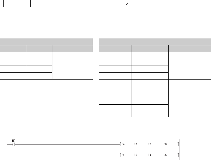
App - 46
(c) Replacing a part of floating-point operation instructions with double-precision floating-point
operation instructions using subroutine programs
The flow of a replacement program described in (b) can be regarded as one subroutine program.
Create a subroutine program for each floating-point operation instruction and then replace the original floating-
point operation instructions with the CALL(P) instruction so that the corresponding subroutine program is
called.
With this method, changes in the program are minimized, but the processing for calling subroutine programs
increases the scan time.
In addition, since conversions from double precision to single precision are performed for each instruction,
rounding-off errors generated during operations are larger than those in the replacement program described in
(b).
1) Device assignment
2) Program before replacemennt
Example Replacing the floating-point operation[A B+C] (Using a subroutine program)
TableApp.38 Device assignment
Before replacement After replacement
Application Device Data type Application Device Data type
Data A D0 to D1
Floating-point data
(single precision)
Data A D0 to D1
Floating-point data
(single precision)
Data B D2 to D3 Data B D2 to D3
Data C D4 to D5 Data C D4 to D5
Result D6 to D7 Result D6 to D7
Subroutine input
data 1 D900 to D903
Floating-point data
(double precision)
Subroutine input
data 2 D904 to D907
Subroutine
operation result D908 to D911
Figure App.24 Sample program

1
2
3
APPEN-
DIX
6
7
8
Appendix 3 Method of Replacing Basic Model QCPU or High Performance Model QCPU with Universal
Model QCPU
Appendix 3.4 Functions
APPENDICES
App - 47
3) Program after replacement
Figure App.25 Sample program
A subroutine program for
multiplication using the
double-precision
floating-point operation
instruction
A subroutine program for
addition using the
double-precision
floating-point operation
instruction
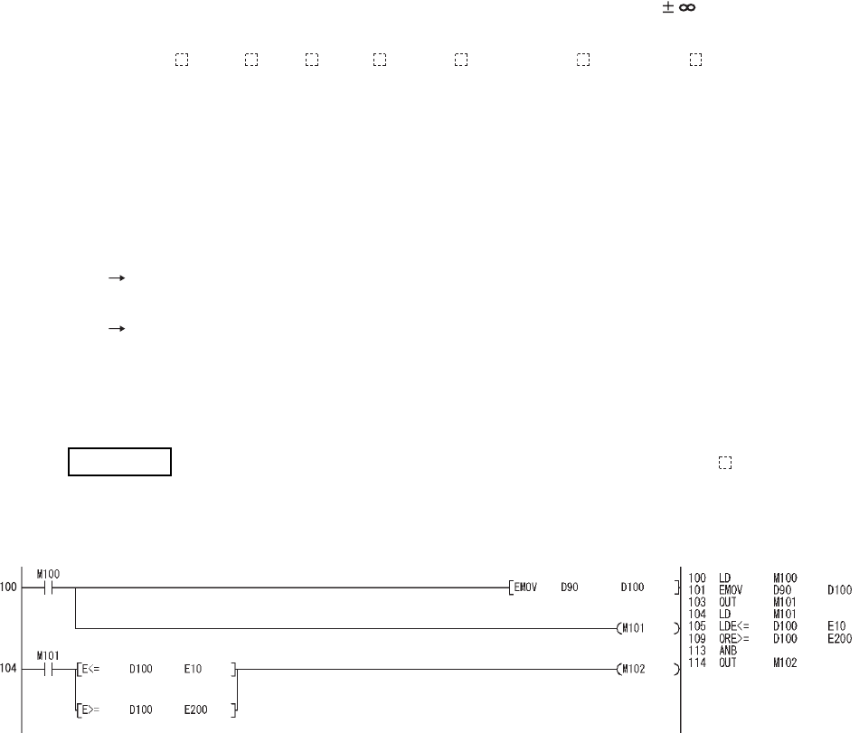
App - 48
Appendix 3.4.2 Error check processing for floating-point data comparison
instructions
(1) Input data check
Error check processing for floating-point data comparison instructions performed in the Universal model QCPU
are enhanced. Input of a "special value" (-0, nonnumeric, unnormalized number, or ) is checked, and if those
special values are input, the CPU module detects “OPERATION ERROR” (error code: 4140).
When the LDE , ANDE , ORE , LDED , ANDED , and/or ORED instructions ( indicates one of the fol-
lowings; =,<>,<,>,<=,>=) are used in the program, “OPERATION ERROR” (error code: 4140) may be detected if
invalid floating-point data exist. This occurs even when interlocks are provided using the valid data flags (the sig-
nal which shows the floating-point validity).
Invalid floating-point data are not stored in the result of operations performed in the Universal model QCPU.
Those invalid data are considered to be stored in the following cases:
• The same device is used for storing floating-point data and other data, such as binary values, BCD values,
and strings.
Use different devices for storing floating-point data and data other than floating-point data.
• Floating-point data externally written are invalid.
Take measures on the external-source side so that valid data are written.
If an error occurs in the floating-point data comparison instructions, take appropriate measures to
remove error causes described above.
[Ladder mode] [List mode]
In the ladder block starting from the step 104, the floating-point data comparison instructions of the step 105 and
109 are not executed when the M101 (valid data flag) is off.
However, the LDE<= instruction of the step 105 and the ORE>= instruction of the step 109 are executed regard-
less of the execution result of the LD instruction of the step 104 in the program above.
Therefore, even when the M101 is off, “OPERATION ERROR” (error code: 4140) will be detected in the LDE<=
instruction of the step 105 if a "special value" is stored in D100.
For the method of avoiding “OPERATION ERROR”, refer to(2) in this section.
Example 1) Detecting “OPERATION ERROR” (error code: 4140) in the LDE instruction
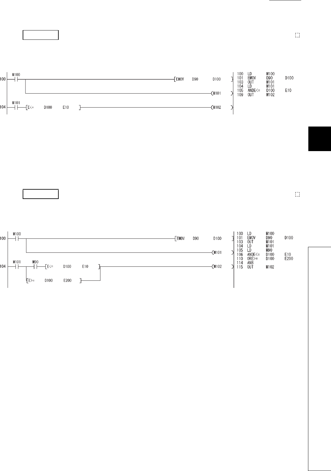
1
2
3
APPEN-
DIX
6
7
8
Appendix 3 Method of Replacing Basic Model QCPU or High Performance Model QCPU with Universal
Model QCPU
Appendix 3.4 Functions
APPENDICES
App - 49
[Ladder mode] [List mode]
In the ladder block starting from the step 104, the ANDE<= instruction of the step 105 is not executed when the
M101 (valid data flag) is off.
The ANDE<= instruction of the step 105 is not executed when the M101 is off in the LD instruction of the step 104
in the program above. Therefore, when the M101 is off, “OPERATION ERROR” (error code: 4140) will not be
detected even if a "special value" is stored in D100.
[Ladder mode] [List mode]
In the ladder block starting from the step 104, the ANDE<= instruction of the step 106 and the OR>= instruction of
the step 110 are not executed when the M101 (valid data flag) is off.
However, if the M90 is on in the LD instruction of the step 105, the ANDE<= instruction of the step 106 is exe-
cuted. Therefore, even when the M101 is off, "OPERATION ERROR" (error code: 4140) will be detected in the
ANDE<= instruction of the step 106 if the M90 is on and a "special value" is stored in D100.
For the method of avoiding “OPERATION ERROR”, refer to (2) in this section.
Example 2) Not detecting “OPERATION ERROR” (error code: 4140) in the ANDE
instruction
Example 3) Detecting "OPERATION ERROR" (error code: 4140) in the ANDE
instruction
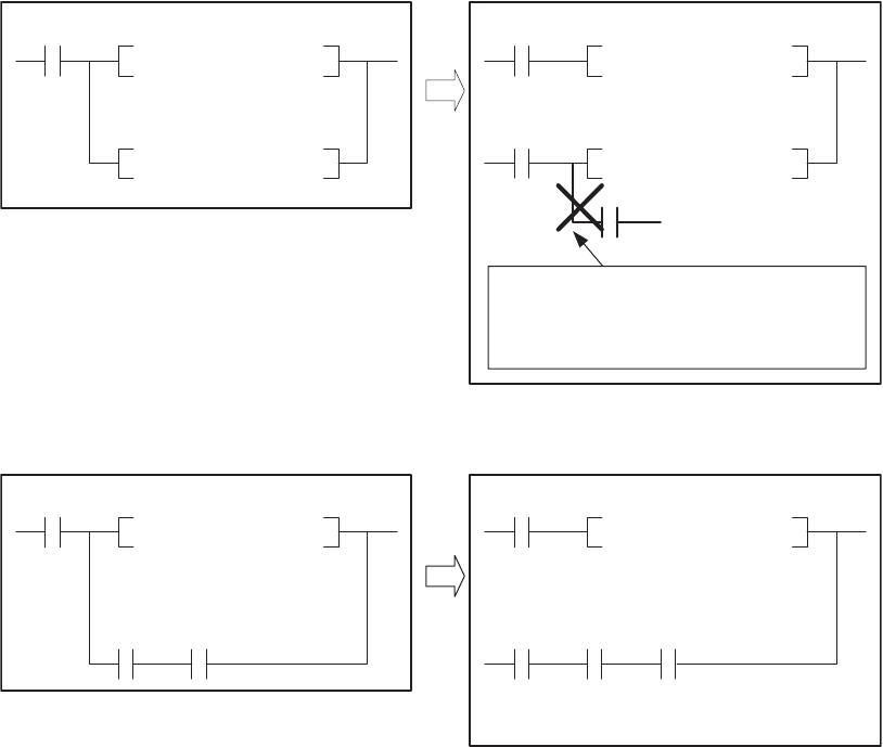
App - 50
(2) Method of avoiding “OPERATION ERROR” (error code: 4140) in the floating-point data
comparison instructions
As shown in the modification examples below, connect the contacts of valid data flag in series for each floating-
point data comparison instruction. (Use AND connection for connecting the contact of the valid data flag and the
floating-point data comparison instruction.)
Make sure that there is no line (OR connection) between the valid data flag and the floating-point data compari-
son instruction.
<Modification example 1>
<Modification example 2>
(Before modification) (After modification)
E<= D100 E10
E>= D100 E200
E<= D100 E10
E>= D100 E200
Valid
data
flag
Valid
data
flag
Valid
data
flag
Make sure that there is no line (OR connection)
between the signal which shows the
floating-point data validity (valid data flag) and
the floating-point data comparison instruction.
(Before modification) (After modification)
E<= E10D100 E<= D100 E10
M200 M201 M200 M201
Valid
data
flag
Valid
data
flag
Valid
data
flag
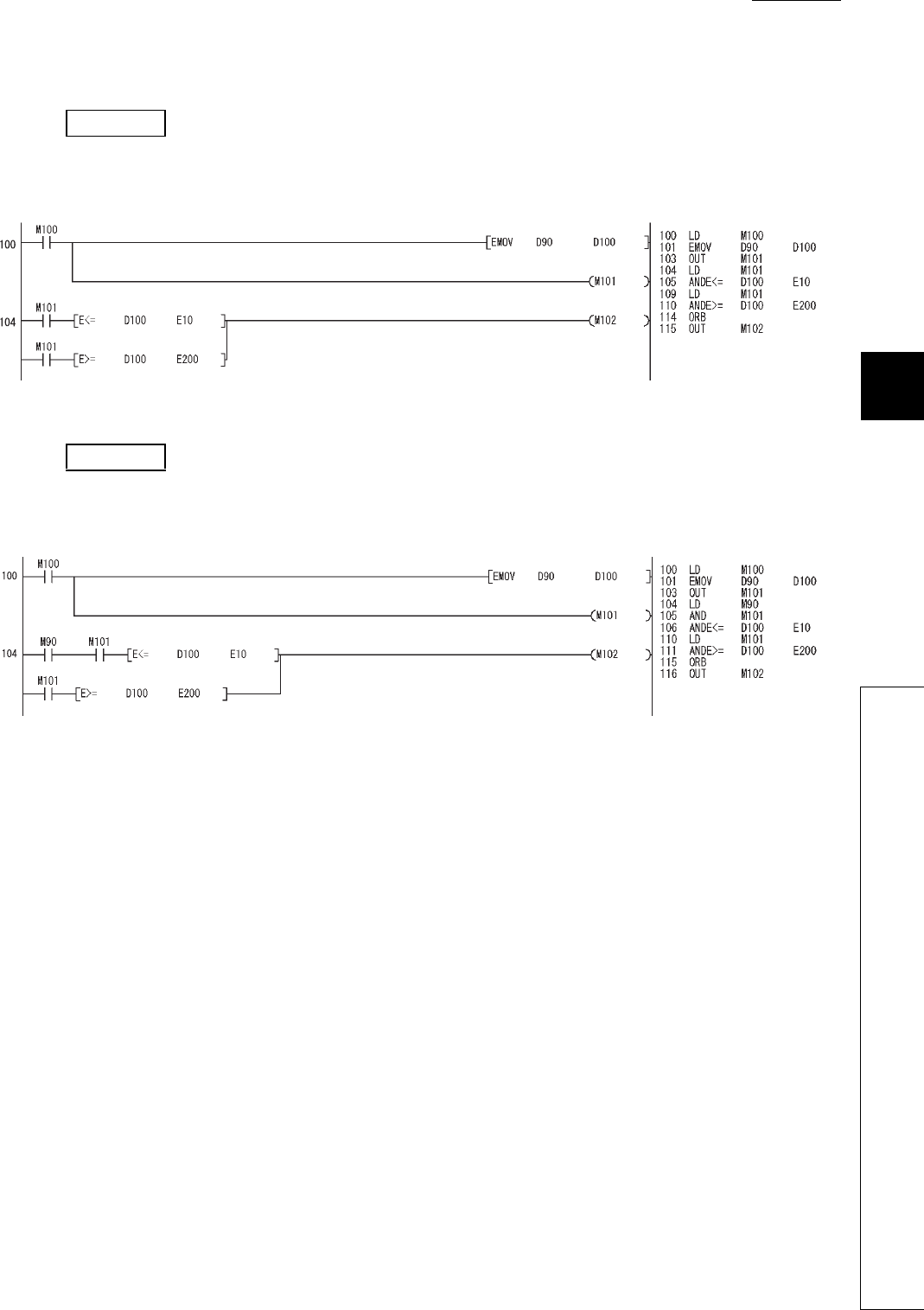
1
2
3
APPEN-
DIX
6
7
8
Appendix 3 Method of Replacing Basic Model QCPU or High Performance Model QCPU with Universal
Model QCPU
Appendix 3.4 Functions
APPENDICES
App - 51
Program examples after modification for Example 1) and 3) in (1) are shown below.
[Ladder mode] [List mode]
[Ladder mode] [List mode]
Example 4) Program after modification for Example 1) ("OPERATION ERROR" (error code:
4140) is no longer detected.)
Example 5) Program after modification for Example 3) ("OPERATION ERROR" (error code:
4140) is no longer detected.)
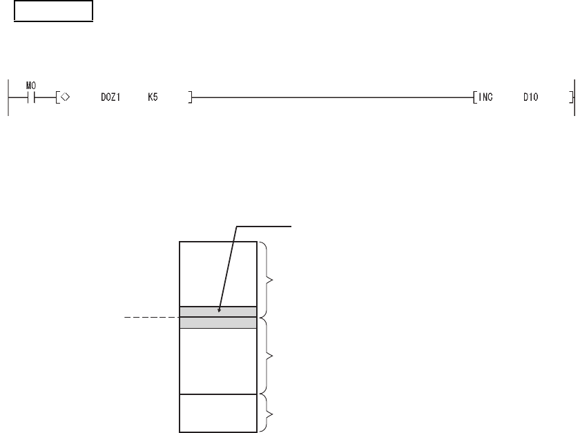
App - 52
Appendix 3.4.3 Range check processing for index-modified devices
(1) Device range check
Error check processing at index modification of devices has been enhanced for the Universal model QCPU.
Each index-modified device range is checked, and if the check target device is outside the device range before
index modification, the CPU module detects "OPERATION ERROR" (error code: 4101).
In Example 1), when the contact (M0) is on and the value, -1 or less, is specified in Z1, the device D0Z1 is
included in the C device range, exceeding the D device range, as shown in Figure App.26.
As a result, "OPERATION ERROR" (error code: 4101) will be detected.
When an error is detected, check the index modification value (value of Z1 in the above example) and remove the
error cause.
Examples of the cases where an error is detected and not detected are shown below.
Example 1) Detecting "OPERATION ERROR" (error code: 4101) by error check processing at
index modification of devices
Figure App.26 Device D0Z1 when the value of Z1 is -1
C0
C device area
D device area
W device area
D0
W0
When the value of Z1 is -1,
the device is included in the
C device range, resulting in an error.
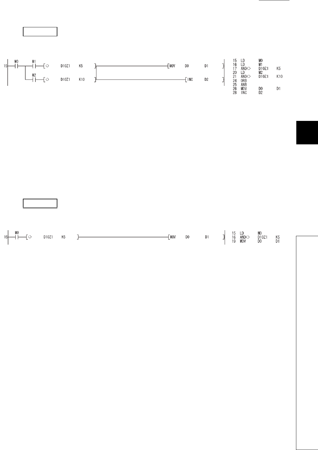
1
2
3
APPEN-
DIX
6
7
8
Appendix 3 Method of Replacing Basic Model QCPU or High Performance Model QCPU with Universal
Model QCPU
Appendix 3.4 Functions
APPENDICES
App - 53
[Ladder mode] [List mode]
In Example 2, in the ladder block starting from the step 15, the AND<> instruction of the step 17 or 21 is supposed
to be not executed when M0 (valid data flag) is off.
However, since the LD instruction which is always executed is used in the step 16 and 20, the AND<> instruction
of the step 17 or 21 is executed regardless of the execution status of the LD instruction in the step 15 when M1 or
M2 is on.
For this reason, even when M0 is off, if the D10Z1 value is outside the D device range, "OPERATION ERROR"
(error code: 4101) will be detected in the AND<> instruction of the step 17.
Note that the step 26 (MOV D0 D1) and the step 28 (INC D2) are not executed.
For the method of avoiding "OPERATION ERROR" (error code: 4101), refer to (2) in this section.
[Ladder mode] [List mode]
In Example 3, the AND<> instruction of the step 16 is not executed when M0 (valid data flag) of the step 15 is off.
For this reason, "OPERATION ERROR" (error code: 4101) will not be detected no matter what the D10Z1 value
is.
Example 2) Detecting "OPERATION ERROR" (error code: 4101)
Example 3) Not detecting "OPERATION ERROR" (error code: 4101)
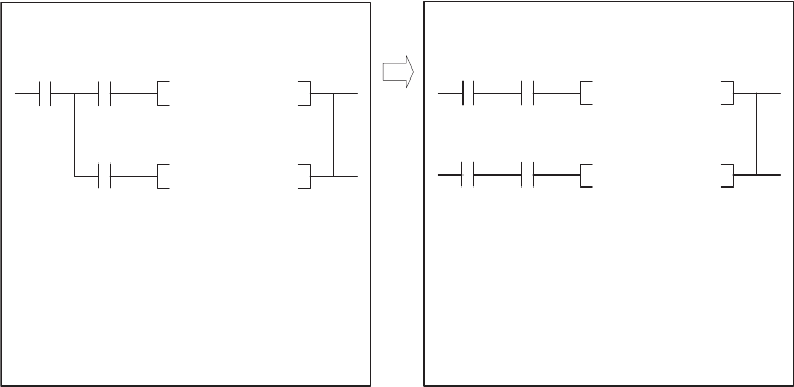
App - 54
(2) Method of avoiding "OPERATION ERROR" (error code: 4101)
When the index-modified device range does not need to be checked, use the method 1).
When the index-modified device range needs to be checked, use the method 2).
1) Deselect the "Check device range at indexing" item in the PLC RAS tab of the PLC parameter dialog box so
that the index-modified device range will not be checked.
2) As shown in the modification examples below, connect the contacts of valid data flag in series for each
instruction that checks the index-modified device range.
<Modification example>
In the program before modification (on the left), the instruction immediately before the AND<> instruction is
regarded as the LD instruction. However, in the program after modification (on the right), the same instruction will
be regarded as the AND instruction.
In the program after modification, only when both contacts of M0 and M1 (or M2) turn on, the AND<> instruction
is executed. As a result, no error will be detected during index-modified device range check processing.
M0
(After modification)
(Before modification)
[Ladder mode] [Ladder mode]
[List mode] [List mode]
M0
M0
M1 M1
M2 M2
Valid
data
flag
LD
M0
LD
M1
AND <>
D10Z1
K5
LD
M2
AND <>
D10Z1
K10
ORB
ANB
<> D10Z1 K5
<> D10Z1 K10
<> D10Z1 K5
<> D10Z1 K10
Valid data
flag
Valid data
flag
LD
M0
AND
M1
AND <>
D10Z1
K5
LD
M0
AND
M2
AND <>
D10Z1
K10
ORB

1
2
3
APPEN-
DIX
6
7
8
Appendix 3 Method of Replacing Basic Model QCPU or High Performance Model QCPU with Universal
Model QCPU
Appendix 3.4 Functions
APPENDICES
App - 55
Appendix 3.4.4 Device latch function
(1) Overview
The device latch function*1 for the Universal model QCPU is more enhanced compared to that for the Basic
model QCPU and High performance model QCPU.
This section describes the enhanced device latch function in the Universal model QCPU.
*1: The latch function is used to hold device data even when the CPU module is powered off or reset.
(2) Device data latch methods
Device data of the Universal model QCPU can be latched by:
• using the large-capacity file register (R, ZR),
• writing/reading device data to the standard ROM (with the SP.DEVST and S(P).DEVLD instructions), or
• specifying a latch range of internal user devices.
(3) Details of each latch method
(a) Large-capacity file register (R, ZR)
Data in the file register can be latched by batteries.
File register size is larger and processing speed is higher in the Universal model QCPU, compared to the Basic
model QCPU and High Performance model QCPU.
To latch a lot of data (many device points), use of the file register is effective.
TableApp.39 shows the file register size available for each CPU module.
(b) Writing/reading device data to the standard ROM (SP.DEVST and S(P).DEVLD instructions)
Device data of the Universal model QCPU can be latched using the SP.DEVST and S (P).DEVLD instructions
(instructions for writing/reading data to/from the standard ROM).
Utilizing the standard ROM allows data backup without batteries.
This method is effective for latching data that will be updated less frequently.
TableApp.39 File register size available for each CPU module
Model File register (R, ZR) size in the standard RAM
Q00UCPU,Q01UCPU,Q02UCPU 64K points
Q03UDCPU,Q03UDECPU 96K points
Q04UDHCPU,Q04UDEHCPU 128K points
Q06UDHCPU,Q06UDEHCPU 384K points
Q10UDHCPU,Q13UDHCPU,Q10UDEHCPU,Q13UDEHCPU 512K points
Q20UDHCPU,Q20UDHCPU,Q26UDEHCPU,Q26UDEHCPU 640K points
App - 56
(c) Specifying the latch range of internal user devices
Device data of the Universal model QCPU can be latched by specifying a latch range of internal user devices in
the same way as for the Basic model QCPU and High Performance model QCPU.
The ranges can be set in the Device tab of the PLC parameter dialog box.
Internal user devices that can be latched are as follows:
• Latch relay (L)
• Link relay (B)
• Annunciator (F)
• Edge relay (V)
•Timer (T)
• Retentive timer (ST)
• Counter (C)
• Data register (D)
• Link register (W)
●If latch ranges of internal user devices are specified in the Universal model QCPU, the processing time will be added to
the scan time in proportion to the device points set to be latched. (For example, if 8K points are latched for the latch
relay (L), the scan time will be 28.6 s.) To shorten the scan time, remove unnecessary latch device points to minimize
the latch range.
●The scan time will not increase when a latch range of the file register (R, ZR) is specified.
(4) How to shorten the scan time
When data to be latched are stored in the file register (R, ZR), the processing time is shorter than that
for latching internal user device.
*1: Time indicates the time required additionally when the file register is stored in the standard RAM.
Example Reducing the latch points of the data register (D) from 8K points to 2K points,
and using the file register (ZR) instead (when the Q06UDHCPU is used)
TableApp.40 Differences between before and after moving latch points of the data register (D) to the file register (ZR)
Item Before After
Latch points of the data register (D) 8192 (8K) points
2048 (2K) points
(6K points are moved to the file
register.)
Number of devices in the program Data register (D) (Latch range) 400 100
File register (ZR) (Standard RAM) 0300
Additional scan time 0.41ms 0.13ms*1
Number of steps increased --- 300 steps
1
2
3
APPEN-
DIX
6
7
8
Appendix 3 Method of Replacing Basic Model QCPU or High Performance Model QCPU with Universal
Model QCPU
Appendix 3.4 Functions
APPENDICES
App - 57
Appendix 3.4.5 File usability setting
(1) Differences between High Performance model QCPU and Universal model QCPU
(a) High Performance model QCPU
In the High Performance model QCPU, file usability ("Use PLC file setting" or "Not used") of the following files
can be set for each program on the screen opened by clicking the "File usability setting" button on the Program
tab of the PLC parameter dialog box.
• File register
• Initial device value
• Comment
• Local device
Figure App.27 Program tab
App - 58
(b) Universal model QCPU
In the Universal model QCPU, file usability of the following files*1 cannot be set for each program on the screen
opened by clicking the "File usability setting" button on the Program tab of the PLC parameter dialog box.
• File register
• Initial device value
• Comment
*1: Even file usability of local device file cannot be set if the serial number (first five digits) of the Q02UCPU, Q03UDCPU,
Q04UDHCPU, or Q06UDHCPU is "10011" or earlier.
If the local device is set to be used in the PLC file tab of the PLC parameter dialog box in the High Performance
model QCPU, all the programs use the local device in the Universal model QCPU after replacement.
When the file usability setting is set in the High Performance model QCPU, change the setting as described
below.
Figure App.28 File usability setting screen

1
2
3
APPEN-
DIX
6
7
8
Appendix 3 Method of Replacing Basic Model QCPU or High Performance Model QCPU with Universal
Model QCPU
Appendix 3.4 Functions
APPENDICES
App - 59
(2) Method of replacing High Performance model QCPU with Universal model QCPU
Replacement method varies depending on the settings in the PLC file tab of the PLC parameter dialog box.
TableApp.41 Replacement method
Setting in the PLC file tab Setting in Universal model QCPU
"Not used." is selected. No change in parameter settings is required. Operation of the Universal model QCPU is the same
regardless of the file usability setting in the High Performance model QCPU.
"Use the same file name as the
program." is selected.
When file usability is set to "Not used." in the High Performance model QCPU, delete the
corresponding program file (file register, initial device value, or comment), which uses the same name
as the program, from the target memory. The Universal model QCPU executes a program without
using a program file if no program file that uses the same name as the program exists in the target
memory.
"Use the following file." is
selected.
No change in parameter settings is required. Operation of the Universal model QCPU is the same
regardless of the file usability setting in the High Performance model QCPU.
PLC parameter setting
High Performance model QCPU Universal model QCPU
PLC parameter setting
Program name File register
MAIN Use PLC file setting
SUB1 Not used
SUB2 Not used
PLC file setting PLC file setting
Program setting
SRAM card SRAM card
MAIN SUB1 SUB2
File
register
File
register
MAIN SUB1 SUB2
File register
setting
Use the same file name as the
program. (Target memory: Memory
card (RAM))
Use the same file name as the
program. (Target memory: Memory
card (RAM))
File
register
File
register
File
register
File
register
Programs do not use file registers 'SUB1' and 'SUB2'
according to the "File usability setting".
File registers 'SUB1' and 'SUB2' shall be deleted so that the
programs 'SUB1' and 'SUB2' do not used them.
File
usability
setting
File register
setting

App - 60
Appendix 3.4.6 Parameter-valid drive and boot file setting
(1) Differences between High Performance model QCPU and Universal model QCPU
(a) High Performance model QCPU
The parameter-valid drive is specified by the switches on the front panel of the High Performance
model QCPU.
(b) Universal model QCPU
The Universal model QCPU automatically determines the parameter-valid drive, depending on the existence of
parameters in the drive (program memory, memory card, or standard ROM).
Therefore, when replacing the High Performance model QCPU with the Universal model QCPU, changing the
boot file setting for parameter and/or moving files to another drive may be required.
When replacing the module, change the setting as described below.
(2) Method of replacing High Performance model QCPU with Universal model QCPU
(a) When the parameter-valid drive is set to the standard ROM in the High Performance model
QCPU
(To the next page)
TableApp.42 When the parameter-valid drive is set to the standard ROM
Setting in High Performance model QCPU
Setting in Universal model QCPU
Setting in the Boot file tab of the PLC parameter
dialog box
No boot file setting
Change the setting so that the Universal model QCPU can refer to the
parameters in the standard ROM.
• Changes in parameter settings are not required.
• Delete parameters that exist in the program memory and memory card.*2
Settings in the Boot file tab
(No boot file setting for parameters)
Change the setting so that programs are stored in the program memory in the
first place, instead of booting from the standard ROM.
• Delete all settings for parameter in the Boot file tab of the PLC parameter
dialog box.
• Delete parameters that exist in the program memory and memory card.*2
• Move the programs with boot setting into the program memory from the
standard ROM.*1
Settings in the Boot file tab Change the setting so that programs and parameters are stored in the
program memory in the first place, instead of booting from the standard ROM.
• Move the programs and parameters with boot setting into the program
memory from the standard ROM.*1
• Delete all settings for parameter in the Boot file tab of the PLC parameter
dialog box.
Settings in the Boot file tab
(No boot file setting for parameters)
Change the setting so that the Universal model QCPU can refer to the
parameters in the memory card, and programs are booted from the memory
card to the program memory.
• Move the parameters in the standard ROM into the memory card.
• Make setting so that programs are booted from the memory card to the
program memory in the Boot file tab of the PLC parameter dialog box.*3
Type Transfer from Transfer to
Program Standard ROM Program memory
Type Transfer from Transfer to
Program Standard ROM Program memory
Parameter Standard ROM Program memory
Type Transfer from Transfer to
Program Memory card Program memory

1
2
3
APPEN-
DIX
6
7
8
Appendix 3 Method of Replacing Basic Model QCPU or High Performance Model QCPU with Universal
Model QCPU
Appendix 3.4 Functions
APPENDICES
App - 61
*1: Since the Universal model QCPU holds the data in the program memory even when the battery voltage drops, the boot file setting is not
necessary.
*2: The Universal model QCPU searches for parameters in order of in the program memory, in the memory card, and in the standard ROM.
Then, the module uses the parameters found first.
If parameters exist in the program memory or the memory card, the Universal model QCPU cannot use the parameters in the standard
ROM.
*3: The Universal model QCPU ignores the boot file setting for parameters in the standard ROM.
TableApp.42 When the parameter-valid drive is set to the standard ROM (Continued)
Setting in High Performance model QCPU
Setting in Universal model QCPU
Setting in the Boot file tab of the PLC parameter
dialog box
Settings in the Boot file tab
Change the setting so that the Universal model QCPU can refer to the
parameters in the memory card, and programs and parameters are booted
from the memory card to the program memory.
• Move the parameters in the standard ROM into the memory card.
• Make setting so that programs and parameters are booted from the memory
card to the program memory in the Boot file tab of the PLC parameter dialog
box.*3
Settings in the Boot file tab
Delete all settings for data other than programs and parameters in the boot file
setting.
Since these data can be used even not stored in the program memory, it is not
necessary to transfer them to the program memory. Or, change the setting so
that they are stored in the program memory in the first place.
• Delete all settings for data other than programs and parameters in the Boot
file tab of the PLC parameter dialog box.
• Move the data other than programs and parameters into the program
memory as needed.
Settings in the Boot file tab
(Data other than program and parameter indicate initial
device value, device comment, and label program.)
Type Transfer from Transfer to
Program Memory card Program memory
Parameter Memory card Program memory
Type Transfer from Transfer to
(Data other
than program
and parameter)
Memory card Program memory
Type Transfer from Transfer to
(Data other
than program
and parameter)
Standard ROM Program memory

App - 62
(b) When the parameter-valid drive is set to the memory card (RAM) or memory card (ROM) in
the High Performance model QCPU
*1: Since the Universal model QCPU holds the data in the program memory even when the battery voltage drops, the boot file setting is not
necessary.
*2: The Universal model QCPU searches for parameters in order of in the program memory, in the memory card, and in the standard ROM.
Then, the module uses the parameters found first.
If parameters exist in the program memory or the memory card, the Universal model QCPU cannot use the parameters in the standard
ROM.
TableApp.43 When the parameter-valid drive is set to the memory card (RAM) or memory card (ROM)
Setting in High Performance model QCPU
Setting in Universal model QCPU
Setting in the Boot file tab of the PLC parameter
dialog box
No boot file setting
Change the setting so that the Universal model QCPU can refer to the
parameters in the memory card.
• Changes in parameter settings are not required.
• Delete parameters that exist in the program memory.*2
Settings in the Boot file tab
(No boot file setting for parameters)
Change the setting so that the Universal model QCPU can refer to the
parameters in the memory card.
• Changes in parameter settings are not required.
• Delete parameters that exist in the program memory.*2
Settings in the Boot file tab
No changes are required.
Settings in the Boot file tab
(No boot file setting for parameters)
Change the setting so that programs are stored in the program memory in the
first place, instead of booting from the standard ROM.
• Move the programs targeted for booting from the standard ROM into the
program memory.*1
• Delete all settings for program in the Boot file tab of the PLC parameter
dialog box.
• Delete parameters that exist in the program memory.*2
Settings in the Boot file tab Change the setting so that programs are stored in the program memory in the
first place, instead of booting from the standard ROM.
• Move the programs targeted for booting from the standard ROM into the
program memory.*1
• Delete all settings for program in the Boot file tab of the PLC parameter
dialog box.
Settings in the Boot file tab
Delete all settings for data other than programs and parameters in the boot file
setting.
Since these data can be used even not stored in the program memory, it is not
necessary to transfer them to the program memory. Or, change the setting so
that they are stored in the program memory in the first place.
• Delete all settings for data other than programs and parameters in the Boot
file tab of the PLC parameter dialog box.
• Move the data other than programs and parameters into the program
memory as needed.
Settings in the Boot file tab
(Data other than program and parameter indicate initial
device value, device comment, and label program.)
Type Transfer from Transfer to
Program Memory card Program memory
Type Transfer from Transfer to
Program Memory card Program memory
Parameter Memory card Program memory
Type Transfer from Transfer to
Program Standard ROM Program memory
Type Transfer from Transfer to
Program Standard ROM Program memory
Parameter Memory card Program memory
Type Transfer from Transfer to
(Data other
than program
and parameter)
Memory card Program memory
Type Transfer from Transfer to
(Data other
than program
and parameter)
Standard ROM Program memory

1
2
3
APPEN-
DIX
6
7
8
Appendix 3 Method of Replacing Basic Model QCPU or High Performance Model QCPU with Universal
Model QCPU
Appendix 3.4 Functions
APPENDICES
App - 63
Appendix 3.4.7 External input/output forced on/off function
(1) Differences between High Performance model QCPU and Universal model QCPU
(a) High Performance model QCPU
External input/output can be forcibly turned on/off on the screen opened by selecting [Online]
[Debug] [Forced input output registration/cancellation] in GX Developer.
(b) Universal model QCPUNote1
The external input/output forced on/off function is not supported in the Universal model QCPU. NoteApp.1
External input/output can be forcibly turned on/off by using the replacement program described below.
(2) Method of replacing High Performance model QCPU with Universal model QCPU
As shown in Figure App.29, add programs, "SETX" and "SETY", in the Program tab of the PLC parameter dialog
box.
The following table shows the program setting of the "SETX" and "SETY".
Note1
Figure App.29 Modification in the Program tab of the PLC parameter setting
TableApp.44 ÅgProgram setting of "SETX" and "SETY"
Program name Execution type Position where program is added
SETX Scan Start of Program setting (No.1)
SETY Scan End of Program setting
NoteApp.1
When performing an external input/output forced on/off operation for the Q02UCPU, Q03UDCPU, Q04UDHCPU,
Q06UDHCPU, Q13UDHCPU, or Q26UDHCPU, check the versions of the CPU module and GX Develover.
( Appendix 2 )
Universal
App - 64
The programs, "SETX" and "SETY", turns on or off the X and Y devices, which have been registered
for forced on/off using the external input/output forced on/off function, at each scan using the SET and
RST instructions.
Example) Forcibly turning X40, X77, and X7A on, and X41 and Y7B off
High Performance model QCPU
Universal model QCPU
• Program example of “SETX”
• Program example of “SETY”
(1)
(2)
(3)
(4)
(5)
(1)
(2)
(3)
(4)
(5)
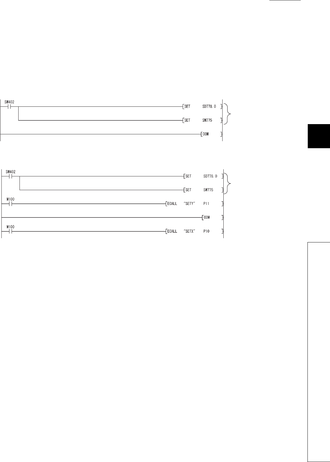
1
2
3
APPEN-
DIX
6
7
8
Appendix 3 Method of Replacing Basic Model QCPU or High Performance Model QCPU with Universal
Model QCPU
Appendix 3.4 Functions
APPENDICES
App - 65
(3) Replacing the COM instruction
If the COM instruction is used, add subroutine calls for P10 and P11 before and after the COM instruc-
tion. (P10 and P11 are pointers shown in the program examples in (2).) When SM775 is on (Executes
refresh set by SD778) and also the 0 bit of SD778 is off (Do not execute I/O refresh), replacement of
the instruction is not necessary.
(a) Program before replacement
(b) Program after replacement
Selection of refresh processing
during COM instruction execution
Selection of refresh processing
during COM instruction execution
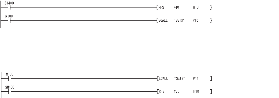
App - 66
(4) Replacing the RFS instruction
If any I/O numbers targeted for forced on/off are included in the partial refresh range specified by the RFS instruc-
tion, add subroutine calls for P10 and P11 before and after the RFS instruction. (P10 and P11 are pointers shown
in the program examples in (2).)
If no I/O number targeted for forced on/off is included, addition of subroutine calls for P10 and P11 is not neces-
sary.
(a) When partial refresh for input (X) is executed by the RFS instruction
Add a subroutine call that executes forced input after the RFS instruction.
(b) When partial refresh for output (Y) is executed by the RFS instruction
Add a subroutine call that executes forced output before the RFS instruction.
(5) Restrictions
Replacements described in (2) to (4) do not apply in the following cases.
• Input and output targeted for forced on/off are referred to or changed using the direct input device (DX) and
direct output device (DY).
• Input and output targeted for forced on/off are referred to or changed within an interrupt program.
A subroutine call that executes
forced input is added.
A subroutine call that executes
forced output is added.

1
2
3
APPEN-
DIX
6
7
8
Appendix 3 Method of Replacing Basic Model QCPU or High Performance Model QCPU with Universal
Model QCPU
Appendix 3.5 Special Relay and Special Register
APPENDICES
App - 67
Appendix 3.5 Special Relay and Special Register
The Universal model QCPU does not support the use of the special relay and special register described in Appendix
3.5.1 and Appendix 3.5.2.
Replace them using the method described in the table or delete the corresponding sections.
Appendix 3.5.1 Special relay list
TableApp.41 lists the special relay not supported in the Universal model QCPU and measures to be taken.
(To the next page)
TableApp.45 Special relay not supported by the Universal model QCPU and measures
Number Name/Description Measures
SM80 CHK detection
The Universal model QCPU does not support the CHK
instruction. For the replacing method of the CHK
instruction, refer to Appendix 3.3.3.
SM91
Step transition monitoring timer start
The Universal model QCPU does not support the step
transition monitoring timer function. For the replacing
method of this function, refer to “Appendix 3.
Restrictions and replacing method of the Basic model
QCPU and Universal model QCPU" in the QCPU (Q
Mode)/QnACPU Programming Manual (SFC).
SM92
SM93
SM94
SM95
SM96
SM97
SM98
SM99
SM250 Largest mounted I/O number read
Operation of SD250 is not necessary. The Universal
model QCPU always stores the largest mounted I/O
number in SD250. Delete the corresponding sections.
SM255
MELSECNET/H
module 1
information
Indicates operative network or standby network
These are special relays for the simple dual-structured
network function. Since the Universal model QCPU
does not support this function, there is no application for
these special relays. Delete the corresponding sections.
SM256 At refresh from link module to CPU, selects
whether to read data from the link module.
SM257 At refresh from CPU to link module, selects
whether to write data to the link module.
SM260
MELSECNET/H
module 2
information
Indicates operative network or standby network
SM261 At refresh from link module to CPU, selects
whether to read data from the link module.
SM262 At refresh from CPU to link module, selects
whether to write data to the link module.
SM265
MELSECNET/H
module 3
information
Indicates operative network or standby network
SM266 At refresh from link module to CPU, selects
whether to read data from the link module.
SM267 At refresh from CPU to link module, selects
whether to write data to the link module.
SM270
MELSECNET/H
module 4
information
Indicates operative network or standby network
SM271 At refresh from link module to CPU, selects
whether to read data from the link module.
SM272 At refresh from CPU to link module, selects
whether to write data to the link module.

App - 68
(To the next page)
TableApp.45 Special relay not supported in the Universal model QCPU and measures (Continued)
Number Name/Description Measures
SM280 CC-Link error Replace the relay with the I/O signals (Xn0, Xn1, and XnF) of the mounted CC-Link
module.
SM315 Communication reserved time delay
enable/disable flag
Set a service processing time value in the PLC system tab of the PLC parameter dia-
log box.
SM330 Operation mode for low-speed
execution type program
The Universal model QCPU does not support low-speed execution type programs.
Delete the corresponding sections.
SM331 Normal SFC program execution
status The Universal model QCPU supports only normal SFC programs. Delete SM331 and
SM332, which are used as interlocks, or replace them with SM321.
SM332 Program execution management
SFC program execution status
SM390 Access execution flag Modify the program that Module ready signal (Xn) is used as an interlock, according
to sample programs described in the manual for each module.
SM404 ON for only 1 scan after RUN of low-
speed execution type programs The Universal model QCPU does not support low-speed execution type programs.
Delete the corresponding sections or replace them with the special relays for scan
execution type programs (SM402 and SM403).
SM405 Off for only 1 scan after RUN of low-
speed execution type programs
SM430 User timing clock No.5 (for low-
speed execution type programs)
The Universal model QCPU does not support low-speed execution type programs.
Delete the corresponding sections or replace them with the special relays for scan
execution type programs (SM420 and SM424).
SM431 User timing clock No.6 (for low-
speed execution type programs)
SM432 User timing clock No.7 (for low-
speed execution type programs)
SM433 User timing clock No.8 (for low-
speed execution type programs)
SM434 User timing clock No.9 (for low-
speed execution type programs)
SM510 Low-speed execution type program
executing flag
The Universal model QCPU does not support low-speed execution type programs.
Delete the corresponding sections.
SM551 Module service interval time read The Universal model QCPU does not support the service interval measurement
function. Delete the corresponding sections.
SM580 Program to program I/O refresh Perform I/O refresh at the start or end of each program with the RFS or COM instruc-
tion.
SM660 Boot operation Move files with a boot setting (from the standard ROM or a memory card to the pro-
gram memory) to the program memory.
SM672 Memory card file register access
range flag
When outside the range of the file register in the memory card is accessed, the
Universal model QCPU detects "OPERATION ERROR" (error code: 4101).
Programming for detecting errors using this special realy is not necessary. Delete
the corresponding sections.
SM710 CHK instruction priority flag The Universal model QCPU does not support the CHK instruction. For the replacing
method of the CHK instruction, refer to Appendix 3.3.
SM734 XCALL instruction execution
condition specification
The Universal model QCPU executes the XCALL instruction on the rising edge of
execution condition as well. There is no application for this special relay. Delete the
corresponding sections.
SM735 SFC comment readout instruction in-
execution flag
The Universal model QCPU does not support the following instructions:
• SFC step comment readout instruction (S(P).SFCSCOMR)
• SFC transition condition comment readout instruction (S(P).SFCTCOMR)
Delete the corresponding sections.

1
2
3
APPEN-
DIX
6
7
8
Appendix 3 Method of Replacing Basic Model QCPU or High Performance Model QCPU with Universal
Model QCPU
Appendix 3.5 Special Relay and Special Register
APPENDICES
App - 69
*1: The special relay can be used if the serial number (first five digits) of the Universal model QCPU is "10042" or later.
TableApp.45 Special relay not supported in the Universal model QCPU and measures (Continued)
Number Name/Description Measures
SM1780*1 Power supply off detection flag
The Universal model QCPU does not store redundant power supply system
information in SM1780 to SM1783. Delete the corresponding sections. (SM1780 to
SM1783 are always off.)
SM1781*1 Power supply failure detection flag
SM1782*1 Momentary power failure detection
flag for power supply 1
SM1783*1 Momentary power failure detection
flag for power supply 2

App - 70
Appendix 3.5.2 Special register list
TableApp.42 lists the special register not supported in the Universal model QCPU and measures to be
taken
(To the next page)
TableApp.46 Special register not supported in the Universal model QCPU and measures
Number Name/Description Measures
SD80 CHK number The Universal model QCPU does not support the CHK instruction. For the replacing
method of the CHK instruction, refer to Appendix 3.3.
SD90
Step transition monitoring timer
setting value
The Universal model QCPU does not support the step transition monitoring timer
function. For the replacing method of this function, refer to ”Appendix 3. Restrictions
and replacing method of the Basic model QCPU and Universal model QCPU" in the
QCPU (Q Mode)/QnACPU Programming Manual (SFC).
SD91
SD92
SD93
SD94
SD95
SD96
SD97
SD98
SD99
SD130 to
SD137 Fuse blown module Replace SD130 to SD137 with SD1300 to SD1307.
SD150 to
SD157 I/O module verify error Replace SD150 to SD157 with SD1400 to SD1407.
SD245 No. of base slots (Mounting status) Replace SD245 and SD246 with SD243 and SD244, respectively.
SD246
SD280 CC-Link error Replace these registers with the I/O signals (Xn0, Xn1, and XnF) of the mounted CC-
Link module.
SD281
SD315 Time reserved for communication
processing
Service processing setting is available for the Universal model QCPU on the PLC
system setting tab of the PLC parameter dialog box.
Select "Specify service process time." for the service processing setting parameter
and set the service processing time. Other setting methods can be selected as well.
SD394 CPU mounting information
• Check the type and model of other CPU modules mounted on the System monitor
screen of GX Developer.
• Check the mounting status of other CPU modules in SD396 to SD398.
SD430 Low-speed scan counter
The Universal model QCPU does not support low-speed execution type programs.
Delete the corresponding sections or replace them with the special register for scan
execution type programs (SD420).
SD510 Low-speed execution type program
number
The Universal model QCPU does not support low-speed execution type programs.
Delete the corresponding sections or replace them with the special register for scan
execution type programs (SD500).
SD528 Current scan time for low-speed
execution type programs
The Universal model QCPU does not support low-speed execution type programs.
Delete the corresponding sections or replace them with the special register for scan
execution type programs (SD520 and SD521).
SD529
SD532 Minimum scan time for low-speed
execution type programs The Universal model QCPU does not support low-speed execution type programs.
Delete the corresponding sections or replace them with the special registers for scan
execution type programs (SD524 to SD527).
SD533
SD534 Maximum scan time for low-speed
execution type programs
SD535
SD544 Cumulative execution time for low-
speed execution type programs
The Universal model QCPU does not support low-speed execution type programs.
Delete the corresponding sections.
SD545
SD546 Execution time for low-speed
execution type programs
The Universal model QCPU does not support low-speed execution type programs.
Delete the corresponding sections.
SD547

1
2
3
APPEN-
DIX
6
7
8
Appendix 3 Method of Replacing Basic Model QCPU or High Performance Model QCPU with Universal
Model QCPU
Appendix 3.5 Special Relay and Special Register
APPENDICES
App - 71
*1: The special register can be used if the serial number (first five digits)of the Universal model QCPU is "10042" or later.
TableApp.46 Special register not supported in the Universal model QCPU and measures (Continued)
Number Name/Description Measures
SD550 Service interval measurement
module The Universal model QCPU does not support the service interval measurement
function. Delete the corresponding sections.SD551 Service interval time
SD552
SD720 Program No. specification for
PLAODP instruction
The Universal model QCPU does not support the PLAODP instruction. Delete the
corresponding sections.
SD1780 *1 Power supply off detection status
The Universal model QCPU does not store redundant power supply system
information in SD1780 to SD1783. Delete the corresponding sections. (SD1780 to
SD1783 are always off.)
SD1781 *1 Power supply failure detection status
SD1782 *1 Momentary power failure detection
counter for power supply 1
SD1783 *1 Momentary power failure detection
counter for power supply 1

App - 72
Appendix 4 Device Point Assignment Sheet
*1: The points are fixed for the system. (Cannot be changed)
The points for the step relay (S) can be changed to 0 if the Universal model QCPU whose serial number (first five digits) is "10042" or
later.
*2: Up to 32K points can be set for each device.
However, up to 60K points can be set for each device of the internal relay and link relay if the Universal model QCPU whose serial
number (first five digits) is "10042" or later,
*3: Enter the values multiplied (or divided) by the number shown in the Size (words) column.
TableApp.47 Device point assignment sheet
Device name Symbol Numeric
notation
Number of device point *2 Restriction check
Points Range Size (words)*3 Points (bits)*2
Input relay*1 X Hexadecimal 8K (8192) X0000 to X1FFF /16 512 18192
Output relay*1 Y Hexadecimal 8K (8192) Y0000 to Y1FFF /16 512 18192
Internal relay M Decimal K ( ) M0 to /16 1
Latch relay L Decimal K ( ) L0 to /16 1
Link relay B Hexadecimal K ( ) B0000 to /16 1
Annunciator F Decimal K ( ) F0 to /16 1
Link special relay SB Hexadecimal K ( ) SB0000 to /16 1
Edge relay V Decimal K ( ) V0 to /16 1
Step relay*1 S Decimal 8K (8192) S0 to S8191 /16 512 18192
Timer T Decimal K ( ) T0 to 2
Retentive timer ST Decimal K ( ) ST0 to 2
Counter C Decimal K ( ) C0 to 2
Data register D Decimal K ( ) D0 to 1
Link register W Hexadecimal K ( ) W0000 to 1
Link special
register SW Hexadecimal K ( ) SW0000 to 1
Tota l (29696 or less) (65536 or less)
18
16
18
16
18
16

1
2
3
4
INDEX
INDEX
7
8
Index - 1
INDEX
[A]
Acknowledge XY assignment . . . . . . . . . . . . . . . 8-16
Annunciator (F)
Processing after annunciator off . . . . . . . . . . . 9-14
Processing after annunciator on . . . . . . . . . . . 9-12
ASCII code . . . . . . . . . . . . . . . . . . . . . . . . . . . . . 2-43
Auto mode . . . . . . . . . . . . . . . . . . . . . . . . . . . . . . . 4-1
Auto refresh setting . . . . . . . . . . . . . . . . . . . . . . . . 7-2
[B]
B (Link relay) . . . . . . . . . . . . . . . . . . . . . . . . . . . . 9-16
Backup data restoration function . . . . . . . . . . . . 6-157
Backup function to memory card . . . . . . . . . . . . 6-149
Base unit . . . . . . . . . . . . . . . . . . . . . . . . . . . . . . . A-21
Battery life-prolonging function . . . . . . . . . . . . . 6-139
BCD (Binary-coded decimal) . . . . . . . . . . . . . . . . 2-38
BIN (Binary code) . . . . . . . . . . . . . . . . . . . . . . . . 2-35
BL (SFC block device). . . . . . . . . . . . . . . . . . . . . 9-78
Boot operation . . . . . . . . . . . . . . . . . . . . . . . . . . . 5-23
Built-in Ethernet port of the CPU module . . . . . . 1-12
Built-in Ethernet port setting . . . . . . . . . . . . . . . . 8-19
[C]
C (Counter) . . . . . . . . . . . . . . . . . . . . . . . . . . . . . 9-27
CC-Link . . . . . . . . . . . . . . . . . . . . . . . . . . . . . . . . A-22
Changing clock data . . . . . . . . . . . . . . . . . . . . . . 6-14
Changing the program execution type. . . . . . . . . 2-30
Character string . . . . . . . . . . . . . . . . . . . . . . . . . . 9-83
Checking the function version . . . . . . . . . . . . . . . 1-13
Checking the serial number. . . . . . . . . . . . . . . . . 1-13
Clearing
Clearing data in the latch relay . . . . . . . . . . . . 9-10
Clearing local device data . . . . . . . . . . . . . . . . 9-94
Clearing the counter value . . . . . . . . . . . . . . . . 9-28
Clearing the error history data . . . . . . . . . . . . 6-105
Clearing the file register data . . . . . . . . . . . . . . 9-54
Clearing the retentive timer value . . . . . . . . . . 9-22
Remote latch clear . . . . . . . . . . . . . . . . . . . . . . 6-25
Clock function . . . . . . . . . . . . . . . . . . . . . . . . . . . 6-13
Common pointer . . . . . . . . . . . . . . . . . . . . . . . . . 9-74
Communications with the FROM and TO
instructions . . . . . . . . . . . . . . . . . . . . . . . . . . . . . . 7-5
Constant scan . . . . . . . . . . . . . . . . . . . . . . . . . . . . 6-4
Counter (C)
Counting. . . . . . . . . . . . . . . . . . . . . . . . . . . . . . 9-27
Resetting the counter. . . . . . . . . . . . . . . . . . . . 9-28
CPU module change function with memory card
. . . . . . . . . . . . . . . . . . . . . . . . . . . . . . . . . . . . . . 6-147
Cyclic transmission area device (U3En\G). . . . 9-45
[D]
D (Data register) . . . . . . . . . . . . . . . . . . . . . . . . . 9-31
Data clear processing . . . . . . . . . . . . . . . . . . . . . . 3-6
Data register (D) . . . . . . . . . . . . . . . . . . . . . . . . . 9-31
Debug execution
Operation procedure . . . . . . . . . . . . . . . . . . . . 6-92
Debug function from multiple GX Developers . . . 6-91
Decimal constant (K) . . . . . . . . . . . . . . . . . . . . . . 9-81
Detail mode . . . . . . . . . . . . . . . . . . . . . . . . . . . . . . 4-1
Device list . . . . . . . . . . . . . . . . . . . . . . . . . . . . . . . 9-1
Device point assignment sheet . . . . . . . . . . . .App-72
Device setting . . . . . . . . . . . . . . . . . . . . . . . . . . . . 8-8
Direct access input . . . . . . . . . . . . . . . . . . . . . . . 3-12
Direct access input (DX) . . . . . . . . . . . . . . . . . . . 3-12
Direct access output . . . . . . . . . . . . . . . . . . . . . . 3-12
Direct access output (DY) . . . . . . . . . . . . . . . . . . 3-12
Direct mode . . . . . . . . . . . . . . . . . . . . . . . . . . . . . 3-12
Double-precision floating-point data . . . . . . . . . . 2-41
Duty . . . . . . . . . . . . . . . . . . . . . . . . . . . . . . . . . . . 9-30
DX (Direct access input) . . . . . . . . . . . . . . . . . . . 3-12
DY (Direct access output) . . . . . . . . . . . . . . . . . . 3-12
[E]
E (Real number) . . . . . . . . . . . . . . . . . . . . . . . . . 9-82
Edge relay (V) . . . . . . . . . . . . . . . . . . . . . . . . . . . 9-15
END processing. . . . . . . . . . . . . . . . . . . . . . . . . . . 3-2
Error
Clearing errors . . . . . . . . . . . . . . . . . . . . . . . . 6-104
Error time output mode setting. . . . . . . . . . . . . 6-29
Operating mode when there is an error . . . . . . . 8-6
Error history . . . . . . . . . . . . . . . . . . . . . . . . . . . . 6-105
Ethernet . . . . . . . . . . . . . . . . . . . . . . . . . . . . . . . .A-22
Execution time measurement . . . . . . . . . . . . . . . 6-69
Executional conditioned device test. . . . . . . . . . . 6-48
Extended data register (D). . . . . . . . . . . . . . . . . . 9-64
Extended link register (W) . . . . . . . . . . . . . . . . . . 9-64
Extension base unit . . . . . . . . . . . . . . . . . . . . . . .A-21
External input/output forced on/off. . . . . . . . . . . . 6-43
[F]
F (Annunciator) . . . . . . . . . . . . . . . . . . . . . . . . . . 9-11
FD (Function register) . . . . . . . . . . . . . . . . . . . . . 9-36
File . . . . . . . . . . . . . . . . . . . . . . . . . . . . . . . . . . . . 5-30
File register
Accesses available for the file register. . . . . . . 9-55
Block switching method . . . . . . . . . . . . . . . . . . 9-61
Clearing the file register data . . . . . . . . . . . . . . 9-54
Serial number access method . . . . . . . . . . . . . 9-61
File size . . . . . . . . . . . . . . . . . . . . . . . . . . . . . . . . 5-34
File usability setting . . . . . . . . . . . . . . . . . . . . . . . 2-15
Fixed scan execution type program. . . . . . . . . . . 2-26
Floating-point data . . . . . . . . . . . . . . . . . . . . . . . . 2-39
Forced on/off . . . . . . . . . . . . . . . . . . . . . . . . . . . . 6-43
Formatting
Formatting the ATA card . . . . . . . . . . . . . . . . . 5-15
Formatting the SRAM card. . . . . . . . . . . . . . . . 5-15

Index - 2
Memory card clear . . . . . . . . . . . . . . . . . . . . . 5-15
Function devices (FX, FY, FD) . . . . . . . . . . . . . . 9-35
Function list . . . . . . . . . . . . . . . . . . . . . . . . . . . . . 6-1
FX (Function input) . . . . . . . . . . . . . . . . . . . . . . . 9-35
FY (Function output). . . . . . . . . . . . . . . . . . . . . . 9-36
[G]
Global device . . . . . . . . . . . . . . . . . . . . . . . . . . . 9-84
GOT . . . . . . . . . . . . . . . . . . . . . . . . . . . . . . . . . . A-22
GX Configurator . . . . . . . . . . . . . . . . . . . . . . . . . . 7-2
GX Developer . . . . . . . . . . . . . . . . . . . . . . . . . . . A-22
[H]
H (Hexadecimal constant) . . . . . . . . . . . . . . . . . 9-81
H/W error time PLC operation mode . . . . . . . . . 6-30
H/W error time PLC operation mode setting. . . . 6-30
Hardware check . . . . . . . . . . . . . . . . . . . . . . . . . 11-3
HEX (Hexadecimal) . . . . . . . . . . . . . . . . . . . . . . 2-37
Hexadecimal constant (H) . . . . . . . . . . . . . . . . . 9-81
High-speed timer (T). . . . . . . . . . . . . . . . . . . . . . 9-21
[I]
I (Interrupt pointer) . . . . . . . . . . . . . . . . . . . . . . . 9-76
I/O assignment . . . . . . . . . . . . . . . . . . . . . . . . . . . 4-8
I/O assignment on remote I/O stations . . . . . . . . . 4-6
I/O No. specification device (U) . . . . . . . . . . . . . 9-79
I/O number . . . . . . . . . . . . . . . . . . . . . . . . . . . . . . 4-1
I/O number assignment . . . . . . . . . . . . . . . . . . . . 4-1
I/O processing and response delay . . . . . . . . . . . 3-8
I/O response time . . . . . . . . . . . . . . . . . . . . . . . . 6-27
Index register (Z)
Restoring the index register data . . . . . . . . . . 9-49
Saving the index register data . . . . . . . . . . . . 9-49
Initial device value . . . . . . . . . . . . . . . . . . . . . . 6-135
Initial execution monitoring time . . . . . . . . . . . . . 2-19
Initial execution type program. . . . . . . . . . . . . . . 2-17
Initial processing. . . . . . . . . . . . . . . . . . . . . . . . . . 3-1
Initial setting . . . . . . . . . . . . . . . . . . . . . . . . . . 7-2,7-5
Input (X) . . . . . . . . . . . . . . . . . . . . . . . . . . . . . . . . 9-6
Intelligent function module
Intelligent function module dedicated
instructions . . . . . . . . . . . . . . . . . . . . . . . . . . . . 7-8
Intelligent function module device (U\G). . 9-43
Intelligent function module switch setting . . . . 6-31
Interrupt form intelligent function module . . . 6-119
Intelligent function module setting . . . . . . . . . . . . 8-3
Internal relay (M) . . . . . . . . . . . . . . . . . . . . . . . . . 9-9
Internal system device . . . . . . . . . . . . . . . . . . . . 9-35
Internal user device . . . . . . . . . . . . . . . . . . . . . . . 9-3
Interrupt
Interrupt form intelligent function module . . . 6-119
Interrupt module . . . . . . . . . . . . . . . . . . . . . . . 6-27
Interrupt pointer (I) . . . . . . . . . . . . . . . . . . . . . 9-76
Interrupt pointer setting . . . . . . . . . . . . . . . . . . . 8-3
Interrupt program . . . . . . . . . . . . . . . . . . . . . . . 2-6
Interrupt program monitor list . . . . . . . . . . . . . 6-72
List of interrupt factors. . . . . . . . . . . . . . . . . . . 9-77
Interrupt program/Fixed scan program setting . . . 8-4
[J]
J (Network No. specification device). . . . . . . . . . 9-78
J\ (Link direct device) . . . . . . . . . . . . . . . . . . 9-40
[K]
K (Decimal constant) . . . . . . . . . . . . . . . . . . . . . 9-81
[L]
L (Latch relay). . . . . . . . . . . . . . . . . . . . . . . . . . . 9-10
Ladder mode. . . . . . . . . . . . . . . . . . . . . . . . . 2-2,6-58
Latch . . . . . . . . . . . . . . . . . . . . . . . . . . . . . . . . . . . 6-7
Latch clear . . . . . . . . . . . . . . . . . . . . . . . . . . . . . . 3-7
Latch clear operation disable range
(Latch (2) start/end) . . . . . . . . . . . . . . . . . . . . . . . 3-7
Latch clear operation enable range
(Latch (1) start/end) . . . . . . . . . . . . . . . . . . . . . . . 3-7
Latch data backup to standard ROM function
. . . . . . . . . . . . . . . . . . . . . . . . . . . . . . . . . . . . . 6-141
Latch function . . . . . . . . . . . . . . . . . . . . . . . . . . . . 6-7
Latch relay (L). . . . . . . . . . . . . . . . . . . . . . . . . . . 9-10
LED
Methods for turning off the LEDs . . . . . . . . . 6-116
Link direct device (J\) . . . . . . . . . . . . . . . . . . 9-40
Link register (W) . . . . . . . . . . . . . . . . . . . . . . . . . 9-32
Link relay (B). . . . . . . . . . . . . . . . . . . . . . . . . . . . 9-16
Link special register (SW). . . . . . . . . . . . . . . . . . 9-34
Link special relay (SB) . . . . . . . . . . . . . . . . . . . . 9-18
List mode . . . . . . . . . . . . . . . . . . . . . . . . . . . . . . . 2-2
Local device . . . . . . . . . . . . . . . . . . . . . . . . . . . . 9-85
Clearing local device data . . . . . . . . . . . . . . . . 9-94
Local device monitor . . . . . . . . . . . . . . . . . . . . 6-40
Local pointer . . . . . . . . . . . . . . . . . . . . . . . . . . . . 9-72
Low-speed timer (T) . . . . . . . . . . . . . . . . . . . . . . 9-21
[M]
M (Internal relay). . . . . . . . . . . . . . . . . . . . . . . . . . 9-9
Macro instruction argument device (VD) . . . . . . 9-80
Main base unit . . . . . . . . . . . . . . . . . . . . . . . . . . A-21
Main routine program . . . . . . . . . . . . . . . . . . . . . . 2-4
Maximum counting speed. . . . . . . . . . . . . . . . . . 9-30
MELSECNET/H . . . . . . . . . . . . . . . . . . . . . . . . . A-22
Memory capacities of files . . . . . . . . . . . . . . . . . 5-34
Memory capacity. . . . . . . . . . . . . . . . . . . . . . . . . 5-34
Memory card. . . . . . . . . . . . . . . . . . . . . . . . . . . . 5-14
Memory check function. . . . . . . . . . . . . . . . . . . 6-140
Memory composition. . . . . . . . . . . . . . . . . . . . . . . 5-1
Module service interval . . . . . . . . . . . . . . . . . . . 6-128
Momentary power failure . . . . . . . . . . . . . . . . . . . 3-5
Monitor . . . . . . . . . . . . . . . . . . . . . . . . . . . . . . . . 6-33
Monitor condition setting. . . . . . . . . . . . . . . . . . . 6-34
Motion CPU . . . . . . . . . . . . . . . . . . . . . . . . . . . . A-21

1
2
3
4
INDEX
INDEX
7
8
Index - 3
Multiple CPU high speed transmission area
setting . . . . . . . . . . . . . . . . . . . . . . . . . . . . . . . . . 8-18
Multiple CPU settings . . . . . . . . . . . . . . . . . . . . . 8-17
Multiple CPU synchronous interrupt . . . . . . . . . . 9-76
[N]
N (Nesting) . . . . . . . . . . . . . . . . . . . . . . . . . . . . . 9-70
Nesting . . . . . . . . . . . . . . . . . . . . . . . . . . . . . . . . 9-70
Network No. specification device (J) . . . . . . . . . . 9-78
Network parameters . . . . . . . . . . . . . . . . . . . . . . 8-21
[O]
Online change . . . . . . . . . . . . . . . . . . . . . . . . . . . 6-58
Online change (files) . . . . . . . . . . . . . . . . . . . . 6-61
Online change (ladder mode) . . . . . . . . . . . . . 6-58
Online change from multiple GX Developers . . . 6-93
Output mode at STOP to RUN . . . . . . . . . . . . . . 6-11
[P]
P (Pointer) . . . . . . . . . . . . . . . . . . . . . . . . . . . . . . 9-71
Parameters
Network parameters. . . . . . . . . . . . . . . . . . . . . 8-21
PLC . . . . . . . . . . . . . . . . . . . . . . . . . . . . . . . . . . 8-2
Password. . . . . . . . . . . . . . . . . . . . . . . . . . . . . . 6-106
PAUSE status . . . . . . . . . . . . . . . . . . . . . . . . . . . . 3-3
PC CPU module . . . . . . . . . . . . . . . . . . . . . . . . . A-21
PC RAS (1) setting . . . . . . . . . . . . . . . . . . . . . . . . 8-6
PLC file setting . . . . . . . . . . . . . . . . . . . . . . . . . . . 8-5
PLC name setting . . . . . . . . . . . . . . . . . . . . . . . . . 8-2
PLC parameters . . . . . . . . . . . . . . . . . . . . . . . . . . 8-2
Pointer
Common pointer . . . . . . . . . . . . . . . . . . . . . . . 9-74
Interrupt pointer . . . . . . . . . . . . . . . . . . . . . . . . 9-76
Local pointer . . . . . . . . . . . . . . . . . . . . . . . . . . 9-72
Points occupied by empty slot . . . . . . . . . . . . . . . . 8-4
Procedure
Procedure for boot run . . . . . . . . . . . . . . . . . . . 5-24
Procedure for writing a program . . . . . . . . . . . 5-19
Program cache memory . . . . . . . . . . . . . . . . . . . . 5-8
Program monitor list . . . . . . . . . . . . . . . . . . . . . . 6-69
Program setting . . . . . . . . . . . . . . . . . . . . . . . . . . 8-10
Protection
Password registration . . . . . . . . . . . . . . . . . . 6-106
Remote password . . . . . . . . . . . . . . . . . . . . . 6-108
[Q]
Q series power supply module . . . . . . . . . . . . . . A-22
Q3B . . . . . . . . . . . . . . . . . . . . . . . . . . . . . . . . . A-21
Q3DB . . . . . . . . . . . . . . . . . . . . . . . . . . . . . . . . A-21
Q3RB . . . . . . . . . . . . . . . . . . . . . . . . . . . . . . . . A-21
Q3SB . . . . . . . . . . . . . . . . . . . . . . . . . . . . . . . . A-21
Q5B . . . . . . . . . . . . . . . . . . . . . . . . . . . . . . . . . A-21
Q6B . . . . . . . . . . . . . . . . . . . . . . . . . . . . . . . . . A-21
Q6RB . . . . . . . . . . . . . . . . . . . . . . . . . . . . . . . . A-21
QI60. . . . . . . . . . . . . . . . . . . . . . . . . . . . . . . . . . . 6-27
QnUD(H)CPU . . . . . . . . . . . . . . . . . . . . . . . . . . .A-21
[R]
R (File register) . . . . . . . . . . . . . . . . . . . . . . . . . . 9-53
Reading clock data . . . . . . . . . . . . . . . . . . . . . . . 6-15
Redundant power extension base unit . . . . . . . .A-21
Redundant power main base unit . . . . . . . . . . . .A-21
Refresh mode . . . . . . . . . . . . . . . . . . . . . . . . . . . . 3-9
Remote latch clear. . . . . . . . . . . . . . . . . . . . . . . . 6-25
Remote operation . . . . . . . . . . . . . . . . . . . . . . . . 6-18
Remote password . . . . . . . . . . . . . . . . . . . . . . . 6-108
Remote PAUSE . . . . . . . . . . . . . . . . . . . . . . . . . . 6-21
Remote RESET . . . . . . . . . . . . . . . . . . . . . . . . . . 6-23
Remote RUN/STOP. . . . . . . . . . . . . . . . . . . . . . . 6-18
RUN status . . . . . . . . . . . . . . . . . . . . . . . . . . . . . . 3-3
[S]
S (Step relay). . . . . . . . . . . . . . . . . . . . . . . . . . . . 9-19
Sampling trace. . . . . . . . . . . . . . . . . . . . . . . . . . . 6-77
SB (Link special relay) . . . . . . . . . . . . . . . . . . . . . 9-18
Scan execution type program . . . . . . . . . . . . . . . 2-20
Scan time. . . . . . . . . . . . . . . . . . . . . . . . . . . . . . . 2-18
Scan time accuracy . . . . . . . . . . . . . . . . . . . . . . . 2-18
Scan time measurement . . . . . . . . . . . . . . . . . . . 6-73
SD (Special register) . . . . . . . . . . . . . . . . . . . . . . 9-38
Self-diagnostic function . . . . . . . . . . . . . . . . . . . . 6-97
Serial communication function. . . . . . . . . . . . . . 6-120
Serial setting . . . . . . . . . . . . . . . . . . . . . . . . . . . . 8-15
Service processing . . . . . . . . . . . . . . . . . . . . . . 6-128
Service processing setting. . . . . . . . . . . . . . . . . 6-128
Setting in GX Configurator. . . . . . . . . . . . . . . . . . . 7-2
SFC block device (BL) . . . . . . . . . . . . . . . . . . . . . 9-78
SFC setting . . . . . . . . . . . . . . . . . . . . . . . . . . . . . 8-12
Single-precision floating-point data . . . . . . . . . . . 2-39
Size (file capacity) . . . . . . . . . . . . . . . . . . . . . . . . 5-34
Slim type main base unit . . . . . . . . . . . . . . . . . . .A-21
Slim type power supply module . . . . . . . . . . . . . .A-22
SM (Special relay) . . . . . . . . . . . . . . . . . . . . . . . . 9-38
Special register (SD) . . . . . . . . . . . . . . . . . . . . . . 9-38
Special relay (SM) . . . . . . . . . . . . . . . . . . . . . . . . 9-38
ST (Retentive timer). . . . . . . . . . . . . . . . . . . . . . . 9-22
Standard device register (Z) . . . . . . . . . . . . . . . . 9-48
Standard RAM . . . . . . . . . . . . . . . . . . . . . . . . . . . 5-12
Standard ROM. . . . . . . . . . . . . . . . . . . . . . . . . . . 5-11
Stand-by type program . . . . . . . . . . . . . . . . . . . . 2-21
Step relay (S). . . . . . . . . . . . . . . . . . . . . . . . . . . . 9-19
STOP status . . . . . . . . . . . . . . . . . . . . . . . . . . . . . 3-3
Subroutine program . . . . . . . . . . . . . . . . . . . . . . . . 2-5
SW (Link special register) . . . . . . . . . . . . . . . . . . 9-34
Switch setting
Intelligent function module switch setting. . . . . 6-31
System protection . . . . . . . . . . . . . . . . . . . . . . . 6-106
[T]
T (Timer) . . . . . . . . . . . . . . . . . . . . . . . . . . . . . . . 9-20
Timer (T)

Index - 4
Accuracy . . . . . . . . . . . . . . . . . . . . . . . . . . . . . 9-24
Processing . . . . . . . . . . . . . . . . . . . . . . . . . . . 9-23
Timer limit setting . . . . . . . . . . . . . . . . . . . . . . . . . 8-3
Transferring data to the program memory . . . . . . 5-9
[U]
U (I/O No. specification device) . . . . . . . . . . . . . 9-79
U3En\G (Cyclic transmission area device) . . . 9-45
Units . . . . . . . . . . . . . . . . . . . . . . . . . . . . . . . . . . 5-36
Units of file sizes. . . . . . . . . . . . . . . . . . . . . . . . . 5-36
U\G (Intelligent function module device) . . . 9-43
User setting system area . . . . . . . . . . . . . . . . . . . 5-5
[V]
V (Edge relay). . . . . . . . . . . . . . . . . . . . . . . . . . . 9-15
VD (Macro instruction argument device) . . . . . . 9-80
[W]
W (Link register) . . . . . . . . . . . . . . . . . . . . . . . . . 9-32
Watchdog timer (WDT). . . . . . . . . . . . . . . . . . . . 6-95
WDT (Watchdog timer). . . . . . . . . . . . . . . . . . . . 6-95
WDT setting . . . . . . . . . . . . . . . . . . . . . . . . . . . . 6-95
Write the program memory to ROM . . . . . . . . . . 5-18
Write to PLC (Flash ROM) . . . . . . . . . . . . . . . . . 5-20
Writing
Writing data to the memory card. . . . . . . . . . . 5-16
Writing data to the program memory . . . . . . . . 5-7
Writing data to the standard RAM. . . . . . . . . . 5-13
Writing data to the standard ROM . . . . . . . . . 5-11
Writing/reading device data to/from standard
ROM . . . . . . . . . . . . . . . . . . . . . . . . . . . . . . . . . 6-146
[X]
X (Input) . . . . . . . . . . . . . . . . . . . . . . . . . . . . . . . . 9-6
[Y]
Y (Output) . . . . . . . . . . . . . . . . . . . . . . . . . . . . . . . 9-8
[Z]
Z (Index register) . . . . . . . . . . . . . . . . . . . . . . . . 9-46
Z (Standard device register) . . . . . . . . . . . . . . . . 9-48
ZR (Serial number access method of file
register) . . . . . . . . . . . . . . . . . . . . . . . . . . . . . . . 9-61

Warranty
Please confirm the following product warranty details before using this product.
1. Gratis Warranty Term and Gratis Warranty Range
If any faults or defects (hereinafter "Failure") found to be the responsibility of Mitsubishi occurs during use of the
product within the gratis warranty term, the product shall be repaired at no cost via the sales representative or
Mitsubishi Service Company.
However, if repairs are required onsite at domestic or overseas location, expenses to send an engineer will be
solely at the customer's discretion. Mitsubishi shall not be held responsible for any re-commissioning,
maintenance, or testing on-site that involves replacement of the failed module.
[Gratis Warranty Term]
The gratis warranty term of the product shall be for one year after the date of purchase or delivery to a designated
place.
Note that after manufacture and shipment from Mitsubishi, the maximum distribution period shall be six (6) months,
and the longest gratis warranty term after manufacturing shall be eighteen (18) months. The gratis warranty term of
repair parts shall not exceed the gratis warranty term before repairs.
[Gratis Warranty Range]
(1) The range shall be limited to normal use within the usage state, usage methods and usage environment, etc.,
which follow the conditions and precautions, etc., given in the instruction manual, user's manual and caution
labels on the product.
(2) Even within the gratis warranty term, repairs shall be charged for in the following cases.
1. Failure occurring from inappropriate storage or handling, carelessness or negligence by the user. Failure
caused by the user's hardware or software design.
2. Failure caused by unapproved modifications, etc., to the product by the user.
3. When the Mitsubishi product is assembled into a user's device, Failure that could have been avoided if
functions or structures, judged as necessary in the legal safety measures the user's device is subject to or
as necessary by industry standards, had been provided.
4. Failure that could have been avoided if consumable parts (battery, backlight, fuse, etc.) designated in the
instruction manual had been correctly serviced or replaced.
5. Failure caused by external irresistible forces such as fires or abnormal voltages, and Failure caused by force
majeure such as earthquakes, lightning, wind and water damage.
6. Failure caused by reasons unpredictable by scientific technology standards at time of shipment from
Mitsubishi.
7. Any other failure found not to be the responsibility of Mitsubishi or that admitted not to be so by the user.
2. Onerous repair term after discontinuation of production
(1) Mitsubishi shall accept onerous product repairs for seven (7) years after production of the product is
discontinued.
Discontinuation of production shall be notified with Mitsubishi Technical Bulletins, etc.
(2) Product supply (including repair parts) is not available after production is discontinued.
3. Overseas service
Overseas, repairs shall be accepted by Mitsubishi's local overseas FA Center. Note that the repair conditions at
each FA Center may differ.
4. Exclusion of loss in opportunity and secondary loss from warranty liability
Regardless of the gratis warranty term, Mitsubishi shall not be liable for compensation of damages caused by any
cause found not to be the responsibility of Mitsubishi, loss in opportunity, lost profits incurred to the user by Failures
of Mitsubishi products, special damages and secondary damages whether foreseeable or not , compensation for
accidents, and compensation for damages to products other than Mitsubishi products, replacement by the user,
maintenance of on-site equipment, start-up test run and other tasks.
5. Changes in product specifications
The specifications given in the catalogs, manuals or technical documents are subject to change without prior notice.

Microsoft, Windows, Windows NT, Windows Vista are registered trademarks of Microsoft Corporation in the United States
and other countries.
Pentium and Celeron are trademarks of Intel Corporation in the United States and other countries.
Ethernet is a trademark of Xerox Co., Ltd. in the United States.
CompactFlash is a trademark of SanDisk Corporation.
VxWorks, Tornado, WindPower, WindSh and WindView are registered trademarks of Wind River Systems, Inc.
Other company names and product names used in this document are trademarks or registered trademarks of respective
owners.
SH(NA)-080807ENG-D