Mitsubishi Electronics Qj71C24N Users Manual Q Corresponding Serial Communication Module User's (Basic)
SH-080007 to the manual d4987e48-1b24-4573-b675-27f0a8680a1e
2015-02-09
: Mitsubishi-Electronics Mitsubishi-Electronics-Qj71C24N-Users-Manual-556762 mitsubishi-electronics-qj71c24n-users-manual-556762 mitsubishi-electronics pdf
Open the PDF directly: View PDF ![]() .
.
Page Count: 358 [warning: Documents this large are best viewed by clicking the View PDF Link!]
- SAFETY PRECAUTIONS
- REVISIONS
- INTRODUCTION
- CONTENTS
- About Manuals
- Conformation to the EMC Directive and Low Voltage Instruction
- The Manual's Use and Structure
- About The Generic Terms and Abbreviations
- Definitions and Descriptions of Terminology
- Product Configuration
- 1 OVERVIEW
- 2 SYSTEM CONFIGURATION AND AVAILABLE FUNCTIONS
- 3 SPECIFICATIONS
- 3.1 Performance Specifications
- 3.2 RS-232 Interface Specification
- 3.3 RS-422/485 Interface Specifications
- 3.4 Serial Communication Module Function List
- 3.5 Dedicated Instruction List
- 3.6 Utility Package (GX Configurator-SC) Function List
- 3.7 List of GX Developer Setting Items for Serial Communication Modules
- 3.8 List of Input/Output Signals for the PLC CPU
- 3.9 List of Applications and Assignments of the Buffer Memory
- 4 SETTINGS AND PROCEDURES PRIOR TO OPERATION
- 5 DATA COMMUNICATION USING THE MELSEC COMMUNICATION PROTOCOL
- 6 DATA COMMUNICATION USING THE NON PROCEDURE PROTOCOL
- 7 DATA COMMUNICATION USING THE BIDIRECTIONAL PROTOCOL
- 8 UTILITY PACKAGE (GX Configurator-SC)
- 8.1 Functions Available with Utility Package
- 8.2 Installing and Uninstalling Utility Package
- 8.3 Explanation of Utility Package Operation
- 8.4 System Registration to Flash ROM
- 8.4.1 User frame registration
- 8.4.2 Data for modem initialization registration
- 8.4.3 Data for modem connection registration
- 8.4.4 Modem function system setting/registration
- 8.4.5 Transmission control and others system setting
- 8.4.6 MC protocol system setting
- 8.4.7 Non procedure system setting
- 8.4.8 Bidirectional system setting
- 8.4.9 PLC CPU monitoring system setting
- 8.4.10 Transmission user frame No. designation system setting
- 8.4.11 Resetting the buffer memory/flash ROM setting values to the default values
- 8.4.12 Flash ROM write allow/prohibit setting
- 8.5 Auto Refresh Setting
- 8.6 Monitor/Test
- 8.6.1 X · Y monitor/test
- 8.6.2 Modem function monitor/test
- 8.6.3 Transmission control and others monitor/test
- 8.6.4 MC protocol monitor
- 8.6.5 Non procedure monitor/test
- 8.6.6 Bidirectional monitor
- 8.6.7 PLC CPU monitoring monitor
- 8.6.8 Transmission user frame No. designation monitor
- 8.6.9 Monitor/test others
- 8.6.10 Display LED off and communication error information/error code initialization
- 8.7 Non Procedure Protocol Receive Data Clear
- 9 DEDICATED INSTRUCTIONS
- 10 TROUBLESHOOTING
- 10.1 Checking the Status of the Serial Communication Module
- 10.1.1 Checking the LED ON status, communications error status, and switch setting status of the serial communication module
- 10.1.2 Initializing error information of the serial communication module
- 10.1.3 Reading the RS-232 control signal status
- 10.1.4 Reading the data communication status (Transmission sequence status)
- 10.1.5 Reading the switch setting status
- 10.1.6 How to read the current operation status
- 10.2 Error Code Tables
- 10.3 Troubleshooting by Symptom
- 10.3.1 Troubleshooting when "RUN" LED is turned OFF
- 10.3.2 Troubleshooting when "RD" LED does not blink even though an external device is transmitting a message
- 10.3.3 Troubleshooting when the Q series C24 does not return a response message even though an external device ...
- 10.3.4 Troubleshooting when an external device transmitted a message and "RD" LED blinked, but the Read Request signal ...
- 10.3.5 Troubleshooting when communication error "NAK" generates
- 10.3.6 Troubleshooting when communication error "C/N" generates
- 10.3.7 Troubleshooting when communication error "P/S" generates
- 10.3.8 Troubleshooting when communication error "PRO." generates
- 10.3.9 Troubleshooting when communication error "SIO" generates
- 10.3.10 Troubleshooting when communication error "CH1 ERR.", "CH2 ERR." generate
- 10.3.11 Troubleshooting when communications is intermittently established and lost
- 10.3.12 Troubleshooting when data that cannot be decoded is transmitted and received
- 10.3.13 Troubleshooting when it is unclear whether the communication error cause is in the Q series C24 or an external device
- 10.3.14 Troubleshooting when data cannot be communicated via modem
- 10.3.15 Troubleshooting when data cannot be communicated with the ISDN sub-address
- 10.3.16 Troubleshooting when constant cycle transmission does not operate normally
- 10.3.17 Troubleshooting when condition agreement transmission does not operate normally
- 10.3.18 Troubleshooting when data cannot be received by an interrupt program
- 10.3.19 Troubleshooting when data cannot be written to Flash ROM
- 10.3.20 Troubleshooting when the "ERR" LED is lit
- 10.1 Checking the Status of the Serial Communication Module
- APPENDIX
- Appendix 1 Functional Improvements of the Q Series C24
- Appendix 2 QnA/A Series Module
- Appendix 2.1 Functional Comparison with the Q series C24 and the QnA/A Series Modules
- Appendix 2.2 Using Programs Designed for the QC24 (N) and Installing the Q Series C24 into Existing Systems
- Appendix 2.3 Using Programs Designed for the Computer Link Module and Installing the Q Series C24 into Existing Systems
- Appendix 3 Processing Time
- Appendix 4 ASCII-Code Table
- Appendix 5 External Dimensions
- Appendix 6 Example of Connection when a Converter is Used
- Appendix 7 Communication Support Tool (MX Component)
- Appendix 8 Example of Clear Process Program for Receive Data
- Appendix 9 Program Examples for Using Q Series C24 at MELSECNET/H Remote I/O Station
- Appendix 9.1 System configuration and program conditions
- Appendix 9.2 When accessing buffer memory using sequence program
- Appendix 9.3 When sending on-demand data
- Appendix 9.4 When receiving data using nonprocedural or bidirectional protocol
- Appendix 9.5 When sending data using nonprocedural or bidirectional protocol
- Appendix 9.6 When clearing received data
- Appendix 9.7 When sending data using user frames
- Appendix 9.8 When performing initial setting
- Appendix 9.9 When registering user frame
- Appendix 9.10 When reading user frame
- Appendix 9.11 When deleting user frame
- Appendix 9.12 When changing the communication protocol and transmission setting
- Appendix 10 Setting Value Recording Sheet
- INDEX
- WARRANTY

MELSEC System Q
Programmable Logic Controllers
User's Manual
(Basic)
Serial Communication Modules
QJ71C24N/-R2/-R4, QJ71C24/-R2
GX Configurator-SC
INDUSTRIAL AUTOMATION
MIT
SU
BI
S
HI ELE
C
TRI
C
MIT
SU
BI
S
HI ELE
C
TRI
C
Art. no.: 130031
01 09 2004
SH (NA)-080006
Version H
A - 1 A - 1
• SAFETY PRECAUTIONS •
(Always read these instructions before using this equipment.)
Before using this product, please read this manual and the relevant manuals introduced in this manual
carefully and pay full attention to safety to handle the product correctly.
The instructions given in this manual are concerned with this product. For the safety instructions of the
programmable controller system, please read the user's manual of the CPU module to use.
In this manual, the safety instructions are ranked as "DANGER" and "CAUTION".
!DANGER
CAUTION
!
Indicates that incorrect handling may cause hazardous conditions,
resulting in death or severe injury.
Indicates that incorrect handling may cause hazardous conditions,
resulting in medium or slight personal injury or physical damage.
Note that the !CAUTION level may lead to a serious consequence according to the circumstances.
Always follow the instructions of both levels because they are important to personal safety.
Please save this manual to make it accessible when required and always forward it to the end user.
[Design Instructions]
! DANGER
• See manuals of each data link for the operating status of each station when there is a
communication error in the data link.
There is the risk of an accident occurring due to output error or malfunctioning.
• When using the notification function, the pager receiver may not be contacted due to the frequency
transmission status from the system setup environment and error on the receiver side.
To ensure the safety of the PLC system, install a call circuit with a lamp display or buzzer sound.
• When performing the control of the PLC in operation (changing data) by connecting a peripheral
devices to the CPU module or personal computer, etc. to the intelligent device module, configure an
interlock circuit in a sequence program so the safety of the overall system is always maintained.
Also when performing other controls of the PLC in operation (changing program and operation
status (status control)), read this manual carefully and confirm if the overall safety is maintained.
Especially, when this control is performed to a remote PLC from an external device, troubles
that have occurred on the PLC side may not be able to immediately be handled if there is a data
communication error.
Define a troubleshooting agreement between external devices and the PLC CPU for data
communication error occurrences, as well as construct an interlock circuit in the sequence program.
• Do not write data into the "system area" of the buffer memory of intelligent function modules.
Also, do not use any "prohibited to use" signals as an output signal to an intelligent function
module from the PLC CPU.
Writing data into the "system area" or outputting a signal for "prohibited to use" may cause a
PLC system malfunction.
A - 2 A - 2
[Design Instructions]
! CAUTION
• Do not bunch the control wires or communication cables with the main circuit or power wires, or
install them close to each other.
They should be installed 100mm(3.9inch) or more from each other.
Not doing so could result in noise that may cause malfunction.
• When using the module while values, such as buffer memory set values, are registered in the
Flash ROM, do not turn off the power supply for the module loading station nor reset the PLC
CPU.
If the power supply for the module loading station is turned off or the PLC CPU is reset while any
values are registered, the data contents in the Flash ROM become inconsistent and as a result the
values must be set again in the buffer memory, etc. and reregistered to the Flash ROM.
Also, this may cause failure and malfunction of the module.
[Installation Instructions]
! CAUTION
• Use the PLC in an environment that meets the general specifications contained in the user's
manual of the CPU module to use.
Using this PLC in an environment outside the range of the general specifications may cause
electric shock, fire, malfunction, and damage to or deterioration of the product.
• While pressing the installation lever located at the bottom of module, insert the module fixing tab
into the fixing hole in the base unit until it stops. Then, securely mount the module with the fixing
hole as a supporting point.
If the module is not installed properly, it may cause the module to malfunction, fail or fall off.
Secure the module with screws especially when it is used in an environment where constant
vibrations may occur.
• Tighten the screws within the range of specified torque.
If the screws are loose, it may cause the module to fallout, short circuits, or malfunction.
If the screws are tightened too much, it may cause damage to the screw and/or the module,
resulting in fallout, short circuits or malfunction.
• Switch all phases of the external power supply off when mounting or removing the module.
Not doing so may cause damage to the module.
• Do not directly touch the conductive area or electronic components of the module.
Doing so may cause malfunction or failure in the module.

A - 3 A - 3
[Wiring Instructions]
! CAUTION
• When turning on the power and operating the module after installation and wiring are completed,
always attach the terminal cover that comes with the product.
There is a risk of electric shock if the terminal cover is not attached.
• Perform correct pressure-displacement, crimp-contact or soldering for external wire connections
using the tools specified by the manufactures.
Incorrect connection may cause short circuits, fire, or malfunction.
• Attach connectors to the module securely.
• Be sure to fix communication cables or power supply cables leading from the module by placing
them in the duct or clamping them.
Cables not placed in the duct or without clamping may hang or shift, allowing them to be
accidentally pulled, which may cause a module malfunction and cable damage.
• Before connecting the cables, check the type o f interface to be connected.
Connecting or erroneous wiring to the wrong interface may cause failure to the module and
external devices.
• Tighten the terminal screws within the range of specified torque.
If the terminal screws are loose, it may result in short circuits or malfunction.
If the screws are tightened too much, it may cause damage to the screw and/or the module,
resulting in fallout, short circuits or malfunction.
• When removing the communication cable or power supply cable from the module, do not pull the
cable. When removing the cable with a connector, hold the connector on the side that is
connected to the module.
When removing the cable connected to the terminal block, first loosen the screws on the part
that is connected to the terminal block.
Pulling the cable that is still connected to the module may cause malfunction or damage to the
module or cable.
• Be careful not to let foreign matters such as sawdust or wire chips get inside the module.
They may cause fires, failure or malfunction.
• The top surface of the module is covered with protective film to prevent foreign objects such as
cable offcuts from entering the module when wiring.
Do not remove this film until the wiring is complete.
Before operating the system, be sure to remove the film to provide adequate heat ventilation.
A - 4 A - 4
[Startup/Maintenance Instructions]
! CAUTION
• Do not disassemble or modify each module.
Doing so could cause failure, malfunction injury or fire.
• Switch all phases of the external power supply off when mounting or removing the module.
Not doing so may cause failure or malfunction of the module.
• Do not mount/remove the module onto/from base unit more than 50 times (IEC61131-2-
compliant), after the first use of the product.
Failure to do so may cause the module to malfunction due to poor contact of connector.
• Do not touch the connector while the power is on.
Doing so may cause malfunction.
• Switch all phases of the external power supply off when cleaning or retightening terminal screws
and module installing screws.
Not doing so may cause failure or malfunction of the module.
If the screws are loose, it may cause the module to fallout, short circuits, or malfunction.
If the screws are tightened too much, it may cause damages to the screws and/or the module,
resulting in the module falling out, short circuits or malfunction.
• Always make sure to touch the grounded metal to discharge the electricity charged in the body,
etc., before touching the module.
Failure to do so may cause a failure or malfunctions of the module.
[Operation Instructions]
! CAUTION
• When performing the control of the PLC in operation (especially changing data, program, and
operation status (status control)) by connecting a personal computer, etc. to the intelligent
function module, read this manual carefully and confirm if the overall safety is maintained.
Failure to perform correct operation s to change data, program, or the status may result in
system malfunction, machine damage, or an accident.
[Disposal Instructions]
! CAUTION
• When disposing of this product, treat it as industrial waste.
A - 5 A - 5
REVISIONS The manual number is given on the bottom left of the back cover.
Print Date Manual Number Revision
Dec., 1999 SH (NA)-080006-A First Printing
Oct., 2000 SH (NA)-080006-B Add the contents of the function version B.
Correction
Contents, Entire manual (change MELSECNET/10H to MELSECNET/H),
About Manuals, About The Generic Terms and Abbreviations, Product
Configuration, Section 1.2, 1.2(8), 1.3 POINT, Section 2.2, 2.3, 2.5, 2.6,
Section 3.1, 3.6, 3.9, Section 4.2, 4.4.1(2)(a)(Figure), 4.6(1), Chapter
5(all), Section 6.1.1, 6.1.3, 6.1.4, Section 7.1.1, 7.1.2, 7.2.2, Section 8.1,
8.2.1, 8.2.2, 8.3.1, 8.3.2, Section 9.2 to 9.7, Section 10.1.1, 10.2.1,
10.3.8, 10.3.18, Appendix 1.1(2), Appendix 2(all), appendix 3(2),
Appendix 7, appendix 8
Addition
Entire manual (add the explanation on MELSECNET/H remote I/O
station), The Manual's Use and Structure, Section 2.1, Section
3.1(Table), Section 4.4.2(1)(d), 4.9.2, Section 8.3.2 POINT, Section
10.2.1 (7164H, 7E70H), Appendix 3(1)
Jun., 2001 SH (NA)-080006-C Put Windows® base software product together from Mitsubishi
Programmable Logic Controller MELSEC Series to Mitsubishi integrated
FA Software MELSOFT Series.
Standardize the name from software package (GPP function) to Product
name (GX Developer).
Standardize the name from utility package (QSCU) to Product name (GX
Congifurator-SC).
Correction
Conformation to the EMC Directive and Low Voltage Instruction, About
the Generic Terms and Abbreviations, Product Configuration, Program
Examples (Section 6.1.4, 6.2.3, Section 7.2.3, Section 9.3, 9.5, Appendix-
8), Section 1.2(1)(d), 1.2(4)(b)(Diagram), 1.2(8)(b), 1.3, Section 2.1, 2.3,
2.4, 2.5, 2.7, Section 3.1(Table), 3.2.1(3), 3.3.3(2), 3.4(Table), 3.9,
Section 4.3, 4.5.2, Section 5.1.5(3), 5.2, Section 6.1.4, Section 8.2, 8.3.2
POINT, 8.4.2, 8.4.9(Table), 8.6.3(Table), 8.6.7(Table), Section 10.1.2(b),
10.3(Table), Appendix 1.1, 2.1, 6, 7, 9
Addition
Section 2.6, Section 8.4.4, 8.6.2(Table), Section 10.2.1(716FH, 7FEFH),
10.2.3(7FE9H), 10.3.14, Appendix 3
Feb., 2002 SH (NA)-080006-D Addition
About The Generic Terms and Abbreviations, Section 1.2, Section 2.1,
2.7, Section 4.5.2, Section 8.2.1, 8.2.2, Section 10.2.1, Appendix 1.1, 6
Oct., 2002 SH (NA)-080006-E Addition
The Manual’s Use and Structure, About The Generic Terms and
Abbreviations, Section 1.2(1)(4), Section 2.1, 2.4, Section 5.2, Section
6.1.4, Section 9.8, Appendix 7
Jan., 2003 SH (NA)-080006-F Addition model
QJ71C24N, QJ71C24N-R2, QJ71C24N-R4
A - 6 A - 6
The manual number is given on the bottom left of the back cover.
Print Date Manual Number Revision
Jan., 2003 SH (NA)-080006-F Addition
SAFETY PRECAUTIONS, About Manuals, About The Generic Terms
and Abbreviations, Product Configuration, Section 1.3, Section 2.1, 2.2,
2.3, 2.5, 2.6, 2.7, Section 3.1, 3.2.1, 3.3.1, 3.6, 3.8, 3.9, Section 4.1, 4.3,
4.4, 4.5, 4.6, 4.7.1, Section 6.1.1, 6.1.2, Section 7.1, 7.2.2, Chapter 8(all),
Section 9.1, 9.6, Section 10.1.2(b), 10.1.3(1), 10.2, Appendix 1, Appendix
2.1, Appendix 3, Appendix 5, Appendix 9
Jun., 2004 SH (NA)-080006-G Correction
About The Generic Terms and Abbreviations, Product Configuration,
Chapter 2 (all), Section 3.8, Section 4.2.2 (1), Section 5.1.3 POINT,
Section 5.1.4, Chapter 8 (screen change), Section 8.6.10, Section 10.1.1,
Section 10.2
Addition
Appendix 9
Sep., 2004 SH (NA)-080006-H Correction
Section 1.3, Section 2.5, 2.6, Section 3.5, 3.6, 3.9, Section 4.1, Chapter 8
(screen change), Section 8.6.9, 8.6.10, Section 10.1, 10.2, Appendix 1.1
Addition
Appendix 9.12
Japanese Manual Version SH-080001-L
This manual confers no industrial property rights or any rights of any other kind, nor does it confer any patent
licenses. Mitsubishi Electric Corporation cannot be held responsible for any problems involving industrial property
rights which may occur as a result of using the contents noted in this manual.
1999 MITSUBISHI ELECTRIC CORPORATION

A - 7 A - 7
INTRODUCTION
Thank you for purchasing the MELSEC-Q series PLC.
Before using the equipment, please read this manual carefully to develop full familiarity with the functions
and performance of the Q series PLC you have purchased, so as to ensure correct use.
Please forward a copy of this manual to the end user.
CONTENTS (This manual)
SAFETY PRECAUTIONS..............................................................................................................................A- 1
REVISIONS....................................................................................................................................................A- 5
CONTENTS....................................................................................................................................................A- 7
About Manuals ...............................................................................................................................................A-15
Conformation to the EMC Directive and Low Voltage Instruction ................................................................A-15
The Manual’s Use and Structure ...................................................................................................................A-16
About The Generic Terms and Abbreviations...............................................................................................A-19
Definitions and Descriptions of Terminology.................................................................................................A-21
Product Configuration ....................................................................................................................................A-23
1 OVERVIEW 1- 1 to 1-11
1.1 Overview of the Serial Communication Module.....................................................................................1- 1
1.2 Features of the Serial Communication Module...................................................................................... 1- 2
1.3 About Added/Changed Functions in Function Version B ...................................................................... 1-10
2 SYSTEM CONFIGURATION AND AVAILABLE FUNCTIONS 2- 1 to 2-14
2.1 Applicable Systems................................................................................................................................. 2- 1
2.2 Combinations of PLC CPU and External Device, and Available Functions.......................................... 2- 3
2.3 For Use in Multiple CPU System............................................................................................................2- 6
2.4 For Use with Q00J/Q00/Q01CPU .......................................................................................................... 2- 7
2.5 For Use at MELSECNET/H Remote I/O Station.................................................................................... 2- 8
2.6 Checking the Function Version, Serial No., and Software Version....................................................... 2-12
3 SPECIFICATIONS 3- 1 to 3-31
3.1 Performance Specifications.................................................................................................................... 3- 1
3.2 RS-232 Interface Specification............................................................................................................... 3- 3
3.2.1 RS-232 connector specifications ..................................................................................................... 3- 3
3.2.2 RS-232 cable specification ..............................................................................................................3- 5
3.3 RS-422/485 Interface Specifications...................................................................................................... 3- 6
3.3.1 RS-422/485 terminal block specifications ....................................................................................... 3- 6
3.3.2 RS-422/485 cable specifications ..................................................................................................... 3- 7
3.3.3 Precautions when transferring data using RS-422/485 circuit .......................................................3- 8
3.4 Serial Communication Module Function List.......................................................................................... 3-11
3.5 Dedicated Instruction List........................................................................................................................ 3-12
3.6 Utility Package (GX Configurator-SC) Function List.............................................................................. 3-13
3.7 List of GX Developer Setting Items for Serial Communication Modules............................................... 3-14
3.8 List of Input/Output Signals for the PLC CPU........................................................................................ 3-15
3.9 List of Applications and Assignments of the Buffer Memory ................................................................. 3-17

A - 8 A - 8
4 SETTINGS AND PROCEDURES PRIOR TO OPERATION 4- 1 to 33
4.1 Handling Precautions.............................................................................................................................. 4- 1
4.2 Settings and Procedures Prior to Operation .......................................................................................... 4- 2
4.3 Part Names and Functions ..................................................................................................................... 4- 3
4.4 External Wiring........................................................................................................................................4- 5
4.4.1 Connecting the RS-232 interface (full-duplex communications) .................................................... 4- 6
4.4.2 Connecting the RS-422/485 interface .............................................................................................4- 8
4.5 Settings for GX Developer ...................................................................................................................... 4-12
4.5.1 I/O assignment settings.................................................................................................................... 4-12
4.5.2 Switch settings for I/O and intelligent functional module ................................................................4-13
4.5.3 The Intelligent function module interrupt pointer setting ................................................................. 4-20
4.6 Settings with the Utility Package (GX Configurator-SC)........................................................................ 4-22
4.7 Individual Station Test............................................................................................................................. 4-25
4.7.1 ROM/RAM/switch tests .................................................................................................................... 4-25
4.7.2 Individual station loopback test........................................................................................................ 4-28
4.8 Loopback Test......................................................................................................................................... 4-30
4.9 Maintenance and Inspection................................................................................................................... 4-32
4.9.1 Maintenance and inspection............................................................................................................ 4-32
4.9.2 When mounting/dismounting the module........................................................................................ 4-33
5 DATA COMMUNICATION USING THE MELSEC COMMUNICATION PROTOCOL 5- 1 to 5- 6
5.1 Data Communication Functions ............................................................................................................. 5- 1
5.1.1 Accessing the PLC CPUs using the MC protocol........................................................................... 5- 1
5.1.2 Message format and control procedure for data communication................................................... 5- 2
5.1.3 PLC CPU setting for performing data communication.................................................................... 5- 2
5.1.4 Support of multiple CPU system or redundant system................................................................... 5- 3
5.1.5 Support for the QCPU remote password function .......................................................................... 5- 4
5.2 Utilizing the MX Component ................................................................................................................... 5- 6
6 DATA COMMUNICATION USING THE NON PROCEDURE PROTOCOL 6- 1 to 6-31
6.1 Data Reception from the External Device..............................................................................................6- 2
6.1.1 Receiving methods...........................................................................................................................6- 2
6.1.2 The receive area and the received data list ....................................................................................6- 6
6.1.3 Sequence program for data reception............................................................................................. 6-11
6.1.4 Receive data clear............................................................................................................................ 6-14
6.1.5 How to detect reception errors......................................................................................................... 6-17
6.1.6 Received data count and receive complete code settings ............................................................. 6-20
6.2 Sending Data to the External Device ..................................................................................................... 6-22
6.2.1 Transmission methods..................................................................................................................... 6-22
6.2.2 Arrangement and contents of the transmission area and the transmission data........................... 6-23
6.2.3 Sequence program for transmission data ....................................................................................... 6-25
6.2.4 How to detect transmission errors ................................................................................................... 6-28
6.3 Data Communications Precautions........................................................................................................ 6-30

A - 9 A - 9
7 DATA COMMUNICATION USING THE BIDIRECTIONAL PROTOCOL 7- 1 to 7-28
7.1 Data Reception from the External Device..............................................................................................7- 2
7.1.1 Receiving methods...........................................................................................................................7- 2
7.1.2 Arrangement and contents of the receive area and the receive data ............................................ 7- 4
7.1.3 Sequence program for data reception............................................................................................. 7-10
7.1.4 How to detect reception errors......................................................................................................... 7-13
7.1.5 Receive data clear............................................................................................................................ 7-14
7.2 Sending Data to the External Device ..................................................................................................... 7-15
7.2.1 Transmission methods..................................................................................................................... 7-15
7.2.2 Arrangement and contents of the transmission area and the transmission data........................... 7-16
7.2.3 Sequence program for data transmission ....................................................................................... 7-19
7.2.4 How to detect transmission errors ................................................................................................... 7-22
7.3 Processing when Simultaneous Transmission Performed During Full-Duplex Communications .......7-24
7.3.1 Processing when simultaneous transmissions occur .....................................................................7-24
7.3.2 Communication data processing when simultaneous transmissions occur................................... 7-25
7.4 Data Communications Precautions........................................................................................................ 7-27
8 UTILITY PACKAGE (GX CONFIGURATOR-SC) 8- 1 to 8-51
8.1 Functions Available with Utility Package................................................................................................ 8- 2
8.2 Installing and Uninstalling Utility Package..............................................................................................8- 3
8.2.1 Usage precautions ...........................................................................................................................8- 3
8.2.2 Operating environment..................................................................................................................... 8- 5
8.3 Explanation of Utility Package Operation...............................................................................................8- 6
8.3.1 Operation overview ..........................................................................................................................8- 6
8.3.2 Starting the intelligent function module utility
(displaying the [select parameter setting module] screen)........................................................................ 8-10
8.3.3 Performing common utility operations ............................................................................................. 8-13
8.4 System Registration to Flash ROM........................................................................................................ 8-16
8.4.1 User frame registration..................................................................................................................... 8-18
8.4.2 Data for modem initialization registration ........................................................................................ 8-19
8.4.3 Data for modem connection registration ......................................................................................... 8-20
8.4.4 Modem function system setting/registration.................................................................................... 8-21
8.4.5 Transmission control and others system setting............................................................................. 8-22
8.4.6 MC protocol system setting.............................................................................................................. 8-24
8.4.7 Non procedure system setting......................................................................................................... 8-25
8.4.8 Bidirectional system setting ............................................................................................................. 8-26
8.4.9 PLC CPU monitoring system setting ............................................................................................... 8-27
8.4.10 Transmission user frame No. designation system setting............................................................ 8-29
8.4.11 Resetting the buffer memory/flash ROM setting values to the default values............................. 8-30
8.4.12 Flash ROM write allow/prohibit setting.......................................................................................... 8-30
8.5 Auto Refresh Setting............................................................................................................................... 8-31
8.6 Monitor/Test ............................................................................................................................................ 8-32
8.6.1 X · Y monitor/test.............................................................................................................................. 8-33
8.6.2 Modem function monitor/test ........................................................................................................... 8-34
8.6.3 Transmission control and others monitor/test ................................................................................. 8-37
8.6.4 MC protocol monitor......................................................................................................................... 8-39

A - 10 A - 10
8.6.5 Non procedure monitor/test ............................................................................................................. 8-41
8.6.6 Bidirectional monitor......................................................................................................................... 8-43
8.6.7 PLC CPU monitoring monitor .......................................................................................................... 8-44
8.6.8 Transmission user frame No. designation monitor ......................................................................... 8-46
8.6.9 Monitor/test others............................................................................................................................ 8-47
8.6.10 Display LED off and communication error information/error code initialization ........................... 8-49
8.7 Non Procedure Protocol Receive Data Clear ........................................................................................ 8-51
9 DEDICATED INSTRUCTIONS 9- 1 to 9-21
9.1 Dedicated Instruction List........................................................................................................................ 9- 1
9.2 ONDEMAND Instruction ......................................................................................................................... 9- 2
9.3 OUTPUT Instruction................................................................................................................................ 9- 5
9.4 INPUT Instruction....................................................................................................................................9- 8
9.5 BIDOUT Instruction................................................................................................................................. 9-11
9.6 BIDIN Instruction..................................................................................................................................... 9-14
9.7 SPBUSY Instruction................................................................................................................................ 9-17
9.8 CSET (Receive data clear)..................................................................................................................... 9-19
10 TROUBLESHOOTING 10- 1 to 10-43
10.1 Checking the Status of the Serial Communication Module ...............................................................10- 1
10.1.1 Checking the LED ON status, communications error status, and switch setting status of
the serial communication module................................................................................................10- 1
10.1.2 Initializing error information of the serial communication module...............................................10- 6
10.1.3 Reading the RS-232 control signal status................................................................................... 10- 9
10.1.4 Reading the data communication status (Transmission sequence status) ...............................10-10
10.1.5 Reading the switch setting status................................................................................................10-11
10.1.6 How to read the current operation status ....................................................................................10-13
10.2 Error Code Tables...............................................................................................................................10-15
10.2.1 Error code table............................................................................................................................10-15
10.2.2 A compatible 1C frame communications error code table..........................................................10-24
10.2.3 Error code list while modem function is used..............................................................................10-25
10.3 Troubleshooting by Symptom.............................................................................................................10-27
10.3.1 Troubleshooting when "RUN" LED is turned OFF......................................................................10-29
10.3.2 Troubleshooting when "RD" LED does not blink even though an external device is
transmitting a message................................................................................................................10-30
10.3.3 Troubleshooting when the Q series C24 does not return a response message even
though an external device transmitted a message and the "RD" LED blinked..........................10-31
10.3.4 Troubleshooting when an external device transmitted a message and "RD" LED blinked,
but the Read Request signal was not turned ON .......................................................................10-32
10.3.5 Troubleshooting when communication error "NAK" generates ..................................................10-33
10.3.6 Troubleshooting when communication error "C/N" generates ...................................................10-33
10.3.7 Troubleshooting when communication error "P/S" generates....................................................10-34
10.3.8 Troubleshooting when communication error "PRO." generates.................................................10-35
10.3.9 Troubleshooting when communication error "SIO" generates ...................................................10-36
10.3.10 Troubleshooting when communication error "CH1 ERR.", "CH2 ERR." generate..................10-37
10.3.11 Troubleshooting when communications is intermittently established and lost ........................10-38
10.3.12 Troubleshooting when data that cannot be decoded is transmitted and received .................. 10-39

A - 11 A - 11
10.3.13 Troubleshooting when it is unclear whether the communication error cause is in
the Q series C24 or an external device ....................................................................................10-40
10.3.14 Troubleshooting when data cannot be communicated via modem..........................................10-41
10.3.15 Troubleshooting when data cannot be communicated with the ISDN sub-address................10-42
10.3.16 Troubleshooting when constant cycle transmission does not operate normally......................10-42
10.3.17 Troubleshooting when condition agreement transmission does not operate normally ...........10-42
10.3.18 Troubleshooting when data cannot be received by an interrupt program ...............................10-42
10.3.19 Troubleshooting when data cannot be written to Flash ROM ..................................................10-42
10.3.20 Troubleshooting when the "ERR" LED is lit ..............................................................................10-43
APPENDIX APP.- 1 to APP.-58
Appendix 1 Functional Improvements of the Q Series C24 ...................................................................App.- 1
Appendix 1.1 Comparison of the Functions of Q Series C24/GX Configurator-SC...........................App.- 1
Appendix 1.2 Precautions when Updating the Module from Function Version A to B.......................App.- 5
Appendix 2 QnA/A Series Module...........................................................................................................App.- 6
Appendix 2.1 Functional Comparison with the Q series C24 and the QnA/A Series Modules .........App.- 6
Appendix 2.2 Using Programs Designed for the QC24 (N) and Installing the Q Series C24
into Existing Systems ....................................................................................................App.- 8
Appendix 2.2.1 Using programs designed for the QC24 (N)..................................................... App.- 8
Appendix 2.2.2 Installing on existing systems........................................................................... App.- 9
Appendix 2.3 Using Programs Designed for the Computer Link Module and Installing
the Q Series C24 into Existing Systems......................................................................APP.-10
Appendix 2.3.1 Using programs designed for the computer link module..................................App.-10
Appendix 2.3.2 Installing the Q series C24 into existing systems............................................. App.-13
Appendix 3 Processing Time...................................................................................................................App.-14
Appendix 4 ASCII-Code Table.................................................................................................................App.-17
Appendix 5 External Dimensions.............................................................................................................App.-18
Appendix 6 Example of Connection when a Converter is Used.............................................................App.-20
Appendix 7 Communication Support Tool (MX Component) .................................................................App.-23
Appendix 7.1 Overview of MX Component .........................................................................................App.-23
Appendix 7.2 Usage Procedure of MX Component............................................................................App.-26
Appendix 8 Example of Clear Process Program for Receive Data........................................................App.-30
Appendix 9 Program Examples for Using Q Series C24 at MELSECNET/H Remote I/O Station........App.-32
Appendix 9.1 System configuration and program conditions .............................................................App.-32
Appendix 9.2 When accessing buffer memory using sequence program..........................................App.-34
Appendix 9.3 When sending on-demand data....................................................................................App.-35
Appendix 9.4 When receiving data using nonprocedural or bidirectional protocol ............................App.-37
Appendix 9.5 When sending data using nonprocedural or bidirectional protocol..............................App.-39
Appendix 9.6 When clearing received data.........................................................................................App.-41
Appendix 9.7 When sending data using user frames .........................................................................App.-43
Appendix 9.8 When performing initial setting ......................................................................................App.-46
Appendix 9.9 When registering user frame.........................................................................................App.-48
Appendix 9.10 When reading user frame............................................................................................App.-50
Appendix 9.11 When deleting user frame ...........................................................................................App.-52
Appendix 9.12 When changing the communication protocol and transmission setting.....................App.-54
Appendix 10 Setting Value Recording Sheet..........................................................................................App.-57
INDEX Index- 1 to Index- 2

A - 12 A - 12
(Related Manual-1) … Q Corresponding Serial Communication Module User's Manual (Application)
SH-080007-G
1 OVERVIEW
1.1 Overview
1.2 Functions Added/Changed by Function
Version B
2 USING THE PLC CPU MONITORING
FUNCTION
2.1 Overview
2.2 About the PLC CPU Monitoring Function
2.3 Settings for Using the PLC CPU Monitoring
Function
2.4 Precautionary Notes for Using the PLC CPU
Monitoring Function
3 COMMUNICATIONS BY THE MODEM
FUNCTION
3.1 Overview
3.2 System Configuration
3.3 Specifications
3.4 Start-up of the Modem Function
3.5 Sample Programs
4 RECEIVING DATA WITH AN INTERRUPT
PROGRAM
4.1 Settings for Receiving Data Using an Interrupt
Program
4.2 Interrupt Program Startup Timing
4.3 Reception Control Method Using an Interrupt
Program
4.4 Programming
5 CHANGING SEND AND RECEIVE DATA
LENGTH UNITS TO BYTE UNITS
(WORD/BYTES UNITS SETTING)
6 CHANGING THE DATA COMMUNICATIONS
MONITORING TIMES
6.1 No-Reception Monitoring Time (timer 0)
Setting
6.2 Response Monitoring Time (timer 1) Setting
6.3 Transmission Monitoring Time (timer 2)
Setting
6.4 Message Wait Time Setting
7 DATA COMMUNICATIONS USING DC CODE
TRANSMISSION CONTROL
7.1 Control Contents of DTR/DSR (ER/DR)
Signal Control
7.2 Control Contents of DC Code Control
7.3 Precautions when Using the Transmission
Control Functions
8 DATA COMMUNICATIONS USING HALF-
DUPLEX COMMUNICATIONS
8.1 Half-duplex Communications
8.2 Data Transmission and Reception Timing
8.3 Changing the Communication System
8.4 Connector Connections for Half-duplex
Communications
8.5 Half-duplex Communications Precautions
9 CONTENTS AND REGISTRATION OF THE
USER FRAMES FOR DATA COMMUNICATION
9.1 User Frame Types and Contents During
Communication
9.2 Transmission/Reception Processing Using
User Frame Register Data
9.3 Precautions when Registering, Reading,
Deleting and Using User Frames
9.4 Register/Read/Delete User Frames
10 ON-DEMAND DATA COMMUNICATIONS
USING USER FRAMES
10.1 User Frame Data Communications Function
10.2 User Frame Types and Registration
10.3 User Frame On-Demand Data Transmission
and Buffer Memory Used
10.4 On-Demand Function Control Procedure
During User Frame Use
10.5 Example of an On-Demand Data
Transmission Program Using User Frames
11 DATA COMMUNICATIONS USING USER
FRAMES
11.1 Overview of Data Communication
Procedure
11.2 Data Reception
11.3 Receive Program
11.4 Data Transmission
11.5 Transmission program
12 TRANSPARENT CODES AND ADDITIONAL
CODES
12.1 Handling the Transparent Code and
Additional Code Data
12.2 Registering Transparent Codes and
Additional Codes
12.3 Handling Transparent Codes and Additional
Codes During Non Procedure Protocol Data
Communication
12.4 Example of Data Communication Using the
Non Procedure Protocol
12.5 Handling Transparent Codes and Additional
Codes During Bidirectional Protocol Data
Communication
12.6 Example of Data Communication Using the
Bidirectional Protocol

A - 13 A - 13
(Related Manual-1) … Q Corresponding Serial Communication Module User's Manual (Application)
SH-080007-G
13 COMMUNICATING WITH ASCII CODE (ASCII-
BIN CONVERSION)
13.1 ASCII-BIN Conversion
13.2 Settings for ASCII-BIN Conversion
13.3 Performing ASCII-BIN Conversion for Data
Communicated via Non Procedure Protocol
13.4 Example of Data Communication Using the
Non Procedure Protocol
13.5 Performing ASCII-BIN Conversion for Data
Communicated Via the Bidirectional Protocol
13.6 Example of Data Communication Using the
Bidirectional Protocol
14 DATA COMMUNICATIONS USING EXTERNAL
DEVICE AND PLC CPU M : N
CONFIGURATION
14.1 Data Communications Precautions
14.2 External Devices Interlock Conditions
14.3 Examples of Procedure for Data
Communications with the PLC CPU
15 SWITCHING THE MODE AFTER STARTING
15.1 Mode Switching Operation and Contents
that can be Changed
15.2 Mode Switching Precautions
15.3 I/O Signals for Handshake with PLC CPU
and Buffer Memory
15.4 Switching the Mode from the PLC CPU
15.5 Switching the Mode from an External Device
16 USING COMMUNICATION DATA
MONITORING FUNCTION
16.1 Communication Data Monitoring Function
16.2 Communication Data Monitoring Function
Settings
16.3 Communication Data Monitoring Example
17 DEDICATED INSTRUCTIONS
17.1 Dedicated Instruction List
17.2 BUFRCVS Instruction
17.3 CSET Instruction (PLC CPU Monitoring
Register/Cancel)
17.4 CSET Instruction (Initial Settings)
17.5 GETE Instruction
17.6 PRR Instruction
17.7 PUTE Instruction
17.8 UINI Instruction

A - 14 A - 14
(Related Manual-2) … Q Corresponding MELSEC Communication Protocol Reference Manual
SH-080008-F
1 OVERVIEW
1.1 Overview of the MELSEC Communication
Protocol
1.2 Features of the MELSEC Communication
Protocol
2 DATA COMMUNICATION USING THE MELSEC
COMMUNICATION PROTOCOL
2.1 Types and Applications of Data
Communication Frames
2.2 Accessible Range of Each Data
Communication Frames
2.3 How to Read the Control Procedures of the
MC Protocol
2.4 Access Timing of the PLC CPU Side
2.5 Setting Method for Writing to the PLC CPU
during RUN
2.6 Accessing Other Stations
2.7 Precautions on Data Communication
2.8 Time Chart and Communication Time of the
Transmission Sequence of the Serial
Communication Module
2.9 Transmission Time When Accessing Other
Stations Via MELSECNET/H, MELSECNET/10
2.10 Compatibility with Multiple CPU Systems
2.11 Compatibility with the Q00CPU, Q01CPU
Serial Communication Function
3 WHEN COMMUNICATING USING THE QnA
COMPATIBLE 3E/3C/4C FRAMES
3.1 Message Formats
3.2 List of Commands and Functions for the QnA
Compatible 3E/3C/4C Frames
3.3 Device Memory Read/Write
3.4 Buffer Memory Read/Write
3.5 Reading from and Writing to the Buffer
Memory of an Intelligent Function Module
3.6 PLC CPU Status Control
3.7 Drive Memory Defragmentation (for Other
Station QnACPU)
3.8 File Control
3.9 Registering, Deleting and Reading User
Frames: for Serial Communication Modules
3.10 Global Function: for Serial Communication
Modules
3.11 Data Transmission to an External device
(On-Demand Function): for Serial
Communication Modules
3.12 Initializing the Transmission Sequence: for
Serial Communication Modules
3.13 Mode Switching: for Serial Communication
Module
3.14 Turning Off Displayed LEDs and Initializing
Communication Error Information and Error
Code: for Serial Communication Module
3.15 Turning Off the COM.ERR LED: for Ethernet
Modules
3.16 Loopback Test
3.17 Registering or Canceling PLC CPU
Monitoring: for Serial Communication
Modules
3.18 Remote Password Unlock/Lock
4 WHEN COMMUNICATING USING THE QnA
COMPATIBLE 2C FRAMES
4.1 Control Procedures and Message Formats
4.2 Contents of the Data Designation Items
4.3 List of Commands and Functions for QnA
Compatible 2C Frames
4.4 Precautions on the Data Communication
4.5 Example of Data Communication Using QnA
Compatible 2C Frames
5 WHEN COMMUNICATING USING THE A
COMPATIBLE 1C FRAMES
5.1 Control Procedures and Message Formats
5.2 Device Memory Read/Write
5.3 Extension File Register Read and Write
5.4 Reading and Writing in the Buffer Memory of
an Intelligent Function Module
5.5 Loopback Test
6 WHEN COMMUNICATING USING THE A
COMPATIBLE 1E FRAMES
6.1 Message Formats and Control Procedures
6.2 List of Commands and Functions for A
Compatible 1E Frames
6.3 Device Memory Read/Write
6.4 Extension File Register Read and Write
6.5 Reading and Writing in the Buffer Memory of
an Intelligent Function Module
APPENDIX
Appendix-1 Reading and Writing by Designation
of the Device Memory Extension
Appendix 2 Reading from and Writing to the
Buffer Memory
Appendix-3 Processing Time of the PLC CPU
Side While Communicating Using
the MC Protocol

A - 15 A - 15
About Manuals
The following table lists the manuals relating to this product. Please order the desired manual(s) as needed.
Related manuals
Manual Name Manual Number
(Model Code)
Q Corresponding Serial Communication Module User's Manual (Application)
This manual explains the specifications and operating procedures for the special module functions, the
settings for use of special functions, and data-communication method for use with external devices.
(sold separately)
SH-080007
(13JL87)
Q Corresponding MELSEC Communication Protocol Reference Manual
This manual explains how the external devices read and write PLC CPU data through communication
with the MC protocol using the serial communication module/Ethernet module.
(sold separately)
SH-080008
(13JF89)
GX Configurator-SC Version 2 Operating Manual (Protocol FB support function)
This manual explains the function and usage of the protocol FB support function that supports the
creation of the data communication program of the module and set up of each parameter.
(sold separately)
SH-080393E
(13JU46)
Conformation to the EMC Directive and Low Voltage Instruction
For details on making Mitsubishi PLC conform to the EMC directive and low voltage
instruction when installing it in your product, please see Chapter 3, "EMC Directive
and Low Voltage Instruction" of the User's Manual (Hardware) of the CPU module to
use.
The CE logo is printed on the rating plate on the main body of the PLC that conforms
to the EMC directive and low voltage instruction.
By making this product conform to the EMC directive and low voltage instruction, it is
not necessary to make those steps individually.

A - 16 A - 16
The Manual's Use and Structure
How to use this manual
In this manual, details of the serial communication modules (QJ71C24N,
QJ71C24N-R2, QJ71C24N-R4, QJ71C24 and QJ71C24-R2) are organized as
shown below, according to their applications.
Please use this manual using the contents below as a reference.
(1) To learn about features, functions and component parts
(a) To learn about features and functions
• Chapter 1 describes the features of the serial communication modules.
• Chapter 3 describes the common specifications and functions of the serial
communication modules.
(b) To learn about the packed items and system-configured items
• The section prior to Chapter 1, "Product Configuration", describes the
parts that are packed along with the serial communication module.
• Parts and components other than those packed with the module must be
prepared separately by the user.
(2) To learn about processing required to start up the serial
communication module
(a) To learn about the startup procedure
• Section 4.2 describes the general procedures prior to starting the
operation of the serial communication module.
(b) To learn about the connection with the external devices
• Section 4.4 describes the connection methods for each type of interface.
(c) To learn about processing required prior to operation of the serial
communication module
• Section 4.5 explains the parameter settings with GX Developer in order to
use the serial communication module.
• Section 4.6 and Chapter 8 describe the settings from GX Configurator-SC
to perform the initial setting of the serial communication module.
To change an initial value, follow the procedure described in Chapter 8.
(d) To check for failure in the serial communication module
• Section 4.7 describes the test of the individual serial communication
module.
(e) To learn how to check for a connection error with the external devices
• Section 4.8 describes how to perform the individual module test and the
loopback test using MC protocol-based communication.
Details of the loopback test command are described in the reference
manual.

A - 17 A - 17
(3) To learn about data communication functions and detailed
explanations
(a) To learn about the communication functions
• Section 3.4 describes an overview of the serial communication module
functions.
(b) To learn about detailed explanations of the communication functions
• The basic communication methods are described in Chapters 5 to 7.
• Special functions are described in the User's Manual (Application).
(4) To learn about data communication functions and programming
(a) To learn how to read data from and written to the PLC CPU
• Data is read from and written to the PLC CPU with a communication
function using the MC protocol.
Details are described in the Reference Manual.
• Appendix 7 describes an overview of the communication support tool (MX
Component) that supports communication using the MC protocol.
(b) To learn how to send and receive data between the PLC CPU and the
external devices
• Data communication between the PLC CPU and the external devices is
performed with a communication function using the non procedure
protocol or the bidirectional protocol.
• Chapter 6 explains details of the communication functions and
programming using the non procedure protocol.
• Chapter 7 explains details of the communication functions and
programming using the bidirectional protocol.
(5) To learn how to check for error occurrences and take corrective
actions
Chapter 10 describes troubleshooting, how to check for errors, and detailed
explanations of error codes.
(6) To learn about functions that have been added or changed in
function version B
• Section 1.3 lists the functions that have been added or changed as well as
manuals that provide detailed explanations hereof.
• Appendix 1.1 provides a breakdown of the functions of Q series C24/GX
Configurator-SC by function version/software version.

A - 18 A - 18
The structure of this manual
The module's buffer memory stores default values that are used as initial settings
to execute the data send/receive functions in order to communicate with the
external devices.
Data can be sent to or received from the external devices using these default
values. However, it may be necessary to change the default values, depending on
system specifications.
This manual explains how to perform the initial settings in order to use each
function of the utility package available for this module (GX-Configurator-SC).
When changing a default value for sending and receiving data to/from an opposite
device, first see the section describing the applicable function to verify the initial
setting item and setting value you wish to change, then change the default value
as explained in Chapter 8.
A - 19 A - 19
About The Generic Terms and Abbreviations
This manual uses the following generic terms and abbreviations to describe the serial communication
modules, unless otherwise specified.
(1) Generic terms and abbreviations of relevant modules
In this manual, the following generic terms and abbreviations are used to indicate
the PLC CPU and other modules used for the data-communication functions of
the serial communication modules. Module model names are provided when
relevant model names are needed to be shown.
Generic term/abbreviation Description of generic term/abbreviation
Q series C24 (C24)
Abbreviation for QJ71C24N, QJ71C24N-R2, QJ71C24N-R4, QJ71C24 and QJ71C24-R2 type serial
communication modules.
(Indicated as "C24" in the diagrams)
QC24 Generic term for AJ71QC24, AJ71QC24-R2, AJ71QC24-R4, A1SJ71QC24, A1SJ71QC24-R2.
QC24N Generic term for AJ71QC24N, AJ71QC24N-R2, AJ71QC24N-R4, A1SJ71QC24N, A1SJ71QC24N-
R2.
QC24(N) Generic term for QC24, QC24N.
QCPU Q mode Generic term for Q00JCPU, Q00CPU, Q01CPU, Q02CPU, Q02HCPU, Q06HCPU,
Q12HCPU, Q25HCPU, Q12PHCPU, Q25PHCPU.
QCPU station Abbreviation for the PLC with QCPU installed.
QnACPU Generic term for Q2ACPU, Q2ACPU-S1, Q2ASCPU, Q2ASCPU-S1, Q2ASHCPU, Q2ASHCPU-S1,
Q3ACPU, Q4ACPU, Q4ARCPU.
Q/QnACPU Generic term for QCPU, QnACPU.
UC24
Computer link module
Generic term for AJ71UC24, A1SJ71UC24-R2, A1SJ71UC24-R4, A1SJ71UC24-PRF,
A1SJ71C24-R2, A1SJ71C24-R4, A1SJ71C24-PRF, A2CCPUC24, A2CCPUC24-PRF.
A series computer link modules.
Generic term for the module below.
QnA series
AJ71QC24, AJ71QC24-R2, AJ71QC24-R4, A1SJ71QC24, A1SJ71QC24-R2,
AJ71QC24N, AJ71QC24N-R2, AJ71QC24N-R4, A1SJ71QC24N, A1SJ71QC24N-
R2.
Serial communication module
Q series QJ71C24N, QJ71C24N-R2, QJ71C24N-R4, QJ71C24, QJ71C24-R2

A - 20 A - 20
(2) Other generic terms and abbreviations
This manual uses the following generic terms and abbreviations to explain the
data-communication devices for the serial communication module. The
names/model names are provided when it is necessary to explicitly identify the
model being discussed.
Generic term/abbreviation Description of generic term/abbreviation
Buffer memory Generic term for memory of the intelligent function modules/special function modules used for
storing data sent to or received from the PLC CPU (setting values, monitor values, etc.)
Computer Generic term for one of the external devices with which data can be sent/received using the MC
protocol or the bidirectional protocol.
Data communication functions Generic term for MC protocol, non procedure protocol, and bidirectional protocol.
GX Configurator-SC
Abbreviation for GX Configurator-SC (SW0D5C-QSCU-E or later).
• Initial settings for the module, monitoring and testing can be performed without using a sequence
program and without considering I/O signals or buffer memory. (Intelligent function utility)
• Converting sequence programs necessary for data communication processing into FB can
shorten program production man-hours.
In addition, the monitoring and analysis of the transmitted/received data by the communication
network can shorten the system start-up time. (Protocol FB support function)
GX Developer Abbreviation for GX Developer (SWnD5C-GPPW-E). (n in the model should be 4 or greater)
I/F Abbreviation for interface
Intelligent function module devices Generic term for buffer memory of the intelligent function modules used for storing data sent to or
received from the PLC CPU (setting values, monitor values, etc.)
Intelligent function modules
Generic term for the Q series PLC modules that are operated by commands from the PLC CPU
(equivalent to the A series PLC special function modules).
Examples:
• CC-Link interface module
• A/D and D/A conversion modules
• Ethernet interface module
• Serial communication module
MELSECNET/10 Abbreviation for MELSECNET/10 network system.
MELSECNET/H Abbreviation for MELSECNET/H network system.
MX Component Abbreviation for MX Component (SW0D5C-ACT-E or later).
Operating Manual
(Protocol FB support function) GX Configurator-SC Version 2 Operating Manual (Protocol FB support function)
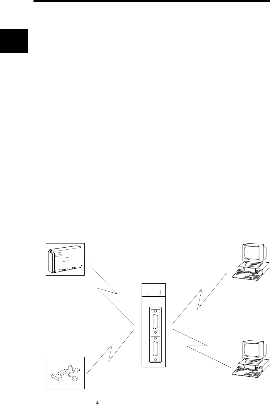
Opposite devices
(external devices)
Generic term for computers, indicators, measuring instruments, ID modules, bar code readers,
regulators, other serial communication modules, UC24, etc. that are connected to this serial
communication module for data communication.
Reference Manual Q Corresponding MELSEC Communication Protocol Reference Manual
RS-232 (interface) Abbreviation for interface conforming to RS-232.
RS-422/485 (interface) Abbreviation for interface conforming to RS-422 and RS-485.
Special function modules
Generic term for the A/QnA series PLC modules that are operated by commands from the PLC
CPU (equivalent to the Q series PLC intelligent function modules).
Examples:
• CC-Link interface module
• A/D and D/A conversion modules
• High-speed counter module
• Ethernet interface module
• Computer link module and serial communication module
Switch setting Generic term for intelligent function module switch setting
User's Manual (Application) or
Application Q Corresponding Serial Communication Module User's Manual (Application)
User's Manual (Basic) or Basic Q Corresponding Serial Communication Module User's Manual (Basic)

A - 21 A - 21
Definitions and Descriptions of Terminology
The following table lists the definitions and descriptions of terminology used in this manual and related
manuals for the Q series serial communication modules.
Terms Description
A compatible IC frame
(Formats 1 to 4)
One of the message formats for the serial communication module for performing communication
using the MC protocol and ASCII code data.
This is the same message format as when communicating using the protocol for the A series
computer link modules. Device memory read/write operations for the QCPU are allowed within
the device range of the AnACPU.
For details, see Chapter 5 of the Reference Manual.
Bidirectional protocol
A communication procedure for the serial communication modules and one of the data
communication functions for communicating any data between the PLC CPU and an opposite
device. Details are explained in Chapter 7.
Independent operation
A mode of interface operation to communicate data with external devices using a function
specified in each communication protocol setting. Two interfaces of serial communication
modules do not interact.
Linked operation
The operation mode of each of the two interfaces for a serial communication module that are
connected to external devices and linked to one another in order to send/receive data to/from the
external devices.
The two interfaces communicate data using the identical data-communication function (MC
protocol (identical format) or non procedure protocol) and the identical transmission
specifications. (Linked operation using the bidirectional protocol is not allowed.)
MELSEC communication protocol
(MC protocol)
A communication procedure for the Q series serial communication modules or the Ethernet
interface modules, and a name of communication method for accessing to the PLC CPU from an
opposite device. (This is called the MC protocol in this manual.)
There are two communication methods; one uses ASCII code data and the other uses binary
code data.
Details are explained in the Reference Manual.
Message send function
(Printer function)
This function registers character data (messages) to be sent to external devices (mainly printers)
in the serial communication module as an user frame in advance, and sends the registered data
for multiple user frames using the non procedure protocol (sent by an instruction from the PLC
CPU).
Multidrop connection A name of the connection when multiple external devices or other serial communication modules are
connected in a 1:n or m:n mode using the serial communication module's RS-422/485 interface.
Non procedure protocol
An user's communication procedure and one of the data communication functions for
communicating any data between the PLC CPU and an opposite device. Details are explained in
Chapter 6.
QnA compatible 2C frame
(Formats 1 to 4)
One of the message formats for the serial communication module for performing communication
using the MC protocol and ASCII code data.
This is the same message format as the communication frame using the protocol for the QnA
series serial communication modules.
• QnA compatible 2C frame (Formats 1 to 4): QnA simplified frame (Formats 1 to 4)
Details are explained in Chapter 4 of the Reference Manual.
QnA compatible 3C frame
(Formats 1 to 4)
QnA compatible 4C frame
(Formats 1 to 4)
One of the message formats for the serial communication module for performing communication
using the MC protocol and ASCII code data.
This is the same message format as the communication frame using the protocol for the QnA
series serial communication modules.
• QnA compatible 3C frame (Formats 1 to 4): QnA frame (Formats 1 to 4)
• QnA compatible 4C frame (Formats 1 to 4): QnA extension frame (Formats 1 to 4)
Details are explained in Chapter 3 of the Reference Manual.

A - 22 A - 22
Terms Description
QnA compatible 4C frame
(Format 5)
One of the message formats for the serial communication module for performing communication
using the MC protocol and binary code data.
This is the same message format as the communication frame using the protocol for the QnA
series serial communication modules.
• QnA compatible 4C frame (Format 5): QnA extension frame (Format 5)
Details are explained in Chapter 3 of the Reference Manual.
User frame
Data name when the fixed format portion of messages to be sent or received between a serial
communication module and an opposite device is registered in the module and used for sending
and receiving data with the functions listed below. (The contents of an user frame data should
conform to the specifications of the opposite device).
The data array of the head and tail sections of a message (transmission control code, C24 station
number, sum check, fixed data, etc.) to be sent and received is registered in the serial
communication module before use.
• MC protocol on-demand function.
• Data communication function using the non procedure protocol.
Details are explained in Chapter 9 of the User's Manual (Applications).
A - 23 A - 23
Product Configuration
The following lists the product configuration of the Q series serial communication modules.
Model Item name Quantity
QJ71C24N serial communication module or QJ71C24 serial
communication module 1
Terminal resistor 330 1/4 W (for RS-422 communication) 2
QJ71C24N or QJ71C24
Terminal resistor 110 1/2 W (for RS-485 communication) 2
QJ71C24N-R2 or
QJ71C24-R2
QJ71C24N-R2 serial communication module or QJ71C24-R2 serial
communication module 1
QJ71C24N-R4 serial communication module 1
RS-422/485 plug-in connector socket block 2
Terminal resistor 330 1/4 W (for RS-422 communication) 4
Terminal resistor 110 1/2 W (for RS-485 communication) 4
QJ71C24N-R4
Plate terminal (for connecting a braided shield cable) 4
SW2D5C-QSCU-E GX Configurator-SC Version 2 (1-license product) (CD-ROM) 1
SW2D5C-QSCU-EA GX Configurator-SC Version 2 (Multiple-license product) (CD-ROM) 1
1 - 1 1 - 1
MELSEC-Q
1 OVERVIEW
1
1 OVERVIEW
This manual describes the specifications for the QJ71C24N, QJ71C24N-R2,
QJ71C24N-R4, QJ71C24, QJ71C24-R2 serial communication module (hereinafter
referred to as "Q series C24"), as well as the procedures prior to starting the operation,
maintenance, inspection, data communication methods for use with external devices
and troubleshooting.
When applying the following program examples to the actual system, make sure to
examine the applicability and confirm that it will not cause system control problems.
1.1 Overview of the Serial Communication Module
The Q series C24 is a module that connects the Q series PLC CPU and an external
device using an RS-232 or RS-422/485 line for serial communication, in order to
achieve the data communication described below.
By using a modem/terminal adapter, a public line (analog/digital) can be used for data
communication with a remote location.
• PLC data collection/change from the external devices
(See the MELSEC Communication Protocol Reference Manual.)
• PLC monitoring and control from the external devices (See Chapter 2 of the User's
Manual (Application).)
• Data receiving and sending in any formats that conform to the external device
specifications (See (2) and (3) of Section 1.2.)
• Collection of measured data from a measuring device (See (2) of Section 1.2.)
• Operation of a PLC CPU that is connected to a personal computer (hereinafter
abbreviated as PC) installed with GX Developer (SW4D5C-GPPW-E or later,
hereinafter abbreviated as GX Developer). (See the GX Developer Manual.)
QJ71C24-R2
ERR.
NEU
SD
RD
RUN
NEU
SD
RD
CH. 1
CH.1 CH.2
• PLC data collection/change
• PLC monitoring and control from an
external device
• Data receiving and sending in any
formats that conform to the external
device specifications
• GX Developer
• File writing/reading
• Device monitoring/testing
• Collection of measured
data
• Collection of read data
Being a convenient means of connection among different devices (PCs, display
devices, printers, etc.), the serial communication line is the most widely used
medium on the market today.

1 - 2 1 - 2
MELSEC-Q
1 OVERVIEW
1
1.2 Features of the Serial Communication Module
The following describes the features of the Q series C24.
(1) Data communication based on the MELSEC communication
protocol (hereinafter referred to as the MC protocol)
(Details are explained in the MELSEC Communication Protocol Reference
Manual.)
(a) External devices can read/write the PLC device data and sequence
programs, and can monitor PLC equipment status.
With the exception of the on-demand function described below, the PLC
does not require a sequence program because the PLC sends and receives
data based solely on commands from external devices.
(b) Using the on-demand function, data can be sent from the PLC CPU to the
external devices in each frame format of the MC protocol.
(c) Data communication can be performed using a program at the external
device side that has been created for communicating data with conventional
A/QnA series computer link module/serial communication modules.
(d) If the external device is a PC running one of the basic operation systems
below, it is possible to create a communication program for the external
device without considering the detailed MC protocol (transmission/reception
procedures) using one of the following separately sold communication
support tools.
(Supported basic operation systems)
• Microsoft® Windows® 95 Operating System
• Microsoft® Windows® 98 Operating System
• Microsoft® Windows NT® Workstation Operating System Version 4.0
• Microsoft® Windows® Millennium Edition Operating System
• Microsoft® Windows® 2000 Professional Operating System
• Microsoft® Windows® XP Professional Operating System
• Microsoft® Windows® XP Home Edition Operating System
Depending on the version of MX Component used, different operating
systems are supported.
See the manual of MX Component for the details.
(Separately sold communication support tools)
• MX Component (SW0D5C-ACT-E or later, hereinafter abbreviated as MX
Component)
See Appendix 7 for the overview of MX Component.
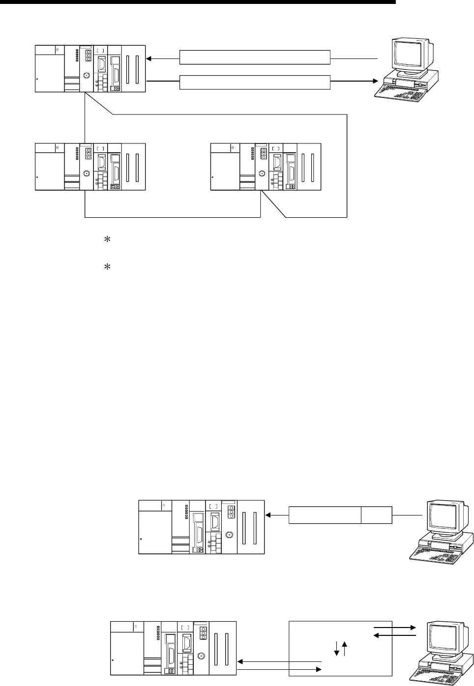
1 - 3 1 - 3
MELSEC-Q
1 OVERVIEW
Q25HCPU
MODE
RUN
ERR.
USER
BAT.
BOOT
RS-232
USB
MITSUBISHI
MELSEC
POWER
PULL
QJ71E71
RUN
INIT.
OPEN
SD
ERR.
COM.ERR
RD
10BASE-T
+12V
12G
10BASE
QJ71C24
CH1. CH2.
RS-232
CH1.
CH.2
SDA
SG
SDB
RS-422
/485
RDA
RDB
(FG)
(FG)
1
2
5
7
3
4
6
Q25HCPU
MODE
RUN
ERR.
USER
BAT.
BOOT
RS-232
USB
MITSUBISHI
MELSEC
POWER
PULL
QJ71E71
RUN
INIT.
OPEN
SD
ERR.
COM.ERR
RD
10BASE-T
10BASE
QJ71C24
CH1. CH2.
RS-232
CH1.
CH.2
SDA
SG
SDB
RS-422
/485
RDA
RDB
(FG)
(FG)
1
2
5
7
3
4
6
Q25HCPU
MODE
RUN
ERR.
USER
BAT.
BOOT
RS-232
USB
MITSUBISHI
MELSEC
POWER
PULL
QJ71E71
RUN
INIT.
OPEN
SD
ERR.
COM.ERR
RD
10BASE-T
+12V
12G
10BASE
QJ71C24
CH1. CH2.
RS-232
CH1.
CH.2
SDA
SG
SDB
RS-422
/485
RDA
RDB
(FG)
(FG)
1
2
5
7
3
4
6
Command
Command request data
MELSECNET/H
(MELSECNET/H mode)
In the MELSECNET/10 mode, other stations (including the A/QnA series PLC
CPUs) can be accessed during data link operation.
The MC protocol is equivalent to the communication function using a dedicated
protocol that is supported by the A/QnA series computer link module/serial
communication modules.
(2) Data communication using the non procedure protocol
(Details are explained in Chapter 6 and the User's Manual (Application).)
(a) Data can be transferred in any message formats that conform to the
specifications of external devices (measuring devices, PCs, etc.).
(b) Fixed or variable length messages can be received in accordance with the
external device specifications.
• How to receive the variable length data
The external device sends data by adding at the end of the message the
end-code data (CR+LF or any one-byte data) that is set for the Q series C24.
• How to receive the fixed length data
The external device sends the amount of data equivalent to the size of the
end data that is set for the Q series C24.
End
code
Reception data
(When receiving variable length data)
QJ71E71
RUN
INIT.
OPEN
SD
ERR.
COM.ERR
RD
10BASE-T
+12 V
12G
10BASE
RS-232
MODE
RUN
ERR.
USER
BAT.
BOOT
CH.2
SDA
SG
SDB
(FG)
RDA
(FG)
RDB
RS-4 22
/485
CH1.
CH2.CH1.
2
1
3
4
5
6
7
RS-232
USB
Q25HCPU
POWER
MELSEC
PULL
MITSUBISHI
QJ71C24
(c) ASCII code data can be used for communication using the ASCII-BIN
conversion function.
ASCII-BIN
conversion
Binary
data
QJ71C24
Binary
data
ASCII
data
QJ71E71
RUN
INIT.
OPEN
SD
ERR.
COM.ERR
RD
10BASE-T
+12V
12G
10BASE
RS-232
MODE
RUN
ERR.
USER
BAT.
BOOT
CH.2
SDA
SG
SDB
(FG)
RDA
(FG)
RDB
RS-4 22
/485
CH1.
CH2.CH1.
2
1
3
4
5
6
7
RS-232
USB
Q25HCPU
POWER
MELSEC
PULL
MITSUBISHI
QJ71C24
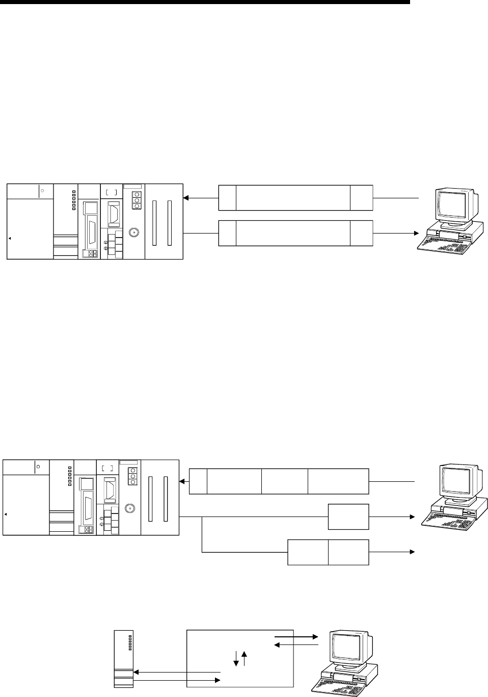
1 - 4 1 - 4
MELSEC-Q
1 OVERVIEW
(d) It is necessary to create a sequence program for communication control that
conforms to the external device.
(e) Communication can be performed using an user frame by registering the fixed
format portion of the head and tail sections of a message as an user frame.
• When sending data, the Q series C24 adds an user frame to any data
specified by the user.
• When receiving data, the Q series C24 transfers any data excluding the
user frame to the PLC CPU.
Any data format ETX
ETX STX
STX
QJ71E71
RUN
INIT.
OPEN
SD
ERR.
COM.ER R
RD
10BASE-T
+12V
12G
10BASE
RS-232
MODE
RUN
ERR.
USER
BAT.
BOOT
CH.2
SDA
SG
SDB
(FG)
RDA
(FG)
RDB
RS-422
/485
CH1.
CH2.CH1.
2
1
3
4
5
6
7
RS-232
USB
Q25HCPU
POWER
MELSEC
PULL
MITSUBISHI
QJ71C24
Any data format
When receiving data
When sending data
(f) It is possible to clear the current reception data without interrupting the
transmission processing by using the dedicated instruction "CSET."
(3) Data communication using the bidirectional protocol
(Details are explained in Chapter 7 and the User's Manual (Application).)
(a) In communication between PLC CPUs and communication with an external
device for which transmission/receive control programming is allowed, data
communication is performed in a sequence of "data transmission and
response receipt".
(b) Error check of received data can be performed using the sum-check code,
while the occurrence of a reception error at an external device can be
checked via an ACK/NAK response.
ENQ Sum check
code
Any data
ACK
Data length
NAK
Error
code
Sending completed normally
Sending completed
abnormall
y
QJ71E71
RUN
INIT.
OPEN
SD
ERR.
COM.E RR
RD
10BASE-T
+12V
12G
10BASE
RS-232
MODE
RUN
ERR.
USER
BAT.
BOOT
CH.2
SDA
SG
SDB
(FG)
RDA
(FG)
RDB
RS-422
/485
CH1.
CH2.
CH1.
2
1
3
4
5
6
7
RS-232
USB
Q25HCPU
POWER
MELSEC
PULL
MITSUBISHI
QJ71C24
(c) ASCII code data can be used for communication using the ASCII-BIN
conversion function.
ASCII-BIN
conversion
Binary
data
QJ71C24
Binary
data
ASCII
data
MOD E
RUN
ERR.
USER
BAT.
BOOT
RS-232
USB
Q25HCPU
QCPU
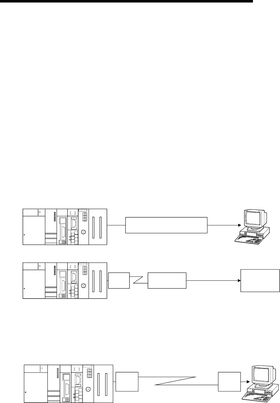
1 - 5 1 - 5
MELSEC-Q
1 OVERVIEW
(4) Monitoring the PLC CPU
(Details are explained in the User's Manual (Application).)
(a) The self-station's PLC CPU can be monitored at time intervals set by the
user without using a sequence program.
1) The following monitoring information can be sent/notified as the result of
monitoring the PLC CPU.
• Transmission of information on devices and the PLC CPU status to be
monitored. (It is also possible to send the monitoring information
through combined use of the modem function.)
• Notification of a notification message (string data) registered as the
connection data of the modem function, through combined use of the
modem function.
2) The user can select either one of the following timing choices at which to
send the PLC CPU monitoring result to the external device.
• Send/notify every time the PLC CPU is monitored (periodic
transmission).
• Send/notify when the information read from the PLC CPU matches
the conditions set by the user (conditional transmission).
(b) The PLC CPU monitoring function can be used in communication using the
MC or non procedure protocol.
Data
Notification
message
Modem
QJ71E71
RUN
INIT.
OPEN
SD
ERR.
COM.ERR
RD
10BAS E-T
+12V
12G
10BASE
RS-232
MODE
RUN
ERR.
USER
BAT.
BOOT
CH.2
SDA
SG
SDB
(FG)
RDA
(FG)
RDB
RS-422
/485
CH1.
CH2.CH1.
2
1
3
4
5
6
7
RS-232
USB
Q25HCPU
POWER
MELSEC
PULL
MITSUBISHI
QJ71C24
QJ71E71
RUN
INIT.
OPEN
SD
ERR.
COM.ERR
RD
10BAS E-T
+12V
12G
10BASE
RS-232
MODE
RUN
ERR.
USER
BAT.
BOOT
CH.2
SDA
SG
SDB
(FG)
RDA
(FG)
RDB
RS-422
/485
CH1.
CH2.CH1.
2
1
3
4
5
6
7
RS-232
USB
Q25HCPU
POWER
MELSEC
PULL
MITSUBISHI
QJ71C24
Pager
(5) Remote communications using the modem function
(Details are explained in the User's Manual (Application).)
(a) Data communication can be performed with a remotely located external device.
(b) Modem initialization and line connection/disconnection can be performed.
(c) Data communication can be performed using the MC, non procedure or
bidirectional protocol.
QJ71E71
RUN
INIT.
OPEN
SD
ERR.
COM.ERR
RD
10BASE-T
+12V
12G
10BASE
RS-232
MODE
RUN
ERR.
USER
BAT.
BOOT
CH.2
SDA
SG
SDB
(FG)
RDA
(FG)
RDB
RS-422
/485
CH1.
CH2.CH1.
2
1
3
4
5
6
7
RS-232
USB
Q25HCPU
POWER
MELSEC
PULL
MITSUBISHI
QJ71C24
Modem Modem
(6) Initial settings and communication settings without using a
sequence program
Various initial settings can be performed using the GX Congifurator-SC
(SW0D5C-QSCU-E or later, hereinafter abbreviated as GX Configurator-SC).
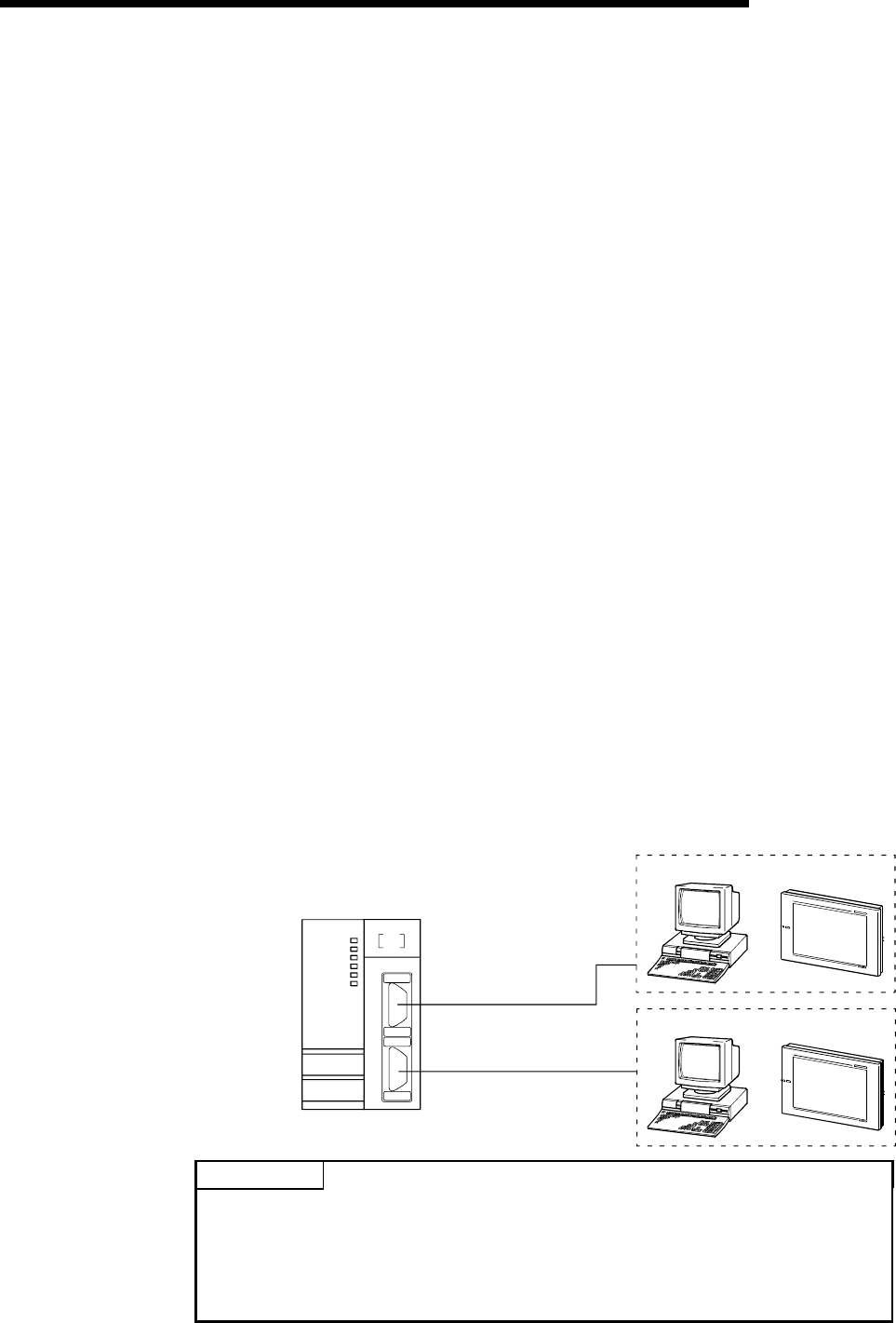
1 - 6 1 - 6
MELSEC-Q
1 OVERVIEW
(7) Connecting the GX Developer and the GOT
(a) Connecting the GX Developer (Details are explained in the GX Developer
Operating Manual.)
• By connecting a PC installed with a GX Developer to the interface of the Q
series C24 at the same time, operations such as programming, monitoring
and testing for the PLC CPU can be performed.
• By connecting multiple PCs installed with GX Developers to the PLC CPU
or Q-series C24 at the same time, operations such as programming and
monitoring can be performed simultaneously by multiple operators.
Operating the GX Developers using these simultaneous connections can
improve program performance.
• Operations can be performed from a GX Developer by setting the
communication protocol of the Q series C24 interface to which a PC is
connected to "0" with the switch setting using the GX Developer.
(b) Connecting the GOT (Details are explained in the GOT User's Manual
(Connection).)
• By connecting a GOT (graphic operation terminal) to the interface for the
Q series C24 operations such as monitoring the PLC CPU can be
performed.
• Operations such as monitoring the PLC CPU can be performed by setting
the communication protocol of the Q series C24 interface to which a GOT
is connected to "0" with the switch setting using a GX Developer.
(c) Simultaneous connection of GX Developer and GOT
• It is possible to connect a PC with GX Developer and the GOT to two
interfaces of the Q series C24 at the same time. It is thus possible for more
than one user to perform programming, monitoring, etc. simultaneously.
• When the GOT and the PC with GX Developer are connected at the same
time, the two interfaces of the Q series C24 cannot perform an interlock
operation.
QJ71C24-R2
CH1. CH2.
CH1.
CH2.
Q25HCPU
MODE
RUN
ERR.
USER
BAT.
BOOT
RS-232
USB
RS-232 cable
GX Developer GOT
or
GOT
or
GX Developer
POINT
When GX Developer and/or the GOT is connected directly to the Q series C24,
switching settings using GX Developer need not be made to perform access to the
QCPU, monitoring and other operations. (They can also be performed when the
communication protocol is set to "0" by making switch settings using GX
Developer.)
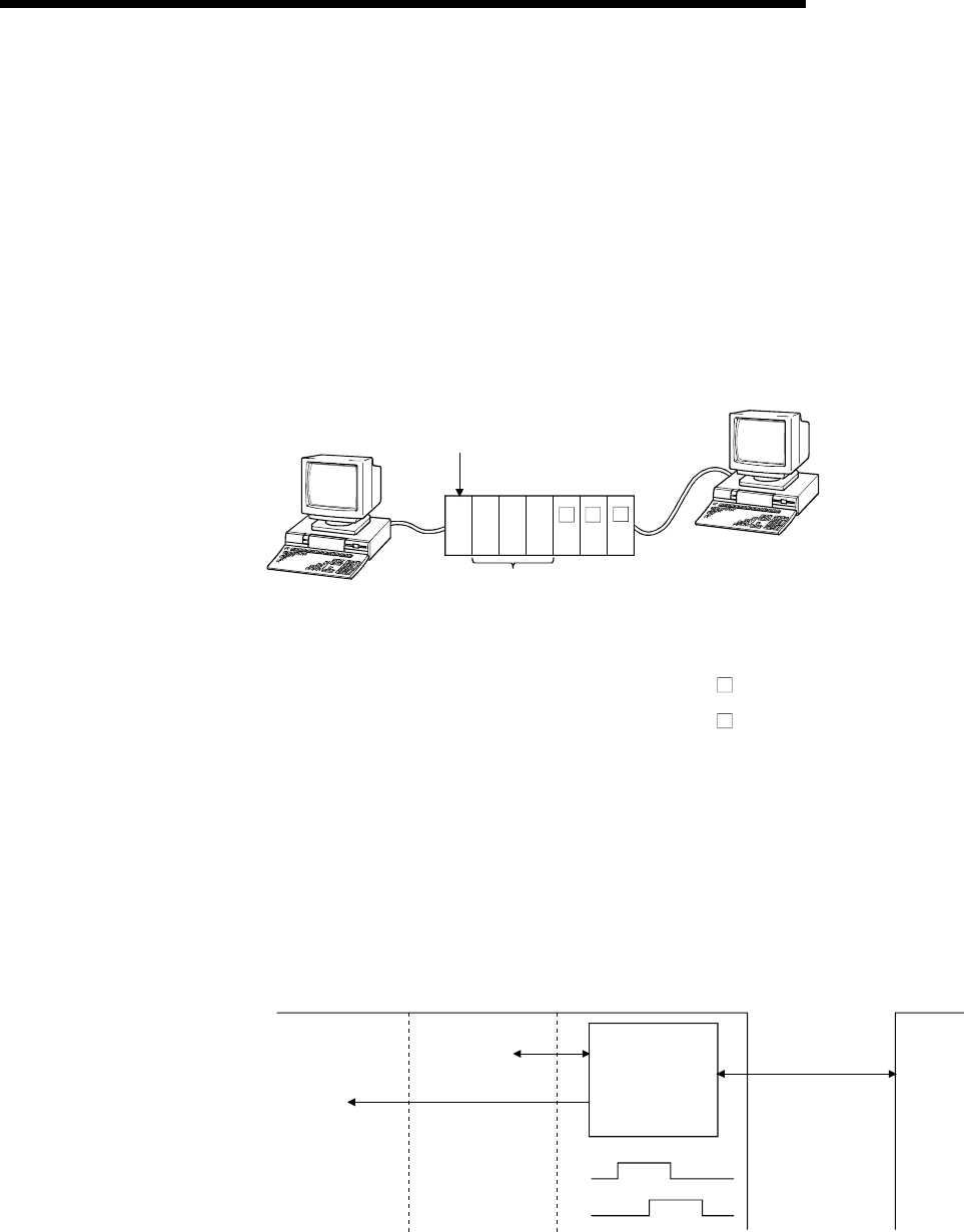
1 - 7 1 - 7
MELSEC-Q
1 OVERVIEW
(8) Functions supporting multiple CPU systems (Details are explained
in the Reference Manual.)
(a) When accessing QCPUs in a multiple CPU system using the MC protocol or
through GX Developer, it is possible to perform data communication such as
reading/writing device data by specifying the QCPU to be accessed.
• When using the Q series C24 in a multiple CPU system, a QCPU
controlling the Q series C24 (hereinafter referred to as the control PLC)
should be specified using GX Developer.
It is also possible to mount a Q series C24 of function version A in a
multiple CPU system and access to the only control PLC (PLC No.1).
1) : PLC No.1
2) : PLC No.2
3) : PLC No.3
4) : PLC No.4
1: Module controlled by
PLC No.1
2: Module controlled by
PLC No.2
External device
Communication through GX Developer
Communication using the MC protocol
Setting from
GX Developer
Peripheral device
1 2 1
1) 2) 3) 4)
C24
Q series C24
control PLC
Q series C24
non-control PLCs
(b) When a Q series C24 CPU of function version B is used in a multiple CPU
system, the following forms of data communication can be performed with
the Q series C24.
1) It is possible to perform data communication using the non
procedure/bidirectional protocols from the control PLC
2) It is possible to read the buffer memory from non-control PLCs.
Input/output signals can be used as contacts.
Buffer memory
FROM/TO instruction
Dedicated instruction
FROM
instruction
Use the input/
output signal as
a contact
Use the input/
output signal as a
contact
It should be output
to an out
p
ut si
g
nal
Data communication
Non-control PLC Control PLC Q series C24 External
device
X
Y
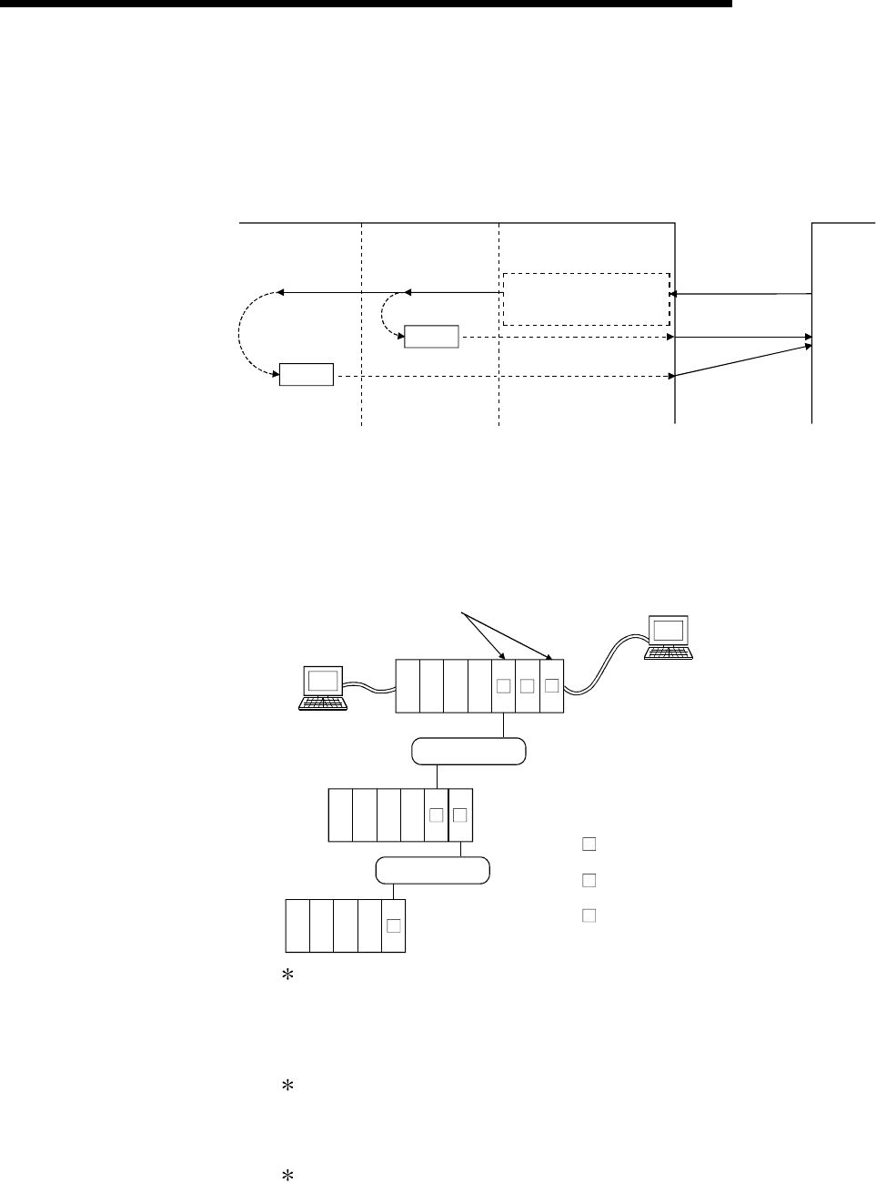
1 - 8 1 - 8
MELSEC-Q
1 OVERVIEW
3) It is possible to access the control PLC and non-control PLCs using the
MC protocol and through GX Developer from the external device.
In addition, data communication with the control PLC of the Q series C24
can be performed using the non procedure/bidirectional protocol.
(Example) When communicating with the MC protocol
Non-control PLC Control PLC Q series C24
Specify the QCPU to be
accessed by the I/O number
of the requested module.
External
device
Command message
transmitted using a
QnA compatible 4C
frame
03FFH
03E0H to 03E3H
Device memory, etc.
Data Response message
Communication using the
MC protocol (read/write)
Device memory, etc.
Data
If the MC protocol, GX Developer is used to access other stations, it is
possible to access the control PLC and non-control PLCs of the station to
be accessed even if the relay station and the accessed station are
multiple CPU systems.
(Example)
MELSECNET/H
1) : PLC No.1
2) : PLC No.2
3) : PLC No.3
4) : PLC No.4
1: Module used for routing, controlled
by PLC No.1
: Q series C24 controlled by
PLC No.1
: Module used for routing, controlled
by PLC No.2
1'
2
Local station
Relay station
External device
Communication throu
g
h GX Develope
r
Communication using the MC protocol
Setting from GX Developer
Peripheral device
MELSECNET/H
Station to be accessed
1 2 1'
1) 2) 3) 4)
2 21) 2) 3) 4)
21) 2) 3) 4)
It is possible to access other stations re
g
ardless
of whether the control PLC of the module to be
routed through is the same or different.
The modules used for the routing are MELSECNET/H network modules
The QnA compatible 4C frame should be performed for access to non-
control PLCs when communicating using the MC protocol.
However, the available functions differ depending on the QCPU to be
accessed (whether it is a control PLC or a non-control PLC).
See the Reference Manual for the available functions and accessible range.
A module used for routing can access the following modules when
accessing other stations:
• MELSECNET/H, MELSECNET/10 network module
• Q series C24 • Ethernet interface module
If there is a module of function version A among the modules for routing,
it is possible to access the control PLC of that particular module only. In
addition, it is possible to access other stations via a module controlled
by the same control PLC.

1 - 9 1 - 9
MELSEC-Q
1 OVERVIEW
(9) Remote password check function
(Details are explained in the User's Manual (Application) and the Reference Manual.)
(a) The remote password check function of the Q series C24 prevents users at
a remote location to access QCPUs illegally using the modem function of the
Q series C24.
(The remote password is checked in the following forms of data communication)
• Communication using the MC protocol
(The remote password check is not carried out in data communication
using the non procedure/bidirectional protocols.)
• Access to the PLC through GX Developer
The remote password function is one of the QCPU functions and used for
preventing illegal access to the QCPU by other users.
Use GX Developer to set a remote password for the QCPU in order to
activate the remote password function of the QCPU.
(b) If the Q series C24 is specified in the parameters of a QCPU as being
subject to the remote password check, the remote password can be
unlocked (canceled) using either one of the methods below, to allow data
communication from the external device. It is necessary to connect a line to
the modem first.
• When communicating using the MC protocol
Use the dedicated command for communication using the MC protocol to
unlock the remote password from the external device.
• When accessing the PLC through GX Developer
Unlock the remote password using GX Developer at the start of online
operation.
The remote password is automatically locked by disconnecting the line to
the modem.
Accessing
external device
Modem
Dialup line
Modem
QCPU Q series C24
Communication using the MC protocol
Communication through GX Developer.
GX Develo
p
er
Set the parameters to make
the Q series C24 as a subject to
the remote password check.
Remote
password
Remote
password
check
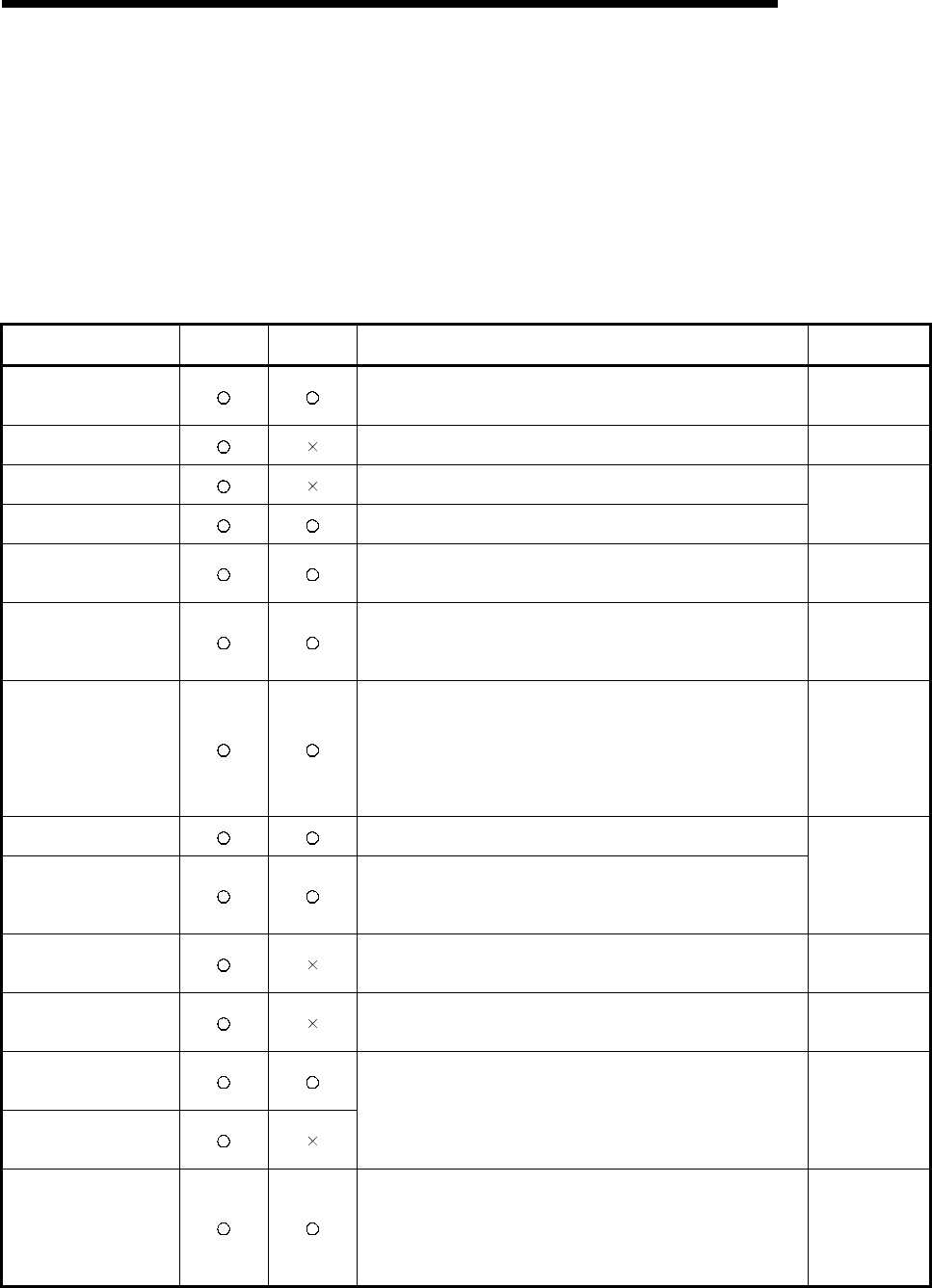
1 - 10 1 - 10
MELSEC-Q
1 OVERVIEW
1.3 About Added/Changed Functions in Function Version B
The table below lists the functions that have been added or changed in the Q series
C24 of function version B.
See Section 2.6 for the function version, serial NO. and software version of products
(CPU module, GX Developer, GX Configurator-SC) related to the Q series C24 which
can use added/changed functions.
See Appendix 1.1 concerning a comparison of functions in the different Q series C24
function versions.
Function QJ71C24N
(-R2/R4)
QJ71C24
(-R2) Outline of function Reference section
Simultaneous connection of
GX Developer and GOT
This function allows access to the PLC from a PC with GX Developer and a
GOT connected to two different interfaces of the Q series C24 at the same
time.
Section 1.2 of
User’s Manual
(Basic)
Control of RS and DTR
signal states
This function allows the control of the on or off state of the RS and DTR
signals with the PLC program.
Remark of section
3.2.1
Support for 230,400 bps This function allows data communication with an external device at a
transmission speed of 230,400 bps.
Data transmission/reception
at low speed
This function allows data communication with an external device at a
transmission speed of 50 bps.
Chapter 4 of
User’s Manual
(Basic)
Clearing reception data by a
dedicated instruction
This function allows clearing reception data using the CSET instruction
during data communication using the non procedure protocol.
It is possible to clear the data even when data is being transmitted.
Chapter 6, Section
9.8 of User’s
Manual (Basic)
Transmission of the PLC
CPU monitoring information
through combined use of the
modem function
When the PLC CPU monitoring function is active, this function sends the
monitoring information of the PLC CPU to the external device through the
modem.
Chapter 2 of
User’s Manual
(Application)
Remote password check
This function allows data communication after the external device
completes the unlock processing of the remote password set at a QCPU. It
is executed when the QCPU is accessed from a remote location using the
modem function of the Q series C24 in the following forms of data
communication:
• Communication using the MC protocol
• Communication using GX Developer
Chapter 3 of
User’s Manual
(Application)
Section 3.18 of
Reference Manual
Automatic initialization for
modem Initializes the modem automatically when Q Series C24 starts up.
Callback
After line connection from the GX Developer, access to the QCPU from the
GX Developer is made possible through line reconnection from the Q Series
C24 (callback). Transmission costs after line connection from the Q Series
C24 side are borne by the Q Series C24 side.
Chapter 3 of the
User’s Manual
(Application)
Addition of non reception
monitoring time format in
non procedure protocol
This function allows messages to be received in the non reception protocol
by time-out in non reception monitoring time (timer 0) if the received
complete code and received data count have been not determined.
Chapter 6 of
User’s Manual
(Application)
Transmission control
start/end free area
designation
This function allows the designation of the available capacity of the OS area
that notifies the data reception failure at the time of transmission control
(DTR/DSR signal control and DC code control).
Chapter 7 of
User’s Manual
(Application)
Addition of changeable data
to the user frame
(05H, 0BH, 11H, 17H)
Addition of changeable data
to the user frame
(04H, 0AH, E5H, EBH)
These functions allow the following codes to be registered as the
changeable data of user frames for data communication.
• Horizontal parity code
• Sum check code of two’s-complement number
Chapter 9 of
User’s Manual
(Application)
Adding a reception function
through the use of user
frames
This function allows reception of a message consisting of the head frame
and any data field when receiving data by specifying the head frame.
The data length of the data field can be specified freely for each
combination of user frames for reception set by the user.
(Receiving 1 byte providing ACK/NAK only is also possible by setting the
data length of the data field to “0.”)
Chapter 11 of
User’s Manual
(Application)
1 - 11 1 - 11
MELSEC-Q
1 OVERVIEW
Function QJ71C24N
(-R2/R4)
QJ71C24
(-R2) Outline of function Reference section
Multiple specification of
transparent codes for
transmission
This function allows specification of a maximum of 10 types of transparent
codes for transmission per interface when sending data using one of the
following protocols:
• Non procedure protocol
• Bidirectional protocol
Chapter 12 of
User’s Manual
(Application)
Switching to the GX
Developer connection mode
by switching the mode
This functions allows the GX Developer connection mode to be switched by
an external device or the PLC CPU.
Chapter 15 of
User’s Manual
(Application)
Section 3.13 of
Reference Manual
Communication data
monitoring function
This function allows the monitoring of communication data transmitted on
the communication network of the Q series C24 and an external device.
Chapter 16 of
User’s Manual
(Application)
Operating Manual
(Protocol FB
support function)
UINI instruction The UINI instruction allows change of the mode, transmission specifications
and host station No. of the Q series C24.
Chapter 17 of
User’s Manual
(Application)
Support for multiple CPU
system
This function allows access to the control/non-control PLCs specified by the
user when performing the following forms of data communication with a
multiple CPU system:
• Communication using the MC protocol
• QCPU access from GX Developer
Section 2.10 of
Reference Manual
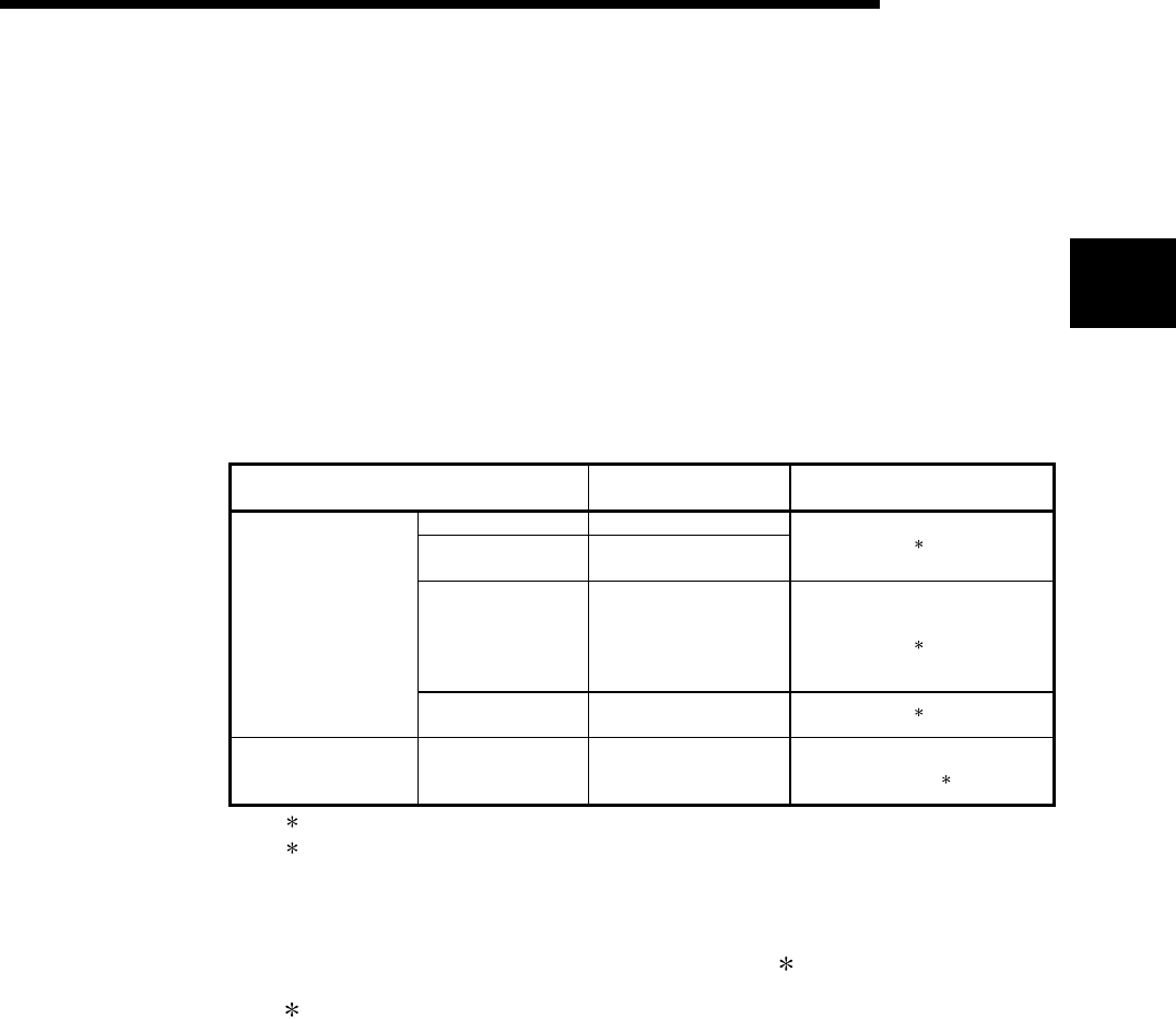
2 - 1 2 - 1
MELSEC-Q
2 SYSTEM CONFIGURATION AND AVAILABLE FUNCTIONS
2
2 SYSTEM CONFIGURATION AND AVAILABLE FUNCTIONS
This Chapter describes the system configuration and available functions.
2.1 Applicable Systems
The following describes applicable systems.
(1) Applicable modules and number of modules that can be mounted
The following table lists the CPU module and network modules (for remote I/O
stations) that the Q series C24 can be mounted and the number of modules
which can be mounted.
Applicable module Number of modules that
can be installed Remarks
Q00JCPU Maximum 8
Q00CPU
Q01CPU Maximum 24 (1)
Q02CPU
Q02HCPU
Q06HCPU
Q12HCPU
Q25HCPU
Maximum 64 Can be installed in Q mode only
(1)
CPU module
Q12PHCPU
Q25PHCPU Maximum 64 (1)
Network module
QJ72LP25-25
QJ71LP25GE
QJ72BR15
Maximum 64 MELSECNET/H Remote I/O
station ( 2)
1 See User's Manual (Function Explanation, Program Fundamentals) for the CPU module to use.
2 See Q Corresponding MELSECNET/H Network System Reference Manual (Remote I/O
network).
(2) The base module to which the Q series C24 can be mounted
The Q series C24 can be mounted into any I/O slot ( 1) of the base module.
1 Limited to within the range of I/O points for the CPU module and network
module (for remote I/O station)
(3) Multiple CPU systems
When using the Q series C24 on a multiple CPU system, refer to the QPU User's
Manual (Multiple CPU System) before operation.
(a) Applicable Q series C24
If using the Q series C24 on a multiple CPU system, use function version B
of the Q series C24.
(b) Intelligent function module parameter
To write the intelligent function module parameter on a PLC, be sure to
write it in the Q series C24 control PLC only.
2 - 2 2 - 2
MELSEC-Q
2 SYSTEM CONFIGURATION AND AVAILABLE FUNCTIONS
2
(4) Applicable software packages
(a) Software/setting & monitor tools ( 1) for the PLC
The following table lists the systems and software packages applicable for
the Q series C24.
When using the Q series C24, GX Developer is required.
Software packages
GX Developer GX Configurator-SC
Single CPU system Version 7 or later
Q00J/Q00/Q001CPU Multiple CPU system Version 8 or later
Version 1.0 or later
(Versions prior to SW0D5C-
QSCU-E 40E are not usable.)
Single CPU system Version 4 or later SW0D5C-QSCU-E 00A or later
Q02/Q02H/Q06H/
Q12H/Q25HCPU Multiple CPU system Version 6 or later SW0D5C-QSCU-E 20C or later
Single CPU system
Q12PH/Q25PHCPU Multiple CPU system Version 7.10L or later
Version 1.13P or later
(Versions prior to SW0D5C-
QSCU-E 40E are not usable.)
When installing an MELSECNET/H remote I/O
station Version 6 or later SW0D5C-QSCU-E 30D or later
1 See section 2.6 for the versions of the GX Developer and GX Configurator-SC that support the
functions added through improvements in the Q series C24.
(b) Communication support tools for external devices
Item Name Model Remark
MX Component SWnD5C-ACT -E ActiveX control library.
The "n" in the model name is 0 or greater. ( 1)
1 Depending on the version of MX Component used, different versions of Q series C24 are
supported.
See the manual of MX Component for the details.
2 - 3 2 - 3
MELSEC-Q
2 SYSTEM CONFIGURATION AND AVAILABLE FUNCTIONS
2.2 Combinations of PLC CPU and External Device, and Available Functions
The following describes the system configurations and available functions when using
the Q series C24.
(1) System configurations
System configurations (combinations of PLC CPU and external device) for data
communication are shown below.
(a) External device and Q series C24 with 1:1 system configuration
RS-232/422
QJ71E71
RUN
INIT.
OPEN
SD
ERR.
COM.ERR
RD
10BASE-T
+12V
12G
10BASE
RS-232
MODE
RUN
ERR.
USER
BAT.
BOOT
CH.2
SDA
SG
SDB
(FG)
RDA
(FG)
RDB
RS-422
/485
CH1.
CH2.CH1.
2
1
3
4
5
6
7
RS-232
USB
Q25HCPU
POWER
MELSEC
PULL
MITSUBISHI
QJ71C24
(b) External device and Q series C24 with n:1 system configuration
RS-485
QJ71E71
RUN
INIT.
OPEN
SD
ERR.
COM.ERR
RD
10BASE-T
+12V
12G
10BASE
RS-232
MODE
RUN
ERR.
USER
BAT.
BOOT
CH.2
SDA
SG
SDB
(FG)
RDA
(FG)
RDB
RS-422
/485
CH1.
CH2.CH1.
2
1
3
4
5
6
7
RS-232
USB
Q25HCPU
POWER
MELSEC
PULL
MITSUBISHI
QJ71C24
2 - 4 2 - 4
MELSEC-Q
2 SYSTEM CONFIGURATION AND AVAILABLE FUNCTIONS
(c) External device and Q series C24 with 1:n system configuration
RS-485
QJ71E71
RUN
INIT.
OPEN
SD
ERR.
COM.ERR
RD
10BASE -T
+12V
12G
10BASE
RS-232
MODE
RUN
ERR.
USER
BAT.
BOOT
CH.2
SDA
SG
SDB
(FG)
RDA
(FG)
RDB
RS-422
/485
CH1.
CH2.CH1.
2
1
3
4
5
6
7
RS-232
USB
Q25HCPU
POWER
MELSEC
PULL
MITSUBISHI
QJ71C24 QJ71E7 1
RUN
INIT.
OPEN
SD
ERR.
COM.ERR
RD
10BASE -T
+12V
12G
10BASE
RS-232
MODE
RUN
ERR.
USER
BAT.
BOOT
CH.2
SDA
SG
SDB
(FG)
RDA
(FG)
RDB
RS-422
/485
CH1.
CH2.CH1.
2
1
3
4
5
6
7
RS-232
USB
Q25HCPU
POWER
MELSEC
PULL
MITSUBISHI
QJ71C24 QJ71E7 1
RUN
INIT.
OPEN
SD
ERR.
COM.ERR
RD
10B ASE-T
+12V
12G
10BASE
RS-232
MODE
RUN
ERR.
USER
BAT.
BOOT
CH.2
SDA
SG
SDB
(FG)
RDA
(FG)
RDB
RS-422
/485
CH1.
CH2.CH1.
2
1
3
4
5
6
7
RS-232
USB
Q25HCPU
POWER
MELSEC
PULL
MITSUBISHI
QJ71C24
QJ71E71
RUN
INIT.
OPEN
SD
ERR.
COM.ERR
RD
10BASE -T
+12V
12G
10BASE
RS-232
MODE
RUN
ERR.
USER
BAT.
BOOT
CH.2
SDA
SG
SDB
(FG)
RDA
(FG)
RDB
RS-422
/485
CH1.
CH2.CH1.
2
1
3
4
5
6
7
RS-232
USB
Q25HCPU
POWER
MELSEC
PULL
MITSUBISHI
QJ71C24
RS-485RS-232
QJ71E71
RUN
INIT.
OPEN
SD
ERR.
COM.ERR
RD
10BASE -T
+12V
12G
10BASE
RS-232
MODE
RUN
ERR.
USER
BAT.
BOOT
CH.2
SDA
SDB
(FG)
RDA
(FG)
RDB
RS-422
/485
CH1.
CH2.CH1.
2
1
3
4
5
6
7
RS-232
USB
Q25HCPU
POWER
MELSEC
PULL
MITSUBISHI
QJ71C24QJ71E71
RUN
INIT.
OPEN
SD
ERR.
COM.ERR
RD
10BASE -T
+12V
12G
10BASE
RS-232
MODE
RUN
ERR.
USER
BAT.
BOOT
CH.2
SDA
SG
SDB
(FG)
RDA
(FG)
RDB
RS-422
/485
CH1.
CH2.CH1.
2
1
3
4
5
6
7
RS-232
USB
Q25HCPU
POWER
MELSEC
PULL
MITSUBISHI
QJ71C24QJ71E71
RUN
INIT.
OPEN
SD
ERR.
COM.ERR
RD
10BASE -T
+12V
12G
10BASE
RS-232
MODE
RUN
ERR.
USER
BAT.
BOOT
CH.2
SDA
SG
SDB
(FG)
RDA
(FG)
RDB
RS-422
/485
CH1.
CH2.CH1.
2
1
3
4
5
6
7
RS-232
USB
Q25HCPU
POWER
MELSEC
PULL
MITSUBISHI
QJ71C24QJ71E71
RUN
INIT.
OPEN
SD
ERR.
COM.ERR
RD
10BASE -T
+12V
12G
10BASE
RS-232
MODE
RUN
ERR.
USER
BAT.
BOOT
CH.2
SDA
SG
SDB
(FG)
RDA
(FG)
RDB
RS-422
/485
CH1.
CH2.CH1.
2
1
3
4
5
6
7
RS-232
USB
Q25HCPU
POWER
MELSEC
PULL
MITSUBISHI
QJ71C24
(d) External device and Q series C24 with m:n system configuration
RS-485 RS-485 RS-485
QJ71E71
RUN
INIT.
OPEN
SD
ERR.
COM.ERR
RD
10BASE -T
+12V
12G
10BASE
RS-2 32
MODE
RUN
ERR.
USER
BAT.
BOOT
CH.2
SDA
SG
SDB
(FG)
RDA
(FG)
RDB
RS-422
/485
CH1.
CH2.CH1.
2
1
3
4
5
6
7
RS-232
USB
Q25HCPU
POWER
MELSEC
PULL
MITSUBISHI
QJ71C24 QJ71E7 1
RUN
INIT.
OPEN
SD
ERR.
COM.ERR
RD
10BASE -T
+12V
12G
10BASE
RS-232
MODE
RUN
ERR.
USER
BAT.
BOOT
CH.2
SDA
SG
SDB
(FG)
RDA
(FG)
RDB
RS-422
/485
CH2.CH1.
2
1
3
4
5
6
7
RS-232
USB
Q25HCPU
POWER
MELSEC
PULL
MITSUBISHI
QJ71C24 QJ71E7 1
RUN
INIT.
OPEN
SD
ERR.
COM.ERR
RD
10BASE -T
+12V
12G
10BASE
RS-232
MODE
RUN
ERR.
USER
BAT.
BOOT
CH.2
SDA
SG
SDB
(FG)
RDA
(FG)
RDB
RS-422
/485
CH1.
CH2.CH1.
2
1
3
4
5
6
7
RS-232
USB
Q25HCPU
POWER
MELSEC
PULL
MITSUBISHI
QJ71C24 QJ71E7 1
RUN
INIT.
OPEN
SD
ERR.
COM.ERR
RD
10B ASE-T
+12V
12G
10BASE
RS-232
MODE
RUN
ERR.
USER
BAT.
BOOT
CH.2
SDA
SG
SDB
(FG)
RDA
(FG)
RDB
RS-422
/485
CH1.
CH2.CH1.
2
1
3
4
5
6
7
RS-232
USB
Q25HCPU
POWER
MELSEC
PULL
MITSUBISHI
QJ71C24
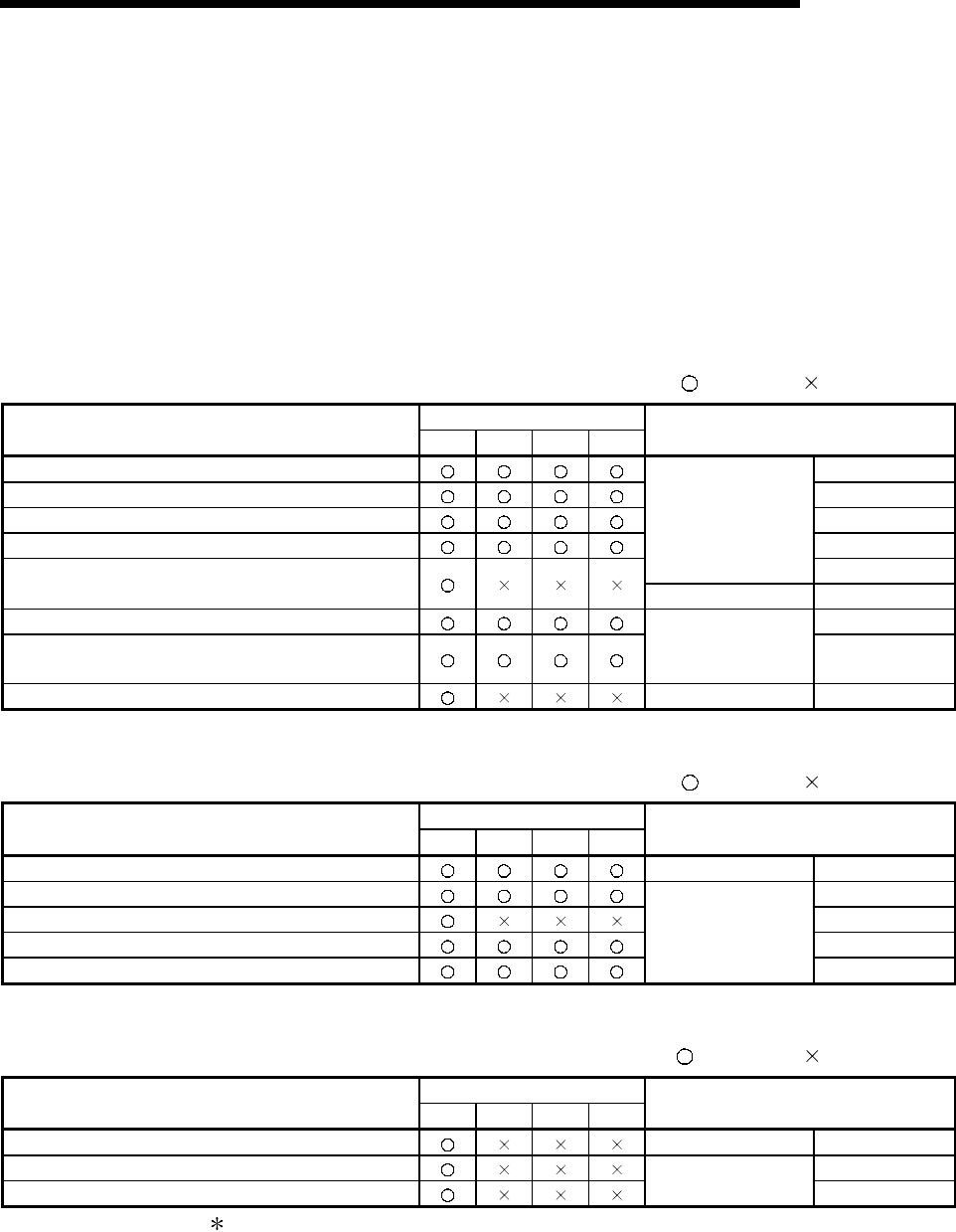
2 - 5 2 - 5
MELSEC-Q
2 SYSTEM CONFIGURATION AND AVAILABLE FUNCTIONS
(2) Correspondence between the data communication functions and
system configurations
The following shows system configurations that can use the data communication
functions of the Q series C24.
The manual names shown in the reference section column in the table below are
as follows:
• Application
Q Corresponding Serial Communication Module User's Manual (Application)
• Reference
Q Corresponding MELSEC Communication Protocol Reference Manual
(a) Communication using the MC protocol ( : Available, : Not available)
System configuration
Functions of the Q series C24 1 : 1 n : 1 1 : n m : n Reference section
PLC CPU device memory read/write Section 3.3
Intelligent function module buffer memory read/write Section 3.5
Sequence program read/write Section 3.8
PLC CPU status control (remote RUN, STOP, etc.) Section 3.6
Reference
Section 3.11
On-demand function Application Chapter 10
Global function Section 3.10
Accessing the PLC of other stations in the MELSECNET/H,
MELSECNET/10
Reference Section 2.7
PLC CPU monitoring function Application Chapter 2
(b) Communication using the non procedure protocol
( : Available, : Not available)
System configuration
Functions of the Q series C24 1 : 1 n : 1 1 : n m : n Reference section
Data transmission/receiving in arbitrary format This manual Chapter 6
Data transmission/receiving with user frames Chapter 11
PLC CPU monitoring function Chapter 2
Reading received data using interrupt programs Chapter 4
Sending/receiving ASCII data using ASCII-BIN conversion
Application
Chapter 13
(c) Communication using the bidirectional protocol
( : Available , : Not available)
System configuration
Functions of the Q series C24 1 : 1 n : 1 1 : n m : n Reference section
Data transmission/receiving This manual Chapter 7
Reading received data using interrupt programs Chapter 4
Sending/receiving ASCII data using ASCII-BIN conversion Application Chapter 13
In general, if data communication is performed using a system configuration of
other than 1:1 connection mode, the following points should be well noted.
• Avoid simultaneous transmission.
• Discard data received other than that addressed to the local station.
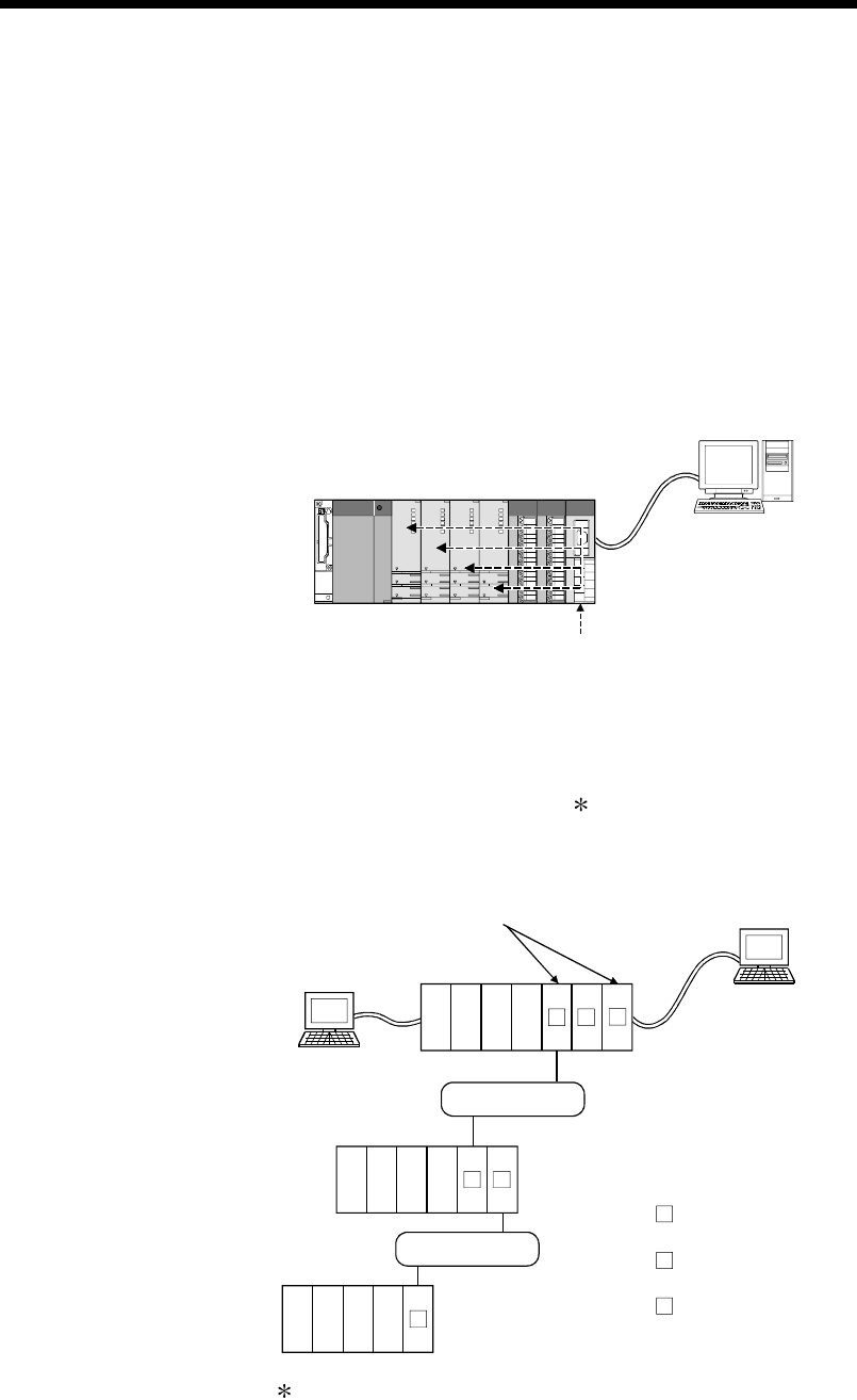
2 - 6 2 - 6
MELSEC-Q
2 SYSTEM CONFIGURATION AND AVAILABLE FUNCTIONS
2.3 For Use in Multiple CPU System
This section explains the use of the Q series C24 in a multiple CPU system.
(1) When making access from the external device to the non-control CPU of the Q
series C24 using either of the following functions, use the Q series C24 of function
version B.
When the Q series C24 of function version A is used, only the control CPU can be
accessed. (Access to the non-control CPU will result in an error.)
• Communication using MC protocol
• Communication using GX Developer
Communication using MC protocol
Communication using GX Develope
r
External device
Q series C24 of function version B
Multiple CPU system
(2) If the other stations to be accessed belong to the multiple CPU system, the
modules used for routing and QCPUs at the local station, all the relay stations,
and the accessed station should be modules of function version B or later. This
has to hold in all cases of accessing the non-control PLC of the module used for
routing and the accessed station. 1
(Example)
MELSECNET/H
1) : PLC No.1
2) : PLC No.2
3) : PLC No.3
4) : PLC No.4
1: Module used for routing, controlled
by PLC No.1
: Q series C24 controlled by
PLC No.1
: Module used for routing, controlled
by PLC No.2
1'
2
Local station
Relay station
External device
Communication through GX Develope
r
Communication using the MC protocol
Setting from GX Developer
Peripheral device
MELSECNET/H
Station to be accessed
121'
1) 2) 3) 4)
2 21) 2) 3) 4)
21) 2) 3) 4)
It is possible to access other stations regardless
of whether the control PLC of the module to be
routed through is the same or different.
The modules used for the routing are MELSECNET/H network modules
1 When accessing other stations, a module used for routing can access the
following modules:
• MELSECNET/H, MELSECNET/10 network modules
• Q series C24
• Ethernet interface modules
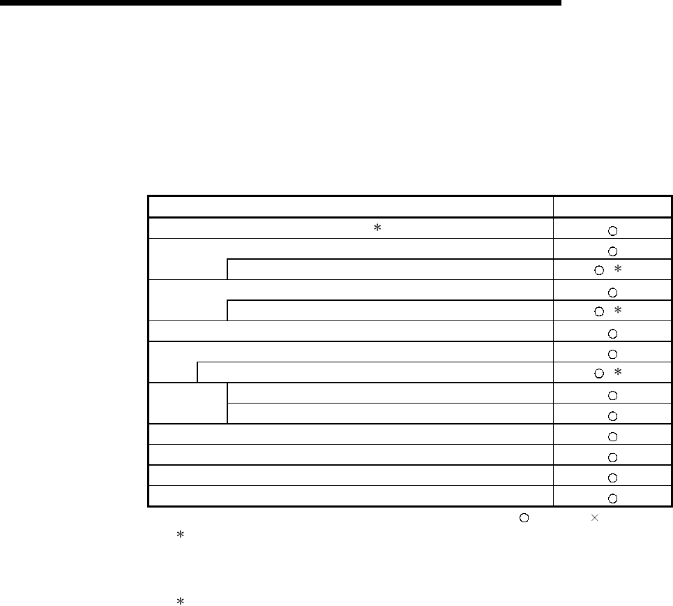
2 - 7 2 - 7
MELSEC-Q
2 SYSTEM CONFIGURATION AND AVAILABLE FUNCTIONS
2.4 For Use with Q00J/Q00/Q01CPU
This section describes the use of the Q series C24 with the Q00J/Q00/Q01CPU.
(1) Available functions
The following table indicates the functions that can be used when the Q series
C24 is mounted in the Q00J/Q00/Q01CPU.
Function Availability
Communications using the MC protocol ( 1)
Communications using non procedure protocol
Data reception by interrupt program ( 2)
Communications using the bidirectional protocol
Data reception by interrupt program ( 2)
Communications using dedicated instructions
Communications via public line, etc. (modem function)
Remote password check ( 2)
DC code control (including Xon/Xoff control)
Transmission
Control DTR/DSR (ER/DR) control
Communications protocol switching
Independent/linked operation of each interface
Initial setting and monitoring/testing of setting values by the utility package
Connecting the GX Developer and GOT
: Available : Not available
1 Communications are according to the MC protocol. See the Reference Manual concerning the
number of devices that can be accessed and the processing time.
The range of devices that can be accessed differs depending on the frame used in data
communications.
2 Use Q00J/Q00/Q01CPU (function version B) or later.
When using the function, version 8 or later of the GX Developer is required.
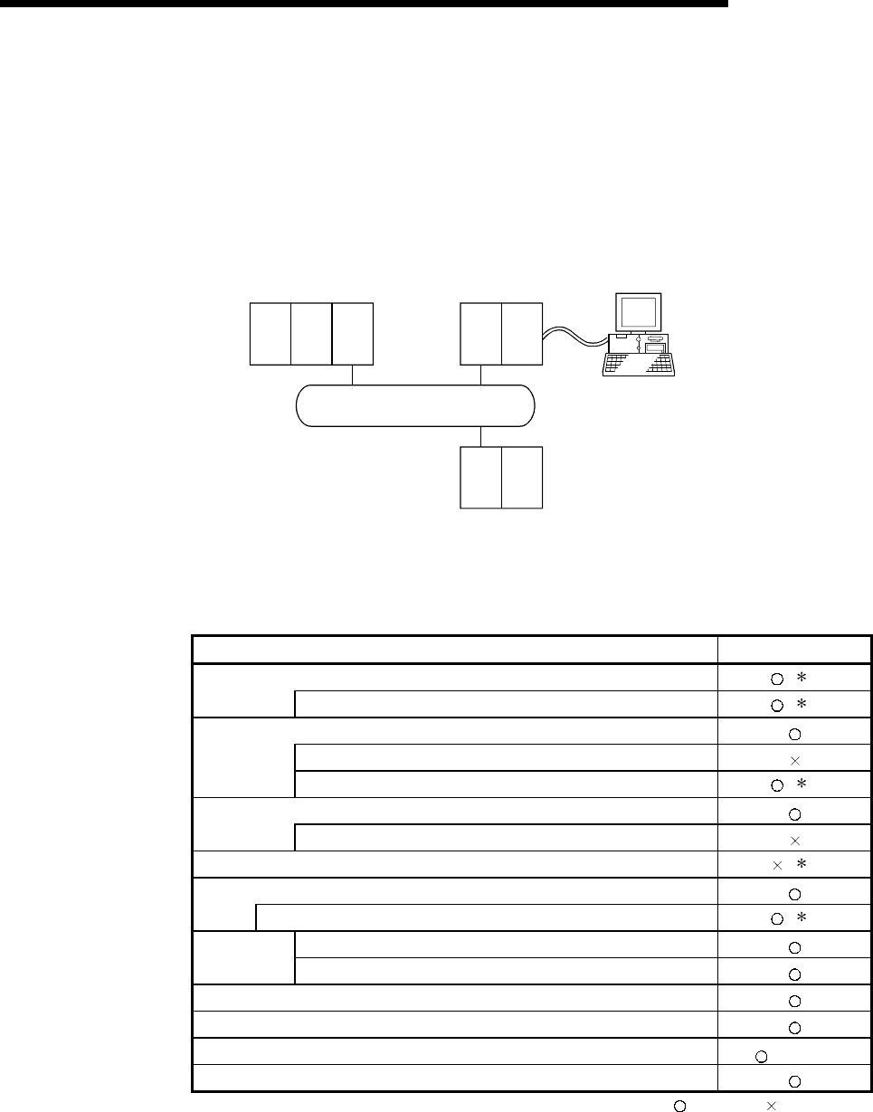
2 - 8 2 - 8
MELSEC-Q
2 SYSTEM CONFIGURATION AND AVAILABLE FUNCTIONS
2.5 For Use at MELSECNET/H Remote I/O Station
This section describes the use of the Q series C24 at a MELSECNET/H remote I/O
station.
It is not necessary to read this section if the Q series C24 is used with the QCPU.
(1) System configuration
(Example)
MELSECNET/H
Remote I/O network
QCPU QJ71
LP21
-25
(Remote master station) (Remote I/O station)
External device
QJ71
C24
QJ72
LP25
-25
QJ72
LP25
-25
(Remote I/O station)
(2) Available functions
The following table indicates the functions that can be used when the Q series
C24 is mounted on a MELSECNET/H remote I/O station.
Function Availability
Communications using the MC protocol ( 1)
PLC CPU monitoring (PLC CPU monitoring function) ( 2)
Communications using non procedure protocol
Data reception by interrupt program
PLC CPU monitoring (PLC CPU monitoring function) ( 2)
Communications using the bidirectional protocol
Data reception by interrupt program
Communications using dedicated instructions ( 3)
Communications via public line, etc. (modem function)
Remote password check ( 4)
DC code control (including Xon/Xoff control)
Transmission
Control DTR/DSR (ER/DR) control
Communications protocol switching
Independent/linked operation of each interface
Initial setting and monitoring/testing of setting values by the utility package (See (4))
Connecting the GX Developer
: Available : Not available
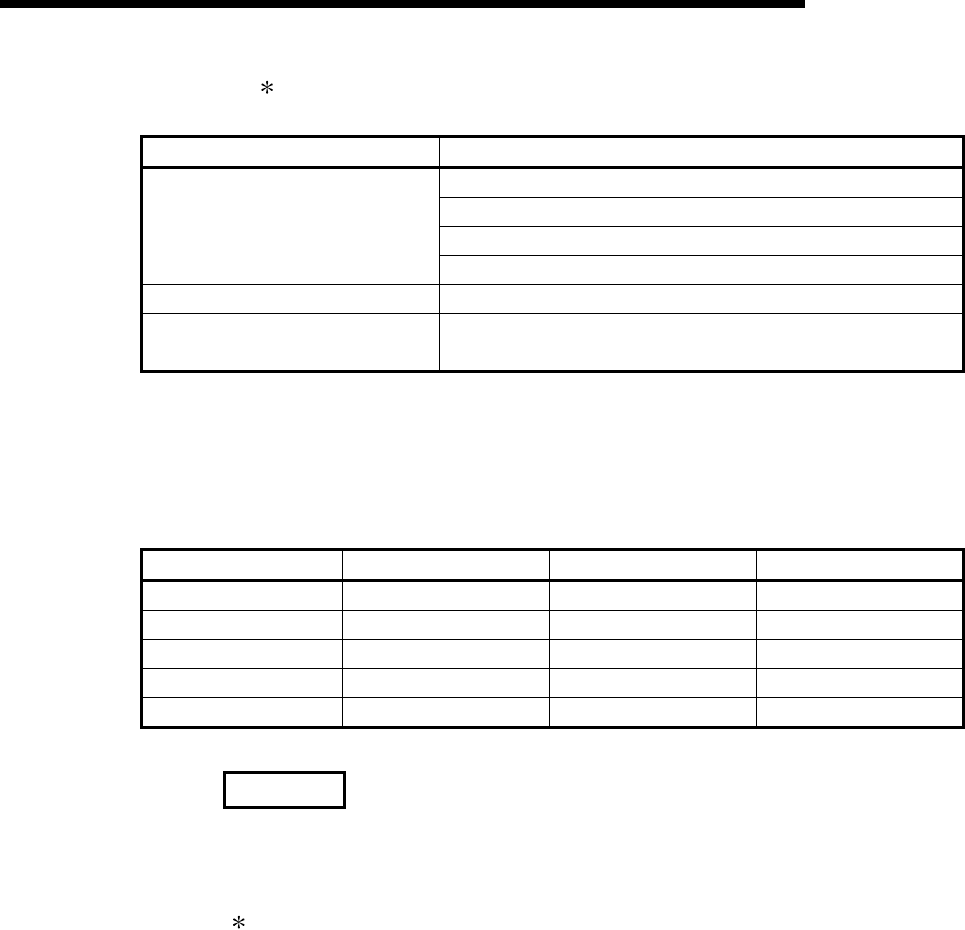
2 - 9 2 - 9
MELSEC-Q
2 SYSTEM CONFIGURATION AND AVAILABLE FUNCTIONS
1 The following functions are available when communicating with the
MELSECNET/H remote I/O station using the MC protocol.
Available function Function
Batch read and batch write
Random read, test (random write)
Monitor data registration, monitoring
Device memory read/write
Batch read of multiple blocks, batch write of multiple blocks
Buffer memory read/write Reading/writing from/to the buffer memory of the Q series C24
Reading/writing buffer memory of an
intelligent function module
Reading/writing from/to the buffer memory of the specified
intelligent function module
The following devices of a MELSECNET/H remote I/O station can be accessed
by the device memory read/write function. Note that the accessible devices and
the ranges vary depending on the type of frames used for the data
communication.
See the Reference Manual for a detailed explanation.
Device name Device symbol Device name Device symbol
Special relay SM Link relay B
Special register SD Data register D
Input relay X Link register W
Output relay Y Link special relay SB
Internal relay M Link special register SW
REMARK
It is only possible to read/write from/to the buffer memory of an intelligent function
module for the MELSECNET/10 remote I/O station compatible with the QnA/A series.
2 PLC CPU monitoring can be registered using the MC protocol or GX
Configurator-SC.
The dedicated instruction CSET cannot be used for registration.
The device to be monitored can be registered within the device range of the
MELECNET/H remote I/O station.
2 - 10 2 - 10
MELSEC-Q
2 SYSTEM CONFIGURATION AND AVAILABLE FUNCTIONS
3 The dedicated instructions are unavailable for the MELSECNET/H remote I/O
station.
For the functions that use the dedicated instructions to make communication,
perform programming by the following methods.
Dedicated instruction Method Explanation section
FROM, TO Perform programming using the REMFR/REMTO instruction. Appendix 9.2
ONDEMAND Appendix 9.3
INPUT Appendix 9.4
OUTPUT Appendix 9.5
BIDIN Appendix 9.4
BIDOUT
Perform programming using the REMFR/REMTO instruction
and I/O signal.
Appendix 9.5
SPBUSY No method
CSET (Receive data clear) Perform programming using the receive data clear request
area of the buffer memory. Appendix 9.6
BUFRCVS No method
(Data cannot be received using an interrupt program)
PRR Appendix 9.7
CSET (Initial setting)
Perform programming using the REMFR/REMTO instruction
and I/O signal. Appendix 9.8
CSET (PLC CPU monitoring
function)
No method
(Register/delete the PLC CPU using the MC protocol or GX
Configurator-SC.)
PUTE Appendix 9.9
Appendix 9.11
GETE
Perform programming using the REMFR/REMTO instruction
and I/O signal. Appendix 9.10
UINI Perform programming using the REMFR/REMTO instructions
and I/O signals. (However, the station No. cannot be changed.) Appendix 9.12
4 Available for the MELSECNET/H remote I/O station of function version D or
later.
GX Developer Version 8.18U or later is required to use the function.
2 - 11 2 - 11
MELSEC-Q
2 SYSTEM CONFIGURATION AND AVAILABLE FUNCTIONS
(3) Setting from GX Developer
The following parameters should be set through GX Developer in order to use
the Q series C24 mounted to a MELECNET/H remote I/O station.
Each of setting is the same way as when setting the parameters for the Q series
C24 mounted to a QCPU station: see Section 4.5 and after.
See the operating manual for GX Developer for how to display each setting
screen.
(Parameter setting items for the Q series C24 mounted to a MELECNET/H
remote I/O station)
Parameter setting item Setting Remarks
I/O Assignment Set the module mounting information See Section 4.5.1
Switch setting for I/O and
intelligent function module
Set the transmission specification and the
communication protocol for communication
with the external device
See Section 4.5.2
Remote password setting Perform settings for the remote password. User's Manual (Application)
Section 3.3.3
POINT
(1) Connect GX Developer to a MELECNET/H remote I/O station and set the
parameters.
(2) Reset the MELECNET/H remote I/O station after changing the setting.
(4) When monitoring/setting with GX Configurator-SC
(a) About the automatic refresh setting
1) When reading/writing data created by the automatic refresh setting
using PLC, the read/write operation should be performed by GX
Developer. It cannot be performed from GX Configurator-SC.
2) The devices used for the automatic refresh setting must be of the types
M, B, D, or W.
POINT
(1) GX Configurator-SC should be connected to a MELECNET/H remote I/O
station before the monitoring/setting.
(2) The MELECNET/H remote I/O station should be reset after changing the
setting.
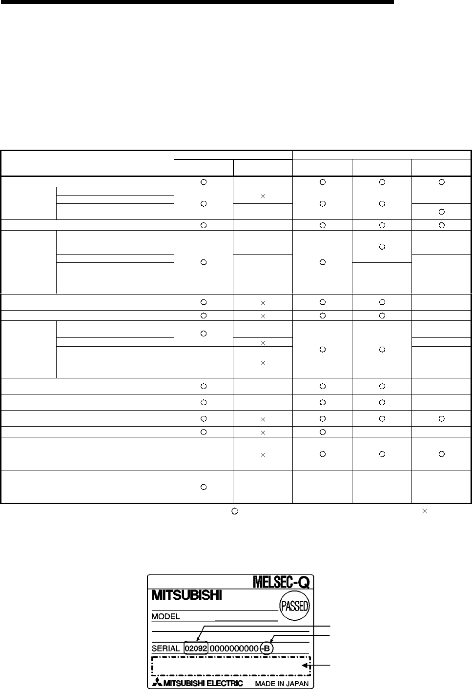
2 - 12 2 - 12
MELSEC-Q
2 SYSTEM CONFIGURATION AND AVAILABLE FUNCTIONS
2.6 Checking the Function Version, Serial No., and Software Version
This section explains how to check the the function version, serial No. and software
version of related products that can use the functions added by the improvement of the
Q series C24.
(1) Correspondence of related products for use additional functions of
Q series C24
Function version of the Q series C24 Version of related product
Additional function QJ71C24N
(-R2/R4) QJ71C24 (-R2) CPU module GX Developer GX Configurator-
SC
Simultaneous connection of GX Developer and GOT Function version B
RS and DTR signal status designation
Support for 230400 bps Version 2 or later
Transmission
specifications Data transmission/ reception at low
speed (50 bps) Function version B
Clearing reception data by a dedicated instruction Function version B
Transmission of the PLC CPU
monitoring information through
combined use of the modem function Function version B SW0D5C-QSCU-E
20C or later
Automation initialization of modem
Communication
via modem
function Callback
Function version B
or later whose first
5 digits of the serial
No. are 03043 Version 7 or later
Version 1.0 or later
(Versions prior to
SW0D5C-QSCU-E
40E are not
usable.)
Non procedure and non reception monitoring time format
designation Version 2 or later
Transmission control start/end free area designation Version 2 or later
05H, 0BH, 11H, 17HFunction version B SW0D5C-QSCU
20C or later
04H, 0AHVersion 2 or later
Addition of
changeable data
to the user frame E5H, EBH
Function version B
or later whose first
5 digits of the serial
No. are 06062
Version 2.06G or
later
Reception according to user frames
(reception according to format 1) Function version B SW0D5C-QSCU-E
20C or later
Multiple specification of transparent codes for
transmission Function version B SW0D5C-QSCU-E
20C or later
Switching the GX Developer connection mode by
switching the mode
Communication data monitoring function Version 8 or later Version 2 or later
UINI instruction
Function version B
or later whose first
5 digits of the serial
No. are 06062
Remote password check Function version B
Function version A
or later whose first
5 digits of the serial
No. are 02092
Version 6 or later SW0D5C-QSCU-E
20C or later
: Usable (no restrictions depending on the version) : Not usable
(2) Checking the version and serial No. of Q series PLC functions
(a) Using the rated plate on the side of the module to check
The serial No. and function version of the corresponding module is shown in
the SERIAL column of the rated plate.
Compliant standard
Serial No. (first 5 digits)
Function version
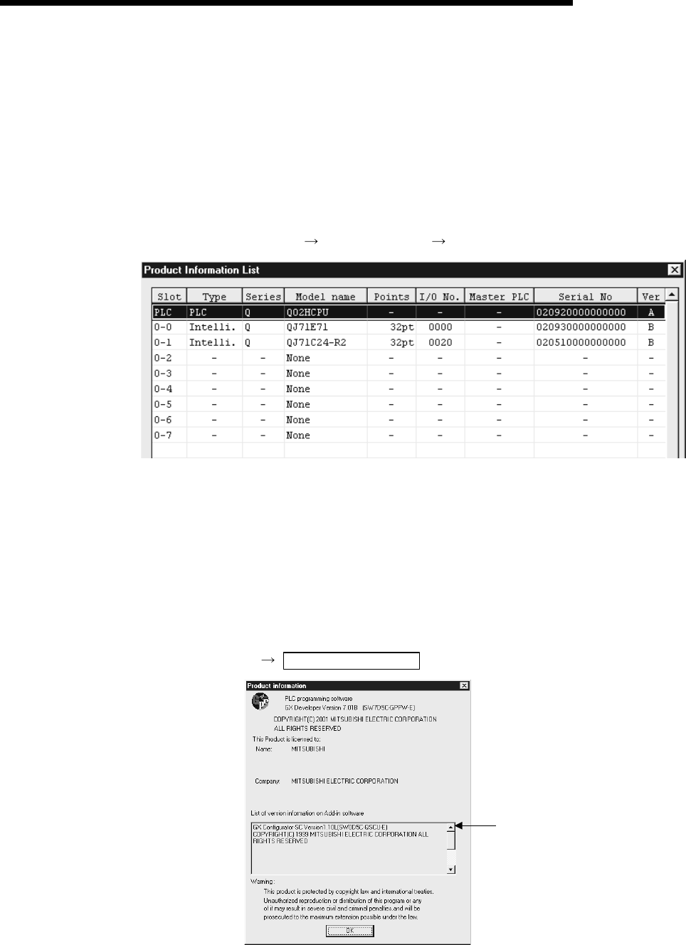
2 - 13 2 - 13
MELSEC-Q
2 SYSTEM CONFIGURATION AND AVAILABLE FUNCTIONS
(b) Using the GX Developer to check
The method of checking the serial No. and function version of the
corresponding module with the GX Developer is shown.
The serial No. and function version are displayed on the GX Developer
"Product Information List" or "Module's Detailed Information" screen.
The method of checking the serial No. and function version on the "Product
Information List" screen is shown below. (See Section 10.1.1 for details
about the "Module's Detailed Information" screen.)
[Start Procedure]
"Diagnostics" "System monitor" "Product Inf. List"
[Serial No., Ver.]
• The corresponding module's serial No. is shown in the Serial No. column.
• The function version of the corresponding module is shown in the Ver. column.
(3) Checking the software version of the GX Configurator-SC
The GX Configurator-SC software version can be checked on the "Product
Information List" screen of the GX Developer.
[Start Procedure]
"Help" Product Information
Software version

2 - 14 2 - 14
MELSEC-Q
2 SYSTEM CONFIGURATION AND AVAILABLE FUNCTIONS
REMARK
The version indication for the GX Configurator-SC has been changed as shown
below from the SW0D5C-QSCU-E 40E upgrade product.
Previous product Upgrade and subsequent versions
SW0D5C-QSCU-E 40E GX Configurator-SC Version 1.10L
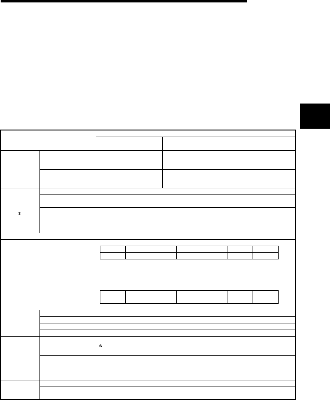
3 - 1 3 - 1
MELSEC-Q
3 SPECIFICATIONS
3
3 SPECIFICATIONS
The following shows the Q series C24 performance specifications.
See the User's Manual of the QCPU (Q mode) for general specifications.
3.1 Performance Specifications
The following shows the Q series C24 performance specifications. For the
transmission specifications when communicating via the modem function, see this
section and Chapter 3 of User's Manual (Application).
(1) Transmission specification
Specifications
Item QJ71C24N
QJ71C24
QJ71C24N-R2
QJ71C24-R2 QJ71C24N-R4
CH1 RS-232-compliance
(D-sub 9 pin)
RS-232-compliance
(D-sub 9 pin)
RS-422/485-compliance
(2-piece plug-in connector socket
block)
Interface
CH2 RS-422/485-compliance
(2-piece terminal block)
RS-232-compliance
(D-sub 9 pin)
RS-422/485-compliance
(2-piece plug-in connector socket
block)
Line Full-duplex/half-duplex communications
MC protocols
communication Half-duplex communications
Non procedure protocol
communication Full-duplex/full-duplex communications
Communications
system ( 1)
Bidirectional protocol
communication Full-duplex/full-duplex communications
Synchronization method Start-stop synchronization method
[QJ71C24N(-R2/R4)]
50 300 600 1200 2400 4800 9600
14400 19200 28800 38400 57600 115200 230400 (bps)
• Transmission speed 230400 bps is available for only CH1. (Not available for CH2)
• Total transmission speed of two interfaces is available up to 230400 bps.
• Total transmission speed of two interfaces is available up to 115200 bps when the communication data
monitoring function is used.
[QJ71C24(-R2)]
50 300 600 1200 2400 4800 9600
14400 19200 28800 38400 57600 115200 - (bps)
Transmission speed
• Total transmission speed of two interfaces is available up to 115200 bps.
Start bits 1
Data bits 7/8
Parity bits 1 (vertical parity) or none
Data format
Stop bits 1/2
MC protocol communication
Processes one request during installed PLC CPU END processing.
Number of scans that must be processed/number of link scans depends on the contents of the request.
(See Reference Manual.)
Access cycle Non procedure protocol
communication
Bidirectional protocol
communication
Sends each time a send request is issued. Can receive at any time.
Parity check All protocols and when ODD/EVEN is selected by parameter.
Error detection Sum check code MC protocol/bidirectional protocol selected by parameter.
Non procedure protocol selected by user frame.
(Continued on next page)
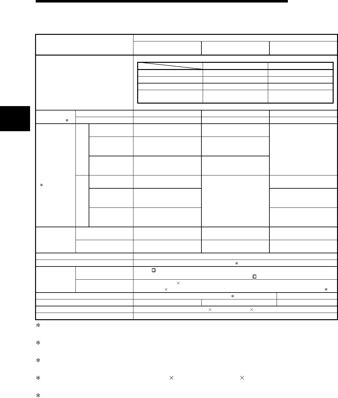
3 - 2 3 - 2
MELSEC-Q
3 SPECIFICATIONS
3
(Continued from preceding page)
Specifications
Item QJ71C24N
QJ71C24
QJ71C24N-R2
QJ71C24-R2 QJ71C24N-R4
RS-232 RS-422/485
DTR/DSR (ER/DR) control Enabled Disabled
RS/CS control Enabled Disabled
CD signal control Enabled Disabled
DC1/DC3 (Xon/Xoff) control
DC2/DC4 control Enabled Enabled
Transmission control
• DTR/DSR signal control and DC code control are selected by the user.
RS-232 1:1 1:1 —
Line configuration
(Connection) ( 2) RS-422/485 1:1, 1:n, n:1, m:n — 1:1, 1:n, n:1, m:n
MC protocols
communication 1:1, 1:n, m:n 1:1
Non procedure
protocol
communication
1:1, 1:n, n:1 1:1
RS-
232
Bidirectional
protocols
communication
1:1 1:1
—
MC protocols
communication 1:1, 1:n, m:n 1:1, 1:n, m:n
Non procedure
protocol
communication
1:1, 1:n, n:1 1:1, 1:n, n:1
Line configuration
(Data
communication)
(2)
RS-
422/
485 Bidirectional
protocols
communication
1:1
—
1:1
RS-232 Maximum 15 m
(49.2 ft.)
Maximum 15 m
(49.2 ft.) —
Transmission
distance (Overall
distance) RS-422/485 Maximum 1200 m (4592.4 ft.)
(overall distance) —Maximum 1200 m (4592.4 ft.)
(overall distance)
Flash ROM write count Maximum 100,000 times to the same area
Number of occupied I/O points 32 points per slot (I/O assignment: Intelli: 32 points) ( 3)
RS-232 7/0. 127 P HRV-SV Outside diameter 8.5mm (0.33in.) or more
(Oki Electric Cable Co., Ltd. Applicable number is specified in .)
Recommended
cable RS-422/485 SPEV (SB)-MPC-0.2 3P Outside diameter approx. 6.5mm (0.26 in.) (Mitsubishi Cable Industries, LTD.)
SPEV(SB)-0.2 3P Outside diameter approx. 7.5mm (0.3 in.) (Mitsubishi Cable Industries, LTD.) ( 4)
Applicable connector for external wiring D-sub 9 pin (male) screw type ( 5) —
5V DC internal current consumption 0.31A 0.26A 0.39A
External dimensions 98 (3.86 in.) (H) 27.4 (1.08 in.) (W) 90 (3.54 in.) (D)[mm]
Weight 0.20kg (0.44lb)
1 Set to transfer data with external devices using a full-duplex communication system when the Q series C24
is started. For switching to a half-duplex communication system, refer to the User’s Manual (Application).
2 Indicates possible combinations when connecting the PLC CPU and external devices (external device
side: PLC CPU side). The total number of n and m+n is up to 32 stations.
3 In order to use the Q series C24, it is necessary to set the GX Developer switches.
To set the GX Developer switches, refer to section 4.5.
4 Recommended cables SPEV (SB)-MPC-0.2 3P and SPEV (SB)-0.2 3P are equivalent in the electrical
characteristics, but partially different in the outside diameter, internal wire colors, etc.
5 See Section 3.2.1 (3) for the recommended connector.
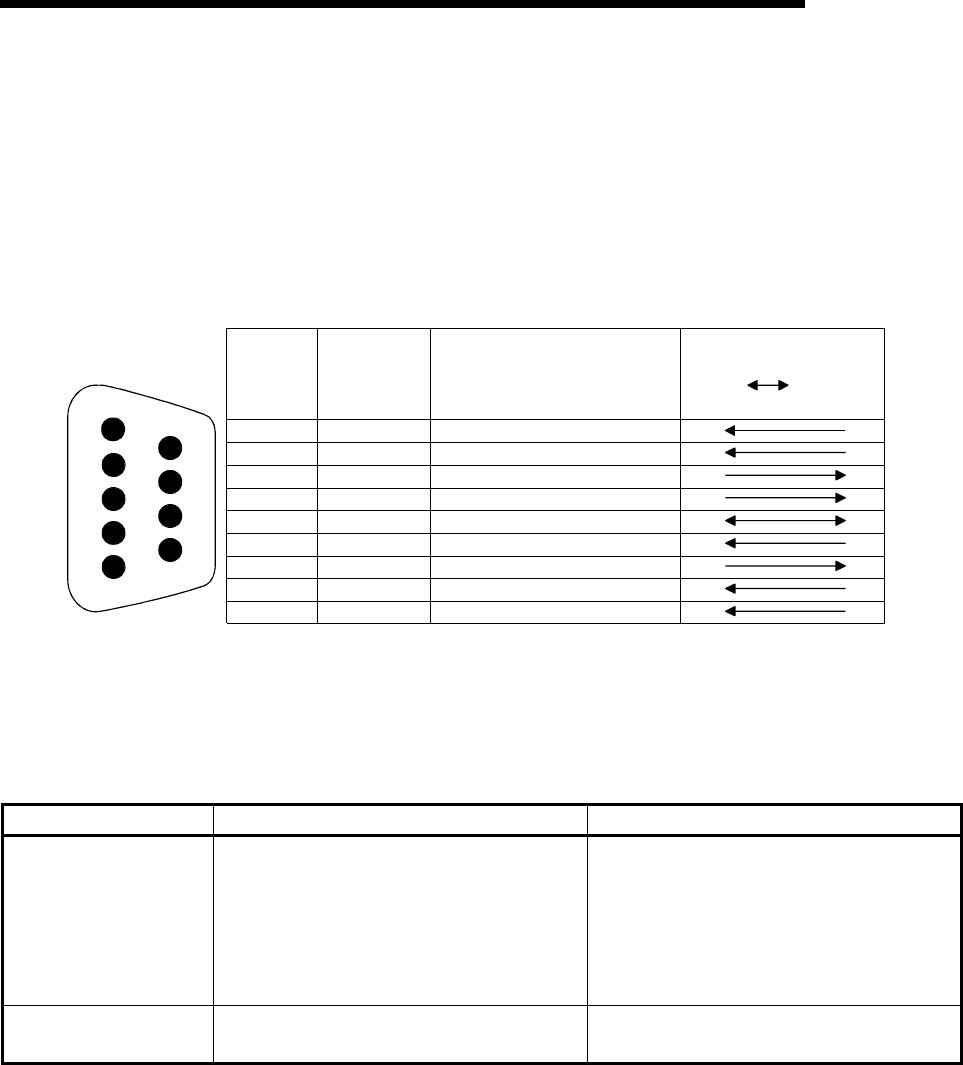
3 - 3 3 - 3
MELSEC-Q
3 SPECIFICATIONS
3.2 RS-232 Interface Specification
The following shows the RS-232 interface specifications.
3.2.1 RS-232 connector specifications
The following shows the specifications of the RS-232 connector that connects the Q
series C24 to an external device.
Carrier detect
Receive data
Send data
Data terminal ready
Signal ground
Request to send
Clear to send
CD
RD(RXD)
SD(TXD)
DTR(ER)
SG
DSR(DR)
RS(RTS)
CS(CTS)
RI(CI)
Pin number Signal name
Signal direction
External
device
1
2
3
4
5
6
7
8
9
C24
9
1
2
3
4
5
6
7
8
Signal
abbreviation
Call Indicate
Dataset ready
(1) The control signals are described below. (The pin numbers of the connector are
enclosed in parentheses.)
1) CD signal (1)
• The Q series C24 operates according to the setting CD terminal check (see
Section 8.4.5) of the Q series C24.
CD terminal check enabled CD terminal check disabled
Full-duplex
communication
• The Q series C24 performs send and receive
processing when the CD signal (receive
carrier detection) is ON.
• If the CD signal is turned off during data
communication, the Q series C24 initializes
the transmission sequence.
• The Q series C24 performs send and receive
processing regardless of the ON/OFF status
of the CD signal.
• Data communications is possible with an
external device that cannot turn the CD
signal ON/OFF.
Half-duplex
communication See Chapter 8 of User's Manual (Application) Setting impossible.
2) RD signal
This is a signal to receive data.
3) SD signal
This is a signal to send data.

3 - 4 3 - 4
MELSEC-Q
3 SPECIFICATIONS
4) DTR signal (4)
• When communicating data using the non procedure protocol, the Q series
C24 turns on or off (on when data is receivable) depending on the amount
of unused memory in the OS area allocated for receive data storage, if
DTR/DSR control is being performed.
Read the receive data from the sequence program, as the receive data is
stored in the OS area when the DTR signal is OFF.
If DTR/DSR control is not implements, the DTR signal is always ON.
• If an MC protocol or bidirectional protocol is performing data communication,
the Q series C24 turns ON when communications is enabled.
5) DSR signal (6)
• During DTR/DSR control, if this signal is OFF, the Q series C24 does not
send data to the external device.
Be sure that this signal is always turned ON when the external device is
ready to receive.
• If DTR/DSR control is not implemented, the DSR signal status is ignored.
6) RS signal (7)
• The Q series C24 turns ON/OFF the RS signal as shown below.
• When the communication system is full-duplex communications, if the Q series
C24 ready signal (X1E) is ON, the Q series C24 turns ON the RS signal.
• When the communication system is half-duplex communications, when the
Q series C24 sends data to an external device, it turns ON the RS signal.
• The RS signal is not turned OFF even when the receive data cannot be
stored in the Q series C24.
7) CS signal (8)
• The Q series C24 does not send data to an external device when this signal is OFF.
• Be sure that this signal is always turned ON when the external device is
ready to receive.
8) RI signal (9)
• The RI signal is used when the modem status is monitored on the Q series
C24 side. It should be connected as needed. The RI signal is not needed
to be connected when the modem is not connected.
(2) The ON and OFF states of each signal indicate the following conditions:
(Output side) (Input side)
ON ……… 5 V DC to 15 V DC, 3 V DC to 15 V DC
OFF ……… –5 V DC to –15 V DC, –3 V DC to –15 V DC
(3) Interface connector
The Q series C24 uses the following type of RS-232 interface connector.
9-pin D sub (female) screw fixing type
Use one of the following as a connector shell for the connection cable of
the Q series C24 side.
• 3M
Plug model: 8209-6009 Shell model: 3702-2209 M2.6
• Tyco Electronics AMP K.K.
Plug model: 747904-2 Shell model: 747515 or 174469-2
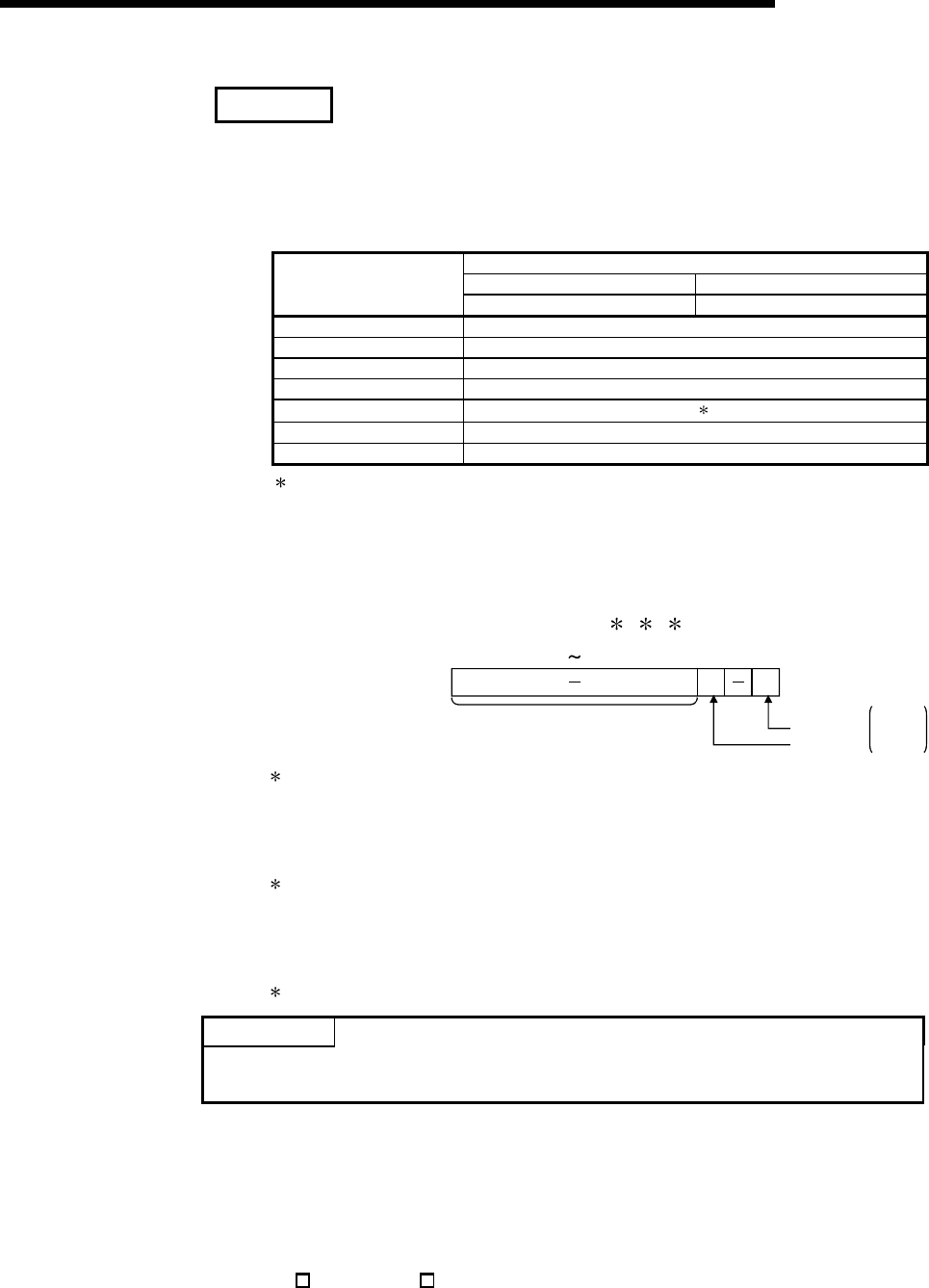
3 - 5 3 - 5
MELSEC-Q
3 SPECIFICATIONS
REMARK
(1) Confirmation of RS-232 control signal status
The control signal status of DTR, DSR, RS, and CD can be confirmed during
data communication by the RS-232 control signal status storage area (address
254H, 264H) of the GX Configurator-SC or Q series C24 buffer memory.
Buffer memory address
CH1 side CH2 sideBit position
254H264H
b0 RS
b1 DSR
b2 DTR
b3 CD
b4 CS 1
b5 RI
b6 to b15 —
1 System area for QJ71C24 (-R2)
(2) Designation of RS and DTR signal status
When the Q series it turned on or off, the on and off states of the RS and DTR
signals can be designated when the buffer memory of the RS and DTR signal
status designation area (address: 92H, 132H) for the corresponding bit is turned
on or off by the RS signal or DTR signal. 1 2 3
Buffer memory address 92H/132H1/0
b15 b3 b2 b1 b0
1/0
System 1:ON
0:OFF
RS
DTR
[Default 0005H]
1 The RS signal is controlled by the Q series C24 in the following cases. (Ignore setting
contents.)
• When data is communicated with half-duplex communication
• When communication time and the RS and CS signals are controlled by the modem function
2 The DTR signal is controlled by the Q series C24 in the following cases. (Ignore setting
contents.)
• When the DTR and DSR signals are controlled
• When data is communicated by the modem function
3 After writing in the buffer memory, a lag of 0 to 20 ms occurs until it is reflected in the signal.
POINT
Be sure to control the RS and DTR signals with the Q series C24. Control of the RS
and DTR signals by the user is a prime factor for data communication errors.
3.2.2 RS-232 cable specification
• Use a 15 m (49.21 ft.), or shorter, cable conforming to the RS-232 standard as the
RS-232 cable.
(Recommended cable)
7/0. 127 P HRV-SV… : Designates the number of pairs. (For 13 pairs 7/0.127
13P HRV-SV)
(Oki Electric Cable Co., Ltd)
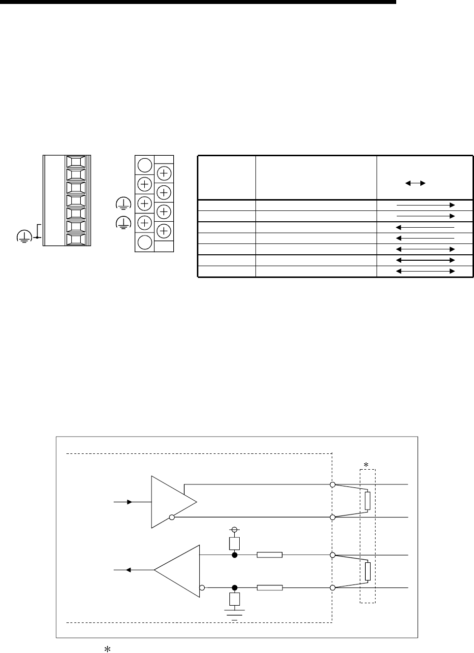
3 - 6 3 - 6
MELSEC-Q
3 SPECIFICATIONS
3.3 RS-422/485 Interface Specifications
The following shows the RS-422/485 interface specification.
3.3.1 RS-422/485 terminal block specifications
The following shows the specifications of the RS-422 connector and RS-422/485
terminal block that connect to an external device.
Signal
abbreviation Signal name Signal direction
C24 External
device
SDA
SDB
RDA
RDB
SG
FG
FG
Send data (+)
Send data (–)
Receive data (+)
Receive data (–)
Signal ground
Frame ground
Frame ground
SG
SDA
SDB
RDA
RDB
SG
RDB
RDA
SDB
(FG)
SDA
QJ71C24N-R4 QJ71C24N
QJ71C24
(FG)
(FG)
(1) The following describes the control signals.
1) SDA, SDB signals
These are signals to send data from the Q series C24 to the external
device.
2) RDA, RDB signals
These are signals for the Q series C24 to receive data from the external
device.
(2) The following shows the function block diagrams.
(RS-422/485 interface)
Send data
SDA
SDB
RDA
RDB
1
+
+
–
–
Receive data
1 The following shows the terminal resistor connection.
Connect the terminal resistor according to Section 4.4.2 or the User's Manual
(Hardware) of the Q series C24 used.
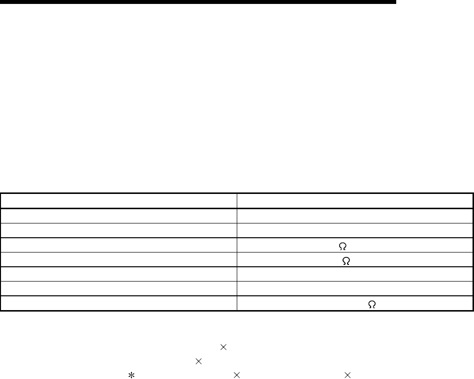
3 - 7 3 - 7
MELSEC-Q
3 SPECIFICATIONS
3.3.2 RS-422/485 cable specifications
The following shows the RS-422/485 cable specification.
(1) Use a 1200 m (3937 ft.), or shorter, cable that satisfies the following specification
for the RS-422/485 cable (cable to connect the Q series C24 terminal block).
(2) Make the total distance within 1200 m (3937 ft.) when two or more device are
connected in a 1:n or m:n configuration.
(3) The RS-422/485 cable specification is shown below.
Item Description
Cable type Shielded cable
Number of pairs 3P
Conductor resistance (20 C°)88.0 /km or less
Insulation resistance 10000 M - km or more
Dielectric strength 500 V DC, 1 minute
Electrostatic capacitance (1 kHz) 60nF/km or less on average
Characteristic impedance (100 kHz) 110 ± 10
(Recommended cable)
SPEV (SB)-MPC-0.2 3P ..... (MITSUBISHI CABLE INDUSTRIES, Ltd.)
SPEV (SB)-0.2 3P .............. (MITSUBISHI CABLE INDUSTRIES, Ltd.)
SPEV (SB)-MPC-0.2 3P and SPEV (SB)-0.2 3P have the same electrical
characteristics, but different external diameter and internal wire colors.
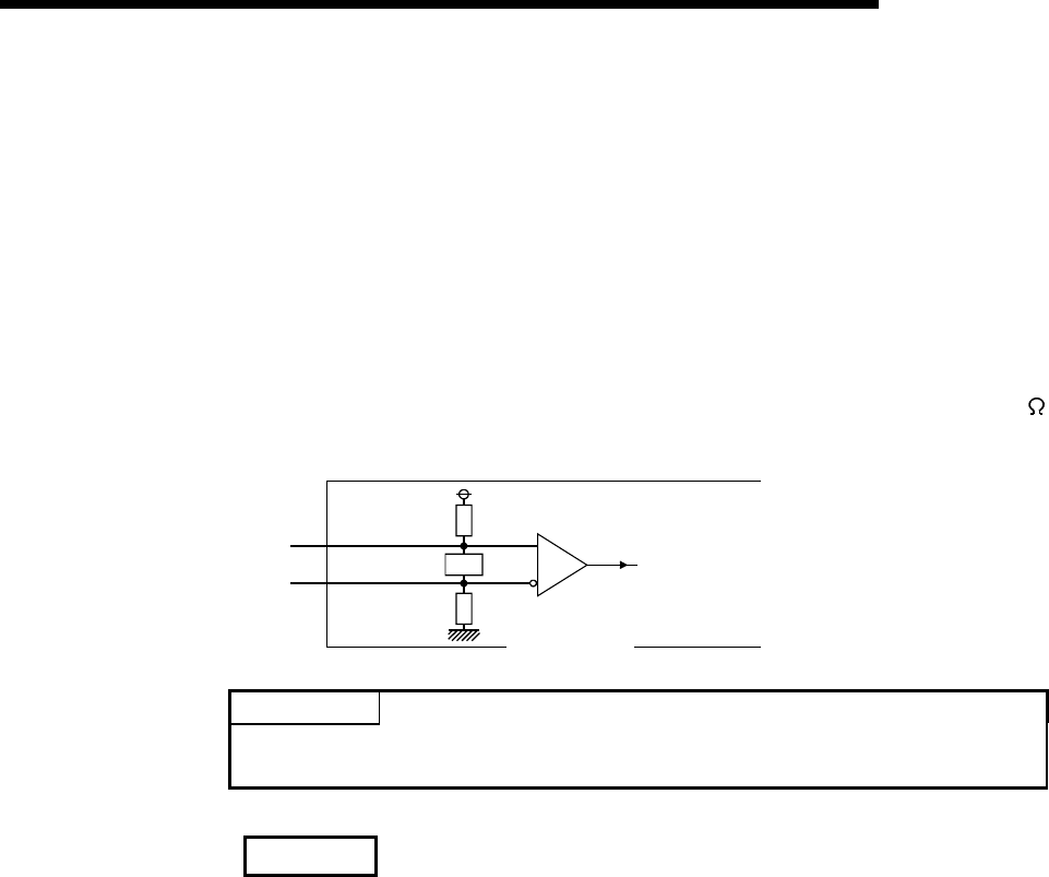
3 - 8 3 - 8
MELSEC-Q
3 SPECIFICATIONS
3.3.3 Precautions when transferring data using RS-422/485 circuit
The following precautions must be observed when transferring data with an external
device through the Q series C24 RS-422/485 interface.
Take the following into account when the transferring data with the external device.
(1) Error receive data countermeasures at external device during RS-
422/485 connection
If the external device may receive erroneous data, install a pull-up or pull-down
resistor to the external device as follows.
Installing a pull-up or pull-down resistor (resistance value criteria: approx. 4.7 k
1/4 W) can prevent the reception of erroneous data.
Receive data
External device
4.7kΩ 1/4W
4.7kΩ 1/4W
Terminating
resistor
RDA
RDB
+
-
POINT
When there is a pull-up or pull-down resistor at the external device, erroneous data
is not received.
REMARK
The following describes the case when a pull-up or pull-down resistor is not installed
to the external device.
When no station is sending, the send line becomes high impedance and noise, etc.
may cause the send line to change and the external device to receive erroneous
data.
In this case, there is probably a parity error or framing error.
Therefore, skip the erroneous data.
Since the first data during data reception is fixed in the following cases, also skip the
receive data until the fixed head data is received.
• When using an MC protocol to send data, the first data is fixed according to the
frame and format the user uses.
• When transferring data using user frames with non procedure protocol or
bidirectional protocol, the first data is selected according to the user frame that the
user registers to the Q series C24.
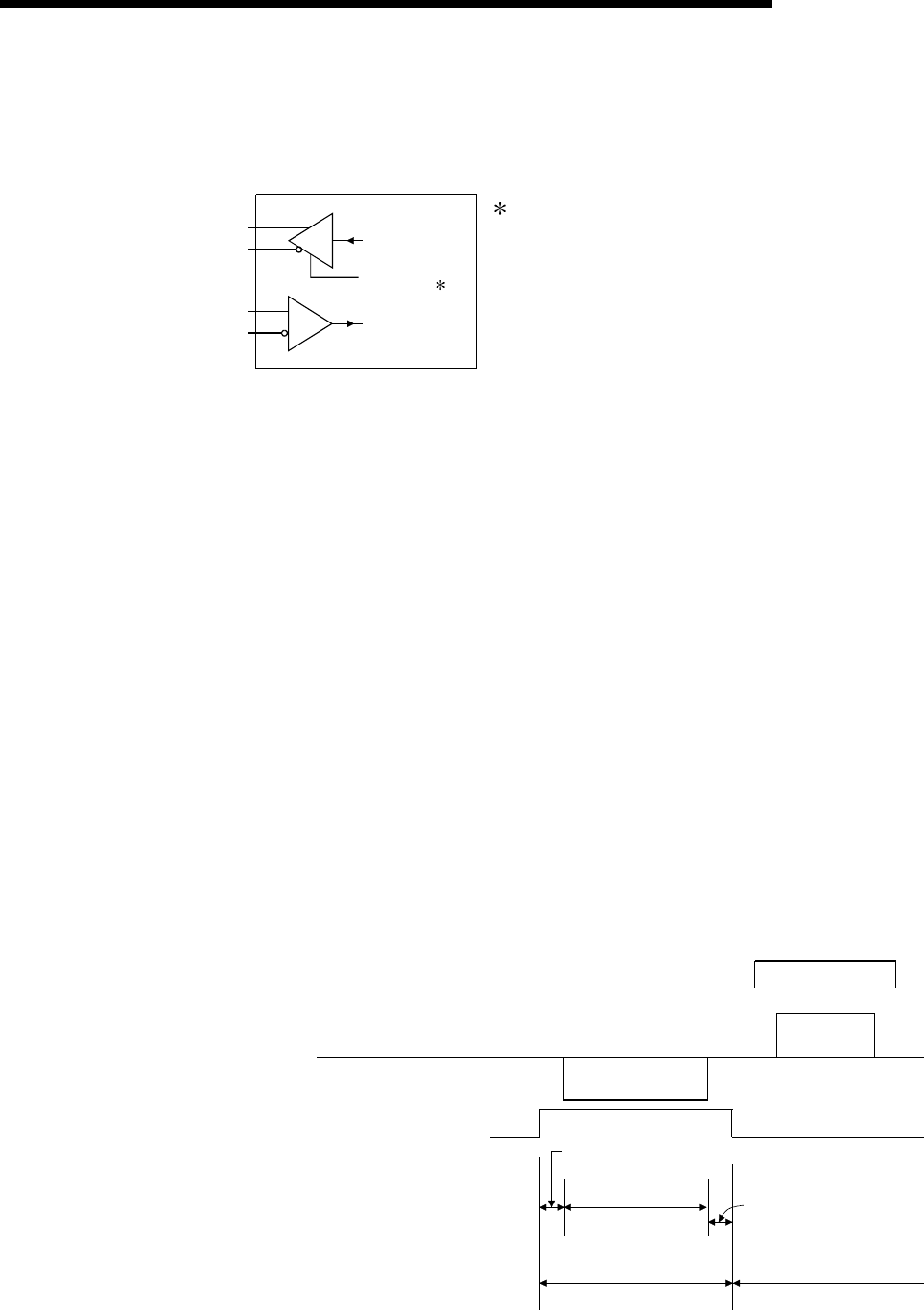
3 - 9 3 - 9
MELSEC-Q
3 SPECIFICATIONS
(2) RS-422/485 interface operation
1) RS-422-485 interface construction
The following illustration shows the construction of the Q series C24 RS-
422/485 interface driver (send)/receiver (receive).
Receive data
Send data
SDR
SDB
RDA
RDB
Output control input ( 1)
Receiver
Driver 1 "Output control input" (also called send gate) of
the driver (send) section of the illustration at
the left determines whether or not data from
SDA/SDB is output to the outside.
2) RS-422/485 interface operation
When the "Output control input" in the illustration above is ON, the interface
enters the low impedance state (state in which data can be sent).
When the "Output control input" is OFF, the interface enters the high
impedance state (state in which data cannot be sent).
3) Timing to start sending and to complete the transmission processing for the Q
series C24
• Timing to start sending
During data transmission, the Q series C24 outputs the actual data after
sending a mark for 2 characters, or longer, after the high impedance set by
the operations described in 1) and 2) above is reset.
• Transmission processing completion timing
The following times are necessary as H/W gate OFF time from the time that
data transmission is completed until transmission processing is completed
(the state changes to the high impedance state). (The transmission rate set
in the Q Series C24 is the object.)
When the transmission rate
is 600 bps or higher : Time for 0 to 1 bits of data to be sent
When the transmission rate
is 50 bps, 300 bps : several ms
Outputs a mark for 2 characters, or longer
Data send time range H/W gate OFF time
(See explanation above)
Q series C24 is in the data
transmission and data
reception enable status
(Output control input)
External device
Q series C24 Data
Data
(Output control input)
"Output control input"
ON time range
(Low impedance state)
"Output control input"
OFF time range
(High impedance state)
Q series C24 is in the data
reception enable state.
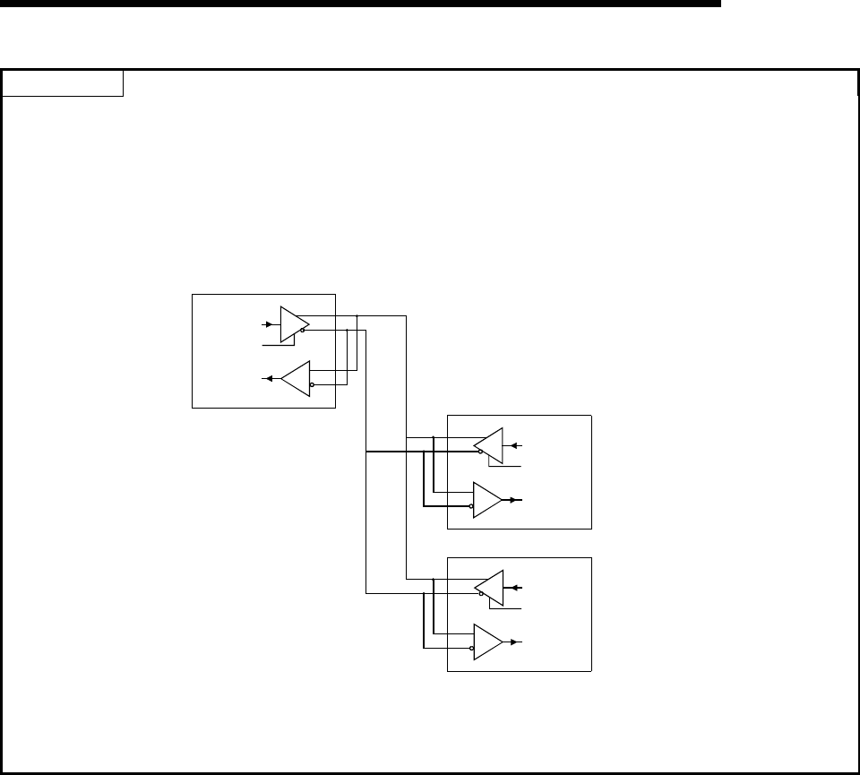
3 - 10 3 - 10
MELSEC-Q
3 SPECIFICATIONS
POINT
(1) When the external device and the Q series C24 connected in n:1 and m:n configurations
When the send signal of each device is connected as shown below, if the "Output control input" is
turned ON at two or more devices, the relevant devices output (send) data at the same time.
For the external device to transfer data normally,
• "Output control input" must be turned ON only when sending data.
• "Output control input" must be turned OFF when not sending data.
SDA
SDB
RDA
RDB
Q series C24
SDA
SDB
RDA
RDB
Q series C24
Receive
data
Send data
SDA
SDB
RDA
RDB
Output control input
External device or converter
Receive
data
Send data
Output control input
Receive
data
Send data
Output control input
(2) When the Q series C24 is used, if operation of the two interfaces is linked (see Section 4.5.2 (2)), the
time to send one character becomes the Q series C24 H/W gate OFF time.
(The Q series C24 turns OFF the gate after the one-character send time.)
3 - 11 3 - 11
MELSEC-Q
3 SPECIFICATIONS
3.4 Serial Communication Module Function List
The following table lists the functions of the Q series C24.
Function Reference section
Communication with QnA compatible 3C frame
Communication with QnA compatible 4C frame
Communication with QnA compatible 2C frame
Communication with
ASCII code
Communication with A compatible 1C frame
Formats 1 to 4
exist for each.
Communication with
binary code Communication with QnA compatible 4C frame Format 5
Batch read/write in bit/word units
Monitoring of device memory
Batch read/write of multiple blocks
Read/write by extension designation
Read/write of device
memory
Accessing other stations via network system
Reading/writing from/to the buffer memory of the Q series C24
Reading/writing from/to the buffer memory of intelligent function modules
Reading/writing from/to sequence program files
Monitoring the PLC CPUs (PLC CPU monitoring function)
Status control of the PLC CPUs (remote RUN/STOP, etc.)
Turning on/off input signals of the Q series C24 from an external device (global function)
Communication
using MC protocol
(1)
Data transmission from a PLC CPU to an external device (on-demand function)
Chapter 5
Reference Manual
Data transmission/reception in any format Chapter 6
Data transmission/reception using user frames
Data reception by interrupt programs
Monitoring the PLC CPUs (PLC CPU monitoring function)
ASCII data transmission/reception by ASCII-BIN conversion
Communication
using non
procedure protocol
(2)
Data transmission/reception by specifying transparent code
User's Manual
(Application)
Data transmission/reception in any format Chapter 7
Data reception by interrupt programs
ASCII data transmission/reception by ASCII-BIN conversion
Communication
using bidirectional
protocol ( 1) Data transmission/reception by specifying transparent code
Communication with MC Protocol/non procedure protocol/bidirectional protocol
Communication via
public network, etc.
(modem function) PLC access from GX Developer
DC code control (including Xon/Xoff control)
Transmission
control DTR/DSR (ER/DR) control
User's Manual
(Application)
Independent/linked operation of each interface Section 4.5.2
Monitoring/testing of initial settings and setting values with utility software Chapter 8
Supporting multiple CPU system Section 2.10 of
Reference Manual
Remote password check
Section 3.3.3 of
User's Manual
(Application)
1 If the external device is capable of incorporating a program and communicating
data using a protocol of the MELSEC PLC, it is possible to access the PLC CPU
using the above mentioned MC protocol. Furthermore, it is possible to transfer any
data using the bidirectional protocol.
2 When it is necessary to communicate using the protocol of an external device,
such as a measuring instrument or a bar code reader, the above-mentioned non
procedure protocol is used for data communication. In that case, the processing of
the communication data becomes easier by using the user frame communication
function.
3 - 12 3 - 12
MELSEC-Q
3 SPECIFICATIONS
3.5 Dedicated Instruction List
The following table lists dedicated instructions that can be used in the Q series C24.
: Available : Not available
Protocol
Classification Instruction Description MC Non Bi
Reference
section
ONDEMAND Sends data with the on-demand function
OUTPUT Sends designated number of data
INPUT Receives data (reads received data)
BIDOUT Sends data
BIDIN Receives data (reads received data)
SPBUSY Reads the status of data sent/received with each
dedicated instruction
CSET
Allows clearing data received up to the present
without interrupting the data transmission
processing.
Chapter 9
BUFRCVS Receives data with an interrupt program (reads
received data)
For data
communication
PRR Sends data with user frames using transmission
schedule table
PUTE Stores user frames in flash ROM of the Q series
C24 (writing)
Setting value
registration/
reading GETE Reads user frames stored in flash ROM of the Q
series C24
Performs PLC CPU monitoring
registration
PLC CPU
monitoring
instructions Cancels PLC CPU monitoring
For PLC
CPU
monitoring
function
Initial value
setting
instruction
CSET
Sets the unit for the number of communication
data (words/bytes) and the data communication
area
Mode switching
instruction UINI Changes the mode, transmission specifications
and host station No. of the Q series C24.
Chapter 17 of
User's Manual
(Application )
Abbreviations used in the
Protocol column
MC : MC protocol
Non : Non procedure
protocol
Bi : Bidirectional protocol
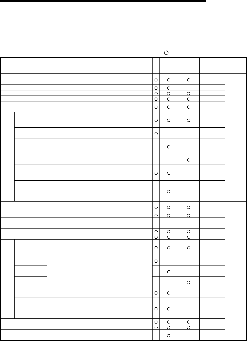
3 - 13 3 - 13
MELSEC-Q
3 SPECIFICATIONS
3.6 Utility Package (GX Configurator-SC) Function List
The following table lists the utility package function for the Q series C24.
( : Protocol for which setting is valid)
Function MC
Non-
procedure
protocol
Bidirectional
protocol
Explanation
page Remarks
Auto refresh setting Refresh the Q series C24's error codes and set devices on the PLC
CPU side. Section 4.6
User frame Register the user frame in the flash ROM. — Section 8.4.1
Data for modem initialization Register the data for modem initialization in the flash ROM. Section 8.4.2
Data for modem connection Register the data for model connection in the flash ROM. Section 8.4.3
Modem function system
setting
Register the system setting values for model function in the flash
ROM. Section 8.4.4
CHn Transmission
control and others
system setting
Set the transmission specifications with the other device.
(DTR/DSR control, DC code control, communication method, data
communication monitoring timer value, etc.)
Section 8.4.5
CHn MC protocol
system setting
Assign the buffer memory for on-demand function, set the user
frame number, etc. — — Section 8.4.6
CHn Non procedure
system setting
Assign the buffer memory needed to perform data communication
using the non procedure protocol, and change the setting values,
etc.
—— Section 8.4.7
CHn Bidirectional
system setting
Assign the buffer memory needed to perform data communication
using the bidirectional protocol, and change the setting values, etc. —— Section 8.4.8
CHn PLC CPU
monitoring system
setting
Set the PLC CPU monitoring function. — Section 8.4.9
System
setting
CHn Transmission
user frame No.
designation system
setting
Set the user frame number to be transmitted, etc. — — Section 8.4.10
Can be used
via online
operation.
Can be used
via offline
operation.
System setting default Reset the setting values in the buffer memory to their default
values. Section 8.4.11
System setting write Write the setting values in the buffer memory to the flash ROM. Section 8.4.11
Flash ROM write
allow/prohibit designation Set whether to allow or prohibit writing to the flash ROM. — — — Section 8.4.12
X · Y monitor/test Perform the monitoring/testing of I/O signals to/from the PLC CPU. Section 8.6.1
Modem function monitor/test Monitor the execution status of the modem function. Section 8.6.2
CHn Transmission
control and others
monitor/test
Monitor the status of interface control signals, values set from the
GX Developer, etc. Section 8.6.3
CHn MC protocol
monitor — — Section 8.6.4
CHn Non procedure
monitor/test —— Section 8.6.5
CHn Bidirectional
monitor
Monitor the data communication result, I/O signal status, and
setting values in the buffer memory.
—— Section 8.6.6
CHn PLC CPU
monitoring monitor
Monitor the setting values and operating status of the PLC CPU
monitoring function. — Section 8.6.7
Monitor
CHn User frame
No. designation
monitor for
transmission
Monitor the setting value for user frame to be transmitted. — Section8.6.8
Monitor/test others Monitor the data reception result, error occurrence status, etc. Section 8.6.9
ERR LED off Turn off the ERR LEDs on the front face of the module. Section 8.6.10
Non procedure protocol
receive data clear Clear the currently received data. — — Section 8.7
Can be used
only via
online
operation.
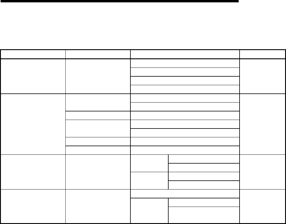
3 - 14 3 - 14
MELSEC-Q
3 SPECIFICATIONS
3.7 List of GX Developer Setting Items for Serial Communication Modules
The following table lists the parameters that are set using the GX Developer.
Parameter setting item Parameter description Set data Reference section
Type
Model name
Points
I/O assignment setting
Performs I/O assignment
for the Q series C24 and
enables the switch settings
listed below. Start X/Y
Section 4.5.1
CH1 Transmission setting
Switch 1 CH1 Communication rate setting
Switch 2 CH1 Communication protocol setting
CH2 Transmission setting
Switch 3 CH2 Communication rate setting
Switch 4 CH2 Communication protocol setting
Switch setting
Switch 5 Station number setting
Section 4.5.2
Interrupt pointer Start No.
CPU side Interrupt pointer No. of units
Start I/O No.
Interrupt pointer setting
Performs setting for
reading reception date with
interrupt programs. Intelligent
module side Start SI No.
Section 4.5.3
Password settings
Model name
Remote password settings
Sets the remote password
and the Q series C24 that
performs the check.
Password
active module
settings Start XY
Section 3.3.3 of
User's Manual
(Application)
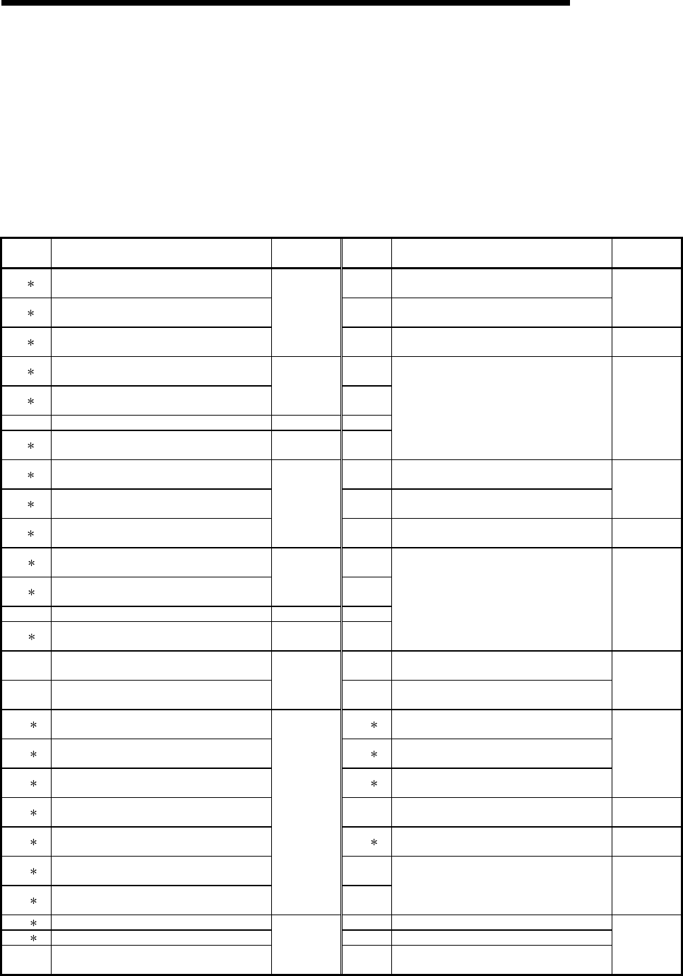
3 - 15 3 - 15
MELSEC-Q
3 SPECIFICATIONS
3.8 List of Input/Output Signals for the PLC CPU
This section describes the input/output signals of the Q series C24.
For assignments of the input/output signals shown in the table below, it is assumed
that the Q series C24 is mounted in slot 0 of the basic base unit.
Device numbers starting with X indicate input signals from the Q series C24 to the PLC
CPU, and device numbers starting with Y indicate output signals from the PLC CPU to
the Q series C24.
The following table lists the input/output signals for the PLC CPU.
Device
number Signal description Reference
section
Device
number Signal description Reference
section
X0 1CH1 Transmission normal completion
ON: Normal completion Y0 CH1 Transmission request
ON: Requesting transmission
X1 1CH1 Transmission abnormal completion
ON: Abnormal completion Y1 CH1 Reception data read completion
ON: Data read completed
—
X2 1CH1 Transmission processing
ON: Transmission in progress
Section 8.6.4
Section 8.6.5
Section 8.6.6
Y2 CH1 Mode switching request
ON: Requesting switch
Application,
Chapter 15
X3 2CH1 Reception data read request
ON: Requesting read Y3
X4 2CH1 Reception abnormal detection
ON: Abnormal detection
Section 6.1
Section 7.1
Section 8.6.5
Section 8.6.6 Y4
X5 (For system) — Y5
X6 3CH1 Mode switching
ON: Switching
Application,
Chapter 15 Y6
Use prohibited —
X7 1CH2 Transmission normal completion
ON: Normal Completion Y7 CH2 Transmission request
ON: Requesting transmission
X8 1CH2 Transmission abnormal completion
ON: Abnormal completion Y8 CH2 Reception data read completion
ON: Data read completed
—
X9 1CH2 Transmission processing
ON: Transmission in progress
Section 8.6.4
Section 8.6.5
Section 8.6.6
Y9 CH2 Mode switching request
ON: Requesting switch
Application,
Chapter 15
XA 2CH2 Reception data read request
ON: Requesting read YA
XB 2CH2 Reception abnormal detection
ON: Abnormal detection
Section 6.1
Section 7.1
Section 8.6.5
Section 8.6.6 YB
XC (For system) — YC
XD 3CH2 Mode switching
ON: Switching
Application,
Chapter 15 YD
Use prohibited —
XE CH1 ERR. occurrence
ON: Error occurring YE CH1 ERR.clear request
ON: Requesting error clear
XF CH2 ERR. occurrence
ON: Error occurring
Section 8.6.10
Section 10.1.2 YF CH2 ERR. clear request
ON: Requesting error clear
Section 8.6.10
Section 10.1.2
X10 6Modem initialization completion
ON: Initialization completed Y10 6Modem initialization request (standby request)
ON: Requesting initialization
X11 6Dialing
ON: Dial in progress Y11 6Connection request
ON: Requesting connection
X12 6Connection
ON: Connection in progress Y12 6Modem disconnection request
ON: Requesting disconnection
Section 8.6.2
Application,
Chapter 3
X13 6Initialization/connection abnormal completion
ON: Initialization/ connection abnormally completed Y13 Use prohibited —
X14 6Modem disconnection complete
ON: Disconnection completed Y14 6Notification- issued request
OFF: Requesting notification issuance
X15 6Notification normal completion
ON: Normal completion Y15
X16 6Notification abnormal completion
ON: Abnormal completion
Section 8.6.2
Application,
Chapter 3
Y16
Use prohibited —
X17 1 Flash ROM read completion ON: Completed Y17 Flash ROM read request ON: Requesting
X18 1 Flash ROM write completion ON: Completed Y18 Flash ROM write request ON: Requesting
X19 Flash ROM system setting write completion
ON: Completed
—
Y19 Flash ROM system setting write request
ON: Requesting
—
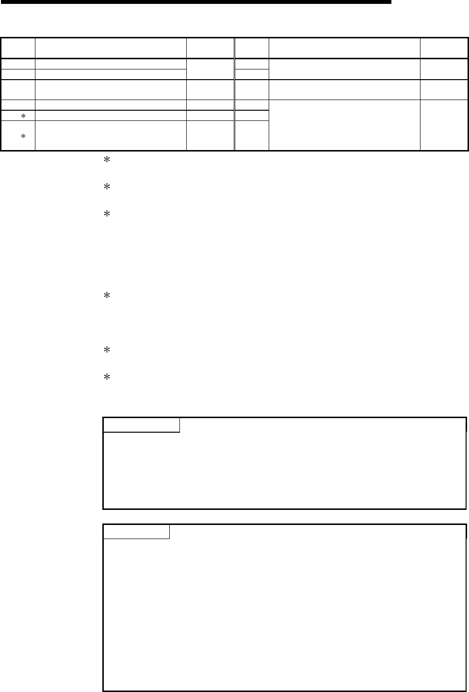
3 - 16 3 - 16
MELSEC-Q
3 SPECIFICATIONS
Device
number Signal description Reference
section
Device
number Signal description Reference
section
X1A CH1 Global signal ON: Output instructed Y1A
X1B CH2 Global signal ON: Output instructed
Section 3.10,
Reference Y1B Use prohibited —
X1C System setting default completion
ON: Completed Section 8.4.11 Y1C System setting default request
ON: Requesting Section 8.4.11
X1D (For system) — Y1D
X1E 4 Q series C24 ready ON: Accessible — Y1E
X1F 5
Watchdog timer error (WDT error)
ON : Module error occurred
OFF: Module being normally operated
—Y1F
Use prohibited —
1 The device does not turn on/off by execution of a dedicated instruction when a
function that corresponds to the input signal is used.
2 The device does turn on/off by execution of a dedicated instruction when a function
that corresponds to the input signal is used (from ON to OFF: Data read completed).
3 The mode switching signal (X6/XD) turns ON at mode switching, receive clear,
user frame receive designation or transmission sequence initialization.
While the mode switching signal (X6/XD) is ON, do not issue a communication
request to the target interface.
(The communication processing of the Q series C24 is stopped while the mode
switching signal (X6/XD) is ON.)
4 The Q series C24 ready signal indicates whether or not it is possible to access the
Q series C24 from the PLC CPU.
Use it as a interlock signal for a sequence program.
(It turns on about one second after turning the power ON and reset operation.)
5 Restart the PLC CPU when the watchdog timer error signal is turned on (reset the
power and the CPU module).
6 QJ71C24N-R4 cannot be used. (Related to modem function signal.)
• X10 to X16: For system
• Y10 to Y16: Use prohibited
IMPORTANT
(1) Of the input/output signals to the PLC CPU, the signals marked with "Use
prohibited" must not be output (ON).
If any of the "Use prohibited" signals is output, the PLC system may
malfunction.
(2) When the modem function is not used or the QJ71C24N-R4 is used, X10 to
X16 are used for the system and Y10 to Y16 cannot be used.
POINT
(1) The input/output signals shown in this section are the signals used when a QnA
series serial communication module program is utilized for the Q series C24
(see Section 2 in appendix).
In the QCPU, the on/off of input/output signals to intelligent function modules is
executed with a dedicated instruction.
It is not necessary to turn the signals on/off by the sequence program, except
for the input/output signals shown in the programming of each function
reference page.
(2) When a program for a QnA series serial communication module is also utilized
for the Q series C24, it is recommended to replace the instructions with the
dedicated instructions shown on the corresponding function reference page of
each manual for the Q series C24.

3 - 17 3 - 17
MELSEC-Q
3 SPECIFICATIONS
3.9 List of Applications and Assignments of the Buffer Memory
This section describes the buffer memory.
(1) Configuration of the buffer memory
A buffer memory consists of a user area and a system area, as shown below.
(a) User area
1) This is the area where users write/read data.
2) The user area consists of areas for storing setting values for data
communication, for actual data communication, and for storing
communication status and communication error information.
3) Data read/write to the user area should be performed following the
instructions in the corresponding detailed reference page.
(b) System area
This area is used by the Q series C24 system.
(2) List of buffer memory assignments
A buffer memory is configured with 16 bits per address.
Name, default value, etc. of each address of the buffer memory is shown in the
lists on the following pages.
1) Abbreviations in the target Protocol column
MC : MC protocol
Non: Non procedure protocol
Bi : Bidirectional protocol
2) Meaning of symbols shown in the target Protocol column
The following symbols are assigned to protocols related to the setting
values of a corresponding area and to areas used for controlled with user
settings, and indicate what kind of access is allowed to the area in question.
RW : Area where it is possible to read/write from/to the PLC CPU and
an external device.
R : Area where only reading is possible from the PLC CPU and an
external device.
– : System area used by the system or area not used by the
corresponding protocol.
3) Meaning of symbols shown in the Registration allowed/not allowed
column
Indicates whether or not it is possible to use a value in the corresponding
area by registering it to the flash ROM of the Q series C24.
Allowed : Area that can be registered and used.
Not allowed : Area that cannot be registered.
IMPORTANT
Do not write data in the "System area" of the buffer memory.
If data is written to any of the system areas, the PLC system may malfunction.
Some of the user areas are partially system areas. Care must be taken when
performing read/write to the buffer memory.

3 - 18 3 - 18
MELSEC-Q
3 SPECIFICATIONS
POINT
(1) Use the FROM/TO instructions or other applicable commands to access the
buffer memory shown in this section when a program for a QnA series serial
communication module is utilized for the Q series C24 (see Section 2 in
Appendix).
In QCPU, the access to the buffer memory of an intelligent function module is
executed with a dedicated instruction.
It is not necessary to access directly using the FROM/TO instructions or other
instructions from the sequence program, except when accessing the buffer
memory as shown in the programming on each function reference page.
(2) When a program for a QnA series serial communication module is utilized for
the Q series C24, it is recommended to replace the instructions with the
dedicated instructions shown on the corresponding function reference page of
each manual for the Q series C24.
(3) The following initial settings (changing the default values) for data
communication must be performed by a registration operation using GX
Configurator-SC or by executing the CSET instruction for the sequence
program.
1) Initial settings for communication using the MC protocol
• Setting the unit of data length sent by the on-demand function
Word/byte units designation (addresses 150 (96H), 310 (136H))
• Setting the buffer memory used by the on-demand function
Buffer memory head address designation (addresses 160 (A0H), 320
(140H))
Data length designation (addresses 161 (A1H), 321 (141H))
2) Initial settings for communication using the non procedure/bidirectional
protocols
• Setting the unit of data length to be sent and received
Word/byte units designation (addresses 150 (96H), 310 (136H))
• Setting the transmission area
Transmission buffer memory head address designation (addresses 162
(A2H), 322 (142H))
Transmission buffer memory length designation (addresses 163 (A3H),
323 (143H))
• Setting the reception area
Receive buffer memory head address designation (addresses 166
(A6H), 326 (146H))
Receive buffer memory length designation (addresses 167 (A7H), 327
(147H))
For more details on the registration operation by GX Configurator-SC, see
the explanation of the system settings of the corresponding protocol in
Sections 8.4.5 to 8.4.8.
For more details on the CSET instruction, see Section 16.4 of the User's
Manual (Application).
3 - 19 3 - 19
MELSEC-Q
3 SPECIFICATIONS
Address
Decimal (Hex)
Applicable
protocol
CH1 CH2
Application Name Initial
value MC Non Bi
Registration
allowed/not
allowed
Reference
section
Communication error clear request for CH1 and to turn LED off
0: ON, No initialization request
1: OFF, Initialization requested
SD WAIT (b0) C/N (b4)
SIO (b1)) NAK (b5)
PRO. (b2) ACK. (b6)
P/S (b3) NEU. (b7)
0
(0H)—
For system (b8) to (b15)
Communication error clear request for CH2 and to turn LED off
0: ON, No initialization request
1: OFF, Initialization requested
SD WAIT (b0) NAK (b5)
SIO (b1) ACK. (b6)
PRO. (b2) NEU. (b7)
P/S (b3) CH2 ERR. (b14)
C/N (b4) CH1 ERR. (b15)
—1
(1H)
For LED and
communication
error clear
For system (b8) to (b13)
0 RW Not allowed
Section
8.6.10
Section
10.1.1
Section
10.1.2
Register/read/delete instructions
2
(2H)0: No request
2: Read request
1: Register request
3: Delete request
Frame No. direction
3
(3H)0: No designation Other than 0: Frame No.
Registration/read/delete result storage
4
(4H)0: Normal completion Other than 0: Abnormal completion
Number of data bytes registered designation
5
(5H)0 : No designation
Other than 0: Number of data bytes registered (maximum 80 bytes)
User frame
6 to 45
(6H to 2DH)
For flash ROM
access
0 : No designation
Other than 0: Registered data (maximum 80 bytes)
0 RW — Not allowed
Section
8.4.1
Section
8.4.2
Section
8.4.11
Section
8.4.12
Modem connection channel designation
46
(2EH)0: Non 1: CH1 2: CH2
Notification execution designation
47
(2FH)0: Do not execute. 1: Execute.
0
Number of connection retries designation
48
(30H)1 to 5: Number of retries 3
Connection retry interval designation
49
(31H)90 to 300: Connection retry interval (unit: s) 180
Initialization/connection timeout designation
50
(32H)1 to 60: Timeout (unit: s) 60
Number of initialization retries designation
51
(33H)1 to 5: Number of retries 3
Data No. for initialization designation
52
(34H)
0H : Send initialization data designated by the
designated area of the user frame for
transmission.
7D0H to 801F: Data No. for initialization
7D0H
Data No. for connection designation
53
(35H)BB8H to 801FH: Data No. for connection
GX Developer connection designation
54
(36H)0: Do not connect. 1: Connect.
0
No - communication interval time designation
55
(37H)
0 : Wait infinitely
1 to 120: No communication interval (Waiting time for line
disconnection) (unit: min.)
30
RS · CS control yes/no designation
56
(38H)
For designation
of modem
function-1
0: No control 1: Controlled 1
RW Allowed
Section
8.4.2
Section
8.4.3
Section
8.4.4
Chapter 3
of User's
Manual
(Application)
57 to 143
(39H to 8FH)Use prohibited System area —
3 - 20 3 - 20
MELSEC-Q
3 SPECIFICATIONS
Address
Decimal (Hex)
Applicable
protocol
CH1 CH2
Application Name Initial
value MC Non Bi
Registration
allowed/not
allowed
Reference
section
Switching mode no. designation (0001H to 0007H, 00FFH)
0001H: MC protocol (format 1) 0005H: MC protocol (format 5)
0002H: MC protocol (format 2) 0006H: Non procedure protocol
0003H: MC protocol (format 3) 0007H: Bidirectional protocol
144
(90H)
304
(130H)
0004H: MC protocol (format 4) 00FFH: GX Developer
connection
Transmission specifications after switching designation
Designates transmission specifications (below) after switching
when b15 of this area is 1 (ON).
Operation setting (b0) 0: Independent 1: Link
Data bit (b1) 0: 7 bit 1: 8 bit
Parity bit (b2) 0: No 1: Yes
Odd/even parity (b3) 0: Odd 1: Even
Stop bit (b4) 0: 1 bit 1: 2 bit
Sum check code (b5) 0: No 1: Yes
Write during RUN (b6) 0: Prohibited 1: Allowed
Setting modification (b7) 0: Prohibited 1: Allowed
Communication rate (b8 to b11) 50 bps to 230400 bps
For system (b12 to b14) All 0
145
(91H)
305
(131H)
For designation of
mode switching
Transmission specifications after switching (b15) designation
0: Match settings in GX Developer
1: Match settings in this area
0 RW Not allowed
Section
4.5.2
Chapter 15
of User's
Manual
(Application)
146
(92H)
306
(132H)
Signal setting
(1)
RS and DTR signal status designation
0: Off 1: On
RS signal (b0)
DTR signal (b2)
For system (b1), (b3) to (b15)
0005HRW Allowed Section 3.2.1
DTR/DSR(ER/DR), DC control designation
147
(93H)
307
(133H)
• Transmission control (b0)
0: DTR/DSR control 1: DC code control
• DC1/DC3 control (b8)
0: No control 1: Controlled
• DC2/DC4 control (b9)
0: No control 1: Controlled
0
DC1/DC3(Xon/Xoff) code designation
148
(94H)
308
(134H)
• DC1 code (b0 to b7)
00H to FFH: DC1 code
• DC3 code (b8 to b15)
00H to FFH: DC3 code
1311H
DC2/DC4 code designation
149
(95H)
309
(135H)
For designation of
transmission
control
• DC2 code (b0 to b7)
00H to FFH: DC2 code
• DC4 code (b8 to b15)
00H to FFH: DC4 code
1412H
RW
Section
8.4.5
Chapter 7
of User's
Manual
(Application)
150
(96H)
310
(136H)
Word/byte units designation
0: Word units 1: Byte units 0
Chapters 6
Chapter 7
Section
8.4.5
151
(97H)
311
(137H)
For designation
of communica-
tion control CD terminal check designation (for RS-232)
0: Check 1: No check 1
RW
Allowed
Section
3.2.1
Section
8.4.5
3 - 21 3 - 21
MELSEC-Q
3 SPECIFICATIONS
Address
Decimal (Hex)
Applicable
protocol
CH1 CH2
Application Name Initial
value MC Non Bi
Registration
allowed/not
allowed
Reference
section
Communication system designation (for RS-232)
152
(98H)
312
(138H)
For designation
of communica-
tion control 0: Full duplex communication 1: Half-duplex communication 0
Simultaneous transmission priority/non-priority designation
153
(99H)
313
(139H)0: Priority
Other than 0: Non-priority (transmission wait time, unit: 100 ms)
Retransmission time transmission method designation
154
(9AH)
314
(13AH)0: Do not resend. 1: Resend.
RW
Simultaneously transmission data valid/invalid designation
155
(9BH)
315
(13BH)
For half- duplex
communica-tions
control
designation (RS-
232) • Receive data valid/invalid (b0)
0: Valid 1: Invalid
• Transmission data valid/invalid (b8)
0: Valid 1: Invalid
0
—RW
Allowed
Chapter 7
Section
8.4.5
Section
8.4.8
Chapter 8
of User's
Manual
(Application)
No-reception monitoring time (timer 0) designation
156
(9CH)
316
(13CH)0H : Wait infinitely
28H to FA0H: Monitoring time (unit: byte)
0HRW
Response monitoring time (timer 1) designation
157
(9DH)
317
(13DH)0H : Wait infinitely
1H to BB8H: Monitoring time (unit: 100 ms)
32H
(5 sec.) —
Transmission monitoring time (timer 2) designation
158
(9EH)
318
(13EH)
For designation
of data
communica-tion
time monitoring
0H : Wait infinitely
1H to BB8H: Monitoring time (unit: 100 ms)
708H
(3 min.)
RW
RW
RW
Allowed
Section
8.4.5
Chapter 6
of User's
Manual
(Application)
159
(9FH)
319
(13FH)Use prohibited System area —
160
(A0H)
320
(140H)
Buffer memory head address designation
(400H to 1AFFH, 2600H to 3FFFH)
CH1:
400H
CH2:
800H
161
(A1H)
321
(141H)
For designation
of on-demand
function Data length designation
(0000H to 3400H)0
RW —
Section
8.4.6
Reference
Manual
162
(A2H)
322
(142H)
Transmission buffer memory head address designation
(400H to 1AFFH, 2600H to 3FFFH)
CH1:
400H
CH2:
800H
163
(A3H)
323
(143H)
For designation
of transmission
area Transmission buffer memory length designation
(0001H to 1A00H)200H
RW
Received data count designation
164
(A4H)
324
(144H)0001H to 33FEH: Received data count 1FFH
Receive complete code designation
165
(A5H)
325
(145H)
For data
reception FFFFH : No designation for receive complete code
0H to FFH: Receive complete code
0D0AH:
(CR+LF)
—
166
(A6H)
326
(146H)
Receive buffer memory head address designation
(400H to 1AFFH, 2600H to 3FFFH)
CH1:
600H
CH2:
A00H
167
(A7H)
327
(147H)
For designation
of reception area Receive buffer memory length designation
(0001H to 1A00H)200H
RW
Allowed
Receive data clear request
168
(A8H)
328
(148H)
For data
reception 0: No request 1: Requested 0
—RW
— Not allowed
Chapter 6
Chapter 7
Section
8.4.5
Section
8.4.7
Section 8.7
First frame No. designation 1st
169
(A9H)
329
(149H)0: No designation Other than 0: Designated
First frame No. designation 2nd
170
(AAH)
330
(14AH)0: No designation Other than 0: Designated
Last frame No. designation 1st
171
(ABH)
331
(14BH)0: No designation Other than 0: Designated
Last frame No. designation 2nd
172
(ACH)
332
(14CH)
For designation
of on-demand
user frame
0: No designation Other than 0: Designated
RW —
Section
8.4.6
Chapters 9
and 10 of
User's
Manual
(Application)
User frame use enable/disable designation
0: Do not use 1: Use
173
(ADH)
333
(14DH)2: Data communication possible (Q series C24 set)
First frame No. designation 1st (1st to 4th)
174 to
177
(AEH to
B1H)
334 to
337
(14EH to
151H)0H: No designation 1H or more: Head frame No.
0
—RW—
Last frame No. designation (1st to 4th)
0H: No designation 1H or more: Last frame No.
178 to
181
(B2H to
B5H)
338 to
341
(152H to
155H)
For designation
of receive user
frame
0: No transmission designation 1 or more: Output frame No.
1: 0DH
2: 0AH
3: 0H
4: 0H
—RW—
Allowed Section
8.4.7
Chapters 9
and 11 of
User's
Manual
(Application)
3 - 22 3 - 22
MELSEC-Q
3 SPECIFICATIONS
Address
Decimal (Hex)
Applicable
protocol
CH1 CH2
Application Name Initial
value MC Non Bi
Registration
allowed/not
allowed
Reference
section
User frame being transmitted
182
(B6H)
342
(156H)
User frame being
transmitted 0 : Not send
1 to 100: User frame being transmitted (nth)
0 R Not allowed
CR/LF output designation
183
(B7H)
343
(157H)0: Do not send. 1: Send.
Output head pointer designation
184
(B8H)
344
(158H)0: No designation 1 to 100: Send from nth
Output count designation
185
(B9H)
345
(159H)0: No designation 1 to 100: Output n
186 to
285
(BAH to
11DH)
346 to
445
(15AH to
1BDH)
For user frame
being transmitted
designation
Output frame No. designation (A maximum of 100 can be specified)
0
—
RW
—
Allowed
Section
8.4.7
Chapters 9
and 11 of
User's
Manual
(Application)
Message wait time designation
286
(11EH)
446
(1BEH)
For designation
of transmission
wait time 0: No wait time 1H to FH: Wait time (unit: 10 ms) RW — Section
8.4.6
Transmission transparent code designation 1st
0000H : No designation
Other than 0000H: Designated (below)
287
(11FH)
447
(1BFH)• Transparent code (b0 to b7)
00H to FFH: Transparent code
• Additional code (b8 to b15)
00H to FFH: Additional code
Receive transparent code designation
0000H : No designation
Other than 0000H: Designated (below)
288
(120H)
448
(1C0H)
For designation
of transparent
code
• Transparent code (b0 to b7)
00H to FFH: Transparent code
• Additional code (b8 to b15)
00H to FFH: Additional code
ASCII-BIN conversion designation
289
(121H)
449
(1C1H)
For conversion
designation 0: No conversion 1: Convert
0
—RW
Allowed
Section
8.4.5
Chapter 12
of User's
Manual
(Application)
290 to
303
(122H to
12FH)
450 to
511
(1C2H to
1EFH)
Use prohibited System area —
512
(200H)
For confirmation
of station No.
setting status
Station No. (switch setting)
Depends
on
parame-
ter setting
LED ON status and communication error status on CH1 side
0: Turned off/OFF, no error 1: Turned on/ON, error
513
(201H)
SD WAIT (b0)
SIO (b1)
PRO. (b2)
P/S (b3)
For system (b8) to (b15)
C/N (b4)
NAK (b5)
ACK. (b6)
NEU. (b7)
LED ON status and communication error status on CH2 side
0: Turned off/OFF, no error 1: Turned on/ON, error
514
(202H)
For confirmation
of LED ON status
and
communication
error status SD WAIT (b0)
SIO (b1)
PRO. (b2)
P/S (b3)
C/N (b4)
For system (b8) to (b13)
NAK (b5)
ACK. (b6)
NEU. (b7)
CH2.ERR. (b14)
CH1 ERR. (b15)
Depends
on
module
status
R Not allowed
Section 4.3
Section
4.5.2
Section
8.6.9
3 - 23 3 - 23
MELSEC-Q
3 SPECIFICATIONS
Address
Decimal (Hex)
Applicable
protocol
CH1 CH2
Application Name Initial
value MC Non Bi
Registration
allowed/not
allowed
Reference
section
Switch setting error and mode switching error status
0: No error
Other than 0: Switch setting error and mode switching error
515
(203H)
For confirmation
of switch setting
and mode
switching
CH1 Communication protocol setting No. (b0)
0: Normal 1: Error
CH1 Communication rate setting (b1)
0: Normal 1: Error
CH1 Setting change prohibit time mode switching (b3)
0: Normal 1: Error
CH2 Communication protocol setting No. (b4)
0: Normal 1: Error
CH2 Communication rate setting (b5)
0: Normal 1: Error
CH2 Setting change prohibit time mode switching (b7)
0: Normal 1: Disable
Setting station No. (b14)
0: Normal 1: Out of range
Linked operation setting (b15)
0: Normal 1: Error
0R
Not allowed
Section 4.3
Section
4.5.2
Section
8.6.9
Number of registered user frames
516
(204H)0H: No registration 1 or more: Number of registered frames
User frame registration status (for confirmation of registration No.)
0: No registration 1: Registered
517 to 541
(205H to 21DH) Bit corresponding to registration No. is 0(ON)/1(OFF).
Registration No.3E8H (1000) : Address 205H (b0) to
Registration No. 4AFH (1199) : Address 211H (b7)
Section
8.6.9
542
(51EH)
For confirmation
of user frame
Number of registered default registration frames (for system)
Depends
on
registration
status
R — Not allowed Section
8.6.9
Section
9.1.2 of
User's
Manual
(Application)
543
(51FH)Use prohibited System area —
Flash ROM system parameters write result
544
(220H)
For confirmation
of flash ROM
write result
0 : Normal completion
Other than 1 (error code) : Abnormal completion
RW Not allowed Section
8.6.9
Modem function error code (error code when modem function is
being used)
545
(221H)0 : Normal completion
Other than 1 (error code) : Abnormal completion
Modem function sequence status
546
(222H)
0: Idle
1: Waiting for initialization
2: Initializing modem
3: Waiting
4: Checking password
5: Communicating
6: Notification in progress
7: Modem disconnected
8: Callback Request reception waiting
9: Callback Modem disconnect waiting
10: Callback Delay time waiting
11: Callback Reconnecting
12: Callback Rechecking password
Number of data registration for connection
547
(223H)0: No registration 1 or more: Number of registration
Data registration status for connection
(for confirmation of registration No.)
0: No registration 1: Registered
548 to 549
(224H to 225H) Bit corresponding to registration No. is 0(ON)/1(OFF).
Registration No. BB8H (3000) : Address 224H (b0) to
Registration No. BD5H (3029) : Address 225H (b13)
Number of data registration for initialization
550
(226H)
For confirmation
of modem
function
0: No registration 1 or more: Number of registrations
0
R Not allowed
Section
8.6.2
Chapter 3
of User's
Manual
(Application)
3 - 24 3 - 24
MELSEC-Q
3 SPECIFICATIONS
Address
Decimal (Hex)
Applicable
protocol
CH1 CH2
Application Name Initial
value MC Non Bi
Registration
allowed/not
allowed
Reference
section
Data registration status for initialization
(for confirmation of registration No.)
0: No registration 1: Registered
551 to 552
(227H to 228H)
For confirmation
of modem
function Bit corresponding to registration No. is 0(ON)/1(OFF).
Registration No.9C4H (2500) : Address 227H (b0) to
Registration No. 9E1H (2529) : Address 228H (b13)
Number of notification execution
553
(229H)0: Not executed 1 or more: Number of executions
0R
554
(22AH)
Notification execution data No.
0 : Notification not executed
BB8H or more: Notification executed
(notification execution No.)
0R
555 to 557
(22BH to 22DH)
Data
storage
area 1 System area (use prohibited) —
558 to 561
(22EH to 231H)Data storage area 2
562 to 565
(232H to 235H)Data storage area 3
566 to 569
(236H to 239H)Data storage area 4
570 to 573
(23AH to 23DH)
For confirmation
of notification
status
Data storage area 5
The configuration of each area is the same as the data storage area 1.
Not allowed
Section
8.6.2
Chapter 3
of User's
Manual
(Application)
574 to 590
(23EH to 24EH)Use prohibited System area —
591
(24FH)
For confirmation
of station No.
setting status
(3)
Station No. (instruction setting)
Depends
on module
status
RNot allowed
Section
4.5.2
Section
8.6.3
Section
10.1.6
Communication protocol status (switch setting)
592
(250H)
608
(260H)
0: GX Developer connection
1: MC protocol (format 1)
2: MC protocol (format 2)
3: MC protocol (format 3)
4: MC protocol (format 4)
5: MC protocol (format 5)
6: Non procedure protocol
7: Bidirectional protocol
8: (For linked operation)
Section
4.5.2
Section
8.6.3
Section
10.1.5
Transmission setting status (switch setting)
Operation setting (b0)
Data bit (b1)
Parity bit (b2)
Odd/even parity (b3)
Stop bit (b4)
Sum check code (b5)
Write during RUN (b6)
Setting modification (b7)
0: Independent
0: 7 bit
0: No
0: Odd
0: 1 bit
0: No
0: Prohibited
0: Prohibited
1: Link
1: 8 bit
1: Yes
1: Even
1: 2 bit
1: Yes
1: Allowed
1: Allowed
593
(251H)
609
(261H)
Communication rate (b8 to b11)
For system (b12 to b15)
50 bps to 230400 bps
All 0
Communication protocol status (current)
594
(252H)
610
(262H)
0: GX Developer connection
1: MC protocol (format 1)
2: MC protocol (format 2)
3: MC protocol (format 3)
4: MC protocol (format 4)
5: MC protocol (format 5)
6: Non procedure protocol
7: Bidirectional protocol
8: (For linked operation)
Transmission status (current)
Operation setting (b0)
Data bit (b1)
Parity bit (b2)
Odd/even parity (b3)
Stop bit (b4)
Sum check code (b5)
Write during RUN (b6)
Setting modification (b7)
0: Independent
0: 7 bit
0: No
0: Odd
0: 1 bit
0: No
0: Prohibited
0: Prohibited
1: link
1: 8 bit
1: Yes
1: Even
1: 2 bit
1: Yes
1: Allowed
1: Allowed
595
(253H)
611
(263H)
For confirmation
of transmission
control status
Communication rate (b8 to b11)
For system (b12 to b15)
50 bps to 230400 bps
All 0
Depends
on
parameter
setting
RSection
4.5.2
Section
8.6.3
Section
10.1.6
RS-232 control signal status
0: OFF status 1: ON status
RS (b0)
DSR (b1)
DTR (b2)
CD (b3)
CS (b4)
RI (b5)
596
(254H)
612
(264H)
Control signal
status
Not used (b6 to b15) All 0
Depends
on signal
status
R
Not allowed
Section
8.6.3
Section
10.1.3
3 - 25 3 - 25
MELSEC-Q
3 SPECIFICATIONS
Address
Decimal (Hex) Applicable
protocol
CH1 CH2 Application Name Initial
value MC Non Bi
Registration
allowed/not
allowed
Reference
section
Transmission sequence status (For confirmation of MC protocol
communication status)
597
(255H)
613
(265H)
0: Waiting for receiving command
1: Receiving command
2: Command reception complete
3: Waiting to access PLC CPU
4: Accessing PLC CPU
5: PLC CPU access complete
6: Response message transmission
R—
On-demand execution result
598
(256H)
614
(266H)0 : Normal completion
1 or more: Abnormal completion (error code)
RW —
Section
8.6.4
Section
10.1.4
Data transmission result
599
(257H)
615
(267H)0 : Normal completion
1 or more: Abnormal completion (error code)
Data reception result
600
(258H)
616
(268H)0 : Normal completion
1 or more: Abnormal completion (error code)
0
RW
Not allowed
Chapter 6
Chapter 7
Section
8.6.5
Section
8.6.6
601
(259H)
617
(269H)System area —
MC protocol transmission error code
(excludes A compatible 1C frame communication)
602
(25AH)
618
(26AH)0: No error 1 or more: Transmission error code
RW — Section
8.6.4
Receive user frame (nth)
603
(25BH)
619
(26BH)
For confirmation
of communica-
tion result
0 : Not received
1 to 4: Combination of user frame No. designations for reception
message
0
—R—
Not allowed
Section
8.6.5
604 to
607
(25CH
to 25FH)
620 to
1023
(26CH to
3FFH)
Use prohibited System area —
Transmission data count designation
1024
(400H)2048
(800H)0: No designation 1 or more: Number of send data
Transmission data designation
1025 to
1535
(401H to
5FFH)
2049 to
2559
(801H to
9FFH)Data to be sent to an external device
Receive data count (Number of data for which read is requested)
1536
(600H)2560
(A00H)0: No receive data 1 or more: Number of receive data
Receive data
1537 to
2047
(601H to
7FFH)
2561 to
3071
(A01H to
BFFH)
Transmission/rece
ive area
Data received from an external device
0 RW Not allowed
Chapter 6
Chapter 7
Section
8.4.5
Section
8.4.7
3072 to 6911
(C00H to 1AFFH)For user User free area (3840 words)
Determined by the user. 0 RW Not allowed —
6912to 6952
(1B00H to 1B28H)For registration No. 8001H
6953 to 6993
(1B29H to 1B51H)For registration No. 8002H
6994 to 7034
(1B52H to 1B7AH)For registration No. 8003H
7035 to 7075
(1B7BH to 1BA3H)For registration No. 8004H
7076 to 7116
(1BA4H to 1BCCH)For registration No. 8005H
7117 to 7157
(1BCDH to 1BF5H)For registration No. 8006H
7158 to 7198
(1BF6H to 1C1EH)For registration No. 8007H
7199 to 7239
(1C1FH to 1C47H)For registration No. 8008H
7240 to 7280
(1C48H to 1C70H)For registration No. 8009H
7281 to 7321
(1C71H to 1C99H)For registration No. 800AH
7322 to 7362
(1C9AH to 1CC2H)For registration No. 800BH
7363 to 7403
(1CC3H to 1CEBH)For registration No. 800CH
7404 to 7444
(1CECH to 1D14H)For registration No. 800DH
7445 to 7485
(1D15H to 1D3DH)For registration No. 800EH
The user registration area has the following combined uses, with
data written by the user according to the purpose of use by the
TO instruction, etc.
See each explanation item concerning the configuration of each
area, the data written, etc.
(1) If data communications is being carried out by user
registration frame.
• User registration frame (User’s Manual (Application),
Chapter 9)
(2) If data communications is being carried out by the modem
function.
• Initialization Data (User’s Manual (Application) Section
3.4.3)
• Connection Data (User’s Manual (Application) Section
3.4.4)
Not allowed Refer to left
description
3 - 26 3 - 26
MELSEC-Q
3 SPECIFICATIONS
Address
Decimal (Hex) Applicable
protocol
CH1 CH2 Application Name Initial
value MC Non Bi
Registration
allowed/not
allowed
Reference
section
7486 to 7526
(1D3EH to 1D66H)For registration No. 800FH
7527 to 7567
(1D67H to 1D8FH)For registration No. 8010H
7568 to 7608
(1D90H to 1DB8H)For registration No. 8011H
7609 to 7649
(1DB9H to 1DE1H)For registration No. 8012H
7650 to 7690
(1DE2H to 1E0AH)For registration No. 8013H
7691 to 7731
(1E0BH to 1E33H)For registration No. 8014H
7732 to 7772
(1E34H to 1E5CH)For registration No. 8015H
7773 to 7813
(1E5DH to 1E85H)For registration No. 8016H
7814 to 7854
(1E86H to 1EAEH)For registration No. 8017H
7855 to 7895
(1EAFH to 1DE7H)For registration No. 8018H
7896 to 7936
(1ED8H to 1F00H)For registration No. 8019H
7937 to 7977
(1F01H to 1F29H)For registration No. 801AH
7978 to 8018
(1F2AH to 1F52H)For registration No. 801BH
8019 to 8059
(1F53H to 1F7BH)For registration No. 801CH
8060 to 8100
(1F7CH to 1FA4H)For registration No. 801DH
8101 to 8141
(1FA5H to 1FCDH)For registration No. 801EH
8142 to 8182
(1FCEH to 1FF6H)For registration No. 801FH
The user registration area has the following combined uses, with
data written by the user according to the purpose of use by the
TO instruction, etc.
See each explanation item concerning the configuration of each
area, the data written, etc.
(1) If data communications is being carried out by user
registration frame.
• User registration frame (User’s Manual (Application),
Chapter 9)
(2) If data communications is being carried out by the modem
function.
• Initialization Data (User’s Manual (Application) Section
3.4.3)
• Connection Data (User’s Manual (Application) Section
3.4.4)
Not allowed Refer to left
description
8183 to 8191
(1FF7H to 1FFFH)Use prohibited System area —
Flash ROM write allow/prohibit designation
8192
(2000H)
System
designation 0: Write prohibited 1: Write allowed 0 RW Not allowed Section
8.4.12
8193
(2001H)
Callback function designation
0H: Auto
1H: Callback connection (during fixed)·····························(Setting 4)
3H: Callback connection (during designated number)·····(Setting 5)
7H: Callback connection
(during max. designated number is 10)·····················(Setting 6)
9H: Auto/Callback connection (during fixed)·····················(Setting 1)
BH: Auto/Callback connection
(during designated number)·······································(Setting 2)
FH: Auto/Callback connection
(during max. designated number is 10)·····················(Setting 3)
0
8194
(2002H)
For callback
function
Callback denial notification accumulated count designation
0H: Not specified
1H to FFFFH: Notification accumulated number count 1
RW — Allowed
Section
8.4.4
Chapter 3 of
User’s
Manual
(Application)
8195 to 8198
(2003H to 2006H)Use prohibited System area —
8199
(2007H)
Auto modem initialization designation
0: Do not auto initialize 1: Auto initialize 0
Modem initialization time DR (DSR) signal valid/invalid designation
8200
(2008H)0: Do not ignore DR signal. 1: Ignore DR signal. 1
Complete signal handling for modem function designation
8201
(2009H)0: Do not turn on/off X13 to X16.
1: Turn on/off X13 to X16. 1
8202
(200AH)
For designation
of modem
function -2
Wait time of notification designation
0000H to FFFFH: Wait time (unit: s) 10
RW Allowed
Section
8.4.4
Chapter 3
of User's
Manual
(Application)
8203
(200BH)Use prohibited System area —
8204
(200CH)
Remote password mismatch notification count designation
0H: No designation
1H to FFFFH: Notification times
0
8205
(200DH)
For remote
password
function
Remote password mismatch notification accumulated count
designation
0H: No designation
1H to FFFFH: Cumulative times of notification
1
RW —Allowed
Section 5.1.5
Section 8.4.4
Chapter 3 of
User's
Manual
(Application)
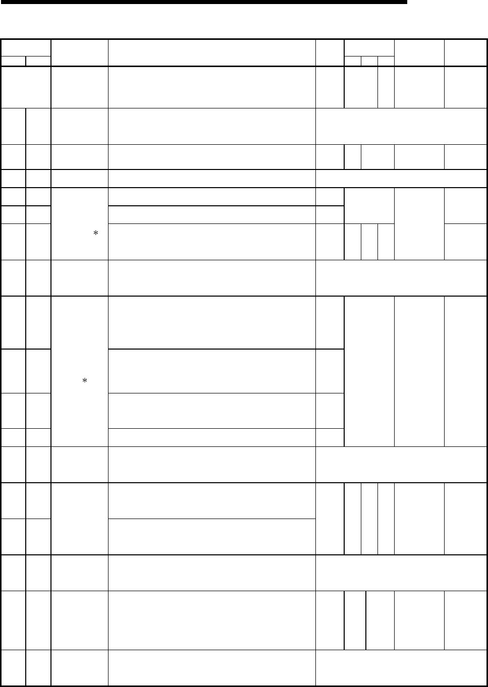
3 - 27 3 - 27
MELSEC-Q
3 SPECIFICATIONS
Address
Decimal (Hex) Applicable
protocol
CH1 CH2 Application Name Initial
value MC Non Bi
Registration
allowed/not
allowed
Reference
section
8206
(200EH)
For designation
of modem
function -3
Circuit disconnect wait time (PLC CPU watch use)
0000H to FFFFH: Wait time (unit: s) 0RW —Allowed
Section 8.4.4
Chapter 3 of
User's
Manual
(Application)
8207
(200FH)
8456 to
8463
(2108H
to
210FH)
Use prohibited System area —
Receive interrupt-issued designation
8208
(2010H)
8464
(2110H)
Interrupt
designation 0: Do not issue interrupt. 1: Issue interrupt. 0 — RW Allowed Chapter 4 of
User's Manual
(Application)
8209
(2011H)8465
(2111H)Use prohibited System area —
8210
(2012H)
8466
(2112H)
Transmission control start free area designation
64 to 4,095: transmission control start free area 64
8211
(2013H)
8467
(2113H)
Transmission control end free area designation
263 to 4096: transmission control end free area 263
RW
Chapter 7 of
User’s
Manual
(Application)
Non procedure and non reception monitoring time format
designation
8212
(2014H)
8468
(2114H)
For transmission
control
designation ( 1)
0: Format-0 1: Format-1
0—RW —
Allowed Chapter 6 of
User’s
Manual
(Application)
8213 to
8215
(2015H
to
2017H)
8469 to
8471
(2115H
to
2117H)
Use prohibited System area —
8216
(2018H)
8472
(2118H)
Communication data monitoring designation
0000H: No monitor/stopped monitor designation
0001H: Monitor start designation
0002H: Monitoring (Q series C24 is a set.)
1002H: Monitoring stopped (Q series C24 is set.)
100FH: Monitor setting error (Q series C24 is a set.)
0
8217
(2019H)
8473
(2119H)
Data optional designation
0: Off 1: On
Full stop designation (b0)
Timer 0 errors at occurrence stop designation (b2)
For system (b1), (b3) to (b15)
0
8218
(201AH)
8474
(211AH)
Monitor buffer head address designation
(400H to 1AFDH,2600H to 3FFDH)
CH1:
2600H
CH2:
3300H
8219
(201BH)
8475
(211BH)
Communication
data monitoring
function ( 1)
Monitor buffer size designation
(0003H to 1A00H)0D00H
RW Allowed
Chapter 16
of User’s
Manual
(Application)
8220 to
8223
(201CH
to
201FH)
8476 to
8479
(211CH
to
211FH)
Use prohibited System area —
User frame receive format designation (1st to 4th)
8224 to
8227
(2020H
to
2023H)
8480 to
8483
(2120H
to
2123H)
0: Format-0, 1: Format-1
8228 to
8231
(2024H
to
2027H)
8484 to
8487
(2124H
to
2127H)
For designation
of user frame
receiving method Exclusive format-1 received data count (1st to 4th)
0 or more: Exclusive format-1 received data count
0—RW —Allowed
Section
3.4.7
Chapter 11
of User's
Manual
(Application)
8232 to
8239
(2028H
to
202FH)
8488 to
8495
(2128H
to
212FH)
Use prohibited System area —
Transmission transparent code designation (2nd to 4th)
0000H
Other than 0000H
:No designation
:Designated (below)
8240 to
8248
(2030H
to
2038H)
8496 to
8504
(2130H
to
2138H)
For designation
of transparent
code • Transparent code (b0 to b7)
00H to FFH : Transparent code
• Additional code (b8 to b15)
00H to FFH : Additional code
0—RW Allowed
Section
3.4.5
Chapter 12
of User's
Manual
(Application)
8249 to
8255
(2039H
to
203FH)
8505 to
8511
(2139H
to
213FH)
Use prohibited System area —
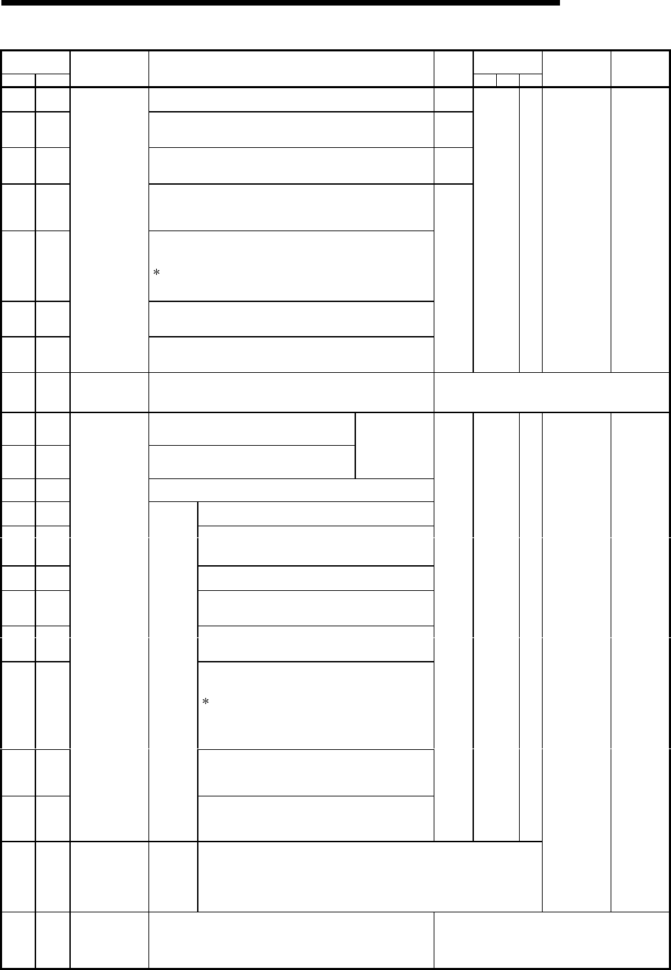
3 - 28 3 - 28
MELSEC-Q
3 SPECIFICATIONS
Address
Decimal (Hex) Applicable
protocol
CH1 CH2 Application Name Initial
value MC Non Bi
Registration
allowed/not
allowed
Reference
section
Cycle time units designation
8256
(2040H)8512
(2140H)0: 100 ms 1: s 2: min 2
Cycle time designation
8257
(2041H)8513
(2141H)0H : No designation
1H to FFFFH: PLC CPU monitoring cycle time 5H
PLC CPU monitoring function designation
0: Do not use the function. 1: Fixed cycle transmission
8258
(2042H)8514
(2142H)2: Condition agreement transmission 0
PLC CPU monitoring transmission measure designation
(for fixed cycle transmission)
8259
(2043H)8515
(2143H)0: Data transmission (device data and CPU status data)
1: Notification
8260
(2044H)8516
(2144H)
Transmission pointer designation (For fixed cycle transmission and
data transmission)
1 to 100: Output head point (send from the nth)
Send the user frames designated in the following transmission
frame No. designation areas from the designated pointer position.
(addresses: CH1 side = BAH to 11DH, CH2 side = 15AH to 1BDH)
Output count designation (for fixed cycle transmission and data
transmission)
8261
(2045H)8517
(2145H)1 to 100:Output count (designate the number of frame transmissions.)
Data No. for connection designation (for fixed cycle transmission
and notification)
8262
(2046H)8518
(2146H)
For designation
of PLC CPU
monitoring
function
0BB8H to 0BD5H, 8001H to 801FH: Data No. for connection
0
R — Allowed
Chapter 2
of User's
Manual
(Application)
8263 to
8268
(2047H to
204CH)
8519 to
8524
(2147H to
2149H)
Use prohibited System area —
Number of registered word blocks designation
8269
(204DH)8225
(214DH)0 : No designation
1 to 10: Number of blocks of word devices
Number of registered bit blocks designation
8270
(204EH)8226
(214EH)0 : No designation
1 to 10: Number of blocks of bit devices
It is possible to
designate a
maximum of 10
blocks in total.
PLC CPU abnormal monitoring designation
8271
(204FH)8527
(214FH)0: Do not monitor. 1: Monitor.
Monitoring device designation
8272
(2050H)8528
(2150H)90H to CCH: Device code
Head device No. designation
8273 to
8274
(2051H to
2052H)
8529 to
8530
(2151H to
2152H)
0 or more: Head device No.
Read point designation
8275
(2053H)8531
(2153H)1 or more: Number to read points
Monitoring condition designation (judgment condition
designation)
8276
(2054H)8532
(2154H)1 or more: Monitoring condition
Monitoring condition value designation
8277
(2055H)8533
(2155H)At bit device 0: OFF 1: ON
At word device 0 to FFFFH: Monitoring condition value
8278
(2056H)8534
(2156H)
Transmission pointer designation (for condition
agreement transmission and data transmission)
1 to 100: Output head point (send from nth)
Send the user frames designated in the following
transmission frame No. designation areas from the
designated pointer position.
(address: CH1 side = BAH to 11DH, CH2 side = 15AH
to 1BDH)
Output count designation (for condition agreement
transmission and data transmission)
8279
(2057H)8535
(2157H)1 to 100: Output count (designate the number
of frame transmissions)
Data No. for connection designation (for condition
agreement transmission and notification)
8280
(2058H)8536
(2158H)
For designation
of PLC CPU
monitoring
function No. 1
block
monitoring
device
0BB8H to 0BD5H, 8001H to 801FH: Data No. for
connection
0R—
8281 to
8361
(2059H to
20A9H)
8537 to
8617
(2159H to
21A9H)
For designation
of PLC CPU
monitoring
function
Block
monitoring
devices
No. 2 to
10
The structure of each area is the same as the first block monitoring device area
See *2 for the details of each area.
Allowed
Chapter 2
of User's
Manual
(Application)
8362 to
8421
(20AAH to
20E5H)
8618 to
8677
(21AAH to
21E5H)
Use prohibited System area —
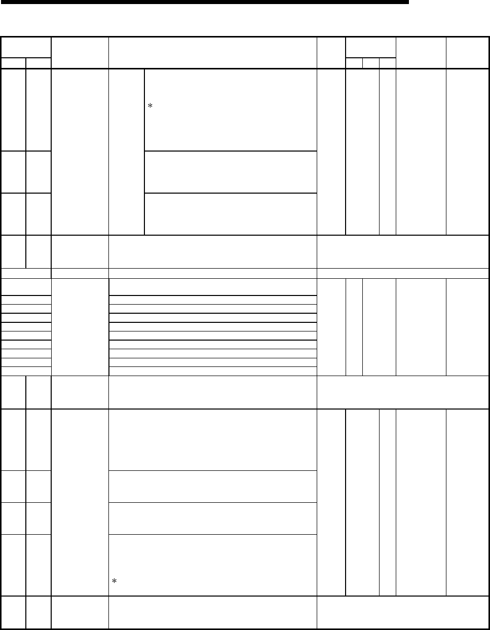
3 - 29 3 - 29
MELSEC-Q
3 SPECIFICATIONS
Address
Decimal (Hex)
Applicable
protocol
CH1 CH2
Application Name Initial
value MC Non Bi
Registration
allowed/not
allowed
Reference
section
8422
(20E6H)
8678
(21E6H)
Transmission pointer designation (for condition
agreement transmission)
1 to 100: Output head point (send from nth)
Send the user frames designated in the following
transmission frame No. designation areas from the
designated pointer position.
(address: CH1 side = BAH to 11DH, CH2 side =
15AH to 1BDH)
Output count designation (for condition agreement
transmission)
8423
(20E7H)
8679
(21E7H)1 to 100: Output count (designate the number of
frame transmissions)
Data No. for connection designation (for condition
agreement transmission and notification)
8424
(20E8H)
8680
(21E8H)
For designation
of PLC CPU
monitoring
function
CPU
abnormal
monitoring
designation
0BB8H to 0BD5H, 8001H to 801FH: Data No. for
connection
0 R — Allowed
Chapter 2
of User's
Manual
(Application)
8425 to
8447
(20E9H to
20FFH)
8681 to
8703
(21E9H to
21FFH)
Use prohibited System area —
8448 (2100H)Use Prohibited System area —
8449 (2101H)Data No. for callback designation 1
0BB8H to 0BD5H, 8001H to 801FH: Data number for callback.
8450 (2102H)Data No. for callback designation 2
8451 (2103H)Data No. for callback designation 3
8452 (2104H)Data No. for callback designation 4
8453 (2105H)Data No. for callback designation 5
8454 (2106H)Data No. for callback designation 6
8455 (2107H)Data No. for callback designation 7
8456 (2108H)Data No. for callback designation 8
8457 (2109H)Data No. for callback designation 9
8458 (210AH)
For callback
function
Data No. for callback designation 10
0RW— Allowed
Section
8.4.4
Chapter 3 of
User’s
Manual
(Application)
8704 to
8707
(2200H to
2203H)
8960 to
8963
(2300H to
2303H)
Use prohibited System area —
8708
(2204H)
8964
(2304H)
PLC CPU monitoring function operation status
0: Not executed (waiting for registration of PLC CPU monitoring)
1: Wait for PLC CPU monitoring time
(waiting to access PLC CPU)
2: Accessing PLC CPU
3: Sending monitoring results
PLC CPU monitoring function execution result (current)
8709
(2205H)
8965
(2305H)0: Normal completion
1 or more: Abnormal completion (error code)
PLC CPU monitoring function number of transmission
8710
(2206H)
8966
(2306H)0: Not executed
1 or more: Number of transmissions
8711
(2207H)
8967
(2307H)
PLC CPU
monitoring
function
Monitoring condition arrival block No.
0 : The monitoring condition is not enabled for any block
1 to 10: Registration order of word/bit block (nth)
4096 : CPU abnormal monitoring block
The latest block No. for which monitoring condition is enabled is
stored.
0 R — Not allowed
Chapter 2
of User's
Manual
(Application)
8712 to
8954
(2208H to
22FAH)
8968 to
9215
(2308H to
23FFH)
Use prohibited System area —
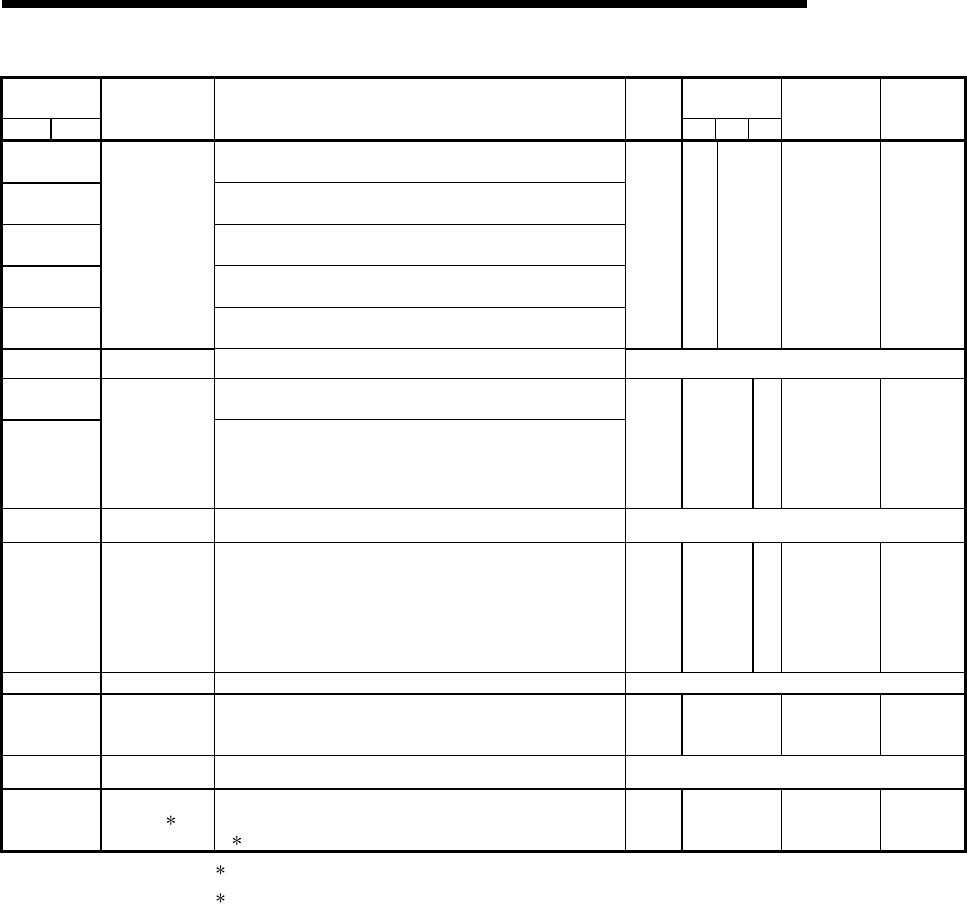
3 - 30 3 - 30
MELSEC-Q
3 SPECIFICATIONS
Address
Decimal (Hex)
Applicable
protocol
CH1 CH2
Application Name Initial
value MC Non Bi
Registration
allowed/not
allowed
Reference
section
8944 (22F0H)Callback permit accumulated count
0 or more : Accumulated count
8945 (22F1H)Callback denial accumulated count
0 or more : Accumulated count
8946 (22F2H)Auto (callback) connection permit accumulated count
0 or more : Accumulated count
8947 (22F3H)Auto (callback) connection denial accumulated count
0 or more : Accumulated count
8948 (22F4H)
For callback
function
Accumulated count of callback receive procedure cancel
0 or more : Accumulated count
0RW—Not allowed
Section
8.6.2
Chapter 3 of
User's
Manual
(Application)
8949 to 8954
(22F5H to 22FAH)Use prohibited System area —
8955 (22FBH)Accumulated count of unlock process normal completion
0 or more: Accumulated count of normal completion
8956(22FCH)
For the remote
password
function
Accumulated count of unlock process abnormal completion
processing
0 or more: Accumulated count of abnormal completion
0RW
—Not allowed
Section
5.1.5
Section
8.6.2
Chapter 3 of
User's
Manual
(Application)
8957 to 8958
(22FDH to 22FEH)Use prohibited System area —
8959(22FFH)
For the remote
password
function
Accumulated count of lock process based on circuit disconnection
0 or more: Accumulated count of lock process based on circuit
disconnection
0RW
—Not allowed
Section
5.1.5
Section
8.6.2
Chapter 3 of
User's
Manual
(Application)
9216(2400H)Use prohibited System area —
9217(2401H)
For flash ROM
write count
housing
Flash ROM write count
0 to 1000: Write count 0 R Not allowed —
9218 to 9427
(2402H to 25FFH)Use prohibited System area —
9728 to 16383
(2600H to 3FFFH)For user ( 1)
User free area 2 (6656 words)
(Transmission/receiving data monitoring function default buffer)
Usage is determined by the user.
0 RW Not allowed —
1 Only QJ71C24N (-R2/R4) is usable. (System area when using QJ71C24 (-R2)
2 The following tables show the areas of block monitoring devices No. 1 to 10 (CH1
side: 8272 to 8361 (2050H to 20A9H), CH2 side: 8528 to 8617 (2150H to 21A9H)),
which are assigned for designating the PLC CPU monitoring function.

3 - 31 3 - 31
MELSEC-Q
3 SPECIFICATIONS
[CH1 side buffer memory address: decimal (hexadecimal)]
nth block monitoring device
12345678910 Name
8272
(2050H)
8281
(2059H)
8290
(2062H)
8299
(206BH)
8308
(2074H)
8317
(207DH)
8326
(2086H)
8335
(208FH)
8344
(2098H)
8353
(20A1H)Monitoring device designation
8273 to
8274
(2051H to
2052H)
8282 to
8283
(205AH to
205BH)
8291 to
8292
(2063H to
2064H)
8300 to
8301
(206CH to
206DH)
8309 to
8310
(2075H to
2076H)
8318 to
8319
(207EH to
207FH)
8327 to
8328
(2087H to
2088H)
8336 to
8337
(2090H to
2091H)
8345 to
8346
(2099H to
209AH)
8354 to
8355
(20A2H to
20A3H)
Head device No. designation
8275
(2053H)
8284
(205CH)
8293
(2065H)
8302
(206EH)
8311
(2077H)
8320
(2080H)
8329
(2089H)
8338
(2092H)
8347
(209BH)
8356
(20A4H)Designation of number of points read
8376
(2054H)
8385
(205DH)
8294
(2066H)
8303
(206FH)
8312
(2078H)
8321
(2081H)
8330
(208AH)
8339
(2093H)
8348
(209CH)
8357
(20A5H)
Monitoring condition designation (Judgment
condition designation)
8277
(2055H)
8286
(205EH)
8295
(2067H)
8304
(2070H)
8313
(2079H)
8322
(2082H)
8331
(208BH)
8340
(2094H)
8349
(209DH)
8358
(20A6H)Monitoring condition value designation
8278
(2056H)
8287
(205FH)
8296
(2068H)
8305
(2071H)
8314
(207AH)
8323
(2083H)
8332
(208CH)
8341
(2095H)
8350
(209EH)
8359
(20A7H)
Transmission pointer designation (for
conditional transmission, data transmission)
8279
(2057H)
8288
(2060H)
8297
(2069H)
8306
(2072H)
8315
(207BH)
8324
(2084H)
8333
(208DH)
8342
(2096H)
8351
(209FH)
8360
(20A8H)
Designation of number of outputs (for
conditional transmission, data transmission)
8280
(2058H)
8289
(2061H)
8298
(206AH)
8307
(2073H)
8316
(207CH)
8325
(2085H)
8334
(208EH)
8343
(2097H)
8352
(20A0H)
8361
(20A9H)
Designation of data No. for connection
(for conditional transmission and notification)
[CH2 side buffer memory address: decimal (hexadecimal)]
nth block monitoring device
12345678910 Name
8528
(2150H)
8537
(2159H)
8546
(2162H)
8555
(216BH)
8564
(2174H)
8573
(217DH)
8582
(2186H)
8591
(218FH)
8600
(2198H)
8609
(21A1H)Monitoring device designation
8529 to
8530
(2151H to
2152H)
8538 to
8539
(215AH to
215BH)
8547 to
8548
(2163H to
2164H)
8556 to
8557
(216CH to
216DH)
8565 to
8566
(2175H to
2176H)
8574 to
8575
(217EH to
217FH)
8583 to
8584
(2187H to
2188H)
8592 to
8593
(2190H to
2191H)
8601 to
8602
(2199H to
219AH)
8610 to
8611
(21A2H to
21A3H)
Head device No. designation
8531
(2153H)
8540
(215CH)
8549
(2165H)
8558
(216EH)
8567
(2177H)
8576
(2180H)
8585
(2189H)
8594
(2192H)
8603
(219BH)
8612
(21A4H)Designation of number of points read
8532
(2154H)
8541
(215DH)
8550
(2166H)
8559
(216FH)
8568
(2178H)
8577
(2181H)
8586
(218AH)
8595
(2193H)
8604
(219CH)
8613
(21A5H)
Monitoring condition designation (Judgment
condition designation)
8533
(2155H)
8542
(215EH)
8551
(2167H)
8560
(2170H)
8569
(2179H)
8578
(2182H)
8587
(218BH)
8596
(2194H)
8605
(219DH)
8614
(21A6H)Monitoring condition value designation
8534
(2156H)
8543
(215FH)
8552
(2168H)
8561
(2171H)
8570
(217AH)
8579
(2183H)
8588
(218CH)
8597
(2195H)
8606
(219EH)
8615
(21A7H)
Transmission pointer designation (for
conditional transmission, data transmission)
8535
(2157H)
8544
(2160H)
8553
(2169H)
8562
(2172H)
8571
(217BH)
8580
(2184H)
8589
(218DH)
8598
(2196H)
8607
(219FH)
8616
(21A8H)
Designation of number of outputs (for
conditional transmission, data transmission)
8536
(2158H)
8545
(2161H)
8554
(216AH)
8563
(2173H)
8572
(217CH)
8581
(2185H)
8590
(218EH)
8599
(2197H)
8608
(21A0H)
8617
(21A9H)
Designation of data No. for connection
(for conditional transmission and notification)
3 Only the QJ71C24N(-R2/R4) whose first 5 digits of the serial No. are 06062 or
later is applicable. (System area for other than the one described on the left)
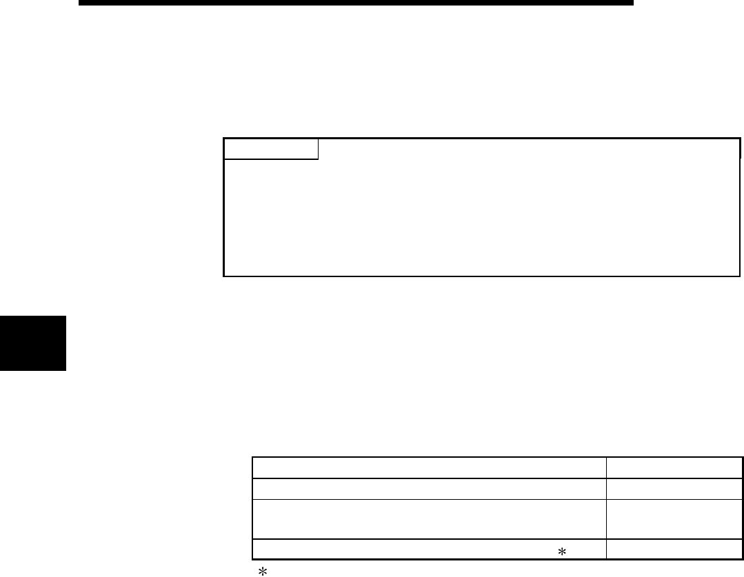
4 - 1 4 - 1
MELSEC-Q
4 SETTINGS AND PROCEDURES PRIOR TO OPERATION
4
4 SETTINGS AND PROCEDURES PRIOR TO OPERATION
This chapter explains the settings and procedures required before starting a system
that uses the Q series C24.
POINT
(1) When using the Q series C24, please read the safety precautions at the
beginning of this manual.
(2) The installation and setup methods of the Q series C24 are the same as those
for CPU modules.
(3) For module installation and setup, see the user's manual for the PLC CPU
used.
4.1 Handling Precautions
The following explains the precautions for handling the Q series C24:
(1) Do not drop the module or subject it to heavy impact since it is made of resin.
(2) Tighten the module terminal and fixing screws within the specified tightening
torque range as follows:
Screw location Tightening torque range
RS-422/485 terminal block terminal screws (M3 screw) 0.42 to 0.58 N · m
RS-422/485 plug-in connector socket terminal screw for
QJ71C24N-R4 (M2 screw) 0.20 to 0.25 N · m
Module fixing screw (normally not required) (M3 screw) ( 1) 0.36 to 0.48 N · m
1 A module can be easily fixed to a base unit using the hooks in the upper part
of the module. However, it is recommended that the module be fixed using
the module mounting screws when it is used in a place subject to vibration or
impact.
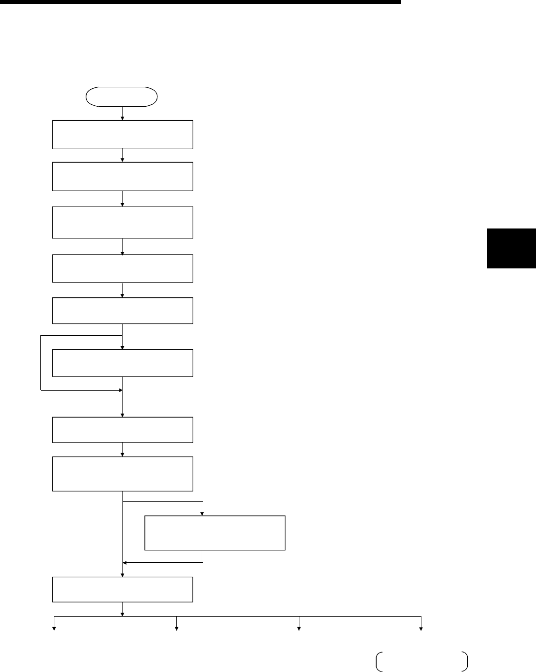
4 - 2 4 - 2
MELSEC-Q
4 SETTINGS AND PROCEDURES PRIOR TO OPERATION
4
4.2 Settings and Procedures Prior to Operation
The outline of the procedure before operation is shown below.
Start
Check which functions and
specifications are to be used
Connect the module with an
external device using a cable
Connect GX Developer and
QCPU with a cable
Perform various settings with
GX Developer
Perform individual station tests
with GX Developer
Perform a loopback test from the
external device
Set an operation mode with
GX Developer
Perform auto refresh setting
with GX Configurator-SC
Change setting values to use various
functions with GX Configurator-SC
Transmission and receive data
• Connection of the Q series C24 and an external device
• See Section 4.4 in this manual.
• I/O assignment setting of the Q series C24
• Setting of operation mode and transmission specifications for
the Q series C24 and the external device
• See Section 4.5 in this manual.
• ROM/RAM/switch tests of the Q series C24
• Self-loopback test of the Q series C24
• See Section 4.7 in this manual
• When communication using the MC protocol is possible between
the Q series C24 and the external device, set the operation mode for
MC protocol communication and perform a loopback test.
• See Section 4.8 in this manual.
• Set an operation mode for the data communication system
between the Q series C24 and the external device.
• See Section 4.5.2 in this manual.
• A setting that automatically refreshes the status of the Q series C24
and error data to the GX Configurator-SC device.
• See Sections 4.6 and 8.3 in this manual.
• It is possible to change setting values for
various functions, including special functions.
• See the explanation for each function in
the applicable sections and manuals.
• See Chapter 8.
• Transmission and reception for the data communication system
• See the explanation for each function in the applicable sections
and manuals.
C
ommunication using non
procedure protocol
(see Chapter 6)
Communication using MC protocol
(see the Reference Manual)
Communication using
special functions
Communication using
bidirectional protocol
(see Chapter 7) see the User's
Manual
(
A
pp
lication
)
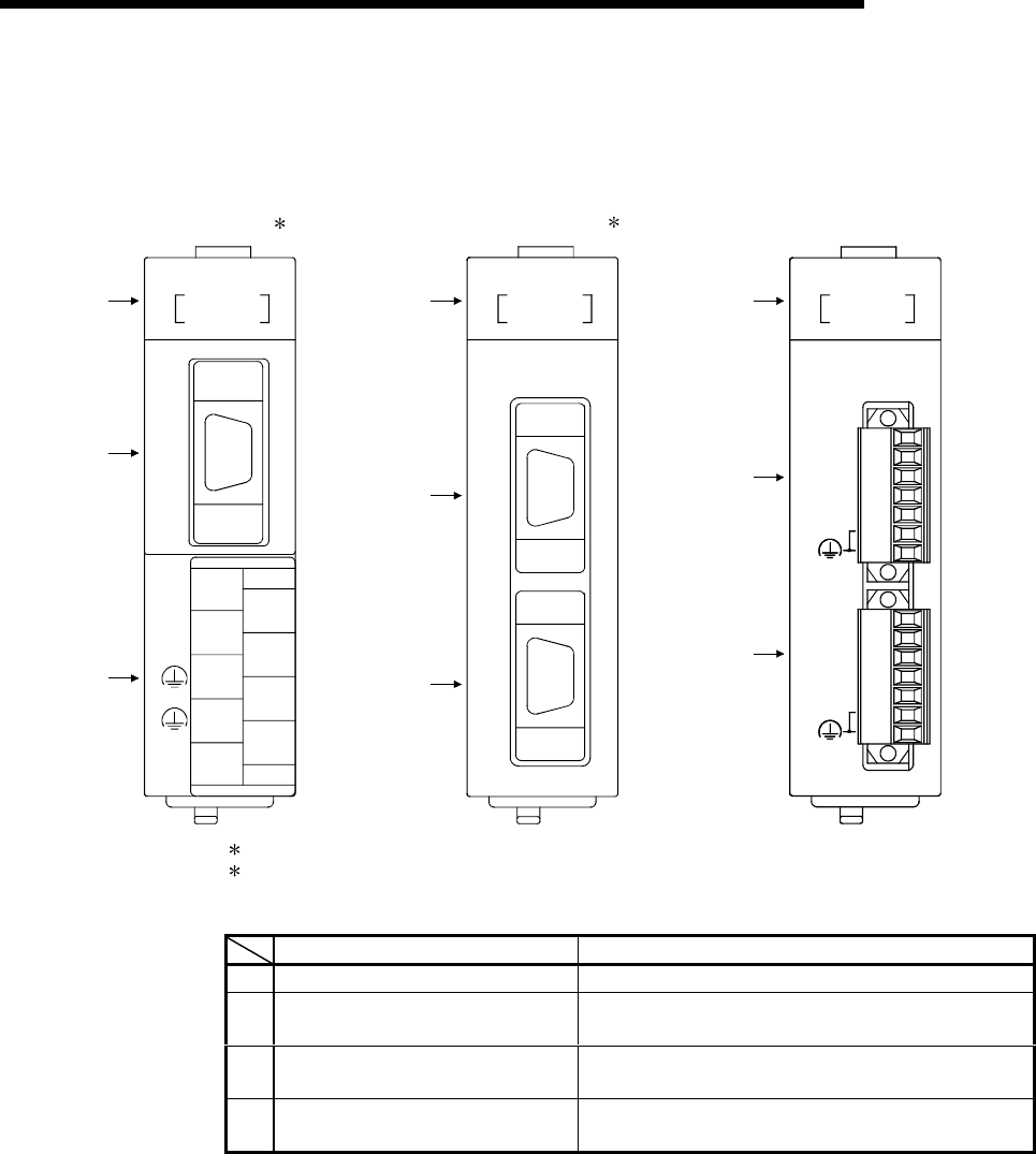
4 - 3 4 - 3
MELSEC-Q
4 SETTINGS AND PROCEDURES PRIOR TO OPERATION
4.3 Part Names and Functions
Part names of Q series C24 are shown below.
CH2
CH1
RS-422/485
RS-422/485
QJ71C24N-R4
(FG)
SG
RDB
RDA
SDB
SG
RDB
RDA
SDB
SDA
SDA
(FG)
QJ71C24N-R4
RUN
RD
NEU.
SD
NEU.
RD
SD
CH1 CH2
ERR.
1) 1) 1)
2
)
3)
2)
2)
4)
4)
( 1)
QJ71C24N-R2
RS-232
RS-232
CH2
CH1
QJ71C24N-R2
RUN
RD
NEU.
SD
NEU.
RD
SD
CH1 CH2
ERR.
4
2
5
3
1
6
7
(FG)
(FG)
RS-232
/485
RS-422
CH2
RDB
RDA
SDB
SG
SDA
CH1
QJ71C24N
RUN
RD
NEU.
SD
NEU.
RD
SD
CH1 CH2
ERR.
QJ71C24N
QJ71C24 ( 2)
QJ71C24N-R2
QJ71C24-R2
QJ71C24N-R4
1 The external diagrams of the QJ71C24 are the same as QJ71C24N (except for the model name).
2 The external diagrams of the QJ71C24-R2 are the same as QJ71C24N-R2 (except for the model
name).
Name Contents
1) Display LED Display LED (For details, see (1).)
2) RS-232 interface RS232 interface for serial communication with external
devices (D-Sub 9 pin)
3) RS-422/485 interface RS422/485 interface for serial communication with external
devices (2-piece terminal block)
4) RS-422/485 interface RS422/485 interface for serial communication with external
devices (2-piece plug-in socket block)
4 - 4 4 - 4
MELSEC-Q
4 SETTINGS AND PROCEDURES PRIOR TO OPERATION
(1) LED display list
ERR.
CH2
CH1 SD
RD
NEU.
SD
NEU.
RD
RUN
QJ71C24N
ERR.
CH2
CH1 SD
RD
NEU.
SD
NEU.
RD
RUN
QJ71C24N-R2
ERR.
CH2
CH1 SD
RD
NEU.
SD
NEU.
RD
RUN
QJ71C24N-R4
Compatible protocol
CH LED Display contents On/flashing Off MC Non-procedural Bidirectional
RUN Normal operation display Normal Faulty or reset
—ERR Error display ( 1) Error has occurred Normal Valid
NEU
(3)
Neutral status on the CH1
side display ( 2)
Waiting for MC command
message to be received
MC command message
being received Valid Invalid (Off)
SD Transmission status
display Data being transmitted Data not transmitted
CH1
RD Reception status display Data being received Data not received
Valid
NEU
(3)
Neutral status on the CH2
side display ( 2)
Waiting for MC command
message to be received
MC command message
being received Valid Invalid (Off)
SD Transmission status
display Data being transmitted MC command message
not transmitted
CH2
RD Reception status display Data being received MC command message
not received
Valid
1 This LED comes on when an error occurs at Q series C24 hardware or during data communication.
2 This LED displays the data communication status via MC protocol. (see chapter 10.)
On: Waiting for the command message to be received from the external device.
Off: Processing the command message received from the external device.
3 This LED can be made valid also when "GX Developer connection" (0H) is specified in communication
protocol setting.
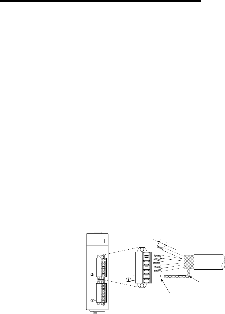
4 - 5 4 - 5
MELSEC-Q
4 SETTINGS AND PROCEDURES PRIOR TO OPERATION
4.4 External Wiring
This section explains wiring between the Q series C24 and external device.
As the wiring precautions, external wiring which is resistant to the effects of external
noise is a prerequisite for reliable system operation and full use of the Q series C24
function.
(1) Ground the shield at only one point.
(2) When connecting with an external device using an RS-232 line, use a connector
shell as specified in Section 3.2.1 on the Q series C24 end.
(3) When connecting with an external device using an RS-422/485 cable, be sure to
note the following.
(a) QJ71C24N and QJ71C24
1) Use the RS-422/485 cable recommended in section 3.3.2.
2) The RS-422/485 interface terminal block uses M3 terminal screws.
Use suitable crimp-on terminals for the terminals.
(b) QJ71C24N-R4
1) Use the RS-422/485 cable recommended in section 3.3.2.
Be sure to strip the outer insulation layer by 7 mm before connecting
the cable to the plug-in socket block.
2) When connecting the braided shield wire inside the RS-422/485 cable,
use the plate terminals included with the product. The braided shield
wire can be connected without the plate terminal. Four plate terminals
are included to connect the FG terminals of both stations. (see section
4.4.2.(6).)
3) When connecting the plug-in socket block to the QJ71C24N-R4, be
sure to confirm the layout of the socket block, and then insert it into the
RS-422/485 connector on the QJ71C24N-R4.
SG
RDB
RDA
SDB
SDA
(FG)
Plate terminal
(included with product)
Braided shield wire
7mm
(0.28 in.)
CH2
CH1
RS-422/485
RS-422/485
QJ71C24N-R4
(FG)
SG
RDB
RDA
SDB
SG
RDB
RDA
SDB
SDA
SDA
(FG)
QJ71C24N-R4
RUN
RD
NEU.
SD
NEU.
RD
SD
CH1 CH2
ERR.
(4) Connect the external device according to its specifications.
(5) See Appendix 5 for the bend radius of the connection cable.
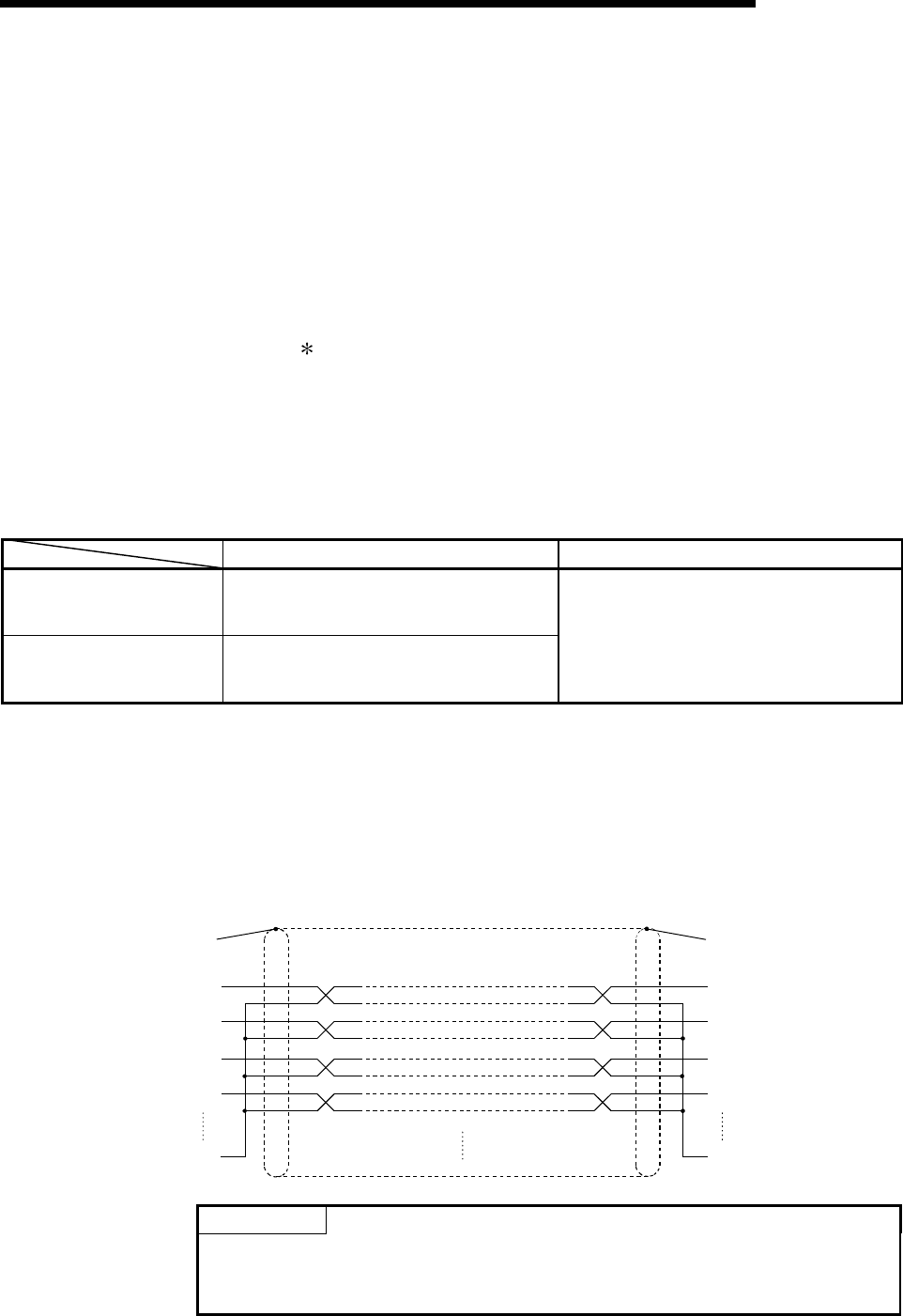
4 - 6 4 - 6
MELSEC-Q
4 SETTINGS AND PROCEDURES PRIOR TO OPERATION
4.4.1 Connecting the RS-232 interface (full-duplex communications)
The following shows the connection precautions and connection examples when using
the Q series C24 RS-232 interface for full-duplex communications.
(1) Connection precautions
(a) For further information about the following items, see the explanation in the
applicable section in the User's Manual (Application).
• Controlling the communication on the Q series C24 side by the external
device side using the CD signal of the RS-232 interface.
This is affected by the "RS-232 CD terminal check setting" in "CHn
transmission control and others system setting change" screen on GX
Configurator-SC.
• Performing half-duplex communication using specifications on the external
device side (an example of such a connection is shown in this section).
• Using modem functions.
(b) The connection cable FG signal and shield are connected as follows.
Connection on the Q series C24 side Notes
Connection cable FG signal Connect to the Q series C24 connector
housing
Connection cable shield Connect to the external device FG terminal
or the Q series C24 connector housing
Do not short the communication cable FG
signal and the SG signal.
When the FG signal and the SG signal are
connected inside the external device, do not
connect the FG signal to the Q series C24.
(c) When normal data communication is not obtained due to external noise,
perform the wiring as follows:
1) Connect the FG terminals on the external device and the Q series C24
using the shield of the connection cable.
2) Signals other than SG should be connected with SG signals in the
twisted pair.
FG
RD
SD
DTR
DSR
SG
RD
SD
DTR
DSR
SG
To Connector
housing
Q series C24 Shield (External device)
POINT
When using an RS-232 to RS-422 converter to connect the external device and the
Q series C24, use a converter that is compatible with the external device and PLC
CPU system configuration (1:1).
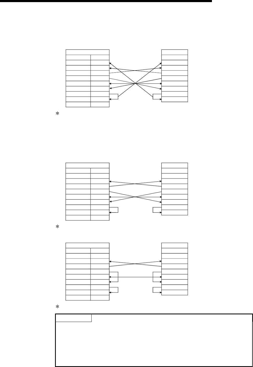
4 - 7 4 - 7
MELSEC-Q
4 SETTINGS AND PROCEDURES PRIOR TO OPERATION
(2) Connection examples
(a) Connection example with an external device capable of turning on and off the
CD signal (No. 1 pin)
Q series C24
Pin No.
CD
RD(RXD)
SG
DSR(DR)
1
2
3
4
5
6
7
8
9
External device
Signal name Signal name
SD(TXD)
DTR(ER)
RS(RTS)
CS(CTS)
RI(CI)
CD
RD(RXD)
SG
DSR(DR)
SD(TXD)
DTR(ER)
RS(RTS)
CS(CTS)
The CD terminal check setting is set according to the specification of the external
device. When wiring shown above, DTR/DSR control or DC code control may be
performed.
(b) Connection example with an external device not capable of turning on and off
the CD signal (No. 1 pin)
1) Connection example 1
Q series C24
Pin No.
CD
RD(RXD)
SG
DSR(DR)
1
2
3
4
5
6
7
8
9
External device
Signal name Signal name
SD(TXD)
DTR(ER)
RS(RTS)
CS(CTS)
RI(CI)
CD
RD(RXD)
SG
DSR(DR)
SD(TXD)
DTR(ER)
RS(RTS)
CS(CTS)
When wiring shown above, DTR/DSR control or DC code control may be performed.
2) Connection example 2
Q series C24
Pin No.
CD
RD(RXD)
SG
DSR(DR)
1
2
3
4
5
6
7
8
9
External device
Signal name Signal name
SD(TXD)
DTR(ER)
RS(RTS)
CS(CTS)
RI(CI)
CD
RD(RXD)
SG
DSR(DR)
SD(TXD)
DTR(ER)
RS(RTS)
CS(CTS)
When wiring shown above, DC code control may be performed.
POINT
If the PLC CPU and an external device cannot be communicated, try to perform data
communication as a connection test, using the wiring connection as shown in
Connection example 2.
If data can be communicated using the wiring connection shown in Connection
example 2, rewire after checking the interface specifications on the external device
side.
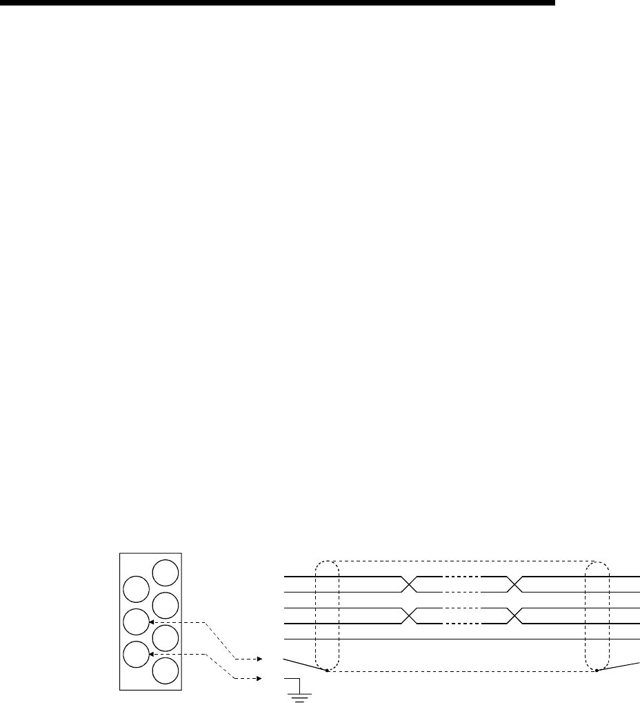
4 - 8 4 - 8
MELSEC-Q
4 SETTINGS AND PROCEDURES PRIOR TO OPERATION
4.4.2 Connecting the RS-422/485 interface
The following shows the connection precautions and connection examples when using
the Q series C24 RS-422/485 interface.
(1) Connection precautions
(a) When connecting the Q series C24 SG and FG signals to the external
device, connect them according to the specifications of the external device.
(b) Connect the shield of the connection cable to the FG terminal on either of
the connected devices.
If normal data communication is not obtained due to external noise even if
wiring is made as shown above, perform wiring as follows:
1) Connect between the FG of both stations with the shield of the
connection cable.
On the external device side, however, follow the instruction manual of
the external device.
Be sure to use the plate terminals included with the product when
connecting the braided shield wire to the QJ71C24N-R4.
2) Connect the (FG) of the Q series C24 side to the FG terminal at the power
supply module of the station which has the Q series C24 is installed, or to
the FG terminal of the control panel on which the Q series C24 PLC is
installed.
3) Connect nnA and nnB of each signal in the connection cable as a pair.
Correspondance of the RS-422/485 terminal block and signal location.
Shield
Q series C24 External device
SDA
SDB
RDA
RDB
SG
(FG)
(FG)
SDA
SDB
RDA
RDB
SG
FG
SG
FG
FG
SDA
SDB
RDB
RDA
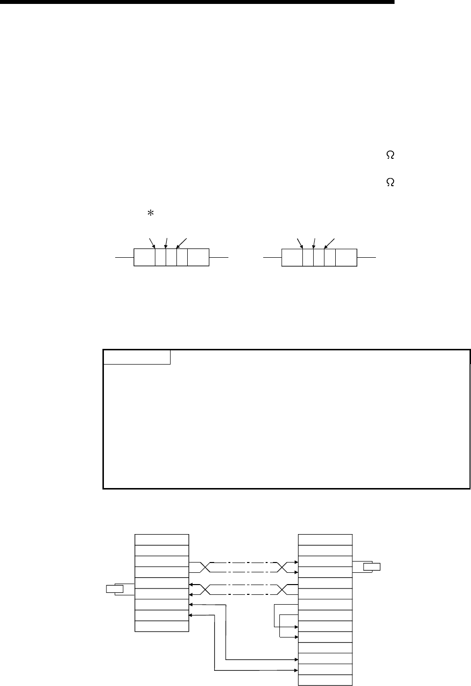
4 - 9 4 - 9
MELSEC-Q
4 SETTINGS AND PROCEDURES PRIOR TO OPERATION
(c) Terminal resistor must be set (or connected) for the station of both ends on
the circuit.
Match the Q series C24 to the specifications of the external device and
connect a terminal resistor (packed with the Q series C24) according to this
section.
Connect, or set a terminal resistor at the external device according to the
instruction manual of the external device.
(The terminal resistor to connect to the Q series C24)
• When communications performed using RS-422, "330 1/4 W" resistor is
connected.
• When communications performed using RS-485, "110 1/2 W" resistor is
connected.
How to discriminate between the terminating resistors
330 Ω110 Ω
Brown
Orange Orange Brown Brown Brown
(d) If data cannot be communicated with the external device at all, the polarity of
the external device could be wrong and should be checked again. If the
polarities of the Q series C24 and the external device do not match, reverse
the polarity of each signal on either device side and connect the devices with
the cable; this may enable the data to be communicated.
POINT
(1) For terminal resistor setting/connection described in this section, when the RS-
232 to RS-422 converters or similar device is used at the external device at
both ends of the circuit, a terminal resistor must be set, or connected, at the
converter.
(2) When using the RS-232C to RS-422 converters to connect the external
devices and the Q series C24, use a converter that is compatible with the
external device and PLC CPU system configuration (1:1, 1:n, m:n).
(3) Device connected to the Q series C24 RS-422/485 interface must be
standardized as RS-422 or RS-485, including 1:n and m:n connections.
(2) Connection examples
(a) External device and Q series C24 with 1:1 system configuration
Terminal
resistor R
R
Q series C24
Signal name
SDA
SDB
RDA
RDB
External device
RDA
RDB
SDA
SDB
RSA
RSB
CSA
CSB
SG
FG
SG
FG
FG
Terminal
resistor
Signal name
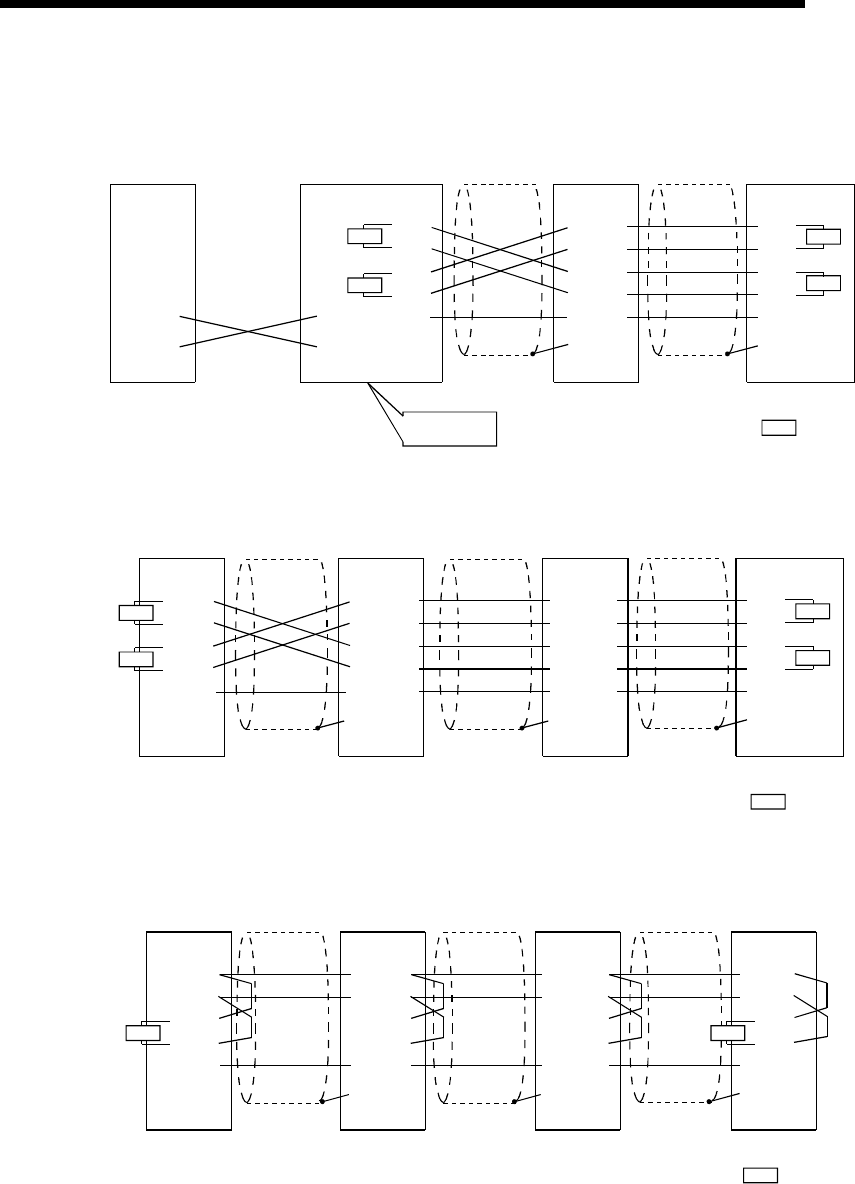
4 - 10 4 - 10
MELSEC-Q
4 SETTINGS AND PROCEDURES PRIOR TO OPERATION
(b) External device and Q series C24 with 1:n (multidrop) system configuration
1) Connection example
Terminal
resistor
R
R
R
R
R
Linked
operation
SDA
SDB
RDA
RDB
SG
FG
SDA
SDB
RDA
RDB
SG
FG
SDA
SDB
RDA
RDB
SG
FG
SD
RD
SD
RD
External device C24 1) C24 2) C24n
RS-422/485
cable
RS-422/485
cable
RS-232
2) Connection example 2
Terminal
resistor
R
R
R
SDA
SDB
RDA
RDB
SG
FG
SDA
SDB
RDA
RDB
SG
FG
External device C24 1) C24 2) C24n
RS-422/485
cable
RS-422/485
cable
SDA
SDB
RDA
RDB
SG
FG
R
RSDA
SDB
RDA
RDB
SG
FG
RS-422/485
cable
(c) External device and Q series C24 with n:1 (multidrop) system configuration
Terminal
resistor
R
SDA
SDB
RDA
RDB
SG
FG
External device 1) C24 1)
RS-422/485
cable
RS-422/485
cable
SDA
SDB
RDA
RDB
SG
FG
R
SDA
SDB
RDA
RDB
SG
FG
SDA
SDB
RDA
RDB
SG
FG
RS-422/485
cable
External device 2) External device n
R
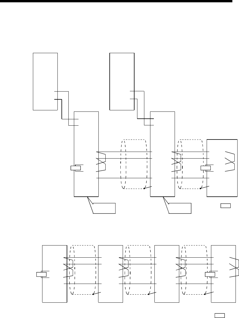
4 - 11 4 - 11
MELSEC-Q
4 SETTINGS AND PROCEDURES PRIOR TO OPERATION
(d) External device and Q series C24 with m:n (multidrop) system configuration
1) Connection example 1
Terminal
resistor
R
SDA
SDB
RDA
RDB
SG
FG
External device 1)
C24n
RS-422/485
cable
RS-422/485
cable
SD
RD
SDA
SDB
RDA
RDB
SG
FG
R
SD
RD
SDA
SDB
RDA
RDB
SG
FG
SD
RD
SD
RD
RS-232 RS-232
Linked
operation
External device 2)
C24 1) C24 2)
Linked
operation
R
2) Connection example 2
Terminal
resistor
R
SDA
SDB
RDA
RDB
SG
FG
External device 1) C24 1) C24n
RS-422/485
cable
RS-422/485
cable
SDA
SDB
RDA
RDB
SG
FG
R
SDA
SDB
RDA
RDB
SG
FG
SDA
SDB
RDA
RDB
SG
FG
RS-422/485
cable
R
External device 2)
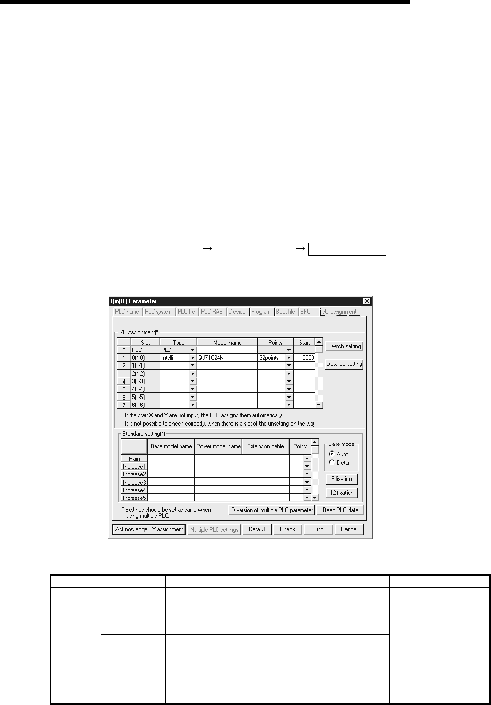
4 - 12 4 - 12
MELSEC-Q
4 SETTINGS AND PROCEDURES PRIOR TO OPERATION
4.5 Settings for GX Developer
This chapter explains various settings via GX Developer that allow the Q series C24 to
perform data communication with external devices.
See Section 3.3.3 of the User's Manual (Application) for how to perform the remote
password setting.
4.5.1 I/O assignment settings
[Setting purpose]
The I/O assignment settings perform the settings for the types of modules to be
mounted on a base unit, the range of input/output signals, and switches of the Q
series C24.
[Startup procedure]
[GX Developer] [PLC parameters] I/O assignment .
For screen display, see the GX Developer Operating Manual.
[Setting screen]
[Display description]
Item name Setting for item Remarks
Type Select "intelli."
Model name Enter the module model name to be mounted.
(Example: QJ71C24N)
Points Select 32 points.
Start XY Enter the start I/O signal (Hexadecimal) for the target module.
Switch setting Set the communication rate, transmission specifications,
communication protocol, etc. See Section 4.5.2.
I/O
assignment
Detailed setting Select the control PLC of the Q series C24 when a multiple
CPU system is employed.
Multiple CPU settings Select when using a multiple CPU system.
See QCPU User's Manual
(Multiple CPU System)
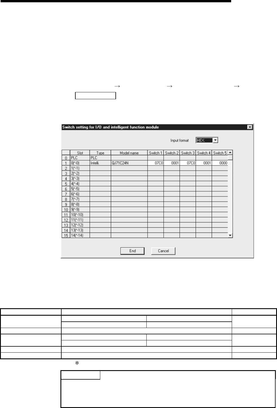
4 - 13 4 - 13
MELSEC-Q
4 SETTINGS AND PROCEDURES PRIOR TO OPERATION
4.5.2 Switch settings for I/O and intelligent functional module
[Setting purpose]
The switch settings for I/O module and intelligent functional module perform the
settings for transmission specifications and communication protocol for
communicate with external devices.
[Setting procedure]
[GX Developer] [PLC parameters] [I/O assignment setting]
Switch setting .
For screen display, see the GX Developer Operating Manual.
[Setting screen]
[Display description]
(1) Switches 1 to 5
Set the transmission specifications and communication protocol of each interface
using the combinations of setting values for each switch with 16 bit binary data
according to the following table.
Switch number Description Remarks
b15 to b8 b7 to b0
Switch 1 CH1 Communication rate setting CH1 Transmission setting See a) and b)
Switch 2 CH1 communication protocol setting See c)
b15 to b8 b7 to b0
Switch 3 CH2 Communication rate setting CH2 Transmission setting See a) and b)
Switch 4 CH2 Communication protocol setting See c)
Switch 5 Station number setting See d)
For settings to perform linked operation between two Q series C24 interfaces, see (2).
POINT
When GX Developer and/or the GOT is connected directly to the Q series C24,
switching settings using GX Developer need not be made to perform access to the
QCPU, monitoring and other operations. (If switch settings are not made, operation
is performed in the GX Developer connection mode.)
4 - 14 4 - 14
MELSEC-Q
4 SETTINGS AND PROCEDURES PRIOR TO OPERATION
(a) Transmission setting (CH1 side: switch 1 (lower level); CH2 side: switch 3
(lower level))
b7 b6 b5 b4 b3 b2 b1 b0
CH1 side
CH2 side
Bit Description OFF (0) ON (1) Remarks
b0 Operation setting Independent Link Must be set to OFF on CH1
b1 Data bit 7 8 Parity bit is not included
b2 Parity bit NO Yes Vertical parity
b3 Even/odd parity Odd Even Valid only when parity bit is set to
Yes
b4 Stop bit 1 2 —
b5 Sum check code NO Yes —
b6 Write during RUN Prohibited Allowed —
b7 Setting modifications Prohibited Allowed —
All items listed in the table should be set to OFF for the interfaces for which
"GX Developer connection" is set in the communication protocol setting.
If connecting directly to the GX Developer, it operates with the setting value
on the GX developer. (Refer to the description below.)
Transmission setting Setting description for GX Developer
Operation setting Independent
Data bit 8
Parity bit Yes
Even/odd parity Odd
Stop bit 1
Sum check code Yes
Write during RUN Allowed
Setting modifications Allowed/Prohibited
1) Operation setting
• This sets whether to use each of the two Q series C24 interfaces for
independent data communication, or to use the two for linked data
communication.
• The setting and data flow for linked operation is explained in (2).
2) Data bit setting
• This sets the bit length for one character in data communicated with an
external device according to the specifications of the external device.
(When data communication is performed using format 5 of the MC
protocol (for binary code communication), it is necessary to set it to 8
bits when processing the sum check code with the bidirectional
protocol.)
• If 7 bits are set, the data is communicated by ignoring the most
significant bit (8th bit).
3) Parity bit setting
• This sets whether or not a parity bit (vertical parity) is added for one
byte of transmission/receive data, according to the specifications of
the external device.
• The addition of the parity bit to the transmission data and the checking
of the parity bit of receive data are performed by the Q series C24.

4 - 15 4 - 15
MELSEC-Q
4 SETTINGS AND PROCEDURES PRIOR TO OPERATION
4) Even/odd parity setting
This sets whether the parity bit (vertical parity) should be odd parity or
even parity when adding the parity bit (vertical parity), according to the
specifications of the external device.
5) Stop bit setting
This sets the stop bit length for one character in data communicated with
an external device, according to the specifications of the external device.
6) Sum check code setting
• This sets according to the specifications of the external device whether
or not a sum check code is added to transmission and reception
messages of each frame and format during data communication using
the MC or bidirectional protocol.
• For an explanation of the message configuration and sum check code
when a sum check code is added (set to Yes), see the applicable
explanation of each protocol.
7) Write during RUN setting
• This sets according to the system specifications whether or not data
transmitted using the MC protocol is written to the PLC CPU from an
external device while the PLC CPU is running.
• When write during RUN is prohibited (disabled), the data is not written
and an NAK message is returned if the external device requests the
PLC CPU to write data while it is running.
• For an explanation of the functions available in this setting, check in
the "write allowed setting" and "write prohibited setting" columns in the
command list of the Reference Manual.
8) Setting modifications setting
This sets whether or not the following actions are allowed after starting
up the Q series C24.
Changing data communication functions and transmission
• Specifications, and the switching mode of each interface
• Writing data to the flash ROM (writing the system setting values and
user frame)
POINT
(1) A setting change in the connected interface side should be set to Allowed, in
order to register a user frame to the flash ROM from an external device using
the MC protocol.
(2) Setting changes in interfaces on the CH1 and CH2 sides should both be set to
Allowed, in order to register the system setting values and user frames to the
flash ROM from the PLC CPU.
4 - 16 4 - 16
MELSEC-Q
4 SETTINGS AND PROCEDURES PRIOR TO OPERATION
(b) Communication rate setting (CH1 side: switch 1 (upper level); CH2 side:
switch 3 (upper level)) 1 2 3
Bit position Bit position
Communication rate
(Unit: bps) b15 to b8
Communication rate
(Unit: bps) b15 to b8 Remarks
50 0FH14400 06H
300 00H19200 07H
600 01H28800 08H
1200 02H38400 09H
2400 03H57600 0AH
4800 04H115200 0BH
9600 05H230400 0CH
Try lowering the communication
rate when data cannot be
communicated normally with an
external device due to overrun
errors and framing errors etc.
1 Transmission speed of 230,400 bps is available for only CH1 of the
QJ71C24N (-R2/R4).
2 When connecting external devices to both of two interfaces, the total of
the communication speed should be 115,200bps or less (230,400 bps
or less if using QJ71C24N (-R2/R4)). When connecting an external
device to either of two interfaces, the maximum of 115,200 bps is
available for the interface (the maximum of 230,400 bps if using
QJ71C24N (-R2/R4)). In this case, set 300 bps for the other interface to
which no external device is connected.
3 Set "00H" to the interface for which "GX Developer connection" is set in
the communication protocol setting. Serial communication module will
operate at the communication speed set on the GX Developer.
(c) Communication protocol setting (CH1 side: switch 2; CH2 side: switch 4)
Set number Description Remarks
0HGX Developer connection GX Developer communication rate and transmission specifications are
automatically set.
1HFormat 1
2HFormat 2
3HFormat 3
4HFormat 4
For communication with ASCII code in the specified form of an A compatible 1C
frame or QnA compatible 2C/3C/4C frame
5H
MC protocol
Format 5 For communication with binary code in a QnA compatible 4C frame
6HNon procedure protocol For communication using non procedure protocol
7HBidirectional protocol For communication using bidirectional protocol
8HFor linked operation setting Set to the CH1 side when CH1 and CH2 interfaces are used in linked operation
(operated with the communication protocol of the CH2 side).
9H to DHSetting prohibited —
EHROM/RAM/switch test For self-diagnosis of the modules
FHIndividual station loopback test For checking operation of each interface of the modules
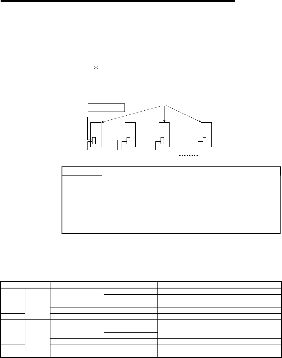
4 - 17 4 - 17
MELSEC-Q
4 SETTINGS AND PROCEDURES PRIOR TO OPERATION
(d) Station number setting (switch 5 (common for both CH1 and CH2 sides))
• This setting is for communication using the MC protocol.
• When several the Q series C24s are connected on the same line with
multidrop connection, set the station number designated in the data items
of the transmission frame in each external device to 0 to 31 (0H to 1FH).
This number designates which external device is to be communicated
with the Q series C24.
• Set the station number to 0 when the system configuration of the external
device and the PLC CPU is 1:1.
External device
Station 0 Station 1 Station 2 Station 31
Q series C24
POINT
If the communication of data with external device is to be started, check the
specifications of the functions to be used and then make the settings and connect
the cables.
Make the following switch settings from the GX Developer if there is to be no
communication (if the cables are not to be connected) at the interface.
• Communication protocol setting : Set between 0H and 7H.
• Transmission setting, communication rate setting: Set all to OFF.
(2) The setting and data flow in linked operation
(a) Set the related switches as follows when two Q series C24 interfaces are in
linked operation.
Switch number Settings Setting value
Operation setting b0 = OFF
Data bit settingTransmission setting
:
Set each switch on both CH1 and CH2 sides to
the same specification.
Switch 1
Communication rate setting Match the external device.
Switch 2
CH1 side
Communication protocol setting 8
Operation setting b0 = ON
Data bit settingTransmission setting
:
Set each switch on both CH1 and CH2 sides to
the same specification.
Switch 3
Communication rate setting Match the external device.
Switch 4
CH2 side
Communication protocol setting 0 to 7
Switch 5 Station number setting Set according to (d) of (1)
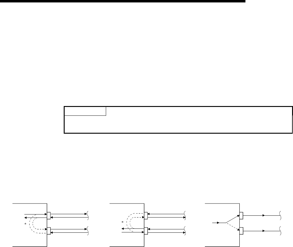
4 - 18 4 - 18
MELSEC-Q
4 SETTINGS AND PROCEDURES PRIOR TO OPERATION
(b) Do not use the above settings for the following cases, because linked
operation cannot be performed.
1) When using the QJ71C24N-R2 or QJ71C24-R2.
2) When an external device is not connected to either of the interfaces.
3) When the bidirectional protocol is used for data communication.
4) When communicating data with an external device connected to two
interfaces that are not interacting, using functions set in the
communication protocol settings (MC protocol/non procedure protocol).
5) When communicating data using the modem function.
POINT
When two interfaces are in linked operation, the transmission time for one
character becomes equal to the hardware gate off time of the Q series C24.
(c) The data flow in linked operation is as follows.
1) Two interfaces operate linked together using functions defined with the
communication protocol setting on the CH2 side (MC protocol in the
same format or a non procedure protocol) within the transmission
specifications set in the respective transmission settings (specifications
for CH1 and CH2 must be the same).
CH2
Q series C24 (data flow in linked operation)
*
CH1
CH2
CH1
2ch
1ch
Transmits only
to a designated
CH side.
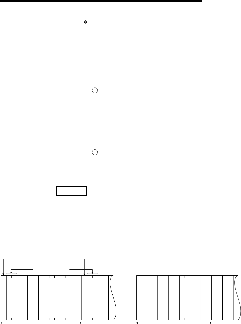
4 - 19 4 - 19
MELSEC-Q
4 SETTINGS AND PROCEDURES PRIOR TO OPERATION
In linked operation, all data received from one of the two interfaces is
transmitted from the other interface. In this case, exclusive control of the
received data is necessary when data is communicated using the non-
procedure protocol since all the connected stations receive the data.
When data communication is performed using the MC protocol, only
the Q series C24 having the station number designated in the
message performs the process designated by the command.
Furthermore, when data communication is performed using QnA
compatible 2C/3C/4C frames of the MC protocol, the header
information for linked operation is added to messages directed to
other stations linked by multidrop connection.
a Processing performed by the Q series C24 connected to an
external device
• The header information is added to the command messages
received from the external device that are directed to other
stations and sends them to the stations through the other
interface.
• The header information is deleted from the response
messages received from other stations and sends them to the
external device using the other interface.
(The header information is also sent during m:n connection.)
b Operation of the accessed station
The accessed station processes the request contained in the
command message, adds the header information to a response
message, and sends it using the interface that received the
command message.
REMARK
The following describes the header information that is added by the Q series C24 to
a message in linked operation.
1) When communicating with ASCII code (formats 1 to 4)
The following 13/15 character header information is added immediately before
the control code (ENQ/STX/ACK/NAK) at the start of each message (13
characters for formats 1, 3 and 4; 15 characters for format 2).
2) When communicating in binary mode (format 5)
The following 10 byte header information is added immediately before the
control code (DLE + STX) at the start of each message.
(In ASCII code communication)
Existence in format 2
"STX" in format 3
(In binary code communication)
Header information (10 byte)Header information (13/15 characters)
E
N
Q
E
N
Q
D
L
E
S
T
X
D
L
E
S
T
X
HL HL HL H L HL HL HL HL L H LH LH
--
Block No.
Frame ID No. for link
Module I/O No. for
link station
Module station No.
for link station
System data
Station No.
Block No.
Frame ID No.
System data
Frame ID No. for link
Station No.
Module I/O No. for
link station
Module station No.
for link station
System data
No. of data bytes
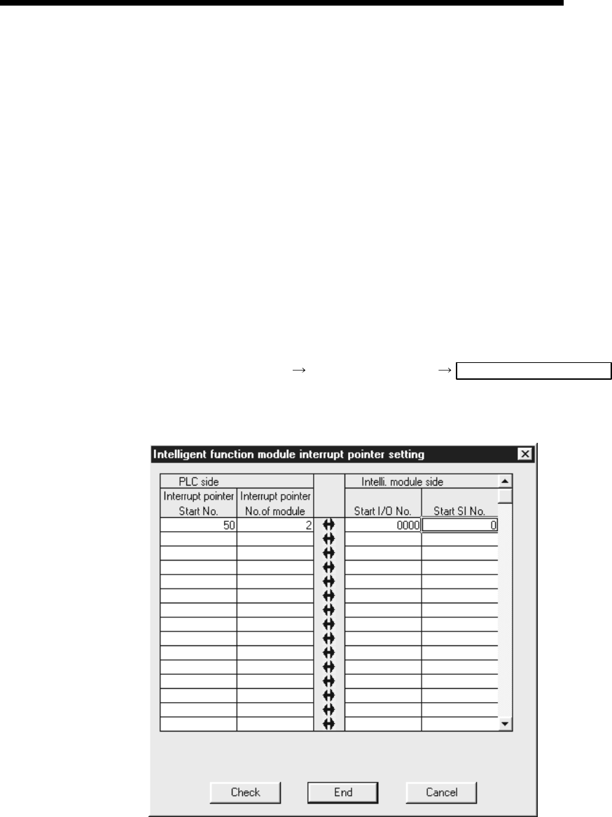
4 - 20 4 - 20
MELSEC-Q
4 SETTINGS AND PROCEDURES PRIOR TO OPERATION
4.5.3 The Intelligent function module interrupt pointer setting
The following explains the interrupt pointer setting with GX Developer in order to
receive data using an interrupt program.
For the method to receive data using an interrupt program, see User's Manual
(Applications) Chapter 4.
[Setting purpose]
The intelligent function module interrupt pointer sets the information to read the
receive data with an interrupt program of the PLC CPU during communication
using the non procedural/bidirectional protocol.
By performing this setting, an interrupt program starts when data is received from
an external communicating device and the reading of data received by the PLC
CPU becomes possible.
[Startup procedure]
[PLC parameters] [PLC system setting] Interrupt pointer setting .
For display screen, see the GX Developer Operating Manual.
[Setting screen]
[Setting description]
(1) Interrupt pointer start No. on the PLC side
Set the start number (ranging from 50 to 255) of the interrupt pointer (Ixx) for
use in the sequence program.
(2) Interrupt pointer No. of units on the PLC side
Set the number of units (2) of interrupt pointers (I) for use in the sequence
program.

4 - 21 4 - 21
MELSEC-Q
4 SETTINGS AND PROCEDURES PRIOR TO OPERATION
(3) Start I/O No. on the intelligent module (unit) side
Set the start I/O No. for the Q series C24.
(4) Start SI No. on intelligent module (unit) side
1) Assign control numbers (SI) on the Q series C24 side to the interrupt
pointers (Ixx) used in the sequence program.
2) Set the start SI No. (0) of the interrupt control numbers.
3) The interfaces for data reception corresponding to the interrupt control
numbers are as follows:
SI No. 0: for interface on the CH1 side
SI No. 1: for interface on the CH2 side
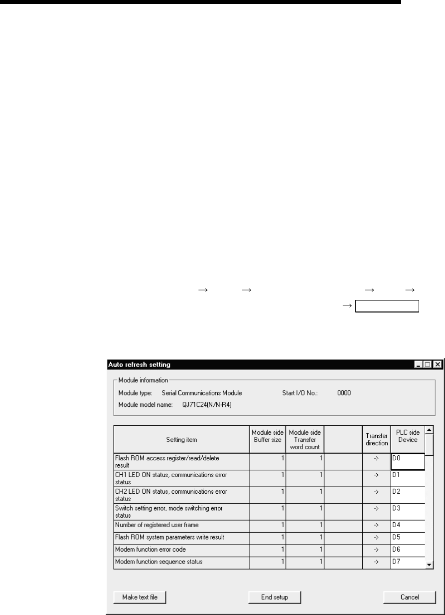
4 - 22 4 - 22
MELSEC-Q
4 SETTINGS AND PROCEDURES PRIOR TO OPERATION
4.6 Settings with the Utility Package (GX Configurator-SC)
The settings defined with GX Configurator-SC for operation of the Q series C24 are
described in Chapter 8.
The following concerns the data set from GX Configurator-SC.
1) Data set in the Q series C24 for the use of specific functions
2) Data set in the PLC CPU to communicate information between the Q series C24
and the PLC CPU of the mounting station.
This section explains the "Auto refresh settings" of the data mentioned in 2) above.
[Setting purpose]
The auto refresh settings are defined to automatically store the error and status
information stored in the buffer memory of the Q series C24 in devices
designated by the PLC CPU.
By this setting, the users can see the module error and status information without
accessing the Q series C24.
[Setup procedure]
[GX Developer] [Tools] [Intelligent function utility] [Start] "Intelligent
function module parameter setting module select" Auto refresh .
For display screen, see Section 8.3.
[Setting screen]
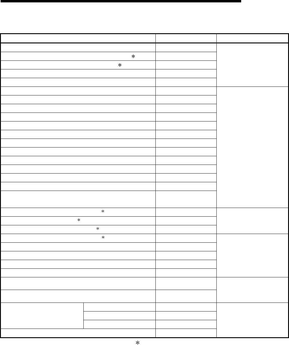
4 - 23 4 - 23
MELSEC-Q
4 SETTINGS AND PROCEDURES PRIOR TO OPERATION
[Setting items]
Setting item Buffer memory address Reference section
Flash ROM access register/read/delete result 4H
CH1/CH2 LED ON status, communication error status ( 1)201H /202H
Switch setting error, mode switching error status ( 1)203H
Number of registered user frame 204H
Flash ROM system parameters write result 220H
Section 8.6.9
Section 10.1
Modem function error code 221H
Modem function sequence status 222H
Number of data registrations for connection 223H
Number of data registrations for initialization 226H
Number of notification execution 229H
Data storage area 1 notification execution data No. 22AH
Data storage area 2 notification execution data No. 22EH
Data storage area 3 notification execution data No. 232H
Data storage area 4 notification execution data No. 236H
Data storage area 5 notification execution data No. 23AH
Accumulated count of unlock process normal completion 22FBH
Accumulated count of unlock process abnormal completion 22FCH
Accumulated count of lock process based on circuit
disconnection 22FFH
Section 8.6.2
Section 3.3 of User’s Manual
(Application)
CH1/CH2 communication protocol status ( 1)252H/262H
Transmission status ( 1)253H/263H
RS-232 control signal status ( 1)254H/264H
Section 4.5.2
Section 8.6.3
Section 10.1
Transmission sequence status ( 1)255H/265H
On-demand execution result 256H/266H
Data transmission result 257H/267H
Data reception result 258H/268H
MC protocol transmission error code 25AH/26AH
Sections 8.6.4 to 8.6.6
Section 10.1
Receive user frame nth 25BH/26BH
User frame being transmitted B6H/156H
Section 8.6.5
Chapter 11 of User’s Manual
(Application)
Operation status 2204H/2304H
Execution result 2205H/2305H
PLC CPU monitoring
function Number of transmission 2206H/2306H
Monitoring condition arrival block No. 2207H/2307H
Section 8.6.7
Chapter 2 of User’s Manual
(Application)
1 See Section 10.1 for the contents of the buffer memory.

4 - 24 4 - 24
MELSEC-Q
4 SETTINGS AND PROCEDURES PRIOR TO OPERATION
(1) Devices
(a) Set the word device of the PLC CPU which stores error and status
information in the setting item field when using the auto refresh function
between the Q series C24 and the PLC CPU.
(b) The devices used must be of the types X, Y, M, L, B, T, C, ST, D, W, R, or
ZR.
If bit devices of types X, Y, M, L, or B are used, a number that can be
divided by 16 points (e.g., X30, Y120, M16, etc.) should be specified. The
buffer memory data is stored in 16 point units from the specified device
number (e.g., if M16 is set, data is stored from M16 to M31).
(c) The device can be set to auto refresh for required information only.
(2) Writing auto refresh settings to QCPU and saving them in a file
(a) Writing auto refresh settings to QCPU
Use online PLC write function of GX Configurator-SC or GX Developer.
(b) Saving in a file
Use the file storage function shown in the file items in the parameter module
selection screen shown in Section 8.3.2. of GX Configurator-SC.
POINT
(1) The auto refresh settings are stored in the intelligent function module
parameter.
After the intelligent function module parameters have been written to the CPU
module, it enables the auto refresh setting by turning the power OFF ON or
by resetting the CPU module.
(2) The auto refresh settings cannot be changed from the sequence program.
However it is possible to add a process similar to auto refresh by using the
FROM/TO command of the sequence program.

4 - 25 4 - 25
MELSEC-Q
4 SETTINGS AND PROCEDURES PRIOR TO OPERATION
4.7 Individual Station Test
After installing the Q series C24 to the base unit of QCPU, perform an individual station
test first to check the switch setting (see Section 4.5.2) and operation of the Q series
C24.
POINT
(1) When a problem occurs during data communication with an external device,
perform an individual station test as described in this section to check whether
or not there is any problem in the operation of the Q series C24.
(2) In order to avoid problems, set the PLC CPU to STOP status during the
individual station test.
(3) Test both interfaces of the Q series C24 simultaneously in an individual station test.
Alternatively, either one of the interfaces can be tested in an individual station
loopback test.
In that case, ignore the test results on the interface side for which the test is not
performed.
(4) Cable removal and reconnection before and after the individual station
loopback test should be performed with the power to the Q series C24
mounting station turned off.
(5) To restart data communication with an external device after an individual
station test, check the specifications of the devices used before defining
various settings and reconnecting cables.
For the interface that is not used for communication (no cable connection), define
the switch settings in GX Developer as follows (for the setting method, see Section
4.5.2).
• Communication protocol setting: 0H to 7H
• Transmission control settings and communication rate settings: all set to OFF.
(6) If an error occurs even though the correct settings have been made for the Q
series C24 through an individual station test, please consult your nearest
dealer or branch office with a description of the error.
4.7.1 ROM/RAM/switch tests
A ROM/RAM/switch test checks the contents of the memory of the Q series C24 and
the switch settings set with GX Developer.
Perform a ROM/RAM/switch test with the procedure described below.
(Procedure 1) Communication protocol setting and transmission setting (see Section 4.5.2)
(1) Set the communication protocol setting on the CH2 side to EH (ROM/RAM/switch test).
Set the communication protocol setting on the CH1 side to the number (1 to 8)
used for data communication with an external device following the test.
(2) Set the transmission settings for the two interfaces to match the specifications
used when communicating data with an external device.
(Procedure 2) Performing ROM/RAM/switch tests
(1) Set the PLC CPU to STOP status.

4 - 26 4 - 26
MELSEC-Q
4 SETTINGS AND PROCEDURES PRIOR TO OPERATION
(2) Restart the PLC CPU station or reset the CPU. The test starts automatically in
about one second.
(3) For the Q series C24, the following tests should be performed once.
1) ROM check
Read the ROM data and verify the sum check.
2) RAM check
Write data to RAM, and read and check it.
3) Switch check
Check whether or not each switch is set within the tolerance range and the
operation setting in the transmission settings is set to off.
4) Linked operation setting check (perform this test with the operation setting in
the transmission settings of CH2 set to on)
Check to see that the communication protocol setting on CH1 is set to 8H and
whether the communication rate setting of each channel is within the tolerance
range.
A linked operation setting check is performed when values are set as follows:
• Communication protocol setting on the CH1 side : 8H
• Operation setting in the transmission settings on the CH2 side: bit 8 = ON.
(Procedure 3) Checking results of ROM/RAM/switch tests
(1) The test is completed when the NEU LED on CH1 side is lit (approximately 2
seconds).
(2) The test is completed normally when the ERR LED turns off.
(3) The test is completed with error when the ERR LED turns on. Check the error
description in one of the following screens.
• The "Monitor/test others" screen of GX Configurator-SC (see Section 8.6.9)
• The buffer memory monitor screen of GX Developer (see the GX Developer
Manual for the operation method)
When checking errors in the buffer memory monitor screen of GX Developer,
monitor the following buffer memory.
Check the error descriptions on the screens by bit-decoding the monitored value
(16-bit integer). Each bit corresponds to the following error description.
Buffer memory monitored
Address
Bit location
CH1 side
201H
CH2 side
202H
CH1/CH2 side
203H
Description when corresponding bit is on Corrective action
b0 — — —
b1 SIO — Transmission setting error
b2 PRO —
When linked operation
setting Protocol setting error
b3 P/S — Transmission setting error
b4 C/N —
When independent
operation setting Protocol setting error
Review setting value
(see Section 4.5.2)
b5 to b6 — — — —
b7 NEU — Test completed —
b8 to b13 — — —
CH2 ERR — RAM error ( 1)
b14 —Setting station
number Out of the setting station number range Review setting value
(see Section 4.5.2)
b15
—
CH1 ERR — ROM error ( 1)
1 Consult your nearest dealer.

4 - 27 4 - 27
MELSEC-Q
4 SETTINGS AND PROCEDURES PRIOR TO OPERATION
(Procedure 4) Ending a ROM/RAM/switch test
(1) Perform the following procedures after checking normal completion/abnormal
completion of the test results.
Normal completion : Perform operation (2) to finish tests.
Upon error occurrence : When an error occurs in a switch check or linked
operation setting check, set the correct values and test
again.
When an error occurs in a ROM or RAM check, check the
mounting status of module and test again.
If there is no error in the mounting status of module,
consult your nearest dealer or branch office.
(2) Perform the ending procedure for ROM/RAM/switch test
1) Follow the procedure in Section 4.7.2 to perform an individual loopback test
operation.
2) Perform the following procedure to end the test and start data communication
with an external device.
• Set the switch settings on GX Developer according to the procedure
specified in Section 4.5.2.
• Turn off the power to the station on which the Q series C24 is installed and
connect the communication cable with an external device.
• Turn on the power to the station on which the Q series C24 is installed.
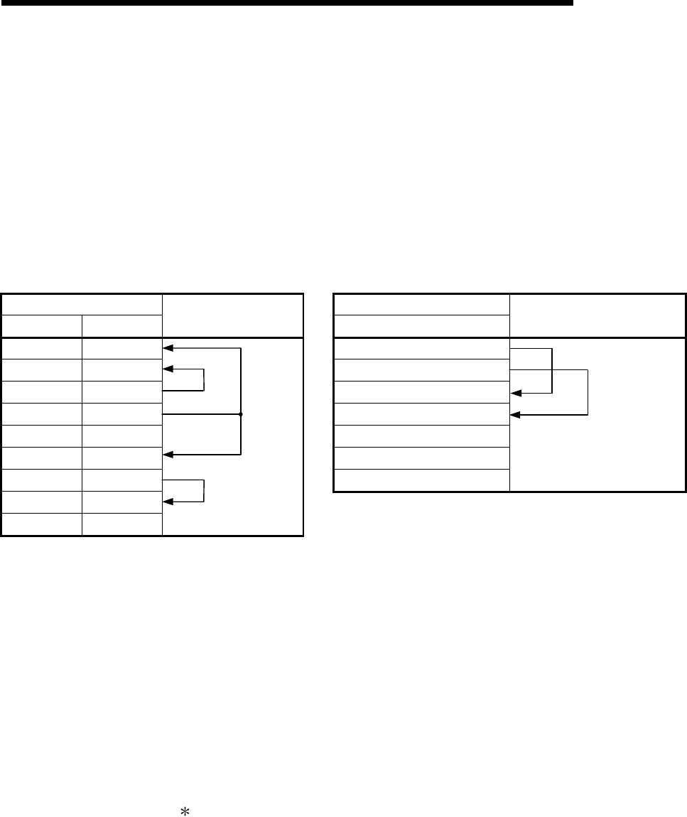
4 - 28 4 - 28
MELSEC-Q
4 SETTINGS AND PROCEDURES PRIOR TO OPERATION
4.7.2 Individual station loopback test
The individual station loopback test checks the operation of the communication
function of the Q series C24.
Follow the procedure below to perform an individual station loopback test.
(Procedure 1) Connecting cable
(1) Connect cables to two interfaces as follows.
• Connect cables to the RS-232 interface within the connector and install it to the
interface.
• Connect cables to the RS-422/485 interface on a terminal block.
RS-232 interface (D-Sub 9 pin) RS-422/485 interface
Q series C24 side Q series C24 side
Signal name Pin number Cable connection Signal name Cable connection
CD 1 SDA
RD (RXD) 2 SDB
SD (TXD) 3 RDA
ER (DTR) 4 RDB
SG 5 SG
DR (DSR) 6 FG
RS (RTS) 7 FG
CS (CTS) 8
RI (CI) 9
(Procedure 2) Communication protocol setting and transmission setting (see Section 4.5.2)
(1) Set the communication protocol setting to FH (individual station loopback test) for
both interfaces.
(2) Set each transmission setting of the two interfaces according to the transmission
specification for data communication with an external device.
(Procedure 3) Performing the individual station loopback test
(1) Set the PLC CPU to STOP status.
(2) Restart the PLC CPU station or reset the CPU. The test starts automatically in
about one second.
(3) For the Q series C24, perform the following tests in sequence and repeat them
(one test cycle takes approximately one second).
End testing when all test results become abnormal.
1) Check communication with the PLC CPU
Read and check the model type of the PLC CPU.
2) Check transmission and reception functions of the interface
Perform communication while changing data.
(4) The LED corresponding to a test item flashes when the test starts.
• The CH1 NEU LEDs flash when checking communication with the PLC CPU.
• The SD and RD LEDs of the interface being tested flash when checking the
communication functions of each interface.
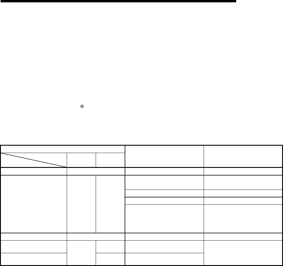
4 - 29 4 - 29
MELSEC-Q
4 SETTINGS AND PROCEDURES PRIOR TO OPERATION
(Procedure 4) Checking the results of an individual loopback test
(1) This test is performed repeatedly. When the ERR LED is off, the test is being
executed normally.
(2) The test is completed with an error when the ERR LED is lit. Check the error
description on one of the following screens. (The ERR LED is lit upon error
occurrence, and the test is completed.)
• The "Monitor/test others" screen of GX Configurator-SC (see Section 8.6.9)
• The buffer memory monitor screen of GX Developer (see the GX Developer
Manual for operation method)
When checking for errors in the buffer memory monitor screen of GX
Developer, monitor the LED ON status storage area (address CH1: 201H,
CH2: 202H).
Check the error descriptions on the screens by bit-decoding the monitored value
(16-bit integer). Each bit corresponds to the following error description.
Buffer memory monitored
Address
Bit location
CH1 side
201H
CH2 side
202H
Description when corresponding
bit is on Corrective action
b0 to b3 — — —
Error occurrence in the CPU module. Remove errors occurring in the CPU
module.
Not enough power supply capacity. Examine the power supply capacity.
Module is not mounted correctly. Reinstall the module properly.
b4 C/N —
Error occurrence in the base unit,
extension cable, CPU module, or the
Q series C24.
Check each module and remove the
cause of the error.
Reconnect the cable correctly.
Reinstall the module correctly.
b5 to b13 — — —
b14 CH2 ERR CH2 side communication error
b15
—
CH1 ERR CH1 side communication error
Reconnect the cable correctly.
Examine the test wiring connection.
(Procedure 5) Ending individual station loopback test
(1) Perform the following procedures after checking normal completion/abnormal
completion of the test result.
Normal completion : Perform operation (2) to finish the test.
Upon error occurrence : Remove the cause of the error according to the corrective
action specified in the table above, and test again.
(2) Perform the ending procedure for individual station loopback test
1) Follow the procedure in Section 4.7.1 to perform a ROM/RAM/switch test.
2) Perform the following procedure to end the test and start data communication
with an external device.
• Set the switch settings on GX Developer according to the procedure
specified in Section 4.5.2.
• Turn off the power to the station on which the Q series C24 is installed and
connect the communication cable with the external device.
• Turn on the power to the station on which the Q series C24 is installed.

4 - 30 4 - 30
MELSEC-Q
4 SETTINGS AND PROCEDURES PRIOR TO OPERATION
4.8 Loopback Test
A loopback test performs a communication test using the loopback test function of the
MC protocol, in order to check the connection between the Q series C24 and an
external device, the communication function of each device, and the operation of the
communication program of the external device.
(Procedure 1) Connecting the Q series C24 to an external device
Turn off the power to the station on which the Q series C24 is installed and connect a
communication cable to an external device to perform data communication using the
MC protocol (see Section 4.4).
(Procedure 2) Switch setting with GX Developer
(1) Set the switch settings with GX Developer as shown in Section 4.5 and write the
parameters to the PLC CPU in order to perform data communication using the MC
protocol.
(2) The following shows an example of the settings when performing a loopback test
on the interface on the CH1 side.
• Switch 1: 0544HTransmission Operation setting : Independent operation
setting Data bit : 7 bit
Parity bit : Yes (odd)
Stop bit : 1 bit
Sum check code : No
Write during RUN : Allowed
Setting modification : Prohibited
Communication rate setting : 9600 bps
• Switch 2: 0001HCommunication protocol setting : MC protocol (format 1)
• Switch 3: 0000H
• Switch 4: 0000H
• Switch 5: 0000HStation number setting : 0 station
(Procedure 3) Performing a loopback test
(1) Set the PLC CPU to STOP status, and turn the power on or reset the CPU
(communication is enabled in about one second).
(2) Create a program for a loopback test on the external device side and send a
command message like the one in the example below to the Q series C24.
The commands used are as follows:
• When performing communication test in an A compatible 1C frame: TT
command (for an example, see the following page)
• When performing communication test in a QnA compatible frame: 0619 command
See the Reference Manual when performing communication tests in a QnA
compatible frame.
(Procedure 4) Checking loopback test result
(1) The Q series C24 sends a response message to the external device when it
receives a loopback test command message.
The Q series C24 sends the external device the received data as is.
(2) Check on the external device whether the data received from the Q series C24
matches the data sent from the external device.
4 - 31 4 - 31
MELSEC-Q
4 SETTINGS AND PROCEDURES PRIOR TO OPERATION
(Procedure 5) Ending the loopback test
Perform the following procedure according to the function used, and start data
communication.
• Set the switch settings with GX Developer according to the procedure specified in
Section 4.5.2.
• Turn on the power to the station on which the Q series C24 is installed.
An example of control procedure when the TT command is used in the loopback
test mentioned in Procedure 3.
(Station number: 00, sum check code: Yes)
PLC CPU side
(Example)
(Data name)
External
device side
Header data sent
by the external device
TT (ACPU common command)
Two characters (hexadecimal) … Designate the number of characters (1 to 254) of return data to be
sent immediately afterward.
Designate with a text string consisting of "0" to "9" and "A" to "F" (capital letter)
(In case of format 1)
Two characters (hexadecimal)
Character A part
Becomes the
same data
Header data to be sent by
the PLC CPU Character B part
S
T
X
E
T
X
02H30H30H46H46H30H35H41H42H43H44H45H03H41H33H
HL
00
HL
FF
HL
05AB CDE
HL
A3
E
N
Q
41H42H43H44H
30H37H38H
AB CDE
HL
78
35H45H
30H
54H
54H
46H
46H
30H
30H
05H
HL
00
HL
FFTT005
HL
Station No.
PC No.
Command
Message wait
Character length
Loopback data
data with the
length given
by Character
length
Sum check
code
Station No.
PC No.
Character length
Loopback data
data with the
length given
by Character
length
Sum check
code
(Example)
(Data name)
4 - 32 4 - 32
MELSEC-Q
4 SETTINGS AND PROCEDURES PRIOR TO OPERATION
4.9 Maintenance and Inspection
This section explains the maintenance and inspection and installing and removing of
the Q series C24.
4.9.1 Maintenance and inspection
The Q series C24 has no special inspection items other than below.
For items other than listed below, perform inspection according to the inspection items
listed in the User's Manual of the PLC CPU module in order to always use the system
in the optimal condition.
(the Q series C24 inspection items)
1) Check if the terminal resistors and cables are connected securely.
2) Verify that the module installation screws and the terminal block installation screws
are securely tightened.
POINT
Be sure to read through the Safety Precautions in the beginning of this manual
regarding the Q series C24 inspection and maintenance.

4 - 33 4 - 33
MELSEC-Q
4 SETTINGS AND PROCEDURES PRIOR TO OPERATION
4.9.2 When mounting/dismounting the module
Please read 4.1, "Handling Precautions" before mounting or dismounting the module,
and make sure to pay attention to safety and handle the module properly during the
operation.
When replacing the Q series C24 and QCPU, it becomes necessary to register the
following data on the Q series C24 again for the module to be replaced.
• Q series C24: System setting data in the flash ROM
• QCPU: PLC parameters (I/O assignment, switch setting, etc.)
The procedure for replacing a module, including re-registration of data, is as follows.
<Operation procedure when replacing the Q series C24>
(Step 1) Read all the system setting data of the Q series C24 using the
Read from module function of GX Configurator-SC.
(Step 2) Save the system setting data read to the specified file using the
File Save function of GX Configurator-SC ( 1).
(Step 3) Turn the power supply to the Q series C24 off.
(Step 4) Dismount the cables and the module itself.
(Step 5) Replace the module and start up the module according to "4.2 Settings
and Procedures Prior to Operation."
(Step 6) Read the data saved in (Step 2) back into the system and register the
system setting data to the flash ROM of the Q series C24 using the
Write to module function of GX Configurator-SC.
<Operation procedure when replacing the QCPU>
(Step 1) Read the PLC parameters with GX Developer from the QCPU and save
them.
(Step 2) Replace the QCPU. (See the user's manual for QCPU.)
(Step 3) Register the PLC parameter saved by GX Developer back into the
QCPU again.
1 It is recommended to record and save the system setting parameters not
only when replacing the module, but also when changing the system setting
parameters using GX Configurator-SC.

5 - 1 5 - 1
MELSEC-Q
5 DATA COMMUNICATION USING THE MELSEC COMMUNICATION
PROTOCOL
5
5 DATA COMMUNICATION USING THE MELSEC COMMUNICATION
PROTOCOL
This chapter explains an overview of the MELSEC communication protocol (hereinafter
abbreviated as the MC protocol). See the following manual for a detailed explanation of
the data communication functions that are available when using the MC protocol.
Q Corresponding MELSEC Communication Protocol Reference Manual (SH-080008)
5.1 Data Communication Functions
The MELSEC protocol (MC protocol) is a communication system for the Q series PLCs.
Using this protocol, the external devices can read or write device data and programs for
the PLC CPUs via the Q series C24 or Q series Ethernet interface module.
Any external devices on which application programs can be installed and which can
transmit and receive data in accordance with the MELSEC PLC protocol can
communicate with the PLC CPUs using the MC protocol.
5.1.1 Accessing the PLC CPUs using the MC protocol
This section describes the main functions for accessing the PLC CPUs using the
MC protocol.
(An overview of the data communication functions using the MC protocol is
provided in Section 3.4).
With the exception of the on-demand function described below, the Q series C24
sends and receives data based on commands from the external devices.
Thus, the PLC CPU side does not require sequence programs for data
communication.
(1) Data read/write
This function reads and writes data from/to the PLC CPU device memory of the
local-station or other station on the MELSECNET/H, MELSECNET/10 as well as
the intelligent function module buffer memory.
By reading and writing data, the PLC CPU operation monitoring, data analysis and
production management can be performed on the external device side.
Also, production directions can be executed on the external device side.
(2) File read/ write
This function reads and writes files stored in the PLC CPU such as sequence
programs and parameter files. By reading and writing files, file management for
the GX Configurator-SC and the QnACPUs of other stations can be performed
on the external station side.
Also, execution programs can be changed (replaced) from the external device side.
(3) Remote control of the PLC CPU
This function executes remote RUN/STOP/PAUSE/latch clear/reset operations.
Remote operations of the PLC CPU can be performed from the external device
side using the PLC CPU remote control function.
5 - 2 5 - 2
MELSEC-Q
5 DATA COMMUNICATION USING THE MELSEC COMMUNICATION
PROTOCOL
5
(4) Monitoring the PLC CPU
This function monitors the operating status of the PLC CPU and the data in the
device memory.
The PLC CPU status and the device memory data can be sent to the external
device at fixed intervals, when an error occurs in the machine equipment, or
when certain conditions are satisfied.
This function reduces the data read processing load on the external device side.
(5) Sending data from the PLC CPU to the external device
A function for requesting data transmission from the PLC CPU to the external
device is called the on-demand function.
Urgent data that must be forwarded to the external device can be sent as on-
demand data to the external device by starting up from the PLC CPU.
5.1.2 Message format and control procedure for data communication
The data communication functions using the MC protocol correspond to the data
communication functions using the dedicated protocol for the conventional products
listed below.
• A series computer link module
• QnA series serial communication module
Therefore, the message format and control procedure are the same as when
accessing the PLC using these conventional modules.
The external device side can access the Q series PLC with a program used for
accessing the PLC via a conventional module.
(Example)
E
N
Q
HL HL H L H L
0001QR 0 X000040 0 2 2
7
05H30H30H30H31H51H52H30H58H30H30H30H30H34H30H30H32H37H32H
S
T
X
HL HL
00011234 BCD
02H30H30H30H31H31H32H33H34H42H43H44H
HL
8
9
39H38H
E
T
X
03H
A
41H
(Command message for A compatible 1C frame) (Response for A compatible 1C frame)
Station No.
PC No.
Command
Message wait
Head device
No. of device
points
2 characters
(hexadecimal)
Sum check
code
Sum check
code
Station No.
PC No.
Data for the number
of device points
Number of device
points × 4 characters
POINT
The following manual is available for performing data communication using the MC
protocol.
MELSEC Communication Protocol Reference Manual (sold separately)
5.1.3 PLC CPU setting for performing data communication
Data communication using the MC protocol is achieved by performing the GX
Developer settings indicated below on a PC, performing the system settings by the GX
Configurator-SC, and registering the settings to the PLC.
(1) Settings using the GX Developer (Required)
Perform the I/O assignments and switch settings indicated in Section 4.5 and
write the parameters to the PLC CPU where the Q series C24 is installed.
5 - 3 5 - 3
MELSEC-Q
5 DATA COMMUNICATION USING THE MELSEC COMMUNICATION
PROTOCOL
(2) System settings using the GX Configurator-SC
When it is necessary to change the default values registered in the Q series C24,
perform the settings as indicated in Chapter 8 and register these to the flash
ROM in the Q series C24.
• MC protocol system setting
• Transmission control and others system setting
POINT
To write from the external device to the intelligent function module installed in the
MELSECNET/H remote I/O station during communication using the MC protocol,
set the "Write allow/prohibit during PLC CPU RUN" in the GX Developer to enable.
5.1.4 Support of multiple CPU system or redundant system
When the external device accesses a QCPU in a multiple CPU system or redundant
system, it is possible to selectively access either a control or non-control CPU in the
multiple CPU system or a control or standby system CPU or System A or System B
CPU in the redundant system by specifying the target QCPU in "Requested module
I/O No." of the QnA compatible 4C frame for the MC protocol.
Refer to the Reference Manual for details.
Refer to Chapter 2 of this manual for the system configuration.
(Example) When multiple CPU No.1 is specified
Frame ID No.
46H
05H
Self-station No.
Command
Sub command
Device code
Head device
Number of device
points
Sum check code
38H30H33H30H33H45H30H30H30H30H30H30H34H30H31H30H30H30H31H58H2AH30H30H30H30H34H30H30H30H30H35H
H
F
L
8
H
0
L
7
H
0
L
0
H
0
L
0
H
0
L
0
H
0
L
1
H
0
L
1X
L
0
L
5
PC No.
—
0
—
0
H
0
—
0
—
4
H
0
—
0
—
0
—
4
—
3
—
0
—
0
—
0
E
N
Q
Station No.
30H35H
H
0
L
5
Network No.
30H37H
H
0
L
7
—
E
33H36H
H
3
L
6
Requested module
station No.
Requested module
I/O No.
(Command massage of the QnA compatible 4C frame format 1)
REMARK
• When using the Q series C24 in a multiple CPU system, it is necessary to specify
the QCPU that controls the Q series C24 (hereinafter referred to as the control
PLC) using GX Developer.
• It is also possible to mount a Q series C24 of function version A in a multiple CPU
system. In this case, it is only possible to access the control PLC (PLC No.1).
• It is only possible to access the control PLC if data is communicated by means of
frames other than the QnA compatible 4C frame.

5 - 4 5 - 4
MELSEC-Q
5 DATA COMMUNICATION USING THE MELSEC COMMUNICATION
PROTOCOL
5.1.5 Support for the QCPU remote password function
This section explains an overview of the remote password function when a remote
password is set for the Q series C24 mounted to a QCPU.
See Chapter 3 of the User's Manual (Application) for a detailed explanation.
(1) Checking remote passwords
If the following items are set to the QCPU using GX Developer, the Q series C24
performs a remote password check whenever an external device accesses the
PLC using the modem function of the Q series C24.
(a) Setting by GX Developer
• When the remote password is set on the QCPU with the Q series C24.
• When the Q series C24 is set to be subject to the remote password check.
(b) Access in which the remote password is checked
The remote password is checked when the following access is attempted.
Access attempts to all PLCs of the local station (the local station with the Q
series C24 and other stations accessed via the local station) are subject to
the remote password checking.
(Access function to the PLC in which the remote password is checked)
• Data communication using the MC protocol
• Access to the PLC using GX Developer
The remote password is not checked in data communication using the
non procedure/bidirectional protocols.
(c) Remote password to be checked
The check is performed against the remote password set to the local
station QCPU with the Q series C24.
Access to the specified station is allowed if the remote password
specified by the user and the remote password set to the QCPU match
when accessing.
(2) Data communication procedure
1) Initialize the modem.
2) Connect the line from the external device.
3) Unlock (cancel) the remote password of the QCPU belonging to the station
with the Q series C24 mounted from the external device via the dedicated
command for communication using the MC protocol.
4) Initiate the data communication between the external device and PLC using
the MC protocol.
5) Disconnect the modem line from the external device side when completing
the data communication using the MC protocol.
The remote password is automatically locked when the modem is
disconnected.

5 - 5 5 - 5
MELSEC-Q
5 DATA COMMUNICATION USING THE MELSEC COMMUNICATION
PROTOCOL
REMARK
The remote password should be set to a QCPU using GX Developer in order to use
the remote password function of QCPU.
• Unlocking the remote password is possible only for the QCPU of the local station
with the Q series C24.
It is impossible to unlock the remote password for the QCPU of other stations.
See Section 3.18 of the Reference Manual for the command for unlocking the
remote password.
• When accessing the PLC using GX Developer, the remote password should be
unlocked when starting the online operation.
(3) Q series C24 setting and monitoring function when using the QCPU
remote password function
(a) Modem function system setting by GX Configurator-SC
1) Remote password mismatch notification count designation
Designate the number of times before notification when a remote
password disagreement occurs at the unlock processing by the
user/external device after the line is connected.
The Q series C24 automatically disconnects the line if more remote
password disagreements occur than the number of times designated by
this value.
2) Remote password mismatch notification accumulated count designation
Designate the number of times before notification when remote
password disagreements occur at the unlock processing by the
user/external device after the startup of the Q series C24.
The error signal on the CHn side (XE, XF) and the ERR LED turn on if
remote password disagreements occur more than the number of times
designated by this value (the line is not disconnected).
The user can clear the cumulative value counted by the Q series
C24 at an occurrence of remote password disagreement using either
one of the methods below:
• Set the cumulative number of abnormal completions of unlock
processing to "0" in the modem function monitor/test screen of GX
Configurator-SC.
• Write "0" to the storage area in the buffer memory corresponding
to the Accumulated count of abnormal completions of unlock
processing (address: 8956 (22FCH)).
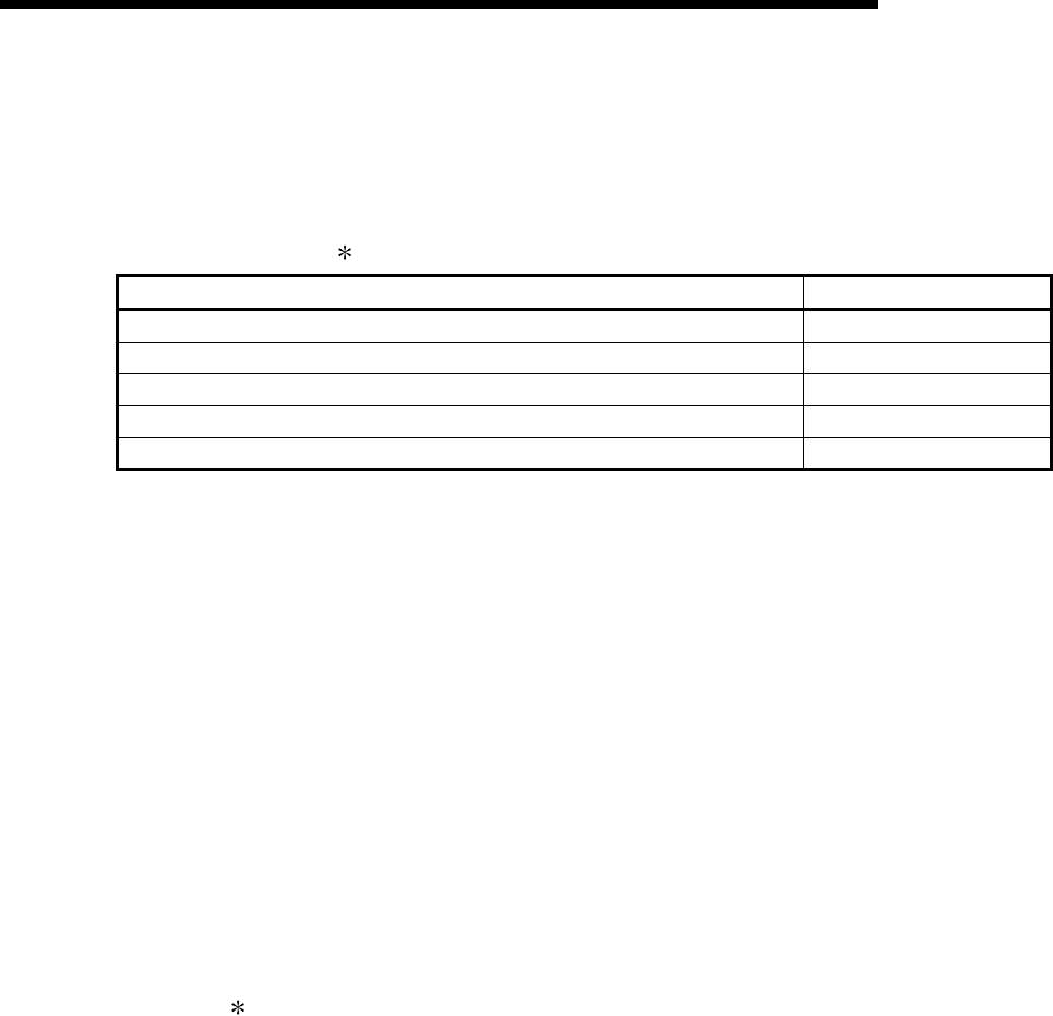
5 - 6 5 - 6
MELSEC-Q
5 DATA COMMUNICATION USING THE MELSEC COMMUNICATION
PROTOCOL
(b) Modem function monitor/test by GX Configurator-SC
It is possible to monitor the setting values for the remote password and the
number of occurrences up to the present, such as the designation of the
number of times before notifying an unmatched remote password and the
current number of occurrences.
It is possible to set each monitor value to "0."
Monitored items in the “modem function monitor/test” screen Buffer memory address
Remote password mismatch notification count designation 8204 (200CH)
Remote password mismatch notification accumulated count designation 8205 (200DH)
Accumulated count of unlock process normal completion 8955 (22FBH)
Accumulated count of unlock process abnormal completion 8956 (22FCH)
Accumulated count of lock process based on circuit disconnection 8959 (22FFH)
5.2 Utilizing the MX Component
If the external device is a PC running one of the basic operation systems below, it is
possible to create a communication program for the external device without
considering the detailed MC protocol (transmission/reception procedures) using one of
the following separately sold communication support tools.
See Appendix 7 for the overview of MX Component.
(Supported basic operation systems)
• Microsoft® Windows® 95 Operating System
• Microsoft® Windows® 98 Operating System
• Microsoft® Windows NT® Workstation Operating System Version 4.0
• Microsoft® Windows® Millennium Edition Operating System
• Microsoft® Windows® 2000 Professional Operating System
• Microsoft® Windows® XP Professional Operating System
• Microsoft® Windows® XP Home Edition Operating System
Depending on the version of MX Component used, different operating systems are
supported.
See the manual of MX Component for details.
(Communication support tools)
• MX Component (SW0D5C-ACT-E or later.)

6 - 1 6 - 1
MELSEC-Q
6 DATA COMMUNICATION USING THE NON PROCEDURE PROTOCOL
6
6 DATA COMMUNICATION USING THE NON PROCEDURE PROTOCOL
Data communication using the non procedure protocol is a function for sending and
receiving data between a PLC CPU and an external device using the message format
and transmission control procedure specified by the user.
Data can be transferred using the non procedure protocol when it is necessary to
perform data communication using the protocol for external devices such as a
measuring instrument and a bar code reader. In that case, transmission/receive data
processing can be simplified by using the communication functions with the user
frames described in the User's Manual (Application).
This chapter explains the basic transmission and reception methods when performing
data communication using the non procedure protocol.
Follow the procedure described in this chapter to create sequence programs for
sending and receiving data for the PLC CPU.
For details on the additional functions listed below for data communication using the
non procedure protocol, see the separate User's Manuals (Application).
• Sending/receiving data using user frames (See Chapter 11, Application)
• Monitoring the PLC CPU (automatic information function)
(See Chapter 2, Application)
• Switching modes from the PLC CPU (See Chapter 15, Application)
• Reading received data using interrupt programs (See Chapter 4, Application)
• Sending/receiving data using transparent code designation
(See Chapter 12, Application)
• Sending/receiving data using ASCII data (ASCII-BIN conversion)
(See Chapter 13, Application)
• Controlling half-duplex communication (See Chapter 8, Application)
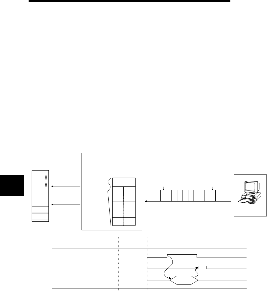
6 - 2 6 - 2
MELSEC-Q
6 DATA COMMUNICATION USING THE NON PROCEDURE PROTOCOL
6
6.1 Data Reception from the External Device
This section explains data reception from the external device.
There are two methods for receiving data: the "reception via receive complete code"
for receiving variable length messages, and the "reception via received data count" for
receiving fixed length messages. The receive complete code and received data count
used for data reception can be changed to any setting values chosen by the user using
GX Configurator-SC.
6.1.1 Receiving methods
The following shows the methods for receiving data in any format using the non-
procedure protocol.
There are two methods for receiving data: the "reception via receive complete code"
for receiving variable length messages, and the "reception via received data count" for
receiving fixed length messages. The receive complete code and received data count
used for data reception can be changed to any setting values chosen by the user using
GX Configurator-SC.
PLC CPU
1)
Reception data
read request
Receiving area
(buffer memory)
Receive data
storage area
Receive data
count storage
area
10
STX
D
F
H
(02H)
(48H)
(46H)
(44H)
B
(42H)
(0AH)
A
(41H)
G
(47H)
E
(45H)
C
(43H)
ETX
(03H)
(00H)
Q series C24
STX A BCDEFGHETX
Head data Receive complete code
(02H)(41
H)(48
H)(47H)(46H)(45H)(44H)(43H)(42H)(03
H)
Transmission data External device
RUN.
ERR.
USER.
BAT.
BOOT.
RS-232
USB
Q25HCPU
MODE.
2) 3)
INPUT
instruction
Description
Reception data read request signal
INPUT instruction complete device
INPUT instruction
CH1/CH2
X3/XA
Control timing
INPUT
1) When data is received from the external device using either "reception via receive
complete code" or "reception via received data count" method, the reception data
read request signal (X3/XA) turns ON.
2) Control data is stored in the device designated with the INPUT instruction.
3) When the INPUT instruction is executed, receive data is read from the reception
area of the buffer memory.
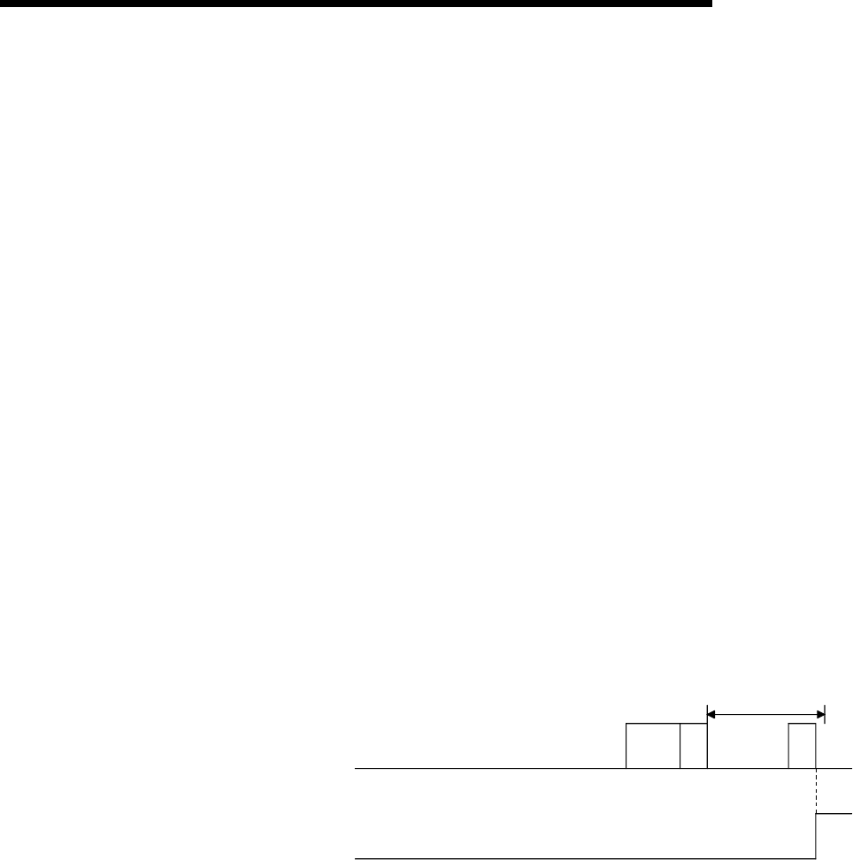
6 - 3 6 - 3
MELSEC-Q
6 DATA COMMUNICATION USING THE NON PROCEDURE PROTOCOL
(1) Data reception by receive complete code (for variable length
reception)
(a) This method is used to send data by adding the receive complete code set in
the Q series C24 at the complete of the message to be sent from the external
device.
(b) When the Q series C24 receives the receive complete code data preset in
GX Configurator-SC by the user, it sends a receive data read request to the
sequence program.
The read request from the Q series C24 allows the sequence program to
read the receive data up to the receive complete code received from the
external device.
(c) The receive complete code can be changed to match the specifications of the
external device. An arbitrary 1-character (1-byte) code within the 00H to FFH
range can be designated.
(d) The Q series C24 issues a receive data read request to the PLC CPU as
follows, according to the set value of the receive end code.
1) When receive complete code not changed (Default value: 0D0AH)
(CR+LF is added to the end of the message and sent from the external
device.)
• If LF is received within the time set in the no-reception monitoring time
(timer 0) after CR is received, the Q series C24 stores the receive data
up to CR+LF to the buffer memory receive data storage area and turns
on the read request signal to the PLC CPU.
External device
Reception data read reqest signal
(X3/XA)
Timer 0
set time
C
R
L
F
Q series C24
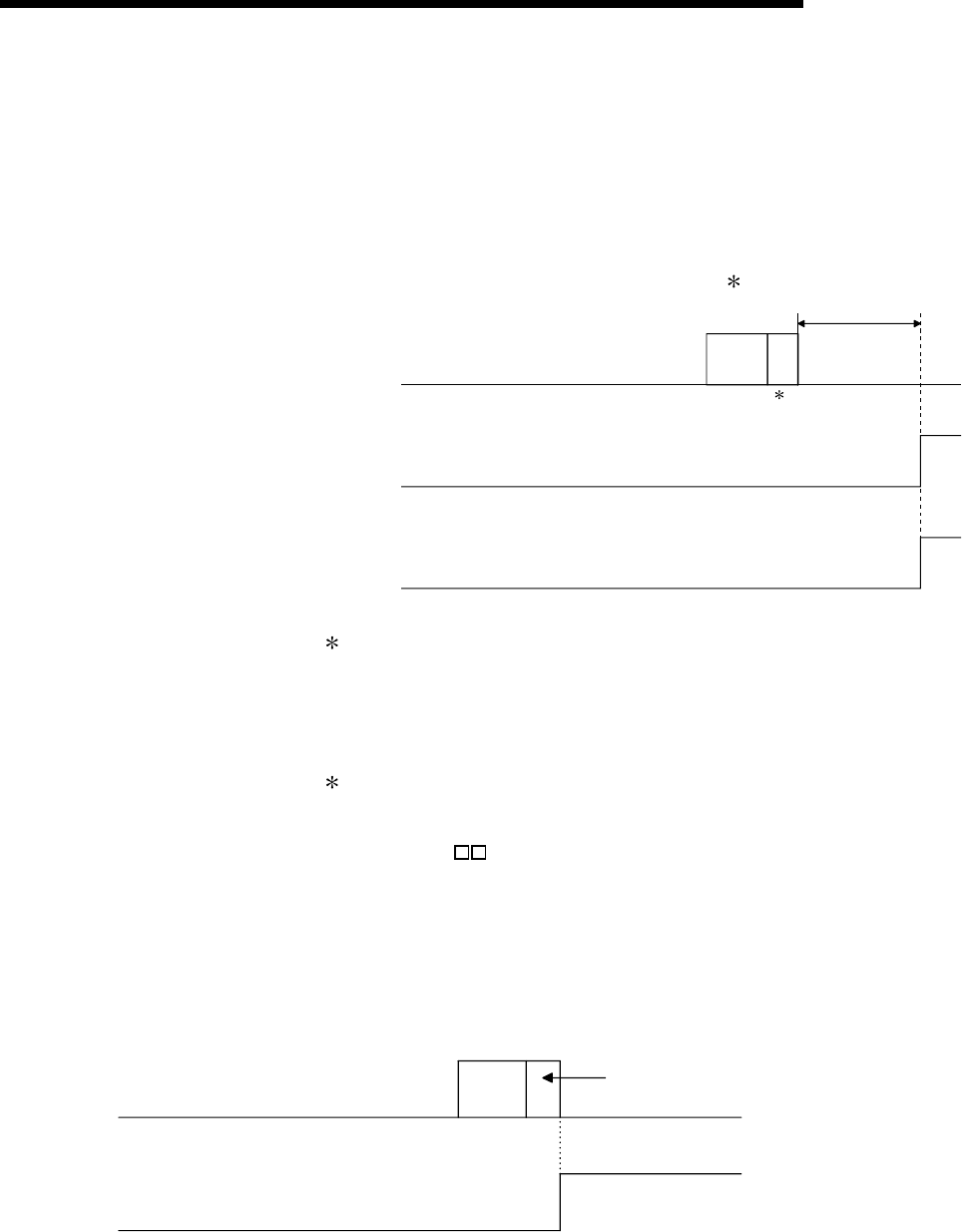
6 - 4 6 - 4
MELSEC-Q
6 DATA COMMUNICATION USING THE NON PROCEDURE PROTOCOL
• If the next data (LF, etc.) is not received within the time set in the non
reception monitoring time (timer 0) after CR is received, the Q series
C24 stores the received data up to CR to the buffer memory receive
data storage area and turns on the following signals to the PLC CPU.
When non procedure and non reception monitoring time format is 0:
Reception abnormal detection signal (X4/XB)
When non procedure and non reception monitoring time format is 1:
Reception data read request signal (X3/XA) 1
Reception abnormal detection signal
(X4/XB)
Timer 0
set time
C
R
Q series C24
External device
( 2)
[Format is 0]
Reception data read reqest signal
(X3/XA)
[Format is 1]
1 In non procedure protocol, a message is received by the increase in
non reception monitoring time (timer 0) if the received complete code
and the received data count are not decided.
For the non procedure protocol at the non reception monitoring time
format, see Chapter 6 of the User’s Manual (Application).
2 CR is included as 1 byte of data included in the message.
2) When the receive complete code is changed and an arbitrary code is
designated (00 H designated)
(User defined receive complete code data is added to the end of the
message and sent from the external device).
When the Q series C24 receives the receive complete code data
changed by the user, it stores the receive data up to the receive complete
code to the buffer memory receive area and turned on the read request
signal to the PLC CPU.
External device
Reception data request signal
(X3/XA)
Receive complete code data
Q series C24
3) When receive complete code not designated (FFFFH designated)
Reading by received data count is enabled.
See (2) for a description of reading by received data count.

6 - 5 6 - 5
MELSEC-Q
6 DATA COMMUNICATION USING THE NON PROCEDURE PROTOCOL
(2) Reception by received data count (For fixed length reception)
(a) This method is used to receive messages of the same length (size) from the
external device every time.
(b) When the Q series C24 receives data of the received data count preset in
GX Configurator-SC by the user, it sends a reception data read request to
the sequence program.
When the sequence program receives the read request from the Q series
C24, it reads data up to the received data count received from the external
device.
(c) The received data count default value is set to 511 (words). However, it can
be changed within the size of the receive data storage area depending on
the data contents exchanged with the external device.
POINT
(1) When the receive complete code and received data count are set to GX
Configurator-SC, both become valid.
In this case, if the Q series C24 receives the receive complete code before
data corresponding to the received data count, it outputs (X3/XA: ON) a
reception read request signal to the sequence program.
(2) For details on how to change the receive complete code and received data
count, see Section 8.4.7.
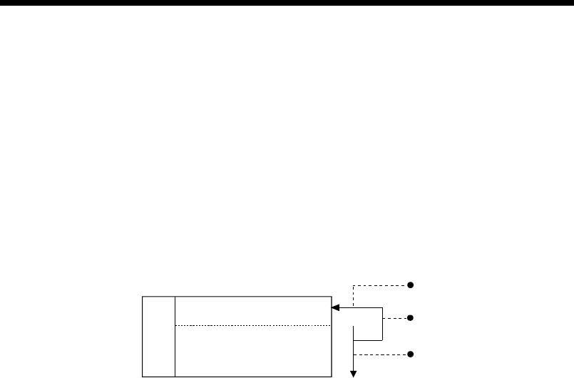
6 - 6 6 - 6
MELSEC-Q
6 DATA COMMUNICATION USING THE NON PROCEDURE PROTOCOL
6.1.2 The receive area and the received data list
The following shows the list of the receive area and the receive data for performing
data reception using the non procedure protocol.
(1) Receive area
The receive area is a memory area for storing the data received from the external
device and the receive data count in order to read the receive data for the PLC
CPU. By default, the receive area is assigned to addresses 600H to 7FFH (CH1
side) and A00H to BFFH (CH2 side).
Buffer memory
Receive data count storage area
Receive data storage area
CH1
address
600H
601H
7FFH
(Default)
Writes the receive data storage count when the PLC CPU
is requested to read the receive data.
Stores the arbitrary data area of the receive data.
The receive data count units (word/byte) are up to the value
set to GX Configurator-SC word/byte units designation.
Receive area
•
•
•
to

6 - 7 6 - 7
MELSEC-Q
6 DATA COMMUNICATION USING THE NON PROCEDURE PROTOCOL
POINT
(1) The position and size of the receive area in the buffer memory can be changed
with the GX Configurator-SC in accordance with the specifications of the
external device and the receive data length. (See Section 8.4.7.)
(a) When changing the position and size of the receive area in the buffer
memory with GX Configurator-SC, specify as follows:
1) Receive buffer memory head address designation
Designate the starting address for the area to be used as the receive
area in the user-definable area of the buffer memory (address: 400H
to 1AFFH, 2600H to 3FFFH).
2) Receive buffer memory length designation
Designate by address the length of the area (0001H to 1A00H) to be
used as the receive area in the user-definable area of the buffer
memory (address: 400H to 1AFFH, 2600H to 3FFFH).
(b) If the following functions are also used when the position and size of the
receive area in the buffer memory are changed, make sure that the
addresses of the receive area do not overlap with those for the buffer
memory that stores the transmission and reception data to be used by
these functions.
1) MC protocol buffer memory read/write function
2) MC protocol on-demand function
3) Non procedure protocol transmission/receive function
4) Bidirectional protocol transmission/receive function
5) Communication data monitoring function
(2) When sending data from the external device to the Q series C24, one of the
following two adjustments should be made so that the relationship shown
below is maintained.
1) Reduce the transmission data size.
2) Increase the receive area.
Receive data storage area ≥ Size of data sent from the external device
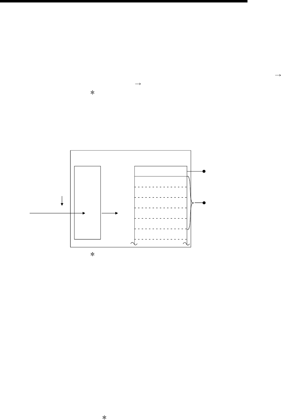
6 - 8 6 - 8
MELSEC-Q
6 DATA COMMUNICATION USING THE NON PROCEDURE PROTOCOL
(2) Receive data list
The following describes the data list when data received from an external device
is stored to the receive area.
1) The receive message is stored to the Q series C24 buffer memory (receive
data storage area).
2) The data is stored to the receive data storage area in low address (L) (H),
next address (L) (H) order.
Under the following conditions, when the receive data count is an odd
byte, 00H is stored in the upper byte of the final data storage position:
• When the unit for the received data count is designated in bytes.
• When data reception is performed using the receive complete code.
(Example) When receive arbitrary data area "ABCDEFG123" was stored
(The receive area is the default value.)
600H
601H
602H
603H
604H
605H
606H
(B)
42H
(C)
43H
(D)
44H
(E)
45H
(F)
46H
(G)
47H
(1)
31H
(2)
32H
(3)
33H
"321GFEDCBA"
Head
……
(A)
41H
Q series C24
( 1)
From external
device
OS area
The receive data is stored in low
address (L) → (H), next address
(L) → (H) order in the order in which
it is received.
Receive data storage area
Receive data count storage area
5 or 10
Buffer memory
CH1
address
1 The OS area of the Q series C24 shown in the above diagram is the
memory (8448 bytes) that temporarily stores the data to be received while a
request for the reading of the receive data is being made to the PLC CPU.
(The user cannot read the receive data in the OS area).
When the sequence program finishes reading the receive data in the
buffer memory in response to the read request, the receive data in the OS
area, and any succeeding receive data, is stored successively in the
receive area of the buffer memory when the next read request is issued.
Also, when the OS area's free space, which stores the receive data, is
reduced to 64 bytes default value or less, a request to discontinue data
reception from the external device is issued by the following transmission
control (the RS signal does not turn OFF):
• When DTR control is set, the DTR signal turns OFF.
• When DC1/DC3 control is set, DC3 is sent.
When there is no more free space in the OS area to store receive data,
an SIO error occurs and the SIO information bit in the communication
error information storage area (address: 201H/202H) in the buffer
memory turns ON. In that case, succeeding receive data is discarded
until a free space becomes available in the OS area.
For more details on the transmission control, see Chapter 7 of the
User's Manual (Application).
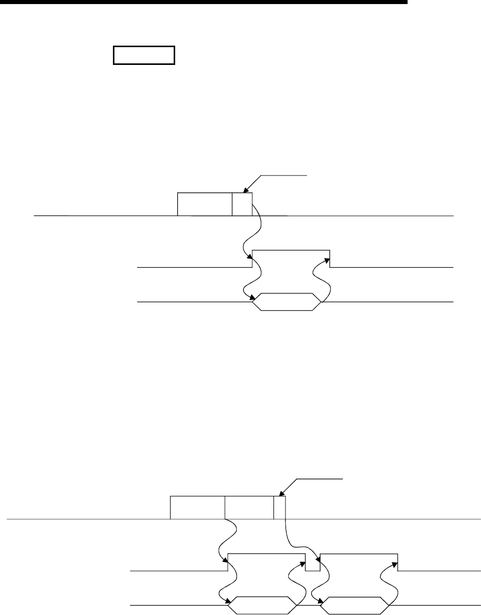
6 - 9 6 - 9
MELSEC-Q
6 DATA COMMUNICATION USING THE NON PROCEDURE PROTOCOL
REMARK
(1) Data reception when the receive data storage area is larger than
the receive data length
The following control is performed.
(Example) When the receive area for the CH1 side interface is located at
addresses 600H to 7FFH (default values) and data of 511 words or
less is received by the CH1 side interface.
INPUT
Q series C24
Complete code
External device 100 words
Reception data read
request signal
Sequence program
X3
Read data count: 100 words
(2) Data reception when the receive data storage area is smaller
than the receive data length
Since the following control is performed, data link processing is required in the
sequence program.
1) Reception using the complete code
(Example) When the receive area for the CH1 side interface is located at
addresses 600H to 7FFH (default values), and data of 534
words is received by the CH1 side interface.
External device
Reception data read request
X3
511 words
Sequence program INPUT INPUT
23 words
Q series C24
Read data count:
511 words Read data count:
23 words
Complete code
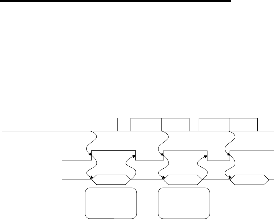
6 - 10 6 - 10
MELSEC-Q
6 DATA COMMUNICATION USING THE NON PROCEDURE PROTOCOL
2) Reception by received data count
When the received data count is set larger than the receive data storage
area, the receive buffer memory length (default: 512 words) -1 set in buffer
memory addresses A7H/147H is processed as the received data count.
(Receive data storage area) > (Data length received from external device)
(Example) When 550 words of data is received through the CH1 interface
in three parts when the CH1 interface receive area consists of
addresses 600H to 7FFH (default value)
External device
Reception data read
request signal
X3
511 words
Sequence program INPUT INPUT
39 words
INPUT
472 words 78 words 433 words 117 words
1st data 2nd data 3rd data
Read data....
1st 511 words
Read data....
1st 39 words and
2nd 472 words
Q series C24
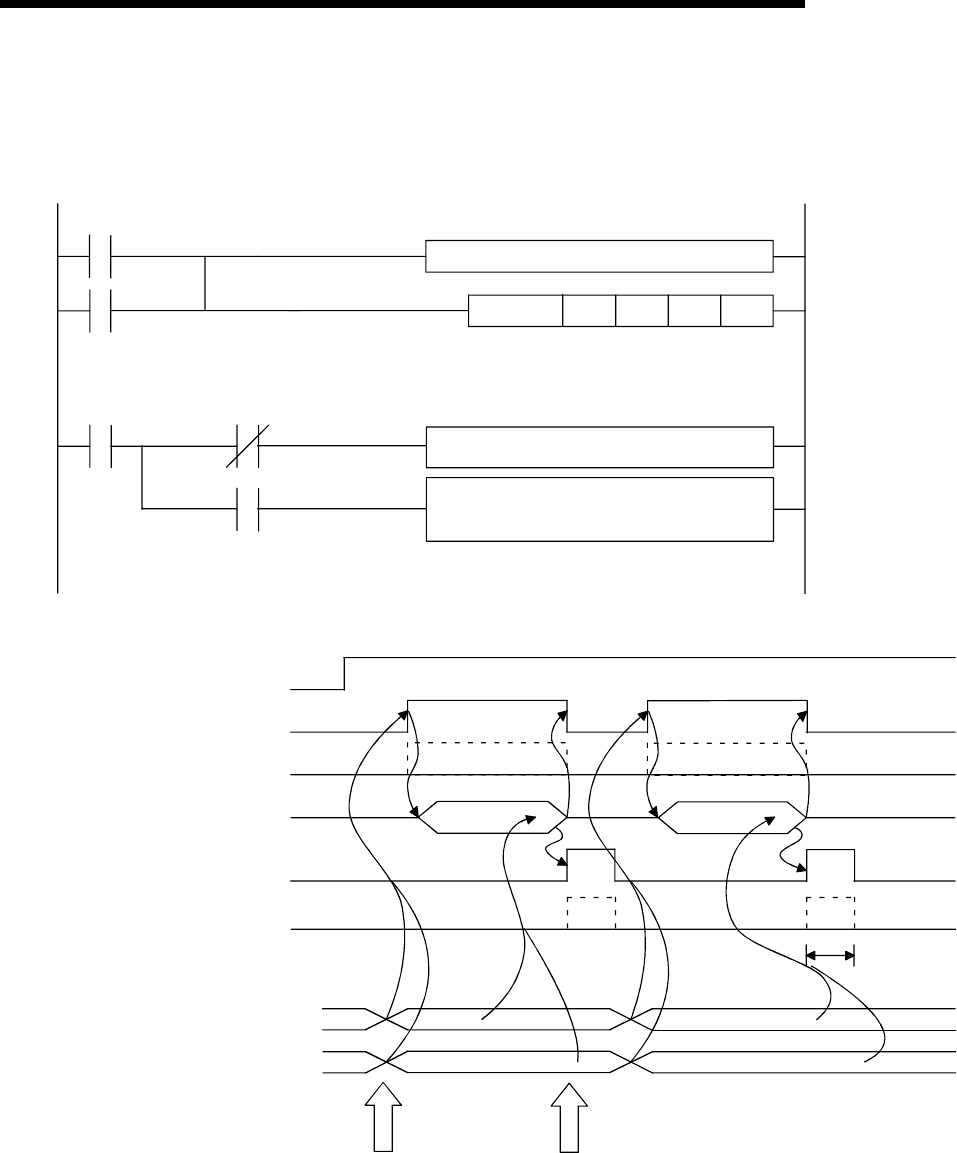
6 - 11 6 - 11
MELSEC-Q
6 DATA COMMUNICATION USING THE NON PROCEDURE PROTOCOL
6.1.3 Sequence program for data reception
This section explains the sequence program for data reception.
For details on the INPUT instruction for data reception, see Chapter 9.
X3 Read request
X4 Abnormal
detection G.INPUT UnD0D10M0
M0
M1
M1
Create control data from D0
Processing for normal completion
(receive data is stored)
Processing for abnormal completion
(Reading and discarding received data,
resent request, etc.
(CH1 side)
(CH1 side)
ON during abnormal
reception detection
Q series C24 ready signal
Reception data read request
signal
Reception abnormal detection
signal
INPUT instruction
INPUT instruction complete
device
INPUT instruction complete
device +1
(Normal completion/abnormal completion)
Received data count storage area
(Buffer memory address: 600H)
Received data storage area
(Buffer memory address: 601H to)
(X1E)
(X3)
(X4)
(M0)
(M1)
1)
2)
3)
4) 4)
INPUT INPUT
mn 1
Receive data 1 Receive data 2
Data reception-1 Data reception-2
1 scan
Data reception
2)
3)
ON during abnormal
reception detection
1) Start the self-station PLC.
The values specified with GX Developer are stored in the Q series C24.
2) When the amount of data specified by the received data count or data containing
the receive complete code is received from the external device, the reception data
read request signal turns ON.
3) After the control data for the INPUT instruction is stored in the device, the
sequence program executes the INPUT instruction and reads the receive data.
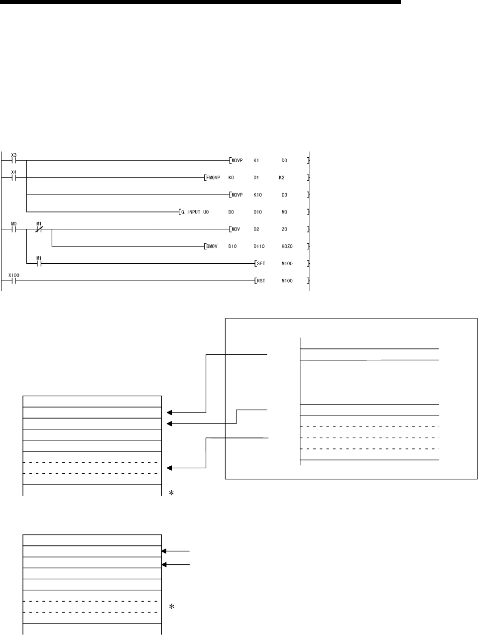
6 - 12 6 - 12
MELSEC-Q
6 DATA COMMUNICATION USING THE NON PROCEDURE PROTOCOL
4) The device completing the INPUT instruction turns ON when the reading of receive
data is completed.
When the complete device + 1 (abnormal completion signal) turns ON, the error
code is stored in the control data completion status (S1 + 1).
(Program example)
When the Q series C24 I/O signals are from X/Y00 to X/Y1F:
Designate the receive channel.
Clear the reception result and receive data count
storage device to 0.
Designate the allowable receive data count.
With normal completion, the receive data within the
allowable receive data count (user designated) is read
from the receive data storage area in the buffer memory.
Once the INPUT instruction is executed, the user
designated read completion signal (M0) turns ON
for 1 scan.
The reading of receive data and switching of the
ON/OFF status are performed by the PLC CPU.
•
•
The abnormal completion flag is reset by an external
command.
Data received prior to an error occurrence will be
stored in the receive data storage device.
For normal completion
(1)
(0)
(n)
(10)
(1)
(other than 0)
(n)
(10)
Q series C24
D 0
D 1
D 2
D 3
D10
D m
Interface number
Reception result
Receive data count
Allowable receive data count
Receive data
Receive data
For abnormal completion
D 0
D 1
D 2
D 3
D10
D x
Interface number
Reception result
Receive data count
Allowable receive data count
Receive data
Receive data
Buffer memory
Data reception result storage area
Receive data count storage area
Receive data storage area
Address
258H
600H
601H
7FFH
When the receive data count is larger than the
allowable receive data count, only the data up to
the allowable receive data count will be stored
and the excess data will be discarded.
From the buffer memory (address 258H)
From the buffer memory (address 600H)
to to
to
to to

6 - 13 6 - 13
MELSEC-Q
6 DATA COMMUNICATION USING THE NON PROCEDURE PROTOCOL
POINT
(1) Receive data can also be read using interrupt programs.
For more details on reading receive data with interrupt programs, see Chapter
4 of the User's Manual (Application).
Note that if the reading of data received from the same interface is to be
performed, it is not possible to combine the reading of data received by the
main program and reading of data received by the interrupt program.
Accordingly, use one or the other of the above programs to read the data
received.
(2) The SPBUSY instruction is used to read the execution status when using a
dedicated instruction. (See Chapter 9.)
(3) More than one INPUT instruction cannot be executed simultaneously.
Execute the next INPUT instruction only after the execution of the first INPUT
instruction is completed.
(4) When the communication data count is set in word units, and if the received
data count is an odd byte when requesting the reading of received data to the
PLC CPU, the receive data count is processed as follows:
Receive data count = Receive data byte count/2 … Fractions following the
decimal point are rounded up
Also, 00H is stored in the higher byte of the final data storage position in the
receive area where receive data is stored.

6 - 14 6 - 14
MELSEC-Q
6 DATA COMMUNICATION USING THE NON PROCEDURE PROTOCOL
6.1.4 Receive data clear
For the data reception by a non procedure protocol, if the transmission of data from a
transmitting device is interrupted due to trouble occurring, it may be necessary for the
data received up to the present time are cleared in the receiving device and for the
data to be received again from the start.
The methods for clearing reception data in the Q Series C24 is shown below. Either
method may be used to clear the reception data as is necessary.
1) Clear the reception data by the dedicated instruction "CSET."
2) Write to/read from the reception data clear request area (address A8H/148H).
(FROM/TO instruction)
3) Clear the reception data by GX Configurator-SC (see Section 8.7).
REMARK
When transmitting data to an external device from the Q Series C24, do not execute
a clear request of the reception data shown in this section.
If a reception data clear request is executed when transmitting data to an external
device, The Q Series C24 stops data transmission and terminates the dedicated
instruction for transmission abnormally. (The transmission completed signal does not
go ON.) If a reception data clear request is executed during data reception, the data
received up to that point are cleared.
(1) Receive data clear processing
The Q series C24 performs the following procession when the receive data clear
is performed.
• The data received up to that point can be ignored.
• The receive data count up to that point is "0".
(The receive area in the buffer memory is not initialized).
• Set to the status prior to the start of data reception.
(2) Procedure for clearing the reception data by the dedicated
instruction "CSET"
This instruction clears the reception data up to the present without interrupting
the data transmission processing.
(Procedure for clearing) ··· In case of the CH1 side interface
1) Execute the CSET instruction
If the CSET instruction is executed while the read request (X03/X0A) or
reception abnormal detection signal (X04/X0B) is turned on, the CSET
instruction is kept waiting until the signal is turned off.
2) The reception data clear processing is executed at the OS area of the Q
series C24 (see Section 6.1.2).
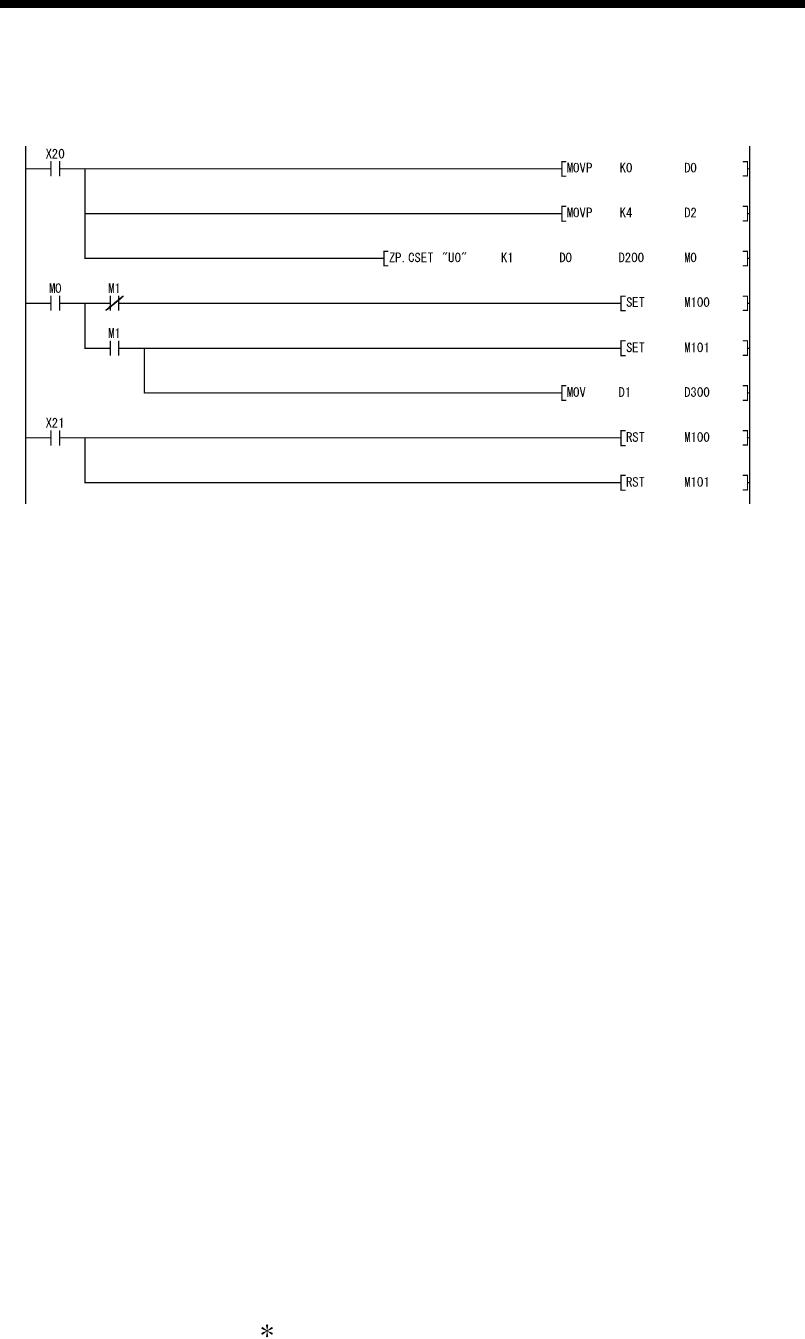
6 - 15 6 - 15
MELSEC-Q
6 DATA COMMUNICATION USING THE NON PROCEDURE PROTOCOL
The following is a program example of clearing the reception data by the
dedicated instruction "CSET."
Set the execution type
Set the request type
(Reception data clear)
Execute the reception
data clear
Normal completion
Abnomal completion
Reset the complete flag b
y
external command
(3) Receive data clear procedure using FROM/TO instruction
Write and read the buffer memory receive data clear request area (addresses A8
H/148H) using the procedure described below.
When resuming data communications with an external device, resume it after
completing the reception data clear processing with the Q Series C24.
Depending on the data communications system, it may be necessary to restart
data communications with the external device after notifying the external device
from the PLC CPU that resumption of communications is possible.
(Clear Procedure)· ··When the CH1 side interface is used.
(1) Since receive processing, send processing and receive data clear processing
are not being performed, “1” is written to buffer memory address A8H using
the TO instruction for the sequence program.
(2) Receive data clear processing is performed for the Q Series C24’s OS area
(See Section 6.1.2).
(3) When receive data clear processing is completed, the value in buffer memory
address A8H becomes “0.”
The following page shows an example of a program to clear receive data with the
FROM/TO instruction.
Create a program that contains the contacts (user flags, etc.) indicating the
following statuses in the TO instruction.
• Contact when the CHn reception data read request signal (X3/XA) is OFF
• Contact when the CHn reception abnormal detection signal (X4/XB) is OFF
• Contact indicating that send and receive processes are not currently being
performed
• Contact indicating that reception data clear processing is not currently being
performed
1 When the function version A Q Series C24 is used, resume data
communications a further 100 ms after the buffer memory address
A8H/148H value changes from a “1” to a “0.”
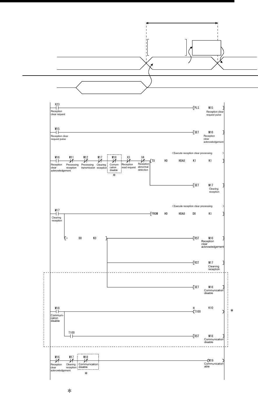
6 - 16 6 - 16
MELSEC-Q
6 DATA COMMUNICATION USING THE NON PROCEDURE PROTOCOL
Q series C24
Buffer memory
address A8H
PLC CPU
(Program) TO instruction
(Write "1" to address A8H)
"0" "1" "0"
Send request
execution disabled
Receive
data clear
processing
(2)
Dedicated instruction
for sending execution
disabled, too (3)
(1)
( 1
)
( 1)
( 1)
1 Add the dotted line portion to the sequence program when the function version
A Q Series C24 is used. (Carry out communications when M19 is ON.)
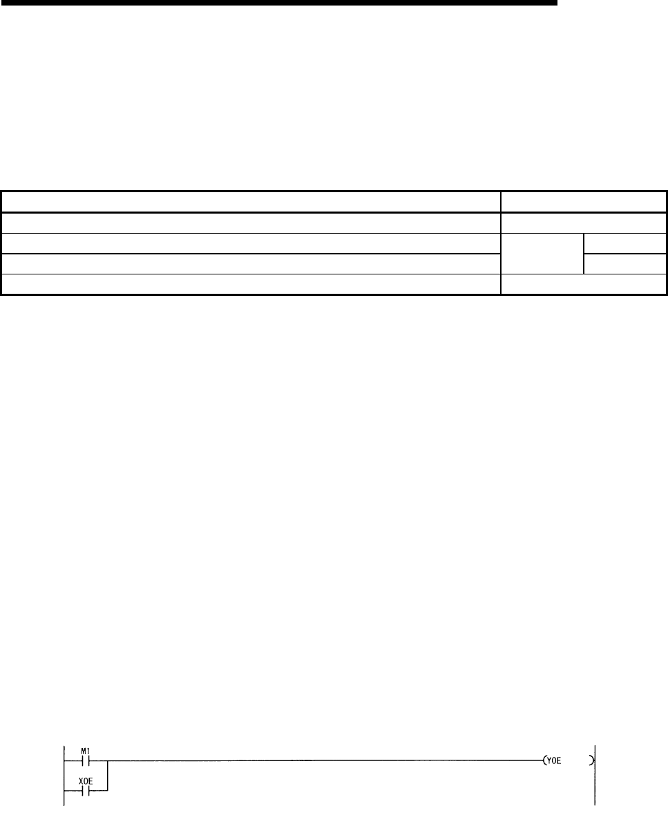
6 - 17 6 - 17
MELSEC-Q
6 DATA COMMUNICATION USING THE NON PROCEDURE PROTOCOL
6.1.5 How to detect reception errors
This section explains how to detect errors that may occur when receiving data from the
external device.
The following items are considered as the primary causes of errors that may occur
during data reception.
Cause of reception error Reference section
A transmission error occurred due to noise. —
A timeout for the no-reception monitoring (timer 0) occurred. Chapter 6
Received data that could not be converted using the ASCII-BIN conversion.
User's Manual
(Application) Chapter 13
Received data larger than the size that could be stored in the OS area of the Q series C24. Section 6.1.2
(1) Confirmation using the sequence program
1) The following device and input signals turn ON.
• INPUT instruction complete device + 1
• Reception abnormal detection signal (X4/XB)
• ERR LED ON signal (XE/XF)
2) The reception error code can be checked using the INPUT instruction
control data ((S1) + 1).
Or, it can be checked by reading the data reception result storage area
in the buffer memory (addresses 258H/268H).
For details on how to check the error code contents and take corrective
actions, see Chapter 10.
(b) How to turn off the ERR LED and clear the error code (see Section 10.1.2.)
1) To turn off only the ERR LED, write "1" to the LED OFF request area
(addresses 0H/1H) in the buffer memory.
2) To turn off the ERR LED and clear the error code, turn ON the ERR LED
OFF request output signal (YE/YF).
(Example) To perform the ERR LED OFF and the error code clear on the
CH1 side
INPUT instruction
Completion device + 1

6 - 18 6 - 18
MELSEC-Q
6 DATA COMMUNICATION USING THE NON PROCEDURE PROTOCOL
(2) Confirmation using the module and GX Configurator-SC
1) Confirmation using the display LED
When the Q series C24 detects an error, including a transmission error, the
ERR LED lights up. (See Chapter 10.)
2) Confirmation using GX Configurator-SC
• The monitor function is used to check for errors. (See Sections 8.6.3 and
8.6.5.)
• The ERR LED is turned off with the ERR LED OFF function. (See Section
8.6.10.)
3) Confirming the error code
Use one of the following to confirm the error code.
• GX Configurator-SC monitor function (See Section 8.6.5.)
• GX Developer buffer memory monitor function (monitors addresses
258H/268H)
(3) Receive data when a reception error occurs
(a) Storing receive data
The receive data for which an error was detected is discarded and only the
normally received data is stored in the Q series C24.
Thus, there may be missing data among the data that has been read to the
PLC CPU when a reception error occurs.
(b) Reading receive data
When receive data is read to the PLC CPU by turning the reception
abnormal detection signal (X4/XB) ON, the data that was normally received
prior to the error detection is read. Read and discard receive data as
needed.
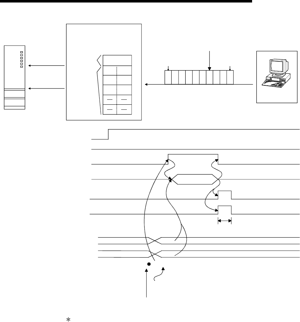
6 - 19 6 - 19
MELSEC-Q
6 DATA COMMUNICATION USING THE NON PROCEDURE PROTOCOL
Reception
abnormal
detection
Receive area
(buffer memory)
Receive data
count storage
area STX
D
(02H)
(44H)
B
(42H)
(03H)
A
(41H)
E
(45H)
C
(43H)
(00H)
STX A BCDEFGHETX
Head data Receive
complete code
(02H)(41
H)(48
H)(47H)(46H)(45H)(44H)(43H)(42H)(03
H)
Transmission data External device
Reception error causing data
PLC CPU
RUN.
ERR.
USER.
BAT.
BOOT.
RS-232
USB
Q25HCPU
MODE.
3
Q series C24
INPUT
instruction
Receive data
storage area
Q series C24 ready signal
Reception data read request
Reception abnormal
detection signal
INPUT instruction
INPUT instruction complete device
INPUT instruction complete device + 1
(normal completion/abnormal
completion)
Receive data count storage area
(Buffer memory address: 600H)
Receive data storage area
(Buffer memory addresses: 601H to)
INPUT
(X1E)
(X3)
(X4)
Receive data
Data reception
1 scan
ERR LED lights up
Reception abnormal
detection data
n3
When the data from "G" to in the reception message shown in the figure above is
received normally, the data is stored in the Q series C24 OS area.
The receive data stored in the OS area will be read to the PLC CPU in the
succeeding read operation.
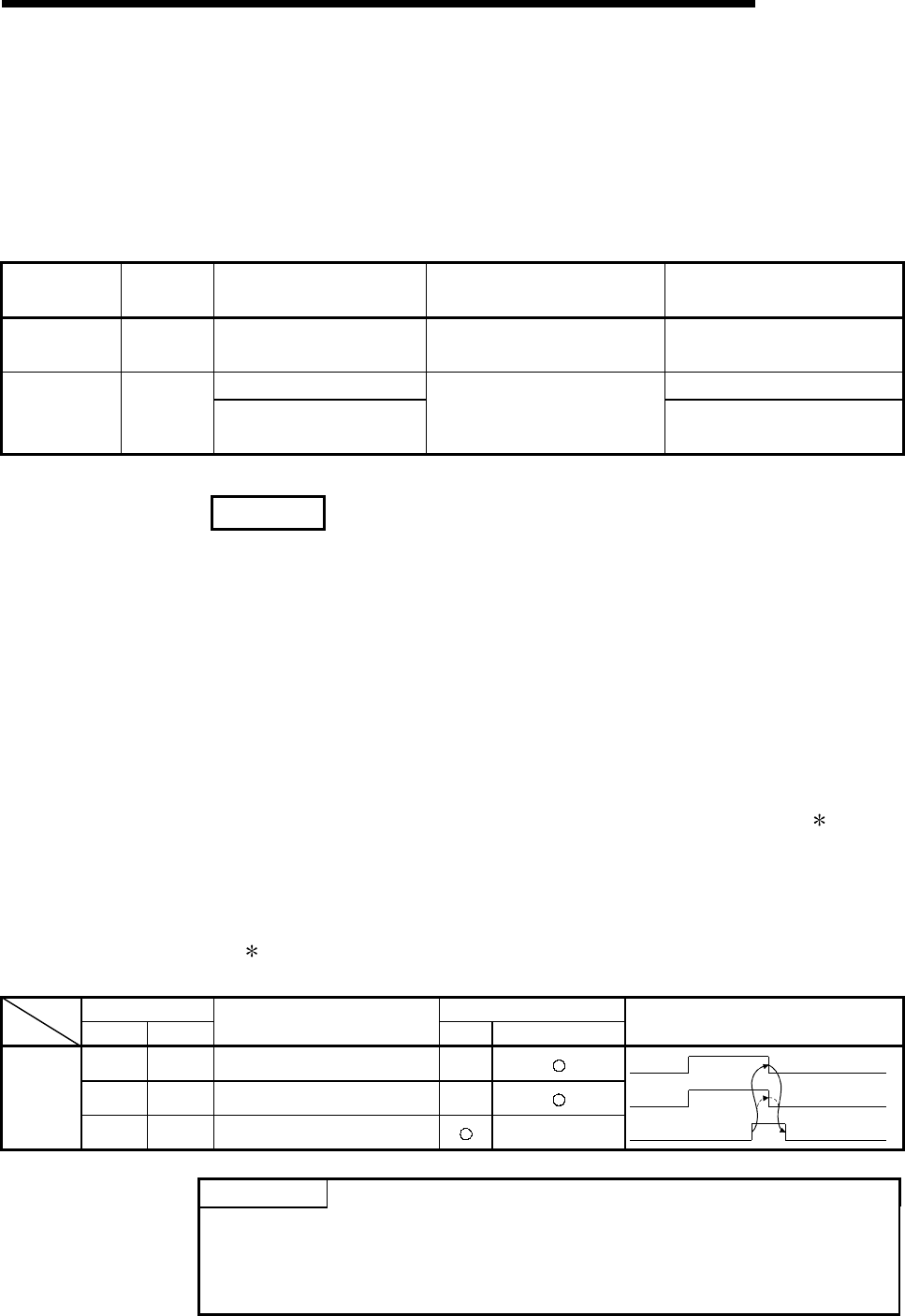
6 - 20 6 - 20
MELSEC-Q
6 DATA COMMUNICATION USING THE NON PROCEDURE PROTOCOL
6.1.6 Received data count and receive complete code settings
The following default values have been set for the received data count and receive
complete code that are used for data reception with the non procedure protocol.
If it is necessary to change the following default settings, change the settings on the
GX Configurator-SC "Non procedure system setting" screen according to the
specifications of the external device (see Sections 8.4.5 and 8.4.7).
Setting data Default
value Allowable range Buffer memory address where
the setting value is stored Remarks
Received data
count 511 (1FFH)Less than the size of the
receive data storage area A4H/144HUnit is in accordance with the
word/byte units designation
0000H to 00FFHWhen any code is set
Receive
complete code
0D0AH
(CR, LF) FFFFHA5H/145HWhen there is no receive
complete code
REMARK
Other than through the setting using GX Configurator-SC or the TO instruction at the
startup of the Q series C24, the received data count and receive complete code
setting values can be changed even after data communication has started if the
timing is as shown in the chart below.
The following describes the procedure for changing setting values for data reception
via the non procedure protocol after the start of data communication, and for the
resumption of data reception processing. Specifically, the module restrictions are
explained, along with the timing and procedure for changing the setting values.
(1) Data receiving method
Reception using a dedicated instruction (INPUT) or an interrupt program ( 1) cannot
be performed. (Transmission using a dedicated instruction (OUTPUT) can be
performed.) Data must be received using the FROM instruction in the main program.
The following describes the I/O signals. (A program example is shown on the
following page.)
1 For details on the data reception using interrupt programs, see the User's
Manual (Application).
I/O signal Device that turns ON/OFF
CH1 side CH2 side Signal name CPU Q series C24 Timing
X3 XA Reception data read request
X4 XB Reception abnormal detection
Reception
Y1 Y8 Reception data read completion
(Only when normal)
(Only when abnormal)
POINT
When the reception abnormal detection signal (X4/XB) turns ON, read the error
code from the buffer memory below, and then check the type of error and take
corrective action based on the information found in Chapter 10.
• Data reception result storage area (addresses 258H/268H)
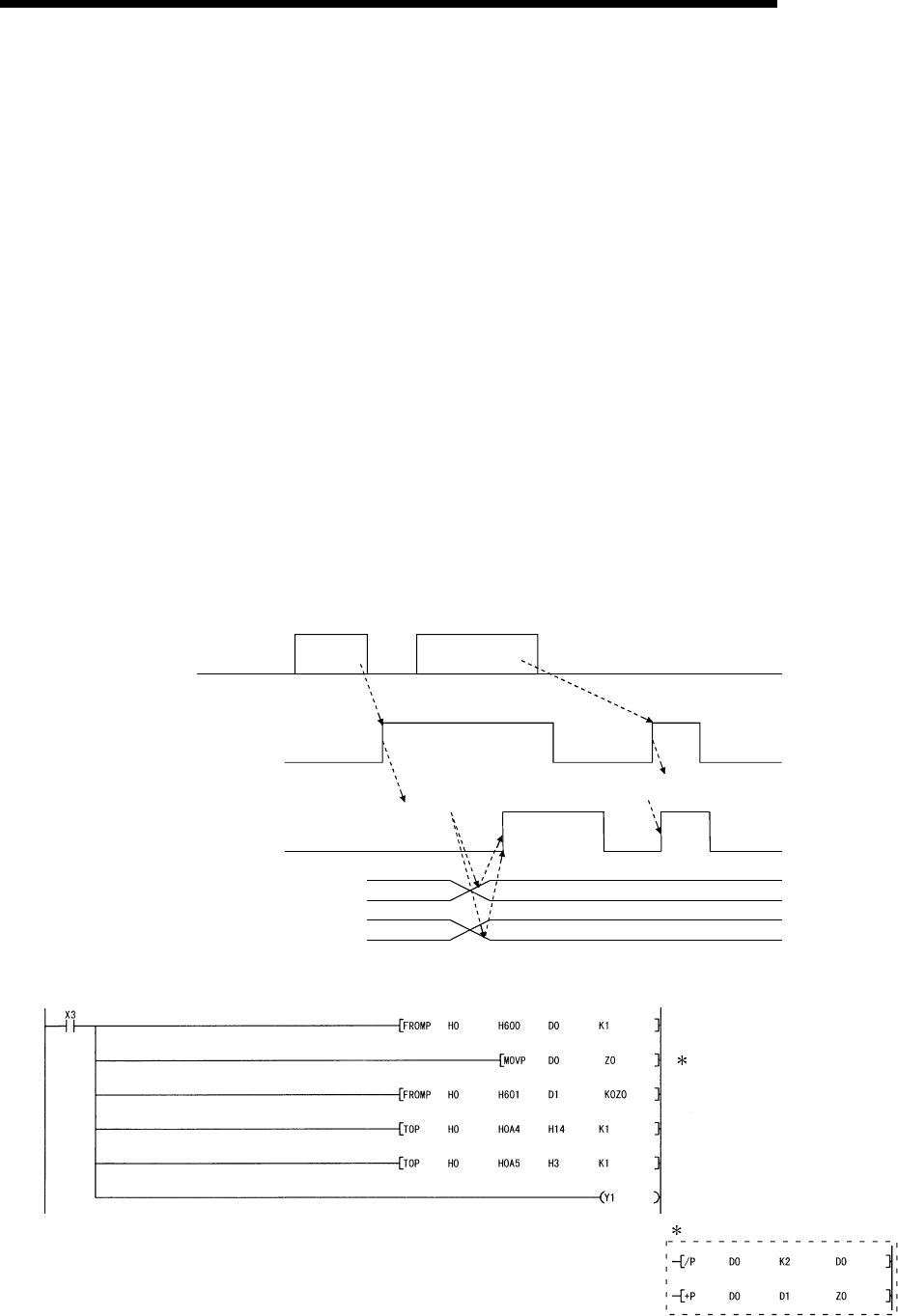
6 - 21 6 - 21
MELSEC-Q
6 DATA COMMUNICATION USING THE NON PROCEDURE PROTOCOL
(2) Setting values that can be changed
Of the initial settings from GX Configurator-SC stored in the buffer memory, only
the following setting values can be changed after data communication has
started.
• Received data count (buffer memory addresses: A4H, 144H)
• Receive complete code (buffer memory addresses: A5H, 145H)
(3) Timing and procedure for changing the setting values
1) Timing of change
To change the receive complete code and received data count after data
communication has started, change the setting when the status of the I/O
signals relating to the reading of receive data is as follows.
• Reception data read request signal (X3, XA) or reception abnormal
detection signal (X4, XB): ON
• Reception data read completion signal (X1, Y8): OFF
2) Change procedure
When data reception from an external device causes the reception data read
request signal/reception abnormal detection signal to turn ON, turn ON the
reception data read completion signal after performing the following.
• Read the receive data.
• Change the setting values for the receive complete code and the received
data count.
(Example) When reading data received in the CH1 side interface
External
device side Data 1 Data 2
PLC CPU side
Read request signal
(X3)
Read completion signal
(Y1)
Received data count setting area
(buffer memory address: A4H)
Receive complete code setting area
(buffer memory address: A5H)
Setting value-A
1)
2)
3) 5)
4)
Reads
receive data
Data read request using
setting value -A/-1
Data read request using
setting value -B/-2
Reads
receive data
Setting value-1
Setting value-B
Setting value-2
(Program example: I/O signals for the Q series C24 are from X/Y00 to X/Y1F)
Reads the data that is equal to the receive
data count.
Change the setting value for the received
data count as needed.
Change the setting value for the receive
complete code as needed.
Reads receive data count.
Turns ON the read complete signal.
( 1)
1 When unit is in bytes
Read request
1) 2)
2)
3)
4)
5)
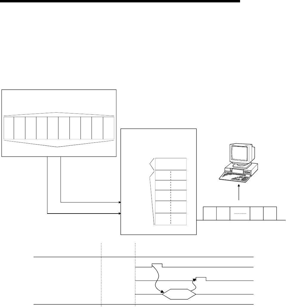
6 - 22 6 - 22
MELSEC-Q
6 DATA COMMUNICATION USING THE NON PROCEDURE PROTOCOL
6.2 Sending Data to the External Device
This section explains data transmission from the PLC CPU to the external device.
6.2.1 Transmission methods
The following shows how to send data in any format using the non procedure protocol.
Transmission area
(buffer memory)
STX A BCDEFGHETX
Transmission data
(02H)(41
H)(48
H)(47H)(46H)(45H)(44H)(43H)(42H)(03
H)
A
(41H)
G
(47H)
E
(45H)
C
(43H)
STX
B
D
F
H
(02H)
(48H)
(46H)
(44H)
(42H)
ETX
(03H)
10
(0AH)(00H)
3)
Transmission data
PLC CPU
ETX H
(03H)(48H)(41
H)(03H)
External device
ASTX
1) 2)
OUTPUT instruction
Q series C24
Transmission
data count
designation
area
Transmission
data
designation
area
OUTPUT instruction
completion device
OUTPUT instruction OUTPUT
Transmission instruction
Contents CH1/CH2 Control timing
1) Transmission data is stored in the device designated with the OUTPUT instruction.
2) Control data is stored in the device designated with the OUTPUT instruction.
3) When the OUTPUT instruction is executed, the Q series C24 sends the amount of
data designated by the transmission data count from the transmission data area to
the external device in ascending order of the transmission data area addresses.
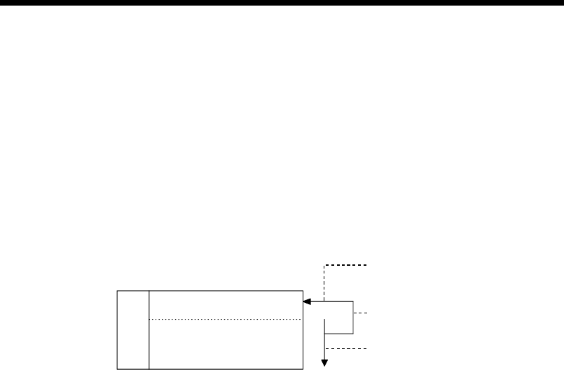
6 - 23 6 - 23
MELSEC-Q
6 DATA COMMUNICATION USING THE NON PROCEDURE PROTOCOL
6.2.2 Arrangement and contents of the transmission area and the transmission data
This section explains the arrangement and contents of the transmission area and the
transmission data for performing data transmission using the non procedure protocol.
(1) Transmission area
The transmission area is a memory area for storing the data and the data count
that are transmitted from the PLC CPU to the external device via the Q series
C24. By default, the transmission area is assigned to addresses 400H to 5FFH
(CH1 side) and 800H to 9FFH (CH2 side).
Buffer memory
Transmission data count
storage area
CH1 side
address
400H
401H
5FFH
(Default setting)
The unit of transmission data count (words/bytes)
is in accordance with the word/byte units
designation in GX Configurator-SC.
The transmission data count designated with the
OUTPUT instruction is written.
The transmission data designated with the OUTPUT
instruction is written.
Transmission data
storage area
to
Transmission
area
•
•
•

6 - 24 6 - 24
MELSEC-Q
6 DATA COMMUNICATION USING THE NON PROCEDURE PROTOCOL
POINT
(1) The position and size of the transmission area in the buffer memory can be
changed with GX Configurator-SC in accordance with the specifications of the
external device and the received data length. (See Sections 8.4.5 and 8.4.7.)
(a) When changing the position and size of the transmission area in the buffer
memory with GX Configurator-SC, specify as follows:
1) Transmission buffer memory head address designation
Designate the starting address for the area to be used as the
transmission area in the user definable area of the buffer memory
(address: 400H to 1AFFH, 2600H to 3FFFH).
2) Transmission buffer memory length designation
Designate by addresses the length of the area (0001H to 1A00H) to be
used as the transmission area in the user definable area of the buffer
memory (address: 400H to 1AFFH, 2600H to 3FFFH).
(b) If the following functions are also used when the position and size of the
transmission area in the buffer memory are changed, make sure that the
addresses of the transmission area do not overlap with those for the
buffer memory that stores the transmission and receive data to be used
by these functions.
1) MC protocol buffer memory read/write function
2) MC protocol on-demand function
3) Non procedure protocol transmission/receive function
4) Bidirectional protocol transmission/receive function
5) Communication data monitoring function
(2) Set the size of data per data transmission from the PLC CPU to the external
device so that it is smaller than the size of the transmission data's designated
area in the buffer memory.
(Transmission data designation area) ≥ (Size of arbitrary data portion to be sent
from the PLC CPU)
To transmit data whose size is larger than the transmission data designation area,
increase the transmission area, or divide the transmission data before sending.
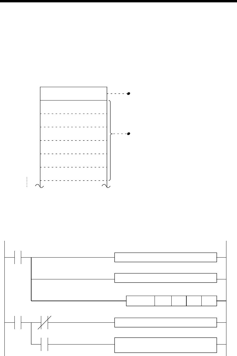
6 - 25 6 - 25
MELSEC-Q
6 DATA COMMUNICATION USING THE NON PROCEDURE PROTOCOL
(2) Transmission data arrangement
The following example shows an arrangement of the transmission data to be sent
to the external device when storing it in the transmission area.
(Example) When transmitting "ABCDEFG123" (The transmit area is the default
value.)
CH1 side
address
400H
401H
402H
403H
404H
405H
406H
5 or 10
(B)
42H
(A)
41H
(C)
43H
(D)
44H
(E)
45H
(F)
46H
(G)
47H
(1)
31H
(2)
32H
(3)
33H
(5)
35H
(4)
34H
1)
2)
Buffer memory
Transmission data count storage area
In accordance with the word/byte units designation
Word units....5
Bytes units....10
Transmission data designation area
Sequentially store the transmission data to low address (L) → (H), next
address (L) → (H), in the order of transmission.
6.2.3 Sequence program for transmission data
A sequence program for transmission data is explained below.
For details on the OUTPUT instruction used for data transmission, see Chapter 9.
G.OUTPUT Un D0 D11 M0
M0 M1
M1
(In case of the CH1 side)
Transmission
instruction
Create transmission data from D11
Create control data from D0
Processing for normal completion
Processing for abnormal completion
(retransmission, etc.)
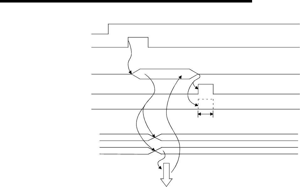
6 - 26 6 - 26
MELSEC-Q
6 DATA COMMUNICATION USING THE NON PROCEDURE PROTOCOL
Q series C24 ready signal
Transmission instruction
OUTPUT instruction
OUTPUT instruction complete device
OUTPUT instruction complete device + 1
(normal completion/abnormal
completion)
Transmission data count designation area
(buffer memory address: 400H)
Transmission data storage area
(buffer memory address: 401H to)
OUTPUT
(X1E)
1 scan
0n
Transmission data
Transmitting data
1)
2)
3)
4)
ON when transmission
abnormal completion
1) Starts the local station PLC.
The setting values for GX Developer are stored in the Q series C24.
2) Inputs the user data transmission command signal.
3) Executes the OUTPUT instruction after storing the transmission data and the
control data for the OUTPUT instruction in the device.
Data is sent when the OUTPUT instruction is executed.
4) When the Q series C24 transmission processing completes, the completion device
for the OUTPUT instruction turns ON.
When the completion device + 1 (abnormal completion signal) turns ON, the error
code is stored in the control data completion status (S1+1).
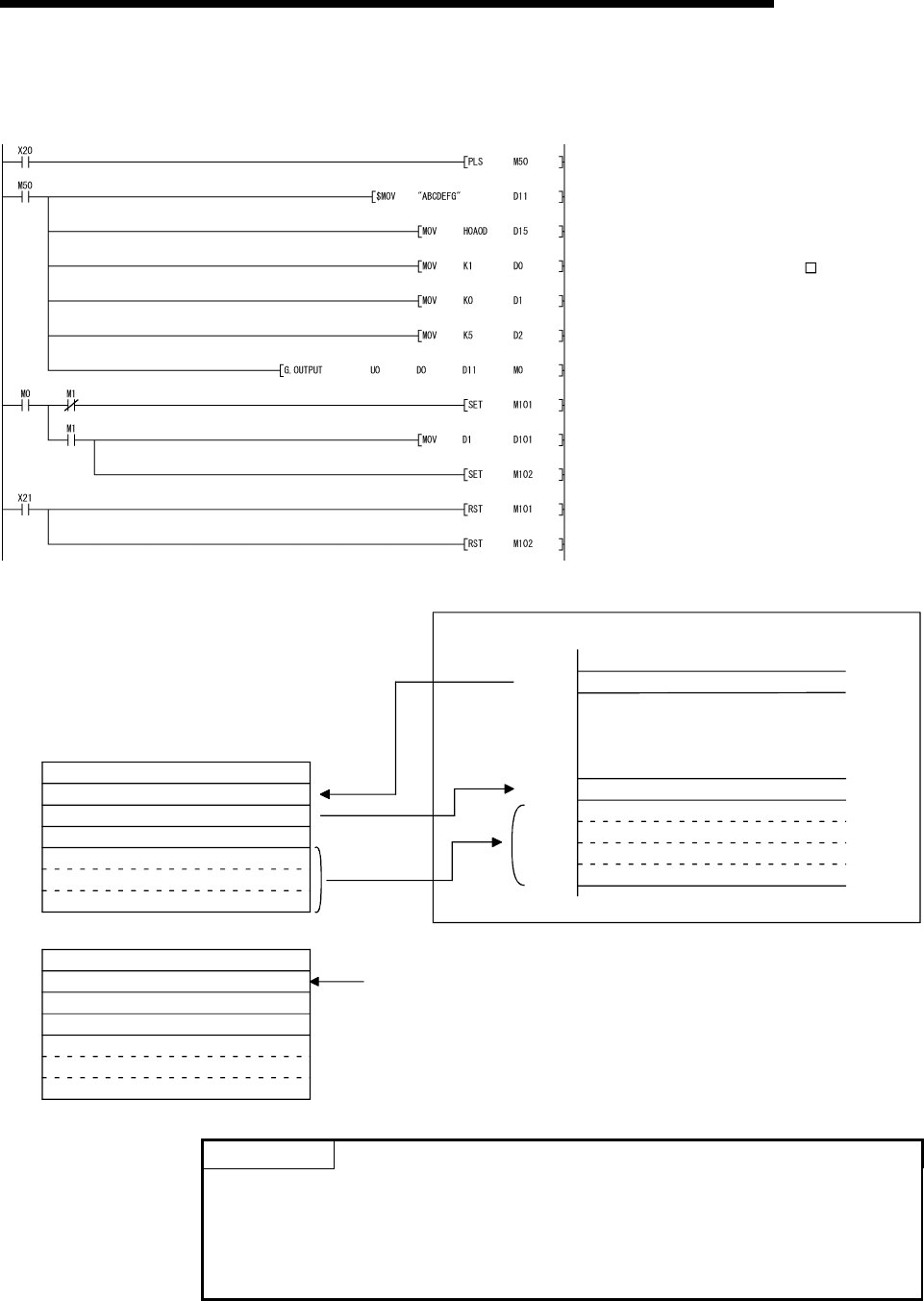
6 - 27 6 - 27
MELSEC-Q
6 DATA COMMUNICATION USING THE NON PROCEDURE PROTOCOL
(Program example)
When Q series C24 I/O signals are from X/Y00 to X/Y1F:
The transmission command is converted into pulse.
The transmission data stored in the designated device
is sent.
Designate the number of the interface(CH ) that will send the
data.
Designate the transmission data count in word units.
(Designate K10 when the unit is bytes.)
Clear the transmission result storage device to 0.
Transmission data is stored.
After the OUTPUT instruction is executed, the user
designated transmission complete signal (M0) turns ON
for one scan.
Storing the transmission data and writing the
transmission data count in the buffer memory, and
issuing a transmission request to the Q series C24 are
all executed by the PLC CPU.
The completion flag is reset by an external command.
Interface number
Transmission result
Transmission data count
(0001H)
(0000H)
D 0
D 1
D 2
D11
D15
From buffer memory (address 257H)
Buffer memory
Data transmission result storage area
Transmission data count designation area
Transmission data designation area
Address
257H
400H
401H
5FFH
(4241H)
(0A0DH)
(0001H)D 0
D 1
D 2
D11
D15
(4241H)
(0A0DH)
Q series C24
For normal completion
(0005H)
(0005H)
For abnormal completion
Interface number
Transmission result
Transmission data count
to to
to to
to
(other than 0000H)
Transmission data
Transmission data
POINT
(1) The SPBUSY instruction is used to read the execution status when using a
dedicated instruction. (See Chapter 9.)
(2) More than one OUTPUT instruction cannot be executed simultaneously.
Execute the next OUTPUT instruction only after the execution of the first
OUTPUT instruction is completed.
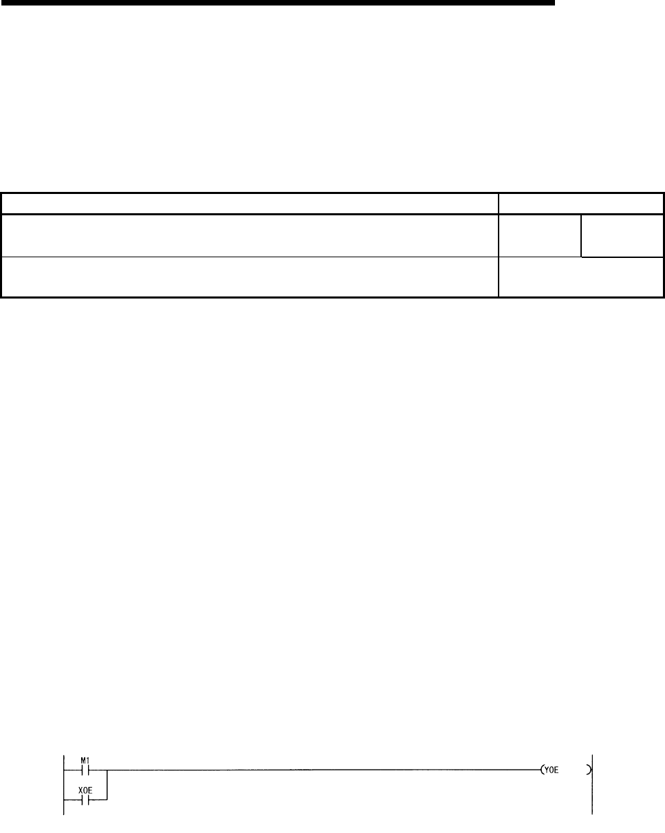
6 - 28 6 - 28
MELSEC-Q
6 DATA COMMUNICATION USING THE NON PROCEDURE PROTOCOL
6.2.4 How to detect transmission errors
This section explains how to detect errors that may occur when sending data to the
external device.
The following items are considered as the primary causes of errors that may occur
during data transmission.
Cause of reception error Reference section
A timeout occurred for the transmission monitoring time (timer 2) User's Manual
(Application) Section 6.3
Designated number of transmission data was larger than the size that could be stored in the
transmission area Section 6.2.2
(1) Confirmation using the sequence program
(a) Detecting a transmission error
1) The following device and input signal turn ON.
• OUTPUT instruction complete device + 1
• ERR LED ON signal (XE/XF)
2) The transmission error code can be checked using the OUTPUT
instruction control data ((S1) + 1).
Or, it can be checked by reading the data transmission result storage
area in the buffer memory (addresses 257H/267H).
For details on how to check the error code contents and corrective
actions, see Chapter 10.
(b) How to turn off the ERR LED and clear the error code (see Section 10.1.2)
1) To turn off only the ERR LED, write a "1" to the LED OFF request area
(addresses 0H/1H) in the buffer memory.
2) To turn off the ERR LED and clear the error code, turn ON the ERR LED
OFF request output signal (YE/YF).
(Example) To perform the ERR LED OFF and the error code clear on the
CH1 side
OUTPUT instruction
Complete device + 1
6 - 29 6 - 29
MELSEC-Q
6 DATA COMMUNICATION USING THE NON PROCEDURE PROTOCOL
(2) Confirmation using the module and GX Configurator-SC
1) Confirmation using the display LED
When the Q series C24 detects an error, including a transmission error, the
ERR LED lights up. (See Chapter 10.)
2) Confirmation using the GX Configurator-SC
• The monitor function is used to check for errors. (See Sections 8.6.3 and
8.6.5.)
• The ERR LED is turned off with the ERR LED OFF function. (See Section
8.6.10.)
3) Confirming the error code
Use one of the following to confirm the error code.
• GX Configurator-SC monitor function (See Section 8.6.5.)
• GX Developer buffer memory monitor function (monitors addresses
257H/267H)
POINT
When a transmission error occurs, the PLC CPU may not transmit all the
designated data.
It is recommended that data communications be performed by establishing a user
arbitrary communication procedure that can check normal transmission by
reception of a response to data transmission.

6 - 30 6 - 30
MELSEC-Q
6 DATA COMMUNICATION USING THE NON PROCEDURE PROTOCOL
6.3 Data Communications Precautions
The following describes the precautions to be taken during non procedure protocol
data communications.
(1) The Q series C24 transmission sequence initialization conditions
The initial status indicates the status where transmission has stopped and
reception data has been discarded.
The Q series C24 transmission sequence initialization conditions are as follows.
1) When the power is turned on, the Reset switch on the CPU panel is
operated, or the Q series C24 mode is switched
2) When the receive data was cleared.
3) When the CD signal was turned off when data communications were
performed by setting CD terminal check enable during full-duplex
communications through the RS-232 interface.
(2) Generation of framing error in external device
When nothing is transmitted from the Q series C24 to the external device through
the RS-422 or RS-422/485 interface, a framing error may be generated by the
noise etc, in the external device.
Send an arbitrary code to identify the head of the send data from the Q series
C24 to the external device.
Before data communication check the Q series C24 interface specifications.
(3) Data communications with external device (computer, etc.) over a
multidrop link
When the external device PLC CPU are connected by a 1:n multidrop link, each
the Q series C24 receives the data transmitted by the external device.
With a multidrop link, receive data by user frame ( 1).
If data is not received by user frame, a sequence program that ignores the
receive data other than the receive data addressed to the local station by
sequence program, including the data indicating the objective PLC CPU in the
message, must be written.
(Sample message)
STX Space Station
No. 0 CR LF
(02H)(20
H)(32
H)(32
H)(0D
H)(0A
H)
(Example)
Station
No. 2 Data length
(BIN data) Data
1 See chapter 11 of User's Manual (Application)

6 - 31 6 - 31
MELSEC-Q
6 DATA COMMUNICATION USING THE NON PROCEDURE PROTOCOL
(4) Retry processing for data reception errors
The data when reception error occurred is discarded and only the data for the
normal reception is taken into the Q series C24. For this reason, the reception
message may be missing data when an error occurs. To assure the correct
transmission and reception of data it is recommended that a normal/error
response message is received and a response message reception timeout check
is conducted for data transmitted between the PLC CPU and the external
equipment and that measures be taken when an error message is received or
when an error timeout occurs, such as retransmitting the data (transmission
retry).

7 - 1 7 - 1
MELSEC-Q
7 DATA COMMUNICATION USING THE BIDIRECTIONAL PROTOCOL
7
7 DATA COMMUNICATION USING THE BIDIRECTIONAL PROTOCOL
Data communication using the bidirectional protocol is a function for sending/receiving
any data using the message format and transmission control procedure for the Q
series C24 bidirectional protocol between external devices and PLC CPUs.
Any external devices that can install application programs and transmit and receive
data in accordance with the MELSEC PLC protocol can communicate with the PLC
CPUs using the bidirectional protocol.
This chapter explains the basic transmission and reception methods when performing
data communication using the bidirectional protocol.
Follow the procedure described in this chapter to create sequence programs for
sending and receiving data for the PLC CPU.
Regarding the additional functions listed below for data communication using the
bidirectional protocol, see the separate User's Manuals (Application)
• Reading receive data using interrupt programs
(See Chapter 4 of Application)
• Sending/receiving data using ASCII data (ASCII-BIN conversion)
(See Chapter 13 of Application)
• Sending/receiving data using transparent code designation
(See Chapter 12 of Application)
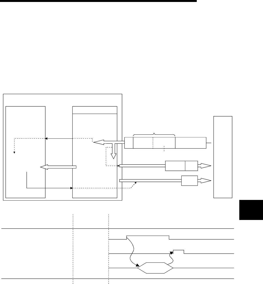
7 - 2 7 - 2
MELSEC-Q
7 DATA COMMUNICATION USING THE BIDIRECTIONAL PROTOCOL
7
7.1 Data Reception from the External Device
This section explains the data reception from the external device.
7.1.1 Receiving methods
The following shows how to receive data sent from the external device using the
bidirectional protocol. Since the size of each message received is recognized using the
"data length" information contained in the message, messages of any size can be sent
from the external device.
PLC CPU
Sequence
program
3)
Read
(BIDIN
instructions)
External
device
1)
Arbirary data
(00H to FFH)4)
2)
2)
Read request
(00H to FFH)
Buffer memory
Receive area
Q series C24
(When normal)
ENQ Data length Data area Sum check code
Arbitrary data
(When abnormal)
Ignored
Error code NAK
ACK
Reception data read request signal
BIDIN instruction completion device
BIDIN instruction
CH1/CH2
X3/XA
Control Timing
BIDIN
Contents

7 - 3 7 - 3
MELSEC-Q
7 DATA COMMUNICATIONS USING BIDIRECTIONAL PROTOCOL
1) When the control code ENQ is received, the Q series C24 starts data reception
processing.
When the data specified by the data length is received, the Q series C24 ends the
reception processing of that data.
If "Sum check" is set with GX Developer, the Q series C24 checks whether the
message is normal or abnormal using the sum check code received immediately
after the message and the sum check code calculated by internal processing.
If "No sum check" is set with GX Developer, messages are not checked using
the sum check codes.
2) If the message has normally been received, the reception data read request signal
(X3/XA) turns ON.
If an error has been detected when receiving the message, the Q series C24
sends an abnormal end response (NAK message) to the external device.
The reception data read request will not be sent to the PLC CPU.
(The reception abnormal detection signal (X4/XB) does not come on.)
3) Control data is stored in the device designated with the BIDIN instruction and then
the BIDIN instruction is executed.
Receive data is read from the receive area of the buffer memory.
4) When the BIDIN instruction has been executed, the Q series C24 sends a normal
end response (ACK message) to the external device.
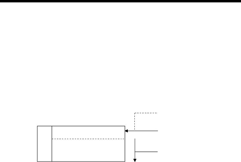
7 - 4 7 - 4
MELSEC-Q
7 DATA COMMUNICATIONS USING BIDIRECTIONAL PROTOCOL
7.1.2 Arrangement and contents of the receive area and the receive data
This section shows the arrangement and contents of the receive area and the receive
data for performing data reception using the bidirectional protocol.
(1) Receive area
The receive area is a memory that stores the received data length (receive data
count) and data area received from an external device.
The receive area is allocated to addresses 600H to 7FFH (CH1 side) and A00H to
BFFH (CH2 side) at initial setting.
Buffer memory
Receive area
Receive data count storage area
Receive data storage area
CH1
address
600H
601H
7FFH
(Default)
The units of data length (word/byte) is in accordance
with the word/byte units designation in GX Configurator-SC.
Data length
The contents of data length of the received
message are stored.
Data area
The contents of the data area of the received
message are stored in ascending address order.
to
•
•
•

7 - 5 7 - 5
MELSEC-Q
7 DATA COMMUNICATIONS USING BIDIRECTIONAL PROTOCOL
POINT
(1) The position and size of the receive area in the buffer memory can be changed
with GX Configurator-SC in accordance with the specifications of the external
device and the received data length. (See Sections 8.4.5 and 8.4.7.)
(a) When changing the position and size of the receive area in the buffer
memory with GX Configurator-SC, specify as follows:
1) Receive buffer memory head address designation
Designate the starting address for the area to be used as the receive
area in the user definable area of the buffer memory (address: 400H to
1AFFH, 2600H to 3FFFH).
2) Receive buffer memory length designation
Designate by addresses the length of the area (0001H to 1A00H) to be
used as the receive area in the user definable area of the buffer
memory (address: 400H to 1AFFH, 2600H to 3FFFH).
(b) If the following functions are also used when the position and size of the
receive area in the buffer memory are changed, make sure that the
addresses of the receive area do not overlap with those for the buffer
memory that stores the transmission and reception data to be used by
these functions.
1) MC protocol buffer memory read/write function
2) MC protocol on-demand function
3) Non procedure protocol transmission/receive function
4) Bidirectional protocol transmission/receive function
5) Communication data monitoring function
(2) When sending data to the Q series C24 from the external device, one of the
following two adjustments should be made so that the relationship shown
below is maintained.
1) Reduce the send data size.
2) Increase the receive area.
(Receive data storage area) ≥ (Size of data portion sent from the external device)
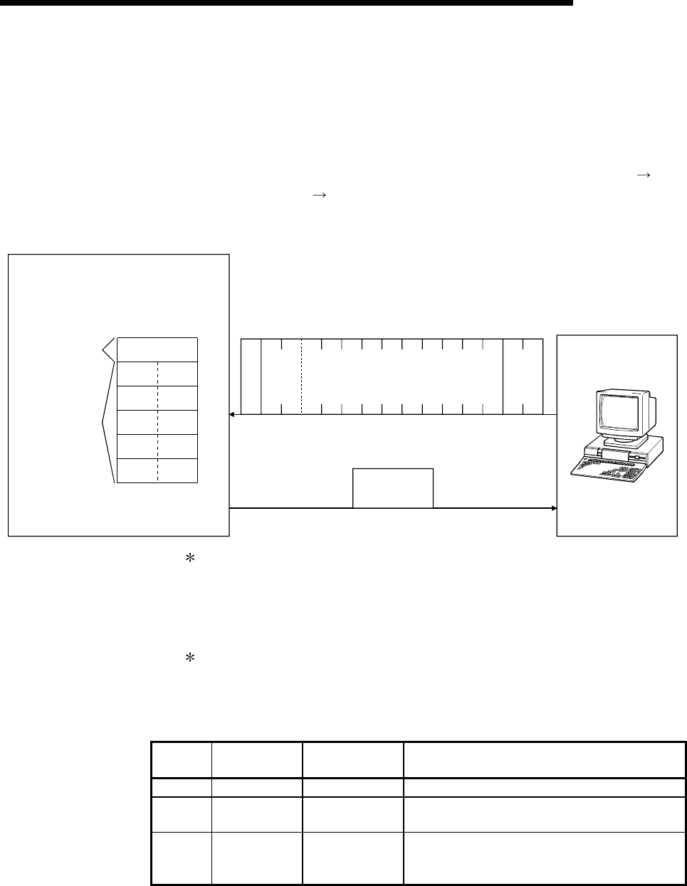
7 - 6 7 - 6
MELSEC-Q
7 DATA COMMUNICATIONS USING BIDIRECTIONAL PROTOCOL
(2) Arrangement of receive data
The following example illustrates the arrangement of data received from the
external device when it is stored in the receive area.
1) The receive message is stored to the Q series C24 buffer memory (receive
data storage area).
2) The data is stored to the receive data storage area in low address (L) (H),
next address (L) (H) order.
If the received data is "ABCDEFG123", it will be stored as shown below (for
the CH1 side):
ENQ (0005H)
ABCDEFG1 23
LH LH
05H00H41H46H44H42H43H32H45H31H47H33H47H02H
Sum
check
code
5
(00H)(05
H)
B
(42H)
D
(44H)
F
(46H)
1
(31H)
3
(33H)
A
(41H)
C
(43H)
E
(45H)
G
(47H)
2
(32H)
Receive
data count
storage area
Receive
data storage
area
Receive area
(buffer memory)
Q series C24
External device
Transmission data (response message)
ACK
06H
(Normal completion)
Data
length
Receive data (response message)
When the data length unit is in bytes, 00H is stored in the higher byte of the
last data storage position in the receive area when the data length of the
message is an even byte.
(3) Contents of receive data
The contents of receive data, including the receive data as indicated in
Section 7.2.2, are explained below.
(a) Control codes
The types of control codes are shown in the table below.
Signal
name
Code
(hexadecimal) Contents Application
ENQ 05HEnquiry Code for starting data transmission.
ACK 06HAcknowledge Response code to the opposite side when data was
received normally.
NAK 15HNegative
Acknowledge
Response code to the opposite side when data could
not be received normally. (Error code is sent
immediately after the response code.)
1) For data communication from the external device to the Q series C24
the Q series C24 checks and processes the control code received.
It cannot be read from the sequence program.
2) For data communication from the Q series C24 to the external device
The control code to be transmitted is added by the Q series C24.

7 - 7 7 - 7
MELSEC-Q
7 DATA COMMUNICATIONS USING BIDIRECTIONAL PROTOCOL
(b) Data length
This indicates the number of bytes or words for the data portion of the
message.
The unit of data length (words/bytes) is in accordance with the word/byte
units designation in GX Configurator-SC.
1) For data communication from the external device to the Q series C24
The Q series C24 checks the length of the data received.
When the reception is normal, the Q series C24 stores the receive data
in the receive data storage area of the Q series C24 buffer memory,
assigning the first byte as the lower byte (L).
2) For data communication from the Q series C24 to the external device
The length of the transmission data is the number of the transmission
data designated by the sequence program using the BIDOUT
instruction.
The Q series C24 sends this value as is from the lower byte (L).
(c) Data portion
This consists of an array of original one-byte data to be transmitted to the
external device side, which can handle 00H to FFH code data.
1) For data communication from the external device to the Q series C24
If the receive data portion is normal, the Q series C24 takes the codes
as is and stores them in the receive data storage area in sequence,
beginning with the youngest address.
The storage size is in accordance with the data length in the message
(See item (b) above) and the word/byte units designation in GX
Configurator-SC.
2) For data communication from the Q series C24 to the external device
The transmission data portion is the number of the transmission data
designated by the sequence program using the BIDOUT instruction.
The Q series C24 sends the transmission data using the existing codes
until the transmission data count is reached in accordance with the
word/byte units designation in GX Configurator-SC to the transmission
data designation area.
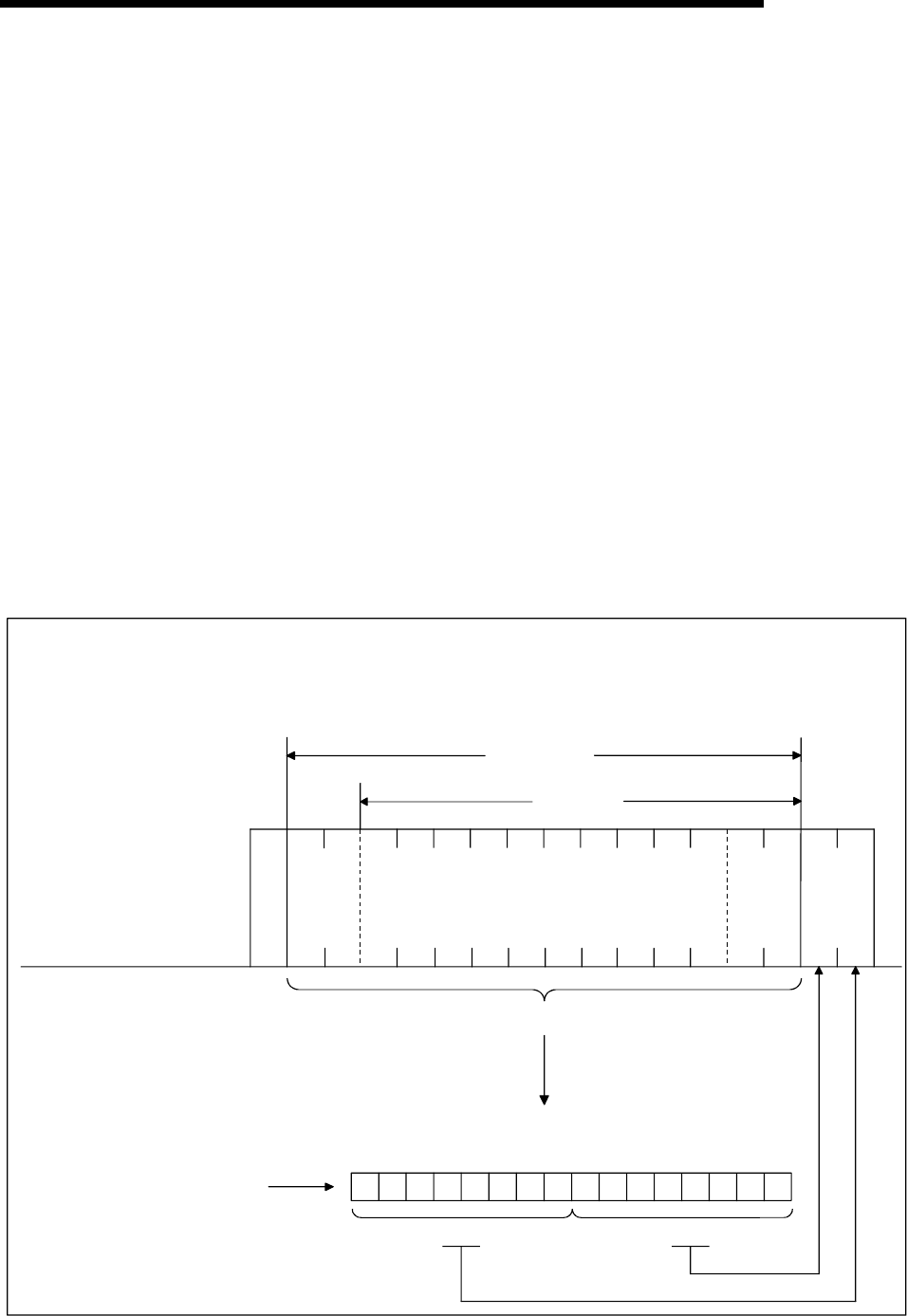
7 - 8 7 - 8
MELSEC-Q
7 DATA COMMUNICATIONS USING BIDIRECTIONAL PROTOCOL
(d) Sum check code
The sum check code expresses the numeric value for the lower two bytes
(16 bits) of the results (sum) from the addition of the data length and the
data portion in the message as binary code data.
When "Sum check" is specified with the transmission setting in GX
Developer, it is necessary to add a sum check code at the end of the
message.
1) For data communication from the external device to the Q series C24
The Q series C24 checks and processes the sum check code received.
It cannot be read from the sequence program.
When "No sum check" is specified, once a data portion of message
corresponding to the data length is received, the succeeding data
received will be ignored up to the control code that follows (See (a)).
The following example shows the contents of a sum check code in the
message.
2) For data communication from the Q series C24 to the external device
The sum check code to be transmitted is calculated and added by the Q
series C24. When "No sum check" is specified, no sum check code is
transmitted.
E
N
QABCDEFGH IJ 100
LH LHLH
00 000000 111111 00
b15 b8 b7 b1 b0
(Example) The following shows the sum check code when "ABCDEFGHIJ " and the numeric value 100 are sent as data
(when the unit is in bytes).
External device side
Q series C24
Arbitrary data
Data
Data
length
(000CH)(0064H)
Sum
check
code
Contents of 0327H memory
03H27H
(L) (H)
(H)
0CH + 00H + 41H + 42H + 43H + 44H + 45H + 46H +
47H + 48H + 49H + 4AH + 64H + 00H
Added value = 0327H
(L)
toto
0CH00H41H47H
42H43H44H45H46H48H49H4AH64H00H27H03H
05H

7 - 9 7 - 9
MELSEC-Q
7 DATA COMMUNICATIONS USING BIDIRECTIONAL PROTOCOL
(e) Error code
The error code indicates the definition of the error during NAK response.
(For more details on the error codes, see Chapter 10.)
1) For data communication from the external device to the Q series C24
For error codes from the external device, transmit the codes specified by
the user.
The error codes (0022H to 005FH) that are not used by the Q series C24
can be used.
The Q series C24 stores the received error codes as a completion status
in the control code for the BIDOUT instruction.
They are also stored in the data transmission result storage area in the
buffer memory (address: 257H).
2) For data communication from the Q series C24 to the external device
The error codes are added by the Q series C24.
When an error code is transmitted, the Q series C24 writes the same
error code in the data reception result storage area of the buffer memory
(address: 258H).
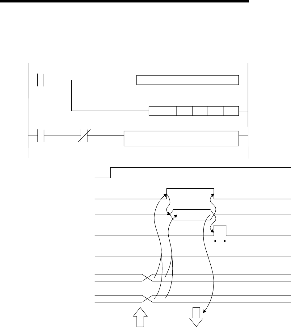
7 - 10 7 - 10
MELSEC-Q
7 DATA COMMUNICATIONS USING BIDIRECTIONAL PROTOCOL
7.1.3 Sequence program for data reception
This section explains the sequence program for data reception.
For details on the BIDIN instruction for data reception, see Chapter 9.
X3 Read request
Create control data from D0
G.BIDIN Un D0 D10 M0
M0 M1
(CH1)
Processing for normal completion
(stores receive data, etc.)
(X1E)
(X3)
1)
2)
3)
4)
Reception data read
request signal
BIDIN instruction
BIDIN instruction complete device
BIDIN instruction complete device +1
(Normal completion)
Receive data count storage area
(Buffer memory address: 600H)
Receive data storage area
(Buffer memory address: 601H to 7FFH) Receive data
One scan
Response transmissionData reception
Q series C24 ready signal
BIDIN
(OFF)
mn
1) Start the local station PLC.
The values specified with GX Developer are stored in the Q series C24.
2) When data is received from the external device, the reception data read request
signal turns ON.
3) After the control data for the BIDIN instruction is stored in the device, the sequence
program executes the BIDIN instruction and reads the receive data.
4) When the reading of receive data is completed, a response message (ACK
message when the operation was completed normally) is sent and the device that
has completed the BIDIN instruction turns ON.
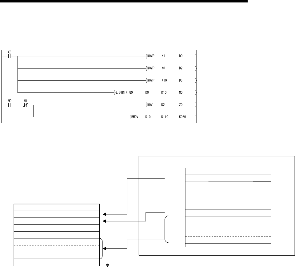
7 - 11 7 - 11
MELSEC-Q
7 DATA COMMUNICATIONS USING BIDIRECTIONAL PROTOCOL
(Program example)
When Q series C24 I/O signals are from X/Y00 to X/Y1F:
Clear the receive data count storage device
to 0.
Designate the allowable receive data count.
•The reading of received data is performed
by the PLC CPU.
Designate the receive channel.
•After the BIDIN instruction is executed,
the user designated read completion
signal (M0) comes on for 1 scan.
With the normal completion, the receive
data within the allowable receive data count
(user designated) is read from the receive
data storage area in the buffer memory.
Interface number
Reception result
Receive data count
Allowable receive data count
Receive data
Receive data
D 0
D 1
D 2
D 3
D10
D m
When the received data count is larger than the
allowable received data count, only the data up to
the allowable received data count will be stored
and the excess data will be discarded.
Buffer memory
Data reception result storage area
Receive data count storage area
Receive data storage area
Address
258H
600H
601H
7FFH
For normal completion
(1)
(0)
(n)
(10)
Q series C24
to
to to

7 - 12 7 - 12
MELSEC-Q
7 DATA COMMUNICATIONS USING BIDIRECTIONAL PROTOCOL
POINT
(1) Receive data can also be read using interrupt programs.
For more details on reading receive data with interrupt programs, see Chapter
4 of the User's Manual (Application).
Note that if the reading of data received from the same interface is to be
performed, it is not possible to combine the reading of data received by the
main program and reading of data received by the interrupt program.
Accordingly, use one or the other of the above programs to read the data
received.
(2) The SPBUSY instruction is used to read the execution status when using a
dedicated instruction. (See Chapter 9.)
(3) More than one BIDIN instruction cannot be executed simultaneously.
Execute the next BIDIN instruction only after the execution of the first BIDIN
instruction is completed.
(4) If the communication data count is set in byte units and the receive data count
is an odd byte when requesting the reading of receive data to the PLC CPU,
00H is stored in the higher byte of the final data storage position in the receive
data storage area.
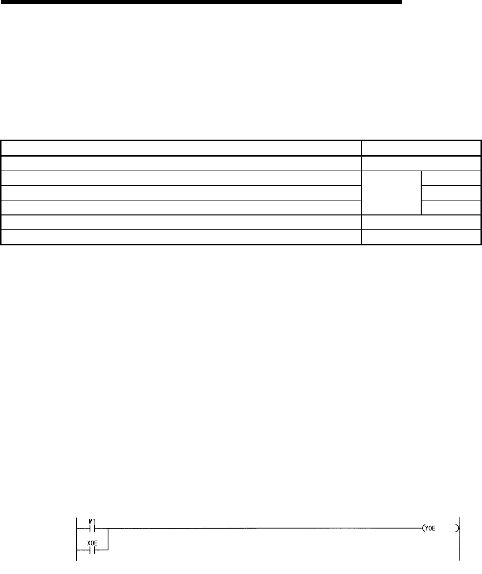
7 - 13 7 - 13
MELSEC-Q
7 DATA COMMUNICATIONS USING BIDIRECTIONAL PROTOCOL
7.1.4 How to detect reception errors
This section explains how to detect errors that may occur when receiving data from the
external device.
The following items are considered as the primary causes of errors that may occur
during data reception.
Cause of reception error Reference section
A transmission error occurred because of noise. —
A timeout occurred for the no-reception monitoring time (timer 0). Section 6.1
A timeout occurred for the transmission monitoring time (timer 2) Section 6.2
Data that could not be converted with the ASCII-BIN conversion was detected.
User's Manual
(Application) Chapter 13
Received the data length that was too long to store in the receiving area. Section 7.1.2
Simultaneous transmissions occurred. Section 7.3
(1) Confirmation using the sequence program
(a) Detecting the occurrence of a reception error
1) The single (XE/XF) is on when the ERR LED is on.
2) The receive error code is confirmed and read in the buffer memory data
reception result storage area (address: 258H/268H).
For details on how to check the error code contents and corrective
actions, see Chapter 10.
(b) How to turn off the ERR LED and clear the error code (see Section 10.1.2)
1) To turn off only the ERR LED, write a "1" to the LED OFF request area
(addresses 0H/1H) in the buffer memory.
2) To turn off the ERR LED and clear the error code, turn ON the ERR LED
OFF request output signal (YE/YF).
(Example) To perform the ERR LED OFF and the error code clear on
the CH1 side
Read command

7 - 14 7 - 14
MELSEC-Q
7 DATA COMMUNICATIONS USING BIDIRECTIONAL PROTOCOL
(2) Confirmation using the module and GX Configurator-SC
1) Confirmation using the display LED
When the Q series C24 detects an error, including a transmission error, the
ERR LED lights up. (See Chapter 10.)
2) Confirmation using GX Configurator-SC
• The monitor function is used to check for errors. (See Sections 8.6.3 and
8.6.6.)
• The ERR LED is turned off with the ERR LED OFF function. (See Section
8.6.10.)
3) Confirming the error code
Use one of the following to confirm the error code.
• GX Configurator-SC monitor function (See Section 8.6.6.)
• GX Developer buffer memory monitor function (monitors addresses
258H/268H)
(3) Handling of receive data when a reception error occurs
1) All of the receive data for which an error was detected is ignored and an
response message indicating an abnormal completion (NAK message) is
sent to the external device.
When an error is detected during message reception, the Q series C24
does not issue a reception data read request to the PLC CPU.
2) The receive area in the buffer memory will contain the data received normally
just prior to the error occurrence. (Data will not be rewritten.)
7.1.5 Receive data clear
Data communications using the bidirectional protocol must be performed after a
response message is received in reply to the preceding data transmission.
If the Q series C24 detects an error while receiving data, it sends an NAK message
(response message) to the external device after the data reception completion and
ignores the data being received when the error was detected.
Therefore, the receive data does not have to be cleared.
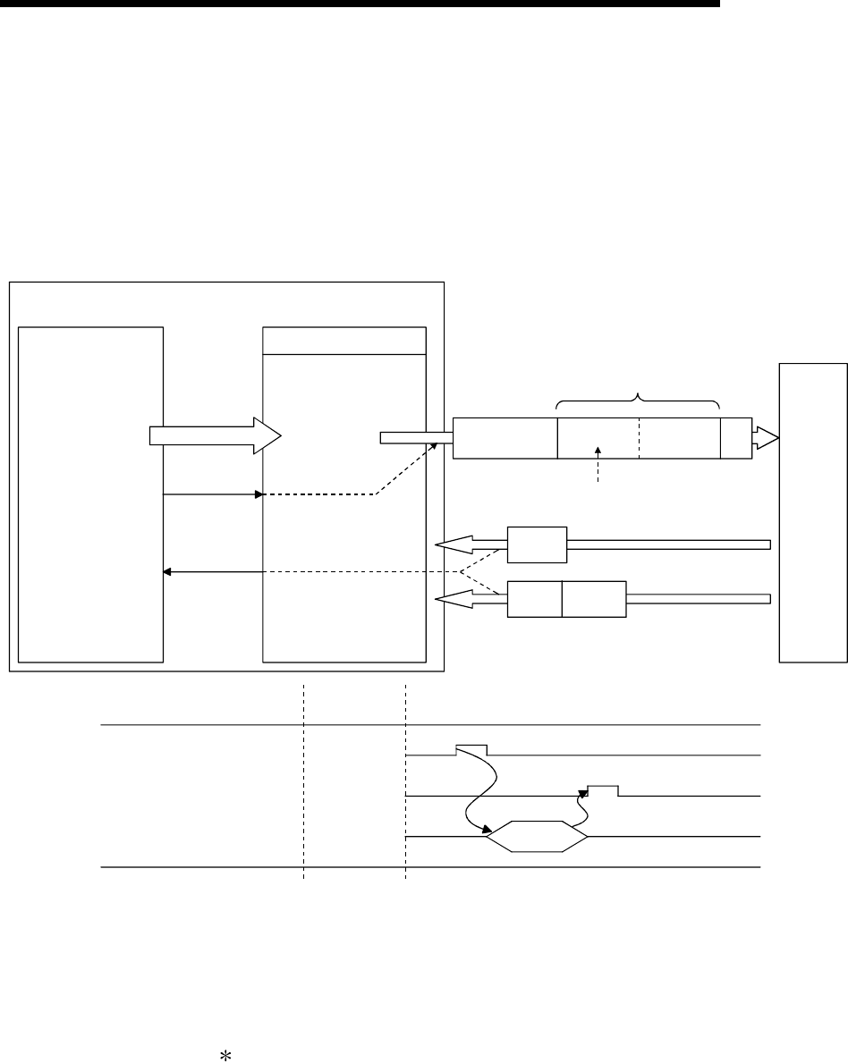
7 - 15 7 - 15
MELSEC-Q
7 DATA COMMUNICATIONS USING BIDIRECTIONAL PROTOCOL
7.2 Sending Data to the External Device
This section explains data transmission from the PLC CPU to the external device.
7.2.1 Transmission methods
The following shows the method of sending data to the external device through data
communication using the bidirectional protocol.
PLC CPU
PLC program Buffer memory
Transmission area
Transmission
completed
1)
Write
(BIDOUT
instruction)
External
device
(00H to FFH)
4)
(When abnormal)
2)
(When normal)
(00H to FFH)
Any data
3)
5)
Data
Q series C24
Sum check code Data portion Data length ENQ
ACK
NAK Error code
BIDOUT instruction
completion device
BIDOUT instruction
CH1/CH2 Control timing
Send instruction
Contents
BIDOUT
1) Data such as control data and transmission data are stored in the device designated
with the BIDOUT instruction and then the BIDOUT instruction is executed.
2) The transmission data count and transmission data are written into the
transmission area of the buffer memory.
3) The Q series C24 sends data by adding the control code ENQ at the beginning of
the data.
When "Sum check" is designated with GX Developer, the Q series C24 adds
the sum check code calculated by internal processing to the end of the
message and then transmits the message.
When "No sum check" is designated with GX Developer, no sum check code is
sent.
4) A response for the data transmission (for normal completion: ACK message; for
abnormal completion: NAK message) is received.
5) The execution of the BIDOUT instruction completes with the transmission
processing completion of the Q series C24.
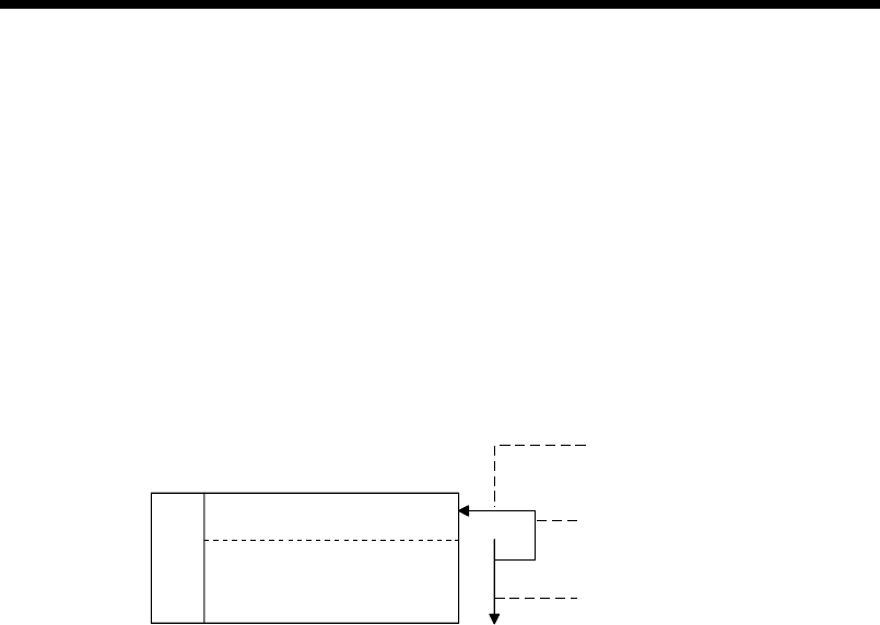
7 - 16 7 - 16
MELSEC-Q
7 DATA COMMUNICATIONS USING BIDIRECTIONAL PROTOCOL
7.2.2 Arrangement and contents of the transmission area and the transmission data
This section explains the arrangement and contents of the transmission area and the
transmission data for performing data transmission using the bidirectional protocol.
For details on the contents of transmission data, see Section 7.1.2 (3).
(1) Transmission area
The transmission area is a memory area for storing the data and the data count
that are transmitted from the PLC CPU to the external device via the Q series
C24. By default, the transmission area is assigned to addresses 400H to 5FFH
(CH1 side) and 800H to 9FFH (CH2 side).
400H
401H
5FFH
CH1 side
address
(Default)
to
Buffer memory
Transmission
area
Transmission data count
designation area
Transmission data
designation area
The unit of transmission data count
(words/bytes) is in accordance with the
word/byte units designation in GX Configurator-SC.
Transmission data count
The transmission data count designated with the
BIDOUT instruction is written, and sent as the
data length.
Transmission data
The transmission data designated with the
BIDOUT instruction is written and then sent.
•
•
•

7 - 17 7 - 17
MELSEC-Q
7 DATA COMMUNICATIONS USING BIDIRECTIONAL PROTOCOL
POINT
(1) The position and size of the transmission area in the buffer memory can be
changed with GX Configurator-SC in accordance with the specifications of the
external device and the transmission data length. (See Section 8.4.5.)
(a) When changing the position and size of the transmission area in the buffer
memory with GX Configurator-SC, designate as follows:
1) Transmission buffer memory head address designation
Designate the starting address for the area to be used as the
transmission area in the user definable area of the buffer memory
(address: 400H to 1AFFH, 2600H to 3FFFH).
2) Transmission buffer memory length designation
Designate by addresses the length of the area (0001H to 1A00H) to be
used as the transmission area in the user definable area of the buffer
memory (address: 400H to 1AFFH, 2600H to 3FFFH).
(b) If the following functions are also used when the position and size of the
transmission area in the buffer memory are changed, make sure that the
addresses of the transmission area do not overlap with those for the
buffer memory that stores the transmission and receive data to be used
by these functions.
1) MC protocol buffer memory read/write function
2) MC protocol on-demand function
3) Non procedure protocol transmission/receive function
4) Bidirectional protocol transmission/receive function
5) Communication data monitoring function
(2) Set the size of data per data transmission from the PLC CPU to the external
device to be smaller than the size of the transmission data designation area in
the buffer memory.
(Transmission data designation area) ≥ (Size of data portion to be sent from the PLC CPU)
To transmit data whose size is larger than the transmission data designation area,
increase the transmission area, or divide the transmission data before sending.
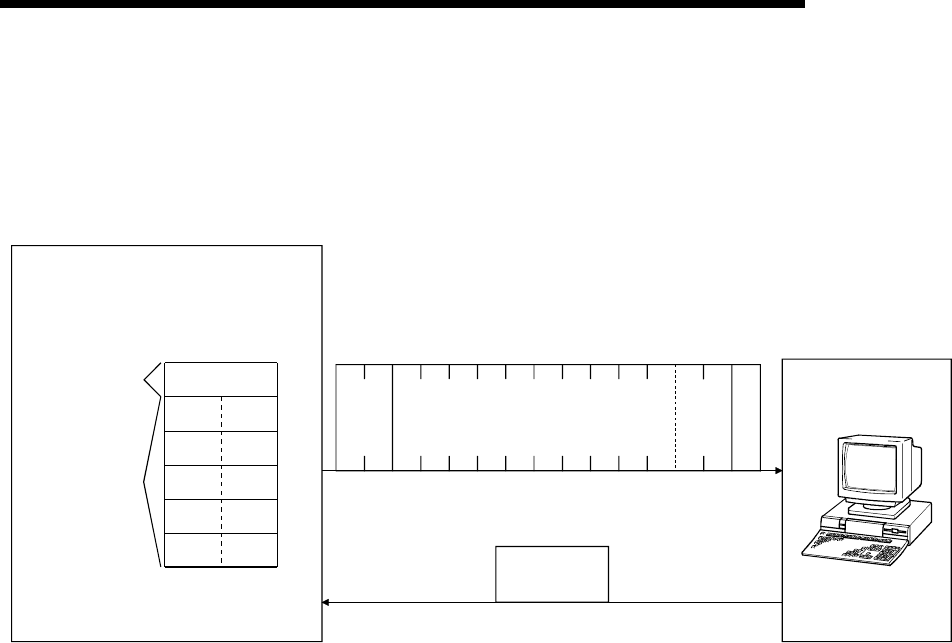
7 - 18 7 - 18
MELSEC-Q
7 DATA COMMUNICATIONS USING BIDIRECTIONAL PROTOCOL
(2) Transmission data arrangement
The following example shows an arrangement of the transmission data to be sent
to the external device when storing it in the transmission area.
(Example) When "ABCDEFG123" is sent:
HL
02H47H33H32H31H47H46H45H44H43H42H41H00H05H
3 2 1 GF EDCBA
HL
ENQ
Sum
check
code
5
(00H)(05
H)
B
(42H)
D
(44H)
F
(46H)
1
(31H)
3
(33H)
A
(41H)
C
(43H)
E
(45H)
G
(47H)
2
(32H)
Transmission
data count
designation area
Transmission
data designation
area
Transmission area
(buffer memory)
Q series C24
External device
Receive data (response message)
ACK
06H
(Normal completion)
(0005H)
Data
length
Transmission data (response message)
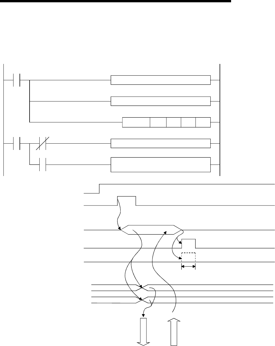
7 - 19 7 - 19
MELSEC-Q
7 DATA COMMUNICATIONS USING BIDIRECTIONAL PROTOCOL
7.2.3 Sequence program for data transmission
A sequence program for data transmission is explained below.
For details on the BIDOUT instruction for data transmission, see Chapter 9.
G.BIDOUT Un D0 D11 M0
M0 M1
M1
Transmission
instruction
Create transmission data from D11
(In case of the CH1 side)
Create control data from D0
Processing for normal completion
Processing for abnormal completion
(retransmission, etc.)
Q series C24 ready signal
Transmission instruction
BIDOUT instruction
BIDOUT instruction complete device
BIDOUT instruction complete device + 1
(Normal completion/abnormal completion)
Transmission data count designation area
(buffer memory address: 400H)
Transmission data storage area
(buffer memory address: 401H to)
BIDOUT
(X1E)
1 scan
0n
Transmission data
Data transmission
1)
2)
3)
4)
ON when transmission
abnormal completion
Receiving response
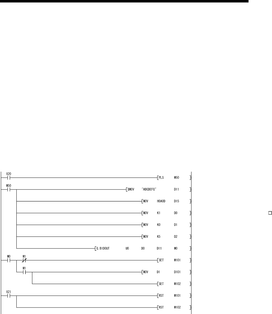
7 - 20 7 - 20
MELSEC-Q
7 DATA COMMUNICATIONS USING BIDIRECTIONAL PROTOCOL
1) Starts the local station PLC.
The setting values for GX Developer are stored in the Q series C24.
2) Inputs the user data transmission instruction signal.
3) Executes the BIDOUT instruction after storing the transmission data and the
control data for the BIDOUT instruction in the device.
Data is sent when the BIDOUT instruction is executed.
4) A response message for the data transmission (for normal completion: ACK
message; for abnormal completion: NAK message) is received.
5) When the response is received, the Q series C24 transmission processing
completes and the device that has completed the BIDOUT instruction turns ON.
When the BIDOUT instruction ends abnormally due to the reception of an NAK
message, the complete device +1 (abnormal completion signal) turns ON and the
error code is stored in the control data completion status (S1+1).
(Program example)
When Q series C24 I/O signals are from X/Y00 to X/Y1F:
Transmission data is stored.
Clear the transmission result storage device to 0.
Designate the transmission data count in word units.
(Designate K10 when the unit is bytes.)
The transmission data stored in the designated device is
sent.
After the BIDOUT instruction is executed, the user
designated transmission complete signal (M1) turns ON for
one scan.
Storing the transmission data and writing the transmission
data count in the buffer memory, and issuing a
transmission request to the Q series C24 are all executed
by the PLC CPU.
Designate the number of the interface (CH ) that will
send the data.
Transmission command is converted to pulse.
The completion flag is reset by the external command.
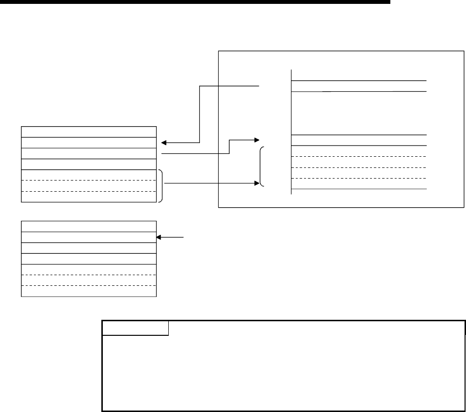
7 - 21 7 - 21
MELSEC-Q
7 DATA COMMUNICATIONS USING BIDIRECTIONAL PROTOCOL
Interface number
Transmission result
Transmission data count
Transmission data
(0001H)
(0000H)
(0005H)
D 0
D 1
D 2
D11
D15
For normal completion
From buffer memory (address 257H)
Buffer memory
Data transmission result storage area
Transmission data count designation area
Transmission data designation area
Address
257H
400H
401H
5FFH
Q series C24
(4241H)
(0A0DH)
(0001H)
(0005H)
D 0
D 1
D 2
D11
D15
(4241H)
(0A0DH)
For abnormal completion
Interface number
Transmission result
Transmission data count
Transmission data
to to
to to
to
(other than 0000H)
POINT
(1) The SPBUSY instruction is used to read the execution status when using a
dedicated instruction. (See Chapter 9.)
(2) More than one BIDOUT instruction cannot be executed simultaneously.
Execute the next BIDOUT instruction only after the execution of the first
BIDOUT instruction is completed.
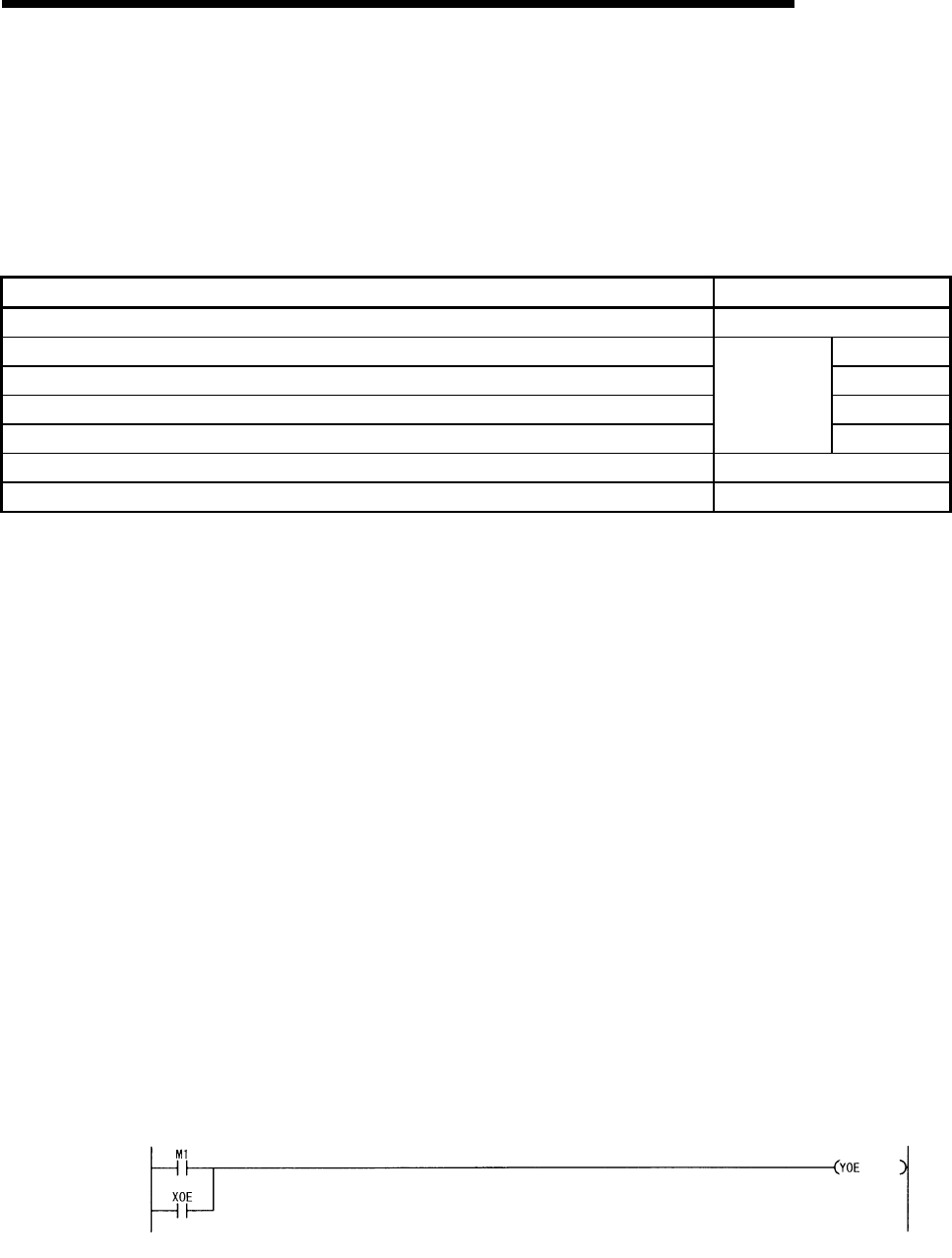
7 - 22 7 - 22
MELSEC-Q
7 DATA COMMUNICATIONS USING BIDIRECTIONAL PROTOCOL
7.2.4 How to detect transmission errors
This section explains how to detect errors that may occur when sending data to the
external device.
The following items are considered as the primary causes of errors that may occur
during data transmission.
Cause of transmission error Reference section
A transmission error occurred because of noise. —
A timeout occurred for the no-reception monitoring time (timer 0). Section 6.1
A timeout occurred for the response monitoring time (timer 1). Section 6.2
A timeout occurred for the transmission monitoring time (timer 2) Section 6.3
Data that could not be converted with the ASCII-BIN conversion was detected.
User's Manual
(Application)
Chapter 13
Designated the transmission data count that exceeded the transmission area size. Section 7.2.2
Simultaneous transmissions occurred. Section 7.3
(1) Confirmation using the sequence program
(a) Detecting a transmission error
1) The following device and input signal turn ON.
• BIDOUT instruction complete device + 1
• ERR LED ON signal (XE/XF)
2) The transmission error code can be checked using the BIDOUT
instruction control data ((S1) + 1).
Or, it can be checked by reading the data transmission result storage
area in the buffer memory (addresses 257H/267H).
For details on how to check the error code contents and corrective
actions, see Chapter 10.
(b) How to turn off the ERR LED and clear the error code (see Section 10.1.2)
1) To turn off only the ERR LED, write a "1" to the LED OFF request area
(addresses 0H/1H) in the buffer memory.
2) To turn off the ERR LED and clear the error code, turn ON the ERR LED
OFF request output signal (YE/YF).
(Example) To perform the ERR LED OFF and the error code clear on
the CH1 side:
Read command

7 - 23 7 - 23
MELSEC-Q
7 DATA COMMUNICATIONS USING BIDIRECTIONAL PROTOCOL
(2) Confirmation using the module and GX Configurator-SC
1) Confirmation using the display LED
When the Q series C24 detects an error, including a reception error, the ERR
LED lights up. (See Chapter 10.)
2) Confirmation using GX Configurator-SC
• The monitor function is used to check for errors. (See Sections 8.6.3 and
8.6.6.)
• The ERR LED is turned off with the ERR LED OFF function. (See Section
8.6.10.)
3) Confirming the error code
Use one of the following to confirm the error code.
• GX Configurator-SC monitor function (See Section 8.6.6.)
• GX Developer buffer memory monitor function (monitors addresses
257H/267H)

7 - 24 7 - 24
MELSEC-Q
7 DATA COMMUNICATIONS USING BIDIRECTIONAL PROTOCOL
7.3 Processing when Simultaneous Transmission Performed During Full-Duplex
Communications
This section explains the processing when simultaneous transmissions occur in full-
duplex communication.
7.3.1 Processing when simultaneous transmissions occur
This section explains the processing performed by the Q series C24 when the external
device and the Q series C24 transmit at the same time during data communications
using the bidirectional protocol.
Since the external device and the Q series C24 do not transmit at the same time
during half-duplex communications (see User's Manual (Application) Chapter 8), this
section does not have to be read.
When an external device and the Q series C24 transmit at the same time, the Q series
C24 processing depends on the setting of "Simultaneous transmission data valid/invalid
designation" with GX Configurator-SC.
The GX Configurator-SC setting value, "Simultaneous transmission data valid/invalid
designation" is stored in the following areas of the buffer memory.
Simultaneous transmission data valid/invalid designation area (addresses: 9BH/13BH)
The Q series C24 communication data processing for each setting is described in
Section 7.3.2.
Q series C24 processing contents
Setting contents
with GX Configurator-SC
Value set to buffer memory
(Address 9BH/13BH)Message transmit processing Message receive processing
Transmission data: Valid
Receive data: Valid 0000H
Waits to receive the response message
(1)-2) while checking time-out after data
transmission (1)-1) is complete.
Posts normal end or abnormal end
according to whether or not the PLC
CPU received a response message
through the buffer memory.
Transmits a response message (2)-2)
after data reception (2)-1) is complete.
Posts the receive data and receive
result to the PLC CPU through the
buffer memory.
Transmission data: Invalid
Receive data: Valid 0100H
Posts a simultaneous transmission error
to the PLC CPU through the buffer
memory after data transmission (1)-1).
Does not wait for a response massage
(1)-2) in reply to data transmission (1)-1).
Transmits a response message (2)-2)
after data reception (2)-1) is complete.
Posts the receive data and receive
result to the PLC CPU through the
buffer memory.
Transmission data: Valid
Receive data: Invalid 0001H
Waits to receive the response message
(1)-2) while checking time-out after data
transmission (1)-1) is complete.
Posts normal end or abnormal end
according to whether or not the PLC
CPU received a response message
through the buffer memory.
Ignores data reception (2)-1) and
discards the received data.
Does not transmit a response
message (2)-2).
Does not inform the PLC CPU that
data was received.
Transmission data: Invalid
Receive data: Invalid 0101H
Posts a simultaneous transmission error
to the PLC CPU through the buffer
memory after data transmission (1)-1).
Does not wait to a response massage
(1)-2) in reply to data transmission (1)-1).
Ignored data reception (2)-1) and
discards the receive data.
Does not transmit a response
message (2)-2).
Does not inform the PLC CPU that
data was received.
( )-m) is the number showing the correspondence with the messages in the illustration shown in Section 7.3.2.
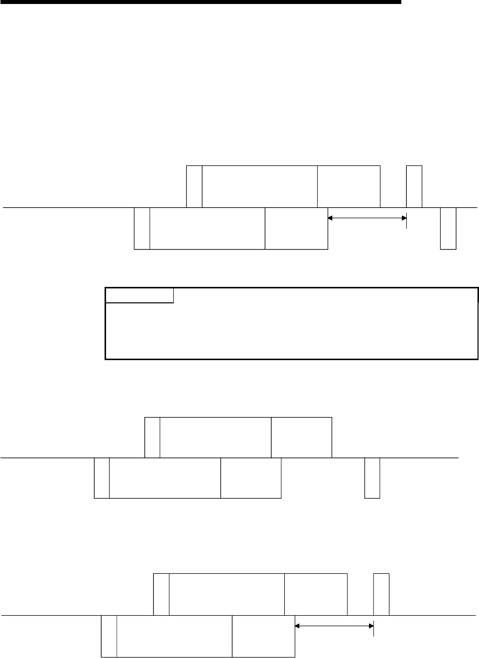
7 - 25 7 - 25
MELSEC-Q
7 DATA COMMUNICATIONS USING BIDIRECTIONAL PROTOCOL
7.3.2 Communication data processing when simultaneous transmissions occur
Examples of the Q series C24 communication data processing for various settings of
"Simultaneous transmission data valid/invalid designation" by GX Configurator-SC are
explained.
(1) Transmission: valid, reception: valid
Q series C24
External device
Arbitrary data
E
N
Q
Sum check
code
Arbitrary data
E
N
Q
Sum check
code
A
C
K
A
C
K
Time check
(timer 1)
1)-22)-1
1)-1 2)-2
POINT
When the entire message of 2)-1 was received while transmitting the message of
1)-1 in the illustration.
• The Q series C24 outputs the receive data read request signal of 2)-1 to the PLC
CPU after transmitting all 1)-1. (Turns on the X3/XA.)
(2) Transmission: invalid, reception: valid
External device
Arbitrary data
E
N
Q
Sum check
code
Arbitrary data
E
N
Q
Sum check
code
A
C
K
2)-1
1)-1 2)-2
Ignores the receive
data of 1)-1.
(Generates a simultaneous
transmission error.)
Q series C24
(3) Transmission: valid, reception: invalid
External device
E
N
Q
E
N
Q
A
C
K
1)-21)-1
1)-1
Q series C24 Time check
(timer 1)
Ignores the receive
data of 2)-1.
Arbitrary data Sum check
code
Arbitrary data Sum check
code
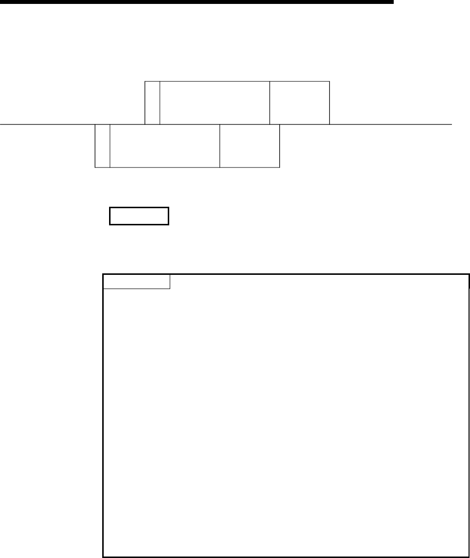
7 - 26 7 - 26
MELSEC-Q
7 DATA COMMUNICATIONS USING BIDIRECTIONAL PROTOCOL
(4) Transmission: invalid, reception: invalid
Q series C24
External device
E
N
Q
E
N
Q
2)-1
1)-1
Ignores the receive
data of 1)-1.
Generates a simultaneous
transmission error.
Ignores the receivedata of 2)-1.
Arbitrary data Sum check
code
Arbitrary data Sum check
code
REMARK
Time-check timer 1 (response monitoring time) shown in the illustration is described
in Section 6.2 of User's Manual (Application).
POINT
When the transmission control (see Chapter 9 of User's Manual (Application)) is
performed, and the simultaneous transmission data valid/invalid designation sets
that the receive data is valid and transmission data is valid, the Q series C24
performs message transmission and message reception processing as described
below.
During message transmission processing, time check by timer 1 (response
monitoring time) is performed.
1) Message transmission (1)-1 in the illustration)
• If the Q series C24 receives a terminate transmission request (DC3
received/DSR signal OFF) from the external device during message
transmission, it terminates data transmission.
• When the Q series C24 receives the ready to send signal (DC1
received/DSR signal ON), it restarts data transmission.
2) Message reception
• If the Q series C24 cannot send a response message to the external device
in response to message reception because the external device issued a
terminate transmission request (DC3 received/DSR signal OFF), it transmits
the response message after it receives the ready to send signal (DC1
received/DSR signal ON) from the external device.

7 - 27 7 - 27
MELSEC-Q
7 DATA COMMUNICATIONS USING BIDIRECTIONAL PROTOCOL
7.4 Data Communications Precautions
The following shows the precautions when performing data communications using the
bidirectional protocol.
(1) When the transmission sequence is in the initial status, it indicates that data
transmission and reception processing has not been started.
The Q series C24 transmission sequence is initialized in the following cases.
• The power is turned on, the CPU is reset.
• When operating, or the mode is switched.
• When a response message (ACK, NAK, etc.) was received in reply to data
transmission.
• When a response message (ACK, NAK, etc.) was transmitted in reply to data
reception.
• When the CD signal was turned off during data communications using Check
CD terminal in full-duplex communications through the RS-232 interface.
(2) As a data transmission procedure, data transmission from the external device or
the Q series C24 should be performed after an response for the immediately
preceding data transmission has been received.
(3) The external device and PLC CPU must agree so that the units of the data length
(word count/byte count) in the message to be transmitted and received is the same.
The PLC CPU units can be set using the GX Configurator-SC word/byte units
designation.
Make the length of the data area in the message to be transmitted and received
the size of the Q series C24 buffer memory transmission data designation area
and receive data storage area, or less.
(4) NAK code response
1) Response from the Q series C24 to external device
After the error detection message reception complete, it transmits the NAK
code to the external device.
2) Response from external device to the Q series C24
Transmit the error code (0022H to 005FH) immediately after the NAK
response.

7 - 28 7 - 28
MELSEC-Q
7 DATA COMMUNICATIONS USING BIDIRECTIONAL PROTOCOL
POINT
(1) Perform error processing according to the error code received immediately
after the NAK message at the device that received NAK as the response
message after data transmission.
Chapter 10 shows the error codes that are transmitted from the Q series C24.
(2) If the Q series C24 receives an NAK response while transmitting data to an
external device, it completes data transmission, then reads the NAK, perform
abnormal completion.
(3) If the Q series C24 detects an error while receiving data, it ignores the receive
data corresponding to the data length.
If the data length is abnormal, the Q series C24 ignores all the data up to the
receive message head data (ENQ, etc.) received thereafter.
(5) External device time-out check
When checking time-out up to reception of the response message at the external
device during data transmission from external device to the Q series C24, make
the time-out time the time shown below, or longer.
(PLC CPU maximum scan time 2) + 100 ms
(6) External device framing error
When nothing is transmitted from the Q series C24 to the external device though
the RS-422 or RS-422/485 interface, a framing error may be generated in the
external device.
Make the external device skip the data up to transmission of the head data (ENQ,
NAK, etc.) of the message from the Q series C24.
Before communicating data through the RS-422/485 interface, check Q series
C24 specifications given in Section 3.3.
(7) Data bit settings
When adding a sum check code to a message, set the data bits to 8 bits using the
transmission setting of the GX Developer.
For more details on the data bit settings, see Section 4.5.
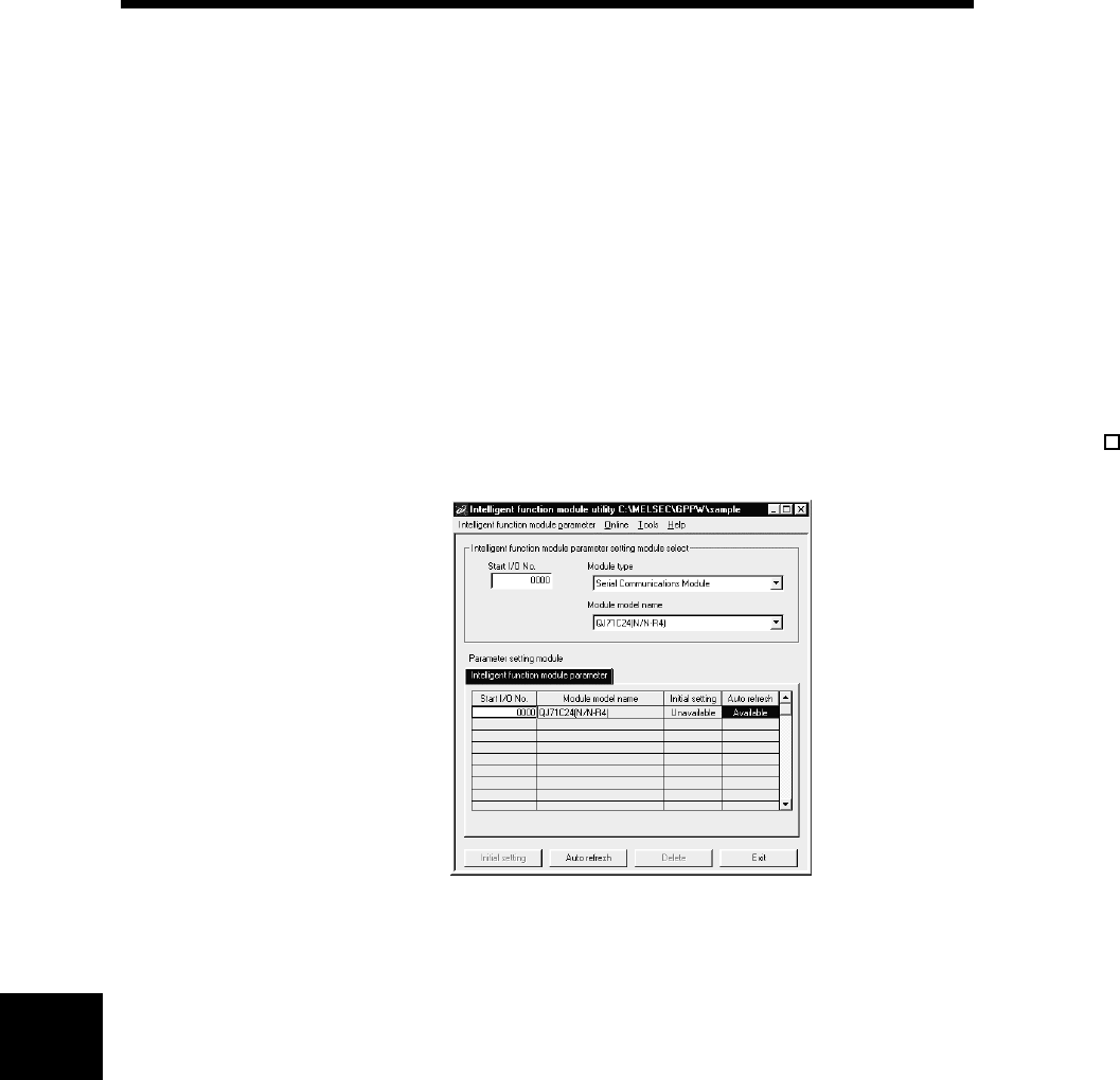
8 - 1 8 - 1
MELSEC-Q
8 UTILITY PACKAGE (GX Configurator-SC)
8
8 UTILITY PACKAGE (GX Configurator-SC)
The GX Configurator-SC is a tool that supports the production of necessary PLC
programs with initial setting, monitoring and testing, and data communication
processing of the Q series C24.
The GX Configurator-SC is composed of an intelligent function utility and protocol FB
support function.
(1) Intelligent function utility (utility package) (see this chapter)
The utility package facilitates the initial settings and monitoring of the Q series
C24 by using dedicated screens without having to consider the I/O signals or
buffer memory.
The utility package can also be used together with the GX Simulator (SWnD5 -
LLT-E).
(2) Protocol FB support function
The protocol FB support function automatically generates the FB (function block)
for communication that supports data communication processing and traces the
network that monitors the data transmitted/received on the communication
network.
By using the protocol FB support function, producing PLC programs and
transmission debug is made easy.
For details on the protocol FB support function, see the GX Configurator-SC
Operating Manual (Protocol FB support function).
8 - 2 8 - 2
MELSEC-Q
8 UTILITY PACKAGE (GX Configurator-SC)
8
8.1 Functions Available with Utility Package
The following table lists the utility package function.
( : indicates that the setting is valid with the applicable protocol.)
Function MC
Non
procedure
protocol
Bidirectional
protocol
Explanation
page Remarks
Auto refresh setting Refresh the Q series C24's error codes and set devices on the PLC
CPU side. Section 4.6
User frame Register the user frame in the flash ROM. — Section 8.4.1
Data for modem initialization Register the data for modem initialization in the flash ROM. Section 8.4.2
Data for modem connection Register the data for model connection in the flash ROM. Section 8.4.3
Modem function system
setting
Register the system setting values for model function in the flash
ROM. Section 8.4.4
CHn Transmission
control and others
system setting
Set the transmission specifications with the other device.
(DTR/DSR control, DC code control, communication method, data
communication monitoring timer value, etc.)
Section 8.4.5
CHn MC protocol
system setting
Assign the buffer memory for on-demand function, set the user
frame number, etc. — — Section 8.4.6
CHn Non procedure
system setting
Assign the buffer memory needed to perform data communication
using the non procedure protocol, and change the setting values,
etc.
—— Section 8.4.7
CHn Bidirectional
system setting
Assign the buffer memory needed to perform data communication
using the bidirectional protocol, and change the setting values, etc. —— Section 8.4.8
CHn PLC CPU
monitoring system
setting
Set the PLC CPU monitoring function. — Section 8.4.9
System
setting
CHn Transmission
user frame No.
designation system
setting
Set the user frame number to be transmitted, etc. — — Section 8.4.10
Can be used
via online
operation.
Can be used
via offline
operation.
System setting default Reset the setting values in the buffer memory to their default
values. Section 8.4.11
System setting write Write the setting values in the buffer memory to the flash ROM. Section 8.4.11
Flash ROM write
allow/prohibit designation Set whether to allow or prohibit writing to the flash ROM. — — — Section 8.4.12
X · Y monitor/test Perform the monitoring/testing of I/O signals to/from the PLC CPU. Section 8.6.1
Modem function monitor/test Monitor the execution status of the modem function. Section 8.6.2
CHn Transmission
control and others
monitor/test
Monitor the status of interface control signals, values set from the
GX Developer, etc. Section 8.6.3
CHn MC protocol
monitor — — Section 8.6.4
CHn Non procedure
monitor/test —— Section 8.6.5
CHn Bidirectional
monitor
Monitor the data communication result, I/O signal status, and
setting values in the buffer memory.
—— Section 8.6.6
CHn PLC CPU
monitoring monitor
Monitor the setting values and operating status of the PLC CPU
monitoring function. — Section 8.6.7
Monitor
CHn User frame
No. designation
monitor for
transmission
Monitor the setting value for user frame to be transmitted. — Section8.6.8
Monitor/test others Monitor the data reception result, error occurrence status, etc. Section 8.6.9
ERR LED off Turn off the ERR LEDs on the front face of the module. Section 8.6.10
Non procedure protocol
receive data clear Clear the currently received data. — — Section 8.7
Can be used
only via
online
operation.

8 - 3 8 - 3
MELSEC-Q
8 UTILITY PACKAGE (GX Configurator-SC)
8.2 Installing and Uninstalling Utility Package
See "Method of installing the MELSOFT Series" attached with the utility package
regarding the install and uninstall operation for the utility package.
8.2.1 Usage precautions
The following describes the precautions on using the utility package:
(1) Important safety information
Since the utility package is add-in software for GX Developer, read "Safety
Precautions" and the basic operating procedures contained in GX Developer's
Operating Manual.
(2) About installation
The GX Configurator-SC (utility package) is an add-in package for GX Developer
Version 4 or later products.
Therefore, install GX Configurator-SC in a personal computer in which GX
Developer Version 4 or a later product has been installed.
(3) About display screen errors while using the intelligent function
module utility
There may be cases in which the screen will not properly display while the
intelligent function module utility is being used, due to a lack of system resources.
If this occurs, close the intelligent function module utility first and then GX
Developer (program, comments, etc.) and other applications. Then, restart GX
Developer and the intelligent function module utility.
(4) To start the intelligent function module utility
(a) In GX Developer, select "QCPU (Q mode)" for the PLC series and specify
the project.
If anything other than "QCPU (Q mode)" is selected for the PLC series, or if
the project is not specified, the intelligent function module utility will not start.
(b) Multiple intelligent function module utilities can be started.
However, the [Open file]/[Save file] intelligent function module's parameter
operations can only be performed by a single intelligent function module
utility. Other intelligent function module utilities can perform the
[Monitor/Test] operation only.
(5) How to change screens when two or more intelligent function
module utilities are started
When two or more intelligent function module utility screens cannot be displayed
side by side, use the task bar to change the intelligent function module utility
screen so that it is displayed on top of other screens.
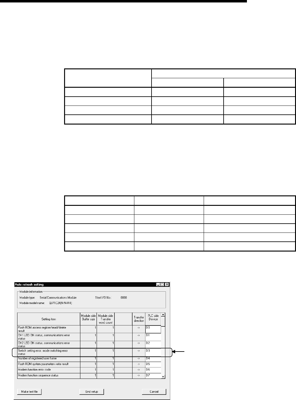
8 - 4 8 - 4
MELSEC-Q
8 UTILITY PACKAGE (GX Configurator-SC)
(6) About the number of parameters that can be set in GX
Configurator-SC
The number of parameters that can be set by the GX Configurator for an
intelligent function module installed in the CPU module and in a remote I/O
station of the MELSECNET/H network system is limited.
Maximum number of parameter settings
Intelligent function module
installation object Initial setting Automatic refresh setting
Q00J/Q00/Q01CPU 512 256
Q02/Q02H/Q06H/Q12H/Q25HCPU 512 256
Q12PH/Q25PHCPU 512 256
MELSECNET/H remote I/O station 512 256
For example, if multiple intelligent function modules are installed in a remote I/O
station, set the GX Configurator so that the number of parameter settings of all
the intelligent function modules does not exceed the maximum number of
parameter settings. The total number of parameter settings is calculated
separately for the initial setting and for the automatic refresh setting.
The number of parameter settings that can be set for one module in the GX
Configurator-SC is as shown below.
Object Module Initial setting Automatic refresh setting
QJ71C24N 0 (not used) 46 (Maximum number of settings)
QJ71C24N-R2 0 (not used) 47 (Maximum number of settings)
QJ71C24N-R4 0 (not used) 46 (Maximum number of settings)
QJ71C24 0 (not used) 46 (Maximum number of settings)
QJ71C24-R2 0 (not used) 47 (Maximum number of settings)
Example) Counting the number of parameter settings in the automatic refresh
setting
The number of settings in this one line is
counted as one setting.
The number of settings is not counted by columns.
Add up all the setting items in this setting screen,
then add them to the total for the other intelligent
function modules to get a grand total.
8 - 5 8 - 5
MELSEC-Q
8 UTILITY PACKAGE (GX Configurator-SC)
8.2.2 Operating environment
The operating environment of the personal computer where the GX Configurator-SC is
used is explained.
Item Peripheral devices
Installation (Add-in) destination 1Add-in to GX Developer Version 4 (English version) or later 2
Computer main unit Personal computer on which Windows® operates.
CPU
Required memory
Refer to the following table "Used operating system and performance required for
personal computer".
For installation 65 MB or more
Hard disk
free space For operation 20 MB or more
Display 800 600 dot or more resolution 3
Operating system
Microsoft® Windows® 95 Operating System (English version)
Microsoft® Windows® 98 Operating System (English version)
Microsoft® Windows® Millennium Edition Operating System (English version)
Microsoft® Windows NT® Workstation Operating System Version 4.0 (English version)
Microsoft® Windows® 2000 Professional Operating System (English version)
Microsoft® Windows® XP Professional Operating System (English version)
Microsoft® Windows® XP Home Edition Operating System (English version)
1: Install the GX Configurator-SC in GX Developer Version 4 or higher in the same language.
GX Developer (English version) and GX Configurator-SC (Japanese version) cannot be used in
combination, and GX Developer (Japanese version) and GX Configurator-SC (English version) cannot be
used in configuration.
2: GX Configurator-SC cannot be used as an add-in with GX Developer Version 3 or earlier versions.
3: Setting fonts Size of WindowsR for "Large Fonts" may cause the text to extend off screen. Therefore,
choose "Small Fonts".
Used operating system and performance required for personal computer
Performance Required for Personal Computer
Operating system CPU Required memory
Windows® 95 (Service Pack 1 or later) Pentium® 133MHz or more 32MB or more
Windows® 98 Pentium® 133MHz or more 32MB or more
Windows® Me Pentium® 150MHz or more 32MB or more
Windows NT® Workstation 4.0
(Service Pack 3 or later) Pentium® 133MHz or more 32MB or more
Windows® 2000 Professional Pentium® 133MHz or more 64MB or more
Windows® XP
Professional Pentium® 300MHz or more 128MB or more
Windows® XP
Home Edition
"XP compatibility
mode" and "Fast User
Switching" are not
supported. Pentium® 300MHz or more 128MB or more
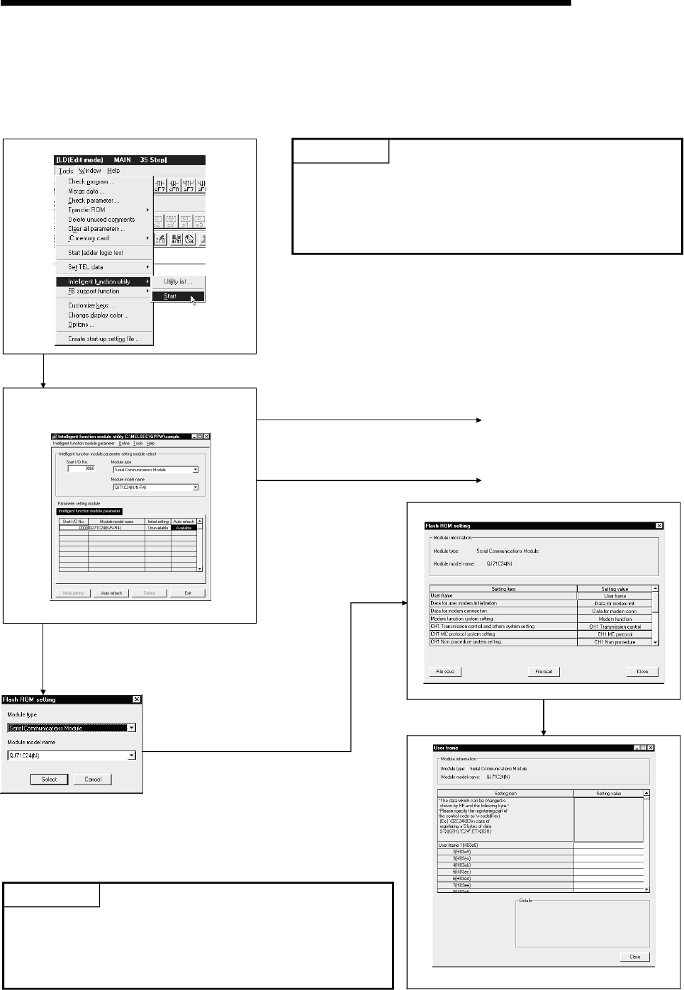
8 - 6 8 - 6
MELSEC-Q
8 UTILITY PACKAGE (GX Configurator-SC)
8.3 Explanation of Utility Package Operation
8.3.1 Operation overview
GX Developer screen POINT
The following settings must be performed before starting
the intelligent function module utility:
• Set the project using the GX Developer
• Set "QCPU (Q mode)" for the PC series.
Intelligent Function Module
Select Parameter Setting Module screen
See Section 8.3.2
[Tools] – [Intelligent function utility] – [Start]
When auto refresh is set 2) Go to next page
When used via online operation 1) Go to next page
Select [Tools] – [Flash ROM stting] from the menu bar.
When used via offline operation
Select the module type and
module model name.
See Sections 8.4.1 through 8.4.10
POINT
The various setting values to be registered in the Q series C24's
flash ROM can be saved in a file of the PC via offline operation.
Use online operation to write system setting values to the Q series
C24.
Flash ROM settings screen
See Section 8.4
To each setting screen
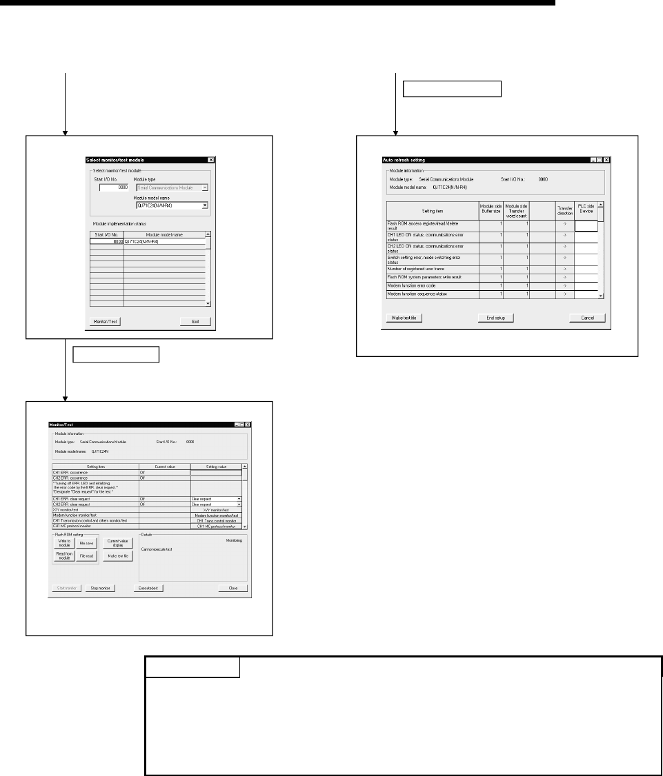
8 - 7 8 - 7
MELSEC-Q
8 UTILITY PACKAGE (GX Configurator-SC)
Auto refresh screen
Enter "Start I/O No.," then select "Module type"
and "Module model name."
Auto refresh
See Screen 4.6
Select monitor/test module screen
Select [Online] – [Monitor/test] from the menu bar.
1) When using online operation
Monitor/test screen
Select the parameter setting module
for monitor/test.
Monitor/test
See Section 8.4
See Section 8.6
2) When setting auto refresh
POINT
(1) When the setting operation is complete in each system setting screen, register
the system setting data in the flash ROM, then restart the PLC CPU resume
data transmission.
(2) With the Q series C24, monitoring, testing, and reading/writing of setting
values can be performed via online operation.
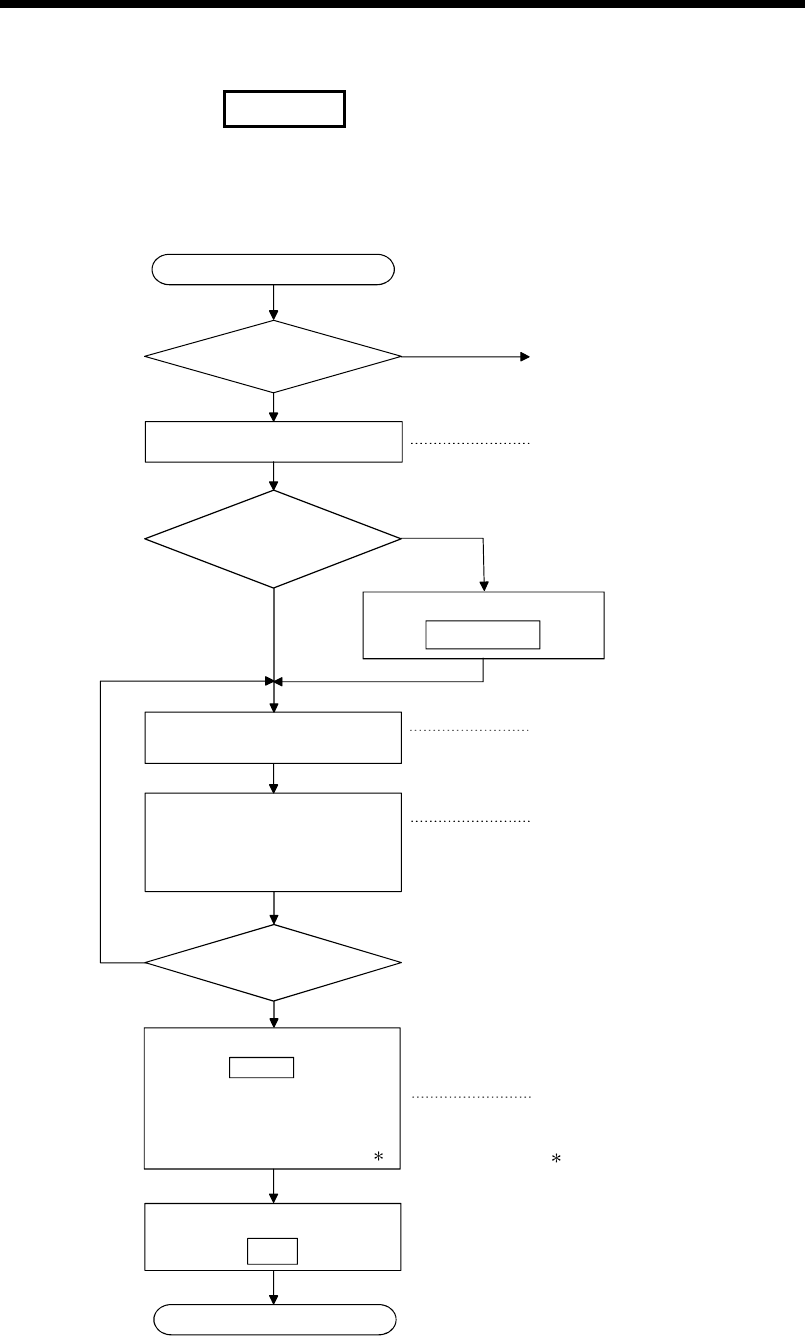
8 - 8 8 - 8
MELSEC-Q
8 UTILITY PACKAGE (GX Configurator-SC)
REMARK
The following diagram illustrates the overview of a procedure in which the GX
Configurator-SC is used to change the system setting values of the Q series C24
and save the new values to a file or write them to the Q series C24's flash ROM.
Close the [Flash ROM setting] screen.
Close
I—¹
Start the [Flash ROM setting]
screen.
Display the system setting sub-screen
for changing the setting values.
Click on each of the setting items
corresponding to the setting values
you wish to change. For each item,
enter or select the new setting value
in the [Setting value] field.
In the [Flash ROM setting] screen,
Start
Select in the [Flash ROM setting] screen.
See Section 8.4.
[Intelligent function module select
parameter setting module] screen
See Section 8.3.1
Change the setting values in the corresponding
system setting sub-screens.
See Sections 8.4.1 through 8.4.10.
This operation is allowed only in the [Flash ROM
setting] screen.
See Section 8.3.3.
Go to 1) setting via online operation
Read the data from the file.
File read
YES (offline operation)
NO
YES
End
YES
NO
Do you wish to
change the setting values via
offline operation?
click on the File save button. Then,
NO
Is the original data
saved in a file?
Have you
changed all the applicable
setting values?
in the file designation dialog box,
designate the file name under which
the data will be saved. All of the new
setting values will be saved in the file.
1 1 Save the new system setting values in a file
for backup.
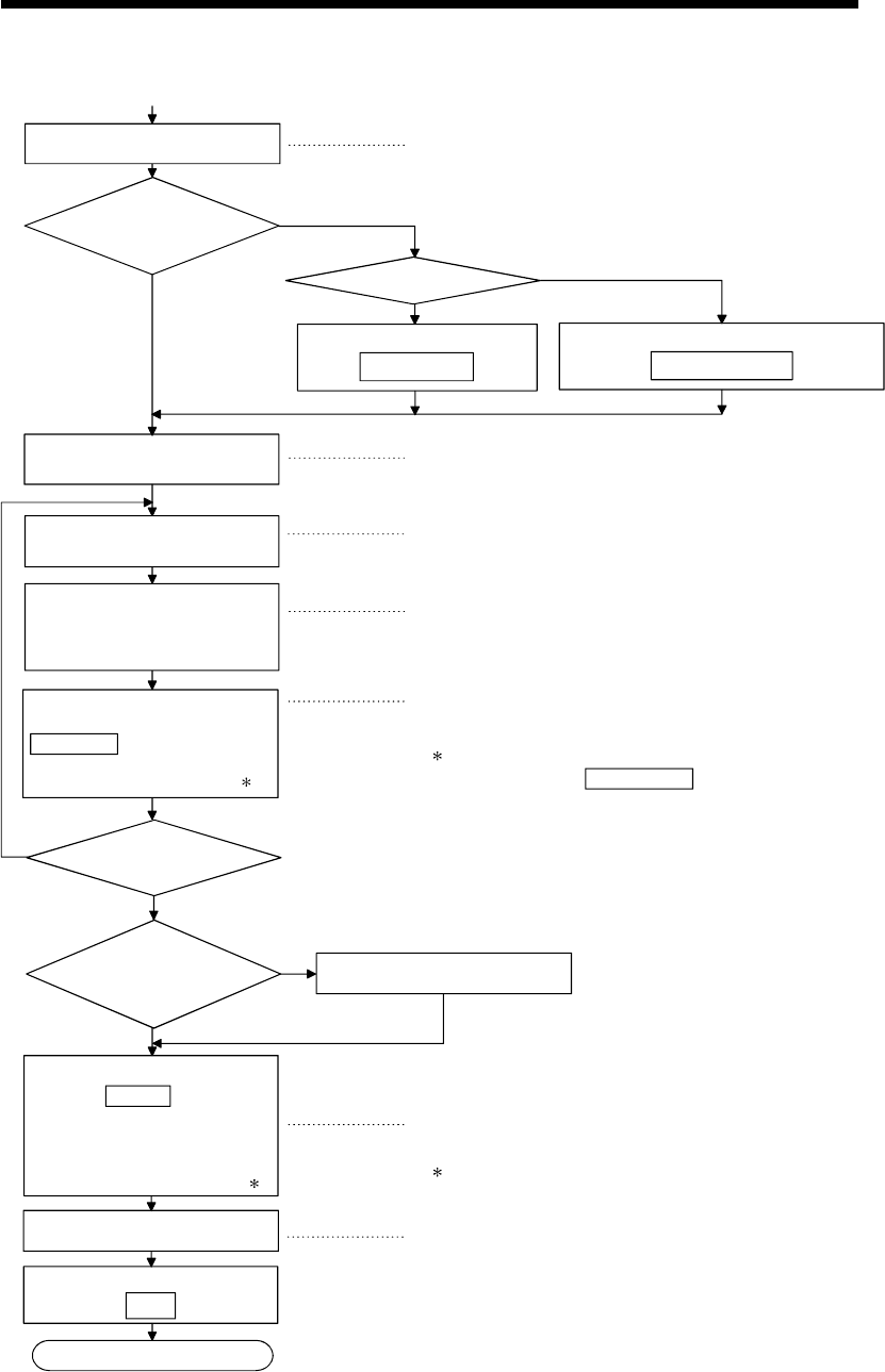
8 - 9 8 - 9
MELSEC-Q
8 UTILITY PACKAGE (GX Configurator-SC)
Start the [Monitor/test] screen.
Set the flash ROM write allow/prohibit
designation to "allowed".
Select in the [Monitor] screen.
See Section 8.4.12.
Select in the [Monitor] screen.
See Section 8.4.
Each system setting sub-screen.
See Section 8.4.
The [Monitor] screen or each sub-screen.
See Section 8.3.3.
The [Monitor] screen or each sub-screen.
See Section 8.3.3.
NO
YES
1) (Online operation)
[Intelligent Function Module
Select Parameter setting module] screen
See Section 8.3.1
Is the original data saved? YES
NO Is the data saved in a file?
Read the data from the file.
File read Read from module
Read the data from the module's flash ROM.
NO
YES
Display the system setting sub-screens
for changing the setting values.
YES
NO
Close the [Monitor/test] screen.
I—¹
End
Set the flash ROM write allow/prohibit
designation to "prohibited". Select in the [Monitor] screen.
See Section 8.4.12.
Have you
changed all the applicable
setting values?
Designate the setting value for the
item to be changed, then click on the
Execute test button.
The setting value will be written to the
Q series C24's flash ROM.
1 To write all the new setting values to the flash ROM
at once, click on the Write to module button after
all the applicable setting values have been changed.
All the setting values will be written to the Q series
C24's flash ROM.
Do you wish
to write the new setting
values to the module's Reset the CPU.
In the [Flash ROM setting] screen,
click on the File save button. Then,
in the file designation dialog box,
designate the file name under which
the data will be saved. All of the new
setting values will be saved in the file.
22 Save the new system setting values in a file for
backup.
Close
Click each of the setting items
corresponding to the setting values to
be changed. For each item, enter or
select the new setting value in the
[Setting value] field.
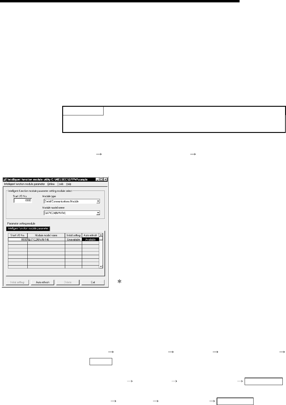
8 - 10 8 - 10
MELSEC-Q
8 UTILITY PACKAGE (GX Configurator-SC)
8.3.2 Starting the intelligent function module utility (displaying the [select parameter setting
module] screen)
[Purpose]
Start the intelligent function module utility from the GX Developer, and display the
module selection screen for the intelligent function module utility parameter setting.
The screens that perform system setting, auto refresh setting, and
monitoring/testing for the Q series C24 can be started from this module selection
screen.
POINT
To start the Intelligent function module utility, a project created with the GX
Developer whose PLC series is set as "QCPU (Q mode)" is required.
[Startup procedure]
[Tools] [Intelligent function module utility] [Start]
[Setting screen]
• Start I/O No.
Enter the start I/O number for the applicable the Q series C24
using a hexadecimal expression.
• Module type
Select [Serial communication module].
• Module model name
Select the module model name of the applicable the Q series
C24.
• Intelligent function module parameter setting module
The modules for which parameters are set with the intelligent
function module utility are displayed.
Select the target module of your operation.
It is not necessary to select [Intelligent function module,
select parameter setting module] to perform monitor/test
operation.
[Explanation of items]
(1) How to start each screen
(a) Starting the flash ROM setting screen
[Tools] [Flash ROM setting] "Module type" "Module model Name"
Select
(b) Starting auto refresh settings
"Start I/O No." "Module type" "Module model name" Auto refresh
(c) Monitor/test module selection screen
[Online] [Monitor/test] "Module selection" Monitor/test
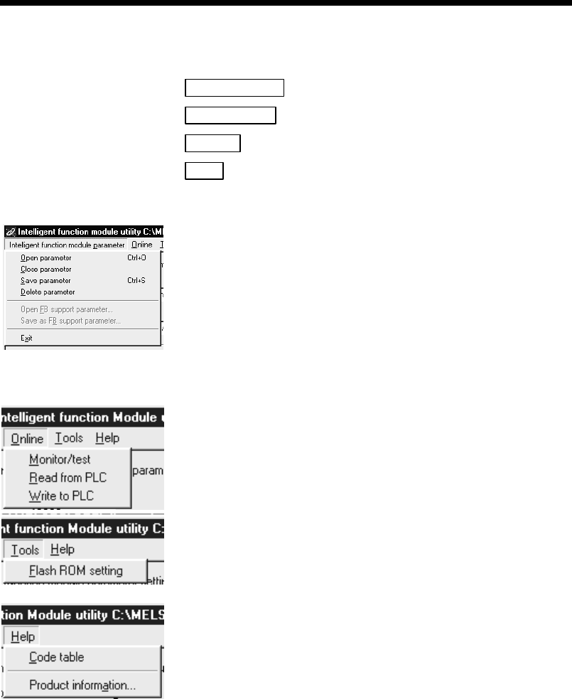
8 - 11 8 - 11
MELSEC-Q
8 UTILITY PACKAGE (GX Configurator-SC)
(2) Command buttons
Initial settings : Cannot be selected.
Auto refresh : Starts the auto refresh setting screen.
Delete : Deletes the initial settings and auto refresh settings.
Exit : Closes the parameter setting module selection screen.
(3) Menu bar
(a) File items
The intelligent function module parameters for the project opened by GX
Developer can be processed in file operation.
[Open parameter] : Reads the parameter file.
[Close parameter] : Closes the parameter file. If it has been modified, the
file save confirmation dialog box appears.
[Save parameter] : Saves the parameter file.
[Delete parameter] : Deletes the parameter file.
[Exit] : Exits from the intelligent function module utility.
(b) Online items
[Monitor/test] : Starts the monitor/test module selection screen.
[Read from PLC] : Reads the intelligent function module parameters
from the CPU module.
[Write to PLC] : Writes the intelligent function module parameters to
the CPU module.
(c) Tool items
[Flash ROM setting] : Starts the flash ROM setting screen.
(d) Help items
[Code list] : Displays the ASCII code list. Use this list as reference
when setting data.
[Product information] : Displays the version information of the intelligent
function module utility.

8 - 12 8 - 12
MELSEC-Q
8 UTILITY PACKAGE (GX Configurator-SC)
POINT
(1) Saving the intelligent function module parameter files
Since files cannot be saved using the GX Developer project save operation,
save the files on the module selection screen for parameter setting described
above.
(2) Reading from and writing to PLC operations for the intelligent function module
parameters using GX Developer
(a) After the intelligent function module parameters are saved in a file, they
can be read from and written into the PLC.
(b) Set the target PLC using the GX Developer [Online] [Transfer setup].
Only use the control PLC for the Q series C24 to write the intelligent
function module parameters for a multiple CPU system to the PLC.
(c) Use the GX Developer for PLC reading or PLC writing the intelligent
function module parameters at the remote I/O station.
GX Configurator-SC can not be used.
(3) Checking for the required utility
The head I/O is displayed in the Intelligent function module utility setting
screen, but a " " may be displayed for the model name.
This means that either the required utility is not installed or that the utility
cannot be started from the GX Developer.
Check for the required utility in [Tools] - [Intelligent function utility] - [Utility
list...] in GX Developer, and set it.
8 - 13 8 - 13
MELSEC-Q
8 UTILITY PACKAGE (GX Configurator-SC)
8.3.3 Performing common utility operations
This section explains how to perform the common operations in the data setting, auto
refresh setting and monitor/test screens.
(1) Available Control Keys
The following table lists the special keys that can be used during operation of
utility and their applications:
Name of key Application
Esc Cancels a newly entered value when entering data in a cell.
Closes the window.
Tab Moves between the controls in the window.
Ctrl Used in conjunction with the mouse to select multiple cells in the selection test.
Delete When a cell is selected, clears all set data.
Back
space Deletes the character where the cursor is positioned.
↑ ↓ ← →Moves the cursor.
Page
up Moves the cursor one page up.
Page
Down Moves the cursor one page down.
Enter Confirms the value entered in the cell.
(2) Operation Command Buttons
Current value display : Displays the current value of the selected item.
Make text file : Creates a text file (TXT format) under the specified
file name and saves to it the contents currently
displayed on the screen.
Start monitor : Starts monitoring of the current value field.
Stop monitor : Stops monitoring of the current value field.
Execute test : Registers the system setting data of the selected
item in the flash ROM. 1
To apply Execute test to multiple items
simultaneously, set the data for the corresponding
items, select the multiple items while pressing down
Ctrl , then click Execute test .
1 The settings for "receive data clear request"
and "flash ROM write allow/prohibit
designation" are written to the buffer memory.
Write to module : Registers all system setting data for the Q series
C24 in the flash ROM.
Read from module : Reads all system setting data for the Q series C24
from the flash ROM.
8 - 14 8 - 14
MELSEC-Q
8 UTILITY PACKAGE (GX Configurator-SC)
File save : Saves all system setting data for the Q series C24
to the designated file (extension: UMD).
File read : Reads all system setting data for the Q series C24
from the designated file (extension: UMD).
Close : Closes the currently displayed screen and returns
to the previously displayed screen.
End setup : Saves/writes the system setting data, closes the
current screen, and returns to the previously
displayed screen.
With offline operation, only [File save] and [File
read] are enabled.
POINT
(1) When the setting operation is complete in each system setting screen, register
the system setting data in the flash ROM, then restart the PLC CPU to resume
data transmission.
(2) If two or more intelligent function module utility package are running, perform
each operation after selecting the target utility package from the task bar and
making it active.
(3) When the menu screen for system registration to flash ROM (see Section 8.4) is
closed, all the system setting data will be cleared. Before closing the screen, write
the data to the module (enabled only via online operation) or save it to a file.
(3) Data/file to be created with utility package
The data and files shown below that are created with utility package are also
used by GX Developer operation. Figure 8.1 shows an operation used to create
data with utility package.
<Intelligent function module parameters>
(a) This data is created with the auto refresh settings, and stored in the intelligent
function module parameter file of the project to be created using GX Developer.
Project
Program
Parameters
PLC Parameters
Network Parameters
Intelligent Function Module Parameters
(b) Steps 1) to 3) shown in Figure 8.1 are performed using the following operations.
1) Operating from GX Developer.
[Project] [Open existing project] / [Save project] / [Save project as]
2) Operating from the utility parameter setting module selection screen.
[File] [File read] / [File save]
3) Operating from the GX Developer.
[Online] [Read from PLC / [Write to PLC] "Intelligent function
module parameters"
Or, operate from the utility parameter setting module selection screen.
[Online] [Read from PLC] / [Write to PLC]
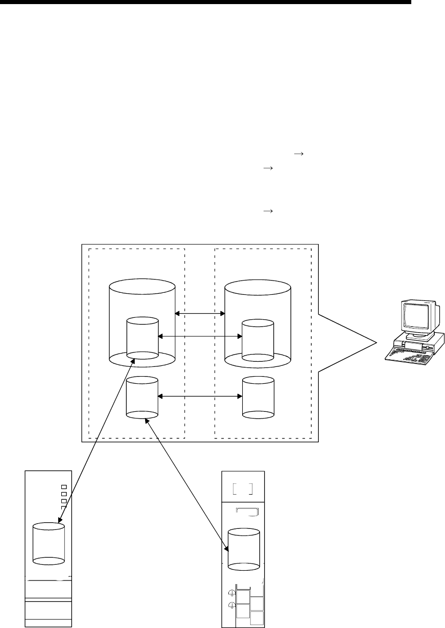
8 - 15 8 - 15
MELSEC-Q
8 UTILITY PACKAGE (GX Configurator-SC)
<Flash ROM data>
(a) The data set in [Flash ROM setting] can be saved in the desired directory
separately from the GX Developer project.
(b) Operations 4) and 5) shown in Figure 8.1 are performed as follows:
4) This operation can be performed from the [Flash ROM setting] screen or
[Monitor/test] screen.
[Flash ROM setting] screen [File read]/[File save]
[Monitor/test] screen [File read]/[File save]
5) This operation can be performed from the [Monitor/Test] screen of the
utility.
[Monitor/test] screen [Read from module]/[Write to module]
QCPU
Q25HCPU
MODE
RUN
ERR.
USER
BAT.
BOOT
RS-232
USB
A
QJ71C24
QJ71C24
CH1. CH2.
RS-232
CH1.
CH.2
SDA
SDB
RS-422
/485
RDA
RDB
(FG)
(FG)
1
2
5
7
3
4
6
B
B
1)
2)
4)
B
A
A
3) 5)
GX Developer/
GX Configurator-SC Disk
Project Project
Personal computer
A: Indicates an intelligent function module parameter.
B: Indicates flash ROM data.
Figure 8.1 Correlation chart for data created by the utility package
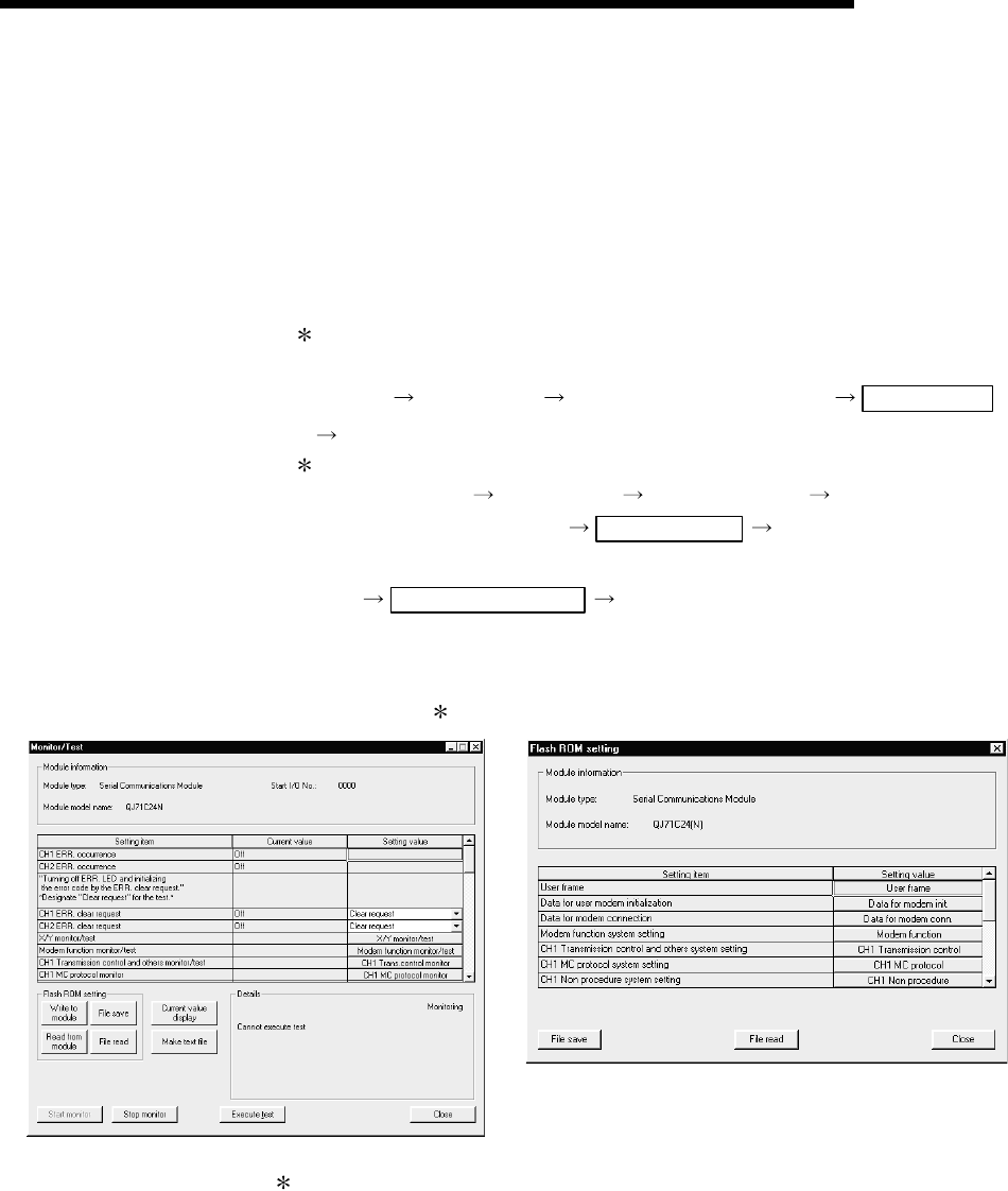
8 - 16 8 - 16
MELSEC-Q
8 UTILITY PACKAGE (GX Configurator-SC)
8.4 System Registration to Flash ROM
[Purpose]
Display the menu screen for flash ROM registration, which is used to change the
initial values set in the Q series C24's buffer memory.
[Startup procedure]
• Online operation
Startup from Intelligent function module utility
(GX Developer Version 4 or later)
[Online] [Monitor/test] "Select monitor/test module" Monitor/test
[Monitor] screen
Startup from the system monitor (GX Developer Version 6 or later).
[GX Developer] [Diagnostics] [System Monitor] "Select the Q series
C24 by installation status" Diagnostics... [Monitor] screen
• Offline operation
[Tools] Flash ROM setting [Flash ROM setting] screen
[Setting screen]
Screen displayed during online operation ( 1) Screen displayed during offline operation
1 The selection menus for system setting/registration are displayed by scrolling
on the [Monitor] screen during online operation.
The selection buttons pertaining to flash ROM registration are displayed in
blue on the screen.
8 - 17 8 - 17
MELSEC-Q
8 UTILITY PACKAGE (GX Configurator-SC)
[Setting Items]
The following table shows the selection menus for system setting/registration to
be displayed:
Function Section Remarks
User frame registration Section 8.4.1
Data for modem initialization registration Section 8.4.2
Data for modem connection registration Section 8.4.3
Modem function system setting Section 8.4.4
Transmission control and others system setting Section 8.4.5
MC protocol system setting Section 8.4.6
Non procedure system setting Section 8.4.7
Bidirectional system setting Section 8.4.8
PLC CPU monitoring system setting Section 8.4.9
Transmission user frame No. designation system setting Section 8.4.10
Can be used via online
operation.
Can be used via offline
operation.
Resetting buffer memory/flash ROM setting values to default values Section 8.4.11
Flash ROM write allow/prohibit setting Section 8.4.12
Can be used only via online
operation.
POINT
(1) The User's Manual (Basic) and GX Configurator-SC's Help function provide
the code list. Use this list as a reference.
(2) The values set in the respective setting screens explained in Section 8.4 can
be written to the Q series C24 module (via online operation only) or saved to a
file.
(3) Perform the following operations in advance to enable the registration of
setting values in the flash ROM:
(a) Switch setting using the GX Developer (see Section 4.5.2)
Set "Setting change" under [Transmission settings] to "Enable" for both
the CH1 and CH2 sides.
(b) Setting using GX Configurator-SC (see Section 8.4.12)
Set the flash ROM write allow/prohibit designation to "Allowed".
(4) Some system setting screens have a pair of screens: one for CH1 and the
other for CH2. Please note that the explanations given in Section 8.4.1 and
thereafter apply to the online operations performed in the CH1 screens.
The setting items are the same between CH1 and CH2, but different buffer
memory addresses are used to store the setting values. The respective
addresses are indicated as follows where applicable.
(Left side: address for the CH1 side, right side: address for the CH2 side)
Setting item Setting value storage buffer
memory address
Reference section containing detailed
explanation
DTR/DC control
designation 93H/133HChapter 7 of
User's Manual (Application)
(5) When a multiple CPU system is employed, GX Configurator-SC should be
connected to the control PLC of the Q series C24, and the system setting data
register in the flash ROM.
It is not possible to set target PLC to multiple CPU setting of "Transfer setup"
of GX Developer and register the system setting data in the flash ROM.
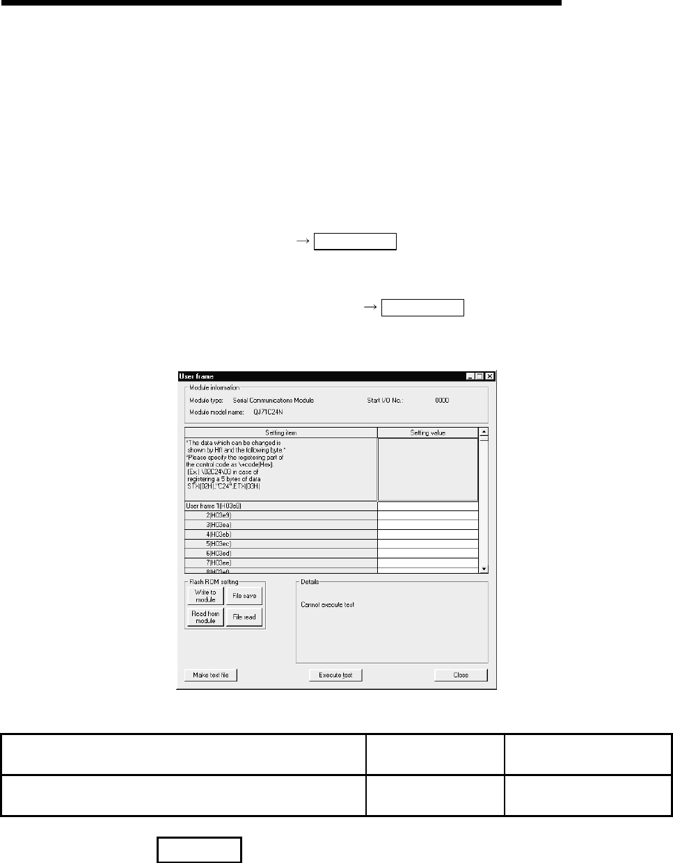
8 - 18 8 - 18
MELSEC-Q
8 UTILITY PACKAGE (GX Configurator-SC)
8.4.1 User frame registration
[Purpose]
Register the user frame used in the following functions:
• On-demand function using the MC protocol.
• Data transmission/receive function using the non procedure protocol.
[Startup procedure]
• Online operation
[Monitor] screen User frame
• Offline operation
[Flash ROM setting] screen User frame
[Setting screen]
[Setting item]
Setting item Setting value storage
buffer memory address
Reference section containing
detailed explanation
User frame 1 to 200 — Chapter 9 of
User's Manual (Application)
REMARK
Use \ + code to specify hexadecimal numbers in the control code registration field if
QSCU is used for registering a user frame.
(Example) To register the 5 bytes of data, STX (02H), "C24," and ETX (03H), specify
the following:
\02C24\03
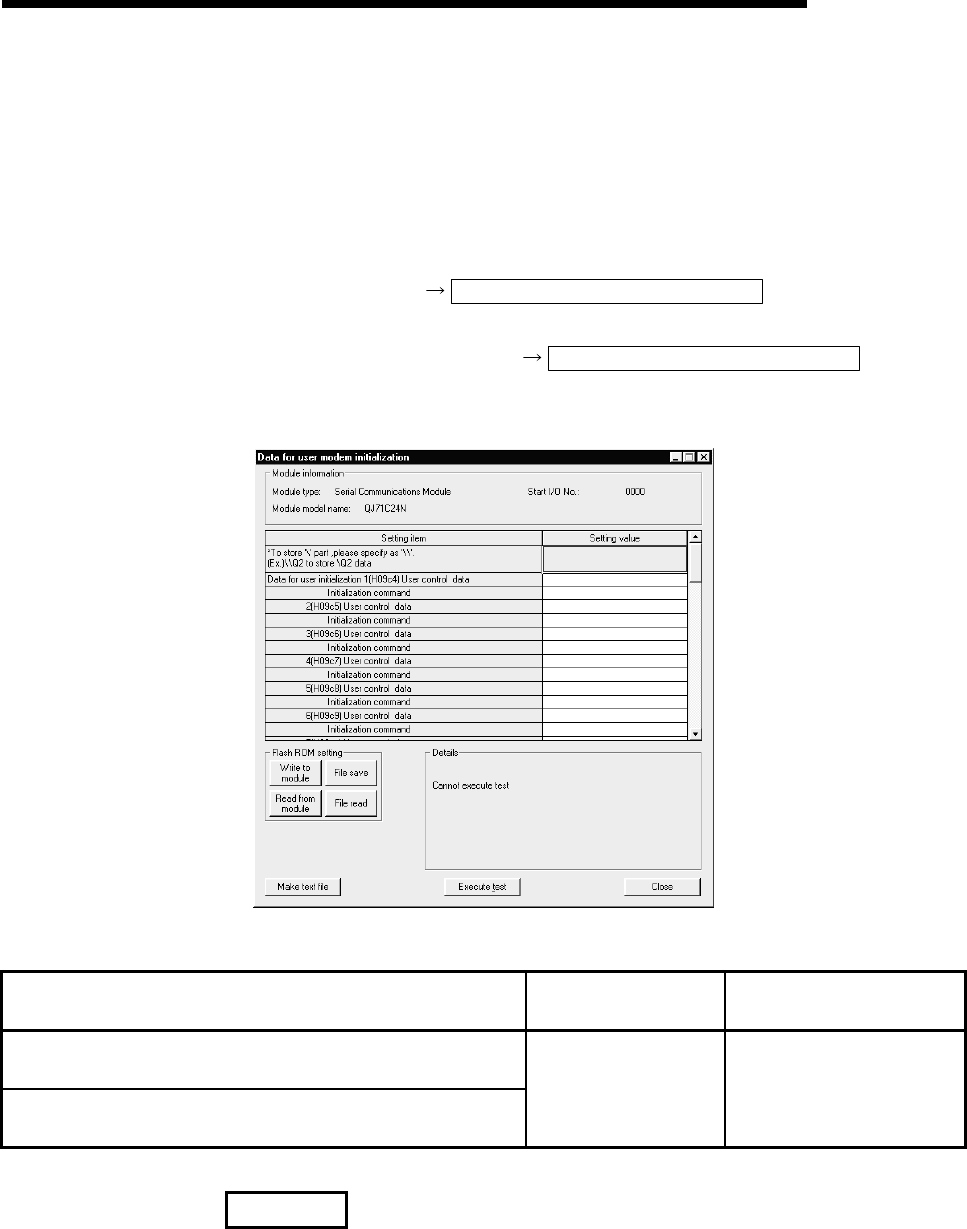
8 - 19 8 - 19
MELSEC-Q
8 UTILITY PACKAGE (GX Configurator-SC)
8.4.2 Data for modem initialization registration
[Purpose]
Register the data for initializing the modem connected to the Q series C24.
[Startup procedure]
• Online operation
[Monitor] screen Data for user modem initialization
• Offline operation
[Flash ROM setting] screen Data for user modem initialization
[Setting screen]
[Setting item]
Setting item Setting value storage
buffer memory address
Reference section containing
detailed explanation
Data for user initialization 1 to 30
User control data
Data for user initialization 1 to 30
Initialization command
—Chapter 3 of
User's Manual (Application)
REMARK
Use \\ code to specify a field to register "\" if GX Configurator-SC is used for data for
modem initialization.
(Example) To register the \Q2 of data: \\Q2
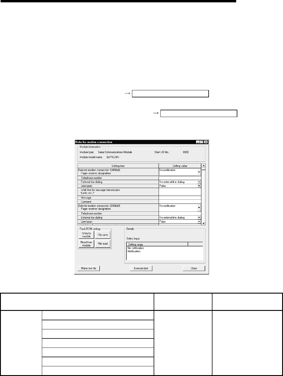
8 - 20 8 - 20
MELSEC-Q
8 UTILITY PACKAGE (GX Configurator-SC)
8.4.3 Data for modem connection registration
[Purpose]
For data communication and notification using the modem function, register the
data for connection with external devices.
[Startup procedure]
• Online operation
[Monitor] screen Data for modem connection
• Offline operation
[Flash ROM setting] screen Data for modem connection
[Setting screen]
[Setting items]
Setting item Setting value storage
buffer memory address
Reference section containing
detailed explanation
Pager receiver designation
Telephone number
External line dialing
Line types
Wait time for message transmission units: s
Message
Data for modem
connection
1 to 30
Comment
—Chapter 3 of
User's Manual (Application)
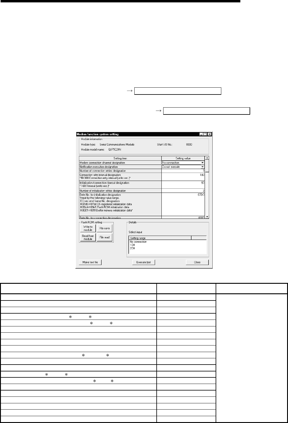
8 - 21 8 - 21
MELSEC-Q
8 UTILITY PACKAGE (GX Configurator-SC)
8.4.4 Modem function system setting/registration
[Purpose]
For data communication using the modem function, register system setting
values.
[Startup procedure]
• Online operation
[Monitor] screen Modem function system setting
• Offline operation
[Flash ROM setting] screen Modem function system setting
[Setting screen]
[Setting items]
Setting item Setting value storage buffer
memory address Reference section containing detailed
explanation
Modem connection channel designation 2EH
Notification execution designation 2FH
Number of connection retries designation 30H
Connection retry interval designation units: s 31H
Initialization/connection timeout time designation units: s 32H
Number of initialization retries designation 33H
Data No. for initialization designation 34H
Data No. for connection designation 35H
GX Developer connection designation 36H
No-communication interval time designation units: min 37H
RS · CS control yes/no designation 38H
Modem initialization time DR signal valid/invalid designation 2008H
Wait time of notification units: s 200AH
Circuit disconnect wait time (PLC CPU watch use) units: s 200EH
Remote password mismatch notification count designation 200CH
Remote password mismatch notification accumulated count designation 200DH
Auto modem initialization designation 2007H
Callback function designation 2001H
Callback denial notification accumulated count designation 2002H
Data No. for callback designation 1 to 10 2101H to 210AH
Chapter 3 of
User's Manual (Application)
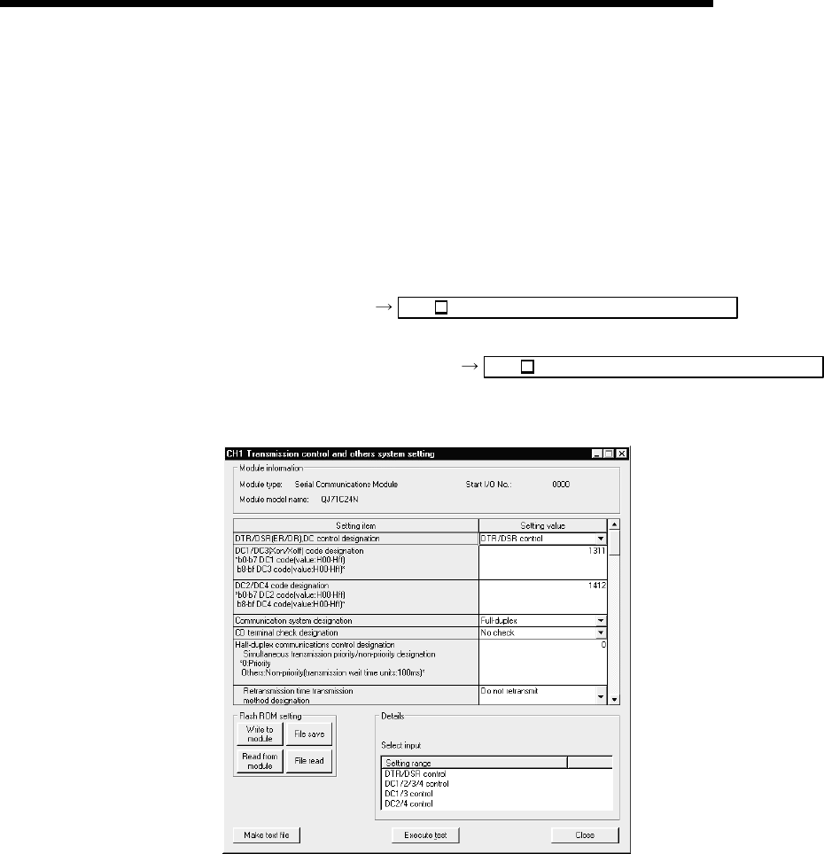
8 - 22 8 - 22
MELSEC-Q
8 UTILITY PACKAGE (GX Configurator-SC)
8.4.5 Transmission control and others system setting
[Purpose]
For data communication with external devices, register system setting values for
the transmission control method, monitoring time, and buffer memory
assignment.
[Startup procedure]
• Online operation
[Monitor] screen CH Transmission control system setting
• Offline operation
[Flash ROM setting] screen CH Transmission control system setting
[Setting screen]

8 - 23 8 - 23
MELSEC-Q
8 UTILITY PACKAGE (GX Configurator-SC)
[Setting items]
Setting item Setting value storage
buffer memory address
Reference section containing
detailed explanation
DTR/DSR (ER/DR), DC control designation 93H/133H
DC1/DC3 (Xon/Xoff) code designation 94H/134H
DC2/DC4 code designation 95H/135H
Chapter 7 of
User's Manual (Application)
Communication system designation 98H/138H
CD terminal check designation 97H/137H
Section 3.2 of
User's Manual (Basic)
Half-duplex communications control designation
Simultaneous transmission priority/non-priority designation 99H/139H
Half-duplex communications control designation
Retransmission time transmission method designation 9AH/13AH
Chapter 8 of
User's Manual (Application)
No-reception monitoring time (timer 0) designation 9CH/13CH
Response monitoring time (timer 1) designation 9DH/13DH
Transmission monitoring time (timer 2) designation 9EH/13EH
Chapter 6 of
User's Manual (Application)
Word/byte units designation 96H/136HChapter 5 of
User's Manual (Application)
RTS (RS) designation 92H/132H … b0
DTR (ER) designation 92H/132H … b2
Section 3.2.1 of
User's Manual (Basic)
Transmission control start free area 2012H/2112H
Transmission control end free area 2013H/2113H
Chapter 7 of
User's Manual (Application)
Send/Recv data monitoring designation 2018H/2118H
Action for buffer full 2019H/2119H … b0
Stop by Timer 0 error 2019H/2119H … b2
Monitor buffer head address 201AH/211AH
Monitor buffer size 201BH/211BH
Chapter 16 of
User's Manual (Application)
Transmission buffer memory head address designation A2H/142H
Transmission buffer memory length designation A3H/143H
Receive buffer memory head address designation A6H/146H
Receive buffer memory length designation A7H/147H
Chapters 6 and 7 of
User's Manual (Basic)
Transmission transparent code designation 1st 11FH/1BFH
Transmission transparent code designation 2nd to 10th 2030H to 2038H/
2130H to 2138H
Receive transparent code designation 120H/1C0H
Chapter 12 of
User's Manual (Application)
ASCII-BIN conversion designation 121H/1C1HChapter 13 of
User's Manual (Application)
Receive interrupt-issued designation 2010H/2110HChapter 4 of
User's Manual (Application)
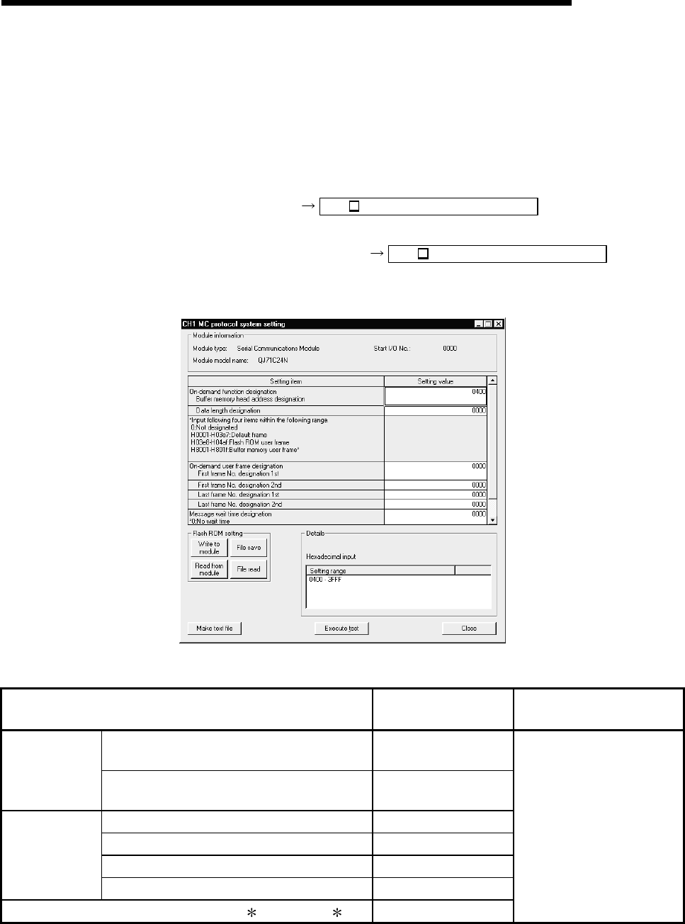
8 - 24 8 - 24
MELSEC-Q
8 UTILITY PACKAGE (GX Configurator-SC)
8.4.6 MC protocol system setting
[Purpose]
For data transmission using the MC protocol, register system setting values.
[Startup procedure]
• Online operation
[Monitor] screen CH MC protocol system setting
• Offline operation
[Flash ROM setting] screen CH MC protocol system setting
[Setting screen]
[Setting items]
Setting item Setting value storage
buffer memory address
Reference section containing
detailed explanation
Buffer memory head address designation A0H/140H
On-demand
function
designation Data length designation A1H/141H
First frame No. designation 1st A9H/149H
First frame No. designation 2nd AAH/14AH
Last frame No. designation 1st ABH/14BH
On-demand user
frame
designation Last frame No. designation 2nd ACH/14CH
Message wait time designation waiting time units: 10 ms 11EH/1BEH
Chapter 10 of
User's Manual (Application)
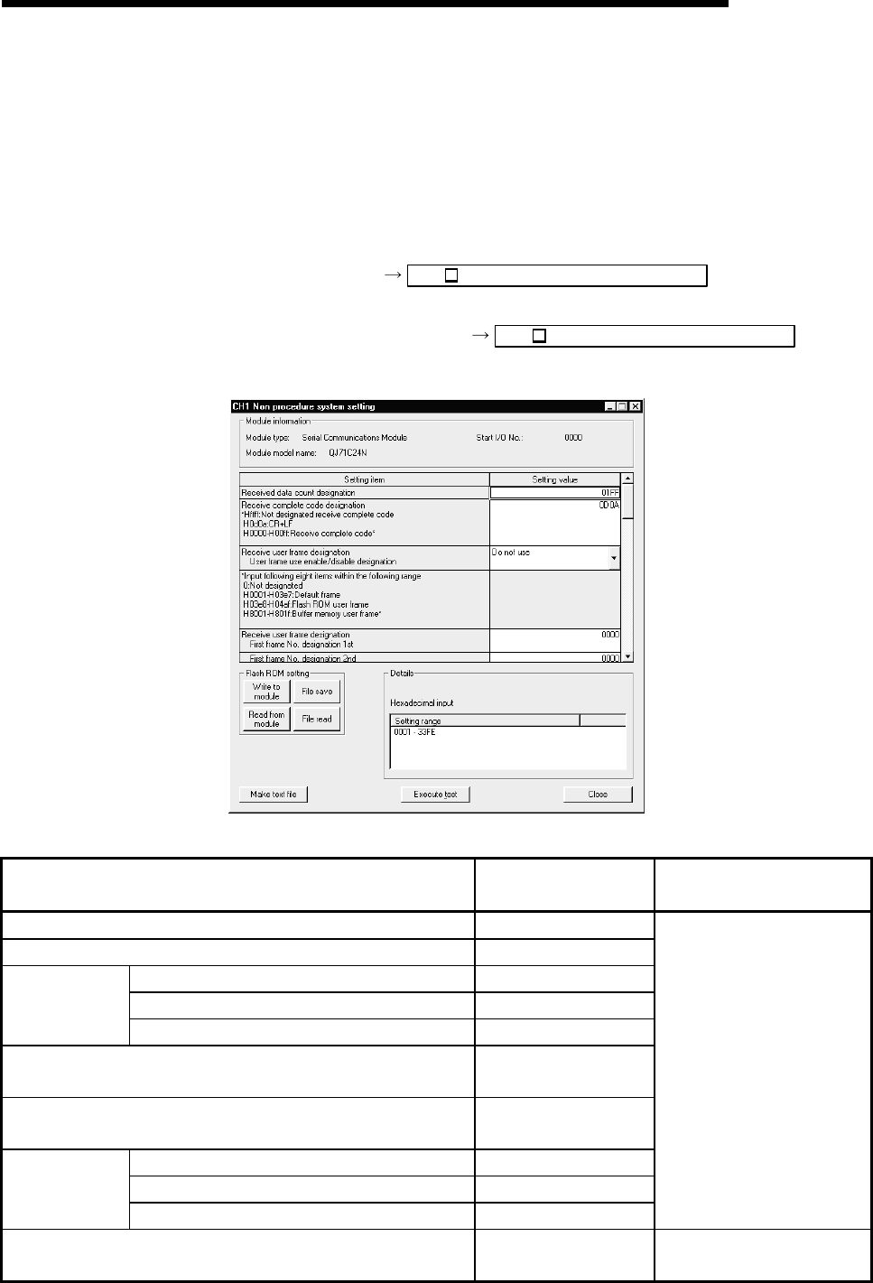
8 - 25 8 - 25
MELSEC-Q
8 UTILITY PACKAGE (GX Configurator-SC)
8.4.7 Non procedure system setting
[Purpose]
For data transmission using the non procedure protocol, register system setting
values.
[Startup procedure]
• Online operation
[Monitor] screen CH Non procedure system setting
• Offline operation
[Flash ROM setting] screen CH Non procedure system setting
[Setting screen]
[Setting items]
Setting item Setting value storage
buffer memory address
Reference section containing
detailed explanation
Received data count designation A4H/144H
Receive complete code designation A5H/145H
Chapter 6 of
User's Manual (Basic)
User frame use enable/disable designation ADH/14DH
First frame No. designation 1st to 4th AEH to B1H/14EH to 151H
Receive user
frame
designation Last frame No. designation 1st to 4th B2H to B5H/152H to 155H
User frame receive format designation 1st to 4th 2020H to 2023H/
2120H to 2123H
Exclusive format-1 received data count 1st to 4th 2024H to 2027H/
2124H to 2127H
CR/LF output designation B7H/157H
Output head pointer designation B8H/158H
Transmission
user frame
designation Output count designation B9H/159H
Chapters 9 and 11 of
User's Manual (Application)
Timeout at No-protocol 2014H/2114HChapters 6 of
User's Manual (Application)
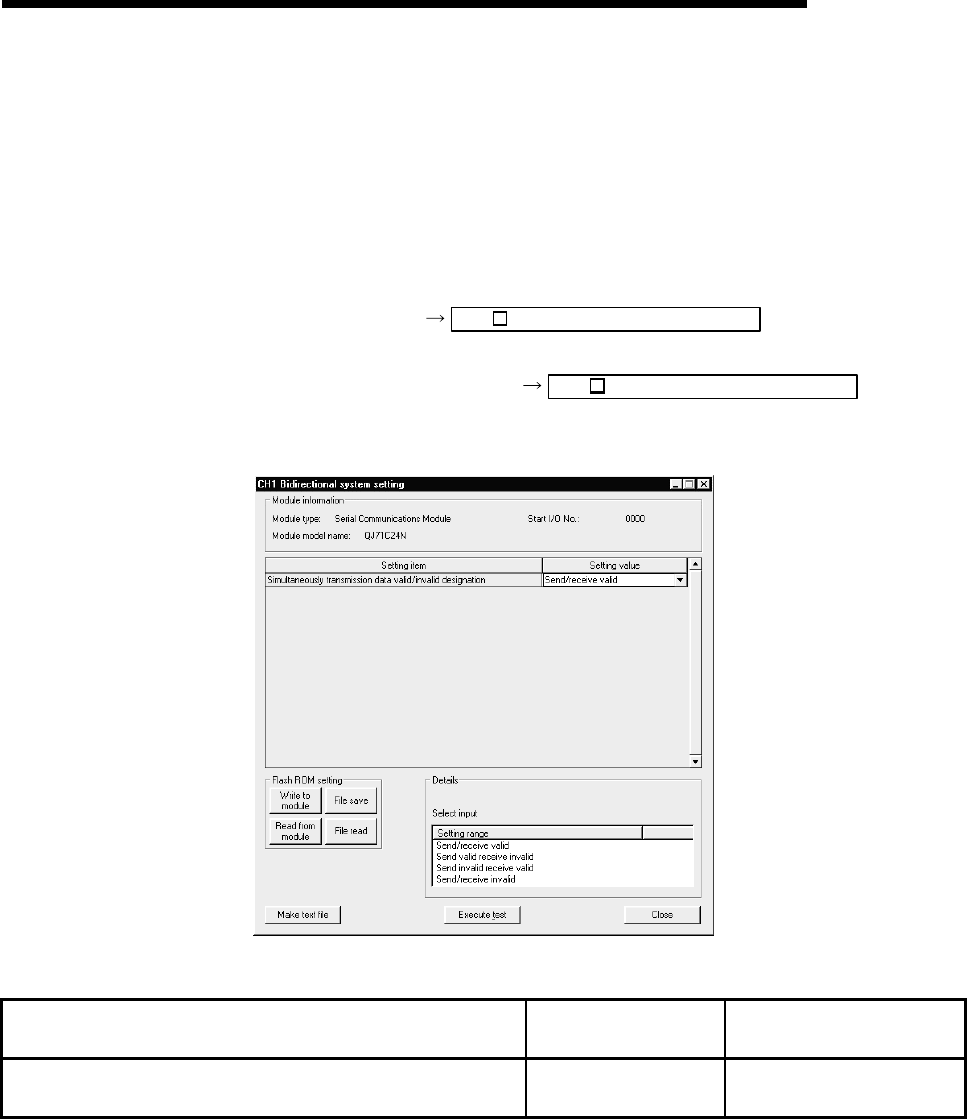
8 - 26 8 - 26
MELSEC-Q
8 UTILITY PACKAGE (GX Configurator-SC)
8.4.8 Bidirectional system setting
[Purpose]
For data transmission using the bidirectional protocol, register system setting
values.
[Startup procedure]
• Online operation
[Monitor] screen CH Bidirectional system setting
• Offline operation
[Flash ROM setting] screen CH Bidirectional system setting
[Setting screen]
[Setting item]
Setting item Setting value storage
buffer memory address
Reference section containing
detailed explanation
Simultaneously transmission data valid/invalid designation 9BH/13BHSection 7.3 of
User's Manual (Basic)
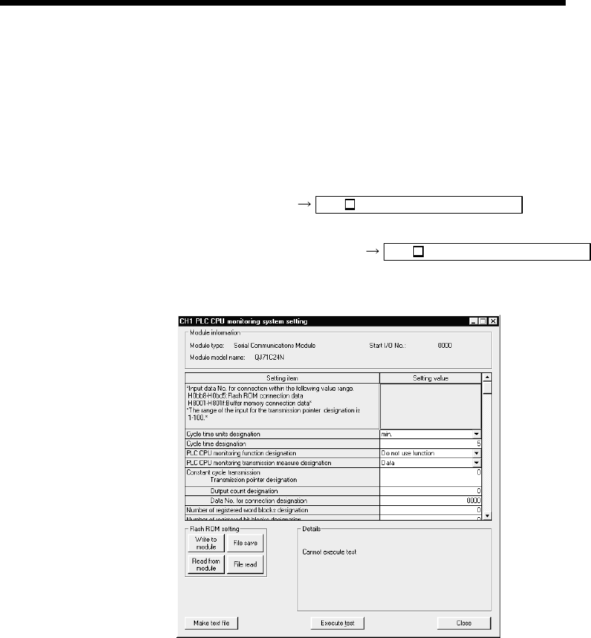
8 - 27 8 - 27
MELSEC-Q
8 UTILITY PACKAGE (GX Configurator-SC)
8.4.9 PLC CPU monitoring system setting
[Purpose]
Register system setting values to use the PLC CPU monitoring function.
[Startup procedure]
• Online operation
[Monitor] screen CH Monitoring system setting
• Offline operation
[Flash ROM setting] screen CH Monitoring system setting
[Setting screen]
8 - 28 8 - 28
MELSEC-Q
8 UTILITY PACKAGE (GX Configurator-SC)
[Setting items]
Setting item Setting value storage
buffer memory address
Reference section containing
detailed explanation
Cycle time units designation 2040H/2140H
Cycle time designation 2041H/2141H
PLC CPU monitoring function designation 2042H/2142H
PLC CPU monitoring transmission measure designation 2043H/2143H
Transmission pointer 2044H/2144H
Output count designation 2045H/2145H
Constant cycle
transmission Data No. for connection designation 2046H/2146H
Number of registered word blocks designation 204DH/214DH
Number of registered bit blocks designation 204EH/214EH
PLC CPU abnormal monitoring designation 204FH/214FH
No. n block monitoring device
Monitoring device designation
2050H/2150H to
20A1H/21A1H
Head device No. designation
2051H-2052H/2151H-
2152H to 20A1H-20A2H/
21A1H-21A2H
Read point designation 2053H/2153H to
20A3H/21A3H
Condition agreement transmission
Monitoring condition designation
2054H/2154H to
20A4H/21A4H
Monitoring condition value designation 2055H/2155H to
20A5H/21A5H
Transmission pointer designation 2056H/2156H to
20A6H/21A6H
Number of output designation 2057H/2157H to
20A7H/21A7H
Data No. for connection designation 2058H/2158H to
20A8H/21A8H
PLC PCU abnormal monitoring designation
Condition agreement transmission
Transmission pointer
20E6H/21E6H
Output count designation 20E7H/21E7H
Data No. for connection designation 20E8H/21E8H
Chapter 2 of
User's Manual (Application)
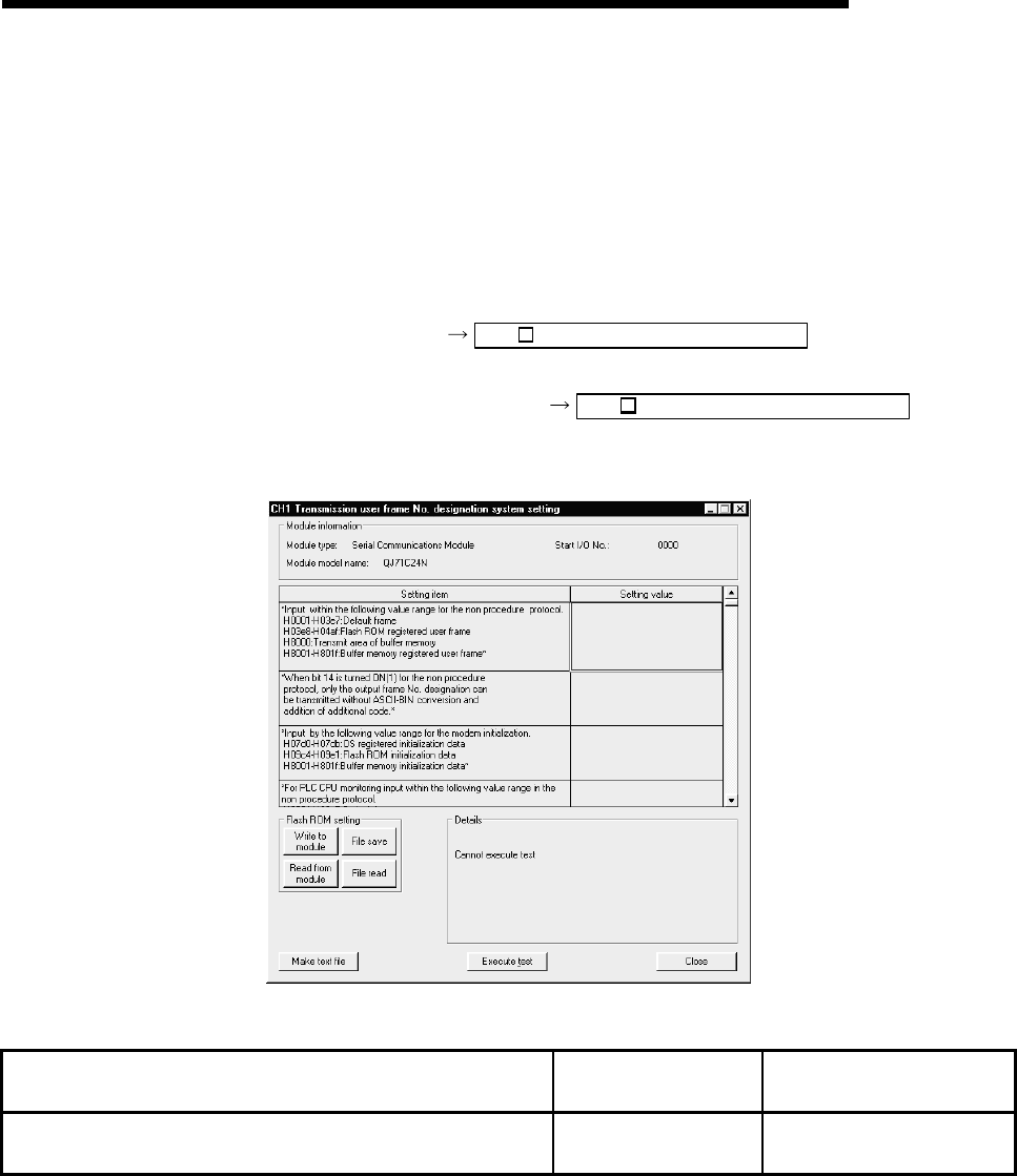
8 - 29 8 - 29
MELSEC-Q
8 UTILITY PACKAGE (GX Configurator-SC)
8.4.10 Transmission user frame No. designation system setting
[Purpose]
Register the output frame number to transmit data with the non procedure
protocol using the user frame.
[Startup procedure]
• Online operation
[Monitor] screen CH Output frame system setting
• Offline operation
[Flash ROM setting] screen CH Output frame system setting
[Setting screen]
[Setting item]
Setting item Setting value storage
buffer memory address
Reference section containing
detailed explanation
Output frame No. designation 1st to 100th BAH to 11DH/
15AH to 1BDH
Chapter 11 of
User's Manual (Application)
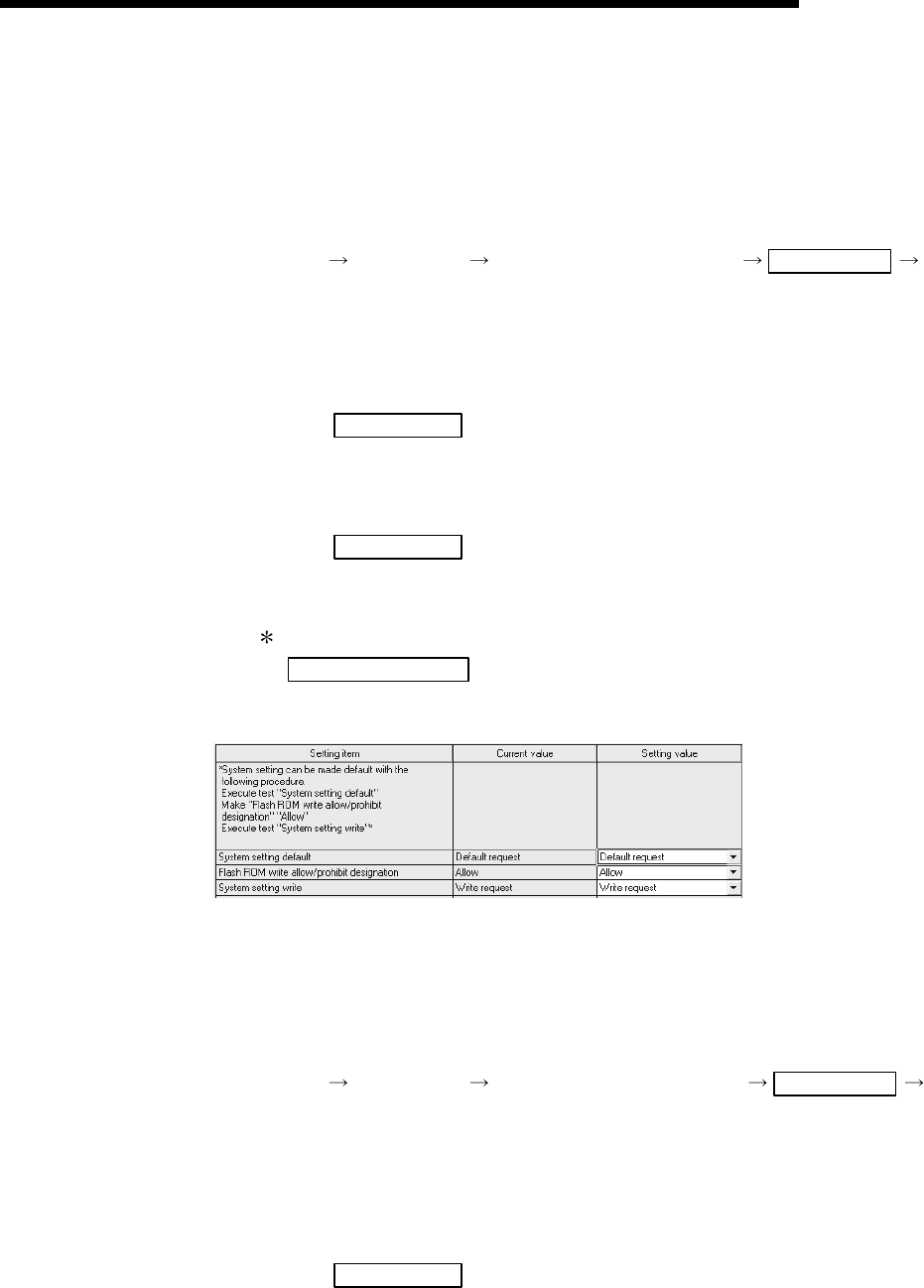
8 - 30 8 - 30
MELSEC-Q
8 UTILITY PACKAGE (GX Configurator-SC)
8.4.11 Resetting the buffer memory/flash ROM setting values to the default values
This section explains how to reset the values set in the buffer memory/flash ROM to
their default values.
[Startup procedure]
[Online] [Monitor/test] "Select monitor/Test module" Monitor/test
[Monitor] screen
[Operating procedure]
(Procedure 1) In the [Monitor] screen, select [Default request] for [System setting default].
(Procedure 2) Click on Execute test .
The setting values in the buffer memory will return to their default values.
(Procedure 3) Change the setting of [Flash ROM write allow/prohibit] to "Allowed."
(Procedure 4) In the [Monitor] screen, select [Write request] for [System setting write].
(Procedure 5) Click on Execute test .
The setting values in the flash ROM will return to their default values.
When confirming the processing results in GX Configurator-SC, perform
Read from module .
(Items subject to this operation in the [Monitor] screen)
8.4.12 Flash ROM write allow/prohibit setting
This section explains the settings to allow or prohibit writing to the flash ROM.
[Startup procedure]
[Online] [Monitor/test] "Select monitor/Test module" Monitor/test
[Monitor] screen
[Operating procedure]
(Procedure 1) In the [Monitor] screen, select [Flash ROM write allow/prohibit] and set "Allowed"
or "Prohibited."
(Procedure 2) Click on Execute test .
[Flash ROM write allow/prohibit] will be set to "Allowed" or "Prohibited,"
accordingly.

8 - 31 8 - 31
MELSEC-Q
8 UTILITY PACKAGE (GX Configurator-SC)
8.5 Auto Refresh Setting
The Auto Refresh Settings are used to automatically store the error information and
status information currently stored in the Q series C24's buffer memory in the device
specified by the PLC CPU.
For details, see Section 4.6.
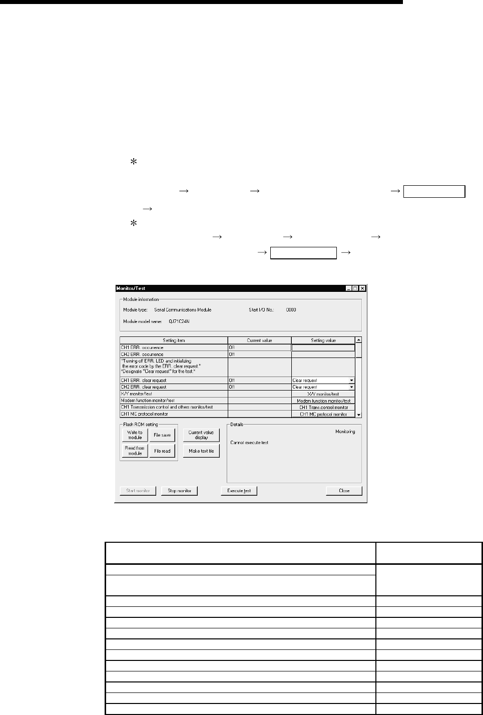
8 - 32 8 - 32
MELSEC-Q
8 UTILITY PACKAGE (GX Configurator-SC)
8.6 Monitor/Test
[Purpose]
The displayed menu screen is used to perform various operations, including the
monitoring of the Q series C24's operating status and setting values and the
testing of its output signals. The monitor/test operations can be performed only
via online operation.
[Startup procedure]
Startup from Intelligent function module utility
(GX Developer Version 4 or later)
[Online] [Monitor/test] "Select monitor/Test module" Monitor/test
[Monitor] screen
Startup from the system monitor (GX Developer Version 6 or later).
[GX Developer] [Diagnostics] [System Monitor] "Select the Q series
C24 by installation status" Diagnostics... [Monitor] screen
[Monitor/test screen]
[Monitor/test items]
The following selection menus for monitor/test operation will be displayed.
Function Reference section containing
explanation
ERR. occurrence
ERR. clear request
(Communication error information, error code information)
Section 8.6.10
X · Y monitor/test Section 8.6.1
Modem function monitor/test Section 8.6.2
Transmission control and others monitor/test Section 8.6.3
MC protocol monitor Section 8.6.4
Non procedure monitor/test Section 8.6.5
Bidirectional monitor Section 8.6.6
PLC CPU monitoring monitor Section 8.6.7
Transmission user frame No. designation monitor Section 8.6.8
Monitor/test others Section 8.6.9
System setting default, system setting write Section 8.4.11
Flash ROM write allow/prohibit designation Section 8.4.12
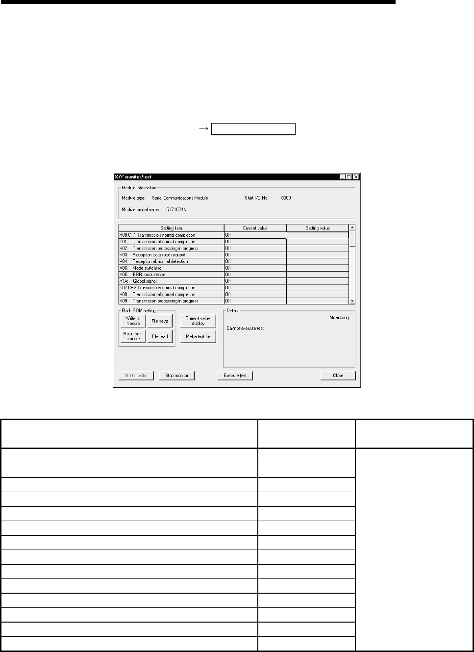
8 - 33 8 - 33
MELSEC-Q
8 UTILITY PACKAGE (GX Configurator-SC)
8.6.1 X · Y monitor/test
[Purpose]
Perform the monitoring of I/O signals and testing of output signals.
[Startup procedure]
[Monitor] screen X · Y monitor/test
[Monitor/test screen]
[Monitor/test items]
Monitor/test items Setting value storage
buffer memory address
Reference section containing
detailed explanation
X00: CH1 Transmission normal completion —
X01: CH1 Transmission abnormal completion —
X02: CH1 Transmission processing in progress —
X03: CH1 Reception data read request —
X04: CH1 Reception abnormal detection —
X06: CH1 Mode switching —
X0E: CH1 ERR. Occurrence —
X1A: CH1 Global signal —
X07: CH2 Transmission normal completion —
X08: CH2 Transmission abnormal completion —
to to
Y18: Flash ROM write request —
Y19: Flash ROM system setting request —
Y1C: System setting default request —
Section 3.8.
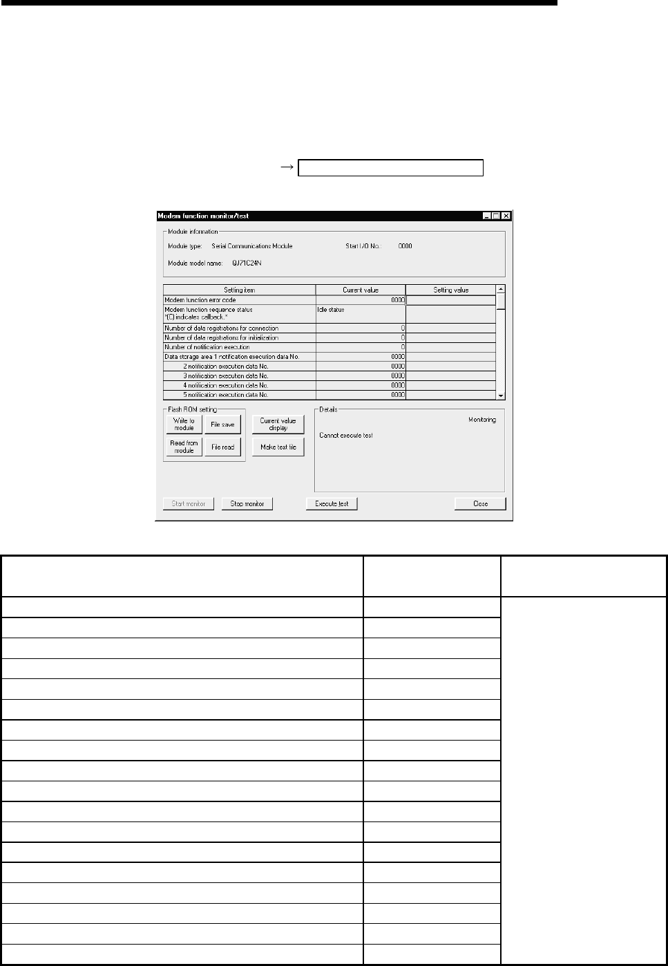
8 - 34 8 - 34
MELSEC-Q
8 UTILITY PACKAGE (GX Configurator-SC)
8.6.2 Modem function monitor/test
[Purpose for monitor/test]
Monitor/test the operating status and setting values of the modem function.
[Startup procedure]
[Monitor] screen Modem function monitor/test
[Monitor/test screen]
[Monitor/test items]
Monitor/test items Setting value storage
buffer memory address
Reference section containing
detailed explanation
Modem function error code 221H
Modem function sequence status 222H
Number of data registration for connection 223H
Number of data registrations for initialization 226H
Number of notification execution 229H
Data storage area 1 notification execution data No. 22AH
Data storage area 2 notification execution data No. 22EH
Data storage area 3 notification execution data No. 232H
Data storage area 4 notification execution data No. 236H
Data storage area 5 notification execution data No. 23AH
X10: Modem initialization completion —
X11: Dial in progress —
X12: Connection in progress —
X13: Initialization/connection abnormal completion —
X14: Modem disconnection completion —
X15: Notification normal completion —
X16: Notification abnormal completion —
Y10: Modem initialization request —
Section 3.3 of
User's Manual (Application)
8 - 35 8 - 35
MELSEC-Q
8 UTILITY PACKAGE (GX Configurator-SC)
Monitor/test items Setting value storage
buffer memory address
Reference section containing
detailed explanation
Y11: Connection request —
Y12: Modem disconnection request —
Y14: Notification-issued request —
Modem connection channel designation 2EH
Notification execution designation 2FH
Number of connection retires designation 30H
Connection retry interval designation units: s 31H
Initialization/connection timeout designation units: s 32H
Number of initialization retries designation 33H
Data No. for initialization designation 34H
Data No. for connection designation 35H
GX Developer connection designation 36H
No-communication interval time designation units: min 37H
RS · CS control yes/no designation 38H
Modem initialization time DR signal valid/invalid designation 2008H
Wait time of notification units: s 200AH
Circuit disconnect wait time (PLC CPU watch use) units: s 200EH
Remote password mismatch notification count designation 200CH
Remote password mismatch notification accumulated count
designation 200DH
Accumulated count of unlock process normal completion 22FBH
Accumulated count of unlock process abnormal completion 22FCH
Accumulated count of lock process based on circuit disconnection 22FFH
Auto modem initialization designation 2007H
Callback function designation 2001H
Callback denial notification accumulated count designation 2002H
Data No. for Callback designation 1 to 10 2101H to 210AH
Callback permit accumulated count 22F0H
Callback denial accumulated count 22F1H
Auto (callback) connection permit accumulated count 22F2H
Auto (callback) connection denial accumulated count 22F3H
Accumulated count of callback receive procedure cancel 22F4H
Section 3.3 of
User's Manual (Application)
8 - 36 8 - 36
MELSEC-Q
8 UTILITY PACKAGE (GX Configurator-SC)
[Test Items]
The following accumulated count of times counter values can be cleared to "0" by
the select test function.
Test items Setting value storage
buffer memory address
Reference section containing
detailed explanation
Accumulated count of unlock process normal completion 22FBH
Accumulated count of unlock process abnormal completion 22FCH
Accumulated count of lock process based on circuit disconnection 22FFH
Callback permit accumulated count 22F0H
Callback denial accumulated count 22F1H
Auto (callback) connection permit accumulated count 22F2H
Auto (callback) connection denial accumulated count 22F3H
Accumulated count of callback receive procedure cancel 22F4H
Section 3.3 of
User's Manual (Application)
[Operation procedure]
(Step 1) Display the "Modem function monitor/test" screen.
(Step 2) Click the setting value area of the item to be cleared to "0."
(Step 3) Click the " Execute test ."
The counter value of the selected item becomes "0."
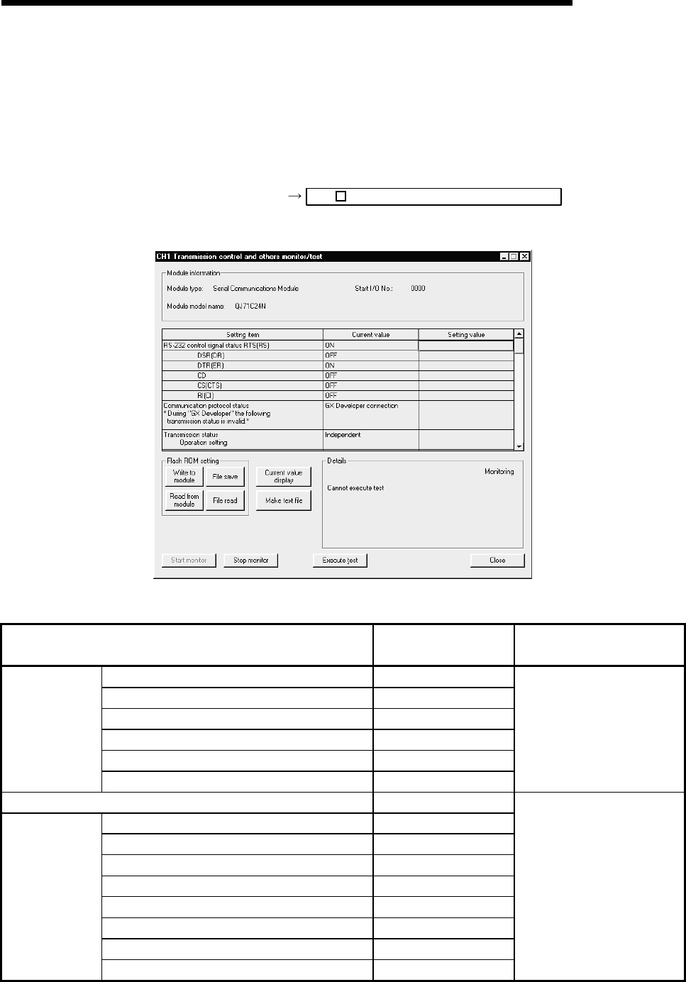
8 - 37 8 - 37
MELSEC-Q
8 UTILITY PACKAGE (GX Configurator-SC)
8.6.3 Transmission control and others monitor/test
[Purpose]
Monitor the RS-232 signal status and the various setting values for data
communication.
[Startup procedure]
[Monitor] screen CH Transmission control monitor/test
[Monitor/test screen]
[Monitor/test items]
Monitor/test items Setting value storage
buffer memory address
Reference section containing
detailed explanation
RTS (RS) 254H/264H … b0
DSR (DR) 254H/264H … b1
DTR (ER) 254H/264H … b2
CD 254H/264H … b3
CS (CTS) 254H/264H … b4
RS-232 control
signal status
RI (CI) 254H/264H … b5
Section 4.4.1 of
User's Manual (Basic)
Communication protocol status 252H/262H
Operation setting 253H/263H … b0
Data bit 253H/263H … b1
Parity bit enable/disable 253H/263H … b2
Even/odd parity 253H/263H … b3
Stop bit 253H/263H … b4
Sum check code 253H/263H … b6
Write during RUM 253H/263H … b6
Transmission
status
Setting modification 253H/263H … b7
Section 4.5.2 of
User's Manual (Basic)
8 - 38 8 - 38
MELSEC-Q
8 UTILITY PACKAGE (GX Configurator-SC)
Monitor/test items Setting value storage
buffer memory address
Reference section containing
detailed explanation
Transmission
status Transmission speed 253H/263H … b8 to b11 Section 4.5.2 of
User's Manual (Basic)
DTR/DSR (ER/DR), DC control designation 93H/133H
DC1/DC3 (Xon/Xoff) code designation 94H/134H
DC2/DC4 code designation 95H/135H
Chapter 7 of
User's Manual (Application)
Communication system designation 98H/138H
CD terminal check designation 97H/137H
Section 4.5.2 of
User's Manual (Basic)
Half-duplex communications control designation
Simultaneous transmission priority/non-priority designation 99H/139H
Half-duplex communications control designation
Retransmission time transmission method designation 9AH/13AH
Chapter 8 of
User's Manual (Application)
No-reception monitoring time (timer 0) designation units: byte 9CH/13CH
Response monitoring time (timer 1) designation units: 100 ms 9DH/13DH
Transmission monitoring time (timer 2) designation
units: 100 ms 9EH/13EH
Chapter 6 of
User's Manual (Application)
Word/byte units designation 96H/136HChapter 5 of
User's Manual (Application)
RTS (RS) designation 92H/132H … b0
DTR (ER) designation 92H/132H … b2
Section 3.2.1 of
User's Manual (Basic)
Transmission control start free area 2012H/2112H
Transmission control end free area 2013H/2113H
Chapter 7 of
User's Manual (Application)
Send/Recv data monitoring designation 2018H/2118H
Action for buffer full 2019H/2119H … b0
Stop by Timer 0 error 2019H/2119H … b2
Monitor buffer head address 201AH/211AH
Monitor buffer size 201BH/211BH
Chapter 16 of
User's Manual (Application)
Transmission buffer memory head address designation A2H/142H
Transmission buffer memory length designation A3H/143H
Receive buffer memory head address designation A6H/146H
Receive buffer memory length designation A7H/147H
Chapters 6 and 7 of
User's Manual (Basic)
Transmission transparent code designation 1st 11FH/1BFH
Transmission transparent code designation 2nd to 10th 2030H to 2038H/
2130H to 2138H
Receive transparent code designation 120H/1C0H
Chapter 12 of
User's Manual (Application)
ASCII-BIN conversion designation 121H/1C1HChapter 13 of
User's Manual (Application)
Receive interrupt-issued designation 2010H/2110HChapter 4 of
User's Manual (Application)
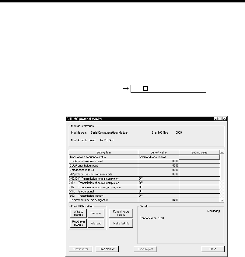
8 - 39 8 - 39
MELSEC-Q
8 UTILITY PACKAGE (GX Configurator-SC)
8.6.4 MC protocol monitor
[Purpose]
Monitor the status and setting values of the data communication using the MC
protocol.
[Startup procedure]
[Monitor] screen CH MC protocol monitor
[Monitor screen]
8 - 40 8 - 40
MELSEC-Q
8 UTILITY PACKAGE (GX Configurator-SC)
[Monitor items]
Monitor items Setting value storage
buffer memory address
Reference section containing
detailed explanation
Transmission sequence status 255H/265H
On-demand execution result 256H/266H
Data transmission result 257H/267H
Data reception result 258H/268H
MC protocol transmission error code 25AH/26AH
X00: CH1 Transmission normal completion —
X01: CH1 Transmission abnormal completion —
X02: CH1 Transmission processing in progress —
X1A: CH1 Global signal —
Y00: CH1 Transmission request —
Buffer memory head address designation A0H/140H
On-demand
function
designation Data length designation A1H/141H
Chapter 10 of
User's Manual (Basic)
Sections 3.10 and 3.11 of
Reference Manual
First frame No. designation 1st A9H/149H
First frame No. designation 2nd AAH/14AH
Last frame No. designation 1st ABH/14BH
On-demand user
frame
designation Last frame No. designation 2nd ACH/14CH
Chapter 10 of
User's Manual (Application)
Message wait time designation units: 10 ms 11EH/1BEHChapter 6 of
User's Manual (Application)
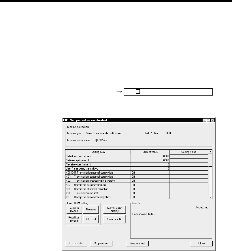
8 - 41 8 - 41
MELSEC-Q
8 UTILITY PACKAGE (GX Configurator-SC)
8.6.5 Non procedure monitor/test
[Purpose]
Monitor the status and setting values of the data transmission using the non
procedure protocol. The test operation for the receive data clear is explained in
Section 8.7.
[Startup procedure]
[Monitor] screen CH Non procedure monitor/test
[Monitor/test screen]
8 - 42 8 - 42
MELSEC-Q
8 UTILITY PACKAGE (GX Configurator-SC)
[Monitor/test items]
Monitor/test items Setting value storage
buffer memory address
Reference section containing
detailed explanation
Data transmission result 257H/267H
Data reception result 258H/268H
Chapter 10 of
User's Manual (Basic)
Receive user frame nth 25BH/26BH
User frame being transmitted B6H/156H
Chapter 11 of
User's Manual (Application)
X00: CH1 Transmission normal completion —
X01: CH1 Transmission abnormal completion —
X02: CH1 Transmission processing in progress —
X03: CH1 Reception data read request —
X04: CH1 Reception abnormal detection —
Y00: CH1 Transmission request —
Y01: CH1 Reception data read completion —
Chapter 6 of
User's Manual (Basic)
Received data count designation A4H/144H
Receive complete code designation A5H/145H
Chapter 6 of
User's Manual (Basic)
User frame use enable/disable designation ADH/14DH
First frame No. designation 1st to 4th AEH to B1H/14EH to 151H
Receive user
frame
designation Last frame No. designation 1st to 4th B2H to B5H/152H to 155H
User frame receive format designation 1st to 4th 2020H to 2023H/
2120H to 2123H
Exclusive format-1 received data count 1st to 4th 2024H to 2027H/
2124H to 2127H
CR/LF output designation B7H/157H
Output head pointer designation B8H/158H
Transmission
user frame
designation Output count designation B9H/159H
Chapter 9 of
User's Manual (Application)
Timeout at No-protocol 2014H/2114H
Chapter 6 of
User's Manual (Application)
Receive data clear request A8H/148HChapter 6 of
User's Manual (Basic)
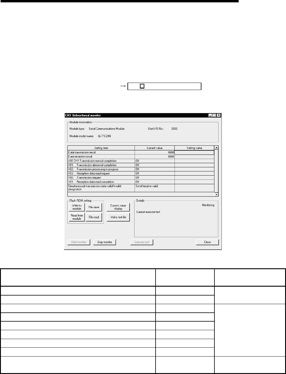
8 - 43 8 - 43
MELSEC-Q
8 UTILITY PACKAGE (GX Configurator-SC)
8.6.6 Bidirectional monitor
[Purpose]
Monitor the status and setting values of the data transmission using the
bidirectional protocol.
[Startup procedure]
[Monitor] screen CH Bidirectional monitor
[Monitor screen]
[Monitor items]
Monitor items Setting value storage
buffer memory address
Reference section containing
detailed explanation
Data transmission result 257H/267H
Data reception result 258H/268H
Chapter 10 of
User's Manual (Basic)
X00: CH1 Transmission normal completion —
X01: CH1 Transmission abnormal completion —
X02: CH1 Transmission processing in progress —
X03: CH1 Reception data read request —
Y00: CH1 Transmission request —
Y01: CH1 Reception data read completion —
Chapter 7 of
User's Manual (Basic)
Simultaneously transmission data valid/invalid designation 9BH/13BHSection 7.3 of
User's Manual (Basic)
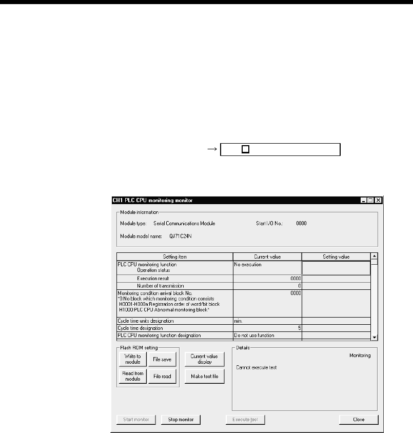
8 - 44 8 - 44
MELSEC-Q
8 UTILITY PACKAGE (GX Configurator-SC)
8.6.7 PLC CPU monitoring monitor
[Purpose]
Monitor the operating status and setting values of the PLC CPU monitoring
function.
[Startup procedure]
[Monitor] screen CH Monitoring monitor
[Monitor screen]
8 - 45 8 - 45
MELSEC-Q
8 UTILITY PACKAGE (GX Configurator-SC)
[Monitor items]
Monitor items Setting value storage
buffer memory address
Reference section containing
detailed explanation
Operation status 2204H/2304H
Execution result 2205H/2305H
PLC CPU
monitoring
function Number of transmission 2206H/2306H
Monitoring condition arrival block No. 2207H/2307H
Cycle time units designation 2040H/2140H
Cycle time designation 2041H/2141H
PLC CPU monitoring function designation 2042H/2142H
PLC CPU monitoring transmission measure designation 2043H/2143H
Transmission pointer 2044H/2144H
Output count designation 2045H/2145H
Constant cycle
transmission Data No. for connection designation 2046H/2146H
Number of registered word blocks designation 204DH/214DH
Number of registered bit blocks designation 204EH/214EH
PLC CPU abnormal monitoring designation 204FH/214FH
No. n block monitoring device
Monitoring device designation
2050H/2150H to
20A1H/21A1H
Head device No. designation
2051H-2052H/
2151H-2152H to
20A1H-20A2H/
21A1H-21A2H
Read point designation 2053H/2153H to
20A3H/21A3H
Condition agreement transmission
Monitoring condition designation
2054H/2154H to
20A4H/21A4H
Monitoring condition value designation 2055H/2155H to
20A5H/21A5H
Transmission pointer designation 2056H/2156H to
20A6H/21A6H
Output count designation 2057H/2157H to
20A7H/21A7H
Data No. for connection designation 2058H/2158H to
20A8H/21A8H
PLC PCU abnormal monitoring designation
Condition agreement transmission
Transmission pointer
20E6H/21E6H
Number of output designation 20E7H/21E7H
Data No. for connection designation 20E8H/21E8H
Chapter 2 of
User's Manual (Application)
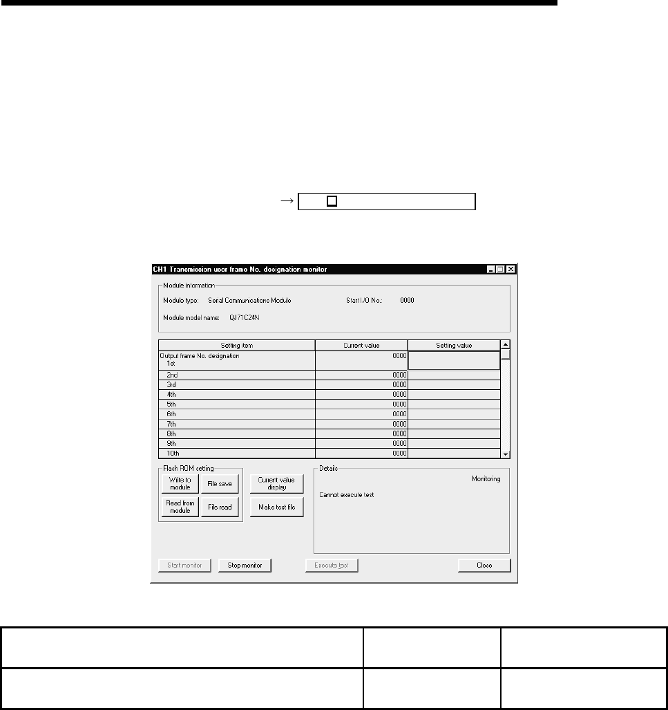
8 - 46 8 - 46
MELSEC-Q
8 UTILITY PACKAGE (GX Configurator-SC)
8.6.8 Transmission user frame No. designation monitor
[Purpose]
Monitor the setting value of output frame number used when transmitting data
with the non procedure protocol using the user frame.
[Startup procedure]
[Monitor] screen CH Output frame monitor
[Monitor screen]
[Monitor item]
Monitor item Setting value storage
buffer memory address
Reference section containing
detailed explanation
Output frame No. designation 1st to 100th BAH to 11DH/
15AH to 1BDH
Chapters 9 through 11 of
User's Manual (Application)
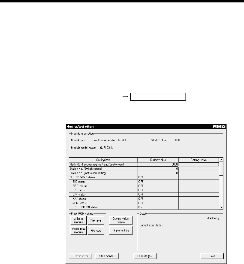
8 - 47 8 - 47
MELSEC-Q
8 UTILITY PACKAGE (GX Configurator-SC)
8.6.9 Monitor/test others
[Purpose]
Monitor the result of access to the flash ROM, the data communication status of
each interface, and the result of the intelligent function module switch settings
using GX Developer.
[Startup procedure]
[Monitor] screen Monitor/test others
[Monitor/test screen]

8 - 48 8 - 48
MELSEC-Q
8 UTILITY PACKAGE (GX Configurator-SC)
[Monitor/test items]
Monitor/test items Setting value storage
buffer memory address
Reference section containing
detailed explanation
Flash ROM access register/read/delete result 4H
Station No. (Switch setting) 200H
Station No. (Instruction setting) 24FH
SD WAIT status 201H … b0
SIO status 201H … b1
PRO. status 201H … b2
P/S status 201H … b3
C/N status 201H … b4
NAK status 201H … b5
ACK. status 201H … b6
NEU. LED status 201H … b7
CH1
ERR. LED status 202H … b15
Communication error clear request for CH1 and to turn LED off 0H
SD WAIT status 202H … b0
SIO status 202H … b1
PRO. status 202H … b2
P/S status 202H … b3
C/N status 202H … b4
NAK status 202H … b5
ACK. status 202H … b6
NEU. LED status 202H … b7
CH2
ERR. LED status 202H … b14
Communication error clear request for CH2 and to turn LED off 1H
CH1 Communication protocol setting No. error 203H … b0
CH1 Transmission speed setting error 203H … b1
CH1 Mode switching error of setting change prohibit time 203H … b3
CH2 Communication protocol setting No. error 203H … b4
CH2 Transmission speed setting error 203H … b5
CH2 Mode switching error of setting change prohibit time 203H … b7
Station No. out of range error 203H … b14
Linked operation setting error 203H … b15
Number of registered user frame 204H
Number of registered default registration frames 21EH
Flash ROM system parameters write result 220H
Chapter 10 of
User's Manual (Basic)
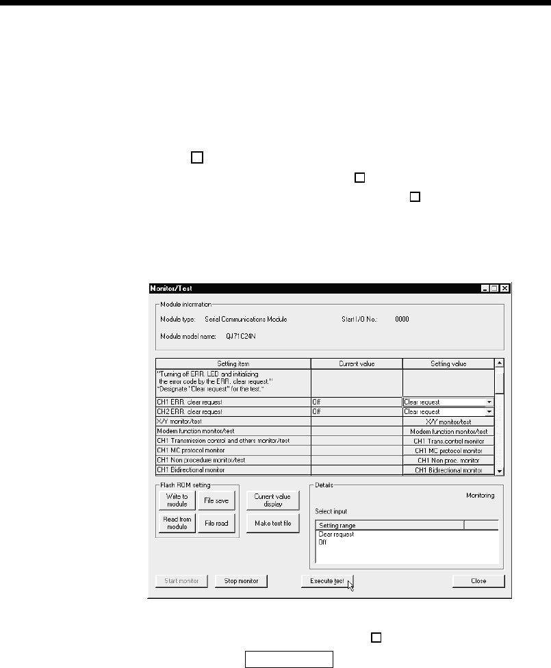
8 - 49 8 - 49
MELSEC-Q
8 UTILITY PACKAGE (GX Configurator-SC)
8.6.10 Display LED off and communication error information/error code initialization
This section explains how to turn off the display LEDs of the Q series C24 and initialize
its communication error information and error codes.
(1) CH ERR. clear request on Monitor/Test screen
This is used to turn off the CH ERR. LED of the Q series C24 and to initialize
(clear) the error codes stored in the CH side buffer memory.
Refer to Section 10.1.2 (1) for the buffer memory where the error codes are
stored.
[Operation procedure]
1) Display the "Monitor/Test" screen.
2) Select "Clear request" for "CH ERR. clear request".
3) Click on Execute test .
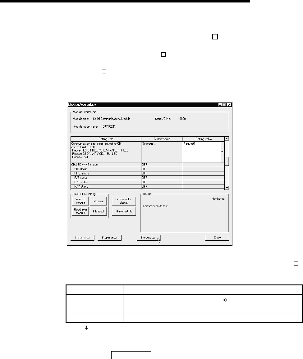
8 - 50 8 - 50
MELSEC-Q
8 UTILITY PACKAGE (GX Configurator-SC)
(2) Communication error clear request for CH and to turn LED off on
Monitor/test others screen
This is used to turn off the CH LED of the Q series C24 and to initialize (clear)
the communication error information.
The CH LED on status and communication error information can be confirmed
on the Monitor/test others screen.
[Operation procedure]
1) Display the "Monitor/test others" screen.
2) Select any of "Request 1 to 3" for "Communication error clear request for CH
and to turn LED off".
Setting range Target of LED off/communication error information initialization
Request 1 SIO, PRO., P/S, C/N, NAK, ERR. LED ( 1)
Request 2 SD WAIT, ACK., NEU. LED
Request 3 All of Requests 1 and 2
1 The ERR. LED is turned off. (However, it is not turned off if an error has
occurred on either the CH1 or CH2 side.)
3) Click on Execute test .
8 - 51 8 - 51
MELSEC-Q
8 UTILITY PACKAGE (GX Configurator-SC)
8.7 Non Procedure Protocol Receive Data Clear
This section explains how to clear the received data using the non procedure protocol.
By using this function, the receive data can be cleared from GX Configurator-SC while
the communication with the non procedure protocol is still in progress, without resetting
the PLC CPU or turning off the power.
[Operation procedure]
(Procedure 1) Display the [Non procedure monitor/test] screen. (See Section 8.6.5.)
(Procedure 2) Set [Clear request issued] for "Receive data clear request".
(Procedure 3) Click on Execute test .
The received data will be cleared.
POINT
Clear the received data when transmission/reception are not in progress with the
external device.
Executing a receive data clear while the data transmission is in progress causes
the Q series C24 to stop the data transmission abruptly, resulting in an abnormal
completion of the dedicated transmission instruction. (The transmission completion
signal will not be lit.)
When the receive data clear is executed while the data reception is in progress, the
data received up to that point will be cleared.
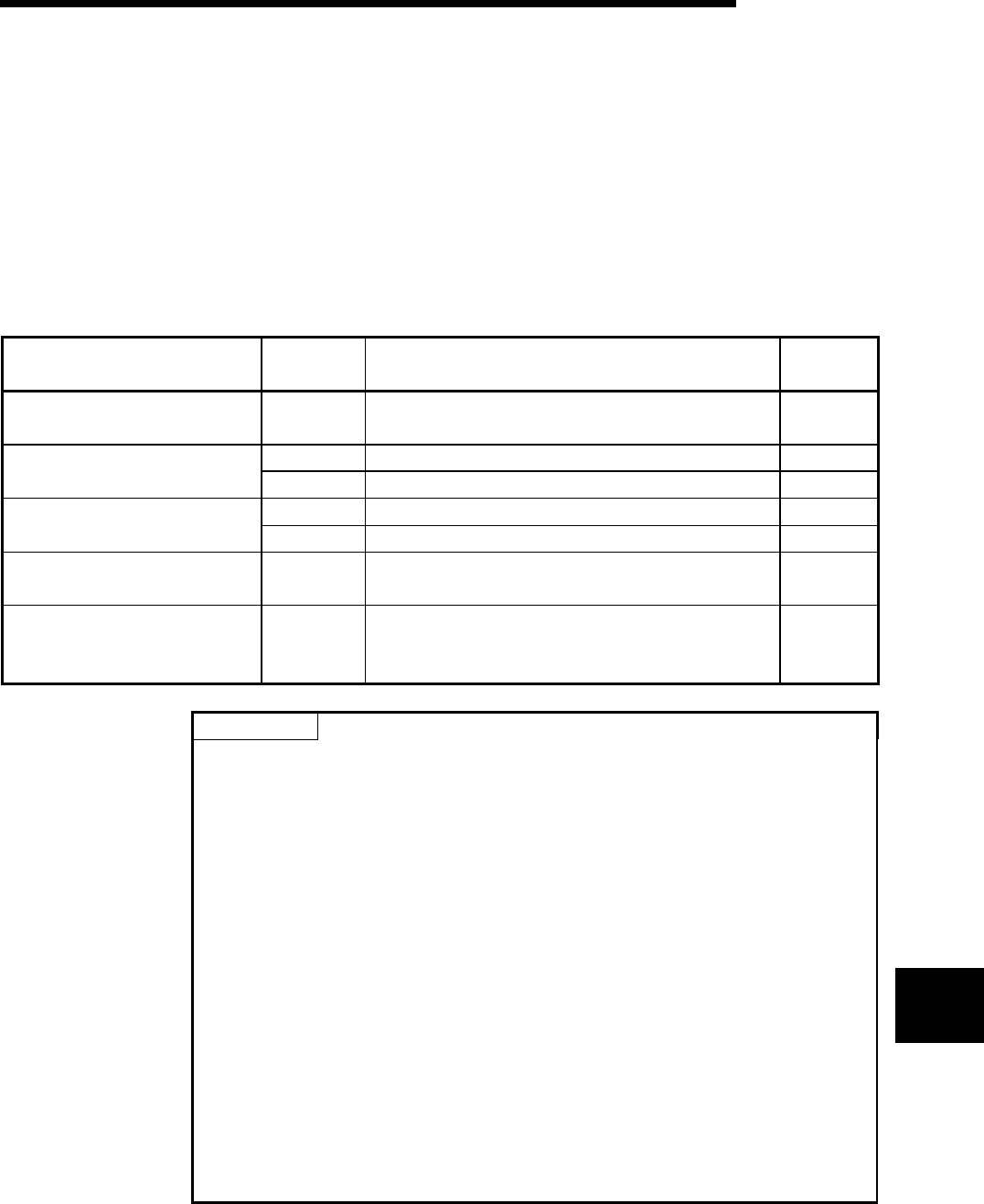
9 - 1 9 - 1
MELSEC-Q
9 DEDICATED INSTRUCTIONS
9
9 DEDICATED INSTRUCTIONS
Dedicated instructions are used to simplify programming when using intelligent function
module functions.
This chapter describes the dedicated instructions for the Q series C24, which is part of
the functions of the QCPU (in Q mode) explained in this manual.
9.1 Dedicated Instruction List
The following table lists the dedicated instructions explained in this chapter.
Application Dedicated
instruction Description of function Explanation
page
On-demand function transmission ONDEMAND Sends data using the on-demand function of the MC
protocol. Section 9.2
OUTPUT Sends data for the specified data count. Section 9.3
Non procedure protocol
communication INPUT Reads received data. Section 9.4
BIDOUT Sends data for the designated data count. Section 9.5
Bidirectional protocol
communication BIDIN Reads received data. Section 9.6
Communication status confirmation SPBUSY Reads the status of data transmission/reception via a
dedicated instruction. Section 9.7
Receive data clear CSET
Perform the receive data clear without stopping the
transmission processing during the non procedure
protocol.
Section 9.8
POINT
(1) The user should not change data values (control data, request data, etc.)
designated by a dedicated instruction until the execution of the dedicated
instruction is completed.
(2) Dedicated instructions for the Q series C24 are executed based on the current
setting values stored in the buffer memory when the module is started.
When it is necessary to change a setting value, change the value by GX
Configurator-SC before starting up the module.
Alternatively, a setting value can be changed via the sequence program using
a CSET instruction before starting up the PLC CPU (See the User's Manual
(Application)).
1) Area of buffer memory assigned as applicable functions for dedicated
instructions.
2) Setting values for data communication
• Word/byte units designation
• Receive complete code
• Received data count
etc.
9 - 2 9 - 2
MELSEC-Q
9 DEDICATED INSTRUCTIONS
9
9.2 ONDEMAND Instruction
The ONDEAMAND instruction transmission data using the on-demand function of the
MC protocol.
Applicable device
Internal device
(System, user)
MELSECNET/H,
MELSECNET/10
Direct J \
Set
data
Bit Word
File register
Bit Word
Special module
U\G Index register Zn Constant Others
(S1) — —
(S2) — —
(D) —
Command
Command
[Executing
condition]
[Instruction
code]
ONDEMAND
ONDEMAND
(D)(S1) (S2)
G.ONDEMAND Un
GP.ONDEMAND Un (S1) (S2) (D)
Set data Description Set by Data type
Un Start I/O signal of the module
(00 to FE: Top two-digit when I/O signals are expressed in 3-digit.) User BIN16 bit
(S1) Head number of the devices in which control data is stored. User,
system
(S2) Head number of the devices in which transmission data is stored. User
Device name
Set data
(D) Bit device number to be turned on at completion of execution. System Bit
The file register per local device and program cannot be used as the set data.
Control data
Device Item Set data Setting range Set by 3
(S1) + 0 Transmission channel
• Set transmission channel
1: Channel 1 (CH1 side)
2: Channel 2 (CH2 side)
1, 2 User
(S1) + 1 Transmission result
• Result read by an ONDEMAND instruction is stored.
0: Normal
Other than 0: Error code 1—System
(S1) + 2 Transmission data count • Set the transmission data count. 21 or more User
1 For error codes relating to abnormal completion, see Chapter 10 of the User's
Manual (Basic).
2 When setting "Word/byte units designation" by GX Configurator-SC, set the number
of bytes when bytes are designated and set the number of words when words are
designated.
3 The settings are done by either of the following:
• User: Data set by the user before executing the ONDEMAND instructions.
• System: The PLC CPU stores the execution result of the ONDEMAND instructions.
9 - 3 9 - 3
MELSEC-Q
9 DEDICATED INSTRUCTIONS
Function
(1) Data stored in the device designated in (S2) and succeeding devices are sent
according to the control data of the device designated in (S1) and succeeding
devices, via the on-demand function of the MC protocol of the module designated in
Un.
(S2)+ 0
+ 1
+ 2
b15 b0
to
Channel 1
Channel 2
QCPU Q series C24
Send
Send
Channel to be
used is set by
the control data.
(2) When an ONDEMAND instruction is executed on a channel, other ONDEMAND
instructions cannot be executed on that channel at the same time.
If an attempt is made during execution of an ONDEMAND instruction to execute
another ONDEMAND instruction, the second instruction will not be executed until
the execution of the first instruction is completed.
(3) Whether an ONDEMAND instruction was completed normally or abnormally can
be checked by the completion device ((D)) or status display device at completion
((D)+1).
(a) Completion device : Turns on at the END processing of the scan where
the ONDEMAND instruction is completed, and turns
off at the next END processing.
(b) Status display device
at completion : Turns on and off depending on the completion status
of the ONDEMAND instruction.
• Normal completion : Off with no change.
• Abnormal completion: Turns on at the END
processing of the scan where
the ONDEMAND instruction
is completed, and turns off at
the next END processing.
[Operation during execution of an ONDEMAND instruction]
Sequence
program
ONDEMAND
instruction
Completion device
Status display device
at completion
END
processing END
processing
Execution of ONDEMAND
instruction
Completion of reading user frame
by ONDEMAND instruction
ON
ON
Abnormal
completion
Normal
completion
One scan
OFF
OFF
END
processing END
processing
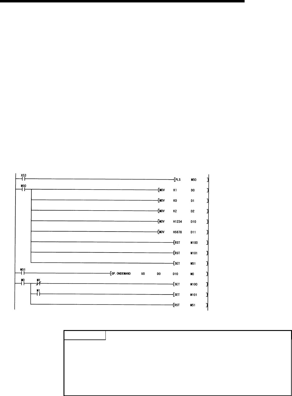
9 - 4 9 - 4
MELSEC-Q
9 DEDICATED INSTRUCTIONS
Error
(1) When a dedicated instruction is completed abnormally, the abnormal completion
signal, (D)+1, turns on and the error code is stored in the transmission result
(S1)+1.
In case of operation errors, the error flag (SM0) turns on and the error code is
stored in the SD0.
See one of the following manuals according to the error code, and check and
correct the error.
<Error code>
4FFFH or less : QCPU(Q Mode) User's Manual
(Hardware Design, Maintenance and Inspection)
7000H or more: Section 10.2 of the User's Manual (Basic)
Program example
A program that sends data stored in D10 to D11 using an on-demand transmission
When input/output signals of the Q series C24 are from X/Y00 to X/Y1F
On-demand transmission command puls
e
Set the transmission channel to CH1.
Set the send data count to 2 words.
Set the transmission data to D10 to D11.
Reset the normal completion flag.
Set the transmission ready flag.
On-demand transmission execution
Normal completion
Reset the abnormal completion flag.
Abnormal completion
Reset the transmission ready flag.
POINT
(1) The status of communication via dedicated instructions can be read by an
SPBUSY instruction.
(2) Designate the storage capacity of transmission data (stored in D10 to D11 in
the program example above) and data length (stored in D2 in the program
example above) within the range of the buffer memory the user has assigned
for an on-demand function.
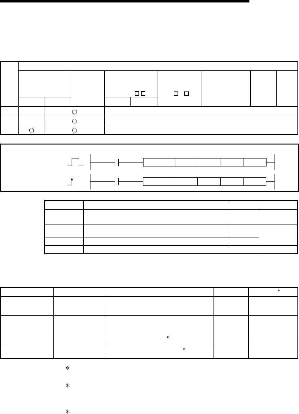
9 - 5 9 - 5
MELSEC-Q
9 DEDICATED INSTRUCTIONS
9.3 OUTPUT Instruction
This instruction transmission data in any message format specified by the user using
the non procedure protocol.
Applicable device
Internal device
(System, user)
MELSECNET/H,
MELSECNET/10
Direct J \
Set
data
Bit Word
File register
Bit Word
Special module
U\G Index register Zn Constant Others
(S1) — —
(S2) — —
(D) —
GP.OUTPUT
OUTPUT
OUTPUT
(D)
(S1) (S2)
(D)
(S2)(S1)
G.OUTPUT Un
Un
Command
Command
[Executing
condition]
[Instruction
code]
Set data Description Set by Data type
Un Start I/O signal of the module
(00 to FE: Top two-digit when I/O signals are expressed in 3-digit.) User BIN16 bit
(S1) Head number of the devices in which control data is stored. User,
system
(S2) Head number of the devices in which transmission data is stored. User
Device name
Set data
(D) Bit device number to be turned on at completion of execution. System Bit
The file register per local device and program cannot be used as the set data.
Control data
Device Item Set data Setting range Set by 3
(S1) + 0 Transmission channel
• Set transmission channel
1: Channel 1 (CH1 side)
2: Channel 2 (CH2 side) 1, 2 User
(S1) + 1 Transmission result
• Transmission result by an OUTPUT instruction
are stored.
0: Normal
Other than 0: Error code 1
—System
(S1) + 2 Transmission data
count • Set the transmission data count. 21 or more User
1 For error codes relating to abnormal completion, see Chapter 10 of the User's
Manual (Basic).
2 When setting "Word/byte units designation" by GX Configurator-SC, set the number
of bytes when bytes are designated and set the number of words when words are
designated and set the number of words when words are selected as the unit types.
3 The settings are done by either of the following:
• User: Data set by the user before executing the OUTPUT instructions.
• System: The PLC CPU stores the execution result of the OUTPUT instructions.
9 - 6 9 - 6
MELSEC-Q
9 DEDICATED INSTRUCTIONS
Function
(1) Data stored in the device designated in (S2) and succeeding devices are sent
according to the control data of the device designated in (S1) and succeeding
devices, via the non procedure protocol of the module specified in Un.
b15 b0
to
(S2) + 0
+ 1
+ 2
Channel 1
Channel 2
QCPU Q series C24
Send
Send
Channel to be
used is set by
the control data.
(2) The following instructions cannot be executed on a channel on which an OUTPUT
instruction is being executed.
• Other OUTPUT instructions
• PRR instructions
If an attempt is made during execution of an OUTPUT instruction to execute one
of the instructions above, the second instruction will not be executed until the
execution of the OUTPUT instruction is completed.
(3) Whether an OUTPUT instruction was completed normally or abnormally can be
checked by the completion device ((D)) or status display device at completion
((D)+1).
(a) Completion device: Turns on at the END processing of the scan where the
OUTPUT instruction is completed, and turns off at the
next END processing.
(b) Status display device
at completion : Turns on and off depending on the completion status
of the OUTPUT instruction.
• Normal completion : Off with no change.
• Abnormal completion: Turns on at the END
processing of the scan where
the OUTPUT instruction is
completed, and turns off at
the next END processing.
[Operation during execution of an OUTPUT instruction]
OUTPUT instruction
Execution of OUTPUT
instruction
Completion of transmission by
the OUTPUT instruction
ON
ON
OFF
OFF
END
processing END
processing END
processing END
processing
Sequence
program
Completion device
Status display device
at completion
Abnormal
completion
Normal
completion
One scan
9 - 7 9 - 7
MELSEC-Q
9 DEDICATED INSTRUCTIONS
Error
(1) When a dedicated instruction is completed abnormally, the abnormal completion
signal, (D)+1, turns on and the error code is stored in the transmission result
(S1)+1.
In case of operation errors, the error flag (SM0) turns on and the error code is
stored in the SD0.
See one of the following manuals according to the error code, and check and
correct the error.
<Error code>
4FFFH or less : QCPU(Q Mode) User's Manual
(Hardware Design, Maintenance and Inspection)
7000H or more: Section 10.2 of the User's Manual (Basic)
Program example
The following example shows a program that sends any data stored in D11 to D15
using the non procedure protocol.
When input/output signals of the Q series C24 are from X/Y00 to X/Y1F:
The transmission command is converted into pulse.
The transmission data stored in the designated device
is sent.
Designate the number of the interface (CH ) that will
send the data.
Designate the transmission data count in word units.
(Designate K10 when the unit is bytes.)
Clear the transmission result storage device to 0.
Transmission data is stored.
After the OUTPUT instruction is executed, the user
designated transmission complete signal (M0) turns
ON for one scan.
Storing the transmission data and writing the
transmission data count in the buffer memory, and
issuing a transmission request to the Q series C24
are all executed by the PLC CPU.
The completion flag is reset by an external instruction.
9 - 8 9 - 8
MELSEC-Q
9 DEDICATED INSTRUCTIONS
9.4 INPUT Instruction
This instruction receives data in any message format specified by the user using the
non procedure protocol.
Applicable device
Internal device
(System, user)
MELSECNET/H,
MELSECNET/10
Direct J \
Set
data
Bit Word
File register
Bit Word
Special module
U\G Index register Zn Constant Others
(S) — —
(D1) — —
(D2) —
INPUT (D2)
(S) (D1)
G.INPUT Un
Command
[Executing
condition]
[Instruction
code]
Set data Description Set by Data type
Un Start I/O signal of the module
(00 to FE: Top two-digit when I/O signals are expressed in 3-digit.) User BIN16 bit
(S) Head number of the devices in which control data is stored. User,
system
(D1) Head number of the devices in which receive data is stored. System
Device name
Set data
(D2) Bit device number to be turned on at completion of execution. System Bit
The file register per local device and program cannot be used as the set data.
Control data
Device Item Set data Setting range Set by 3
(S) + 0 Receive channel
• Set receive channel
1: Channel 1 (CH1 side)
2: Channel 2 (CH2 side)
1, 2 User
(S) + 1 Reception result
• Reception result by an INPUT instruction are
stored.
0: Normal
Other than 0: Error code 1
—System
(S) + 2 Receive data count • Receive data count is stored. 20 or more System
(S) + 3 Allowable number of
receive data
• Set the allowable number of words for received
data that can be stored in (D1). 1 or more User
POINT
(1) The command of G.INPUT cannot be converted into pulse.
(2) G.INPUT should be executed while the read request of the input/output signal
is turned on.

9 - 9 9 - 9
MELSEC-Q
9 DEDICATED INSTRUCTIONS
1 For error codes relating to abnormal completion, see Chapter 10 of the User's
Manual (Basic).
2 When setting "Word/byte units designation" by GX Configurator-SC, set the number
of bytes when bytes are designated and set the number of words when words are
designated.
3 The settings are done by either of the following:
• User: Data set by the user before executing the INPUT instructions.
• System: The PLC CPU stores the execution result of the INPUT instructions.
Function
(1) The function stores in the device designated in (D1) and succeeding devices the data
received with the non procedure protocol of the module designated in Un, according
to the control data of the device designated in (S) and succeeding devices.
(2) When an INPUT instruction is executed on a channel, other INPUT instructions
cannot be executed on the channel at the same time.
If an attempt is made during execution of an INPUT instruction to execute another
INPUT instruction, the second instruction will not be executed until the execution
of the first INPUT instruction is completed.
(3) In case of reading the receive data to the same interface, it cannot be used along
with BUFRCVS instruction (for interrupt programs).
(4) Whether an INPUT instruction was completed normally or abnormally can be
checked by the completion device ((D2)) or status display device at completion
((D2)+1).
(a) Completion device: Turns on at the END processing of the scan where the
INPUT instruction is completed, and turns off at the next
END processing.
(b) Status display device
at completion : Turns on and off depending on the completion status
of the INPUT instruction.
• Normal completion : Off with no change.
• Abnormal completion: Turns on at the END
processing of the scan where
the INPUT instruction is
completed, and turns off at
the next END processing.
[Operation during execution of an INPUT instruction]
Execution of INPUT
instruction Completion of reception by
an INPUT instruction
ON
ON
OFF
OFF
Sequence
program
INPUT
instruction
Completion device
Status display device
at completion
END
processing END
processing
Abnormal
completion
Normal
completion
One scan
END
processing END
processing
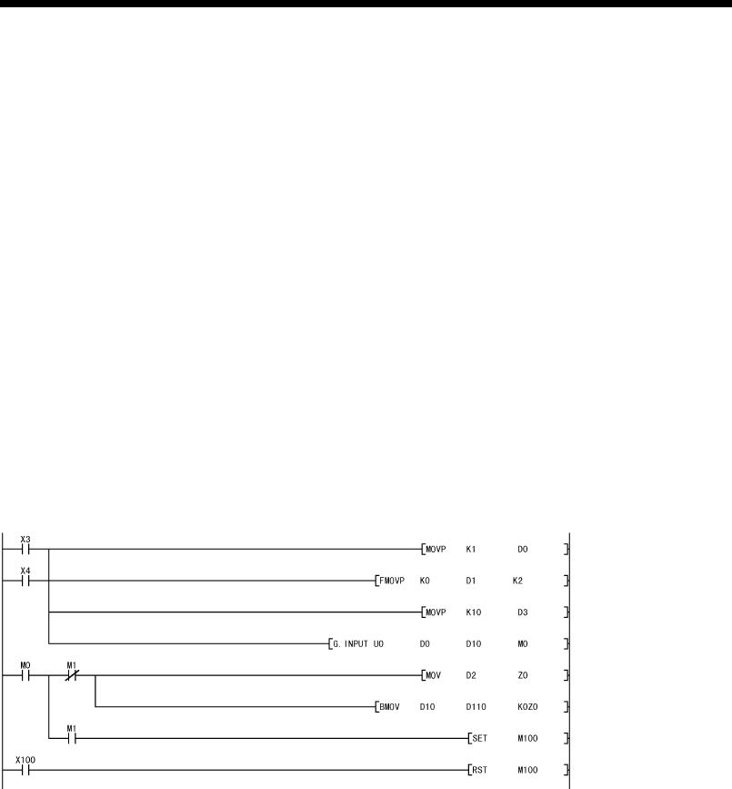
9 - 10 9 - 10
MELSEC-Q
9 DEDICATED INSTRUCTIONS
Error
(1) When a dedicated instruction is completed abnormally, the abnormal completion
signal (D2)+1, turns on and the error code is stored in the transmission result
(S1)+1.
In case of operation errors, the error flag (SM0) turns on and the error code is
stored in SD0.
See one of the following manuals according to the error code, and check and
correct the error.
<Error code>
4FFFH or less : QCPU(Q Mode) User's Manual
(Hardware Design, Maintenance and Inspection)
7000H or more: Section 10.2 of the User's Manual (Basic)
Program example
The following example shows a program that stores data received via the non-
procedure protocol in D10 and later.
When the input/output signals of the Q series C24 are from X/Y00 to X/Y1F:
Clear the reception result and receive data count
storage device to 0.
Designate the allowable receive data count.
With normal completion, the receive data within the
allowable receive data count (user designated) is read
from the receive data storage area in the buffer memory.
Once the INPUT instruction is executed, the user
designated read completion signal (M0) turns ON for
1 scan.
The reading of receive data and switching of the
ON/OFF status are performed by the PLC CPU.
•
•
The abnormal completion flag is reset by an external
command.
Designate the receive channel.
9 - 11 9 - 11
MELSEC-Q
9 DEDICATED INSTRUCTIONS
9.5 BIDOUT Instruction
This instruction transmission data using the bidirectional protocol.
Applicable device
Internal device
(System, user)
MELSECNET/H,
MELSECNET/10
Direct J \
Set
data
Bit Word
File register
Bit Word
Special module
U\G Index register Zn Constant Others
(S1) — —
(S2) — —
(D) —
GP.BIDOUT
BIDOUT
BIDOUT
(D)
(S1) (S2)
(D)
(S2)(S1)
G.BIDOUT Un
Un
Command
Command
[Executing
condition]
[Instruction
code]
Set data Description Set by Data type
Un Start I/O signal of the module
(00 to FE: Top two-digit when I/O signals are expressed in 3-digit.) User BIN16 bit
(S1) Head number of the devices in which control data is stored. User,
system
(S2) Head number of the devices in which transmission data is stored. User
Device name
Set data
(D) Bit device number to be turned on at completion of execution. System Bit
The file register per local device and program cannot be used as the set data.
Control data
Device Item Set data Setting range Set by 3
(S1) + 0 Transmission channel
• Set transmission channel
1: Channel 1 (CH1 side)
2: Channel 2 (CH2 side)
1, 2 User
(S1) + 1 Transmission result
• Transmission result by a BIDOUT instruction
are stored.
0: Normal
Other than 0: Error code 1
—System
(S1) + 2 Transmission data
count • Set the transmission data count. 21 or more User
1 For error codes relating to abnormal completion, see Chapter 10 of the User's
Manual (Basic).
2 When setting "Word/byte units designation" by GX Configurator-SC, set the number
of bytes when bytes are designated and set the number of words when words are
designated.
3 The settings are done by either of the following:
• User: Data set by the user before executing the BIDOUT instructions.
• System: The PLC CPU stores the execution result of the BIDOUT instructions.

9 - 12 9 - 12
MELSEC-Q
9 DEDICATED INSTRUCTIONS
Function
(1) The function sends data stored in the device designated in (S2) and succeeding
devices according to the control data of the device designated in (S1) and
succeeding devices, via the bidirectional protocol of the module designated in Un.
(2) When a BIDOUT instruction is executed on a channel, other BIDOUT instructions
cannot be executed on that channel at the same time.
If an attempt is made during execution of a BIDOUT instruction to execute another
BIDOUT instruction, the second instruction will not be executed until the execution
of the first instruction is completed.
(3) Whether a BIDOUT instruction was completed normally or abnormally can be
checked by the completion device ((D)) or status display device at completion
((D)+1).
(a) Completion device: Turns on at the END processing of the scan where the
BIDOUT instruction is completed, and turns off at the next
END processing.
(b) Status display device
at completion : Turns on and off depending on the completion status
of the BIDOUT instruction.
• Normal completion : Off with no change.
• Abnormal completion: Turns on at the END
processing of the scan where
the BIDOUT instruction is
completed, and turns off at
the next END processing.
[Operation during execution of a BIDOUT instruction]
BIDOUT instruction
Execution of BIDOUT
instruction Completion of transmission by
a BIDOUT
ON
ON
OFF
OFF
END
processing END
processing END
processing END
processing
Sequence
program
Completion device
Status display device
at completion
Abnormal
completion
Normal
completion
One scan
Error
(1) When a dedicated instruction is completed abnormally, the abnormal completion
signal (D)+1, turns on and the error code is stored in the transmission result (S1)+1.
In case of operation errors, the error flag (SM0) turns on and the error code is
stored in SD0.
See one of the following manuals according to the error code, and check and
correct the error.
<Error code>
4FFFH or less : QCPU(Q Mode) User's Manual
(Hardware Design, Maintenance and Inspection)
7000H or more: Section 10.2 of the User's Manual (Basic)
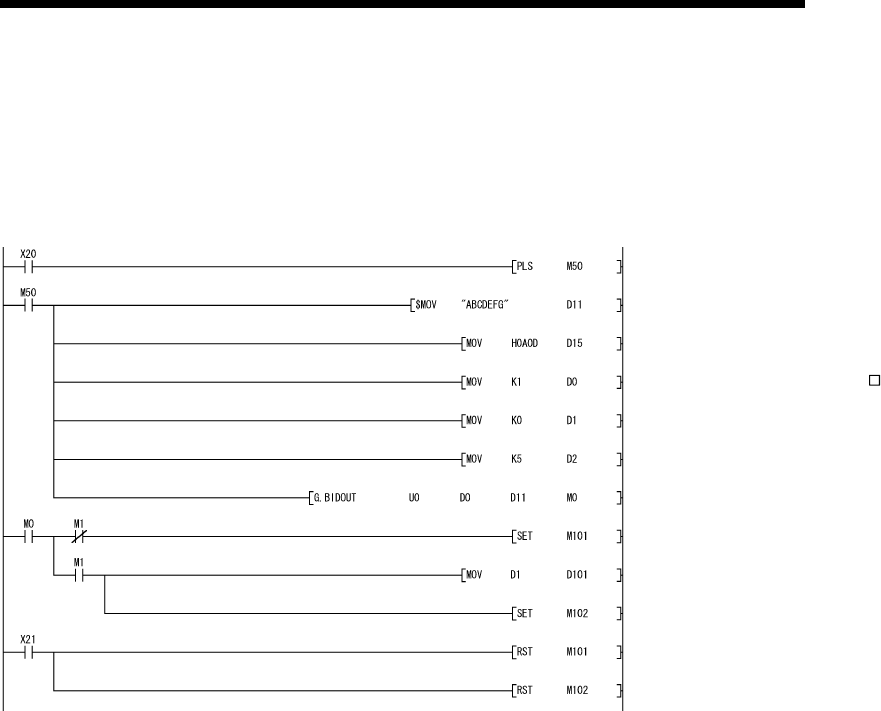
9 - 13 9 - 13
MELSEC-Q
9 DEDICATED INSTRUCTIONS
Program example
The following example shows a program that sends any data stored in D11 to D15
using the bidirectional protocol.
When the input/output signals of the Q series C24 are from X/Y00 to X/Y1F:
Transmission data is stored.
Clear the transmission result storage device to 0.
Designate the transmission data count in word units.
(Designate K10 when the unit is bytes.)
The transmission data stored in the designated device is
sent.
After the BIDOUT instruction is executed, the user
designated transmission complete signal (M1) turns ON for
one scan.
Storing the transmission data and writing the transmission
data count in the buffer memory, and issuing a
transmission request to Q series C24 are all executed by
the PLC CPU.
Designate the number of the interface (CH ) that will
send the data.
Transmission command is converted to pulse.
The completion flag is reset by the external command.
9 - 14 9 - 14
MELSEC-Q
9 DEDICATED INSTRUCTIONS
9.6 BIDIN Instruction
This instruction receives data using the bidirectional protocol.
Applicable device
Internal device
(System, user)
MELSECNET/H,
MELSECNET/10
Direct J \
Set
data
Bit Word
File register
Bit Word
Special module
U\G Index register Zn Constant Others
(S) — —
(D1) — —
(D2) —
GP.BIDIN
BIDIN
BIDIN
(D2)
(S) (D1)
(D2)
(D1)(S)
G.BIDIN Un
Un
Command
Command
[Executing
condition]
[Instruction
code]
Set data Description Set by Data type
Un Start I/O signal of the module
(00 to FE: Top two-digit when I/O signals are expressed in 3-digit.) User BIN16 bit
(S) Head number of the devices in which control data is stored. User,
system
(D1) Head number of the devices in which receive data is stored. System
Device name
Set data
(D2) Bit device number to be turned on at completion of execution. System Bit
The file register per local device and program cannot be used as the set data.
Control data
Device Item Set data Setting range Set by 2
(S) + 0 Receive channel
• Set receive channel
1: Channel 1 (CH1 side)
2: Channel 2 (CH2 side)
1, 2 User
(S) + 1 Reception result
• Reception result by a BIDIN instruction are
stored.
0: Normal
—System
(S) + 2 Receive data count • The number of data received is stored. 11 or more System
(S) + 3 Allowable number of
receive data
• Set the allowable number of words for received
data that can be stored in (D1). 1 or more User
POINT
(1) The command of G (P).BIDIN cannot be converted into pulse.
(2) G (P).BIDIN should be executed while the read request of the input/output
signal is turned on.
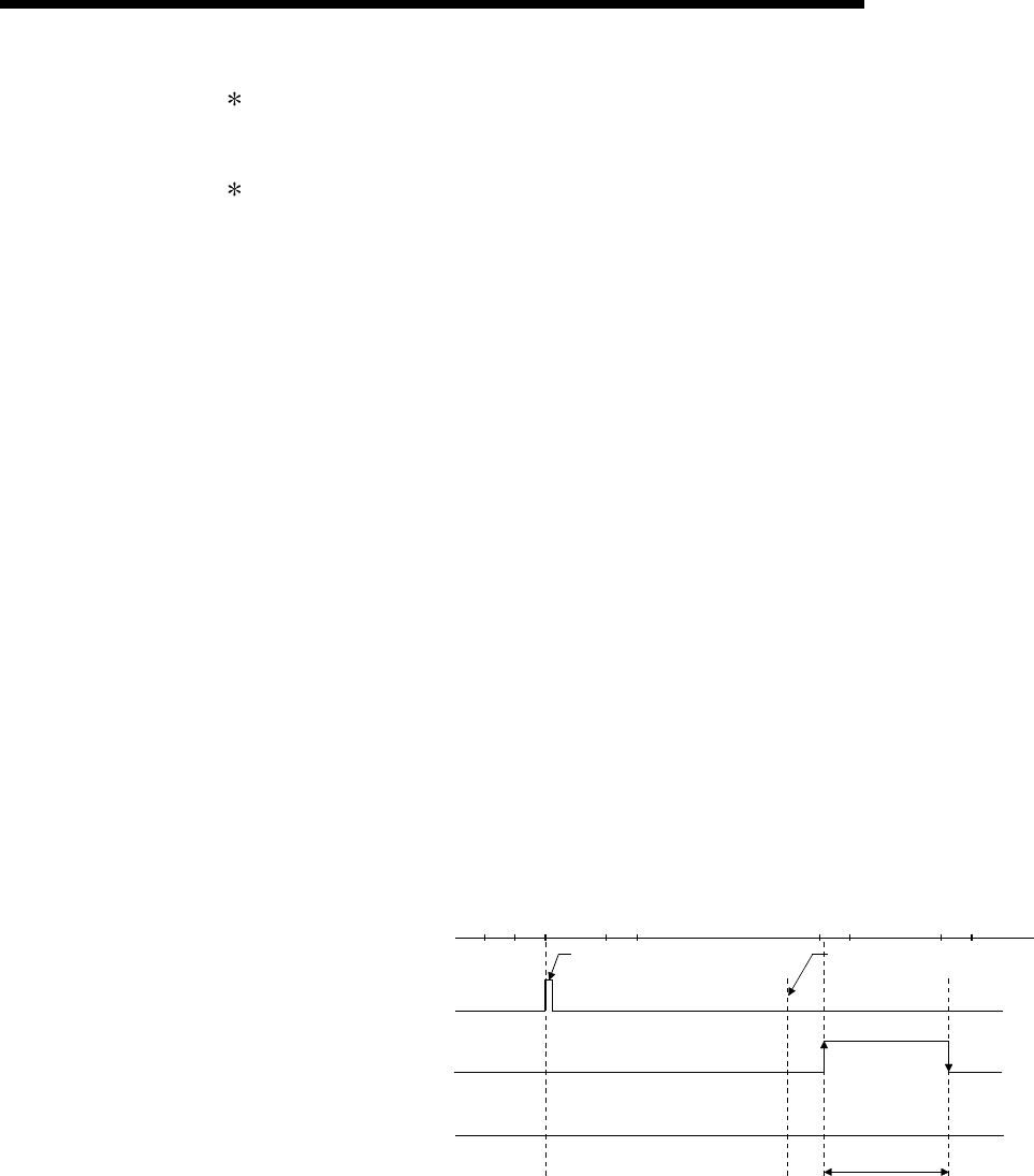
9 - 15 9 - 15
MELSEC-Q
9 DEDICATED INSTRUCTIONS
1 When setting "Word/byte units designation" by GX Configurator-SC, set the
number of bytes when bytes are designated and set the number of words when
words are designated as the unit types.
2 The settings are done by either of the following:
• User: Data set by the user before executing the BIDIN instructions.
• System: The PLC CPU stores the execution result of the BIDIN instructions.
Function
(1) The function stores in the device designated in (D1) and succeeding devices the data
received via the bidirectional protocol of the module designated in Un, according to
the control data of the device designated in (S) and succeeding devices.
(2) When a BIDIN instruction is executed on a channel, other BIDIN instructions
cannot be executed on the channel at the same time.
If an attempt is made during execution of a BIDIN instruction to execute another
BIDIN instruction, the second instruction will not be executed until the execution of
the first instruction is completed.
(3) It cannot be used along with BUFRCVS instruction (for interrupt programs).
(4) Whether a BIDIN instruction was completed normally can be checked by the
completion device ((D2)) or status display device at completion ((D2)+1).
(a) Completion device: Turns on at the END processing of the scan where the
BIDIN instruction is completed normally, and turns off at
the next END processing.
(b) Status display device at completion: Does not change when left off.
[Operation during execution of a BIDIN instruction]
Execution of BIDIN instruction Completion of reception by
BIDIN instruction
ON
OFF
OFF
Sequence
program
BIDIN
instruction
Completion device
Status display device
at completion
END
processing END
processing
One scan
END
processing END
processing
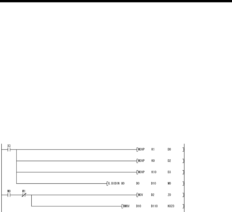
9 - 16 9 - 16
MELSEC-Q
9 DEDICATED INSTRUCTIONS
Error
(1) In case of operation errors, the error flag (SM0) turns on and the error code is
stored in SD0.
See one of the following manuals according to the error code, and check and
correct the error.
<Error code>
4FFFH or less : QCPU(Q Mode) User's Manual
(Hardware Design, Maintenance and Inspection)
Program example
The following example shows a program that receives any data using the bidirectional
protocol and stores that data in D10 or later.
The input/output signals of the Q series C24 are from X/Y00 to X/Y1F:
Clear the receive data count storage device
to 0.
Designate the allowable receive data count.
•The reading of received data is performed
by the PLC CPU.
Designate the receive channel.
•After the BIDIN instruction is executed,
the user designated read completion
signal (M0) comes on for 1 scan.
With the normal completion, the receive
data within the allowable receive data count
(user designated) is read from the receive
data storage area in the buffer memory.
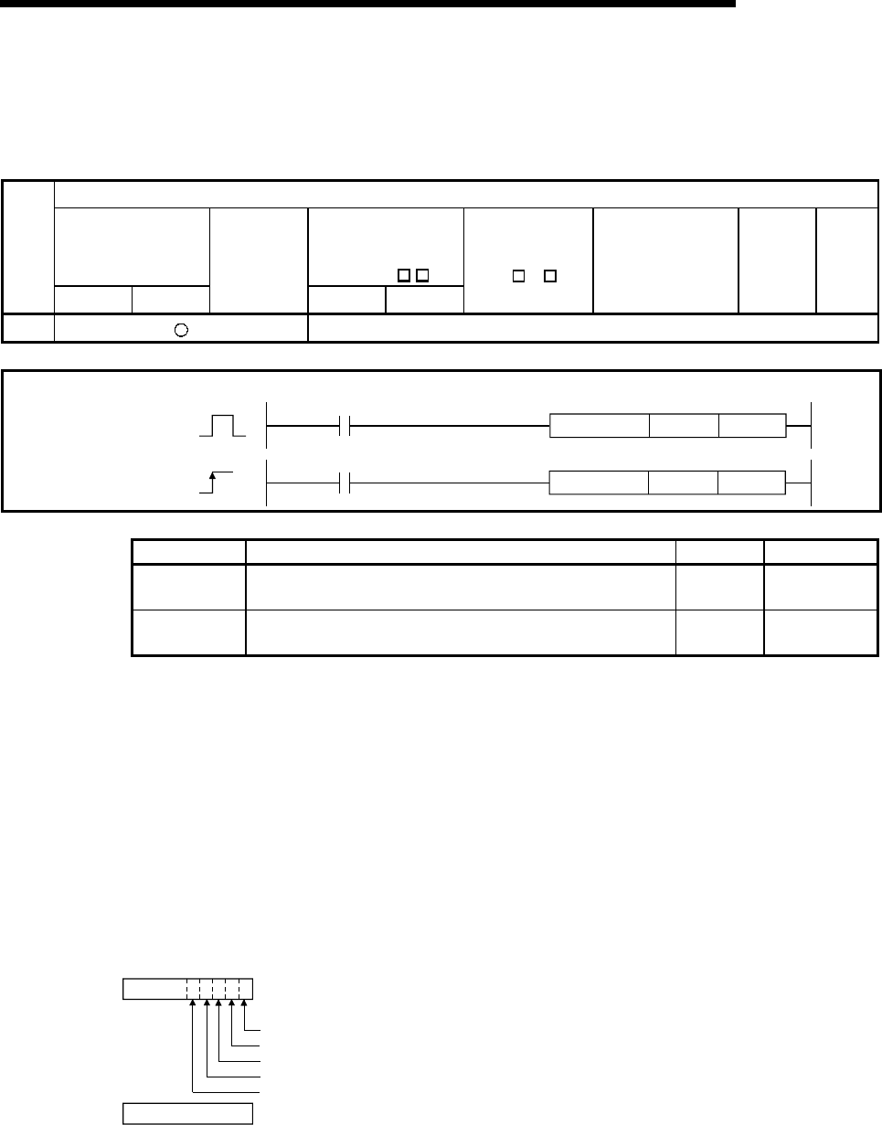
9 - 17 9 - 17
MELSEC-Q
9 DEDICATED INSTRUCTIONS
9.7 SPBUSY Instruction
This instruction reads the status of data transmission and reception executed with
dedicated instructions.
Applicable device
Internal device
(System, user)
MELSECNET/H,
MELSECNET/10
Direct J \
Set
data
Bit Word
File register
Bit Word
Special module
U\G Index register Zn Constant Others
(D) —
SPBUSY
SPBUSY
(D)
(D)
GP.SPBUSY
G.SPBUSY Un
Un
Command
Command
[Executing
condition]
[Instruction
code]
Set data Description Set by Data type
Un Start I/O signal of the module
(00 to FE: Top two-digit when I/O signals are expressed in 3-digit.) User BIN16 bit
Set data
(D) Head number of devices in which the read communication status is
stored. System Device name
Function
(1) The function reads the execution status of a dedicated instruction directed to a
module designated by the start I/O signal, and stores it in the device designated
by (D) or later.
(2) The execution status is stored in (D) in the form of "1" at the corresponding bit
when the processing of each instruction is started, and "0" when the processing is
completed.
The processing of each instruction is completed when the completion flag of each
instruction is turned from on to off.
(D) + 0
b15 to b4b3b2b1b0
Stores the execution status of ONDEMAND, OUTPUT, PRR, and BIDOUT instructions directed to channel 1.
Stores the execution status of INPUT and BIDIN instructions directed to channel 1.
Stores the execution status of ONDEMAND, OUTPUT, PRR, and BIDOUT instructions directed to channel 2.
Stores the execution status of INPUT and BIDIN instructions directed to channel 2.
Stores the execution status of GETE and PUTE instructions.
0(Always stores "0".)
(D) + 1
(3) The SPBUSY instruction is executed for every scan while the read command is
ON, if the system is executing during ON. And, the instruction will be executed for
a single scan when the read command rises from OFF to ON, if the system is
starting up.

9 - 18 9 - 18
MELSEC-Q
9 DEDICATED INSTRUCTIONS
Error
(1) In case of operation errors, the error flag (SM0) turns on and the error code is
stored in SD0.
See one of the following manuals according to the error code, and check and
correct the error.
<Error code>
4FFFH or less : QCPU(Q Mode) User's Manual
(Hardware Design, Maintenance and Inspection)
7000H or more: Section 10.2 of the User's Manual (Basic)
Program example
A program that reads the communication status of a target module.
When input/output signals of the Q series C24 are from X/Y00 to X/Y1F
The function reads the communication status o
f
a target module and stores it in a device.
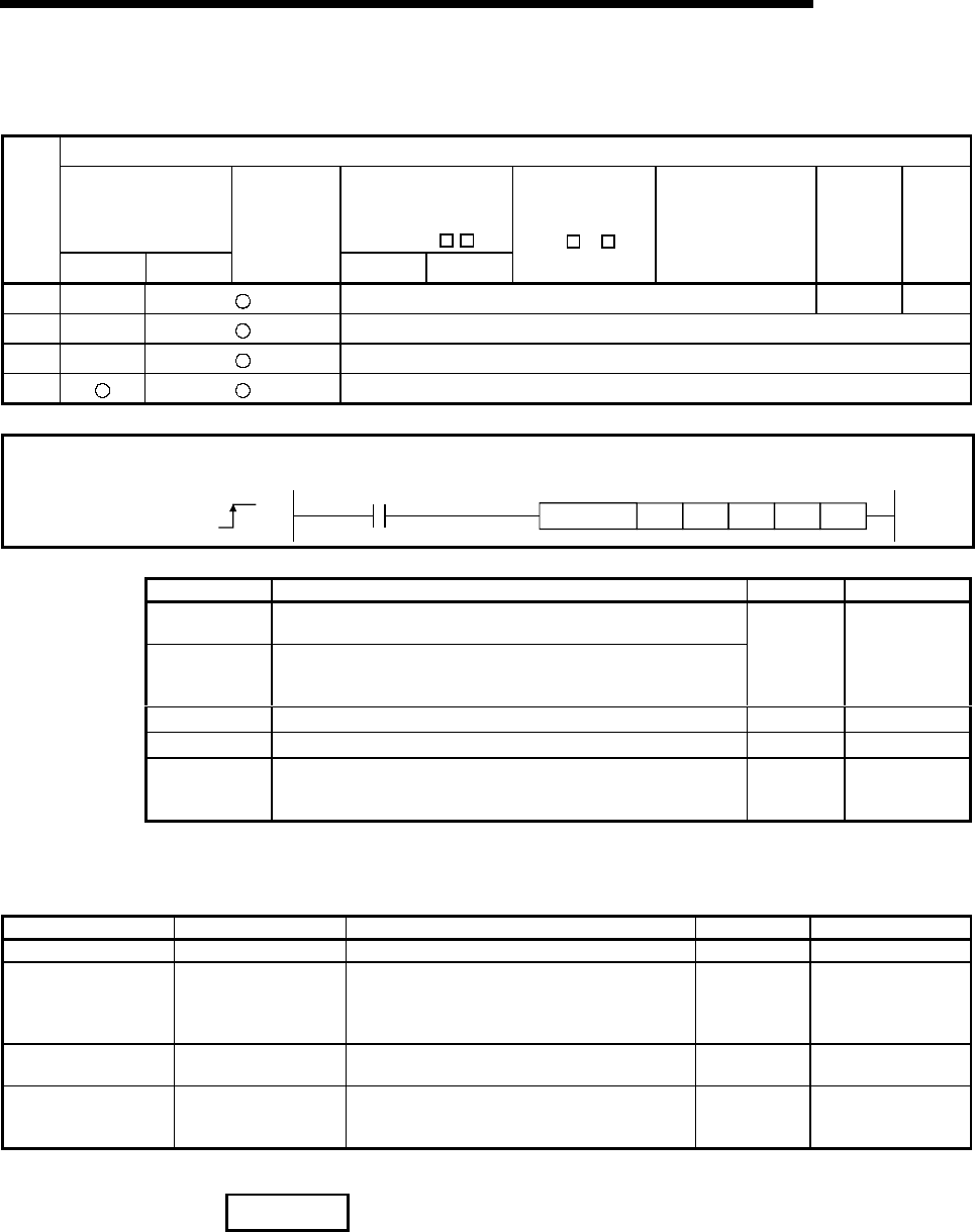
9 - 19 9 - 19
MELSEC-Q
9 DEDICATED INSTRUCTIONS
9.8 CSET (Receive data clear)
Applicable device
Internal device
(System, user)
MELSECNET/H,
MELSECNET/10
Direct J \
Set
data
Bit Word
File register
Bit Word
Special module
U\G Index register Zn Constant Others
(S1) — —K, H—
(S2) — —
(D1) — —
(D2) —
(D2)ZP.CSET
CSET (D1)(S2)(S1)"Un"
[Executing
condition]
[Instruction
code] [Instruction
form]
Set data Description Set by Data type
"Un" Start I/O signal of the module
(00 to FE: Top two-digit when I/O signals are expressed in 3-digit.)
Set data
(S1)
Number of the channel that demands to clear receiving data.
1: Channel 1 (CH1 side)
2: Channel 2 (CH2 side)
User BIN16 bit
(S2) Head number of the device that stores the control data. User, System Device name
(D1) Dummy — Device name
(D2)
Head number of the bit device at the self-station that turns on for one scan at
the completion of the instruction.
(D2) + 1 also turns on at an abnormal completion.
System Bit
Each of file registers for local device and program cannot be used as the setting data.
Control data
Device Item Set data Setting range Set by
(S2) + 0 Execution type Select 0. 0 User
(S2) + 1 Complete status
The execution result at the completion of the instruction
is stored.
0: Normal
Other than 0: Abnormal (error code)
—System
(S2) + 2 Request type Specify the request.
4: Receive data clear request 4User
(S2) + 3
to
(S2) + 111
For system — — System
REMARK
(1) See the "Error" explanation on the following page for details on errors caused by
wrong data specifications by the user.
(2) The setting sides are partitioned as follows:
• User: Data set by the user before executing the dedicated instruction.
• System: The PLC CPU stores the execution result of the dedicated instruction.
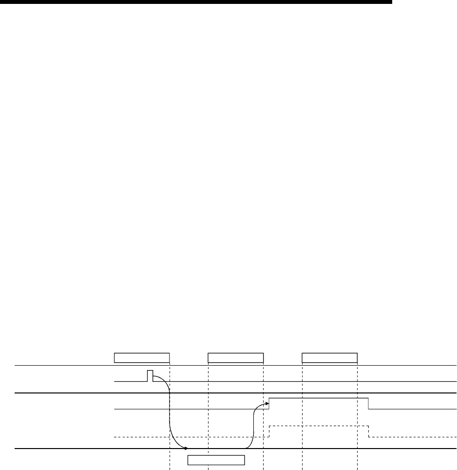
9 - 20 9 - 20
MELSEC-Q
9 DEDICATED INSTRUCTIONS
Function
(1) This function clears reception data in the OS area. It does not clear the user data
reception area in the buffer memory.
(2) If the CSET instruction is executed while the read request (X03/X0A) or reception
abnormal detection signal (X04/X0B) is turned on, the CSET instruction is kept
waiting until the signal is turned off.
(3) The status of the CSET instruction, whether it is being executed or completed
normally/abnormally, can be checked by the complete device (D2) specified by
the setting data.
(a) Complete device ((D2) + 0)
This device turns on at the End processing of the scan at which the CSET
instruction is completed and turns off at the next End processing.
(b) Complete device ((D2) + 1)
It turns on/off by the status at which the CSET instruction is completed.
• At normal completion: It is kept turned off and does not change.
• At abnormal completion: It turns on at the END processing of the scan at
which the CSET instruction is completed and
turns off at the next END processing.
[Operation at execution of CSET instruction]
Scan
Sequence program
Q series C24
At abnormal completion
End
processing Scan Scan
CSET instruction
Complete device
Complete device+1
Execution of instruction
Setting processing
End
processing End
processing
Error
(1) If the dedicated instruction is abnormally completed, the error flag (SM0) turns on
and the error code is stored in SD0.
See the following manuals according to the error code, and check/take action
according to the error.
<Error code>
4FFFH or less : QCPU User's Manual
(Hardware Design, Maintenance and Inspection)
7000H or more: Section 10.2 of the User's Manual (Basic)
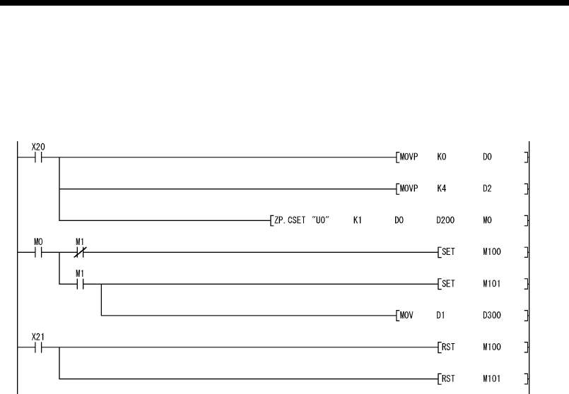
9 - 21 9 - 21
MELSEC-Q
9 DEDICATED INSTRUCTIONS
Program example
This is an example of a program that clears reception data on the Q series C24 side.
It is assumed that the input/output signals of the Q series C24 are X/Y00 to X/Y1F.
Set the execution type
Set the request type
(Reception data clear)
Execute the reception
data clear
Normal completion
Abnomal completion
Reset the complete flag by
external command
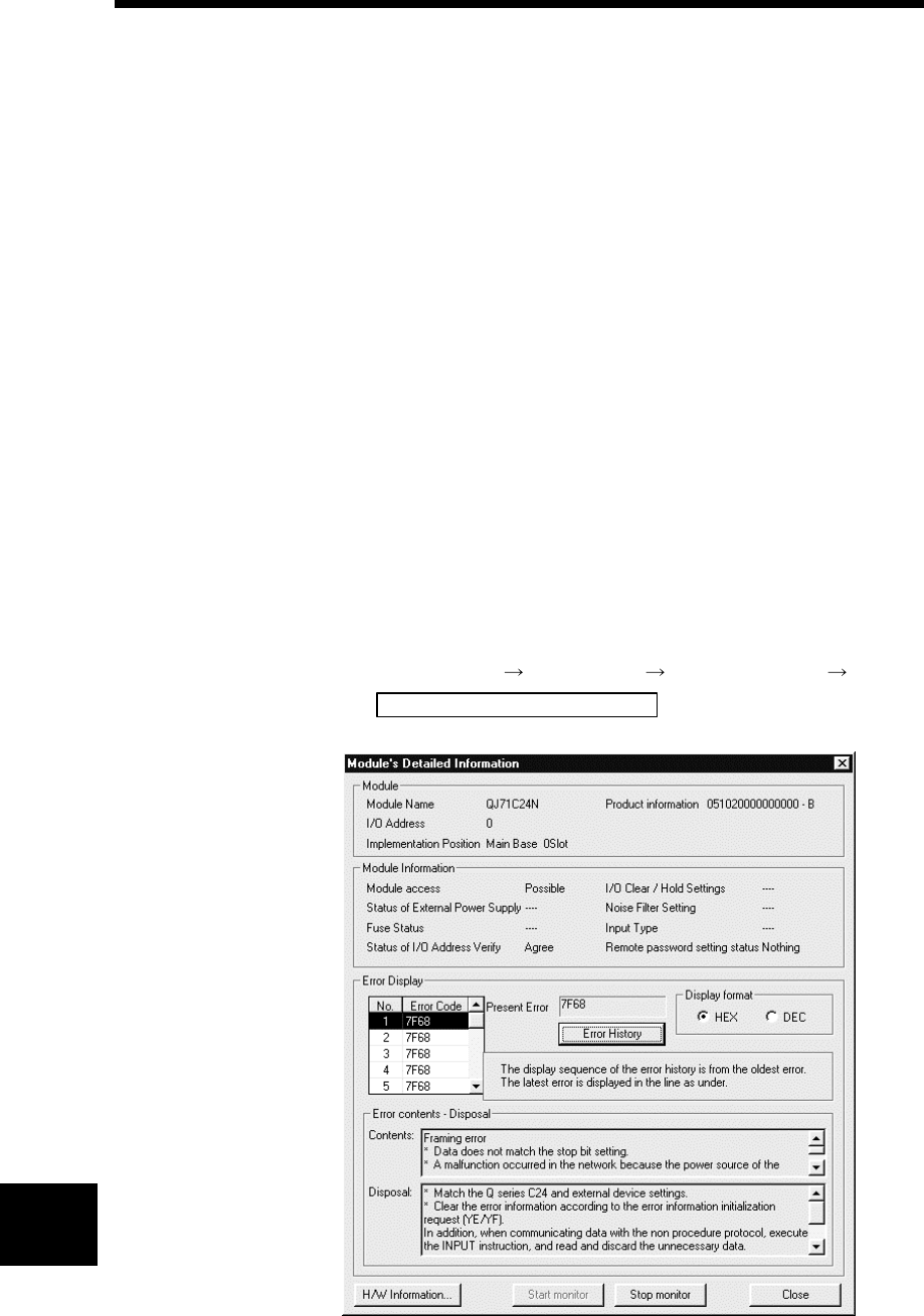
10 - 1 10 - 1
MELSEC-Q
10 TROUBLESHOOTING
10
10 TROUBLESHOOTING
This chapter explains the definitions of errors that may occur during data
communication between the Q series C24 and external devices, and the corrective
actions.
10.1 Checking the Status of the Serial Communication Module
10.1.1 Checking the LED ON status, communications error status, and switch setting status
of the serial communication module
This section explains how to check the status of communication between the Q series
C24 and external devices, the transmission status of the Q series C24, and the switch
setting status of the Q series C24.
When a communication problem occurs, check the error status using one of the
following procedures:
(1) Checking the module status and error codes in the detailed module
information screen of the GX Developer diagnostic functions
[Startup procedure]
GX Developer [Diagnostics] [System monitor]
Module's Detailed Information
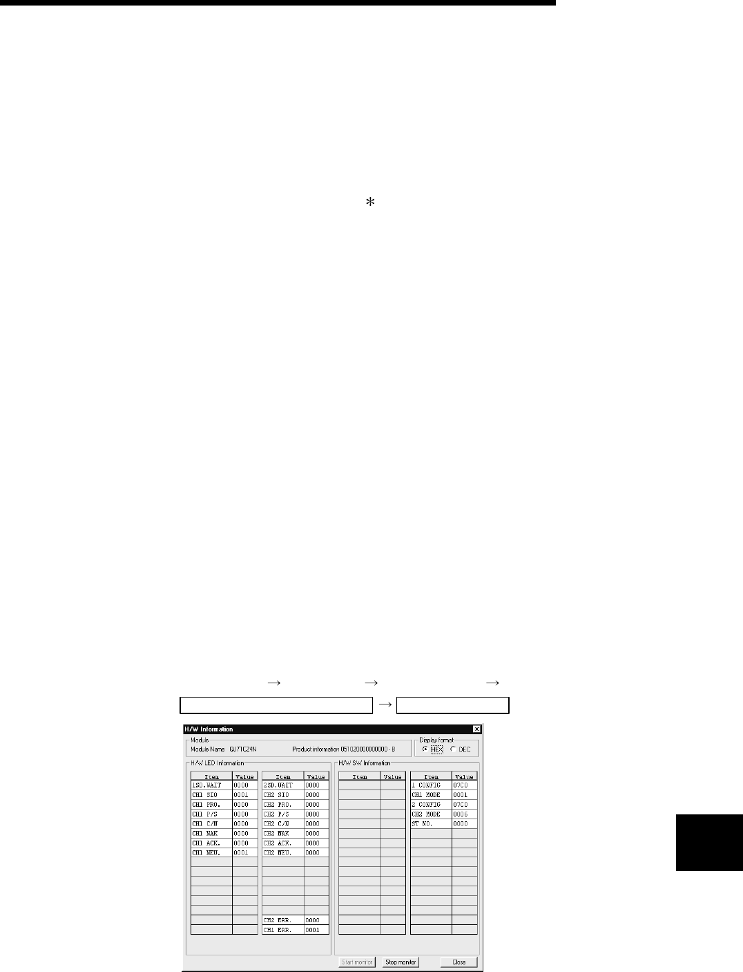
10 - 2 10 - 2
MELSEC-Q
10 TROUBLESHOOTING
10
[Displays]
• Module
The following information is displayed:
Module name : The name of the module installed
I/O Address : The start input/output signal (number) of the target
module
Implementation Position: The slot position where the module is mounted
Product information : Product information
The last character of the product information
indicates the function version of the module.
(Example) If the last character is "B," it means
that the module is of function
version B.
• Unit access (Module access)
Displays access permissions when the Ready signal (X1E) is turned on and
the WDT error signal (X1F) is turned off.
• Status of I/O Address Verify
Displays whether or not the module for which the user set the parameters
matches the module installed.
• Remote password setting status
Displays the setting status of the remote password.
• Present Error
Displays the error code of the latest error occurrence.
• Error Display
Displays the error codes for any errors that have occurred in any of the
functions being used.
• Error details, corrective action
Displays the error details and corrective action for the error code selected in
Error Display.
(2) Checking using the hardware information screen of the GX
Developer diagnostic functions
[Startup procedure]
GX Developer [Diagnostics] [System monitor]
Module's Detailed Information H/W Information
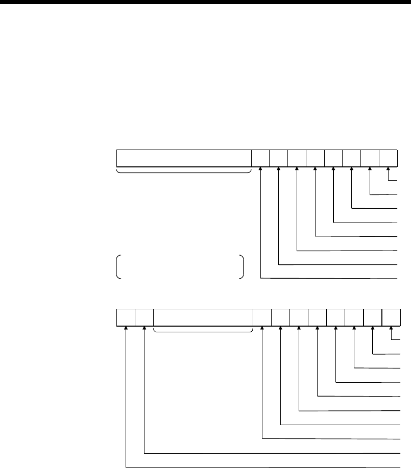
10 - 3 10 - 3
MELSEC-Q
10 TROUBLESHOOTING
[Displays]
1) H/W LED Information Right side (Left side: CH1 information/
Right side: CH2 information)
Displays the transmission status and the communications error status
of the Q series C24.
(Displays 201H/202H of the buffer memory.)
1/0 1/0 1/0 1/0 1/0 1/0 1/0 1/0
SD WAIT
SIO
PRO.
P/S
NEU.
C/N
NAK
ACK.
For system
Buffer memory address 201H
b15 b7b6b5b4b3b2b1b0
to
(Information of CH1 side)
1: Lit/Communication error
0: not lit/No communication error
b8
1/0 1/0 1/0 1/0 1/0 1/0 1/0 1/0
SD WAIT
SIO
PRO.
P/S
NEU.
C/N
NAK
ACK.
For system
Buffer memory address 202H
b15 b7 b6 b5 b4 b3 b2 b1 b0
to
(Information of CH2 side)
1/0 1/0
b14 b13 b8
CH2 ERR.
CH1 ERR.
2) H/W SW Information Parameter
The switch information of the Q series C24 is displayed.
Numbers 1 through 5 correspond to switches 1 through 5 shown in
Section 4.5.2.
(See Section 4.5.2 of the User's Manual (Basic).)
10 - 4 10 - 4
MELSEC-Q
10 TROUBLESHOOTING
(3) Checking by GX Configurator-SC
Display the "Monitor/test others" screen.
For details on display screens, see Section 8.6.9 of the User's Manual (Basic).
(4) Description of LED ON status and communications error status
Related protocol
No.
Status
signal
name
Description
Description when ON
(when LED is turned on
(1))
Description when OFF
(when LED is turned off
(0))
Initial
state MC
Non
procedure
protocol
Bidirection-
al protocol
1 SD WAIT Transmission wait status Waiting for data
transmission Data transmission start OFF
Overrun or framing
error occurred. OFF
2 SIO SIO error status OS area is full.
Received data was
deleted.
Normal
OFF —
3PRO. Communication protocol
error status Error occurred. Normal OFF —
4P/S Status of parity error or
sum check error Error occurred. Normal OFF
5C/N Access status with the
PLC CPU (1)Normal OFF
6NAK Abnormal completion
status
Abnormal completion
transmission
Normal completion
transmission OFF
7ACK. Normal completion
status
Normal completion
transmission
Abnormal completion
transmission OFF
8NEU.
Neutral status
Waiting to receive
command
Neutral Command reception (2)
—
9 CH2. ERR Error occurrence status
on CH2 side OFF
10 CH1. ERR Error occurrence status
on CH1 side
Switch setting error
Mode switching error
Transmission error
Reception error
On-demand error
Normal
OFF
1 C/N turns on in the following cases:
• An external device issued a data read request to the PLC CPU when write
during RUN is set to prohibit in the switch settings by GX Developer (see
Section 4.5.2).
For functions that cannot be used when write during RUN is set to prohibit, see
the explanation section in each command list of the Reference Manual.
• When an error has occurred during access between the Q series C24 and the
PLC CPU.
2 NEU. is valid when a target interface is set to use the MC protocol.
When the target interface is set to other than the MC protocol, the status of NEU.
is off.

10 - 5 10 - 5
MELSEC-Q
10 TROUBLESHOOTING
(a) When a communication error occurs, take corrective action according to
Section 10.3.
(b) The initial status of the LED ON and communications error indicates the
status when the Q series C24 starts up by turning on the power or resetting
the PLC CPU.
(c) Each of the communications error status, C/N to SIO, CH1 ERR. and CH2
ERR., turns on when an error occurs, and keeps its on-status even after the
communication returns to normal.
The PLC CPU can check the aforementioned LED ON status and
communications error status, and initialize any error information using
read/write to the buffer memory of the Q series C24 and input/output signals.
Initialize the error information according to Section 10.1.2.
(d) NAK to NEU. (No. 6 to 8) turn on/off depending on the status.
(e) SD WAIT turns on when data cannot be sent to the external device by the
transmission control of the Q series C24 (waiting for data transmission).
• When transmission cannot be started.
• When a transmission pause request is received during data transmission.
(DSR signal is off, reception by DC3)
SD WAIT turns off when transmission becomes possible and data
transmission is started/resumed.
10 - 6 10 - 6
MELSEC-Q
10 TROUBLESHOOTING
10.1.2 Initializing error information of the serial communication module
This section explains the ERR. LED ON factors and the error code initialization (clear)
for the Q series C24.
(1) ERR. LED ON factors
When any of the following errors occurs, its error code is stored in the buffer
memory corresponding to the interface (CH) where the error occurred, and the
ERR. LED turns on.
Error code storage buffer memory Applicable protocol
Address
Cause of error
CH1 CH2 Name MC
Non-
procedure
protocol
Bidirec-
tional
protocol
Switch setting error
Mode switching error 203HSwitch setting error, mode switching error
storage area
On-demand execution
error 256H266HOn-demand execution result storage area
Data transmission error 257H267HData transmission result storage area
Data reception error 258H268HData reception result storage area
MC protocol transmission
error 025AH026AHMC protocol transmission error code
Monitoring device error 2205H2305HPLC CPU monitoring function execution
result
(2) Turning off the ERR. LED and initializing the error codes by GX
Configurator-SC (Refer to Section 8.6.10)
(a) When turning off the ERR. LED and initializing the error codes
By making the CH ERR. clear request on the "Monitor/Test" screen, the
ERR. LED of the Q series C24 turns off and the stored error codes are
initialized.
(b) When initializing the communication error information
By making the Communication error clear request for CH and to turn LED
off on the "Monitor/test others" screen, the LEDs (ERR., NEU.) of the Q
series C24 turn off and the communication error information is initialized.
(3) Turning off the ERR. LED and initializing the error codes by
sequence program
(a) Input signals used to notify of error occurrences and output signals used to
initialize the error code
I/O signal Name of status information Description/function
XE Error occurrence on CH1 side Turns on upon error occurrence in CH1 interface.
Input signal XF Error occurrence on CH2 side Turns on upon error occurrence in CH2 interface.
YE CH1 Error information initialization request Turns on when initializing error code of interface on CH1 side.
Output signal YF CH2 Error information initialization request Turns on when initializing error code of interface on CH2 side.
Initialization of error code is continuously performed when output signal (YE/YF) is
on.
POINT
The CHn side error information can be initialized by an off request to the LED off
request area (address 1H) of the buffer memory. By using output signals YE to YF,
the error codes stored in the above buffer memory can further be initialized
(cleared).
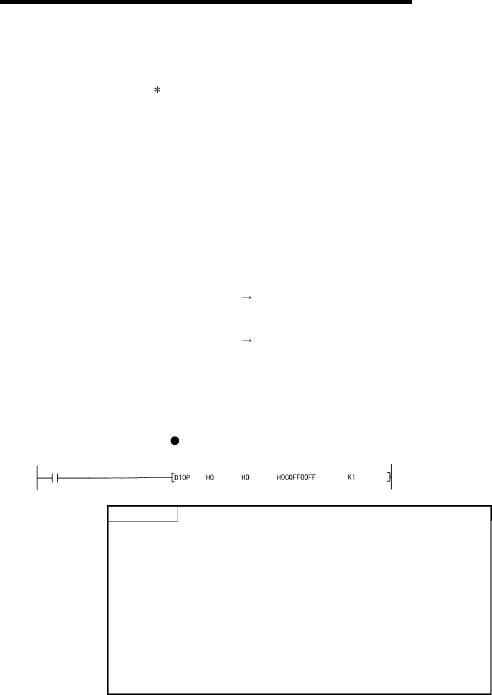
10 - 7 10 - 7
MELSEC-Q
10 TROUBLESHOOTING
(b) Initializing communication error information by writing
Communication error information can be initialized by writing "1" to the
corresponding bit in the buffer memory addresses 0H to 1H.
The displayed LEDs and communication error information may be turned
on/off in the following cases:
• NEU. to NAK turn on/off depending on the status.
• C/N to SIO turn on when errors occur and keep the ON-status even
after the operation returns to normal.
1) LED and communications error information initialization request area
(address: 0H to 1H)
The contents of the error information corresponding to each bit in this
request area are the same as those for the LED ON/communication
error status storage area (address: 201H to 202H).
For more details, see Section 10.1.1 (1).
The following describes the correspondence between the LED OFF
request areas and the LED ON status storage areas:
• Communication error clear request area for CH1 and to turn LED off
(address: 0H) LED ON status and communication error status area
on CH1 side (address: 201H)
• Communication error clear request area for CH2 and to turn LED off
(address: 1H) LED ON status and communication error status area
on CH2 side (address: 202H)
2) Example of a program for turning off displayed LEDs
The following shows an example of a program that issues an
initialization request for all the communication error information of CH1
and CH2.
(Input/output signals X/Y00 to X/Y1F of QC24)
Example of TO instruction
Writes 00FFH to
address 0H and C0FFH
to address 1H.
Turn off command
POINT
(1) Initialization requests are valid only when write operation is performed.
The initialization requests clear all data in the LED ON and communication
error information storage area (201H to 202H) at the same time.
Furthermore, when initialization of error information on the CH1 and CH2 sides
is requested, XE and XF also turn off.
(2) Data written to the buffer memory address 0H to 1H is cleared after initialization
processing.
(3) If errors persist even after completion of the initialization processing, the
corresponding communication error information is stored again and the
corresponding bit in the LED ON and communications error status storage
area (201H to 202H) turns on (1).
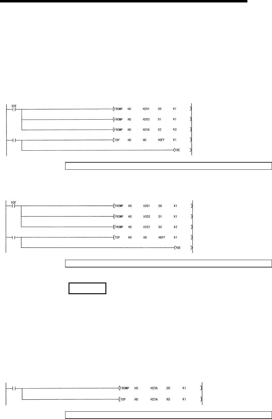
10 - 8 10 - 8
MELSEC-Q
10 TROUBLESHOOTING
(c) Examples of programs that initialize displayed LED and communication error
information
The following shows examples of a program that reads error codes when
errors described in (1) above occur in an interface on the CH1 side and
initializes the displayed LED and communication error information.
Incorporate the necessary part of the program.
(Input/output signals X/Y00 to X/Y1F of the Q series C24)
1) When data is communicated using the MC protocol
Turn off/clear
command
Reads LED and communication error
information from address 201H.
Reads switch setting error description from address 203H.
Reads data transmission/reception
results from address 256H to 258H.
Requests initialization of error information on the
CH1 side and clearing of error codes in the buffer memory.
Requests initialization of error information on the CH1
side and clearing of error codes in the buffer memory.
Check the error codes and take corrective action according to Section 10.2.
2) When data is communicated using the non procedure or bidirectional
protocol
Reads LED and communication error information from
address 201H.
Reads switch setting error description from address 203H.
Reads data transmission/reception results from address
257H to 258H.
Writes initialization request such as for displayed LED to
address 0H.
Requests initialization of error information on the CH1
side and clearing of error codes in the buffer memory.
Turn off/clear
command
Check the error codes and take corrective action according to Section 10.2.
REMARK
When data is communicated using the MC protocol, the displayed ERR. LED may
not be turned on if the Q series C24 sends an NAK message to the external device
in response to the command message.
Error codes (see Section 10.2) corresponding to the error content when the NAK
message is sent back to the external device are stored in the following areas. (when
communicating with an A compatible 1C frame, the error codes differ from the
transmission error code.)
When checking error codes transmitted by the PLC CPU, incorporate the following
program (in case of the interface on the CH1 side).
Read command Reads transmission error codes from address 25AH.
Clears error codes.
Check the error codes and take corrective action according to Section 10.2.
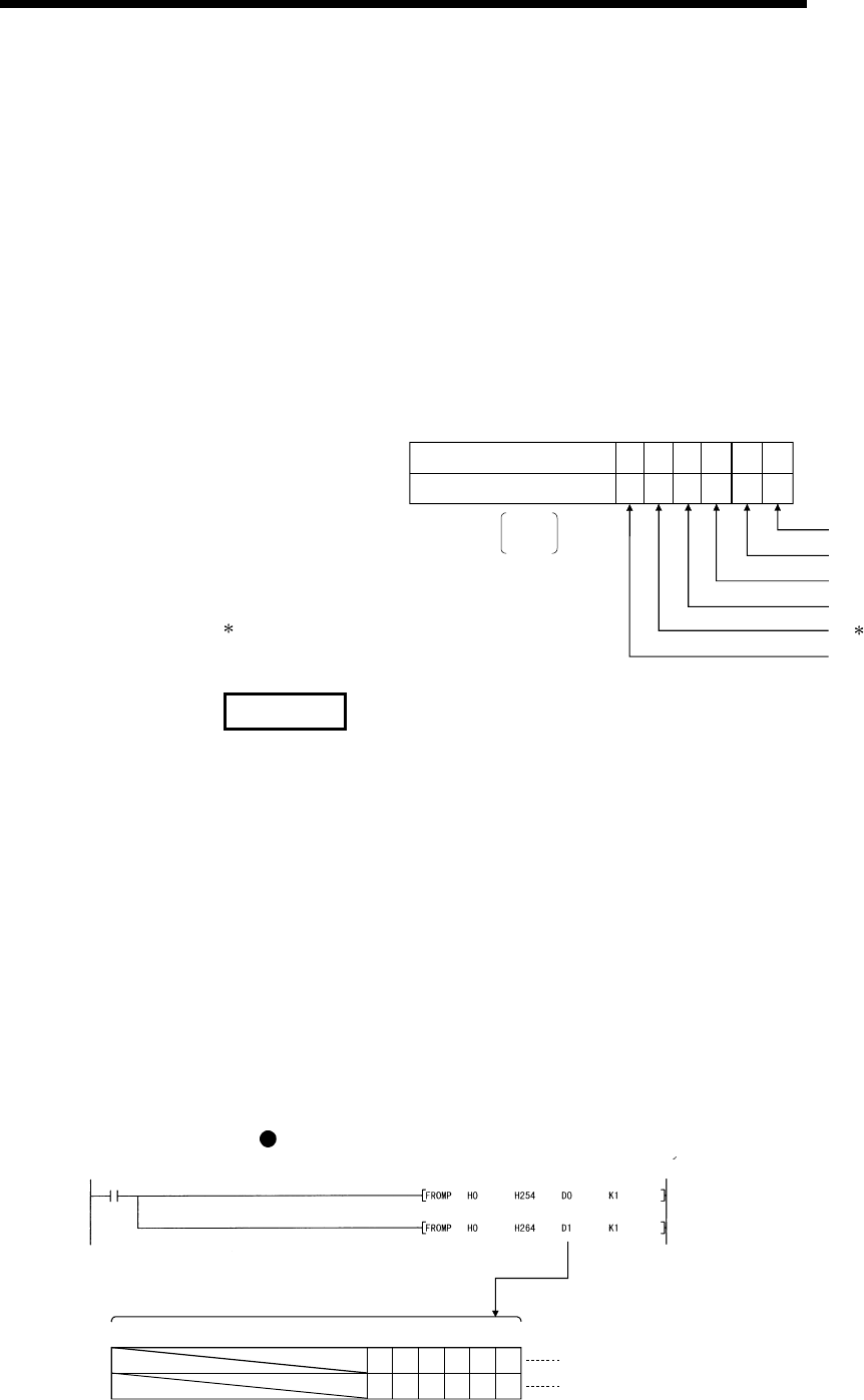
10 - 9 10 - 9
MELSEC-Q
10 TROUBLESHOOTING
10.1.3 Reading the RS-232 control signal status
This section explains how to read the control signal status stored in the buffer memory
during communication using RS-232 interface.
When GX Configurator-SC is used, check the status using the "Transmission control
and others monitor/test" screen (see Section 8.6.3).
When a transmission problem occurs, read operation is executed to check the signal
on/off status of the RS-232 interface.
(1) RS-232 control signal status storage area (address: 254H, 264H)
The status of the RS-232 signals is stored in buffer memory addresses 254H and
264H as follows:
1 : ON
0 : OFF
b0b1b2b3b4
to
Buffer memory address
264H
0
0
(Information on CH1 side)
(Information on CH2 side)
1/0
1/0
1/01/01/0
1/01/01/0
b15 b5b6
1/0
1/0
254H
System area for QJ71C24 (-R2)
RS
DSR
DTR
CD
RI
CS
1/0
1/0
REMARK
(1) For more details on signals for RS-232, see Section 3.2.1.
(2) Signals output from the Q series C24 side (RTS and DTR) are controlled by the
operating system (OS) of the Q series C24.
They cannot be directly controlled by the sequence program.
(3) There is a maximum delay of 100 ms in signal status stored in the buffer
memory above.
(2) Example of a program that reads from RS-232 control signal status
storage area
The following shows an example of a program that reads the RS-232 control
signal status.
(input/output signals X/Y00 to X/Y1F of the Q series C24)
Example of FROM instruction
b15 to b4 b3 b2 b1 b0
0
1
1
1
1
1
1
0
D0
D1 CD signal: ON, DTR signal: ON, DSR signal: ON
DTR signal: ON, DSR signal: ON, RTS signal: ON
0
0
b5
0
0
b6
Reads the status of RS-232 control signal on
the CH1 side from address 254H.
Reads the status of RS-232 control signal on
the CH2 side from address 264H.
Read command
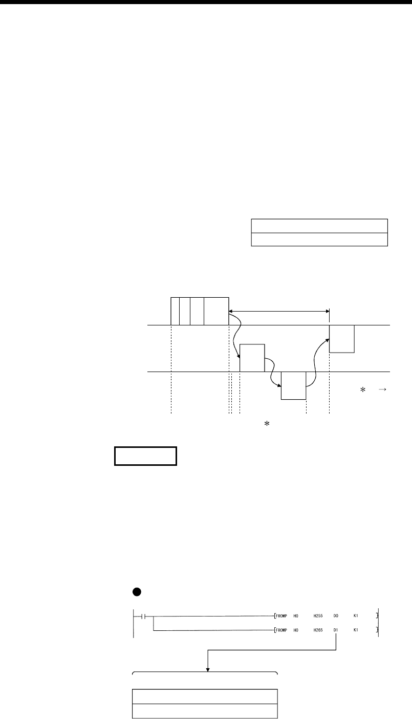
10 - 10 10 - 10
MELSEC-Q
10 TROUBLESHOOTING
10.1.4 Reading the data communication status (Transmission sequence status)
This section explains how to read the current status of the data communication using
the MC protocol stored in the buffer memory.
When GX Configurator-SC is used, check the status using the "MC protocol monitor"
screen (see Section 8.6.4).
When a transmission problem occurs, read operation is executed to check the status
of the data communication using the MC protocol.
(1) Transmission sequence status storage area (address: 255H and 265H)
The status of data communication using the MC protocol is stored as a numerical
value in buffer memory addresses 255H and 265H.
b15 to b0
0 to 9
0 to 9
Buffer memory address
265H
(Information on the CH1 side)
(Information on the CH2 side)
255H
The following shows the correspondence between the numerical values in the
transmission sequence status storage area and the data communication status.
"6" "1"..."6" is repeated afterward.
Values 7 to 9 are stored when "mode switching" or "initialization
of transmission sequence" is performed.
E
N
Q
Station
number HL
Request
to CPU
Response
from
CPU
ACK
or
NAK
Message wait
Request from an external device
External
device
Q series C24
Stored
v
alue
103456
2
REMARK
When the target interface is not set to use the MC protocol, "0" is stored in the
transmission sequence status storage area.
(2) Example of a program that reads from transmission sequence
status storage area
The following shows an example of a program that reads from the transmission
sequence status storage area.
(input/output signals X/Y00 to X/Y1F of the Q series C24)
Example of FROM instruction
b15 to b0
0
4
D0
D1
The CH1 side is waiting to receive a command message,
and is using non procedure or bidirectional protocol.
CH2 is accessing the PLC CPU upon reception of a
command message.
Reads the status of data communication
on the CH1 side from address 255H.
Reads the status of data communication
on the CH2 side from address 265H.
Read command
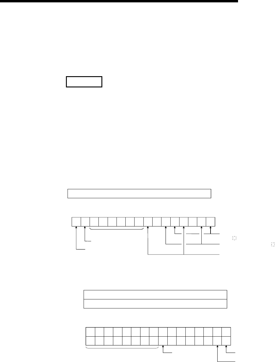
10 - 11 10 - 11
MELSEC-Q
10 TROUBLESHOOTING
10.1.5 Reading the switch setting status
This section explains how to read the switch setting status of the Q series C24.
When GX Configurator-SC is used, check the status in the "Monitor/test others" screen
(see Section 8.6.9).
REMARK
(1) The switch settings can be changed when the mode is switched or when the
UINI instruction is executed. (The station No. setting can be changed only when
the UINI instruction is executed.)
For the mode switching, refer to Chapter 15 of the User's Manual (Application).
For the UINI instruction, refer to Chapter 17 of the User's Manual (Application).
(2) For the switch settings, refer to Section 4.5.
(1) Setting status storage area
The switch settings by GX Developer and setting error information are stored in
different areas of the buffer memory shown below.
1) Station number storage area (address: 200H)
b0
Buffer memory address 200H(Station number)
0 to 31
b15 to
2) Switch setting error/mode switching error storage area (address: 203H)
b15 b14 b13 b12 b11 b10 b9 b8 b7 b6 b5 b4 b3 b2 b1 b0
Buffer memory address 203H
Ignore (including b2 and b6)
Mode switching request was
issued when the setting
modification allow/prohibit was
set to prohibit.
(1: Error, 0: Normal)
1/01/01/01/01/01/0
1/0
Linked operation setting error
(see Section 4.5.2 (2)).
CH2CH2CH2 CH1 CH1 CH1 Communication protocol number
on CH side is outside the range.
Communication rate on CH side
is outside the range.
1/0
Station number of the Q series
C24 is outside the range.
3) Communication protocol storage area (address: 250H and 260H)
b0
Buffer memory address 250H
260H(Information on the CH2 side)
(Information on the CH1 side)
0 to 8
0 to 7
b15 to
4) Transmission setting status storage area (address: 251H and 261H)
b15 b14 b13 b12 b11 b10 b9 b8 b7 b6 b5 b4 b3 b2 b1 b0
Communication rate setting
Data bit settin
g
Operation setting
Buffer memory address 251H
261H(Information on the CH2 side)
(Information on the CH1 side)
1/0
1/0
1/01/01/01/01/01/01/01/01/01/01/0
1/01/01/01/01/01/01/01/01/01/01/0
0000
0000
Setting modification
allow/prohibit
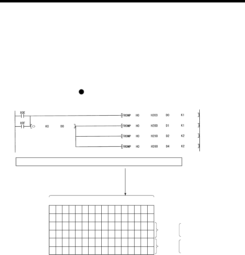
10 - 12 10 - 12
MELSEC-Q
10 TROUBLESHOOTING
(2) Example of a program that reads from the setting status storage
area
The following shows an example of a program that reads the setting of various
switches of the Q series C24 from the setting status storage area.
For details on XE and XF of the input/output signals used in the program, see
Section 10.1.2 (3).
(input/output signals X/Y00 to X/Y1F of the Q series C24)
Example of FROM instruction
Reads error description from address 203H.
Reads station number setting and switch
setting description from address 200H.
Reads communication protocol setting and
transmission setting description on the CH1
side from addresses 250H to 251H.
Reads communication protocol setting and
transmission setting description on CH2
from addresses 260H to 261H.
Restarts the Q series C24 after checking the error code and resetting switches.
b15b14b13b12b11b10 b9 b8 b7 b6 b5 b4 b3 b2 b1 b0
Error description (1: Communication protocol number setting error)
Setting station number of the Q series C24 (0).
CH1 side
D0
D1
D2
D3
D4
D5
Communication protocol setting number (9).
(transmission setting description)
CH2 side
Displays communication protocol number setting error status on the CH1 side
0000000000000000
0000000000001001
00000 10100001010
0000000000000001
00000 10 10 110 10 10
0000000000000001
Communication protocol setting number (1).
(transmission setting description)
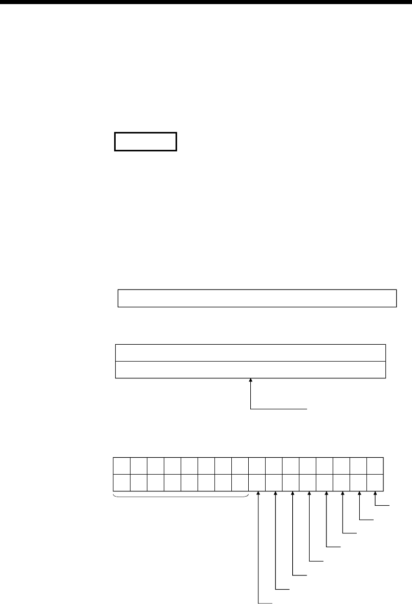
10 - 13 10 - 13
MELSEC-Q
10 TROUBLESHOOTING
10.1.6 How to read the current operation status
This section explains how to read the current operation status of the Q series C24.
When GX Configurator-SC is used, check the status in the "Transmission control and
others monitor/test" screen (see Section 8.6.3).
REMARK
• The status of the switch settings by GX Developer can be checked by performing
read operations as described in Section 10.1.5.
• Refer to Section 4.5 for the switch settings.
(1) Operation mode status storage area
The current operation status of the Q series C24 is stored into the following buffer
memory areas.
1) Station No. storage area (address: 24FH)
b0
(Station No.)
0 to 31
b15
Buffer memory address 24FH
to
2) Communication protocol status storage area (addresses: 252H and 262H)
b0
Mode number currentl
y
operatin
g
Buffer memory address 252H
262H(Information on the CH2 side)
(Information on the CH1 side)
1 to 7
1 to 7
b15 to
3) Transmission status storage area (address : 253H, 263H)
b15 b14 b13 b12 b11 b10 b9 b8 b7 b6 b5 b4 b3 b2 b1 b0
Communication rate setting
Buffer memory address 253H
263H(Information on the CH2 side
)
(Information on the CH1 side
)
1/0 1/0 1/0 1/0 1/0 1/0 1/0 1/0 1/0 1/0 1/0 1/0
1/01/01/01/01/01/01/01/01/01/01/01/0
Operation setting
Data bit setting
Parity bit setting
Even/odd parity setting
Stop bit setting
Sum check code setting
Write during RUN setting
Setting modification allow/prohibit
0000
0000
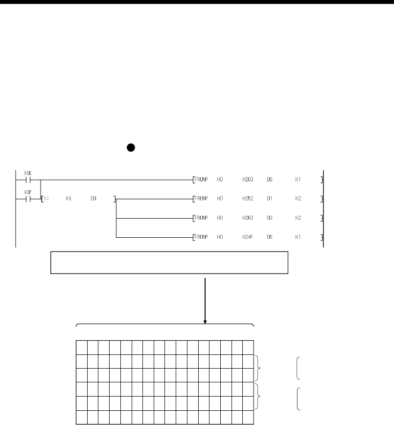
10 - 14 10 - 14
MELSEC-Q
10 TROUBLESHOOTING
(2) Example of a program that reads from the current setting status
storage area
The following shows an example of a program that reads from the switch setting
status storage area for current operation of the Q series C24.
For details regarding XE and XF of the input/output signals used in the program,
see Section 10.1.2 (3).
(input/output signals X/Y00 to X/Y1F of the Q series C24)
Example of FROM instruction
Reads error description from address 203H.
After checking error codes and changed setting values, designate
the correct setting values and switch mode.
b15b14b13b12 b11b10 b9 b8 b7 b6 b5 b4 b3 b2 b1 b0
Error description (2: Communication rate error)
D0
D1
CH1 side
D2
D3
D4
Setting communication protocol number 6
(transmission setting description)
CH2 side Setting communication protocol number 1
(transmission setting description)
While the CH1 side is set to the non procedure protocol and the CH2 side is set to the MC protocol (format 1),
this indicates the communication rate setting error on the CH1 side.
0000000000000 110
0000111100001010
000000000000000 1
00000 10 10110 10 10
0000000000000010
0 0 00 0 00 00 0 00 00 01
Communication protocol
Reads CH1 side communication protocol
status and transmission status from
addresses 252H to 253H.
Reads CH2 side communication protocol
status and transmission status from
addresses 262H to 263H.
Reads station No. from address 24FH.
D5 Station No. 1 being set.
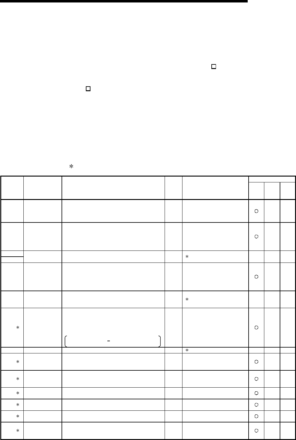
10 - 15 10 - 15
MELSEC-Q
10 TROUBLESHOOTING
10.2 Error Code Tables
The following shows the error codes, error contents, and corrective action for errors
that are generated during communication between the Q series C24 and an external
device.
The signal name in the following table indicates the CH side LED on status or
communication error status that is stored into buffer memory address 201H/202H when
an error occurs.
The CH side LED on status and communication error status can be confirmed by GX
Developer's System monitor or GX Configurator-SC. (Refer to Section 10.1.1.)
For errors without a corresponding signal name entered to errors generated with the
MC protocol communication, “NAK” comes on.
10.2.1 Error code table
The following shows the error codes, error contents, and corrective action for errors
generated during communication using MC protocol (excluding A compatible 1C
frame), non procedure protocol, and bidirectional protocol.
(" " in the table is the error code when the target CPU is not a Q/QnACPU.)
Protocol
Error code
(Hexa-
decimal)
Error Error Contents Signal
name Corrective action MC
Non
Proce-
dure
Bidire-
ctional
3E8H
to
3FFFH
— (Error detected by the CPU) —
• See Troubleshooting of the
QCPU (Q mode) maintenance
and inspection user's manual
and take corrective action.
4000H
to
4FFFH
— (Error detected by the CPU) —
• See Appendix of the QCPU (Q
mode) maintenance and
inspection user's manual
(details) and take corrective
action.
7101H
7102HSystem error • The OS of the Q series C24 detected some error. — ( 1)
7103HPLC access error • Cannot communicate with the Q series C24 CPU. C/N
• Make the watchdog timer (timer
1) time longer.
• Check if the CPU can
communicate in communication
protocol No. "F".
7104H
to
7116H
System error • The OS of the Q series C24 detected some error. — ( 1)
7140HRequest data error
• Number of request points exceeds the range for the
command.
• A word device was designated in a bit units
command.
• The last device No. exceeds the range.
Given device last No. > Designated head device
No. + Designated number of points
PRO
• Check and correct the external
device transmit message and
restart data communications.
7141HSystem error • The OS of the Q series C24 detected some error. — ( 1)
7142HDevice name error • A device that cannot be designated by the given
command was designated. PRO
• Check and correct the external
device transmit message and
restart data communications.
7143HDevice No. error • The head device No. is out of range. PRO
• Check and correct the external
device transmit message and
restart data communications.
7144HMonitor data write
error
• Monitoring was requested before the device to be
monitored was written. PRO • Write the device to be monitored
before issuing a monitor request.
7145HMonitor PLC No.
error
• The written PLC No. and PLC No. in the monitor
request are different. C/N • Rewrite the monitor data.
7146HMonitor CPU model
name error
• The written CPU model name and the CPU monitor
name in the monitor request are different. C/N • Rewrite the monitor data.
7147H
Written number of
monitoring points
overrun error
• The written number of monitoring points exceeds
the designated range. PRO
• Check and correct the external
device transmit message and
restart data communications.
10 - 16 10 - 16
MELSEC-Q
10 TROUBLESHOOTING
Protocol
Error code
(Hexa-
decimal)
Error Error Contents Signal
name Corrective action MC
Non
Proce-
dure
Bidire-
ctional
7148HExtension R block
No. error
• A nonexistent extension file register block No. was
designated.
• A block No. being used as an extension comment
area, sampling trace area, or status latch area was
designated.
PRO
• Correct the designated block
No. and restart data
communications.
7149HSystem error • The OS of the Q series C24 detected some error. — ( 1)
714AH
Cannot execute a
command during
RUN
• A write command was designated when "Disable
write during RUN" was set.
• Parameter or sequence program was written during
RUN.
C/N
• Change the setting to "Enable
write during RUN" and restart
data communications.
• Stop the CPU and restart data
communications.
714BH
to
714DH
System error • The OS of the Q series C24 detected some error. — ( 1)
714EHMonitor network
No. error
• The written monitor network No. and the monitor
request network No. are different. C/N
• Check and correct the other
station access valid module No.
in the network parameters.
• Rewrite the monitor data.
7150HSystem error • The OS of the Q series C24 detected some error. — ( 1)
7151HPLC No.
designation error
• A PLC No. other than "FF" or "0 to 64(00H to 40H)"
was designated. C/N
• Check and correct the external
device transmit message and
restart data communications.
7152HSystem error • The OS of the Q series C24 detected some error. — ( 1)
7153HFrame length error • The received message length has exceeded the
allowable range.
CHn
ERR.
• Review the transmission
message.
• Correct the message format so
the number of access points is
within the allowable range.
7154HSystem error • The OS of the Q series C24 detected some error. — ( 1)
7155HUnwritten monitor
data error
• Monitoring was requested before monitor data was
written. PRO
• Write the device to be monitored
before issuing a monitor
request.
7156HSystem error • The OS of the Q series C24 detected some error. — ( 1)
7160HPLC access error • CPU model name cannot be confirmed. C/N
• If there is an error in the CPU,
remove the CPU error and
restart data communications.
7161H
to
7163H
System error • The OS of the Q series C24 detected some error. — ( 1)
7164HRequest error • Either the request or the device designation method
is wrong.
• Check the transmission
message/request from the
external device, make the
necessary corrections, and send
again.
7166HSystem error • The OS of the Q series C24 detected some error. — ( 1)
7167H• A write command was designated when "Disable
write during RUN" was set. C/N
• Change the setting to "Enable
write during RUN" and restart
data communications.
7168H
Cannot execute a
command during
RUN • A command that cannot be executed during RUN
was designated. C/N • Stop the CPU and restart data
communications.
7169HCPU error • Cannot communicate normally with the CPU. C/N
• If there is an error in the CPU,
remove the CPU error and
restart data communications.
716AH
to
716CH
System error • The OS of the Q series C24 detected some error. — ( 1)
716DH• Monitor data was not written using QnA compatible
2C/3C/4C frame. PRO
716EH
Monitor data write
error • Monitor data was not written using A compatible 1C
frame. PRO
• Rewrite monitor data.
10 - 17 10 - 17
MELSEC-Q
10 TROUBLESHOOTING
Protocol
Error code
(Hexa-
decimal)
Error Error Contents Signal
name Corrective action MC
Non
Proce-
dure
Bidire-
ctional
716FHDevice error
• A nonexistent device was designated.
• Device that cannot be specified by the
corresponding command was designated.
PRO
• Check and correct the external
device transmit message and
restart data communications.
7170H• Number of access points exceeded the range. PRO
7171H• A device that cannot be designated was designated. PRO
7172H
A compatible 1C
frame error
• Written number of monitoring points is incorrect. For
example, [0] was designated. PRO
• Check and correct the external
device transmit message and
restart data communications.
7173HMonitor data write
error
• Monitor data was written for a CPU other than a
Q/QnACPU using QnA compatible 2C/3C/4C frame. PRO
• Write the monitor data and use
the A compatible 1C frame to a
CPU other than a Q/QnACPU.
7E00H
to
7E05H
System error • The OS of the Q series C24 detected some error. — ( 1)
7E06H
Buffer memory
address setting
error
• Transmit/receive buffer memory addresses are in
the special applications area.
• Change the buffer memory
addresses so that they are outside
the special applications area.
7E07H
to
7E0AH
System error • The OS of the Q series C24 detected some error. — ( 1)
7E40HCommand error • A nonexistent command or subcommand was
designated. PRO
• Check and correct the external
device transmit message and
restart data communications.
7E41HData length error
• A data length exceeding the number of points that
can communicate during random read/write was
designated.
PRO
• Check and correct the external
device transmit message and
restart data communications.
7E42HError count error • Number of requested points exceeds the range for
the command. PRO
• Check and correct the external
device transmit message and
restart data communications.
7E43HDevice error
• A nonexistent device was designated.
• Device that cannot be specified by the
corresponding command was designated.
PRO
• Check and correct the external
device transmit message and
restart data communications.
7E44HTimer 1 time-out
error
• A response message was not returned within the
response monitoring time (timer 1) monitoring time. C/N
• Make the timer 1 monitoring
time longer.
• When accessing another
station's CPU, check if the
routing parameters match.
7E46HSystem error • The OS of the Q series C24 detected some error. — ( 1)
7E47HContinuous request
error
• The next request was received before a response
message was returned for the preceding request. PRO
• Do not issue continuous
requests from the external
device.
• Set the timer 1 monitoring time
to the external device time-out
time.
7E48H
to
7E4CH
System error • The OS of the Q series C24 detected some error. — ( 1)
7E4DHError during data
transmission
• Mode switching was executed during data
transmission.
CHn
ERR.
• Make arrangements between
the target device and PLC CPU
so that mode switching is not
executed during data
transmission.
7E4EHSystem error • The OS of the Q series C24 detected some error. — ( 1)
7E4FHDevice point count
error • Access point count is incorrect. PRO
• Check and correct the external
device transmit message and
restart data communications.
7E50HUser frame No.
designation error • A user frame No. outside the range was designated. PRO
• Check and correct the external
device transmit message and
restart data communications.
• Recheck the frame No..
7E51HUnwritten user
frame error • An unwritten user frame No. was designated. PRO
• Write the frame beforehand.
• Change the frame No. and
restart data communications.
• Recheck the frame No..

10 - 18 10 - 18
MELSEC-Q
10 TROUBLESHOOTING
Protocol
Error code
(Hexa-
decimal)
Error Error Contents Signal
name Corrective action MC
Non
Proce-
dure
Bidire-
ctional
7E52HUser frame
overwrite error • A written frame No. overwrite request was issued. PRO
• Change the write destination to
an unwritten frame No.
• When overwriting, delete the
given No. beforehand.
7E53HUser frame access
data error
• A nonexistent command was designated in a
subcommand.
• Byte count exceeding the number of bytes that can
be requested was designated.
PRO
• Check and correct the external
device transmit message and
restart data communications.
7E54HModification
allowed error
• Flash ROM write allow/prohibit designation from GX
Configurator-SC is set to OFF.
• At the switch setting on GX Developer, modification
allowed switch was set to OFF.
PRO
• Set to ON at GX Configurator-
SC.
• Set to ON at GX Developer.
7E55HUser frame data
error • There is an error in the user frame variable data. PRO
• Check and correct the external
device transmit message and
restart data communications.
7E56HSystem error • The OS of the Q series C24 detected some error. — ( 1)
7E57HFlash ROM write
error • Cannot write to Flash ROM normally. PRO
• Re-execute the write operation.
If the error is generated again,
replace the module.
7E58HMode modification
error
• There was an error in the mode No. or transmission
specification designated contents when changing
the mode.
PRO
• Check and correct the contents
of the external device transmit
message and restart data
communications.
• Recheck the switch setting on
the Q series C24.
7E59H
Flash ROM write
count over limit
error
• Flash ROM written 1,000 times —
• Review the program.
• Rewrite the flash ROM area
(address: 2401H) of the buffer
memory to 0 and restart data
communications.
7E5F H
I/O number error
on requested
module
• I/O number of requested module is incorrect. — • Correct the I/O number of the
module to which data is sent.
7E60 H
Device monitoring
duplicate
registration error
• PLC CPU monitoring registration was performed
twice. —
• Cancel the PLC CPU monitoring
and perform the PLC CPU
monitoring registration again.
7E61 H Cycle time units
range error • Setting value of cycle time units is out of range. — • Correct the setting value of the
cycle time units.
7E62 H
PLC CPU
monitoring function
error
• Setting value of PLC CPU monitoring function is out
of range. —• Correct the setting value of the
PLC CPU monitoring function.
7E63 H
Transmission
measure setting
error
• Setting of transmission measure of the PLC CPU
monitoring is incorrect. —• Correct the setting value of the
transmission measure.
7E64 H Registration point
range error • Registration point (word/bit) is out of range. — • Correct the setting value of the
registration point (word/byte)
7E65 H
PLC CPU abnormal
monitoring number
error
• Setting value of the PLC CPU abnormal monitoring
is out of range. —• Correct the setting value of the
PLC CPU abnormal monitoring.
7E66 H
Monitoring
condition error of
monitoring device
• Setting value of transmission condition is out of
range. —• Correct the setting value of the
transmission condition.
7E67 H
CPU abnormal
monitoring setting
value error
• Setting value (fixed value) of CPU abnormal
monitoring is out of range. —
• Correct the setting value (fixed
value) of the CPU abnormal
monitoring.
7E68H
Transmission
condition range
error of monitoring
device
• Setting value of transmission condition (condition
agreement transmission) is out of range. —
• Correct the setting value of the
transmission condition
(condition agreement
transmission).
7E69H
CPU abnormal
monitoring setting
value error
• Setting value (fixed value) of CPU abnormal
monitoring is out of range. —
• Correct the setting value (fixed
value) of the CPU abnormal
monitoring.
10 - 19 10 - 19
MELSEC-Q
10 TROUBLESHOOTING
Protocol
Error code
(Hexa-
decimal)
Error Error Contents Signal
name Corrective action MC
Non
Proce-
dure
Bidire-
ctional
7E6AH
Monitoring device
read point range
error
• Read point of monitoring device is out of range. —
• Correct the setting value of the
read point of the monitoring
device.
7E6BH—
7E6CH—
7E6DH
CPU abnormal
monitoring setting
value error
• Setting value (fixed value) of CPU abnormal
monitoring is out of range. —
• Correct the setting value (fixed
value) of the CPU abnormal
monitoring.
7E6EHSystem error • The OS of the Q series C24 detected some error. — ( 1)
7E6FHModem connection
error • Modem is connected to an incorrect channel. — • Correct the CH to which
notification is sent.
7E70HCPU error • The communication with the CPU could not be
performed normally. C/N
• If there is an error in the CPU,
eliminate the error on the CPU
side and communicate again.
7E81H
to
7E8EH
7EC1H
7EC2H
System error • The OS of the Q series C24 detected some error. — ( 1)
7EC3HDouble send
request error
• A send request was performed while another send
request was being processed. • Interlock (handshake) the send
requests.
7EC4H
Transmission data
count error
Transmission/
receipt buffer
setting error
• Data larger than the transmit buffer size was
transmitted.
• Transmission/receipt buffer settings out of range.
• Make the transmission data
count smaller than the transmit
buffer size.
• Make the non procedure
protocol transmit buffer size
larger.
• Designate the first address and
size of transmission/receipt
buffer in the free area range of
the user.
7EC5HFlash ROM access
error
• Write to Flash ROM was requested when the setting
modification enable/disable switch in the GX
Developer was set to OFF.
• When writing to Flash ROM, set
switch shown left of the given
interface to ON and restart the
Q series C24.
7EC6HFlash ROM access
error
• There is an error in the Flash ROM read/write
request contents.
• Check the read/write request
data and designate the correct
data.
7F00HSystem error • The OS of the Q series C24 detected some error. — ( 1)
• The next data was received before processing of the
previous data was completed.
• Increase the transmission time
by performing handshake with
the external device, etc.
7F01HBuffer full error • Multiple requests was simultaneously issued for one
channel.
• Perform handshake with the
request source external device.
7F02H
to
7F06H
System error • The OS of the Q series C24 detected some error. — ( 1)
• An ASCII code that cannot be converted to binary
code was received.
• Check and correct the external
device transmit message and
restart data communications.
7F20 H ASCII BIN
conversion error • An odd number of bytes of data was received during
data communications using ASCII BIN
conversion.
PRO • When communicating using
ASCII BIN conversion,
always transmit the data in even
number bytes units.
• There is an error in the command (frame) part.
7F21 H Receive header
area error • An ASCII code that cannot be converted to binary
code was received.
PRO
• Check and correct the external
device transmit message and
restart data communications.
7F22 H Command error • A nonexistent command or device was designated.
• The remote password length is wrong. PRO
• Check and correct the external
device transmit message and
restart data communications.
7F23 H MC protocol
message error
• There is no data (ETX, CR-LF, etc.) following the
character area, or designation was incorrect. PRO
• Check and correct the external
device transmit message and
restart data communications.
10 - 20 10 - 20
MELSEC-Q
10 TROUBLESHOOTING
Protocol
Error code
(Hexa-
decimal)
Error Error Contents Signal
name Corrective action MC
Non
Proce-
dure
Bidire-
ctional
7F24 H Sum check error • The sum check calculated by the Q series C24 and
the received sum check are not the same. P/S • Recheck the external device
sum check.
7F25 H Data length error • The length of the received data exceeds the receive
area size.
CHn
ERR.
• Correct the "data length" that is
transmitted from the external
device.
• Change the "word/byte units"
set by the Q series C24 to byte
units.
• Increase the receiving area of
the Q series C24.
7F26 H Command error • Another command was received before an unlock
processing while the remote password is registered.
CHn
ERR.
• Perform the communication
after the unlock processing is
normally completed.
7F30HSystem error • The OS of the Q series C24 detected some error. — ( 1)
7F31HSimultaneous
transmission error
• The Q series C24 and an external device started
transmitting simultaneously.
• Process by agreement with the
external device.
• When necessary, change the
simultaneous transmission data
valid/invalid designation setting
by GX Configurator-SC. (buffer
memory addresses 9BH/13BH)
7F32HSystem error • The OS of the Q series C24 detected some error. — ( 1)
7F40H• No reception watchdog timer (timer 0) time-out
occurred. PRO
• Check if data was dropped from
the receive data.
• Check if DTR control, etc.
interrupted reception.
7F41H• Response watchdog timer (timer 1) time-out
occurred.
• Check the status of the
message transmission
destination and restart data
communications, as required.
7F42H
Time-out error
• Transmit watchdog timer (timer 2) time-out
occurred. • Check if DTR control, etc.
interrupted transmission.
7F50H
to
7F54H
7F60H
to
7F66H
System error • The OS of the Q series C24 detected some error. — ( 1)
7F67HOverrun error • The Q series C24 received the next data before it
completed receive processing of the previous data. SIO
• Decrease the data transmission
rate and restart data
communications.
• Check whether a temporary stop
has occurred in the station in
which the Q series C24 is
installed. (For the QCPU this can
be checked using special register
SD1005.) If a temporary stop has
occurred, remove its cause.
7F68HFraming error
• Data does not match the stop bit setting.
• A malfunction occurred in the network because the
power source of the partner station was on or off.
• Noise occurs in the network.
• When the multidrop was connected, data was
transmitted simultaneously by multiple devices.
SIO
• Match the Q series C24 and
external device settings.
• Clear the error information
according to the error
information initialization request
(YE/YF).
In addition, when
communicating data with the
non procedure protocol, execute
the INPUT instruction, and read
and discard the unnecessary
data.
• Measure the noise.
• When connecting the multidrop,
remove the interlock so that
data will not be transmitted
simultaneously by multiple
devices.
10 - 21 10 - 21
MELSEC-Q
10 TROUBLESHOOTING
Protocol
Error code
(Hexa-
decimal)
Error Error Contents Signal
name Corrective action MC
Non
Proce-
dure
Bidire-
ctional
7F69HParity error
• Data does not match the parity bit setting.
• A malfunction occurred in the network because the
power source of the partner station was on or off.
• Noise occurs in the network.
• When the multidrop was connected, data was
transmitted simultaneously by multiple devices.
P/S
• Match the Q series C24 and
external device settings.
• Clear the error information
according to the error
information initialization request
(YE/YF).
In addition, when
communicating data with the
non procedure protocol, execute
the INPUT instruction, and read
and discard the unnecessary
data.
• Measure the noise.
• When connecting the multidrop,
remove the interlock so that
data will not be transmitted
simultaneously by multiple
devices.
7F6AHBuffer full error • OS receive buffer overflowed and receive data was
skipped. SIO
• Use DTR and DC control and
perform data communications
so that the buffer does not
become full. (Perform RS ⋅ CS
control when the modem
function is used.)
• If the Read Request signal was
turned ON, execute read
immediately.
7F6BHCD signal control
error
• Data was received when CD signal is OFF when
"CD terminal check enabled" was designated.
CHn
ERR.
• Recheck the CD signal control
of the external device.
(Send while the CD signal is ON.)
• Set "no CD terminal checking"
and perform communication.
7F6CHTransmission error • Data cannot be sent because the line is not
connected.
CHn
ERR.
• Transmit data after line
connection processing on the
interface side that uses the
modem function.
7F91H
to
7F96H
7F98H
to
7F9AH
7F9DH
7F9EH
7FA0H
to
7FA3H
7FA8H
7FAAH
to
7FADH
7FAFH
to
7FB2H
7FB5H
7FB6H
7FB8H
to
7FBCH
7FC0H
to
7FC4H
System error • The OS of the Q series C24 detected some error. — ( 1)
10 - 22 10 - 22
MELSEC-Q
10 TROUBLESHOOTING
Protocol
Error code
(Hexa-
decimal)
Error Error Contents Signal
name Corrective action MC
Non
Proce-
dure
Bidire-
ctional
7FC9H
to
7FCFH
System error • The OS of the Q series C24 detected some error. (1)
7FE6H• Remote passwords do not match. • Check the remote password and
communicate again.
7FE7H
• The remote password is not registered.
• The remote password processing command was
received on the interface side where the modem
function is not used.
• The GX Developer connection is selected in the
communication protocol setting on the
corresponding CH.
CHn
ERR.
• A remote password processing
command is not necessary
when a remote password is not
registered.
• Perform a remote password
unlock processing through GX
Developer. Alternatively, change
the communication protocol
setting of the corresponding CH
to the MC protocol.
7FE8H
Processing
disabled
• The number of remote password disagreements
exceeded the value designated at the address
200D H.
CHn
ERR.
• Clear the storage area of the
cumulative number of abnormal
completions of unlock processing
(address: 22FC H) to 0.
7FEFHSwitch setting error • There is an error in the switch setting by the GX
Developer
CHn
ERR.
• Write CPU to the parameter and
reboot after correcting the
setting value for the switch.
7FF0H
Dedicated
instructions
simultaneous
execution error
• Executed dedicated instructions simultaneously. • Do not use dedicated
instructions simultaneously.
7FF1HControl data error • Setting value is incorrect.
• Setting value is out of range. • Correct the setting value in the
control data.
7FF2H
Communication
protocol setting
error
• Instruction cannot be executed with the current
communication protocol. • Correct the setting value of the
communication protocol.
7FF3H
to
7FF4H
System error • The OS of the Q series C24 detected some error. — ( 1)
7FF5H
Processing
canceled due to
mode
switching/transmiss
ion sequence
initialization
• The processing was canceled due to mode
switching or receive data clear executed during the
processing.
• Do not execute mode
switching/receive data clear
during any processing.
7FF7HSimultaneous
access error
• Multiple external devices accessed a remote station
on the same network at the same time.
• Multiple external devices must
not access a remote station on
the same network at the same
time.
7FF8H
7FFFHSystem error • The OS of the Q series C24 detected some error. — ( 1)
B000H
to
BFFFH
• Errors detected by the CC-Link module —
• Take corrective action by
referring to the CC-Link
Master/Local Module User's
Manual.
C000H
to
CFFFH
• Errors detected by the Ethernet module —
• Take corrective action by
referring to the Ethernet
Interface Module User's Manual.
F000H
to
FFFFH
• Errors detected by the MELSECNET/H,
MELSECNET/10 network system
• Take corrective action by referring
to MELSECNET/H,
MELSECNET/10 network system
reference manual.

10 - 23 10 - 23
MELSEC-Q
10 TROUBLESHOOTING
1 Take corrective action in the following procedure.
1) Check whether the Q series C24, power supply module and CPU module are
mounted correctly on the base unit.
2) Check whether the operating environment of the Q series C24 is within the
general specifications range of the CPU module.
3) Check whether the power supply capacity is sufficient or not.
4) Check whether the hardware of the Q series C24, CPU module and base unit
are normal according to the manuals of the corresponding modules.
If any module is faulty, please contact your local Mitsubishi service center or
representative for repair.
5) If the problem cannot be solved through the above steps, please consult your
local Mitsubishi service center or representative, explaining a detailed
description of the problem.
10 - 24 10 - 24
MELSEC-Q
10 TROUBLESHOOTING
10.2.2 A compatible 1C frame communications error code table
The following table lists the error code, error contents, and corrective action for errors
generated during A compatible 1C frame communications.
Protocol
Error code
(Hexa-
decimal)
Error Error Contents Signal
name Corrective action MC
Non
Proce-
dure
Bidire-
ctional
00HDisable during
RUN
• A write command was designated when "Disable
write during RUN" was set.
• Parameter or sequence program was written during
RUN.
C/N
• Change the setting to "Enable
write during RUN" and restart
data communications.
• Stop the CPU and restart data
communications.
01HParity error • The data does not match the parity bit setting. P/S • Match the Q series C24 and
external device settings.
02HSum check error • The sum check calculated by the Q series C24 and
the transmitted sum check are not the same. P/S • Check the external device sum
check.
03HProtocol error • Received message that is different from the control
procedure with the communication protocol setting. PRO
• Check and correct the external
device transmit message and
restart data communications.
04HFraming error • The data does not match the stop bit setting. SIO • Match the Q series C24 and
external device settings.
05HOverrun error • The next data was received before the Q series C24
received all the preceding data. SIO • Decrease the transmission rate
and restart data communications.
06HCharacter area
error
• Designation method error in part of a message.
• A command that does not exist was designated.
• The number of processing points is outside the
range for the command.
• A device that does not exist was designated.
PRO
07HCharacter error • Received data that cannot be used. PRO
• Check and correct the external
device transmit message and
restart data transmission.
08HPLC access error • The CPU cannot communicate with the Q series
C24. C/N
• Replace the CPU with a CPU that
can communicate with the Q
series C24.
10HPLC No. error • The PLC No. is not "FF", or a station No. set in the
network parameters. C/N
• Check and correct the external
device transmit message and
restart data communications.
11HMode error • An error was detected upon access to the PLC
CPU. —
• Send again.
• Conduct individual station recovery
test and check the Q series C24.
12H
Special function
module designation
error
• A special function module does not exist at the
specified position. C/N
• Check and correct the external
device transmit message and
restart data communications.
21HSpecial function
module bus error
• An error was detected upon access to a special
function module at the specified position. C/N
• Check the error and take
corrective action according to the
manual of the corresponding
module.
42HOther errors See POINT .
POINT
• If an error occurs during A compatible 1C frame communications, the Q series C24
adds a 2-character error code (00H to 10H, 42H) to the "NAK" code and returns the
"NAK" code to the external device and stores the error code (equivalent to QnA
compatible 2C/3C/4C frame error code) to buffer memory address 25AH (CH1) or
26AH (CH2).
The exact error contents can be checked by reading the value stored to the
buffer memory.
See Section 10.2.1 for a detailed description of the error codes.
10 - 25 10 - 25
MELSEC-Q
10 TROUBLESHOOTING
10.2.3 Error code list while modem function is used
The following describes the error codes, contents and corrective actions for errors
(including errors at the abnormal completion) that may occur while the Q series C24
modem function is used.
The error codes for the modem function are stored in the modem function error code
storage area (address : 221H(545)) of the buffer memory.
The reference pages listed in the table below are found in the User's Manual
(Application).
Error code
(Hexa-
decimal)
Error Error Contents Signal
name Corrective action Reference section
7FD0HThere is an error in the designation of the notification
execution.
Set 0 to 1 to the notification execution
designation.
7FD1HThere is an error in the designation of the number of
connection retries.
Set the number of connection retries in
the range of 1 to 5.
7FD2HThere is an error in the designation of the connection
retry interval.
Set the connection retry interval in the
range of 90 to 300 (s).
7FD3HThere is an error in the initialization/connection time-
out designation.
Set the initialization/connection time- out
in the range of 1 to 60 (s).
7FD4HThere is an error in the designation of the number of
initialization retries.
Set the number of initialization retries in
the range of 1 to 5.
Section 3.3.6
7FD5HThere is an error in the designation of the data
number for initialization.
Designate the registered data number for
initialization, or 0.
Section 3.3.6
Section 3.4.5
7FD6HRecheck the pager receiver designation.
7FD7H
Modern
function
error
There is an error in the data for connection designated
by the data number for connection.
CHn
ERR.
Recheck the dialing number of the
external line.
Section 3.4.4
7FD8HSystem error The OS of the Q series C24 detected some error. (1)
7FD9HExternal destination is connected to network or
modem has not been initialized.
After the modem has been initialized,
connect to the network if the external
destination is not connected to the
network or report it.
Section 3.4.6
Section 3.4.7
7FDAHThere is an error in the designation of the data number
for connection.
Designate a registered number for the
data for connection.
Section 3.3.6
Section 3.4.6
7FDBHThere is an error in the designation of the GX
Developer connection.
Set 0 to 1 to the GX Developer
connection designation. Section 3.3.6
7FDCHThere is an error in the data for connection designated
by the data number for connection.
Recheck the waiting time for the
notification-message part of the message
transmission.
Section 3.4.4
7FDDHA connection time-out error occurred.
• Recheck the telephone number in the
data for connection.
• Check if the destination is ready for a
connection.
• Recheck the set value of the
connection time-out.
• Recheck the initialization command.
Section 3.3.6
Section 3.4.3
Section 3.4.4
7FDEHConnection to the modem/TA was unsuccessful, or
the modem/TA is not connected.
CHn
ERR.
• Check if there is any problem with the
modem/TA by seeing the operation
manual of the modem/TA.
• Connect the modem/TA to the Q series
C24.
• Check the connection cable by seeing
the operation manual of the
modem/TA.
—
7FDFHModem connection channel number is not designated.
7FE0H
Modern
function
error
Designated value of modem connection channel is
incorrect.
Set 1 to 2 to the modem connection
channel designation. Section 3.3.6
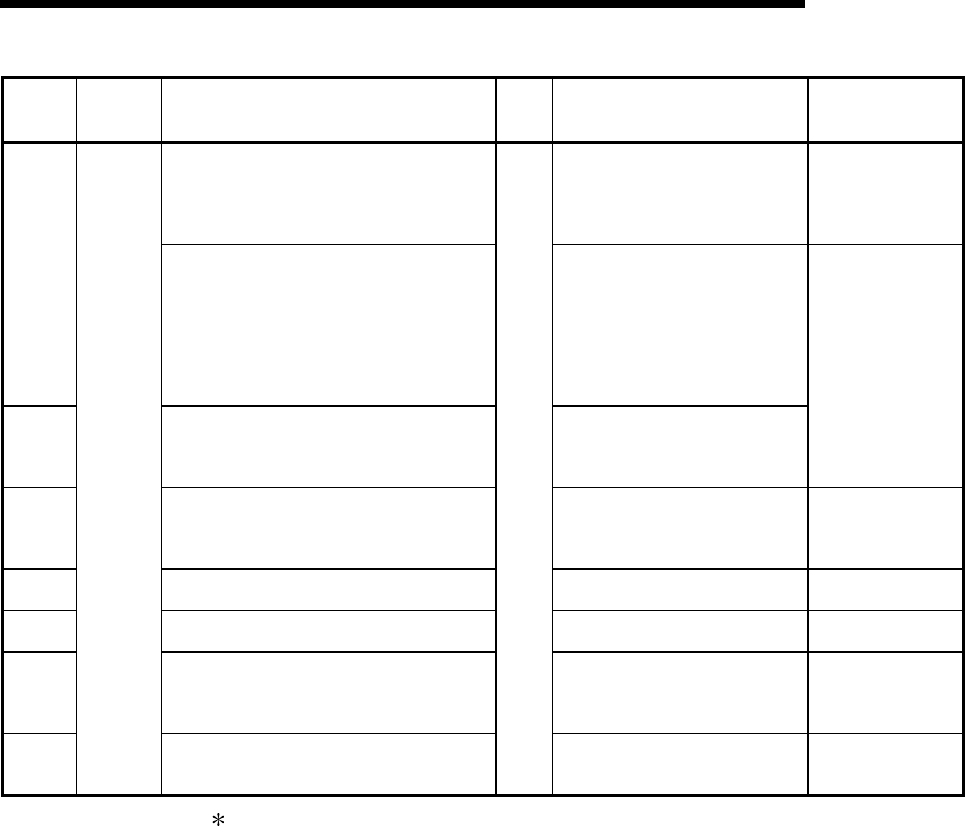
10 - 26 10 - 26
MELSEC-Q
10 TROUBLESHOOTING
Error code
(Hexa-
decimal)
Error Error Contents Signal
name Corrective action Reference section
There is an error in the designation of the user frame
number.
• Recheck the user frame number.
• Designate the registered user frame
number.
• Register the designated data for
initialization.
Section 3.4.3
Section 3.4.4
Section 3.4.5
7FE1H
There is an error in the designation of the output head
pointer.
• Designate the output head pointer in
the range of 1 to 100.
• Designate the position (n-th position)
where the data for initialization number
is designated.
• Designate the data for initialization
number at the designated position
(n-th position).
7FE2HThere is an error in the designation of the output frame
number.
Designate a registered data for
initialization number within the range of
the designated number of outputs from
the location of the output head pointer.
Section 3.4.5
7FE3HThere is an error in the designation of the number of
registered data bytes.
• Designate the data for initialization in
the range of 1 to 78.
• Designate 80 for the data for
connection.
Section 3.4.3
Section 3.4.4
7FE4HThere is an error in the data for connection. • Recheck the message length of the
message for notification. Section 3.4.4
7FE5HThere is an error in the designation of the no-
communication interval time.
• Designate the no-communication
interval time in the range of 0 to 120. Section 3.3.6
7FE8HThe number of remote password mismatch exceeded
the value designated at the address 200DH.
• Clear the storage area of the
Accumulated count of unlock process
abnormal completion (address: 22FCH)
to 0.
Section 3.3.3
7FE9H
Modern
function
error
Callback denial exceeded the value designated at the
address 2002H
CHn
ERR.
• Clear the storage area of the callback
denial accumulated count (address:
22F1H) to 0.
Section 3.3.4
1 Take corrective action in the following procedure.
1) Check whether the Q series C24, power supply module and CPU module are
mounted correctly on the base unit.
2) Check whether the operating environment of the Q series C24 is within the
general specifications range of the CPU module.
3) Check whether the power supply capacity is sufficient or not.
4) Check whether the hardware of the Q series C24, CPU module and base unit
are normal according to the manuals of the corresponding modules.
If any module is faulty, please contact your local Mitsubishi service center or
representative for repair.
5) If the problem cannot be solved through the above steps, please consult your
local Mitsubishi service center or representative, explaining a detailed
description of the problem.
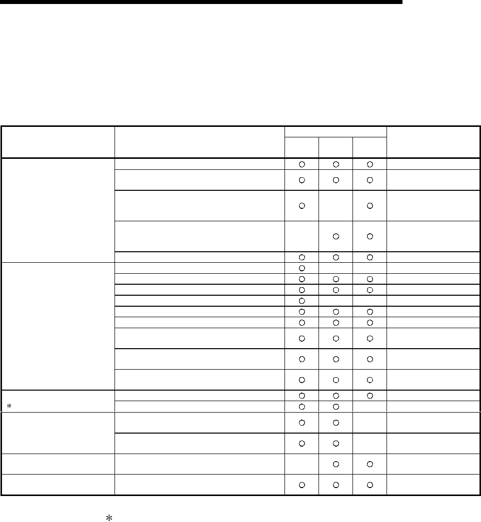
10 - 27 10 - 27
MELSEC-Q
10 TROUBLESHOOTING
10.3 Troubleshooting by Symptom
This following shows troubleshooting of trouble generated during communications
between the Q series C24 and external device according to the trouble symptom.
When trouble occurs, first confirm the status of the Q series C24 and check the
relevant item in the table below.
Protocol
Symptom Symptom description Dedicated Non
procedure
Bidirec-
tional
Reference section
• "RUN" LED turned off. Section 10.3.1
• "RD" does not blink even through an external device
is transmitting a message. Section 10.3.2
• An external device transmitted a message and "RD"
blinked, but the Q series C24 did not return a
response message.
Section 10.3.3
• An external device transmitted a message and "RD"
blinked, but the Q series C24 did not turn ON the
read request.
Section 10.3.4
LED turns on/off (check according to
Section 4.3)
• ERR. LED turns on. Section 10.3.20
• The "NAK" was turned ON. Section 10.3.5
• The "C/N" was turned ON. Section 10.3.6
• The "P/S" was turned ON. Section 10.3.7
• The "PRO" was turned ON. Section 10.3.8
• The "SIO" was turned ON. Section 10.3.9
• The "CH1. ERR. " or "CH2. ERR. " was turned ON. Section 10.3.10
• Communications are intermittently established and
lost. Section 10.3.11
• Data that cannot be decoded was transmitted and
received. Section 10.3.12
Communication errors occurred
(check according to Section 10.1.1)
• Whether the cause of the communications error is in
the Q series C24 or the external device is unknown. Section 10.3.13
• Cannot communicate via modem. Section 10.3.14
Cannot communicate via modem
(1)• Cannot communicate with ISDN sub-address. Section 10.3.15
• Does not operate in the cycle time designated in the
constant cycle transmission setting. Section 10.3.16
The PLC CPU monitoring function
does not operate in the designated
cycle time. • Does not operate in the cycle time designated in
condition agreement transmission setting. Section 10.3.17
Cannot receive by an interrupt
program • Cannot receive data. Section 10.3.17
Cannot perform initial setting • Cannot write setting value in flash ROM of the Q
series C24. Section 10.3.19
1 If an error occurs while performing data exchange using the modem function
described in User's Manual (Application) Chapter 3, first check the following items
and confirm whether or not the error is caused by the modem/TA connection.
If an error relating to the modem function is occurring, perform necessary
corrective actions for each cause according to the reference sections given below:
• Check the ON/OFF status of current I/O signals of the Q series C24.
• Check the storage status for error codes related to the modem function. (See
Sections 10.2.3.)
• Check the ON/OFF status of the DR terminal of the modem/TA. (See the
manual for the modem/TA.)

10 - 28 10 - 28
MELSEC-Q
10 TROUBLESHOOTING
REMARK
The following are precautionary notes when exchanging data with an external device
via one of the Q series C24 interfaces.
(1) When the power supply to the Q series C24 or external device is started, the
remote device that is connected may generate a reception error.
(2) If the remote device that is connected starts up while data is being transmitted,
the remote device side will generate a reception error.
(3) When the Q series C24 error LED lights up because a reception error has
occurred, turn off the light if necessary in accordance with Section 10.1.
Also, if a reception error has occurred on the external device side, handle the
error by seeing to the operating manual for the external device.
Handle the occurrence of a reception error on the Q series C24 side using
the following corrective actions.
• When communicating with the MC protocol
The Q series C24 will disregard the received data or returns a response
message indicating an abnormal termination if it detects a reception error
after receiving the head data of the command message in the set format.
If the reception error is detected before the head data of the command
message in the set format is received, the received data will be
disregarded.
• When communicating using non procedure protocol
If the Q series C24 detects a reception error, the reception abnormal
detection signal (X4, XB) turns ON.
Perform procedures such as detection of reception error or clearing
received data as required by following the explanations found in Sections
6.1.4 and 6.1.5.
• When communicating using bidirectional protocol
When the Q series C24 detects a reception error after the head data of a
communication message for bidirectional protocol is received, it returns a
response message indicating an abnormal termination.
If the reception error is detected before the head data of the
communication message for bidirectional protocol is received, the
received data will be disregarded.
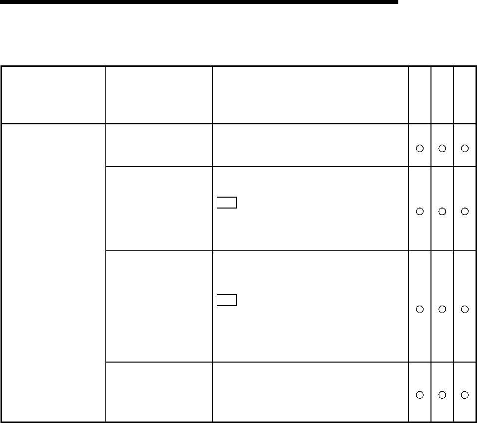
10 - 29 10 - 29
MELSEC-Q
10 TROUBLESHOOTING
10.3.1 Troubleshooting when "RUN" LED is turned OFF
Symptom Cause Corrective action MC
Bidirectional
Non
procedure
• A transmission setting
switch is set to an
unusable position.
• Set the switch by GX Developer correctly and
after writing to the CPU reset the CPU.
• PLC CPU error.
• Remove the cause of the CPU error and reset
the CPU.
Note
• During the Q series C24 and external device
loopback test, the minimum parameters file
must be written to the CPU beforehand.
• Power module 5 V
current capacity is
insufficient.
• Calculate the 5 V current drain of each installed
module. If the current capacity is insufficient,
check power module selection.
Note
• Whether or not the current capacity is
insufficient can be checked by disconnecting
the expansion base and installing only the Q
series C24 to the basic base.
• The Q series C24
"RUN" LED turned off.
• Extraneous noise
caused the Q series
C24 to abnormal
operation.
• Check if the shield wire is 2-point ground.
• When ground is used with other devices,
ground the Q series C24 independently.
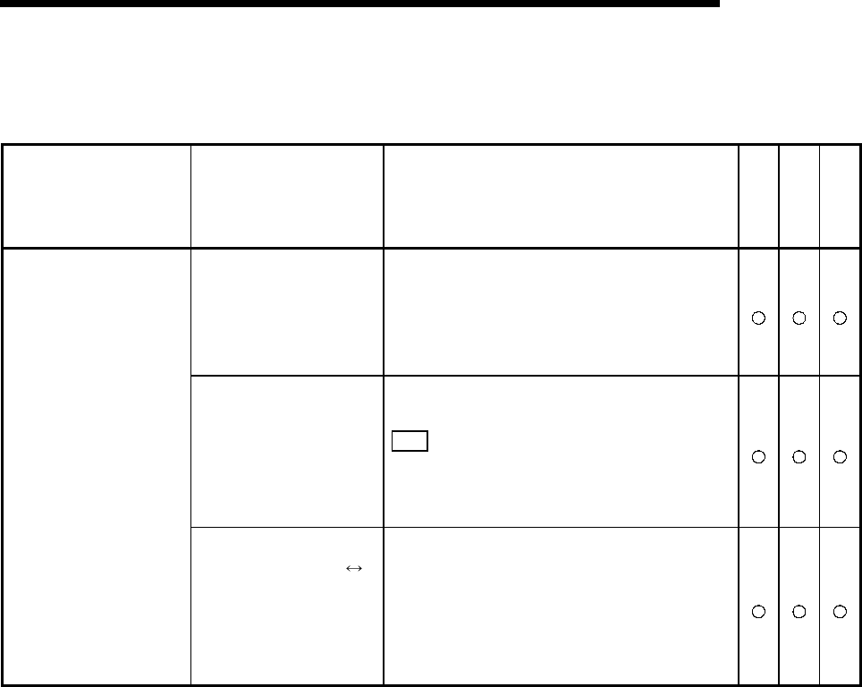
10 - 30 10 - 30
MELSEC-Q
10 TROUBLESHOOTING
10.3.2 Troubleshooting when "RD" LED does not blink even though an external device is
transmitting a message
Symptom Cause Corrective action MC
Bidirectional
Non
procedure
• Signal lines are not
connected correctly.
• Check if the Q series C24 and external RD and
SD signal lines are cross connected.
• Use the external device OPEN statement to
check if the opened port and the cable
connection port are matched.
• External device
transmission control
signals are not turned
ON.
• Connect the wiring so that the "DSR", "CS", and
other transmission control signals are ready.
Note
• Since the control signal specifications depend
on the device, connect the wiring by seeing
the instruction manual of the device used.
• "RD" does not blink
even through an
external device is
transmitting a message.
• If the message passes
through an RS-232
RS-422 converter,
modem, etc., the signal
is interrupted at one of
the intervening devices.
• Check the specifications of the converter and
modem and recheck the settings and wiring
10 - 31 10 - 31
MELSEC-Q
10 TROUBLESHOOTING
10.3.3 Troubleshooting when the Q series C24 does not return a response message even
though an external device transmitted a message and the "RD" LED blinked
Symptom Cause Corrective action MC
Bidirectional
Non
procedure
• Communication protocol
is set incorrectly.
• Check if the communication protocol is set
correctly.
• Check if the mode was switched without using
the buffer memory mode switching area.
Note
• The communication protocol setting contents
and the communication protocol in the current
operation can be checked at buffer memory
addresses 250H to (CH1) and 260H (CH2).
• When "Check CD
terminal" was set, the CD
terminal was turned OFF.
• Since the message is initialized (skipped reading)
when the CD terminal is turned OFF when "Check
CD terminal" is set, change the wiring so that the
CD terminal remains on all the time.
• The header byte of the
message is not data
needed by the set
protocol and format.
• Check if the external device sent a message
matched to the protocol and format.
Note
• The Q series C24 skips all the messages
transmitted until the header byte set for each
protocol and format (for example, "ENQ
(05H)" for format 1) is received.
• The Q series C24
station No. switch
setting and message
station No. designation
do not match.
• Check the Q series C24 station No. setting and
message station No. designation.
Note
• When the station No. designation is local
station after the header byte set for each
protocol and format is received, the Q series
C24 performs receive processing.
• The Q series C24 data
communications
monitoring time is set to
"infinite", or the
monitoring time is too
long.
• Set, or shorten, the monitoring time and
retransmit the message from the external
device and determine the trouble from the
contents of the time-out error.
Note
• Error detection by watchdog timers (timer 0 to
timer 2) is possible in the following cases.
• When part of a message is skipped.
• When transmission from an external device
is interrupted.
• When a link error was generated while
accessing another station over a
MELSECNET/H, MELSECNET/10.
See Chapter 6 of User's Manual (Application)
for a detailed description of the monitoring time.
• An external device
transmitted a message
and "RD" blinked, but
the Q series C24 did
not return a response
message. ("NEU"
remains on and "SD"
does not blink)
• The path setting of the
PLC CPU to be
accessed is incorrect.
Check the path of the PLC CPU to be accessed
and set the path again.
10 - 32 10 - 32
MELSEC-Q
10 TROUBLESHOOTING
10.3.4 Troubleshooting when an external device transmitted a message and "RD" LED
blinked, but the Read Request signal was not turned ON
Symptom Cause Corrective action MC
Bidirectiona
Non
procedure
• Communication protocol
is set incorrect.
• Check if the communication protocol is set correctly.
• Check if the mode was switched without using the
buffer memory mode switching area.
Note
• The communication protocol setting contents and
the communication protocol in the current operation
can be checked at buffer memory addresses 250H
to (CH1) and 260H (CH2).
• When "Check CD
terminal" was set, the CD
terminal was turned off.
• Since messages are skipped when the CD terminal is
turned OFF when "Check CD terminal" is set, change
the wiring so that the CD terminal remains on all the
time.
• When DC control is
selected, the necessary
DC codes are not
transmitted.
• Check if a message is transmitted without transmitting
"DC1 (11H)" after the external device transmits "DC3
(13H)" during DC1/DC3 external control.
• Check if the next message is transmitted without
adding "DC2 (12H)" after the external device transmits
"DC4 (14H)" during DC2/DC4 external control.
• The end code was not
received, or fixed length
data was not received.
• Check if the end code set at the Q series C24 and the
end code transmitted from the external device are the
same.
• Check if the external device transmitted the fixed
length designated at the Q series C24.
• Check if the trailer frame was transmitted during
communications by user frame.
Note
• When the send data from the external device is
correct, take the corrective action described in
Sections 10.3.10 and 10.3.11.
• The Q series C24
setting and message
format do not match.
• The data count basics, message format, etc. depend
on the following settings.
⋅ ASCII-BIN conversion enable/disable
⋅ Transparent code setting
⋅ User frame setting
See the relevant section for a description of operation
according to the set contents and setting of each item.
• An external device
transmitted a message
and "RD" blinked, but
the read request signal
(X0) was not turned
ON.
• The Q series C24 data
communications
monitoring time is set to
"infinite", or the
monitoring time is too
long.
• Set, or shorten, the monitoring time and retransmit the
message from the external device and determine the
trouble from the contents of the time-out error.
Note
• Error detection by the watchdog timer (timer 0 to
timer 2) is possible in the following cases.
⋅ When part of a message is skipped.
⋅ When transmission from an external device is
interrupted.
See Chapter 6 of User's Manual (Application) for a
detailed description of the monitoring time.
10 - 33 10 - 33
MELSEC-Q
10 TROUBLESHOOTING
10.3.5 Troubleshooting when communication error "NAK" generates
Symptom Cause Corrective action MC
Bidirectional
Non
procedure
• See section that
describes the
communication error
signal ("C/N", "P/S",
"PRO", "SIO") that are
turned on
simultaneously when the
"NAK" signal is turned
on.
• Take corrective action corresponding to the
contents of the error.
Note
Since the error code is added to "NAK" and is transmitted from the Q series C24 to the
external device when the "NAK" signal is turned on, take the corrective action described in
the error code table (see Section 10.2).
Since the error code added when "NAK" is transmitted is stored to the Q series C24 buffer
memory shown below, it can also be checked at the Q series C24.
Error code storage buffer memory address
CH1 side 25AH
CH2 side 26AH
• Communication error
signal "NAK" turned on.
10.3.6 Troubleshooting when communication error "C/N" generates
Symptom Cause Corrective action MC
Bidirectional
Non
procedure
• The Q series C24
cannot be installed in
the CPU.
• Change to a CPU to which the Q series C24
can be installed.
• PLC No. designated
local station (FF), or a
station other than a
station No. set with the
network parameters.
• Change the PLC No. to local station (FF), or a
station No. set with the network parameter and
restart data communications.
• Communication error
signal "C/N" turned on.
• Routing parameters
between CPU with the Q
series C24 loaded and
communications
destination CPU are not
set.
• Check the routing parameters and set them up
to the communications destination CPU.
10 - 34 10 - 34
MELSEC-Q
10 TROUBLESHOOTING
Symptom Cause Corrective action MC
Bidirectional
Non
procedure
• An error was generated
on the MELSECNET/ H,
MELSECNET/10.
• The local station CPU
on the MELSECNET/H,
MELSECNET/10
generated an error.
• Check the error contents from the state of SB
and SW related to the MELSECNET/H,
MELSECNET/10 with the GX Developer
monitor, etc. and perform the checks and take
the corrective action described in the
MELSECNET/H, MELSECNET/10 reference
manual.
• Module installation
address designation
during communications
with intelligent function
module is incorrect.
• Change the transmit message designation data.
• Stop the CPU and restart data communications.
• Communication error
signal "C/N" turned on.
• A command that cannot
be transmitted during
RUN (sequence
program, parameters,
etc.) was transmitted, or
"Disable write during
RUN" is set.
• Set the "Enable/disable write during RUN"
switch to "Enable" by command.
10.3.7 Troubleshooting when communication error "P/S" generates
Symptom Cause Corrective action MC
Bidirectional
Non
procedure
• Data does not match the
parity bit setting.
• Check the Q series C24 and external device
data format and match the settings.
• Sum check codes do not
match.
• Check if the sum check code transmitted from
the external device is correct. (Recalculate)
• Communication error
signal "P/S" turned on.
• When CH1 and CH2 are
used in the linked mode,
the cable is not
connected to one of the
interface.
• When using CH1 and CH2 independently, check
that the Q series C24 is not in the linked mode.
• When using CH1 and CH2 in the linked mode,
also connect the cable to both of the interfaces.
Note
• If the cable is not connected to one of the
interfaces when CH1 and CH2 are used in
the linked mode, noise may enter and the
data may be destroyed and "Data cannot be
decoded" or "Communications error cause"
may occur.
10 - 35 10 - 35
MELSEC-Q
10 TROUBLESHOOTING
10.3.8 Troubleshooting when communication error "PRO." generates
Symptom Cause Corrective action MC
Bidirectional
Non
procedure
• Communications were
performed with a control
procedure different from
the Q series C24
communication protocol
setting.
• Some of the data are
different from the control
procedure.
• Designated command
does not exist.
• The device No.
designation is not the
character count
corresponding to the
command.
• Check the Q series C24 communication
protocol setting and the message from the
external device and match the settings, or
correct the message and restart data
communications.
• The characters in the
message include a data
other than the "A to Z",
"0 to 9", " ", and
control data.
• Check and correct the external device message
and restart data communications.
Note
• Only the data "0 to 9" and "A to F" can be
handled as character area data during
communications using an MC protocol (ASCII
mode). Therefore, when transmitting a
character string as data, convert the ASCII code
of each character string to 2-byte binary code.
Examples)
• Transmitting the character "G"
The ASCII code for the character "G" is 47H
and is transmitted as the two bytes 34 H, 37H.
• Transmitting the character "A"
The ASCII code for "A" is 41H and is
transmitted as the two bytes 34H, 31H.
If the ASCII code 41H for the character "A" is
transmitted unchanged, the Q series C24
ASCII-BIN conversion will convert it to AH
(10) and pass it to the PLC CPU.
• A device No. outside the
designated range was
designated.
• When designating a device, check "Device
setting" of the parameters written to the CPU
and correct it to a device No. within the
designated range and restart data
communications.
• Communication error
signal "PRO" turned on.
• A remote RUN/STOP
request was issued
while remote STOP was
applied from another
module.
• Check if remote STOP is applied from another
module and restart data communications.
10 - 36 10 - 36
MELSEC-Q
10 TROUBLESHOOTING
10.3.9 Troubleshooting when communication error "SIO" generates
Symptom Cause Corrective action MC
Bidirectional
Non
procedure
• Data does not match the
stop bit setting.
• Check if the Q series C24 and external device
settings are the same.
• Transmission rate is too
fast and the next data is
transmitted before the Q
series C24 completes
processing of the
receive data.
• Decrease the transmission rate and restart data
communications.
• Data larger than the
receive buffer size was
received.
• Use DTR and DC control and interrupt
transmission before the buffer becomes full.
Perform RS and CS control when the modem
function is used.
• Increase the transmission interval and provide
an ample PLC CPU read processing time.
Note
• The non procedure protocol stores the data
received up to first the end code received, or
fixed length data, to the non procedure
receive buffer memory and turns on the Read
Request signal to the PLC CPU.
If the next data is sent while the Read
Request signal is ON, the data is temporarily
stored to the OS receive buffer. When the OS
receive buffer becomes full, the Q series C24
skips the rest of the data and turns on the
"SIO" LED.
• Communication error
signal "SIO" turned on.
• With a multidrop link,
two or more devices
transmitted data at the
same time.
• Connect the external devices and the Q series
C24 in a 1:1 configuration and perform a
communications test. Since data is transmitted
simultaneously from two or more devices with a
multidrop link when normal communications
among all the devices is possible, interlock the
devices so that cannot transmit simultaneously.
10 - 37 10 - 37
MELSEC-Q
10 TROUBLESHOOTING
10.3.10 Troubleshooting when communication error "CH1 ERR.", "CH2 ERR." generate
Symptom Cause Corrective action MC
Bidirectional
Non
procedure
• There is an error in the
communication protocol
or transmission setting.
• Read the error code from the buffer memory
and check the error contents and change the
switch setting to the correct setting.
• There is an error in the
on-line mode switching
designation.
• Read the error code from the buffer memory
and check the error contents and correct the
designation contents.
• On-demand execution
generated an error.
• Read the error code from the buffer memory
and check the error contents and correct the
designation contents.
• The Q series C24
detected an error while
transmitting data.
• Read the error code from the buffer memory
and take the corrective action corresponding to
the error contents.
• The Q series C24
detected an error while
receiving data.
• Read the error code from the buffer memory
and take the corrective action corresponding to
the error contents.
Note
• When the "ERR." LED is turned on, the error code is stored to the following buffer memory.
Error code storage buffer memory
AddressError cause
CH1 CH2 Name
Switch setting error
Mode switching error 203HSwitch setting error, mode switching error storage area
On-demand execution
error 256H266HOn-demand execution result storage area
Data transmission error 257H267HData transmission result storage area
Data receive error 258H268HData receive result storage area
Modern function error 221HModern function error code storage area
MC protocol
transmission error 025AH026AHMC protocol transmission error code
Monitoring device error 2205H2305HPLC CPU monitoring function execution result
• "ERR." LED turned on.
See Section 10.2 for a detailed description of the error codes.
10 - 38 10 - 38
MELSEC-Q
10 TROUBLESHOOTING
10.3.11 Troubleshooting when communications is intermittently established and lost
Symptom Cause Corrective action MC
Bidirectional
Non
procedure
• With a multidrop link, two or
more devices transmitted
data at the same time.
• Connect the external devices and the Q series C24 in a
1:1 configuration and perform a communications test.
Since data is transmitted simultaneously from two or
more devices with a multidrop link when normal
communications among all the devices is possible,
interlock the external devices so that they do not
transmit simultaneously.
• The signal cable wiring
connection is faulty. • Replace the cable, or make the connections firm.
• When "Check CD terminal"
is set, the CD signal is
turned on/off repeatedly.
• Change the wiring so that the CD signal remains ON all
the time, or change the setting to "Do not check CD
terminal".
• When half-duplex
communications is selected,
the ON/OFF timing of each
signal is not matched.
• Control the external device so that the ON/OFF timing
of each signal is matched.
See Chapter 8 of User's Manual (Application).
• Communications are
intermittently established
and lost.
(1)
• Requested processing of the
next transmission before the
processing of the current
transmission is completed.
• Requested processing of the
next reception before the
processing of the current
reception is completed.
• Make sure to obtain handshake in the sequence
program.
1 The following explains how to take corrective actions when a normal exit response
message cannot be received upon sending of a command message.
1) When a response message of abnormal end is received
When an external device sent a command message and received an
abnormal end response message, take corrective action with the error
according to the error code in the response message (see Section 10.2).
2) When response messages cannot be received
Change the setting value for the response monitoring time (timer 1, default
value is 5 seconds).
(See Section 6.2 of the User's Manual (Application).)
If response messages still cannot be received after changing the setting value,
check the communication protocol setting of the corresponding interface, the
ON status of the displayed LED, and the connection cable.
3) When the first part of a response message cannot be received
Increase the setting value of the message wait time (the default value is 0 ms).
(See Section 6.4 of the User's Manual (Application).)
If response messages still cannot be received after increasing the setting value,
it is necessary to reduce the processing time from the end of transmission
processing to the start of reception processing on the external device side.
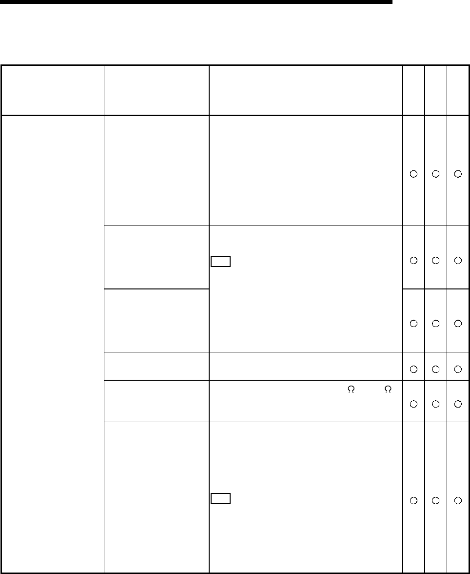
10 - 39 10 - 39
MELSEC-Q
10 TROUBLESHOOTING
10.3.12 Troubleshooting when data that cannot be decoded is transmitted and received
Symptom Cause Corrective action MC
Bidirectional
Non
procedure
• With a multidrop link,
two or more devices
transmitted data at the
same time.
• Connect the external devices and the Q series
C24 in a 1:1 configuration and perform a
communications test.
Since data is transmitted simultaneously from
two or more devices with a multidrop link when
normal data communications among all the
devices is possible, interlock the external devices
so that they do not transmit simultaneously.
• Data does not match the
parity bit setting.
• Data does not match the
parity bit setting.
• Match the Q series C24 and external device
parity bit settings.
Note
• If the setting of one side is data bit length 7
bits and with parity and the setting of the
other side is data length 8 bits and without
parity, the number of transmission/receive
bits will be the same and the data will sent
and receive without generating an error.
• Transmission rate
settings do not match.
• Match the Q series C24 and external device
transmission rates.
• With a multidrop link, the
terminal resistor is not
connected correctly.
• Check if the terminal resistor (110 or 330
in case of the Q series C24) is connected to the
stations at both ends of the link.
• Data that cannot be
decoded was
transmitted and
received
• When CH1 and CH2 are
used to the linked mode,
there is an interface
without cable
connection.
• When using CH1 and CH2 independently,
check that the Q series C24 is not in the linked
mode.
• When using CH1 and CH2 in the linked mode,
also connect the cable to both of the interfaces.
Note
• If the cable is not connected to one of the
interfaces when CH1 and CH2 are used in
the linked mode, noise may enter and destroy
the data and "Data cannot be decoded" or
"Communication error cause" may occur.
10 - 40 10 - 40
MELSEC-Q
10 TROUBLESHOOTING
10.3.13 Troubleshooting when it is unclear whether the communication error cause is in the
Q series C24 or an external device
Symptom Cause Corrective action MC
Bidirectional
Non
procedure
• Whether the
communications error
cause is in the Q series
C24 or an external
device is unclear.
• Test the Q series C24 as described below to
check where the cause is.
1) Check the hardware.
• The Q series C24 must be installed firmly.
• The pins of the Q series C24 must not be
bent or otherwise abnormal.
2) Test the Q series C24 alone. (See Section
4.7.)
• ROM/RAM/switch test must not generate
any errors.
• Self loopback test must not generate any
errors.
3) Check the state of the PLC CPU.
• There must not be any errors that stop
PLC CPU operation.
Note
• The following methods are available for
testing if normal communications are possible
with the Q series C24 alone.
1) With one the Q series C24, set CH1 and
CH2 to the non procedure protocol and
connect the wiring the same as for the self
loopback test and transmit data from one
channel and receive the transmitted data
at the other channel. If the transmitted
data and the received data are the same,
transmit and receive processing is
performed normally.
2) When two Q series C24 are available, set
one Q series C24 to the non procedure
protocol and the other Q series C24 to a
dedicated protocol and transmit an MC
protocol message from the non procedure
protocol station. If the MC protocol station
returns the transmit message normally,
transmit and receive processing is
normal.
10 - 41 10 - 41
MELSEC-Q
10 TROUBLESHOOTING
10.3.14 Troubleshooting when data cannot be communicated via modem
Symptom Cause Corrective action MC
Non
procedure
protocol
Bidirection
al protocol
• A modem initialization error occurs. • Check the error code and execute
processing accordingly.
• Modem connection channel designation is
not performed.
• Set Modem connection channel
designation.
• Auto modem initialization
cannot be executed.
• There is an error in the switch settings in the
GX Developer.
• Review the switch settings. Set it to match
the local station modem and the TA.
• Communication protocol setting is incorrect. • Set the communication protocol to MC
protocol, format 5.
• Transmission setting does not match the
external device. • Review the transmission setting.
• Data cannot be
communicated with GX
Developer supporting the Q
series C24. • Communication rate does not match the
external device. • Review the communication rate setting.
• The product is not supported by the GX
Developer. • Confirm the GX Developer’s S/W version.
• There was an error in the GX Developer
connection system.
• Check the GX Developer’s connection
system.
• Set the connection system on “callback
reception waiting” and connect.
• The GX Developer does not
receive the callback signals
from the Q Series C24.
• There is an error in the GX Developer side’s
modem settings.
• Set the modem’s settings on "Auto
Reception."
• There s an error in the GX Developer’s
connection system.
• Check the GX Developer’s connection
system.
• Correct the Q Series C24’s settings.
• Callback connections from
the GX Developer are
refused by the Q Series
C24. • There is an error in the connection system’s
telephone No.
• Check the telephone No.
• Change the telephone No. to the data for
callback.
• There is an error in the Q Series C24
setting value.
• Set the callback function designation on the
setting 1 to 3.
• There is an error in the GX Developer’s
connection system.
• Check the GX Developer’s connection
system.
• Check the Q Series C24’s settings.
• When performing Auto
(callback: during fixed/
during designated number)
from the GX Developer,
connection to the Q Series
C24 is refused. • There is an error in the telephone No. of the
connection system.
• Check the telephone No.
• Change the telephone No. to the data for
callback.
• The timer value for the status of the modem
used or the line is short.
• Adjust each of the timer values for the
callback function on the GX Developer side.
(Line callback cancel wait time, callback
delay time)
• It is possible to connect
from the GX Developer, but
callback from the Q Series
C24 cannot be performed. • There is a problem with the modem
specifications or settings.
• Check the modem’s specifications and
settings.
10 - 42 10 - 42
MELSEC-Q
10 TROUBLESHOOTING
10.3.15 Troubleshooting when data cannot be communicated with the ISDN sub-address
Circumstance Cause Corrective action MC
Non
procedure
protocol
Bidirection
al protocol
• Sub-address is incorrect. • Review the sub-address.
• Modem does not support ISDN sub-
address.
• Use modem that supports ISDN sub-
address.
• Data cannot be
communicated with ISDN
sub-address • Sub-address is incorrectly partitioned. • Review how to partition the sub-address
using the TA manual.
10.3.16 Troubleshooting when constant cycle transmission does not operate normally
Circumstance Cause Corrective action MC
Non
procedure
protocol
Bidirection
al protocol
• The setting value of the constant cycle
transmission is incorrect.
• Review the constant cycle transmission
setting.
• Does not operate in the
cycle time designated in the
constant cycle transmission
setting
• The cycle time is affected by some causes. • Remove the causes or designate the cycle
time anticipating the causes.
10.3.17 Troubleshooting when condition agreement transmission does not operate normally
Circumstance Cause Corrective action MC
Non
procedure
protocol
Bidirection
al protocol
• The setting value of the condition
agreement transmission is incorrect.
• Review the condition agreement
transmission setting.
• Does not operate in the
cycle time designated in
condition agreement
transmission setting
• The cycle time is affected by some causes. • Remove the causes or designate the cycle
time anticipating the causes.
10.3.18 Troubleshooting when data cannot be received by an interrupt program
Circumstance Cause Corrective action MC
Non
procedure
protocol
Bidirection
al protocol
• Interrupt issuance was not designated. • Designate interrupt issuance.
• Receiving by instruction other than
BUFRCVS.
• Use BUFRCVS instruction to receive
interrupt data.
• Cannot receive data with
the interrupt program • "Parameter setting" - "PC system setting" -
or "Interrupt pointer setting" are not set on
the PLC CPU side, or the settings are
incorrect.
• Review "Parameter setting" - "PS system
setting" - "Interrupt pointer setting" on the
PLC CPU side
10.3.19 Troubleshooting when data cannot be written to Flash ROM
Circumstance Cause Corrective action MC
Non
procedure
protocol
Bidirection
al protocol
• Flash ROM overwrite allow/prohibit was not
set to allow.
• Set Flash ROM overwrite allow/prohibit to
allow.
• Cannot write data to Flash
ROM • Setting change was not set to allow in the
switch settings by GX Developer.
• Set setting change to allow in the switch
setting by GX Developer.

10 - 43 10 - 43
MELSEC-Q
10 TROUBLESHOOTING
10.3.20 Troubleshooting when the "ERR" LED is lit
Circumstance Cause Corrective action MC
Non
procedure
protocol
Bidirection
al protocol
• A communication error has occurred. • Check the error and remove the cause
according to Section 10.1.1.
• "ERR" LED is lit • Switch settings of the Q series C24 are
incorrect.
• Review the switch settings of the Q series
C24.
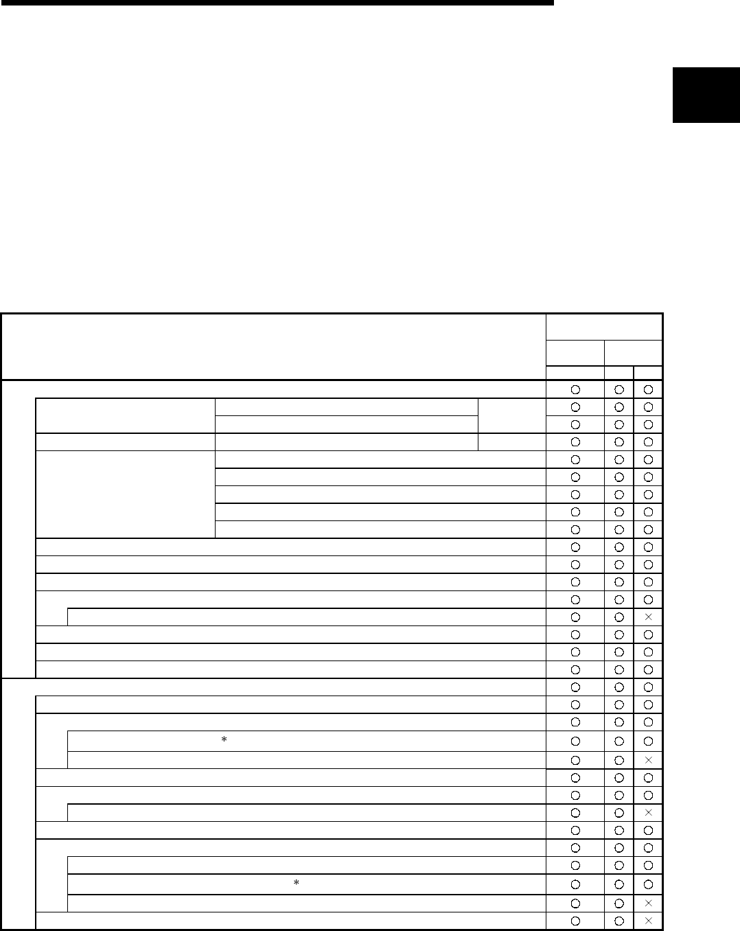
App. - 1 App. - 1
MELSEC-Q
APPENDIX
APPENDIX
Appendix 1 Functional Improvements of the Q Series C24
The Q series C24 of function version B has several functions that have been added or
changed from the conventional product (function version A).
This chapter explains a comparison of the functions of Q series C24/GX Configurator-
SC accompanied by the change/addition of functions, and explains how to utilize
programs created for function version A as well as how to incorporate function version
B modules into the existing system.
Appendix 1.1 Comparison of the Functions of Q Series C24/GX Configurator-SC
(1) Comparison of the functions of Q series C24
The following table shows the functions of Q series C24.
Q series C24
(function version)
QJ71C24N
(-R2/R4)
QJ71C24
(-R2)
Function
BBA
Communication using the MC protocol
Communication with QnA compatible 2C/3C/4C frame
Communication with ASCII code Communication with A compatible 1C frame
Formats 1 to 4
exist for each.
Communication with binary code Communication with QnA compatible 4C frame Format 5
Batch read/write in bit/word units
Monitoring of device memory
Batch read/write of multiple blocks
Read/write by extension designation
Read/write of device memory
Accessing other stations via network system
Reading/writing from/to the buffer memory of the Q series C24
Reading/writing from/to the buffer memory of intelligent function modules
Reading/writing from/to sequence program files
Monitoring the PLC CPUs (PLC CPU monitoring function)
Transmission of the monitoring information using the modem function.
Status control of the PLC CPUs (remote RUN/STOP, etc.)
Turning on/off input signals of the Q series C24 from an external device (global function)
Data transmission from a PLC CPU to an external device (on-demand function)
Communication using non-procedure protocol
Data transmission/reception in any format
Data transmission/reception using user frames
Data reception using format-0 ( 2)
Data reception using format-1
Data reception by interrupt programs
Monitoring the PLC CPUs (PLC CPU monitoring function)
Transmission of the monitoring information using the modem function.
ASCII data transmission/reception by ASCII-BIN conversion
Data transmission/reception by specifying transparent code
Specification of Receive transparent code
Specification of Transmission transparent 1st ( 3)
Multiple specification of Transmission transparent 2nd to 10th
Reception data clear by dedicated instruction (CSET instruction)
App.
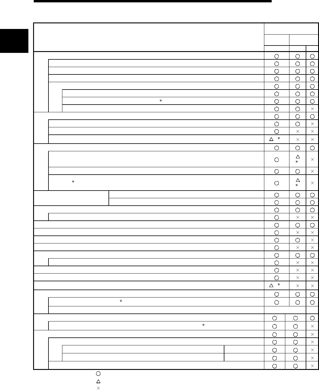
App. - 2 App. - 2
MELSEC-Q
APPENDIX
Q series C24
(function version)
QJ71C24N
(-R2/R4)
QJ71C24
(-R2)
Function
BBA
Communication using bidirectional protocol
Data transmission/reception in any format
Data reception by interrupt programs
ASCII data transmission/reception by ASCII-BIN conversion
Data transmission/reception by specifying transparent code
Specification of Receive transparent code
Specification of Transmission transparent 1st ( 3)
Multiple specification of Transmission transparent 2nd to 10th
Registration of user frame for data communication
Registration of changeable data (added 05H, 0BH, 11H, and 17H)
Registration of changeable data (added 04H and 0AH)
Registration of changeable data (added E5H and EBH) ( 1)
Communication via public network, etc. (modem function)
Automatic initialization of modem (1)
Remote password check
Callback ( 4)(1)
DC code control (including Xon/Xoff control)
Transmission control DTR/DSR (ER/DR) control
Mode switching
Switch to GX Developer connection mode
Independent/linked operation of each interface
Support for 230400 bps
Data transmission/reception at low speed (transmission speed: 50 bps)
Control of RS and DTR signal states
Data communication monitoring time
Non procedure and non reception monitoring time format designation
Transmission control start/end free area designation
Communication data monitoring function
UINI instruction ( 1)
Monitoring/testing of initial settings and setting values with utility package
Startup from the system monitor ( 5)
Addition to the setting items (See (2)) —
GX Developer and GOT connection
Simultaneous connection of GX Developer and GOT to the Q series C24 ( 6)
Support for multiple CPU system
Communication with non-control CPU using the MC protocol
Communication with QnA compatible 4C frame (ASCII code) Formats 1 to 4
Communication with QnA compatible 4C frame (binary code) Format 5
Multiple CPU setting using GX Developer (I/O assignment, switch setting, interrupt pointer setting, etc.)
: Usable
: Usable (Model serial no. [production date] limited)
: Usable
App.

App. - 3 App. - 3
MELSEC-Q
APPENDIX
1 There is a limitation in the production date of the Q series C24 that contains
functions that are usable.
For version verification, see section 2.6.
2 The data reception using format-0 refers to the method of receiving data by user
frame, which was supported in the Q series C24 of function version A.
3 The Q series C24 of function version A is capable of setting one pair of
transparent code and additional code per interface for both transmission and
reception.
4 This function can be used when connecting with GX Developer.
5 This function is available in GX Developer Version 6 or later.
6 GX Developer can only be connected to the CH1 side in case of the Q series C24
of function version A.
It is not possible to connect both GX Developer and the GOT to the two interfaces
at the same time.
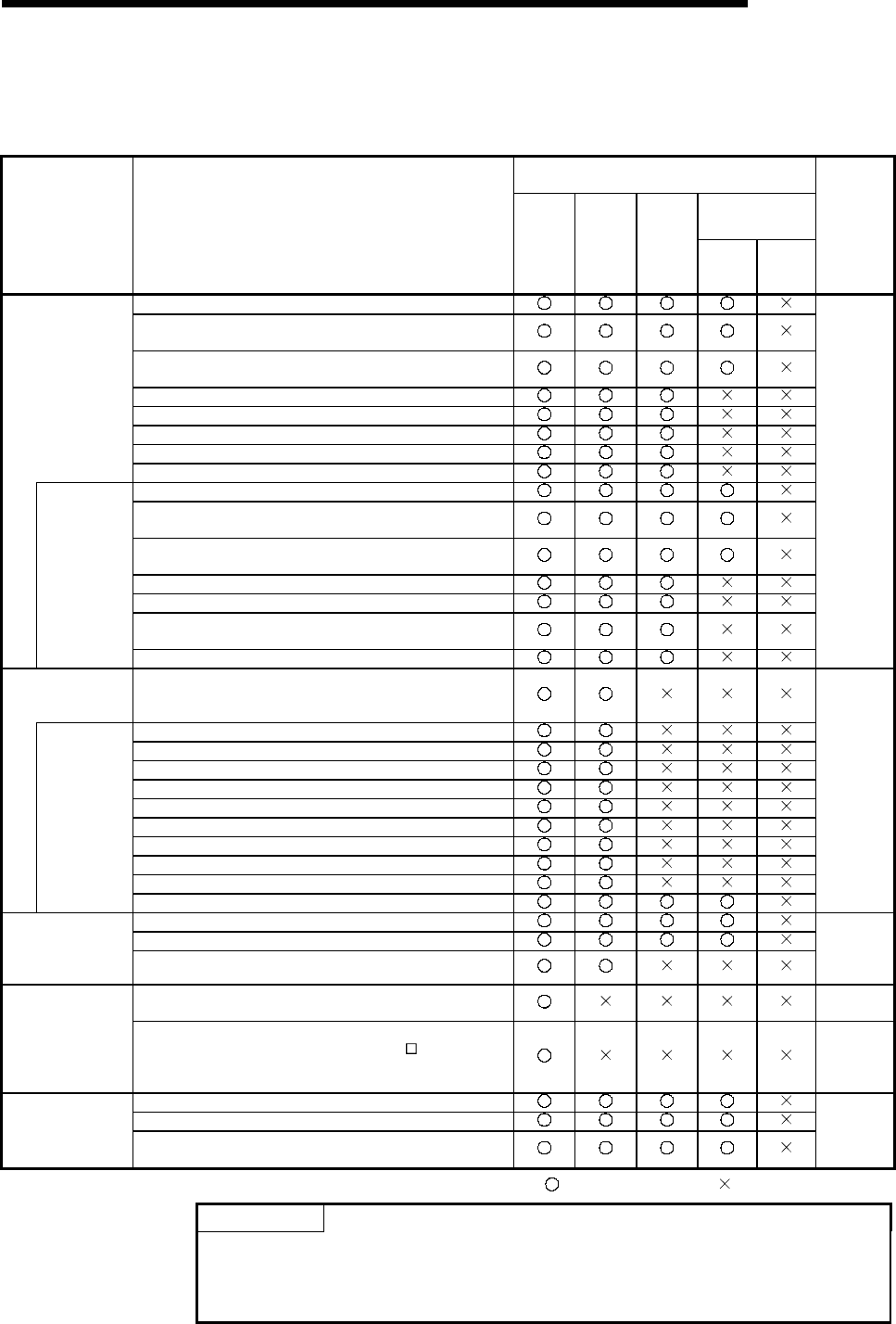
App. - 4 App. - 4
MELSEC-Q
APPENDIX
(2) List of added setting items for GX Configurator-SC
The following table lists the setting items added to the GX Configurator-SC due to
a software version upgrade.
GX Configurator-SC
Software version
SW0D5C-QSCU-E
Screen
(System
setting/monitor) Additional setting item Version
2.06G
Version
2.00A
Version
1.10L 40E,
30D,
20C
10B,
00A
Reference
section
Accumulated count of unlock process normal completion
Accumulated count of unlock process abnormal
completion
Accumulated count of lock process based on circuit
disconnect
Callback permit accumulated count
Callback denial accumulated count
Auto (callback) connection permit accumulated count
Auto (callback) connection denial accumulated count
Modem function
monitor/test
Accumulated count of callback receive procedure cancel
Circuit disconnect wait time (PLC CPU watch use)
Remote password mismatch notification count
designation
Remote password mismatch notification accumulated
count designation
Auto modem initialization designation
Callback function designation
Callback denial notification accumulated count
designation
Modem
function
system
setting
Data No. for callback designation 1 to 10
Section
8.4.4
Section
8.6.2
Transmission
control and other
monitoring/tests RS-232 control signal status CS (CTS)
RTS (RS) designation
DTR (ER) designation
Transmission control start free area
Transmission control end free area
Send/Recv data monitoring designation
Action for buffer full
Stop by Timer 0 error
Monitor buffer head address
Monitor buffer size
Transmission
control and
other system
settings
Transmission transparent code designation (2nd to 10th)
Section
8.4.5
Section
8.6.3
User frame receive format designation (1st to 4th)
Exclusive format-1 received data count (1st to 4th)
Non procedure
system setting
Non procedure
monitor/test Timeout at No-protocol
Section
8.4.7
Section
8.6.5
Station. No. (Instruction setting) Section
8.6.9
Monitor/test others Communication error clear request for CH and to turn
LED off
Section
8.6.9
Section
8.6.10
Accumulated count of unlock process normal completion
Accumulated count of unlock process normal completionAuto refresh
setting Accumulated count of lock process based on circuit
disconnect
Section
4.6
: Setting possible : Setting impossible
POINT
(1) GX Configurator-SC SW0D5C-QSCU-E 20C or later supports the Q series
C24 of function version B.
(2) See Section 2.6 of this manual for how to check the software version of GX
Configurator-SC.

App. - 5 App. - 5
MELSEC-Q
APPENDIX
Appendix 1.2 Precautions when Updating the Module from Function Version A to B
This section explains how to utilize programs created for the Q series C24 of function
version A for the Q series C24 of function version B and how to incorporate function
version B into the existing system.
(1) Program utilization
Programs created for the Q series C24 of function version A can be used as they
are for the Q series C24 of function version B.
(2) Incorporation into the existing system
The wiring used for function version A can be used as is for the Q series C24 of
function version B.
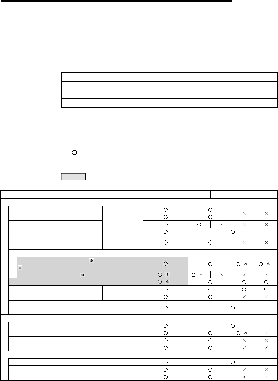
App. - 6 App. - 6
MELSEC-Q
APPENDIX
Appendix 2 QnA/A Series Module
This section explains a comparison of the functions of the Q series C24 and QnA/A
series modules, and explains how to utilize programs created for A series modules as
well as how to install the Q series C24 into the existing system.
QnA/A modules refer to the following products.
Model name Product name
QC24N AJ71QC24N (-R2,R4), A1SJ71QC24N (-R2)
QC24 AJ71QC24 (-R2,R4), A1SJ71QC24 (-R2)
UC24, C24-S8 AJ71UC24, A1SJ71UC24 (-R2,R4,PRF), AJ71C24-S8
Appendix 2.1 Functional Comparison with the Q series C24 and the QnA/A Series Modules
The following shows a functional comparison between the Q series C24 and the
QnA/A series modules.
The symbol in the model name columns indicates that the corresponding functions
are compatible between the applicable models (for more information, see the manual
for each module).
Indicates functions that have been added to or modified from the QnA/A
series modules.
Function Q series C24 QC24N QC24 UC24 C24-S8
Communication using MC protocol —
Communication in QnA compatible 3C frame
Communication in QnA compatible 4C frame
Communication in QnA compatible 2C frame
Communication in A compatible 1C frame
Communication
with ASCII code
Communication in QnA compatible 4C frame Communication
with binary code
Read/write of QCPU device memory —
Batch read/write of device memory ( 5)
Excluding multiple block batch read/write. ( 1) ( 1)
Multiple block batch read/write ( 5) ( 2) ( 2)
Accessing other stations (via network/data link) ( 3)
Arbitrary data
Transmission from the PLC CPU (on-demand) Using user frame
Communication with m:n connection between the PLC CPU and
external devices
Communication using non procedure protocol —
Transmitted/received with arbitrary format
Transmitted/received with user frame ( 4)
Transmitted/received with ASCII-BIN conversion
Transmitted/received with transparent code designation
Communication using bidirectional protocol —
Transmitted/received with arbitrary format
Transmitted/received with ASCII-BIN conversion
Transmitted/received with transparent code designation
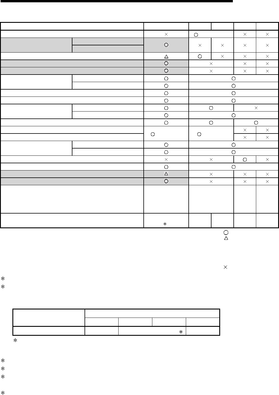
App. - 7 App. - 7
MELSEC-Q
APPENDIX
Function Q series C24 QC24N QC24 UC24 C24-S8
Accessing other stations with link dedicated instructions (via QC24 (N))
Non procedure protocol
Interrupt processing
(at data reception) Bidirectional protocol
Communication via public lines using modem function
Communication using the PLC CPU monitoring function
Auto refresh directed to the PLC CPU
DC code control
Transmission control DTR/DSR signal control
Half-duplex communication control
Mode switching
Setting the same protocol
Independent operation of two
interfaces Setting different protocols
Linked operation of two interfaces
Registering initial setting values of the buffer memory
Registering user frame (Flash ROM) (EEPROM)
1:1, 1:n
Connection forms with external
devices m:n
I/O signal transmission/receive by multi drop link function
Connection of GX Developer
Communication data monitoring
Registering and monitoring of setting values by the utility package
PLC that can be mounted
QCPU
MELSECNET/H
remote I/O station
QnACPU
MELSECNET/10,
Remote I/O station
ACPU
AnACPU
AnUCPU
QnACPU
ACPU
AnACPU
AnUCPU
QnACPU
Data transmission rate (bps) 230400 maximum
(6)
115200
maximum
19200
maximum
19200
maximum
19200
maximum
: Function exists/possible
: Function exists/possible
(specification is different
depends on the function
version (see Appendix 1)
: No function/impossible
1 Access is possible only within the range of an AnACPU device.
2 A multiple block batch read/write function can be used for the local station QCPU to which the Q series
C24 is mounted and the next CPU module, which will be another station, via MELSECNET/H,
MELSECNET/10.
PLC CPU
Function QCPU QnACPU Q2AS(H) Q4AR
Multiple block batch read/write (All allowed) (9707B or later products) (All allowed)
This function is added to modules showing 9707B or later in the package indication and the DATE
column of the rating plate.
3 Access to other stations cannot be performed via data link system (MELSECNET(II), MELSECNET/B).
4 Transmission is only possible using the printer function.
5 When the Q series C24 is used, it is possible to read/write a maximum of 960 words (in case of QC24(N), it
is possible to read/write a maximum of 480 words.)
6 230400 bps can be used via CH1 of QJ71C24N (-R2/R4) only.
The maximum transmission speed of QJ71C24 (-R2) is 115200 bps.

App. - 8 App. - 8
MELSEC-Q
APPENDIX
Appendix 2.2 Using Programs Designed for the QC24 (N) and Installing the Q Series C24
into Existing Systems
This section explains how to use programs designed for serial communication modules
in the QnA series and the installation of the Q series C24 into an existing system.
POINT
When using the Q series C24, make sure to set the operation mode, station
number, and transmission specifications with the following parameter setting
screen of GX Developer.
• "Intelligent function module switch setting" screen
The Q series C24 does not have the setting switches to set the operation mode,
station number, and transmission specification that are available in the serial
communication modules for QnA series.
Appendix 2.2.1 Using programs designed for the QC24 (N)
The data communication between the QnACPU and external devices as well as other
QnACPU which has been performed by QC24(N) can also be performed by the Q
series C24.
The following explains how to use programs designed for QC24(N) during data
communication using the Q series C24.
(1) The communication programs directed to the QC24(N) on the external device side
and the communication programs on the QnACPU (self-station) side to which the
QC24(N) is mounted can be used for the Q series C24.
However, note the following points.
• There is no function that allows data communication with other station's PLC
CPUs by a data link instruction.
Delete the part of data communication program by data link instructions.
• When using a new function, create a new program.
(2) Make sure to check operation when using communication programs for QC24(N)
on the external device side and the QnACPU (self-station) side.
(3) The notes during data communication by RS-422/485 interface also apply to the Q
series C24.
• Take measures against data error reception on the external device side (see
Section 3.3.3).
• Operation of RS-422/485 interface on the PLC side.
App. - 9 App. - 9
MELSEC-Q
APPENDIX
Appendix 2.2.2 Installing on existing systems
The following explains the Installation of the Q series C24 on an existing system.
(1) Installing on a multidrop connection system
The Q series C24 can be installed on an existing system to which the PLC CPU
and external devices are connected as 1:n or m:n multidrop connection ( 1).
1 This is when a QC24(N) or a computer link module (such as AJ71UC24) is
used as the PLC CPU module of the multidrop connection.
However, there are frame restrictions when data communication is performed.
(See the Reference Manual.)
(2) Replacing the QnACPU module with a QCPU
The wiring used by the QC24(N) can be used as is.
POINT
The functional use is the same, except for the functions added by the Q series C24
to the conventional module. However, with the introduction of high-speed QCPUs,
there may be cases in which communication cannot be performed normally when a
PLC module in the QnA series is replaced by a Q series PLC. When a module is
changed to a Q series PLC module, make sure to perform an operation check.

App. - 10 App. - 10
MELSEC-Q
APPENDIX
Appendix 2.3 Using Programs Designed for the Computer Link Module and Installing the Q
Series C24 into Existing Systems
This section describes how to use programs created for A series computer link
modules and installing the Q series C24 into an existing system.
POINT
When using the Q series C24, make sure to set the operation mode, station
number, and transmission specifications with the following parameter setting
screen of GX Developer.
• "Intelligent function module switch setting" screen
The Q series C24 does not have the setting switches to set the operation mode,
station number, and transmission specification that are available in the computer
link module for A series.
Appendix 2.3.1 Using programs designed for the computer link module
The data communication between the PLC CPU and external device as well as other
PLC CPU that has been performed by A series computer link modules (hereinafter
abbreviated as UC24/C24-S8) can also be performed using the Q series C24.
However, UC24/C24-S8 and the Q series C24 have major differences in the following
points.
For PLC CPU side, create a new program according to the explanation in the section
of the function used.
(Differences between UC24/C24-S8 and the Q series C24)
• Initial setting items and the setting method of addresses and special application
areas of the buffer memory
• Input/output signals for handshake
• Dedicated instructions of the PLC CPU
(1) Initial settings for special application area in buffer memory
1) In the Q series C24 the addresses for special application areas in the buffer
memory are different from those of UC24/C24-S8. The Q series C24 has
more initial setting items.
The setting method is different such that the settings are performed using the
utility package (GX Configurator-SC).
2) Register necessary initial setting values according to Chapter 8.
3) The default value for the CD terminal check setting is changed to "No check".
(2) Data communication using the MC protocol (identical to the
communication functions of the dedicated protocol of UC24/C24-S8)
(a) Communication protocol setting
Data communication is performed using an A compatible 1C frame by
setting the communication protocol setting of the Q series C24 specified by
GX Developer to the same form as set in the mode setting switch of
UC24/C24-S8.

App. - 11 App. - 11
MELSEC-Q
APPENDIX
(b) Command message and response message
1) The message format used in the data communication using the A
compatible 1C frame is the same as the message format of UC24/C24-S8.
2) Check available commands and devices that can be accessed in
Chapter 8 of the Reference Manual, and access the PLC CPU from the
external device.
3) For the QCPU, only read/write of device memory is possible.
For the range of devices that can be accessed, see Section 5.2.1 of the
Reference Manual.
The devices added to the QCPU, i.e. the latch relay (L), step relay
(S), and file register (R) devices, are accessed using commands for
QnA compatible 2C/3C/4C frames. It is necessary to create new
programs.
(c) Accessing other stations
1) When accessing other station's PLC CPU via the MELSECNET/10,
"Valid module during other station access" must be designated in the
parameter setting by GX Developer.
2) Check the stations that can be accessed in Chapter 5 of the Reference
Manual, and access the PLC CPU from the external device.
3) When it is necessary to access other stations on other MELSECNET/10,
data communication must be performed in a QnA compatible 3C/4C
frame.
Create a new program for the external device side according to Chapter
3 of the Reference Manual.
4) It is not possible to access other stations via the MELSECNET(II)/B.
(d) Transmitting data to the external device by the on-demand function
1) The program for data transmission on the PLC CPU side is different
from when UC24/C24-S8 is used.
Create a new program on the PLC CPU side according to Section 3.11
in the Reference Manual.
2) Data to be sent to the external device is identical to when the UC24/C24-
S8 is used.
(3) Data communication using the non procedure protocol
(a) Data transmission/reception
1) The same data transmission/reception as used by UC24/C24-S8 can be
performed.
2) Create a new program for data communication upon checking functions
and instructions used on the PLC CPU side in Chapter 6 of this manual
and Chapter 11 of the User's Manual (Application).
Data transmission/reception is performed using dedicated instructions.

App. - 12 App. - 12
MELSEC-Q
APPENDIX
3) When data is received by a reception end code, the external device side
must send the end code data (the default is CR+LF (code: 0DH and 0AH)
at the end of the data sent to the PLC CPU side.
Once any end code is registered, data can be transmitted in the same
way as for the UC24/C24-S8.
4) The external device side can receive data from the Q series C24 in the
same ways as UC24.
(b) Message transmission by printer function (when using programs designed
for UC24)
1) Message transmission using the printer function of the UC24 can be
implemented by the data transmission function that uses a user frame.
2) For the PLC CPU, register and send messages according to the User's
Manual (Application).
Messages handled by the UC24 will become user frames in the Q series
C24.
(4) Data communication using the bidirectional protocol
(a) Setting to add a sum check code to a message
The setting to add a sum check code to a message has been changed. It is
set during switch setting operation by GX Developer.
(b) Data transmission/reception
1) The same data transmission/reception as used by UC24/C24-S8 can be
performed.
2) Create a new program for data communication upon checking functions
and instructions used on the PLC CPU side in Chapter 7.
Data transmission/reception is performed using dedicated instructions.
3) The external device can transmission/receive data in the same way as
the UC24/C24-S8.
(5) Others
1) The Q series C24 has other functions that are equivalent to those of
UC24/C24-S8, which are not mentioned above.
2) Check functions and specifications in this manual and the manuals listed
below, and use the applicable functions.
• User's Manual (Application)
• Reference Manual

App. - 13 App. - 13
MELSEC-Q
APPENDIX
Appendix 2.3.2 Installing the Q series C24 into existing systems
This section shows the notes when installing the Q series C24 into an existing system
that uses UC24/C24-S8.
(1) Data communication using m:n connection
When the Q series C24 is installed into an existing system that has an m:n system
structure between the PLC CPU and external devices, and data communication is
performed using the MC protocol, the following notes should be considered:
(a) Accessing the PLC using a frame for form 5
When the UC24/C24-S8 is connected on the line, it is not possible to access
the PLC in the QnA compatible 4C frame (form 5) for binary code
communication.
(b) Data communication between external devices
1) When data communication is performed in order to link with an external
devices to perform a 1:1 communication with the PLC CPU, it is
necessary to change the station number (80H to A0H 00H to 1FH)
designated in the "Station number" and "Local station number" items in
the messages on the external device side. (It is not necessary to specify
this when an A compatible 1C frame is used.)
Alternatively, it is necessary to change the message frame so that it has
a data order different from that of the MC protocol.
• Station number: Designate the number of device to which data is sent
• Local station number: Designate the number of the device that sends
data
2) Perform the data communication according to Chapter 14 of the User's
Manual (Application).
(c) Processing reception data on the external device side
Set the external device so that it ignores the following reception messages
that are unrelated to the local station.
• The command message and the corresponding response message that
are sent from other stations when accessing the PLC CPU using the MC
protocol.
• Messages when accessing between external devices.
(2) Data communication using 1:n connection
When the UC24/C24-S8 is connected on the line, it is not possible to access the
PLC in the QnA compatible 4C frame (format 5) for binary code communication.
POINT
Since performances and response speeds are different between the Q series C24
and the UC24/C24-S8, communication may not be performed normally when a
PLC module in the A series is replaced by a Q series PLC.
When a module is changed to a Q series PLC module, make sure to check
operation.
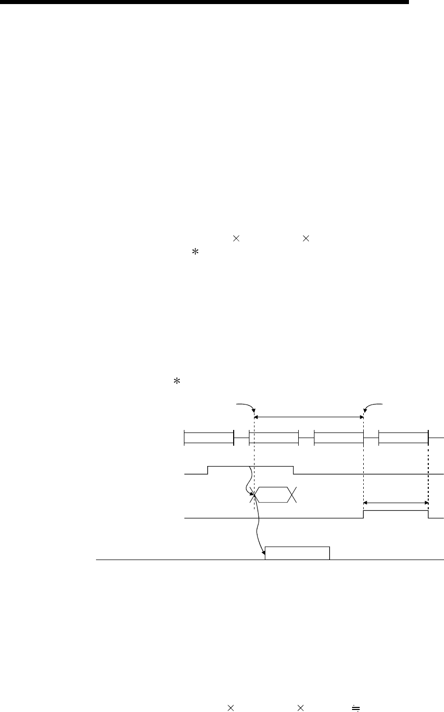
App. - 14 App. - 14
MELSEC-Q
APPENDIX
Appendix 3 Processing Time
(1) Time required to process communication using the non procedure
protocol (guideline)
The processing time for the Output and Input instructions can be estimated by
the following formula. Note, however, that the processing time may become
longer depending on other communication functions (e.g., communication using
the MC protocol) and special functions (e.g., ASCII-binary conversion,
transmission control) that are used at the same time.
The value obtained from the following formula should be used as a guideline for
the processing time when reception or transmission only is performed using only
CH1 (RS-232 connection).
(a) Output instruction
Tp = St + (Dle/Cr 1000 + 0.07) Ds + T1
Tp ( 1): The time from the start of execution of the Output instruction
to the End processing of the sequence scan at the
completion of the Output instruction execution (ms)
St : Scan time
Dle : Data length of 1 byte at data transmission (number of bits)
Cr : Communication rate (bps)
Ds : Number of bytes of transmission data
T1 : QJ71C24N (-R2/R4) T1 = 3.0
QJ71C24 (-R2) T1 = 4.86
1 This stands for the time range of processing (Tp).
Sequence program
Transmission command
Output instruction
Output instruction
complete device
OUTPUT
Step 0 END
Tp
One scan
Q series C24 side
External device side
Transmission data
Start of the Output
instruction execution
Start of the End processing of
the scan at the completion of
the Output instruction execution
[Calculation example]
Estimate the time required to process the Output instruction when
transmitting 100 bytes of data using the non procedure protocol with the
QJ71C24N. (Unit: ms)
• Scan time : 10 ms
• Data length : 10 bits (1 start bit, 8 data bits, 1 stop bit, no parity
bit)
• Communication rate : 19200 bps
10 + (10/19200 1000 + 0.07) 100 + 3.0 72.08 (ms)
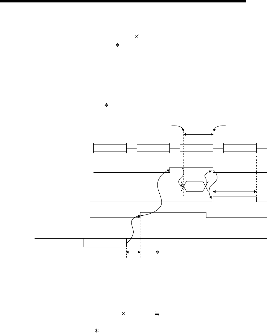
App. - 15 App. - 15
MELSEC-Q
APPENDIX
(b) Input instruction
Tp = Sr + 0.09 Dr + T2
Tp ( 1) : Time from the start of execution of the Input instruction to the
End processing of the sequence scan at the completion of
the Input instruction execution (ms)
Sr : Scan time
Dr : Number of bytes of reception data
T2 : QJ71C24N (-R2/R4) T2 = 7.0
QJ71C24 (-R2) T2 = 14.91
1 This stands for the time range of processing (Tp).
Sequence program
Reception data read
request (X3)
Input instruction
Input instruction
complete device
Step 0 END
Tp
1 scan
Q series C24 side
External device side
Start of the Input
instruction execution
the Input instruction execution
(DX3)
Start of the End processing of
the scan at the completion of
INPUT
2ms ( 2)
Reception data
[Calculation example]
Estimate the time required to process the Input instruction when receiving
100 bytes of data using the non procedure protocol with the QJ71C24N.
(Unit: ms)
• Scan time : 10 ms
10 + 0.09 100 + 7.0 26.00 (ms)
2 When only using CH1 of the Q series C24 and when processing only
30 bytes of data received, the time until the reception data read request
(X3) comes on is displayed after the Q series C24 receives data from
the network.
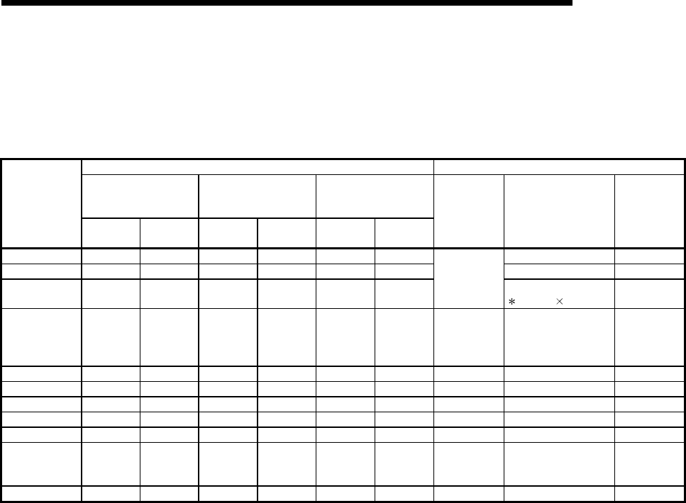
App. - 16 App. - 16
MELSEC-Q
APPENDIX
2) Processing time of dedicated instructions
The following table shows the operation processing time (rough
standard) of each dedicated instruction.
The operation processing time differs slightly depending on the system
configuration and communication protocol.
Processing time (unit: ms) Instruction execution condition
Q02H/Q06H/Q12H/
Q25H/Q12PH/Q25PH
CPU
Q02CPU Q00J/Q00/ Q01CPU
Instruction name
QJ71C24N
(-R2/R4)
QJ71C24
(-R2)
QJ71C24N
(-R2/R4)
QJ71C24
(-R2)
QJ71C24N
(-R2/R4)
QJ71C24
(-R2)
Transmission
speed
Transmission/receive
(registered) data count Others
ONDEMAND 48.0 51.5 48.6 52.2 49.7 53.6 40 bytes Send in form 3
OUTPUT 23.4 24.8 23.8 25.3 25.6 26.7 40 bytes —
PRR 23.3 26.8 24.2 27.0 25.1 28.3
19200 bps
Data size: 8
Stop bit: 1
Parity: none
40 bytes
8 bytes 5 frames —
INPUT 3.4 9.9 3.9 9.9 4.9 10.0 — 40 bytes
Execute
instruction after
40 bytes have
been received.
BIDOUT 28.6 47.0 30.5 47.1 32.6 49.6 — 40 bytes —
BIDIN 26.4 29.1 27.6 29.9 29.8 31.7 — 40 bytes —
PUTE 881.9 881.9 884.4 884.4 871.4 899.5 — 40 bytes —
GETE 1.1 1.1 1.5 1.5 3.1 3.2 — 40 bytes —
SPBUSY 0.1 0.1 0.2 0.2 0.3 0.3 — — —
CSET 1.0 1.2 1.6 1.7 3.4 3.9 — —
Transmission/
receipt buffer
setting
BUFRCVS 0.3 0.3 0.5 0.5 — — 19200 bps 40 bytes —
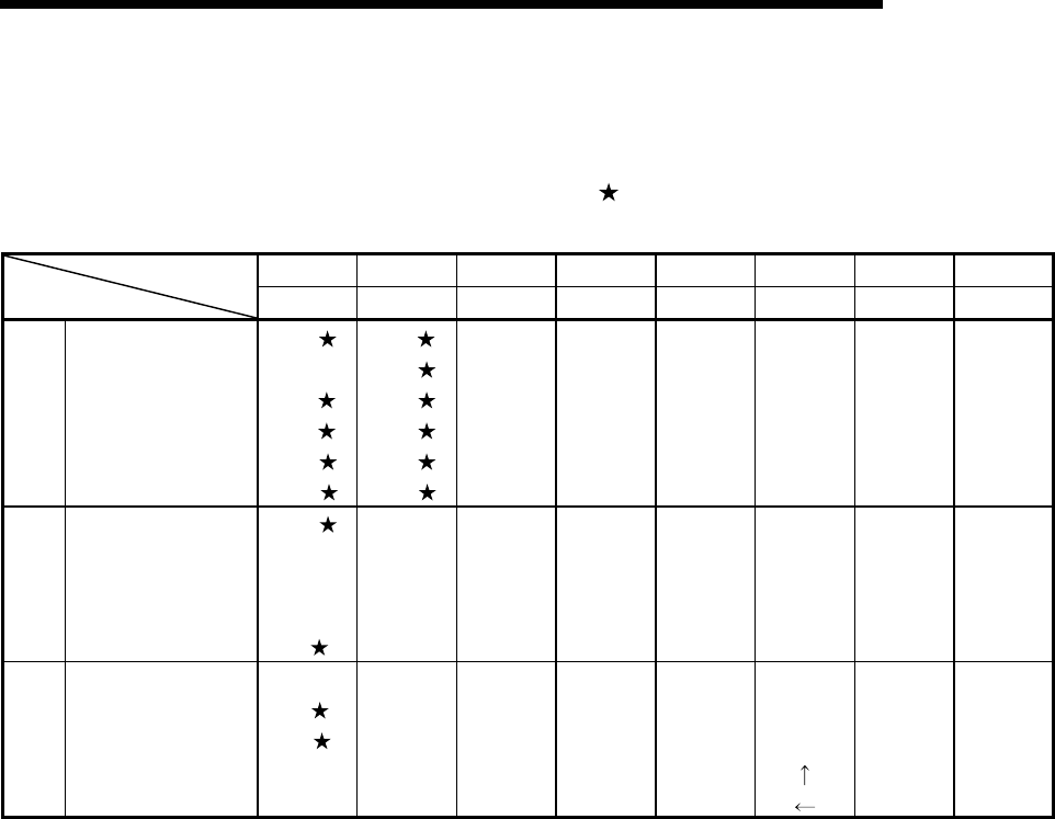
App. - 17 App. - 17
MELSEC-Q
APPENDIX
Appendix 4 ASCII-Code Table
The ASCII-code table is shown below. (7-bit code)
The codes 00H to 1FH indicated by the are used as Q series C24 control codes. (DC
codes 11H to 14H can be changed by the user.)
01234567
MSD
LSD 000 001 010 011 100 101 110 111
0
1
2
3
4
5
0000
0001
0010
0011
0100
0101
NUL
SOH
STX
ETX
EOT
ENQ
DLE
DC1
DC2
DC3
DC4
NAK
SP
!
"
#
$
%
0
1
2
3
4
5
@
A
B
C
D
E
P
Q
R
S
T
U
‚
a
b
c
d
e
p
q
r
s
t
u
6
7
8
9
A
0110
0111
1000
1001
1010
ACK
BEL
BS
HT
LF
SYN
ETB
CAN
EM
SUB
&
/
(
)
*
6
7
8
9
:
F
G
H
I
J
V
W
X
Y
Z
f
g
h
i
j
v
w
x
y
z
B
C
D
E
F
1011
1100
1101
1110
1111
VT
FF
CR
SO
SI
ESC
FS
GS
RS
US
+
,
.
/
;
<
=
>
?
K
L
M
N
O
[
\
]
k
l
m
n
o
{
|
}
~
DEL
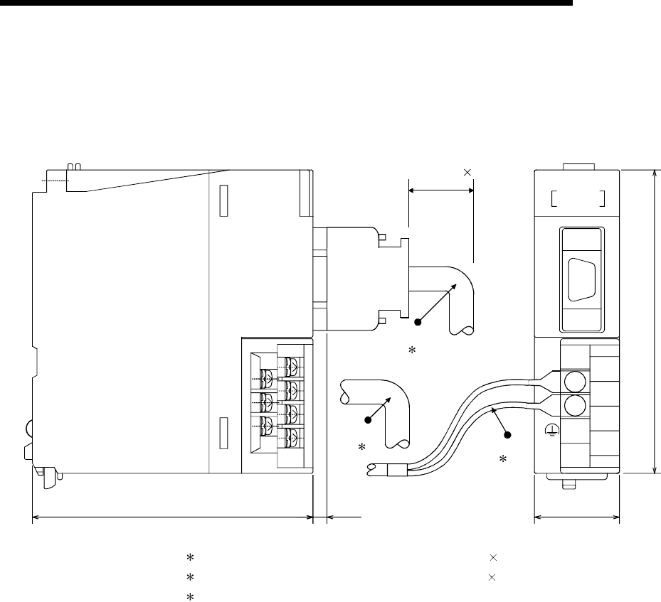
App. - 18 App. - 18
MELSEC-Q
APPENDIX
Appendix 5 External Dimensions
(1) QJ71C24N, QJ71C24
The following diagram shows the QJ71C24 and QJ71C24N. The dimensions of
the QJ71C24 are the same as QJ71C24N (except for model name).
R1
( 1)
90 (3.54)
98 (3.86)
4.5
(0.18)
ERR.
CH2
CH1 SD
RD
NEU.
SD NEU.
RD
RUN
5
3
1
6
7
(FG)
RS-232
/485
RS-422
CH2
RDB
RDA
SDB
SDA
CH1
27.4 (1.08)
QJ71C24N
r1
( 3)
R2
Cable diameter 4 + 10
( 2)
(Unit: mm (in.))
1: R1 (Bending radius near terminal block): Cable diameter 4
2: R2 (Bending radius near connector) : Cable diameter 4
3: r1 (Bending radius near crimp contact) : Connectable as long as not bended extremely
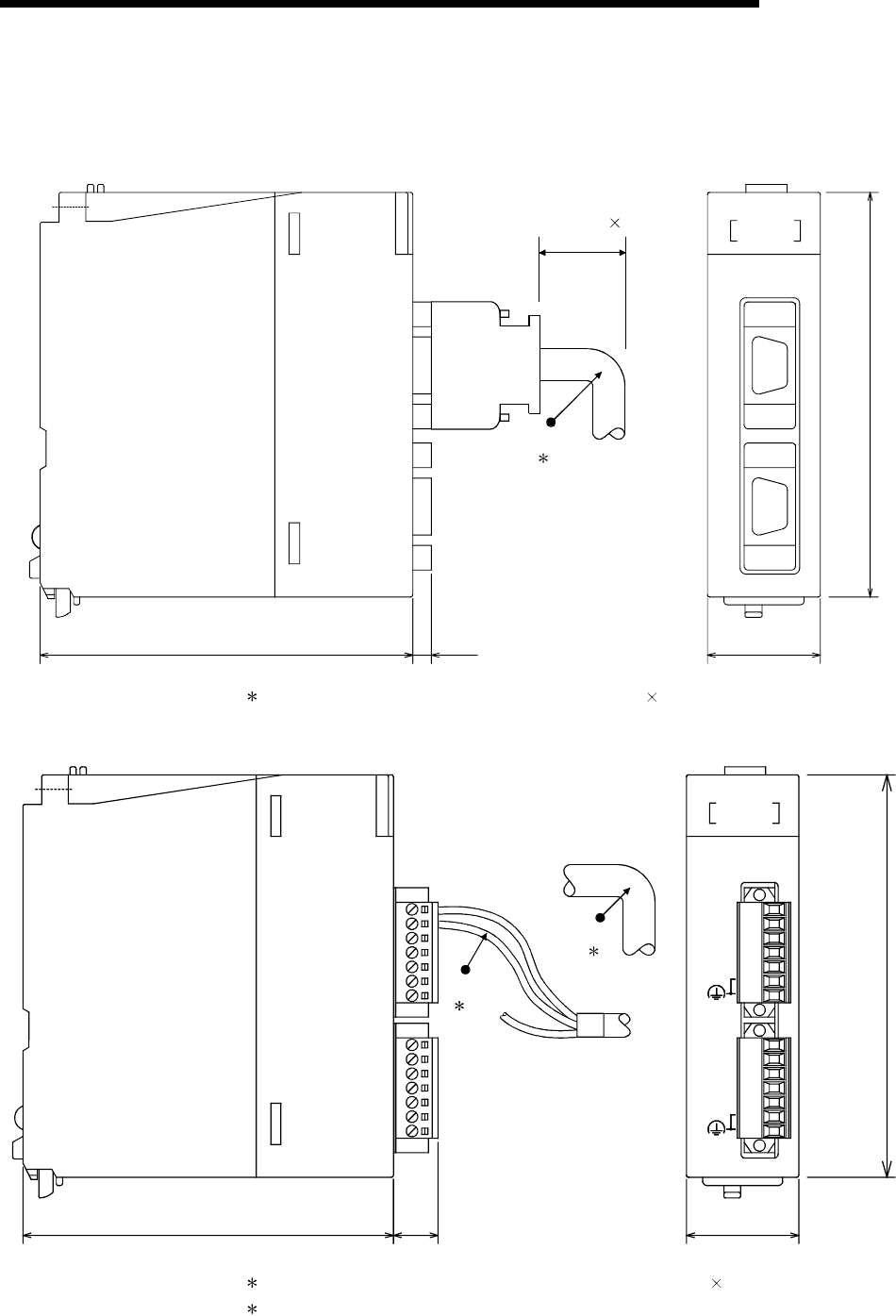
App. - 19 App. - 19
MELSEC-Q
APPENDIX
(2) QJ71C24N-R2, QJ71C24-R2
The following diagram shows the QJ71C24-R2 and QJ71C24N-R2. The
dimensions of the QJ71C24-R2 are the same as QJ71C24N-R2 (except for
model name).
R2
98 (3.86)
4.5
(0.18)
90 (3.54)
ERR.
CH2
CH1 SD
RD
NEU.
SD NEU.
RD
RUN
QJ71C24N-R2
27.4 (1.08)
QJ71C24N-R2
RS-232
RS-232
CH2
CH1
( 1)
(Unit: mm (in.))
Cable diameter 4 + 10
1: R2 (Bending radius near connector) : Cable diameter 4
(3) QJ71C24N-R4
11.5
(0.45)
98 (3.86)
90 (3.54)
QJ71C24N-R4
CH2
CH1
RS-422/485
RS-422/485
27.4 (1.08)
QJ71C24N-R4
(FG)
SG
RDB
RDA
SDB
SG
RDB
RDA
SDB
SDA
SDA
(FG)
RUN
RD
NEU.
SD
NEU.
RD
SD
CH1 CH2
ERR.
R3
( 1)
r2
( 2)
(Unit: mm (in.))
1: R3 (Bending radius near the plug-in socket block): Cable diameter 4
2: r2 (Bending radius near the wire connection) : Connectable as long as not bended extremely

App. - 20 App. - 20
MELSEC-Q
APPENDIX
Appendix 6 Example of Connection when a Converter is Used
The following shows an example of a connection where the RS-232 to RS-422/485
converters are used in order to communicate data using data communication functions
with the MC, non-procedure, or bidirectional protocol.
The converters covered in the Appendix are as follows:
Manufacturer
Model name
(Recommended
product)
Contact Tel No.
Fax No.
EL Engineering Ltd. EL-LINE-II Funato-cho 7-16, Nakagawa-ku,
Nagoya, 454-0805
Tel: (052) 361-2290
Fax: (052) 363-1050
System Sacom Co., Ltd.
KS-1
KS-10P
KS-485
Shibuya Property West Bldg 12F,
Higashi 1-32-12 , Shibuya-ku,
Tokyo, 150-0011
Tel: (03) 3797-0211
Fax: (03) 3797-0231
A recommended product is a product that this company has verified and has found to satisfy this company’s standards.
When using this products, use it so that it conforms to the recommended product’s specifications (standards).
(1) Combination between available converters and connections
Q series C24 side
connection interface
System configuration
with external devices
External device
interface Available converter Description No. of
connection example
EL-LINE-II Connection example 1
RS-422 KS-1
KS-10P Connection example 2
RS-232 1:1
RS-485 KS-485 Connection example 3
RS-422/485 1:1, 1:n, m:n RS-232 KS-485 Connection example 4
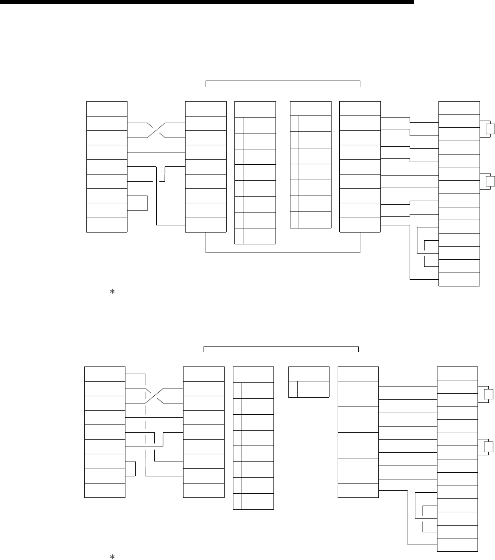
App. - 21 App. - 21
MELSEC-Q
APPENDIX
(2) Connection example
(Connection example 1)
CD
RD
SD
DTR
SG
DSR
RS
CS
RI
FG
TXD
RXD
RTS
CTS
DTR
DSR
CD
SG
RS232 signal
SW1
1
2
3
4
5
6
7
8
OFF
ON
OFF
ON
OFF
ON
OFF
ON
SW2
OFF1
2
3
4
5
6
7
OFF
OFF
OFF
OFF
OFF
OFF
TX
RX
RTS
CTS
SG
RS422 signal
FG
External device side
RDA
RDB
SDA
SDB
DSRA
DSRB
DTRA
DTRB
RTSA
RTSB
CTSA
CTSB
1 or 14
20
7
16
3
19
6
15
2
(EL-LINE-II)
SG
R
R
1
2
3
4
5
6
7
8
9
1
2
3
4
5
20
6
8
7
Q series C24 side
• The CD terminal check setting should be set to "No check" according to the explanation in Section 3.2.1 (1).
• DC code control or DTR/DSR control becomes possible for transmission control.
(Connection example 2)
CD
RD
SD
DTR
SG
DSR
RS
CS
RI
FG
RD
SD
CS
RS
ER
SG
CD
DR
RS232 signal
SW1
1
2
3
4
5
6
7
8
ON
ON
OFF
OFF
ON
ON
ON
ON
SW2
ON1
SG
RS485 signal
FG
External device side
RDA
RDB
SDA
SDB
DSRA
DSRB
DTRA
DTRB
RTSA
RTSB
CTSA
CTSB
(KS-1/KS-10P)
SG
R
R
1
2
3
4
5
6
7
8
9
1
2
3
4
5
6
7
8
9
FG
(+)
DATA
OUT
(-)
(+)
DATA
IN
(-)
(+)
CONT
OUT
(-)
(+)
CONT
IN
(-)
1
19
25
15
17
14
16
21
7
23
Q series C24 side
• The CD terminal check setting should be set to "No check" according to the explanation in Section 3.2.1 (1).
• DC code control or DTR/DSR control becomes possible for transmission control.
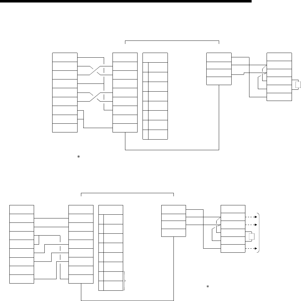
App. - 22 App. - 22
MELSEC-Q
APPENDIX
(Connection example 3)
CD
RD
SD
DTR
SG
DSR
RS
CS
RI
FG
RD
SD
CS
ER
SG
DR
TC
CNT
RS232 signal
SW1
1
2
3
4
5
6
7
8
ON
ON
ON
OFF
OFF
OFF
ON
ON
RS485 signal
FG
External device side
SDA
SDB
RDA
RDB
SG
(KS-485)
1
2
3
4
5
6
7
8
9
1
2
3
5
6
7
20
24
25
SG 1
TRD+
TRD-
FG
2
3
9
R
Q series C24 side
• Data communication can be made in half-duplex communication.
• The CD terminal check setting should be set to "No check" according to the explanation in Section 3.2.1 (1).
• Transmission control cannot be used.
(Connection example 4)
FG
SD
RD
RS
CS
DSR
SG
CD
DTR
External device side
FG
RD
SD
CS
ER
SG
DR
TC
CNT
RS232 signal
SW1
1
2
3
4
5
6
7
8
ON
ON
ON
OFF
OFF
OFF
OFF
OFF
RS485 signal
FG
SDA
SDB
RDA
RDB
SG
(KS-485)
1
2
3
5
6
7
20
24
25
SG 1
TRD+
TRD-
FG
2
3
9
R
These switches should
be ON when the KS-485
is at the terminal of the
line.
When connecting
with other stations
Q series C24 side
• Data communication can be made
in half-duplex communication.
• Transmission control cannot be used.
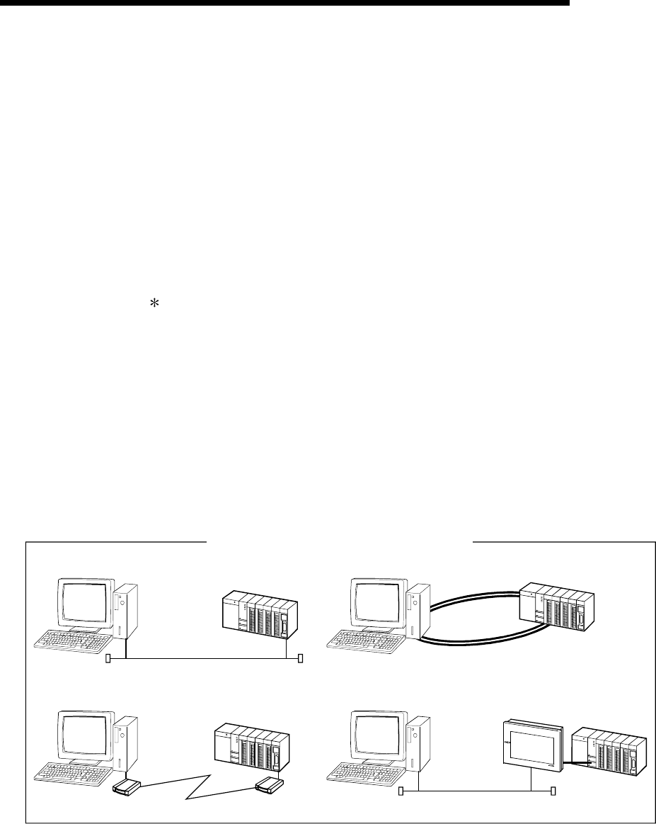
App. - 23 App. - 23
MELSEC-Q
APPENDIX
Appendix 7 Communication Support Tool (MX Component)
MX Component is an ActiveX control library that supports any types of communication
paths between IBM PC/AT compatible personal computers and PLCs. It allows the
users to establish communication using simple processing only, without having to
know about the different communication protocols used in the individual
communication.
It also supports various programming languages, allowing for a wide range of
application development.
This section provides the overview of the functions provided by MX Component and
explains the procedure up to creation of applications.
See Operating Manual and Programming Manual of MX Component for the details.
Appendix 7.1 Overview of MX Component
This section provides the overview of MX Component.
Different communication paths, operating systems, programming languages, and
functions are supported depending on the version of MX Component used.
(1) Support for a wide range of communication paths to PLCs
MX Component supports a wide range of communication paths to PLCs. It is
possible to construct systems according to the needs of the users.
Ethernet communication
Modem communication
MELSECNET/H communication
GOT
Gateway function communication
<Example of communication using MX Component>
(2) Dramatic improvement of application development efficiency
MX Component provides wizard-style communication setting utilities.
The user only needs to select settings from menus displayed on the screen in an
interactive manner to achieve the communication settings required to access the
target PLC CPU.
Moreover, once the communication setting has been performed, it is possible to
access the PLC CPU simply by specifying the logical station number that is
stored via the communication setting utilities.
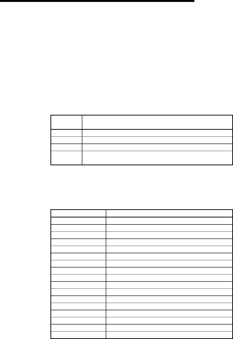
App. - 24 App. - 24
MELSEC-Q
APPENDIX
(3) Support for wide choice of basic operating systems
MX Component can run on IBM PC/AT compatible personal computers running
the following basic operating systems:
• Microsoft® Windows® 95 Operating System
• Microsoft® Windows® 98 Operating System
• Microsoft® Windows NT® Workstation Operating System Version 4.0
• Microsoft® Windows® Millennium Edition Operating System
• Microsoft® Windows® 2000 Professional Operating System
• Microsoft® Windows® XP Professional Operating System
• Microsoft® Windows® XP Home Edition Operating System
(4) Support for a wide variety of programming languages
MX Component supports the following programming languages.
It allows the user to develop a wide range of customized applications.
Programming
language
Development software
Visual Basic®Microsoft® Visual Basic® 6.0
Visual C++®Microsoft® Visual C++® 6.0
VBScript Text editors and commercially available HTML tools
VBA Microsoft® Excel 2000, Microsoft® Excel 2002,
Microsoft® Access 2000 or Microsoft® Access 2002
(5) Support for functions dedicated for data communication with PLCs
MX Component provides the functions necessary for data communication with
PLCs, including functions for opening/closing communication lines and
reading/writing devices.
Multi-function communication programs can thus easily be developed with MX
Component.
Function name Function
Connect Connects a telephone line.
Open Opens a communication line.
Close Closes a communication line.
Disconnect Disconnects a telephone line.
GetErrorMessage Displays error definition and corrective action.
ReadDeviceBlock Batch-reads data from devices. (LONG type)
WriteDeviceBlock Batch-writes data to devices. (LONG type)
ReadDeviceBlock2 Batch-reads data from devices. (SHORT type/INT type)
WriteDeviceBlock2 Batch-writes data to devices. (SHORT type/INT type)
ReadDeviceRandom Randomly reads data from devices. (LONG type)
WriteDeviceRandom Randomly writes data to devices. (LONG type)
ReadDeviceRandom2 Randomly reads data from devices. (SHORT type/INT type)
WriteDeviceRandom2 Randomly writes data to devices. (SHORT type/INT type)
SetDevice Sets one device. (LONG type)
GetDevice Acquires the data of one device. (LONG type)
SetDevice2 Sets one device. (SHORT type/INT type)
GetDevice2 Acquires data of one device. (SHORT type/INT type)

App. - 25 App. - 25
MELSEC-Q
APPENDIX
Function name Function
ReadBuffer Reads from buffer memory.
WriteBuffer Writes to buffer memory.
GetClockData Reads clock data from PLC CPU.
SetClockData Writes clock data to PLC CPU.
GetCpuType Reads a PLC CPU type.
SetCpuStatus Remote RUN/STOP/PAUSE of PLC CPU
EntryDeviceStatus Registers device status monitor.
FreeDeviceStatus Deregisters device status monitor.
OnDeviceStatus Announces event.
(6) Collecting data on Excel without programming
Using MX Component and MX Sheet (SWnD5C-SHEET-E) allows users to
collect PLC device data on Excel with only simple setting and without any
programming.
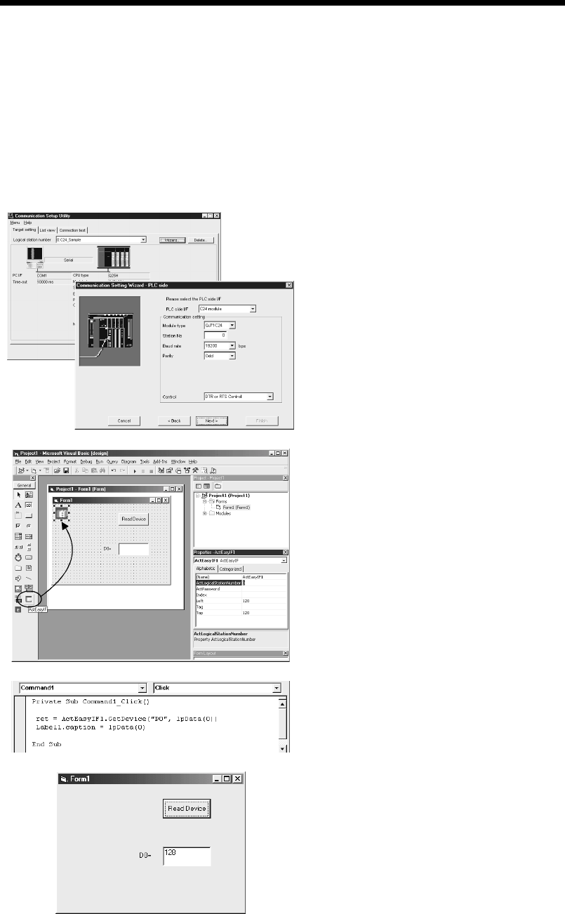
App. - 26 App. - 26
MELSEC-Q
APPENDIX
Appendix 7.2 Usage Procedure of MX Component
This section explains the procedure for creating programs and sample programs using
MX Component.
(1) Procedure for creating programs
The procedure for creating programs is outlined below.
The usage procedure below uses Visual Basic® as an example.
1) Perform the communication settings from a IBM
PC/AT compatible personal computer to the PLC by
following the wizard. (Some types of controls are set
only by programs without using the wizard.)
The wizard allows the user to perform the settings
required for the communication such as logical
station number, connected module type, and PLC to
be connected.
↓
2) Paste the ACT control icon onto the form and assign
the logical station number set in step 1 to the
property of the pasted control.
↓
3) Use the functions provided by the software to write a
program that reads the device data.
↓
Completed
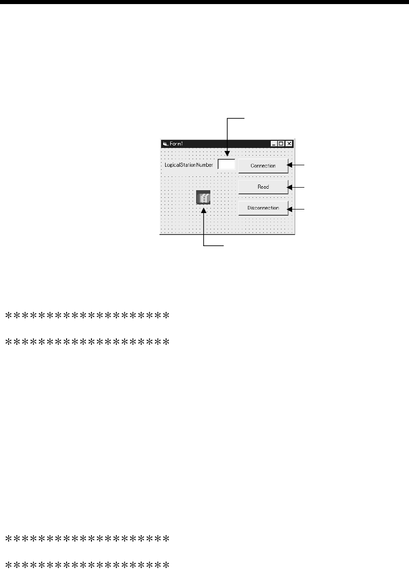
App. - 27 App. - 27
MELSEC-Q
APPENDIX
(2) Sample program
The following sample program reads D0 to D4 (five points) of the target PLC
using the logical station number.
(a) When Visual Basic® is used
1) Screen example (Form1)
Command1
' Connect to the communication line.
Command2
' Read the device data.
Command3
' Cut the communication line.
Text1
' Enter the logical station number.
ACT control (ActEasy IF)
' ACT control for utility setting type
2) Program example
Private Sub Command1_Click()
'
' Connection
'
Dim rtn As Long
' Get LogicalstationNumber
ActEasyIF1. ActLogicalStationNumber = Val(Text1.Text)
' Connection
rtn = ActEasyIF1. Open()
If rtn = 0 Then
MsgBox "The connection was successful"
Else
MsgBox "Connection Error:" & Hex(rtn)
End If
End Sub
Private Sub Command2_Click()
'
' Read
'
Dim rtn As Long
Dim idata(5) As Integer
' D0-D4 are read
rtn = ActEasyIF1. ReadDeviceBlock2 ("D0", 5, idata(0))
If rtn = 0 Then
MsgBox "D0-D5 = " & idata(0) & ", " & idata(1) & ", " & idata(2) & ", " & idata(3) & "," & idata(4)
Else
MsgBox "Read Error:" & Hex(rtn)
End If
End Sub

App. - 28 App. - 28
MELSEC-Q
APPENDIX
Private Sub Command3_Click()
'
' Disconnection
'
Dim rtn As Long
' Disconnection
rtn = ActEasyIF1. Close()
If rtn = 0 Then
MsgBox "The disconnection was successful"
Else
MsgBox "Disconnection Error:" & Hex(rtn)
End If
End Sub
(b) When Visual C++® is used
//
// Connection
//
void CVCDlg::OnOpen()
{
long lRet;
CString szMessage;
UpdateData();
// Get LogicalStationNumber
m_actEasyIF. SetActLogicalStationNumber ( m_lLogicalStationNumber ):
// Connection
lRet = m_actEasyIF. Open();
if ( lRet == 0) {
MessageBox ( "The connection was successful" )
} else {
szMessage. Format ( "Connection Error: %x", lRet );
MessageBox ( szMessage )
}
}

App. - 29 App. - 29
MELSEC-Q
APPENDIX
//
// Read
//
void CVCDlg::OnRead()
{
long lRet;
short sData[5];
CString szMessage;
// D0-D4 are read
lRet = m_actEasyIf. ReadDeviceBlock2 ( "D0", 5, sData );
if ( lRet == 0) {
szMessage. Format ( "D0-D5 = %d, %d, %d, %d, %d",
sData[0], sData[1], sData[2], sData[3], sData[4] );
MessageBox ( szMessage );
} else {
szMessage. Format ( "Read Error: %x", lRet );
MessageBox ( szMessage )
}
}
//
// Disconnection
//
void CVCDlg::OnOpen()
{
long lRet;
CString szMessage;
// Disconnection
lRet = m_actEasyIF. Close();
if ( lRet == 0) {
MessageBox ( "The disconnection was successful" )
} else {
szMessage. Format ( "Disconnection Error: %x", lRet );
MessageBox ( szMessage )
}
}
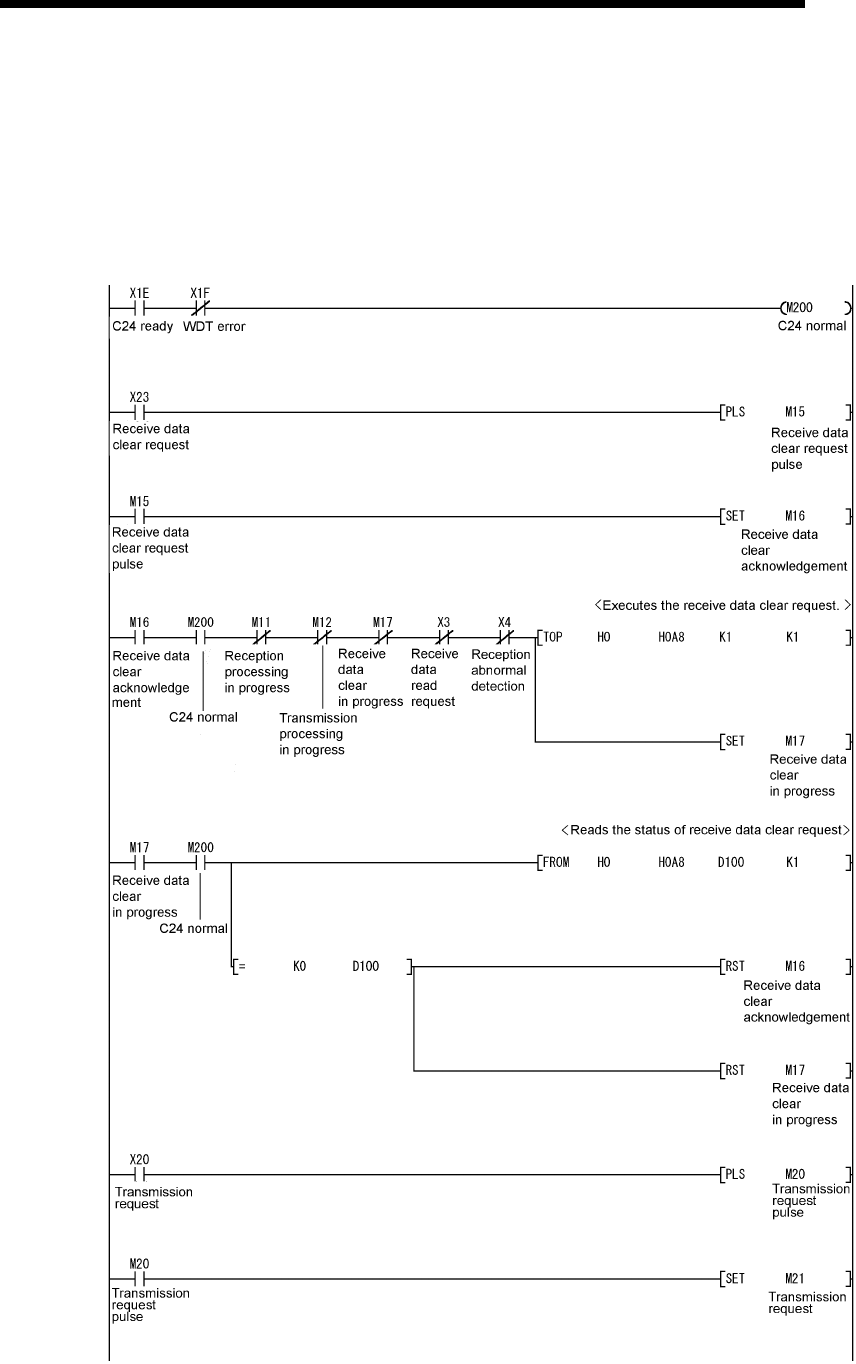
App. - 30 App. - 30
MELSEC-Q
APPENDIX
Appendix 8 Example of Clear Process Program for Receive Data
When performing data communications with non procedure protocol, use the receive
data clear request shown in 6.1.4. and display the sequence program example if
clearing the receive data from external device. (If the Q series C24 input/output signal
is X/Y000 to X/Y01F.)
The following I/O signals (X) and internal relays (M) are used in the program.
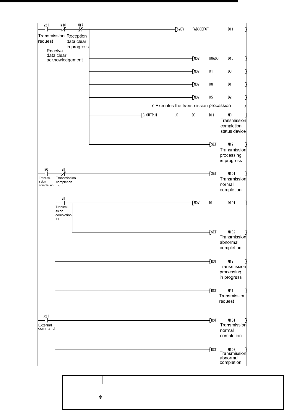
App. - 31 App. - 31
MELSEC-Q
APPENDIX
POINT
When a function version A for the Q Series C24 is used, add the partial circuit
(shown with 1) shown in the program example in Section 6.1.4 (3).
(Communications are possible when M19 is ON.)
App. - 32 App. - 32
MELSEC-Q
APPENDIX
Appendix 9 Program Examples for Using Q Series C24 at MELSECNET/H Remote I/O
Station
Appendix 9.1 System configuration and program conditions
(1) System configuration
The system configuration used in the program examples of this section is shown
below.
GX Developer
MELSECNET/H (remote I/O net)
network No.1
QJ71LP21-25
Remote master station
( 2)
Control target
QJ71C24N( 1)
QJ72lP25-25
Remote I/O station
(Station No.1)
1 It is assumed that the QJ71C24N is mounted on Slot 0 of the base unit and
the starting I/O No. is "0".
2 Set the network parameters of the remote master station as shown below.
1) Network type : MNET/H (Remote master)
2) Starting I/O No. : 0000H
3) Network No. : 1
4) Total stations : 1
5) Mode : Online
6) Network range assignment (XY setting)
7) Refresh parameters
App. - 33 App. - 33
MELSEC-Q
APPENDIX
(2) Program example for interlocking the remote master station and
remote I/O station
Interlocks should be applied to the programs according to the link status of the
remote master station (host station) and remote I/O station (other station).
The following example shows an interlock in the communication program that
uses the link status (SB47, SB49) of the remote master station and the link status
(SW70 bit 0, SW74 bit 0, SW78 bit 0) of the remote I/O station (Station No. 1).
Sample programs (Refer to Appendix 9.2 and later)
SB47: Baton pass status of host
SB49: Data link status of host
SW70: Baton pass status of other station
SW74: Data link status of other station
SW78: Parameter communication
status of other station
SB20: Network module status
Set the following values for the timer constant K .
Baton pass status
(T0, T2) More than (sequence scan time 4)
Cyclic transmission status
Parameter communication status
(T1, T3, T4)
More than (sequence scan time 3)
Reason: This way the control is not stopped even if the network detects an
instantaneous error due to a faulty cable condition and noise
interference.
Also, the multipliers of 4 and 3 should only be considered as a
guideline.
(3) REMFR/REMTO instruction
Perform programming so that the next instruction is executed after the
REMFR/REMTO instruction is executed and then completed.
The completion of the REMFR/REMTO instruction can be confirmed by the
completion device.
POINT
(1) After the execution of the REMFR/REMTO instruction, several scans are
required before the read/write of the actual data is completed.
(2) For the interlock program for the remote master station and remote I/O station
of the MELSECNET/H and details of the REMFR/REMTO instruction, refer to
the "Q Corresponding MELSECNET/H Network System Reference Manual
(Remote I/O Network)".
App. - 34 App. - 34
MELSEC-Q
APPENDIX
Appendix 9.2 When accessing buffer memory using sequence program
In the following program example, data are read from or written to the buffer memory of
the Q series C24 using the REMFR/REMTO instruction.
POINT
Use GX Configurator-SC to change the default value of the buffer memory. Using
GX Configurator-SC, save the new setting value to the flash ROM of the Q series
C24. (Refer to Chapter 8.)
(1) Program conditions
The following program reads data from or writes data to the QJ71C24N buffer
memory (CH1 side word/byte units designation area) when the read/write
command (X1020, X1021) turns ON.
(a) Devices used:
• Read/write command.............................................................. X1020, X1021
• Read/write command pulse signal ......................................... M10, M11
• Completion device for REMFR/REMTO instruction .............. M100 to 103
• Normal/abnormal completion flag for REMFR/REMTO
instruction................................................................................ M200 to 203
• Read from word/byte units designation area ......................... D0
• Write to word/byte units designation area.............................. D1
(2) Program examples
(a) Read from buffer memory
<Read command>
Changes the read command
into pulses.
Abnormal completion of
REMFR instruction
Normal completion of
REMFR instruction
Reads the word/byte units
designation area data of the
buffer memory to D0.
(b) Write to buffer memory
<Write command>
<Write command>
Abnormal completion of
REMTO instruction
Changes the write command
into pulses.
Sets the word/byte units
designation to byte.
Transfers the setting value to
the word/byte units designation
area of the buffer memory.
Normal completion of
REMTO instruction
App. - 35 App. - 35
MELSEC-Q
APPENDIX
Appendix 9.3 When sending on-demand data
The following program example sends on-demand data using the REMFR/REMTO
instruction and I/O signals.
For the on-demand function, refer to Section 3.11 of the Reference Manual and
Chapter 10 of the User's Manual (Application).
(1) Program conditions
The following program sends on-demand data from the CH1 side when the
transmission command (X1022) turns ON.
(a) Devices used:
• Transmission command ............................................................ X1022
• Transmission command pulse signal........................................ M10
• On-demand function designation command............................. M11
• On-demand data transmission flag ........................................... M12
• On-demand execution result acquisition command .................M13
• LED ON status acquisition command ....................................... M14
• Completion device for REMFR/REMTO instruction .................M100 to 107
• Normal/abnormal completion flag for REMFR/REMTO
instruction................................................................................... M200 to 204
• Normal/abnormal completion of on-demand data
transmission............................................................................... M300, M301
• Transmission data...................................................................... D0, D1
• Buffer memory head address designation for on-demand
function....................................................................................... D2
• Data length designation for on-demand function...................... D3
• On-demand execution result ..................................................... D8
• LED ON status and communication error status on CH1 side
................................................................................................... D9
(b) Intelligent function module switch settings (Refer to Section 4.5.2)
Bit
Switch No. Position Designated value Description Setting
value
b0 OFF Operation setting Independent
b1 ON Data bit 8 bits
b2 OFF Parity bit No
b3 OFF Even/odd parity Odd
b4 OFF Stop bit 1 bit
b5 ON Sum check code Yes
b6 ON Write during RUN Enabled
b7 ON
Transmission
setting
Setting modifications Enabled
Switch 1
b8 to b15 — Communication rate setting 19200bps
07E2H
Switch 2 — Communication protocol setting MC protocol format 1 0001H
Switch 5 — Station number setting Station 0 0000H
(c) Buffer memory settings used in this example
Address Decimal (Hexadecimal)
CH1 Name Setting
value
150 (96H) Word/byte units designation Word units
160 (A0H) Buffer memory head address designation for on-demand function designation 0C00H
161 (A1H) Data length designation for on-demand function designation 2
513 (201H) LED ON status and communication error status on CH1 side —
598 (256H) On-demand execution result —
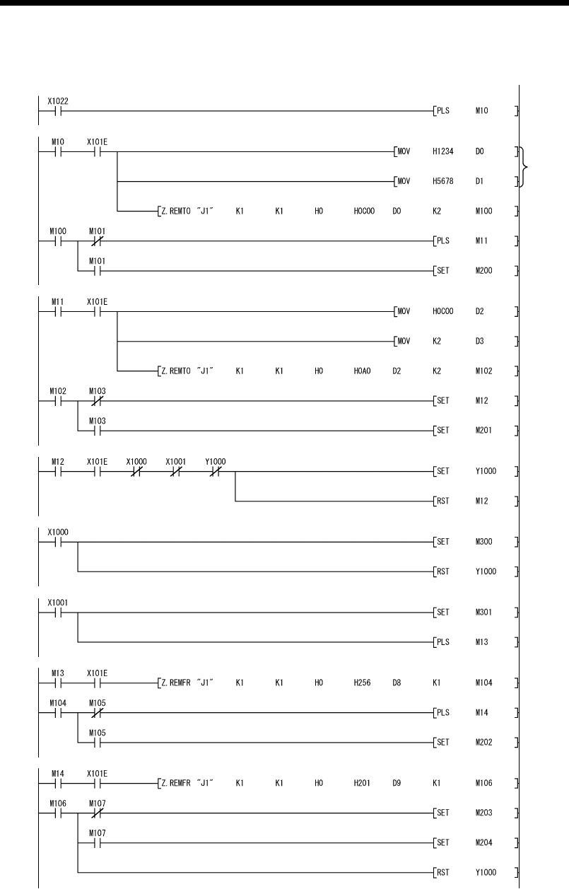
App. - 36 App. - 36
MELSEC-Q
APPENDIX
(2) Program example
<Transmission command>
<Setting of transmission data>
<Setting of buffer memory head address and data length>
<On-demand transmission>
<Processing for normal completion>
<Processing for abnormal completion>
<Abnormal completion: Read of on-demand execution result>
<Abnormal completion: Read of LED ON status>
Changes the transmission
command into pulses.
Sets the transmission data.
Transfers the transmission data
to the transmission area address
of the buffer memory.
On-demand function designation
command
Abnormal completion of REMTO
instruction
Buffer memory head address for
on-demand function
Data length for on-demand function
Transfers the setting value to the
on-demand function designation
area of the buffer memory.
Sets the on-demand data
transmission flag.
Abnormal completion of REMTO
instruction
Turns ON the transmission
request signal.
Resets the on-demand data
transmission flag.
Normal completion of on-demand
data transmission
Turns OFF the transmission
request signal.
Abnormal completion of on-demand
data transmission
On-demand execution result
acquisition command
Reads the on-demand execution
result of the buffer memory to D8.
LED ON status acquisition
command
Abnormal completion of REMFR
instruction
Reads the LED ON status of the
buffer memory to D9.
Normal completion of REMFR
instruction
Abnormal completion of REMFR
instruction
Turns OFF the transmission
request signal.
App. - 37 App. - 37
MELSEC-Q
APPENDIX
Appendix 9.4 When receiving data using nonprocedural or bidirectional protocol
The following program example receives data under the nonprocedural protocol (or
bidirectional protocol) using the REMFR instruction and I/O signals.
Refer to Chapter 6 for the communication using the nonprocedural protocol.
Refer to Chapter 7 for the communication using the bidirectional protocol.
Refer to Chapter 11 of the User's Manual (Application) for data communication using
the user frames.
(1) Program conditions
The following program receives data from the external device by communication
using the nonprocedural protocol, then turns ON the receive read request signal
(X1003), and reads the received data from the QJ71C24N buffer memory to the
PLC CPU.
(a) Devices used:
• Error code read signal ............................................................ X1023
• Receive read request signal................................................... M10
• Received data acquisition command ..................................... M11
• Receive result acquisition command...................................... M12
• Completion device for REMFR instruction............................. M100 to 105
• Normal/abnormal completion flag for REMFR instruction..... M200 to 203
• Normal/abnormal completion of receive ................................ M300, M301
• Received data count ............................................................... D0
• Received data (when 5-word data are received)................... D1 to D5
• Data reception result............................................................... D8000
(b) Intelligent function module switch settings (Refer to Section 4.5.2)
Bit
Switch No. Position Designated value Description Setting
value
b0 OFF Operation setting Independent
b1 OFF Data bit 7 bits
b2 OFF Parity bit No
b3 OFF Even/odd parity Odd
b4 OFF Stop bit 1 bit
b5 OFF Sum check code No
b6 ON Write during RUN Enabled
b7 ON
Transmission
setting
Setting modifications Enabled
Switch 1
b8 to b15 — Communication rate setting 19200bps
07C0H
Switch 2 — Communication protocol setting Non-procedure protocol 0006H
Switch 5 — Station number setting Station 0 0000H
(c) Buffer memory settings used in this example
Address Decimal (Hexadecimal)
CH1 Name Setting
value
150 (96H) Word/byte units designation Word units
164 (A4H) Received data count designation 01FFH
165 (A5H) Receive complete code designation 0D0AH
166 (A6H) Receive buffer memory head address designation 0600H
167 (A7H) Receive buffer memory length designation 0200H
600 (258H) Data reception result —
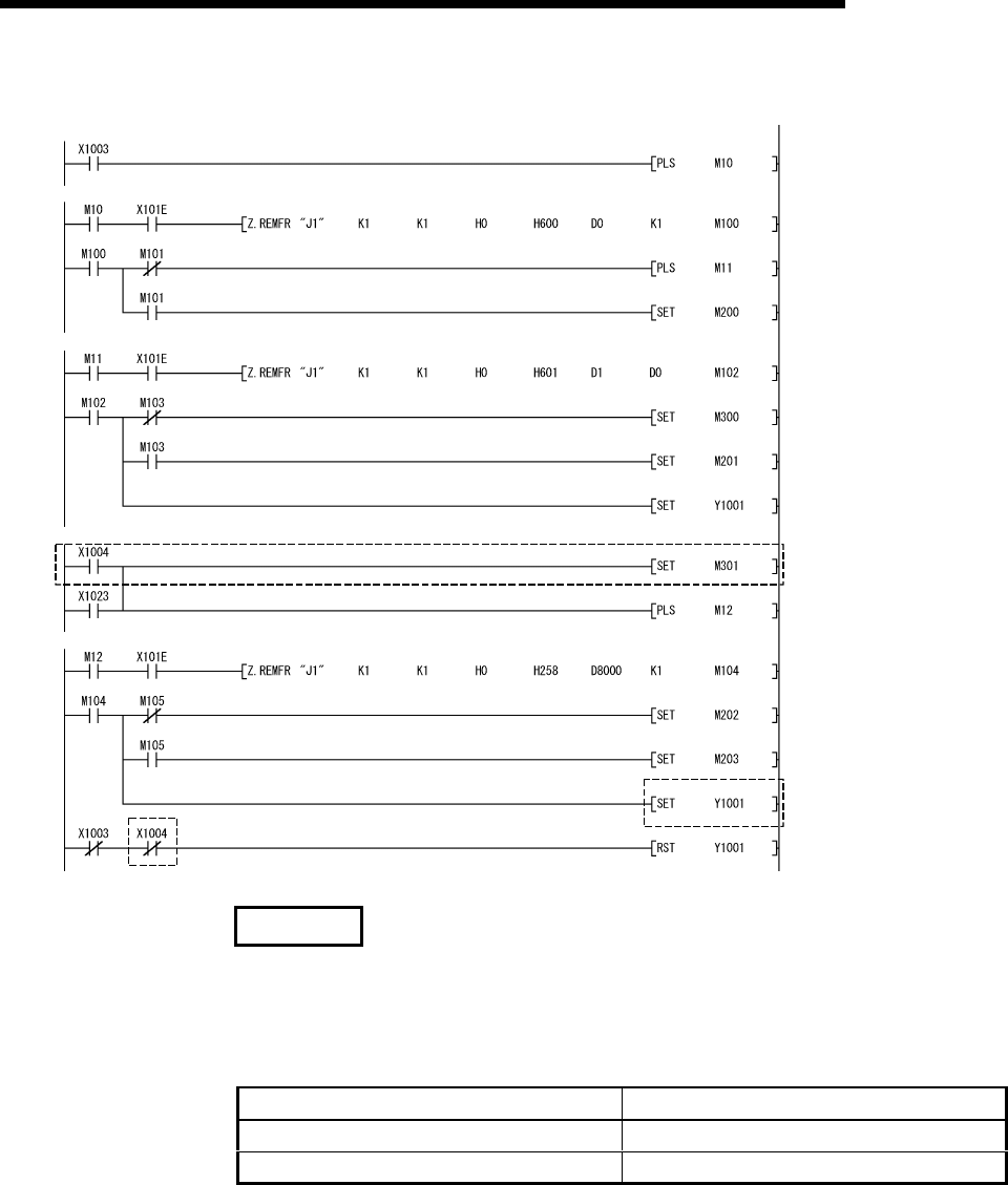
App. - 38 App. - 38
MELSEC-Q
APPENDIX
(2) Program example
<Receive read request>
<Read of received data count>
<Read of received data>
<Receive error detection>
<When receive error detected: Read of data reception result>
Changes the receive read
request signal into pulses.
Reads the received data count
from the communication area of
the buffer memory to D1.
Received data acquisition
command
Abnormal completion of
REMFR instruction
Reads data as many as the
received data count from the
communication area of the buffer
memory to D1.
Normal reception completion
Abnormal completion of REMFR
instruction
Turns ON the receive read
completion signal.
Abnormal reception completion
Reception result acquisition
command
Reads the data reception result
of the buffer memory to D8000.
Normal completion of REMFR
instruction
Abnormal completion of REMFR
instruction
Turns ON the receive read
completion signal.
Turns OFF the receive read
completion signal.
REMARK
When data reception is executed by the bidirectional protocol, the area enclosed by
the dotted line shown above must be removed.
Set the intelligent function module switches as indicated below. (Refer to Section
4.5.2.)
Switch No. Setting value
Switch 1 07C0H
Switch 2 0007H
App. - 39 App. - 39
MELSEC-Q
APPENDIX
Appendix 9.5 When sending data using nonprocedural or bidirectional protocol
The following program example sends data under the nonprocedural protocol (or
bidirectional protocol) using the REMFR/REMTO instruction and I/O signals.
Refer to Chapter 6 for the communication using the nonprocedural protocol, and to
Chapter 7 for the communication using the bidirectional protocol.
(1) Program conditions
The following program sends data from the CH1 side when the transmission
signal (X1024) turns ON.
(a) Devices used:
• Transmission command ......................................................... X1024
• Transmission command pulse signal..................................... M10
• Transmission result acquisition command............................. M11
• Completion device for REMFR/REMTO instruction .............. M100 to 103
• Normal/abnormal completion flag for REMFR/REMTO
instruction................................................................................ M200 to 202
• Normal/abnormal completion of transmission........................ M300, M301
• Transmission data count ........................................................ D10
• Transmission data (5 words) .................................................. D11 to D15
• Data transmission result ......................................................... D20
(b) Intelligent function module switch settings (Refer to Section 4.5.2)
Bit
Switch No. Position Designated value Description Setting
value
b0 OFF Operation setting Independent
b1 OFF Data bit 7 bits
b2 OFF Parity bit No
b3 OFF Even/odd parity Odd
b4 OFF Stop bit 1 bit
b5 OFF Sum check code No
b6 ON Write during RUN Enabled
b7 ON
Transmission
setting
Setting modifications Enabled
Switch 1
b8 to b15 — Communication rate setting 19200bps
07C0H
Switch 2 — Communication protocol setting
Non-procedure protocol
or
bidirectional protocol
0006H
or
0007H
Switch 5 — Station number setting Station 0 0000H
(c) Buffer memory settings used in this example
Address Decimal (Hexadecimal)
CH1 Name Setting
value
150 (96H) Word/byte units designation Word units
162 (A2H) Transmission buffer memory head address designation 0400H
163 (A3H) Transmission buffer memory length designation 0200H
599 (257H) Data transmission result —
App. - 40 App. - 40
MELSEC-Q
APPENDIX
(2) Program example
<Transmission command>
<Setting of transmission data>
<Transmission request>
<Processing for normal completion>
<Processing for abnormal completion>
<Abnormal completion: Read of data transmission result>
Changes the transmission
command into pulses.
Sets the transmission data.
Sets the transmission data count.
Transfers the setting value to the
communication area of the buffer
memory.
Turns ON the transmission request
signal.
Abnormal completion of REMTO
instruction
Normal completion of transmission
Turns OFF the transmission request
signal.
Abnormal completion of
transmission
Transmission result acquisition
instruction
Reads the data transmission
result of the buffer memory to D20.
Normal completion of REMFR
instruction
Abnormal completion of REMFR
instruction
Turns OFF the transmission
request signal.

App. - 41 App. - 41
MELSEC-Q
APPENDIX
Appendix 9.6 When clearing received data
The following program example uses the receive data clear request area of the buffer
memory.
Refer to Section 6.1.4 for received data clear.
(1) Program conditions
The following program clears the received data in the OS area of the QJ71C24N
when the receive clear command (X1025) turns ON.
(a) Devices used:
• Receive clear command......................................................... X1025
• Receive clear processing execution command ..................... M10
• Receive processing flag.......................................................... M11
• Transmission processing flag................................................. M12
• Receive clear command pulse signal .................................... M15
• Receive clear acceptance flag ............................................... M16
• Receive clearing flag............................................................... M17
• Communication disable flag ................................................... M18
• Communication enable flag.................................................... M19
• Completion check flag ............................................................ M20
• Receive clear processing execution status acquisition
command ................................................................................ M21
• Receive clear processing execution status judgment
command ................................................................................ M22
• Completion device for REMFR/REMTO instruction .............. M100 to 103
• Normal/abnormal completion flag for REMFR/REMTO
instruction................................................................................ M200, M201
• Receive data clear request area information......................... D0
• Clear request........................................................................... D1
(b) Intelligent function module switch settings (Refer to Section 4.5.2)
Bit
Switch No. Position Designated value Description Setting
value
b0 OFF Operation setting Independent
b1 OFF Data bit 7 bits
b2 OFF Parity bit No
b3 OFF Even/odd parity Odd
b4 OFF Stop bit 1 bit
b5 OFF Sum check code No
b6 ON Write during RUN Enabled
b7 ON
Transmission
setting
Setting modifications Enabled
Switch 1
b8 to b15 — Communication rate setting 19200bps
07C0H
Switch 2 — Communication protocol setting Non-procedure protocol 0006H
Switch 5 — Station number setting Station 0 0000H
(c) Buffer memory settings used in this example
Address Decimal (Hexadecimal)
CH1 Name Setting
value
168 (A8H) Receive data clear request 0, 1
App. - 42 App. - 42
MELSEC-Q
APPENDIX
(2) Program example
<Receive clear command>
<Receive clear processing execution>
<Read of receive clear status>
Changes the receive clear
command into pulses.
Sets the receive clear acceptance
flag.
Receive clear processing execution
command
Transfers the setting value to the
receive data clear request area
of the buffer memory.
Sets the receive clearing flag.
Sets the completion check flag.
Receive clear processing execution
status acquisition command
Abnormal completion of REMTO
instruction
Reads data of the receive data clear
request area of the buffer memory
to D0.
Receive clear processing execution
status judgment command
Abnormal completion of REMFR
instruction
Resets the receive clear acceptance
flag.
Resets the receive clearing flag.
Resets the completion check flag.
Sets the communication
disable flag.
Receive clear processing execution
status acquisition command
Timer start
Resets the communication
disable flag.
Outputs the communication enable
flag.
Sets the clear request.
( 1)
( 1)
( 1)
(
1
)
1 When using the Q series C24 of function version A, add the areas enclosed
by the dotted lines to the sequence program. (Make communication when
M19 is ON.)
App. - 43 App. - 43
MELSEC-Q
APPENDIX
Appendix 9.7 When sending data using user frames
The following program example sends data by the user frames using the
REMFR/REMTO instruction and I/O signals.
Refer to Section 11.4 of the User's Manual (Application) for the transmission using the
user frames.
(1) Program conditions
The following program sends data using the user frames from the CH1 side when
the transmission signal (X1026) turns ON.
(a) Devices used:
• Transmission command ......................................................... X1026
• Transmission command pulse signal..................................... M10
• Transmission user frame designation command................... M11
• Transmission result acquisition command............................. M12
• Completion device for REMFR/REMTO instruction .............. M100 to 105
• Normal/abnormal completion flag for REMFR/REMTO
instruction................................................................................ M200 to 203
• Normal/abnormal completion of transmission........................ M300, M301
• Transmission data count ........................................................ D0
• Transmission data................................................................... D1, D2
• CR/LF output designation....................................................... D5
• Output head pointer designation ............................................ D6
• Output count designation........................................................ D7
• Output frame No. designation ................................................ D8 to D12
• Data transmission result ......................................................... D20
(b) Intelligent function module switch settings (Refer to Section 4.5.2)
Bit
Switch No. Position Designated value Description Setting
value
b0 OFF Operation setting Independent
b1 ON Data bit 8 bits
b2 OFF Parity bit No
b3 OFF Even/odd parity Odd
b4 OFF Stop bit 1 bit
b5 OFF Sum check code No
b6 ON Write during RUN Enabled
b7 ON
Transmission
setting
Setting modifications Enabled
Switch 1
b8 to b15 — Communication rate setting 19200bps
07C2H
Switch 2 — Communication protocol setting Non-procedure protocol 0006H
Switch 5 — Station number setting Station 0 0000H

App. - 44 App. - 44
MELSEC-Q
APPENDIX
(c) Buffer memory settings used in this example
Address Decimal (Hexadecimal)
CH1 Name Setting
value
150 (96H) Word/byte units designation Byte units
162 (A2H) Transmission buffer memory head address designation 0400H
163 (A3H) Transmission buffer memory length designation 0200H
183 (B7H) CR/LF output designation 0
184 (B8H) Output head pointer designation 1
185 (B9H) Output count designation 5
186 (BAH) First output frame No. designation 03F2H
187 (BBH) Second output frame No. designation 03F3H
188 (BCH) Third output frame No. designation 8001H
189 (BDH) Fourth output frame No. designation 8000H
190 (BEH) Fifth output frame No. designation 041BH
6912 (1B00H) Registered data byte count designation 2
6913 (1B01H)
For registration
No. 8001HUser frame storage 012DH
App. - 45 App. - 45
MELSEC-Q
APPENDIX
(2) Program example
The user frames No. 3F2H, 3F3H, 41BH and 8001H are assumed to have been
registered in advance.
<Transmission command>
<Setting of transmission data>
<Transmission user frame designation command>
<Transmission request>
<Processing for normal completion>
<Processing for abnormal completion>
<Abnormal completion: Read of data transmission result>
Sets the transmission data.
Transfers the setting value to the
communication area of the buffer
memory.
Transmission user frame designation
command
Abnormal completion of REMTO
instruction
Sets the CR/LF output.
Sets the output head pointer.
Sets the output count.
First output frame No. designation
Second output frame No. designation
Third output frame No. designation
Fourth output frame No. designation
Fifth output frame No. designation
Transfers the setting values to the
transmission user frame designation
area of the buffer memory.
Turns ON the transmission request
signal.
Abnormal completion of REMTO
instruction
Normal completion of transmission
Turns OFF the transmission request
signal.
Abnormal completion of transmission
Transmission result acquisition
instruction
Reads the data transmission result
of the buffer memory to D20.
Normal completion of REMFR
instruction
Abnormal completion of REMFR
instruction
Turns OFF the transmission request
signal.
Changes the transmission
command into pulses.
Sets the transmission data count.
App. - 46 App. - 46
MELSEC-Q
APPENDIX
Appendix 9.8 When performing initial setting
The following program example performs initial setting using the REMTO instruction.
Execute this program when changing the default values of the Q series C24 buffer
memory.
Refer to Chapter 8 when changing the default values of the Q series C24 buffer
memory using GX Configurator-SC.
(1) Program conditions
The following program performs initial setting on the CH1 side when the initial
setting command (X1027) turns ON.
(a) Devices used:
• Initial setting command........................................................... X1027
• Initial setting command pulse signal ...................................... M10
• Initial setting command 2........................................................ M11
• Initial setting command 3........................................................ M12
• Completion device for REMTO instruction............................. M100 to105
• Normal/abnormal completion flag for REMTO instruction..... M200 to 203
• Word/byte units designation ................................................... D0
• Buffer memory head address designation for on-demand
transmission............................................................................ D1
• Buffer memory length designation for on-demand
transmission............................................................................ D2
• Transmission buffer memory head address designation ...... D3
• Transmission buffer memory length designation................... D4
• Receive buffer memory head address designation............... D5
• Receive buffer memory length designation ........................... D6
(b) Buffer memory settings used in this example
Address Decimal (Hexadecimal)
CH1 Name Setting
value
150 (96H) Word/byte units designation Byte units
160 (A0H)Buffer memory head address designation for on-demand function
designation 0400H
161 (A1H) Data length designation for on-demand function designation 0000H
162 (B2H) Transmission buffer memory head address designation 0C00H
163 (A3H) Transmission buffer memory length designation 0400H
166 (A6H) Receive buffer memory head address designation 0600H
167 (A7H) Receive buffer memory length designation 0200H
App. - 47 App. - 47
MELSEC-Q
APPENDIX
(2) Program example
Changes the initial setting
command into pulses.
Sets the word/byte units
designation to byte.
Transfers the setting value to
the word/byte units designation
area of the buffer memory.
Initial setting command 2
Abnormal completion of REMTO
instruction
Sets 400H to the buffer memory head
address for on-demand transmission.
Sets 0H to the buffer memory length
for on-demand transmission.
Sets 0C00H to the transmission
buffer memory head address.
Sets 400H to the transmission buffer
memory length.
Transfers the setting values to the
on-demand function designation
and transmission area designation
areas of the buffer memory.
Initial setting command 3
Abnormal completion of REMTO
instruction
Sets 600H to the receive buffer
memory head address.
Sets 200H to the receive buffer
memory length.
Transfers the setting value to the
receive area designation area of the
buffer memory.
Initial setting completion
Abnormal completion of REMTO
instruction
<Initial setting command>
<Setting of word/byte units designation>
<Setting of on-demand function designation and transmission area designation>
<Setting of receive area designation>
REMARK
When changing the default values of the following buffer memory areas, refer to
above (2) Program example to perform programming.
• DTR/DSR (ER/DR), DC control designation
• DC1/DC3 (Xon/Xoff) code designation
• DC2/DC4 code designation
• CD terminal check designation (for RS-232)
• Communication system designation (for RS-232)
• Simultaneous transmission priority/non-priority designation
• Retransmission time transmission method designation
• Simultaneously transmission data valid/invalid designation
• No-reception monitoring time (timer 0) designation
App. - 48 App. - 48
MELSEC-Q
APPENDIX
Appendix 9.9 When registering user frame
The following program example registers a user frame to the flash ROM of the Q
series C24 using the REMFR/REMTO instruction and I/O signals.
Refer to Section 9.4 of the User's Manual (Application) for the registration of the user
frame.
POINT
It is recommended to use GX Configurator-SC when registering a user frame to the
flash ROM of the Q series C24. (Refer to Chapter 8.)
(1) Program conditions
The following program registers a user frame to the flash ROM of the QJ71C24N
when the registration command (X1028) turns ON.
(a) Devices used:
• Registration command............................................................ X1028
• Registration command pulse signal ....................................... M10
• Registration command 2......................................................... M11
• Registration flag ...................................................................... M12
• Registration result acquisition command ............................... M13
• Completion device for REMFR/REMTO instruction .............. M100 to 105
• Normal/abnormal completion flag for REMFR/REMTO
instruction................................................................................ M200 to 203
• Registration instruction ........................................................... D0
• Frame No. ............................................................................... D1
• Registration result................................................................... D2
• Number of data bytes registered............................................ D3
• User frame .............................................................................. D4 to 8
(b) Buffer memory settings used in this example
Address Decimal (Hexadecimal)
CH1 Name Setting
value
2 (2H) Register/read/delete instructions 1
3 (3H) Frame No. direction 03E8H
4 (4H) Registration/read/delete result storage —
5 (5H) Number of data bytes registered designation 10
6 (6H)3946H
7 (7H)3030H
8 (8H)3030H
9 (9H)4646H
10 (AH)
For flash ROM
access
User frame
3030H
App. - 49 App. - 49
MELSEC-Q
APPENDIX
(2) Program example
Resets the registration flag.
<Registration command>
<Setting of user frame>
<Registration command 2>
<Flash ROM write request>
<Read of registration result>
Changes the registration
command into pulses.
Sets the registration instruction.
Sets the frame No.
Sets the number of data bytes
registered.
Sets the user frame.
Transfers the setting values to the
flash ROM access area of the
buffer memory(registration
instruction and frame No.).
Registration instruction 2
Abnormal completion of REMTO
instruction
Transfers the setting values to the
flash ROM access area of the
buffer memory(number of registered
data bytes and later).
Sets the registration flag.
Abnormal completion of REMTO
instruction
Turns ON the flash ROM write
request signal.
Registration result acquisition
command
Reads the registration result from
the flash ROM access area of
the buffer memory to D2.
Normal completion of REMFR
instruction
Abnormal completion of REMFR
instruction
Turns OFF the flash ROM write
request signal.
App. - 50 App. - 50
MELSEC-Q
APPENDIX
Appendix 9.10 When reading user frame
The following program example reads a user frame registered to the flash ROM of the
Q series C24 using the REMFR/REMTO instruction and I/O signals.
Refer to Section 9.4 of the User's Manual (Application) for details.
POINT
It is recommended to use GX Configurator-SC when reading a user frame
registered to the flash ROM of the Q series C24. (Refer to Chapter 8.)
(1) Program conditions
The following program reads a user frame registered to the flash ROM of the
QJ71C24N when the read command (X1029) turns ON.
(a) Devices used:
• Read command....................................................................... X1029
• Read command pulse signal.................................................. M10
• Read flag................................................................................. M11
• Registration result acquisition command ............................... M12
• Number of data byte registered acquisition command.......... M13
• User frame acquisition command........................................... M14
• Completion device for REMFR/REMTO instruction .............. M100 to 107
• Normal/abnormal completion flag for REMFR/REMTO
instruction................................................................................ M200 to 204
• Read instruction ...................................................................... D0
• Frame No. ............................................................................... D1
• Read result.............................................................................. D2
• Number of data bytes registered............................................ D3
• User frame .............................................................................. D4 or later
• Number of registered data...................................................... D50, D100
(b) Buffer memory settings used in this example
These settings are used to read the user frame registered in Appendix 9.9.
Address Decimal (Hexadecimal)
CH1 Name Setting
value
2 (2H) Register/read/delete instructions 2
3 (3H) Frame No. direction 03E8H
4 (4H) Registration/read/delete result storage —
5 (5H) Number of data bytes registered designation 10
6 (6H)3946H
7 (7H)3030H
8 (8H)3030H
9 (9H)4646H
10 (AH)
For flash ROM
access
User frame
3030H
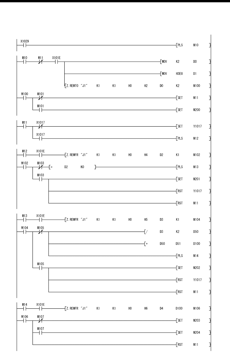
App. - 51 App. - 51
MELSEC-Q
APPENDIX
(2) Program example
Sets the read flag.
<Read command>
<Setting of read instruction>
<Flash ROM read request>
<Read of read result>
<Read of the number of data bytes registered >
<Read of user frame>
Changes the read
command into pulses.
Sets the read instruction.
Sets the frame No.
Transfers the setting values to the
flash ROM access area of the
buffer memory.
Sets the read flag.
Abnormal completion of REMTO
instruction
Turns ON the flash ROM read
request signal.
Registration result acquisition
command
Reads the read result from the
flash ROM access area of the
buffer memory to D2.
No. of data byte registered
acquisition command
Abnormal completion of REMFR
instruction
Turns OFF the flash ROM read
request signal.
Sets the read flag.
Reads the number of registered
data bytes from the flash ROM
access area of the buffer
memory to D3.
Converts the number of registered
data bytes into the word units.
Adds 1 word when the number of
registered data bytes is odd.
User frame acquisition command
Abnormal completion of REMTO
instruction
Turns OFF the flash ROM read
request signal.
Sets the read flag.
Reads the user frame from the
flash ROM access area of the
buffer memory to D4 and higher.
Normal completion of REMFR
instruction
Abnormal completion of REMFR
instruction
App. - 52 App. - 52
MELSEC-Q
APPENDIX
Appendix 9.11 When deleting user frame
The following program example deletes a user frame registered to the flash ROM of
the Q series C24 using the REMFR/REMTO instruction and I/O signals.
Refer to Section 9.4 of the User's Manual (Application) for details.
POINT
It is recommended to use GX Configurator-SC when deleting a user frame
registered to the flash ROM of the Q series C24. (Refer to Chapter 8.)
(1) Program conditions
The following program deletes a user frame registered to the flash ROM of the
QJ71C24N when the delete command (X1030) turns ON.
(a) Devices used:
• Delete command..................................................................... X1030
• Delete command pulse signal ................................................ M10
• Delete flag ............................................................................... M11
• Delete result acquisition command ........................................ M12
• Completion device for REMFR/REMTO instruction .............. M100 to 103
• Normal/abnormal completion flag for REMFR/REMTO
instruction................................................................................ M200 to 202
• Delete instruction .................................................................... D0
• Frame No. ............................................................................... D1
• Delete result ............................................................................ D2
(b) Buffer memory settings used in this example
These settings assume that the user frame registered in Appendix 9.9 is
deleted.
Address Decimal (Hexadecimal)
CH1 Name Setting
value
2 (2H) Register/read/delete instructions 3
3 (3H) Frame No. direction 03E8H
4 (4H)
For flash ROM
access Registration/read/delete result storage —
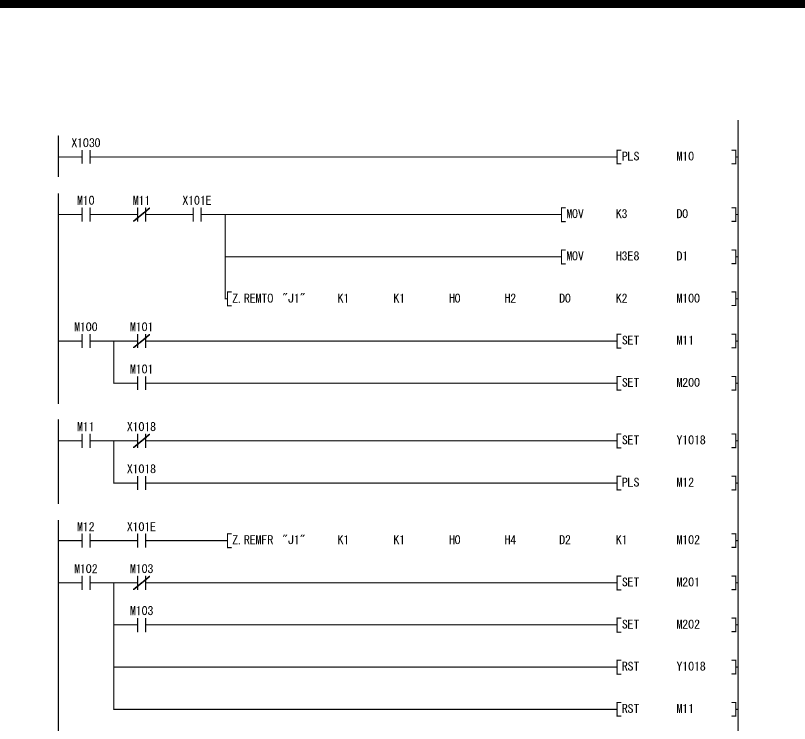
App. - 53 App. - 53
MELSEC-Q
APPENDIX
(2) Program examples
Sets the delete flag.
<Delete command>
<Setting of delete instruction>
<Flash ROM write request>
<Read of delete result>
Changes the delete command
into pulses.
Sets the delete instruction.
Sets the frame No.
Transfers the setting values to the
flash ROM access area of the
buffer memory.
Sets the delete flag.
Abnormal completion of REMTO
instruction
Turns ON the flash ROM read
request signal.
Delete result acquisition command
Reads the delete result from the
flash ROM access area of the
buffer memory to D2.
Normal completion of REMFR
instruction
Abnormal completion of REMFR
instruction
Turns OFF the flash ROM read
request signal.
App. - 54 App. - 54
MELSEC-Q
APPENDIX
Appendix 9.12 When changing the communication protocol and transmission setting
This section provides a program example that changes the communication protocol
and transmission setting using the REMFR/REMTO instructions and I/O signals.
(When the module is used on a MELSECNET/H remote I/O station, the station No.
cannot be changed because the UINI instruction is unavailable.)
For changing the communication protocol and transmission setting, refer to Chapter 15
of the User's Manual (Application).
(1) Program conditions
When the change command (X1031) turns on, the communication protocol and
transmission setting are changed.
(a) Devices used by user
• Change command .................................................................. X1031
• Changing flag.......................................................................... M300
• Change completion flag.......................................................... M301
• CH1 change command pulse signal ...................................... M10
• CH1 change command........................................................... M11
• CH1 mode switching completion............................................ M12
• CH1 receive processing.......................................................... M13
• CH1 send processing ............................................................. M14
• CH2 change command pulse signal ...................................... M20
• CH2 change command........................................................... M21
• CH2 mode switching completion............................................ M22
• CH2 receive processing.......................................................... M23
• CH2 send processing ............................................................. M24
• REMFR/REMTO instruction completion device..................... M100 to 107
• REMFR/REMTO instruction abnormal completion flag......... M200 to 205
• Switching mode No. designation............................................ D0, D10
• Transmission specifications after switching designation....... D1, D11
• Switch setting error and mode switching error status............ D2, D12
(b) Buffer memory settings used in this example
Address, Decimal
(Hexadecimal) Bit
CH1 CH2 Position Specified
value
Description Set value
114 (90H) 304 (130H) — Switching mode No. designation MC protocol
(Format 1) 0001H
b0 OFF Operation
setting Independent
b1 OFF Data bit 7 bits
b2 OFF Parity bit No
b3 OFF Even/odd parity Odd
b4 ON Stop bit 2 bits
b5 ON Sum check
code Yes
b6 OFF Write during
RUN Prohibited
b7 ON Setting
modifications Allowed
b8 to b11 — Communication
rate setting 9600bps
B12 to 14 All OFF For system —
145 (91 H) 305 (131H)
B15 ON
Transmission
specifications
after switching
designation
Transmission
specifications
after switching
designation
Make setting
as set in this
area.
85B0H
515 (203H) — Switch setting error and mode switching error status —
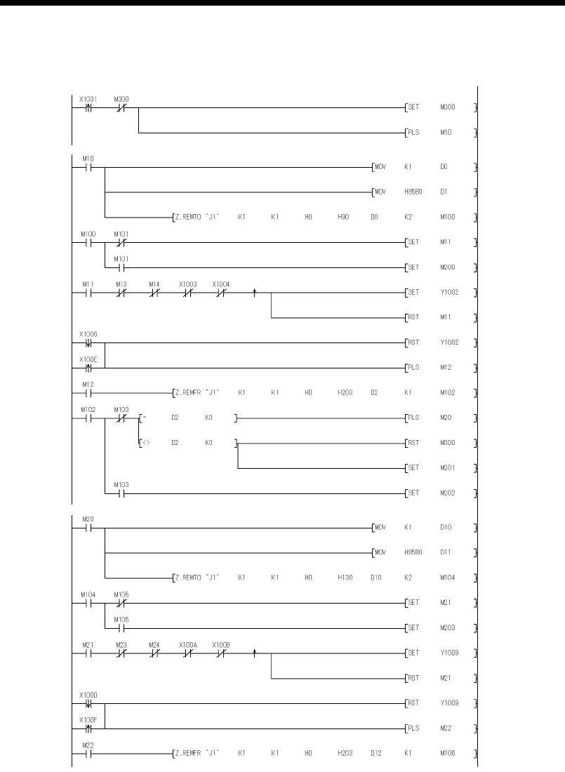
App. - 55 App. - 55
MELSEC-Q
APPENDIX
(2) Program examples
<Change command>
<Change processing of CH1>
<Change processing of CH2>
Sets the changing flag.
Starts the change processing of CH1.
Sets the switching mode No.
designation.
Sets the transmission specifications after
switching designation.
Transfers the set values to the mode
switching designation area.
Sets the CH1 change command.
REMTO instruction abnormally completed
Sets the CH1 mode switching request.
Resets the CH1 mode switching request.
CH1 mode switching completed
Transfers the mode switching error status.
Starts the change processing of CH2.
Reexamines the modifications.
REMFR instruction abnormally completed
Sets the switching mode No. designation.
Sets the transmission specifications after
switching designation.
Transfers the set values to the mode
switching designation area.
Sets the CH2 change command.
REMTO instruction abnormally completed
Sets the CH2 mode switching request.
Resets the CH2 mode switching request.
CH2 mode switching completed
Transfers the mode switching error status.
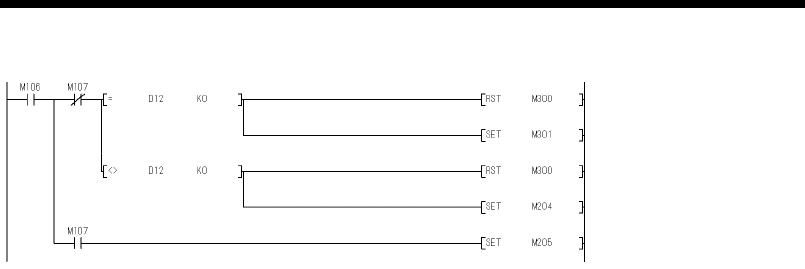
App. - 56 App. - 56
MELSEC-Q
APPENDIX
Resets the changing flag.
Sets the change completion flag.
Reexamines the modifications.
REMFR instruction abnormally completed
App. - 57 App. - 57
MELSEC-Q
APPENDIX
Appendix 10 Setting Value Recording Sheet
The following sheet is for recording parameter setting values set by GX Developer.
Use as many copies as needed.
In order to review the setting values of the utility package (GX Configurator-SC),
print out the content of the file generated by the "Make text file" function of GX
Configurator-SC which can be used as the setting value recording sheet.
[Module No. ]
Recording sheet 1 (Intelligent function module interrupt pointer setting)
Set data
GX Developer
setting screen Data item name Setting value Remarks
Interrupt pointer start No.
CPU side Interrupt pointer No. of modules 2 (fixed) Input format: Decimal
Start I/O number Input format: Hexadecimal
Intelligent
function module
interrupt pointer
setting
Intelligent
module side Start SI number 0 (fixed) Input format: Decimal
Recording sheet 2 (Remote password setting)
Set data
GX Developer
setting screen Data item name Setting value Remarks
Password
settings Password Input format: Character strings
Model name QJ71C24/CMO Input format: Selection
Remote
password
settings
Password
active module
settings Start XY Input format: Hexadecimal
Recording sheet 3 (Intelligent function module switch setting)
Switch number Description
CH1 Communication rate setting CH1 Transmission setting
b15 b14 b13 b12 b11 b10 b9 b8 b7 b6 b5 b4 b3 b2 b1 b0
Switch 1
H
Switch 2 CH1 Communication protocol setting =
CH2 Communication rate setting CH2 Transmission setting
b15 b14 b13 b12 b11 b10 b9 b8 b7 b6 b5 b4 b3 b2 b1 b0
Switch 3
H
Switch 4 CH2 Communication protocol setting =
Switch 5 Station number setting =
Check the setting values in the next page and record them.
App. - 58 App. - 58
MELSEC-Q
APPENDIX
(GX Developer "Intelligent function module switch setting" setting values recording check
sheet)
(1) Transmission setting (Enter "0" or "1" in the bit position field)
b7 b6 b5 b4 b3 b2 b1 b0
CH1 side
CH2 side
Bit Description OFF (0) ON (1) Remarks
b0 Operation setting Independent Linked Always set to OFF on
CH1 side.
b1 Data bit 7 8 Do not include parity bit.
b2 Parity bit No Yes Vertical parity
b3 Odd/even parity Odd Even Valid only when parity
bit is set to Yes.
b4 Stop bit 1 2 —
b5 Sum check code No Yes —
b6 Write during RUN Prohibit Allow —
b7 Setting modification Prohibit Allow —
(2) Communication rate setting (Enter check marks in the CH1 and
CH2 fields)
CH1 CH2 Setting value Communication speed (unit: bps)
FH50
0H300
1H600
2H1200
3H2400
4H4800
5H9600
6H14400
7H19200
8H28800
9H38400
AH57600
BH115200
CH230400
(3) Communication protocol setting (Enter check marks in the CH1 and
CH2 fields)
CH1 CH2 Setting value Setting data
0HGX Developer connection
1HFormat 1
2HFormat 2
3HFormat 3
4HFormat 4
5H
MC protocol
Format 5
6HNon procedure protocol
7HBidirectional protocol
8HFor linked operation setting
9H to DHSetting prohibited
EHROM/RAM/Switch test
FHIndividual station recovery test

Index - 1 Index - 1
INDEX
[A]
Applicable modules ..................................... 2-1
ASCII-code table ...................................App-17
Auto refresh .............................................. 4-22
[B]
BIDIN.......................................................... 9-14
Bidirectional protocol ................................... 7-1
BIDOUT ..................................................... 9-11
[C]
C/N........................................................... 10-33
CH1.ERR, CH2.ERR............................... 10-37
Checking the function version................... 2-12
Checking the LED ON status,
communications error status..................... 10-1
Checking the software version
(GX Configurator-SC)................................ 2-13
Communication protocol setting................ 4-16
Communication rate .................................. 4-16
Communication support tool .................App-23
Communication system............................... 3-1
Computer link module ...........................App-10
Connecting the RS-232 interface................ 4-6
Connecting the RS-422/485 interface ........ 4-8
Comparison of the function .....................App-1
CSET (Receive data clear) ..............6-14, 9-19
[D]
Data bit....................................................... 4-14
Data communication functions.................... 2-5
Data format .................................................. 3-1
Data reception by receive complete code .. 6-3
Dedicated instruction list ............................. 9-1
Dedicated instructions................................. 9-1
[E]
ERR. LED .................................................. 10-6
Error code table ....................................... 10-15
Explanation of utility package operation..... 8-6
External dimensions..............................App-18
[F]
Full-duplex communications ......................7-24
Function lists of the Q series C24..............3-11
Functions available with utility package ......8-2
[G]
GX Configurator-SC....................A-20, 2-2, 8-1
GX Configurator-SC function list ...............3-13
GX Developer.....................................A-20, 2-2
[H]
H/W gate OFF time ......................................3-9
How to detect reception error
(bidirectional)..............................................7-13
How to detect reception error
(non procedure)..........................................6-17
How to detect transmission errors
(bidirectional)..............................................7-22
How to detect transmission errors
(non procedure)..........................................6-28
How to read the setting status of
switches....................................................10-11
[ I ]
I/O assignment settings .............................4-12
Individual station loopback test..................4-28
Individual station test..................................4-25
Initializing error information .......................10-6
INPUT...........................................................9-8
Installing utility package...............................8-3
Interrupt pointer..........................................4-20
[L]
LEDs displayed ............................................4-4
Linked operation.........................................4-17
List of applications and assignments of
the buffer memory......................................3-17
List of input/output signals for the
PLC CPU....................................................3-15
Ind

Index - 2 Index - 2
Ind
[M]
m:n ............................................................... 2-4
Monitor/test ................................................ 8-32
Multiple CPU system ............................1-7, 5-3
[N]
n:1 ................................................................ 2-3
NAK.......................................................... 10-33
Non procedure protocol............................... 6-1
[O]
ONDEMAND................................................ 9-2
Operation mode....................................... 10-13
OUTPUT ...................................................... 9-5
[P]
P/S ........................................................... 10-34
Parity bit ..................................................... 4-14
Part names and functions .......................... 4-3
PRO. ........................................................ 10-35
Processing time .....................................App-14
[Q]
QnA/A series module ..............................App-6
[R]
Reading the data communication
status........................................................ 10-10
Reading the RS-232 control signal
status.......................................................... 10-9
Reading the signal status (RS-232).......... 10-9
Receive area (bidirectional) ........................ 7-4
Receive area (non procedure) .................... 6-6
Receive complete code setting................. 6-20
Receive data (bidirectional)......................... 7-6
Receive data (non procedure) .................... 6-8
Receive data clear (bidirectional).............. 7-14
Receive data clear (non procedure) ......... 6-14
Received data count.................................. 6-20
Receiving methods (bidirectional)............... 7-6
Receiving methods (non procedure)........... 6-8
ROM/RAM/switch tests ............................. 4-25
RS-232 interface specification .................... 3-3
RS-422/485 interface specification............. 3-6
"RUN" LED............................................... 10-29
Remote password check......................1-9, 5-4
[S]
Serial communication module .....................1-1
Setting and procedures prior to operation...4-1
Setting for GX Developer...........................4-12
Simultaneous transmissions......................7-24
SIO............................................................10-36
SPBUSY.....................................................9-17
Starting the utility........................................8-10
Station number setting...............................4-17
Sum check code.........................................4-15
Switch setting .............................................4-13
System configuration ...................................2-3
System registration to flash ROM..............8-16
[T]
Transmission area (bidirectional) ..............7-16
Transmission area (non procedure) ..........6-23
Transmission data (bidirectional)...............7-18
Transmission data (non procedure) ..........6-25
Transmission methods (bidirectional)........7-15
Transmission methods (non procedure) ...6-22
Transmission setting ..................................4-14
Transmission specification...........................3-1
Troubleshooting .........................................10-1
[U]
Uninstalling utility package ..........................8-3
Utility package..............................................8-1
[1]
1:1 system configuration..............................2-3
1:n.................................................................2-4

WARRANTY
Please confirm the following product warranty details before using this product.
1. Gratis Warranty Term and Gratis Warranty Range
If any faults or defects (hereinafter "Failure") found to be the responsibility of Mitsubishi occurs during use of the product
within the gratis warranty term, the product shall be repaired at no cost via the sales representative or Mitsubishi Service
Company.
However, if repairs are required onsite at domestic or overseas location, expenses to send an engineer will be solely at
the customer’s discretion. Mitsubishi shall not be held responsible for any re-commissioning, maintenance, or testing on-
site that involves replacement of the failed module.
[Gratis Warranty Term]
The gratis warranty term of the product shall be for one year after the date of purchase or delivery to a designated
place.
Note that after manufacture and shipment from Mitsubishi, the maximum distribution period shall be six (6) months, and
the longest gratis warranty term after manufacturing shall be eighteen (18) months. The gratis warranty term of repair
parts shall not exceed the gratis warranty term before repairs.
[Gratis Warranty Range]
(1) The range shall be limited to normal use within the usage state, usage methods and usage environment, etc.,
which follow the conditions and precautions, etc., given in the instruction manual, user's manual and caution labels
on the product.
(2) Even within the gratis warranty term, repairs shall be charged for in the following cases.
1. Failure occurring from inappropriate storage or handling, carelessness or negligence by the user. Failure caused
by the user's hardware or software design.
2. Failure caused by unapproved modifications, etc., to the product by the user.
3. When the Mitsubishi product is assembled into a user's device, Failure that could have been avoided if functions
or structures, judged as necessary in the legal safety measures the user's device is subject to or as necessary
by industry standards, had been provided.
4. Failure that could have been avoided if consumable parts (battery, backlight, fuse, etc.) designated in the
instruction manual had been correctly serviced or replaced.
5. Failure caused by external irresistible forces such as fires or abnormal voltages, and Failure caused by force
majeure such as earthquakes, lightning, wind and water damage.
6. Failure caused by reasons unpredictable by scientific technology standards at time of shipment from Mitsubishi.
7. Any other failure found not to be the responsibility of Mitsubishi or that admitted not to be so by the user.
2. Onerous repair term after discontinuation of production
(1) Mitsubishi shall accept onerous product repairs for seven (7) years after production of the product is discontinued.
Discontinuation of production shall be notified with Mitsubishi Technical Bulletins, etc.
(2) Product supply (including repair parts) is not available after production is discontinued.
3. Overseas service
Overseas, repairs shall be accepted by Mitsubishi's local overseas FA Center. Note that the repair conditions at each FA
Center may differ.
4. Exclusion of loss in opportunity and secondary loss from warranty liability
Regardless of the gratis warranty term, Mitsubishi shall not be liable for compensation of damages caused by any cause
found not to be the responsibility of Mitsubishi, loss in opportunity, lost profits incurred to the user by Failures of Mitsubishi
products, special damages and secondary damages whether foreseeable or not , compensation for accidents, and
compensation for damages to products other than Mitsubishi products, replacement by the user, maintenance of on-site
equipment, start-up test run and other tasks.
5. Changes in product specifications
The specifications given in the catalogs, manuals or technical documents are subject to change without prior notice.
6. Product application
(1) In using the Mitsubishi MELSEC programmable logic controller, the usage conditions shall be that the application will
not lead to a major accident even if any problem or fault should occur in the programmable logic controller device, and
that backup and fail-safe functions are systematically provided outside of the device for any problem or fault.
(2) The Mitsubishi programmable logic controller has been designed and manufactured for applications in general
industries, etc. Thus, applications in which the public could be affected such as in nuclear power plants and other
power plants operated by respective power companies, and applications in which a special quality assurance system
is required, such as for Railway companies or Public service purposes shall be excluded from the programmable logic
controller applications.
In addition, applications in which human life or property that could be greatly affected, such as in aircraft, medical
applications, incineration and fuel devices, manned transportation, equipment for recreation and amusement, and
safety devices, shall also be excluded from the programmable logic controller range of applications.
However, in certain cases, some applications may be possible, providing the user consults their local Mitsubishi
representative outlining the special requirements of the project, and providing that all parties concerned agree to the
special circumstances, solely at the users discretion.

Microsoft, Windows, Windows NT are registered trademarks of Microsoft Corporation in the United States and other
countries.
Adobe and Acrobat are registered trademarks of Adobe Systems Incorporation.
Pentium and Celeron are trademarks of Intel Corporation in the United States and other countries.
Ethernet is a trademark of Xerox. Co., Ltd in the United States.
Other company names and product names used in this document are trademarks or registered trademarks of respective
owners.
VS-VIEW
Copyright (c) 2001 ComponentOne LLC
VS-FlexGrid Pro
Copyright (c) 2000 VideoSoft Corporation
SPREAD
Copyright (c) 1996 FarPoint Technologies, Inc.
INDUSTRIAL AUTOMATION
MIT
SU
BI
S
HI ELE
C
TRI
C
MIT
SU
BI
S
HI ELE
C
TRI
C
Gothaer Strasse 8 Phone: +49 2102 486-0 Fax: +49 2102 486-7170 www.mitsubishi-automation.de
D-40880 Ratingen Hotline: +49 1805 000-765 megfa-mail@meg.mee.com www.mitsubishi-automation.com
HEADQUARTERS
MITSUBISHI ELECTRIC EUROPE
EUROPE B.V.
German Branch
Gothaer Straße 8
D-40880 Ratingen
Phone: +49 (0)2102 486-0
Fax: +49 (0)2102 486-1120
e mail: megfamail@meg.mee.com
MITSUBISHI ELECTRIC FRANCE
EUROPE B.V.
French Branch
25, Boulevard des Bouvets
F-92741 Nanterre Cedex
Phone:+33155685568
Fax:+33155685685
e mail: factory.automation@fra.mee.com
MITSUBISHI ELECTRIC IRELAND
EUROPE B.V.
Irish Branch
Westgate Business Park, Ballymount
IRL-Dublin 24
Phone: +353 (0) 1 / 419 88 00
Fax: +353 (0) 1 / 419 88 90
e mail: sales.info@meir.mee.com
MITSUBISHI ELECTRIC . ITALY
EUROPE B.V
Italian Branch
Via Paracelso 12
I-20041 Agrate Brianza (MI)
Phone: +39 039 60 53 1
Fax: +39 039 60 53 312
e mail: factory.automation@it.mee.com
MITSUBISHI ELECTRIC SPAIN
EUROPE B.V.
Spanish Branch
Carretera de Rubí 76-80
E-08190 Sant Cugat del Vallés
Phone: +34 9 3 565 3131
Fax: +34 9 3 589 2948
e mail: industrial@sp.mee.com
MITSUBISHI ELECTRIC UK
EUROPE B.V.
UK Branch
Travellers Lane
GB-HatfieldHerts.AL108XB
Phone: +44 (0) 1707 / 27 61 00
Fax: +44 (0) 1707 / 27 86 95
e mail: automation@meuk.mee.com
MITSUBISHI ELECTRIC JAPAN
CORPORATION
Office Tower “Z” 14 F
8-12,1 chome, Harumi Chuo-Ku
Tokyo 104-6212
Phone: +81 3 622 160 60
Fax: +81 3 622 160 75
MITSUBISHI ELECTRIC USA
AUTOMATION
500 Corporate Woods Parkway
Vernon Hills, IL 60061
Phone: +1 847 478 21 00
Fax: +1 847 478 22 83
EUROPEAN REPRESENTATIVES
GEVA AUSTRIA
Wiener Straße 89
AT-2500 Baden
Phone: +43 (0)2252 / 85 55 20
Fax: +43 (0)2252 / 488 60
e mail: office@geva.at
TEHNIKON BELARUS
Oktjabrskaya 16/5, Ap 704
BY-220030 Minsk
Phone: +375 (0)17 / 2104626
Fax: +375 (0)17 / 2275830
e mail: tehnikon@belsonet.net
Getronics b.v. BELGIUM
Control Systems
Pontbeeklaan 43
BE-1731 Asse-Zellik
Phone: +32 (0)2 / 467 17 51
Fax: +32 (0)2 / 467 17 45
e mail: infoautomation@getronics.com
TELECON CO. BULGARIA
4, A. Ljapchev Blvd.
BG-1756 Sofia
Phone: +359 (0)2 / 97 44 058
Fax: +359 (0)2 / 97 44 061
e mail: —
INEA CR d.o.o. CROATIA
Losinjska 4 a
HR-10000 Zagreb
Phone: +385 (0) 1 / 36 940-01
Fax: +385 (0) 1 / 36 940-03
e mail: inea@inea.hr
AutoCont CZECH REPUBLIC
Control Systems s.r.o.
Nemocnicni 12
CZ-70200 Ostrava 2
Phone: +420 59 / 6152 111
Fax: +420 59 / 6152 562
e mail: consys@autocont.cz
louis poulsen DENMARK
industri & automation
Geminivej 32
DK-2670 Greve
Phone:+45(0)43/959595
Fax:+45(0)43/959591
e mail: lpia@lpmail.com
UTU Elektrotehnika AS ESTONIA
Pärnu mnt.160i
EE-10621 Tallinn
Phone: +372 (0)6 / 51 72 80
Fax: +372 (0)6 / 51 72 88
e mail: utu@utu.ee
UTU POWEL OY FINLAND
Box 236
FIN-28101 Pori
Phone: +358 (0)2 / 550 800
Fax: +358 (0)2 / 550 8841
e mail: tehoelektroniikka@urhotuominen.fi
UTECO A.B.E.E. GREECE
5, Mavrogenous Str.
GR-18542 Piraeus
Phone: +302 (0)10 / 42 10 050
Fax: +302 (0)10 / 42 12 033
e mail: uteco@uteco.gr
Meltrade Automatika Kft. HUNGARY
55, Harmat St.
HU-1105 Budapest
Phone: +36 (0)1 / 2605 602
Fax: +36 (0)1 / 2605 602
e mail: office@meltrade.hu
SIA POWEL LATVIA
Lienes iela 28
LV-1009 Riga
Phone: +371 784 2280
Fax: +371 784 2281
e mail: utu@utu.lv
EUROPEAN REPRESENTATIVES
UAB UTU POWEL LITHUANIA
Savanoriu Pr. 187
LT-2053 Vilnius
Phone: +370 (0)52323-101
Fax: +370 (0)52322-980
e mail: powel@utu.lt
Intehsis Srl MOLDOVA
Cuza-Voda 36/1-81
MD-2061 Chisinau
Phone: +373 (0)2 / 562 263
Fax: +373 (0)2 / 562 263
e mail: intehsis@mdl.net
Getronics b.v. NETHERLANDS
Control Systems
Donauweg 2 B
NL-1043 AJ Amsterdam
Phone: +31 (0)20 / 587 6700
Fax: +31 (0)20 / 587 6839
e mail: info.gia@getronics.com
Motion Control NETHERLANDS
Automation b.v.
Markenweg 5
NL-7051 HS Varsseveld
Phone: +31 (0)315 / 257 260
Fax: +31 (0)315 / 257 269
e mail: —
Beijer Electronics AS NORWAY
Teglverksveien 1
NO-3002 Drammen
Phone:+47(0)32/243000
Fax:+47(0)32/848577
e mail: info@beijer.no
MPL Technology Sp. z o.o. POLAND
ul. Sliczna 36
PL-31-444 Kraków
Phone: +48 (0)12 / 632 28 85
Fax: +48 (0)12 / 632 47 82
e mail: krakow@mpl.pl
Sirius Trading & Services srl ROMANIA
Str. Biharia Nr. 67-77
RO-013981 Bucuresti 1
Phone: +40 (0) 21 / 201 1146
Fax: +40 (0) 21 / 201 1148
e mail: sirius@siriustrading.ro
ACP Autocomp a.s. SLOVAKIA
Chalupkova 7
SK-81109 Bratislava
Phone: +421 (02)5292-2254
Fax: +421 (02)5292-2248
e mail: info@acp-autocomp.sk
INEA d.o.o. SLOVENIA
Stegne 11
SI-1000 Ljubljana
Phone: +386 (0)1 513 8100
Fax: +386 (0)1 513 8170
e mail: inea@inea.si
Beijer Electronics AB SWEDEN
Box 426
S-20124 Malmö
Phone:+46(0)40/358600
Fax:+46(0)40/358602
e mail: info@beijer.de
ECONOTEC AG SWITZERLAND
Postfach 282
CH-8309 Nürensdorf
Phone: +41 (0)1 / 838 48 11
Fax: +41 (0)1 / 838 48 12
e mail: info@econotec.ch
GTS TURKEY
Darülaceze Cad. No. 43A KAT: 2
TR-80270 Okmeydani-Istanbul
Phone: +90 (0)212 / 320 1640
Fax: +90 (0)212 / 320 1649
e mail: gts@turk.net
EUROPEAN REPRESENTATIVES
CSC Automation UKRAINE
15, M. Raskova St., Fl. 10, Off. 1010
UA-02002 Kiev
Phone: +380 (0)44 / 238 83 16
Fax: +380 (0)44 / 238 83 17
e mail: csc-a@csc-a.kiev.ua
EURASIAN REPRESENTATIVE
CONSYS RUSSIA
Promyshlennaya St. 42
RU-198099 St Petersburg
Phone: +7 812 / 325 36 53
Fax: +7 812 / 325 36 53
e mail: consys@consys.spb.ru
ELEKTROSTYLE RUSSIA
ul. Garschina 11
RU-140070 Moscow Oblast
Phone: +7 095/ 557 9756
Fax: +7 095/ 746 8880
e mail: mjuly@elektrostyle.ru
ELEKTROSTYLE RUSSIA
Krasnij Prospekt 220-1, Office 312
RU-630049 Novosibirsk
Phone: +7 3832 / 10 66 18
Fax: +7 3832 / 10 66 26
e mail: elo@elektrostyle.ru
ICOS RUSSIA
Ryazanskij Prospekt, 8A, Office 100
RU-109428 Moscow
Phone: +7 095 / 232 0207
Fax: +7 095 / 232 0327
e mail: mail@icos.ru
SMENA RUSSIA
Polzunova 7
RU-630051 Novosibirsk
Phone: +7 095 / 416 4321
Fax: +7 095 / 416 4321
e mail: smena-nsk@yandex.ru
SSMP Rosgidromontazh Ltd RUSSIA
23, Lesoparkovaya Str.
RU-344041 Rostov On Don
Phone: +7 8632 / 36 00 22
Fax: +7 8632 / 36 00 26
e mail: —
STC Drive Technique RUSSIA
Poslannikov per., 9, str.1
RU-107005 Moscow
Phone: +7 095 / 786 21 00
Fax: +7 095 / 786 21 01
e mail: info@privod.ru
MIDDLE EAST REPRESENTATIVE
SHERF Motion Techn. Ltd ISRAEL
Rehov Hamerkava 19
IL-58851 Holon
Phone: +972 (0)3 / 559 54 62
Fax: +972 (0)3 / 556 01 82
e mail: —
AFRICAN REPRESENTATIVE
CBI Ltd SOUTH AFRICA
Private Bag 2016
ZA-1600 Isando
Phone: +27 (0)11 / 928 2000
Fax: +27 (0)11 / 392 2354
e mail: cbi@cbi.co.za
