Montage 715000 Traxit X 2G GPS Module User Manual
Montage Traxit X 2G GPS Module
UserManual.wiki
>
Montage
>
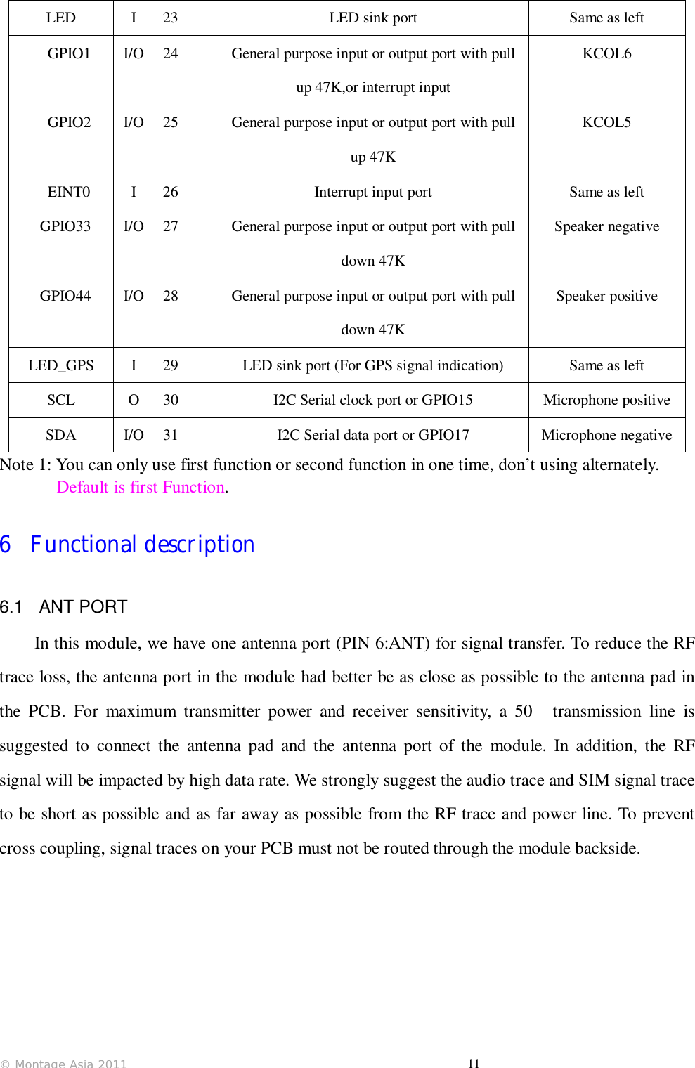
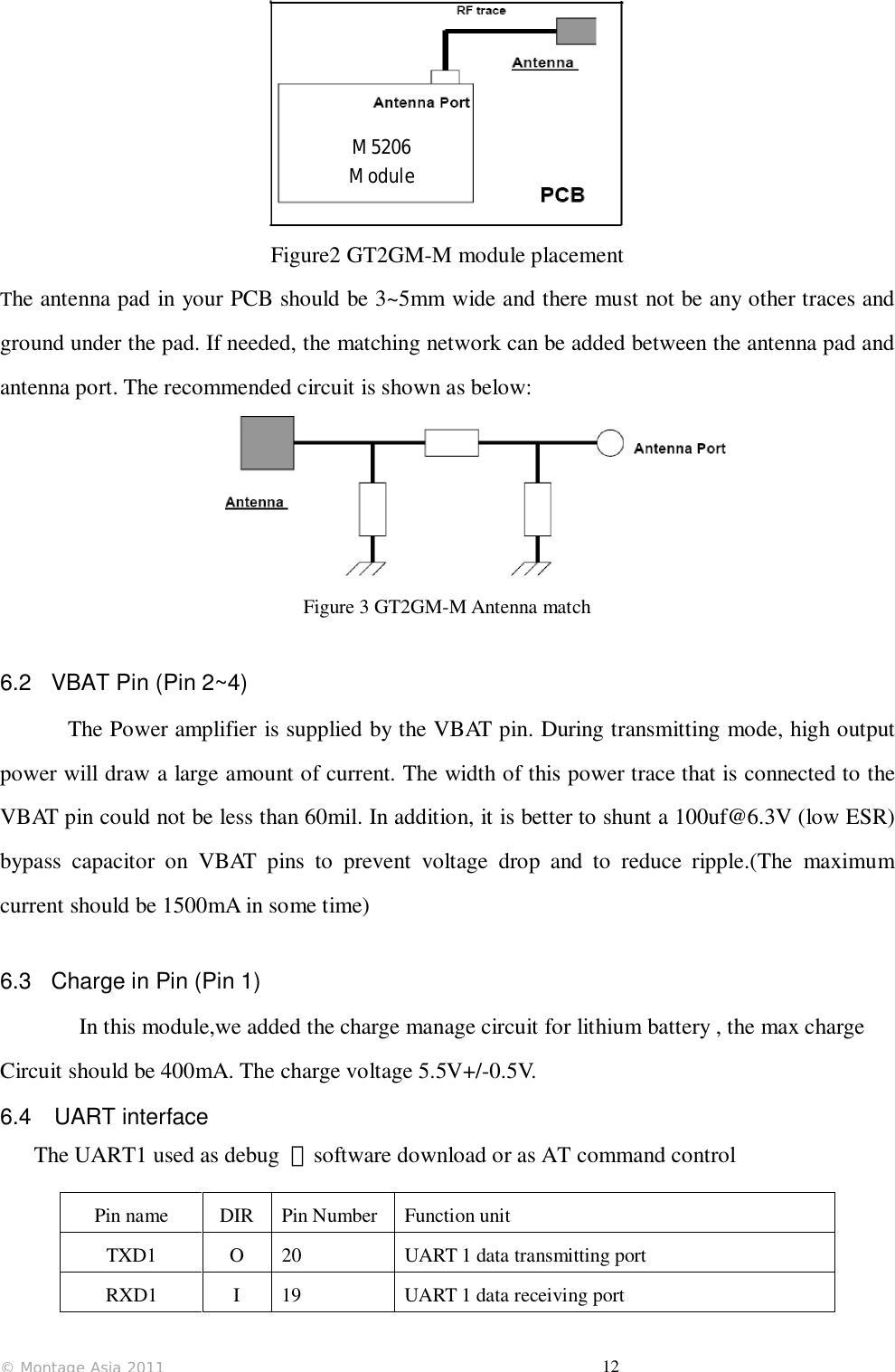
715000 User Manual
User Manual
Navigation menu
Upload a User Manual
Namespaces
Wiki Guide
HTML
PDF
Info
Views
User Manual
Discussion / Help
Navigation
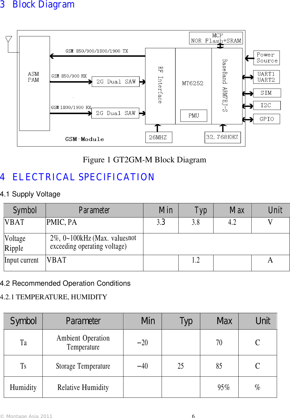
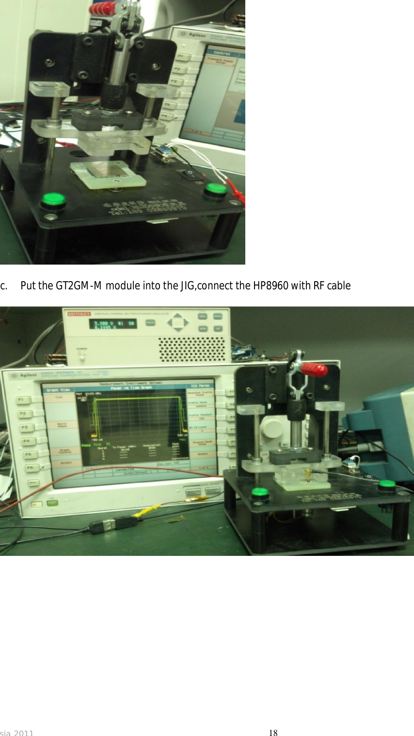
![© Montage Asia 2011 1 GT2GM-M Wireless Module User Manual Status: [ ]Draft [ ]Release [√]Revise File Indicator: EL_GT2GM-M Hardware Design Guide Current Version: 1.2 Author: Date: 2012-07-18](https://usermanual.wiki/Montage/715000/User-Guide-1756801-Page-1.png)