Motorola Solutions 89FC4825 Non Broadcast Transmitter User Manual Summit BR 800 Tx FCC Filing 3
Motorola Solutions, Inc. Non Broadcast Transmitter Summit BR 800 Tx FCC Filing 3
Exhibit D Users Manual per 2 1033 c3

APPLICANT: MOTOROLA EQUIPMENT TYPE: ABZ89FC4825
EXHIBIT D
User / Operational Manual
Operational or User’s Manual
The manual should include instruction, installation, operator, or technical manuals with required ‘information to the
users’. This manual should include a statement that cautions the user that changes or modifications not expressly
approved by the party responsible for compliance could void the user’s authority to operate the equipment. The
manual shall include RF Hazard warning statements, if applicable.
The instruction and service manual for this base radio are not published at this time. However, draft copy of
available manual information has been assembled and has been included as part of this filing package.
Upon request, published manuals will be sent to the commission and/or telecommunication certification body
(TCB) as soon as they become available. All of the descriptions, block diagrams, and schematics that are included
in this filing package are current as of the package submittal date.
EXHIBIT DESCRIPTION
D1-1 Manual Front Matter (Draft)
D1-2 Specifications (Draft)
D1-3 Field Replaceable Units and Orderable Parts (Draft)
D1-4 Tune-Up Procedure (Draft)
D1-5 Racking Configurations (Draft)
D1-6 Functional Description / Operation of Modules (Draft)
APPLICANT: MOTOROLA EQUIPMENT TYPE: ABZ89FC4825
EXHIBIT D1-1
User / Operational Manual
Manual Front Matter (Draft)

APPLICANT: MOTOROLA EQUIPMENT TYPE: ABZ89FC4825
EXHIBIT D1-1
User / Operational Manual
Manual Front Matter (Draft, Continued)
APPLICANT: MOTOROLA EQUIPMENT TYPE: ABZ89FC4825
EXHIBIT D1-1
User / Operational Manual
Manual Front Matter (Draft, Continued)

APPLICANT: MOTOROLA EQUIPMENT TYPE: ABZ89FC4825
EXHIBIT D1-1
User / Operational Manual
Manual Front Matter (Draft, Continued)

APPLICANT: MOTOROLA EQUIPMENT TYPE: ABZ89FC4825
EXHIBIT D1-2
User / Operational Manual
Specifications (Draft)
General Performance
Model T3000
Number of Channels 16
Frequency Generation Synthesized
H x W x D 5.25" x 19" x 16.5" (133x483x419mm)
Weight 40 lbs (19 kg)
Power Requirements
AC: 85-264 VAC, 47-63 Hz Standy 0.6A, Rated Power 5.4A @ 117 VAC
DC: 21.6 - 32 Volts DC Standy 1A, Rated Power 13A @ 28 VDC
Tem perature Range -30 to 60 °C (-22 to 140 °F)
Input / Output Impedance 50 ohms
Antenna Connectors Tx / Rx N-Type
Modes of Operation Half-Duplex / Duplex
Frequency Bands 403 - 470 MHz, 470 - 524 MHz
Internal Frequency Stability 1.5 PPM
External Reference Capable Yes
Channel Spacing 12.5 kHz, 25 kHz
Transmitter
Frequency Range R1: 406.1-470 MHz, R2: 470-512 MHz
Rated Output Power 8 - 100 W atts, Variable
Intermodulation Attenuation 40 dB
Adjacent Channel Power -80 dBc (25 kHz) / -60 dBc (12.5 kHz)
Wideband Noise (1 MHz) -152 dBc/Hz
Rated System Deviation 5 kHz (25 kHz) / 2.5 kHz (12.5 kHz)
Audio Distortion <3%
FM Hum and Noise 50 dB (25 kHz) / 45 dB (12.5 kHz)
Spurious Harmonic Emissions
Attenuation 90 dB
FCC Type Acceptance
FCC Ide ntifier: Frequency Range Type Power Output
ABZ89FC4825 470-512 MHz Transmitter Variable 8-100 W
ABZ89FR4826 470-512 MHz Receiver N/A

APPLICANT: MOTOROLA EQUIPMENT TYPE: ABZ89FC4825
EXHIBIT D1-3
User / Operational Manual
Field Replaceable Units and Orderable Parts (Draft)
Motorola provides the following approved accessories to improve the productivity of your base station / repeater.
For a list of Motorola-approved accessories, visit the following web site:
http://www.motorola.com/governmentandenterprise.
MOTOTRBO MTR3000 Ordering Guideline
Model Description
T3000 MTR3000 Base Station/Repeater
X340MT UHF 100W Power (403–470 MHz)
X540MT UHF 100W Power (470–524 MHz)
X182UL Duplexer, UHF 403–435 MHz
X182UM Duplexer, UHF 435–470 MHz
X182UN Duplexer, UHF 470–494 MHz
X182UH Duplexer, UHF 494–512 MHz
X265UL Preselector, UHF 380–435 MHz
X265UM Preselector, UHF 435–470 MHz
X265UH Preselector, UHF 470–524 MHz
X676UL Dual Circulator, UHF (403–470 MHz)
X676UH Dual Circulator, UHF (470–524 MHz)
X371BA Antenna Relay
Note: Antenna Relay is not compatible if ordering X182, Duplexer
X189AA Power Cable, Europe
X162AD Power Cable, UK
X191AD Power Cable, Australia
CA01520AA Power Cable, DC
U178AB Cabinet Mount Hardware
X153BA Rack Mount Hardware
X347AF Manual Install and User CD
X244AF Auxiliary System Cable
X244AG Community Base Station/Repeater Panel Cable
X244AH Phone Patch Cable
C540AD System Connector Cable
HKLN4439_ MTR3000 Capacity Plus Software Upgrade
Customer Replaceable Power Cables for Standalone Base Radio
Part Number Description
TRN7663A Power Cable, North America
TRN7755A Power Cable, Continental Europe
TTN5049A Power Cable, UK / Ireland
TTN5103A Power Cable, Australia
APPLICANT: MOTOROLA EQUIPMENT TYPE: ABZ89FC4825
EXHIBIT D1-3
User / Operational Manual
Field Replaceable Units and Orderable Parts (Draft) (Continued)
MOTOTRBO MTR3000 Field Replaceable Units
Model Description
DLN6701_ 100W PA, UHF 403–470 MHz
DLN6702_ 100W PA, UHF 470–524 MHz
DLN6703_ Exciter, UHF 403–470 MHz
DLN6704_ Exciter, UHF 450–524 MHz
DLN6705_ Receiver, UHF 403–470 MHz
DLN6706_ Receiver, UHF 450–524 MHz
DLN6707_ AC/DC Power Supply
DLN6719_ Station Control TCXO
CLN8629 MOTOTRBO MTR3000 Installation and User CD
X347AF Manual Install and User CD
Note The Manual Install and User CD contains:
• MOTOTRBO MTR3000 Installation and User Manual (Including MTR2000 to MTR3000 MOTOTRBO
Upgrade Kit)
• MOTOTRBO MTR3000 Basic Service Manual
Microphones/Speakers
Model Description
GMMN4063 Noise Cancelling Mic
0185180U01 Cable For External Speaker
HSN1006 Speaker
Miscellaneous Accessories
Model Description
RRX4025 ISB50LNC2 Bulkhead Arrestor 125-100
RRX4032 T-1 ISB50 Series Round Member Mount
RRX4021 Lightening / Surge Arrestor
RRX4034 Lightening / Surge Arrestor (110/220V AC Line Surge Protector)
TRN4589 Dual Line Suppressor
3083908X02 Cable, Field System Adapter
CLN1317* Antenna Relay
CLN1316** Antenna Relay For Preselector
Note
(*) Includes Antenna Relay and required cables for stations without X265, Preselector
(**) Includes Antenna Relay and required cables for stations that include X265, Preselector
CKN1039* Preselector Cable Kit
CKN1040** Preselector Cable For Antenna Relay
Note
(*) Order this cable for stations without X371, Antenna Relay
(**) Order this cable for stations with X371, Antenna Relay
Cabinets/Racks and Hardware
Model Description
THN6700 12 inch Indoor Cabinet
THN6701 30 inch Indoor Cabinet
THN6702 46 inch Indoor Cabinet
THN6752 30 inch Modular Rack (16 RK U)
THN6753 45 inch Modular Rack (24 RK U)
THN6754 52 inch Modular Rack (27 RK U)
THN6788_ Slides Motorola Cabinet
CLN6833_ Slides Non-Motorola Cabinet
CLN6679_ Rack Mount Hardware
APPLICANT: MOTOROLA EQUIPMENT TYPE: ABZ89FC4825
EXHIBIT D1-4
User / Operational Manual
Tune-Up Procedure (Draft)
All adjustments are software controlled and are pre-set at the factory. Certain station operating parameters can be
changed using Customer Programming Software (CPS), within predetermined limits. Examples include transmit /
receiver operating frequencies and transmitter power level.
After the base station / repeater and ancillary equipment have been mechanically installed, properly cabled, and
power applied, the equipment must then be optimized; that is, before placing the base station / repeater in
operation. The cable required is a standard “USB A to B” cable. Optimization is performed through the Customer
Programming Software (CPS), kit number RVN5115.
After the base station / repeater is operational, the base station / repeater’s codeplug data must be copied to a
PC- compatible computer.
Optimization involves the following tasks:
1. Reading the base station / repeater codeplug from the base station / repeater (this ensures a match between
the base station / repeater serial number (resident in the codeplug) and the serial number (part of the
customized base station / repeater codeplug data) that is written back to the base station / repeater (see task
5).
2. Customizing the base station / repeater codeplug and saving the data to the base station / repeater.
3. Aligning the base station / repeater for:
- Modulation Limit
- Speaker Level
- Station Reference
- MTR2000 PA Calibration
- Receiver Squelch Adjust
4. Performing post-optimization procedures.
5. Writing the customized codeplug to the base station / repeater codeplug.
For details on these tasks, refer to the Customer Programming Software (CPS) Online Help.
APPLICANT: MOTOROLA EQUIPMENT TYPE: ABZ89FC4825
EXHIBIT D1-5
User / Operational Manual
Racking Configurations (Draft)
There are various equipment racking configurations available to customers. The following section depicts some of
the racking alternatives.
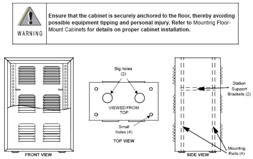
Floor-Mount Cabinet
The front, side and top views for all available floor-mount cabinets are shown below. Cabinet models and
hardware are shown in the following table:
Model Description
THN6700 12 inch Indoor Cabinet
THN6701 30 inch Indoor Cabinet
THN6702 46 inch Indoor Cabinet
THN6788 Motorola Cabinet Slides
CLN6833 Non-Motorola Cabinet Slides
See the installation manual for recommended equipment ventilation clearances. For improved access to the unit,
tray slides are available as shown in the table above.
APPLICANT: MOTOROLA EQUIPMENT TYPE: ABZ89FC4825
EXHIBIT D1-5
User / Operational Manual
Racking Configurations (Draft, Continued)
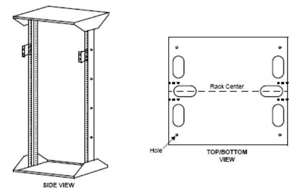
Modular Racks
The front, side and top views for all available floor-mount cabinets are shown below. The cabinet models and
associated description are shown in the following table:
Rack Model Description
THN6752 30 inch Modular Rack (16 RK U)
THN6753 45 inch Modular Rack (24 RK U)
THN6754 52 inch Modular Rack (27 RK U)
The side, top and bottom views for all available modular racks are shown below. The top and bottom plates are
identical, and all dimensions and clearances are common to all racks.
Recommended clearance front and rear is 91.44 cm (36 in) minimum for servicing access. Refer to Equipment
Ventilation for recommended ventilation clearances.
FRU kit CLN6679 (Rack Mount Hardware) is included with each rack model. This allows proper installation of the
MTR3000 base station / repeater within the rack’s center of gravity.
NOTE: This kit includes two rack mount standoffs and eight mounting screws.
APPLICANT: MOTOROLA EQUIPMENT TYPE: ABZ89FC4825
User / Operational Manual
Functional Description / Operation of Modules (Draft)
EXHIBIT D1-6
Base Radio Module Overview
The Motorola MTR3000 Base Station / Repeater (BR) provides a modular, flexible analog and digital station design
for today's communication systems and of the future. The stations are available for use in Analog Conventional,
Digital Conventional (MOTOTRBO), LTR Trunking, Passport Trunking, MOTOTRBO Capacity Plus Trunking, and
MOTOTRBO Connect Plus Trunking configurations.
The MTR3000 BR can either be configured as a stand-alone base station / repeater or as a base station / repeater
connected to a back-end network, as in the case of operating in IP Site Connect mode. As a base station /
repeater, it listens on one uplink frequency, and then re-transmits on a downlink frequency thus providing the RF
interface to the field subscribers. When configured for analog station operation, the BR is designed to operate with
most existing analog systems, therefore making a smooth migration to the MOTOTRBO system.
When configured for digital operation, the BR offers additional services. The digital BR operates in TDMA mode,
which essentially divides one channel into two virtual channels using time slots; therefore the user capacity is
doubled. The BR utilizes embedded signaling to inform the field radios of the busy/idle status of each channel
(time slot), the type of traffic, and even the source and destination information.
Note: When configured in Digital Mode, the BR can only be used as a repeater.
Note: At any given time, the BR either operates as a digital repeater or as an analog repeater.
The MTR3000 BR is divided into functional modules that separate the frequency band specific and transmitter
power specific circuits from other circuits and has separate modules for the control interface. These modules are
self contained functional blocks with module-specific alarms. This design facilitates the field replaceable unit
(FRU) concept of field repair to maximize system uptime.
Indicators and Connections
This section describes the LED indicators and connectors provided on the base station / repeater. The set of
LEDs indicate the operational status of the base station / repeater. There are two sets of connectors for devices
external to the base station / repeater:
• One set connects to external devices to enable full operation of the base station / repeater. These are
located at the back of the base station / repeater.
• Another set connects to external devices for servicing the base station / repeater. These are located on
the Station Control Module.
LED Indicators
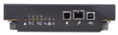
A set of eight LEDs is located on the base station / repeater front bezel. The position of the eight LEDs on the
front bezel is shown below. These LEDs indicate the status of the base station / repeater during normal operation.
Front Bezel LEDs and Connectors
After booting up the base station / repeater, the six LEDs (Power/Status, TX Slot 1, TX Slot 2, RX Slot 1, RX Slot 2
and the Mode LEDs) flashes in unison. The general status and condition of the MTR3000 Base Station / Repeater
can be obtained by observing the eight LED indicators on the front bezel. The following tables show the LED
symbols and their meaning and identify the information conveyed via the LED indicators.
APPLICANT: MOTOROLA EQUIPMENT TYPE: ABZ89FC4825
User / Operational Manual
Functional Description / Operation of Modules (Draft)
EXHIBIT D1-6
Front Bezel LED Indicators
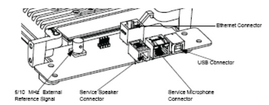
External Connections - Electrical Connections for the base station / repeater external connectors and line cord are
located on the back panel and are shown below.
Location of External Connectors at Rear of Base Station / Repeater
The connection to external devices on the back panel is the J7 Auxiliary System Connector. The connector is a
25-pin connector used for connecting to an external device such as a trunking controller, tone remote adaptor, or
phone patch.
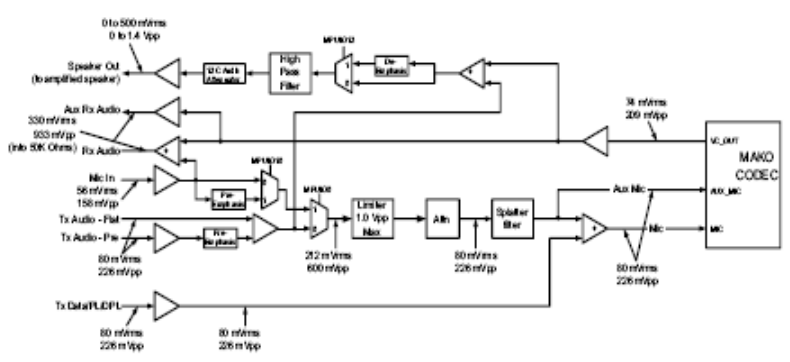
Service ports and LEDs are located on the front of the Station Control Module (SCM). The connection to external
devices on the front of the station control module is the BNC connector. The connector allows the base station /
repeater to be connected to a 5 MHz or 10 MHz external reference signal. The service ports include connectors
for:
• 5/10 MHz External Reference Signal
• Ethernet Connector
• Service Speaker Connector
• USB Connector
• Service Microphone Connector
APPLICANT: MOTOROLA EQUIPMENT TYPE: ABZ89FC4825
User / Operational Manual
Functional Description / Operation of Modules (Draft)
EXHIBIT D1-6
The locations of the connectors on the front of the station control module are shown below.
Control Overview
The Station Control Module (SCM) is described in this section. A general description, identification of controls,
indicators, and inputs/outputs, a functional block diagram, and functional theory of operation are provided. The
information provided is sufficient to give service personnel a functional understanding of the module, allowing
maintenance and troubleshooting to the module level.
General Description
The SCM circuitry performs the digital signal processing, data formatting and audio routing for the base station /
repeater (BR) and provides the external interfaces to the rest of the site.
The SCM uses two TI OMAP1710 processors:
- One for transmit and overall BR control functionalities
- One for all receive functionalities
Both OMAP1710 processors have independent boot Flash and RAM and, therefore can boot independently.
General SCM functionality includes:
• Data and Control interface to the Receiver’s Abacus III devices
• Data and Control interface to the Exciter’s Trident chip set
• Audio Codec interface with MAKO IC
• Host memory size, speed, and types supported
• External ports (Ethernet, USB, speaker and microphone)
• External physical interfaces (switches, connectors, LEDs, external references etc.)
• TX/RX DSP Multi-Channel Buffered Serial Port (MCBSP) interfaces
• Intermodule communication (using SPI)
• Internal station reference generation
Functional Theory of Operation
The following theory of operation describes the operation of the SCM at a functional level. The information is
presented to give the service technician a basic understanding of the functions performed by the module in order
to facilitate maintenance and troubleshooting to the module level.
TX OMAP - The TX DSP is a TI OMAP Multimedia Processor. The OMAP1710 consists of a microprocessor unit
(MPU) subsystem and a digital signal processor (DSP) subsystem.
OMAP1710 has dedicated external memory interface that allow point-to-point connection to standard mobile
SDRAM/DDR and mobile flash devices. It is a low-power device (1.4V Core and 1.8V I/O supply). TX OMAP
handles all transmit tasks of the SCM.
External Memory - Both transmit and receive DSP’s support independent external memory banks.
RAM - The SCM supports Mobile Double Data Rate SDRAM. It has the following basic characteristics: The
maximum external clock rate for the DDR is 90 MHz. Since data is transferred on both clock edges, the effective
data rate is 180 Mwords/s.
Flash - The SCM supports 256 MB external flash memory.
Serial Peripheral Interface (SPI) - The station local and Intermodule SPI Bus is controlled by both TX and RX
OMAP1710 processors, which has an on-chip SPIF (fast SPI) interface. The OMAP1710 SPIF supports master

APPLICANT: MOTOROLA EQUIPMENT TYPE: ABZ89FC4825
User / Operational Manual
Functional Description / Operation of Modules (Draft)
EXHIBIT D1-6
and slave modes, programmable clock rate, phase, polarity, programmable word size, programmable bit ordering,
and loopback.
Before an SPI data transfer can take place, the SPI master (initiator) must assert the select line of the slave
(target) device. The OMAP1710 is always the SPI master for MTR3000 BR. To simplify overall SPI architecture
for MTR3000 BR, address decoding is used instead of individual device chip signals. This approach not only
minimizes the number of GPIOs needed for device chip select, it also provides flexibility for future expansion. This
device address decoding is handled by a Field Programmable Gate Array (FPGA) on the SCM and a Customer
Programmable Logic Device (CPLD) on each FRU’s, except the power supply.
The FPGA SPI module performs address and chip select decoding, level shifting, and signal mixing for both the TX
OMAP SPI bus and the RX OMAP SPI bus. Simultaneous RX and TX SPI accesses are allowed. The TX and RX
SPI are 100% independent.
Station Reference RX - A TCXO provides the frequency reference for the BR. The TCXO is 16.8 MHz. The FPGA
is used to create other clocks locked to the TCXO which are needed by various devices on the Control Board.
The clocks are summarized in the following table:
Station Control Module (SCM) FPGA output Frequencies
Frequency Destination
12 MHz TX OMAP, RX OMAP
24.576 MHz MAKO
32.768 kHz TX OMAP, RX OMAP, MAKO
RX OMAP
The RX DSP is a TI OMAP Multimedia Processor. The OMAP1710 consists of a microprocessor unit (MPU)
subsystem and a digital signal processor (DSP) subsystem. OMAP1710 has dedicated external memory interface
that allows point-to-point connection to standard mobile SDRAM/DDR and mobile flash devices. It is a low-power
device (1.4V Core and 1.8V I/O supply). The RX OMAP handles receiving tasks of the SCM only.
MAKO - MAKO IC is a customized IC and the SCM uses this device to leverage some unique functionality that it
provides.
Most of the MAKO functionalities are not used on the SCM. Only the MAKO codec, USB driver, ADC, DAC, and
some voltage regulators are used for MTR3000. The 9 channel general purpose ADC is used for various controller
metering.
Field Programmable Gate Array (FPGA) - The SCM FPGA includes the following major functions:
• External reference watchdog
• SPI Address decoding and buffering
• TCXO Phase detection and compensation
• Clock generation
• Reset controller
• External Interface (Wireline SSI, LED, etc.)
FPGA field upgrade capability is also supported on MTR3000.
Audio - There are four transmit inputs: TX Audio, TX Audio-Pre & TX Data on the backplane 25-Pin connector, and
the microphone input on a front panel RJ45 connector.
TX Audio is a flat (not pre-emphasized) input which is used if the incoming transmit audio signal is already pre-
emphasized or if pre-emphasis is not needed. The TX Audio-Pre input provides a hardware pre-emphasis filter.
The TX Data input is used for low speed data, Private-Line (PL) and Digital Private Line (DPL) signals. The TX
Audio, TX Audio-Pre and microphone inputs pass through a hardware modulation limiter and splatter filter before
being summed with TX Data, with the TX Data bypassing the limiter and splatter filter. This summed signal is
applied to the MAKO codec “mic” input. The audio signal without TX Data is provided on the MAKO codec
“aux_mic” input.
There are three receive outputs: RX Audio & Aux RX Audio on the backplane 25-Pin connector and speaker audio
on a front panel RJ11. The speaker audio is the sum of the MAKO codec output (demodulated audio) and transmit
audio. A high pass filter removes any data, PL or DPL from the speaker audio. A programmable attenuator is
used to adjust the speaker audio level before being output on the RJ11 connector. Aux RX Audio is the output of
APPLICANT: MOTOROLA EQUIPMENT TYPE: ABZ89FC4825
User / Operational Manual
Functional Description / Operation of Modules (Draft)
EXHIBIT D1-6
the MAKO codec (demodulated audio), and RX Audio is the sum of the MAKO codec output and the microphone
audio.
A block diagram of the audio paths follows:
Ethernet Interface - Since OMAP1710 does not support a direct Ethernet interface, a bridge device is needed to
support Ethernet on the SCM. The bridge device is a high performance hi-speed USB2.0 to 10/100 Ethernet
controller. The device contains an integrated 10/100 Ethernet PHY, USB PHY, Hi-Speed USB 2.0 device
controller, 10/100 Ethernet MAC, TAP controller, EEPROM controller and a FIFO controller with a total of 30
KBytes of internal packet buffering. The following is a list for functionality that the Ethernet Interface can provide:
• Fully Compliant with IEEE 802.3 and 802.3u Compatible Ethernet Controller
• 10Base-T and 100Base-TX support
• Integrated Media Access Control (MAC) and PHYsical (PHY)
• Supports one 10BT port with automatic polarity detection and correction
• Supports full and half duplex mode and flow control
• Universal Serial Bus (USB) and Joint Test Action Group (JTAG) parameters
Backplane - The connector that connects the controller to the backplane is a right angle, 96-Pin Connector. It
provides connectivity between the MTR3000 controller and other station FRU, such as the Wireline card, the AUX
IO card as well as, third party equipments.
Exciter - The connector used to connect the controller to the Exciter and Receiver is a dual row, right angle, early
entry receptacle, without flange, 30-Pin Connector. It provides 16.8 MHz reference clock, 14.2V, 10V and 8V
supply voltage, SPI, Trident SSI and other digital handshake signals with the Exciter.
Receiver - The connector used to connect the controller to the Exciter and Receiver is a dual row, right angle, early
entry receptacle, without flange, 30-Pin Connector. It provides 16.8 MHz reference clock, 14.2V, 10V and 8V
supply voltage, SPI, Abacus SPI/SSI and other digital handshake signals with the Receiver.
APPLICANT: MOTOROLA EQUIPMENT TYPE: ABZ89FC4825
User / Operational Manual
Functional Description / Operation of Modules (Draft)
EXHIBIT D1-6
Receiver Overview
The Receiver Module provides the Receiver functionality for the UHF station. The Receiver module performs
highly-selective bandpass filtering and dual down-conversion of the desired RF signal. A custom Receiver IC then
performs an analog-to-digital conversion of the desired received signal and outputs a differential data signal to the
Station Control Module (SCM).
The Receiver Module kit contains an on-board, varactor-tuned preselector, which cover the frequency ranges of
403–470 MHz, and 450–524 MHz, respectively. The UHF range Receivers utilize an external coaxial-resonator
bandpass filter (BPF) for some configurations.
Overview of Circuitry
The Receiver Module contains the following circuitry:
• Frequency Synthesizer Circuitry – consists a phase-locked loop and Voltage-Controlled Oscillator (VCO),
generates the first LO injection signal
• Varactor-tuned Preselector Filter – provides bandpass filtering of the station Receiver RF input
• Receiver Front End Circuitry – performs filtering, amplification, and the first down conversion of the
Receiver RF signal
• Custom Receiver IC Circuitry – consists a custom IC which performs the second down conversion,
filtering, amplification, and analog-to-digital conversion of the receive signal
• Analog to Digital Converter (ADC) Converter Circuitry – converts analog Receiver status signals to digital
format for transfer, upon request, to the SCM
• Local Power Supply Regulation – accepts +8V, +10V and +14.2V inputs and outputs +2.775V, +3.3V, +5V,
+10V, and +14.2V operating voltages
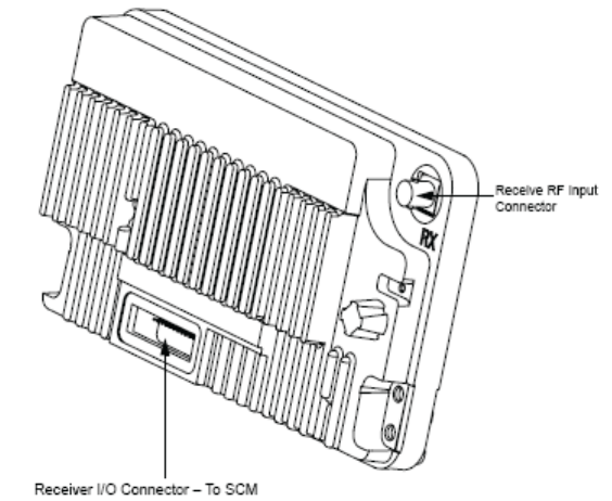
Input and Output Connections
The following shows the Receiver module input and output external connections.

APPLICANT: MOTOROLA EQUIPMENT TYPE: ABZ89FC4825
User / Operational Manual
Functional Description / Operation of Modules (Draft)
EXHIBIT D1-6
Specifications
The following table shows the specifications of MTR3000 Base Station / Repeater’s Receiver.
Parameter Specification
Frequency Ranges 403–470 MHz (UHF R1) or 450–524 MHz (UHF R2)
Electronic Bandwidth Full Bandwidth (UHF R1 and R2)
Analog Sensitivity 12 dB SINAD 0.257 μV (-118.8 dBm)
Intermodulation Rejection 85 dB
Adjacent Channel Rejection* 75 dB at 12 kHz, 80 dB at 25 kHz
Spurious and Image Response Rejection 85 dB
Intermediate Frequencies 1st: 73.35 MHz
2nd: 2.25 MHz
RF Impedance 50 Ω
Current Draw (Maximum) 0.04A from 14.2 VDC supply
0.52A from 10 VDC supply
0.11A from 8 VDC supply
Receiver Front End Circuitry
The RF signal enters the Receiver through a BNC-type RF connector, located on the bottom side of the Receiver.
The signal is then low-pass filtered, and the 1/2 IF and image frequency are filtered through the tunable
preselector. This signal is then amplified using a low-noise amplifier (LNA), and then further filtered to remove the
image signal.
Receiver Back End Circuitry
The signal after the image filter is then mixed down to the first IF, via a high performance (high IIP3) mixer, driven
by the low-phase noise, voltage-controlled Colpitts oscillator (VCO). The mixed-down signal then passes through
a 3-pole, crystal IF bandpass filter and an IF amplifier. The amplifier output signal passes through another 3-pole
crystal bandpass filter, and the resultant signal passes through a digital step attenuator. The desired signal is then
applied to the RF input of the custom backend Receiver IC.
Voltage Controlled Oscillator (VCO)
The Receiver Voltage Controlled Oscillator (VCO) generates a sinusoidal output signal that ranges from 476.35
MHz to 543.35 MHz (UHF R1) and 523.35 MHz to 597.35 MHz (UHF R2). Either UHF R1 or UHF R2 can be used
at a time. The Receive Voltage-Controlled Oscillator (RXVCO) line-up consists of four sub-circuits: a Voltage-
Controlled Oscillator (VCO), an attenuator, a buffer-amplifier, and a low pass filter (LPF).
The active device is from oscillator topology, utilizing a high-Q resonator, and four anti-parallel configured, hyper-
abrupt, tuning varactors.
The attenuator provides a broadband RF load for the VCO. The buffer-amplifier provides power leveling and
isolation. The LPF provides VCO harmonic attenuation.
Synthesizer Circuitry
The Receiver synthesizer is a subcircuit within a custom IC, which when connected with a loop filter, VCO, buffer
amplifier, lowpass filter, driver amplifier, unequal splitter, and feedback attenuator forms a phase-locked loop. The
frequency and phase of the VCO is locked to a highly-stable external Temperature Compensated Crystal Oscillator
(TCXO) reference (16.8 MHz). The custom IC contains the following integrated Phase locked loop (PLL)
components: prescaler, fractional-N divider, reference divider, phase detector, and charge-pump (for the external
loop-filter). The reference divider frequency is selected to be either 8.4 MHz or 5.6 MHz.
APPLICANT: MOTOROLA EQUIPMENT TYPE: ABZ89FC4825
User / Operational Manual
Functional Description / Operation of Modules (Draft)
EXHIBIT D1-6
Custom Backend Receiver IC Circuitry
The custom backend Receiver IC provides additional amplification, filtering, and a second downconversion. The
second IF signal is converted to a digital signal, and output via either a differential or single-ended driver to the
digital signal processor (DSP) in the SCM.
Memory Circuitry
The memory circuitry consists of an Electrically Erasable Programmable Read-Only Memory (EEPROM), located
in the Receiver. The SCM performs memory read and write operations via the SPI bus. The RX Front-End Filter
tuning calibration is stored in the EEPROM. Therefore, no field tuning is ever required for the Receiver.
Analog to Digital (ADC) Converter Metering Circuitry
Analog signals from points throughout the Receiver are applied to the ADC converter. These analog signals are
converted to digital signals and then sent to the SCM, via the Serial Peripheral Interface (SPI) lines, upon request
of the SCM.
Communications with Station Control Module
Data communications between the Receiver and the Station Control Module microprocessor (μP) is performed via
a Serial Peripheral Interface (SPI) bus. This bus allows the SCM μP to send data to the synthesizer PLL IC (to
select frequency) and to read the ADC Converter IC.
ADC Converter Circuitry
Analog signals from various strategic operating points throughout the Receiver board are fed to an ADC converter,
which converts them to a digital signal and, upon request by the Station Control Module, outputs the signal to the
Station Control Module via the Serial Peripheral Interface (SPI) bus.
APPLICANT: MOTOROLA EQUIPMENT TYPE: ABZ89FC4825
User / Operational Manual
Functional Description / Operation of Modules (Draft)
EXHIBIT D1-6
Exciter Overview
The Exciter Modules (in conjunction with the Power Amplifier Module) provides the transmitter functions for the
station. Contained within a metal clamshell housing, the Exciter board generates a low-level modulated Radio
Frequency (RF) signal which is input to the power amplifier module for further amplification and output to the
transmit antenna. The Exciter Modules interfaces directly with the Station Control Module (SCM), which provides
control signals and monitoring, and routes transmit audio to the Exciter.
The RF carrier is generated by a frequency synthesizer consisting of synthesizer circuitry and Voltage-Controlled
Oscillator (VCO) circuitry. Exciter module control signals, monitoring, and audio processing are handled by the
Station Control Module (SCM). The Exciter Modules differ only in the range of operation. Unless otherwise noted,
the information provided in this section applies to all models.
The Exciter board contains the following circuitry:
• Frequency Synthesizer Circuitry – consists of a phase-locked loop and Voltage-Controlled Oscillator
(VCO), generates a modulated RF signal at the transmitter carrier frequency
• RF Isolation Switch – allows the SCM to turn on/off the Exciter RF output signal to the power amplifier
module
• Analog to Digital Converter (ADC) Converter Circuitry – converts the analog Exciter status signals to the
digital format for transfer, upon request, to the SCM
• Local Power Supply Regulation/Filtering – accepts +8V, +10V and +14.2V inputs and provides +5V, +10V,
and +12V operating voltages
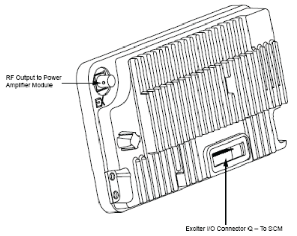
Input and Output Connections - The following shows the Exciter module input and output external connections.
Specifications of Exciter Module
Parameter Specification
Frequency Ranges 403–470 MHz (UHF R1) or 450–524 MHz (UHF R2)
Electronic Bandwidth Full Bandwidth (UHF R1 and R2)
Output Power 10–14 dBm
Current Draw (Maximum) 0.04A from 14.2 VDC supply
0.15A from 10 VDC supply
0.02A from 8 VDC supply
Harmonics -20 dBc
APPLICANT: MOTOROLA EQUIPMENT TYPE: ABZ89FC4825
User / Operational Manual
Functional Description / Operation of Modules (Draft)
EXHIBIT D1-6
Functional Theory of Operation
The following theory of operation describes the operation of the Exciter circuitry at a functional level. The
information is presented to give the service technician a basic understanding of the functions performed by the
module in order to facilitate maintenance and troubleshooting to the module level. Refer to a block diagram of the
Exciter module.
Functional Overview
Synthesizer and VCO Circuitry
Phase-Locked Loop
The phase-locked loop (PLL) IC receives frequency selection data from the SCM microprocessor (via the SPI bus).
Once programmed, the PLL IC compares an 8.4 MHz reference signal (from the SCM) with a divided-down
feedback sample of the VCO output. Depending on whether the feedback signal is higher or lower in frequency
than the 8.4 MHz reference, up/down correction pulses are generated. (The width of these correction pulses
depends on the quantitative difference between the 8.4 MHz reference and the VCO feedback).
The up/down pulses from the PLL IC are fed to a charge pump which outputs a DC voltage proportional to the
pulse widths. This DC voltage is then low-pass filtered and fed to the VCO as the control voltage.
Voltage Controlled Oscillator (VCO)
The DC control voltage from the synthesizer is fed to dual VCOs which generate the RF carrier signal. Within each
band, one VCO generates signals in the upper half of the band, while the other VCO generates signals in the lower
half of the band. Only one VCO is active at a time. Selection of the active VCO is provided by a VCO_SELECT
signal from the PLL IC.
The active VCO responds to the DC control voltage and generates the appropriate RF signal. This signal is fed
through impedance matching, amplification, and filtering and is output to the RF Switch Circuitry. A sample of the
output is returned to the PLL IC to serve as a VCO feedback signal.
Modulation
The Exciter uses dual-port FM modulator consisting of Digital Signal Processor (DSP), PLL low-port and high port
blocks, fractional-N PLL, loop filter and the VCO. The modulator is calibrated once during factory test and its
values are stored in the EEPROM. The modulator does not require any further tuning or maintenance.
Amplifiers
The amplifiers consist of a driver amplifier and the final amplifier. The driver amplifier operates from a nominal 5V
supply and the final amplifier operates from a nominal 10V supply. The driver amplifier amplifies the VCO output
signal and provides the output signal to the final amplifier. There are fixed attenuators at the output of the driver
and final amplifier to set the Exciter output power level. The final amplifier amplifies the signal and provides a
constant signal level to the PA.
RF Switch Circuitry
The modulated RF signal from the VCO is fed through a buffer, driver, and attenuator and finally to an RF switch
circuit. Signal EX_ENABLE from the SCM controls the switch and final amplifier. The RF signal is passed through
a LPF and to a BNC connector mounted in one corner of the module, just outside the module cover. A short
coaxial cable connects the Exciter output to the power amplifier module.
APPLICANT: MOTOROLA EQUIPMENT TYPE: ABZ89FC4825
User / Operational Manual
Functional Description / Operation of Modules (Draft)
EXHIBIT D1-6
Communications with Station Control Module
Data communications between the Exciter and the Station Control Module microprocessor (μP) is performed via a
Serial Peripheral Interface (SPI) bus. This bus allows the SCM μP to send data to the synthesizer PLL IC (to
select frequency) and to read the ADC Converter IC.
ADC Converter Circuitry
Analog signals from various strategic operating points throughout the Exciter board are fed to an ADC converter,
which converts them to a digital signal and, upon request by the Station Control Module, outputs the signal to the
Station Control Module via the Serial Peripheral Interface (SPI) bus.
Voltage Regulation/Filtering Circuitry
The voltage regulator circuitry consists of a +5V, +3.3V and +2.775V regulators that supplies power to the digital
circuitry and the PLL. The +12V regulator is used to supply power to the VCO and the +10V supplies power to the
final device.
APPLICANT: MOTOROLA EQUIPMENT TYPE: ABZ89FC4825
User / Operational Manual
Functional Description / Operation of Modules (Draft)
EXHIBIT D1-6
Power Amplifier Module Overview
The Power Amplifier (PA) is a forced convection-cooled RF power amplifier. It accepts a low-level modulated RF
signal from the Exciter Module, and amplifies it for transmission via the site transmit antenna port. The PA is non-
linear, and is therefore used for continuous wave (CW) applications only. The output power is continually
monitored and regulated by a feedback and control loop, with a power output control voltage being generated by
the transmitter control circuitry located on the PA Input/Output boards.
Overview of Circuitry
The Power Amplifier contains the following sub-circuits:
• DC Distribution Board – main interface for the PA to the Station Control Module (SCM) and Power Supply
(PS). This board contains PA SPI circuits including Analog to Digital Converter (ADC), Digital to Analog
Converter (DAC), and Non-Volatile Memory (NVM) devices, and hardware (HW) metering circuitry
• RF Board – provides RF signal amplification from the Exciter Module low-level signal to the BR output
power level
• Isolator – protects the PA from damage when poor RF load conditions exist. Also assists with
intermodulation attenuation performance
• Output Board – performs harmonic filtering and RF power detection functions, and routes the RF signal to
the antenna port
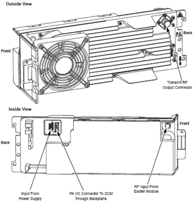
Input and Output Connections
The following shows the PA input and output external connections.
APPLICANT: MOTOROLA EQUIPMENT TYPE: ABZ89FC4825
User / Operational Manual
Functional Description / Operation of Modules (Draft)
EXHIBIT D1-6
The following table shows the specifications of MTR3000 Power Amplifier (PA).
Specifications of Power Amplifier
Parameter Specification
Operational Frequency Range 403–470 MHz (UHF R1) or 470–524 MHz (UHF R2)
Minimum Input Return Loss (TX mode) 7 dB
Rated RF Output Power Range 8–100 W
Rated RF Input Power Range 9.8–14 dBm
28.6V Supply Nominal Voltage (AC Power) 28.6V (+/- 4%)
14.2V Supply Nominal Voltage 14.2V (+/- 3%)
28.6V Supply Maximum Current Draw 12.6A
14.2V Supply Maximum Current Draw 2.0A
Maximum Standby Power Consumption 1.2 W
Functional Theory of Operation
The Power Amplifier (PA) is designed for continuous-duty operation across each specified band and power level.
All PA contain a multi-stage power amplifier board at the input (RF Board), a circulator with isolation load
termination, a low-pass filter/directional coupler at the output (Output Board), and a DC Distribution Board
incorporating circuitry for diagnostics and RF power control. The PA and its sub-circuits are broad-band devices
and require no manual tuning or alignment to operate over the specified conditions.
The main interface between the PA and the rest of the BR is through the DC Distribution Board. The DC
distribution board contains the PA external I/O’s that connects to the power supply directly through a cable and to
the control module through a cable to the backplane. These I/O’s are used to distribute the DC supply buses
(28.6V and 14.2V nominal) from the power supply to within the PA as well as the various signals used for the
control of the PA from the SCM such as the SPI bus signals, PA enable, and the reset line.
The DC Distribution Board contains the SPI circuitry as well as metering circuitry used by both SW and internal PA
HW for determining when fault conditions are present and take appropriate action when needed. A brief
description of the PA SPI devices is shown below:
• Customer Programmable Logic Device (CPLD): main PA SPI interface, with all other PA SPI devices
connected through this device
• Non-Volatile Memory (NVM): used to store calibration data and identification information
• Digital to Analog Converter (DAC): converts SW digital signals to analog within the PA. This controls the
PA fan, power control circuit, and some other circuits within the PA
• Analog to Digital Converter (ADC): converts analog signals within the PA to digital for SW interface. These
signals are used by SW for HW metering
A combination of software (SW) and hardware (HW) controls are used to regulate the PA RF output power level.
By way of software control, the SCM programs RF output power through the SPI bus. Once programmed, the PA
power control loop will level the output power to the requested level, if possible. The requested output power may
not be achievable if an alarm condition is present, and output power may be reduced by way of SW or HW control
if alarm conditions are present.
Within the Base Station / Repeater (BR), the modulated RF signal passes from the Exciter Module to the driver
amplifier within the PA. The driver amplifier is located on the RF Board and is a multi-stage amplifier circuit that
amplifies the RF input signal up to a maximum of approximately 4 W, as needed to achieve the software requested
BR RF output power. The RF signal from the driver amplifier is further amplified by the final amplifier stage, which
is also located on the RF Board and consists of multiple paralleled RF devices with associated splitting and
combining circuitry.
This RF signal then passes through a circulator and harmonic (low pass) filter, through an RF directional coupler,
and is output to the site transmit antenna port. The circulator prevents a high Voltage Standing Wave Ratio
(VSWR) at the PA output from damaging the final amplifier devices, and also improves intermodulation attenuation
(IMA) performance by providing isolation to the final amplifier. The harmonic filter attenuates the harmonic levels
generated by the preceding RF amplifier devices.
The RF directional coupler is a calibrated wattmeter, with its calibration information stored in the PA NVM. The
forward and reverse power wattmeter provides a signal corresponding to the measured output power to the ADC
APPLICANT: MOTOROLA EQUIPMENT TYPE: ABZ89FC4825
User / Operational Manual
Functional Description / Operation of Modules (Draft)
EXHIBIT D1-6
for metering purposes so that SW can monitor the PA/BR output power. Also, this voltage is provided to the power
control circuitry within the PA to serve as the feedback signal in the power control loop for setting output power.
The forward power meter along with the reverse power meter is used by SW to measure the VSWR presented to
the PA output and to determine when an alarm condition is present.
The SW requested power level may include one or more SW controlled adjustments based on various alarm
conditions, if present, generated from monitored PA metering signals which are fed back to the SCM via an ADC
converter. Using the ADC metering circuitry, SW monitors the PA for alarm conditions, such as high reflected
power/VSWR or high/low supply voltage, and takes action to reduce output power or dekey the station accordingly
in order to protect the HW from damage or improper operation.
Temperature monitoring circuitry is also contained within the PA. When the temperature reaches a certain
threshold, the PA fan turns on to reduce the operating temperature of the PA. If the temperature continues to rise
and reaches another predefined threshold, the BR output power may also be reduced in order to protect the HW
from thermal failure. Both the fan control and the power control manipulation for thermal protection is fully HW
controlled, and requires no SW interaction.

APPLICANT: MOTOROLA EQUIPMENT TYPE: ABZ89FC4825
User / Operational Manual
Functional Description / Operation of Modules (Draft)
EXHIBIT D1-6
Power Supply Module Overview
The Power Supply is described in this section. The information provided is sufficient to give service personnel a
functional understanding of the module, allowing maintenance and troubleshooting to the module level. (Refer to
the service manual for Maintenance and Disassembly/Reassembly Procedures for detailed removal or installation
procedures for all modules in the station.)
The Power Supply has built in power factor correction and includes a connection for battery backup that also
serves as the DC input when the supply is used in DC only input mode.
The Power Supply accepts an AC or a DC input (AC input = 85 to 264 VAC, 50/60 Hz, DC input = 21.6 to 32 VDC)
and generates three output DC voltages to power the station modules: +28.6 VDC, +14.2 VDC and +5.1 VDC.
Note: When used in DC input mode, the 28.6 VDC output equals the DC input within 0 to -0.5 VDC.
Note: An external 24V (nominal) battery system is required to support the battery backup feature so that when the
AC power fails, the BR can be powered from a DC battery source if it is connected to the PS. This results in
uninterrupted radio service (for as long as battery power can be provided). As the PS does not have a battery
charging function, when the AC power is restored, an external charger is required to recharge the battery.
The power supply is a high-frequency switched mode design, all contained in a metal heat-sink, and mounted on
the left-hand side of the station. The design provides for output over-voltage/overcurrent protection.
The AC input connection is made at the rear of the station via an IEC-type connector keyed to accept only high
temperature type mating connectors. Also provided is a Battery Backup connection (see DC mode above). Power
supply cooling, when necessary, is provided by an external fan (located near the middle of the heatsink) which
provides forced air across the power supply heatsink fins.
The following shows the electrical performance specifications for the power supply.
Power Supply Module AC Performance Specification:
Parameter Value or Range
Input Voltage Range 85 VAC to 264 VAC
Input Frequency Range 47–63 Hz
Steady State Output Voltage 28.6 V @ 13 A,
14.2 V @ 8 A,
5.1 V @ 2 A
Output Power (Rated) 500 W
Output Ripple:
+28.6 VDC
+14.2 VDC
+5.1 VDC
50 mV p-p, @ 25°C (77°F)
50 mV p-p, @ 25°C (77°F)
100 mV p-p, @ 25°C (77°F)
Power Supply Module DC Performance Specification:
Parameter Value or Range
Input Voltage Range 21.6 - 32 VDC
Steady State Output Voltage 28.6 V @ 13 A, Input Voltage Dependent
14.2 V @ 8 A, Regulated
5.1 V @ 2 A, Regulated
Output Power (Rated) 500 W
Output Ripple:
+28.6 VDC
+14.2 VDC
+5.1 VDC
Input Voltage Dependent, 0-0.5V below input
50 mV p-p, @ 25°C (77°F)
100 mV p-p, @ 25°C (77°F)