Motorola Solutions 89FC5798-P Licensed Base Station for Part 24 User Manual 2 688001E35 E
Motorola Solutions, Inc. Licensed Base Station for Part 24 2 688001E35 E
UserManual.wiki
>
Motorola Solutions
>
89FC5798 P User Manual
Exhibit D Users Manual per 2 1033 c3
Navigation menu
Upload a User Manual
Namespaces
Wiki Guide
HTML
PDF
Info
Views
User Manual
Discussion / Help
Navigation

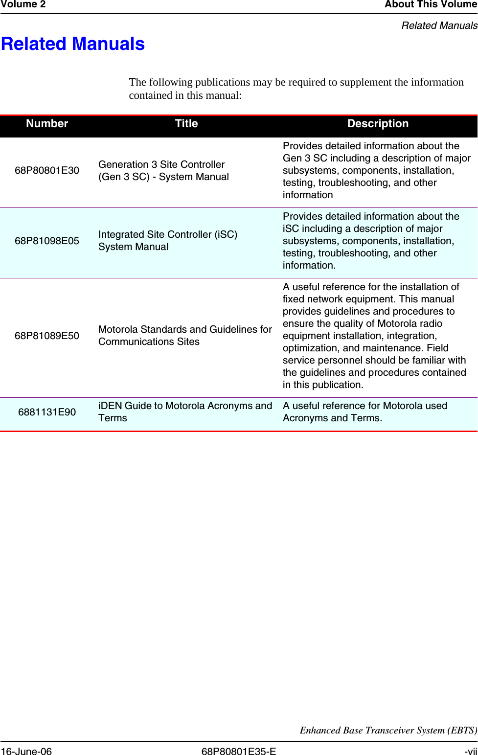
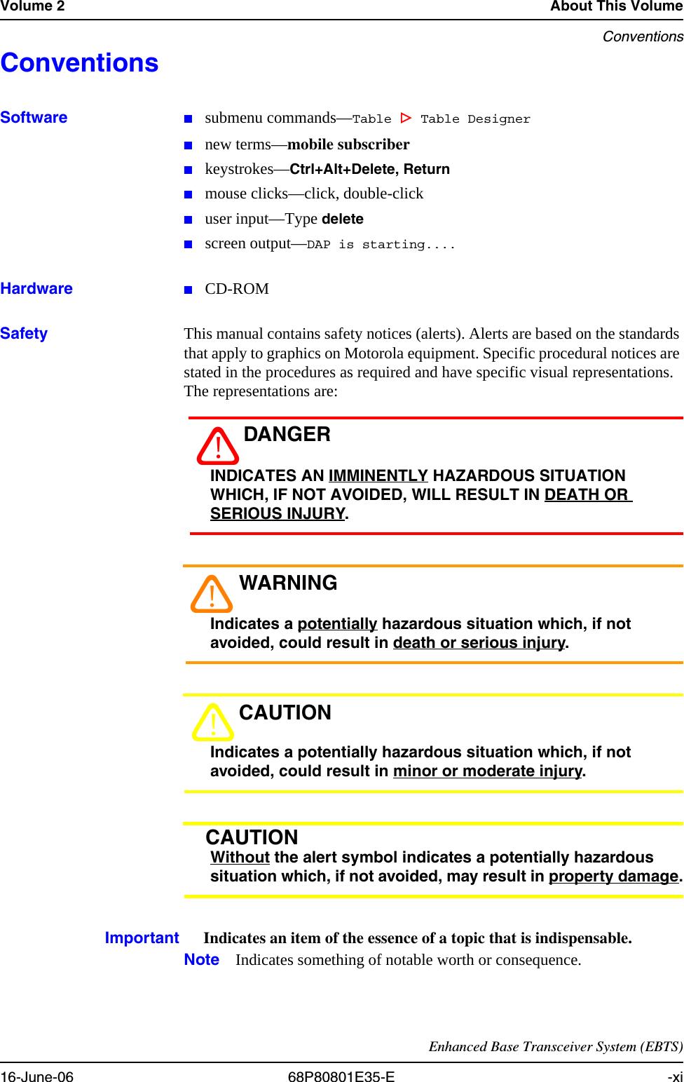
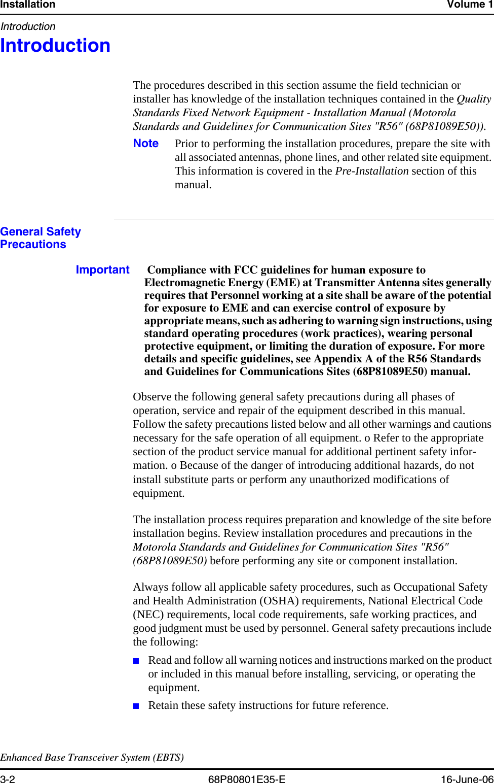
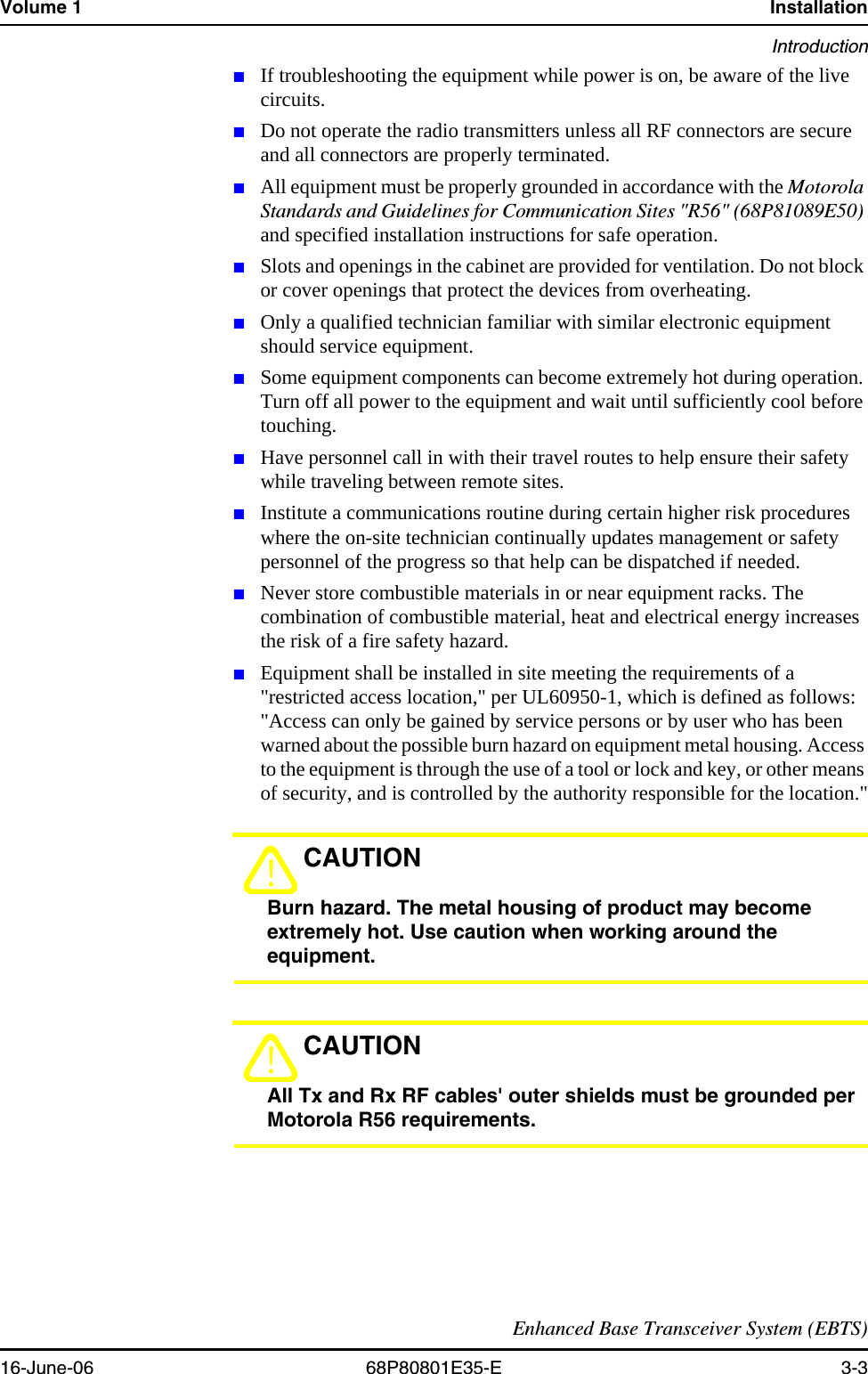
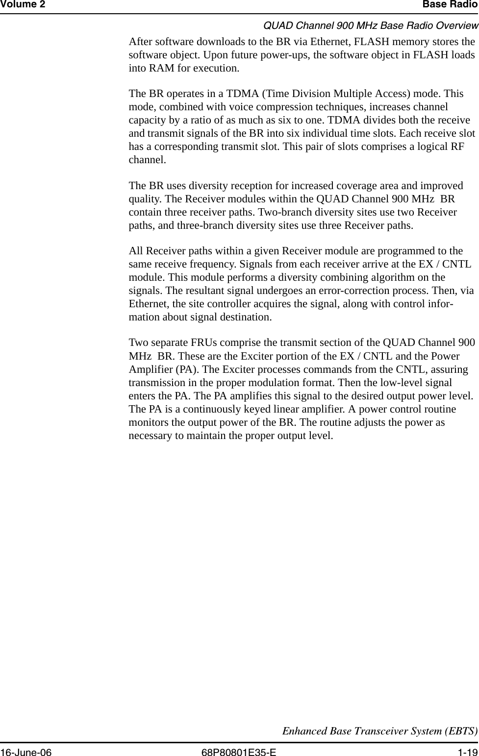
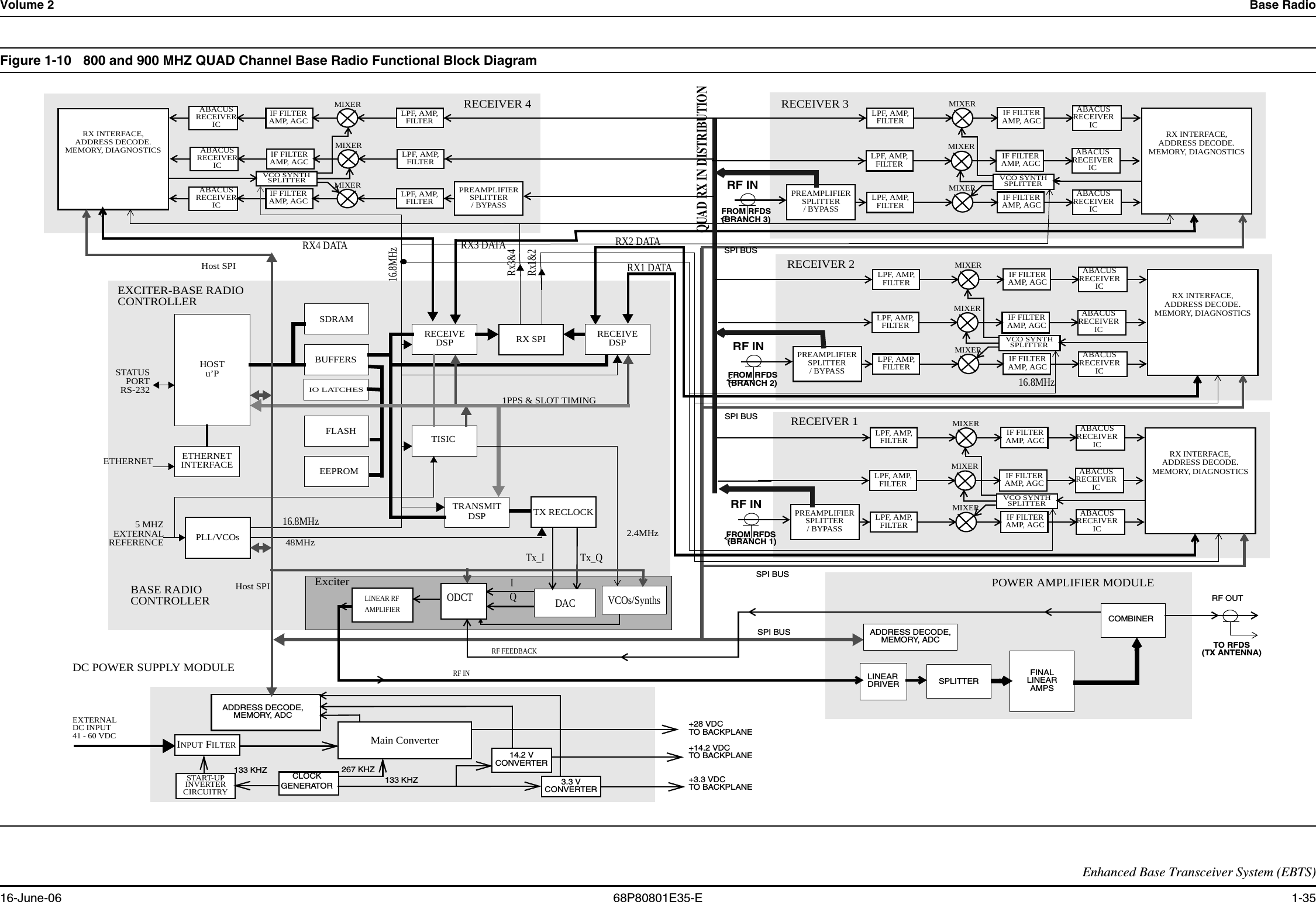

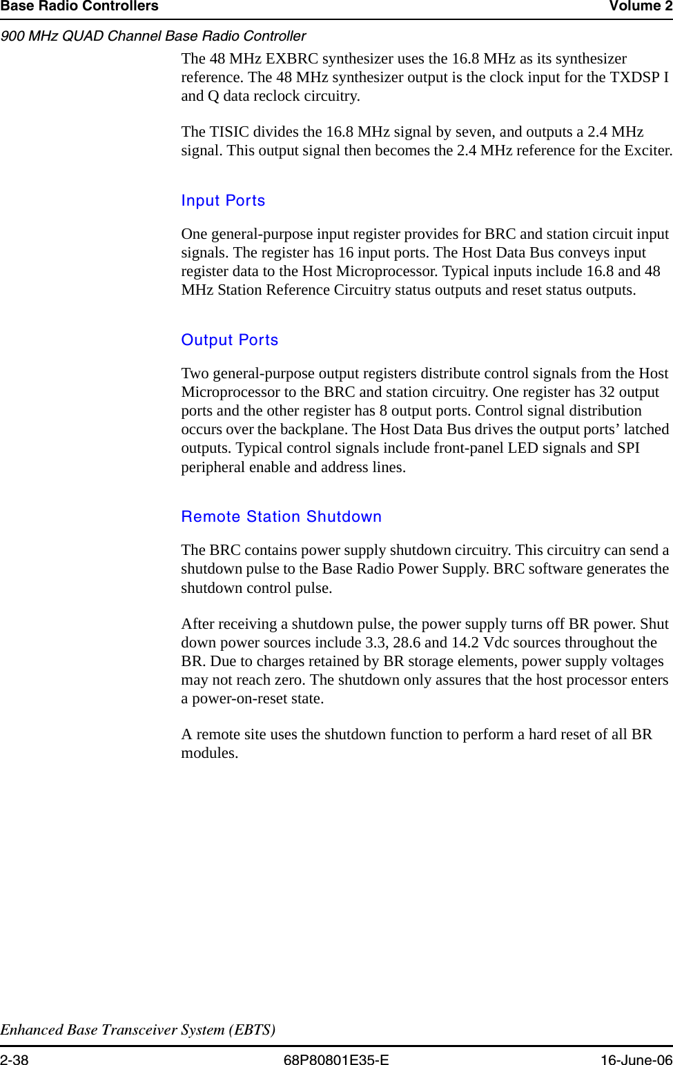
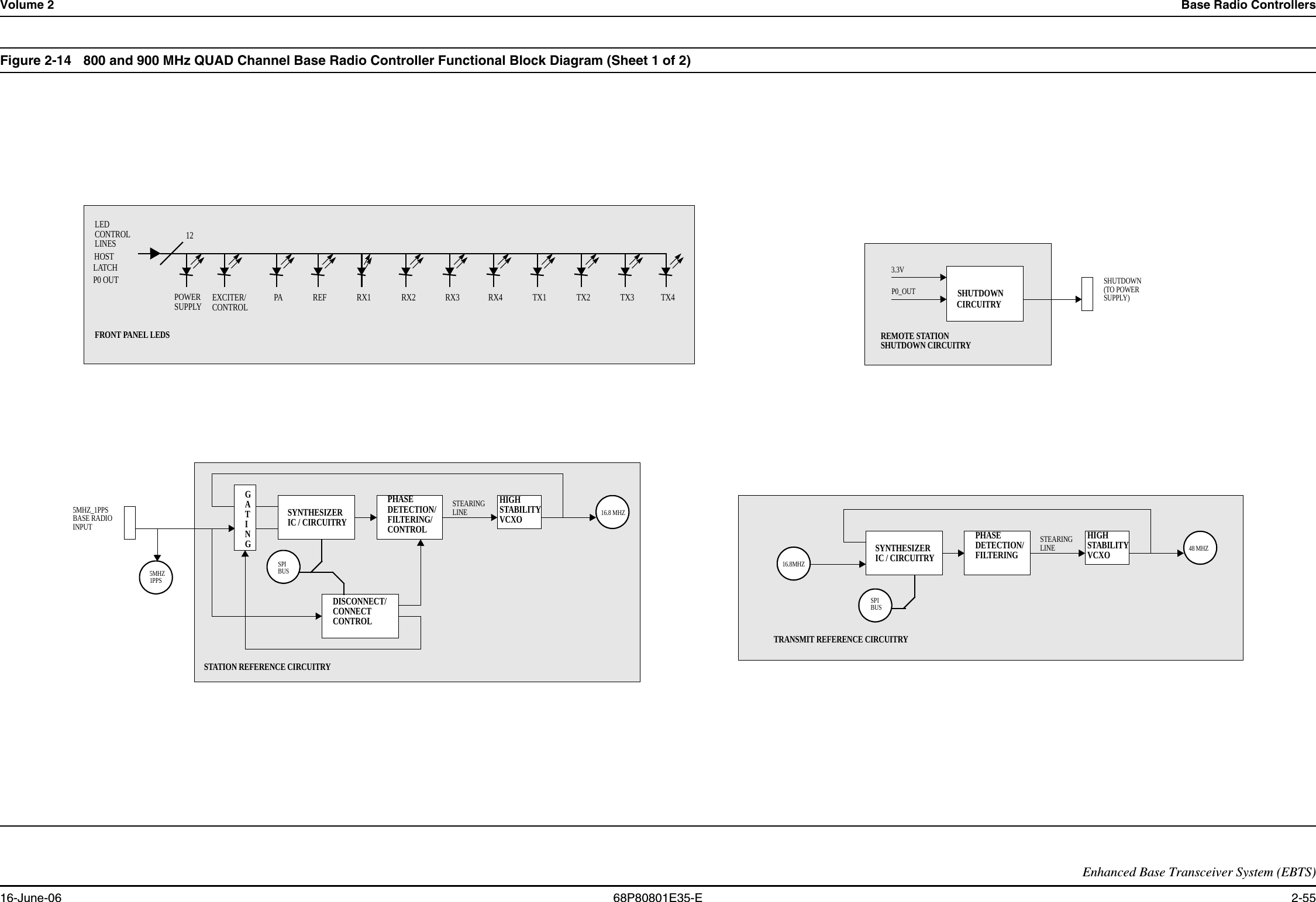
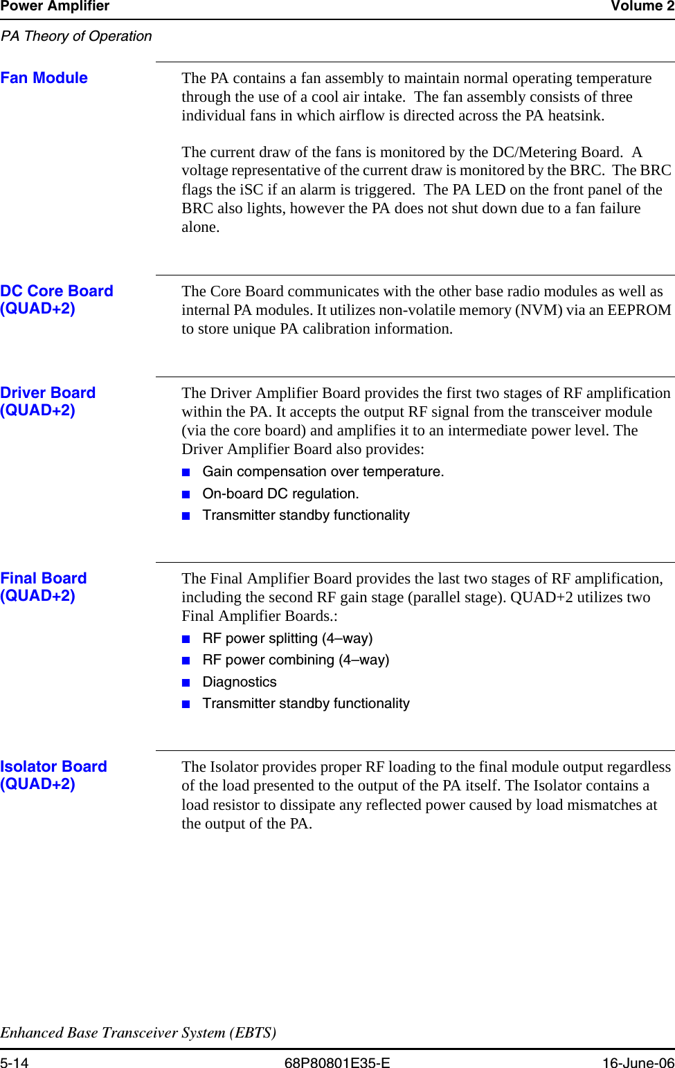
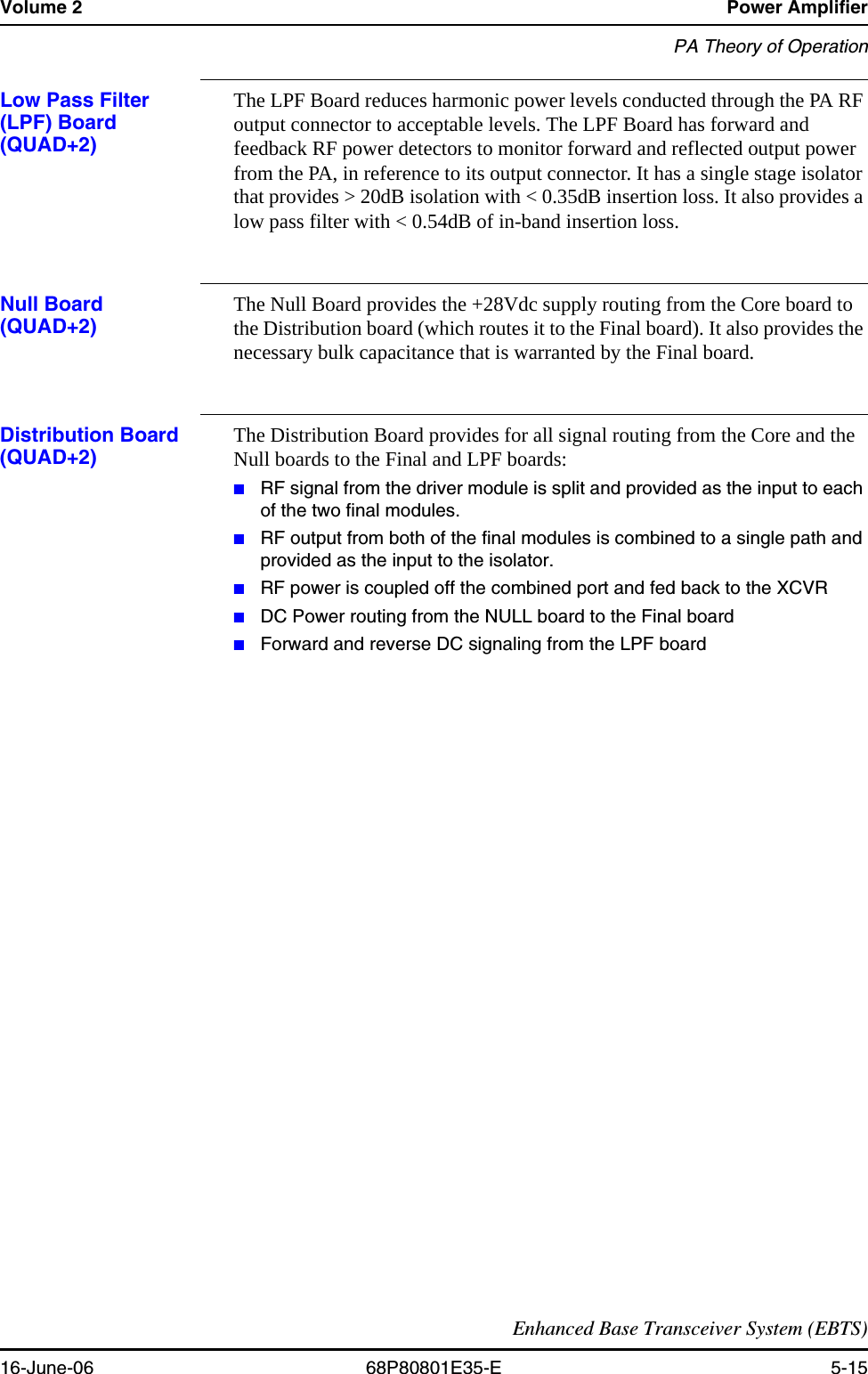
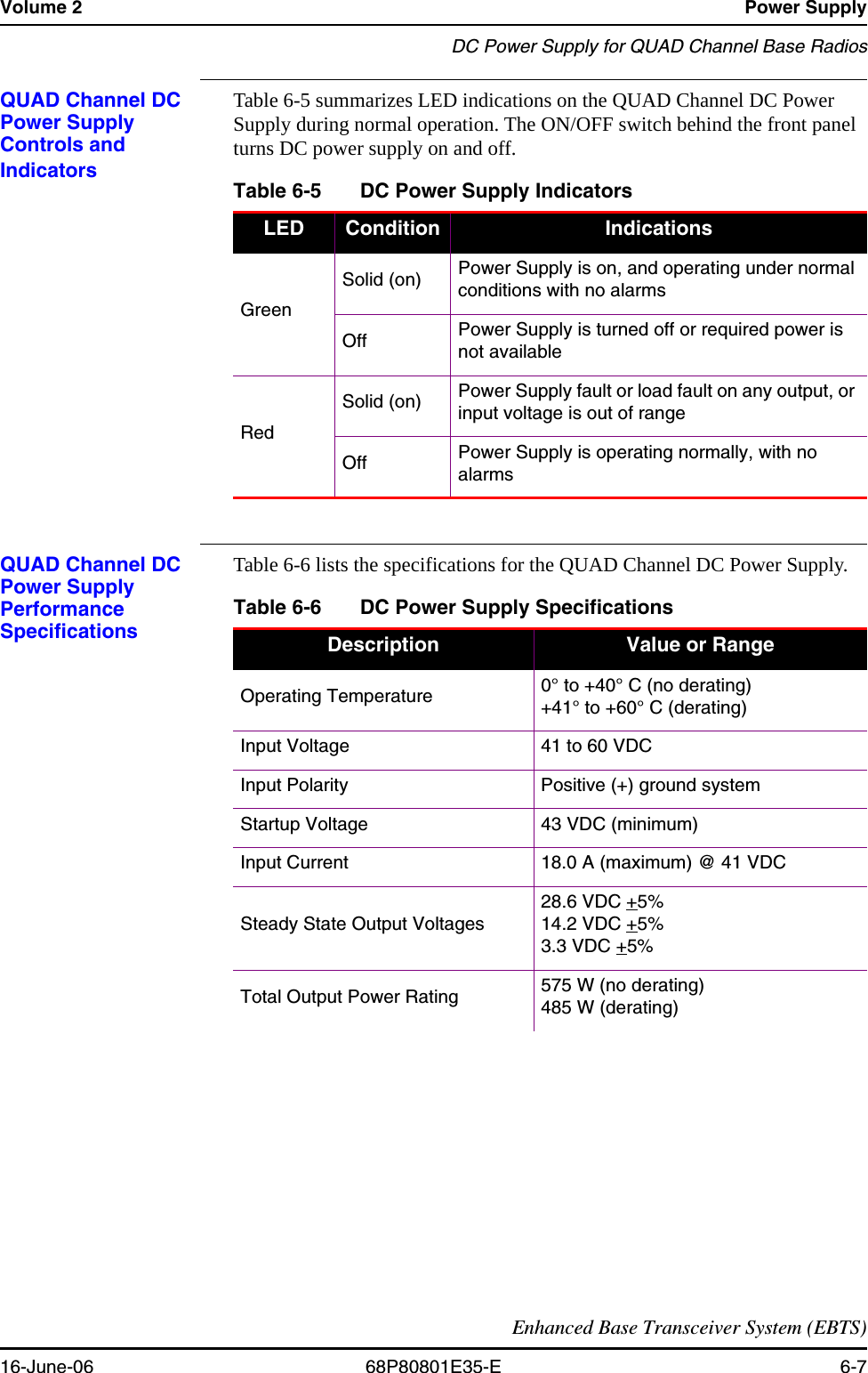
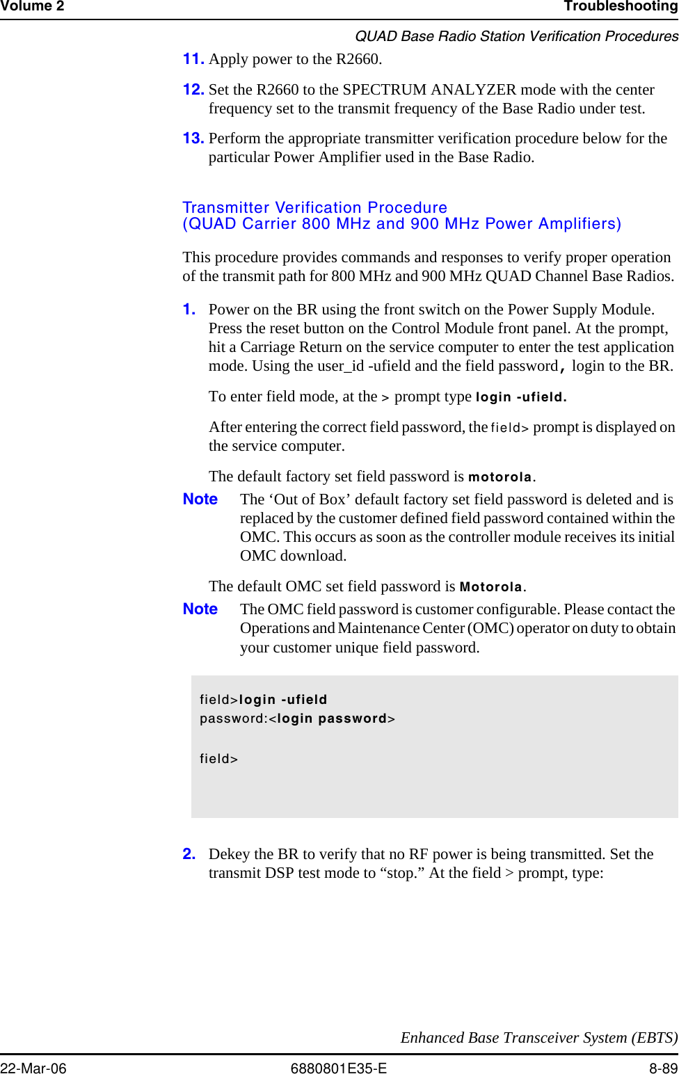
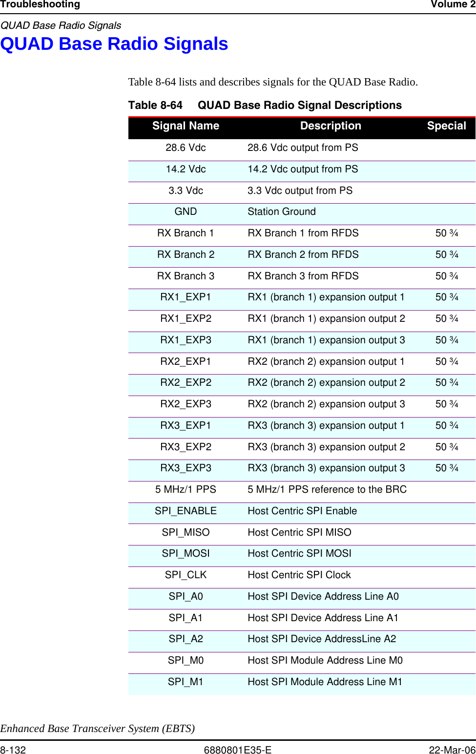
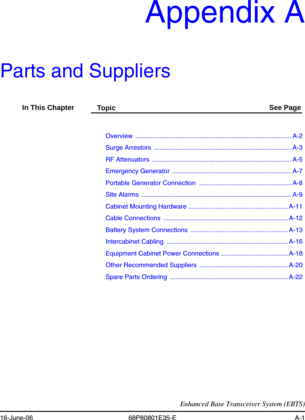
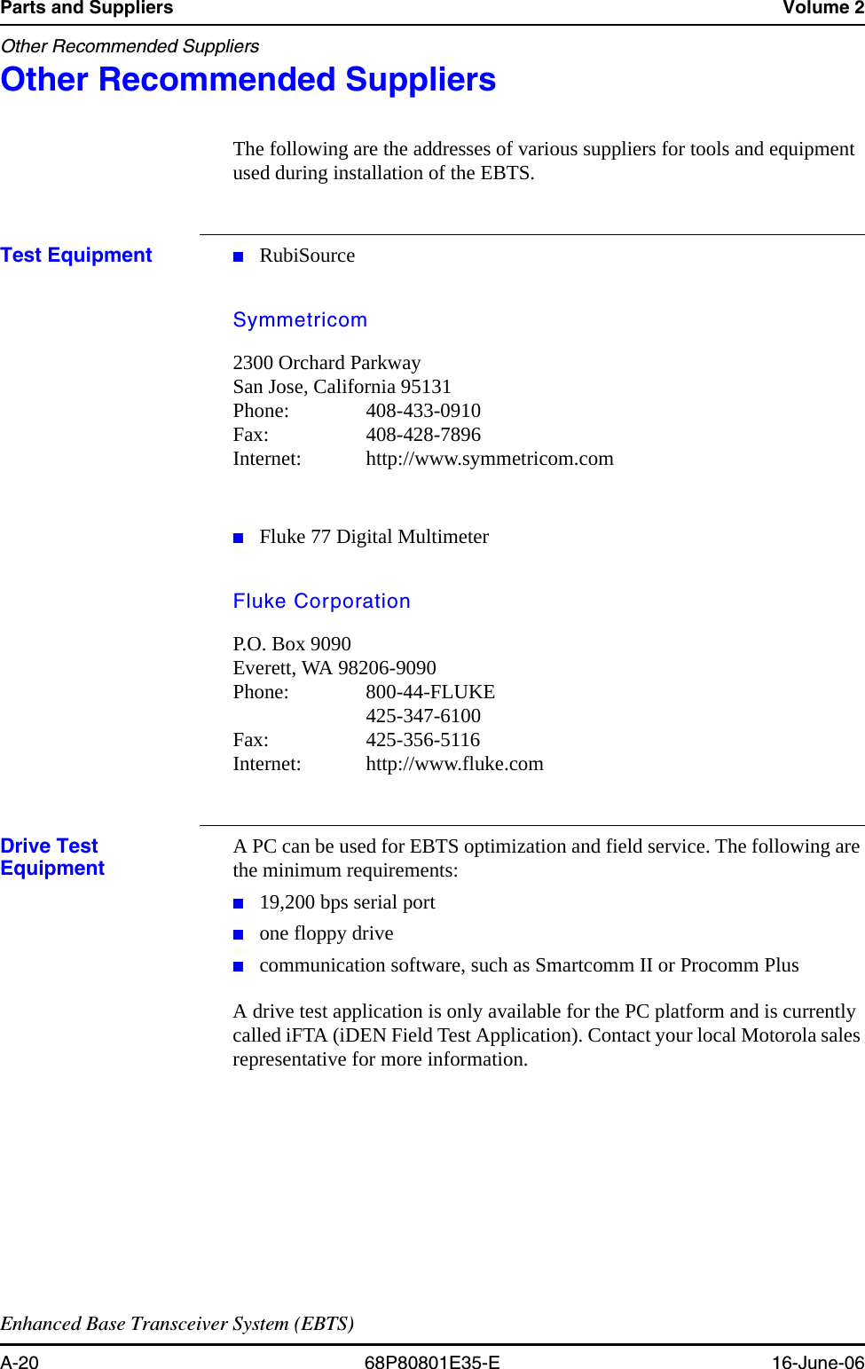
![Base Radio Controllers Volume 2Enhanced Base Transceiver System (EBTS)2-56 68P80801E35-E 16-June-06Figure 2-15 800 and 900 MHz QUAD Channel Base Radio Controller Functional Block Diagram (Sheet 2 of 2) HOSTMICRO-ETHERNETSERIALINTERFACE TRANS-CDRCV RXTRMT TXCLSN10BASE2COAXETHERNETSERIALINTERFACECEIVERISOLATIONTRANSFORMERPROCESSORSCC18SDRAM4M x 16SDRAM4M x 16SDRAM4M x 16SDRAM4M x 16GPLA0, A[8,9,17,18,20:29],RAS,CAS,WECS2CS3D[0:31]D[0:15]D[16:31]D[0:15]D[16:31]BUFFERBUFFERBUFFERBUFFERBUFFERBUFFERD[0:31]D[0:7]A[10:31]MA[21:0]DSP_D[31:24]A[0:7]DSP_A[31:24]MD[31:0]EIA-232BUSRECEIVERS/DRIVERS2STATUS PORT(9 PIN D CONNECTORON BRC FRONT PANEL)2BUFFER33SPI BUS TO/FROM STATION MODULESFLASH1M x 16FLASH1M x 16FLASH1M x 16FLASH1M x 16CS0CS1MD[0:15]MD[16:31]MD[0:15]MD[16:31]1616161616 161616MA[2:21]MA[2:21]EEPROM32k x 8MD[24:31]MA[0:14]CS4P1_OUTLATCHP0_OUTLATCHMD[0:32]MD[24:31]P0_INBUFFERMD[16,17,20-24,28-31]STATUS BUSFROMSTATION MODULESP0_IN8CONTROL BUSTOSTATION MODULESP0_OUT/P1_OUT328TRANSMITDIGITALSIGNALPROCESSOR(TX DSP)SINGLE ENDTO DIFFERENTIALTRANSMITCLOCK ANDFRAME SYNCHCIRCUITRYI/Q DATASERIAL DATATO EXCITERDIFFERENTIALTO SINGLE ENDRX1 SERIAL DATARECEIVEDIGITALSIGNALPROCESSOR(RX DSP 1)RECEIVEDIGITALSIGNALPROCESSOR(RX DSP 2)TISICA[0:5]D[0, 8:23]PARALLELTO SERIALCIRCUITRYD[16:23]D[16:23]D[0, 23]SPI BUS TORECEIVER 1 & 2SPI BUS TORECEIVER 3 & 42.4 MHz1 PPS TIMING, CONTROL/ SLOT TIMING/RESETNETWORKEDSCI16.8MHZ48 MHZSPIBUSSPIBUSEXCITERSPICONTROLDSP SPISPI BUSTO EXCITERDIGITAL SIGNAL PROCESSING CIRCUITRYDIGITAL SIGNAL PROCESSING CIRCUITRYDIFFERENTIALTO SINGLE ENDDIFFERENTIALTO SINGLE ENDDIFFERENTIALTO SINGLE END50 MHZCLOCKFRONT PANELRESETDRAM MEMORYETHERNET INTERFACENON-VOLATILE MEMORY EXPANDED STATUS INPUTAND OUTPUT CONTROL CIRCUITRYEXTENDED HOSTBUS BUFFERS40TO EXCITER5MHZ1PPSRX2 SERIAL DATARX3 SERIAL DATARX4 SERIAL DATAHOST ADDRESS BUSHOST DATA BUSHOST BUFFERED DATA BUSHOST BUFFERED ADDRESS BUSHOST-DSP BUFFERED DATA BUSHOST-DSP BUFFERED ADDRESS BUSSERIAL MANAGEMENT CONTROLLER (SMC2)SERIAL PERIPHERAL INTERFACE](https://usermanual.wiki/Motorola-Solutions/89FC5798-P/User-Guide-737090-Page-38.png)