Motorola Solutions 89FC5798 Non-Broadcast Transmitter User Manual Quad BR 800 Tx FCC Filing
Motorola Solutions, Inc. Non-Broadcast Transmitter Quad BR 800 Tx FCC Filing
Exhibit D Users Manual per 2 1033 c3

APPLICANT: MOTOROLA INC. EQUIPMENT TYPE: ABZ89FC5798
EXHIBIT 8
INSTRUCTION MANUALS
The instruction and service manual for this base radio are not published at this time. However, draft copy of the
manual is available and has been included as part of the filing package in the form of an electronic pdf document.
Upon request, published and/or printed manuals will be sent to the commission and/or telecommunication
certification body (TCB) as soon as they become available. All of the descriptions and schematics included this
filing package are up to date.

APPLICANT: MOTOROLA INC. EQUIPMENT TYPE: ABZ89FC5798
EXHIBIT 9
TUNE-UP PROCEDURE
There is no field tune-up procedure. All adjustments are software controlled and are pre-set at the factory. Certain
station operating parameters can be changed via man-machine interface (MMI) commands, within predetermined
limits. Examples include transmit / receiver operating frequencies and power level.

68P80801H45-1
ECCN 5E992
Global Telecommunications Solutions Sector
ENHANCED BASE TRANSCEIVER SYSTEM (EBTS)
VOLUME 2 OF 3
BASE RADIOS
© 2002 Motorola, Inc.
All Rights Reserved
Printed in U.S.A.
PRELIMINARY
FCC INTERFERENCE WARNING
The FCC requires that manuals pertaining to Class A computing devices must contain warnings about possible interference with local residential radio and TV reception. This
warning reads as follows:
Note: This equipment has been tested and found to comply with the limits for a Class A digital device, pursuant to Part 15 of the FCC Rules. These limits
are designed to provide reasonable protection against harmful interference when the equipment generates, uses, and can radiate radio frequency
energy and, if not installed and used in accordance with the instruction manual, may cause harmful interference to radio communications. Operation of
this equipment in a residential area is likely to cause harmful interference in which case the user will be required to correct the interference at his own
expense.
INDUSTRY OF CANADA NOTICE OF COMPLIANCE
This Class A digital apparatus meets all requirements of the Canadian Interference-Causing Equipment Regulations.
Cet appareil numérique de la classe A respecte toutes les exigences du Règlement sur le matériel brouilleur du Canada.
COMMERCIAL WARRANTY (STANDARD)
Motorola radio communications products (the “Product”) is warranted to be free from defects in material and workmanship for a period of ONE (1) YEAR (except for crystals and
channel elements which are warranted for a period of ten (10 years) from the date of shipment. Parts including crystals and channel elements, will be replaced free of charge for
the full warranty period but the labor to replace defective parts will only be provided for One Hundred-Twenty (120) days from the date of shipment. Thereafter purchaser must
pay for the labor involved in repairing the Product or replacing the parts at the prevailing rates together with any transportation charges to or from the place where warranty
service is provided. This express warranty is extended by Motorola, 1301 E. Algonquin Road, Schaumburg, Illinois 60196 to the original end use purchaser only, and only to
those purchasing for purpose of leasing or solely for commercial, industrial, or governmental use.
THIS WARRANTY IS GIVEN IN LIEU OF ALL OTHER WARRANTIES EXPRESS OR IMPLIED WHICH ARE SPECIFICALLY EXCLUDED, INCLUDING WARRANTIES OF
MERCHANTABILITY OR FITNESS FOR A PARTICULAR PURPOSE. IN NO EVENT SHALL MOTOROLA BE LIABLE FOR INCIDENTAL OR CONSEQUENTIAL DAMAGES TO
THE FULL EXTENT SUCH MAY BE DISCLAIMED BY LAW.
In the event of a defect, malfunction or failure to conform to specifications established by Motorola, or if appropriate to specifications accepted by Motorola in writing, during the
period shown, Motorola, at its option, will either repair or replace the product or refund the purchase price thereof. Repair at Motorola's option, may include the replacement of
parts or boards with functionally equivalent reconditioned or new parts or boards. Replaced parts or boards are warranted for the balance of the original applicable warranty
period. All replaced parts or product shall become the property of Motorola.
This express commercial warranty is extended by Motorola to the original end user purchaser or lessee only and is not assignable or transferable to any other party. This is the
complete warranty for the Product manufactured by Motorola. Motorola assume no obligations or liability for additions or modifications to this warranty unless made in writing and
signed by an officer of Motorola. Unless made in a separate agreement between Motorola and the original end user purchaser, Motorola does not warrant the installation,
maintenance or service of the Products.
Motorola cannot be responsible in any way for any ancillary equipment not furnished by Motorola which is attached to or used in connection with the Product, or for operation of
the Product with any ancillary equipment, and all such equipment is expressly excluded from this warranty. Because each system which may use Product is unique, Motorola
disclaims liability for range, coverage, or operation of the system as a whole under this warranty.
This warranty does not cover:
a) Defects or damage resulting from use of the Product in other than its normal and customary manner.
b) Defects or damage from misuse, accident, water or neglect
c) Defects or damage from improper testing, operation, maintenance installation, alteration, modification, or adjusting.
d) Breakage or damage to antennas unless caused directly by defects in material workmanship.
e) A Product subjected to unauthorized Product modifications, disassemblies or repairs (including without limitation, the addition to the Product of non-Motorola supplied
equipment) which adversely affect performance of the Product or interfere with Motorola's normal warranty inspection and testing of the Product to verify any warranty claim.
f) Product which has had the serial number removed or made illegible.
g) A Product which, due to illegal to unauthorized alteration of the software/firmware in the Product, does not function in accordance with Motorola's published specifications or
the FCC type acceptance labeling in effect for the Product at the time the Product was initially distributed from Motorola.
This warranty sets forth the full extent of Motorola's responsibilities regarding the Product. Repair, replacement or refund of the purchase date, at Motorola’s option is the
exclusive remedy. IN NO EVENT SHALL MOTOROLA BE LIABLE FOR DAMAGES IN EXCESS OF THE PURCHASE PRICE OF THE PRODUCT, FOR ANY LOSS OF USE,
LOSS OR TIME, INCONVENIENCE, COMMERCIAL LOSS, LOST PROFITS OR SAVINGS OR OTHER INCIDENTAL, SPECIAL OR CONSEQUENTIAL DAMAGE ARISING
OUT OF THE USE OR INABILITY TO USE SUCH PRODUCT, TO THE FULL EXTENT SUCH MAY BE DISCLAIMED BY LAW.
SOFTWARE NOTICE/WARRANTY
Laws in the United States and other countries preserve for Motorola certain exclusive rights for copyrighted Motorola software such as the exclusive rights to reproduce in copies
and distribute copies of such Motorola software. Motorola software may be used in only the Product in which the software was originally embodied and such software in such
Product may not be replaced, copied, distributed, modified in any way, or used to produce any derivative thereof. No other use including without limitation alteration, modification,
reproduction, distribution, or reverse engineering of such Motorola software or exercise of rights in such Motorola software is permitted. No license is granted by implication,
estoppel or otherwise under Motorola patent rights or copyrights.
This warranty extends only to individual products: batteries are excluded, but carry their own separate limited warranty.
In order to obtain performance of this warranty, purchaser must contact its Motorola salesperson or Motorola at the address first above shown, attention Quality Assurance
Department.
This warranty applies only within the fifty (50) United States and the District of Columbia.

68P80801H45-1 1/20/2002 11
Global Telecommunications Solutions Sector
1301 E. Algonquin Road, Schaumburg, IL 60196
Base Radios
About This Volume
Volume 2 of the Enhanced Base Transceiver System (EBTS) manual, Base Radios,
provides the experienced service technician with an overview of the EBTS
operation and functions, and contains information regarding the 800 MHz,
900 MHz, 1500 MHz Single Channel and 800 MHz and 900 MHz QUAD Channel
Channel base radios.
The EBTS System has three major components:
❐Generation 3 Site Controller (Gen 3 SC) or an integrated Site Controller (iSC)
❐Base Radios (BRs)
❐RF Distribution System (RFDS)
Installation and testing is described in Volume 1, System Installation and Testing,
and RFDS are described in Volume 3, RF Distribution Systems (RFDS). Detailed
information about the Gen 3 SC is contained in the Gen 3 SC Supplement Manual,
68P80801E30. Detailed information about the iSC is contained in the iSC
Supplement Manual, 68P81098E05
The information in this manual is current as of the printing date. If changes to
this manual occur after the printing date, they will be documented and issued as
Schaumburg Manual Revisions (SMRs).
Target Audience
The target audience of this document includes field service technicians
responsible for installing, maintaining, and troubleshooting the EBTS.
In keeping with Motorola’s field replaceable unit (FRU) philosophy, this manual
provides sufficient functional information to the FRU level. Please refer to the
appropriate section of this manual for removal and replacement instructions.

12 68P80801H45-1 1/20/2002
Base Radios EBTS System Manual - Vol 2
Maintenance Philosophy
The EBTS has been designed using a Field Replaceable Unit (FRU) maintenance
concept. To minimize system down time, faulty FRUs may be quickly and easily
replaced with replacement FRUs. This helps to restore normal system operation
quickly.
Due to the high percentage of surface mount components and multi-layer circuit
boards, field repair is discouraged. Faulty or suspect FRUs should be returned to
the Motorola Customer Support Center for further troubleshooting and repair.
Each FRU has a bar code label attached to its front panel. This label identifies a
sequential serial number for the FRU. Log this number whenever contacting the
Motorola Customer Support Center. For complete information on ordering
replacement FRUs, or instructions on how to return faulty FRUs for repair,
contact:
Nippon Motorola LTD. OR Motorola Customer Support Center
Tokyo Service Center 1311 East Algonquin Road
044-366-8860 Schaumburg, Illinois 60196
(800) 448-3245 or (847) 576-7300
Technical Support Service
Motorola provides technical support services for installation, optimization, and
maintenance of its fixed network equipment. Before calling the Motorola
Customer Support Center, please note the following information:
❐Where the system is located.
❐The date the system was put into service.
❐A brief description of problem.
❐Any other unusual circumstances.

68P80801H45-1 1/20/2002 13
EBTS System Manual - Vol 2 Base Radios
General Safety Information
General Safety Information
The following general safety precautions must be observed during all phases of
operation, service, and repair of the equipment described in this manual. The
safety precautions listed below represent warnings of certain dangers of which
we are aware. You should follow these warnings and all other safety precautions
necessary for the safe operation of the equipment in your operating environment.
Read and follow all warning notices and instructions marked on the product or
included in this manual before installing, servicing or operating the equipment.
Retain these safety instructions for future reference. Also, all applicable safety
procedures, such as Occupational, Safety, and Health Administration (OSHA)
requirements, National Electrical Code (NEC) requirements, local code
requirements, safe working practices, and good judgement must be used by
personnel.
Refer to appropriate section of the product service manual for additional
pertinent safety information.
Because of the danger of introducing additional hazards, do not install substitute
parts or perform any unauthorized modifications of equipment.
Identify maintenance actions that require two people to perform the repair. Two
people are required when:
A repair has the risk of injury that would require one person to perform first
aid or call for emergency support. An example would be work around high
voltage sources. A second person may be required to remove power and call
for emergency aid if an accident occurs to the first person.
Use the National Institute of Occupational Safety and Health (NIOSH) listing
equation to determine whether a one or two person lift is required when a
system component must be removed and replaced in its rack.
If troubleshooting the equipment while power is applied, be aware of the live
circuits.
DO NOT operate the transmitter of any radio unless all RF connectors are secure
and all connectors are properly terminated.
All equipment must be properly grounded in accordance with Motorola Standards
and Guidelines for Communications Sites “R56” 68P81089E50 and specified
installation instructions for safe operation.
Slots and openings in the cabinet are provided for ventilation. To ensure reliable
operation of the product and protect it from overheating, these slots and openings
must not be blocked or covered.
Only a qualified technician familiar with similar electronic equipment should
service equipment.
Some equipment components can become extremely hot during operation. Turn
off all power to the equipment and wait until sufficiently cool before touching.

14 68P80801H45-1 1/20/2002
Base Radios EBTS System Manual - Vol 2
General Safety Information
Human Exposure Compliance
This equipment is designed to generate and radiate radio frequency (RF) energy
by means of an external antenna. When terminated into a non-radiating RF load,
the base station equipment is certified to comply with Federal Communications
Commission (FCC) regulations pertaining to human exposure to RF radiation in
accordance with the FCC Rules Part 1 section 1.1310 as published in title 47 code
of federal regulations and procedures established in TIA/EIA TSB92, Report on
EME Evaluation for RF Cabinet Emissions Under FCC MPE Guidelines,
Compliance to FCC regulations of the final installation should be assessed and
take into account site specific characteristics such as type and location of
antennas, as well as site accessibility of occupational personnel (controlled
environment) and the general public (uncontrolled environment). This equipment
should only be installed and maintained by trained technicians. Licensees of the
FCC using this equipment are responsible for insuring that its installation and
operation comply with FCC regulations Part 1 section 1.1310 as published in title
47 code of federal regulations.
Whether a given installation meets FCC limits for human exposure to radio
frequency radiation may depend not only on this equipment but also on whether
the “environments” being assessed are being affected by radio frequency fields
from other equipment, the effects of which may add to the level of exposure.
Accordingly, the overall exposure may be affected by radio frequency generating
facilities that exist at the time of the licensee’s equipment is being installed or
even by equipment installed later. Therefore, the effects of any such facilities must
be considered in site selection and in determining whether a particular
installation meets the FCC requirements.
FCC OET Bulletin 65 provides materials to assist in making determinations if a
given facility is compliant with the human exposure to RF radiation limits.
Determining the compliance of transmitter sites of various complexities may be
accomplished by means of computational methods. For more complex sites direct
measurement of power density may be more expedient. Additional information
on the topic of electromagnetic exposure is contained in the Motorola Standards and
Guideline for Communications Sites publication. Persons responsible for installation
of this equipment are urged to consult the listed reference material to assist in
determining whether a given installation complies with the applicable limits.
In general the following guidelines should be observed when working in or
around radio transmitter sites:
- All personnel should have electromagnetic energy awareness training.
- All personnel entering the site must be authorized.
- Obey all posted signs
- Assume all antennas are active
- Before working on antennas, notify owners and disable appropriate
transmitters.
- Maintain minimum 3 feet clearance from all antennas.
- Do not stop in front of antennas.
- Use personal RF monitors while working near antennas.
- Never operate transmitters without shields during normal operation.
- Do not operate base station antennas in equipment rooms

68P80801H45-1 1/20/2002 15
EBTS System Manual - Vol 2 Base Radios
General Safety Information
For installations outside of the U.S., consult with the applicable governing body
and standards for RF energy human exposure requirements and take necessary
steps for compliance with local regulations.
References:
TIA/EIA TSB92 “Report on EME Evaluation for RF Cabinet Emissions Under
FCC MPE Guidelines”, Global Engineering Documents: http://globl.ihs.com/
FCC OET Bulletin 65 “Evaluating Compliance with FCC Guidelines for Human
Exposure to Radiofrequency Electromagnetic Fields”; http://www.fcc.gov/oet/
rfsaftey/.
Motorola Standards and Guideline for Communications Sites, Motorola manual
68P81089E50.
IEEE Recommended Practice for the Measure of Potentially Hazardous
Electromagnetic Fields-- RF and Microwave, IEEE Std. C95.3-1991, Publication
Sales, 445 Hoes Lane, P.O. Box 1331, Piscattaway, NJ 08855-1331
IEEE Standard for Safety Levels with Respect to Human Exposure to Radio
Frequency Electromagnetic Fields, 3 kHz to 300 GHz, IEEE C95.1-1991,

68P80801H45-1 1/20/2002 1
Global Telecommunications Solutions Sector
1301 E. Algonquin Road, Schaumburg, IL 60196
Base Radio
Overview
This chapter provides an overview of the 800/900/1500 MHz Legacy,
800 MHz Generation 2 Single Channel, 800 MHz and 900 MHz QUAD
Channel Base Radios (BRs) along with technical information. The
section topics are listed and described in Table 1.
FRU Number to Kit Number Cross Reference
Section Page Description
Generation 2 Single Channel 800
MHz Base Radio Overview
3 Describes Controls and Indications,
Theory of Operation, and Specifications for
the 800 MHz Generation 2 Base Radio.
QUAD Channel 900 MHz Base Radio
Overview
11 Provides information on the 900 MHz
QUAD Channel Base Radio’s Controls and
Indications, Specifications and Theory of
Operation.
QUAD Channel 800 MHz Base Radio
Overview
16 Provides information on the 800 MHz
QUAD Channel Base Radio’s Controls and
Indications, Specifications and Theory of
Operation.
Legacy Single Carrier 800 MHz Base
Radio Overview
21 This section provides information on the
Legacy Single Channel 800/900/1500MHz
Base Radio including Controls and
Indications, Specifications and Theory of
Operation.
Ta ble 1 FRU Number to Kit Number Cross Reference
Description FRU Number Kit Number
Single Channel 800/900/1500 MHz BRC TLN3334 CLN1469
Single Channel BRC (MCI) TLN3425 CLN1472
Enhanced Base Radio Controller DLN6446 CLN1653
900 MHz QUAD Channel BRC DLN1203 CLF6242
800 MHz QUAD Channel BRC CLN1497 CLF1560

268P80801H45-1 1/20/2002
Base Radio EBTS System Manual - Vol 2
NOTE
The Single Carrier Base Radio section covers the
800 MHz, 900 MHz and 1500 MHz Legacy and
800 MHz Generation 2 versions of the Base
Radio (BR). Information is presented generally
for all models. Information that is model
specific noted in the text.
NOTE
For Generation 2 BR, both the 800 MHz Exciter and
the 800 MHz Low Noise Exciter modules are
supported subject to Table 2 on page 4.
NOTE
For QUAD Channel 800 MHz BR use, all Single
Carrier BR modules have undergone redesign.
Therefore, Single Carrier BR modules are
incompatible with the QUAD Channel 800 MHz BR.
QUAD Channel 800 MHz BR modules are
incompatible with the Single Carrier BR.
Do not attempt to insert QUAD Channel 800 MHz BR
modules into a Single Carrier BR or Single Carrier BR
modules into a QUAD Channel 800 MHz BR.
NOTE
For QUAD Channel 900 MHz BR use, all Single
Carrier BR modules are incompatable with the 900
MHz QUAD Channel BR. 900 MHz QUAD Channel
BR modules are incompatable with the Single Carrier
BR.
Do not attempt to insert QUAD Channel 900 MHz BR
modules into a Single Carrier BR or Single Carrier BR
modules into a QUAD Channel 900 MHz BR.
68P80801H45-1 1/20/2002 11
EBTS System Manual - Vol 2 Base Radio
QUAD Channel 900 MHz Base Radio Overview
QUAD Channel 900 MHz Base Radio Overview
The QUAD Channel 900 MHz BR provides reliable, digital BR capabilities in a
compact, software-controlled design. Voice compression techniques, time division
multiplexing (TDM) and multi-carrier operation provide increased channel
capacity.
The QUAD Channel 900 MHz BR contains the four FRUs listed below:
❐QUAD Channel 900 MHz EX /Cntl
❐QUAD Channel 900 MHz Power Amplifier
❐QUAD Channel 800 MHz and 900 MHz Power Supply (DC)
❐QUAD Channel 900 MHz Receiver (qty. 4)
The modular design of the QUAD Channel 900 MHz BR also offers increased
shielding and provides easy handling. All FRUs connect to the backplane through
blindmate connectors.
NOTE
Both the 800 MHz QUAD and 900 MHz QUAD Base
Radios use the same backplane and cardcage but call
out different FCC ID numbers.
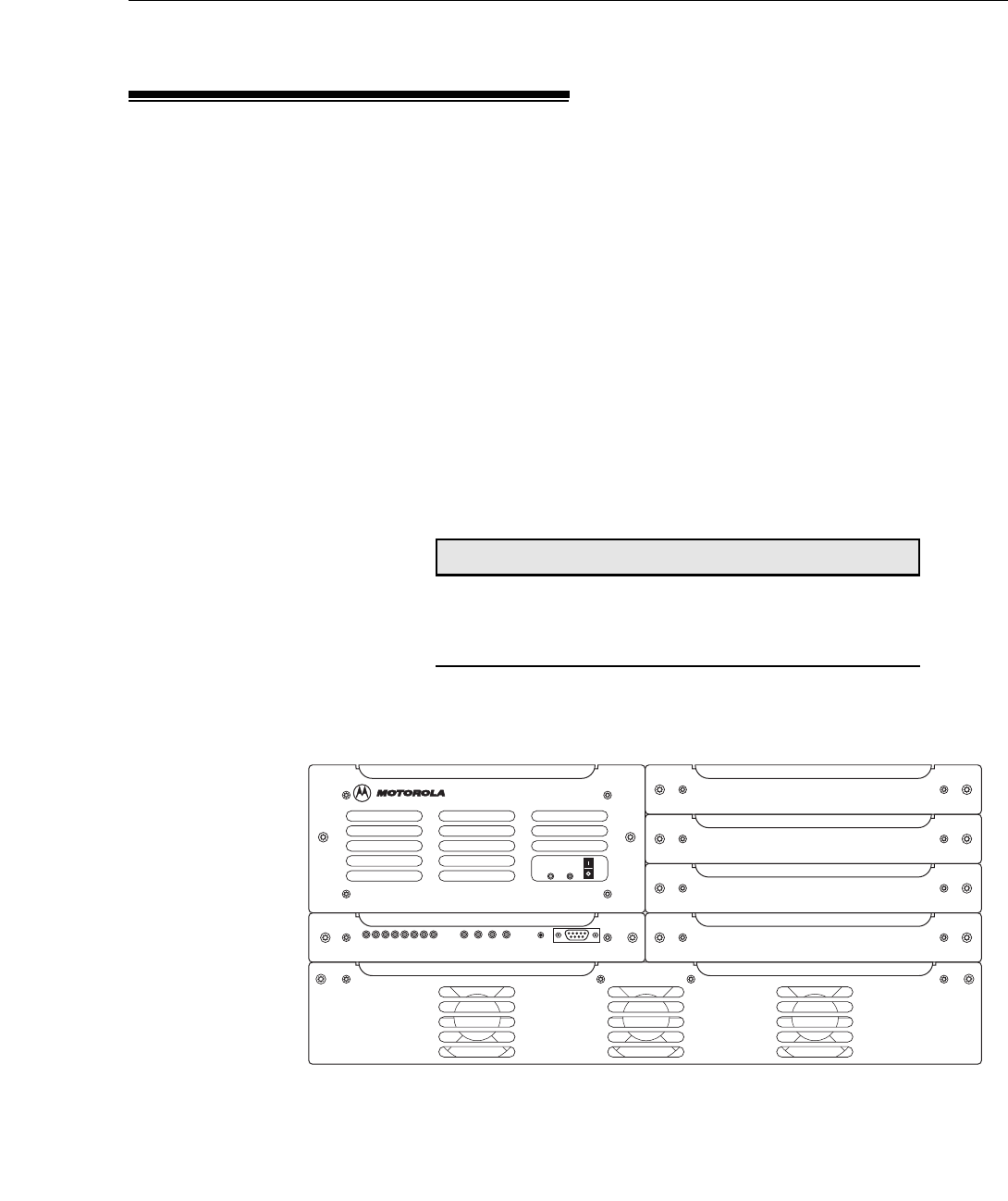
Figure 2 shows the front view of the BR.
EBTS282Q_900
112601JNM
900 QUAD CHANNEL RECEIVER
QUAD CHANNEL POWER SUPPLY
900 QUAD CHANNEL RECEIVER 900 QUAD CHANNEL RECEIVER
900 QUAD CHANNEL RECEIVER
900 QUAD CHANNEL RECEIVER
900 QUAD CHANNEL RECEIVER
STATUS
RESET
TX4
TX4
TX4
TX4
PS
EX/CNTL
PA
REF
RX1
RX2
RX3
RX4
Figure 2 QUAD Channel 900 MHz Base Radio (Typical)

12 68P80801H45-1 1/20/2002
Base Radio EBTS System Manual - Vol 2
QUAD Channel 900 MHz Base Radio Overview
QUAD Channel 900 MHz Base Radio Controls and Indicators
Power Supply and EX / CNTL controls and indicators monitor BR status and
operating conditions, and also aid in fault isolation. The Power Supply and EX /
CNTL sections of this chapter discuss controls and indicators for both modules.
The Power Supply has two front panel indicators. The EX / CNTL has twelve
front panel indicators. The Power Supply power switch applies power to the BR.
The EX / CNTL RESET switch resets the BR.
QUAD Channel 900 MHz Base Radio Performance Specifications
QUAD Channel 900 MHz Base Radio General Specifications
Table 6 lists general specifications for the BR.
Table 6 QUAD Channel 900 MHz BR General Specifications
Specification Value or Range
Dimensions:
Height
Width
Depth
Weight
5 EIA Rack Units (RU)
19" (482.6 mm)
16.75" (425 mm)
85 lbs. (38.6 kg)
Operating Temperature 32˚ to 104˚ F (0˚ to 40˚ C)
Storage Temperature -22˚ to 140˚ F (-30˚ to 60˚ C)
Rx Frequency Range:
900 MHz iDEN 896 - 901 MHz
Tx Frequency Range:
900 MHz iDEN 935 - 940 MHz
Tx – Rx Spacing:
900 MHz iDEN 39 MHz
Carrier Spacing 25 kHz
Carrier Capacitya
a. Multi-carrier operation must utilize adjacent, contiguous RF carriers.
1, 2, 3 or 4
Frequency Generation Synthesized
Digital Modulation QPSK, M-16QAM, and M-64QAM
Power Supply Inputs:
VDC -48 VDC (-41 to -60 VDC)
Diversity Branches Up to 3

68P80801H45-1 1/20/2002 13
EBTS System Manual - Vol 2 Base Radio
QUAD Channel 900 MHz Base Radio Overview
QUAD Channel 900 MHz Base Radio Transmit Specifications
Table 7 lists the BR transmit specifications.
QUAD Channel 900 MHz Base Radio Receive Specifications
Table 8 lists the receive specifications.
Table 7 QUAD Channel 900 MHz BR Transmit Specifications
Specification Value or Range
Low average output
power per carrier
High average output
power per carrier
Average Power Output:
(900 MHZ) Single Carrier 5.0W 52.0W
(900 MHz) Dual Carrier 2.5W 26.0W
(900 MHz) Triple Carrier 1.7W 16.1W
(900 MHz) QUAD Channel 1.3W 10.5W
Transmit Bit Error Rate (BER) 0.01%
Occupied Bandwidth 18.5 kHz
Frequency Stability * 1.5 ppm
RF Input Impedance 50 Ω (nom.)
FCC Designation (FCC Rule Part 90):
900 MHz QUAD BR ABZ89FC5798
* Transmit frequency stability locks to an external site reference, which controls ultimate frequency stability to a
level of 50 ppb.
Table 8 QUAD Channel 900 MHz Receive Specifications
Specification Value or Range
Static Sensitivity †:
900 MHz BR -108 dBm (BER = 8%)
BER Floor (BER = 0.01%) ≥ -80 dBm
IF Frequencies
1st IF (All bands):
2nd IF:
73.35 MHz (1st IF)
450 kHz (2nd IF)
Frequency Stability * 1.5 ppm
RF Input Impedance 50 Ω (nom.)
FCC Designation (FCC Rule Part 15):
900 MHz BR ABZ89FR5799
† Measurement referenced from single receiver input port of BR.
* Stability without site reference connected to station. Receive frequency stability locks to an external site
reference, which controls ultimate frequency stability to a level of 50 ppb.

14 68P80801H45-1 1/20/2002
Base Radio EBTS System Manual - Vol 2
QUAD Channel 900 MHz Base Radio Overview
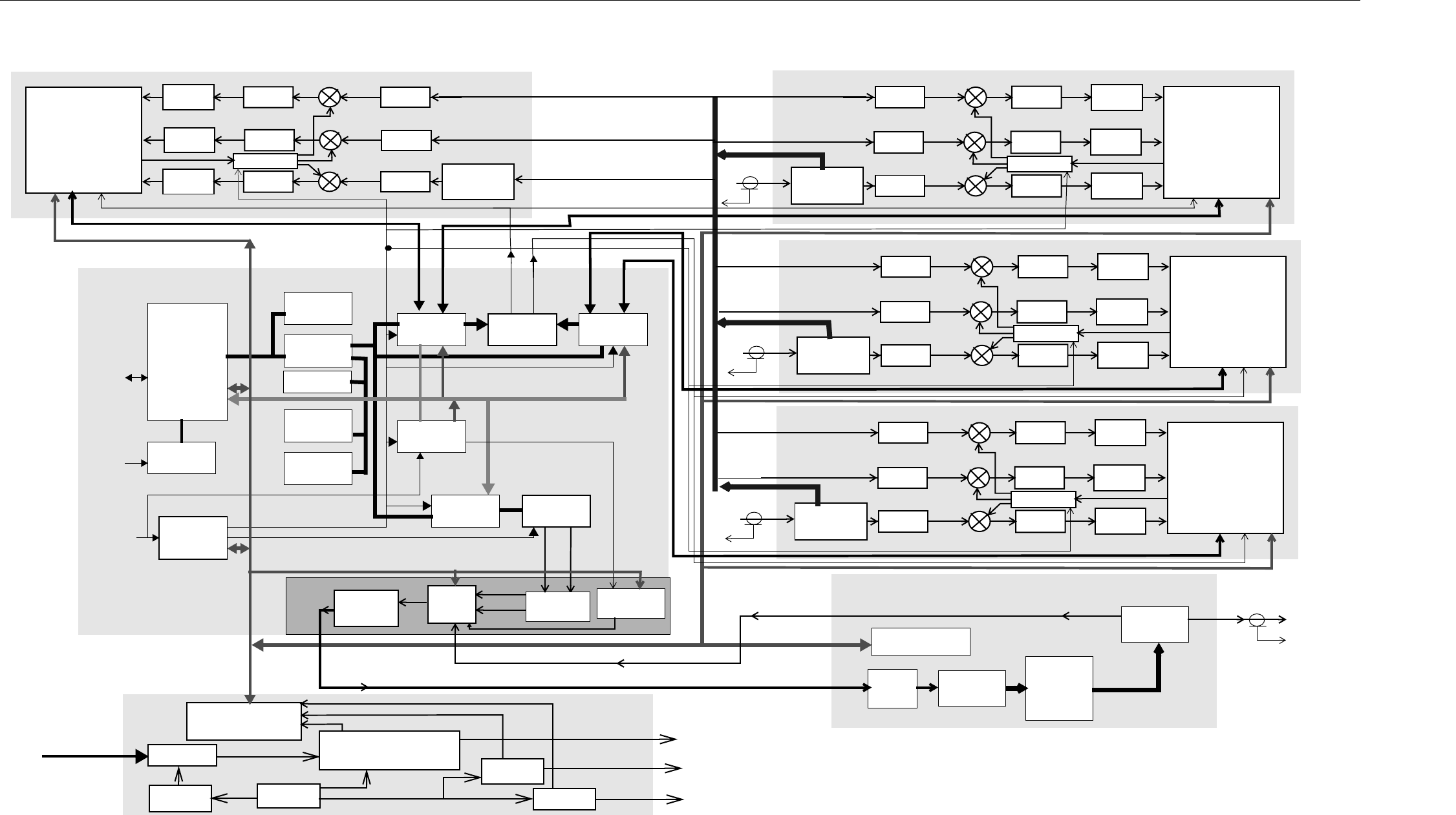
QUAD Channel 900 MHz Base Radio Theory of Operation
The QUAD Channel 900 MHz BR operates with other site controllers and
equipment and must be properly terminated. The following description assumes
such a configuration. Figure 6 show an overall block diagram of the QUAD
Channel 900 MHz BR.
Power is applied to the DC Power inputs located on the QUAD Channel 900 MHz
BR backplane. The DC Power input is connected if -48 VDC or batteries are used
in the site.
Power is applied to the BR by setting the Power Supply power switch to the ON
position. Upon power-up, the QUAD Channel 900 MHz BR performs
self-diagnostic tests to ensure the integrity of the unit. These tests, which include
memory and Ethernet verification routines, primarily examine the EX / CNTL.
After completing self-diagnostic tests, the QUAD Channel 900 MHz BR reports
alarm conditions on any of its modules to the site controller via Ethernet. Alarm
conditions may also be verified locally. Local verification involves using the
service computer and the STATUS port located on the front of the QUAD Channel
900 MHz EX / CNTL.
The software resident in FLASH on the EX / CNTL registers the BR with the site
controller via Ethernet. After BR registration on initial power-up, the BR software
downloads via resident FLASH or Ethernet and executes from RAM. The
download includes operating parameters for the QUAD Channel 900 MHz BR.
These parameters allow the QUAD Channel 900 MHz BR to perform call
processing functions.
After software downloads to the BR via Ethernet, FLASH memory stores the
software object. Upon future power-ups, the software object in FLASH loads into
RAM for execution.
The BR operates in a TDMA (Time Division Multiple Access) mode. This mode,
combined with voice compression techniques, increases channel capacity by a
ratio of as much as six to one. TDMA divides both the receive and transmit
signals of the BR into six individual time slots. Each receive slot has a
corresponding transmit slot. This pair of slots comprises a logical RF channel.

68P80801H45-1 1/20/2002 15
EBTS System Manual - Vol 2 Base Radio
QUAD Channel 900 MHz Base Radio Overview
The BR uses diversity reception for increased coverage area and improved
quality. The Receiver modules within the QUAD Channel 900 MHz BR contain
three receiver paths. Two-branch diversity sites use two Receiver paths, and
three-branch diversity sites use three Receiver paths.
All Receiver paths within a given Receiver module are programmed to the same
receive frequency. Signals from each receiver arrive at the EX / CNTL module.
This module performs a diversity combining algorithm on the signals. The
resultant signal undergoes an error-correction process. Then, via Ethernet, the site
controller acquires the signal, along with control information about signal
destination.
Two separate FRUs comprise the transmit section of the QUAD Channel 900 MHz
BR. These are the Exciter portion of the EX / CNTL and the Power Amplifier (PA).
The Exciter processes commands from the CNTL, assuring transmission in the
proper modulation format. Then the low-level signal enters the PA. The PA
amplifies this signal to the desired output power level. The PA is a continuously
keyed linear amplifier. A power control routine monitors the output power of the
BR. The routine adjusts the power as necessary to maintain the proper output
level.
28
68P80801H45-1 1/20/2002
800/900/1500 MHz Base Radios EBTS System Manual - Vol 2
Base Radio Overview
16.8MHz
2.4MHz
48MHz
Host SPI
Host SPI
16.8MHz
STATUS
PORT
RS-232
5 MHZ
EXTERNAL
REFERENCE
ETHERNET
1PPS & SLOT TIMING
RX1 DATA
RX2 DATA
RX3 DATA
RX4 DATA
Rx1&2
Rx3&4
POWER AMPLIFIER MODULE
Tx_I Tx_Q
EXCITER-BASE RADIO
CONTROLLER
HOST
u’P
SDRAM
RECEIVE
DSP
ETHERNET
EEPROM
FLASH
PLL/VCOs
TRANSMIT
DSP
TISIC
TX RECLOCK
BUFFERS
RX SPI
BASE RADIO
CONTROLLER Exciter
IO LATCHES
RECEIVE
DSP
INTERFACE
ADDRESS DECODE,
MEMORY, ADC
SPI BUS
LINEAR
DRIVER
FINAL
LINEAR
AMPS
COMBINER
SPLITTER
RF OUT
TO RFDS
(TX ANTENNA)
DAC VCOs/Synths
I
Q
ODCT
LINEAR RF
AMPLIFIER
RF IN
RF FEEDBACK
DC POWER SUPPLY MODULE
I
NPUT
F
ILTER
START-UP
INVERTER
CIRCUITRY
EXTERNAL
DC INPUT
41 - 60 VDC
CLOCK
GENERATOR
133 KHZ 267 KHZ
133 KHZ
14.2 V
CONVERTER
3.3 V
CONVERTER
+28 VDC
TO BACKPLANE
+14.2 VDC
TO BACKPLANE
+3.3 VDC
TO BACKPLANE
Main Converter
MIXER IF FILTER
AMP, AGC ABACUS
RECEIVER
IC
LPF, AMP,
FILTER
MIXER IF FILTER
AMP, AGC ABACUS
RECEIVER
IC
LPF, AMP,
FILTER
MIXER IF FILTER
AMP, AGC ABACUS
RECEIVER
IC
LPF, AMP,
FILTER
RX INTERFACE,
ADDRESS DECODE.
MEMORY, DIAGNOSTICS
PREAMPLIFIER
SPLITTER
/ BYPASS
VCO SYNTH
SPLITTER
RF IN
FROM RFDS
(BRANCH 2)
MIXER IF FILTER
AMP, AGC ABACUS
RECEIVER
IC
LPF, AMP,
FILTER
MIXER IF FILTER
AMP, AGC ABACUS
RECEIVER
IC
LPF, AMP,
FILTER
MIXER IF FILTER
AMP, AGC ABACUS
RECEIVER
IC
LPF, AMP,
FILTER
RX INTERFACE,
ADDRESS DECODE.
MEMORY, DIAGNOSTICS
PREAMPLIFIER
SPLITTER
/ BYPASS
VCO SYNTH
SPLITTER
RF IN
FROM RFDS
(BRANCH 3)
MIXER IF FILTER
AMP, AGC ABACUS
RECEIVER
IC
LPF, AMP,
FILTER
MIXER IF FILTER
AMP, AGC ABACUS
RECEIVER
IC
LPF, AMP,
FILTER
MIXER IF FILTER
AMP, AGC ABACUS
RECEIVER
IC
LPF, AMP,
FILTER
RX INTERFACE,
ADDRESS DECODE.
MEMORY, DIAGNOSTICS
PREAMPLIFIER
SPLITTER
/ BYPASS
VCO SYNTH
SPLITTER
RF IN
FROM RFDS
(BRANCH 1)
RECEIVER 2
RECEIVER 3
RECEIVER 4
RECEIVER 1
MIXER
IF FILTER
AMP, AGC
ABACUS
RECEIVER
IC LPF, AMP,
FILTER
MIXER
IF FILTER
AMP, AGC
ABACUS
RECEIVER
IC LPF, AMP,
FILTER
MIXER
IF FILTER
AMP, AGC
ABACUS
RECEIVER
IC LPF, AMP,
FILTER
RX INTERFACE,
ADDRESS DECODE.
MEMORY, DIAGNOSTICS
PREAMPLIFIER
SPLITTER
/ BYPASS
VCO SYNTH
SPLITTER
SPI BUS
SPI BUS
SPI BUS
ADDRESS DECODE,
MEMORY, ADC
QUAD RX IN DISTRIBUTION
16.8MHz
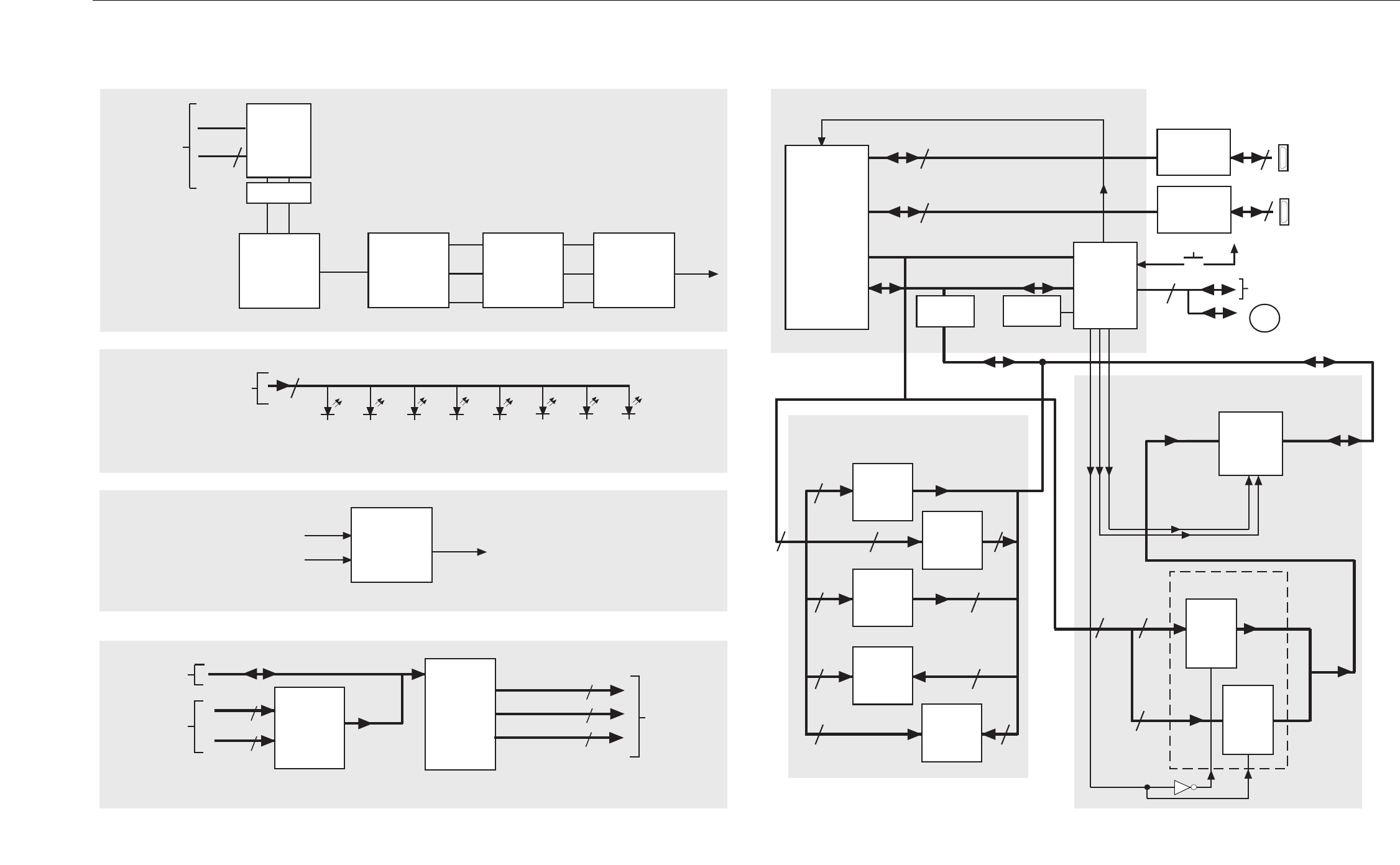
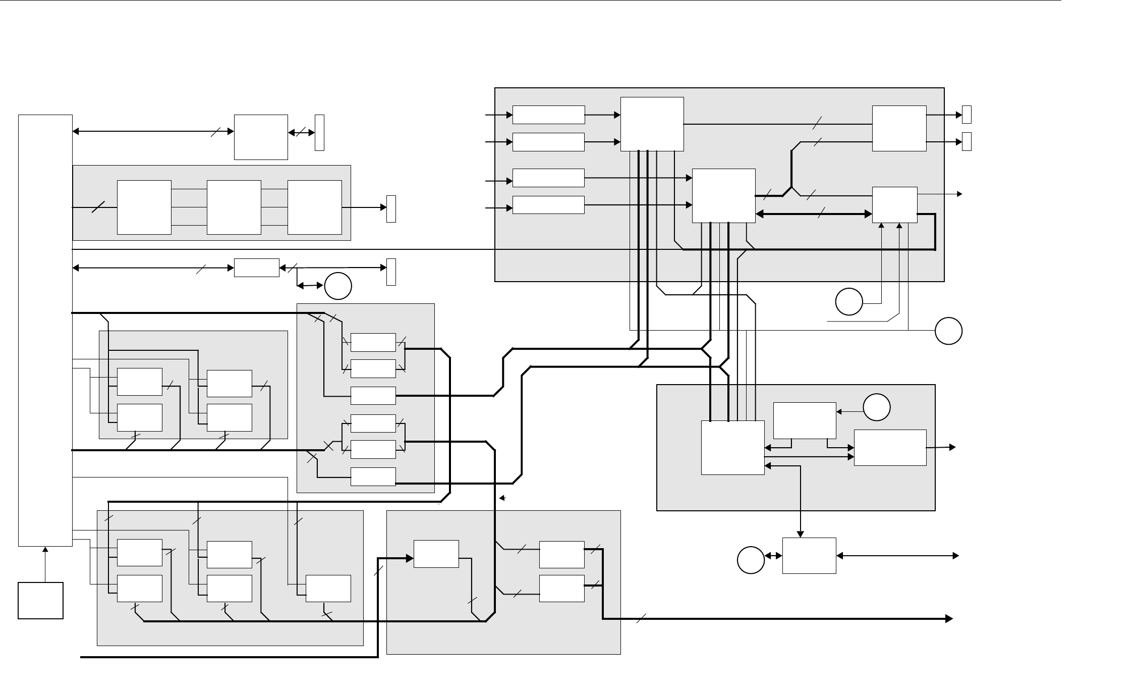
Figure 6 800 and 900 MHZ QUAD Channel Base Radio Functional Block Diagram
RECEIVER 4
68P80801H45-1 1/20/2002 1
Global Telecommunications Solutions Sector
1301 E. Algonquin Road, Schaumburg, IL 60196
Base Radio Controllers
Overview
This chapter provides information on Base Radio Controllers (BRCs):
FRU Number to Kit Number Cross Reference
Base Radio Controller (BRC) Field Replaceable Units (FRUs) are available for the
iDEN EBTS. The FRU contains the BRC kit and required packaging. Table 1
provides a cross reference between BRC FRU numbers and kit numbers.
Chapter Topic Page Description
Enhanced Base Radio Controller 2 Includes information on the Enhanced Base Radio
Controller’s Controls and Indications and Theory of
Operation
900 MHz QUAD Channel Base Radio
Controller
15 Provides an 900 MHz QUAD Channel BRC Controls and
Indications as well as the controller’s Theory of Operation
800 MHz QUAD Channel Base Radio
Controller
25 Provides an overview, 800 MHz QUAD Channel BRC
Controls and Indications as well as the controller’s Theory of
Operation
800/900/1500 MHz Legacy Base Radio
Controller
35 Provides an overview, outline of controls and indications as
well as the controller’s Theory of Operation
Table 1 FRU Number to Kit Number Cross Reference
Description FRU Number Kit Number
Single Channel 800/900/1500 MHz Base Radio
Controller
TLN3334 CLN1469
Single Channel Base Radio Controller
(1500 MHz MCI)
TLN3425 CLN1472
Enhanced Base Radio Controller DLN6446 CLN1653
QUAD Channel 900 MHz Exciter/BR Controller DLN1203
QUAD Channel 800 MHz Exciter/BR Controller CLN1497 CLF1560
68P80801H45-1 1/20/2002 15
EBTS System Manual - Vol 2 Base Radio Controllers
900 MHz QUAD Channel Base Radio Controller
900 MHz QUAD Channel Base Radio Controller
900 MHz QUAD Channel Base Radio Controller Overview
The Base Radio Controller (BRC) provides signal processing and operational
control for Base Radio modules. The BRC module consists of a printed circuit
board, a slide-in housing, and associated hardware.
The BRC memory contains the operating software and codeplug. The software
defines BR operating parameters, such as output power and operating frequency.
The BRC connects to the Base Radio backplane with one 168-pin FutureBus+
connector and one blindmate RF connector. Two Torx screws secure the BRC in
the Base Radio chassis.
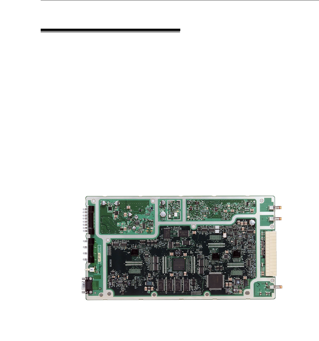
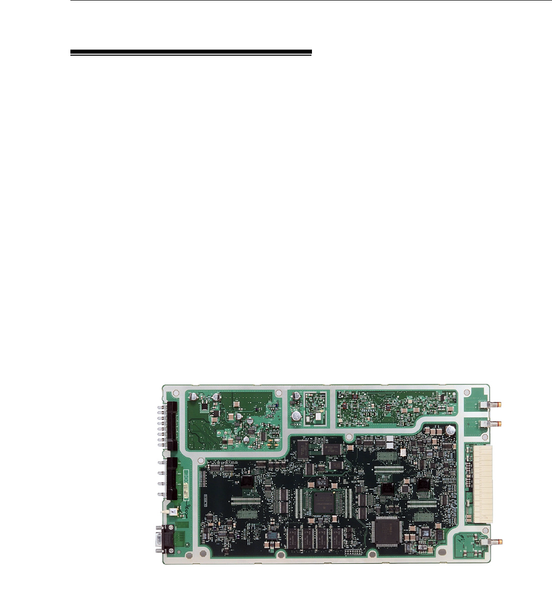
Figure 3 shows a top view of the EX/CNTL (model CLF1560) with the cover
removed.
Figure 3 900 MHz QUAD Channel Base Radio Controller, version DLN1203
(with cover removed)
16 68P80801H45-1 1/20/2002
Base Radio Controllers EBTS System Manual - Vol 2
900 MHz QUAD Channel Base Radio Controller
900 MHz QUAD Channel Base Radio Controller Controls and Indicators
The BRC monitors the functions of other Base Radio modules. The LEDs on the
front panel indicate the status of BRC-monitored modules. All LEDs on the BRC
front panel normally flash three times upon initial power-up. A RESET switch
allows a manual reset of the Base Radio. Figure 4 shows the front panel of the
BRC.
Indicators
Table 7 lists and describes the BRC LEDs.
Table 7 900 MHz QUAD Channel BR Controller Indicators
LED Color Module
Monitored
Condition Indications
PS Red Power
Supply
Solid (on) FRU failure indication - Power Supply
has a major alarm, and is out of service
Flashing (on) Power Supply has a minor alarm, and
may be operating at reduced
performance
Off Power Supply is operating normally
(no alarms)
EXBRC Red Controller/
Exciter
Solid (on) FRU failure indication - Controller/
Exciter has a major alarm, and is out of
service (Note: Upon power-up of the
BR, this LED indicates a failed mode
until BR software achieves a known
state of operation.)
Flashing (on) Controller/Exciter has a minor alarm,
and may be operating at reduced
performance
Off Controller/Exciter is operating
normally (no alarms)
PA Red Power
Amplifier
Solid (on) FRU failure indication - PA has a major
alarm, and is out of service
Flashing (on) PA has a minor alarm, and may be
operating at reduced performance
Off PA is operating normally (no alarms)
QUAD CHANNEL EX/CNTL
STATUS
RESET
TX4
TX4
TX4
TX4
PS
EX/CNTL
PA
REF
RX1
RX2
RX3
RX4
EBTS316Q
013001JNM
Figure 4 900 MHz QUAD Channel BR Controller (Front View)

68P80801H45-1 1/20/2002 17
EBTS System Manual - Vol 2 Base Radio Controllers
900 MHz QUAD Channel Base Radio Controller
Controls
Table 8 lists the controls and descriptions.
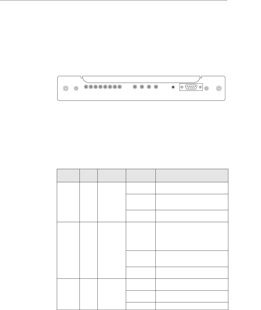
STATUS Connector
Table 9 the pin-outs for the STATUS connector.
REF Red Controller
Station
Reference
Solid (on) FRU failure indication - Controller
Station Reference has a major alarm,
and is out of service
Flashing (on) BRC has a minor alarm, and may be
operating in a marginal region
Off BRC is operating normally (no alarms)
RX1
RX2
RX3
RX4
Red Receiver #1,
#2, #3, or #4
Solid (on) FRU failure indication - Receiver (#1,
#2, #3 or #4) has a major alarm, and is
out of service
Flashing (on) Receiver (#1, #2, #3 or #4) has a minor
alarm, and may be operating at
reduced performance
Off Receiver (#1, #2, #3 or #4) is operating
normally (no alarms)
TX1 Green BR Solid (on) Station Transmit Carrier #1 is keyed
Flashing (on) Station Transmit Carrier #1 is not
keyed
Off Station is out of service, or power is
removed
TX2 Green BR Solid (on) Station Transmit Carrier #2 is keyed
Flashing (on) Station Transmit Carrier #2 is not
keyed
Off Station is out of service, or power is
removed
TX3 Green BR Solid (on) Station Transmit Carrier #3 is keyed
Flashing (on) Station Transmit Carrier #3 is not
keyed
Off Station is out of service, or power is
removed
TX4 Green BR Solid (on) Station Transmit Carrier #4 is keyed
Flashing (on) Station Transmit Carrier #4 is not
keyed
Off Station is out of service, or power is
removed
Table 7 900 MHz QUAD Channel BR Controller Indicators (Continued)
LED Color Module
Monitored
Condition Indications

18 68P80801H45-1 1/20/2002
Base Radio Controllers EBTS System Manual - Vol 2
900 MHz QUAD Channel Base Radio Controller
900 MHz QUAD Channel Base Radio Controller Theory of Operation
Table 10 briefly describes the BRC circuitry. Figure 13 is a functional block
diagram of the BRC.
Host Microprocessor
The host microprocessor is the main controller for the BR. The processor operates
at a 50-MHz clock speed. The processor controls Base Radio operation according
to station software in memory. Station software resides in FLASH memory. For
normal operation, the system transfers this software to non-volatile memory. An
EEPROM contains the station codeplug.
NOTE
At BR power-up, the EXBRC LED indicates a major
alarm. This indication continues until BR software
achieves a predetermined state of operation.
Afterward, the software turns off the EXBRC LED.
Table 8 900 MHz QUAD Channel BR Controller Controls
Control Description
RESET Switch A push-button switch used to manually reset the BR.
STATUS
connector
A 9-pin connector used for connection of a service computer, providing a
convenient means for testing and configuring.
Table 9 Pin-outs for the STATUS Connector
Pin-out Signal
1 not used
2 TXD
3 RXD
4 not used
5 GND
6 not used
7 not used
8 not used
9 not used

68P80801H45-1 1/20/2002 19
EBTS System Manual - Vol 2 Base Radio Controllers
900 MHz QUAD Channel Base Radio Controller
Table 10 900 MHz QUAD Channel BR Controller Circuitry
Circuit Description
Host Microprocessor Contains integrated circuits that comprise the central controller
of the BRC and station
Non-Volatile Memory Consists of:
• FLASH containing the station operating software
• EEPROM containing the station codeplug data
Volatile Memory Contains SDRAM to store station software used to execute
commands.
Ethernet Interface Provides the BRC with a 10Base2 Ethernet communication port
to network both control and compressed voice data
RS-232 Interface Provides the BRC with an RS-232 serial interface
Digital Signal Processors Performs high-speed modulation/demodulation of
compressed audio and signaling data
TISIC Contains integrated circuits that provide timing reference
signals for the station
TX Reclock Contains integrated circuits that provide highly stable,
reclocked transmit signals and peripheral transmit logic
RX DSP SPI Contains integrated circuits that provide DSP SPI capability
and peripheral receive logic
Station Reference Circuitry Generates the 16.8 MHz and 48 MHz reference signals used
throughout the station
Input Ports Contains 16 signal input ports that receive miscellaneous
inputs from the BR
Output Ports Contains 40 signal output ports, providing a path for sending
miscellaneous control signals to circuits throughout the BR
Remote Station Shutdown Provides software control to cycle power on the BR

20 68P80801H45-1 1/20/2002
Base Radio Controllers EBTS System Manual - Vol 2
900 MHz QUAD Channel Base Radio Controller
Serial Communication Buses
The microprocessor provides a general-purpose SMC serial management
controller bus.
The SMC serial communications bus is an asynchronous RS-232 interface with no
hardware handshake capability. The BRC front panel includes a nine-pin, D-type
connector. This connector provides a port where service personnel may connect a
service computer. Service personnel can perform programming and maintenance
tasks via Man-Machine Interface (MMI) commands. The interface between the
SMC port and the front- panel STATUS connector is via EIA-232 Bus Receivers
and Drivers.
Host Processor
The microprocessor incorporates 4k bytes of instruction cache and 4k bytes of
data cache that significantly enhance processor performance.
The microprocessor has a 32-line address bus. The processor uses this bus to
access non-volatile memory and SDRAM memory. Via memory mapping, the
processor also uses this bus to control other BRC circuitry.
The microprocessor uses its Chip Select capability to decode addresses and assert
an output signal. The eight chip-select signals select non-volatile memory,
SDRAM memory, input ports, output ports, and DSPs.
The Host processor...
❐Provides serial communications between the Host Microprocessor and other
Base Radio modules.
❐Provides condition signals necessary to access SDRAM.
❐Accepts interrupt signals from BRC circuits (such as DSPs).
❐Organizes the interrupts, based on hardware-defined priority ranking.
❐The Host supports several internal interrupts from its Communications
Processor Module. These interrupts allow efficient use of peripheral
interfaces.
❐The Host supports 10 Mbps Ethernet/IEEE 802.3.
❐Provides a 32-line data bus transfers data to and from BRC SDRAM and
other BRC circuitry. Buffers on this data bus allow transfers to and from
non-volatile memory, general input and output ports and DSPs.
Non-Volatile Memory
Base Radio software resides in 2M x 32 bits of FLASH memory. The Host
Microprocessor addresses the FLASH memory with 20 of the host address bus’ 32
lines. The host accesses FLASH data over the 32-line host data bus. A
host-operated chip-select line provides control signals for these transactions.
The FLASH contains the operating system and application code. The system
stores application code in FLASH for fast recovery from reset conditions.
Application code transfers from network or site controllers may occur in a

68P80801H45-1 1/20/2002 21
EBTS System Manual - Vol 2 Base Radio Controllers
900 MHz QUAD Channel Base Radio Controller
background mode. Background mode transfers allow the station to remain
operational during new code upgrades.
The data that determines the station personality resides in a 32K x eight bit
codeplug EEPROM. The microprocessor addresses the EEPROM with 15 of the
host address bus’ 32 lines. The host accesses EEPROM data with eight of the data
bus’ 32 lines. A host-operated chip-select line provides control signals for these
transactions.
During the manufacturing process, the factory programs the codeplug’s default
data. The BRC must download field programming data from network and site
controllers. This data includes operating frequencies and output power level. The
station permits adjustment of many station parameters, but the station does not
store these adjustments. Refer to the Software Commands chapter for additional
information.
Volatile Memory
Each BRC contains 8MB x 32 bits of SDRAM. The BRC downloads station
software code into SDRAM for station use. SDRAM also provides short-term
storage for data generated and required during normal operation. SDRAM is
volatile memory. A loss of power or system reset destroys SDRAM data.
The system performs read and write operations over the Host Address and Data
buses. These operations involve column and row select lines under control of the
Host processor’s DRAM controller. The Host address bus and column row signals
sequentially refresh SDRAM memory locations.
Ethernet Interface
The Host processor’s Communications Processor Module (CPM) provides the
Local Area Network (LAN) Controller for the Ethernet Interface. The LAN
function implements the CSMA/CD access method, which supports the IEEE
802.3 10Base2 standard.
The LAN coprocessor supports all IEEE 802.3 Medium Access Control, including
the following:
❐framing
❐preamble generation
❐stripping
❐source address generation
❐destination address checking
The PCM LAN receives commands from the CPU.
The Ethernet Serial Interface works directly with the CPM LAN to perform the
following major functions:
❐10 MHz transmit clock generation (obtained by dividing the 20 MHz signal
provided by on-board crystal)
❐Manchester encoding/decoding of frames

22 68P80801H45-1 1/20/2002
Base Radio Controllers EBTS System Manual - Vol 2
900 MHz QUAD Channel Base Radio Controller
❐electrical interface to the Ethernet transceiver
An isolation transformer provides high-voltage protection. The transformer also
isolates the Ethernet Serial Interface (ESI) and the transceiver. The pulse
transformer has the following characteristics:
❐Minimum inductance of 75 µH
❐2000 V isolation between primary and secondary windings
❐1:1 Pulse Transformer
The Coaxial Transceiver Interface (CTI) is a coaxial cable line driver and receiver
for the Ethernet. CTI provides a 10Base2 connection via a coaxial connector on the
board. This device minimizes the number of external components necessary for
Ethernet operations.
A DC/DC converter provides a constant voltage of -9 Vdc for the CTI from a
3.3 Vdc source.
The CTI performs the following functions:
❐Receives and transmits data to the Ethernet coaxial connection
❐Reports any collision that it detects on the coaxial connection
❐Disables the transmitter when packets are longer than the legal length
(Jabber Timer)
Digital Signal Processors
The BRC includes two Receive Digital Signal Processors (RXDSPs) and a Transmit
Digital Signal Processor (TXDSP). These DSPs and related circuitry process
compressed station transmit and receive audio or data. The related circuitry
includes the TDMA Infrastructure Support IC (TISIC) and the TISIC Interface
Circuitry. The DSPs only accept input and output signals in digitized form.
The RXDSP inputs are digitized receiver signals. The TXDSP outputs are digitized
voice audio and data (modulation signals). These signals pass from the DSP to the
Exciter portion of the EXBRC. DSPs communicate with the Microprocessor via an
eight-bit, host data bus on the host processor side. For all DSPs, interrupts drive
communication with the host.
The RXDSPs operate from an external 16.8 MHz clock, provided by the local
station reference. The RXDSP internal operating clock signal is 150MHz,
produced by an internal Phase-Locked Loop (PLL).
The RXDSPs accept digitized signals from the receivers through Enhanced
Synchronous Serial Interface (ESSI) ports. Each of two ESSI ports on a RXDSP
supports a single carrier (single receiver) digital data input. The DSP circuitry
includes two RXDSPs. These allow processing of up to four carriers (four
receivers).
The RXDSP accesses its DSP program and signal-processing algorithms in 128k
words of internal memory. The RXDSPs communicate with the host bus over an
8-bit interface.
Each RXDSP provides serial communications to its respective receiver module for
receiver control via a Serial Peripheral Interface (SPI). The SPI is a

68P80801H45-1 1/20/2002 23
EBTS System Manual - Vol 2 Base Radio Controllers
900 MHz QUAD Channel Base Radio Controller
parallel-to-serial conversion circuit, connected to the RXDSP data bus. Each
RXDSP communicates to two receive modules through this interface.
Additionally, a serial control path connects the two RXDSPs and the TXDSP. The
Synchronous Communications Interface (SCI) port facilitates this serial control
path.
For initialization and control purposes, one RXDSP connects to the TISIC device.
The TXDSP operates at an external clock speed of 16.8 MHz, provided by the
EXBRC local station reference. The TXDSP internal operating clock is 150MHz,
produced by an internal Phase Lock Loop (PLL).
The TXDSP sends up to four carriers of digitized signal to the EX11 exciter. The
exciter converts the digital signal to analog. Also at the exciter, a highly stable
clock reclocks the digital data. Reclocking enhances transmit signal integrity. Two
framed and synchronized data streams result. One data stream is I-data, and the
other is the Q-data stream.
The TXDSP contains its own, internal address and data memory. The TXDSP can
store 128k words of DSP program and data memory. An eight-bit interface
handles TXDSP-to-host bus communications.
TISIC
The TISIC controls internal DSP operations. This circuit provides the following
functions:
❐For initialization and control, interfaces with one RXDSP via the DSP
address and data buses.
❐Accepts a 16.8 MHz signal from Station Reference Circuitry.
❐Accepts a 5 MHz signal, modulated with one pulse per second (1 PPS) from
the site reference.
❐Demodulates the 1 PPS
❐Outputs a 1 PPS signal and a windowed version of this signal for network
timing alignment.
❐Outputs a 2.4 MHz reference signal used by the Exciter.
❐Generates 15 ms and 7.5 ms ticks. (These ticks synchronize to the 1 PPS time
mark. The system decodes the time mark from the site reference. Then the
system routes the reference to the TXDSP and RXDSPs.)
Station Reference Circuitry
The Station Reference Circuitry is a phase-locked loop (PLL). This PLL consists of
a high-stability, Voltage-Controlled, Crystal Oscillator (VCXO) and a PLL IC. GPS
output from the iSC connects to the 5 MHz/1 PPS BNC connector on the BR
backplane. Wiring at this connector routes signals to EXBRC station reference
circuitry.
The PLL compares the 5 MHz reference frequency to the 16.8 MHz VCXO output.
Then the PLL generates a DC correction voltage. The PLL applies this correction
voltage to the VCO through an analog gate. The analog gate closes when three

24 68P80801H45-1 1/20/2002
Base Radio Controllers EBTS System Manual - Vol 2
900 MHz QUAD Channel Base Radio Controller
conditions coexist: (1) The 5 MHz tests stable. (2) The PLL IC is programmed. (3)
Two PLL oscillator and reference signal output alignments occur.
When the gate enables, the control voltage from the PLL can adjust the
high-stability VCXO frequency. The adjustment can achieve a stability nearly
equivalent to that of the external, 5 MHz frequency reference.
The correction voltage from the PLL continuously adjusts the VXCO frequency.
The VXCO outputs a 16.8 MHz clock signal. The circuit applies this clock signal to
the receiver, 48 MHz reference and TISIC.
The receivers use the 16.8MHz as the clock input and synthesizer reference.
The 48 MHz EXBRC synthesizer uses the 16.8 MHz as its synthesizer reference.
The 48 MHz synthesizer output is the clock input for the TXDSP I and Q data
reclock circuitry.
The TISIC divides the 16.8 MHz signal by seven, and outputs a 2.4 MHz signal.
This output signal then becomes the 2.4 MHz reference for the Exciter.
Input Ports
One general-purpose input register provides for BRC and station circuit input
signals. The register has 16 input ports. The Host Data Bus conveys input register
data to the Host Microprocessor. Typical inputs include 16.8 and 48 MHz Station
Reference Circuitry status outputs and reset status outputs.
Output Ports
Two general-purpose output registers distribute control signals from the Host
Microprocessor to the BRC and station circuitry. One register has 32 output ports
and the other register has 8 output ports. Control signal distribution occurs over
the backplane. The Host Data Bus drives the output ports’ latched outputs.
Typical control signals include front-panel LED signals and SPI peripheral enable
and address lines.
Remote Station Shutdown
The BRC contains power supply shutdown circuitry. This circuitry can send a
shutdown pulse to the Base Radio Power Supply. BRC software generates the
shutdown control pulse.
After receiving a shutdown pulse, the power supply turns off BR power. Shut
down power sources include 3.3, 28.6 and 14.2 Vdc sources throughout the BR.
Due to charges retained by BR storage elements, power supply voltages may not
reach zero. The shutdown only assures that the host processor enters a
power-on-reset state.
A remote site uses the shutdown function to perform a hard reset of all BR
modules.
68P80801H45-1 1/20/2002
45
EBTS System Manual - Vol 2 800/900/1500 MHz Base Radios
Base Radio Controller
ETHERNET
SERIAL
INTERFACE
ISOLATION
TRANSFORMER TRANSCEIVER
HOST BUFFERED DATA BUS
HOST ADDRESS BUS
HOST BUFFERED DATA BUS
HOST ADDRESS BUS
HOST DATA BUS
DRAM ADDRESS
MULTIPLEXER
COLUMN/ROW
SELECT
DRAM
COLUMN
ADDRESS
DRAM
ROW
ADDRESS
16.5 MHZ CLK
SERIAL COMMUNICATIONS BUS
SERIAL COMMUNICATIONS BUS
ROW
SELECT
(RAS*)
COL
SELECT
(CAS*)
DRAM
ADDRESS
HOST
GLUE
ASIC
33 MHZ
TIMING
CIRCUITRY
BUFFERS
EPROM
512K X 8
8K X 8
EEPROM
CODEPLUG
32K X 8
SRAM
32K X 8
SRAM
A1-A11
A10-A22
A1-A19
A1-A19
A1-A15
HOST
ADDRESS
A1-A18
4
8
STATUS PORT
(9 PIN D CONNECTOR
ON BRC FRONT PANEL)
RS-232 PORT
(9 PIN D CONNECTOR
ON BACKPLANE)
EIA-232
BUS
RECEIVERS/
DRIVERS
4
8
EPROM
512K X 8
BUFFERS
SPI BUS
SPI BUS
TO/FROM
STATION MODULES
3
HOST ADDRESS BUS
NON-VOLATILE MEMORY
HOST
MICRO-
PROCESSOR
HOST MICROPROCESSOR / HOST ASIC
HOST
ADDRESS
1-23
EIA-232
BUS
RECEIVERS/
DRIVERS
DRAM MEMORY
BUFFERS
VARIOUS INPUTS
FROM BRC &
STATION CIRCUITRY
INPUT/OUTPUT PORTS CIRCUITRY
I/O PORT P0 IN
HOST DATA BUS
I/O PORT P0 OUT
I/O PORT P1 OUT
I/O PORT P2 OUT
VARIOUS
CONTROL
LINES TO BRC &
STATION
CIRCUITRY
FROM HOST
MICROPROCESSOR
I/O PORT P1 IN
BUFFERS
BUFFERS
16
16
16
16
16
REMOTE STATION
SHUTDOWN CIRCUITRY
SHUTDOWN
(TO POWER
SUPPLY)
28V
I/O PORT
P2 OUT
FRONT PANEL LEDS
LED CONTROL
LINES
(P/O I/O PORT
P0 OUT)
BASE
RADIO
POWER
SUPPLY EXCITER PA CTL R1 R2 R3
8
ETHERNET INTERFACE
CD
RX
TX
CLSN
RCV
TRMT
FROM
HOST
MICROPROCESSOR
ADDR BUS
DATA BUS
COPROCESSOR
ADDR BUS
COPROCESSOR
DATA BUS
10BASE2
COAX
ETHERNET
SERIAL
INTERFACE
HOST
INTERFACE
ETHERNET
COPROCESSOR
(82596DX)
A
EBTS286
010397SN
D0-D15
LANIIC
SHUTDOWN
CIRCUITRY
A1-A15
A1-A15
D0-D15
D0-D7
D0-D15
D0-D15
VCC RESET SWITCH
(FRONT PANEL)
DRAM
1M X 16
A2-A23
Base Radio Controller
Figure 10 800/900 MHz Base Radio Controller Functional Block Diagram
(Sheet 1 of 2)
46
68P80801H45-1 1/20/2002
800/900/1500 MHz Base Radios EBTS System Manual - Vol 2
Base Radio Controller
Base Radio Controller
Functional Block Diagram
Model TLN3424
(Includes Front Panel Board)
HOST BUFFERED DATA BUS
HOST ADDRESS BUS
HOST BUFFERED DATA BUS
HOST ADDRESS BUS
HOST DATA BUS
DRAM ADDRESS
MULTIPLEXER
COLUMN/ROW
SELECT
DRAM
COLUMN
ADDRESS
DRAM
ROW
ADDRESS
16.5 MHZ CLK
SERIAL COMMUNICATIONS BUS (SCC2)
SERIAL COMMUNICATIONS BUS (SCC3)
ROW
SELECT
(RAS*)
COL
SELECT
(CAS*)
COL
SELECT
(CAS*)
ROW
SELECT
(RAS*)
DRAM
ADDRESS
DRAM
ADDRESS
HOST
ASIC
(U509)
33 MHZ
TIMING
CIRCUITRY
(Y500)
BUFFERS
(U107 - U110)
EPROM
256K X 8
(U802)
8K X 8
EEPROM
CODEPLUG
(U800)
8K X 8
SRAM
(U803)
8K X 8
SRAM
(U804)
A1-A11
A10-A22
A1-A18
A1-A18
A1-A15
HOST
ADDRESS
A1-A23
4
8
STATUS
(9 PIN D CONNECTOR
ON BRC FRONT PANEL)
RS232
(9 PIN D CONNECTOR
ON BACKPLANE)
EIA-232
BUS
RECEIVERS/
DRIVERS
(U901, U902)
EPROM
256K X 8
(U801)
SPI BUS
SPI BUS
TO/FROM
STATION MODULES
3
HOST ADDRESS BUS
NON-VOLATILE MEMORY
HOST
MICRO-
PROCESSOR
(U701)
HOST MICROPROCESSOR / HOST ASIC
DRAM
1M X 8
(U114)
DRAM
1M X 8
(U114)
HOST
ADDRESS
1-23
EIA-232
BUS
RECEIVERS/
DRIVERS
(U900)
DYNAMIC RAM
VARIOUS INPUTS
FROM BRC &
STATION CIRCUITRY
INPUT/OUTPUT PORTS CIRCUITRY
I/O PORT P0 IN
HOST DATA BUS I/O PORT P0 OUT
I/O PORT P1 OUT
I/O PORT P2 OUT
I/O PORT P3 OUT
VARIOUS
CONTROL
LINES TO BRC &
STATION
CIRCUITRY
FROM HOST
MICROPROCESSOR
I/O PORT P1 IN
LATCHES
(U602 - U605,
U608 - U611)
BUFFERS
(U600, U601,
U606, U607)
16
16
16
16
16
16
REMOTE STATION
SHUTDOWN CIRCUITRY
SHUTDOWN
(TO POWER
SUPPLY)
28V
I/O PORT
P3 OUT
FRONT PANEL LEDS (Part of TRN7769)
LED CONTROL
LINES
(P/O I/O PORT
P0 OUT)
BASE
RADIO
POWER
SUPPLY EXCITER PA BRC RX1 RX2 RX3
8
ETHERNET INTERFACE
CD
RX
TX
CLSN
RCV
TRMT
FROM
HOST
MICROPROCESSOR
ADDR BUS
DATA BUS
COPROCESSOR
ADDR BUS
COPROCESSOR
DATA BUS
10BASE2
COAX
ETHERNET
SERIAL
INTERFACE
82596DX
ETHERNET
COPROCESSOR
(U408)
ETHERNET
SERIAL
INTERFACE
(U1308)
TRANSCEIVER
(U1311)
A
HOST
INTERFACE
(U404 - U406)
ISOLATION
TRANSFORMER
(T100)
SHUTDOWN
CIRCUITRY
(U3)
BUFFERS
(U108 - U110)
BUFFERS
(U108 - U110)
DC/DC
CONVERTER
(U1310)
5 VDC
-9 VDC
23
16
20 MHZ
TIMING
CIRCUIT
(Y1300)
XMT CLK
(10 MHZ)
A1-A13
A1-A13
6
9
STATIC RAM
Figure 10 800/900 MHz QUAD Channel Base Radio Functional Block Diagram Sheet 2 of 2)
49
68P80801H45-1 1/20/2002
800/900/1500 MHz Base Radios EBTS System Manual - Vol 2
Base Radio Controller
SPI
BUS
PHASE
DETECTION/
FILTERING
HIGH
STABILITY
VCXO
48 MHZ
16.8MHZ
QUAD Channel Base
Radio Controller
Functional Block Diagram
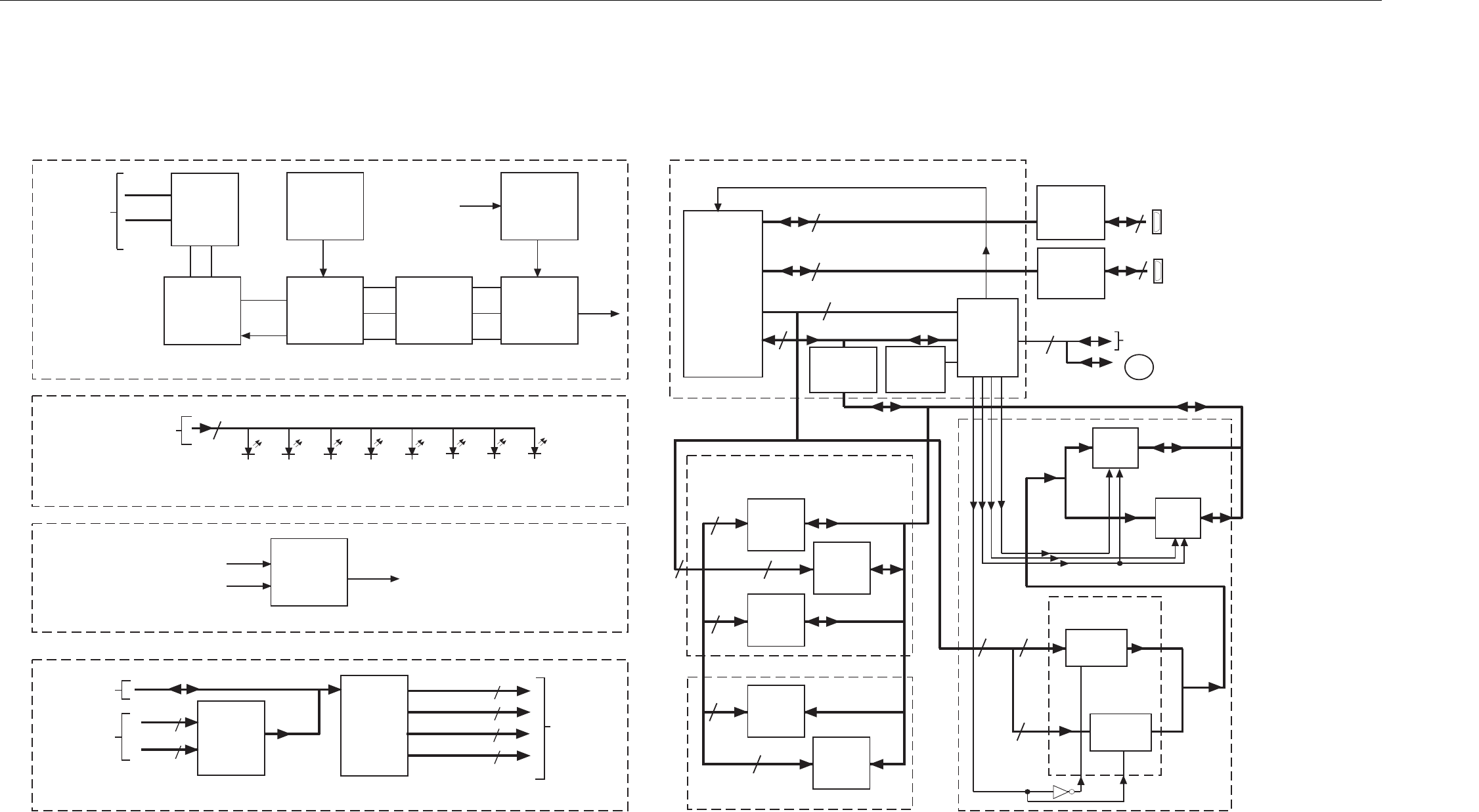
Figure 13 800 and 900 MHz QUAD Channel Base Radio Controller Functional
Block Diagram (Sheet 1 of 2)
POWER
SUPPLY EXCITER/
CONTROL PA REF RX1 RX2 RX3 RX4 TX1 TX2 TX3 TX4
P0 OUT
LED
CONTROL
LINES
HOST
LATCH
12
FRONT PANEL LEDS REMOTE STATION
3.3V
P0_OUT
SHUTDOWN
CIRCUITRY
SHUTDOWN
(TO POWER
SUPPLY)
SHUTDOWN CIRCUITRY
SYNTHESIZER
IC / CIRCUITRY
5MHZ_1PPS
BASE RADIO
INPUT
HIGH
STABILITY
VCXO
PHASE
DETECTION/
FILTERING/
CONTROL
STEARING
LINE
DISCONNECT/
CONNECT
CONTROL
G
A
T
I
N
G
SPI
BUS
16.8 MHZ
SYNTHESIZER
IC / CIRCUITRY
STEARING
LINE
STATION REFERENCE CIRCUITRY
TRANSMIT REFERENCE CIRCUITRY
5MHZ
1PPS
50
68P80801H45-1 1/20/2002
800/900/1500 MHz Base Radios EBTS System Manual - Vol 2
Base Radio Controller
QUAD Channel
Base Radio Controller
Functional Block Diagram
Figure 14
800 and 900 MHz QUAD Channel Base Radio Controller Functional Block
Diagram (Sheet 2 of 2)
HOST
MICRO-
ETHERNET
SERIAL
INTERFACE TRANS-
CD
RCV RX
TRMT TX
CLSN
10BASE2
COAX
ETHERNET
SERIAL
INTERFACE
CEIVER
ISOLATION
TRANSFORMER
PROCESSOR
SCC1
8
SDRAM
4M x 16
SDRAM
4M x 16
SDRAM
4M x 16
SDRAM
4M x 16
GPLA0, A[8,9,17,18,20:29],RAS,CAS,WE
CS2
CS3
D[0:31]
D[0:15]
D[16:31]
D[0:15]
D[16:31]
BUFFER
BUFFER
BUFFER
BUFFER
BUFFER
BUFFER
D[0:31]
D[0:7]
A[10:31]
MA[21:0]
DSP_D[31:24]
A[0:7]
DSP_A[31:24]
MD[31:0]
EIA-232
BUS
RECEIVERS/
DRIVERS
2STATUS PORT
(9 PIN D CONNECTOR
ON BRC FRONT PANEL)
2
BUFFER
33SPI BUS
TO/FROM
STATION MODULES
FLASH
1M x 16
FLASH
1M x 16
FLASH
1M x 16
FLASH
1M x 16
CS0
CS1 MD[0:15]
MD[16:31]
MD[0:15]
MD[16:31]
16
16
16
16
16 16
16
16
MA[2:21]
MA[2:21]
EEPROM
32k x 8
MD[24:31]
MA[0:14]
CS4
P1_OUT
LATCH
P0_OUT
LATCH
MD[0:32]
MD[24:31]
P0_IN
BUFFER
MD[16,17,20-24,28-31]
STATUS BUS
FROM
STATION MODULES
P0_IN
8
CONTROL BUS
TO
STATION MODULES
P0_OUT/P1_OUT
32
8
TRANSMIT
DIGITAL
SIGNAL
PROCESSOR
(TX DSP)
SINGLE END
TO DIFFERENTIAL
TRANSMIT
CLOCK AND
FRAME SYNCH
CIRCUITRY
I/Q DATA SERIAL DATA
TO EXCITER
DIFFERENTIAL
TO SINGLE END
RX1 SERIAL DATA
RECEIVE
DIGITAL
SIGNAL
PROCESSOR
(RX DSP 1)
RECEIVE
DIGITAL
SIGNAL
PROCESSOR
(RX DSP 2)
TISIC
A[0:5]
D[0, 8:23]
PARALLEL
TO SERIAL
CIRCUITRY
D[16:23]
D[16:23]
D[0, 23]
SPI BUS TO
RECEIVER 1 & 2
SPI BUS TO
RECEIVER 3 & 4
2.4 MHz
1 PPS TIMING, CONTROL/ SLOT TIMING/RESET
NETWORKED
SCI
16.8MHZ
48 MHZ
SPI
BUS
SPI
BUS
EXCITER
SPI
CONTROL
DSP SPI
SPI BUS
TO EXCITER
DIGITAL SIGNAL PROCESSING
CIRCUITRY
DIGITAL SIGNAL PROCESSING
CIRCUITRY
DIFFERENTIAL
TO SINGLE END
DIFFERENTIAL
TO SINGLE END
DIFFERENTIAL
TO SINGLE END
50 MHZ
CLOCK
FRONT PANEL
RESET
DRAM MEMORY
ETHERNET INTERFACE
NON-VOLATILE MEMORY EXPANDED STATUS INPUT
AND OUTPUT CONTROL CIRCUITRY
EXTENDED HOST
BUS BUFFERS
40
TO EXCITER
5MHZ
1PPS
RX2 SERIAL DATA
RX3 SERIAL DATA
RX4 SERIAL DATA
HOST ADDRESS BUS
HOST DATA BUS
HOST BUFFERED DATA BUS
HOST BUFFERED ADDRESS BUS
HOST-DSP BUFFERED DATA BUS
HOST-DSP BUFFERED ADDRESS BUS
SERIAL MANAGEMENT CONTROLLER (SMC2)
SERIAL PERIPHERAL INTERFACE

68P80801H45-1 1/20/2002 1
EBTS System Manual - Vol 2 Base Radio Exciter
Base Radio Exciter
Overview
This chapter provides technical information for the Exciter (EX).
FRU Number to Kit Number Cross Reference
Exciter Field Replaceable Units (FRUs) are available for the iDEN EBTS. The FRU
contains the Exciter kit and required packaging. Table 1 provides a cross reference
between Exciter FRU numbers and kit numbers.
Section Page Description
800 Legacy MHz Exciter –
TLN3337; 900 MHz Exciter –
CLN1357; 1500 MHz Exciter –
TLN3428
2 Describes the functions and characteristics of the
Exciter module for the single channel Base Radio
(BR).
Low Noise 800 MHz Exciter 7 Describes the functions and characteristics of the
Exciter module for the Low Noise Exciter for the
Generation 2 Base Radio (Gen2 BR).
QUAD Channel 900 MHz
Exciter
11 Describes the functions and characters of the 900
MHz QUAD Channel Base Radio (BR)
QUAD Channel 800 MHz
Exciter
15 Describes the functions and characteristics of the
Exciter module for the 800 MHz QUAD channel
Base Radio (BR).
Table 1 FRU Number to Kit Number Cross Reference
Description FRU Number Kit Number
Single Channel Exciter (800 MHz) TLN3337 CLF1490
Single Channel Exciter (900 MHz) CLN1357 CLF1500
Single Channel Exciter (1500 MHz) TLN3428 CTX1120
QUAD Channel 900 MHz Exciter/
Base Radio Controller)
CLN1497 CLF6452
QUAD Channel 800 MHz Exciter/
Base Radio Controller
CLN1497 CLF1560
LNODCT (Low Noise Offset Direct
Conversion Transmit) Exciter (800
MHz)
TLN3337 CLF1789
68P80801H45-1 1/20/2002 11
EBTS System Manual - Vol 2 Base Radio Exciter
QUAD Channel 900 MHz Exciter
QUAD Channel 900 MHz Exciter
QUAD Channel 900 MHz Exciter Overview
The Exciter and the Power Amplifier (PA) provide the transmitter functions of the
QUAD Channel 900 MHz Base Radio. The Exciter module consists of a printed
circuit board, a slide in housing, and associated hardware. The BRC shares the
printed circuit board and housing.
The Exciter connects to the Base Radio backplane through a 168-pin connector
and two blindmate RF connectors. Controller and exciter circuitry also
interconnect on the Exciter/Controller module. Two Torx screws on the front of
the Exciter secure it to the chassis.
An LED identifies the Exciter’s operational condition, as described in the
manual’s Controller section. The Base Radio section of the manual provides
specifications for transmitter circuitry. This information includes data on the
Exciter and PAs.
Figures 5 shows the Exciter with the cover removed.
Figure 4 900 MHz QUAD Channel Exciter (with cover removed)

12 68P80801H45-1 1/20/2002
Base Radio Exciter EBTS System Manual - Vol 2
QUAD Channel 900 MHz Exciter
900 MHz QUAD Channel Exciter Theory of Operation
Table 4 describes the basic circuitry of the Exciter. Figures 9 show the QUAD
Carrier Exciter’s functional block diagram.
Memory Circuitry
The memory circuitry is an EEPROM on the Controller portion of the Exciter/
Controller module. The Controller performs memory read and write operations
over the parallel bus. The memory device stores the following data...
❐kit number
❐revision number
❐module specific scaling and correction factors
❐serial number
❐free form information (scratch pad)
A/D Converter Circuitry
Analog signals from various areas throughout the Exciter board enter the A/D
converter (A/DC). The A/DC converts these analog signals to digital form. Upon
Table 4 900 MHz Exciter Circuitry
Circuit Description
LNODCT IC • Up-converts baseband data to the transmit frequency
• Down-converts the PA feedback signal to baseband
• Uses a baseband Cartesian feedback loop system, necessary
to obtain linearity from the transmitter and avoid
splattering power into adjacent channels
• Performs training functions for proper linearization of the
transmitter
Memory & A/D Converter Serves as the main interface between the synthesizer, Tranlin
IC, A/D, and EEPROM on the Exciter, and the BRC via the
SPI bus
Frequency Synthesizer
Circuitry
• Consists of a phase-locked loop and VCO
• Provides a LO signal to the LNODCT IC for the second
up-conversion and first down-conversion of the feedback
signal from the PA
1025 MHz VCO (900 MHz BR) Provides a LO signal to the LNODCT IC, for up-conversion
to the transmit frequency
90.3 MHz VCO (900 MHz BR) Provides a LO signal to LNODCT IC, for the up-conversion
and for the down-conversion of the feedback signal.
The mixed output becomes the LO signal for Transmit signal
up- and down- conversion
Regulator Circuitry Provides a regulated voltage to various ICs and RF devices
located on the Exciter
Linear RF amplifier Stages Amplifies the RF signal from the Exciter IC to an appropriate
level for input to the PA

68P80801H45-1 1/20/2002 13
EBTS System Manual - Vol 2 Base Radio Exciter
QUAD Channel 900 MHz Exciter
request of the BRC, A/DC output signals enter the BRC via SPI lines. The
Controller periodically monitors all signals.
Some of the monitored signals include amplifier bias and synthesizer signals.
Low Noise Offset Direct Conversion Transmit (LNODCT) IC Circuitry
The Low Noise IC is a main interface between the Exciter and BRC. The BRC’s
Digital Signal Processor (DSP) sends digitized signals (baseband data) to the
Exciter over the DSP data bus.
The differential data clock signal serves as a 2.4 MHz reference signal to the Low
Noise IC’s internal synthesizer. The Low Noise IC compares the reference signal
with the outputs of Voltage Controlled Oscillators (VCOs). The Low Noise IC
might sense that a VCO’s output is out of phase or off-frequency. If so, then the
Low Noise IC sends correction pulses to the VCO. The pulses adjust VCO output,
thereby matching phase and frequency with the reference.
The Low Noise IC up-converts baseband data from the BRC to the transmit
frequency. The Low Noise IC also down-converts the Transmit signal from the
Power Amplifier to baseband data for cartesian feedback linearization.
The BRC uses the Serial Peripheral Interface (SPI) bus to communicate with the
Low Noise IC. The SPI bus serves as a general purpose, bi-directional, serial link
between the BRC and other Base Radio modules, including the Exciter. The SPI
carries control and operational data signals to and from Exciter circuits.
Synthesizer Circuitry
The synthesizer circuit consists of the Phase-Locked Loop (PLL) IC and associated
circuitry. This circuit’s controls the 1025 MHz VCO signal. An internal phase
detector generates a logic pulse. This pulse is proportional to the phase or
frequency difference between the reference frequency and loop pulse signal.
The charge pump circuit generates a correction signal. The correction signal
moves up or down in response to phase detector output pulses. The correction
signal passes through the low-pass loop filter. The signal then enters the 1025
MHz Voltage Controlled Oscillator (VCO) circuit.
1025 MHz Voltage Controlled Oscillator (VCO)
For proper operation, the VCO requires a very low-noise, DC supply voltage. An
ultra low-pass filter prepares the necessary low-noise voltage and drives the
oscillator.
A portion of the oscillator output signal enters the synthesizer circuitry. The
circuitry uses this feedback signal to generate correction pulses.
The 1025MHz VCO output mixes with the 90.3 MHz VCO output. The result is a
Local Oscillator [LO) signal for the Low Noise IC. The LNODCT uses this LO
signal to up-convert the programmed transmit frequency. The Low Noise IC also
uses the LO signal to down-convert the PA feedback signal.

14 68P80801H45-1 1/20/2002
Base Radio Exciter EBTS System Manual - Vol 2
QUAD Channel 900 MHz Exciter
90.3 MHz Voltage Controlled Oscillator (VCO)
The synthesizer within the Low Noise IC sets the 90.3 MHz signal. The 90.3 MHz
VCO provides a LO signal to the LNODCT IC. The Low Noise IC uses this signal
in up-converting and down-converting the feedback signal.
Regulator Circuitry
The voltage regulators generate three regulated voltages: +3 Vdc, +5 Vdc and
+11.7 Vdc. The regulators obtain input voltages from the +3.3 Vdc and +14.2 Vdc
backplane voltages. The regulated voltages power various ICs and RF devices in
the Exciter.
Linear RF Amplifier Stages
The linear RF amplifiers boost the RF signal from the Low Noise IC. The RF
Amplifier generates an appropriate signal level to drive the PA.
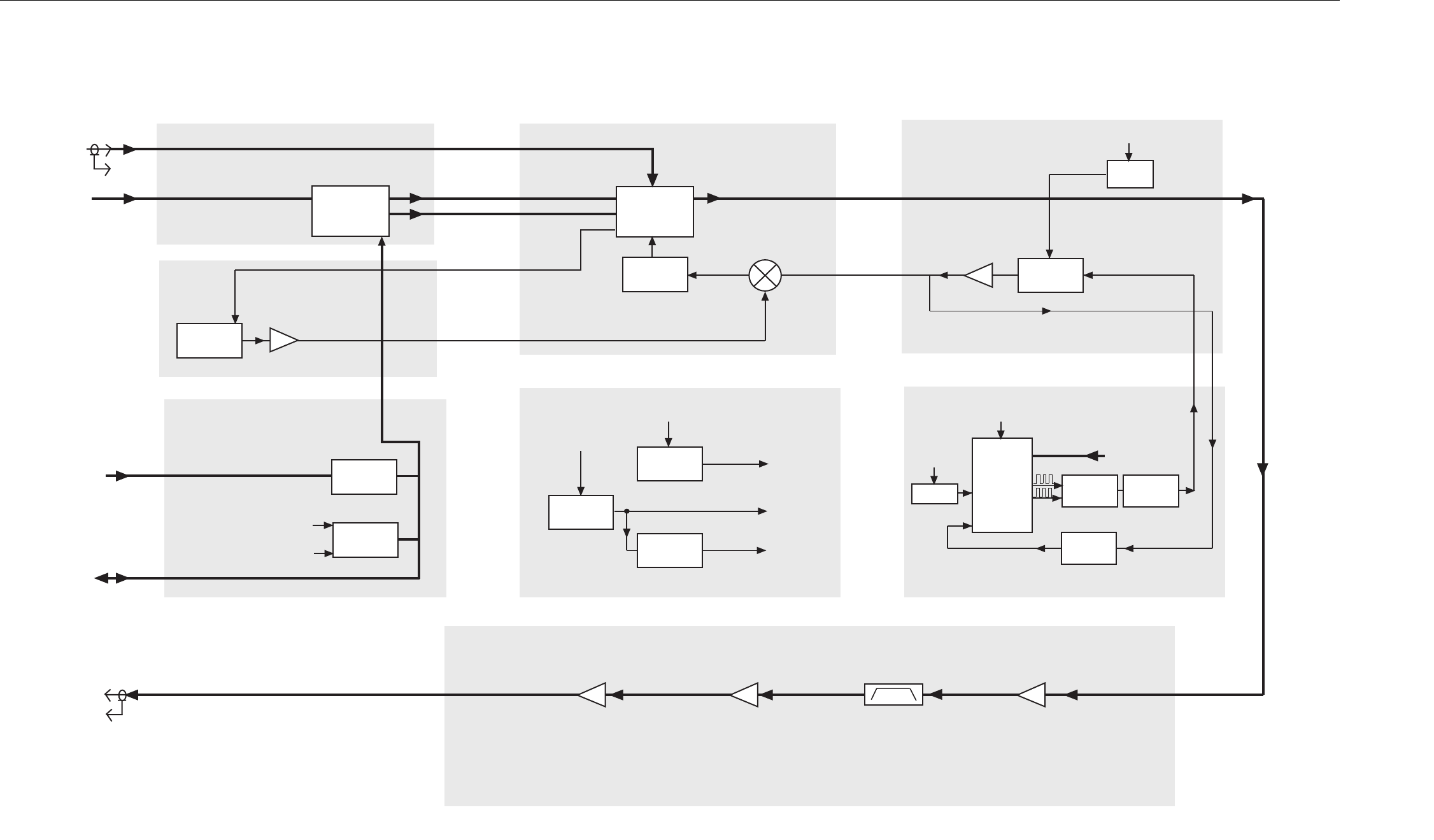
22
68P80801H45-1 1/20/2002
800/900/1500 MHz Base Radios EBTS System Manual - Vol 2
Exciter
DIFFERENTIAL
DATA & CLOCK
FROM
BRC MODULE
ADDRESS BUS
FROM CONTROL
MODULE
SPI BUS
TO/FROM CONTROL
MODULE
ADDRESS DECODE, MEMORY, & A/D
CONVERTER CIRCUITRY
EXCITER IC CIRCUITRY 970 MHZ
VCO CIRCUITRY
SYNTHESIZER
CIRCUITRY
LINEAR RF AMPLIFIER
CIRCUITRY
LO
INJECTION
CIRCUITRY
MEMORY
A/D
CONVERTER
VARIOUS
SIGNALS
TO MONITOR
DC
FILTER
+10 V
CONTROL VOLTAGE
OSCILLATOR
CHARGE
PUMP
2.4 MHZ
VCO FEEDBACK
CHIP
SELECT
SPI BUS (CLOCK & DATA)
FROM BACKPLANE
PHASE
LOCKED
LOOP
IC
RIN
FIN
90.3
VCO
CIRCUITRY
OSCILLATOR
BUFFER
AMP
LNODCT IC CIRCUITRY
LNODCT IC
TX DATA & CLOCK
LOW-PASS
LOOP
FILTER
BUFFER
VCO
FEEDBACK
RF OUTPUT
TO PA MODULE
DAC
I
Q
RF FEEDBACK
FROM PA MODULE
BUFFER
AMP
BPF
REGULATOR
CIRCUITRY
+11.7 V
REGULATOR
+14.2 V
FROM
BACKPLANE
+3 V
SOURCE
+11.7 V
SOURCE
+5 V
SOURCE
+5 V
REGULATOR
+3 V
REGULATOR
(U3702)
EBTS283Q
080601JNM
NOTE: Where two frequencies are given, frequency without parentheses applies to 800 MHz BR only and frequency with parentheses applies to 900 MHz BR only.
+3.3 V
Figure 9 800 and 900 MHz MHz QUAD Channel Exciter Functional Block Diagram

68P80801H45-1 1/20/2002 1
EBTS System Manual - Vol 2 Power Amplifier (PA)
Power Amplifier (PA)
Overview
This section provides technical information for the Power Amplifier (PA).
FRU Number to Kit Number Cross Reference
Power Amplifier (PA) Field Replaceable Units (FRUs) are available for the iDEN
EBTS. The FRU contains the PA kit and required packaging. Table 1 provides a
cross reference between PA FRU numbers and kit numbers.
Section Page Description
Power Amplifer Overview 1 Describes the the various Base Radio Power
Amplifier (PAs) for the single channel and QUAD
Channel Base Radios (BR)s.
PA Theory of Operation 8 Describes the various modules and functions for
the various single channel and QUAD Channel
Base Radios (BRs)
40W - 800 MHz PA
Functional Block Diagram
(Sheet 1 of 1)
17 Functional Block Diagram for the 40 Watt, 800
MHz, Single Channel Base Radio Power Amplifier
(PA)
70W - 800 MHz PA
Functional Block Diagram
(Sheet 1 of 1)
18 Functional Block Diagram for the 70 Watt, 800
MHz, Single Channel Base Radio Power Amplifier
(PA)
60W - 900 MHz PA
Functional Block Diagram
(Sheet 1 of 1)
19 Functional Block Diagram for the 60 Watt, 900
MHz, Single Channel Base Radio Power Amplifier
(PA)
40W - 1500 MHz PA
Functional Block Diagram
(Sheet 1 of 1)
20 Functional Block Diagram for the 40 Watt, 1500
MHz, Single Channel Base Radio Power Amplifier
(PA)
800 MHz QUAD Channel BR
PA Functional Block
Diagram (Sheet 1 of 1)
21 Functional Block Diagram for the 800 MHz QUAD
Channel Base Radio Power Amplifier (PA)
900 MHz QUAD Channel BR
PA Functional Block
Diagram (Sheet 1 of 1)
21 Functional Block Diagram for the 900 MHz QUAD
Channel Base Radio Power Amplifier (PA)
Table 1 FRU Number to Kit Number Cross Reference
Description FRU Number Kit Number
40 W- 800 MHz Single Channel Base Radio PA TLF2020 CLF1772
70 W- 800 MHz Single Channel Base Radio PA TLN3335 CLF1771
60 W- 900 MHz Single Channel Base Radio PA CLN1355 CLF1300
40 W- 1500 MHz Single Channel Base Radio PA TLN3426 TTG1000
52 W- 900 MHz QUAD Channel Base Radio PA DLN1202 CTF1082
52 W- 800 MHz QUAD Channel Base Radio PA CLF1499 CLF1400

268P80801H45-1 1/20/2002
Power Amplifier (PA) EBTS System Manual - Vol 2
Power Amplifer Overview
Power Amplifer Overview
NOTE
The power outputs discussed on this section for the
800 MHz QUAD and 900 MHz QUAD Power
Amplifiers are referenced to the single carrier mode,
operating at 52 W average power output from the
Power Amplifier’s output connector.
The Power Amplifier (PA), with the Exciter, provides the transmitter functions for
the Base Radio. The PA accepts the low-level modulated RF signal from the
Exciter. The PA then amplifies the signal for transmission and distributes the
signal through the RF output connector.
The 800 MHz Base Radio can be equipped with either 40 Watt PA, TLF2020
(version CLF1771) or 70 Watt PA, TLN3335 (version CLF1772). The 40W PA
module consists of five hybrid modules, four pc boards, and a module heatsink/
housing assembly. The 70W PA module consists of eight hybrid modules, four pc
boards, and a module heatsink/housing assembly.
The 900 MHz Base Radio is equipped with 60 Watt PA, CLN1355 (kit no.
CLF1300A). The PA module consists of four hybrid modules, two pc boards, and
a module heatsink/housing assembly.
The 1500 MHz Base Radio is equipped with 40 Watt PA, TLN3426 (version
TTG1000). The PA module consists of four hybrid modules, two pc boards, and
the module heatsink/housing assembly.
The PA connects to the chassis backplane through a 96-pin DIN connector and
three blindmate RF connectors. Two Torx screws located on the front of the PA
hold it in the chassis.
Specifications of the transmitter circuitry, including the Exciter and PAs, are
provided in Base Radio Overview section. Figure 1 shows the 40W, 800 MHz PA.
Figure 2 shows the 70W, 800 MHz PA. Figure 3 shows the 60W, 900 MHz PA.
Figure 4 shows the 40W, 1500 MHz PA. Figure 5 shows the 800 MHz QUAD PA
(the 900 MHz QUAD PA is similar in appearance)
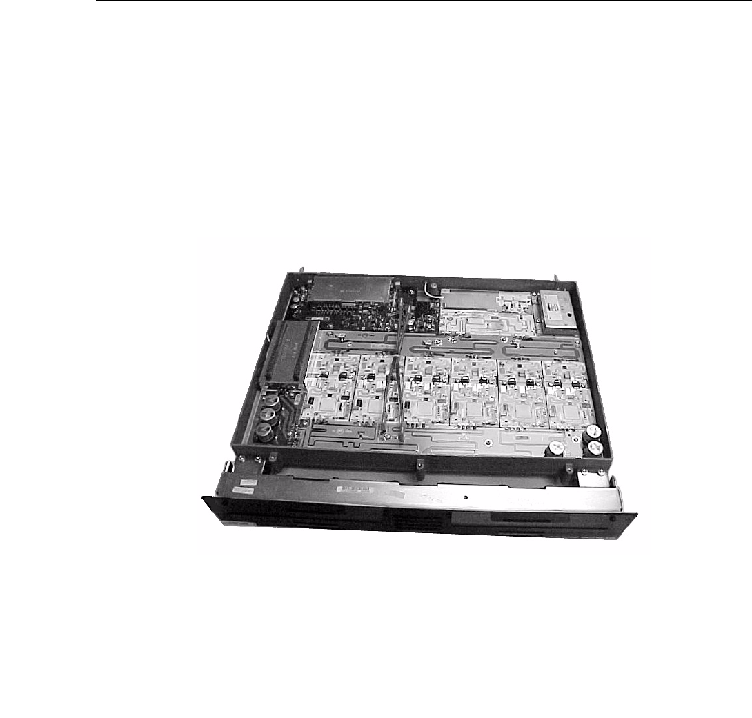
68P80801H45-1 1/20/2002 7
EBTS System Manual - Vol 2 Power Amplifier (PA)
Power Amplifer Overview
Figure 5 800/900 MHz QUAD PA

868P80801H45-1 1/20/2002
Power Amplifier (PA) EBTS System Manual - Vol 2
PA Theory of Operation
PA Theory of Operation
Table 2 describes the basic functions of the PA circuitry. Figures 6 and 7 show the
functional block diagrams of 40W, 800 MHz and 70W, 800 MHz PA, respectively.
Figure 8 shows the functional block diagram of the 60W, 900 MHz PA. Figure 9
shows a functional block diagram of the 40W, 1500 MHz PA. Figure 10 shows a
functional block diagram of 800 MHz. Figure 10 shows a functional block
diagram of 900 MHz QUAD PA.
Table 2 Power Amplifier Circuitry
Circuit Description
DC/Metering Board • Serves as the main interface between the PA and the backplane board
• Accepts RF input from the Exciter via a blindmate RF connector
• Routes the RF input via a 50 Ω stripline to the Linear Driver Module
RF amplifier
• Routes the RF feedback from the RF Combiner/Peripheral Module
to the Exciter via a blindmate RF connector
• Provides digital alarm and metering information of the PA to the
BRC via the SPI bus
• Routes DC power to the fans and PA
• Contains the thermistor that senses the PA temperature (800 MHz
QUAD and 900 MHz QUAD)
• Contains a Linear Driver Module and Linear Final Module Bias
Enable Circuit (900 MHz QUAD)
• Contains a Voltage Variable Attenuator Circuit (900 MHz QUAD)
Linear Driver Module
(LDM)
• Contains two Class AB stages with the final stage in a parallel
configuration (70W-800 MHz, 40W-800 MHz, 800 MHz QUAD)
• Contains three cascaded Class AB stages with the first two stages
configured as distributed amplifiers and the final stage in parallel
configuration (900 MHz QUAD)
• Contains three cascaded stages (Class A + Class AB + Class AB) with
the final stage in push-pull configuration (900 MHz)
• Contains four cascaded stages (Class A + Class AB + Class AB +
Class AB) with the final stage in a push-pull configuration (1500
MHz)
• Amplifies the low-level RF signal ~25 mW average power from the
Exciter via the DC/Metering Board (900 MHz)
• Amplifies the low level RF signal ~11mW average power from the
Exciter via the DC/Metering Board (70W-800 MHz, 800 MHz
QUAD*, 900 MHz QUAD*)
• Amplifies the low-level RF signal ~8 mW average power from the
Exciter via the DC/Metering Board (40W- 800 MHz, 1500MHz)
• Provides an output of:
~8 W (70W, 800MHz) average power
~4 W (40W, 800 MHz) average power
~6 W (800 MHz QUAD* and 900 MHz QUAD*) average power
~17 W (900MHz) average power
~16 W (1500MHz) average power

68P80801H45-1 1/20/2002 9
EBTS System Manual - Vol 2 Power Amplifier (PA)
PA Theory of Operation
Interconnect Board
(70W-800 MHz, 40W-800
MHz, 800 QUAD, and 900
MHz QUAD
• Provides RF interconnection from the LDM to the RF Splitter board
• Provides DC supply filtering
RF Splitter/DC board • Interfaces with the DC/Metering Board to route DC power to the
LFMs
• Interfaces with the DC/Metering Board to route PA Bias Enable to
the six Linear Final Modules (900 MHz Quad)
• Contains splitter circuits that split the RF output signal of the LDM
to the three Linear Final Modules (40W- 800 MHz)
• Contains splitter circuits that split the RF output signal of the LDM
to the six Linear Final Modules (70W- 800 MHz, 800 MHz QUAD
and 900 MHz QUAD)
• Contains a Quadrature splitter circuit to split the RF output signal of
the LDM to the two Linear Final Modules (900 MHz and 1500 MHz)
Linear Final Module
(LFM)
• Each module contains two Class AB amplifiers in parallel. Each
module amplifies one of three RF signals (~ 84 W average power)
from the LDM (via the Splitter/DC board). Three LFMs provide a
sum RF output of approximately 48 W average power, before losses.
(40W, 800MHz)
• Each module contains two Class AB amplifiers in parallel. Each
module amplifies one of six RF signals (~ 8 W average power) from
the LDM (via the Splitter/DC board). Six LFMs provide a sum RF
output of approximately 97 W average power, before losses. (70W,
800MHz)
• Each module contains two Class AB amplifiers in parallel. Each
module amplifies one of six RF signals (~6W average power) from
the LDM (via the splitter/DC Board). Six LFMs provide a sum RF
output of approximately 73W average power , before losses. (800
MHZ QUAD* and 900 MHz QUAD*)
• Each module contains two Class push-pull AB amplifiers in parallel.
Each module amplifies one of two RF signals (~ 17 W average
power) from the LDM (via the Splitter/DC board). Two LFMs
provide a sum RF output of approximately 75 W average power,
before losses. (900MHz)
• Each module contains two push-pull Class AB amplifiers in parallel.
Each module amplifies one of two RF signals (~ 16 W average
power) from the LDM (via the Splitter/DC board). Two LFMs
provide a sum RF output of approximately 56W average power,
before losses. (1500MHz)
RF Interconnect Board
(40W- 800 MHz PA only)
• Contains three transmission lines that interconnect the LFMs to the
RF Combiner/Peripheral Module
Combiner Board
(70W-800 MHz PA, 800
MHz QUAD, 900 MHz
QUAD)
• Contains three separate Quadrature combiner circuits that
respectively combine the six RF outputs from the LFMs into three
signals. These three signals, in turn, are applied to the RF Combiner/
Peripheral Module.
Table 2 Power Amplifier Circuitry (Continued)
Circuit Description

10 68P80801H45-1 1/20/2002
Power Amplifier (PA) EBTS System Manual - Vol 2
PA Theory of Operation
DC/Metering Board (Non-QUAD PA)
The DC/Metering Board provides the interface between the PA and the Base
Radio backplane. The preamplified/modulated RF signal is input directly from
the Exciter via the Base Radio backplane.
The RF input signal is applied to the input of the Linear Driver Module (LDM).
The RF feedback signal is fed back to the Exciter, where it is monitored for errors.
The primary function of the DC/Metering Boards is to monitor proper operation
of the PA. This information is forwarded to the Base Radio Controller (BRC) via
the SPI bus. The alarms diagnostic points monitored by the BRC on the PA
include the following:
❐Forward power
❐Reflected power
❐PA temperature sense
❐Fan Sensor
RF Combiner/Peripheral
Module
• Contains a combiner circuit that combines the three RF signals from
the RF Interconnect Board (40W- 800 MHz PA) or the Combiner
Board (70W-800 MHz PA). It then routes the combined RF signal
through a single stage circulator and a Low Pass Filter. The final
output signal is routed to the blindmate RF connector (40W-800 MHz
and 70W-800 MHz PAs).
• Contains a combiner circuit that combines the three RF signals from
the Combiner Board. It then routes the combined RF signal through a
dual stage circulator and a Low Pass Filter. The final output signal is
routed to the blindmate RF output connector. (800 MHz QUAD and
900 MHz QUAD PAs)
• Contains a Quadrature combiner circuit to combine the RF signal
from the two LFMs. It routes the combined RF signal through a
circulator and a Low Pass Filter. The output signal is routed to the
blindmate RF connector (900 MHz and 1500 MHz PAs)
• Contains an RF coupler that provides an RF feedback signal to the
Exciter via a blindmate RF connector on the DC/Metering Board.
Also contains a forward and reverse power detector for alarm and
power monitoring purposes.
• Contains the thermistor that senses PA temperature and feeds the
signal back to the DC/Metering Board for processing (40W-800
MHz, 70W-800 MHz, 900 MHz and 1500 MHz)
Fan Assembly • Consists of three fans used to keep the PA within predetermined
operating temperatures
NOTE: * The power outputs described in this section for the 800 QUAD and 900 QUAD PAs are references to the
single carrier mode operating at 52W average power out from the PA output connector.
Table 2 Power Amplifier Circuitry (Continued)
Circuit Description

68P80801H45-1 1/20/2002 11
EBTS System Manual - Vol 2 Power Amplifier (PA)
PA Theory of Operation
DC/Metering Board (QUAD PA Only)
The DC/Metering Board in the QUAD Radio serves the same function as it does
in other radios. However, its circuitry is modified for compatibility with the
QUAD Station. As a result, its logic circuitry is operated at 3.3 VDC.
In addition to the functions listed for non-QUAD versions above, the following
meter points are ported to the SPI bus:
❐A and B Currents
❐Thermistor (for PA temperature sensing circuit on the DC/Metering Board)
❐Voltage Variable Attenuator Circuit (900 MHz QUAD version)
❐PA Bias Enable Circuitry (900 MHz QUAD version)
Linear Driver Module
40W-800 MHz, 70W-800 MHZ and 800 MHZ QUAD PAs
The Linear Driver Module (LDM) amplifies the low-level RF signal from the
Exciter. The LDM consists of a two-stage cascaded Class AB amplifier, with the
final stage in a parallel configuration.
See Table 2 for the approximate input and output levels of the various LDMs. The
LDM output is fed to the RF Splitter/DC Distribution Board via an Interconnect
Board.
900 MHz PA
The Linear Driver Module (LDM) amplifies the low-level RF signal from the
Exciter. The LDM consists of a three-stage, cascaded, Class AB amplifier, with the
first two stages configured as distributed amplifiers and the final stage in a
push-pull configuration. This output is fed directly to the RF Splitter/DC
Distribution Board.
See Table 2 for the approximate input and output power of the 900 MHz LDM.
The LDM output is fed to the RF Splitter/DC Distribution Board via the
Interconnect Board.
1500 MHz PA
The Linear Driver Module (LDM) takes the low level RF signal and amplifies it.
The LDM consists of a four stage, cascaded, Class AB amplifier, with the final
stage configured in push-pull configuration. This output is fed directly to the RF
Splitter/DC Distribution Board.
See Table 2 for the approximate input and output power of the 1500 MHz LDM.

12 68P80801H45-1 1/20/2002
Power Amplifier (PA) EBTS System Manual - Vol 2
PA Theory of Operation
900 QUAD PA
The Linear Driver Module (LDM) amplifies the low-level RF signal from the
Exciter. The LDM consists of a three stage, cascaded, Class AB amplifier, with the
final stage in a parallel configuration.
See Table 2 for the approximate input and output power of the 900 MHz QUAD
LDM.
The LDM Output is fed to the RF Splitter/DC Distribution Board via the
Interconnect Board.
Interconnect Board (40W-800 MHz, 70W-800 MHz , 800 MHz QUAD
and 900 MHz QUAD)
The output of the LDM is applied to the Interconnect Board, which provides an
RF connection to the RF Splitter/DC Distribution Board. As a separate function,
area on the Interconnect Board serves as a convenient mounting location for
electrolytic capacitors used for filtering the +28 VDC supply.
RF Splitter/DC Distribution Board
40W-800 MHz, 70W-800 MHz, 800 MHz QUAD and 900 MHz QUAD
The RF Splitter portion of this board accepts the amplified signal from the LDM
(via the Interconnect Board). The primary function of this circuit is to split the RF
signal into drive signals for the LFMs.
In the 40W-800 MHz PA, this circuit splits the drive signal into three separate
paths to be applied to the three LFMs, where the signals will be amplified further.
In the 70W-800 MHz, 800 MHz QUAD and 900 MHZ QUAD PAs, this circuit
splits the drive signal into six separate paths to be applied to the six LFMs, where
the signals will be amplified further.
The DC Distribution portion of this board interfaces directly with the DC/
Metering Board to route DC power to the LFMs and provide PA Bias Enable (900
MHz QUAD only)
900 MHz and 1500 MHz
The RF Splitter portion of this board accepts the amplified signal from the LDM.
The primary function of this circuit is to split the RF signal into two separate
paths. These two outputs are fed directly to two separate Linear Final modules
where the RF signals will be amplified further.
The DC Distribution portion of this board interfaces directly with the DC/
Metering Board to route DC power to the LFMs.

68P80801H45-1 1/20/2002 13
EBTS System Manual - Vol 2 Power Amplifier (PA)
PA Theory of Operation
Linear Final Modules
40W-800 MHz, 70W-800 MHz, 800 MHz QUAD and 900 MHz QUAD
The RF Splitter output signals are applied directly into the LFMs for final
amplification. Each LFM contains a coupler that splits the LFM input signal and
feeds the parallel Class AB amplifiers that amplify the RF signals.
In the 40W PA, the amplified signals are then combined on the LFM and sent
directly to the RF Interconnect Board. In the 70W PA, the amplified signals are
then combined on the LFM and sent directly to the Combiner Board.
See Table 2 for the approximate total summed output powers of the various
LFMs, before output losses.
900 MHz PA
The RF signals from the outputs of the RF Splitter are applied directly into the
Linear Final Module (LFM) for final amplification. Each LFM contains a
branchline coupler that splits the LFM’s input signal and feeds the dual Class AB
push-pull amplifiers that amplify the RF signals. The amplified signals are then
combined on the LFM and sent directly to the RF Combiner circuit for final
distribution. See Table 2 for the approximate total summed output power of the
900 MHz LFMs, before output losses.
1500 MHz PA
The two RF signals from the outputs of the RF Splitter are input directly into the
Linear Final Module (LFM) for final amplification. Each LFM contains a
branchline coupler that splits the LFM’s input signal and feeds the dual Class AB
push-pull amplifiers that amplify the RF signals. The amplified signals are then
combined on the LFM , via a branchline coupler, and sent directly to the RF
Combiner circuit for final distribution. See Table 2 for the approximate total
summed output power of the 1500 MHz LFMs, before output losses.
The current drains of the 1500 MHz LFMs are monitored by the A/D converter on
the DC/Metering board. A voltage signal representative of the LFM current drain
is sent to the BRC. A Power Amplifier alarm is generated if the signal is outside of
either the upper or lower limits.
RF Interconnect Board (40W- 800 MHz PA Only)
The RF Interconnect Board consists of transmission line paths which route the
three output signals from the LFMs to the three inputs of the RF Combiner/
Peripheral Module.
Combiner Board (40W- 800 MHz, 70W- 800 MHz, 800 MHz QUAD and
900 MHz QUAD PAs)
The Combiner Board combines pairs of signals into single signals, thereby
combining the six signals from the LDMs into three signals. The resulting three
signals are applied to the RF Combiner/Peripheral Module.

14 68P80801H45-1 1/20/2002
Power Amplifier (PA) EBTS System Manual - Vol 2
PA Theory of Operation
RF Combiner/Peripheral Module (40- 800 MHz, 70W- 800 MHz PAs)
This module consists of two portions: an RF combiner and a peripheral module.
The RF Combiner portion of the module combines the three RF signals from the
RF Interconnect Board (40W- 800 MHz PA) or the Combiner Board (70W- 800
MHz PA) into a single signal using a Wilkinson coupler arrangement.
Following the combiner circuit, the single combined RF signal is then passed
through a directional coupler which derives a signal sample of the LFM RF power
output. Via the coupler, a sample of the RF output signal is fed to the Exciter, via
the DC/Metering Board, as a feedback signal. Following the coupler, the power
output signal is passed through a single stage circulator, which protects the PA in
the event of high reflected power.
The peripheral portion of the module provides a power monitor circuit that
monitors the forward and reflected power of the output signal. This circuit
furnishes the A/D converter on the DC/Metering Board with input signals
representative of the forward and reflected power levels.
For forward power, a signal representative of the measured value is sent to the
BRC via the SPI bus. The BRC determines if this level is within tolerance of the
programmed forward power level. If the level is not within parameters, the BRC
will issue a warning to the site controller which, in turn, will shut down the
Exciter if required.
Reflected power is monitored in the same manner. The BRC uses the reflected
power to calculate the voltage standing wave ratio (VSWR). If the VSWR is
determined to be excessive, the forward power is rolled back. If it is extremely
excessive, the BRC issues a shut-down command to the Exciter.
A thermistor is located on the RF Combiner/Peripheral module to monitor the
operating temperature of the PA. The thermistor signal indicating excessive
temperature is applied to the A/D converter and then sent to the BRC. The BRC
rolls back forward power if the monitored temperature is excessive.
900 MHz PA
This module consists of two parts: an RF combiner and a peripheral module. The
RF combiner combines the two RF signals from each LDM into a single signal,
using a branchline coupler arrangement. Then, the RF signal passes through a
directional coupler which derives a signal sample of the LFMs RF power output.
Via the coupler, a sample of the RF output signal is fed to the Exciter, via the DC/
Metering Board, as a feedback signal, thereby allowing the Exciter to accordingly
adjust signal drive. Following the coupler, the power output signal is passed
through a circulator, which protects the PA in the event of high reflected power.
A power monitor circuit monitors the forward and reflected power of the output
signal. This circuit furnishes the A/D converter on the DC/Metering Board with
input signals representative of the forward and reflected power levels.
For forward power, a signal representative of the measured value is sent to the
BRC via the SPI bus. The BRC determines if this level is within tolerance of the
programmed forward power level. If the level is not within parameters, the BRC
will issue a warning to the site controller which, in turn, will shut down the
Exciter if required.

68P80801H45-1 1/20/2002 15
EBTS System Manual - Vol 2 Power Amplifier (PA)
PA Theory of Operation
Reflected power is monitored in the same manner. The BRC uses the reflected
power to calculate the voltage standing wave ratio (VSWR). If the VSWR is
determined to be excessive, the forward power is rolled back. If it is extremely
excessive, the BRC issues a shut-down command to the Exciter.
A thermistor is located on the RF Combiner/Peripheral module to monitor the
operating temperature of the PA. A voltage representative of the monitored
temperature is sent from the A/D converter to the BRC. The BRC rolls back
forward power if the monitored temperature is excessive.
1500 MHz
Both LFM outputs are input into this module where they are combined, with a
branchline coupler, for a single output signal. The RF signal is first coupled to the
Exciter module, via the DC/Metering Board, so that it can be monitored. The RF
output signal is then passed through a circulator that acts as a protection device
for the PA in the event of reflected power.
A power monitor circuit monitors the forward and reflected power of the output
signal. This circuit provides the A/D converter on the DC/Metering board with
an input signal representative of the forward or reflected power levels.
For forward power, a signal representative of the measured value is sent to the
BRC module via the SPI bus. The BRC determines if this level is within tolerance
of the programmed forward power level. The programmed forward power is set
through the use of MMI commands. If the level is not within certain parameters,
the BRC will issue a warning to the site controller and may shut-down the Exciter
module.
Reflected power is monitored in the same manner except that the BRC determines
an acceptable reflected power level. The BRC calculates the reflected power
through an algorithm stored in memory. If the reflected power is determined to be
excessive, the forward power is rolled back. If the reflected power level is
extremely excessive, the BRC will issues a shut-down command to the Exciter
module.
A thermistor is located on the RF Combiner/Peripheral module to monitor the
operating temperature of the Power Amplifier. A voltage representative of the
monitored temperature is sent from the A/D converter to the BRC. The BRC
issues a cut-back command to the Exciter module if the monitored temperature is
greater than 121˚ F (85˚ C).
RF Combiner/Peripheral Module (800 MHz QUAD and 900 MHz QUAD)
This module consists of two parts: an RF combiner and a Peripheral module. The
RF combiner combines three RF signals from the Combiner Board into a single
signal using a Wilkinson coupler arrangement. Following the combiner circuit,
the single combined RF signal is then passed through a directional coupler, which
derives a signal sample of the LFM RF power output. Via the coupler, a sample of
the RF output signal is fed to the Exciter, via the DC/Metering Board, as a
feedback signal. Following the coupler, the power output signal is passed through
a dual stage circulator, which protects the PA in the event of high reflected power.

16 68P80801H45-1 1/20/2002
Power Amplifier (PA) EBTS System Manual - Vol 2
PA Theory of Operation
The Peripheral module provides a power monitor circuit that monitors the
forward and reflected power of the output signal. This circuit furnishes the A/D
converter on the DC/Metering Board with input signals, representative of the
forward and reflected power levels.
For forward power, a signal representative of the measured value is sent to the
BRC via the SPI bus. The BRC determines if this level is within tolerance of the
programmed forward power level. If the level is not within tolerance, the BRC
will issue a warning to the site controller, which, in turn, will shut down the
Exciter, if required.
Reflected power is monitored in the same manner. The BRC uses the reflected
power to calculate the voltage standing wave ratio (VSWR). If the VSWR is
calculated as excessive, forward power is rolled back. If the VSWR calculation is
exceedingly out of tolerance, the BRC issues a shut-down command to the Exciter.
NOTE
The Thermistor that monitors the operating
temperature of the 800 MHZ QUAD and 900 MHz
QUAD PAs is located on the DC/Metering Board
Fan Module
The PA contains a fan assembly to maintain normal operating temperature
through the use of a cool air intake. The fan assembly consists of three individual
fans in which airflow is directed across the PA heatsink.
The current draw of the fans is monitored by the DC/Metering Board. A voltage
representative of the current draw is monitored by the BRC. The BRC flags the
iSC if an alarm is triggered. The PA LED on the front panel of the BRC also lights,
however the PA does not shut down due to a fan failure alone.
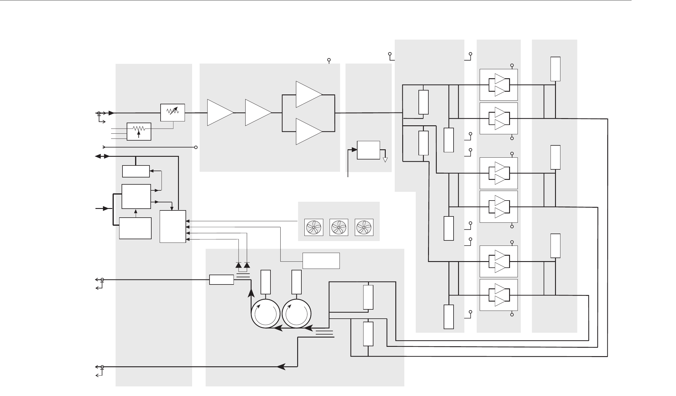
22
68P80801H45-1 1/20/2002
800/900/1500 MHz Base Radios EBTS System Manual - Vol 2
Power Amplifier
COMBINER
BOARD
LINEAR DRIVER MODULE
LINEAR FINAL
MODULES
50 OHM
LOAD
ADDRESS BUS
FROM BRC
SPI BUS
TO/FROM BRC
ADDRESS DECODE, MEMORY,
& A/D CONVERTER CIRCUITRY
MEMORY
A/D
CONVERTER
BOARD SELECT
DECODE
CIRCUITRY
PA TEMP SENSE
CHIP
SELECT
CHIP SELECT
DECODE
CIRCUITRY
CHIP SELECT
RF COMBINER/
PERIPHERAL MODULE
LOW-PASS
FILTER
RF INPUT
RF OUT
TO ANTENNA
RF FEEDBACK
TO EXCITER
MODULE
REF PWR
FWD PWR
FAN SENSE
FAN ASSEMBLY
TEMPERATURE
SENSOR
EBTS417_900
121701JNM
CLK/DATA
CIRCULATOR
50 OHM
LOAD
50 OHM
LOAD
50 OHM
LOAD
50 OHM
LOAD
50 OHM
LOAD
50 OHM
LOAD
STAGE 2
CLASS AB
RF SPLITTER/DC
DISTRIBUTION BOARD
INTERCONNECT
BOARD
STAGE 3
CLASS AB
DC
FILTER
+28 VDC
CIRCULATOR
50 OHM
LOAD
50 OHM
LOAD
50 OHM
LOAD
50 OHM
LOAD
50 OHM
LOAD
EEPOT
STAGE 2
CLASS AB
DISTRIBUTED
STAGE 1
CLASS AB
DISTRIBUTED
C_E
INC
V_D
VVA
PA_ENABLE (PA_E)
PA_E PA_E
PA_E
PA_E
PA_E
PA_E
PA_E
PA_E
PA_E
PA_E
PA_E
PA_E
PA_E
PA_E
Figure 11 900 MHz QUAD Channel BR PA Functional Block Diagram
(Sheet 1 of 1)
900 MHz QUAD Power Amplifier – DLN1202 (CTF1082)
Functional Block Diagram

68P80801H45-1 1/20/2002 1
EBTS System Manual - Vol 2 DC Power Supply
DC Power Supply
Overview
This section provides technical information for the DC Power Supply (PS).
FRU Number to Kit Number Cross Reference
DC Power Supply Field Replaceable Units (FRUs) are available for the iDEN
EBTS. The FRU contains the Power Supply kit and required packaging. Table 1
provides a cross reference between Exciter FRU numbers and kit numbers.
Chapter Page Description
Single Channel DC Power
Supply Overview
1 Describes the functions and characteristics of the
DC Power Supply (PS) module for the single
channel Base Radio (BR).
DC Power Supply for
QUAD Channel Base Radios
5 Describes the functions and characteristics of the
DC Power Supply (PS) module for the QUAD
channel Base Radio (BR).
DC Power Supply Functional
Block Diagram (Sheet 1 of 2)
9 Functional Block Diagram for the Single Channel
DC Power Supply (PS)
QUAD BR DC Power Supply
(Sheet 1 of 2)
11 Functional Block Diagram for the QUAD Channel
DC Power Supply (PS)
Table 1 FRU Number to Kit Number Cross Reference
Description FRU Number Kit Number
Single Channel DC Power Supply TLN3338 CPN1027
QUAD Channel DC Power Supply CLN1498 CLN1461
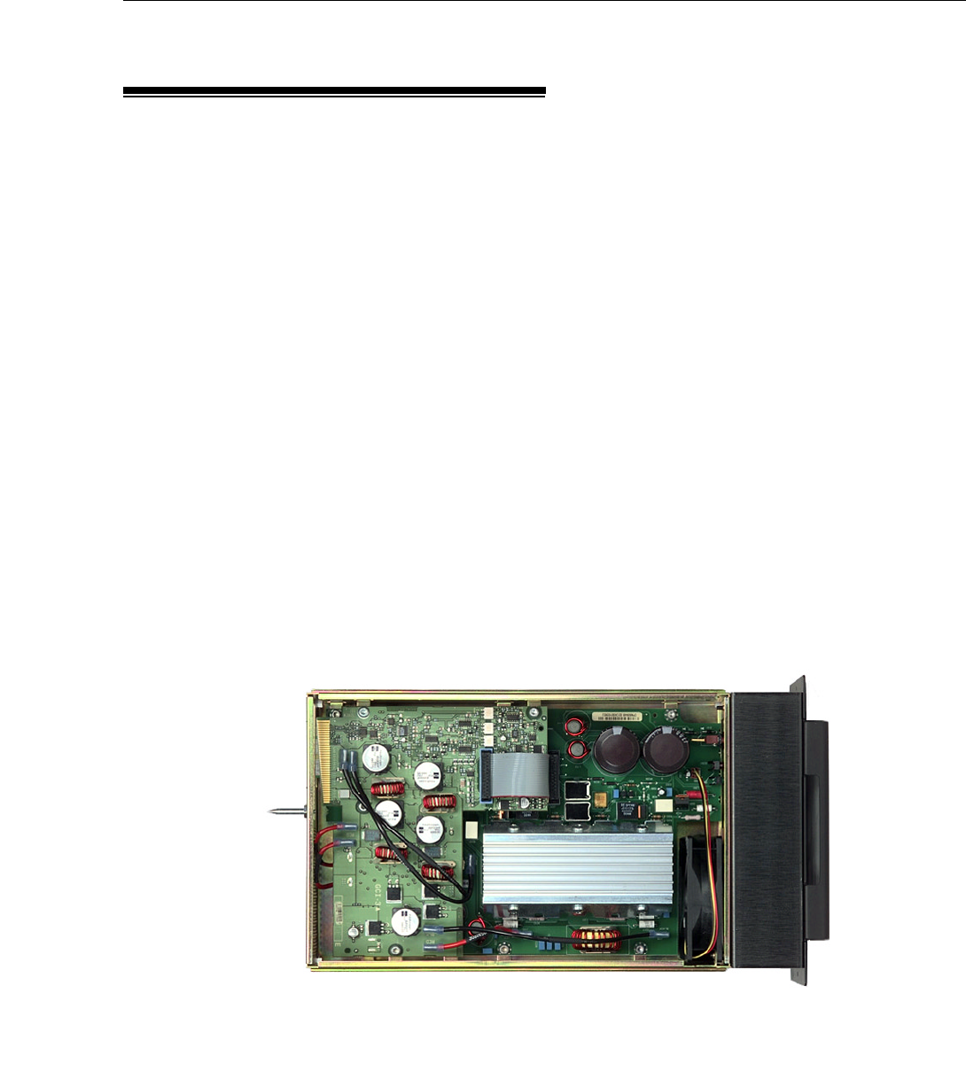
68P80801H45-1 1/20/2002 5
EBTS System Manual - Vol 2 DC Power Supply
DC Power Supply for QUAD Channel Base Radios
DC Power Supply for QUAD Channel Base Radios
QUAD Channel DC Power Supply Overview
The QUAD Channel DC Power Supply provides DC operating voltages to QUAD
Channel Base Radio FRUs. The power supply accepts input voltage sources from
41VDC to 60VDC. Input sources may be either positively or negatively grounded.
On initial startup, the supply requires a nominal 43 VDC. If the voltage drops
below 41 VDC, the QUAD Channel DC Power Supply enters quiescent mode. In
quiescent mode, the power supply emits no power.
The QUAD Channel DC Power Supply is designed for sites with an available DC
voltage source. Output voltages from the DC Power Supply are 28.6 VDC,
14.2 VDC and 3.3 VDC, with reference to output ground. The supply is rated for
575 Watts of continuous output, with up to 113˚ F (45˚ C) inlet air. At 140˚ F (60˚
C), the 28.6 VDC output reduces to 80% of maximum.
The QUAD Channel DC Power Supply consists of the Power Supply and front
panel hardware. The QUAD Channel DC Power Supply connects to the chassis
backplane through an edgecard connector. Two Torx screws on the front panel
secure the QUAD Channel DC power supply to the chassis.
Figure 2 shows the QUAD Channel Power Supply with the cover removed.
Figure 2 Quad Carrier Power Supply

668P80801H45-1 1/20/2002
DC Power Supply EBTS System Manual - Vol 2
DC Power Supply for QUAD Channel Base Radios
QUAD Channel DC Power Supply Controls and Indicators
Table 5 summarizes LED indications on the QUAD Channel DC Power Supply
during normal operation. The ON/OFF switch behind the front panel turns DC
power supply on and off.
QUAD Channel DC Power Supply Performance Specifications
Table 6 lists the specifications for the QUAD Channel DC Power Supply.
Table 5 DC Power Supply Indicators
LED Condition Indications
Green Solid (on) Power Supply is on, and operating under normal conditions with
no alarms
Off Power Supply is turned off or required power is not available
Red Solid (on) Power Supply fault or load fault on any output, or input voltage is
out of range
Off Power Supply is operating normally, with no alarms
Table 6 DC Power Supply Specifications
Description Value or Range
Operating Temperature 0° to +40° C (no derating)
+41° to +60° C (derating)
Input Voltage 41 to 60 VDC
Input Polarity Positive (+) ground system
Startup Voltage 43 VDC (minimum)
Input Current 18.0 A (maximum) @ 41 VDC
Steady State Output Voltages 28.6 VDC +5%
14.2 VDC +5%
3.3 VDC +5%
Total Output Power Rating 575 W (no derating)
485 W (derating)
Output Ripple All outputs 150mV p-p (measured with
20 MHz BW oscilloscope at 25°C)
High Frequency individual harmonic voltage
limits (10kHz to 100MHz) are:
28.6 VDC 1.5 mV p-p
14.2 VDC 3.0 mV p-p
3.3 VDC 5.0 mV p-p
Short Circuit Current 0.5 A average (maximum)

68P80801H45-1 1/20/2002 7
EBTS System Manual - Vol 2 DC Power Supply
DC Power Supply for QUAD Channel Base Radios
QUAD Channel DC Power Supply Theory of Operation
Table 7 briefly describes the basic DC Power Supply circuitry. Figure 5 shows the
functional block diagrams for the DC Power Supply.
Table 7 DC Power Supply Circuitry
Circuit Description
Input Circuit Routes input current from the DC power input cable through the
high current printed circuit edge connector, EMI filter, panel mounted
combination circuit breaker, and on/off switch
Startup Inverter
Circuitry
Provides VDC for power supply circuitry during initial power-up
Main Inverter Circuitry Consists of a switching-type power supply to generate the +28.6 VDC
supply voltage
Temperature Protection The Power Supply contains a built-in cooling fan that runs whenever
the supply is powered on. The supply shuts down if the temperature
exceeds a preset threshold
+14.2 VDC Secondary
Converter Circuitry
Consists of a switching-type power supply to generate the +14.2 VDC
supply voltage
+3.3 VDC Secondary
Converter Circuitry
Consists of a switching-type power supply to generate the +3.3 VDC
supply voltage
Clock Generator
Circuitry
Generates the 267 kHz and 133 kHz clock signals used by the pulse
width modulators in the four inverter circuits
Address Decode,
Memory, & A/D
Converter
Serves as the main interface between A/D on the Power Supply and
the BRC via the SPI bus
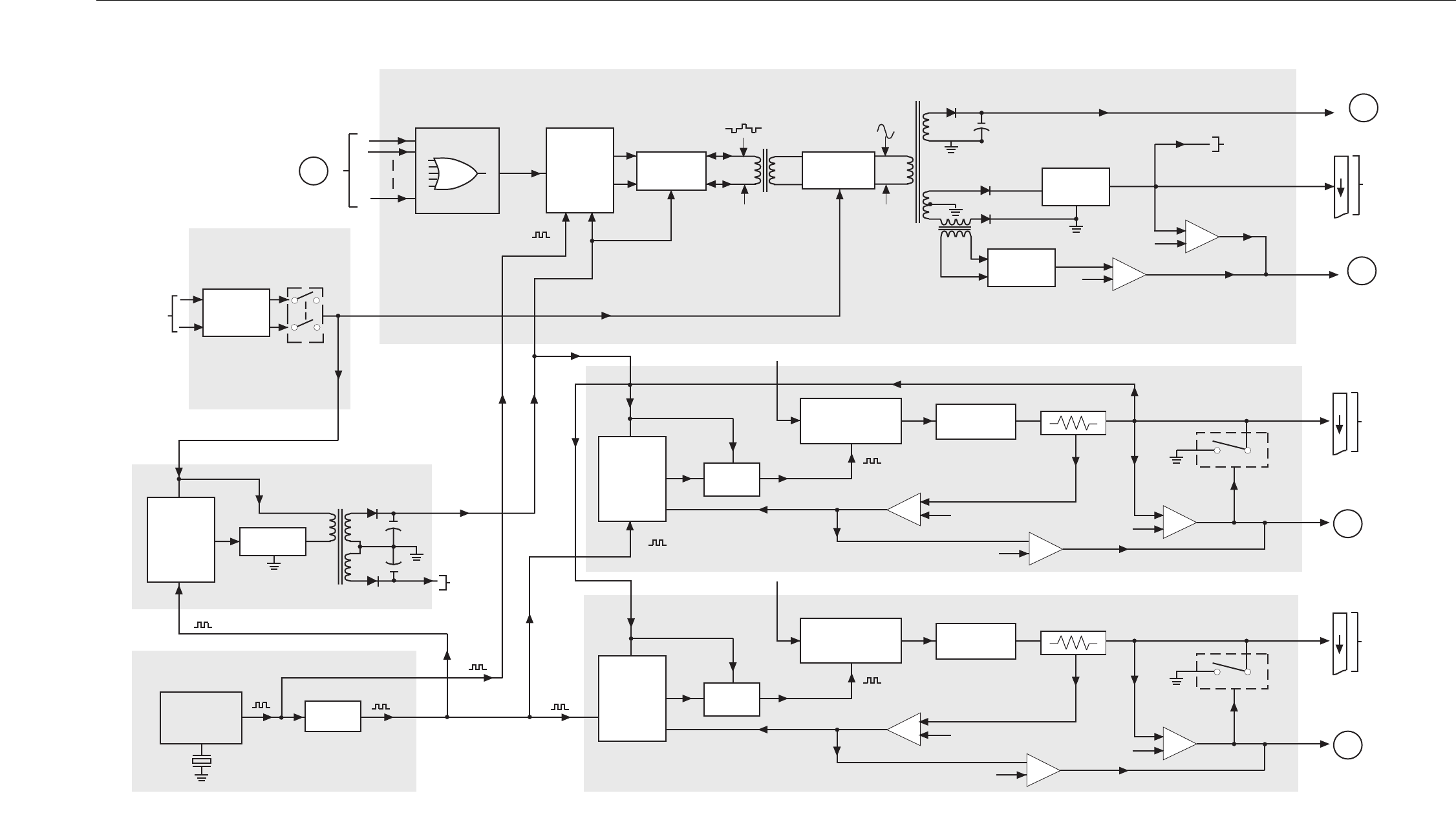
1/20/2002
11
EBTS System Manual - Vol 2 800/900/1500 MHz Base Radios
DC Power Supply
+5.1 V INVERTER CIRCUITRY
FET
DRIVER
POWER FET
SWITCH FILTER
CIRCUITRY
VCC
VCC
+ 5V OVERCURRENT
DETECT
REF
REF
SURGE CURRENT
DELAY REF
OVERVOLTAGE
DETECT
FET
CROWBAR
CIRCUIT
+ 28V BULK
PULSE
WIDTH
MODULATOR
A
24
25
30
31
+5.1 V DC
TO
STATION
MODULES
VIA
BACKPLANE
P/O
BACKPLANE
CONNECTOR
+5.1 V
÷ 2
CLOCK GENERATOR CIRCUITRY
STARTUP INVERTER CIRCUITRY
BULK DETECT
TO
DIAGNOSTICS
CIRCUITRY
PULSE
WIDTH
MODULATOR
VCC
VCC STARTUP ISOLATION
TRANSFORMER
+14.2 V INVERTER CIRCUITRY
FET
DRIVER
POWER FET
SWITCH FILTER
CIRCUITRY
VCC
VCC
+ 14.2V OVERCURRENT
DETECT
REF
REF
SURGE CURRENT
DELAY REF
OVERVOLTAGE
DETECT
FET
CROWBAR
CIRCUIT
A
16
17
22
23
+14.2V DC
TO
STATION
MODULES
VIA
BACKPLANE
P/O
BACKPLANE
CONNECTOR
+14.2V
+14.2V
PULSE
WIDTH
MODULATOR
PULSE
WIDTH
MODULATOR
FRONT PANEL
ON / OFF
SWITCH
EXTERNAL
DC INPUT
41-60 VDC
FILTER
CIRCUITRY
INPUT FILTER BOARD
3
4
14
15
+28.6 VDC
TO
STATION
MODULES
VIA
BACKPLANE
P/O
BACKPLANE
CONNECTOR
MAIN INVERTER CIRCUITRY
REF
REF
CURRENT
DETECT A
+28.6 V OVERVOLTAGE
DETECT
+28 V BULK TO
DIAGNOSTICS
CIRCUITRY
OVERCURRENT
DETECT
+28.6 VDC
CLOCK
GENERATOR
CIRCUITRY
267 KHZ
TRANSISTOR
SWITCH
B
MAIN ISOLATION
TRANSFORMER
TRANSISTOR
DRIVERS
SOFTSTART
CIRCUITRY
SHUTDOWN
A
+12V STARTUP BIAS
+12V STARTUP BIAS
VCC
VCC
MOD FAIL
133 KHZ
267 KHZ
133 KHZ
133 KHZ
133 KHZ
133 KHZ
133 KHZ
267 KHZ
133 KHZ
267 KHZ
133 KHZ
POWER FET
SWITCHES FILTERING
CIRCUITRY
+28 V BULK
EBTS323
011497JNM
Figure 5
QUAD BR DC Power Supply (Sheet 1 of 2)
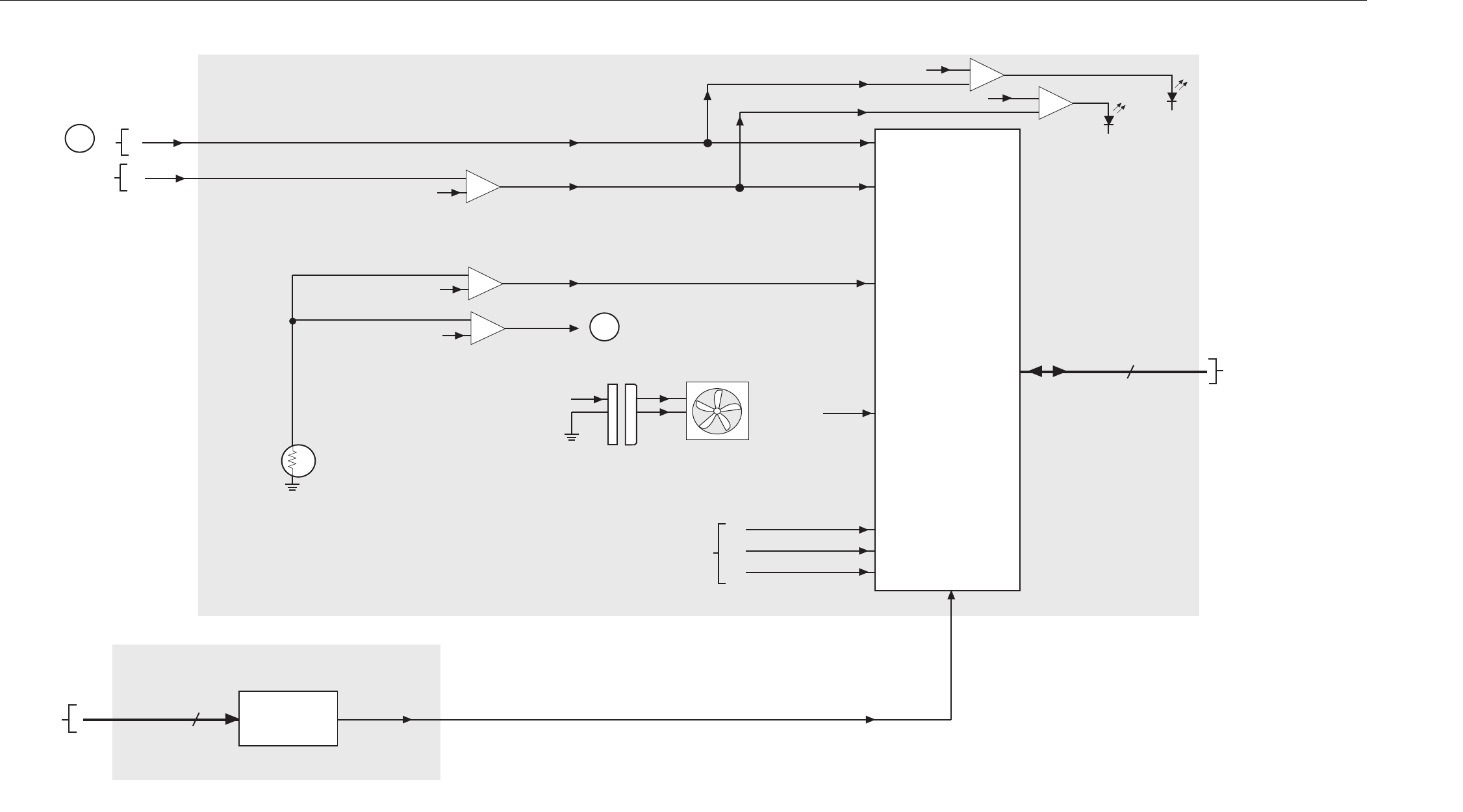
12
1/20/2002
800/900/1500 MHz Base Radios EBTS System Manual - Vol 2
DC Power Supply
A/D
CONVERTER
COOLING
FAN
THERMISTOR
MOUNTED ON
HEATSINK
SPI BUS
REF
REF
REF
MOD FAIL
INPUT FAIL
HEATSINK DIAG
+5.1 V
+14.2V DIAG
+5.1 V DIAG
+28.6 V DIAG
REF
REF
HEATSINK STATUS
DETECT
HI-TEMP
DETECT
BULK DETECT
FROM STARTUP
INVERTER
CIRCUITRY
FROM
DETECT
CIRCUITRY
A
B
INPUT GOOD
(GREEN)
MODULE
FAIL
(RED)
3
SPI BUS
TO/FROM
STATION CONTROL
MODULE
ADDRESS DECODE CIRCUITRY
ADDRESS
DECODE
CIRCUITRY
FROM
STATION
CONTROL
BOARD
9
P/O ADDRESS BUS ENABLE ENABLE
DIAGNOSTICS CIRCUITRY
T°
EBTS324
012097JNM
J300
REF
Figure 6
QUAD BR DC Power Supply Functional Block Diagram (Sheet 2 of 2)

44 68P80801H45-1 1/20/2002
Troubleshooting EBTS System Manual - Vol 2
QUAD Channel Base Radio/Base Radio FRU Replacement Procedures
QUAD Channel Base Radio/Base Radio FRU Replacement Procedures
Replace suspected station modules with known non-defective modules to restore
the station to proper operation. The following procedures provide FRU
replacement instructions, post-replacement adjustments and verification
instructions.
QUAD Base Radio Replacement Procedure
NOTE
Base Radio removal and installation procedures
appear for reference or buildout purposes. Field
maintenance of Base Radios typically consists of
replacement of FRUs within the Base Radio. Perform
Base Radio FRU replacement according to “Base Radio
FRU Replacement Procedure” below.
Perform Base Radio (BR) replacement as described in the following paragraphs.
CAUTION
!CAUTION
!
Improper lifting or dropping the BR could result in
serious personal injury or equipment damage.
Base Radios are HEAVY!
Handle the BR with extreme caution, and according to
local health and safety regulations.
Removal
Remove the BR from the Equipment Cabinet as follows:
CAUTION
!CAUTION
!
A Single Carrier BR can weigh up to 76 LBS (34 KG). A
Quad Carrier BR can weigh up to 91 LBS (41 KG).
Handle the BR with extreme caution, and according to
local health and safety regulations.

68P80801H45-1 1/20/2002 45
EBTS System Manual - Vol 2 Troubleshooting
QUAD Channel Base Radio/Base Radio FRU Replacement Procedures
1. Remove power from the Base Radio by setting the Power Supply ON/OFF
switch to the OFF position.
2. Tag and disconnect the cabling from the BR rear panel connectors.
3. Remove the Power Amplifier module to reduce the BR weight. Remove the
two M10 Torx screws that secure the Power Amplifier module. Slide the
module out of the chassis.
4. Remove the four M30 TORX screws which secure the BR front panel to the
Equipment Cabinet mounting rails.
5. While supporting the BR, carefully remove the BR from the Equipment
Cabinet by sliding the BR from the front of cabinet. When the BR becomes
free from its mounting rails, be sure to fully support it.
Installation
Install BR in Equipment Cabinet as follows:
CAUTION
!CAUTION
!
A Single Carrier BR can weigh up to 76 LBS (34 KG). A
Quad Carrier BR can weigh up to 91 LBS (41 KG).
Handle the BR with extreme caution, and according to
local health and safety regulations.
1. If adding a BR, install side rails in the appropriate BR mounting position in
the rack.
2. Remove the Power Amplifier module to reduce the BR weight. Remove the
two M10 Torx screws that secure the Power Amplifier module. Slide the
module out of the chassis.
3. While supporting the BR, carefully lift and slide the BR in the Equipment
Cabinet mounting position.
4. Secure the BR to the Equipment Cabinet mounting rails using four M30 Torx
screws. Tighten the screws to 40 in-lb (4.5 Nm).
5. Slide the Power Amplifier module back into the BR chassis. Replace two
M10 Torx screws that secure the Power Amplifier module. Secure the
module by tightening the screws to the specified torque of 5 in-lbs.
6. Connect the cabinet cabling to the BR. Refer to Backplane figure XX.
7. Perform BR activation as described below.

46 68P80801H45-1 1/20/2002
Troubleshooting EBTS System Manual - Vol 2
QUAD Channel Base Radio/Base Radio FRU Replacement Procedures
NOTE
Base Radio removal and installation procedures
appear for reference or buildout purposes. Field
maintenance of Base Radios typically consists of
replacement of FRUs within the Base Radio. Perform
Base Radio FRU replacement according to “Base Radio
FRU Replacement Procedure” below.
Anti-Static Precautions
CAUTION
The Base Radio contains static-sensitive devices.
Prevent electrostatic discharge damage to Base Radio
modules! When replacing Base Radio FRUs, wear a
grounded wrist strap. Observe proper anti-static
procedures.
Motorola publication 68P81106E84 provides complete static protection
information. This publication is available through Motorola National Parts.
Observe the following additional precautions:
❐Wear a wrist strap (Motorola Part No. 4280385A59 or equivalent) at all times
when servicing the Base Radio to minimize static build-up.
❐A grounding clip is provided with each EBTS cabinet. If not available, use
another appropriate grounding point.
❐DO NOT insert or remove modules with power applied to the Base Radio.
ALWAYS turn the power OFF using the Power Supply rocker switch on the
front of the Power Supply module.
❐Keep spare modules in factory packaging for transporting. When shipping
modules, always pack in original packaging.

68P80801H45-1 1/20/2002 47
EBTS System Manual - Vol 2 Troubleshooting
QUAD Channel Base Radio/Base Radio FRU Replacement Procedures
QUAD BRs Radio FRU Replacement Procedure
Perform the following steps to replace any of the Base Radio FRUs:
NOTE
After a Control Board or BR replacement, the
integrated Site Controller (iSC) reboots the BR.
Whenever the BR goes off-line, the Replacement BRC
Accept Timer begins counting down. A BR reboot
occurs if the BR remains off-line as the timer times out.
(The timer’s default period is three minutes.) If
someone turns on the BR before the timer times out,
power down the BR. Then wait for the minimum
timer period before turning on the BR.
1. Notice the Power Supply rocker switch, behind the front panel of the Power
Supply. Set the Power Supply rocker switch to the OFF (0) position. Turning
off this switch removes power from the Base Radio.
2. Loosen the front panel fasteners. These are located on each side of the
module being replaced.
3. Pull out the module.
4. Insert the non-defective replacement module by aligning the module side
rails with the appropriate rail guides inside the Base Radio chassis.
5. Gently push the replacement module completely into the Base Radio chassis
assembly using the module handle(s).
CAUTION
DO NOT slam or force the module into the chassis
assembly. Rough handling can damage the connectors
or backplane.
6. Secure the replacement module by tightening the front panel fasteners to the
specified torque of 5 in-lbs.
7. Apply power to the Base Radio by setting the switch to the ON position.
8. Perform the Station Verification Procedure.

48 68P80801H45-1 1/20/2002
Troubleshooting EBTS System Manual - Vol 2
QUAD Channel Base Radio/Base Radio FRU Replacement Procedures
QUAD BR Power Amplifier (PA) Fan FRU Replacement
Perform the following steps to replace the Power Amplifier (PA) fans.
1. Remove the Power Amplifier from the Base Radio per FRU Replacement
Procedure.
2. Disconnect fan power cable from PA housing.
3. Remove front panel from fan assembly.
4. Remove fan assembly from PA chassis.
NOTE
To install the new fan kit, reverse above procedure.

68P80801H45-1 1/20/2002 49
EBTS System Manual - Vol 2 Troubleshooting
QUAD Base Radio Station Verification Procedures
QUAD Base Radio Station Verification Procedures
Perform the Station Verification Procedures whenever you replace a FRU. The
procedures verify transmit and receive operations. Each procedure also contains
the equipment setup.
QUAD BR Replacement FRU Verification
Before shipment, the factory programs all module-specific information. Base
Radio specific information (e.g., receive and transmit frequencies) involves a
download to the Base Radio from the network/site controller.
The Base Radio does not require replacement FRU alignment.
QUAD BR Base Repeater FRU Hardware Revision Verification
NOTE
The following procedure requires the Base Radio to be
out of service. Unless the Base Radio is currently out
of service, Motorola recommends performing this
procedure during off-peak hours. Performing this
procedure then minimizes or eliminates disruption of
service to system users.
1. Connect one end of the RS-232 cable to the service computer.
2. Connect the other end of the RS-232 cable to the STATUS port, located on the
front panel of the EX/CNTL module.
3. Power on the BR using the front switch on the Power Supply Module. Press
the reset button on the Control Module front panel. At the prompt, hit a
Carriage Return on the service computer to enter the test application mode.
Use the user_id -ufield and the password motorola, log in to the BR

50 68P80801H45-1 1/20/2002
Troubleshooting EBTS System Manual - Vol 2
QUAD Base Radio Station Verification Procedures
NOTE
Future versions of the QUAD BR will ship with
software that recognizes the BR cabinet position.
Default Motorola Manufacturing BR programmed
cabinet position is (0,0), which automatically sends the
radio to Test Application software mode upon power
up. Upon setting a valid cabinet position, the radio
will default to the Call Processing mode of operation..
4. Collect revision numbers from the station by typing the
following command:
5. If all modules return revision numbers of the format “Rxx.xx.xx”, then all
revision numbers are present. In that case, verification requires no further
action. If revision numbers return as blank, or not in the format “Rxx.xx.xx”,
contact your local Motorola representative or Technical Support.
6. Set desired cabinet id, position, and of BR by typing the following
commands, with the final number on each command being the desired
cabinet id and position. The command example below sets cabinet id to 5,
and cabinet position to 2.
7. After checking all BRs, log out by keying the following command:
NOTE
To start Call Processing mode of operation, reset the
Base Radio using the front panel switch.
> login -ufield
password: motorola
field>
field> fv -oplatform
field>
field> ci -oplatform -c5
field> pi -oplatform -p2
field>
field> logout

68P80801H45-1 1/20/2002 51
EBTS System Manual - Vol 2 Troubleshooting
QUAD Base Radio Station Verification Procedures
QUAD BR Transmitter Verification
The transmitter verification procedure verifies the transmitter operation and the
integrity of the transmit path. This verification procedure is recommended after
replacing an Exciter, Power Amplifier, BRC, or Power Supply module.
NOTE
The following procedure requires the Base Radio to be
out of service. Unless the Base Radio is currently out
of service, Motorola recommends performing this
procedure during off-peak hours. This minimizes or
eliminates disruption of service to system users.
Equipment Setup
To set up the equipment, use the following procedure:
1. Remove power from the Base Radio by setting the Power Supply rocker
switch (located behind the front panel of the Power Supply) to the OFF (0)
position.
2. Connect one end of the RS-232 cable to the service computer.
3. Connect the other end of the RS-232 cable to the STATUS port located on the
front panel of the BRC.
CAUTION
!CAUTION
!
Make sure power to BR is OFF before disconnecting
transmitter RF connectors. Disconnecting transmitter
RF connectors while the BR is keyed may result in RF
burns from arcing.
4. Disconnect the existing cable from the connector labeled PA OUT. This
connector is located on the backplane of the Base Radio.
5. Connect a test cable to the PA OUT connector.
6. Connect a 10 dB attenuator (100 W or more average power dissipation) on
the other end of the test cable.
7. From the attenuator, connect a cable to the RF IN/OUT connector on the
R2660 Communications Analyzer.
8. Remove power from the R2660 and connect the Rubidium Frequency
Standard 10MHZ OUTPUT to a 10 dB attenuator.

52 68P80801H45-1 1/20/2002
Troubleshooting EBTS System Manual - Vol 2
QUAD Base Radio Station Verification Procedures
9. Connect the other end of the 10 dB attenuator to the 10MHZ REFERENCE
OSCILLATOR IN/OUT connector on the R2660.
NOTE
Refer to the equipment manual provided with the
R2660 for further information regarding mode
configuration of the unit (Motorola Part
No. 68P80386B72).
10. Set the R2660 to the EXT REF mode.
11. Apply power to the R2660.
12. Set the R2660 to the SPECTRUM ANALYZER mode with the center
frequency set to the transmit frequency of the Base Radio under test.
13. Perform the appropriate transmitter verification procedure below for the
particular Power Amplifier used in the Base Radio.

68P80801H45-1 1/20/2002 53
EBTS System Manual - Vol 2 Troubleshooting
QUAD Base Radio Station Verification Procedures
Transmitter Verification Procedure
(QUAD Carrier 800 MHz and 900 MHz Power Amplifiers)
This procedure provides commands and responses to verify proper operation of
the transmit path for 800 MHz and 900 MHz QUAD Channel Base Radios.
1. Power on the BR using the front switch on the Power Supply Module. Press
the reset button on the Control Module front panel. At the prompt, hit a
Carriage Return on the service computer to enter the test application mode.
Using the user_id -ufield and the password motorola, login to the BR.
2. Dekey the BR to verify that no RF power is being transmitted. Set the
transmit DSP test mode to “stop.” At the field > prompt, type:
NOTE
The following command keys the transmitter. Make
sure that transmission only occurs on licensed
frequencies or into an RF load.
3. Key the BR to 40 watts, following the steps below from the field > prompt:
> login -ufield
password: motorola
field>
field> power -otxch1 -p0
field> ptm -otx_all -mstop
field> dpm -otxch1 -mnone
field> dpm -otxch2 -mnone
field> dpm -otxch3 -mnone
field> dpm -otxch4 -mnone

54 68P80801H45-1 1/20/2002
Troubleshooting EBTS System Manual - Vol 2
QUAD Base Radio Station Verification Procedures
3.1 800 MHz QUAD: Set the frequency of transmit channel 1 through
4.
3.2 900 MHz QUAD: Set the frequency of transmit channel 1 through
4.
3.3 Enable the channels by setting a data pattern to “iden”
NOTE
After the following command is entered, power will
be transmitted at the output of the Power Amplifier.
field> freq -otxch1 -f860
field> freq -otxch2 -f860.025
field> freq -otxch3 -f860.05
field> freq -otxch4 -f860.075
field> freq -otxch1 -f935
field> freq -otxch2 -f935.025
field> freq -otxch3 -f935.05
field> freq -otxch4 -f935.075
field> dpm -otxch1 -miden
field> dpm -otxch2 -miden
field> dpm -otxch3 -miden
field> dpm -otxch4 -miden

68P80801H45-1 1/20/2002 55
EBTS System Manual - Vol 2 Troubleshooting
QUAD Base Radio Station Verification Procedures
3.4 Set the transmit power to 40 watts and key the BR.
4. After keying the Base Radio, verify the forward and reflected powers of the
station along with the station VSWR with the parameters listed in Table 2.
NOTE
The reported value for forward power are not
indicative of Base Radio performance. This value is
reported from the internal wattmeter. These limits are
only for verification of operation and are not
representative of true operational power of the
transmitter.
4.1 At the field > prompt, type:
This command returns all active alarms of the Base Radio.
Table 20 QUAD BR Transmitter Parameters
Parameter Value or Range
Forward Power Greater than 36 Watts
Reflected Power Less than 2.0 Watts
VSWR Less than 1.6:1
field> ptm -otx_all -mdnlk_framed
field> power -otxch1 -p40
field> power -otx_all
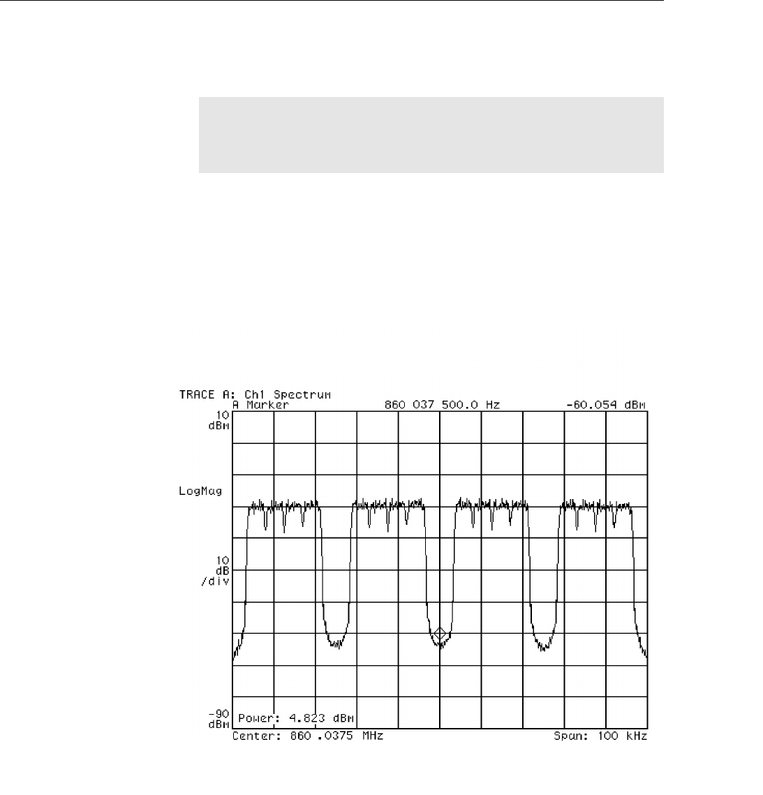
56 68P80801H45-1 1/20/2002
Troubleshooting EBTS System Manual - Vol 2
QUAD Base Radio Station Verification Procedures
4.2 At the field > prompt, type:
If the alarms command displays alarms, refer to the System
Troubleshooting section of this manual for corrective actions.
5. View the spectrum of the transmitted signal on the R2660 Communications
Analyzer in the Spectrum Analyzer mode. Figure 5 and Figure 6 shows a
sample of the 800MHz and 900MHz spectrum, respectively.
field> alarms -ofault_hndlr
Figure 5 800 MHz Quad Carrier Spectrum
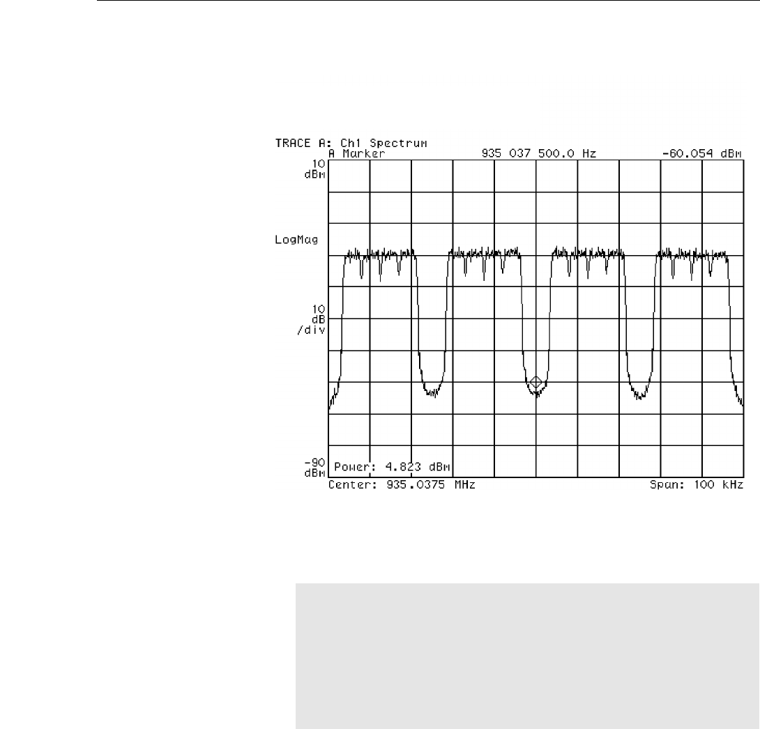
68P80801H45-1 1/20/2002 57
EBTS System Manual - Vol 2 Troubleshooting
QUAD Base Radio Station Verification Procedures
6. Dekey the BR to verify no RF power is being transmitted. Set the transmit
DSP test mode to “stop.” At the field> prompt, type:
Equipment Disconnection
Use the following steps to disconnect equipment after verifying the transmitter.
1. Remove power from the Base Radio by setting the Power Supply rocker
switch (located behind the front panel of the Power Supply) to the OFF (0)
position.
2. Disconnect the RS-232 cable from the connector on the service computer.
3. Disconnect the other end of the RS-232 cable from the RS-232 connector
located on the front panel of the BRC.
Figure 6 900 MHz Quad Carrier Spectrum
field> power -otxch1 -p0
field> ptm -otx_all -mstop
field> dpm -otxch1 -mnone
field> dpm -otxch2 -mnone
field> dpm -otxch3 -mnone
field> dpm -otxch4 -mnone

58 68P80801H45-1 1/20/2002
Troubleshooting EBTS System Manual - Vol 2
QUAD Base Radio Station Verification Procedures
CAUTION
!CAUTION
!
Make sure power to BR is OFF before disconnecting
transmitter RF connectors. Disconnecting transmitter
RF connectors while the BR is keyed may result in RF
burns from arcing.
4. Disconnect the test cable from the PA OUT connector located on the
backplane of the Base Radio.
5. Connect the standard equipment cable to the PA OUT connector.
6. Disconnect the 10 dB attenuator from the other end of the test cable.
7. From the attenuator, disconnect the cable to the R2660
Communications Analyzer.
8. Restore power to the Base Radio by setting the Power Supply rocker switch
to the ON (1) position.
9. If necessary, continue with the Receiver Verification Procedure.

68P80801H45-1 1/20/2002 83
EBTS System Manual - Vol 2 Troubleshooting
QUAD Channel BR Backplane
QUAD Channel BR Backplane
Backplane Connectors
The Base Radio backplane includes all external equipment connections. Table 21
lists and describes the backplane connectors.
Table 21 QUAD BR Backplane Connectors
Connector Module Description Connector Type
P1 EXBRC Signal 168 Pin AMP Z-Pack
Futurebus
P2 RX1 Signal 72 Pin AMP Z-Pack
Futurebus
P3 RX1 RF 6 coax Harting Harpak
P4 RX2 Signal 72 Pin AMP Z-Pack
Futurebus
P5 RX2 RF 6 coax Harting Harpak
P6 RX3 Signal 72 Pin AMP Z-Pack
Futurebus
P7 RX3 RF 6 coax Harting Harpak
P8 RX4 Signal 72 Pin AMP Z-Pack
Futurebus
P9 RX4 RF 6 coax Harting Harpak
P10 PA Signal 96 Pin EURO
P11 PS Signal & Power 78 Pin AMP Teledensity
P12a
a. P12 is a cutout in the backplane with threaded inserts for securing the connector which
mates directly to the power supply.
PS -48 Vdc Power In 8 Pin AMP 530521-3
P13 EX RF(EX from PA) SMA blindmate
P14 EX RF(EX to PA) SMA blindmate
P15 External / EXBRC Ethernet BNC blindmate
P16 External / PA RF (PA from EX) SMA blindmate
P17 External / PA RF (PA to EX) SMA Blindmate
P18 External / PA TX Output SMA blindmate
P19 RX Branch 1 RF SMA
P20 RX Branch 2 RF SMA
P21 RX Branch 3 RF SMA
P22bExternal RS232 Dsub-9
P23 External Alarm Dsub-25
P24 External 5MHz/1PPS BNC
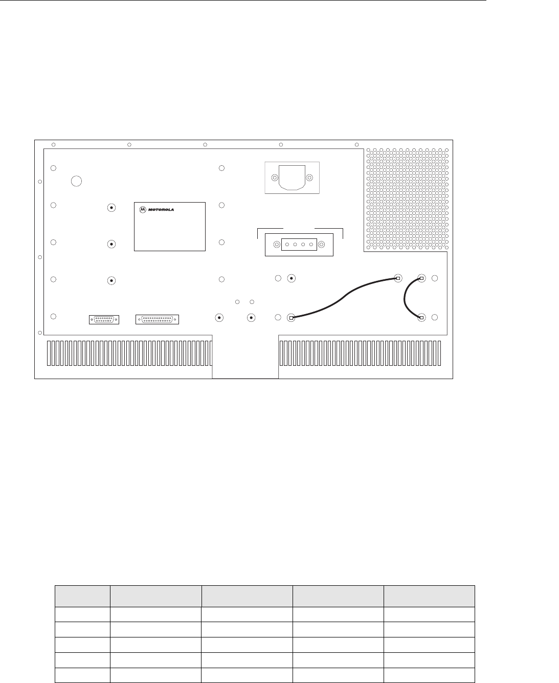
84 68P80801H45-1 1/20/2002
Troubleshooting EBTS System Manual - Vol 2
QUAD Channel BR Backplane
Figure 9 shows the locations of the QUAD Base Radio external connections.
QUAD BR Backplane Connector Pinouts
Table 22 lists the pin-outs for the Base Radio Controller board’s 168-pin P1
connector.
b. P22 will not be placed on the backplane. However, the backplane shall be designed with
P22 to allow for reuse on future products.
Table 22 EXBRC P1 Pinout, Signal and Power
Row A B C D
1 GND 3.3 Vdc 3.3 Vdc NC
2 GND 3.3 Vdc 14.2 Vdc 14.2 Vdc
3 GND 3.3 Vdc 14.2 Vdc 14.2 Vdc
4 GND GND GND GND
5NCNCNCNC
EX OUT
PA IN
ETHERNET
PA FB
DC POWER
AC POWER
RS 232 ALARM
RX 1
(RED)
RX 2
(GRN)
RX 3
(YEL)
5MHZ/1 PPS
PA OUT
GROUND
EBTS327Q
112501JNM
RE BLACK
This port must be terminated by 50Ω load when configured for
2 Branch Diversity. Also, the rx_fru_config parameter must be set to R12.
*
*
EX FB
Figure 9 QUAD Base Radio Backplane Connectors

68P80801H45-1 1/20/2002 85
EBTS System Manual - Vol 2 Troubleshooting
QUAD Channel BR Backplane
6 GND GND GND GND
7 GND 16.8MHz_RX 16.8MHz_RX_RTN GND
8 GND GND GND GND
9 GND 5 MHz/1 PPS 3.3 Vdc 3.3 Vdc
10 NC NC NC 3.3 Vdc
11 TxD CTS DTR BRG
12 RTS RxD DSR CD
13 NC NC NC 3.3 Vdc
14 NC NC SHUTDOWN_ SLEEP_
15 PA_ENABLE NC 28.6 Vdc 14.2 Vdc
16 NC NC NC 3.3 Vdc
17 EXT_GPI_1_ EXT_GPI_2_ EXT_GPO_1_ EXT_GPO_2_
18 BAT_STAT_ MTR_STAT_ EXT_VFWD EXT_VREV
19 SPI_M3 SPI_M2 SPI_M1 SPI_M0
20 SPI_ENABLE SPI_MOSI SPI_MISO SPI_CLK
21 SPI_A2 SPI_A1 SPI_A0 WP_
22 NC RxRESET_ NC NC
23 NC Clock_SyncB_ NC NC
24 GND GND 3.3 Vdc 3.3 Vdc
25 SSI_Data_D SSI_CLK_D SSI_FS_D 3.3 Vdc
26 SSI_Data_D_RTN SSI_CLK_D_RTN NC 3.3 Vdc
27 GND GND 3.3 Vdc 3.3 Vdc
28 DSPIb_MOSI DSPIb_CLK DSPIb_EN_1 DSPIb_EN_2
29 DSPIb_MOSI_RTN DSPIb_CLK_RTN DSPIb_EN_3 NC
30 GND GND 3.3 Vdc 3.3 Vdc
31 GND SSI_Data_C SSI_CLK_C SSI_FS_C
32 GND SSI_Data_C_RTN SSI_CLK_C_RTN NC
33 NC Clock_SyncA_ NC NC
34 GND GND 3.3 Vdc 3.3 Vdc
35 SSI_Data_B SSI_CLK_B SSI_FS_B 3.3 Vdc
36 SSI_Data_B_RTN SSI_CLK_B_RTN NC 3.3 Vdc
37 GND GND 3.3 Vdc 3.3 Vdc
38 DSPIa_MOSI DSPIa_CLK DSPIa_EN_1 DSPIa_EN_2
39 DSPIa_MOSI_RTN DSPIa_CLK_RTN DSPIa_EN_3 NC
40 GND GND 3.3 Vdc 3.3 Vdc
41 GND SSI_Data_A SSI_CLK_A SSI_FS_A
42 GND SSI_Data_A_RTN SSI_CLK_A_RTN NC
Table 22 EXBRC P1 Pinout, Signal and Power
Row A B C D

86 68P80801H45-1 1/20/2002
Troubleshooting EBTS System Manual - Vol 2
QUAD Channel BR Backplane
Table 23 EXBRC P13 Pinout, Exciter from PA
Coaxial Description
Center PA IN
Outer GND
Table 24 EXBRC P14 Pinout, Exciter to PA
Coaxial Description
Center PA Feedback
Outer GND
Table 25 EXBRC P15 Pinout, Ethernet
Coaxial Description
Center Ethernet
Outer GND

68P80801H45-1 1/20/2002 87
EBTS System Manual - Vol 2 Troubleshooting
QUAD Channel BR Backplane
RX1 Connections
Table 26 RX1 P2 Pinout, Signal and Power
Row A B C D
1 NC GND GND Clock_SyncA_
2 GND DSPIa_MOSI_RTN DSPIa_CLK_RTN DSPIa_EN_1
3 GND DSPIa_MOSI DSPIa_CLK DSPIa_EN_2
4 GND GND GND GND
5 14.2 SSI_CLK_A_RTN SSI_FS_B SSI_CLK_B_RTN
6 14.2 SSI_CLK_A SSI_FS_A SSI_CLK_B
7 14.2 GND GND GND
8 14.2 SSI_Data_A_RTN GND SSI_Data_B
9 GND SSI_Data_A GND SSI_Data_B_RTN
10 GND NC NC NC
11 3.3 RxRESET_ GND (ID0) GND (ID1)
12 3.3 WP_ SPI_A0 SPI_A1
13 3.3 SPI_MISO SPI_CLK SPI_A2
14 GND SPI_M0 SPI_ENABLE SPI_MOSI
15 GND SPI_M1 SPI_M2 SPI_M3
16 GND GND GND NC
17 GND 16.8MHz_RX GND NC (WB switch)
18 GND 16.8MHz_RX_RTN GND NC (MC switch)
Table 27 RX1 P3 Pinout, RF Input and Output Connection
Row A B C D E
1 GND - GND - GND
2 - RX3_EXP3 - RX1_EXP3 -
3 GND - GND - GND
4 GND - GND - GND
5 - RX2_EXP2 - RX1_EXP2 -
6 GND - GND - GND
7 GND - GND - GND
8 - RX Branch 1 - RX1_EXP1 -
9 GND - GND - GND

88 68P80801H45-1 1/20/2002
Troubleshooting EBTS System Manual - Vol 2
QUAD Channel BR Backplane
RX2 Connections
Table 28 RX2 P4 Pinout, Signal and Power
Row A B C D
1 NC GND GND Clock_SyncA_
2 GND DSPIa_MOSI_RTN DSPIa_CLK_RTN DSPIa_EN_3
3 GND DSPIa_MOSI DSPIa_CLK DSPIa_EN_2
4 GND GND GND GND
5 14.2 SSI_CLK_B_RTN NC NC
6 14.2 SSI_CLK_B SSI_FS_B NC
7 14.2 GND GND GND
8 14.2 SSI_Data_B_RTN GND NC
9 GND SSI_Data_B GND NC
10 GND NC NC NC
11 3.3 RxRESET_ NC (ID0) GND (ID1)
12 3.3 WP_ SPI_A0 SPI_A1
13 3.3 SPI_MISO SPI_CLK SPI_A2
14 GND SPI_M0 SPI_ENABLE SPI_MOSI
15 GND SPI_M2 SPI_M1 SPI_M3
16 GND GND GND NC
17 GND 16.8MHz_RX GND NC (WB switch)
18 GND 16.8MHz_RX_RTN GND NC (MC switch)
Table 29 RX2 P5 Pinout, RF Input and Output Connection
Row A B C D E
1 GND - GND - GND
2 - RX3_EXP2 - RX2_EXP3 -
3 GND - GND - GND
4 GND - GND - GND
5 - RX1_EXP1 - RX2_EXP2 -
6 GND - GND - GND
7 GND - GND - GND
8 - RX Branch 2 - RX2_EXP1 -
9 GND - GND - GND

68P80801H45-1 1/20/2002 89
EBTS System Manual - Vol 2 Troubleshooting
QUAD Channel BR Backplane
RX3 Connections
Table 30 RX3 P6 Pinout, Signal and Power
Row A B C D
1 NC GND GND Clock_SyncB_
2 GND DSPIb_MOSI_RTN DSPIb_CLK_RTN DSPIb_EN_1
3 GND DSPIb_MOSI DSPIb_CLK DSPIb_EN_2
4 GND GND GND GND
5 14.2 SSI_CLK_C_RTN SSI_FS_D SSI_CLK_D_RTN
6 14.2 SSI_CLK_C SSI_FS_C SSI_CLK_D
7 14.2 GND GND GND
8 14.2 SSI_Data_C_RTN GND SSI_Data_D
9 GND SSI_Data_C GND SSI_Data_D_RTN
10 GND NC NC NC
11 3.3 RxRESET_ GND (ID0) NC (ID1)
12 3.3 WP_ SPI_A0 SPI_A1
13 3.3 SPI_MISO SPI_CLK SPI_A2
14 GND SPI_M2 SPI_ENABLE SPI_MOSI
15 GND SPI_M1 SPI_M0 SPI_M3
16 GND GND GND NC
17 GND 16.8MHz_RX GND GND (WB switch)
18 GND 16.8MHz_RX_RTN GND NC (MC switch)
Table 31 RX3 P7 Pinout, RF Input and Output Connection
Row A B C D E
1 GND - GND - GND
2 - RX1_EXP2 - RX3_EXP3 -
3 GND - GND - GND
4 GND - GND - GND
5 - RX2_EXP1 - RX3_EXP2 -
6 GND - GND - GND
7 GND - GND - GND
8 - RX Branch 3 - RX3_EXP1 -
9 GND - GND - GND

90 68P80801H45-1 1/20/2002
Troubleshooting EBTS System Manual - Vol 2
QUAD Channel BR Backplane
RX4 Connections
Table 32 RX4 P8 Pinout, Signal and Power
Row A B C D
1 NC GND GND Clock_SyncB_
2 GND DSPIb_MOSI_RTN DSPIb_CLK_RTN DSPIb_EN_3
3 GND DSPIb_MOSI DSPIb_CLK DSPIb_EN_2
4 GND GND GND GND
5 14.2 SSI_CLK_D_RTN NC NC
6 14.2 SSI_CLK_D SSI_FS_D NC
7 14.2 GND GND GND
8 14.2 SSI_Data_D_RTN GND NC
9 GND SSI_Data_D GND NC
10 GND NC NC NC
11 3.3 RxRESET_ NC (ID0) NC (ID1)
12 3.3 WP_ SPI_A0 SPI_A1
13 3.3 SPI_MISO SPI_CLK SPI_A2
14 GND SPI_M0 SPI_ENABLE SPI_MOSI
15 GND SPI_M3 SPI_M2 SPI_M1
16 GND GND GND NC
17 GND 16.8MHz_RX GND NC (WB switch)
18 GND 16.8MHz_RX_RTN GND GND (MC switch)
Table 33 RX4 P9 Pinout, RF Input and Output Connection
Row A B C D E
1 GND - GND - GND
2 - RX1_EXP3 - NC -
3 GND - GND - GND
4 GND - GND - GND
5 - RX2_EXP3 - NC -
6 GND - GND - GND
7 GND - GND - GND
8 - RX3_EXP1 - NC -
9 GND - GND - GND

68P80801H45-1 1/20/2002 91
EBTS System Manual - Vol 2 Troubleshooting
QUAD Channel BR Backplane
PA Connections
Table 34 QUAD BR PA P10 Pinout, Signal and Power
Row A B C
1 SPI_ENABLE GND 28.6 Vdc
2 GND GND 28.6 Vdc
3 SPI_A0 GND 28.6 Vdc
4 GND GND 28.6 Vdc
5 SPI_A1 GND 28.6 Vdc
6 GND GND 28.6 Vdc
7 SPI_A2 GND 28.6 Vdc
8 GND GND 28.6 Vdc
9 SPI_M0 GND 28.6 Vdc
10 GND GND 28.6 Vdc
11 SPI_M1 GND 28.6 Vdc
12 GND GND 28.6 Vdc
13 SPI_M2 GND 28.6 Vdc
14 GND GND 28.6 Vdc
15 SPI_M3 GND 28.6 Vdc
16 GND GND 28.6 Vdc
17 SPI_MISO GND 28.6 Vdc
18 GND GND 28.6 Vdc
19 SPI_MOSI GND 28.6 Vdc
20 GND GND 28.6 Vdc
21 SPI_CLK GND 28.6 Vdc
22 GND 3.3 Vdc 28.6 Vdc
23 WP* 3.3 Vdc 28.6 Vdc
24 GND GND 28.6 Vdc
25 PA_ENABLE GND 28.6 Vdc
26 GND 14.2 Vdc 28.6 Vdc
27 GND 14.2 Vdc 28.6 Vdc
28 GND 14.2 Vdc 28.6 Vdc
29 GND 14.2 Vdc 28.6 Vdc
30 GND 28.6 Vdc 28.6 Vdc
31 GND 28.6 Vdc 28.6 Vdc
32 GND 28.6 Vdc 28.6 Vdc

92 68P80801H45-1 1/20/2002
Troubleshooting EBTS System Manual - Vol 2
QUAD Channel BR Backplane
External Connections
Table 35 EXBRC P16 Pinout, PA from Exciter
Coaxial Description
Center PA IN
Outer GND
Table 36 EXBRC P17 Pinout, PA to Exciter
Coaxial Description
Center PA Feedback
Outer GND
Table 37 EXBRC P18 Pinout, PA RF OUT
Coaxial Description
Center PA RF OUT
Outer GND
Table 38 QUAD BR Backplane Coaxial and DC
Signal
P12 -48 Vdc Power
P13 EX Out
P14 Feedback
P15 Ethernet
P16 PA In
P17 PA Feedback
P18 PA RF OUT
P19 RX Branch 1
P20 RX Branch 2
P21 RX Branch 3
P24 5 MHz/1 PPS

68P80801H45-1 1/20/2002 93
EBTS System Manual - Vol 2 Troubleshooting
QUAD Channel BR Backplane
Table 39 QUAD BR Backplane Alarm 25 Pin Dsub (P23)
Alarm Signal
1 EXT_GPI_1_
2 EXT_GPO_1_
3 GND
4 EXT_GPI_2_
5 EXT_GPO_2_
6
7
8
9
10 GND
11
12
13
14
15
16 GND
17 BAT_STAT_
18 MTR_STAT_
19 EXT_VFWD
20 EXT_VREV
21 GND
22 GND
23
24
25 GND
Table 40 QUAD BR Backplane RS-232 9 Pin Dsub (P22)
RS-232 Signal
1CD
2RxD
3 TxD
4 DTR
5 GND
6 DSR
7RTS
8 CTS
9 BRG*

94 68P80801H45-1 1/20/2002
Troubleshooting EBTS System Manual - Vol 2
QUAD Channel BR Backplane
PS Connections
-
Table 41 QUAD PS Power and Signal (P11)
Pin Description Pin Description Pin Description
1 GND (Plug In) 31 3.3 Vdc 61 SPI_MOSI
2 GND 32 GND 62 SPI_CLK
3 GND 33 GND 63 N.C.
4 28.6 Vdc 34 GND 64 N.C.
5 28.6 Vdc 35 GND 65 N.C.
6 28.6 Vdc 36 GND 66 N.C.
7 28.6 Vdc 37 GND 67 SPI_A0
8 28.6 Vdc 38 GND 68 SPI_A1
9 28.6 Vdc 39 GND 69 SPI_M2
10 28.6 Vdc 40 GND 70 SPI_M3
11 28.6 Vdc 41 GND 71 SPI_M1
12 28.6 Vdc 42 GND 72 SLEEP_
13 28.6 Vdc 43 GND 73 SPI_M0
14 28.6 Vdc 44 GND 74 WP_
15 28.6 Vdc 45 GND 75 SPI_A2
16 14.2 Vdc 46 GND 76 GND
17 14.2 Vdc 47 GND 77 GND
18 14.2 Vdc 48 GND 78 GND
19 14.2 Vdc 49 GND
20 14.2 Vdc 50 GND
21 14.2 Vdc 51 GND
2 14.2 Vdc 52 GND
23 14.2 Vdc 53 GND
24 3.3 Vdc 54 NC (FAN CON-
TROL)
25 3.3 Vdc 55 N.C.
26 3.3 Vdc 56 N.C.
27 3.3 Vdc 57 SHUTDOWN_
28 3.3 Vdc 58 NC (Power shar-
ing)
29 3.3 Vdc 59 SPI_ENABLE
30 3.3 Vdc 60 SPI_MISO

68P80801H45-1 1/20/2002 95
EBTS System Manual - Vol 2 Troubleshooting
QUAD Channel BR Backplane
Table 42 QUAD BR 48 Vdc Battery Power (P12)
Pin Description Description Pin
1 + BATTERY + BATTERY 5
2 + BATTERY + BATTERY 6
3 - BATTERY (RTN) - BATTERY (RTN) 7
4 - BATTERY (RTN) - BATTERY (RTN) 8

96 68P80801H45-1 1/20/2002
Troubleshooting EBTS System Manual - Vol 2
QUAD Base Radio Signals
QUAD Base Radio Signals
Table 43 lists and describes signals for the QUAD Base Radio.
Table 43 QUAD Base Radio Signal Descriptions
Signal Name Description Special
28.6 Vdc 28.6 Vdc output from PS
14.2 Vdc 14.2 Vdc output from PS
3.3 Vdc 3.3 Vdc output from PS
GND Station Ground
RX Branch 1 RX Branch 1 from RFDS 50 Ω
RX Branch 2 RX Branch 2 from RFDS 50 Ω
RX Branch 3 RX Branch 3 from RFDS 50 Ω
RX1_EXP1 RX1 (branch 1) expansion output 1 50 Ω
RX1_EXP2 RX1 (branch 1) expansion output 2 50 Ω
RX1_EXP3 RX1 (branch 1) expansion output 3 50 Ω
RX2_EXP1 RX2 (branch 2) expansion output 1 50 Ω
RX2_EXP2 RX2 (branch 2) expansion output 2 50 Ω
RX2_EXP3 RX2 (branch 2) expansion output 3 50 Ω
RX3_EXP1 RX3 (branch 3) expansion output 1 50 Ω
RX3_EXP2 RX3 (branch 3) expansion output 2 50 Ω
RX3_EXP3 RX3 (branch 3) expansion output 3 50 Ω
5 MHz/1 PPS 5 MHz/1 PPS reference to the BRC
SPI_ENABLE Host Centric SPI Enable
SPI_MISO Host Centric SPI MISO
SPI_MOSI Host Centric SPI MOSI
SPI_CLK Host Centric SPI Clock
SPI_A0 Host SPI Device Address Line A0
SPI_A1 Host SPI Device Address Line A1
SPI_A2 Host SPI Device AddressLine A2
SPI_M0 Host SPI Module Address Line M0
SPI_M1 Host SPI Module Address Line M1
SPI_M2 Host SPI Module Address Line M2
SPI_M3 Host SPI Module Address Line M3
WP_ Write Protect (active low)
PA_ENABLE Turns off PA bias with active low
SLEEP_ Sleep signal from PS
SHUTDOWN_ PS reset line from BRC
CD RS232 Carrier Detect
RxD RS232 RX Data

68P80801H45-1 1/20/2002 97
EBTS System Manual - Vol 2 Troubleshooting
QUAD Base Radio Signals
TxD RS232 TX Data
DTR RS232 Data Terminal Ready
DSR RS232 Data Set Ready
RTS RS232 Request to Send
CTS RS232 Clear to Send
BRG Baud Rate Generator
RxRESET_ Reset Signal to RX modules
16.8MHz_RX 16.8 MHz reference to RX differential
16.8MHz_RX_RTN 16.8 MHz reference to RX return differential
Clock_SyncA_ Clock Sync signal to RX1 & RX2 For Abacus III
Clock_SyncB_ Clock Sync signal to RX3 & RX4 For Abacus III
SSI_Data_A RX Data from RX module 1 differential
SSI_Data_A_RTN RX Data from RX module 1return differential
SSI_Data_B RX Data from RX module 2 differential
SSI_Data_B_RTN RX Data from RX module 2 return differential
SSI_Data_C RX Data from RX module 3 differential
SSI_Data_C_RTN RX Data from RX module 3 return differential
SSI_Data_D RX Data from RX module 4 differential
SSI_Data_D_RTN RX Data from RX module 4 return differential
SSI_CLK_A RX Clock from RX module 1 differential
SSI_CLK_A_RTN RX Clock from RX module 1 return differential
SSI_CLK_B RX Clock from RX module 2 differential
SSI_CLK_B_RTN RX Clock from RX module 2 return differential
SSI_CLK_C RX Clock from RX module 3 differential
SSI_CLK_C_RTN RX Clock from RX module 3 return differential
SSI_CLK_D RX Clock from RX module 4 differential
SSI_CLK_D_RTN RX Clock from RX module 4 return differential
SSI_FS_A RX Frame Sync from RX module 1
SSI_FS_B RX Frame Sync from RX module 2
SSI_FS_C RX Frame Sync from RX module 3
SSI_FS_D RX Frame Sync from RX module 4
DSPIa_En_1 DSPa SPI RX1 Abacus enable
DSPIa_En_3 DSPa SPI RX2 Abacus enable
DSPIa_En_2 DSPa SPI RX1 & RX2 SGC enable
DSPIb_En_1 DSPb SPI RX3 Abacus enable
DSPIb_En_3 DSPb SPI RX4 Abacus enable
DSPIb_En_2 DSPb SPI RX3 & RX4 SGC enable
DSPIa_MOSI DSPa SPI MOSI differential
DSPIa_MOSI_RTN DSPa SPI MOSI return differential
DSPIb_MOSI DSPb SPI MOSI differential
Table 43 QUAD Base Radio Signal Descriptions (Continued)
Signal Name Description Special

98 68P80801H45-1 1/20/2002
Troubleshooting EBTS System Manual - Vol 2
QUAD Base Radio Signals
DSPIb_MOSI_RTN DSPb SPI MOSI return differential
DSPIa_CLK DSPa SPI Clock differential
DSPIa_CLK_RTN DSPa SPI CLK return differential
DSPIb_CLK DSPb SPI Clock differential
DSPIb_CLK_RTN DSPb SPI CLK return differential
MTR_STAT_ External Wattmeter Status
BAT_STAT_ Battery Status
EXT_VFWD External Wattmeter Forward meter
EXT_VREV External Wattmeter Reflected meter
EXT_GPO_1_ General purpose output 1
EXT_GPO_2_ General purpose output 2
EXT_GPI_1_ General purpose input 1
EXT_GPI_2_ General purpose input 2
NC Not connected reserved
Table 43 QUAD Base Radio Signal Descriptions (Continued)
Signal Name Description Special

68P80801H45-1 1/20/2002 1
Acronyms
Global Telecommunications Solutions Sector
1301 E. Algonquin Road, Schaumburg, IL 60196
Acronyms
A/D Analog-to-Digital
AAmperes
AC Alternating Current
ACT active
ADA Americans with Disabilities Act
AGC Automatic Gain Control
AIC Ampere Interrupting Capacity
AIS Alarm Indication Signal (Keep Alive)
ANSI American National Standards Institute
ASCII American National Standard Code for
Information Interchange
ASIC Application Specific Integrated Circuit
Aux auxiliary
avg average
AWG American Wire Gauge
bd baud
BDM Background Debug Mode
BER Bit Error Rate
BERT Bit Error Rate Test
BMR Base Monitor Radio
BNC Baby “N” Connector
BPV Bipolar Variation
BR Base Radio
BRC Base Radio Controller
BSC Base Site Controller
BTU British Thermal Unit
BW bandwidth
C/N + I Carrier Power to Noise + Interference
Ratio
CC Control Cabinet
CD Carrier Detect
cd change directory
CLK Clock
CLT Controller
cm centimeter
CMOS Complementary Metal Oxide
Semiconductor
CPU Central Processing Unit
CSMA/CD Carrier Sense Multiple Access with
Collision Detect
CTI Coaxial Transceiver Interface
CTL Control (Base Radio Control)
CTS Clear-to-Send
D/A Digital-to-Analog
DAP Dispatch Application Processor
DB-15 15-pin D-subminiature
DB-9 9-pin D-subminiature
dB Decibel
dBc Decibels relative to carrier
dBm Decibels relative to 1mW
DC Direct Current
DCE Data Circuit-Terminating Equipment
DCSPLY DC Supply
DDM Dual Device Module
deg degree
DIN Deutsche Industrie-Norm
DIP Dual In-line Package
div division

-268P80801H45-1 1/20/2002
Acronyms EBTS System Manual - Vol 2
DMA Direct Memory Access
DOP Dilution of Precision
DRAM Dynamic Random Access Memory
DSP Digital Signal Processor
DTE Data Terminal Equipment
DTTA Duplexed Tower-Top Amplifier
DVM Digital Volt Meter
E1 European telephone multiplexing
standard
EAS Environmental Alarm System
E-NET Ethernet
EBTS Enhanced Base Transceiver System
EGB Exterior Ground Bar
EIA Electronics Industry Association
EMI Electro-Magnetic Interference
EPROM Erasable Programmable Read Only
Memory
EEPROM Electronically Erasable Programmable
Read Only Memory
ERFC Expansion RF Cabinet
ESI Ethernet Serial Interface
ESMR Enhanced Special Mobile Radio
EX Exciter
FB feedback
FCC Federal Communications Commission
FIFO First-In, First-Out
FNE Fixed Network Equipment
freq frequency
FRU Field Replaceable Unit
Gen 3 SC Generation 3 Site Controller
GFI Ground Fault Interrupter
GND ground
GPS Global Positioning System
GPSR Global Positioning System Receiver
HDLC High-level Data Link
HSMR High Elevation Specialized Mobile Radio
HSO High Stability Oscillator
HVAC Heating/Ventilation/Air Conditioning
Hz Hertz
I/O Input/Output
IC Integrated Circuit
iDEN integrated Dispatch Enhanced Network
IEEE Institute of Electrical and Electronic
Engineers
IF intermediate frequency)
iMU iDen Monitor Unit
in inches
in injection
iSC integrated Site Controller
ISA Industry Standard Architecture
kg kilogram
kHz kiloHertz
LAN Local Area Network
LANIIC Local Area Network Interface IC
LAPD Link Access Procedure D-Channel
lbs pounds
LDM Linear Driver Module
LED Light Emitting Diode
LFM Linear Final Module
LIU Line Interface Unit
LLC Link Layer Controller
LNA Low Noise Amplifier
LO Local Oscillator
LOS Loss of Signal
MAU Media Access Unit
max maximum
MC Multicoupler
MGB Master Ground Bar
MGN Multi-Grounded Neutral

68P80801H45-1 1/20/2002 -3
EBTS System Manual - Vol 2 Acronyms
MHz MegaHertz
min minimum
min minute
MISO Master In/Slave Out
mm millimeter
MMI Man-Machine-Interface
MOSI Master Out/Slave In
MPM Multiple Peripheral Module
MPS Metro Packet Switch
MS Mobile Station
ms millisecond
MSC Mobile Switching Center
MSO Mobile Switching Office
MST Modular Screw Terminals
mV milliVolt
mW milliWatt
N.C. Normally Closed
N.O. Normally Open
NEC National Electric Code
NIC Network Interface Card
no. number
NTM NIC Transition Module
NTWK Network
OMC Operations and Maintenance Center
OSHA Occupational Safety and Health Act
PA Power Amplifier
PAL Programmable Array Logic
PC Personal Computer
PCCH Primary Control Channel
PDOP Position Dilution of Precision
pF picoFarad
PLL Phase Locked Loop
P/N Part Number
P/O Part Of
ppm parts per million
PPS Pulse Per Second
PS Power Supply
PSTN Public Switched Telephone Network
PVC Polyvinyl Chloride
pwr power
QAM Quadrature Amplitude Modulation
QRSS Quasi Random Signal Sequence
Qty Quantity
R1 Receiver #1
R2 Receiver #2
R3 Receiver #3
RAM Random Access Memory
RCVR Receiver
Ref Reference
RF Radio Frequency
RFC RF Cabinet
RFDS RF Distribution System
RFS RF System
ROM Read Only Memory
RPM Revolutions Per Minute
RSSI Received Signal Strength Indication
RTN Return
RU Rack Unit
Rx Receive
RXDSP Receive Digital Signal Processor
SCI Serial Communications Interface
SCON VME System Controller
SCRF Stand-alone Control and RF Cabinet
(configuration)
SCSI Small Computer System Interface
sec second
SGC Software Gain Control
SINAD Signal Plus Noise Plus Distortion to Noise
Plus Distortion Radio

-468P80801H45-1 1/20/2002
Acronyms EBTS System Manual - Vol 2
SMART Systems Management Analysis, Research
and Test
SPI Serial Peripheral Interface
SQE Signal Quality Estimate
SRAM Static Random Access Memory
SRC Subrate Controller
SRI Site Reference Industry standard
SRIB SMART Radio Interface Box
SRRC Single Rack, Redundant Controller
(configuration)
SRSC Single Rack, Single Controller
(configuration)
SS Surge Suppressor
SSC System Status Control
SSI Synchronous Serial Interface
ST Status
STAT Status
Std Standard
S/W Software
T1 North american telephone mutiplexing
standard
TB Terminal Board
TDM Time Division Multiplex
telco telephone company
SCON VME System Controller
TISIC TDMA Infrastructure Support IC
TSI Time Slot Interface
TSI Time Slot Interchange
TTA Tower-Top Amplifier
TTL Transistor - Transistor Logic
Tx Transmit
TXD Transmit Data
TXDSP Transmit Digital Signal Processor
Txlin Tranlin IC
typ typical
UL Underwriters Laboratories
VVolts
VAC Volts - alternating current
VCO Voltage Controlled Oscillator
VCXO Voltage Controlled Crystal Oscillator
VDC Volts - direct current
VFWD Voltage representation of Forward Power
VME Versa-Module Eurocard
Vp-p Voltage peak-to-peak
VREF Voltage representation of Reflected Power
VSWR Voltage Standing Wave Radio
WWatt
WDT Watchdog Timer
WP Write Protect
WSAPD Worldwide Systems and Aftermarket
Products Division

68P80801H45-1 1/20/2002 1
Global Telecommunications Solutions Sector
1301 E. Algonquin Road, Schaumburg, IL 60196
Parts and Suppliers
This appendix contains recommended part numbers (p/n) and manufacturers for
various hardware, tools, and equipment used during installation of the EBTS.
Also contained in this appendix is other installation related information, such as
determining types of wire lugs, lengths and sizes of various wires and cables,
custom cabling information, and fuses.
All suppliers and model numbers listed are recommended due to their proven
performance record in previous installations. Motorola cannot guarantee the
effectiveness of the installation or performance of the system when using other
supplier parts.
Addresses, phone numbers, fax numbers, and other information is presented for
each of the recommended suppliers, when possible.
NOTE
In some listings, phone number and address are for
corporate or main sales office. Other sales locations
may be available. Call number given or go to website
for expanded listings.
NOTE
This information is subject to change without notice.
Surge Arrestors
Two types of surge arrestors should be used in the EBTS site, including:
❐AC Power and Telco
❐Antenna Surge Arrestors

268P80801H45-1 1/20/2002
Parts and Suppliers EBTS System Manual - Vol 2
AC Power and Telco Surge Arrestors
The recommended AC Power and Telco surge arrestors are both manufactured by
Northern Technologies. The model numbers are:
❐AC Power - LAP-B for 120/240 single-phase
LAP-C for 208 Vac three-phase
❐Telco - TCS T1D
Northern Technologies
P.O. Box 610
Liberty Lake, WA 99019
Phone: 800-727-9119
Fax: 509-927-0435
Internet: www.north-tech.com
Antenna Surge Arrestors
The recommended antenna surge arrestors are manufactured by Polyphaser Inc.
The following models are recommended:
❐Base Monitor Radio antennas - ISS50NXXC2MA
❐Base Radio antenna (800 MHz tower top amplifier only) - 094-0801T-A
❐Base Radio antenna (800 MHz cavity combined, transmit only; up to 5
channels) - IS-CT50HN-MA
❐Base Radio antennas (800 MHz duplexed) - IS-CT50HN-MA
❐Base Radio antennas (900 MHz duplexed) - 097-0311G-A.2
❐GPS antennas - 092-082-0T-A
❐Lightning arrestor bracket kit - Contact your local Motorola Sales representative
to order this kit
❐Receive Tower Top amplifier - 094-0801T-A
❐Tower top test port cable - IS-50NX-C2
Polyphaser, Inc.
P.O. Box 9000
Minden, NV 89423-9000
Phone: 800-325-7170
702-782-2511
Fax: 702-782-4476
Internet: www.polyphaser.com
Motorola has set up several kits that contain the necessary arrestors with proper
mounting hardware for the various antenna configurations. Contact your local
Motorola representative for these OEM kits.

68P80801H45-1 1/20/2002 3
EBTS System Manual - Vol 2 Parts and Suppliers
RF Attenuators
Several RF attenuators are needed at a site to ensure proper receive adjustments.
The attenuators are used at the LNA sites to offset the excess gain from the Tower
Top amplifiers, to balance the receive path, and to attenuate the BMR signal path.
Use the following specifications when choosing vendors:
❐Specified frequency range
❍800 MHz systems – requires attenuator specification to include
806-821 MHz range
❍900 MHz systems – requires attenuator specification to include
896-901 MHz range
❐1 dB increments
❐0.5 dB accuracy or better
❐Female N connector / Male N connector
Alan Industries, Inc.
745 Green Way Drive
P.O. Box 1203
Columbus, IN 47202
Phone: 800-423-5190
812-372-8869
Fax: 812-372-5909
Huber + Suhner, Inc.
19 Thompson Drive
Essex, VT 05451
Phone: 802-878-0555
Fax: 802-878-9880
Internet: www.hubersuhnerinc.com
JFW Industries, Inc.
5134 Commerce Square Drive
Indianapolis, IN 46237
Phone: 317-887-1340
Fax: 317-881-6790
email: JFW atten@aol.com
Pasternack Enterprises
P.O. Box 16759
Irvine, CA 92713
Phone: 714-261-1920
Fax: 714-261-7451
RF attenuators are also needed for test equipment. The attenuators must be used
between frequency reference equipment, service monitors, and the Motorola
EBTS equipment. The following attenuators should be used at the site
during optimization:
❐Female BNC connector / Male BNC connector, 10 dB attenuator (1 W)
between the Rubidium Standard and the R2660 Communications Analyzer.
Refer to the System Testing section.

468P80801H45-1 1/20/2002
Parts and Suppliers EBTS System Manual - Vol 2
❐Female BNC connector / Male BNC connector, 30 dB attenuator (1 W)
between the Rubidium Standard and the R2660. Refer to the System Testing,
section.
Emergency Generator
Several different sizes of generators are available. Determine the loading
requirements of the site prior to ordering a generator. A recommended
manufacturer of the emergency backup generator power system is:
Generac Corporation
P.O. Box 8
Waukesha, WI 53187
Phone: 414-544-4811
Fax: 414-544-0770
Portable Generator Connection
The recommended portable generator connection is the AJA200-34200RS,
manufactured by Appleton Electric. Figure 1 is a view of a connector located on
the building. An adapter may be required if local electrical standards conflict with
the wiring configuration.
An alternate supplier of the portable generator connection is the ARKTITE Heavy
Duty Receptacle Model 80, Style 2, 200 Amps, manufactured by Crouse-Hinds.
Cooper Industries
Crouse-Hinds, Inc.
P.O. Box 4999
Syracuse, NY 13221
Phone: 315-477-7000
Fax: 315-477-5717
Figure 1 Portable Generator Connector
EBTS078
061295JNM
12
3
HOT
HOT NEUTRAL
GROUND
POLARIZATION
RIB

68P80801H45-1 1/20/2002 5
EBTS System Manual - Vol 2 Parts and Suppliers
GPS Evaluation Kit
The GPS evaluation kit (part number VPEVL0002) is available from Motorola
Position and Navigation System Business.
Motorola Position and Navigation System Business
4000 Commercial Avenue
Northbrook, IL 60062
Phone: 847-714-7329
Fax: 847-714-7325
GPS Antenna Amplifier
There are two recommended manufacturers of the GPS antenna amplifiers. The
model numbers are:
❐LA20RPDC-N (made by WR, Inc.) (Type 1)
❐GA-12F-N (made by CTS Co.) (Type 2)
WR, Inc.
710A W. 4th Street
Pueblo, CO 81003
Phone: 800-463-3063
719-595-9880
Fax: 719-595-9890
Internet: www.fleetpc.com
email: gpsman@wr-inc.com
Carl Tinch Sales (CTS) Co.
811 S. Central Expressway #518
Richardson, TX 75080
Phone: 972-231-1322
Fax: 972-231-3403
668P80801H45-1 1/20/2002
Parts and Suppliers EBTS System Manual - Vol 2
Specifications Type 1 Type 2
Dimensions 3.293” x 2” x 1” 1” Dia. x Approx. 6”
Connectors Type N female, both ends Type N female, both ends
Gain 23 dB gain typical
20 dB min.
12 dB ± 2 dB
Noise Figure 2.6 dB typical 4.0 dB
VSWR < 2.2:1 <2:1
Frequency Range 1575.42 ± 50 MHz 1575.42 ± 10 MHz
Filtering Yes Yes
Maximum Input
Power
+ 13 dBm 0 dBm
Voltage 4.5 - 15 VDC 4.5 - 15 VDC
Current @ 5 V < 15 mA typical < 20 mA
Figure 2 GPS Antenna Amplifiers
EBTS126
051094JNM
TYPE 1
TYPE 2
1"
2"
3 5/16"
ANTENNA
RF INPUT
+13dBM MAX
VDC THRU
RECEIVER/
ANT VOLTAGE
Approximately 6"
2"
INPUT OUTPUT

68P80801H45-1 1/20/2002 7
EBTS System Manual - Vol 2 Parts and Suppliers
Site Alarms
Three types of alarms should be used in an EBTS site, including:
❐Intrusion Alarm
❐Smoke Alarm
❐Temperature Alarm
Intrusion Alarm
The recommended intrusion alarm is the Sonitrol 29A.
Sonitrol
211 N. Union Street, Suite 350
Alexandria, VA 22314
Phone: 800-326-7475
Fax: 703-684-6612
Internet: www.sonitrol.com
Smoke Alarm
A recommended smoke alarm is the Sentrol 320CC. This smoke alarm provides a
relay closure for the iMU alarm. These smoke detectors are available from many
electrical wholesale distributors. For the location nearest you, call between 6 a.m.
and 5 p.m. Pacific Standard Time and ask Sales for the location of the nearest EW
(Electric Wholesale) distributor.
Sentrol, Inc.
12345 SW Leveton Drive
Tualatin, OR 97062
Phone: 800-547-2556
503-692-4052
Internet: www.sentrol.com
Temperature Alarm
The recommended temperature alarm is the Grainger #2E206 thermostat. This
alarm is manufactured by Dayton Electronics and distributed by W.W. Grainger:
W.W. Grainger
Locations Nationwide
Phone: 800-323-0620
Fax: 800-722-3291
Internet: www.grainger.com

868P80801H45-1 1/20/2002
Parts and Suppliers EBTS System Manual - Vol 2
Cabinet Mounting Hardware
The cabinet mounting hardware is site dependent and must be procured locally.
Equipment Cabinets
The mounting hardware used to secure the Equipment Cabinets containing
control and/or RF hardware must be able to provide 1545 pounds of
retention force.
❐If the cabinets are to be secured to a concrete floor, 1/2" grade 8 bolts with
anchors are recommended.
❐If the cabinets are to be secured to another type of floor, determine the
appropriate mounting hardware.
Power Supply Rack
The Motorola offered Power Supply rack from Power Conversion Products is
available in a standard and an earthquake rack.
Power Conversion Products, Inc.
42 East Street
P.O. Box 380
Crystal Lake, IL 60039-0380
Phone: 800-435-4872 (customer service)
815-459-9100
Fax: 815-526-2524
Internet: www.pcpinc.com
If the earthquake rack is used, it must be bolted to the floor using the 02100-13
High Performance Anchor Kit, consisting of:
❐anchors (qty. 4)
❐load sharing plates (qty. 2)
❐large square washers (qty. 8)
Hendry Telephone Products
P.O. Box 998
Goleta, CA 93116
Phone: 805-968-5511
Fax: 805-968-9561
Internet: www.hendry.com
email: mailbox@hendry.com

68P80801H45-1 1/20/2002 9
EBTS System Manual - Vol 2 Parts and Suppliers
Cable Connections
The recommended manufacturer for all wire lugs used during EBTS installation is
Thomas & Betts. All wire lug part numbers listed are for Thomas & Betts.
Thomas & Betts
1555 Lynnfield Road
Memphis, TN 38119
Phone: 800-888-0211 (general information)
800-248-7774 (sales/technical support)
NOTE
Double hole wire lugs are preferred, but single hole
wire lugs can be used where mounting requirements
dictate their use.
Selecting Master Ground Bar Lugs
Table 1 identifies recommended part numbers for wire lugs used to connect
chassis ground wiring to the master ground bar from each cabinet.
Selecting Cabinet Ground Lugs
Table 2 identifies recommended part numbers for wire lugs used to connect
chassis ground wiring to the grounding point of each cabinet.
Table 1 Recommended Master Ground Bar Lugs
Wire Size Wire Type Lug
Color
Description P/N †
#2 AWG Stranded Brown Single 1/4” diameter hole 54107
#2 AWG Stranded Brown Double 1/4” diameter hole, 5/8” center 54207
#6 AWG Stranded Blue Single 1/4” diameter hole 54105
#6 AWG Stranded Blue Double 1/4” diameter hole, 5/8” center 54205
NOTE: These lugs require the use of the TBM5-S crimping tool.
† All part numbers are Thomas & Betts.
Table 2 Recommended Junction Panel Ground Lugs
Wire Size Wire Type Lug
Color
Description P/N †
#2 AWG Stranded Brown Single 1/2” diameter hole 54145
#6 AWG Stranded Blue Single 3/8” diameter hole E6-12
NOTE: These lugs require the use of the TBM5-S crimping tool.
† All part numbers are Thomas & Betts.

10 68P80801H45-1 1/20/2002
Parts and Suppliers EBTS System Manual - Vol 2
Battery System
Connections
The cable loop length refers to the total length of wire within a given circuit. For
example, the combined length of the -48 Vdc (hot) lead and the DC return lead
equals the cable loop length. This would mean that a cabinet that needs 16 feet of
wire between the batteries and Power Supply Rack has a total loop length of
32 feet.
Determining Battery System Wire Size
The wire size for the connection between the batteries and the Power Supply Rack
is determined by the required wire length and the maximum allowable voltage
drop. The voltage drop in the loop must be kept to below 200 mV. The wire
selected should be UL approved and contain a high number of strands
for flexibility.
For a standard configuration, the Power Supply rack is located directly adjacent to
the batteries with a cable loop length of 20 feet or less, which requires the use of a
4/0 wire. Table 3 shows recommended wire sizes for various loop lengths. Larger
wire sizes may be used if the recommended sizes are not available. The
recommended wire sizes are large enough to allow site expansion to a fully
loaded site.
Selecting Battery System Lugs
Depending on the wire size used and the manufacturer of the Batteries, different
wire lugs are crimped onto the power cable ends. After the wire size has been
determined from Table 3, verify the manufacturer of the Batteries (Dynasty
or Absolyte).
Two different battery systems are offered with the EBTS. The Dynasty system is a
low to medium capacity, field expandable system supplied for smaller sites or
sites with minimal backup hour requirements. This system is custom designed to
Motorola specifications. The Dynasty system is manufactured by
Johnson Controls:
Table 3 Battery System Wire Size
Loop Length Wire size
20 feet 4/0 (or 250 MCM)
30 feet 350 MCM
45 feet 500 MCM

68P80801H45-1 1/20/2002 11
EBTS System Manual - Vol 2 Parts and Suppliers
C & D Technologies
900 East Keefe Avenue
P.O. Box 591
Milwaukee, WI 53212
Phone: 414-967-6500
Fax: 414-961-6506
The Absolute IIP battery system is a heavy duty, high capacity battery system
manufactured by GNB Technologies:
GNB Technologies
829 Parkview Boulevard
Lombard, IL 60148
Phone: 800-872-0471
630-629-5200
Fax: 630-629-2635
Refer to Table 4 to determine the proper wire lug for the connection of that wire to
the Power Supply rack.
Refer to Table 5 to determine the proper wire lug for the connection to the
batteries, based on the wire size and battery manufacturer. One column lists the
selection for Dynasty and the other lists the selection for Absolyte IIP.
Table 4 Power Supply Rack Connection Lugs
Wire Size Cabinet Lug Crimp Tool Lug P/N †
4/0 Double 3/8” hole, 1” center TBM5-S 54212
250 MCM Double 3/8” hole, 1” center TBM8-S 54213
350 MCM Double 3/8” hole, 1” center TBM8-S 54215
500 MCM Double 3/8” hole, 1” center TBM8-S 54218
† All part numbers are Thomas & Betts.
Table 5 Battery Connection Lugs
Wire
Size
Lug
Color
Dynasty Absolyte IIP
Description P/N Description P/N
4/0 Purple Double 3/8” hole, 1” center 54212 Single 1/2” hole 54170
250 MCM Yellow Double 3/8” hole, 1” center 54215 Single 1/2” hole 54113
350 MCM Red Double 3/8” hole, 1” center 54218 Single 1/2” hole 54115
500 MCM Brown Double 3/8” hole, 1” center 54220 Single 5/8” hole 54118

12 68P80801H45-1 1/20/2002
Parts and Suppliers EBTS System Manual - Vol 2
Anti-Oxidant Greases
Any one of the following anti-oxidant greases are recommended for connections
to the positive (+) and negative (-) terminals of the batteries:
❐No-Ox
❐OxGuard
❐Penetrox
Intercabinet Cabling
Ethernet and alarm cables connecting to the junction panels of each cabinet are
supplied with the system. These cables may not be suitable for every EBTS site. It
may be necessary to locally manufacture cables for a custom fit. Information is
provided for both supplied cables and custom cables.
Supplied Cables
The cables listed in Table 6 are supplied with the system. The length of these
cables should be sufficient if the considerations outlined in the Pre-Installation
section are followed.
Making Custom Cables
If custom Ethernet or 5 MHz cables must be locally manufactured, use the part
numbers listed in Table 7 for ordering the required materials.
Table 6 Supplied Inter-Cabinet Cabling
Description Qty. P/N †
120" long, N-type Male to N-type male cable 3 0112004B24
108" long, BNC Male-to-BNC Male, RG400
cable
2* 0112004Z29
210" long, 8-pin Modular plug cable 1* 3084225N42
186" long, PCCH redundancy control cable 1** 3082070X01
Phasing Harness 1 0182004W04
† All part numbers are Motorola.
* Per RF rack.
** Per Control rack.
Table 7 Parts for Ethernet and 5 MHz Cables
Description Qty. P/N †
Connector, BNC male As required 2884967D01
Cable, RG400 As required 3084173E01
† All part numbers are Motorola.

68P80801H45-1 1/20/2002 13
EBTS System Manual - Vol 2 Parts and Suppliers
Table 8 lists the part numbers for custom alarm cables.
Table 9 lists the part numbers for custom PCCH cables.
Equipment Cabinet Power Connections
Selecting Power Connection Lugs
Table 10 identifies recommended part numbers for lugs used for power
connections between the Power Supply rack and the Control and RF Cabinets.
The maximum wire size accepted by the Control and RF Cabinets is 2/0. The
Control and RF Cabinets use screw type compression connectors and do not
require lugs.
Table 8 Parts for Alarm Cables
Description Qty. P/N †
Connector, 8-pin modular As required 2882349V01
Cable, 8-wire As required Locally procured
† All part numbers are Motorola.
Table 9 Parts for Extending PCCH Redundancy Control Cables
Description Qty. P/N †
186” long, PCCH redundancy
control cable
1* 3082070X01
8-pin male Telco to 8-pin male
Telco extension cable, length:
as needed
As required Locally procured
Modular, 8-pin
female-to-female adaptor
As required Locally procured
NOTE: Motorola does not guarantee proper operation of system if longer PCCH
cable is used.
† All part numbers are Motorola.
* Per Control rack.
Table 10 Recommended Power Connection Lugs for Power Supply Rack
Size Lug Color Description P/N †
2/0 Black Double 3/8” hole, 1” center 54210
#2 AWG Brown Double 1/4” hole, 5/8” center 54207
#4 AWG Gray Double 1/4” hole, 5/8” center 54206
#6 AWG Blue Double 1/4” hole, 5/8” center 54205
† All part numbers are Thomas & Betts.

14 68P80801H45-1 1/20/2002
Parts and Suppliers EBTS System Manual - Vol 2
Determining Power Connection Wire Size
The cable loop length refers to the total length of wire within a given circuit. For
example, the combined length of the -48 Vdc (hot) lead and the DC return lead
equals the cable loop length. This would mean that a cabinet which needs 16 feet
of wire between the Power Supply rack and equipment cabinets has a total loop
length of 32 feet.
The wire size for the connection between the Power Supply rack and the
equipment cabinets is determined by the required wire length and the maximum
allowable voltage drop. The voltage drop in the loop must be kept to below
500 mV. The wire selected should be UL approved and contain a high number of
strands for flexibility. Table 11 shows the recommended wire sizes for various
loop lengths of the RF Cabinet. Table shows the recommended wire sizes for loop
lengths of the Control Cabinet
For a standard configuration, the equipment cabinets are located adjacent to the
Power Supply rack with a cable loop length less than 35’.
Each equipment cabinet has a total of four Power Supply Rack connections; two
-48 Vdc (hot) and two DC return. Each equipment cabinet contains two separate
power distribution systems. A single hot wire and a single return wire are used
for each side of the bus. Two return leads provide redundancy and allow a
uniform wire size to be used for all 48 Vdc power distribution system
connections.
Table 11 Power Connection Wire Size
Loop Length Wire Size
25 feet or less #6 AWG
25 to 40 feet #4 AWG
40 to 60 feet #2 AWG
60 to 130 feet 1/0 AWG
NOTE: The wire sizes listed are large enough to allow full RF
Cabinet Base Radio capacity.
Table 12 Power Connection Wire Size for Control Cabinet
Loop Length Wire Size
150 feet or less #6 AWG

68P80801H45-1 1/20/2002 15
EBTS System Manual - Vol 2 Parts and Suppliers
Other Recommended Suppliers
The following are the addresses of various suppliers for tools and equipment
used during installation of the EBTS.
Test Equipment
❐PRFS Rubidium Frequency Standard
Ball Corp. Efratom Inc.
3 Parker
Irvine, CA 92618-1696
Phone: 800-EFRATOM (337-2866)
714-770-5000
Fax: 714-770-2463
Internet: www.efratom.com
❐Fluke 77 Digital Multimeter
Fluke Corporation
P.O. Box 9090
Everett, WA 98206-9090
Phone: 425-347-6100
Fax: 425-356-5116
Internet: www.fluke.com
email: fluke-info@tc.fluke.com
Service Computer
A PC or Macintosh can be used for EBTS optimization and field service. The
following are the minimum requirements:
❐19,200 bps serial port
❐one floppy drive
❐communication software, such as Smartcomm II or Procomm Plus
The Test Mobile Application is only available for the Macintosh platform. Contact
your local Motorola sales representative.

16 68P80801H45-1 1/20/2002
Parts and Suppliers EBTS System Manual - Vol 2
Software
❐PKZIP software
PKWare Inc.
9025 N. Deerwood Drive
Brown Deer, WI 53223
Phone: 414-354-8699
Fax: 414-354-8559
Internet: www.pkware.com
❐ProComm software
Quarterdeck Select Corporation
P.O. Box 18049
Clearwater, FL 34622-9969
Phone: 800-683-6696
Fax: 813-532-4222
Internet: www.Qdeck.com
Spare Parts Ordering
Motorola Inc.
America’s Part Division
Attn: Order Processing
1313 E. Algonquin Road
Schaumburg, IL 60196
Phone: 800-422-4210 (sales/technical support)
Fax: 847-538-8198
Newark Electronics
Call for a local phone number in your area to order parts
Phone: 800-463-9275 (catalog sales)
773-784-5100
Fax: 847-310-0275
Internet: www.newark.com