Motorola Solutions 89FC5812 Non-Broadcast Transmitter User Manual Summit BR 800 Tx FCC Filing 3
Motorola Solutions, Inc. Non-Broadcast Transmitter Summit BR 800 Tx FCC Filing 3
Exhibit D Users Manual per 2 1033 c3

APPLICANT: MOTOROLA EQUIPMENT TYPE: ABZ89FC5812
EXHIBIT D
User / Operational Manual
Operational or User’s Manual
The manual should include instruction, installation, operator, or technical manuals with required ‘information to the
users’. This manual should include a statement that cautions the user that changes or modifications not expressly
approved by the party responsible for compliance could void the user’s authority to operate the equipment. The
manual shall include RF Hazard warning statements, if applicable.
The instruction and service manual for this base radio are not published at this time. However, information from
draft copy of manual sections has been assembled and has been included as part of this filing package.
Upon request, published and/or printed manuals will be sent to the commission and/or telecommunication
certification body (TCB) as soon as they become available. All of the descriptions, block diagrams, and
schematics that are included in this filing package are current as of the package submittal date.
EXHIBIT DESCRIPTION
D1-1 Manual Front Matter (Draft)
D1-2 Specifications (Draft)
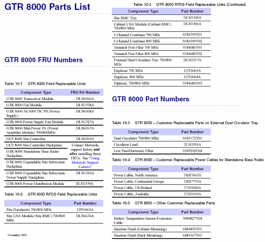
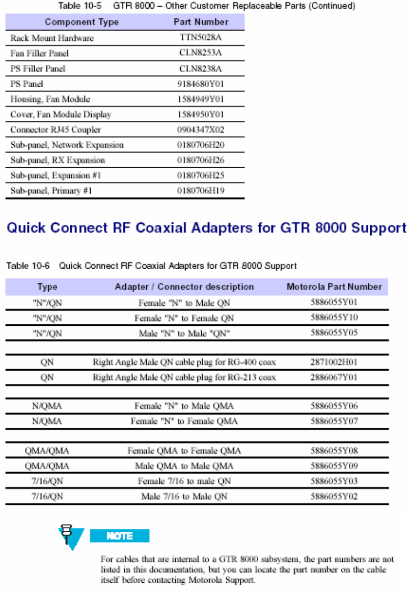
D1-3 Field Replaceable Units and Orderable Parts (Draft)
D1-4 Tune-Up Procedure
D1-5 Racking Configurations
D1-6 Functional Description / Operation of Modules and Interconnect (Draft)

APPLICANT: MOTOROLA EQUIPMENT TYPE: ABZ89FC5812
EXHIBIT D1-1
User / Operational Manual
Manual Front Matter (Draft)
APPLICANT: MOTOROLA EQUIPMENT TYPE: ABZ89FC5812
EXHIBIT D1-1
User / Operational Manual
Manual Front Matter (Draft, Continued)

APPLICANT: MOTOROLA EQUIPMENT TYPE: ABZ89FC5812
EXHIBIT D1-1
User / Operational Manual
Manual Front Matter (Draft, Continued)
APPLICANT: MOTOROLA EQUIPMENT TYPE: ABZ89FC5812
EXHIBIT D1-1
User / Operational Manual
Manual Front Matter (Draft, Continued)

APPLICANT: MOTOROLA EQUIPMENT TYPE: ABZ89FC5812
EXHIBIT D1-2
User / Operational Manual
Specifications (Draft)
General Performance
Model T7039
H x W x D 5.25" x 19" x 18" (133x483x457mm)
Weight 45 lbs (20 kg)
Power Requirements
AC: 90-264 VAC, 47-63 Hz
DC: 43-60 VDC
Temperature Range -22 to 140F (-30 to 60C)
Input / Output Impedance 50 ohms
Antenna Connectors
Transmit: N female
Receive: N female
Modulation
HPD Transmit / Receive: 64QAM, 16QAM, QPSK
IV&D Transmit / Receive: C4FM, LSM
Frequency Stability External Reference
Channel Spacing
HPD: 25 kHz
C4FM / LSM: 12.5 kHz
Transmitter
Frequency Range 762-776 MHz
Power output
HPD: 2-50 Watts (Average)
C4FM: 2-100 Watts
LSM: 2-100 Watts (Average)
Electronic Bandwidth Full Bandwidth
Intermodulation Attenuation 40 dB
Spurious and Harmonic Emissions
Attenuation 85 dB
FCC Type Acceptance
FCC Designation:
Frequency Range
Type
Power Output
ABZ89FC5812 762-776 MHz Transmitter, HPD Variable 2-50 W
Transmitter, C4FM/LSM Variable 2-100 W
ABZ89FR5811 792-824 MHz Receiver N/A
APPLICANT: MOTOROLA EQUIPMENT TYPE: ABZ89FC5812
EXHIBIT D1-3
User / Operational Manual
Field Replaceable Units and Orderable Parts (Draft)
Field replaceable units, or FRUs, include special packaging to allow shipment to customers. Parts and
FRUs available for customer order are listed in this section. All parts and FRUs are sourced through the
Radio Products and Service Division (RPSD).
APPLICANT: MOTOROLA EQUIPMENT TYPE: ABZ89FC5812
EXHIBIT D1-3
User / Operational Manual
Field Replaceable Units and Orderable Parts (Draft) (Continued)
APPLICANT: MOTOROLA EQUIPMENT TYPE: ABZ89FC5812
EXHIBIT D1-4
User / Operational Manual
Tune-Up Procedure
There is no field tune-up procedure. All adjustments are software controlled and are pre-set at the factory. Certain
station operating parameters can be changed via man-machine interface (MMI) commands, within predetermined
limits. Examples include transmit / receiver operating frequencies and transmitter power level.
APPLICANT: MOTOROLA EQUIPMENT TYPE: ABZ89FC5812
EXHIBIT D1-5
User / Operational Manual
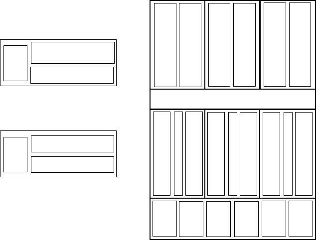
Racking Configurations
There are various equipment racking configurations available to customers. The following section includes
sketches which depict many of the racking alternatives.
GTR 8000 Expandable Site Sub-system Layout
PS #1
PS #2
PS #3
PS #4
PS #5
PS #6
PA #1
PA #2
PA #3
PA #4
PA #5
PA #6
XCVR #1
XCVR #2
XCVR #3
XCVR #4
XCVR #5
XCVR #6
SC #1
SC #2
ALARM
Bay #1 Bay #2 Bay #3
PS #1
PS #2
PS #3
PS #4
PS #5
PS #6
PA #1
PA #2
PA #3
PA #4
PA #5
PA #6
XCVR #1
XCVR #2
XCVR #3
XCVR #4
XCVR #5
XCVR #6
SC #1
SC #2
ALARM
Bay #1 Bay #2 Bay #3
Fan Module #1 serves PA Bay #1
Fan Module #2 serves PA Bay #2
Fan Module #3 serves PA Bay #3
Fan Module #4 serves XCVR Bay #1
Fan Module #5 serves XCVR Bay #2
Fan Module #6 serves XCVR Bay #3
Fan Module #1 serves PA Bay #1
Fan Module #2 serves PA Bay #2
Fan Module #3 serves PA Bay #3
Fan Module #4 serves XCVR Bay #1
Fan Module #5 serves XCVR Bay #2
Fan Module #6 serves XCVR Bay #3
Configuration Layout
PA
XCVR
PS
Base Radio
PA
XCVR
PS
XCVR #2
PS
XCVR #1
XCVR #2XCVR #2
PS
Receive Only Base Radio
GTR 8000 Expandable Site Sub-system Layout
PS #1
PS #2
PS #3
PS #4
PS #5
PS #6
PA #1
PA #2
PA #3
PA #4
PA #5
PA #6
XCVR #1
XCVR #2
XCVR #3
XCVR #4
XCVR #5
XCVR #6
SC #1
SC #2
ALARM
Bay #1 Bay #2 Bay #3
PS #1
PS #2
PS #3
PS #4
PS #5
PS #6
PA #1
PA #2
PA #3
PA #4
PA #5
PA #6
XCVR #1
XCVR #2
XCVR #3
XCVR #4
XCVR #5
XCVR #6
SC #1
SC #2
ALARM
Bay #1 Bay #2 Bay #3
Fan Module #1 serves PA Bay #1
Fan Module #2 serves PA Bay #2
Fan Module #3 serves PA Bay #3
Fan Module #4 serves XCVR Bay #1
Fan Module #5 serves XCVR Bay #2
Fan Module #6 serves XCVR Bay #3
Fan Module #1 serves PA Bay #1
Fan Module #2 serves PA Bay #2
Fan Module #3 serves PA Bay #3
Fan Module #4 serves XCVR Bay #1
Fan Module #5 serves XCVR Bay #2
Fan Module #6 serves XCVR Bay #3
Configuration Layout
PA
XCVR
PS
Base Radio
PA
XCVR
PS
XCVR #2XCVR #2
PS
XCVR #1XCVR #1
XCVR #2XCVR #2
PS
Receive Only Base Radio

APPLICANT: MOTOROLA EQUIPMENT TYPE: ABZ89FC5812
User / Operational Manual
Functional Description / Operation of Modules and Interconnect (Draft)
EXHIBIT D1-6
Control Module Overview
The transceiver control circuitry performs the digital signal processing data formatting for the base radio (BR) and
provides the external interfaces to the rest of the communication equipment present at the site. The Host
Processor is the MPC8250 and the DSP is the MSC8101. General functionality includes:
• Data and Control interface to the Receiver chip set devices
• Data and Control interface to the Exciter chip set devices
• Block Encoder / Decoder Interface
• DSP interfaces
• DSP / Host interface
• Host bus size and speed
• Host memory size, speed, and types supported
• External ports (ethernet, RS232, etc.)
• External physical interfaces (switches, connectors, etc.)
Control Switches
There is one switch on the Front Panel of the XCVR Control Module. The function of this multifunction switch can
be seen in the table below. The switch is debounced in hardware for 100 ms for the “less than 1 second” case.
When the switch is pressed for greater than 3 seconds a “PreReset” signal is sent to the Host processor via the
CPLDs IRQ1x signal followed by the actual reset command 1 second later.
Switch Functions
Switch Function
Switch1
Pressed for less than 1
second
(See note)
(Application Specific)
When this switch closure conditions are met, the
Host CPLD/FPGA will generate an interrupt on
IRQ2x
Switch1 -
Pressed for greater than 3
seconds
XCVR Control Module Reset
When these switch closure conditions are met the
Host CPLD/FPGA will generate a Pre-reset signal
to the MPC8250 via IRQ1x of the CPLD followed by
a HRESET one second later.
Note: This switch function can be SW controlled. The typical usage for this switch is Access Disable, which
disables the power amplifier.

APPLICANT: MOTOROLA EQUIPMENT TYPE: ABZ89FC5812
User / Operational Manual
Functional Description / Operation of Modules and Interconnect (Draft)
EXHIBIT D1-6
Front Panel LEDs
The number and color scheme of the LEDs is described in the following table. The Alarm LED (LED0) is placed
closest to the outside edge of the front panel. The physical location of the other LEDs are placed in numerical
order next to LED0.
Normal LED Operation
LED Color Status Condition
Alarm Red Off
See Service User Interface Spec document for
more info.
Red Same as above
Status Green Off See Service User Interface Spec document for
more info.
LED7_g Green Off No Power
LED7_r Red Green
Flashing
Green
Red Spare
Constant
Amber Spare
LED6_g Green Off No Power
LED6_r Red Green
Flashing
Green
Red
Constant
Amber
LED5_g Green Off No Power
Red Green LED5_r Flashing
Green
Red Constant
Amber
Green Off No Power
Green
Flashing
Green
Red
LED4_g
LED4_r
Red
Constant
Amber
Off No Power
Green
Flashing
Green
Red
LED3_g
LED3_r
Red
Green
Constant
Amber
Off No Power
Green
Flashing
Green
Red
LED2_g
LED2_r
Red
Green
Constant
Amber

APPLICANT: MOTOROLA EQUIPMENT TYPE: ABZ89FC5812
User / Operational Manual
Functional Description / Operation of Modules and Interconnect (Draft)
EXHIBIT D1-6
LED Color Status Condition
Off No Power
Green
Flashing
Green
Red
LED1_g
LED1_r
Red
Green
Constant
Amber
Ethernet Link1 Green Off No link established
On Link established,
Off No Activity Amber On Link activity
Ethernet Link2 Green Off No link established
On Link established,
Off No Activity Amber On
Link activity
Front Panel
Ethernet (visual
indication on
connector)
Green Off No link established
ON Link established (referenced to front view,
connector tab at top, green LED will be on the
left side of the connector)
Yellow/
Amber Off No Activity
On Link activity (referenced to front view,
connector tab at top, green LED will be on the
right side of the connector)
Exciter Module Overview
The exciter, in conjunction with the Power Amplifier or PA, provides the transmitter functions for the Base Radio.
The exciter, which is a part of ‘transceiver’ RF board, consists of a baseband circuit block, a baseband modulator
circuit block, a pre-amplifier circuit block, and a final amplifier circuit block. The transmitter Voltage Controlled
Oscillator (VCO) and frequency synthesis circuitry blocks are also part of the exciter. Other functional blocks in the
exciter include the various DC voltage regulators which drive the different circuits, the digital decoding circuitry
block which interfaces the exciter circuits to the microprocessor in the control section, metering capability, and
exciter to receiver loopback capability for diagnostic purposes.
The exciter interconnects to the control module using an 84-pin flex cable connector. There are no user controls or
indicators on the exciter.
APPLICANT: MOTOROLA EQUIPMENT TYPE: ABZ89FC5812
User / Operational Manual
Functional Description / Operation of Modules and Interconnect (Draft)
EXHIBIT D1-6
Power Amplifier Module Overview
The power amplifier (PA) module is a forced convection cooled RF power amplifier that operates to the following
electrical performance specifications:
- RF Gain: 42 dB
- Input Return Loss: 10 dB
- Max Current Draw: 17.4 Amps
- Rated Average Power Out: 100 Watt
- Rated Peak Power Out: 200 Watt
- Supply Voltage: 29 Volts DC
- Operational Frequency Range: 746 MHz to 870 MHz
The Power Amplifier is comprised of six internal modules. These are described briefly in the following paragraphs.
1. The Core Board provides the following functionality:
- Routes DC to the Converter and Driver Boards
- Routes RF to the Driver Board
- Provides gain and FB power control
- Provides for diagnostic sensors
- Provides for intermediate voltages used by itself and other modules in the PA
- Provides the PA’s digital interface to the rest of the Base Radio
- Provides for cooling measures control
- Provides for control of subordinate modules
2. The Power Converter Board provides the following functionality:
- Provides 29 Volts DC and an intermediate voltage to the Distribution Board
3. The Driver Amplifier Board provides the following functionality:
- Provides the first RF gain stage of the PA
- Provides supporting bias circuits for the Driver Amplifier
4. The Final Amplifier Board provides the following functionality:
- Provides the second RF gain stage of the PA (parallel stage)
- Provides supporting bias circuits for the Final Amplifier
- Provides for RF power splitting
- Provides for RF power combining
- Provides diagnostics
APPLICANT: MOTOROLA EQUIPMENT TYPE: ABZ89FC5812
User / Operational Manual
Functional Description / Operation of Modules and Interconnect (Draft)
EXHIBIT D1-6
5. The Distribution Board provides the following functionality:
- Provides for RF routing from the Driver Amplifier to the Final Amplifier
- Provides for RF routing from the Final Amplifier to the Output Module
- Provides for DC power routing from the Core Board to the Output Module
- Provides for DC power routing from the Power Converter Board to the Final Amplifier
- Provides for Forward and Reverse Power routing from the Output Module to the Core Board
- Provides for feedback power coupling to the Core Board
- Routes module control from the Core Board to the Final Module
- Routes diagnostics from the Final Module to the Core Board
6. The Output Module provides the following functionality:
- Provides output isolation to the PA
- Provides for harmonic attenuation
- Provides for forward and reverse power detection
Power Supply Module Overview
The power supply module operates from either an AC or DC input and provides the DC operating voltages for the
other Base Radio modules. These modules are sometimes also referred to as field replaceable units (FRU).
When operating from an AC source (90 to 264 VAC, 47 to 63 Hz), the supply generates two DC output voltages of
28.94 Volts with reference to output ground. The power supply automatically adjusts to AC input ranges and
supplies a steady output. In AC mode, the power supply contains a separate battery charger which can be used to
maintain the charge on a 48 Volt DC nominal system, positive or negative ground (if installed).
When operating from a DC source (43 VDC to 60 VDC, positive or negative ground), the supply generates two DC
output voltages of 28.94 Volts with reference to output ground. The battery charger is not useable when operating
from a DC input power source.
When both AC and DC sources are available, the power supply operates from the AC source. When the AC
source is lost, the power supply automatically shifts to DC operating mode. When the AC source is restored, the
power supply automatically shifts to AC operating mode.
The power supply contains several switching-type power supply circuits, power factor correction circuitry, battery
charging circuitry, diagnostics and monitoring circuitry.
The power supply module interconnects to the chassis backplane using a multi-pin power connector. Two Torx
screws on the front panel of the power supply module secure it in the chassis.
APPLICANT: MOTOROLA EQUIPMENT TYPE: ABZ89FC5812
User / Operational Manual
Functional Description / Operation of Modules and Interconnect (Draft)
EXHIBIT D1-6
Power Supply Controls and Indicators
The power supply module has three front panel light emitting diode (LED) indicators:
1) ALARM: a RED LED that when illuminated indicates the power supply is no longer operating within its
design specifications
2) STATUS: a GREEN LED that when illuminated indicates the power supply is operating within its design
specifications
3) FAN: a RED LED that when illuminated indicates the power supply fan is no longer functioning per its
design specifications.
The front panel ON/OFF switch is used to enable or disable the DC outputs of the power supply module.
Power Supply Performance Specifications
Operating Temperature: -30 to +60 °C
Input Voltage: AC: 90 to 264 Volts AC
DC: 43 to 60 Volts DC
Input Frequency Range (AC operation): 47 to 63 Hz
Input Current: AC: 10 Amps Maximum
DC: 18A maximum
Steady-State Output Voltage:
Main DC Output: 28.94 Volts DC +/- 2.7%
Aux DC Output: 28.94 Volts DC +/- 2.7%
Total Output Power Rating:
DC Outputs: 600 Watts
Battery Charger: 150 Watts
Battery Charger Output Voltage Range: 45 to 58 Volts DC
Output Ripple: All outputs 50 mV p-p
(measured with 20 MHz BW oscilloscope at 25°C)
Short Circuit Current: 0.5 Amp average (maximum)
Receiver Module Overview
The Receiver, which supports three-branch diversity, provides the receiver functions for the Base Radio. The
receiver is a part of the ‘transceiver’ RF board and consists of a front end low noise amplifier section, an on board
pre-selector section, an IF filter section, and a baseband converter section. The receiver Voltage Controlled
Oscillator (VCO) and frequency synthesis circuitry blocks are also part of the receiver section. A digital decoding
section for interface to the control section microprocessor also exists as part of the receiver module.
The receiver interconnects to the control module using an 84-pin flex cable connector. There are no user controls
or indicators on the receiver.
APPLICANT: MOTOROLA EQUIPMENT TYPE: ABZ89FC5812
User / Operational Manual
Functional Description / Operation of Modules and Interconnect (Draft)
EXHIBIT D1-6
Additional Information – Control, Reference, Interconnect
The Host
The host microprocessor is a MPC8250A also known as the Power Quad Integrated Communications Controller II
(PowerQUICC II). The MPC8250 features 64-bit data and 32-bit address busses providing up to 4 GBytes of
address space. The MPC8250 is comprised of a variant of the PowerPC 603e core with Memory Management
Units (MMUs), and a Communication Processor Module (CPM). The MPC8250 is in a 480-pin TBGA package to
allow easier migration to other PowerQUICC processors.
Control and Communications Features
• Microprocessor
— 266 MHz PowerQuicc II Core
— 66 MHz External Bus
— 64-bit (only 32 used) wide 60x Compatible Data Bus, 4 GB Address Space
— 32-bit wide Local Data Bus, 256 KB Address Space
— Separate 16-Kbyte data and instruction caches
— Three User Programmable Machines
— SDRAM Controller
— Virtual DMA for memory to memory and memory to I/O transfers
— 166 MHz Communication Processor Module
— COP/JTAG Test Access Port
— Four General Purpose Timers
— Bus Monitor
— Software Watchdog Timer
— Periodic Interval Timer
— Flexible Interrupt Controller
• Main Memory
— 32 Mbytes of SDRAM, one 32-bits wide bank
— Option to place an additional 96 MB of SDRAM (for a total of 128 MB)
— On board SDRAM components
— 66/133 MHz Device with 9 ns (or faster) Cycle Time
— No Parity Support
• Non-volatile Memory
— 32 MB Compact Flash Memory Card (Application, 16 bit), which can be easily upgraded to larger densities
— One 8/16 MB Flash device (Test app., Boot 0, parameter/data storage, 16 bit)
— On board Flash components
• External Interfaces
— Serial Peripheral Interface (SPI) Bus
— One V.24 / RS-232 Serial Port: Synchronous (Front panel)
— One RS-232 Serial Port, (TXD and RXD only): (Front panel)
— One RS232 / Ethernet CST Port (Front panel)
— Three internal 10/100BaseT Ethernet ports

APPLICANT: MOTOROLA EQUIPMENT TYPE: ABZ89FC5812
User / Operational Manual
Functional Description / Operation of Modules and Interconnect (Draft)
EXHIBIT D1-6
Serial Interfaces and I/O
The following table shows the MPC8250’s communication port configuration for the control board. SCC1 will
support a synchronous RS232 port. It will also support the same V.24 functionality.
MPC8250 Communication Port Configuration
Port Interface supported
FCC1 10/100BaseT Ethernet
FCC2 10/100BaseT Ethernet
FCC3 10/100BaseT Ethernet
SCC1 Sync. RS232 / V.24
SCC2 Asynch RS232
SCC3 Transparent RX-only for PSM
SCC4 Unused
SMC1 Unused
SMC2 Front panel RS232
MCC1 Unused
MCC2 Unused
I2C I2C to 1-wire Bridge (to Dallas DS2433 EEPROM)
IDMA2 IDMA2 (DSP)
IDMA3 IDMA3 (DSP)
IDMA4 IDMA4 (Compact Flash)
SPI SPI
The control board has 64 MB of total SDRAM in the form of two 32 MB(16Mx16) devices. It supports a total of two
separate Flash memory banks, one bank for boot and one for application code. It also supports a CompactFlash
memory card. CompactFlash I/O cards are not supported. The Control board supports both Type I and Type II
form factor cards.
Reset Configuration
The front panel has one switch. The switch provides two functions, Access Disable and Reset. The Front Panel
switch is debounced for 16-32 ms. An Access Disable function will occur if the switch is pressed for less than 1
second but greater than the debounce time. A Reset sequence will occur if the switch is pressed for greater than
3 seconds. The reset sequence will consist of a Pre-Reset signal after 3 seconds followed by the actual reset 1
second later. The Pre-reset signal is used to notify the MPC8250 that an HRESET* is coming and to gracefully
shutdown the processor before reset occurs.
The DSP is an industrial temperature StarCore (SC140) based MSC8101. Production parts will operate at the
highest core and CPM rates supported at the date of shipment. Initial devices have a maximum core frequency of
275 MHz but will run at 268.8 MHz with CPMs running about half that speed. Core voltages are 1.6 VDC and IO
voltages are 3.3 VDC. On chip memory size is 512 KB. The package is a 332 pin FC-PBGA. See the following
table for clock mode and frequency information.
DSP Clock Information
Clock Mode 06
DSP Clock Input 67.2 MHz
Core Clock 268.8 MHz
CPM Clock 134.4 MHz
System Bus Clock 67.2 MHz
SCC Clock 67.2 MHz
Clock Out 67.2 MHz
BRG Clock 16.8 MHz default, configurable in SCCR
Station Reference
The station reference clock is 16.8 MHz. This clock is derived from a VCXO and in normal operation is locked to
an external reference of 5 MHz, 10 MHz, 20 MHz, or 5 MHz / 1 PPS. The 5MHz_1PPs signal is a 5 MHz signal
with an embedded 1 PPS clock. Typically the duty cycle of the clock is 25%. The duty cycle will change to 75%
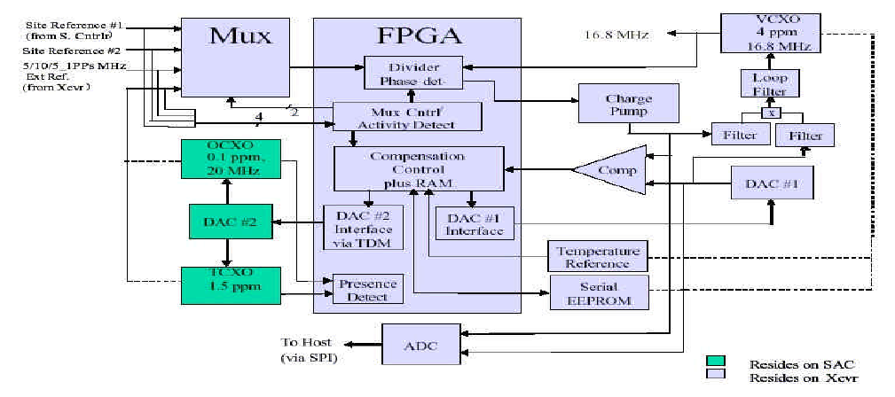
APPLICANT: MOTOROLA EQUIPMENT TYPE: ABZ89FC5812
User / Operational Manual
Functional Description / Operation of Modules and Interconnect (Draft)
EXHIBIT D1-6
for one period to indicate this is the 1 PPS mark. The external reference sources are the Ext_Ref input, the two
CP2 links, and the OCXO which resides on the Supplemental Analog Card (SAC) (future development). The STIC
FPGA will automatically or manually (based on the STIC’s memory mapped register configuration) determine what
clock will be used as the reference. The same applies to the 1 PPS signals which come from a variety of sources.
The 1 PPS sources are the CP2_A, CP2_B, Ext_Ref, and Ext_1PPS. A block diagram of the Station Reference
Circuit can be seen in the Figure below.
The 16.8 MHz and external reference clocks will be divided down to 200 kHz internally in the STIC. These
resulting signals will be fed into an internal phase detector function block which will measure the phase difference
between the two signals. If the rising edge of the 200 kHz clock sourced from 16.8 MHz occurs later than the
rising edge of the 200 kHz clock sourced from the external reference, then the Phase_Det_U output of the FPGA
will pulse high for the duration of the phase difference. The high pulse on the Phase_Det_U will result in the
Charge Pump increasing its output voltage and increasing the VCXO frequency. The same scenario occurs if the
200 kHz clock sourced from 16.8 MHz occurs before the rising edge of the 200 kHz clock sourced from the
external reference. In this case the output of the Phase_Det_D pulses high for the duration of the difference. This
pulse will result in the Charge Pump decreasing the phase locked loop steering voltage and decreasing the VCXO
frequency.
The OCXO can be calibrated by applying a 5 or 10 MHz input signal (preferably a rubidium or equivalent) to the
reference BNC on the front panel of the XCVR. The STIC will automatically generate an interrupt (if not masked in
SW) to the DSP to indicate the presence of a valid 5 or 10 MHz input signal. The station reference will use this
signal to lock the 16.8 MHz VCXO. When locked it will record the steering voltage required to create this lock
condition by reading an ADC. Then the OCXO frequency reference will be used to lock the 16.8 MHz VCXO. The
VCXO steering voltage required for lock will also be recorded using the same ADC. The two VCXO steering
voltages will be compared. If the voltages are different, the OCXO steering voltage will be changed via the DAC.
The OCXO steering voltage will be changed until its output frequency creates the same VCXO steering voltage as
the VCXO steering voltage recorded when using the 5/10 MHz input reference. The OCXO DAC will reside on the
SAC. Data for the OCXO DAC will be placed on the DSP TDM bus TX Slot #8 (Outbound from DSP, Inbound to
SAC FGPA). The CST interface can be used to initiate the calibration process and indicate when the calibration is
complete. It can also record and timestamp the calibration date(s) and indicate when another calibration is
required.
Station Reference Block Diagram
The external references supported are the two 20 MHz clocks from the Site Controller, the external reference, and
the OCXO from the SAC board (future development). The STIC will monitor all of these signals and determine
which ones are not present or grossly out of tolerance. Each one of these fault conditions can be enabled to
create an interrupt to the DSP. The reference clock status can be determined by reading the STIC’s IRQ register
and/or the Clock Frequency Status registers. The FPGA can automatically determine which reference should use

APPLICANT: MOTOROLA EQUIPMENT TYPE: ABZ89FC5812
User / Operational Manual
Functional Description / Operation of Modules and Interconnect (Draft)
EXHIBIT D1-6
and automatically select that reference. It also has the option of manually selecting the reference that should be
used. The order or priority of the reference clocks are shown below.
External Reference Clock Sources and Frequencies Supported
Reference Source Clock
(clocks shown in accending order
with highest priority clock first)
Clock Frequencies
Supported
CP2 Link1 20 MHz
CP2 Link2 20 MHz
External Reference 5 MHz, 10 MHz, 20 MHz, and 5
MHz / 1 PPS
OCXO Reference 10 MHz or 20 MHz
Front Panel 5 MHz or 10 MHz
1 PPS Sources
The table below shows the possible 1 PPS sources and their priority levels. Each source can be manually or
automatically selected based on the configuation of the STIC FPGA. While both CP2 links have an imbedded
1PPS signal, the Host CPLD will select which CP2 1 PPS signal gets sent to the FPGA. Thus there is only one
CP2 1 PPS signal to the FPGA.
1PPS Sources and Frequencies Supported
Reference Source Clock
(clocks shown in accending order with
highest priority clock first)
CP2 Link (CP2A or CP2B)
(aka Raw_1PPs)
Ext_Ref
(Demodulated 5MHz_1PPS)
External 1PPS
External Interfaces
RS-232 Port
This Async port is used to hook up to a dial up modem, MOSCAD, and as the zone link for a Trunking IR system.
This port can also be configured for asyncronous operation. This port interfaces to SCC2 of the MPC8250.
Async. RS-232 Port Signals
RJ-45 Pin # RS-232 Signal Type Resource
1 RTS Output PD26
2 DSR/CD Input PC12
3 RxD Input PD28
4 Local_Failsoft* Input PA13
5 GND GND
6 TxD Output PD27
7 DTR Output PC21
8 CTS Input PC13

APPLICANT: MOTOROLA EQUIPMENT TYPE: ABZ89FC5812
User / Operational Manual
Functional Description / Operation of Modules and Interconnect (Draft)
EXHIBIT D1-6
V.24 Port
This port can be used for either synchronous or asynchronous applications. This RJ45 connector and pinout is
the same as used on previous product V.24 boards. This port can also be configured for asyncronous operation.
This port interfaces to SCC1 of the MPC8250.
Synchronous V.24 RJ-45 Telco Pin-out (on Xcvr)
RJ-45 Pin
# V.24
Signal Type Resource
1 RCLK Input PC20
2 RX Line Det. Input PC14
3 TCLK Input/Output PC29
4 GND GND
5 RX Data Input PD31
6 TX Data Output PD30
7 CTS Input PC15
8 RTS Output PD29
External 1 PPS
The external 1PPS connector currently resides on the Backplane. It is DC coupled, high impedance input,
accepts 3.3V DC TTL level signals and is 5 Volt tolerant.
External References
There are two external references (Ext_Ref and 5MHz_In). The Ext_Ref signal resides on the Backplane. It
accepts both 5 MHz, 5 MHz / 1 PPS, and 10 MHz references and is DC coupled. The second external reference
(5MHz_In) is located on the front panel behind the fan assembly. It has a 50 ohm input resistance and is AC
coupled. This input will be used to align the OCXO residing on the SAC.
System Connector
The System connector is a 50-pin Mini SCSI connector. It is used for all the Wildcard general purpose inputs and
outputs. It also provides I/O for both MRTI Phone Patch and 6809 Trunking Controller configurations.
Wildcard Connector
Pin # Signal Type Function/Notes
1 Aux In1 (Site Failsoft) Input Customer-defined transistor buffered input (Note1)
2 Aux In2 (TX Inhibit) Input Customer-defined transistor buffered input (Note1)
3 Aux In3 (Rx Inhibit) Input Customer-defined transistor buffered input (Note1)
4 Aux In4 (Duplex Enable) Input Customer-defined transistor buffered input (Note1)
5 Aux In5 (In Cabinet
Repeat) Input Customer-defined transistor buffered input (Note1)
6 Aux In6 Input Customer-defined transistor buffered input
7 Aux In7 Input Customer-defined transistor buffered input
8 Aux In8 Input Customer-defined transistor buffered input
9 Aux In 9 Opto+
(Ext_PTT) Aux In 9
Opto+
(Ext_PTT)
Opto-isolated customer defined input (Opto A+)
10 Aux In 9 Opto-
(Ext_PTT) Aux In 9
Opto-
(Ext_PTT)
Opto-isolated customer defined input (Opto A-)
Doubles as MRTI PTT and 6809 PTT
11 Aux In 10 Opto+ Input Opto-isolated customer defined input
12 Aux In 10 Opto- Input Opto-isolated customer defined input
13 Aux In 11 Opto+ Input Opto-isolated customer defined input
14 Aux In 11 Opto- Input Opto-isolated customer defined input
15 Aux In 12 Opto+ Input Opto-isolated customer defined input
16 Aux In 12 Opto- Input Opto-isolated customer defined input
17 Aux Out1 (Failsoft
Indicate) Output Customer-defined transistor buffered output (Note1)

APPLICANT: MOTOROLA EQUIPMENT TYPE: ABZ89FC5812
User / Operational Manual
Functional Description / Operation of Modules and Interconnect (Draft)
EXHIBIT D1-6
Pin # Signal Type Function/Notes
18 Aux Out2 Output Customer-defined transistor buffered output
19 Aux Out3 Output Customer-defined transistor buffered output
20 Aux Out4 Output Customer-defined transistor buffered output
21 Aux Out5 Output Customer-defined transistor buffered output
22 Aux Out6 Output Customer-defined transistor buffered output
23 Aux Out Relay7
N.O.(RdStat) N.O. contact of Relay A (Note1)
24 Aux Out Relay7 Com
(RdStat) COM contact of Relay A (Note1)
25 Aux Out Relay8 N.O. N.O. contact of Relay A
26 Aux Out Relay8 Com COM contact of Relay A
27 Aux Out Relay9 N.O. N.O. contact of Relay A
28 Aux Out Relay9 Com COM contact of Relay A
29 Aux Out Relay10 N.O. N.O. contact of Relay A
30 Aux Out Relay10 Com COM contact of Relay A
31 GND
32 Aux Out11 Output Customer-defined transistor buffered output
33 Ext_Reset Input External Reset Input (to CPLD)
34 GND
35 GND
36 Mute Monitor In Input 6809 Mute / MRTI Monitor Input
37 CCI / PL Strip In Input 6809 CCI / MRTI PL Strip Input
38 RxAudio Output 6809/MRTI RX Audio output
39 RSTAT/Aux Indicate Out
Detect Output 6809 RSTAT / MRTI Aux Indicate output
40 TSTAT/RXCarrier Detect Output 6809 TDATA / MRTI RX Carrier output
41 Tx Data+ Input 6809 Tdata to AuxTX ADC
42 TX Data -/GND Ground
43 MRTI TxAudio In Input MRTI Transmit Audio (to PCM Codec)
44 Patch Inhibit Out Output MRTI Patch Inhibit output
45 GND
46 GND
47 PL+ Input
48 PL- Input
49 Gen TX+ Input
50 GenTX- Input
Transceiver Power / Backplane Connector
This connector provides the interconnect between the XCVR Control and XCVR RF (Exciter and Receiver) board
which also incorporates the power supply. This connector consists of the two 10/100 BaseT Ethernet signals, SPI
signals for the 28.6 VDC power supply and Power Amplifier, Fan Kit signals, and the CP2 TDM links. All of these
signals go to the backplane. This connector also supplies the XCVR Control board with power from the power
supply on the XCVR RF board.
XCVR Power/Backplane Interconnect
Pin # Signal Type Function/Notes
1 ETH_TX1+ Output Primary Ethernet Link
2 GND
3 ETH_TX1- Output Primary Ethernet Link
4 GND
5 NC
6 SPARE
7 ETH_RX1+ Input Primary Ethernet Link
8 GND
9 ETH_RX1- Input Primary Ethernet Link
10 GND
11 NC
12 GND
13 SPARE

APPLICANT: MOTOROLA EQUIPMENT TYPE: ABZ89FC5812
User / Operational Manual
Functional Description / Operation of Modules and Interconnect (Draft)
EXHIBIT D1-6
Pin # Signal Type Function/Notes
14 GND
15 NC
16 GND
17 PWR_ON_
SEQUENCE Input Provides 2V (Host Core) power up
sequence control
18 GND
19 NC
20 GND
21 ETH_TX2+ Output Redundant Ethernet Link
22 GND
23 ETH_TX2- Output Redundant Ethernet Link
24 GND
25 NC
26 GND
27 12VDC
28 12VDC
29 12VDC
30 12VDC
31 NC
32 GND
33 ETH_RX2+ Output Redundant Ethernet Link
34 GND
35 ETH_RX2- Output Redundant Ethernet Link
36 GND
37 NC
38 SPARE
39 TDM_TX1+ Input Primary TDM Link
40 GND
41 TDM_TX1- Input Primary TDM Link
42 GND
43 NC
44 SPARE
45 TDM_CLK1+ Input Primary TDM Link
46 GND
47 TDM_CLK1- Input Primary TDM Link
48 GND
49 NC
50 SPARE
51 TDM_TX2+ Input Redundant TDM Link
52 GND
53 TDM_TX2- Input Redundant TDM Link
54 GND
55 NC
56 SPARE
57 TDM_CLK2+ Input Redundant TDM Link
58 GND
59 TDM_CLK2- Input Redundant TDM Link
60 GND
61 3.3VDC
62 3.3VDC
63 3.3VDC
64 3.3VDC
65 3.3VDC
66 3.3VDC
67 3.3VDC
68 3.3VDC
69 Wattmeter_Vf Input Wattmeter Forward Power voltage
70 GND
71 NC
72 GND

APPLICANT: MOTOROLA EQUIPMENT TYPE: ABZ89FC5812
User / Operational Manual
Functional Description / Operation of Modules and Interconnect (Draft)
EXHIBIT D1-6
Pin # Signal Type Function/Notes
73 PSM_4.2MHz+ To PA for PSM
74 GND
75 PSM_4.2MHz- To PA for PSM
76 GND
77 NC
78 Fan_PWR_Status
79 SPARE DIFF Pins 79 and 81 form diff pair spare
80 GND
81 SPARE DIFF Pins 79 and 81 form diff pair spare
82 GND
83 NC
84 GND
85 Wattmeter_Vr Input Wattmeter Reflected Power voltage
86 GND
87 Fan Fail Lamp Test Normally high, a logic low will illuminate the
Fan Fail LED
88 GND
89 NC
90 GND
91 TEMP Temperature signal from Circulator. Goes to
ADC1 channel 0 (first channel)
92 GND
93 5VDC
94 5VDC
95 5VDC
96 5VDC
97 5VDC
98 5VDC
99 5VDC
100 5VDC
101 ANT_RLY_PDx A low indicates the antenna relay is present
102 GND
103 ANT_RLY Output From PC30 on DSP.
Needs to be defined. Voltage level,
protection, default state etc.
104 GND
105 FAN_FAIL Input Multidrop signal?
106 GND
107 FAN_POWER_
CNTL
Output Controls fan power switch on XCVR RF
board.
108 FAN_DETECTx Input Multidrop signal?
109 ALT_RESETx Output (for PA and PS)
110 GND
111 NC
112 GND
113 PA_SPI_CLK Output Dedicated SPI_CLK for PA
114 GND
115 NC
116 PA1_SPI_EN Output
117 PA1_PRESENCE_D
ETECT Input Pulled down by PA when PA is present
118 GND
119 PA_ENABLEx Output Low activates PA(for P2 HW and beyond))
120 GND
121 NC
122 HPB_IRQx Input
123 HPB_SPI_EN Output
124 GND
125 NC

APPLICANT: MOTOROLA EQUIPMENT TYPE: ABZ89FC5812
User / Operational Manual
Functional Description / Operation of Modules and Interconnect (Draft)
EXHIBIT D1-6
Pin # Signal Type Function/Notes
126 HPB_PRESENCE_
DETECT Input Pulled down by HPB when HPB is present
127 HPB_SPI_CLK Output Dedicated SPI_CLK for HPB
128 GND
129 NC
130 GND
131 SPI_A0 Output SPI, to PS&PA
132 GND
133 NC
134 SPI_A1 Output SPI, to PS&PA
135 SPI_A2 Output SPI, to PS&PA
136 GND
137 SPI_A3 Output SPI, to PS&PA
138 GND
139 NC
140 SPI_MOSI Output SPI
141 SPI_MISO Input SPI
142 GND
143 NC
144 GND
145 PS1_SPI_EN Output
146 GND
147 NC
148 PS1_FAULT Input Indicates to XCVR Control board that the
Power supply detected a fault condition and
to write the condition to its EEPROM before
it goes off-line.
149 PS_PRESENCE_D
ETECT Input Pulled down by PS when PS is present
150 GND
151 PS_SPI_CLK Output Dedicated SPI_CLK for PS
152 GND
153 NC
154 BP_ID1 Input/Output BP_ID1
155 NC
156 GND
157 EXT_REF Input
158 GND
159 NC
160 EXT_1PPS Input
RF Board Receiver Interconnect
The XCVR Control board interfaces to the RF board via a ribbon cable. The signals going to the RF board
Receiver’s interface are shown in the following Table.
RF Board Receiver Interconnect
Pin # Signal Type Function/Notes
1 Attn_Cntl_1_5 Output To RCVR from FPGA GPIO1_5
2 GND
3 Attn_Cntl_1_4 Output To RCVR from FPGA GPIO1_4
4 GND
5 Attn_Cntl_1_3 Output To RCVR from FPGA GPIO1_3
6 GND
7 Attn_Cntl_1_2 Output To RCVR from FPGA GPIO1_2
8 GND
9 Attn_Cntl_1_1 Output To RCVR from FPGA GPIO1_1
10 GND
11 Rcvr3_CU_Cntl Output switch control for RX power
From Host

APPLICANT: MOTOROLA EQUIPMENT TYPE: ABZ89FC5812
User / Operational Manual
Functional Description / Operation of Modules and Interconnect (Draft)
EXHIBIT D1-6
Pin # Signal Type Function/Notes
12 GND
13 Abacus3 FS3 Input From Abacus3_3, to FPGA
14 GND
15 Abacus3 Data3 Input From Abacus3_3, to FPGA
16 GND
17 Abacus3 Clk3 Input From Abacus3_3, to FPGA
18 GND
19 Abacus3 FS2 Input From Abacus3_2, to FPGA
20 GND
21 Abacus3 Data2 Input From Abacus3_2, to FPGA
22 GND
23 Abacus3 Clk2 Input From Abacus3_2, to FPGA
24 GND
25 Abacus3 FS1 Input From Abacus3_1, to FPGA
26 GND
27 Abacus3 Data1 Input From Abacus3_1, to FPGA
28 GND
29 Abacus3 Clk1 Input From Abacus3_1, to FPGA
30 GND
31 Rcvr2_CU_Cntl Output Switch control for RX power
From Host
32 GND
33 Attn_Cntl_2_5 Output To RCVR from FPGA GPIO2_5
34 GND
35 Attn_Cntl_2_4 Output To RCVR from FPGA GPIO2_4
36 GND
37 Attn_Cntl_2_3 Output To RCVR from FPGA GPIO2_3
38 GND
39 Attn_Cntl_2_2 Output To RCVR from FPGA GPIO2_2
40 GND
41 Attn_Cntl_2_1 Output To RCVR from FPGA GPIO2_1
42 GND
43 Aba_SPI_En3
44 GND
45 Aba_SPI_Data3
46 GND
47 Aba_SPI_Clk3
48 GND
49 Aba_SPI_En2
50 GND
51 Aba_SPI_Data2
52 GND
53 Aba_SPI_Clk2
54 GND
55 Aba_ SPI_En1
56 GND
57 Aba_ SPI_Data1
58 GND
59 Aba_ SPI _Clk1
60 GND
61 SPI CLK Output SPI CLK
62 GND
63 RCVR_SPI_EN Output From Host pin PD6
64 GND
65 SPI MOSI Output
66 GND
67 SPI MISO Input
68 GND
69 SPI Addr2 Output SPI Addr signal (MSB) for Abacus3s,
Metering, tunable filters, and LV

APPLICANT: MOTOROLA EQUIPMENT TYPE: ABZ89FC5812
User / Operational Manual
Functional Description / Operation of Modules and Interconnect (Draft)
EXHIBIT D1-6
Pin # Signal Type Function/Notes
Fract-N. See DSP SPI section for
address decoding.
70 GND
71 SPI Addr1 Output SPI Addr signal for Abacus3s, Metering,
tunable filters, and LV Fract-N. See DSP
SPI section for address decoding.
72 GND
73 SPI Addr0 Output SPI Addr signal (LSB) for Abacus3s,
Metering, tunable filters, and LV Fract-N.
See DSP SPI section for address decoding.
74 GND
75 Noise_Cntl_1 Output To RCVR from FPGA GPIO2_0
76 GND
77 SYNCB Output Reset SSI data
78 GND
79 GND
80 GND
81 16.8MHz_ref
82 GND
83 GND
84 GND
RF Board Exciter Interconnect
The XCVR Control board interfaces to the RF board Exciter interface via a ribbon cable. The signals going to the
RF board Exciter’s interface are shown in Table 8.9.
RF Board Exciter Interconnect
Pin # Signal Type Function/Notes
1 Exciter_PWDN Shuts off power to Exciter
2 GND
3 RXD Receive data for PSM (to Host SCC3)
4 GND
5 RCLK Receive Clock for PSM (to Host SCC3)
6 GND
7 RFS Frame Sync for PSM (to Host SCC3)
8 GND
9 PSM_ACQ
10 GND
11 Exc_Tmhk_
Resetx Output Alt_Resetx AND’ed Exc_Tmhk_Resetx
(From Host PC31)
12 GND
13 Exc_Jav_Resetx Alt_Resetx AND’ed Exc_Jav_Resetx
(From Host PC27 )
14 GND
15 Spare
16 GND
17 Javelin TSLOT/Tx
Enable Output Exciter, GPIO from MSC8101 (Pin PA23).
Note PA22 reserved for TSLOTB if
differential signaling is used
18 GND
19 GND
20 GND
21 SCF_2X_CLK
22 GND
23 SCF_CLK From FPGA
24 GND

APPLICANT: MOTOROLA EQUIPMENT TYPE: ABZ89FC5812
User / Operational Manual
Functional Description / Operation of Modules and Interconnect (Draft)
EXHIBIT D1-6
Pin # Signal Type Function/Notes
25 DMCS Output Exciter, to Tomahawk
26 GND
27 Tomahawk FS Input Exciter, from Tomahawk
28 GND
29 Spare
30 GND
31 SSI Data Output Exciter, to Tomahawk
32 GND
33 GND
34 GND
35 SSI CLK Input Exciter, from Tomahawk
36 GND
37 GND
38 GND
39 Spare
40 GND
41 Spare
42 GND
43 Power Detector
dynamic range
control Cntl*
Output from Host pin PA22. This signal is
pulled down.
44 GND
45 GND
46 GND
47 SPI CLK Output Exciter , same signal to Rcvr
48 GND
49 Exciter_SPI_En Output From Host
50 GND
51 SPI MOSI Output Exciter , same signal
to Rcvr
52 GND
53 SPI MISO Input
54
GND
55 Spare
56 GND
57 SPI_A3 Output SPI MSB Address signals for Tomahawk,
Javelin, EEPROM, LV Fract-N, and Metering
CSs.
(See SPI section for address decoding.)
58 GND
59 SPI_A2 Output SPI Address signals for Tomahawk, Javelin,
EEPROM, LV Fract-N, and Metering CSs.
(See SPI section for address decoding.)
60 GND
61 SPI_A1 Output SPI Address signals for Tomahawk, Javelin,
EEPROM, LV Fract-N, and Metering CSs.
(See SPI section for address decoding.)
62 GND
63 SPI_A0 Output SPI LSB Address signals for Tomahawk,
Javelin, EEPROM, LV Fract-N, and Metering
CSs.
(See SPI section for address decoding.)
64 GND
65 GND
66 GND
67
TX Forward
Switch Cntl*
From Host
Normally low.
68 GND
69 Spare .
70 GND

APPLICANT: MOTOROLA EQUIPMENT TYPE: ABZ89FC5812
User / Operational Manual
Functional Description / Operation of Modules and Interconnect (Draft)
EXHIBIT D1-6
Pin # Signal Type Function/Notes
71 DSP_DC_NULL_
DOUT
Input to FPGA
SPI_ADC_MISO
72 GND
73 DSP_DC_NULL_
DIN Output from FPGA
SPI_ADC_MOSI
74 GND
75 DSP_DC_NULL_
CS Output from FPGA
SPI_ADC_CS
76 GND
77 DSP_DC_NULL_
CLK Output from FPGA
SPI_ADC_CLK
78 GND
79 GND
80 GND
81 16.8MHz_ref Output Exciter , Javelin
82 GND
83 GND
84 GND
Front Panel RS-232 / Ethernet (DB9) / RJ45 Interface
The Front Panel CST port supports 2-wire RS-232 on a DB9 connector and 10/100BaseT Ethernet on a RJ45
connector. See tables below for connector pinout.
Only the TXD and RXD signals are supported by the SMC, no other handshake signals are provided. Refer to the
SMC section of the MPC8250 User’s Manual for features and programming information. The table below shows
the signals supported along with the Host hardware resource responsible the RS232 signals.
The front panel also supports a 10/100BaseT Ethernet port. The connector is configured and an MDI-X port that
can be connected to a laptop using a standard cable. In essence, the transmit and receive signal pairs are
reversed on the BRC front panel compared to that defined in IEEE Std. 802.3 Clause 14.5.1. The Ethernet PHY is
a Broadcom BCM5221. Its address (4:0) is '00100'. Both the Front Panel Ethernet PHYand the CP2 PHY
(BCM5222) communicate to the Host via the "bit -banged" GPIO MDC and MDIO signals.
Front Panel Port Signals
RJ45 Pin # RS-232 Signal
1 RD+ (Ethernet)
2 RD- (Ethernet)
3 TD+ (Ethernet)
4 NC
5 NC
6 TD- (Ethernet)
7 NC
8 NC
Front Panel RS232 Cable Adapter
RJ45 Pin # RS232 DB9 / Female
1 NC
2 TXD (RS232) (Host PA9)
3 RXD (RS232) (Host PA8)
4 NC
5 GND
6 Ext_Trigger_In (DSP IRQ1)
7 NC
8 GND
9 Ext_Trigger_Out (DSP PA20)