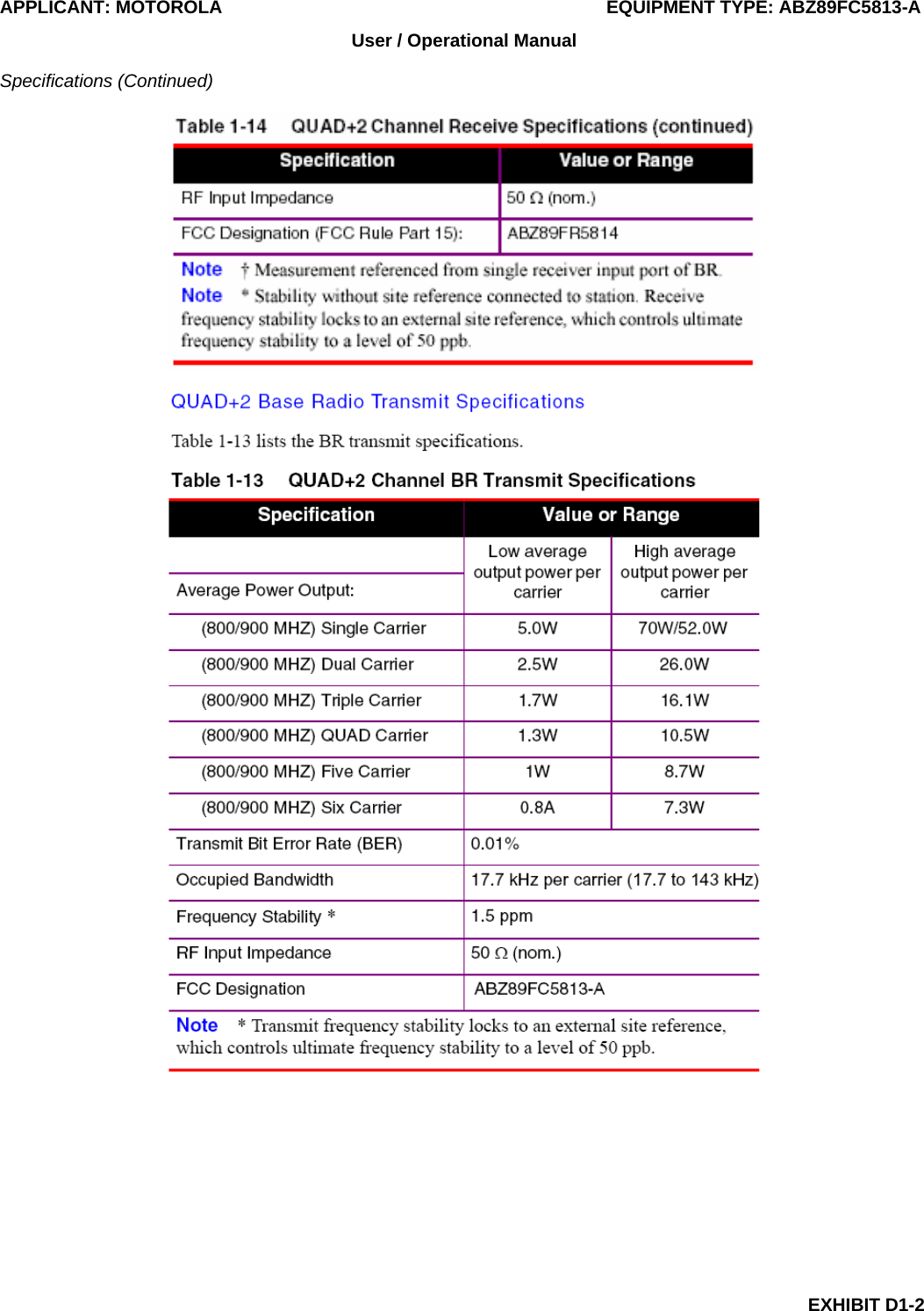
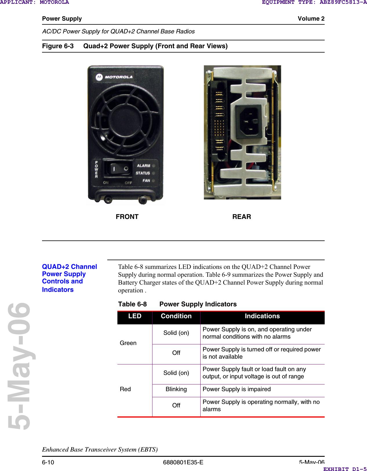
Motorola Solutions 89FC5813-A Licensed Base Station for Part 24 User Manual Quad 2 BR 800 900 Tx FCC Filing v8

Motorola Solutions, Inc. Licensed Base Station for Part 24 Quad 2 BR 800 900 Tx FCC Filing v8

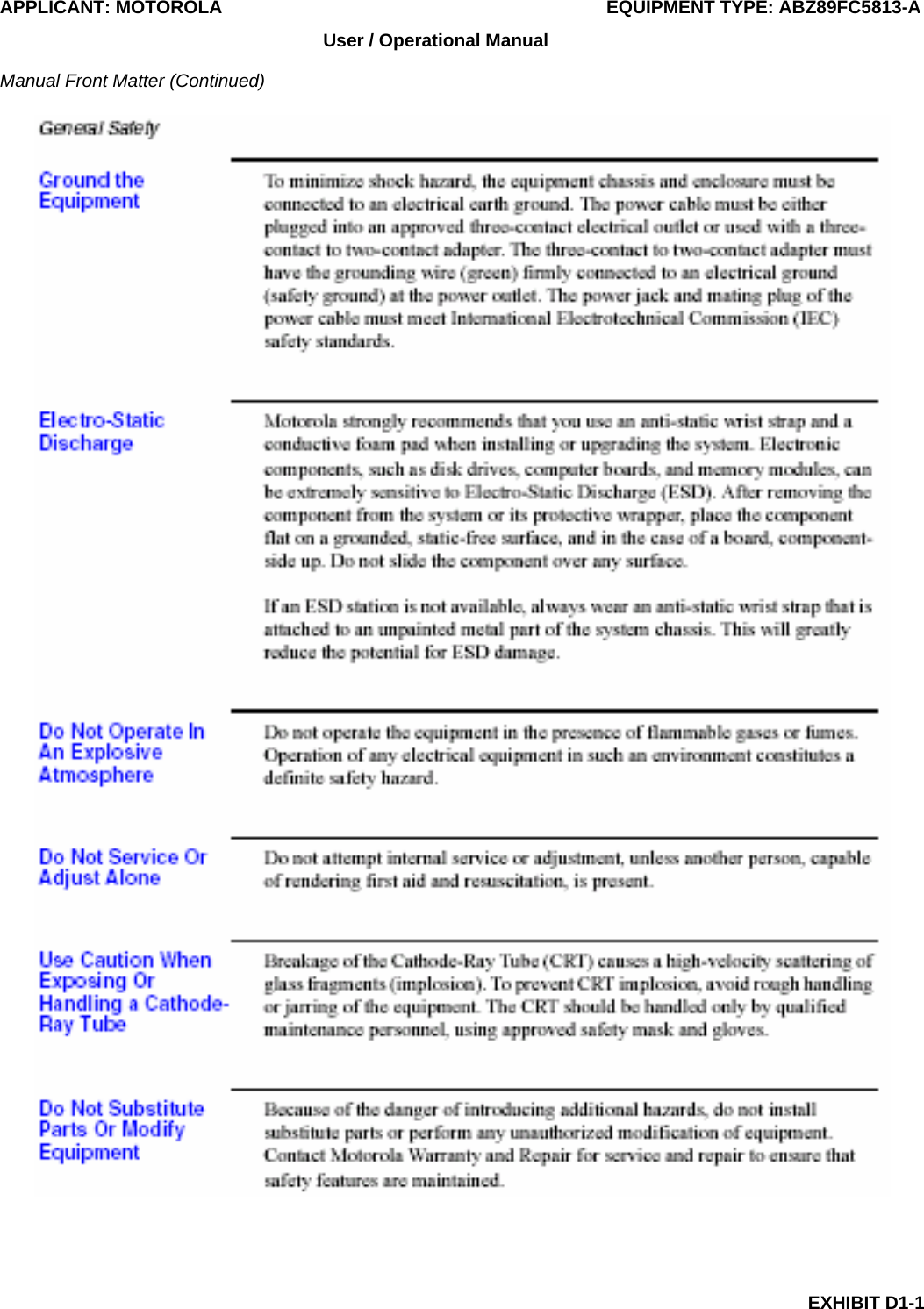
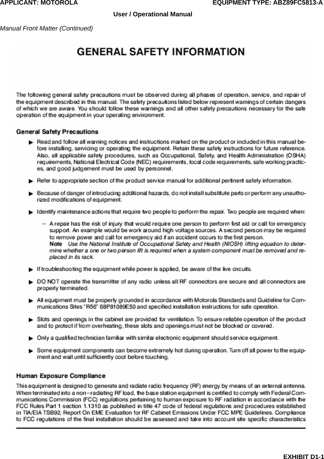
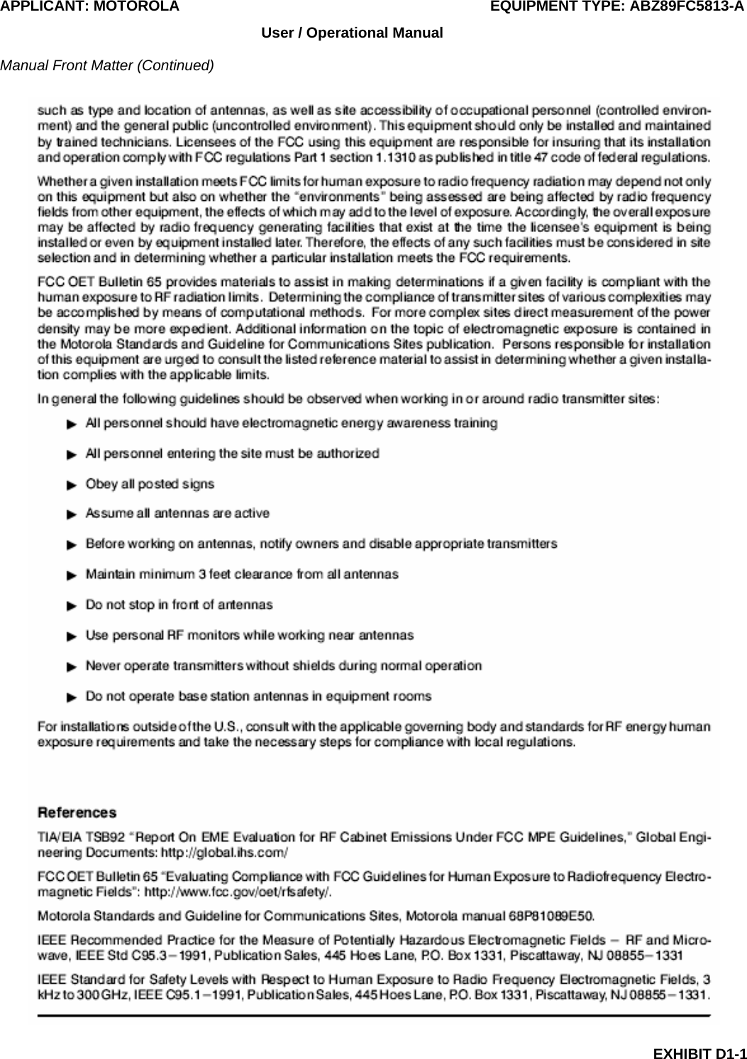
Exhibit D Users Manual per 2 1033 c3

APPLICANT: MOTOROLA    EQUIPMENT TYPE: ABZ89FC5813-A EXHIBIT D User / Operational Manual  Operational or User’s Manual The manual should include instruction, installation, operator, or technical manuals with required ‘information to the users’.  This manual should include a statement that cautions the user that changes or modifications not expressly approved by the party responsible for compliance could void the user’s authority to operate the equipment.  The manual shall include RF Hazard warning statements, if applicable.  The instruction and service manual for this base radio are available via the internet or CD.  Pertinent excerpts from the manuals have been assembled and are included as part of this filing package.  Upon request, published and/or printed manuals will be sent to the commission and/or telecommunication certification body (TCB).  All of the descriptions, block diagrams, and schematics that are included in this filing package are current as of the package submittal date.   EXHIBIT DESCRIPTION D1-1  Manual Front Matter D1-2 Specifications D1-3  Field Replaceable Units and Orderable Parts D1-4 Tune-Up Procedure D1-5  Functional Description / Operation of Modules
APPLICANT: MOTOROLA    EQUIPMENT TYPE: ABZ89FC5813-A EXHIBIT D1-1 User / Operational Manual  Manual Front Matter
APPLICANT: MOTOROLA    EQUIPMENT TYPE: ABZ89FC5813-A EXHIBIT D1-1 User / Operational Manual  Manual Front Matter (Continued)
APPLICANT: MOTOROLA    EQUIPMENT TYPE: ABZ89FC5813-A EXHIBIT D1-2 User / Operational Manual  Specifications
APPLICANT: MOTOROLA    EQUIPMENT TYPE: ABZ89FC5813-A EXHIBIT D1-2 User / Operational Manual  Specifications (Continued)
APPLICANT: MOTOROLA  EQUIPMENT TYPE: ABZ89FC5813-A EXHIBIT D1-3  User / Operational Manual  Field Replaceable Units and Orderable Parts  Field replaceable units, or FRUs, include special packaging to allow shipment to customers.  Parts and FRUs available for customer order are listed in this section.  All parts and FRUs are sourced through the Radio Products and Service Division (RPSD).  Structure of Part / FRU #  Description T7132A  iDEN QUAD+2 800 / 900 MHz Base Radio CLF1835B  Power Amplifier Tanapa CLF6528A  Combiner board (New kit number for 800/900) CLF6506C  PA Driver module CLF6530A PA Final CLF6531A  PA Low Pass Filter CLN8053C  PA DC Board CLN8117A  NULL Modulator Board CLN8215A PA Housing Kit 0174000A10  PA Mechanics specific 0173000A19  PA Heatsink and Cover PCUF1001B  Transceiver, 6 Channel 800 / 900 MHz PCCN4025A Transceiver board 0173000A76 Transceiver Core assembly CLN8221B  Hardware, Transceiver, 6-Channel MCPN1082B  BR Power Supply Tanapa 0180706H34  Chassis and Backplane, Quad2 0180706G92 Backplane Assembly 0173000A68 BR Chassis Core 4385826Y01 Plastic shim CLN8251A  BR Card Cage Kit 0173000A67  RF cable, retainer clip, and RJ45 plugs 0180706G82 Fan Assembly 0173000A34 Fan Module Parts CLN8332A QUAD+2 rack filler CLN8333A FCC Label   T7132A  iDEN QUAD+2 800 / 900 MHz Base Radio X899AF  BR FRU packing option (must be added to order for BR to ship standalone) CBN6230A BR Packing kit DLN6654A  Transceiver FRU number CUF1001B  Transceiver, 6 Channel 800 / 900 MHz CBN6239A  PA / Transceiver Packing kit  DLN6655A  Power Amplifier FRU number CLF1835B  Power Amplifier Tanapa CBN6239A  PA / Transceiver Packing kit  DLN6656A  BR Power Supply FRU number MCPN1082A  Power Supply Tanapa CBN6240A  Power Supply Packing kit  DLN6657A  Fan Assembly FRU number 0180706G82  Fan Assembly Tanapa CBN6244A  Fan Packing kit
APPLICANT: MOTOROLA  EQUIPMENT TYPE: ABZ89FC5813-A EXHIBIT D1-4 User / Operational Manual  Tune-Up Procedure There is no field tune-up procedure.  All adjustments are software controlled and are pre-set at the factory.  Certain station operating parameters can be changed via man-machine interface (MMI) commands, within predetermined limits.  Examples include transmit / receiver operating frequencies and transmitter power level.
APPLICANT: MOTOROLA  EQUIPMENT TYPE: ABZ89FC5813-A EXHIBIT D1-5 User / Operational Manual  Functional Description / Operation of Modules  The following pages are excerpts from the manual and are intended to give an overview of the base radio and the modules that comprise the base radio.
Base Radio Volume 2QUAD+2 Base Radio OverviewEnhanced Base Transceiver System (EBTS)1-24 6880801E35-E 5-May-065-May-06QUAD+2 Base Radio Theory of OperationThe QUAD+2 Channel BR operates together with other site controllers and equipment that are properly terminated. The following description assumes such a configuration. Figure 1-11 shows an overall block diagram of the QUAD+2 Channel BR.Power is applied to the DC Power inputs located on the QUAD+2 Channel BR backplane. The DC Power input is connected if -48 VDC or batteries are used in the site.Power is applied to the BR by setting the Power Supply power switch to the ON position. Upon power-up, the QUAD+2 Channel BR performs self-diagnostic tests to ensure the integrity of the unit. These tests, which include memory and Ethernet verification routines, primarily examine the EX / CNTL. After completing self-diagnostic tests, the QUAD+2 Channel BR reports alarm conditions on any of its modules to the site controller via Ethernet. Alarm conditions may also be verified locally. Local verification involves using the service computer and the STATUS port located on the front of the QUAD+2 Channel BR.The software resident in FLASH on the XCVR registers the BR with the site controller via Ethernet. After BR registration on initial power-up, the BR software  downloads via Ethernet and executes from RAM. The download includes operating parameters for the QUAD+2 Channel BR. These param-eters allow the QUAD+2 Channel BR to perform call processing functions.  EXHIBIT D1-5EQUIPMENT TYPE: ABZ89FC5813-AAPPLICANT: MOTOROLA
Volume 2 Base RadioQUAD+2 Base Radio OverviewEnhanced Base Transceiver System (EBTS)5-May-06 6880801E35-E 1-255-May-06After software downloads to the BR via Ethernet, FLASH memory stores the software object. Upon future power-ups, the software object in FLASH loads into RAM for execution.The BR operates in a TDMA (Time Division Multiple Access) mode. This mode, combined with voice compression techniques, increases channel capacity by a ratio of as much as six to one. TDMA divides both the receive and transmit signals of the BR into six individual time slots. Each receive slot has a corresponding transmit slot. This pair of slots comprises a logical RF channel. The BR uses diversity reception for increased coverage area and improved quality. The Receiver modules within the QUAD+2 Channel BR contain three receiver paths. Two-branch diversity sites use two Receiver paths, and three-branch diversity sites use three Receiver paths. All Receiver paths within the Transceiver module are programmed to the same receiver frequency. Signals from each receiver are diversity combined and undergo error-correction. Then, via Ethernet, the site controller acquires the signal, along with control information about signal destination.Two separate FRUs comprise the transmit section of the QUAD+2 Channel BR. These are the Exciter and Control (XCVR) portion of the Transceiver and the Power Amplifier (PA). The Exciter processes commands from the CNTL, assuring transmission in the proper modulation format. Then the low-level signal enters the PA. The PA amplifies this signal to the desired output power level. The PA is a continuously keyed linear amplifier. A power control routine monitors the output power of the BR. The routine adjusts the power as necessary to maintain the proper output level.EXHIBIT D1-5EQUIPMENT TYPE: ABZ89FC5813-AAPPLICANT: MOTOROLAEXHIBIT D1-5EQUIPMENT TYPE: ABZ89FC5813-AAPPLICANT: MOTOROLA
Base Radio Transceiver Volume 2OverviewEnhanced Base Transceiver System (EBTS)3-2 6880801E35-E 5-May-065-May-06Overview 3This chapter provides information on the QUAD+2 Base Radio Transceiver (XCVR).FRU Number to Kit Number Cross ReferenceBase Radio Transceiver (XCVR) Field Replaceable Units (FRUs) are available for the iDEN EBTS. The FRU contains the XCVR kit and required packaging. Table 3-1provides a cross reference between XCVR FRU numbers and kit numbers. Table 3-1 FRU Number to Kit Number Cross ReferenceDescriptionFRU NumberKit NumberQUAD+2 Channel Base Radio Transceiver DLN6654 PCUF1001 EXHIBIT D1-5EQUIPMENT TYPE: ABZ89FC5813-AAPPLICANT: MOTOROLA
Volume 2 Base Radio TransceiverQUAD+2 Channel Base Radio TransceiverEnhanced Base Transceiver System (EBTS)5-May-06 6880801E35-E 3-35-May-06QUAD+2 Channel Base Radio Transceiver  3QUAD+2 Base Radio OverviewThe transceiver (XCVR) module provides the control, exciter and receiver functions for the Base Radio.The XCVR generates the station reference which typically needs to be locked on to one of many possible external sources. The external source can be either the site controller 20 MHz TDM clocks or the external reference operating at 5 or 10 MHz.The XCVR SPI bus allows communication with its receiver and exciter circuitry, as well as the power supply and power amplifier modules.The XCVR circuit board contains two major sections:nXCVR Control : Performs the control management, digital signal processing, and transmit and receive data formatting for the Base Radio.nXCVR RF : Contains DC power conversion/regulation and performs receiver and exciter functions.Figure 3-1shows a top view of the Transceiver.Figure 3-1 800/900 MHz QUAD+2 Channel Transceiver (Front View)EXHIBIT D1-5EQUIPMENT TYPE: ABZ89FC5813-AAPPLICANT: MOTOROLA
Base Radio Transceiver Volume 2QUAD+2 Channel Base Radio TransceiverEnhanced Base Transceiver System (EBTS)3-4 6880801E35-E 5-May-065-May-06Transceiver Control SectionThe main operating software for the base radio is loaded in the XCVR’s control section. As the main manager for the base radio, the XCVR control  provides operational control over the other station modules. It handles three types of information flow, in the following ways:nServes as a gateway between the network and RF functionality, by distributing the RF payload to and from the networknSupports operational and diagnostic functions with digital control data (for example: site information, channel assignments, and identification numbers for call processing)nEnsures the flow of other network management configuration informationFigure 3-2 shows the information flow through the transceiver Control and RF sections for HPD systems. Figure 3-2 800/900 MHz QUAD+2 Transceiver Information FlowTransceiver RF SectionIn addition to DC power conversion/regulation, the XCVR RF section provides circuitry for the following receiver and exciter functions.ExciterThe exciter on the XCVR RF section provides the transmitter functions for the base radio. The exciter circuitry generates a low-level, modulated RF signal that passes to the power amplifier. It supports various modulation types as well as bandwidths up to 25 kHz, through software programming.The exciter also provides a controlled output power level to the power amplifier.Ethernet viaSite ControllerBase Radio (XCVR)ADCDACPDSPPARFDSControlRFHostEXHIBIT D1-5EQUIPMENT TYPE: ABZ89FC5813-AAPPLICANT: MOTOROLA
Volume 2 Base Radio TransceiverQUAD+2 Channel Base Radio TransceiverEnhanced Base Transceiver System (EBTS)5-May-06 6880801E35-E 3-55-May-06ReceiverThe QUAD+2  receiver provides multiple receiver inputs for one to three diversity branches with multiple channels of up to six channels within each branch. The receiver is tuned to pass frequenies anywhere between 806 MHz and 901 MHz. The receiver is best suited for:nLow density RF environmentsnStations with external multicouplersnStations with requirements for multi-frequency operation beyond 14 MHzControls and IndicatorsThe transceiver external interfaces include 2 external ports, a switch and LEDs. The ports and switch are described here. The LED states are listed in the reference section of the documentation. Figure 3-3 shows the port, switch and LED locations when the access door is opened. Figure 3-4 shows the Rear View connectors.Figure 3-3 800/900 MHz QUAD+2 QUAD+2 Transceiver (with access door opened)PortsLEDsAlarm LEDReset SwitchStatus LEDEXHIBIT D1-5EQUIPMENT TYPE: ABZ89FC5813-AAPPLICANT: MOTOROLA
Base Radio Transceiver Volume 2QUAD+2 Channel Base Radio TransceiverEnhanced Base Transceiver System (EBTS)3-6 6880801E35-E 5-May-065-May-06Figure 3-4 800/900 MHz QUAD+2 Transceiver Backplane (Rear View) Transceiver Ports - FrontTwo ports are accessible via a dropdown door to the left of the fans. An asynchronous port and a synchronous port.Transceiver Ports - RearThe transceiver interconnects to the backplane using a 120–pin HVDML digital connector and 8–pack RF connector, as shown in Figure 3-4. These connections handle multiple signals including power, power supply communi-cations, power amplifier communications, 10Base2 Ethernet, fan interface and peripheral interface. The digital connection receives alarm data and the site controllers’ TDM signals, which are used to pass reference and control data to the station.Transceiver SwitchThere is one multifunction switch on the front of the transceiver module, accessible via the dropdown door to the left of the fans.RF and Ethernet DigitalTable 3-2 Transceiver ConnectionsXCVR Port / TypeConnects to this Device/Port DescriptionRJ-45 10/100BaseT port Ethernet port for future use.Service port, DB-9Service PC, RS-232 portSerial service port for configuration.EXHIBIT D1-5EQUIPMENT TYPE: ABZ89FC5813-AAPPLICANT: MOTOROLA
Volume 2 Base Radio TransceiverQUAD+2 Channel Base Radio TransceiverEnhanced Base Transceiver System (EBTS)5-May-06 6880801E35-E 3-75-May-06Table 3-3 lists the Transceiver Front Switch Functions.Transceiver LEDsTable 3-4 and Table 3-5 lists the Transceiver LEDs.   \Table 3-3 XCVR Front Switch FunctionsUser Action ResultPress switch for less than 1 second Access DisablePress switch for greater than 3 seconds Transceiver Control Module ResetTable 3-4 QUAD+2 Channel Base Radio Status and Alarm LED IndicationsCondition Status LED Alarm LEDNo Power Off OffLamp Test Green RedFailure Off RedImpaired Green Red (blinking)Booting Up Green (blinking) OffOnline Green OffTable 3-5 QUAD+2 Channel Base Radio Transceiver LED IndicationsLabel LED State Description1Green Proper Base Radio operation with no alarm conditions and channel 1 is keyedGreen (Blinking) Channel 1 is not keyedOff Channel 1 is not in operation or the Base Radio is out of service or power is removed2Green Proper Base Radio operation with no alarm conditions and channel 2 is keyedGreen (Blinking) Channel 2 is not keyedOff Channel 2 is not in operation or the Base Radio is out of service or power is removedEXHIBIT D1-5EQUIPMENT TYPE: ABZ89FC5813-AAPPLICANT: MOTOROLA
Base Radio Transceiver Volume 2QUAD+2 Channel Base Radio TransceiverEnhanced Base Transceiver System (EBTS)3-8 6880801E35-E 5-May-065-May-06Transceiver Band StatesTable 3-6 lists the Transceiver Band States 3Green Proper Base Radio operation with no alarm conditions and channel 3 is keyedGreen (Blinking) Channel 3 is not keyedOff Channel 3 is not in operation or the Base Radio is out of service or power is removed4Green Proper Base Radio operation with no alarm conditions and channel 4 is keyedGreen (Blinking) Channel 4 is not keyedOff Channel 4 is not in operation or the Base Radio is out of service or power is removed5(See Note)Green Proper Base Radio operation with no alarm conditions and channel 5 is keyedGreen (Blinking) Channel 5 is not keyedOff Channel 5 is not in operation or the Base Radio is out of service or power is removed6(See Note)Green Proper Base Radio operation with no alarm conditions and channel 6 is keyedGreen (Blinking) Channel 6 is not keyedOff Channel 6 is not in operation or the Base Radio is out of service or power is removedNote Five and six carrier operation is only supported in Test Application mode and requires licensing agreement with Motorola for activation in Call Processing mode.Table 3-5 QUAD+2 Channel Base Radio Transceiver LED Indications (continued)Label LED State DescriptionTable 3-6 QUAD+2 Channel Base Radio Band StateLabel LED State BR Band7Solid Red Install Band FailureSolid Green 800 MHzSolid Amber 900 MHzEXHIBIT D1-5EQUIPMENT TYPE: ABZ89FC5813-AAPPLICANT: MOTOROLA
Volume 2 Base Radio TransceiverQUAD+2 Channel Base Radio TransceiverEnhanced Base Transceiver System (EBTS)5-May-06 6880801E35-E 3-95-May-06Theory of Operation - Controller SectionTable 3-7 briefly describes the BRC circuitry. Figure 3-5 shows the Controller with the cover removed. Figure 3-8 shows the Controller’s functional block diagram. Table 3-7 Control Section CircuitryCircuit DescriptionHost Microprocessor Contains integrated circuits that comprise the central controller of the BRC and stationNon-Volatile MemoryConsists of: • FLASH containing the station operating software• Codeplug dataVolatile Memory Contains SDRAM to store station software used to execute commands.Ethernet InterfaceProvides the BRC with a 10Base2 Ethernet communication port to network both control and compressed voice dataRS-232 Interface Provides the BRC with an RS-232 serial interfaceDigital Signal Processor Performs high-speed modulation/demodulation of compressed audio and signaling data2QICContains integrated circuits that provide:• Highly stable, reclocked transmit signals and peripheral transmit control logic• Receive SPI capability for receive  control, metering ADC and signal path attenuators• Receive DSP functions including baseband mixing and digital  filtering for multiple branches with multiple channels with interleaved serialization of output• Synthesizer for station reference and related control• Site Reference timing decode and related Base Radio timing signals generation• SPI interface to ADC devices for meteringStation Reference CircuitryGenerates the 16.8 MHz and 48 MHz reference signals used throughout the stationRemote Station Shutdown Provides software control to cycle power on the BRSerial Peripheral Interface (SPI)Provides serial control and metering capability with the exciter, receiver, power amplifier, and power supply.EXHIBIT D1-5EQUIPMENT TYPE: ABZ89FC5813-AAPPLICANT: MOTOROLA
Base Radio Transceiver Volume 2QUAD+2 Channel Base Radio TransceiverEnhanced Base Transceiver System (EBTS)3-10 6880801E35-E 5-May-065-May-06Figure 3-5 Controller Section (with housing removed) Host MicroprocessorThe host microprocessor is the main controller for the BR. The processor operates at a 266-MHz core clock speed. The processor controls Base Radio operation according to station software in memory. Station software resides in FLASH memory. For normal operation, the system transfers this software to volatile S-DRAM memory.Note At BR power-up and normal conditions, the Status and Alarm LEDs transition through the  Conditions stated in Table 3-4 as follows: Power Off, Failure, Lamp Test, Booting Up and Online states as indicated in Table 3-4. Any other sequence of Conditions indicates an impairment or failure.Serial Communication BusesThe microprocessor provides a general-purpose SMC serial management controller bus.EXHIBIT D1-5EQUIPMENT TYPE: ABZ89FC5813-AAPPLICANT: MOTOROLA
Volume 2 Base Radio TransceiverQUAD+2 Channel Base Radio TransceiverEnhanced Base Transceiver System (EBTS)5-May-06 6880801E35-E 3-115-May-06The SMC serial communications bus is an asynchronous RS-232 interface with no hardware handshake capability. The BRC front panel includes a nine-pin, D-type connector. This connector provides a port where service personnel may connect a service computer. Service personnel can perform programming and maintenance tasks via Man-Machine Interface (MMI) commands. The interface between the SMC port and the front- panel STATUS connector is via EIA-232 Bus Receivers and Drivers.MPC8250 Host ProcessorThe MPC8250 microprocessor incorporates 16k bytes of instruction cache and 16k bytes of data cache that significantly enhance processor performance.The microprocessor has a 32-line data bus. The processor uses this bus to access non-volatile memory and SDRAM memory. Via memory mapping, the processor also uses this bus to control other BRC circuitry. The microprocessor uses its Chip Select capability to decode addresses and assert an output signal. The chip-select signals select non-volatile memory, SDRAM memory, and DSP.The microprocessor has a Local Bus that is used to interface to the DSP.The Host processor... nProvides serial communications between the Host Microprocessor and other Base Radio devices and modules for control and metering of radio functions.nProvides RS-232 serial user interfacenProvides condition signals necessary to access SDRAM, FLASH, and Compact FlashnAccepts interrupt signals from BRC circuits (such as DSP and 2QIC). nOrganizes the interrupts, based on hardware-defined priority ranking.nThe Host supports several internal interrupts from its Communications Processor Module. These interrupts allow efficient use of peripheral interfaces.nThe Host supports 10/100 Mbps BaseT and 10Base2 Ethernet/IEEE 802.3nProvides a 32-line data bus transfers data to and from BRC SDRAM and other BRC circuitry.nProvides a Local Bus for communciations with the DSPEXHIBIT D1-5EQUIPMENT TYPE: ABZ89FC5813-AAPPLICANT: MOTOROLA
Base Radio Transceiver Volume 2QUAD+2 Channel Base Radio TransceiverEnhanced Base Transceiver System (EBTS)3-12 6880801E35-E 5-May-065-May-06Non-Volatile MemoryBase Radio software resides in a minimum of 32M x 16 bits of Compact FLASH memory and 16M x 16 bits of additional board FLASH. The Host Microprocessor addresses the Compact FLASH memory with 4 of the host address bus’ 32 lines in conjunction with the data lines. The host accesses FLASH data over the 16-line host data bus. A host-operated chip-select line provides control signals for these transactions. FLASH memory contains the operating system and application code. The system stores application code in Compact FLASH for fast recovery from reset conditions. Application code transfers from network or site controllers may occur in a background mode. Background mode transfers allow the station to remain operational during new code upgrades.The data that determines the station personality (codeplug) resides in the 16M x 16 bit FLASH. The microprocessor addresses the FASH with 24 of the host address bus’ 32 lines. The host accesses FLASH data with 16 of the data bus’ 32 lines. A host-operated chip-select line provides control signals for these transactions. During the manufacturing process, the factory programs the codeplug’s default data. The BRC must download field programming data from network and site controllers. This data includes operating frequencies and output power level. The station permits adjustment of many station parameters, but the station does not store these adjustments. Refer to the Software Commands chapter for additional information.Volatile MemoryEach BRC contains 16MB x 32 bits of SDRAM. The BRC downloads station software code into SDRAM for station use. SDRAM also provides short-term storage for data generated and required during normal operation. SDRAM is volatile memory. A loss of power or system reset destroys SDRAM data. The system performs read and write operations over the Host Address and Data buses. These operations involve column and row select lines under control of the Host processor’s DRAM controller. The Host address bus and column row signals sequentially refresh SDRAM memory locations.Ethernet InterfaceThe Host processor’s Communications Processor Module (CPM) provides the Local Area Network (LAN) Controller for the Ethernet Interface. The LAN function implements the CSMA/CD access method, which supports the IEEE 802.3 10Base2 standard. The LAN coprocessor supports all IEEE 802.3 Medium Access Control, including the following: EXHIBIT D1-5EQUIPMENT TYPE: ABZ89FC5813-AAPPLICANT: MOTOROLA
Volume 2 Base Radio TransceiverQUAD+2 Channel Base Radio TransceiverEnhanced Base Transceiver System (EBTS)5-May-06 6880801E35-E 3-135-May-06nframing npreamble generation nstrippingnsource address generationndestination address checkingThe PCM LAN receives commands from the CPU. The Ethernet Serial Interface works directly with the CPM LAN to perform the following major functions:n10 MHz transmit clock generation (obtained by dividing the 20 MHz signal provided by on-board crystal)nManchester encoding/decoding of framesnelectrical interface to the Ethernet transceiverAn isolation transformer provides high-voltage protection. The transformer also isolates the Ethernet Serial Interface (ESI) and the transceiver. The pulse transformer has the following characteristics:nMinimum inductance of 75 µHn2000 V isolation between primary and secondary windingsn1:1 Pulse Transformer The Coaxial Transceiver Interface (CTI) is a coaxial cable line driver and receiver for the Ethernet. CTI provides a 10Base2 connection via a coaxial connector on the board. This device minimizes the number of external compo-nents necessary for Ethernet operations. A DC/DC converter provides a constant voltage of -9 Vdc for the CTI from a 3.3 Vdc source. The CTI performs the following functions:nReceives and transmits data to the Ethernet coaxial connectionnReports any collision that it detects on the coaxial connectionnDisables the transmitter when packets are longer than the legal length (Jabber Timer)Digital Signal ProcessorsThe BRC includes one Digital Signal Processor for receive and transmit processing. This DSP and related circuitry process compressed station transmit and receive audio and data. The related circuitry includes the QUAD+2 Integrated Circuit (2QIC). The DSP only accepts input and output signals in digitized form.EXHIBIT D1-5EQUIPMENT TYPE: ABZ89FC5813-AAPPLICANT: MOTOROLA
Base Radio Transceiver Volume 2QUAD+2 Channel Base Radio TransceiverEnhanced Base Transceiver System (EBTS)3-14 6880801E35-E 5-May-065-May-06The DSP inputs are digitized receiver signals. The DSP outputs are digitized voice audio and data (modulation signals). These signals pass from the DSP to the Exciter section of the QUAD+2. DSP communicates with the Micropro-cessor via a 32-bit, host data bus on the host processor side. Interrupts drive communication between the DSP and the host.The DSP operate from an external 49 MHz clock, provided by the CPLD and phase locked to the 16.8 MHz local station reference clock. The DSP internal core operating clock signal is 394MHz, produced by an internal Phase-Locked Loop (PLL). The DSP accepts receive digitized signals from the 2QIC through the Time-Division Multiplexing (TDM) interface ports. The QUAD+2 uses 3 of these ports. All 3 ports use the same clock and framesync signals to input data.  Each port handles digital data for 1 of the 3 branches. Each port handles digitized data for 6 channels, 2 status words, and 2 power detect words.The QUAD+2 accesses its DSP program and signal-processing algorithms in 1440 kB  of internal memory. The DSP communicates with the host bus over an 32-bit interface. The DSP communicates with the 2QIC to  provide serial communications to the receiver paths for receiver control over a Serial Peripheral Interface (SPI) link. The 2QIC provides a parallel-to-serial conversion circuit that accepts parallel data from the DSP and serial data to the receive circuitry.The DSP sends up to six carriers of digitized signal to the 2QIC along with embedded control signals.  Two framed and synchronized data streams are output. One data stream is I-data, and the other is the Q-data stream.  The control bits are appendended at the end of the data streams. The 2QIC extracts and applies the control signals. The 2QIC synchronizes the 2QIC I and Q output frames with system timing signals that exist in the 2QIC.  The synchro-nized outputs are sent to a Digital to Analog Converter (DAC) in the exciter section that converts the digital signals to analog.2QICplusThe 2QIC controls internal DSP operations. This circuit provides the following functions:The 2QICplus is a DSP programmable FPGA that provides the circuit integration needed to condition, route and control receive and transmit data between the RF circuitry and the DSP, and provide consolidated monitoring and control for QUAD+2 transceiver. Following are the major functions of the 2QICplusnFor nitialization and control, the 2QICplus interfaces with the DSP through address and data buses. nProvides six Independent Abacus III receiver data and control interfaces with fault detection and handlingEXHIBIT D1-5EQUIPMENT TYPE: ABZ89FC5813-AAPPLICANT: MOTOROLA
Volume 2 Base Radio TransceiverQUAD+2 Channel Base Radio TransceiverEnhanced Base Transceiver System (EBTS)5-May-06 6880801E35-E 3-155-May-06nRF Signal Gain Control for 18 receiver pathsnProgrammable General-Purpose Input/Output pins for monitor and control of the transceivernProvides clocks required for the transceivernPhase detector for the 16.8MHz Synthesizer and PLL with PLL steering line gate control nInputs a site reference signal, demodulates a 1PPS timing marker from this signal and outputs the 1PPS signal for network timing alignment.n15 ms and 7.5 ms timing signals generation. (These signals are synchronize to the 1 PPS time mark. The system decodes the time mark from the site reference. Then the system routes the reference to the DSP.)nProgrammable Interrupt Controller for metering and status.nProvides serial transmit data translation and tranmit control and synchronization to the network timingnComplex Mixer capability to translate each of the six receive channels to DCnPolyphase 256 FIR filter with decimation by 10 for enhancing channel selectivitynSignal Energy detector for signal strength indication used for system signal path attenuator controlnProvides output serializers to Time Division Multiplex information for six channels two status values and two Energy Detection values for each branchStation Reference CircuitryThe Station Reference Circuitry is a phase-locked loop (PLL). This PLL consists of a high-stability, Voltage-Controlled, Crystal Oscillator (VCXO) and a PLL IC. GPS output from the iSC connects to the 5 MHz/1 PPS BNC connector on the BR backplane. Wiring at this connector routes signals to EXBRC station reference circuitry. The PLL compares the 5 MHz reference frequency to the 16.8 MHz VCXO output. Then the PLL generates a DC correction voltage. The PLL applies this correction voltage to the VCO through an analog gate. The analog gate closes when three conditions coexist: (1) The 5 MHz tests stable. (2) The PLL IC is programmed. (3) Two PLL oscillator and reference signal output alignments occur. A loss of the 5 MHz/1PPS signal causes the control voltage enable switch to open. This permits the PLL to free run, which allows the BR to retain a clock for control purposes.When the gate enables, the control voltage from the PLL can adjust the high-stability VCXO frequency. The adjustment can achieve a stability nearly equivalent to that of the external, 5 MHz frequency reference.EXHIBIT D1-5EQUIPMENT TYPE: ABZ89FC5813-AAPPLICANT: MOTOROLA
Base Radio Transceiver Volume 2QUAD+2 Channel Base Radio TransceiverEnhanced Base Transceiver System (EBTS)3-16 6880801E35-E 5-May-065-May-06The correction voltage from the PLL continuously adjusts the VXCO frequency. The VXCO outputs a 16.8 MHz clock signal. The circuit applies this clock signal to the receiver, 48 MHz reference and TISIC. The receivers use the 16.8MHz as the clock input and synthesizer reference.The 48 MHz EXBRC synthesizer uses the 16.8 MHz as its synthesizer reference. The 48 MHz synthesizer output is the clock input for the TXDSP I and Q data reclock circuitry.The TISIC divides the 16.8 MHz signal by seven, and outputs a 2.4 MHz signal. This output signal then becomes the 2.4 MHz reference for the Exciter.Input PortsOne general-purpose input register provides for BRC and station circuit input signals. The register has 16 input ports. The Host Data Bus conveys input register data to the Host Microprocessor. Typical inputs include 16.8 and 48 MHz Station Reference Circuitry status outputs and reset status outputs.Output PortsTwo general-purpose output registers distribute control signals from the Host Microprocessor to the BRC and station circuitry. One register has 32 output ports and the other register has 8 output ports. Control signal distribution occurs over the backplane. The Host Data Bus drives the output ports’ latched outputs. Typical control signals include front-panel LED signals and SPI peripheral enable and address lines.Remote Station ShutdownThe BRC contains power supply shutdown circuitry. This circuitry can send a shutdown pulse to the Base Radio Power Supply. BRC software generates the shutdown control pulse. After receiving a shutdown pulse, the power supply turns off BR power. Shut down power sources include 3.3, 28.6 and 14.2 Vdc sources throughout the BR. Due to charges retained by BR storage elements, power supply voltages may not reach zero. The shutdown only assures that the host processor enters a power-on-reset state. A remote site uses the shutdown function to perform a hard reset of all BR modules. EXHIBIT D1-5EQUIPMENT TYPE: ABZ89FC5813-AAPPLICANT: MOTOROLA
Volume 2 Base Radio TransceiverQUAD+2 Channel Base Radio TransceiverEnhanced Base Transceiver System (EBTS)5-May-06 6880801E35-E 3-175-May-06Theory of Operation - Exciter and Power Amplifier SectionThe Exciter and the Power Amplifier (PA) provide the transmitter functions of the QUAD+2 Channel 800/900 MHz Base Radio.  The Exciter module consists of a printed circuit board, a slide in housing, and associated hardware. The BRC shares the printed circuit board and housing.The Exciter connects to the Base Radio backplane through a 168-pin connector and two blindmate RF connectors. Controller and exciter circuitry also interconnect on the Exciter/Controller module. Two Torx screws on the front of the Exciter secure it to the chassis. An LED identifies the Exciter’s operational condition, as described in the manual’s Controller section.  The Base Radio section of the manual provides specifications for transmitter circuitry. This information includes data on the Exciter and PAs.RF- Exciter Board Table 3-8 describes the basic circuitry of the Exciter. Figure 3-6 shows the Exciter with the housing removed. Figure 3-9 show the Exciter’s functional block diagram. Table 3-8 Exciter Board Circuitry Circuit DescriptionLNODCT IC• Up-converts baseband data to the transmit frequency• Down-converts the PA feedback signal to baseband• Uses a baseband Cartesian feedback loop system, necessary to obtain linearity from the transmitter and avoid splattering power into adjacent channels• Performs training functions for proper linearization of the transmitterMemory & A/D ConverterServes as the main interface between the synthesizer, Tranlin IC, A/D, and EEPROM on the Exciter, and the BRC via the SPI busFrequency Synthesizer Circuitry• Consists of a phase-locked loop and VCO• Provides a LO signal to the LNODCT IC for the second up-conversion and first down-conversion of the feedback signal from the PA1025 MHz VCO (900 MHz BR)Provides a LO signal to the LNODCT IC, for up-conversion to the transmit frequencyEXHIBIT D1-5EQUIPMENT TYPE: ABZ89FC5813-AAPPLICANT: MOTOROLA
Base Radio Transceiver Volume 2QUAD+2 Channel Base Radio TransceiverEnhanced Base Transceiver System (EBTS)3-18 6880801E35-E 5-May-065-May-06Figure 3-6 Exciter Board (with housing removed) Memory CircuitryThe memory circuitry is an EEPROM on the Controller portion of the Exciter/Controller module.  The Controller performs memory read and write opera-tions over the parallel bus.  The memory device stores the following data...nkit numbernrevision numbernmodule specific scaling and correction factorsnserial numbernfree form information (scratch pad)90.3 MHz VCO (900 MHz BR)Provides a LO signal to LNODCT IC, for the up-conversion and for the down-conversion of the feedback signal. The mixed output becomes the LO signal for Transmit signal up- and down- conversionRegulator Circuitry Provides a regulated voltage to various ICs and RF devices located on the ExciterLinear RF amplifier Stages Amplifies the RF signal from the Exciter IC to an appropriate level for input to the PATable 3-8 Exciter Board Circuitry Circuit DescriptionEXHIBIT D1-5EQUIPMENT TYPE: ABZ89FC5813-AAPPLICANT: MOTOROLA
Volume 2 Base Radio TransceiverQUAD+2 Channel Base Radio TransceiverEnhanced Base Transceiver System (EBTS)5-May-06 6880801E35-E 3-195-May-06A/D Converter CircuitryAnalog signals from various areas throughout the Exciter board enter the A/D converter (A/DC).  The A/DC converts these analog signals to digital form. Upon request of the BRC, A/DC output signals enter the BRC via SPI lines. The Controller periodically monitors all signals.Some of the monitored signals include amplifier bias and synthesizer signals. Low Noise Offset Direct Conversion Transmit (LNODCT) IC CircuitryThe Low Noise IC is a main interface between the Exciter and BRC. The BRC’s Digital Signal Processor (DSP) sends digitized signals (baseband data) to the Exciter over the DSP data bus.The differential data clock signal serves as a 2.4 MHz reference signal to the Low Noise IC’s internal synthesizer.  The Low Noise IC compares the reference signal with the outputs of Voltage Controlled Oscillators (VCOs). The Low Noise IC might sense that a VCO’s output is out of phase or off-frequency. If so, then the Low Noise IC sends correction pulses to the VCO. The pulses adjust VCO output, thereby matching phase and frequency with the reference. The Low Noise IC up-converts baseband data from the BRC to the transmit frequency. The Low Noise IC also down-converts the Transmit signal from the Power Amplifier to baseband data for cartesian feedback linearization.The BRC uses the Serial Peripheral Interface (SPI) bus to communicate with the Low Noise IC. The SPI bus serves as a general purpose, bi-directional, serial link between the BRC and other Base Radio modules, including the Exciter.  The SPI carries control and operational data signals to and from Exciter circuits.Synthesizer CircuitryThe synthesizer circuit consists of the Phase-Locked Loop (PLL) IC and associated circuitry.  This circuit’s controls the 1025 MHz VCO signal. An internal phase detector generates a logic pulse. This pulse is proportional to the phase or frequency difference between the reference frequency and loop pulse signal. The charge pump circuit generates a correction signal. The correction signal moves up or down in response to phase detector output pulses.  The correction signal passes through the low-pass loop filter. The signal then enters the 1025 MHz Voltage Controlled Oscillator (VCO) circuit.  EXHIBIT D1-5EQUIPMENT TYPE: ABZ89FC5813-AAPPLICANT: MOTOROLA
Base Radio Transceiver Volume 2QUAD+2 Channel Base Radio TransceiverEnhanced Base Transceiver System (EBTS)3-20 6880801E35-E 5-May-065-May-061025 MHz Voltage Controlled Oscillator (VCO)For proper operation, the VCO requires a very low-noise, DC supply voltage.  An ultra low-pass filter prepares the necessary low-noise voltage and drives the oscillator. A portion of the oscillator output signal enters the synthesizer circuitry.  The circuitry uses this feedback signal to generate correction pulses. The 1025MHz VCO output mixes with the 90.3 MHz VCO output. The result is a Local Oscillator [LO) signal for the Low Noise IC. The LNODCT uses this LO signal to up-convert the programmed transmit frequency.  The Low Noise IC also uses the LO signal to down-convert the PA feedback signal.90.3 MHz Voltage Controlled Oscillator (VCO)The synthesizer within the Low Noise IC sets the 90.3 MHz signal. The 90.3 MHz VCO provides a LO signal to the LNODCT IC. The Low Noise IC uses this signal in up-converting and down-converting the feedback signal. Regulator CircuitryThe voltage regulators generate three regulated voltages: +3 Vdc, +5 Vdc and +11.7 Vdc. The regulators obtain input voltages from the +3.3 Vdc and +14.2 Vdc backplane voltages.  The regulated voltages power various ICs and RF devices in the Exciter.Linear RF Amplifier StagesThe linear RF amplifiers boost the RF signal from the Low Noise IC. The RF Amplifier generates an appropriate signal level to drive the PA.EXHIBIT D1-5EQUIPMENT TYPE: ABZ89FC5813-AAPPLICANT: MOTOROLA
Volume 2 Base Radio TransceiverQUAD+2 Channel Base Radio TransceiverEnhanced Base Transceiver System (EBTS)5-May-06 6880801E35-E 3-215-May-06RF- Receiver Board Table 3-9 lists the Receiver circuitry. Figure 3-7 shows the Receiver Board with the housing removed. Figure 3-10 shows the Receiver’s functional block diagram.  Frequency Synthesizer and VCO CircuitryThe synthesizer and VCO circuitry generate the RF signal used to produce the 1st LO injection signal for the first mixer in all the Receiver front end circuits. Functional operation of these circuits involves a Phase-Locked Loop (PLL) and VCO.The PLL IC receives frequency selection data from the BRC module micro-processor via the SPI bus.  Once programmed, the PLL IC compares a 2.1 MHz reference signal from the BRC with a feedback sample of the VCO output from its feedback buffer.The PLL ICC generates correction pulses, depending on whether the feedback signal is higher or lower in frequency than the 2.1 MHz reference.  The width of these pulses depends on the amount of difference between the 2.1 MHz reference and the VCO feedback.Table 3-9 Receiver Circuitry Circuit DescriptionFrequency Synthesizer CircuitryConsists of a phase-locked loop and VCO. It generates the 1st LO injection signal for all three receivers.Receiver Front-End CircuitryProvides filtering, amplification, and the 1st down conversion of the receive RF signal. This block includes digital step attenuators at the 1st IF.Custom Receiver IC CircuitryConsists of a custom IC to perform the 2nd down conversion, filtering, amplification, and conversion of the receive signal. This block outputs the receive signal as differential data to the BRC.Address Decode, A/D Converter, & Memory CircuitryPerforms address decoding for board and chip-select signals. Converts analog status signals to digital format for use by the BRC. A memory device holds module-specific information.Local Power Supply RegulationAccepts +14.2 VDC input from the backplane interconnect board. Also  generates two +10 VDC, a +11.5 VDC, and two +5 VDC signals for the receiver.EXHIBIT D1-5EQUIPMENT TYPE: ABZ89FC5813-AAPPLICANT: MOTOROLA
Base Radio Transceiver Volume 2QUAD+2 Channel Base Radio TransceiverEnhanced Base Transceiver System (EBTS)3-22 6880801E35-E 5-May-065-May-06Figure 3-7 Receiver Board (with housing removed)The up/down pulses enter a charge pump circuit. The charge pump outputs a DC voltage proportional to the pulse widths.  After low-pass filtering, this DC voltage enters the VCO circuit as the control voltage.  The control voltage measures between +2.5 VDC and +7.5 VDC.The DC control voltage from the synthesizer enters the VCO. The VCO generates the RF signal that the circuit uses to produce the 1st LO injection signal.  The VCO responds to the DC control voltage by generating the appro-priate RF signal.  This signal passes through a buffer to the 1st LO injection amplifier.  A sample of this signal returns to the PLL IC through a buffer to close the VCO feedback loop.Receiver Front End CircuitryThe station receive RF signal enters the Receiver through the RF-type connector  on the back of the Receiver board.  The circuit low-pass filters and amplifies this signal.  The amplified output passes through an image filter before entering the 1st mixer.  The signal mixes with the 1st LO injection signal to produce a 73.35 MHz 1st IF signal.The 1st IF signal passes through a four-pole, bandpass filter and enters a buffer amplifier.  The buffer amplifier output signal again undergoes four-pole, bandpass filtering. The resultant signal then passes through a digital attenuator.  The BRC determines the amount of  attenuation.  The resulting signal then enters  the RF input of the custom Receiver IC.EXHIBIT D1-5EQUIPMENT TYPE: ABZ89FC5813-AAPPLICANT: MOTOROLA
Volume 2 Base Radio TransceiverQUAD+2 Channel Base Radio TransceiverEnhanced Base Transceiver System (EBTS)5-May-06 6880801E35-E 3-235-May-06Custom Receiver IC CircuitryThe custom Receiver IC provides additional amplification, filtering, and a second down-conversion.  The IC converts the 2nd IF signal to a digital signal. The digital signal exits the receiver IC via differential driver circuitry, and passes to the BRC.  This data signal contains I and Q information, AGC information, and other data transfer information. The BRC uses this infor-mation to facilitate processing of the receive signal.The remainder of the custom Receiver IC circuitry consists of timing and tank circuits. These circuits support the internal oscillator, 2nd LO synthesizer, and 2nd IF circuitry.A serial bus provides data communications between the custom Receiver IC and the DSP Glue ASIC (DGA). These circuits are on the BRC.  The serial bus enables the DGA to perform several control functions...ncontrol various current and gain settingsnestablish the data bus clock ratenprogram the 2nd LOnperform other control functionsAddress Decode CircuitryAddress decode circuitry enables the BRC to use the SPI bus to select a specific device on a specific Receiver for control or data communication purposes.  If board-select circuitry decodes address lines A2 through A5 as the Receiver address, it enables the chip select circuitry.  The chip select circuitry then decodes address lines A0 and A1. The decoding process generates the chip select signals for the EEPROM, A/D converter, and PLL IC.Memory CircuitryThe memory circuitry consists of three EEPROMs located on the Receiver.  The BRC performs memory read and write operations via the SPI bus.  Infor-mation stored in this memory device includes...nthe kit numbernrevision numbernmodule specific scaling and correction factorsnfree form module information (scratch pad)EXHIBIT D1-5EQUIPMENT TYPE: ABZ89FC5813-AAPPLICANT: MOTOROLA
Base Radio Transceiver Volume 2QUAD+2 Channel Base Radio TransceiverEnhanced Base Transceiver System (EBTS)3-24 6880801E35-E 5-May-065-May-06A/D Converter CircuitryAnalog signals from various strategic operating points throughout the Receiver board pass through the A/D converter.  These analog signals become a digital signal. Upon request of the BRC,  this signal travels to the BRC via the SPI lines.Voltage Regulator CircuitryThe voltage regulator circuitry consists of two +10 VDC, a +10.8 VDC, and two +5 VDC regulators.  The two +10 VDC and the +10.8 VDC regulators accept the +14.2 VDC input from the backplane interconnect board. These regulators produce operating voltages for the Receiver circuitry.The +10 VDC regulators each feed a +5 VDC regulator. One of these regulators outputs Analog +5 VDC. The other regulator outputs Digital +5 VDC operating voltages for use by the custom Receiver IC. The backplane interconnect board also produces a +5.1 VDC operating voltage. This voltage powers the remainder of the Receiver circuitry.QUAD+2 Channel Receiver  Diversity Uses and CautionsThe QUAD+2 Channel BR Receiver board can be used in one, two, or three-branch diversity systems.  The diversity parameter determines the number of active receivers.  To view the diversity parameter, use the MMI command. (See software commands.)  Each repeater’s configuration can be changed in the field to match the number of receivers connected to antennas.  To change the diversity parameter, use the command (see software commands). For the iDEN system to work optimally, the diversity parameter must match the number of receivers connected to antennas.  CAUTIONImproperly setting the diversity parameter will cause serious system degradation.Modifying Base Radios from Three Branch to Two Branch DiversityWhen modifying a three-branch Base Radio to a two-branch Base Radio, observing all precautionary statements in the previous paragraph is important.  To modify a three-branch Base Radio to a two-branch Base Radio:1. Disconnect the RF cable from the RX3 connector on the Base Radio.EXHIBIT D1-5EQUIPMENT TYPE: ABZ89FC5813-AAPPLICANT: MOTOROLA
Volume 2 Base Radio TransceiverQUAD+2 Channel Base Radio TransceiverEnhanced Base Transceiver System (EBTS)5-May-06 6880801E35-E 3-255-May-062. Connect an SMA male load (Motorola part number 5882106P03) to the RX3 connector on the Base Radio.The SMA male load is required to limit the amount of radiated emissions. 3. Verify that the diversity parameter is set properly, according to the Diversity Uses and Caution paragraph above.Modifying Base Radios from Two Branch to Three Branch Diversity1. Remove the SMA male load from the RX3 connector of the Base Radio that you wish to convert from two-branch diversity to three-branch diversity.2. Connect the Receive Antenna #3 RF cable to the RX3 connector on the Base Radio.3. Verify that the diversity parameter is set properly, according to the Diversity Uses and Cautions paragraph.EXHIBIT D1-5EQUIPMENT TYPE: ABZ89FC5813-AAPPLICANT: MOTOROLA
Power Amplifier Volume 2PA Theory of OperationEnhanced Base Transceiver System (EBTS)5-14 6880801E35-E 5-May-065-May-06Fan Module The PA contains a fan assembly to maintain normal operating temperature through the use of a cool air intake.  The fan assembly consists of three individual fans in which airflow is directed across the PA heatsink.  The current draw of the fans is monitored by the DC/Metering Board.  A voltage representative of the current draw is monitored by the BRC.  The BRC flags the iSC if an alarm is triggered.  The PA LED on the front panel of the BRC also lights, however the PA does not shut down due to a fan failure alone.DC Core Board (QUAD+2)The Core Board communicates with the other base radio modules as well as internal PA modules. It utilizes non-volatile memory (NVM) via an EEPROM to store unique PA calibration information.Driver Board (QUAD+2)The Driver Amplifier Board provides the first two stages of RF amplification within the PA. It accepts the output RF signal from the transceiver module (via the core board) and amplifies it to an intermediate power level. The Driver Amplifier Board also provides:■Gain compensation over temperature.■On-board DC regulation.■Transmitter standby functionalityFinal Board (QUAD+2)The Final Amplifier Board provides the last two stages of RF amplification, including the second RF gain stage (parallel stage). QUAD+2 utilizes two Final Amplifier Boards.:■RF power splitting (4–way)■RF power combining (4–way)■Diagnostics■Transmitter standby functionalityIsolator Board (QUAD+2)The Isolator provides proper RF loading to the final module output regardless of the load presented to the output of the PA itself. The Isolator contains a load resistor to dissipate any reflected power caused by load mismatches at the output of the PA.EXHIBIT D1-5EQUIPMENT TYPE: ABZ89FC5813-AAPPLICANT: MOTOROLA
Volume 2 Power AmplifierPA Theory of OperationEnhanced Base Transceiver System (EBTS)5-May-06 6880801E35-E 5-155-May-06Low Pass Filter (LPF) Board (QUAD+2)The LPF Board reduces harmonic power levels conducted through the PA RF output connector to acceptable levels. The LPF Board has forward and feedback RF power detectors to monitor forward and reflected output power from the PA, in reference to its output connector. It has a single stage isolator that provides > 20dB isolation with < 0.35dB insertion loss. It also provides a low pass filter with < 0.54dB of in-band insertion loss. Null Board (QUAD+2)The Null Board provides the +28Vdc supply routing from the Core board to the Distribution board (which routes it to the Final board). It also provides the necessary bulk capacitance that is warranted by the Final board.Distribution Board (QUAD+2)The Distribution Board provides for all signal routing from the Core and the Null boards to the Final and LPF boards: ■RF signal from the driver module is split and provided as the input to each of the two final modules.■RF output from both of the final modules is combined to a single path and provided as the input to the isolator.■RF power is coupled off the combined port and fed back to the XCVR■DC Power routing from the NULL board to the Final board■Forward and reverse DC signaling from the LPF boardEXHIBIT D1-5EQUIPMENT TYPE: ABZ89FC5813-AAPPLICANT: MOTOROLA
Volume 2 Power SupplyAC/DC Power Supply for QUAD+2 Channel Base Ra-Enhanced Base Transceiver System (EBTS)5-May-06 6880801E35-E 6-95-May-06AC/DC Power Supply for QUAD+2 Channel Base Radios 6QUAD+2 Channel Power Supply OverviewThe power supply contains an AC supply and a fully integrated battery charger, and power sensing circuitry that allows the unit to revert to regulated DC operation automatically in the event of an AC power interruption.The supply operates from either an AC or DC input and provides the DC operating voltage for the Base Radio or Site Controller.When operating from an AC source (90 to 264 VAC, 47-63 Hz), the supply generates two DC output voltages of 29 VDC with respect to output ground. The power supply automatically adjusts to AC input ranges and supplies a steady output. In AC mode, the power supply contains a separate battery charger which can be used to maintain the charge on a 48 VDC nominal system, positive or negative ground (if installed).When operating from a DC source (43.2 VDC to 60 VDC, positive or negative ground), the supply generates two DC output voltages of 29 VDC with reference to output ground. The battery charger is not usable when operating from a DC input power source.When both AC and DC sources are available, the power supply operates from the AC source. If the AC source is lost, the supply automatically switches to DC operating mode. When the AC source is restored, the power supply automatically returns to AC operating mode. Output is not interrupted when switching between AC and DC sources.Figure 6-3 shows the QUAD+2 Channel Power Supply.EXHIBIT D1-5EQUIPMENT TYPE: ABZ89FC5813-AAPPLICANT: MOTOROLA
Power Supply Volume 2AC/DC Power Supply for QUAD+2 Channel Base RadiosEnhanced Base Transceiver System (EBTS)6-10 6880801E35-E 5-May-065-May-06Figure 6-3 Quad+2 Power Supply (Front and Rear Views) QUAD+2 Channel Power Supply Controls and IndicatorsTable 6-8 summarizes LED indications on the QUAD+2 Channel Power Supply during normal operation. Table 6-9 summarizes the Power Supply and Battery Charger states of the QUAD+2 Channel Power Supply during normal operation . FRONT REARTable 6-8 Power Supply IndicatorsLED Condition IndicationsGreenSolid (on) Power Supply is on, and operating under normal conditions with no alarmsOff Power Supply is turned off or required power is not availableRedSolid (on) Power Supply fault or load fault on any output, or input voltage is out of rangeBlinking Power Supply is impairedOff Power Supply is operating normally, with no alarmsEXHIBIT D1-5EQUIPMENT TYPE: ABZ89FC5813-AAPPLICANT: MOTOROLA
Volume 2 Power SupplyAC/DC Power Supply for QUAD+2 Channel Base Ra-Enhanced Base Transceiver System (EBTS)5-May-06 6880801E35-E 6-115-May-06QUAD+2 Channel Power Supply Performance Specifications Table 6-10 through Table 6-12 lists the specifications for the QUAD+2 Channel Power Supply.      Table 6-9 Power Supply ON/OFF SwitchSwitch Position Power Supply StateBattery Charger StateOn■Power Factor Correction (PFC) section is active (AC input only)■Main DC converter runs to create the MAIN and AUX DC outputsCan be started if desired(AC input only)Off■Main DC converter is turned OFF and the MAIN and AUX DC outputs become 0.0VDC■PFC section continues to run in an idle modeDisabled (AC input only)Table 6-10 Environmental Specifications DescriptionOperational(No Derating)Functional(With Derating) Storage ShipmentTemperature -30° to 60° C 60° to 70° C -40° to 85° CNon-condensing 40° to 85° CRelative Humidity 5 to 95%Non-condensing5 to 95%Non-condensing5 to 95%Non-condensing5 to 95%Non-condensingAltitudeSea Level to 10,000 ft.(3050 Meters)Sea Level to 10,000 ft.(3050 Meters)Sea Level to 10,000 ft.(3050 Meters)Sea Level to 10,000 ft.(3050 Meters) nonpressurized,50,000 ft.(15250 Meters)pressurizedTable 6-11 Normal AC Operational ParametersDescription Value or RangeHiPot Primary to Chassis 2414 VDC (minimum)Grounding Continuity 0.1 ohmsAC Input Voltage90 VAC (minimum)120/240 VAC (nominal)264 VAC (maximum)EXHIBIT D1-5EQUIPMENT TYPE: ABZ89FC5813-AAPPLICANT: MOTOROLA
Power Supply Volume 2AC/DC Power Supply for QUAD+2 Channel Base RadiosEnhanced Base Transceiver System (EBTS)6-12 6880801E35-E 5-May-065-May-06Startup Settle Time 5 secondsMain DC Output Load0.1 ADC (minimum)9.0 ADC (nominal)18.0 ADC (maximum)Aux DC Output Load0.1 ADC / 290 Load Ohms (minimum)1.5 ADC / 19 Load Ohms (nominal)3.0 ADC / 9.5 Load Ohms (maximum)Battery Charger Load0.1 ADC / 576 Load Ohms (minimum)1.5 ADC / 38 Load Ohms (nominal)3.0 ADC / 19 Load Ohms (maximum)Main DC Output Voltage28.16 VDC (minimum)28.94 VDC (nominal)29.72 VDC (maximum)Aux DC Output Voltage28.07 VDC (minimum)28.94 VDC (nominal)29.81 VDC (maximum)Battery Charger Output Voltage -42.00 VDC (minimum)-60.00 VDC (maximum)Main DC Output Overcurrent20.0 ADC (minimum)23.0 ADC (nominal)26.0 ADC (maximum)Aux DC Overcurrent4.0 ADC (minimum)5.0 ADC (nominal)6.0 ADC (maximum)Battery Charger Overcurrent3.0 ADC (minimum)3.5 ADC (nominal)4.0 ADC (maximum)Main DC Output Open Circuit Voltage 32.5 VDCAux DC Open Circuit Voltage 32.5 VDCBattery Charger Open Circuit Voltage 62.5 VDCMain DC Output Overvoltage Limit 30.0 VDC (minimum)32.5 VDC (maximum)Battery Charger Overvoltage Limit 32.5 VDCMain DC Output VDC Ripple 250 mVp-pAux DC Output Ripple 250 mVp-pTable 6-11 Normal AC Operational Parameters (continued)Description Value or RangeEXHIBIT D1-5EQUIPMENT TYPE: ABZ89FC5813-AAPPLICANT: MOTOROLA
Volume 2 Power SupplyAC/DC Power Supply for QUAD+2 Channel Base Ra-Enhanced Base Transceiver System (EBTS)5-May-06 6880801E35-E 6-135-May-06Battery Charger Ripple 250 mVp-pEfficiency 80 % (minimum)83% (nominal)Note “Load Ohms” corresponds to the setting on the electronic load for the equivalent Aux DC or battery charger output current, based on a maximum expected Aux DC voltage of 29.72V and a maximum battery charger output of 57.6VDC.Table 6-12 Normal DC (Battery Revert) Operational ParametersDescription Value or RangeDC Input Voltage43.0 VDC (minimum)54.3 VDC (nominal)62.4 VDC (maximum)Main DC Ouput Load0.1 ADC (minimum)10.5 ADC (nominal)21.0 ADC (maximum)Aux DC Output Load0.1 ADC / 290 Load Ohms (minimum)1.5 ADC / 19 Load Ohms (nominal)3.0 ADC / 9.5 Load Ohms (maximum)Main DC Output Voltage28.16 VDC (minimum)28.94 VDC (nominal)29.72 VDC (maximum)Aux DC Output Voltage28.07 VDC (minimum)28.94 VDC (nominal)29.81 VDC (maximum)Main DC Output VDC Ripple 250 mVp-pAux DC Output Ripple 250 mVp-pEfficiency 82 % (minimum)85% (nominal)Low Voltage Disconnect41 VDC (minimum)42 VDC (nominal)43 VDC (maximum)DC Input Overvoltage Lockout62.4 VDC (minimum)62.7 VDC (nominal)63.0 VDC (maximum)Note “Load Ohms” corresponds to the setting on the electronic load for the equivalent Aux DC output current, based on a maximum expected Aux DC voltage of 29.72V.Table 6-11 Normal AC Operational Parameters (continued)Description Value or RangeEXHIBIT D1-5EQUIPMENT TYPE: ABZ89FC5813-AAPPLICANT: MOTOROLA
Power Supply Volume 2AC/DC Power Supply for QUAD+2 Channel Base RadiosEnhanced Base Transceiver System (EBTS)6-14 6880801E35-E 5-May-065-May-06QUAD+2 Channel  Power Supply Theory of OperationTable 6-13 briefly describes the basic  Power Supply circuitry. Figure 6-8 shows the functional block diagrams for the Power Supply. Table 6-13 Power Supply Circuitry Circuit DescriptionPower Flow Control CircuitThe Power Flow Control circuitry ensures the battery charger output is routed to the batteries when the charger is ON, and routes DC input power to the DC side converter when AC power is not available and DC operation is required.Power Factor Correction ConverterThe Power Factor Correction (PFC) Converter uses a boost converter stage to create a stable 400V source for use by the battery charger, AC side DC/DC converter and AC housekeeping supplies.AC Input Undervoltage LockoutThe power supply is designed to operate with AC voltages greater then 90 VAC. To prevent operation below this value (which prevents excessive current draw during operation), an input undervoltage lockout (UVLO) is employed. U203 on the CPN6111 board provides this function.DC VccDC Vcc is developed on the CPN6112 board by U303, a fully integrated switching converter. The 48VDC bulk cap C320 serve as the energy source for DC Vcc. When the voltage across C320 is more than 24VDC, U303 is enabled and begins operating.DC Input Reverse Polarity ProtectionDC input reverse polarity protection is implemented by components on the CPN6112 board. If the DC input is connected in the incorrect polarity, the output transistor of DS300 will be turned ON, pulling the gates of transistors Q301/Q303 to the same value as the DC input, preventing the transistors from turning ON. Also, the output transistor of U100 is turned ON, which prevents the AC converter section from starting up until the reversed polarity condition is corrected.EXHIBIT D1-5EQUIPMENT TYPE: ABZ89FC5813-AAPPLICANT: MOTOROLA
Volume 2 Power SupplyAC/DC Power Supply for QUAD+2 Channel Base Ra-Enhanced Base Transceiver System (EBTS)5-May-06 6880801E35-E 6-155-May-06DC Input Undervoltage LockoutThe DC Input Undervoltage Lockout (UVLO) function is implemented by using the EN pin (pin 1) of control IC U301 on the CPN6112 board. The resistor divider comprised of R307 and R308 reduce the DC input voltage at the EN pin of U301. When DC input rises above 44V, the voltage at pin 1 is above the enable threshold (going HIGH) voltage level, enabling the IC which turns ON the blocking FET Q301. When DC bus voltage drops below 42V, the voltage at pin 1 drops below the enable threshold (going LOW) and Q301 is turned OFF.The UVLO can be overridden by controlling the ON state of Q305. If Q305 is turned ON, Q307 is turned OFF and DC Vcc is fed directly to the EN pin via D300, keeping U301 enabled regardless of the magnitude of DC input voltage.DC Input Overvoltage LockoutThe DC Input Overvoltage Lockout (OVLO) function is implemented by TL431 U304 on the CPN6112 board. Voltage divider consisting of R336, R337 and R360 divide down the DC input voltage to the reference pin of U304. When DC input voltage exceeds 62.4V, the voltage at the reference input of U304 exceeds 2.5V and triggers U304. Q306 is then turned ON which applies DC Vcc to the gate of Q308, turning it ON. This pulls the EN pin of U301 to GROUND, disabling U301 and turning OFF the DC input blocking FET Q301. Feedback resistor R342 introduces approximately 100mV hysteresis between the set and reset points of U304, preventing oscillations when the DC voltage exceeds the setpoint.DC Output OvervoltageDC output overvoltage protection is implemented by U600 on the CPN6112 board. Resistor divider R600 and R601 divide the 28V down to the reference pin of TL431 U600. When 28V exceeds 31.4V, U600 is triggered, turning ON Q600 which then turns ON Q601, pulling the shutdown signal line to ground. Feedback resistor R604 provides a small amount of hysteresis so that the shutdown signal does not oscillate when the DC voltage is close to the setpoint value.Table 6-13 Power Supply Circuitry Circuit DescriptionEXHIBIT D1-5EQUIPMENT TYPE: ABZ89FC5813-AAPPLICANT: MOTOROLA
Power Supply Volume 2AC/DC Power Supply for QUAD+2 Channel Base RadiosEnhanced Base Transceiver System (EBTS)6-16 6880801E35-E 5-May-065-May-06DC Output OvercurrentThe principal method for output overcurrent protection is a primary-side current sense. This feature is implemented by TL431 ICs U702 (when the supply is operating from an AC source) or U1201 (when the supply is operating from a DC source). Both are located on the CPN6112 board.When the combined output current (the sum of the main and aux DC output current) exceeds 25A, the voltage at the reference pin of U702 (U1201) exceeds 2.5V and the TL431 is triggered. No hysteresis is incorporated into this setpoint because the shutdown of the supply immediately reduces the output current to zero (continuous operation with values approximately equal to the setpoint is not possible).Aux Output OvercurrentControl circuitry for the Aux DC output disables the Aux output if fault conditions are sensed. An overcurrent condition on the Aux output is sensed by control IC U2000 on the CPN6112 board. When the aux output current is high enough to develop 50mV across sense resistor R2004, U2000 removes the gate drive signal from blocking FET Q2000 and turns OFF the aux output. U2000 periodically attempts to turn Q2000 back ON, but the existence of an overcurrent condition causes U2000 to turn Q2000 back OFF until the fault is cleared and the output current results in a voltage across R2000 of less than 50mV.Power Supply EnableThe power supply includes a feature historically referred to as a “pin 1 enable” due to the use of pin 1 in legacy designs. Small signal pin D4 must be connected to chassis ground in order to permit the power supply to operate. If D4 is not grounded, the supply will operate in hiccup mode until D4 is terminated to ground.Power Supply Remote ShutdownThe power supply can be remotely shut down by writing 0xFFC to U7300 (DAC 1) channel “OUTE”. This causes pin 6 of U7300 to go HIGH, turning ON Q100 and initiating a shutdown timer cycle. Simultaneously, the PRESET pin of U7300 is pulled LOW by transistor Q7300, causing all DAC output channels to be reset to zeros (all DAC channels are set to zeros as part of the initialization routine). This ensures that a single reset timer cycle occurs and the power supply and platform software will restart/reboot normally.Table 6-13 Power Supply Circuitry Circuit DescriptionEXHIBIT D1-5EQUIPMENT TYPE: ABZ89FC5813-AAPPLICANT: MOTOROLA
Volume 2 Power SupplyAC/DC Power Supply for QUAD+2 Channel Base Ra-Enhanced Base Transceiver System (EBTS)5-May-06 6880801E35-E 6-175-May-06Power Supply Fan Speed ControlThe power supply includes a two-speed cooling fan. When power is first applied, the fan defaults to low speed. If core software determines that the higher fan speed is needed, 0xCE4 is written to U7300 (DAC1) channel “OUTC”. This applies 3.3V to the control lead of the fan and causes the fan to operate at high speed. When the channel output is set to zero (by writing 0x000), the fan resumes low speed.Power Factor Correction Circuit Remote ShutdownTo incorporate features such as battery capacity testing, remote shutdown of the PFC section is implemented through U505 (DAC2) channel “OUTD” and Q506 on the CPN6111 board. When 0xFFC is written to OUTD, Q506 is turned ON which turns ON the transistor of DS202. Transistor Q102 is turned OFF, which turns OFF Q113 and removes Vcc from the PFC IC U101. When OUTD of U505 is returned to LOW (either by writing 0x000 to OUTD, by cycling the front panel ON/OFF switch, or removing/ restoring AC input power) the PFC is again enabled.Battery Charger ControlThe Battery Charger control circuit creates a DC output voltage used to maintain the state of charge on the DC input source (normally a battery backup). Software turns ON and OFF the battery charger as needed, and sets the output voltage as required for the battery type selected.Battery Charger Output Overvoltage ShutdownOvervoltage shutdown of the battery charger occurs when voltage in excess of 60V is sensed. This is accomplished by TL431 U402 on the CPN6111 board. Resistor divider R418 and the parallel combination of R419 and R437 provide a scaled value of the output voltage to the reference pin of U402. When output voltage exceeds 60V, U402 is triggered, DS402 is turned OFF and the battery charger control IC is disabled by Q303/Q302.Table 6-13 Power Supply Circuitry Circuit DescriptionEXHIBIT D1-5EQUIPMENT TYPE: ABZ89FC5813-AAPPLICANT: MOTOROLA

Navigation menu