Motorola Solutions 92FT5809 PDR3500 Transportable Repeater User Manual 93C75 O PRINTCover
Motorola Solutions, Inc. PDR3500 Transportable Repeater 93C75 O PRINTCover
UserManual.wiki
>
Motorola Solutions
>
92FT5809 User Manual
Users Manual
Navigation menu
Upload a User Manual
Namespaces
Wiki Guide
HTML
PDF
Info
Views
User Manual
Discussion / Help
Navigation


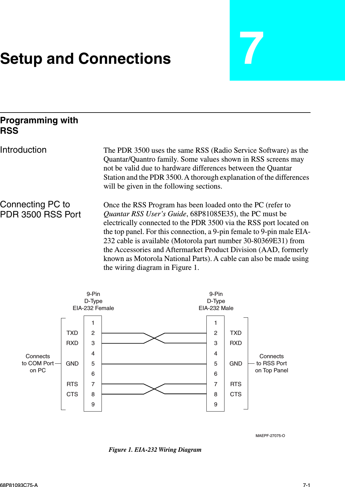
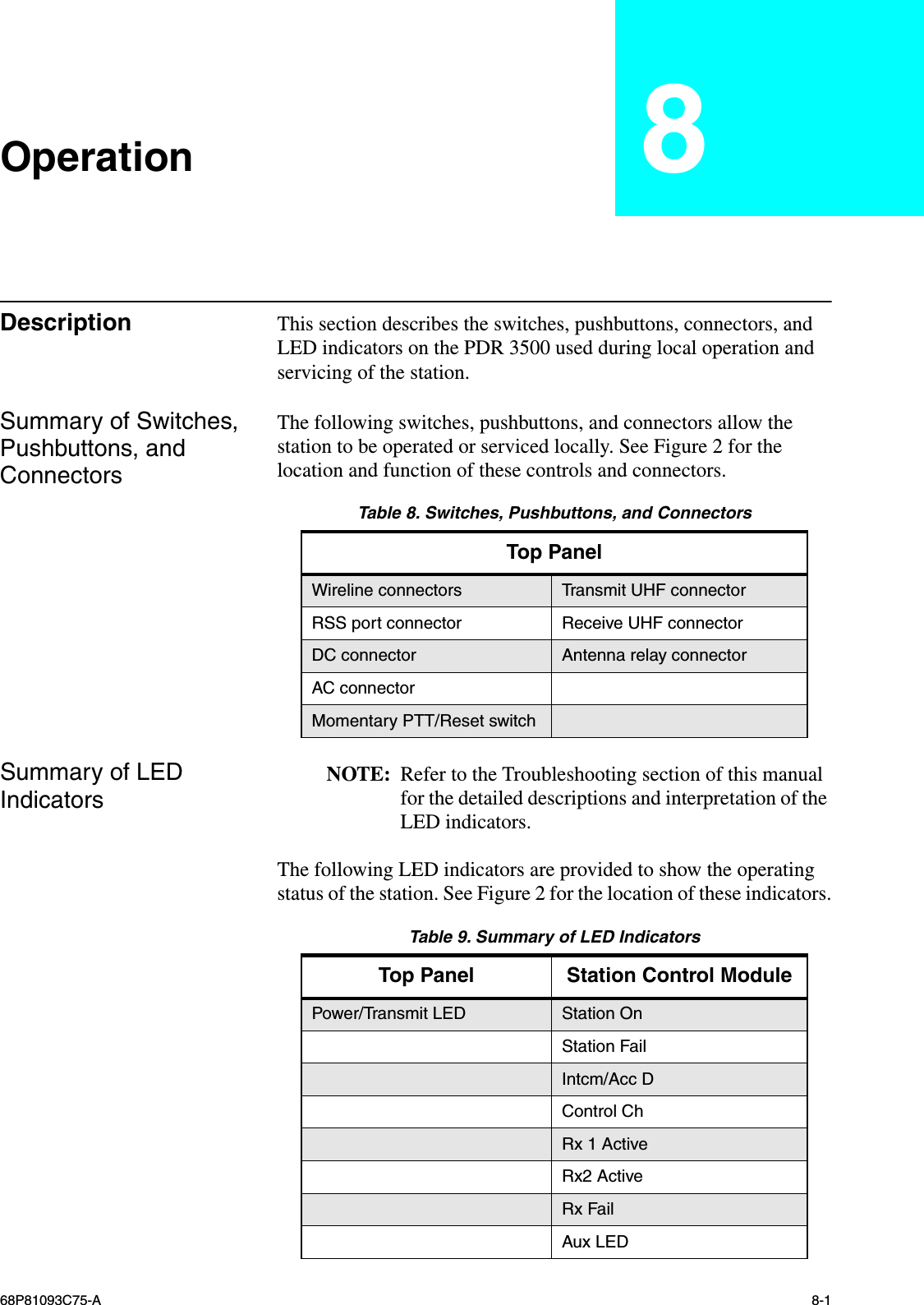
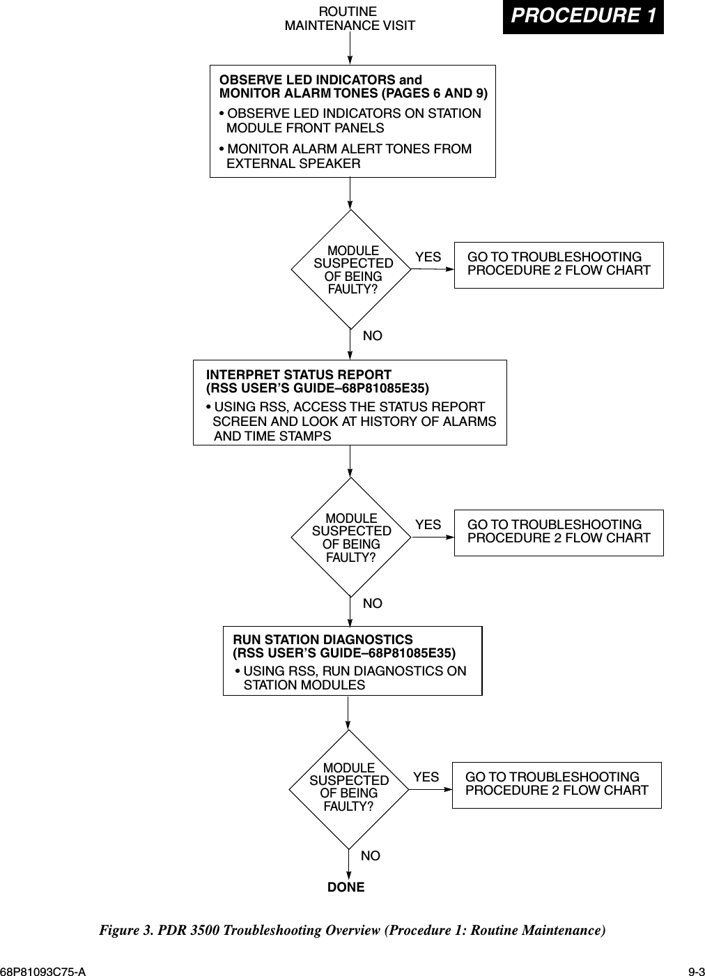
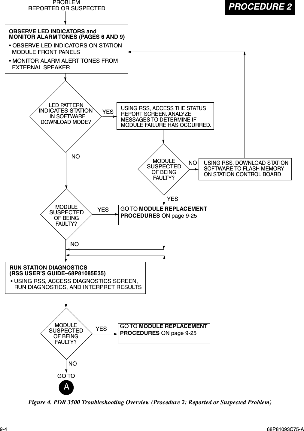
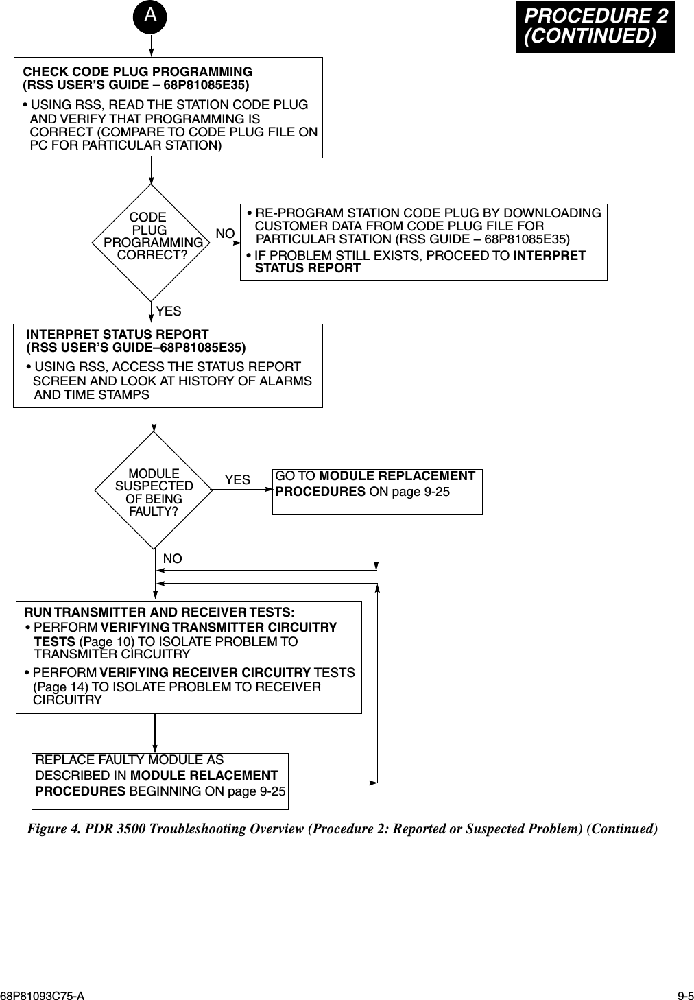
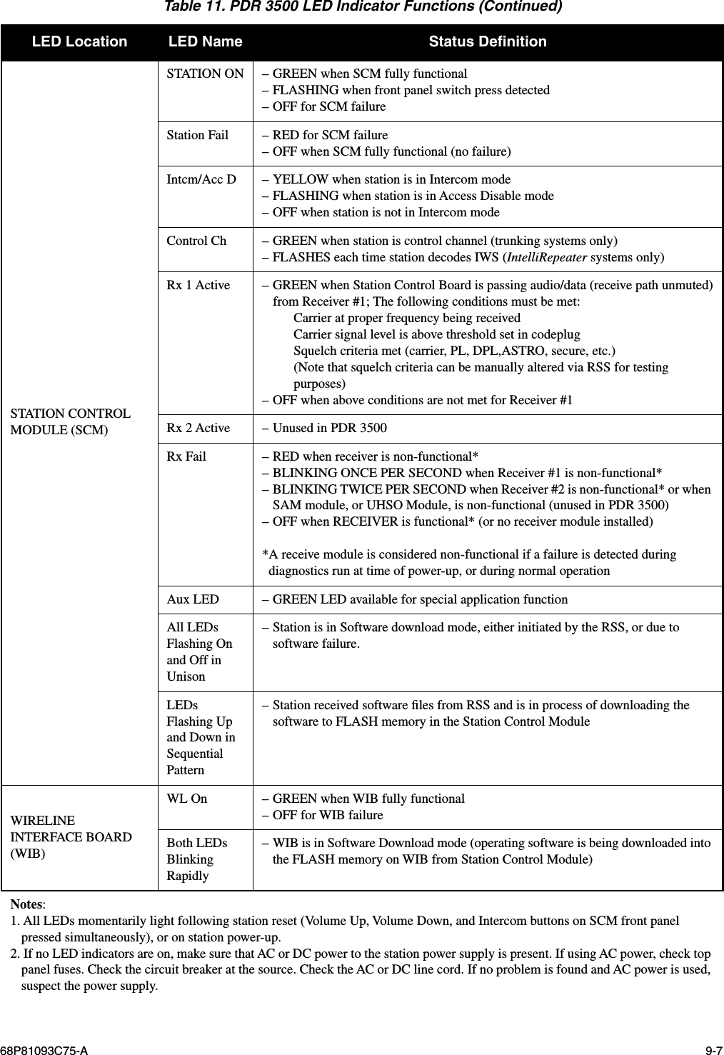
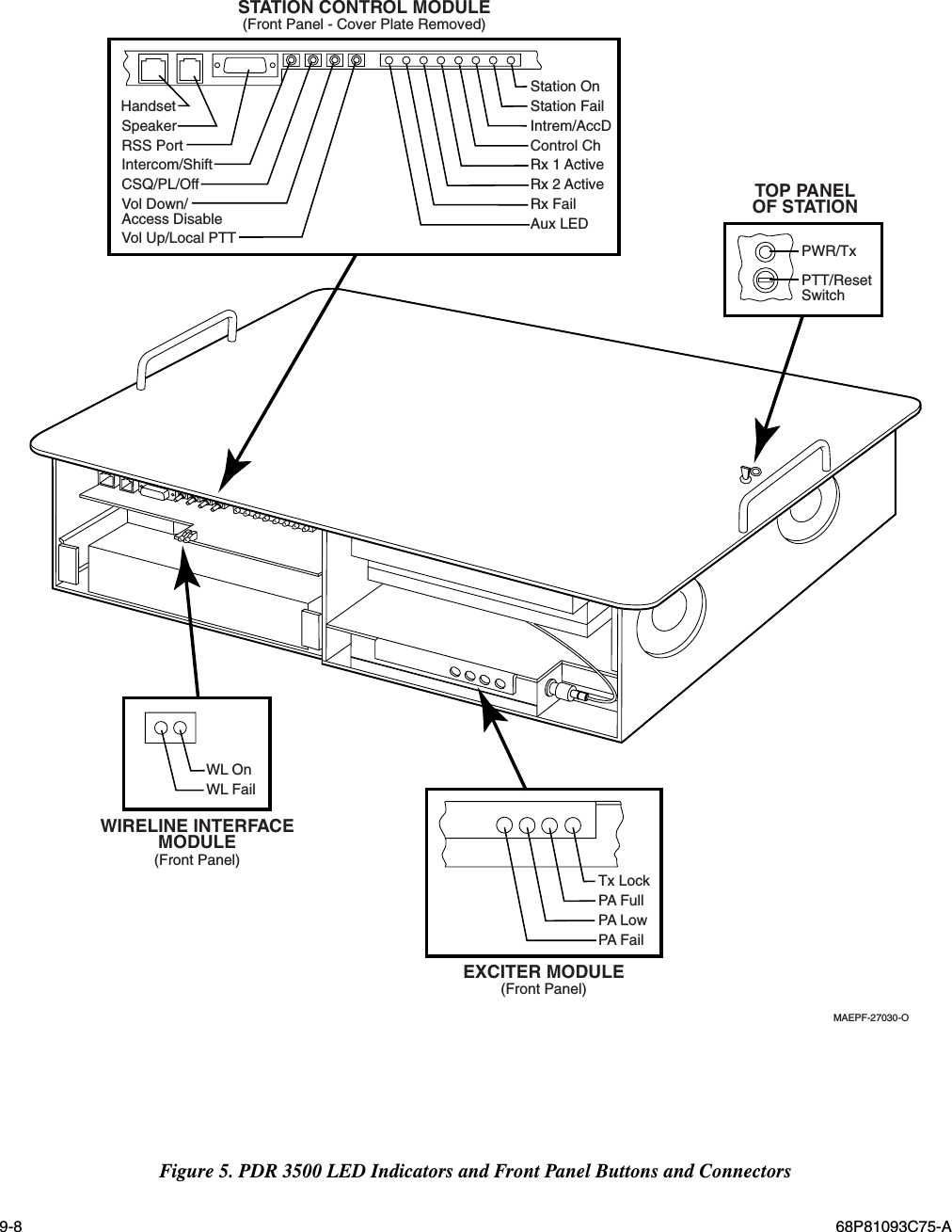
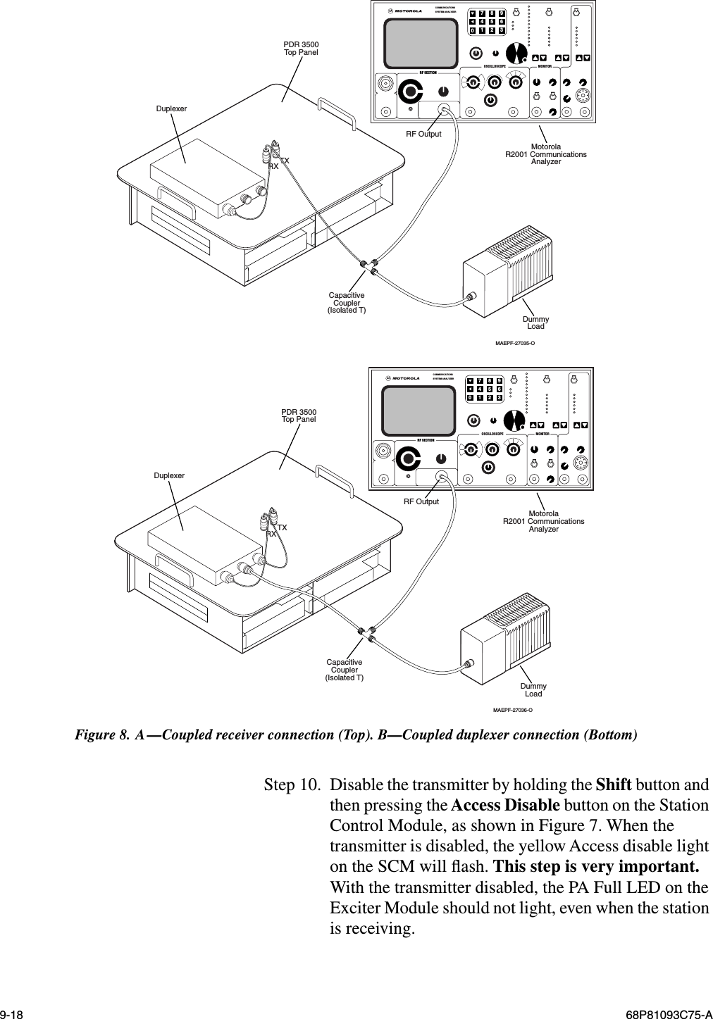
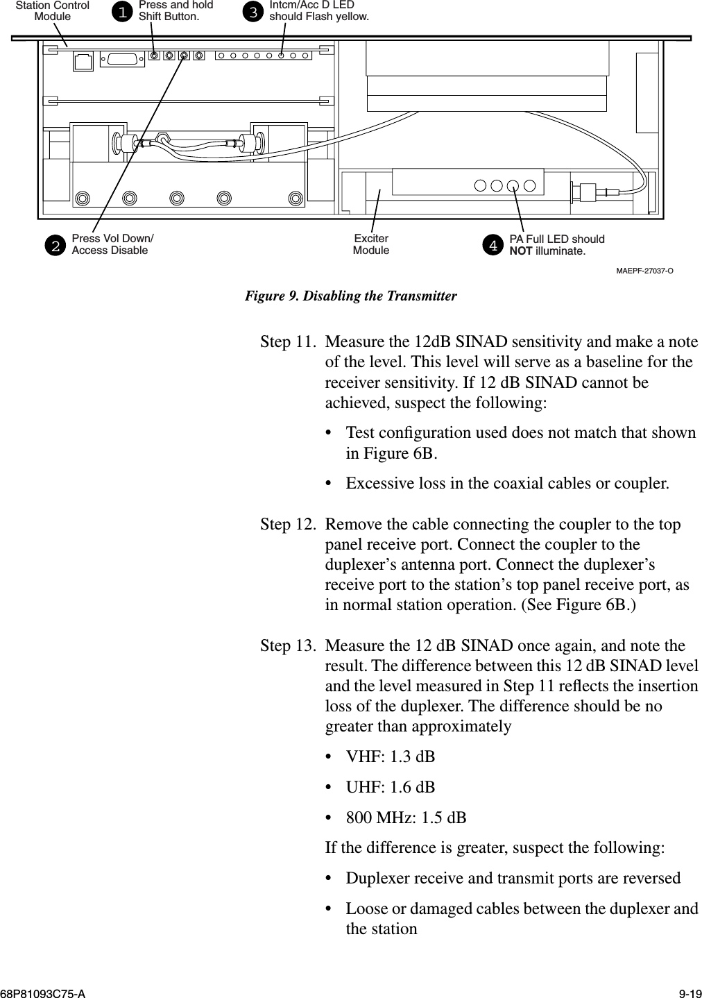
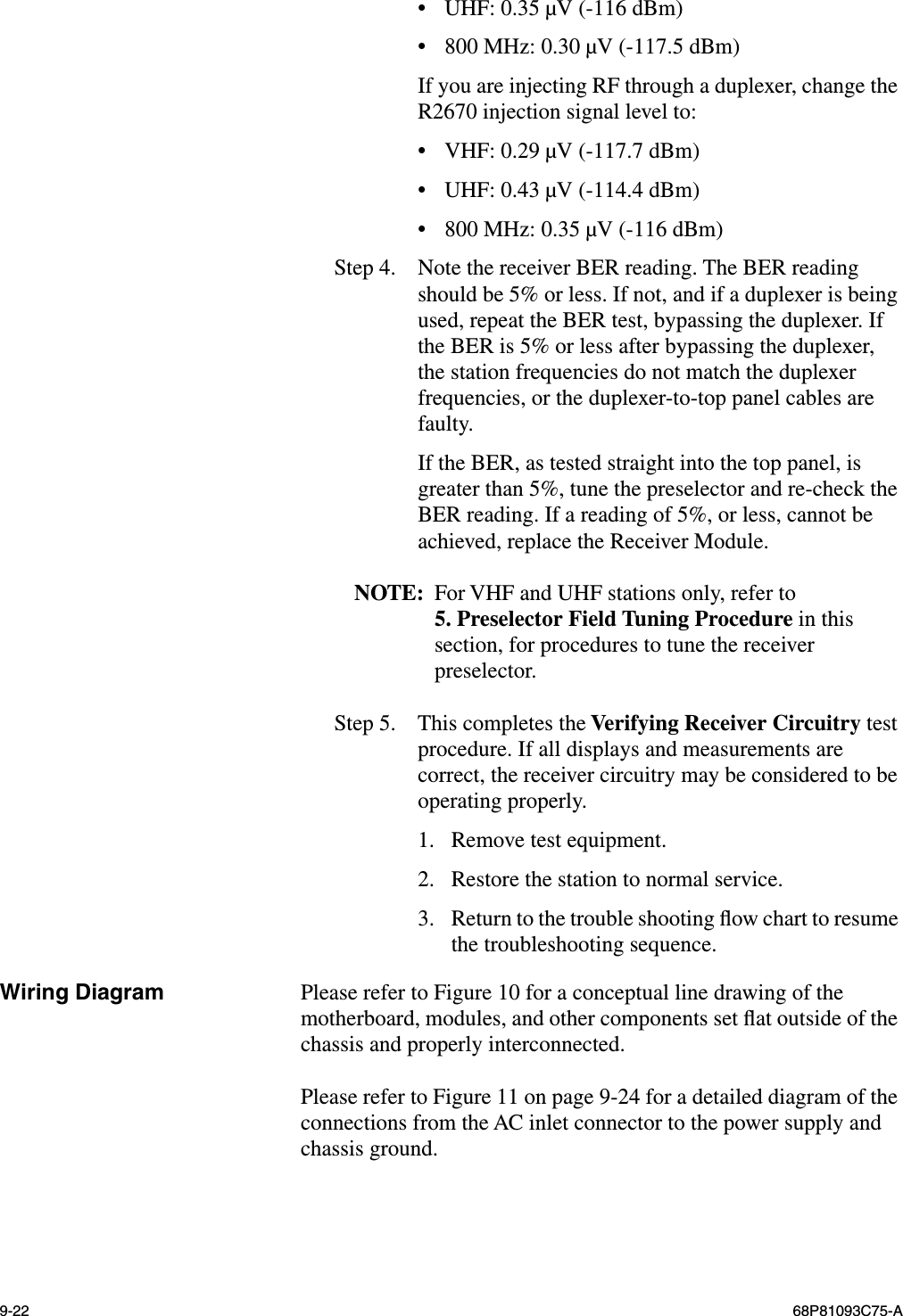
![68P81093C75-A 9-9 Interpreting Alarm Alert Tones Introduction Four station alarm conditions are reported with audio alert tones which are routed to the external speaker connector (RJ-11) on the front of the control module. (Pin 4 on the RJ-11 is Speaker High; Pin 1 is Speaker Ground.) The alarms are also entered into the alarm log which can be accessed using the RSS. Refer to the RSS User’s Guide , part number 68P81085E35. NOTE: The alarm tones may also be routed to the console (via the wireline) and transmitted over the air. Refer to the RSS User’s Guide (part number 68P81085E35) for details on enabling or disabling these two alarm routing options.The four alarm conditions are represented by a series of alarm tones, from a single beep, to four beeps. Each beep is a 1200 Hz tone, lasting 125 msec. The alarm tones occur during a repeating 10 second window, with two seconds between successive alarms (when more than one alarm is active). The following two examples illustrate the timing of the alarm tones.The alarm tone definitions are as follows:Example 1: Single Alarm (#3)beep...beep....beep.................................................................................................[repeats]Alarm #310 Second WindowExample 2: Multiple Alarms (#1 and #4)beep... ........................beep....beep ... beep ....beep ................................................[repeats]2 secondsAlarm #1 Alarm #410 Second Window Number of BeepsAlarm Condition Name Alarm Condition Description 1Battery Revert Alarm is reported when low DC voltage is detected by the station. (Threshold depends on station Tx frequency band.) Alarm is cleared when DC voltage returns to normal.2 PA Fail Alarm is reported when PA fails to keyup to full ouput power. Alarm is cleared upon successful keyup to full power.3 Synthesizer Alarm is reported when either Tx or Rx synthesizers fail to lock. Alarm is cleared when both sythesizers lock.4 Overvoltage Should not occur in PDR 3500.](https://usermanual.wiki/Motorola-Solutions/92FT5809/User-Guide-224451-Page-40.png)