Motorola MVME6100 V6100a_pg1 User Manual To The 0b0d8c82 75d8 4d65 B393 0e62836460c9
User Manual: Motorola MVME6100 to the manual
Open the PDF directly: View PDF ![]() .
.
Page Count: 57
- Contents
- List of Figures
- List of Tables
- About This Guide
- Board Description and Memory Maps
- Introduction
- Overview
- Memory Maps
- Default Processor Memory Map
- MOTLoad’s Processor Memory Map
- Default PCI Memory Map
- MOTLoad’s PCI Memory Maps
- VME Memory Map
- System I/O Memory Map
- System Status Register 1
- System Status Register 2
- System Status Register 3
- Presence Detect Register
- Configuration Header/Switch Register (S1)
- Time Base Enable Register
- Quad Universal Asynchronous Receiver/Transmitter (UART)
- Real-Time Clock and NVRAM
- Programming Details
- Introduction
- MV64360 Multi-Purpose Port Configuration
- MV64360 Reset Configuration
- Flash Memory
- Real-Time Clock and NVRAM
- Two-Wire Serial Interface
- DDR DRAM Serial Presence Detect
- MV64360 Initialization
- VPD and User Configuration EEPROMs
- Temperature Sensor
- MV64360 Device Controller Bank Assignments
- MPC Bus and PCI Bus Arbitration
- PCI Bus 0 and PCI Bus 1 Local Buses
- MV64360 Interrupt Controller
- MV64360 Endian Issues
- Related Documentation
- Index
MVME6100
Single-Board Computer
Programmer’s Reference
Guide
V6100A/PG1
July 2004 Edition
© Copyright 2004 Motorola Inc.
All rights reserved.
Printed in the United States of America.
Motorola and the stylized M logo are trademarks of Motorola, Inc., registered in the U.S.
Patent and Trademark Office.
All other product or service names mentioned in this document are the property of their
respective owners.

Safety Summary
The following general safety precautions must be observed during all phases of operation, service, and repair of
this equipment. Failure to comply with these precautions or with specific warnings elsewhere in this manual
could result in personal injury or damage to the equipment.
The safety precautions listed below represent warnings of certain dangers of which Motorola is aware. You, as
the user of the product, should follow these warnings and all other safety precautions necessary for the safe
operation of the equipment in your operating environment.
Ground the Instrument.
To minimize shock hazard, the equipment chassis and enclosure must be connected to an electrical ground. If the
equipment is supplied with a three-conductor AC power cable, the power cable must be plugged into an approved
three-contact electrical outlet, with the grounding wire (green/yellow) reliably connected to an electrical ground
(safety ground) at the power outlet. The power jack and mating plug of the power cable meet International
Electrotechnical Commission (IEC) safety standards and local electrical regulatory codes.
Do Not Operate in an Explosive Atmosphere.
Do not operate the equipment in any explosive atmosphere such as in the presence of flammable gases or fumes.
Operation of any electrical equipment in such an environment could result in an explosion and cause injury or
damage.
Keep Away From Live Circuits Inside the Equipment.
Operating personnel must not remove equipment covers. Only Factory Authorized Service Personnel or other
qualified service personnel may remove equipment covers for internal subassembly or component replacement
or any internal adjustment. Service personnel should not replace components with power cable connected. Under
certain conditions, dangerous voltages may exist even with the power cable removed. To avoid injuries, such
personnel should always disconnect power and discharge circuits before touching components.
Use Caution When Exposing or Handling a CRT.
Breakage of a Cathode-Ray Tube (CRT) causes a high-velocity scattering of glass fragments (implosion). To
prevent CRT implosion, do not handle the CRT and avoid rough handling or jarring of the equipment. Handling
of a CRT should be done only by qualified service personnel using approved safety mask and gloves.
Do Not Substitute Parts or Modify Equipment.
Do not install substitute parts or perform any unauthorized modification of the equipment. Contact your local
Motorola representative for service and repair to ensure that all safety features are maintained.
Observe Warnings in Manual.
Warnings, such as the example below, precede potentially dangerous procedures throughout this manual.
Instructions contained in the warnings must be followed. You should also employ all other safety precautions
which you deem necessary for the operation of the equipment in your operating environment.
Warning
War ni ng To prevent serious injury or death from dangerous voltages, use extreme
caution when handling, testing, and adjusting this equipment and its
components.

Flammability
All Motorola PWBs (printed wiring boards) are manufactured with a flammability rating
of 94V-0 by UL-recognized manufacturers.
EMI Caution
!
Caution
Caution This equipment generates, uses and can radiate electromagnetic energy. It
may cause or be susceptible to electromagnetic interference (EMI) if not
installed and used with adequate EMI protection.
Lithium Battery Caution
This product contains a lithium battery to power the clock and calendar circuitry.
!
Caution
Caution Danger of explosion if battery is replaced incorrectly. Replace battery only
with the same or equivalent type recommended by the equipment
manufacturer. Dispose of used batteries according to the manufacturer’s
instructions.
Attention
!
Caution Il y a danger d’explosion s’il y a remplacement incorrect de la batterie.
Remplacer uniquement avec une batterie du même type ou d’un type
équivalent recommandé par le constructeur. Mettre au rebut les batteries
usagées conformément aux instructions du fabricant.
Vorsicht
!
Caution Explosionsgefahr bei unsachgemäßem Austausch der Batterie. Ersatz nur
durch denselben oder einen vom Hersteller empfohlenen Typ. Entsorgung
gebrauchter Batterien nach Angaben des Herstellers.

CE Notice (European Community)
!
Warning
War ni ng This is a Class A product. In a domestic environment, this product may
cause radio interference, in which case the user may be required to take
adequate measures.
Motorola Computer Group products with the CE marking comply with the EMC Directive
(89/336/EEC). Compliance with this directive implies conformity to the following
European Norms:
EN55022 “Limits and Methods of Measurement of Radio Interference Characteristics
of Information Technology Equipment”; this product tested to Equipment Class A
EN55024 “Information technology equipment—Immunity characteristics—Limits and
methods of measurement”
Board products are tested in a representative system to show compliance with the above
mentioned requirements. A proper installation in a CE-marked system will maintain the
required EMC performance.
In accordance with European Community directives, a “Declaration of Conformity” has
been made and is available on request. Please contact your sales representative.
Notice
While reasonable efforts have been made to assure the accuracy of this document,
Motorola, Inc. assumes no liability resulting from any omissions in this document, or from
the use of the information obtained therein. Motorola reserves the right to revise this
document and to make changes from time to time in the content hereof without obligation
of Motorola to notify any person of such revision or changes.
Electronic versions of this material may be read online, downloaded for personal use, or
referenced in another document as a URL to the Motorola Computer Group Web site. The
text itself may not be published commercially in print or electronic form, edited, translated,
or otherwise altered without the permission of Motorola, Inc.
It is possible that this publication may contain reference to or information about Motorola
products (machines and programs), programming, or services that are not available in your
country. Such references or information must not be construed to mean that Motorola
intends to announce such Motorola products, programming, or services in your country.
Limited and Restricted Rights Legend
If the documentation contained herein is supplied, directly or indirectly, to the U.S.
Government, the following notice shall apply unless otherwise agreed to in writing by
Motorola, Inc.
Use, duplication, or disclosure by the Government is subject to restrictions as set forth in
subparagraph (b)(3) of the Rights in Technical Data clause at DFARS 252.227-7013 (Nov.
1995) and of the Rights in Noncommercial Computer Software and Documentation clause
at DFARS 252.227-7014 (Jun. 1995).
Motorola, Inc.
Computer Group
2900 South Diablo Way
Tempe, Arizona 85282

vii
About This Guide
Overview of Contents ................................................................................................xiv
Comments and Suggestions ......................................................................................xiv
Conventions Used in This Manual .............................................................................xv
CHAPTER 1 Board Description and Memory Maps
Introduction .............................................................................................................. 1-1
Overview .................................................................................................................. 1-1
Memory Maps .......................................................................................................... 1-5
Default Processor Memory Map ....................................................................... 1-5
MOTLoad’s Processor Memory Map ............................................................... 1-7
Default PCI Memory Map ................................................................................ 1-8
MOTLoad’s PCI Memory Maps ....................................................................... 1-9
VME Memory Map ........................................................................................... 1-9
System I/O Memory Map ................................................................................. 1-9
System Status Register 1 ................................................................................. 1-11
System Status Register 2 ................................................................................. 1-13
System Status Register 3 ................................................................................. 1-15
Presence Detect Register ................................................................................. 1-16
Configuration Header/Switch Register (S1) ................................................... 1-17
Time Base Enable Register ............................................................................. 1-19
Quad Universal Asynchronous Receiver/Transmitter (UART) ....................... 1-19
Real-Time Clock and NVRAM ...................................................................... 1-20
CHAPTER 2 Programming Details
Introduction .............................................................................................................. 2-1
MV64360 Multi-Purpose Port Configuration .......................................................... 2-1
MV64360 Reset Configuration ................................................................................ 2-3
Flash Memory .......................................................................................................... 2-8
Real-Time Clock and NVRAM ................................................................................ 2-8
Two-Wire Serial Interface ........................................................................................ 2-9
DDR DRAM Serial Presence Detect ..................................................................... 2-10
MV64360 Initialization .......................................................................................... 2-11
VPD and User Configuration EEPROMs .............................................................. 2-11
Contents

viii
Temperature Sensor ................................................................................................2-11
MV64360 Device Controller Bank Assignments ...................................................2-11
MPC Bus and PCI Bus Arbitration .........................................................................2-12
PCI Bus 0 and PCI Bus 1 Local Buses ...................................................................2-12
PCI Mode/Frequency Selection .......................................................................2-12
PCI Configuration Space .................................................................................2-13
PCI Arbitration Assignments for MV64360 ASIC .........................................2-14
PCI Bus 1 Local Bus PMC Expansion Slots ...................................................2-14
PCI Bus 0 Local Bus Devices .........................................................................2-15
Tsi148 ASIC ............................................................................................. 2-15
PCI6520 PMCSpan Bridge ......................................................................2-15
MV64360 Interrupt Controller ...............................................................................2-16
MV64360 Endian Issues .........................................................................................2-18
APPENDIX A Related Documentation
Motorola Computer Group Documents ...................................................................A-1
Manufacturers’ Documents ..................................................................................... A-2
Related Specifications ............................................................................................. A-5


xi
Table 1-1. MVME6100 Features Summary ............................................................ 1-2
Table 1-2. Default Processor Address Map ............................................................. 1-5
Table 1-3. MOTLoad’s Processor Address Map ..................................................... 1-7
Table 1-4. Default PCI Address Map ...................................................................... 1-8
Table 1-5. MOTLoad’s PCI Memory Maps ............................................................ 1-9
Table 1-6. Device Bank 1 I/O Memory Map ......................................................... 1-10
Table 1-7. System Status Register 1 ...................................................................... 1-11
Table 1-8. System Status Register 2 ...................................................................... 1-13
Table 1-9. System Status Register 3 ...................................................................... 1-15
Table 1-10. Presence Detect Register .................................................................... 1-16
Table 1-11. Configuration Header/Switch Register .............................................. 1-17
Table 1-12. TBEN Register ................................................................................... 1-19
Table 1-13. M48T37V Access .............................................................................. 1-20
Table 2-1. MV64360 MPP Pin Function Assignments ........................................... 2-2
Table 2-2. MV64360 Power-Up Configuration Settings ......................................... 2-4
Table 2-3. M48T37V Access .................................................................................. 2-9
Table 2-4. I2C Bus Device Addressing ................................................................. 2-10
Table 2-5. Device Bank Assignments ................................................................... 2-12
Table 2-6. IDSEL Mapping for PCI Devices ........................................................ 2-13
Table 2-7. PCI Arbitration Assignments for MV64360 ASIC .............................. 2-14
Table 2-8. MV64360 Interrupt Assignments ......................................................... 2-16
Table A-1. Motorola Computer Group Documents ................................................A-1
Table A-2. Manufacturers’ Documents ...................................................................A-2
Table A-3. Related Specifications ...........................................................................A-5
List of Tables

xiii
About This Guide
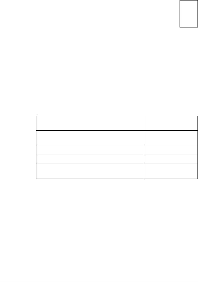
The MVME6100 Single-Board Computer Programmer’s Reference Guide
provides general programming information, including memory maps,
interrupts, and register data for the MVME6100 family of boards. This
document should be used by anyone who wants general, as well as
technical information about the MVME6100 products.
As of the printing date of this manual, the MVME6100 supports the
models listed below.
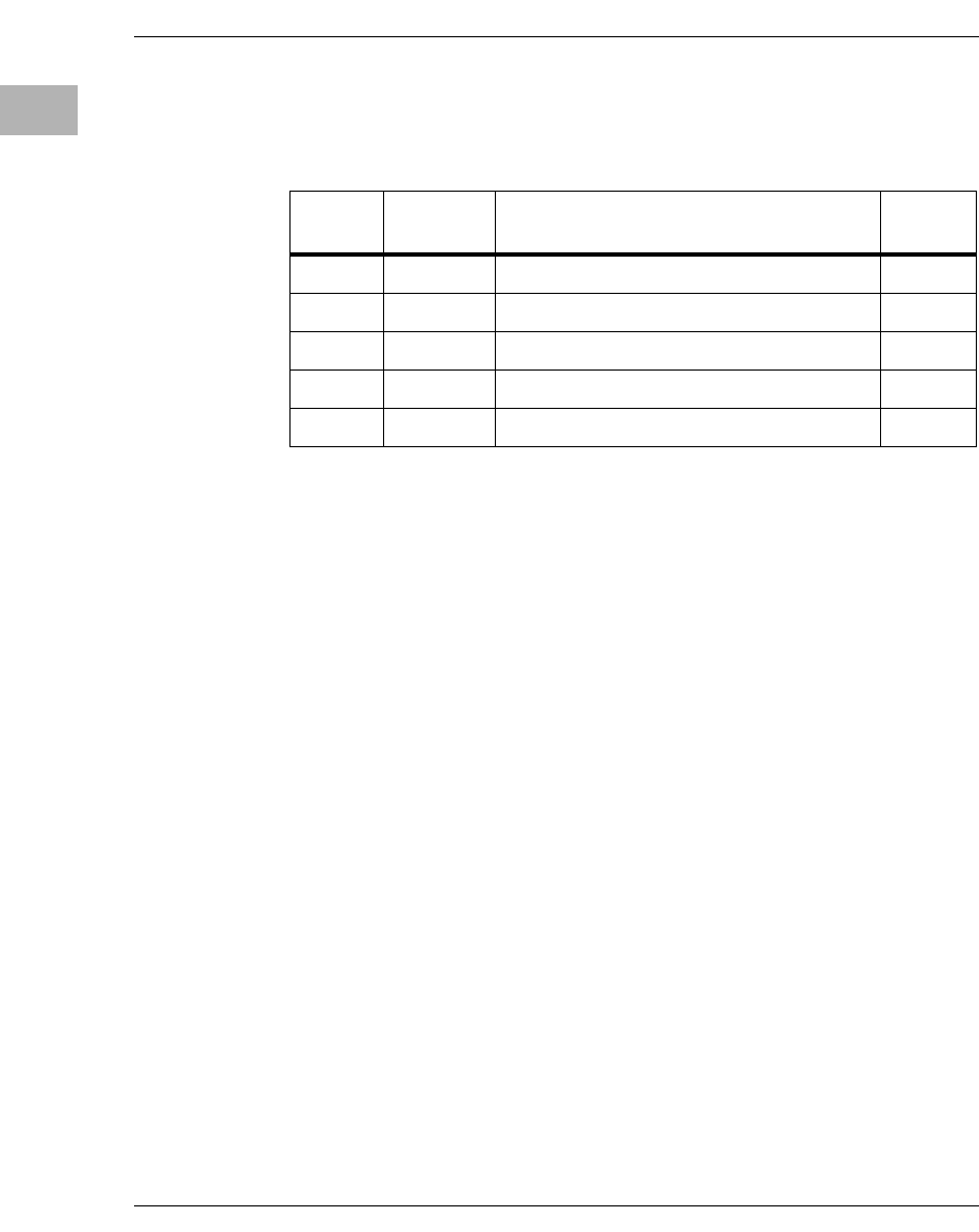
Model Number Description
MVME6100-0161 1.267 GHz MPC7457 processor, 512MB DDR
memory, 128MB Flash, Scanbe handles
MVME6100-0163 1.267 GHz MPC7457 processor, 512MB DDR
memory, 128MB Flash, IEEE handles
MVME6100-0171 1.267 GHz MPC7457 processor, 1GB DDR
memory, 128MB Flash, Scanbe handles
MVME6100-0173 1.267 GHz MPC7457 processor, 1GB DDR
memory, 128MB Flash, IEEE handles

xiv
Overview of Contents
This manual is divided into the following chapters and appendices:
Chapter 1, Board Description and Memory Maps, provides a brief product
description and a block diagram. The remainder of the chapter provides
information on memory maps and system and configuration registers.
Chapter 2, Programming Details, provides additional programming
information including IDSEL mapping, interrupt assignments for the
MV64360 interrupt controller, flash memory, two-wire serial interface
addressing, and other device and system considerations.
Appendix A, Related Documentation, provides a listing of related
Motorola manuals, vendor documentation, and industry specifications.
Comments and Suggestions
Motorola welcomes and appreciates your comments on its documentation.
We want to know what you think about our manuals and how we can make
them better. Mail comments to:
Motorola Computer Group
Reader Comments DW164
2900 S. Diablo Way
Tempe, Arizona 85282
You can also submit comments to the following e-mail address:
reader-comments@mcg.mot.com
In all your correspondence, please list your name, position, and company.
Be sure to include the title and part number of the manual and tell how you
used it. Then tell us your feelings about its strengths and weaknesses and
any recommendations for improvements.

xv
Conventions Used in This Manual
The following typographical conventions are used in this document:
bold
is used for user input that you type just as it appears; it is also used for
commands, options and arguments to commands, and names of
programs, directories and files.
italic
is used for names of variables to which you assign values, for function
parameters, and for structure names and fields. Italic is also used for
comments in screen displays and examples, and to introduce new
terms.
courier
is used for system output (for example, screen displays, reports),
examples, and system prompts.
<Enter>, <Return> or <CR>
represents the carriage return or Enter key.
Ctrl
represents the Control key. Execute control characters by pressing the
Ctrl key and the letter simultaneously, for example, Ctrl-d.

1-1
1
1Board Description and Memory
Maps
Introduction
This chapter briefly describes the board level hardware features of the
MVME6100 single-board computer, including a table of features and a
block diagram. The remainder of the chapter provides memory map
information including a default memory map, MOTLoad’s processor
memory map, a default PCI memory map, MOTLoad’s PCI memory map,
a PCI I/O memory map, and system I/O memory maps.
Note Programmable registers in the MV64360 system controller are
documented in a separate publication and obtainable from
Motorola Computer Group by contacting your Field Area
Engineer. Refer to Appendix A, Related Documentation, for
more information on obtaining this documentation.
Overview
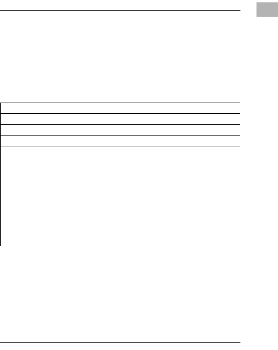
The MVME6100 is a single-board computer based on the PowerPC
MPC7457 processor, the Marvell MV64360 system controller, up to 2 GB
of ECC-protected DDR DRAM, up to 128MB of Flash memory, a dual
Gigabit Ethernet interface, two asynchronous serial ports, and two
IEEE1386.1 PCI, PCI-X capable mezzanine card slots (PMCs).

1-2 Computer Group Literature Center Web Site
Board Description and Memory Maps
1
The following table lists the features of the MVME6100.
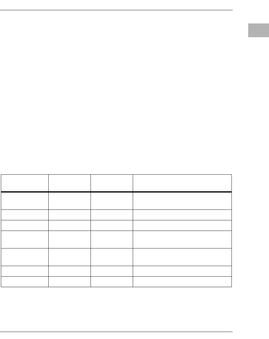
Table 1-1. MVME6100 Features Summary
Feature Description
Processor – Single 1.3 GHz MPC7457 processor
– Bus clock frequency at 133 MHz
– 36-bit address, 64-bit data buses
– Integrated L1 and L2 cache
L3 Cache – 2MB using DDR SRAM
– Bus clock frequency at 211 MHz
Flash – Two banks (A & B) of soldered Intel StrataFlash devices
– 8 to 64MB supported on each bank
– Boot bank is switch selectable between banks
– Bank A has combination of software and hardware write-protect
scheme
– Bank B top 1MB block can be write-protected through
software/hardware write-protect control
System Memory – Two banks on board for up to 2GB using 256Mb or 512Mb
devices
– Bus clock frequency at 133 MHz
Memory Controller
PCI Host Bridge
Dual 10/100/1000 Ethernet
Interrupt Controller
PCI Interface
I2C Interface
– Provided by Marvell MV64360 system controller
NVRAM
Real-Time Clock
Watchdog Timer
– 32KB provided by MK48T37
On-board Peripheral
Support – Dual 10/100/1000 Ethernet ports routed to front panel RJ-45
connectors, one optionally routed to P2 backplane
– Two asynchronous serial ports provided by an ST16C554D; one
serial port is routed to a front panel RJ-45 connector and the second
serial port is optionally routed to the P2 connector for rear I/O or
on-board header

Overview
http://www.motorola.com/computer/literature 1-3
1
PCI/PMC – Two 32/64-bit PMC slots with front-panel I/O plus P2 rear I/O as
specified by IEEE P1386
– 64-bit slots; 33/66 MHz PCI or 66/100 MHz PCI-X
VME Interface – Tsi148 VME 2Esst ASIC provides:
❏Eight programmable VMEbus map decoders
❏A16, A24, A32, and A64 address
❏8-bit, 16-bit, and 32-bit single cycle data transfers
❏8-bit, 16-bit, 32-bit, and 64-bit block transfers
❏Supports SCT, BLT, MBLT, 2eVME, and 2eSST protocols
❏8 entry command and 4KB data write post buffer
❏4KB read ahead buffer
PMCspan Support – One PMCspan slot
– Supports 33/66 MHz, 32/64-bit PCI bus
– Access through PCI6520 bridge to PMCspan
Form Factor – Standard 6U VME
Miscellaneous – Combined reset and abort switch
– Status LEDs
– 8-bit software-readable switch
– VME geographical address switch
Table 1-1. MVME6100 Features Summary (continued)
Feature Description
1-4 Computer Group Literature Center Web Site
Board Description and Memory Maps
1
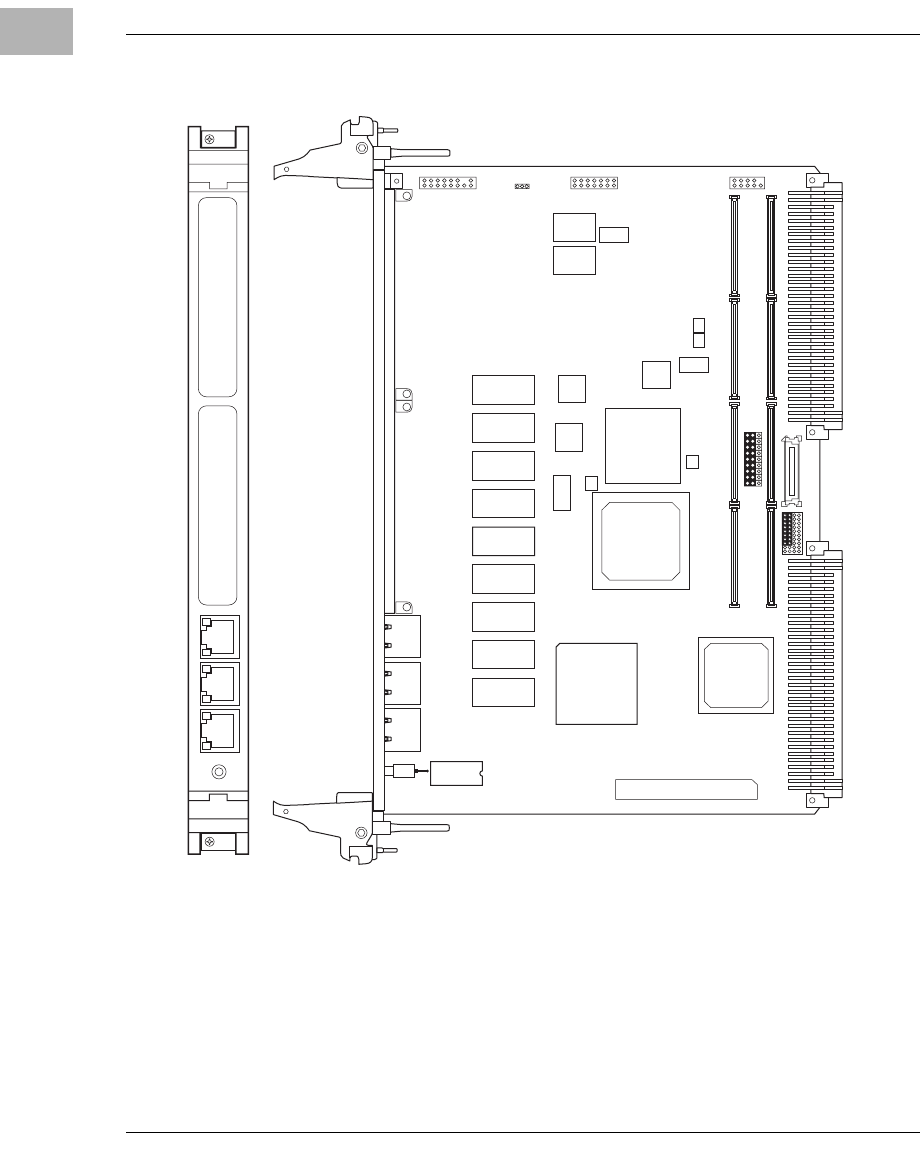
Figure 1-1. MVME6100 Board Layout Diagram
4248 0504
10/100/1000 DEBUG
ABT/RST
LAN 2LAN 1
J42 J8
J30
U20
J3
J19
J13 J14
J11 J12
J23 J24
J21 J22
P1
P2
U21
PCI MEZZANINE CARDPCI MEZZANINE CARD
J4
U12
10/100/1000
J93
J9
J29
U1
J7
PMC
IPMC
U32
U7
U6
U5
U3
U4
U11
U10
U9
U8 U13
U18
U14
U15
U22
U30
U19
U17
U16
U23
U27
U25
Memory Maps
http://www.motorola.com/computer/literature 1-5
1
Memory Maps
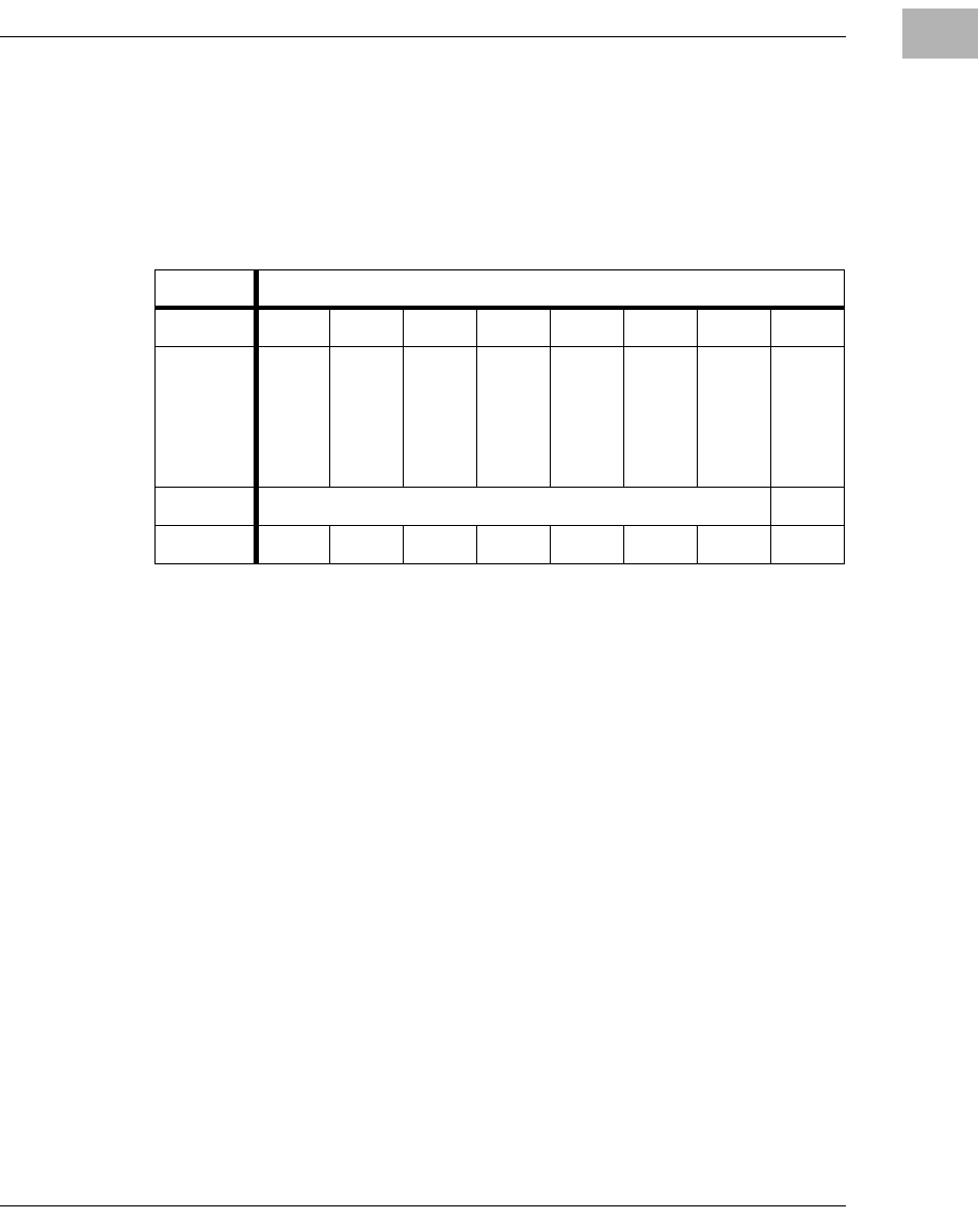
Default Processor Memory Map
The MV64360 presents a default CPU memory map following RESET
negation. The following table shows the default memory map from the
point of view of the processor. Address bits [35:32] are only relevant for
the MPC7457 extended address mode and are not shown in the following
tables. (Note that it is the same as the GT-64260A with the addition of
integrated SRAM.)
Table 1-2. Default Processor Address Map
Processor Address
Size Definition
Notes
Start End
0000 0000 007F FFFF 8M DRAM Bank 0
0080 0000 00FF FFFF 8M DRAM Bank 1
0100 0000 017F FFFF 8M DRAM Bank 2
0180 0000 01FF FFFF 8M DRAM Bank 3
0200 0000 0FFF FFFF 224M Unassigned
1000 0000 11FF FFFF 32M PCI Bus 0 I/O Space
1200 0000 13FF FFFF 32M PCI Bus 0 Memory Space 0
1400 0000 1BFF FFFF 128M Unassigned
1C00 0000 1C7F FFFF 8M Device CS0*
1C80 0000 1CFF FFFF 8M Device CS1*
1D00 0000 1DFF FFFF 16M Device CS2*
1E00 0000 1FFF FFFF 32M Unassigned
2000 0000 21FF FFFF 32M PCI Bus 1 I/O
2200 0000 23FF FFFF 32M PCI Bus 1 Memory Space 0
2400 0000 25FF FFFF 32M PCI Bus 1 Memory Space 1
2600 0000 27FF FFFF 32M PCI Bus 1 Memory Space 2

1-6 Computer Group Literature Center Web Site
Board Description and Memory Maps
1
Note Set by configuration resistors.
2800 0000 29FF FFFF 32M PCI Bus 1 Memory Space 3
2A00 0000 41FF FFFF 384M Unassigned
4200 0000 4303 FFFF 256K MV64360 Integrated SRAM
4304 0000 F0FF FFFF 2783M Unassigned
F100 0000 F100 FFFF 64K Internal Registers See
Note
F101 0000 F1FF FFFF 16M-64K Unassigned
F200 0000 F3FF FFFF 32M PCI Bus 0 Memory Space 1
F400 0000 F5FF FFFF 32M PCI Bus 0 Memory Space 2
F600 0000 F7FF FFFF 32M PCI Bus 0 Memory Space 3
F800 0000 FEFF FFFF 112M Unassigned
FF00 0000 FF7F FFFF 8M Device CS3*
FC00 0000 FFFF FFFF 64M Boot Flash (Bank A or B
depending on S4:3 switch
setting)
Table 1-2. Default Processor Address Map (continued)
Processor Address
Size Definition
Notes
Start End
MOTLoad’s Processor Memory Map
http://www.motorola.com/computer/literature 1-7
1
MOTLoad’s Processor Memory Map
MOTLoad’s processor memory map is given in the following table.
Note The internal registers only occupy the first 64KB, but minimum
address decoding resolution is 1MB.
Table 1-3. MOTLoad’s Processor Address Map
Processor Address
Size Definition NotesStart End
0000 0000 top_dram-1 dram_size System Memory (onboard DRAM)
8000 0000 DFFF FFFF 1536M PCI Bus 0 and/or VME Memory
Space
E000 0000 EFFF FFFF 256M PCI Bus 1 Memory Space
F000 0000 F07F FFFF 8M PCI Bus 1 I/O Space
F080 0000 F0FF FFFF 8M PCI Bus 0 I/O Space
F100 0000 F10F FFFF 1M MV64360 Internal Registers See
Note
F110 0000 F11F FFFF 1M Device CS1* I/O
System
Regs/NVRAM/RTC/UARTs
F400 0000 F7FF FFFF 64M Device CS0* Flash Bank A
F800 0000 FBFF FFFF 64M Device Boot Flash Bank B

1-8 Computer Group Literature Center Web Site
Board Description and Memory Maps
1
Default PCI Memory Map
The MV64360 presents the following default PCI memory map after
RESET negation. Note: it is the same as the GT-64260A with the addition
of integrated SRAM.
Table 1-4. Default PCI Address Map
PCI Address
Size DefinitionStart End
0000 0000 007F FFFF 8M DRAM Bank 0
0080 0000 00FF FFFF 8M DRAM Bank 1
0100 0000 017F FFFF 8M DRAM Bank 2
0180 0000 01FF FFFF 8M DRAM Bank 3
0200 0000 0FFF FFFF 224M Unassigned
1000 0000 11FF FFFF 32M PCI Bus 1 P2P I/O Space
1200 0000 13FF FFFF 32M PCI Bus 1 P2P Memory Space 0
1400 0000 1400 FFFF 64K Internal Registers
1401 0000 1BFF FFFF 128M-64K Unassigned
1C00 0000 1C7F FFFF 8M Device CS0*
1C80 0000 1CFF FFFF 8M Device CS1*
1D00 0000 1DFF FFFF 16M Device CS2*
1E00 0000 1FFF FFFF 32M Unassigned
2000 0000 21FF FFFF 32M PCI Bus 0 P2P I/O Space
2200 0000 23FF FFFF 32M PCI Bus 0 P2P Memory Space 0
2400 0000 25FF FFFF 32M PCI Bus 0 P2P Memory Space 1
2600 0000 41FF FFFF 448M Unassigned
4200 0000 4303 FFFF 256K MV64360 Integrated SRAM
4304 0000 F1FF FFFF 2800M Unassigned
MOTLoad’s PCI Memory Maps
http://www.motorola.com/computer/literature 1-9
1
MOTLoad’s PCI Memory Maps
MOTLoad’s PCI memory map for each PCI domain is shown in the
following tables.
VME Memory Map
The MVME6100 is fully capable of supporting both the PReP and the
CHRP VME Memory Map examples with RAM size limited to 2 GB.
System I/O Memory Map
System resources including system control and status registers,
NVRAM/RTC, and the 16550 UART are mapped into a 1 MB address
F200 0000 F3FF FFFF 32M PCI Bus 1 P2P Memory Space 1
F400 0000 FEFF FFFF 176M Unassigned
FF00 0000 FF7F FFFF 8M Device CS3*
FC00 0000 FFFF FFFF 64M Boot Flash Bank B
Table 1-4. Default PCI Address Map (continued)
PCI Address
Size DefinitionStart End
Table 1-5. MOTLoad’s PCI Memory Maps
PCI Address
Size DefinitionStart End
0000 0000 top_dram dram_size System Memory (onboard
DRAM)

1-10 Computer Group Literature Center Web Site
Board Description and Memory Maps
1
range assigned to Device Bank 1. The memory map is defined in the
following table:
Table 1-6. Device Bank 1 I/O Memory Map
Address Definition
F110 0000 System Status Register 1
F110 0001 System Status Register 2
F110 0002 System Status Register 3
F110 0003 Reserved
F110 0004 Presence Detect Register
F110 0005 Software Readable Header/Switch
F110 0006 Timebase Enable Register
F110 0008 -F110 FFFF Reserved for onboard registers
F111 0000 -F111 7FFF M48T37V NVRAM/RTC
F112 0000 -F112 0FFF COM 1 UART
F112 1000 -F112 0FFF COM 2 UART
F112 2000 -F112 0FFF Reserved (undefined)
F112 3000 -F11F FFFF Reserved (undefined)
System Status Register 1
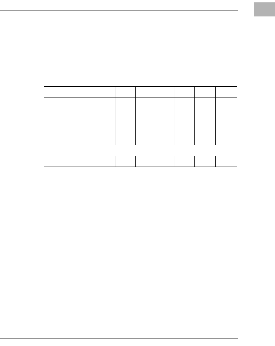
http://www.motorola.com/computer/literature 1-11
1
System Status Register 1
The MVME6100 board System Status Register 1 is a read-only register
used to provide board status information.
REF_CLK
Reference clock. This bit reflects the current state of the 28.8 KHz
reference clock derived from the 1.8432 MHz UART oscillator divided
by 64. This clock may be used as a fixed timing reference.
BANK_SEL
Boot Flash bank select. This bit reflects the current state of the boot
Flash bank select jumper. A cleared condition indicates that Flash bank
A is the boot bank. A set condition indicates that Flash B is the boot
bank.
SAFE_START
ENV safe start. This bit reflects the current state of the ENV safe start
select jumper. A set condition indicates that MOTLoad should provide
the user the capability to select which Boot Image is used to boot the
board, cleared MOTLoad should proceed with the first boot image
found.
Table 1-7. System Status Register 1
REG System Status Register 1- 0xF1100000
BIT 7654321 0
FIELD
REF_CLK
BANK_SELECT
SAFE_START
ABORT_L
FLASH_BSY_L
FUSE_STAT
SROM_INIT
RSVD
OPER R
RESET XXXX1 1 X 0

1-12 Computer Group Literature Center Web Site
Board Description and Memory Maps
1
ABORT_L
Abort. This bit reflects the current state of the onboard abort signal.
This is a debounced version of the abort switch and may be used to
determine the state of the abort switch. A set condition indicates that
the abort switch is not depressed while a cleared condition would
indicate that the abort switch is asserted.
FLASH_BSY_L
FLASH Busy. This bit provides the current state of the Flash Bank A
StrataFlash device Status pins. These two open drain output pins are
wire ORed. Refer to the appropriate Intel StrataFlash data sheet for a
description on the function of the Status pin.
FUSE_STAT
Fuse Status. This bit indicates the status of the onboard fuses. A
cleared condition indicates that one of the fuses is open. A set
condition indicates that all fuses are functional.
SROM_INIT
SROM Init. This bit indicates the status of the SROM Init. A cleared
condition indicates that the SROM Init is disabled. A set condition
indicates that the SROM Init is enabled and the MV64360 was
initialized using the MV64360 User Defined Initialization SROM at
$A6.

System Status Register 2
http://www.motorola.com/computer/literature 1-13
1
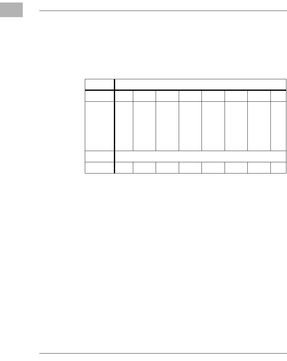
System Status Register 2
The MVME6100 board system status register 2 provides board control and
status bits.
BD_FAIL
Board Fail. This bit is used to control the Board Fail LED located on
the front panel. A set condition illuminates the front panel LED and a
cleared condition extinguishes the front panel LED.
EEPROM_WP
Not used on the MVME6100.
FLASHA_WP
Software Flash Bank A Write Protect. This bit is to provide software-
controlled protection against inadvertent writes to the expansion
FLASH memory devices. Clearing this bit and disabling the HW
write-protect will enable writes to the Bank A Flash devices. This bit
is set during reset and must be reset by the system software to enable
writing of the flash devices.
Table 1-8. System Status Register 2
REG System Status Register 2- 0xF1100001
BIT 76543210
FIELD
BD_FAIL
EEPROM_WP
(NOT USED)
FLASHA_WP
TSTAT_MASK
FBOOTB_WP
FBA_WP_HDR
FBOOTB_WP_HDR
RSVD
OPER R/W R R/W R/W R/W R R R
RESET 11111XXX

1-14 Computer Group Literature Center Web Site
Board Description and Memory Maps
1
TSTAT_MASK
Thermostat Mask. This bit is used to mask the DS1621 temperature
sensor thermostat output. If this bit is cleared, the thermostat output
will be enabled to generate an interrupt on GPP3. If the bit is set, the
thermostat output is disabled from generating an interrupt.
FBOOTB_WP
Software Flash Bank B Boot Block Write Protect. This bit is to provide
software-controlled protection against inadvertent writes to the Flash
Bank B Top 1 MB (0xFFF00000) space. Clearing this bit and disabling
HW write-protect will enable writes to the Bank B Flash Top 1MB
boot block devices. This bit is set during reset and must be reset by the
system software to enable writing of the Flash Bank B boot block.
FBA_WP_HDR
Hardware Flash Bank A write protect header status. Read ONLY.
Hardware jumper configuration can not be overridden by the software
control bit 6 in this register.
FBOOTB_WP_HDR
Hardware Flash Bank B Boot Block write protect header status. Read
ONLY. Hardware jumper configuration can not be overridden by the
software control bit 3 in this register.

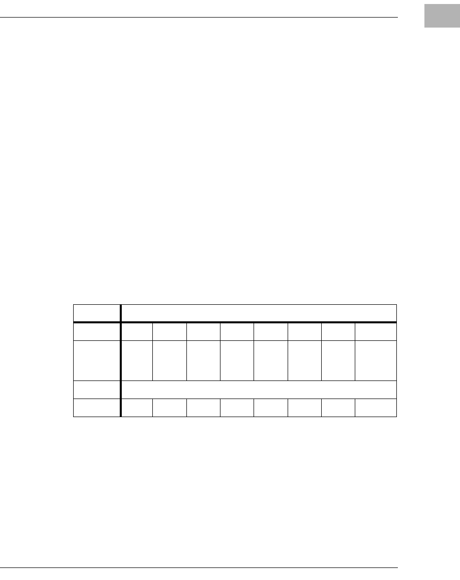
System Status Register 3
http://www.motorola.com/computer/literature 1-15
1
System Status Register 3
The MVME6100 board system status register 3 provides the board
software-controlled reset functions.
BOARD_RESET
Board Reset. Setting this bit will force a hard reset of the MVME6100
board. This bit will clear automatically when the board reset is
complete. This bit will always be cleared during a read.
Table 1-9. System Status Register 3
REG System Status Register 3- 0xF1100002
BIT 76543210
FIELD
BOARD_RESET
RSVD
RSVD
RSVD
RSVD
RSVD
RSVD
RSVD
OPER R/WRRRRRRR
RESET 00000000
1-16 Computer Group Literature Center Web Site
Board Description and Memory Maps
1
Presence Detect Register
The MVME5500 board contains a presence detect register that may be
read by the system software to determine the presence of optional devices.
IPMC_PRSNT
IPMC Module Present. If set (HIGH true), there is PMCspan module
installed. If cleared, the PMCspan module is not installed.
EREADY1
EREADY1. Indicates that the PrPMC module installed in PMC slot 2
is ready for enumeration when set. If cleared, the PrPMC module is not
ready for enumeration. The PrPMC software must assert EREADY#
for this bit to be set. The purpose of EREADY# is to provide a
signaling method indicating that a non-monarch (vassal) PrPMC is
ready to be enumerated.
EREADY0
EREADY0. Indicates that the PrPMC module installed in PMC slot 1
is ready for enumeration when set. If cleared, the PrPMC module is not
ready for enumeration. The purpose of EREADY# is to provide a
signaling method indicating that a non-monarch (vassal) PrPMC is
ready to be enumerated.
Table 1-10. Presence Detect Register
REG Presence Detect Register - 0xF1100004
BIT 76543210
FIELD
RSVD
RSVD
IPMC_PRSNT
EREADY1
EREADY0
PCIE_PRSNT_L
PMC1P_L
PMC0P_L
OPER R
RESET XXXXXXXX
Configuration Header/Switch Register (S1)
http://www.motorola.com/computer/literature 1-17
1
PCIE_PRSNT_L
PMCspan Module Present. If set, there is no PMCspan module
installed. If cleared, the PMCspan module is installed.
PMC0P_L
PMC Module 0 Present. If set, there is no PMC module installed in slot
0. If cleared, the PMC module is installed.
PMC1P_L
PMC Module 1 Present. If set, there is no PMC module installed in slot
1. If cleared, the PMC module is installed.
Configuration Header/Switch Register (S1)
The MVME6100 board has an 8-bit header or switch that may be read by
the software.
CFG[7-0]
Configuration Bits 7-0. These bits reflect the position of the switch
installed in the configuration header location. A cleared condition
Table 1-11. Configuration Header/Switch Register
REG Configuration Header/Switch Register - 0xF1100005
BIT 76543210
FIELD
CFG_7
CFG_6
CFG_5
CFG_4
CFG_3
CFG_2
CFG_1
CFG_0
OPER R
RESET XXXXXXXX
1-18 Computer Group Literature Center Web Site
Board Description and Memory Maps
1
indicates that the switch is ON for the header position associated with
that bit, and a set condition indicates that the switch is OFF.
CFG_0 = 0
CFG_1 = 0
CFG_2 = 0
CFG_3 = 0
CFG_4 = 0
CFG_5 = 0
CFG_6 = 0
CFG_7 = 0
CFG_0 = 1
CFG_1 = 1
CFG_2 = 1
CFG_3 = 1
CFG_4 = 1
CFG_5 = 1
CFG_6 = 1
CFG_7 = 1
ON ON
11
16 16
12345678
12345678
Time Base Enable Register
http://www.motorola.com/computer/literature 1-19
1
Time Base Enable Register
The time base enable (TBEN) register provides the means to control the
processor’s TBEN input.
TBEN0
Processor 0 time base enable. When this bit is cleared, the TBEN pin
of processor 0 is driven low. When this bit is set, the TBEN pin is
driven high.
TBEN1
Not used on the MVME6100.
Quad Universal Asynchronous Receiver/Transmitter (UART)
The MVME6100 board contains one EXAR ST16C554D Quad UART
device connected to the MV64360 device controller bus to provide
asynchronous debug ports. The Quad UART supports up to four
asynchronous serial ports of which two are used on the MVME6100. The
ST16C554D is a universal asynchronous receiver and transmitter and is an
enhanced UART with 16 byte FIFOs, receive trigger levels, and data rates
up to 1.5 Mbps. Onboard status registers provide the user with error
indications, operational status, and modem interface control. System
Table 1-12. TBEN Register
REG TBEN Register - 0xF1100006
BIT 76543210
FIELD
RSVD
RSVD
RSVD
RSVD
RSVD
RSVD
TBEN1
(NOT USED)
TBEN0
OPER R/W
RESET 11111XX1

1-20 Computer Group Literature Center Web Site
Board Description and Memory Maps
1
interrupts may be tailored to meet user requirements. The
ST16C554DCQ64 provides constant active interrupt outputs but do not
offer TXRDY/RXRDY outputs. Refer to the EXAR ST16C554D data
sheet for additional information.
COM 1 is an RS232 port and the TTL-level signals are routed through
appropriate EIA-232 drivers and receivers to an RJ45 connector on the
front panel. COM2 is also an RS232 port which is routed to an onboard
planar header for rear I/O access via option inductors/resistors. Unused
control inputs on COM1 and COM2 are wired active. The reference clock
frequency for the QUART is 1.8432 MHz. All UART ports are capable of
signaling at up to 115 Kbaud.
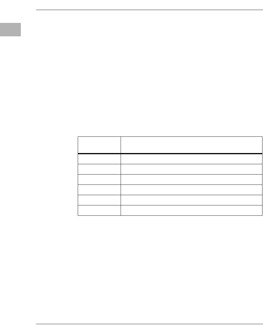
Real-Time Clock and NVRAM
The Real-Time Clock/NVRAM/Watchdog Timer is implemented using a
SGS-Thompson M48T37V Timekeeper SRAM, and M4T28-BR12SH1
SnapHat battery. Refer to the M48T37V data sheets for additional
programming information.
Table 1-13. M48T37V Access
Address Offset Function - 0xF1110000
0x0000 - 0x5FFF Available for users
0x0100 - 0x0200 VxWorks "bootline"
0x6000 - 0x6FFF Reserved (MOTLoad expansion)
0x7000 - 0x7FEF MOTLoad use (GEVs)
0x7FF0 0 0x7FFF Real Time Block

2-1
2
2Programming Details
Introduction
This chapter includes additional programming information for the
MVME6100 single-board computer. Items discussed include:
❏MV64360 Multi-Purpose Port Configuration on page 2-1
❏MV64360 Reset Configuration on page 2-3
❏Flash Memory on page 2-8
❏Real-Time Clock and NVRAM on page 2-8
❏Two-Wire Serial Interface on page 2-9
❏DDR DRAM Serial Presence Detect on page 2-10
❏MV64360 Initialization on page 2-11
❏VPD and User Configuration EEPROMs on page 2-11
❏Temperature Sensor on page 2-11
❏MV64360 Device Controller Bank Assignments on page 2-11
❏MPC Bus and PCI Bus Arbitration on page 2-12
❏PCI Bus 0 and PCI Bus 1 Local Buses on page 2-12
❏MV64360 Interrupt Controller on page 2-16
❏MV64360 Endian Issues on page 2-18
MV64360 Multi-Purpose Port Configuration
The MV64360 contains a 32-bit multi-purpose port (MPP). The MPP pins
can be configured as general purpose I/O pins, as external interrupt inputs,
or as a specific control/status pin for one of the MV64360 internal devices.
After reset, all MPP pins default to GPP pins (general purpose inputs).
Software must then configure each of the pins for the desired function. The

2-2 Computer Group Literature Center Web Site
Programming Details
2following table defines the function assigned to each MPP pin on the
MVME6100 board.
Table 2-1. MV64360 MPP Pin Function Assignments
MPP Pin
Number Input/
Output Function
0 I COM1 /COM2 interrupts (ORed)
1IUnused
2 I Abort interrupt
3 I RTC and thermostat interrupts (ORed)
4IUnused
5 I IPMC761 interrupt
6 I MV64360 WDNMI# interrupt
7 I BCM5421S PHY interrupts (ORed)
MPP[7:0] Interrupts
8 O PCI Bus 1 PMC slot 0 agent grant
9 I PCI Bus 1 PMC slot 0 agent request
10 O PCI Bus 1 PMC slot 1 agent grant
11 I PCI Bus 1 PMC slot 1 agent request
12 O PCI Bus 1 PMC slot 0 grant
13 I PCI Bus 1 PMC slot 0 request
14 O PCI Bus 1 PMC slot 1 grant
15 I PCI Bus 1 PMC slot 1 request
MPP[15:8] PCI_1 Arbitration Request-Grant Pairs
16 I PCI Bus 1 Interrupts PCI-PMC0 INTA#, PMC1 INTC#
17 I PCI Bus 1 Interrupts PCI-PMC0 INTB#, PMC1 INTD#,
18 I PCI Bus 1 Interrupts PCI-PMC0 INTC#, PMC1 INTA#
19 I PCI Bus 1 Interrupts PCI-PMC0 INTD#, PMC1 INTB#
MV64360 Reset Configuration
http://www.motorola.com/computer/literature 2-3
2
MV64360 Reset Configuration
The MV64360 supports two methods of device initialization following
reset:
❏Pins sampled on the deassertion of reset
❏Partial pin sample on deassertion of reset plus Serial ROM
initialization via the I2C bus for user defined initialization
20 I PCI Bus 0 Interrupt PCI-VME INT 0 (Tempe LINT0#, PMCspan
INT 2#)
21 I PCI Bus 0 Interrupt PCI-VME INT 1 (Tempe LINT1#, PMCspan
INT 3#)
22 I PCI Bus 0 Interrupt PCI-VME INT 2 (Tempe LINT2#, PMCspan
INT 0#)
23 I PCI Bus 0 Interrupt PCI-VME INT 3 (Tempe LINT3#, PMCspan
INT 1#)
MPP[19:16] PCI_1 Interrupts,
MPP[23:20] PCI_0 Interrupts
24 O MV64360 SROM initialization active (InitAct)
25 O Watchdog Timer Expired output (WDE#)
26 O Watchdog Timer NMI output (WDNMI#)
27 I Reserved for future device interrupt
28 O Tempe ASIC (VMEbus) grant
29 I Tempe ASIC (VMEbus) request
30 O PCI6520 (PMCspan bridge) grant
31 I PCI6520 (PMCspan bridge) request
MPP[31:28] PCI_0 Arbitration Request-Grant Pairs
Table 2-1. MV64360 MPP Pin Function Assignments (continued)
MPP Pin
Number Input/
Output Function

2-4 Computer Group Literature Center Web Site
Programming Details
2The MVME6100 board supports both options. An onboard switch setting
will be used to select the option. If the pin sample only method is selected,
then states of the various pins on the device AD bus are sampled when reset
is deasserted to determine the desired operating modes. The following
table describes the configuration options. Combinations of pullups,
pulldowns and switches are used to set the options. Some options are fixed
and some are selectable at build time by installing the proper
pullup/pulldown resistor. Finally, some options may be selected using an
onboard switch. Each option is described in the Table 6.
Using the SROM initialization method, any of the MV64360 internal
registers or other system components (i.e. devices on the PCI bus) can be
initialized. Initialization takes place by sequentially reading 8 byte
address/data pairs from the SROM and writing the 32-bit data to the
decoded 32-bit address until the a data pattern matching the last serial data
item register is read from the SROM (default value 0xffffffff). An 8 Kbyte
EEPROM is provided onboard for this user defined initialization of the
MV64360.
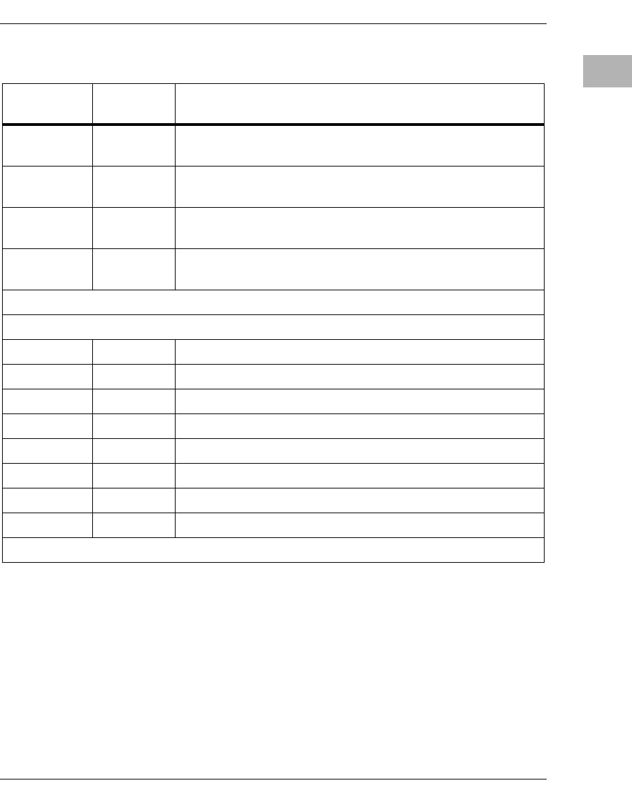
Table 2-2. MV64360 Power-Up Configuration Settings
Device
AD Bus
Signal Select
Option
Default
Power-Up
Setting Description State of Bit vs. Function
AD[0] switch X SROM
Initialization 0 No SROM initialization
1 SROM initialization enabled
AD[1] Resistor 1 DRAM Pads
Calibration 0 Calibration Disabled
1 Calibration Enabled
AD[3:2] Resistors 11 SROM Device
Address 00 1010000 ($A0)
01 1010001 ($A2)
10 1010010 ($A4)
11 1010011 ($A6)
AD[4] Fixed 1 Internal 60x
Bus Arbiter 0 Internal arbiter disabled
1 Internal arbiter enabled

MV64360 Reset Configuration
http://www.motorola.com/computer/literature 2-5
2
AD[5] Resistor 1 Internal Space
Default
Address
0 0x1400.0000
1 0xf100.0000
AD[7:6] Resistor 01 CPU Bus
Configuration 00 60x bus mode
01 MPX bus mode
10 Reserved
11 Reserved
AD[8] Resistor 1 CPU Pads
Calibration 0 Calibration Disabled
1 Calibration Enabled
AD[9] Fixed 0 Multiple
MV64360
Support
0 Not supported
1 Supported
AD[12] Resistor 1 PCI_0 Pads
Calibration 0 Calibration Disabled
1 Calibration Enabled
AD[13] Resistor 1 PCI_1 Pads
Calibration 0 Calibration Disabled
1 Calibration Enabled
AD[15:14] Resistors 10 BootCS*
Device Width 00 8 bits
01 16 bits
10 32 bits
11 Reserved
AD[16] Resistor 1 PCI Retry 0 Disable
1Enable
AD[17] Fixed 1 1 Must pull high
Table 2-2. MV64360 Power-Up Configuration Settings (continued)
Device
AD Bus
Signal Select
Option
Default
Power-Up
Setting Description State of Bit vs. Function

2-6 Computer Group Literature Center Web Site
Programming Details
2
AD[18] Resistor 1 DRAM Clock
Select 0 DRAM is running at a
higher frequency than the
core clock
1 DRAM is running at a same
frequency as the core clock
AD[19] Resistor 1 DRAM
Address/Contr
ol Delay
0 DRAM address and control
signals toggle on falling
edge of DRAM clock
1 DRAM address and control
signals toggle on rising edge
of DRAM clock
AD[21:20] Resistors 01 DRAM control
path pipeline
select
00 Reserved
01 Two Pipe stages
10 Reserved
11 Three pipe stages
AD[24:22] Resistors 000 DRAM read
path control 000
100 DRAM running in sync
mode
001
111 DRAM running in async
mode
AD[25] Fixed 0 Gigabit port 3
Enable 0 Disable
1Enable
AD[28:26] Resistors 101 PCI_1 DLL
control 000 DLL disable
001 Conventional PCI mode at
66MHz
101 PCI-X mode at 133 MHz
110 PCI-X mode at 66 MHz
Table 2-2. MV64360 Power-Up Configuration Settings (continued)
Device
AD Bus
Signal Select
Option
Default
Power-Up
Setting Description State of Bit vs. Function

MV64360 Reset Configuration
http://www.motorola.com/computer/literature 2-7
2
AD[31:29] Resistors 101 PCI_0 DLL
control 000 DLL disable
001 Conventional PCI mode at
66MHz
101 PCI-X mode at 133 MHz
110 PCI-X mode at 66 MHz
TxD0[0] Resistor 0 Gigabit port 0
GMII/PCS
Select
0MII/GMII
1PCS
TxD1[0] Resistor 0 Gigabit port 1
GMII/PCS
Select
0MII/GMII
1PCS
WE[3:0],
DP[3:0] Resistor X DRAM PLL N
Divider [7:4],
[3:0]
TBD Refer to MV64360
Specification MV-S100614-
00 Rev. B (1/13/2003) page
144 for detail. MVME6100
is not using this mode.
BADR[0] Resistor 1 DRAM PLL
NP 1 Pull up NP
BADR[1] Resistor 1 DRAM PLL
HIKVCO 1 Pull down HIKVCO
BADR[2] Resistor 1 DRAM PLL
NP 0 PLL power down
(normal operation)
1 PLL power up
TxD0[6:1] Resistor X DRAM PLL M
Divider TBD Refer to MV64360
Specification MV-S100614-
00 Rev. B (1/13/2003) page
144 for detail. MVME6100
is not using this mode.
Table 2-2. MV64360 Power-Up Configuration Settings (continued)
Device
AD Bus
Signal Select
Option
Default
Power-Up
Setting Description State of Bit vs. Function

2-8 Computer Group Literature Center Web Site
Programming Details
2
Flash Memory
The MVME6100 contains two banks of flash memory accessed via the
Device Controller bus contained within MV64360. Each bank contains
from 8MB to 64MB of 32-bit wide Boot Block flash memory provided by
two 16-bit wide Intel StrataFlash devices.
The Boot Bank is jumper selectable to select either flash bank as the boot
bank. The jumper effectively swaps the chip selects to the two flash banks
so that either bank can be used as the boot bank. The state of the jumper is
readable in the BANK_SELECT bit of System Status Register 1 to
properly set up the MV64360 Device Controller Bus memory maps.
The boot device bank is the same as any of the other device banks except
that its default address map matches the PowerPC CPU boot address
(0xfff0.0100) and that its default width is sampled at reset.
Real-Time Clock and NVRAM
The Real-Time Clock/NVRAM/Watchdog Timer is implemented using a
SGS-Thompson M48T37V Timekeeper SRAM, and M4T28-BR12SH1
SnapHat battery. Refer to the M48T37V data sheets for additional
programming information. Refer to Appendix A, Related Documentation.
TxD0[7] Resistor 0 JTAG Pad
Calib Bypass 0 Normal Operation
1 Bypass pad calibration
TxD1[1] Resistor 0 Core PLL
Bypass 0 Normal Operation
1 Bypass the core’s PLL
TxD1[4:2] Resistors 000 Core PLL
Control 000 Tuning of the core PLL
clock tree.
Table 2-2. MV64360 Power-Up Configuration Settings (continued)
Device
AD Bus
Signal Select
Option
Default
Power-Up
Setting Description State of Bit vs. Function
Two-Wire Serial Interface
http://www.motorola.com/computer/literature 2-9
2
Two-Wire Serial Interface
A two-wire serial interface for the MVME6100 is provided by an I2C
compatible serial controller integrated into the MV64360 system
controller. The I2C serial controller provides two basic functions. The first
function is to provide MV64360 register initialization following a reset.
The MV64360 can be configured (by switch setting) to automatically read
data out of a serial EEPROM following a reset and initialize any number
of internal registers. In the second function, the controller is used by the
system software to read the contents of the VPD and SPD EEPROMs
contained on the MVME6100 to initialize the memory controller and other
interfaces. For additional details regarding the MV64360 two-wire serial
controller operation, refer to the MV64360 System Controller Data Sheet.
See Appendix A, Related Documentation.
Table 2-3. M48T37V Access
Address Offset Function - 0xF1110000
0x0000 - 0x5FFF Available for users
0x0100 - 0x0200 VxWorks "bootline"
0x6000 - 0x6FFF Reserved (MOTLoad expansion)
0x7000 - 0x7FEF MOTLoad use (GEVs)
0x7FF0 0 0x7FFF Real Time Block
2-10 Computer Group Literature Center Web Site
Programming Details
2The following table shows the I2C devices on the MVME6100 and their
assigned device IDs.
Notes 1. The SPD defines the physical attributes of each bank or
group of banks, i.e. if both banks of a group are populated,
they will be the same speed and memory size.
2. This is a dual address serial EEPROM (AT24C64A or
equivalent).
DDR DRAM Serial Presence Detect
There are two onboard SPD serial EEPROMs on the MVME6100
accessible via the I2C serial interface. The first 128 bytes of each SPD
contains module type, SDRAM organization, and timing parameters.
Table 2-4. I2C Bus Device Addressing
Device Function Size Device Address
(A2A1A0) I2C BUS
Address Notes
Memory SPD (Bank 0 and 1) 256 x 8 000b $A0 1
Memory SPD (Bank 2 and 3) 256 x 8 001b $A2 1
Reserved (PMCSpan SROM) NA 010b $A4
MV64360 User Defined Initialization 8K x 8 011b $A6 2
Configuration VPD 8K x 8 100b $A8 2
User VPD 8K x 8 101b $AA 2
Not Used NA 110b $AC
Not Used NA 111b $AE
DS1621 Temperature Sensor NA 011b $90

MV64360 Initialization
http://www.motorola.com/computer/literature 2-11
2
MV64360 Initialization
Serial EEPROM devices are provided to support optional initialization of
the MV64360 (enabled by the S4:4 switch). Using the SROM initialization
method, any of the MV64360 internal registers or other system
components; that is, devices on the PCI bus, can be initialized.
Initialization takes place by sequentially reading 8 byte address/data pairs
from the SROM and writing the 32-bit data to the decoded 32-bit address
until the a data pattern matching the last serial data item register is read for
the SROM (default value 0xffffffff). The onboard reset logic keeps the
processor reset asserted until this initialization process is completed. An
SROM is provided for user MV64360 initialization.
VPD and User Configuration EEPROMs
The MVME6100 board contains an Atmel AT24C64 or compatible Vital
Product Data (VPD) EEPROM containing configuration information
specific to the board. Typical information that may be present in the VPD
is: manufacturer, board revision, build version, date of assembly, memory
present, options present, and L3 cache information. A second AT24C64
device is available for user data storage.
Temperature Sensor
The MVME6100 board provides a Maxim DS1621 digital temperature
sensor with an I2C Serial Bus interface. This device may be used to
provide a measure of the ambient temperature of the board.
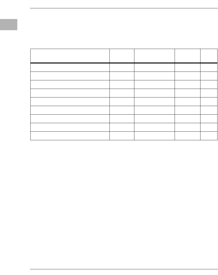
MV64360 Device Controller Bank Assignments
The MVME6100 board uses three of the MV64360 Device Controller
banks for interfacing to various devices. The following tables define the
device bank assignments and the programmable device bank timing
parameters required for each of the banks used.
2-12 Computer Group Literature Center Web Site
Programming Details
2
Note 1. Determined by boot bank select jumper.
MPC Bus and PCI Bus Arbitration
The MV64360 ASIC supplies these functions. Refer to the MV64360 Data
Sheet, listed in Appendix A, Related Documentation, for details.
PCI Bus 0 and PCI Bus 1 Local Buses
The PCI devices on the MVME6100 are: the MV64360 ASIC, the
PMCspan bridge PCI6520, the Tsi148 ASIC, PMCspan slot and the PMC
Slots.
PCI Mode/Frequency Selection
The MVME6100 PCI Bus 0 bus is be set to PCI-X and 133 MHz for
maximum performance. Onboard logic drives the PCI-X initialization
pattern, as defined by the PCI-X Addendum to the PCI Local Bus
Specification Revision 1.0a at the rising edge of RST#.
The MVME6100 dynamically determines the mode and frequency of the
PCI Bus 1 (defined by the PCI-X Addendum to the PCI Local Bus
Table 2-5. Device Bank Assignments
Device
Bank Data
Width Function Notes
0 32 bit Bank A or Bank B Soldered FLASH 1
1 8 bit I/O Devices
2NANot Used
3NANot Used
Boot 32 bit Bank A or Bank B Soldered FLASH 1
PCI Configuration Space
http://www.motorola.com/computer/literature 2-13
2
Specification Revision 1.0b) at the rising edge of RST#. Onboard logic
will sense the states of PCIXCAP and M66EN for all devices on the bus
and select the appropriate mode and clock frequency. Software can access
the MV64360 Configuration Registers to determine the PCI mode and
clock frequency of PCI Bus 1 and PCI Bus 0. Refer to the MV64360 Data
Sheet, listed in Appendix A, Related Documentation, for details.
Voltage Input/Output (VIO) is selected on PCI Bus 1 by the position of the
PMC keying pins. Both sites should be set for the same VIO; that is, keyed
identically. If 5V VIO is selected, PCI Bus 1 reverts to PCI mode at 33
MHz.
PCI Configuration Space
The MV64360 controls all PCI configuration space access from either the
CPU or PCI busses. The IDSEL assignments for MVME6100 are shown
on the following table:
Table 2-6. IDSEL Mapping for PCI Devices
PCI Bus # Device
Number Field PCI Address
Line IDSEL Connection
PCI Bus 0, PCI
Bus 1 0b1_0000 AD16 MV64360 ASIC
PCI Bus 0,0 0b1_0100 AD22 PCI6520
PCI Bus 0 0b1_0101 AD21 Tempe VME Bridge ASIC
PCI Bus 1 0b1_0100 AD20 PMC Slot 0 (SCSI controller also uses
IDSEL AD20)
PCI Bus 1 0b1_0101 AD21 PMC Slot 0, Secondary PCI Agent,
IPMC slot
PCI Bus 1 0b1_0110 AD22 PMC Slot 1
PCI Bus 1 0b1_0111 AD23 PMC Slot 1, Secondary PCI Agent
2-14 Computer Group Literature Center Web Site
Programming Details
2PCI Arbitration Assignments for MV64360 ASIC
PCI arbitration is performed by the MV64360 ASIC. The MV64360
integrates two PCI arbiters, one for each PCI interface (PCI Bus 0/1). Each
arbiter can handle up to six external agents plus one internal agent (PCI
Bus 0/1 master). The internal PCI arbiter REQ#/GNT# signals are
multiplexed on the MV64360 MPP pins. The internal PCI arbiter is
disabled by default (the MPP pins function as general purpose inputs).
Software will configure the MPP pins to function as request/grant pairs for
the internal PCI arbiter.
The arbitration assignments on MVME6100 are as follows:
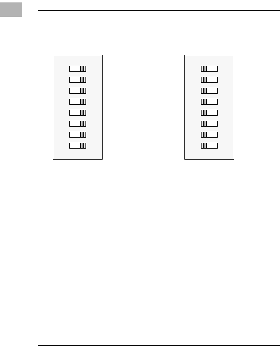
PCI Bus 1 Local Bus PMC Expansion Slots
Two PMC slots reside on the PCI Bus 1 local bus. The presence of PMCs
can be positively determined by reading System Status Register 3. The
INTA#, INTB#, INTC#, and INTD# from the PMC slots are routed by the
MVME6100 as follows:
Table 2-7. PCI Arbitration Assignments for MV64360
ASIC
MPP Pin
Assignment PCI Master(s)
30, 31 PCI6520 (PMCspan bridge) GNT (MPP30), REQ (MPP 31)
28, 29 Tsi148 ASIC (VMEbus) GNT (MPP 28), REQ (MPP 29)
12, 13 PMC Slot 0 GNT, REQ
14, 15 PMC Slot 1 GNT, REQ
8, 9 PMC Slot 0 Secondary PCI Agent / IPMC761 GNT, REQ
10, 11 PMC Slot 1 Secondary PCI Agent GNT, REQ
PCI Bus 0 Local Bus Devices
http://www.motorola.com/computer/literature 2-15
2
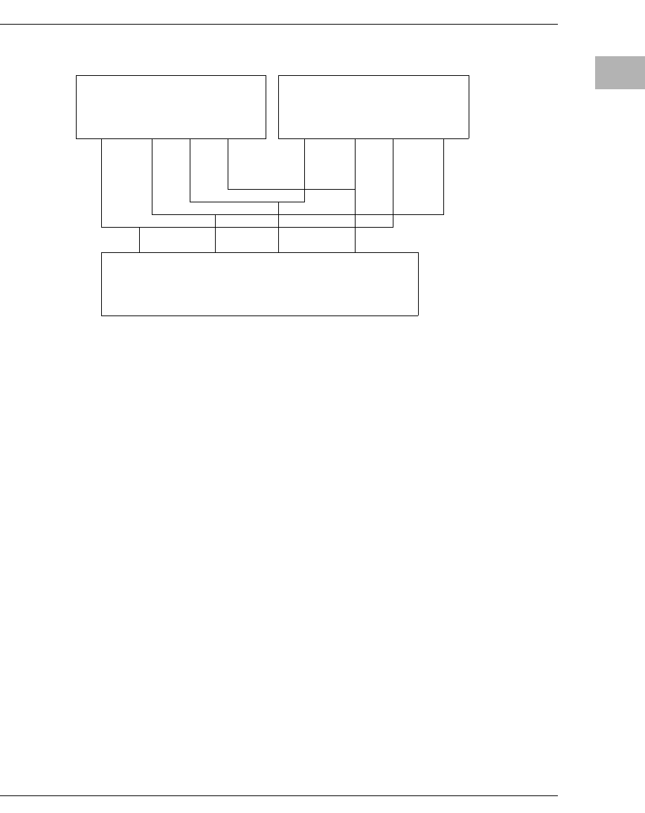
Figure 2-1. PCI Bus 1 Local Bus PMC Expansion Slots
PCI Bus 0 Local Bus Devices
The MV64360 PCI Bus 0 local bus contains the Tsi148 ASIC and PCI6520
PMCSpan bridge.
Tsi148 ASIC
The VMEbus interface is provided by the Tsi148 ASIC. Tempe is a PCI-X
bus to VMEbus interface chip. While Tsi148 has many of the same features
as the VMEchip2 and Universe, it includes new features and
enhancements. Therefore, Tsi148 is not register compatible with the
VMEchip2 or Universe chips. See the Tsi148 User’s Manual from Tundra
Semiconductor listed in Appendix A, Related Documentation, for further
details.
PCI6520 PMCSpan Bridge
The PMCSpan interface is provided by the PCI6520. PCI6520 is a PCI-X-
to-PCI-X transparent bridge to interface between PMCspan bus and the
local PCI0 bus. This part operates asynchronously between primary/local
PMC Slot 0 PMC Slot 1
INTA# INTB# INTC# INTD# INTA# INTB# INTC# INTD#
MV64360
GPP[16] GPP[17] GPP[18] GPP[19]

2-16 Computer Group Literature Center Web Site
Programming Details
2PCI0 bus at 133MHz and the secondary PMCspan bus at 33 or 66 MHz.
See the PLX PCI6520 Specification for further programming information.
MV64360 Interrupt Controller
The MVME6100 uses the MV64360 interrupt controller to route internal
and external interrupt requests to the CPU and the PCI bus. The MV64360
interrupt controller registers are implemented as part of the CPU interface
unit in order to have minimum read latency from CPU interrupt handler.
This is not backward compatible with the Discovery I implementation
since the registers are placed at different offsets. The external interrupt
sources will use the GPP interface to register external interrupts. The
following table shows the MVME6100 interrupt assignment to MV64360
GPP pins.
Table 2-8. MV64360 Interrupt Assignments
GPP
Group MV64360 Edge/Level Polarity Interrupt Source Notes
0 GPP[0] Level High COM1 || COM2 3
GPP[1] Level N.A. Unused, pulled high
onboard 7
GPP[2] Level Low ABORT#
GPP[3] Level Low RTC || Thermostat output 6
GPP[5] Level High IPMC761 interrupt 2
GPP[6] Level Low MV64360 WDNMI#
interrupt
GPP[7] Level Low BCM5421S PHY 1 INTR# ||
BCM5421S PHY 2 INTR#
2 GPP[16] Level Low PCI-PMC 0 INTA#, PMC 1
INTC# 2
GPP[17] Level Low PCI-PMC 0 INTB#, PMC 1
INTD#, 2

MV64360 Interrupt Controller
http://www.motorola.com/computer/literature 2-17
2
Notes 1. The interrupting device is addressed from the MV64360 PCI
Bus 0.
2. The interrupting device is addressed from the MV64360 PCI
Bus 1.
3. The interrupting device is addressed from the MV64360
Device Bus.
GPP[18] Level Low PCI-PMC 0 INTC#, PMC 1
INTA# 2
GPP[19] Level Low PCI-PMC 0 INTD#, PMC 1
INTB# 2
GPP[20] Level Low PCI-VME INT 0 (Tsi148
LINT0#), PMCspan INT 2 1,5
GPP[21] Level Low PCI-VME INT 1 (Tsi148
LINT1#), PMCspan INT 3 1,5
GPP[22] Level Low PCI-VME INT 2 (Tsi148
LINT2#), PMCspan INT 0 1,5
GPP[23] Level Low PCI-VME INT 3 (Tsi148
LINT3#), PMCspan INT 1 1,5
3 GPP[24] Reserved for SROM
initialization active InitAct
output
GPP[25] Reserved for Watchdog
Timer WDE# output
GPP[26] Reserved for Watchdog
Timer WDNMI# output
GPP[27] Reserved for future device
interrupt
Table 2-8. MV64360 Interrupt Assignments (continued)
GPP
Group MV64360 Edge/Level Polarity Interrupt Source Notes

2-18 Computer Group Literature Center Web Site
Programming Details
24. The interrupting device is addressed from the MV64360 I2C
Bus.
5. The mapping of VMEbus interrupt sources and Tsi148
internal interrupt sources are programmable via the Interrupt
Map Registers 1 and 2 in the Tsi148 ASIC.
6. The DS1621 Digital Thermometer and Thermostat provides
9-bit temperature readings which indicate the temperature of
the device. The thermal alarm output, TOUT, is active when
the temperature of the device exceeds a user defined
temperature TH.
7. GPP[1,4,30,31] are unused. They are resistively pulled high
onboard.
MV64360 Endian Issues
The MV64360 supports only a big endian CPU bus. The endianess of the
local memory (DDR and SRAM) is also big endian. Data transferred
to/from the local memory is never swapped. The internal registers of the
MV64360 are always programed in little endian. On a CPU access to the
internal registers, data is byte swapped.
Data swapping on a CPU access to the PCI is controlled via PCI Swap bits
of each PCI Low Address register. This configurable setting allows a CPU
access to PCI agents with a different endianess convention.
Refer to the MV64360 Data Sheet, listed in Appendix A, Related
Documentation, for additional information and programming details.
A-1
A
ARelated Documentation
Motorola Computer Group Documents
The Motorola publications listed below are referenced in this manual. You
can obtain electronic copies of Motorola Computer Group publications by:
❏Contacting your local Motorola sales office
❏Visiting Motorola Computer Group’s World Wide Web literature
site, http://www.motorola.com/computer/literature
To obtain the most up-to-date product information in PDF or HTML
format, visit http://www.motorola.com/computer/literature
Table A-1. Motorola Computer Group Documents
Document Title Motorola Publication
Number
MVME6100 Single-Board Computer Installation
and Use V6100A/IH
MOTLoad Firmware Package User’s Manual MOTLODA/UM
IPMC712/761 I/O Module Installation and Use VIPMCA/IH
PMCspan PMC Adapter Carrier Board Installation
and Use PMCSPANA/IH

A-2 Computer Group Literature Center Web Site
Related Documentation
A
Manufacturers’ Documents
For additional information, refer to the following table for manufacturers’
data sheets or user’s manuals. As an additional help, a source for the listed
document is provided. Please note that, while these sources have been
verified, the information is subject to change without notice.
Table A-2. Manufacturers’ Documents
Document Title and Source Publication Number
MPC7457 RISC Microprocessor Hardware Specification
Literature Distribution Center for Motorola
Telephone: 1-800- 441-2447
FAX: (602) 994-6430 or (303) 675-2150
Web Site: http://e-
www.motorola.com/webapp/sps/library/prod_lib.jsp
E-mail: ldcformotorola@hibbertco.com
MPC7457EC/D
Rev. 1.3,3/2003
Tsi148 PCI/X to VME Bus Bridge User Manual
Tundra Semiconductor Corporation
603 March Road
Ottawa, Ontario, Canada
K2K 2M5
Web Site: www.tundra.com
80A3020_MA001_02
PowerPC™ Apollo Microprocessor Implementation Definition Book
IV
Literature Distribution Center for Motorola
Telephone: 1-800- 441-2447
FAX: (602) 994-6430 or (303) 675-2150
Web Site: http://e-
www.motorola.com/webapp/sps/library/prod_lib.jsp
E-mail: ldcformotorola@hibbertco.com
Addendum to SC-Vger
Book IV Version - 1.0
04/21/00
MV64360 System Controller for PowerPC Processors Data Sheet
Contact your local Motorola Computer Group Field Area
Engineer for Programmable Register documentation
MV-S100414-00C

Manufacturers’ Documents
http://www.motorola.com/computer/literature A-3
A
BCM5421S 10/100/1000BASE-T Gigabit Transceiver with SERDES
Interface
Broadcom Corporation
Web Site: http://www.broadcom.com
5421S-DS05-D2
10/25/02
3 Volt Intel StrataFlash Memory
28F256K3
Intel Corporation
Literature Center
19521 E. 32nd Parkway
Aurora CO 80011-8141
Web Site:
http://developer.intel.com/design/flcomp/datashts/290737.htm
290737
PCI6520 (HB7) Transparent PCIx/PCIx Bridge Preliminary Data
Book
PLX Technology, Inc.
870 Maude Avenue
Sunnyvale, California 94085
Web Site: http://www.hintcorp.com/products/hint/default.asp
PCI6520
Ver. 0.992
EXAR ST16C554/554D, ST68C554 Quad UART with 16-Byte
FIFOs
EXAR Corporation
48720 Kato Road
Fremont, CA 94538
Web Site: http://www.exar.com
ST16C554/554D
Rev. 3.10
Table A-2. Manufacturers’ Documents (continued)
Document Title and Source Publication Number

A-4 Computer Group Literature Center Web Site
Related Documentation
A
3.3V-5V 256Kbit (32Kx8) Timekeeper SRAM
ST Microelectronics
1000 East Bell Road
Phoenix, AZ 85022
Web Site: http://www.st.com/stonline/books/toc/index.htm
M48T37V
2-Wire Serial CMOS EEPROM
Atmel Corporation
San Jose, CA
Web Site: http://www.atmel.com/atmel/support/
AT24C02N
AT24C64A
Dallas Semiconductor DS1621Digital Thermometer and Thermostat
Dallas Semiconductor
Web Site: http://www.dalsemi.com
DS1621
TSOP Type I Shielded Metal Cover SMT
Yamaichi Electronics USA
Web Site: http://www.yeu.com
Table A-2. Manufacturers’ Documents (continued)
Document Title and Source Publication Number
Related Specifications
http://www.motorola.com/computer/literature A-5
A
Related Specifications
For additional information, refer to the following table for related
specifications. For your convenience, a source for the listed document is
also provided. It is important to note that in many cases, the information is
preliminary and the revision levels of the documents are subject to change
without notice.
Table A-3. Related Specifications
Document Title and Source Publication Number
VITA http://www.vita.com/
VME64 Specification ANSI/VITA 1-1994
VME64 Extensions ANSI/VITA 1.1-1997
2eSST Source Synchronous Transfer VITA 1.5-199x
PCI Special Interest Group (PCI SIG) http://www.pcisig.com/
Peripheral Component Interconnect (PCI) Local Bus Specification,
Revision 2.0, 2.1, 2.2 PCI Local Bus
Specification
PCI-X Addendum to the PCI Local Bus Specification Rev 1.0b
IEEE http://standards.ieee.org/catalog/
IEEE - Common Mezzanine Card Specification (CMC) Institute of
Electrical and Electronics Engineers, Inc. P1386 Draft 2.0
IEEE - PCI Mezzanine Card Specification (PMC)
Institute of Electrical and Electronics Engineers, Inc.
P1386.1 Draft 2.0

IN-1
B
block diagram 1-4
C
comments, sending xiv
config switch register 1-17
conventions used in the manual xv
D
default PCI memory map 1-8
default processor memory map 1-5
documentation, related A-1
M
manual conventions xv
manufacturers’ documents A-2
memory maps
default PCI 1-8
default processor 1-5
MOTLoad’s PCI 1-9
MOTLoad’s processor 1-7
system I/O 1-9
MOTLoad’s PCI memory map 1-9
MOTLoad’s processor memory map 1-7
N
NVRAM 2-8
P
presence detect register 1-16
R
real-time clock 2-8
registers
config switch register 1-17
presence detect register 1-16
system status register 1 1-11
system status register 2 1-13
system status register 3 1-15
time base enable register 1-19
related documentation A-1
S
suggestions, submitting xiv
system I/O memory map 1-9
system status register 1 1-11
system status register 2 1-13
system status register 3 1-15
T
time base enable register 1-19
typeface, meaning of xv
Index
