Motorola Mvme2300 Series Users Manual VME Processor Module Programmer's Reference Guide
MVME2300 Series to the manual ae79c0b2-8705-4798-be5f-66b36f52cc52
2015-01-23
: Motorola Motorola-Mvme2300-Series-Users-Manual-271827 motorola-mvme2300-series-users-manual-271827 motorola pdf
Open the PDF directly: View PDF ![]() .
.
Page Count: 282 [warning: Documents this large are best viewed by clicking the View PDF Link!]
- Contents
- List of Figures
- List of Tables
- About This Manual
- Board Description and Memory Maps
- Introduction
- Overview
- Summary of Features
- System Block Diagram
- Functional Description
- Programming Model
- ISA Local Resource Bus
- Raven PCI Bridge ASIC
- Introduction
- Features
- Block Diagram
- Functional Description
- Raven Registers
- MPC Registers
- Vendor ID/Device ID Registers
- Revision ID Register
- General Control-Status/Feature Registers
- MPC Arbiter Control Register
- Prescaler Adjust Register
- MPC Error Enable Register
- MPC Error Status Register
- MPC Error Address Register
- MPC Error Attribute Register - MERAT
- PCI Interrupt Acknowledge Register
- MPC Slave Address (0,1 and 2) Registers
- MPC Slave Address (3) Register
- MPC Slave Offset/Attribute (0,1 and 2) Registers
- MPC Slave Offset/Attribute (3) Registers
- General-Purpose Registers
- PCI Registers
- MPC Registers
- Raven Interrupt Controller
- Features
- Architecture
- Block Diagram Description
- MPIC Registers
- RavenMPIC Registers
- Feature Reporting Register
- Global Configuration Register
- Vendor Identification Register
- Processor Init Register
- IPI Vector/Priority Registers
- Spurious Vector Register
- Timer Frequency Register
- Timer Current Count Registers
- Timer Base Count Registers
- Timer Vector/Priority Registers
- Timer Destination Registers
- External Source Vector/Priority Registers
- External Source Destination Registers
- Raven-Detected Errors Vector/Priority Register
- Raven-Detected Errors Destination Register
- Interprocessor Interrupt Dispatch Registers
- Interrupt Task Priority Registers
- Interrupt Acknowledge Registers
- End-of-Interrupt Registers
- Programming Notes
- Architectural Notes
- Falcon ECC Memory Controller Chip Set
- Introduction
- Features
- Block Diagrams
- Functional Description
- Programming Model
- CSR Architecture
- Register Summary
- Detailed Register Bit Descriptions
- Vendor/Device Register
- Revision ID/ General Control Register
- DRAM Attributes Register
- DRAM Base Register
- CLK Frequency Register
- ECC Control Register
- Error Logger Register
- Error Address Register
- Scrub/Refresh Register
- Refresh/Scrub Address Register
- ROM A Base/Size Register
- ROM B Base/Size Register
- DRAM Tester Control Registers
- 32-Bit Counter
- Test SRAM
- Power-Up Reset Status Register 1
- Power-Up Reset Status Register 2
- External Register Set
- Software Considerations
- Universe (VMEbus to PCI) Chip
- Programming Details
- Related Documentation
- Glossary
- Index
MVME2300 Series
VME Processor Module
Programmer’s Reference
Guide
V2300A/PG5
Edition of June 2001
© Copyright 2001 Motorola, Inc.
All rights reserved.
Printed in the United States of America.
Motorola® and the Motorola logo are registered trademarks of Motorola, Inc.
PowerPC® is a registered trademark of International Business Machines Corporation and
is used by Motorola with permission.
All other products mentioned in this document are trademarks or registered trademarks of
their respective holders.

Safety Summary
The following general safety precautions must be observed during all phases of operation, service, and repair of this
equipment. Failure to comply with these precautions or with specific warnings elsewhere in this manual could result
in personal injury or damage to the equipment.
The safety precautions listed below represent warnings of certain dangers of which Motorola is aware. You, as the user
of the product, should follow these warnings and all other safety precautions necessary for the safe operation of the
equipment in your operating environment.
Ground the Instrument.
To minimize shock hazard, the equipment chassis and enclosure must be connected to an electrical ground. If the
equipment is supplied with a three-conductor AC power cable, the power cable must be plugged into an approved
three-contact electrical outlet, with the grounding wire (green/yellow) reliably connected to an electrical ground
(safety ground) at the power outlet. The power jack and mating plug of the power cable meet International
Electrotechnical Commission (IEC) safety standards and local electrical regulatory codes.
Do Not Operate in an Explosive Atmosphere.
Do not operate the equipment in any explosive atmosphere such as in the presence of flammable gases or fumes.
Operation of any electrical equipment in such an environment could result in an explosion and cause injury or damage.
Keep Away From Live Circuits Inside the Equipment.
Operating personnel must not remove equipment covers. Only Factory Authorized Service Personnel or other
qualified service personnel may remove equipment covers for internal subassembly or component replacement or any
internal adjustment. Service personnel should not replace components with power cable connected. Under certain
conditions, dangerous voltages may exist even with the power cable removed. To avoid injuries, such personnel should
always disconnect power and discharge circuits before touching components.
Use Caution When Exposing or Handling a CRT.
Breakage of a Cathode-Ray Tube (CRT) causes a high-velocity scattering of glass fragments (implosion). To prevent
CRT implosion, do not handle the CRT and avoid rough handling or jarring of the equipment. Handling of a CRT
should be done only by qualified service personnel using approved safety mask and gloves.
Do Not Substitute Parts or Modify Equipment.
Do not install substitute parts or perform any unauthorized modification of the equipment. Contact your local
Motorola representative for service and repair to ensure that all safety features are maintained.
Observe Warnings in Manual.
Warnings, such as the example below, precede potentially dangerous procedures throughout this manual. Instructions
contained in the warnings must be followed. You should also employ all other safety precautions which you deem
necessary for the operation of the equipment in your operating environment.
Warning
To prevent serious injury or death from dangerous voltages, use extreme
caution when handling, testing, and adjusting this equipment and its
components.

Flammability
All Motorola PWBs (printed wiring boards) are manufactured with a flammability rating
of 94V-0 by UL-recognized manufacturers.
EMI Caution
!
Caution
This equipment generates, uses and can radiate electromagnetic energy. It
may cause or be susceptible to electromagnetic interference (EMI) if not
installed and used with adequate EMI protection.
Lithium Battery Caution
This product contains a lithium battery to power the clock and calendar circuitry.
!
Caution
Danger of explosion if battery is replaced incorrectly. Replace battery only
with the same or equivalent type recommended by the equipment
manufacturer. Dispose of used batteries according to the manufacturer’s
instructions.
Attention
!Il y a danger d’explosion s’il y a remplacement incorrect de la batterie.
Remplacer uniquement avec une batterie du même type ou d’un type
équivalent recommandé par le constructeur. Mettre au rebut les batteries
usagées conformément aux instructions du fabricant.
Vorsicht
!Explosionsgefahr bei unsachgemäßem Austausch der Batterie. Ersatz nur
durch denselben oder einen vom Hersteller empfohlenen Typ. Entsorgung
gebrauchter Batterien nach Angaben des Herstellers.
CE Notice (European Community)
Motorola Computer Group products with the CE marking comply with the EMC Directive
(89/336/EEC). Compliance with this directive implies conformity to the following
European Norms:
EN55022 “Limits and Methods of Measurement of Radio Interference Characteristics
of Information Technology Equipment”; this product tested to Equipment Class B
EN50082-1:1997 “Electromagnetic Compatibility—Generic Immunity Standard, Part
1. Residential, Commercial and Light Industry”
System products also fulfill EN60950 (product safety) which is essentially the requirement
for the Low Voltage Directive (73/23/EEC).
Board products are tested in a representative system to show compliance with the above
mentioned requirements. A proper installation in a CE-marked system will maintain the
required EMC/safety performance.
In accordance with European Community directives, a “Declaration of Conformity” has
been made and is on file within the European Union. The “Declaration of Conformity” is
available on request. Please contact your sales representative.
Notice
While reasonable efforts have been made to assure the accuracy of this document,
Motorola, Inc. assumes no liability resulting from any omissions in this document, or from
the use of the information obtained therein. Motorola reserves the right to revise this
document and to make changes from time to time in the content hereof without obligation
of Motorola to notify any person of such revision or changes.
Electronic versions of this material may be read online, downloaded for personal use, or
referenced in another document as a URL to the Motorola Computer Group website. The
text itself may not be published commercially in print or electronic form, edited, translated,
or otherwise altered without the permission of Motorola, Inc.
It is possible that this publication may contain reference to or information about Motorola
products (machines and programs), programming, or services that are not available in your
country. Such references or information must not be construed to mean that Motorola
intends to announce such Motorola products, programming, or services in your country.
Limited and Restricted Rights Legend
If the documentation contained herein is supplied, directly or indirectly, to the U.S.
Government, the following notice shall apply unless otherwise agreed to in writing by
Motorola, Inc.
Use, duplication, or disclosure by the Government is subject to restrictions as set forth in
subparagraph (b)(3) of the Rights in Technical Data clause at DFARS 252.227-7013 (Nov.
1995) and of the Rights in Noncommercial Computer Software and Documentation clause
at DFARS 252.227-7014 (Jun. 1995).
Motorola, Inc.
Computer Group
2900 South Diablo Way
Tempe, Arizona 85282

vii
Contents
About This Manual
Summary of Changes.................................................................................................. xx
Overview of Contents ................................................................................................xxi
Comments and Suggestions .......................................................................................xxi
Conventions Used in This Manual............................................................................xxii
CHAPTER 1 Board Description and Memory Maps
Introduction................................................................................................................1-1
Overview....................................................................................................................1-1
Summary of Features.................................................................................................1-2
System Block Diagram ..............................................................................................1-3
Functional Description...............................................................................................1-6
VMEbus Interface...............................................................................................1-6
Front Panel..........................................................................................................1-6
PCI interface .......................................................................................................1-7
P2 I/O...........................................................................................................1-7
Programming Model ..................................................................................................1-7
Processor Memory Maps ....................................................................................1-7
Default Processor Memory Map..................................................................1-8
Processor CHRP Memory Map...................................................................1-9
Processor PREP Memory Map..................................................................1-11
PCI Configuration Access .........................................................................1-12
PCI Memory Maps............................................................................................1-13
Default PCI Memory Map.........................................................................1-13
PCI CHRP Memory Map ..........................................................................1-13
PCI PREP Memory Map ...........................................................................1-16
VMEbus Mapping.............................................................................................1-20
VMEbus Master Map ................................................................................1-20
VMEbus Slave Map...................................................................................1-21
Falcon-Controlled System Registers ................................................................1-24
System Configuration Register (SYSCR) .................................................1-25
Memory Configuration Register (MEMCR).............................................1-27
System External Cache Control Register (SXCCR)..................................1-29
Processor 0 External Cache Control Register (P0XCCR).........................1-30
Processor 1 External Cache Control Register (P1XCCR).........................1-30

viii
CPU Control Register ............................................................................... 1-30
ISA Local Resource Bus..........................................................................................1-31
W83C553 PIB Registers ..................................................................................1-31
16550 UART ....................................................................................................1-31
General-Purpose Readable Jumpers.................................................................1-32
NVRAM/RTC and Watchdog Timer Registers................................................ 1-32
Module Configuration and Status Registers.....................................................1-33
CPU Configuration Register ..................................................................... 1-34
Base Module Feature Register .................................................................. 1-35
Base Module Status Register (BMSR)...................................................... 1-36
Seven-Segment Display Register..............................................................1-37
VME Registers .................................................................................................1-37
LM/SIG Control Register..........................................................................1-38
LM/SIG Status Register ............................................................................ 1-39
Location Monitor Upper Base Address Register ......................................1-41
Location Monitor Lower Base Address Register......................................1-41
Semaphore Register 1 ............................................................................... 1-42
Semaphore Register 2 ............................................................................... 1-42
VME Geographical Address Register (VGAR)........................................1-43
Emulated Z8536 CIO Registers and Port Pins.................................................1-43
Emulated Z8536 Registers ........................................................................ 1-43
Z8536 CIO Port Pins.................................................................................1-44
ISA DMA Channels .........................................................................................1-45
CHAPTER 2 Raven PCI Bridge ASIC
Introduction ............................................................................................................... 2-1
Features......................................................................................................................2-1
Block Diagram...........................................................................................................2-2
Functional Description .............................................................................................. 2-4
MPC Bus Interface.............................................................................................2-4
MPC Address Mapping............................................................................... 2-4
MPC Slave ..................................................................................................2-6
MPC Write Posting .....................................................................................2-8
MPC Master ................................................................................................2-8
MPC Arbiter..............................................................................................2-10
MPC Bus Timer ........................................................................................2-10
PCI Interface.....................................................................................................2-10
PCI Address Mapping ............................................................................... 2-11
PCI Slave...................................................................................................2-14
PCI Write Posting .....................................................................................2-17

ix
PCI Master.................................................................................................2-17
Generating PCI Cycles ..............................................................................2-21
Endian Conversion............................................................................................2-25
When MPC Devices are Big-Endian .........................................................2-25
When MPC Devices are Little-Endian......................................................2-27
Raven Registers and Endian Mode............................................................2-27
Error Handling..................................................................................................2-28
Transaction Ordering ........................................................................................2-29
Raven Registers .......................................................................................................2-30
MPC Registers..................................................................................................2-30
Vendor ID/Device ID Registers ................................................................2-32
Revision ID Register .................................................................................2-33
General Control-Status/Feature Registers .................................................2-33
MPC Arbiter Control Register...................................................................2-36
Prescaler Adjust Register...........................................................................2-36
MPC Error Enable Register.......................................................................2-37
MPC Error Status Register ........................................................................2-39
MPC Error Address Register.....................................................................2-40
MPC Error Attribute Register - MERAT ..................................................2-41
PCI Interrupt Acknowledge Register ........................................................2-43
MPC Slave Address (0,1 and 2) Registers ................................................2-43
MPC Slave Address (3) Register...............................................................2-44
MPC Slave Offset/Attribute (0,1 and 2) Registers....................................2-45
MPC Slave Offset/Attribute (3) Registers.................................................2-46
General-Purpose Registers ........................................................................2-47
PCI Registers ....................................................................................................2-47
Vendor ID/ Device ID Registers ...............................................................2-49
PCI Command/ Status Registers................................................................2-50
Revision ID/ Class Code Registers............................................................2-52
I/O Base Register.......................................................................................2-52
Memory Base Register ..............................................................................2-53
PCI Slave Address (0,1,2 and 3) Registers................................................2-54
PCI Slave Attribute/ Offset (0,1,2 and 3) Registers ..................................2-55
CONFIG_ADDRESS Register..................................................................2-56
CONFIG_DATA Register.........................................................................2-58
Raven Interrupt Controller.......................................................................................2-60
Features.............................................................................................................2-60
Architecture ......................................................................................................2-60
Readability of CSR....................................................................................2-61
Interrupt Source Priority............................................................................2-61
Processor’s Current Task Priority..............................................................2-61

x
Nesting of Interrupt Events .......................................................................2-62
Spurious Vector Generation......................................................................2-62
Interprocessor Interrupts (IPI)...................................................................2-62
8259 Compatibility.................................................................................... 2-62
Raven-Detected Errors ..............................................................................2-63
Timers ....................................................................................................... 2-63
Interrupt Delivery Modes.......................................................................... 2-64
Block Diagram Description..............................................................................2-65
Program-Visible Registers ........................................................................2-66
Interrupt Pending Register (IPR) ..............................................................2-66
Interrupt Selector (IS) ...............................................................................2-66
Interrupt Request Register (IRR) ..............................................................2-67
In-Service Register (ISR)..........................................................................2-67
Interrupt Router.........................................................................................2-67
MPIC Registers ................................................................................................ 2-69
RavenMPIC Registers...............................................................................2-69
Feature Reporting Register .......................................................................2-73
Global Configuration Register..................................................................2-74
Vendor Identification Register..................................................................2-75
Processor Init Register ..............................................................................2-75
IPI Vector/Priority Registers.....................................................................2-76
Spurious Vector Register ..........................................................................2-77
Timer Frequency Register.........................................................................2-77
Timer Current Count Registers ................................................................. 2-78
Timer Base Count Registers......................................................................2-78
Timer Vector/Priority Registers................................................................ 2-79
Timer Destination Registers......................................................................2-80
External Source Vector/Priority Registers................................................2-81
External Source Destination Registers......................................................2-82
Raven-Detected Errors Vector/Priority Register ......................................2-83
Raven-Detected Errors Destination Register ............................................2-84
Interprocessor Interrupt Dispatch Registers.............................................. 2-84
Interrupt Task Priority Registers...............................................................2-85
Interrupt Acknowledge Registers..............................................................2-86
End-of-Interrupt Registers ........................................................................ 2-86
Programming Notes.......................................................................................... 2-87
External Interrupt Service .........................................................................2-87
Reset State.................................................................................................2-88
Interprocessor Interrupts ...........................................................................2-89
Dynamically Changing I/O Interrupt Configuration.................................2-89
EOI Register..............................................................................................2-90
Interrupt Acknowledge Register ...............................................................2-90

xi
8259 Mode.................................................................................................2-90
Current Task Priority Level.......................................................................2-90
Architectural Notes...........................................................................................2-91
CHAPTER 3 Falcon ECC Memory Controller Chip Set
Introduction................................................................................................................3-1
Features......................................................................................................................3-1
Block Diagrams .........................................................................................................3-2
Functional Description...............................................................................................3-5
Bit Ordering Convention ....................................................................................3-5
Performance........................................................................................................3-5
Four-beat Reads/Writes...............................................................................3-5
Single-beat Reads/Writes ............................................................................3-6
DRAM Speeds.............................................................................................3-6
ROM/Flash Speeds....................................................................................3-10
PowerPC 60x Bus Interface..............................................................................3-11
Responding to Address Transfers..............................................................3-11
Completing Data Transfers........................................................................3-11
Cache Coherency.......................................................................................3-11
Cache Coherency Restrictions...................................................................3-12
L2 Cache Support ......................................................................................3-12
ECC...................................................................................................................3-12
Cycle Types...............................................................................................3-12
Error Reporting..........................................................................................3-13
Error Logging ............................................................................................3-14
DRAM Tester....................................................................................................3-14
ROM/Flash Interface ........................................................................................3-14
Refresh/Scrub....................................................................................................3-18
Blocks A and/or B Present, Blocks C and D Not Present .........................3-18
Blocks A and/or B Present, Blocks C and/or D Present............................3-19
DRAM Arbitration............................................................................................3-20
Chip Defaults....................................................................................................3-20
External Register Set ........................................................................................3-21
CSR Accesses ...................................................................................................3-21
Programming Model ................................................................................................3-21
CSR Architecture..............................................................................................3-21
Register Summary.............................................................................................3-27
Detailed Register Bit Descriptions ...................................................................3-27
Vendor/Device Register ............................................................................3-30
Revision ID/ General Control Register .....................................................3-31

xii
DRAM Attributes Register .......................................................................3-33
DRAM Base Register................................................................................3-35
CLK Frequency Register...........................................................................3-35
ECC Control Register ...............................................................................3-36
Error Logger Register ...............................................................................3-39
Error Address Register..............................................................................3-42
Scrub/Refresh Register..............................................................................3-43
Refresh/Scrub Address Register ...............................................................3-44
ROM A Base/Size Register.......................................................................3-45
ROM B Base/Size Register.......................................................................3-48
DRAM Tester Control Registers...............................................................3-50
32-Bit Counter........................................................................................... 3-50
Test SRAM................................................................................................3-50
Power-Up Reset Status Register 1 ............................................................3-51
Power-Up Reset Status Register 2 ............................................................3-51
External Register Set................................................................................. 3-52
Software Considerations..........................................................................................3-53
Parity Checking on the PowerPC Bus..............................................................3-53
Programming ROM/Flash Devices ..................................................................3-53
Writing to the Control Registers.......................................................................3-53
Sizing DRAM...................................................................................................3-54
ECC Codes ....................................................................................................... 3-57
Data Paths.........................................................................................................3-60
CHAPTER 4 Universe (VMEbus to PCI) Chip
Introduction ............................................................................................................... 4-1
Features......................................................................................................................4-1
Block Diagram...........................................................................................................4-3
Functional Description .............................................................................................. 4-3
VMEbus Interface ..............................................................................................4-4
Universe as VMEbus Slave.........................................................................4-4
Universe as VMEbus Master ......................................................................4-5
PCI Bus Interface ...............................................................................................4-5
Universe as PCI Slave.................................................................................4-6
Universe as PCI Master...............................................................................4-6
Interrupter...........................................................................................................4-6
VMEbus Interrupt Handling ....................................................................... 4-7
DMA Controller ................................................................................................. 4-7
Universe Control and Status Registers (UCSR)................................................. 4-8
Universe Register Map................................................................................4-9

xiii
Universe Chip Problems after PCI Reset..........................................................4-14
Description.................................................................................................4-14
Workarounds .............................................................................................4-15
Examples...........................................................................................................4-16
Example 1: MVME2600 Series Board Exhibits PCI Reset Problem........4-16
Example 2: MVME3600 Series Board Acts Differently...........................4-17
Example 3: Universe Chip is Checked at Tundra......................................4-19
CHAPTER 5 Programming Details
Introduction................................................................................................................5-1
PCI Arbitration...........................................................................................................5-1
Interrupt Handling......................................................................................................5-2
RavenMPIC ........................................................................................................5-3
8259 Interrupts....................................................................................................5-4
ISA DMA Channels...................................................................................................5-7
Exceptions..................................................................................................................5-8
Sources of Reset..................................................................................................5-8
Soft Reset............................................................................................................5-9
Universe Chip Problems after PCI Reset............................................................5-9
Error Notification and Handling.......................................................................5-10
Endian Issues ...........................................................................................................5-11
Processor/Memory Domain..............................................................................5-13
Role of the Raven ASIC ...................................................................................5-13
PCI Domain ......................................................................................................5-13
PCI-SCSI ...................................................................................................5-13
PCI/Ethernet ..............................................................................................5-13
PCI-Graphics .............................................................................................5-14
Role of the Universe ASIC...............................................................................5-14
VMEbus Domain..............................................................................................5-14
ROM/Flash Initialization .........................................................................................5-15
APPENDIX A Related Documentation
Motorola Computer Group Documents ....................................................................A-1
Manufacturers’ Documents.......................................................................................A-2
Related Specifications...............................................................................................A-4


xv
List of Figures
Figure 1-1. MVME2300 Series System Block Diagram ...........................................1-5
Figure 1-2. VMEbus Master Mapping.....................................................................1-20
Figure 1-3. VMEbus Slave Mapping .......................................................................1-22
Figure 1-4. General-Purpose Software-Readable Header........................................1-32
Figure 2-1. Raven Block Diagram.............................................................................2-3
Figure 2-2. MPC-to-PCI Address Decoding..............................................................2-5
Figure 2-3. MPC to PCI Address Translation............................................................2-6
Figure 2-4. PCI to MPC Address Decoding ............................................................2-12
Figure 2-5. PCI to MPC Address Translation..........................................................2-13
Figure 2-6. PCI Spread I/O Address Translation.....................................................2-22
Figure 2-7. Big- to Little-Endian Data Swap...........................................................2-26
Figure 2-8. RavenMPIC Block Diagram .................................................................2-65
Figure 3-1. Falcon Pair Used with DRAM in a System ............................................3-2
Figure 3-2. Falcon Internal Data Paths (Simplified)..................................................3-3
Figure 3-3. Overall DRAM Connections...................................................................3-4
Figure 3-4. Data Path for Reads from the Falcon Internal CSRs.............................3-22
Figure 3-5. Data Path for Writes to the Falcon Internal CSRs.................................3-23
Figure 3-6. Memory Map for Byte Reads to CSR...................................................3-24
Figure 3-7. Memory Map for Byte Writes to Internal Register Set
and Test SRAM........................................................................................................3-25
Figure 3-8. Memory Map for 4-Byte Reads to CSR................................................3-26
Figure 3-9. Memory Map for 4-Byte Writes to Internal Register Set
and Test SRAM........................................................................................................3-26
Figure 3-10. PowerPC Data to DRAM Data Correspondence.................................3-60
Figure 4-1. Architectural Diagram for the Universe..................................................4-4
Figure 4-2. UCSR Access Mechanisms.....................................................................4-9
Figure 5-1. MVME2300 Series Interrupt Architecture..............................................5-2
Figure 5-2. PIB Interrupt Handler Block Diagram....................................................5-5
Figure 5-3. Big-Endian Mode..................................................................................5-11
Figure 5-4. Little-Endian Mode ...............................................................................5-12


xvii
List of Tables
Table 1-1. Features: MVME2300 Series....................................................................1-2
Table 1-2. Default Processor Memory Map...............................................................1-8
Table 1-3. CHRP Memory Map Example..................................................................1-9
Table 1-4. Raven MPC Register Values for CHRP Memory Map...........................1-10
Table 1-5. PREP Memory Map Example.................................................................1-11
Table 1-6. Raven MPC Register Values for PREP Memory Map ...........................1-12
Table 1-7. PCI CHRP Memory Map........................................................................1-13
Table 1-8. Raven PCI Register Values for CHRP Memory Map.............................1-15
Table 1-9. Universe PCI Register Values for CHRP Memory Map.........................1-15
Table 1-10. PCI PREP Memory Map.......................................................................1-16
Table 1-11. Raven PCI Register Values for PREP Memory Map............................1-18
Table 1-12. Universe PCI Register Values for PREP Memory Map........................1-19
Table 1-13. Universe PCI Register Values for VMEbus Slave Map Example ........1-23
Table 1-14. VMEbus Slave Map Example...............................................................1-24
Table 1-15. System Register Summary....................................................................1-24
Table 1-16. 16550 Access Registers ........................................................................1-31
Table 1-17. M48T59/559 Access Registers .............................................................1-33
Table 1-18. Module Configuration and Status Registers .........................................1-33
Table 1-19. VME Registers......................................................................................1-38
Table 1-20. Emulated Z8536 Access Registers .......................................................1-43
Table 1-21. Z8536 CIO Port Pin Assignments ........................................................1-44
Table 2-1. Features of the Raven ASIC .....................................................................2-1
Table 2-2. Command Types — MPC Slave Response...............................................2-7
Table 2-3. MPC Transfer Types.................................................................................2-9
Table 2-4. Command Types — PCI Slave Response...............................................2-15
Table 2-5. PCI Master Command Codes .................................................................2-18
Table 2-6. Address Modification for Little-Endian Transfers .................................2-27
Table 2-7. Raven MPC Register Map......................................................................2-31
Table 2-8. Raven PCI Configuration Register Map.................................................2-48
Table 2-9. Raven PCI I/O Register Map..................................................................2-49
Table 2-10. RavenMPIC Register Map....................................................................2-69
Table 3-1. Features of the Falcon Chip Set................................................................3-1
Table 3-2. PowerPC 60x Bus to DRAM Access Timing — 70ns Page Devices.......3-7
Table 3-3. PowerPC 60x Bus to DRAM Access Timing — 60ns Page Devices.......3-8

xviii
Table 3-4. PowerPC Bus to DRAM Access Timing — 50ns Hyper Devices ...........3-9
Table 3-5. PowerPC 60x Bus to ROM/Flash Access Timing — 64 Bits
(32 Bits per Falcon)................................................................................................. 3-10
Table 3-6. PowerPC 60x Bus to ROM/Flash Access Timing — 16 Bits (8 Bits
per Falcon)...............................................................................................................3-10
Table 3-7. Error Reporting.......................................................................................3-13
Table 3-8. PowerPC 60x to ROM/Flash Address Mapping — ROM/Flash
16 Bits Wide (8 Bits per Falcon) .............................................................................3-16
Table 3-9. PowerPC 60x to ROM/Flash Address Mapping — ROM/Flash
64 Bits Wide (32 Bits per Falcon) ...........................................................................3-17
Table 3-10. Register Summary ................................................................................3-28
Table 3-11. ram spd1,ram spd0 and DRAM Type................................................... 3-32
Table 3-12. Block_A/B/C/D Configurations ...........................................................3-34
Table 3-13. rtest Encodings .....................................................................................3-43
Table 3-14. ROM Block A Size Encoding ..............................................................3-46
Table 3-15. rom_a_rv and rom_b_rv Encoding.......................................................3-46
Table 3-16. Read/Write to ROM/Flash.................................................................... 3-47
Table 3-17. ROM Block B Size Encoding ..............................................................3-49
Table 3-18. Sizing Addresses ..................................................................................3-56
Table 3-19. PowerPC 60x Address to DRAM Address Mappings.......................... 3-56
Table 3-20. Syndrome Codes Ordered by Bit in Error............................................3-57
Table 3-21. Single-Bit Errors Ordered by Syndrome Code.....................................3-59
Table 3-22. PowerPC Data to DRAM Data Mapping .............................................3-61
Table 4-1. Features of the Universe ASIC.................................................................4-2
Table 4-2. Universe Register Map........................................................................... 4-10
Table 5-1. PCI Arbitration Assignments ...................................................................5-1
Table 5-2. RavenMPIC Interrupt Assignments ......................................................... 5-3
Table 5-3. PIB PCI/ISA Interrupt Assignments ........................................................5-6
Table 5-4. Reset Sources and Devices Affected........................................................5-9
Table 5-5. Error Notification and Handling.............................................................5-10
Table 5-6. ROM/Flash Bank Default......................................................................5-15
xix
About This Manual
The MVME2300 Series VME Processor Module Programmer’s Reference
Guide provides board-level information and detailed ASIC information,
including register bit descriptions, for the MVME2300 and
MVME2300SC series of VME processor modules.
The MVME2300 series VME processor module is based on an MPC603
or MPC604 PowerPC microprocessor, and features dual PCI Mezzanine
Card (PMC) slots with front panel and/or P2 I/O. In addition, the
MVME2300SC versions of the board give both PMC slots access (via P2)
to an SCSA (Signal Computing System Architecture) backplane bus, if the
system supports one.
The MVME2300 series VME processor module is compatible with
optional double-width or single-width PMCs, and with the PMCspan PCI
expansion mezzanine module. By utilizing the two onboard PMC slots and
stacking PMCspan(s), the MVME2300SC can provide support for up to
six PMCs.
As of the publication date, the information presented in this manual applies
to the following MVME2300 and MVME2300SC models:
Model Memory Processor
MVME2301 16MB ECC DRAM
MPC603
@ 200 MHz
MVME2302 32MB ECC DRAM
MVME2303 64MB ECC DRAM
MVME2304 128MB ECC DRAM
MVME2304-0111, -0113, MVME2305* 16MB ECC DRAM MPC604
@ 300*/333
MHz
MVME2304-0121, -0121SC, -0123, MVME2306* 32MB ECC DRAM
MVME2304-0131, -0131SC, -0133, MVME2307* 64MB ECC DRAM
MVME2304-0141, -0141SC, -0143, MVME2308* 128MB ECC DRAM
MVME2306SC-1 32MB ECC DRAM MPC604
@ 300 MHz
MVME2307SC-1 64MB ECC DRAM

xx
This manual is intended for anyone who designs OEM systems, adds
capability to an existing compatible system, or works in a lab environment
for experimental purposes. A basic knowledge of computers and digital
logic is assumed. To use this manual, you may also wish to become
familiar with the publications listed in Appendix A, Related
Documentation.
Summary of Changes
This is the fifth edition of the Programmer’s Reference Guide. It
supersedes the March 2001 edition and incorporates the following updates.
Date Description of Change
January 2001 A caution about DRAM component requirements was added to the DRAM
Attributes Register and Sizing DRAM sections of Chapter 3.
January 2001 In descriptions of the general-purpose software-readable header (J10/J17), such
as Figure 1-4 in Chapter 1, information on bit 1 (SRH1) was updated to
correctly reflect the functionality of that bit.
March 2001 At various locations in the manual, such as P2 I/O on page 1-7, information has
been added to accommodate the MVME2300SC variants of the board.
The contents of the manual have also been reorganized somewhat to conform
with present Computer Group practice for board manuals.
June 2001 All data referring to the VME CSR Bit Set Register (VCSR_SET) and VME
CSR Bit Clear Register (VCSR_CLR) has been deleted. These registers of the
Universe II are unavailable for implementation as intended by the MVME
materials and the Universe II User Manual.

xxi
Overview of Contents
Chapter 1, Board Description and Memory Maps, describes the board-
level hardware features of MVME2300 series VME processor modules. It
includes memory maps and a discussion of some general software
considerations such as cache coherency, interrupts, and bus errors.
Chapter 2, Raven PCI Bridge ASIC, describes the Raven ASIC, the PCI
local bus/PowerPC processor bus interface chip used on MVME2300
series boards.
Chapter 3, Falcon ECC Memory Controller Chip Set, describes the Falcon
memory controller chip set, which provides the interface between the
PowerPC processor bus and memory systems on MVME2300 series
boards.
Chapter 4, Universe (VMEbus to PCI) Chip, describes the Universe ASIC,
the VMEbus/PCI local bus interface chip used on MVME2300 series
boards.
Chapter 5, Programming Details, examines aspects of several
programming functions that are not tied to any specific ASIC on
MVME2300 series boards.
Appendix A, Related Documentation, lists all documentation related to the
MVME2300 and MVME2300SC series boards.
Comments and Suggestions
Motorola welcomes and appreciates your comments on its documentation.
We want to know what you think about our manuals and how we can make
them better. Mail comments to:
Motorola Computer Group
Reader Comments DW164
2900 S. Diablo Way
Tempe, Arizona 85282
You can also submit comments to the following e-mail address:
reader-comments@mcg.mot.com

xxii
In all your correspondence, please list your name, position, and company.
Be sure to include the title and part number of the manual and tell how you
used it. Then tell us your feelings about its strengths and weaknesses and
any recommendations for improvements.
Conventions Used in This Manual
The following typographical conventions are used in this document:
bold
is used for user input that you type just as it appears; it is also used for
commands, options and arguments to commands, and names of
programs, directories and files.
italic
is used for names of variables to which you assign values. Italic is also
used for comments in screen displays and examples, and to introduce
new terms.
courier
is used for system output (for example, screen displays, reports),
examples, and system prompts.
<Enter>, <Return> or <CR>
<CR> represents the carriage return or Enter key.
CTRL
represents the Control key. Execute control characters by pressing the
Ctrl key and the letter simultaneously, for example, Ctrl-d.
Data and address parameters are preceded by a character identifying the
numeric format as follows:
$
%
&
dollar
percent
ampersand
specifies a hexadecimal character
specifies a binary number
specifies a decimal number

xxiii
For example, “12” is the decimal number twelve, and “$12” is the decimal
number eighteen.
Unless otherwise specified, all address references are in hexadecimal.
In descriptions of the VMEbus interface, an asterisk (∗) following the
signal name for signals which are level significant denotes that the signal
is true or valid when the signal is low. An asterisk (∗) following the signal
name for signals which are edge significant denotes that the actions
initiated by that signal occur on high to low transition.
In references to other bus signals (such as PCI) found on MVME2300
series boards, an underscore (_) or pound sign (#) following the signal
name denotes an active low signal.
In this manual, assertion and negation signify the forcing of a signal to a
particular state. In particular, assertion and assert refer to a signal that is
active or true; negation and negate indicate a signal that is inactive or false.
These terms are used independently of the voltage level (high or low) that
they represent.
Data and address sizes for MPC60x chips are defined as follows:
❏A byte is eight bits, numbered 0 through 7, with bit 0 being the least
significant.
❏A half-word is 16 bits, numbered 0 through 15, with bit 0 being the
least significant.
❏A word or single word is 32 bits, numbered 0 through 31, with bit 0
being the least significant.
❏A double word is 64 bits, numbered 0 through 63, with bit 0 being
the least significant.
Refer to Endian Issues in Chapter 5 for a discussion of which elements on
MVME2300 series boards use big-endian byte ordering, and which use
small-endian byte ordering.
The terms control bit and status bit are used extensively in this document.
The term control bit is used to describe a bit in a register that can be set and
cleared under software control. The term true is used to indicate that a bit
is in the state that enables the function it controls. The term false is used to

xxiv
indicate that the bit is in the state that disables the function it controls. In
all tables, the terms 0 and 1 are used to describe the actual value that should
be written to the bit, or the value that it yields when read. The term status
bit is used to describe a bit in a register that reflects a specific condition.
The status bit can be read by software to determine operational or
exception conditions.

1-1
1
1Board Description and Memory
Maps
Introduction
This manual provides programming information for MVME2300 and
MVME2300SC VME processor modules. Extensive programming
information is provided for several Application-Specific Integrated Circuit
(ASIC) devices used on the boards. Reference information is included in
Appendix A for the Large Scale Integration (LSI) devices used on the
boards and sources for additional information are listed.
This chapter briefly describes the board level hardware features of the
MVME2300-series VME processor modules. The chapter begins with a
board level overview and features list. Memory maps are next, and are the
major feature of this chapter.
Programmable registers that reside in ASICs in the MVME2300 series are
covered in the chapters on those ASICs. Chapter 2, Raven PCI Bridge
ASIC covers the Raven chip, Chapter 3, Falcon ECC Memory Controller
Chip Set covers the Falcon chip set, Chapter 4, Universe (VMEbus to PCI)
Chip covers the Universe chip, and Chapter 5, Programming Details
covers certain programming features, such as interrupts and exceptions.
Appendix A, Related Documentation lists all related documentation.
Overview
The MVME2300-series VME Processor Module family, hereafter
sometimes referred to simply as the MVME230x or the MVME2300
series, provides many standard features required by a computer system:
Ethernet interface, async serial port, boot Flash, and up to 128MB of ECC
DRAM.

1-2 Computer Group Literature Center Web Site
Board Description and Memory Maps
1
Summary of Features
There are many models based on the MVME2300 series architecture. The
following table summarizes the major features of the MVME2300 series:
Table 1-1. Features: MVME2300 Series
Feature MVME2300 MVME2300SC
Microprocessor
200 MHZ MPC603 PowerPC®
processor
(MVME2301 - 2304 models) 300 MHZ MPC604 PowerPC®
processor (All models)
300 MHZ MPC604 PowerPC®
processor
(MVME2305 - 2308 models)
Form factor 6U VMEbus
ECC DRAM Two-way interleaved, ECC-
protected 16MB, 32MB, 64MB, or
128MB
Two-way interleaved, ECC-
protected 32MB or 64MB
Flash memory
Bank B: Two 32-pin PLCC sockets that can be populated with 1MB 8-bit
Flash devices
Bank A: Four 16-bit Smart Voltage
SMT devices that can be populated
with 8Mbit Flash devices (4MB) or
4Mbit devices (2MB)
Bank A: Four 16-bit Smart Voltage
SMT devices populated with 8Mbit
Flash devices (4MB)
Real-time clock 8KB NVRAM with RTC, battery
backup, and watchdog function
(SGS-Thomson M48T59/T559)
8KB NVRAM with RTC, battery
backup, and watchdog function
(SGS-Thomson M48T559)
Switches Reset (RST) and Abort (ABT)
Status LEDs Four: Board fail (BFL), CPU, PMC
(one for PMC slot 2, one for slot 1) Four: Board Fail (BFL), CPU,
System Controller (SCON), Fuses
(FUS)
Timers
One 16-bit timer in W83C553 PCI/ISA bridge; four 32-bit timers in
Raven (MPIC) device
Watchdog timer provided in SGS-Thomson M48T59/T559
Interrupts Software interrupt handling via Raven (PCI/MPU bridge) and Winbond
(PCI/ISA bridge) controllers
VME I/O VMEbus P2 connector
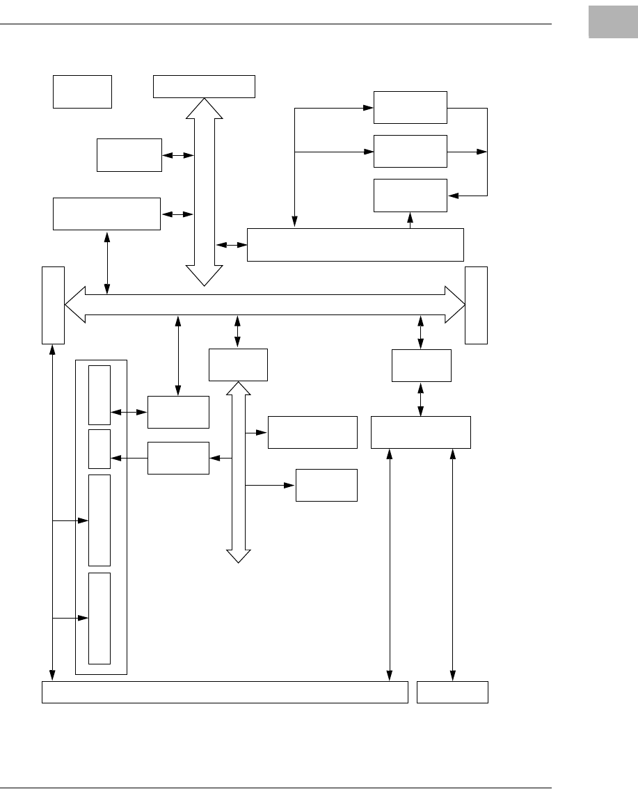
System Block Diagram
http://www.motorola.com/computer/literature 1-3
1
System Block Diagram
The MVME2300 series does not provide any look-aside external cache
option. The Falcon chip set controls the boot Flash and the ECC DRAM.
The Raven ASIC functions as the 64-bit PCI host bridge and the MPIC
interrupt controller. PCI devices include: VME, Ethernet, and two PMC
Serial I/O One asynchronous debug port via
RJ45 connector on front panel One asynchronous debug port via
DB9 connector on front panel,
also via P2 and transition module
Ethernet I/O
10BaseT/100BaseTX connections
via RJ45 connector on front panel 10BaseT/100BaseTX connections
via RJ45 connector on front panel;
AUI connections via P2 and
transition module
PCI interface
Two IEEE P1386.1 PCI Mezzanine Card (PMC) slots for one double-
width or two single-width PMCs
Front panel and/or VMEbus P2 I/O on both PMC slots
One 114-pin Mictor connector for optional PMCspan expansion module
SCSA I/O Not available
Connections from both PMC slots
to SCSA backplane TDM bus (if
present in system) via shared pins
on P2 connector
VMEbus interface
VMEbus system controller functions
VME64 extension
VMEbus-to-local-bus interface (A24/A32, D8/D16/D32/block transfer
[D8/D16/D32/D64])
Local-bus-to-VMEbus interface (A16/A24/A32, D8/D16/D32)
VMEbus interrupter
VMEbus interrupt handler
Global Control/Status Register (GCSR) for interprocessor
communications
DMA for fast local memory/VMEbus transfers (A16/A24/A32,
D16/D32/D64)
Table 1-1. Features: MVME2300 Series (Continued)
Feature MVME2300 MVME2300SC

1-4 Computer Group Literature Center Web Site
Board Description and Memory Maps
1
slots. Standard I/O functions are provided by the UART device which
resides on the ISA bus. The NVRAM/RTC also resides on the ISA bus.
The general system block diagram for MVME2300 series is shown below:
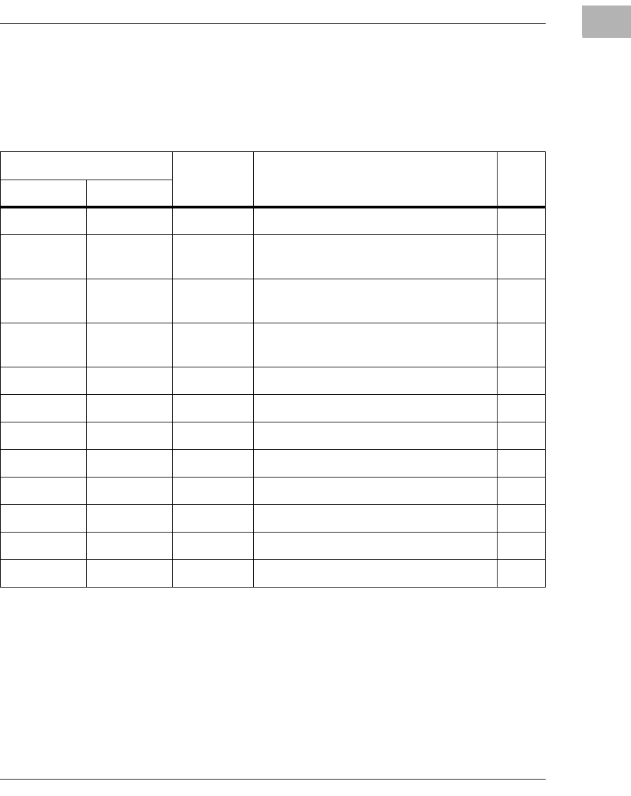
System Block Diagram
http://www.motorola.com/computer/literature 1-5
1
Figure 1-1. MVME2300 Series System Block Diagram
SYSTEM
REGISTERS
2067 9708
PMC FRONT I/O SLOT
DEBUG CONNECTOR
CLOCK
GENERATOR
PROCESSOR
MPC603/604
Flash
3MB or 5MB
PHB & MPIC
RAVEN ASIC
MEMORY CONTROLLER
FALCON CHIP SET
64-BIT PMC SLOT
PCI EXPANSION
33MHz 32/64-BIT PCI LOCAL BUS
PIB
W83C553 VME BRIDGE
UNIVERSE
BUFFERS
VME P2 VME P1
RTC/NVRAM/WD
MK48T59/559
ETHERNET
DEC21140
10BT/100BTX
FRONT PANEL
ISA BUS
66MHz MPC604 PROCESSOR BUS
DRAM
16/32/64/128MB
PMC FRONT I/O SLOT SERIAL
PORT
PC16550
UART
ISA
REGISTERS

1-6 Computer Group Literature Center Web Site
Board Description and Memory Maps
1
Functional Description
The MVME2300 series is a family of single-slot VME processor modules.
It consists of the MPC603/604 processor, the Raven PCI Bridge and
Interrupt Controller, the Falcon ECC Memory Controller chip set, 3MB or
5MB of Flash memory, 16MB to 128MB of ECC-protected DRAM, and a
rich set of I/O features.
I/O peripheral devices on the PCI bus are: Ethernet chip, Universe
VMEbus interface ASIC, and two PMC slots. Functions provided from the
ISA bus are: one asynchronous serial port, a real-time clock,
counters/timers, and a software-readable header.
VMEbus Interface
MVME2300 series boards interface to the VMEbus via the P1 and P2
backplane connectors. MVME2300SC boards use the three-row 96-pin
connectors specified in the original VMEbus standard; non-SCbus
MVME2300 boards use the 5-row 160-pin connectors specified in the
VME64 Extension standard.
Both types of boards draw +5V, +12V, and –12V power from the VMEbus
backplane through these two connectors. 3.3V and 2.5V supplies are
regulated onboard from the +5 power.
Front Panel
Front panel connectors on the non-SCbus MVME2300 series boards
include an RJ45 connector for the Ethernet 10BaseT/100BaseTX
interface, and a second RJ45 connector for the asynchronous serial debug
port.
Front panel connectors on the MVME2300SC include an RJ45 connector
for the Ethernet 10BaseT/100BaseTX interface, and a 9-pin DB9
connector for the asynchronous serial debug port.

Programming Model
http://www.motorola.com/computer/literature 1-7
1
PCI interface
MVME2300 and MVME2300SC boards are equipped with two IEEE
1386.1 PCI Mezzanine Card (PMC) slots. The PMC slots are 64-bit
capable and support both front and rear I/O.
P2 I/O
Certain pins of each PMC slot connector are routed to VME backplane
connector P2 for use in rear I/O configurations.
On MVME2300 boards, pins 1-64 of PMC slot 1 connector J14 are routed
to rows C and A of the 5-row DIN P2 connector. Pins 1-46 of PMC slot 2
connector J24 are routed to rows D and Z of connector P2.
On MVME2300SC boards, pins 1-32 of PMC slot 1 connector J14 are
routed to rows C and A of the 3-row DIN P2 connector. Pins 1-32 of PMC
slot 2 connector J24 (as with J14) are routed to rows C and A of connector
P2.
Additional PCI expansion is supported with a 114-pin Mictor connector.
This connection allows stacking of one or two PMCspan dual-PMC carrier
boards, to increase the I/O capability. Each PMCspan board requires an
additional VME slot.
Programming Model
The following sections describe the memory maps for the MVME2300
series boards.
Processor Memory Maps
The Processor memory map is controlled by the Raven ASIC and the
Falcon chip set. The Raven ASIC and the Falcon chip set have flexible
programming Map Decoder registers to customize the system for many
different applications.
1-8 Computer Group Literature Center Web Site
Board Description and Memory Maps
1
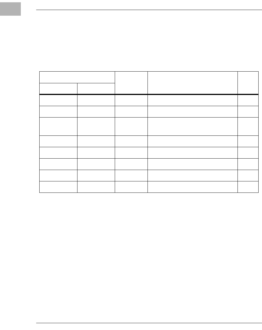
Default Processor Memory Map
After a reset, the Raven ASIC and the Falcon chip set provide the default
processor memory map as shown in the following table.
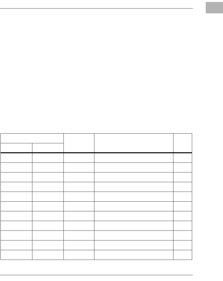
Notes
1. This default map for PCI/ISA I/O space allows software to
determine whether the system is MPC105-based or Falcon/Raven-
based by examining either the PIB Device ID or the CPU Type
register.
2. The first Megabyte of ROM/Flash bank A appears at this range after
a reset if the rom_b_rv control bit is cleared. If the rom_b_rv control
bit is set, then this address range maps to ROM/Flash bank B.
Table 1-2. Default Processor Memory Map
Processor Address Size Definition
Notes
Start End
0000 0000 7FFF FFFF 2G Not mapped
8000 0000 8001 FFFF 128K PCI/ISA I/O Space 1
8002 0000 FEF7 FFFF 2G - 16M -
640K Not mapped
FEF8 0000 FEF8 FFFF 64K Falcon Registers
FEF9 0000 FEFE FFFF 384K Not mapped
FEFF 0000 FEFF FFFF 64K Raven Registers
FF00 0000 FFEF FFFF 15M Not mapped
FFF0 0000 FFFF FFFF 1M ROM/Flash Bank A or Bank B 2
Programming Model
http://www.motorola.com/computer/literature 1-9
1
Processor CHRP Memory Map
The following table shows a recommended CHRP memory map from the
point of view of the processor.
Notes
1. Programmable via Falcon chip set. For the MVME2300 series,
RAM size is limited to 128MB and ROM/Flash to 4MB.
2. To enable the “Processor-hole” area, program the Falcon chip set to
ignore 0x000A0000 - 0x000BFFFF address range and program the
Raven to map this address range to PCI memory space.
Table 1-3. CHRP Memory Map Example
Processor Address Size Definition
Notes
Start End
0000 0000 top_dram dram_size System Memory (onboard DRAM) 1, 2
4000 0000 FCFF FFFF 3G - 48M PCI Memory Space:
4000 0000 to FCFF FFFF 3,4,8
FD00 0000 FDFF FFFF 16M Zero-Based PCI/ISA Memory Space
(mapped to 00000000 to 00FFFFFF) 3,8
FE00 0000 FE7F FFFF 8M Zero-Based PCI/ISA I/O Space
(mapped to 00000000 to 007FFFFF) 3,5,8
FE80 0000 FEF7 FFFF 7.5M Reserved
FEF8 0000 FEF8 FFFF 64K Falcon Registers
FEF9 0000 FEFE FFFF 384K Reserved
FEFF 0000 FEFF FFFF 64K Raven Registers 9
FF00 0000 FF7F FFFF 8M ROM/Flash Bank A 1,7
FF80 0000 FF8F FFFF 1M ROM/Flash Bank B 1,7
FF50 0000 FFEF FFFF 6M Reserved
FFF0 0000 FFFF FFFF 1M ROM/Flash Bank A or Bank B 7
1-10 Computer Group Literature Center Web Site
Board Description and Memory Maps
1
3. Programmable via Raven ASIC.
4. CHRP requires the starting address for the PCI memory space to be
256MB-aligned.
5. Programmable via Raven ASIC for either contiguous or spread-I/O
mode.
6. The actual size of each ROM/Flash bank may vary.
7. The first Megabyte of ROM/Flash bank A appears at this range after
a reset if the rom_b_rv control bit is cleared. If the rom_b_rv control
bit is set then this address range maps to ROM/Flash bank B.
8. This range can be mapped to the VMEbus by programming the
Universe ASIC accordingly. The map shown is the recommended
setting which uses the Special PCI Slave Image and two of the four
programmable PCI Slave Images.
9. The only method of generating a PCI Interrupt Acknowledge cycle
(8259 IACK) is to perform a read access to the Raven’s PIACK
register at 0xFEFF0030.
The following table shows the programmed values for the associated
Raven MPC registers for the processor CHRP memory map.
Table 1-4. Raven MPC Register Values for CHRP Memory Map
Address Register Name Register Value
FEFF 0040 MSADD0 4000 FCFF
FEFF 0044 MSOFF0 & MSATT0 0000 00C2
FEFF 0048 MSADD1 FD00 FDFF
FEFF 004C MSOFF1 & MSATT1 0300 00C2
FEFF 0050 MSADD2 0000 0000
FEFF 0054 MSOFF2 & MSATT2 0000 0002
FEFF 0058 MSADD3 FE00 FE7F
FEFF 005C MSOFF3 & MSATT3 0200 00C0
Programming Model
http://www.motorola.com/computer/literature 1-11
1
Processor PREP Memory Map
The Raven/Falcon chip set can be programmed for PREP-compatible
memory map. The following table shows the PREP memory map of the
MVME2300 series from the point of view of the processor.
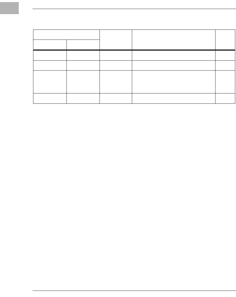
Notes
1. Programmable via Falcon chip set. For the MVME2300 series,
RAM size is limited to 128MB and ROM/Flash to 4MB.
2. Programmable via Raven ASIC.
3. The actual size of each ROM/Flash bank may vary.
Table 1-5. PREP Memory Map Example
Processor Address Size Definition Notes
Start End
0000 0000 top_dram dram_size System Memory (onboard DRAM) 1
8000 0000 BFFF FFFF 1G Zero-Based PCI I/O Space:
0000 0000 - 3FFFF FFFF
2
C000 0000 FCFF FFFF 1G - 48M Zero-Based PCI/ISA Memory Space:
0000 0000 - 3CFFFFFF 2, 5
FD00 0000 FEF7 FFFF 40.5M Reserved
FEF8 0000 FEF8 FFFF 64K Falcon Registers
FEF9 0000 FEFE FFFF 384K Reserved
FEFF 0000 FEFF FFFF 64K Raven Registers 6
FF00 0000 FF7F FFFF 8M ROM/Flash Bank A 1, 3
FF80 0000 FF8F FFFF 1M ROM/Flash Bank B 1, 3
FF90 0000 FFEF FFFF 6M Reserved
FFF0 0000 FFFF FFFF 1M ROM/Flash Bank A or Bank B 4
1-12 Computer Group Literature Center Web Site
Board Description and Memory Maps
1
4. The first Megabyte of ROM/Flash bank A appears at this range after
a reset if the rom_b_rv control bit is cleared. If the rom_b_rv control
bit is set then this address range maps to ROM/Flash bank B.
5. This range can be mapped to the VMEbus by programming the
Universe ASIC accordingly.
6. The only method of generating a PCI Interrupt Acknowledge cycle
(8259 IACK) is to perform a read access to the Raven’s PIACK
register at 0xFEFF0030.
The following table shows the programmed values for the associated
Raven MPC registers for the processor PREP memory map.
PCI Configuration Access
PCI Configuration accesses are accomplished via the CONFIG_ADD and
CONFIG_DAT registers. These two registers are implemented in the
Raven ASIC. In the CHRP memory map example, the CONFIG_ADD and
CONFIG_DAT registers are located at 0xFE000CF8 and 0xFE000CFC,
respectively. With the PREP memory map, the CONFIG_ADD register
and the CONFIG_DAT register are located at 0x80000CF8 and
0x80000CFC, respectively.
Table 1-6. Raven MPC Register Values for PREP Memory Map
Address Register Name Register Value
FEFF 0040 MSADD0 C000 FCFF
FEFF 0044 MSOFF0 & MSATT0 4000 00C2
FEFF 0048 MSADD1 0000 0000
FEFF 004C MSOFF1 & MSATT1 0000 0002
FEFF 0050 MSADD2 0000 0000
FEFF 0054 MSOFF2 & MSATT2 0000 0002
FEFF 0058 MSADD3 8000 BFFF
FEFF 005C MSOFF3 & MSATT3 8000 00C0
Programming Model
http://www.motorola.com/computer/literature 1-13
1
PCI Memory Maps
The PCI memory map is controlled by the Raven ASIC and the Universe
ASIC. The Raven ASIC and the Universe ASIC have flexible
programming Map Decoder registers to customize the system to fit many
different applications.
Default PCI Memory Map
After a reset, the Raven ASIC and the Universe ASIC turn all the PCI slave
map decoders off. Software must program the appropriate map decoders
for a specific environment.
PCI CHRP Memory Map
The following table shows a PCI memory map of the MVME2300 series
that is CHRP-compatible from the point of view of the PCI local bus.
Table 1-7. PCI CHRP Memory Map
PCI Address Size Definition Notes
Start End
0000 0000 top_dram dram_size Onboard ECC DRAM 1
4000 0000 EFFF FFFF 3G - 256M VMEbus A32/D32 (Super/Program) 3
F000 0000 F7FF FFFF 128M VMEbus A32/D16 (Super/Program) 3
F800 0000 F8FE FFFF 16M - 64K VMEbus A24/D16 (Super/Program) 4
F8FF 0000 F8FF FFFF 64K VMEbus A16/D16 (Super/Program) 4
F900 0000 F9FE FFFF 16M - 64K VMEbus A24/D32 (Super/Data) 4
F9FF 0000 F9FF FFFF 64K VMEbus A16/D32 (Super/Data) 4
FA00 0000 FAFE FFFF 16M - 64K VMEbus A24/D16 (User/Program) 4
FAFF 0000 FAFF FFFF 64K VMEbus A16/D16 (User/Program) 4
FB00 0000 FBFE FFFF 16M - 64K VMEbus A24/D32 (User/Data) 4
FBFF 0000 FBFF FFFF 64K VMEbus A16/D32 (User/Data) 4
1-14 Computer Group Literature Center Web Site
Board Description and Memory Maps
1
Notes
1. Programmable via the Raven’s PCI Configuration registers. For the
MVME2300 series, RAM size is limited to 128MB.
2. To enable the CHRP “io-hole”, program the Raven to ignore the
0x000A0000 - 0x000FFFFF address range.
3. Programmable mapping via the four PCI Slave Images in the
Universe ASIC.
4. Programmable mapping via the Special Slave Image (SLSI) in the
Universe ASIC.
FC00 0000 FC03 FFFF 256K RavenMPIC 1
FC04 0000 FCFF FFFF 16M - 256K PCI Memory Space
FD00 0000 FDFF FFFF 16M PCI Memory Space
or System Memory Alias Space
(mapped to 00000000 to 00FFFFFF)
1
FE00 0000 FFFF FFFF 48M Reserved
Table 1-7. PCI CHRP Memory Map (Continued)
PCI Address Size Definition Notes
Start End
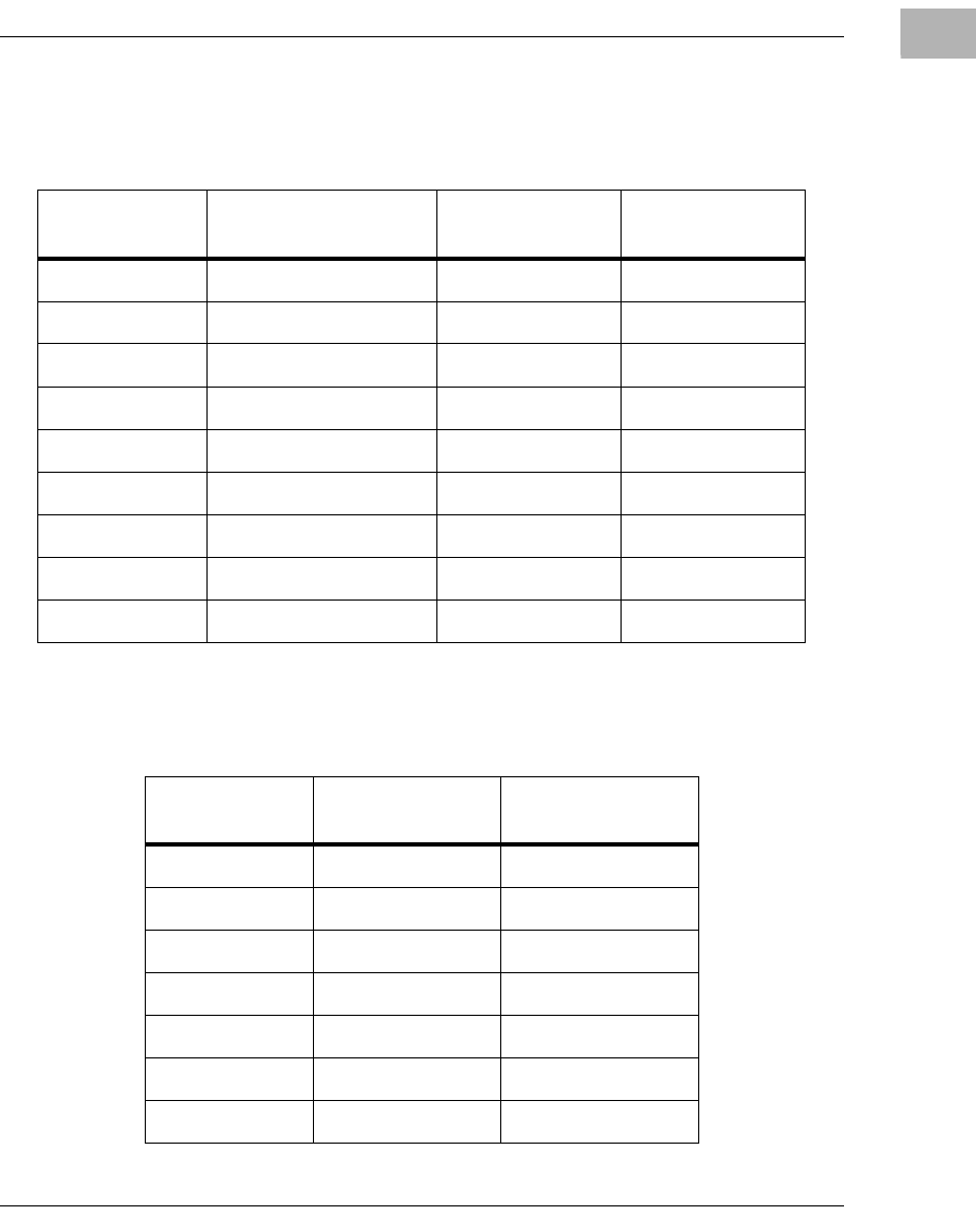
Programming Model
http://www.motorola.com/computer/literature 1-15
1
The following table shows the programmed values for the associated
Raven PCI registers for the PCI CHRP memory map.
The next table shows the programmed values for the associated Universe
PCI registers for the PCI CHRP memory map.
Table 1-8. Raven PCI Register Values for CHRP Memory Map
Configuration
Address Offset Configuration
Register Name Register Value
(Aliasing OFF) Register Value
(Aliasing ON)
$14 RavenMPIC MBASE FC00 0000 FC00 0000
$80 PSADD0 0000 3FFF 0100 3FFF
$84 PSOFF0 & PSATT0 0000 00FX 0000 00FX
$88 PSADD1 0000 0000 FD00 FDFF
$8C PSOFF1 & PSATT1 0000 0000 0000 00FX
$90 PSADD2 0000 0000 0000 0000
$94 PSOFF2 & PSATT2 0000 0000 0000 0000
$98 PSADD3 0000 0000 0000 0000
$9C PSOFF3 & PSATT3 0000 0000 0000 0000
Table 1-9. Universe PCI Register Values for CHRP Memory Map
Configuration
Address Offset Configuration
Register Name Register Value
$100 LSI0_CTL C082 5100
$104 LSI0_BS 4000 0000
$108 LSI0_BD F000 0000
$10C LSI0_TO XXXX 0000
$114 LSI1_CTL C042 5100
$118 LSI1_BS F000 0000
$11C LSI1_BD F800 0000
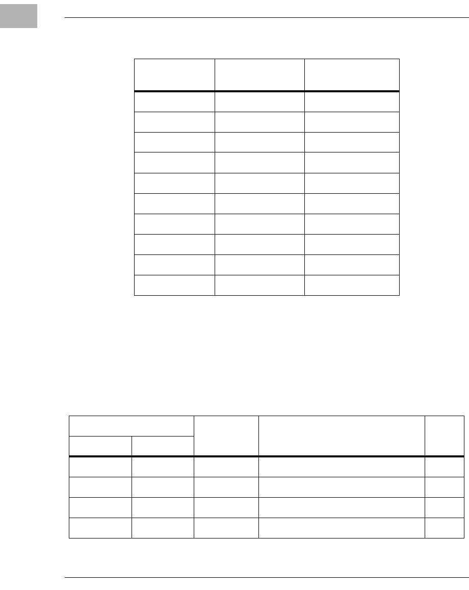
1-16 Computer Group Literature Center Web Site
Board Description and Memory Maps
1
PCI PREP Memory Map
The following table shows a PCI memory map of the MVME2300 series
boards that is PREP-compatible from the point of view of the PCI local
bus.
$120 LSI1_TO XXXX 0000
$128 LSI2_CTL 0000 0000
$12C LSI2_BS XXXX XXXX
$130 LSI2_BD XXXX XXXX
$134 LSI2_TO XXXX XXXX
$13C LSI3_CTL 0000 0000
$140 LSI3_BS XXXX XXXX
$144 LSI3_BD XXXX XXXX
$148 LSI3_TO XXXX XXXX
$188 SLSI C0A053F8
Table 1-10. PCI PREP Memory Map
PCI Address Size Definition Notes
Start End
0000 0000 00FF FFFF 16M PCI/ISA Memory Space
0100 0000 2FFF FFFF 752M VMEbus A32/D32 (Super/Program) 3
3000 0000 37FF FFFF 128M VMEbus A32/D16 (Super/Program) 3
3800 0000 38FE FFFF 16M - 64K VMEbus A24/D16 (Super/Program) 4
Table 1-9. Universe PCI Register Values for CHRP Memory Map (Continued)
Configuration
Address Offset Configuration
Register Name Register Value
Programming Model
http://www.motorola.com/computer/literature 1-17
1
Notes
1. Programmable via the Raven’s PCI Configuration registers. For the
MVME2300 series, RAM size is limited to 128MB.
2. To enabled the CHRP “io-hole”, program the Raven to ignore the
0x000A0000 - 0x000FFFFF address range.
3. Programmable mapping via the four PCI Slave Images in the
Universe ASIC.
4. Programmable mapping via the Special Slave Image (SLSI) in the
Universe ASIC.
38FF 0000 38FF FFFF 64K VMEbus A16/D16 (Super/Program) 4
3900 0000 39FE FFFF 16M - 64K VMEbus A24/D32 (Super/Data) 4
39FF 0000 39FF FFFF 64K VMEbus A16/D32 (Super/Data) 4
3A00 0000 3AFE FFFF 16M - 64K VMEbus A24/D16 (User/Program) 4
3AFF 0000 3AFF FFFF 64K VMEbus A16/D26 (User/Program) 4
3B00 0000 3BFE FFFF 16M - 64K VMEbus A24/D32 (User/Data) 4
3BFF 0000 3BFF FFFF 64K VMEbus A16/D32 (User/Data) 4
3C00 0000 7FFF FFFF 1G + 64M PCI Memory Space
8000 0000 FBFF FFFF 2G - 64M Onboard ECC DRAM 1
FC00 0000 FC03 FFFF 256K RavenMPIC 1
FC04 0000 FFFF FFFF 64M - 256K PCI Memory Space
Table 1-10. PCI PREP Memory Map (Continued)
PCI Address Size Definition Notes
Start End
1-18 Computer Group Literature Center Web Site
Board Description and Memory Maps
1
The following table shows the programmed values for the associated
Raven PCI registers for the PREP-compatible memory map.
Table 1-11. Raven PCI Register Values for PREP Memory Map
Configuration
Address Offset Configuration
Register Name Register Value
$14 RavenMPIC MBASE FC00 0000
$80 PSADD0 8000 FBFF
$84 PSOFF0 & PSATT0 8000 00FX
$88 PSADD1 0000 0000
$8C PSOFF1 & PSATT1 0000 0000
$90 PSADD2 0000 0000
$94 PSOFF2 & PSATT2 0000 0000
$98 PSADD3 0000 0000
$9C PSOFF3 & PSATT3 0000 0000
Programming Model
http://www.motorola.com/computer/literature 1-19
1
The next table shows the programmed values for the associated Universe
PCI registers for the PCI PREP memory map.
Table 1-12. Universe PCI Register Values for PREP Memory Map
Configuration
Address Offset Configuration
Register Name Register Value
$100 LSI0_CTL C082 5100
$104 LSI0_BS 0100 0000
$108 LSI0_BD 3000 0000
$10C LSI0_TO XXXX 0000
$114 LSI1_CTL C042 5100
$118 LSI1_BS 3000 0000
$11C LSI1_BD 3800 0000
$120 LSI1_TO XXXX 0000
$128 LSI2_CTL 0000 0000
$12C LSI2_BS XXXX XXXX
$130 LSI2_BD XXXX XXXX
$134 LSI2_TO XXXX XXXX
$13C LSI3_CTL 0000 0000
$140 LSI3_BS XXXX XXXX
$144 LSI3_BD XXXX XXXX
$148 LSI3_TO XXXX XXXX
$188 SLSI C0A05338
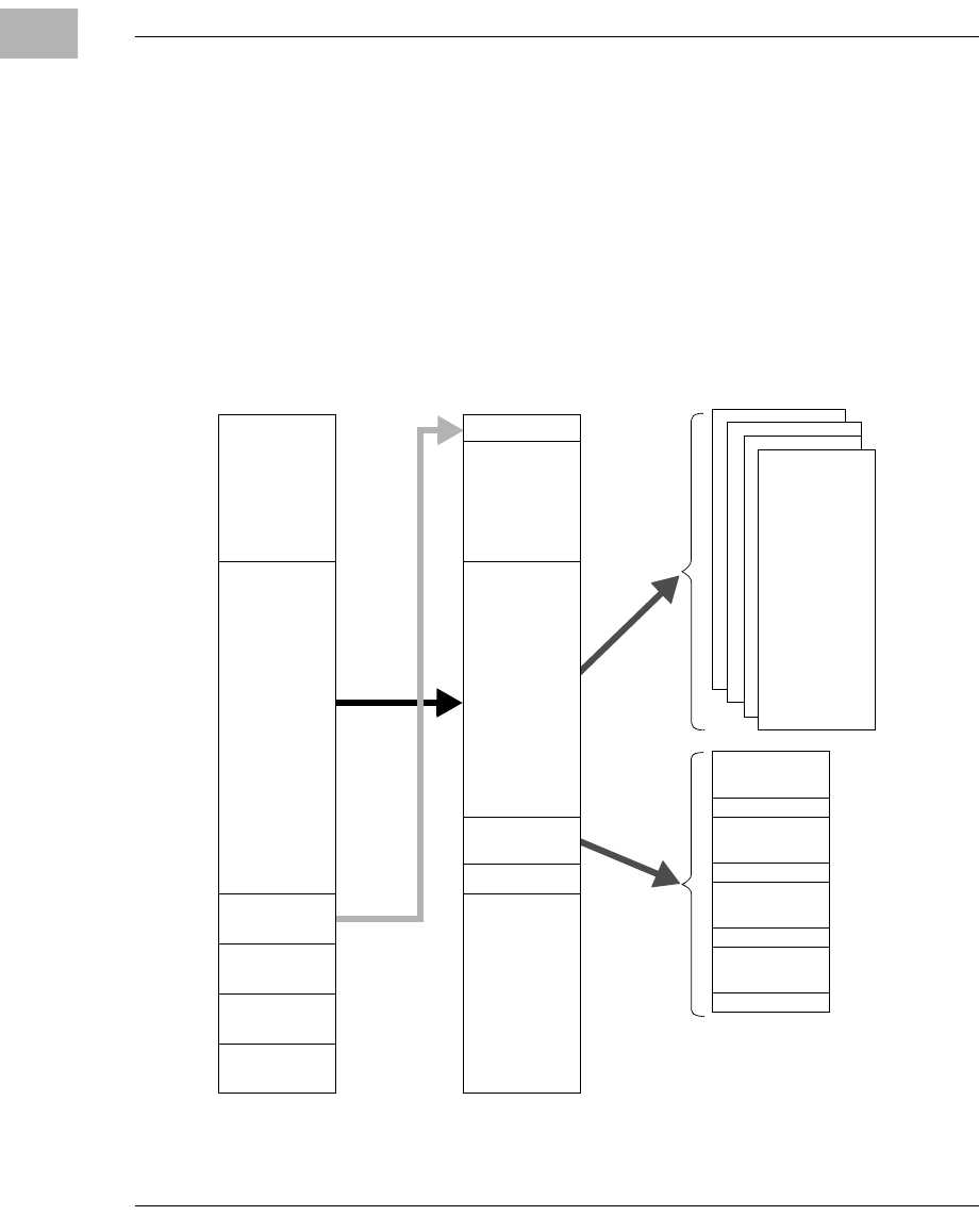
1-20 Computer Group Literature Center Web Site
Board Description and Memory Maps
1
VMEbus Mapping
The processor can access any address range in the VMEbus with the help
of the Universe ASIC’s address translation capabilities. The Processor
Memory Map section shows the recommended mapping.
VMEbus Master Map
The figure below illustrates how VMEbus master mapping is
accomplished. (Note that for MVME2300 series boards, RAM size is
limited to 128MB.)
Figure 1-2. VMEbus Master Mapping
VMEBUS
11553.00 9609
VME A24
VME A16
VME A24
VME A16
VME A24
VME A16
VME A24
VME A16
PROGRAMMABLE
SPACE
PCI MEMORYPROCESSOR
PCI MEMORY
SPACE
PCI/ISA
MEMORY SPACE
PCI
I/O SPACE
MPC
RESOURCES
NOTE 1
NOTE 1
NOTE 2
NOTE 3
ONBOARD
MEMORY

Programming Model
http://www.motorola.com/computer/literature 1-21
1
Notes
1. Programmable mapping done by the Raven ASIC.
2. Programmable mapping via the four PCI Slave Images in the
Universe ASIC.
3. Programmable mapping via the Special Slave Image (SLSI) in the
Universe ASIC.
VMEbus Slave Map
The four programmable VME Slave images in the Universe ASIC give
other VMEbus masters access to any devices on the board. The
combination of the four Universe VME Slave images and the four Raven
PCI Slave decoders offers great flexibility in mapping the system
resources as seen from the VMEbus.
In most applications, the VMEbus needs to see only the system memory
and, perhaps, the software interrupt registers (SIR1 and SIR2 registers).
For an example of the VMEbus slave map, refer to the figure below:
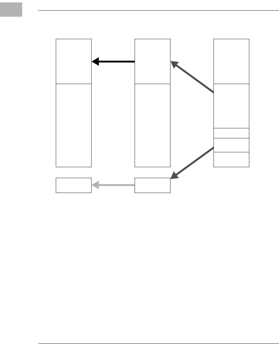
1-22 Computer Group Literature Center Web Site
Board Description and Memory Maps
1
Figure 1-3. VMEbus Slave Mapping
Notes
1. Programmable mapping via the four VME Slave Images in the
Universe ASIC.
2. Programmable mapping via PCI Slave Images in the Raven ASIC.
3. Fixed mapping via the PIB device.
1896 9609
PCI Memory
NOTE 2
NOTE 1
Software INT
Registers
Processor
ISA Space
Onboard
Memory
VMEbus
NOTE 1
PCI I/O Space
NOTE3
Programming Model
http://www.motorola.com/computer/literature 1-23
1
The following table shows the programmed values for the associated
Universe registers for the VMEbus slave function.
Table 1-13. Universe PCI Register Values for VMEbus Slave Map Example
Configuration
Address Offset Configuration
Register Name Register Value
(CHRP) Register Value
(PREP)
$F00 VSI0_CTL C0F2 0001 C0F2 0001
$F04 VSI0_BS 4000 0000 4000 0000
$F08 VSI0_BD 4000 1000 4000 1000
$F0C VSI0_TO C000 1000 C000 1000
$F14 VSI1_CTL E0F2 00C0 E0F2 00C0
$F18 VSI1_BS 1000 0000 1000 0000
$F1C VSI1_BD 2000 0000 2000 0000
$F20 VSI1_TO F000 0000 7000 0000
$F28 VSI2_CTL 0000 0000 0000 0000
$F2C VSI2_BS XXXX XXXX XXXX XXXX
$F30 VSI2_BD XXXX XXXX XXXX XXXX
$F34 VSI2_TO XXXX XXXX XXXX XXXX
$F3C VSI3_CTL 0000 0000 0000 0000
$F40 VSI3_BS XXXX XXXX XXXX XXXX
$F44 VSI3_BD XXXX XXXX XXXX XXXX
$F48 VSI3_TO XXXX XXXX XXXX XXXX
1-24 Computer Group Literature Center Web Site
Board Description and Memory Maps
1
The register values in the table yield the following VMEbus slave map:
Falcon-Controlled System Registers
The Falcon chip set latches the states of the DRAM data lines onto the
PR_STAT1 and PR_STAT2 registers. MVME2300 series boards use these
status registers to provide the system configuration information. In
addition, the Falcon chip set performs the decode and control for an
external register port. This function is utilized by MVME2300 series
boards to provide the system control registers.
The following subsections describe these system registers in detail.
Table 1-14. VMEbus Slave Map Example
VMEbus Address Size CHRP Map PREP Map
Range Mode
4000 0000 -
4000 0FFF A32 U/S/P/D
D08/16/32 4K PCI/ISA I/O Space:
0000 1000 - 0000 1FFF PCI/ISA I/O Space:
0000 1000 - 0000 1FFF
1000 0000 -
1FFF FFFF
A32 U/S/P/D
D08/16/32/64
RMW 256M PCI/ISA Memory Space
(On-board DRAM)
0000 0000 - 0FFF FFFF
PCI/ISA Memory Space
(On-board DRAM)
8000 0000 - 8FFF FFFF
Table 1-15. System Register Summary
BIT # ---->
0
1
2
3
4
5
6
7
8
9
10
11
12
13
14
15
16
17
18
19
20
21
22
23
24
25
26
27
28
29
30
31
FEF80400 System Configuration Register (Upper Falcon’s PR_STAT1)
FEF80404 Memory Configuration Register (Lower Falcon’s PR_STAT1)
FEF88000 System External Cache
Control Register
FEF88300 CPU Control Register
Programming Model
http://www.motorola.com/computer/literature 1-25
1
System Configuration Register (SYSCR)
The states of the RD[0:31] DRAM data pins, which have weak internal
pull-ups, are latched by the upper Falcon chip at a rising edge of the power-
up reset and stored in this System Configuration register to provide some
information about the system. Configuration is accomplished with external
pull-down resistors. This 32-bit read-only register is defined as follows:
SYSID System Identification. This field specifies the type of the
overall system configuration so that the software may
appropriately handle any software visible differences. For
the MVME2300 series, this field returns a value of $FD.
SYSCLK System Clock Speed. This field relays the system clock
speed and the PCI clock speed information as follows:
REG System Configuration Register - $FEF80400
BIT
0
1
2
3
4
5
6
7
8
9
10
11
12
13
14
15
16
17
18
19
20
21
22
23
24
25
26
27
28
29
30
31
FIELD SYSID SYSCLK SYSXC P0STAT P1STAT
OPER Read Only
RESET $FD 1111 1111 0111 1111 1 1 $F
SYSCLK Value System Clock Speed PCI Clock Speed
0B0000 to 0B1100 Reserved Reserved
0B1101 50MHz 25MHz
0B1110 60MHz 30MHz
0B1111 66.66MHz 33.33MHz
1-26 Computer Group Literature Center Web Site
Board Description and Memory Maps
1
SYSXC System External Cache Size. The MVME2300 series does
not offer any external caching options. Reads from this
field will always return a hardwired value of 0b1111
indicating the absence of external caching.
P0/1STAT Processor 0/1 Status. This field is encoded as follows:
P0/1STAT Value Processor 0/1 Present External In-line Cache
Size
0B0000 to 0B0011 Reserved Reserved
0B0100 Yes 1M
0B0101 Yes 512K
0B0110 Yes 256K
0B0111 Yes None
0B1000 to 0B1111 No N/A
Programming Model
http://www.motorola.com/computer/literature 1-27
1
Memory Configuration Register (MEMCR)
The states of the RD[00:31] DRAM data pins, which have weak internal
pull-ups, are latched by the lower Falcon chip at a rising edge of the power-
up reset and stored in this Memory Configuration register to provide some
information about the system memory. Configuration is accomplished
with external pull-down resistors. This 32-bit read-only register is defined
as follows:
M_SIZE[0:1]
Memory Size. This field is encoded as follows:
M_FREF Block A/B/C/D Fast Refresh. When this bit is set, it
indicates that a DRAM block requires faster refresh rate.
If any of the four blocks requires faster refresh rate then
the ram ref control bit should be set.
REG Memory Configuration Register - $FEF80404
BIT
32
33
34
35
36
37
38
39
40
41
42
43
44
45
46
47
48
49
50
51
52
53
54
55
56
57
58
59
60
61
62
63
FIELD
M_SIZE0
M_SIZE1
M_FREF
M_SPD0
M_SPD1
R_A_TYP0
R_A_TYP1
R_A_TYP2
R_B_TYP0
R_B_TYP1
R_B_TYP2
L2_TYPE0
L2_TYPE1
L2_TYP2
L3_TYPE3
L2_PLL0
L2_PLL1
L2_PLL2
L2_PLL3
FLSHP0_
FLSHP1_
FLSHP2-
OPER
RESET
X
X
1
X
1
1
X
X
1
X
X
X
1
X
X
X
X
X
X
X
X
X
X
X
1
1
X
X
X
1
1
1
M_SIZE[0:1] Total Memory On Board
0B00 16 Megabytes
0B01 32 Megabytes
0B10 64 Megabytes
0B11 128 Megabytes
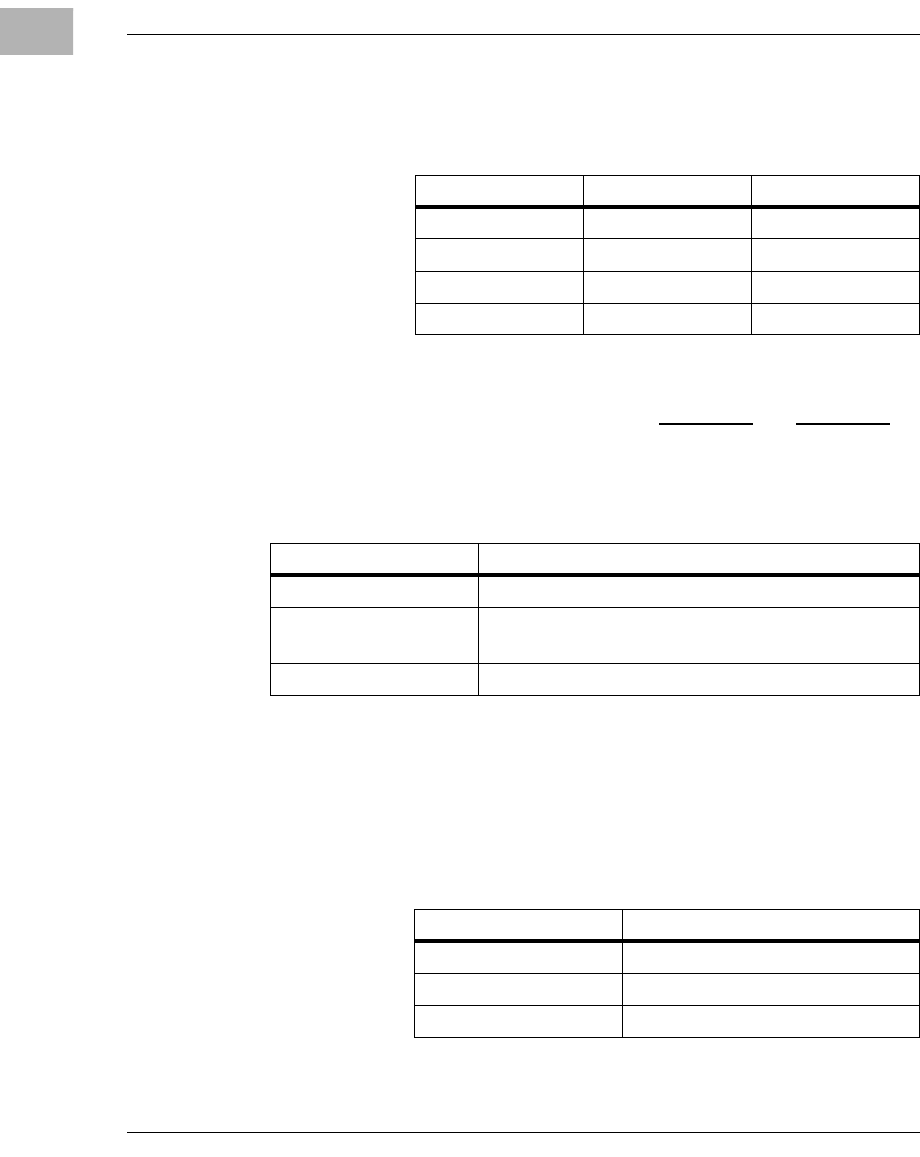
1-28 Computer Group Literature Center Web Site
Board Description and Memory Maps
1
M_SPD[0:1]
Memory Speed. This field relays the memory speed
information as follows:
These two bits reflect the combined status of the four
blocks of DRAM. Initialization software uses this
information to program the ram_spd0 and ram_spd1
control bits in the Falcon’s Chip Revision register.
R_A/B_TYP[0:2]
ROM/Flash Type. This field is encoded as follows:
Note The device width differs from the width of the Flash bank. If the
bank width is 64 bits and the device width is 16 bits, then the
Flash bank consists of four Flash devices.
L2_TYPE[0:3]
L2 Memory Type. This field is encoded as follows:
M_SPD[0:1] DRAM Speed DRAM Type
0B00 70ns Past Page
0B01 60ns Fast Page
0B10 Reserved Reserved
0B11 50ns EDO
ROM_A/B_TYP[0:2] ROM/Flash Type
0B000 to 0B101 Reserved
0B110 Intel 16-bit wide Flash with 16K Bottom Boot
Block
0B111 Unknown type (i.e. ROM/Flash sockets)
L2_TYPE[0:3] Configuration
0B0000 Late write Sync
0B0001 Pipelined Sync Burst
0B0010 to 0B1111 Reserved
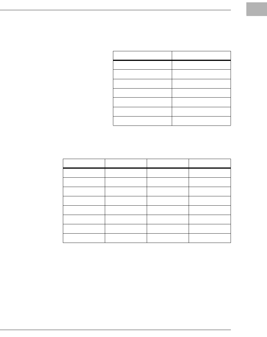
Programming Model
http://www.motorola.com/computer/literature 1-29
1
L2_PLL[0:3]
L2 Core Frequency to L2 Frequency divider. This field is
encoded as follows:
FLSHP[0:2]
Bank A Flash memory size. This field is encoded as
follows:
System External Cache Control Register (SXCCR)
The MVME2300 and MVME2300SC boards do not implement this
register. Writes to this register location ($FEF88000) will have no system
effects. Reads from this register location will return undefined data.
PLL Value] Size
0B0000 Disable
0B0001 1
0B0010 1.5
0B0011 2
0B0100 2.5
0B0101 3
0B0110 to 0B1111 Reserved
Flash Size FLSHP0_ FLSHP1_ FLSHP2_
1MB000
2MB 001
4MB 010
8MB 011
16MB 100
32MB 101
64MB 110
No Flash 111

1-30 Computer Group Literature Center Web Site
Board Description and Memory Maps
1
Processor 0 External Cache Control Register (P0XCCR)
The MVME2300 and MVME2300SC boards do not implement this
register. Writes to this register location ($FEF88100) will have no system
effects. Reads from this register location will return undefined data.
Processor 1 External Cache Control Register (P1XCCR)
The MVME2300 and MVME2300SC boards do not implement this
register. Writes to this register location ($FEF88200) will have no system
effects. Reads from this register location will return undefined data.
CPU Control Register
The CPU Control register is accessed via the RD[32:39] data lines of the
upper Falcon device. This 8-bit register is defined as follows:
LEMODE Little Endian Mode. This bit must be set in conjunction
with the LEND bit in the Raven for little-endian mode.
P0_TBEN Processor 0 Time Base Enable. When this bit is cleared,
the TBEN pin of the processor will be driven low.
REG CPU Control Register - $FEF88300
BIT 01234567
FIELD
LEMODE
P0_TBEN
OPER RRRR/WRRRR
RESET 1001XXXX
ISA Local Resource Bus
http://www.motorola.com/computer/literature 1-31
1
ISA Local Resource Bus
W83C553 PIB Registers
The PIB contains ISA Bridge I/O registers for various functions. These
registers are actually accessible from the PCI bus. Refer to the W83C553
Data Book for details.
16550 UART
The 16550 UART provides the MVME2300 series boards with an
asynchronous serial port. Refer to the 16550 Data Sheet for additional
details and programming information.
The following table shows the mapping of the 16550 registers within the
MVME2300 series boards’ ISA I/O space beginning at address 0x3F8:
Table 1-16. 16550 Access Registers
ISA I/O Address Function
0000 03F8 Receiver Buffer (Read);
Transmitter Holding (Write)
0000 03F9 Interrupt Enable
0000 03FA Interrupt Identification (Read);
FIFO Control (Write)
0000 03FB Line Control
0000 03FC MODEM control
0000 03FD Line Status
0000 03FE MODEM Status
0000 03FF Scratch

1-32 Computer Group Literature Center Web Site
Board Description and Memory Maps
1
General-Purpose Readable Jumpers
Headers J10 (on the MVME2300SC) and J17 (on the MVME2300)
provide eight software-readable jumpers. These jumpers can be read as a
register at ISA I/O address $801 (hexadecimal). Bit 0 is associated with
header pins 1-2; bit 7 is associated with pins 15-16. The bit values are read
as a 0 when a jumper is installed, and as a 1 when the jumper is removed.
The PowerPC firmware, PPCBug, reserves all bits, SRH0 to SRH7. The
board is shipped from the factory with J10 / J17 set to all 0s (jumpers on
all pins), as shown in Figure 1-4.
Figure 1-4. General-Purpose Software-Readable Header
NVRAM/RTC and Watchdog Timer Registers
The M48T59/559 provides the MVME2300 series boards with 8K of non-
volatile SRAM, a time-of-day clock, and a watchdog timer. Accesses to
the M48T59/559 are accomplished via three registers:
❏The NVRAM/RTC Address Strobe 0 register
❏The NVRAM/RTC Address Strobe 1 register
❏The NVRAM/RTC Data Port register
J10/J17
15
Bit 0 (SRH0)
Bit 1 (SRH1)
Bit 2 (SRH2)
Bit 6 (SRH6)
Bit 3 (SRH3)
Bit 4 (SRH4)
Bit 5 (SRH5)
12
16Bit 7 (SRH7)
Reserved for future use
Reserved for future use
Reserved for future use
PPCBug INSTALLED
Reserved for future use
Reserved for future use
Reserved for future use
Reserved for future use
Reserved for future use
ISA Local Resource Bus
http://www.motorola.com/computer/literature 1-33
1
The NVRAM/RTC Address Strobe 0 register latches the lower 8 bits of the
address and the NVRAM/RTC Address Strobe 1 register latches the upper
5 bits of the address.
The NVRAM and RTC are accessed through the above three registers.
When accessing an NVRAM/RTC location, follow this procedure:
1. Write the low address (A7-A0) of the NVRAM to the
NVRAM/RTC STB0 register,
2. Write the high address (A15-A8) of the NVRAM to the
NVRAM/RTC STB1 register, and
3. Then read or write the NVRAM/RTC Data Port.
Refer to the M48T59 Data Sheet for additional details and programming
information.
Module Configuration and Status Registers
Four registers provide the configuration and status information about the
board. These registers are listed in the following table:
Table 1-17. M48T59/559 Access Registers
PCI I/O Address Function
0000 0074 NVRAM/RTC Address Strobe 0 (A7 - A0)
0000 0075 NVRAM/RTC Address Strobe 1 (A15 - A8)
0000 0077 NVRAM/RTC Data Register
Table 1-18. Module Configuration and Status Registers
PCI I/O Address Function
0000 0800 CPU Configuration Register
0000 0802 Base Module Feature Register
0000 0803 Base Module Status Register
0000 08C0 - 0000 08C1 Seven-Segment Display Register
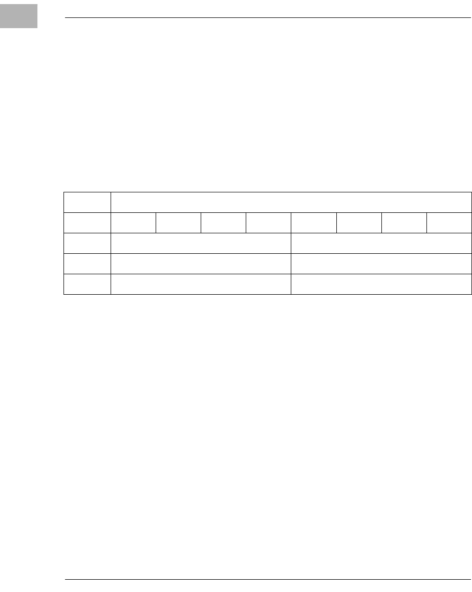
1-34 Computer Group Literature Center Web Site
Board Description and Memory Maps
1
The following subsections describe the configuration and status registers
in detail.
CPU Configuration Register
The CPU Configuration register is an 8-bit register located at ISA I/O
address x0800. This register is defined for the MVME2300 series to
provide some backward compatibility with older MVME1600 products.
The Base Module Status register should be used to identify the base
module type and the System Configuration register should be used to
obtain information about the overall system.
CPUTYPE CPU Type. This field will always read as $E for the
MVME2300 series. (The whole register will read $EF.)
The System Configuration register should be used for
additional information.
REG Old CPU Configuration Register - $FE000800
BIT SD7 SD6 SD5 SD4 SD3 SD2 SD1 SD0
FIELD CPUTYPE
OPER RR
RESET $E $F
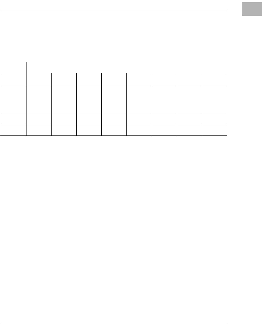
ISA Local Resource Bus
http://www.motorola.com/computer/literature 1-35
1
Base Module Feature Register
The Base Module Feature register is an 8-bit register providing the
configuration information about the MVME2300-series VME processor
module. This read-only register is located at ISA I/O address x0802.
PCIXP_ PCI Expansion Slot present. If set, there is no PCIX
device installed. If cleared, the PCIX slot contains a PCI
Mezzanine Card.
PMC2P_ PMC Slot 2 present. If set, there is no PCI Mezzanine
Card installed in PMC Slot 2. If cleared, PMC Slot 2
contains a PMC.
PMC1P_ PMC Slot 1 present. If set, there is no PCI Mezzanine
Card installed in PMC Slot 1. If cleared, PMC Slot 1
contains a PMC.
VMEP_ VMEbus present. If set, there is no VMEbus interface. If
cleared, VMEbus interface is supported.
LANP_ Ethernet present. If set, there is no Ethernet transceiver
interface. If cleared, there is on-board Ethernet support.
REG Base Module Feature Register - Offset $0802
BIT SD7 SD6 SD5 SD4 SD3 SD2 SD1 SD0
FIELD
PCIXP_
PMC2P_
PMC1P_
VMEP_
LANP_
OPER RRRRRRRR
RESET X1XXX1X1
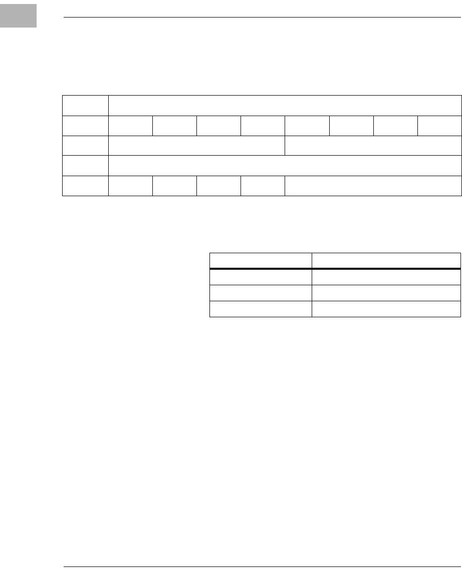
1-36 Computer Group Literature Center Web Site
Board Description and Memory Maps
1
Base Module Status Register (BMSR)
The Base Module Status register is an 8-bit read-only register located at
ISA I/O address x0803.
BASE_TYPE
Base Module Type. This four-bit field is used to provide
the category of the base module and is defined as follows:
REG Base Module Status Register - Offset $0803
BIT SD7 SD6 SD5 SD4 SD3 SD2 SD1 SD0
FIELD BASE_TYPE
OPER R
RESET 1111 N/A
BASE_TYPE Value Base Module Type
$0 to $8 Reserved
$9 MVME2300
$A to $F Reserved
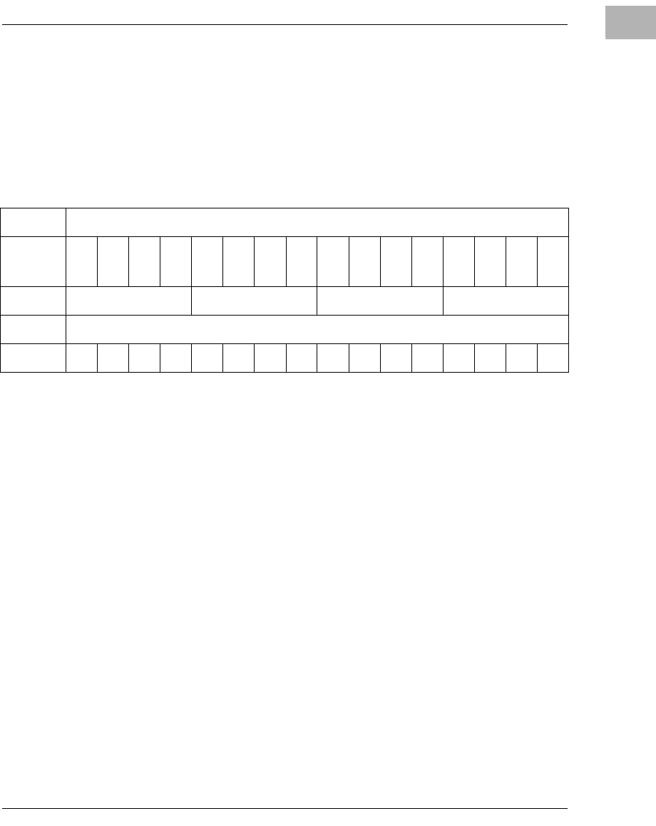
ISA Local Resource Bus
http://www.motorola.com/computer/literature 1-37
1
Seven-Segment Display Register
Note This register is NOT USED on the MVME2300-series
boards.
This 16-bit register allows data to be sent to the 4-digit hexadecimal
diagnostic display. The register also allows the data to be read back.
DIG3[3:0] Hexadecimal value of the most significant digit.
DIG2[3:0] Hexadecimal value of the third significant digit.
DIG1[3:0] Hexadecimal value of the second significant digit.
DIG0[3:0] Hexadecimal value of the least significant digit.
VME Registers
The registers listed in the table below provide the following functions for
the VMEbus interface:
❏A software interrupt capability
❏A location monitor function
❏A geographical address status
For these registers to be accessible from the VMEbus, the Universe ASIC
must be programmed to map VMEbus Slave Image 0 into the appropriate
PCI I/O address range. Refer to the VMEbus Slave Map section for
additional details.
REG 7-Segment Display Register - Offset $08C0
BIT
SD15
SD14
SD13
SD12
SD11
SD10
SD9
SD8
SD7
SD6
SD5
SD4
SD3
SD2
SD1
SD0
FIELD DIG3[3:0] DIG2[3:0] DIG1[3:0] DIG0[3:0]
OPER R/W
RESET XXXXXXXXXXXXXXXX
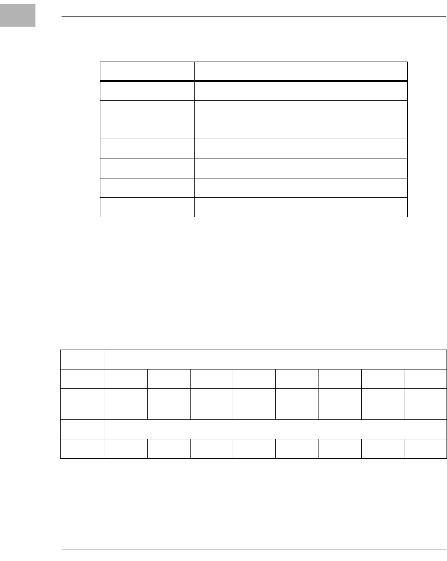
1-38 Computer Group Literature Center Web Site
Board Description and Memory Maps
1
These registers are described in the following subsections.
LM/SIG Control Register
The LM/SIG Control register is an 8-bit register located at ISA I/O address
x1000. This register provides a method to generate software interrupts.
The Universe ASIC is programmed so that this register can be accessed
from the VMEbus to generate software interrupts to the processor(s).
SET_SIG1 Writing a 1 to this bit will set the SIG1 status bit.
SET_SIG0 Writing a 1 to this bit will set the SIG0 status bit.
Table 1-19. VME Registers
PCI I/O Address Function
0000 1000 SIG/LM Control Register
0000 1001 SIG/LM Status Register
0000 1002 VMEbus Location Monitor Upper Base Address
0000 1003 VMEbus Location Monitor Lower Base Address
0000 1004 VMEbus Semaphore Register 1
0000 1005 VMEbus Semaphore Register 2
0000 1006 VMEbus Geographical Address Status
REG LM/SIG Control Register - Offset $1000
BIT SD7 SD6 SD5 SD4 SD3 SD2 SD1 SD0
FIELD SET
SIG1 SET
SIG0 SET
LM1 SET
LM0 CLR
SIG1 CLR
SIG0 CLR
LM1 CLR
LM0
OPER WRITE-ONLY
RESET 00000000

ISA Local Resource Bus
http://www.motorola.com/computer/literature 1-39
1
SET_LM1 Writing a 1 to this bit will set the LM1 status bit.
SET_LM0 Writing a 1 to this bit will set the LM0 status bit.
CLR_SIG1Writing a 1 to this bit will clear the SIG1 status bit.
CLR_SIG0Writing a 1 to this bit will clear the SIG0 status bit.
CLR_LM1 Writing a 1 to this bit will clear the LM1 status bit.
CLR_LM0 Writing a 1 to this bit will clear the LM0 status bit.
LM/SIG Status Register
The LM/SIG Status register is an 8-bit register located at ISA I/O address
x1001. This register, in conjunction with the LM/SIG Control register,
provides a method to generate interrupts. The Universe ASIC is
programmed so that this register can be accessed from the VMEbus to
provide a capability to generate software interrupts to the onboard
processor(s) from the VMEbus.
EN_SIG1 When the EN_SIG1 bit is set, an LM/SIG Interrupt 1 is
generated if the SIG1 bit is asserted.
EN_SIG0 When the EN_SIG0 bit is set, an LM/SIG Interrupt 0 is
generated if the SIG0 bit is asserted.
REG LM/SIG Status Register - Offset $1001
BIT SD7 SD6 SD5 SD4 SD3 SD2 SD1 SD0
FIELD EN
SIG1 EN
SIG0 EN
LM1 EN
LM0 SIG1 SIG0 LM1 LM0
OPER R/W READ-ONLY
RESET 00000000

1-40 Computer Group Literature Center Web Site
Board Description and Memory Maps
1
EN_LM1 When the EN_LM1 bit is set, an LM/SIG Interrupt 1 is
generated and the LM1 bit is asserted.
EN_LM0 When the EN_LM0 bit is set, an LM/SIG Interrupt 0 is
generated and the LM0 bit is asserted.
SIG1 SIG1 status bit. This bit can only be set by the SET_LM1
control bit. It can only be cleared by a reset or by writing
a 1 to the CLR_LM1 control bit.
SIG0 SIG0 status bit. This bit can only be set by the SET_LM0
control bit. It can only be cleared by a reset or by writing
a 1 to the CLR_LM0 control bit.
LM1 LM1 status bit. This bit can be set by either the location
monitor function or the SET_LM1 control bit. LM1
correspond to offset 3 from the location monitor base
address. This bit can only be cleared by a reset or by
writing a 1 to the CLR_LM1 control bit.
LM0 LM0 status bit. This bit can be set by either the location
monitor function or the SET_LM0 control bit. LM0
correspond to offset 1 from the location monitor base
address. This bit can only be cleared by a reset or by
writing a 1 to the CLR_LM0 control bit.
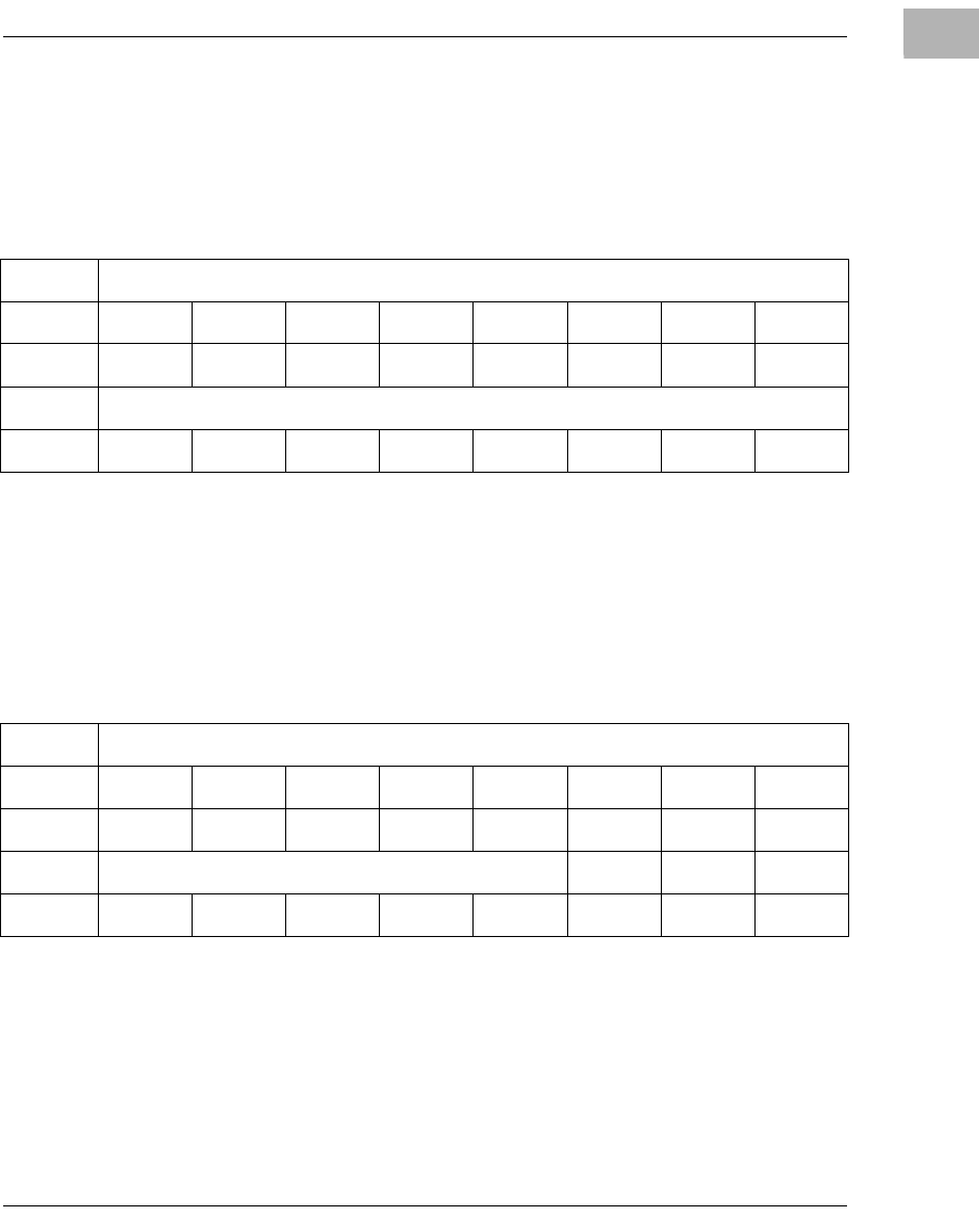
ISA Local Resource Bus
http://www.motorola.com/computer/literature 1-41
1
Location Monitor Upper Base Address Register
The Location Monitor Upper Base Address register is an 8-bit register
located at ISA I/O address x1002. The Universe ASIC is programmed so
that this register can be accessed from the VMEbus to provide VMEbus
location monitor function.
VA[15:8] Upper Base Address for the location monitor function.
Location Monitor Lower Base Address Register
The Location Monitor Lower Base Address register is an 8-bit register
located at ISA I/O address x1003. The Universe ASIC is programmed so
that this register can be accessed from the VMEbus to provide VMEbus
location monitor function.
VA[7:4] Lower Base Address for the location monitor function.
LMEN This bit must be set to enable the location monitor
function.
REG Location Monitor Upper Base Address Register - Offset $1002
BIT SD7 SD6 SD5 SD4 SD3 SD2 SD1 SD0
FIELD VA15 VA14 VA13 VA12 VA11 VA10 VA9 VA8
OPER R/W
RESET 00000000
REG Location Monitor Lower Base Address Register - Offset $1003
BIT SD7 SD6 SD5 SD4 SD3 SD2 SD1 SD0
FIELD VA7 VA6 VA5 VA4 LMEN
OPER R/W R R R
RESET 00000000
1-42 Computer Group Literature Center Web Site
Board Description and Memory Maps
1
Semaphore Register 1
Semaphore Register 1 is an 8-bit register located at ISA I/O address x1004.
The Universe ASIC is programmed so that this register can be accessible
from the VMEbus. This register can only be updated if bit 7 is low or if the
new value has the most significant bit cleared. When bit 7 is high, this
register will not latch in the new value if the new value has the most
significant bit set.
Semaphore Register 2
Semaphore Register 2 is an 8-bit register located at ISA I/O address x1005.
The Universe ASIC is programmed so that this register can be accessible
from the VMEbus. This register can only be updated if bit 7 is low or if the
new value has the most significant bit cleared. When bit 7 is high, this
register will not latch in the new value if the new value has the most
significant bit set.
REG Semaphore Register 1 - Offset $1004
BIT SD7 SD6 SD5 SD4 SD3 SD2 SD1 SD0
FIELD SEM1
OPER R/W
RESET 00000000
REG Semaphore Register 2 - Offset $1005
BIT SD7 SD6 SD5 SD4 SD3 SD2 SD1 SD0
FIELD SEM2
OPER R/W
RESET 00000000
ISA Local Resource Bus
http://www.motorola.com/computer/literature 1-43
1
VME Geographical Address Register (VGAR)
The VME Geographical Address register is an 8-bit read-only register
located at ISA I/O address x1006. This register reflects the states of the
geographical address pins at the P1 connector.
Emulated Z8536 CIO Registers and Port Pins
Although MVME2300 series boards do not use a Z8536 device, several of
its functions are emulated within an ISA Register PLD. These functions
are accessed by reading/writing the Port A, B, C Data registers and Control
register. Note that the Pseudo IACK function is not implemented in the
MVME2300 series.
Emulated Z8536 Registers
The MVME2300 series implements the Z8536 CIO functions according to
the following table.
REG VME Geographical Address Register - Offset $1006
BIT SD7 SD6 SD5 SD4 SD3 SD2 SD1 SD0
FIELD GAP# GA4# GA3# GA2# GA1# GA0#
OPER READ ONLY
RESET XXXXXXXX
Table 1-20. Emulated Z8536 Access Registers
PCI I/O Address Function
0000 0844 Port C’s Data Register
0000 0845 Port B’s Data Register
0000 0846 Port A’s Data Register
0000 0847 Control Register
1-44 Computer Group Literature Center Web Site
Board Description and Memory Maps
1
Z8536 CIO Port Pins
The following table shows the signal function and port mapping for the
Z8536 CIO emulation. The signal directions are fixed in hardware.
Table 1-21. Z8536 CIO Port Pin Assignments
Port
Pin Signal
Name Direction Descriptions
PA0 I/O Not used
PA1 I/O Not used
PA2 I/O Not used
PA3 I/O Not used
PA4 I/O Not used
PA5 I/O Not used
PA6 BRDFAIL Output Board Fail: When set, will illuminate BFL LED.
PA7 I/O Not used
PB0 I/O Not used
PB1 I/O Not used
PB2 I/O Not used
PB3 I/O Not used
PB4 I/O Not used
PB5 I/O Not used
PB6 I/O Not used
PB7 ABORT_ Input Status of ABORT# signal
PC0 I/O Not used
PC1 I/O Not used

ISA Local Resource Bus
http://www.motorola.com/computer/literature 1-45
1
ISA DMA Channels
No ISA DMA channels are implemented on MVME2300 series boards.
PC2 BASETYP0 Input Genesis Base Module Type:
00b = Genesis II (see Base Module Status Register)
01b = MVME1600-011
10b = Reserved
11b = MVME1600-001
PC3 BASETYP1 Input
Table 1-21. Z8536 CIO Port Pin Assignments (Continued)
Port
Pin Signal
Name Direction Descriptions
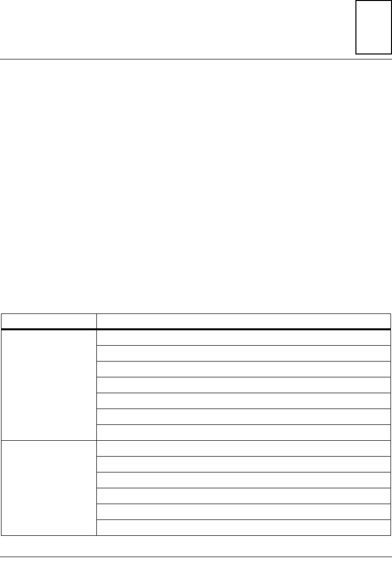
2-1
2
2Raven PCI Bridge ASIC
Introduction
This chapter describes the architecture and usage of the Raven ASIC, a
PowerPC-to-PCI-Local-Bus bridge controller chip. The Raven is intended
to provide PowerPC 60x (MPC60x) compliant devices access to devices
residing on the PCI Local Bus. In the remainder of this chapter, the
MPC60x bus is referred to as the "MPC bus" and the PCI Local Bus is
referred to as "PCI". PCI is a high-performance 32-bit or 64-bit, burst
mode, synchronous bus capable of transfer rates of 132 MB/sec in 32-bit
mode or 264 MB/sec in 64-bit mode using a 33MHz clock.
Features
The following table summarizes the characteristics of the Raven ASIC.
Table 2-1. Features of the Raven ASIC
Function Features
MPC Bus Interface Direct interface to MPC603 or MPC604 processors
64-bit data bus, 32-bit address bus
Four independent software-programmable slave map decoders
Multi-level write-post FIFO for writes to PCI
Support for MPC bus clock speeds up to 66MHz
Selectable big- or little-endian operation
3.3V signal levels
PCI Interface Fully PCI Rev. 2.0 compliant
32-bit or 64-bit address/data bus
Support for accesses to all four PCI address spaces
Single-level write-posting buffers for writes to the MPC bus
Read-ahead buffer for reads from the MPC bus
Four independent software-programmable slave map decoders
2-2 Computer Group Literature Center Web Site
Raven PCI Bridge ASIC
2
Block Diagram
Figure 2-1 shows a functional block diagram of the Raven ASIC. The
Raven control logic is subdivided into the following functions:
❏PCI slave
❏PCI master
❏MPC slave
❏MPC master
Interrupt Controller MPIC compliant
Support for 16 external interrupt sources and two processors
Multiprocessor interrupt control allowing any interrupt source to be
directed to either processor
Multilevel cross-processor interrupt control for multiprocessor
synchronization
Four 31-bit tick timers
Processor
Coordination Two 64-bit general purpose registers for cross-processor messaging
Table 2-1. Features of the Raven ASIC (Continued)
Function Features
Block Diagram
http://www.motorola.com/computer/literature 2-3
2
Figure 2-1. Raven Block Diagram
1914 9702
Data Path ‘B’
Mux FIFO
Endian
Mux FIFO
Endian
Data Path ‘A’
PCI Regs
MPIC
PCI Dec
Mux Reg
Mux Reg
PCI Slave
MPC Slave
Reg
Reg
MPC Dec
PCIADIN
PCI Master
Mux PCI
MPC Master
MPC Regs
Raven
PCI Bus
MPC Bus
Mux MPC
MPCADIN

2-4 Computer Group Literature Center Web Site
Raven PCI Bridge ASIC
2Functional Description
The Raven data path logic is subdivided into the following functions:
❏Data Path ‘A’ FIFOs/muxes
❏Data Path ‘B’ FIFOs/muxes
❏PCIADIN, MPCADIN, Mux PCI, and Mux MPC
Address decoding is handled in the PCI Decode and MPC Decode blocks.
The control register logic is contained in the PCI Registers and MPC
Registers blocks. The interrupt controller (RavenMPIC) and the MPC
arbiter functions make up the remainder of the Raven design.
The data path function imposes some restrictions on access to the
RavenMPIC, the PCI registers, and the MPC registers. The RavenMPIC
and the PCI registers are only accessible to PCI-originated transactions.
The MPC registers are only accessible to MPC-originated transactions.
MPC Bus Interface
The MPC Bus interface is designed to be coupled directly to up to two
MPC603 or MPC604 microprocessors as well as a memory/cache
subsystem. It uses a subset of the capabilities of the MPC60x bus protocol.
MPC Address Mapping
The Raven will map either PCI memory space or PCI I/O space into MPC
address space using four programmable map decoders. These decoders
provide windows into the PCI bus from the MPC bus. The most significant
16 bits of the MPC address are compared with the address range of each
map decoder, and if the address falls within the specified range, the access
is passed on to PCI. An example of this appears in Figure 2-2.
Functional Description
http://www.motorola.com/computer/literature 2-5
2
Figure 2-2. MPC-to-PCI Address Decoding
The Raven ASIC imposes no limits on how large an address space a map
decoder can represent. There is a minimum of 64KB due to the resolution
of the address compare logic.
For each map, there is an associated set of attributes. These attributes are
used to enable read accesses, enable write accesses, enable write-posting,
and define the PCI transfer characteristics.
Each map decoder also includes a programmable 16-bit address offset. The
offset is added to the 16 most significant bits of the MPC address, and the
result is used as the PCI address. This offset allows PCI devices to reside
at any PCI address, independent of the MPC address map. An example of
this appears in Figure 2-3.
MPC Bus Address 80801234
31
16150
MSADDx Register 70809000
31
1615 0
>= <=andDecode is
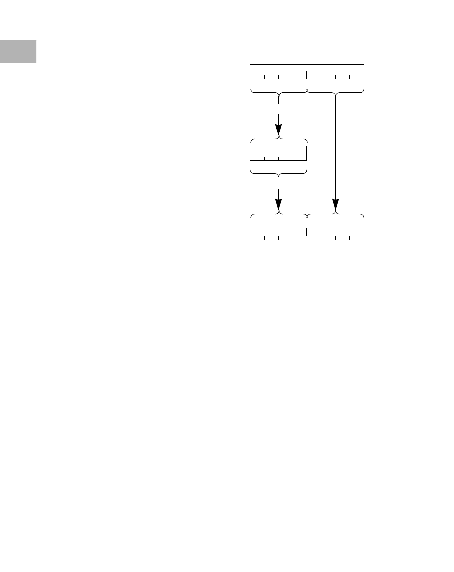
2-6 Computer Group Literature Center Web Site
Raven PCI Bridge ASIC
2
Figure 2-3. MPC to PCI Address Translation
You should take care to assure that all programmable decoders decode
unique address ranges, since overlapping address ranges will lead to
undefined operation.
MPC Slave
The MPC slave provides the interface between the MPC bus and the Raven
FIFOs. The MPC slave is responsible for tracking and maintaining
coherency to the 60x processor bus protocol.
The MPC slave divides MPC command types into three categories:
Address Only; Write; and Read.
If a command is of type address-only and the address presented at the time
of the command is a valid Raven address, the MPC slave will respond
immediately. The Raven will not respond to address-only cycles where the
address presented is not a Raven address. The response of the MPC slave
to command types is listed in Table 2-2.
MPC Bus Address 8 0801234
31
16150
MSOFFx Register 9000
150
+
PCI Bus Address 10801234
0
151631
=
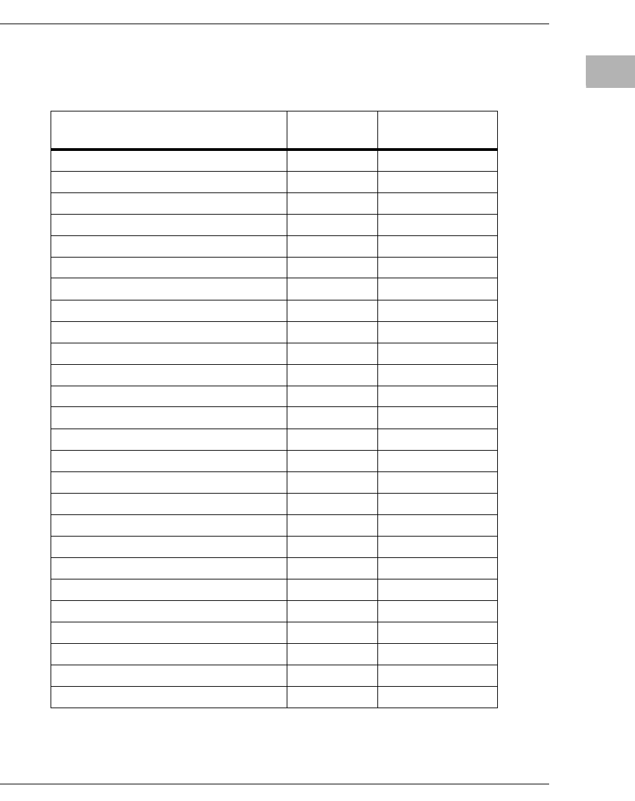
Functional Description
http://www.motorola.com/computer/literature 2-7
2
Table 2-2. Command Types — MPC Slave Response
MPC Transfer Type Transfer
Encoding Transaction
Clean Block 00000 Addr Only
Flush Block 00100 Addr Only
SYNC 01000 Addr Only
Kill Block 01100 Addr Only
EIEIO 10000 Addr Only
ECOWX 10100 No Response
TLB Invalidate 11000 Addr Only
ECIWX 11100 No Response
LWARX 00001 Addr Only
STWCX 00101 Addr Only
TLBSYNC 01001 Addr Only
ICBI 01101 Addr Only
Reserved 1XX01 No Response
Write-with-flush 00010 Write
Write-with-kill 00110 Write
Read 01010 Read
Read-with-intent-to-modify 01110 Read
Write-with-flush-atomic 10010 Write
Reserved 10110 No Response
Read-atomic 11010 Read
Read-with-intent-to-modify-atomic 11110 Read
Reserved 00011 No Response
Reserved 00111 No Response
Read-with-no-intent-to-cache 01011 Read
Reserved 01111 No Response
Reserved 1xx11 No Response

2-8 Computer Group Literature Center Web Site
Raven PCI Bridge ASIC
2MPC Write Posting
The MPC write FIFO stores up to eight data beats in any combination of
single- and four-beat (burst) transactions. If write-posting is enabled,
Raven stores the data necessary to complete an MPC write transfer to the
PCI bus and immediately acknowledges the transaction on the MPC bus.
This frees the MPC bus from waiting for the potentially long PCI
arbitration and transfer. The MPC bus may be used for more useful work
while the Raven manages the completion of the write-posted transaction
on PCI.
All transactions will be completed on the PCI bus in the same order that
they are completed on the MPC bus. A read or a compelled write
transaction will force all previously issued write-posted transactions to be
flushed from the FIFO. All write-posted transfers will be completed before
a non-write-posted read or write is begun, to assure that all transfers are
completed in the order issued. All write-posted transfers will also be
completed before any access to the Raven’s registers is begun.
MPC Master
The MPC master will attempt to move data using burst transfers wherever
possible. A 64-bit-by-16 entry FIFO is used to hold data between the PCI
slave and the MPC master to ensure that optimum data throughput is
maintained. While the PCI slave is filling the FIFO with one cache line
worth of data, the MPC master can be moving another cache line worth
onto the MPC bus. This will allow the PCI slave to receive long block
transfers without stalling.
When programmed in “read ahead” mode (the RAEN bit in the PSATTx
register is set) and the PCI slave receives a Memory Read Line or Memory
Read Multiple command, the MPC master will fetch data in bursts and
store it in the FIFO. The contents of the FIFO will then be used to attempt
to satisfy the data requirements for the remainder of the PCI block
transaction. If the data requested is not in the FIFO, the MPC master will
read another cache line. The contents of the FIFO are “invalidated” at the
end of each PCI block transaction.

Functional Description
http://www.motorola.com/computer/literature 2-9
2
Notes
1. Read-ahead mode should not be used when data coherency may be
a problem, as there is no way to snoop all MPC bus transactions and
invalidate the contents of the FIFO.
2. Accesses near the top of local memory with read-ahead mode
enabled could cause the MPC master to perform reads beyond the
top of local memory, which could produce an MPC bus timeout
error.
The MPC bus transfer types generated by the MPC master depend on the
PCI command code and the INV/GBL bits in the PSATTx registers. The
GBL bit determines whether or not the GBL∗ signal is asserted for all
portions of a transaction, and is fully independent of the PCI command
code and INV bit. Table 2-3 shows the relationship between PCI command
codes and the INV bit.
Table 2-3. MPC Transfer Types
The MPC master incorporates an optional operating mode called Bus Hog.
When Bus Hog is enabled, the MPC master will continually request the
MPC bus for the entire duration of each PCI transfer. When Bus Hog is not
PCI Command Code INV MPC Transfer Type MPC Transfer Size TT0-TT4
Memory Read
Memory Read Multiple
Memory Read Line
0 Read Burst/Single Beat 01010
Memory Read
Memory Read Multiple
Memory Read Line
1 Read With Intent to
Modify Burst/Single Beat 01110
Memory Write
Memory Write and
Invalidate
x Write with Kill Burst 00110
Memory Write
Memory Write and
Invalidate
x Write with Flush Single Beat 00010

2-10 Computer Group Literature Center Web Site
Raven PCI Bridge ASIC
2enabled, the MPC master will structure its bus request actions according to
the requirements of the FIFO. Use this mode with caution, since the over-
generosity of bus ownership to the MPC master can be detrimental to the
host CPU’s performance. The Bus Hog mode can be controlled by the
BHOG bit within the GCSR. The default state for BHOG is disabled.
MPC Arbiter
The MPC Arbiter is an optional feature in the Raven ASIC. It is not used
on MVME2300 series boards. Arbitration for the MPC bus on the
MVME2300 series is performed external to the Raven.
MPC Bus Timer
The MPC bus timer allows the current bus master to recover from a lock-
up condition resulting from no slave response to the transfer request.
The timeout duration of the bus timer is determined by the MBT field in
the Global Control/Status register.
The bus timer starts ticking at the beginning of an address transfer (TS∗
asserted). If the address transfer is not terminated (AACK∗ asserted)
before the timeout period has elapsed, the Raven will assert the MATO bit
in the MPC Error Status register, latch the MPC address in the MPC Error
Address register, and then terminate the cycle.
The MATO bit may be configured to generate an interrupt or a machine
check through the MEREN register.
The timer is disabled if the transfer is intended for PCI. PCI-bound
transfers will be timed by the PCI master.
PCI Interface
The Raven PCI interface is designed for direct connection to a PCI Local
Bus. It supports Master and Target transactions within Memory space, I/O
space, and Configuration space.

Functional Description
http://www.motorola.com/computer/literature 2-11
2
The PCI interface may operate at any clock speed up to 33MHz. The
PCLK input must be externally synchronized with the MCLK input, and
the frequency of the PCLK input must be exactly half the frequency of the
MCLK input.
PCI Address Mapping
The Raven ASIC provides three resources to PCI:
❏Configuration registers mapped into PCI Configuration space
❏MPC bus address space mapped into PCI Memory space
❏RavenMPIC control registers mapped into either PCI I/O space or
PCI Memory space
Configuration Registers
The Raven has no IDSEL pin. Instead, an internal connection made within
the Raven logically associates the assertion of IDSEL with the assertion of
AD31.
Raven provides a configuration space that is fully compliant with the PCI
Local Bus Specification 2.0 definition for configuration space. Two base
registers within the standard 64-byte header are used to control the
mapping of RavenMPIC. One register is dedicated to mapping
RavenMPIC into PCI I/O space; the other register is dedicated to mapping
RavenMPIC into PCI Memory space. The mapping of MPC address space
is handled by device-specific registers located above the 64-byte header.
These control registers support a mapping scheme that is functionally
similar to the PCI-to-MPC mapping scheme described in the section on
MPC Address Mapping earlier in this chapter.
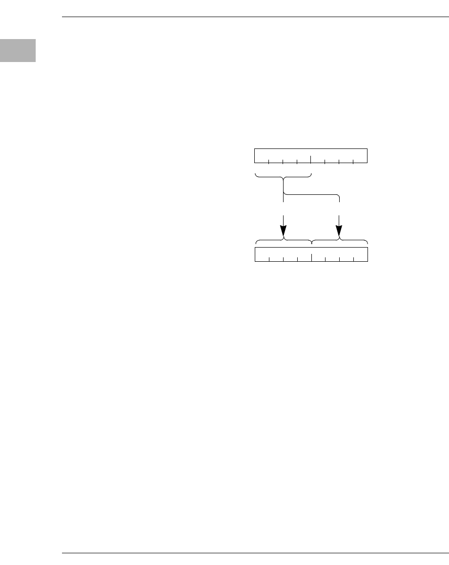
2-12 Computer Group Literature Center Web Site
Raven PCI Bridge ASIC
2MPC Bus Address Space
The Raven will map MPC address space into PCI Memory space using
four programmable map decoders. The most significant 16 bits of the PCI
address are compared with the address range of each map decoder; if the
address falls within the specified range, the access is passed on to the MPC
bus. An example of this appears in Figure 2-4.
Figure 2-4. PCI to MPC Address Decoding
The Raven ASIC imposes no limits on how large an address space a map
decoder can represent. There is a minimum of 64KB due to the resolution
of the address compare logic.
For each map, there is an associated set of attributes. These attributes are
used to enable read accesses, enable write accesses, enable write-posting,
and define the MPC bus transfer characteristics.
Each map decoder also includes a programmable 16-bit address offset. The
offset is added to the 16 most significant bits of the PCI address, and the
result is used as the MPC address. This offset allows devices to reside at
any MPC address, independent of the PCI address map. An example of this
appears in Figure 2-5.
PCI Bus Address 80801234
0
151631
PSADDx Register 7 0809000
0
151631
>= <=andDecode is
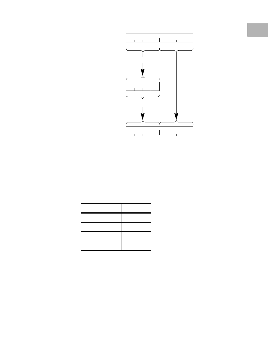
Functional Description
http://www.motorola.com/computer/literature 2-13
2
Figure 2-5. PCI to MPC Address Translation
All Raven address decoders are prioritized so that programming multiple
decoders to respond to the same address is not a problem. When the PCI
address falls into the range of more than one decoder, only the highest
priority one will respond. The decoders are prioritized as shown below.
RavenMPIC Control Registers
The RavenMPIC control registers are located within either PCI memory or
PCI I/O space using traditional PCI-defined base registers within the
predefined 64-byte header. Refer to the section on Raven Interrupt
Controller for more information.
Decoder Priority
PCI Slave 0 highest
PCI Slave 1
PCI Slave 2
PCI Slave 3 lowest
PCI Bus Address 80801234
0
151631
PSOFFx Register 9 000
1631
+
MPC Bus Address 1 0801234
31
16150
=

2-14 Computer Group Literature Center Web Site
Raven PCI Bridge ASIC
2PCI Slave
The PCI slave provides the control logic needed to interface the PCI bus to
the Raven’s FIFO buffers. The PCI slave can accept either 32-bit or 64-bit
transactions, but it can accept only 32-bit addressing.
There is no limit to the length of the transfer that the slave can handle.
During posted write cycles, the slave will continue to accept write data
until the write-post FIFO is full. If the write-post FIFO is full, the slave will
hold off the master with wait states until there is more room in the FIFO.
The slave will not initiate a disconnect.
If the write transaction is compelled, the slave will hold off the master with
wait states while each beat of data is being transferred. The slave will
acknowledge the completion of the transfer only after the data transfer has
successfully completed on the MPC bus.
If a read transaction is occurring within an address space marked for
prefetching, the slave (in conjunction with the MPC master) will attempt
to read far enough ahead on the MPC bus to allow for an uninterrupted
burst transaction on the PCI bus. Read transactions within address spaces
marked for no prefetching will be acknowledged on the PCI bus only after
a single beat read has successfully completed on the MPC bus.
Each read on the MPC bus will begin only after the previous read has been
acknowledged on the PCI bus and there is an indication that the PCI master
wishes more data to be transferred.
The following paragraphs identify some associations between the
operation of the PCI slave and the requirements of the PCI 2.0 Local Bus
Specification.
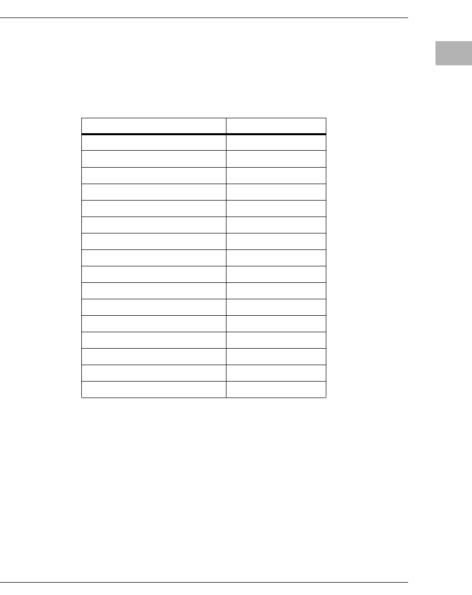
Functional Description
http://www.motorola.com/computer/literature 2-15
2
Command Types
Table 2-4 shows which types of PCI cycles the slave has been designed to
accept.
Addressing
The slave will accept any combination of byte enables during read or write
cycles. During write cycles, a discontinuity (i.e., a ‘hole’) in the byte
enables will force the slave to issue a disconnect. During all read cycles,
the slave will return an entire word of data regardless of the byte enables.
During I/O read cycles, the slave will perform integrity checking of the
byte enables against the address being presented and assert SERR∗ in the
event there is an error.
Table 2-4. Command Types — PCI Slave Response
Command Type Slave Response?
Interrupt Acknowledge No
Special Cycle No
I/O Read Yes
I/O Write Yes
Reserved No
Reserved No
Memory Read Yes
Memory Write Yes
Reserved No
Reserved No
Configuration Read Yes
Configuration Write Yes
Memory Read Multiple Yes
Dual Address Cycle No
Memory Read Line Yes
Memory Write and Invalidate Yes

2-16 Computer Group Literature Center Web Site
Raven PCI Bridge ASIC
2The slave will honor only the Linear Incrementing addressing mode. The
slave will perform a disconnect with data if any other mode of addressing
is attempted.
Device Selection
The PCI slave will always respond to valid decoded cycles as a medium
responder.
Target-Initiated Termination
The PCI slave normally strives to complete transactions without issuing
disconnects or retries.
One exception is when the slave performs configuration cycles. All
configuration cycles are terminated with a disconnect after one data beat
has been transferred. Another exception is the issue of a disconnect when
asked to perform a transaction with byte enable ‘holes’.
Fast Back-to-Back Transactions
The PCI slave supports both of the fundamental target requirements for
fast back-to-back transactions. The PCI slave meets the first criteria of
being able to successfully track the state of the PCI bus without the
existence of an IDLE state between transactions. The second criteria,
associated with signal turn-around timing, is met by default since the slave
functions as a medium responder.
Latency
The PCI slave has no hardware mechanisms in place to guarantee that the
initial and subsequent target latency requirements are met. This is typically
not a problem, since the bandwidth of the MPC bus far exceeds the
bandwidth of the PCI bus. The Raven MPC arbiter has been designed to
give the highest priority to its own transactions, which further reduces PCI
bus latency.
Exclusive Access
The PCI slave has no mechanism to support exclusive access.

Functional Description
http://www.motorola.com/computer/literature 2-17
2
Parity
The PCI slave supports address parity error detection, data parity
generation and data parity error detection.
Cache Support
The PCI slave does not participate in the PCI caching protocol.
PCI Write Posting
If write-posting is enabled, the Raven stores the target address, attributes,
and up to 128 bytes of data from one PCI write transaction and
immediately acknowledges the transaction on the PCI bus. This allows the
slower PCI to continue to transfer data at its maximum bandwidth, and the
faster MPC bus to accept data in high-performance cache-line burst
transfers.
Only one PCI transaction may be write-posted at any given time. If the
Raven is busy processing a previous write-posted transaction when a new
PCI transaction begins, the next PCI transaction is delayed (TRDY∗ is not
asserted) until the previous transaction has completed. If during a
transaction the write-post buffer is filled, subsequent PCI data transfers are
delayed (TRDY∗ is not asserted) until the Raven has removed some data
from the FIFO. Under normal conditions, the Raven should be able to
empty the FIFO faster than the PCI bus can fill it.
PCI Configuration cycles intended for internal Raven registers are also
delayed if the Raven is busy, so that control bits which may affect write-
posting do not change until all write-posted transactions have completed.
PCI Master
The PCI master, in conjunction with the capabilities of the MPC slave, will
attempt to move data in either single-beat or four-beat (burst) transactions.
All single-beat transactions will be subdivided into one or two 32-bit
transfers, depending on the alignment and size of the transaction. The PCI
master will attempt to transfer all four-beat transactions in 64-bit mode if
the PCI bus has 64-bit mode enabled. If at any time during the transaction
the PCI target indicates that it cannot support 64-bit mode, the PCI master
will continue to transfer the remaining data in 32-bit mode.
2-18 Computer Group Literature Center Web Site
Raven PCI Bridge ASIC
2The PCI master can support Critical Word First (CWF) burst transfers. The
PCI master will divide this transaction into two parts. The first part will
start on the address presented with the CWF transfer request and continue
up to the end of the current cache line. The second transfer will start at the
beginning of the associated cache line and work its way up to (but not
including) the word addressed by the CWF request.
It should be noted that even though the master can support burst
transactions, a majority of the transaction types handled are single-beat
transfers. Since PCI space is typically not configured as cacheable, burst
transactions to PCI space would not naturally occur. Burst transactions
must be supported, however, since it is conceivable that bursting could
happen. For example, nothing prevents the processor from loading up a
cache line with PCI write data and manually flushing the cache line.
The following paragraphs identify some associations between the
operation of the PCI master and the requirements of the PCI 2.0 Local Bus
Specification.
Command Types
The PCI command codes generated by the PCI master depend on the type
of transaction being performed on the MPC bus. Please refer to the MPC
Slave section earlier in this chapter for a further description of MPC bus
read and MPC bus write transactions. Table 2-5 summarizes the command
types supported and shows how they are generated.
Table 2-5. PCI Master Command Codes
Entity Addressed MPC
Transfer Type TBST∗MEM C/BE PCI Command
PIACK Read x x 0000 Interrupt Acknowledge
CONADD/CONDAT Write x x 0001 Special Cycle
MPC Mapped PCI Space Read x 0 0010 I/O Read
Write x 0 0011 I/O Write
-- Unsupported -- 0100 Reserved
-- Unsupported -- 0101 Reserved
MPC Mapped PCI Space Read 1 1 0110 Memory Read
Write x 1 0111 Memory Write
Functional Description
http://www.motorola.com/computer/literature 2-19
2
Addressing
The PCI master will generate all memory transactions using the linear
incrementing addressing mode.
Combining, Merging, and Collapsing
The PCI master does not participate in any of these protocols.
Master Initiated Termination
The PCI master can handle any defined method of target retry, target
disconnect, or target abort. If the target responds with a retry, the PCI
master will wait for the required two clock periods and attempt the
transaction again. The attempts will continue indefinitely until the
transaction either completes, or is aborted by the target, or is aborted due
to a Raven-detected bridge lock. The same happens if the target responds
with a disconnect and there is still data to be transferred.
If the PCI master detects a target abort during a read, any untransferred
read data will be filled with 1s. If the PCI master detects a target abort
during a write, any untransferred portions of data will be dropped. The
same rule applies if the PCI master generates a Master Abort cycle.
-- Unsupported -- 1000 Reserved
-- Unsupported -- 1001 Reserved
CONADD/CONDAT Read x x 1010 Configuration Read
CONADD/CONDAT Write x x 1011 Configuration Write
-- Unsupported -- 1100 Memory Read Multiple
-- Unsupported -- 1101 Dual Address Cycle
MPC Mapped PCI Space Read 0 1 1110 Memory Read Line
-- Unsupported -- 1111 Memory Write and
Invalidate
Table 2-5. PCI Master Command Codes (Continued)
Entity Addressed MPC
Transfer Type TBST∗MEM C/BE PCI Command

2-20 Computer Group Literature Center Web Site
Raven PCI Bridge ASIC
2Arbitration
The PCI master can support parking on the PCI bus. If the PCI master starts
a transaction that is going to take more than one beat, the PCI master will
continuously assert its request until the transaction has completed. The one
exception is when the PCI master receives a disconnect or a retry.
Fast Back-to-Back Transactions
The PCI master does not generate fast back-to-back transactions.
Arbitration Latency
Because the bulk of the transactions on PCI are limited to single-beat
transfers, the PCI master does not implement a Master Latency timer.
Exclusive Access
The PCI master is not able to initiate exclusive access transactions.
Address/Data Stepping
The PCI master does not participate in the Address/Data Stepping
protocol.
Parity
The PCI master supports address parity generation, data parity generation,
and data parity error detection.
Cache Support
The PCI master does not participate in the PCI caching protocol.
Functional Description
http://www.motorola.com/computer/literature 2-21
2
Generating PCI Cycles
Four basic types of bus cycles can be generated on the PCI bus:
❏Memory and I/O
❏Configuration
❏Special Cycle
❏Interrupt Acknowledge
Generating PCI Memory and I/O Cycles
Each programmable slave may be configured to generate PCI I/O or
memory accesses through the MEM and IOM fields in its Attribute register
as shown below.
:
If the MEM bit is set, the Raven will perform Memory addressing on the
PCI bus. The Raven will take the MPC bus address, apply the offset
specified in the MSOFFx register, and map the result directly to the PCI
bus.
The IBM CHRP specification describes two approaches for handling PCI
I/O addressing: contiguous or spread address modes. When the MEM bit
is cleared, the IOM bit is used to select between these two modes whenever
a PCI I/O cycle is to be performed.
The Raven will perform contiguous I/O addressing when the MEM bit is
clear and the IOM bit is clear. The Raven will take the MPC address, apply
the offset specified in the MSOFFx register, and map the result directly to
PCI.
MEM IOM PCI Cycle Type
1xMemory
0 0 Contiguous I/O
0 1 Spread I/O
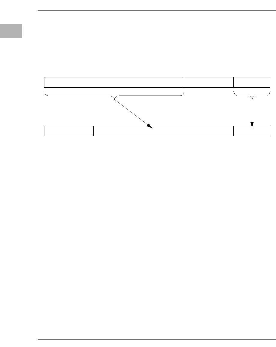
2-22 Computer Group Literature Center Web Site
Raven PCI Bridge ASIC
2The Raven will perform spread I/O addressing when the MEM bit is clear
and the IOM bit is set. The Raven will take the MPC address, apply the
offset specified in the MSOFFx register, and map the result to PCI as
shown in Figure 2-6.
.
Figure 2-6. PCI Spread I/O Address Translation
Spread I/O addressing allows each PCI device’s I/O registers to reside on
a different MPC memory page, so device drivers can be protected from
each other using memory page protection.
All I/O accesses must be performed within natural word boundaries. Any
I/O access that is not contained within a natural word boundary will result
in unpredictable operation. For example, an I/O transfer of four bytes
starting at address $80000010 is considered a valid transfer. An I/O
transfer of four bytes starting at address $80000011 is considered an
invalid transfer since it crosses the natural word boundary at address
$80000013/$80000014.
Generating PCI Configuration Cycles
The Raven uses configuration mechanism #1 as defined in PCI Local Bus
Specification 2.0 to generate configuration cycles. Please refer to the
specification for a complete description of this function.
1915 9702
MPC Address + Offset
31 12 11 5 4 0
31 0
PCI Address
25 24
0 0 0 0 0 0 0
0000000
54

Functional Description
http://www.motorola.com/computer/literature 2-23
2
Configuration mechanism #1 uses an address register/data register format.
Performing a configuration access is a two-step process. The first step is to
place the address of the configuration cycle within the
CONFIG_ADDRESS register. Note that this action does not generate any
cycles on the PCI bus. The second step is to either read or write
configuration data into the CONFIG_DATA register. If the
CONFIG_ADDRESS register has been set up correctly, the Raven will
pass this access on to the PCI bus as a configuration cycle.
The addresses of the CONFIG_ADDRESS and CONFIG_DATA registers
are actually embedded within PCI I/O space. If the CONFIG_ADDRESS
register has been set incorrectly or the access to either the
CONFIG_ADDRESS or CONFIG_DATA register is not 1,2, or 4 bytes
wide, the Raven will pass the access on to PCI as a normal I/O Space
transfer.
The CONFIG_ADDRESS register is located at offset $CF8 from the
bottom of PCI I/O space. The CONFIG_DATA register is located at offset
$CFC from the bottom of PCI I/O space. The Raven address decode logic
has been designed such that MSADD3 and MSOFF3 must be used for
mapping to PCI Configuration (consequently I/O) space. The
MSADD3/MSOFF3 register group is initialized at reset to allow PCI I/O
access starting at address $80000000. The powerup location (that is, little-
endian disabled) of the CONFIG_ADDRESS register is $80000CF8, and
the CONFIG_DATA register is located at $80000CFC.
The CONFIG_ADDRESS register must be prefilled with four fields:
1. Register Number
2. Function Number
3. Device Number
4. Bus Number
The Register Number and Function Number are passed along to the PCI
bus as portions of the lower address bits.
When performing a configuration cycle, the Raven uses the upper 20
address bits as IDSEL lines. During the address phase of a configuration
cycle, only one of the upper address bits will be set. The device that has its
2-24 Computer Group Literature Center Web Site
Raven PCI Bridge ASIC
2IDSEL connected to the address bit being asserted will be selected for a
configuration cycle. The Raven decodes the Device Number to determine
which of the upper address lines to assert. The decoding of the five-bit
Device Number is show below:.
The Bus Number determines which bus is the target for the configuration
read cycle. The Raven will always host PCI bus #0. Accesses that are to be
performed on the PCI bus connected to the Raven must have zero
programmed into the Bus Number. If the configuration access is targeted
for another PCI bus, then that bus number should be programmed into the
Bus Number field. The Raven will detect a nonzero field and convert the
transaction to a Type 1 Configuration cycle.
Generating PCI Special Cycles
The Raven supports the method stated in PCI Local Bus Specification 2.0
to generate special cycles using Configuration Mechanism #1. To prime
the Raven for a special cycle, the host processor must write a 32-bit value
to the CONFIG_ADDRESS register. The contents of the write are defined
later in this chapter under the CONFIG_ADDRESS register definition.
After the write to CONFIG_ADDRESS has been accomplished, the next
write to the CONFIG_DATA register causes the Raven to generate a
special cycle on the PCI bus. The write data is driven onto AD[31:0]
during the special cycle’s data phase.
Device Number Address Bit
00000 AD31
00001 - 01010 All Zeros
01011 AD11
01100 AD12
(etc.) (etc.)
11101 AD29
11110 AD30
11111 All Zeros

Functional Description
http://www.motorola.com/computer/literature 2-25
2
Generating PCI Interrupt Acknowledge Cycles
Performing a read from the PIACK register will initiate a single PCI
Interrupt Acknowledge cycle. Any single byte or combination of bytes
may be read from, and the actual byte enable pattern used during the read
will be passed on to the PCI bus. Upon completion of the PCI interrupt
acknowledge cycle, the Raven will present the resulting vector information
obtained from the PCI bus as read data.
Endian Conversion
The Raven ASIC supports both big- and little-endian data formats. Since
the PCI bus is inherently little-endian, conversion is necessary if all MPC
devices are configured for big-endian operation. The Raven may be
programmed to perform the endian conversion described below.
When MPC Devices are Big-Endian
When all MPC devices are operating in big-endian mode, all data to/from
the PCI bus must be swapped such that the PCI bus looks big-endian from
the MPC bus’s perspective. This association is true regardless of whether
the transaction originates on the PCI bus or the MPC bus. Figure 2-7
illustrates the concept.
2-26 Computer Group Literature Center Web Site
Raven PCI Bridge ASIC
2.
Figure 2-7. Big- to Little-Endian Data Swap
1916 9610
DH07-00
DH15-08
DH23-16
DH31-24
DL07-00
DL15-08
DL23-16
DL31-24
D0 D1 D2 D3 D4 D5 D6 D7
D7 D6 D5 D4 D3 D2 D1 D0
D0 D1 D2 D3 D4 D5 D6 D7
AD63-56
AD55-48
AD47-40
AD39-32
AD31-24
AD23-16
AD15-08
AD07-00
DH07-00
DH15-08
DH23-16
DH31-24
DL07-00
DL15-08
DL23-16
DL31-24
D7 D6 D5 D4
D3 D2 D1 D0
AD31-24
AD23-16
AD15-08
AD07-00
PPC Bus
64-bit PCI
PPC Bus
32-bit PCI
Functional Description
http://www.motorola.com/computer/literature 2-27
2
When MPC Devices are Little-Endian
When all MPC devices are operating in little-endian mode, the originating
address is modified to remove the exclusive-ORing applied by MPC60x
processors before being passed on to the PCI bus. Note that no data
swapping is performed. Address modification happens to the originating
address regardless of whether the transaction originates from the PCI bus
or the MPC bus. The three low-order address bits are exclusive-ORed with
a three-bit value that depends on the length of the operand, as shown in
Table 2-6.
Table 2-6. Address Modification for Little-Endian Transfers
Note The only legal data lengths supported in little-endian mode
are 1-, 2-, 4-, or 8-byte aligned transfers.
Since there are some difficulties with this method in dealing with
unaligned PCI-originated transfers, the Raven MPC master will break up
all unaligned PCI transfers into multiple aligned PCI transfers into
multiple aligned transfers on the MPC bus.
Raven Registers and Endian Mode
The Raven ASIC’s registers are not sensitive to changes in big-endian and
little-endian mode. With respect to the MPC bus (but not always the
address internal to the processor), the MPC registers are always
represented in big-endian mode. This means that the processor’s internal
view of the MPC registers will vary depending on the processor’s
operating mode.
Data
Length
(bytes)
Address
Modification
1 XOR with 111
2 XOR with 110
4 XOR with 100
8 No change

2-28 Computer Group Literature Center Web Site
Raven PCI Bridge ASIC
2With respect with the PCI bus, the RavenMPIC registers and the
configuration registers are always represented in little-endian mode.
The CONFIG_ADDRESS and CONFIG_DATA registers are actually
represented in PCI space to the processor and are subject to the endian
functions. For example, the powerup location of the CONFIG_ADDRESS
register with respect to the MPC bus is $80000CF8 when the Raven is in
big-endian mode. When the Raven is switched to little-endian mode, the
CONFIG_ADDRESS register with respect to the MPC bus is $80000CFC.
Note that in both cases the address generated internal to the processor will
be $80000CF8.
The contents of the CONFIG_ADDRESS register are not subject to the
endian function.
The data associated with PIACK accesses is subject to the endian
swapping function. Because the address of a PIACK cycle is undefined,
address modification during little-endian mode is not an issue.
Error Handling
The Raven is capable of detecting and reporting the following errors to one
or more MPC masters:
❏MPC address bus time-out
❏PCI master signalled master abort
❏PCI master received target abort
❏PCI parity error
❏PCI system error
Each of these error conditions will set an error status bit in the MPC Error
Status register. If a second error is detected while any of the error bits is
set, the OVFL bit is asserted, but none of the error bits are changed. You
can clear each bit in the MPC Error Status register by writing a 1 to it;
writing a 0 to it has no effect. New error bits may be set only when all
previous error bits have been cleared.
Functional Description
http://www.motorola.com/computer/literature 2-29
2
When any bit in the MPC Error Status register is set, the Raven ASIC will
attempt to latch as much information as possible about the error in the
MPC Error Address and Attribute registers. Information is saved as
follows:
Each MERST error bit may be programmed to generate a machine check
and/or a standard interrupt. The error response is programmed through the
MPC Error Enable register on a source-by-source basis. When a machine
check is enabled, either the MID field in the MPC Error Attribute register
or the DFLT bit in the MEREN register determine the master to which the
machine check is directed. For errors in which the master that originated
the transaction can be determined, the MID field is used, provided the MID
is%00 (processor 0), %01 (processor 1), or %10 (processor 2). For errors
not associated with a particular MPC master, or associated with masters
other than processor 0, 1, or 2, the DFLT bit is used. One example of an
error condition which cannot be associated with a particular MPC master
would be a PCI system error.
Transaction Ordering
The Raven ASIC supports transaction ordering with an optional FIFO
flushing option. The FLBRD (Flush Before Read) bit within the GCSR
register controls the flushing of PCI write-posted data when performing
MPC-originated read transactions.
Error Status Error Address
and Attributes
MATO From MPC bus
SMA From PCI bus
RTA From PCI bus
PERR Invalid
SERR Invalid

2-30 Computer Group Literature Center Web Site
Raven PCI Bridge ASIC
2When the FLBRD bit is set, Raven will handle read transactions
originating from the MPC bus in the following manner:
❏Write-posted transactions originating from the processor bus are
flushed by the nature of the FIFO architecture. The Raven will hold
the processor with wait states until the PCI-bound FIFO is empty.
❏Write-posted transactions originating from the PCI bus are flushed
whenever the PCI slave has accepted a write-posted transaction and
the transaction has not completed on the MPC bus.
Raven Registers
This section provides a detailed description of all registers in the Raven
ASIC. The registers are organized in two groups: MPC registers and PCI
Configuration registers. The MPC registers are accessible only from the
MPC bus, but accept any valid transfer size. The PCI Configuration
registers reside in PCI configuration space. They are accessible from the
MPC bus through the Raven ASIC.
The MPC registers are described first; the PCI Configuration registers are
described next. A complete discussion of the RavenMPIC registers can be
found later in this chapter.
The following conventions are used in the Raven register charts:
❏R Read Only field.
❏R/W Read/Write field.
❏S Writing a ONE to this field sets this field.
❏C Writing a ONE to this field clears this field.
MPC Registers
The Raven MPC register map is shown in Table 2-7.
2Raven PCI Bridge ASIC
0Raven Registers

Raven Registers
http://www.motorola.com/computer/literature 2-31
2
Table 2-7. Raven MPC Register Map
Bit ---> 01234567891
01
11
21
31
41
51
61
71
81
92
02
12
22
32
42
52
62
72
82
93
03
1
$FEFF0000 VENID DEVID
$FEFF0004 REVID
$FEFF0008 GCSR FEAT
$FEFF000C MARB
$FEFF0010 PADJ
$FEFF0014
$FEFF0018
$FEFF001C
$FEFF0020 MEREN
$FEFF0024 MERST
$FEFF0028 MERAD
$FEFF002C MERAT
$FEFF0030 PIACK
$FEFF0034
$FEFF0038
$FEFF003C
$FEFF0040 MSADD0
$FEFF0044 MSOFF0 MSATT0
$FEFF0048 MSADD1
$FEFF004C MSOFF1 MSATT1
$FEFF0050 MSADD2
$FEFF0054 MSOFF2 MSATT2
$FEFF0058 MSADD3
$FEFF005C MSOFF3 MSATT3
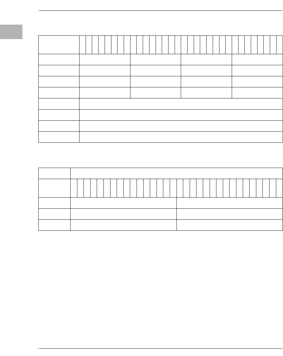
2-32 Computer Group Literature Center Web Site
Raven PCI Bridge ASIC
2
Vendor ID/Device ID Registers
VENID Vendor ID. Identifies the manufacturer of the device. The
identifier is allocated by the PCI SIG to ensure
uniqueness. $1057 has been assigned to Motorola. This
register is duplicated in the PCI Configuration registers.
DEVID Device ID. Identifies this particular device. The Raven
will always return $4801. This register is duplicated in the
PCI Configuration registers.
$FEFF0060
$FEFF0064
$FFEF0068
$FEFF006C
$FEFF0070 GPREG0(Upper)
$FEFF0074 GPREG0(Lower)
$FEFF078 GPREG1(Upper)
$FEFF07C GPREG1(Lower)
Address $FEFF0000
Bit 01234567891
01
11
21
31
41
51
61
71
81
92
02
12
22
32
42
52
62
72
82
93
03
1
Name VENID DEVID
Operation RR
Reset $1057 $4801
Table 2-7. Raven MPC Register Map (Continued)
Bit ---> 01234567891
01
11
21
31
41
51
61
71
81
92
02
12
22
32
42
52
62
72
82
93
03
1
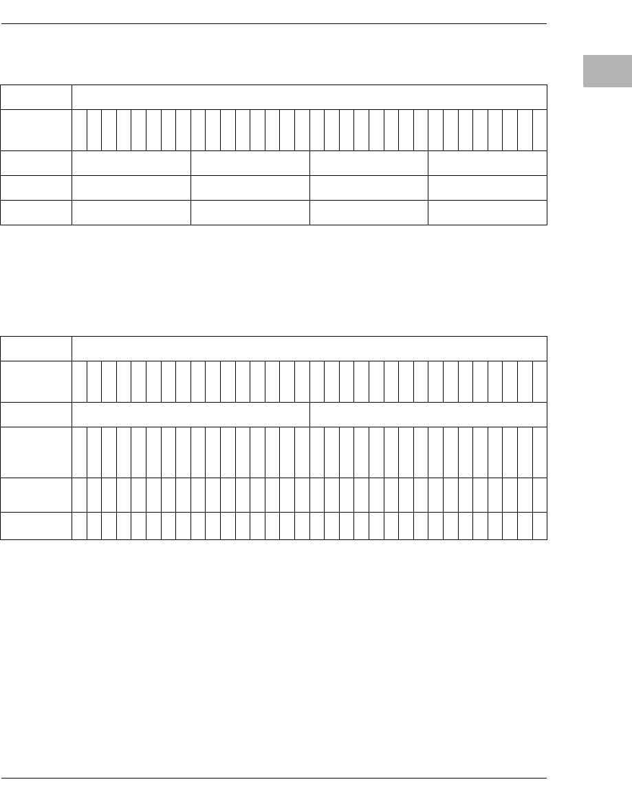
Raven Registers
http://www.motorola.com/computer/literature 2-33
2
Revision ID Register
REVID Revision ID. Identifies the Raven revision level. This
register is duplicated in the PCI Configuration registers.
General Control-Status/Feature Registers
LEND Endian Select. If set, the MPC bus is operating in little-
endian mode. The MPC address will be modified as
described in the When MPC Devices are Little-Endian
section. When LEND is clear, the MPC bus is operating in
big-endian mode, and all data to/from PCI is swapped as
described in the When MPC Devices are Big-Endian
section.
Address $FEFF0004
Bit 01234567891
01
11
21
31
41
51
61
71
81
92
02
12
22
32
42
52
62
72
82
93
03
1
Name REVID
Operation RRRR
Reset $00 $02 $00 $00
Address $FEFF0008
Bit 01234567891
01
11
21
31
41
51
61
71
81
92
02
12
22
32
42
52
62
72
82
93
03
1
Name GCSR FEAT
LEND
BHOG
FLBRD
MBT1
MBT0
P64
MARB
MPIC
MID1
MID0
EXT14
EXT13
EXT12
EXT11
EXT10
EXT09
EXT08
EXT07
EXT06
EXT05
EXT04
EXT03
EXT02
EXT01
EXT00
Operation
R/W
R
R
R
R/W
R/W
R/W
R/W
R
R
R
R
R
R
R
R
R
R
R
R
R
R
R
R
R
R
R
R
R
R
R
R
Reset
0
0
0
0
0
0
0
0
0
0
0
0
0
0
0
0
0
0/1
0/1
0/1
0/1
0/1
0/1
0/1
0/1
0/1
0/1
0/1
0/1
0/1
0/1
0/1
2-34 Computer Group Literature Center Web Site
Raven PCI Bridge ASIC
2FLBRD Flush Before Read. If set, the Raven will guarantee that
all PCI-initiated posted write transactions will complete
before any MPC-initiated read transactions are allowed to
complete. When FLBRD is clear, there is no correlation
between these transaction types and their order of
completion. Please refer to the Transaction Ordering
section for more information.
BHOG Bus Hog. If set, the Raven MPC master will operate in the
Bus Hog mode. Bus Hog mode means the MPC master
will continually request the MPC bus for the entire
duration of each PCI transfer. If Bus Hog is not enabled,
the MPC master will request the bus in a normal manner.
Please refer to the MPC Master section for more
information.
MBTx MPC Bus Time-out. Specifies the MPC bus time-out
length. The time-out length is encoded as follows:
P64 64-bit PCI Mode Enable. If set, the Raven is connected
to a 64-bit PCI bus. This bit is set if REQ64∗ is asserted
on the rising edge of RESET∗.
MARB MPC Arbiter Enable. If set, the Raven internal MPC
Arbiter is enabled. This bit is set if CPUID is %111 on the
rising edge of RESET∗.
MPIC Multi-Processor Interrupt Controller Enable. If set,
the Raven internal MPIC interrupt controller is enabled.
This bit is set if EXT15 is high on the rising edge of
RESET∗. If cleared, Raven-detected errors are passed on
to the processor 0 INT pin.
MBT Time-Out Length
00 256 µsec
01 64 µsec
10 8 µsec
11 Disabled
Raven Registers
http://www.motorola.com/computer/literature 2-35
2
MIDx Master ID. Encoded as shown below to indicate who is
currently the MPC bus master. When the internal MPC
arbiter is enabled (MARB is set), these bits are controlled
by the internal arbiter. When the internal arbiter is
disabled (MARB is clear) these bits reflect the status of
the CPUID pins. In a multi- processor environment, these
bits allow software to determine on which processor it is
currently running. The internal MPC arbiter encodes this
field as follows:
.
FEAT Feature Register. Each bit in this register reflects the
state of one of the external interrupt input pins on the
rising edge of RESET∗. This register may be used to
report hardware configuration parameters to system
software.
MID Current MPC Data Bus Master
00 Device on ABG0*
01 Device on ABG1*
10 Device on ABG2
11 Raven
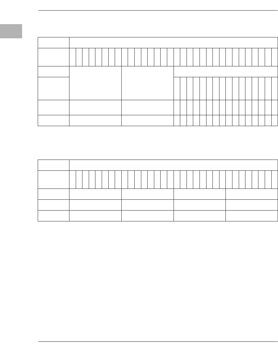
2-36 Computer Group Literature Center Web Site
Raven PCI Bridge ASIC
2MPC Arbiter Control Register
This register is not used in MVME2300 series boards.
Prescaler Adjust Register
PADJ Prescaler Adjust. Used to specify a scale factor for the
prescaler to ensure that the time base for the bus timer is
1 MHz. The scale factor is calculated as follows:
PADJ = 256 - Clk,
where Clk is the frequency of the CLK input in MHz. This
register should be written with the value $BE, indicating
a 66MHz MPC bus.
Address $FEFF000C
Bit 01234567891
01
11
21
31
41
51
61
71
81
92
02
12
22
32
42
52
62
72
82
93
03
1
Name MARB
BREN2
BREN1
BREN0
PKEN
PKMD
GLMD
BAMD
DEFM1
DEFM0
Operation RR
R
R
R
R
R
R/W
R/W
R/W
R/W
R/W
R/W
R/W
R
R
R/W
R/W
Reset $00 $00
0
0
0
0
0
1
1
1
0
0
0
1
0
0
1
1
Address $FEFF0010
Bit 01234567891
01
11
21
31
41
51
61
71
81
92
02
12
22
32
42
52
62
72
82
93
03
1
Name PADJ
Operation RRRR/W
Reset $00 $00 $00 $B4
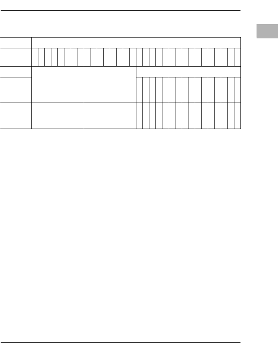
Raven Registers
http://www.motorola.com/computer/literature 2-37
2
MPC Error Enable Register
DFLT Default MPC Master ID. This bit determines which
MCHK∗ pin will be asserted for error conditions in which
the MPC master ID cannot be determined or the Raven
was the MPC master. For example, in event of a PCI
parity error for a transaction in which the Raven’s PCI
master was not involved, the MPC master ID cannot be
determined. When DFLT is set, MCHK1∗ is used. When
DFLT is clear, MCHK0∗ is used.
MATOM MPC Address Bus Time-out Machine Check Enable.
When this bit is set, the MATO bit in the MERST register
is used to assert the MCHK output to the current address
bus master. When this bit is clear, MCHK is not asserted.
PERRM PCI Parity Error Machine Check Enable. When this
bit is set, the PERR bit in the MERST register is used to
assert the MCHK output to bus master 0. When this bit is
clear, MCHK is not asserted.
SERRM PCI System Error Machine Check Enable. When this
bit is set, the SERR bit in the MERST register is used to
assert the MCHK output to bus master 0. When this bit is
clear, MCHK is not asserted.
Address $FEFF0020
Bit 01234567891
01
11
21
31
41
51
61
71
81
92
02
12
22
32
42
52
62
72
82
93
03
1
Name MEREN
DFLT
MATOM
PERRM
SERRM
SMAM
RTAM
MATOII
PERRI
SERRI
SMAI
RTAI
Operation RR
R
R/W
R/W
R
R/W
R/W
R/W
R/W
R
R
R/W
R
R/W
R/W
R/W
R/W
Reset $00 $00
0
0
0
0
0
0
0
0
0
0
0
0
0
0
0
0

2-38 Computer Group Literature Center Web Site
Raven PCI Bridge ASIC
2SMAM PCI Signalled Master Abort Machine Check Enable.
When this bit is set, the SMA bit in the MERST register is
used to assert the MCHK output to the bus master which
initiated the transaction. When this bit is clear, MCHK is
not asserted.
RTAM PCI Master Received Target Abort Machine Check
Enable.When this bit is set, the RTA bit in the MERST
register is used to assert the MCHK output to the bus
master which initiated the transaction. When this bit is
clear, MCHK is not asserted.
MATOI MPC Address Bus Time-out Interrupt Enable.When
this bit is set, the MATO bit in the MERST register is used
to assert an interrupt through the MPIC interrupt
controller. When this bit is clear, no interrupt is asserted.
PERRI PCI Parity Error Interrupt Enable.When this bit is set,
the PERR bit in the MERST register is used to assert an
interrupt through the MPIC interrupt controller. When this
bit is clear, no interrupt is asserted.
SERRI PCI System Error Interrupt Enable.When this bit is
set, the PERR bit in the MERST register is used to assert
an interrupt through the MPIC interrupt controller. When
this bit is clear, no interrupt is asserted.
SMAI PCI Master Signalled Master Abort Interrupt
Enable.When this bit is set, the SMA bit in the MERST
register is used to assert an interrupt through the MPIC
interrupt controller. When this bit is clear, no interrupt is
asserted.
RTAI PCI Master Received Target Abort Interrupt
Enable.When this bit is set, the RTA bit in the MERST
register is used to assert an interrupt through the MPIC
interrupt controller. When this bit is clear, no interrupt is
asserted.
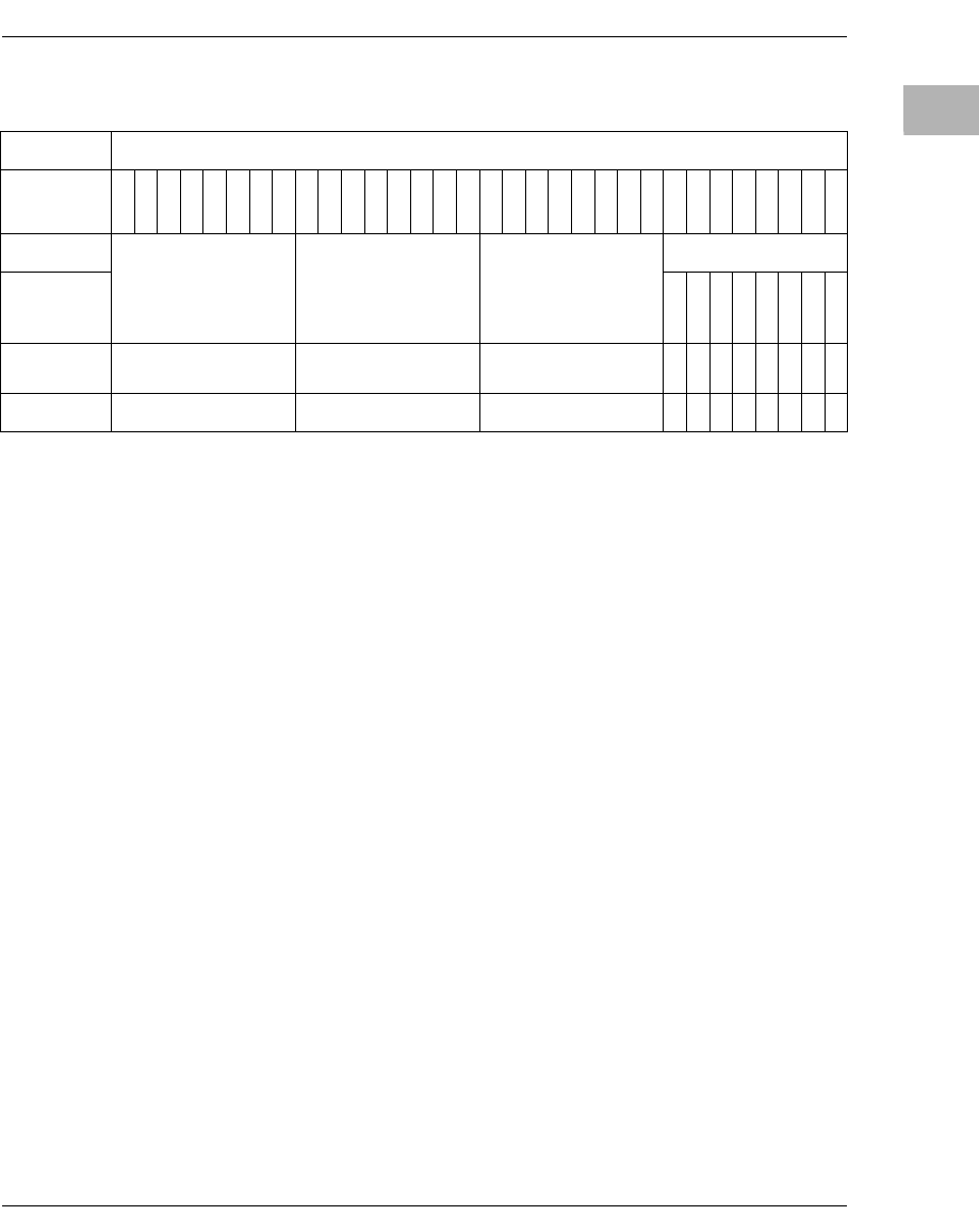
Raven Registers
http://www.motorola.com/computer/literature 2-39
2
MPC Error Status Register
OVF Error Status Overflow. This bit is set when an error is
detected and any of the error status bits are already set.
The bit may be cleared by writing a 1 to it; writing a 0 to
it has no effect.
MATO MPC Address bus Time-Out. This bit is set when the
MPC address bus timer times out. The bit may be cleared
by writing it to a 1; writing it to a 0 has no effect. When
the MATOM bit in the MEREN register is set, the
assertion of this bit will assert MCHK to the master
designated by the MID field in the MERAT register. When
the MATOI bit in the MEREN register is set, the assertion
of this bit will assert an interrupt through the MPIC
interrupt controller.
PERR PCI Parity Error. This bit is set when the PCI PERR∗ pin
is asserted. The bit may be cleared by writing it to a 1;
writing it to a 0 has no effect. When the PERRM bit in the
MEREN register is set, the assertion of this bit will assert
MCHK to the master designated by the DFLT bit in the
MERAT register. When the PERRI bit in the MEREN
register is set, the assertion of this bit will assert an
interrupt through the MPIC interrupt controller.
Address $FEFF0024
Bit 01234567891
01
11
21
31
41
51
61
71
81
92
02
12
22
32
42
52
62
72
82
93
03
1
Name MERST
OVF
MATO
PERR
SERR
SMA
RTA
Operation RRR
R/C
R
R/C
R
R/C
R/C
R/C
R/C
Reset $00 $00 $00
0
0
0
0
0
0
0
0
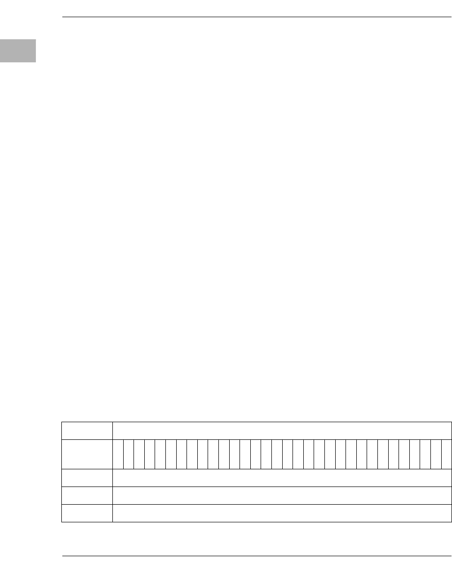
2-40 Computer Group Literature Center Web Site
Raven PCI Bridge ASIC
2SERR PCI System Error. This bit is set when the PCI SERR∗
pin is asserted. The bit may be cleared by writing it to a 1;
writing it to a 0 has no effect. When the SERRM bit in the
MEREN register is set, the assertion of this bit will assert
MCHK to the master designated by the DFLT bit in the
MERAT register. When the SERRI bit in the MEREN
register is set, the assertion of this bit will assert an
interrupt through the MPIC interrupt controller.
SMA PCI Master Signalled Master Abort. This bit is set
when the PCI master signals master abort to terminate a
PCI transaction. The bit may be cleared by writing it to a
1; writing it to a 0 has no effect. When the SMAM bit in
the MEREN register is set, the assertion of this bit will
assert MCHK to the master designated by the MID field
in the MERAT register. When the SMAI bit in the
MEREN register is set, the assertion of this bit will assert
an interrupt through the MPIC interrupt controller.
RTA PCI Master Received Target Abort. This bit is set when
the PCI master receives target abort to terminate a PCI
transaction. The bit may be cleared by writing it to a 1;
writing it to a 0 has no effect. When the RTAM bit in the
MEREN register is set, the assertion of this bit will assert
MCHK to the master designated by the MID field in the
MERAT register. When the RTAI bit in the MEREN
register is set, the assertion of this bit will assert an
interrupt through the MPIC interrupt controller.
MPC Error Address Register
Address $FEFF0028
Bit 01234567891
01
11
21
31
41
51
61
71
81
92
02
12
22
32
42
52
62
72
82
93
03
1
Name MERAD
Operation R
Reset $00000000
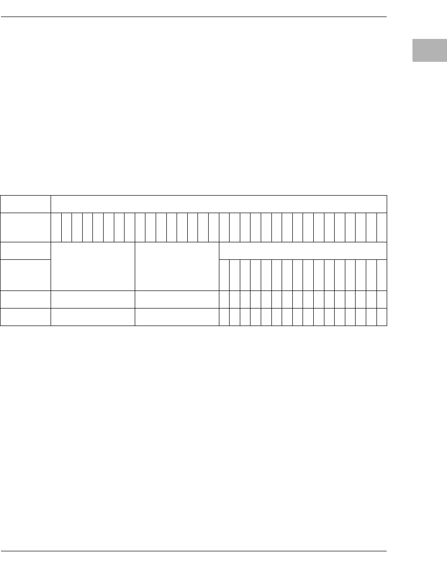
Raven Registers
http://www.motorola.com/computer/literature 2-41
2
MERAD MPC Error Address. This register captures the MPC
address when the MATO bit is set in the MERST register.
It captures the PCI address when the SMA or RTA bits are
set in the MERST register. Its contents are not defined
when the PERR or SERR bits are set in the MERST
register.
MPC Error Attribute Register - MERAT
If the PERR or SERR bits are set in the MERST register, the contents of
the MERAT register are zero. If the MATO bit is set, the register is defined
by the following figure:
MIDx MPC Master ID. Contains the ID of the MPC master
which originated the transfer in which the error occurred.
The encoding scheme is identical to that used in the GCSR
register.
TBST Transfer Burst. This bit is set when the transfer in which
the error occurred was a burst transfer.
TSIZx Transfer Size. Contains the transfer size of the MPC
transfer in which the error occurred.
TTx Transfer Type. Contains the transfer type of the MPC
transfer in which the error occurred.
Address $FEFF002C
Bit 01234567891
01
11
21
31
41
51
61
71
81
92
02
12
22
32
42
52
62
72
82
93
03
1
Name MERAT
MID1
MID0
TBST
TSIZ0
TSIZ1
TSIZ2
TT0
TT1
TT2
TT3
TT4
Operation RR
R
R
R
R
R
R
R
R
R
R
R
R
R
R
R
R
Reset $00 $00
0
0
0
0
0
0
0
0
0
0
0
0
0
0
0
0
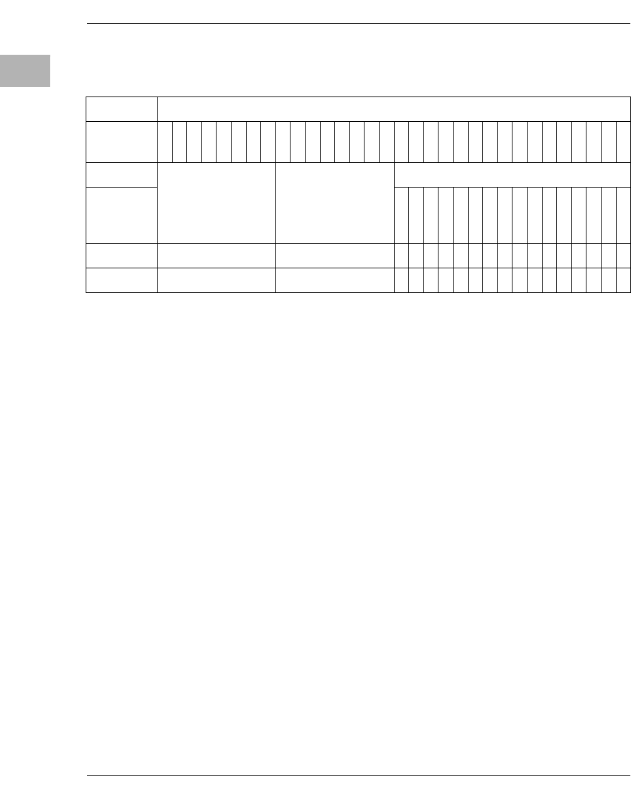
2-42 Computer Group Literature Center Web Site
Raven PCI Bridge ASIC
2If the SMA or RTA bits are set, the register is defined by the following
figure:
WP Write-Post Completion. This bit is set when the PCI
master detects an error while completing a write-post
transfer.
MIDx MPC Master ID. Contains the ID of the MPC master
which originated the transfer in which the error occurred.
The encoding scheme is identical to that used in the GCSR
register
COMMx PCI Command. Contains the PCI command of the PCI
transfer in which the error occurred.
BYTEx PCI Byte Enable. Contains the PCI byte enables of the
PCI transfer in which the error occurred. A set bit
designates a selected byte.
Address $FEFF002C
Bit 01234567891
01
11
21
31
41
51
61
71
81
92
02
12
22
32
42
52
62
72
82
93
03
1
Name MERAT
WP
MID1
MID0
COMM3
COMM2
COMM1
COMM0
BYTE7
BYTE6
BYTE5
BYTE4
BYTE3
BYTE2
BYTE1
BYTE0
Operation RR
R
R
R
R
R
R
R
R
R
R
R
R
R
R
R
R
Reset $00 $00
0
0
0
0
0
0
0
0
0
0
0
0
0
0
0
0
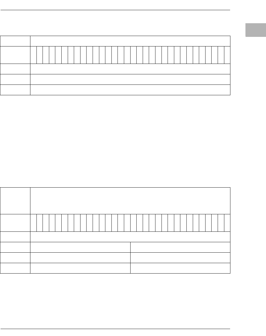
Raven Registers
http://www.motorola.com/computer/literature 2-43
2
PCI Interrupt Acknowledge Register
PIACK PCI Interrupt Acknowledge. Performing a read from
this register will initiate a single PCI Interrupt
Acknowledge cycle. Any single byte or combination of
bytes may be read from, and the actual byte enable pattern
used during the read will be passed on to the PCI bus.
Upon completion of the PCI interrupt acknowledge cycle,
the Raven will present the resulting vector information
obtained from the PCI bus as read data.
MPC Slave Address (0,1 and 2) Registers
To initiate a PCI cycle from the MPC bus, the MPC address must be
greater than or equal to the START field and less than or equal to the END
field.
Address $FEFF0030
Bit 01234567891
01
11
21
31
41
51
61
71
81
92
02
12
22
32
42
52
62
72
82
93
03
1
Name PIACK
Operation R
Reset $00000000
Address MSADD0 - $FEFF0040
MSADD1 - $FEFF0048
MSADD2 - $FEFF0050
Bit 01234567891
01
11
21
31
41
51
61
71
81
92
02
12
22
32
42
52
62
72
82
93
03
1
Name MSADDx
START END
Operation R/W R/W
Reset $0000 $0000
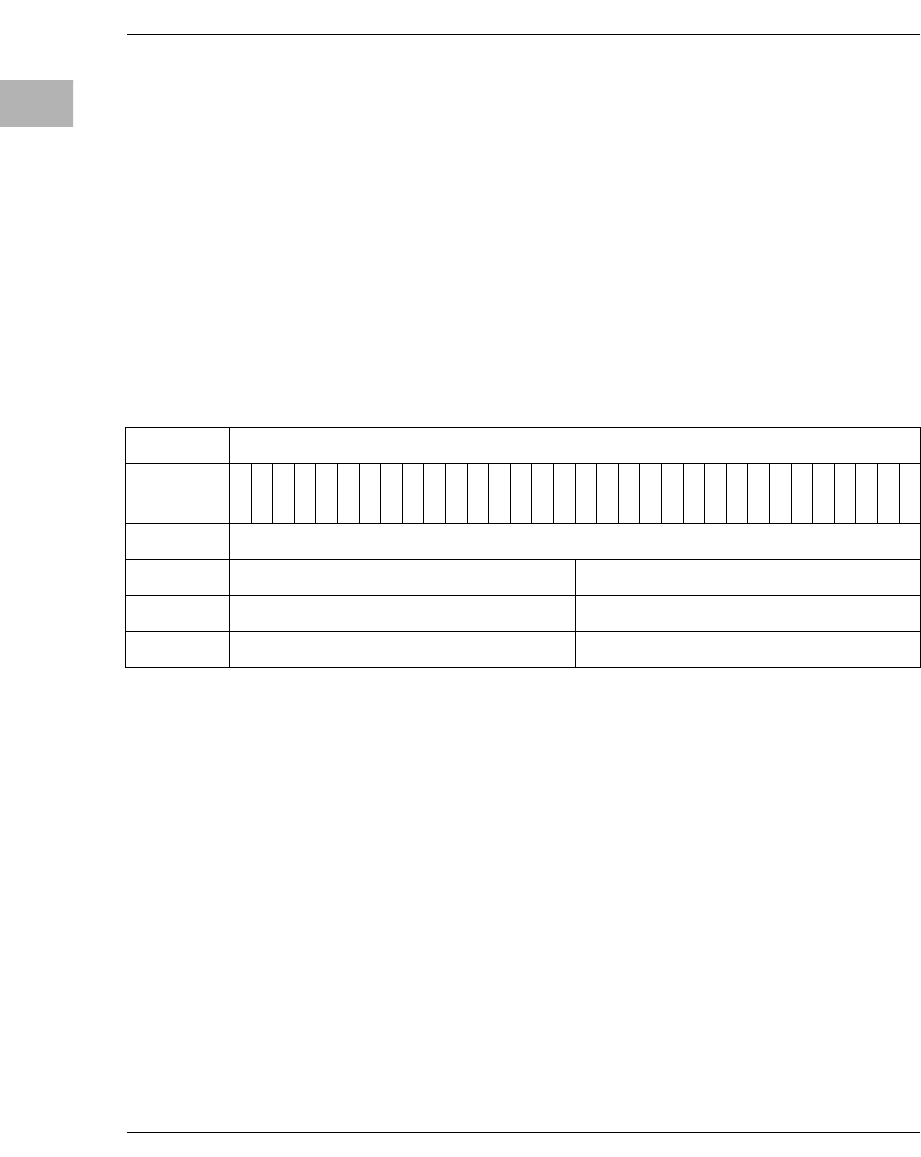
2-44 Computer Group Literature Center Web Site
Raven PCI Bridge ASIC
2START Start Address. Determines the start address of a
particular memory area on the MPC bus which will be
used to access PCI bus resources. The value of this field
will be compared with the upper 16 bits of the incoming
MPC address.
END End Address. Determines the end address of a particular
memory area on the MPC bus which will be used to access
PCI bus resources. The value of this field will be
compared with the upper 16 bits of the incoming MPC
address.
MPC Slave Address (3) Register
MSADD3, MSOFF3 and MSATT3 represent the only register group
which can be used to initiate access to the PCI Configuration Address
($80000CF8) and Configuration Data ($80000CFC) registers. Note that
this implies that MSxxx3 also represents the generation of PCI Special
Cycles. The power-up default values of MSADD3, MSOFF3 and
MSATT3 are set to allow access to PCI configuration space without MPC
register initialization. For additional information, please refer to the
description of the MSOFF3/MSATT3 registers under MPC Slave
Offset/Attribute (3) Registers.
To initiate a PCI cycle from the MPC bus, the MPC address must be
greater than or equal to the START field and less than or equal to the END
field.
Address MSADD3 - $FEFF0058
Bit 01234567891
01
11
21
31
41
51
61
71
81
92
02
12
22
32
42
52
62
72
82
93
03
1
Name MSADD3
START END
Operation R/W R/W
Reset $8000 $8080
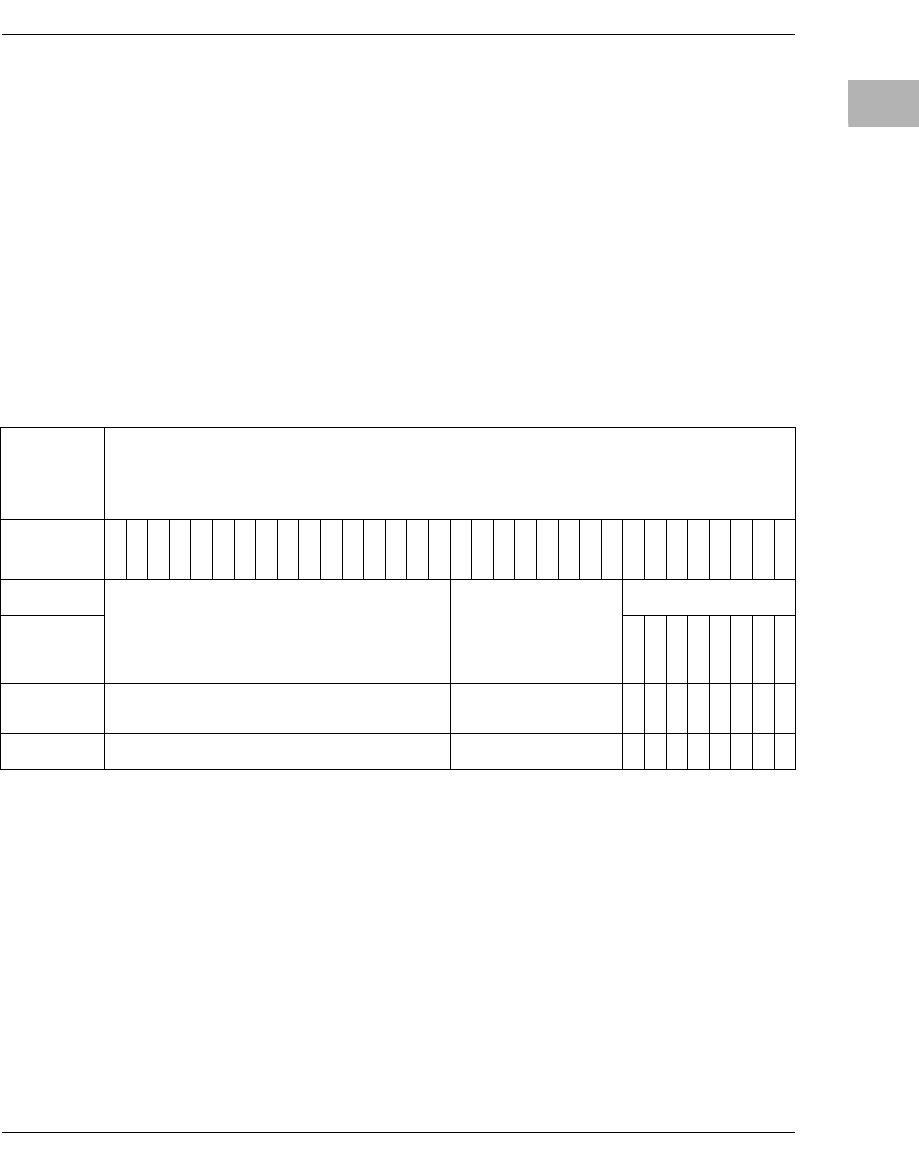
Raven Registers
http://www.motorola.com/computer/literature 2-45
2
START Start Address. Determines the start address of a
particular memory area on the MPC bus which will be
used to access PCI bus resources. The value of this field
will be compared with the upper 16 bits of the incoming
MPC address.
END End Address. Determines the end address of a particular
memory area on the MPC bus which will be used to access
PCI bus resources. The value of this field will be
compared with the upper 16 bits of the incoming MPC
address.
MPC Slave Offset/Attribute (0,1 and 2) Registers
MSOFFx MPC Slave Offset. A 16-bit offset that is added to the
upper 16 bits of the MPC address to determine the PCI
address used for transfers from the MPC bus to PCI. This
offset allows PCI resources to reside at addresses that
would not normally be visible from the MPC bus.
REN Read Enable. If set, the corresponding MPC slave is
enabled for read transactions.
WEN Write Enable. If set, the corresponding MPC slave is
enabled for write transactions.
Address MSOFF0/MSATT0 - $FEFF0044
MSOFF1/MSATT1 - $FEFF004C
MSOFF2/MSATT2 - $FEFF0054
Bit 01234567891
01
11
21
31
41
51
61
71
81
92
02
12
22
32
42
52
62
72
82
93
03
1
Name MSOFFx MSATTx
REN
WEN
WPEN
MEM
IOM
Operation R/W R
R/W
R/W
R
R/W
R
R
R/W
R/W
Reset $0000 $00
0
0
0
0
0
0
0
0
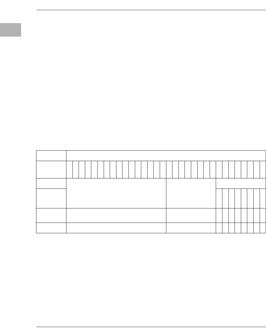
2-46 Computer Group Literature Center Web Site
Raven PCI Bridge ASIC
2WPEN Write-Post Enable. If set, write-posting is enabled for the
corresponding MPC slave.
MEM PCI Memory Cycle. If set, the corresponding MPC slave
will generate transfers to or from PCI memory space.
When clear, the corresponding MPC slave will generate
transfers to or from PCI I/O space using the addressing
mode defined by the IOM field.
IOM PCI I/O Mode. If set, the corresponding MPC slave will
generate PCI I/O cycles using spread addressing as
defined in the section on Generating PCI Memory and I/O
Cycles. When clear, the corresponding MPC slave will
generate PCI I/O cycles using contiguous addressing.
This field only has meaning when the MEM bit is clear.
MPC Slave Offset/Attribute (3) Registers
MSOFF3 MPC Slave Offset. Contains a 16-bit offset that is added
to the upper 16 bits of the MPC address to determine the
PCI address used for transfers from the MPC bus to PCI.
This offset allows PCI resources to reside at addresses that
would not normally be visible from the MPC bus. It is
initialized to $8000 to facilitate a zero-based access to PCI
space.
Address MSOFF3/MSATT3 - $FEFF005C
Bit 01234567891
01
11
21
31
41
51
61
71
81
92
02
12
22
32
42
52
62
72
82
93
03
1
Name MSOFF3 MSATT3
REN
WEN
WPEN
IOM
Operation R/W R
R/W
R/W
R
R/W
R
R
R
R/W
Reset $8000 $00
1
1
0
0
0
0
0
0
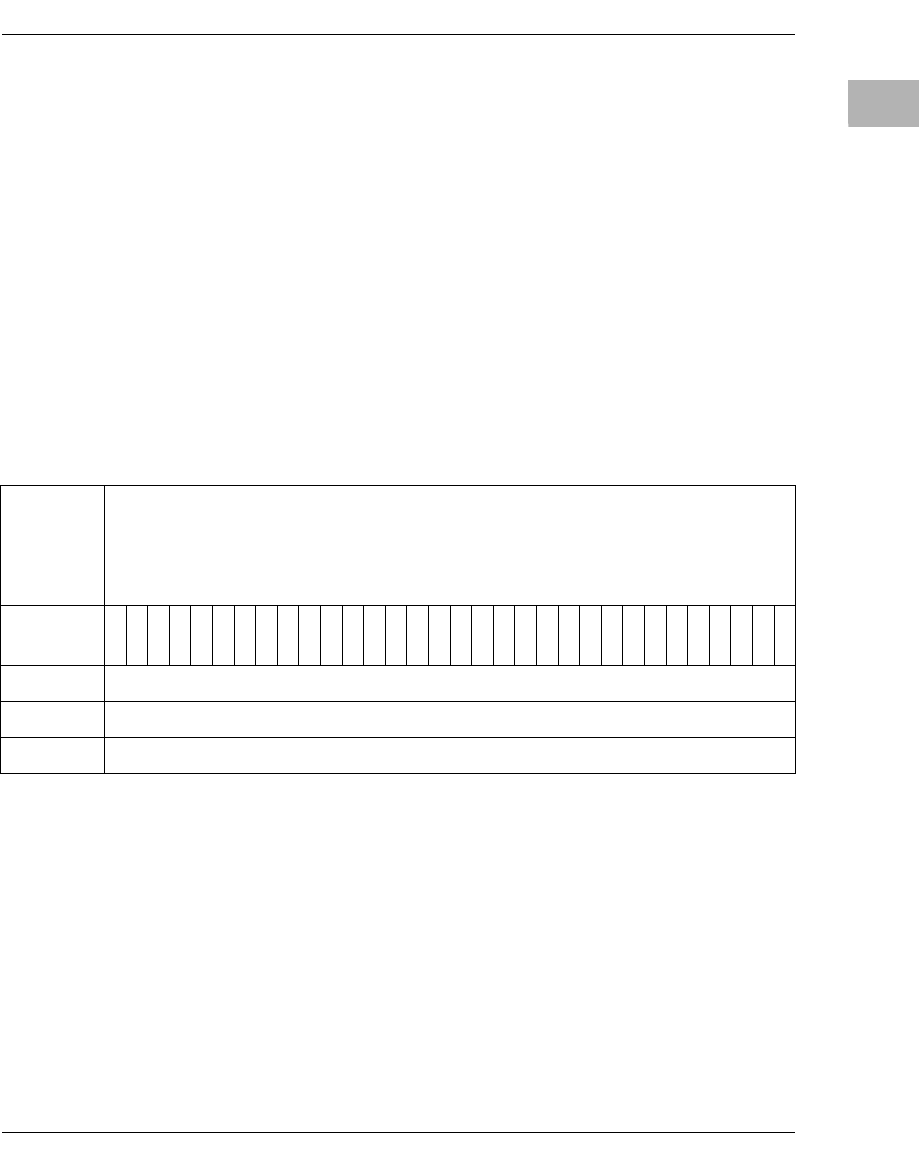
Raven Registers
http://www.motorola.com/computer/literature 2-47
2
REN Read Enable. If set, the corresponding MPC slave is
enabled for read transactions.
WEN Write Enable. If set, the corresponding MPC slave is
enabled for write transactions.
WPEN Write-Post Enable. If set, write-posting is enabled for the
corresponding MPC slave.
IOM PCI I/O Mode. If set, the corresponding MPC slave will
generate PCI I/O cycles using spread addressing as
defined in the section on Generating PCI Memory and I/O
Cycles. When clear, the corresponding MPC slave will
generate PCI I/O cycles using contiguous addressing.
General-Purpose Registers
These general-purpose read/write registers are provided for inter-process
message passing or general-purpose storage. They do not control any
hardware.
PCI Registers
The PCI Configuration registers are compliant with the configuration
register set described in the PCI Local Bus Specification, Revision 2.0.
The CONFIG_ADDRESS and CONFIG_DATA registers described in
this section are accessed within PCI I/O space.
Address GPREG0 (Upper) - $FEFF0070
GPREG0 (Lower) - $FEFF0074
GPREG1 (Upper) - $FEFF0078
GPREG1 (Lower) - $FEFF007C
Bit 01234567891
01
11
21
31
41
51
61
71
81
92
02
12
22
32
42
52
62
72
82
93
03
1
Name GPREGx
Operation R/W
Reset $00000000
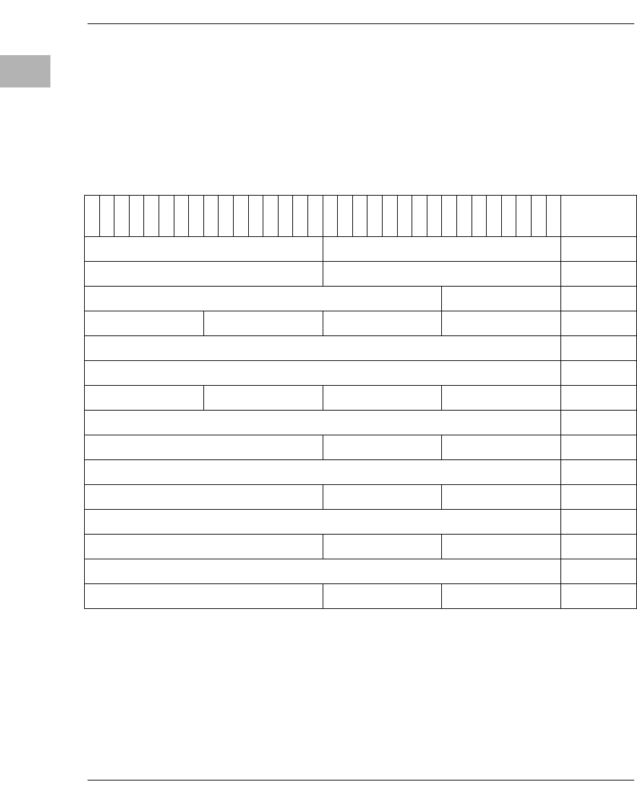
2-48 Computer Group Literature Center Web Site
Raven PCI Bridge ASIC
2All write operations to reserved registers will be treated as no-ops. That is,
the access will be completed normally on the bus and the data will be
discarded. Read accesses to reserved or unimplemented registers will be
completed normally and a data value of 0 returned.
The Raven PCI Configuration Register map appears in Table 2-8. The
Raven PCI I/O Register map appears in Table 2-9.
Table 2-8. Raven PCI Configuration Register Map
3
13
02
92
82
72
62
52
42
32
22
12
01
91
81
71
61
51
41
31
21
11
09876543210 <--- Bit
DEVID VENID $00
PSTAT PCOMM $04
CLASS REVID $08
$0C
IOBASE $10
MEMBASE $14
$18 - $7F
PSADD0 $80
PSOFF0 PSATT0 $84
PSADD1 $88
PSOFF1 PSATT1 $8C
PSADD2 $90
PSOFF2 PSATT2 $94
PSADD3 $98
PSOFF3 PSATT3 $9C
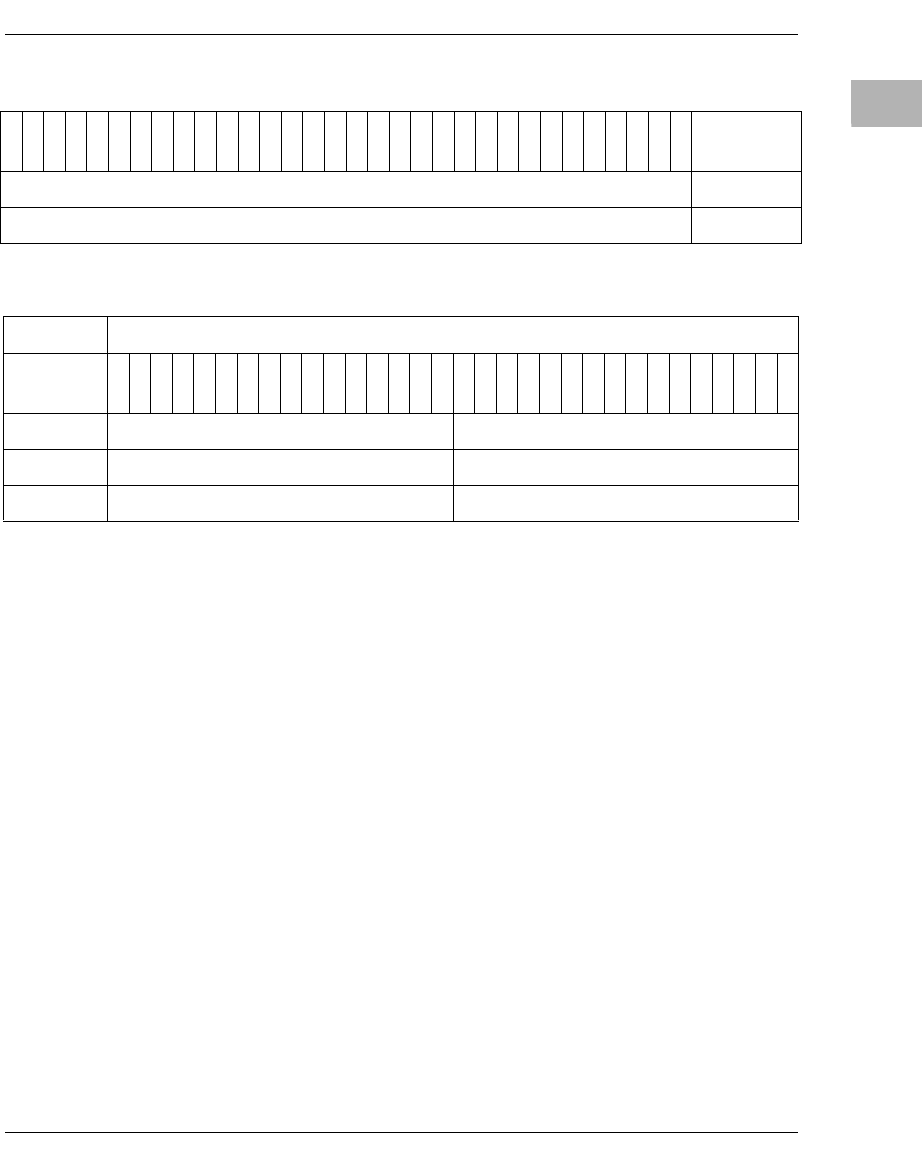
Raven Registers
http://www.motorola.com/computer/literature 2-49
2
Table 2-9. Raven PCI I/O Register Map
Vendor ID/ Device ID Registers
VENID Vendor ID. Identifies the manufacturer of the device.
This identifier is allocated by the PCI SIG to ensure
uniqueness. $1057 has been assigned to Motorola. This
register is duplicated in the MPC registers.
DEVID Device ID. Identifies the particular device. The Raven
will always return $4801. This register is duplicated in the
MPC registers.
3
13
02
92
82
72
62
52
42
32
22
12
01
91
81
71
61
51
41
31
21
11
09876543210 <--- Bit
CONFIG_ADDRESS $CF8
CONFIG_DATA $CFC
Offset $00
Bit 3
13
02
92
82
72
62
52
42
32
22
12
01
91
81
71
61
51
41
31
21
11
09876543210
Name DEVID VENID
Operation RR
Reset $4801 $1057
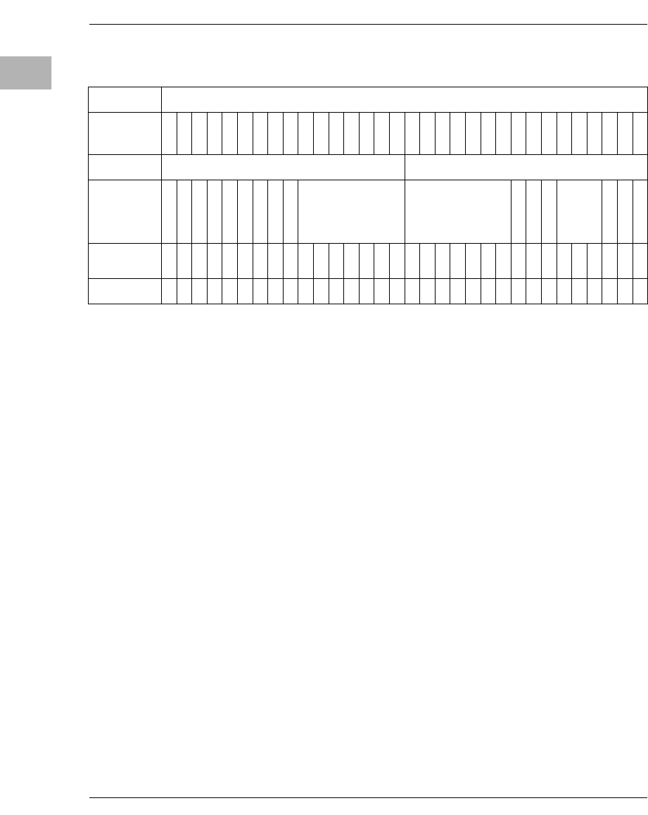
2-50 Computer Group Literature Center Web Site
Raven PCI Bridge ASIC
2PCI Command/ Status Registers
IOSP IO Space Enable. If set, the Raven will respond to PCI
I/O accesses when appropriate. If cleared, the Raven will
not respond to PCI I/O space accesses.
MEMSP Memory Space Enable. If set, the Raven will respond to
PCI memory space accesses when appropriate. If cleared,
the Raven will not respond to PCI memory space
accesses.
MSTR Bus Master Enable. If set, the Raven may act as a master
on PCI. If cleared, the Raven may not act as a PCI master.
PERR Parity Error Response. If set, the Raven will check
parity on all PCI transfers. If cleared, the Raven will
ignore any parity errors that it detects and will continue
normal operation.
SERR System Error Enable. This bit enables the SERR∗ output
pin. If clear, the Raven will never drive SERR∗. If set, the
Raven will drive SERR∗ active when a system error is
detected.
FAST Fast Back-to-Back Capable. This bit indicates that the
Raven is capable of accepting fast back-to-back
transactions with different targets.
Offset $04
Bit 3
13
02
92
82
72
62
52
42
32
22
12
01
91
81
71
61
51
41
31
21
11
09876543210
Name PSTAT PCOMM
RCVPE
SIGSE
RCVMA
RCVTA
SIGTA
SELTIM1
SELTIM0
DPAR
FAST
SERR
PERR
MSTR
MEMSP
IOSP
Operation
R/C
R/C
R/C
R/C
R/C
R
R
R/C
R
R
R
R
R
R
R
R
R
R
R
R
R
R
R
R/W
R
R/W
R
R
R
R/W
R/W
R/W
Reset
0
0
0
0
0
0
1
0
1
0
0
0
0
0
0
0
0
0
0
0
0
0
0
0
0
0
0
0
0
1
0
0

Raven Registers
http://www.motorola.com/computer/literature 2-51
2
DPAR Data Parity Detected. This bit is set when three
conditions are met: 1) the Raven asserted PERR∗ itself or
observed PERR∗ asserted; 2) the Raven was the PCI
master for the transfer in which the error occurred; 3) the
PERR bit in the PCI Command register is set. This bit is
cleared by writing it to 1; writing a 0 has no effect.
SELTIM DEVSEL Timing. This field indicates that the Raven will
always assert DEVSEL∗ as a ‘medium’ responder.
SIGTA Signalled Target Abort. This bit is set by the PCI slave
whenever it terminates a transaction with a target-abort.
The bit is cleared by writing it to 1; writing a 0 has no
effect.
RCVTA Received Target Abort. This bit is set by the PCI master
whenever its transaction is terminated by a target-abort.
The bit is cleared by writing it to 1; writing a 0 has no
effect.
RCVMA Received Master Abort. This bit is set by the PCI master
whenever its transaction (except for Special Cycles) is
terminated by a master-abort. The bit is cleared by writing
it to 1; writing a 0 has no effect.
SIGSE Signaled System Error. This bit is set whenever the
Raven asserts SERR∗. The bit is cleared by writing it to 1;
writing a 0 has no effect.
RCVPE Detected Parity Error. This bit is set whenever the
Raven detects a parity error, even if parity error checking
is disabled (see bit PERR in the PCI Command register).
The bit is cleared by writing it to 1; writing a 0 has no
effect.
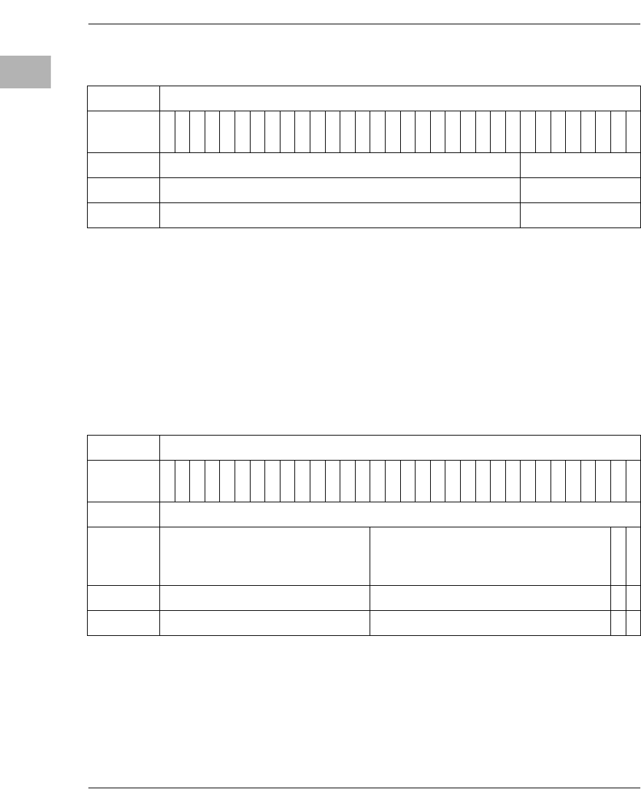
2-52 Computer Group Literature Center Web Site
Raven PCI Bridge ASIC
2Revision ID/ Class Code Registers
REVID Revision ID. Identifies the Raven revision level. This
register is duplicated in the MPC registers.
CLASS Class Code. Identifies the Raven as follows:
Base Class Code $06 PCI Bridge Device
Subclass Code $00 PCI Host Bridge
Program Class Code $00 Not Used
I/O Base Register
This register controls the mapping of the MPIC control registers in PCI I/O
space.
IO/MEM IO Space Indicator. This bit is hard-wired to a logic 1 to
indicate PCI I/O space.
Offset $08
Bit 3
13
02
92
82
72
62
52
42
32
22
12
01
91
81
71
61
51
41
31
21
11
09876543210
Name CLASS REVID
Operation RR
Reset $060000 $02
Offset $10
Bit 3
13
02
92
82
72
62
52
42
32
22
12
01
91
81
71
61
51
41
31
21
11
09876543210
Name IOBASE
IOBA
RES
IO/MEM
Operation R/W R
R
R
Reset $0000 $0000
0
1
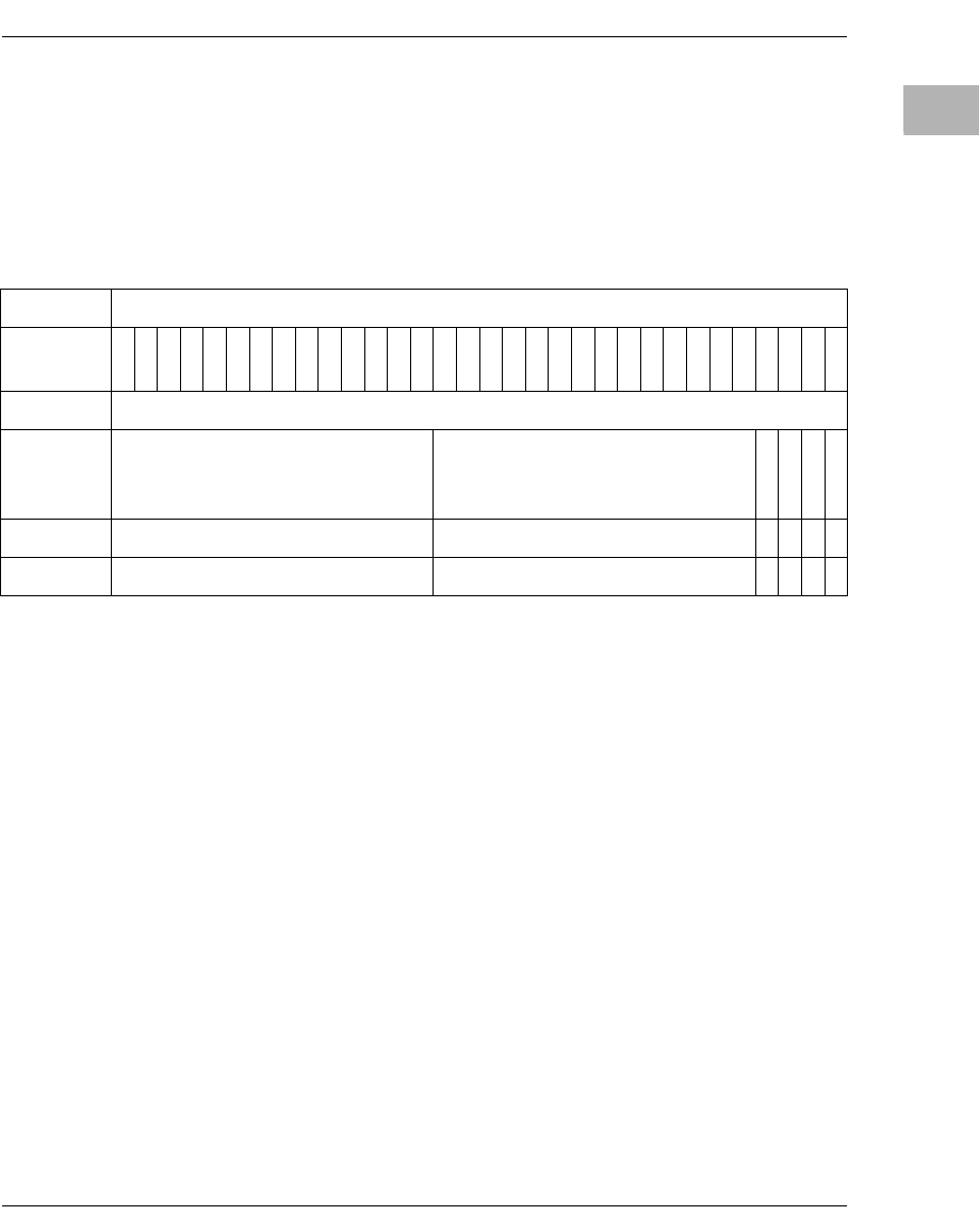
Raven Registers
http://www.motorola.com/computer/literature 2-53
2
RES Reserved. This bit is hard-wired to 0.
IOBA I/O Base Address. These bits define the I/O space base
address of the MPIC control registers. The IOBASE
decoder is disabled when the IOBASE value is zero.
Memory Base Register
This register controls the mapping of the MPIC control registers in PCI
memory space.
IO/MEM IO Space Indicator. This bit is hard-wired to a logic 0 to
indicate PCI memory space.
MTYPx Memory Type. These bits are hard-wired to 0 to indicate
that the MPIC registers can be located anywhere in the 32-
bit address space
PRE Prefetch. This bit is hard-wired to 0 to indicate that the
MPIC registers are not prefetchable.
MEMBA Memory Base Address. These bits define the memory
space base address of the MPIC control registers. The
MBASE decoder is disabled when the MBASE value is
zero.
Offset $14
Bit 3
13
02
92
82
72
62
52
42
32
22
12
01
91
81
71
61
51
41
31
21
11
09876543210
Name MEMBASE
MEMBA
PRE
MTYP1
MTYP0
IO/MEM
Operation R/W R
R
R
R
R
Reset $0000 $0000
0
0
0
0
2-54 Computer Group Literature Center Web Site
Raven PCI Bridge ASIC
2PCI Slave Address (0,1,2 and 3) Registers
To initiate an MPC cycle from the PCI bus, the PCI address must be greater
than or equal to the START field and less than or equal to the END field.
START Start Address. Determines the start address of a
particular memory area on the PCI bus which will be used
to access MPC bus resources. The value of this field will
be compared with the upper 16 bits of the incoming PCI
address.
END End Address. Determines the end address of a particular
memory area on the PCI bus which will be used to access
MPC bus resources. The value of this field will be
compared with the upper 16 bits of the incoming PCI
address.
Offset PSADD0 - $80
PSADD1 - $88
PSADD2 - $90
PSADD3 - $98
Bit 3
13
02
92
82
72
62
52
42
32
22
12
01
91
81
71
61
51
41
31
21
11
09876543210
Name PSADDx
START END
Operation R/W R/W
Reset $0000 $0000
Raven Registers
http://www.motorola.com/computer/literature 2-55
2
PCI Slave Attribute/ Offset (0,1,2 and 3) Registers
INV Invalidate Enable. If set, the MPC master will issue a
transfer type code which specifies the current transaction
should cause an invalidate for each MPC transaction
originated by the corresponding PCI slave. The transfer
type codes generated are shown in Table 2-3.
GBL Global Enable. If set, the MPC master will assert the
GBL∗ pin for each MPC transaction originated by the
corresponding PCI slave.
RAEN Read Ahead Enable. If set, read-ahead is enabled for the
corresponding PCI slave.
WPEN Write-Post Enable. If set, write-posting is enabled for the
corresponding PCI slave.
WEN Write Enable. If set, the corresponding PCI slave is
enabled for write transactions.
REN Read Enable. If set, the corresponding PCI slave is
enabled for read transactions.
PSOFFx PCI Slave Offset. Contains a 16-bit offset that is added to
the upper 16 bits of the PCI address to determine the MPC
address used for transfers from PCI to the MPC bus. This
offset allows MPC resources to reside at addresses that
would not normally be visible from PCI.
Offset PSATT0/PSOFF0 - $84
PSATT1/PSOFF1 - $8C
PSATT2/PSOFF2 - $94
PSATT3/PSOFF3 - $9C
Bit 3
13
02
92
82
72
62
52
42
32
22
12
01
91
81
71
61
51
41
31
21
11
09876543210
Name PSOFFx PSATTx
REN
WEN
WPEN
RAEN
GBL
INV
Operation R/W R
R/w
R/W
R/W
R/W
R
R
R/W
R/W
Reset $0000 $00
0
0
0
0
0
0
0
0
2-56 Computer Group Literature Center Web Site
Raven PCI Bridge ASIC
2CONFIG_ADDRESS Register
The description of the CONFIG_ADDRESS register is presented in three
perspectives: from the PCI bus, from the MPC bus in big-endian mode, and
from the MPC bus in little-endian mode. Note that the view from the PCI
bus is purely conceptual, since there is no way to access the
CONFIG_ADDRESS register from the PCI bus.
Conceptual perspective from the PCI bus
Perspective from the MPC bus in Big-Endian mode
Offset $CFB $CFA $CF9 $CF8
Bit 3
13
02
92
82
72
62
52
42
32
22
12
01
91
81
71
61
51
41
31
21
11
09876543210
Name CONFIG_ADDRESS
EN
BUS DEV FUN REG
Operation
R/W
R R/W R/W R/W R/W
R
R
Reset
1
$00 $00 $00 $0 $00
0
0
Offset $CF8 $CF9 $CFA $CFB
Bit (DH) 01234567891
01
11
21
31
41
51
61
71
81
92
02
12
22
32
42
52
62
72
82
93
03
1
Name CONFIG_ADDRESS
REG DEV FUN BUS
EN
Operation R/W
R
R
R/W R/W R/W
R/W
R
Reset $00
0
0
$00 $0 $00
1
$00
Raven Registers
http://www.motorola.com/computer/literature 2-57
2
Perspective from the MPC bus in Little-Endian mode
The register fields are defined as follows:
REG Register Number.
Configuration Cycles: Identifies a target double word within a
target’s configuration space. This field is copied to the PCI AD bus
during the address phase of a Configuration cycle.
Special Cycles: This field must be written with all 0s.
FUN Function Number.
Configuration Cycles: Identifies a function number within a
target’s configuration space. This field is copied to the PCI AD bus
during the address phase of a Configuration cycle.
Special Cycles: This field must be written with all 1s.
DEV Device Number.
Configuration Cycles: Identifies a target’s physical PCI device
number. Refer to the section on Generating PCI Configuration
Cycles for a description of how this field is encoded.
Special Cycles: This field must be written with all 1s.
Offset $CFC $CFD $CFE $CFF
Bit (DL) 01234567891
01
11
21
31
41
51
61
71
81
92
02
12
22
32
42
52
62
72
82
93
03
1
Name CONFIG_ADDRESS
EN
BUS DEV FUN REG
Operation
R/W
R R/W R/W R/W R/W
R
R
Reset
1
$00 $00 $00 $0 $00
0
0

2-58 Computer Group Literature Center Web Site
Raven PCI Bridge ASIC
2BUS Bus Number.
Configuration Cycles: Identifies a targeted bus number. If written
with all zeros, a Type 0 Configuration Cycle will be generated. If
written with any value other than all 0s, then a Type 1
Configuration Cycle will be generated.
Special Cycles: Identifies a targeted bus number. If written with all
0s, a Special Cycle will be generated. If written with any value
other than all 0s, then a Special Cycle translated into a Type 1
Configuration Cycle will be generated.
EN Enable.
Configuration Cycles: Writing a 1 to this bit enables
CONFIG_DATA to Configuration Cycle translation. If this bit is a
0, subsequent accesses to CONFIG_DATA will be passed though
as I/O cycles.
Special Cycles: Writing a 1 to this bit enables CONFIG_DATA to
Special Cycle translation. If this bit is a 0, subsequent accesses to
CONFIG_DATA will be passed though as I/O cycles.
CONFIG_DATA Register
The description of the CONFIG_DATA register is also presented in three
perspectives: from the PCI bus, from the MPC bus in big-endian mode, and
from the MPC bus in little-lndian mode. Note that the view from the PCI
bus is purely conceptual, since there is no way to access the
CONFIG_DATA register from the PCI bus.
2Raven PCI Bridge ASIC
0Raven Registers
Raven Registers
http://www.motorola.com/computer/literature 2-59
2
Conceptual perspective from the PCI bus
Perspective from the MPC bus in Big-Endian mode
Perspective from the MPC bus in Little-Endian mode
Offset $CFF $CFE $CFD $CFC
Bit 3
13
02
92
82
72
62
52
42
32
22
12
01
91
81
71
61
51
41
31
21
11
09876543210
Name CONFIG_DATA
Data ‘D’ Data ‘C’ Data ‘B’ Data ‘A’
Operation R/W R/W R/W R/W
Reset n/a n/a n/a n/a
Offset $CFC $CFD $CFE $CFF
Bit (DL) 01234567891
01
11
21
31
41
51
61
71
81
92
02
12
22
32
42
52
62
72
82
93
03
1
Name CONFIG_DATA
Data ‘A’ Data ‘B’ Data ‘C’ Data ‘D’
Operation R/W R/W R/W R/W
Reset n/a n/a n/a n/a
Offset $CF8 $CF9 $CFA $CFB
Bit (DH) 01234567891
01
11
21
31
41
51
61
71
81
92
02
12
22
32
42
52
62
72
82
93
03
1
Name CONFIG_DATA
Data ‘D’ Data ‘C’ Data ‘B’ Data ‘A’
Operation R/W R/W R/W R/W
Reset n/a n/a n/a n/a

2-60 Computer Group Literature Center Web Site
Raven PCI Bridge ASIC
2Raven Interrupt Controller
This section describes the general implementation of the Raven Interrupt
Controller (RavenMPIC).
Features
The RavenMPIC has the characteristics listed below.
❏MPIC programming model
❏Support for two processors
❏Support for 16 external interrupts
❏Support for 15 programmable Interrupt and Processor Task priority
levels
❏Support for the connection of an external 8259 for ISA/AT
compatibility
❏Distributed interrupt delivery for external I/O interrupts
❏Direct/Multicast interrupt delivery for Interprocessor and timer
interrupts
❏Four Interprocessor Interrupt sources
❏Four timers
❏Processor initialization control
Architecture
The Raven PCI Slave implements two address decoders for placing the
RavenMPIC registers in PCI IO or PCI Memory space. Access to these
registers require MPC and PCI bus mastership. These accesses include
interrupt and timer initialization and interrupt vector reads.

Raven Interrupt Controller
http://www.motorola.com/computer/literature 2-61
2
The RavenMPIC receives interrupt inputs from:
❏16 external sources
❏Four interprocessor sources
❏Four timer sources
❏One Raven internal error detection source
Externally sourced interrupts 1 through 15 have two modes of activation:
low level or active high positive edge. External interrupt 0 can be either
level- or edge-activated with either polarity. The Interprocessor and timer
interrupts are event-activated.
Readability of CSR
Unless explicitly specified, all registers are readable and return the last
value written. The exceptions are the IPI dispatch registers and the EOI
registers which return 0s on reads, the interrupt source ACT bit which
returns current interrupt source status, the interrupt acknowledge register
which returns the vector of the highest-priority currently pending interrupt,
and reserved bits which return 0s. The interrupt acknowledge register is
also the only register which exhibits any read side-effects.
Interrupt Source Priority
Each interrupt source is assigned a priority value in the range from 0 to 15,
where 15 is the highest priority level. For delivery of an interrupt to take
place, the priority of the source must be greater than that of the destination
processor. Therefore, setting a source priority to zero inhibits that
interrupt.
Processor’s Current Task Priority
Each processor has a task priority register which is set by system software
to indicate the relative importance of the task running on that processor.
The processor will not receive interrupts with a priority level equal to or
lower than its current task priority. Therefore, setting the current task
priority to 15 prohibits the delivery of all interrupts to the associated
processor.

2-62 Computer Group Literature Center Web Site
Raven PCI Bridge ASIC
2Nesting of Interrupt Events
A processor is guaranteed never to have an in-service interrupt preempted
by an equal- or lower-priority source. An interrupt is considered to be in
service from the time its vector is returned during an interrupt
acknowledge cycle until an EOI is received for that interrupt. The EOI
cycle indicates the end of processing for the highest-priority in-service
interrupt.
Spurious Vector Generation
Under certain circumstances the RavenMPIC will not have a valid vector
to return to the processor during an interrupt acknowledge cycle. In these
cases, the spurious vector from the spurious vector register will be
returned. The following cases would cause a spurious vector fetch.
❏INT is asserted in response to an externally sourced interrupt which
is activated with level sensitive logic and the asserted level is
negated before the interrupt is acknowledged.
❏INT is asserted for an interrupt source which is masked using the
mask bit in the Vector-Priority register before the interrupt is
acknowledged.
Interprocessor Interrupts (IPI)
Processors 0 and 1 can generate interrupts which are targeted for the other
processor or both processors. There are four Interprocessor Interrupt (IPI)
channels. The interrupts are initiated by writing a bit in the IPI dispatch
registers. If subsequent IPIs are initiated before the first is acknowledged,
only one IPI will be generated. The IPI channels deliver interrupts in
Direct mode and can be directed to more than one processor.
8259 Compatibility
The RavenMPIC provides a mechanism to support PC-AT compatible
chip sets using the 8259 interrupt controller architecture. After power-on
reset, the RavenMPIC defaults to 8259 pass-through mode. In this mode,
interrupts from external source number 0 (the interrupt signal from the
8259 is connected to this external interrupt source on the RavenMPIC) are

Raven Interrupt Controller
http://www.motorola.com/computer/literature 2-63
2
passed directly to processor 0. If the pass-through mode is disabled, the
8259 interrupts are delivered using the priority and distribution
mechanisms of the RavenMPIC.
The RavenMPIC does not interact with the vector fetch from the 8259
interrupt controller.
Raven-Detected Errors
Raven-detected errors are grouped together and sent to the interrupt logic
as a single interrupt source. The interrupt delivery mode for this interrupt
is distributed. The Raven Error Vector Priority register should be
programmed for high true level sensitive activation.
For system implementations where the RavenMPIC controller is not used,
the Raven-Detected Error condition will be made available by a signal
which is external to the Raven ASIC. Presumably this signal would be
connected to an externally sourced interrupt input of a MPIC controller in
a different device. Since the MPIC specification defines external I/O
interrupts to operate in the distributed mode, the delivery mode of this
error interrupt should be consistent.
Timers
There is a divide-by-eight prescaler which is synchronized to the Raven
clock (MPC processor clock). The output of the prescaler enables the
decrement of the four timers. The timers may be used for system timing or
to generate periodic interrupts. Each timer has four registers which are
used for configuration and control. They are:
1. Current Count register
2. Base Count register
3. Vector Priority register
4. Destination register

2-64 Computer Group Literature Center Web Site
Raven PCI Bridge ASIC
2Interrupt Delivery Modes
The direct and distributed interrupt delivery modes are supported. Note
that the direct delivery mode has sub modes of multicast or non-multicast.
The Interprocessor Interrupts (IPIs) and Timer interrupts operate in the
direct delivery mode. The externally sourced or I/O interrupts operate in
the distributed mode.
In direct delivery mode, the interrupt is directed to one or both processors.
If it is directed to two processors (i.e. multicast), it will be delivered to two
processors. The interrupt is delivered to the processor when the priority of
the interrupt is greater than the priority contained in the task register for
that processor, and when the priority of the interrupt is greater than any
interrupt which is in-service for that processor. An interrupt is considered
to be in service from the time its vector is returned during an interrupt
acknowledge cycle until an EOI is received for that interrupt. The EOI
cycle indicates the end of processing for the highest-priority in-service
interrupt.
In distributed delivery mode, the interrupt is pointed to one or more
processors but it will be delivered to only one processor. Therefore, for
externally sourced or I/O interrupts, multicast delivery is not
supported.The interrupt is delivered to a processor when the priority of the
interrupt is greater than the priority contained in the task register for that
processor, and when the priority of the interrupt is greater than any
interrupt which is in-service for that processor, and when the priority of
that interrupt is the highest of all interrupts pending for that processor, and
when that interrupt is not in-service for the other processor. If both
destination bits are set for each processor, the interrupt will be delivered to
the processor that has a lower task register priority.
Note Because a deadlock condition can occur when the task register
priorities for each processor are the same and both processors are
targeted for interrupt delivery, the interrupt will be delivered to
processor 0.
Raven Interrupt Controller
http://www.motorola.com/computer/literature 2-65
2
Block Diagram Description
The description of the block diagram focuses on the theory of operation for
the interrupt delivery logic. If the preceding section is a satisfactory
description of the interrupt delivery modes and the reader is not interested
in the logic implementation, this section can be skipped.
Figure 2-8. RavenMPIC Block Diagram
1917 9610
IPR
Interrupt
Selector_1
IRR_1
Interrupt
Router
ISR_1
Interrupt
Signals
Program
Visible
Registers
Interrupt
Selector_0
IRR_0
ISR_0
INT1 INT 0

2-66 Computer Group Literature Center Web Site
Raven PCI Bridge ASIC
2Program-Visible Registers
These are the registers which software can access. They are described in
detail in the Raven Registers section.
Interrupt Pending Register (IPR)
The interrupt signals to the RavenMPIC are qualified and synchronized to
the clock by the IPR. If the interrupt source is internal to the Raven ASIC
or external with their Sense bit = 0 (edge sensitive), a bit is set in the IPR.
That bit is cleared when the interrupt associated with that bit is
acknowledge. If the interrupt source is external and level activated, the
output from the IPR is not negated until the level into the IPR is negated.
Externally sourced interrupts are qualified based upon their Sense and/or
Pol bits in the Vector Priority register. IPI and Timer Interrupts are
generated internally to the Raven ASIC and are qualified by their
Destination bit. Since the internally generated interrupts use direct delivery
mode with multicast capability, there are two bits in the IPR, one for each
processor, associated with each IPI and Timer interrupt source.
The MASK bits from the Vector Priority registers are used to qualify the
output of the IPR. Therefore, if an interrupt condition is detected when the
MASK bit is set, that interrupt will be requested when the MASK bit is
lowered.
Interrupt Selector (IS)
There is an Interrupt Selector (IS) for each processor. The IS receives
interrupt requests from the IPR. If the interrupt request are from an
external source, they are qualified by the destination bit for that interrupt
and processor. If they are from an internal source, they have been qualified.
The output of the IS will be the highest priority interrupt that has been
qualified. This output is the priority of the selected interrupt and its source
identification. The IS will resolve an interrupt request in two Raven clock
ticks.
The IS also receives a second set of inputs from the ISR. During the End
Of Interrupt cycle, these inputs are used to select which bits are to be
cleared in the ISR.

Raven Interrupt Controller
http://www.motorola.com/computer/literature 2-67
2
Interrupt Request Register (IRR)
There is an Interrupt Request register (IRR) for each processor. The IRR
always passes the output of the IS except during Interrupt Acknowledge
cycles. This guarantees that the vector which is read from the Interrupt
Acknowledge register is not changing due to the arrival of a higher priority
interrupt. The IRR also serves as a pipeline register for the two tick
propagation time through the IS.
In-Service Register (ISR)
There is an In-Service register (ISR) for each processor. The contents of
the ISR is the priority and source of all interrupts which are in-service. The
ISR receives a bit-set command during Interrupt Acknowledge cycles and
a bit-clear command during End Of Interrupt cycles.
The ISR is implemented as a 40 bit register with individual bit set and clear
functions. Fifteen bits are used to store the priority level of each interrupt
which is in-service. Twenty-five bits are used to store the source
identification of each interrupt which is in service. Therefore there is one
bit for each possible interrupt priority and one bit for each possible
interrupt source.
Interrupt Router
The Interrupt Router monitors the outputs from the ISRs, Current Task
Priority registers, Destination registers, and the IRRs to determine when to
assert a processor’s INT pin.
When considering the following rule sets, it is important to remember that
there are two types of inputs to the Interrupt Selectors. If the interrupt is a
distributed class interrupt, there is a single bit in the IPR associated with
this interrupt and it is delivered to both Interrupt Selectors. This IPR bit is
qualified by the destination register contents for that interrupt before the
Interrupt Selector compares its priority to the priority of all other
requesting interrupts for that processor. If the interrupt is programmed to
be edge sensitive, the IPR bit is cleared when the vector for that interrupt
is returned when the Interrupt Acknowledge register is examined. On the
other hand, if the interrupt is a direct/multicast class interrupt, there are two
bits in the IPR associated with this interrupt: one bit for each processor.

2-68 Computer Group Literature Center Web Site
Raven PCI Bridge ASIC
2Then one of these bits is delivered to each Interrupt Selector. Since this
interrupt source can be multicast, each of these IPR bits must be cleared
separately when the vector is returned for that interrupt to a particular
processor.
If one of the following sets of conditions is true, the interrupt pin for
processor 0 is driven active.
❏Set1
The source ID in IRR_0 is from an external source.
The destination bit for processor 1 is a 0 for this interrupt.
The priority from IRR_0 is greater than the highest priority in
ISR_0.
The priority from IRR_0 is greater than the contents of task
register_0.
❏Set2
The source ID in IRR_0 is from an external source.
The destination bit for processor 1 is a 1 for this interrupt.
The source ID in IRR_0 is not present is ISR_1.
The priority from IRR_0 is greater than the highest priority in
ISR_0.
The priority from IRR_0 is greater than the Task Register_0
contents.
The contents of Task Register_0 is less than the contents of Task
Register_1.
❏Set3
The source ID in IRR_0 is from an internal source.
The priority from IRR_0 is greater than the highest priority in
ISR_0.
The priority from IRR_0 is greater than the Task Register_0
contents.
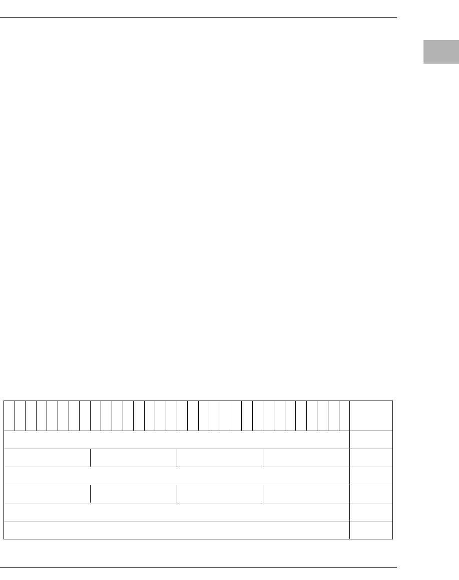
Raven Interrupt Controller
http://www.motorola.com/computer/literature 2-69
2
There is the possibility of a priority tie between the two processors when
resolving external interrupts. In such cases the interrupt is always
delivered to processor 0. This case is not defined in the above rule set.
MPIC Registers
The following conventions are used in the Raven register charts:
❏R Read Only field.
❏R/W Read/Write field.
❏S Writing a 1 to this field sets this field.
❏C Writing a 1 to this field clears this field.
RavenMPIC Registers
The RavenMPIC register map is shown in the following table. The Off
field is the address offset from the base address of the RavenMPIC
registers in the MPC-IO or MPC-MEMORY space. Note that this map
does not depict linear addressing. The Raven PCI-SLAVE has two
decoders for generating the RavenMPIC select. These decoders will
generate a select and acknowledge all accesses which are in a reserved
256K byte range. If the index into that 256K block does not decode a valid
RavenMPIC register address, the logic will return $00000000.
The registers are 8-, 16-, or 32-bit accessible.
Table 2-10. RavenMPIC Register Map
3
13
02
92
82
72
62
52
42
32
22
12
01
91
81
71
61
51
41
31
21
11
09876543210 Off
FEATURE REPORTING REGISTER 0 $01000
GLOBAL CONFIGURATION REGISTER 0 $01020
MPIC VENDOR IDENTIFICATION REGISTER $01080
PROCESSOR INIT REGISTER $01090
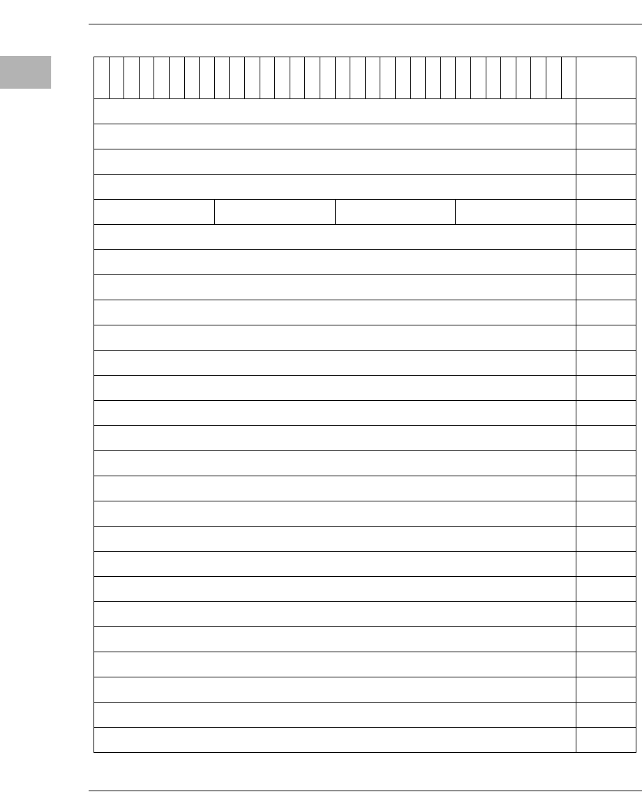
2-70 Computer Group Literature Center Web Site
Raven PCI Bridge ASIC
2
IPI0 VECTOR-PRIORITY REGISTER $010A0
IPI1 VECTOR-PRIORITY REGISTER $010B0
IPI2 VECTOR-PRIORITY REGISTER $010C0
IPI3 VECTOR-PRIORITY REGISTER $010D0
SP REGISTER $010E0
TIMER FREQUENCY REPORTING REGISTER $010F0
TIMER 0 CURRENT COUNT REGISTER $01100
TIMER 0 BASE COUNT REGISTER $01110
TIMER 0 VECTOR-PRIORITY REGISTER $01120
TIMER 0 DESTINATION REGISTER $01130
TIMER 1 CURRENT COUNT REGISTER $01140
TIMER 1 BASE COUNT REGISTER $01150
TIMER 1VECTOR-PRIORITY REGISTER $01160
TIMER 1DESTINATION REGISTER $01170
TIMER 2 CURRENT COUNT REGISTER $01180
TIMER 2 BASE COUNT REGISTER $01190
TIMER 2 VECTOR-PRIORITY REGISTER $011A0
TIMER 2 DESTINATION REGISTER $011B0
TIMER 3 CURRENT COUNT REGISTER $011C0
TIMER 3 BASE COUNT REGISTER $011D0
TIMER 3 VECTOR-PRIORITY REGISTER $011E0
TIMER 3 DESTINATION REGISTER $011F0
INT. SRC. 0 VECTOR-PRIORITY REGISTER $10000
INT. SRC. 0 DESTINATION REGISTER $10010
INT. SRC. 1 VECTOR-PRIORITY REGISTER $10020
INT. SRC. 1 DESTINATION REGISTER $10030
3
13
02
92
82
72
62
52
42
32
22
12
01
91
81
71
61
51
41
31
21
11
09876543210 Off

Raven Interrupt Controller
http://www.motorola.com/computer/literature 2-71
2
INT. SRC. 2 VECTOR-PRIORITY REGISTER $10040
INT. SRC. 2 DESTINATION REGISTER $10050
INT. SRC. 3 VECTOR-PRIORITY REGISTER $10060
INT. SRC. 3 DESTINATION REGISTER $10070
INT. SRC. 4 VECTOR-PRIORITY REGISTER $10080
INT. SRC. 4 DESTINATION REGISTER $10090
INT. SRC. 5 VECTOR-PRIORITY REGISTER $100A0
INT. SRC. 5 DESTINATION REGISTER $100B0
INT. SRC. 6 VECTOR-PRIORITY REGISTER $100C0
INT. SRC. 6 DESTINATION REGISTER $100D0
INT. SRC. 7 VECTOR-PRIORITY REGISTER $100E0
INT. SRC. 7 DESTINATION REGISTER $100F0
INT. SRC. 8 VECTOR-PRIORITY REGISTER $10100
INT. SRC. 8 DESTINATION REGISTER $10110
INT. SRC. 9 VECTOR-PRIORITY REGISTER $10120
INT. SRC. 9 DESTINATION REGISTER $10130
INT. SRC. 10 VECTOR-PRIORITY REGISTER $10140
INT. SRC. 10 DESTINATION REGISTER $10150
INT. SRC. 11 VECTOR-PRIORITY REGISTER $10160
INT. SRC. 11 DESTINATION REGISTER $10170
INT. SRC. 12 VECTOR-PRIORITY REGISTER $10180
INT. SRC. 12 DESTINATION REGISTER $10190
INT. SRC. 13 VECTOR-PRIORITY REGISTER $101A0
INT. SRC. 13 DESTINATION REGISTER $101B0
INT. SRC. 14 VECTOR-PRIORITY REGISTER $101C0
INT. SRC. 14 DESTINATION REGISTER $101D0
3
13
02
92
82
72
62
52
42
32
22
12
01
91
81
71
61
51
41
31
21
11
09876543210 Off
2-72 Computer Group Literature Center Web Site
Raven PCI Bridge ASIC
2
INT. SRC. 15 VECTOR-PRIORITY REGISTER $101E0
INT. SRC. 15 DESTINATION REGISTER $101F0
RAVEN DETECTED ERRORS VECTOR-PRIORITY REGISTER $10200
RAVEN DETECTED ERRORS DESTINATION REGISTER $10210
IPI 0 DISPATCH REGISTER PROC. 0 $20040
IPI 1 DISPATCH REGISTER PROC. 0 $20050
IPI 2 DISPATCH REGISTER PROC. 0 $20060
IPI 3 DISPATCH REGISTER PROC. 0 $20070
CURRENT TASK PRIORITY REGISTER PROC. 0 $20080
IACK REGISTER
P0 $200A0
EOI REGISTER
P0 $200B0
IPI 0 DISPATCH REGISTER PROC. 1 $21040
IPI 1 DISPATCH REGISTER PROC. 1 $21050
IPI 2 DISPATCH REGISTER PROC. 1 $21060
IPI 3 DISPATCH REGISTER PROC. 1 $21070
CURRENT TASK PRIORITY REGISTER PROC. 1 $21080
IACK REGISTER
P1 $210A0
EOI REGISTER
P1 $210B0
3
13
02
92
82
72
62
52
42
32
22
12
01
91
81
71
61
51
41
31
21
11
09876543210 Off
Raven Interrupt Controller
http://www.motorola.com/computer/literature 2-73
2
Feature Reporting Register
NIRQ NUMBER OF IRQs. The number of the highest external
IRQ source supported. The IPI, Timer, and Raven
Detected Error interrupts are excluded from this count.
NCPU NUMBER OF CPUs. The number of the highest physical
CPU supported. This design supports two CPUs (CPU 0
and CPU 1).
VID VERSION ID. Version ID for this interrupt controller.
This value reports what level of the specification is
supported by this implementation. A version level of 02 is
used for the initial release of the MPIC specification.
Offset $01000
Bit 3
13
02
92
82
72
62
52
42
32
22
12
01
91
81
71
61
51
41
31
21
11
09876543210
Name FEATURE REPORTING
NIRQ NCPU VID
Operation RRRRR
Reset $0 $00F $0 $01 $02
2-74 Computer Group Literature Center Web Site
Raven PCI Bridge ASIC
2Global Configuration Register
R Reset Controller. Writing a 1 to this bit forces the
controller logic to be reset. The bit is cleared
automatically when the reset sequence is complete. While
this bit is set, the values of all other register are undefined.
M Cascade Mode. Allows cascading of an external 8259
pair connected to the first interrupt source input pin (0).
This bit will always be set to 1, indicating mixed mode. In
mixed mode, 8259 interrupts are delivered using the
priority and distribution mechanism of the RavenMPIC.
The Vector/Priority and Destination registers for interrupt
source 0 are used to control the delivery mode for all
8259-generated interrupt sources.
2Raven PCI Bridge ASIC
0Raven Interrupt Controller
Offset $01020
Bit 3
13
02
92
82
72
62
52
42
32
22
12
01
91
81
71
61
51
41
31
21
11
09876543210
Name GLOBAL CONFIGURATION
RESET
M
Operation
C
R
R/W
RRRR
Reset
0
0
0
$00 $00 $00 $00
Raven Interrupt Controller
http://www.motorola.com/computer/literature 2-75
2
Vendor Identification Register
Two of the fields in the Vendor Identification register are not defined for
the RavenMPIC implementation, but are defined in the MPIC
specification. They are the vendor identification and device ID fields.
STP Stepping. The stepping or silicon revision number is
initially 0.
Processor Init Register
P1 Processor 1. Writing a 1 to P1 will assert the Soft Reset
input of processor 1. Writing a 0 to it will negate the
SRESET signal.
P0 Processor 0. Writing a 1 to P0 will assert the Soft Reset
input of processor 0. Writing a 0 to it will negate the
SRESET signal.
Offset $01080
Bit 3
13
02
92
82
72
62
52
42
32
22
12
01
91
81
71
61
51
41
31
21
11
09876543210
Name VENDOR IDENTIFICATION
STP
Operation RRRR
Reset $00 $02 $00 $00
Offset $01090
Bit 3
13
02
92
82
72
62
52
42
32
22
12
01
91
81
71
61
51
41
31
21
11
09876543210
Name PROCESSOR INIT
P1
P0
Operation RRRR
R/W
R/W
Reset $00 $00 $00 $00
0
0
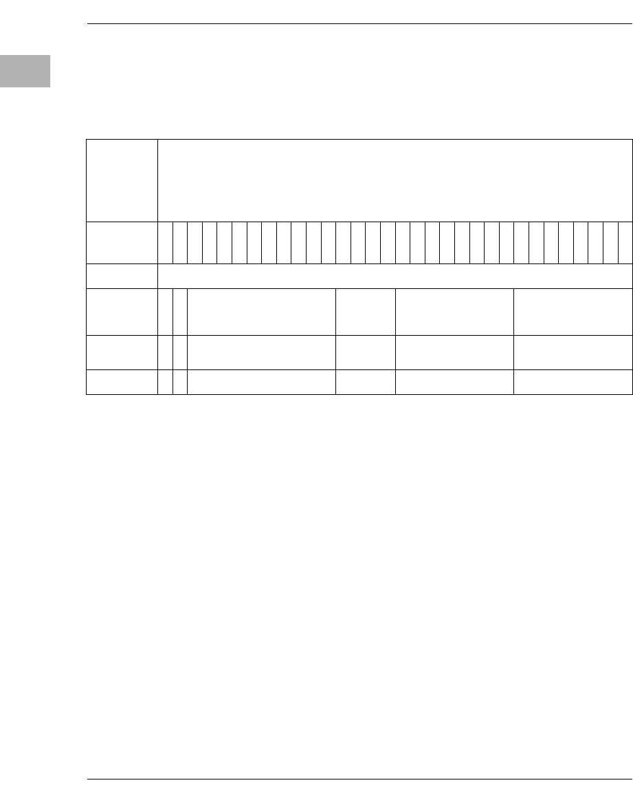
2-76 Computer Group Literature Center Web Site
Raven PCI Bridge ASIC
2The Soft Reset input to the MPC603 or MPC604 is negative-edge-
sensitive.
IPI Vector/Priority Registers
MASK Mask. Setting this bit disables any further interrupts from
this source. If the mask bit is cleared while the bit
associated with this interrupt is set in the IPR, the interrupt
request will be generated.
ACT Activity. The activity bit indicates that an interrupt has
been requested or that it is in-service. The ACT bit is set
to a 1 when its associated bit in the Interrupt Pending
register or In-Service register is set.
PRIOR Interrupt Priority. Priority 0 is the lowest and 15 is the
highest. Note that a priority level of 0 will not enable
interrupts.
VECTOR Interrupt Vector. This vector is returned when the
Interrupt Acknowledge register is examined during a
request for the interrupt associated with this vector.
Offset IPI 0 - $010A0
IPI 1 - $010B0
IPI 2 - $010C0
IPI 3 - $010D0
Bit 3
13
02
92
82
72
62
52
42
32
22
12
01
91
81
71
61
51
41
31
21
11
09876543210
Name IPI VECTOR/PRIORITY
MASK
ACT
PRIOR VECTOR
Operation
R/W
R
R R/W R R/W
Reset
1
0
$000 $0 $00 $00
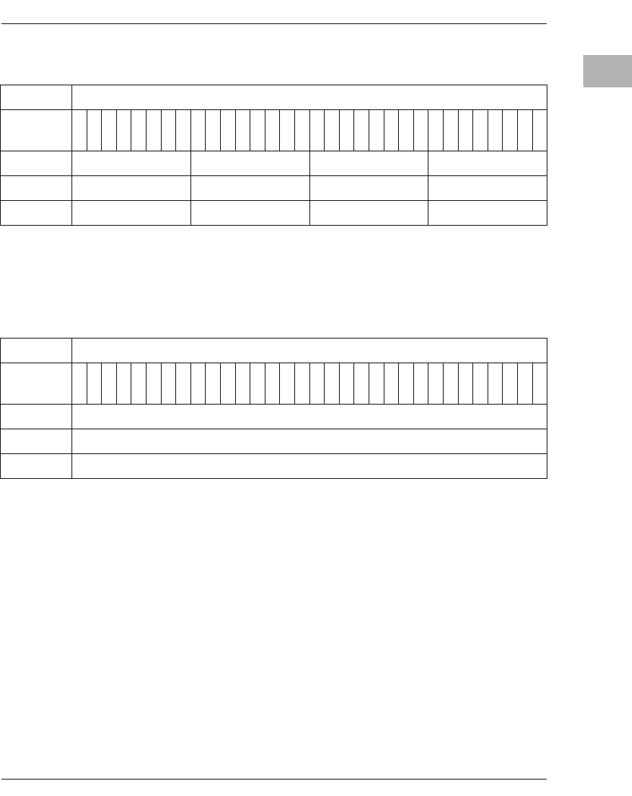
Raven Interrupt Controller
http://www.motorola.com/computer/literature 2-77
2
Spurious Vector Register
VECTOR Interrupt Vector. This vector is returned when the
Interrupt Acknowledge register is read during a spurious
vector fetch.
Timer Frequency Register
This register is used to report the frequency (in Hz) of the clock source for
the global timers. Following a reset, this register contains zero. For the
Raven implementation of MPIC on the MVME2300 series, this register
must be written with a value of $7DE290 (that is, 66/8 MHz or 8.25 MHz),
which corresponds to a 66MHz MPC bus.
Offset $010E0
Bit 3
13
02
92
82
72
62
52
42
32
22
12
01
91
81
71
61
51
41
31
21
11
09876543210
Name VECTOR
Operation RRRR/W
Reset $00 $00 $00 $FF
Offset $010F0
Bit 3
13
02
92
82
72
62
52
42
32
22
12
01
91
81
71
61
51
41
31
21
11
09876543210
Name TIMER FREQUENCY
Operation R/W
Reset $00000000
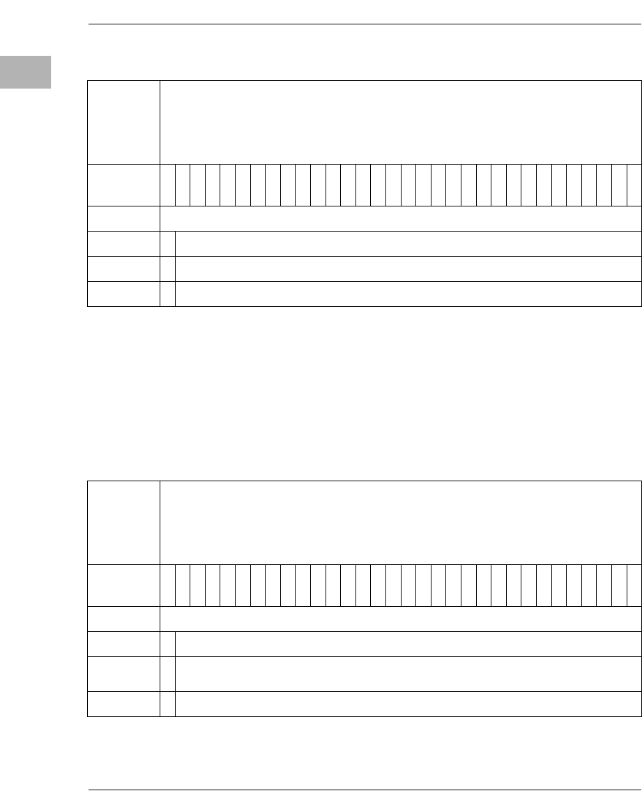
2-78 Computer Group Literature Center Web Site
Raven PCI Bridge ASIC
2Timer Current Count Registers
T Toggle. This bit toggles when ever the current count
decrements to zero.
CC Current Count. The Current Count field decrements
while the Count Inhibit bit in the Base Count register is
zero. When the timer counts down to zero, the Current
Count register is reloaded from the Base Count register.
Timer Base Count Registers
Offset Timer 0 - $01100
Timer 1 - $01140
Timer 2 - $01180
Timer 3 - $011C0
Bit 3
13
02
92
82
72
62
52
42
32
22
12
01
91
81
71
61
51
41
31
21
11
09876543210
Name TIMER CURRENT COUNT
T
CC
Operation
R
R
Reset
0
$00000000
Offset Timer 0 - $01110
Timer 1 - $01150
Timer 2 - $01190
Timer 3 - $011D0
Bit 3
13
02
92
82
72
62
52
42
32
22
12
01
91
81
71
61
51
41
31
21
11
09876543210
Name TIMER BASECOUNT
CI
BC
Operation
R/W
R/W
Reset
1
$00000000
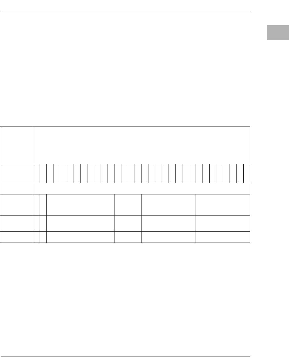
Raven Interrupt Controller
http://www.motorola.com/computer/literature 2-79
2
CI Count Inhibit. Setting this bit to 1 inhibits counting for
this timer. Setting the bit to 0 allows counting to proceed.
BC Base Count. This field contains the 31-bit count for this
timer. When a value is written into this register and the CI
bit transitions from a 1 to a 0, the value is copied into the
corresponding Current Count register and the toggle bit in
the Current Count register is cleared. When the timer
counts down to zero, the Current Count register is
reloaded from the Base Count register.
Timer Vector/Priority Registers
MASK Mask. Setting this bit disables any further interrupts from
this source. If the mask bit is cleared while the bit
associated with this interrupt is set in the IPR, the interrupt
request will be generated.
ACT Activity. The activity bit indicates that an interrupt has
been requested or that it is in-service. The ACT bit is set
to a 1 when its associated bit in the Interrupt Pending
register or In-Service register is set.
Offset Timer 0 - $01120
Timer 1 - $01160
Timer 2 - $011A0
Timer 3 - $011E0
Bit 3
13
02
92
82
72
62
52
42
32
22
12
01
91
81
71
61
51
41
31
21
11
09876543210
Name TIMER VECTOR/PRIORITY
MASK
ACT
PRIOR VECTOR
Operation
R/W
R
R R/W R R/W
Reset
1
0
$000 $0 $00 $00
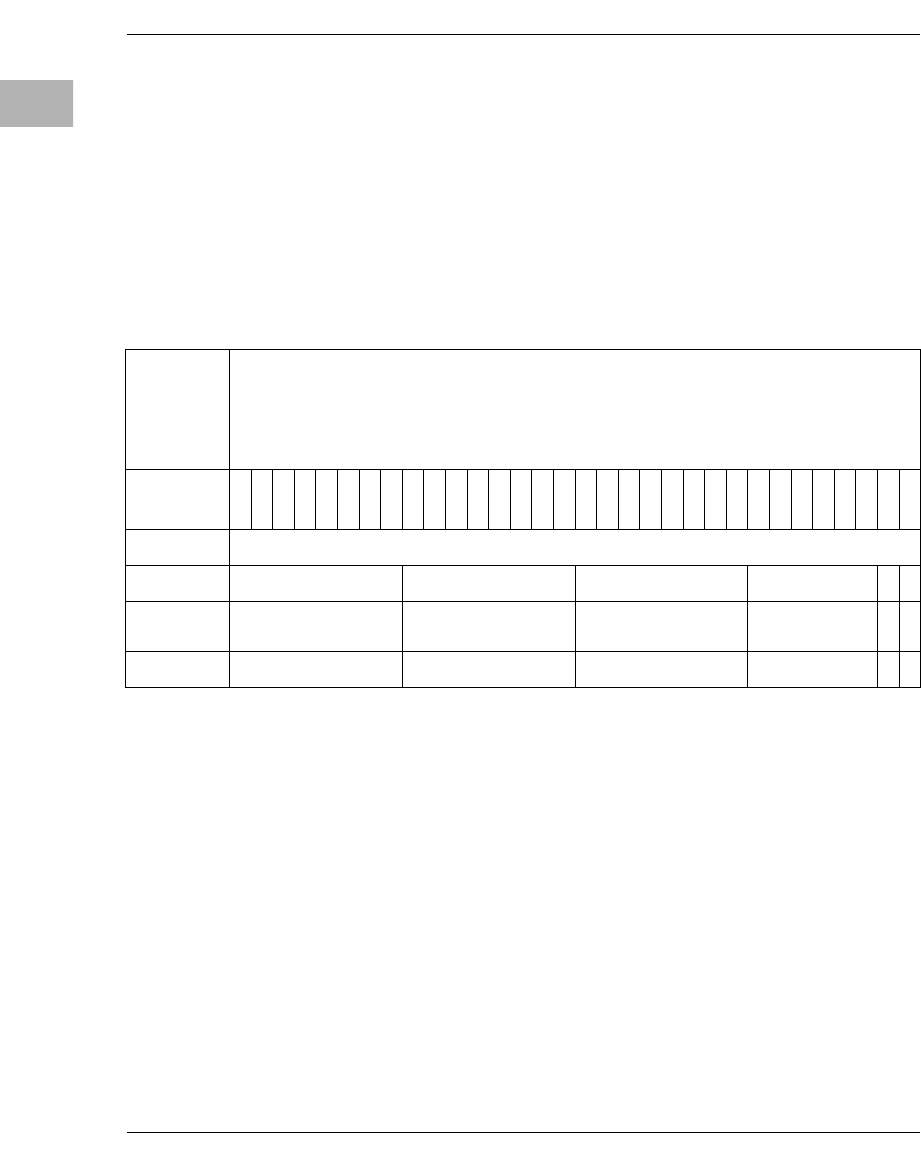
2-80 Computer Group Literature Center Web Site
Raven PCI Bridge ASIC
2PRIOR Interrupt Priority. Priority 0 is the lowest and 15 is the
highest. Note that a priority level of 0 will not enable
interrupts.
VECTOR Interrupt Vector. This vector is returned when the
Interrupt Acknowledge register is examined upon
acknowledgment of the interrupt associated with this
vector.
Timer Destination Registers
This register indicates the destinations for this timer’s interrupts. Timer
interrupts operate in the Directed delivery interrupt mode. This register
may specify multiple destinations (multicast delivery).
P1 PROCESSOR 1. The interrupt is directed to processor 1.
P0 PROCESSOR 0. The interrupt is directed to processor 0.
Offset Timer 0 - $01130
Timer 1 - $01170
Timer 2 - $011B0
Timer 3 - $011F0
Bit 3
13
02
92
82
72
62
52
42
32
22
12
01
91
81
71
61
51
41
31
21
11
09876543210
Name TIMER DESTINATION
P1
P0
Operation RRRR
R/W
R/W
Reset $00 $00 $00 $00
0
0
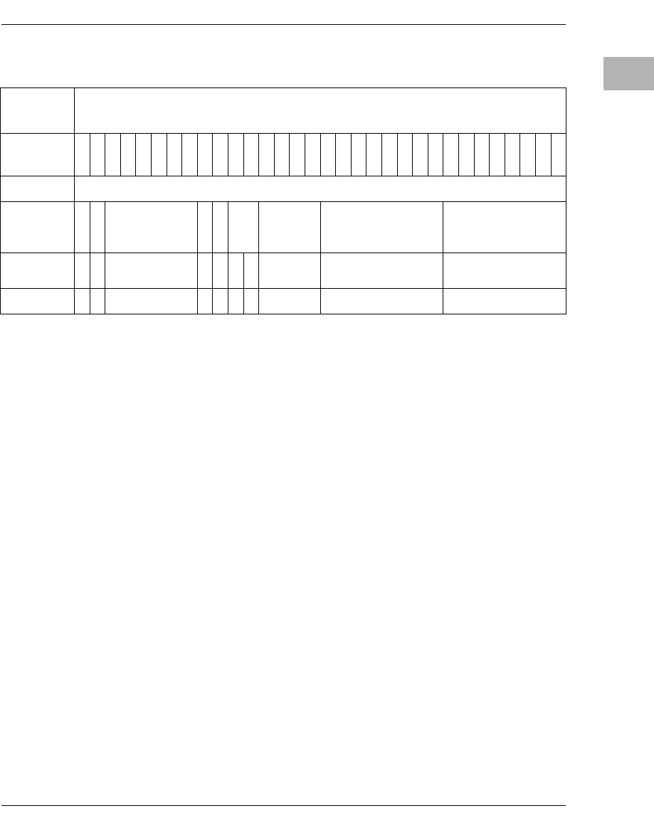
Raven Interrupt Controller
http://www.motorola.com/computer/literature 2-81
2
External Source Vector/Priority Registers
MASK Mask. Setting this bit disables any further interrupts from
this source. If the mask bit is cleared while the bit
associated with this interrupt is set in the IPR, the interrupt
request will be generated.
ACT Activity. The activity bit indicates that an interrupt has
been requested or that it is in-service. The ACT bit is set
to a 1 when its associated bit in the Interrupt Pending
register or In-Service register is set.
POL Polarity. This bit sets the polarity for external interrupts.
Setting this bit to a 0 enables active low or negative edge.
Setting this bit to a 1 enables active high or positive edge.
Only External Interrupt Source 0 uses this bit in this
register.
SENSE Sense. This bit sets the sense for external interrupts.
Setting this bit to a zero enables edge-sensitive interrupts.
Setting this bit to a one enables level-sensitive interrupts.
For external interrupt sources 1 through 15, setting this bit
to a 0 enables positive edge-triggered interrupts. Setting
this bit to a one enables active-low level-triggered
interrupts.
Offset Int Src 0 - $10000
Int Src 2 -> Int Src15 - $10020 -> $101E0
Bit 3
13
02
92
82
72
62
52
42
32
22
12
01
91
81
71
61
51
41
31
21
11
09876543210
Name EXTERNAL SOURCE VECTOR/PRIORITY
MASK
ACT
POL
SENSE
PRIOR VECTOR
Operation
R/W
R
R
R/W
R/W
R
R
R/W R R/W
Reset
1
0
$000
0
0
0
0
$0 $00 $00
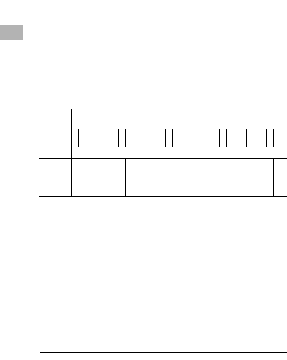
2-82 Computer Group Literature Center Web Site
Raven PCI Bridge ASIC
2PRIOR Interrupt Priority. Priority 0 is the lowest and 15 is the
highest. Note that a priority level of 0 will not enable
interrupts.
VECTOR Interrupt Vector. This vector is returned when the
Interrupt Acknowledge register is examined upon
acknowledgment of the interrupt associated with this
vector.
External Source Destination Registers
This register indicates the possible destinations for the external interrupt
sources. These interrupts operate in the Distributed interrupt delivery
mode.
P1 Processor 1. The interrupt is pointed to processor 1.
P0 Processor 0. The interrupt is pointed to processor 0.
Offset Int Src 0 - $10010
Int Src 2 -> Int Src 15 - $10030 -> $101F0
Bit 3
13
02
92
82
72
62
52
42
32
22
12
01
91
81
71
61
51
41
31
21
11
09876543210
Name EXTERNAL SOURCE DESTINATION
P1
P0
Operation RRRR
R/W
R/W
Reset $00 $00 $00 $00
0
0
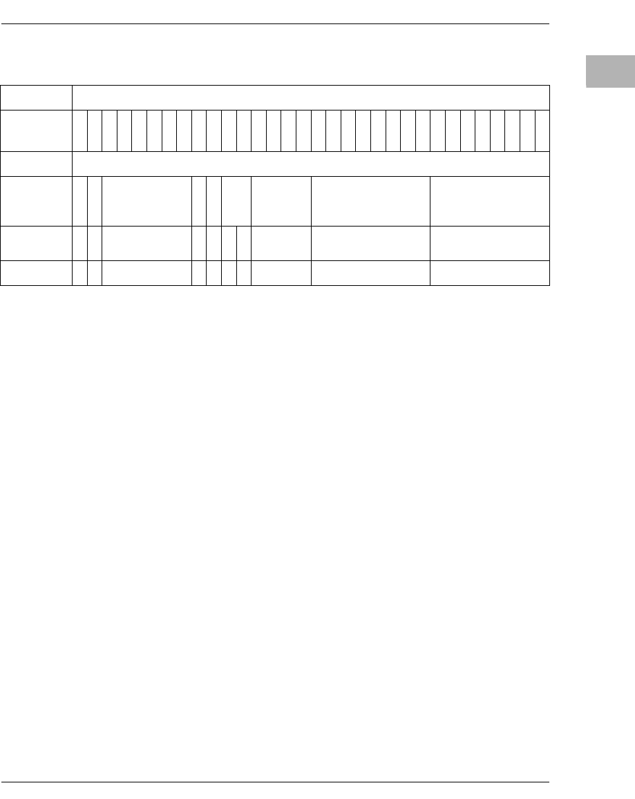
Raven Interrupt Controller
http://www.motorola.com/computer/literature 2-83
2
Raven-Detected Errors Vector/Priority Register
MASK Mask. Setting this bit disables any further interrupts from
this source. If the mask bit is cleared while the bit
associated with this interrupt is set in the IPR, the interrupt
request will be generated.
ACT Activity. The activity bit indicates that an interrupt has
been requested or that it is in-service. The ACT bit is set
to a 1 when its associated bit in the Interrupt Pending
register or In-Service register is set.
SENSE Sense. This bit sets the sense for external interrupts.
Setting this bit to a 0 enables positive edge sensitive
interrupts. Setting this bit to a 1 enables active low level
sensitive interrupts.
PRIOR Interrupt Priority. Priority 0 is the lowest and 15 is the
highest. Note that a priority level of 0 will not enable
interrupts.
VECTOR Interrupt Vector. This vector is returned when the
Interrupt Acknowledge register is examined upon
acknowledgment of the interrupt associated with this
vector.
Offset $10200
Bit 3
13
02
92
82
72
62
52
42
32
22
12
01
91
81
71
61
51
41
31
21
11
09876543210
Name RAVEN DETECTED ERRORS VECTOR/PRIORITY
MASK
ACT
SENSE
PRIOR VECTOR
Operation
R/W
R
R
R
R/W
R
R
R/W R R/W
Reset
1
0
$000
0
0
0
0
$0 $00 $00
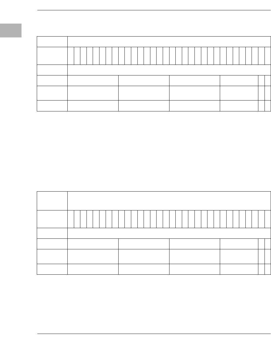
2-84 Computer Group Literature Center Web Site
Raven PCI Bridge ASIC
2Raven-Detected Errors Destination Register
This register indicates the possible destinations for the Raven-detected
error interrupt source. These interrupts operate in the Distributed interrupt
delivery mode.
P1 Processor 1. The interrupt is pointed to processor 1.
P0 Processor 0. The interrupt is pointed to processor 0.
Interprocessor Interrupt Dispatch Registers
There are four Interprocessor Interrupt Dispatch registers. Writing to an
IPI Dispatch register with the P0 and/or P1 bit set causes an interprocessor
interrupt request to be sent to one or more processors. Note that each IPI
Offset $10210
Bit 3
13
02
92
82
72
62
52
42
32
22
12
01
91
81
71
61
51
41
31
21
11
09876543210
Name RAVEN DETECTED ERROR DESTINATION
P1
P0
Operation RRRR
R/W
R/W
Reset $00 $00 $00 $00
0
0
Offset Processor 0 $20040, $20050, $20060, $20070
Processor 1 $21040, $21050,$21060, $21070
Bit 3
13
02
92
82
72
62
52
42
32
22
12
01
91
81
71
61
51
41
31
21
11
09876543210
Name IPI DISPATCH
P1
P0
Operation RRRR
R/W
R/W
Reset $00 $00 $00 $00
0
0
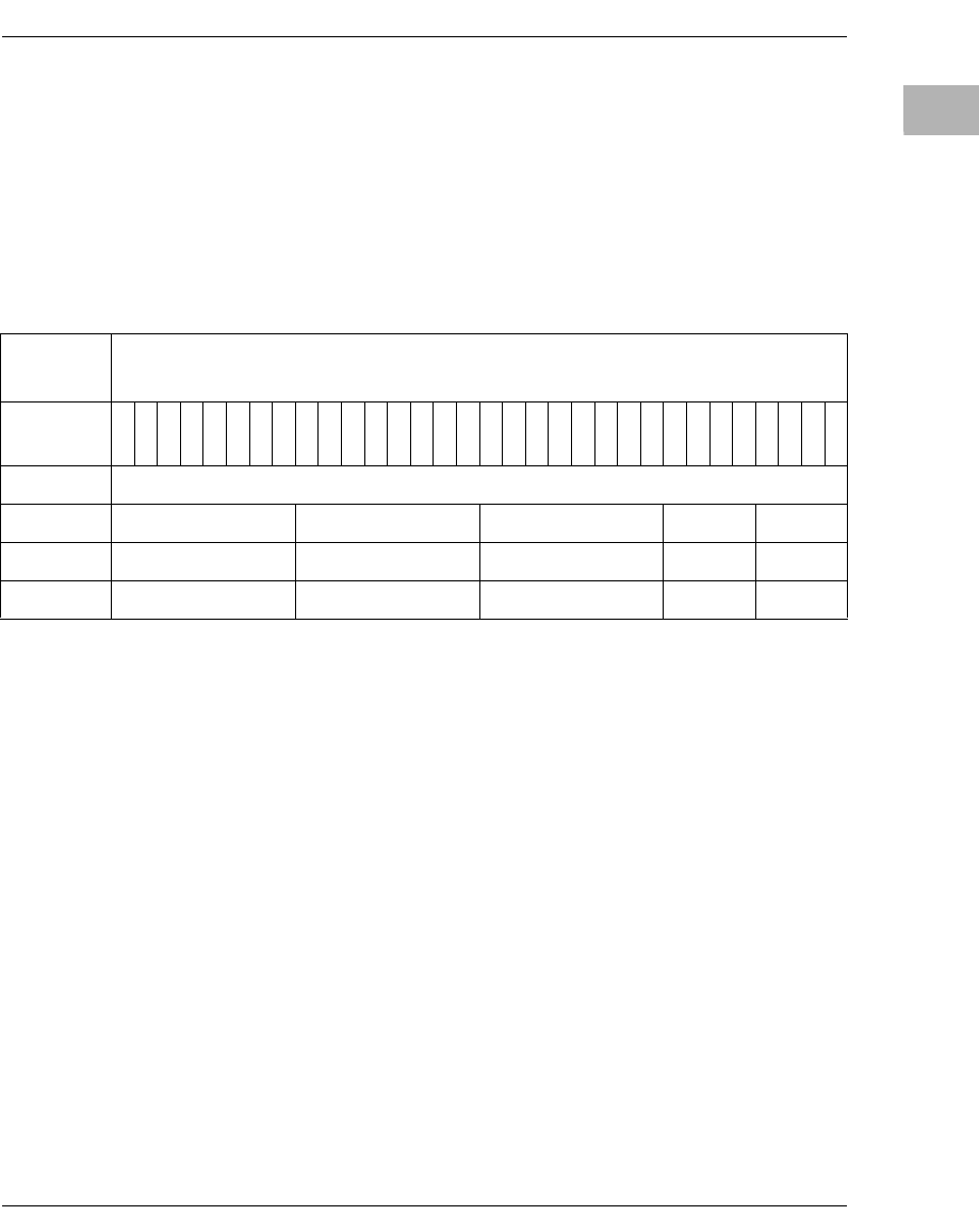
Raven Interrupt Controller
http://www.motorola.com/computer/literature 2-85
2
Dispatch register has two addresses. These registers are considered to be
per-processor registers and there is one address per processor. Reading
these registers returns zeros.
P1 Processor 1. The interrupt is directed to processor 1.
P0 Processor 0. The interrupt is directed to processor 0.
Interrupt Task Priority Registers
There is one Task Priority register per processor. Priority levels from 0
(lowest) to 15 (highest) are supported. Setting the Task Priority register to
15 masks all interrupts to this processor. Hardware will set the task register
to $F when it is reset, or when the Init bit associated with this processor is
written to a 1.
Offset Processor 0 $20080
Processor 1 $21080
Bit 3
13
02
92
82
72
62
52
42
32
22
12
01
91
81
71
61
51
41
31
21
11
09876543210
Name INTERRUPT TASK PRIORITY
TP
Operation RRRRR/W
Reset $00 $00 $00 $0 $F
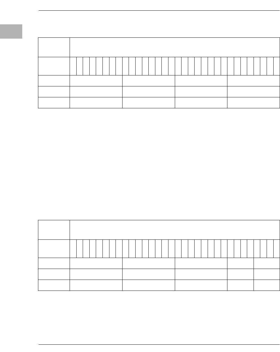
2-86 Computer Group Literature Center Web Site
Raven PCI Bridge ASIC
2Interrupt Acknowledge Registers
On PowerPC-based systems, Interrupt Acknowledge is implemented as a
read request to a memory-mapped Interrupt Acknowledge register.
Reading the Interrupt Acknowledge register returns the interrupt vector
corresponding to the highest-priority pending interrupt. Reading this
register also has the following side effects.
❏The associated bit in the Interrupt Pending register is cleared.
❏Reading this register will update the In-Service register.
Reading this register without a pending interrupt will return a value of $FF
hexadecimal.
End-of-Interrupt Registers
EOI End Of Interrupt. There is one EOI register per
processor. EOI code values other than 0 are currently
undefined. Data values written to this register are ignored;
zero is assumed. Writing to this register signals the end of
Offset Processor 0 $200A0
Processor 1 $210A0
Bit 3
13
02
92
82
72
62
52
42
32
22
12
01
91
81
71
61
51
41
31
21
11
09876543210
Name VECTOR
Operation RRRR
Reset $00 $00 $00 $FF
Offset Processor 0 $200B0
Processor 1 $210B0
Bit 3
13
02
92
82
72
62
52
42
32
22
12
01
91
81
71
61
51
41
31
21
11
09876543210
Name EOI
Operation RRRRW
Reset $00 $00 $00 $0 $0

Raven Interrupt Controller
http://www.motorola.com/computer/literature 2-87
2
processing for the highest-priority interrupt currently in
service by the associated processor. The write operation
will update the In-Service register by retiring the highest-
priority interrupt. Reading this register returns zeros.
Programming Notes
This section includes a number of items of information that should prove
helpful in programming your MVME2300 series board for a variety of
applications.
External Interrupt Service
The following summarizes how an external interrupt is serviced:
1. An external interrupt occurs.
2. The processor state is saved in the machine status save/restore
registers. A new value is loaded into the Machine State register
(MSR). The External Interrupt Enable bit in the new MSR (MSRee)
is set to zero. Control is transferred to the O/S external interrupt
handler.
3. The external interrupt handler calculates the address of the Interrupt
Acknowledge register for this processor (RavenMPIC Base Address
+ 0x200A00 + (processor ID shifted left 12 bits)).
4. The external interrupt handler issues an Interrupt Acknowledge
request to read the interrupt vector from the RavenMPIC. If the
interrupt vector indicates the interrupt source is the 8259, the
interrupt handler issues a second Interrupt Acknowledge request to
read the interrupt vector from the 8259. The RavenMPIC does not
interact with the vector fetch from the 8259.
5. The interrupt handler saves the processor state and other interrupt-
specific information in system memory and re-enables for external
interrupts (the MSRee bit is set to 1). The RavenMPIC blocks
interrupts from sources with equal or lower priority until an End-of-
Interrupt is received for that interrupt source. Interrupts from
higher-priority interrupt sources continue to be enabled. If the

2-88 Computer Group Literature Center Web Site
Raven PCI Bridge ASIC
2interrupt source was the 8259, the interrupt handler issues an EOI
request to the RavenMPIC. This resets the In-Service bit for the
8259 within the RavenMPIC and allows it to recognize higher-
priority interrupt requests, if any, from the 8259. If none of the
nested interrupt modes of the 8259 are enabled, the interrupt handler
issues an EOI request to the 8259.
a. The device driver interrupt service routine associated with this
interrupt vector is invoked.
b. If the interrupt source was not the 8259, the interrupt handler
issues an EOI request for this interrupt vector to the
RavenMPIC. If the interrupt source was the 8259 and any of the
nested interrupt modes of the 8259 are enabled, the interrupt
handler issues an EOI request to the 8259.
Normally, interrupts from ISA devices are connected to the 8259
interrupt controller. ISA devices typically rely on the 8259 Interrupt
Acknowledge to flush buffers between the ISA device and system
memory. If interrupts from ISA devices are directly connected to the
RavenMPIC (bypassing the 8259), the device driver interrupt
service routine must read status from the ISA device to ensure
buffers between the device and system memory are flushed.
Reset State
After a power-on reset, the RavenMPIC state is as follows:
❏Current task priority for all CPUs set to 15.
❏All interrupt source priorities set to 0.
❏All interrupt source mask bits set to 1.
❏All interrupt source activity bits cleared.
❏Processor Init register cleared.
❏All counters stopped and interrupts disabled.
❏Controller mode set to 8259 pass-through.

Raven Interrupt Controller
http://www.motorola.com/computer/literature 2-89
2
Interprocessor Interrupts
Four interprocessor interrupt (IPI) channels are provided for use by all
processors. During system initialization, the IPI vector/priority registers
for each channel should be programmed to set the priority and vector
returned for each IPI event. During system operation a processor may
generate an IPI by writing a destination mask to one of the IPI dispatch
registers.
Note that each IPI dispatch register is shared by both processors. Each IPI
dispatch register has two addresses but they are shared by both processors.
That is, there is a total of four IPI dispatch registers in the RavenMPIC.
The IPI mechanism may be used for self-interrupts by programming the
dispatch register with the bit mask for the originating processor.
Dynamically Changing I/O Interrupt Configuration
The interrupt controller provides a mechanism for safely changing the
vector, priority, or destination of I/O interrupt sources. This is provided to
support systems which allow dynamic configuration of I/O devices. In
order to change the vector, priority, or destination of an active interrupt
source, the following sequence should be performed:
1. Mask the source using the MASK bit in the vector/priority register.
2. Wait for the activity bit (ACT) for that source to be cleared.
3. Make the desired changes.
4. Unmask the source.
This sequence ensures that the vector, priority, destination, and mask
information remain valid until all processing of pending interrupts is
complete.

2-90 Computer Group Literature Center Web Site
Raven PCI Bridge ASIC
2EOI Register
Each processor has a private EOI register which is used to signal the end
of processing for a particular interrupt event. If multiple nested interrupts
are in service, the EOI command terminates the interrupt service of the
highest priority source. Once an interrupt is acknowledged, only sources
of higher priority will be allowed to interrupt the processor until the EOI
command is received. This register should always be written with a value
of zero which is the nonspecific EOI command.
Interrupt Acknowledge Register
Upon receipt of an interrupt signal, the processor may read this register to
retrieve the vector of the interrupt source which caused the interrupt.
8259 Mode
The 8259 mode bits control the use of an external 8259 pair for PC-AT
compatibility. Following a reset, this mode is set for pass-through, which
essentially disables the advanced controller and passes an 8259 input on
external interrupt source 0 directly through to processor 0. During interrupt
controller initialization this channel should be programmed for mixed
mode in order to take advantage of the interrupt delivery modes.
Current Task Priority Level
Each processor has a separate Current Task Priority Level register. The
system software uses this register to indicate the relative priority of the task
running on the corresponding processor. The interrupt controller will not
deliver an interrupt to a processor unless it has a priority level which is
greater than the current task priority level of that processor. This value is
also used in determining the destination for interrupts which are delivered
using the distributed deliver mode.

Raven Interrupt Controller
http://www.motorola.com/computer/literature 2-91
2
Architectural Notes
The hardware and software overhead required to update the Task Priority
register synchronously with instruction execution may far outweigh the
anticipated benefits of the Task Priority register. To minimize this
overhead, the interrupt controller architecture should allow the Task
Priority register to be updated asynchronously with respect to instruction
execution. Lower-priority interrupts may continue to occur for an
indeterminate number of cycles after the processor has updated the Task
Priority register. If this is not acceptable, the interrupt controller
architecture should recommend that if the Task Priority register is not
implemented with the processor, the Task Priority register should be
updated only when the processor enter or exits an idle state.
Only when the Task Priority register is integrated within the processor,
(such that it can be accessed as quickly as the MSRee bit defined in the
Programming Notes section, for example), should the architecture require
the Task Priority register to be updated synchronously with instruction
execution.
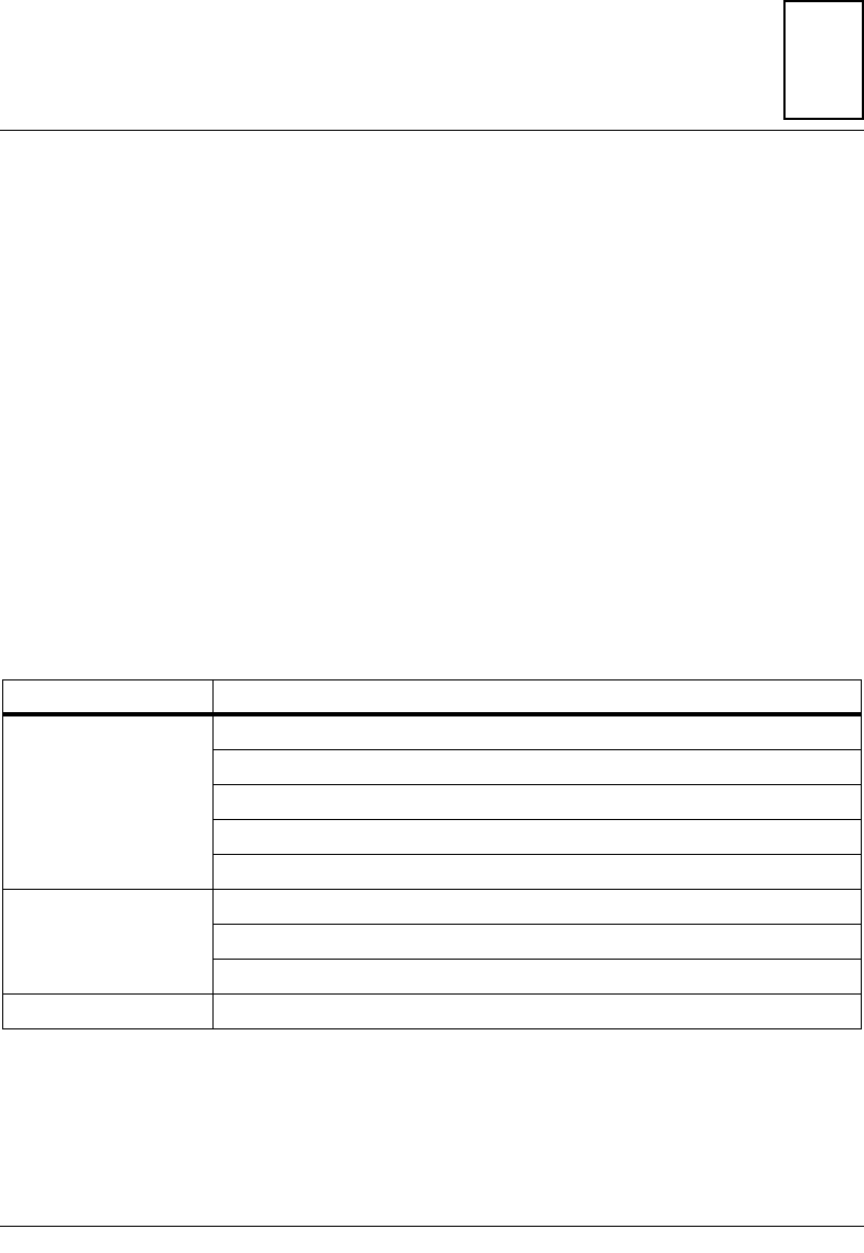
3-1
3
3Falcon ECC Memory Controller
Chip Set
Introduction
The Falcon DRAM controller ASIC is designed for the MVME2300
family of boards. It is used in sets of two to provide the interface between
the PowerPC 60x bus (also called MPC60x bus or MPC bus) and a 144-bit
ECC-DRAM memory system. It also provides an interface to ROM/Flash.
This chapter provides a functional description and programming model for
the Falcon chip set. Most of the information necessary to use the device in
a system, program it in a system, and test it can be found here.
Features
The following table summarizes the characteristics of the Falcon chip set.
Table 3-1. Features of the Falcon Chip Set
Function Features
DRAM Interface Double-bit error detect/Single-bit error correct on 72-bit basis
Up to four blocks
Programmable base address for each block
Two-way interleave factor
Built-in Refresh/Scrub
Error Notification for
DRAM Software-programmable Interrupt on Single/Double-Bit error
Error address and Syndrome Log Registers for Error Logging
Does not provide TEA_ on Double-Bit Error. (Chip has no TEA_ pin.)
ROM/Flash Interface Two blocks with two 8-bit devices, or two 32-bit devices per block
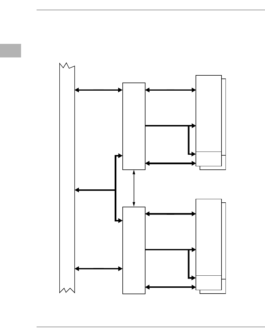
3-2 Computer Group Literature Center Web Site
Falcon ECC Memory Controller Chip Set
3
Block Diagrams
Figure 3-1 depicts a Falcon pair as it would be connected in a system.
Figure 3-2 shows the Falcon’s internal data paths. Figure 3-3 shows the
overall DRAM connections.
Figure 3-1. Falcon Pair Used with DRAM in a System
1900 9609
Lower PowerPC
Check
Data
FALCONFALCON
Lower
DRAM
ARRAYS
Check
Data
Upper
DRAM
ARRAYS
Data (32Bits)
Lower DRAM
Data (64 Bits)
Lower DRAM
Address & Control
Lower DRAM
Check-bits (8 Bits)
Upper DRAM
Data (64 Bits)
Upper DRAM
Address & Control
Upper DRAM
Check-bits (8 Bits)
Upper PowerPC
Data (32 Bits)
PowerPC
Address &
Control
Serial Bus
PowerPC 60x Bus
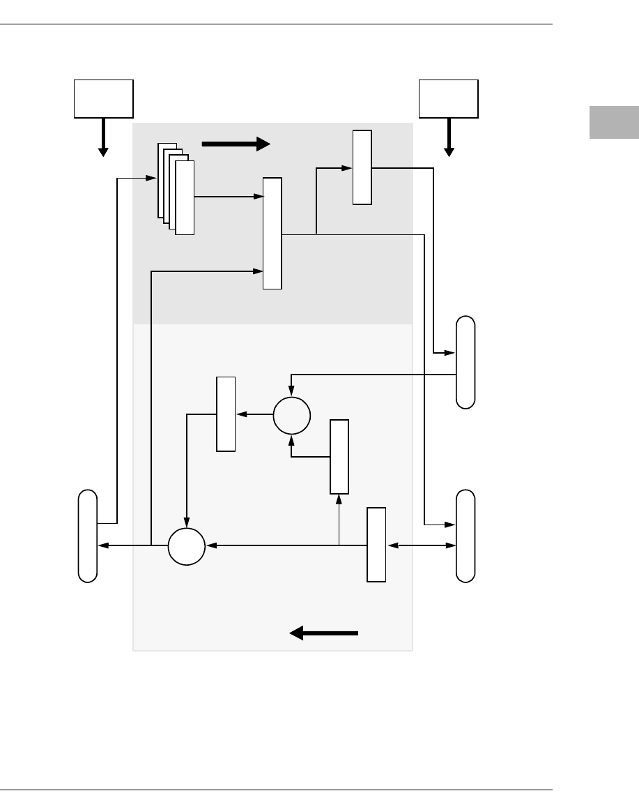
Block Diagrams
http://www.motorola.com/computer/literature 3-3
3
Figure 3-2. Falcon Internal Data Paths (Simplified)
1901 9609
(64 Bits)
PowerPC
Side
RD[0:63]
HAMGEN
DFF’s
HAMGEN
+
+
DRAM
Side
LATCHES
CKD[0:7]
MUX
D[0:31]
(64 Bits)
(64 Bits)
Latched D
(64 Bits)
Corrected Data
(8 Bits)
(8 Bits)
(8 Bits)
SYNDEC
(64 Bits)
Uncorrected Data
(64 Bits)
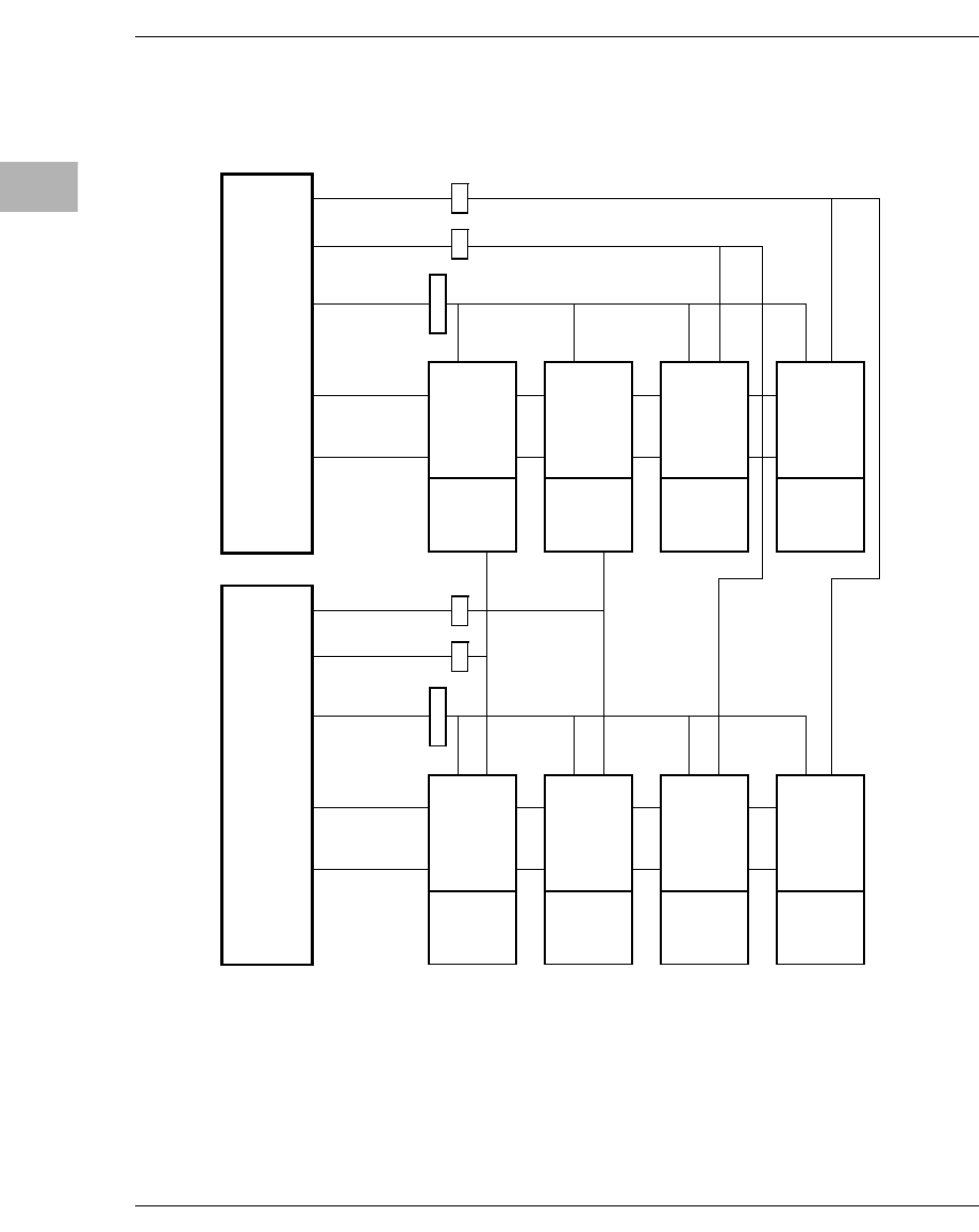
3-4 Computer Group Literature Center Web Site
Falcon ECC Memory Controller Chip Set
3
Figure 3-3. Overall DRAM Connections
DRAM
BLOCK A
UPPER
DRAM
BLOCK B
UPPER
DRAM
BLOCK C
UPPER
DRAM
BLOCK D
UPPER
BD_RAS_/CAS_
AC_RAS_/CAS_
RA/OE_/WE_
RD0-63
CKD0-7
1902 9609
LOWER
FALCON
UPPER
FALCON
DRAM
BLOCK A
LOWER
DRAM
BLOCK B
LOWER
DRAM
BLOCK C
LOWER
DRAM
BLOCK D
LOWER
BD_RAS_/CAS_
AC_RAS_/CAS_
RA/OE_/WE_
RD0-63
CKD0-7

Functional Description
http://www.motorola.com/computer/literature 3-5
3
Functional Description
The following sections describe the logical function of the Falcon ASIC.
The Falcon is designed to be used as a set of two chips. A pair of Falcons
works with x1 or wider DRAM memory devices to form a memory system
for the PowerPC 60x bus. A pair of Falcons that is connected to implement
a memory control function is referred to in this document as a “Falcon
pair”.
Bit Ordering Convention
All Falcon bused signals are named using big-endian bit ordering (bit 0 is
the most significant bit).
Performance
The following sections describe the Falcon pair’s data transfer
characteristics in various configurations.
Four-beat Reads/Writes
The Falcon pair is specifically designed to provide maximum performance
for cache line (four-beat) cycles to and from the PowerPC 60x bus at
66MHz. This is done by providing a two-way interleave between the 64-
bit PowerPC 60x data bus and the 128-bit (144 with check-bits) DRAM
bus. When a PowerPC 60x bus master begins a quad-aligned, four-beat
read to DRAM, the Falcon pair accesses the full 144-bit width of DRAM
at once so that when the DRAM access time is reached, not only is the first
64-bit double-word of data ready to be transferred to the PowerPC 60x bus
master, but so is the next. While the Falcon pair is presenting the first two
double-words to the PowerPC 60x bus, it cycles CAS without cycling RAS
to obtain the next two double-words. The Falcon pair transfers the next two
double-words to the PowerPC 60x bus after 0 or more idle clocks.
The Falcon pair also profits from the fact that PowerPC 60x processors can
do address pipelining. Many times while a data cycle is finishing, the
PowerPC 60x processor begins a new address cycle. The Falcon pair can
begin the next DRAM access earlier when this happens, thus shortening

3-6 Computer Group Literature Center Web Site
Falcon ECC Memory Controller Chip Set
3
the access time. Further savings come when the new address cycle is to an
address close enough to the previous one that it falls within the same row
in the DRAM array. When this happens, the Falcon pair can transfer the
data for the next cycle by cycling CAS without cycling RAS.
Single-beat Reads/Writes
Single-beat cycles to and from the PowerPC 60x bus do not achieve data
rates as high as do four-beat cycles. The Falcon pair does take advantage
of the PowerPC 60x address pipelining as much as possible for single-beat
accesses.
Single-beat writes are the slowest type of accesses because they require
that the Falcon pair perform first a read cycle, then a write cycle to the
DRAM in order to complete. When the Falcon pair can take advantage of
address pipelining, back-to-back single-beat writes take 10 clocks to
complete.
DRAM Speeds
The Falcon pair can be configured for three different DRAM speeds: 50ns,
60ns and 70ns. When the Falcon pair is configured for 50ns DRAMs, it
assumes that the devices are Hyper-Page parts. When the Falcon pair is
configured for 70ns DRAMs, it assumes that the devices are Page parts.
When the pair is configured for 60ns DRAMs, it allows the devices to be
either Page or Hyper-Page parts. Performance summaries using the
different devices are shown in Table 3-2, Table 3-3, and Table 3-4.
Functional Description
http://www.motorola.com/computer/literature 3-7
3
Notes
1. These numbers assume that the PowerPC 60x bus master is doing
address pipelining with TS_ occurring at the minimum time after
AACK_ is asserted. Also, the two numbers shown in the 1st Beat
column are for page miss/page hit.
2. In some cases, the numbers shown are averages and specific
instances may be longer or shorter.
Table 3-2. PowerPC 60
x
Bus to DRAM Access Timing — 70ns Page Devices
Access Type
Clock Periods Required For: Total
Clocks
1st
Beat 2nd
Beat 3rd
Beat 4th
Beat
4-Beat Read after Idle (Quad-
word aligned) 10 1 3 1 15
4-Beat Read after Idle (Quad-
word misaligned) 10 4 1 1 16
4-Beat Read after 4-Beat Read
(Quad-word aligned) 9/3 11 3 1 14/8
4-Beat Read after 4-Beat Read
(misaligned) 7/2 1 41113/8
4-Beat Write after Idle 4111
7
4-Beat Write after 4-Beat Write
(Quad-word aligned) 10/6 111113/9
1-Beat Read after Idle 10---
10
1-Beat Read after 1-Beat Read 11/7 1---
11/7
1-Beat Write after Idle 4---
4
1-Beat Write after 1-Beat Write 15/11 1---15/11
3-8 Computer Group Literature Center Web Site
Falcon ECC Memory Controller Chip Set
3
Table 3-3. PowerPC 60
x
Bus to DRAM Access Timing — 60ns Page Devices.
Notes
1. These numbers assume that the PowerPC 60x bus master is doing
address pipelining with TS_ occurring at the minimum time after
AACK_ is asserted. Also, the two numbers shown in the 1st Beat
column are for page miss/page hit.
2. In some cases, the numbers shown are averages and specific
instances may be longer or shorter.
Access Type
Clock Periods Required For: Total
Clocks
1st
Beat 2nd
Beat 3rd
Beat 4th
Beat
4-Beat Read after Idle (Quad-
word aligned) 91 2113
4-Beat Read after Idle (Quad-
word misaligned) 931114
4-Beat Read after 4-Beat Read
(Quad-word aligned) 7/3 11 2 1 11/7
4-Beat Read after 4-Beat Read
(misaligned) 6/2 1 31111/7
4-Beat Write after Idle 4111
7
4-Beat Write after 4-Beat Write
(Quad-word aligned) 7/3 111110/6
1-Beat Read after Idle 9---
9
1-Beat Read after 1-Beat Read 9/6 1---
9/6
1-Beat Write after Idle 4---4
1-Beat Write after 1-Beat Write 13/10 1---13/10
Functional Description
http://www.motorola.com/computer/literature 3-9
3
Table 3-4. PowerPC Bus to DRAM Access Timing — 50ns Hyper Devices
Notes
1. These numbers assume that the PowerPC 60x bus master is doing
address pipelining with TS_ occurring at the minimum time after
AACK_ is asserted. Also, the two numbers shown in the 1st Beat
column are for page miss/page hit.
2. In some cases, the numbers shown are averages and specific
instances may be longer or shorter.
Access Type
Clock Periods Required For: Total
Clocks
1st
Beat 2nd
Beat 3rd
Beat 4th
Beat
4-Beat Read after Idle (Quad-
word aligned) 81 1111
4-Beat Read after Idle (Quad-
word misaligned) 82 1112
4-Beat Read after 4-Beat Read
(Quad-word aligned) 5/2 11 1 1 8/5
4-Beat Read after 4-Beat Read
(misaligned) 4/2 1 2118/6
4-Beat Write after Idle 41117
4-Beat Write after 4-Beat Write
(Quad-word aligned) 4/3 11117/6
1-Beat Read after Idle 8---8
1-Beat Read after 1-Beat Read 7/5 1---
7/5
1-Beat Write after Idle 4---4
1-Beat Write after 1-Beat Write 9/7 1---9/7
3-10 Computer Group Literature Center Web Site
Falcon ECC Memory Controller Chip Set
3
ROM/Flash Speeds
The Falcon pair provides the interface for two blocks of ROM/Flash. Each
block can address up to 64MB of memory depending on the width
implemented for that block (16 bits or 64 bits). Bank A is 64 bits wide and
bank B is 16 bits wide. The access times for ROM/Flash are listed in Table
3-5 and Table 3-6.
Table 3-5. PowerPC 60
x
Bus to ROM/Flash Access Timing — 64 Bits
(32 Bits per Falcon)
Table 3-6. PowerPC 60
x
Bus to ROM/Flash Access Timing — 16 Bits (8 Bits
per Falcon)
Access Type
Clock Periods Required For: Total
Clocks
1st
Beat 2nd
Beat 3rd
Beat 4th
Beat
4-Beat Read 20 16 16 16 68
4-Beat Write N/A N/A N/A N/A N/A
1-Beat Read 20 - - - 20
1-Beat Write 19 - - - 19
Access Type
Clock Periods Required For: Total
Clocks
1st
Beat 2nd
Beat 3rd
Beat 4th
Beat
4-Beat Read 68 64 64 64 260
4-Beat Write N/A N/A N/A N/A N/A
1-Beat Read (2 bytes to 8 bytes) 68 - - - 68
1-Beat Read (1 byte) 20 - - - 20
1-Beat Write 19 - - - 19

Functional Description
http://www.motorola.com/computer/literature 3-11
3
PowerPC 60
x
Bus Interface
The Falcon pair has a PowerPC slave interface only. It has no PowerPC
master interface. The slave interface is the mechanism for all accesses to
DRAM, ROM/Flash, and Falcon registers/SRAM.
Responding to Address Transfers
When the Falcon pair detects an address transfer to which it should
respond, it asserts AACK_ immediately if there is no uncompleted
PowerPC 60x bus data transfer in progress. If a transfer is in progress, the
Falcon pair waits and asserts AACK_ coincident with the uncompleted
data transfer’s last data beat if the Falcon pair is the slave for the previous
data. If it is not the slave for the previous data, the Falcon pair holds off
AACK_ until the CLOCK after the previous data transfer’s last data beat.
Completing Data Transfers
If an address transfer to the Falcon pair will have an associated data
transfer, the Falcon pair begins a read or write cycle to the accessed entity
(DRAM/ROM/Flash/internal register) as soon as the entity is free. If the
data transfer will be a read, the Falcon pair begins providing data to the
PowerPC 60x bus as soon as the entity has data ready and the PowerPC 60x
data bus is granted. If the data transfer will be a write, the Falcon pair
begins latching data from the PowerPC data bus as soon as any previously
latched data is no longer needed and the PowerPC 60x data bus has been
granted.
Cache Coherency
The Falcon pair supports cache coherency by monitoring the ARTRY_
control signal on the PowerPC 60x bus and behaving appropriately when
it is asserted. When ARTRY_ is asserted, if the access is a read, the Falcon
pair does not source the data for that access. If the access is a write, the
Falcon does not write the data for that access to the DRAM array.
Depending upon when the retry occurs however, the Falcon pair may cycle
the DRAM even though the data transfer does not happen.

3-12 Computer Group Literature Center Web Site
Falcon ECC Memory Controller Chip Set
3
Cache Coherency Restrictions
The PowerPC 60x GBL_ signal must not be asserted in the CSR areas.
L2 Cache Support
The Falcon pair provides support for a look-aside L2 cache by
implementing a hold-off input, L2CLM_. On cycles that select the Falcon
pair, the Falcon pair samples L2CLM_ on the second rising edge of
CLOCK after the assertion of TS_. If L2CLM_ is high, the Falcon pair
responds normally to the cycle. If it is low, the Falcon pair ignores the
cycle.
Note The MVME2300 series boards have no L2 cache.
ECC
The Falcon pair performs single-bit error correction and double-bit error
detection for DRAM. (No checking is provided for ROM/Flash.) The 64-
bit wide PowerPC 60x data bus is divided into upper (DH0-DH31) and
lower (DL0-DL31) halves. Each half is routed through a Falcon which
multiplexes it with half of the DRAM data bus. Each Falcon connects to
64 DRAM data-bits and to 8 DRAM check-bits. The total DRAM array
width is 144 bits (2×[64+8]).
Cycle Types
To support ECC, the Falcon pair always deals with DRAM using full
width (144-bit) accesses. When the PowerPC 60x bus master requests any
size read of DRAM, the Falcon pair reads 144 bits at least once. When the
PowerPC 60x bus master requests a four-beat write to DRAM, the Falcon
pair writes all 144 bits twice. When the PowerPC 60x bus master requests
a single-beat write to DRAM, the Falcon pair performs a 144-bit wide read
cycle to DRAM, merges in the appropriate PowerPC 60x bus write data,
and writes 144 bits back to DRAM.

Functional Description
http://www.motorola.com/computer/literature 3-13
3
Error Reporting
The Falcon pair checks data from the DRAM during single- and four-beat
reads, during single-beat writes, and during scrubs. Table 3-7 shows the
actions taken by the Falcon pair for different errors during these accesses.
Note that the Falcon pair does not assert TEA_ on double-bit errors. In fact,
the Falcon pair does not have a TEA_ signal pin and it assumes that the
system does not implement TEA_. The Falcon can, however, assert
machine check (MCP_) on double-bit errors.
Notes 1. No opportunity for error, since no read of DRAM occurs
during a four-beat write.
Table 3-7. Error Reporting
Error Type Single-Beat/
Four-Beat Read Single-Beat Write Four-Beat Write Scrub
Single-Bit
Error
Terminate the
PowerPC 60x bus cycle
normally.
Provide corrected data to
the PowerPC 60x bus
master.
Assert INT_ if so
enabled.
Terminate the
PowerPC 60x bus cycle
normally.
Correct the data read
from DRAM, merge with
the write data, and write
the corrected, merged
data to DRAM.
Assert INT_ if so
enabled.
N/A 1
This cycle is not seen on
the PowerPC 60x bus.
Write corrected data
back to DRAM if so
enabled.
Assert INT_ if so
enabled.
Double-Bit
Error
Terminate the
PowerPC 60x bus cycle
normally.
Provide miss-corrected,
raw DRAM data to the
PowerPC 60x bus master.
Assert INT_ if so
enabled.
Assert MCP_ if so
enabled.
Terminate the
PowerPC 60x bus cycle
normally.
Do not perform the write
portion of the read-
modify-write cycle to
DRAM.
Assert INT_ if so
enabled.
Assert MCP_ if so
enabled.
N/A 1
This cycle is not seen on
the PowerPC 60x bus.
Do not perform the
write portion of the
read-modify-write cycle
to DRAM.
Assert INT_ if so
enabled.
Triple- (or
greater)
Bit Error
Some of these errors are detected correctly and are treated the same as double-bit errors. The rest could
show up as “no error” or “single-bit error”, both of which are incorrect.

3-14 Computer Group Literature Center Web Site
Falcon ECC Memory Controller Chip Set
3
Error Logging
ECC error logging is facilitated by the Falcon because of its internal
latches. When an error (single- or double-bit) occurs in the DRAMs to
which a Falcon is connected, it records the address and syndrome bits
associated with the data in error. Each Falcon performs this logging
function independently of the other. Once a Falcon has logged an error, it
does not log any more until the elog control /status bit has been cleared by
software unless the currently logged error is single-bit and a new, double-
bit error is encountered. The logging of errors that occur during scrub can
be enabled/disabled in software. Refer to the Error Logger Register
section of this chapter.
DRAM Tester
The DRAM tester is for factory testing purposes only; it should not be used
by customers.
ROM/Flash Interface
The Falcon pair provides the interface for two blocks of ROM/Flash. Each
block provides addressing and control for up to 64MB. Note that no error
checking (ECC or Parity) is provided for the ROM/Flash.
The ROM/Flash interface allows each block to be individually configured
by jumpers and/or by software as follows:
1. Access for each block is controlled by two software-programmable
control register bits: an overall enable, a write enable, and a reset
vector enable. The overall enable controls normal read accesses.
The write enable is used to program Flash devices. The reset vector
enable controls whether the block is also enabled at $FFF00000 -
$FFFFFFFF. The overall enable and write enable bits are always
cleared at reset. The reset vector enable bit is cleared or set at reset
depending on external jumper configuration. This allows the board
designer to use external jumpers to enable/disable Block A/B
ROM/Flash as the source of reset vectors.
The write enable bit is cleared at reset for both blocks.

Functional Description
http://www.motorola.com/computer/literature 3-15
3
2. The base address for each block is software programmable. At reset,
Block A’s base address is $FF000000 and Block B’s base address is
$FF400000.
As noted above, in addition to appearing at the programmed base
address, the first 1Mbyte of Block A/B also appears at $FFF00000-
$FFFFFFFF if the reset vector enable bit is set.
3. The assumed size for each block is software-programmable. It is
initialized to its smallest setting at reset.
4. The assumed device type for Block A/B is determined by an
external jumper at reset time. It also is available as a status bit and
cannot be changed by software.
When the width status bit is cleared, the block’s ROM/Flash is
considered to be 16 bits wide, where each Falcon interfaces to 8 bits.
In this mode, the following rules are enforced:
a. Only single-byte writes are allowed (all other sizes are ignored).
b. All reads are allowed (multiple accesses are performed to the
ROM/Flash devices when the read is for greater than one byte).
When the width status bit is set, the block’s ROM/Flash is
considered to be 64 bits wide, where each Falcon interfaces with 32
bits. In this mode, the following rules are enforced:
a. Only aligned, 4-byte writes should be attempted (all other sizes
are ignored).
b. All reads are allowed (multiple accesses to the ROM/Flash
device are performed for burst reads).
More information about ROM/Flash can be found in the Programming
Model section of this chapter.
In order to place code correctly in the ROM/Flash devices, address
mapping information is required. Table 3-8 shows how PowerPC 60x
addresses map to the ROM/Flash addresses when ROM/Flash is 16 bits
wide (8 bits per Falcon). Table 3-9 shows how they map when Flash is 64
bits wide (32 bits per Falcon).

3-16 Computer Group Literature Center Web Site
Falcon ECC Memory Controller Chip Set
3
Table 3-8. PowerPC 60
x
to ROM/Flash Address Mapping — ROM/Flash
16 Bits Wide (8 Bits per Falcon)
PowerPC 60x A0-A31 ROM/Flash A22-A0 ROM/Flash Device Selected
$XX000000 $000000 Upper
$XX000001 $000001 Upper
$XX000002 $000002 Upper
$XX000003 $000003 Upper
$XX000004 $000000 Lower
$XX000005 $000001 Lower
$XX000006 $000002 Lower
$XX000007 $000003 Lower
$XX000008 $000004 Upper
$XX000009 $000005 Upper
$XX00000A $000006 Upper
$XX00000B $000007 Upper
$XX00000C $000004 Lower
$XX00000D $000005 Lower
$XX00000E $000006 Lower
$XX00000F $000007 Lower
.
.
.
.
.
.
.
.
.
$XXFFFFF8 $7FFFFC Upper
$XXFFFFF9 $7FFFFD Upper
$XXFFFFFA $7FFFFE Upper
$XXFFFFFB $7FFFFF Upper
$XXFFFFFC $7FFFFC Lower
$XXFFFFFD $7FFFFD Lower
$XXFFFFFE $7FFFFE Lower
$XXFFFFFF $7FFFFF Lower
Functional Description
http://www.motorola.com/computer/literature 3-17
3
Table 3-9. PowerPC 60
x
to ROM/Flash Address Mapping — ROM/Flash
64 Bits Wide (32 Bits per Falcon)
PowerPC 60x A0-A31 ROM/Flash A22-A0 ROM/Flash Device Selected
$X0000000 $000000 Upper
$X0000001 $000000 Upper
$X0000002 $000000 Upper
$X0000003 $000000 Upper
$X0000004 $000000 Lower
$X0000005 $000000 Lower
$X0000006 $000000 Lower
$X0000007 $000000 Lower
$X0000008 $000001 Upper
$X0000009 $000001 Upper
$X000000A $000001 Upper
$X000000B $000001 Upper
$X000000C $000001 Lower
$X000000D $000001 Lower
$X000000E $000001 Lower
$X000000F $000001 Lower
.
.
.
.
.
.
.
.
.
$X3FFFFF0 $7FFFFE Upper
$X3FFFFF1 $7FFFFE Upper
$X3FFFFF2 $7FFFFE Upper
$X3FFFFF3 $7FFFFE Upper
$X3FFFFF4 $7FFFFE Lower
$X3FFFFF5 $7FFFFE Lower
$X3FFFFF6 $7FFFFE Lower
$X3FFFFF7 $7FFFFE Lower
$X3FFFFF8 $7FFFFF Upper
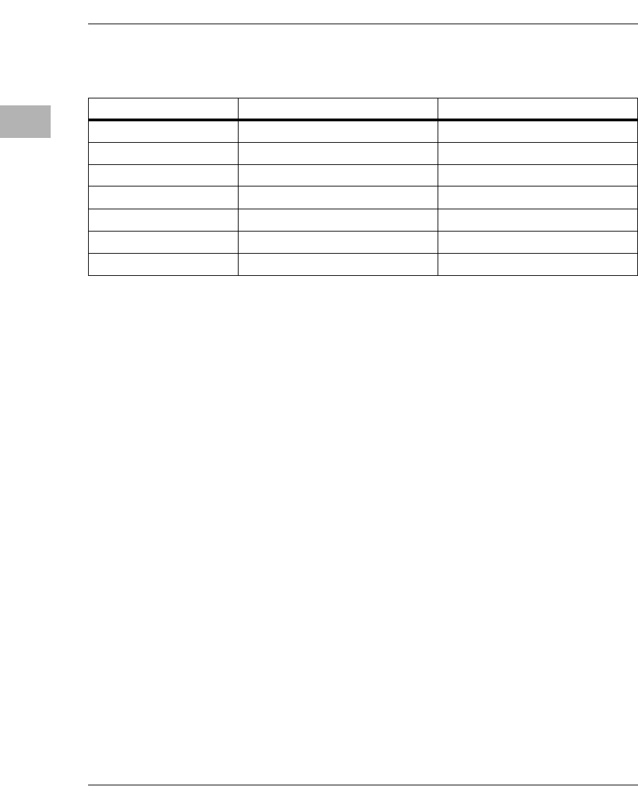
3-18 Computer Group Literature Center Web Site
Falcon ECC Memory Controller Chip Set
3
Refresh/Scrub
The Refresh/Scrub operation varies according to which DRAM blocks are
populated: (A and/or B) but not (C and D); or (A and/or B) and (C and/or
D).
Blocks A and/or B Present, Blocks C and D Not Present
The Falcon pair performs refreshes by doing a burst of four RAS_ cycles
approximately once every 60µs. This increases to once every 30µs when
certain DRAM devices are used. (The refresh rate is controlled by the
ram_fref bit in the status registers.) RAS_ is asserted to both of Blocks A
and B during each of the 4 cycles. Along with RAS_, the Falcon pair also
asserts CAS_ with (OE_ then WE_) to one of the blocks during one of the
four cycles. This forms a read-modify-write which is a scrub cycle to that
location.
After each of the 4 cycles, the DRAM row address increments by one.
When it reaches all 1s, it rolls over and starts anew at 0. Each time the row
address rolls over, the block that is scrubbed toggles between A and B.
Every second time that the row address rolls over, which of the 4 cycles
that is a scrub changes from 1st to 2nd, from 2nd to 3rd, from 3rd to 4th,
or from 4th to 1st. Every eighth time that the row address rolls over, the
column address increments by one. When the column address reaches all
ones, it rolls over and starts over at 0. Each time the column address rolls
over, the SC1, SC0 bits in the scrub/refresh register increment by 1.
$X3FFFFF9 $7FFFFF Upper
$X3FFFFFA $7FFFFF Upper
$X3FFFFFB $7FFFFF Upper
$X3FFFFFC $7FFFFF Lower
$X3FFFFFD $7FFFFF Lower
$X3FFFFFE $7FFFFF Lower
$X3FFFFFF $7FFFFF Lower
Table 3-9. PowerPC 60
x
to ROM/Flash Address Mapping — ROM/Flash
64 Bits Wide (32 Bits per Falcon) (Continued)
PowerPC 60x A0-A31 ROM/Flash A22-A0 ROM/Flash Device Selected

Functional Description
http://www.motorola.com/computer/literature 3-19
3
Blocks A and/or B Present, Blocks C and/or D Present
The Falcon pair performs refreshes by doing a burst of four RAS_ cycles
approximately once every 30µs. This increases to once every 15µs when
certain DRAM devices are used. (The refresh rate is controlled by the
ram_fref bit in the status registers.) RAS_ is asserted to blocks A and B
during the first cycle, to blocks C and D during the second cycle, back to
blocks A and B during the third cycle and to blocks C and D during the
fourth cycle. Along with RAS, the Falcon pair also asserts CAS_ (with
OE_ then WE_) to one of the blocks during one of the four cycles. This
forms a read-modify-write which is a scrub cycle to that location.
After the second and fourth cycles, the DRAM row address increments by
one. When it reaches all 1s, it rolls over and starts anew at 0. Each time the
row address rolls over, the block that is scrubbed toggles between A/C and
B/D. Every second time the row address rolls over, which of the 4 cycles
that is a scrub changes from 1st to 2nd, from 2nd to 3rd, from 3rd to 4th,
or from 4th to 1st. Every eighth time that the row address rolls over, the
column address increments by 1. When the column address reaches all
ones, it rolls over and starts anew at 0. Each time the column address rolls
over, the SC1, SC0 bits in the scrub/refresh register increment by 1.
Note that an entire refresh of DRAM is achieved every time the row
address rolls over, and that an entire scrub of DRAM is achieved every
time the column address rolls over.
During scrub cycles, if the SWEN bit is cleared, the Falcon pair does not
perform the write portion of the read-modify write cycle. If the SWEN bit
is set, the Falcon pair does perform the write unless it encounters a double-
bit error during the read.
If so enabled, single- and double-bit scrub errors are logged, and the
PowerPC 60x bus master is notified via interrupt.

3-20 Computer Group Literature Center Web Site
Falcon ECC Memory Controller Chip Set
3
DRAM Arbitration
The Falcon pair has 3 different entities that can request use of the DRAM
cycle controller:
❏The PowerPC 60x bus master
❏The tester
❏The refresher/scrubber
The Falcon pair’s arbiters assign priority with the refresher/scrubber
highest, the tester next, and the PowerPC 60x bus lowest. When no
requests are pending, the arbiter defaults to providing a PowerPC 60x bus
grant. This provides fast response for PowerPC 60x bus cycles. Although
the arbiter operates on a priority basis, it also performs a pseudo round-
robin algorithm in order to prevent starving any of the requesting entities.
Note that PowerPC DRAM or ROM/Flash accesses should not be
attempted while the tester is in operation.
Chip Defaults
Some jumper option kinds of parameters need to be configured by
software in the Falcon pair. These parameters include DRAM and
ROM/Flash attributes. In order to set up these parameters correctly,
software needs some way of knowing about the devices that are being used
with the Falcon pair. One way of providing this information is by using the
power-up status registers in the Falcon pair. At power-up reset, each
Falcon latches the level on its RD0-RD63 signal pins into its power-up
status registers. Since the RD signal pins are high impedance during reset,
their power-up reset level can be controlled by pullup/pulldown resistors.
(They are pulled up internally.)
3Falcon ECC Memory Controller Chip Set
0Programming Model

Programming Model
http://www.motorola.com/computer/literature 3-21
3
External Register Set
Each chip in the Falcon pair has an external register chip select pin which
enables it to talk to an external set of registers. This interface is like the
ROM/Flash interface but with less flexibility. It is intended for the system
designer’s use in implementing general-purpose status/control signals.
Refer to the Programming Model section of this chapter for a description
of the external register set.
CSR Accesses
An important part of the operation of a Falcon pair is that the value written
to the internal control registers and SRAM in each of the two chips must
be the same at all times. To facilitate this, writes to the pair itself are
restricted to the upper Falcon only. When software writes to the upper
Falcon, hardware in the two chips shifts this same value into the lower
Falcon before the cycle completion is acknowledged. The shifting is done
in holding registers such that the actual update of the control register
happens on the same CLOCK cycle in both chips. Writes to the upper
Falcon can be single-byte or 4-byte. Writes to the lower Falcon are
ignored.
This duplicating of writes from upper to lower applies to the Falcon’s
internal registers and SRAM only. No duplication is performed for writes
to DRAM, ROM/Flash, or the External Register set.
Programming Model
The following sections describe the programming model for the Falcon
chip set.
CSR Architecture
The CSR (Control/Status Register set) consists of the chip’s internal
register set, its test SRAM, and its external register set. The base address
of the CSR is hard coded to the address $FEF80000 (or $FEF90000 if the
SIO pin is low at reset).
3-22 Computer Group Literature Center Web Site
Falcon ECC Memory Controller Chip Set
3
Accesses to the CSR are mapped differently depending on whether they
are reads or writes. For reads, CSR data read on the upper half of the data
bus comes from the upper Falcon while CSR data read on the lower half of
the data bus comes from the lower Falcon. (See Figure 3-4.)
Figure 3-4. Data Path for Reads from the Falcon Internal CSRs
For writes, internal register or test SRAM data written on the upper half of
the data bus goes to the upper Falcon and is automatically copied by
hardware to the lower Falcon. Internal register or test SRAM data written
on the lower half of the data bus does not go to either Falcon in the pair,
but the access is terminated normally with TA_. (See Figure 3-5.)
Upper FALCON
1903 9609
Upper
Lower FALCON
Data Bus
Lower
Data Bus
CSR CSR
MPC60x Master
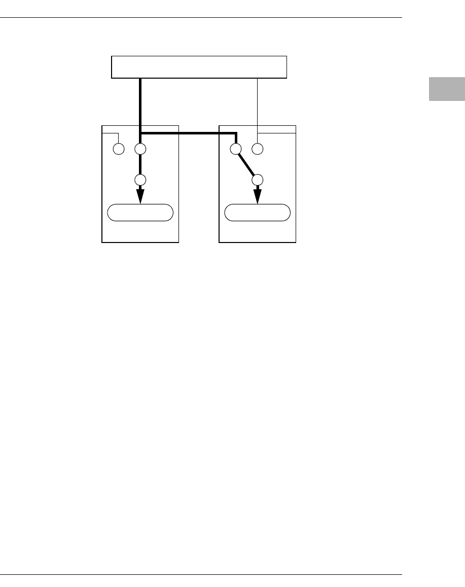
Programming Model
http://www.motorola.com/computer/literature 3-23
3
Figure 3-5. Data Path for Writes to the Falcon Internal CSRs
External register data that is written on the upper data bus goes through the
upper Falcon, while data that is written on the lower data bus goes through
the lower Falcon. Unlike the internal register set, there is no automatic
copying of upper data to lower data for the external register set.
CSR read accesses can have a size of 1, 2, 4, or 8 bytes with any alignment.
CSR write accesses are restricted to a size of 1 or 4 bytes and they must be
aligned. Some Tester registers are limited to 4-byte only accesses. Figure
3-6 through Figure 3-9 show the memory maps for the different kinds of
access.
Upper FALCON
1904 9609
Upper
Data Bus
Lower
Data Bus
CSR
MPC60x Master
Lower FALCON
CSR
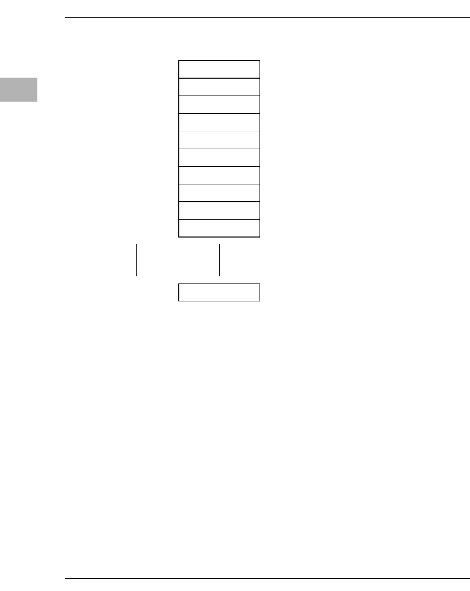
3-24 Computer Group Literature Center Web Site
Falcon ECC Memory Controller Chip Set
3
Figure 3-6. Memory Map for Byte Reads to CSR
1905 9609
Upper Falcon
Upper Falcon
Upper Falcon
Upper Falcon
Lower Falcon
Lower Falcon
Lower Falcon
Lower Falcon
Upper Falcon
Upper Falcon
$FEF80000
Lower Falcon
$FEF80001
$FEF80002
$FEF80003
$FEF80004
$FEF80005
$FEF80006
$FEF80007
$FEF80008
$FEF80009
$FEF807FF
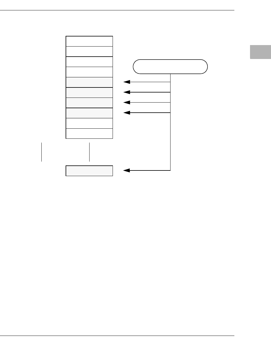
Programming Model
http://www.motorola.com/computer/literature 3-25
3
Figure 3-7. Memory Map for Byte Writes to Internal Register Set
and Test SRAM
1906 9609
Both Falcons
Both Falcons
Both Falcons
Both Falcons
Both Falcons
Both Falcons
$FEF80000
$FEF80001
$FEF80002
$FEF80003
$FEF80004
$FEF80005
$FEF80006
$FEF80007
$FEF80008
$FEF80009
$FEF807FF
Writes not allowed Here
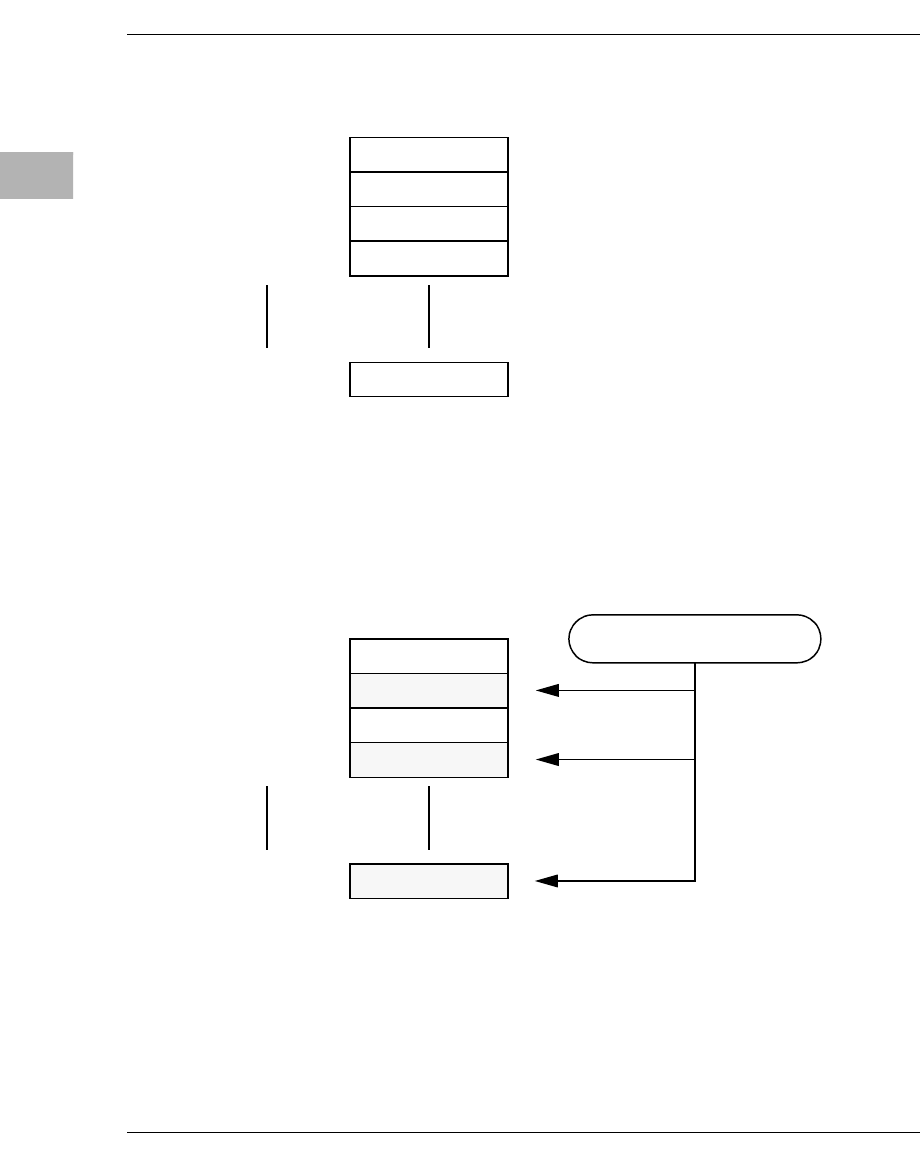
3-26 Computer Group Literature Center Web Site
Falcon ECC Memory Controller Chip Set
3
Figure 3-8. Memory Map for 4-Byte Reads to CSR
Figure 3-9. Memory Map for 4-Byte Writes to Internal Register Set
and Test SRAM
1907 9609
Upper Falcon
Lower Falcon
Upper Falcon
Lower Falcon
$FEF80000
Lower Falcon
$FEF80004
$FEF80008
$FEF8000C
$FEF807FC
1908 9609
Both Falcons
Both Falcons
$FEF80000
$FEF80004
$FEF80008
$FEF8000C
$FEF807FC
Writes not allowed Here

Programming Model
http://www.motorola.com/computer/literature 3-27
3
Register Summary
Table 3-10 shows a summary of the CSR. Note that the table shows only
addresses for accesses to the upper Falcon. To get the addresses for
accesses to the lower Falcon, add 4 to the address shown. Since the only
way to write to the lower Falcon’s internal register set and test SRAM is to
duplicate what is written to the upper Falcon, only the addresses shown in
the table should be used for writes to them. Writes to the external register
set are not duplicated from upper to lower, so writes to them can be via the
upper or lower Falcon.
Detailed Register Bit Descriptions
The sections following Table 3-10 describe the registers and their bits in
detail. The possible operations for each bit in the register set are as follows:
R The bit is a read-only status bit.
R/W The bit is readable and writable.
R/C The bit is cleared by writing a 1 to itself.
C The bit is readable. Writing a 0 to the bit will clear it.
The possible states of the bits after local and power-up reset are as defined
below.
P The bit is affected by power-up reset.
L The bit is affected by local reset.
X The bit is not affected by reset.
V The effect of reset on the bit is variable.
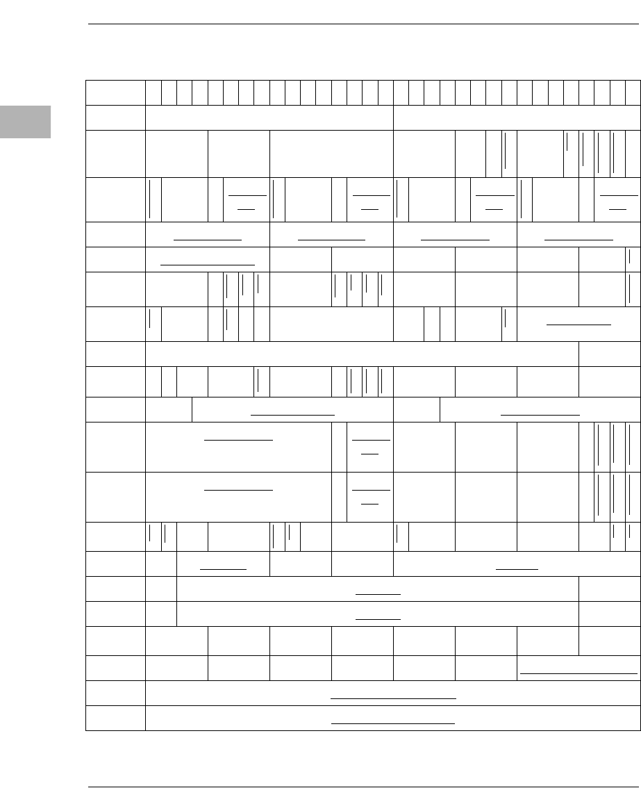
3-28 Computer Group Literature Center Web Site
Falcon ECC Memory Controller Chip Set
3
Table 3-10. Register Summary
BIT # ---->
0
1
2
3
4
5
6
7
8
9
10
11
12
13
14
15
16
17
18
19
20
21
22
23
24
25
26
27
28
29
30
31
FEF80000
VENDID DEVID
FEF80008
REVID
aonly_en
isa_hole
adis
ram fref
ram spd0
ram spd1
chipu
FEF80010
ram a en
RAM A
SIZ
ram b en
RAM B
SIZ
ram c en
RAM C
SIZ
ram d en
RAM D
SIZ
FEF80018 RAM A BASE RAM B BASE RAM C BASE RAM D BASE
FEF80020 CLK FREQUENCY
por
FEF80028
refdis
rwcb
derc
scien
tien
sien
mien
mcken
FEF80030
elog
escb
esen
embt
esbt
ERROR_SYNDROME
esblk0
esblk1
scof
SBE COUNT
FEF80038
ERROR_ADDRESS
FEF80040
scb0
scb1
swen
rtest0
rtest1
rtest2
FEF80048
ROW ADDRESS COL ADDRESS
FEF80050 ROM A BASE
rom_a_64
ROM A
SIZ
rom_a_rv
rom a en
rom a we
FEF80058 ROM B BASE
rom_b_64
ROM B
SIZ
rom_b_rv
rom b en
rom b we
FEF80060
trun
tsse
tpass
tfail
tzbit
tb0
tb1
FEF80068
TEST PC TEST IR
FEF80070
TEST A0
FEF80078
TEST A1
FEF80080
FEF80088
TEST D0 (Upper 8 Bits)
FEF80090
TEST D0 (Middle 32 Bits)
FEF80098
TEST D0 (Lower 32 Bits)
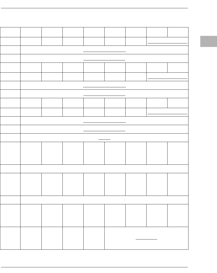
Programming Model
http://www.motorola.com/computer/literature 3-29
3
FEF800A0
FEF800A8
TEST D1 (Upper 8 Bits)
FEF800B0
TEST D1 (Middle 32 Bits)
FEF800B8
TEST D1 (Lower 32 Bits)
FEF800C0
FEF800C8
TEST D2 (Upper 8 Bits)
FEF800D0
TEST D2 (Middle 32 Bits)
FEF800D8
TEST D2 (Lower 32 Bits)
FEF800E0
FEF800E8
TEST D3 (Upper 8 Bits)
FEF800F0
TEST D3 (Middle 32 Bits)
FEF800F8
TEST D3 (Lower 32 Bits)
FEF80100
CTR32
FEF80200
.
.
FEF803F8
FEF80400
PR_STAT1
FEF80408
.
.
FEF804F8
FEF80500
PR_STAT2
FEF80508
.
.
FEF807F8
FEF80800
.
.
FEF80BF8
TEST SRAM
Table 3-10. Register Summary (Continued)
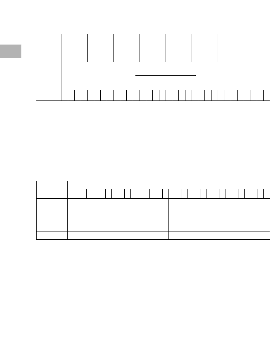
3-30 Computer Group Literature Center Web Site
Falcon ECC Memory Controller Chip Set
3
Notes 1. All shaded bit fields are reserved and read as zeros.
2. All status bits are shown in italics.
3. All control bits are shown with underline.
4. All control and status bits are shown with italics and underline.
Vendor/Device Register
VENDID This read-only register contains the value $1507. It
represents the vendor number assigned to Motorola Inc.
Note The current value of VENDID ($1507) is incorrect. The correct
vendor ID is $1057. This error is presently handled as an erratum.
DEVID This read-only register contains the value $4802. It is the
device number for the Falcon.
FEF80C00
.
.
FEF87FF8
FEF88000
.
.
FEF8FFF8
EXTERNAL REGISTER SET
BIT # ---->
0
1
2
3
4
5
6
7
8
9
10
11
12
13
14
15
16
17
18
19
20
21
22
23
24
25
26
27
28
29
30
31
Address $FEF80000
Bit
0
1
2
3
4
5
6
7
8
9
10
11
12
13
14
15
16
17
18
19
20
21
22
23
24
25
26
27
28
29
30
31
Name
VENDID DEVID
Operation READ ONLY READ ONLY
Reset XX
Table 3-10. Register Summary (Continued)
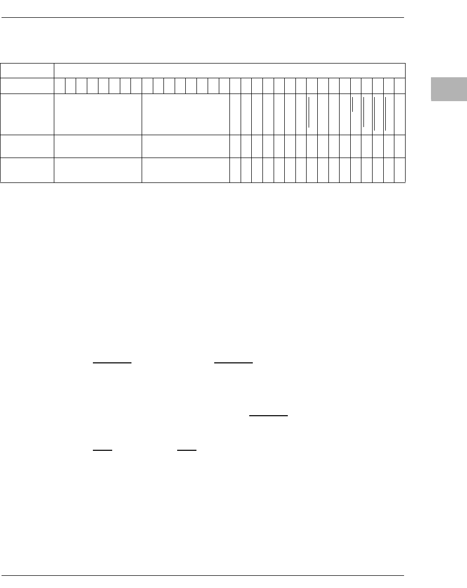
Programming Model
http://www.motorola.com/computer/literature 3-31
3
Revision ID/ General Control Register
REVID The REVID bits are hard-wired to indicate the revision
level of the Falcon. The values are $01 for the first
revision, $02 for the second.
aonly_en Normally, the Falcon pair responds to address-only cycles
only if they fall within the address range of one of its
enabled map decoders. When the aonly_en bit is set, the
Falcon pair also responds to address-only cycles that fall
outside of the range of its enabled map decoders provided
they are not acknowledged by some other slave within 8
clock periods. aonly_en is read-only and reflects the level
that was on the CKD4 pin at power-up reset.
isa_hole When it is set, isa_hole disables any of the DRAM or
ROM/Flash blocks from responding to PowerPC accesses
in the range from $000A0000 to $000BFFFF. This has the
effect of creating a hole in the DRAM memory map for
accesses to ISA. When isa_hole is cleared, there is no hole
created in the memory map.
adis When adis is clear, fast page mode operation is used for
back-to-back pipelined accesses to the same page within
DRAM. When it is set, RAS is cycled between accesses.
This bit should normally be cleared unless the Falcon has
a problem operating that way.
Address $FEF80008
Bit
0
1
2
3
4
5
6
7
8
9
10
11
12
13
14
15
16
17
18
19
20
21
22
23
24
25
26
27
28
29
30
31
Name
REVID
0
0
0
0
0
0
aonly_en
isa_hole
0
0
0
adis
ram fref
ram spd0
ram spd1
chipu
Operation READ ZERO READ ONLY
R
R
R
R
R
R
R
R/W
R
R
R
R/W
R/W
R/W
R/W
R
Reset XX
X
X
X
X
X
X
V P
0 PL
X
X
X
0 P
1 P
0 P
0 P
V P
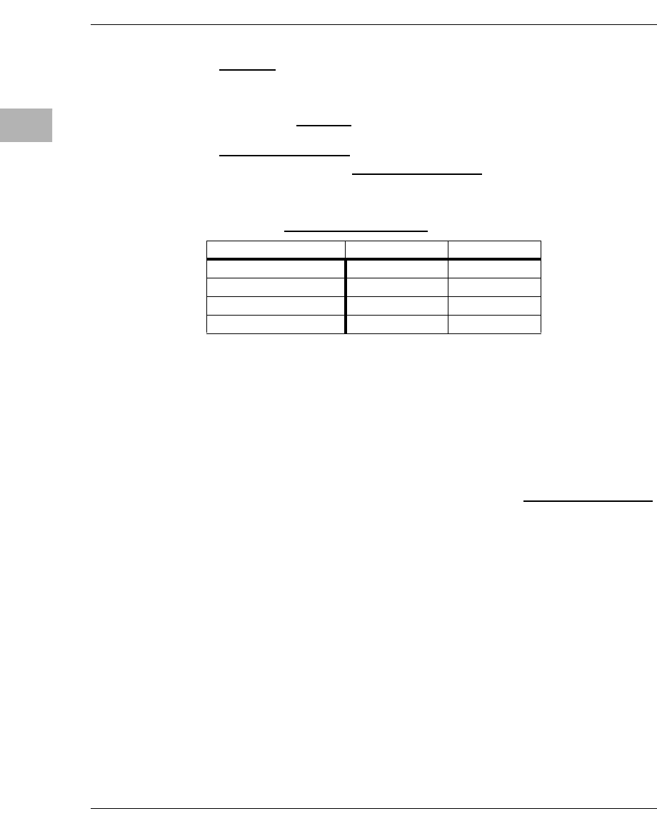
3-32 Computer Group Literature Center Web Site
Falcon ECC Memory Controller Chip Set
3
ram fref Some DRAMs require that they be refreshed at the rate of
7.8µs per row rather than the standard 15.6µs per row. If
any of the DRAM devices require the higher rate, then the
ram fref bit should be left set, otherwise, it can be cleared.
ram spd0,ram spd1
Together ram spd0,ram spd1 control DRAM timing used
by the Falcon pair. They are encoded as shown:
EDO refers to DRAMs that use an output latch on data.
Sometimes these parts are referred to as Hyper-Page
Mode DRAMs.
To ensure reliable operation, the system should always be
configured so that these two bits are encoded to match the
slowest devices used. Also, if any parts do not support
EDO, then these bits must set for Page Mode. The only
case in which it is permissible to set ram spd0,ram spd1
for “50ns, EDO” is when all parts are 50ns and all support
EDO.
chipu chipu indicates which of the two positions within the
Falcon pair is occupied by this chip. When chipu is low,
this chip is connected to the lower half of the PowerPC
60x data bus and it does not drive TA_ or AACK_. When
chipu is high, this chip is connected to the upper half of
the PowerPC 60x data bus, and it drives TA_ and AACK_.
chipu reflects the level that was on the ERCS_ pin during
power-up reset.
Table 3-11. ram spd1
,
ram spd0 and DRAM Type
ram spd0, ram spd1 DRAM Speed DRAM Type
%00 70ns Page Mode
%01 60ns Page Mode
%10 - Reserved
%11 50ns EDO
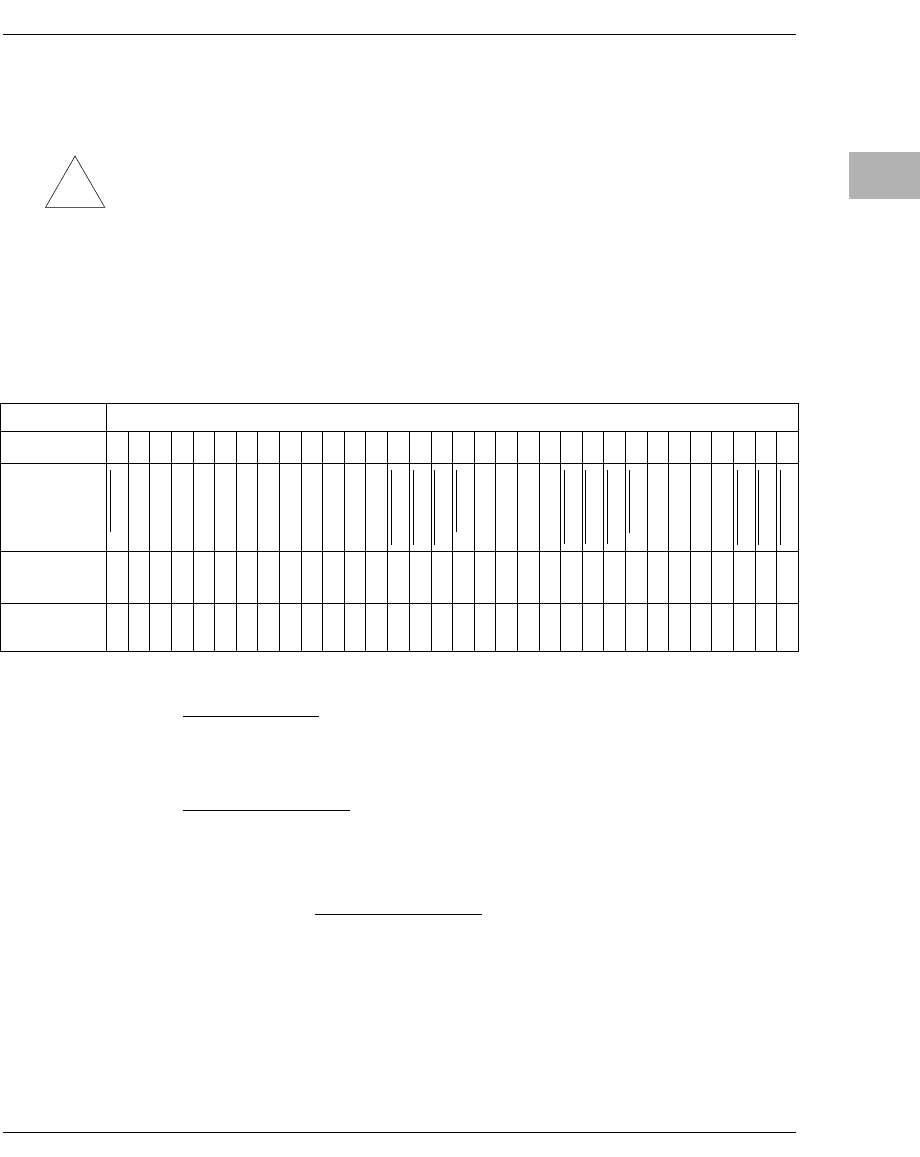
Programming Model
http://www.motorola.com/computer/literature 3-33
3
DRAM Attributes Register
!
Caution
To satisfy DRAM component requirements before the memory is used at
start-up, software must always wait at least 500µs after the initial setting
of a bank’s size bits to a nonzero value before the initial access to that
bank. These settings are stored in the DRAM Attributes register (offset
$FEF80010). The delay is introduced to ensure that the bank has been
refreshed at least eight times before use. The 500µs interval is sufficient,
as the CLK Frequency register (offset $FEF80020) is within a factor of
two of matching the actual processor clock frequency.
ram a/b/c/d en
Control bits that enable accesses to the corresponding
block of DRAM when set, and disable them when cleared.
ram a/b/c/d siz0-2
These control bits define the size of their corresponding
block of DRAM. Table 3-12 shows the block
configuration assumed by the Falcon pair for each value
of ram siz0-ram siz2.
ADDRESS $FEF80010
BIT
0
1
2
3
4
5
6
7
8
9
10
11
12
13
14
15
16
17
18
19
20
21
22
23
24
25
26
27
28
29
30
31
NAME
ram a en
0
0
0
0
ram a siz0
ram a siz1
ram a siz2
ram b en
0
0
0
0
ram b siz0
ram b siz1
ram b siz2
ram c en
0
0
0
0
ram c siz0
ram c siz1
ram c siz2
ram d en
0
0
0
0
ram d siz0
ram d siz1
ram d siz2
OPERATI
ON
R/W
R
R
R
R
R/W
R/W
R/W
R/W
R
R
R
R
R/W
R/W
R/W
R/W
R
R
R
R
R/W
R/W
R/W
R/W
R
R
R
R
R/W
R/W
R/W
RESET
0 PL
X
X
X
X
0 P
0 P
0 P
0 PL
X
X
X
X
0 P
0 P
0 P
0 PL
X
X
X
X
0 P
0 P
0 P
0 PL
X
X
X
X
0 P
0 P
0 P
3-34 Computer Group Literature Center Web Site
Falcon ECC Memory Controller Chip Set
3
It is important that all of the ram a/b/c/d siz0-2 bits be set to accurately
match the actual size of their corresponding blocks. This includes clearing
them to %000 if their corresponding blocks are not present. Failure to do
so will cause problems with addressing and with scrub error logging.
Table 3-12. Block_A/B/C/D Configurations
ram a/b/c/d
siz0-2 Block Size Devices Used Technology Comments
%000 0MB - - - - Block Not Present
%001 16MB
36 - 1Mx4s 4Mb
8 - 1Mx18s 16Mb
4 - 1Mx36s 4Mb/1Mb SIMM/DIMM
%010 32MB 18 - 2Mx8s 16Mb
%011 64MB
144 - 4Mx1s 4Mb
36 - 4Mx4s 16Mb
8 - 4Mx18s 64Mb
4 - 4Mx36s 16Mb/4Mb SIMM/DIMM
%100 128MB 18 - 8Mx8s 64Mb
%101 256MB
144 - 16Mx1s 16Mb
36 - 16Mx4s 64Mb
4 - 16Mx36s 64Mb/16Mb SIMM/DIMM
%110 1024MB 144 - 64Mx1s 64Mb
%111 0MB --- - Reserved
Programming Model
http://www.motorola.com/computer/literature 3-35
3
DRAM Base Register
RAM A/B/C/D BASE
These control bits define the base address for their block’s
DRAM. RAM A/B/C/D BASE bits 0-7/8-15/16-23/24-
31 correspond to PowerPC 60x address bits 0 - 7. For
larger DRAM sizes, the lower significant bits of A/B/C/D
BASE are ignored. This means that the block’s base
address will always appear at an even multiple of its size.
Note that bit 0 is MSB.
Also note that the combination of RAM_X_BASE and
ram_x_siz should never be programmed such that
DRAM responds at the same address as the CSR,
ROM/Flash, External Register Set, or any other slave on
the PowerPC bus.
CLK Frequency Register
CLK FREQUENCY
These bits should be programmed with the hexadecimal
value of the operating CLOCK frequency in MHz (i.e.
$42 for 66MHz). When these bits are programmed this
way, the chip’s prescale counter produces a 1MHz output.
Address $FEF80018
Bit
0
1
2
3
4
5
6
7
8
9
10
11
12
13
14
15
16
17
18
19
20
21
22
23
24
25
26
27
28
29
30
31
Name RAM A BASE RAM B BASE RAM C BASE RAM D BASE
Operation READ/WRITE READ/WRITE READ/WRITE READ/WRITE
Reset 0 PL 0 PL 0 PL 0 PL
Address $FEF80020
Bit
0
1
2
3
4
5
6
7
8
9
10
11
12
13
14
15
16
17
18
19
20
21
22
23
24
25
26
27
28
29
30
31
Name CLK
FREQUENCY
0
0
0
0
0
0
0
por
Operation READ/WRITE READ ZERO READ ZERO
R
R
R
R
R
R
R
R/C
Reset 42 P X X
X
X
X
X
X
X
X
1 P
3-36 Computer Group Literature Center Web Site
Falcon ECC Memory Controller Chip Set
3
The output of the chip prescale counter is used by the
refresher/scrubber and the 32-bit counter. After power-up,
this register is initialized to $42 (for 66MHz).
por por is set by the occurrence of power-up reset. It is cleared
by writing a 1 to it. Writing a 0 to it has no effect.
ECC Control Register
refdis When set, refdis causes the refresher and all of its
associated counters and state machines to be cleared and
maintained that way until refdis is removed (cleared). If a
refresh cycle is in process when refdis is updated by a
write to this register, the update does not take effect until
the refresh cycle has completed. This prevents the
generation of illegal cycles to the DRAM when refdis is
updated.
rwcb rwcb, when set, causes reads and writes to DRAM from
the PowerPC 60x bus to access check-bit data rather than
normal data. The data path used for this mode is DH24-31
for check-bit data controlled by the upper Falcon, and
DL24-31 for check-bit data controlled by the lower
Falcon. Each 8-bit check-bit location services 64 bits of
normal data. The 64 bits of data are all within the same
Falcon. Each Falcon provides every other 32 bits of data
in the normal mode. The following figure shows the
relationship between normal data and check-bit data.
Address $FEF80028
Bit
0
1
2
3
4
5
6
7
8
9
10
11
12
13
14
15
16
17
18
19
20
21
22
23
24
25
26
27
28
29
30
31
Name
0
0
0
0
0
refdis
rwcb
derc
0
0
0
0
scien
tien
sien
mien
0
0
0
0
0
0
0
mcken
Operation
R
R
R
R
R
R/W
R/W
R/W
R
R
R
R
R/W
R/W
R/W
R/W
READ ZERO
R
R
R
R
R
R
R
R/W
Reset
X
X
X
X
X
0 PL
0 PL
1 PL
X
X
X
X
0 PL
0 PL
0 PL
0 PL
X
X
X
X
X
X
X
X
0 PL
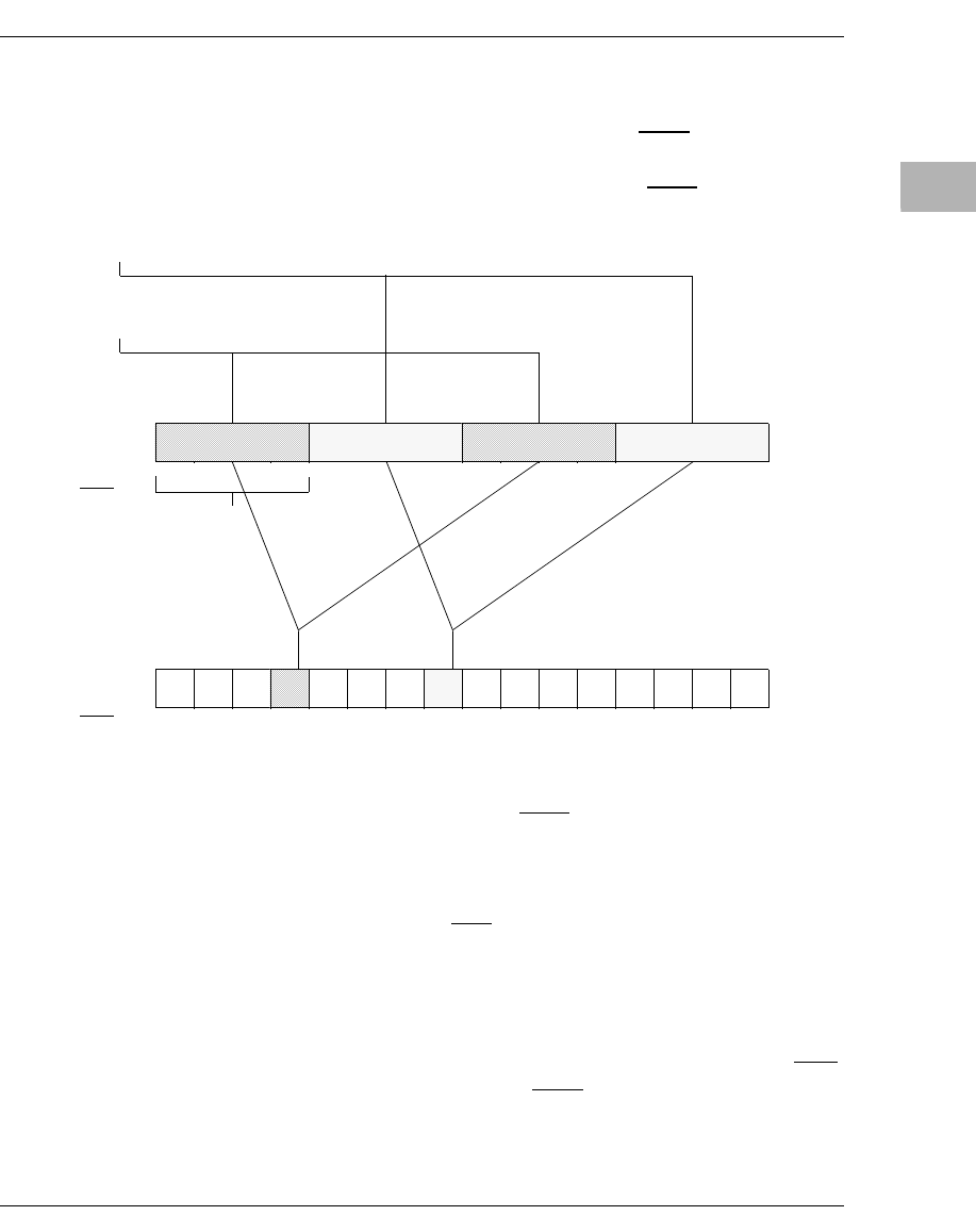
Programming Model
http://www.motorola.com/computer/literature 3-37
3
So, for example, the check-bits that correspond to the 64
bits of data found in normal mode (rwcb=0) at
$00001000-$00001003 and $00001008-$0000100b are
written and read in check-bit mode (rwcb=1) at location
$00001003.
Note that if test software wishes to force a single-bit error
to a location using the rwcb function, the scrubber may
correct the location before the test software gets a chance
to check for the single-bit error. This can be avoided by
disabling scrub writes. Also note that writing bad check-
bits can set the elog bit in the Error Logger register. The
writing of check-bits causes the Falcon to perform a read-
modify-write to DRAM. If the location to which check-
bits are being written has a single- or double-bit error, data
in the location may be altered by the write check-bits
operation. To avoid this, it is recommended that the derc
bit also be set while the rwcb bit is set. A possible
sequence for performing read-write check-bits is as
follows:
0 1 2 3 4 5 6 7
32 bits
048C
Normal
View of
Data
(rwcb=0)
Check-bit
View
(rwcb=1
Connected to
Upper Falcon
Connected to
Lower Falcon
11707.00 9701

3-38 Computer Group Literature Center Web Site
Falcon ECC Memory Controller Chip Set
3
1. Disable scrub writes by clearing the swen bit if it is set.
2. Stop all DRAM Tester operations by clearing the trun bit.
3. Make sure software is not using DRAM at this point, because while
rwcb is set, DRAM will not function as normal memory.
4. Set the derc and rwcb bits in the Data Control register.
5. Perform the desired read and/or write check-bit operations.
6. Clear the derc and rwcb bits in the Data Control register.
7. Perform the desired testing related to the location/locations that
have had their check-bits altered.
8. Enable scrub writes by setting the swen bit if it was set before.
derc Setting derc to 1 alters Falcon pair operation as follows:
1. During reads, data is presented to the PowerPC 60x data bus
uncorrected from the DRAM array.
2. During single-beat writes, data is written without correcting single-
bit errors that may occur on the read portion of the read-modify-
write. Check-bits are generated for the data being written.
3. During single-beat writes, the write portion of the read-modify-
write happens regardless of whether there is a multiple-bit error
during the read portion. No correction of data is attempted. Check-
bits are generated for the data being written.
4. During refresh/scrub cycles, if swen is set, a read-write to DRAM
happens with no attempt to correct data bits. Check-bits are
generated for the data being written.
derc is useful for initializing DRAM after power-up and
for testing DRAM, but it should be cleared during normal
system operation.
scien When scien is set, the rolling over of the SBE COUNT
register causes the INT_ signal pin to pulse true.
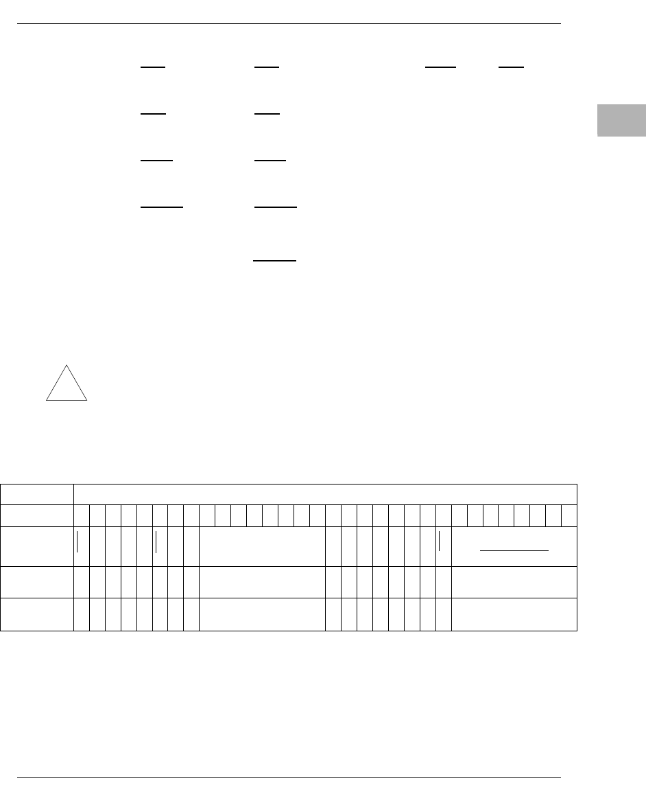
Programming Model
http://www.motorola.com/computer/literature 3-39
3
tien When tien is set, the setting of the tpass or the tfail bit
causes the INT_ signal pin to pulse true.
sien When sien is set, the logging of a single-bit error causes
the INT_ signal pin to pulse true.
mien When mien is set, the logging of a non-correctable error
causes the INT_ signal pin to pulse true.
mcken When mcken is set, the detection of a multiple-bit error
during a PowerPC read or write causes the Falcon to pulse
its machine check interrupt request pin (MCP_) true.
When mcken is cleared, the Falcon does not ever assert its
MCP_ pin.
The Falcon never asserts its MCP_ pin in response to a
multiple-bit error detected during a scrub cycle.
!
Caution
The INT_ and MCP_ pins are the only non-polled notification that a
multiple-bit error has occurred. The Falcon pair does not assert TEA as a
result of a multiple bit error. In fact, the Falcon pair does not have a TEA_
signal pin and it assumes that the system does not implement TEA_.
Error Logger Register
The Error Logger and Error Address registers behave the same as the other
registers, in that data written to the upper Falcon is automatically
duplicated in the lower Falcon. They also behave the same as the other
registers, in that status read from the upper Falcon pertains to the upper
Falcon, and status read from the lower Falcon pertains to the lower Falcon.
Address $FEF80030
Bit
0
1
2
3
4
5
6
7
8
9
10
11
12
13
14
15
16
17
18
19
20
21
22
23
24
25
26
27
28
29
30
31
Name
elog
0
0
0
escb
esen
embt
esbt
ERROR_SYNDROME
0
0
esblk0
esblk1
0
0
0
scof
SBE_COUNT
Operation
R/C
R
R
R
R
R/W
R
R
READ ONLY
R
R
R
R
R
R
R
R/C
READ/WRITE
Reset
0 P
X
X
X
X P
0 PL
X P
X P
X P
X
X
X
X
X
X
X
0 P
0 P

3-40 Computer Group Literature Center Web Site
Falcon ECC Memory Controller Chip Set
3
Unlike most of the other registers, however, it is normal for this status to
differ between the two. This is due to the fact that each Falcon is connected
to its own set of DRAMs. The upper Falcon can log an error during a cycle
and the local Falcon not, or vice-versa. Or they can both log an error during
the same cycle and have the attributes of the errors differ.
Due to the above characteristics, software must monitor both the upper and
lower Falcon’s Error Logger and Error Address registers. This includes
checking the elog bit from the upper Falcon and from the lower Falcon.
When the upper Falcon logs an error, it updates its attribute bits (escb,
embt, esbt, ERROR_SYNDROME, eblk0, eblk1, and
ERROR_ADDRESS) to match the results of the read cycle for its portion
of the DRAM array. When the lower Falcon logs an error, it updates its
attribute bits to match the results of the read cycle for its portion of the
DRAM array.
While the logging of errors by one Falcon in a pair does not affect the
logging of errors by the other, writing to the Error Logger Register control
bits affects both Falcons. This is of particular interest as regards the elog
bit. Writing a 1 to the elog bit clears the elog bit for both the upper and
lower Falcons. Because of this, software needs to check the status of both
upper and lower Error Logger and Error Address registers before it clears
the elog bits. Otherwise, it could miss a logged error.
elog When set, elog indicates that a single- or multiple-bit error
has been logged by its Falcon. If elog is set by a multiple-
bit error, then no more errors will be logged until software
clears it. If elog is set by a single-bit error, then no more
single-bit errors will be logged until software clears it,
however if elog is set by a single-bit error and a multiple-
bit error occurs, the multiple-bit error will be logged and
the single-bit error information overwritten. elog can only
be set by the logging of an error and cleared by the writing
of a 1 to itself or by power-up reset.
escb escb indicates the entity that was accessing DRAM at the
last logging of a single- or multiple-bit error by its Falcon.
If escb is 1, it indicates that the scrubber was accessing

Programming Model
http://www.motorola.com/computer/literature 3-41
3
DRAM. If escb is 0, it indicates that the PowerPC 60x bus
master was accessing DRAM. Note that the DRAM Tester
cannot cause an error to be logged.
esen When set, esen allows errors that occur during scrubs to
be logged. When cleared, esen does not allow errors that
occur during scrubs to be logged.
embt embt is set by the logging of a multiple-bit error in its
Falcon. It is cleared by the logging of a single-bit error in
its Falcon. It is undefined after power-up reset. A Falcon’s
syndrome code is meaningless if its embt bit is set.
esbt esbt is set by the logging of a single-bit error in its Falcon.
It is cleared by the logging of a multiple-bit error in its
Falcon. When a Falcon logs a single-bit error, its
syndrome code indicates which bit was in error. (Refer to
the section on ECC Codes.)
ERROR_SYNDROME
ERROR_SYNDROME reflects the syndrome value at the
last logging of an error by its Falcon. This eight-bit code
indicates the position of the data error. When all the bits
are zero, there was no error. Note that if the logged error
was non-correctable, then these bits are meaningless.
Refer to the ECC Codes section for a decoding of the
syndromes.
esblk0,esblk1
Together these two bits indicate which block of DRAM
was being accessed when their Falcon logged a scrub
error. esblk0,esblk1 are 0,0 for Block A; 0,1 for Block B;
1,0 for Block C; and 1,1 for Block D.
scof scof is set by the SBE COUNT register rolling over from
$FF to $00. It is cleared by software writing a 1 to it.
SBE COUNT
This register keeps track of the number of single-bit errors
that have occurred since it was last cleared. It counts up by
one each time its half of the Falcon pair detects a single-
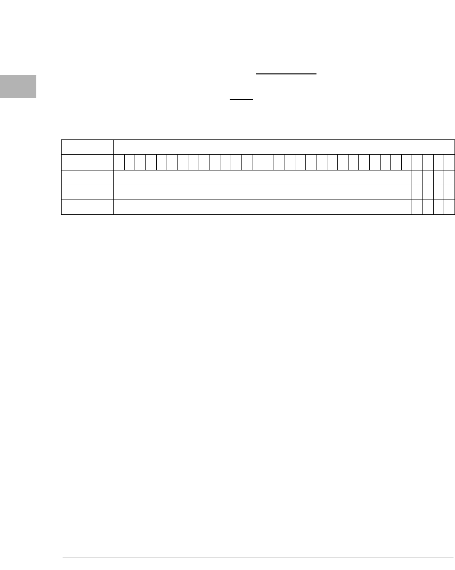
3-42 Computer Group Literature Center Web Site
Falcon ECC Memory Controller Chip Set
3
bit error (independent of the state of the elog bit). It is
cleared by power-up reset and by software writing all 0s
to it. When SBE COUNT rolls over from $FF to $00, its
Falcon sets the scof bit. It also pulses the INT_ signal low
if the scien bit is set.
Error Address Register
ERROR_ADDRESS
These bits reflect the value that corresponds to bits 0-27
of the PowerPC 60x address bus when their Falcon last
logged an error during a PowerPC access to DRAM. They
reflect the value of the DRAM row and column addresses
if the error was logged during a scrub cycle. In this case,
bits 2-14 correspond to row address signals 0-12
respectively and bits 15-27 correspond to column address
signals 0-12 respectively. Refer to Table 3-19 in the Sizing
DRAM subsection under Software Considerations. It
shows how PowerPC addresses correspond to DRAM row
and column addresses.
3Falcon ECC Memory Controller Chip Set
0Programming Model
Address $FEF80038
Bit
0
1
2
3
4
5
6
7
8
9
10
11
12
13
14
15
16
17
18
19
20
21
22
23
24
25
26
27
28
29
30
31
Name ERROR_ADDRESS
0
0
0
0
Operation READ ONLY
R
R
R
R
Reset X P
X
X
X
X
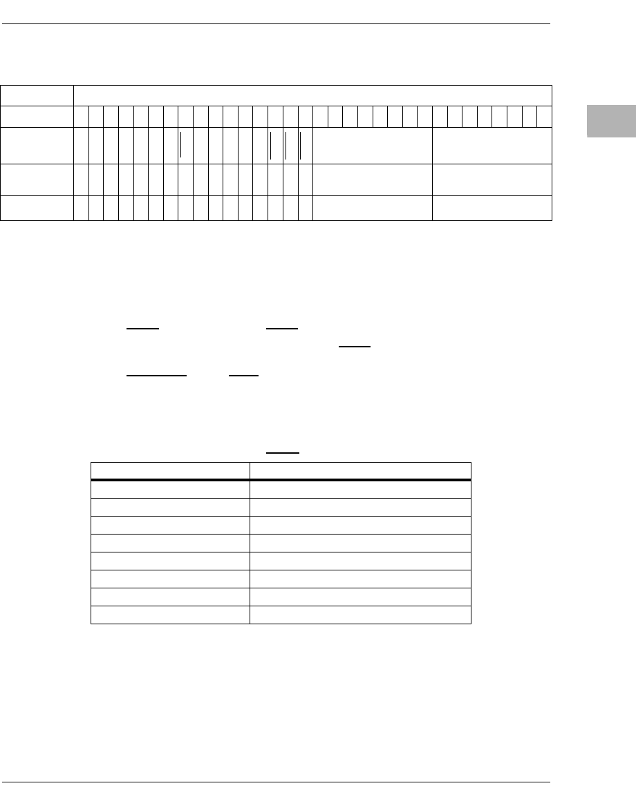
Programming Model
http://www.motorola.com/computer/literature 3-43
3
Scrub/Refresh Register
scb0,scb1 These bits increment every time the scrubber completes a
scrub of the entire DRAM. When these bits reach binary
11, they roll over to binary 00 and continue. They are
cleared by power-up reset.
swen When set, swen allows the scrubber to perform write
cycles. When cleared, swen prevents scrubber writes.
rtest0,1,2 The rtest bits enable certain refresh counter test modes.
Table 3-13 shows their encodings. Note that these test
modes are not intended to be used once the chip is in a
system.
Address $FEF80040
Bit
0
1
2
3
4
5
6
7
8
9
10
11
12
13
14
15
16
17
18
19
20
21
22
23
24
25
26
27
28
29
30
31
Name
scb0
scb1
0
0
0
0
0
swen
0
0
0
0
0
rtest0
rtest1
rtest2
Operation
R
R
R
R
R
R
R
R/W
R
R
R
R
R
R/W
R/W
R/W
READ ZERO READ ZERO
Reset
0 P
0 P
X
X
X
X
X
0 P
X
X
X
X
X
0 P
0 P
0 P
XX
Table 3-13. rtest Encodings
rtest0,rtest1,rtest2 Test Mode selected
%000 Normal counter operation
%001 RA counts at 16x
%010 RA counts at 256x
%011 RA is always at roll value for CA
%100 CA counts at 16x
%101 CA counts at 256x
%110 Reserved
%111 Reserved
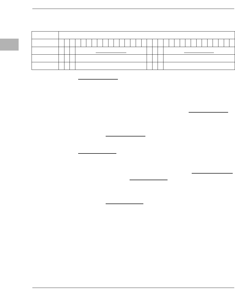
3-44 Computer Group Literature Center Web Site
Falcon ECC Memory Controller Chip Set
3
Refresh/Scrub Address Register
ROW ADDRESS
These bits form the row address counter used by the
refresher/scrubber for all blocks of DRAM. The row
address counter increments by one after each
refresh/scrub cycle. When it reaches all 1s, it rolls back
over to all 0s and continues counting. ROW ADDRESS is
readable and writable for test purposes.
Note that within each block, the most significant bits of
ROW ADDRESS are used only when their DRAM
devices are large enough to require them.
COL ADDRESS
These bits form the column address counter used by the
refresher/scrubber for all blocks of DRAM. The counter
increments by 1 every eighth time the ROW ADDRESS
rolls over. COL ADDRESS is readable and writable for
test purposes.
Note that within each block, the most significant bits of
COL ADDRESS are only used when their DRAM devices
are large enough to require them.
Address $FEF80048
Bit
0
1
2
3
4
5
6
7
8
9
10
11
12
13
14
15
16
17
18
19
20
21
22
23
24
25
26
27
28
29
30
31
Name
0
0
0
ROW ADDRESS
0
0
0
COL ADDRESS
Operation
R
R
R
READ/WRITE
R
R
R
READ/WRITE
Reset
X
X
X
0 P
X
X
X
0 P
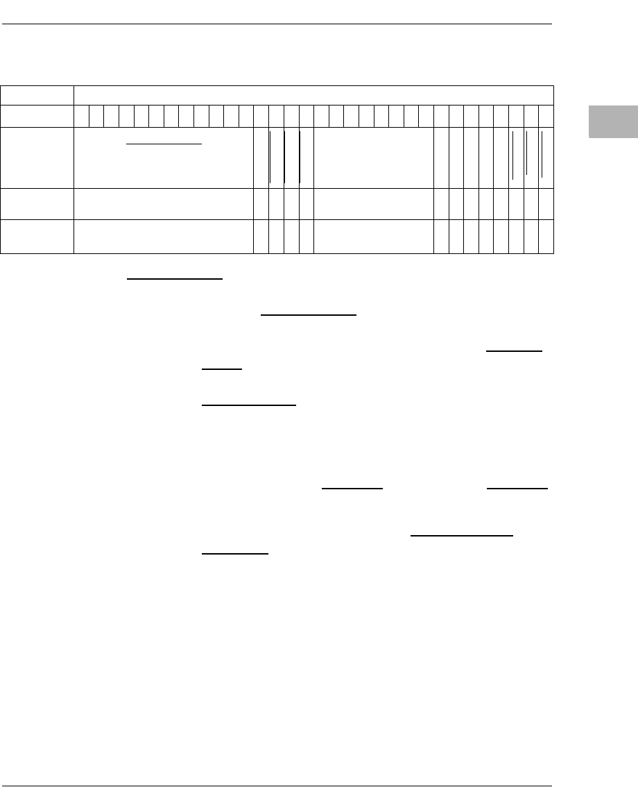
Programming Model
http://www.motorola.com/computer/literature 3-45
3
ROM A Base/Size Register
ROM A BASE
These control bits define the base address for ROM/Flash
Block A. ROM A BASE bits 0-11 correspond to
PowerPC 60x address bits 0 - 11 respectively. For larger
ROM/Flash sizes, the lower significant bits of ROM A
BASE are ignored. This means that the block’s base
address will always appear at an even multiple of its size.
ROM A BASE is initialized to $FF0 at power-up or local
bus reset.
Note that in addition to the programmed address, the first
1Mbyte of Block A also appears at $FFF00000 -
$FFFFFFFF if the rom_a_rv bit is set and the rom_b_rv
bit is cleared.
Also note that the combination of ROM_A_BASE and
rom_a_siz should never be programmed such that
ROM/Flash Block A responds at the same address as the
CSR, DRAM, External Register set, or any other slave on
the PowerPC bus.
rom_a_64 rom_a_64 indicates the width of the ROM/Flash
device(s) being used for Block A. When rom_a_64 is
cleared, Block A is 16 bits wide, where each Falcon
interfaces to 8 bits. When rom_a_64 is set, Block A is 64
Address $FEF80050
Bit
0
1
2
3
4
5
6
7
8
9
10
11
12
13
14
15
16
17
18
19
20
21
22
23
24
25
26
27
28
29
30
31
Name ROM A BASE
rom_a_64
rom a siz0
rom a siz1
rom a siz2
0
0
0
0
0
rom_a_rv
rom a en
rom a we
Operation READ/WRITE
R
R/W
R/W
R/W
READ ZERO
R
R
R
R
R
R/W
R/W
R/W
Reset $FF0 PL
V P
0 PL
0 PL
0 PL
X
X
X
X
X
X
V P
0 PL
0 PL
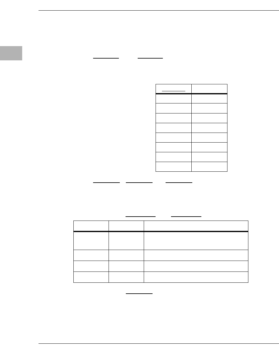
3-46 Computer Group Literature Center Web Site
Falcon ECC Memory Controller Chip Set
3
bits wide, where each Falcon interfaces to 32 bits.
rom_a_64 matches the value that was on the CKD2 pin at
power-up reset. It cannot be changed by software.
rom a siz The rom a siz control bits are the size of ROM/Flash for
Block A. They are encoded as shown in Table 3-14.
rom_a_rv rom_a_rv and rom_b_rv determine which (if either) of
Blocks A and B is the source of reset vectors or any other
access in the range $FFF00000 - $FFFFFFFF as shown in
the table below.
rom_a_rv is initialized at power-up reset to match the
value on the CKD0 pin.
Table 3-14. ROM Block A Size Encoding
rom a siz Block Size
%000 1MB
%001 2MB
%010 4MB
%011 8MB
%100 16MB
%101 32MB
%110 64MB
%111 Reserved
Table 3-15.
rom_a_rv
and
rom_b_rv
Encoding
rom_a_rv rom_b_rv Result
0 0 Neither block is the source of reset
vectors.
0 1 Block B is the source of reset vectors.
1 0 Block A is the source of reset vectors.
1 1 Block B is the source of reset vectors.
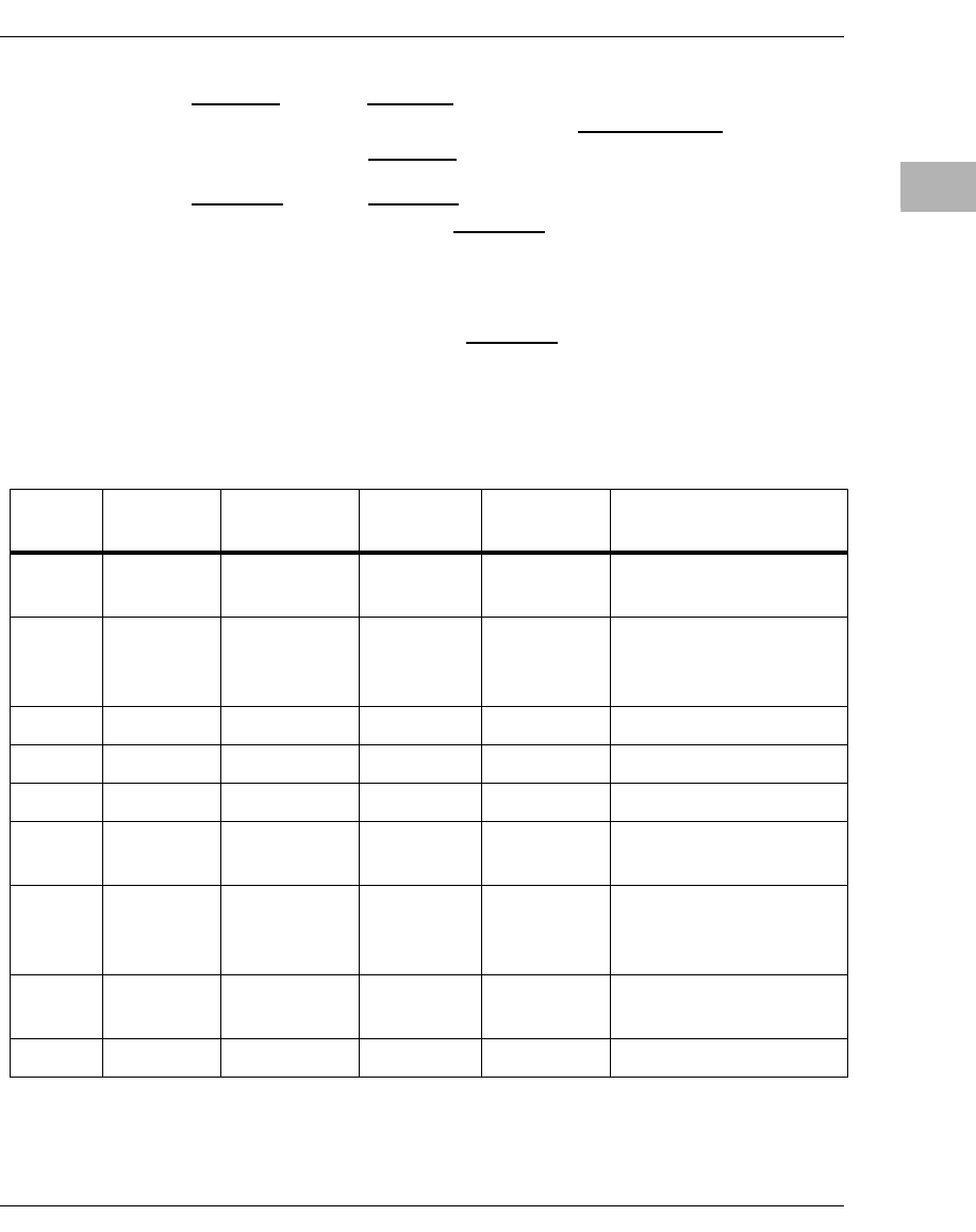
Programming Model
http://www.motorola.com/computer/literature 3-47
3
rom a en When rom a en is set, accesses to Block A ROM/Flash in
the address range selected by ROM A BASE are enabled.
When rom a en is cleared, they are disabled.
rom a we When rom a we is set, writes to Block A ROM/Flash are
enabled. When rom a we is cleared, they are disabled.
Note that if rom_a_64 is cleared, only one-byte writes are
allowed. If rom_a_64 is set, only four-byte writes are
allowed. The Falcon ignores other writes. If a valid write
is attempted and rom a we is cleared, the write does not
happen but the cycle is terminated normally. Refer to
Table 3-16 for details of ROM/Flash accesses.
Table 3-16. Read/Write to ROM/Flash
Cycle Transfer
Size Alignment rom_x_64 rom_x_we Falcon Response
Write 1-byte X 0 0 Normal termination, but
no write to ROM/Flash
Write 1-byte X 0 1 Normal termination,
write occurs to
ROM/Flash
Write 1-byte X 1 X No Response
Write 4-byte Misaligned X X No Response
Write 4-byte Aligned 0 X No Response
Write 4-byte Aligned 1 0 Normal termination, but
no write to ROM/Flash
Write 4-byte Aligned 1 1 Normal termination,
write occurs to
ROM/Flash
Write 2,3,5,6,7,
8,32-byte X X X No Response
Read X X X X Normal Termination
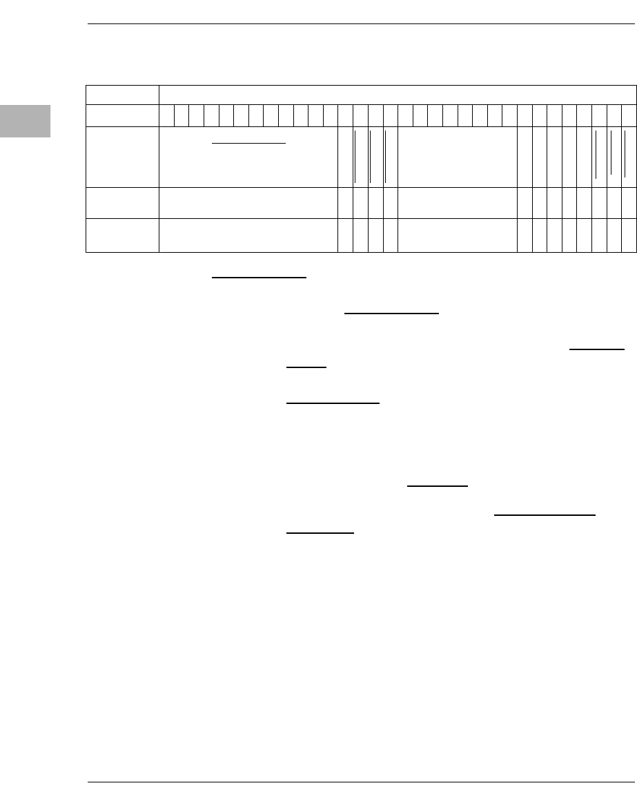
3-48 Computer Group Literature Center Web Site
Falcon ECC Memory Controller Chip Set
3
ROM B Base/Size Register
ROM B BASE
These control bits define the base address for ROM/Flash
Block B. ROM B BASE bits 0-11 correspond to
PowerPC 60x address bits 0-11 respectively. For larger
ROM/Flash sizes, the lower significant bits of ROM B
BASE are ignored. This means that the block’s base
address will always appear at an even multiple of its size.
ROM B BASE is initialized to $FF4 at power-up or local
bus reset.
Note that in addition to the programmed address, the first
1Mbyte of Block B also appears at $FFF00000 -
$FFFFFFFF if the rom_b_rv bit is set.
Also note that the combination of ROM_B_BASE and
rom_b_siz should never be programmed such that
ROM/Flash block B responds at the same address as the
CSR, DRAM, External Register set, or any other slave on
the PowerPC bus.
rom_b_64 rom_b_64 indicates the width of the ROM/Flash
device(s) being used for block B. When rom_b_64 is
cleared, block B is 16 bits wide, where each Falcon
interfaces to 8 bits. When rom_b_64 is set, block B is 64
bits wide, where each Falcon interfaces to 32 bits.
Address $FEF80058
Bit
0
1
2
3
4
5
6
7
8
9
10
11
12
13
14
15
16
17
18
19
20
21
22
23
24
25
26
27
28
29
30
31
Name ROM B BASE
rom_b_64
rom b siz0
rom b siz1
rom b siz2
0
0
0
0
0
rom_b_rv
rom b en
rom b we
Operation READ/WRITE
R
R/W
R/W
R/W
READ ZERO
R
R
R
R
R
R/W
R/W
R/W
Reset $FF4 PL
V P
0 PL
0 PL
0 PL
X
X
X
X
X
X
V P
0 PL
0 PL
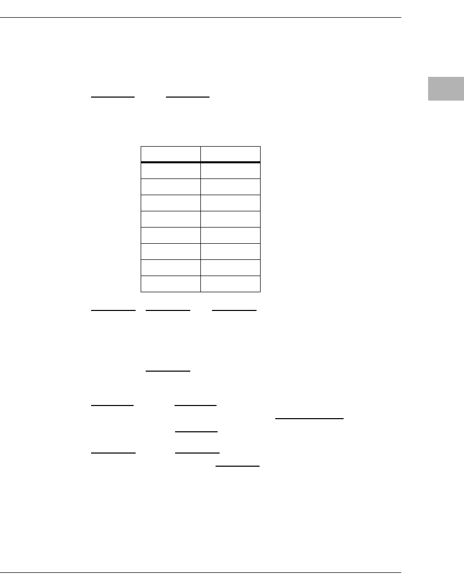
Programming Model
http://www.motorola.com/computer/literature 3-49
3
rom_b_64 matches the inverse of the value that was on the
CKD3 pin at power-up reset. It cannot be changed by
software.
rom b siz The rom b siz control bits are the size of ROM/Flash for
block B. They are encoded as shown in Table 3-17.
Table 3-17. ROM Block B Size Encoding
rom_b_rv rom_b_rv and rom_a_rv determine which if either of
Blocks A and B is the source of reset vectors or any other
access in the range $FFF00000 - $FFFFFFFF as shown in
Table 3-15.
rom_b_rv is initialized at power-up reset to match the
inverse of the value on the CKD1 pin.
rom b en When rom b en is set, accesses to block B ROM/Flash in
the address range selected by ROM B BASE are enabled.
When rom b en is cleared they are disabled.
rom b we When rom b we is set, writes to block B ROM/Flash are
enabled. When rom b we is cleared they are disabled.
Refer back to Table 3-16 for more details.
rom b siz Block Size
%000 1MB
%001 2MB
%010 4MB
%011 8MB
%100 16MB
%101 32MB
%110 64MB
%111 Reserved
3-50 Computer Group Literature Center Web Site
Falcon ECC Memory Controller Chip Set
3
DRAM Tester Control Registers
!
Caution
The tester should not be used by software. The trun and tsse bits (bits 0
and 1 of the register at address $FEF80060) should never be set.
32-Bit Counter
CTR32 CTR32 is a 32-bit, free-running counter that increments
once per microsecond if the CLK_FREQUENCY register
has been programmed properly. Notice that CTR32 is
cleared by power-up and local reset. It does not exist in
Revision 1 of Falcon.
Note When the system clock is a fractional frequency, such as
66.67MHz, CTR32 will count at a fractional amount faster or
slower than 1MHz, depending on the programming of the
CLK_FREQUENCY register.
Test SRAM
(Deleted)
Address $FEF80100
Bit
0
1
2
3
4
5
6
7
8
9
10
11
12
13
14
15
16
17
18
19
20
21
22
23
24
25
26
27
28
29
30
31
Name CTR32
Operation READ/WRITE
Reset 0 PL
Programming Model
http://www.motorola.com/computer/literature 3-51
3
Power-Up Reset Status Register 1
PR_STAT1 PR_STAT1 (power-up reset status) reflects the value that
was on the RD0-RD31 signal pins at power-up reset. This
register is read-only.
Note For descriptions of how this register is used in the MVME2300
series boards, refer to the Falcon-Controlled System Registers
section in Chapter 1, especially to System Configuration Register
(SYSCR) and Memory Configuration Register (MEMCR).
Power-Up Reset Status Register 2
PR_STAT2 PR_STAT2 (power-up reset status) reflects the value that
was on the RD32-RD63 signal pins at power-up reset.
This register is read-only.
Address $FEF80400
Bit
0
1
2
3
4
5
6
7
8
9
10
11
12
13
14
15
16
17
18
19
20
21
22
23
24
25
26
27
28
29
30
31
Name PR_STAT1
Operation READ
Reset V P
Address $FEF80500
Bit
0
1
2
3
4
5
6
7
8
9
10
11
12
13
14
15
16
17
18
19
20
21
22
23
24
25
26
27
28
29
30
31
Name PR_STAT2
Operation READ
Reset V P
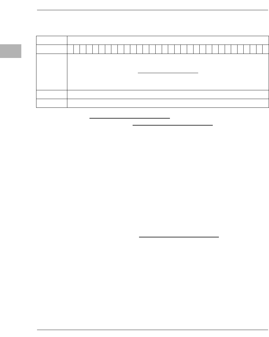
3-52 Computer Group Literature Center Web Site
Falcon ECC Memory Controller Chip Set
3
External Register Set
EXTERNAL REGISTER SET
The EXTERNAL REGISTER SET is user-provided and
is external to the Falcon pair. The Falcon pair provides a
static RAM style interface for the external registers. The
external registers can be SRAM, ROM, Flash or some
other user device. There can be one device connected to
either the upper or lower Falcon, or there can be two
devices with one connected to each Falcon. The devices
can be 8, 16, or 32 bits wide. The data path to the external
devices is via the RD32-RD63 pins. Reads to the external
devices can be any size except burst. Note that if the
devices are less than 32 bits wide, reads to unused data
lanes will yield undefined data. Note that writes are
restricted to one- or four-byte length only. Four-byte
writes can be used for any size device; data should be
placed on the correct portion of the data bus so that valid
data is written to the device. Data duplication is turned off
for the EXTERNAL REGISTER SET so writes can be to
either the upper Falcon, or to the lower Falcon.
Note For descriptions of how these registers are used in the
MVME2300 series boards, refer to the Falcon-Controlled System
Registers section of Chapter 1, especially to System External
Cache Control Register (SXCCR) and CPU Control Register.
3Falcon ECC Memory Controller Chip Set
0Programming Model
Address $FEF88000 - $FEF8FFF8
Bit
0
1
2
3
4
5
6
7
8
9
10
11
12
13
14
15
16
17
18
19
20
21
22
23
24
25
26
27
28
29
30
31
Name
EXTERNAL REGISTER SET
Operation READ/WRITE
Reset X PL

Software Considerations
http://www.motorola.com/computer/literature 3-53
3
Software Considerations
This section contains information that may be helpful in making efficient
use of the Falcon pair when programming.
Parity Checking on the PowerPC Bus
The Falcon does not generate parity on the PowerPC address or data buses.
Because of this, the appropriate registers in the MPC60x should be
programmed to disable parity checking for the address bus and for the data
bus.
Programming ROM/Flash Devices
Those who program devices to be controlled by the Falcon should make
note of the address mapping that is shown in Table 3-8 and in Table 3-9.
When using eight-bit devices, for example, the code will be split so that
every other four-byte segment goes in each device.
Writing to the Control Registers
Software should not change control register bits that affect DRAM
operation while DRAM is being accessed. Because of pipelining, software
should always make sure that the two accesses before and after the
updating of critical bits are not DRAM accesses. A possible scenario for
trouble would be to execute code out of DRAM while updating the critical
DRAM control register bits. The preferred method is to be executing code
out of ROM/Flash and avoiding DRAM accesses while updating these
bits.
Since software has no way of controlling refresh accesses to DRAM, the
hardware is designed so that updating control bits coincidentally with
refreshes is not a problem. An exception to this is the ROW_ADDRESS
and COL_ADDRESS bits. In any event, however, it is not intended that
software write to these bits.

3-54 Computer Group Literature Center Web Site
Falcon ECC Memory Controller Chip Set
3
As with DRAM, software should not change control register bits that affect
ROM/Flash while the affected block is being accessed. This generally
means that the ROM/Flash size, base address, enable, write enable, etc. are
changed only during initial execution in the reset vector area ($FFF00000
- $FFFFFFFF).
Sizing DRAM
!
Caution
To satisfy DRAM component requirements before the memory is used at
start-up, software must always wait at least 500µs after the initial setting
of a bank’s size bits to a nonzero value before the initial access to that
bank. These settings are stored in the DRAM Attributes register (offset
$FEF80010). The delay is introduced to ensure that the bank has been
refreshed at least eight times before use. The 500µs interval is sufficient,
as the CLK Frequency register (offset $FEF80020) is within a factor of
two of matching the actual processor clock frequency.
The following routine can be used to size DRAM for the Falcon.
First, initialize the Falcon control register bits to a known state as follows:
1. Clear the isa_hole bit.
2. Make sure that ram_fref and ram_spd0,ram_spd1 are correct.
3. Set CLK_FREQUENCY to match the operating frequency.
4. Clear the refdis, rwcb bits.
5. Set the derc bit.
6. Clear the scien, tien, sien, and mien bits.
7. Clear the mcken bit.
8. Clear the swen and rtest0,rtest1,rtest2 bits.
9. Make sure that ROM/Flash banks A and B are not enabled to
respond in the range from $00000000 to $40000000.

Software Considerations
http://www.motorola.com/computer/literature 3-55
3
10. Make sure that no other devices respond in the range from
$00000000 to $40000000.
Then, for each block:
1. Set the block’s base address to $00000000.
2. Enable the block and make sure that the other three blocks are
disabled.
3. Set the block’s size control bits. Start with the largest possible
(1024MB).
4. Write differing 64-bit data patterns to certain addresses within the
block. The data patterns do not matter as long as each 64-bit data
pattern is unique. The addresses to be written vary depending on the
size that is currently being checked and are specified in Table 3-18.
Table 3-19 shows how PowerPC addresses correspond to DRAM
row/column addresses.
5. Read back all of the addresses that have been written.
If all of the addresses still contain exactly what was written, then the
block’s size has been found. It is the size for which the block is
currently programmed.
If any of the addresses do not match exactly, then the amount of
memory is less than that for which it is currently programmed.
Sizing needs to continue for this block by programming its control
bits to the next smaller size and repeating steps 4 and 5.
6. If no match is found for any size, then the block is unpopulated and
has a size of 0MB.

3-56 Computer Group Literature Center Web Site
Falcon ECC Memory Controller Chip Set
3
Each size that is checked has a specific set of locations that must be written
and read. The following table shows the addresses that go with each size.
Table 3-18. Sizing Addresses
1024MB 256MB 128MB 64MB 32MB 16MB
$00000000
$20000000
$00000000
$02000000
$08000000
$0A000000
$00000000
$00002000
$02000000
$02002000
$04000000
$04002000
$06000000
$06002000
$00000000
$00002000
$02000000
$02002000
$00000000
$00001000
$00002000
$00003000
$01000000
$01001000
$01002000
$01003000
$00000000
Table 3-19. PowerPC 60
x
Address to DRAM Address Mappings
RA ---->
Block Size
|
V
0123456789101112
16MB ROW A19 A18 A8 A9 A10 A11 A12 A13 A14 A15 A16 A17
COL A18 A19 A20 A21 A22 A23 A24 A25 A26 A27
32MB ROW A18 A7 A8 A9 A10 A11 A12 A13 A14 A15 A16 A17
COL A18 A19 A20 A21 A22 A23 A24 A25 A26 A27
64MB ROW A18 A6 A7 A8 A9 A10 A11 A12 A13 A14 A15 A16 A17
COL A6 A18 A19 A20 A21 A22 A23 A24 A25 A26 A27
128MB ROWA6A5A7A8A9A10A11A12A13A14A15A16A17
COL A6 A18 A19 A20 A21 A22 A23 A24 A25 A26 A27
256MB ROWA4A5A7A8A9A10A11A12A13A14A15A16A17
COL A4 A6 A18 A19 A20 A21 A22 A23 A24 A25 A26 A27
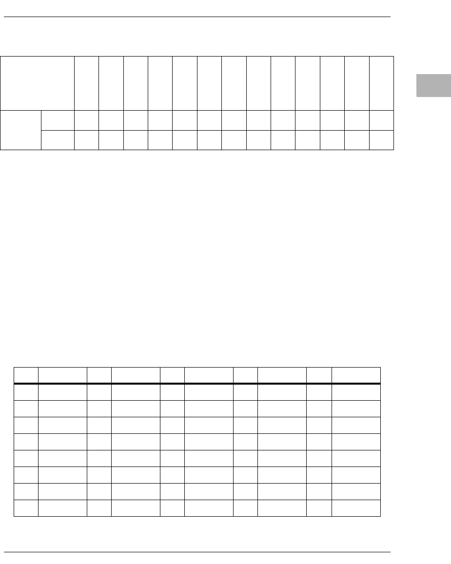
Software Considerations
http://www.motorola.com/computer/literature 3-57
3
ECC Codes
When the Falcon reports a single-bit error, software can use the syndrome
that was logged by the Falcon (upper or lower depending where the error
occurred) to determine which bit was in error. Table 3-20 shows the
syndrome for each possible single bit error. Table 3-21 shows the same
information ordered by syndrome. In order to relate this information to
PowerPC addresses and bit numbers, the user needs to understand how the
Falcon pair positions PowerPC data in DRAM. See the section on Data
Paths for an explanation of this.
Note that these tables are the same whether the Falcon is configured as
upper or as lower device.
1024MB ROWA3A5A7A8A9A10A11A12A13A14A15A16A17
COL A2 A4 A6 A18 A19 A20 A21 A22 A23 A24 A25 A26 A27
Table 3-20. Syndrome Codes Ordered by Bit in Error
Bit Syndrome Bit Syndrome Bit Syndrome Bit Syndrome Bit Syndrome
rd0 $4A rd16 $92 rd32 $A4 rd48 $29 ckd0 $01
rd1 $4C rd17 $13 rd33 $C4 rd49 $31 ckd1 $02
rd2 $2C rd18 $0B rd34 $C2 rd50 $B0 ckd2 $04
rd3 $2A rd19 $8A rd35 $A2 rd51 $A8 ckd3 $08
rd4 $E9 rd20 $7A rd36 $9E rd52 $A7 ckd4 $10
rd5 $1C rd21 $07 rd37 $C1 rd53 $70 ckd5 $20
rd6 $1A rd22 $86 rd38 $A1 rd54 $68 ckd6 $40
rd7 $19 rd23 $46 rd39 $91 rd55 $64 ckd7 $80
Table 3-19. PowerPC 60
x
Address to DRAM Address Mappings
RA ---->
Block Size
|
V
0123456789101112
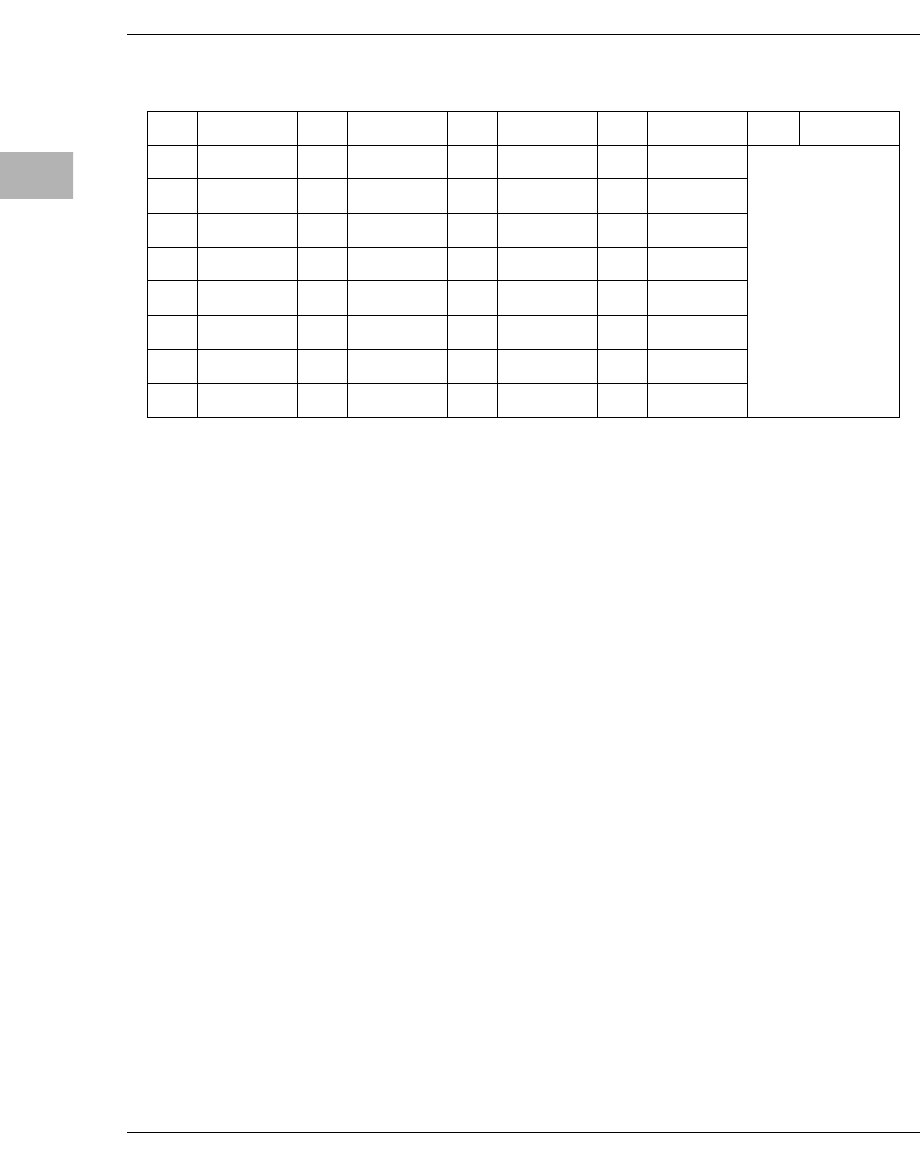
3-58 Computer Group Literature Center Web Site
Falcon ECC Memory Controller Chip Set
3rd8 $25 rd24 $49 rd40 $52 rd56 $94
rd9 $26 rd25 $89 rd41 $62 rd57 $98
rd10 $16 rd26 $85 rd42 $61 rd58 $58
rd11 $15 rd27 $45 rd43 $51 rd59 $54
rd12 $F4 rd28 $3D rd44 $4F rd60 $D3
rd13 $0E rd29 $83 rd45 $E0 rd61 $38
rd14 $0D rd30 $43 rd46 $D0 rd62 $34
rd15 $8C rd31 $23 rd47 $C8 rd63 $32
Table 3-20. Syndrome Codes Ordered by Bit in Error
Bit Syndrome Bit Syndrome Bit Syndrome Bit Syndrome Bit Syndrome

Software Considerations
http://www.motorola.com/computer/literature 3-59
3
Table 3-21. Single-Bit Errors Ordered by Syndrome Code
Syn-
drome Bit Syn-
drome Bit Syn-
drome Bit Syn-
drome Bit Syn-
drome Bit Syn-
drome Bit Syn-
drome Bit Syn-
drome Bit
$00 - $20 ckd5 $40 ckd6 $60 - $80 ckd7 $A0 - $C0 - $E0 rd45
$01 ckd0 $21 - $41 - $61 rd42 $81 - $A1 rd38 $C1 rd37 $E1 -
$02 ckd1 $22 - $42 - $62 rd41 $82 - $A2 rd35 $C2 rd34 $E2 -
$03 - $23 rd31 $43 rd30 $63 - $83 rd29 $A3 - $C3 - $E3 -
$04 ckd2 $24 - $44 - $64 rd55 $84 - $A4 rd32 $C4 rd33 $E4 -
$05 - $25 rd8 $45 rd27 $65 - $85 rd26 $A5 - $C5 - $E5 -
$06 - $26 rd9 $46 rd23 $66 - $86 rd22 $A6 - $C6 - $E6 -
$07 rd21 $27 - $47 - $67 - $87 - $A7 rd52 $C7 - $E7 -
$08 ckd3 $28 - $48 - $68 rd54 $88 - $A8 rd51 $C8 rd47 $E8 -
$09 - $29 rd48 $49 rd24 $69 - $89 rd25 $A9 - $C9 - $E9 rd4
$0A - $2A rd3 $4A rd0 $6A - $8A rd19 $AA - $CA - $EA -
$0Brd18$2B-$4B-$6B-$8B-$AB-$CB-$EB-
$0C - $2C rd2 $4C rd1 $6C - $8C rd15 $AC - $CC - $EC -
$0Drd14$2D-$4D-$6D-$8D-$AD-$CD-$ED-
$0Erd13$2E-$4E-$6E-$8E-$AE-$CE-$EE-
$0F - $2F - $4F rd44 $6F - $8F - $AF - $CF - $EF -
$10 ckd4 $30 - $50 - $70 rd53 $90 - $B0 rd50 $D0 rd46 $F0 -
$11 - $31 rd49 $51 rd43 $71 - $91 rd39 $B1 - $D1 - $F1 -
$12 - $32 rd63 $52 rd40 $72 - $92 rd16 $B2 - $D2 - $F2 -
$13rd17$33-$53-$73-$93-$B3-$D3rd60$F3-
$14 - $34 rd62 $54 rd59 $74 - $94 rd56 $B4 - $D4 - $F4 rd12
$15rd11$35-$55-$75-$95-$B5-$D5-$F5-
$16rd10$36-$56-$76-$96-$B6-$D6-$F6-
$17 - $37 - $57 - $77 - $97 - $B7 - $D7 - $F7 -
$18 - $38 rd61 $58 rd58 $78 - $98 rd57 $B8 - $D8 - $F8 -
$19 rd7 $39 - $59 - $79 - $99 - $B9 - $D9 - $F9 -
$1A rd6 $3A - $5A - $7A rd20 $9A - $BA - $DA - $FA -
$1B - $3B - $5B - $7B - $9B - $BB - $DB - $FB -
$1C rd5 $3C - $5C - $7C - $9C - $BC - $DC - $FC -
$1D-$3Drd28$5D-$7D-$9D-$BD-$DD-$FD-
$1E - $3E - $5E - $7E - $9E rd36 $BE - $DE - $FE -
$1F - $3F - $5F - $7F - $9F - $BF - $DF - $FF -
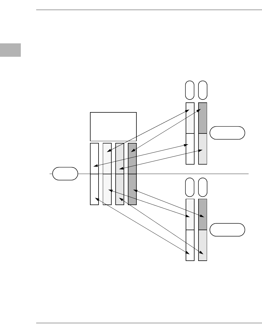
3-60 Computer Group Literature Center Web Site
Falcon ECC Memory Controller Chip Set
3
Data Paths
Because of the Falcon “pair” architecture, data paths can be confusing.
Figure 3-10 attempts to show the placement of data that is written by a
PowerPC master to DRAM. Table 3-22 shows the same information in
tabular format.
Figure 3-10. PowerPC Data to DRAM Data Correspondence
1909 9609
Lower Falcon’s
DRAM
Upper Falcon’s
DRAM
ra12=1
PowerPC
Data
ra12=0
ra12=1
ra12=0
rd63
dl31
rd32
rd31
rd0
rd63
rd32
rd31
rd0
dl0
dh31
dh0
a[27:28]=0
a[27:28]=1
a[27:28]=2
a[27:28]=3

Software Considerations
http://www.motorola.com/computer/literature 3-61
3
Table 3-22. PowerPC Data to DRAM Data Mapping
PowerPC DRAM Array
A[27] A[28] Data Bits RA[12] Upper Falcon DRAM
Data Bits Lower Falcon DRAM
Data Bits
0 0 dh[00:07] 0 rd[00:07] -
0 0 dh[08:15] 0 rd[08:15] -
0 0 dh[16:23] 0 rd[16:23] -
0 0 dh[24:31] 0 rd[24:31] -
0 0 dl[00:07] 0 - rd[00:07]
0 0 dl[08:15] 0 - rd[08:15]
0 0 dl[16:23] 0 - rd[16:23]
0 0 dl[24:31] 0 - rd[24:31]
0 1 dh[00:07] 0 rd[32:39] -
0 1 dh[08:15] 0 rd[40:47] -
0 1 dh[16:23] 0 rd[48:55] -
0 1 dh[24:31] 0 rd[56:63] -
0 1 dl[00:07] 0 - rd[32:39]
0 1 dl[08:15] 0 - rd[40:47]
0 1 dl[16:23] 0 - rd[48:55]
0 1 dl[24:31] 0 - rd[56:63]
1 0 dh[00:07] 1 rd[00:07] -
1 0 dh[08:15] 1 rd[08:15] -
1 0 dh[16:23] 1 rd[16:23] -
1 0 dh[24:31] 1 rd[24:31] -
1 0 dl[00:07] 1 - rd[00:07]
1 0 dl[08:15] 1 - rd[08:15]
1 0 dl[16:23] 1 - rd[16:23]
1 0 dl[24:31] 1 - rd[24:31]
1 1 dh[00:07] 1 rd[32:39] -
1 1 dh[08:15] 1 rd[40:47] -
1 1 dh[16:23] 1 rd[48:55] -
1 1 dh[24:31] 1 rd[56:63] -
1 1 dl[00:07] 1 - rd[32:39]
1 1 dl[08:15] 1 - rd[40:47]
1 1 dl[16:23] 1 - rd[48:55]
1 1 dl[24:31] 1 - rd[56:63]

4-1
4
4Universe (VMEbus to PCI) Chip
Introduction
This chapter describes the VMEbus interface on MVME2300 series
boards, the CA91C042 Universe ASIC. The Universe chip interfaces the
32/64-bit PCI local bus to the VMEbus. It provides a PCI-bus-to-VMEbus
interface, a VMEbus-to-PCI-bus interface, and the DMA controller
functions of the local VMEbus.
Note that all of the information in this chapter (except the section entitled
Universe Chip Problems after PCI Reset) is taken from the Universe User
Manual, which is listed under Manufacturers’ Documents in Appendix A,
Related Documentation. Refer to that manual for detailed information on
the Universe ASIC.
Features
The Universe VMEbus interface chip (CA91C042) provides a reliable
high-performance 64-bit VMEbus-to-PCI interface in one device.
Designed by Tundra Semiconductor Corporation in consultation with
Motorola, the Universe is compliant with the VME64 specification and is
tuned to the new generation of high-speed processors.
The Universe is ideally suited for CPU boards acting as both master and
slave in the VMEbus system, and is particularly fitted for PCI local
systems. The Universe is manufactured in a CMOS process.
4-2 Computer Group Literature Center Web Site
Universe (VMEbus to PCI) Chip
4
The following table summarizes the characteristics of the Universe ASIC.
Table 4-1. Features of the Universe ASIC
Function Features
VMEbus Interface Fully compliant, high-performance 64-bit VMEbus interface
VMEbus transfer rates of 60-70 MB/sec
Full VMEbus system controller functionality
Integral FIFOs for write-posting to maximize bandwidth utilization
Automatic initialization for slave-only applications:
− A32/A24/A16 master and slave
− D64 (MBLT)/D32/D16/D08 master and slave
− D64 (MBLT)/D32/D16/D08 master and slave
− BLT, ADOH, RMW, LOCK
Complete suite of VMEbus address and data transfer modes
PCI Local Bus
Interface Fully compliant, 64-bit, 33 MHz PCI local bus interface
Integral FIFOs for write-posting to maximize bandwidth utilization
Automatic initialization for slave-only applications
DMA Controller Programmable DMA controller with linked list support
Additional
Functionality Flexible register set, programmable from both the PCI bus and VMEbus
ports
IEEE 1149.1 JTAG testability support
Available in 313-pin Plastic BGA and 324-pin contact Ceramic BGA

Block Diagram
http://www.motorola.com/computer/literature 4-3
4
Block Diagram
The descriptions in the following sections make reference to the functional
block diagram supplied in Figure 4-1. Notice that for each interface,
VMEbus and PCI bus, there are three functionally distinct modules: master
module, slave module, and interrupt module.
These three modules are connected to the different functional channels
operating in the Universe. These channels are:
❏VME Slave channel
❏PCI Bus Slave channel
❏DMA channel
❏Interrupt channel
❏Register channel
Functional Description
The functional description is organized into the following sections:
❏VMEbus Interface
❏PCI Bus Interface
❏Interrupter and Interrupt Handler
❏DMA Controller
These sections describe the operation of the Universe in terms of the
different modules and channels listed above and illustrated in Figure 4-1.
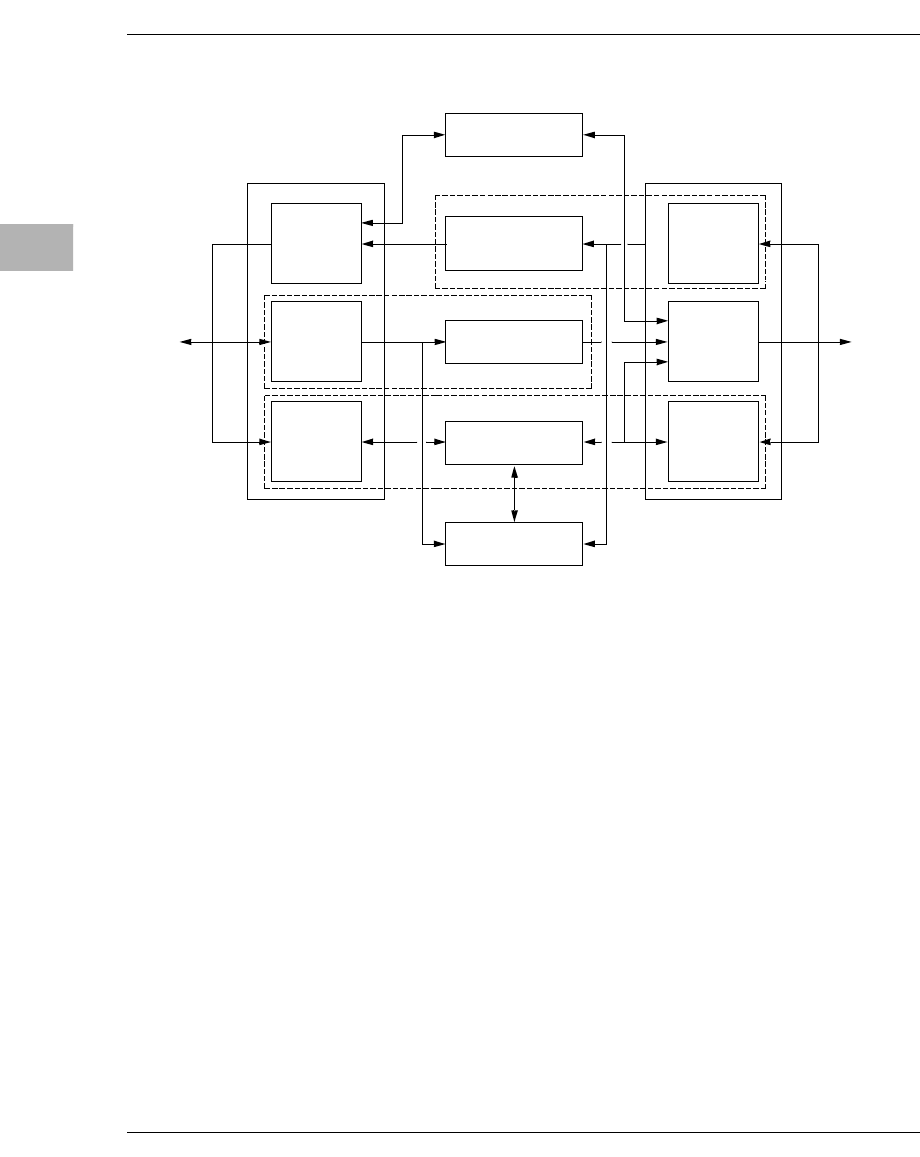
4-4 Computer Group Literature Center Web Site
Universe (VMEbus to PCI) Chip
4
Figure 4-1. Architectural Diagram for the Universe
VMEbus Interface
This section examines the Universe ASIC’s VMEbus interface function,
from the standpoint of the Universe as VMEbus slave as well as VMEbus
master.
Universe as VMEbus Slave
The Universe VME Slave channel accepts all of the addressing and data
transfer modes documented in the VME64 specification (except A64 and
those intended to support 3U applications, that is, A40 and MD32).
Incoming write transactions from the VMEbus may be treated as either
coupled or posted, depending upon the programming of the VMEbus slave
image. (Refer to VME Slave Images in the Universe User Manual.) With
posted write transactions, data is written to a Posted Write Receive FIFO
(RXFIFO), and the VMEbus master receives data acknowledgment from
VME
Slave
VME
Master
VME
Interrupts
posted writes FIFO
coupled read logic
DMA bidirectional FIFO
Interrupt Handler
Interrupter
Register Channel
VMEbus Slave Channel
posted writes FIFO
prefetch read FIFO
coupled read
PCI Bus Slave Channel
Interrupt Channel
PCI
Master
PCI
Slave
PCI
Interrupts
VMEbus
PCI
BUS
PCI Bus
Interface
VMEbus
Interface
DMA Channel
1894 9609

Functional Description
http://www.motorola.com/computer/literature 4-5
4
the Universe. Write data is transferred to the PCI resource from the
RXFIFO without the involvement of the initiating VMEbus master (Refer
to Posted Writes in the Universe User Manual for a full explanation of this
operation.). With a coupled cycle, the VMEbus master only receives data
acknowledgment when the transaction is complete on the PCI bus. This
means that the VMEbus is unavailable to other masters while the PCI bus
transaction is executed.
Read transactions may be prefetched or coupled. If enabled by the user, a
prefetched read is initiated when a VMEbus master requests a block read
transaction (BLT or MBLT) and this mode is enabled. When the Universe
receives the block read request, it begins to fill its Read Data FIFO
(RDFIFO) using burst transactions from the PCI resource. The initiating
VMEbus master then acquires its block read data from the RDFIFO rather
than from the PCI resources directly.
Universe as VMEbus Master
The Universe becomes VMEbus master when the VME Master interface
is internally requested by the PCI Bus Slave channel, the DMA channel, or
the Interrupt channel. The Interrupt channel always has priority over the
other two channels. Several mechanisms are available to configure the
relative priority that the PCI Bus Slave channel and DMA channel have
over ownership of the VMEbus Master interface.
The Universe’s VME Master interface generates all of the addressing and
data transfer modes documented in the VME64 specification (except A64
and those intended to support 3U applications, that is, A40 and MD32).
The Universe is also compatible with all VMEbus modules conforming to
pre-VME64 specifications. As VMEbus master, the Universe supports
Read-Modify-Write (RMW), and Address-Only-with-Handshake
(ADOH) but does not accept RETRY∗ as a termination from the VMEbus
slave. The ADOH cycle is used to implement the VMEbus Lock
command, allowing a PCI master to lock VMEbus resources.
PCI Bus Interface
This section examines the Universe ASIC’s PCI bus interface function,
from the standpoint of the Universe as PCI slave as well as PCI master.

4-6 Computer Group Literature Center Web Site
Universe (VMEbus to PCI) Chip
4
Universe as PCI Slave
Read transactions from the PCI bus are always processed as coupled. Write
transactions may be either coupled or posted, depending upon the setting
of the PCI bus slave image. (Refer to PCI Bus Slave Images in the Universe
User Manual.) With a posted write transaction, write data is written to a
Posted Write Transmit FIFO (TXFIFO) and the PCI bus master receives
data acknowledgment from the Universe with zero wait states. Meanwhile,
the Universe obtains the VMEbus and writes the data to the VMEbus
resource independent of the initiating PCI master. (Refer to Posted Writes
in the Universe User Manual for a full description of this operation.)
To allow PCI masters to perform RMW and ADOH cycles, the Universe
provides a Special Cycle Generator. The Special Cycle Generator can be
used in combination with a VMEbus ownership function to guarantee PCI
masters exclusive access to VMEbus resources over several VMEbus
transactions. (Refer to Exclusive Accesses and RMW and ADOH Cycles in
the Universe User Manual for a full description of this functionality.)
Universe as PCI Master
The Universe becomes PCI master when the PCI Master Interface is
internally requested by the VME Slave Channel or the DMA Channel.
There are mechanisms provided which allow the user to configure the
relative priority of the VME Slave Channel and the DMA Channel.
Interrupter
The Universe interrupt channel provides a flexible scheme to map
interrupts to either the PCI bus or VMEbus interface. Interrupts are
generated from either hardware or software sources (refer to the
Interrupter section of the Universe User Manual for a full description of
hardware and software sources). Interrupt sources can be mapped to any of
the PCI bus or VMEbus interrupt output pins. Interrupt sources mapped to
VMEbus interrupts are generated on the VMEbus interrupt output pins
VIRQ∗[7:1]. When a software and hardware source are assigned the same
VIRQn∗ pin, the software source always has higher priority.

Functional Description
http://www.motorola.com/computer/literature 4-7
4
Interrupt sources mapped to PCI bus interrupts are generated on one of the
INT∗[7:0] pins. To be fully PCI compliant, all interrupt sources must be
routed to a single INT∗ pin.
For VMEbus interrupt outputs, the Universe interrupter supplies an 8-bit
STATUS/ID to a VMEbus interrupt handler during the IACK cycle, and
optionally generates an internal interrupt to signal that the interrupt vector
has been provided. (Refer to VMEbus Interrupt Generation in the Universe
User Manual.)
Interrupts mapped to PCI bus outputs are serviced by the PCI interrupt
controller. The CPU determines which interrupt sources are active by
reading an interrupt status register in the Universe. The source negates its
interrupt when it has been serviced by the CPU. (Refer to PCI Interrupt
Generation in the Universe User Manual.)
VMEbus Interrupt Handling
A VMEbus interrupt triggers the Universe to generate a normal VMEbus
IACK cycle and generate the specified interrupt output. When the IACK
cycle is complete, the Universe releases the VMEbus and the interrupt
vector is read by the PCI resource servicing the interrupt output. Software
interrupts are ROAK, while hardware and internal interrupts are RORA.
DMA Controller
The Universe provides an internal DMA controller for high-performance
data transfer between the PCI bus and VMEbus. DMA operations between
the source and destination bus are decoupled through the use of a single
bidirectional FIFO (DMAFIFO). Parameters for the DMA transfer are
software configurable in the Universe registers. (Refer to DMA Controller
in the Universe User Manual.)
The principal mechanism for DMA transfers is the same for operations in
either direction (PCI to VME, or VME to PCI); only the relative identity
of the source and destination bus changes. In a DMA transfer, the Universe
gains control of the source bus and reads data into its DMAFIFO.

4-8 Computer Group Literature Center Web Site
Universe (VMEbus to PCI) Chip
4
Following specific rules of DMAFIFO operation (refer to FIFO Operation
and Bus Ownership in the Universe User Manual), it then acquires the
destination bus and writes data from its DMAFIFO.
The DMA controller can be programmed to perform multiple blocks of
transfers using entries in a linked list. The DMA will work through the
transfers in the linked-list following pointers at the end of each linked-list
entry. Linked-list operation is initiated through a pointer in an internal
Universe register, but the linked list itself resides in PCI bus memory.
Universe Control and Status Registers (UCSR)
The Universe Control and Status Registers (UCSR) facilitate host system
configuration and allow the user to control Universe operational
characteristics. The UCSR set is divided into three groups:
❏PCI Configuration Space (PCICS)
❏VMEbus Control and Status Registers (VCSR)
❏Universe Device-Specific Status Registers (UDSR)
The Universe registers are little-endian.
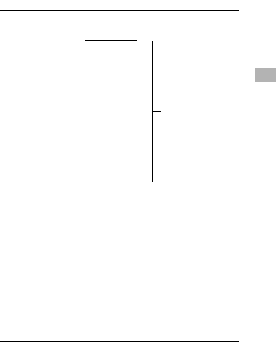
Functional Description
http://www.motorola.com/computer/literature 4-9
4
Figure 4-2 summarizes the supported register access mechanisms.
Figure 4-2. UCSR Access Mechanisms
Universe Register Map
Table 4-2 lists the Universe registers by address offset. Tables in the
Universe User Manual provide detailed descriptions of each register.
VMEbus Configuration
and Status Registers
(VCSR)
UNIVERSE DEVICE
SPECIFIC REGISTERS
(UDSR)
PCI CONFIGURATION
SPACE
(PCICS)
4 Kbytes
1895 9609
4-10 Computer Group Literature Center Web Site
Universe (VMEbus to PCI) Chip
4
Address offsets in Table 4-2 below apply to accesses from the PCI bus and
to accesses from the VMEbus side using the VMEbus Register Access
Image (Refer to Registers in the Universe User Manual.). For register
accesses in CR/CSR space, be sure to add 508KB (0x7F00) to the address
offsets provided in the table.
Table 4-2. Universe Register Map
Offset Register Name
000 PCI Configuration Space ID Register PCI_ID
004 PCI Configuration Space Control and Status Register PCI_CSR
008 PCI Configuration Class Register PCI_CLASS
00C PCI Configuration Miscellaneous 0 Register PCI_MISC0
010 PCI Configuration Base Address Register PCI_BS
014 PCI Unimplemented
018 PCI Unimplemented
01C PCI Unimplemented
020 PCI Unimplemented
024 PCI Unimplemented
028 PCI Reserved
02C PCI Reserved
030 PCI Unimplemented
034 PCI Reserved
038 PCI Reserved
03C PCI Configuration Miscellaneous 1 Register PCI_MISC1
040 - 0FF PCI Unimplemented
100 PCI Slave Image 0 Control LSI0_CTL
104 PCI Slave Image 0 Base Address Register LSI0_BS
108 PCI Slave Image 0 Bound Address Register LSI0_BD
10C PCI Slave Image 0 Translation Offset LSI0_TO
110 Universe Reserved
114 PCI Slave Image 1 Control LSI1_CTL
118 PCI Slave Image 1 Base Address Register LSI1_BS
Functional Description
http://www.motorola.com/computer/literature 4-11
4
11C PCI Slave Image 1 Bound Address Register LSI1_BD
120 PCI Slave Image 1 Translation Offset LSI1_TO
124 Universe Reserved
128 PCI Slave Image 2 Control LSI2_CTL
12C PCI Slave Image 2 Base Address Register LSI2_BS
130 PCI Slave Image 2 Bound Address Register LSI2_BD
134 PCI Slave Image 2 Translation Offset LSI2_TO
138 Universe Reserved
13C PCI Slave Image 3 Control LSI3_CTL
140 PCI Slave Image 3 Base Address Register LSI3_BS
144 PCI Slave Image 3 Bound Address Register LSI3_BD
148 PCI Slave Image 3 Translation Offset LSI3_TO
14C - 16C Universe Reserved
170 Special Cycle Control Register SCYC_CTL
174 Special Cycle PCI bus Address Register SCYC_ADDR
178 Special Cycle Swap/Compare Enable Register SCYC_EN
17C Special Cycle Compare Data Register SCYC_CMP
180 Special Cycle Swap Data Register SCYC_SWP
184 PCI Miscellaneous Register LMISC
188 Special PCI Slave Image SLSI
18C PCI Command Error Log Register L_CMDERR
190 PCI Address Error Log LAERR
194 - 1FC Universe Reserved
200 DMA Transfer Control Register DCTL
204 DMA Transfer Byte Count Register DTBC
208 DMA PCI bus Address Register DLA
20C Universe Reserved
210 DMA VMEbus Address Register DVA
214 Universe Reserved
Table 4-2. Universe Register Map (Continued)
Offset Register Name
4-12 Computer Group Literature Center Web Site
Universe (VMEbus to PCI) Chip
4
218 DMA Command Packet Pointer DCPP
21C Universe Reserved
220 DMA General Control and Status Register DGCS
224 DMA Linked List Update Enable Register D_LLUE
228 - 2FC Universe Reserved
300 PCI Interrupt Enable LINT_EN
304 PCI Interrupt Status LINT_STAT
308 PCI Interrupt Map 0 LINT_MAP0
30C PCI Interrupt Map 1 LINT_MAP1
310 VMEbus Interrupt Enable VINT_EN
314 VMEbus Interrupt Status VINT_STAT
318 VMEbus Interrupt Map 0 VINT_MAP0
31C VMEbus Interrupt Map 1 VINT_MAP1
320 Interrupt Status/ID Out STATID
324 VIRQ1 STATUS/ID V1_STATID
328 VIRQ2 STATUS/ID V2_STATID
32C VIRQ3 STATUS/ID V3_STATID
330 VIRQ4 STATUS/ID V4_STATID
334 VIRQ5 STATUS/ID V5_STATID
338 VIRQ6 STATUS/ID V6_STATID
33C VIRQ7 STATUS/ID V7_STATID
340 - 3FC Universe Reserved
400 Master Control MAST_CTL
404 Miscellaneous Control MISC_CTL
408 Miscellaneous Status MISC_STAT
40C User AM Codes Register USER_AM
410 - EFC Universe Reserved
F00 VMEbus Slave Image 0 Control VSI0_CTL
F04 VMEbus Slave Image 0 Base Address Register VSI0_BS
Table 4-2. Universe Register Map (Continued)
Offset Register Name
Functional Description
http://www.motorola.com/computer/literature 4-13
4
F08 VMEbus Slave Image 0 Bound Address Register VSI0_BD
F0C VMEbus Slave Image 0 Translation Offset VSI0_TO
F10 Universe Reserved
F14 VMEbus Slave Image 1 Control VSI1_CTL
F18 VMEbus Slave Image 1 Base Address Register VSI1_BS
F1C VMEbus Slave Image 1 Bound Address Register VSI1_BD
F20 VMEbus Slave Image 1 Translation Offset VSI1_TO
F24 Universe Reserved
F28 VMEbus Slave Image 2 Control VSI2_CTL
F2C VMEbus Slave Image 2 Base Address Register VSI2_BS
F30 VMEbus Slave Image 2 Bound Address Register VSI2_BD
F34 VMEbus Slave Image 2 Translation Offset VSI2_TO
F38 Universe Reserved
F3C VMEbus Slave Image 3 Control VSI3_CTL
F40 VMEbus Slave Image 3 Base Address Register VSI3_BS
F44 VMEbus Slave Image 3 Bound Address Register VSI3_BD
F48 VMEbus Slave Image 3 Translation Offset VSI3_TO
F4C - F6C Universe Reserved
F70 VMEbus Register Access Image Control Register VRAI_CTL
F74 VMEbus Register Access Image Base Address VRAI_BS
F78 Universe Reserved
F7C Universe Reserved
F80 VMEbus CSR Control Register VCSR_CTL
F84 VMEbus CSR Translation Offset VCSR_TO
F88 VMEbus AM Code Error Log V_AMERR
F8C VMEbus Address Error Log VAERR
F90 - FEC Universe Reserved
Table 4-2. Universe Register Map (Continued)
Offset Register Name
4-14 Computer Group Literature Center Web Site
Universe (VMEbus to PCI) Chip
4
!
Caution
Register space marked as “Reserved” should not be overwritten.
Unimplemented registers return a value of 0 on reads; writes complete
normally.
Note The VMEbus CSR Bit Clear Register and the VMEbus CSR Bit
Set Register are not supported on the MVME2300. Writing a 1 to
the VMEbus CSR Bit Set Register reset bit will cause the board
to go into a permanent reset condition.
Universe Chip Problems after PCI Reset
Customers who overwrite the firmware settings for the Universe chip, or
who replace the MCG firmware with their own, may find that under the
conditions described below, there are problems with the Universe chip
after a PCI reset.
Description
The Universe chip is being enabled on the PCI bus after a PCI reset (the
problem does not occur after a board reset or power up).
The Universe is causing the "bye" command to hang the system. The
Universe Master Enable and Memory Enable in the PCI_CSR
(Configuration Space register) are enabled, even before the PCI_BS
register has been initialized. The symptoms can be alleviated by modifying
the PCI probe list such that the Universe PCI configuration is done first.
FF0 VME CR/CSR Reserved
FF4 VMEbus CSR Bit Clear Register VCSR_CLR
FF8 VMEbus CSR Bit Set Register VCSR_SET
FFC VMEbus CSR Base Address Register VCSR_BS
Table 4-2. Universe Register Map (Continued)
Offset Register Name

Functional Description
http://www.motorola.com/computer/literature 4-15
4
The Configuration Space enables are not the only things enabled after a
PCI reset. The LSI0 image may also not be disabled by a PCI reset,
regardless of the enable bit’s power-up condition. If the image is active at
the time the reset occurs, it will remain enabled through the reset.
Additionally, the image does not remain in the same VME or PCI address
range.
How many of the Power-Up (P/U) option bits actually get latched as the
Universe manual indicates they should, is uncertain. In any case, the EN
bit in the LSI0_CTL register is not latched; on MVME2300 series boards,
its P/U state is disabled but is not honored.
Workarounds
The software cannot completely correct this problem, but can minimize the
effects of it. Two possible solutions are presented:
Method 1
1. Modify the PCI probe code to disable each PCI device prior to
writing its configuration space BS registers. This will prevent the
Universe from being active on the PCI bus while it has a base
address of 0.
2. Once the Universe has been assigned a valid PCI Base Address,
enable register space access and disable the LSI0 slave image by
clearing the EN bit of the LSI0_CTL register.
Method 2
Modify the port 92 reset code to disable the LSI0 image before
propagating the reset. This will cause the LSI0 image to come up
disabled.
MCG understands that both of these methods are awkward, because the
PCI probe/reset code should not contain any device-specific patches. It
should only need to follow the probing conventions of the PCI
specification. However, the only other option appears to be avoidance of
the LSI0 image altogether.
Tundra engineering describes the problem as follows:

4-16 Computer Group Literature Center Web Site
Universe (VMEbus to PCI) Chip
4
"Following are the most recently discovered bugs which will be
addressed in Universe 1.1.
1. LSIO image
Description: After a PCI reset, the LSIO image is still enabled, but the
base, bound, and translation offset changes value.
Workaround: None."
Motorola Firmware Engineering has implemented Method 1 in its
firmware workaround in PPCBug debugger release 3.1.
Note As mentioned at the start of this section, the preceding notes
describing this Universe chip PCI reset problem are meant to
assist those customers who replace the MCG firmware with their
own, or who overwrite the firmware settings for the Universe
chip. Customers who do that may encounter this problem.
Those who leave Motorola’s PPCBug firmware intact should not
experience any difficulties.
Examples
In this section you will find some representative solutions implemented as
workarounds for the Universe PCI reset problem described above.
Example 1: MVME2600 Series Board Exhibits PCI Reset Problem
Use an MVME2600 series board to exhibit the problem.
Conditions:
The board is an MVME260x running PPCOF2.0 Ir05. All the
Universe code which initializes the Universe has been disabled (the
driver code, not the PCI code). The Probe list has been modified to
d,c,e,f,10. The env parameters are set such that an LSI0 image will be
enabled.
Procedure:

Functional Description
http://www.motorola.com/computer/literature 4-17
4
1. Manually call each Universe initialization word, to duplicate typical
operation.
With the LSI0 enabled, the registers are:
CTL BS BD TO
80821000 1012000 21012000 3efee000
2. Execute a bye command.
3. Manually enable access to the Universe register set, and read the
LSI0 registers:
CTL BS BD TO
80820000 0 20000000 0
This means that the PCI reset has changed the image as follows:
– From supervisor address modifier to user
– From PCI space base address 1012000 to 0 (size of 2000.0000
constant)
– From VME address range 4000.0000 through 5FFF.FFFF to a
new VMEbus range of 0 through 1FFF.FFFF
It is still enabled.
Example 2: MVME3600 Series Board Acts Differently
In this example, portions of the earlier example are repeated on an
MVME3600 series board. This particular board had customized values for
the LSI0 setup parameters. It had not previously been seen to hang upon
PCI reset.
Conditions:
The Universe register init code is still disabled, and must be manually
called. The PCI init code is enabled, so the Universe PCI memory space
requirement defined by its Configuration Space register at offset 0x10 is
being accommodated and enabled during PCI probing. The PCI probe list
is set to d,c,e,f,10.
Procedure:
1. After a power-up reset, before the init code has written the registers,
the LSI0 register settings are:

4-18 Computer Group Literature Center Web Site
Universe (VMEbus to PCI) Chip
4
CTL BS BD TO
800000 0 0 0
2. Run the init code and the LSI0 registers become:
CTL BS BD TO
80821000 3000000 300a000 4d000000
3. After a bye, before the init code has run:
CTL BS BD TO
80820000 0 0 0
Therefore the PCI reset caused the following changes in the LSI0
image:
– From supervisor to user
– From PCI space base address 300.0000 to 0
– From PCI space size of A000 to size of 0
– From a VME base address of 5000.0000 to 0
This explains why the PCI reset problem had never arisen on this
particular MVME360x. The fact that the PCI base and PCI bound
registers are both 0 makes the effective size of the image 0 bytes.
Therefore this "enabled" image will never utilize any PCI address
space.
4. Now try modifying the LSI0 env parameters to match those on the
MVME260x which failed:
printenv
vme3_lsi0_vmeaddr 1073741824 1073741824
vme3_lsi0_size 536870912 536870912
vme3_lsi0_phi 77 77
After a power-up, before the init code has run, the LSI0 values are:
800000 0 0 0
5. Do NOT run the init code, but press the RESET button, and the
values become:
830001 f0000000 f0000000 0
6. Run the vme3 init code, and the values are set to accommodate env
parameters:

Functional Description
http://www.motorola.com/computer/literature 4-19
4
80821000 3000000 23000000 3d000000
7. Do a bye.
The values before the init code runs are:
80820000 0 20000000 0
This produces the same results with the MVME360x as with the
MVME260x, and the difference seen earlier is related to the values
of the LSI0 slave at the time the PCI reset occurred.
Example 3: Universe Chip is Checked at Tundra
An engineer at Tundra Semiconductor Corporation had run a simulation on
the LSI0_CTL register, and could see that it was going to be enabled after
a port 92 reset. Motorola engineers mentioned that the problem was
primarily with the _BS, _BD, and _TO registers. He said he would run
more simulations to look at the outcome on those registers. Motorola
engineers explained what they had seen.
The engineer at Tundra re-ran the simulation based on the information
given him. He saw exactly what the Motorola engineers had seen, i.e., that
the LSI0_BS, LSI0_BD, and LSI0_TO values changed, as well as the
LSI0_CTL fields for program, super, and vct. He checked to see whether
this was in fact what the Universe is supposed to do.
The following are his results:
Register Before RST# After RST#
-------- ----------- -----------
LSI0_CTL 8082_5FFF 8082_0001
LSI0_BS FFFF_FFFF F000_0000
LSI0_BD FFFF_FFFF F000_0000
LSIO_TO FFFF_FFFF 0000_0000
Explanation:
All the fields in the LSI0 registers which are "Power-up Options" cannot
be reset by assertion of RST# (PCI reset).
The following fields in the LSIO registers cannot be reset by a PCI reset:

4-20 Computer Group Literature Center Web Site
Universe (VMEbus to PCI) Chip
4
LSI0_CTL register: EN, VAS, LAS
LSI0_BS register: Bits [31:28]
LSI0_BD register: Bits [31:28]
All the other fields in the LSI0 registers are reset to 0, which explains why
the PGM and SUPER fields changed, the translation offset reset to 0, etc.
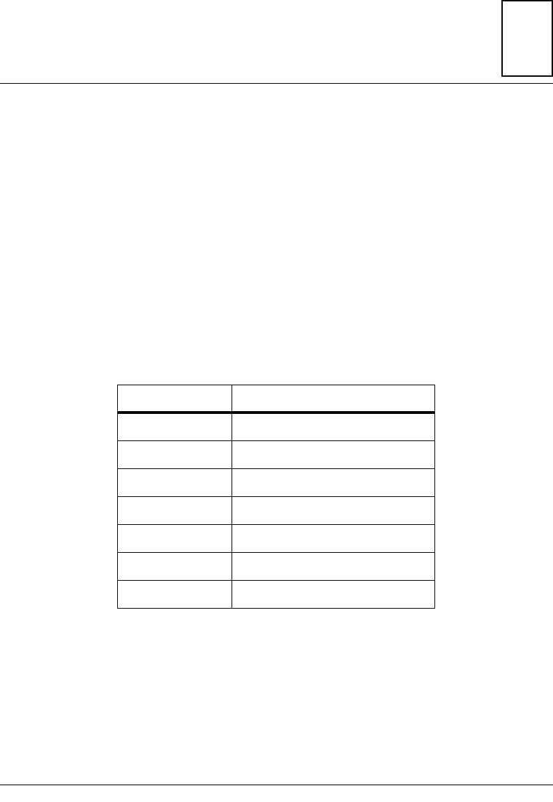
5-1
5
5Programming Details
Introduction
This chapter discusses details of several programming functions that are
not tied to any specific ASIC chip.
PCI Arbitration
PCI arbitration is performed by the PCI-to-ISA Bridge (PIB) which
supports six PCI external PCI masters. The PIB can also be a PCI master
for ISA DMA functions. The arbitration assignments on the MVME2300
series are as follows:
Upon power-up, the PIB defaults to a “round-robin” arbitration mode. The
relative priority of each request/grant pair can be customized via PCI
Priority Control Register 1. Refer to the W83C553 Data Book for
additional details, in Appendix A, Related Documentation.
Table 5-1. PCI Arbitration Assignments
Pci Bus Request PCI Master(s)
PIB (internal) PIB
CPU Raven ASIC
Request 0 PMC Slot 2
Request 1 PMC Slot 1
Request 2 PCIX Slot
Request 3 Ethernet
Request 4 Universe ASIC (VMEbus)
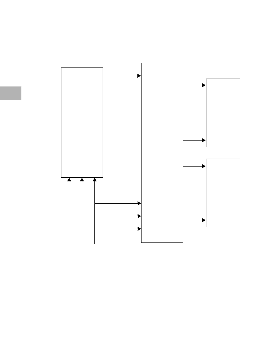
5-2 Computer Group Literature Center Web Site
Programming Details
5
Interrupt Handling
The interrupt architecture of the MVME2300 series VME processor
module is illustrated in the following figure:
Figure 5-1. MVME2300 Series Interrupt Architecture
11559.00 9609
PIB
(8529 Pair) Processor
INT_
MCP_
Processor
INT_
MCP_
RavenMPIC
INT
SERR_& PERR_
PCI Interrupts
ISA Interrupts
Interrupt Handling
http://www.motorola.com/computer/literature 5-3
5
RavenMPIC
The Raven ASIC has a built-in interrupt controller that meets the Multi-
Processor Interrupt Controller (MPIC) specification. This MPIC supports
up to two processors and 16 external interrupt sources. There are also six
other interrupt sources inside the MPIC: Two cross-processor interrupts
and four timer interrupts.
All ISA interrupts go through the 8259 pair in the PIB. The output of the
PIB then goes through the MPIC in the Raven. Refer to Chapter 2, Raven
PCI Bridge ASIC for details on the RavenMPIC. The following table
shows the interrupt assignments for the RavenMPIC on MVME2300
series boards:
Table 5-2. RavenMPIC Interrupt Assignments
MPIC
IRQ Edge/
Level Polarity Interrupt Source Notes
IRQ0 Level High PIB (8259) 1
IRQ1 Edge Low Falcon-ECC Error 2
IRQ2 Level Low PCI-Ethernet 4
IRQ3 N/A N/A Not used
IRQ4 N/A N/A Not used
IRQ5 Level Low PCI-VME INT 0 (Universe LINT0#) 3, 4
IRQ6 Level Low PCI-VME INT 1 (Universe LINT1#) 3
IRQ7 Level Low PCI-VME INT 2 (Universe LINT2#) 3
IRQ8 Level Low PCI-VME INT 3 (Universe LINT3#) 3
IRQ9 Level Low PCI-PMC1 INTA#, PMC2 INTD#, PCIX INTA# 4
IRQ10 Level Low PCI-PMC1 INTB#, PMC2 INTA#, PCIX INTB#
IRQ11 Level Low PCI-PMC1 INTC#, PMC2 INTB#, PCIX INTC#
IRQ12 Level Low PCI-PMC1 INTD#, PMC2 INTC#, PCIX INTD#
IRQ13 Level Low LM/SIG Interrupt 0 4
5-4 Computer Group Literature Center Web Site
Programming Details
5Notes
1. Interrupt from the PCI/ISA Bridge.
2. Interrupt from the Falcon chip set for a single and/or double bit
memory error.
3. The mapping of interrupt sources from the VMEbus and Universe
internal interrupt sources is programmable via the Local Interrupt
Map 0 Register and the Local Interrupt Map 1 Register in the
Universe ASIC.
4. These interrupts also appear at the PIB for backward compatibility
with older MVME1600 and PM603/4 modules.
8259 Interrupts
There are 15 interrupt requests supported by the PIB. These 15 interrupts
are ISA-type interrupts that are functionally equivalent to two 82C59
interrupt controllers. Except for IRQ0, IRQ1, IRQ2, IRQ8_, and IRQ13,
each of the interrupt lines can be configured for either edge-sensitive mode
or level-sensitive mode by programming the appropriate ELCR registers
in the PIB.
There is also support for four PCI interrupts, PIRQ3_-PIRQ0_. The PIB
has four PIRQ Route Control registers to allow each of the PCI interrupt
lines to be routed to any of eleven ISA interrupt lines (IRQ0, IRQ1, IRQ2,
IRQ8_, and IRQ13 are reserved for ISA system interrupts). Since PCI
interrupts are defined as level-sensitive, software must program the
selected IRQ(s) for level-sensitive mode. Note that more than one PCI
IRQ14 Level Low LM/SIG Interrupt 1 4
IRQ15 N/A N/A Not used
Table 5-2. RavenMPIC Interrupt Assignments (Continued)
MPIC
IRQ Edge/
Level Polarity Interrupt Source Notes
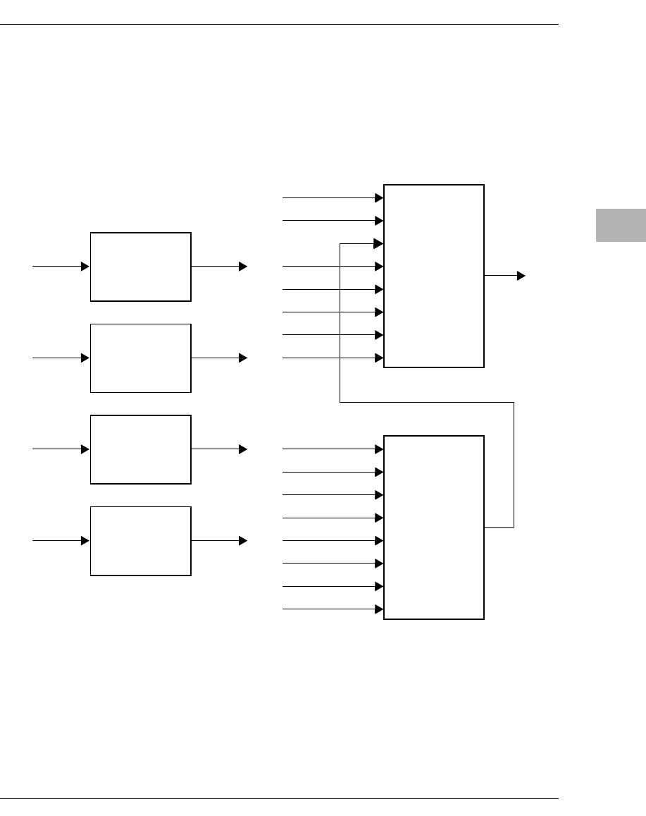
Interrupt Handling
http://www.motorola.com/computer/literature 5-5
5
interrupt can be routed to the same ISA IRQ line. The PIB can be
programmed to handle the PCI interrupts if the RavenMPIC is either not
present or not used.
The following figure shows the interrupt structure of the PIB.
Figure 5-2. PIB Interrupt Handler Block Diagram
1897 9609
IRQx
PIRQ Route
Control Register
PIRQ Route
Control Register
PIRQ Route
Control Register
PIRQ Route
Control Register
PIRQ3_
IRQx
PIRQ2_
IRQx
PIRQ1_
IRQx
PIRQ0_
Controller 2
(INT2)
IRQ8
IRQ9
IRQ11
IRQ10
IRQ12
IRQ13
IRQ14
IRQ15
0
1
2
3
4
5
6
7
Controller 1
(INT1)
Timer1/Counter0
IRQ1
IRQ3
IRQ4
IRQ5
IRQ6
IRQ7
0
1
2
3
4
5
6
7
INTR
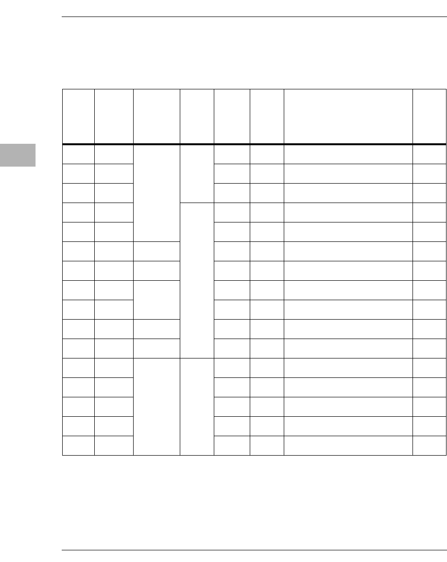
5-6 Computer Group Literature Center Web Site
Programming Details
5
The assignments of the PCI and ISA interrupts supported by the PIB are as
follows:
Table 5-3. PIB PCI/ISA Interrupt Assignments
PRI ISA
IRQ PCI
IRQ
Controller
Edge/
Level
Polarity
Interrupt Source
Notes
1 IRQ0 INT1 Edge High Timer 1 / Counter 0 1
2 IRQ1 N/A N/A Not used
3-10 IRQ2 Edge High Cascade Interrupt from INT2
3IRQ8_ INT2 Edge Low ABORT Switch Interrupt
4IRQ9 N/A N/A Not used
5 IRQ10 PIRQ0_ Level Low PCI-Ethernet Interrupt 2,3,4
6 IRQ11 PIRQ1_ Level Low Universe Interrupt (LINT0#) 2,3,4
7 IRQ12 N/A N/A Not used
8 IRQ13 N/A N/A Not used
9 IRQ14 PIRQ2_ N/A N/A Not used
10 IRQ15 PIRQ3_ Level Low PMC/PCIX Interrupt 2,3,4
11 IRQ3 INT1 N/A N/A Not used
12 IRQ4 Edge High COM1 (16550)
13 IRQ5 Level High LM/SIG Interrupt 0/1 4
14 IRQ6 N/A N/A Not used
15 IRQ7 N/A N/A Not used

ISA DMA Channels
http://www.motorola.com/computer/literature 5-7
5
Notes
1. Internally generated by the PIB.
2. After a reset, all ISA IRQ interrupt lines default to edge-sensitive
mode.
3. These PCI interrupts are routed to the ISA interrupts by
programming the PRIQ Route Control registers in the PIB. The
PCI-to-ISA interrupt assignments in this table are suggested. Each
ISA IRQ to which a PCI interrupt is routed must be programmed for
level-sensitive mode. Use this routing for PCI interrupts only when
the RavenMPIC is either not present or not used.
4. The RavenMPIC, when present, should be used for these interrupts.
ISA DMA Channels
The MVME2300 series boards do not implement any ISA DMA channels.

5-8 Computer Group Literature Center Web Site
Programming Details
5
Exceptions
Sources of Reset
There are eight potential sources of reset on MVME2300 series boards.
They are:
1. Power-On reset
2. RESET switch
3. Watchdog Timer reset via the MK48T59/559 Timekeeper device
4. Port 92 Register via the PIB
5. I/O Reset via the Clock Divisor register in the PIB
6. VMEbus SYSRESET∗ signal
7. Local software reset via the Universe ASIC (MISC_CTL register)
8. VME System Reset Via the Universe ASIC (MISC_CTL register)
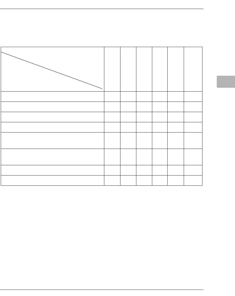
Exceptions
http://www.motorola.com/computer/literature 5-9
5
The following table shows which devices are affected by the various reset
sources:
Soft Reset
Software can assert the SRESET∗ pin of any processor by programming
the Processor Init register of the RavenMPIC appropriately.
Universe Chip Problems after PCI Reset
Under certain conditions, there may be problems with the Universe chip
after a PCI reset. Refer to Universe Chip Problems after PCI Reset in
Chapter 4 for details.
Table 5-4. Reset Sources and Devices Affected
Processor (s)
Raven ASIC
Falcon Chip Set
PCI Devices
ISA Devices
VMEbus (System
Controller)
Power-On ✓✓✓✓✓ ✓
Reset Switch ✓✓✓✓✓ ✓
Watchdog (MK48T59/559) ✓✓✓✓✓ ✓
VME System Reset (SYSRESET∗ Signal) ✓✓✓✓✓ ✓
VME System Software Reset (MISC_CTL
Register)
✓✓✓✓✓ ✓
VME Local Software Reset (MISC_CTL
Register)
✓✓✓✓✓
Hot Reset (Port 92 Register) ✓✓✓✓✓
PCI/ISA Reset (Clock Divisor Register) ✓✓
Devices Affected
Sources of Reset

5-10 Computer Group Literature Center Web Site
Programming Details
5
Error Notification and Handling
The Raven ASIC and Falcon chip set can detect certain hardware errors
and can be programmed to report these errors via the RavenMPIC
interrupts or Machine Check Interrupt. Note that the TEA∗ signal is not
used at all by the MVME2300 series. The following table summarizes how
hardware errors are handled by the MVME2300 series boards:
Table 5-5. Error Notification and Handling
Cause Action
Single-bit ECC Store: Write corrected data to memory.
Load: Present corrected data to the MPC master.
Generate interrupt via RavenMPIC if so enabled.
Double-bit ECC Store: Terminate the bus cycle normally without writing to DRAM.
Load: Present un-corrected data to the MPC master.
Generate interrupt via RavenMPIC if so enabled.
Generate Machine Check Interrupt to the processor(s) if so enabled.
MPC Bus Time Out Store: Discard write data and terminate bus cycle normally.
Load: Present undefined data to the MPC master.
Generate interrupt via RavenMPIC if so enabled.
Generate Machine Check Interrupt to the processor(s) if so enabled.
PCI Target Abort Store: Discard write data and terminate bus cycle normally.
Load: Return all ones and terminate bus cycle normally.
Generate interrupt via RavenMPIC if so enabled.
Generate Machine Check Interrupt to the processor(s) if so enabled.
PCI Master Abort Store: Discard write data and terminate bus cycle normally
Load: Return all ones and terminate bus cycle normally
Generate interrupt via RavenMPIC if so enabled
Generate Machine Check Interrupt to the processor(s) if so enabled
PERR# Detected Generate interrupt via RavenMPIC if so enabled
Generate Machine Check Interrupt to the processor(s) if so enabled
SERR# Detected Generate interrupt via RavenMPIC if so enabled
Generate Machine Check Interrupt to the processor(s) if so enabled
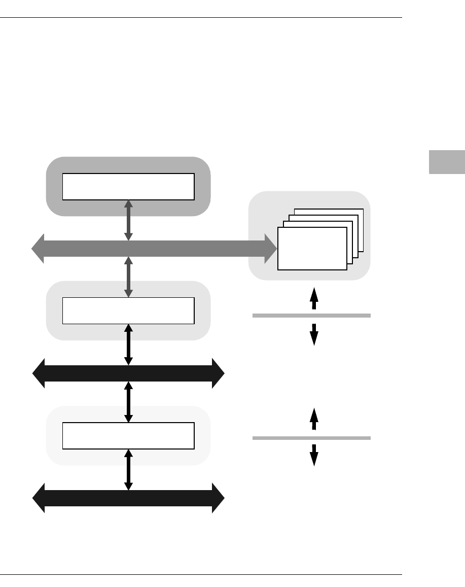
Endian Issues
http://www.motorola.com/computer/literature 5-11
5
Endian Issues
The MVME2300 series supports both little-endian and big-endian
software. Because the PowerPC processor is inherently big-endian, PCI is
inherently little-endian, and the VMEbus is big-endian, there is potential
for confusion. The figures below illustrate how the MVME2300 series
boards handle the endian issue in big-endian and little-endian modes.
Figure 5-3. Big-Endian Mode
Big-Endian PROGRAM
1898 9609
Raven
Universe
Falcons
DRAM
Big-Endian
Little-Endian
Big-Endian
Little-Endian
PCI Local Bus
VMEbus
N-way Byte Swap
N-way Byte Swap
60X System Bus
5-12 Computer Group Literature Center Web Site
Programming Details
5
Figure 5-4. Little-Endian Mode
EA Modification (XOR)
1899 9609
Raven
Universe
Falcons
DRAM
Big-Endian
Little-Endian
Big-Endian
Little-Endian
PCI Local Bus
VMEbus
N-way Byte Swap
EA Modification
60X System Bus
Big-Endian
Little-Endian
Little-Endian PROGRAM

Endian Issues
http://www.motorola.com/computer/literature 5-13
5
Processor/Memory Domain
The MPC603 and MPC604 processors can operate in both big-endian and
little-endian mode. However, they always treat the external
processor/memory bus as big-endian by performing address
rearrangement and reordering when running in little-endian mode.
The MPC registers inside the Raven, the registers inside the Falcon chip
set, the DRAM, the ROM/Flash, and the system registers always appear as
big-endian.
Role of the Raven ASIC
Since PCI is little-endian, the Raven PowerPC-to-PCI-Local-Bus bridge
controller chip performs byte swapping in both directions (from PCI to
memory and from the processor to PCI) to maintain address invariance
when it is programmed to operate in big-endian mode with the processor
and the memory subsystem.
In little-endian mode, it reverse-rearranges the address for PCI-bound
accesses and rearranges the address for memory-bound accesses (from
PCI). In this case, no byte swapping is done.
PCI Domain
The PCI bus is inherently little-endian and all devices connected directly
to PCI will operate in little-endian mode, regardless of the mode of
operation in the processor’s domain.
PCI-SCSI
The MVME2300 series boards do not implement SCSI.
PCI/Ethernet
Ethernet is byte-stream-oriented, with the byte having the lowest address
in memory being the first one transferred regardless of endian mode. Since
address invariance is maintained by the Raven in both little-endian and

5-14 Computer Group Literature Center Web Site
Programming Details
5
big-endian mode, there should be no endian issues for Ethernet data. Big-
endian software, however, must still take the byte-swapping effect into
account when accessing the registers of the PCI-Ethernet device.
PCI-Graphics
Big-endian software must take the effects of byte swapping on big-endian
software into account.
Note On MVME2300 series boards this is not presently a
consideration, as no graphics are implemented on these
boards.
Role of the Universe ASIC
Since PCI is little-endian and the VMEbus is big-endian, the Universe
VMEbus interface chip performs byte swapping in both directions (from
PCI to VMEbus and from VMEbus to PCI) to maintain address invariance,
regardless of the mode of operation in the processor’s domain.
VMEbus Domain
The VMEbus is inherently big-endian. All devices connected directly to
the VMEbus are expected to operate in big-endian mode, regardless of the
mode of operation in the processor’s domain.
In big-endian mode on the MVME2300 series boards, byte swapping is
performed by the Universe and then by the Raven. The result has the
desirable effect of being transparent to the big-endian software.
In little-endian mode, however, software must take the byte-swapping
effect of the Universe ASIC and the address reverse-rearranging effect of
the Raven into account.
ROM/Flash Initialization
http://www.motorola.com/computer/literature 5-15
5
ROM/Flash Initialization
There are two methods of injecting code into the Flash in bank A:
1. In-circuit programming
2. Loading it from ROM/Flash bank B
For the second method, hardware must direct the Falcon chip set to map
the FFF00000-FFFFFFFF address range to Flash bank B following a hard
reset. Bank A then can be programmed by code from bank B.
Software can determine the mapping of the FFF00000-FFFFFFFF address
range by examining the rom_b_rv bit in the Falcon’s Rom B Base/Size
register.
Table 5-6. ROM/Flash Bank Default
rom_b_rv Default Mapping for FFF00000-FFFFFFFF
0 ROM/FLASH Bank A
1 ROM/FLASH Bank B

A
A-1
ARelated Documentation
Motorola Computer Group Documents
The Motorola publications listed below are referenced in this manual. You
can obtain paper or electronic copies of Motorola Computer Group
publications by:
❏Contacting your local Motorola sales office
❏Visiting MCG’s World Wide Web literature site,
http://www.motorola.com/computer/literature
To locate and view the most up-to-date product information in PDF or
HTML format, visit http://www.motorola.com/computer/literature.
Document Title Publication
Number
MVME2300SC VME Processor Module Installation and Use V2300SCA/IH
MVME2300-Series VME Processor Module Installation and Use V2300A/IH
MVME2300-Series VME Processor Module Programmer’s Reference Guide V2300A/PG
PPCBug Firmware Package User’s Manual (Parts 1 and 2) PPCBUGA1/UM
PPCBUGA2/UM
PPCBug Diagnostics Manual PPCDIAA/UM
PMCspan PMC Adapter Carrier Module Installation and Use PMCSPANA/IH

A-2 Computer Group Literature Center Web Site
Related Documentation
A
Manufacturers’ Documents
For additional information, refer to the following table for manufacturers’
data sheets and user’s manuals. For your convenience, a source for the
listed document is also provided.
It is important to note that in many cases, the information shown is
preliminary and the revision levels of the documents are subject to change
without notice.
Document Title and Source Publication
Number
PowerPC 603e® RISC Microprocessor Technical Summary
PowerPC 604e® RISC Microprocessor Technical Summary
Literature Distribution Center for Motorola
Telephone: 1-800- 441-2447
FAX: (602) 994-6430 or (303) 675-2150
WebSite: http://e-www.motorola.com/webapp/DesignCenter/
E-mail: ldcformotorola@hibbertco.com
MPC603E/D
MPC604E/D
PowerPC 603e® RISC Microprocessor User’s Manual
PowerPC 604e® RISC Microprocessor User’s Manual
Literature Distribution Center for Motorola
Telephone: 1-800- 441-2447
FAX: (602) 994-6430 or (303) 675-2150
WebSite: http://e-www.motorola.com/webapp/DesignCenter/
E-mail: ldcformotorola@hibbertco.com
OR
IBM Microelectronics
PowerPC603e User Manual
PowerPC604e User Manual
Web Site:
http://www.chips.ibm.com/techlib/products/powerpc/manuals
MPC603EUM/AD
MPC604EUM/AD
G522-0297-00
G522-0330-00

Manufacturers’ Documents
http://www.motorola.com/computer/literature A-3
A
PowerPC® Microprocessor Family: The Programming Environments for
32-Bit Microprocessors
Literature Distribution Center for Motorola
Telephone: 1-800- 441-2447
FAX: (602) 994-6430 or (303) 675-2150
WebSite: http://e-www.motorola.com/webapp/DesignCenter/
E-mail: ldcformotorola@hibbertco.com
OR
IBM Microelectronics
Programming Environment Manual
Web Site:
http://www.chips.ibm.com/techlib/products/powerpc/manuals
MPCFPE/AD
G522-0290-01
PC16550 UART
National Semiconductor Corporation
http://www.national.com/
PC16550DV
21140 Fast Etherworks PCI 10-Flash-100 Ethernet Adapter Owner’s
Manual
Compaq
Telephone: 1-800.at.compaq
http://www3.compaq.com/support
EK-DE500-OM
W83C553 Enhanced System I/O Controller with PCI Arbiter (PIB)
Winbond Electronics Corporation;
http://www.winbond.com.tw/product/
W83C553F
M48T59 CMOS 8K x 8 TIMEKEEPERTM SRAM Data Sheet
STMicroelectronics;
http://eu.st.com/stonline/index.shtml
M48T59
Universe User Manual
Tundra Semiconductor Corporation
http://www.tundra.com/page.cfm?tree_id=100008#Universe II
(CA91C042)
8091042_MD300_
05.pdf
Universe User Manual
Tundra Semiconductor Corporation
http://www.tundra.com/page.cfm?tree_id=100008#Universe II
(CA91C042)
8091042_MD300_
05.pdf
Document Title and Source Publication
Number

A-4 Computer Group Literature Center Web Site
Related Documentation
A
Related Specifications
For additional information, refer to the following table for related
specifications. For your convenience, a source for the listed document is
also provided. It is important to note that in many cases, the information is
preliminary and the revision levels of the documents are subject to change
without notice.
Document Title and Source Publication
Number
VME64 Specification
VITA (VMEbus International Trade Association)
Web Site: http://www.vita.com/
ANSI/VITA 1-1994
Versatile Backplane Bus: VMEbus
Institute of Electrical and Electronics Engineers, Inc.
OR
Microprocessor system bus for 1 to 4 byte data
Bureau Central de la Commission Electrotechnique Internationale
3, rue de Varembé
Geneva, Switzerland
Web Site: http://standards.ieee.org/catalog/
ANSI/IEEE
Standard 1014-1987
IEC 821 BUS
IEEE - Common Mezzanine Card Specification (CMC)
Institute of Electrical and Electronics Engineers, Inc.
Web Site: http://standards.ieee.org/catalog/
P1386 Draft 2.0
IEEE - PCI Mezzanine Card Specification (PMC)
Institute of Electrical and Electronics Engineers, Inc.
Web Site: http://standards.ieee.org/catalog/
P1386.1 Draft 2.0
Bidirectional Parallel Port Interface Specification
Institute of Electrical and Electronics Engineers, Inc.
Web Site: http://standards.ieee.org/catalog/
IEEE Standard
1284

Related Specifications
http://www.motorola.com/computer/literature A-5
A
Peripheral Component Interconnect (PCI) Local Bus Specification,
Revision 2.0
PCI Special Interest Group
Web Site: http://www.pcisig.com/
PCI Local Bus
Specification
PowerPC Reference Platform (PRP) Specification,
Third Edition, Version 1.0, Volumes I and II
International Business Machines Corporation
Web Site: http://www.ibm.com
MPR-PPC-RPU-02
PowerPC Microprocessor Common Hardware Reference Platform: A
System Architecture (CHRP), Version 1.0
Literature Distribution Center for Motorola
Telephone: 1-800- 441-2447
FAX: (602) 994-6430 or (303) 675-2150
Web Site: http://e-www.motorola.com/webapp/DesignCenter/
E-mail: ldcformotorola@hibbertco.com
OR
Morgan Kaufmann Publishers, Inc.
Telephone: (415) 392-2665
Telephone: 1-800-745-7323
Web Site: http://www.mkp.com/books_catalog/
ISBN
1-55860-394-8
Interface Between Data Terminal Equipment and Data Circuit-
Terminating Equipment Employing Serial Binary Data Interchange
Electronic Industries Alliance
Web Site: http://www.eia.org/
Web Site: http://global.ihs.com/index.cfm (for publications)
TIA/EIA-232
Standard
Document Title and Source Publication
Number

GL-1
Glossary
10Base-5 An Ethernet implementation in which the physical medium is a
doubly shielded, 50-ohm coaxial cable capable of carrying data at 10
Mbps for a length of 500 meters (also referred to as thicknet). Also
known as thick Ethernet.
10Base-2 An Ethernet implementation in which the physical medium is a
single-shielded, 50-ohm RG58A/U coaxial cable capable of
carrying data at 10 Mbps for a length of 185 meters (also referred to
as AUI or thinnet). Also known as thin Ethernet.
10Base-T An Ethernet implementation in which the physical medium is an
unshielded twisted pair (UTP) of wires capable of carrying data at
10 Mbps for a maximum distance of 185 meters. Also known as
twisted-pair Ethernet.
100Base-TX An Ethernet implementation in which the physical medium is an
unshielded twisted pair (UTP) of wires capable of carrying data at
100 Mbps for a maximum distance of 100 meters. Also known as
fast Ethernet.
AIX Advanced Interactive eXecutive (IBM version of UNIX).
architecture The main overall design in which each individual hardware
component of the computer system is interrelated. The most
common uses of this term are 8-bit, 16-bit, or 32-bit architectural
design systems.
ASCII American Standard Code for Information Interchange; a 7-bit code
used to encode alphanumeric information. In the IBM-compatible
world, this is expanded to eight bits to encode a total of 256
alphanumeric and control characters.
ASIC Application-Specific Integrated Circuit.
AUI Attachment Unit Interface.
BBRAM Battery Backed-up Random Access Memory.
bi-endian Having big-endian and little-endian byte ordering capability.

Glossary
GL-2 Computer Group Literature Center Web Site
G
L
O
S
S
A
R
Y
big-endian A byte-ordering method in memory where the address n of a word
corresponds to the most significant byte. In an addressed memory
word, the bytes are ordered (left to right) 0, 1, 2, 3, with 0 being the
most significant byte.
BLT BLock Transfer.
bus The pathway used to communicate between the CPU, memory, and
various input/output devices, including floppy and hard disk drives.
Available in various widths (8-, 16-, and 32-bit), with accompanying
increases in speed.
cache A high-speed memory that resides logically between a central
processing unit (CPU) and the main memory. This temporary
memory holds the data and/or instructions that the CPU is most
likely to use over and over again and avoids accessing the slower
hard or floppy disk drive.
CAS Column Address Strobe. The clock signal used in dynamic RAMs to
control the input of column addresses.
CISC Complex-Instruction-Set Computer. A computer whose processor
is designed to sequentially run variable-length instructions, many of
which require several clock cycles, that perform complex tasks and
thereby simplify programming.
CPU Central Processing Unit. The master computer unit in a system.
DCE Data Circuit-terminating Equipment.
DIMM Dual Inline Memory Module.
DMA Direct Memory Access. A method by which a device may read or
write to memory directly without processor intervention. DMA is
typically used by block I/O devices.
DRAM Dynamic Random Access Memory. A memory technology that is
characterized by extreme high density, low power, and low cost. It
must be more or less continuously refreshed to avoid loss of data.
DTE Data Terminal Equipment.
ECC Error Correction Code
EEPROM Electrically Erasable Programmable Read-Only Memory. A
memory storage device that can be written repeatedly with no
special erasure fixture. EEPROMs do not lose their contents when
they are powered down.

http://www.motorola.com/computer/literature GL-3
G
L
O
S
S
A
R
Y
EIDE Enhanced Integrated Drive Electronics. An improved version of
IDE, with faster data rates, 32-bit transactions, and DMA. Also
known as Fast ATA-2.
EISA (bus) Extended Industry Standard Architecture (bus) (IBM). An
architectural system using a 32-bit bus that allows data to be
transferred between peripherals in 32-bit chunks instead of 16-bit or
8-bit that most systems use. With the transfer of larger bits of
information, the machine is able to perform much faster than the
standard ISA bus system.
EPROM Erasable Programmable Read-Only Memory. A memory storage
device that can be written once (per erasure cycle) and read many
times.
ESD Electro-Static Discharge/Damage
Ethernet A local area network standard that uses radio frequency signals
carried by coaxial cables.
Falcon The DRAM controller chip developed by Motorola for the
MVME2600 and MVME3600 series of boards. It is intended to be
used in sets of two to provide the necessary interface between the
Power PC60x bus and the 144-bit ECC DRAM (system memory
array) and/or ROM/Flash.
fast Ethernet See 100Base-TX.
FDDI Fiber Distributed Data Interface. A network based on the use of
optical-fiber cable to transmit data in non-return-to-zero, invert-on-
1s (NRZI) format at speeds up to 100 Mbps.
firmware The program or specific software instructions that have been more
or less permanently burned into an electronic component, such as a
ROM (read-only memory) or an EPROM (erasable programmable
read-only memory).
hardware A computing system is normally spoken of as having two major
components: hardware and software. Hardware is the term used to
describe any of the physical embodiments of a computer system,
with emphasis on the electronic circuits (the computer) and
electromechanical devices (peripherals) that make up the system.
IDE Integrated Drive Electronics. A disk drive interface standard. Also
known as ATA (Advanced Technology Attachment).
IEEE Institute of Electrical and Electronics Engineers

Glossary
GL-4 Computer Group Literature Center Web Site
G
L
O
S
S
A
R
Y
ISA (bus) Industry Standard Architecture (bus). The de facto standard system
bus for IBM-compatible computers until the introduction of VESA
and PCI. Used in the reference platform specification. (IBM)
ISASIO ISA Super Input/Output device
ISDN Integrated Services Digital Network. A standard for digitally
transmitting video, audio, and electronic data over public phone
networks.
LAN Local Area Network
LED Light-Emitting Diode
little-endian A byte-ordering method in memory where the address n of a word
corresponds to the least significant byte. In an addressed memory
word, the bytes are ordered (left to right) 3, 2, 1, 0, with 3 being the
most significant byte.
MPC603, MPC604 Motorola’s component designations for the PowerPC 603 and
PowerPC 604 microprocessors.
MPIC Multi-Processor Interrupt Controller
MPU MicroProcessing Unit
nonvolatile memory A memory in which the data content is maintained whether the
power supply is connected or not.
NVRAM Non-Volatile Random Access Memory
OEM Original Equipment Manufacturer
OS Operating System. The software that manages the computer
resources, accesses files, and dispatches programs.
parallel port A connector that can exchange data with an I/O device eight bits at
a time. This port is more commonly used for the connection of a
printer to a system.
PCI (local bus) Peripheral Component Interconnect (local bus) (Intel). A high-
performance, 32-bit internal interconnect bus used for data transfer
to peripheral controller components, such as those for audio, video,
and graphics.
PCMCIA (bus) Personal Computer Memory Card International Association (bus).
A standard external interconnect bus which allows peripherals
adhering to the standard to be plugged in and used without further
system modification.

http://www.motorola.com/computer/literature GL-5
G
L
O
S
S
A
R
Y
PHB PCI Host Bridge
physical address A binary address that refers to the actual location of information
stored in secondary storage.
PIB PCI-to-ISA Bridge
PMC PCI Mezzanine Card
POWER Performance Optimized With Enhanced RISC architecture (IBM)
PowerPC™ The trademark used to describe the Performance Optimized With
Enhanced RISC microprocessor architecture for Personal
Computers developed by the IBM Corporation. PowerPC is
superscalar, which means it can handle more than one instruction per
clock cycle. Instructions can be sent simultaneously to three types of
independent execution units (branch units, fixed-point units, and
floating-point units), where they can execute concurrently, but finish
out of order. PowerPC is used by Motorola, Inc. under license from
IBM.
RAM Random-Access Memory. The temporary memory that a computer
uses to hold the instructions and data currently being worked with.
All data in RAM is lost when the computer is turned off.
RAS Row Address Strobe. A clock signal used in dynamic RAMs to
control the input of the row addresses.
Raven The PowerPC-to-PCI local bus bridge chip developed by Motorola
for the MVME2600 and MVME3600 series of boards. It provides
the necessary interface between the PowerPC 60x bus and the PCI
bus, and acts as interrupt controller.
Reduced-Instruction-Set Computer (RISC)
A computer in which the processor’s instruction set is limited to
constant-length instructions that can usually be executed in a single
clock cycle.
RFI Radio Frequency Interference
ROM Read-Only Memory
RTC Real-Time Clock
SBC Single Board Computer

Glossary
GL-6 Computer Group Literature Center Web Site
G
L
O
S
S
A
R
Y
SCSA Signal Computing System Architecture. A hardware model for
computer telephony servers. A key SCSA element is a TDM (time
division multiplexed) telephony bus for voice and video signals,
known as the SCbus™ in VME implementations of this architecture.
SCSI Small Computer Systems Interface. An industry-standard high-
speed interface primarily used for secondary storage. SCSI-1
provides up to 5 Mbps data transfer.
SCSI-2 (Fast/Wide) An improvement over plain SCSI; and includes command queuing.
Fast SCSI provides 10 Mbps data transfer on an 8-bit bus. Wide
SCSI provides up to 40 Mbps data transfer on a 16- or 32-bit bus.
serial port A connector that can exchange data with an I/O device one bit at a
time. It may operate synchronously or asynchronously, and may
include start bits, stop bits, and/or parity.
SIM Serial Interface Module
SIMM Single Inline Memory Module. A small circuit board with RAM
chips (normally surface mounted) on it designed to fit into a standard
slot.
SIO Super I/O controller
SMT Surface Mount Technology. A method of mounting devices (such as
integrated circuits, resistors, capacitors, and others) on a printed
circuit board, characterized by not requiring mounting holes. Rather,
the devices are soldered to pads on the printed circuit board.
Surface-mount devices are typically smaller than the equivalent
through-hole devices.
software A computing system is normally spoken of as having two major
components: hardware and software. Software is the term used to
describe any single program or group of programs, languages,
operating procedures, and documentation of a computer system.
Software is the real interface between the user and the computer.
SRAM Static Random Access Memory
TDM Time Division Multiplexing. A multiplexing scheme in which
individual I/O ports or channels share slices of time on an aggregate
channel, Receivers and transmitters are synchronized. The SCbus™
is a TDM implementation that provides up to 2048 time slots, the
equivalent of 1024 voice conversations at 64 Kbps.
thick Ethernet See 10base-5.

http://www.motorola.com/computer/literature GL-7
G
L
O
S
S
A
R
Y
thin Ethernet See 10base-2.
twisted-pair Ethernet See 10Base-T.
UART Universal Asynchronous Receiver/Transmitter
Universe ASIC developed by Tundra in consultation with Motorola which
provides the complete interface between the PCI bus and the
VMEbus.
VESA (bus) Video Electronics Standards Association (or VL bus). An internal
interconnect standard for transferring video information to a
computer display system.
virtual address A binary address issued by a CPU that indirectly refers to the
location of information in primary memory, such as main memory.
When data is copied from disk to main memory, the physical address
is changed to the virtual address.
VL bus See VESA Local bus (VL bus).
volatile memory A memory in which the data content is lost when the power supply
is disconnected.


IN-1
Index
Numerics
16550 UART registers 1-31
8259 mode (Raven interrupt controller) 2-90,
5-4
A
access timing
DRAM 3-7, 3-8, 3-9
ROM/Flash 3-10
address mapping
PowerPC to DRAM 3-56
PowerPC to ROM/Flash 3-16, 3-17
address transfers (PowerPC bus) 3-11
addresses, sizing of 3-56
addressing PCI slave 2-15
Application-Specific Integrated Circuits
(ASICs) 1-1
Falcon ECC Memory Controller chip set
3-1
Raven PCI Bridge 2-1
Universe VMEbus/PCI interface 4-1
architecture
Falcon ECC Memory Controller chip set
3-2
Raven interrupt controller 2-60
Universe ASIC 4-4
ARTRY_ signal (PowerPC 60x bus) 3-11
assertion, definition of xxiii
asterisk (*), meaning of xxiii
B
Base Module Feature register 1-35
Base Module Status register (BMSR) 1-36
big-endian byte ordering xxiii, 5-11
in Raven PCI Bridge ASIC 2-25
binary number, symbol for xxii
bit ordering conventions (Falcon chip set) 3-5
block diagrams
Falcon ECC Memory Controller chip set
3-2
MVME2300 series boards 1-5
PIB interrupt handler 5-5
Raven interrupt controller function 2-65
Raven PCI Bridge ASIC 2-2
board connectors 1-6
bus interface (PowerPC 60x bus) 3-11
byte ordering conventions 5-11
MVME2300 series xxiii
PCI domain 5-13
PCI/Ethernet 5-13
PCI/graphics 5-14
processor/memory domain 5-13
Universe ASIC 5-14
VMEbus domain 5-14
byte, definition of xxiii
C
cache coherency (PowerPC 60x bus) 3-11,
3-12
changing I/O interrupt configurations (Raven
interrupt controller) 2-89
CIO port pins (Z8536 emulation) 1-44
CLK Frequency register (Falcon chip set)
3-35
clock frequency (Falcon chip set) 3-35
CONFIG_ADDRESS register 2-56

Index
IN-2 Computer Group Literature Center Web Site
I
N
D
E
X
CONFIG_DATA register 2-58
configuration registers (Raven PCI Bridge
ASIC) 2-11
connectors, MVME2300 series boards 1-6
control bit, definition of xxiii
control registers, writing to (Falcon chip set)
3-53
control/status registers (Falcon chip set) 3-21
CPU Configuration register 1-34
CPU Control register 1-30
CSR accesses (Falcon chip set) 3-21
CSR base address (Falcon chip set) 3-21
current task priority level (Raven interrupt
controller) 2-90
cycle types (Falcon chip set) 3-12
D
data paths, PowerPC/DRAM 3-60
data transfers (PowerPC 60x bus) 3-11
decimal number, symbol for xxii
default memory maps
PCI 1-13
processor 1-8
defaults (Falcon chip set) 3-20
Disable Error Correction control bit (Falcon
chip set) 3-38
DMA controller (Universe ASIC) 4-7
documentation, related A-1
double word, definition of xxiii
double-bit errors (Falcon chip set) 3-13
DRAM
addressing 3-56
arbitration (Falcon chip set) 3-20
connection diagrams 3-2, 3-3, 3-4
size control bits (Falcon chip set) 3-33
sizing 3-54
speed control bits (Falcon chip set) 3-32
speeds 3-6
DRAM Attributes register (Falcon chip set)
3-33
DRAM Base register (Falcon chip set) 3-35
DRAM Tester Control registers (Falcon chip
set) 3-50
E
ECC codes (Falcon chip set) 3-57
ECC Control register (Falcon chip set) 3-36
ECC implementation 3-12
emulated Z8536 registers 1-43
endian conversion (Raven PCI Bridge ASIC)
2-25
endian data swaps 2-26
endian issues 5-11
End-of-Interrupt registers (Raven MPIC)
2-86, 2-90
errorcorrection (Falcon chip set) 3-12
correction codes (Falcon chip set) 3-57
detection (Falcon chip set) 3-12
handling (Raven PCI Bridge ASIC) 2-28
logging (Falcon chip set) 3-14
notification and handling 5-10
reporting (Falcon chip set) 3-13
Error Address register (Falcon chip set) 3-42
Error Logger register (Falcon chip set) 3-39
examples, Universe/PCI reset problem 4-16
external
interrupt service (Raven MPIC) 2-87
register set (Falcon chip set) 3-21, 3-52
External Source Destination registers (Raven
MPIC) 2-82
External Source Vector/Priority registers
(Raven MPIC) 2-81
F
Falcon ECC Memory Controller chip set
address pipelining 3-5, 3-6
control/status registers 3-21
external register set 3-21, 3-52
features 3-1
four-beat reads/writes 3-5
functional description 3-5
programming model 3-21

http://www.motorola.com/computer/literature IN-3
I
N
D
E
X
reading internal CSRs 3-22
single-beat reads/writes 3-6
software considerations 3-53
writing to internal CSRs 3-23
Falcon-controlled system registers 1-24
false, definition of xxiii
fast refresh control bit (Falcon chip set) 3-32
Feature Reporting register (RavenMPIC)
2-73
features
Falcon ECC Memory Controller chip set
3-1
MVME2300 series boards 1-2
Raven PCI Bridge ASIC 2-1
Universe ASIC 4-1, 4-2
Flash (see ROM/Flash interface) 3-14
functional description
Falcon ECC Memory Controller chip set
3-5
Raven PCI Bridge ASIC 2-4
Universe ASIC 4-3
G
General Control/Status and Feature registers
2-33
General-Purpose registers 2-47
general-purpose software-readable header
(J10/J17) 1-32
generating PCI cycles (Raven PCI Bridge
ASIC) 2-21
Global Configuration register (RavenMPIC)
2-74
H
half-word, definition of xxiii
headers
J10/J17 (general-purpose software-read-
able header) 1-32
hexadecimal character, symbol for xxii
hints for programming 5-1
I
I/O Base register 2-52
initializing ROM/Flash 5-15
In-Service register (ISR) 2-67
Interprocessor Interrupt Dispatch registers
(Raven MPIC) 2-84
interprocessor interrupts 2-89
Interrupt Acknowledge registers (Raven
MPIC) 2-86, 2-90
interrupt delivery modes (Raven ASIC) 2-64
Interrupt Enable control bits (Falcon chip set)
3-38
interrupt handling, MVME2300 boards 5-2
Interrupt Pending register (IPR) 2-66
Interrupt Request register (IRR) 2-67
interrupt router (Raven ASIC) 2-67
interrupt selector (IS) 2-66
Interrupt Task Priority registers (Raven-
MPIC) 2-85
interrupter and interrupt handler (Universe
ASIC) 4-6
IPI Vector/Priority registers (Raven MPIC)
2-76
ISA local resource bus 1-31
J
jumper headers
J10/J17 (general-purpose software-read-
able header) 1-32
L
Large Scale Integration (LSI) 1-1
little-endian byte ordering xxiii, 5-12
LM/SIG Control register 1-38
LM/SIG Status register 1-39
Location Monitor
Lower Base Address register 1-41
Upper Base Address register 1-41
M
manual terminology xxiii
manufacturers’ documents A-2

Index
IN-4 Computer Group Literature Center Web Site
I
N
D
E
X
Memory Base register 2-53
Memory Configuration register (MEMCR)
1-27
memory maps
byte reads to CSRs (Falcon chip set)
3-24
byte writes to internal register set and
test SRAM (Falcon chip set)
3-25
default processor 1-8
four-byte reads to CSR (Falcon chip set)
3-26
four-byte writes to internal register set
and test SRAM (Falcon chip
set) 3-26
PCI bus 1-13
PCI PREP 1-16
processor CHRP 1-9
processor PREP 1-11
Raven PCI configuration registers 2-48
Raven PCI I/O registers 2-49
VMEbus master 1-20
VMEbus slave 1-21
MK48T59/559 access registers 1-33
module configuration and status registers
1-33
MPC
address mapping 2-4
arbiter (Raven PCI Bridge ASIC) 2-10
Arbiter Control register 2-36
bus address space (Raven PCI Bridge
ASIC) 2-12
bus interface (Raven PCI Bridge ASIC)
2-4
bus timer (Raven PCI Bridge ASIC)
2-10
bus transfer types (Raven PCI Bridge
ASIC) 2-9
Error Address register 2-40
Error Attribute register (MERAT) 2-41
Error Enable register 2-37
Error Status register 2-39
master function (Raven PCI Bridge
ASIC) 2-8
Slave Address (0,1 and 2) registers 2-43
Slave Address (3) register 2-44
slave function (Raven PCI Bridge ASIC)
2-6
Slave Offset/Attribute (0,1 and 2) regis-
ters 2-45
Slave Offset/Attribute (3) registers 2-46
write posting (Raven PCI Bridge ASIC)
2-8
MPC-to-PCI address decoding 2-5
MPC-to-PCI address translation 2-6
MPIC registers (Raven ASIC) 2-69
MVME2300 series interrupt architecture 5-2
N
negation, definition of xxiii
NVRAM/RTC 1-32
P
P2 signal routing 1-7
parity checking and Falcon chip set 3-53
PCI address mapping (Raven PCI Bridge
ASIC) 2-11
arbitration 5-1
CHRP memory map 1-13
Command/ Status registers 2-50
configuration access 1-12
interface function (Raven PCI Bridge
ASIC) 2-10
interface function (Universe ASIC) 4-5
Interrupt Acknowledge register 2-43
master function (Raven PCI Bridge
ASIC) 2-17
memory maps 1-13
PREP memory map 1-16
registers (Raven ASIC) 2-47
reset problems with Universe ASIC 4-14
Slave Address (0,1,2 and 3) registers
2-54

http://www.motorola.com/computer/literature IN-5
I
N
D
E
X
Slave Attribute/ Offset (0,1,2 and 3) reg-
isters 2-55
slave command types 2-15
slave function (Raven PCI Bridge ASIC)
2-14
write posting 2-17
PCI/ISA interrupt assignments 5-6
PIB interrupt handler
block diagram 5-5
PCI/ISA interrupt assignments 5-6
pound sign (#), meaning of xxiii
PowerPC to DRAM
access timing 3-7, 3-8, 3-9
address mapping 3-56
data mapping 3-61
PowerPC to ROM/Flash
address mapping 3-16, 3-17
Power-Up Reset status bit (Falcon chip set)
3-36
Power-Up Reset Status registers (Falcon chip
set) 3-51
Prescaler Adjust register 2-36
priority level, current task (Raven interrupt
controller) 2-90
processor CHRP memory map 1-9
Processor Init register (RavenMPIC) 2-75
processor memory maps 1-7
processor PREP memory map 1-11
programming details 5-1
programming model
Falcon chip set 3-21
MVME2300 series boards 1-7
programming notes 2-87
programming ROM/Flash 3-53
program-visible registers (Raven interrupt
controller) 2-66
R
Raven interrupt controller implementation
2-60
Raven MPC register values
for CHRP memory map 1-10
for PREP memory map 1-12
Raven PCI
configuration register map 2-48
I/O register map 2-49
register values for CHRP memory map
1-15
register values for PREP memory map
1-18
Raven PCI Bridge ASIC, description of 2-1
Raven-Detected Errors
Destination register (Raven MPIC) 2-84
Vector/Priority register (Raven MPIC)
2-83
RavenMPIC
control registers 2-13
interrupt controller 5-3
register map 2-69
Read/Write Checkbits control bit (Falcon
chip set) 3-36
read/write cycles to ROM/Flash (Falcon
chipset) 3-47
readable jumpers 1-32
Refresh Counter Test control bits (Falcon
chip set) 3-43
Refresh/Scrub Address register (Falcon chip
set) 3-44
refresh/scrub implementation (Falcon chip
set) 3-18, 3-19
register descriptions, locations of 1-1
register maps
Falcon chip set 3-27
Raven ASIC 2-30
Universe ASIC 4-9
registers
16550 UART 1-31
Base Module Features 1-35
Base Module Status 1-36
CPU Configuration 1-34
CPU Control 1-30
emulated Z8536 1-43
Falcon-controlled 1-24
LM/SIG Control 1-38

Index
IN-6 Computer Group Literature Center Web Site
I
N
D
E
X
LM/SIG Status 1-39
Location Monitor Lower Base Address
1-41
Location Monitor Upper Base Address
1-41
Memory Configuration (MEMCR) 1-27
MK48T59/559 access 1-33
module configuration and status 1-33
NVRAM/RTC and Watchdog Timer
1-32
Raven configuration 2-11
Raven MPC 1-10, 1-12
RavenMPIC control 2-13
Semaphore Register 1 1-42
Semaphore Register 2 1-42
System Configuration (SYSCR) 1-25
System External Cache Control (SXC-
CR) 1-29
Universe Control and Status registers
(UCSR) 4-8
VME Geographical Address (VGAR)
1-43
W83C553 PIB 1-31
registers and endian mode (Raven PCI
Bridge ASIC) 2-27
registers, Falcon chip set
CLK Frequency 3-35
CSR summary 3-27
DRAM Attributes 3-33
DRAM Base 3-35
DRAM Tester Control 3-50
ECC Control 3-36
Error Address 3-42
Error Logger 3-39
Power-Up Reset Status 3-51
RAM/Flash Block A Base/Size 3-45
Refresh/Scrub 3-44
Revision ID/General Control 3-31
ROM/Flash Block B Base/Size 3-48
Scrub/Refresh 3-43
Vendor/Device 3-30
registers, Raven ASIC
CONFIG_ADDRESS 2-56
CONFIG_DATA 2-58
End-of-Interrupt registers (Raven
MPIC) 2-86
External Source Destination registers
(Raven MPIC) 2-82
External Source Vector/Priority registers
(Raven MPIC) 2-81
Feature Reporting register (Raven-
MPIC) 2-73
General Control/Status and Features
2-33
General-Purpose 2-47
Global Configuration register (Raven-
MPIC) 2-74
I/O Base 2-52
In-Service register (ISR) 2-67
Interprocessor Interrupt Dispatch regis-
ters (Raven MPIC) 2-84
Interrupt Acknowledge registers (Raven
MPIC) 2-86
Interrupt Pending register (IPR) 2-66
Interrupt Request register (IRR) 2-67
interrupt selector (IS) 2-66
Interrupt Task Priority registers (Raven-
MPIC) 2-85
IPI Vector/Priority registers (Raven
MPIC) 2-76
Memory Base 2-53
MPC 2-30
MPC Arbiter Control 2-36
MPC Error Address 2-40
MPC Error Attributes 2-41
MPC Error Enable 2-37
MPC Error Status 2-39
MPC Slave Address (0,1 and 2) 2-43
MPC Slave Address (3) 2-44
MPC Slave Offset/Attribute (0,1 and 2)
2-45
MPC Slave Offset/Attribute (3) 2-46
PCI Command/ Status 2-50
PCI Interrupt Acknowledge 2-43

http://www.motorola.com/computer/literature IN-7
I
N
D
E
X
PCI Slave Address (0,1,2 and 3) 2-54
PCI Slave Attribute/ Offset (0,1,2 and 3)
2-55
Prescaler Adjust 2-36
Processor Init register (RavenMPIC)
2-75
Raven-Detected Errors Destination reg-
ister (Raven MPIC) 2-84
Raven-Detected Errors Vector/Priority
register (Raven MPIC) 2-83
Revision ID 2-33
Revision ID/ Class Code 2-52
Spurious Vector register (Raven MPIC)
2-77
Timer Base Count registers (Raven
MPIC) 2-78
Timer Current Count registers (Raven
MPIC) 2-78
Timer Destination registers (Raven
MPIC) 2-80
Timer Frequency register (Raven MPIC)
2-77
Timer Vector/Priority registers (Raven
MPIC) 2-79
Vendor ID/Device ID 2-32, 2-49
Vendor Identification register (Raven-
MPIC) 2-75
registers, writing to (Falcon chip set) 3-53
related documentation A-1
related specifications A-4
reset sources on MVME2300 boards 5-8
devices affected 5-9
reset state (Raven MPIC) 2-88
revision ID (Falcon chip set) 3-31
Revision ID register (Raven ASIC) 2-33
Revision ID/Class Code registers (Raven
ASIC) 2-52
Revision ID/General Control register (Falcon
chip set) 3-31
ROM 5-15
ROM/Flash
initialization 5-15
interface (Falcon chip set) 3-14
programming 3-53
speed 3-10
ROM/FLASH bank default mapping 5-15
ROM/Flash Block A
Base Address control bits (Falcon chip
set) 3-45
Base/Size register (Falcon chip set) 3-45
size encoding (Falcon chip set) 3-46
Width control bit (Falcon chip set) 3-45
ROM/Flash Block B
Base Address control bits (Falcon chip
set) 3-48
Base/Size register (Falcon chipset) 3-48
size encoding (Falcon chip set) 3-49
Width control bit (Falcon chip set) 3-48
S
scrub counter (Falcon chip set) 3-43
Scrub Write Enable control bit (Falcon chip
set) 3-43
Scrub/Refresh register (Falcon chip set) 3-43
SCSA bus xix, 1-3, 1-6, 1-7
Semaphore Register 1 1-42
Semaphore Register 2 1-42
signal routing, P2 connector 1-7
single word, definition of xxiii
single-bit error counter (Falcon chip set) 3-41
single-bit errors (Falcon chip set) 3-13
ordered by syndrome code 3-59
sizing addresses 3-56
sizing DRAM 3-54
soft resets 5-9
software considerations (Falcon chip set)
3-53
software-readable jumpers 1-32
sources of reset 5-8
specifications, related A-4
spread I/O addressing (Raven PCI Bridge
ASIC) 2-22
Spurious Vector register (Raven MPIC) 2-77
SRAM base address (Falcon chip set) 3-21

Index
IN-8 Computer Group Literature Center Web Site
I
N
D
E
X
status bit, definition of xxiii
symbols, use of xxii
syndrome codes, ECC (Falcon chip set) 3-57
System Configuration register (SYSCR) 1-25
System External Cache Control register (SX-
CCR) 1-29
T
Timer registers (Raven MPIC)
Base Count registers 2-78
Current Count registers 2-78
Destination registers 2-80
Frequency register 2-77
Vector/Priority registers 2-79
timing (DRAM access) 3-7, 3-8, 3-9
timing (ROM/Flash access) 3-10
transaction ordering (Raven PCI Bridge
ASIC) 2-29
triple- (or greater) bit errors (Falcon chip set)
3-13
true, use of xxiii
U
UCSR access mechanisms 4-9
underscore (_), meaning of xxiii
Universe (VMEbus to PCI) interface chip 4-1
architectural diagram 4-4
as PCI master 4-6
as PCI slave 4-5
as VMEbus master 4-5
as VMEbus slave 4-4
byte ordering 5-14
chip problems after PCI reset 4-14, 5-9
Control and Status registers (UCSR) 4-8
interrupter and interrupt handler 4-6
PCI Register values for CHRP memory
map 1-15
PCI register values for PREP memory
map 1-19
PCI register values for VMEbus slave
map 1-23
register map 4-9
upper/lower chip status bit (Falcon chip set)
3-32
V
Vendor ID/Device ID registers 2-32, 2-49
Vendor Identification register (RavenMPIC)
2-75
Vendor/Device register (Falcon chip set)
3-30
VME Geographical Address register
(VGAR) 1-43
VME registers 1-37
VMEbus
interface 4-4
interrupt handling (Universe ASIC) 4-7
mapping 1-20
master map 1-20
slave map 1-21, 1-24
Universe ASIC and 4-1
W
W83C553 PIB registers 1-31
Watchdog Timer registers 1-32
word, definition of xxiii
write posting (Raven PCI Bridge ASIC) 2-17
writing to control registers (Falcon chip set)
3-53
Z
Z8536 emulation (CIO port pins) 1-44
