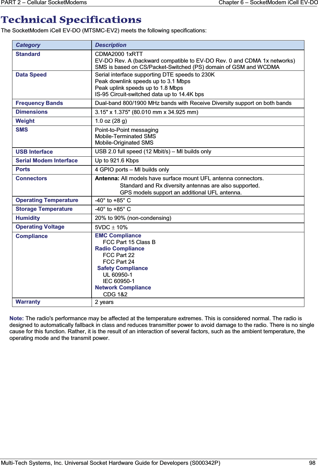
Multi Tech Systems 92U09J14829 Universal Socket Modem User Manual Universal Socket Hardware Guide
Multi Tech Systems Inc Universal Socket Modem Universal Socket Hardware Guide
UserManual.wiki
>
Multi Tech Systems
>
92U09J14829 User Manual
Users Manual
Navigation menu
Upload a User Manual
Namespaces
Wiki Guide
HTML
PDF
Info
Views
User Manual
Discussion / Help
Navigation
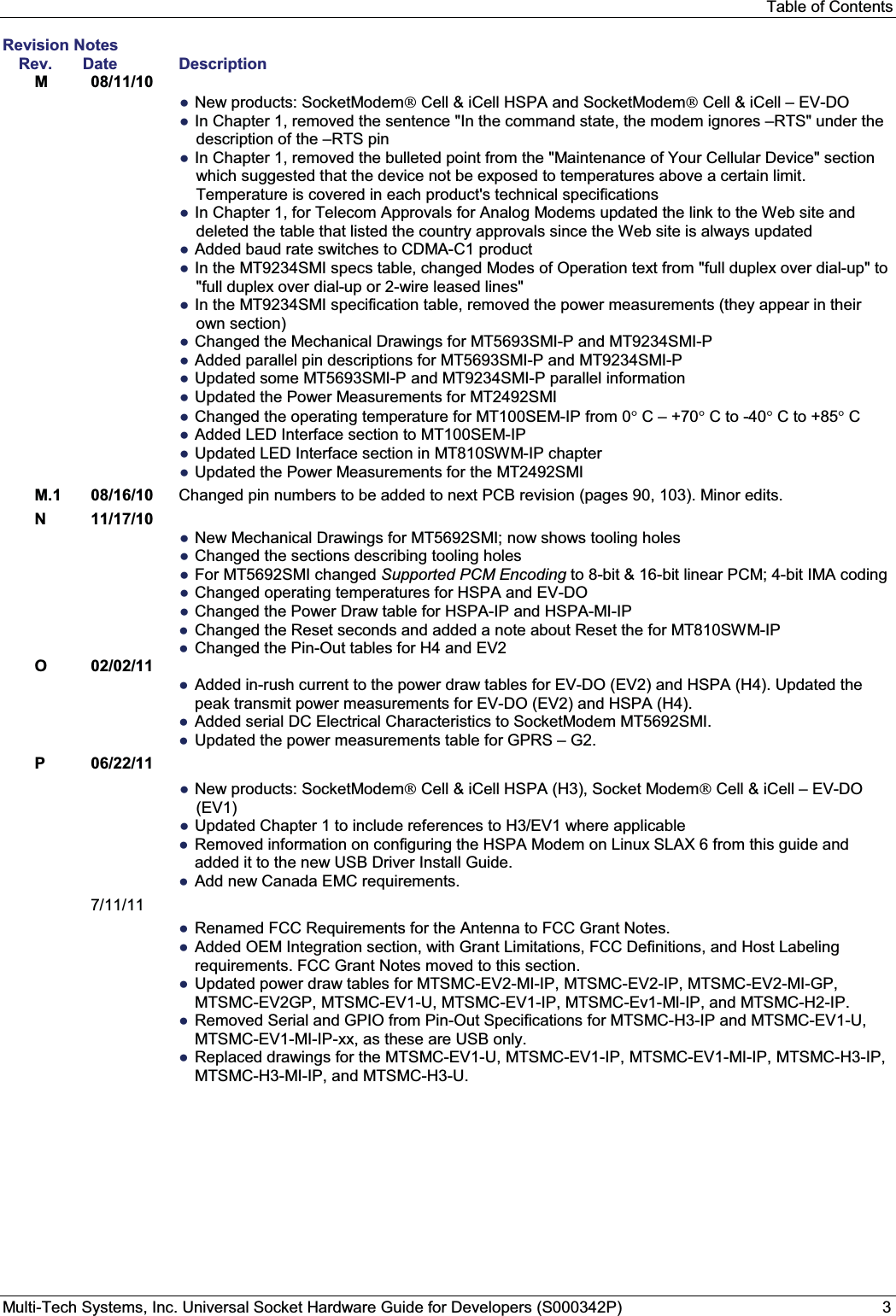
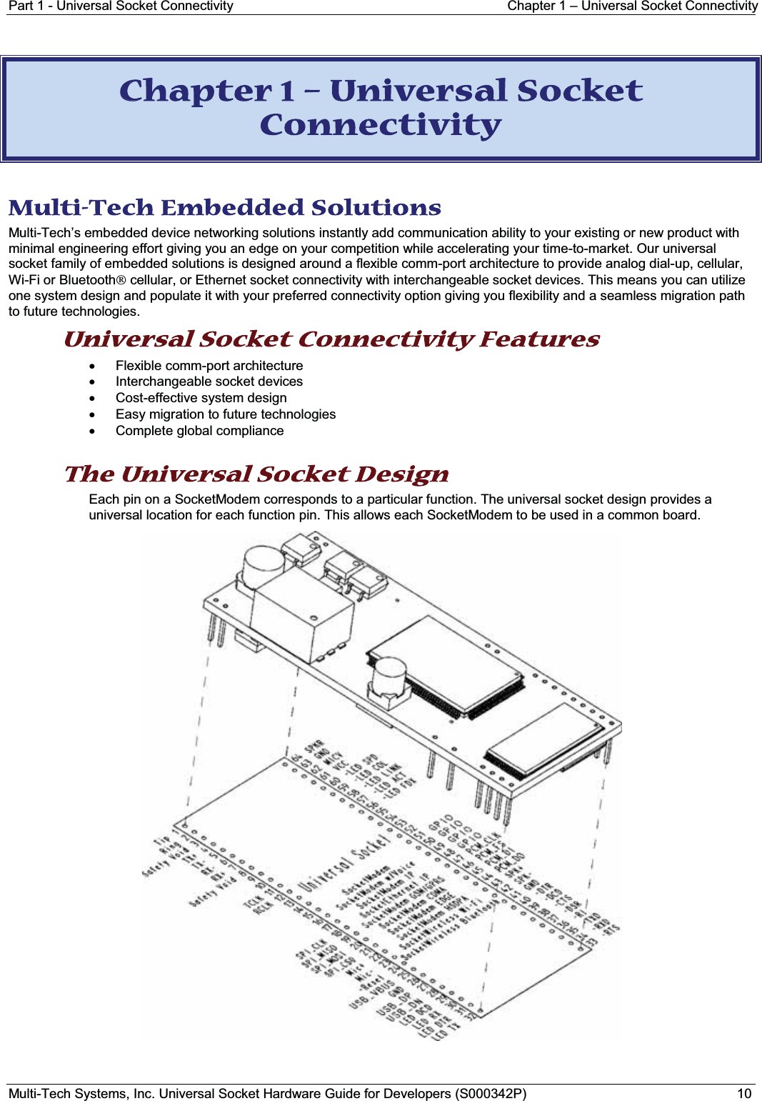
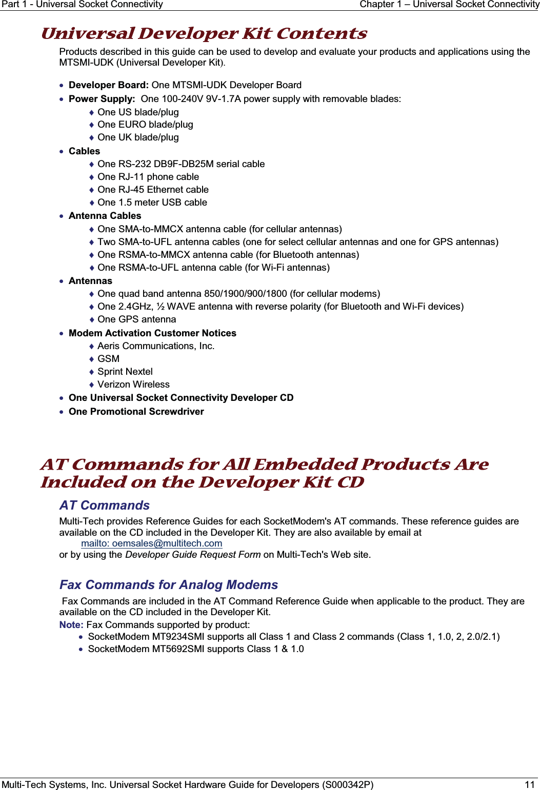
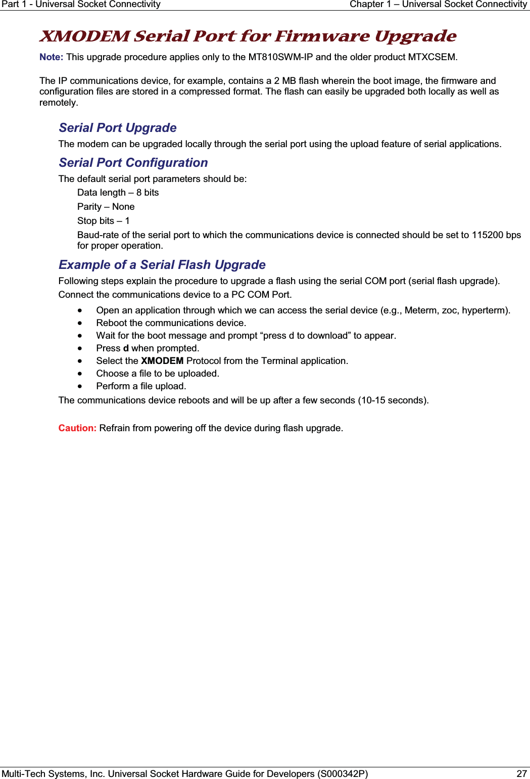
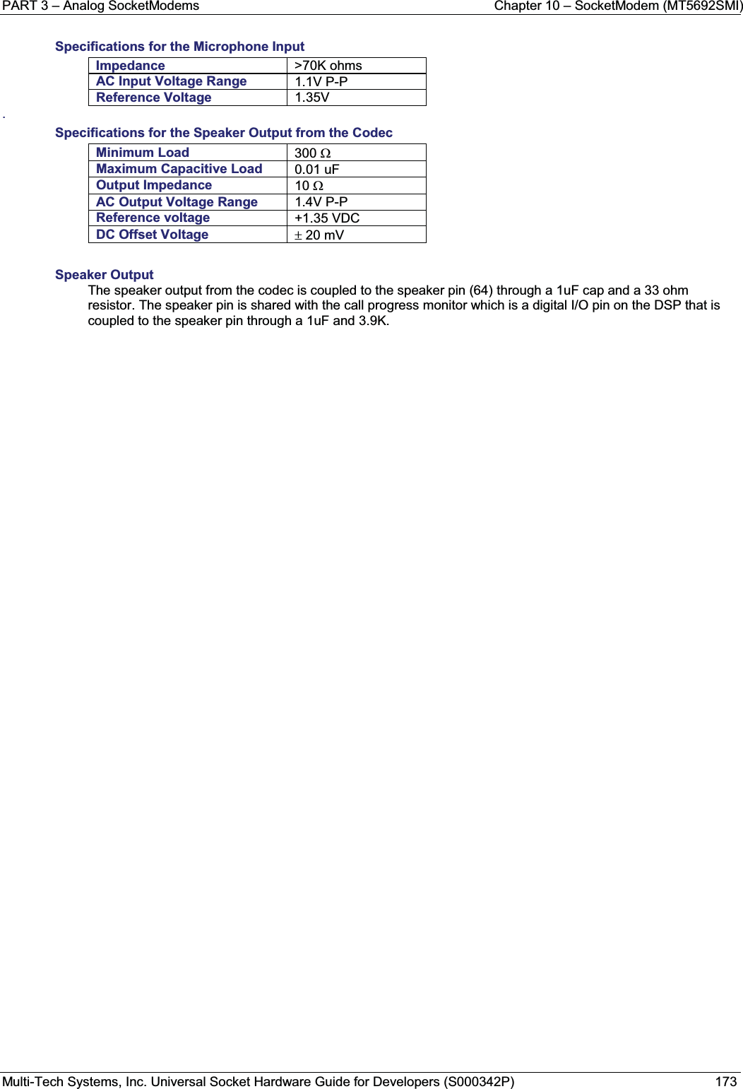
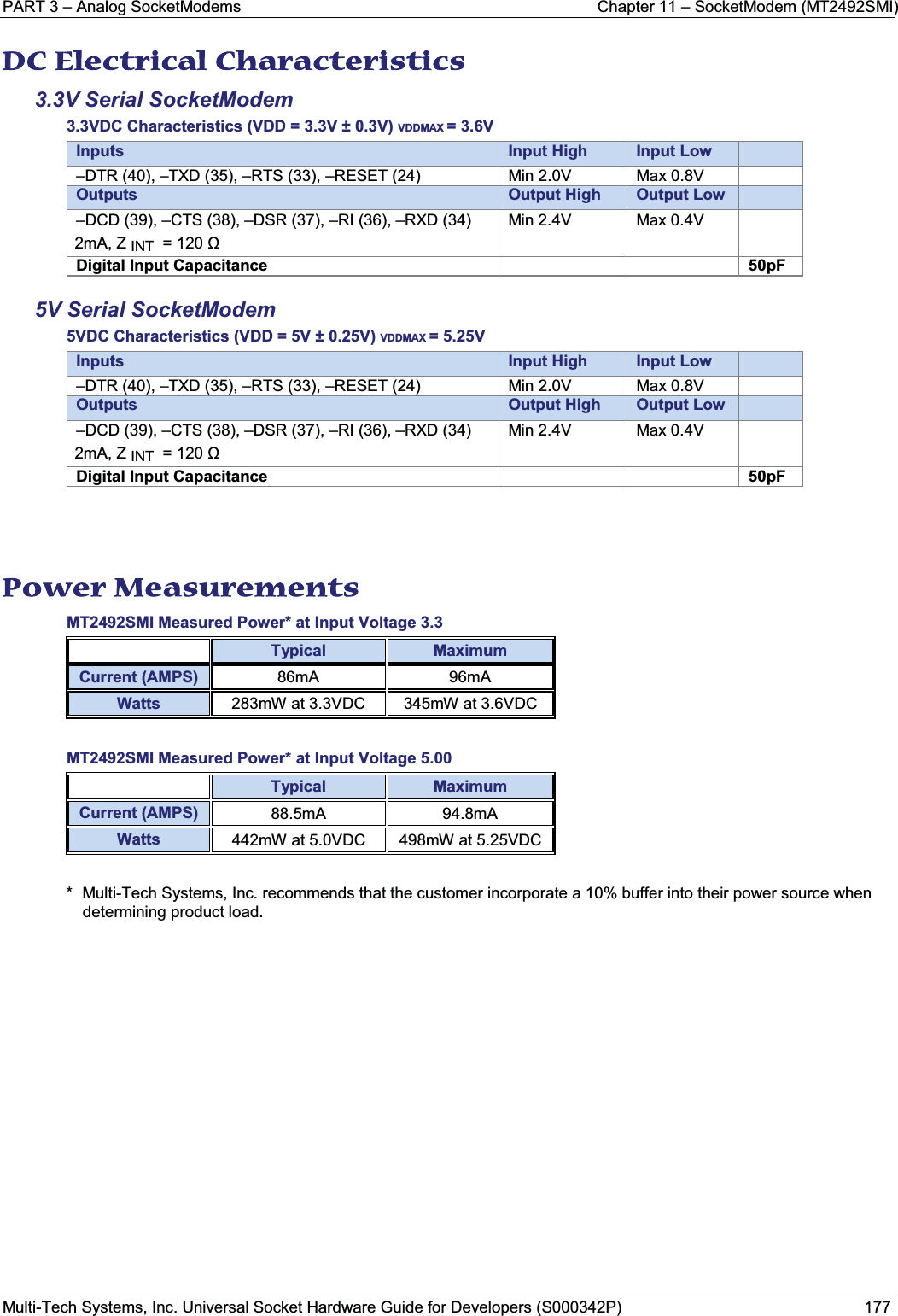
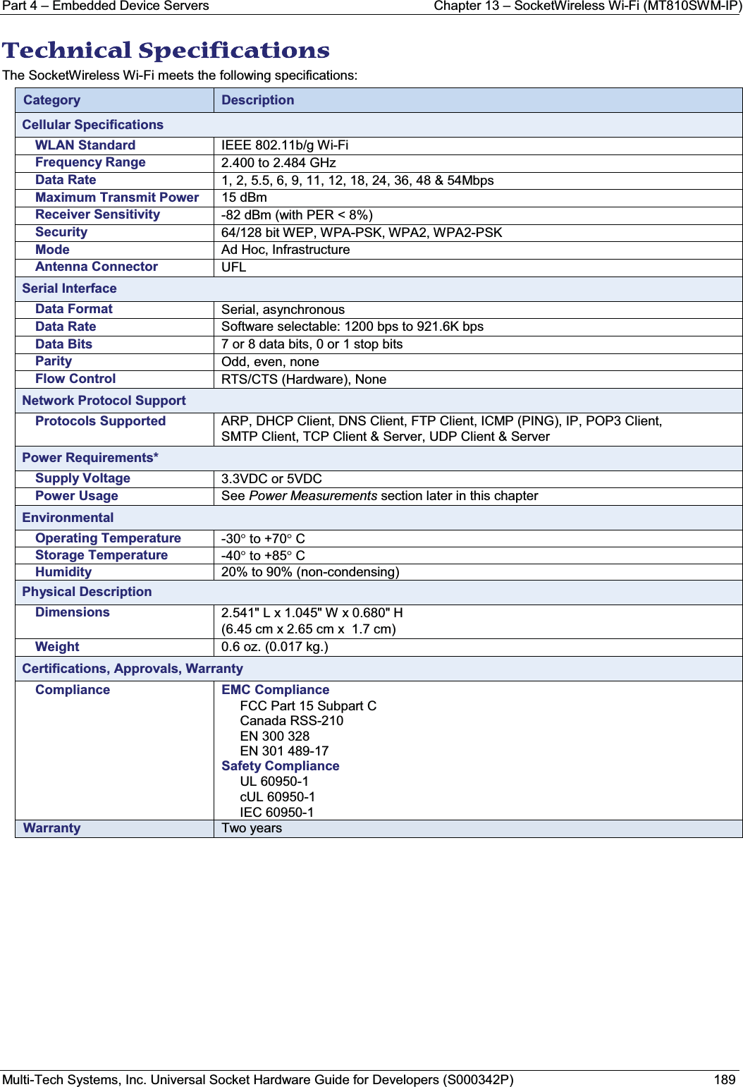
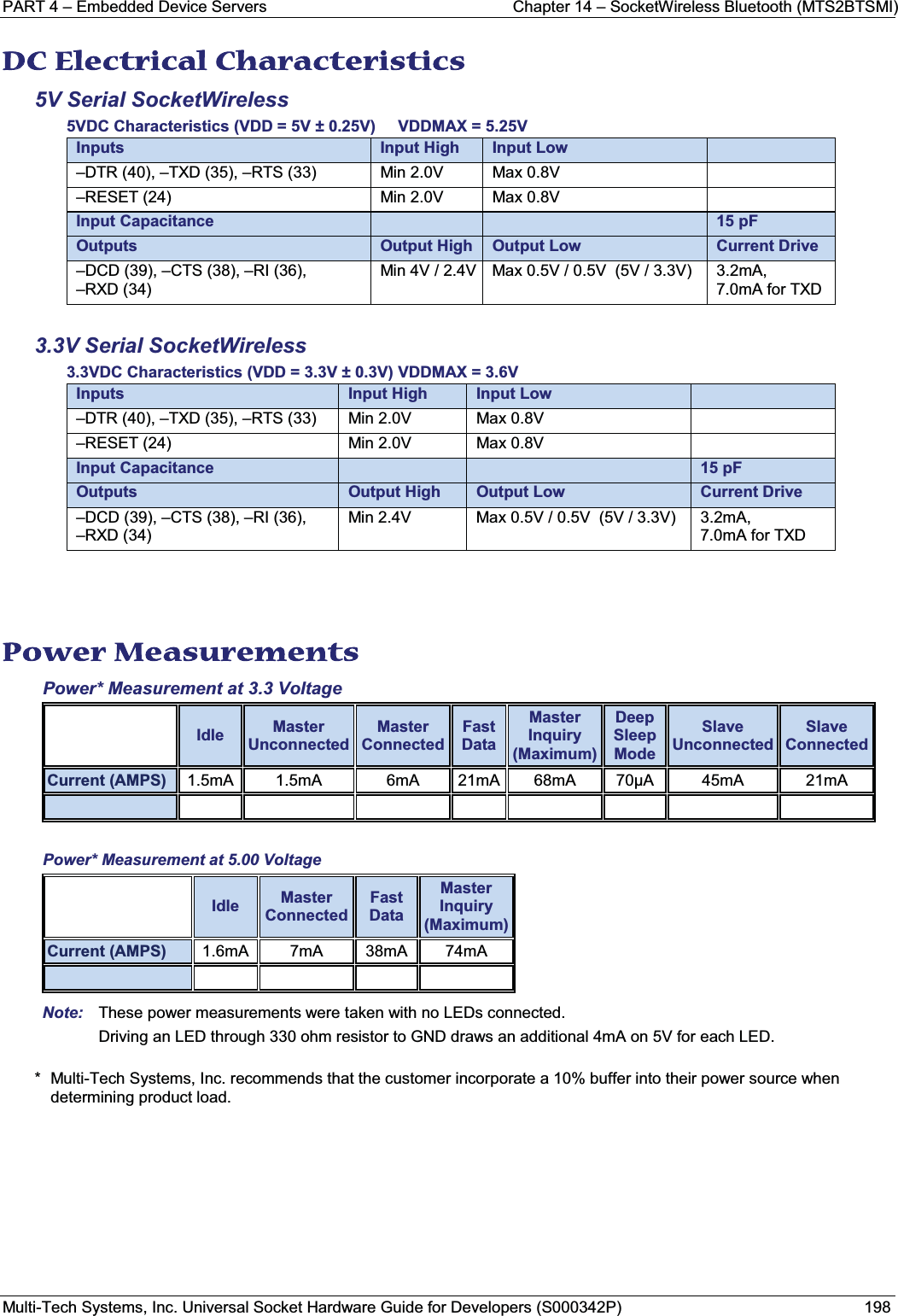
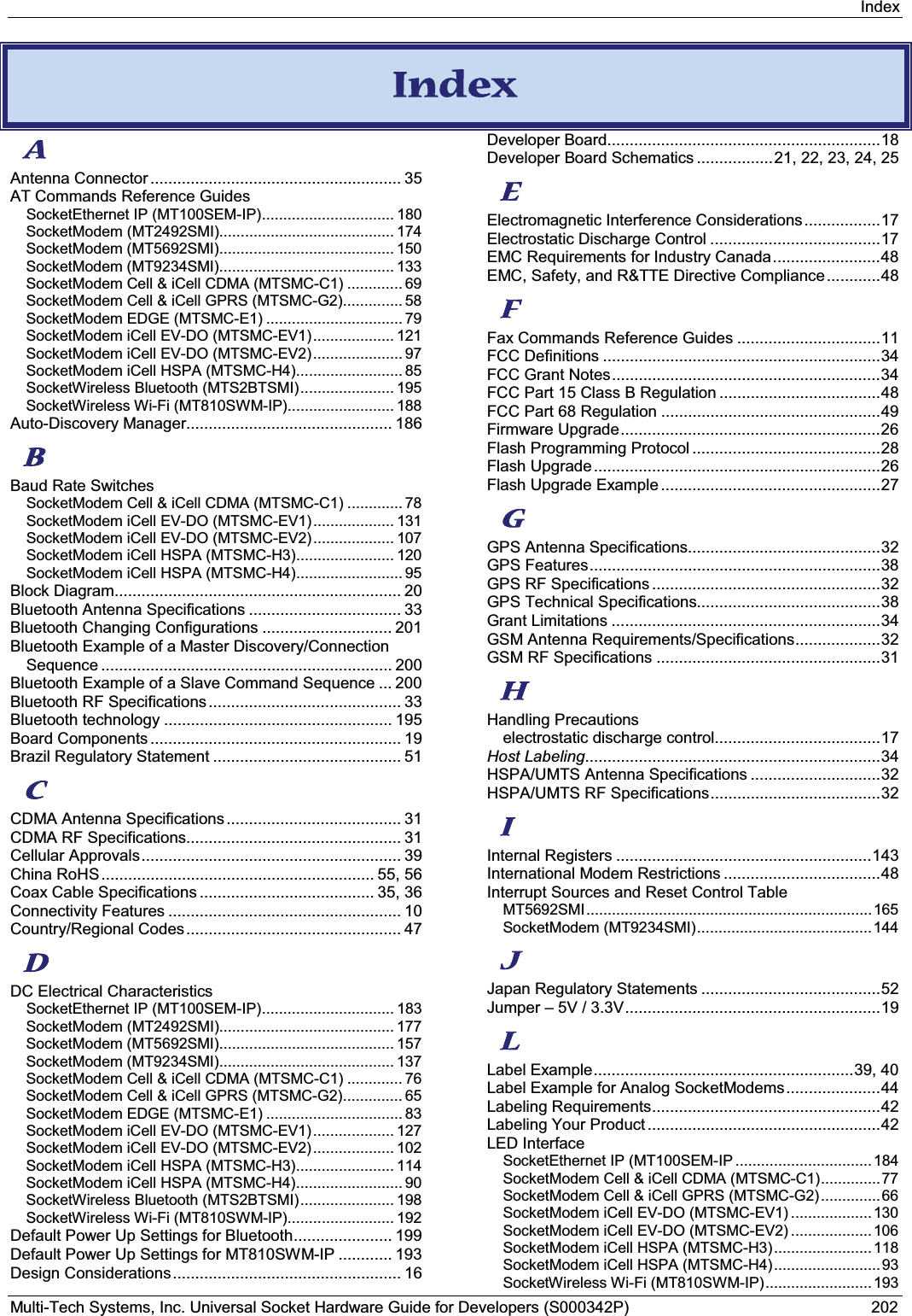
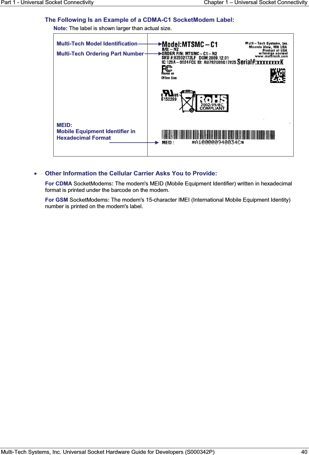
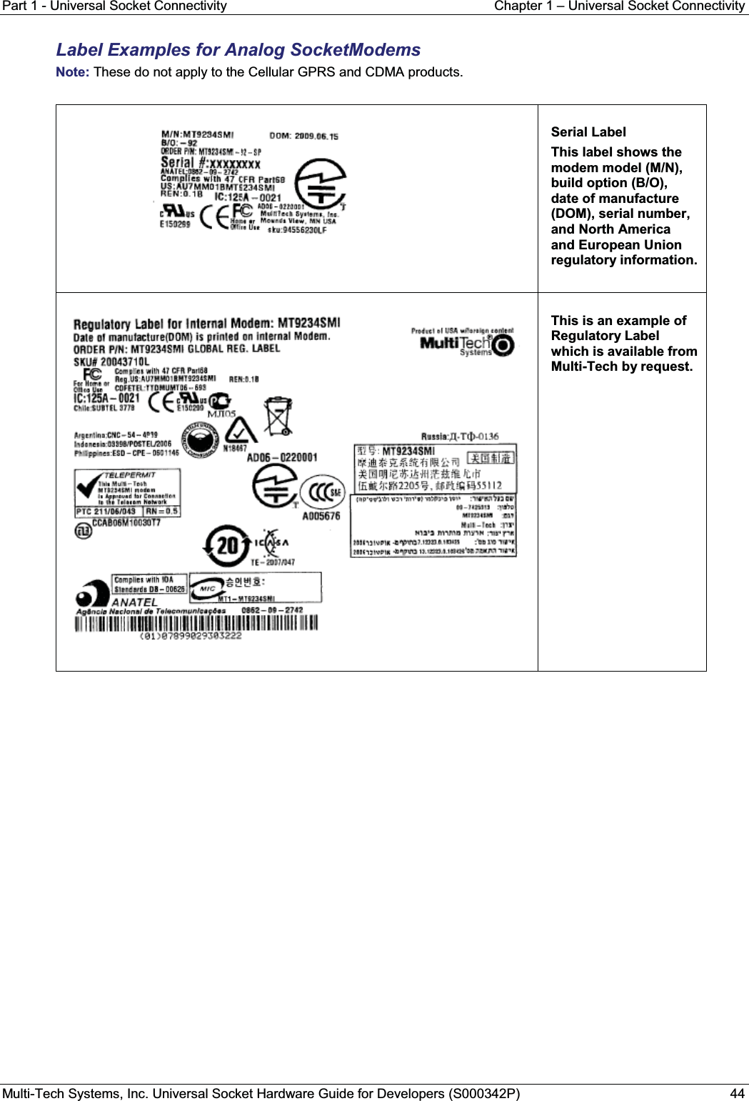
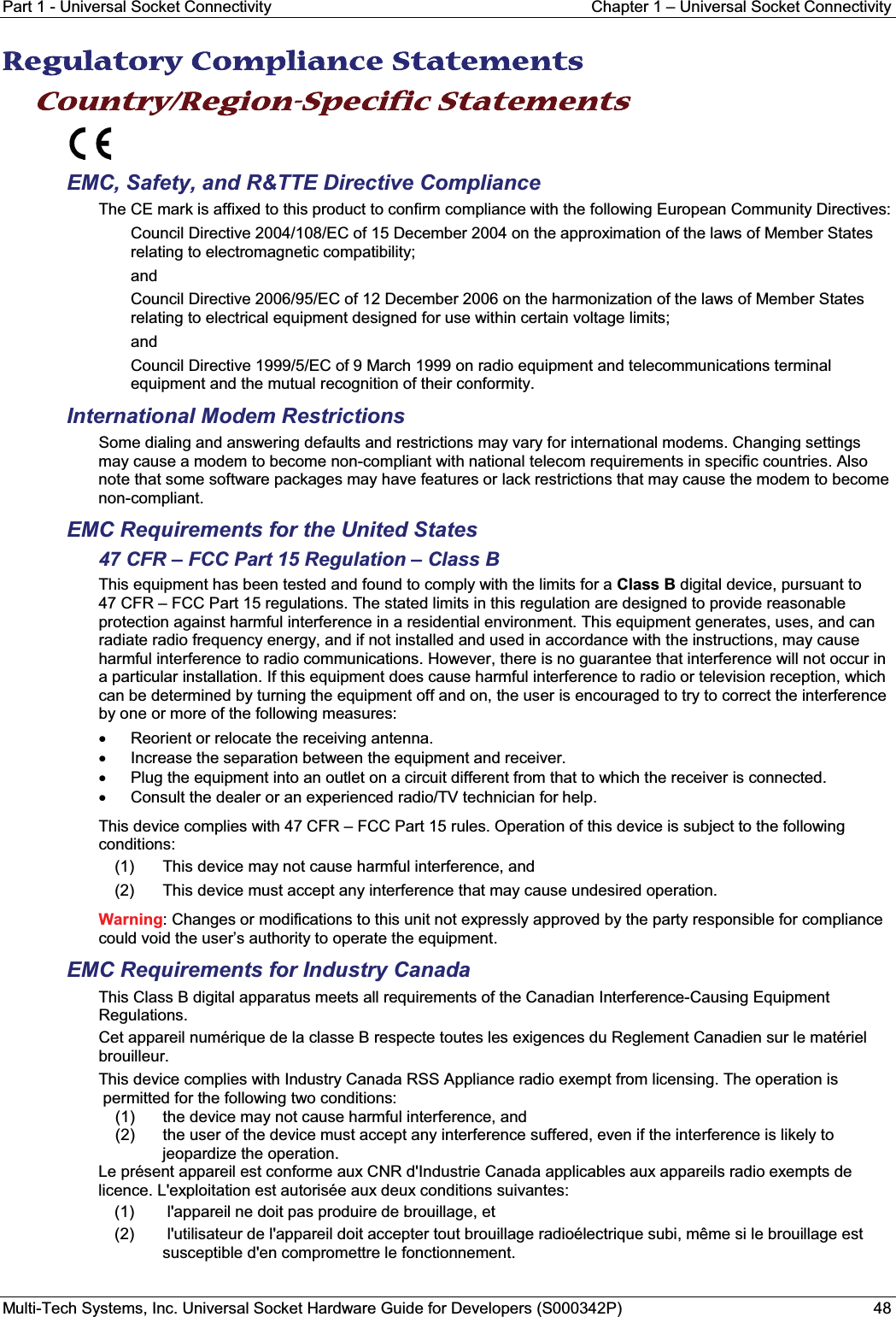
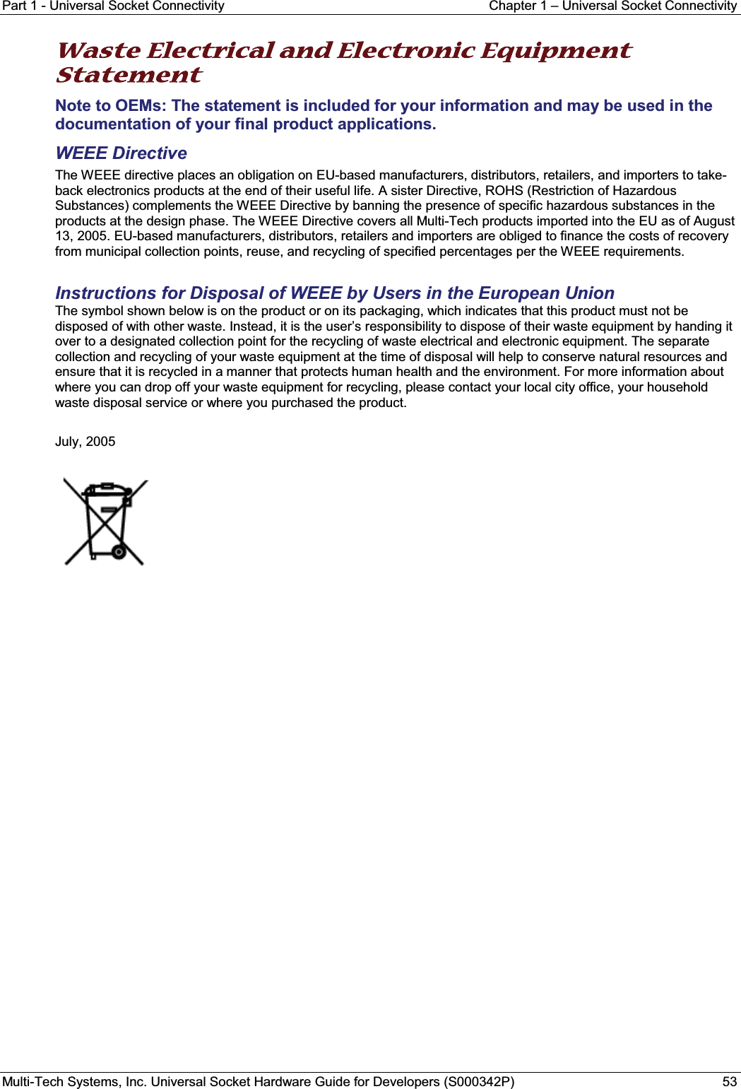
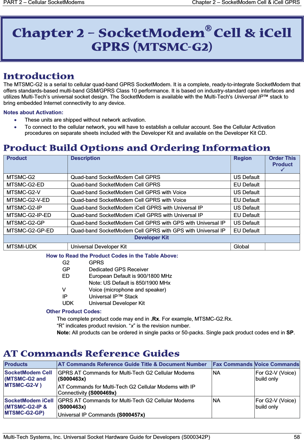
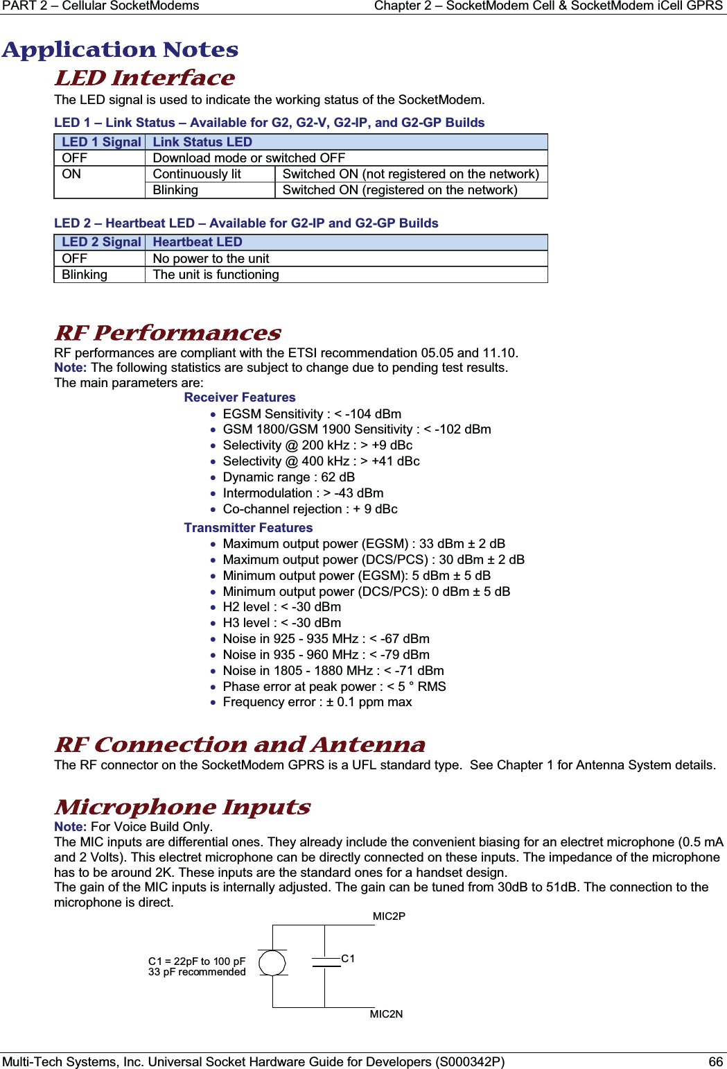
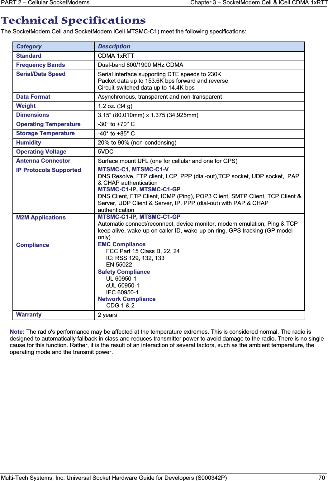
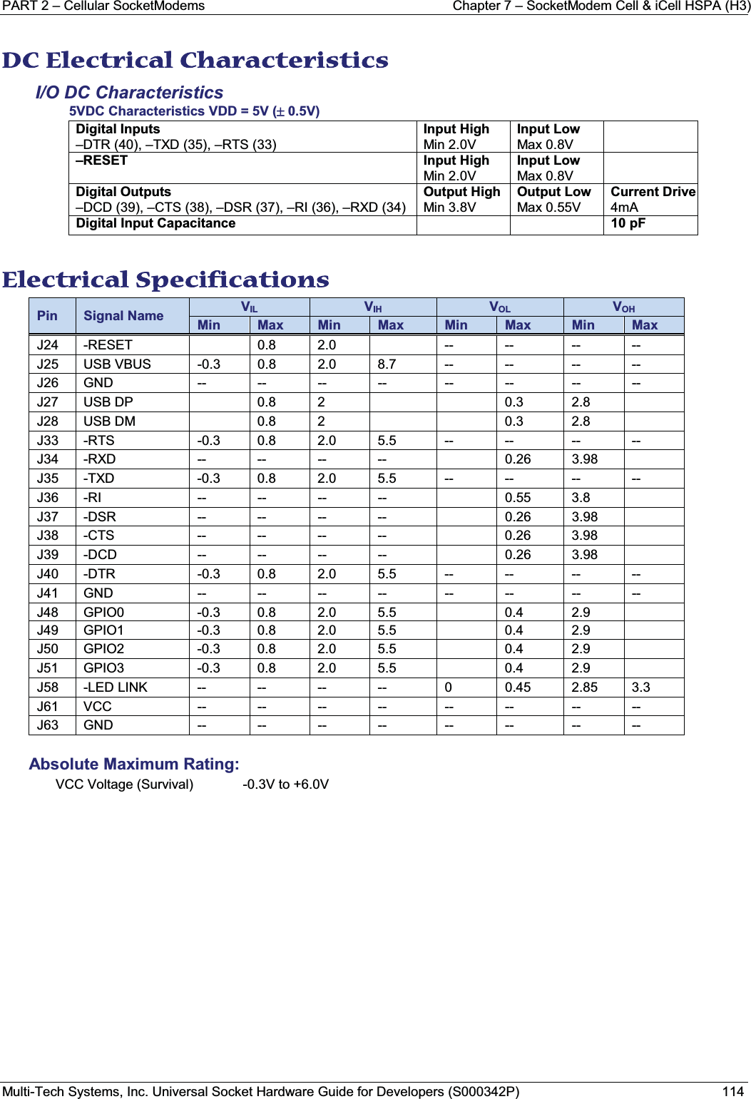
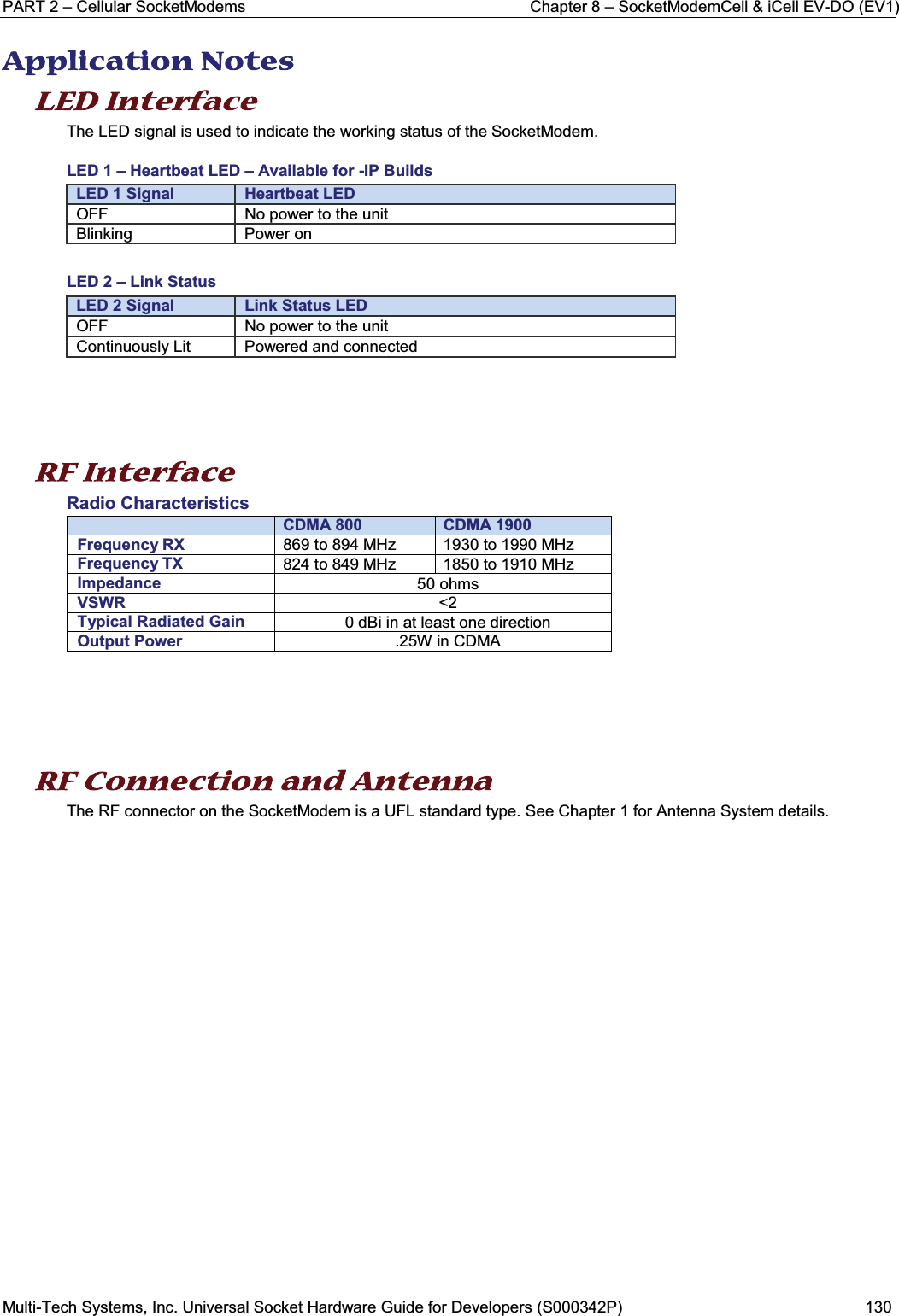
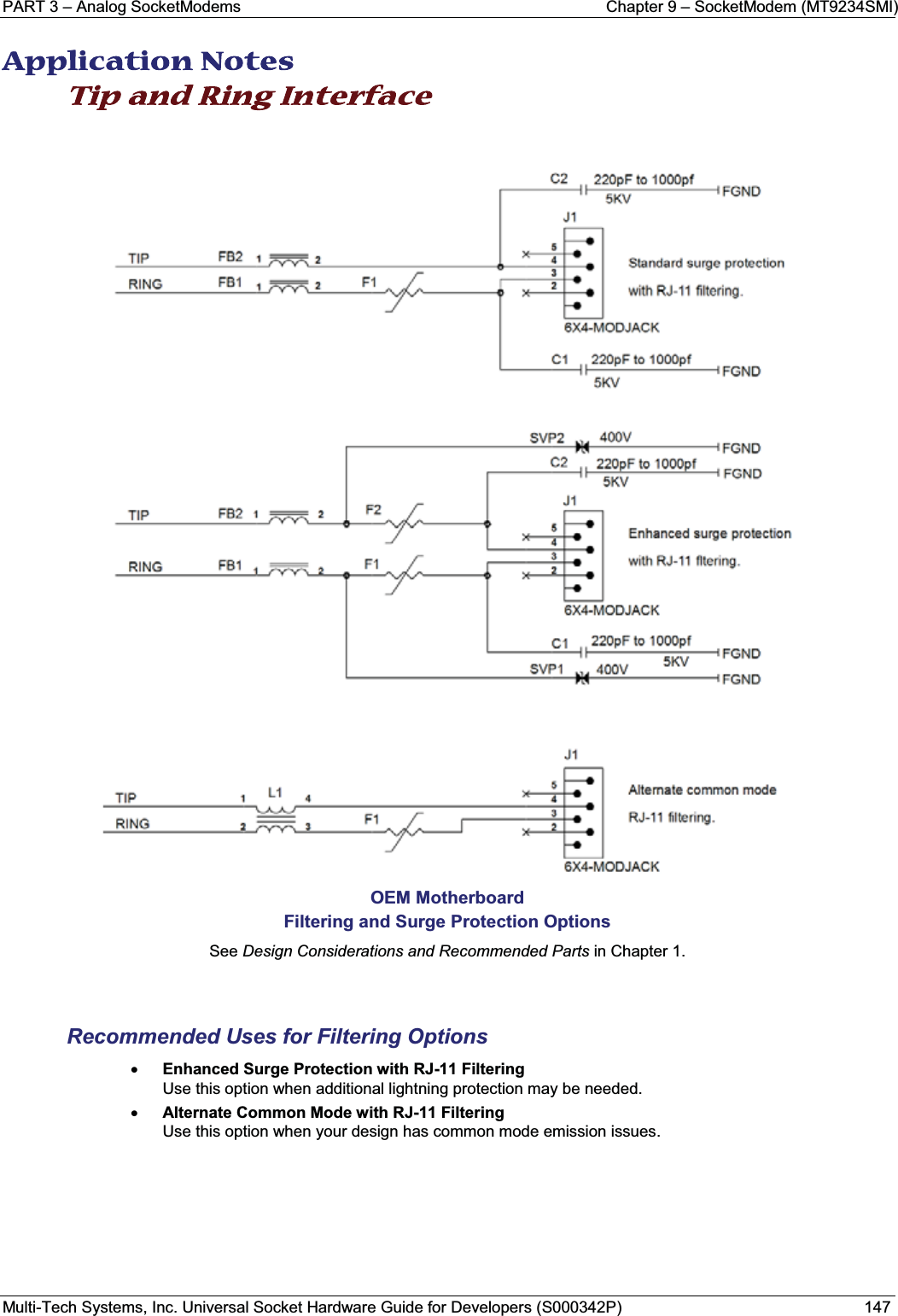
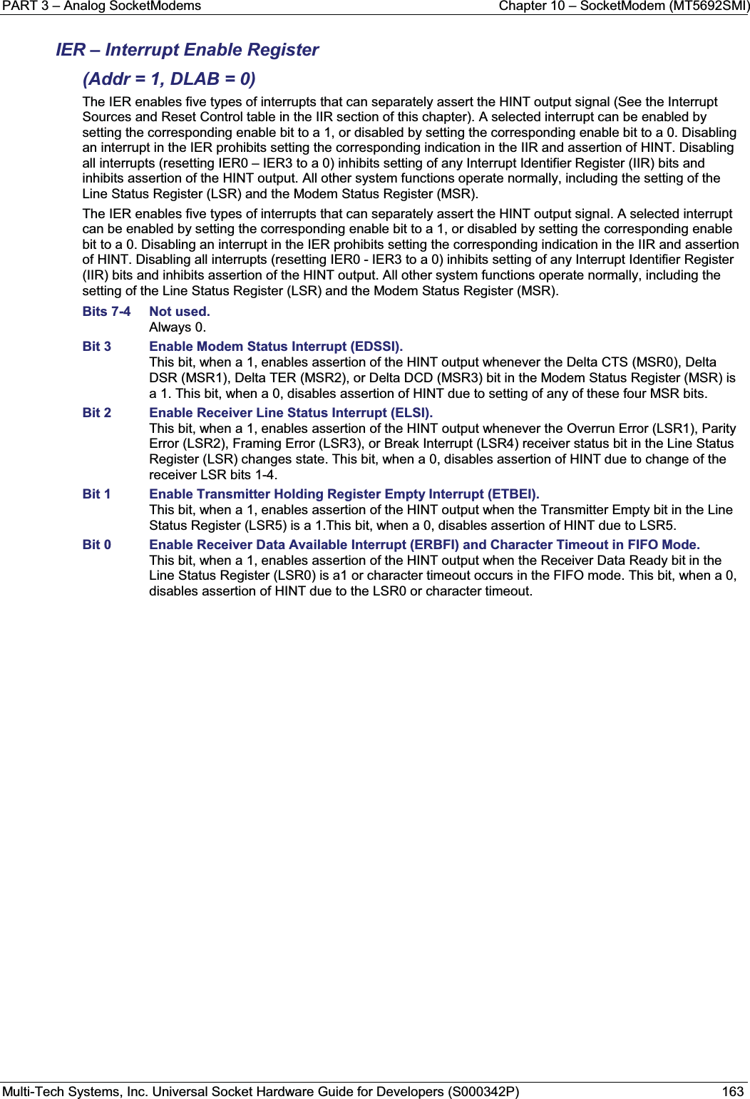
![Part 1 - Universal Socket Connectivity Chapter 1 – Universal Socket ConnectivityMulti-Tech Systems, Inc. Universal Socket Hardware Guide for Developers (S000342P) 28MMulti-Tech Systems, Inc. Flash Programming Protocol This information is provided exclusively for the users of Multi-Tech Systems, Inc. SocketModems, specifically the MT9234SMI.Multi-Tech Systems, Inc. SocketModem owners have the right to use, modify, and incorporate this code into other products provided they include the Multi-Tech Systems, Inc. notice and the associated copyright notice with any such product.Copyright (C) Multi-Tech Systems, Inc. 1995All Right ReservedThe flash programming protocol is provided "AS IS” without warranty.Important: When interacting with the boot code, it is possible to make the modem inoperable. Use extreme caution.Programming the ModemThere are two ways to start flash programming a modem. It can be programmed1. From “AT” mode2. When the modem powers up. The following table shows how a modem is programmed.DTE Modem CommentsAT*FS\r This effectively “restarts” the modem so that it enters the boot code.Handshake SequenceM’s Many M’s are sent (10 milliseconds apart) at 19200 baud.This is where the handshake starts if the modem is just powered up.U U is sent at 19200 baud if M’s are received within 100 milliseconds of power up. If the M’s are not received within 100 milliseconds, then the modem starts up normally. If the AT*FS command is used, then you have 1 second (1000mS) to perform the handshake.D Sent at 19200 baud.M M if can receive at 9600/19200/38400/57600/115200I|J|K|L|M I if modem will be programmed at 9600J if modem will be programmed at 19200K if modem will be programmed at 38400L if modem will be programmed at 57600M if modem will be programmed at 115200\r\nOK\r\n Modem is ready to be programmedProgram Sequence:DTE Modem CommentsATFLP\r Request to the modem to programG Modem is ready for next program packet[Length High]High byte of data packet length[Length Low] Low byte of data packet lengthPacket lengths can be up to 4096 bytes in size for most boot code versions [Address High]High byte of program address[Address Middle]Middle byte of program address[Address Low]Low byte of program addressAddresses are 3 byte values with a range of 00000h-FFFFFh [Data Bytes] These are the data bytes to be programmed at the address specified above. They must be the same number of bytes as specified above. [Checksum] This checksum is generated by exclusive ORing together all of the Data Bytes (do not include the Length or Address bytes in that calculation).\nOK\r\n\nERROR\r\nIf bytes are programmed and verified.If verify fails or checksum is bad.Retry the block 3 times on an ERROR.…. ….More of the above sequence until all the data bytes have been sent to the modem.ATFLEND\r This ends programming and restarts the modem.](https://usermanual.wiki/Multi-Tech-Systems/92U09J14829/User-Guide-1513497-Page-28.png)
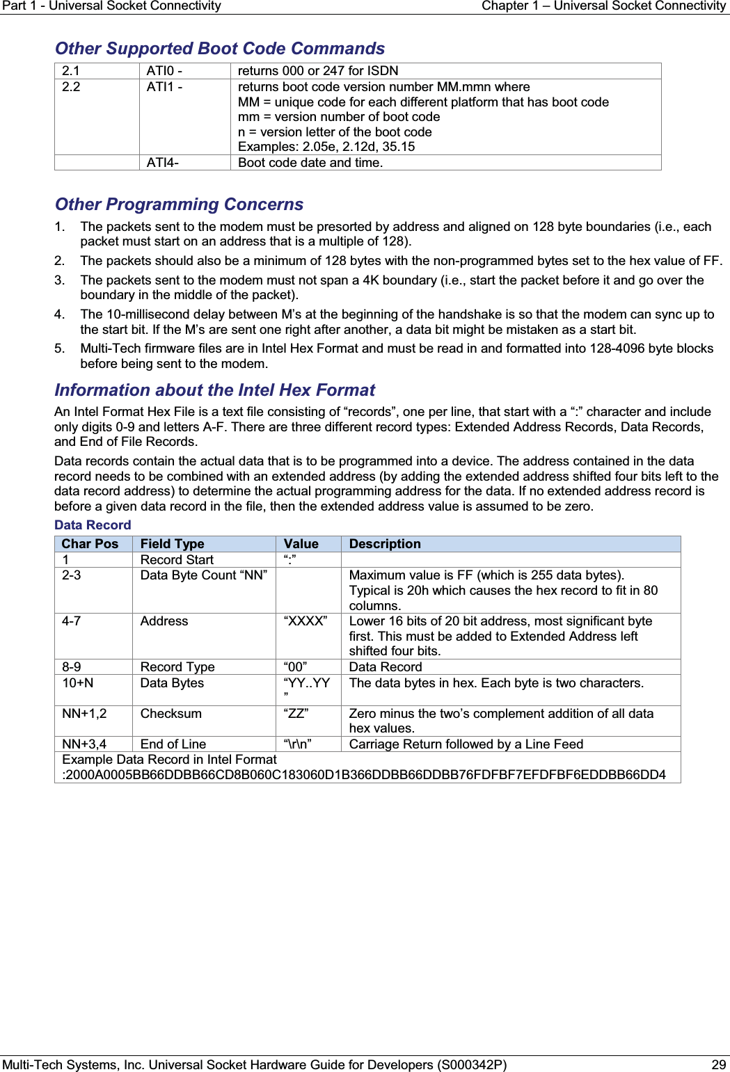
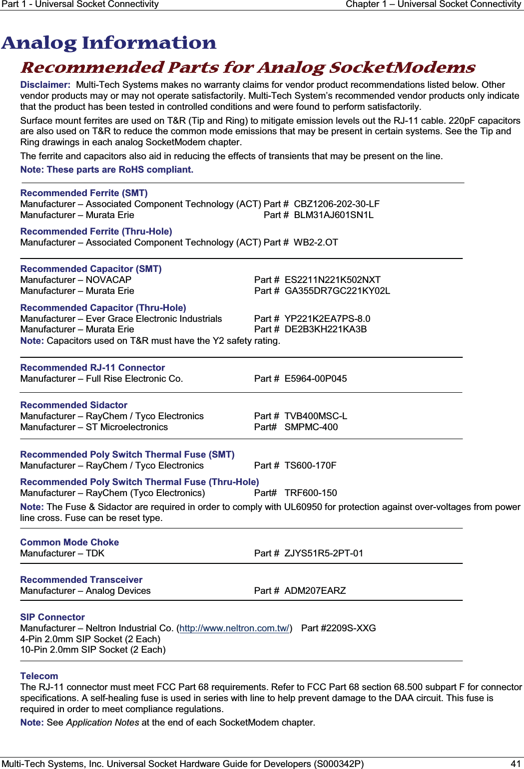
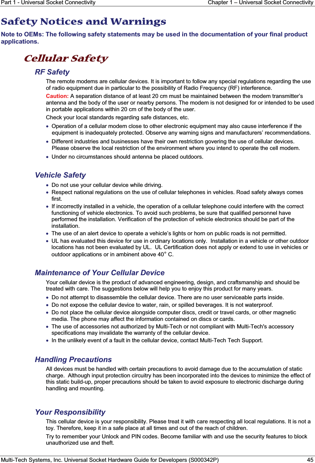
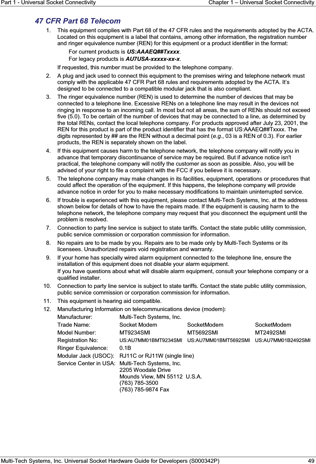

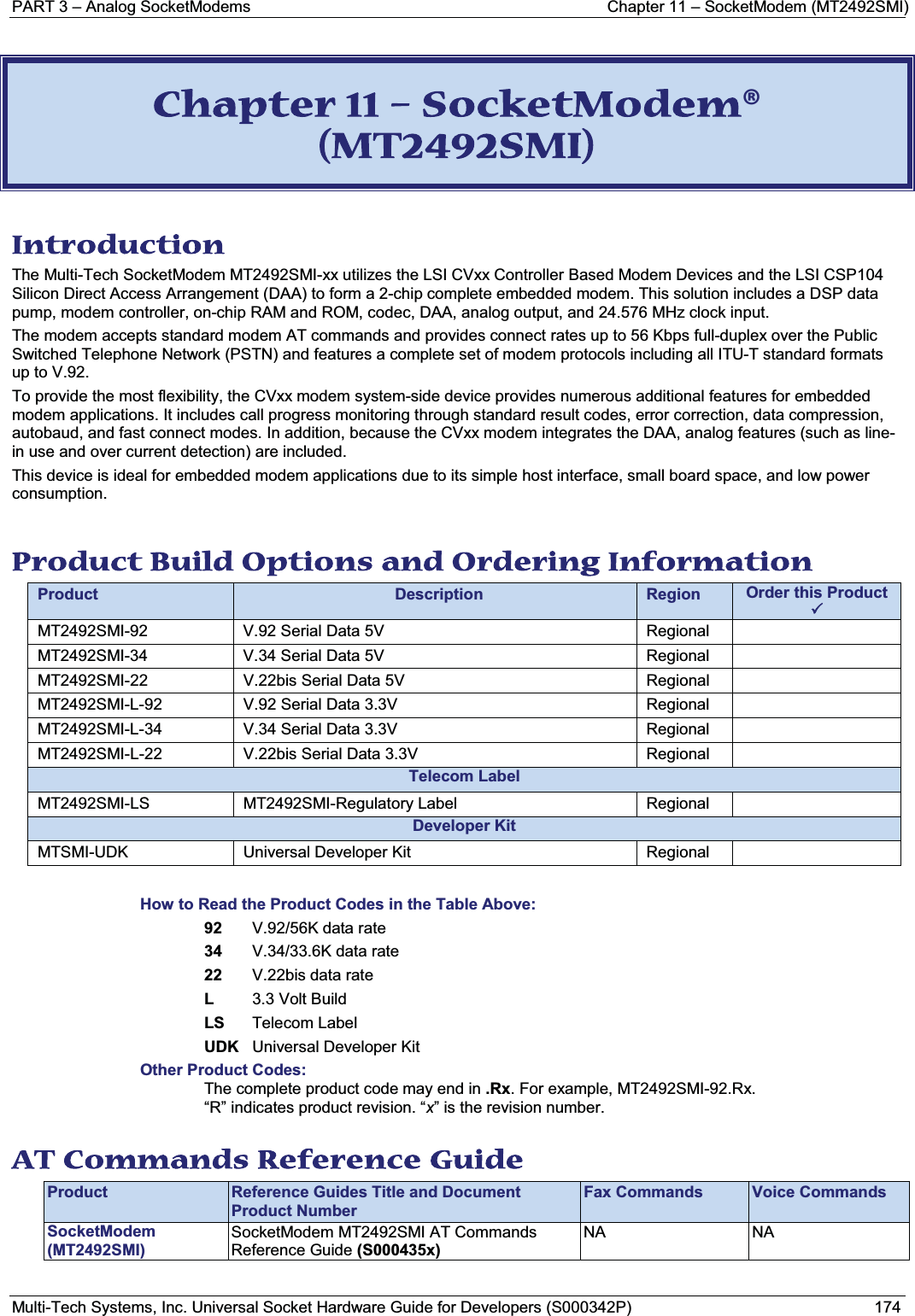
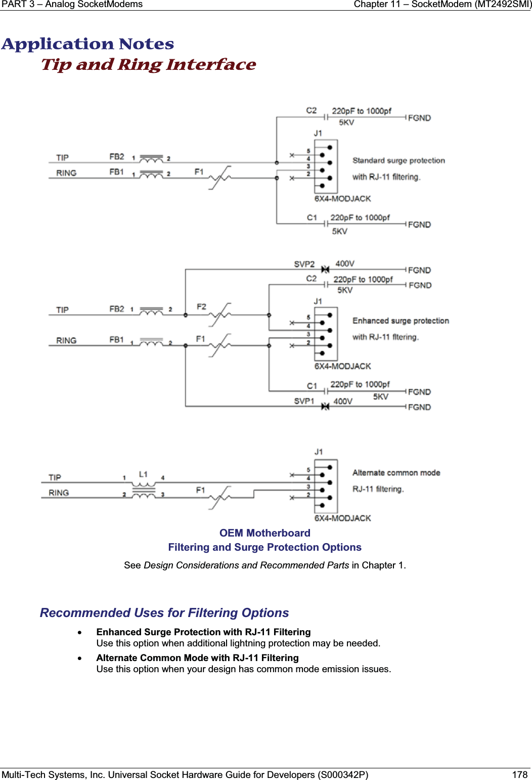
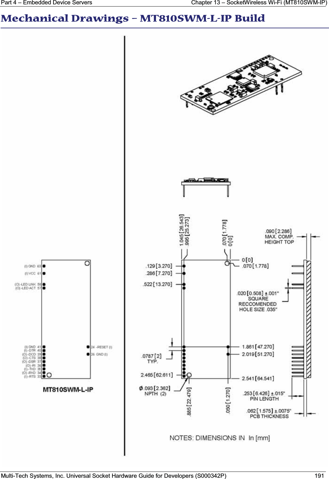
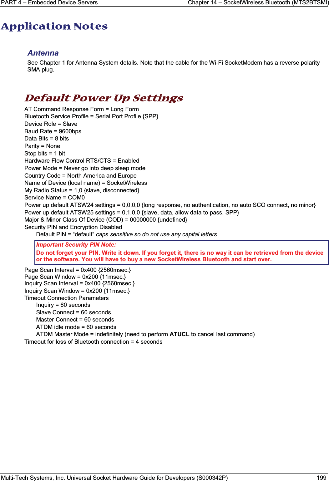
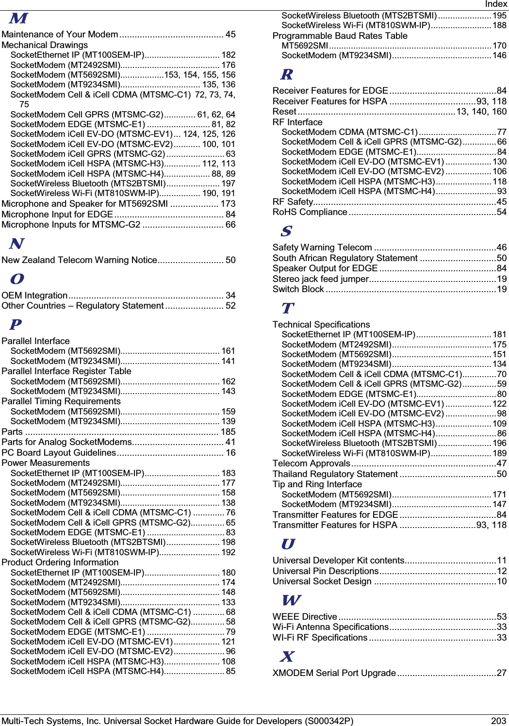
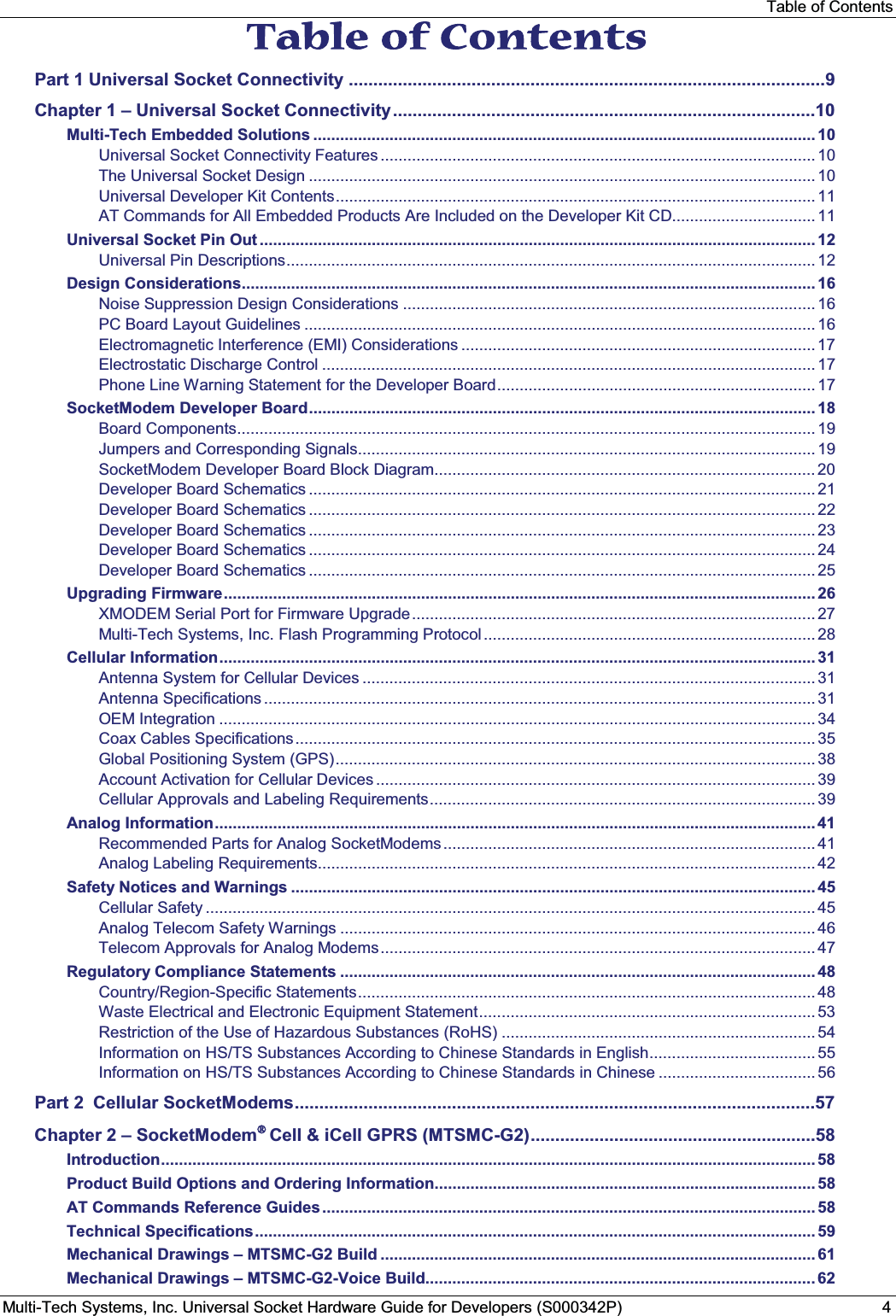
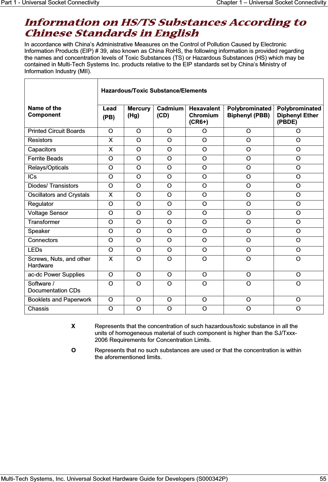
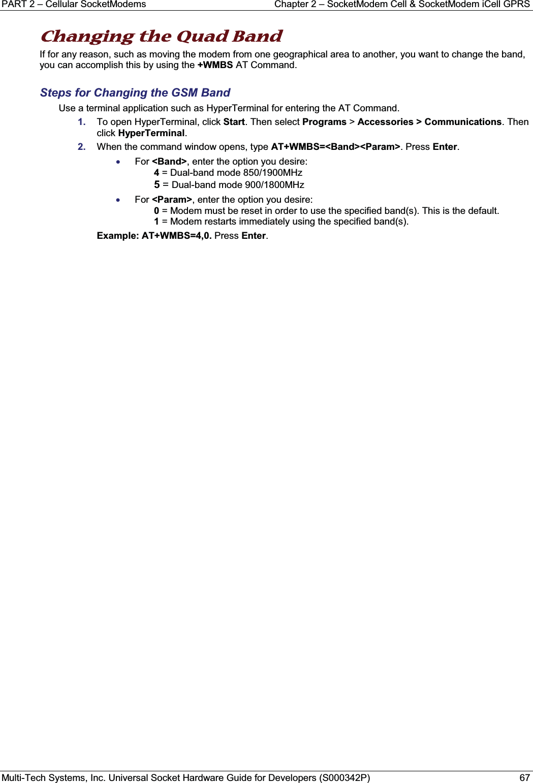
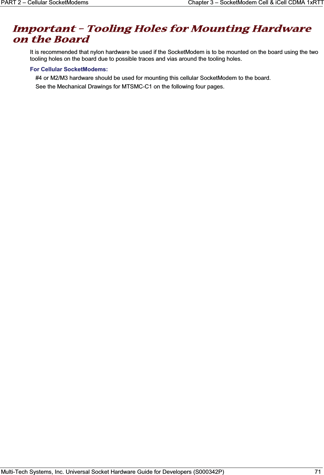
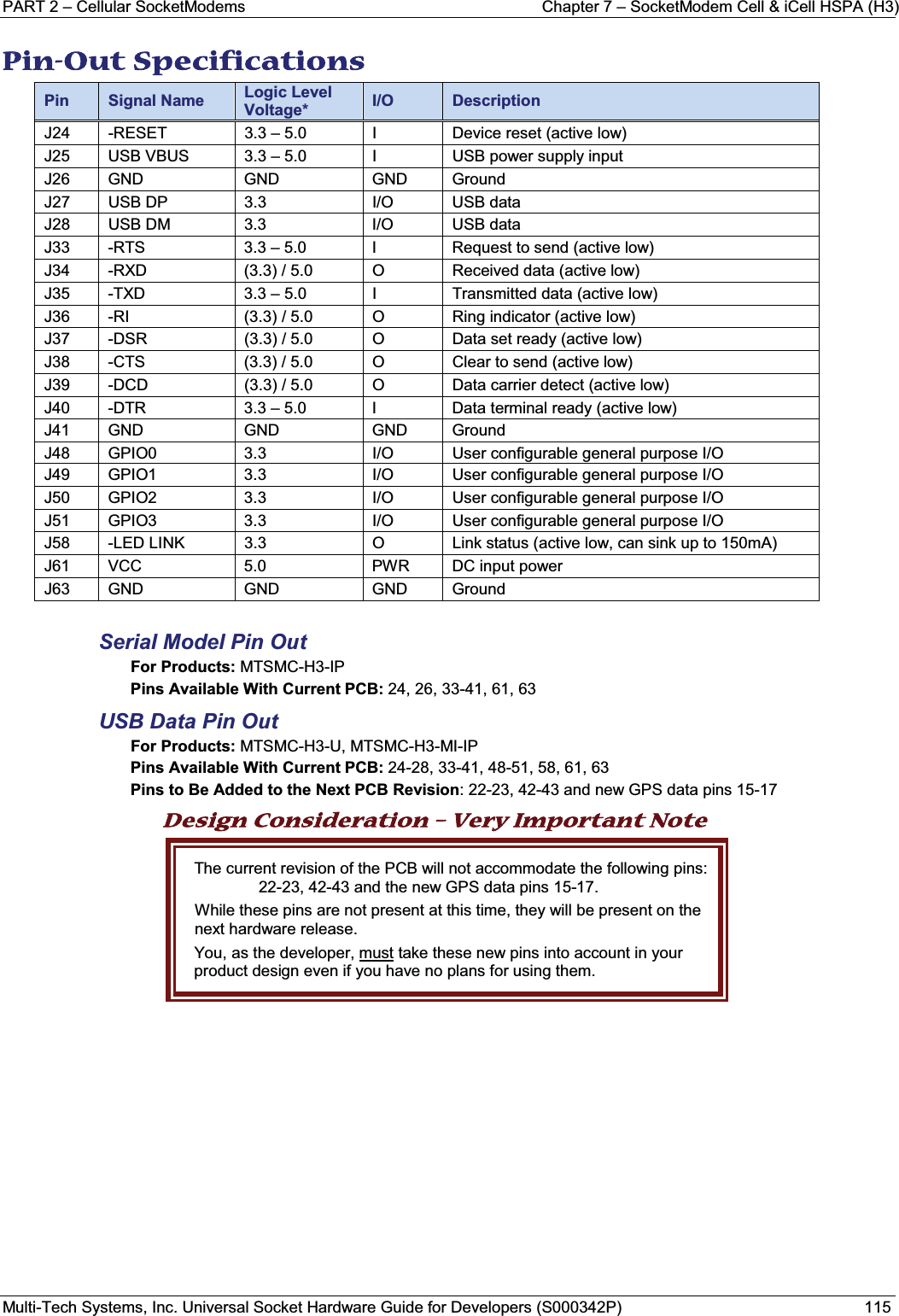
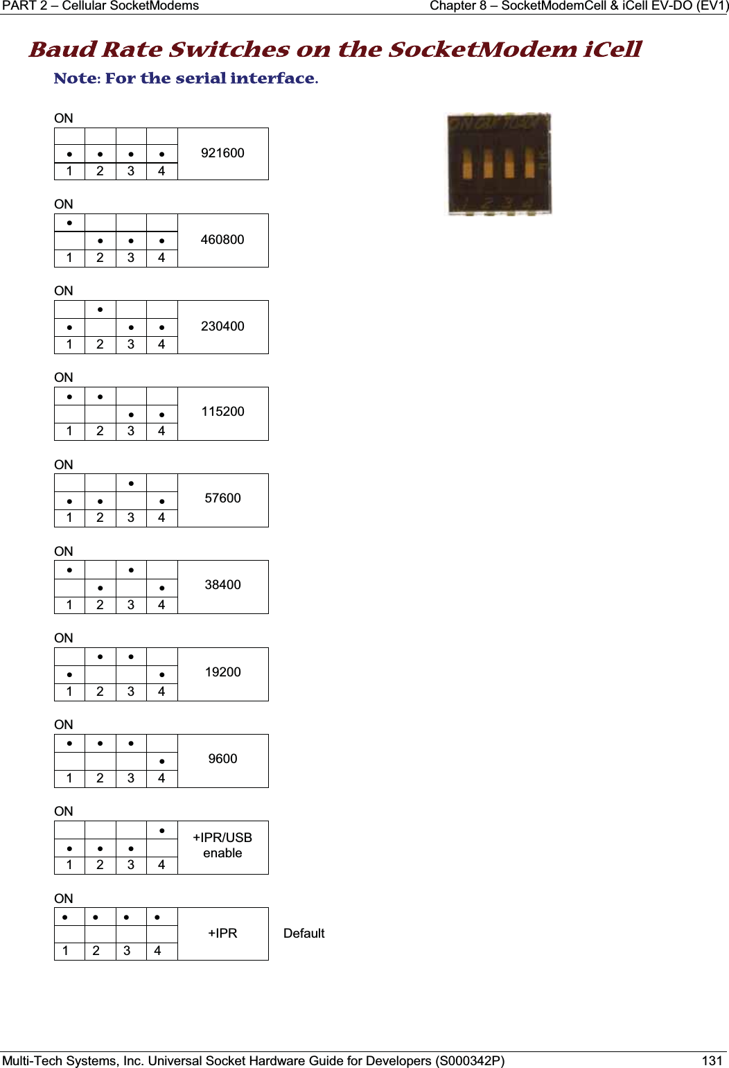
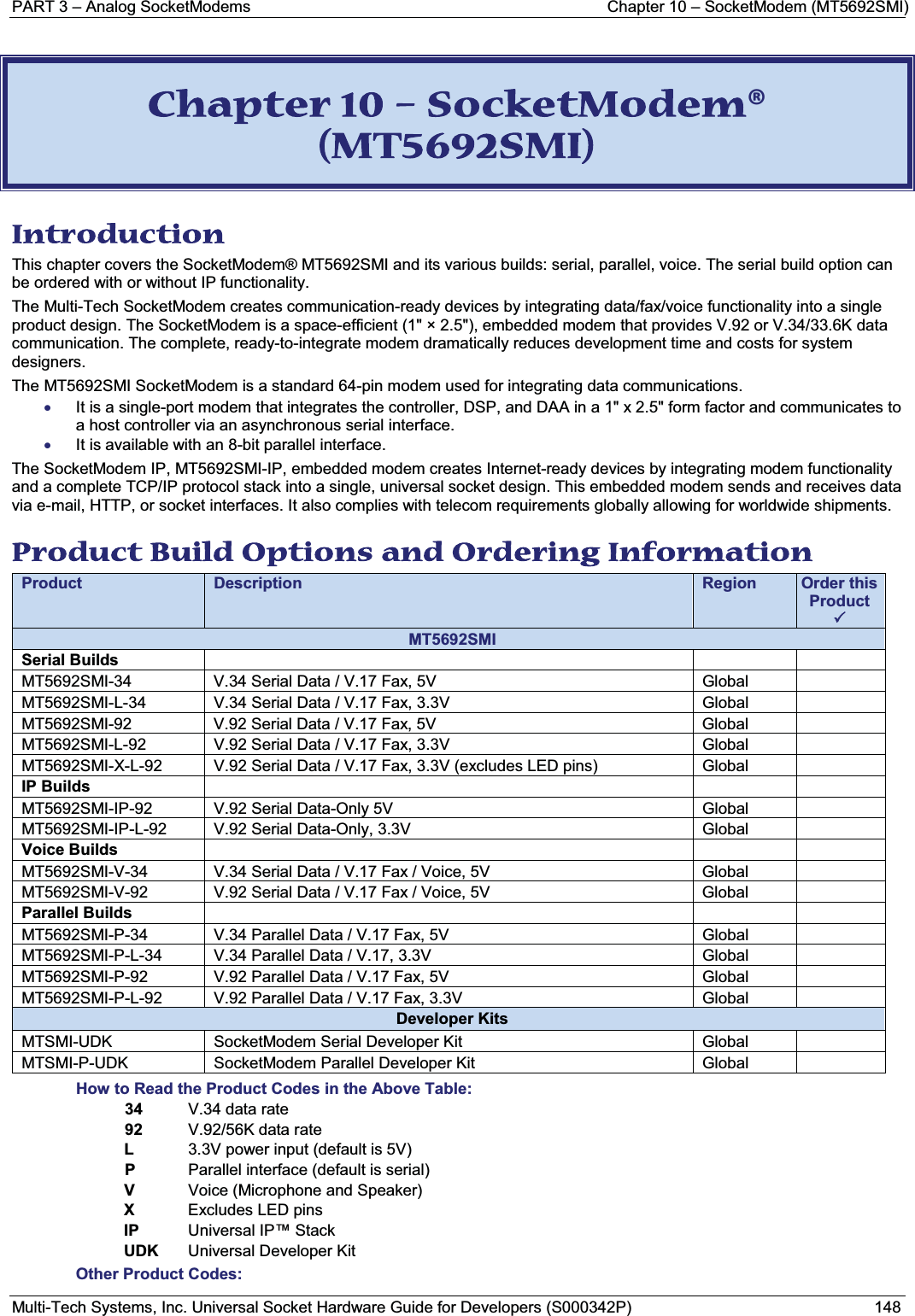
![Part 1 - Universal Socket Connectivity Chapter 1 – Universal Socket ConnectivityMulti-Tech Systems, Inc. Universal Socket Hardware Guide for Developers (S000342P) 54RRestriction of the Use of Hazardous Substances (RoHS) Multi-Tech Systems, Inc.Certificate of Compliance 2002/95/ECMulti-Tech Systems Inc. confirms that its embedded products now comply with the chemical concentration limitations set forth in the directive 2002/95/EC of the European Parliament (Restriction Of the use of certain Hazardous Substances in electrical and electronic equipment - RoHS)These Multi-Tech Systems, Inc. products do not contain the following banned chemicals:Lead, [Pb] < 1000 PPMMercury, [Hg] < 1000 PPMHexavalent Chromium, [Cr+6] <1000 PPMCadmium, [Cd] < 100 PPMPolybrominated Biphenyl, [PBB] < 1000 PPMPolybrominated Diphenyl Ether, [PBDE] < 1000 PPMMoisture Sensitivity Level (MSL) =1 Maximum Soldering temperature = 260C (wave only)Notes:1. Lead usage in some components is exempted by the following RoHS annex; therefore, higher lead concentration would be found in some SocketModems (>1000ppm).a. Lead in high melting temperature type solders (i.e., tin-lead solder alloys containing more than 85% lead).b. Lead in electronic ceramic parts (e.g., piezoelectronic devices).2. Moisture Sensitivity Level (MSL) – Analysis is based on the components/material used on the board.](https://usermanual.wiki/Multi-Tech-Systems/92U09J14829/User-Guide-1513497-Page-54.png)
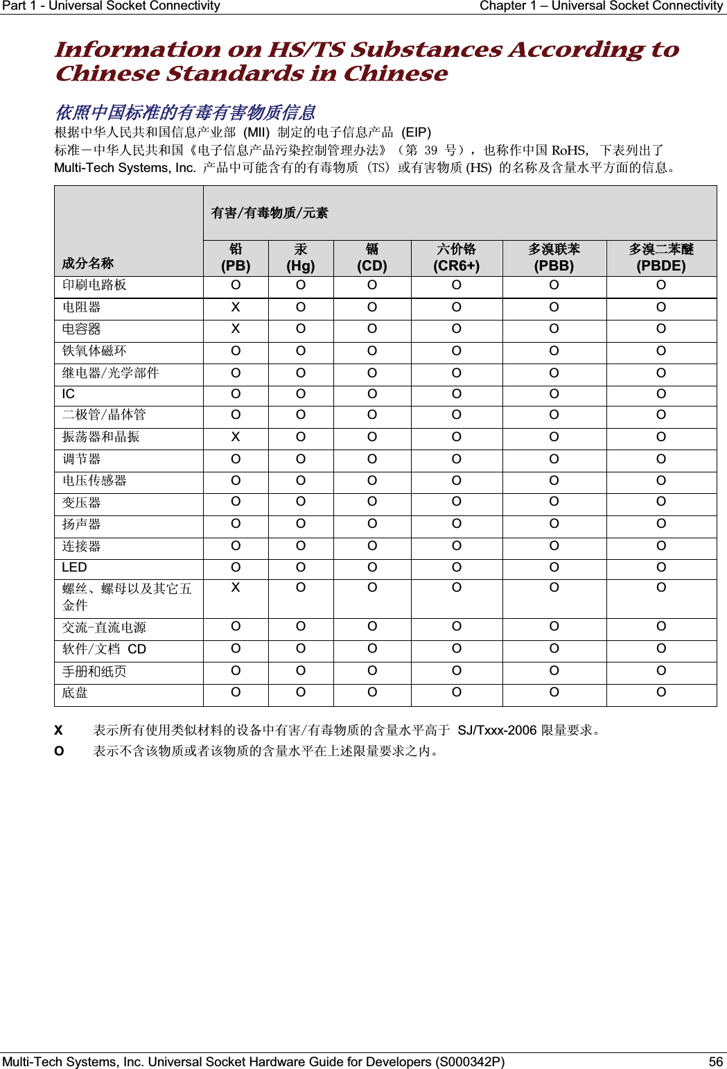
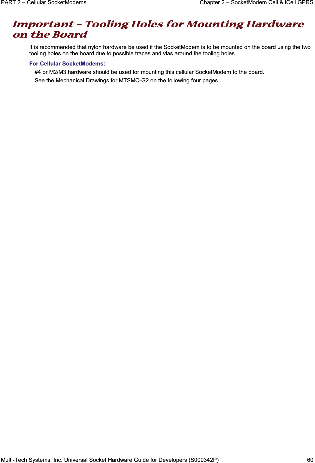
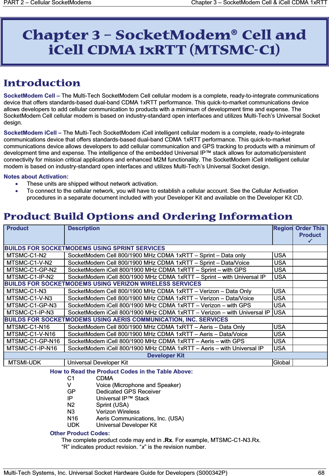
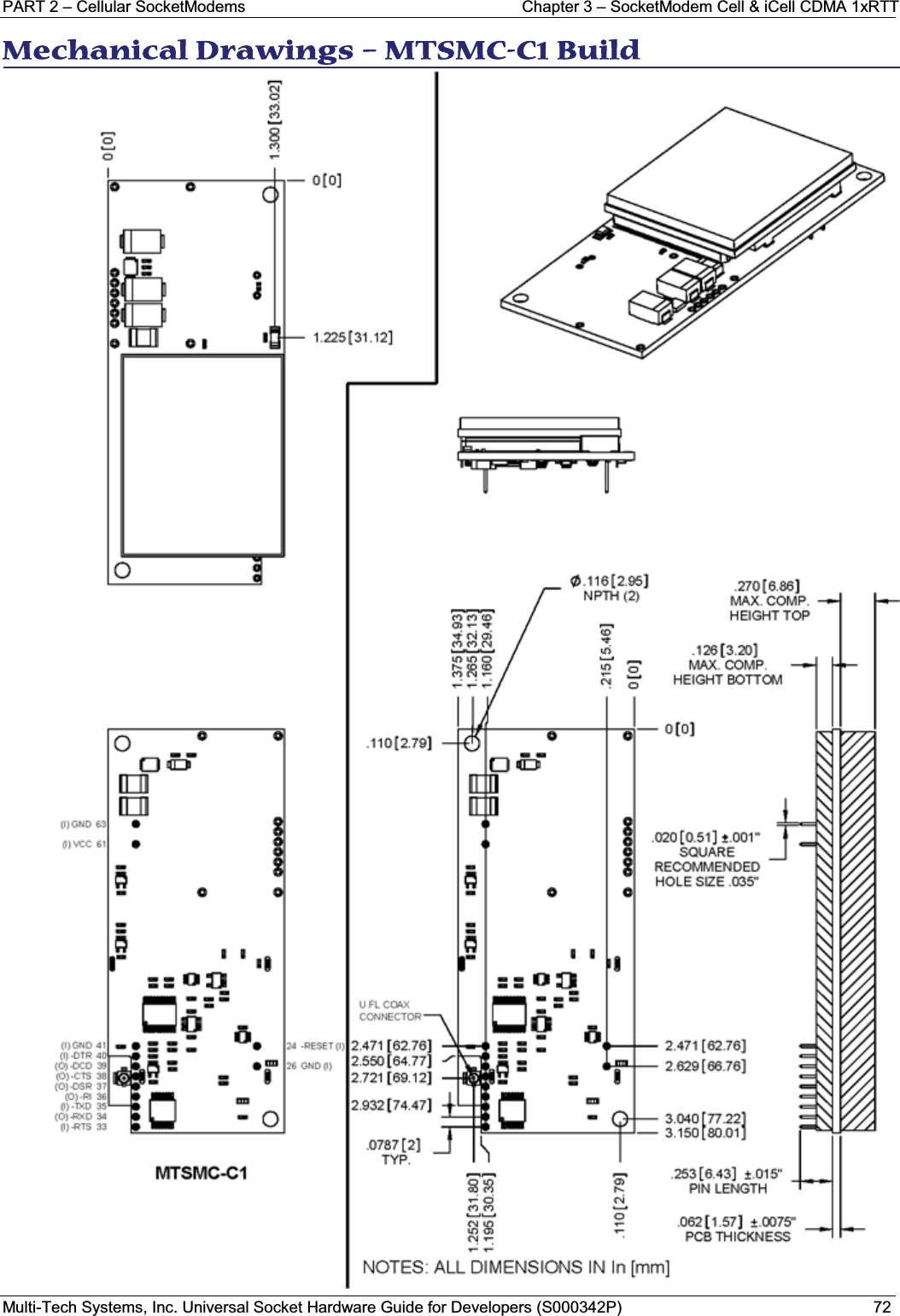
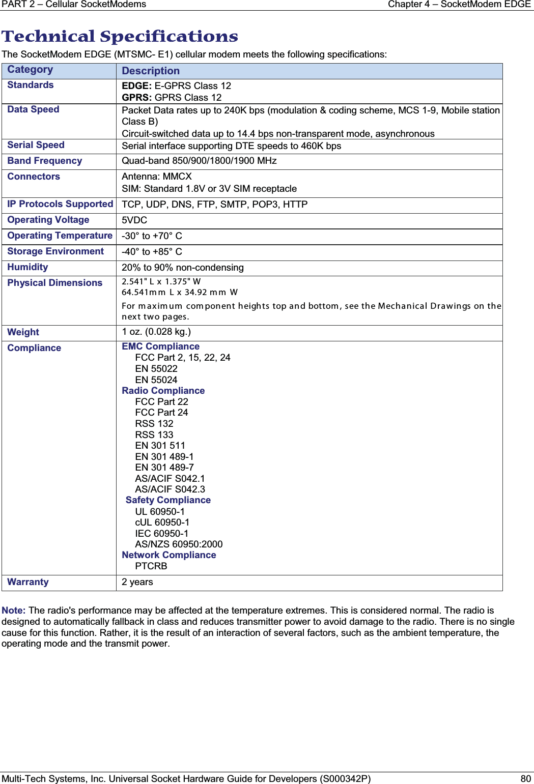
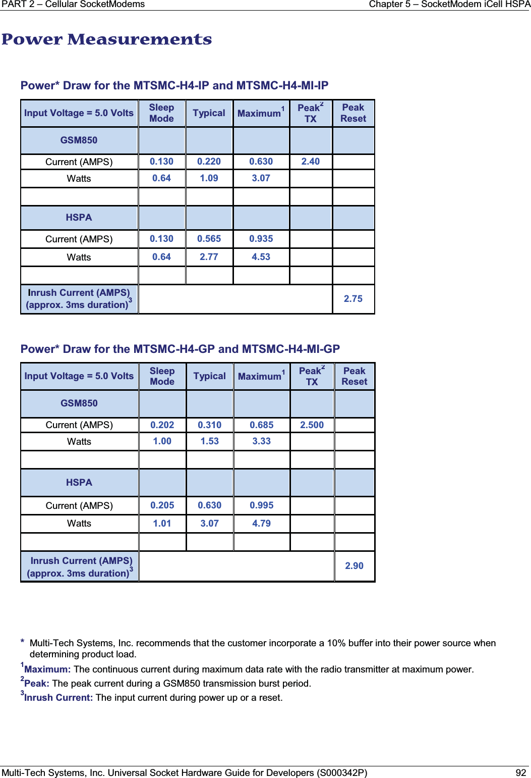
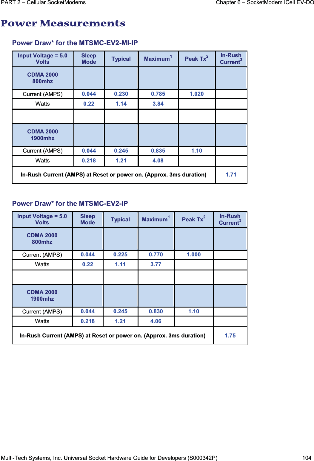
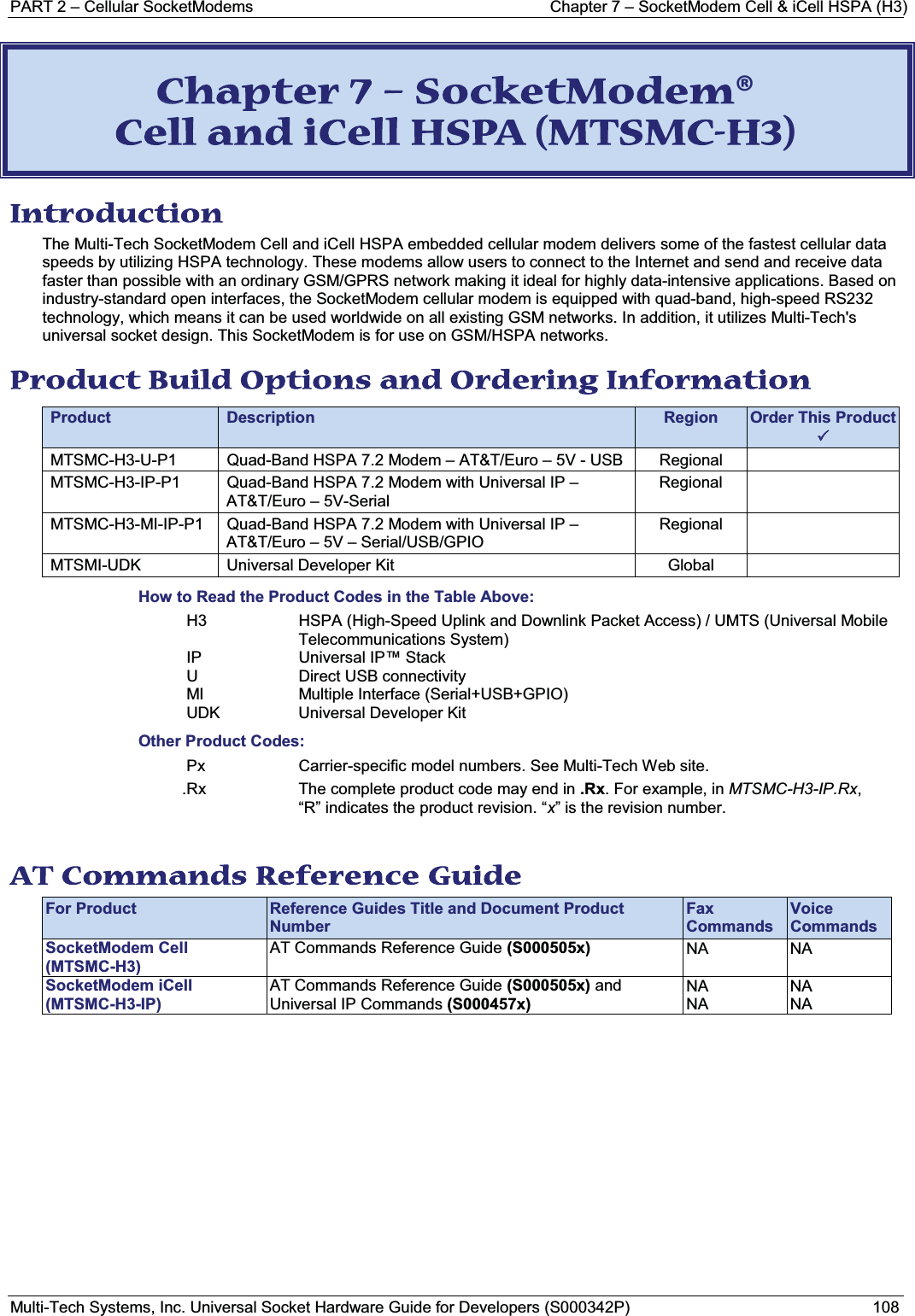
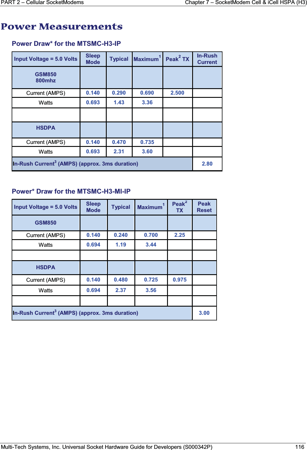
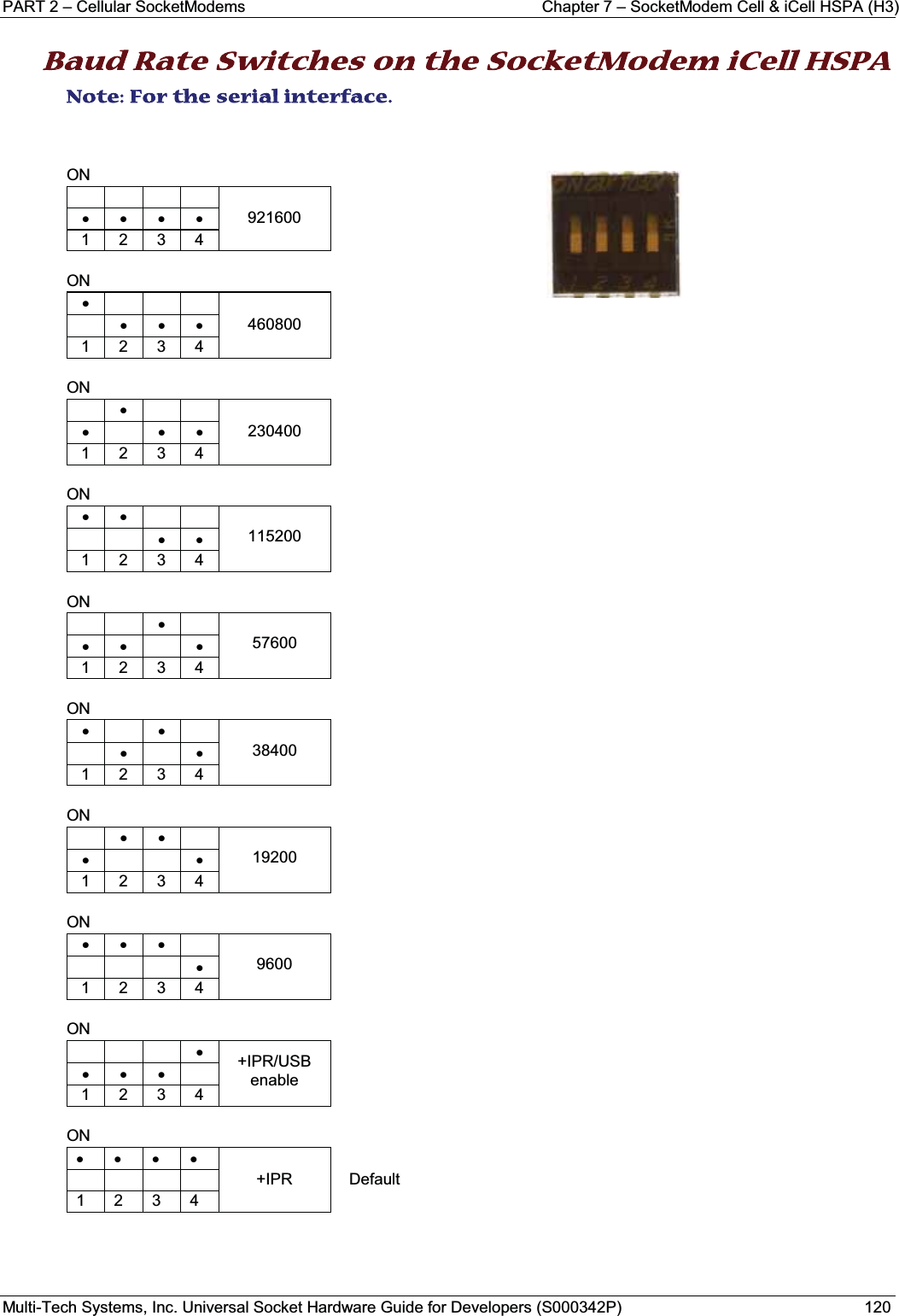
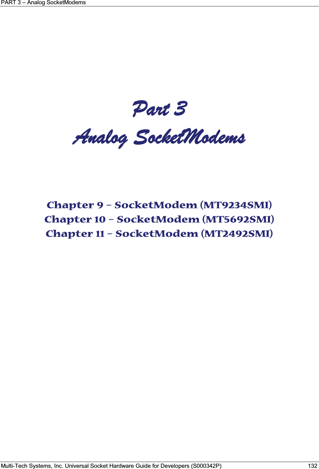
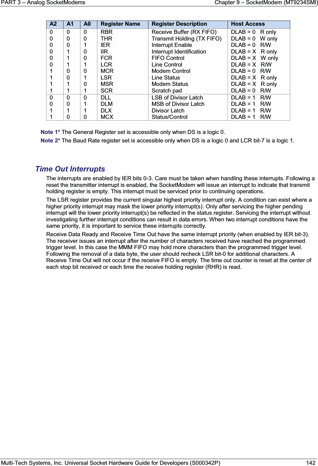
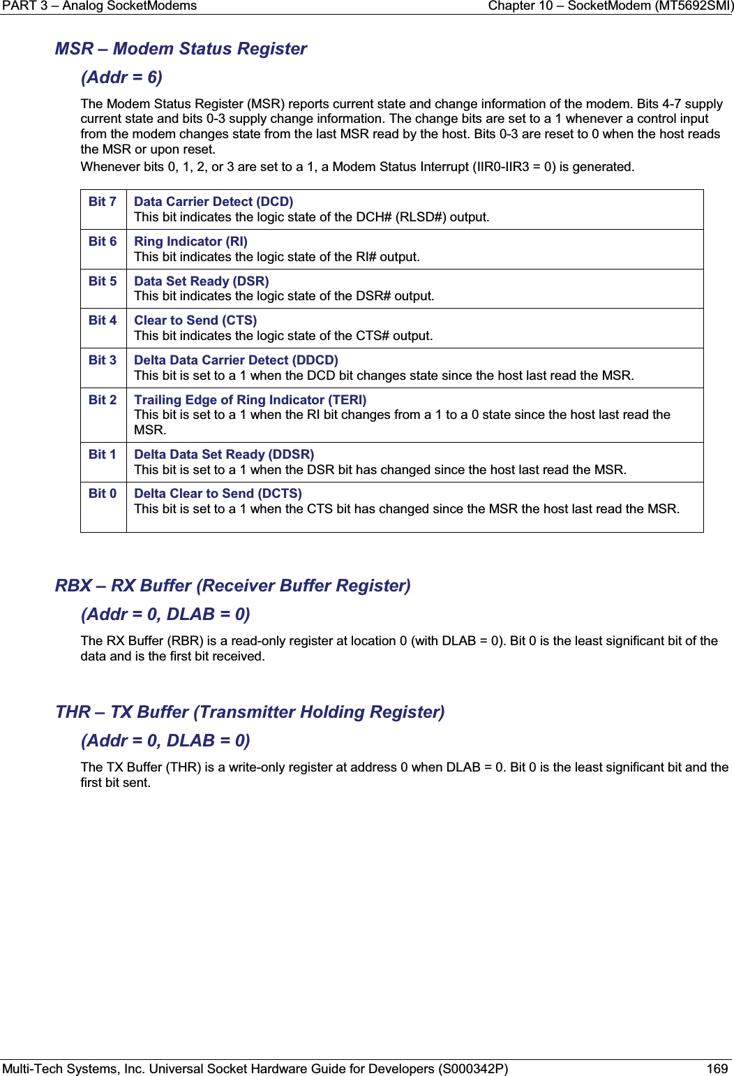
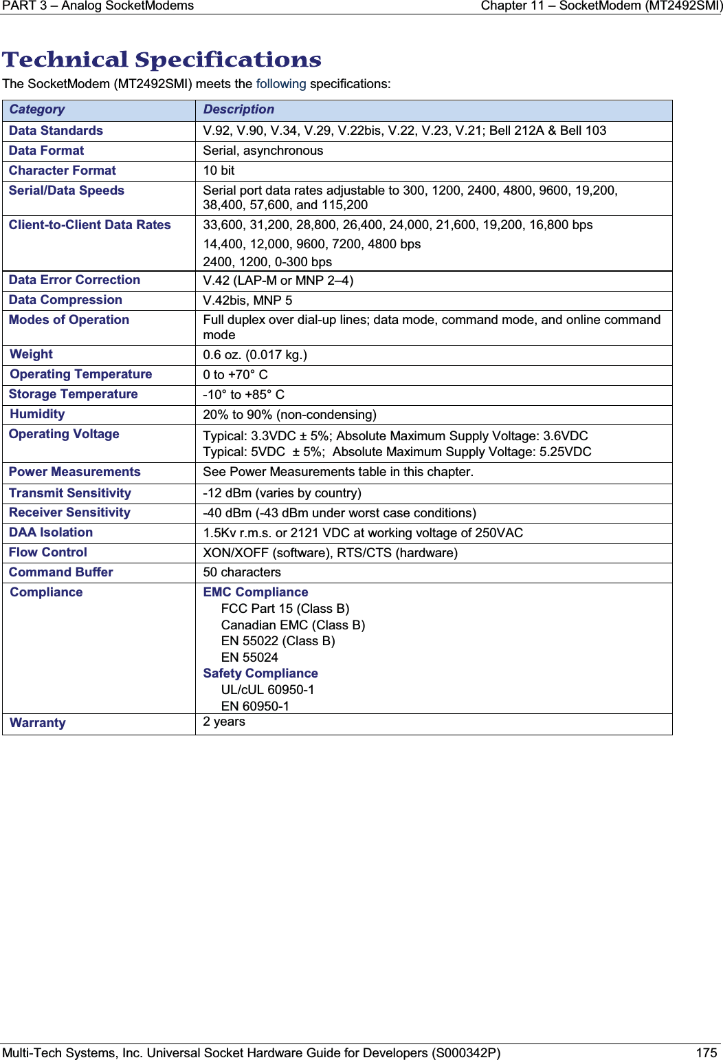
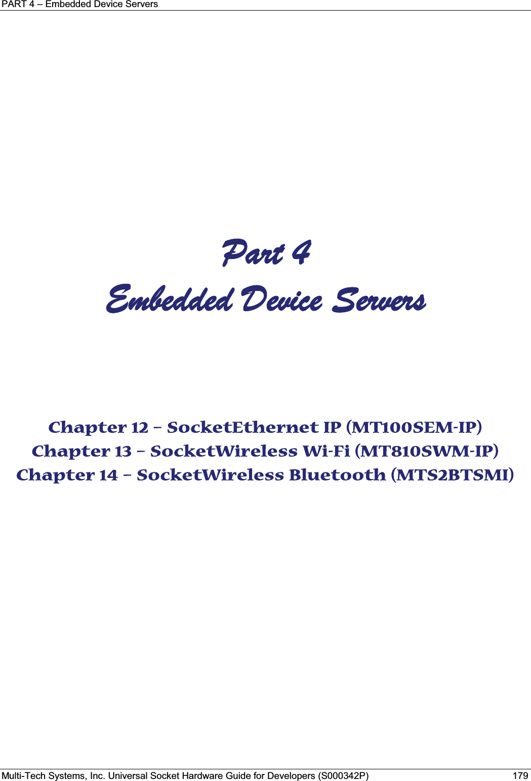
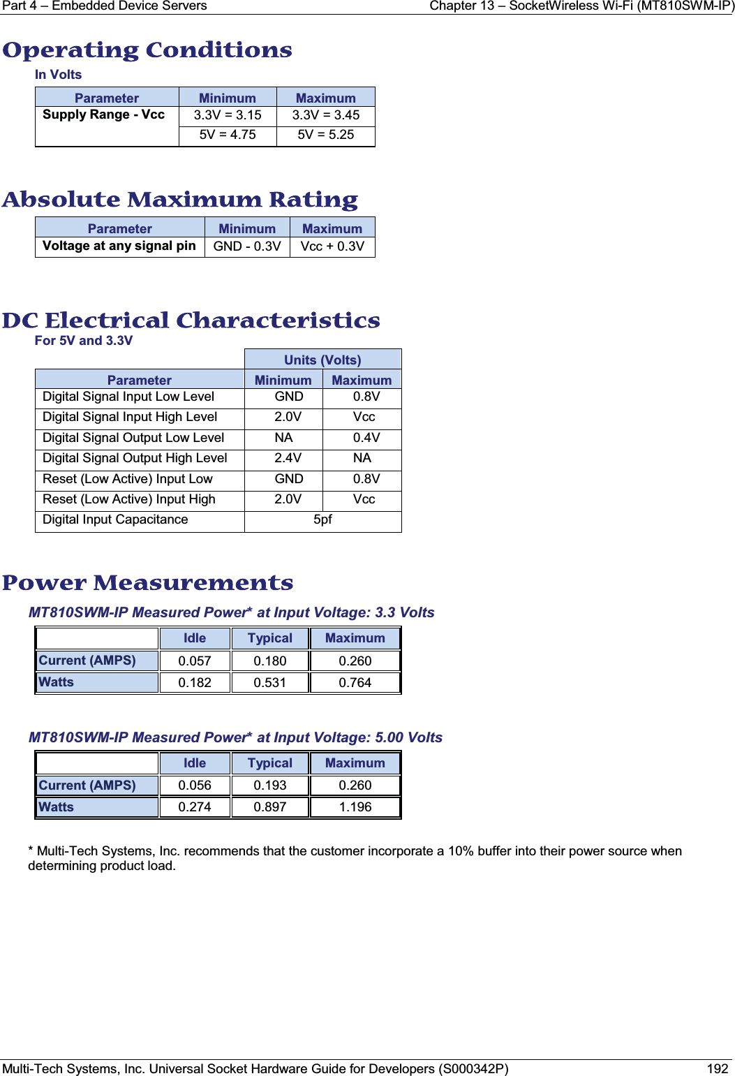
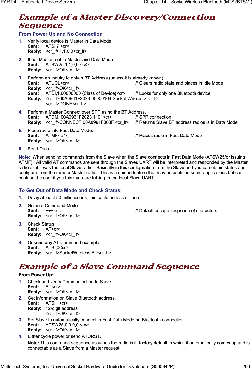
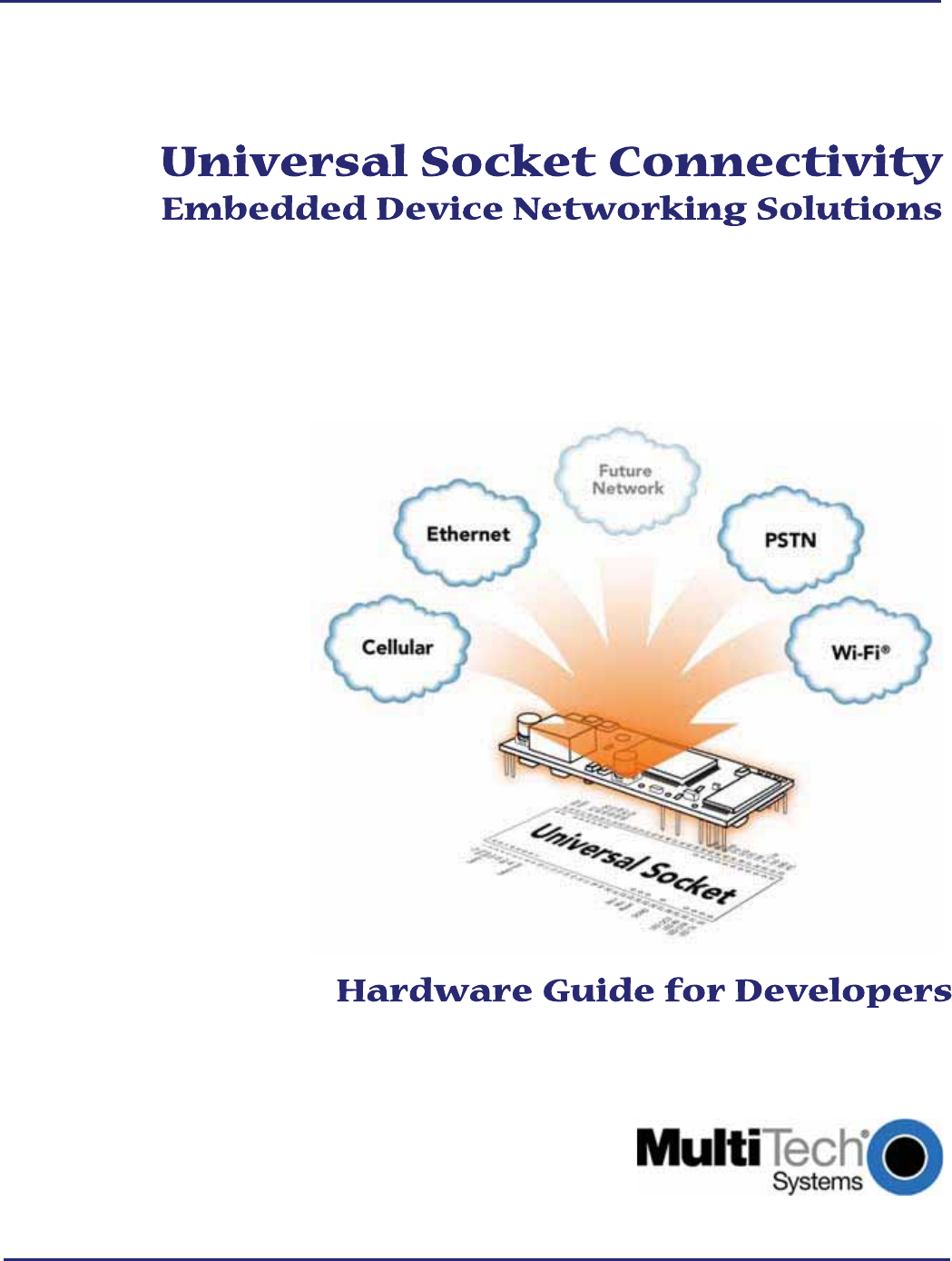
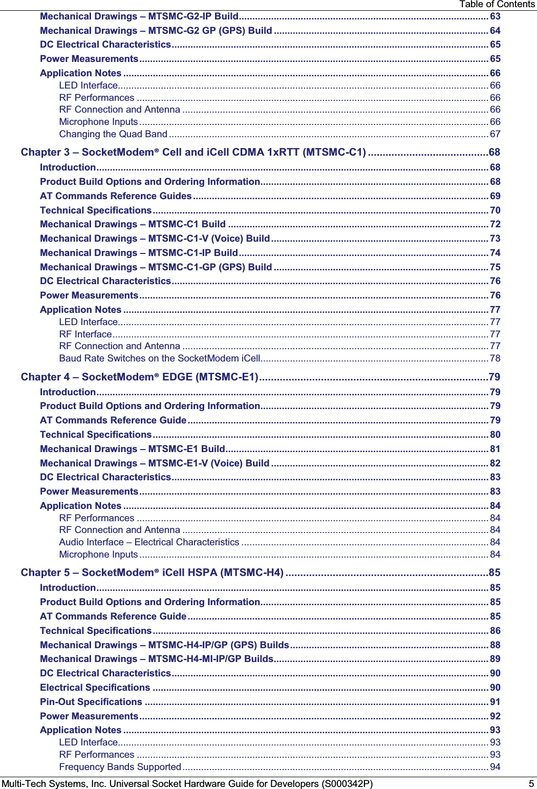
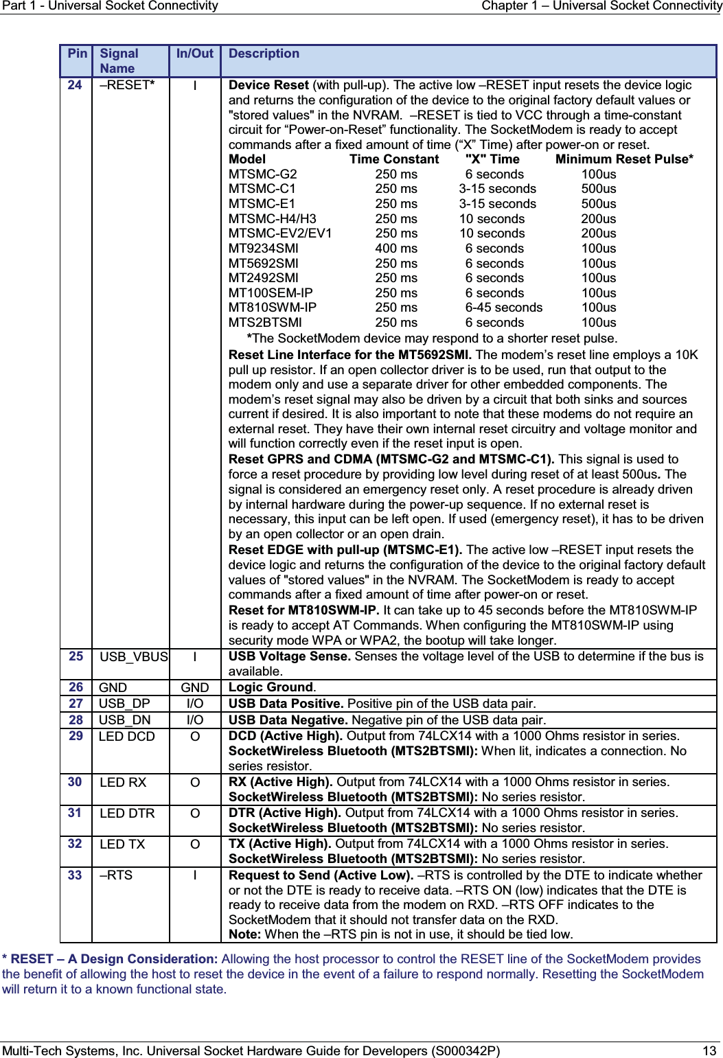
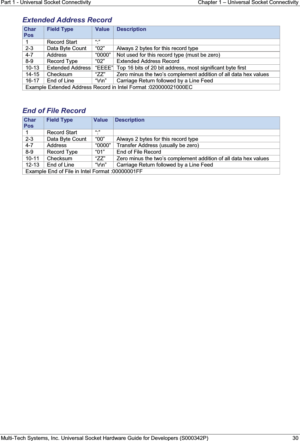
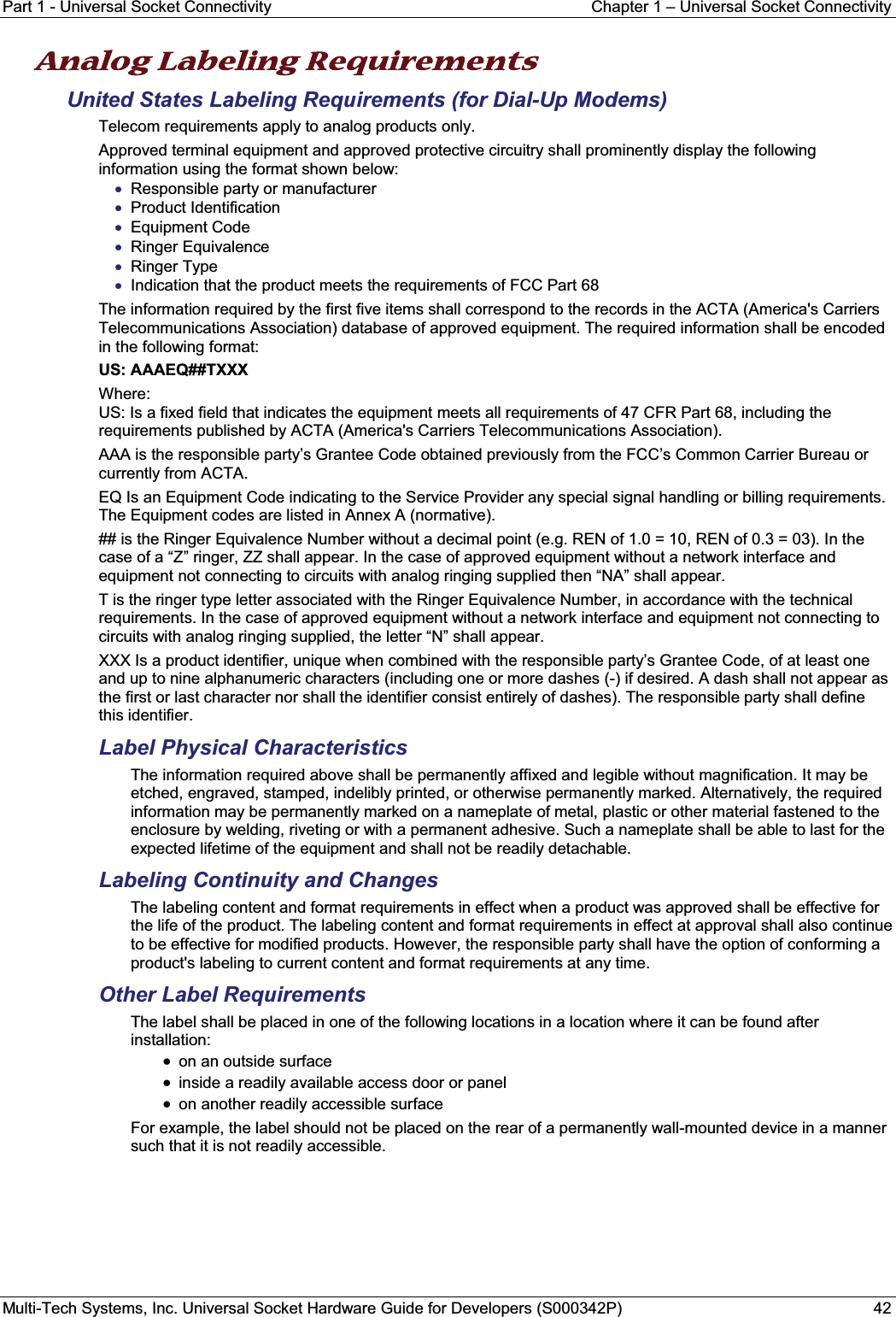
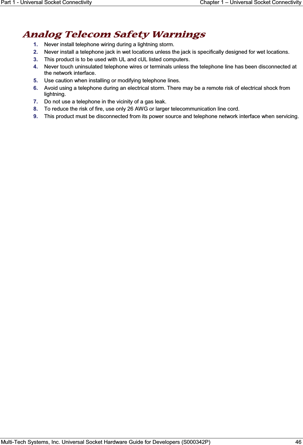
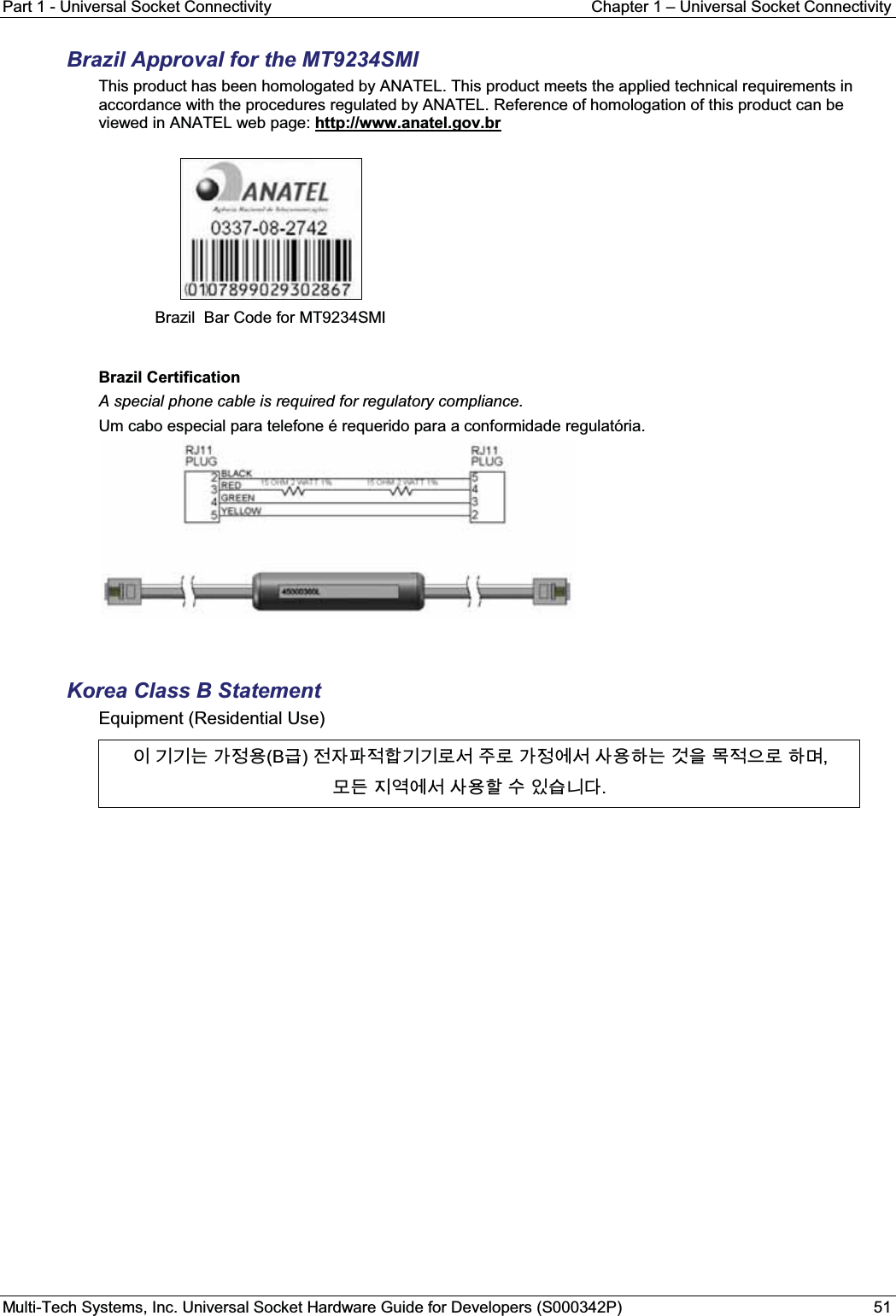
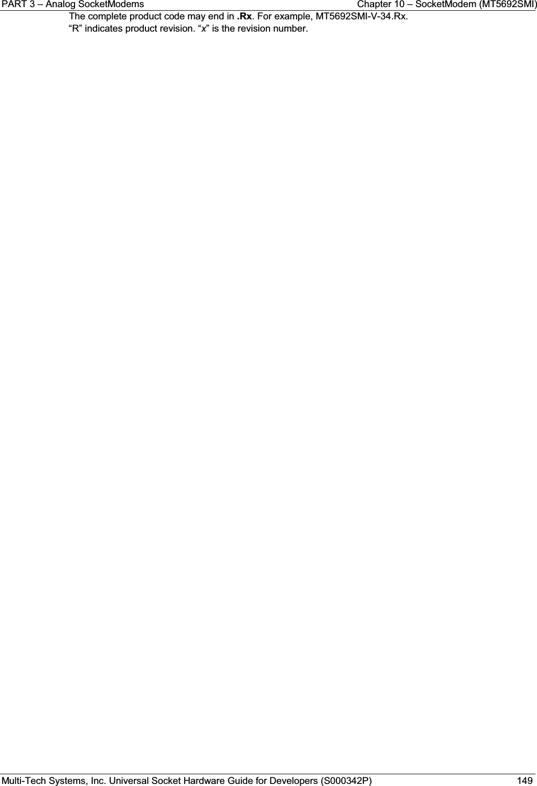
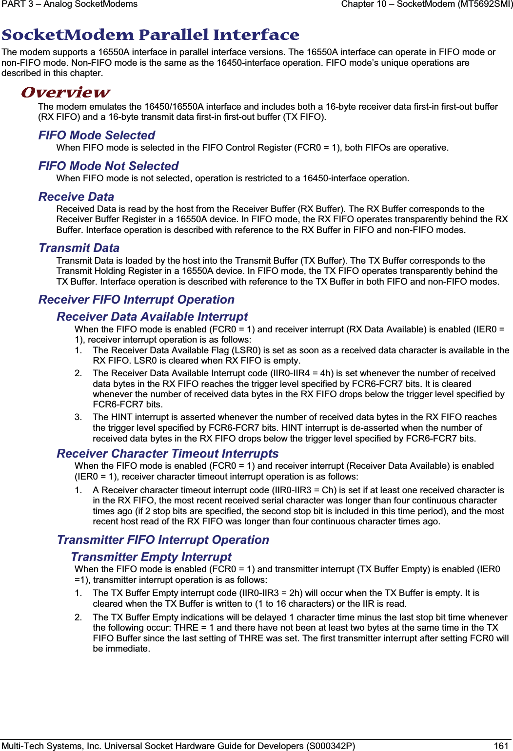
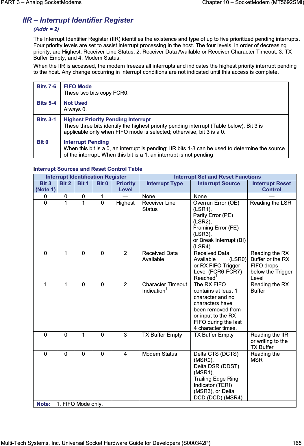
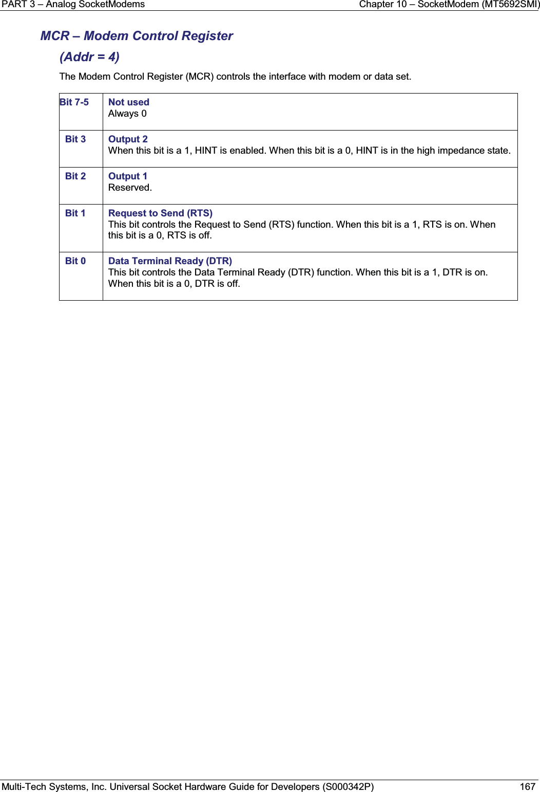
![PART 3 – Analog SocketModems Chapter 9 – SocketModem (MT9234SMI)Multi-Tech Systems, Inc. Universal Socket Hardware Guide for Developers (S000342P) 143RRegister Functional Definitions The following table delineates the assigned bit functions for the twelve internal registers. The assigned bit functions are more fully defined in the following paragraphs.Internal RegistersA2 A1 A0 Register[Default] Note *3BIT-7 BIT-6 BIT-5 BIT-4 BIT-3 BIT-2 BIT-1 BIT-0General Register Set: Note 1*0 0 0 RBR [XX] Bit-7 Bit-6 Bit-5 Bit-4 Bit-3 Bit-2 Bit-1 Bit-00 0 0 THR [XX] Bit-7 Bit-6 Bit-5 Bit-4 Bit-3 Bit-2 Bit-1 Bit-00 0 1 IER [00] 0 0 0 0 Modem Status InterruptReceive Line Status interruptTransmit Holding Register interruptReceive Holding Register interrupt0 1 0 IIR [XX] FIFO enable FIFO enable0 0 Interrupt IDInterrupt IDInterrupt IDInterrupt Pending0 1 0 FCR [00] RX Trigger (MSB)RX trigger (LSB)Detect change in FCRTX FIFO overrun bit0XMIT FIFO resetRCVR FIFO resetFIFO enable0 1 1 LCR [00] Divisor latch access(DLAB)Set breakStick parityEven parity Parity enable0Word length bit-1Word length bit-01 0 0 MCR [00] 0 0 0 0 INT enable OUT 1 -RTS -DTR1 0 1 LSR [60] RX FIFO data errorTX empty THR emptyTHR EmptyBreak interruptFraming errorParity errorOverrun errorReceive data ready1 1 0 MSR [X0] CD RI DSR CTS Delta -CDDelta-RIDelta -DSRDelta-CTS1 1 1 SCR [FF] Bit-7 Bit-6 Bit-5 Bit-4 Bit-3 Bit-2 Bit-1 Bit-0Special Register Set: Note *20 0 0 DLL [00] Bit-7 Bit-6 Bit-5 Bit-4 Bit-3 Bit-2 Bit-1 Bit-00 0 1 DLM [00] Bit-7 Bit-6 Bit-5 Bit-4 Bit-3 Bit-2 Bit-1 Bit-0Notes: 1* The General Register set is accessible only when DS is a logic 0.2* The Baud Rate register set is accessible only when DS is a logic 0 and LCR bit-7 is a logic 1.3* The value between the square brackets represents the register's initialized HEX value, X = N/A.RBR – Receive Buffer (RX FIFO)All eight bits are used for receive channel data (host read/data in; host write/data out). The three error bits per byte are copied into bits 2, 3, and 4 of the LSR during each host I/O read; therefore, they are available for monitoring on a per-byte basis.THR – Transmit Holding Register (TX FIFO)All eight bits are used for transmit channel data (host write/data out; host read/data in).IER – Interrupt EnableBits 4–7: Reserved and will always read 0.Bits 0-3: Set by host software only and cleared by software control or host reset.Bit 3: Enables modem status IRQ. If bits 0–3 of the MSR are set and this bit is set to 1 (enabled), a host interrupt is generated.Bit 2: Enables receive line status IRQ. If bits 1–4 (overrun, parity, framing, break errors) of the LSR are set and this bit is set to a logic 1, a host interrupt is generated.Bit 1: Enables transmit holding register IRQ. If bit 5 (transmit holding register empty) of the LSR is set and this bit is set to a 1, a host interrupt is generated.Bit 0: Enables received data available IRQ. If bit 0 (data ready) of the LSR is set and this bit is set to a 1, a host interrupt is generated.](https://usermanual.wiki/Multi-Tech-Systems/92U09J14829/User-Guide-1513497-Page-143.png)
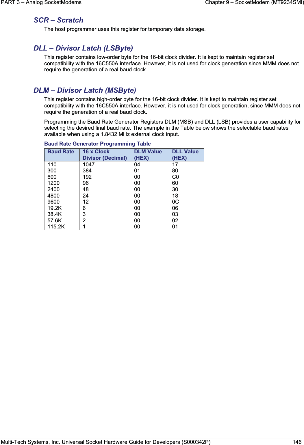
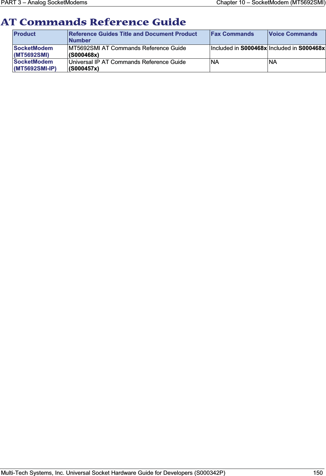
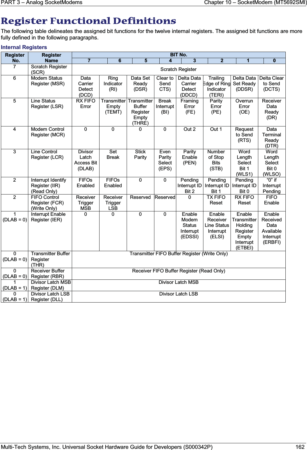
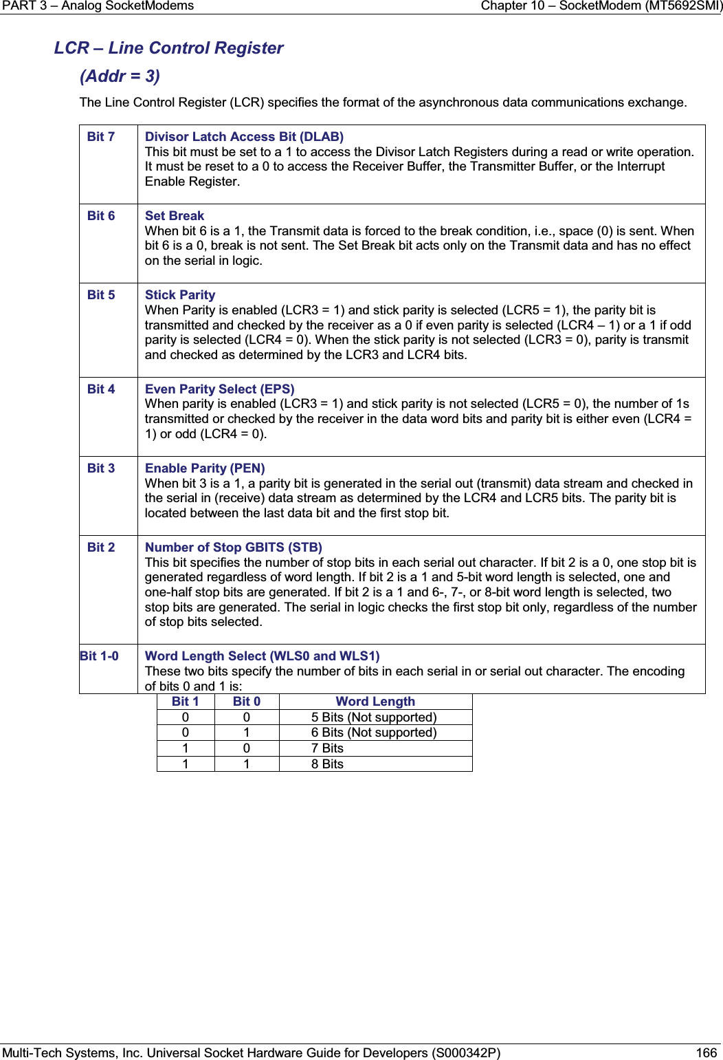
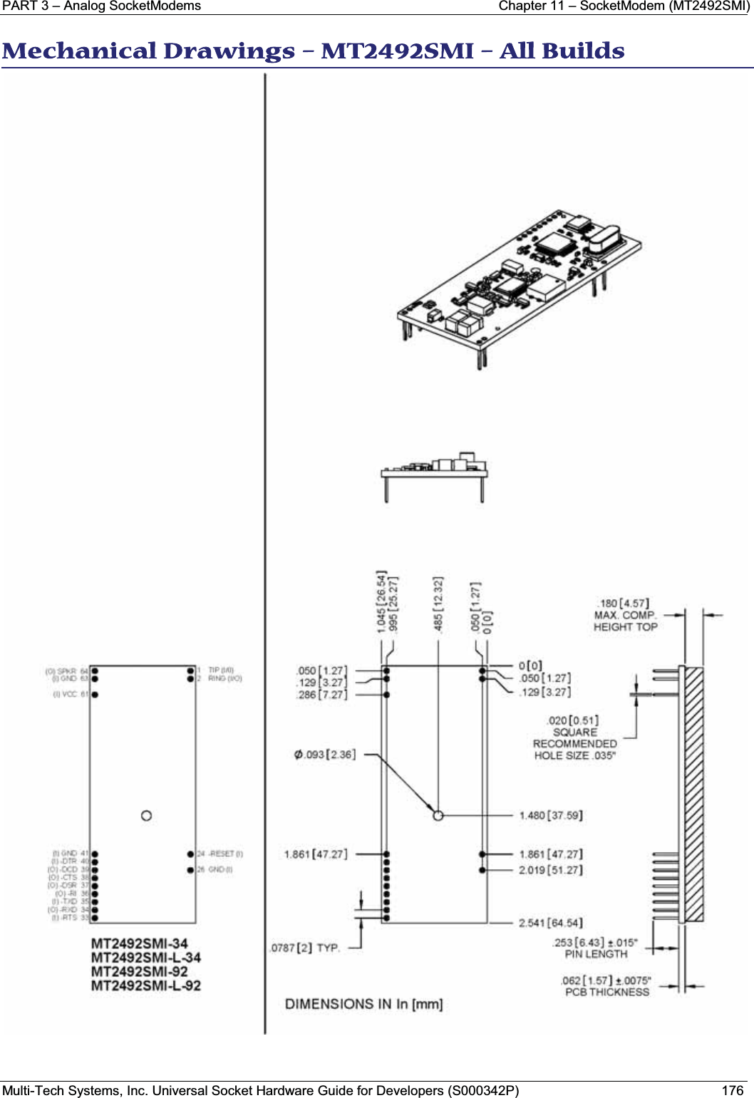
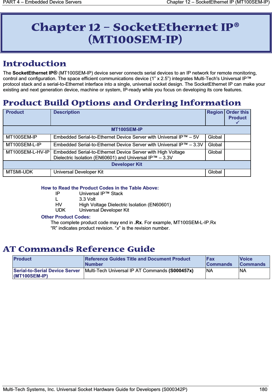
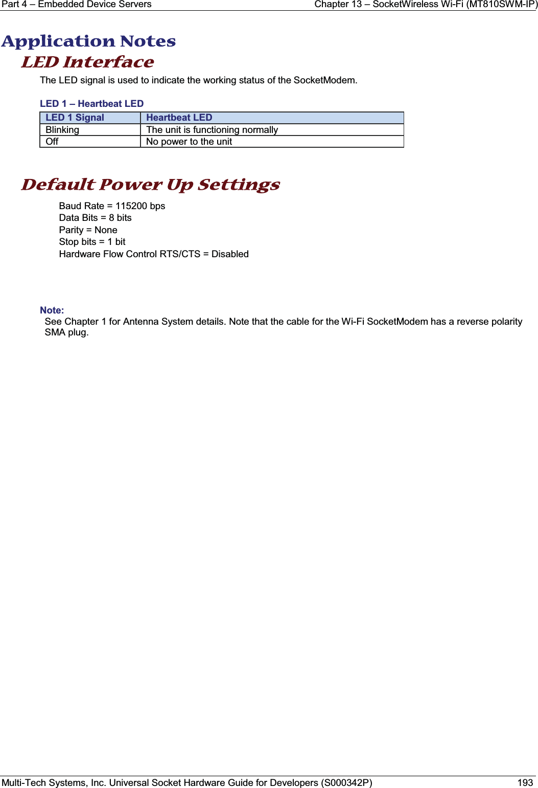
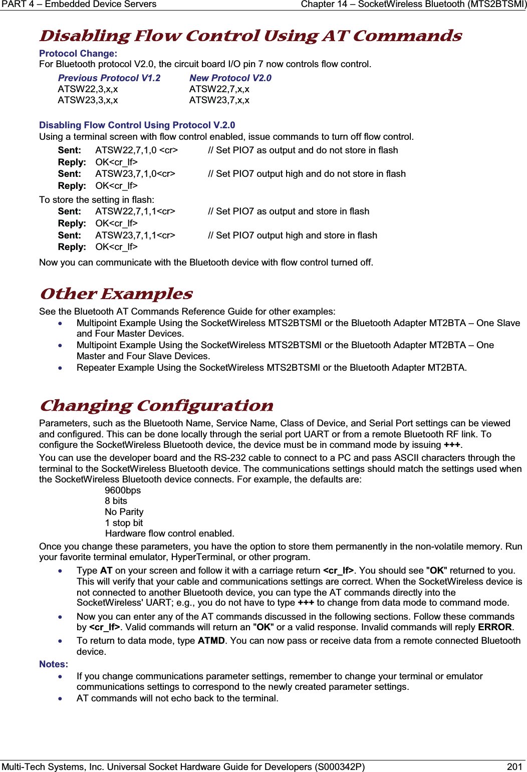
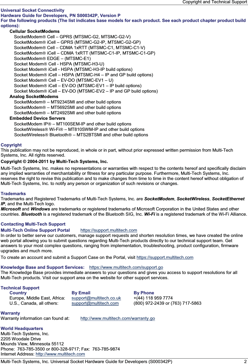
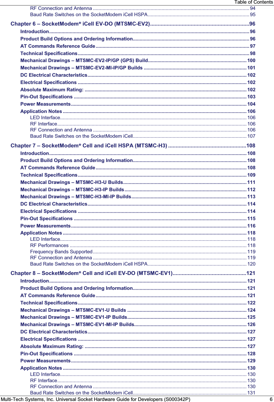
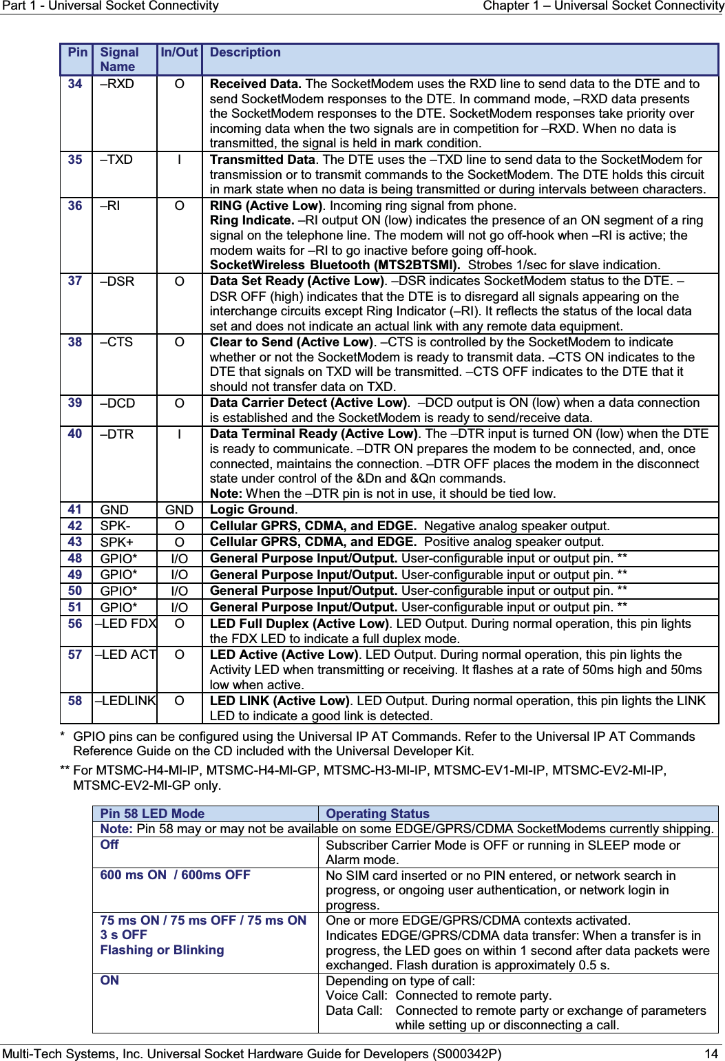
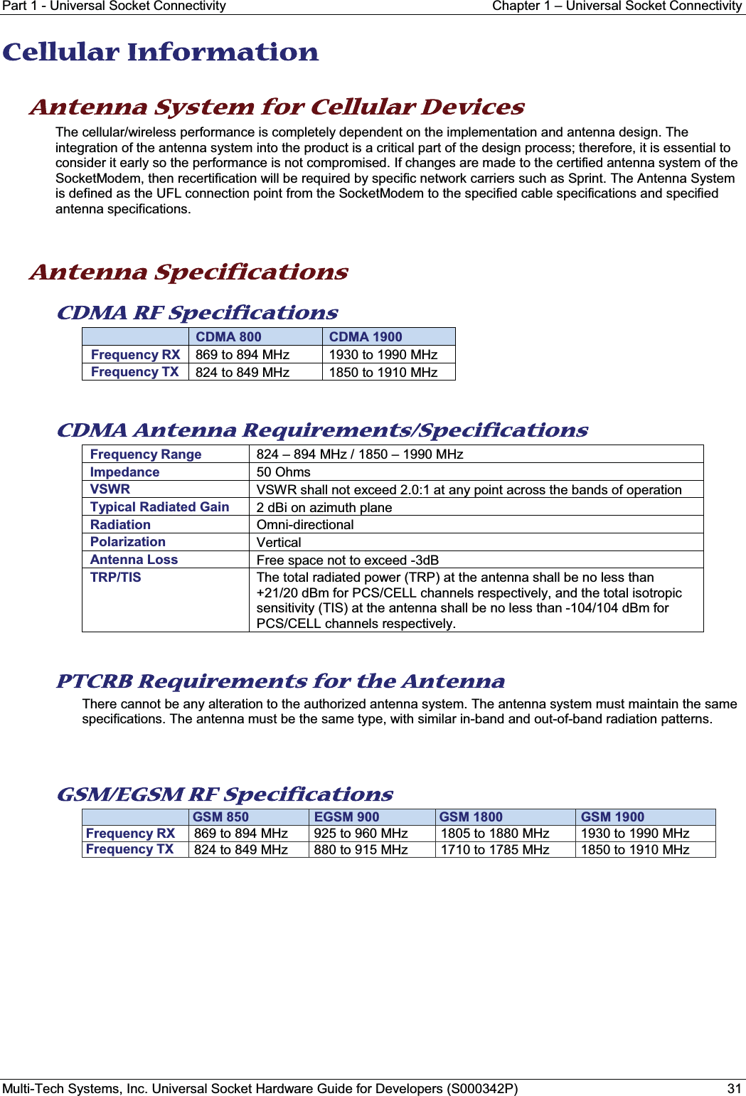
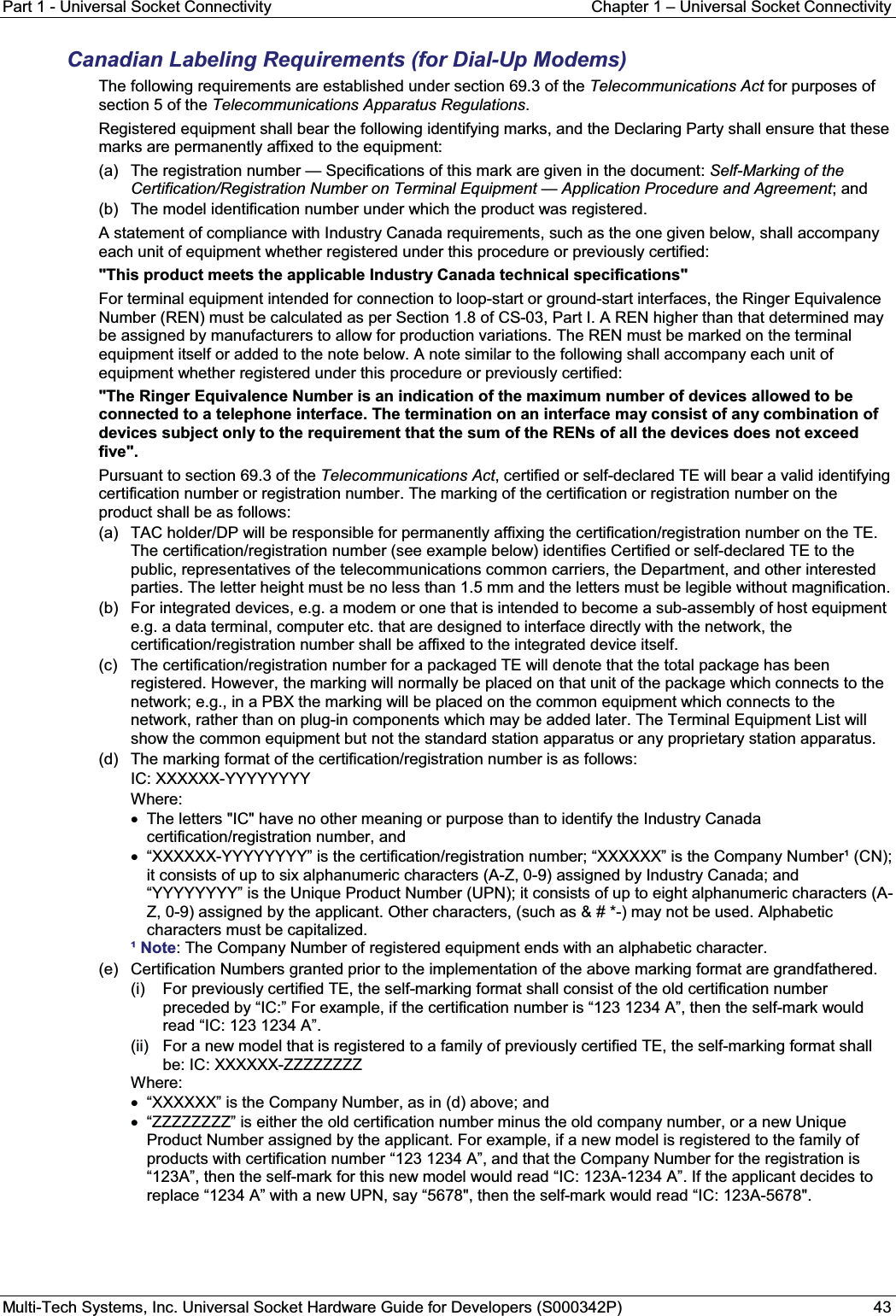
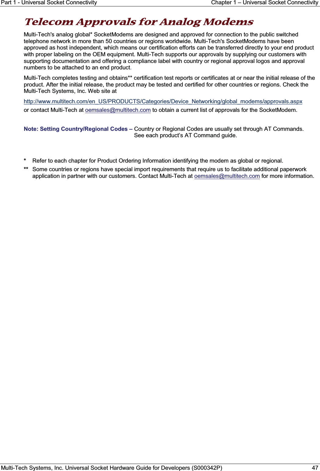
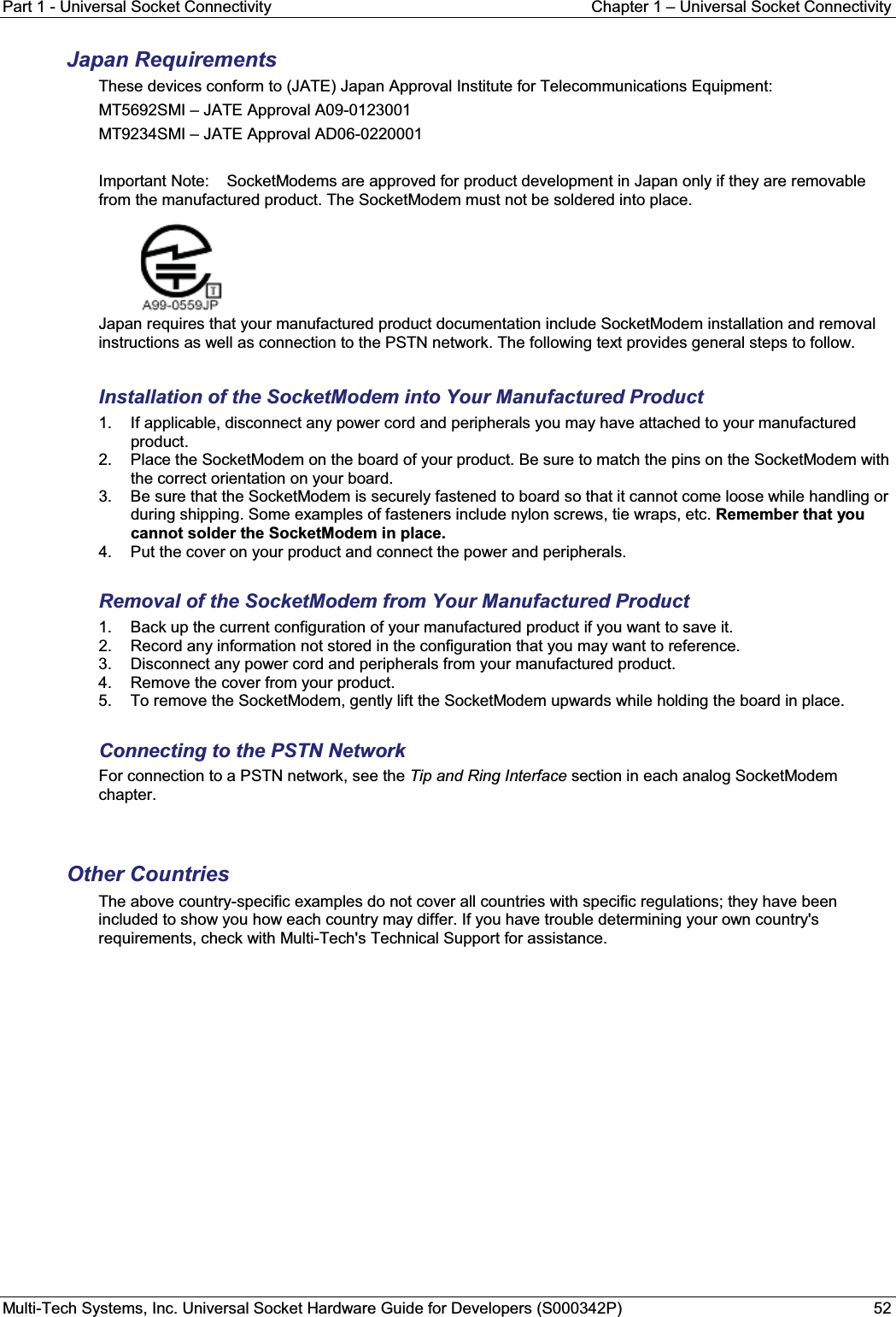
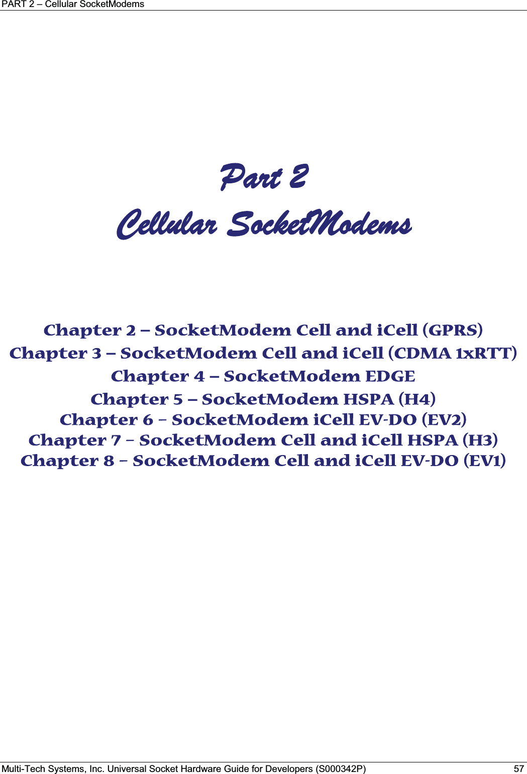
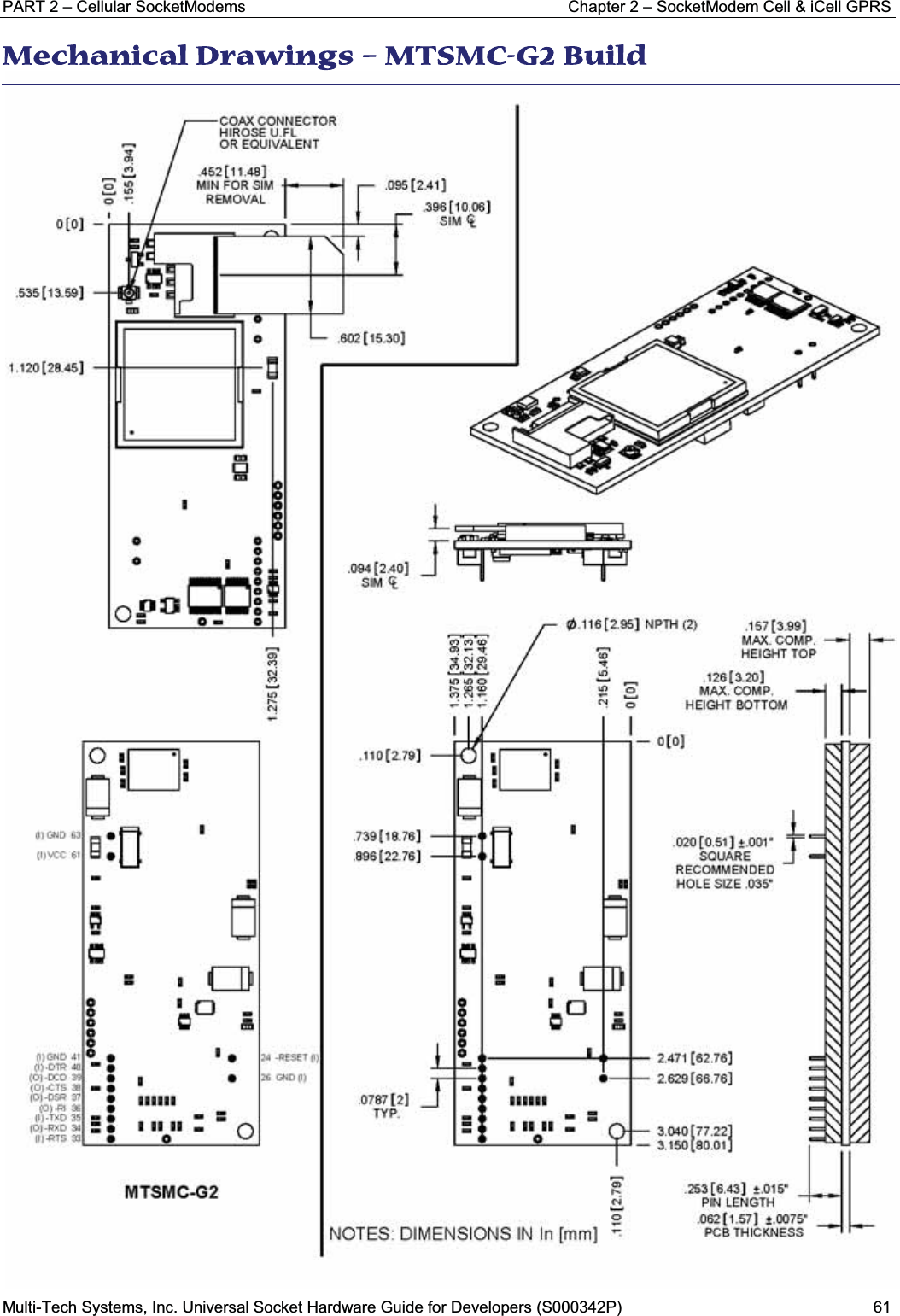
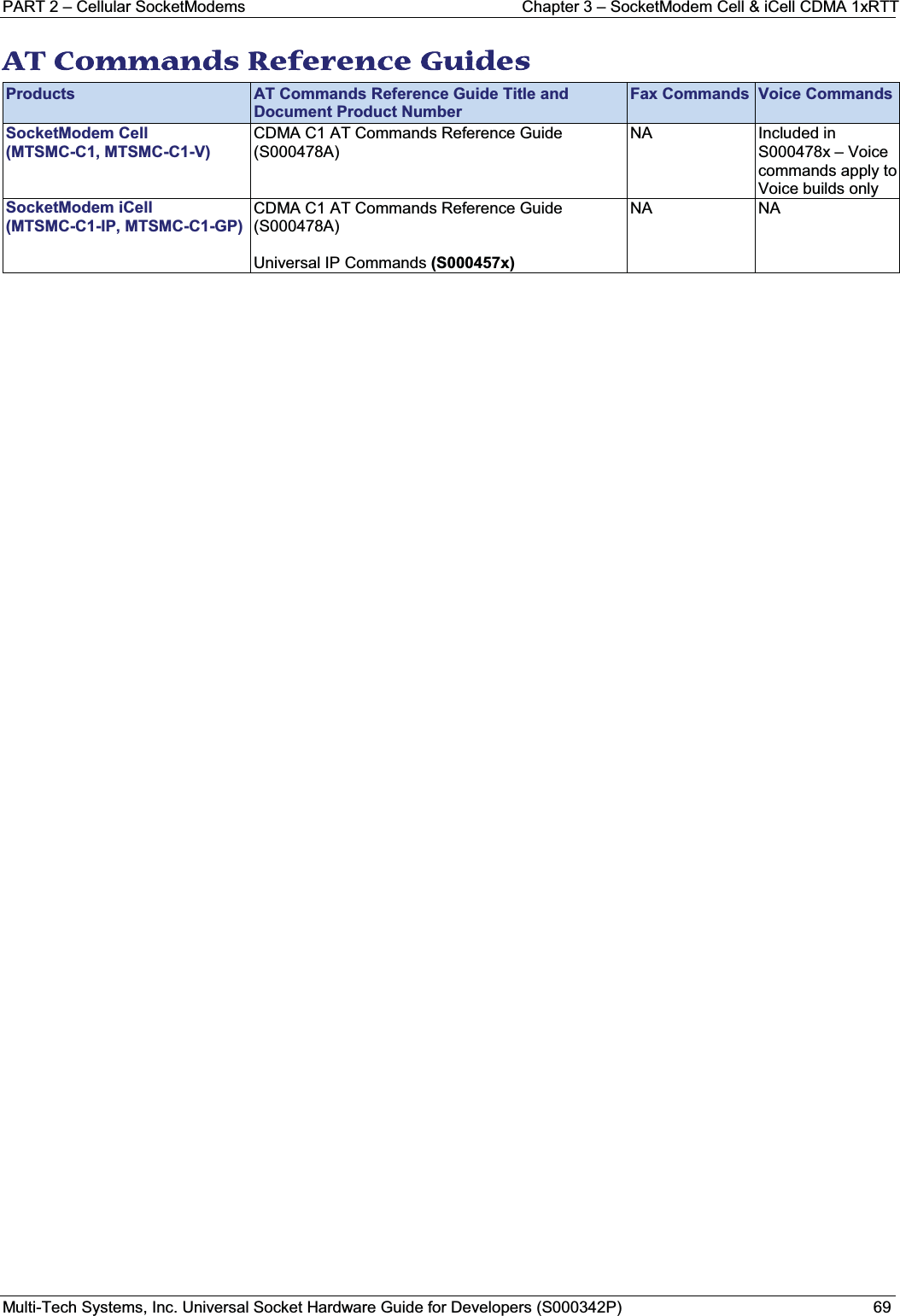
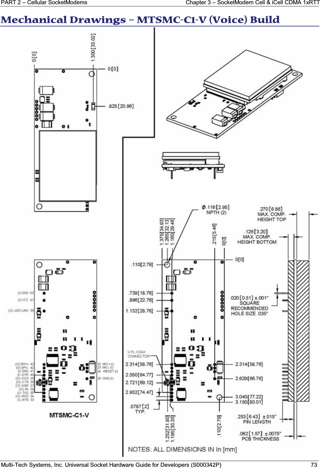
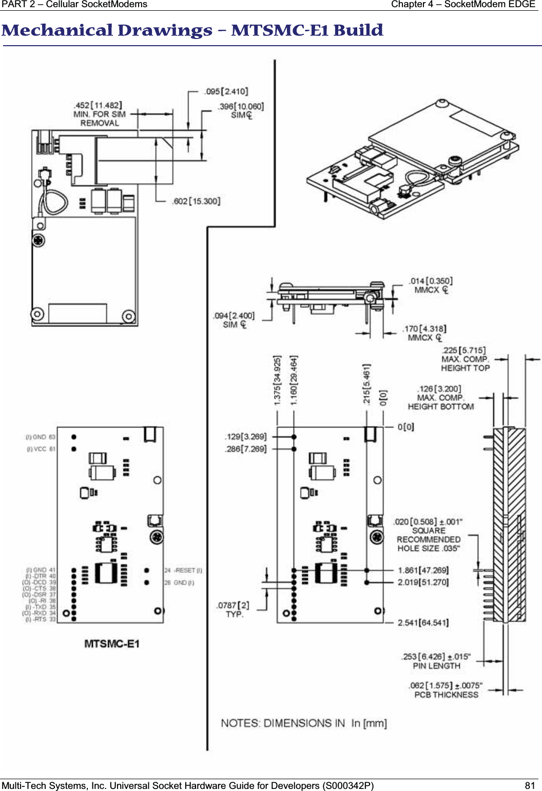
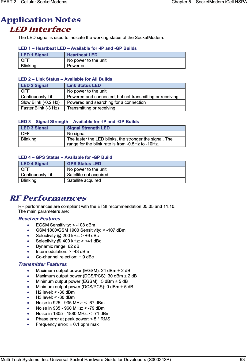
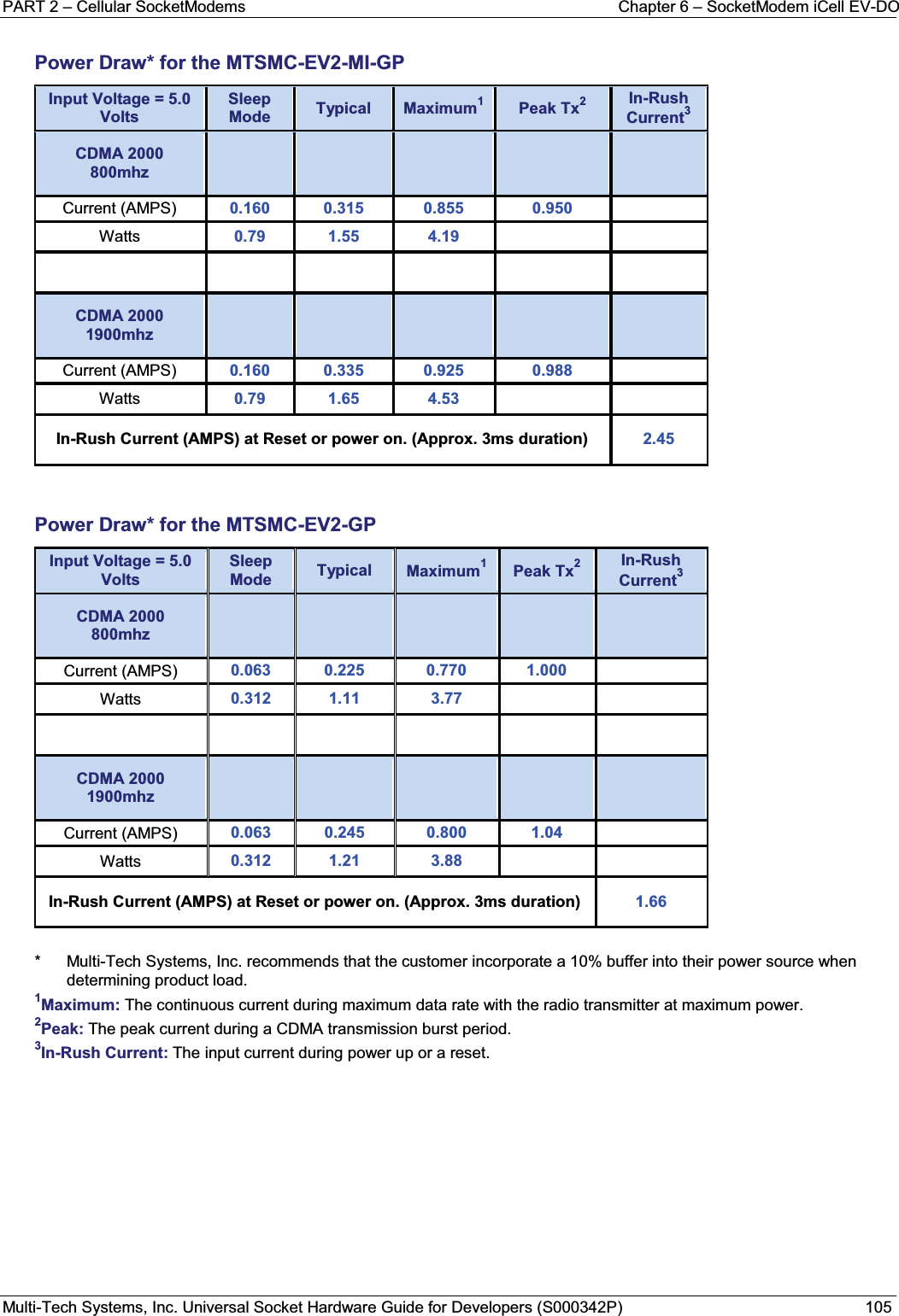
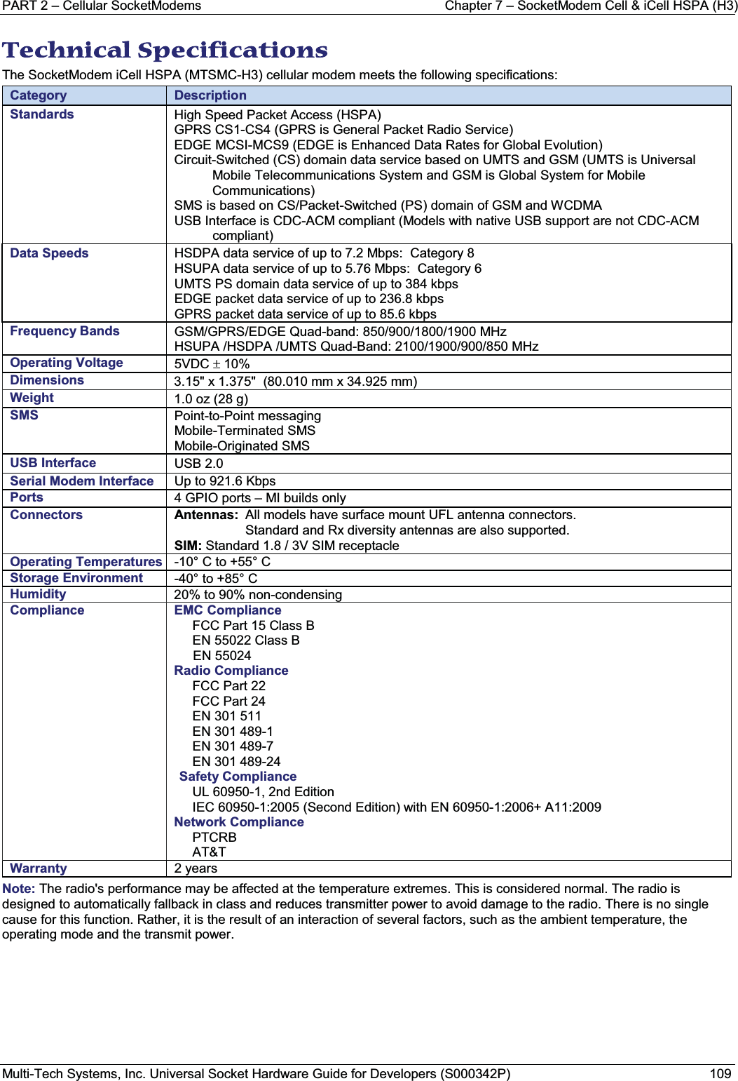
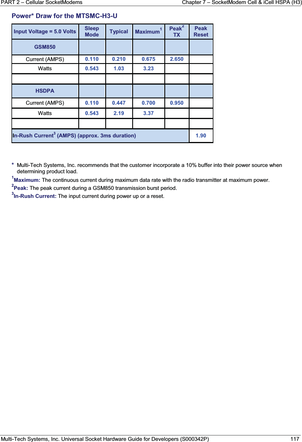
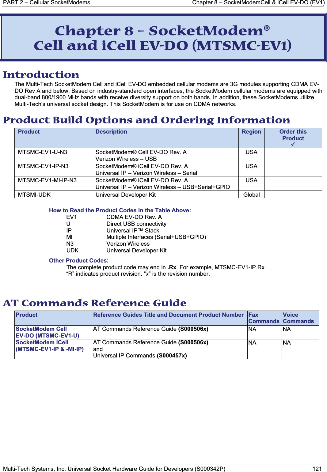
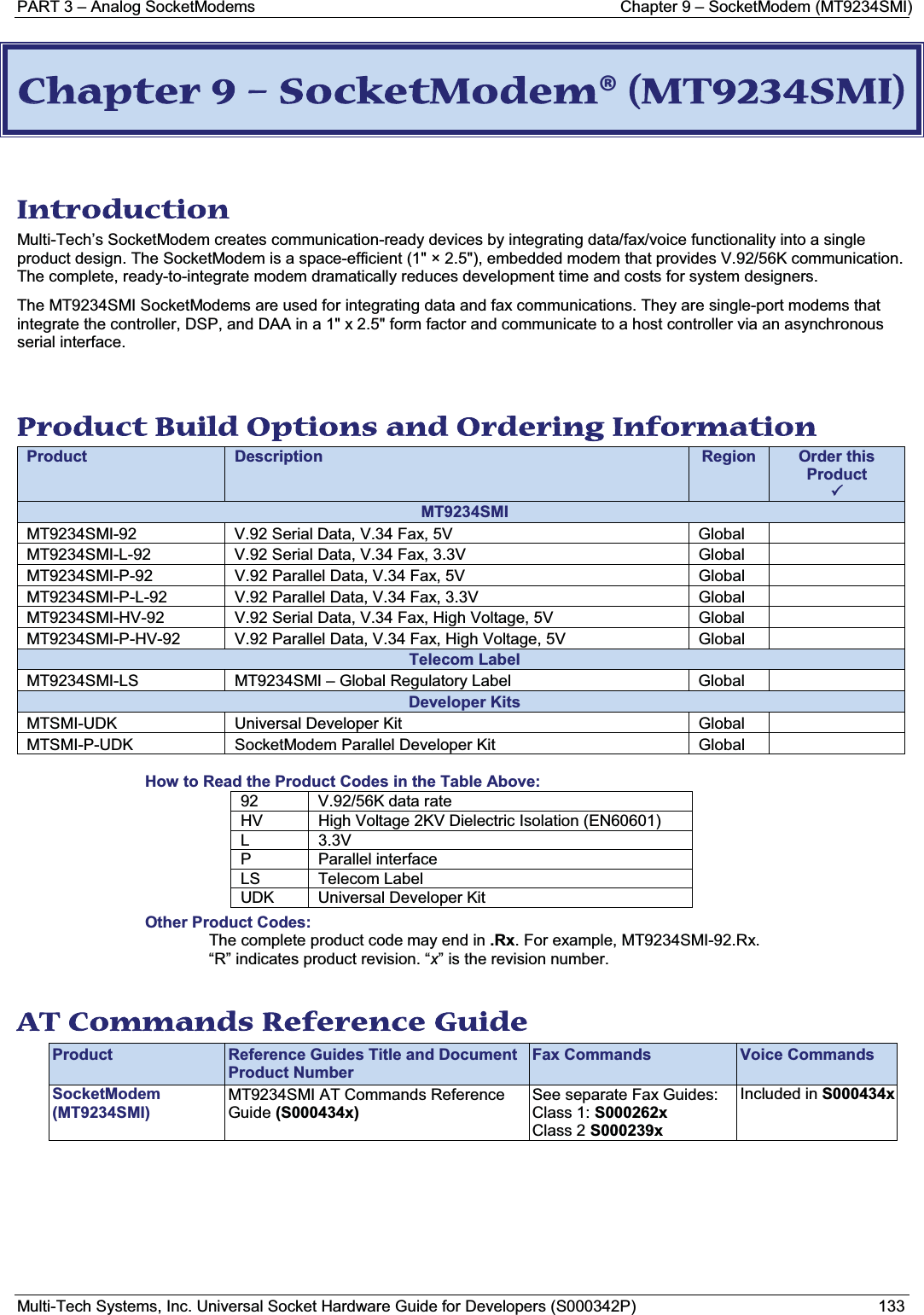
![PART 3 – Analog SocketModems Chapter 10 – SocketModem (MT5692SMI)Multi-Tech Systems, Inc. Universal Socket Hardware Guide for Developers (S000342P) 168LSR – Line Status Register (Addr = 5)This 8-bit register provides status information to the host concerning data transferBit 7 RX FIFO ErrorIn the 16450 mode, this bit is not used and is always 0.In the FIFO mode, this bit is set if there are one or more characters in the RX FIFO with parity error, framing error, or break indication detected. This bit is reset to a 0 when the host reads the LSR and note of the above conditions exist in the RX FIFO.Bit 6 Transmitter Empty (TEMT)This bit is set to a 1 whenever the TX Buffer (THR) and equivalent of the Transmitter Shift Register (TRS) are both empty. It is reset to a 0 whenever either the THR or the equivalent of the TSR contains a character.In the FIFO mode, this bit is set to a 1 whenever the TX FIFO and the equivalent of the TSR are both emptyBit 5 Transmitter Holding Register Empty (THRE) [TX Buffer Empty]This bit, when set, indicates that the TX Buffer is empty and the modem can accept a new character for transmission. In addition, this bit causes the modem to issue an interrupt to the host when the Transmit Holding Register Empty Interrupt Enable bit (IIR1) is set to 1. The THRE bit is set to a 1 when a character is transferred from the TX Buffer. The bit is reset to 0 when a byte is written into the TX Buffer by the host.In the FIFO mode, this bit is set when the TX FIFO is empty; it is cleared when at least one byte is in the TX FIFO.Bit 4 Break Interrupt (BI)This bit is set to a 1 whenever the received data input is a space (logic 0) for longer than two full word lengths plus 3 bits. The BI is reset when the host reads the LSR.Bit 3 Framing Error (FE)This bit indicates that the received character did not have a valid stop bit. The FE bit is set to a 1 whenever the stop bit following the last data bit or parity bit is detected as a logic o (space). The FE bit is reset to a 0 when the host reads the LSR.In the FIFO mode, the error indication is associated with the particular character in the FIFO it applies to. The FE bit set to a 1 when this character is loaded into the RX Buffer.Bit 2 Parity Error (PE)This bit indicates that the received data character in the RX Buffer does not have the correct even or odd parity, as selected by the Even Parity Select bit (LCR4) and the Stick Parity bit (LCR5). The PE bit is reset to a 0 when the host reads the LSR.In the FIFO mode, the error indication is associated with the particular character in the FIFO it applies to. The PE bit set to a 1 when this character is loaded into the RX Buffer.Bit 1 Overrun Error (OE)This bit is set to a 1 whenever received data is loaded into the RX Buffer before the host has read the previous data from the RX Buffer. The OE is reset to a 0 when the host reads the LSR.In the FIFO mode, if data continues to fill beyond the trigger level, an overrun condition will occur only if the RX FIFO is full and the next character has been completely received. Bit 0 Receiver Data Ready (DR)This bit is set to a 1 whenever a complete incoming character has been received and transferred into the RX Buffer. The DR bit is reset to a 0 when the host reads the RX Buffer.In the FIFO mode, the DR bit is set when the number of received data bytes in the RX FIFO equals or exceeds the trigger level specified in the FCR0-FCR1.](https://usermanual.wiki/Multi-Tech-Systems/92U09J14829/User-Guide-1513497-Page-168.png)