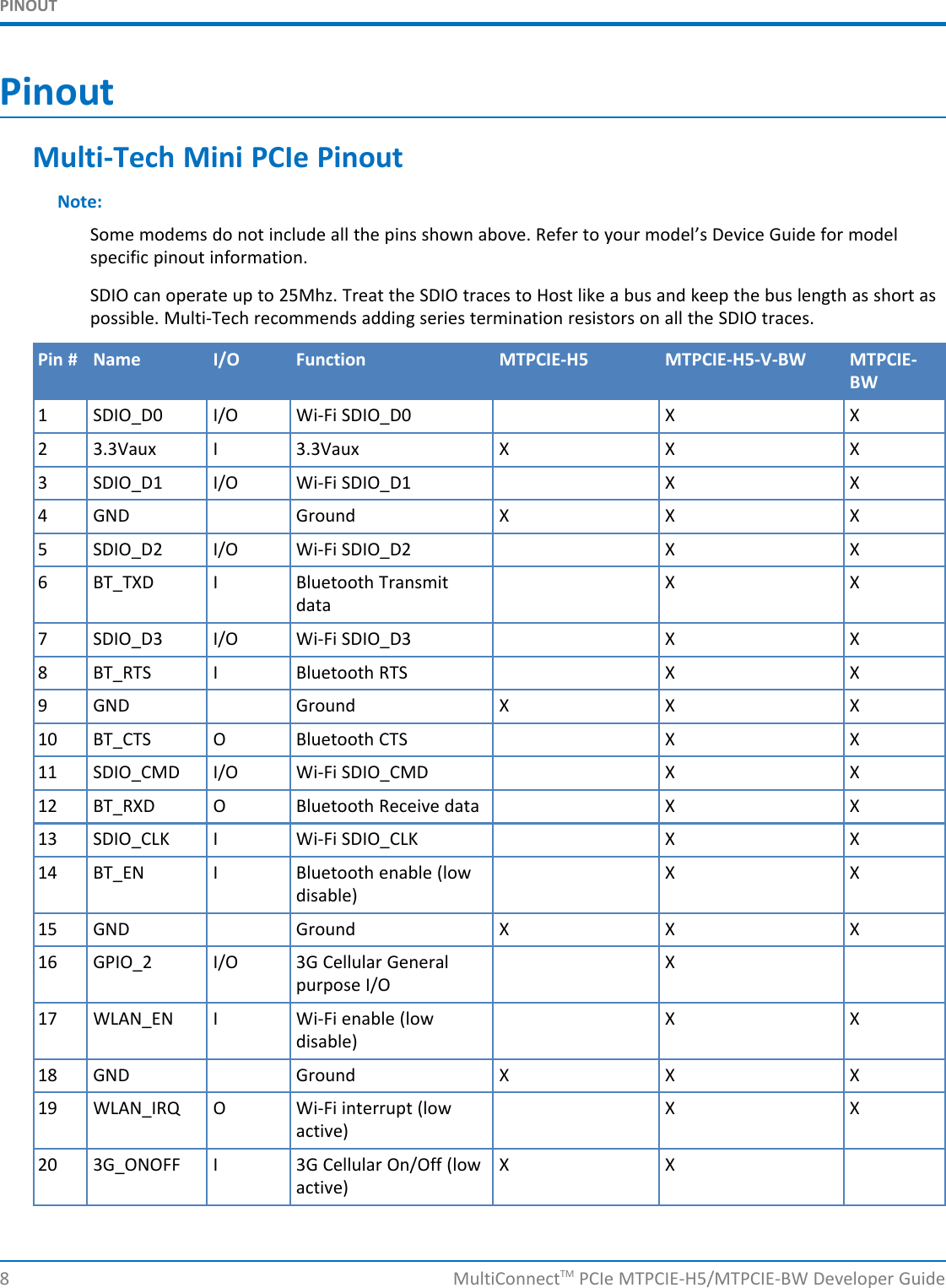
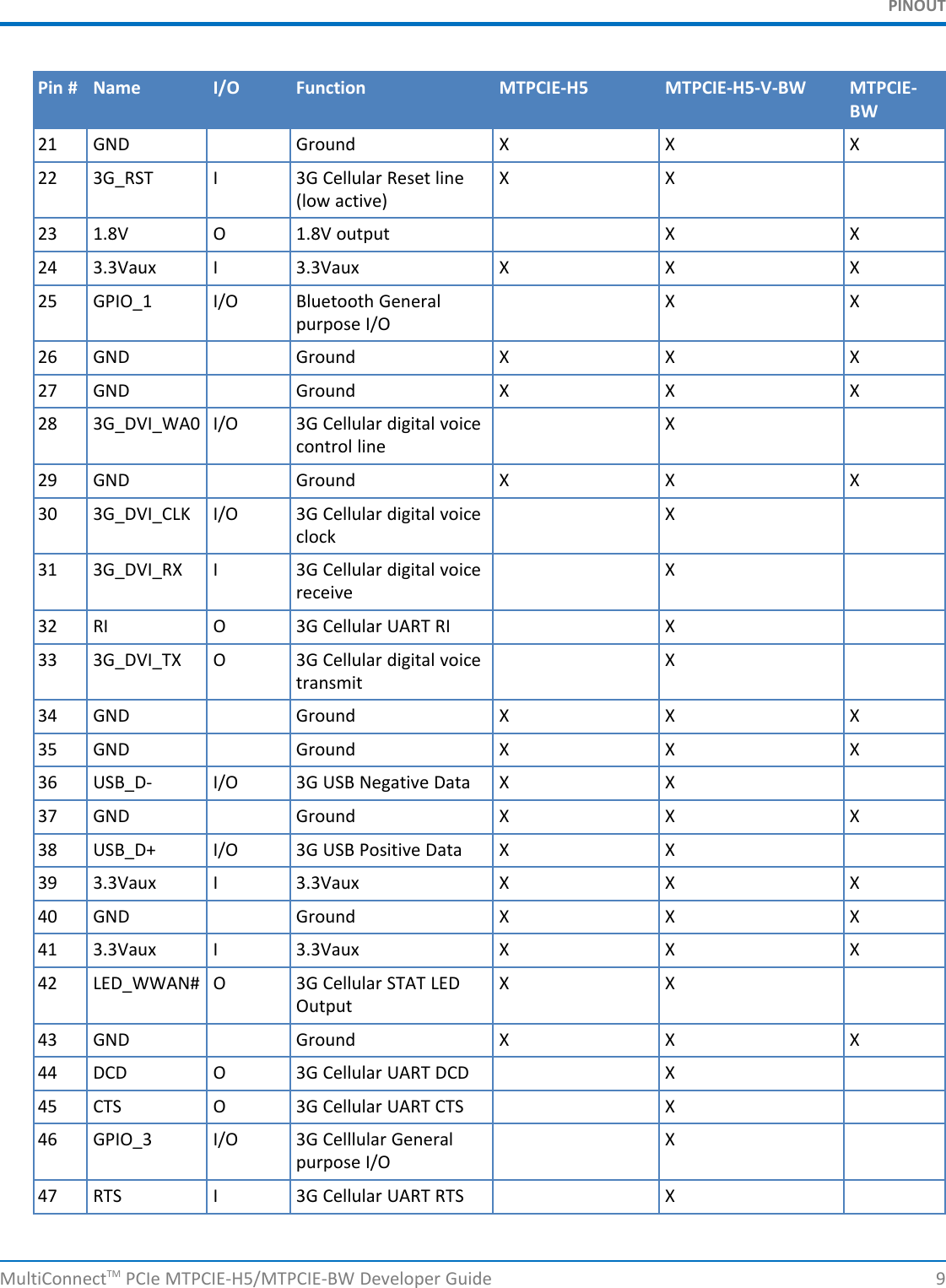
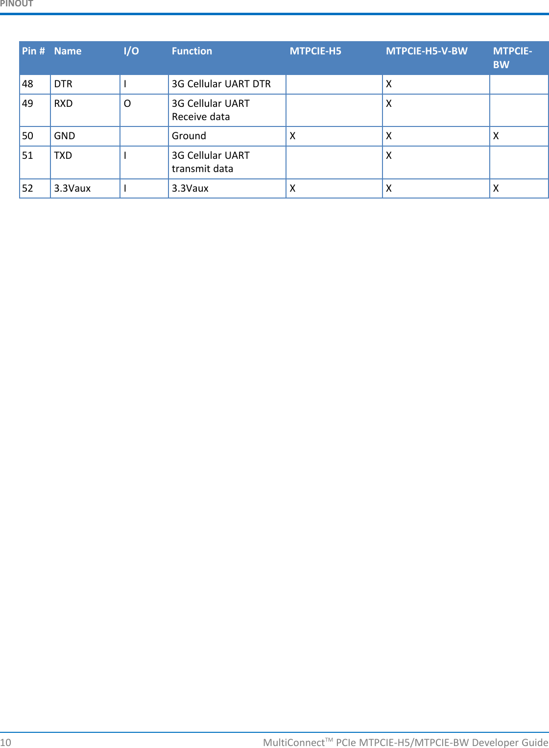
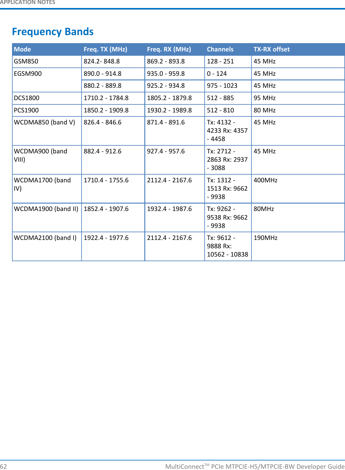
Multi Tech Systems 92U12616836 MultiConnect Embedded PCIe Cellular Modem User Manual MultiConnect PCIe H5 Developer Guide US Edition
Multi Tech Systems Inc MultiConnect Embedded PCIe Cellular Modem MultiConnect PCIe H5 Developer Guide US Edition
developer guide


![REGULATORY STATEMENTSRestriction of the Use of Hazardous Substances (RoHS)Multi-Tech Systems, IncCertificate of Compliance2011/65/EUMulti-Tech Systems confirms that its embedded products comply with the chemical concentration limitations setforth in the directive 2011/65/EU of the European Parliament (Restriction of the use of certain HazardousSubstances in electrical and electronic equipment - RoHS).These Multi-Tech products do not contain the following banned chemicals1:■Lead, [Pb] < 1000 PPM■Mercury, [Hg] < 1000 PPM■Hexavalent Chromium, [Cr+6] < 1000 PPM■Cadmium, [Cd] < 100 PPM■Polybrominated Biphenyl, [PBB] < 1000 PPM■Polybrominated Diphenyl Ether, [PBDE] < 1000 PPMEnvironmental considerations:■Moisture Sensitivity Level (MSL) =1■Maximum Soldering temperature = 260C (in SMT reflow oven)1Lead usage in some components is exempted by the following RoHS annex, therefore higher lead concentrationwould be found in some modules (>1000 PPM);- Resistors containing lead in a glass or ceramic matrix compound.International Modem RestrictionsSome dialing and answering defaults and restrictions may vary for international modems. Changing settings maycause a modem to become non-compliant with national regulatory requirements in specific countries. Also notethat some software packages may have features or lack restrictions that may cause the modem to become non-compliant.Industry Canada and FCCThis device complies with Industry Canada licence-exempt RSS standard(s) and part 15 of the FCC rules. Operationis subject to the following two conditions:(1) this device may not cause interference, and(2) this device must accept any interference, including interference that may cause undesired operation of thedevice.Cet appareil est conforme avec Industrie Canada RSS exemptes de licence standard (s) et la partie 15 des règles dela FCC. Son fonctionnement est soumis aux deux conditions suivantes:MultiConnectTM PCIe MTPCIE-H5/MTPCIE-BW Developer Guide 37](https://usermanual.wiki/Multi-Tech-Systems/92U12616836/User-Guide-2171072-Page-37.png)
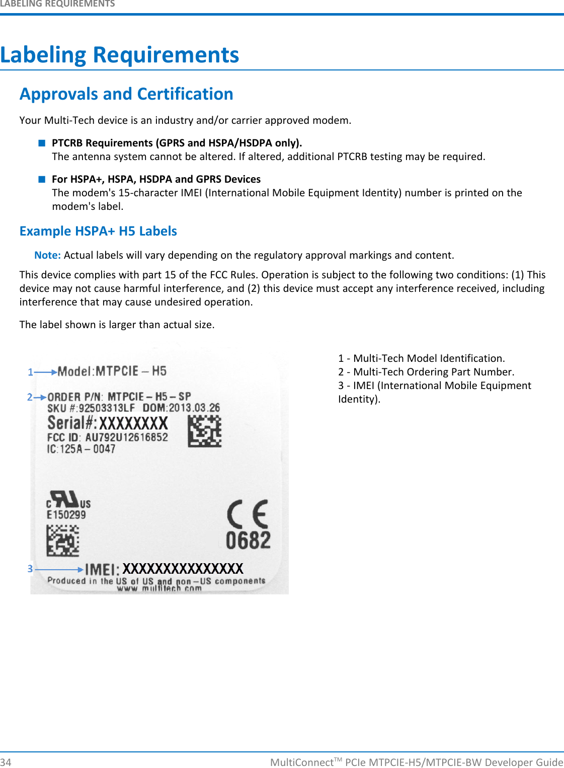
![USING LINUX WITH H5 DEVICESpathname – file name with its own path.flags – is an int specifying file opening mode: is one of O_RDONLY, O_WRONLY or O_RDWR which request openingthe file read-only, write-only or read/write, respectively.Returns:The new file descriptor fildes if successful, -1 otherwise.ExampleOpen the /dev/ttyACM0.int fd; // file descriptor for the /dev/ttyACM0 entryif((fd = open("/dev/ttyACM0", O_RDONLY) < 0){/* Error Management Routine */} else {/* ttyACM0 Device Opened */}read()The read() function reads nbyte bytes from the file associated with the open file descriptor, fildes, and copies themin the buffer that is pointed to by buf.Header Fileunistd.hPrototype:ssize_t read(int fildes, void *buf, size_t nbyte)Parameters:fildes - file descriptorbuf - destination buffer pointernbyte - number of bytes that read() attempts to readReturns:The number of bytes actually read if the operation is completed successfully, otherwise it is -1.ExampleRead sizeof(read_buff) bytes from the file associated with fd and stores them into read_buff.char read_buff[BUFF_LEN];if(read(fd, read_buff, sizeof(read_buff)) < 0){/* Error Management Routine */} else {/* Value Read */}MultiConnectTM PCIe MTPCIE-H5/MTPCIE-BW Developer Guide 71](https://usermanual.wiki/Multi-Tech-Systems/92U12616836/User-Guide-2171072-Page-71.png)
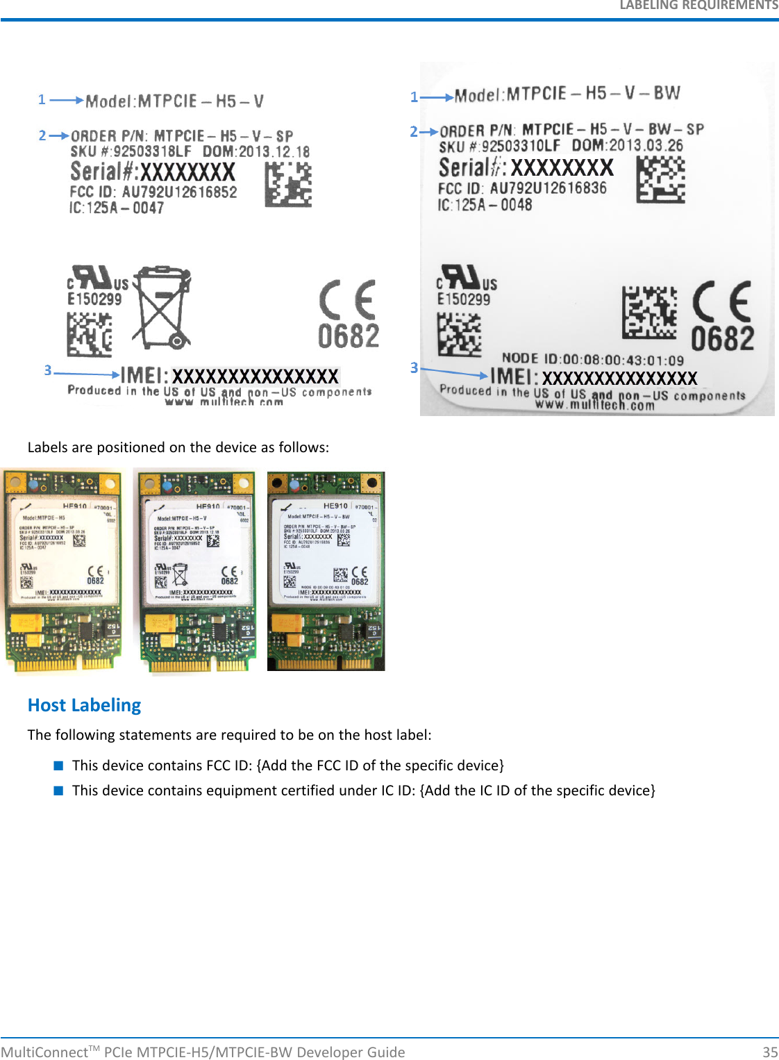
![USING LINUX WITH H5 DEVICESwrite()The write() function writes nbyte bytes from the buffer that are pointed by buf to the file associated with the openfile descriptor. fildes.Header Fileunistd.hPrototype:ssize_t write(int fildes, const void *buf, size_t nbyte)Parameters:fildes – file descriptorbuf – destination buffer pointernbyte – number of bytes that write() attempts to writeReturns:The number of bytes actually written if the operation is completed successfully, otherwise it is -1.ExampleWrite strlen(value_to_be_written) bytes from the buffer pointed by value_to_be_written to the fileassociated with the open file descriptor, fd.char value_to_be_written[] = “dummy_write”;if (write(fd, value_to_be_written, strlen(value_to_be_written)) < 0){/* Error Management Routine */} else {/* Value Written */}close()The close() function shall deallocate the file descriptor indicated by fildes. To deallocate means to make the filedescriptor available for return by subsequent calls to open() or other functions that allocate file descriptors.Header Fileunistd.hPrototype:int close(int fildes);Parameters:fildes - file descriptorReturns:0 if successful, otherwise it is -1.72 MultiConnectTM PCIe MTPCIE-H5/MTPCIE-BW Developer Guide](https://usermanual.wiki/Multi-Tech-Systems/92U12616836/User-Guide-2171072-Page-72.png)
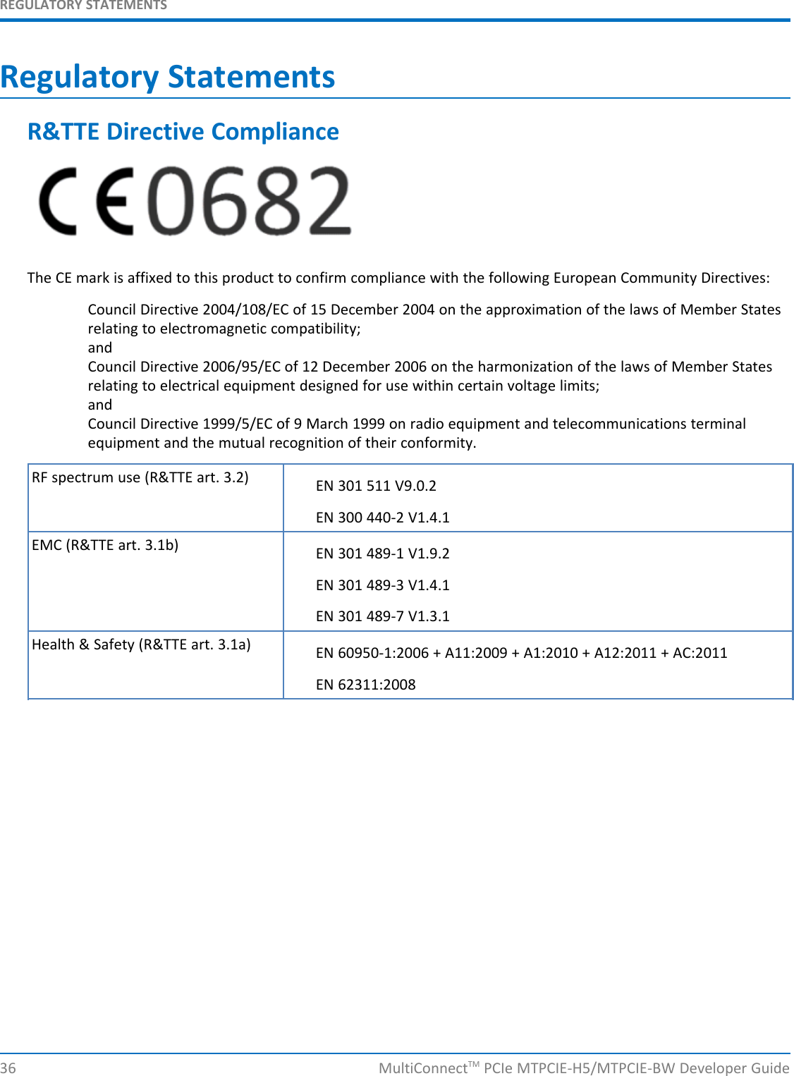
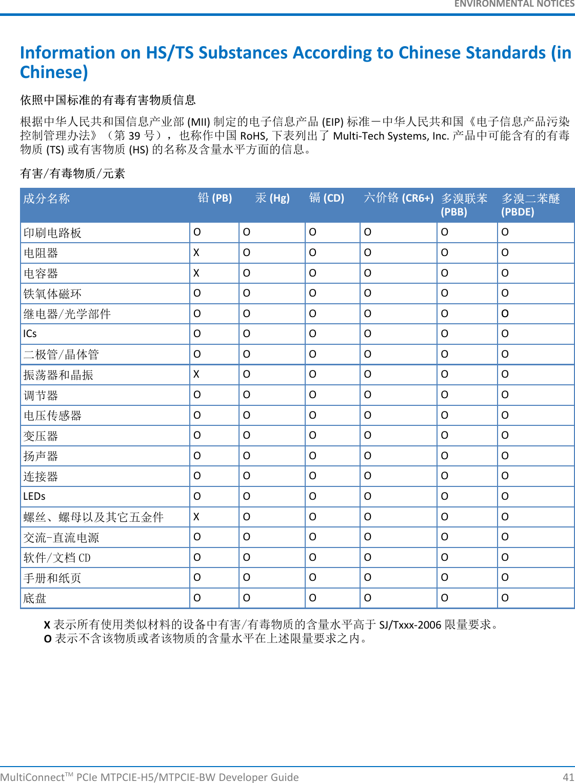
![USING LINUX WITH H5 DEVICESelseprintf ( "%s\n", "succeed" );}return (fd);}int main(){int serialFD = open_port(USB);char buf[BUFSIZE];memset(buf,0,BUFSIZE);write(serialFD, "AT\r" , strlen("AT\r"));sleep(1);read( serialFD, buf, BUFSIZE );printf("The string is: %s\n", buf);close(serialFD);return 0;}The sleep instruction is required because the modem response after issuing the AT command is not immediate, soyou need to wait a bit before reading. There are more efficient ways to do this, for example, you can put the readcall in a while loop and exit when the read buffer contains a certain string.74 MultiConnectTM PCIe MTPCIE-H5/MTPCIE-BW Developer Guide](https://usermanual.wiki/Multi-Tech-Systems/92U12616836/User-Guide-2171072-Page-74.png)