Multitone Electronics PLC TLA-FLA Alphanumeric VHF Radio Paging Receiver User Manual TM1205pr
Multitone Electronics PLC Alphanumeric VHF Radio Paging Receiver TM1205pr
UserManual.wiki
>
Multitone Electronics PLC
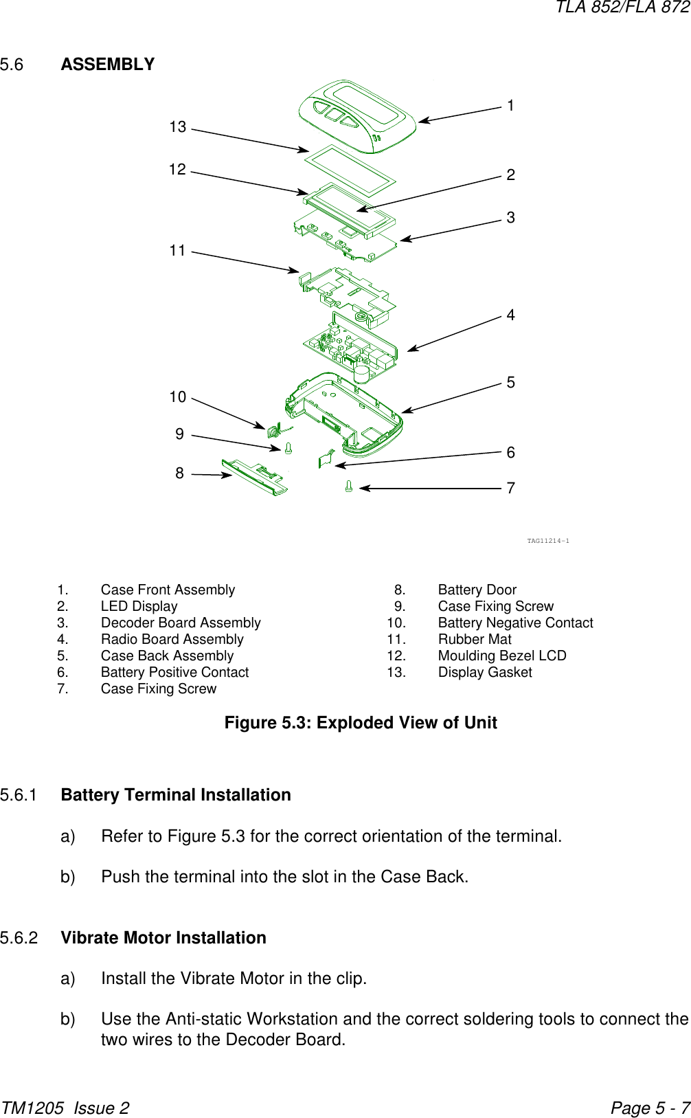
>
TLA-FLA User Manual
>
Technical Manual
Contents
1.
Technical Manual
2.
Users Guide
Technical Manual
Navigation menu
Upload a User Manual
Namespaces
Wiki Guide
HTML
PDF
Info
Views
User Manual
Discussion / Help
Navigation