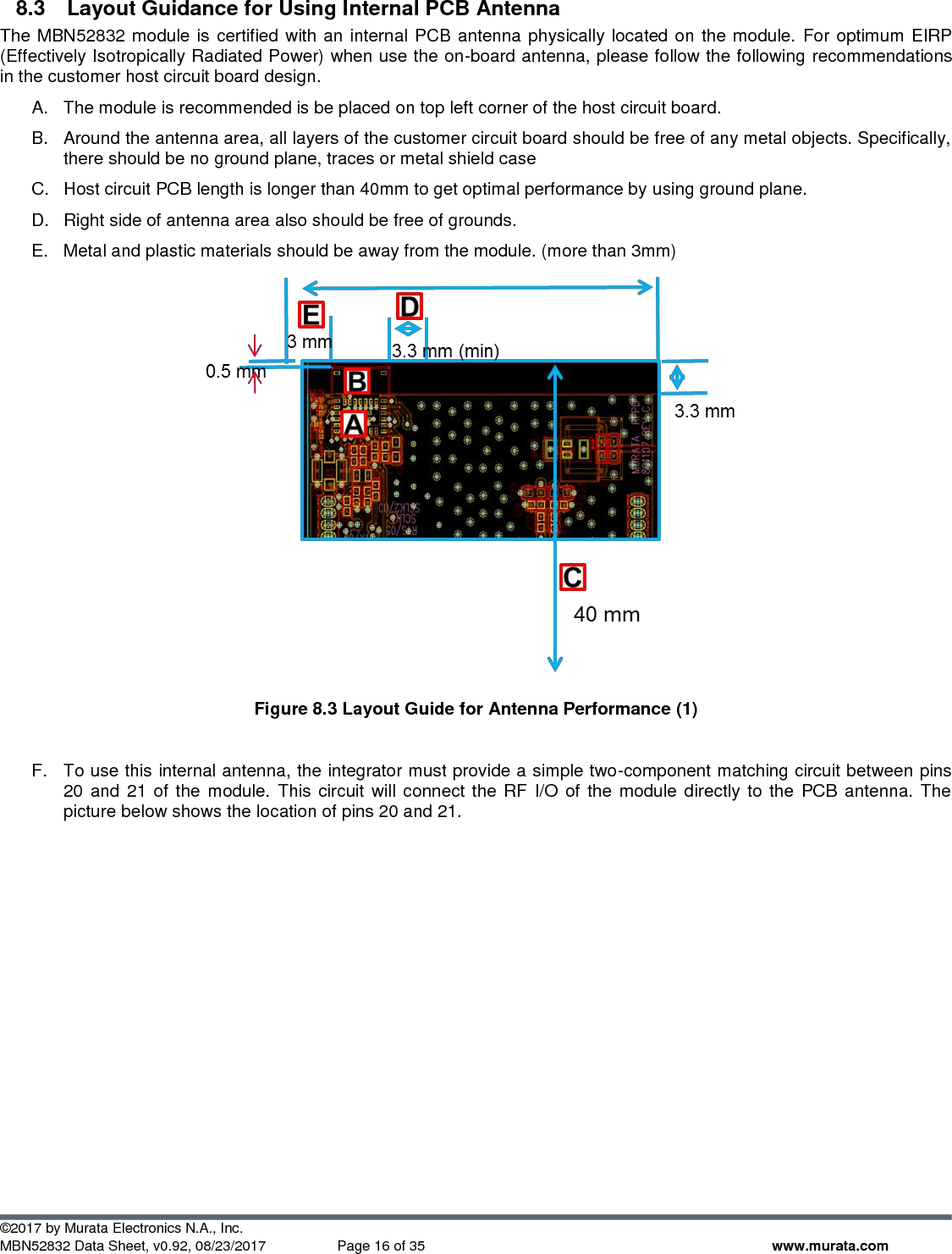
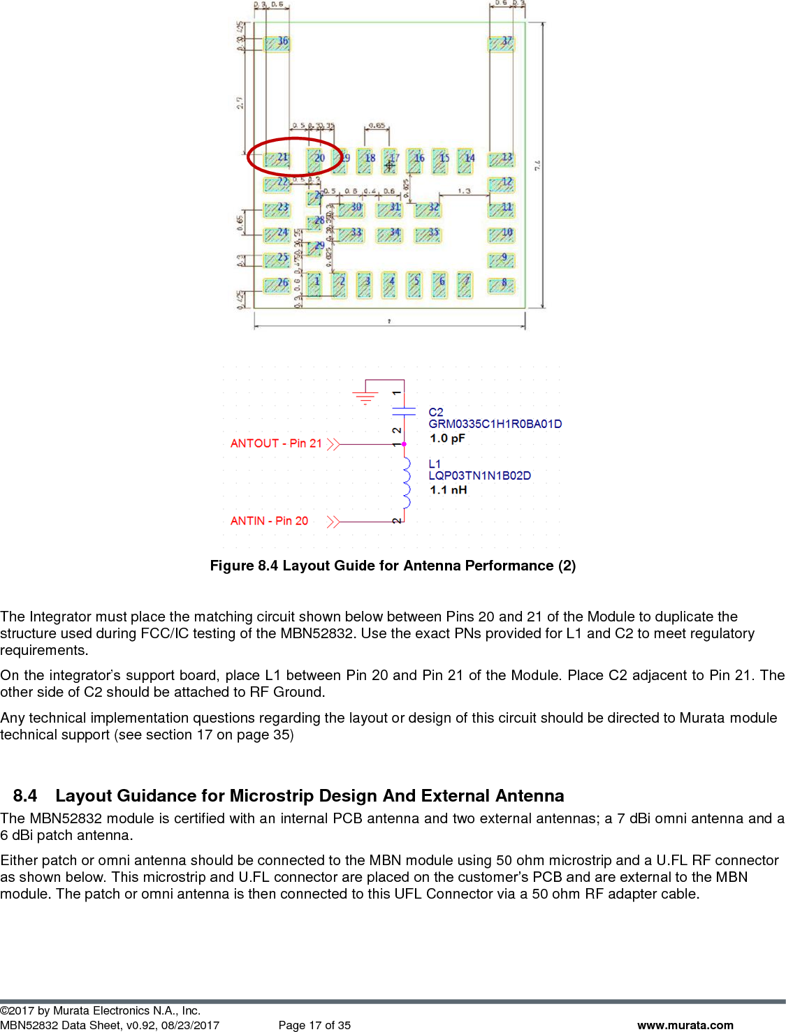
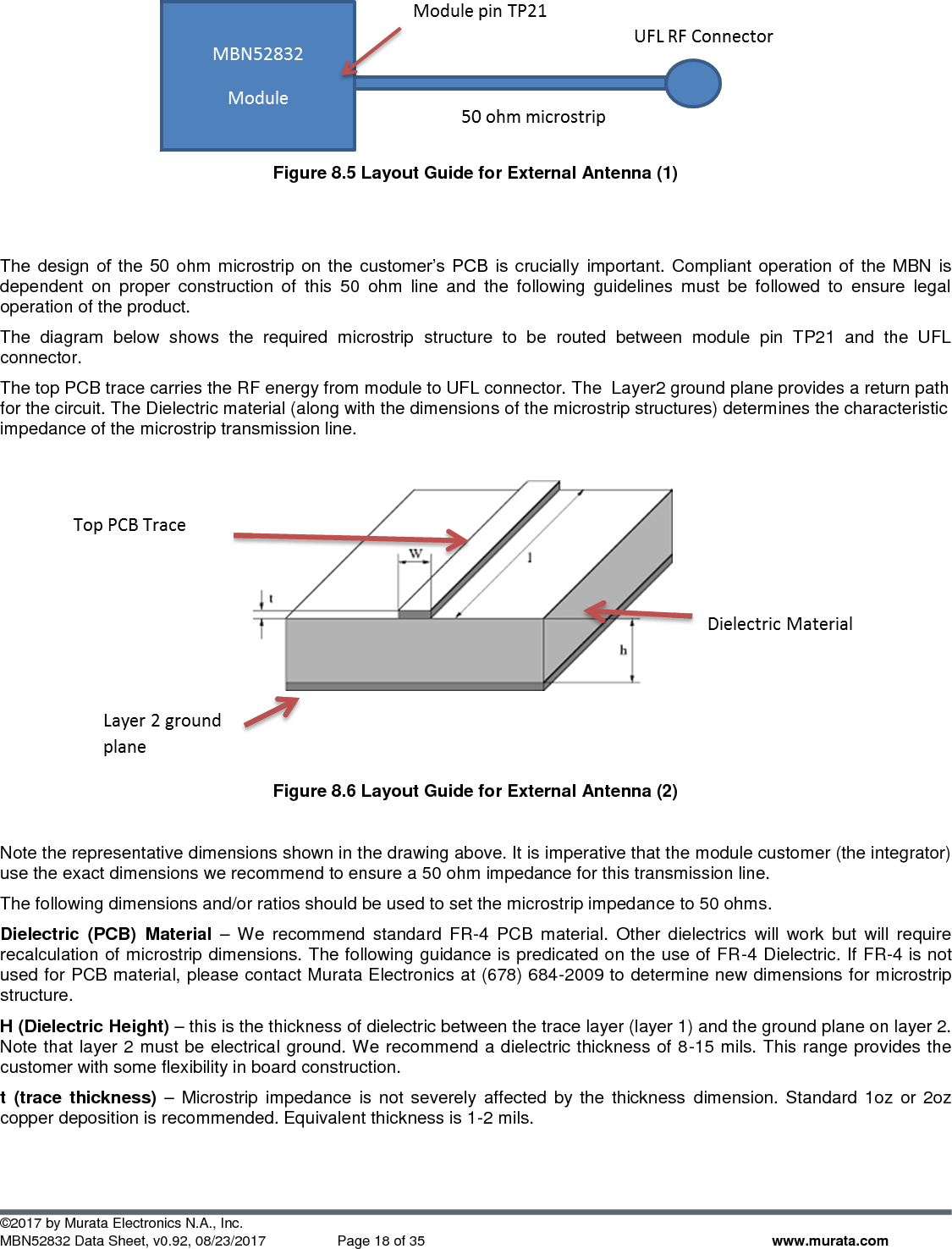
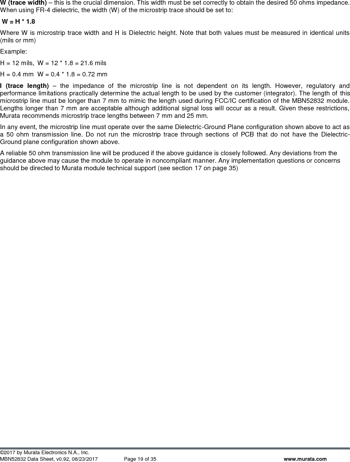
Murata Electronics North America 2832 Bluetooth Low Energy Module User Manual Manual
Murata Electronics North America Bluetooth Low Energy Module Manual
UserManual.wiki
>
Murata Electronics North America
>
2832 User Manual
Manual
Navigation menu
Upload a User Manual
Namespaces
Wiki Guide
PDF
Info
Views
User Manual
Discussion / Help
Navigation
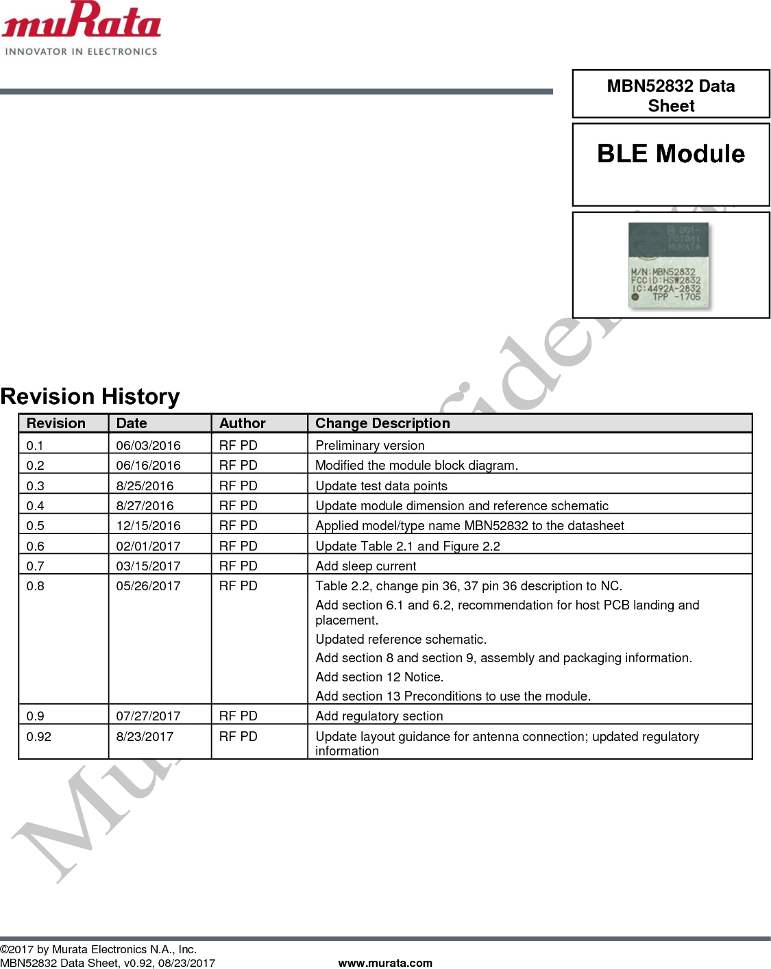
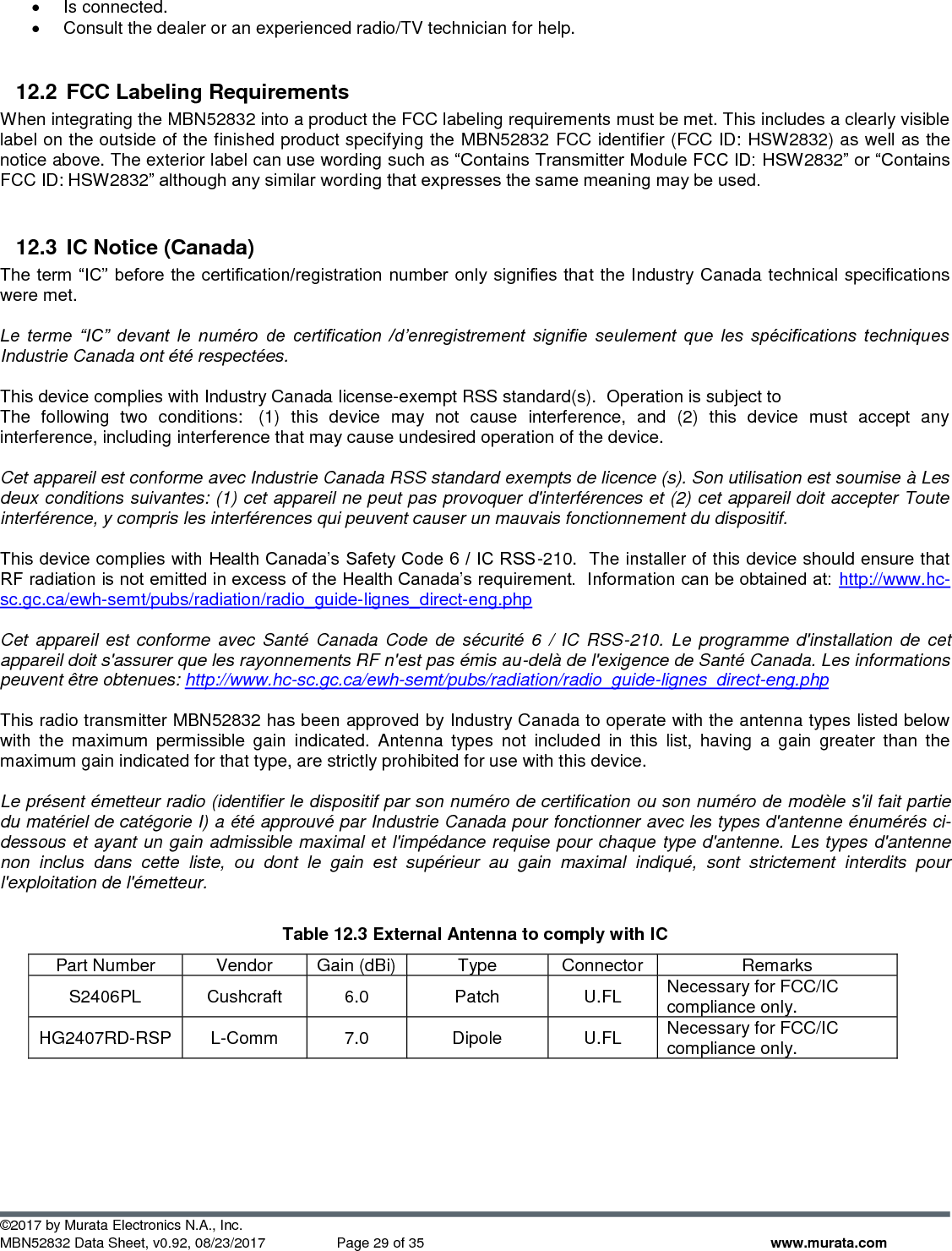
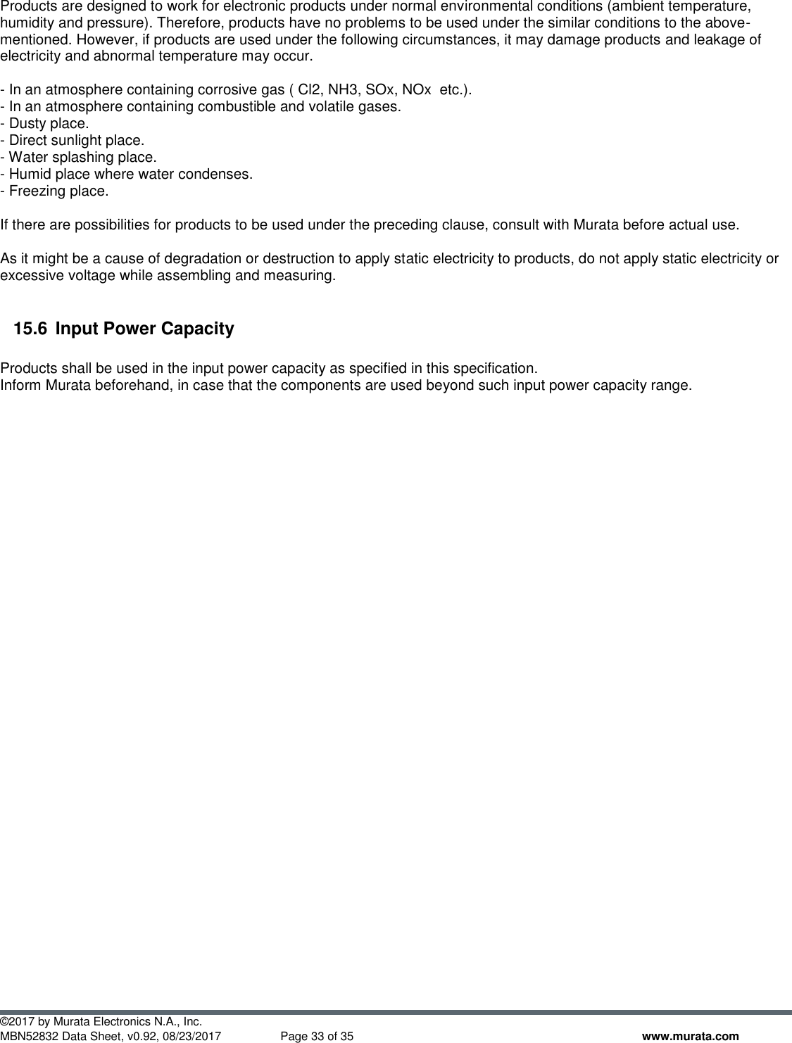
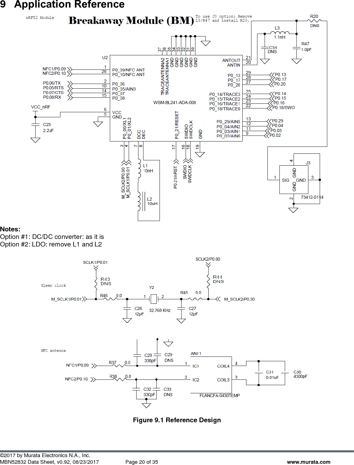
![©2017 by Murata Electronics N.A., Inc. MBN52832 Data Sheet, v0.92, 08/23/2017 Page 6 of 35 www.murata.com 1.3 Block Diagram Figure 1.1 Block Diagram 1.4 Acronyms - AIO Analog Input / Output - GPIO General Purpose Input / Output - I2C Inter-Integrated Circuit - LPCOMP Low Power Comparator - SPI Serial Peripheral Interface - UART Universal Asynchronous Receiver Transmitter 1.5 References [1] Nordic Semiconductor, nRF52832 - Product Specification v1.3, 2017 [2] Nordic Semiconductor, nRF52832-CIAA Pin assignment and mechanical dimensions, 2016 VCC UART SWD GPIO/AIO SPI Nordic nRF52832 32MHz X’tal Matching circuit 32KHz X’tal (for ANT only Optional) NFC Antenna (Optional) BLE/ANT Antenna To external or on-board antenna Inductor for DC/DC (optional)](https://usermanual.wiki/Murata-Electronics-North-America/2832/User-Guide-3544240-Page-7.png)
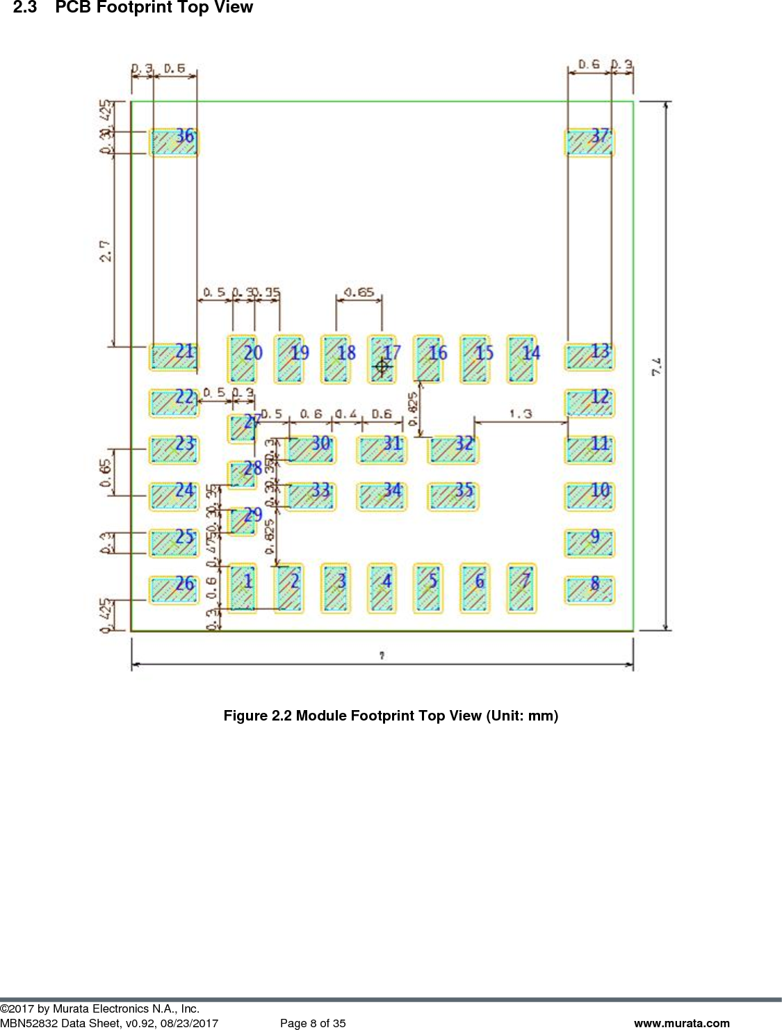
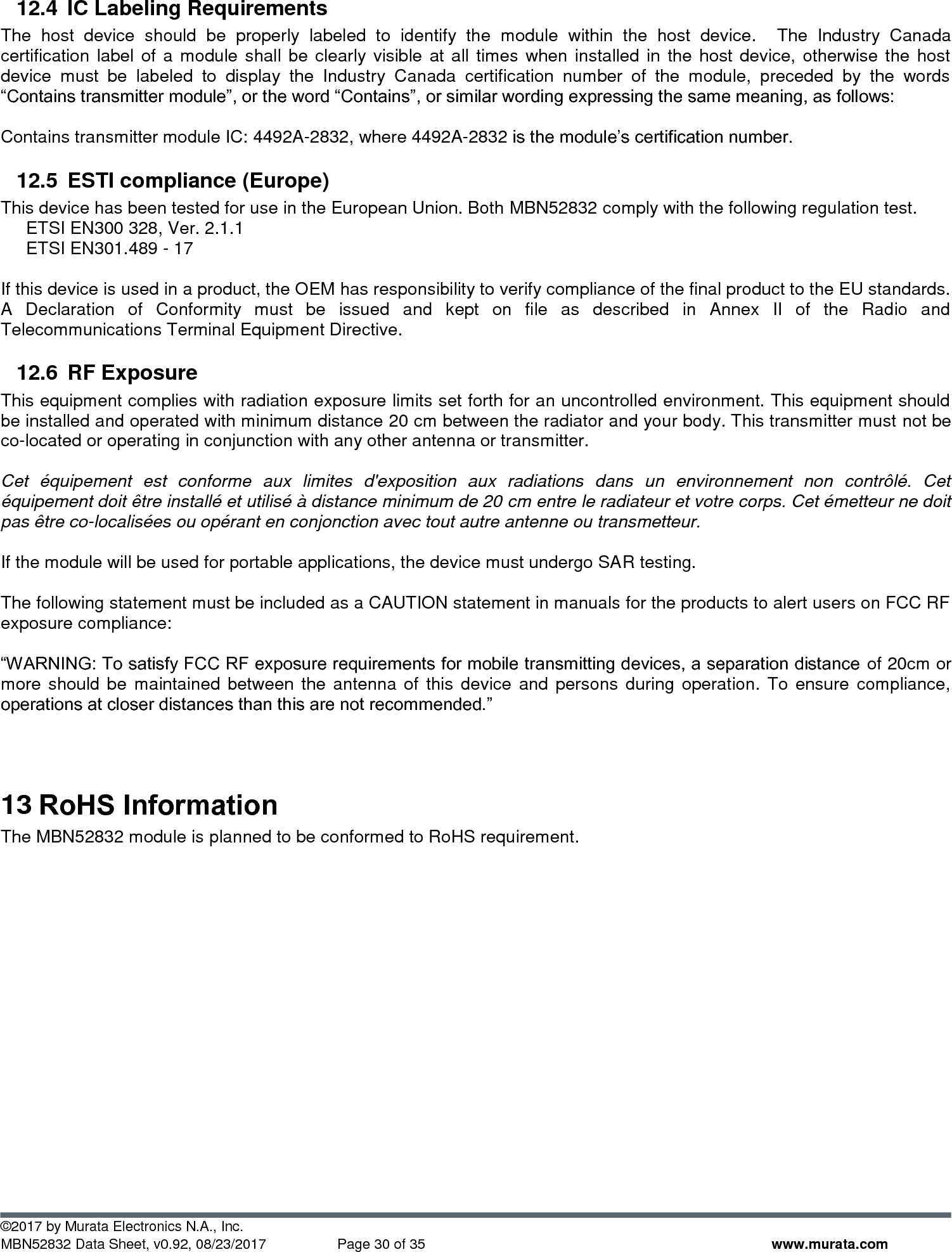
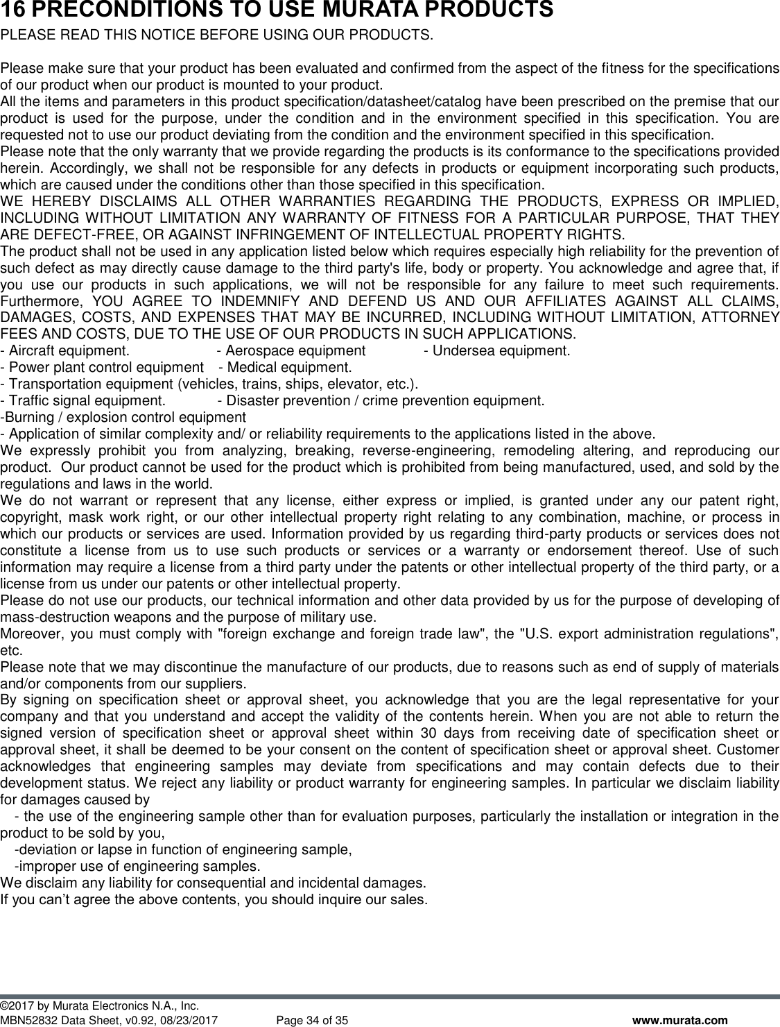
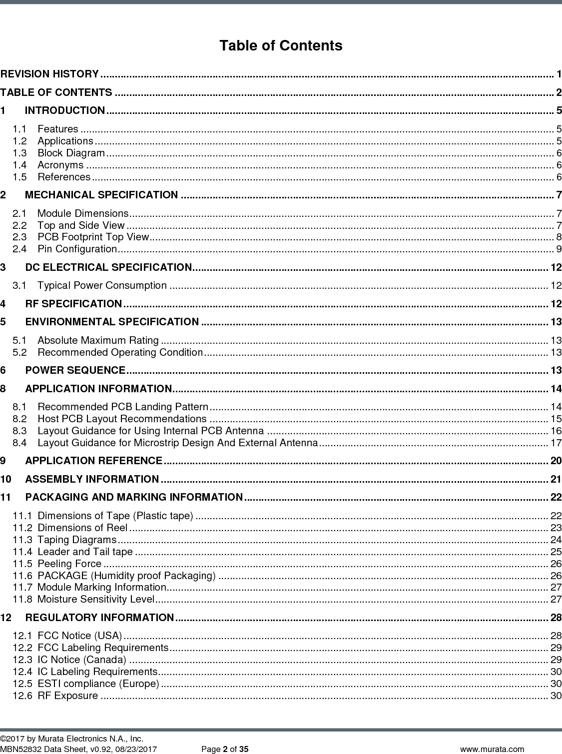
![©2017 by Murata Electronics N.A., Inc. MBN52832 Data Sheet, v0.92, 08/23/2017 Page 10 of 35 www.murata.com Table 2.2 Pinouts Pin # Pin Name Nordic IC Pin I/O Description 1 P0_09/NFC ANT P0.09/NFC I/O GPIO; NFC antenna connection. 2 P0_06 P0.06 I/O GPIO 3 P0_00/XL1 P0.00/XL1 I/O Connection for 32.768kHz crystal (LFXO); GPIO 4 P0_01/XL2 P0.01/XL2 I/O Connection for 32.768kHz crystal (LFXO); GPIO 5 GND GND 6 VCC VDD Module power supply 7 DCC DCC DC/DC converter output pin. *Refer to reference schematic. 8 DEC DEC4 1V3 regulator supply decoupling. Input from DC/DC converter. Output from 1.3V LDO. *Refer to reference schematic. 9 P0_02/AIN0 P0.02/AIN0 I/O GPIO; SAADC/COMP/LPCOMP input 10 P0_05/AIN3 P0.05/AIN3 I/O GPIO; SAADC/COMP/LPCOMP input 11 P0_03/AIN1 P0.03/AIN1 I/O GPIO; SAADC/COMP/LPCOMP input 12 P0_04/AIN2 P0.04/AIN2 I/O GPIO; SAADC/COMP/LPCOMP input 13 P0_29/AIN5 P0.29/AIN5 I/O GPIO; SAADC/COMP/LPCOMP input 14 P0_07 P0.07 I/O GPIO 15 P0_08 P0.08 I/O GPIO 16 SWDIO SWDIO I/O Serial Wire Debug I/O for debug and programming. 17 P0_21/RESET P0.21/RESET I/O GPIO; Configurable as system RESET pin 18 SWDCLK SWDCLK I/O Serial Wire Debug clock input for debug and programming. 19 GND GND GND 20 ANTIN *Refer to reference schematic. 21 ANTOUT RF signal output. Connect to ANTIN for on-board antenna or to external antenna. *Refer to reference schematic. 22 P0_18/TRACE0 P0.18/TRACEDATA[0] I/O GPIO; Trace port output; 23 P0_16/TRACE1 P0.16/TRACEDATA[1] I/O GPIO; Trace port output. 24 P0_15/TRACE2 P0.15/TRACEDATA[2] I/O GPIO; Trace port output. 25 P0_14/TRACE3 P0.14/TRACEDATA[3] I/O GPIO; Trace port output. 26 P0_10/NFC ANT P0.10/NFC I/O GPIO; NFC antenna connection. 27 P0_20 P0.20 I/O GPIO 28 P0_17 P0.17 I/O GPIO 29 P0_13 P0.13 I/O GPIO 30 GND Ground. 31 GND Ground. 32 GND Ground. 33 GND Ground.](https://usermanual.wiki/Murata-Electronics-North-America/2832/User-Guide-3544240-Page-11.png)
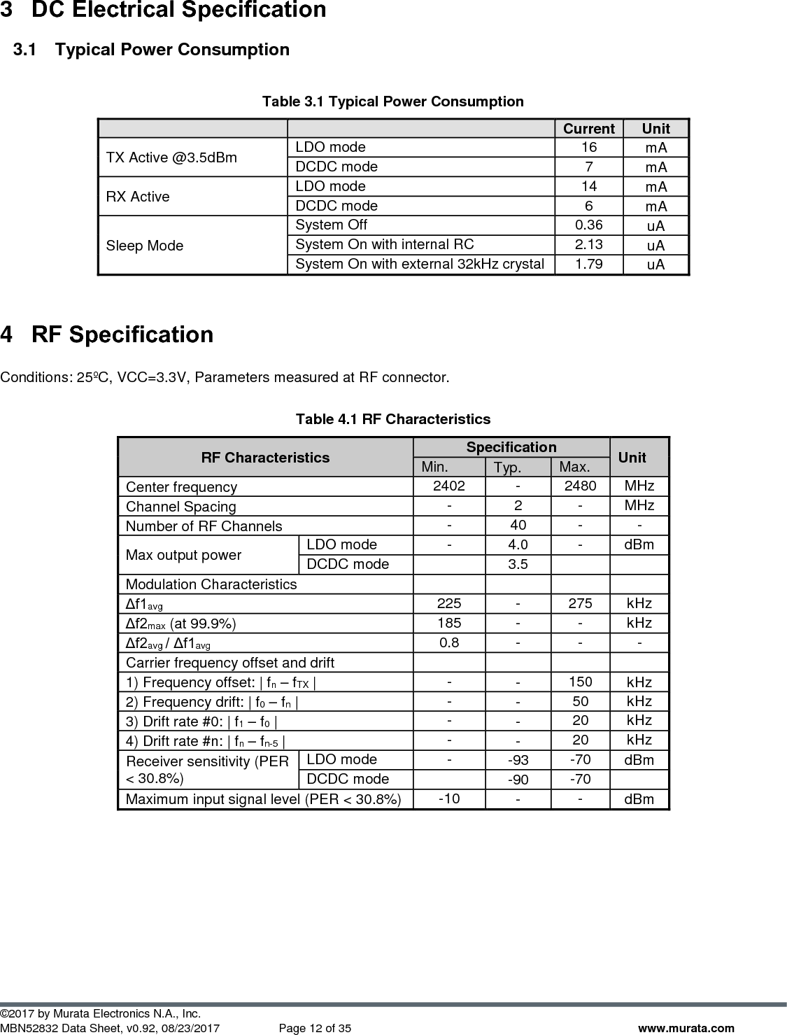
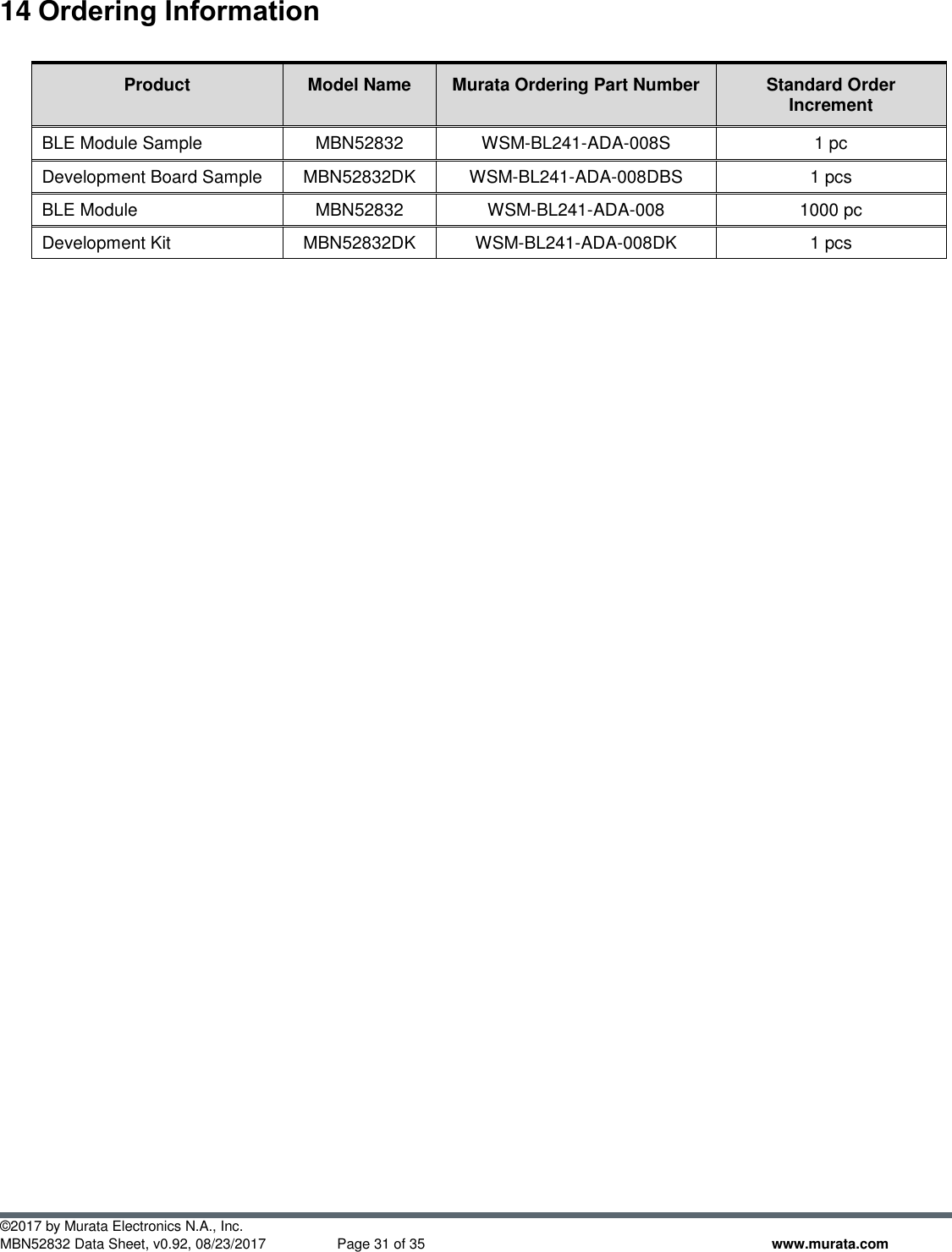
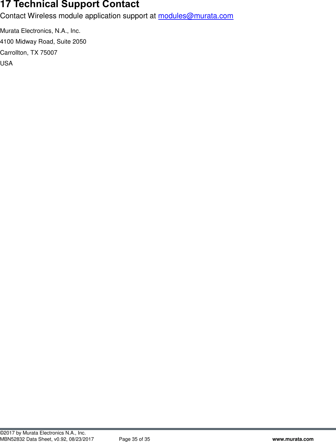
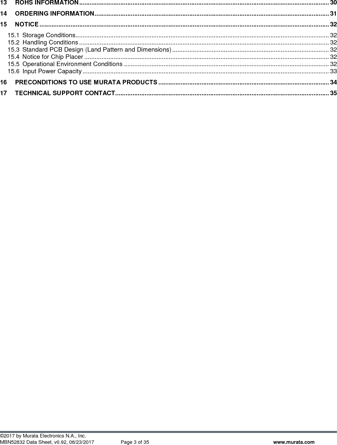
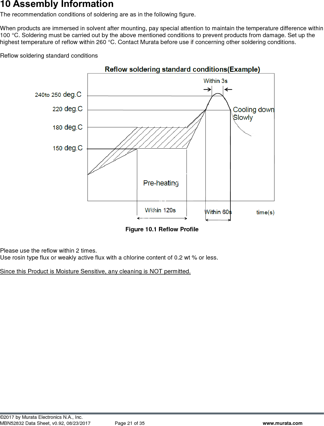
![©2017 by Murata Electronics N.A., Inc. MBN52832 Data Sheet, v0.92, 08/23/2017 Page 13 of 35 www.murata.com 5 Environmental Specification 5.1 Absolute Maximum Rating Table 5.1 Absolute Maximum Rating Description Min Max Unit Storage temperature -40 +125 °C Operating temperature -40 85 °C VCC -0.3 +3.9 V VIO, VDD ≤ 3.6 V -0.3 VCC+0.3 V VIO, VDD > 3.6 V -0.3 3.9 V NFC antenna pin current 80 mA RF input level 10 dBm 5.2 Recommended Operating Condition Table 5.2 Recommended Operating Condition Parameter Min Max Unit Operating Temperature Range -40 85 °C VCC 1.7 3.6 V Supply rise time (0V to 1.7V) 60 ms 6 Power Sequence For device start up sequence, please refer to Nordic Semiconductor, nRF52832 - Product Specification [1].](https://usermanual.wiki/Murata-Electronics-North-America/2832/User-Guide-3544240-Page-14.png)
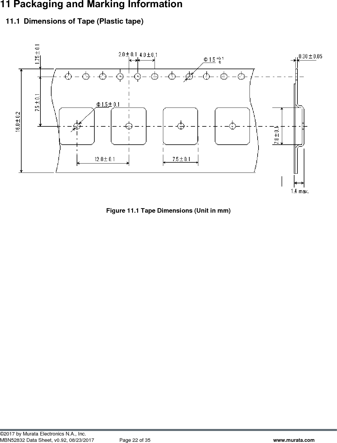
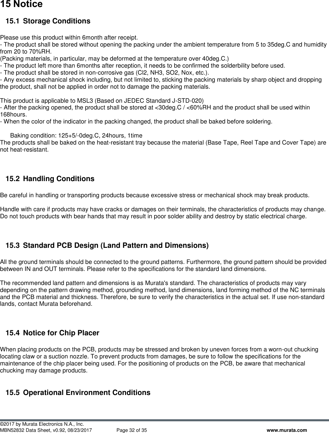
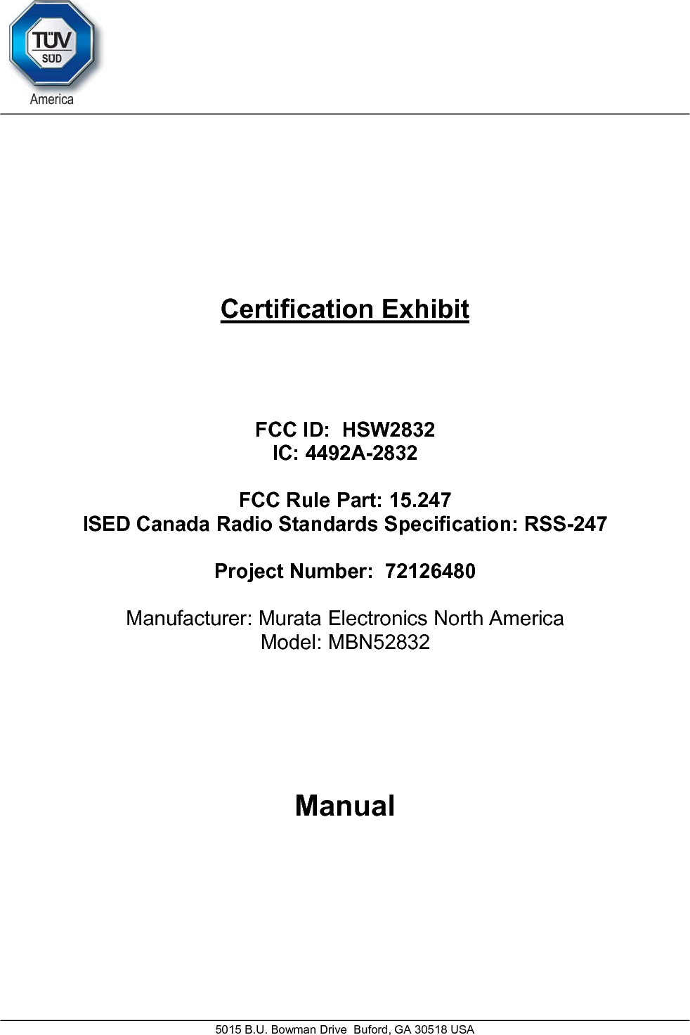
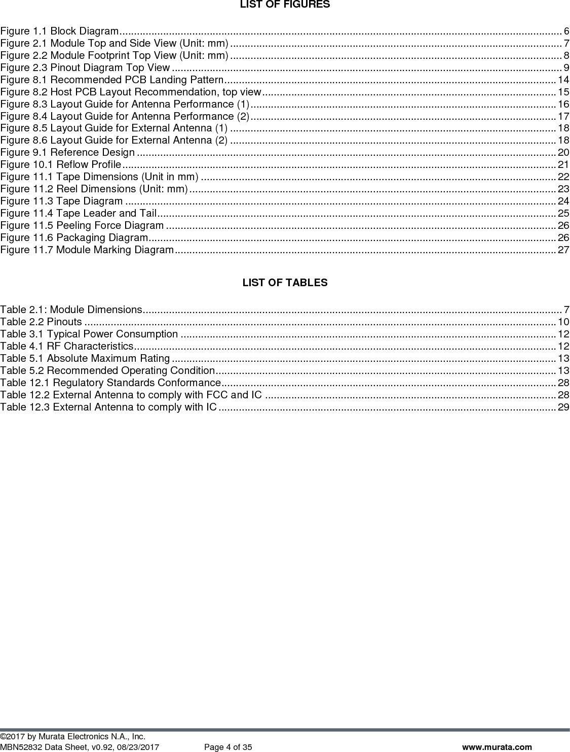
![©2017 by Murata Electronics N.A., Inc. MBN52832 Data Sheet, v0.92, 08/23/2017 Page 24 of 35 www.murata.com 11.3 Taping Diagrams [1] Feeding Hole : As specified in (1) [2] Hole for chip : As specified in (1) [3] Cover tape : 62 um in thickness [4] Base tape : As specified in (1) Figure 11.3 Tape Diagram Feeding Hole Chip Feeding Direction Pin 1 Marking](https://usermanual.wiki/Murata-Electronics-North-America/2832/User-Guide-3544240-Page-25.png)