Murata Electronics North America 3020 SYCHIP SN3020 IEEE802.15.4/ZIGBEE SMART ENERGY MODULE User Manual SN3020 Datasheet Manual v1 0
Murata Electronics North America SYCHIP SN3020 IEEE802.15.4/ZIGBEE SMART ENERGY MODULE SN3020 Datasheet Manual v1 0
Users Manual

SyChip SN3020
IEEE802.15.4/ZigBee
Smart Energy Module
User Manual
and Datasheet
Version: 1.0
February 3, 2011
Confidential Information
Note: SyChip, Inc. reserves the right to make changes in specifications at anytime and without notice. The information
furnished in this data sheet is believed to be accurate and reliable. However, no responsibility is assumed by Sychip for
its use, nor any infringements of patents or other rights of third parties resulting from its use. No license is generated
under any rights of SyChip or its supporters unless specifically agreed.

SyChip/Murata Confidential Page 2 of 26 SN3020 User Manual 1.0
Table of Contents
1 SYSTEM DESCRIPTIONS.....................................................................................................................................4
1.1 APPLICATIONS ................................................................................................................................................... 4
1.2 MODULE SUMMARY .......................................................................................................................................... 4
1.3 BLOCK DIAGRAM .............................................................................................................................................. 5
1.4 ACRONYMS........................................................................................................................................................ 5
2 MECHANICAL SPECIFICATIONS.....................................................................................................................6
2.1 MODULE DIMENSION ......................................................................................................................................... 6
2.2 MODULE TOP AND SIDE VIEW............................................................................................................................. 6
2.3 MODULE BOTTOM VIEW..................................................................................................................................... 7
2.4 DETAILED MECHANICAL DATA (TOP VIEW) ........................................................................................................ 8
2.5 MODULE PIN-OUT.............................................................................................................................................. 9
3 DC ELECTRICAL SPECIFICATIONS..............................................................................................................12
3.1 TYPICAL POWER CONSUMPTION ...................................................................................................................... 12
3.2 DIGITAL IO SPECIFICATION ............................................................................................................................. 12
4 RF SPECIFICATIONS..........................................................................................................................................13
5 ENVIRONMENTAL SPECIFICATIONS...........................................................................................................14
5.1 ABSOLUTE MAXIMUM RATINGS ....................................................................................................................... 14
5.2 OPERATION CONDITIONS.................................................................................................................................. 14
6 APPLICATION INFORMATION........................................................................................................................15
6.1 REFERENCE CONNECTION FOR UART HOST INTERFACE .................................................................................. 15
6.2 REFERENCE CONNECTION FOR THE SPI HOST INTERFACE ................................................................................ 16
6.3 RECOMMENDED HOST (CUSTOMER) CIRCUIT BOARD PCB PATTERN ................................................................ 17
6.4 HOST PCB LAYOUT RECOMMENDATIONS ........................................................................................................ 17
6.5 MODULE LOCATION......................................................................................................................................... 18
6.5.1 Location in x-y plane..................................................................................................................................19
6.5.2 Location in z-plane..................................................................................................................................... 19
7 ASSEMBLY INFORMATION .............................................................................................................................20
7.1 LEAD-FREE SOLDERING REFLOW PROFILE ........................................................................................................ 20
8 PACKAGE INFORMATION ...............................................................................................................................21
8.1 TAPE AND REEL SPECIFICATION ....................................................................................................................... 21
8.2 MODULE MARKING .......................................................................................................................................... 22
9 ORDERING INFORMATION .............................................................................................................................23
10 ROHS DECLARATION........................................................................................................................................23
11 REGULATORY INFORMATION.......................................................................................................................23
11.1 FCC NOTICE (USA) ........................................................................................................................................ 23
11.1.1 FCC Labeling Requirements .................................................................................................................24
11.1.2 RF Exposure..........................................................................................................................................24
11.2 IC NOTICE (CANADA)...................................................................................................................................... 25
11.3 CE NOTICE (EUROPE) ...................................................................................................................................... 25
12 TECHNICAL SUPPORT CONTACT .................................................................................................................26
13 REFERENCES.......................................................................................................................................................26

SyChip/Murata Confidential Page 3 of 26 SN3020 User Manual 1.0
List of Figures
FIGURE 1 SN3020 MODULE BLOCK DIAGRAM ..................................................................................................................... 5
FIGURE 2 MODULE TOP AND SIDE VIEW .............................................................................................................................. 6
FIGURE 3 MODULE BOTTOM VIEW ...................................................................................................................................... 7
FIGURE 4 DETAILED MECHANICAL DATA (TOP VIEW) .......................................................................................................... 8
FIGURE 5 UART HOST INTERFACE REFERENCE DIAGRAM ................................................................................................. 15
FIGURE 6 SPI HOST INTERFACE REFERENCE DIAGRAM ...................................................................................................... 16
FIGURE 7 RECOMMENDED HOST (CUSTOMER) PCB PATTERN ............................................................................................ 17
FIGURE 8 RECOMMENDED HOST CIRCUIT BOARD DESIGN UNDERNEATH THE MODULE .................................................... 18
FIGURE 9 RECOMMENDED LOCATIONS IN XY-PLANE .......................................................................................................... 19
FIGURE 10 LOCATIONS NOT RECOMMENDED IN XY-PLANE ................................................................................................ 19
FIGURE 11 RECOMMENDED LOCATIONS IN Z-PLANE........................................................................................................... 19
FIGURE 12 LOCATIONS NOT RECOMMENDED IN XY-PLANE ................................................................................................ 19
FIGURE 13 REFLOW PROFILE PATTERN............................................................................................................................... 20
FIGURE 14 TAPE DIMENSIONS............................................................................................................................................. 21

SyChip/Murata Confidential Page 4 of 26 SN3020 User Manual 1.0
1 System Descriptions
1.1 Applications
SyChip’s SN3020 module is a standard-based wireless transceiver targeting the Smart Energy
market with low power consumption, high transmit power (20 dBm typ.) and high receiver
sensitivity (-103 dBm). It is based upon the IEEE 802.15.4 wireless network specification. The
module can be used to develop applications supporting the ZigBee PRO Smart Energy application
profile. The SN3020 module operates in the 2.4 GHz unlicensed ISM frequency band for
worldwide deployment.
1.2 Module Summary
• Dimensions: 27.20 x 14.75 x 2.90 mm3
• Ember EM357 high-performance, integrated ZigBee/802.15.4 chipset
• Supply voltage: 2.4V to 3.4V
• Data logging memory: 8 Mbits serial flash
• Security: 128-bit AES
• Antenna: on-module
• Host Interface: SPI, UART
• Meter interface: I2C, GPIO
• ADC ports: 6 x 14-bit
• RoHS compliant
• MSL JEDEC level 3
SyChip/Murata Confidential Page 5 of 26 SN3020 User Manual 1.0
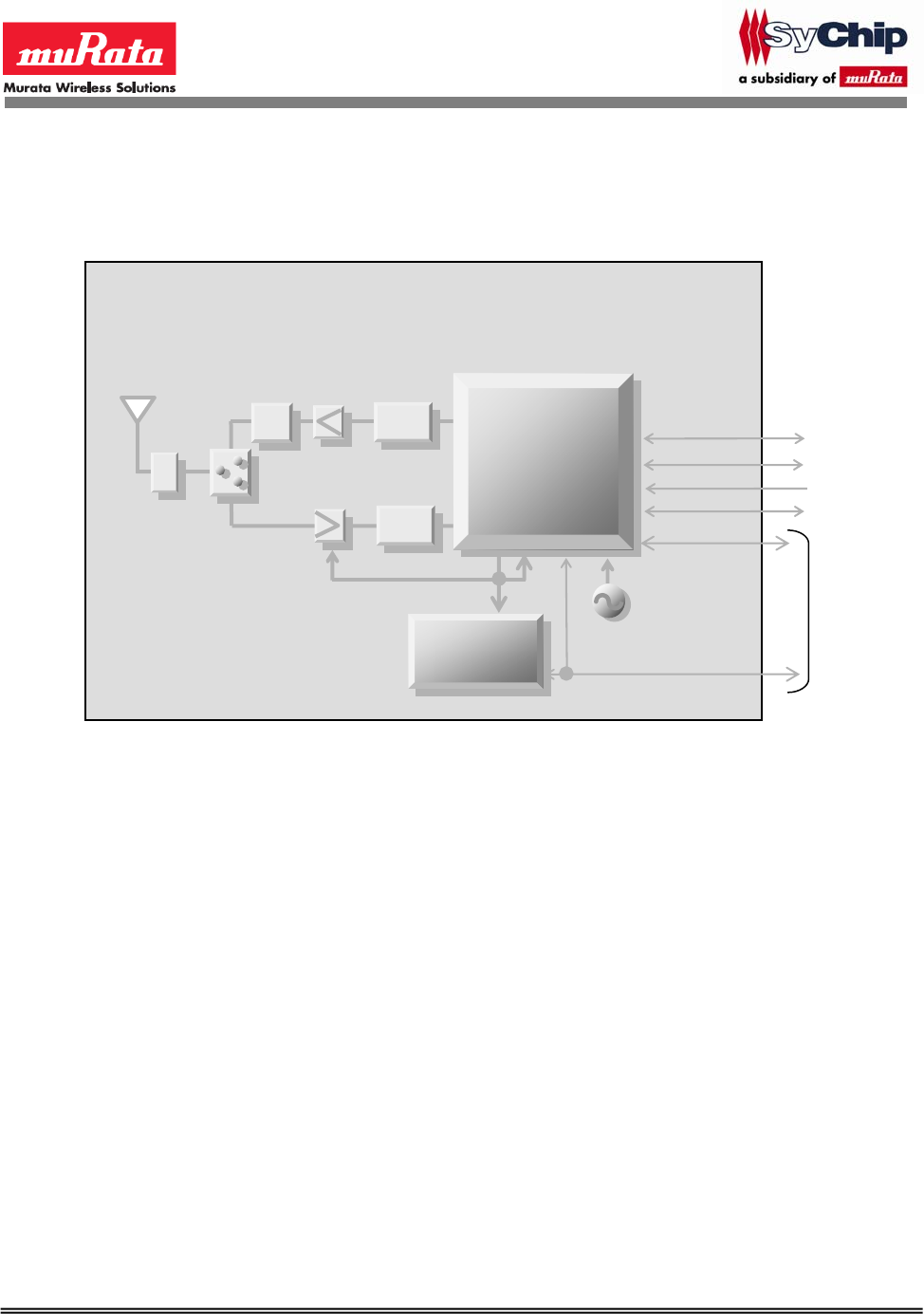
1.3 Block Diagram
Figure 1 SN3020 Module Block Diagram
1.4 Acronyms
ADC Analog to Digital Converter
AMR Automatic Meter Reading
GPIO General-Purpose Input-Output
I2C Intelligent Interface Controller
ISM Industrial, Scientific and Medical
MAC Medium Access Control
MSL Moisture Sensitivity Level
PER Packet Error Rate
ROHS Restriction of Hazardous Substances
SPI Serial Peripheral Interface
UART Universal Asynchronous Receiver-Transmitter
WPAN Wireless Personal Area Network
Balun
Balun
EM357
(ZigBee IC)
Serial Flash
(
8Mbit
)
PA
LNA
LPF
Antenna
Switch
Connector
SPDT
XTAL
(24MHz)
VREG OUT
(
1.8V
)
GPIO I/F
SPI I/F
UART I/F
nRESET
JTAG
SyChip/Murata Confidential Page 6 of 26 SN3020 User Manual 1.0
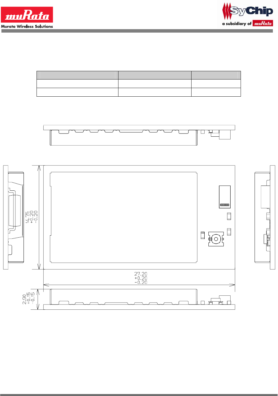
2 Mechanical Specifications
2.1 Module Dimension
Parameter Typical Units
Dimension (LxWxH) 27.20 x 14.75 x 2.90 mm
Dimension tolerances (LxWxH) ±0.20 x ±0.20 x ±0.15 mm
2.2 Module top and side view
Figure 2 Module Top and Side View
SyChip/Murata Confidential Page 7 of 26 SN3020 User Manual 1.0
2.3 Module bottom view
Figure 3 Module Bottom View
SyChip/Murata Confidential Page 8 of 26 SN3020 User Manual 1.0
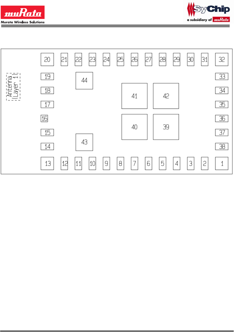
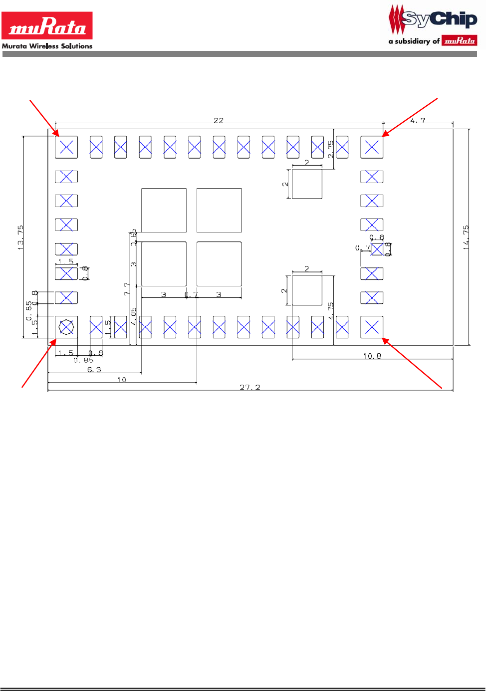
2.4 Detailed mechanical data (top view)
Pin 1 Pin 13
Pin 20
Pin 32
Figure 4 Detailed Mechanical Data (top view)
SyChip/Murata Confidential Page 9 of 26 SN3020 User Manual 1.0
2.5 Module Pin-out
Table 1 Module Connector Signal Description
Pin # Pin name I/O Description
1 GND - Ground
2 Reserved O
Internal serial flash on/off control (active low),
for debugging use only
3 PC4/JTMS I/O
Programmable I/O control available to the host,
or
JTAG mode select
4 PB0/IRQA I/O
Programmable I/O control available to the host,
or
an interrupt input
5 Reserved O
Internal serial flash nCS, for debugging use
only
6 PB6/ADC1/IRQB I/O
Programmable I/O control available to the host,
or
ADC input, or
an interrupt input
7 PC1/ADC3 I/O
Programmable I/O control available to the host,
or
an ADC input
8 SWCLK/JTCK I JTAG/Serial Wire debugging port clock
9 PC0/JRST/IRQD I/O
Programmable I/O control available to the host,
or
an interrupt input, or
the JTAG reset input
10 GND - Ground
11 PB5/ADC0 I/O
Programmable I/O control available to the host,
or
an ADC input
12 GND - Ground
13 GND - Ground
14 GND - Ground
15 GND - Ground
SyChip/Murata Confidential Page 10 of 26 SN3020 User Manual 1.0
Pin # Pin name I/O Description
16 Reserved I/O Not connected in SN3020.
17 GND - Ground
18 Reserved O
Used internally as the LNA on (active low), for
debugging use only
19 nRESET I Module reset signal (Internal pull-up)
20 GND - Ground
21 GND - Ground
22 PA3 I/O Programmable I/O control available to the host,
23 GND - Ground
24 PC6/OSC32B I/O
Programmable I/O control available to the host,
or
32.768kHZ crystal
25 PC7/OSC32A I/O
Programmable I/O control available to the host,
or
32.768kHz crystal
26 SC1SCLK/PB3 I/O
SPI port 1 clock, or
programmable I/O control available to the host,
27 Reserved O
Used internally as the serial flash MOSI, for
debugging use only
28 Reserved O
Used internally as the serial flash MISO, for
debugging use only
29 VBATT PI Module power supply
30 Reserved O
Used internally as the serial flash clock, for
debugging use only
31 PA4/ADC4 I/O
Programmable I/O control available to the host,
or ADC input
32 GND - Ground
33 PA5/ADC5/nBOOTMODE I/O
Programmable I/O control available to the host,
or
ADC input, or
Boot control, must be left open or pulled
high during the reset to enable the normal
firmware boot process.
SyChip/Murata Confidential Page 11 of 26 SN3020 User Manual 1.0
Pin # Pin name I/O Description
34 SC1MISO(s)/
SC1MOSI(m)/TXD/PB1/SC1SDA I/O
SPI port 1 MISO (slave)/ MOSI (master)
signal, UART TXD signal, I2C port 1 DATA
signal, or programmable I/O control
available to the host.
35 SC1MOSI(s)/
SC1MISO(m)/RXD/PB2/SC1SCL I/O
SPI port 1 MOSI (slave)/ MISO (master)
signal, UART RXD signal, I2C port 1 CLK
signal, or programmable I/O control
available to the host.
36 PC2/JTDO/SWO I/O
Programmable I/O control available to the host,
or
Serial Wire port OUTPUT signal, or
JTAG data out
37 SC1nSSEL/PB4 I/O
SPI port 1 slave select, or
programmable I/O control available to the host,
38 PC3/JTDI I/O
Programmable I/O control available to the host,
or
JTAG data in
39 GND - Ground
40 GND - Ground
41 GND - Ground
42 GND - Ground
43 GND - Ground
44 GND - Ground
SyChip/Murata Confidential Page 12 of 26 SN3020 User Manual 1.0
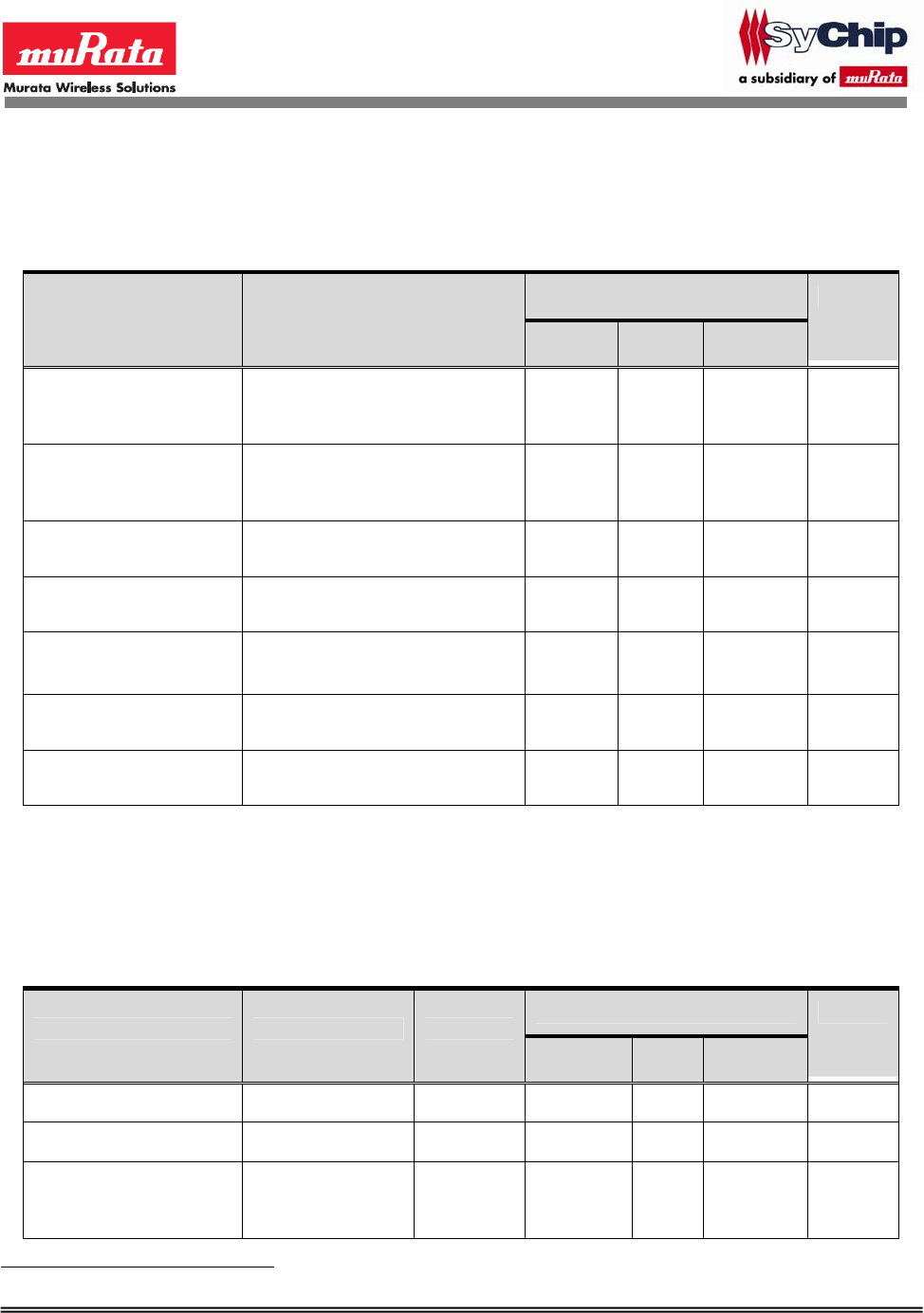
3 DC Electrical Specifications
3.1 Typical Power Consumption
Table 2 Typical Power Consumption
Values
Item Condition
Min Typ Max
Units
Sleep mode VCC = 3.0V, TAMB = 25°C
Internal RC oscillator on
Processor, radio, peripherals off
1.2 µA
Standby mode VCC = 3.0V, TAMB = 25°C
Processor on
Radio and peripherals off
12 mA
Receive mode VCC = 3.0V, TAMB = 25°C
Radio receive chain on
35 mA
Transmit mode
(+20dBm)
VCC = 3.0V, TAMB = 25°C
Radio transmit chain on
175 mA
Serial controller current For each controller at maximum
data rate
0.2 mA
General purpose timer
current
For each timer at maximum clock
rate
0.25 mA
General purpose ADC
current
At maximum sample rate, DMA
enabled
1.1 mA
3.2 Digital IO Specification
VCC = 3.0V, TAMB = 25°C, NORMAL MODE1 unless otherwise stated
Table 3 Digital IO Specification
Values
Item Condition Symbol
Min Typ Max
Units
Input current for logic 0 IIL -0.5 µA
Input current for logic 1 IIH 0.5 µA
Low Schmitt switching
threshold
Schmitt input
threshold going
from high to low
VSWIL 0.42 x VCC 0.5 x VCC V
1 NORMAL MODE as defined by Ember for EM357.
SyChip/Murata Confidential Page 13 of 26 SN3020 User Manual 1.0
High Schmitt switching
threshold
Schmitt input
threshold going
from low to high
VSWIH 0.62 x VCC 0.8 x VCC V
Output voltage for logic 0 IOL = 4mA (8mA)
for standard (high
current) pads
VOL 0 0.18 x VCC V
Output voltage for logic 1 IOH = 4mA
(8mA)for standard
(high current) pads
VOH 0.82 x VCC V
CC V
Output Source Current Standard current
pad IOHS 4 mA
Output Sink current Standard current
pad IOLS 4 mA
Output Source Current High current pad IOHH 8 mA
Output Sink current High current pad IOLH 8 mA
Total output current IOH + IOL 40 mA
4 RF Specifications
VCC = 3.0V, TAMB = 25°C, NORMAL MODE measured at 50Ω terminal load connected to the
RF connector
Table 4 RF Specifications
Parameter Min Typ Max Units
Frequency range 2400 2500 MHz
Receiver sensitivity -103 dBm
Maximum input signal level -20 dBm
Transmitter power at the maximum
setting 2 20 dBm
Adjacent channel rejection 24 dB
Alternate channel rejection 42 dB
Carrier frequency error -40 +40 ppm
2 Ember RF output power programmed to -12 by emberSetRadioPower [2] or equivalent under NORMAL mode
SyChip/Murata Confidential Page 14 of 26 SN3020 User Manual 1.0
5 Environmental Specifications
5.1 Absolute maximum ratings
Table 5 Absolute Maximum Rating
Symbol Description Min Max Units
Top Operating temperature -40 85 °C
Tst Storage temperature -40 85 °C
Vbatt Power supply -0.3 3.6 V
RFin RF input power 10 dBm
MSL Moisture Sensitivity Level 3
RoHS Restriction of Hazardous Substances Compliant
5.2 Operation conditions
Table 6 Recommended Operating Conditions
Symbol Parameter Min Typ Max Units
Vbatt Power supply 2.4 3.0 3.43 V
Top Operating temperature -40 85 °C
3 This value is handled by Firmware to meet FCC regulation for modular approval.
SyChip/Murata Confidential Page 15 of 26 SN3020 User Manual 1.0
6 Application Information
6.1 Reference connection for UART host interface
Figure 5 illustrates the connections between SN3020 module and the host MCU via UART
interface. A level shifter may be needed if the host UART interface level does not match with
SN3020.
GPIO
RXD
TXD
Host uC
nRESET
TXD
RXD
SN3020
Power supply
Figure 5 UART Host Interface Reference Diagram
SyChip/Murata Confidential Page 16 of 26 SN3020 User Manual 1.0
6.2 Reference connection for the SPI host interface
Figure 6 illustrates the connections between SN3020 module and the host MCU via SPI interface.
GPIO
SCLK
SCS
MOSI
MISO
Host uC
nRESET
SC1SCLK
SC1nSSEL
SC1MOSI
SC1MISO
SN3020
Power supply
Figure 6 SPI Host Interface Reference Diagram
SyChip/Murata Confidential Page 17 of 26 SN3020 User Manual 1.0
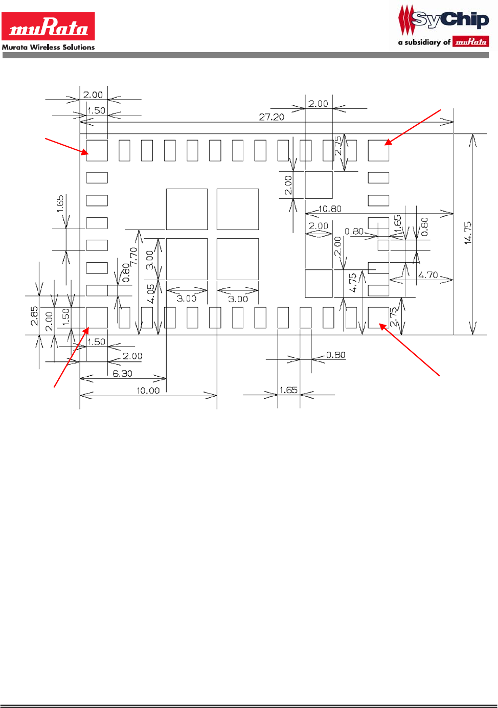
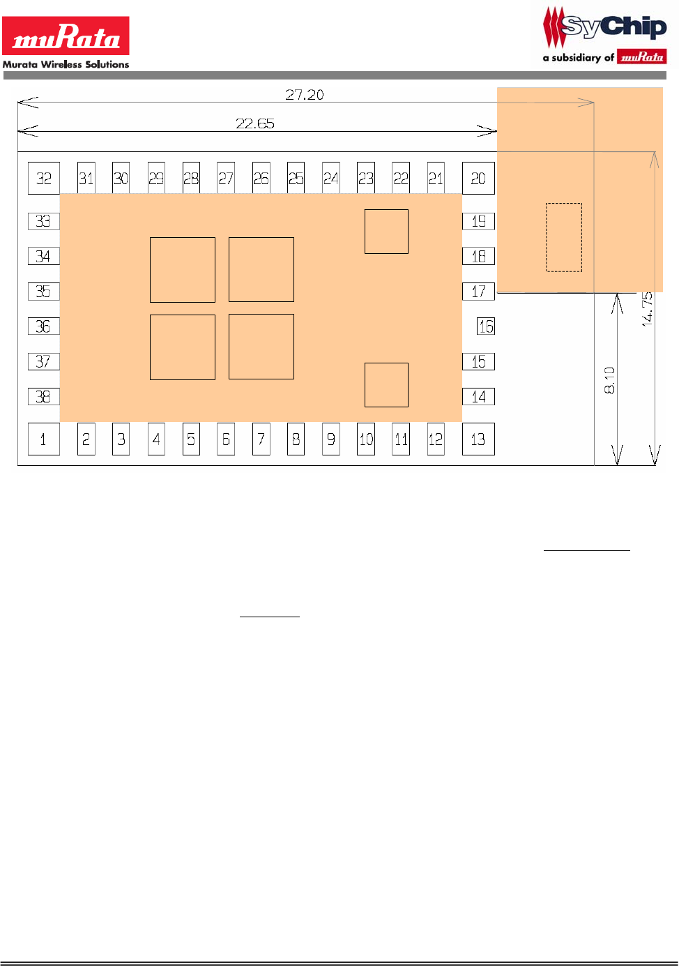
6.3 Recommended host (customer) circuit board PCB pattern
Pin 1 Pin 13
Pin 20Pin 32
Figure 7 Recommended Host (customer) PCB Pattern
6.4 Host PCB layout recommendations
The SN3020 module has an onboard antenna therefore it requires some special host PCB layout
underneath the module such that the radio can achieve its best RF performance. Refer to Figure 8
for the requirements.
SyChip/Murata Confidential Page 18 of 26 SN3020 User Manual 1.0
Zone1
Zone2
Antenna
(Layer 1)
GND GND
GND GND
GND
GND
Figure 8 Recommended Host Circuit Board Design underneath the Module
Notes:
1. Due to the surface mount antenna on the module, the area in ‘Zone1’ on all layers of the
customer circuit board should be free of any metal objects. Specifically, there should be no
ground plane, traces, or metal shield case.
2. The area in ‘Zone2’ on the top layer of the customer circuit board should have ground only
with no signal traces.
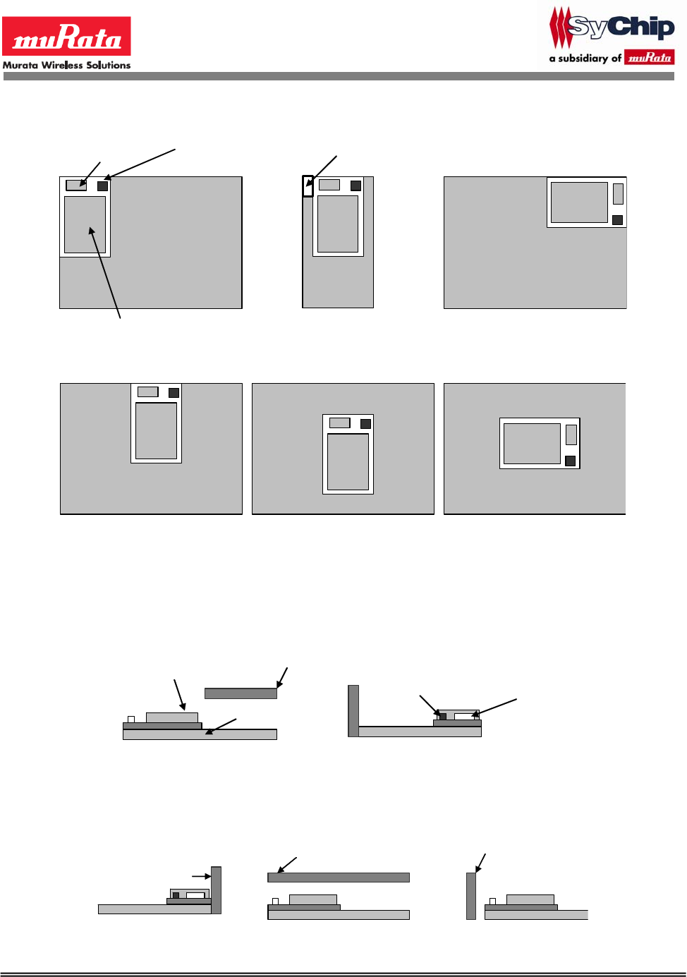
6.5 Module Location
For optimum EIRP, customer is advised to use the recommended module location on their
respective PCB.
SyChip/Murata Confidential Page 19 of 26 SN3020 User Manual 1.0
6.5.1 Location in x-y plane
Antenna Connector
Antenna
Shield Case
No GND in this area (See Fig.8)
Figure 9 Recommended Locations in xy-plane
Figure 10 Locations Not Recommended in xy-plane
6.5.2 Location in z-plane
Antenna Connector Antenna
Metal
Module
Mother Board
Metal
Figure 11 Recommended Locations in z-plane
Metal
Metal
Metal
Figure 12 Locations Not Recommended in xy-plane
SyChip/Murata Confidential Page 20 of 26 SN3020 User Manual 1.0
7 Assembly Information
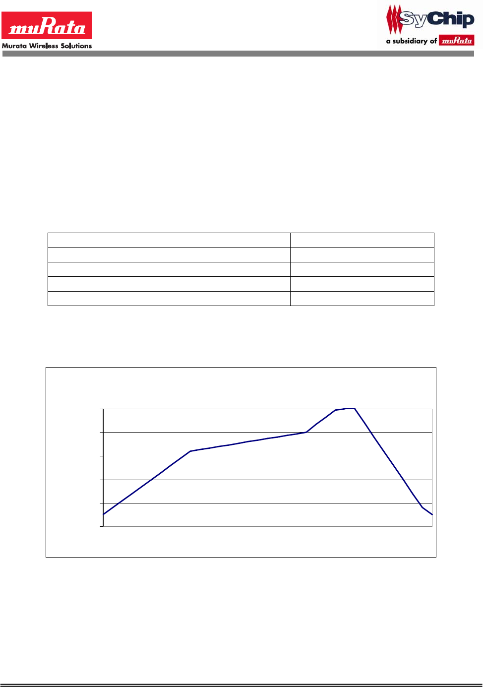
7.1 Lead-free soldering reflow profile
The lead-free solder reflow profile is recommended in the table & graph below. The profile is
used to attach the module to its host PCB.
The module is designed to withstand 2 reflows. Opposite side reflow is prohibited due to the
module weight.
Table 7 Reflow Profile Recommendation
Ramp up rate 3oC/second max
Maximum time maintained above 217oC 120 seconds
Peak temperature 250oC
Maximum time within 5oC of peak temperature 20 seconds
Ramp down rate 6oC/second max
Reflow Profile
0
50
100
150
200
250
Time, seconds
Temperature, C
Figure 13 Reflow Profile Pattern
SyChip/Murata Confidential Page 21 of 26 SN3020 User Manual 1.0
8 Package Information
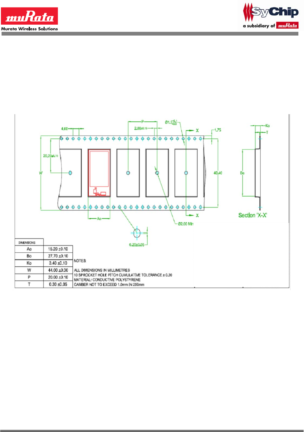
8.1 Tape and reel specification
The product will be shipped in tape and reel package.
(1) Dimensions of tape (Plastic tape)
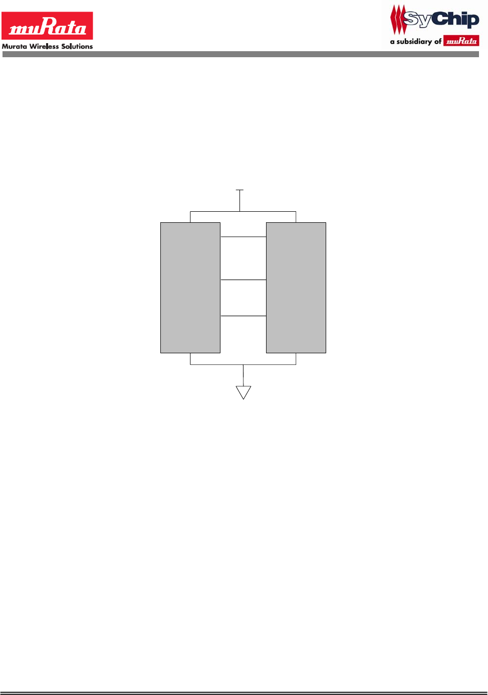
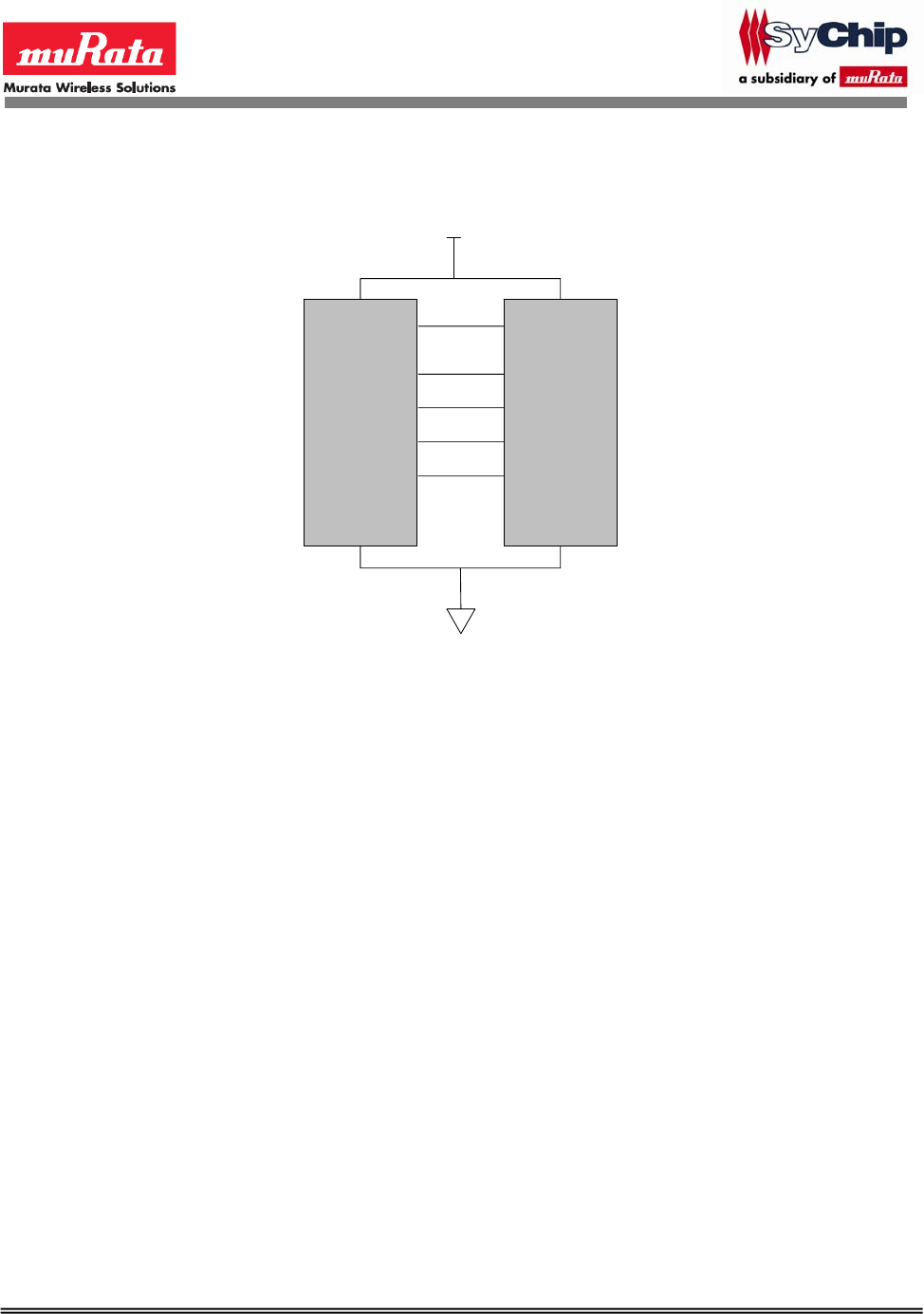
Figure 14 Tape Dimensions
(2) Dimensions of reel
TBD
SyChip/Murata Confidential Page 22 of 26 SN3020 User Manual 1.0
8.2 Module marking
The module will be marked using a label suitable for reflow soldering.
Table 8 Module Marking
Item Description
A Pin 1 ID
B Model Name
C MFG barcode in human readable form (includes module type, date code
and serial number)
D Certification Information
SyChip/Murata Confidential Page 23 of 26 SN3020 User Manual 1.0
9 Ordering Information
Table 9 Ordering Information
Product SyChip Model
Number SyChip Part
Number
Evaluation kit SN3020EVK 88-00143-85
Module SN3020 88-00143-00/01*
• -01 is for engineering sample quantities in cut tape (Ex. 5~50 pieces)
• -00 is for full production reel (950 pcs/reel)
10 RoHS Declaration
Given supplier declarations, this product does not contain substances that are banned by Directive
2002/95/EC or contains a maximum concentration of 0.1% by weight in homogeneous materials for
• Lead and lead compounds
• Mercury and mercury compounds
• Chromium (VI)
• PBB (polybrominated biphenyl)
• PBDE (polybrominated biphenyl ether)
And a maximum concentration of 0.01% by weight in homogeneous materials for
• Cadmium and cadmium compounds
11 Regulatory Information
SN3020 has obtained the certifications described below.
11.1 FCC Notice (USA)
This device complies with Part 15 of the FCC rules. Operation is subject to the following two
conditions: (1) this device may not cause harmful interference, and (2) this device must accept any
interference received, including interference that may cause undesired operation.
The FCC requires the user to be notified that any changes or modifications not expressly approved
by SyChip, Inc. may void the user’s authority to operate the equipment. While an application of the
SN3020 module in a product is not required to obtain a new FCC authorization for the module, this
does not preclude the possibility that some other form of authorization or testing may be required for
that end product.

SyChip/Murata Confidential Page 24 of 26 SN3020 User Manual 1.0
This device using the integrated antenna has been tested to comply with FCC CFR Part 15. The
device meets the requirements for modular transmitter approval as detailed in the FCC public notice
DA00.1407.transmitter given the following considerations:
• Maximum output power level for the channels as defined by IEEE 802.15.4 [1] must be set
to the value below using emberSetRadioPower or equivalent under NORMAL mode as
specified in [2].
o For channels 11 to 24, the value of -11
o For channel 25, the value of -17
o For channel 26, the value of -27
• Duty cycle of 67% allowed.
• The firmware disables power out if the source voltage is greater than 3.4V.
• VBATT must be between 2.4V – 3.4V.
This equipment has been tested and found to comply with the limits for a Class B digital device,
pursuant to Part 15 of the FCC Rules. These limits are designed to provide reasonable protection
against harmful interference in a residential installation. This equipment generates, uses and can
radiate radio frequency energy and, if not installed and used in accordance with the instructions, may
cause harmful interference to radio communications. However, there is no guarantee that
interference will not occur in a particular installation. If this equipment does cause harmful
interference to radio or television reception, which can be determined by turning the equipment off
and on, the user is encouraged to try to correct the interference by one or more of the following
measures: reorient or relocate the receiving antenna, increase the separation between the equipment
and receiver, connect the equipment into an outlet on a circuit different from that to which the
receiver is connected, or consult the dealer or an experienced radio/TV technician for help.
11.1.1 FCC Labeling Requirements
When integrating the SN3020 into a product the FCC labeling requirements must be met. This
includes a clearly visible label on the outside of the finished product specifying the SN3020 FCC
identifier (FCC ID:QPU3020) as well as the notice above. The exterior label can use wording such
as “Contains Transmitter Module FCC ID:QPU3020” or “Contains FCC ID:QPU3020” although
any similar wording that expresses the same meaning may be used.
11.1.2 RF Exposure
This module has been certified for remote and base radio applications and is not intended to be
operated within 20cm of the body. If the module will be used for portable applications, the device
must undergo SAR testing.
The following statement must be included as a CAUTION statement in manuals for the products to
alert users on FCC RF exposure compliance:
“WARNING: To satisfy FCC RF exposure requirements for mobile transmitting devices, a
separation distance of 20cm or more should be maintained between the antenna of this device and
persons during operation. To ensure compliance, operations at closer distances than this are not
recommended.”
SyChip/Murata Confidential Page 25 of 26 SN3020 User Manual 1.0
11.2 IC Notice (Canada)
The term “IC” before the certification/registration number only signifies that the Industry Canada
technical specifications were met.
Le terme “IC” devant le numéro de certification /d’enregistrement signifie seulement que les
spécifications techniques Industrie Canada ont été respectées.
This device complies with Health Canada’s Safety Code 6 / IC RSS-210. The installer of this device
should ensure that RF radiation is not emitted in excess of the Health Canada’s requirement.
Information can be obtained at: http://www.hc-sc.gc.ca/ewh-semt/pubs/radiation/radio_guide-
lignes_direct-eng.php
Cet appareil est conforme avec Santé Canada Code de sécurité 6 / IC RSS-210. Le programme
d'installation de cet appareil doit s'assurer que les rayonnements RF n'est pas émis au-delà de
l'exigence de Santé Canada. Les informations peuvent être obtenues: http://www.hc-sc.gc.ca/ewh-
semt/pubs/radiation/radio_guide-lignes_direct-eng.php
The host device should be properly labeled to identify the module within the host device. The
Industry Canada certification label of a module shall be clearly visible at all times when installed in
the host device, otherwise the host device must be labeled to display the Industry Canada
certification number of the module, preceded by the words “Contains transmitter module”, or the
word “Contains”, or similar wording expressing the same meaning, as follows:
Contains transmitter module IC:4523A-SN3020
where 4523A-SN3020 is the module’s certification number.
11.3 CE Notice (Europe)
This device has been tested and certified for use in the European Union.
If this device is used in a product, the OEM has responsibility to verify compliance of the final
product to the EU standards. A Declaration of Conformity must be issued and kept on file as
described in Annex II of the Radio and Telecommunications Terminal Equipment Directive.
The ‘CE’ mark must be placed on the OEM product per the labeling requirements of the Directive.
Given that the operating frequency band is not harmonized by a few European countries, the
restriction or alert sign must be placed along side the ‘CE’ mark as shown below. As of the date of
this document, only France has a restriction. The restriction is that, if the radio is operated outdoors
in the 2450-2483.5 MHz band, the power must be limited to 10 mW instead of 100 mW. The OEM
must account for this and the product must have the alert mark. It does not require country
notifications, however.

SyChip/Murata Confidential Page 26 of 26 SN3020 User Manual 1.0
12 Technical Support Contact
SyChip, Inc
2805 Dallas Parkway, Suite 400
Plano, TX 75093
USA
Tel: (972) 202-8900
Fax: (972) 633-0327
Note: SyChip, Inc is an operating unit within Murata Wireless Solutions
13 References
[1] IEEE Standard 802.15.4 – 2003 Wireless Medium Access Control (MAC) and Physical Layer
(PHY) Specifications for Low-Rate Wireless Personal Area Networks (LR-WPANs)
[2] Ember, “EmberZNet API Reference: For the EM35x SoC Platform”, 120-3022-000G, October
28 2010