Murata Electronics North America DM1810A Wireless Transceiver Module User Manual dm1810 916b03 vp
Murata Electronics North America Wireless Transceiver Module dm1810 916b03 vp
user manual
1
DM1810-
916MB
Rating Value Units
All Input/Output Pins Except VIN -0.3 to +3.3 V
Non-Operating Ambient Temperature Range -40 to 85 oC
Absolute Maximum Ratings
Electrical Characteristics
Characteristic Sym Notes Minimum Typical Maximum Units
Operating Frequency fO916.30 916.70 MHz
Modulation Type OOK on BPSK Spreading Code
RF Encoded Data Transmission Rate 4.8 kb/s
Average Receive Input Current, No External Power Supply Load IR5.5 mA
Receiver Input Signal for 10-3 BER, 25 °C-100 dBm
Average Transmit Input Current, No External Power Supply Load ITA 15.75 mA
Peak Transmit Input Current, No External Power Supply Load ITP 32 mA
Peak Transmitter Output Power PO10 mW
Bind Input Logic High 2.4 V
Bind Input Logic Low 0.45 V
Serial Port Data Rate 9.6 kb/s
Average Sleep Input Current, No External Power Supply Load ISA 60 µA
Power Supply Input Voltage Range, -40 to +85 oC VIN 3.1 10 V
Power Supply Input Voltage Range, 0 to +85 oC VIN 2.6 10 V
Regulated Power Supply Output Voltage, VIN 3.1 to 10 V VOUT 3.0 Vdc
Regulated Power Supply Voltage Ripple 10 mVP-P
Relative Humidity Range, Non-Condensing RH 10 90 %
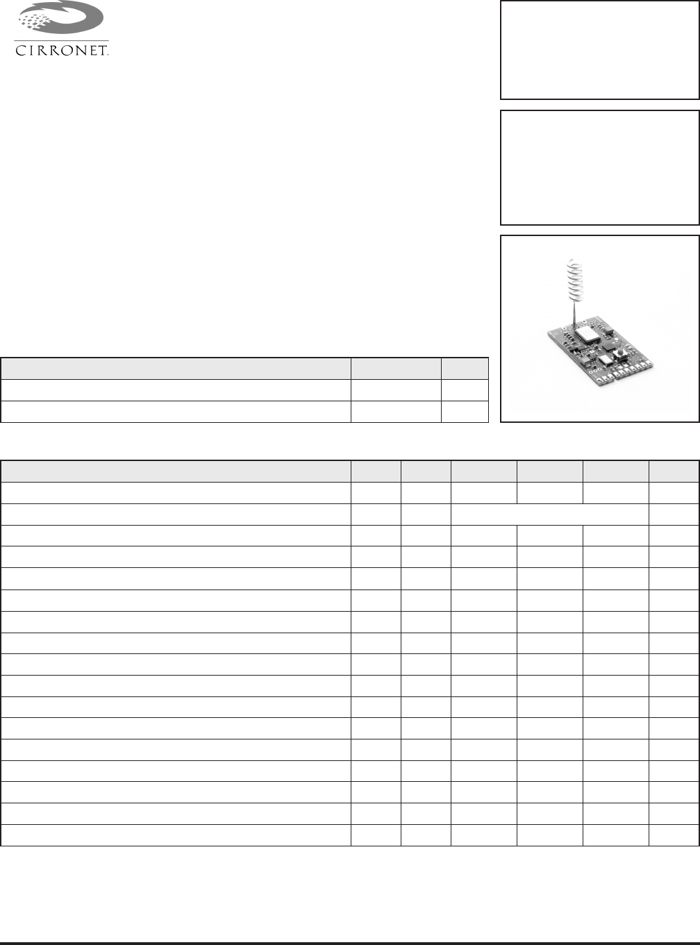
916.50 MHz
Transceiver
Module
The DM1810-916MB is the 916.50 MHz base station module in the DM1810 family of RF transceiv-
ers. The DM1810 family is designed for adding wireless mesh network connectivity to a wide range
of monitoring and control systems. The DM1810-916MB is equipped with a serial I/O port to inter-
face a host microcontroller. Radio communications range in an “open field” environment is typically
600 meters/hop. The DM1810-916MB combines RFM’s very low current ASH radio technology with
low power microcontroller technology to achieve long battery life. This module is compatible with
Cirronet’s miniMESHTM network protocol, which provides add-on “plug-and-play” multicast mesh
network routing. The DM1810-916MB is certified for operation under FCC 15.247 and Canadian
RSS 210 regulations.
•Base Station with Host Serial Interface
•Compatible with Cirronet miniMESHTM Network Protocol
•3 V, Very Low Current Operation
•Ready-to-Use OEM Module
2
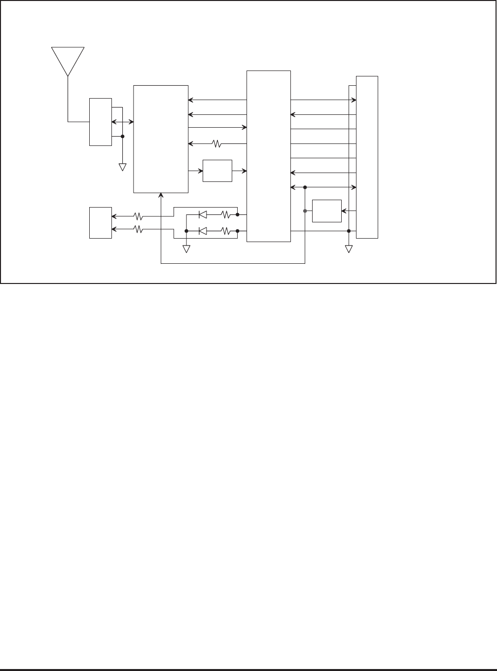
Theory of Operation
The major components of the DM1810-916MB include
an RFM TR8100 ASH transceiver and a Microchip
PIC16F689 microcontroller. The TR8100 operates on
a frequency of 916.50 MHz, at a nominal output power
of 10 mW.
The 16F689 provides a 9.6 kb/s serial interface for
communication with a host microcontroller. A compan-
ion interface board, the IM1800, is available with USB
bridge circuitry to interface the DM1810-916MB to a
host PC. The DM1810 includes two LEDs that indicate
the module’s operating mode.
The DM1810-916MB firmware is based on Cirronet’s
miniMESH network protocol, which utilizes time-syn-
chronized redundant routing to provide robust, deter-
ministic packet delivery though a network with up to 15
routers. Network configuration and maintenance fea-
tures are built into the miniMESH protocol, simplifying
commissioning and operating logistics. The firmware
also includes several sleep cycling methods for ex-
tended battery life operation.
Please refer to the DM1810 User’s Guide and the
AN1810 series Application Notes for installation and
application programming information. See Cirronet’s
web site at www.Cirronet.com.
DM1810-916MB FCC Certification
The DM1810-916MB hardware has been certified for
operation under FCC Part 15 Rules, Section 15.247.
The antenna(s) used for this transmitter must be in-
stalled to provide a separation distance of at least
20 cm from all persons and must not be co-located or
operating in conjunction with any other antenna or
transmitter.
FCC Notices and Labels
This device complies with Part 15 of the FCC rules.
Operation is subject to the following two conditions:
(1) this device may not cause harmful interference,
and (2) this device must accept any interference re-
ceived, including interference that may cause unde-
sired operation.
A clearly visible label is required on the outside of the
user’s (OEM) enclosure stating that this product con-
tains a DM1810-916MB transceiver assembly, FCC
ID: HSW-DM1810A. WARNING: This device oper-
ates under Part 15 of the FCC rules. Any modification
to this device, not expressly authorized by Cirronet,
Inc., may void the user’s authority to operate this de-
vice.
T X M O D
R X D A T A
C N T R L 1
C N T R L 0
P I C
1 6 F 6 8 9
µ P
D M 1 8 1 0 - 9 1 6 M B B l o c k D i a g r a m
L E D 1
L E D 2
T R 8 1 0 0
A S H
T r a n s c e i v e r
G N D
S E R I A L T X
S E R I A L R X
B I N D
G N D
V O U T
V I N
3 V
R e g
G N D
G N D
J 1 - 1
J 1 - 2
J 1 - 3
J 1 - 4
J 1 - 5
J 1 - 6
J 1 - 7
J 1 - 8
J 1 - 9
J 1 - 1 0
J 3 - 2
J 3 - 1
J 3 - 3
R S S I
J 4 - 1
J 4 - 2
D 1
D 2
Figure 1

Canadian Department of Communications Industry
Notice - IC: 4492A-DM1810A
This apparatus complies with Health Canada’s Safety
Code6/ICRSS210.
To prevent radio interference to the licensed service,
this device is intended to be operated indoors and
away from windows to provide maximum shielding.
Equipment (or its transmit antenna) that is installed
outdoors may be subject to licensing.
ICES-003
This digital apparatus does not exceed the Class B
limits for radio noise emissions from digital apparatus
as set out in the radio interference regulations of In-
dustry Canada.
Le present appareil numerique n’emet pas de bruits
radioelectriques depassant les limites applicables aux
appareils numeriques de Classe B prescrites dans le
reglement sur le brouillage radioelectrique edicte par
Industrie Canada.
3
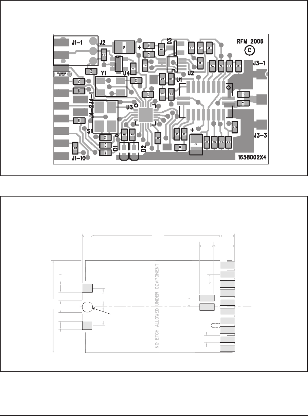
Pin Name Description
J1-1 GND This pad is a signal and power supply ground.
J1-2 VIN This is the power supply input pad. The allowed input voltage range is 2.6 to 10 V.
J1-3 VOUT
VOUT tracks 50 to 100 mV below VIN when VIN is in the range of 2.6 to 3.1 V. When VIN is in the range of 3.1
to 10 V, VOUT is regulated at 3.0 Vdc. Up to 10 mA can be supplied from this pad for powering external circuits
such as thermistor-resistor networks. External circuitry must not impress more than 10 mVp-p ripple on the regu-
lated output voltage.
J1-4 BIND
This pad is connected to a logic input on the microcontroller, and is configured with a weak pull-up. When this
pin is momentarily grounded to J1-1 or J1-10, the module is placed into the bind mode, allowing this module to
be associated with other modules to form a network.
J1-5 - This pad is unused in base station operation. Leave this pad electrically unconnected.
J1-6 - This pad is unused in base station operation. Leave this pad electrically unconnected.
J1-7 - This pad is unused in base station operation. Leave this pad electrically unconnected.
J1-8 SERIAL RX
This pad is connected to the module’s serial data input (USART). Data to this pin is received at 9.6 kb/s, using
8 data bits, no parity, and one stop bit. The input voltage range on this pad is 0 to VOUT. Applying a voltage
outside of this range may damage the module.
J1-9 SERIAL TX This pad is connected to the module’s serial data output (USART) through a 1 kilohm resistor, which provides
short-circuit protection. Data from this pad is sent at 9.6 kb/s, using 8 data bits, no parity, and one stop bit.
J1-10 GND This pad is a signal and power supply ground.
J3-1 GND This pad is a ground for the antenna port.
J3-2 ANT This pad is the antenna port.
J3-3 GND This pad is a ground for the antenna port.
J4-1 D1 This pad is the LED 1 signal.
J4-2 D2 This pad is the LED 2 signal.
CAUTION: Electrostatic Sensitive Device. Observe precautions when handling.
DM1810-916MB I/O Pad Descriptions
4
D M 1 8 1 0 - 9 1 6 M B I / O P a d L a b e l s
S E R I A L T X
S E R I A L R X
G N D
B I N D
V O U T
V I N
G N D
G N D
R F I O
G N D
D 1
D 2
Figure 2
1.485
D M 1 8 1 0 - 9 1 6 M B S M T M o u n t i n g P a t t e r n
1.000
. 1 3 0 . 0 9 0. 0 9 0
. 2 0 0 . 2 0 0
. 0 7 0 T Y P
D i m e n s i o n s i n i n c h e s . P C B p l u s c o m p o n e n t h e i g h t i s . 1 7 0 m a x ;
P C B p l u s a n t e n n a h e i g h t i s 2 . 1 5 m a x
. 1 0 0 T Y P
. 1 2 0 . 1 8 0
. 1 0 0
. 1 2 0
. 0 9 5
P l a c e . 1 0 0 u n p l a t e d
a n t e n n a c l e a r a n c e h o l e
u n d e r a n t e n n a p a d ( d o
n o t s o l d e r a n t e n n a p a d )
Figure 3
Note: Specifications subject to change without notice.
file: dm1810_916b03.vp, 2007.07.21 rev
Cirronet, 3079 Premiere Parkway, Suite 140, Duluth Georgia USA 30097, www.cirronet.com, Phone +1.678.684.2000, FAX+1.678.684.2001