Murata Electronics North America DM2100A TRANSCEIVER MODULE User Manual USERS MANUAL
Murata Electronics North America TRANSCEIVER MODULE USERS MANUAL
USERS MANUAL
1
®
DM2100
The DM2100 is a 916.5 MHz transceiver module designed for wireless industrial sensor applica-
tions. The DM2100 is equipped with seven I/O ports. Each port can be configured as an analog
input, a digital input, or a digital output. The DM2100 is also equipped with a serial data port. The
communication range of the DM2100 in an “open field” environment is typically 200 meters/hop.
The DM2100 combines RFM’s low-current ASH radio technology with low-power microprocessor
technology to achieve very long battery life. The DM2100 employs NOKOTA’s SOS-OEA V1.5
multi-mode mesh network protocol, which provides robust and flexible wireless network routing, a
rich application command set, and a powerful and easy-to-use network management utility. The
DM2100 is certified under FCC 15.249 regulations.
Rating Value Units
All Input/Output Pins -0.3 to +4.0 V
Non-Operating Ambient Temperature Range -50 to +100 oC
Absolute Maximum Ratings
•NOKOTA SOS-OEA V1.5 Multi-mode Mesh Network Protocol
•Network Configurable Analog, Digital and Serial I/O Ports
•3 V, Very Low Current Operation plus Sleep Mode
•FCC 15.249 Certified
In Development
Electrical Characteristics
Characteristic Sym Notes Minimum Typical Maximum Units
Operating Frequency fO916.30 916.70 MHz
Modulation Type OOK
RF Encoded Data Transmission Rate 4.8 kb/s
Receive Mode:
Average Input Current, 3 Vdc Supply IR4mA
Input Signal for 10-3 BER, 25 °C-100 dBm
Transmit Mode:
Peak Input Current, 3 Vdc Supply ITP 13.5 mA
Peak Output Power PO1mW
Sleep Mode Average Input Current, 3 Vdc Supply IS10 µA
Analog Input Measurement Range (10-bit ADC) 0 VDD V
Analog Input Impedance 2500 ohms
Digital Output Source Current 0.5 mA
Digital Output Sink Current 1mA
Reference Crystal Accuracy ±200 ppm
Serial Port Data Rate 9.6 kb/s
Internal Power Supply Input Voltage Range 3.1 14.0 Vdc
External Power Supply Voltage Range VDD 2.85 3.7 Vdc
External Power Supply Voltage Ripple 10 mVP-P
Operating Ambient Temperature Range TA-40 +85 oC
916.50 MHz
Transceiver
Module
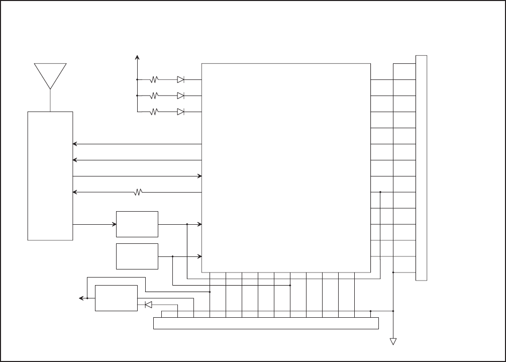
DM2100 Theory of Operation
The major components of the DM2100 include the
TR1000 ASH transceiver and the Texas Instruments
MSP430F148 microcontroller. The TR1000 operates on
916.5 MHz, with a nominal output power of 1 mW. The
MSP430F148 operates from an internal oscillator
referenced to an external 32.768 kHz “watch” crystal.
The MSP430F148 UART is used to provide a CMOS
serial interface on connector J2. The microcontroller’s
general purpose I/O pins are also available on con-
nector J2 for external monitoring or control. Each of
these pins can be separately configured through the RF
network as a logic input, a logic output, or an analog
input. Note that GP0 is dedicated to measuring the
value of the received signal strength indicator (RSSI)
circuit and should always be set as an analog input.
GP1 - GP7 can be used in any configuration needed by
the application. The three LEDs on the DM2100 display
RF communication activity.
DM2100 operation is based on NOKOTA’s SOS-OEA
V1.5 multi-mode mesh network protocol, which sup-
ports data and command transfers through both the se-
rial interface and the RF channel. See the SOS-OEA
V1.5 Protocol User’s Guide for further details.
2
56789104321
GND VIN
11 12 13 14
VREN VDD TD0 TD1 TW S TCK RST CFG0CFG1CFG2CFG3 GND
J1
1
2
3
4
5
6
7
8
9
10
11
12
13
14
J2
3 VD C
GRN
YEL
RED
TR 1000
ASH
Transceiver
RSSI
Low
Voltage
Reset
TXM O D
RXDATA
CNTRL1
CNTRL0
3 VD C Voltage
Regulator
D M 2100 B lock D iagram
GND
GP7
GP6
GP5
GP4
GP3
GP2
GP1
GP0/RSSI
RTS
CTS
TXD
RXD
GND
M SP430F148
M icrocontroller
Figure 1
DM2100 FCC Certification
The DM2100 has been certified for operation under
FCC Part 15 Rules, Section 15.249. This certification
applies only when the DM2100 is equipped with one of
the following RFM antennas:
¼ wave antenna, RFM part number 400-1595-001
helical antenna, RFM part number 500-1141-001
¼ wave antenna-coax assembly, RFM part num-
ber 500-1142-001
WARNING: the DM2100 must be re-certified if used
with any antennas other than the three listed above.
Contact RFM for further information if your application
requires a special antenna configuration.
When the DM2100 is run from an off-board power sup-
ply (applied to J1-4), the supply voltage must be limited
to a maximum of 3.7 Vdc, and the power supply voltage
ripple must not exceed 10 mVP-P.
FCC Labels and Notices
A clearly visible label is required on the outside of the
user’s (OEM) enclosure stating that this product con-
tains a DM2100 radio module, FCC ID: TE6-DM2100A.
This device complies with Part 15 of the FCC rules.
Operation is subject to the following two conditions: (1)
this device may not cause harmful interference, and (2)
this device must accept any interference received, in-
cluding interference that may cause undesired opera-
tion.
WARNING: This device operates under Part 15 of the
FCC rules. Any modification to this device, not ex-
pressly authorized by RF Monolithics, Inc., may void
the user’s authority to operate this device.
DM2100 Applications
There are two ways to use the DM2100 in an applica-
tion. The DM2100 can be used with a companion appli-
cation interface board, the IM2100. The IM2100 has
provisions for powering the DM2100 from a USB cable,
an external unregulated DC supply such asa5Vdc
“wall” transformer, an external regulated 3 Vdc power
supply, or an external battery. The IM2100 also pro-
vides the choice of UART, RS232, RS485 (single drop)
or USB for a host computer serial interface. In addition,
the IM2100 includes captured-screw terminal strips for
connecting analog inputs, digital logic inputs, digital
logic outputs and form C relay outputs. Refer to the
IM2100 data sheet for additional details.
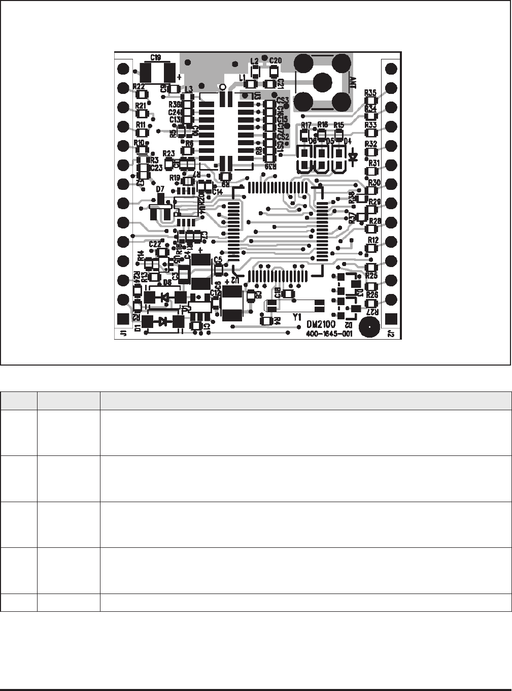
The DM2100 can also be integrated into the user’s own
application board. The DM2100 pin descriptions are
given in the Table on pages 4 and 5. The DM2100
pin-out locations are show in Figure 2, and the PCB lay-
out for the mating connectors is shown in Figure 3.
The operating range of the DM2100 critically depends
on the antenna being located properly. When using ei-
ther the 400-1595-001 or the 500-1141-001 antenna,
care should be taken to keep the antenna at least 0.5
inch away from the sides of its enclosure. The enclo-
sure must be made from a plastic with low RF attenua-
tion, such as fiberglass, PVC or ABS. For a metal
enclosure, use the 500-1142-001 antenna-coax assem-
bly, with the antenna mounted on the outside of the en-
closure. Note that a reverse-pin SMA connector must
be installed on the DM2100 to use this assembly.
The DM2100 enclosure should be mounted so the an-
tenna is at least 4 feet off the ground, and ideally 6 or
more feet off the ground.
The DM2100 has an on-board regulator input on Pin
J1-2. To use the on-board regulator, connect J1-3 to
J1-2 and apply a voltage to this connection of at least
3.1 Vdc, but not greater than 14 Vdc, including ripple
variations. When running from the on-board regulator,
up to 5 mA is available on J1-4 to operate external cir-
cuitry. Any external circuitry connected to J1-4 must not
induce more that 10 mVP-P ripple on the regulated 3 Vdc
at this pin.
The DM2100 can also be run from an off-board regu-
lated supply or a battery. In this case, connect J1-3 to
ground, leave J1-2 unconnected, and apply the regu-
lated supply or battery input to J1-4. Note the input volt-
age range for J1-4 must be in the range of 2.9 to 3.7
Vdc, with no more than 10 mVP-P ripple.
Only pins J1-2 and J1-3 are rated to operate from a
supply voltage higher than 3.7 Vdc. Further, care must
be taken so that analog or logic inputs applied to the
DM2100 stay within the voltage range of 0 to VDD (volt-
age at J1-4). Applying a voltage outside of the 0 to VDD
voltage range to an analog or logic input can damage
the DM2100.
The DM2100 has current limiting protection resistors on
most of the I/O pins. These limit the current that a logic
output can source or sink. Any DM2100 pin defined as
an output should be used only to drive a high imped-
ance load such as a CMOS logic input or a MOSFET
transistor.
3

Pin Name Description
J1-1 GND This pin is connected to ground.
J1-2 VIN This pin is the input to the DM2100 on-board voltage regulator. The minimum input voltage to this pin is 3.1 V,
and the maximum input to this pin is 14.0 V.
J1-3 VREN This pin is the enable input for the DM2100 on-board regulator. To enable the on-board regulator, connect this
pin to J1-2. To disable the on-board regulator, connect this pin to ground.
J1-4 VDD
This pin is connected to the DM2100 positive power supply buss. When the DM2100 is powered from the
on-board regulator, this pin can provide up to 5 mA of current at 3.0 Vdc. Note this current adds to the receive,
transmit and sleep currents listed in the specifications on Page 1. The external load must not impress more
than 10 mV peak -peak ripple on the supply buss. If the on-board regulator is disabled, the DM2100 can be
powered through this pin by an external 2.85 to 3.7 Vdc source (maximum ripple 10 mV peak-peak).
J1-5 TD0 This pin is only used for factory programming. It must be left unconnected in normal operation.
J1-6 TDI This pin is only used for factory programming. It must be left unconnected in normal operation.
J1-7 TWS This pin is only used for factory programming. It must be left unconnected in normal operation.
J1-8 TCK This pin is only used for factory programming. It must be left unconnected in normal operation.
J1-9 RST This pin is only used for factory programming. It must be left unconnected in normal operation.
J1-10 CFG0
This pin is a hardware configuration input. When this pin is low, the DM2100 is placed in a low current sleep
mode. When this pin is high, the DM2100 operates normally. If this pin is not driven by external logic, connect it
to J1-4 (positive supply buss) for normal operation.
J1-11 CFG1
This pin is a hardware configuration input. When this pin is low, the DM2100 is placed in the beacon mode, and
transmits beacon packets about once every eight seconds. When this pin is high, the DM2100 operates nor-
mally. If this pin is not driven by external logic, connect it to J1-4 (positive supply buss) for normal operation.
J1-12 CFG2 This pin is a hardware configuration input, reserved for future use. Connect it to J1-4 (positive supply buss) for
normal operation.
J1-13 CFG3 This pin is a hardware configuration input, reserved for future use. Connect it to J1-4 (positive supply buss) for
normal operation.
J1-14 GND This pin is connected to ground.
J2-1 GND This pin is connected to ground.
J2-2 RXD This pin is the serial data input (CMOS).
J2-3 TXD This pin is the serial data output (CMOS).
J2-4 CTS This pin is a serial data flow control input (CMOS). Hardware flow control is required.
J2-5 RTS This pin is a serial data flow control output (CMOS). Hardware flow control is required.
J2-6 GP0/RSSI This pin is a general purpose I/O pin dedicated to monitoring the RSSI circuit output. It should always be config-
ured as an analog-to-digital converter input. The RSSI signal can also be monitored externally at this pin.
J2-7 GP1
This pin is a general purpose I/O pin. The default configuration of this pin is a logic input. The configuration of
this pin can be changed by commands through the RF channel. Other configuration options include a logic out-
put, or an analog-to-digital converter input. If this pin is unused, it may be reconfigured for a logic low output to
minimize current. In this case, the pin must be left unconnected.
J2-8 GP2
This pin is a general purpose I/O pin. The default configuration of this pin is a logic input. The configuration of
this pin can be changed by commands through the RF channel. Other configuration options include a logic out-
put, or an analog-to-digital converter input. If this pin is unused, it may be reconfigured for a logic low output to
minimize current. In this case, the pin must be left unconnected.
J2-9 GP3
This pin is a general purpose I/O pin. The default configuration of this pin is a logic input. The configuration of
this pin can be changed by commands through the RF channel. Other configuration options include a logic out-
put, or an analog-to-digital converter input. If this pin is unused, it may be reconfigured for a logic low output to
minimize current. In this case, the pin must be left unconnected.
4
Pin Descriptions
Pin Name Description
J2-10 GP4
This pin is a general purpose I/O pin. The default configuration of this pin is a logic input. The configuration of
this pin can be changed by commands through the RF channel. Other configuration options include a logic out-
put, or an analog-to-digital converter input. If this pin is unused, it may be reconfigured for a logic low output to
minimize current. In this case, the pin must be left unconnected.
J2-11 GP5
This pin is a general purpose I/O pin. The default configuration of this pin is a logic input. The configuration of
this pin can be changed by commands through the RF channel. Other configuration options include a logic out-
put, or an analog-to-digital converter input. If this pin is unused, it may be reconfigured for a logic low output to
minimize current. In this case, the pin must be left unconnected.
J2-12 GP6
This pin is a general purpose I/O pin. The default configuration of this pin is a logic input. The configuration of
this pin can be changed by commands through the RF channel. Other configuration options include a logic out-
put, or an analog-to-digital converter input. If this pin is unused, it may be reconfigured for a logic low output to
minimize current. In this case, the pin must be left unconnected.
J2-13 GP7
This pin is a general purpose I/O pin. The default configuration of this pin is a logic input. The configuration of
this pin can be changed by commands through the RF channel. Other configuration options include a logic out-
put, or an analog-to-digital converter input. If this pin is unused, it may be reconfigured for a logic low output to
minimize current. In this case, the pin must be left unconnected.
J2-14 GND This pin is connected to ground.
5
GND
CFG3
CFG2
CFG1
CFG0
RST
TCK
TW S
TD1
TD0
VDD
VREN
VIN
GND
GND
GP7
GP6
GP5
GP4
GP3
GP2
GP1
GP0/RSSI
RTS
CTS
TXD
RXD
GND
D M 2100 Pin O ut
Figure 2
6
Note: Specifications subject to change without notice.
file: dm2100m.vp, 2005.06.21 rev
1.4
(35.6)
1.3
(33.0)
1.4
(35.6)
0.2
(5 .1 )
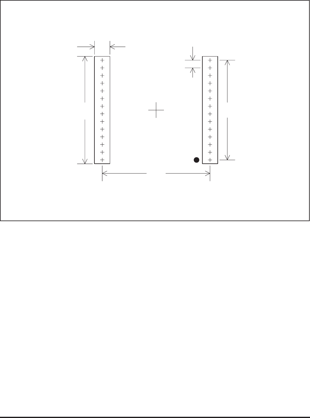
D M 2100 Interface C onnector
PCB Layout Detail
0.1
(2 .5 )
C onnectors are FC I Electronics 66951-Y 13 or equivalent
D im ensions in inches and (m m )
J1 J2
Figure 3