Murata Electronics North America WSN802G 2.4GHz Transceiver Module User Manual Manual
Murata Electronics North America 2.4GHz Transceiver Module Manual
Manual

5015 B.U. Bowman Drive Buford, GA 30518 USA Voice: 770-831-8048 Fax: 770-831-8598
Certification Exhibit
FCC ID: HSW-WSN802G
IC: 4492A-WSN802G
FCC Rule Part: 15.247
IC Radio Standards Specification: RSS-210
ACS Report Number: 09-0120 - 15C
Manufacturer: RFM / Cirronet Inc.
Model(s): WSN802GC, WSN802GP
Manual
www.RFM.com
Technical support +1.678.684.2000 Page 1 of 51
©2009 by RF Monolithics, Inc. E-mail:
tech sup@rfm.com
WSN802G - 04/30/09
WSN802G Series
802.11g Wireless Sensor
Network Modules
Preliminary
Integration Guide

www.RFM.com
Technical support +1.678.684.2000 Page 2 of 51
©2009 by RF Monolithics, Inc. E-mail:
tech sup@rfm.com
WSN802G - 04/30/09
Important Regulatory Information
FCC ID: HSW-WSN802G
IC: 4492A-WSN802G
THIS DEVICE COMPLIES WITH PART 15 OF THE FCC RULES. OPERATION IS SUBJECT TO THE
FOLLOWING TWO CONDITIONS. (1) THIS DEVICE MAY NOT CAUSE HARMFUL INTERFERENCE,
AND (2) THIS DEVICE MUST ACCEPT ANY INTERFERENCE RECEIVED, INCLUDING INTERFERENCE
THAT MAY CAUSE UNDESIRED OPERATION.
This Class B digital apparatus complies with Canadian ICES-003.
Cet appareil numérique de la classe B est conforme à la norme NMB-003 du Canada.
FCC User Information
“NOTE: This equipment has been tested and found to comply with the limits for a Class B digital device,
pursuant to Part 15 of the FCC Rules. These limits are designed to provide reasonable protection against
harmful interference in a residential installation. This equipment generates, uses, and can radiate radio
frequency energy and, if not installed and used in accordance with the instructions, may cause harmful
interference to radio communications. However, there is no guarantee that interference will not occur in a
particular installation. If this equipment does cause harmful interference to radio or television reception,
which can be determined by turning the equipment off and on, the user is encouraged to try to correct the
interference by one or more of the following measures:
• Reorient or relocate the receiving antenna.
• Increase the separation between the equipment and receiver.
• Connect equipment to an outlet on a circuit different in which the receiver is connected.
• Consult the dealer or an experienced radio/TV technician for help.”
Warning: Changes or modifications to this device not expressly approved by RFM Inc.
could void the user’s authority to operate the equipment.
Industry Canada
This Class B digital apparatus meets all requirements of the Canadian Interference Causing Equipment
Regulations. Operation is subject to the following two conditions: (1) this device may not cause harmful
interference, and (2) this device must accept any interference received, including interference that may
cause undesired operation.
Cet appareillage numérique de la classe B répond à toutes les exigences de l'interférence canadienne
causant des règlements d'équipement. L'opération est sujette aux deux conditions suivantes: (1) ce
dispositif peut ne pas causer l'interférence nocive, et (2) ce dispositif doit accepter n'importe quelle
interférence reçue, y compris l'interférence qui peut causer l'opération peu désirée.
“To reduce potential radio interference to other users, the antenna type and its gain should be
so chosen that the equivalent isotropically radiated power (e.i.r.p.) is not more than that
permitted for successful communication.”

www.RFM.com
Technical support +1.678.684.2000 Page 3 of 51
©2009 by RF Monolithics, Inc. E-mail:
tech sup@rfm.com
WSN802G - 04/30/09
RF Exposure
The WSN802G module is approved for mobile operation provided the following conditions are
met.
The antenna(s) used for this transmitter must be installed to provide a separation distance of at
least 20 cm from all persons and must not be co-located or operating in conjunction with any
other antenna or transmitter.
This device has been designed to operate with the antennas listed below, and having a maximum
gain of 12 dBi. Antennas types not included in this list or having a gain greater than 12 dBi are
strictly prohibited for use with this device. The required antenna impedance is 50 ohms.
Mobile Mart OMNI249 9 dBi Omni Antenna
RFM 12 dBi Patch Antenna
Additional equivalent antennas may be substitute if they are the same type and have equal or less
gain without a new equipment authorization application. All antennas used with this device must
be approved by RFM/Cirronet and must employ a unique antenna coupler
OEM Installation and Compliance Labeling
The WSN802G module is labeled with its own FCC and IC ID number, and, if the ID numbers are
not visible when the module is installed inside another device, then the outside of the device into
which the module is installed must also display a label referring to the enclosed transmitter
module.
This exterior label can use wording such as the following:
“Contains Transmitter Module FCC ID: HSW-WSN802G” or
“Contains FCC ID: HSW-WSN802G”
The same requirements are used in Canada.
“Contains Transmitter Module IC: 4492A-WSN802G” or
“Contains IC: 4492A-WSN802G”
Any similar wording that expresses the same meaning may be used. The Grantee may either
provide such a label, an example of which must be included in the application for equipment
authorization, or, must provide adequate instructions along with the module which explain this
requirement. In the latter case, a copy of these instructions must be included in the application for
equipment authorization.
See Section 3.10 of this manual for regulatory notices and labeling requirements. Changes or modifica-
tions to a WSN802G not expressly approved by RFM may void the user’s authority to operate the
module.

www.RFM.com
Technical support +1.678.684.2000 Page 4 of 51
©2009 by RF Monolithics, Inc. E-mail:
tech sup@rfm.com
WSN802G - 04/30/09
Table of Contents
1.0 WSN802G Introduction......................................................................... 5
1.1 Features............................................................................................. 6
1.2 Applications ....................................................................................... 6
2.0 WSN802G Operation............................................................................ 7
2.1 Active and Sleep Modes.................................................................... 7
2.2 Automatic I/O Reporting ................................................................... 8
2.3 Data Serial Port ................................................................................. 8
2.4 Diagnostic Serial Port ........................................................................ 8
2.5 Analog I/O.......................................................................................... 8
2.6 Digital I/O ........................................................................................... 8
3.0 WSN802G Hardware ............................................................................ 9
3.1 Absolute Maximum Ratings............................................................... 9
3.2 Specifications .................................................................................... 10
3.3 Module Interface................................................................................ 11
3.4 WSN802G Antenna Connector ......................................................... 12
3.5 Input Voltage ..................................................................................... 13
3.6 ESD and Transient Protection ........................................................... 13
3.7 Interfacing to 5 V Logic Systems....................................................... 13
3.8 Power-On Reset Requirements ........................................................ 13
3.9 Mounting and Enclosures ..................................................................... 13
3.10
Labeling and Notices ......................................................................... 14
4.0 Application Protocol .............................................................................. 15
4.1 I/O Report Request............................................................................ 16
4.2 I/O Report .......................................................................................... 16
4.3 I/O Write GPIO .................................................................................. 17
4.4 I/O Write PWM................................................................................... 17
4.5 I/O Write Reply .................................................................................. 18
4.6 Serial Data ......................................................................................... 18
5.0 IP Address Discovery Protocol ............................................................ 19
5.1 IP Hunt Query.................................................................................... 19
5.2 IP Hunt Reply .................................................................................... 20
6.0 SSID and Security Keys ....................................................................... 21
6.1 Router Scanning................................................................................ 21
7.0 Module Configuration............................................................................ 22
7.1 SNMP Traps ...................................................................................... 22
7.2 SNMP Management Information Blocks ........................................... 23
7.3 System Configuration Parameters .................................................... 23
7.4 Application Configuration Parameters............................................... 27

www.RFM.com
Technical support +1.678.684.2000 Page 5 of 51
©2009 by RF Monolithics, Inc. E-mail:
tech sup@rfm.com
WSN802G - 04/30/09
8.0 WSN802GDK Developer’s Kit............................................................................................................
29
8.1 WSN802GDK Kit Contents............................................................................................................
29
8.2 Additional Items Needed ...............................................................................................................
29
8.3 Developer Kit Assembly and Testing.............................................................................................
30
8.4 Developer Board Features ............................................................................................................
32
8.5 WSNConfig Program Operation ...................................................................................................
34
9.0 Troubleshooting ................................................................................................................................
44
10.0
Appendices .......................................................................................................................................
45
10.1
Ordering Information......................................................................................................................
45
10.2
Technical Support..........................................................................................................................
45
10.3
WSN802G Mechanical Specifications ...........................................................................................
46
10.4
WSN802G Developer Board Schematic ......................................................................................
48
11.0
Warranty.............................................................................................................................................
51
www.RFM.com
Technical support +1.678.684.2000 Page 6 of 51
©2009 by RF Monolithics, Inc. E-mail:
tech sup@rfm.com
WSN802G - 04/30/09
1.0 WSN802G Introduction
The WSN802G transceiver module is a low cost, robust solution for 802.11 b/g sensor networks. The
WSN802G is unique in that it is able to sleep while still remaining a member of an 802.11 b/g network.
The WSN802G
'
s low active current and very low sleep current makes long life battery operation practical.
The WSN802G module includes analog, digital and serial I/O, providing the flexibility and versatility
needed to serve a wide range of sensor network applications. The WSN802G module is easy to integrate
and is compatible with standard 802.11 b/g routers.
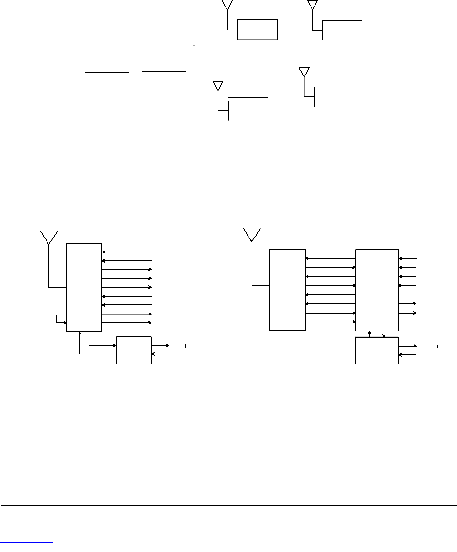
802.11b/g Network with WSN802G Sensor Nodes
Application
Server (PC)
802.11b/g
Rout er
Figure 1.0.1
An example 802.11 b/g network with WSN802G sensor nodes is shown in Figure 1.0.1. A sensor network
application running on a server or PC communicates with one or more WSN802G sensor nodes through
a commercial 802.11b/g router. WSN802G sensor nodes can be used with 802.11b/g routers that are
also serving other applications.
Figure 1.0.2
A WSN802G module is integrated with other components to create a complete sensor node. These com-
ponents include a host circuit board, a power supply (battery), sensor I/O electronics and/or a host micro-
controller, an antenna and a housing. Two common configurations are show in Figure 1.0.2. Serial data
communication between a WSN802G and its host microcontroller requires no protocol formatting. The
WSN802G formats data received from its host into UDP packets for RF transmission, and delivers the
payload data from received UDP packets to its host. The sensor network application on the server or PC
uses a simple protocol to send and receive data from WSN802G sensor nodes, as detailed in Section 4.
WSN802G
Sensor
Node 1
802.11b/g
Lapt op
802.11b/g
Print er
WSN802G
Sensor
Node 2
WSN802G Sensor Node with
Direct Sensor Interface
ADC0
ADC1
ADC _REF
PWN0
PWM1
DIN0
DIN1
DOUT0
DOUT1
WSN802G
1
WAKE _ IN
Seria
I/O
RS232
Converter
RADIO_RXD
RADIO_TXD
RS232
Converter
Seria
I/O
WSN802G Sensor Node with
Host Microcontroller
WSN802G
RADIO_RXD
Analog
and/or
Digital
Inputs
RADIO_TXD
WAKE _ I N
WAKE_OUT
DIN0
Analog
and/or
Digital
Outputs
DIN1
DOUT0
DOUT1
Host
Microcontroller
and
Sensor
I/O

www.RFM.com
Technical support +1.678.684.2000 Page 7 of 51
©2009 by RF Monolithics, Inc. E-mail:
tech sup@rfm.com
WSN802G - 04/30/09
1.1 Features
WSN802G modules provide a unique set of features for wireless sensor network applications:
• Compatibility with commercial and industrial 802.1 1b/g routers
• Low power consumption for long life battery operation including sleep mode
• Full -40 to +85 ºC industrial temperature range operation
• Analog and digital I/O plus data and diagnostic UART ports
• Separate data and diagnostic ports
• System/application set up using just two Management Information Blocks (MIBs)
• Full 14 channel 802.11 b/g coverage for world wide operation
• FCC, Canadian IC and European ETSI certifications
• Choice of plug-in or solder reflow configurations
• Automatic or manual I/O data reporting
1.2 Applications
WSN802G sensor networks are well suited to applications where IEEE 802.1 1b/g router compatibility,
industrial temperature range operation and long battery life are important. Many applications match these
criteria, including:
• Energy Monitoring and Management
• Physical Asset Management
• Cold Chain Data Logging and Food Safety
• Security and Access Control Systems
• Environmental Monitoring
• Many More

www.RFM.com
Technical support +1.678.684.2000 Page 8 of 51
©2009 by RF Monolithics, Inc. E-mail:
tech sup@rfm.com
WSN802G - 04/30/09
2.0 WSN802G Operation
WSN802G operation is designed to support long battery life by allowing the module to stay in sleep mode
to the maximum extent possible. Compared to 802.11 b/g cards used in notebook and handheld com-
puters, the WSN802G’s active current is also very low.
2.1 Active and Sleep Modes
Once the SNMP Server IP address has been set, the default state of the WSN802G is sleep mode. The
WSN802G has a dedicated input to switch it from sleep to active mode, WAKE_IN (Pin 26). There are five
events that will wake the WSN802G from sleep mode:
•
Applying a logic high signal on the WAKE_IN pin
•
Expiration of the AutoReport timer
•
Expiration of Linkup trap timer
•
Expiration of the Config trap timer
•
Module’s SNMP Server IP address has not been set (this will not wake it, it prevents it from
sleeping)
The WAKE_IN and AutoReport can be enabled/disabled. The Linkup timer sends a keep alive packet to
the router every 60 seconds by default. The Config timer cannot be disabled and will generate a Config
trap every 10 seconds by default.
When the module wakes to an active state due to either the WAKE_IN pin or the AutoReport timer, it re-
mains awake for a time period controlled by the Wake Timeout timer. The module returns to sleep mode
when the Wake Timeout timer expires, subject to the conditions listed below. The Wake Timeout timer is
held in reset and the module remains in active mode when any of the following events occur:
•
A logic high signal is held on the WAKE_IN pin
•
A serial byte is received
•
An RF packet is sent or received
•
Module’s SNMP Server IP address has not been set
The Wake Timeout feature is used to support scenarios such as a server application parsing the I/O report
and sending back a serial string or I/O output change command, or a host processor sending a serial
string and waiting for a response.
As discussed in Section 5, the SNMP Server IP address can be set in a short period of time, allowing the
module to switch to sleep mode for battery conservation. The SNMP server IP address only needs to be
set one time.
A WSN802G module that has an SNMP Server IP Address but is not linked to an 802.11 b/g router will
cycle between sleep and active mode under the control of the scanning algorithm, even if none of the
wake events discussed above are present.
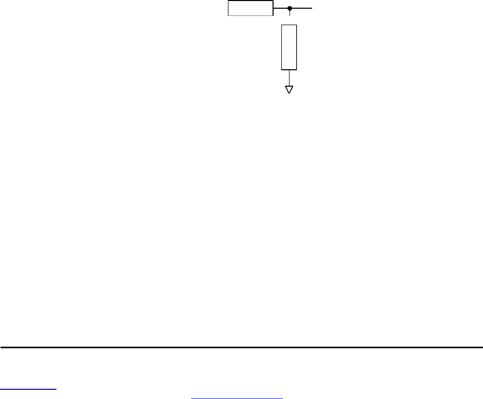
Whenever the module is in active mode, a logic high is asserted on WAKE_OUT (Pin 27). WAKE_OUT
can be used to signal an external processor. When the WSN802G is in sleep mode, WAKE_OUT is set
to logic low.

www.RFM.com
Technical support +1.678.684.2000 Page 9 of 51
©2009 by RF Monolithics, Inc. E-mail:
tech sup@rfm.com
WSN802G - 04/30/09
2.2 Automatic I/O Reporting
The WSN802G sends an I/O report when one of the following events occur:
•
A logic high signal is applied to the WAKE_IN pin
•
The AutoReport timer fires (module in either active or sleep mode)
2.3 Data Serial Port
The data serial port of the WSN802G supports baud rates from 1.2 to 921.6 kb/s. The following serial port
configurations are supported:
•
5, 6, 7 and 8-bit character lengths
•
1 or 2 stop bits
•
Even, odd, mark, space or no parity
The default serial port configuration is 9.6 kb/s, 8, N,1. See Section 7.2 for serial port configuration de-
tails. Serial port operation is full-duplex. Data is sent and received on the serial port transparently. No pro-
tocol formatting is required. The WSN802G includes an acknowledgement and retry mechanism to mini-
mize data loss on RF transmissions. However, the UDP/IP protocol being carried by the RF transmissions
does not provide guaranteed end-to-end delivery. The user must make provisions for detecting and re-
sending data lost on an end-to-end transmission. The WSN802G is a three-wire interface; hardware flow
control will be provided in a future firmware release.
2.4 Analog I/O
The WSN802G includes two 10-bit ADC inputs. Input ADC0 is on Pin 18 and input ADC1 is on Pin 19. Pin
25 provides a full-scale reference voltage to support ratiometric ADC measurements. ADC measurements
are triggered and added to the automatic I/O report when a logic high signal is first applied to the WAKE_
IN pin or the AutoReport timer fires, as discussed in Section 2.2. An ADC reading is also made on the
internal buss voltage of the WSN802G and included in the automatic I/O report. These readings can also
be retrieved anytime the WSN802G is in active mode using the IO_REPORT application protocol com-
mand as discussed in Section 4.1.
The WSN802G also includes an active 16-bit pulse width modulated output, PWM0 (Pin 9). The PWM
output is low-pass filtered to provide an analog output voltage with ripple suppressed to 7 bits. External
low-pass filtering can be added to further suppress ripple. The full-scale PWM output is referenced to the
regulated supply voltage (Pin 24). The PWM output is set using the IO_ WRITE_PWM application proto-
col command, as discussed in Section 4.3.
2.5 Digital I/O
The WSN802G includes two digital inputs, DIN0 (Pin 4) and DIN1(Pin 11). The states of the DIN pins are
captured as part of the automatic I/O report when a logic high signal is applied to the WAKE_IN pin or the
AutoReport timer fires, as discussed in Section 2.2. These readings can also be retrieved anytime the
WSN802G is in active mode using the IO_REPORT application protocol command as discussed in Sec-
tion 4.1. The WSN802G also includes two digital outputs, DOUT0 (Pin 10) and DOUT1 (Pin 12). The
states of the DOUT pins are set using the IO_WRITE_GPIO application protocol command as discussed
in Section 4.2.
www.RFM.com
Technical support +1.678.684.2000 Page 10 of 51
©2009 by RF Monolithics, Inc. E-mail:
tech sup@rfm.com
WSN802G - 04/30/09
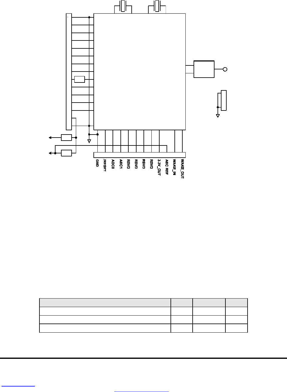
3.0 WSN802G Hardware
WSN802G Block Diagram
Figure 3.0.1
The WSN802G operates in the international 2.4 GHz ISM band over the frequency range of 2401-
2474 MHz, with a nominal RF output power of 10 mW. The WSN802G supports two standard 802.11g RF
data rates, 1 and 2 Mb/s. The WSN802G transceiver module provides a variety of hardware interfaces.
There are two serial interfaces, one for data and a second for diagnostics. The data port supports stan-
dard serial baud rates from 1.2 to 921.6 kb/s, and the diagnostic port operates at a fixed baud rate of
9.6 kb/s. Hardware flow control is not currently implemented on either serial port. The WSN802G includes
two 10-bit ADC inputs, a 16-bit PWM (DAC) output, two digital inputs and two digital outputs to support
sensor network applications.
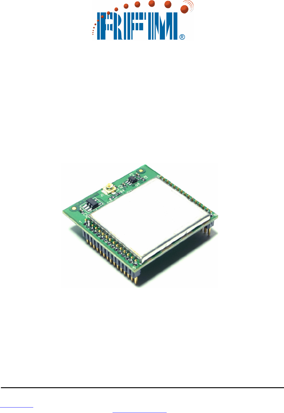
The WSN802G is available in two mounting configurations. The WSN802GC is designed for solder reflow
mounting, and the WSN802GP is designed for plug-in connector mounting.
3.1 Absolute Maximum Ratings
Rating
Sym Value
Units
Input/Output Pins Except ADC Inputs
-0.5 to +3.63
V
ADC Input Pins
-0.5 to 1.98 V
Non-Operating Ambient Temperature Range
-40 to +85
o
C
Table 3.1.1
+3.3 V
+1.8 V
GND
DIAG_TX
DIAG_RX
DIN0
RADIO_TXD
RADIO_RXD
RSVD
RSVD
PWM0
DOUT0
DIN1
DOUT1
RSVD
VCC
GND
Reg
Reg
10
11
12
13
14
15
3
4
8
9
2
5
6
7
1
Filter
16 17 18 19 20 21 22 23 24 25 26 27
32.768 kHz
802.11g
Low Current
Transceiver
44 M
Hz
RFIO
GND
RSVD
GND
Balun
>
BPF
28
29
30

www.RFM.com
Technical support +1.678.684.2000 Page 11 of 51
©2009 by RF Monolithics, Inc. E-mail:
tech sup@rfm.com
WSN802G - 04/30/09
3.2 Specifications
Characteristic
Sym
Minimum
Typical
Maximum
Units
Operating Frequency Range
2401
2474 MHz
Spread Spectrum Method
CCK Direct Sequence
RF Chip Rate
11 Mc/s
RF Data Rates
1 or 2 Mb/s
Modulation Type
BPSK at 1 Mb/s, QPSK at 2 Mb/s
Number of RF Channels
11
RF Channel Spacing
5
MHz
Receiver Sensitivity, 8% PER:
-92
dBm
1 Mb/s RF Data Rate
2 Mb/s RF Data Rate
-90
dBm
RF Transmit Power
10
mW
RF Connector
U.FL Coaxial Connector
Optimum Antenna Impedance
50
Ω
ADC Input Range
0
1.8 V
ADC Input Resolution
10
bits
ADC Input Impedance
1
M
Ω
PWM Output Resolution
16 bits
Data Serial Port Baud Rates
1.2, 2.4, 4.8, 9.6 (default), 19.2, 28.8, 38.4,
57.6, 76.8, 115.2, 230.4, 460.8, 921.6 kb/s
Diagnostic Serial Port Baud Rate
9.6
kb/s
-0.3
0.7 V
2.24
V
CC
V
50
1000 K
Ω
0
0.4 V
Digital I/O:
Logic Low Input Level
Logic High Input Level
Input Pull Up/Down Resistor
Logic Low Output Level
Logic High Output Level
2.4
V
CC
V
Power Supply Voltage Range V
CC
+3
+3.63 Vdc
Power Supply Voltage Ripple
10 mV
P-P
Receive Mode Current
150 mA
Transmit Mode Current
200 mA
Sleep Mode Current
7.5
µA
WSN802GC Mounting
Reflow Soldering
WSN802GP Mounting
Socket
Operating Temperature Range
-40
85
o
C
Operating Relative Humidity Range, Non-condensing
10
90 %
Table 3.2.1

www.RFM.com
Technical support +1.678.684.2000 Page 12 of 51
©2009 by RF Monolithics, Inc. E-mail:
tech sup@rfm.com
WSN802G - 04/30/09
3.3 Module Interface
Pin Name I/O Description
1 GND - Power supply and signal ground. Connect to the host circuit board ground.
2 DIAG_TX O Diagnostic serial port output.
3 DIAG_RX I Diagnostic serial port input.
4 DIN0 I Digital input port 0.
5 RADIO_TXD O Serial data output from the radio.
6 RADIO_RXD I Serial data input to the radio.
7 RSVD - Reserved pin. Leave unconnected.
8 RSVD - Reserved pin. Leave unconnected.
9 PWM0 O
16-bit pulse-width modulated output 0 with internal low-pass filter. Filter is first-order, with a 159
Hz 3 dB bandwidth, 10K output resistance.
10 DOUT0 O Digital output port 0.
11 DIN1 I Digital input port 1.
12 DOUT1 O Digital output port 1.
13 RSVD - Reserved pin. Leave unconnected.
14 VCC I Power supply input, +3.0 to +3.63 Vdc.
15 GND - Power supply and signal ground. Connect to the host circuit board ground.
16 GND - Power supply and signal ground. Connect to the host circuit board ground.
17 /RESET I Active low module hardware reset.
18 ADC0 I 10-bit ADC input 0. ADC full scale reading can be referenced to the module’s +1.8 V regulated supply.
19 ADC1 I 10-bit ADC input 1. ADC full scale reading can be referenced to the module’s +1.8 V regulated supply.
20 RSVD - Reserved pin. Leave unconnected.
21 RSVD - Reserved pin. Leave unconnected.
22 RSVD - Reserved pin. Leave unconnected.
23 RSVD - Reserved pin. Leave unconnected.
24 3.3V _ OUT O
Module’s +3.3 V regulated supply, available to power external sensor circuits. Current drain on this
output should be no greater than 50 mA.
25 ADC _ REF O
Module’s +1.8 V regulated supply, used for ratiometric ADC readings. Current drain on this output
should be no greater than 5 mA.
26 WAKE _ IN I
Active high interrupt input to wake the module from timer sleep. Can be used to wake module on
event, etc.
27 WAKE _ OUT O
Active high output asserted when module wakes from timer sleep. Can be used to wake an
external device.
28 GND - RF ground for the WSN802GC only. Connect to the host circuit board ground plane.
29 RSVD - Reserved pin. Leave unconnected.
30 GND - RF ground for the WSN802GC only. Connect to the host circuit board ground plane.
Table 3.3.1
www.RFM.com
Technical support +1.678.684.2000 Page 13 of 51
©2009 by RF Monolithics, Inc. E-mail:
tech sup@rfm.com
WSN802G - 04/30/09
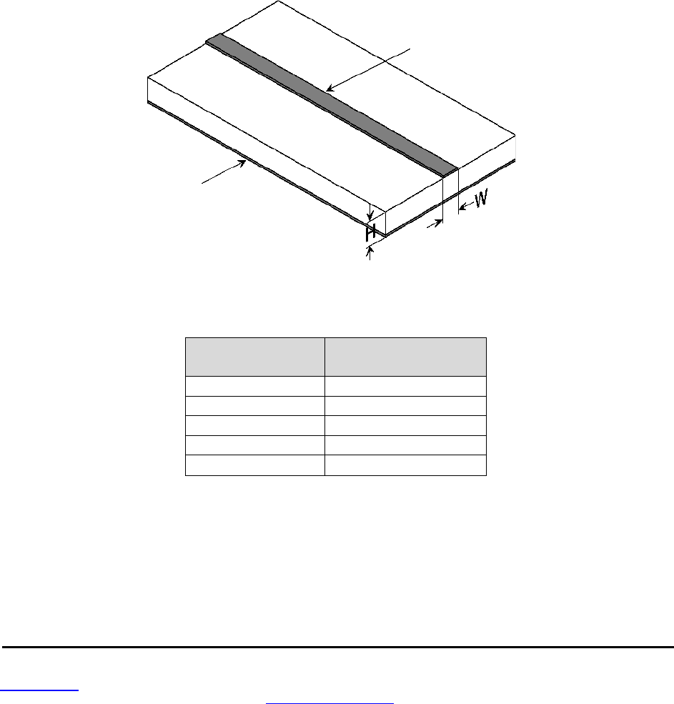
3.4 WSN802G Antenna Connector
A U.FL miniature coaxial connector is provided on both WSN802G configurations for connection to the
RFIO port. A short U.FL coaxial cable can be used to connect the RFIO port directly to an antenna. In this
case the antenna should be mounted firmly to avoid stressing the U.FL coaxial cable due to antenna
mounting flexure. Alternately, a U.FL coaxial jumper cable can be used to connect the WSN802G module
to a U.FL connector on the host circuit board. The connection between the host circuit board U.FL con-
nector and the antenna or antenna connector on the host circuit board should be implemented as a
50 ohm stripline. Referring to Figure 3.4.1, the width of this stripline depends on the thickness of the cir-
cuit board between the stripline and the groundplane. For FR-4 type circuit board materials (dielectric
constant of 4.7), the width of the stripline is equal to 1.75 times the thickness of the circuit board. Note
that other circuit board traces should be spaced away from the stripline to prevent signal coupling, as
shown in Table 3.4.1. The stripline trace should be kept short to minimize its insertion loss.
Circuit Board Stripline Trace Detai
Trace Separation from
50 ohm Microstrip
Length of Trace Run
Parallel to Microstrip
100 mil 125 mill
150 mil 200 mil
200 mil 290 mil
250 mil 450 mil
300 mil 650 mil
Table 3.4.1
Copper
Ground
Plane
FR
-
4 PCB
Material
Copper
Stripline
Trace
For 50 ohm impedance W = 1.75 * H
Figure 3.4.1
www.RFM.com
Technical support +1.678.684.2000 Page 14 of 51
©2009 by RF Monolithics, Inc. E-mail:
tech sup@rfm.com
WSN802G - 04/30/09
3.5 Input Voltage
WSN802G radio modules can operated from an unregulated DC input (Pin 14) in the range of 3.0 V
(trough) to 3.63 V (peak) over the temperature range of -40 to 85
°
C.
Applying AC, reverse DC, or a DC
voltage outside the range given above can cause damage and/or create a fire and safety hazard. Further,
care must be taken so logic inputs applied to the radio stay within the voltage range of 0 to 3.3 V. Signals
applied to the analog inputs must be in the range of 0 to ADC_REF (Pin 25). Applying a voltage to a logic
or analog input outside of its operating range can damage the WSN802G module.
3.6 ESD and Transient Protection
WSN802G circuit boards are electrostatic discharge (ESD) sensitive. ESD precautions must be observed
when handling and installing these components. Installations must be protected from electrical transients
on the power supply and I/O lines. This is especially important in outdoor installations, and/or where con-
nections are made to sensors with long leads.
Inadequate transient protection can result in damage
and/or create a fire and safety hazard.
3.7 Interfacing to 5 V Logic System
All logic signals including the serial ports on the WSN802G are 3.3 V signals. To interface to 5 V signals,
the resistor divider network shown in Figure 3.7.1 below must be placed between the 5 V signal outputs
and the WSN802G signal inputs. The output voltage swing of the WSN802G 3.3 V signals is sufficient to
drive 5 V logic inputs. Figure 3.7.1 refers to the DNT500
5V
Logic
WSN802G
2.2K
4.3K
Figure 3.7.1
3.8 Power-On Reset Requirements
When applying power to the WSN802G, the /RESET pin should be held low until the power supply volt-
age reaches 3.3 volts for 100 milliseconds.
3.9 Mounting and Enclosures
WSN802GC radio modules are mounted by reflow soldering them to a host circuit board. WSN802GP
modules are mounted by plugging their pins into a set of mating connectors on the host circuit board.
Refer to Section 10.3 and/or the WSN802G Data Sheet for mounting details.
WSN802G enclosures must be made of plastics or other materials with low RF attenuation to avoid com-
promising antenna performance where antennas are internal to the enclosure. Metal enclosures are not
suitable for use with internal antennas as they will block antenna radiation and reception. Outdoor enclo-
sures must be water tight, such as a NEMA 4X enclosure.

www.RFM.com
Technical support +1.678.684.2000 Page 15 of 51
©2009 by RF Monolithics, Inc. E-mail:
tech sup@rfm.com
WSN802G - 04/30/09
3.10 Labeling and Notices
WSN802G FCC Certification - The WSN802G hardware has been certified for operation under FCC Part
15 Rules, Section 15.247.
The antenna(s) used for this transmitter must be installed to provide a separa-
tion distance of at least 20 cm from all persons and must not be co-located or operating in conjunction
with any other antenna or transmitter.
WSN802G FCC Notices and Labels -
This device complies with Part 15 of the FCC rules. Operation is
subject to the following two conditions: (1) this device may not cause harmful interference, and (2) this
device must accept any interference received, including interference that may cause undesired operation.
A clearly visible label is required on the outside of the user’s (OEM) enclosure stating ”Contains FCC ID:
HSW-WSN802G.”
WARNING: This device operates under Part 15 of the FCC rules. Any modification to this device, not
expressly authorized by RFM, Inc., may void the user’s authority to operate this device. Canadian De-
partment of Communications Industry Notice - IC: 4492A-WSN802G
This apparatus complies with Health Canada’s Safety Code 6 / IC RSS 210.
ICES-003
This digital apparatus does not exceed the Class B limits for radio noise emissions from digital apparatus
as set out in the radio interference regulations of Industry Canada.
Le present appareil numerique n’emet pas de bruits radioelectriques depassant les limites applicables
aux appareils numeriques de Classe B prescrites dans le reglement sur le brouillage radioelectrique
edicte par Industrie Canada.
ETSI EN 300 328
The WSN802G module has passed ETSI EN 300 328 testing conducted by an independent test
laboratory.
www.RFM.com
Technical support +1.678.684.2000 Page 16 of 51
©2009 by RF Monolithics, Inc. E-mail:
tech sup@rfm.com
WSN802G - 04/30/09
4.0 Application Protocol
In most applications, the auto-reporting functions of the WSN802G will be used to send data from nodes
to the application removing the need for the application to poll nodes. However, applications can read and
write data to and from WSN802G nodes if desired. WSN802G modules only accept commands over the
air; commands cannot be entered through either the data or diagnostic serial ports. Obviously, WSN802G
modules must be in active mode (awake) to receive commands. The WSN802G supports this type of op-
eration through use of the auto-reporting function and the AutoReport and Wake Timeout timers. For ex-
ample, a WSN802G module has been configured to wake up once every minute. When the module
wakes up, it will send its I/O report. While the data may not be of interest, it will serve as a notification to
the application that the module is awake. Setting the Wake Timeout timer to 2 seconds will keep the mod-
ule awake giving the application 2 seconds to send any application commands to the module. The mod-
ule will remain awake past the 2 seconds if commands are being received or processed. Once the appli-
cation commands are completed the module will return to sleep immediately if the Wake Timeout time has
elapsed. Typically, this mode will be used when the application needs to write data to the WSN802G
module.
All commands and responses between a server and its WSN802G clients are formatted as UDP/IP pack-
ets. The IPv4 UDP/IP packet format is shown in Figure 4.0.1 below. WSN802G commands and re-
sponses are carried in the UDP datagram payload area. In the text below, commands and responses will
be referred to as datagrams with the understanding they are the payload of a UDP datagram. Automati-
cally generated I/O reports from the WSN802G module due to timeouts or event interrupts take the form
of the I/O_Report application command.
Byte 0 Byte 1 Byte 2 Byte 3
IP
Version
Header
Length
Type of
Service
Total
Length
ID Flags Fragment Offset
Time to Live Protocol
Header Checksum
Source IP Address
Destination IP Address
Source Port
Destination Port
UDP Length
Checksum
Payload (Application Command)
Figure 4.0.1
WSN802G modules only accept application commands from and send application command data/replies
to the IP address of the server running their sensor application. As shown in Figure 4.0.2 below,
WSN802G application protocol datagrams use a standard header beginning with a protocol identifier to
discriminate WSN802G protocol messages from other message types. Datagrams are in 32-bit, big-
endian format. The standard header fields are:
Protocol Identifier:
Unique identifier for all WSN messages, 0x52464D49
Opcode:
Code indicating the type of command or response
Transaction ID:
This is an incrementing transaction reference counter. Each end of the
link must keep its own counter for transactions that it originates. The
most significant bit of the transaction ID will be set for all transactions
that the server originates.
www.RFM.com
Technical support +1.678.684.2000 Page 17 of 51
©2009 by RF Monolithics, Inc. E-mail:
tech sup@rfm.com
WSN802G - 04/30/09
Byte 0 Byte 1 Byte 2 Byte 3
WSN802G Protocol Identifier = 0x52464D49
Opcode
Transaction ID
Data (variable length)
Figure 4.0.2
The WSN802G application protocol commands are listed in Table 4.0.1 below. The port number that the
module sends and receives application messages on is defined by the SensorS erverPortNum parameter,
as discussed in Section 7.2. A WSN802G module will accept messages specifically addressed to it, or
that are broadcast (addressed to all modules). If a command is received through a broadcast, the WSN
will reply with a broadcast.
Opcode Direction Description
0x0000 Server-to-Module IO_REPORT_REQUEST
0x0001 Module-to-Server IO_REPORT
0x0002 Server-to-Module IO_WRITE_GPIO
0x0003 Server-to-Module IO_WRITE_PWM
0x0004 Module-to-Server IO_WRITE_REPLY
0x0005 Bidirectional SERIAL_DATA
Table 4.0.1
4.1 I/O Report Request
The IO_REPORT_REQUEST datagram is used to request current I/O values, as shown in Figure 4.1.1.
Byte 0
Byte 1
Byte 2
Byte 3
WSN802G Protocol Identifier = 0x52464D49
Opcode = 0x0000
Transaction ID = varies
Figure 4.1.1
The module responds to an IO_REPORT_REQUEST with an IO_REPORT
4.2 I/O Report
The IO_REPORT datagram is used to report current I/O values, as shown in Figure 4.2.1.
Byte 0 Byte 1 Byte 2 Byte 3
WSN802G Protocol Identifier = 0x52464D49
Timestamp High Bytes
Timestamp Low Bytes
Opcode = 0x0001
Transaction ID = varies
ADC0
ADC1
VOLT
RSSI
DIN
Figure 4.2.1
www.RFM.com
Technical support +1.678.684.2000 Page 18 of 51
©2009 by RF Monolithics, Inc. E-mail:
tech sup@rfm.com
WSN802G - 04/30/09
The fields specific to this datagram are:
ADC0:
Current ADC0 reading, only the low 10 bits are significant
ADC1:
Current ADC1 reading, only the low 10 bits are significant
VOLT:
Current module voltage reading, only the low 10 bits are significant
RSSI:
RSSI of this IO_REPORT message, only the low 10 bits are significant
DIN:
Current digital input states, only bit positions 0 (DIN0) and 1 (DIN1)
are valid
The module generates an IO_REPORT based on the AutoReportInterval (see Section 7.4) and in re-
sponse to an IO_REPORT_REQUEST.
4.3 I/O Write GPIO
The IO_WRITE_GPIO datagram is used by the server to set module outputs, as shown in Figure 4.3.1.
Byte 0
Byte 1
Byte 2
Byte 3
WSN802G Protocol Identifier = 0x52464D49
Opcode = 0x0002 Transaction ID = varies
DOUT
Figure 4.3.1
The fields specific to this datagram are:
DOUT:
Digital output settings, only bit positions 2 (DOUT0) and 3 (DOUT1)
are valid. Setting a bit to 1 sets the DOUT to 3.3 V, setting a bit to 0 sets
the DOUT to 0 V.
The module responds to an IO_WRITE_GPIO with an IO_WRITE_REPLY.
4.4 I/O Write PWM
The IO_WRITE_PWM datagram is used by the server to set the PWM0 output , as shown in Figure 4.4.1.
Byte 0 Byte 1 Byte 2 Byte 3
WSN802G Protocol Identifier = 0x52464D49
Opcode = 0x0003
Transaction ID = varies
PWM0
Reserved
Figure 4.4.1
The fields specific to this datagram are:
PWM0:
PWM0 setting, 16-bit unsigned value
The module responds to an IO_WRITE_PWM with an IO_WRITE_REPLY.

www.RFM.com
Technical support +1.678.684.2000 Page 19 of 51
©2009 by RF Monolithics, Inc. E-mail:
tech sup@rfm.com
WSN802G - 04/30/09
4.5 I/O Write Reply
An IO_WRITE_REPLY is sent by the WSN802G to confirm receipt of an IO_WRITE_GPIO,
IO_WRITE_PWM or SERIAL_DATA datagram, as shown in Figure 4.5.1.
Byte 0 Byte 1
Byte 2
Byte 3
WSN802G Protocol Identifier = 0x52464D49
Opcode = 0x0004 Transaction ID = varies
Status
Figure 4.5.1
The field specific to this datagram is:
Status:
0x0000 = successful, 0x0001 = failed
4.6 Serial Data
The SERIAL_DATA datagram shown in Figure 4.6.1 is used by the sensor application on the server to
send or receive WSN802G serial data. Note that data sent or received on the WSN802G serial port is
unformatted.
Byte 0 Byte 1
Byte 2
Byte 3
WSN802G Protocol Identifier = 0x52464D49
Opcode = 0x0005 Transaction ID = varies
Serial Data, 0-256 bytes
Figure 4.6.1
The field specific to this datagram is:
Serial Data:
Serial data, 0-256 bytes
Whenever the module is in active mode and receives a string on its serial port, it sends a SERIAL_DATA
message to its server. If the module receives a SERIAL_DATA message, it will output the received data
on its serial port.
www.RFM.com
Technical support +1.678.684.2000 Page 20 of 51
©2009 by RF Monolithics, Inc. E-mail:
tech sup@rfm.com
WSN802G - 04/30/09
5.0 IP Address Discovery Protocol
The WSN802G module supports a separate UDP client port that provides a discovery protocol. The dis-
covery protocol is used to find IP addresses of modules in a network when the IP addresses have been
assigned by a DHCP server. The discovery protocol is also used to set the module’s SNMP Server IP
address which enables module commissioning. This protocol uses port 24776. The discovery protocol
datagrams are shown in Table 6.0.1.
Opcode Direction Description
0x0071 Server-to-Module IP_HUNT_QUERY
0x0072 Module-to-Server IP_HUNT_REPLY
Table 6.0.1
Since the IP addresses of potential recipients may not be known, both query and reply messages are
sent as UDP broadcasts. UDP broadcasts are not routed, so only nodes on the same network segment
as the sender will respond. All nodes that hear an IP_HUNT_QUERY will respond with an IP_HUNT_
REPLY. Ordinarily these commands are only used to initially commission a module. Since a WSN802G
module must be in active mode to hear a command, an un-commissioned module stays in active mode
until its Primary SNMP server address has been set.
5.1 IP Hunt Query
The IP_HUNT_QUERY datagram shown in Figure 5.1.1 is broadcast by a commissioning server to dis-
cover WSN802G modules:
Byte 0 Byte 1 Byte 2 Byte 3
I P h u
n t e r
Opcode = 0x0071 Primary SNMP Server IP Address [31:16]
Primary SNMP Server IP Address [15:0] Secondary SNMP Server IP Address [31:16]
Secondary SNMP Server IP Address [15:0]
Figure 5.1.1
The fields specific to this datagram are:
SNMP Server Address:
The Primary and Secondary SNMP server address fields inform WSN802G
modules of the SNMP server addresses to solicit for configuration parameter
updates (destination addresses for Config traps). If either or both server ad-
dress fields are set to 0.0.0.0, a module hearing the message will retain its
current SNMP server setting for the respective field(s). The default IP ad-
dresses for the Primary SNMP server is 0.0.0.0. The default IP address for
the Secondary SNMP server is 192.168.3.200. The Primary SNMP Server IP
address must be set to a different value to allow the module to enter normal
sleep mode.

www.RFM.com
Technical support +1.678.684.2000 Page 21 of 51
©2009 by RF Monolithics, Inc. E-mail:
tech sup@rfm.com
WSN802G - 04/30/09
5.2 IP Hunt Reply
The IP_HUNT_REPLY datagram shown in Figure 5.2.1 is sent by a module in response to an
IP_HU NT_QUERY command:
Byte 0
Byte 1
Byte 2
Byte 3
I
P
h
u
n
t
e
r
Opcode = 0x0072
MAC Address [47:31]
MAC Address [30:0]
IP Address
Subnet Mask
Device Code = 0x0102
Hardware Version
Firmware Version
Figure 5.2.1
The fields specific to this datagram are:
MAC Address:
MAC address of the module
IP Address:
IP address of the module
Subnet Mask:
Subnet mask of the module
Device Code:
Unique WSN802G device code - 0x0102
Hardware Version:
Hardware version of the module
Firmware Version:
Firmware version in the module

www.RFM.com
Technical support +1.678.684.2000 Page 22 of 51
©2009 by RF Monolithics, Inc. E-mail:
tech sup@rfm.com
WSN802G - 04/30/09
6.0 SSID and Security Keys
WSN802G modules support three SSID and security key pairs. A channel number is also specified for
each SSID/security key pair. SSID and security keys are scanned in priority order. If the entry 1 is not
found, entry 2 will be scanned, and then entry 3. To allow the recovery of a module with an unknown con-
figuration, entry 3 is permanently mapped to:
SSID Security Key Channel
WSN-COMMISSION
Key corresponding to passphrase
"RFM-WIRELESS" 11
Table 6.7.1
SSID/security key pairs 1 and 2 are user configurable.
6.1 Router Scanning
To establish an 802.11 b/g router connection, WSN802G modules use the following scanning method:
Attempt 1: Node scans SSID/Key/Channel 1 for up to MaxScanInterval
Attempt 1: Node scans SSID/Key/Channel 2 for up to MaxScanInterval
Attempt 1: Node scans SSID/Key/Channel 3 for up to MaxScanInterval
Attempt 2: Node scans SSID/Key/Channel 1 for up to MaxScanInterval
Attempt 2: Node scans SSID/Key/Channel 2 for up to MaxScanInterval
Attempt 2: Node scans SSID/Key/Channel 3 for up to MaxScanInterval
Repeat the scan sequence above for up to NumOfRetry attempts
Module sleeps for RetryInterval
If commissioned, the entire scan sequence and sleep interval above is repeated until an 802.11 b/g
router or access point is found.
If a module loses connection to its wireless router/access point, it uses the same scanning method to at-
tempt to reconnect.

www.RFM.com
Technical support +1.678.684.2000 Page 23 of 51
©2009 by RF Monolithics, Inc. E-mail:
tech sup@rfm.com
WSN802G - 04/30/09
7.0 Module Configuration
The WSN802G is configured through SNMP commands sent over the wireless link in response to SNMP
configuration requests from the module. The default setting has the module issuing Config Traps every
10 seconds. The Config Traps are sent to the SNMP server address sent in the IPHunter device discov-
ery communications. The interval between Config Traps is one of the configuration parameters. The less
frequently Config Traps are issued by the WSN802G module, the longer the battery life will be but the
longer it takes to change the module’s configuration.
The WSNConfig utility included with the developer’s kit was designed to operate as a commissioning util-
ity for the WSN802G. Alternatively, a third party SNMP server or utility may be used to serve the same
function.
The WSNConfig utility allows for each node to be configured independently or as a whole. Individual set-
tings may be configured or a list of configuration parameters can be queued for transmission when the
node or nodes wake up and issue the Config Trap.
The configuration parameters for the WSN802G can be divided into two main types: System Configura-
tion Parameters; and Application Configuration Parameters. To simplify the configuration process, sepa-
rate SNMP Management Information Blocks (MIBs) have been created. The System Configuration Pa-
rameters are primarily concerned with the 802.11 b/g configuration. The Application Configuration Pa-
rameters are primarily concerned with the serial port and I/O configuration, including sleep and wake
times.
7.1 SNMP Traps
The WSN802G uses two periodic SNMP traps to control signaling. The port numbers used for SNMP are
162 for traps and 161 for SNMP commands.
The Linkup trap is a message sent periodically by the module to maintain its association with its
802.11 b/g router. No information is conveyed, just "I'm here". The period of the Linkup trap is set by the
LinkupTrapInterval system parameter. For compatibility with the majority of 802.11 b/g routers, the default
period is 60 seconds.
The Config trap is a message sent periodically by a WSN802G to poll the SNMP server to see if it has
any commands waiting for it. After sending the trap, the module remains awake for a period of two sec-
onds in order to allow the server to send it commands. The period of the Config trap is set by the Con fig-
TrapInterval system parameter. The default value is once every 10 seconds. Because Config trap activity
requires a significant amount of energy to execute, for battery-powered deployments the user should set
this interval to once an hour or a few times a day to conserve battery life. At the end of the configuration
trap, the server should send a SET_PARAM request to the Con figComplete register to indicate it has no
more commands to send. This allows the module to go back to sleep mode immediately, rather than re-
maining in active mode for rest of the configuration window.

www.RFM.com
Technical support +1.678.684.2000 Page 24 of 51
©2009 by RF Monolithics, Inc. E-mail:
tech sup@rfm.com
WSN802G - 04/30/09
7.2 SNMP Management Information Blocks
The WSN802G supports two Simple Network Management Protocol (SNMP) Management Information
Blocks (MIBs) to hold module parameters: one for system parameters, and one for application parame-
ters, as detailed in Sections 7.3 and 7.4 below. The parameters in both MIBs can be read or updated us-
ing SNMP and Config Trap as discussed in Section 7.3, or with RFM’s WSNConfig utility. These parame-
ters are stored in the System MIB.
7.3 System Configuration Parameters
Table 7.3.1 lists the system configuration parameters required for WSN802G module commissioning.
These parameters are stored in the System MIB.

..,
=
CO
0
0
...
=
c
o
a)
0
z
co
...
co
=
a)
9
z
co
...
co
=
a
)
9
z
c
o
—
(.0
—
. . .
0
r: C
0
co
co
<
R-
co
0
r: C
0
co
co
<
R-
co
0
r: C
0
c
o
i
n
<
cl
-
co
.‘
—
N
c...)
C
Q
.
15
-
u)
o
0
—
a) .c
i— 0
c
l
)
8
.
r2
i
I
E
O
ul
.
F,
CD 0
-
C —
0 )
E
E
o
0 0
0 —
c7) 2
c0 IR
o a
CD
co
0
0 -..
-
o -o
a
)
(13
X 0
4=
=
0
o '
°
CT)
4
5
u)
'.
2
—
Co
°
c7)
(/)
-0
a
)
c
4
=
C
D
-
0
6
3
c
o
=
1
3
c
o
o
a)
ci
)
.
0
E
o
z
.
0
E
0E
0
.
c
a
"O
0
a)
0
2
,2
1
E
—
CO
co
8
4
—
cr)
3
=
c
1
2
c
c0
.
c
0
`0'
—
CO
co
8
4
—
cr)
13
E
=
c
1
2
c
c
0
.
c
`0
)
—
CO
co
8
4—
cr)
13
E
=
c
1
2
c
co
.c
0
E
c7)
co
8
.—
>,
a)
-'`
.s
0
0
°
"O
0
al
.c
0
.,
a)
,_
O
0
c7)
co
8
>
s
a
)
_,
e
:.'
c
=
0
0
co
13
;2
al
.c
co
0
c7)
co
8
>
s
_,
e
:'s
c
=
0
0
co
13
;2
al
.c
;2
a
)
E
c7)
co
8
a)
co
2
_c
Co
al
a
CV
0
c7)
co
8
a)
co
2
_c
a
u
,
co
w
a
13
;2
co
0
;
2
a
co
O
C
,
)
0
c7)
co
8
a)
co
F2
_c
°-
(
o
a
-
0
;2
co
0
2
a
co
0-
vi
6
—
*
0
c7)
CO
I—
0
0
>s
1
/
0_
w
vi
6
N
*
0
c7)
CO
I—
0
0
>s
1
/
0_
w
ri
(4,
*
0
c7)
CO
I_
0
0
>s
1
/
0_
w
co
)
Lri
.
F
t
0
c7)
co
o
4—
(.,'?
6
-
C
t
h
c
a)
>s
/
6
v.)
Lri
.
0
c7)
co
o
4—
(.,'?
6
-
C
t
h
c
a)
>s
1
/
0_
w
v.)
lfi
.
V
0
c7)
co
o
4—
(.,'?
6
-
C
t
h
c
a)
>s
1
/
0_
w
1
1 1 1 1 1 ce
'
0
R
I
—
i L ,,
W
dr—
1—
r
y
01—
0
cn
IL
W dr—
1—
r
y
01—
Ocn
W dr—
1—
r
y
01—
Ocn
y.c.,
v.)
1—
Z
v.)
1—
Z
v.)
1
—
Z
W dr—
1—
r
y
01—
Ow
W dr—
1—
r
y
01—
0 co
W dr—
1—
r
y
01—
0 co
ILT.ILT.ILT.ILT.ILT.IL
T.
W dr—
1—
r
y
01
—
0 co
W dr—
1—
r
y
01—
0 co
W dr—
1—
r
y
0
1
_
0 co
cv
v.)
1
—
z
cv
v.)
1—
z
cv
v.)
1—
z
cv
v.)
1
—
z
cv
v.)
1—
z
cv
v.)
I—
z
5
e'
s
6
4
.
0,
6
N
CO
CS
!
C
D
cs
,
e'
s
U
)
4
.
6
c
o
N
C
O
CS
!
CD
v.)
csi
isi
4
6
o)
CV
CO
CS
!
CD
.‘—
ri
6
4
6
o)
CV
CO
CS
!
CD
cv
ri
6
4
6
o)
CV
CO
CS
!
CD
v.)
ri
6
4
6
o)
CV
CO
CS
!
CD
c=
6
eNi
%—
co
C
V
0
3
C
V
%—
CD
(
.5
p.
%—%—
e's
co
C
V
C
O
C
S
!
%
—
CD
ci
cp
csi
%—
e's
co
C
V
C
O
C
S
!
%
—
CD
CD
ci
%—
6
co
CV
CO
CS
!
%_
si
CD
c"?
cs,
6
co
CV
CO
CS!
%_
c
c"
?
r)
%—
co
C
V
C
O
"
%
_
6
c'
.‘—
Tr.
6
m
CV
CO
C
S
!
CD
c6
CD
Q
om
)
cs,
Tr.
6
m
CV
6
co
)
Tr.
6
m
CV
CO
C
S
!
CD
c6
Q
om
)
.‘
—
q
6
m
CV
CO
C
S
!
CD
c6
cs,
q
6
m
CV
CO
C
S
!
CD
ri
Q
om
)
co
)
q
6
m
CV
CO
C
S
!
CD
ri
co
to'
E
co
I.
CO
o.
E
V
)
C
r)
?
)
,
—
N
0
C l )
co
-
o
;2
a3
;2
o_
c
,
)
0
Cl
)
c
o
-
o
;2
cr
)
`c7)
Z
T.
)
0
C
CO
.
c
0
0
c7
)
c
o
-
o
;
c
O
i
z
TD
0
C
CO
.c
0
0
c7)
co
-
o
;2
cr)
;2
0_
cc3
z
TD
0
C
CO
.c
0
0
c7
)
c
o
;2
cr)
;2
CL
-
o
7.,
a)
_e
Co
0
_
0
Cl
)
c
o -
o
;2
a)
_,
e
Co
0
_
0
Cl
)
c
o
-
o
;2
a)
_,
e
Co
0_
0
V
)
c
o
-o
;2
a3
;2
r
u
C
o
,c
2
.
c
a
0
)
2
0_
CV
a)
Co
,c
2
.
c
a
0
)
2
0
_
_,
e
0
1
a)
,c
2
.
c
a
0)
al
0-
-
,
e,
0
-
a
—
-
o
5
,
a)
a
a)
a
<
c
v
-
o
5
,
a
)
a
a)
c
co
)
-
o
5
,
a)
a
a)
.‘—
C
_
,
>
s
a
)
a
a)
a
cs
,
c
cp
_
,
>
s
a
)
a
a
)
c o)
0
cp
_
,
>
s
a
)
a
a)
a
=a
0

..,
7
CO
..
0
C
i
1 . 1 .
—
.
—
.
—
CD
.
.
O
0
L
0
C
D
C
0
0
C.
°
)
O
,,,,
.7.7:
Z
,A0
.7.7:
Z
c,
0
0
CD
0
0
9
c,
c,
0
0
C
D
0
0
9
c,
c,
0
0
C
D
0
0
9
c,
6
.
5!:?, c p
O
C V
L')
•
0 C
.)
.
CO_ co
- ‹ C O
0 •L—
0
c
,
i
c
,x 0)
—
6
.
52 cp
O
(NI
L')
•
0 C
.)
.
CO_ co
-‹ CO
0
(
5
)
<
c
,
i
ci 0
—
C
47
,
o
.
c
V
C P
0
c.7)
CO
'a
a)
=
>
>.
,
a
)
Cl
w
0
c.7)
C.0
'a
a)
=
>
>.
,
a)
Cl
W
0
c7)
CO
'a
a)
=
>
>
,
a
)
Cl
W
4
.
7k
o
rn
c
o
c
5
F
i
.
a)
-o
o
E
g
:0
(„, -o
N CD
a .c
:5 o co-
.S
=
ca
ii
ii
c3a)(05a)curpa)(0,_
4
.
7k
o
c7
)
c
o
c5
c
ci.
—
a)
4
.
7k
o
c7)
co
c5
c
ci.
_
—
a
)
-
o
o
E
0
co -o
N
a)
a .c
o
a
l ii ii
0_ •a— CV
W
o_
0
=
a
co
8
,„
0 _
0
i
D
2,
-C7)
co
2
-
o
F
a
0
<
2
4
°
-=
CO
co-
'
_,
e
c
o
E
a)
=
0
D-D-
D
-
o_cn
o
co
E
-0
-o
g
a)
0
,E,Z
0
0
0)E
0
co
a)
,_
-0
- 0
al
o_
co
.
0)
o
a)
I—
-0
-0
a
,
Cl
cr)
z
c
t
-
E
0
0
co
co
E
-o
-o
o
c
.C1)
a)
co
,-
a)
0)
La
c
o
E
0
-
cr
)
CO
co
co
E
-
o
-
o
c
o
'cr)
a)
co
.
C1)
c
o
c
o
C
co
E
o_
2
z
L
".
c
1 1 1 1
1 1
1
1
1
1
1 1
O
R
i—
IL C
9
w
z
0 co
I
—
Fel
—
Fel
—
E
i—
IL
C
9
w
z
i—
IL C
9
w
z
I—
0 cn
(NI
01
1—
z
(NI
01
1—
z
(
N
I
0
1
1
—
z
(NI
co
1—
Z0I—
IL C
9
w z
E
0
co
o_
—
D
co
I
-
22222
o_
—
D_
co
zzz
z
o_
—
D_
o_
—
D_
co
o_
—
D_
z
co
o_
—
D
2
z
co
o_
0_
2
z
co
CL
5
1.6
4
.,
Lcij
E.
,,,,
(N
I
4
CD
ch
CV
CD
1.6
4
.,
LLi
0)
cv
03
(N
I
4
CD
ch
C
,
)
CD
1.6
4
.,
LLi
0 )
CV
03
(N
I
4
CD
ch
1.6
4
.,
LLi
0 )
CV
03
(N
I
4
CD
ch
CV
CD
1.6
.,
LLi
0 )
CV
03
(N
I
CD
c
6
C
,
)
Cq
1.6
.,
LLi
0 )
CV
03
(N
I
CD
CD
co
1.6
0)
C
V
C
O
C
V
ca
("'
CD
lfi
ci
Lci
0
)
C
V
C
O
C
V
ca
("'
4
.
4
.
CI
%—
ci
Lci
0)
CV
CO
C
N
!
ca
vi.
CD
Csi
ci
Lci
0)
CV
CO
C
N
!
ca
("'
CD
C6
ci
Lci
0)
CV
CO
C
N
!
ca
("'
CD
l's:
ci
Lci
0)
CV
CO
C
N
!
ca
("'
CD
ea
Cl
Lci
0)
CV
CO
C
N
!
ca
("'
CD
ri
Ti:
Lci
0)
CV
CO
C
N
!
ca
("'
CD
4
4
.
LC;
0)
CV
03
C
N
!
4
.
ca
c'i
a)
1
6
.
E
Es
CO
o.
—
T
o
>
a)
Y.
).
a)
Cl
N
To
>
a)
Y
a)
fa.
<
01
To
>
a)
Y
a)
fa.
<
a)
-o
o
2
.c
=
<
0.
a)
cv
C)
-o
o
2
.c
=
<
0.
a)
0
1
C
)
o
2
.
c
=
o_
T. )
:
6
CO
ci
,
ow
a)
,-
3
3
.
5
CO
2
o
E
-
0
-°
<
1
ocoo
-
1
)
.
s
.,
CD
c
1
cn
3
/13
-
o
-
o
<
5.,
0
5
11)
CO
0
o
o
-
0
-
o
<
a
7,
c
0
0
E
'c
0_
c
o
c
o
C
)
,
_
<S,.
cr,
c
0
co
-
0
C
°
2
-
0 • E
gi)
a)
,-
-
0
5
>
Co
El_
2
Z
Co
I=
c
o
c
o
-
0
15
....
cc,
4-
0
CI
O
c)
u_
c, ,T
)
o c,
OD
p......
p
X
0
co
co
a c
--,-
;
c, c
,
0 % -
Q
.---
0
c)
c,
c)
.
c)
c,
0
0
X
0
Li_
u_
Cl)
.
8
p
0
X
0
f
c
--
5
a)
.
-
9
-
ro
CD
W
..97.
-
cc
c)
c)
cg
8
0
C'
X
0
c,
co a
6
p %-
C) c--
"c5
C) •---
-
0
47.)
•
••
•
L
0
co
CD
13
,_)e=
a)
.>
(71
a
_Nc
Y
N
C a)
a)
3 7
.
)
'al
N
SD
r....
a) Q
E
(
-7)
=
-
o ,
-
t..
-
w
a)
o. c-
)
._
a
..,_
m o
c
o
CD- •-
c C
z
i
-
--:
CD N
_c -.
6
.
W t
CD 0
U)
a
c c O o
8
0
0
Cow
---
a)
-C (N
0 r...,
c)
a) :)-
a) c'')
)
.0
---
a)
_,[
E -2
:o
c
-
0 7,
0 ---
w
a)
73
o. .c
ca
C L E
2
...., E
0)
(3
.- 0
,_
0 .-
,..
-
v!
a)
r
a
CT
CO
CD 0
CO 0
3
‘ . . 7 .
cc_
1
2,'
,
-
0
o
-
Ca
2
0
0
co
CO
CD
2
0
-
=
3
a 2
...
0)
.c
E
co
L'
a)
co
to
co
-C
c.)
z
3
3 ---,
0 CO
Ti ) N,
.0
w :
>
c
,
cl
)
L') '
'
C
'
a)
CD
....,-,
co
co a)
CO
.0
a
)
O
_c
0
§
cc,
-
a)
-
o
o
c
a)
_c
.0
0
1
E
3
3
0 R
T) e ,
.0 cl
_ ,-
ED '
>
ci
`
1.
--">,,
C .
•
a)
ca
.-
c
a
0
>
C
a)
-ro
.
0
a)
-c
0
.c
0
-
=
C/)
0
a)
-
c
To Co
L T,
,
r
,
::5
?_
c
a)
c
p
.
0
-.5 Cl
co
.2
_
a)
CO
C
-
a
)
i
d
-
a
a
c
2
co
E
:47=
c
-a
.1)
o
,...
a)
L
m
a )
15
w
4)!
-
0
0
a)
-
ra
1:
1
C
l =
2
0
3
E
.-
c
'cil
-s;
0
0
,_
a)
L
a)
,, 2
o
"cp
.0
E
=
, -
t
o
0
-
a)
-.-
cvl
-0
Ø.
'
,a2
co
,,c
C
D
a
)
-''
E
0
0
"
)
0-9
Tr
a)
,
.ci)
.>
.
c
.,-
it
2
03
13-
d
,
a)
c
c
)
'
r
.
7
1
=
ta
)
,4
=
c
o
0
o
o
a
„
,
,
,L
-
0
-5
a)
0
a)
c
8
4-
t 2
=
.-
3
a)
-
-o
o
E ---
cr)
a)
E
.c
-
c,
CD In
E .,-
:= ,=,
o co
CD
-P.
-0
= ...-
0
E --r
c
co
6
a
)
.0
CO
-5-
,
VI
co
a)
.,., 0
a) 0
CO
Co
0
_Ne
co
.
0
o
ca
o a
2
o
.,_,
Po .-
6
,_
4-
'
CD 0
-= 0
- ,
r
,
co
c t)
P
.)
a)12
0
a)
-
,
cn
a)
.
-.5
-
"
c
0
f0
>,
•
-• .0
CD 2
:•
L
Lo
o)
c
:c
--•
4=
.,..,
a
)
_
c
0
c
a
0
_
11)
al
0
. . =
E
w
a
)
.
0
v5
v)
'
6
1
i
1
i
1
1 1 1 I
0)
0-
>4
CV
C')
H
z
CV
C
,
")
H
z
CV
(+1
H
z
CV
C')
H
z
CV
l'
,
"
H
z
CV
C')
H
z
a_
7
"
3
.
2
z
cn
CV
co)
H
z
CV
C')
E-
z
CV
C')
H
z
CV
co)
H
z
CV
C')
E-
z
CV
C')
H
z
CV
c
,..
)
H
z
0
-
0
0
06
4.
uj
Q)
C
V
C
O
C
V
.,-
CD
0'5
CD
N
.4-
C(1
a)
C
V
C
O
CV
..-
c6
c
7
CD
6
,-
Ln
a)
C
V
C
O
N
,
t-
CO
c
6
0
6
.,-
Ln
a)
CV
CO
CV
,-
CD
c
6
CD
C)
%.-
U
a)
CV
CO
C
\!
,-
(6
vi.
C
'
6
-
,-
,.-
-
,,,
a
)
co
"
CN!
.4
:
-
. , - -
6
oi
0
CO
Ln
a)
CV
CA
C
\
!
•
••
•,--
4
c
6
.
C
C
O
0
cNi
CO
Ln
a)
CV
CO
N
.t-
4
CD
c
6
.
CD
c6
CO
%
-
.
L.6
a)
C
V
C
O
N
..-
-4:
c
6
.
c
CID
-
L
r)
a
,
(N
CO
(N
.,
-
-
7
0
,-
•
Ln
0)
CV
CO
N
't
Tr
•
<s)
c
6
0
6
"
cNi
'r
-
6
a)
(N
i
c0
cs,
„.-
T
-
6
c6
,
-
0
CD
4
„-
U)
a)
CV
CO
eN
.,
4
.
CD
ri
0
CO
CV
c`i„-
CC)
a)
CV
CO
CV
"l-
4
.
CO
c
6
.
0
II;
E
0
s.
T
o
L
a
)
"
E'
a
2
I-
0
-
=
-
4
e
=
-
El
Z
a)
;
E'
-
12
o)
C
0
0
a)
-
g
o
0
.0
0
r:
1
5
>
a)
_
1
cr)
.
c
E
.
0
:0
0
TD
>
a)
_..i
>,
.
0
-
0
c
al
CO
0
,
-
.5
03
o
-
Cl)
u_
V
2
,....-
u-
L.,
2
ru
00
0.
71)
---
CO
-o
CL
D
u_
-c
Et
a)
.-,
CO
-o
CL
D
u_
-
o
a
) -
o
a
)
a
)
Z
a
)
-
..e_
w
-
o
a)
On
H
2
0
cn
c
a
r)
L
'
o
'L
I
co
LL
a)
ro
8
a)
E
I:
:
c
c
o
0
C
O
a
)
......
-
a)
a)
7:1
_
E
0
c
2
a
-,)
E
iii
co
C .)
4.,
2

..,
42
„,
-,
0
1-
0
,-°
6
CI)
z
cr)
00 C
0
gi
CO ..„.:
to s..
,
.
co
c
o
<
OD
o ,-
c.) CV
X
a)
0
-
LO
Lo
eN
co
CO
CO -
",,,,
Cq "'
0
x - - -
o
iif
<
E
9 c,
o ._
—
iif
4
5 E
x c
,
c
,
,._.,
(p
c°
E
x ci
o
Lo
<
-
±-
.
c)
c,
c,
c,
o
o
0
X
cc
- Z 0 - -
. - -
.
'
O
c)
co
c)
c)
c)
c,
co
0
o
o
0
c)
O
i
.o
-c
CNI
—
0
co
a
0
0-
' r-
0
s
0
ai
f7).
E
X c o
a)
8
U_
o
CO
c
co
-c
8
E
E
co
c
a)
.3
co
c . •
a>
E
c0
0
cP CC
L
a) :7,
c) p
02
co
TO
-
o
8
C
c o
a)
CO
o_
0
D
-
0
c
a)
co
o
cr)
L
a)
CO
'45
w
T
C
73
° • c
r
,
I- c)."
N
-t
o
a
2
iii
- 0
'
5
'
rn
c
a)
co
o_
0
D
-
0
a)
0
0
43
-ci
E
=
c
' g
o_
-
02
o
"a
0
.2
-
eL -•
7 3
c o
a) 0
`
n -
'
7
)
= E
,_.
-
o D
co -
c
co
(
1
)
_.
5
co
a) 0
-
c
cn
-.-.,
_
c
6
2
-
_c ,
c
t
-'-'
L
-
° °
a.
' ' '
L °
° - r. ,
a
-iii
E 2
=
a)
.c
-
o --,
c o
o
-„, .8
,.=
c a
.-
a
=
1-
3
D ,
0 c-)
1 6
w
0
Y = -
< a
2 =
0
,
cp " ,
c
. c - -
.... 6
= a)
.c.) c
3
al a)
a) =
•-•
-
0
5 °
0
.4-
.
>
E
c 1-3
0
ca
0
-
F3
(
11
) °
'
La
5 ,
C
O
I-
z
E w
=
D
-
a
a
o '
cn
w
. c
co
D
c Cl)u)
.0
.
-
..
___,
-
;
„
= c
I- (..)
D .,._ o)
0
0
to 3
o
< a)
>
id
C -0
a) '
--
m
o
.c - E
.-.
.c co o
co
._ c i5
a)
a)
a)
•.-• 1
:
5
o >
.,_,
'
4-
..7.-, u)
c c...
) E)
0 co
L.
,
a)
,
011
....°
-
c
W
I 1
,
--
-
se
o
u;
0) -0
F c
§ 0
c.)
$
cs
°
ri) .-
C
a) E
co
CD
.G
-
c
.,...
E.
-
e
a)
c..)
_se
co
a) a)
C
cl T)
›.., .0
'5
'cr)
co
<
z
0
_CI
—
:Ci
-
>, TO
c >
0
2
5.-;
9
.2
-a ,?
,
0
5
-
-
--
en
0
co
a)
....„,
=
....,
To °
5
0
.c 0
2,
ET_ o)
0
-7.
c
'
4
5
.
'6
-Y °
CO °-
0
E
2
8
mo
>0
-
0
o
aFt_o
-
8
a)
'
I; >,
c
w cV
.
0
—
a)
>
>,
co
c -c
0
co
vi a
a) .-
_
2 6
co
> °
--.
0- a
)
o u)
0
0
a
E 0
° o
"8 2
7
, '
-se C
m_.,-.
.`-'
E
g
-o
2
11
a)
>., CO
2
(
7
)
)
a) L-
...- .c •-
•
CV -
n
E -c
8
CO.
o)
c c
.- '5
.
(0
_
co
-0
0 c c,
'a c. -
co co
co
co
'- 0
0 0
0 <
< 11
X
_ -o
`'-
=
o
C11
La c,
0
,-
°o
a
< <
a)
o
II co
__ o)
--- c
..-4 2 f
3
„
,,, a) -
E -c 2
i5
'..- - -0
c
6
co
r:C
co2
c, 0
c
7
)
o Lo
o
u)
c) II
C Q x
2
-
o
.
o
co
,..
CD
c
-
co
a)
co
..-•• -'
o c 7 )
-
9
2
a)
.c
3
.ci
.o
.o
-0
.0
_a
.o
ID
_a
.o
.o
- -
-
0
S-9
a
E .o
5
8
c
c
^ 0
co
c c,
4=. c,
Ir) c, c
e n 0 G
8
2 ,z,
a
11
c
,
CD
CD -0
CO
-o
.
o
5
a
a)
_se
co
3
a)
C
-
5
-
a
T
o
a)
-
a'
•-
T
o
c)
C
2
0-
0
i
o
1
1
1
1 1 I
C
1
W 1 1
a)
I
L (9
w
z
1-
Fe
,...
s
o I,7,
....., v.,
n_
_
2
z
to
CN
Cn
w
0
D
<
0
C
c
‘,
j)
L.L.I
0
D
<
0
CV
CO
W
CD
D
<
CD
CV
CO
W
0
D
<
CD
C
V
C
O
W
0
D
<
0
sc
z
CV
CO
W
0
D
<
0
CV
CO
L11
0
D
<
0
CV
cn
F-
Z
_
CV
Cc)
W
0
D
<
(..9
CV
CO
W
0
D
<
CD
CV
CO
W
0
D
<
CD
CI
—
0
Q
O
co
I.0
•
0
.
)
CV
CI
CD
c` j
.-
0
C
6
cci
co
ui
.4-
c..)
CV
co
CD
C`')
..-
0
4
.
ca
co
La
cr
u.)
CV
co
CD
cci
.,-
0
(
"
s
cci
co
ui
'Tr
v.)
CV
01
c.6
cO
..-
0
L(5
cci
co
La
-a
-
c.
-
)
CV
C
CD
CO
,-
0
CO
cö
co
La
-a
-
r.,
CV
C
CD
C
O
,-
0
N
có
03
La
cr
C')
CV
c
o
C
D
(.
6
,
-
0
C
O
(xi
U)
ui
cr
v.)
CV
co
CD
(`')
•,-
0
7.
c-4
ca
CO
La
-4•
cc)
CV
c
o
CD
cci
.,-
0
CV
CV
CO
CO
ui
-4-
CO
(NI
co
(.6
c6
,-
0
CI
CV
CD
CO
La
-4-
C''
CV
co
CD
CO
0
4
.
CV
46
CO
la
NI-
C')
CV
co
CD
CO
,-
0
La
CNi
cö
CO
La
NI-
C ' )
CV
co
CO
CO
,-
c o
CV
ca
CO
ui
CV
co.
CD
c'i.
..-
a)
T
o
'
E
4o
.._
M
0-
a)
E
co
Z
t)
co
c
CD
CO
CO
ca
,a2
73
-o
n
<
LA-
5
L
a)
co
'5
rn
c
CI)
U)
E
0
Z
=
o
n
,-
.,
a
)
L
CD
cn
,_
o
co
c
To
a
a)
c
U
0
CI
a
)
w
o
>.
al
TD
2
o_
-
5
0
_se
Y
co
>-.
ca
7
5
-
o
C
O
o
n_
'
5
0
a)
o
a)
1=
Y
co
0
L
a)
co
Cl)
()
c
1
0
-
o_
0
'5
0
1
0
E
0
CO
a)
c
T
o
>
1
0
0
<
o
a)
a
T
o
>
I
c7
) (-
0
C
L
TO
a)
=
To
>
1
2
0-
To
L
a)
+5
To
-
3
a)
c
)
a
L.)
I
0
cci
2
0
co
Tn.
0.
a)
_c
0
co
a)
a)
E
as
a)
a)
_c
ui
a)
E
Ca
C
0
O)
C
U
C
O
co
0.
0.
co
a)
_c
U)
N.
a)
.7)
co

....
3
0
0
aso
D
in
-
:a
<0 D
co
0)
c.,
CO
J
9 -0
<0 c
o
CD
<09
5;-•
-
'
.o
-,7;
.,
—
>,
Tc• ',=
9
C a
<0 0
C
in
-
o
§
E
PC CV
<0
(v)
,c:I
.
-P
C
-
o
0
CD >
8
4.1
= o
in
-
:a
....
c
,
'
9
a
0 is)
'l
'l
••
•,
p
9
0
ci
co
\
°
0
4.7.
Q
.
%.
7
0
•
••
•E
o ,-
c).
0
, .0
. .?
,_ „
a) 1-
1
,
T
,
c
•c
•
••
•
ffi
CD
u)
E ,_
CD CD
E,
c
9
8 c,
I
CO
,_ .4
-
0
11
cf)
.>
a)
f,
co
"
T
o
-
0
.2 2
u) co_
r
i
j
,
E
,p_
,_
a)
t
2
co
f)
't
0
o
:P.
a .o
T
o
LC)
•
••
•,_-
cr) II
0
ct
,
cl
To'
0
:
P.
.o
CO
Il
.%-
0
:
P.
.o
l'`
Il
(NI
0
:
P.
.o
c o
II
cs)
0)
:P.
.0
a
0
0
,
-
t
0
T
o
•
a)
0
ct
,
to
-
0
,s
.o
°-
°
in'
. % -
II
cl
CO
e.•
.o
0
-
°
tri
c
c
II
.%-
ci
)
c
a)
co
Zs
= >, Zo ' ;.' '—
co
e
-•
0_ ,_ Zs ''ci
.
c5
-
0..
6
co .=
CL CL
'C
a co _, a)
0 a C "
0
a
1
:s
CD 0
CO
-
o o > ,- a
T
o
o c
CD C cO
•
a) II II II II
11
0
ct
, cl
.1
-
•a— CV C
,
)
to-
0
cS
a)
.co
=
E
..
€
o
a
To
•
••
•c
a)
co
S
co
-
o
a)
E.
44.C2
-P
5
-
0
a)
E
._
...
a)
>
'a)
cr
j
0
To
.a3
co
8
0)
..
c).
'0
u)
a)
e 17
1
0 a)
-
-
Cl) a)
i-
Ce
II
co 's
-
co
i
s
LC)
a)
.1-
.0
0 as
—
0
EL
b
0 1 1
445
c,
a)
c
0
0
= ,_
c / ) - E
.
.
CD 0
.0
0
co
c
0
W =
•
••
•E
0
0.
To
'
=
a) o
cf
)
0 >
'2 b
o T
o
c
.
=
o)
a
, a)
L
0
co
CD CD
.0
cl
C
°
8 c,
4 CO
,— V
o
11
cri
-
'> a)
f, ta
.
"
To -
0
•
••
•c =
a)
co
CO
CO
a)
.c
c
o
c
o
'2
E
8
c
.
-
a
)
0
co
J.,,
c
a
.
c
E
)
o
)
=
.
0
a)
-0
1
:5
..., .
a -a
0. 0
4-• a
°
o 0
a)
fa
a)
o
.0
C
>
a)
Ce
ii
b
c
l
.
iL
5
a
l
3
-
,
2
c
o
.
c
a)
.c
.8
a)
-0
0
iL5
co
14=
a)
.c
a)
'
0
0
0
C
o
:ti)
>
CC
E
"
a
,a2
g
E
4=
-
o
o
E
a
)
1
1
1
1
1
1 1 1 1 CC CC CC
0
0 0
N
V%
inEa
c
•
-
CV
V)
w
0
D
<
0
CV
V)
W
0
D
<
0
CV
V)
W
0
D
<
0
CV
V)
W
0
D
<
0
C
V
V
)
W
0
D
<
C
V
V
)
W
0
D
<
C
V
V)
W
0
D
<
0
CV
c.)
W
0
?„
''''•
0
IL C
9
w Z
0 1 -
0
co
i—Ei—Ei—
r
y
IL C
9
w Z
0 1 -
0
co
IL C
9
w Z
0 1 -
0 co
0
5
R
M
ea
co
cri
Tc•
cn
cv
m
—
4.
—
c16
ci
„-
CD
@
m
ea
co
cri
Tc•
cn
cv
m
—
4.
—
cci
ci
„-
CD
M
m
ea
co
cri
Tc•
cn
cv
m
—
4.
—
cci
ci
„-
CD
4
.
r)
ea
co
cri
Tc•
cn
cv
m
—
4.
—
cci
ci
„-
CD
4
m
ea
co
cri
Tr
co
cv
m
—
4.
—
cci
ci
„-
CD
#
m
ea
co
cri
Tc•
co
cv
m
—
4.
—
cci
ci
„-
CD
N
m
ea
co
cri
Tc•
cn
cv
m
—
4.
—
cci
ci
„-
CD
ea
m
ea
co
cri
Tc•
co
cv
m
—
4.
—
cci
ci
„-
CD
as?
ea
co
cr
i
Tc
•
c
o
c
v
m
—
4.
cci
ci
„-
„
-
—
CD
ci
„-
co
B
cr
i
A
c
v
m
.
—
4
.
o
„-
„-
„-
ea
co
cri
A
c
v
m
.
—
4.
„-
ca
m
„-
...
to.
E
as
1-
co
o.
8
.co
>
b
To
•
••
•c
a
)
Cl
VI
E
Le
co
0
To
•
••
•
c
a)
Cl)
8
.c
a)
co
a
cr)
To
•
••
•c
a)
Cl)
>s
e-•
c
co
o_
To
•
••
•c
a)
Cl)
-P5-
o
a)
E
i=,,
&
To
•
••
•c
0
Cl
,c:I.
-PC-
C.
)
3
o
L.T
_
T
o
•
••
•
c
8
.co
>
b
o
)
co
5
o
a) .o
co
c
w
o)
co
5
c
o
:c7)
Ce
,a2
g
-
,
2
c
o
:c
7)
>
a
)
C
e
,a
2
a
I
co
0
-
0
.
5
o
3
,a
2
a
E
u_
www.RFM.com
Technical support +1.678.684.2000 Page 30 of 51
©2009 by RF Monolithics, Inc. E-mail:
tech sup@rfm.com
WSN802G - 04/30/09
8.0 WSN802GDK Developer’s Kit
Figure 8.1.1
8.1 WSN802GDK Kit Contents
•
One WSN802GP transceiver module installed in a developer board with one U.FL jumper
cable
•
One patch antenna and one dipole antenna with MMCX to SMA-R adaptor cable
•
One 9 V wall-plug power supply, 120/240 VAC, for developer board power, and one 9 V
battery
•
One RJ-45/DB-9F cable assembly, one RJ-1 1/DB-9F cable assembly and one A/B USB
cable
•
One pre-configured NETGEAR WGR614 Wireless-G Router with wall-plug power supply and
Ethernet cable
•
One WSN802GDK documentation and software CD
8.2 Additional Items Needed
•
One PC with Microsoft Windows XP or Vista Operating System.
Figure 8.3.1 Figure 8.3.2
www.RFM.com
Technical support +1.678.684.2000 Page 31 of 51
©2009 by RF Monolithics, Inc. E-mail:
tech sup@rfm.com
WSN802G - 04/30/09
8.3 Developer Kit Assembly and Testing
Note: the NETGEAR WGR614 router has been preconfigured for use with the WSN802GDK developer’s
kit. Do not reconfigure the router.
1. Observe ESD precautions when handling the WSN802GDK developer board. Install an AC plug on
the 9 V developer board power supply. Plug the power supply cable into the developer board power
connector. See Figure 8.3.1.
2. Referring to Figures 8.3.1 and 8.3.2, install the patch antenna on the developer board antenna con-
nector. The antenna “snaps” onto the connector with moderate pressure. Plug the 9 V power supply in.
3. If using a PC with WiFi, connect the NETGEAR wall-plug power supply cable to the NETGEAR router
and plug the power supply in. No other connections to the router are required. Confirm the PC is
configured for DHCP. Open the Wireless Network Connection dialog box on the PC. The NETGEAR
router will be operating on channel 11 with an SSID of WSN-Default in secure mode. The security
passphrase to allow router access is WSN-PASSWORD. Establish a wireless connection to the router.
4. If using a PC without WiFi, connect the Ethernet cable between the PC and one of the LAN ports on
the NETG EAR router. Confirm the PC is configured for DHCP. Connect the NETG EAR wall-plug power
supply cable to the NETGEAR router and plug the power supply in.
5. Copy WSNConfig.exe and WSNApp.exe from the Programs folder on the kit CD to a convenient folder
on the PC. These programs run using ordinary Window’s resources and do not require any framework
installations, registry entries, etc., to run.
Figure 8.3.3
6. Start the WSNConfig.exe program. Click on the WSNConfig.exe Discovery button. In a few moments
the IP address of the WSN802G module will be displayed near the top of the left hand text box on the
WSNConfig window, as shown in Figure 8.3.3.
www.RFM.com
Technical support +1.678.684.2000 Page 32 of 51
©2009 by RF Monolithics, Inc. E-mail:
tech sup@rfm.com
WSN802G - 04/30/09
7. Select Sensor Server IP Address from the Select Item drop-down box on the WSNConfig.exe Com-
mission tab. Enter the IP Address from the PC Information area in the Item Value text box. Then click the
Add/Update button. See Figure 8.3.4. This action configures the WSN802G module to send its periodic
I/O report data to the PC running WSNConfig.exe.
Figure 8.3.4
8. Start WSNApp.exe. Data will automatically begin filling the charts at a 10 s update interval, with data
first appearing 20 to 30 s after starting the program. Adjusting the pot on the developer board can be
observed in the Pot (ADC0) chart, as shown in Figure 8.3.5. The developer kit is now ready for use.
Figure 8.3.5
9. If any difficulty is encountered in setting up your kit, contact RFM’s module technical support group.
See Section 10.2 for contact details.
www.RFM.com
Technical support +1.678.684.2000 Page 33 of 51
©2009 by RF Monolithics, Inc. E-mail:
tech sup@rfm.com
WSN802G - 04/30/09
8.4 Developer Board Features
A schematic of the WSN802GDK developer board is provided in the Appendix Section 10.4. The location
of key components is shown in Figures 8.4.1 and 8.4.2.
Figure 8.4.1
Switch S1 is connected to the WSN802G’s GPIO0 input and switch S2 is connected to the GPIO1 input.
These normally open, momentary contact switches present a logic low unless pressed, when they pre-
sent a logic high. Note: the silkscreen on some developer boards have the GPIO labels reversed on
switches S1 and S2. Switch S3 provides a hardware reset for the WSN802G module. Switch S4 asserts a
hardware wake input to the WSN802G module.
Placing a jumper on JP14 provides a continuous wake input to the module. Pot R9 is the input to ADC0
on the WSN802G module. Thermistor RT1 is part of a voltage divider driving the ADC1 input of the
WSN802G module.
www.RFM.com
Technical support +1.678.684.2000 Page 34 of 51
©2009 by RF Monolithics, Inc. E-mail:
tech sup@rfm.com
WSN802G - 04/30/09
LED D1 illuminates when the developer board is powered. When run from a battery, D2 will illuminate
when the battery voltage declines to the minimum operating voltage. D3 illuminates when the
WSN802G’s WAKE_OUT line is high. D4 illuminates when GPIO3 on the module outputs a logic high.
D5 illuminates when GPIO2 on the module outputs a logic high.
Figure 8.4.2
www.RFM.com
Technical support +1.678.684.2000 Page 35 of 51
©2009 by RF Monolithics, Inc. E-mail:
tech sup@rfm.com
WSN802G - 04/30/09
8.5 WSNConfig Program Operation
WSNConfig.exe provides a number of useful functions in addition to those covered above. WSN-
Config.exe can be run separately or at the same time as the customer’s application program to provide
WSN802G module configuration support. WSNConfig.exe configuration commands run on Port 161, and
WSNConfig.exe listens for SNMP traps on Port 162. The application (sensor server) runs on Port 8255 by
default. When active, the customer program runs as the sensor server. Only one program at a time can
run as the sensor server. In Section 8.3, WSNApp.exe is an example customer application program.
Figure 8.5.1
Double clicking on a module IP address in the left text box of the main WSNConfig frame launches a
multi-tab configuration dialog box for the module, as shown in Figure 8.5.1.
All tabs in the Config dialog frame have Refresh, Get All and Apply buttons. WSNConfig.exe maintains a
local buffer that holds a copy of all MIB configuration parameters (see Table 7.3.1). Clicking the Refresh
button loads the configuration parameters from the local buffer into various tabs in the Con fig dialog box.
Clicking the Get All button queues a request to the WSN802G module to send a new copy of all its con-
figuration parameters. How quickly the module responds depends on the Con figTrapInterval system pa-
rameter and when in the trap interval the request was queued. As a new copy of the configuration pa-
rameters is received, the local buffer is updated. Clicking the Refresh button after the local buffer is up-
dated will, in turn, update the data in the various tabs in the Config dialog box.
Clicking on the Apply button will queue a request to the WSN802G module to modify parameter values
that have been changed in a Con fig dialog tab. Again, how quickly the module updates parameter values
depends on the Con figTrapInterval system parameter and when in the trap interval the request was
queued.
The IP Address in the lower left of each tab in the Config dialog box is the WSN802G module IP address.
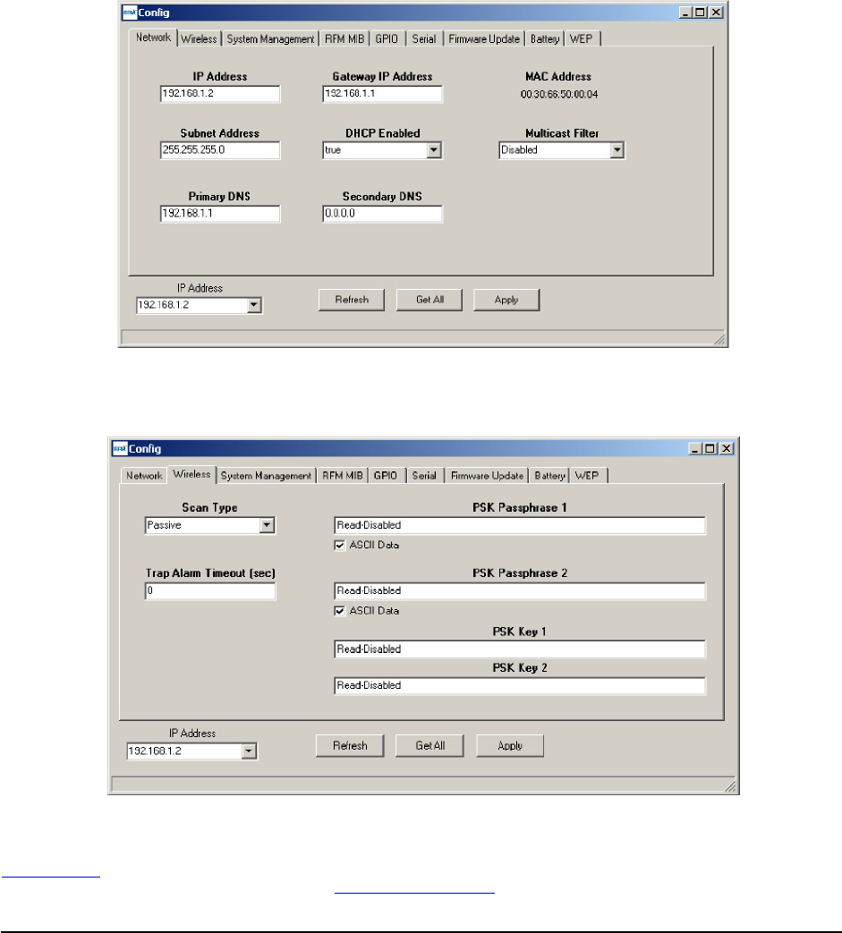
Figure 8.5.8
www.RFM.com
Technical support +1.678.684.2000 Page 36 of 51
©2009 by RF Monolithics, Inc. E-mail:
tech sup@rfm.com
WSN802G - 04/30/09
The Network tab displays basic network parameters information. Note: Unless you are familiar with IP
networking contact RFM module technical support before making any changes on this tab. A parameter
entry error on this tab can irreversibly disable a WSN802G module.
Figure 8.5.3
The Wireless tab accepts inputs for Scan Type (active/passive), Trap Alarm Timeout (0 disables the

Figure 8.5.8
www.RFM.com
Technical support +1.678.684.2000 Page 37 of 51
©2009 by RF Monolithics, Inc. E-mail:
tech sup@rfm.com
WSN802G - 04/30/09
alarm), the IP Address of the WSN802G module, and the PSK Passphrase or PSK Key inputs for
SSIDs 1 and 2. Note that you can only enter passphrases or keys. Clicking the Refresh button loads the
ASCII byte string Read-Disabled in the PSK Passphrase and PSK Key text boxes. Clicking the Apply
button queues a request to update the module with changes entered in this tab.
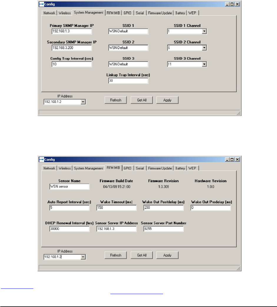
Figure 8.5.8
www.RFM.com
Technical support +1.678.684.2000 Page 38 of 51
©2009 by RF Monolithics, Inc. E-mail:
tech sup@rfm.com
WSN802G - 04/30/09
The System Management tab displays and accepts inputs on the Primary and Secondary SNMP Man-
ager IP addresses, the Config Trap Interval, the module IP Address, and SSIDs and channel assignments
for SSIDs 1 and 2 (SSID3 is read only).

Figure 8.5.8
www.RFM.com
Technical support +1.678.684.2000 Page 39 of 51
©2009 by RF Monolithics, Inc. E-mail:
tech sup@rfm.com
WSN802G - 04/30/09
Figure 8.5.5
The RFM MIB tab displays and accepts inputs related to MIB application parameters. The Sensor Server
IP Address can be set and applied in this tab as an alternative to Step 7 in Section 8.3.
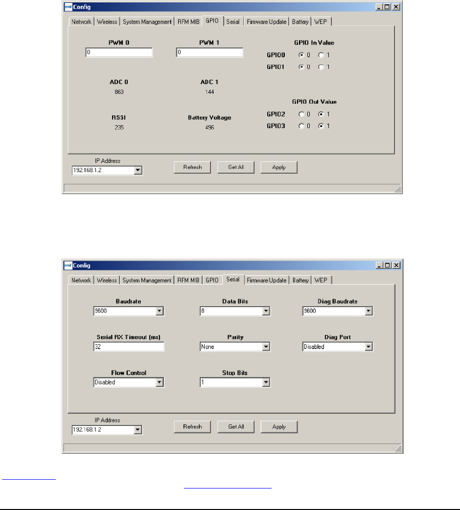
Figure 8.5.8
www.RFM.com
Technical support +1.678.684.2000 Page 40 of 51
©2009 by RF Monolithics, Inc. E-mail:
tech sup@rfm.com
WSN802G - 04/30/09
The
GPIO
tab displays analog and digital module inputs and displays and accepts changes in analog and
digital module outputs. Numerical data is displayed and entered in decimal format. Note: the PWM 1 text
box is not used by the current version of the WSN802G module.

Figure 8.5.8
www.RFM.com
Technical support +1.678.684.2000 Page 41 of 51
©2009 by RF Monolithics, Inc. E-mail:
tech sup@rfm.com
WSN802G - 04/30/09
Figure 8.5.7
The
Serial
tab displays and accepts changes for parameters related to the module’s serial ports. The
Diag
Port is not used for operational diagnostics in the current firmware.
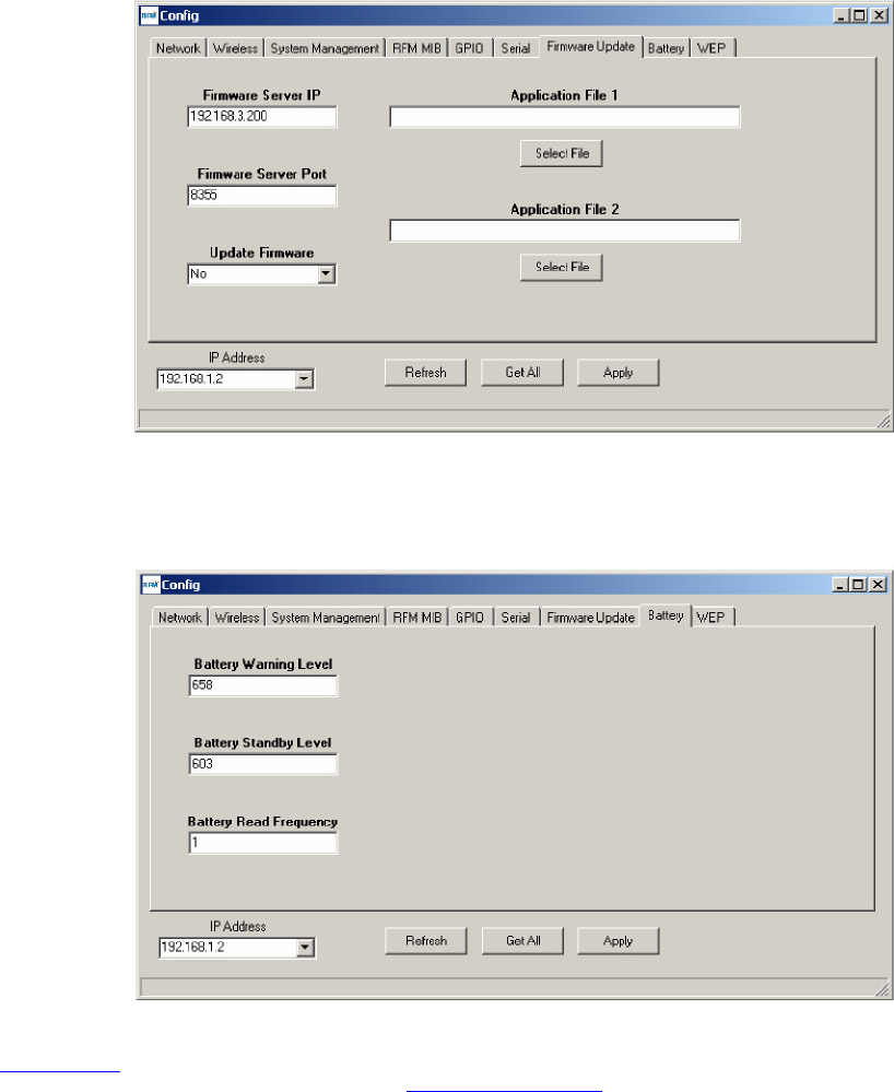
Figure 8.5.8
www.RFM.com
Technical support +1.678.684.2000 Page 42 of 51
©2009 by RF Monolithics, Inc. E-mail:
tech sup@rfm.com
WSN802G - 04/30/09
The Firmware Update tab allows new firmware to be loaded into a WSN802G module. Input the names of
the two firmware Application Files including the paths to the files if they are not located in the same folder
as WSNConfig.exe. Click on each Select File button. Set the Firmware Server IP address and Firmware
Server Port number. Select Yes from the Update Firmware drop-down box and click on Apply.
Figure 8.5.9

Figure 8.5.8
www.RFM.com
Technical support +1.678.684.2000 Page 43 of 51
©2009 by RF Monolithics, Inc. E-mail:
tech sup@rfm.com
WSN802G - 04/30/09
The Battery Tab allows the power supply voltage levels that send a warning and place the module in
standby to be read and/or modified. The read frequency is in units of seconds. Note: contact RFM mod-
ule technical support before making changes to the default warning and standby levels.
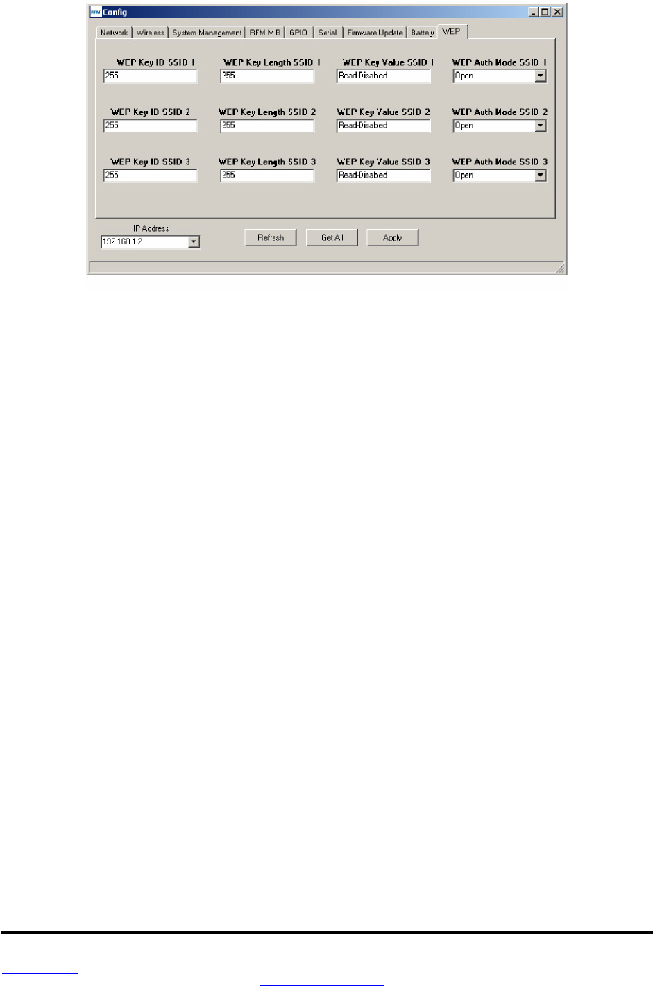
www.RFM.com
Technical support +1.678.684.2000 Page 44 of 51
©2009 by RF Monolithics, Inc. E-mail:
tech sup@rfm.com
WSN802G - 04/30/09
WEP
encryption can be used instead of PSK encryption for compatibility with legacy WiFi routers. WEP
encryption is not implemented in the current version of the module firmware.
Figure 8.5.10
www.RFM.com
Technical support +1.678.684.2000 Page 45 of 51
©2009 by RF Monolithics, Inc. E-mail:
tech sup@rfm.com
WSN802G - 04/30/09
Figure 8.5.11
Figure 8.5.11 shows the same
WSNConfig
main screen as Figure 8.3.4, but with the module IP address
tree expanded on the left and the Sensor Sever IP Address tree expanded on the right.
Figure 8.5.12
The
SNMP
tab allows individual MIB parameters to be manually displayed and modified. The
OID Value
s
and the
Object Types
for the various MIB parameters are listed in Tables 7.3.1 and 7.4.1. Clicking the
Get
button queues a request to retrieve the value of a parameter. Clicking the
Set
button queues a request to
change the value of a parameter. How quickly the module responds to
Set
or
Get
depends on the
Con-
figTrapInterval
system parameter and when in the trap interval the request was queued. Clicking the
Con-
fig
button launches a multi-tab
Con fig
dialog box discussed earlier.
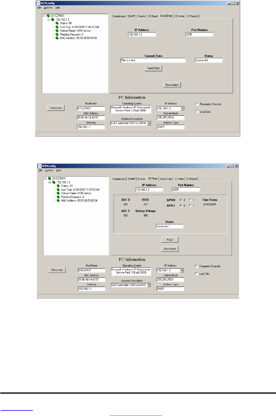
www.RFM.com
Technical support +1.678.684.2000 Page 46 of 51
©2009 by RF Monolithics, Inc. E-mail:
tech sup@rfm.com
WSN802G - 04/30/09
The Events tab displays a running history of events received from the WSN802G module.
The WSN802G module must be awake in order to use the IO Read tab. To hold the module awake,
place a jumper on JP14, which is labeled ALWAYS ON or push and hold the WAKE IN button. The IP
Address and Port Number on the I/O read tab refer to the WSN802G module’s Sensor socket. Clicking
Read sends an IO_REPORT_REQUEST to the module. Note that ADC0 is reading the voltage from
pot R9, and ADC1 is reading the voltage from a voltage divider consisting of a fixed resistor and thermistor
RT1. GPIO0 reads the state of switch S1 and GPIO1 reads the state of switch S2. A GPIO value of 1
indicates the switch is closed. Note: the silkscreen on some developer boards have the GPIO labels
reversed on switches S1 and S2. A quick reply to the IO_REPORT_REQUEST is indicated by a Successful
Status. A Failure Status is usually caused by forgetting to install a jumper on JP14.
The WSN802G module must be awake in order to use the Serial Data tab. To hold the module awake,
Figure 8.5.13
Figure 8.5.14
Figure 8.5.15
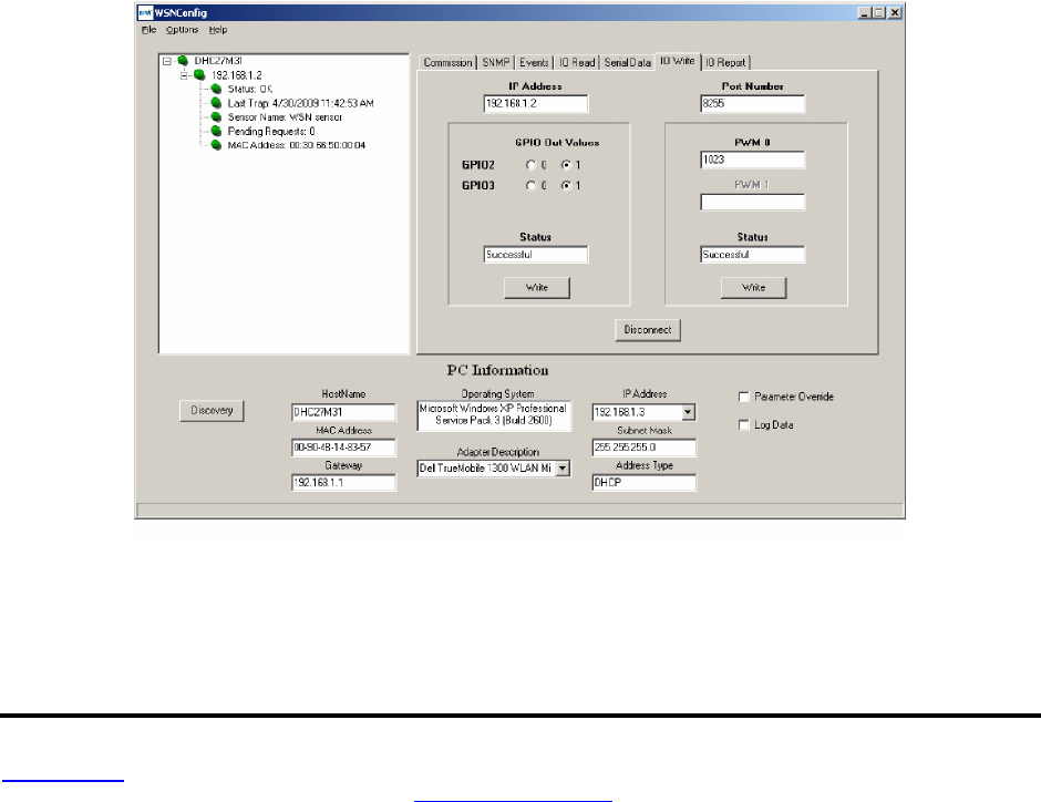
www.RFM.com
Technical support +1.678.684.2000 Page 47 of 51
©2009 by RF Monolithics, Inc. E-mail:
tech sup@rfm.com
WSN802G - 04/30/09
place a jumper on JP14, which is labeled ALWAYS ON or push and hold the WAKE IN button. The IP
Address and Port Number on the I/O read tab refer to the WSN802G module’s Sensor socket. Clicking
Send Data sends the string in the Transmit Data text box in a SERIAL_DATA command to the module. A
quick reply to the command is indicated by a Successful Status. A Failure Status is usually caused by
forgetting to install a jumper on JP14.
The WSN802G module must be awake in order to use the IO Write tab. To hold the module awake, place
a jumper on JP14, which is labeled ALWAYS ON or push and hold the WAKE IN button. The IP Address
and Port Number on the I/O read tab refer to the WSN802G module’s Sensor socket. Clicking the Write
button under GPIO Out Values sends an IO_WRITE_GPIO to the module. Clicking the Write button under
Figure 8.5.16
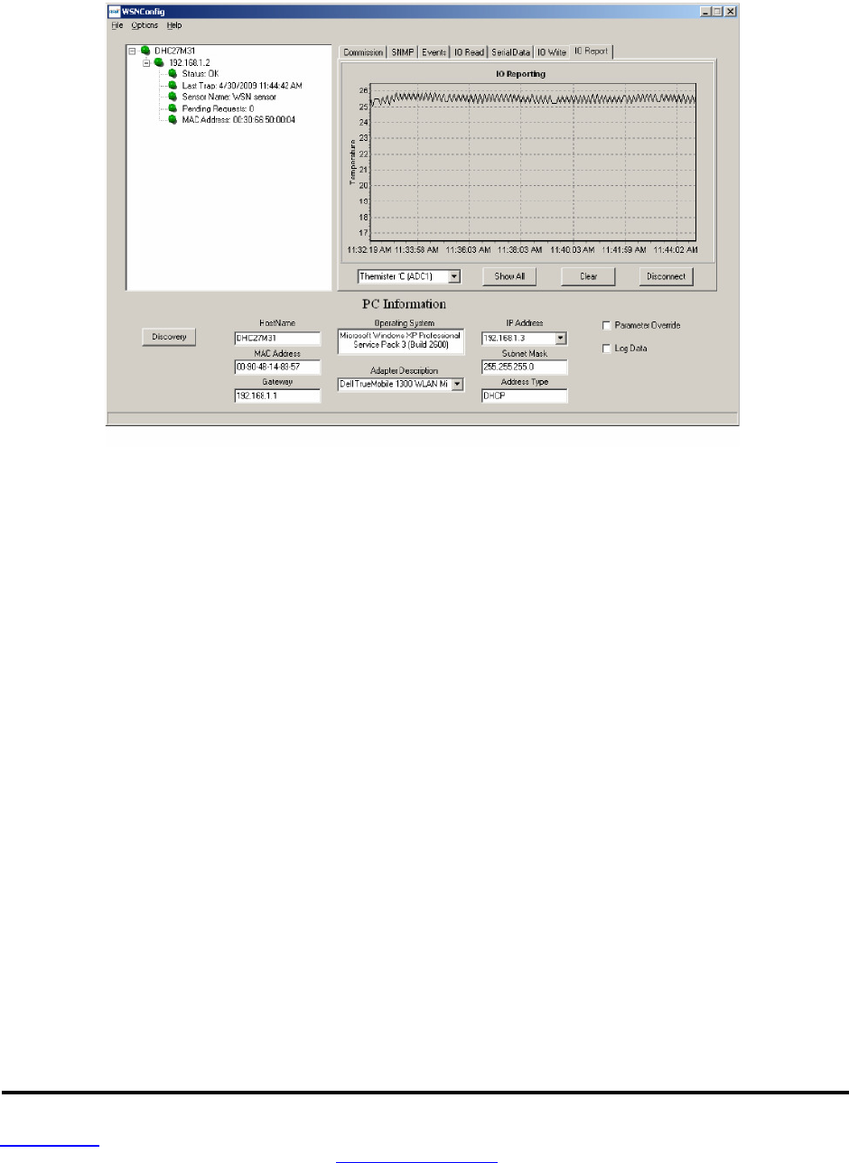
www.RFM.com
Technical support +1.678.684.2000 Page 48 of 51
©2009 by RF Monolithics, Inc. E-mail:
tech sup@rfm.com
WSN802G - 04/30/09
PWM 0 sends an IO_WRITE_PWM command to the module. A quick reply to either write command is
indicated by a Successful Status. A Failure Status is usually caused by forgetting to install a jumper on
JP14. On the developer board, GPIO2 and 3 are connected to LEDs such that the LEDs light when the
module pin is set to 1.
The WSN802G module must be awake in order to use the IO Report tab. To hold the module awake,
place a jumper on JP14, which is labeled ALWAYS ON or push and hold the WAKE IN button. Either a
single parameter can be selected for charting from the drop-down box in the lower left corner of the IO
Report tab, or all parameters can be selected for charting by clicking on the Show All button. The chart
area can be cleared and reset by clicking the Clear button.
Figure 8.5.17

www.RFM.com
Technical support +1.678.684.2000 Page 49 of 51
©2009 by RF Monolithics, Inc. E-mail:
tech sup@rfm.com
WSN802G - 04/30/09
9.0 Troubleshooting
WSNConfig.exe does not communicate with a WSN802G module - The wireless router and the WiFi in
the PC running WSNConfig.exe must be set to match the WSN802G Wireless configuration. The default
is channel 11 with an SSID of WSN-Default (case sensitive) in secure mode. The security passphrase to
allow router access is WSN-PASSWORD. Note: the NETG EAR router shipped in the WSN802GDK is
preconfigured for use with the WSN802G module. Do not reconfigure the router. The WSN802G module
must be connected to an antenna to work.
WSN802G will not accept sensor application commands - the module must be awake to accept applica-
tion commands. Either assert a logic high on the WAKE_IN hardware line or queue the sensor application
command to immediately follow an automatic (timer) I/O Report. Use the RFM MIB tab on the Con fig dia-
log window in WSNConfig.exe to check for suitable AutoReport and Wake Timeout values. See Section
8.6 for additional information.
Range is extremely limited - this is usually a sign of a poor antenna connection or the wrong antenna.
Check that the antenna is firmly connected. If possible, remove any obstructions near the antenna.

www.RFM.com
Technical support +1.678.684.2000 Page 50 of 51
©2009 by RF Monolithics, Inc. E-mail:
tech sup@rfm.com
WSN802G - 04/30/09
10.0 Appendices
10.1 Ordering Information
WSN802GC: transceiver module for solder-pad mounting
WSN802GP: transceiver module for pin-socket mounting
10.2 Technical Support
For WSN802G product support contact RFM’s module technical support group. The phone number is
+1.678.684.2000. Phone support is available from 08.30 AM to 5:30 PM US Eastern Time Zone, Monday
through Friday. The e-mail address is tech_sup@rfm.com.
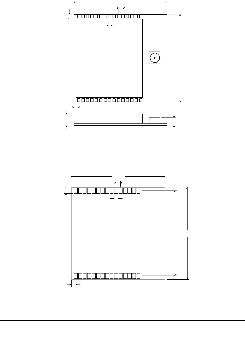
www.RFM.com
Technical support +1.678.684.2000 Page 51 of 51
©2009 by RF Monolithics, Inc. E-mail:
tech sup@rfm.com
WSN802G - 04/30/09
10.3 WSN802G Mechanical Specifications
WSN802GC Outline and Mounting Dimensions
WSN802GC Solder Pad Dimensions
Dimensions in inches
Figure 10.3.2
0.125
0.090
1.0
50
0.050
1
0.040
15
0.030
Top View
16
30
0.050
Dimensions in inches
Figure 10.3.1
0.985
1.050
0.050
0.060
15
0.035
1
0.960
1.040
Top View
16
30
0.050
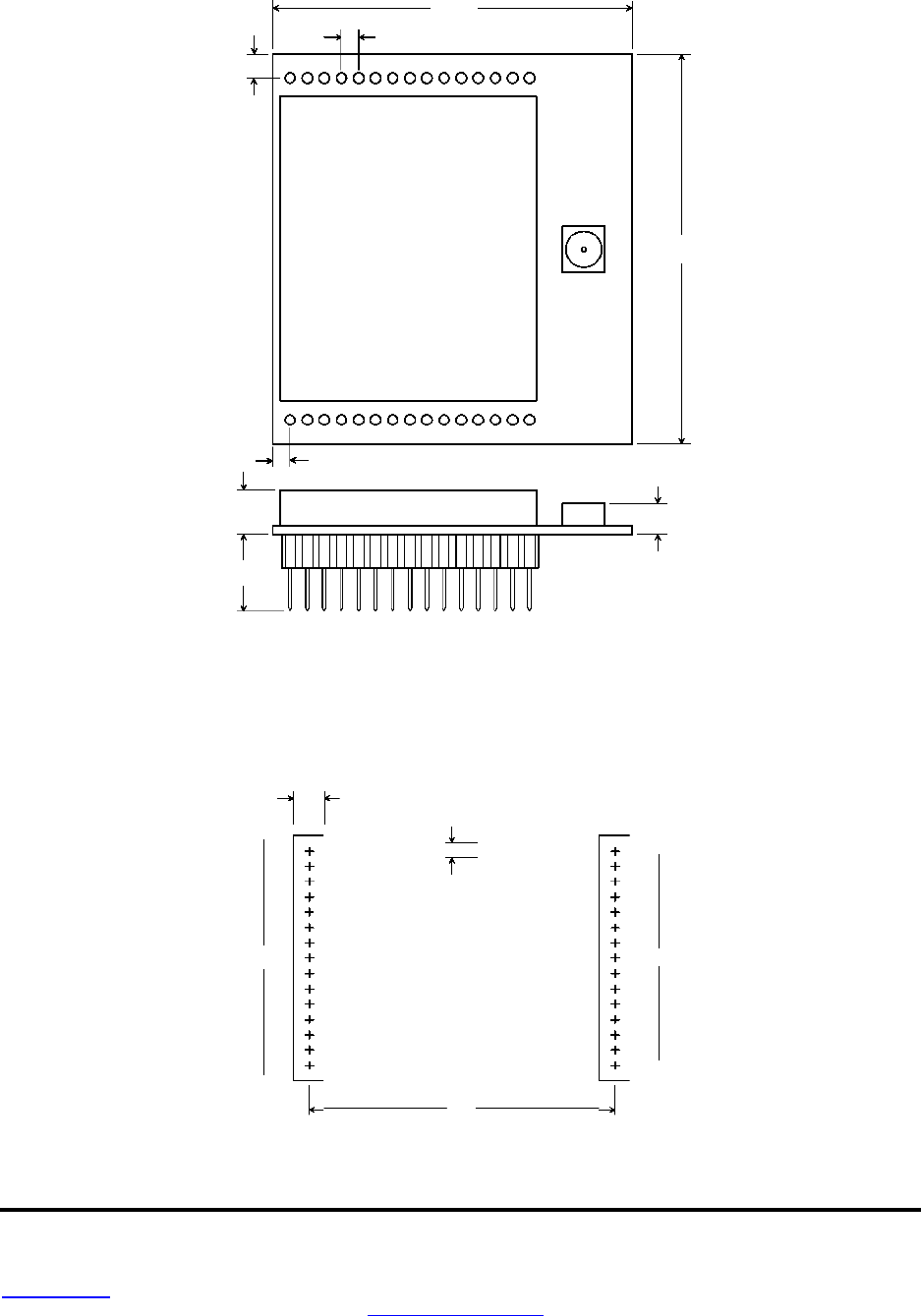
www.RFM.com
Technical support +1.678.684.2000 Page 52 of 51
©2009 by RF Monolithics, Inc. E-mail:
tech sup@rfm.com
WSN802G - 04/30/09
WSN802GP Outline and Mounting Dimensions
Dimensions in inches
Figure 10.3.3
WSM802GP Interface Connector
PCB Layout Detail
0.10
0.05
Connectors are SAMTEC
SLM-115-01-G-S
or Equivalent
1.00
Dimensions are in inches
Figure 10.3.4
0.05
15
1
0.05
1.14
0.07
1.05
Top View
16
30
0.125
0.09
0.225
0.80
0.70
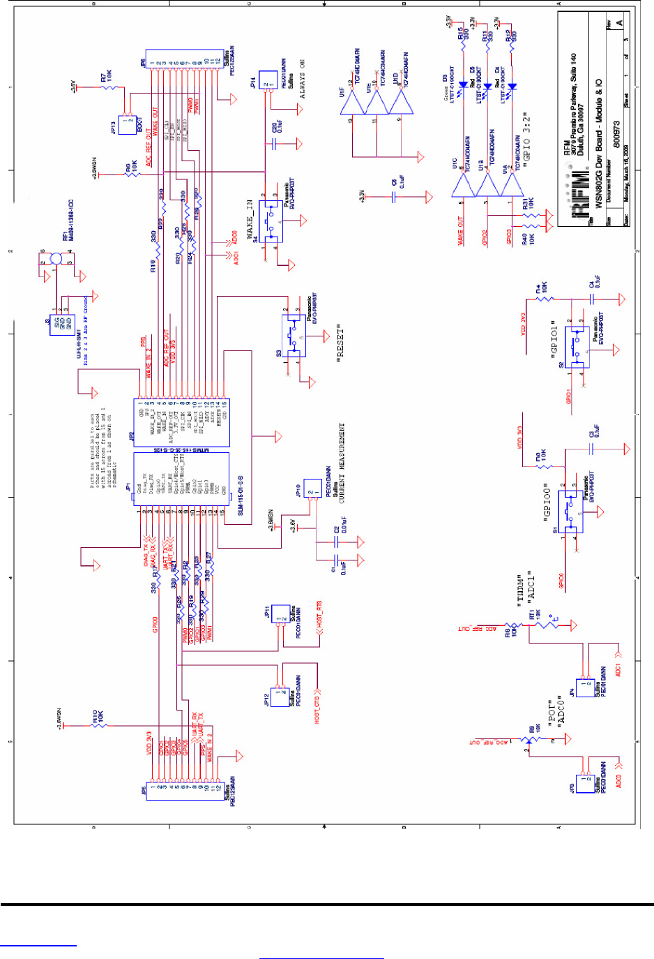
www.RFM.com
Technical support +1.678.684.2000 Page 53 of 51
©2009 by RF Monolithics, Inc. E-mail:
tech sup@rfm.com
WSN802G - 04/30/09
10.4 WSN802G Developer Board Schematic
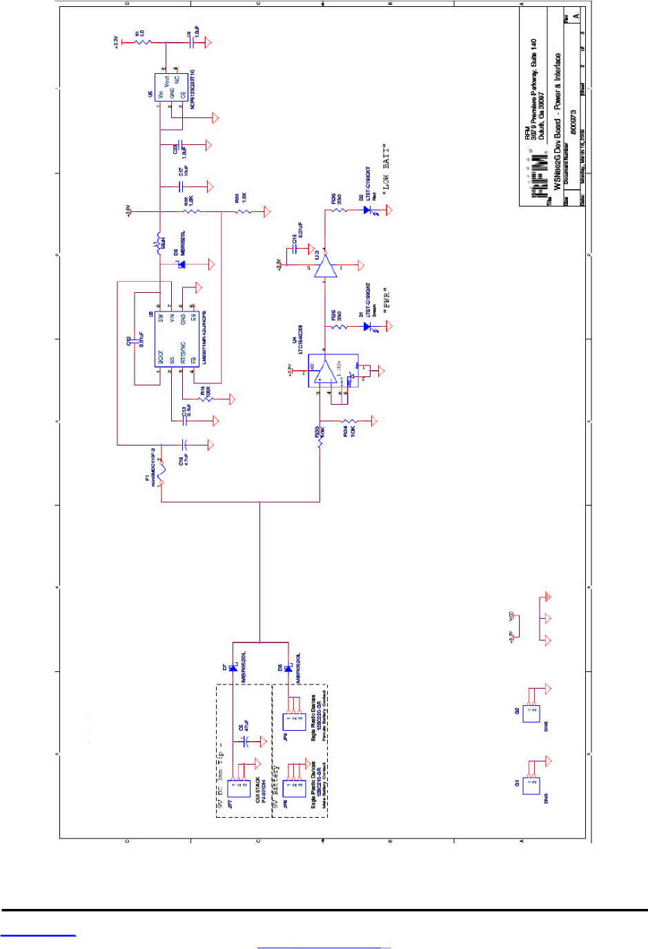
www.RFM.com
Technical support +1.678.684.2000 Page 49 of 51
©2009 by RF Monolithics, Inc.
E
-
mail:
tech sup@rfm.com
WSN802
G
-
04/30/09
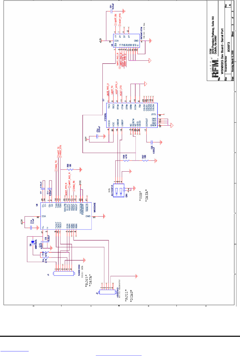
www.RFM.com
Technical support +1.678.684.2000 Page 55 of 51
©2009 by RF Monolithics, Inc. E-mail:
tech sup@rfm.com
WSN802G - 04/30/09

www.RFM.com
Technical support +1.678.684.2000 Page 56 of 51
©2009 by RF Monolithics, Inc. E-mail:
tech sup@rfm.com
WSN802G - 04/30/09
11.0 Warranty
Seller warrants solely to Buyer that the goods delivered hereunder shall be free from defects in materials
and workmanship, when given normal, proper and intended usage, for twelve (12) months from the date
of delivery to Buyer. Seller agrees to repair or replace at its option and without cost to Buyer all defective
goods sold hereunder, provided that Buyer has given Seller written notice of such warranty claim within
such warranty period. All goods returned to Seller for repair or replacement must be sent freight prepaid
to Seller’s plant, provided that Buyer first obtain from Seller a Return Goods Authorization before any
such return. Seller shall have no obligation to make repairs or replacements which are required by normal
wear and tear, or which result, in whole or in part, from catastrophe, fault or negligence of Buyer, or from
improper or unauthorized use of the goods, or use of the goods in a manner for which they are not de-
signed, or by causes external to the goods such as, but not limited to, power failure. No suit or action
shall be brought against Seller more than twelve (12) months after the related cause of action has oc-
curred. Buyer has not relied and shall not rely on any oral representation regarding the goods sold here-
under, and any oral representation shall not bind Seller and shall not be a part of any warranty.
THE PROVISIONS OF THE FOREGOING WARRANTY ARE IN LIEU OF ANY OTHER WARRANTY,
WHETHER EXPRESS OR IMPLIED, WRITTEN OR ORAL (INCLUDING ANY WARRANTY OR MER-
CHANT ABILITY OR FITNESS FOR A PARTICULAR PURPOSE). SELLER’S LIABILITY ARISING
OUT OF THE MANUFACTURE, SALE OR SUPPLYING OF THE GOODS OR THEIR USE OR DISPO-
SITION, WHETHER BASED UPON WARRANTY, CONTRACT, TORT OR OTHERWISE, SHALL NOT
EXCEED THE ACTUAL PURCHASE PRICE PAID BY BUYER FOR THE GOODS. IN NO EVENT
SHALL SELLER BE LIABLE TO BUYER OR ANY OTHER PERSON OR ENTITY FOR SPECIAL, IN-
CIDENTAL OR CONSEQUENTIAL DAMAGES, INCLUDING, BUT NOT LIMITED TO, LOSS OF PROF-
ITS, LOSS OF DATA OR LOSS OF USE DAMAGES ARISING OUT OF THE MANUFACTURE, SALE
OR SUPPLYING OF THE GOODS. THE FOREGOING WARRANTY EXTENDS TO BUYER ONLY AND
SHALL NOT BE APPLICABLE TO ANY OTHER PERSON OR ENTITY INCLUDING, WITHOUT LIMI-
TATION, CUSTOMERS OF BUYERS.
Part # M-0802-1 002, Rev A