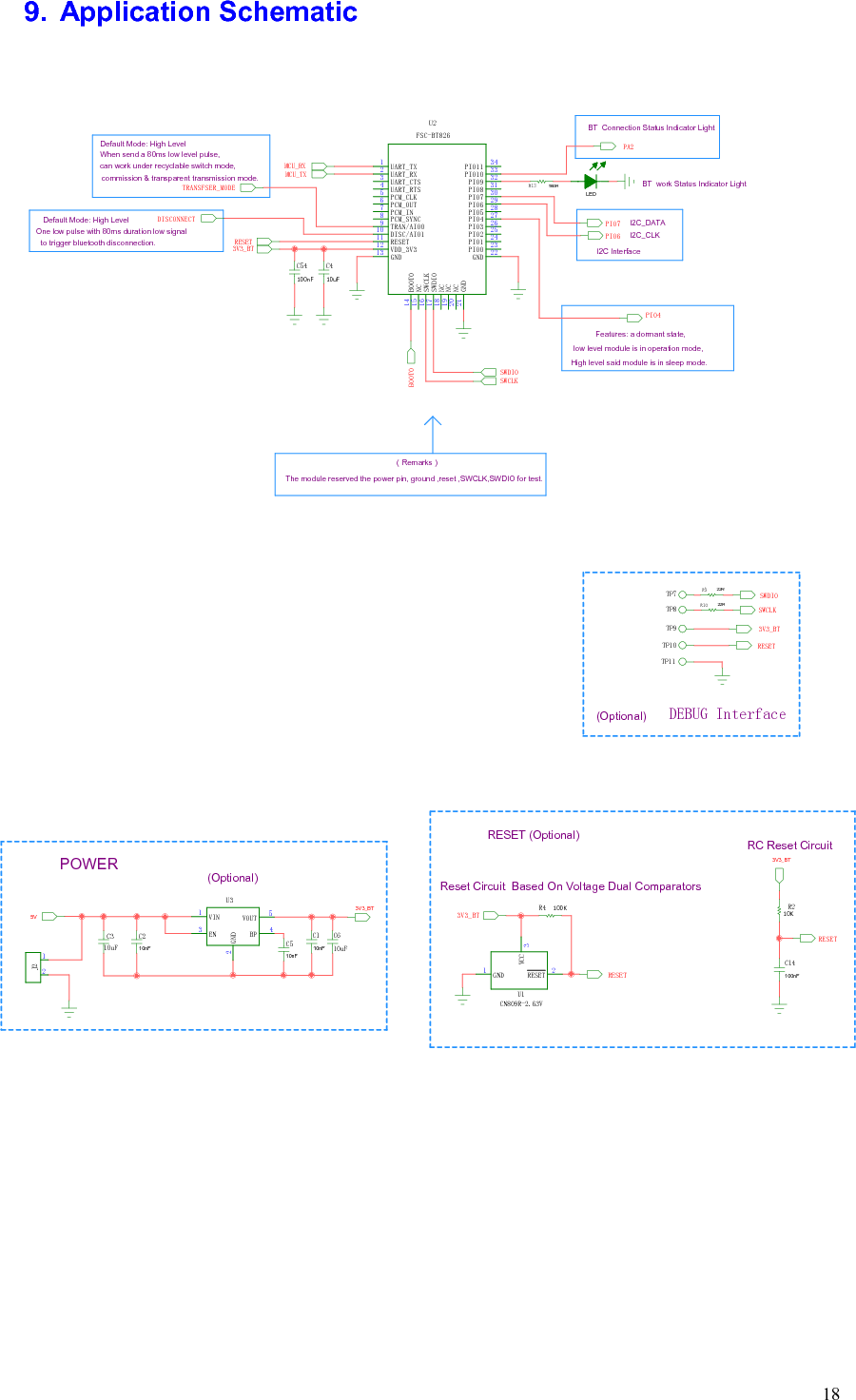
NUMA Electronics 319-BT82600 Bluetooth Module User Manual

NUMA Electronics Inc. Bluetooth Module

User manual

     1    Bluetooth Module User Guide                  NUMA  319-BT82600 Bluetooth module
     2 Release Record Version Number  Release Date  Comments Revision 1.0  2014-11-5  First Release Revision 1.1  2015-09-09   Revision 1.2  2016-03-24  1, Modified BT Status for 33 pin, 2,  Modify  the  application  circuit diagram. Revision 1.3  2016-04-16  1, Modify the Pin 9 ,10 , 14, 16 ,       17,28,31 function definition. 2, Modify the application circuit diagram. 3, This version of the specification is applicable to V1.2 version of the PCB. Revision 1.4  2016-08-06  1, PIN27 Alternative Function :BT Power Mode 2, Modify the application circuit diagram.
FEDERAL COMMUNICATIONS COMMISSION INTERFERENCE STATEMENT This equipment has been tested and found to comply with the limits for a Class B digital device, pursuant  to  part  15  of  the  FCC  Rules.  These  limits  are  designed  to  provide  reasonable protection against harmful interference in a residential installation. This equipment generates, uses and can radiate radio frequency energy and, if not installed and used in accordance with the instructions, may cause harmful interference to radio communications. However, there is no guarantee that interference will not occur in a particular installation. If this equipment does cause  harmful  interference  to  radio  or  television  reception,  which  can  be  determined  by  turning the equipment off and on, the user is encouraged to try to correct the interference by one or more of the following measures: -Reorient or relocate the receiving antenna. -Increase the separation between the equipment and receiver. -Connect the equipment into an outlet on a circuit different from that to which the receiver is connected. -Consult the dealer or an experienced radio/ TV technician for help.  CAUTION: Any changes or modifications not expressly approved by the grantee of this device could void the user's authority to operate the equipment.  This device complies with Part 15 of the FCC Rules. Operation is subject to the following two conditions: (1) this device may not cause harmful interference, and (2) this device must accept any interference received, including interference that may cause undesired operation.  RF exposure warning This equipment must be installed and operated in accordance with provided instructions and the antenna(s) used for this transmitter must be installed to provide a separation distance of at least 20 cm from all persons and must not be co-located or operating in conjunction with any other antenna or transmitter. End-users and installers must be provide with antenna installation instructions and transmitter operating conditions for satisfying RF exposure compliance.  End Product Labeling This transmitter module is authorized only for use in device where the antenna may be installed such that 20cm may be maintained between the antenna and users. The final end product must be labeled in a visible area with the following: "Contains FCC ID: YKH319-BT82600 “ Information for the OEMs and Integrators The following statement must be included with all versions of this document supplied to an OEM or integrator, but should not be distributed to the end user. 1) This device is intended for OEM integrators only. 2) Please see the full Grant of Equipment document for other restrictions.
     41.2    Feature ◆  Postage stamp sized form factor. ◆  Low power. ◆  Class 1.5 support(high output power) ◆  The default UART Baud rate is 115.2Kbps and can support from 1200bps up to 921Kbps,. ◆  UART, I2C,PCM / I2S data connection interfaces.   ◆  Support the OTA upgrade. ◆  Bluetooth stack profiles support: SPP, HID, MAP, and all BLE protocols.     1.3  Application  ◆  Smart Watch and Bluetooth Bracelet ◆  Health & Medical devices ◆  Wireless POS ◆  Measurement and monitoring systems ◆  Industrial sensors and controls ◆  Asset Tracking                       Note: For YKH319-BT82600, it supports Bluetooth V3.0, V2.1+EDR mode only without BLE function.
     52.    GENERAL SPECIFICATION  General Specification Chipset  Realtek RTL8761 Product    FSC-BT826 Dimension  13mm x 26.9mm x 2mm Bluetooth Specification  Bluetooth V4.0 (Dual Mode) Power Supply  3.3 Volt DC   Sensitivity  -82dBm@0.1%BER Frequency Band  2.402GHz -2.480GHz ISM band Modulation  FHSS,GFSK,DPSK,DQPSK Baseband Crystal OSC  40MHz Hopping & channels 1600hops/sec, 1MHz channel space,79 Channels(BT 4.0 to 2MHz channel space) RF Input Impedance  50 ohms Antenna  Integrated chip antenna Interface  Data: UART, I2C, PCM / I2S Profile SPP, GATT(BLE Standard) MFI,Airsync,ANCS, iBeacon, MAP(optional),OTA(optional) Temperature  -20ºC    to    +70 ºC Humidity  10%~95% Non-Condensing Environmental  RoHS Compliant Table 1
     63.  PHYSICAL CHARACTERISTIC  FSC-BT826 dimension is 26.9mm(L)x13mm(W)x2mm(H).     Figure 2:Package Dimensions(TOP VIEW)
     74.  PIN DEFINITION DESCRIPTIONS * Special tips: PIO0,PIO1,PIO2,PIO3    I/O port for reuse. When using the OTA function upgrade (air), please send the I/O mouth dangling; If the I/O port to connect the MCU, then set the MCU I/O ports for the input port or high impedance state.   Figure 3:PIN description   Pin  Pin Name  Pad Type  Description 1  UART_TX  CMOS output  UART data output 2  UART_RX  CMOS input  UART data input 3 UART_CTS  CMOS input UART clear to send active low Alternative Function: Programmable input/output line 4  UART_RTS  CMOS output UART request to send active low Alternative Function: Programmable input/output line 5  PCM_CLK  Bi-directional  Synchronous data clock 6  PCM_OUT CMOS Output  Synchronous data output 7  PCM_IN CMOS Input  Synchronous data input
     88  PCM_SYNC  Bi-directional  Synchronous data Sync 9  Tran/AIO0  I/O Host MCU change UART transmission mode. (Default) If current UART transmission mode is command mode, one low pulse with 80ms duration low signal will change UART transmission mode to throughput mode, and another low pulse could change UART transmission mode back to command mode. Otherwise it will be set as high always. Alternative Function:   Analogue programmable I/O line. 10  Disc/AIO1  I/O Host MCU disconnect bluetooth. (Default) One low pulse with 80ms duration low signal to trigger bluetooth disconnection.Otherwise it will be set as high always.   Alternative Function:   Analogue programmable I/O line. 11  RESET  CMOS input Reset if low. Input debounced so must be low for >5ms to cause a reset. 12  VDD_3V3  VDD  Power supply voltage 3.3V 13  GND  VSS  Power Ground 14  BOOT0  Bi-directional The default is low. (internal 10K resistance drop) When writing to MCU when using the serial port, this pin is connected with the high level. 15  NC  NC  NC 16  SWCLK  Bi-directional  Debugging through the clk line(Default) 17  SWDIO  Bi-directional  Debugging through the data line(Default) 18  NC  NC  NC 19  NC  NC  NC 20  NC  NC  NC 21  GND  VSS  Power Ground 22  GND  VSS  Power Ground 23 PIO0  I/O Programmable input/output line * The I/O port for reuse. 24 PIO1  I/O Programmable input/output line * The I/O port for reuse. 25 PIO2  I/O Programmable input/output line * The I/O port for reuse.
     926  PIO3  I/O Programmable input/output line * The I/O port for reuse. 27  PIO4  I/O Programmable input/output line Alternative Function: BT Power Mode, low level in run mode, it will be set to high level when fall asleep. 28  PIO5  I/O  With the use of the Pin 9. 29  PIO6  I/O Programmable input/output line     Alternative Function: I2C CLK line (Default) 30  PIO7 I/O Programmable input/output line   Alternative Function: I2C DATA line (Default) 31  PIO8  I/O  With the use of the Pin 10. 32 PIO9  I/O Programmable input/output line Alternative Function: LED(Default) 33 PIO10  I/O Programmable input/output line Alternative Function: BT Status(Default) 34  PIO11  I/O  Programmable input/output line Table 2   5.  Interface Characteristics 5.1  UART Interface   Four signals are used to implement the UART function. When FSC-BT826 is connected to another digital device, UART_RX and UART_TX transfer data between the two devices. The remaining two signals, UART_CTS and UART_RTS, can be used to implement RS232 hardware flow control where both are active low indicators. The interface consists of four-line connection as described in below: Signal name  Driving source  Description UART-TX  FSC-BT826 module  Data from FSC-BT826 module UART-RX  Host  Data from Host UART-RTS  FSC-BT826 module  Request to send output of FSC-BT826 module UART-CTS  Host  Clear to send input of FSC-BT826 module Table 3
     10Default Data Format Property  Possible Values BCSP-Specific Hardware  Enable Baud Rate  115. 2 Kbps Flow Control  None Data bit length  8bit Parity  None Number of Stop Bits  1 Table 4  5.2  I2C Interface   ◆  Up to two I2C bus interfaces can support both master and slave mode with a frequency up to 400KHZ. ◆  Provide arbitration function, optional PEC(packet error checking) generation and checking. ◆  Supports 7 –bit and 10 –bit addressing mode and general call addressing mode.  The I2C interface is an internal circuit allowing communication with an external I2C interface which is an industry standard two line serial interface used for connection to external hardware. These two serial lines are known as a serial data line (SDA) and a serial clock line (SCL). The I2C module provides two data transfer rates: 100 kHz of standard mode or 400kHz of the fast mode. The I2C module also has an arbitration detect function to prevent the situation where more than one master attempts to transmit data to the I2C bus at the same time. A CRC-8 calculator is also provided in I2C interface to perform packet error checking for I2C data.  5.3  Analog to digital converter (ADC) ◆  12-bit SAR ADC engine with up to 1 MSPS conversion rate ◆  Conversion range: VSSA to VDDA (2.6 to 3.6 V) ◆  Temperature sensor One 12-bit 1 μs multi-channel ADC is integrated in the device. The conversion range is between 2.6 V < VDDA < 3.6 V. An analog watchdog block can be used to detect the channels, which are required to remain within a specific threshold window. A configurable channel management block of analog inputs also can be used to perform conversions in single, continuous, scan or discontinuous mode to support more advanced usages. The ADC can be triggered from the events generated by the general-purpose timers (TMx) and the advanced-control timers (TM1) with internal connection. The temperature sensor can be used to generate a voltage that varies linearly with temperature. Each device is factory-calibrated to improve the accuracy and the calibration data are stored in the system memory area.  5.4  PCM Interface Characteristics The FSC-BT826 supports a PCM digital audio interface that is used for transmitting digital audio/voice data to/from the Audio Codec. Features are supported as below
     11 ◆  Supports Master and Slave mode ◆  Programmable long/short Frame Sync ◆  Supports 8-bit A-law/µ-law, and 13/16-bit linear PCM formats ◆  Supports sign-extension and zero-padding for 8-bit and 13-bit samples ◆  Supports padding of Audio Gain to 13-bit samples ◆  PCM Master Clock Output: 64, 128, 256, or 512kHz ◆  Supports SCO/ESCO link   5.4.1  PCM Format FrameSync is the synchronizing function used to control the transfer of DAC_Data and ADC_Data. A Long FrameSync indicates the start of ADC_Data at the rising edge of FrameSync (Figure 3), and a Short FrameSync indicates the start of ADC_Data at the falling edge of FrameSync (Figure 4).   Figure 4:Long FrameSync         Figure 5:Short FrameSync   5.4.2  Sign Extension and Zero Padding for 8-Bit and 13-Bit Samples  For 16-bit linear PCM output, 3 or 8 unused bits may be sign extended/zero padded.   Figure 6:16-Bit Output Data with 8-Bit PCM Sample Data and Sign Extension
     12 Figure 7:16-Bit Output Data with 8-Bit PCM Sample Data and Zero Padding    Figure 8:16-Bit Output Data with 13-Bit PCM Sample Data and Sign Extension  For 16-bit linear PCM output, 3-bit programmable audio gain value can be padded to 13-bit sample data.  Figure 9:16-Bit Output Data with 13-Bit PCM Sample Data and Audio Gain     5.4.3  PCM Interface Timing  Figure 10:PCM Interface (Long FrameSync)
     13 Figure 11:PCM Interface (Short FrameSync)  Table 5: PCM Interface Clock Specifications  Table 6: PCM Interface Timing      5.4.4 PCM Interface Signal Levels The PCM signal level ranges from 1.8V to 3.3V.
     146.  RECOMMENDED TEMPERATURE REFLOW PROFILE The re-flow profiles are illustrated in Figure 11 and Figure 12 below.   Follow: IPC/JEDEC J-STD-020 C   Condition:   Average ramp-up rate(217  to peak):1~2 /sec max.℃ ℃    Preheat:150~200C,60~180 seconds   Temperature maintained above 217 :60~150 seconds℃   Time within 5  of actual peak temperature:20~40 sec.℃   Peak temperature:250+0/-5  or 260+0/℃-5℃   Ramp-down rate:3 /sec.max.℃   Time 25  to peak temperature:8℃ minutes max   Cycloe interval:5 minus  Figure 12: Typical Lead-free Re-flow Solder Profile
     152170C2420C Figure 13 : Typical Lead-free Re-flow The soldering profile depends on various parameters according to the use of different solder and material. The data here is given only for guidance on solder re-flow. FSC-BT826 will withstand up to two re-flows to a maximum temperature of 245°C. 7.    Reliability and Environmental Specification 7.1  Temperature test Put the module in demo board which uses exit power supply, power on the module and connect to mobile. Then put the demo in the  ‐20℃  space for 1 hour and then move to +70℃  space within 1minute, after 1 hour move back to  ‐20℃  space within1 minute. This is 1 cycle. The cycles are 32 times and the units have to pass the testing. 7.2  Vibration Test The  module  is  being  tested  without  package.  The  displacement  requests  1.5mm  and  sample  is vibrated  in  three  directions(X,Y,Z).Vibration  frequency  set  as  0.5G  ,  a  sweep  rate  of  0.1  octave/min from 5Hz to 100Hz last for 90 minutes each direction. Vibration frequency set as 1.5G, a sweep rate of 0.25 octave/min from 100Hz to 500Hz last for 20 minutes each direction. 7.3      Desquamation test Use  clamp  to  fix  the  module,  measure  the  pull  of  the  component  in  the  module,  make  sure  the module`s soldering is good.
     167.4    Drop test Free fall the  module (condition built in a wrapper which can defend ESD) from 150cm height to cement  ground,  each  side  twice,  total  twelve  times.  The  appearance  will  not  be  damaged  and  all functions OK. 7.5    Packaging information After unpacking, the module should be stored in environment as follows:  Temperature: 25  ± 2℃ ℃  Humidity: <60%  No acidity, sulfur or chlorine environment The module must be used in four days after unpacking.  8.  Layout and Soldering Considerations 8.1  Soldering Recommendations FSC-BT826 is compatible  with industrial standard  reflow profile for Pb-free solders. The  reflow profile used is dependent on the thermal mass of the entire populated PCB, heat transfer efficiency of the oven and particular type of solder  paste  used.  Consult the datasheet of particular solder  paste for profile configurations. Feasycom will give following recommendations for soldering the module to ensure reliable solder joint  and  operation  of  the  module  after  soldering.  Since  the  profile  used  is  process  and  layout dependent,  the  optimum  profile  should  be  studied  case  by  case.  Thus  following  recommendation should be taken as a starting point guide. 8.2    Layout Guidelines It is strongly recommended to use good layout practices to ensure proper operation of the module. Placing copper  or any metal near antenna deteriorates its  operation by having effect on  the matching properties. Metal shield around the antenna will prevent the radiation and thus metal case should not be used with the module. Use grounding vias separated max 3 mm apart at the edge of grounding areas to prevent  RF  penetrating  inside  the  PCB  and  causing  an  unintentional  resonator.  Use  GND  vias  all around the PCB edges.   The mother board should have no bare conductors or vias in this restricted area, because it is not covered by stop mask print. Also no copper (planes, traces or vias) are allowed in this area, because of mismatching the on-board antenna.
Shenzhen Feasycom Technology Co.,LTD                                           www.feasycom.com     17   Figure 14: FSC-BT826 Restricted Area Following  recommendations  helps  to  avoid  EMC problems arising in the design.  Note  that  each design is unique and the following list do not consider all basic design rules such as avoiding capacitive coupling between signal lines. Following list is aimed to avoid EMC problems caused by RF part of the module. Use good consideration to avoid problems arising from digital signals in the design. Ensure that signal lines have return paths as short as possible. For example if a signal goes to an inner  layer  through  a  via,  always  use  ground  vias  around  it.  Locate  them  tightly  and  symmetrically around the signal vias. Routing of any sensitive signals should be done in the inner layers of the PCB. Sensitive traces should have a ground area above and under the line. If this is not possible, make sure that the return path is short by other means (for example using a ground line next to the signal line).
     189.  Application Schematic  Features: a dormant state,low level module is in operation mode,Default Mode: High LevelWhen send a 80ms low level pulse,can work under recyclable switch mode,Default Mode: High LevelOne low pulse with 80ms duration low signal  to trigger bluetooth disconnection. commission & transparent transmission mode. BT  work Status Indicator LightI2C InterfaceI2C_CLKI2C_DATABT  Connection Status Indicator Light(Remarks)The module reserved the power pin, ground ,reset ,SWCLK,SWDIO for test.High level said module is in sleep mode.12345678910111213141516171819202122232425262728293031323334MCU_RXMCU_TXRESETSWDIOSWCLK3V3_BTPA2PIO7PIO6DISCONNECTTRANSFSER_MODEBOOT0PIO4LEDR13560RC54100nFC410uFUART_TXUART_RXUART_CTSUART_RTSPCM_CLKPCM_OUTPCM_INPCM_SYNCTRAN/AIO0DISC/AIO1RESETVDD_3V3GNDBOOT0NCSWCLKSWDIONCNCNCGNDGNDPIO0PIO1PIO2PIO3PIO4PIO5PIO6PIO7PIO8PIO9PIO10PIO11U2FSC-BT826DEBUG Interface (Optional)3V3_BTRESETSWDIOSWCLKR322RR1022RTP7TP8TP9TP10TP11POWERRESET (Optional)Reset Circuit  Based On Voltage Dual ComparatorsRC Reset Circuit (Optional)12345121 233V3_BT5V3V3_BTRESET3V3_BTRESETC310uFC110nFC510nFC610uFVINGNDEN BPVOUTU3C210nFC14100nFR210KJ2R4 100KGND RESETVCCU1CN809R-2.63V

Navigation menu