NXP Laboratories UK JN5121M4 802.15.4/ ZigBee Module User Manual JN DS JN5121 xxx Myy
NXP Laboratories UK Ltd 802.15.4/ ZigBee Module JN DS JN5121 xxx Myy
Manual
Preliminary Data Sheet – JN5121-xxx-Myy
IEEE802.15.4/ZigBee Module Family
Preliminary - JN-DS-JN5121MO-1v23.doc © Jennic 2006
Features: Module
•
2.4GHz IEEE802.15.4
compliant
•
2.7-3.6V operation
•
Sleep current (with active
sleep timer) < 14µA
•
JN5121-xxx-M00/01/03
Standard module, 0dBm power
M00: on board antenna or
M01: SMA connector,
M03: RP-SMA connector
> 400m range
o Receiver sensitivity -90dBm
o TX current < 45mA
o RX current < 50mA
o 18x30mm
•
JN5121-xxx-M02/04
18.5dBm power with LNA and
SMA connector, > 4km range
Receiver sensitivity -93dBm
o TX current < 120mA
o RX current < 55mA
o 18x40mm
Features: Microcontroller
•
16MHz 32-bit RISC CPU
•
96kB RAM, 64kB ROM
•
4-input 12-bit ADC, 2 11-bit
DACs, comparator,
temperature sensor
•
2 Application timer/counters,
3 system timers
•
2 UARTs (one for in-system
debug)
•
SPI port with 5 selects
•
2-wire serial interface
•
21 GPIO
•
Evaluation kits available with
full, unlimited, Software
Development Kit
Industrial temperature range
(-20°C to +70°C)
Lead-free and RoHS compliant
Overview Overview
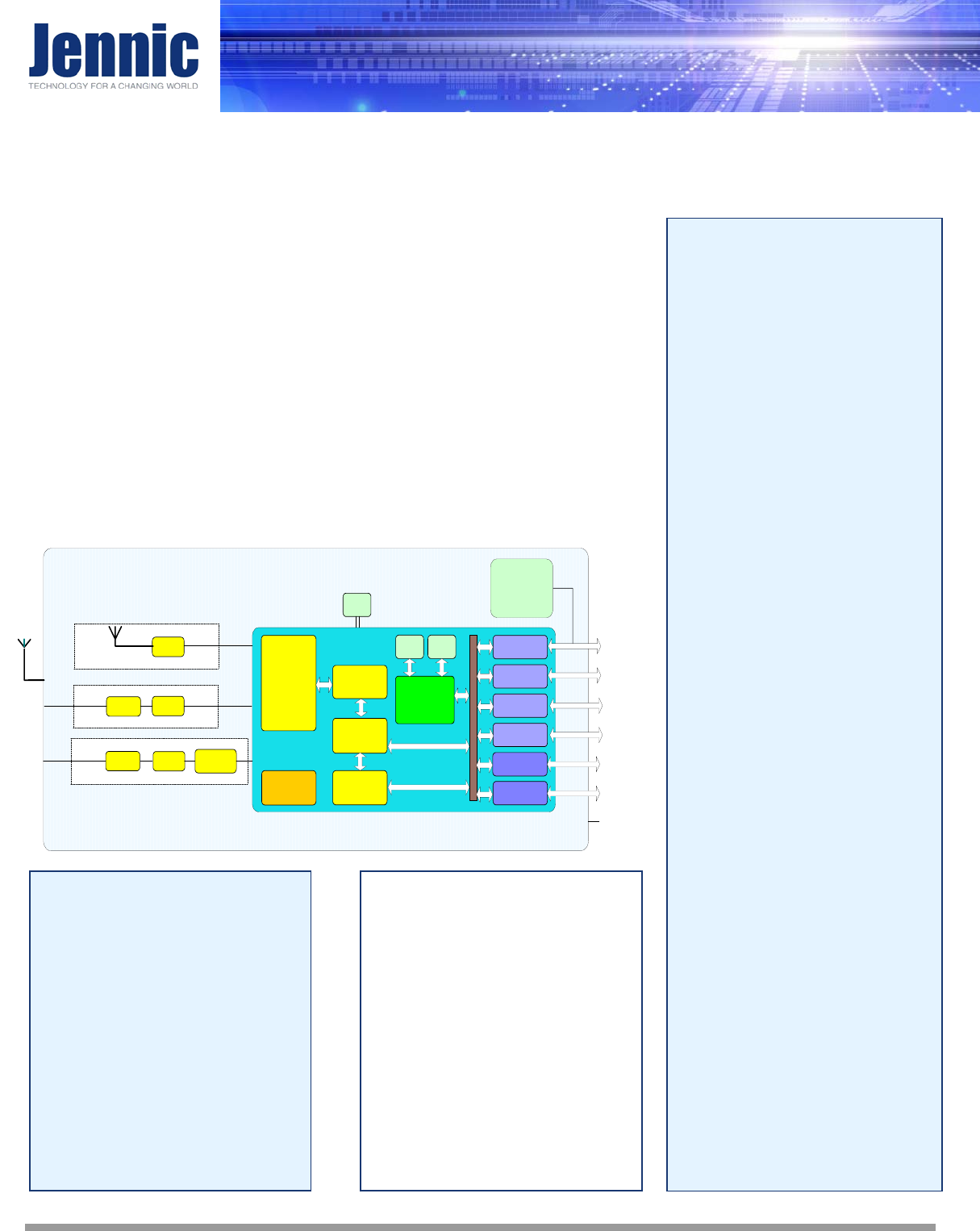
The JN5121-xxx-Myy is a family of surface mounted modules that enable users to implement
IEEE802.15.4 or ZigBee compliant systems with minimum time to market and at the lowest
cost. They remove the need for expensive and lengthy development of custom RF board
designs and test suites. The modules use Jennic’s JN5121 wireless microcontroller to provide
a comprehensive solution, including all RF components. All that is required to develop and
manufacture wireless control or sensing products is to connect a power supply and peripherals
such as switches, actuators, sensors, considerably simplifying product development.
Three basic hardware module variants are available: JN5121-xxx-M00 with an integrated
antenna, JN5121-xxx-M01/M03 with an antenna connector and JN5121-xxx-M02/M04 with a
power amplifier and LNA for extended range. Each of these can be provided pre-programmed
with a ZigBee network stack (JN5121-Z01-Myy) or with customer-specific software.
Block Diagram Block Diagram
Timers
UARTs
12-bit ADC,
comparator
11-bit DACs,
temp sensor
2-wire serial
SPI
RAM
96kB
128-bit AES
Encryption
Accelerator
2.4GHz
Radio
ROM
64kB
RISC CPU
Power
Management
XTAL
O-QPSK
Modem
IEEE802.15.4
MAC
Accelerator
128kB Serial
Flash Memory
JN5121 chip
Power
Balun
SMA
Connector
Balun
Ceramic Antenna
Balun
SMA
Connector PA / LNA
External
Antenna
MO00 Option
M01/03 Option
M02/04 Option
Benefits
•
Microminiature module solutions
•
Ready to use in products
•
Minimises product development
time
•
No RF test required for systems
•
Compliant with FCC part 15
rules, ETSI ETS 300-328 and
Japan ARIB STD-T66
•
Production volumes supplied
pre-programmed with
application software
Applications
•
Robust and secure low power
wireless applications
•
Wireless sensor networks,
particularly IEEE802.15.4 /
ZigBee systems
•
Home and commercial building
automation
•
Home networks
•
Toys and gaming peripherals
•
Industrial systems
•
Telemetry and utilities
(e.g. AMR)

Jennic
Contents
1. Introduction 1
1.1. Variants 1
1.2. Regulatory Approvals 1
2. Specifications 2
3. Product Development 3
3.1. JN5121 Single Chip Wireless Microcontroller 3
4. Pin Configurations 4
4.1. Pin Assignment 5
4.2. Pin Descriptions 6
4.3. Power Supplies 6
4.4. SPI Memory Connections 6
5. Electrical Characteristics 7
5.1. Maximum Ratings 7
5.2. Operating Conditions 7
Appendix A Mechanical and Ordering Information 8
A.1 Outline Drawing 8
A.2 Module PCB Footprint 11
A.3 Ordering Information 12
A.4 Accessories 13
A.5 Tape and Reel Information: 14
A.5.1 Tape Orientation and dimensions 14
A.5.2 Cover tape details 14
A.5.3 Leader and Trailer 15
A.5.4 Reel Dimensions: 15
A.6 Related Documents 16
A.7 Federal Communication Commission Interference Statement 16
A.8 Disclaimers 18
A.9 Version Control 18
A.10 Contact Details 19
ii Preliminary - JN-DS-JN5121MO-1v23.doc © Jennic 2006

Jennic
1. Introduction
The JN5121-xxx-Myy module family provides designers with a ready made component which allows IEEE802.15.4 [1]
wireless applications, including ZigBee, to be quickly and easily included in product designs. The modules integrate
all of the RF components, removing the need to perform expensive RF design and test. Products can be designed by
simply connecting sensors and switches to the module IO pins. The modules use Jennic’s single chip IEEE802.15.4
Wireless Microcontroller, allowing designers to make use of the extensive chip development support material.
Hence, this range of modules allows designers to bring wireless applications to market in the minimum time with
significantly reduced development effort and cost.
Three basic modules are available: JN5121-xxx-M00 (standard module with on board ceramic antenna), JN5121-xxx-
M01 (standard module with SMA connector for use with external antennae) and JN5121-xxx-M02 (high RF power,
improved sensitivity module for extended range applications). Each of these modules can be supplied with a range of
protocol stacks, including a simple IEEE802.15.4 protocol for point to point and star applications and a ZigBee mesh
networking stack. The variants available are described below.
1.1. Variants
Variant Description FCCID
JN5121-000-M00 IEEE802.15.4 stack, ceramic antenna TYOJN5121M0
JN5121-Z01-M00 ZigBee stack, ceramic antenna TYOJN5121M0
JN5121-000-M01 IEEE802.15.4 stack, SMA connector N/A
JN5121-Z01-M01 ZigBee stack, SMA connector N/A
JN5121-000-M02 High Power (18.5dBm), IEEE802.15.4 stack,
SMA connector N/A
JN5121-Z01-M02 High Power (18.5dBm), ZigBee stack, SMA
connector N/A
JN5121-000-M03 IEEE802.15.4 stack, RP-SMA connector TYOJN5121M6
JN5121-Z01-M03 ZigBee stack, RP-SMA connector TYOJN5121M6
JN5121-000-M04 (High Power (18.5dBm), IEEE802.15.4
stack, RP-SMA connector TYOJN5121M4
JN5121-Z01-M04 High Power (18.5dBm), ZigBee stack,
RP-SMA connector TYOJN5121M4
1.2. Regulatory Approvals
All module types have been tested against the requirements of European standard ETS 300
328 and a certificate of compliance to this standard is available on request. The High Power
modules with M02 suffix are approved for use in Europe with reduced output power. They must
not be used with PHY_PIB_ATTR_TX_POWER set above 3 See [4].
Additionally, modules with M00, M03 and M04 suffixes have received FCC “Modular Approvals”,
in compliance with CFR 47 FCC part 15 regulations and in accordance to FCC Public notice
DA00-1407. The modules are approved for use with the following half wave dipole antenna
families: EAD BKR2400 series, Antenna Factor RCT and RCL series, Centurion WCR2400 &
WRR2400, GigaAnt Titanis and Nearson Models 131, 141 & 145. See Appendix A.7 for details
on the conditions applying to this modular approval.
The high power module variant FCC ID TYOJN5121M4 is classified as ‘mobile’ device pursuant
with FCC § 2.1091 and must not be used at a distance of < 20 cm (8”) from any nearby people.
© Jennic 2006 Preliminary - JN-DS-JN5121MO-1v23.doc 1

Jennic
2. Specifications
Most specification parameters for the modules are specified in JN-DS-JN5121 Datasheet for JN5121 single chip
wireless microcontroller, [2]. Where there are differences, the parameters are defined here.
VDD=3.0V @ +25ºC
Typ. DC Characteristics Notes
JN5121-xxx-
M00/01/03 JN5121-xxx-
M02/04
Deep sleep <11uA <11uA
Sleep <14uA <14uA With active sleep timer
Radio transmit 44mA 115mA CPU in doze, radio transmitting
Radio receive 49mA 60mA CPU in doze, radio receiving
Centre frequency accuracy +/-25ppm +/-25ppm Additional +/-15ppm allowance for
temperature and aging
Typ. RF Characteristics Notes
Receive sensitivity -90dBm -93dBm Nominal for 1% PER, as per
802.15.4 section 6.5.3.3
Max. Transmit power 0dBm 16dBm Nominal
Transmit power at 3.6V 18.5dBm With Vcc=3.6V
Maximum input signal -10dBm -15dBm For 1% PER, measured as
sensitivity
RSSI range -95 to -10
dBm -115 to -20
dBm
RF Port impedance - SMA connector 50 ohm 50 ohm 2.4 - 2.5GHz
VSWR (max) 2:1 2:1 2.4 - 2.5GHz
Peripherals Notes
Master SPI port with five select outputs 250kHz - 16MHz
Slave SPI port 250kHz - 16MHz
Two UARTs 16550 compatible
Two-wire serial I/F (compatible with SMbus & I2C) Up to 400kHz
Two programmable Timer/Counters with
capture/compare facility, Tick timer
16MHz clock
Two programmable Sleep Timers 32kHz clock
Twenty-one digital IO lines (multiplexed with
UARTs, timers and SPI selects)
Four-channel, 12-bit, Analogue-to-Digital
converter
Up to 100ks/s
Two 11-bit Digital-to-Analogue converters Up to 100ks/s
Programmable analogue comparator Ultra low power mode for sleep
Internal temperature sensor and battery monitor
2 Preliminary - JN-DS-JN5121MO-1v23.doc © Jennic 2006

Jennic
3. Product Development
Jennic supplies all the development tools and networking stacks needed to enable end product development to occur
quickly and efficiently. These are all freely available from Jennic’s support website: http://www.jennic.com/support/ .
A range of evaluation/developer kits is also available, allowing products to be quickly breadboarded. Efficient
development of software applications is enabled by the provision of a complete, unlimited, software developer kit.
Together with the available libraries for the IEEE802.15.4 MAC and the ZigBee network stack, this package provides
everything required to develop application code and to trial it with hardware representative of the final module.
The modules can be programmed by the user, for both development and production, using Jennic supplied software.
They can also be supplied ready loaded with customer defined software if required. The JN-UG-3007 Flash Loader
User Guide [5], describes how to put the module into programming mode, download software onto the module and to
load individual MAC addresses. Access to the on-chip peripherals, MAC and ZigBee stack software is provided
through specific APIs. These are described in the JN-RM-2001 Hardware Peripheral Library Reference Manual [3],
JN-RM-2002 Stack Software Reference Manual [4] and JN-RM-2014 ZigBee Application Development API Reference
Manual . Additional information is available on the Jennic support website.[6]
3.1. JN5121 Single Chip Wireless Microcontroller
The JN5121-xxx-Myy series is constructed around the JN5121 single chip wireless microcontroller, which includes
the radio system, a 32-bit RISC CPU, ROM and RAM memory and a range of analogue and digital peripherals.
The chip is described fully in JN-DS-JN5121 Datasheet for JN5121 single chip wireless microcontroller [2].
© Jennic 2006 Preliminary - JN-DS-JN5121MO-1v23.doc 3
Jennic
4. Pin Configurations
1
2
3
4
16
ADC4
DAC1
DAC2
COMP+
COMP-
SPICLK
SPIMISO
SPIMOSI
SPISSZ
DIO0/SPISEL1
DIO1/SPISEL2
DIO2/SPISEL3
SPISSM
SPISWP
DIO3/SPISEL4
DIO4/CTS0
DIO5/RTS0
DIO6/TXD0
DIO7/RXD0
DIO8/TIM0GT
DIO9/TIM0_CAP
DIO10/TIM0_OUT
DIO11/TIM1GT
VDD
GND
VSSA
ADC3
ADC2
ADC1
DNC
DNC
DIO20/RXD1
DIO19/TXD1
DIO18/RTS1
DIO17/CTS1
DIO16
DIO15/SIF_D
RESETN
DIO14/SIF_CLK
DIO13/TIM1_OUT
DIO12/TIM1_CAP
5
6
7
8
9
10
11
12
13
14
15
17 18 19 20 21 22 23 24 25 26
41
40
39
38
37
36
35
34
33
32
31
30
29
28
27
Antenna
J1
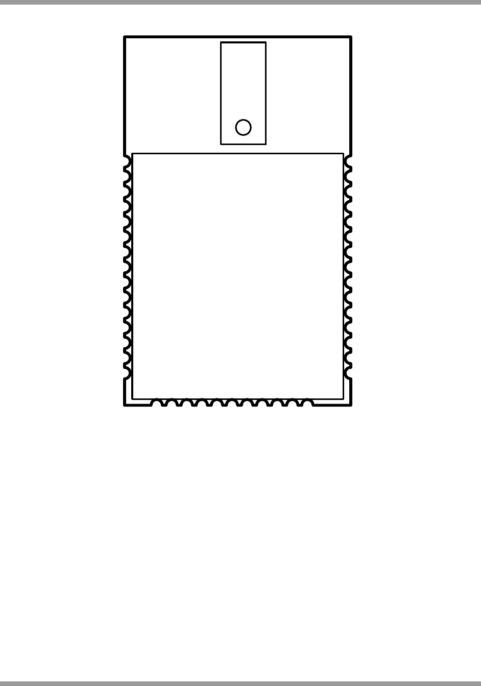
Figure 1: Pin Configuration (top view)
Note that the same basic pin configuration applies for all module designs. However, DIO3/SPISEL4 and
DIO2/SPISEL3 are not available with high power modules.
4 Preliminary - JN-DS-JN5121MO-1v23.doc © Jennic 2006

Jennic
4.1. Pin Assignment
Module
Pin Signal Function Alternative Function
1 ADC4 Analogue to Digital input
2 DAC1 Digital to Analogue output
3 DAC2 Digital to Analogue output
4 COMP+
5 COMP-
Comparator inputs
6 SPICLK SPI master clock out/slave clock in
7 SPIMISO SPI Master In/Slave Out
8 SPIMOSI SPI Master Out/Slave In
9 SPISSZ SPI select from module - SS0 (output)
10 SPISEL1 SPI Slave Select1 (output) General Purpose Digital I/O DIO0
11 SPISEL2 SPI Slave Select2 (output) General Purpose Digital I/O DIO1
12 SPISEL3* SPI Slave Select3 (output) General Purpose Digital I/O DIO2 *
13 SPISSM SPI select to FLASH (input)
14 SPISWP FLASH write protect (input)
15 SPISEL4*
(t Hi
SPI Slave Select4 (output) General Purpose Digital I/O DIO3*
16 CTS0 UART0 Clear To Send (input) General Purpose Digital I/O DIO4
17 RTS0 UART0 Request To Send (output) General Purpose Digital I/O DIO5
18 TXD0 UART0 Transmit Data (output) General Purpose Digital I/O DIO6
19 RXD0 UART0 Receive Data (input) General Purpose Digital I/O DIO7
20 TIM0GT Timer0 clock/gate (input) General Purpose Digital I/O DIO8
21 TIM0_CAP Timer0 capture (input) General Purpose Digital I/O DIO9
22 TIM0_OUT Timer0 PWM (output) General Purpose Digital I/O DIO10
23 TIM1GT Timer1 clock/gate (input) General Purpose Digital I/O DIO11
24 VDD 3V power
25 GND Digital ground
26 VSSA Analogue ground
27 TIM1_CAP Timer1 capture (input) General Purpose Digital I/O DIO12
28 TIM1_OUT Timer1 PWM (output) General Purpose Digital I/O DIO13
29 RESETN Active low reset
30 SIF_CLK Serial Interface clock / Intelligent peripheral clock General Purpose Digital I/O DIO14
© Jennic 2006 Preliminary - JN-DS-JN5121MO-1v23.doc 5

Jennic
Module
Pin Signal Function Alternative Function
31 SIF_D Serial Interface data / Intelligent peripheral data
t
General Purpose Digital I/O DIO15
32 DIO 16 Intelligent peripheral device select General Purpose Digital I/O
33 CTS1 UART1 Clear To Send (input) General Purpose Digital I/O DIO17
34 RTS1 UART1 Request To Send (output) General Purpose Digital I/O DIO18
35 TXD1 UART1 Transmit Data (output) General Purpose Digital I/O DIO19
36 RXD1 UART1 Receive Data (input) General Purpose Digital I/O DIO20
37 DNC
38 DNC
Do Not Connect
39 ADC1 Analogue to Digital input
40 ADC2 Analogue to Digital input
41 ADC3 Analogue to Digital input
*: These two pins are not connected for High power modules
4.2. Pin Descriptions
All pins behave as described in the JN5121 datasheet [2], with the exception of the following:
4.3. Power Supplies
A single power supply pin, VDD is provided. Separate analogue (VSSA) and digital (GND) grounds are provided.
These should be connected together at the module pins.
4.4. SPI Memory Connections
SPISWP is a write protect pin for the serial flash memory. This should be held low to inhibit writes to the flash device.
SPISSZ is connected to SPI Slave Select 0 on the JN5121.
SPISSM is connected to the Slave Select pin on the memory.
This configuration allows the flash memory device to be programmed using an external programmer if required. The
JN5121 should be held in reset by taking RESETN low. The memory can then be programmed over the UART by
using the programming mode described in JN-UG-3007 Flash Loader User Guide [5]. Alternatively, the memory can
be programmed by connecting a SPI programmer to SPISSM, SPICLK, and SPIMISO and directly loading the code
into the memory.
For normal operation of the module, SPISSZ should be connected to SPISSM.
6 Preliminary - JN-DS-JN5121MO-1v23.doc © Jennic 2006

Jennic
5. Electrical Characteristics
In most cases, the Electrical Characteristics are the same for both module and chip. They are described in detail in
the chip datasheet. Where there are differences, they are detailed below.
5.1. Maximum Ratings
Exceeding these conditions will result in damage to the device.
Parameter Min Max
Device supply voltage VDD1, VDD2 -0.3V 3.6V
Voltage on analogue pins ADC1-4, DAC1-2,
COMP2M, COMP2P -0.3V VDD + 0.3V
Voltage on 5V tolerant digital pins SPICLK,
SPIMOSI, SPIMISO, SPISEL0, GPIO0-GPIO20,
RESETN -0.3V VDD + 2V or 5.5V,
whichever is the lesser
Storage temperature -40ºC 150ºC
Solder reflow temperature (According to IPC/JEDEC
J-STD-020C) 260 °C
This device is sensitive to ESD and should only be handled using ESD precautions.
5.2. Operating Conditions
Supply Min Max
VDD 2.7V 3.6V
Ambient temperature range -20ºC 70ºC
© Jennic 2006 Preliminary - JN-DS-JN5121MO-1v23.doc 7
Jennic
Appendix A Mechanical and Ordering Information
A.1 Outline Drawing
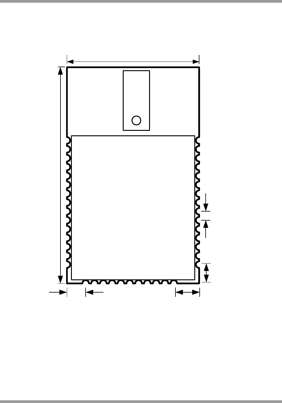
Antenna
30mm
18mm
J1
2.79
mm
2.54
mm
2.54
mm
1.27
mm
Thickness: 3mm
JN5121-xxx-M00 Outline Drawing
8 Preliminary - JN-DS-JN5121MO-1v23.doc © Jennic 2006
Jennic
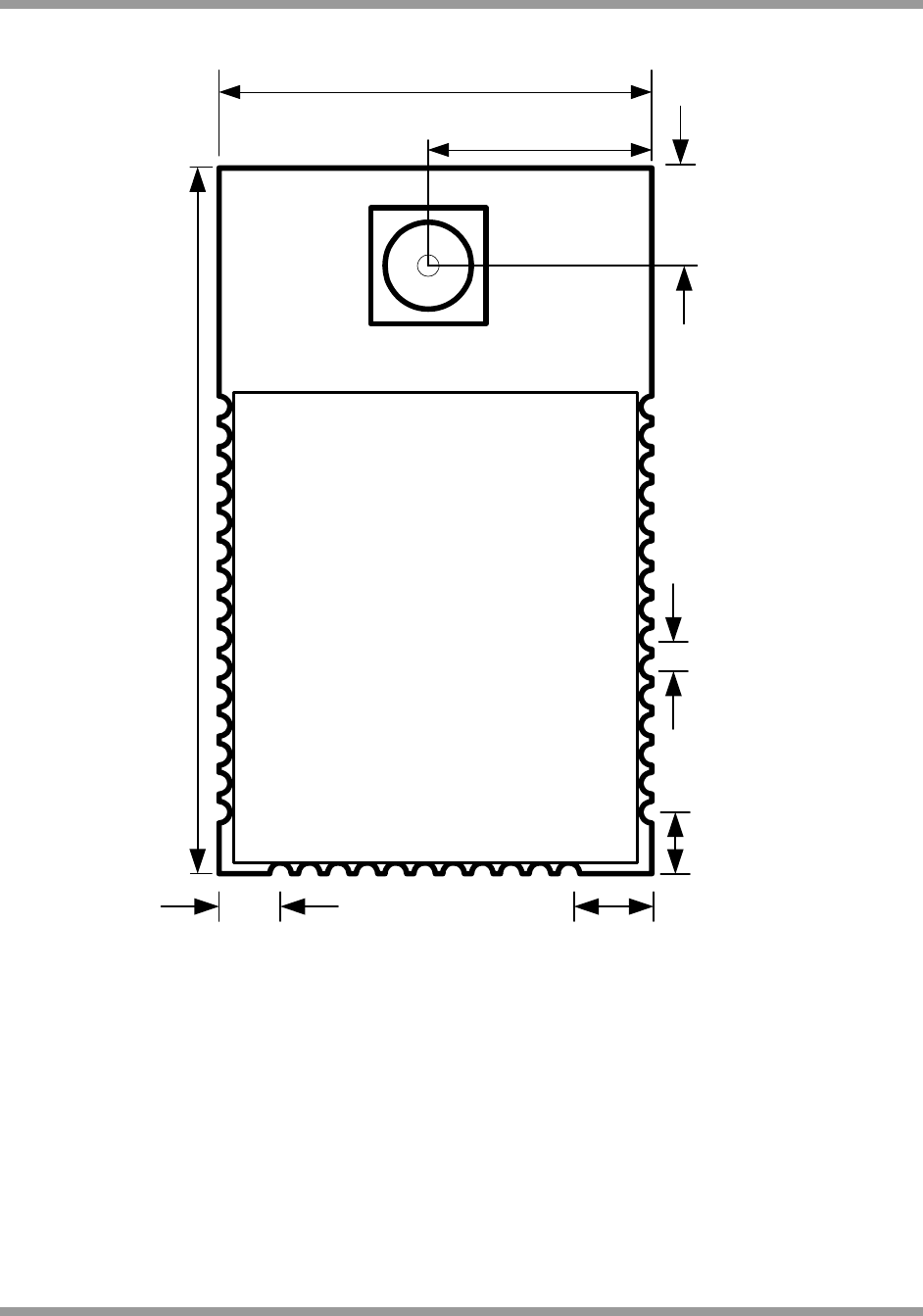
30mm
18mm
2.79
mm
2.54
mm
2.54
mm
4.75
mm
9.5mm
1.27
mm
Thickness: 3mm over can, 10.6mm at SMA connector
JN5121-xxx-M01/M03 Outline Drawing
© Jennic 2006 Preliminary - JN-DS-JN5121MO-1v23.doc 9
Jennic
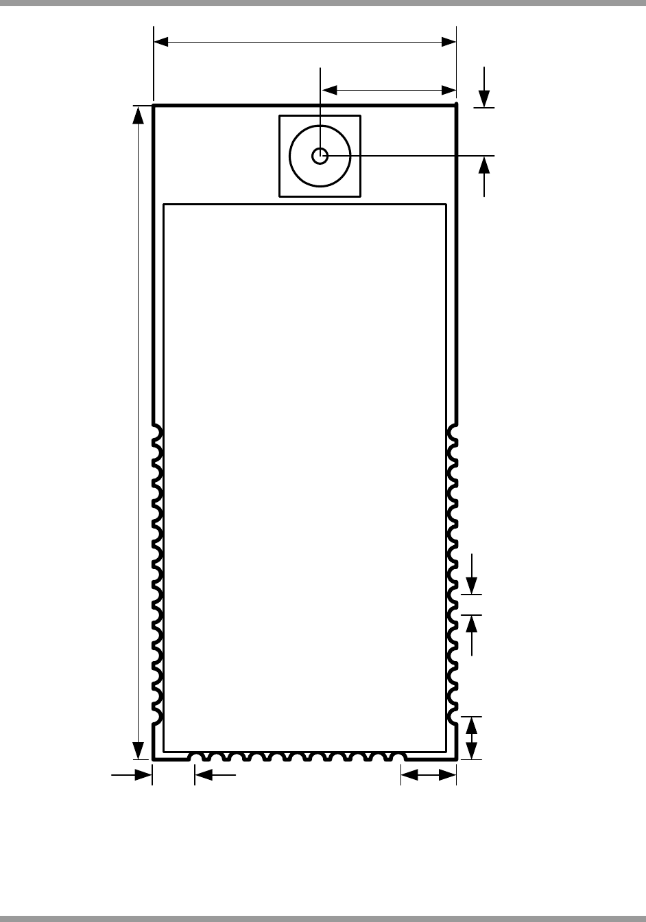
40mm
18mm
.2.79
mm
2.54
mm
1.27
mm
2.54
mm
3.8
mm
7.6mm
Thickness: 3mm, 10.6mm at SMA connector
JN5121-xxx-M02/M04 Outline Drawing
10 Preliminary - JN-DS-JN5121MO-1v23.doc © Jennic 2006
Jennic
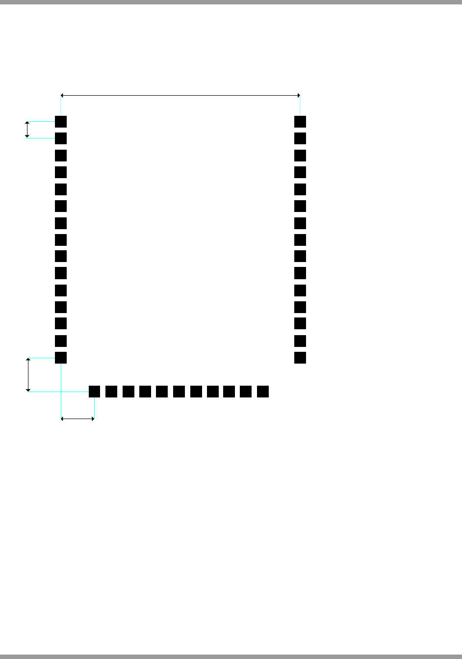
A.2 Module PCB Footprint
All Pads are 0.9mm square on 1.27mm pitch
2.54mm
2.54
mm
1.27
mm
18mm
Note: All modules have the same footprint.
© Jennic 2006 Preliminary - JN-DS-JN5121MO-1v23.doc 11
Jennic
A.3 Ordering Information
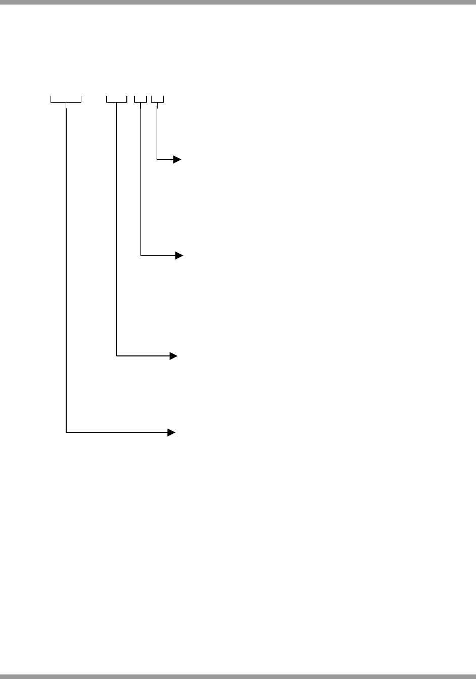
Part Numbering:
JN5121 - XXX - MY1Y2 Y3 Y4
Shipping
R Box (10 modules per pack)
T Tape Mounted 500pcs (00 module only)
V Tape Mounted 200pcs (01,02,03,04 modules
only)
Temp Range / Device Status
D -20°C to +70°C, Qualified
Module Type
00 Standard Power, Ceramic antenna
01 Standard Power, SMA connector
02 High Power, SMA connector
03 Standard Power, RP-SMA connector
04 High power, RP-SMA connector
Software Variant
000 IEEE802.15.4 Stack
Z01 ZigBee Stack
12 Preliminary - JN-DS-JN5121MO-1v23.doc © Jennic 2006
Jennic
A.4 Accessories
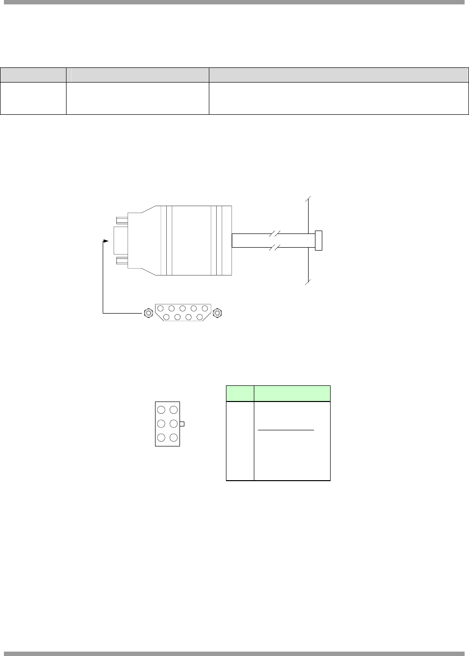
Product Description Note
JNAC001 JN5 serial level converter dongle Connects module UART port to PC serial port to allow code
development and debug
The JNAC001 RS-232 level converter is used to translate the +/- 7V RS-232 levels to CMOS compatible logic levels.
The CMOS levels are made available through a short flying lead with a 6-way IDC socket. This can be connected to
the relevant module UART0 pins. The RS-232 Interface is available on a standard nine-way ‘D’ connector.
J1
JNAC001 RS-232 Converter
CTS
RI
RTS
DSR DCD
TXD
RXD
DTR
GND
FFD
Figure 5-1: JNAC001 RS-232 Converter Connection
J1
1
5
2
6
Pin Function
1 UART 0 TXD
2 UART 0 RXD
3 PROGRAM
4 VCC - IN
5 GND
6 GND
View looking at cable
connector
Figure 5-2: RS-232 Connector
© Jennic 2006 Preliminary - JN-DS-JN5121MO-1v23.doc 13
Jennic
A.5 Tape and Reel Information:
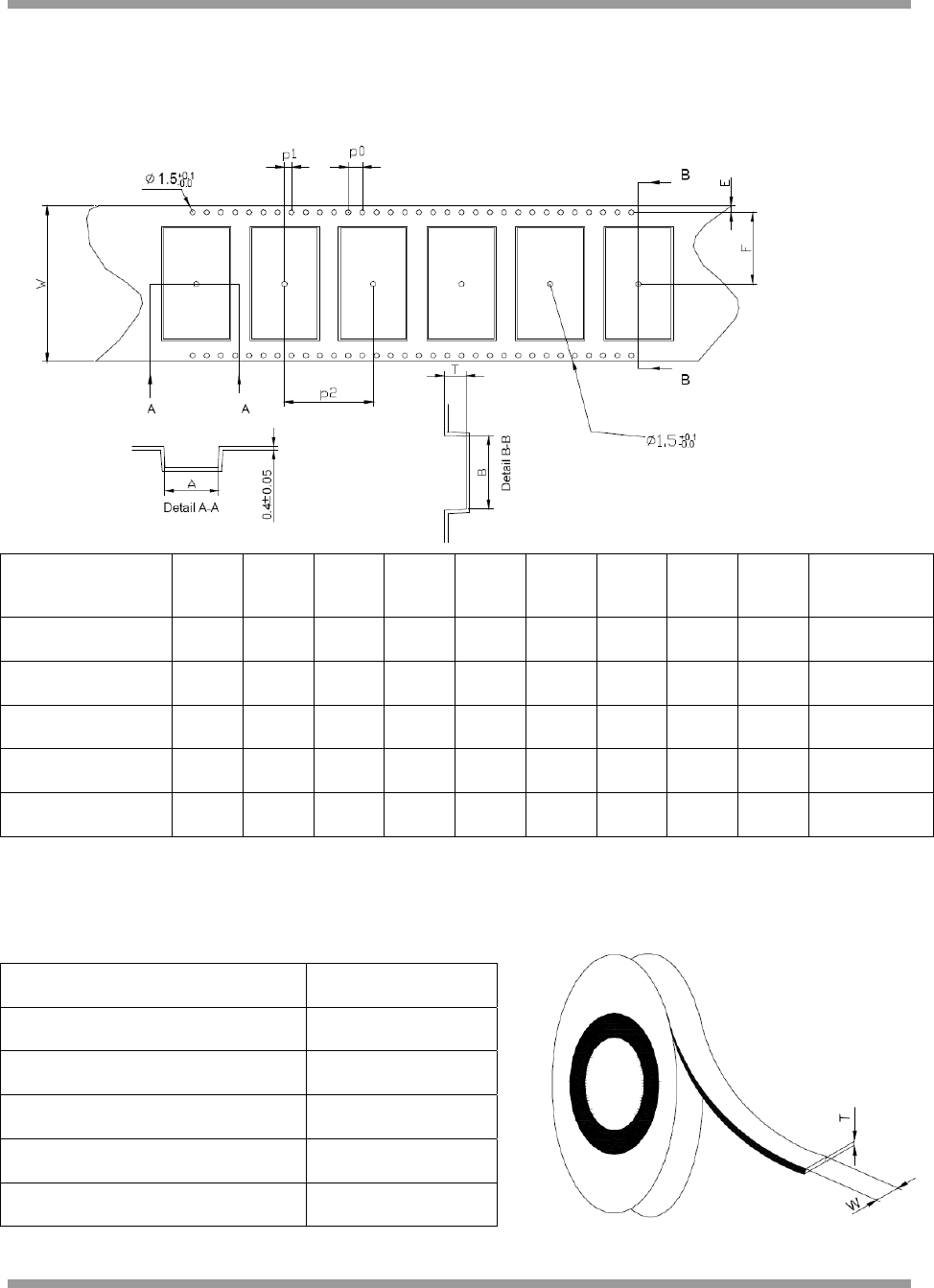
A.5.1 Tape Orientation and dimensions
Module type: A B W F E P0 P1 P2 T Cover Tape
width (W)
JN5121-xxx-M00 18.4 30.4 44 20.2 1.75 4.0 2.0 24.0 3.2 37.5
JN5121-xxx-M01/3 18.4 30.4 56 20.2 1.75 4.0 2.0 24.0 11.4 49.5
JN5121-xxx-M02/4 18.4 40.5 56 20.2 1.75 4.0 2.0 24.0 11.4 49.5
Tolerance ±0.1 ±0.1 ±0.3 ±0.1 +0.1 ±0.1 ±0.1 ±0.1 ±0.1
A.5.2 Cover tape details
Thickness (T) 0.061mm
Surface resistivity (component side) 104 to 107 Ohms/sq
Surface resistivity (component side) Non-conductive
Backing type: Polyester
Adhesive type: PSA
Sealing: Room ambient
14 Preliminary - JN-DS-JN5121MO-1v23.doc © Jennic 2006
Jennic
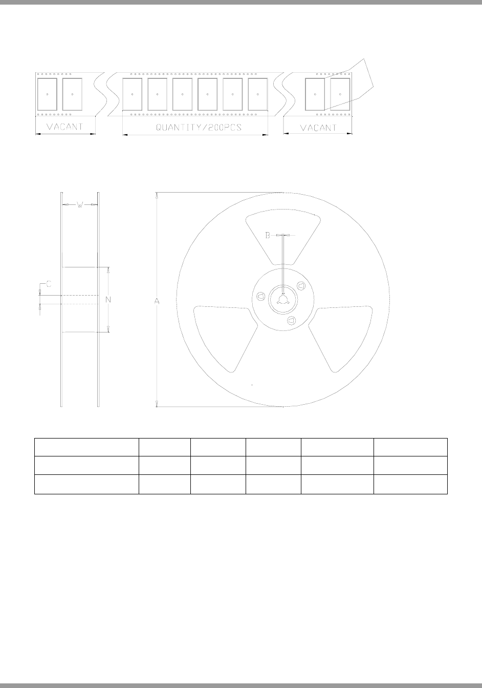
A.5.3 Leader and Trailer
300 MM300 MM
A.5.4 Reel Dimensions:
Module type: A B C N W (min)
JN5121-xxx-M00 330 ±1.0 2.2±0.5 13 ±0.2 100 +0.1 44.5 ±0.3
JN5121-xxx-
M01/02/03/04 330 ±1.0 2.2±0.5 13 ±0.2 100 +0.1 56.5 ±0.3
© Jennic 2006 Preliminary - JN-DS-JN5121MO-1v23.doc 15

Jennic
A.6 Related Documents
[1] IEEE Std 802.15.4-2003 IEEE Standard for Information Technology – Part 15.4 Wireless Medium Access Control
(MAC) and Physical Layer (PHY) Specifications for Low-Rate Wireless Personal Area Networks (LR-WPANs)
[2] JN-DS-JN5121 Datasheet for JN5121 single chip wireless microcontroller
[3] JN-RM-2001 Hardware Peripheral Library Reference Manual
[4] JN-RM-2002 Stack Software Reference Manual
[5] JN-UG-3007 Flash Loader User Guide
[6] JN-RM-2014 ZigBee Application Development API Reference Manual
A.7 Federal Communication Commission Interference Statement
This equipment has been tested and found to comply with the limits for a Class B digital device,
pursuant to Part 15 of the FCC Rules. These limits are designed to provide reasonable
protection against harmful interference in a residential installation. This equipment generates,
uses, and can radiate radio frequency energy and, if not installed and used in accordance with
the instructions, may cause harmful interference to radio communications. However, there is no
guarantee that interference will not occur in a particular installation. If this equipment does
cause harmful interference to radio or television reception, which can be determined by turning
the equipment off and on, the user is encouraged to try to correct the interference by one of the
following measures:
- Reorient or relocate the receiving antenna.
- Increase the separation between the equipment and receiver.
- Connect the equipment into an outlet on a circuit different from that to which the receiver is
connected.
- Consult the dealer or an experienced radio/TV technician for help.
This device complies with Part 15 of the FCC Rules. Operation is subject to the following two
conditions: (1) This device may not cause harmful interference, and (2) this device must accept
any interference received, including interference that may cause undesired operation.
FCC Caution: Any changes or modifications not expressly approved by the party responsible for
compliance could void the user's authority to operate this equipment.
WARNING!
FCC Radiation Exposure Statement:
This portable equipment with its antenna complies with FCC’s RF radiation exposure limits set
forth for an uncontrolled environment. To maintain compliance follow the instructions below;
1. This transmitter must not be co-located or operating in conjunction with any other antenna or
transmitter.
2. Avoid direct contact to the antenna, or keep it to a minimum while using this equipment.
This transmitter module is authorized to be used in other devices only by OEM
integrators under the following condition:
The transmitter module must not be co-located with any other antenna or transmitter.
16 Preliminary - JN-DS-JN5121MO-1v23.doc © Jennic 2006

Jennic
As long as the above condition is met, further transmitter testing will not be required. However,
the OEM integrator is still responsible for testing their end-product for any additional compliance
requirements required with this module installed (for example, digital device emissions, PC
peripheral requirements, etc.).
High Power Module usage limitation
The high power module variant FCC ID TYOJN5121M4 is classified as ‘mobile’ device pursuant
with FCC § 2.1091 and must not be used at a distance of < 20 cm (8”) from any nearby people.
IMPORTANT NOTE: In the event that these conditions can not be met (for certain
configurations or co-location with another transmitter), then the FCC authorization is no longer
considered valid and the FCC ID can not be used on the final product. In these circumstances,
the OEM integrator will be responsible for re-evaluating the end product (including the
transmitter) and obtaining a separate FCC authorization.
The OEM integrator has to be aware not to provide information to the end user regarding how to
install or remove this RF module in the user manual of the end product.
The user manual for the end product must include the following information in a prominent
location;
“To comply with FCC’s RF radiation exposure requirements, the antenna(s) used for this
transmitter must not be co-located or operating in conjunction with any other antenna or
transmitter.”
End Product Labelling
The final ‘end product’ should be labelled in a visible area with the following:
“Contains TX FCC ID: TYOJN5121M0, TYOJN5121M4 or TYOJN5121M6 ” to reflect the
version of the module being used inside the product.
RoHS Compliance
JN5121-xxx-Myy devices meet the requirements of Directive 2002/95/EC of the European Parliament and of the
Council on the Restriction of Hazardous Substance (RoHS).
Status Information
The status of this Data Sheet is Preliminary.
Jennic products progress according to the following format:
Advance
The Data Sheet shows the specification of a product in planning or in development.
The functionality and electrical performance specifications are target values and may be used as a guide to the final
specification.
Jennic reserves the right to make changes to the product specification at anytime without notice.
© Jennic 2006 Preliminary - JN-DS-JN5121MO-1v23.doc 17

Jennic
Preliminary
The Data Sheet shows the specification of a product that is in production, but is not yet fully qualified.
The functionality of the product is final. The electrical performance specifications are target values and may used as a
guide to the final specification. Modules are identified with an R suffix, for example JN5121-Z01-M00R.
Jennic reserves the right to make changes to the product specification at anytime without notice.
Production
This is the final Data Sheet for the product.
All functional and electrical performance specifications, including minimum and maximum values are final.
This Data Sheet supersedes all previous document versions.
Jennic reserves the right to make changes to the product specification at anytime to improve its performance.
A.8 Disclaimers
The contents of this document are subject to change without notice. Jennic reserves the right to make
changes, without notice, in the products, including circuits and/or software, described or contained herein
in order to improve design and/or performance. Information contained in this document regarding device
applications and the like is intended through suggestion only and may be superseded by updates. It is
your responsibility to ensure that your application meets with your specifications.
Jennic assumes no responsibility or liability for the use of any of these products, conveys no license or
title under any patent, copyright, or mask work right to these products, and makes no representations or
warranties that these products are free from patent, copyright, or mask work infringement, unless
otherwise specified.
Jennic products are not intended for use in life support systems, appliances or systems where
malfunction of these products can reasonably be expected to result in personal injury, death or severe
property or environmental damage. Jennic customers using or selling these products for use in such
applications do so at their own risk and agree to fully indemnify Jennic for any damages resulting from
such use.
All trademarks are the property of their respective owners.
A.9 Version Control
Version Notes
0.9 1st Issue of Preliminary Datasheet
1.0 Update performance parameters & Ordering / Tape & Reel information
1.2 Regulatory compliance statements added. Pins 37 & 38 DNC.
18 Preliminary - JN-DS-JN5121MO-1v23.doc © Jennic 2006

Jennic
A.10 Contact Details
Corporate Headquarters
Jennic Ltd, Furnival Street
Sheffield S1 4QT, UK
Tel: +44 (0)114 281 2655
Fax: +44 (0) 114 281 2951
info@jennic.com
www.jennic.com
Jennic Ltd Japan
Osakaya building 4F
1-11-8 Higashigotanda Shinagawa-ku
Tokyo 141-0022, Japan
Tel: +81 3 5449 7501
Fax: +81 3 5449 0741
info@jp.jennic.com
www.jennic.com
Jennic Ltd Taiwan
19F-1, 182, Sec.2 Tun Hwa S. Road.
Taipei 106, Taiwan
Tel: +886 2 2735 7357
Fax: +886 2 2739 5687
info@tw.jennic.com
www.jennic.com
Jennic America Inc - East Coast Office
1322 Scott Street, Suite 203
Point Loma, CA 92106, USA
Tel: +619 223 2215
Fax: +619 223 2081
info@us.jennic.com
www.jennic.com
Jennic America Inc - West Coast Office
1060 First Avenue, Suite 400
King of Prussia, PA 19406, USA
Tel: +1 484 868 0222
Fax: +1 484 971 5015
info@us.jennic.com
www.jennic.com
© Jennic 2006 Preliminary - JN-DS-JN5121MO-1v23.doc 19