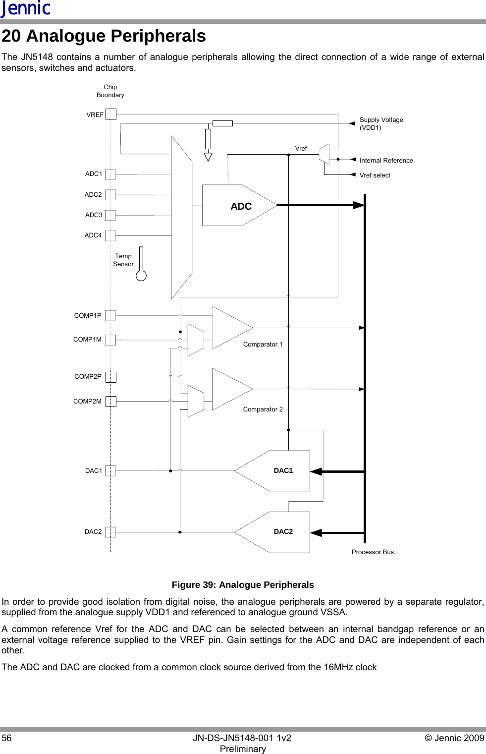
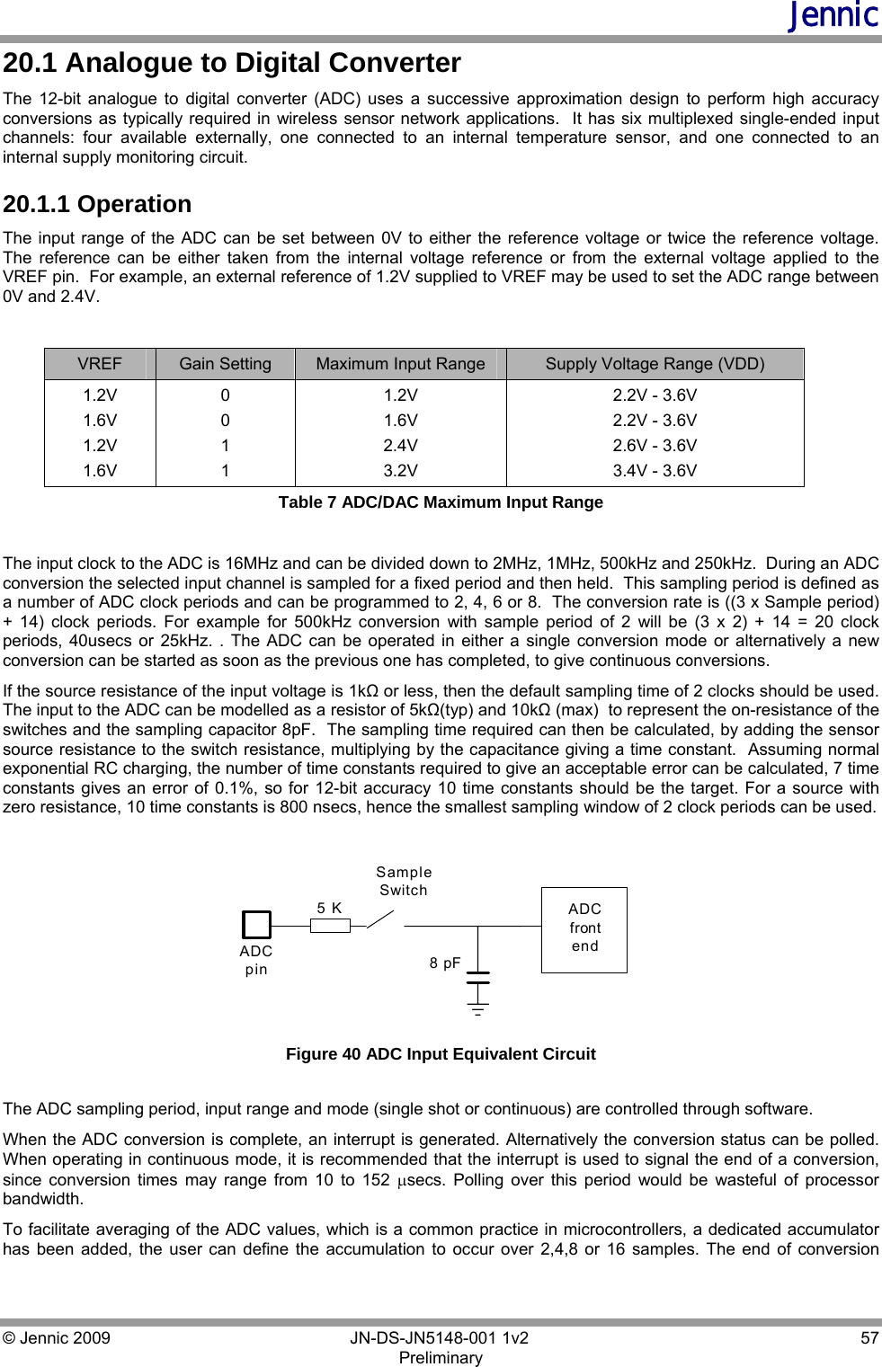
NXP Laboratories UK JN5148M4 IEEE 802.15.4 High Power Wireless Microcontroller User Manual JN5148 001 Data Sheet
NXP Laboratories UK Ltd IEEE 802.15.4 High Power Wireless Microcontroller JN5148 001 Data Sheet
Contents
- 1. chip manual
- 2. user manual
- 3. Antenna 1 of 36
- 4. Antenna 2 of 36
- 5. Antenna 3 of 36
- 6. Antenna 4 of 36
- 7. Antenna 5 of 36
- 8. Antenna 6 of 36
- 9. Antenna 7 of 36
- 10. Antenna 8 of 36
- 11. Antenna 9 of 36
- 12. Antenna 10 of 36
- 13. Antenna 11 of 36
- 14. Antenna 12 of 36
- 15. Antenna 13 of 36
- 16. Antenna 14 of 36
- 17. Antenna 15 of 36
- 18. Antenna 16 of 36
- 19. Antenna 17 of 36
- 20. Antenna 18 of 36
- 21. Antenna 19 of 36
- 22. Antenna 20 of 36
- 23. Antenna 21 of 36
- 24. Antenna 22 of 36
- 25. Antenna 23 of 36
chip manual
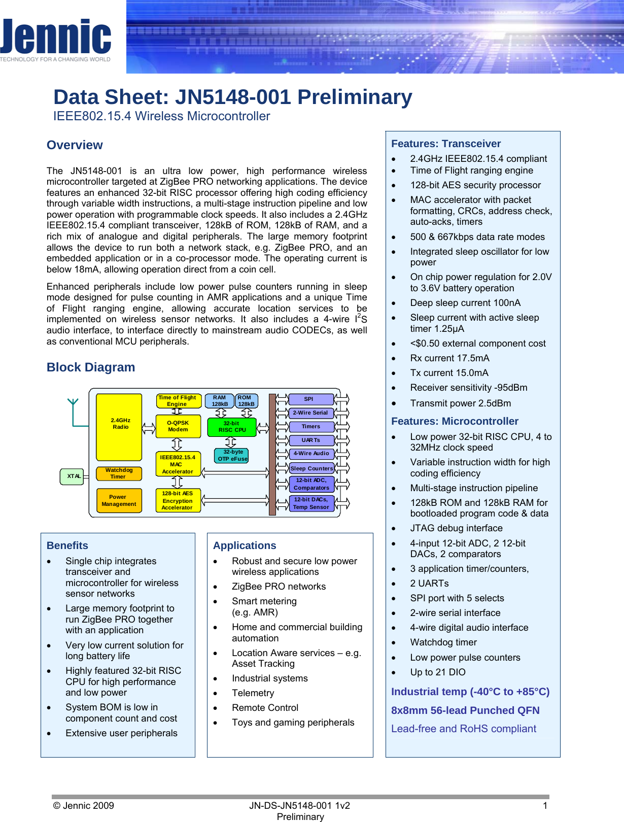
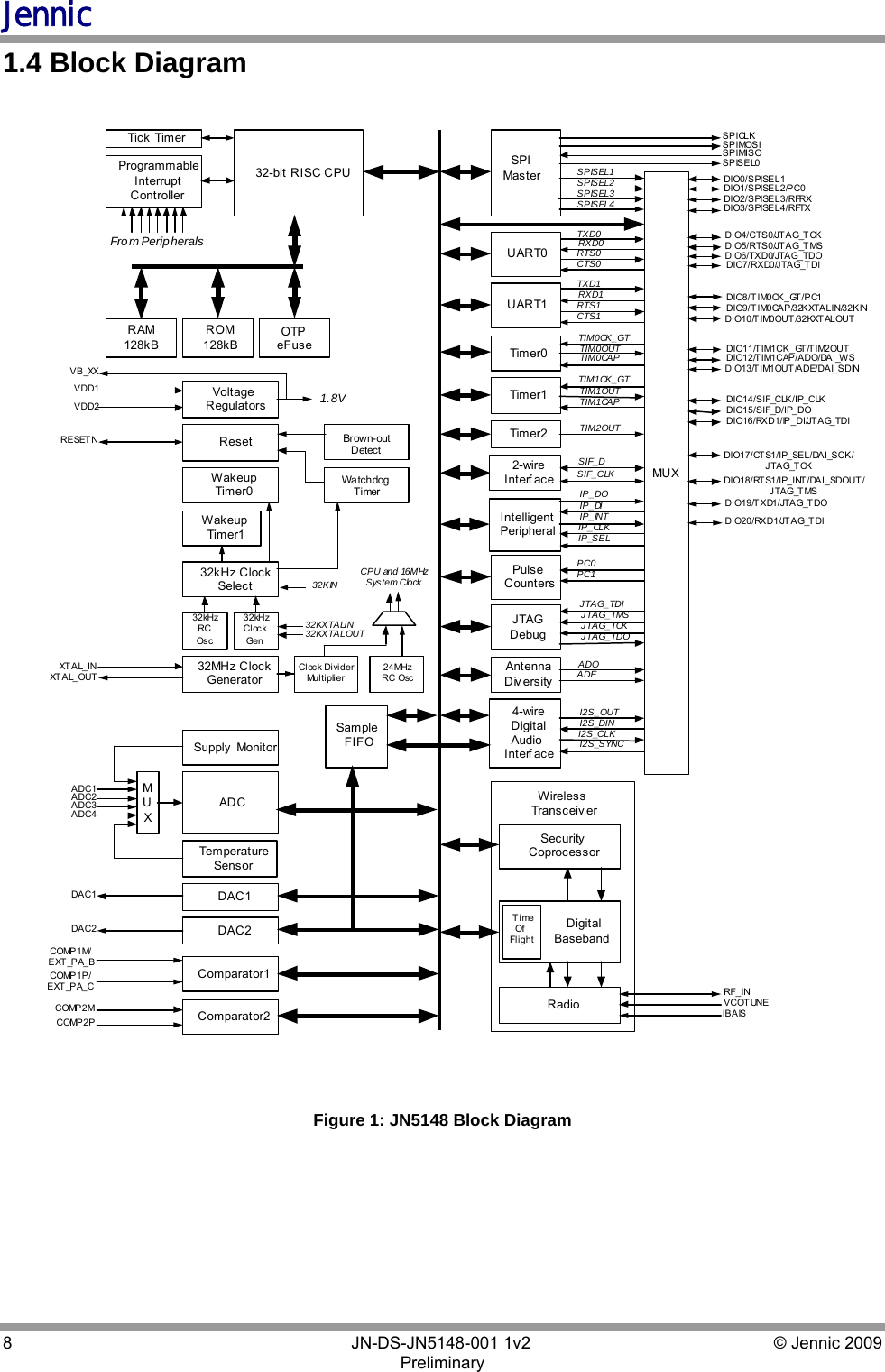
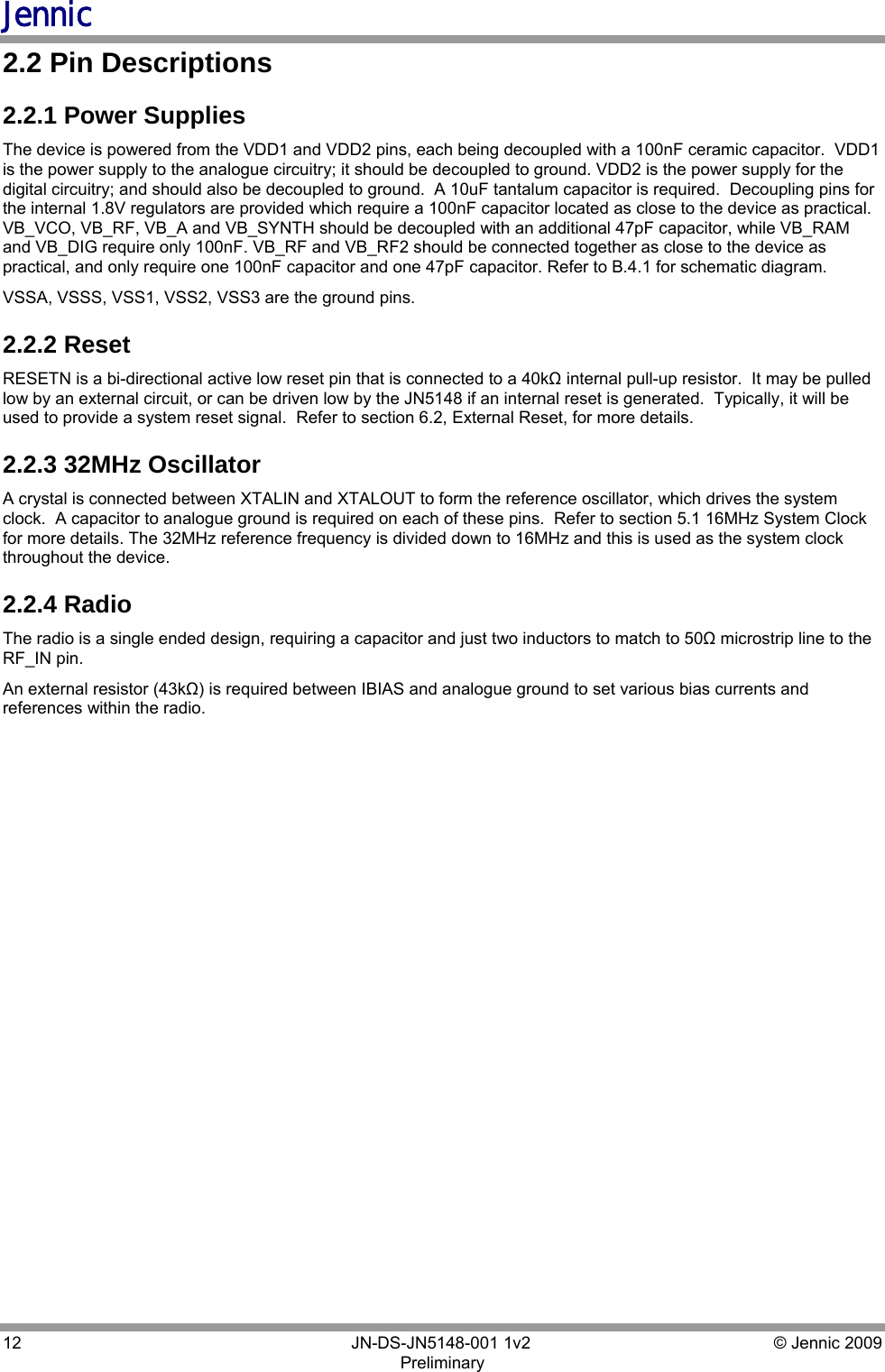
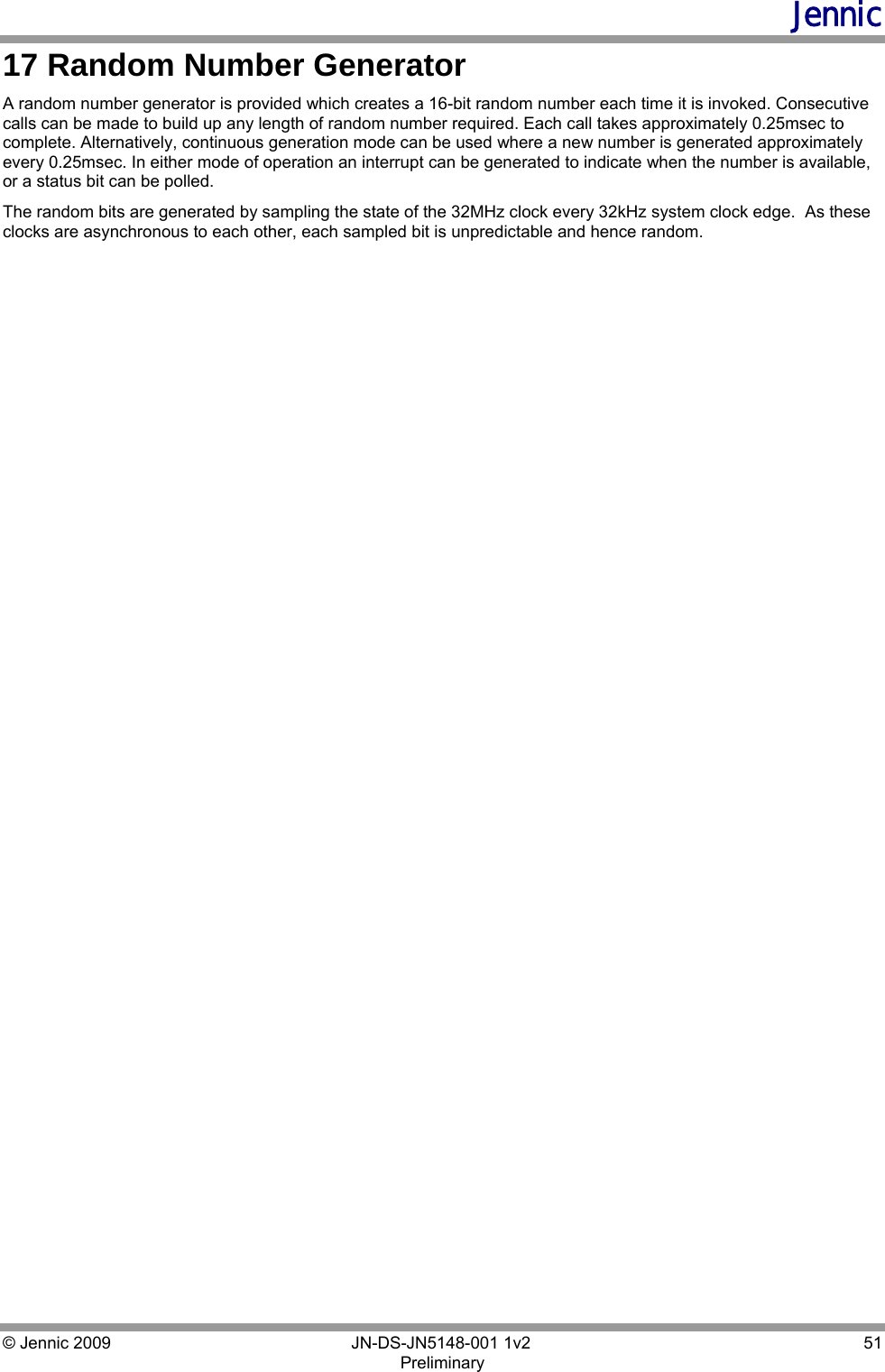
![Jennic 6 JN-DS-JN5148-001 1v2 © Jennic 2009 Preliminary 1 Introduction The JN5148-001 is an IEEE802.15.4 wireless microcontroller that provides a fully integrated solution for applications using the IEEE802.15.4 standard in the 2.4 - 2.5GHz ISM frequency band [1], including ZigBee PRO. It includes all of the functionality required to meet the IEEE802.15.4 and ZigBee PRO specifications and has additional processor capability to run a wide range of applications including, but not limited to Smart Energy, Automatic Meter Reading, Remote Control, Home and Building Automation, Toys and Gaming. Applications that transfer data wirelessly tend to be more complex than wired ones. Wireless protocols make stringent demands on frequencies, data formats, timing of data transfers, security and other issues. Application development must consider the requirements of the wireless network in addition to the product functionality and user interfaces. To minimise this complexity, Jennic provides a series of software libraries and interfaces that control the transceiver and peripherals of the JN5148. These libraries and interfaces remove the need for the developer to understand wireless protocols and greatly simplifies the programming complexities of power modes, interrupts and hardware functionality. In view of the above, the register details of the JN5148 are not provided in the datasheet. The device includes a Wireless Transceiver, RISC CPU, on chip memory and an extensive range of peripherals. Hereafter, the JN5148-001 will be referred to as JN5148. 1.1 Wireless Transceiver The Wireless Transceiver comprises a 2.45GHz radio, a modem, a baseband controller and a security coprocessor. In addition, the radio also provides an output to control transmit-receive switching of external devices such as power amplifiers allowing applications that require increased transmit power to be realised very easily. Appendix B.4, describes a complete reference design including Printed Circuit Board (PCB) design and Bill Of Materials (BOM). The security coprocessor provides hardware-based 128-bit AES-CCM, CBC(1), CTR and CCM* processing as specified by the IEEE802.15.4 standard. It does this in-band on packets during transmission and reception, requiring minimal intervention from the CPU. It is also available for off-line use under software control for encrypting and decrypting packets generated by software layers such as ZigBee and user applications. This means that these algorithms can be off-loaded by the CPU, increasing the processor bandwidth available for user applications. The transceiver elements (radio, modem and baseband) work together to provide IEEE802.15.4 Medium Access Control (MAC) under the control of a protocol stack. Applications incorporating IEEE802.15.4 functionality can be rapidly developed by combining user-developed application software with a protocol stack library. (1) AES-CBC processing is only available off-line for use under software control. 1.2 RISC CPU and Memory A 32-bit RISC CPU allows software to be run on chip, its processing power being shared between the IEEE802.15.4 MAC protocol, other higher layer protocols and the user application. The JN5148 has a unified memory architecture, code memory, data memory, peripheral devices and I/O ports are organised within the same linear address space. The device contains 128kbytes of ROM, 128kbytes of RAM and a 32-byte One Time Programmable (OTP) eFuse memory.](https://usermanual.wiki/NXP-Laboratories-UK/JN5148M4.chip-manual/User-Guide-1145108-Page-6.png)
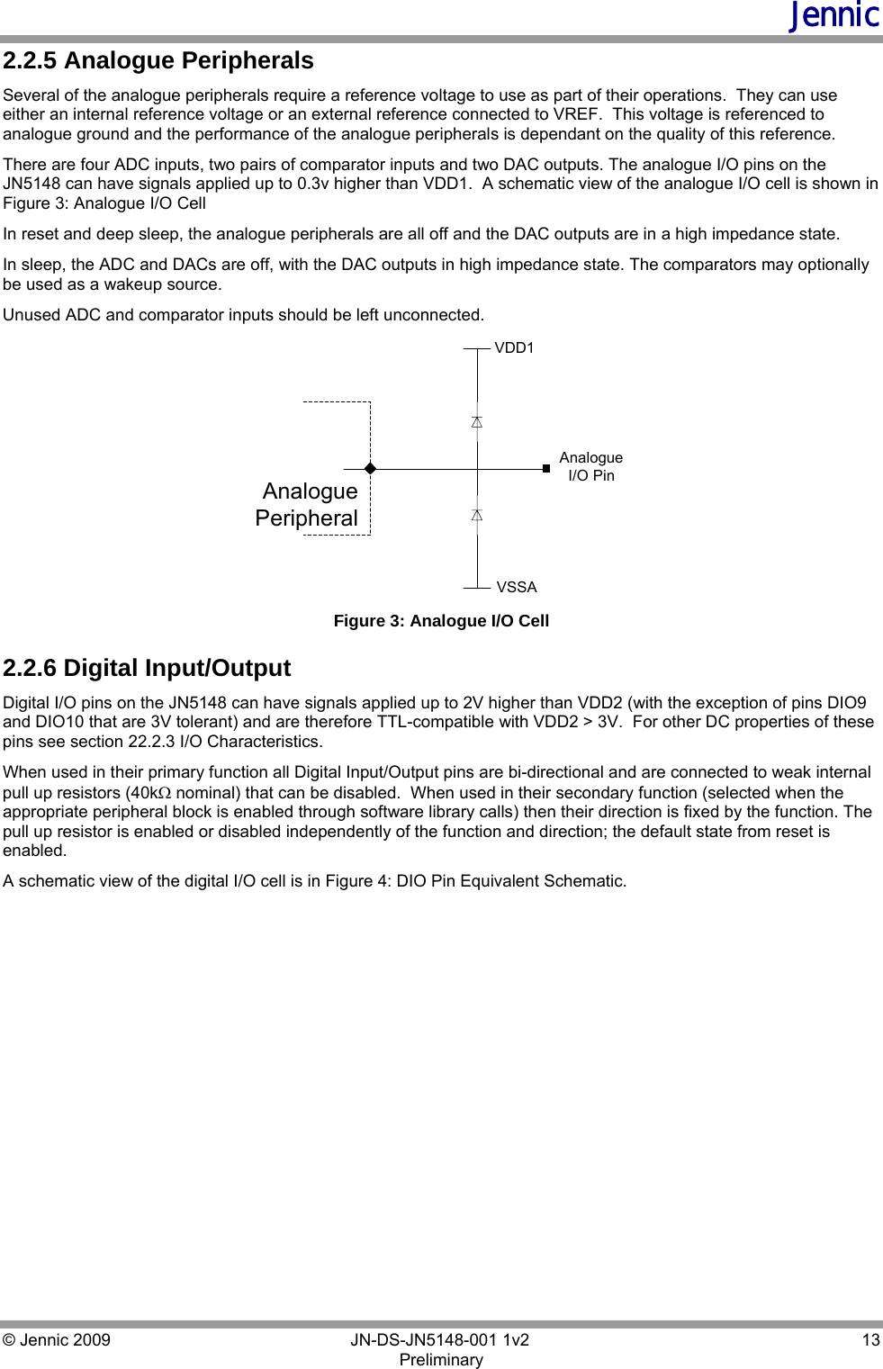
![Jennic 14 JN-DS-JN5148-001 1v2 © Jennic 2009 Preliminary IOIEVDD2VSSPuRPURPROTOEDIO[x] Pin Figure 4: DIO Pin Equivalent Schematic In reset, the digital peripherals are all off and the DIO pins are set as high-impedance inputs. During sleep and deep sleep, the DIO pins retain both their input/output state and output level that was set as sleep commences. If the DIO pins were enabled as inputs and the interrupts were enabled then these pins may be used to wake up the JN5148 from sleep.](https://usermanual.wiki/NXP-Laboratories-UK/JN5148M4.chip-manual/User-Guide-1145108-Page-14.png)
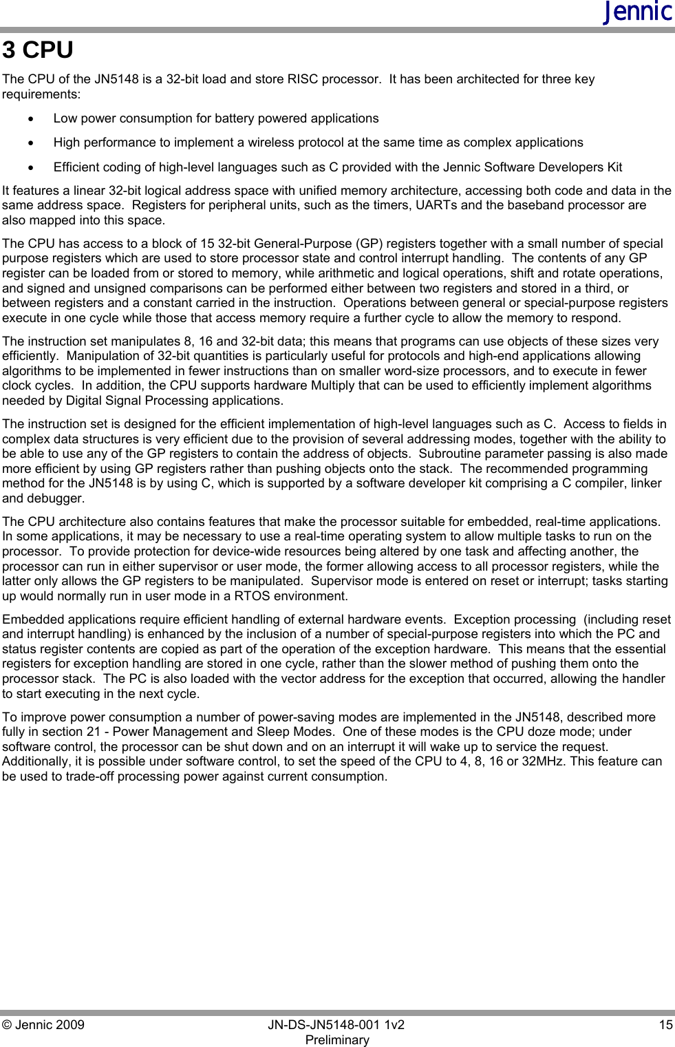
![Jennic 16 JN-DS-JN5148-001 1v2 © Jennic 2009 Preliminary 4 Memory Organisation This section describes the different memories found within the JN5148. The device contains ROM, RAM, OTP eFuse memory, the wireless transceiver and peripherals all within the same linear address space. 0x00000000 0x00020000 RAM (128kB) 0xF0000000 0xFFFFFFFF Unpopulated ROM (128kB) 0xF0020000 RAM Echo 0x04000000 Peripherals 0x02000000 Figure 5: JN5148 Memory Map 4.1 ROM The ROM is 128k bytes in size, and can be accessed by the processor in a single CPU clock cycle. The ROM contents include bootloader to allow external Flash memory contents to be bootloaded into RAM at runtime, a default interrupt vector table, an interrupt manager, IEEE802.15.4 MAC and APIs for interfacing on-chip peripherals. The operation of the boot loader is described in detail in Application Note [8]. The interrupt manager routes interrupt calls to the application’s soft interrupt vector table contained within RAM. Section 7 contains further information regarding the handling of interrupts. ROM contents are shown in Figure 6. Interrupt VectorsInterrupt ManagerBoot LoaderIEEE802.15.4Stack0x000000000x00020000APIsSpare Figure 6: Typical ROM contents](https://usermanual.wiki/NXP-Laboratories-UK/JN5148M4.chip-manual/User-Guide-1145108-Page-16.png)
![Jennic © Jennic 2009 JN-DS-JN5148-001 1v2 17 Preliminary 4.2 RAM The JN5148 contains 128kBytes of high speed RAM. It can be used for both code and data storage and is accessed by the CPU in a single clock cycle. At reset, a boot loader controls the loading of segments of code and data from an external memory connected to the SPI port, into RAM. Software can control the power supply to the RAM allowing the contents to be maintained during a sleep period when other parts of the device are un-powered. Typical RAM contents are shown in Figure 7. MAC DataInterrupt Vector TableApplicationCPU Stack(Grows Down)0x040000000x04020000MAC Address Figure 7: Typical RAM Contents 4.3 OTP eFuse Memory The JN5148 contains a total of 32bytes of eFuse memory; this is a One Time Programmable (OTP) memory that is used to support on chip 64-bit MAC ID and a 128-bit AES security key. A limited number of bits are available for customer use for storage of configuration information; configuration of these is made through use of software APIs. For full details on how to program and use the eFuse memory, please refer to application note JN-AN-1062 Using OTP efuse Memory [2] Alternatively, Jennic can provide an eFuse programming service for customers that wish to use the eFuse but do not wish to undertake this for themselves. For further details of this service, please contact your local Jennic sales office. 4.4 External Memory An external memory with an SPI interface may be used to provide storage for program code and data for the device when external power is removed. The memory is connected to the SPI interface using select line SPISEL0; this select line is dedicated to the external memory interface and is not available for use with other external devices. See Figure 8 for connection details. JN5148 Serial Me mor y SPISEL0 SPIMISO SPIMOSI SPICLK SS SDO SDI CLK Figure 8: Connecting External Serial Memory](https://usermanual.wiki/NXP-Laboratories-UK/JN5148M4.chip-manual/User-Guide-1145108-Page-17.png)
![Jennic 18 JN-DS-JN5148-001 1v2 © Jennic 2009 Preliminary At reset, the contents of this memory are copied into RAM by the software boot loader. The Flash memory devices that are supported as standard through the JN5148 bootloader are given in Table 1. Jennic recommends that where possible one of these devices should be selected. Manufacturer Device Number SST (Silicon Storage Technology) 25VF010A (1Mbyte device) Numonyx M25P10-A (1Mbyte device), M25P40 (4Mbyte device) Table 1: Supported Flash Memories Applications wishing to use an alternate Flash memory device should refer to application note [3] JN-AN-1038 Programming Flash devices not supported by the JN51xx ROM-based bootloader. This application note provides guidance on developing an interface to an alternate device. 4.4.1 External Memory Encryption The contents of the external serial memory may be encrypted. The AES security processor combined with a user programmable 128-bit encryption key is used to encrypt the contents of the external memory. The encryption key is stored in eFuse. When bootloading program code from external serial memory, the JN5148 automatically accesses the encryption key to execute the decryption process. User program code does not need to handle any of the decryption process; it is transparent. With encryption enabled, the time taken to boot code from external flash is increased. 4.5 Peripherals All peripherals have their registers mapped into the memory space. Access to these registers requires 3 clock cycles. Applications have access to the peripherals through the software libraries that present a high-level view of the peripheral’s functions through a series of dedicated software routines. These routines provide both a tested method for using the peripherals and allow bug-free application code to be developed more rapidly. For details, see the Integrated Peripherals API Reference Manual (JN-RM-2001).[6] 4.6 Unused Memory Addresses Any attempt to access an unpopulated memory area will result in a bus error exception (interrupt) being generated.](https://usermanual.wiki/NXP-Laboratories-UK/JN5148M4.chip-manual/User-Guide-1145108-Page-18.png)

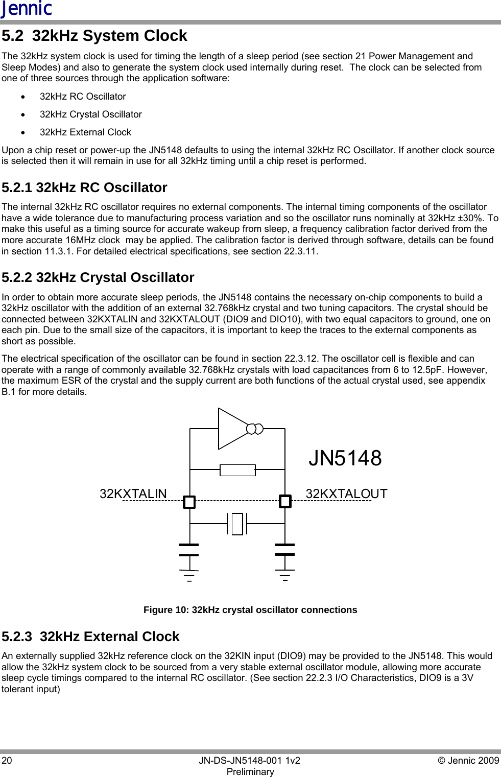
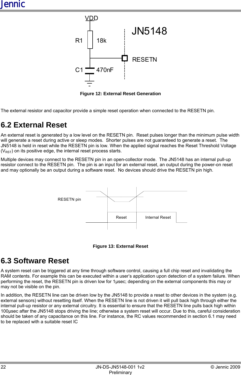
![Jennic © Jennic 2009 JN-DS-JN5148-001 1v2 21 Preliminary 6 Reset A system reset initialises the device to a pre-defined state and forces the CPU to start program execution from the reset vector. The reset process that the JN5148 goes through is as follows. When power is applied, the 32kHz RC oscillator starts up and stabilises, which takes approximately 100μsec. At this point, the 32MHz crystal oscillator is enabled and power is applied to the processor and peripheral logic. The logic blocks are held in reset until the 32MHz crystal oscillator stabilises, typically this takes 0.75ms. Then the internal reset is removed from the CPU and peripheral logic and the CPU starts to run code beginning at the reset vector, consisting of initialisation code and the resident boot loader. [8] Section 22.3.1 provides detailed electrical data and timing. The JN5148 has five sources of reset: • Internal Power-on Reset • External Reset • Software Reset • Watchdog timer • Brown-out detect Note: When the device exits a reset condition, device operating parameters (voltage, frequency, temperature, etc.) must be met to ensure operation. If these conditions are not met, then the device must be held in reset until the operating conditions are met. (See section 22.3) 6.1 Internal Power-on Reset For the majority of applications the internal power-on reset is capable of generating the required reset signal. When power is applied to the device, the power-on reset circuit monitors the rise of the VDD supply. When the VDD reaches the specified threshold, the reset signal is generated and can be observed as a rising edge on the RESETN pin. This signal is held internally until the power supply and oscillator stabilisation time has elapsed, when the internal reset signal is then removed and the CPU is allowed to run. RESETN PinInternal RESETVDD Figure 11: Internal Power-on Reset When the supply drops below the power on reset ‘falling’ threshold, it will re-trigger the reset. Use of the external reset circuit show in Figure 12 is suggested.](https://usermanual.wiki/NXP-Laboratories-UK/JN5148M4.chip-manual/User-Guide-1145108-Page-21.png)
![Jennic © Jennic 2009 JN-DS-JN5148-001 1v2 25 Preliminary 7.3 Hardware Interrupts Hardware interrupts generated from the transceiver, analogue or digital peripherals and DIO pins are individually masked using the Programmable Interrupt Controller (PIC). Management of interrupts is provided in the peripherals library [6]. For details of the interrupts generated from each peripheral see the respective section in this datasheet. Interrupts can be used to wake the JN5148 from sleep. The peripherals, baseband controller, security coprocessor and PIC are powered down during sleep but the DIO interrupts and optionally the pulse counters, wake-up timers and analogue comparator interrupts remain powered to bring the JN5148 out of sleep. Prioritised external interrupt handling (i.e., interrupts from hardware peripherals) is provided to enable an application to control an events priority to provide for deterministic program execution. The priority Interrupt controller provides 15 levels of prioritised interrupts. The priority level of all interrupts can be set, with value 0 being used to indicate that the source can never produce an external interrupt, 1 for the lowest priority source(s) and 15 for the highest priority source(s). Note that multiple interrupt sources can be assigned the same priority level if desired. If while processing an interrupt, a new event occurs at the same or lower priority level, a new external interrupt will not be triggered. However, if a new higher priority event occurs, the external interrupt will again be asserted, interrupting the current interrupt service routine. Once the interrupt service routine is complete, lower priority events can be serviced.](https://usermanual.wiki/NXP-Laboratories-UK/JN5148M4.chip-manual/User-Guide-1145108-Page-25.png)
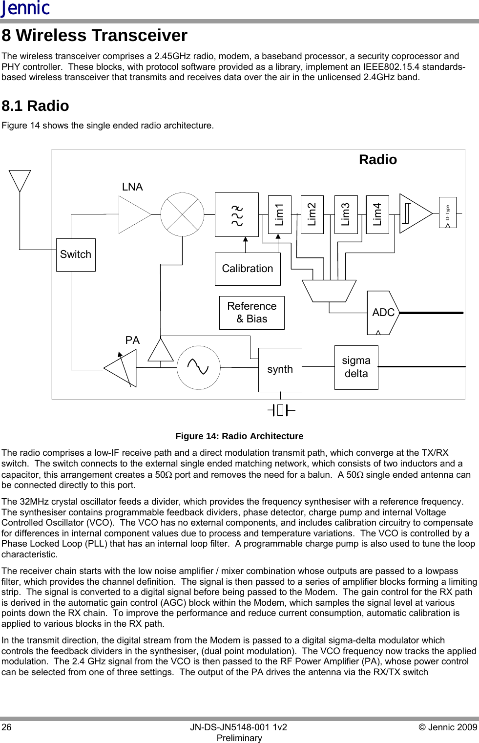
![Jennic © Jennic 2009 JN-DS-JN5148-001 1v2 27 Preliminary 8.1.1 Radio External Components In order to realise the full performance of the radio it is essential that the reference PCB layout and BOM are carefully followed. See Appendix B.4. The radio is powered from a number of internal 1.8V regulators fed from the analogue supply VDD1, in order to provide good noise isolation between the digital logic of the JN5148 and the analogue blocks. These regulators are also controlled by the baseband controller and protocol software to minimise power consumption. Decoupling for internal regulators is required as described in section 2.2.1, Power Supplies For single ended antennas or connectors, a balun is not required, however a matching network is needed. The RF matching network requires three external components and the IBIAS pin requires one external component as shown in schematic in B.4.1. These components are critical and should be placed close to the JN5148 pins and analogue ground as defined in Table 8: JN5148 Printed Antenna Reference Module Components and PCB Layout Constraints 8.1.2 . Antenna Diversity Support is provided for antenna diversity. Antenna diversity is a technique that maximises the performance of an antenna system. It allows the radio to switch between two antennas that have very low correlation between their received signals. Typically, this is achieved by spacing two antennas around 0.25 wavelengths apart or by using two orthogonal polarisations. So, if a packet is transmitted and no acknowledgement is received, the radio system can switch to the other antenna for the retry, with a different probability of success. The JN5148 provides an output (ADO) on DIO12 that is asserted on odd numbered retries that can be used to control an antenna switch; this enables antenna diversity to be implemented easily (see Figure 15 and Figure 16). Antenna AADO (DIO[12])Antenna BDevice RF PortRF Switch: Single-Pole, Double-Throw (SPDT)ABCOMSELSELB Figure 15 Simple Antenna Diversity Implementation using External RF Switch](https://usermanual.wiki/NXP-Laboratories-UK/JN5148M4.chip-manual/User-Guide-1145108-Page-27.png)
![Jennic 28 JN-DS-JN5148-001 1v2 © Jennic 2009 Preliminary TX ActiveADO (DIO[12])1st TX-RX Cycle 2nd TX-RX Cycle (1st Retry)RX Active Figure 16 Antenna Diversity ADO Signal for TX with Acknowledgement DIO13 can be configured to be ADE, the inverse of ADO. In this configuration, an antenna diversity scheme can be implemented without the need for the inverter shown in Figure 15.](https://usermanual.wiki/NXP-Laboratories-UK/JN5148M4.chip-manual/User-Guide-1145108-Page-28.png)

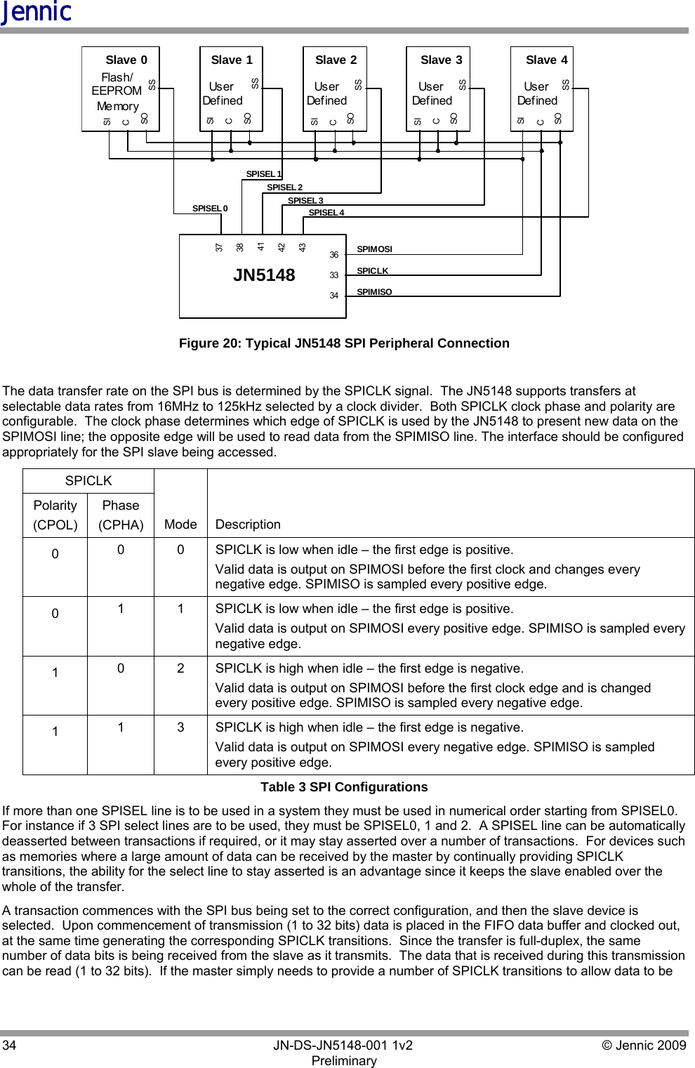
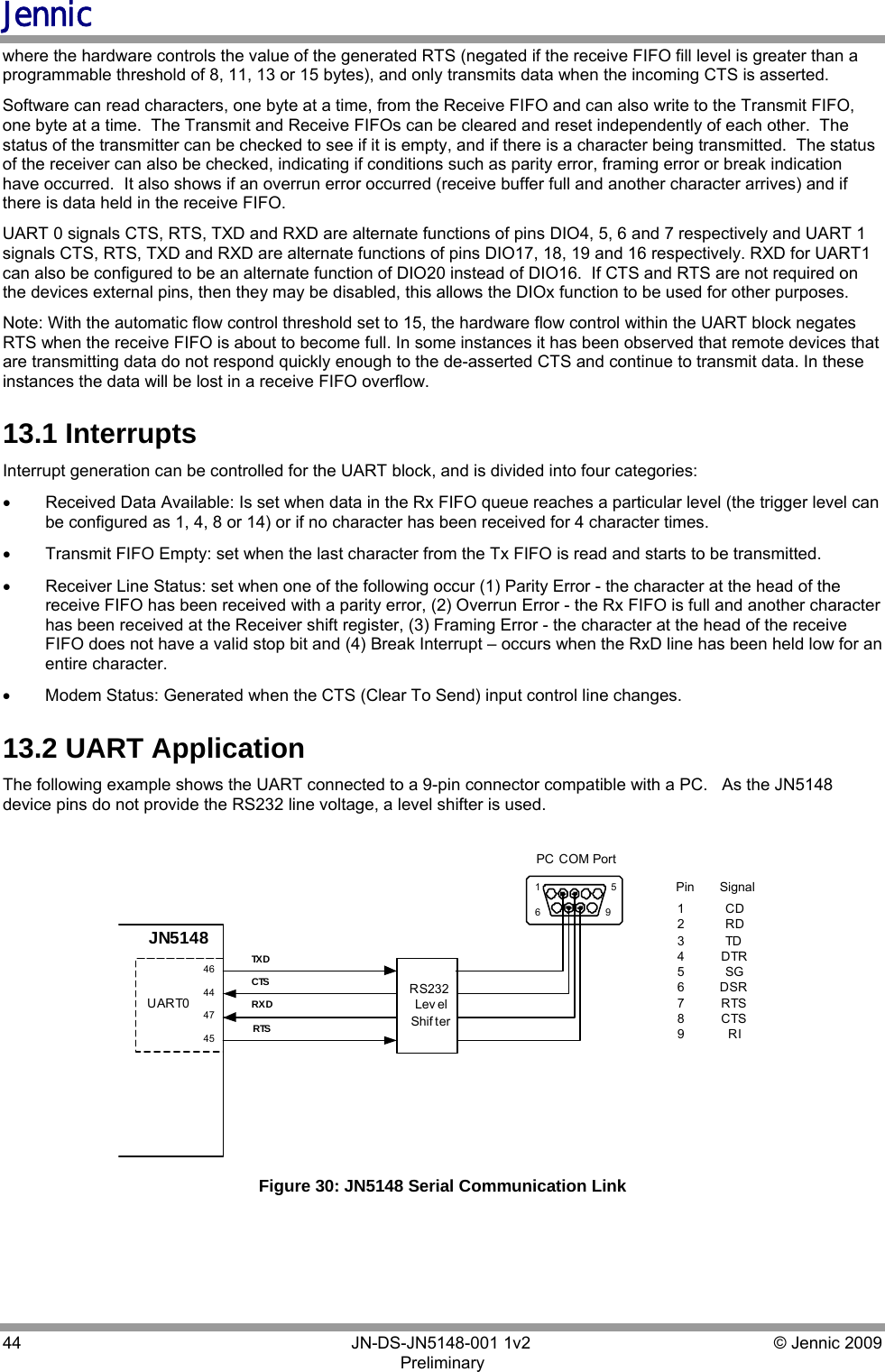
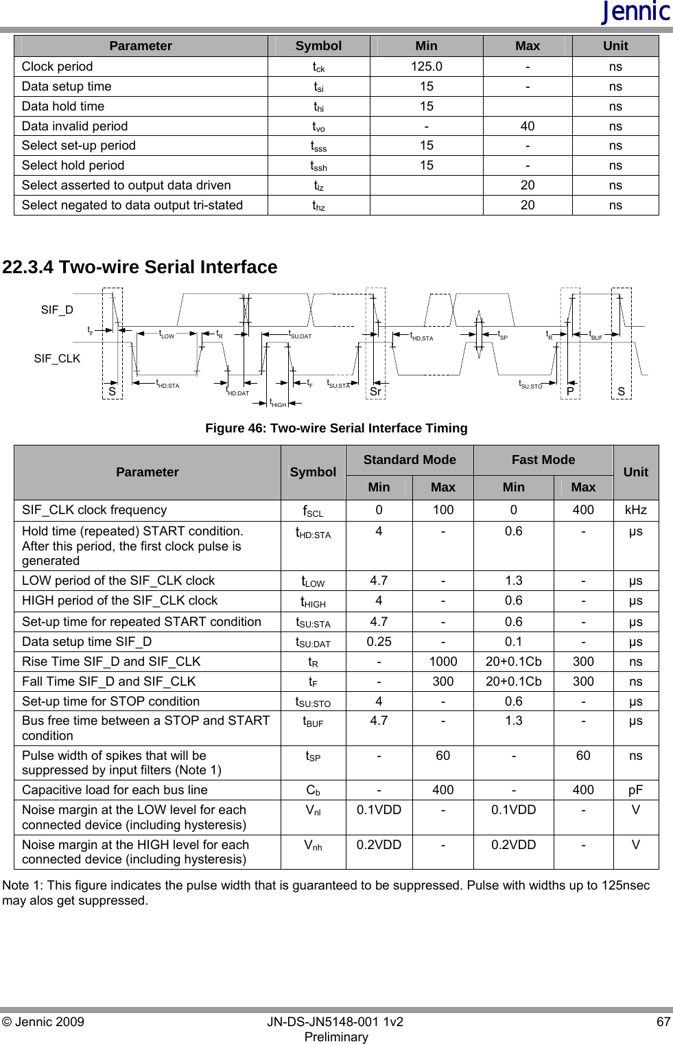
![Jennic © Jennic 2009 JN-DS-JN5148-001 1v2 33 Preliminary 10 Serial Peripheral Interface The Serial Peripheral Interface (SPI) allows high-speed synchronous data transfer between the JN5148 and peripheral devices. The JN5148 operates as a master on the SPI bus and all other devices connected to the SPI are expected to be slave devices under the control of the JN5148 CPU. The SPI includes the following features: • Full-duplex, three-wire synchronous data transfer • Programmable bit rates (up to 16Mbit/s) • Programmable transaction size up to 32-bits • Standard SPI modes 0,1,2 and 3 • Manual or Automatic slave select generation (up to 5 slaves) • Maskable transaction complete interrupt • LSB First or MSB First Data Transfer • Supports delayed read edges ClockDividerSPI BusCycleControllerData BufferDIVClock EdgeSelectDataCHAR_LENLSBSPIMISOSPIMOSISPICLKSelectLatchSPISEL [4..0]16 MHz Figure 19: SPI Block Diagram The SPI bus employs a simple shift register data transfer scheme. Data is clocked out of and into the active devices in a first-in, first-out fashion allowing SPI devices to transmit and receive data simultaneously. There are three dedicated pins SPICLK, SPIMOSI, SPIMISO that are shared across all devices on the bus. Master-Out-Slave-In or Master-In-Slave-Out data transfer is relative to the clock signal SPICLK generated by the JN5148. The JN5148 provides five slave selects, SPISEL0 to SPISEL4 to allow five SPI peripherals on the bus. SPISEL0 is a dedicated pin; this is generally connected to a serial Flash/ EEPROM memory holding application code that is downloaded to internal RAM via software from reset. SPISEL1 to 4, are alternate functions of pins DIO0 to 3 respectively. The interface can transfer from 1 to 32-bits without software intervention and can keep the slave select lines asserted between transfers when required, to enable longer transfers to be performed.](https://usermanual.wiki/NXP-Laboratories-UK/JN5148M4.chip-manual/User-Guide-1145108-Page-33.png)


![Jennic © Jennic 2009 JN-DS-JN5148-001 1v2 45 Preliminary 14 JTAG Debug Interface The JN5148 includes an IEEE1149.1 compliant JTAG port for the sole purpose of software code debug with Jennic's Software Development Kit. The JTAG interface is disabled by default and is enabled under software control. Therefore, debugging is only possible if enabled by the application. Once enabled, the application executes as normal until the external debugger controller initiates debug activity. The Debugger supports breakpoints and watchpoints based on four comparisons between any of program counter, load/store effective address and load/store data. There is the ability to chain the comparisons together. There is also the ability, under debugger control to perform the following commands: go, stop, reset, step over/into/out/next, run to cursor and breakpoints. In addition, under control of the debugger, it is possible to: • Read and write registers on the wishbone bus • Read ROM and RAM, and write to RAM • Read and write CPU internal registers The Debugger interface is accessed, depending upon the configuration, through the pins used for UART0 or UART1. This is enabled under software control and is dealt with in JN-AN-1118 JN5148 Application Debugging [5]. The following table details which DIO are used for the JTAG interface depending upon the configuration. DIO Assignment Signal UART0 pins UART1 pins clock (TCK) 4 17 control (TMS) 5 18 data out (TDO) 6 19 data in (TDI) 7 16 or 20 Table 4 Hardware Debugger IO If doze mode is active when debugging is started, the processor will be woken and then respond to debugger commands. It is not possible to wake the device from sleep using the debug interface and debugging is not available while the device is sleeping. When using the debug interface, program execution is halted, and control of the CPU is handed to the debugger. The watchdog, tick timer and the three timers described in section 11 are stalled while the debugger is in control of the CPU. When control is handed from the CPU to the debugger or back a small number of CPU clock cycles are taken flushing or reloading the CPU pipeline. Because of this, when a program is halted by the debugger and then restarted again, a small number of tick timer cycles will elapse. It is possible to prevent all hardware debugging by blowing the relevant Efuse bit. The JTAG interface does not support boundary scan testing. It is recommended that the JN5148 is not connected as part of the board scan chain.](https://usermanual.wiki/NXP-Laboratories-UK/JN5148M4.chip-manual/User-Guide-1145108-Page-45.png)


![Jennic © Jennic 2009 JN-DS-JN5148-001 1v2 75 Preliminary Radio Parameters: 2.0-3.6V, +25ºC Parameter Min Typical Max Unit Notes Receiver Characteristics Receive sensitivity -95 dBm Nominal for 1% PER, as per 802.15.4 section 6.5.3.3 Maximum input signal +5 dBm For 1% PER, measured as sensitivity Adjacent channel rejection (-1/+1 ch) [CW Interferer] 19/34 [TBC] dBc For 1% PER, with wanted signal 3dB, above sensitivity. (Note1,2) (modulated interferer) Alternate channel rejection (-2 / +2 ch) [CW Interferer] 40/45 [TBC] dBc For 1% PER, with wanted signal 3dB, above sensitivity. (Note1,2) (modulated interferer) Other in band rejection 2.4 to 2.4835 GHz, excluding adj channels 48 dBc For 1% PER with wanted signal 3dB above sensitivity. (Note1) Out of band rejection 52 dBc For 1% PER with wanted signal 3dB above sensitivity. All frequencies except wanted/2 which is 8dB lower. (Note1) Spurious emissions (RX) <-70 -61 -58 dBm Measured conducted into 50ohms 30MHz to 1GHz 1GHz to 12GHz Intermodulation protection 40 dB For 1% PER at with wanted signal 3dB above sensitivity. Modulated Interferers at 2 & 4 channel separation (Note1) RSSI linearity -4 +4 dB -95 to -10dBm. Available through Hardware API Transmitter Characteristics Transmit power +2.5 dBm Output power control range -35 dB In three 12dB steps (Note3) Spurious emissions (TX) <-70 -40 <-70 dBm Measured conducted into 50ohms 30MHz to 1GHz, 1GHz to12.5GHz, The following exceptions apply 1.8 to 1.9GHz & 5.15 to 5.3GHz EVM [Offset] 10 [2.0] 15 % At maximum output power Transmit Power Spectral Density -38 -20 dBc At greater than 3.5MHz offset, as per 802.15.4, section 6.5.3.1](https://usermanual.wiki/NXP-Laboratories-UK/JN5148M4.chip-manual/User-Guide-1145108-Page-75.png)
![Jennic 76 JN-DS-JN5148-001 1v2 © Jennic 2009 Preliminary Radio Parameters: 2.0-3.6V, -40ºC Parameter Min Typical Max Unit Notes Receiver Characteristics Receive sensitivity -96.5 dBm Nominal for 1% PER, as per 802.15.4 section 6.5.3.3 Maximum input signal +9 dBm For 1% PER, measured as sensitivity Adjacent channel rejection (-1/+1 ch) [CW Interferer] 19/34 [TBC] dBc For 1% PER, with wanted signal 3dB, above sensitivity. (Note1,2) (modulated interferer) Alternate channel rejection (-2 / +2 ch) [CW Interferer] 40/45 [TBC] dBc For 1% PER, with wanted signal 3dB, above sensitivity. (Note1,2) (modulated interferer) Other in band rejection 2.4 to 2.4835 GHz, excluding adj channels 47 dBc For 1% PER with wanted signal 3dB above sensitivity. (Note1) Out of band rejection 49 dBc For 1% PER with wanted signal 3dB above sensitivity. All frequencies except wanted/2 which is 8dB lower. (Note1) Spurious emissions (RX) <-70 -60 -57 dBm Measured conducted into 50ohms 30MHz to 1GHz 1GHz to 12GHz Intermodulation protection 39 dB For 1% PER at with wanted signal 3dB above sensitivity. Modulated Interferers at 2 & 4 channel separation (Note1) RSSI linearity -4 +4 dB -95 to -10dBm. Available through Hardware API Transmitter Characteristics Transmit power +2.75 dBm Output power control range -35 dB In three 12dB steps (Note3) Spurious emissions (TX) <-70 -40 <-70 dBm Measured conducted into 50ohms 30MHz to 1GHz, 1GHz to12.5GHz, The following exceptions apply 1.8 to 1.9GHz & 5.15 to 5.3GHz EVM [Offset] 9 [2.0] 15 % At maximum output power Transmit Power Spectral Density -38 -20 dBc At greater than 3.5MHz offset, as per 802.15.4, section 6.5.3.1](https://usermanual.wiki/NXP-Laboratories-UK/JN5148M4.chip-manual/User-Guide-1145108-Page-76.png)
![Jennic © Jennic 2009 JN-DS-JN5148-001 1v2 77 Preliminary Radio Parameters: 2.0-3.6V, +85ºC Parameter Min Typical Max Unit Notes Receiver Characteristics Receive sensitivity -93 dBm Nominal for 1% PER, as per 802.15.4 section 6.5.3.3 Maximum input signal +3 dBm For 1% PER, measured as sensitivity Adjacent channel rejection (-1/+1 ch) [CW Interferer] 19/34 [TBC] dBc For 1% PER, with wanted signal 3dB, above sensitivity. (Note1,2) (modulated interferer) Alternate channel rejection (-2 / +2 ch) [CW Interferer] 40/45 [TBC] dBc For 1% PER, with wanted signal 3dB, above sensitivity. (Note1,2) (modulated interferer) Other in band rejection 2.4 to 2.4835 GHz, excluding adj channels 49 dBc For 1% PER with wanted signal 3dB above sensitivity. (Note1) Out of band rejection 53 dBc For 1% PER with wanted signal 3dB above sensitivity. All frequencies except wanted/2 which is 8dB lower. (Note1) Spurious emissions (RX) <-70 -62 -59 dBm Measured conducted into 50ohms 30MHz to 1GHz 1GHz to 12GHz Intermodulation protection 41 dB For 1% PER at with wanted signal 3dB above sensitivity. Modulated Interferers at 2 & 4 channel separation (Note1) RSSI linearity -4 +4 dB -95 to -10dBm. Available through Hardware API Transmitter Characteristics Transmit power +1.8 dBm Output power control range -35 dB In three 12dB steps (Note3) Spurious emissions (TX) <-70 -40 <-70 dBm Measured conducted into 50ohms 30MHz to 1GHz, 1GHz to12.5GHz, The following exceptions apply 1.8 to 1.9GHz & 5.15 to 5.3GHz EVM [Offset] 10 [2.0] 15 % At maximum output power Transmit Power Spectral Density -38 -20 dBc At greater than 3.5MHz offset, as per 802.15.4, section 6.5.3.1](https://usermanual.wiki/NXP-Laboratories-UK/JN5148M4.chip-manual/User-Guide-1145108-Page-77.png)


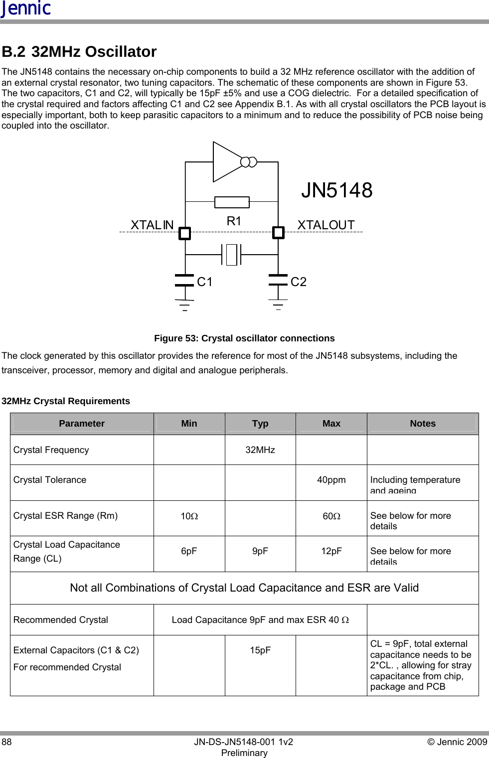
![Jennic © Jennic 2009 JN-DS-JN5148-001 1v2 87 Preliminary B.1.3 Crystal ESR and Required Transconductance The resistor in the crystal equivalent circuit represents the energy lost. To maintain oscillation, power must be supplied by the amplifier, but how much? Firstly, the Pi connected capacitors C1 and C2 with CS from the crystal, apply an impedance transformation to Rm, when viewed from the amplifier. This new value is given by: 2ˆ⎟⎟⎠⎞⎜⎜⎝⎛+=LLSmm CCCRR The amplifier is a transconductance amplifier, which takes a voltage and produces an output current. The amplifier together with the capacitors C1 and C2, form a circuit, which provides a negative resistance, when viewed from the crystal. The value of which is given by: 221ω××=TTmNEG CCgR Where mgis the transconductance ωis the frequency in rad/s Derivations of these formulas can be easily found in textbooks. In order to give quick and reliable oscillator start-up, a common rule of thumb is to set the amplifier negative resistance to be a minimum of 4 times the effective crystal resistance. This gives 221ω×× TTmCCg ≥24⎟⎟⎠⎞⎜⎜⎝⎛+LLSmCCCR This can be used to give an equation for the required transconductance. 21221212])([4TTTTTTSmmCC CCCCCRg××++×≥ω Example: Using typical 32MHz crystal parameters of mR=40Ω, SC=1pF and 1TC=2TC=18pF ( for a load capacitance of 9pF), the equation above gives the required transconductance ( mg) as 2.59mA/V. The JN5148 has a typical value for transconductance of 4.3mA/V The example and equation illustrate the trade-off that exists between the load capacitance and crystal ESR. For example, a crystal with a higher load capacitance can be used, but the value of max. ESR that can be tolerated is reduced. Also note, that the circuit sensitivity to external capacitance [ C1 , C2 ] is a square law. Meeting the criteria for start-up is only one aspect of the way these parameters affect performance, they also affect the time taken during start-up to reach a given, (or full), amplitude. Unfortunately, there is no simple mathematical model for this, but the trend is the same. Therefore, both a larger load capacitance and larger crystal ESR will give a longer start-up time, which has the disadvantages of reduced battery life and increased latency.](https://usermanual.wiki/NXP-Laboratories-UK/JN5148M4.chip-manual/User-Guide-1145108-Page-87.png)
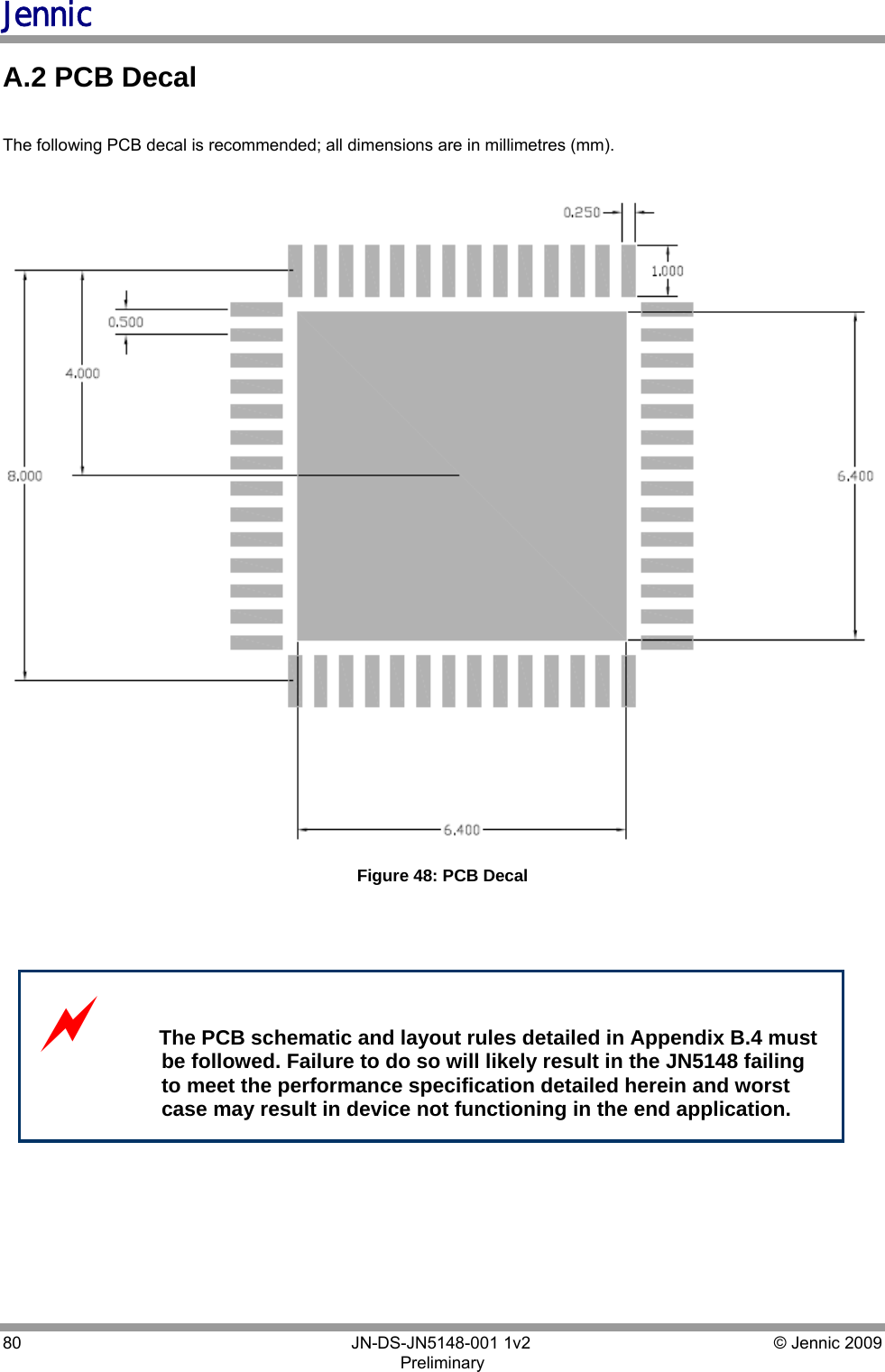
![Jennic 92 JN-DS-JN5148-001 1v2 © Jennic 2009 Preliminary B.4 JN5148 Module Reference Designs For customers wishing to integrate the JN5148 device directly into their system, Jennic provide a range of Module Reference Designs, covering standard and high-power modules fitted with different Antennae To ensure the correct performance, it is strongly recommended that where possible the design details provided by the reference designs, are used in their exact form for all end designs, this includes component values, pad dimensions, track layouts etc. In order to minimise all risks, it is recommended that the entire layout of the appropriate reference module, if possible, be replicated in the end design. For full detail please consult the Standard Module Reference Design JN-RD-6001 [7] , available to download from the Jennic Support web site (www.jennic.com/support) B.4.1 Schematic Diagram A schematic diagram of the JN5148 PCB antenna reference module is shown in Figure 55. Details of component values and PCB layout constraints can be found in Table 8. Figure 55: JN5148 Printed Antenna Reference Module Schematic Diagram](https://usermanual.wiki/NXP-Laboratories-UK/JN5148M4.chip-manual/User-Guide-1145108-Page-92.png)
![Jennic 94 JN-DS-JN5148-001 1v2 © Jennic 2009 Preliminary B.4.2 PCB Design and Reflow Profile PCB and land pattern designs are key to the reliability of any electronic circuit design. The Institute for Interconnecting and Packaging Electronic Circuits (IPC) defines a number of standards for electronic devices. One of these is the "Surface Mount Design and Land Pattern Standard" IPC-SM-782 [4], commonly referred to as “IPC782". This specification defines the physical packaging characteristics and land patterns for a range of surface mounted devices. IPC782 is also a useful reference document for general surface mount design techniques, containing sections on design requirements, reliability and testability. Jennic strongly recommends that this be referred to when designing the PCB. The suggested reflow profile is shown in Figure 56. The specific paste manufacturers guidelines on peak flow temperature, soak times, time above liquidus and ramp rates should also be referenced. Figure 56: Recommended Reflow Profile for Lead-free Solder Paste or PPF lead frame](https://usermanual.wiki/NXP-Laboratories-UK/JN5148M4.chip-manual/User-Guide-1145108-Page-94.png)
![Jennic © Jennic 2009 JN-DS-JN5148-001 1v2 95 Preliminary Related Documents [1] IEEE Std 802.15.4-2003 IEEE Standard for Information Technology – Part 15.4 Wireless Medium Access Control (MAC) and Physical Layer (PHY) Specifications for Low-Rate Wireless Personal Area Networks (LR-WPANs). [2] JN-AN-1062 Using OTP efuse Memory [3] JN-AN-1038 Programming Flash devices not supported by the JN51xx ROM-based bootloader [4] IPC-SM-782 Surface Mount Design and Land Pattern Standard [5] JN-AN-1118 JN5148 Application Debugging [6] JN-RM-2001 Integrated Peripherals API Reference Manual [7] JN-RD-6001 Standard Module Reference Design [8] JN-AN-1003 Boot Loader Operation RoHS Compliance JN5148 devices meet the requirements of Directive 2002/95/EC of the European Parliament and of the Council on the Restriction of Hazardous Substance (RoHS) and of the China RoHS (SJ/T11363 – 2006) requirements which came into force on 1st March 2007. Status Information The status of this Data Sheet is . Preliminary Jennic products progress according to the following format: Advance The Data Sheet shows the specification of a product in planning or in development. The functionality and electrical performance specifications are target values of the design and may be used as a guide to the final specification. Integrated circuits are identified with an Rx suffix, for example JN5148-001R1. Jennic reserves the right to make changes to the product specification at anytime without notice. Preliminary The Data Sheet shows the specification of a product that is commercially available, but is not yet fully qualified. The functionality of the product is final. The electrical performance specifications are target values and may used as a guide to the final specification. Integrated circuits are identified with an Rx suffix, for example JN5148-001R1. Jennic reserves the right to make changes to the product specification at anytime without notice. Production This is the final Data Sheet for the product. All functional and electrical performance specifications, including minimum and maximum values are final. This Data Sheet supersedes all previous document versions. Jennic reserves the right to make changes to the product specification at anytime.](https://usermanual.wiki/NXP-Laboratories-UK/JN5148M4.chip-manual/User-Guide-1145108-Page-95.png)