NXP Laboratories UK JN5168M0 JN5168-ØØ1-MØØ IEEE802.15.4 Wireless Module User Manual JN DS JN5168 001 Myy
NXP Laboratories UK Ltd JN5168-ØØ1-MØØ IEEE802.15.4 Wireless Module JN DS JN5168 001 Myy
User Guide
Data Sheet: JN5168-001-Myy
JenNet, ZigBee PRO and IEEE802.15.4 Module
JN-DS-JN5168-001-Myy © NXP Laboratories UK 2012
Features: Module
2.4GHz IEEE 802.15.4, JenNet-IP,
ZigBee Light Link, ZigBee Smart Energy
and RF4CE compatible
JN5168-001-M00/03
up to 1km range (Ext antenna)
M00: integral antenna 16x30mm
M03: uFl connector 16x21mm
o TX power +2.5dBm
o Receiver sensitivity –95dBm
o TX current 15mA
o RX current 17.5mA
o 2.0-3.6V operation
JN5168-001-M05
up to 2km range (Ext 2dBi Antenna)
o 9.5 dBm TX Power
o Receiver sensitivity -96dBm
o uFl connector
o TX current 35mA
o RX current 22mA
o 16x30mm
o 2.0-3.6V operation
JN5168-001-M06
up to 6km range (Ext 2 dBi Antenna)
o 22dBm TX Power
o Receiver sensitivity -100dBm
o uFl connector
o TX current 175mA
o RX current 22mA
o 16x30mm
o 2.0-3.6V operation
Features: Microcontroller
32-bit RISC CPU, up to 32MIPs with low
power
Data EEPROM with guaranteed 100k
write operations
RF4CE, JenNet-IP, ZigBee Smart
Energy stacks
JTAG debug interface
4-input 10-bit ADC, 1 comparator
5 x PWM (4 x timer, 1 x timer/counter)
2 UARTs
SPI Master & Slave port with 3 selects
2-wire serial interface
Battery and Temperature Sensor
Watchdog timer and BOR
Up to 20 DIO
Industrial temp (-40°C to +85°C)
Lead-free and RoHS compliant
Overview
The JN5168-001-Myy family is a range of ultra low power, high performance surface mount
modules targeted at IEEE 802.15.4, JenNet-IP, ZigBee Light Link, ZigBee Smart Energy and
RF4CE networking applications, enabling users to realise products with minimum time to
market and at the lowest cost. They remove the need for expensive and lengthy development
of custom RF board designs and test suites. The modules use NXP‟s JN5168 wireless
microcontroller to provide a comprehensive solution with large memory, high CPU and radio
performance and all RF components included. All that is required to develop and manufacture
wireless control or sensing products is to connect a power supply and peripherals such as
switches, actuators and sensors, considerably simplifying product development.
Four module variants are available: JN5168-001-M00 with an integrated antenna, JN5168-001-
M03 with an antenna connector and the JN5168-001-M05 and M06 with an antenna connector,
power amplifier and LNA for extended range. The JN5168-001-M05 output power has been
optimised for use in Europe and Asia.
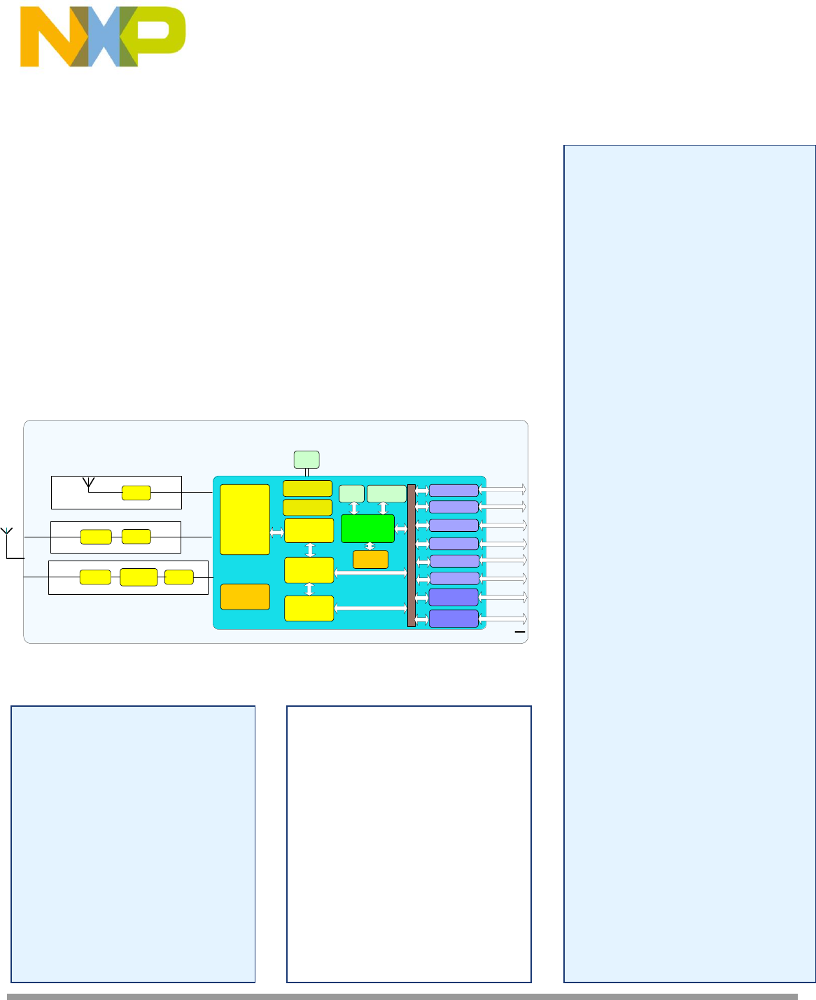
Module Block Diagram
Benefits
Microminiature module solutions
Ready to use in products
Minimises product development
time
No RF test required for systems
Compliant with
o FCC 47CFR Part 15C
o IC Canada RSS 210 Issue 8 -
Annex 8,
o ETSI EN 300-328 V1.7.1
o EN 301-489-17 V2.1.1
o EN60950-1-2006 +A1, A11, A12
Applications
Robust and secure low power wireless
applications
ZigBee and JenNet-IP networks
Home and commercial building
automation
Utilities metering (e.g. AMR)
Location Aware services (e.g. Asset
Tracking)
Toys and gaming peripherals
Industrial systems
Telemetry
Remote Control
4xPWM + Timers
2x UART
4 Chan 10-bit ADC
Battery and Temp
Sensor
2-Wire Serial
(Master/Slave)
SPI Master & Slave
RAM
8/32K
128-bit AES
Encryption
Accelerator
2.4GHz
Radio
Including
Diversity
Flash
64/160/256K
32 -Bit
RISC CPU
Power
Management
XTAL
O-QPSK
Modem
IEEE802.15.4
MAC
Accelerator
Power
Matching
uFl
Connector
Matching
Integrated Antenna
Matching
uFl
Connector PA / LNA
External
Antenna
M00 Option
M03 Option
M05/M06 Option
20 DIO
Sleep Counter
4kB
EEPROM
Watchdog
Timer
Voltage
Brownout

ii JN-DS-JN5168-001-Myy 1v1 © NXP Laboratories UK 2012
Contents
1. Introduction 3
1.1. Variants 3
1.2. Regulatory Approvals 3
2. Specifications 4
2.1. JN5168 Single Chip Wireless Microcontroller 5
3. Pin Configurations 6
3.1. Pin Assignment 7
3.2. Pin Descriptions 8
3.2.1 Power Supplies 8
4. Electrical Characteristics 9
4.1. Maximum Ratings 9
4.2. Operating Conditions 9
Appendix A Additional Information 10
A.1 Outline Drawing 10
A.2 Module PCB Footprint 13
A.3 Optimal PCB placement of the JN5168-001-M00 Module 14
A.4 JN5168-001-M00 Antenna Radiation Pattern 15
A.5 Manufacturing 19
A.5.1 Reflow Profile 19
A.5.2 Soldering Paste and Cleaning 20
A.6 Ordering Information 20
A.7 Related Documents 21
A.8 Federal Communication Commission Interference Statement 21
A.8.1 Antennas approved by FCC for use with JN5168 modules 22
A.8.2 High Power Module usage limitation 22
A.8.3 FCC End Product Labelling 22
A.9 Industry Canada Statement 23
A.9.1 Industry Canada End Product Labelling 23
A.10 European R & TTE Directive 1999/5/EC Statement 23
A.11 RoHS Compliance 24
A.12 Status Information 24
A.13 Disclaimers 24
Version Control 25
© NXP Laboratories UK 2012 JN-DS-JN5168-001-Myy 1v1 3
1. Introduction
The JN5168-001-Myy module family provides designers with a ready-made component that provides a fully
integrated solution for applications, using the IEEE802.15.4 standard in the 2.4-2.5GHz ISM frequency band [1],
including JenNet-IP and ZigBee Smart Energy, and can be quickly and easily included in product designs. The
modules integrate all of the RF components required, removing the need to perform expensive RF design and test.
Products can be designed by simply connecting sensors and switches to the module IO pins. The modules use
NXP‟s single chip IEEE802.15.4 Wireless Microcontroller, allowing designers to make use of the extensive chip
development support material. Hence, this range of modules allows designers to bring wireless applications to
market in the minimum time with significantly reduced development effort and cost.
Four variants are available: JN5168-001-M00, JN5168-001-M03, JN5168-001-M05 and JN5168-001-M06. All
modules have FCC and Industry Canada modular approvals. All modules other than the JN5168-001-M06 are also
CE compliant and subject to a Notified Body Opinion.
The variants available are described below.
1.1. Variants
1.2. Regulatory Approvals
The JN5168-001-M00, M03 and M05 have been tested against the requirements of the following European
standards.
Radio EN 300 328 v1.7.1.
EMC, EN 301 489-17 v2.1.1
Basic Safety Assessment (BSA) EN 60950-1:2006
A Notified Body statement of opinion for this standard is available on request.
The High Power module with M06 suffix is not approved for use in Europe, instead the JN5168-001-M05 module may
be used with an antenna with up to 2.2dBi; 10mW/MHz power spectral density e.i.r.p is the maximum permitted in
Europe.
Additionally, all module types have received FCC “Modular Approval”, in compliance with CFR 47 FCC part 15
regulations and in accordance to FCC Public notice DA00-1407. Appendix A.8 contains details on the conditions
applying to this modular approval. The modules are approved for use with a range of different antennas; further
details of which can be found in section Appendix A.8.1. The modular approvals notice and test reports are available
on request.
All modules are compliant with Industry Canada RSS210 (Issue 8, Annex 8) and have Industry Canada modular
approval.
The JN5168-001-M06 module is subject to user proximity restrictions under FCC and Industry Canada regulations;
more specific information is available in A.8.2.
Variant
Description
FCCID
Industry Canada ID
JN5168-001-M00
Standard Power, integrated antenna
TYOJN5168M0
7438A-CYO5168M0
JN5168-001-M03
Standard Power, uFL connector
TYOJN5168M3
7438A-CYO5168M3
JN5168-001-M05
Medium Power, uFL connector
TYOJN5168M5
7438A-CYO5168M5
JN5168-001-M06
High Power, uFL connector
TYOJN5168M6
7438A-CYO5168M6
4 JN-DS-JN5168-001-Myy 1v1 © NXP Laboratories UK 2012
2. Specifications
Most specification parameters for the modules are specified in the chip datasheet - JN-DS-JN5168 Wireless
Microcontroller Datasheet [2]. Where there are differences, the parameters are defined here.
VDD=3.0V @ +25°C
Typical DC Characteristics
Notes
JN5168-001-
M00/03
JN5168-001-
M06
JN5168-001-
M05
Deep sleep current
100nA
100nA
100nA
Sleep current
0.70uA
0.70uA
0.70uA
With active sleep timer
Radio transmit
current
15mA
175mA
35mA
CPU in doze, radio transmitting
Radio receive
current
17.5mA
22mA
22mA
CPU in doze, radio receiving
Centre frequency
accuracy
+/-25ppm
+/-25ppm
+/-25ppm
Additional +/-15ppm allowance for
temperature and ageing
Typical RF Characteristics
Notes
Receive sensitivity
-95dBm
-100dBm
-96dBm
Nominal for 1% PER, as per 802.15.4
section 6.5.3.3 (Note 1)
Transmit power
2.5dBm
22dBm
9.5 dBm
Nominal
Maximum input
signal
10dBm
5dBm
10dBm
For 1% PER, measured as sensitivity
RSSI range
-95 to
-10dBm
-105 to
-20dBm
-95 to
-10dBm
RF Port impedance
– uFL connector
50 ohm
50 ohm
50 ohm
2.4 - 2.5GHz
Rx Spurious
Emissions
-61dBm
-69dBm
-69dBm
Measured conducted into 50ohms
Tx Spurious
Emissions
-40dBm
-49dBm
-45dBm
Measured conducted into 50ohms
VSWR (max)
2:1
2:1
2:1
2.4 - 2.5GHz
Peripherals
Notes
Master SPI port
3 selects
3 selects
3 selects
250kHz - 16MHz
Slave SPI port
250kHz - 8MHz
Two UARTs
16550 compatible
Two-wire serial I/F
(compatible with
SMbus & I2C)
Up to 400kHz
5 x PWM (4 x timer,
1 x timer/counter)
16MHz clock
Two programmable
Sleep Timers
32kHz clock
Digital IO lines
(multiplexed with
UARTs, timers and
20
18
18
DIO2 & DIO3 not available on JN5168-001-
M05 and JN5168-001-M06 modules

© NXP Laboratories UK 2012 JN-DS-JN5168-001-Myy 1v1 5
SPI selects)
Four channel
Analogue-to-Digital
converter
10-bit, up to 100ks/s
Programmable
analogue
comparators
Ultra low power mode for sleep
Internal
temperature sensor
and battery monitor
The performance of all peripherals is defined in the JN-DS-JN5168 Wireless Microcontroller Datasheet [2].
Note 1: Sensitivity is defined for conducted measurements on connectorised modules. Modules with an integrated
antenna have approximately 1.5 dB less e.i.r.p and reciprocal receive sensitivity.
NXP supplies all the development tools and networking stacks needed to enable end-product development to occur
quickly and efficiently. These are all freely available from www.nxp.com/jennic. A range of evaluation/developer kits
is also available, allowing products to be quickly bread boarded. Efficient development of software applications is
enabled by the provision of a complete, unlimited, software developer kit. Together with the available libraries for the
IEEE802.15.4 MAC and the JenNet-IP and ZigBee PRO network stacks, this package provides everything required to
develop application code and to trial it with hardware representative of the final module.
The modules can be user programmed both in development and in production using software supplied by NXP.
Access to the on-chip peripherals, MAC and network stack software is provided through specific APIs. This
information is available on the NXP support website, together with many example applications, user guides, reference
manuals and application notes.
2.1. JN5168 Single Chip Wireless Microcontroller
The JN5168-001-Myy series is constructed around the JN5168-001 single chip wireless microcontroller, which
includes the radio system, a 32-bit RISC CPU, Flash, RAM & EEPROM memory and a range of analogue and digital
peripherals.
The chip is described fully in JN-DS-JN5168 Wireless Microcontroller Datasheet [2].
6 JN-DS-JN5168-001-Myy 1v1 © NXP Laboratories UK 2012
3. Pin Configurations
10
ADC1
SPICLK
SPIMISO
SPIMISI
SPISSZ
DIO0
DIO1
DIO2
DIO3
DIO4
DIO5
DIO6
DIO7
DIO8
DIO9
DIO10
VDD
GND
ADC2
DIO17
DIO16
DIO15
DIO14
DIO13
RESETN
DIO12
DIO11
1
2
3
4
5
6
7
8
9
11 12 13 14 15 16 17 18
27
26
25
24
23
22
21
20
19
Figure 1: Pin Configuration (top view)
Note that the same basic pin configuration applies for all module designs. However, DIO3 (pin 9) and DIO2 (pin 8)
are not available on the JN5168-001-M05 and JN5168-001-M06.

© NXP Laboratories UK 2012 JN-DS-JN5168-001-Myy 1v1 7
3.1. Pin Assignment
Pin
No
Pin Functions
Signal
Type
Description
Primary
Alternate Functions
1
ADC1
3.3V
Analogue to Digital Input
2
SPICLK
PWM2
CMOS
SPI Master Clock Output or PWM2
Output
3
SPIMISO
CMOS
SPI Master In Slave Out Input
4
SPIMOSI
PWM3
CMOS
SPI Master In Slave Out Input or
PWM3 Output
5
SPISEL0
CMSO
SPI Select From Module – SS0
Output
6
DIO0
SPISEL1
ADC3
CMOS
DIO0, SPI Master Select Output 1
or ADC input 3
7
DIO1
SPISEL2
ADC4
PC0
CMOS
DIO1, SPI Master Select Output 2,
ADC input 4 or Pulse Counter 0
Input
8
DIO2*
RFRX
TIM0CK_GT
CMOS
DIO2, Radio Receive Control
Output or Timer0 Clock/Gate Input
9
DIO3*
RFTX
TIM0CAP
CMOS
DIO3, Radio Transmit Control
Output or Timer0 Capture Input
10
DIO4
CTS0
JTAG_TCK
TIM0OUT
PC0
CMOS
DIO4, UART 0 Clear To Send
Input, JTAG CLK Input, Timer0
PWM Output, or Pulse Counter 0
input
11
DIO5
RTS0
JTAG_TMS
PWM1
PC1
CMOS
DIO5, UART 0 Request To Send
Output, JTAG Mode Select Input,
PWM1 Output or Pulse Counter 1
Input
12
DIO6
TXD0
JTAG_TDO
PWM2
CMOS
DIO6, UART 0 Transmit Data
Output, JTAG Data Output or
PWM2 Output
13
DIO7
RXD0
JTAG_TDI
PWM3
CMOS
DIO7, UART 0 Receive Data
Input, JTAG Data Input or PWM 3
Output
14
DIO8
TIM0CK_GT
PC1
PWM4
CMOS
DIO8, Timer0 Clock/Gate Input,
Pulse Counter1 Input or PWM 4
Output
15
DIO9
TIM0CAP
32KXTALIN
RXD1
32KIN
CMOS
DIO9, Timer0 Capture Input, 32K
External Crystal Input, UART 1
Receive Data Input or 32K
external clock Input
16
DIO10
TIM0OUT
32KXTALOUT
CMOS
DIO10, Timer0 PWM Output or
32K External Crystal Output
17
VDD
3.3V
Supply Voltage
18
GND
0V
Digital Ground
19
DIO11
PWM1
TXD1
CMOS
DIO11, PWM1 Output or UART 1
Transmit Data Output
20
DIO12
PWM2
CTS0
JTAG_TCK
ADO or
SPISMOSI
CMOS
DIO12, PWM2 Output, UART 0
Clear To Send Input, JTAG CLK
Input, Antenna Diversity Odd
Output or SPI Slave Master Out
Slave In Input
21
DIO13
PWM3
RTS0
JTAG_TMS
ADE or
SPISMISO
CMOS
DIO13, PWM3 Output, UART 0
Request To Send Output, JTAG
Mode Select Input, Antenna
Diversity Even output or SPI Slave
Master In Slave Out Output
22
RESETN
CMOS
Reset input
23
DIO14
SIF_CLK
TXD0 TXD1
JTAG_TDO
SPISEL1 or
CMOS
DIO14, Serial Interface Clock,

8 JN-DS-JN5168-001-Myy 1v1 © NXP Laboratories UK 2012
SPISSEL
UART 0 Transmit Data Output,
UART 1 Transmit Data Output,
JTAG Data Output, SPI Master
Select Output 1 or SPI Slave
Select Input
24
DIO15
SIF_D
RXD0 RXD1
JTAG_TDI
SPISEL2
CMOS
DIO15, Serial Interface Data or
Intelligent Peripheral Data Out
25
DIO16
COMP1P
SIF_CLK
SPISMOSI
CMOS
DIO16, Comparator Positive Input,
Serial Interface clock or SPI Slave
Master Out Slave In Input
26
DIO17
COMP1M
PWM4
I2C DATA
SPISIMO
CMOS
DIO17, Comparator Negative
Input, Serial Interface Data or SPI
Slave Master In Slave Out Output
27
ADC2
3.3V
Analogue to Digital Input
* These two pins are not connected for JN5168-001-M05 & JN5168-001-M06 modules.
3.2. Pin Descriptions
All pins behave as described in the JN-DS-JN5168 Wireless Microcontroller Datasheet [2], with the exception of the
following:
3.2.1 Power Supplies
A single power supply pin, VDD is provided.
© NXP Laboratories UK 2012 JN-DS-JN5168-001-Myy 1v1 9
4. Electrical Characteristics
In most cases, the Electrical Characteristics are the same for both module and chip. They are described in detail in
the chip datasheet. Where there are differences, they are detailed below.
4.1. Maximum Ratings
Exceeding these conditions will result in damage to the device.
Parameter
Min
Max
Device supply voltage VDD
-0.3V
3.6V
All Pins
-0.3V
VDD + 0.3V
Storage temperature
-40ºC
150ºC
4.2. Operating Conditions
Supply
Min
Max
VDD
2.0V
3.6V
Ambient temperature range
-40ºC
85ºC
10 JN-DS-JN5168-001-Myy 1v1 © NXP Laboratories UK 2012
Appendix A Additional Information
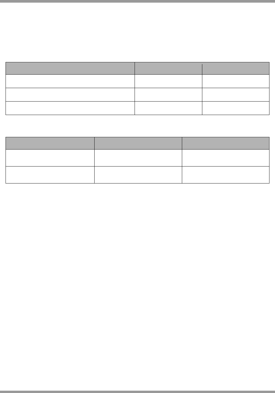
A.1 Outline Drawing
30.0mm
16mm
2.76
mm
2.54
mm
2.54
mm
1.27
mm
Thickness: 3.5mm
Figure 2 JN5168-001-M00 Outline Drawing
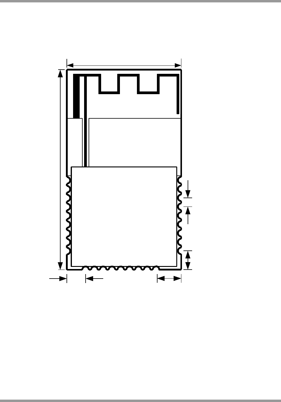
© NXP Laboratories UK 2012 JN-DS-JN5168-001-Myy 1v1 11
21mm
16mm
3.30
mm
2.54
mm
2.54
mm
2.56
mm
9.76mm
1.27
mm
Thickness: 3.5mm
Figure 3 JN5168-001-M03 Outline Drawing
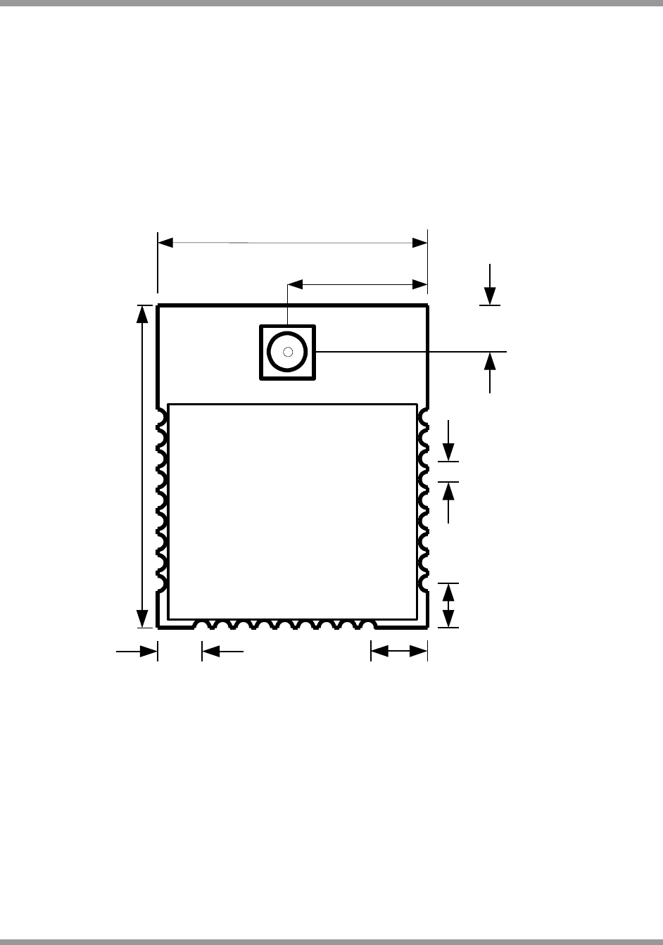
12 JN-DS-JN5168-001-Myy 1v1 © NXP Laboratories UK 2012
30mm
16mm
.3.30
mm
2.54
mm
1.27
mm
2.54
mm
2.90mm
8.0mm
Thickness: 3.5mm
Figure 4 JN5168-001-M05 and JN5168-001-M06 Outline Drawing
© NXP Laboratories UK 2012 JN-DS-JN5168-001-Myy 1v1 13
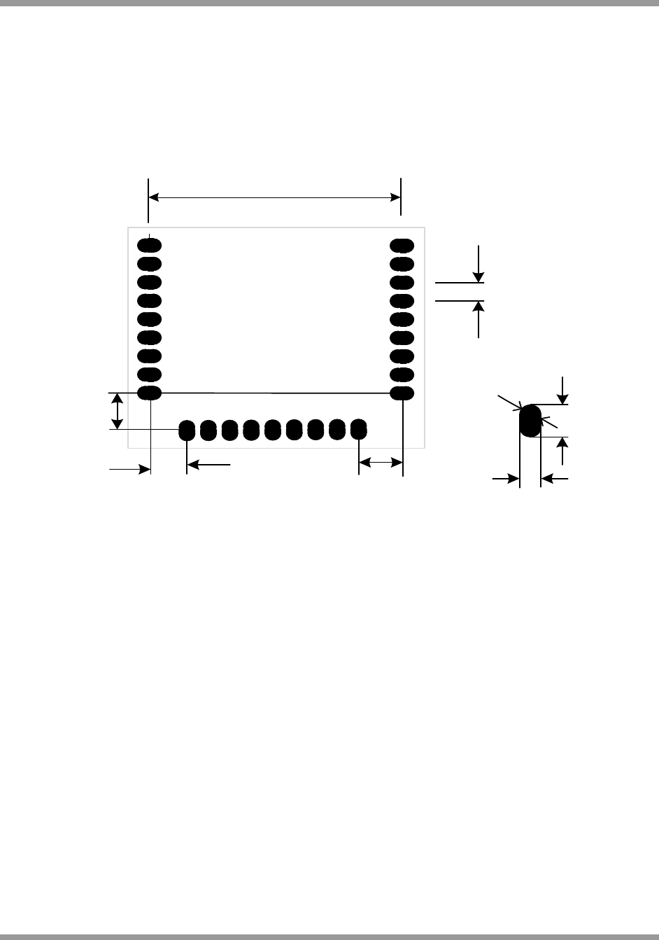
A.2 Module PCB Footprint
All dimensions are in mm.
2.49
2.23
2.23
1.27
14.88
1
1.5
Ø1
Note: All modules have the same footprint
Figure 5 Module PCB footprint
14 JN-DS-JN5168-001-Myy 1v1 © NXP Laboratories UK 2012
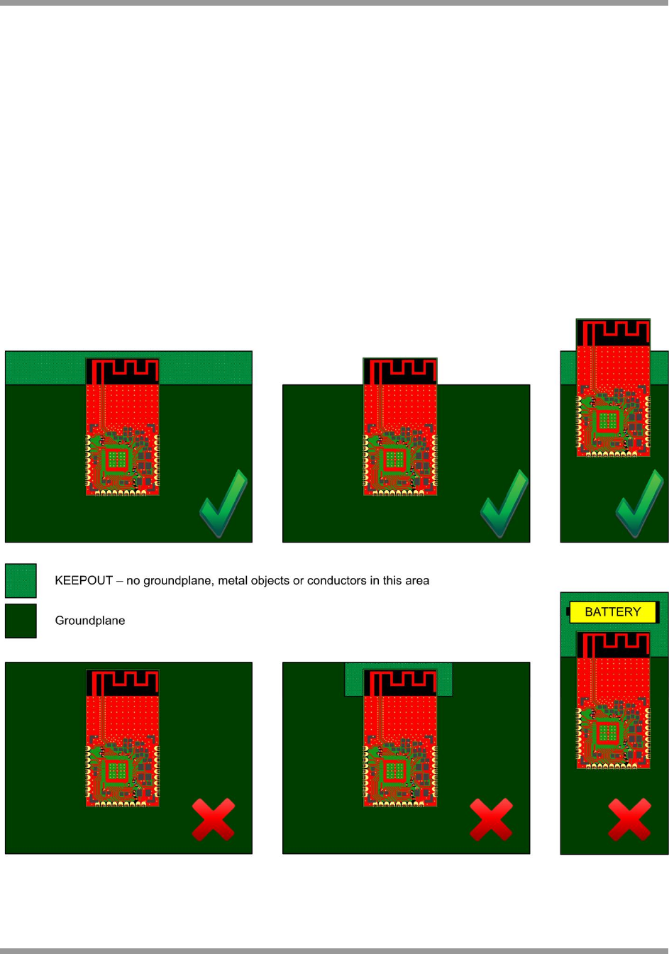
A.3 Optimal PCB placement of the JN5168-001-M00 Module
The JN5168-001-M00 module features an optimised, low cost, integrated, inverted F, printed PCB antenna. The
antenna has a vertically polarised near omnidirectional radiation pattern and up to 1.6 dBi of peak gain. The PCB
design has been elongated in order to increase the ground plane area which increases the antenna efficiency. This
allows stand alone operation without any additional ground plane however care must be taken when mounting this
module onto another PCB. The area around the antenna must be kept clear of conductors or other metal objects for
an absolute minimum of 20 mm. This is true for all layers of the PCB and not just the top layer. Any conductive
objects close to the antenna could severely disrupt the antenna pattern resulting in deep nulls and high directivity in
some directions.
The diagrams below show various possible scenarios. The top 3 scenarios are correct; groundplane may be placed
beneath JN5168-001-M00 module as long as it does not protrude beyond the edge of the top layer ground plane on
the module PCB.
The bottom 3 scenarios are incorrect; the left hand side example because there is groundplane underneath the
antenna, the middle example because there is insufficient clearance around the antenna (it is best to have no
conductors anywhere near the antenna), finally the right hand example has a battery‟s metal casing in the
recommended keep out area.
Figure 6 PCB placement of the JN5168-001-M00 Module
© NXP Laboratories UK 2012 JN-DS-JN5168-001-Myy 1v1 15
A.4 JN5168-001-M00 Antenna Radiation Pattern
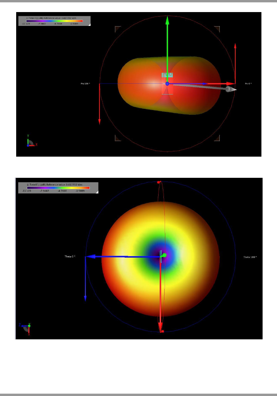
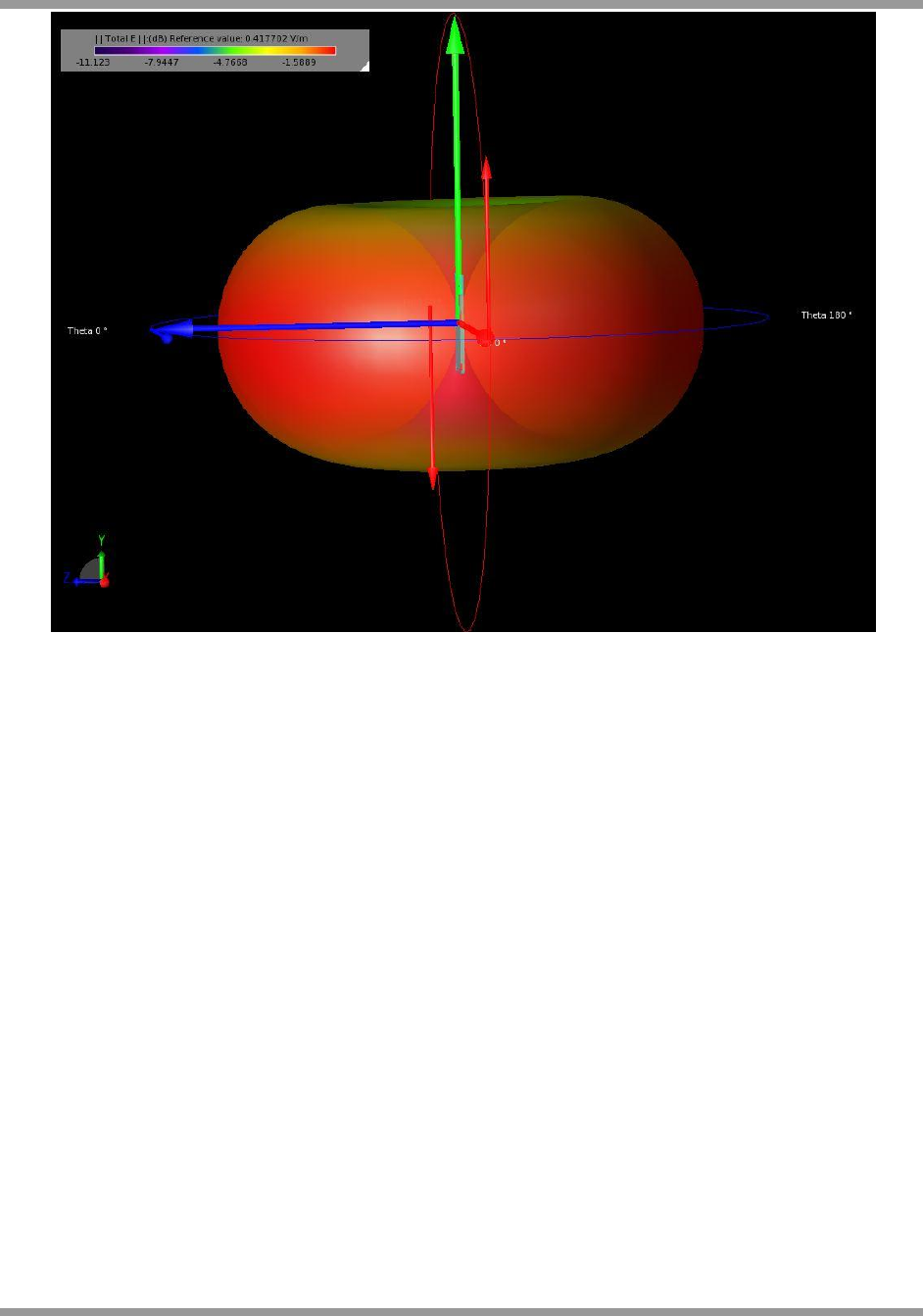
Figure 7, Figure 8 &Figure 9 are simulated 3D radiation plots of the JN5168-001-M00. They are provided here to
help the user orientate the module in end equipment in an optimal way. These visualisations are an accurate
representation of the antenna radiation pattern in the 3D space.
The 2D XZ plots for each channel are shown in
dBuV
104
94
84
74
64
54
44
34
24
14
4
14
24
34
44
54
64
74
84
94
104
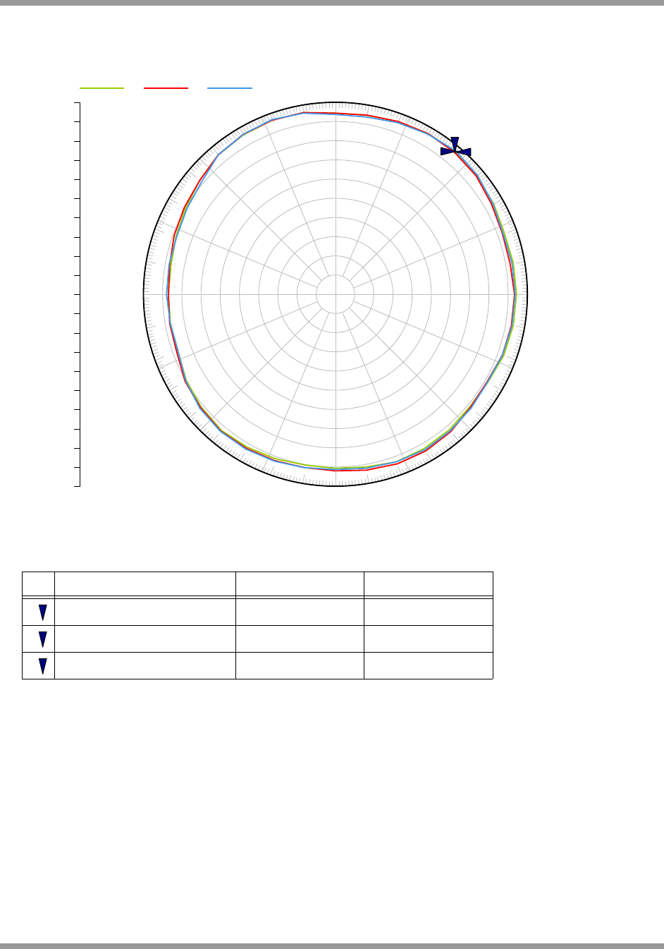
JN5168-001-M00 Radiation Plots @ 3 meters (XZ Orientation)
CH11 CH18 CH26
Mkr Trace X-Axis Value
1
1 CH11 40.0 deg 101.04 dBuV
2
2 CH18 40.0 deg 100.67 dBuV
3
3 CH26 40.0 deg 101.26 dBuV
Figure 10. These are actual measurements in an anechoic chamber with the JN5168-001-M00 mounted on a
DR1174 carrier board from the JN516x-EK001 Evaluation kit. The device under test and the antenna height was 1m
and the values are in dBuV/m at a distance of 3m.
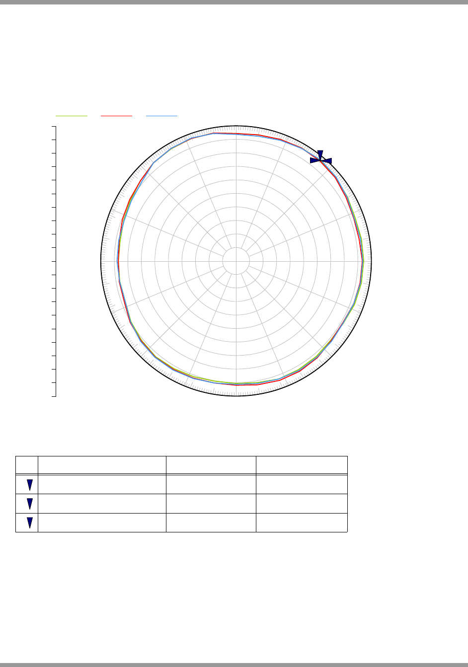
Figure 11 is a plot of the peak field strengths for a JN5168-001-M00, JN5148-001-M00 and JN5168-001-M03. The
M03 is used with a λ/2 vertical antenna. Figure 11 shows that the new integrated antenna is 1.5-3dB better than the
JN5148-001-M00 and is within 1.5 dB of a JN5168-001-M03 λ/2 vertical.
16 JN-DS-JN5168-001-Myy 1v1 © NXP Laboratories UK 2012
Figure 7: 3D radiation plot JN5168-001-M00 XY Orientation (simulation)
Figure 8: 3D radiation plot JN5168-001-M00 XZ Orientation (simulation)
© NXP Laboratories UK 2012 JN-DS-JN5168-001-Myy 1v1 17
Figure 9: 3D radiation plot JN5168-001-M00 YZ Orientation (simulation)
18 JN-DS-JN5168-001-Myy 1v1 © NXP Laboratories UK 2012
dBuV
104
94
84
74
64
54
44
34
24
14
4
14
24
34
44
54
64
74
84
94
104
JN5168-001-M00 Radiation Plots @ 3 meters (XZ Orientation)
CH11 CH18 CH26
Mkr Trace X-Axis Value
1
1 CH11 40.0 deg 101.04 dBuV
2
2 CH18 40.0 deg 100.67 dBuV
3
3 CH26 40.0 deg 101.26 dBuV
Figure 10: Actual radiation plot of JN5168-001-M00 Mounted on a carrier PCB – XZ orientation
© NXP Laboratories UK 2012 JN-DS-JN5168-001-Myy 1v1 19
Figure 11: Peak Field Strengths for various modules optimised for height and azimuth
A.5 Manufacturing
A.5.1 Reflow Profile
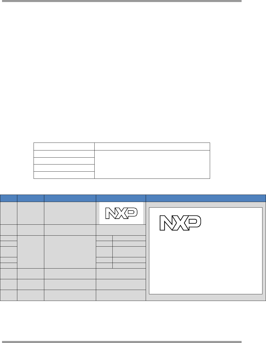
For reflow soldering, it is recommended to follow the reflow profile in figure 6 as a guide, as well as the paste
manufacturer‟s guidelines on peak flow temperature, soak times, time above liquid and ramp rates.
Figure 12: Recommended solder reflow profile
98.0
98.5
99.0
99.5
100.0
100.5
101.0
101.5
102.0
102.5
103.0
103.5
104.0
11
18
26
dBuV/m @ 3m
Channel
Module Peak Field Strengths
JN5168-001-M03 with
vertical
JN5168-001-M00
JN5148-001-M00
Temperature
25~160 ºC
160~190 ºC
> 220º C
230~Pk.
Pk. Temp
(235ºC)
Target Time (s)
90~130
30~60
20~50
10~15
150~270
20 JN-DS-JN5168-001-Myy 1v1 © NXP Laboratories UK 2012
A.5.2 Soldering Paste and Cleaning
NXP does not recommend use of a solder paste that requires the module and PCB assembly to be cleaned (rinsed in
water) for the following reasons:
Solder flux residues and water can be trapped by the PCB, can or components and result in short circuits.
The module label could be damaged or removed.
NXP recommends use of a 'no clean' solder paste for all its module products.
A.6 Ordering Information
Ordering Code Format:
Where this Data Sheet is denoted as “Advanced” or “Preliminary”, devices will be either Engineering Samples or
Prototypes.
Part Number
Description
JN5168-001-M00
Shipped in tape mounted 500 piece reel
JN5168-001-M03
JN5168-001-M05
JN5168-001-M06
Line
Content
Format
Options
Sample
1
NXP Logo
B&W outline logo
JN5168-001-M00
ZSDYWW NNNNN
FCC ID:TYOJN5168M0
IC:7438A-CYO5168M0
2
Part ID
JN5168-001-M0x
x is module type, 0,
3, 5 or 6
3
Z
SSMC
S
APK
D
RoHs
Compliant
Y
Year
WW
Week
3
Serial No.
NNNNN
Serial number from
test
5
FCC ID
FCCID:TYOJN5168Mx
x is module type
0,3,5 or 6
6
IC ID
IC:7438A-
CYO5168Mx
x is module type
0,3,5 or 6
JN5168 - 001 – MYY
Module Type (YY)
00 Standard Power, Integral antenna
03 Standard Power, uFl connector
05 Medium Power, uFL connector
06 High Power, uFl connector
Figure 13: Example module labelling

© NXP Laboratories UK 2012 JN-DS-JN5168-001-Myy 1v1 21
A.7 Related Documents
[1] IEEE Std 802.15.4-2003 IEEE Standard for Information Technology – Part 15.4 Wireless Medium Access Control
(MAC) and Physical Layer (PHY) Specifications for Low-Rate Wireless Personal Area Networks (LR-WPANs)
[2] JN-DS-JN5168 Wireless Microcontroller Datasheet
A.8 Federal Communication Commission Interference Statement
This equipment has been tested and found to comply with the limits for a Class B digital device, pursuant to Part 15
of the FCC Rules. These limits are designed to provide reasonable protection against harmful interference in a
residential installation. This equipment generates, uses, and can radiate radio frequency energy and, if not installed
and used in accordance with the instructions, may cause harmful interference to radio communications. However,
there is no guarantee that interference will not occur in a particular installation. If this equipment does cause harmful
interference to radio or television reception, which can be determined by turning the equipment off and on, the user is
encouraged to try to correct the interference by one of the following measures:
- Reorient or relocate the receiving antenna.
- Increase the separation between the equipment and receiver.
- Connect the equipment into an outlet on a circuit different from that to which the receiver is connected.
- Consult the dealer or an experienced radio/TV technician for help.
This device complies with Part 15 of the FCC Rules. Operation is subject to the following two conditions: (1) This
device may not cause harmful interference, and (2) this device must accept any interference received, including
interference that may cause undesired operation.
FCC Caution: Any changes or modifications not expressly approved by the party responsible for compliance could
void the user's authority to operate this equipment.
WARNING!
FCC Radiation Exposure Statement:
This portable equipment with its antenna complies with FCC‟s RF radiation exposure limits set forth for an
uncontrolled environment. To maintain compliance follow the instructions below;
1. This transmitter must not be co-located or operating in conjunction with any other antenna or transmitter.
2. Avoid direct contact to the antenna, or keep it to a minimum while using this equipment.
This transmitter module is authorized to be used in other devices only by OEM integrators under the
following condition:
The transmitter module must not be co-located with any other antenna or transmitter.
As long as the above condition is met, further transmitter testing will not be required. However, the OEM integrator is
still responsible for testing their end product for any additional compliance requirements required with this module
installed (for example, digital device emissions, PC peripheral requirements, etc.).
This applies to the JN5168-001-M00, JN5168-001-M03 and JN5168-001-M05 devices, the JN5168-001-M06 is a
mobile device (see section A.8.2)
22 JN-DS-JN5168-001-Myy 1v1 © NXP Laboratories UK 2012
A.8.1 Antennas approved by FCC for use with JN5168 modules
Brand
Model Number
Description
Gain (dBi)
Connector type
1
Antenna Factor
ANT-2.4-CW-RCT-RP
Vertical - knuckle antenna
2.2
RP-SMA
2
Antennova
2010B6090-01
Vertical - knuckle antenna
2.2
RP-SMA
3
Hyperlink Technology
HG2402RD-RSF
Vertical - knuckle antenna
2.2
RP-SMA
4
Aveslink Technology, Inc
E-0005-AC
Vertical- flying lead
2
RP-SMA
5
Aveslink Technology, Inc
E-2411-GC
Vertical - swivel
2
RP-SMA
6
Aveslink Technology, Inc
E-2410-CA
Vertical - bulkhead- flying lead
2
uFL
7
Aveslink Technology, Inc
E-2410-GC
Vertical - swivel
2
RP-SMA
8
Aveslink Technology, Inc
E-2820-CA
Vertical - bulkhead- flying lead
2
uFL
9
Aveslink Technology, Inc
E-2820-GC
Vertical - swivel
2
RP-SMA
10
Embedded Antenna Design
FBKR35068-RS-KR
Vertical - knuckle antenna
2
RP-SMA
11
Nearson
S131CL-L-PX-2450S
Vertical - knuckle-flying lead
2
uFL
12
Laird Technologies
WRR2400-IP04
Vertical - knuckle-flying lead
1.5
uFL
13
Laird Technologies
WRR2400-RPSMA
Vertical - knuckle-flying lead
1.3
RP-SMA
14
Aveslink Technology, Inc
E-6170-DA
Vertical - right angle
1
uFL
15
Laird Technologies
WCR2400-SMRP
Vertical - knuckle antenna
1
RP-SMA
This device has been designed to operate with the antennas listed above, and having a maximum gain of 2.2 dBi.
Alternative vertical antennas may be used provided that the gain does not exceed 2.2 dBi. Antennas having a gain
greater than 2.2 dBi are strictly prohibited for use with this device.
The required antenna impedance is 50 ohms.
A.8.2 High Power Module usage limitation
The high power module variants are classified as „mobile‟ device pursuant with FCC § 2.1091 and must not be used
at a distance of < 20 cm (8”) from any people. This applies to the JN5168-001-M06 module type (TYOJN5168M6).
IMPORTANT NOTE: In the event that these conditions cannot be met (for certain configurations or co-location with
another transmitter), then the FCC authorization is no longer considered valid and the FCC ID can not be used on the
final product. In these circumstances, the OEM integrator will be responsible for re-evaluating the end product
(including the transmitter) and obtaining a separate FCC authorization.
The OEM integrator has to be aware not to provide information to the end user regarding how to install or remove this
RF module in the user manual of the end product.
The user manual for the end product must include the following information in a prominent location;
“To comply with FCC‟s RF radiation exposure requirements, the antenna(s) used for this transmitter must not be co-
located or operating in conjunction with any other antenna or transmitter.”
A.8.3 FCC End Product Labelling
The final „end product‟ should be labelled in a visible area with the following:
“Contains TX FCC ID: TYOJN5168M0, TYOJN5168M3, TYOJN5168M5 or TYOJN5168M6” to reflect the version of
the module being used inside the product.
© NXP Laboratories UK 2012 JN-DS-JN5168-001-Myy 1v1 23
A.9 Industry Canada Statement
This device complies with Industry Canada licence-
exempt RSS standard(s). Operation is subject
to the following two conditions: (1) this device may
not cause interference, and (2) this device must
accept any interference, including interference that
may cause undesired operation of the device.
Le présent appareil est conforme aux CNR d'Industrie
Canada applicables aux appareils radio
exempts de licence. L'exploitation est autorisée aux
deux conditions suivantes : (1) l'appareil ne
doit pas produire de brouillage, et (2) l'utilisateur de
l'appareil doit accepter tout brouillage
radioélectrique subi, même si le brouillage est
susceptible d'en compromettre le fonctionnement.
To reduce potential radio interference to other users, the antenna type and its gain should be so chosen that the
equivalent isotropic radiated power (e.i.r.p.) is not more than that permitted for successful communication.
These modules have been designed to operate with antennas having a maximum gain of 2.2 dBi. Antennas having a
gain greater than 2.2 dBi are strictly prohibited for use with this device. The required antenna impedance is 50 ohms.
As long as the above condition is met, further transmitter testing will not be required. However, the OEM integrator is
still responsible for testing their end-product for any additional compliance requirements required with this module
installed (for example, digital device emissions, PC peripheral requirements, etc).
A.9.1 Industry Canada End Product Labelling
For Industry Canada purposes the following should be used.
“Contains Industry Canada ID IC: 7438A-CYO5168M0, IC: 7438A-CYO5168M3, IC: 7438A-CYO5168M5 or IC:
7438A-CYO5168M6” to reflect the version of the module being used inside the product.
A.10 European R & TTE Directive 1999/5/EC Statement
All modules listed in this datasheet with the exception of the JN5168-001-M06 are compliant with ETSI EN 300 328
V1.7.1 (2006-10), EMC, EN 301 489-17 v2.1.1 (2009-02) and the Basic Safety Assessment (BSA) EN 60950-1:2006
(2006-06) and are subject to a Notified Body Opinion.
The modules are approved for use with the antennas listed in the following table. The JN5168-001-M06 module is not
approved for use in Europe, instead use the JN5168-001-M05 which produces the maximum permitted power.
Alternative vertical antennas may be used provided that the gain does not exceed 2.2 dBi.
Brand
Model Number
Description
Gain (dBi)
Connector type
1
Antenna Factor
ANT-2.4-CW-RCT-SMA
Vertical - knuckle antenna
2.2
SMA
2
Antennova
B6090
Vertical - knuckle antenna
2.2
RP-SMA
3
Hyperlink Technology
HG2402RD-RSF
Vertical - knuckle antenna
2.2
RP-SMA
4
Aveslink Technology, Inc
E-0005-AC
Vertical- flying lead
2
RP-SMA
5
Aveslink Technology, Inc
E-2411-GC
Vertical - swivel
2
RP-SMA
6
Aveslink Technology, Inc
E-2410-CA
Vertical - bulkhead- flying lead
2
uFL
7
Aveslink Technology, Inc
E-2410-GC
Vertical - swivel
2
RP-SMA
8
Aveslink Technology, Inc
E-2820-CA
Vertical - bulkhead- flying lead
2
uFL
9
Aveslink Technology, Inc
E-2820-GC
Vertical - swivel
2
RP-SMA
10
Embedded Antenna Design
FBKR35068-RS-KR
Vertical - knuckle antenna
2
RP-SMA
11
Nearson
S131CL-L-PX-2450S
Vertical - knuckle-flying lead
2
uFL
12
Laird Technologies
WRR2400-IP04
Vertical - knuckle-flying lead
1.5
uFL
13
Laird Technologies
WRR2400-RPSMA
Vertical - knuckle-flying lead
1.3
RP-SMA
14
Aveslink Technology, Inc
E-6170-DA
Vertical - right angle
1
uFL
15
Laird Technologies
WCR2400-SMRP
Vertical - knuckle antenna
1
RP-SMA

24 JN-DS-JN5168-001-Myy 1v1 © NXP Laboratories UK 2012
A.11 RoHS Compliance
JN5168-001-Myy devices meet the requirements of Directive 2002/95/EC of the European Parliament and of the
Council on the Restriction of Hazardous Substance (RoHS).
The JN5168-001-M00, M03, M05 and M06 modules meet the requirements of Chinese RoHS requirements
SJ/T11363-2006.
Full data can be found at www.nxp.com/jennic.
A.12 Status Information
The status of this Data Sheet is Preliminary.
NXP products progress according to the following format:
Advanced
The Data Sheet shows the specification of a product in planning or in development.
The functionality and electrical performance specifications are target values and may be used as a guide to the final
specification.
NXP reserves the right to make changes to the product specification at anytime without notice.
Preliminary
The Data Sheet shows the specification of a product that is commercially available, but is not yet fully qualified.
The functionality of the product is final. The electrical performance specifications are target values and may be used
as a guide to the final specification. NXP reserves the right to make changes to the product specification at anytime
without notice.
Production
This is the production Data Sheet for the product.
All functional and electrical performance specifications, where included, including min and max values are derived
from detailed product characterization.
This Data Sheet supersedes all previous document versions.
NXP reserves the right to make changes to the product specification at anytime.
A.13 Disclaimers
The contents of this document are subject to change without notice. NXP reserves the right to make changes,
without notice, in the products, including circuits and/or software, described or contained therein. Information
contained in this document regarding device applications and the like is intended through suggestion only and may
be superseded by updates. It is your responsibility to ensure that your application meets with your specifications.
NXP warrants performance of its hardware products to the specifications applicable at the time of sale in accordance
with NXP‟s standard warranty. Testing and other quality control techniques are used to the extent NXP deems
necessary to support this warranty. Except where mandatory by government requirements, testing of all parameters
of each product is not necessarily performed.
NXP assumes no responsibility or liability for the use of any of these products, conveys no license or title under any
patent, copyright, or mask work right to these products, and makes no representations or warranties that these
products are free from patent, copyright, or mask work infringement, unless otherwise specified.
NXP products are not intended for use in life support systems, appliances or systems where malfunction of these
products can reasonably be expected to result in personal injury, death or severe property or environmental damage.
NXP customers using or selling these products for use in such applications do so at their own risk and agree to fully
indemnify NXP for any damages resulting from such use.
All products are sold subject to NXP's terms and conditions of sale supplied at the time of order acknowledgment.
All trademarks are the property of their respective owners.

© NXP Laboratories UK 2012 JN-DS-JN5168-001-Myy 1v1 25
Version Control
Version
Notes
1.0
Initial release
1.1
Additional clarification of RF exposure conditions added to FCC section A8
NXP Laboratories UK Ltd
Furnival Street
Sheffield
S1 4QT
United Kingdom
Tel: +44 (0)114 281 2655
Fax: +44 (0) 114 281 2951
For the contact details of your local NXP office or distributor, refer to the NXP web site:
www.nxp.com/jennic