NXP Semiconductors FRDMKW41Z FRDM-KW41Z Freedom Development Platform User Manual FRDM KW41Z User s Guide
NXP Semiconductors FRDM-KW41Z Freedom Development Platform FRDM KW41Z User s Guide
Users Manual
NXP Semiconductors, 6501 William Cannon Drive West, Austin, Texas 78735
www.nxp.com
FRDM-KW41Z User’s Guide
Rev 0.1

FRDM-KW41Z User’s Guide Page 2 of 11
Contents
1 Introduction .............................................................................................................................................. 2
1.1 Audience ................................................................................................................................................................................. 3
2 Safety information .................................................................................................................................. 4
2.1 FCC guidelines ...................................................................................................................................................................... 4
2.1.1 Labeling .................................................................................................................................................................................................. 4
2.1.2 Operation conditions ........................................................................................................................................................................ 4
2.1.3 Exposure limits ................................................................................................................................................................................... 4
2.1.4 Antenna restrictions ......................................................................................................................................................................... 4
2.2 Electrostatic dischage considerations ........................................................................................................................ 4
2.3 Disposal instructions ......................................................................................................................................................... 5
3 FRDM-KW41Z overview and description ........................................................................................ 6
3.1 Introduction .......................................................................................................................................................................... 6
3.2 Board features ...................................................................................................................................................................... 6
3.2.1 FRDM-KW41Z board ........................................................................................................................................................................ 6
3.3 Serial and Debug Adapter................................................................................................................................................ 8
3.3.1 Virtual serial port ............................................................................................................................................................................... 9
4 FRDM-KW41Z development board ................................................................................................... 9
4.1 FRDM-KW41Z board overview ..................................................................................................................................... 9
4.1.1 PCB features ......................................................................................................................................................................................... 9
4.2 Functional description ................................................................................................................................................... 10
4.2.1 RF performance and considerations ...................................................................................................................................... 10
1 Introduction
This guide describes the hardware for the FRDM-KW41Z Freescale Freedom development board. The
FRDM-KW41Z Freedom development board is a small, low-power, and cost-effective evaluation and
development board for application prototyping and demonstration of the MKW41Z SoC family of
devices. These evaluation boards offer easy-to-use mass-storage-device mode flash programmer, a
virtual serial port, and standard programming and run-control capabilities.
The MKW41Z is an ultra low-power, highly integrated single-chip device that enables Bluetooth low
energy (BLE) or IEEE Standard 802.15.4 RF connectivity for portable, extremely low-power
embedded systems.

FRDM-KW41Z User’s Guide Page 3 of 11
The MKW41Z SoC integrates a radio transceiver operating in the 2.402 GHz to 2.48 GHz range
supporting a range of GFSK and O-QPSK modulations, an ARM Cortex-M0+ CPU, up to 512 KB
Flash and up to 128 KB SRAM, BLE Link Layer hardware, 802.15.4 packet processor hardware and
peripherals optimized to meet the requirements of the target applications.
1.1 Audience
This guide is intended for system designers.

FRDM-KW41Z User’s Guide Page 4 of 11
2 Safety information
2.1 FCC guidelines
This equipment is to be used by developers for evaluation purposes only, and must not be
incorporated into any other device or system. This device must not be sold to the general public.
Integrators are responsible for re-evaluating the end product (including the transmitter) and obtaining
a separate FCC authorization. The FCC approval of this device only covers the original configuration of
this device (as supplied). Any modifications to this product (including changes shown in this guide) may
violate the rules of the Federal Communications Commission and Industry Canada and make the
operation of the product unlawful.
2.1.1 Labeling
The FCC labels are located on the back of the board.
2.1.2 Operation conditions
The device must comply with part 15 of the FCC rules. Operation is subject to these two conditions:
• This device must not cause harmful interference.
• This device must accept any interference received, including interference that can cause
undesired operation.
2.1.3 Exposure limits
The device must comply with FCC radiation exposure limits set forth for an uncontrolled environment.
Install the antenna(s) used by the device to provide a separation distance of at least 8 inches (20 cm)
from all persons.
The modular transmitter must be equipped with either a permanently affixed label or must be
capable of electronically displaying its FCC identification number:
(A) If using a permanently affixed label, the modular transmitter must be labeled with its own FCC
identification number, and, if the FCC identification number is not visible when the module is installed
inside another device, then the outside of the device into which the module is installed must also
display a label referring to the enclosed module. This exterior label can use wording such as the
following: “Contains Transmitter Module FCC ID:XXMFRDMKW41Z.” Any similar wording that
expresses the same meaning may be used. The Grantee may either provide such a label, an example
of which must be included in the application for equipment authorization, or, must provide adequate
instructions along with the module which explain this requirement. In the latter case, a copy of these
instructions must be included in the application for equipment authorization.
Changes or modifications not expressly approved by the party responsible for compliance could void the
user's authority to operate the equipment.

FRDM-KW41Z User’s Guide Page 5 of 11
Draft
qualification, ESD stresses were performed for the Human Body Model (HBM), the Machine Model
(MM), and the Charge Device Model (CDM). All latch-up test testing must conform to the JESD78 IC
Latch-Up Test. When operating or handling the development boards or components, Freescale strongly
recommends using at least grounding wrist straps, plus any (or all) of these ESD dissipation methods:
• Flexible fabric, solid fixed size, or disposable ESD wrist straps.
• Static control workstations, static control monitors and table or floor static control systems.
• Static control packaging and transportation materials and environmental systems.
2.3 Disposal instructions
This product may be subject to special disposal requirements.
2.2 Electrostatic dischage considerations
Although the damage from electrostatic discharge (ESD) is much less common on these devices when
compared to the early CMOS circuits, use standard handling precautions to avoid exposure to static
discharge. Qualification tests are performed to ensure that these devices can withstand exposure to
reasonable levels of static without suffering any permanent damage. All ESD testing must conform to
the JESD22 Stress Test Qualification for Commercial Grade Integrated Circuits. During the device
2.1.4 Antenna restrictions
An intentional radiator must be designed to ensure that no antenna (other than that furnished by the
responsible party) is used with the device. Using a permanently attached antenna or an antenna that
uses a unique coupling to the intentional radiator is considered sufficient to comply with the provisions
of this Section. The manufacturer may design the unit so that a broken antenna can be replaced by the
user, but using a standard antenna jack or electrical connector is prohibited. This requirement does not
apply to carrier current devices or to devices operated under the provisions of Sections 15.211, 15.213,
15.217, 15.219, or 15.221 of the IEEE 802.15.4 Standard. This requirement does not apply to
intentional radiators that must be professionally installed (such as perimeter protection systems and
field disturbance sensors) or to other intentional radiators which must be measured at the installation
site (in accordance with Section 15.31(d)). The installer is responsible for ensuring that a proper
antenna is employed (to not exceed the limits in this Part).
FRDM-KW41Z User’s Guide Page 6 of 11
Draft
3 FRDM-KW41Z overview and description
3.1 Introduction
The FRDM-KW41Z development board is an evaluation environment supporting Freescale MKW41Z
SoC transceiver. The MKW41Z SoC integrates a radio transceiver operating in the 2.402 GHz to 2.48
GHz range (supporting a range of GFSK and O-QPSK modulations) and an ARM Cortex-M0+ MCU into a
single package. NXP supports the MKW41Z SOC with tools and software that include hardware
evaluation and development boards, software development IDE, applications, drivers, custom PHY
usable with IEEE Std. 802.15.4 compatible MAC, BLE Link Layer, and enables the usage of the Bluetooth
Low Energy protocol in the MBAN frequency range for proprietary applications. The FRDM-KW41Z
development board consists of the MKW41Z device with 32 MHz reference oscillator crystal, RF
circuitry (including antenna), 2-Mbit external serial flash, and supporting circuitry in the popular
Freedom form. The board is a standalone PCB and supports application development with Freescale
IEEE Std. 802.15.4 protocol stacks.
3.2 Board features
3.2.1 FRDM-KW41Z board
The FRDM-KW41Z development board is based on NXP Freedom development platform. It is the most
diverse reference design containing the MKW41Z device and all necessary I/O connections for use as a
standalone board, or connected to an application. You can also connect it to the Freedom
development platform. Figure 1 shows the FRDM-KW41Z development board. A similar board (not
shown) uses the MKW41Z device.
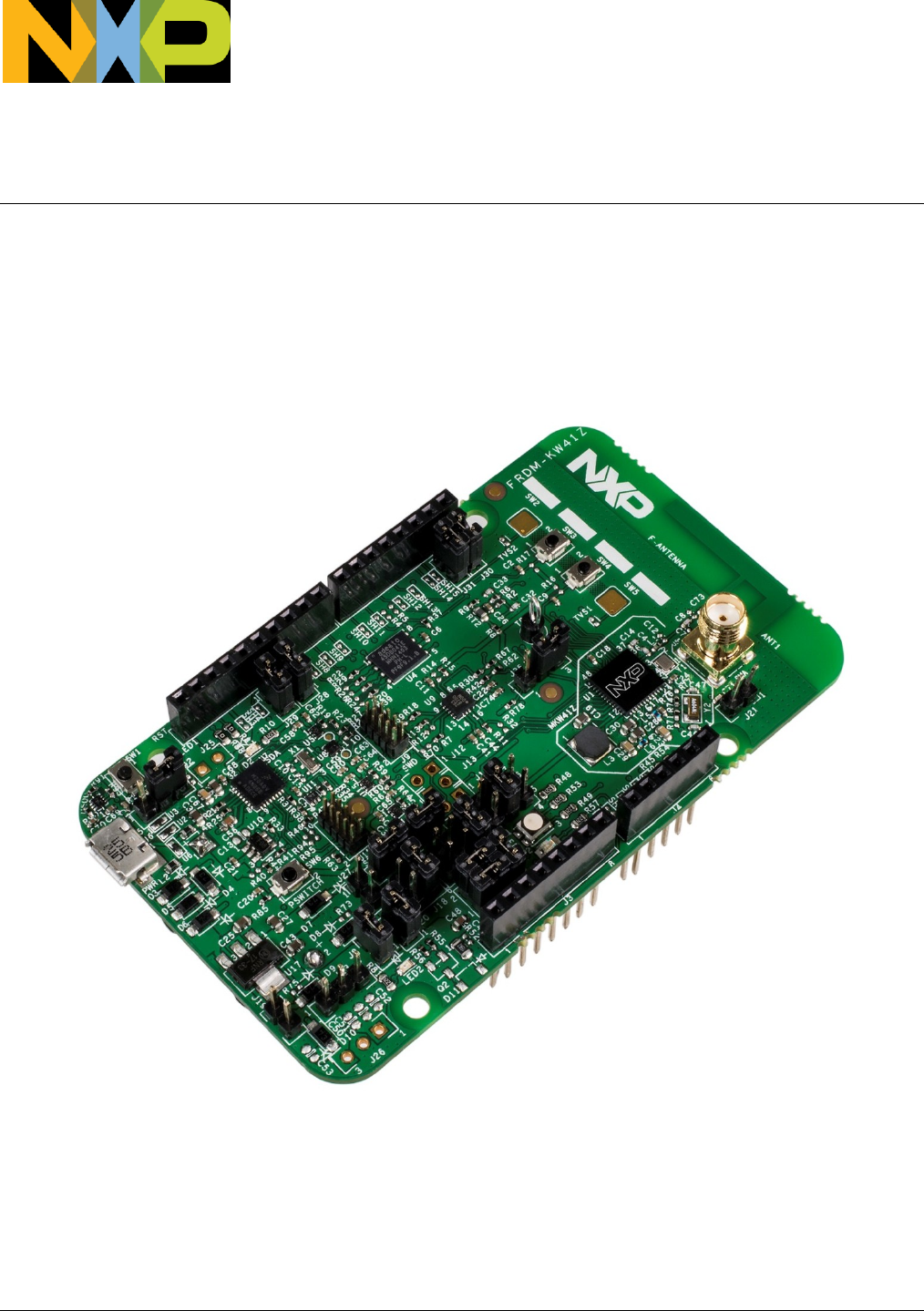
Figure 1: FRDM-KW41Z Freedom development board.

FRDM-KW41Z User’s Guide Page 7 of 11
Draft
The FRDM-KW41Z development board has these features:
• Freescale ultra-low-power MKW41Z SoC BLE/IEEE Std. 802.15.4 platform.
• IEEE Std. 802.15.4, 2006-compliant transceiver supporting 250 kbps O-QPSK data in 5.0 MHz
channels, and full spread-spectrum encoding and decoding.
• Fully compliant Bluetooth v4.2 Low Energy (BLE).
• IEEE 802.15.4-compliant wireless node.
• Reference design area with small-footprint, low-cost RF node.
— Single-ended input/output port.
— Low count of external components.
— Programmable output power from -30 dBm to +3.5 dBm at the SMA connector, no
harmonic trap, with DC/DC Bypass and Buck modes of operation.
— Receiver sensitivity is -100 dBm, typical (@1 % PER for 20-byte payload packet) for
802.15.4 applications, at the SMA connector.
— Receiver sensitivity is -96 dBm (for BLE applications).
• Integrated PCB inverted F-type antenna and SMA RF port.
• Selectable power sources.
• DC-DC converter with Buck, Boost, and Bypass operation modes.
FRDM-KW40Z overview and description
• 32 MHz reference oscillator.
• 32 kHz reference oscillator.
• 2.4 GHz frequency operation (ISM and MBAN).
• External serial flash memory for Over-the-Air Programming (OTAP) support.
• Integrated Open-Standard Serial and Debug Adapter (OpenSDA).
• Cortex 10-pin (0.05) SWD debug port for target MCU.
• Cortex 10-pin (0.05) JTAG port for OpenSDA updates.
•One RGB LED indicator.
• One blue LED indicator.
• Two push-button switches.
• Two TSI buttons.
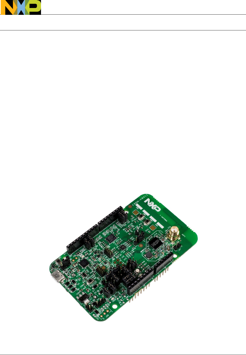
This figure shows the main board features and Input/Output headers for the Freescale FRDM-KW40Z
board:
FRDM-KW41Z User’s Guide Page 8 of 11
Draft
Figure 2: FRDM-KW41Z component placement.
3.3 Serial and Debug Adapter
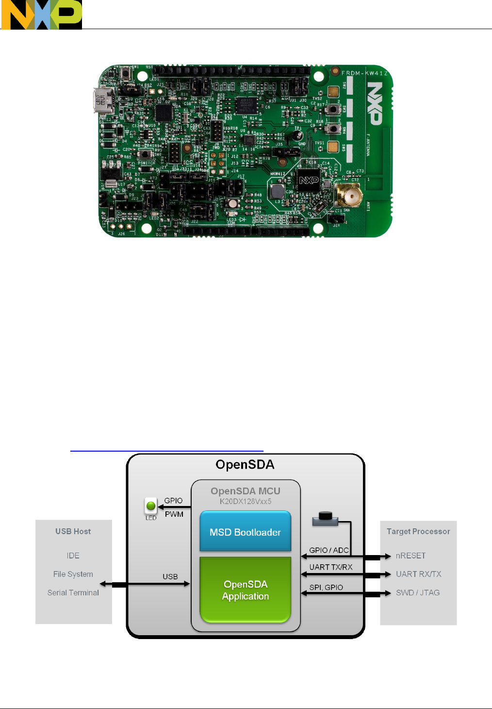
The FRDM-KW41Z development board includes OpenSDA v3.0-a serial and debug adapter circuit that
includes an open-source hardware design, an open-source bootloader, and debug interface software. It
bridges serial and debug communications between a USB host and an embedded target processor as
shown in Figure 3. The hardware circuit is based on a NXP Kinetis K20 family microcontroller (MCU)
with 128 KB of embedded flash and an integrated USB controller. OpenSDAv3.0 comes preloaded with
the DAPLink bootloader - an open-source mass storage device (MSD) bootloader and the DAPLink
Interface firmware, which provides a MSD flash programming interface, a virtual serial port interface,
and a CMSIS-DAP debug protocol interface. For more information on the OpenSDAv3.0 software, see
mbed.org and https://github.com/mbedmicro/DAPLink.
Figure 3: OpenSDAv3.0 high-level block diagram.

FRDM-KW41Z User’s Guide Page 9 of 11
Draft
OpenSDAv3.0 is managed by a Kinetis K20 MCU built on the ARM Cortex-M4 core. The OpenSDAv3.0
circuit includes a status LED (D2) and a pushbutton (SW1). The pushbutton asserts the Reset signal to
the MKW41Z target MCU. It can also be used to place the OpenSDAv3.0 circuit into bootloader mode.
UART and GPIO signals provide an interface to either the SWD debug port or the K20. The
OpenSDAv3.0 circuit receives power when the USB connector J6 is plugged into a USB host.
3.3.1 Virtual serial port
A serial port connection is available between the OpenSDAv3.0 MCU and pins PTC6 and PTC7 of the
MKW41Z.
NOTE
To enable the Virtual COM, Debug, and MSD features, mbed drivers must be installed.
Download the drivers at
https://developer.mbed.org/handbook/Windows-serial-configuration.
4 FRDM-KW41Z development board
4.1 FRDM-KW41Z board overview
The FRDM-KW41Z board is an evaluation board based on Freescale MKW41Z transceiver, and it
provides a platform to evaluate the MKW41Z SoC device and to develop software and applications. The
core device is accompanied by a 32 MHz reference oscillator crystal, RF circuitry (including antenna),
and supporting circuitry.
The FRDM-KW41Z board is intended as the core PCB for MKW41Z device evaluation and application
development, and can be used in the following modes:
• Simple standalone evaluation platform.
• Daughter card for other Freedom development platform boards.
• Mother card for application-specific daughter cards, such as a shield card
4.1.1 PCB features
The FRDM-KW41Z board has these features:
• The NXP Freedom development board form factor.
• Four-layer, metal, 0.062 inches thick FR4 board.
• LGA footprint and power supply (DC-DC converter).
• DC-DC converter with Buck, Boost, and Bypass operation modes.
• Printed-metal F-Antenna or SMA connector (for conducted measurements).
• 32 MHz reference oscillator crystal.
• 32.768 kHz crystal provided for optional timing oscillator.
• Standard Freedom daughter card mounting interface (shield).
FRDM-KW41Z User’s Guide Page 10 of 11
Draft
• External serial flash memory for OTAP support.
• Combo sensor—six-axis sensor with integrated linear accelerometer and magnetometer
4.2 Functional description
The FRDM-KW41Z board is built around NXP MKW41Z SoC in a 48-pin LGA package. It features an IEEE
Std. 802.15.4 and BLE 2.4 GHz radio frequency transceiver and a Kinetis family ultra-low-power, mixed-
signal ARM Cortex-M0+ MCU in a single package. This board is intended as a simple evaluation
platform and as a building block for application development. The four-layer board provides the
MKW41Z SoC with its required RF circuitry, 32 MHz reference oscillator crystal, and power supply with
a DC-DC converter including Bypass, Buck, and Boost modes. The layout for this base-level functionality
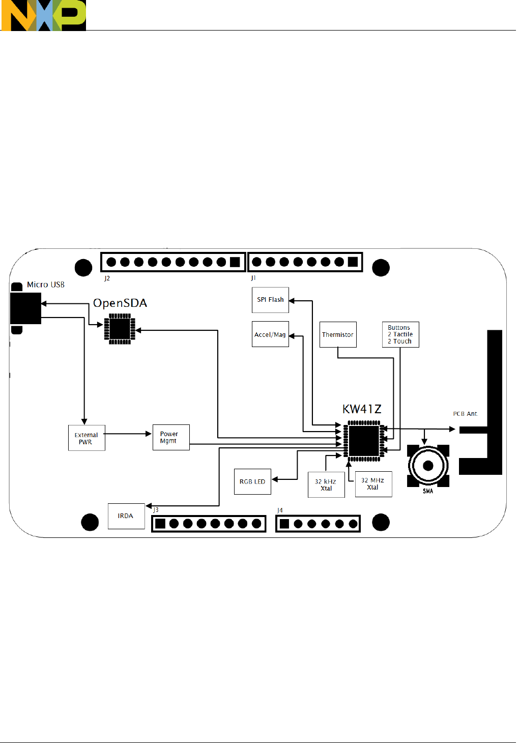
can be used as a reference layout for your target board. This figure shows a simple functional block
diagram:
Figure 4: FRDM-KW41Z block diagram.
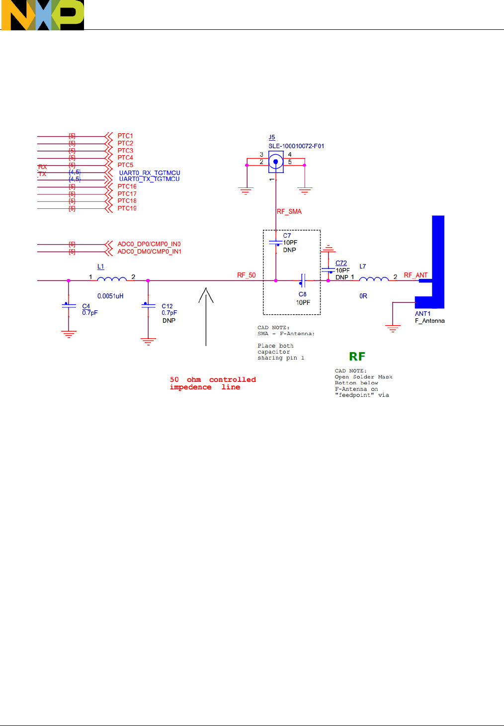
4.2.1 RF performance and considerations
The FRDM-KW41Z board’s integrated transceiver includes a 1 mW nominal output power PA with
internal Voltage-Controlled Oscillator (VCO), integrated transmit/receive switch, on-board power
supply regulation, and full spread-spectrum encoding and decoding. The main specifications of the
MKW41Z SoC are:
• Nominal output power is set to 0 dBm.
• Programmable output power ranges from -30 dBm to +3.5 dBm at the SMA (no harmonic trap).
• Typical sensitivity is -100 dBm (@1 % PER for 25 °C) at the SMA (802.15.4).
• Typical sensitivity is -96 dBm (@1 % PER for 25 °C) at the SMA (BLE).
FRDM-KW41Z User’s Guide Page 11 of 11
Draft
• Differential bidirectional RF input/output port with integrated transmit/receive switch.
• “F” printed-metal antenna for a small-footprint, low-cost design.
• Minimum number of RF marching components
Figure 5: FRDM-KW41Z RF circuit.