NXP Semiconductors JN5169M6V2 ZigBee Modular Transmitter User Manual UM11016
NXP Semiconductors ZigBee Modular Transmitter UM11016
UserManual.wiki
>
NXP Semiconductors
>
JN5169M6V2 User Manual
User Manual.pdf
Navigation menu
Upload a User Manual
Namespaces
Wiki Guide
HTML
PDF
Info
Views
User Manual
Discussion / Help
Navigation

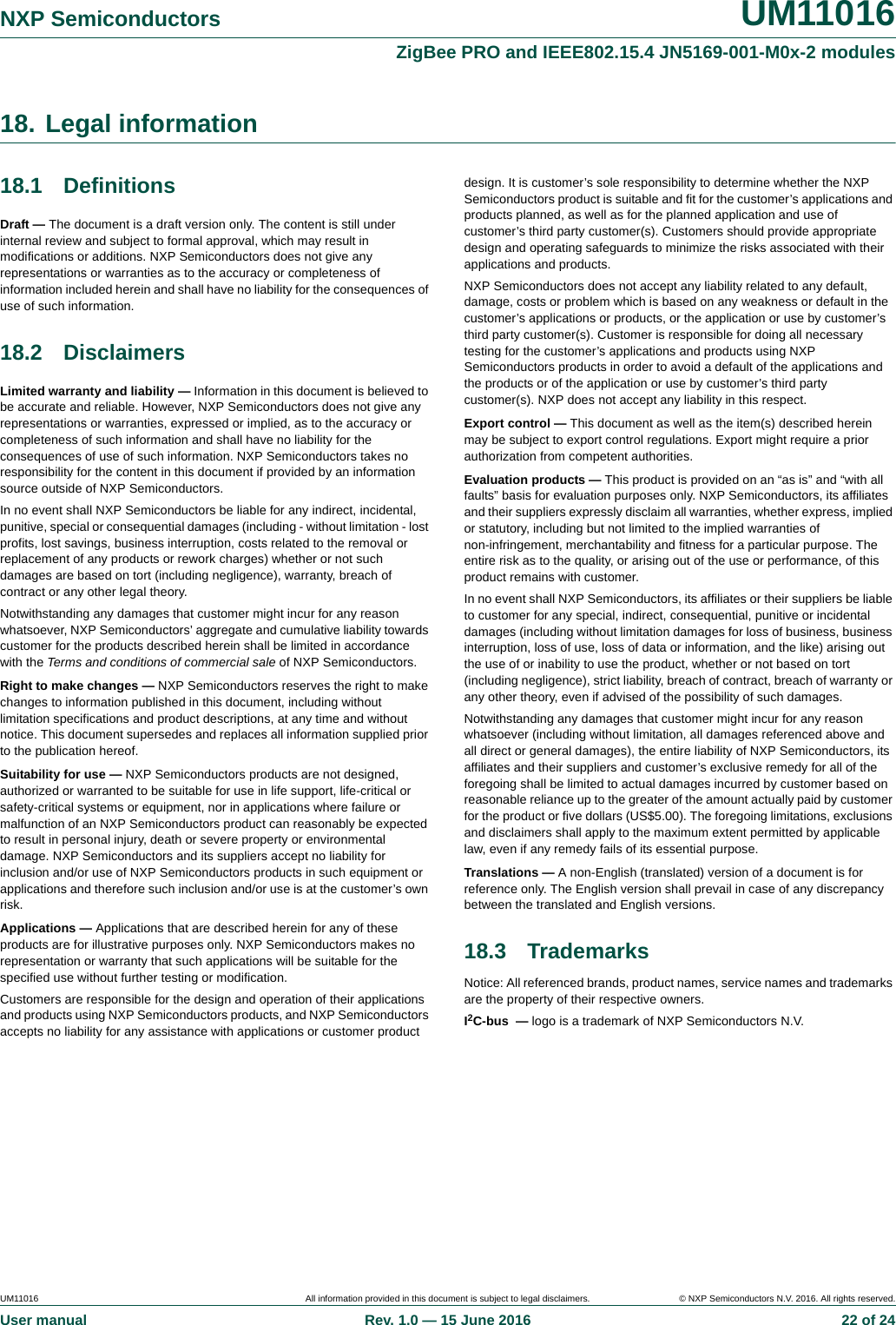
![UM11016 All information provided in this document is subject to legal disclaimers. © NXP Semiconductors N.V. 2016. All rights reserved.User manual Rev. 1.0 — 15 June 2016 6 of 24NXP Semiconductors UM11016ZigBee PRO and IEEE802.15.4 JN5169-001-M0x-2 modulesdevelop and manufacture wireless control or sensing products is to connect a power supply and peripherals such as switches, actuators and sensors, considerably simplifying product development.3 module variants are available:•JN5169-001-M00-2 with an integrated printed antenna•JN5169-001-M03-2 with a FL antenna connector•JN5169-001-M06-2 with a FL antenna connector and also a power amplifier and LNA for extended range5. Marking5.1 JN5169-001-M00-2 and JN5169-001-M03-2 [1] With x = 0 or 3.The JN5169-001-M0x-2 (with x = 0 or 3) family modules meet the requirements of Directive 2002/95/EC of the European Parliament and of the Council on the Restriction of Hazardous Substance (RoHS) and of the Chinese RoHS requirements SJ/T11363-2006 which came into force on 1st March 2007.Fig 1. JN5169-001-M00-2 and JN5169-001-M03-2 packages marking (top view)Table 2. Marking codeLine number Marking codeLine 1 NXP Logo: B&W outline logoLine 2 part ID: JN5169-001-M0x-2[1]Line 3 serial number: NNNNNLine 4 PMC code: ZbHYWWZ: SSMCb: SPILH: Halogen freeY: yearWW: weekLine 5 FCC ID: XXMJN5169MxV2[1]Line 6 IC: 8764A-JN5169Mx[1]JN5169-001-M0x-2(1)FCC ID:XXMJN5169MxV2(1)NNNNNZbHYWWIC: 8764A-JN5169Mx(1)](https://usermanual.wiki/NXP-Semiconductors/JN5169M6V2/User-Guide-3081880-Page-6.png)
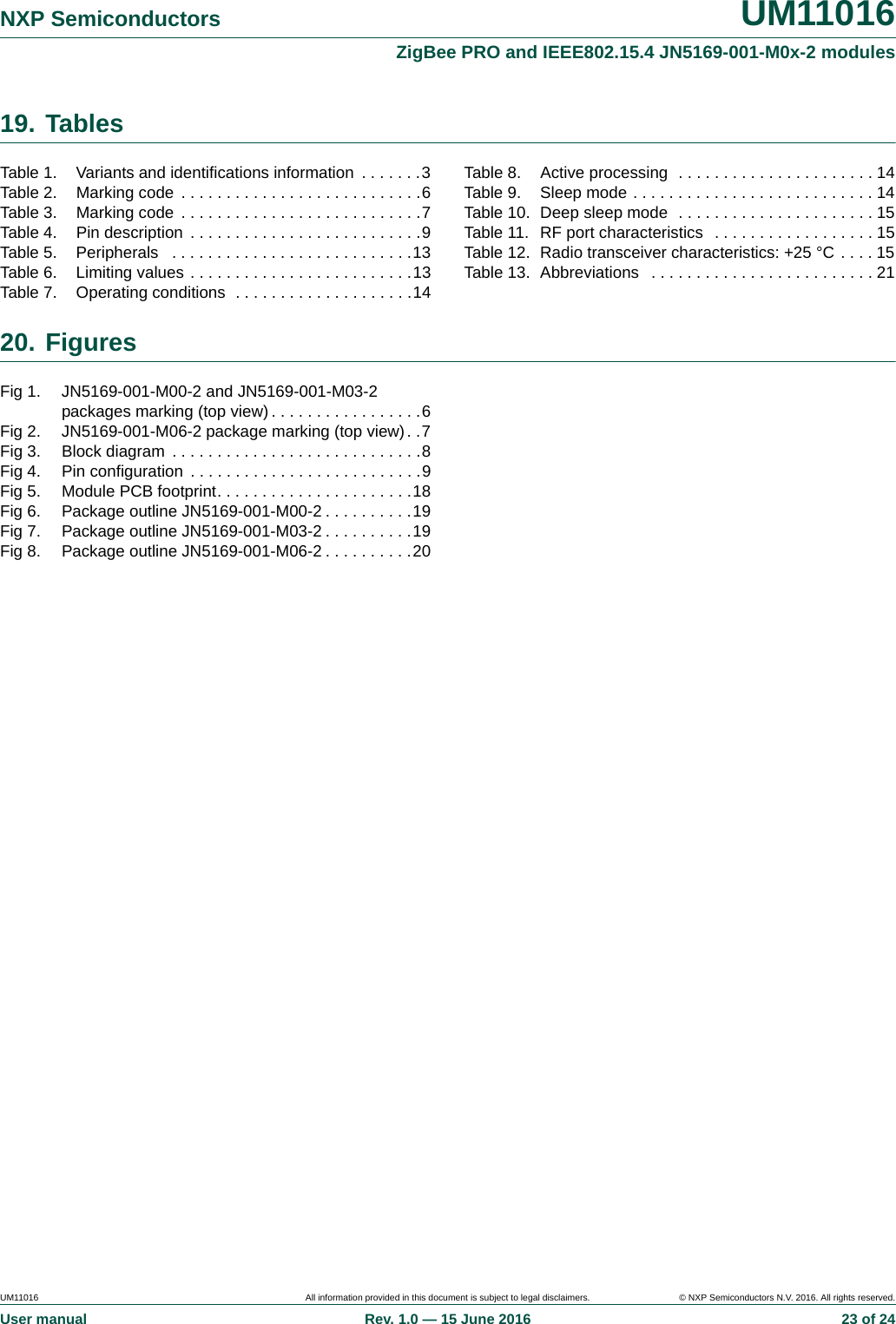
![UM11016 All information provided in this document is subject to legal disclaimers. © NXP Semiconductors N.V. 2016. All rights reserved.User manual Rev. 1.0 — 15 June 2016 9 of 24NXP Semiconductors UM11016ZigBee PRO and IEEE802.15.4 JN5169-001-M0x-2 modules7. Pinning information7.1 Pinning 7.2 Pin description The same basic pin configuration applies for all module designs. However, DIO2 (pin 8) and DIO3 (pin 9) are not available on the JN5169-001-M06-2.(1) Multi-function: DIO12/PWM2/CTS0/JTAG_TCK/ADO/SPISMOSI.(2) Multi-function: DIO13/PWM3/RTS0/JTAG_TMS/ADE/SPISMISO.(3) Multi-function: DIO14/SIF_CLK/TXD0/TXD1/JTAG_TDO/SPISEL1/SPISSEL.(4) Multi-function: DIO15/SIF_D/RXD0/RXD1/JTAG_TDI/SPISEL2/SPISCLK.Fig 4. Pin configuration101112131415161718DIO4/CTS0/JTAG_TCK/TIM0OUT/PC0DIO5/RTS0/JTAG_TMS/PWM1/PC1DIO6/TXD0/JTAG_TDO/PWM2DIO7/RXD0/JTAG_TDI/PWM3DIO8/TIM0CK_GT/PC1/PWM4DIO9/TIM0CAP/32KXTALIN/RXD1/32KINDIO10/TIM0OUT/32KXTALOUTVDDGND123456789272625242322212019VREF/ADC2DIO17/SPISMISO/SIF_D/COMP1M/PWM4DIO16/SPISMISO/SIF_CLK/COMP1PDIO15(4)DIO14(3)RESET_NDIO13(2)DIO12(1)DIO11/PWM1/TXD1ADC1DO0/SPICLK/PWM2DO1/SPIMISO/PWM3DIO18/SPIMOSIDIO19/SPISEL0DIO0/ADO/SPISEL1/ADC3DIO1/ADE/SPISEL2/ADC4/PC0DIO2/RFRX/TIM0CK_GT/ADC5DIO3/RFTX/TIM0CAP/ADC6Transparent top viewTable 4. Pin descriptionSymbol Pin Type[1] DescriptionADC1 1 I ADC1 — ADC input](https://usermanual.wiki/NXP-Semiconductors/JN5169M6V2/User-Guide-3081880-Page-9.png)
![UM11016 All information provided in this document is subject to legal disclaimers. © NXP Semiconductors N.V. 2016. All rights reserved.User manual Rev. 1.0 — 15 June 2016 10 of 24NXP Semiconductors UM11016ZigBee PRO and IEEE802.15.4 JN5169-001-M0x-2 modulesDO0/SPICLK/PWM2[2] 2O DO0 — DO0SPICLK — SPI-bus master clock outputPWM2 — PWM2 outputDO1/SPIMISO/PWM3[3] 3I/O DO1 — DO1SPIMISO — SPI-bus Master In, Slave Out inputPWM3 — PWM3 outputDIO18/SPIMOSI 4 I/O DIO18 — DIO18SPIMOSI — SPI-bus Master Out Slave In outputDIO19/SPISEL0 5 I/O DIO19 — DIO19SPISEL0 — SPI-bus Master Select Output 0DIO0/ADO/SPISEL1/ADC3 6 I/O DIO0 — DIO0ADO — antenna diversity odd outputSPISEL1 — SPI-bus master select output 1ADC3 — ADC input: ADC3DIO1/ADE/SPISEL2/ADC4/PC0 7 I/O DIO1 — DIO1ADE — antenna diversity even outputSPISEL2 — SPI-bus master select output 2ADC4 — ADC input: ADC4PC0 — pulse counter 0 inputDIO2/RFRX/TIM0CK_GT/ADC5[4] 8I/O DIO2 — DIO2RFRX — radio receives control outputTIM0CK_GT — timer0 clock/gate inputADC5 — ADC input: ADC5DIO3/RFTX/TIM0CAP/ADC6[4] 9I/O DIO3 — DIO3RFTX — radio transmit control outputTIM0CAP — timer0 capture inputADC6 — ADC input: ADC6DIO4/CTS0/JTAG_TCK/TIM0OUT/PC0 10 I/O DIO4 — DIO4CTS0 — UART 0 clear to send inputJTAG_TCK — JTAG CLK inputTIM0OUT — timer0 PWM outputPC0 — pulse counter 0 inputDIO5/RTS0/JTAG_TMS/PWM1/PC1 11 I/O DIO5 — DIO5RTS0 — UART 0 request to send outputJTAG_TMS — JTAG mode select inputPWM1 — PWM1 outputPC1 — pulse counter 1 inputDIO6/TXD0/JTAG_TDO/PWM2 12 I/O DIO6 — DIO6TXD0 — UART 0 transmit data outputJTAG_TDO — JTAG data outputPWM2 — PWM2 data outputTable 4. Pin description …continuedSymbol Pin Type[1] Description](https://usermanual.wiki/NXP-Semiconductors/JN5169M6V2/User-Guide-3081880-Page-10.png)
![UM11016 All information provided in this document is subject to legal disclaimers. © NXP Semiconductors N.V. 2016. All rights reserved.User manual Rev. 1.0 — 15 June 2016 11 of 24NXP Semiconductors UM11016ZigBee PRO and IEEE802.15.4 JN5169-001-M0x-2 modulesDIO7/RXD0/JTAG_TDI/PWM3 13 I/O DIO7 — DIO7RXD0 — UART 0 receive data inputJTAG_TDI — JTAG data inputPWM3 — PWM 3 data outputDIO8/TIM0CK_GT/PC1/PWM4 14 I/O DIO8 — DIO8TIM0CK_GT — timer0 clock/gate inputPC1 — pulse counter1 inputPWM4 — PWM 4 outputDIO9/TIM0CAP/32KXTALIN/RXD1/32KIN 15 I/O DIO9 — DIO9TIM0CAP — Timer0 Capture input32KXTALIN — 32 kHz External Crystal inputRXD1 — UART1 Receive Data input32KIN — 32 kHz External clock inputDIO10/TIM0OUT/32KXTALOUT 16 I/O DIO10 — DIO10TIM0OUT — Timer0 PWM Output32KXTALOUT — 32 kHz External Crystal outputVDD 17 P VDD — supply voltageGND 18 GND groundDIO11/PWM1/TXD1 19 I/O DIO11 — DIO11PWM1 — PWM1 outputTXD1 — UART1 Transmit Data outputDIO12[5] 20 I/O DIO12 — DIO12PWM2 — PWM2 outputCTS0 — UART0 clear to send inputJTAG_TCK — JTAG CLK inputADO — antenna diversity odd outputSPISMOSI — SPI-bus slave Master Out, Slave In inputDIO13[6] 21 I/O DIO13 — DIO13PWM3 — PWM3 outputRTS0 — UART0 request to send outputJTAG_TMS — JTAG mode select inputADE — antenna diversity even outputSPISMISO — SPI-bus slave master in slave out outputRESET_N 22 I RESET_N — reset inputDIO14[7] 23 I/O DIO14 — DIO14SIF_CLK — serial interface clockTXD0 — UART 0 transmit data outputTXD1 — UART 1 transmit data outputJTAG_TDO — JTAG data outputSPISEL1 — SPI-bus master select output 1SPISSEL — SPI-bus slave select inputTable 4. Pin description …continuedSymbol Pin Type[1] Description](https://usermanual.wiki/NXP-Semiconductors/JN5169M6V2/User-Guide-3081880-Page-11.png)
![UM11016 All information provided in this document is subject to legal disclaimers. © NXP Semiconductors N.V. 2016. All rights reserved.User manual Rev. 1.0 — 15 June 2016 12 of 24NXP Semiconductors UM11016ZigBee PRO and IEEE802.15.4 JN5169-001-M0x-2 modules[1] P = power supply; G = ground; I = input, O = output; I/O = input/output.[2] JTAG programming mode: must be left floating high during reset to avoid entering JTAG programming mode.[3] UART programming mode: leave pin floating high during reset to avoid entering UART programming mode or hold it low to program.[4] Not available on the JN5169-001-M06-2 since they are used to control the front-end module.[5] Multi-function: DIO12/PWM2/CTS0/JTAG_TCK/ADO/SPISMOSI.[6] Multi-function: DIO13/PWM3/RTS0/JTAG_TMS/ADE/SPISMISO.[7] Multi-function: DIO14/SIF_CLK/TXD0/TXD1/JTAG_TDO/SPISEL1/SPISSEL.[8] Multi-function: DIO15/SIF_D/RXD0/RXD1/JTAG_TDI/SPISEL2/SPISCLK.8. Functional description8.1 JN5169 single chip wireless microcontrollerThe JN5169-001-M0x-2 is constructed around the JN5169-001 single chip wireless microcontroller, which includes the radio system, a 32-bit RISC CPU, Flash, RAM and EEPROM memory and a range of analogue and digital peripherals.The chip is described fully in JN5169 Wireless Microcontroller Datasheet (see Ref. 2).DIO15[8] 24 I/O DIO15 — DIO15SIF_D — serial interface dataRXD0 — UART 0 receive data inputRXD1 — UART 1 receive data inputJTAG_TDI — JTAG data inputSPISEL2 — SPI-bus master select output 2SPISCLK — SPI-bus slave clock inputDIO16/SPISMOSI/SIF_CLK/COMP1P 25 I/O DIO16 — DIO16COMP1P — comparator positive inputSIF_CLK — Serial Interface clockSPISMOSI — SPI-bus Slave Master Out Slave In inputDIO17/SPISMISO/SIF_D/COMP1M 26 I/O DIO17 — DIO17COMP1M — COMP1M; comparator negative inputSIF_D — Serial Interface DataSPISMISO — SPI-bus Slave Master In Slave Out outputPWM4 — PWM 4 outputVREF/ADC2 27 P VREF — analog peripheral reference voltageIADC2 — ADC input 2Table 4. Pin description …continuedSymbol Pin Type[1] Description](https://usermanual.wiki/NXP-Semiconductors/JN5169M6V2/User-Guide-3081880-Page-12.png)
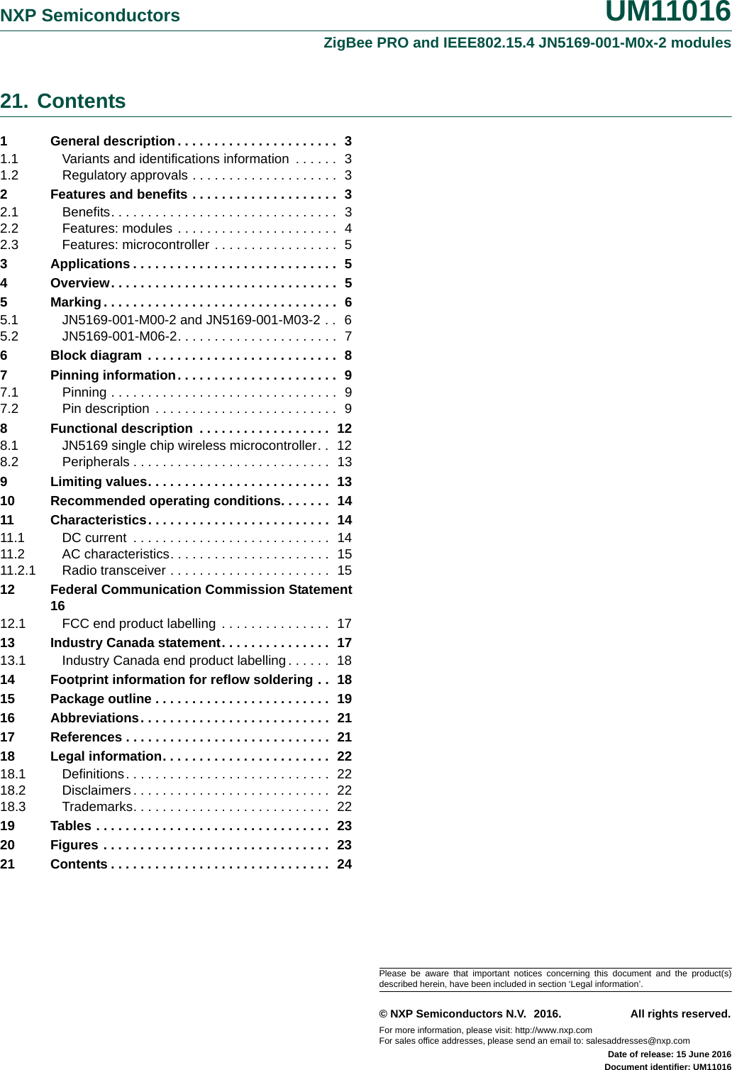
![UM11016 All information provided in this document is subject to legal disclaimers. © NXP Semiconductors N.V. 2016. All rights reserved.User manual Rev. 1.0 — 15 June 2016 14 of 24NXP Semiconductors UM11016ZigBee PRO and IEEE802.15.4 JN5169-001-M0x-2 modules10. Recommended operating conditions [1] To reach the maximum TX power, 2.8 V is the minimum.11. Characteristics11.1 DC current [1] To reach the maximum TX power, 2.8 V is the minimum. VIO(dig) digital input/output voltage 0.3 VDDD + 0.3V VTstg storage temperature 40 +150 CVESD electrostatic discharge voltage according to ETSI EN 301 489-17 2012 V2.2.1 and ETSI EN 301 489-1 2011 V1.9.24- kVTable 6. Limiting values …continuedSymbol Parameter Conditions Min Max UnitTable 7. Operating conditionsSymbol Parameter Conditions Min Max UnitVDD supply voltage [1] 23.6VTamb ambient temperature standard range 40 +85 CTable 8. Active processingVDD = 2 V to 3.6 V; Tamb =40C to +85C; unless otherwise specified.Symbol Parameter Conditions Min Typ Max UnitIDD supply current M00radio in receive mode; maximum input level at 10 dBm - 17.8 - mAradio in receive mode; maximum input level at 0 dBm - 16.7 - mAradio in transmit mode 10 dBm [1] - 27.2 - mAradio in transmit mode 8.5 dBm [1] - 23.6 - mAM03radio in receive mode; maximum input level at 10 dBm - 17.8 - mAradio in receive mode; maximum input level at 0 dBm - 16.7 - mAradio in transmit mode 10 dBm [1] - 27.2 - mAradio in transmit mode 8.5 dBm [1] - 23.6 - mAM06radio in receive mode - 22.8 - mAradio in transmit mode [1] - 181 - mATable 9. Sleep modeVDD = 2 V to 3.6 V; Tamb =40C to +85C; unless otherwise specified.Symbol Parameter Conditions Min Typ Max UnitIDD(IO) input/output supply current in sleep mode; with I/O and RC oscillator timer wake-up; Tamb =25C-0.73-A](https://usermanual.wiki/NXP-Semiconductors/JN5169M6V2/User-Guide-3081880-Page-14.png)
![UM11016 All information provided in this document is subject to legal disclaimers. © NXP Semiconductors N.V. 2016. All rights reserved.User manual Rev. 1.0 — 15 June 2016 15 of 24NXP Semiconductors UM11016ZigBee PRO and IEEE802.15.4 JN5169-001-M0x-2 modules [1] Waiting on chip RESET or I/O event.11.2 AC characteristics11.2.1 Radio transceiverThese modules meet all the requirements of the IEEE802.15.4 standard over 2.0 V to 3.6 V and offers the improved RF characteristics shown in Table 11. All RF characteristics are measured single ended. [1] With external matching inductors and assuming PCB layout. Table 10. Deep sleep modeVDD = 2 V to 3.6 V; Tamb =40C to +85C; unless otherwise specified.Symbol Parameter Conditions Min Typ Max UnitIDD supply current deep sleep mode; measured at 25 C[1] -70-nATable 11. RF port characteristicsSingle-ended; Impedance = 50 [1]; VDD = 2 V to 3.6 V; Tamb =40C to +85C; unless otherwise specified.Symbol Parameter Conditions Min Typ Max Unitfrange frequency range 2.4 - 2.485 GHzTable 12. Radio transceiver characteristics: +25 CVDD = 2 V to 3.6 V; unless otherwise specified.Symbol Parameter Conditions Min Typ Max UnitReceiverM00SRX receiver sensitivity nominal for 1 % PER, as per 802.15.4 - 96.5 - dBmPi(RX)(max) maximum receiver input power 1 % PER, measured as sensitivity; supply current at 17.8 mA -10-dBm1 % PER, measured as sensitivity; supply current at 16.2 mA -0-dBmRSSI RSSI variation 95 dBm to 10 dBm; available through UM11016 Integrated Peripherals API4- +4dBM03SRX receiver sensitivity nominal for 1 % PER, as per 802.15.4 - 96.5 - dBmPi(RX)(max) maximum receiver input power 1 % PER, measured as sensitivity; supply current at 17.8 mA -10-dBm1 % PER, measured as sensitivity; supply current at 16.2 mA -0-dBmRSSI RSSI variation 95 dBm to 10 dBm; available through UM11016 Integrated Peripherals API4- +4dBM06SRX receiver sensitivity nominal for 1 % PER, as per 802.15.4 - 100 - dBmPi(RX)(max) maximum receiver input power 1 % PER, measured as sensitivity - 5 - dBmRSSI RSSI variation 100 dBm to 25 dBm; available through UM11016 Integrated Peripherals API4- +4dBTransmitter](https://usermanual.wiki/NXP-Semiconductors/JN5169M6V2/User-Guide-3081880-Page-15.png)
![UM11016 All information provided in this document is subject to legal disclaimers. © NXP Semiconductors N.V. 2016. All rights reserved.User manual Rev. 1.0 — 15 June 2016 16 of 24NXP Semiconductors UM11016ZigBee PRO and IEEE802.15.4 JN5169-001-M0x-2 modules[1] To reach the maximum TX power, 2.8 V is the minimum on VDD.[2] Up to an extra 2.5 dB of attenuation is available if required.12. Federal Communication Commission Statement•This equipment has been tested and found to comply with the limits for a Class Bdigital device, pursuant to Part 15 of the FCC Rules see Ref. 4. These limits aredesigned to provide reasonable protection against harmful interference in aresidential installation. This equipment generates, uses, and can radiate radiofrequency energy and, if not installed and used in accordance with the instructions,may cause harmful interference to radio communications. However, there is noguarantee that interference will not occur in a particular installation. If this equipmentdoes cause harmful interference to radio or television reception, which can bedetermined by turning the equipment off and on, the user is encouraged to try tocorrect the interference by one of the following measures:–Reorient or relocate the receiving antenna–Increase the separation between the equipment and receiver–Connect the equipment into an outlet on a circuit different from that to which thereceiver is connected–Consult the dealer or an experienced radio/TV technician for help•OEM integrators instructions–The OEM integrators are responsible for ensuring that the end-user has no manualinstructions to remove or install module–The module is limited to installation in mobile or fixed applications, according toCFR 47 Part 2.1091(b)–Separate approval is required for all other operating configurations, includingportable configurations with respect to CFR 47 Part 2.1093 and different antennaconfigurations•User guide mandatory statementsM00Pooutput power IDD = 27.2 mA [1] -10-dBmIDD = 23.6 mA [1] -8.5-dBmPo(cr) control range output power in 6 major steps and then 4 fine steps [2] -42 - dBM03Pooutput power IDD = 27.2 mA [1] -10-dBmIDD = 23.6 mA [1] -8.5-dBmPo(cr) control range output power in 6 major steps and then 4 fine steps [2] -42 - dBM06Pooutput power [1] -21-dBmTable 12. Radio transceiver characteristics: +25 C …continuedVDD = 2 V to 3.6 V; unless otherwise specified.Symbol Parameter Conditions Min Typ Max Unit](https://usermanual.wiki/NXP-Semiconductors/JN5169M6V2/User-Guide-3081880-Page-16.png)

![UM11016 All information provided in this document is subject to legal disclaimers. © NXP Semiconductors N.V. 2016. All rights reserved.User manual Rev. 1.0 — 15 June 2016 21 of 24NXP Semiconductors UM11016ZigBee PRO and IEEE802.15.4 JN5169-001-M0x-2 modules16. Abbreviations 17. References[1] IEEE Std 802.15.4-2011 — IEEE Std 802.15.4-2011 IEEE Standard for Information Technology.[2] JN5169 — JN5169 wireless microcontroller datasheet.[3] Wireless Connectivity — http://www.nxp.com/products/interface-and-connectivity/wireless-connectivity:WIRELESS-CONNECTIVITY[4] Part 15 of the FCC Rules — http://www.ecfr.gov/cgi‐bin/text‐idx?SID=d01e00935bfcb0d53b914e7c8e63f383&node=47:1.0.1.1.16&rgn=div5Table 13. AbbreviationsAcronym DescriptionAPI Application Program InterfaceADC Analog to Digital ConverterFCC Federal Communication CommissionIO Input OutputOEM Original Equipment ManufacturerPCB Printed Circuit BoardPER Packet Error RatePWM Pulse Width ModulationR&TTE Radio and Telecommunications Terminal EquipmentRF Radio FrequencyRISC Reduce Instruction Set ComputingRSSI Receive Signal Strength IndicatorRTS Request-To-SendSPI Serial Peripheral InterfaceSVM Supply Voltage MonitorSYNTH SYNTHesizerUART Universal Asynchronous Receiver/Transmitter](https://usermanual.wiki/NXP-Semiconductors/JN5169M6V2/User-Guide-3081880-Page-21.png)