NXP Semiconductors JN5169U0 Wireless microcontroller suitable for Zigbee applications User Manual UM10929
NXP Semiconductors Wireless microcontroller suitable for Zigbee applications UM10929
User Manual

UM10929
JN5169-USB-Dongle User Manual
Rev. 1.1 — 30 November 2015
User manual
Document information
Info
Content
Keywords
JN5169, ZigBee, dongle, USB
Abstract
JN5169 USB dongle user manual

NXP Semiconductors
UM10929
JN5169-USB-Dongle User Manual
UM10929
All information provided in this document is subject to legal disclaimers.
© NXP Semiconductors N.V. 2014. All rights reserved.
User manual
Rev. 1.1 — 30 November 2015
2 of 14
Contact information
For more information, please visit: http://www.nxp.com
Revision history
Rev
Date
Description
1.0
20150728
First release
1.1
20151130
Session 4: updated.
NXP Semiconductors
UM10929
JN5169-USB-Dongle User Manual
UM10929
All information provided in this document is subject to legal disclaimers.
© NXP Semiconductors N.V. 2014. All rights reserved.
User manual
Rev. 1.1 — 30 November 2015
3 of 14
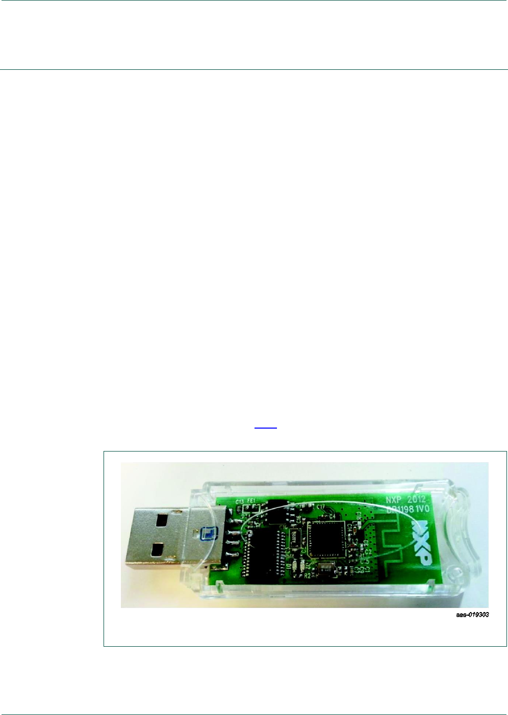
1. Introduction
This chapter introduces the NXP JN5169 USB Dongle (DR1198), which provides a
hardware development platform for wireless microcontroller applications with a USB
interface.
1.1 Overview
The JN5169 USB Dongle features a JN5169 wireless microcontroller and allows
communication with this JN5169 device from a USB connection. The JN5169 device can
act as a node of a wireless network. Thus, the dongle provides an easy way of
interfacing a host machine (such as a PC) to a wireless network based on the
IEEE802.15.4, ZigBee Smart Energy or ZigBee-Home Automation networking protocol.
An FTDI device provides the USB connection between the host machine and the JN5169
device, which in turn provides the radio interface to the wireless network.
Typical uses of the dongle include:
A complete and stable hardware environment for the development of
IEEE802.15.4, ZigBee Smart Energy and ZigBee-Home Automation networking
applications, facilitating an accelerated time-to-market for wireless network
products
The basis of a packet sniffer for IEEE 802.15.4-based wireless communications
A means of integrating the host machine into a wireless network, typically as the
network Coordinator
The small-footprint PCB of the dongle provides all the necessary components for a
wireless microcontroller with access to a USB connection. All RF layout and decoupling
issues are handled by the design of this dongle. Therefore, this design is ready for
application development without the necessity of hardware development.
The JN5168 USB dongle, shown Fig 1, is supplied in the JN5169-EK004 Evaluation Kit.
Fig 1. JN5169 USB dongle (DR1198)
NXP Semiconductors
UM10929
JN5169-USB-Dongle User Manual
UM10929
All information provided in this document is subject to legal disclaimers.
© NXP Semiconductors N.V. 2014. All rights reserved.
User manual
Rev. 1.1 — 30 November 2015
4 of 14
1.2 Features
The dongle has the following features:
USB 2.0 Full-Speed Compatible Interface
IEEE 802.15.4-based wireless microcontroller (JN5169) with the following radio
characteristics:
o Transmit power: 8.5 dBm (typ.), can be increased to 10 dBm (typ.)
o Transmit current: 19.6 mA (typ) at 8.5 dBm / 23.3 mA (typ.) at 10 dBm
o Receive sensitivity: 96dBm (typ.)
o Receive current: 13 mA (typ.)
Integrated printed RF antenna
General-purpose LEDs (one green, one orange)
Serial Flash memory device (4 Mbits)
32-kHz crystal oscillator
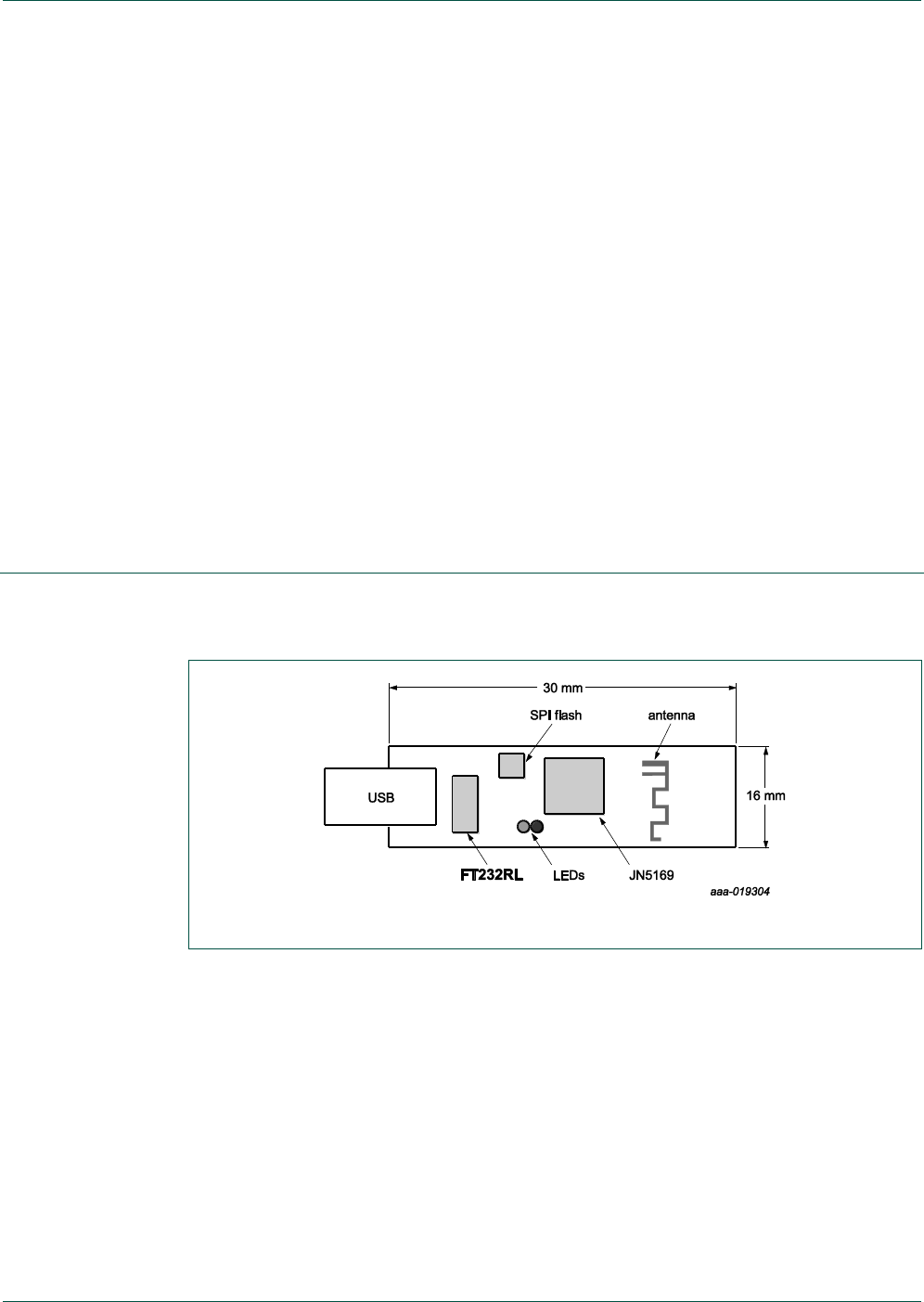
2. Hardware overview
2.1 Dongle layout
Fig 2. DR1198 board layout
NXP Semiconductors
UM10929
JN5169-USB-Dongle User Manual
UM10929
All information provided in this document is subject to legal disclaimers.
© NXP Semiconductors N.V. 2014. All rights reserved.
User manual
Rev. 1.1 — 30 November 2015
5 of 14
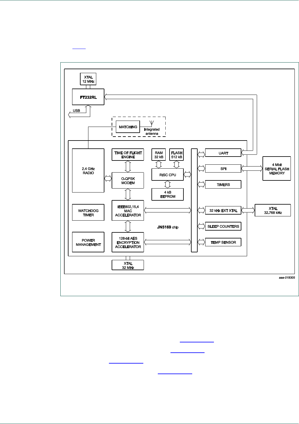
2.2 Dongle block diagram
The Fig 3 illustrates the main hardware blocks of the dongle.
Fig 3. JN5169 USB dongle hardware blocks
2.3 Hardware components
The hardware components on the board are described in the following sub-sections.
JN5169 wireless microcontroller – see section 2.3.1
FTDI FT232RL driver device – see section 2.3.2
LEDs – see section 2.3.3
32-kHz crystal oscillator – see section 2.3.4
2.3.1 JN5169 device
The JN5169 circuit on the board is based around the standard JN5169-001-M00 module.
However, it is built on a 2-layer board, as the DIOs do not need to be externally available.
The JN5169 device uses an integrated antenna on the PCB of the dongle.

NXP Semiconductors
UM10929
JN5169-USB-Dongle User Manual
UM10929
All information provided in this document is subject to legal disclaimers.
© NXP Semiconductors N.V. 2014. All rights reserved.
User manual
Rev. 1.1 — 30 November 2015
6 of 14
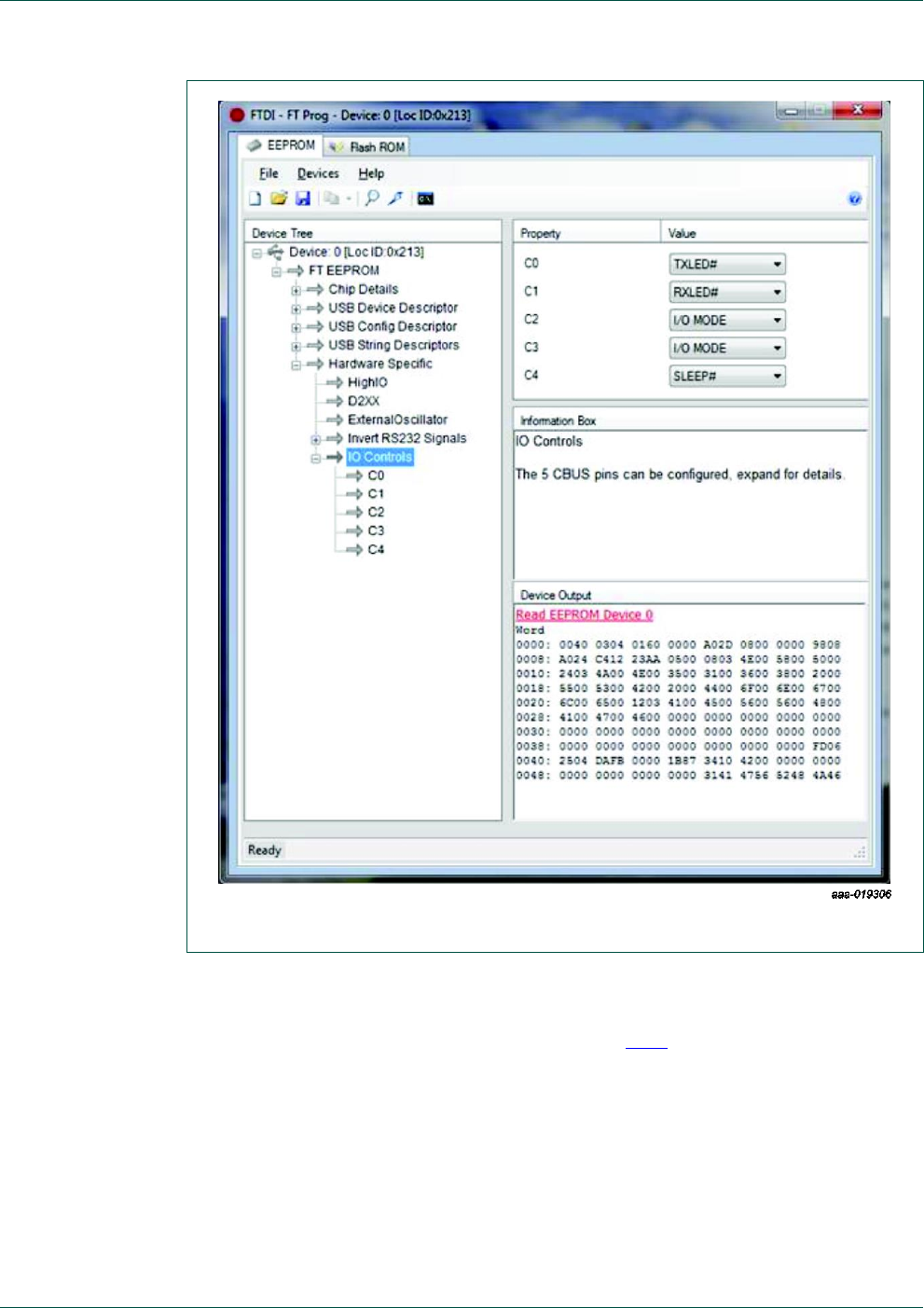
2.3.2 FT232RL device
The FT232RL device is connected to the USB connector and acts as an interface
between the PC and the JN5169 device. The FT232RL will enumerate on the PC as a
virtual COM port connected directly to UART0 on the JN5169 device.
The IO controls C2 and C3 in the FT232RL device need to be set to ’I/O Mode’ to allow
the RESET and PGM signals to operate correctly. To do this, execute the following
instructions.
1. Download the application FT_Prog from the FTDI website www.ftdichip.com
2. Insert the JN5169 USB Dongle into a USB port of your computer and wait for the
device to enumerate
3. Start FT_Prog and click Scan and Parse (the magnifying glass button)
4. Update the IO controls C2 and C3 to I/O MODE – see Fig 4
NXP Semiconductors
UM10929
JN5169-USB-Dongle User Manual
UM10929
All information provided in this document is subject to legal disclaimers.
© NXP Semiconductors N.V. 2014. All rights reserved.
User manual
Rev. 1.1 — 30 November 2015
7 of 14
Fig 4. IO controls window
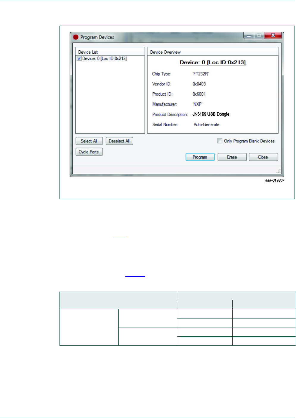
5. Click Program Devices (the lightning button)
6. On the resulting screen, click Program – see Fig 5
NXP Semiconductors
UM10929
JN5169-USB-Dongle User Manual
UM10929
All information provided in this document is subject to legal disclaimers.
© NXP Semiconductors N.V. 2014. All rights reserved.
User manual
Rev. 1.1 — 30 November 2015
8 of 14
Fig 5. Program devices window
2.3.3 LEDs
There are two surface-mounted LEDs that can be controlled by the JN5169 wireless
microcontroller (see Fig 2 for locations):
LED D1 (green)
LED D2 (orange)
Both LEDs are connected to DIO16 and DIO17. These DIOs can be used to control the
LEDs as indicated in the Table 1.
Table 1. DIO control of LEDs
DIO17
Low
High
DIO16
Low
D1: Off
D1: Off
D2: Off
D2: On
High
D1: On
D1: Off
D2: Off
D2: Off
2.3.4 32-kHz crystal oscillator
The JN5169 device has an internal 32-kHz RC oscillator. In order to provide more
accurate system timings, an external 32-kHz crystal can be used with the device. This is
provided on the JN5169 USB dongle and can be enabled from the JN5169 application
using the JN5169 Integrated Peripherals API - refer to the JN5169 Integrated Peripherals
API User Guide (JN-UG-3087).

NXP Semiconductors
UM10929
JN5169-USB-Dongle User Manual
UM10929
All information provided in this document is subject to legal disclaimers.
© NXP Semiconductors N.V. 2014. All rights reserved.
User manual
Rev. 1.1 — 30 November 2015
9 of 14
3. Flash programming
When the JN5169 USB dongle is powered up, it attempts to run an application from the
internal Flash memory of the JN5169 device. This may be a self-contained application
that sends and receives wireless data, and which does not need to communicate with the
host. Alternatively, it may communicate via the USB with an application running on the
host, such as a Windows program, and also communicate with a wireless device or
network.
In order to program an application binary into Flash memory, the JN51xx Production
Flash Programmer can be used, which is described in the JN51xx Production Flash
Programmer User Guide (JN-UG-3099). This programming utility will place the JN5169
into its programming mode. It will then download the program to the Flash memory and
reset the JN5169 device, causing the application to be executed.
4. Compliance statements and documentation
The FCC ID number of the JN5169 USB dongle is XXMJN5169U0
The IC ID number of the JN5169 USB dongle is 8764A-JN5169U0
4.1 FCC statements and documentation
This section contains the Federal Communication Commission (FCC) statements and
documents.
4.1.1 FCC interference statement
This equipment has been tested and found to comply with the limits for a Class B digital
device, pursuant to Part 15 of the FCC Rules. These limits are designed to provide
reasonable protection against harmful interference in a residential installation. This
equipment generates, uses, and can radiate radio frequency energy and, if not installed
and used in accordance with the instructions, may cause harmful interference to radio
communications. However, there is no guarantee that interference will not occur in a
particular installation. If this equipment does cause harmful interference to radio or
television reception, which can be determined by turning the equipment off and on, the
user is encouraged to try to correct the interference by one of the following measures:
Reorient or relocate the receiving antenna
Increase the separation between the equipment and receiver
Connect the equipment into an outlet on a circuit different from that to which the
receiver is connected
Consult the dealer or an experienced radio/TV technician for help
This device complies with Part 15 of the FCC rules. Operation is subject to the following
two conditions: (1) This device may not cause harmful interference, and (2) this device
must accept any interference received, including interference that may cause undesired
operation.
FCC caution: Any changes or modifications not expressly approved by the party
responsible for compliance could void the user's authority to operate this equipment.
NXP Semiconductors
UM10929
JN5169-USB-Dongle User Manual
UM10929
All information provided in this document is subject to legal disclaimers.
© NXP Semiconductors N.V. 2014. All rights reserved.
User manual
Rev. 1.1 — 30 November 2015
10 of 14
WARNING!
FCC radiation exposure statement:
This portable equipment with its integrated antenna complies with FCC’s RF radiation
exposure limits set forth for an uncontrolled environment. To maintain compliance follow
the instructions below;
Avoid direct contact to the antenna, or keep it to a minimum while using this equipment.
4.2 Industry Canada statement
This device complies with Industry
Canada license-exempt RSS
standard(s). Operation is subject to the
following two conditions: (1) this device
may not cause interference, and (2) this
device must accept any interference,
including interference that may cause
undesired operation of the device.
Le présent appareil est conforme aux
CNR d'Industrie Canada applicables
aux appareils radio exempts de licence.
L'exploitation est autorisée aux deux
conditions suivantes : (1) l'appareil ne
doit pas produire de brouillage, et (2)
l'utilisateur de l'appareil doit accepter
tout brouillage radioélectrique subi,
même si le brouillage est susceptible
d'en compromettre le fonctionnement.
5. Abbreviations
Table 2. Abbreviations
Acronym
Description
BOM
Bill Of Materials
DIO
Digital Input/Output
FCC
Federal Communication Commission
IC
Industry Canada
PCB
Printed Circuit Board
UART
Universal Asynchronous Receiver/Transmitter
USB
Universal Serial Bus
6. References
[1] JN5169 JN5169 Data Sheet
[2] JN-UG-3087 JN516x Integrated Peripherals API User Guide
[3] DR1198_JN5168_USB_Dongle_1V0 DR1198 USB dongle PCB files

Error!
Unknown
documen
t property
name.
Error! Unknown document property name.
Error! Unknown document property
name.
NXP Semiconductors
UM10929
JN5169-USB-Dongle User Manual
UM10929
All information provided in this document is subject to legal disclaimers.
© NXP Semiconductors N.V. 2014. All rights reserved.
User manual
Rev. 1.1 — 30 November 2015
11 of 14
7. Legal information
7.1 Definitions
Draft — The document is a draft version only. The content is still under
internal review and subject to formal approval, which may result in
modifications or additions. NXP Semiconductors does not give any
representations or warranties as to the accuracy or completeness of
information included herein and shall have no liability for the consequences
of use of such information.
7.2 Disclaimers
Limited warranty and liability — Information in this document is believed to
be accurate and reliable. However, NXP Semiconductors does not give any
representations or warranties, expressed or implied, as to the accuracy or
completeness of such information and shall have no liability for the
consequences of use of such information. NXP Semiconductors takes no
responsibility for the content in this document if provided by an information
source outside of NXP Semiconductors.
In no event shall NXP Semiconductors be liable for any indirect, incidental,
punitive, special or consequential damages (including - without limitation -
lost profits, lost savings, business interruption, costs related to the removal or
replacement of any products or rework charges) whether or not such
damages are based on tort (including negligence), warranty, breach of
contract or any other legal theory.
Notwithstanding any damages that customer might incur for any reason
whatsoever, NXP Semiconductors’ aggregate and cumulative liability
towards customer for the products described herein shall be limited in
accordance with the Terms and conditions of commercial sale of NXP
Semiconductors.
Right to make changes — NXP Semiconductors reserves the right to make
changes to information published in this document, including without
limitation specifications and product descriptions, at any time and without
notice. This document supersedes and replaces all information supplied prior
to the publication hereof.
Suitability for use — NXP Semiconductors products are not designed,
authorized or warranted to be suitable for use in life support, life-critical or
safety-critical systems or equipment, nor in applications where failure or
malfunction of an NXP Semiconductors product can reasonably be expected
to result in personal injury, death or severe property or environmental
damage. NXP Semiconductors and its suppliers accept no liability for
inclusion and/or use of NXP Semiconductors products in such equipment or
applications and therefore such inclusion and/or use is at the customer’s
own risk.
Applications — Applications that are described herein for any of these
products are for illustrative purposes only. NXP Semiconductors makes no
representation or warranty that such applications will be suitable for the
specified use without further testing or modification.
Customers are responsible for the design and operation of their applications
and products using NXP Semiconductors products, and NXP
Semiconductors accepts no liability for any assistance with applications or
customer product design. It is customer’s sole responsibility to determine
whether the NXP Semiconductors product is suitable and fit for the
customer’s applications and products planned, as well as for the planned
application and use of customer’s third party customer(s). Customers should
provide appropriate design and operating safeguards to minimize the risks
associated with their applications and products.
NXP Semiconductors does not accept any liability related to any default,
damage, costs or problem which is based on any weakness or default in the
customer’s applications or products, or the application or use by customer’s
third party customer(s). Customer is responsible for doing all necessary
testing for the customer’s applications and products using NXP
Semiconductors products in order to avoid a default of the applications and
the products or of the application or use by customer’s third party
customer(s). NXP does not accept any liability in this respect.
Export control — This document as well as the item(s) described herein
may be subject to export control regulations. Export might require a prior
authorization from competent authorities.
Translations — A non-English (translated) version of a document is for
reference only. The English version shall prevail in case of any discrepancy
between the translated and English versions.
Evaluation products — This product is provided on an “as is” and “with all
faults” basis for evaluation purposes only. NXP Semiconductors, its affiliates
and their suppliers expressly disclaim all warranties, whether express,
implied or statutory, including but not limited to the implied warranties of non-
infringement, merchantability and fitness for a particular purpose. The entire
risk as to the quality, or arising out of the use or performance, of this product
remains with customer.
In no event shall NXP Semiconductors, its affiliates or their suppliers be
liable to customer for any special, indirect, consequential, punitive or
incidental damages (including without limitation damages for loss of
business, business interruption, loss of use, loss of data or information, and
the like) arising out the use of or inability to use the product, whether or not
based on tort (including negligence), strict liability, breach of contract, breach
of warranty or any other theory, even if advised of the possibility of such
damages.
Notwithstanding any damages that customer might incur for any reason
whatsoever (including without limitation, all damages referenced above and
all direct or general damages), the entire liability of NXP Semiconductors, its
affiliates and their suppliers and customer’s exclusive remedy for all of the
foregoing shall be limited to actual damages incurred by customer based on
reasonable reliance up to the greater of the amount actually paid by
customer for the product or five dollars (US$5.00). The foregoing limitations,
exclusions and disclaimers shall apply to the maximum extent permitted by
applicable law, even if any remedy fails of its essential purpose.
7.3 Trademarks
Notice: All referenced brands, product names, service names and
trademarks are property of their respective owners.

NXP Semiconductors
UM10929
JN5169-USB-Dongle User Manual
UM10929
All information provided in this document is subject to legal disclaimers.
© NXP Semiconductors N.V. 2014. All rights reserved.
User manual
Rev. 1.1 — 30 November 2015
12 of 14
8. List of figures
Fig 1. JN5169 USB dongle (DR1198) ......................... 3
Fig 2. DR1198 board layout ........................................ 4
Fig 3. JN5169 USB dongle hardware blocks .............. 5
Fig 4. IO controls window ............................................ 7
Fig 5. Program devices window .................................. 8

NXP Semiconductors
UM10929
JN5169-USB-Dongle User Manual
UM10929
All information provided in this document is subject to legal disclaimers.
© NXP Semiconductors N.V. 2014. All rights reserved.
User manual
Rev. 1.1 — 30 November 2015
13 of 14
9. List of tables
Table 1. DIO control of LEDs .......................................... 8
Table 2. Abbreviations .................................................. 10

NXP Semiconductors
UM10929
JN5169-USB-Dongle User Manual
Please be aware that important notices concerning this document and the product(s)
described herein, have been included in the section 'Legal information'.
© NXP Semiconductors N.V. 2014. All rights reserved.
For more information, please visit: http://www.nxp.com
Date of release: 30 November 2015
Document identifier: UM10929
10. Contents
1. Introduction ......................................................... 3
1.1 Overview ............................................................ 3
1.2 Features ............................................................. 4
2. Hardware overview .............................................. 4
2.1 Dongle layout ..................................................... 4
2.2 Dongle block diagram ........................................ 5
2.3 Hardware components ....................................... 5
2.3.1 JN5169 device ................................................... 5
2.3.2 FT232RL device ................................................. 6
2.3.3 LEDs .................................................................. 8
2.3.4 32-kHz crystal oscillator ..................................... 8
3. Flash programming ............................................. 9
4. Compliance statements and documentation .... 9
4.1 FCC statements and documentation .................. 9
4.1.1 FCC interference statement ............................... 9
4.2 Industry Canada statement .............................. 10
5. Abbreviations .................................................... 10
6. References ......................................................... 10
7. Legal information .............................................. 11
7.1 Definitions ........................................................ 11
7.2 Disclaimers....................................................... 11
7.3 Trademarks ...................................................... 11
8. List of figures ..................................................... 12
9. List of tables ...................................................... 13
10. Contents ............................................................. 14