NXP Semiconductors JN5179M0 ZigBee Modular Transmitter User Manual UM10983
NXP Semiconductors ZigBee Modular Transmitter UM10983
User manual.pdf

UM10983
ZigBee PRO and IEEE802.15.4 JN5179-001-M00 module
Rev. 1.0 — 9 March 2016 User manual
Document information
Info Content
Keywords JN5179, ZigBee, module
Abstract JN5179-001-M00 module user manual

UM10983 All information provided in this document is subject to legal disclaimers. © NXP Semiconductors N.V. 2016. All rights reserved.
User manual Rev. 1.0 — 9 March 2016 2 of 23
Contact information
For more information, please visit: http://www.nxp.com
For sales office addresses, please send an email to: salesaddresses@nxp.com
NXP Semiconductors UM10983
ZigBee PRO and IEEE802.15.4 JN5179-001-M00 module
Revision history
Rev Date Description
1.0 20160309 Initial version

UM10983 All information provided in this document is subject to legal disclaimers. © NXP Semiconductors N.V. 2016. All rights reserved.
User manual Rev. 1.0 — 9 March 2016 3 of 23
NXP Semiconductors UM10983
ZigBee PRO and IEEE802.15.4 JN5179-001-M00 module
1. General description
The JN5179-001-M00 module family provides designers with a ready-made component
that provides a fully integrated solution for applications, using the IEEE802.15.4 standard
in the 2.4 GHz - 2.5 GHz ISM frequency band, including ZigBee Smart Energy and Home
Automation and can be quickly and easily included in product designs. The module
integrates all of the RF components required, removing the need to perform expensive RF
design and test. Products can be designed by simply connecting sensors and switches to
the module IO pins. The module uses NXP’s single chip IEEE802.15.4 wireless
microcontroller, allowing designers to make use of the extensive chip development
support material. Hence, this module allows designers to bring wireless applications to
market in the minimum time with significantly reduced development effort and cost.
JN5179-001-M00 module has FCC and Industry Canada modular approval. it is also CE
compliant and subject to a Notified Body Opinion.
1.1 FCC and Industry Canada identification
1.2 Regulatory approvals
The JN5179-001-M00 has been tested against the requirements of the following
European standards.
•Radio EN 300 328 v 1.9.1
•EMC, EN 301 489-17 v 2.2.1, EN 62479 2010, EN 301 489-1 v 1.9.2
•Basic Safety Assessment (BSA) EN 60950-1:2006
A Notified Body statement of opinion for this standard is available on request.
Additionally, the module has received FCC “Modular Approval”, in compliance with CFR
47 FCC part 15 regulations and in accordance to FCC public notice DA00-1407. The
modular approval notice and test report are available on request.
The module is compliant to Industry Canada RSS210 (Issue8 Annex8) and has Industry
Canada modular approval.
2. Features and benefits
2.1 Benefits
•Microminiature module solutions
•Ready to use in products
•Minimises product development time
•No RF test required for systems
•Compliant with:
Table 1. FCC and Industry Canada identification
Module name Description FCCID Industry Canada
JN5179-001-M00 Standard power, integrated antenna XXMJN5179M0 8764A-JN5179M0

UM10983 All information provided in this document is subject to legal disclaimers. © NXP Semiconductors N.V. 2016. All rights reserved.
User manual Rev. 1.0 — 9 March 2016 4 of 23
NXP Semiconductors UM10983
ZigBee PRO and IEEE802.15.4 JN5179-001-M00 module
–FCC 47CFR Part 15C
–ETSI EN 300-328 V1.9.1
–EN 301-489-17 V2.2.1
–EN60950-1-2006
–Temperature range: 40 C to +85 C
–Lead-free and RoHS compliant
2.2 Features: module
•2.4 GHz IEEE 802.15.4, ZigBee Smart Energy and Home Automation compatible
•Integral antenna
•16 mm 30 mm PCB size
•TX power 8.5 dBm/10 dBm
•Receiver sensitivity –96 dBm
•TX current 22.5 mA at 10 dBm
•TX current 19.6 mA at 8.5 dBm
•RX current 14.8 mA at maximum input level 10 dBm
•RX current 12.7 mA at maximum input level 0 dBm
•2.0 V to 3.6 V battery operation
•3.6 V to 10 V operation with internal switched mode power supply
2.3 Features: microcontroller
•ARM Cortex-M3 CPU with debug support
•JN5179: 512 kB/32 kB/4 kB (Flash/RAM/EEPROM)
•OTA firmware upgrade capability
•32 MHz clock selectable down to 1 MHz for low-power operation
•Dual PAN ID support
•Fail-safe I2C-bus interface. operates as either master or slave
•8Timers (6 PWM and 2 timer/counters)
•2 low-power sleep counters
•2UART supporting DALI and DMX512, one with flow control
•SPI-bus master and slave port, 2 simultaneous selects
•Variable instruction width for high coding efficiency
•Multi-stage instruction pipeline
•Data EEPROM with guaranteed 100 k write operations
•ZigBee PRO stack with Smart Home, Smart Lighting and Smart Energy profiles
•Supply voltage monitor with 8 programmable thresholds
•Battery voltage and temperature sensors
•6-input 10-bit ADC
•Analog comparator

UM10983 All information provided in this document is subject to legal disclaimers. © NXP Semiconductors N.V. 2016. All rights reserved.
User manual Rev. 1.0 — 9 March 2016 5 of 23
NXP Semiconductors UM10983
ZigBee PRO and IEEE802.15.4 JN5179-001-M00 module
•Digital monitor for ADC
•Watchdog timer and POR
•Standby power controller
•Up to 18 Digital IO (DIO) and 2 digital outputs pins
3. Applications
•Robust and secure low-power wireless applications
•Thread
•ZigBee 3.0
•Commercial Building and Home Automation
•ZigBee Smart Energy networks
•Smart Lighting and ZigBee Light Link networks
•Toys and gaming peripherals
•Energy harvesting, for example self-powered light switch
•Remote control
4. Overview
The JN5179-001-M00 is an ultra-low power, high performance surface mount module
targeted at IEEE 802.15.4, ZigBee Smart Energy, ZigBee LightLink and Home Automation
networking applications, enabling users to realize products with minimum time to market
and at the lowest cost. It removes the need for expensive and lengthy development of
custom RF board designs and test suites. The module uses NXP’s JN5179 wireless
microcontroller to provide a comprehensive solution with large memory, high CPU and
radio performance and all RF components included. All that is required to develop and
manufacture wireless control or sensing products is to connect a power supply and
peripherals such as switches, actuators and sensors, considerably simplifying product
development.
The module includes an integrated antenna.
5. Marking
Fig 1. JN5179-001-M00 package marking (top view)
aaa-022128
JN5179-001-M00
FCC ID:XXMJN5179M0
IC: 8764A-JN5179M0
0081
UM10983 All information provided in this document is subject to legal disclaimers. © NXP Semiconductors N.V. 2016. All rights reserved.
User manual Rev. 1.0 — 9 March 2016 6 of 23
NXP Semiconductors UM10983
ZigBee PRO and IEEE802.15.4 JN5179-001-M00 module
The JN5179-001-M00 module meets the requirements of Directive 2002/95/EC of the
European Parliament and of the Council on the Restriction of Hazardous Substance
(RoHS) and of the Chinese RoHS requirements SJ/T11363-2006 which came into force
on 1st March 2007.
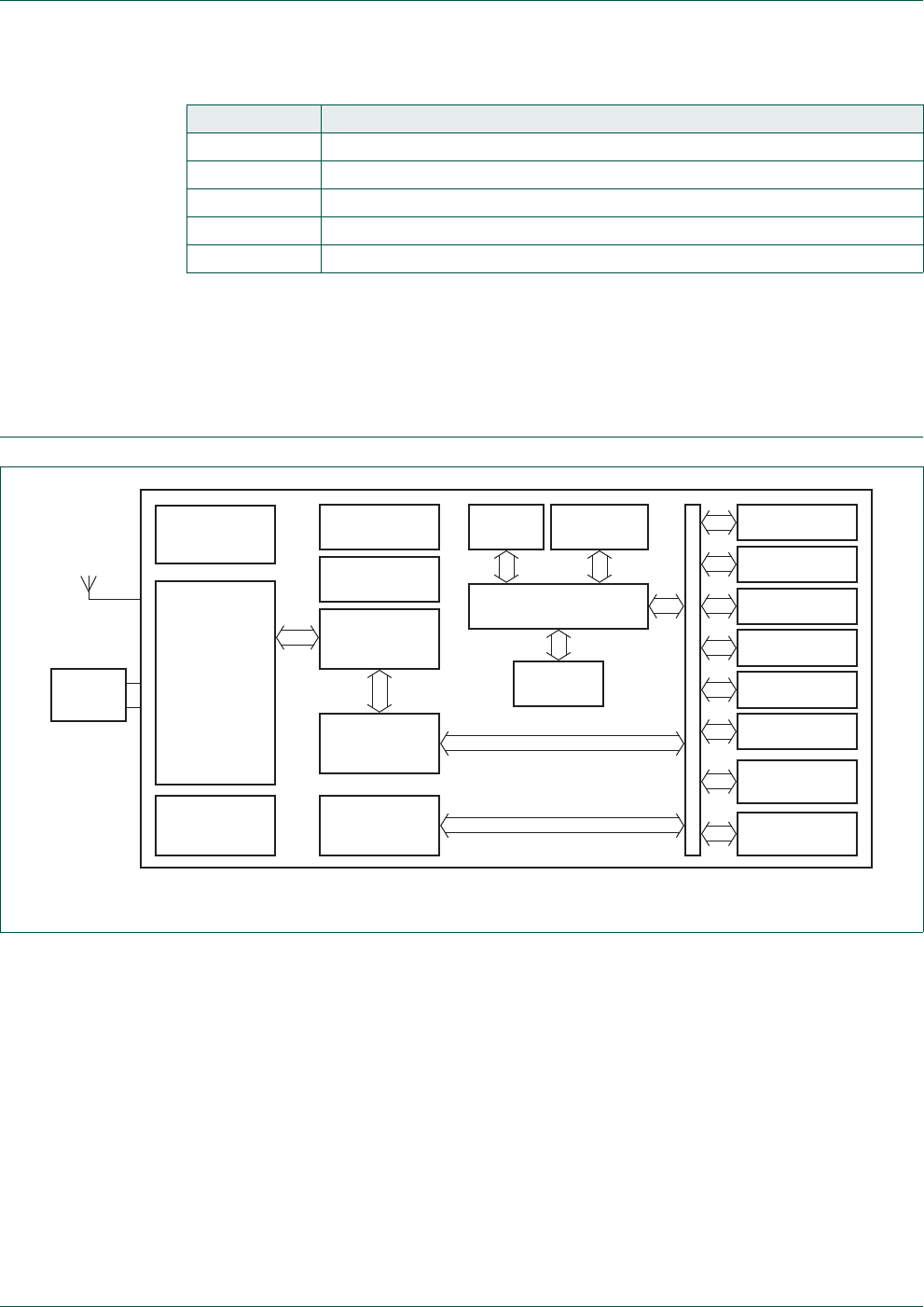
6. Block diagram
Table 2. Marking code
Line number Marking code
Line 1 NXP Logo: B&W outline logo
Line 2 part ID: JN5179-001-M00
Line 3 FCC ID: XXMJN5179M0
Line 4 IC ID: 8764A-JN5179M0
Line 5 European notified body number
Fig 2. Block diagram
XTAL
2.4 GHz
RADIO
INCLUDING
DIVERSITY
WATCHDOG
TIMER
VOLTAGE
BROWNOUT
O-QPSK
MODEM
IEEE802.15.4
MAC
ACCELERATOR
128-BIT AES
ENCRYPTION
ACCELERATOR
POWER
MANAGEMENT
EEPROM
ARM Cortex-M3
RAM FLASH
aaa-015434
SPI-BUS MASTER
AND SLAVE
I
2
C-BUS MASTER
AND SLAVE
DIO
SLEEP COUNTER
6 CHAN
10 BIT ADC
SUPPLY AND
TEMP SENSORS
6 x PWM
PLUS TIMER
2 x UART
10 V to 3.6 V
SWITCHED MODE
POWER SUPPLY
UM10983 All information provided in this document is subject to legal disclaimers. © NXP Semiconductors N.V. 2016. All rights reserved.
User manual Rev. 1.0 — 9 March 2016 7 of 23
NXP Semiconductors UM10983
ZigBee PRO and IEEE802.15.4 JN5179-001-M00 module
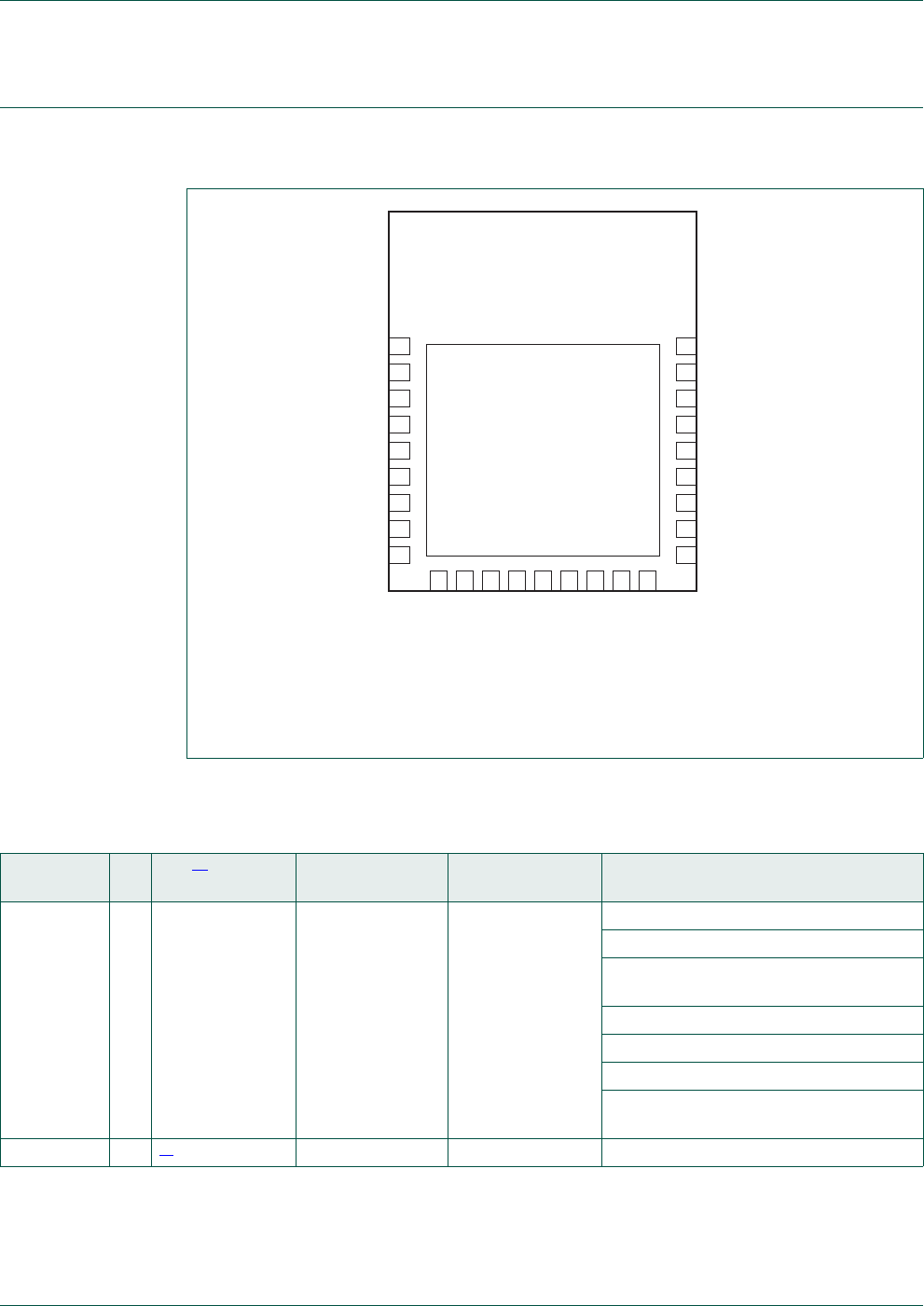
7. Pinning information
7.1 Pinning
7.2 Pin description
(1) SPI_CS = SPISEL0 on the JN5179.
Fig 3. Pin configuration
aaa-022129
1
DIO15
19
V
SS
2DIO18
SPICLK
3
DIO13
20
SPIMISO
4
27
SPI_CS(1)
5
26
SPIMOSI
6
25
7
24
DIO3
8
23
DIO1
9
22
DIO0
21
V
DD
11
ADC1
RESET_N
12
13
DIO14
14
DIO12
15
DIO2
n.c.
16
DIO4
17
DIO10
DIO5
18
DIO9
VDD(SMPS)
DIO8
DIO11
10
ADC0
DIO17
Transparent top view
Table 3. Pin description
Symbol Pin Type[1] Default at reset/
during boot Default internal
pull-up/pull-down Description
DIO2 1 IO DIO2 (I) pull-up DIO2 — digital input/output 2
ADC5 — ADC input 5
SDA — I2C-bus master/slave SDA
input/output (push-pull output)
RXD1 — UART 1 receive data input
TIM0CAP — Timer0 capture input
RFRX — radios receiver control output
VAUX_SENSE — auxiliary voltage sense
input
ADC0 2 I[2] ADC0 — ADC input 0

UM10983 All information provided in this document is subject to legal disclaimers. © NXP Semiconductors N.V. 2016. All rights reserved.
User manual Rev. 1.0 — 9 March 2016 8 of 23
NXP Semiconductors UM10983
ZigBee PRO and IEEE802.15.4 JN5179-001-M00 module
DIO0 3 IO DIO0 (I) pull-up DIO0 — digital input/output 0
ADC4 — ADC input 4
SPISEL0 — SPI-bus master select
output 0
RFRX — radio receiver control output
FLICK_CTRL — flicker control output
ADO — antenna diversity odd output
DIO1 4 IO DIO1 (I) pull-up DIO1 — digital input/output 1
ADC3 — ADC input 3
RFTX — radio transmitter control input
PC0 — pulse counter 0 input
ADE — antenna diversity even output
DIO3 5 IO DIO3 (I) pull-down DIO3 — digital input/output 3
ADC2 — ADC input 2
PWM4 — PWM4 output
SCL — I2C-bus master/slave SCL
input/output (push-pull output)
TXD1 — UART 1 transmit data output
TIM0OUT — Timer0 output
RFTX — radio transmit control input
FLICK_CTRL — flicker control output
DIO4 6 IO (open-drain) DIO4 (I) pull-up DIO4 — digital input/output 4
SCL — I2C-bus master/slave SCL
input/output (open-drain)
RXD0 — UART 0 receive data input
TIM0CK_GT — Timer0 clock/gate input
ADO — antenna diversity odd output
DIO10 7 IO JTAG_TDI (I)/
RXD0 (I) pull-up DIO10 — digital input/output 10
JTAG_TDI — JTAG TDI data input
RXD0 — UART 0 receive data input
DIO9 8 IO JTAG_TDO (O)/
TXD0 (O) pull-up DIO9 — digital input/output 9
JTAG_TDO — JTAG TDO data output
TXD0 — UART 0 transmit data output
TRACESWV — ARM trace serial wire
viewer output
DIO8 9 IO DIO8 (I) pull-down DIO8 — digital input/output 8
PWM5 — PWM5 output
TIM0OUT — Timer0 output
TRACECLK — trace clock output
32KXTALIN — 32 kHz clock input
Table 3. Pin description …continued
Symbol Pin Type[1] Default at reset/
during boot Default internal
pull-up/pull-down Description
UM10983 All information provided in this document is subject to legal disclaimers. © NXP Semiconductors N.V. 2016. All rights reserved.
User manual Rev. 1.0 — 9 March 2016 9 of 23
NXP Semiconductors UM10983
ZigBee PRO and IEEE802.15.4 JN5179-001-M00 module
SPIMOSI[5] 10 IO SPIMOSI (O) pull-down DIO7 — digital input/output 7
SPIMOSI — SPI-bus master data output
JTAG_TDI — JTAG TDI data input
SPISEL2 — SPI-bus master select output
2
SPISSEL — SPI-bus slave select input
CMP_OUT — comparator output
32KIN — 32 kHz External clock input
32KXTALOUT — 32 kHz clock output
SPI_CS[4] 11 IO SPISEL0 (O) pull-up DIO6 — digital input/output 6
SPISEL0 — SPI-bus master select output
0
CTS0 — UART 0 clear to send input
RXD1 — UART 1 receive data input
JTAG_TCK — JTAG TCK input
SWCK — Serial Wire Debugger Clock
input
SPISCLK — SPI-bus slave clock input
TIM1CAP — Timer1 capture input
SPIMISO[3] 12 IO SPIMISO (I) pull-up DO1 — digital output 1
SPIMISO — SPI-bus master data input
SPISMISO — SPI-bus slave data output
ADO — antenna diversity odd output
SPICLK[2] 13 O SPICLK (O) pull-up DO0 — digital output 0
SPICLK — SPI-bus master clock output
ADE — antenna diversity even output
DIO17 14 IO at reset: DIO17 (I);
during boot:
SWCK (I)
pull-up DIO17 — digital input/output 17
JTAG_TCK — JTAG TCK input
SWCK — Serial Wire Debugger Clock
input
SPISEL0 — SPI-bus master select output
0
TIM1CAP — Timer1 capture input
COMP1P — comparator plus input
SPISMISO — SPI-bus slave data output
Table 3. Pin description …continued
Symbol Pin Type[1] Default at reset/
during boot Default internal
pull-up/pull-down Description

UM10983 All information provided in this document is subject to legal disclaimers. © NXP Semiconductors N.V. 2016. All rights reserved.
User manual Rev. 1.0 — 9 March 2016 10 of 23
NXP Semiconductors UM10983
ZigBee PRO and IEEE802.15.4 JN5179-001-M00 module
DIO11 15 IO SWD (I) pull-up DIO11 — digital input/output 11
JTAG_TMS — JTAG TMS input
SWD — serial wire debugger input
RTS0 — UART 0 request to send output
TXD1 — UART 1 transmit data output
SPICLK — SPI-bus master clock output
SPISMOSI — SPI-bus slave data input
TIM1OUT — Timer1 output
TRACED0 — ARM trace data0 output
VDD(SMPS) 16 P; 3.6 V to 10 V VDD(SMPS) — SMPS input supply voltage
VSS 17 G VSS — ground
VDD 18 P VDD — supply voltage
DIO5 19 IO (open-drain) DIO5 (I) pull-up DIO5 — digital input/output 5
SDA — I2C-bus master/slave SDA
input/output (open-drain)
TXD0 — UART 0 transmit data output
PC1 — pulse counter 1 input
TIM0CAP — Timer0 capture input
ADE — antenna diversity even output
n.c. 20 - - - not connected
DIO12 21 IO DIO12 (I) pull-down DIO12 — digital input/output 12
PWM1 — PWM1 output
TXD0 — UART 0 transmit data output
TRACED3 — ARM trace data3 output
VAUX_OUT — auxiliary voltage control
output
DIO13 22 IO DIO13 (I) pull-down DIO13 — digital input/output 13
PWM2 — PWM2 output
RXD0 — UART 0 receive data input
PC0 — pulse counter 0 input
TRACED2 — ARM trace data2 output
DIO14 23 IO DIO14 (I) pull-down DIO14 — digital input/output 14
PWM3 — PWM3 output
PC1 — pulse counter 1 input
CMP_OUT — comparator output
TRACED1 — ARM trace data1 output
SPISMOSI — SPI-bus slave data input
RESET_N 24 I pull-up RESET_N — reset input
Table 3. Pin description …continued
Symbol Pin Type[1] Default at reset/
during boot Default internal
pull-up/pull-down Description
UM10983 All information provided in this document is subject to legal disclaimers. © NXP Semiconductors N.V. 2016. All rights reserved.
User manual Rev. 1.0 — 9 March 2016 11 of 23
NXP Semiconductors UM10983
ZigBee PRO and IEEE802.15.4 JN5179-001-M00 module
[1] P = power supply; G = ground; I = input, O = output; IO = input/output.
[2] JTAG programming mode: must be left floating high during reset to avoid entering JTAG programming mode.
[3] UART programming mode: leave pin floating high during reset to avoid entering UART programming mode or hold it low to program.
[4] Specific precautions have to be followed for UART flow control: CTS0 is not usable in the same time with SPISEL0.
[5] Specific precautions have to be followed if external 32 kHz crystal is used. See Ref. 3.
8. Functional description
8.1 JN5179 single chip wireless microcontroller
The JN5179-001-M00 is constructed around the JN5179-001 single chip wireless
microcontroller, which includes the radio system, a ARM Cortex-M3 CPU, Flash, RAM and
EEPROM memory and a range of analogue and digital peripherals.
The chip is described fully in JN5179 Wireless Microcontroller Datasheet (see Ref. 2).
DIO15 25 IO DIO15 (I) pull-down DIO15 — digital input/output 15
PWM6 — PWM6 output
JTAG_TDO — JTAG TDO data output
SPIMOSI — SPI-bus master data output
SPISEL1 — SPI-bus master select output
1
TIM0CK_GT — Timer0 - clock gate input
TRACESWV — ARM trace Serial Wire
Viewer output
SPISSEL — SPI-bus slave select input
VAUX_SENSE — auxiliary voltage sense
DIO18 26 IO DIO18 (I) pull-up DIO18 — digital input/output 18
JTAG_TMS — JTAG TMS input
SWD — Serial Wire Debugger input
SPIMISO — SPI-bus master data input
TIM1OUT — Timer1 output
COMP1M — comparator minus input
SPISCLK — SPI-bus slave clock input
ADC1 27 I[2] VREF — analog peripheral reference
voltage
ADC1 — ADC input 1
Table 3. Pin description …continued
Symbol Pin Type[1] Default at reset/
during boot Default internal
pull-up/pull-down Description

UM10983 All information provided in this document is subject to legal disclaimers. © NXP Semiconductors N.V. 2016. All rights reserved.
User manual Rev. 1.0 — 9 March 2016 12 of 23
NXP Semiconductors UM10983
ZigBee PRO and IEEE802.15.4 JN5179-001-M00 module
8.2 Peripherals
The performance of all peripherals is defined in the JN5179 Wireless Microcontroller
Datasheet (see Ref. 2).
NXP supplies all the development tools and networking stacks needed to enable
end-product development to occur quickly and efficiently. These are all freely available
from the NXP Wireless Connectivity (see Ref. 3). A range of evaluation/developer kits is
also available, allowing products to be quickly bread boarded. Efficient development of
software applications is enabled by the provision of a complete, unlimited, software
developer kit. Together with the available libraries for the IEEE802.15.4 MAC and ZigBee
PRO network stacks, this package provides everything required to develop application
code and to trial it with hardware representative of the final module.
The module can be user programmed both in development and in production using
software supplied by NXP. Access to the on-chip peripherals, MAC and network stack
software is provided through specific APIs. This information is available on the NXP
support website, together with many example applications, user guides, reference
manuals and application notes.
9. Limiting values
Table 4. Peripherals
Peripherals JN5179-001-M00 Notes
Master SPI-bus port 1 250 kHz - 16 MHz
Slave SPI-bus port 1 250 kHz - 8 MHz
UART 2 16550 compatible
Two-wire serial I/F (compatible with SMbus and I2C-bus) 1 Up to 400kHz
PWM 16 MHz clock
timer 6
timer/counter 2
Programmable Sleep Timers 2 32 kHz clock
Digital IO lines (multiplexed with UARTs, timers and SPI-bus
selects) 18 DIO0 and DIO1 are not available
on JN5179-001-M06 modules
Analog-to-Digital converter 6 10-bit
Programmable analogue comparator 1 ultra low power mode for sleep
Internal temperature sensor 1
Internal battery sensor 1
Table 5. Limiting values
Symbol Parameter Conditions Min Max Unit
VDD supply voltage 0.3 +3.6 V
VDD(SMPS) SMPS supply voltage 0 10 V
VADCX voltage on pin ADCX [1] 0.3 VDD + 0.3 V
VIO(dig) digital input/output voltage on pins DIOx [2] 0.3 VDD + 0.3 V
UM10983 All information provided in this document is subject to legal disclaimers. © NXP Semiconductors N.V. 2016. All rights reserved.
User manual Rev. 1.0 — 9 March 2016 13 of 23
NXP Semiconductors UM10983
ZigBee PRO and IEEE802.15.4 JN5179-001-M00 module
[1] With x = 0, 1.
[2] With x = 0, 1, 2, 3, 4, 5, 8, 9, 10, 11, 12, 13, 14, 15, 17 or 18.
[3] Testing for HBM discharge is performed as specified in JEDEC Standard JS-001.
[4] Testing for CDM discharge is performed as specified in JEDEC Standard JESD22-C101.
10. Recommended operating conditions
[1] To reach the maximum TX power, 2.8 V is the minimum.
[2] Supplied with DC-to-DC at 2.8 V if the SMPS is used.
11. Characteristics
11.1 DC current
[1] To reach the maximum TX power, 2.8 V is the minimum.
[1] Waiting on I/O event.
Tstg storage temperature 40 +150 C
VESD electrostatic discharge voltage HBM [3] - 2000 V
CDM [4] - 1000 V
Table 5. Limiting values …continued
Symbol Parameter Conditions Min Max Unit
Table 6. Operating conditions
Symbol Parameter Conditions Min Max Unit
VDD supply voltage [1][2] 23.6V
VDD(SMPS) SMPS supply voltage 3.6 10 V
Tamb ambient temperature standard range 40 +85 C
Table 7. Active processing
VDD = 2 V to 3.6 V; Tamb =25
C; unless otherwise specified.
Symbol Parameter Conditions Min Typ Max Unit
IDD supply current M00
with radio in receive mode; maximum input level at
10 dBm - 14.8 - mA
with radio in receive mode; maximum input level at
0dBm - 12.7 - mA
with radio in transmit mode 10 dBm [1] - 22.5 - mA
with radio in transmit mode 8.5 dBm [1] - 19.6 - mA
Table 8. Sleep mode
VDD = 2 V to 3.6 V; Tamb =25
C; unless otherwise specified.
Symbol Parameter Conditions Min Typ Max Unit
IDD(IO) input/output supply
current in sleep mode; with I/O and RC oscillator
timer wake-up; Tamb =25C-0.60-A
UM10983 All information provided in this document is subject to legal disclaimers. © NXP Semiconductors N.V. 2016. All rights reserved.
User manual Rev. 1.0 — 9 March 2016 14 of 23
NXP Semiconductors UM10983
ZigBee PRO and IEEE802.15.4 JN5179-001-M00 module
[1] Waiting on chip RESET or I/O event.
11.2 AC characteristics
11.2.1 Radio transceiver
This module meets all the requirements of the IEEE802.15.4 standard over 2.0 V to 3.6 V
and offers the improved RF characteristics shown in Table 10. All RF characteristics are
measured single ended.
[1] With external matching inductors and assuming PCB layout.
Table 9. Deep sleep mode
VDD = 2 V to 3.6 V; Tamb =25
C; unless otherwise specified.
Symbol Parameter Conditions Min Typ Max Unit
IDD supply current deep sleep mode; measured at 25 C[1] -100-nA
Table 10. Antenna port characteristics
Single-ended; Impedance = 50
[1]; VDD = 2 V to 3.6 V; Tamb =
40
C to +125
C; unless otherwise specified.
Symbol Parameter Conditions Min Typ Max Unit
frange frequency range 2.4 - 2.485 GHz
VESD electrostatic discharge
voltage ---
HBM - 2 - kV
CDM - 500 - V
Table 11. Radio transceiver characteristics: +25 C
VDD = 2 V to 3.6 V; unless otherwise specified.
Symbol Parameter Conditions Min Typ Max Unit
Receiver
SRX receiver sensitivity nominal for 1 % PER, as per 802.15.4 - 96 93.5 dBm
Pi(RX)(max) maximum receiver input
power 1 % PER, measured as sensitivity; supply
current at 14.8 mA; high-performance mode -10-dBm
1 % PER, measured as sensitivity; supply
current at 12.7 mA; low-power mode -2- dBm
ch channel rejection 1 % PER, with wanted signal 3 dB, above sensitivity as per 802.15.4
modulated interferer[1][2]
1 channel - 19 - dBc
+1 channel - 34 - dBc
2 channel - 40 - dBc
+2 channel - 44 - dBc
co-channel - 7- dBc
CW interferer[1][2]
1 channel - 25 - dBc
+1 channel - 50 - dBc
2 channel - 57 - dBc
+2 channel - 60 - dBc
UM10983 All information provided in this document is subject to legal disclaimers. © NXP Semiconductors N.V. 2016. All rights reserved.
User manual Rev. 1.0 — 9 March 2016 15 of 23
NXP Semiconductors UM10983
ZigBee PRO and IEEE802.15.4 JN5179-001-M00 module
[1] Blocker rejection is defined as the value, when 1 % PER is seen with the wanted signal 3 dB above sensitivity, as per IEE802.15.4.
[2] Channels 11, 17, 24 low/high values reversed.
[3] To reach the maximum TX power, 2.8 V is the minimum on VDDA.
[4] Up to an extra 2.5 dB of attenuation is available if required.
[5] See IEEE802.15.4.
ib in-band rejection 1 % PER with wanted signal 3 dB above
sensitivity; 2.4 GHz to 2.4835 GHz;
modulated interferers at 3 channel
separation
[1] -43-dBc
oob out-of-band rejection 1 % PER with wanted signal 3 dB above
sensitivity
[1]
all frequencies except wanted/2 which is
8 dB lower -45-dBc
3G frequency at 2.1 GHz - 5- dBm
LTE frequency at 2.5 GHz - 18 - dBm
Psp(RX) receiver spurious power measured conducted into 50
30 MHz to 1 GHz - - 70 dBm
1 GHz to 12 GHz - - 70 dBm
PL(lo) local oscillator leakage
power --57 dBm
IMP intermodulation
protection 1 % PER at with wanted signal 3 dB above
sensitivity; modulated interferers at 3 and 6
channel separation
[1] -46-dB
RSSI RSSI variation 95 dBm to 10 dBm; available through
UM10983 Integrated Peripherals API
4- +4dB
Transmitter
Pooutput power PA = 5 and Att. 2.5 dB OFF [3] -10 - dBm
Po(cr) control range output
power in 6 major steps and then 4 fine steps [4] -42 - dB
Psp(TX) transmitter spurious
power measured conducted into 50
30 MHz to 1 GHz - - 65 dBm
1 GHz to 12.5 GHz (harmonic H2) - - 36 dBm
exceptions
1.8 GHz to 1.9 GHz - - 65 dBm
5.15 GHz to 5.3 GHz - - 65 dBm
EVM error vector magnitude at maximum output power - 8 - %
EVMoffset error vector magnitude
offset at maximum output power - 3 4.5 %
PSD power spectral density at greater than 3.5 MHz offset [5] -38 20 dBc
Table 11. Radio transceiver characteristics: +25 C …continued
VDD = 2 V to 3.6 V; unless otherwise specified.
Symbol Parameter Conditions Min Typ Max Unit

UM10983 All information provided in this document is subject to legal disclaimers. © NXP Semiconductors N.V. 2016. All rights reserved.
User manual Rev. 1.0 — 9 March 2016 16 of 23
NXP Semiconductors UM10983
ZigBee PRO and IEEE802.15.4 JN5179-001-M00 module
12. Federal Communication Commission Statement
•This equipment has been tested and found to comply with the limits for a Class B
digital device, pursuant to Part 15 of the FCC Rules see Ref. 4. These limits are
designed to provide reasonable protection against harmful interference in a
residential installation. This equipment generates, uses, and can radiate radio
frequency energy and, if not installed and used in accordance with the instructions,
may cause harmful interference to radio communications. However, there is no
guarantee that interference will not occur in a particular installation. If this equipment
does cause harmful interference to radio or television reception, which can be
determined by turning the equipment off and on, the user is encouraged to try to
correct the interference by one of the following measures:
–Reorient or relocate the receiving antenna
–Increase the separation between the equipment and receiver
–Connect the equipment into an outlet on a circuit different from that to which the
receiver is connected
–Consult the dealer or an experienced radio/TV technician for help
•OEM integrators instructions
–The OEM integrators are responsible for ensuring that the end-user has no manual
instructions to remove or install module
–The module is limited to installation in mobile or fixed applications, according to
CFR 47 Part 2.1091(b)
–Separate approval is required for all other operating configurations, including
portable configurations with respect to CFR 47 Part 2.1093 and different antenna
configurations
•User guide mandatory statements
–User's instructions of the host device must contain the following statements in
addition to operation instructions:
* “This device complies with part 15 of the FCC Rules. Operation is subject to the
following two conditions:
(1) This device may not cause harmful interference, and
(2) This device must accept any interference received, including interference that
may cause undesired operation”
* “Changes or modifications not expressly approved by the party responsible for
compliance could void the user's authority to operate the equipment”
•FCC RF Exposure requirements
–User's instructions of the host device must contain the following instructions in
addition to operation instructions:
Avoid direct contact to the antenna, or keep it to a 20 cm minimum distance while
using this equipment. This device must not be collocated or operating in
conjunction with another antenna or transmitter.
This module has been designed to operate with antennas having a maximum gain of 0.86
dBi. Antennas having a gain greater than 0.86 dBi are strictly prohibited for use with this
device. The required antenna impedance is 50 ohms.

UM10983 All information provided in this document is subject to legal disclaimers. © NXP Semiconductors N.V. 2016. All rights reserved.
User manual Rev. 1.0 — 9 March 2016 17 of 23
NXP Semiconductors UM10983
ZigBee PRO and IEEE802.15.4 JN5179-001-M00 module
12.1 FCC end product labelling
The final ‘end product’ should be labelled in a visible area with the following:
“Contains TX FCC ID: XXMJN5179M0”.
13. Industry Canada statement
To reduce potential radio interference to other users, the antenna type and its gain should
be so chosen that the equivalent isotropic radiated power (e.i.r.p.) is not more than that
permitted for successful communication.
This module has been designed to operate with antennas having a maximum gain of 0.86
dBi. Antennas having a gain greater than 0.86 dBi are strictly prohibited for use with this
device. The required antenna impedance is 50 ohms.
As long as the above condition is met, further transmitter testing will not be required.
However, the OEM integrator is still responsible for testing their end-product for any
additional compliance requirements required with this module installed (for example,
digital device emissions, PC peripheral requirements, etc).
13.1 Industry Canada end product labelling
For Industry Canada purposes the following should be used:
“Contains Industry Canada ID IC: 8764A-JN5179M0”
This device complies with Industry Canada
licence-exempt RSS standard(s). Operation is
subject to the following two conditions: (1) this
device may not cause interference, and (2) this
device must accept any interference, including
interference that may cause undesired
operation of the device.
This device complies with Industry Canada RF
radiation exposure limits set forth for general
population (uncontrolled exposure). This device
must be installed to provide a separation
distance of at least 20 cm from all persons and
must not be collocated or operating in
conjunction with any other antenna or
transmitter.
Le présent appareil est conforme aux CNR
d’Industrie Canada applicables aux appareils
radio exempts de licence. L’exploitation est
autorisée aux deux conditions suivantes: (1) il
ne doit pas produire de brouillage, et (2)
l’utilisateur du dispositif doit être prêt a accepter
tout brouillage radioélectrique reçu, même si ce
brouillage est susceptible de compromettre le
fonctionnement du dispositif.
Le présent appareil est conforme aux niveaux
limites d’exigences d’exposition RF aux
personnes définies par Industrie Canada. Cet
appareil doit être installé afin d’offrir une
distance de séparation d’au moins 20 cm avec
l’utilisateur, et ne doit pas être installé à
proximité ou être utilisé en conjonction avec une
autre antenne ou un autre émetteur.
UM10983 All information provided in this document is subject to legal disclaimers. © NXP Semiconductors N.V. 2016. All rights reserved.
User manual Rev. 1.0 — 9 March 2016 18 of 23
NXP Semiconductors UM10983
ZigBee PRO and IEEE802.15.4 JN5179-001-M00 module
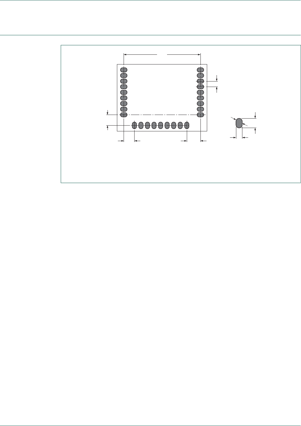
14. Footprint information for reflow soldering
Fig 4. Module PCB footprint
aaa-019074
16.0
Dimensions in mm
2.54
2.54 3.30
1.27
1.5
Ø 1
1
UM10983 All information provided in this document is subject to legal disclaimers. © NXP Semiconductors N.V. 2016. All rights reserved.
User manual Rev. 1.0 — 9 March 2016 19 of 23
NXP Semiconductors UM10983
ZigBee PRO and IEEE802.15.4 JN5179-001-M00 module
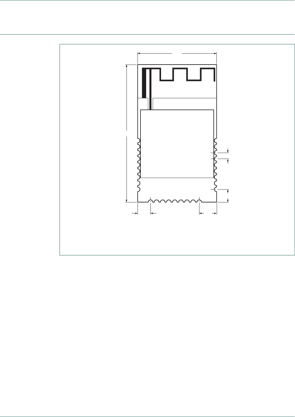
15. Package outline
Fig 5. Package outline JN5179-001-M00
aaa-022130
Dimensions in mm
thickness: 3.5 mm
16.0
2.54 3.3
30.0
2.54
1.27

UM10983 All information provided in this document is subject to legal disclaimers. © NXP Semiconductors N.V. 2016. All rights reserved.
User manual Rev. 1.0 — 9 March 2016 20 of 23
NXP Semiconductors UM10983
ZigBee PRO and IEEE802.15.4 JN5179-001-M00 module
16. Abbreviations
17. References
[1] IEEE Std 802.15.4-2011 — IEEE Std 802.15.4-2011 IEEE Standard for Information
Technology.
[2] JN517x — JN517x wireless microcontroller datasheet.
[3] Wireless Connectivity —
http://www.nxp.com/products/interface-and-connectivity/wireless-connectivity:WIRE
LESS-CONNECTIVITY
[4] Part 15 of the FCC Rules —
http://www.ecfr.gov/cgi-bin/text-idx?SID=d01e00935bfcb0d53b914e7c8e63f383&no
de=47:1.0.1.1.16&rgn=div5
Table 12. Abbreviations
Acronym Description
API Application Program Interface
ADC Analog to Digital Converter
ARM Advanced RISC Machine
FCC Federal Communication Commission
IO Input Output
OEM Original Equipment Manufacturer
PCB Printed Circuit Board
PER Packet Error Rate
PWM Pulse Width Modulation
R&TTE Radio and Telecommunications Terminal Equipment
RF Radio Frequency
RISC Reduce Instruction Set Computing
RSSI Receive Signal Strength Indicator
RTS Request-To-Send
SPI Serial Peripheral Interface
SVM Supply Voltage Monitor
SYNTH SYNTHesizer
UART Universal Asynchronous Receiver/Transmitter

UM10983 All information provided in this document is subject to legal disclaimers. © NXP Semiconductors N.V. 2016. All rights reserved.
User manual Rev. 1.0 — 9 March 2016 21 of 23
NXP Semiconductors UM10983
ZigBee PRO and IEEE802.15.4 JN5179-001-M00 module
18. Legal information
18.1 Definitions
Draft — The document is a draft version only. The content is still under
internal review and subject to formal approval, which may result in
modifications or additions. NXP Semiconductors does not give any
representations or warranties as to the accuracy or completeness of
information included herein and shall have no liability for the consequences of
use of such information.
18.2 Disclaimers
Limited warranty and liability — Information in this document is believed to
be accurate and reliable. However, NXP Semiconductors does not give any
representations or warranties, expressed or implied, as to the accuracy or
completeness of such information and shall have no liability for the
consequences of use of such information. NXP Semiconductors takes no
responsibility for the content in this document if provided by an information
source outside of NXP Semiconductors.
In no event shall NXP Semiconductors be liable for any indirect, incidental,
punitive, special or consequential damages (including - without limitation - lost
profits, lost savings, business interruption, costs related to the removal or
replacement of any products or rework charges) whether or not such
damages are based on tort (including negligence), warranty, breach of
contract or any other legal theory.
Notwithstanding any damages that customer might incur for any reason
whatsoever, NXP Semiconductors’ aggregate and cumulative liability towards
customer for the products described herein shall be limited in accordance
with the Terms and conditions of commercial sale of NXP Semiconductors.
Right to make changes — NXP Semiconductors reserves the right to make
changes to information published in this document, including without
limitation specifications and product descriptions, at any time and without
notice. This document supersedes and replaces all information supplied prior
to the publication hereof.
Suitability for use — NXP Semiconductors products are not designed,
authorized or warranted to be suitable for use in life support, life-critical or
safety-critical systems or equipment, nor in applications where failure or
malfunction of an NXP Semiconductors product can reasonably be expected
to result in personal injury, death or severe property or environmental
damage. NXP Semiconductors and its suppliers accept no liability for
inclusion and/or use of NXP Semiconductors products in such equipment or
applications and therefore such inclusion and/or use is at the customer’s own
risk.
Applications — Applications that are described herein for any of these
products are for illustrative purposes only. NXP Semiconductors makes no
representation or warranty that such applications will be suitable for the
specified use without further testing or modification.
Customers are responsible for the design and operation of their applications
and products using NXP Semiconductors products, and NXP Semiconductors
accepts no liability for any assistance with applications or customer product
design. It is customer’s sole responsibility to determine whether the NXP
Semiconductors product is suitable and fit for the customer’s applications and
products planned, as well as for the planned application and use of
customer’s third party customer(s). Customers should provide appropriate
design and operating safeguards to minimize the risks associated with their
applications and products.
NXP Semiconductors does not accept any liability related to any default,
damage, costs or problem which is based on any weakness or default in the
customer’s applications or products, or the application or use by customer’s
third party customer(s). Customer is responsible for doing all necessary
testing for the customer’s applications and products using NXP
Semiconductors products in order to avoid a default of the applications and
the products or of the application or use by customer’s third party
customer(s). NXP does not accept any liability in this respect.
Export control — This document as well as the item(s) described herein
may be subject to export control regulations. Export might require a prior
authorization from competent authorities.
Evaluation products — This product is provided on an “as is” and “with all
faults” basis for evaluation purposes only. NXP Semiconductors, its affiliates
and their suppliers expressly disclaim all warranties, whether express, implied
or statutory, including but not limited to the implied warranties of
non-infringement, merchantability and fitness for a particular purpose. The
entire risk as to the quality, or arising out of the use or performance, of this
product remains with customer.
In no event shall NXP Semiconductors, its affiliates or their suppliers be liable
to customer for any special, indirect, consequential, punitive or incidental
damages (including without limitation damages for loss of business, business
interruption, loss of use, loss of data or information, and the like) arising out
the use of or inability to use the product, whether or not based on tort
(including negligence), strict liability, breach of contract, breach of warranty or
any other theory, even if advised of the possibility of such damages.
Notwithstanding any damages that customer might incur for any reason
whatsoever (including without limitation, all damages referenced above and
all direct or general damages), the entire liability of NXP Semiconductors, its
affiliates and their suppliers and customer’s exclusive remedy for all of the
foregoing shall be limited to actual damages incurred by customer based on
reasonable reliance up to the greater of the amount actually paid by customer
for the product or five dollars (US$5.00). The foregoing limitations, exclusions
and disclaimers shall apply to the maximum extent permitted by applicable
law, even if any remedy fails of its essential purpose.
Translations — A non-English (translated) version of a document is for
reference only. The English version shall prevail in case of any discrepancy
between the translated and English versions.
18.3 Trademarks
Notice: All referenced brands, product names, service names and trademarks
are the property of their respective owners.
I2C-bus — logo is a trademark of NXP Semiconductors N.V.

UM10983 All information provided in this document is subject to legal disclaimers. © NXP Semiconductors N.V. 2016. All rights reserved.
User manual Rev. 1.0 — 9 March 2016 22 of 23
NXP Semiconductors UM10983
ZigBee PRO and IEEE802.15.4 JN5179-001-M00 module
19. Tables
Table 1. FCC and Industry Canada identification. . . . . . .3
Table 2. Marking code . . . . . . . . . . . . . . . . . . . . . . . . . . .6
Table 3. Pin description . . . . . . . . . . . . . . . . . . . . . . . . . .7
Table 4. Peripherals . . . . . . . . . . . . . . . . . . . . . . . . . . .12
Table 5. Limiting values . . . . . . . . . . . . . . . . . . . . . . . . .12
Table 6. Operating conditions . . . . . . . . . . . . . . . . . . . .13
Table 7. Active processing . . . . . . . . . . . . . . . . . . . . . . 13
Table 8. Sleep mode . . . . . . . . . . . . . . . . . . . . . . . . . . . 13
Table 9. Deep sleep mode . . . . . . . . . . . . . . . . . . . . . . 14
Table 10. Antenna port characteristics . . . . . . . . . . . . . . 14
Table 11. Radio transceiver characteristics: +25 °C . . . . 14
Table 12. Abbreviations . . . . . . . . . . . . . . . . . . . . . . . . . 20
20. Figures
Fig 1. JN5179-001-M00 package marking (top view) . . .5
Fig 2. Block diagram . . . . . . . . . . . . . . . . . . . . . . . . . . . .6
Fig 3. Pin configuration . . . . . . . . . . . . . . . . . . . . . . . . . .7
Fig 4. Module PCB footprint. . . . . . . . . . . . . . . . . . . . . .18
Fig 5. Package outline JN5179-001-M00 . . . . . . . . . . .19

NXP Semiconductors UM10983
ZigBee PRO and IEEE802.15.4 JN5179-001-M00 module
© NXP Semiconductors N.V. 2016. All rights reserved.
For more information, please visit: http://www.nxp.com
For sales office addresses, please send an email to: salesaddresses@nxp.com
Date of release: 9 March 2016
Document identifier: UM10983
Please be aware that important notices concerning this document and the product(s)
described herein, have been included in section ‘Legal information’.
21. Contents
1 General description . . . . . . . . . . . . . . . . . . . . . . 3
1.1 FCC and Industry Canada identification. . . . . . 3
1.2 Regulatory approvals . . . . . . . . . . . . . . . . . . . . 3
2 Features and benefits . . . . . . . . . . . . . . . . . . . . 3
2.1 Benefits. . . . . . . . . . . . . . . . . . . . . . . . . . . . . . . 3
2.2 Features: module . . . . . . . . . . . . . . . . . . . . . . . 4
2.3 Features: microcontroller . . . . . . . . . . . . . . . . . 4
3 Applications . . . . . . . . . . . . . . . . . . . . . . . . . . . . 5
4 Overview. . . . . . . . . . . . . . . . . . . . . . . . . . . . . . . 5
5 Marking . . . . . . . . . . . . . . . . . . . . . . . . . . . . . . . . 5
6 Block diagram . . . . . . . . . . . . . . . . . . . . . . . . . . 6
7 Pinning information. . . . . . . . . . . . . . . . . . . . . . 7
7.1 Pinning . . . . . . . . . . . . . . . . . . . . . . . . . . . . . . . 7
7.2 Pin description . . . . . . . . . . . . . . . . . . . . . . . . . 7
8 Functional description . . . . . . . . . . . . . . . . . . 11
8.1 JN5179 single chip wireless microcontroller. . 11
8.2 Peripherals . . . . . . . . . . . . . . . . . . . . . . . . . . . 12
9 Limiting values. . . . . . . . . . . . . . . . . . . . . . . . . 12
10 Recommended operating conditions. . . . . . . 13
11 Characteristics. . . . . . . . . . . . . . . . . . . . . . . . . 13
11.1 DC current . . . . . . . . . . . . . . . . . . . . . . . . . . . 13
11.2 AC characteristics. . . . . . . . . . . . . . . . . . . . . . 14
11.2.1 Radio transceiver . . . . . . . . . . . . . . . . . . . . . . 14
12 Federal Communication Commission Statement
16
12.1 FCC end product labelling . . . . . . . . . . . . . . . 17
13 Industry Canada statement. . . . . . . . . . . . . . . 17
13.1 Industry Canada end product labelling . . . . . . 17
14 Footprint information for reflow soldering . . 18
15 Package outline . . . . . . . . . . . . . . . . . . . . . . . . 19
16 Abbreviations. . . . . . . . . . . . . . . . . . . . . . . . . . 20
17 References . . . . . . . . . . . . . . . . . . . . . . . . . . . . 20
18 Legal information. . . . . . . . . . . . . . . . . . . . . . . 21
18.1 Definitions. . . . . . . . . . . . . . . . . . . . . . . . . . . . 21
18.2 Disclaimers. . . . . . . . . . . . . . . . . . . . . . . . . . . 21
18.3 Trademarks. . . . . . . . . . . . . . . . . . . . . . . . . . . 21
19 Tables . . . . . . . . . . . . . . . . . . . . . . . . . . . . . . . . 22
20 Figures . . . . . . . . . . . . . . . . . . . . . . . . . . . . . . . 22
21 Contents . . . . . . . . . . . . . . . . . . . . . . . . . . . . . . 23