NXP Semiconductors JN5179M6 ZigBee Modular Transmitter User Manual UM10984
NXP Semiconductors ZigBee Modular Transmitter UM10984
UserManual.wiki
>
NXP Semiconductors
>
JN5179M6 User Manual
User manual.pdf
Navigation menu
Upload a User Manual
Namespaces
Wiki Guide
HTML
PDF
Info
Views
User Manual
Discussion / Help
Navigation
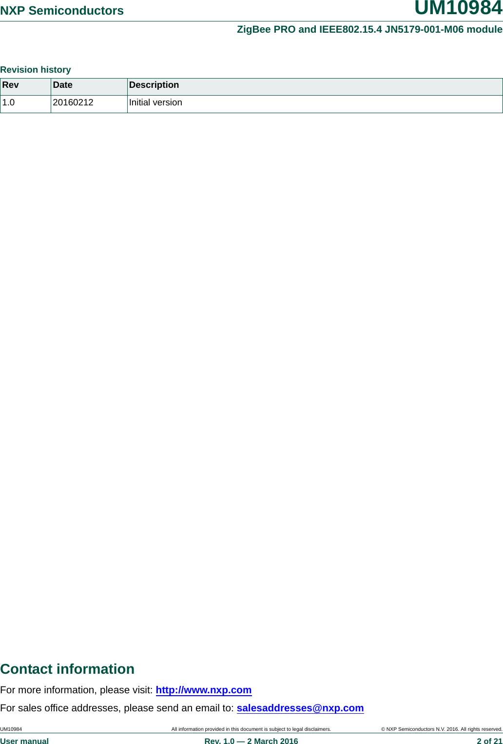
![UM10984 All information provided in this document is subject to legal disclaimers. © NXP Semiconductors N.V. 2016. All rights reserved.User manual Rev. 1.0 — 2 March 2016 7 of 21NXP Semiconductors UM10984ZigBee PRO and IEEE802.15.4 JN5179-001-M06 module7. Pinning information7.1 Pinning 7.2 Pin description (1) SPI_CS = SPISEL0 on the JN5179.(2) DIO0 pin of the module is not connected to DIO0 pin of the JN5179. The DIO0 of the module is LNA_BYPASS.(3) DIO1 pin of the module is not connected to DIO1 pin of the JN5179. The DIO1 of the module is ANT_SEL.Fig 3. Pin configuration1DIO1519VSS2DIO18SPICLK3DIO1320SPIMISO427SPI_CS(1)526SPIMOSI625724DIO3823DIO1(3)922DIO0(2)21VDD11ADC1RESET_N1213DIO1414DIO1215DIO2n.c.16DIO417DIO10DIO518DIO9VDD(SMPS)DIO8DIO1110ADC0DIO17Transparent top viewTable 3. Pin descriptionSymbol Pin Type[1] Default at reset/during boot Default internal pull-up/pull-down DescriptionDIO2 1 IO DIO2 (I) pull-up DIO2 — digital input/output 2ADC5 — ADC input 5SDA — I2C-bus master/slave SDA input/output (push-pull output)RXD1 — UART 1 receive data inputTIM0CAP — Timer0 capture inputRFRX — radios receiver control outputVAUX_SENSE — auxiliary voltage sense inputADC0 2 I[2] ADC0 — ADC input 0DIO0 3 I pull-up LNA_BYPASS — receiver bypass](https://usermanual.wiki/NXP-Semiconductors/JN5179M6/User-Guide-2961839-Page-7.png)
![UM10984 All information provided in this document is subject to legal disclaimers. © NXP Semiconductors N.V. 2016. All rights reserved.User manual Rev. 1.0 — 2 March 2016 8 of 21NXP Semiconductors UM10984ZigBee PRO and IEEE802.15.4 JN5179-001-M06 moduleDIO1 4 I pull-up ANT_SEL — antenna selectionDIO3 5 IO DIO3 (I) pull-down DIO3 — digital input/output 3ADC2 — ADC input 2PWM4 — PWM4 outputSCL — I2C-bus master/slave SCL input/output (push-pull output)TXD1 — UART 1 transmit data outputTIM0OUT — Timer0 outputRFTX — radio transmit control inputFLICK_CTRL — flicker control outputDIO4 6 IO (open-drain) DIO4 (I) pull-up DIO4 — digital input/output 4SCL — I2C-bus master/slave SCL input/output (open-drain)RXD0 — UART 0 receive data inputTIM0CK_GT — Timer0 clock/gate inputADO — antenna diversity odd outputDIO10 7 IO JTAG_TDI (I)/RXD0 (I) pull-up DIO10 — digital input/output 10JTAG_TDI — JTAG TDI data inputRXD0 — UART 0 receive data inputDIO9 8 IO JTAG_TDO (O)/TXD0 (O) pull-up DIO9 — digital input/output 9JTAG_TDO — JTAG TDO data outputTXD0 — UART 0 transmit data outputTRACESWV — ARM trace serial wire viewer outputDIO8 9 IO DIO8 (I) pull-down DIO8 — digital input/output 8PWM5 — PWM5 outputTIM0OUT — Timer0 outputTRACECLK — trace clock output32KXTALIN — 32 kHz clock inputSPIMOSI[5] 10 IO SPIMOSI (O) pull-down DIO7 — digital input/output 7SPIMOSI — SPI-bus master data outputJTAG_TDI — JTAG TDI data inputSPISEL2 — SPI-bus master select output 2SPISSEL — SPI-bus slave select inputCMP_OUT — comparator output32KIN — 32 kHz External clock input32KXTALOUT — 32 kHz clock outputTable 3. Pin description …continuedSymbol Pin Type[1] Default at reset/during boot Default internal pull-up/pull-down Description](https://usermanual.wiki/NXP-Semiconductors/JN5179M6/User-Guide-2961839-Page-8.png)
![UM10984 All information provided in this document is subject to legal disclaimers. © NXP Semiconductors N.V. 2016. All rights reserved.User manual Rev. 1.0 — 2 March 2016 9 of 21NXP Semiconductors UM10984ZigBee PRO and IEEE802.15.4 JN5179-001-M06 moduleSPI_CS[4] 11 IO SPISEL0 (O) pull-up DIO6 — digital input/output 6SPISEL0 — SPI-bus master select output 0CTS0 — UART 0 clear to send inputRXD1 — UART 1 receive data inputJTAG_TCK — JTAG TCK inputSWCK — Serial Wire Debugger Clock inputSPISCLK — SPI-bus slave clock inputTIM1CAP — Timer1 capture inputSPIMISO[3] 12 IO SPIMISO (I) pull-up DO1 — digital output 1SPIMISO — SPI-bus master data inputSPISMISO — SPI-bus slave data outputADO — antenna diversity odd outputSPICLK[2] 13 O SPICLK (O) pull-up DO0 — digital output 0SPICLK — SPI-bus master clock outputADE — antenna diversity even outputDIO17 14 IO at reset: DIO17 (I); during boot: SWCK (I)pull-up DIO17 — digital input/output 17JTAG_TCK — JTAG TCK inputSWCK — Serial Wire Debugger Clock inputSPISEL0 — SPI-bus master select output 0TIM1CAP — Timer1 capture inputCOMP1P — comparator plus inputSPISMISO — SPI-bus slave data outputDIO11 15 IO SWD (I) pull-up DIO11 — digital input/output 11JTAG_TMS — JTAG TMS inputSWD — serial wire debugger inputRTS0 — UART 0 request to send outputTXD1 — UART 1 transmit data outputSPICLK — SPI-bus master clock outputSPISMOSI — SPI-bus slave data inputTIM1OUT — Timer1 outputTRACED0 — ARM trace data0 outputVDD(SMPS) 16 P; 3.6 V to 10 V VDD(SMPS) — SMPS input supply voltageVSS 17 G VSS — groundVDD 18 P VDD — supply voltageTable 3. Pin description …continuedSymbol Pin Type[1] Default at reset/during boot Default internal pull-up/pull-down Description](https://usermanual.wiki/NXP-Semiconductors/JN5179M6/User-Guide-2961839-Page-9.png)
![UM10984 All information provided in this document is subject to legal disclaimers. © NXP Semiconductors N.V. 2016. All rights reserved.User manual Rev. 1.0 — 2 March 2016 10 of 21NXP Semiconductors UM10984ZigBee PRO and IEEE802.15.4 JN5179-001-M06 moduleDIO5 19 IO (open-drain) DIO5 (I) pull-up DIO5 — digital input/output 5SDA — I2C-bus master/slave SDA input/output (open-drain)TXD0 — UART 0 transmit data outputPC1 — pulse counter 1 inputTIM0CAP — Timer0 capture inputADE — antenna diversity even outputn.c. 20 - - - not connectedDIO12 21 IO DIO12 (I) pull-down DIO12 — digital input/output 12PWM1 — PWM1 outputTXD0 — UART 0 transmit data outputTRACED3 — ARM trace data3 outputVAUX_OUT — auxiliary voltage control outputDIO13 22 IO DIO13 (I) pull-down DIO13 — digital input/output 13PWM2 — PWM2 outputRXD0 — UART 0 receive data inputPC0 — pulse counter 0 inputTRACED2 — ARM trace data2 outputDIO14 23 IO DIO14 (I) pull-down DIO14 — digital input/output 14PWM3 — PWM3 outputPC1 — pulse counter 1 inputCMP_OUT — comparator outputTRACED1 — ARM trace data1 outputSPISMOSI — SPI-bus slave data inputRESET_N 24 I pull-up RESET_N — reset inputDIO15 25 IO DIO15 (I) pull-down DIO15 — digital input/output 15PWM6 — PWM6 outputJTAG_TDO — JTAG TDO data outputSPIMOSI — SPI-bus master data outputSPISEL1 — SPI-bus master select output 1TIM0CK_GT — Timer0 - clock gate inputTRACESWV — ARM trace Serial Wire Viewer outputSPISSEL — SPI-bus slave select inputVAUX_SENSE — auxiliary voltage senseTable 3. Pin description …continuedSymbol Pin Type[1] Default at reset/during boot Default internal pull-up/pull-down Description](https://usermanual.wiki/NXP-Semiconductors/JN5179M6/User-Guide-2961839-Page-10.png)
![UM10984 All information provided in this document is subject to legal disclaimers. © NXP Semiconductors N.V. 2016. All rights reserved.User manual Rev. 1.0 — 2 March 2016 11 of 21NXP Semiconductors UM10984ZigBee PRO and IEEE802.15.4 JN5179-001-M06 module[1] P = power supply; G = ground; I = input, O = output; IO = input/output.[2] JTAG programming mode: must be left floating high during reset to avoid entering JTAG programming mode.[3] UART programming mode: leave pin floating high during reset to avoid entering UART programming mode or hold it low to program.[4] Specific precautions have to be followed for UART flow control: CTS0 is not usable in the same time with SPISEL0.[5] Specific precautions have to be followed if external 32 kHz crystal is used. See Ref. 3.8. Functional description8.1 JN5179 single chip wireless microcontrollerThe JN5179-001-M06 is constructed around the JN5179-001 single chip wireless microcontroller, which includes the radio system, a ARM Cortex-M3 CPU, Flash, RAM and EEPROM memory and a range of analogue and digital peripherals.The chip is described fully in JN5179 Wireless Microcontroller Datasheet (see Ref. 2).8.2 Peripherals DIO18 26 IO DIO18 (I) pull-up DIO18 — digital input/output 18JTAG_TMS — JTAG TMS inputSWD — Serial Wire Debugger inputSPIMISO — SPI-bus master data inputTIM1OUT — Timer1 outputCOMP1M — comparator minus inputSPISCLK — SPI-bus slave clock inputADC1 27 I[2] VREF — analog peripheral reference voltageADC1 — ADC input 1Table 3. Pin description …continuedSymbol Pin Type[1] Default at reset/during boot Default internal pull-up/pull-down DescriptionTable 4. PeripheralsPeripherals JN5179-001-M06 NotesMaster SPI-bus port 1 250 kHz - 16 MHzSlave SPI-bus port 1 250 kHz - 8 MHzUART 2 16550 compatibleTwo-wire serial I/F (compatible with SMbus and I2C-bus) 1 Up to 400kHzPWM 16 MHz clocktimer 6timer/counter 2Programmable Sleep Timers 2 32 kHz clockDigital IO lines (multiplexed with UARTs, timers and SPI-bus selects) 16 DIO0 and DIO1 are not available on JN5179-001-M06 modulesAnalog-to-Digital converter 4 10-bit](https://usermanual.wiki/NXP-Semiconductors/JN5179M6/User-Guide-2961839-Page-11.png)
![UM10984 All information provided in this document is subject to legal disclaimers. © NXP Semiconductors N.V. 2016. All rights reserved.User manual Rev. 1.0 — 2 March 2016 12 of 21NXP Semiconductors UM10984ZigBee PRO and IEEE802.15.4 JN5179-001-M06 moduleThe performance of all peripherals is defined in the JN5179 Wireless Microcontroller Datasheet (see Ref. 2).NXP supplies all the development tools and networking stacks needed to enable end-product development to occur quickly and efficiently. These are all freely available from the NXP Wireless Connectivity (see Ref. 3). A range of evaluation/developer kits is also available, allowing products to be quickly bread boarded. Efficient development of software applications is enabled by the provision of a complete, unlimited, software developer kit. Together with the available libraries for the IEEE802.15.4 MAC and ZigBee PRO network stacks, this package provides everything required to develop application code and to trial it with hardware representative of the final module.The module can be user programmed both in development and in production using software supplied by NXP. Access to the on-chip peripherals, MAC and network stack software is provided through specific APIs. This information is available on the NXP support website, together with many example applications, user guides, reference manuals and application notes.9. Limiting values [1] With x = 0, 1.[2] With x = 2, 3, 4, 5, 8, 9, 10, 11, 12, 13, 14, 15, 17 or 18.[3] Testing for HBM discharge is performed as specified in JEDEC Standard JS-001.[4] Testing for CDM discharge is performed as specified in JEDEC Standard JESD22-C101.10. Recommended operating conditions [1] To reach the maximum TX power, 2.8 V is the minimum.[2] Supplied with DC-to-DC at 2.8 V if the SMPS is used.Programmable analogue comparator 1 ultra low power mode for sleepInternal temperature sensor 1Internal battery sensor 1Table 4. Peripherals …continuedPeripherals JN5179-001-M06 NotesTable 5. Limiting valuesSymbol Parameter Conditions Min Max UnitVDD supply voltage 0.3 +3.6 VVADCX voltage on pin ADCX [1] 0.3 VDD + 0.3 VVIO(dig) digital input/output voltage on pins DIOx [2] 0.3 VDD + 0.3 VTstg storage temperature 40 +150 CVESD electrostatic discharge voltage HBM [3] - 2000 VCDM [4] - 1000 VTable 6. Operating conditionsSymbol Parameter Conditions Min Max UnitVDD supply voltage [1][2] 23.6VTamb ambient temperature standard range 40 +85 C](https://usermanual.wiki/NXP-Semiconductors/JN5179M6/User-Guide-2961839-Page-12.png)
![UM10984 All information provided in this document is subject to legal disclaimers. © NXP Semiconductors N.V. 2016. All rights reserved.User manual Rev. 1.0 — 2 March 2016 13 of 21NXP Semiconductors UM10984ZigBee PRO and IEEE802.15.4 JN5179-001-M06 module11. Characteristics11.1 DC current [1] Waiting on chip RESET or I/O event.11.2 AC characteristics11.2.1 Radio transceiverThis module meets all the requirements of the IEEE802.15.4 standard over 2.0 V to 3.6 V and offers the improved RF characteristics shown in Table 10. All RF characteristics are measured single ended. [1] With external matching inductors and assuming PCB layout. Table 7. Active processingVDD =3.3V; Tamb =25C; unless otherwise specified.Symbol Parameter Conditions Min Typ Max UnitIDD supply current with radio in receive mode - 22 - mAwith radio in transmit mode - 159 - mATable 8. Sleep modeVDD =3.3V; Tamb =25C; unless otherwise specified.Symbol Parameter Conditions Min Typ Max UnitIDD(IO) input/output supply current in sleep mode; with I/O and RC oscillator timer wake-up; Tamb =25C-0.60-ATable 9. Deep sleep modeVDD =3.3V; Tamb =25C; unless otherwise specified.Symbol Parameter Conditions Min Typ Max UnitIDD supply current deep sleep mode; measured at 25 C[1] -100-nATable 10. Antenna port characteristicsSingle-ended; Impedance = 50 [1]; VDD = 2 V to 3.6 V; Tamb =40C to +125C; unless otherwise specified.Symbol Parameter Conditions Min Typ Max Unitfrange frequency range 2.4 - 2.485 GHzVESD electrostatic discharge voltage ---HBM - 2 - kVCDM - 500 - VTable 11. Radio transceiver characteristics: +25 CVDD = 3.3 V; unless otherwise specified.Symbol Parameter Conditions Min Typ Max UnitReceiverSRX receiver sensitivity nominal for 1 % PER, as per 802.15.4 - 100 - dBmPi(RX)(max) maximum receiver input power 1 % PER, measured as sensitivity; supply current at 14.8 mA; high-performance mode -1- dBm](https://usermanual.wiki/NXP-Semiconductors/JN5179M6/User-Guide-2961839-Page-13.png)

![UM10984 All information provided in this document is subject to legal disclaimers. © NXP Semiconductors N.V. 2016. All rights reserved.User manual Rev. 1.0 — 2 March 2016 18 of 21NXP Semiconductors UM10984ZigBee PRO and IEEE802.15.4 JN5179-001-M06 module17. Abbreviations 18. References[1] IEEE Std 802.15.4-2011 — IEEE Std 802.15.4-2011 IEEE Standard for Information Technology.[2] JN517x — JN517x wireless microcontroller datasheet.[3] Wireless Connectivity — http://www.nxp.com/products/interface-and-connectivity/wireless-connectivity:WIRELESS-CONNECTIVITY[4] Part 15 of the FCC Rules — http://www.ecfr.gov/cgi-bin/text-idx?SID=d01e00935bfcb0d53b914e7c8e63f383&node=47:1.0.1.1.16&rgn=div5Table 13. AbbreviationsAcronym DescriptionAPI Application Program InterfaceADC Analog to Digital ConverterARM Advanced RISC MachineFCC Federal Communication CommissionIO Input OutputOEM Original Equipment ManufacturerPAP Power Adjustment Programming PCB Printed Circuit BoardPER Packet Error RatePWM Pulse Width ModulationR&TTE Radio and Telecommunications Terminal EquipmentRF Radio FrequencyRISC Reduce Instruction Set ComputingRSSI Receive Signal Strength IndicatorRTS Request-To-SendSPI Serial Peripheral InterfaceSVM Supply Voltage MonitorSYNTH SYNTHesizerUART Universal Asynchronous Receiver/Transmitter](https://usermanual.wiki/NXP-Semiconductors/JN5179M6/User-Guide-2961839-Page-18.png)