National Cp3Bt26 Users Manual DS
CP3BT26 to the manual 981505bf-57bf-453a-9b6c-b0346cb33d9a
2015-02-05
: National National-Cp3Bt26-Users-Manual-493542 national-cp3bt26-users-manual-493542 national pdf
Open the PDF directly: View PDF ![]() .
.
Page Count: 278 [warning: Documents this large are best viewed by clicking the View PDF Link!]
- 1.0 General Description
- 2.0 Features
- 3.0 Device Overview
- 3.1 CR16C CPU Core
- 3.2 Memory
- 3.3 Input/Output Ports
- 3.4 Bus Interface Unit
- 3.5 Interrupt Control Unit (ICU)
- 3.6 Multi-Input Wake-up
- 3.7 Bluetooth LLC
- 3.8 USB
- 3.9 CAN Interface
- 3.10 Quad UART
- 3.11 Advanced Audio interface
- 3.12 CVSD/PCM Conversion Module
- 3.13 12-bit Analog to Digital Converter
- 3.14 Random Number Generator
- 3.15 Microwire/SPI
- 3.16 ACCESS.bus Interface
- 3.17 Multi-Function Timer
- 3.18 Timing and Watchdog Module
- 3.19 Versatile Timer Unit
- 3.20 Triple Clock and Reset
- 3.21 Power Management
- 3.22 DMA Controller
- 3.23 Serial Debug Interface
- 3.24 Development Support
- 4.0 Signal Descriptions
- 5.0 CPU Architecture
- 6.0 Memory
- 7.0 System Configuration Registers
- 8.0 Flash Memory
- 9.0 DMA Controller
- 10.0 Interrupts
- 11.0 Triple Clock and Reset
- 12.0 Power Management
- 13.0 Multi-Input Wake-Up
- 14.0 Input/Output Ports
- 15.0 Bluetooth Controller
- 16.0 12-Bit Analog to Digital Converter
- 17.0 Random Number Generator (RNG)
- 18.0 USB Controller
- 19.0 CAN Module
- 20.0 Advanced Audio Interface
- 21.0 CVSD/PCM Conversion Module
- 22.0 UART Modules
- 23.0 Microwire/SPI Interface
- 24.0 ACCESS.bus Interface
- 25.0 Timing and Watchdog Module
- 26.0 Multi-Function Timer
- 27.0 Versatile Timer Unit (VTU)
- 28.0 Register Map
- 29.0 Register Bit Fields
- 30.0 Electrical Characteristics
- 30.1 Absolute Maximum Ratings
- 30.2 DC Electrical Characteristics (Temperature: -40˚C £ TA £ +85˚C)
- 30.3 USB Transceiver Electrical Characteristics (Temperature: -40˚C £ TA £ +85˚C)
- 30.4 ADC Electrical Characteristics (Temperature: -40˚C £ TA £ +85˚C)
- 30.5 Flash Memory On-Chip Programming
- 30.6 Output Signal Levels
- 30.7 Clock and Reset Timing
- 30.8 UART Timing
- 30.9 I/O Port Timing
- 30.10 Advanced Audio Interface (AAI) Timing
- 30.11 Microwire/SPI Timing
- 30.12 ACCESS.bus Timing
- 30.13 USB Port AC Characteristics
- 30.14 Multi-Function Timer (MFT) Timing
- 30.15 Versatile Timing Unit (VTU) Timing
- 30.16 External Bus Timing
- 31.0 Pin Assignments
- 32.0 Revision History
- 33.0 Physical Dimensions (millimeters) unless otherwise noted
©2004 National Semiconductor Corporation www.national.com
CP3BT26 Connectivity Processor with Bluetooth and Dual CAN Interfaces
PRELIMINARY
MAY 2004
CP3BT26 Reprogrammable Connectivity Processor with
Bluetooth®, USB, and CAN Interfaces
1.0 General Description
The CP3BT26 connectivity processor combines high perfor-
mance with the massive integration needed for embedded
Bluetooth applications. A powerful RISC core with on-chip
SRAM and Flash memory provides high computing band-
width, hardware communications peripherals provide high-
I/O bandwidth, and an external bus provides system ex-
pandability.
On-chip communications peripherals include: Bluetooth
Lower Link Controller, Universal Serial Bus (USB) 1.1 node,
CAN, Microwire/Plus, SPI, ACCESS.bus, quad UART, 12-bit
A/D converter, and Advanced Audio Interface (AAI). Addi-
tional on-chip peripherals include Random Number Gener-
ator (RNG), DMA controller, CVSD/PCM conversion
module, Timing and Watchdog Unit, Versatile Timer Unit,
Multi-Function Timer, and Multi-Input Wake-Up (MIWU)
unit.
Bluetooth hand-held devices can be both smaller and lower
in cost for maximum consumer appeal. The low voltage and
advanced power-saving modes achieve new design points
in the trade-off between battery size and operating time for
handheld and portable applications.
In addition to providing the features needed for the next gen-
eration of embedded Bluetooth products, the CP3BT26 is
backed up by the software resources designers need for
rapid time-to-market, including an operating system, Blue-
tooth protocol stack implementation, peripheral drivers, ref-
erence designs, and an integrated development
environment. Combined with a Bluetooth radio transceiver
such as National’s LMX5252, the CP3BT26 provides a com-
plete Bluetooth system solution.
National Semiconductor offers a complete and industry-
proven application development environment for CP3BT26
applications, including the IAR Embedded Workbench,
iSYSTEM winIDEA and iC3000 Active Emulator, Bluetooth
Development Board, Bluetooth Protocol Stack, and Applica-
tion Software.
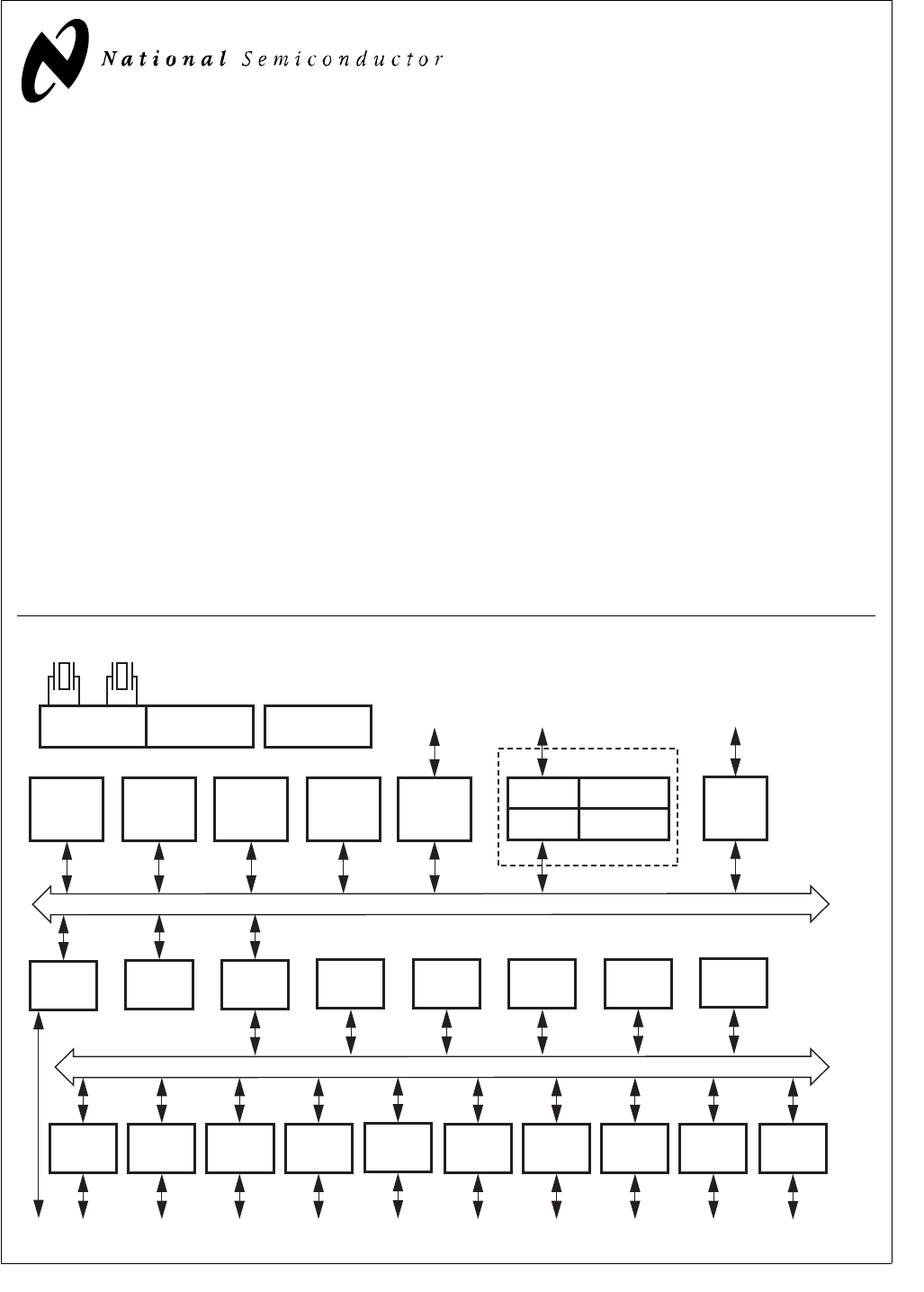
Block Diagram
CPU Core Bus
12 MHz and 32 kHz
Oscillator
Peripheral Bus
PLL and Clock
Generator Power-on-Reset
Bus
Interface
Unit
Peripheral
Bus
Controller
Serial
Debug
Interface
DMA
Controller
Interrupt
Control
Unit
CVSD/PCM
Converter
Power
Manage-
ment
Timing and
Watchdog
Unit
8-Channel
12-bit ADC
Versatile
Timer Unit
Muti-Func-
tion Timer
Multi-Input
Wake-Up
GPIO Audio
Interface
Microwiire/
SPI Quad UART
Clock Generator
Protocol
Core
RF Interface
Bluetooth Lower
Link Controller
4.5K Bytes
Data RAM
1K Byte
Sequencer RAM
DS202
256K Bytes
Flash
Program
Memory
8K Bytes
Flash
Data
32K Bytes
Static
RAM
CR16C
CPU Core
ACCESS
.bus
CAN 2.0B
Controller
Random
Number
Generator
USB
Bluetooth is a registered trademark of Bluetooth SIG, Inc. and is used under license by National Semiconductor.
TRI-STATE is a registered trademark of National Semiconductor Corporation.

www.national.com 2
CP3BT26
Table of Contents
1.0 General Description . . . . . . . . . . . . . . . . . . . . . . . . . . 1
2.0 Features . . . . . . . . . . . . . . . . . . . . . . . . . . . . . . . . . . . . 3
3.0 Device Overview . . . . . . . . . . . . . . . . . . . . . . . . . . . . . 4
3.1 CR16C CPU Core . . . . . . . . . . . . . . . . . . . . . . . . . . . . . . . . . . . . . 4
3.2 Memory. . . . . . . . . . . . . . . . . . . . . . . . . . . . . . . . . . . . . . . . . . . . . . 4
3.3 Input/Output Ports . . . . . . . . . . . . . . . . . . . . . . . . . . . . . . . . . . . . . 4
3.4 Bus Interface Unit. . . . . . . . . . . . . . . . . . . . . . . . . . . . . . . . . . . . . . 4
3.5 Interrupt Control Unit (ICU). . . . . . . . . . . . . . . . . . . . . . . . . . . . . . . 4
3.6 Multi-Input Wake-up . . . . . . . . . . . . . . . . . . . . . . . . . . . . . . . . . . . . 4
3.7 Bluetooth LLC. . . . . . . . . . . . . . . . . . . . . . . . . . . . . . . . . . . . . . . . . 5
3.8 USB . . . . . . . . . . . . . . . . . . . . . . . . . . . . . . . . . . . . . . . . . . . . . . . . 5
3.9 CAN Interface. . . . . . . . . . . . . . . . . . . . . . . . . . . . . . . . . . . . . . . . . 5
3.10 Quad UART . . . . . . . . . . . . . . . . . . . . . . . . . . . . . . . . . . . . . . . . . . 5
3.11 Advanced Audio interface. . . . . . . . . . . . . . . . . . . . . . . . . . . . . . . . 5
3.12 CVSD/PCM Conversion Module. . . . . . . . . . . . . . . . . . . . . . . . . . . 5
3.13 12-bit Analog to Digital Converter. . . . . . . . . . . . . . . . . . . . . . . . . . 5
3.14 Random Number Generator . . . . . . . . . . . . . . . . . . . . . . . . . . . . . . 6
3.15 Microwire/SPI . . . . . . . . . . . . . . . . . . . . . . . . . . . . . . . . . . . . . . . . . 6
3.16 ACCESS.bus Interface . . . . . . . . . . . . . . . . . . . . . . . . . . . . . . . . . . 6
3.17 Multi-Function Timer. . . . . . . . . . . . . . . . . . . . . . . . . . . . . . . . . . . . 6
3.18 Timing and Watchdog Module . . . . . . . . . . . . . . . . . . . . . . . . . . . . 6
3.19 Versatile Timer Unit . . . . . . . . . . . . . . . . . . . . . . . . . . . . . . . . . . . . 6
3.20 Triple Clock and Reset . . . . . . . . . . . . . . . . . . . . . . . . . . . . . . . . . . 6
3.21 Power Management . . . . . . . . . . . . . . . . . . . . . . . . . . . . . . . . . . . . 7
3.22 DMA Controller . . . . . . . . . . . . . . . . . . . . . . . . . . . . . . . . . . . . . . . . 7
3.23 Serial Debug Interface . . . . . . . . . . . . . . . . . . . . . . . . . . . . . . . . . . 7
3.24 Development Support. . . . . . . . . . . . . . . . . . . . . . . . . . . . . . . . . . . 7
4.0 Signal Descriptions . . . . . . . . . . . . . . . . . . . . . . . . . . . 8
5.0 CPU Architecture. . . . . . . . . . . . . . . . . . . . . . . . . . . . 15
5.1 General-Purpose Registers . . . . . . . . . . . . . . . . . . . . . . . . . . . . . 15
5.2 Dedicated Address Registers . . . . . . . . . . . . . . . . . . . . . . . . . . . . 15
5.3 Processor Status Register (PSR) . . . . . . . . . . . . . . . . . . . . . . . . . 16
5.4 Configuration Register (CFG). . . . . . . . . . . . . . . . . . . . . . . . . . . . 17
5.5 Addressing Modes . . . . . . . . . . . . . . . . . . . . . . . . . . . . . . . . . . . . 18
5.6 Stacks. . . . . . . . . . . . . . . . . . . . . . . . . . . . . . . . . . . . . . . . . . . . . . 19
5.7 Instruction Set. . . . . . . . . . . . . . . . . . . . . . . . . . . . . . . . . . . . . . . . 19
6.0 Memory. . . . . . . . . . . . . . . . . . . . . . . . . . . . . . . . . . . . 24
6.1 Operating Environment. . . . . . . . . . . . . . . . . . . . . . . . . . . . . . . . . 24
6.2 Bus Interface Unit (BIU) . . . . . . . . . . . . . . . . . . . . . . . . . . . . . . . . 25
6.3 Bus Cycles . . . . . . . . . . . . . . . . . . . . . . . . . . . . . . . . . . . . . . . . . . 25
6.4 BIU Control Registers. . . . . . . . . . . . . . . . . . . . . . . . . . . . . . . . . . 25
6.5 Wait and Hold States . . . . . . . . . . . . . . . . . . . . . . . . . . . . . . . . . . 28
7.0 System Configuration Registers . . . . . . . . . . . . . . . 29
7.1 Module Configuration Register (MCFG) . . . . . . . . . . . . . . . . . . . . 29
7.2 Module Status Register (MSTAT). . . . . . . . . . . . . . . . . . . . . . . . . 30
7.3 Software Reset Register (SWRESET) . . . . . . . . . . . . . . . . . . . . . 30
8.0 Flash Memory . . . . . . . . . . . . . . . . . . . . . . . . . . . . . . 31
8.1 Flash Memory Protection . . . . . . . . . . . . . . . . . . . . . . . . . . . . . . . 31
8.2 Flash Memory Organization . . . . . . . . . . . . . . . . . . . . . . . . . . . . . 31
8.3 Flash Memory Operations . . . . . . . . . . . . . . . . . . . . . . . . . . . . . . 32
8.4 Information Block Words . . . . . . . . . . . . . . . . . . . . . . . . . . . . . . . 34
8.5 Flash Memory Interface Registers . . . . . . . . . . . . . . . . . . . . . . . . 35
9.0 DMA Controller . . . . . . . . . . . . . . . . . . . . . . . . . . . . . 41
9.1 Channel Assignment . . . . . . . . . . . . . . . . . . . . . . . . . . . . . . . . . . 41
9.2 Transfer Types . . . . . . . . . . . . . . . . . . . . . . . . . . . . . . . . . . . . . . . 41
9.3 Operation Modes . . . . . . . . . . . . . . . . . . . . . . . . . . . . . . . . . . . . . 42
9.4 Software DMA Request . . . . . . . . . . . . . . . . . . . . . . . . . . . . . . . . 43
9.5 Debug Mode. . . . . . . . . . . . . . . . . . . . . . . . . . . . . . . . . . . . . . . . . 43
9.6 DMA Controller Register Set . . . . . . . . . . . . . . . . . . . . . . . . . . . . 43
10.0 Interrupts . . . . . . . . . . . . . . . . . . . . . . . . . . . . . . . . . . 47
10.1 Non-Maskable Interrupts . . . . . . . . . . . . . . . . . . . . . . . . . . . . . . . 47
10.2 Maskable Interrupts . . . . . . . . . . . . . . . . . . . . . . . . . . . . . . . . . . . 47
10.3 Interrupt Controller Registers . . . . . . . . . . . . . . . . . . . . . . . . . . . . 47
10.4 Maskable Interrupt Sources . . . . . . . . . . . . . . . . . . . . . . . . . . . . . 50
10.5 Nested Interrupts . . . . . . . . . . . . . . . . . . . . . . . . . . . . . . . . . . . . . 50
11.0 Triple Clock and Reset . . . . . . . . . . . . . . . . . . . . . . . 51
11.1 External Crystal Network . . . . . . . . . . . . . . . . . . . . . . . . . . . . . . . 52
11.2 Main Clock . . . . . . . . . . . . . . . . . . . . . . . . . . . . . . . . . . . . . . . . . . 53
11.3 Slow Clock . . . . . . . . . . . . . . . . . . . . . . . . . . . . . . . . . . . . . . . . . . 53
11.4 PLL Clock . . . . . . . . . . . . . . . . . . . . . . . . . . . . . . . . . . . . . . . . . . . 53
11.5 System Clock . . . . . . . . . . . . . . . . . . . . . . . . . . . . . . . . . . . . . . . . 54
11.6 Auxiliary Clocks . . . . . . . . . . . . . . . . . . . . . . . . . . . . . . . . . . . . . . 54
11.7 Power-On Reset. . . . . . . . . . . . . . . . . . . . . . . . . . . . . . . . . . . . . . 54
11.8 External Reset . . . . . . . . . . . . . . . . . . . . . . . . . . . . . . . . . . . . . . . 54
11.9 Clock and Reset Registers. . . . . . . . . . . . . . . . . . . . . . . . . . . . . . 54
12.0 Power Management. . . . . . . . . . . . . . . . . . . . . . . . . . 56
12.1 Active Mode . . . . . . . . . . . . . . . . . . . . . . . . . . . . . . . . . . . . . . . . . 56
12.2 Power Save Mode . . . . . . . . . . . . . . . . . . . . . . . . . . . . . . . . . . . . 56
12.3 Idle Mode . . . . . . . . . . . . . . . . . . . . . . . . . . . . . . . . . . . . . . . . . . . 57
12.4 Halt Mode . . . . . . . . . . . . . . . . . . . . . . . . . . . . . . . . . . . . . . . . . . . 57
12.5 Hardware Clock Control . . . . . . . . . . . . . . . . . . . . . . . . . . . . . . . . 57
12.6 Power Management Registers . . . . . . . . . . . . . . . . . . . . . . . . . . . 57
12.7 Switching Between Power Modes . . . . . . . . . . . . . . . . . . . . . . . . 59
13.0 Multi-Input Wake-Up . . . . . . . . . . . . . . . . . . . . . . . . . 61
13.1 Multi-Input Wake-Up Registers. . . . . . . . . . . . . . . . . . . . . . . . . . . 62
13.2 Programming Procedures. . . . . . . . . . . . . . . . . . . . . . . . . . . . . . . 66
14.0 Input/Output Ports . . . . . . . . . . . . . . . . . . . . . . . . . . . 67
14.1 Port Registers. . . . . . . . . . . . . . . . . . . . . . . . . . . . . . . . . . . . . . . . 67
14.2 Open-Drain Operation . . . . . . . . . . . . . . . . . . . . . . . . . . . . . . . . . 71
15.0 Bluetooth Controller . . . . . . . . . . . . . . . . . . . . . . . . . 72
15.1 RF Interface . . . . . . . . . . . . . . . . . . . . . . . . . . . . . . . . . . . . . . . . . 72
15.2 Serial Interface . . . . . . . . . . . . . . . . . . . . . . . . . . . . . . . . . . . . . . . 73
15.3 LMX5251 Power-Up Sequence . . . . . . . . . . . . . . . . . . . . . . . . . . 76
15.4 LMX5252 Power-Up Sequence . . . . . . . . . . . . . . . . . . . . . . . . . . 76
15.5 Bluetooth Sleep Mode . . . . . . . . . . . . . . . . . . . . . . . . . . . . . . . . . 77
15.6 Bluetooth Global Registers . . . . . . . . . . . . . . . . . . . . . . . . . . . . . . 77
15.7 Bluetooth Sequencer RAM . . . . . . . . . . . . . . . . . . . . . . . . . . . . . . 77
15.8 Bluetooth Shared Data RAM . . . . . . . . . . . . . . . . . . . . . . . . . . . . 78
16.0 12-Bit Analog to Digital Converter . . . . . . . . . . . . . . 79
16.1 Functional Description . . . . . . . . . . . . . . . . . . . . . . . . . . . . . . . . . 79
16.2 Touchscreen Interface . . . . . . . . . . . . . . . . . . . . . . . . . . . . . . . . . 81
16.3 ADC Operation in Power-Saving Modes . . . . . . . . . . . . . . . . . . . 83
16.4 Freeze. . . . . . . . . . . . . . . . . . . . . . . . . . . . . . . . . . . . . . . . . . . . . . 83
16.5 ADC Register Set . . . . . . . . . . . . . . . . . . . . . . . . . . . . . . . . . . . . . 83
17.0 Random Number Generator (RNG). . . . . . . . . . . . . . 88
17.1 Freeze. . . . . . . . . . . . . . . . . . . . . . . . . . . . . . . . . . . . . . . . . . . . . . 88
17.2 Random Number Generator Register Set . . . . . . . . . . . . . . . . . . 89
18.0 USB Controller . . . . . . . . . . . . . . . . . . . . . . . . . . . . . . 90
18.1 Functional States . . . . . . . . . . . . . . . . . . . . . . . . . . . . . . . . . . . . . 90
18.2 Endpoint Operation. . . . . . . . . . . . . . . . . . . . . . . . . . . . . . . . . . . . 91
18.3 USB Controller Registers . . . . . . . . . . . . . . . . . . . . . . . . . . . . . . . 93
18.4 Transceiver Interface . . . . . . . . . . . . . . . . . . . . . . . . . . . . . . . . . 108
19.0 CAN Module . . . . . . . . . . . . . . . . . . . . . . . . . . . . . . . 109
19.1 Functional Description . . . . . . . . . . . . . . . . . . . . . . . . . . . . . . . . 109
19.2 Basic CAN Concepts . . . . . . . . . . . . . . . . . . . . . . . . . . . . . . . . . 110
19.3 Message Transfer. . . . . . . . . . . . . . . . . . . . . . . . . . . . . . . . . . . . 118
19.4 Acceptance Filtering . . . . . . . . . . . . . . . . . . . . . . . . . . . . . . . . . . 119
19.5 Receive Structure . . . . . . . . . . . . . . . . . . . . . . . . . . . . . . . . . . . . 120
19.6 Transmit Structure . . . . . . . . . . . . . . . . . . . . . . . . . . . . . . . . . . . 123
19.7 Interrupts. . . . . . . . . . . . . . . . . . . . . . . . . . . . . . . . . . . . . . . . . . . 125
19.8 Time Stamp Counter. . . . . . . . . . . . . . . . . . . . . . . . . . . . . . . . . . 126
19.9 Memory Organization . . . . . . . . . . . . . . . . . . . . . . . . . . . . . . . . . 127
19.10 CAN Controller Registers . . . . . . . . . . . . . . . . . . . . . . . . . . . . . . 128
19.11 System Start-Up and Multi-Input Wake-Up. . . . . . . . . . . . . . . . . 140
19.12 Usage Hint . . . . . . . . . . . . . . . . . . . . . . . . . . . . . . . . . . . . . . . . . 142
20.0 Advanced Audio Interface . . . . . . . . . . . . . . . . . . . . 143
20.1 Audio Interface Signals . . . . . . . . . . . . . . . . . . . . . . . . . . . . . . . . 143
20.2 Audio Interface Modes . . . . . . . . . . . . . . . . . . . . . . . . . . . . . . . . 143
20.3 Bit Clock Generation. . . . . . . . . . . . . . . . . . . . . . . . . . . . . . . . . . 146
20.4 Frame Clock Generation. . . . . . . . . . . . . . . . . . . . . . . . . . . . . . . 146
20.5 Audio Interface Operation . . . . . . . . . . . . . . . . . . . . . . . . . . . . . . 146
20.6 Communication Options . . . . . . . . . . . . . . . . . . . . . . . . . . . . . . . 148
20.7 Audio Interface Registers . . . . . . . . . . . . . . . . . . . . . . . . . . . . . . 151
21.0 CVSD/PCM Conversion Module . . . . . . . . . . . . . . . 158
21.1 Operation . . . . . . . . . . . . . . . . . . . . . . . . . . . . . . . . . . . . . . . . . . 158
21.2 PCM Conversions. . . . . . . . . . . . . . . . . . . . . . . . . . . . . . . . . . . . 158
21.3 CVSD Conversion. . . . . . . . . . . . . . . . . . . . . . . . . . . . . . . . . . . . 159
21.4 PCM to CVSD Conversion . . . . . . . . . . . . . . . . . . . . . . . . . . . . . 159
21.5 CVSD to PCM Conversion . . . . . . . . . . . . . . . . . . . . . . . . . . . . . 159
21.6 Interrupt Generation . . . . . . . . . . . . . . . . . . . . . . . . . . . . . . . . . . 159
21.7 DMA Support . . . . . . . . . . . . . . . . . . . . . . . . . . . . . . . . . . . . . . . 159
21.8 Freeze. . . . . . . . . . . . . . . . . . . . . . . . . . . . . . . . . . . . . . . . . . . . . 160
21.9 CVSD/PCM Converter Registers . . . . . . . . . . . . . . . . . . . . . . . . 160
22.0 UART Modules . . . . . . . . . . . . . . . . . . . . . . . . . . . . . 163
22.1 Functional Overview . . . . . . . . . . . . . . . . . . . . . . . . . . . . . . . . . . 163
22.2 UART Operation . . . . . . . . . . . . . . . . . . . . . . . . . . . . . . . . . . . . . 163
22.3 UART Registers . . . . . . . . . . . . . . . . . . . . . . . . . . . . . . . . . . . . . 168
22.4 Baud Rate Calculations . . . . . . . . . . . . . . . . . . . . . . . . . . . . . . . 172
23.0 Microwire/SPI Interface . . . . . . . . . . . . . . . . . . . . . . 175
23.1 Microwire Operation . . . . . . . . . . . . . . . . . . . . . . . . . . . . . . . . . . 175
23.2 Master Mode. . . . . . . . . . . . . . . . . . . . . . . . . . . . . . . . . . . . . . . . 177
23.3 Slave Mode. . . . . . . . . . . . . . . . . . . . . . . . . . . . . . . . . . . . . . . . . 178
23.4 Interrupt Generation . . . . . . . . . . . . . . . . . . . . . . . . . . . . . . . . . . 178
23.5 Microwire Interface Registers . . . . . . . . . . . . . . . . . . . . . . . . . . . 179
24.0 ACCESS.bus Interface . . . . . . . . . . . . . . . . . . . . . . . 181
24.1 ACB Protocol Overview . . . . . . . . . . . . . . . . . . . . . . . . . . . . . . . 181
24.2 ACB Functional Description . . . . . . . . . . . . . . . . . . . . . . . . . . . . 183
24.3 ACCESS.bus Interface Registers . . . . . . . . . . . . . . . . . . . . . . . . 185
24.4 Usage Hints . . . . . . . . . . . . . . . . . . . . . . . . . . . . . . . . . . . . . . . . 189
25.0 Timing and Watchdog Module . . . . . . . . . . . . . . . . 192
25.1 TWM Structure . . . . . . . . . . . . . . . . . . . . . . . . . . . . . . . . . . . . . . 192
25.2 Timer T0 Operation. . . . . . . . . . . . . . . . . . . . . . . . . . . . . . . . . . . 192
25.3 Watchdog Operation. . . . . . . . . . . . . . . . . . . . . . . . . . . . . . . . . . 193
25.4 TWM Registers . . . . . . . . . . . . . . . . . . . . . . . . . . . . . . . . . . . . . . 193
25.5 Watchdog Programming Procedure . . . . . . . . . . . . . . . . . . . . . . 195
26.0 Multi-Function Timer . . . . . . . . . . . . . . . . . . . . . . . . 196
26.1 Timer Structure . . . . . . . . . . . . . . . . . . . . . . . . . . . . . . . . . . . . . . 196
26.2 Timer Operating Modes . . . . . . . . . . . . . . . . . . . . . . . . . . . . . . . 197
26.3 Timer Interrupts . . . . . . . . . . . . . . . . . . . . . . . . . . . . . . . . . . . . . 202
26.4 Timer I/O Functions . . . . . . . . . . . . . . . . . . . . . . . . . . . . . . . . . . 202
26.5 Timer Registers . . . . . . . . . . . . . . . . . . . . . . . . . . . . . . . . . . . . . 203
27.0 Versatile Timer Unit (VTU) . . . . . . . . . . . . . . . . . . . . 206
27.1 VTU Functional Description . . . . . . . . . . . . . . . . . . . . . . . . . . . . 206
27.2 VTU Registers . . . . . . . . . . . . . . . . . . . . . . . . . . . . . . . . . . . . . . 210
28.0 Register Map. . . . . . . . . . . . . . . . . . . . . . . . . . . . . . . 214
29.0 Register Bit Fields . . . . . . . . . . . . . . . . . . . . . . . . . . 230
30.0 Electrical Characteristics . . . . . . . . . . . . . . . . . . . . 243
30.1 Absolute Maximum Ratings . . . . . . . . . . . . . . . . . . . . . . . . . . . . 243
30.2 DC Electrical Characteristic . . . . . . . . . . . . . . . . . . . . . . . . . . . . 243
30.3 USB Transceiver Electrical Characteristics . . . . . . . . . . . . . . . . 245
30.4 ADC Electrical Characteristics . . . . . . . . . . . . . . . . . . . . . . . . . . 245
30.5 Flash Memory On-Chip Programming . . . . . . . . . . . . . . . . . . . . 246
30.6 Output Signal Levels. . . . . . . . . . . . . . . . . . . . . . . . . . . . . . . . . . 247
30.7 Clock and Reset Timing . . . . . . . . . . . . . . . . . . . . . . . . . . . . . . . 247
30.8 UART Timing . . . . . . . . . . . . . . . . . . . . . . . . . . . . . . . . . . . . . . . 249
30.9 I/O Port Timing . . . . . . . . . . . . . . . . . . . . . . . . . . . . . . . . . . . . . . 250
30.10 Advanced Audio Interface (AAI) Timing . . . . . . . . . . . . . . . . . . . 251
30.11 Microwire/SPI Timing . . . . . . . . . . . . . . . . . . . . . . . . . . . . . . . . . 253
30.12 ACCESS.bus Timing . . . . . . . . . . . . . . . . . . . . . . . . . . . . . . . . . 258
30.13 USB Port AC Characteristics . . . . . . . . . . . . . . . . . . . . . . . . . . . 261
30.14 Multi-Function Timer (MFT) Timing . . . . . . . . . . . . . . . . . . . . . . 261
30.15 Versatile Timing Unit (VTU) Timing . . . . . . . . . . . . . . . . . . . . . . 262
30.16 External Bus Timing . . . . . . . . . . . . . . . . . . . . . . . . . . . . . . . . . . 263
31.0 Pin Assignments . . . . . . . . . . . . . . . . . . . . . . . . . . . 269
31.1 LQFP-128 Package . . . . . . . . . . . . . . . . . . . . . . . . . . . . . . . . . . 269
31.2 LQFP-144 Package . . . . . . . . . . . . . . . . . . . . . . . . . . . . . . . . . . 272
32.0 Revision History . . . . . . . . . . . . . . . . . . . . . . . . . . . . 276
33.0 Physical Dimensions . . . . . . . . . . . . . . . . . . . . . . . . 277

3www.national.com
CP3BT26
2.0 Features
CPU Features
Fully static RISC processor core, capable of operating
from 0 to 24 MHz with zero wait/hold states
Minimum 41.7 ns instruction cycle time with a 24-MHz in-
ternal clock frequency, based on a 12-MHz external input
47 independently vectored peripheral interrupts
On-Chip Memory
256K bytes reprogrammable Flash program memory
8K bytes Flash data memory
32K bytes of static RAM data memory
Addresses up to 12M bytes of external memory
Broad Range of Hardware Communications Peripherals
Bluetooth Lower Link Controller (LLC) including a shared
4.5K byte Bluetooth RAM and 1K byte Bluetooth Se-
quencer RAM
Universal Serial Bus (USB) 1.1 full-speed node
ACCESS.bus serial bus (compatible with Philips I2C bus)
CAN interface with 15 message buffers conforming to
CAN specification 2.0B active
8/16-bit SPI, Microwire/Plus serial interface
Four-channel Universal Asynchronous Receiver/Trans-
mitter (UART), one channel has USART capability
Advanced Audio Interface (AAI) to connect to external 8/
13-bit PCM Codecs as well as to ISDN-Controllers
through the IOM-2 interface (slave only)
CVSD/PCM converter supporting one bidirectional audio
connection
General-Purpose Hardware Peripherals
12-bit A/D Converter (ADC)
Dual 16-bit Multi-Function Timer (MFT)
Versatile Timer Unit with four subsystems (VTU)
Four-channel DMA controller
Timing and Watchdog Unit
Random Number Generator peripheral
Extensive Power and Clock Management Support
On-chip Phase Locked Loop
Support for multiple clock options
Dual clock and reset
Power-down modes
Flexible I/O
Up to 54 general-purpose I/O pins (shared with on-chip
peripheral I/O)
Programmable I/O pin characteristics: TRI-STATE out-
put, push-pull output, weak pull-up input, high-imped-
ance input
Schmitt triggers on general-purpose inputs
Multi-Input Wake-Up (MIWU) capability
Power Supply
I/O port operation at 2.5V to 3.3V
Core logic operation at 2.5V
On-chip power-on reset
Temperature Range
-40°C to +85°C (Industrial)
Packages
LQFP-128, LQFP-144
Complete Development Environment
Pre-integrated hardware and software support for rapid
prototyping and production
Integrated environment
Project manager
Multi-file C source editor
High-level C source debugger
Comprehensive, integrated, one-stop technical support
Bluetooth Protocol Stack
Applications can interface to the high-level protocols or
directly to the low-level Host Controller Interface (HCI)
Transport layer support allows HCI command-based in-
terface over UART port
Baseband (Link Controller) hardware minimizes the
bandwidth demand on the CPU
Link Manager (LM)
Logical Link Control and Adaptation Protocol (L2CAP)
Service Discovery Protocol (SDP)
RFCOMM Serial Port Emulation Protocol
All packet types, piconet, and scatternet functionality
supported
CP3BT26 Connectivity Processor Selection Guide
NSID Speed
(MHz) Temp. Range
Program
Flash
(Kbytes)
Data
Flash
(Kbytes)
SRAM
(Kbytes)
External
Address
Lines
I/Os Package
Type
CP3BT26G18NEP 24 -40° to +85°C 256 8 32 0 54 LQFP-128
CP3BT26G18NEPNOPB 24 -40° to +85°C 256 8 32 0 54 LQFP-128
CP3BT26G18NEPX 24 -40° to +85°C 256 8 32 0 54 LQFP-128
CP3BT26G18NEPXNOPB 24 -40° to +85°C 256 8 32 0 54 LQFP-128
CP3BT26Y98NEP 24 -40° to +85°C 256 8 32 23 48 LQFP-144
CP3BT26Y98NEPNOPB 24 -40° to +85°C 256 8 32 23 48 LQFP-144
CP3BT26Y98NEPX 24 -40° to +85°C 256 8 32 23 48 LQFP-144
CP3BT26Y98NEPXNOPB 24 -40° to +85°C 256 8 32 23 48 LQFP-144
NEP - Erased part (Bluetooth device address in Information Block 1); X - Tape and reel; NOPB - No lead solder

www.national.com 4
CP3BT26
3.0 Device Overview
The CP3BT26 connectivity processor is a complete micro-
computer with all system timing, interrupt logic, program
memory, data memory, and I/O ports included on-chip, mak-
ing it well-suited to a wide range of embedded applications.
The block diagram on page 1 shows the major on-chip com-
ponents of the CP3BT26 devices.
3.1 CR16C CPU CORE
The CP3BT26 device implements the CR16C CPU core
module. The high performance of the CPU core results from
the implementation of a pipelined architecture with a two-
bytes-per-cycle pipelined system bus. As a result, the CPU
can support a peak execution rate of one instruction per
clock cycle.
For more information, please refer to the CR16C Program-
mer’s Reference Manual (document number 424521772-
101, which may be downloaded from National’s web site at
http://www.national.com).
3.2 MEMORY
The CP3BT26 devices support a uniform linear address
space of up to 16 megabytes. Three types of on-chip mem-
ory occupy specific regions within this address space, along
with any external memory:
256K bytes of Flash program memory
8K bytes of Flash data memory
32K bytes of static RAM
Up to 12M bytes of external memory (144-pin devices)
The 256K bytes of Flash program memory are used to store
the application program, Bluetooth protocol stack, and real-
time operating system. The Flash memory has security fea-
tures to prevent unintentional programming and to prevent
unauthorized access to the program code. This memory
can be programmed with an external programming unit or
with the device installed in the application system (in-sys-
tem programming).
The 8K bytes of Flash data memory are used for non-vola-
tile storage of data entered by the end-user, such as config-
uration settings.
The 32K bytes of static RAM are used for temporary storage
of data and for the program stack and interrupt stack. Read
and write operations can be byte-wide or word-wide, de-
pending on the instruction executed by the CPU.
Up to 12M bytes of external memory can be added on an
external bus. The external bus is only available on devices
in 144-pin packages.
For Flash program and data memory, the device internally
generates the necessary voltages for programming. No ad-
ditional power supply is required.
3.3 INPUT/OUTPUT PORTS
The device has up to 54 software-configurable I/O pins, or-
ganized into seven ports called Port B, Port C, Port E, Port
G, Port H, Port I, and Port J. Each pin can be configured to
operate as a general-purpose input or general-purpose out-
put. In addition, many I/O pins can be configured to operate
as inputs or outputs for on-chip peripheral modules such as
the UART, timers, or Microwire/SPI interface.
The I/O pin characteristics are fully programmable. Each pin
can be configured to operate as a TRI-STATE output, push-
pull output, weak pull-up input, or high-impedance input.
3.4 BUS INTERFACE UNIT
The Bus Interface Unit (BIU) controls access to internal/ex-
ternal memory and I/O. It determines the configured param-
eters for bus access (such as the number of wait states for
memory access) and issues the appropriate bus signals for
each requested access.
The BIU uses a set of control registers to determine how
many wait states and hold states are used when accessing
Flash program memory and the I/O area. At start-up, the
configuration registers are set for slowest possible memory
access. To achieve fastest possible program execution, ap-
propriate values must be programmed. These settings vary
with the clock frequency and the type of off-chip device be-
ing accessed.
3.5 INTERRUPT CONTROL UNIT (ICU)
The ICU receives interrupt requests from internal and exter-
nal sources and generates interrupts to the CPU. An inter-
rupt is an event that temporarily stops the normal flow of
program execution and causes a separate interrupt handler
to be executed. After the interrupt is serviced, CPU execu-
tion continues with the next instruction in the program fol-
lowing the point of interruption.
Interrupts from the timers, UARTs, Microwire/SPI interface,
and Multi-Input Wake-Up, are all maskable interrupts; they
can be enabled or disabled by software. There are 47
maskable interrupts, assigned to 47 linear priority levels.
The highest-priority interrupt is the Non-Maskable Interrupt
(NMI), which is generated by a signal received on the NMI
input pin.
3.6 MULTI-INPUT WAKE-UP
The two Multi-Input Wake-Up (MIWU) modules can be used
for two purposes: to provide inputs for waking up (exiting)
from the Halt, Idle, or Power Save mode, and to provide gen-
eral-purpose edge-triggered maskable interrupts to the lev-
el-sensitive interrupt control unit (ICU) inputs. Each 16-
channel module generates four programmable interrupts to
the ICU, for a total of 8 ICU inputs generated from 32 MIWU
inputs. Channels can be individually enabled or disabled,
and programmed to respond to positive or negative edges.

5www.national.com
CP3BT26
3.7 BLUETOOTH LLC
The integrated hardware Bluetooth Lower Link Controller
(LLC) complies to the Bluetooth Specification Version 1.1
and integrates the following functions:
4.5K-byte dedicated Bluetooth Data RAM
1K-byte dedicated Bluetooth Sequencer RAM
Support of all Bluetooth 1.1 packet types
Support for fast frequency hopping of 1600 hops/s
Access code correlation and slot timing recovery circuit
Power Management Control Logic
BlueRF-compatible interface (mode 2/3) to connect with
National’s LMX5252 and other RF transceiver chips
3.8 USB
The CR16 USB node is a Universal Serial Bus (USB) Node
controller compatible with USB Specification 1.1. It inte-
grates the required USB transceiver, the Serial Interface En-
gine (SIE), and USB endpoint FIFOs. A total of seven
endpoint pipes are supported: one bidirectional pipe for the
mandatory control EP0 and an additional six pipes for unidi-
rectional endpoints to support USB interrupt, bulk, and iso-
chronous data transfers.
3.9 CAN INTERFACE
The CAN module contains a Full CAN 2.0B class, CAN se-
rial bus interface for applications that require a high-speed
(up to 1 Mbits per second) or a low-speed interface with
CAN bus master capability. The data transfer between CAN
and the CPU is established by 15 memory-mapped mes-
sage buffers, which can be individually configured as re-
ceive or transmit buffers. An incoming message is filtered by
two masks, one for the first 14 message buffers and another
one for the 15th message buffer to provide a basic CAN
path. A priority decoder allows any buffer to have the high-
est or lowest transmit priority. Remote transmission re-
quests can be processed automatically by automatic
reconfiguration to a receiver after transmission or by auto-
mated transmit scheduling upon reception. In addition, a
time stamp counter (16-bits wide) is provided to support
real-time applications.
The CAN module is a fast core bus peripheral, which allows
single-cycle byte or word read/write access. A set of diag-
nostic features (such as loopback, listen only, and error
identification) support the development with the CAN mod-
ule and provide a sophisticated error management tool.
The CAN receiver can trigger a wake-up condition out of the
low-power modes through the Multi-Input Wake-Up module.
3.10 QUAD UART
Four UART modules support a wide range of programmable
baud rates and data formats, parity generation, and several
error detection schemes. The baud rate is generated on-
chip, under software control. One UART channel supports
hardware flow control, DMA, and USART capability (syn-
chronous mode).
The UARTs offer a wake-up condition from the low-power
modes using the Multi-Input Wake-Up module.
3.11 ADVANCED AUDIO INTERFACE
The audio interface provides a serial synchronous, full-du-
plex interface to CODECs and similar serial devices. Trans-
mit and receive paths operate asynchronously with respect
to each other. Each path uses three signals for communica-
tion: shift clock, frame synchronization, and data.
When the receiver and transmitter use separate shift clocks
and frame sync signals, the interface operates in its asyn-
chronous mode. Alternatively, the transmit and receive path
can share the same shift clock and frame sync signals for
synchronous mode operation.
3.12 CVSD/PCM CONVERSION MODULE
The CVSD/PCM module performs conversion between
CVSD data and PCM data, in which the CVSD encoding is
as defined in the Bluetooth specification and the PCM data
can be 8-bit µ-Law, 8-bit A-Law, or 13-bit to 16-bit Linear.
3.13 12-BIT ANALOG TO DIGITAL
CONVERTER
This device contains an 8-channel, multiplexed input, suc-
cessive approximation, 12-bit Analog-to-Digital Converter. It
supports both Single Ended and Differential modes of oper-
ation.
The integrated 12-bit ADC provides the following features:
8-channel, multiplexed input
4 differential channels
Single-ended and differential external filtering capability
12-bit resolution; 11-bit accuracy
15-microsecond conversion time
Support for 4-wire touchscreen applications
External start trigger
Programmable start delay after start trigger
Poll or interrupt on done
The ADC is compatible with 4-wire resistive touchscreen
applications and is intended to provide the resolution neces-
sary to support handwriting recognition. Low-ohmic touch-
screen drivers are provided internally on the ADC[3:0] pins.
Pendown detection is also provided.
The ADC provides several options for the voltage reference
source. The positive reference can be ADVCC (internal),
VREFP, ADC0, or ADC3. The negative reference can be
ADVCC (internal), ADC1, or ADC2.
Two specific analog channel selection modes are support-
ed. These are as follows:
Allow any specific channel to be selected at one time.
The A/D Converter performs the specific conversion re-
quested and stops.
Allow any differential channel pair to be selected at one
time. The A/D Converter performs the specific differential
conversion requested and stops.
In both Single-Ended and Differential modes, there is the
capability to connect the analog multiplexer output and A/D
converter input to external pins. This provides the ability to
externally connect a common filter/signal conditioning cir-
cuit for the A/D Converter.

www.national.com 6
CP3BT26
3.14 RANDOM NUMBER GENERATOR
RNG peripheral for use in Trusted Computer Peripheral Ap-
plications (TCPA) to improve the authenticity, integrity, and
privacy of Internet-based communication and commerce.
3.15 MICROWIRE/SPI
The Microwire/SPI (MWSPI) interface module supports syn-
chronous serial communications with other devices that
conform to Microwire or Serial Peripheral Interface (SPI)
specifications. It supports 8-bit and 16-bit data transfers.
The Microwire interface allows several devices to communi-
cate over a single system consisting of four wires: serial in,
serial out, shift clock, and slave enable. At any given time,
the Microwire interface operates as the master or a slave.
The Microwire interface supports the full set of slave select
for multi-slave implementation.
In master mode, the shift clock is generated on-chip under
software control. In slave mode, a wake-up out of a low-
power mode may be triggered using the Multi-Input Wake-
Up module.
3.16 ACCESS.BUS INTERFACE
The ACCESS.bus interface module (ACB) is a two-wire se-
rial interface compatible with the ACCESS.bus physical lay-
er. It is also compatible with Intel’s System Management
Bus (SMBus) and Philips’ I2C bus. The ACB module can be
configured as a bus master or slave, and it can maintain bi-
directional communications with both multiple master and
slave devices.
The ACCESS.bus receiver can trigger a wake-up condition
out of the low-power modes through the Multi-Input Wake-
Up module.
3.17 MULTI-FUNCTION TIMER
The Multi-Function Timer (MFT) module contains a pair of
16-bit timer/counter registers. Each timer/counter unit can
be configured to operate in any of the following modes:
—Processor-Independent Pulse Width Modulation
(PWM) mode: Generates pulses of a specified width
and duty cycle and provides a general-purpose timer/
counter.
—Dual Input Capture mode: Measures the elapsed time
between occurrences of external event and provides
a general-purpose timer/counter.
—Dual Independent Timer mode: Generates system
timing signals or counts occurrences of external
events.
—Single Input Capture and Single Timer mode: Pro-
vides one external event counter and one system tim-
er.
3.18 TIMING AND WATCHDOG MODULE
The Timing and Watchdog Module (TWM) contains a Real-
Time timer and a Watchdog unit. The Real-Time Clock Tim-
ing function can be used to generate periodic real-time
based system interrupts. The timer output is one of 16 in-
puts to the Multi-Input Wake-Up module which can be used
to exit from a power-saving mode. The Watchdog unit is de-
signed to detect the application program getting stuck in an
infinite loop resulting in loss of program control or “runaway”
programs. When the watchdog triggers, it resets the device.
The TWM is clocked by the low-speed System Clock.
3.19 VERSATILE TIMER UNIT
The Versatile Timer Unit (VTU) module contains four inde-
pendent timer subsystems, each operating in either dual 8-
bit PWM configuration, as a single 16-bit PWM timer, or a
16-bit counter with two input capture channels. Each of the
four timer subsystems offer an 8-bit clock prescaler to ac-
commodate a wide range of frequencies.
3.20 TRIPLE CLOCK AND RESET
The Triple Clock and Reset module generates a high-speed
main System Clock from an external crystal network. It also
provides the main system reset signal and a power-on reset
function.
This module generates a slow System Clock (32.768 kHz)
from an optional external crystal network. The Slow Clock is
used for operating the device in a low-power mode. The
32.768 kHz external crystal network is optional, because
the low speed System Clock can be derived from the high-
speed clock by a prescaler. Also, two independent clocks di-
vided down from the high speed clock are available on out-
put pins.
The Triple Clock and Reset module provides the clock sig-
nals required for the operation of the various CP3BT26 on-
chip modules. From external crystal networks, it generates
the Main Clock, which can be scaled up to 24 MHz from an
external 12 MHz input clock, and a 32.768 kHz secondary
System Clock. The 12 MHz external clock is primarily used
as the reference frequency for the on-chip PLL. The clock
for modules which require a fixed clock rate (e.g. the Blue-
tooth LLC and the CVSD/PCM transcoder) is also generat-
ed through prescalers from the 12 MHz clock. The PLL may
be used to drive the high-speed System Clock through a
prescaler. Alternatively, the high speed System Clock can
be derived directly from the 12 MHz Main Clock.
In addition, this module generates the device reset by using
reset input signals coming from an external reset and vari-
ous on-chip modules.

7www.national.com
CP3BT26
3.21 POWER MANAGEMENT
The Power Management Module (PMM) improves the effi-
ciency of the device by changing the operating mode and
power consumption to match the required level of activity.
The device can operate in any of four power modes:
—Active: The device operates at full speed using the
high-frequency clock. All device functions are fully op-
erational.
—Power Save: The device operates at reduced speed
using the Slow Clock. The CPU and some modules
can continue to operate at this low speed.
—Idle: The device is inactive except for the Power Man-
agement Module and Timing and Watchdog Module,
which continue to operate using the Slow Clock.
—Halt: The device is inactive but still retains its internal
state (RAM and register contents).
3.22 DMA CONTROLLER
The Direct Memory Access Controller (DMAC) can speed
up data transfer between memory and I/O devices or be-
tween two memories, relative to data transfers performed di-
rectly by the CPU. A method called cycle-stealing allows the
CPU and the DMAC to share the CPU bus efficiently. The
DMAC implements four independent DMA channels. DMA
requests from a primary and a secondary source are recog-
nized for each DMA channel, as well as a software DMA re-
quest issued directly by the CPU. Table 1 shows the DMA
channel assignment on the CP3BT26 architecture. The fol-
lowing on-chip modules can assert a DMA request to the
DMAC:
• CR16C (Software DMA request)
•USB
• USART
• Advanced Audio Interface
• CVSD/PCM Converter
Table 1 shows how the four DMA channels are assigned
to the modules listed above.
Table 1 DMA Channel Assignment
The interface can handle data words of either 8- or 16-bit
length and data frames can consist of up to four slots.
In the normal mode of operation, the interface only transfers
one word at a periodic rate. In the network mode, the inter-
face transfers multiple words at a periodic rate. The periodic
rate is also called a data frame and each word within one
frame is called a slot. The beginning of each new data frame
is marked by the frame sync signal.
3.23 SERIAL DEBUG INTERFACE
The Serial Debug Interface module (SDI module) provides
a JTAG-based serial link to an external debugger, for exam-
ple running on a PC. In addition, the SDI module integrates
an on-chip debug module, which allows the user to set up to
eight hardware breakpoints on instruction execution and
data transfer. The SDI module can act as a CPU bus master
to access all memory mapped resources, such as RAM and
peripherals. Therefore it also allows for fast program code
download into the on-chip Flash program memory using the
JTAG interface.
3.24 DEVELOPMENT SUPPORT
In addition to providing the features needed for the next gen-
eration of embedded Bluetooth products, the CP3BT26 de-
vices are backed up by the software resources designers
need for rapid product development, including an operating
system, Bluetooth protocol stack implementation, peripher-
al drivers, reference designs, and an integrated develop-
ment environment. Combined with National’s LMX5251
Bluetooth radio transceiver, the CP3BT26 devices provide a
total Bluetooth system solution.
National Semiconductor offers a complete and industry-
proven application development environment for CP3BT26
applications, including the IAR Embedded Workbench,
iSYSTEM winIDEA and iC3000 Active Emulator, Bluetooth
Development Board, Bluetooth Protocol Stack, and Applica-
tion Software. See your National Semiconductor sales rep-
resentative for current information on availability and
features of emulation equipment and evaluation boards.
Channel Primary/
Secondary Peripheral Transaction
0Primary USB Read/Write
Secondary UART0 Read
1Primary UART0 Write
Secondary Unused N/A
2Primary AAI Read
Secondary CVSD/PCM Read
3Primary AAI Write
Secondary CVSD/PCM Write
www.national.com 8
CP3BT26
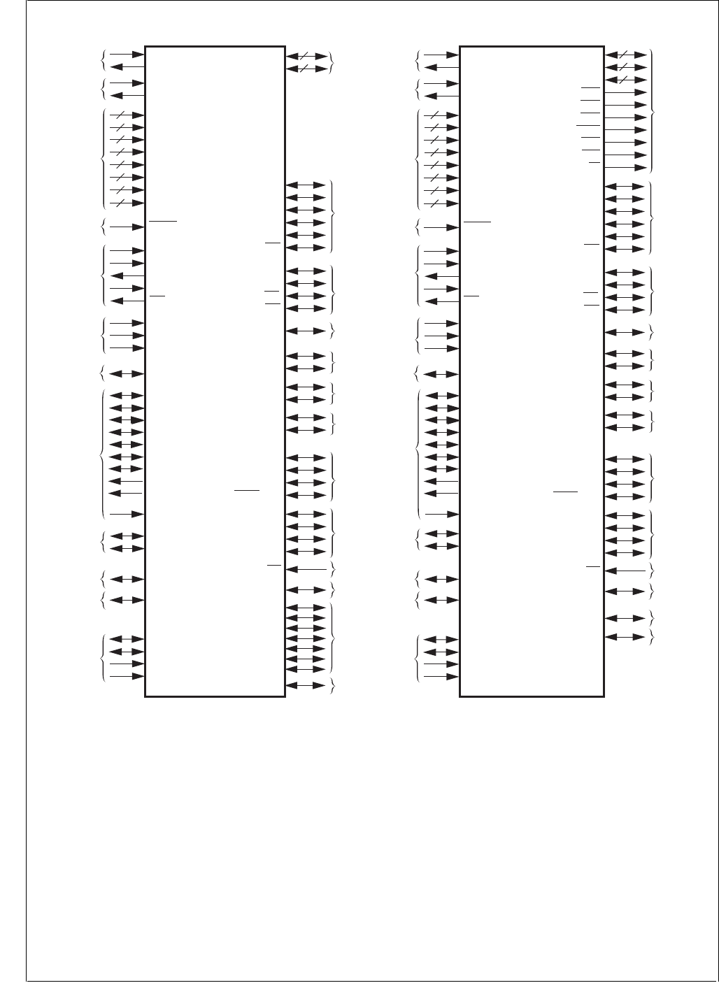
4.0 Signal Descriptions
Figure 1. CP3BT26 Device SIgnals
Some pins may be enabled as general-purpose I/O-port
pins or as alternate functions associated with specific pe-
ripherals or interfaces. These pins may be individually con-
figured as port pins, even when the associated peripheral or
interface is enabled. Table 2 describes the device signals for
the LQFP-128 package. Table 3 describes the device sig-
nals for the LQFP-144 package.
DS208
CP3BT26
(LQFP-128)
RF Interface
RFDATA
PGO/RFSYNC
PG1/RFCE
PG2/BTSEQ1/SRCLK
PE0/RXD0
PE1/TXD0
PE2/RTS
PE3/CTS
PG3/SCLK
PG4/SDAT
PG5/SLE
PE5/SRFS/NMI
UART0
PE4/CKX/TB UART0/MFT
Microwire/
SPI/
VTU
PF0/MSK/TIO1
PF1/MDIDO/TIO2
PF2/MDODO/TIO3
PF3/MWCS/TIO4
AAI/
VTU
PF4/SCK/TIO5
PF5/SFS/TIO6
PF6/STD/TIO7
PF7/SRD/TIO8
RF/AAI
AAI/NMI
X1CKI/BBCLK
12 MHz Crystal
or Ext. Clock X1CKO
X2CKI
32.768 kHz
Crystal X2CKO
ADVCC
GND
IOVCC
6
ADGND
VCC
ENV0
Mode
Selection ENV1
Power
Supply
RESET
Chip Reset
PG7/BTSEQ3/TA
RF/MFT
TMS
TCK
RDY
TDI
TDO
JTAG I/F to
Debugger/
Programmer
6
15
ENV2
1
1
ADC0/TSX+
ADC1/TSY+
ADC2/TSX-
ADC3/TSY-
ADC4/MUXOUT0
ADC5/MUXOUT1
ADC6
ADC7/ADCIN
PJ7/ASYNC/
WUI9
VREFP
ADC/
Touchscreen
IOGND
14
USB UVCC
UGND
D+
D-
SDA
ACCESS.bus SCL
PH0/RXD1/WUI11
PH1/TXD1/WUI12 UART1/MIWU
PH2/RXD1/WUI13
PH3/TXD1/WUI14 UART2/MIWU
PH4/RXD1/WUI15
PH5/TXD1/WUI16 UART3/MIWU
MIWU
PG6/BTSEQ2/WUI10
PJ0/WUI18
PJ1/WUI19
PJ2/WUI20
PJ3/WUI21
PJ4/WUI22
PJ5/WUI23
PJ6/WUI24
8
8
PB[7:0]
PC[7:0] GPIO
AVCC
AGND
1
1
X1CKI/BBCLK
12 MHz Crystal
or Ext. Clock
External
Bus
Interface
X1CKO
X2CKI
32.768 kHz
Crystal
RF Interface
X2CKO
ADVCC
GND
IOVCC
6
ADGND
VCC
RFDATA
PGO/RFSYNC
PG1/RFCE
PG2/BTSEQ1/SRCLK
CP3BT26
(LQFP-144)
SDA
ACCESS.bus SCL
ENV0
Mode
Selection ENV1
PE0/RXD0
PE1/TXD0
PE2/RTS
PE3/CTS
PG3/SCLK
PG4/SDAT
PG5/SLE
Power
Supply
RESET
Chip Reset
PE5/SRFS/NMI
UART0
PE4/CKX/TB UART0/MFT
PG7/BTSEQ3/TA
RF/MFT
TMS
TCK
RDY
TDI
TDO
JTAG I/F to
Debugger/
Programmer
Microwire/
SPI/
VTU
PF0/MSK/TIO1
PF1/MDIDO/TIO2
PF2/MDODO/TIO3
PF3/MWCS/TIO4
AAI/
VTU
PF4/SCK/TIO5
PF5/SFS/TIO6
PF6/STD/TIO7
PF7/SRD/TIO8
6
10
8
8
23
ENV2
PB[7:0]
PC[7:0]
A[22:0]
SEL0
SEL1
SEL2
SELIO
WR0
WR1
RD
RF/AAI
AAI/NMI
1
1
PH0/RXD1/WUI11
PH1/TXD1/WUI12
ADC0/TSX+
ADC1/TSY+
ADC2/TSX-
ADC3/TSY-
ADC4/MUXOUT0
ADC5/MUXOUT1
ADC6
ADC7/ADCIN
PJ7/ASYNC/
WUI9
VREFP
ADC/
Touchscreen
IOGND
11
USB UVCC
UGND
D+
D-
UART1/MIW
U
PH2/RXD1/WUI13
PH3/TXD1/WUI14 UART2/MIW
U
PH4/RXD1/WUI15
PH5/TXD1/WUI16 UART3/MIW
U
PG6/BTSEQ2/WUI10
PJ0/WUI18
AVCC
AGND
1
1
RF/MIWU
MIWU
RF/MIWU
PH6/CANRX/
WUI17
PH7/CANTX
C
AN Bus/MIWU
CAN Bus
PH6/CANRX/
WUI17
PH7/CANTX
CAN Bus/MIWU
CAN Bus

9www.national.com
CP3BT26
Table 2 CP3BT26 LQFP-128 Signal Descriptions
Name Pins I/O Primary Function Alternate
Name Alternate Function
X1CKI 1 Input 12 MHz Oscillator Input BBCLK BB reference clock for the RF Interface
X1CKO 1 Output 12 MHz Oscillator Output None None
X2CKI 1 Input 32 kHz Oscillator Input None None
X2CKO 1 Output 32 kHz Oscillator Output None None
RESET 1Input Chip general reset None None
ENV0 1 I/O Special mode select input with
internal pull-up during reset PLLCLK PLL Clock Output
ENV1 1 I/O Special mode select input with
internal pull-up during reset CPUCLK CPU Clock Output
ENV2 1 I/O Special mode select input with
internal pull-up during reset SLOWCLK Slow Clock Output
TMS 1 Input JTAG Test Mode Select
(with internal weak pull-up) None None
TCK 1 Input JTAG Test Clock Input
(with internal weak pull-up) None None
TDI 1 Input JTAG Test Data Input
(with internal weak pull-up) None None
TDO 1 Output JTAG Test Data Output None None
RDY 1Output NEXUS Ready Output None None
VCC 6 Input 2.5V Core Logic
Power Supply None None
GND 6 Input Core Ground None None
IOVCC 15 Input 2.5–3.3V I/O Power Supply None None
IOGND 14 Input I/O Ground None None
AVCC 1 Input PLL Analog Power Supply None None
AGND 1 Input PLL Analog Ground None None
ADVCC 1 Input ADC Analog Power Supply None None
ADGND 1 Input ADC Analog Ground None None
RFDATA 1 I/O Bluetooth RX/TX Data Pin None None
SCL 1 I/O ACCESS.bus Clock None None
SDA 1 I/O ACCESS.bus Serial Data None None
D- 1 I/O USB D- Upstream Port None None
D+ 1 I/O USB D+ Upstream Port None None
UVCC 1 Input 3.3V USB Transceiver Supply None None
UGND 1 Input USB Transceiver Ground None None
ADC0 1 I/O ADC Input Channel 0 TSX+ Touchscreen X+ contact
ADC1 1 I/O ADC Input Channel 1 TSY+ Touchscreen Y+ contact
ADC2 1 I/O ADC Input Channel 2 TSX- Touchscreen X- contact

www.national.com 10
CP3BT26
ADC3 1 I/O ADC Input Channel 3 TSY- Touchscreen Y- contact
ADC4 1 I/O ADC Input Channel 4 MUXOUT0 Analog Multiplexer Output 0
ADC5 1 I/O ADC Input Channel 5 MUXOUT1 Analog Multiplexer Output 1
ADC6 1 Input ADC Input Channel 6 None None
ADC7 1 Input ADC Input Channel 7 ADCIN ADC Input (in MUX mode)
VREFP 1 Input ADC Positive Voltage Reference None None
PB[7:0] 8 I/O Generic I/O None None
PC[7:0] 8 I/O Generic I/O None None
PE0 1 I/O Generic I/O RXD0 UART Channel 0 Receive Data Input
PE1 1 I/O Generic I/O TXD0 UART Channel 0 Transmit Data Output
PE2 1 I/O Generic I/O RTS UART Channel 0 Ready-To-Send Output
PE3 1 I/O Generic I/O CTS UART Channel 0 Clear-To-Send Input
PE4 1 I/O Generic I/O CKX UART Channel 0 Clock Input
TB Multi Function Timer Port B
PE5 1 I/O Generic I/O SRFS AAI Receive Frame Sync
NMI Non-Maskable Interrupt Input
PF0 1 I/O Generic I/O MSK SPI Shift Clock
TIO1 Versatile Timer Channel 1
PF1 1 I/O Generic I/O MDIDO SPI Master In Slave Out
TIO2 Versatile Timer Channel 2
PF2 1 I/O Generic I/O MDODI SPI Master Out Slave In
TIO3 Versatile Timer Channel 3
PF3 1 I/O Generic I/O MWCS SPI Slave Select Input
TIO4 Versatile Timer Channel 4
PF4 1 I/O Generic I/O SCK AAI Clock
TIO5 Versatile Timer Channel 5
PF5 1 I/O Generic I/O SFS AAI Frame Synchronization
TIO6 Versatile Timer Channel 6
PF6 1 I/O Generic I/O STD AAI Transmit Data Output
TIO7 Versatile Timer Channel 7
PF7 1 I/O Generic I/O SRD AAI Receive Data Input
TIO8 Versatile Timer Channel 8
PG0 1 I/O Generic I/O RFSYNC BT AC Correlation/TX Enable Output
PG1 1 I/O Generic I/O RFCE BT RF Chip Enable Output
PG2 1 I/O Generic I/O BTSEQ1 Bluetooth Sequencer Status
SRCLK AAI Receive Clock
PG3 1 I/O Generic I/O SCLK BT Serial I/F Shift Clock Output
Name Pins I/O Primary Function Alternate
Name Alternate Function

11 www.national.com
CP3BT26
PG4 1 I/O Generic I/O SDAT BT Serial I/F Data
PG5 1 I/O Generic I/O SLE BT Serial I/F Load Enable Output
PG6 1 I/O Generic I/O WUI10 Multi-Input Wake-Up Channel 10
BTSEQ2 Bluetooth Sequencer Status
PG7 1 I/O Generic I/O TA Multi Function Timer Port A
BTSEQ3 Bluetooth Sequencer Status
PH0 1 I/O Generic I/O RXD1 UART Channel 1 Receive Data Input
WUI11 Multi-Input Wake-Up Channel 11
PH1 1 I/O Generic I/O TXD1 UART Channel 1 Transmit Data Output
WUI12 Multi-Input Wake-Up Channel 12
PH2 1 I/O Generic I/O RXD2 UART Channel 2 Receive Data Input
WUI13 Multi-Input Wake-Up Channel 13
PH3 1 I/O Generic I/O TXD2 UART Channel 2 Transmit Data Output
WUI14 Multi-Input Wake-Up Channel 14
PH4 1 I/O Generic I/O RXD3 UART Channel 3 Receive Data Input
WUI15 Multi-Input Wake-Up Channel 15
PH5 1 I/O Generic I/O TXD3 UART Channel 3 Transmit Data Output
WUI16 Multi-Input Wake-Up Channel 16
PH6 1 I/O Generic I/O CANRX CAN Receive Input
WUI17 Multi-Input Wake-Up Channel 17
PH7 1 I/O Generic I/O CANTX CAN Transmit Output
PJ0 1 I/O Generic I/O WUI18 Multi-Input Wake-Up Channel 18
PJ1 1 I/O Generic I/O WUI19 Multi-Input Wake-Up Channel 19
PJ2 1 I/O Generic I/O WUI20 Multi-Input Wake-Up Channel 20
PJ3 1 I/O Generic I/O WUI21 Multi-Input Wake-Up Channel 21
PJ4 1 I/O Generic I/O WUI22 Multi-Input Wake-Up Channel 22
PJ5 1 I/O Generic I/O WUI23 Multi-Input Wake-Up Channel 23
PJ6 1 I/O Generic I/O WUI24 Multi-Input Wake-Up Channel 24
PJ7 1 I/O Generic I/O ASYNC Start convert signal to ADC
WUI9 Multi-Input Wake-Up Channel 9
Name Pins I/O Primary Function Alternate
Name Alternate Function

www.national.com 12
CP3BT26
Table 3 CP3BT26 LQFP-144 Signal Descriptions
Name Pins I/O Primary Function Alternate
Name Alternate Function
X1CKI 1 Input 12 MHz Oscillator Input BBCLK BB reference clock for the RF Interface
X1CKO 1 Output 12 MHz Oscillator Output None None
X2CKI 1 Input 32 kHz Oscillator Input None None
X2CKO 1 Output 32 kHz Oscillator Output None None
RESET 1Input Chip general reset None None
ENV0 1 I/O Special mode select input with
internal pull-up during reset PLLCLK PLL Clock Output
ENV1 1 I/O Special mode select input with
internal pull-up during reset CPUCLK CPU Clock Output
ENV2 1 I/O Special mode select input with
internal pull-up during reset SLOWCLK Slow Clock Output
TMS 1 Input JTAG Test Mode Select
(with internal weak pull-up) None None
TCK 1 Input JTAG Test Clock Input
(with internal weak pull-up) None None
TDI 1 Input JTAG Test Data Input
(with internal weak pull-up) None None
TDO 1 Output JTAG Test Data Output None None
RDY 1Output NEXUS Ready Output None None
VCC 6 Input 2.5V Core Logic
Power Supply None None
GND 6 Input Core Ground None None
IOVCC 10 Input 2.5–3.3V I/O Power Supply None None
IOGND 11 Input I/O Ground None None
AVCC 1 Input PLL Analog Power Supply None None
AGND 1 Input PLL Analog Ground None None
ADVCC 1 Input ADC Analog Power Supply None None
ADGND 1 Input ADC Analog Ground None None
RFDATA 1 I/O Bluetooth RX/TX Data Pin None None
SCL 1 I/O ACCESS.bus Clock None None
SDA 1 I/O ACCESS.bus Serial Data None None
D- 1 I/O USB D- Upstream Port None None
D+ 1 I/O USB D+ Upstream Port None None
UVCC 1 Input 3.3V USB Transceiver Supply None None
UGND 1 Input USB Transceiver Ground None None
ADC0 1 I/O ADC Input Channel 0 TSX+ Touchscreen X+ contact
ADC1 1 I/O ADC Input Channel 1 TSY+ Touchscreen Y+ contact
ADC2 1 I/O ADC Input Channel 2 TSX- Touchscreen X- contact

13 www.national.com
CP3BT26
ADC3 1 I/O ADC Input Channel 3 TSY- Touchscreen Y- contact
ADC4 1 I/O ADC Input Channel 4 MUXOUT0 Analog Multiplexer Output 0
ADC5 1 I/O ADC Input Channel 5 MUXOUT1 Analog Multiplexer Output 1
ADC6 1 Input ADC Input Channel 6 None None
ADC7 1 Input ADC Input Channel 7 ADCIN ADC Input (in MUX mode)
VREFP 1 Input ADC Positive Voltage Reference None None
PB[7:0] 8 I/O Generic I/O D[7:0] External Data Bus Bits 0 to 7
PC[7:0] 8 I/O Generic I/O D[8:15] External Data Bus Bits 8 to 15
A[22:0] 23 Output External Address Bus Bits 0 to 22 None None
SEL0 1 Output Chip Select for Zone 0 None None
SEL1 1 Output Chip Select for Zone 1 None None
SEL2 1 Output Chip Select for Zone 2 None None
SELIO 1 Output Chip Select for I/O Zone None None
WR0 1 Output External Memory Write Low Byte None None
WR1 1 Output External Memory Write High Byte None None
RD 1 Output External Memory Read None None
PE0 1 I/O Generic I/O RXD0 UART0 Receive Data Input
PE1 1 I/O Generic I/O TXD0 UART0 Transmit Data Output
PE2 1 I/O Generic I/O RTS UART0 Ready-To-Send Output
PE3 1 I/O Generic I/O CTS UART0 Clear-To-Send Input
PE4 1 I/O Generic I/O CKX UART0 Clock Input
TB Multi Function Timer Port B
PE5 1 I/O Generic I/O SRFS AAI Receive Frame Sync
NMI Non-Maskable Interrupt Input
PF0 1 I/O Generic I/O MSK SPI Shift Clock
TIO1 Versatile Timer Channel 1
PF1 1 I/O Generic I/O MDIDO SPI Master In Slave Out
TIO2 Versatile Timer Channel 2
PF2 1 I/O Generic I/O MDODI SPI Master Out Slave In
TIO3 Versatile Timer Channel 3
PF3 1 I/O Generic I/O MWCS SPI Slave Select Input
TIO4 Versatile Timer Channel 4
PF4 1 I/O Generic I/O SCK AAI Clock
TIO5 Versatile Timer Channel 5
PF5 1 I/O Generic I/O SFS AAI Frame Synchronization
TIO6 Versatile Timer Channel 6
Name Pins I/O Primary Function Alternate
Name Alternate Function

www.national.com 14
CP3BT26
PF6 1 I/O Generic I/O STD AAI Transmit Data Output
TIO7 Versatile Timer Channel 7
PF7 1 I/O Generic I/O SRD AAI Receive Data Input
TIO8 Versatile Timer Channel 8
PG0 1 I/O Generic I/O RFSYNC BT AC Correlation/TX Enable Output
PG1 1 I/O Generic I/O RFCE BT RF Chip Enable Output
PG2 1 I/O Generic I/O BTSEQ1 Bluetooth Sequencer Status
SRCLK AAI Receive Clock
PG3 1 I/O Generic I/O SCLK BT Serial I/F Shift Clock Output
PG4 1 I/O Generic I/O SDAT BT Serial I/F Data
PG5 1 I/O Generic I/O SLE BT Serial I/F Load Enable Output
PG6 1 I/O Generic I/O WUI10 Multi-Input Wake-Up Channel 10
BTSEQ2 Bluetooth Sequencer Status
PG7 1 I/O Generic I/O TA Multi Function Timer Port A
BTSEQ3 Bluetooth Sequencer Status
PH0 1 I/O Generic I/O RXD1 UART Channel 1 Receive Data Input
WUI11 Multi-Input Wake-Up Channel 11
PH1 1 I/O Generic I/O TXD1 UART Channel 1 Transmit Data Output
WUI12 Multi-Input Wake-Up Channel 12
PH2 1 I/O Generic I/O RXD2 UART Channel 2 Receive Data Input
WUI13 Multi-Input Wake-Up Channel 13
PH3 1 I/O Generic I/O TXD2 UART Channel 2 Transmit Data Output
WUI14 Multi-Input Wake-Up Channel 14
PH4 1 I/O Generic I/O RXD3 UART Channel 3 Receive Data Input
WUI15 Multi-Input Wake-Up Channel 15
PH5 1 I/O Generic I/O TXD3 UART Channel 3 Transmit Data Output
WUI16 Multi-Input Wake-Up Channel 16
PH6 1 I/O Generic I/O CANRX CAN Receive Input
WUI17 Multi-Input Wake-Up Channel 17
PH7 1 I/O Generic I/O CANTX CAN Transmit Output
PJ0 1 I/O Generic I/O WUI18 Multi-Input Wake-Up Channel 18
PJ7 1 I/O Generic I/O ASYNC Start Convert Signal to ADC
WUI9 Multi-Input Wake-Up Channel 9
Name Pins I/O Primary Function Alternate
Name Alternate Function

15 www.national.com
CP3BT26
5.0 CPU Architecture
The CP3BT26 uses the CR16C third-generation 16-bit
CompactRISC processor core. The CPU implements a Re-
duced Instruction Set Computer (RISC) architecture that al-
lows an effective execution rate of up to one instruction per
clock cycle. For a detailed description of the CPU16C archi-
tecture, see the CompactRISC CR16C Programmer’s Ref-
erence Manual which is available on the National
Semiconductor web site (http://www.nsc.com).
The CR16C CPU core includes these internal registers:
General-purpose registers (R0-R13, RA, and SP)
Dedicated address registers (PC, ISP, USP, and INT-
BASE)
Processor Status Register (PSR)
Configuration Register (CFG)
The R0-R11, PSR, and CFG registers are 16 bits wide. The
R12, R13, RA, SP, ISP and USP registers are 32 bits wide.
The PC register is 24 bits wide. Figure 2 shows the CPU
registers.
Figure 2. CPU Registers
Some register bits are designated as “reserved.” Software
must write a zero to these bit locations when it writes to the
register. Read operations from reserved bit locations return
undefined values.
5.1 GENERAL-PURPOSE REGISTERS
The CompactRISC CPU features 16 general-purpose regis-
ters. These registers are used individually as 16-bit oper-
ands or as register pairs for operations on addresses
greater than 16 bits.
General-purpose registers are defined as R0 through
R13, RA, and SP.
Registers are grouped into pairs based on the setting of
the Short Register bit in the Configuration Register
(CFG.SR). When the CFG.SR bit is set, the grouping of
register pairs is upward-compatible with the architecture
of the earlier CR16A/B CPU cores: (R1,R0), (R2,R1) ...
(R11,R10), (R12_L, R11), (R13_L, R12_L), (R14_L,
R13_L) and SP. (R14_L, R13_L) is the same as
(RA,ERA).
When the CFG.SR bit is clear, register pairs are grouped
in the manner used by native CR16C software: (R1,R0),
(R2,R1) ... (R11,R10), (R12_L, R11), R12, R13, RA, SP.
R12, R13, RA, and SP are 32-bit registers for holding ad-
dresses greater than 16 bits.
With the recommended calling convention for the architec-
ture, some of these registers are assigned special hardware
and software functions. Registers R0 to R13 are for general-
purpose use, such as holding variables, addresses, or index
values. The SP register holds a pointer to the program run-
time stack. The RA register holds a subroutine return ad-
dress. The R12 and R13 registers are available to hold base
addresses used in the index addressing mode.
If a general-purpose register is specified by an operation
that is 8 bits long, only the lower byte of the register is used;
the upper part is not referenced or modified. Similarly, for
word operations on register pairs, only the lower word is
used. The upper word is not referenced or modified.
5.2 DEDICATED ADDRESS REGISTERS
The CR16C has four dedicated address registers to imple-
ment specific functions: the PC, ISP, USP, and INTBASE
registers.
5.2.1 Program Counter (PC) Register
The 24-bit value in the PC register points to the first byte of
the instruction currently being executed. CR16C instruc-
tions are aligned to even addresses, therefore the least sig-
nificant bit of the PC is always 0. At reset, the PC is
initialized to 0 or an optional predetermined value. When a
warm reset occurs, value of the PC prior to reset is saved in
the (R1,R0) general-purpose register pair.
5.2.2 Interrupt Stack Pointer (ISP)
The 32-bit ISP register points to the top of the interrupt
stack. This stack is used by hardware to service exceptions
(interrupts and traps). The stack pointer may be accessed
as the ISP register for initialization. The interrupt stack can
be located anywhere in the CPU address space. The ISP
cannot be used for any purpose other than the interrupt
stack, which is used for automatic storage of the CPU reg-
isters when an exception occurs and restoration of these
registers when the exception handler returns. The interrupt
stack grows downward in memory. The least significant bit
and the 8 most significant bits of the ISP register are always
0.
5.2.3 User Stack Pointer (USP)
The USP register points to the top of the user-mode pro-
gram stack. Separate stacks are available for user and su-
pervisor modes, to support protection mechanisms for
multitasking software. The processor mode is controlled by
the U bit in the PSR register (which is called PSR.U in the
shorthand convention). Stack grow downward in memory. If
the USP register points to an illegal address (any address
greater than 0x00FF_FFFF) and the USP is used for stack
access, an IAD trap is taken.
Dedicated Address Registers
23
31 PC
15
15
0
Processor Status Register
PSR
0
General-Purpose Registers
15 0
R0
R1
R2
R3
R4
R5
R6
R7
R8
R9
R10
R11
R12
R13
RA
SP
15
Configuration Register
CFG
0
ISPL
USPL
INTBASEL
ISPH
USPH
INTBASEH
31
DS004

www.national.com 16
CP3BT26
5.2.4 Interrupt Base Register (INTBASE)
The INTBASE register holds the address of the dispatch ta-
ble for exceptions. The dispatch table can be located any-
where in the CPU address space. When loading the
INTBASE register, bits 31 to 24 and bit 0 must written with 0.
5.3 PROCESSOR STATUS REGISTER (PSR)
The PSR provides state information and controls operating
modes for the CPU. The format of the PSR is shown below.
C The Carry bit indicates whether a carry or bor-
row occurred after addition or subtraction.
0 –No carry or borrow occurred.
1 –Carry or borrow occurred.
T The Trace bit enables execution tracing, in
which a Trace trap (TRC) is taken after every
instruction. Tracing is automatically disabled
during the execution of an exception handler.
0 –Tracing disabled.
1 –Tracing enabled.
L The Low bit indicates the result of the last
comparison operation, with the operands in-
terpreted as unsigned integers.
0 –Second operand greater than or equal to
first operand.
1 –Second operand less than first operand.
U The User Mode bit controls whether the CPU
is in user or supervisor mode. In supervisor
mode, the SP register is used for stack opera-
tions. In user mode, the USP register is used
instead. User mode is entered by executing
the Jump USR instruction. When an exception
is taken, the exception handler automatically
begins execution in supervisor mode. The
USP register is accessible using the Load
Processor Register (LPR/LPRD) instruction in
supervisor mode. In user mode, an attempt to
access the USP register generates a UND
trap.
0 –CPU is executing in supervisor mode.
1 –CPU is executing in user mode.
F The Flag bit is a general condition flag for sig-
nalling exception conditions or distinguishing
the results of an instruction, among other
thing uses. For example, integer arithmetic in-
structions use the F bit to indicate an overflow
condition after an addition or subtraction oper-
ation.
Z The Zero bit is used by comparison opera-
tions. In a comparison of integers, the Z bit is
set if the two operands are equal. If the oper-
ands are unequal, the Z bit is cleared.
0 –Source and destination operands un-
equal.
1 –Source and destination operands equal.
N The Negative bit indicates the result of the last
comparison operation, with the operands in-
terpreted as signed integers.
0 –Second operand greater than or equal to
first operand.
1 –Second operand less than first operand.
E The Local Maskable Interrupt Enable bit en-
ables or disables maskable interrupts. If this
bit and the Global Maskable Interrupt Enable
(I) bit are both set, all interrupts are enabled.
If either of these bits is clear, only the non-
maskable interrupt is enabled. The E bit is set
by the Enable Interrupts (EI) instruction and
cleared by the Disable Interrupts (DI) instruc-
tion.
0 –Maskable interrupts disabled.
1 –Maskable interrupts enabled.
P The Trace Trap Pending bit is used together
with the Trace (T) bit to prevent a Trace (TRC)
trap from occurring more than once for one in-
struction. At the beginning of the execution of
an instruction, the state of the T bit is copied
into the P bit. If the P bit remains set at the end
of the instruction execution, the TRC trap is
taken.
0 –No trace trap pending.
1 –Trace trap pending.
I The Global Maskable Interrupt Enable bit is
used to enable or disable maskable interrupts.
If this bit and the Local Maskable Interrupt En-
able (E) bit are both set, all maskable inter-
rupts are taken. If either bit is clear, only the
non-maskable interrupt is taken. Unlike the E
bit, the I bit is automatically cleared when an
interrupt occurs and automatically set upon
completion of an interrupt handler.
0 –Maskable interrupts disabled.
1 –Maskable interrupts enabled.
Bits Z, C, L, N, and F of the PSR are referenced from as-
sembly language by the condition code in conditional
branch instructions. A conditional branch instruction may
cause a branch in program execution, based on the value of
one or more of these PSR bits. For example, one of the
Bcond instructions, BEQ (Branch EQual), causes a branch
if the PSR.Z bit is set.
On reset, bits 0 through 11 of the PSR are cleared, except
for the PSR.E bit, which is set. On warm reset, the values of
each bit before reset are copied into the R2 general-pur-
pose register. Bits 4 and 8 of the PSR have a constant value
of 0. Bits 12 through 15 are reserved. In general, status bits
are modified only by specific instructions. Otherwise, status
bits maintain their values throughout instructions which do
not implicitly affect them.
15 12 11 10 9876543210
Reserved I P E 0 N Z F 0 U L T C

17 www.national.com
CP3BT26
5.4 CONFIGURATION REGISTER (CFG)
The CFG register is used to enable or disable various oper-
ating modes and to control optional on-chip caches. Be-
cause the CP3BT26 does not have cache memory, the
cache control bits in the CFG register are reserved. All CFG
bits are cleared on reset.
ED The Extended Dispatch bit selects whether
the size of an entry in the interrupt dispatch ta-
ble (IDT) is 16 or 32 bits. Each entry holds the
address of the appropriate exception handler.
When the IDT has 16-bit entries, and all ex-
ception handlers must reside in the first 128K
of the address space. The location of the IDT
is held in the INTBASE register, which is not
affected by the state of the ED bit.
0 –Interrupt dispatch table has 16-bit entries.
1 –Interrupt dispatch table has 32-bit entries.
SR The Short Register bit enables a compatibility
mode for the CR16B large model. In the
CR16C core, registers R12, R13, and RA are
extended to 32 bits. In the CR16B large mod-
el, only the lower 16 bits of these registers are
used, and these “short registers” are paired
together for 32-bit operations. In this mode,
the (RA, R13) register pair is used as the ex-
tended RA register, and address displace-
ments relative to a single register are
supported with offsets of 0 and 14 bits in place
of the index addressing with these displace-
ments.
0 –32-bit registers are used.
1 –16-bit registers are used (CR16B mode).
15 10 9 8 7 6 5 2 1 0
Reserved SR ED 0 0 Reserved 0 0

www.national.com 18
CP3BT26
5.5 ADDRESSING MODES
The CR16C CPU core implements a load/store architec-
ture, in which arithmetic and logical instructions operate on
register operands. Memory operands are made accessible
in registers using load and store instructions. For efficient
implementation of I/O-intensive embedded applications, the
architecture also provides a set of bit operations that oper-
ate on memory operands.
The load and store instructions support these addressing
modes: register/pair, immediate, relative, absolute, and in-
dex addressing. When register pairs are used, the lower bits
are in the lower index register and the upper bits are in the
higher index register. When the CFG.SR bit is clear, the 32-
bit registers R12, R13, RA, and SP are also treated as reg-
ister pairs.
References to register pairs in assembly language use pa-
rentheses. With a register pair, the lower numbered register
pair must be on the right. For example,
jump (r5, r4)
load $4(r4,r3), (r6,r5)
load $5(r12), (r13)
The instruction set supports the following addressing
modes:
For additional information on the addressing modes, see the
CompactRISC CR16C Programmer's Reference Manual.
Register/Pair
Mode
In register/pair mode, the operand is held
in a general-purpose register, or in a gen-
eral-purpose register pair. For example,
the following instruction adds the con-
tents of the low byte of register r1 to the
contents of the low byte of r2, and places
the result in the low byte register r2. The
high byte of register r2 is not modified.
ADDB R1, R2
Immediate
Mode
In immediate mode, the operand is a con-
stant value which is encoded in the in-
struction. For example, the following
instruction multiplies the value of r4 by 4
and places the result in r4.
MULW $4, R4
Relative Mode In relative mode, the operand is ad-
dressed using a relative value (displace-
ment) encoded in the instruction. This
displacement is relative to the current
Program Counter (PC), a general-pur-
pose register, or a register pair.
In branch instructions, the displacement
is always relative to the current value of
the PC Register. For example, the follow-
ing instruction causes an unconditional
branch to an address 10 ahead of the
current PC.
BR *+10
In another example, the operand resides
in memory. Its address is obtained by
adding a displacement encoded in the in-
struction to the contents of register r5.
The address calculation does not modify
the contents of register r5.
LOADW 12(R5), R6
The following example calculates the ad-
dress of a source operand by adding a
displacement of 4 to the contents of a
register pair (r5, r4) and loads this oper-
and into the register pair (r7, r6). r7 re-
ceives the high word of the operand, and
r6 receives the low word.
LOADD 4(r5, r4), (r7, r6)
Index Mode In index mode, the operand address is
calculated with a base address held in ei-
ther R12 or R13. The CFG.SR bit must
be clear to use this mode.
For relative mode operands, the mem-
ory address is calculated by adding
the value of a register pair and a dis-
placement to the base address. The
displacement can be a 14 or 20-bit un-
signed value, which is encoded in the
instruction.
For absolute mode operands, the
memory address is calculated by add-
ing a 20-bit absolute address encoded
in the instruction to the base address.
In the following example, the operand ad-
dress is the sum of the displacement 4,
the contents of the register pair (r5,r4),
and the base address held in register r12.
The word at this address is loaded into
register r6.
LOADW [r12]4(r5, r4), r6
Absolute Mode In absolute mode, the operand is located
in memory, and its address is encoded in
the instruction (normally 20 or 24 bits).
For example, the following instruction
loads the byte at address 4000 into the
lower 8 bits of register r6.
LOADB 4000, r6

19 www.national.com
CP3BT26
5.6 STACKS
A stack is a last-in, first-out data structure for dynamic stor-
age of data and addresses. A stack consists of a block of
memory used to hold the data and a pointer to the top of the
stack. As more data is pushed onto a stack, the stack grows
downward in memory. The CR16C supports two types of
stacks: the interrupt stack and program stacks.
5.6.1 Interrupt Stack
The processor uses the interrupt stack to save and restore
the program state during the exception handling. Hardware
automatically pushes this data onto the interrupt stack be-
fore entering an exception handler. When the exception
handler returns, hardware restores the processor state with
data popped from the interrupt stack. The interrupt stack
pointer is held in the ISP register.
5.6.2 Program Stack
The program stack is normally used by software to save and
restore register values on subroutine entry and exit, hold lo-
cal and temporary variables, and hold parameters passed
between the calling routine and the subroutine. The only
hardware mechanisms which operate on the program stack
are the PUSH, POP, and POPRET instructions.
5.6.3 User and Supervisor Stack Pointers
To support multitasking operating systems, support is pro-
vided for two program stack pointers: a user stack pointer
and a supervisor stack pointer. When the PSR.U bit is clear,
the SP register is used for all program stack operations. This
is the default mode when the user/supervisor protection
mechanism is not used, and it is the supervisor mode when
protection is used.
When the PSR.U bit is set, the processor is in user mode,
and the USP register is used as the program stack pointer.
User mode can only be entered using the JUSR instruction,
which performs a jump and sets the PSR.U bit. User mode
is exited when an exception is taken and re-entered when
the exception handler returns. In user mode, the LPRD in-
struction cannot be used to change the state of processor
registers (such as the PSR).
5.7 INSTRUCTION SET
Table 4 lists the operand specifiers for the instruction set,
and Table 5 is a summary of all instructions. For each in-
struction, the table shows the mnemonic and a brief de-
scription of the operation performed.
In the mnemonic column, the lower-case letter “i” is used to
indicate the type of integer that the instruction operates on,
either “B” for byte or “W” for word. For example, the notation
ADDi for the “add” instruction means that there are two
forms of this instruction, ADDB and ADDW, which operate
on bytes and words, respectively.
Similarly, the lower-case string “cond” is used to indicate the
type of condition tested by the instruction. For example, the
notation Jcond represents a class of conditional jump in-
structions: JEQ for Jump on Equal, JNE for Jump on Not
Equal, etc. For detailed information on all instructions, see
the CompactRISC CR16C Programmer's Reference Manu-
al.
Table 4 Key to Operand Specifiers
Operand Specifier Description
abs Absolute address
disp Displacement (numeric suffix
indicates number of bits)
imm Immediate operand (numeric suf-
fix indicates number of bits)
Iposition Bit position in memory
Rbase Base register (relative mode)
Rdest Destination register
Rindex Index register
RPbase, RPbasex Base register pair (relative mode)
RPdest Destination register pair
RPlink Link register pair
Rposition Bit position in register
Rproc 16-bit processor register
Rprocd 32-bit processor register
RPsrc Source register pair
RPtarget Target register pair
Rsrc, Rsrc1, Rsrc2 Source register

www.national.com 20
CP3BT26
Table 5 Instruction Set Summary
Mnemonic Operands Description
MOVi Rsrc/imm, Rdest Move
MOVXB Rsrc, Rdest Move with sign extension
MOVZB Rsrc, Rdest Move with zero extension
MOVXW Rsrc, RPdest Move with sign extension
MOVZW Rsrc, RPdest Move with zero extension
MOVD imm, RPdest Move immediate to register-pair
RPsrc, RPdest Move between register-pairs
ADD[U]i Rsrc/imm, Rdest Add
ADDCi Rsrc/imm, Rdest Add with carry
ADDD RPsrc/imm, RPdest Add with RP or immediate.
MACQWa Rsrc1, Rsrc2, RPdest Multiply signed Q15:
RPdest := RPdest + (Rsrc1 × Rsrc2)
MACSWa Rsrc1, Rsrc2, RPdest Multiply signed and add result:
RPdest := RPdest + (Rsrc1 × Rsrc2)
MACUWa Rsrc1, Rsrc2, RPdest Multiply unsigned and add result:
RPdest := RPdest + (Rsrc1 × Rsrc2)
MULi Rsrc/imm, Rdest Multiply: Rdest(8) := Rdest(8) × Rsrc(8)/imm
Rdest(16) := Rdest(16) × Rsrc(16)/imm
MULSB Rsrc, Rdest Multiply: Rdest(16) := Rdest(8) × Rsrc(8)
MULSW Rsrc, RPdest Multiply: RPdest := RPdest(16) × Rsrc(16)
MULUW Rsrc, RPdest Multiply: RPdest := RPdest(16) × Rsrc(16);
SUBi Rsrc/imm, Rdest Subtract: (Rdest := Rdest - Rsrc/imm)
SUBD RPsrc/imm, RPdest Subtract: (RPdest := RPdest - RPsrc/imm)
SUBCi Rsrc/imm, Rdest Subtract with carry: (Rdest := Rdest - Rsrc/imm)
CMPi Rsrc/imm, Rdest Compare Rdest - Rsrc/imm
CMPD RPsrc/imm, RPdest Compare RPdest - RPsrc/imm
BEQ0i Rsrc, disp Compare Rsrc to 0 and branch if EQUAL
BNE0i Rsrc, disp Compare Rsrc to 0 and branch if NOT EQUAL
ANDi Rsrc/imm, Rdest Logical AND: Rdest := Rdest & Rsrc/imm
ANDD RPsrc/imm, RPdest Logical AND: RPdest := RPsrc & RPsrc/imm
ORi Rsrc/imm, Rdest Logical OR: Rdest := Rdest | Rsrc/imm
ORD RPsrc/imm, RPdest Logical OR: Rdest := RPdest | RPsrc/imm
Scond Rdest Save condition code as boolean
XORi Rsrc/imm, Rdest Logical exclusive OR: Rdest := Rdest ^ Rsrc/imm
XORD RPsrc/imm, RPdest Logical exclusive OR: Rdest := RPdest ^ RPsrc/imm
ASHUi Rsrc/imm, Rdest Arithmetic left/right shift

21 www.national.com
CP3BT26
ASHUD Rsrc/imm, RPdest Arithmetic left/right shift
LSHi Rsrc/imm, Rdest Logical left/right shift
LSHD Rsrc/imm, RPdest Logical left/right shift
SBITi Iposition, disp(Rbase) Set a bit in memory
(Because this instruction treats the destination as a read-
modify-write operand, it not be used to set bits in write-
only registers.)
Iposition, disp(RPbase)
Iposition, (Rindex)disp(RPbasex)
Iposition, abs
Iposition, (Rindex)abs
CBITi Iposition, disp(Rbase) Clear a bit in memory
Iposition, disp(RPbase)
Iposition, (Rindex)disp(RPbasex)
Iposition, abs
Iposition, (Rindex)abs
TBIT
TBITi
Rposition/imm, Rsrc Test a bit in a register
Test a bit in memory
Iposition, disp(Rbase)
Iposition, disp(RPbase)
Iposition, (Rindex)disp(RPbasex)
Iposition, abs
Iposition, (Rindex)abs
LPR Rsrc, Rproc Load processor register
LPRD RPsrc, Rprocd Load double processor register
SPR Rproc, Rdest Store processor register
SPRD Rprocd, RPdest Store 32-bit processor register
Bcond disp9 Conditional branch
disp17
disp24
BAL RPlink, disp24 Branch and link
BR disp9 Branch
disp17
disp24
EXCP vector Trap (vector)
Jcond RPtarget Conditional Jump to a large address
JAL RA, RPtarget, Jump and link to a large address
RPlink, RPtarget
JUMP RPtarget Jump
JUSR RPtarget Jump and set PSR.U
Table 5 Instruction Set Summary
Mnemonic Operands Description

www.national.com 22
CP3BT26
RETX Return from exception
PUSH imm, Rsrc, RA Push “imm” number of registers on user stack, starting
with Rsrc and possibly including RA
POP imm, Rdest, RA Restore “imm” number of registers from user stack,
starting with Rdest and possibly including RA
POPRET imm, Rdest, RA Restore registers (similar to POP) and JUMP RA
LOADi disp(Rbase), Rdest Load (register relative)
abs, Rdest Load (absolute)
(Rindex)abs, Rdest Load (absolute index relative)
(Rindex)disp(RPbasex), Rdest Load (register relative index)
disp(RPbase), Rdest Load (register pair relative)
LOADD disp(Rbase), Rdest Load (register relative)
abs, Rdest Load (absolute)
(Rindex)abs, Rdest Load (absolute index relative)
(Rindex)disp(RPbasex), Rdest Load (register pair relative index)
disp(RPbase), Rdest Load (register pair relative)
STORi Rsrc, disp(Rbase) Store (register relative)
Rsrc, disp(RPbase) Store (register pair relative)
Rsrc, abs Store (absolute)
Rsrc, (Rindex)disp(RPbasex) Store (register pair relative index)
Rsrc, (Rindex)abs Store (absolute index)
STORD RPsrc, disp(Rbase) Store (register relative)
RPsrc, disp(RPbase) Store (register pair relative)
RPsrc, abs Store (absolute)
RPsrc, (Rindex)disp(RPbasex) Store (register pair index relative)
RPsrc, (Rindex)abs Store (absolute index relative)
STOR IMM imm4, disp(Rbase) Store unsigned 4-bit immediate value extended to operand
length in memory
imm4, disp(RPbase)
imm4, (Rindex)disp(RPbasex)
imm4, abs
imm4, (Rindex)abs
LOADM imm3 Load 1 to 8 registers (R2-R5, R8-R11) from memory
starting at (R0)
LOADMP imm3 Load 1 to 8 registers (R2-R5, R8-R11) from memory
starting at (R1, R0)
STORM STORM imm3 Store 1 to 8 registers (R2-R5, R8-R11) to memory starting
at (R2)
Table 5 Instruction Set Summary
Mnemonic Operands Description

23 www.national.com
CP3BT26
STORMP imm3 Store 1 to 8 registers (R2-R5, R8-R11) to memory starting
at (R7,R6)
DI Disable maskable interrupts
EI Enable maskable interrupts
EIWAIT Enable maskable interrupts and wait for interrupt
NOP No operation
WAIT Wait for interrupt
Table 5 Instruction Set Summary
Mnemonic Operands Description

www.national.com 24
CP3BT26
6.0 Memory
The CP3BT26 supports a uniform 16M-byte linear address
space. Table 6 lists the types of memory and peripherals
that occupy this memory space. Unlisted address ranges
are reserved and must not be read or written. The BIU
zones are regions of the address space that share the same
control bits in the Bus Interface Unit (BIU).
Table 6 CP3BT26 Memory Map
6.1 OPERATING ENVIRONMENT
The operating environment controls whether external mem-
ory is supported and whether the reset vector jumps to a
code space intended to support In-System Programming
(ISP). Up to 12M of external memory space is available.
The operating mode of the device is controlled by the states
on the ENV[2:0] pins at reset and the states of the EMPTY
bits in the Protection Word, as shown in Table 7. Internal
pullups on the ENV[2:0] pins select IRE mode or ISP mode
if these pins are allowed to float.
When ENV[2:0] = 111b, IRE mode is selected unless the
EMPTY bits in the Protection word indicate that the program
flash memory is empty (unprogrammed), in which case ISP
mode is selected. When ENV[2:0] = 011b, ERE mode is se-
lected unless the EMPTY bits indicate that the program
flash memory is empty, in which case ISP mode is selected.
When ENV[2:0] = 110b, ISP mode is selected without re-
gard to the states of the EMPTY bits. See Section 8.4.2 for
more details.
In the DEV environment, the on-chip flash memory is dis-
abled, and the corresponding region of the address space
is mapped to external memory. DEVINT mode is equivalent
to DEV mode but maps static memory zone 0 to the on-chip
memory.
Start
Address
End
Address
Size in
Bytes Description BIU Zone
00 0000h 03 FFFFh 256K On-chip Flash Program Memory, including Boot
Memory
Static Zone 0
(mapped internally
in IRE and ERE
mode; mapped to
the external bus in
DEV mode)
04 0000h 0C FFFFh 576K Reserved
0D 0000h 0D 1FFFh 8K On-chip Flash Data Memory
0D 2000h 0D FFFFh 56K Reserved
0E 0000h 0E 7FFFh 32K System RAM N/A
0E 8000h 0E 91FFh 4.5K Bluetooth Data RAM
0E 9200h 0E E7FFh 21.5K Reserved
0E E800h 0E EBFFh 1K Bluetooth Lower Link Controller Sequencer RAM
0E EC00h 0E EFFFh 1K Reserved
0E F000h 0E F13Fh 320 CAN Buffers and Registers
0E F140h 0E F17Fh 64 Reserved
0E F180h 0E F1FFh 128 Bluetooth Lower Link Controller Registers
0E F200h 0F FFFFh 67K Reserved
10 0000h 3F FFFFh 3072K Reserved
40 0000h 7F FFFFh 4096K External Memory Zone 1 Static Zone 1
80 0000h FE FFFFh 8128K External Memory Zone 2 Static Zone 2
FF 0000h FF F1FFh 61952 Reserved
FF F200h FF F5FFh 1K Peripherals and Other I/O Ports N/A
FF F600h FF FAFFh 1280 BIU, DMA, Flash interfaces IN/A
FF FB00h FF FBFFh 256 I/O Expansion I/O Zone
FF FC00h FF FFFFh 1K Peripherals and Other I/O Ports N/A

25 www.national.com
CP3BT26
6.2 BUS INTERFACE UNIT (BIU)
The BIU controls the interface between the CPU core bus
and those on-chip modules which are mapped into BIU
zones. These on-chip modules are the flash program mem-
ory and the I/O zone. The BIU controls the configured pa-
rameters for bus access (such as the number of wait states
for memory access) and issues the appropriate bus signals
for the requested access.
6.3 BUS CYCLES
There are four types of data transfer bus cycles:
Normal read
Fast read
Early write
Late write
The type of data cycle used in a particular transaction de-
pends on the type of CPU operation (a write or a read), the
type of memory or I/O being accessed, and the access type
programmed into the BIU control registers (early/late write
or normal/fast read).
For read operations, a basic normal read takes two clock cy-
cles, and a fast-read bus cycle takes one clock cycle. Nor-
mal read bus cycles are enabled by default after reset.
For write operations, a basic late-write bus cycle takes two
clock cycles, and a basic early-write bus cycle takes three
clock cycles. Early-write bus cycles are enabled by default
after reset. However, late-write bus cycles are needed for
ordinary write operations, so this configuration must be
changed by software (see Section 6.4.1).
In certain cases, one or more additional clock cycles are
added to a bus access cycle. There are two types of addi-
tional clock cycles for ordinary memory accesses, called in-
ternal wait cycles (TIW) and hold (Thold) cycles.
A wait cycle is inserted in a bus cycle just after the memory
address has been placed on the address bus. This gives the
accessed memory more time to respond to the transaction
request.
A hold cycle is inserted at the end of a bus cycle. This holds
the data on the data bus for an extended number of clock cy-
cles.
6.4 BIU CONTROL REGISTERS
The BIU has a set of control registers that determine how
many wait cycles and hold cycles are to be used for access-
ing memory. During initialization of the system, these regis-
ters should be programmed with appropriate values so that
the minimum allowable number of cycles is used. This num-
ber varies with the clock frequency.
There are five BIU control registers, as listed in Table 8.
These registers control the bus cycle configuration used for
accessing the various on-chip memory types.
6.4.1 BIU Configuration Register (BCFG)
The BCFG register is a byte-wide, read/write register that
selects early-write or late-write bus cycles. At reset, the reg-
ister is initialized to 07h. The register format is shown below.
EWR The Early Write bit controls write cycle timing.
0 –Late-write operation (2 clock cycles to
write).
1 –Early-write operation.
At reset, the BCFG register is initialized to 07h, which se-
lects early-write operation. However, late-write operation is
required for normal device operation, so software must
change the register value to 06h. Bits 1 and 2 of this register
must always be set when writing to this register.
Table 7 Operating Environment Selection
ENV[2:0] EMPTY Operating Environment
111 No Internal ROM enabled (IRE) mode
011 No External ROM enabled (ERE) mode
000 N/A Development (DEV) mode
001 N/A Development (DEVINT) mode with
internal memory
110 N/A In-System-Programming (ISP) mode
111 Yes In-System-Programming (ISP) mode
011 Yes In-System-Programming (ISP) mode
Table 8 Bus Control Registers
Name Address Description
BCFG FF F900h BIU Configuration Register
IOCFG FF F902h I/O Zone Configuration
Register
SZCFG0 FF F904h Static Zone 0
Configuration Register
SZCFG1 FF F906h Static Zone 1
Configuration Register
SZCFG2 FF F908h Static Zone 2
Configuration Register
7 3 2 1 0
Reserved 1 1 EWR

www.national.com 26
CP3BT26
6.4.2 I/O Zone Configuration Register (IOCFG)
The IOCFG register is a word-wide, read/write register that
controls the timing and bus characteristics of accesses to
the 256-byte I/O Zone memory space (FF FB00h to FF
FBFFh). The registers associated with Port B and Port C re-
side in the I/O memory array. At reset, the register is initial-
ized to 069Fh. The register format is shown below.
WAIT The Memory Wait Cycles field specifies the
number of TIW (internal wait state) clock cy-
cles added for each memory access, ranging
from 000 binary for no additional TIW wait cy-
cles to 111 binary for seven additional TIW
wait cycles.
HOLD The Memory Hold Cycles field specifies the
number of Thold clock cycles used for each
memory access, ranging from 00b for no
Thold cycles to 11b for three Thold clock cy-
cles.
BW The Bus Width bit defines the bus width of the
IO Zone.
0 –8-bit bus width.
1 –16-bit bus width (default)
IPST The Post Idle bit controls whether an idle cycle
follows the current bus cycle, when the next
bus cycle accesses a different zone. No idle
cycles are required for on-chip accesses.
0 –No idle cycle (recommended).
1 –Idle cycle.
6.4.3 Static Zone 0 Configuration Register (SZCFG0)
The SZCFG0 register is a word-wide, read/write register
that controls the timing and bus characteristics of Zone 0
memory accesses. Zone 0 is used for the on-chip flash
memory (including the boot area, program memory, and
data memory).
At reset, the register is initialized to 069Fh. The register for-
mat is shown below.
WAIT The Memory Wait field specifies the number
of TIW (internal wait state) clock cycles added
for each memory access, ranging from 000b
for no additional TIW wait cycles to 111b for
seven additional TIW wait cycles. These bits
are ignored if the SZCFG0.FRE bit is set.
HOLD The Memory Hold field specifies the number
of Thold clock cycles used for each memory
access, ranging from 00b for no Thold cycles
to 11b for three Thold clock cycles. These bits
are ignored if the SZCFG0.FRE bit is set.
RBE The Read Burst Enable enables burst cycles
on 16-bit reads from 8-bit bus width regions of
the address space. Because the flash pro-
gram memory is required to be 16-bit bus
width, the RBE bit is a don’t care bit. This bit
is ignored when the SZCFG0.FRE bit is set.
0 –Burst read disabled.
1 –Burst read enabled.
WBR The Wait on Burst Read bit controls if a wait
state is added on burst read transaction. This
bit is ignored, when SZCFG0.FRE bit is set or
when SZCFG0.RBE is clear.
0 –No TBW on burst read cycles.
1 –One TBW on burst read cycles.
BW The Bus Width bit controls the bus width of the
zone. The flash program memory must be
configured for 16-bit bus width.
0 –8-bit bus width.
1 –16-bit bus width (required).
FRE The Fast Read Enable bit controls whether
fast read bus cycles are used. A fast read op-
eration takes one clock cycle. A normal read
operation takes at least two clock cycles.
0 –Normal read cycles.
1 –Fast read cycles.
IPST The Post Idle bit controls whether an idle cycle
follows the current bus cycle, when the next
bus cycle accesses a different zone. No idle
cycles are required for on-chip accesses.
0 –No idle cycle (recommended).
1 –Idle cycle inserted.
7 6 5 4 3 2 0
BW Reserved HOLD WAIT
15 10 9 8
Reserved IPST Res.
7 6 5 4 3 2 0
BW WBR RBE HOLD WAIT
15 12 11 10 9 8
Reserved FRE IPRE IPST Res.

27 www.national.com
CP3BT26
IPRE The Preliminary Idle bit controls whether an
idle cycle is inserted prior to the current bus
cycle, when the new bus cycle accesses a dif-
ferent zone. No idle cycles are required for on-
chip accesses.
0 –No idle cycle (recommended).
1 –Idle cycle inserted.
6.4.4 Static Zone 1 Configuration Register (SZCFG1)
The SZCFG1 register is a word-wide, read/write register
that controls the timing and bus characteristics for off-chip
accesses selected with the SEL1 output signal.
At reset, the register is initialized to 069Fh. The register for-
mat is shown below.
WAIT The Memory Wait field specifies the number
of TIW (internal wait state) clock cycles added
for each memory access, ranging from 000b
for no additional TIW wait cycles to 111b for
seven additional TIW wait cycles. These bits
are ignored if the SZCFG1.FRE bit is set.
HOLD The Memory Hold field specifies the number
of Thold clock cycles used for each memory
access, ranging from 00b for no Thold cycles
to 11b for three Thold clock cycles. These bits
are ignored if the SZCFG1.FRE bit is set.
RBE The Read Burst Enable enables burst cycles
on 16-bit reads from 8-bit bus width regions of
the address space. This bit is ignored when
the SZCFG1.FRE bit is set or the
SZCFG1.BW is clear.
0 –Burst read disabled.
1 –Burst read enabled.
WBR The Wait on Burst Read bit controls if a wait
state is added on burst read transaction. This
bit is ignored, when SZCFG1.FRE bit is set or
when SZCFG1.RBE is clear.
0 –No TBW on burst read cycles.
1 –One TBW on burst read cycles.
BW The Bus Width bit controls the bus width of the
zone.
0 –8-bit bus width.
1 –16-bit bus width.
FRE The Fast Read Enable bit controls whether
fast read bus cycles are used. A fast read op-
eration takes one clock cycle. A normal read
operation takes at least two clock cycles.
0 –Normal read cycles.
1 –Fast read cycles.
IPST The Post Idle bit controls whether an idle cycle
follows the current bus cycle, when the next
bus cycle accesses a different zone.
0 –No idle cycle.
1 –Idle cycle inserted.
IPRE The Preliminary Idle bit controls whether an
idle cycle is inserted prior to the current bus
cycle, when the new bus cycle accesses a dif-
ferent zone.
0 –No idle cycle.
1 –Idle cycle inserted.
6.4.5 Static Zone 2 Configuration Register (SZCFG2)
The SZCFG2 register is a word-wide, read/write register
that controls the timing and bus characteristics for off-chip
accesses selected with the SEL2 output signal.
At reset, the register is initialized to 069Fh. The register for-
mat is shown below.
WAIT The Memory Wait field specifies the number
of TIW (internal wait state) clock cycles added
for each memory access, ranging from 000b
for no additional TIW wait cycles to 111b for
seven additional TIW wait cycles. These bits
are ignored if the SZCFG2.FRE bit is set.
HOLD The Memory Hold field specifies the number
of Thold clock cycles used for each memory
access, ranging from 00b for no Thold cycles
to 11b for three Thold clock cycles. These bits
are ignored if the SZCFG2.FRE bit is set.
RBE The Read Burst Enable enables burst cycles
on 16-bit reads from 8-bit bus width regions of
the address space. This bit is ignored when
the SZCFG2.FRE bit is set or the
SZCFG2.BW is clear.
0 –Burst read disabled.
1 –Burst read enabled.
WBR The Wait on Burst Read bit controls if a wait
state is added on burst read transaction. This
bit is ignored, when SZCFG2.FRE bit is set or
when SZCFG2.RBE is clear.
0 –No TBW on burst read cycles.
1 –One TBW on burst read cycles.
BW The Bus Width bit controls the bus width of the
zone.
0 –8-bit bus width.
1 –16-bit bus width.
7 6 5 4 3 2 0
BW WBR RBE HOLD WAIT
15 12 11 10 9 8
Reserved FRE IPRE IPST Res.
7 6 5 4 3 2 0
BW WBR RBE HOLD WAIT
15 12 11 10 9 8
Reserved FRE IPRE IPST Res.

www.national.com 28
CP3BT26
FRE The Fast Read Enable bit controls whether
fast read bus cycles are used. A fast read op-
eration takes one clock cycle. A normal read
operation takes at least two clock cycles.
0 –Normal read cycles.
1 –Fast read cycles.
IPST The Post Idle bit controls whether an idle cycle
follows the current bus cycle, when the next
bus cycle accesses a different zone.
0 –No idle cycle.
1 –Idle cycle inserted.
IPRE The Preliminary Idle bit controls whether an
idle cycle is inserted prior to the current bus
cycle, when the new bus cycle accesses a dif-
ferent zone.
0 –No idle cycle.
1 –Idle cycle inserted.
6.5 WAIT AND HOLD STATES
The number of wait cycles and hold cycles inserted into a
bus cycle depends on whether it is a read or write operation,
the type of memory or I/O being accessed, and the control
register settings.
6.5.1 Flash Program/Data Memory
When the CPU accesses the Flash program and data mem-
ory (address ranges 000000h–03FFFFh and 0E0000h–
0E1FFFh), the number of added wait and hold cycles de-
pends on the type of access and the BIU register settings.
In fast-read mode (SZCFG0.FRE=1), a read operation is a
single cycle access. This limits the maximum CPU operat-
ing frequency to 24 MHz.
For a read operation in normal-read mode
(SZCFG0.FRE=0), the number of inserted wait cycles is
specified in the SZCFG0.WAIT field. The total number of
wait cycles is the value in the WAIT field plus 1, so it can
range from 1 to 8. The number of inserted hold cycles is
specified in the SCCFG0.HOLD field, which can range from
0 to 3.
For a write operation in fast read mode (SZCFG0.FRE=1),
the number of inserted wait cycles is 1. No hold cycles are
used.
For a write operation normal read mode (SZCFG0.FRE=0),
the number of wait cycles is equal to the value written to the
SZCFG0.WAIT field plus 1 (in the late write mode) or 2 (in
the early write mode). The number of inserted hold cycles is
equal to the value written to the SCCFG0.HOLD field, which
can range from 0 to 3.
6.5.2 RAM Memory
Read and write accesses to on-chip RAM is performed with-
in a single cycle, without regard to the BIU settings. The
RAM address is in the range of 0E 0000h–0E 7FFFh and 0E
8000h–0E 91FFh.
6.5.3 Access to Peripherals
When the CPU accesses on-chip peripherals in the range of
0E F000h–0E F1FFh and FF 0000h–FF FBFFh, one wait
cycle and one preliminary idle cycle is used. No hold cycles
are used. The IOCFG register determines the access timing
for the address range FF FB00h–FF FBFFh.

29 www.national.com
CP3BT26
7.0 System Configuration Registers
The system configuration registers control and provide sta-
tus for certain aspects of device setup and operation, such
as indicating the states sampled from the ENV[2:0] inputs.
The system configuration registers are listed in Table 9.
7.1 MODULE CONFIGURATION REGISTER
(MCFG)
The MCFG register is a byte-wide, read/write register that
selects the clock output features of the device.
At reset, the register bits are cleared except for the
USB_ENABLE bit, which is set. Initialization software must
write a specific value to this register to enable the SCLK,
MCLK, output pin function.
The register must be written in active mode only, not in pow-
er save, HALT, or IDLE mode. However, the register con-
tents are preserved during all power modes.
The MCFG register format is shown below.
EXIOE The EXIOE bit controls whether the external
bus is enabled in the IRE environment for im-
plementing the I/O Zone (FF FB00h–FF
FBFFh).
0 –External bus disabled.
1 –External bus enabled.
PLLCLKOE
The PLLCLKOE bit controls whether the PLL
clock is driven on the ENV0/PLLCLK pin.
0 –ENV0/PLLCLK pin is high impedance.
1 –PLL clock driven on the ENV0/PLLCLK
pin.
MCLKOE The MCLKOE bit controls whether the Main
Clock is driven on the ENV1/CPUCLK pin.
0 –ENV1/CPUCLK pin is high impedance.
1 –Main Clock is driven on the ENV1/CPU-
CLK pin.
SCLKOE The SCLKOE bit controls whether the Slow
Clock is driven on the ENV2/SLOWCLK pin.
0 –ENV2/SLOWCLK pin is high impedance.
1 –Slow Clock is driven on the ENV2/SLOW-
CLK pin.
USB_ENABLE
The USB_ENABLE bit can be used to force
an external USB transceiver into its low-power
mode. The power mode is dependent on the
USB controller status, the USB_ENABLE bit
in the Function Word (see Section 8.4.1), and
the USB_ENABLE bit in the MCFG register.
0 –External USB transceiver forced into low-
power mode.
1 –Transceiver power mode dependent on
USB controller status and programming
of the Function Word. (This is the state of
the USB_ENABLE bit after reset.)
MISC_IO_SPEED
The MISC_IO_SPEED bit controls the slew
rate of the output drivers for the ENV[2:0],
RDY
, RFDATA, and TDO pins. To minimize
noise, the slow slew rate is recommended.
0 –Fast slew rate.
1 –Slow slew rate.
MEM_IO_SPEED
The MEM_IO_SPEED bit controls the slew
rate of the output drivers for the A[22:0], RD,
SEL[2:0], SELIO, WR[1:0], PB[7:0], and
PC[7:0] pins. Memory speeds for the
CP3BT26 are characterized with fast slew
rate. Slow slew rate reduces the available
memory access time by 5 ns.
0 –Fast slew rate.
1 –Slow slew rate.
Table 9 System Configuration Registers
Name Address Description
MCFG FF F910h Module Configuration
Register
MSTAT FF F914h Module Status
Register
7 6 5 4 3 2 1 0
Res.
MEM_IO
_SPEED
MISC_IO
_SPEED
USB
_ENABLE
SCLK
OE
MCLK
OE
PLLCLK
OE
EXI
OE

www.national.com 30
CP3BT26
7.2 MODULE STATUS REGISTER (MSTAT)
The MSTAT register is a byte-wide, read-only register that
indicates the general status of the device. The MCFG regis-
ter format is shown below.
OENV2:0 The Operating Environment bits hold the
states sampled from the ENV[2:0] input pins
at reset. These states are controlled by exter-
nal hardware at reset and are held constant in
the register until the next reset.
PGMBUSY The Flash Programming Busy bit is automati-
cally set when either the program memory or
the data memory is being programmed or
erased. It is clear when neither of the memo-
ries is busy. When this bit is set, software must
not attempt to program or erase either of
these two memories. This bit is a copy of the
FMBUSY bit in the FMSTAT register.
0 –Flash memory is not busy.
1 –Flash memory is busy.
DPGMBUSY
The Data Flash Programming Busy indicates
that the flash data memory is being erased or
a pipelined programming sequence is current-
ly ongoing. Software must not attempt to per-
form any write access to the flash program
memory at this time, without also polling the
FSMSTAT.FMFULL bit in the flash memory in-
terface. The DPGMBUSY bit is a copy of the
FMBUSY bit in the FSMSTAT register.
0 –Flash data memory is not busy.
1 –Flash data memory is busy.
WDRST The Watchdog Reset bit indicates that a
Watchdog timer reset has occurred. Write a 1
to this bit to clear it. Power-on reset also
clears this bit.
0 –No Watchdog timer reset has occurred
since this bit was last cleared.
1 –A Watchdog timer reset has occurred
since this bit was last cleared.
ISPRST The Software ISP Reset bit indicates that a
software ISP reset has occurred since the bit
was last cleared. This bit is cleared by a
SWRESET(CLR) sequence or a power-on re-
set.
0 –No software ISP reset has occurred since
this bit was last cleared.
1 –A software ISP reset has occurred since
this bit was last cleared.
7.3 SOFTWARE RESET REGISTER
(SWRESET)
The SWRESET register is a byte-wide, write-only register
which provides a mechanism for software to initiate a reset
into ISP mode without regard to the status of the EMPTY
bits in the flash protection word. This form of reset is only al-
lowed when all of the following conditions are true:
The device is in IRE or ERE mode
BOOTAREA is defined (has a value other than 1111b) in
the Protection Word (see Section 8.4.2 for more details).
ISPE is set in the flash protection word, indicating that
there is ISP code in the flash
To initiate a reset under these conditions, it is necessary to
write the value E1h to the SWRESET register, followed with-
in 127 clock cycles by the value 3Eh. The reset then follows
immediately. This sequence is called SWRESET(ISP).
Once the device has been reset into ISP mode by SWRE-
SET(ISP), any subsequent reset (other than internal or ex-
ternal power-on reset) will cause the part to reset into ISP
mode because the EMPTY bits in the Protection Word con-
tinue to be ignored.
A second set of special values written to the SWRESET reg-
ister will cause a reset out of ISP mode (whether or not the
device is currently in ISP mode). This can be used as a sim-
ple software reset. In this case, no conditions are checked.
To initiate reset out of ISP mode, write the value E1h to the
SWRESET register, followed within 127 clock cycles by the
value 0Eh. The reset then follows immediately. This se-
quence is called SWRESET(CLR). This reset also cancels
the effect of any previous SWRESET(ISP), so subsequent
resets will check the EMPTY bits to determine whether to
enter ISP mode.
The ISP reset behaves similarly to the Watchdog reset, for
example, if the flash interface is busy when reset is assert-
ed, the reset to the clock module is delayed until the flash
operations are completed.
7 6 5 4 3 2 0
ISPRST WDRST Res.
DPGMBUSY
PGMBUSY
OENV2:0

31 www.national.com
CP3BT26
8.0 Flash Memory
The flash memory consists of the flash program memory
and the flash data memory. The flash program memory is
further divided into the Boot Area and the Code Area.
A special protection scheme is applied to the lower portion
of the flash program memory, called the Boot Area. The
Boot Area always starts at address 0 and ranges up to a
programmable end address. The maximum boot area ad-
dress which can be selected is 00 77FFh. The intended use
of this area is to hold In-System-Programming (ISP) rou-
tines or essential application routines. The Boot Area is al-
ways protected against CPU write access, to avoid
unintended modifications.
The Code Area is intended to hold the application code and
constant data. The Code Area begins with the next byte af-
ter the Boot Area. Table 10 summarizes the properties of
the regions of flash memory mapped into the CPU address
space.
Table 10 Flash Memory Areas
8.1 FLASH MEMORY PROTECTION
The memory protection mechanisms provide both global
and section-level protection. Section-level protection
against CPU writes is applied to individual 8K-byte sections
of the flash program memory and 512-byte sections of the
flash data memory. Section-level protection is controlled
through read/write registers mapped into the CPU address
space. Global write protection is applied at the device level,
to disable flash memory writes by the CPU. Global write pro-
tection is controlled by the encoding of bits stored in the
flash memory array.
8.1.1 Section-Level Protection
Each bit in the Flash Memory Write Enable (FM0WER and
FM1WER) registers enables or disables write access to a
corresponding section of flash program memory. Write ac-
cess to the flash data memory is controlled by the bits in the
Flash Slave Memory Write Enable (FSM0WER) register. By
default (after reset) all bits in the FM0WER, FM1WER, and
FSM0WER registers are cleared, which disables write ac-
cess by the CPU to all sections. Write access to a section is
enabled by setting the corresponding write enable bit. After
completing a programming or erase operation, software
should clear all write enable bits to protect the flash program
memory against any unintended writes.
8.1.2 Global Protection
The WRPROT field in the Protection Word controls global
write protection. The Protection Word is located in a special
flash memory outside of the CPU address space. If a major-
ity of the bits in the 3-bit WRPROT field are clear, write pro-
tection is enabled. Enabling this mode prevents the CPU
from writing to flash memory.
The RDPROT field in the Protection Word controls global
read protection. If a majority of the bits in the 3-bit RDPROT
field are clear, read protection is enabled. Enabling this
mode prevents reading by an external debugger through the
serial debug interface or by an external flash programmer.
CPU read access is not affected by the RDPROT bits.
8.2 FLASH MEMORY ORGANIZATION
Each of the flash memories are divided into main blocks and
information blocks. The main blocks hold the code or data
used by application software. The information blocks hold
factory parameters, protection settings, and other device-
specific data. The main blocks are mapped into the CPU ad-
dress space. The information blocks are accessed indirectly
through a register-based interface. Separate sets of regis-
ters are provided for accessing flash program memory (FM
registers) and flash data memory (FSM registers). The flash
program memory consists of two main blocks and two data
blocks, as shown in Table 11. The flash data memory con-
sists of one main block and one information block.
Table 11 Flash Memory Blocks
Area Address Range Read
Access Write Access
Boot
Area 0–BOOTAREA - 1 Yes No
Code
Area BOOTAREA–03 FFFFh Yes
Write access
only if section
write enable
bit is set and
global write
protection is
disabled.
Data
Area 0E 0000h–0E 1FFFh Yes
Write access
only if section
write enable
bit is set and
global write
protection is
disabled.
Name Address Range Function
Main Block 0 00 0000h–01 FFFFh
(CPU address space)
Flash Program
Memory
Information
Block 0
000h–07Fh
(address register)
Function Word,
Factory
Parameters
Main Block 1 02 0000h–03 FFFFh
(CPU address space)
Flash Program
Memory
Information
Block 1
080h–0FFh
(address register)
Protection Word,
User Data
Main Block 2 0D 0000h–0D 1FFFh
(CPU address space)
Flash Data
Memory
Information
Block 2
000h–07Fh
(address register) User Data

www.national.com 32
CP3BT26
8.2.1 Main Block 0 and 1
Main Block 0 and Main Block 1 hold the 256K-byte program
space, which consists of the Boot Area and Code Area.
Each block consists of sixteen 8K-byte sections. Write ac-
cess by the CPU to Main Block 0 and Main Block 1 is con-
trolled by the corresponding bits in the FM0WER and
FM1WER registers, respectively. The least significant bit in
each register controls the section at the lowest address.
8.2.2 Information Block 0
Information Block 0 contains 128 bytes, of which one 16-bit
word has a dedicated function, called the Function Word.
The Function Word resides at address 07Eh. It controls the
power mode of an external USB transceiver. The remaining
Information Block 0 locations are used to hold factory pa-
rameters.
Software only has read access to Information Block 0
through a register-based interface. The Function Word and
the factory parameters are protected against CPU writes.
Table 12 shows the structure of Information Block 0.
Table 12 Information Block 0
8.2.3 Information Block 1
Information Block 1 contains 128 bytes, of which one 16-bit
word has a dedicated function, called the Protection Word.
The Protection Word resides at address 0FEh. It controls
the global protection mechanisms and the size of the Boot
Area. The Protection Word can be written by the CPU, how-
ever the changes only become valid after the next device re-
set. The remaining Information Block 1 locations can be
used to store other user data. Erasing Information Block 1
also erases Main Block 1. Table 13 shows the structure of
the Information Block 1.
Table 13 Information Block 1
8.2.4 Main Block 2
Main Block 2 holds the 8K-byte data area, which consists of
sixteen 512-byte sections. Write access by the CPU to Main
Block 2 is controlled by the corresponding bits in the
FSM0WER register. The least significant bit in the register
controls the section at the lowest address.
8.2.5 Information Block 2
Information Block 2 contains 128 bytes, which can be used
to store user data. The CPU can always read Information
Block 2. The CPU can write Information Block 2 only when
global write protection is disabled. Erasing Information
Block 2 also erases Main Block 2.
8.3 FLASH MEMORY OPERATIONS
Flash memory programming (erasing and writing) can be
performed on the flash data memory while the CPU is exe-
cuting out of flash program memory. Although the CPU can
execute out of flash data memory, it cannot erase or write
the flash program memory while executing from flash data
memory. To erase or write the flash program memory, the
CPU must be executing from the on-chip static RAM or off-
chip memory.
An erase operation is required before programming. An
erase operation sets all of the bits in the erased region. A
programming operation clears selected bits.
The programming mechanism is pipelined, so that a new
write request can be loaded while a previous request is in
progress. When the FMFULL bit in the FMSTAT or FSM-
STAT register is clear, the pipeline is ready to receive a new
request. New requests may be loaded after checking only
the FMFULL bit.
8.3.1 Main Block Read
Read accesses from flash program memory can only occur
when the flash program memory is not busy from a previous
write or erase operation. Read accesses from the flash data
memory can only occur when both the flash program mem-
ory and the flash data memory are not busy. Both byte and
word read operations are supported.
8.3.2 Information Block Read
Information block data is read through the register-based in-
terface. Only word read operations are supported and the
read address must be word-aligned (LSB = 0). The following
steps are used to read from an information block:
1. Load the word address in the Flash Memory Informa-
tion Block Address (FMIBAR) or Flash Slave Memory
Information Block Address (FSMIBAR) register.
2. Read the data word by reading out the Flash Memory
Information Block Data (FMIBDR) or Flash Slave Mem-
ory Information Block Data (FSMIBDR) register.
Name Address
Range
Read
Access Write Access
Function
Word 07Eh–07Fh
Ye s N o
Other (Used
for Factory
Parameters)
000h–07Dh
Name Address
Range
Read
Access Write Access
Protection
Word 0FEh–0FFh
Ye s
Write access only
if section write
enable bit is set
and global write
protection is dis-
abled.
Other
(User Data) 080h–0FDh

33 www.national.com
CP3BT26
8.3.3 Main Block Page Erase
A flash erase operation sets all of the bits in the erased re-
gion. Pages of a main block can be individually erased if
their write enable bits are set. This method cannot be used
to erase the boot area, if defined. Each page in Main Block
0 and 1 consists of 1024 bytes (512 words). Each page in
Main Block 2 consists of 512 bytes (256 words). To erase a
page, the following steps are performed:
1. Verify that the Flash Memory Busy (FMBUSY) bit in the
FMSTAT or FSMSTAT register is clear.
2. Prevent accesses to the flash memory while erasing is
in progress.
3. Set the Page Erase (PER) bit in the FMCTRL or FSM-
CTRL register.
4. Write to an address within the desired page.
5. Wait until the FMBUSY bit becomes clear again.
6. Check the Erase Error (EERR) bit in the FMSTAT or
FSMSTAT register to confirm successful erase of the
page.
7. Repeat steps 4 through 6 to erase additional pages.
8. Clear the PER bit.
8.3.4 Main Block Module Erase
A module erase operation can be used to erase an entire
main block. All sections within the block must be enabled for
writing. If a boot area is defined in the block, it cannot be
erased. The following steps are performed to erase a main
block:
1. Verify that the Flash Memory Busy (FMBUSY) bit in the
FMSTAT or FSMSTAT register is clear.
2. Prevent accesses to the flash memory while erasing is
in progress.
3. Set the Module Erase (MER) bit in the FMCTRL or
FSMCTRL register.
4. Write to any address within the desired main block.
5. Wait until the FMBUSY bit becomes clear again.
6. Check the Erase Error (EERR) bit in the FMSTAT or
FSMSTAT register to confirm successful erase of the
block.
7. Clear the MER bit.
8.3.5 Information Block Module Erase
Erasing an information block also erases the corresponding
main block. If a boot area is defined in the main block, nei-
ther block can be erased. Page erase is not supported for
information blocks. The following steps are performed to
erase an information block:
1. Verify that the Flash Memory Busy (FMBUSY) bit in the
FMSTAT or FSMSTAT register is clear.
2. Prevent accesses to the flash memory while erasing is
in progress.
3. Set the Module Erase (MER) bit in the FMCTRL or
FSMCTRL register.
4. Load the FMIBAR or FSMIBAR register with any ad-
dress within the block, then write any data to the FMIB-
DR or FSMIBDR register.
5. Wait until the FMBUSY bit becomes clear again.
6. Check the Erase Error (EERR) bit in the FMSTAT or
FSMSTAT register to confirm successful erase of the
block.
7. Clear the MER bit.
8.3.6 Main Block Write
Writing is only allowed when global write protection is dis-
abled. Writing by the CPU is only allowed when the write en-
able bit is set for the sector which contains the word to be
written. The CPU cannot write the Boot Area. Only word-
wide write access to word-aligned addresses is supported.
The following steps are performed to write a word:
1. Verify that the Flash Memory Busy (FMBUSY) bit in the
FMSTAT or FSMSTAT register is clear.
2. Prevent accesses to the flash memory while the write
is in progress.
3. Set the Program Enable (PE) bit in the FMCTRL or
FSMCTRL register.
4. Write a word to the desired word-aligned address. This
starts a new pipelined programming sequence. The
FMBUSY bit becomes set while the write operation is in
progress. The FMFULL bit in the FMSTAT or FSMSTAT
register becomes set if a previous write operation is still
in progress.
5. Wait until the FMFULL bit becomes clear.
6. Repeat steps 4 and 5 for additional words.
7. Wait until the FMBUSY bit becomes clear again.
8. Check the programming error (PERR) bit in the FM-
STAT or FSMSTAT register to confirm successful pro-
gramming.
9. Clear the Program Enable (PE) bit.
8.3.7 Information Block Write
Writing is only allowed when global write protection is dis-
abled. Writing by the CPU is only allowed when the write en-
able bit is set for the sector which contains the word to be
written. The CPU cannot write Information Block 0. Only
word-wide write access to word-aligned addresses is sup-
ported. The following steps are performed to write a word:
1. Verify that the Flash Memory Busy (FMBUSY) bit in the
FMSTAT or FSMSTAT register is clear.
2. Prevent accesses to the flash memory while the write
is in progress.
3. Set the Program Enable (PE) bit in the FMCTRL or
FSMCTRL register.
4. Write the desired target address into the FMIBAR or
FSMIBAR register.
5. Write the data word into the FMIBDR or FSMIBDR reg-
ister. This starts a new pipelined programming se-
quence. The FMBUSY bit becomes set while the write
operation is in progress. The FMFULL bit in the FM-
STAT or FSMSTAT register becomes set if a previous
write operation is still in progress.
6. Wait until the FMFULL bit becomes clear.
7. Repeat steps 4 through 6 for additional words.
8. Wait until the FMBUSY bit becomes clear again.
9. Check the programming error (PERR) bit in the FM-
STAT or FSMSTAT register to confirm successful pro-
gramming.
10. Clear the Program Enable (PE) bit.

www.national.com 34
CP3BT26
8.4 INFORMATION BLOCK WORDS
Two words in the information blocks are dedicated to hold
settings that affect the operation of the system: the Function
Word in Information Block 0 and the Protection Word in In-
formation Block 1.
8.4.1 Function Word
The Function Word resides in the Information Block 0 at ad-
dress 07Eh. At reset, the Function Word is copied into the
FMAR0 register.
USB_ENABLE
The USB_ENABLE bit can be used to force
an external USB transceiver into its low-power
mode. The power mode is dependent on the
USB controller status, the USB_ENABLE bit
in the MCFG register (see Section 7.1), and
the USB_ENABLE bit in the Function Word.
0 –External USB transceiver forced into low-
power mode.
1 –Transceiver power mode dependent on
USB controller status and programming
of the Function Word.
8.4.2 Protection Word
The Protection Word resides in Information Block 1 at ad-
dress 0FEh. At reset, the Protection Word is copied into the
FMAR1 register.
BOOTAREA The BOOTAREA field specifies the size of the
Boot Area. The Boot Area starts at address 0
and ends at the address specified by this field.
The inverted bits of the BOOTAREA field
count the number of 2048-byte blocks to be
reserved as the Boot Area. The maximum
Boot Area size is 30K bytes (address range 0
to 77FFh). The end of the Boot Area defines
the start of the Code Area. If the device starts
in ISP mode and there is no Boot Area defined
(encoding 1111b), the device is kept in reset.
Table 14 lists all possible boot area encod-
ings.
EMPTY The EMPTY field indicates whether the flash
program memory has been programmed or
should be treated as blank. If a majority of the
three EMPTY bits are clear, the flash program
memory is treated as programmed. If a major-
ity of the EMPTY bits are set, the flash pro-
gram memory is treated as empty. If the
ENV[1:0] inputs (see Section 6.1) are sam-
pled high at reset and the EMPTY bits indicate
the flash program memory is empty, the de-
vice will begin execution in ISP mode. The de-
vice enters ISP mode without regard to the
EMPTY status if ENV0 is driven low and
ENV1 is driven high.
ISPE The ISPE field indicates whether the Boot
Area is used to hold In-System-Programming
routines or user application routines. If a ma-
jority of the three ISPE bits are set, the Boot
Area is intended to store ISP routines. If ma-
jority of the ISPE bits are clear, the Boot Area
holds user application routines. Table 15 sum-
marizes all possible EMPTY, ISPE, and Boot
Area settings and the corresponding start-up
operation for each combination. In DEV
mode, the EMPTY bit settings are ignored and
the CPU always starts executing from address
0.
15 1 0
Reserved USB_ENABLE
15 13 12 10 9 7 6 4 3 1 0
WRPROT RDPROT ISPE EMPTY BOOTAREA
Table 14 Boot Area Encodings
BOOT
AREA
Size of the Boot
Area
Code Area
Start
Address
1111 No Boot Area defined 00 0000h
1110 2K bytes 00 0800h
1101 4K bytes 00 1000h
1100 6K bytes 00 1800h
1011 8K bytes 00 2000h
1010 10K bytes 00 2800h
1001 12K bytes 00 3000h
1000 14K bytes 00 3800h
0111 16K bytes 00 4000h
0110 18K bytes 00 4800h
0101 20K bytes 00 5000h
0100 22K bytes 00 5800h
0011 24K bytes 00 6000h
0010 26K bytes 00 6800h
0001 28K bytes 00 7000h
0000 30K bytes 00 7800h

35 www.national.com
CP3BT26
RDPROT The RDPROT field controls the global read
protection mechanism for the on-chip flash
program memory. If a majority of the three
RDPROT bits are clear, the flash program
memory is protected against read access
from the serial debug interface or an external
flash programmer. CPU read access is not af-
fected by the RDPROT bits. If a majority of the
RDPROT bits are set, read access is allowed.
WRPROT The WRPROT field controls the global write
protection mechanism for the on-chip flash
program memory. If a majority of the three
WRPROT bits are clear, the flash program
memory is protected against write access
from any source and read access from the se-
rial debug interface. If a majority of the WR-
PROT bits are set, write access is allowed.
8.5 FLASH MEMORY INTERFACE
REGISTERS
There is a separate interface for the program flash and data
flash memories. The same set of registers exist in both in-
terfaces. In most cases they are independent of each other,
but in some cases the program flash interface controls the
interface for both memories, as indicated in the following
sections. Table 16 lists the registers.
Table 15 CPU Reset Behavior
EMPTY ISPE Boot Area Start-Up Operation
Not Empty ISP Defined
Device starts in IRE/
ERE mode from
Code Area start
address
Not Empty ISP Not
Defined
Device starts in IRE/
ERE mode from
Code Area start
address
Not Empty No ISP Don’t Care
Device starts in IRE/
ERE mode from
address 0
Empty ISP Defined
Device starts in ISP
mode from Code
Area start address
Empty ISP Not
Defined Device starts in ISP
mode and is kept in
its reset state
Empty No ISP Don’t Care
Table 16 Flash Memory Interface Registers
Program
Memory
Data
Memory Description
FMIBAR
FF F940h
FSMIBAR
FF F740h
Flash Memory
Information Block
Address Register
FMIBDR
FF F942h
FSMIBDR
FF F742h
Flash Memory
Information Block
Address Register
FM0WER
FF F944h
FSM0WER
FF F744h
Flash Memory 0
Write Enable Register
FM1WER
FF F946h N/A Flash Memory 1
Write Enable Register
FMCTRL
FF F94Ch
FSMCTRL
FF F74Ch
Flash Memory
Control Register
FMSTAT
FF F94Eh
FSMSTAT
FF F74Eh
Flash Memory
Status Register
FMPSR
FF F950h
FSMPSR
FF F750h
Flash Memory
Prescaler Register
FMSTART
FF F952h
FSMSTART
FF F752h
Flash Memory Start
Time Reload Register
FMTRAN
FF F954h
FSMTRAN
FF F754h
Flash Memory
Transition Time
Reload Register
FMPROG
FF F956h
FSMPROG
FF F756h
Flash Memory
Programming Time
Reload Register
FMPERASE
FF F958h
FSMPERASE
FF F758h
Flash Memory Page
Erase Time Reload
Register
FMMERASE0
FF F95Ah
FSMMERASE0
FF F75Ah
Flash Memory Module
Erase Time Reload
Register 0
FMEND
FF F95Eh
FSMEND
FF F75Eh
Flash Memory End
Time Reload Register
FMMEND
FF F960h
FSMMEND
FF F760h
Flash Memory Module
Erase End Time
Reload Register
FMRCV
FF F962h
FSMRCV
FF F762h
Flash Memory
Recovery Time
Reload Register
FMAR0
FF F964h
FSMAR0
FF F764h
Flash Memory
Auto-Read Register 0
FMAR1
FF F966h
FSMAR1
FF F766h
Flash Memory
Auto-Read Register 1
FMAR2
FF F968h
FSMAR2
FF F768h
Flash Memory
Auto-Read Register 2

www.national.com 36
CP3BT26
8.5.1 Flash Memory Information Block Address
Register (FMIBAR/FSMIBAR)
The FMIBAR register specifies the 8-bit address for read or
write access to an information block. Because only word ac-
cess to the information blocks is supported, the least signif-
icant bit (LSB) of the FMIBAR must be 0 (word-aligned). The
hardware automatically clears the LSB, without regard to
the value written to the bit. The FMIBAR register is cleared
after device reset. The CPU bus master has read/write ac-
cess to this register.
IBA The Information Block Address field holds the
word-aligned address of an information block
location accessed during a read or write
transaction. The LSB of the IBA field is always
clear.
8.5.2 Flash Memory Information Block Data Register
(FMIBDR/FSMIBDR)
The FMIBDR register holds the 16-bit data for read or write
access to an information block. The FMIBDR register is
cleared after device reset. The CPU bus master has read/
write access to this register.
IBD The Information Block Data field holds the
data word for access to an information block.
For write operations the IBD field holds the
data word to be programmed into the informa-
tion block location specified by the IBA ad-
dress. During a read operation from an
information block, the IBD field receives the
data word read from the location specified by
the IBA address.
8.5.3 Flash Memory 0 Write Enable Register
(FM0WER/FSM0WER)
The FM0WER register controls section-level write protec-
tion for the first half of the flash program memory. The
FMS0WER registers controls section-level write protection
for the flash data memory. Each data block is divided into 16
8K-byte sections. Each bit in the FM0WER and FSM0WER
registers controls write protection for one of these sections.
The FM0WER and FSM0WER registers are cleared after
device reset, so the flash memory is write protected after re-
set. The CPU bus master has read/write access to this reg-
isters.
FM0WEn The Flash Memory 0 Write Enable n bits con-
trol write protection for a section of a flash
memory data block. The address mapping of
the register bits is shown below.
8.5.4 Flash Memory 1 Write Enable Register
(FM1WER)
The FM1WER register controls write protection for the sec-
ond half of the program flash memory. The data block is di-
vided into 16 8K-byte sections. Each bit in the FM1WER
register controls write protection for one of these sections.
The FM1WER register is cleared after device reset, so the
flash memory is write protected after reset. The CPU bus
master has read/write access to this registers.
FM1WEn The Flash Memory 1 Write Enable n bits con-
trol write protection for a section of a flash
memory data block. The address mapping of
the register bits is shown below.
15 8 7 0
Reserved IBA
15 0
IBD
15 0
FM0WE
Bit Logical Address Range
0 00 0000h–00 1FFFh
1–14 . . .
15 01 E000h–01 FFFFh
15 0
FM1WE
Bit Logical Address Range
0 02 0000h–02 1FFFh
1–14 . . .
15 03 E000h–03 FFFFh

37 www.national.com
CP3BT26
8.5.5 Flash Data Memory 0 Write Enable Register
(FSM0WER)
The FSM0WER register controls write protection for the
flash data memory. The data block is divided into 16 512-
byte sections. Each bit in the FSM0WER register controls
write protection for one of these sections. The FSM0WER
register is cleared after device reset, so the flash memory is
write protected after reset. The CPU bus master has read/
write access to this registers.
FSM0WEn The Flash Data Memory 0 Write Enable n bits
control write protection for a section of a flash
memory data block. The address mapping of
the register bits is shown below.
8.5.6 Flash Memory Control Register (FMCTRL/
FSMCTRL)
This register controls the basic functions of the Flash pro-
gram memory. The register is clear after device reset. The
CPU bus master has read/write access to this register.
LOWPRW The Low Power Mode controls whether flash
program memory is operated in low-power
mode, which draws less current when data is
read. This is accomplished be only accessing
the flash program memory during the first half
of the clock period. The low-power mode must
not be used at System Clock frequencies
above 25 MHz, otherwise a read access may
return undefined data. This bit must not be
changed while the flash program memory is
busy being programmed or erased.
0 –Normal mode.
1 –Low-power mode.
CWD The CPU Write Disable bit controls whether
the CPU has write access to flash memory.
This bit must not be changed while FMBUSY
is set.
0 –The CPU has write access to the flash
memory
1 –An external debugging tool is the current
“owner” of the flash memory interface, so
write accesses by the CPU are inhibited.
DISVRF The Disable Verify bit controls the automatic
verification feature. This bit must not be
changed while the flash program memory is
busy being programmed or erased.
0 –New flash program memory contents are
automatically verified after programming.
1 –Automatic verification is disabled.
IENPROG The Interrupt Enable for Program bit is clear
after reset. The flash program and data mem-
ories share a single interrupt channel but have
independent interrupt enable control bits.
0 –No interrupt request is asserted to the
ICU when the FMFULL bit is cleared.
1 –An interrupt request is made when the
FMFULL bit is cleared and new data can
be written into the write buffer.
PE The Program Enable bit controls write access
of the CPU to the flash program memory. This
bit must not be altered while the flash program
memory is busy being programmed or erased.
The PER and MER bits must be clear when
this bit is set.
0 –Programming the flash program memory
by the CPU is disabled.
1 –Programming the flash program memory
is enabled.
PER The Page Erase Enable bit controls whether a
a valid write operation triggers an erase oper-
ation on a 1024-byte page of flash memory.
Page erase operations are only supported for
the main blocks, not the information blocks. A
page erase operation on an information block
is ignored and does not alter the information
block. When the PER bit is set, the PE and
MER bits must be clear. This bit must not be
changed while the flash program memory is
busy being programmed or erased.
0 –Page erase mode disabled. Write opera-
tions are performed normally.
1 –A valid write operation to a word location
in program memory erases the page that
contains the word.
MER The Module Erase Enable bit controls wheth-
er a valid write operation triggers an erase op-
eration on an entire block of flash memory. If
an information block is written in this mode,
both the information block and its correspond-
ing main block are erased. When the MER bit
is set, the PE and PER bits must be clear. This
bit must not be changed while the flash pro-
gram memory is busy being programmed or
erased.
0 –Module erase mode disabled. Write oper-
ations are performed normally.
1 –A valid write operation to a word location
in a main block erases the block that con-
tains the word. A valid write operation to a
word location in an information block
erases the block that contains the word
and its associated main block.
15 0
FSM0WE
Bit Logical Address Range
0 0E 0000h–0E 01FFh
1–14 . . .
15 0E 1E00h–0E 1FFFh
7 6 5 4 3 2 1 0
MER PER PE IENPROG DISVRF Res. CWD LOWPRW

www.national.com 38
CP3BT26
8.5.7 Flash Memory Status Register (FMSTAT/
FSMSTAT)
This register reports the currents status of the on-chip Flash
memory. The FLSR register is clear after device reset. The
CPU bus master has read/write access to this register.
EERR The Erase Error bit indicates whether an error
has occurred during a page erase or module
(block) erase. After an erase error occurs,
software can clear the EERR bit by writing a 1
to it. Writing a 0 to the EERR bit has no effect.
Software must not change this bit while the
flash program memory is busy being pro-
grammed or erased.
0 –The erase operation was successful.
1 –An erase error occurred.
PERR The Program Error bit indicates whether an
error has occurred during programming. After
a programming error occurs, software can
clear the PERR bit by writing a 1 to it. Writing
a 0 to the PERR bit has no effect. Software
must not change this bit while the flash pro-
gram memory is busy being programmed or
erased.
0 –The programming operation was suc-
cessful.
1 –A programming error occurred.
FMBUSY The Flash Memory Busy bit indicates whether
the flash memory (either main block or infor-
mation block) is busy being programmed or
erased. During that time, software must not
request any further flash memory operations.
If such an attempt is made, the CPU is
stopped as long as the FMBUSY bit is active.
The CPU must not attempt to read from pro-
gram memory (including instruction fetches)
while it is busy.
0 –Flash memory is ready to receive a new
erase or programming request.
1 –Flash memory busy with previous erase
or programming operation.
FMFULL The Flash Memory Buffer Full bit indicates
whether the write buffer for programming is
full or not. When the buffer is full, new erase
and write requests may not be made. The
IENPROG bit can be enabled to trigger an in-
terrupt when the buffer is ready to receive a
new request.
0 –Buffer is ready to receive new erase or
write requests.
1 –Buffer is full. No new erase or write re-
quests can be accepted.
DERR The Data Loss Error bit indicates that a buffer
overrun has occurred during a programming
sequence. After a data loss error occurs, soft-
ware can clear the DERR bit by writing a 1 to
it. Writing a 0 to the DERR bit has no effect.
Software must not change this bit while the
flash program memory is busy being pro-
grammed or erased.
0 –No data loss error occurred.
1 –Data loss error occurred.
8.5.8 Flash Memory Prescaler Register (FMPSR/
FSMPSR)
The FMPSR register is a byte-wide read/write register that
selects the prescaler divider ratio. The CPU must not modify
this register while an erase or programming operation is in
progress (FMBUSY is set). At reset, this register is initial-
ized to 04h if the flash memory is idle. The CPU bus master
has read/write access to this register.
FTDIV The prescaler divisor scales the frequency of
the System Clock by a factor of (FTDIV + 1).
8.5.9 Flash Memory Start Time Reload Register
(FMSTART/FSMSTART)
The FMSTART/FSMSTART register is a byte-wide read/
write register that controls the program/erase start delay
time. Software must not modify this register while a pro-
gram/erase operation is in progress (FMBUSY set). At re-
set, this register is initialized to 18h if the flash memory is
idle. The CPU bus master has read/write access to this reg-
ister.
FTSTART The Flash Timing Start Delay Count field gen-
erates a delay of (FTSTART + 1) prescaler
output clocks.
7 5 4 3 2 1 0
Reserved DERR FMFULL FMBUSY PERR EERR
754 0
Reserved FTDIV
70
FTSTART

39 www.national.com
CP3BT26
8.5.10 Flash Memory Transition Time Reload
Register (FMTRAN/FSMTRAN)
The FMTRAN/FMSTRAN register is a byte-wide read/write
register that controls some program/erase transition times.
Software must not modify this register while program/erase
operation is in progress (FMBUSY set). At reset, this regis-
ter is initialized to 30h if the flash memory is idle. The CPU
bus master has read/write access to this register.
FTTRAN The Flash TIming Transition Count field spec-
ifies a delay of (FTTRAN + 1) prescaler output
clocks.
8.5.11 Flash Memory Programming Time Reload
Register (FMPROG/FSMPROG)
The FMPROG/FSMPROG register is a byte-wide read/write
register that controls the programming pulse width. Soft-
ware must not modify this register while a program/erase
operation is in progress (FMBUSY set). At reset, this regis-
ter is initialized to 16h if the flash memory is idle. The CPU
bus master has read/write access to this register.
FTPROG The Flash Timing Programming Pulse Width
field specifies a programming pulse width of
8 × (FTPROG + 1) prescaler output clocks.
8.5.12 Flash Memory Page Erase Time Reload
Register (FMPERASE/FSMPERASE)
The FMPERASE/FSMPERASE register is a byte-wide
read/write register that controls the page erase pulse width.
Software must not modify this register while a program/
erase operation is in progress (FMBUSY set). At reset, this
register is initialized to 04h if the flash memory is idle. The
CPU bus master has read/write access to this register.
FTPER The Flash Timing Page Erase Pulse Width
field specifies a page erase pulse width of
4096 × (FTPER + 1) prescaler output clocks.
8.5.13 Flash Memory Module Erase Time Reload
Register 0 (FMMERASE0/FSMMERASE0)
The FMMERASE0/FSMMERASE0 register is a byte-wide
read/write register that controls the module erase pulse
width. Software must not modify this register while a pro-
gram/erase operation is in progress (FMBUSY set). At re-
set, this register is initialized to EAh if the flash memory is
idle. The CPU bus master has read/write access to this reg-
ister.
FTMER The Flash Timing Module Erase Pulse Width
field specifies a module erase pulse width of
4096 × (FTMER + 1) prescaler output clocks.
8.5.14 Flash Memory End Time Reload Register
(FMEND/FSMEND)
The FMEND/FSMEND register is a byte-wide read/write
register that controls the delay time after a program/erase
operation. Software must not modify this register while a
program/erase operation is in progress (FMBUSY set). At
reset, this register is initialized to 18h when the flash mem-
ory on the chip is idle. The CPU bus master has read/write
access to this register.
FTEND The Flash Timing End Delay Count field spec-
ifies a delay of (FTEND + 1) prescaler output
clocks.
8.5.15 Flash Memory Module Erase End Time Reload
Register (FMMEND/FSMMEND)
The FMMEND/FSMMEND register is a byte-wide read/write
register that controls the delay time after a module erase op-
eration. Software must not modify this register while a pro-
gram/erase operation is in progress (FMBUSY set). At
reset, this register is initialized to 3Ch if the flash memory is
idle. The CPU bus master has read/write access to this reg-
ister.
FTMEND The Flash Timing Module Erase End Delay
Count field specifies a delay of 8 × (FTMEND
+ 1) prescaler output clocks.
70
FTTRAN
70
FTPROG
70
FTPER
70
FTMER
70
FTEND
70
FTMEND

www.national.com 40
CP3BT26
8.5.16 Flash Memory Recovery Time Reload Register
(FMRCV/FSMRCV)
The FMRCV/FSMRCV register is a byte-wide read/write
register that controls the recovery delay time between two
flash memory accesses. Software must not modify this reg-
ister while a program/erase operation is in progress (FM-
BUSY set). At reset, this register is initialized to 04h if the
flash memory is idle. The CPU bus master has read/write
access to this register.
FTRCV The Flash Timing Recovery Delay Count field
specifies a delay of (FTRCV + 1) prescaler
output clocks.
8.5.17 Flash Memory Auto-Read Register 0 (FMAR0/
FSMAR0)
The FMAR0/FSMAR0 register contains a copy of the Func-
tion Word from Information Block 0. The Function Word is
sampled at reset. The contents of the FMAR0 register are
used to enable or disable special device functions. The CPU
bus master has read-only access to this register. The
FSMAR0 register has the same value as the FMAR0 regis-
ter
USB_ENABLE
The USB_ENABLE bit can be used to force
an external USB transceiver into its low-power
mode. The USB power mode is dependent on
the USB controller status, the USB_ENABLE
bit in the MCFG register (see Section 7.1),
and the USB_ENABLE bit in the Function
Word.
0 –External USB transceiver forced into low-
power mode.
1 –Transceiver power mode dependent on
USB controller status and programming
of the Function Word.
8.5.18 Flash Memory Auto-Read Register 1 (FMAR1/
FSMAR1)
The FMAR1 register contains a copy of the Protection Word
from Information Block 1. The Protection Word is sampled
at reset. The contents of the FMAR1 register define the cur-
rent Flash memory protection settings. The CPU bus mas-
ter has read-only access to this register. The FSMAR1
register has the same value as the FMAR1 register. The for-
mat is the same as the format of the Protection Word (see
Section 8.4.2).
8.5.19 Flash Memory Auto-Read Register 2 (FMAR2/
FSMAR2)
The FMAR2 register is a word-wide read-only register,
which is loaded during reset. It is used to build the Code
Area start address. At reset, the CPU executes a branch,
using the contents of the FMAR2 register as displacement.
The CPU bus master has read-only access to this register.
The FSMAR2 register has the same value as the FMAR2
register.
CADR10:0 The Code Area Start Address (bits 10:0) con-
tains the lower 11 bits of the Code Area start
address. The CADR10:0 field has a fixed val-
ue of 0.
CADR14:11 The Code Area Start Address (bits 14:11) are
loaded during reset with the inverted value of
BOOTAREA3:0.
CADR15 The Code Area Start Address (bits 15) con-
tains the upper bit of the Code Area start ad-
dress. The CADR15 field has a fixed value of
0.
70
FTRCV
15 1 0
Reserved USB_ENABLE
15 13 12 10 9 7 6 4 3 1 0
WRPROT RDPROT ISPE EMPTY BOOTAREA 1
70
CADR7:0
15 14 11 10 8
CADR15 CADR14:11 CADR10:8
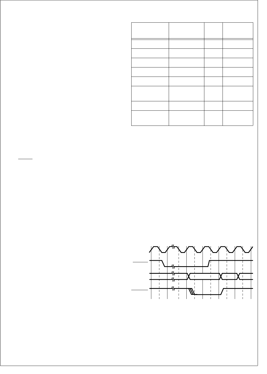
41 www.national.com
CP3BT26
9.0 DMA Controller
The DMA Controller (DMAC) has a register-based program-
ming interface, as opposed to an interface based on I/O
control blocks. After loading the registers with source and
destination addresses, as well as block size and type of op-
eration, a DMAC channel is ready to respond to DMA trans-
fer requests. A request can only come from on-chip
peripherals or software, not external peripherals. On receiv-
ing a DMA transfer request, if the channel is enabled, the
DMAC performs the following operations:
1. Arbitrates to become master of the CPU bus.
2. Determines priority among the DMAC channels, one
clock cycle before T1 of the DMAC transfer cycle. (T1
is the first clock cycle of the bus cycle.) Priority among
the DMAC channels is fixed in descending order, with
Channel 0 having the highest priority.
3. Executes data transfer bus cycle(s) selected by the val-
ues held in the control registers of the channel being
serviced, and according to the accessed memory ad-
dress. The DMAC acknowledges the request during the
bus cycle that accesses the requesting device.
4. If the transfer of a block is terminated, the DMAC does
the following:
Updates the termination bits.
Generates an interrupt (if enabled).
Goes to step 6.
5. If DMRQn is still active, and the Bus Policy is “continu-
ous”, returns to step 3.
6. Returns mastership of the CPU bus to the CPU.
Each DMAC channel can be programmed for direct (flyby)
or indirect (memory-to-memory) data transfers. Once a
DMAC transfer cycle is in progress, the next transfer request
is sampled when the DMAC acknowledge is de-asserted,
then on the rising edge of every clock cycle.
The configuration of either address freeze or address up-
date (increment or decrement) is independent of the num-
ber of transferred bytes, transfer direction, or number of
bytes in each DMAC transfer cycle. All these can be config-
ured for each channel by programming the appropriate con-
trol registers.
Each DMAC channel has eight control registers. DMAC
channels are described hereafter with the suffix n, where n
= 0 to 3, representing the channel number in the register-
names.
9.1 CHANNEL ASSIGNMENT
Table 17 shows the assignment of the DMA channels to dif-
ferent tasks. Four channels can be shared by a primary and
an secondary function. However, only one source at a time
can be enabled. If a channel is used for memory block trans-
fers, other resources must be disabled.
Table 17 DMA Channel Assignment
9.2 TRANSFER TYPES
The DMAC uses two data transfer modes, Direct (Flyby)
and Indirect (Memory-to-Memory). The choice of mode de-
pends on the required bus performance and whether direct
mode is available for the transfer. Indirect mode must be
used when the source and destination have differing bus
widths, when both the source and destination are in memo-
ry, and when the destination does not support direct mode.
9.2.1 Direct (Flyby) Transfers
In direct mode each data item is transferred using a single
bus cycle, without reading the data into the DMAC. It pro-
vides the fastest transfer rate, but it requires identical source
and destination bus widths. The DMAC cannot use Direct
cycles between two memory devices. One of the devices
must be an I/O device that supports the Direct (Flyby) mech-
anism, as shown in Figure 3.
Figure 3. Direct DMA Cycle Followed by a CPU Cycle
Channel Peripheral Trans-
action Register
0 (Primary) USB R/W RX/TX FIFO
0 (Secondary) UART0 R RXBUF
1 (Primary) UART0 W TXBUF
1 (Secondary) Reserved N/A N/A
2 (Primary) Audio Interface R ARDR0
2 (Secondary) CVSD/PCM
Transcoder RPCMOUT
3 (Primary) Audio Interface W ATDR0
3 (Secondary) CVSD/PCM
Transcoder WPCMIN
DMRQ[3:0]
ADDR ADCA
CLK
Bus State
T1 T1T2 Tidle
D
MACK[3:0]
DS00
5

www.national.com 42
CP3BT26
Direct mode supports two bus policies: intermittent and con-
tinuous. In intermittent mode, the DMAC gives bus master-
ship back to the CPU after every cycle. In continuous mode,
the DMAC remains bus master until the transfer is complet-
ed. The maximum bus throughput in intermittent mode is
one transfer for every three System Clock cycles. The max-
imum bus throughput in continuous mode is one transfer for
every clock cycle.
The I/O device which made the DMA request is called the
implied I/O device. The other device can be either memory
or another I/O device, and is called the addressed device.
Because only one address is required in direct mode, this
address is taken from the corresponding ADCAn counter.
The DMAC channel generates either a read or a write bus
cycle, as controlled by the DMACNTLn.DIR bit.
When the DMACNTLn.DIR bit is clear, a read bus cycle
from the addressed device is performed, and the data is
written to the implied I/O device. When the DMACNTLn.DIR
bit is set, a write bus cycle to the addressed device is per-
formed, and the data is read from the implied I/O device.
The configuration of either address freeze or address up-
date (increment or decrement) is independent of the num-
ber of transferred bytes, transfer direction, or number of
bytes in each DMAC transfer cycle. All these can be config-
ured for each channel by programming the appropriate con-
trol register.
Whether 8 or 16 bits are transferred in each cycle is select-
ed by the DMACNTLn.TCS register bit. After the data item
has been transferred, the BLTCn counter is decremented by
one. The ADCAn counter is updated according to the INCA
and ADA fields in the DMACNTLn register.
9.2.2 Indirect (Memory-To-Memory) Transfers
In indirect (memory-to-memory) mode, data transfers use
two consecutive bus cycles. The data is first read into a tem-
porary register, and then written to the destination in the fol-
lowing cycle. This mode is slower than the direct (flyby)
mode, but it provides support for different source and desti-
nation bus widths. Indirect mode must be used for transfers
between memory devices.
If an intermittent bus policy is used, the maximum through-
put is one transfer for every five clock cycles. If a continuous
bus policy is used, maximum throughput is one transfer for
every two clock cycles.
When the DMACNTLn.DIR bit is 0, the first bus cycle reads
data from the source using the ADCAn counter, while the
second bus cycle writes the data into the destination using
the ADCBn counter. When the DMACNTLn.DIR bit is set,
the first bus cycle reads data from the source using the AD-
CBn counter, while the second bus cycle writes the data into
the destination addressed by the ADCAn counter.
The number of bytes transferred in each cycle is taken from
the DMACNTLn.TCS register bit. After the data item has
been transferred, the BLTCn counter is decremented by
one. The ADCAn and ADCBn counters are updated accord-
ing to the INCA, INCB, ADA, and ADB fields in the
DMACNTLn register.
9.3 OPERATION MODES
The DMAC operates in three different block transfer modes:
single transfer, double buffer, and auto-initialize.
9.3.1 Single Transfer Operation
This mode provides the simplest way to accomplish a single
block data transfer.
Initialization
1. Write the block transfer addresses and byte count into
the corresponding ADCAn, ADCBn, and BLTCn
counters.
2. Clear the DMACNTLn.OT bit to select non-auto-initial-
ize mode. Clear the DMASTAT.VLD bit by writing a 1 to
it.
3. Set the DMACNTLn.CHEN bit to activate the channel
and enable it to respond to DMA transfer requests.
Termination
When the BLTCn counter reaches 0:
1. The transfer operation terminates.
2. The DMASTAT.TC and DMASTAT.OVR bits are set, and
the DMASTAT.CHAC bit is cleared.
3. An interrupt is generated if enabled by the
DMACNTLn.ETC or DMACNTLn.EOVR bits.
The DMACNTLn.CHEN bit must be cleared before loading
the DMACNTLn register to avoid prematurely starting a new
DMA transfer.
9.3.2 Double Buffer Operation
This mode allows software to set up the next block transfer
while the current block transfer proceeds.
Initialization
1. Write the block transfer addresses and byte count into
the ADCAn, ADCBn, and BLTCn counters.
2. Clear the DMACNTLn.OT bit to select non-auto-initial-
ize mode. Clear the DMASTAT.VLD bit by writing a 1 to
it.
3. Set the DMACNTLn.CHEN bit. This activates the chan-
nel and enables it to respond to DMA transfer requests.
4. While the current block transfer proceeds, write the ad-
dresses and byte count for the next block into the
ADRAn, ADRBn, and BLTRn registers. The BLTRn reg-
ister must be written last, because it sets the DMAS-
TAT.VLD bit which indicates that all the parameters for
the next transfer have been updated.
Continuation/Termination
When the BLTCn counter reaches 0:
1. The DMASTAT.TC bit is set.
2. An interrupt is generated if enabled by the
DMACNTLn.ETC bit.
3. The DMAC channel checks the value of the VLD bit.
If the DMASTAT.VLD bit is set:
1. The channel copies the ADRAn, ADRBn, and BLTRn
values into the ADCAn, ADCBn, and BLTCn registers.
2. The DMASTAT.VLD bit is cleared.
3. The next block transfer is started.

43 www.national.com
CP3BT26
If the DMASTAT.VLD bit is clear:
1. The transfer operation terminates.
2. The channel sets the DMASTAT.OVR bit.
3. The DMASTAT.CHAC bit is cleared.
4. An interrupt is generated if enabled by the
DMACNTLn.EOVR bit.
The DMACNTLn.CHEN bit must be cleared before loading
the DMACNTLn register to avoid prematurely starting a new
DMA transfer.
Note: The ADCBn and ADRBn registers are used only in
indirect (memory-to-memory) transfer. In direct (flyby)
mode, the DMAC does not use them and therefore does not
copy ADRBn into ADCBn.
9.3.3 Auto-Initialize Operation
This mode allows the DMAC to continuously fill the same
memory area without software intervention.
Initialization
1. Write the block addresses and byte count into the AD-
CAn, ADCBn, and BLTCn counters, as well as the
ADRAn, ADRBn, and BLTRn registers.
2. Set the DMACNTLn.OT bit to select auto-initialize
mode.
3. Set the DMACNTLn.CHEN bit to activate the channel
and enable it to respond to DMA transfer requests.
Continuation
When the BLTCn counter reaches 0:
1. The contents of the ADRAn, ADRBn, and BLTRn regis-
ters are copied to the ADCAn, ADCBn, and BLTCn
counters.
2. The DMAC channel checks the value of the DMAS-
TAT.TC bit.
If the DMASTAT.TC bit is set:
1. The DMASTAT.OVR bit is set.
2. A level interrupt is generated if enabled by the
DMACNTLn.EOVR bit.
3. The operation is repeated.
If the DMASTAT.TC bit is clear:
1. The DMASTAT.TC bit is set.
2. A level interrupt is generated if enabled by the
DMACNTLn.ETC bit.
3. The DMAC operation is repeated.
Termination
The DMA transfer is terminated when the
DMACNTLn.CHEN bit is cleared.
9.4 SOFTWARE DMA REQUEST
In addition to the hardware requests from I/O devices, a
DMA transfer request can also be initiated by software. A
software DMA transfer request must be used for block copy-
ing between memory devices.
When the DMACNTLn.SWRQ bit is set, the corresponding
DMA channel receives a DMA transfer request. When the
DMACNTLn.SWRQ bit is clear, the software DMA transfer
request of the corresponding channel is inactive.
For each channel, use the software DMA transfer request
only when the corresponding hardware DMA request is in-
active and no terminal count interrupt is pending. Software
can poll the DMASTAT.CHAC bit to determine whether the
DMA channel is already active. After verifying the DMAS-
TATn.CHAC bit is clear (channel inactive), check the DMAS-
TATn.TC (terminal count) bit. If the TC bit is clear, then no
terminal count condition exists and therefore no terminal
count interrupt is pending. If the channel is not active and no
terminal count interrupt is pending, software may request a
DMA transfer.
9.5 DEBUG MODE
When the FREEZE signal is active, all DMA operations are
stopped. They will start again when the FREEZE signal
goes inactive. This allows breakpoints to be used in debug
systems.
9.6 DMA CONTROLLER REGISTER SET
There are four identical sets of DMA controller registers, as
listed in Table 18.
Table 18 DMA Controller Registers
Name Address Description
ADCA0 FF F800h Device A Address
Counter Register
ADRA0 FF F804h Device A Address
Register
ADCB0 FF F808h Device B Address
Counter Register
ADRB0 FF F80Ch Device B Address
Register
BLTC0 FF F810h Block Length
Counter Register
BLTR0 FF F814h Block Length Register
DMACNTL0 FF F81Ch DMA Control Register
DMASTAT0 FF F81Eh DMA Status Register
ADCA1 FF F820h Device A Address
Counter Register
ADRA1 FF F824h Device A Address
Register
ADCB1 FF F828h Device B Address
Counter Register
ADRB1 FF F82Ch Device B Address
Register
BLTC1 FF F830h Block Length
Counter Register
BLTR1 FF F834h Block Length Register
DMACNTL1 FF F83Ch DMA Control Register
DMASTAT1 FF F83Eh DMA Status Register
www.national.com 44
CP3BT26
9.6.1 Device A Address Counter Register (ADCAn)
The Device A Address Counter register is a 32-bit, read/
write register. It holds the current 24-bit address of either the
source data item or the destination location, depending on
the state of the DIR bit in the CNTLn register. The ADA bit
of DMACNTLn register controls whether to adjust the point-
er in the ADCAn register by the step size specified in the
INCA field of DMACNTLn register. The upper 8 bits of the
ADCAn register are reserved and always clear.
9.6.2 Device A Address Register (ADRAn)
The Device A Address register is a 32-bit, read/write regis-
ter. It holds the 24-bit starting address of either the next
source data block, or the next destination data area, according
to the DIR bit in the DMACNTLn register. The upper 8 bits of
the ADRAn register are reserved and always clear.
9.6.3 Device B Address Counter Register (ADCBn)
The Device B Address Counter register is a 32-bit, read/
write register. It holds the current 24-bit address of either the
source data item, or the destination location, according to
the DIR bit in the CNTLn register. The ADCBn register is up-
dated after each transfer cycle by INCB field of the
DMACNTLn register according to ADB bit of the
DMACNTLn register. In direct (flyby) mode, this register is
not used. The upper 8 bits of the ADCBn register are re-
served and always clear.
9.6.4 Device B Address Register (ADRBn)
The Device B Address register is a 32-bit, read/write regis-
ter. It holds the 24-bit starting address of either the next
source data block or the next destination data area, accord-
ing to the DIR bit in the CNTLn register. In direct (flyby)
mode, this register is not used. The upper 8 bits of the AD-
CRBn register are reserved and always clear.
9.6.5 Block Length Counter Register (BLTCn)
The Block Length Counter register is a 16-bit, read/write
register. It holds the current number of DMA transfers to be
executed in the current block. BLTCn is decremented by one
after each transfer cycle. A DMA transfer may consist of 1 or
2 bytes, as selected by the DMACNTLn.TCS bit.
Note: 0000h is interpreted as 216-1 transfer cycles.
ADCA2 FF F840h Device A Address
Counter Register
ADRA2 FF F844h Device A Address
Register
ADCB2 FF F848h Device B Address
Counter Register
ADRB2 FF F84Ch Device B Address
Register
BLTC2 FF F850h Block Length
Counter Register
BLTR2 FF F854h Block Length Register
DMACNTL2 FF F85Ch DMA Control Register
DMASTAT2 FF F85Eh DMA Status Register
ADCA3 FF F860h Device A Address
Counter Register
ADRA3 FF F864h Device A Address
Register
ADCB3 FF F868h Device B Address
Counter Register
ADRB3 FF F86Ch Device B Address
Register
BLTC3 FF F870h Block Length
Counter Register
BLTR3 FF F874h Block Length Register
DMACNTL3 FF F87Ch DMA Control Register
DMASTAT3 FF F87Eh DMA Status Register
31 24 23 0
Reserved Device A Address Counter
Table 18 DMA Controller Registers
Name Address Description
31 24 23 0
Reserved Device A Address
31 24 23 0
Reserved Device B Address Counter
31 24 23 0
Reserved Device B Address
15 0
Block Length Counter

45 www.national.com
CP3BT26
9.6.6 Block Length Register (BLTRn)
The Block Length register is a 16-bit, read/write register. It
holds the number of DMA transfers to be performed for the
next block. Writing this register automatically sets the DM-
ASTAT.VLD bit.
Note: 0000h is interpreted as 216-1 transfer cycles.
9.6.7 DMA Control Register (DMACNTLn)
The DMA Control register n is a word-wide, read/write reg-
ister that controls the operation of DMA channel n. This reg-
ister is cleared at reset. Reserved bits must be written with
0.
CHEN The Channel Enable bit must be set to enable
any DMA operation on this channel. Writing a
1 to this bit starts a new DMA transfer even if
it is currently a 1. If all DMACNTLn.CHEN bits
are clear, the DMA clock is disabled to reduce
power.
0 –Channel disabled.
1 –Channel enabled.
ETC If the Enable Interrupt on Terminal Count bit is
set, it enables an interrupt when the DMAS-
TAT.TC bit is set.
0 –Interrupt disabled.
1 –Interrupt enabled.
EOVR If the Enable Interrupt on OVR bit is set, it en-
ables an interrupt when the DMASTAT.OVR
bit is set.
0 –Interrupt disabled.
1 –Interrupt enabled.
TCS The Transfer Cycle Size bit specifies the num-
ber of bytes transferred in each DMA transfer
cycle. In direct (fly-by) mode, undefined re-
sults occur if the TCS bit is not equal to the ad-
dressed memory bus width.
0 –Byte transfers (8 bits per cycle).
1 –Word transfers (16 bits per cycle).
IND The Direct/Indirect Transfer bit specifies the
transfer type.
0 –Direct transfer (flyby).
1 –Indirect transfer (memory-to-memory).
DIR The Transfer Direction bit specifies the direc-
tion of the transfer relative to Device A.
0 –Device A (pointed to by the ADCAn regis-
ter) is the source. In Fly-By mode a read
transaction is initialized.
1 –Device A (pointed to by the ADCAn regis-
ter) is the destination. In Fly-By mode a
write transaction is initialized.
OT The Operation Type bit specifies the operation
mode of the DMA controller.
0 –Single-buffer mode or double-buffer mode
enabled.
1 –Auto-Initialize mode enabled.
BPC The Bus Policy Control bit specifies the bus
policy applied by the DMA controller. The op-
eration mode can be either intermittent (cycle
stealing) or continuous (burst).
0 –Intermittent operation. The DMAC chan-
nel relinquishes the bus after each trans-
action, even if the request is still asserted.
1 –Continuous operation. The DMAC chan-
nel n uses the bus continuously as long
as the request is asserted. This mode can
only be used for software DMA requests.
For hardware DMA requests, the BPC bit
must be clear.
SWRQ The Software DMA Request bit is written with
a 1 to initiate a software DMA request. Writing
a 0 to this bit deactivates the software DMA
request. The SWRQ bit must only be written
when the DMRQ signal for this channel is in-
active (DMASTAT.CHAC = 0).
0 –Software DMA request is inactive.
1 –Software DMA request is active.
ADA If the Device A Address Control bit is set, it en-
ables updating the Device A address.
0 – ADCAn address unchanged.
1 – ADCAn address incremented or decre-
mented, according to INCA field of
DMACNTLn register.
INCA The Increment/Decrement ADCAn field spec-
ifies the step size for the Device A address in-
crement/decrement.
00 – Increment ADCAn register by 1.
01 – Increment ADCAn register by 2.
10 – Decrement ADCAn register by 1.
11 – Decrement ADCAn register by 2.
ADB If the Device B Address Control bit is set, it en-
ables updating the Device B Address.
0 –ADCBn address unchanged.
1 –ADCBn address incremented or decre-
mented, according to INCB field of
DMACNTLn register.
INCB The Increment/Decrement ADCBn field spec-
ifies the step size for the Device B address in-
crement/decrement.
00 – Increment ADCBn register by 1.
01 – Increment ADCBn register by 2.
10 – Decrement ADCBn register by 1.
11 – Decrement ADCBn register by 2.
15 0
Block Length
76543210
BPC OT DIR IND TCS EOVR ETC CHEN
15 14 13 12 11 10 9 8
Res. INCB ADB INCA ADA SWRQ

www.national.com 46
CP3BT26
9.6.8 DMA Status Register (DMASTAT)
The DMA status register is a byte-wide, read register that
holds the status information for the DMA channel n. This
register is cleared at reset. The reserved bits always return
zero when read. The VLD, OVR and TC bits are sticky (once
set by the occurrence of the specific condition, they remain
set until explicitly cleared by software). These bits can be in-
dividually cleared by writing 1 to the bit positions in the DM-
ASTAT register to be cleared. Writing 0 to these bits has no
effect
TC The Terminal Count bit indicates whether the
transfer was completed by a terminal count
condition (BLTCn Register reached 0).
0 –Terminal count condition did not occur.
1 –Terminal count condition occurred.
OVR The behavior of the Channel Overrun bit de-
pends on the operation mode (single buffer,
double buffer, or auto-initialize) of the DMA
channel.
In double-buffered mode (DMACNTLn.OT =
0):
The OVR bit is set when the present transfer
is completed (BLTCn = 0), but the parameters
for the next transfer (address and block
length) are not valid (DMASTAT.VLD = 0).
In auto-initialize mode (DMACNTLn.OT = 1):
The OVR bit is set when the present transfer
is completed (BLTCn = 0), and the DMAS-
TAT.TC bit is still set.
In single-buffer mode:
Operates in the same way as double-buffer
mode. In single-buffered mode, the DMAS-
TAT.VLD bit should always be clear, so it will
also be set when the DMASTAT.TC bit is set.
Therefore, the OVR bit can be ignored in this
mode.
CHAC The Channel Active bit continuously indicates
the active or inactive status of the channel,
and therefore, it is read only. Data written to
the CHAC bit is ignored.
0 –Channel inactive.
1 –Indicates that the channel is active
(CHEN bit in the CNTLn register is 1 and
BLTCn > 0)
VLD The Transfer Parameters Valid bit specifies
whether the transfer parameters for the next
block to be transferred are valid. Writing the
BLTRn register automatically sets this bit. The
bit is cleared in the following cases:
The present transfer is completed and the
ADRAn, ADRBn (indirect mode only), and
BLTR registers are copied to the ADCAn,
ADCBn (indirect mode only), and BLTCn
registers.
Writing 1 to the VLD bit.
7 4 3 2 1 0
Reserved VLD CHAC OVR TC

47 www.national.com
CP3BT26
10.0 Interrupts
The Interrupt Control Unit (ICU) receives interrupt requests
from internal and external sources and generates interrupts
to the CPU. Interrupts from the timers, UARTs, Microwire/
SPI interface, and Multi-Input Wake-Up module are all
maskable interrupts. The highest-priority interrupt is the
Non-Maskable Interrupt (NMI), which is triggered by a falling
edge received on the NMI input pin.
The priorities of the maskable interrupts are hardwired and
therefore fixed. The implemented interrupts are named
IRQ0 through IRQ47, in which IRQ0 has the lowest priority
and IRQ47 has the highest priority. (IRQ0 is not implement-
ed, so IRQ1 is the lowest priority interrupt that normally may
occur.)
10.1 NON-MASKABLE INTERRUPTS
The Interrupt Control Unit (ICU) receives the external NMI
input and generates the NMI signal driven to the CPU. The
NMI input is an asynchronous input with Schmitt trigger
characteristics and an internal synchronization circuit,
therefore no external synchronizing circuit is needed. The
NMI pin triggers an exception on its falling edge.
10.1.1 Non-Maskable Interrupt Processing
The CPU performs an interrupt acknowledge bus cycle
when beginning to process a non-maskable interrupt.
At reset, NMI interrupts are disabled and must remain dis-
abled until software initializes the interrupt table, interrupt
base register (INTBASE), and the interrupt mode. The ex-
ternal NMI interrupt is enabled by setting the EXNMI.EN-
LCK bit and will remain enabled until a reset occurs.
Alternatively, the external NMI interrupt can be enabled by
setting the EXNMI.EN bit and will remain enabled until an in-
terrupt event or a reset occurs.
10.2 MASKABLE INTERRUPTS
The ICU receives level-triggered interrupt request signals
from 47 sources and generates a vectored interrupt to the
CPU when required. Priority among the implemented inter-
rupt sources (named IRQ1 through IRQ47) is fixed.
The maskable interrupts are globally enabled and disabled
by the E bit in the PSR register. The EI and DI instructions
are used to set (enable) and clear (disable) this bit. The glo-
bal maskable interrupt enable bit (I bit in the PSR) must also
be set before any maskable interrupts are taken.
Each interrupt source can be individually enabled or dis-
abled under software control through the ICU interrupt en-
able registers and also through interrupt enable bits in the
peripherals that request the interrupts. The ICU supports
IRQ0, but in the CP3BT26 it is not connected to any inter-
rupt source.
10.2.1 Maskable Interrupt Processing
Interrupt vector numbers are always positive, in the range
10h to 3Fh. The IVCT register contains the interrupt vector
of the enabled and pending interrupt with the highest priori-
ty. The interrupt vector 10h corresponds to IRQ0 and the
lowest priority, while the vector 3Fh corresponds to IRQ47
and the highest priority. The CPU performs an interrupt ac-
knowledge bus cycle on receiving a maskable interrupt re-
quest from the ICU. During the interrupt acknowledge cycle,
a byte is read from address FF FE00h (IVCT register). The
byte is used as an index into the Dispatch Table to deter-
mine the address of the interrupt handler.
Because IRQ0 is not connected to any interrupt source, it
would seem that the interrupt vector would never return the
value 10h. If it does return a value of 10h, the entry in the
dispatch table should point to a default interrupt handler that
handles this error condition. One possible condition for this
to occur is deassertion of the interrupt before the interrupt
acknowledge cycle.
10.3 INTERRUPT CONTROLLER REGISTERS
Table 19 lists the ICU registers.
Table 19 Interrupt Controller Registers
Name Address Description
IVCT FF FE00h Interrupt Vector
Register
NMISTAT FF FE02h
Non-Maskable
Interrupt Status
Register
EXNMI FF FE04h
External NMI Trap
Control and Status
Register
ISTAT0 FF FE0Ah Interrupt Status
Register 0
ISTAT1 FF FE0Ch Interrupt Status
Register 1
ISTAT2 FF FE20h Interrupt Status
Register 2
IENAM0 FF FE0Eh Interrupt Enable and
Mask Register 0
IENAM1 FF FE10h Interrupt Enable and
Mask Register 1
IENAM2 FF FE22h Interrupt Enable and
Mask Register 2

www.national.com 48
CP3BT26
10.3.1 Interrupt Vector Register (IVCT)
The IVCT register is a byte-wide read-only register which re-
ports the encoded value of the highest priority maskable in-
terrupt that is both asserted and enabled. The valid range is
from 10h to 3Fh. The register is read by the CPU during an
interrupt acknowledge bus cycle, and INTVECT is valid dur-
ing that time. It may contain invalid data while INTVECT is
updated.
INTVECT The Interrupt Vector field indicates the highest
priority interrupt which is both asserted and
enabled.
10.3.2 Non-Maskable Interrupt Status Register
(NMISTAT)
The NMISTAT register is a byte-wide read-only register. It
holds the status of the current pending Non-Maskable Inter-
rupt (NMI) requests. On the CP3BT26, the external NMI in-
put is the only source of NMI interrupts. The NMISTAT
register is cleared on reset and each time its contents are
read.
EXT The External NMI request bit indicates wheth-
er an external non-maskable interrupt request
has occurred. Refer to the description of the
EXNMI register below for additional details.
0 –No external NMI request.
1 –External NMI request has occurred.
10.3.3 External NMI Trap Control and Status Register
(EXNMI)
The EXNMI register is a byte-wide read/write register. It in-
dicates the current value of the NMI pin and controls the
NMI interrupt trap generation based on a falling edge of the
NMI pin. TST, EN and ENLCK are cleared on reset. When
writing to this register, all reserved bits must be written with
0 for the device to function properly
EN The EXNMI trap enable bit is one of two bits
that can be used to enable NMI interrupts.
The bit is cleared by hardware at reset and
whenever the NMI interrupt occurs (EXN-
MI.EXT set). It is intended for applications
where the NMI input toggles frequently but
nested NMI traps are not desired. For these
applications, the EN bit needs to be re-en-
abled before exiting the trap handler. When
used this way, the ENLCK bit should never be
set. The EN bit can be set and cleared by soft-
ware (software can set this bit only if EXN-
MI.EXT is cleared), and should only be set
after the interrupt base register and the inter-
rupt stack pointer have been set up.
0 –NMI interrupts not enabled by this bit (but
may be enabled by the ENLCK bit).
1 –NMI interrupts enabled.
PIN The PIN bit indicates the state (non-inverted)
on the NMI input pin. This bit is read-only, data
written into it is ignored.
0 –NMI pin not asserted.
1 –NMI pin asserted.
ENLCK The EXNMI trap enable lock bit is used to per-
manently enable NMI interrupts. Only a de-
vice reset can clear the ENLCK bit. This
allows the external NMI feature to be enabled
after the interrupt base register and the inter-
rupt stack pointer have been set up. When the
ENLCK bit is set, the EN bit is ignored.
0 –NMI interrupts not enabled by this bit (but
may be enabled by the EN bit).
1 – NMI interrupts enabled.
7 6 5 0
0 0 INTVECT
710
Reserved EXT
73210
Reserved ENLCK PIN EN

49 www.national.com
CP3BT26
10.3.4 Interrupt Enable and Mask Register 0 (IENAM0)
The IENAM0 register is a word-wide read/write register
which holds bits that individually enable and disable the
maskable interrupt sources IRQ1 through IRQ15. The reg-
ister is initialized to FFFFh at reset.
IENA Each Interrupt Enable bit enables or disables
the corresponding interrupt request IRQ1
through IRQ15, for example IENA15 controls
IRQ15. Because IRQ0 is not used, IENA0 is
ignored.
0 –Interrupt is disabled.
1 –Interrupt is enabled.
10.3.5 Interrupt Enable and Mask Register 1 (IENAM1)
The IENAM1 register is a word-wide read/write register
which holds bits that individually enable and disable the
maskable interrupt sources IRQ16 through IRQ31. The reg-
ister is initialized to FFFFh at reset.
IENA Each Interrupt Enable bit enables or disables
the corresponding interrupt request IRQ16
through IRQ31, for example IENA31 controls
IRQ31.
0 –Interrupt is disabled.
1 –Interrupt is enabled.
10.3.6 Interrupt Enable and Mask Register 2 (IENAM2)
The IENAM2 register is a word-wide read/write register
which holds bits that individually enable and disable the
maskable interrupt sources IRQ32 through IRQ47. The reg-
ister is initialized to FFFFh at reset.
IENA Each Interrupt Enable bit enables or disables
the corresponding interrupt request IRQ32
through IRQ47, for example IENA47 controls
IRQ47.
0 –Interrupt is disabled.
1 –Interrupt is enabled.
10.3.7 Interrupt Status Register 0 (ISTAT0)
The ISTAT0 register is a word-wide read-only register. It in-
dicates which maskable interrupt inputs to the ICU are ac-
tive. These bits are not affected by the state of the
corresponding IENA bits.
IST The Interrupt Status bits indicate if a
maskable interrupt source is signalling an in-
terrupt request. IST15:1 correspond to IRQ15
to IRQ1 respectively. Because the IRQ0 inter-
rupt is not used, bit 0 always reads back 0.
0 –Interrupt is not active.
1 –Interrupt is active.
10.3.8 Interrupt Status Register 1 (ISTAT1)
The ISTAT1 register is a word-wide read-only register. It in-
dicates which maskable interrupt inputs into the ICU are ac-
tive. These bits are not affected by the state of the
corresponding IENA bits.
IST The Interrupt Status bits indicate if a
maskable interrupt source is signalling an in-
terrupt request. IST31:16 correspond to
IRQ31 to IRQ16, respectively.
0 –Interrupt is not active.
1 –Interrupt is active.
10.3.9 Interrupt Status Register 2 (ISTAT2)
The ISTAT2 register is a word-wide read-only register. It in-
dicates which maskable interrupt inputs into the ICU are ac-
tive. These bits are not affected by the state of the
corresponding IENA bits.
IST The Interrupt Status bits indicate if a
maskable interrupt source is signalling an in-
terrupt request. IST47:32 correspond to
IRQ47 to IRQ32, respectively.
0 –Interrupt is not active.
1 –Interrupt is active.
15 1 0
IENA Res.
15 0
IENA
15 0
IENA
15 1 0
IST Res.
15 0
IST
15 0
IST

www.national.com 50
CP3BT26
10.4 MASKABLE INTERRUPT SOURCES
Table 20 shows the interrupts assigned to various on-chip
maskable interrupts. The priority of simultaneous maskable
interrupts is linear, with IRQ47 having the highest priority.
Table 20 Maskable Interrupts Assignment
All reserved interrupt vectors should point to default or error
interrupt handlers.
10.5 NESTED INTERRUPTS
Nested NMI interrupts are always enabled. Nested
maskable interrupts are disabled by default, however an in-
terrupt handler can allow nested maskable interrupts by set-
ting the I bit in the PSR. The LPR instruction is used to set
the I bit.
Nesting of specific maskable interrupts can be allowed by
disabling interrupts from sources for which nesting is not al-
lowed, before setting the I bit. Individual maskable interrupt
sources can be disabled using the IENAM0 and IENAM1
registers.
Any number of levels of nested interrupts are allowed, limit-
ed only by the available memory for the interrupt stack.
IRQ Number Description
IRQ47 TWM (Timer 0)
IRQ46 Bluetooth LLC 0
IRQ45 Bluetooth LLC 1
IRQ44 Bluetooth LLC 2
IRQ43 Bluetooth LLC 3
IRQ42 Bluetooth LLC 4
IRQ41 Bluetooth LLC 5
IRQ40 USB Interface
IRQ39 DMA Channel 0
IRQ38 DMA Channel 1
IRQ37 DMA Channel 2
IRQ36 DMA Channel 3
IRQ35 CAN
IRQ34 Advanced Audio Interface (AAI)
IRQ33 UART0 RX
IRQ32 CVSD/PCM Converter
IRQ31 ACCESS.bus
IRQ30 TA (Timer input A)
IRQ29 TB (Timer input B)
IRQ28 VTUA (VTU Interrupt Request 1)
IRQ27 VTUB (VTU Interrupt Request 2)
IRQ26 VTUC (VTU Interrupt Request 3)
IRQ25 VTUD (VTU Interrupt Request 4)
IRQ24 Microwire/SPI RX/TX
IRQ23 UART0 TX
IRQ22 UART0 CTS
IRQ21 Reserved
IRQ20 UART1 RX
IRQ19 UART1 TX
IRQ18 UART2 RX
IRQ17 UART2 TX
IRQ16 UART3 RX
IRQ15 UART3 TX
IRQ14 Reserved
IRQ13 ADC (Done)
IRQ12 MIWU Interrupt 0
IRQ11 MIWU Interrupt 1
IRQ10 MIWU Interrupt 2
IRQ9 MIWU Interrupt 3
IRQ8 MIWU Interrupt 4
IRQ7 MIWU Interrupt 5
IRQ6 MIWU Interrupt 6
IRQ5 MIWU Interrupt 7
IRQ4 Reserved
IRQ3 Random Number Generator (RNG)
IRQ2 Reserved
IRQ1 Flash Program/Data Memory
IRQ0 Reserved
IRQ Number Description
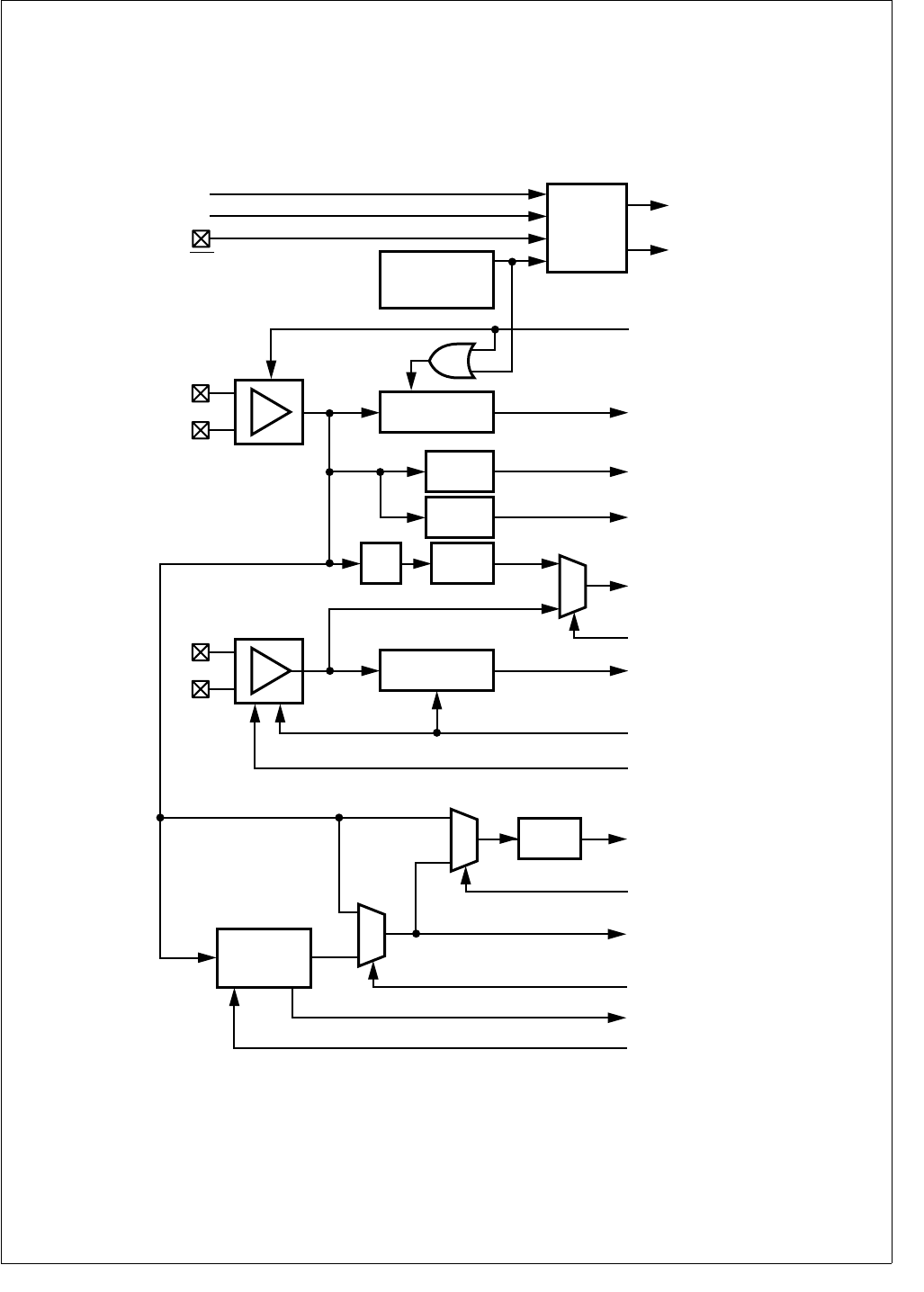
51 www.national.com
CP3BT26
11.0 Triple Clock and Reset
The Triple Clock and Reset module generates a 12 MHz
Main Clock and a 32.768 kHz Slow Clock from external
crystal networks or external clock sources. It provides vari-
ous clock signals for the rest of the chip. It also provides the
main system reset signal, a power-on reset function, Main
Clock prescalers to generate two additional low-speed
clocks, and a 32-kHz oscillator start-up delay.
Figure 4 is block diagram of the Triple Clock and Reset mod-
ule.
Figure 4. Triple Clock and Reset Module
Reset
Module
Device Reset
Stretched
Reset
Stop Main Osc
Good Main Clock
Power-On-Reset
Module (POR)
Start-Up-Delay
14-Bit Timer
TWM (Invalid Watchdog Service)
Flash Interface (Program/Erase Busy)
External Reset
Good Slow Clock
Start-Up-Delay
8-Bit Timer
Auxiliary Clock 1
4-Bit Aux1
Prescaler
Auxiliary Clock 2
4-Bit Aux2
Prescaler
Slow Clock
Slow Clock
Select
Main Clock 8-Bit
Prescaler
Mux
Slow Clock Prescaler
Preset
Time-out
System Clock
Fast Clock
Select
Mux
4-Bit
Prescaler
Fast Clock
Prescaler
PLL
(x3, x4, or x5)
Stop Slow Osc
Bypass
32 kHz Osc
Div.
by 2
Reset
Preset
Stop Main Osc.
High Frequency
Oscillator
X1CKI
X1CKO
Low Frequency
Oscillator
X2CKI
X2CKO
PLL Clock
Bypass PLL
Mux
Stop PLL
Stop PLL
Good PLL Clock
DS006
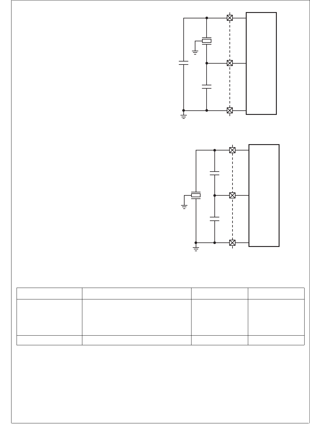
www.national.com 52
CP3BT26
11.1 EXTERNAL CRYSTAL NETWORK
An external crystal network is connected to the X1CKI and
X1CKO pins to generate the Main Clock, unless an external
clock signal is driven on the X1CKI pin. A similar external
crystal network may be used at pins X2CKI and X2CKO for
the Slow Clock. If an external crystal network is not used for
the Slow Clock, the Slow Clock is generated by dividing the
fast Main Clock.
The crystal network you choose may require external com-
ponents different from the ones specified in this datasheet.
In this case, consult with National’s engineers for the com-
ponent specifications
The crystals and other oscillator components must be
placed close to the X1CKI/X1CKO and X2CKI/X2CKO de-
vice input pins to keep the printed trace lengths to an abso-
lute minimum.
Figure 5 shows the external crystal network for the X1CKI
and X1CKO pins. Figure 6 shows the external crystal net-
work for the X2CKI and X2CKO pins. Table 21 shows the
component specifications for the main crystal network, and
Table 22 shows the component specifications for the 32.768
kHz crystal network.
Figure 5. Main Clock External Crystal Network
Figure 6. Slow Clock External Crystal Network
C1
12 MHz
Crystal
C2
GND
X1CKI
X1CKO
DS189
C1
32.768 kHz
Crystal
C2
GND
X2CKI
X2CKO
DS215
Table 21 Component Values of the High Frequency Crystal Circuit
Component Parameters Values Tolerance
Crystal Resonance Frequency
Type
Max. Serial Resistance
Max. Shunt Capacitance
Load Capacitance
12 MHz ± 20 ppm
AT-C ut
50 Ω
7 pF
22 pF
N/A
Capacitor C1, C2 Capacitance 22 pF 20%

53 www.national.com
CP3BT26
Choose capacitor component values in the tables to obtain
the specified load capacitance for the crystal when com-
bined with the parasitic capacitance of the trace, socket, and
package (which can vary from 0 to 8 pF). As a guideline, the
load capacitance is:
C2 > C1
C1 can be trimmed to obtain the desired load capacitance.
The start-up time of the 32.768 kHz oscillator can vary from
one to six seconds. The long start-up time is due to the high
Q value and high serial resistance of the crystal necessary
to minimize power consumption in Power Save mode.
11.2 MAIN CLOCK
The Main Clock is generated by the 12-MHz high-frequency
oscillator or driven by an external signal (typically the
LMX5252 RF chip). It can be stopped by the Power Man-
agement Module to reduce power consumption during peri-
ods of reduced activity. When the Main Clock is restarted, a
14-bit timer generates a Good Main Clock signal after a
start-up delay of 32,768 clock cycles. This signal is an indi-
cator that the high-frequency oscillator is stable.
The Stop Main Osc signal from the Power Management
Module stops and starts the high-frequency oscillator.
When this signal is asserted, it presets the 14-bit timer to
3FFFh and stops the high-frequency oscillator. When the
signal goes inactive, the high-frequency oscillator starts and
the 14-bit timer counts down from its preset value. When the
timer reaches zero, it stops counting and asserts the Good
Main Clock signal.
11.3 SLOW CLOCK
The Slow Clock is necessary for operating the device in re-
duced power modes and to provide a clock source for mod-
ules such as the Timing and Watchdog Module.
The Slow Clock operates in a manner similar to the Main
Clock. The Stop Slow Osc signal from the Power Manage-
ment Module stops and starts the low-frequency (32.768
kHz) oscillator. When this signal is asserted, it presets a 6-
bit timer to 3Fh and disables the low-frequency oscillator.
When the signal goes inactive, the low-frequency oscillator
starts, and the 6-bit timer counts down from its preset value.
When the timer reaches zero, it stops counting and asserts
the Good Slow Clock signal, which indicates that the Slow
Clock is stable.
For systems that do not require a reduced power consump-
tion mode, the external crystal network may be omitted for
the Slow Clock. In that case, the Slow Clock can be synthe-
sized by dividing the Main Clock by a prescaler factor. The
prescaler circuit consists of a fixed divide-by-2 counter and
a programmable 8-bit prescaler register. This allows a
choice of clock divisors ranging from 2 to 512. The resulting
Slow Clock frequency must not exceed 100 kHz.
A software-programmable multiplexer selects either the
prescaled Main Clock or the 32.768 kHz oscillator as the
Slow Clock. At reset, the prescaled Main Clock is selected,
ensuring that the Slow Clock is always present initially. Se-
lection of the 32.768 kHz oscillator as the Slow Clock dis-
ables the clock prescaler, which allows the CLK1 oscillator
to be turned off, which reduces power consumption and ra-
diated emissions. This can be done only if the module de-
tects a toggling low-speed oscillator. If the low-speed
oscillator is not operating, the prescaler remains available
as the Slow Clock source.
11.4 PLL CLOCK
The PLL Clock is generated by the PLL from the 12 MHz
Main Clock by applying a multiplication factor of ×3, ×4, or
×5. The USB interface is clocked directly by the PLL Clock
and requires a 48 MHz clock, so a ×4 scaling factor must be
used if the USB interface is active.
To enable the PLL:
1. Set the PLL multiplication factor in PRFSC.MODE.
2. Clear the PLL power-down bit CRCTRL.PLLPWD.
3. Clear the high-frequency clock select bit CRC-
TRL.FCLK.
4. Read CRCTRL.FCLK, and go back to step 3 if not clear.
The CRCTRL.FCLK bit will be clear only after the PLL has
stabilized, so software must repeat step 3 until the bit is
clear. The clock source can be switched back to the Main
Clock by setting the CRCTRL.FCLK bit.
The PRSFC register must not be modified while the System
Clock is derived from the PLL Clock. The System Clock
must be derived from the low-frequency oscillator clock
while the MODE field is modified.
Table 22 Component Values of the Low Frequency Crystal Circuit
Component Parameters Values Tolerance
Crystal Resonance Frequency
Ty p e
Maximum Serial Resistance
Maximum Shunt Capacitance
Load Capacitance
Min. Q factor
32.768 kHz
Parallel
N-Cut or XY-bar
40 kΩ
2 pF
12.5 pF
40000
N/A
Capacitor C1, C2 Capacitance 25 pF 20%
CL C1 C2×
C1 C2+
--------------------- Cparasitic+=
www.national.com 54
CP3BT26
11.5 SYSTEM CLOCK
The System Clock drives most of the on-chip modules, in-
cluding the CPU. Typically, it is driven by the Main Clock, but
it can also be driven by the PLL. In either case, the clock sig-
nal is passed through a programmable divider (scale factors
from ÷1 to ÷16).
11.6 AUXILIARY CLOCKS
Auxiliary Clock 1 and Auxiliary Clock 2 are generated from
Main Clock for use by certain peripherals. Auxiliary Clock 1
is available for the Bluetooth controller and the Advanced
Audio Interface. Auxiliary Clock 2 is available for the CVSD/
PCM transcoder and the 12-bit ADC. The Auxiliary clocks
may be configured to keep these peripherals running when
the System Clock is slowed down or suspended during low-
power modes.
11.7 POWER-ON RESET
The Power-On Reset circuit generates a system reset signal
at power-up and holds the signal active for a period of time
to allow the crystal oscillator to stabilize. The circuit detects
a power turn-on condition, which presets a 14-bit timer driv-
en by Main Clock to a value of 3FFFh. This preset value is
defined in hardware and not programmable. Once oscilla-
tion starts and the clock becomes active, the timer starts
counting down. When the count reaches zero, the 14-bit
timer stops counting and the internal reset signal is deacti-
vated (unless the RESET pin is held low).
The circuit sets a power-on reset bit on detection of a power-
on condition. The CPU can read this bit to determine wheth-
er a reset was caused by a power-up or by the RESET input.
Note: The Power-On Reset circuit cannot be used to detect
a drop in the supply voltage.
11.8 EXTERNAL RESET
The active-low RESET input can be used to reset the device
at any time. When the signal goes low, it generates an inter-
nal system reset signal that remains active until the RESET
signal goes high again. There is no internal pullup on this in-
put, so it must be driven or pulled high externally for proper
device operation.
If the VCC power supply has slow rise-time. it may be nec-
essary to use an external reset circuit to insure proper de-
vice initialization. Figure 7 shows an example of an external
reset circuit.
Figure 7. External Reset Circuit
The value of R should be less than 50K ohms. The RC time
constant of the circuit should be 5 times the power supply
rise time. The time constant also should exceed the stabili-
zation time for the high-frequency oscillator.
11.9 CLOCK AND RESET REGISTERS
Table 23 lists the clock and reset registers.
11.9.1 Clock and Reset Control Register (CRCTRL)
The CRCTRL register is a byte-wide read/write register that
controls the clock selection and contains the power-on reset
status bit. At reset, the CRCTRL register is initialized as de-
scribed below:
SCLK The Slow Clock Select bit controls the clock
source used for the Slow Clock.
0 –Slow Clock driven by prescaled Main
Clock.
1 –Slow Clock driven by 32.768 kHz oscilla-
tor.
FCLK The Fast Clock Select bit selects between the
12 MHz Main Clock and the PLL as the source
used for the System Clock. After reset, the
Main Clock is selected. Attempting to switch to
the PLL while the PLLPWD bit is set (PLL is
turned off) is ignored. Attempting to switch to
the PLL also has no effect if the PLL output
clock has not stabilized.
0 –The System Clock prescaler is driven by
the output of the PLL.
1 –The System Clock prescaler is driven by
the 12-MHz Main Clock. This is the de-
fault after reset.
PLLPWD The PLL Power-Down bit controls whether the
PLL is active or powered down (Stop PLL sig-
nal asserted). When this bit is set, the on-chip
PLL stays powered-down. Otherwise it is pow-
ered-up or it can be controlled by the Power
Management Module, respectively. Before
software can power-down the PLL in Active
mode by setting the PLLPWD bit, the FCLK bit
must be set. Attempting to set the PLLPWD
bit while the FCLK bit is clear is ignored. The
GND
IOVCC
RESET
DS216
CP3BT2x
IOVCC
R
C
Table 23 Clock and Reset Registers
Name Address Description
CRCTRL FF FC40h Clock and Reset
Control Register
PRSFC FF FC42h High Frequency Clock
Prescaler Register
PRSSC FF FC44h Low Frequency Clock
Prescaler Register
PRSAC FF FC46h Auxiliary Clock
Prescaler Register
7 6 5 4 3 2 1 0
Reserved POR ACE2 ACE1 PLLPWD FCLK SCLK

55 www.national.com
CP3BT26
FCLK bit cannot be cleared until the PLL clock
has stabilized. After reset this bit is set.
0 –PLL is active.
1 –PLL is powered down.
ACE1 When the Auxiliary Clock Enable bit is set and
a stable Main Clock is provided, the Auxiliary
Clock 1 prescaler is enabled and generates
the first Auxiliary Clock. When the ACE1 bit is
clear or the Main Clock is not stable, Auxiliary
Clock 1 is stopped. Auxiliary Clock 1 is used
as the clock input for the Bluetooth LLC and
the Advanced Audio Interface. After reset this
bit is clear.
0 –Auxiliary Clock 1 is stopped.
1 –Auxiliary Clock 1 is active if the Main
Clock is stable.
ACE2 When the Auxiliary Clock Enable 2 bit is set
and a stable Main Clock is provided, the Aux-
iliary Clock 2 prescaler is enabled and gener-
ates Auxiliary Clock 2. When the ACE2 bit is
clear or the Main Clock is not stable, the Aux-
iliary Clock 2 is stopped. Auxiliary Clock 2 is
used as the clock input for the CVSD/PCM
transcoder and the A/D converter. After reset
this bit is clear.
0 –Auxiliary Clock 2 is stopped.
1 –Auxiliary Clock 2 is active if the Main
Clock is stable.
POR Power-On-Reset - The Power-On-Reset bit is
set when a power-turn-on condition has been
detected. This bit can only be cleared by soft-
ware, not set. Writing a 1 to this bit will be ig-
nored, and the previous value of the bit will be
unchanged.
0 –Software cleared this bit.
1 –Software has not cleared his bit since the
last reset.
11.9.2 High Frequency Clock Prescaler Register
(PRSFC)
The PRSFC register is a byte-wide read/write register that
holds the 4-bit clock divisor used to generate the high-fre-
quency clock. In addition, the upper three bits are used to
control the operation of the PLL. The register is initialized to
4Fh at reset (except in PROG mode.)
FCDIV The Fast Clock Divisor specifies the divisor
used to obtain the high-frequency System
Clock from the PLL or Main Clock. The divisor
is (FCDIV + 1).
MODE The PLL MODE field specifies the operation
mode of the on-chip PLL. After reset the
MODE bits are initialized to 100b, so the PLL
is configured to generate a 48-MHz clock.
This register must not be modified when the
System Clock is derived from the PLL Clock.
The System Clock must be derived from the
low-frequency oscillator clock while the
MODE field is modified.
11.9.3 Low Frequency Clock Prescaler Register
(PRSSC)
The PRSSC register is a byte-wide read/write register that
holds the clock divisor used to generate the Slow Clock from
the Main Clock. The register is initialized to B6h at reset.
SCDIV The Slow Clock Divisor field specifies a divi-
sor to be used when generating the Slow
Clock from the Main Clock. The Main Clock is
divided by a value of (2 × (SCDIV + 1)) to ob-
tain the Slow Clock. At reset, the SCDIV reg-
ister is initialized to B6h, which generates a
Slow Clock rate of 32786.89 Hz. This is about
0.5% faster than a Slow Clock generated from
an external 32768 Hz crystal network.
11.9.4 Auxiliary Clock Prescaler Register (PRSAC)
The PRSAC register is a byte-wide read/write register that
holds the clock divisor values for prescalers used to gener-
ate the two auxiliary clocks from the Main Clock. The regis-
ter is initialized to FFh at reset.
ACDIV1 The Auxiliary Clock Divisor 1 field specifies
the divisor to be used for generating Auxiliary
Clock 1 from the Main Clock. The Main Clock
is divided by a value of (ACDIV1 + 1).
ACDIV2 The Auxiliary Clock Divisor 2 field specifies
the divisor to be used for generating Auxiliary
Clock 2 from the Main Clock. The Main Clock
is divided by a value of (ACDIV2 + 1).
7 6 4 3 0
Res MODE FCDIV
MODE2:0
Output
Frequency
(from 12 MHz
input clock)
Description
000 Reserved Reserved
001 Reserved Reserved
010 Reserved Reserved
011 36 MHz 3× Mode
100 48 MHz 4× Mode
101 60 MHz 5× Mode
110 Reserved Reserved
111 Reserved Reserved
7 0
SCDIV
7 4 3 0
ACDIV2 ACDIV2

www.national.com 56
CP3BT26
12.0 Power Management
The Power Management Module (PMM) improves the effi-
ciency of the CP3BT26 by changing the operating mode
(and therefore the power consumption) according to the re-
quired level of device activity. The device implements four
power modes:
Active
Power Save
Idle
Halt
Table 24 summarizes the differences between power
modes: the state of the high-frequency oscillator (on or off),
the System Clock source (clock used by most modules),
and the clock source used by the Timing and Watchdog
Module (TWM). The high-frequency oscillator generates the
12-MHz Main Clock, and the low-frequency oscillator gener-
ates a 32.768 kHz clock. The Slow Clock can be driven by
the 32.768 kHz clock or a scaled version of the Main Clock.
The low-frequency oscillator continues to operate in all four
modes and power must be provided continuously to the de-
vice power supply pins. In Halt mode, however, Slow Clock
does not toggle, and as a result, the TWM timer and Watch-
dog Module do not operate. For the Power Save and Idle
modes, the high-frequency oscillator can be turned on or off
under software control, as long as the low-frequency oscil-
lator is used to drive Slow Clock.
Table 25 shows the clock sources used by the CP3BT26 de-
vice modules and their behavior in each power mode.
* The Analog/Digital Converter (ADC) module is not auto-
matically disabled by entering Halt mode, however its clock
is stopped so no conversions may be performed in Halt
mode. For maximum power savings, software must disable
the ADC module before entering Halt mode.
A module shown as On/Off in Table 25 may be enabled or
disabled by software. A module shown as Active continues
to operate even while its clock is suspended, which allows
wake-up events to be processed during Idle and Halt
modes.
The Random Number Generator (RNG) module has two os-
cillators which operate independently of the rest of the sys-
tem. For maximum power savings, software must disable
these oscillators.
12.1 ACTIVE MODE
In Active mode, the high-frequency oscillator is active and
generates the 12-MHz Main Clock. The 32.768 kHz oscilla-
tor is active and may be used to generate the Slow Clock.
The PLL can be active or inactive, as required. Most on-chip
modules are driven by the System Clock. The System Clock
can be the PLL Clock after a programmable divider or the
12-MHz Main Clock. The activity of peripheral modules is
controlled by their enable bits.
Power consumption can be reduced in this mode by selec-
tively disabling modules and by executing the WAIT instruc-
tion. When the WAIT instruction is executed, the CPU stops
executing new instructions until it receives an interrupt sig-
nal. After reset, the CP3BT26 is in Active Mode.
12.2 POWER SAVE MODE
In Power Save mode, Slow Clock is used as the System
Clock which drives the CPU and most on-chip modules. If
Slow Clock is driven by the 32.768 kHz oscillator and no on-
chip module currently requires the 12-MHz Main Clock, soft-
ware can disable the high-frequency oscillator to further re-
duce power consumption. Auxiliary Clocks 1 and 2 can be
turned off under software control before switching to a re-
duced power mode, or they may remain active as long as
Main Clock is also active. If the system does not require the
PLL output clock, the PLL can be disabled. Alternatively, the
Main Clock and the PLL can also be controlled by the Hard-
ware Clock Control function, if enabled. The clock architec-
ture is described in Section 11.0.
The Bluetooth LLC can either be switched to the 32 kHz
clock internally in the module, or it remains running off Aux-
iliary clock 1 as long as the Main Clock and Auxiliary Clock
1 are enabled.
In Power Save mode, some modules are disabled or their
operation is restricted. Other modules, including the CPU,
continue to function normally, but operate at a reduced clock
rate. Details of each module’s activity in Power Save mode
are described in each module’s descriptions.
It is recommended to keep CPU activity at a minimum by ex-
ecuting the WAIT instruction to guarantee low power con-
sumption in the system.
Table 24 Power Mode Operating Summary
Mode High-Frequency
Oscillator
System
Clock TWM Clock
Active On Main Clock Slow Clock
Power Save On or Off Slow Clock Slow Clock
Idle On or Off None Slow Clock
Halt Off None None
Table 25 Module Activity Summary
Module
Power Mode
Clock
Source
Active Power
Save Idle Halt
CPU On On/Off Off Off System
MIWU On On Active Active System
PMM On On On Active Slow Clock
TWM OnOnOnOffSlow Clock
USB On/Off On/Off On/Off Off PLL Clock
Bluetooth On/Off On/Off On/Off Off Aux 1 Clock
AAI On/Off On/Off On/Off Off Aux 1 Clock
CVSD/PCM On/Off On/Off On/Off Off Aux 2 Clock
ADC On/Off On/Off On/Off Off* Aux 2 Clock
All Others On/Off On/Off Off Off System

57 www.national.com
CP3BT26
12.3 IDLE MODE
In Idle mode, the System Clock is disabled and therefore the
clock is stopped to most modules of the device. The PLL
and the high-frequency oscillator may be disabled as con-
trolled by register bits. The low-frequency oscillator remains
active. The Power Management Module (PMM) and the
Timing and Watchdog Module (TWM) continue to operate
off the Slow Clock. Auxiliary Clocks 1 and 2 can be turned
off under software control before switching to a power sav-
ing mode, or they remain active as long as Main Clock is
also active. Alternatively, the 12 MHz Main Clock and the
PLL can also be controlled by the Hardware Clock Control
function, if enabled.
The Bluetooth LLC can either be switched to the Slow Clock
internally in the module or it remains running off the Auxilia-
ry Clock 1 as long as the Main Clock and Auxiliary Clock 1
are enabled.
12.4 HALT MODE
In Halt mode, all the device clocks, including the System
Clock, Main Clock, and Slow Clock, are disabled. The high-
frequency oscillator and PLL are turned off. The low-fre-
quency oscillator continues to operate, however its circuitry
is optimized to guarantee lowest possible power consump-
tion. This mode allows the device to reach the absolute min-
imum power consumption without losing its state (memory,
registers, etc.).
12.5 HARDWARE CLOCK CONTROL
The Hardware Clock Control (HCC) mechanism gives the
Bluetooth Lower Link Controller (LLC) individual control
over the high-frequency oscillator and the PLL. The Blue-
tooth LLC can enter a Sleep mode for a specified number of
low-frequency clock cycles. While the Bluetooth LLC is in
Sleep mode and the CP3BT26 is in Power Save or Idle
mode, the HCC mechanism may be used to control whether
the high-frequency oscillator, PLL, or both units are dis-
abled.
Altogether, three mechanisms control whether the high-fre-
quency oscillator is active, and four mechanisms control
whether the PLL is active:
HCC Bits: The HCCM and HCCH bits in the PMMCR
register may be used to disable the high-frequency oscil-
lator and PLL, respectively, in Power Save and Idle
modes when the Bluetooth LLC is in Sleep mode.
Disable Bits: The DMC and DHC bits in the PMMCR
register may be used to disable the high-frequency oscil-
lator and PLL, respectively, in Power Save and Idle
modes. When used to disable the high-frequency oscilla-
tor or PLL, the DMC and DHC bits override the HCC
mechanism.
Power Management Mode: Halt mode disables the
high-frequency oscillator and PLL. Active Mode enables
them. The DMC and DHC bits and the HCC mechanism
have no effect in Active or Halt mode.
PLL Power Down Bit: The PLLPWD bit in the CRCTRL
register can be used to disable the PLL in all modes. This
bit does not affect the high-frequency oscillator.
12.6 POWER MANAGEMENT REGISTERS
Table 26 lists the power management registers.
12.6.1 Power Management Control Register (PMMCR)
The Power Management Control/Status Register (PMMCR)
is a byte-wide, read/write register that controls the operating
power mode (Active, Power Save, Idle, or Halt) and enables
or disables the high-frequency oscillator in the Power Save
and Idle modes. At reset, the non-reserved bits of this reg-
ister are cleared. The format of the register is shown below.
PSM If the Power Save Mode bit is clear and the
WBPSM bit is clear, writing 1 to the PSM bit
causes the device to start the switch to Power
Save mode. If the WBPSM bit is set when the
PSM bit is written with 1, entry into Power
Save mode is delayed until execution of a
WAIT instruction. The PSM bit becomes set
after the switch to Power Save mode is com-
plete. The PSM bit can be cleared by soft-
ware, and it can be cleared by hardware when
a hardware wake-up event is detected.
0 –Device is not in Power Save mode.
1 –Device is in Power Save mode.
IDLE The Idle Mode bit indicates whether the de-
vice has entered Idle mode. The WBPSM bit
must be set to enter Idle mode. When the
IDLE bit is written with 1, the device enters
IDLE mode at the execution of the next WAIT
instruction. The IDLE bit can be set and
cleared by software. It is also cleared by the
hardware when a hardware wake-up event is
detected.
0 –Device is not in Idle mode.
1 –Device is in Idle mode.
Table 26 Power Management Registers
Name Address Description
PMMCR FF FC60h Power Management
Control Register
PMMSR FF FC62h Power Management
Status Register
7 6 5 4 3 2 1 0
HCCH HCCM DHC DMC WBPSM HALT IDLE PSM

www.national.com 58
CP3BT26
HALT The Halt Mode bit indicates whether the de-
vice is in Halt mode. Before entering Halt
mode, the WBPSM bit must be set. When the
HALT bit is written with 1, the device enters
the Halt mode at the execution of the next
WAIT instruction. When in HALT mode, the
PMM stops the System Clock and then turns
off the PLL and the high-frequency oscillator.
The HALT bit can be set and cleared by soft-
ware. The Halt mode is exited by a hardware
wake-up event. When this signal is set high,
the oscillator is started. After the oscillator has
stabilized, the HALT bit is cleared by the hard-
ware.
0 –Device is not in Halt mode.
1 –Device is in Halt mode.
WBPSM When the Wait Before Power Save Mode bit is
clear, a switch from Active mode to Power
Save mode only requires setting the PSM bit.
When the WBPSM bit is set, a switch from Ac-
tive mode to Power Save, Idle, or Halt mode is
performed by setting the PSM, IDLE or HALT
bit, respectively, and then executing a WAIT
instruction. Also, if the DMC or DHC bits are
set, the high-frequency oscillator and PLL
may be disabled only after a WAIT instruction
is executed and the Power Save, Idle, or Halt
mode is entered.
0 –Mode transitions may occur immediately.
1 –Mode transitions are delayed until the
next WAIT instruction is executed.
DMC The Disable Main Clock bit may be used to
disable the high-frequency oscillator in Power
Save and Idle modes. In Active mode, the
high-frequency oscillator is enabled without
regard to the DMC value. In Halt mode, the
high-frequency oscillator is disabled without
regard to the DMC value. The DMC bit is
cleared by hardware when a hardware wake-
up event is detected.
0 –High-frequency oscillator is only disabled
in Halt mode or when disabled by the
HCC mechanism.
1 –High-frequency oscillator is also disabled
in Power Save and Idle modes.
DHC The Disable High-Frequency (PLL) Clock bit
and the CRCTRL.PLLPWD bit may be used to
disable the PLL in Power Save and Idle
modes. When the DHC bit is clear (and PLL-
PWD = 0), the PLL is enabled in these modes.
If the DHC bit is set, the PLL is disabled in
Power Save and Idle mode. In Active mode
with the CRCTRL.PLLPWD bit set, the PLL is
enabled without regard to the DHC value. In
Halt mode, the PLL is disabled without regard
to the DMC value. The DHC bit is cleared by
hardware when a hardware wake-up event is
detected.
0 –PLL is disabled only by entering Halt
mode or setting the CRCTRL.PLLPWD
bit.
1 –PLL is also disabled in Power Save or Idle
mode.
HCCM The Hardware Clock Control for Main Clock
bit may be used in Power Save and Idle
modes to disable the high-frequency oscillator
conditionally, depending on whether the Blue-
tooth LLC is in Sleep mode. The DMC bit must
be clear for this mechanism to operate. The
HCCM bit is automatically cleared when the
device enters Active mode.
0 –High-frequency oscillator is disabled in
Power Save or Idle mode only if the DMC
bit is set.
1 –High-frequency oscillator is also disabled
if the Bluetooth LLC is idle.
HCCH The Hardware Clock Control for High-Fre-
quency (PLL) bit may be used in Power Save
and Idle modes to disable the PLL condition-
ally, depending on whether the Bluetooth LLC
is in Sleep mode. The DHC bit and the CRC-
TRL.PLLPWD bit must be clear for this mech-
anism to operate. The HCCH bit is
automatically cleared when the device enters
Active mode.
0 –PLL is disabled in Power Save or Idle
mode only if the DMC bit or the CRC-
TRL.PLLPWD bit is set.
1 –PLL is also disabled if the Bluetooth LLC
is idle.
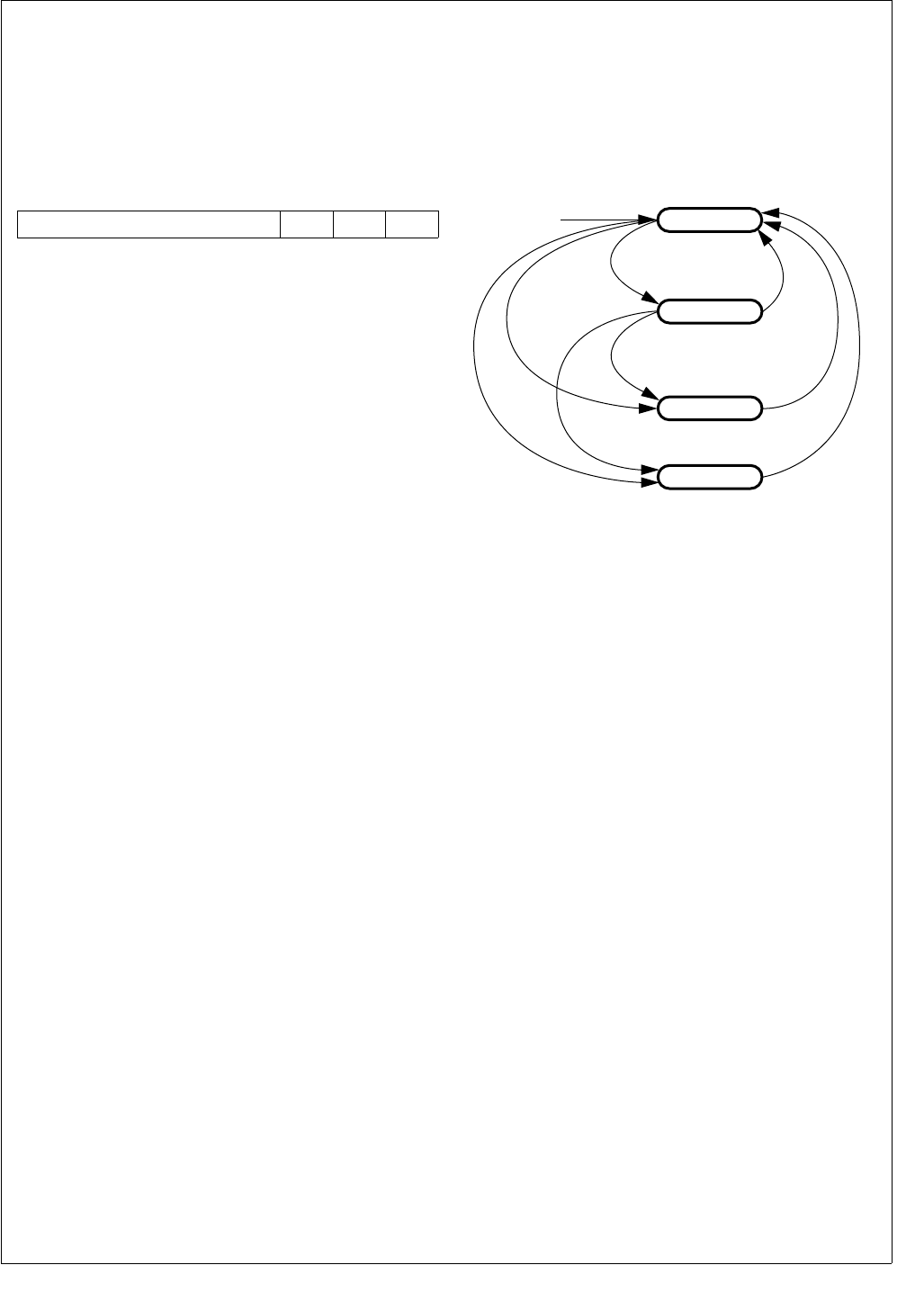
59 www.national.com
CP3BT26
12.6.2 Power Management Status Register (PMMSR)
The Management Status Register (PMMR) is a byte-wide,
read/write register that provides status signals for the vari-
ous clocks. The reset value of PMSR register bits 0 to 2 de-
pend on the status of the clock sources monitored by the
PMM. The upper 5 bits are clear after reset. The format of
the register is shown below.
OLC The Oscillating Low Frequency Clock bit indi-
cates whether the low-frequency oscillator is
producing a stable clock. When the low-fre-
quency oscillator is unavailable, the PMM will
not switch to Power Save, Idle, or Halt mode.
0 –Low-frequency oscillator is unstable, dis-
abled, or not oscillating.
1 –Low-frequency oscillator is available.
OMC The Oscillating Main Clock bit indicates
whether the high-frequency oscillator is pro-
ducing a stable clock. When the high-frequen-
cy oscillator is unavailable, the PMM will not
switch to Active mode.
0 –High-frequency oscillator is unstable, dis-
abled, or not oscillating.
1 –High-frequency oscillator is available.
OHC The Oscillating High Frequency (PLL) Clock
bit indicates whether the PLL is producing a
stable clock. Because the PMM tests the sta-
bility of the PLL clock to qualify power mode
state transitions, a stable clock is indicated
when the PLL is disabled. This removes the
stability of the PLL clock from the test when
the PLL is disabled. When the PLL is enabled
but unstable, the PMM will not switch to Active
mode.
0 –PLL is enabled but unstable.
1 –PLL is stable or disabled (CRCTRL.PLL-
PWD = 0).
12.7 SWITCHING BETWEEN POWER MODES
Switching from a higher to a lower power consumption
mode is performed by writing an appropriate value to the
Power Management Control/Status Register (PMMCR).
Switching from a lower power consumption mode to the Ac-
tive mode is usually triggered by a hardware interrupt.
Figure 8 shows the four power consumption modes and the
events that trigger a transition from one mode to another.
Figure 8. Power Mode State Diagram
Some of the power-up transitions are based on the occur-
rence of a wake-up event. An event of this type can be either
a maskable interrupt or a non-maskable interrupt (NMI). All
of the maskable hardware wake-up events are monitored by
the Multi-Input Wake-Up (MIWU) Module, which is active in
all modes. Once a wake-up event is detected, it is latched
until an interrupt acknowledge cycle occurs or a reset is ap-
plied.
A wake-up event causes a transition to the Active mode and
restores normal clock operation, but does not start execu-
tion of the program. It is the interrupt handler associated
with the wake-up source (MIWU or NMI) that causes pro-
gram execution to resume.
12.7.1 Active Mode to Power Save Mode
A transition from Active mode to Power Save mode is per-
formed by writing a 1 to the PMMCR.PSM bit. The transition
to Power Save mode is either initiated immediately or at ex-
ecution of the next WAIT instruction, depending on the state
of the PMMCR.WBPSM bit.
For an immediate transition to Power Save mode (PM-
MCR.WBPSM = 0), the CPU continues to operate using the
low-frequency clock. The PMMCR.PSM bit becomes set
when the transition to the Power Save mode is completed.
For a transition at the next WAIT instruction (PM-
MCR.WBPSM = 1), the CPU continues to operate in Active
mode until it executes a WAIT instruction. At execution of
the WAIT instruction, the device enters the Power Save
mode, and the CPU waits for the next interrupt event. In this
case, the PMMCR.PSM bit becomes set when it is written,
even before the WAIT instruction is executed.
7 3 2 1 0
Reserved OHC OMC OLC Reset Active Mode
WBPSM = 1 &
HALT = 1 &
"WAIT"
WBPSM = 1 &
IDLE = 1 &
"WAIT"
WBPSM = 1 & IDLE = 1 & "WAIT"
HW Event
HW Event
HW Event
Note:
HW Event = MIWU wake-up or NMI
IDLE = 1
WBPSM = 0 & PSM = 1
or
WBPSM = 1 & PSM = 1 & "WAIT"
Power Save Mode
Idle Mode
Halt Mode
DS008

www.national.com 60
CP3BT26
12.7.2 Entering Idle Mode
Entry into Idle mode is performed by writing a 1 to the PM-
MCR.IDLE bit and then executing a WAIT instruction. The
PMMCR.WBPSM bit must be set before the WAIT instruc-
tion is executed. Idle mode can be entered only from the Ac-
tive or Power Save mode.
12.7.3 Disabling the High-Frequency Clock
When the low-frequency oscillator is used to generate the
Slow Clock, power consumption can be reduced further in
the Power Save or Idle mode by disabling the high-frequen-
cy oscillator. This is accomplished by writing a 1 to the PM-
MCR.DHC bit before executing the WAIT instruction that
puts the device in the Power Save or Idle mode. The high-
frequency clock is turned off only after the device enters the
Power Save or Idle mode.
The CPU operates on the low-frequency clock in Power
Save mode. It can turn off the high-frequency clock at any
time by writing a 1 to the PMMCR.DHC bit. The high-fre-
quency oscillator is always enabled in Active mode and al-
ways disabled in Halt mode, without regard to the
PMMCR.DHC bit setting.
Immediately after power-up and entry into Active mode,
software must wait for the low-frequency clock to become
stable before it can put the device in Power Save mode. It
should monitor the PMMSR.OLC bit for this purpose. Once
this bit is set, Slow Clock is stable and Power Save mode
can be entered.
12.7.4 Entering Halt Mode
Entry into Halt mode is accomplished by writing a 1 to the
PMMCR.HALT bit and then executing a WAIT instruction.
The PMMCR.WBPSM bit must be set before the WAIT in-
struction is executed. Halt mode can be entered only from
Active or Power Save mode.
12.7.5 Software-Controlled Transition to Active Mode
A transition from Power Save mode to Active mode can be
accomplished by either a software command or a hardware
wake-up event. The software method is to write a 0 to the
PMMCR.PSM bit. The value of the register bit changes only
after the transition to the Active mode is completed.
If the high-frequency oscillator is disabled for Power Save
operation, the oscillator must be enabled and allowed to sta-
bilize before the transition to Active mode. To enable the
high-frequency oscillator, software writes a 0 to the PM-
MCR.DMC bit. Before writing a 0 to the PMMCR.PSM bit,
software must first monitor the PMMSR.OMC bit to deter-
mine when the oscillator has stabilized.
12.7.6 Wake-Up Transition to Active Mode
A hardware wake-up event switches the device directly from
Power Save, Idle, or Halt mode to Active mode. Hardware
wake-up events are:
Non-Maskable Interrupt (NMI)
Valid wake-up event on a Multi-Input Wake-Up channel
When a wake-up event occurs, the on-chip hardware per-
forms the following steps:
1. Clears the PMMCR.DMC bit, which enables the high-
frequency clock (if it was disabled).
2. Waits for the PMMSR.OMC bit to become set, which in-
dicates that the high-frequency clock is operating and
is stable.
3. Clears the PMMCR.DHC bit, which enables the PLL.
4. Waits for the PMMSR.OHC bit to become set.
5. Switches the device into Active mode.
12.7.7 Power Mode Switching Protection
The Power Management Module has several mechanisms
to protect the device from malfunctions caused by missing
or unstable clock signals.
The PMMSR.OHC, PMMSR.OMC, and PMMSR.OLC bits
indicate the current status of the PLL, high-frequency oscil-
lator, and low-frequency oscillator, respectively. Software
can check the appropriate bit before switching to a power
mode that requires the clock. A set status bit indicates an
operating, stable clock. A clear status bit indicates a clock
that is disabled, not available, or not yet stable. (Except in
the case of the PLL, which has a set status bit when dis-
abled.)
During a power mode transition, if there is a request to
switch to a mode with a clear status bit, the switch is delayed
until that bit is set by the hardware.
When the system is built without an external crystal network
for the low-frequency clock, Main Clock is divided by a pres-
caler factor to produce the low-frequency clock. In this situ-
ation, Main Clock is disabled only in the Halt mode, and
cannot be disabled for the Power Save or Idle mode.
Without an external crystal network for the low-frequency
clock, the device comes out of Halt or Idle mode and enters
Active mode with Main Clock driving Slow Clock.
Note: For correct operation in the absence of a low-fre-
quency crystal, the X2CKI pin must be tied low (not left float-
ing) so that the hardware can detect the absence of the
crystal.
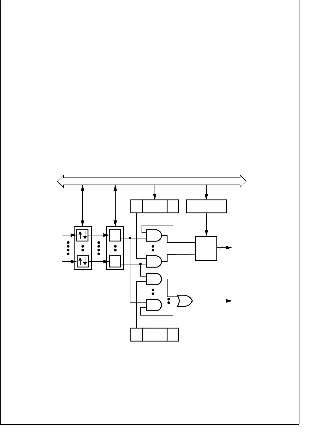
61 www.national.com
CP3BT26
13.0 Multi-Input Wake-Up
The Multi-Input Wake-Up (MIWU) unit consists of two iden-
tical 16-channel modules. Each module can assert a wake-
up signal for exiting from a low-power mode, and each can
assert an interrupt request on any of four Interrupt Control
Unit (ICU) channels assigned to that module. The modules
operate independently, so each may assert an interrupt re-
quest to the ICU. Together, these modules provide 32 MIWU
input channels and 8 interrupt request outputs.
Each 16-channel module monitors its inputs for a software-
selectable trigger condition. On detection of a trigger condi-
tion, the module generates an interrupt request and if en-
abled, a wake-up request. A wake-up request can be used
by the power management unit to exit the Halt, Idle, or Pow-
er Save mode and return to the Active mode. An interrupt
request generates an interrupt to the CPU, which allows an
interrupt handler to respond to MIWU events.
The wake-up event only activates the clocks and CPU, but
does not by itself initiate execution of any code. It is the in-
terrupt request asserted by the MIWU that gets the CPU to
start executing code, by jumping to the corresponding inter-
rupt handler. Therefore, setting up the MIWU interrupt han-
dler is essential for any wake-up operation.
Each 16-channel module has four interrupt requests that
can be routed to the ICU as shown in Figure 9. Each of the
16 channels can be programmed to activate one of these
four interrupt requests.
The 32 MIWU channels are named WUI0 through WUI31,
as shown in Table 27.
Each channel can be configured to trigger on rising or falling
edges, as determined by the setting in the WK0EDG or
WK1EDG register. Each trigger event is latched into the
WK0PND or WK1PND register. If a trigger event is enabled
by its respective bit in the WK0ENA or WK1ENA register, an
active wake-up/interrupt signal is generated. Software can
determine which channel has generated the active signal by
reading the WK0PND or WK1PND register.
The MIWU is active at all times, including the Halt mode. All
device clocks are stopped in this mode. Therefore, detecting
an external trigger condition and the subsequent setting of
the pending bit are not synchronous to the System Clock.
Figure 9. Multi-Input Wake-Up Module Block Diagram
WK0EDG
WK1EDG
WK0PND
WK1PND
WUI16
WUI31
Wake-Up Signal
To Power Mgt
0
15
Peripheral Bus
WK0ICTL1/WK0ICTL2
WK1ICTL1/WK1ICTL2
15 . . . . . . . . . . .
WK0IENA
WK1IENA
0
15 . . . . . . . . . . .
WK0ENA
WK1ENA
0
MIWU Interrupt 3:0
MIWU Interrupt 7:4
Encoder 4
DS218
WUI0
WUI15

www.national.com 62
CP3BT26
13.1 MULTI-INPUT WAKE-UP REGISTERS
Table 28 lists the MIWU registers.
Table 27 MIWU Sources
MIWU Channel Source
WUI0 TWM T0OUT
WUI1 ACCESS.bus
WUI2 CANRX
WUI3 MWCS
WUI4 UART0 CTS
WUI5 UART0 RXD
WUI6 Bluetooth LLC
WUI7 AAI SFS
WUI8 USB Wake-Up
WUI9 PJ7
WUI10 PG6
WUI11 PH0
WUI12 PH1
WUI13 PH2
WUI14 PH3
WUI15 PH4
WUI16 PH5
WUI17 PH6
WUI18 PJ0
WUI19 PJ1
WUI20 PJ2
WUI21 PJ3
WUI22 PJ4
WUI23 PJ5
WUI24 PJ6
WUI25 Reserved
WUI26 UART1 RXD
WUI27 UART2 RXD
WUI28 UART3 RXD
WUI29 Reserved
WUI30 ADC Done
WUI31 Reserved
Table 28 Multi-Input Wake-Up Registers
Name Address Description
WK0EDG FF FC80h
Wake-Up Edge
Detection Register
Module 0
WK1EDG FF FCA0h
Wake-Up Edge
Detection Register
Module 1
WK0ENA FF FC82h
Wake-Up Enable
Register
Module 0
WK1ENA FF FCA2h
Wake-Up Enable
Register
Module 1
WK0ICTL1 FF FC84h
Wake-Up Interrupt
Control Register 1
Module 0
WK1ICTL1 FF FCA4h
Wake-Up Interrupt
Control Register 1
Module 1
WK0ICTL2 FF FC86h
Wake-Up Interrupt
Control Register 2
Module 0
WK1ICTL2 FF FCA6h
Wake-Up Interrupt
Control Register 2
Module 1
WK0PND FF FC88h
Wake-Up Pending
Register
Module 0
WK1PND FF FCA8h
Wake-Up Pending
Register
Module 1
WK0PCL FF FC8Ah
Wake-Up Pending
Clear Register
Module 0
WK1PCL FF FCAAh
Wake-Up Pending
Clear Register
Module 1
WK0IENA FF FC8Ch
Wake-Up Interrupt
Enable Register
Module 0
WK1IENA FF FCACh
Wake-Up Interrupt
Enable Register
Module 1

63 www.national.com
CP3BT26
13.1.1 Wake-Up Edge Detection Register (WK0EDG)
The WK0EDG register is a word-wide read/write register
that controls the edge sensitivity of the MIWU channels. The
WK0EDG register is cleared upon reset, which configures
all channels to be triggered on rising edges. The register for-
mat is shown below.
WKED The Wake-Up Edge Detection bits control the
edge sensitivity for MIWU channels. The
WKED15:0 bits correspond to the WUI15:0
channels, respectively.
0 –Triggered on rising edge (low-to-high
transition).
1 –Triggered on falling edge (high-to-low
transition).
13.1.2 Wake-Up 1 Edge Detection Register (WK1EDG)
The WK1EDG register is a word-wide read/write register
that controls the edge sensitivity of the MIWU channels. The
WK1EDG register is cleared upon reset, which configures
all channels to be triggered on rising edges. The register for-
mat is shown below.
WKED The Wake-Up Edge Detection bits control the
edge sensitivity for MIWU channels. The
WKED15:0 bits correspond to the WUI31:16
channels, respectively.
0 –Triggered on rising edge (low-to-high
transition).
1 –Triggered on falling edge (high-to-low
transition).
13.1.3 Wake-Up Enable Register (WK0ENA)
The WK0ENA register is a word-wide read/write register
that individually enables or disables wake-up events from
the MIWU channels. The WK0ENA register is cleared upon
reset, which disables all wake-up/interrupt channels. The
register format is shown below.
WKEN The Wake-Up Enable bits enable and disable
the MIWU channels. The WKEN15:0 bits cor-
respond to the WUI15:0 channels, respective-
ly.
0 –MIWU channel wake-up events disabled.
1 –MIWU channel wake-up events enabled.
13.1.4 Wake-Up 1 Enable Register (WK1ENA)
The WK1ENA register is a word-wide read/write register
that individually enables or disables wake-up events from
the MIWU channels. The WK1ENA register is cleared upon
reset, which disables all wake-up/interrupt channels. The
register format is shown below.
WKEN The Wake-Up Enable bits enable and disable
the MIWU channels. The WKEN15:0 bits cor-
respond to the WUI31:16 channels, respec-
tively.
0 –MIWU channel wake-up events disabled.
1 –MIWU channel wake-up events enabled.
13.1.5 Wake-Up Interrupt Enable Register (WK0IENA)
The WK0IENA register is a word-wide read/write register
that enables and disables interrupts from the MIWU chan-
nels. The register format is shown below.
WKIEN The Wake-Up Interrupt Enable bits control
whether MIWU channels generate interrupts.
The WKIEN15:0 bits correspond to the
WUI15:0 channels, respectively.
0 –Interrupt disabled.
1 –Interrupt enabled.
13.1.6 Wake-Up 1 Interrupt Enable Register
(WK1IENA)
The WK1IENA register is a word-wide read/write register
that enables and disables interrupts from the MIWU chan-
nels. The register format is shown below.
WK1IEN The Wake-Up Interrupt Enable bits control
whether MIWU channels generate interrupts.
The WKIEN15:0 bits correspond to the
WUI31:16 channels, respectively.
0 –Interrupt disabled.
1 –Interrupt enabled.
15 0
WKED
15 0
WKED
15 0
WKEN
15 0
WKEN
15 0
WKIEN
15 0
WKIEN

www.national.com 64
CP3BT26
13.1.7 Wake-Up Interrupt Control Register 1
(WK0ICTL1)
The WK0ICTL1 register is a word-wide read/write register
that selects the interrupt request signal for the associated
MIWU channels WUI7:0. At reset, the WK0ICTL1 register is
cleared, which selects MIWU Interrupt Request 0 for all
eight channels. The register format is shown below.
WKINTR The Wake-Up Interrupt Request Select fields
select which of the four MIWU interrupt re-
quests are activated for the corresponding
channel.
00 – Selects MIWU interrupt request 0.
01 – Selects MIWU interrupt request 1.
10 – Selects MIWU interrupt request 2.
11 – Selects MIWU interrupt request 3.
13.1.8 Wake-Up 1 Interrupt Control Register 1
(WK1ICTL1)
The WK1ICTL1 register is a word-wide read/write register
that selects the interrupt request signal for the associated
MIWU channels WUI23:16. At reset, the WK1ICTL1 register
is cleared, which selects MIWU Interrupt Request 4 for all
eight channels. The register format is shown below.
WKINTR The Wake-Up Interrupt Request Select fields
select which of the four MIWU interrupt re-
quests are activated for the corresponding
channel.
00 – Selects MIWU interrupt request 4.
01 – Selects MIWU interrupt request 5.
10 – Selects MIWU interrupt request 6.
11 – Selects MIWU interrupt request 7.
13.1.9 Wake-Up Interrupt Control Register 2
(WK0ICTL2)
The WK0ICTL2 register is a word-wide read/write register
that selects the interrupt request signal for the associated
MIWU channels WUI15:8. At reset, the WK2ICTL2 register
is cleared, which selects MIWU Interrupt Request 0 for all
eight channels. The register format is shown below.
WKINTR The Wake-Up Interrupt Request Select fields
select which of the four MIWU interrupt re-
quests are activated for the corresponding
channel.
00 – Selects MIWU interrupt request 0.
01 – Selects MIWU interrupt request 1.
10 – Selects MIWU interrupt request 2.
11 – Selects MIWU interrupt request 3.
13.1.10 Wake-Up 1 Interrupt Control Register 2
(WK1ICTL2)
The WK1ICTL2 register is a word-wide read/write register
that selects the interrupt request signal for the associated
MIWU channels WUI31:24. At reset, the WK1ICTL2 register
is cleared, which selects MIWU Interrupt Request 4 for all
eight channels. The register format is shown below.
WKINTR The Wake-Up Interrupt Request Select fields
select which of the four MIWU interrupt re-
quests are activated for the corresponding
channel.
00 – Selects MIWU interrupt request 4.
01 – Selects MIWU interrupt request 5.
10 – Selects MIWU interrupt request 6.
11 – Selects MIWU interrupt request 7.
15 14 13 12 11 10 9876543210
WKIN
TR7
WKIN
TR6
WKIN
TR5
WKIN
TR4
WKIN
TR3
WKIN
TR2
WKIN
TR1
WKIN
TR0
15 14 13 12 11 10 9876543210
WKIN
TR23
WKIN
TR22
WKIN
TR21
WKIN
TR20
WKIN
TR19
WKIN
TR18
WKIN
TR17
WKIN
TR16
15 14 13 12 11 10 9876543210
WKIN
TR15
WKIN
TR14
WKIN
TR13
WKIN
TR12
WKIN
TR11
WKIN
TR10
WKIN
TR9
WKIN
TR8
15 14 13 12 11 10 9876543210
WKIN
TR31
WKIN
TR30
WKIN
TR29
WKIN
TR28
WKIN
TR27
WKIN
TR26
WKIN
TR25
WKIN
TR24

65 www.national.com
CP3BT26
13.1.11 Wake-Up Pending Register (WK0PND)
The WK0PND register is a word-wide read/write register in
which the Multi-Input Wake-Up module latches any detect-
ed trigger conditions. The CPU can only write a 1 to any bit
position in this register. If the CPU attempts to write a 0, it
has no effect on that bit. To clear a bit in this register, the
CPU must use the WK0PCL register. This implementation
prevents a potential hardware-software conflict during a
read-modify-write operation on the WK0PND register.
This register is cleared upon reset. The register format is
shown below.
WKPD The Wake-Up Pending bits indicate which
MIWU channels have been triggered. The
WKPD15:0 bits correspond to the WUI15:0
channels. Writing 1 to a bit sets it.
0 –Trigger condition did not occur.
1 –Trigger condition occurred.
13.1.12 Wake-Up 1 Pending Register (WK1PND)
The WK1PND register is a word-wide read/write register in
which the Multi-Input Wake-Up module latches any detect-
ed trigger conditions. The CPU can only write a 1 to any bit
position in this register. If the CPU attempts to write a 0, it
has no effect on that bit. To clear a bit in this register, the
CPU must use the WK1PCL register. This implementation
prevents a potential hardware-software conflict during a
read-modify-write operation on the WK1PND register.
This register is cleared upon reset. The register format is
shown below.
WKPD The Wake-Up Pending bits indicate which
MIWU channels have been triggered. The
WKPD15:0 bits correspond to the WUI31:15
channels. Writing 1 to a bit sets it.
0 –Trigger condition did not occur.
1 –Trigger condition occurred.
13.1.13 Wake-Up Pending Clear Register (WK0PCL)
The WK0PCL register is a word-wide write-only register that
lets the CPU clear bits in the WKPND register. Writing a 1
to a bit position in the WKPCL register clears the corre-
sponding bit in the WKPND register. Writing a 0 has no ef-
fect. Do not modify this register with instructions that access
the register as a read-modify-write operand, such as the bit
manipulation instructions.
Reading this register location returns undefined data.
Therefore, do not use a read-modify-write sequence (such
as the SBIT instruction) to set individual bits. Do not attempt
to read the register, then perform a logical OR on the regis-
ter value. Instead, write the mask directly to the register ad-
dress. The register format is shown below.
WKCL Writing 1 to a bit clears it.
0 –Writing 0 has no effect.
1 –Writing 1 clears the corresponding bit in
the WKPD register.
13.1.14 Wake-Up 1 Pending Clear Register (WK1PCL)
The WK1PCL register is a word-wide write-only register that
lets the CPU clear bits in the WK1PND register. Writing a 1
to a bit position in the WK1PCL register clears the corre-
sponding bit in the WK1PND register. Writing a 0 has no ef-
fect. Do not modify this register with instructions that access
the register as a read-modify-write operand, such as the bit
manipulation instructions.
Reading this register location returns undefined data.
Therefore, do not use a read-modify-write sequence (such
as the SBIT instruction) to set individual bits. Do not attempt
to read the register, then perform a logical OR on the regis-
ter value. Instead, write the mask directly to the register ad-
dress. The register format is shown below.
WKCL Writing 1 to a bit clears it.
0 –Writing 0 has no effect.
1 –Writing 1 clears the corresponding bit in
the WK1PD register.
15 0
WKPD
15 0
WKPD
15 0
WKCL
15 0
WKCL

www.national.com 66
CP3BT26
13.2 PROGRAMMING PROCEDURES
To set up and use the Multi-Input Wake-Up function, use the
following procedure. Performing the steps in the order
shown will prevent false triggering of a wake-up condition.
This same procedure should be used following a reset be-
cause the wake-up inputs are left floating, resulting in un-
known data on the input pins.
1. Clear the WK0ENA and WK1ENA registers to disable
the MIWU channels.
2. Write the WK0EDG and WK1EDG registers to select
the desired type of edge sensitivity (clear for rising
edge, set for falling edge).
3. Set all bits in the WK0PCL and WK0PCL registers to
clear any pending bits in the WK0PND and WK1PND
registers.
4. Set up the WK0ICTL1, WK1ICTL1, WK0ICTL2, and
WK1ICTL2 registers to define the interrupt request sig-
nal used for each channel.
5. Set the bits in the WK0ENA and WK1ENA registers
corresponding to the wake-up channels to be activated.
To change the edge sensitivity of a wake-up channel, use
the following procedure. Performing the steps in the order
shown will prevent false triggering of a wake-up/interrupt
condition.
1. Clear the WK0ENA or WK1ENA bit associated with the
input to be reprogrammed.
2. Write the new value to the corresponding bit position in
the WK0EDG or WK1EDG register to reprogram the
edge sensitivity of the input.
3. Set the corresponding bit in the WK0PCL or WK1PCL
register to clear the pending bit in the WK0PND or
WK1PND register.
4. Set the same WK0ENA or WK1ENA bit to re-enable the
wake-up function.
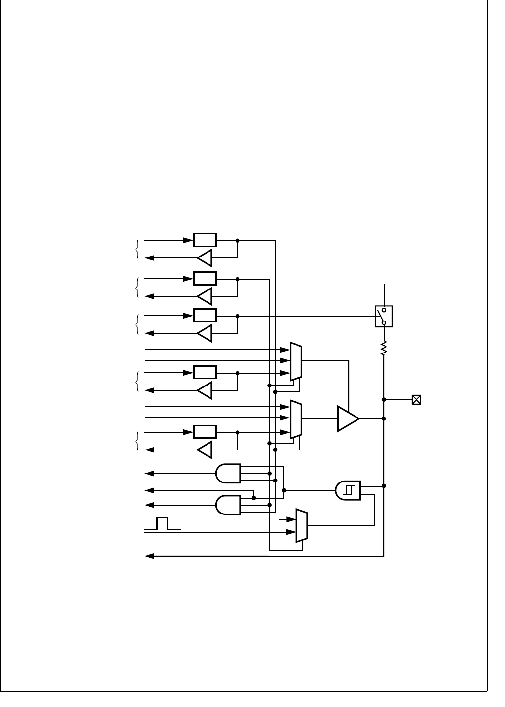
67 www.national.com
CP3BT26
14.0 Input/Output Ports
Each device has up to 54 software-configurable I/O pins, or-
ganized into 8-bit ports (not all bits are used in some ports).
The ports are named Port B, Port C, Port E, Port F, Port G,
Port H, and Port J.
In addition to their general-purpose I/O capability, the I/O
pins of Ports E, F, G, H, and J have alternate functions for
use with on-chip peripheral modules such as the UART or
the Multi-Input Wake-Up unit. The alternate functions of all
I/O pins are shown in Table 94.
Ports B and C are used as the 16-bit data bus when an ex-
ternal bus is enabled (144-pin devices only). This alternate
function is selected by enabling the DEV or ERE operating
environments, not by programming the port registers.
The I/O pin characteristics are fully programmable. Each pin
can be configured to operate as a TRI-STATE output, push-
pull output, weak pull-up input, or high-impedance input.
Different pins within the same port can be individually con-
figured to operate in different modes.
Figure 10 is a diagram showing the I/O port pin logic. The
register bits, multiplexers, and buffers allow the port pin to
be configured into the various operating modes. The output
buffer is a TRI-STATE buffer with weak pull-up capability.
The weak pull-up, if used, prevents the port pin from going
to an undefined state when it operates as an input.
To reduce power consumption, input buffers configured for
general-purpose I/O are only enabled when they are read.
When configured for an alternate function, the input buffers
are enabled continuously. To minimize power consumption,
input signals to enabled buffers must be held within 0.2 volts
of the VCC or GND voltage.
The electrical characteristics and drive capabilities of the in-
put and output buffers are described in Section 30.0.
Figure 10. I/O Port Pin Logic
14.1 PORT REGISTERS
Each port has an associated set of memory-mapped regis-
ters used for controlling the port and for holding the port da-
ta:
PxALT: Port alternate function register
PxALTS: Port alternate function select register
PxDIR: Port direction register
PxDIN: Port data input register
PxDOUT: Port data output register
PxWPU: Port weak pull-up register
PxHDRV: Port high drive strength register
Data In Read Strobe
Alt. A Device Direction
Alt. B Device Direction
Alt. B Data Input
Analog Input
PxDIN Register
PxALTS Register
PxALT Register
PxWKPU Register
PxDIR Register
Alt. A Device Data Outout
Alt. B Device Data Outout
PxDOUT Register
1
DS190
Alt. A Data Input
VCC
Weak Pull-Up Enable
Output Enable
Data Out
Pin
Data In
DQ
DQ
DQ
DQ
DQ

www.national.com 68
CP3BT26
In the descriptions of the ports and port registers, the lower-
case letter “x” represents the port designation, either B, C,
E, F, G, H, or J. For example, “PxDIR register” means any
one of the port direction registers: PBDIR, PCDIR, PEDIR,
PFDIR, PGDIR, PHDIR, or PJDIR.
Table 29 Port Registers
Name Address Description
PBALT FF FB00h Port B Alternate
Function Register
PBDIR FF FB02h Port B Direction Register
PBDIN FF FB04h Port B Data Input Register
PBDOUT FF FB06h Port B Data Output Register
PBWPU FF FB08h Port B Weak Pull-Up
Register
PBHDRV FF FB0Ah Port B High Drive
Strength Register
PBALTS FF FB0Ch Port B Alternate Function
Select Register
PCALT FF FB10h Port C Alternate
Function Register
PCDIR FF FB12h Port C Direction Register
PCDIN FF FB14h Port C Data Input Register
PCDOUT FF FB16h Port C Data Output Register
PCWPU FF FB18h Port C Weak Pull-Up
Register
PCHDRV FF FB1Ah Port C High Drive
Strength Register
PCALTS FF FB1Ch Port C Alternate Function
Select Register
PEALT FF FCC0h Port E Alternate
Function Register
PEDIR FF FCC2h Port E Direction Register
PEDIN FF FCC4h Port E Data Input Register
PEDOUT FF FCC6h Port E Data Output Register
PEWPU FF FCC8h Port E Weak Pull-Up
Register
PEHDRV FF FCCAh Port E High Drive
Strength Register
PEALTS FF FCCCh Port E Alternate Function
Select Register
PFALT FF FCE0h Port F Alternate
Function Register
PFDIR FF FCE2h Port F Direction Register
PFDIN FF FCE4h Port F Data Input Register
PFDOUT FF FCE6h Port F Data Output Register
PFWPU FF FCE8h Port F Weak Pull-Up
Register
PFHDRV FF FCEAh Port F High Drive
Strength Register
PFALTS FF FCECh Port F Alternate Function
Select Register
PGALT FF F300h Port G Alternate
Function Register
PGDIR FF F302h Port G Direction Register
PGDIN FF F304h Port G Data Input Register
PGDOUT FF F306h Port G Data Output Register
PGWPU FF F308h Port G Weak Pull-Up
Register
PGHDRV FF F30Ah Port G High Drive
Strength Register
PGALTS FF F30Ch Port G Alternate Function
Select Register
PHALT FF F320h Port H Alternate
Function Register
PHDIR FF F322h Port H Direction Register
PHDIN FF F324h Port H Data Input Register
PHDOUT FF F326h Port H Data Output Register
PHWPU FF F328h Port H Weak Pull-Up
Register
PHHDRV FF F32Ah Port H High Drive
Strength Register
PHALTS FF F32Ch Port H Alternate Function
Select Register
PJALT FF F340h Port J Alternate
Function Register
PJDIR FF F342h Port J Direction Register
PJDIN FF F344h Port J Data Input Register
PJDOUT FF F346h Port J Data Output Register
PJWPU FF F348h Port J Weak Pull-Up
Register
PJHDRV FF F34Ah Port J High Drive
Strength Register
PJALTS FF F34Ch Port J Alternate Function
Select Register
Table 29 Port Registers
Name Address Description

69 www.national.com
CP3BT26
All of the port registers are byte-wide read/write registers,
except for the port data input registers, which are read-only
registers. Each register bit controls the function of the cor-
responding port pin. For example, PGDIR.2 (bit 2 of the
PGDIR register) controls the direction of port pin PG2.
14.1.1 Port Alternate Function Register (PxALT)
The PxALT registers control whether the port pins are used
for general-purpose I/O or for their alternate function. Each
port pin can be controlled independently.
A clear bit in the alternate function register causes the cor-
responding pin to be used for general-purpose I/O. In this
configuration, the output buffer is controlled by the direction
register (PxDIR) and the data output register (PxDOUT).
The input buffer is visible to software as the data input reg-
ister (PxDIN).
A set bit in the alternate function register (PxALT) causes
the corresponding pin to be used for its peripheral I/O func-
tion. When the alternate function is selected, the output
buffer data and TRI-STATE configuration are controlled by
signals from the on-chip peripheral device.
A reset operation clears the port alternate function regis-
ters, which initializes the pins as general-purpose I/O ports.
This register must be enabled before the corresponding al-
ternate function is enabled.
PxALT The PxALT bits control whether the corre-
sponding port pins are general-purpose I/O
ports or are used for their alternate function by
an on-chip peripheral.
0 –General-purpose I/O selected.
1 –Alternate function selected.
14.1.2 Port Direction Register (PxDIR)
The port direction register (PxDIR) determines whether
each port pin is used for input or for output. A clear bit in this
register causes the corresponding pin to operate as an in-
put, which puts the output buffer in the high-impedance
state. A set bit causes the pin to operate as an output, which
enables the output buffer.
A reset operation clears the port direction registers, which
initializes the pins as inputs.
PxDIR The PxDIR bits select the direction of the cor-
responding port pin.
0 –Input.
1 –Output.
14.1.3 Port Data Input Register (PxDIN)
The data input register (PxDIN) is a read-only register that
returns the current state on each port pin. The CPU can
read this register at any time even when the pin is config-
ured as an output.
PxDIN The PxDIN bits indicate the state on the cor-
responding port pin.
0 –Pin is low.
1 –Pin is high.
14.1.4 Port Data Output Register (PxDOUT)
The data output register (PxDOUT) holds the data to be
driven on output port pins. In this configuration, writing to
the register changes the output value. Reading the register
returns the last value written to the register.
A reset operation leaves the register contents unchanged.
At power-up, the PxDOUT registers contain unknown val-
ues.
PxDOUT The PxDOUT bits hold the data to be driven
on pins configured as outputs in general-pur-
pose I/O mode.
0 –Drive the pin low.
1 –Drive the pin high.
14.1.5 Port Weak Pull-Up Register (PxWPU)
The weak pull-up register (PxWPU) determines whether the
port pins have a weak pull-up on the output buffer. The pull-
up device, if enabled by the register bit, operates in the gen-
eral-purpose I/O mode whenever the port output buffer is
disabled. In the alternate function mode, the pull-ups are al-
ways disabled.
A reset operation clears the port weak pull-up registers,
which disables all pull-ups.
PxWPU The PxWPU bits control whether the weak
pull-up is enabled.
0 –Weak pull-up disabled.
1 –Weak pull-up enabled.
7 0
PxALT
7 0
PxDIR
7 0
PxDIN
7 0
PxDOUT
7 0
PxWPU
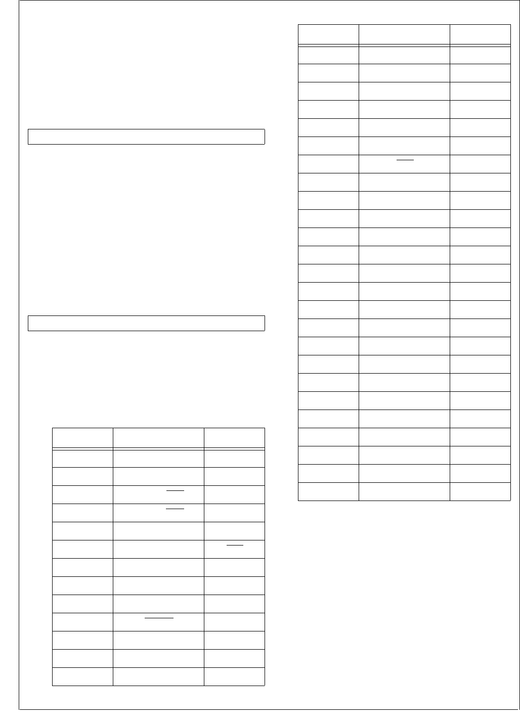
www.national.com 70
CP3BT26
14.1.6 Port High Drive Strength Register (PxHDRV)
The PxHDRV register is a byte-wide, read/write register that
controls the slew rate of the corresponding pins. The high
drive strength function is enabled when the corresponding
bits of the PxHDRV register are set. In both GPIO and alter-
nate function modes, the drive strength function is enabled
by the PxHDRV registers. At reset, the PxHDRV registers
are cleared, making the ports low speed.
PxHDRV The PxHDRV bits control whether output pins
are driven with slow or fast slew rate.
0 –Slow slew rate.
1 –Fast slew rate.
14.1.7 Port Alternate Function Select Register
(PxALTS)
The PxALTS register selects which of two alternate func-
tions are selected for the port pin. These bits are ignored
unless the corresponding PxALT bits are set. Each port pin
can be controlled independently.
PxALTS The PxALTS bits select among two alternate
functions. Table 30 shows the mapping of the
PxALTS bits to the alternate functions. Un-
used PxALTS bits must be clear.
7 0
PxHDRV
7 0
PxALTS
Table 30 Alternate Function Select
Port Pin PxALTS = 0 PxALTS = 1
PE0 UART0 RXD0 Reserved
PE1 UART0 TXD0 Reserved
PE2 UART0 RTS Reserved
PE3 UART0 CTS Reserved
PE4 UART0 CKX TB
PE5 SRFS NMI
PF0 MSK TIO1
PF1 MDIDO TIO2
PF2 MDODI TIO3
PF3 MWCS TIO4
PF4 SCK TIO5
PF5 SFS TIO6
PF6 STD TIO7
PF7 SRD TIO8
PG0 RFSYNC Reserved
PG1 RFCE Reserved
PG2 BTSEQ1 SRCLK
PG3 SCLK Reserved
PG4 SDAT Reserved
PG5 SLE Reserved
PG6 WUI10 BTSEQ2
PG7 TA BTSEQ3
PH0 UART1 RXD1 WUI11
PH1 UART1 TXD1 WUI12
PH2 UART2 RXD2 WUI13
PH3 UART2 TXD2 WUI14
PH4 UART3 RXD3 WUI15
PH5 UART3 TXD3 WUI16
PH6 CANRX WUI17
PH7 CANTX Reserved
PJ0 WUI18 Reserved
PJ1 WUI19 Reserved
PJ2 WUI20 Reserved
PJ3 WUI21 Reserved
PJ4 WUI22 Reserved
PJ5 WUI23 Reserved
PJ6 WUI24 Reserved
PJ7 ASYNC WUI9
Table 30 Alternate Function Select
Port Pin PxALTS = 0 PxALTS = 1

71 www.national.com
CP3BT26
14.2 OPEN-DRAIN OPERATION
A port pin can be configured to operate as an inverting
open-drain output buffer. To do this, the CPU must clear the
bit in the data output register (PxDOUT) and then use the
port direction register (PxDIR) to set the value of the port
pin. With the direction register bit set (direction = out), the
value zero is forced on the pin. With the direction register bit
clear (direction = in), the pin is placed in the TRI-STATE
mode. If desired, the internal weak pull-up can be enabled
to pull the signal high when the output buffer is in TRI-
STATE mode.
www.national.com 72
CP3BT26
15.0 Bluetooth Controller
The integrated hardware Bluetooth Lower Link Controller
(LLC) complies to the Bluetooth Specification Version 1.1
and integrates the following functions:
4.5K-byte dedicated Bluetooth data RAM
1K-byte dedicated Bluetooth Sequencer RAM
Support of all Bluetooth 1.1 packet types
Support for fast frequency hopping of 1600 hops/s
Access code correlation and slot timing recovery circuit
Power Management Control Logic
BlueRF-compatible interface to connect with National’s
LMX5252 and other RF transceiver chips
For a detailed description of the interface to the LMX5252,
consult the LMX5252 data sheet which is available from the
National Semiconductor wireless group. National provides
software libraries for using the Bluetooth LLC. Documenta-
tion for the software libraries is also available from National
Semiconductor.
15.1 RF INTERFACE
The CP3BT26 interfaces to the LMX5251 or LMX5252 radio
chips though the RF interface.
Figure 11 shows the interface between the CP3BT26 and
the LMX5251 radio chip.
Figure 11. LMX5251 Interface
Figure 12 shows the interface between the CP3BT26 and
the LMX5252 radio chip.
Figure 12. LMX5252 Interface
The CP3BT26 implements a BlueRF-compatible interface,
which may be used with other RF transceiver chips.
15.1.1 RF Interface Signals
The RF interface signals are grouped as follows:
Modem Signals (BBCLK, RFDATA, and RFSYNC)
Control Signal (RFCE)
Serial Interface Signals (SCLK, SDAT, and SLE)
Bluetooth Sequencer Status Signals (BTSEQ1,
BTSEQ2, and BTSEQ2)
X1CKI/BBCLK
The X1CKI/BBCLK pin is the input signal for the 12-MHz
clock signal. The radio chip uses this signal internally as the
12× oversampling clock and provides it externally to the
CP3BT26 for use as the Main Clock.
RFDATA
The RFDATA signal is the multiplexed Bluetooth data re-
ceive and transmit signal. The data is provided at a bit rate
of 1 Mbit/s with 12× oversampling, synchronized to the 12
MHz BBCLK. The RFDATA signal is a dedicated RF inter-
face pin. This signal is driven to a logic high level after reset.
RFSYNC
In receive mode (data direction from the radio chip to the
CP3BT26), the RFSYNC signal acts as the frequency cor-
rection/DC compensation circuit control output to the radio
chip. The RFSYNC signal is driven low throughout the cor-
relation phase and driven high when synchronization to the
received access code is achieved.
In transmit mode (data direction from the CP3BT26 to the
radio chip), the RFSYNC signal enables the RF output of
the radio chip. When the RFSYNC pin is driven high, the RF
CP3BT26 LMX5251
X1CKI/BBCLK BBP_CLOCK
RFDATA TX_RX_DATA
PG0/RFSYNC TX_RX_SYNC
PG3/SCLK CCB_CLOCK
PG4/SDAT CCB_DATA
PG1/RFCE CE
IOVCC VDD_DIG_IN
VCC
PG5/SLE CCB_LATCH
DS316
CP3BT26 LMX5252
X1CKI/BBCLK BRCLK
RFDATA BBDATA_1
PG2/BTSEQ1 BPKTCTL
PG3/SCLK BDCLK
PG4/SDAT BDDATA
PG1/RFCE BXTLEN
IOVCC VCC
+2.8V
PG5/SLE BDEN#
DS320

73 www.national.com
CP3BT26
transmitter circuit of the radio chip is enabled, correspond-
ing to the settings of the power control register in the radio
chip.
The RFSYNC signal is the alternate function of the general-
purpose I/O pin PG0. At reset, this pin is in TRI-STATE
mode. Software must enable the alternate function of the
PG0 pin to give control over this signal to the RF interface.
RFCE
The RFCE signal is the chip enable output to the external
RF chip. When the RFCE signal is driven high, the RF chip
power is controlled by the settings of its power control reg-
isters. When the RFCE signal is driven low, the RF chip is
powered-down. However, the serial interface is still opera-
tional and the CP3BT26 can still access the RF chip internal
control registers.
The RFCE signal is the alternate function of the general-
purpose I/O pin PG1. At reset, this pin is in TRI-STATE
mode. Software must enable the alternate function of the
PG1 pin to give control over this signal to the RF interface.
During Bluetooth power-down phases, the CP3BT26 pro-
vides a mechanism to reduce the power consumption of an
external RF chip by driving the RFCE signal of the RF inter-
face to a logic low level. This feature is available when the
Power Management Module of the CP3BT26 has enabled
the Hardware Clock Control mechanism. (However, the cur-
rent version of the radio chip does not implement a power-
reduction mode.)
SCLK
The SCLK signal is the serial interface shift clock output.
The CP3BT26 always acts as the master of the serial inter-
face and therefore always provides the shift clock. The
SCLK signal is the alternate function of the general-purpose
I/O pin PG3. At reset, this pin is in TRI-STATE mode. Soft-
ware must enable the alternate function of the PG3 pin to
give control over this signal to the RF interface.
SDAT
The SDAT signal is the multiplexed serial data receive and
transmit path between the radio chip and the CP3BT26.
The SDAT signal is the alternate function of the general-pur-
pose I/O pin PG4. At reset, this pin is in TRI-STATE mode.
Software must enable the alternate function of the PG4 pin
to give control over this signal to the RF interface.
SLE
The SLE pin is the serial load enable output of the serial in-
terface of the CP3BT26.
During write operations (to the radio chip registers), the data
received by the shift register of the radio chip is copied into
the address register on the next rising edge of SCLK after
the SLE signal goes high.
During read operations (read from the registers), the radio
chip releases the SDAT line on the next rising edge of SCLK
after the SLE signal goes high.
SLE is the alternate function of the general-purpose I/O pin
PG5. At reset, this pin is in TRI-STATE mode. Software must
enable the alternate function of the PG5 pin to give control
over this signal to the RF interface.
BTSEQ[3:1]
The BTSEQ[3:1] signals indicate internal states of the Blue-
tooth sequencer, which are used for interfacing to some ex-
ternal devices.
15.2 SERIAL INTERFACE
The radio chip register set can be accessed by the
CP3BT26 through the serial interface. The serial interface
uses three pins of the RF interface: SDAT, SCLK, and SLE.
The serial interface of the CP3BT26 always operates as the
master, providing the shift clock (SCLK) and load enable
(SLE) signal to the radio chip. The radio chip always acts as
the slave.
A 25-bit shift protocol is used to perform read/write access-
es to the radio chip internal registers. The complete protocol
is comprised of the following sections:
3-bit Header Field
Read/Write Bit
5-bit Address Field
16-bit Data Field
Header
The 3-bit header contains the fixed data 101b (except for
Fast Write Operations).
Read/Write Bit
The header is followed by the read/write control bit (R/W). If
the Read/Write bit is clear, a write operation is performed
and the 16-bit data portion is copied into the addressed ra-
dio chip register.
Address
The address field is used to select one of the radio chip in-
ternal registers.
Data
The data field is used to transfer data to or from a radio chip
register. The timing is modified for reads, to transfer control
over the data signal from the CP3BT26 to the radio chip.
Figure 13 shows the serial interface protocol format.
Figure 13. Serial Interface Protocol Format
Data is transferred on the serial interface with the most sig-
nificant bit (MSB) first.
15 0
Data[15:0]
24 22 21 20 16
Header[2:0] R/W Address[4:0]
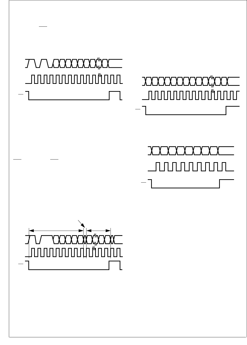
www.national.com 74
CP3BT26
Write Operation
When the R/W bit is clear, the 16 bits of the data field are
shifted out of the CP3BT26 on the falling edge of SCLK.
Data is sampled by the radio chip on the rising edge of
SCLK. When SLE is high, the 16-bit data are copied into the
radio chip register on the next rising edge of SCLK. The
data is loaded in the appropriate radio chip register depend-
ing on the state of the four address bits, Address[4:0].
Figure 14 shows the timing for the write operation.
Figure 14. Serial Interface Write Timing
Read Operation
When the R/W bit is set, data is shifted out of the radio chip
on the rising edge of SCLK. Data is sampled by the
CP3BT26 on the falling edge of SCLK. On reception of the
read command (R/W = 1), the radio chip takes control of the
serial interface data line. The received 16-bit data is loaded
by the CP3BT26 after the first falling edge of SCLK when
SLE is high. When SLE is high, the radio chip releases the
SDAT line again on the next rising edge of SCLK. The
CP3BT26 takes control of the SDAT line again after the fol-
lowing rising edge of SCLK. Which radio chip register is
read, depends on the state of the four address bits, Ad-
dress[4:0]. The transfer is always 16 bits, without regard to
the actual size of the register. Unimplemented bits contain
undefined data. Figure 15 shows the timing for the read op-
eration.
Figure 15. Serial Interface Read Timing
Fast-Write Operation
An enhanced serial interface mode including fast write ca-
pability is enabled when the FW bit in the radio chip is set.
This bit activates a mode with decreased addressing and
control overhead, which allows fast loading of time-critical
registers during normal operation. When the FW bit is set,
the 3-bit header may have a value other than 101b, and it is
used to address the write-only registers of the radio chip.
Fast writes load the same physical register as the corre-
sponding normal write operation.
For the power control and CMOS output registers of the RF
chip, it is only necessary to transmit a total of 8 bits (3 ad-
dress bits and 5 data bits), because the remaining eight bits
are unused.
While the FW bit is set, normal Read/Write operations are
still valid and may be used to access non-time-critical con-
trol registers. Figure 16 shows the timing for a 16-bit Fast-
Write transaction, and Figure 17 shows the timing for an 8-
bit Fast-Write transaction.
Figure 16. Serial Interface 16-bit Fast-Write Timing
Figure 17. Serial Interface 8-bit Fast-Write Timing
32-Bit Write Operation
On the LMX5252, a 32-bit register is loaded by writing to the
same register address twice. The first write loads the high
word (bits 31:16), and the second write loads the low word
(bits 15:0). The two writes must be separated by at least two
clock cycles. For a 4-MHz clock, the minimum separation
time is 500 ns.
The value read from a 32-bit register is a counter value, not
the contents of the register. The counter value indicates
which words have been written. If the high word has been
written, the counter reads as 0000h. If both words have
been written, the counter reads as 0001h. The value re-
turned by reading a 32-bit register is independent of the
contents of the register.
Figure 18 and Figure 19 show the timing for 32-bit register
writing and reading.
The order for accessing the registers is from high to low: 17,
15, 14, 12, 11, 10, 9, 8, 7, 6, 5, 4, 2, and 1. These registers
must be written during the initialization of the LMX5252.
D0D14A0A1A2A3A4WH0H1H2 D15
SLE
SCLK
SDAT
DS012
D0D1A0A1A2A3A4RH0H1H2 D15
SLE
SCLK
SDAT
Master drives SDAT Slave drives SDAT
SDAT Floating
DS013
D8 D7 D6 D1 D0D9D10D11D12A0A1A2
SLE
SCLK
SDAT
DS014
D8D9D10D11D12A0A1A2
SLE
SCLK
SDAT
DS015
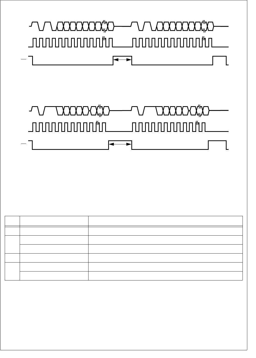
75 www.national.com
CP3BT26
Figure 18. 32-Bit Write Timing
Figure 19. 32-Bit Read Timing
An example of a 32-bit write is shown in Table 31. In this ex-
ample, the 32-bit value FFFF DC04h is written to register
address 0Ah. In cycle 1, the high word (FFFFh) is written. In
the first part of cycle 2, the CP3BT26 drives the header, R/
W bit, and register address for a read cycle. In the second
part of cycle 2, the LMX5252 drives the counter value. The
counter value is 0, which indicates one word has been writ-
ten. In cycle 3, the low word (DC04h) is written. In the first
part of cycle 4, the CP3BT26 drives the header, R/W bit,
and register address for a read cycle. In the second part of
cycle 4, the LMX5252 drives the counter value. The counter
value is 1, which indicates two words have been written.
SLE
SCLK
SDAT
DS322
D16D30A0A1A2A3A4WH0H1H2 D31 D0D14A0A1A2A3A4WH0H1H2 D15
>500 ns
SLE
SCLK
SDAT
DS323
D16D31A0A1A2A3A4RH0H1H2 D0D15A0A1A2A3A4RH0H1H2
>500 ns
Table 31 Example of 32-Bit Write with Interleaved Reads
Cycle Serial Data on SDAT Description
1101 0 01010 1111111111111111 Write cycle driven by CP3BT26. Data is FFFFh. Address is 0Ah.
2
101 1 01010 First part of read cycle driven by CP3BT26. Address is 0Ah.
0000000000000000 Second part of read cycle driven by LMX5252. Counter value is 0.
3101 0 01010 1101110000000100 Write cycle driven by CP3BT26. Data is DC04h. Address is 0Ah.
4
101 1 01010 First part of read cycle driven by CP3BT26. Address is 0Ah.
0000000000000001 Second part of read cycle driven by LMX5252. Counter value is 1.
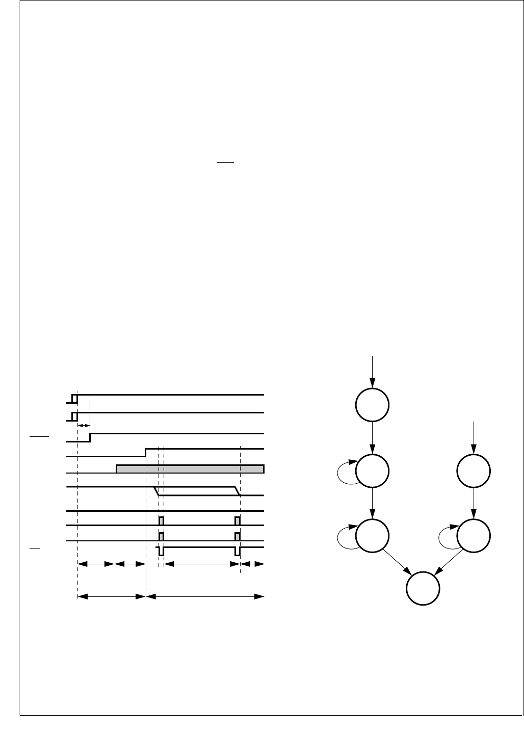
www.national.com 76
CP3BT26
15.3 LMX5251 POWER-UP SEQUENCE
To power-up a Bluetooth system based on the CP3BT26
and LMX5251 devices, the following sequence must be per-
formed:
1. Apply VDD to the LMX5251.
2. Apply IOVCC and VCC to the CP3BT26.
3. Drive the RESET# pin of the LMX5251 high a minimum
of 2 ms after the LMX5251 and CP3000 supply rails are
powered up. This resets the LMX5251 and CP3BT26.
4. After internal Power-On Reset (POR) of the CP3BT26,
the RFDATA pin is driven high. The RFCE, RFSYNC,
and SDAT pins are in TRI-STATE mode. Internal pull-
up/pull-down resistors on the CCB_CLOCK (SCLK),
CCB_DATA (SDAT), CCB_LATCH (SLE), and
TX_RX_SYNC (RFSYNC) inputs of the LMX5251 pull
these signals to states required during the power-up
sequence.
5. When the RFDATA pin is driven high, the LMX5251 en-
ables its oscillator. After an oscillator start-up delay, the
LMX5251 drives a stable 12-MHz BBP_CLOCK
(BBCLK) to the CP3BT26.
6. The Bluetooth baseband processor on the CP3BT26
now directly controls the RF interface pins and drives
the logic levels required during the power-up phase.
When the RFCE pin is driven high, the LMX5251
switches from “power-up” to “normal” mode and dis-
ables the internal pull-up/pull-down resistors on its RF
interface inputs.
7. In “normal” mode, the oscillator of the LMX5251 is con-
trolled by the RFCE signal. Driving RFCE high enables
the oscillator, and the LMX5251 drives its BBP_CLOCK
(BBCLK) output.
Figure 20. LMX5251 Power-Up Sequence
15.4 LMX5252 POWER-UP SEQUENCE
A Bluetooth system based on the CP3BT26 and LMX5252
devices has the following states:
Off—When the LMX5252 enters Off mode, all configura-
tion data is lost. In this state, the LMX5252 drives BPOR
low.
Power-Up—When the power supply is on and the
LMX5252 RESET# input is high, the LMX5252 starts up
its crystal oscillator and enters Power-Up mode. After the
crystal oscillator is settled, the LMX5252 sends four
clock cycles on BRCLK (BBCLK) before driving BPOR
high.
RF Init—The baseband controller on the CP3BT26 now
drives RFCE high and takes control of the crystal oscilla-
tor. The baseband performs all the needed initialization
(such as writing the registers in the LMX5252 and crystal
oscillator trim).
Idle—The baseband controller on the CP3BT26 drives
RFDATA low when the initialization is ready. The
LMX5252 is now ready to start transmitting, receiving, or
enter Sleep mode.
Sleep—The LMX5252 can be forced into Sleep mode at
any time by driving RFCE low. All configuration settings
are kept, only the Bluetooth low power clock is running
(B3k2).
Wait XTL—When RFCE goes high, the crystal oscillator
becomes operational. When it is stable, the LMX5252
enters Idle mode and drives BRCLK (BBCLK).
Figure 21. LMX5252 Power States
The power-up sequence for a Bluetooth system based on
the CP3BT26 and LMX5252 devices is shown in Figure 22.
VDD
LMX5251
RFCE
BBCLK
RFDATA
RFSYNC
VCC
CP3000
IOVCC
CP3000
Low
Low
High
Low
SDAT Low
SCLK Low
SLE
Standby
LMX5251 in Normal ModeLMX5251 in
Power-Up Mode
LMX5251
Oscillator
Start-Up
LMX5251
Initialization
CP3000
Initialization
Active
High
DS016
RESET#
LMX5251
RESET
CP3000
t
PTOR
Idle
DS324
Crystal Osc. Stable
RF Init
RFCE = High
RFDATA = Don't Care
Write Registers
RESET# = High and
Power is On
Power-Up
Wait for
Crystal Osc.
To Stabilize
RESET# = Low or
Power is cycled
Off
RFCE = High
Wait XTL
Wait for
Crystal Osc.
To Stabilize
RFCE = Low
Sleep
Any State
Any State
After RF Init
Crystal Osc. Stable
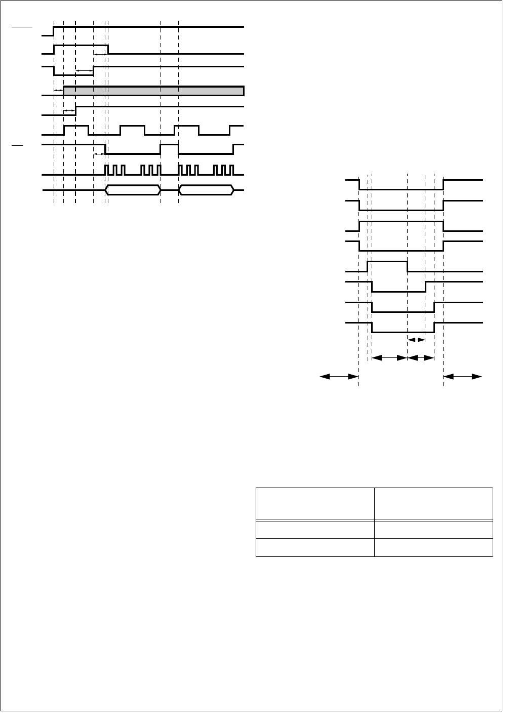
77 www.national.com
CP3BT26
Figure 22. LMX5252 Power-Up Sequence
15.5 BLUETOOTH SLEEP MODE
The Bluetooth controller is capable of putting itself into a
sleep mode for a specified number of Slow Clock cycles. In
this mode, the controller clocks are stopped internally. The
only circuitry which remains active are two counters
(counter N and counter M) running at the Slow Clock rate.
These counters determine the duration of the sleep mode.
The sequence of events when entering the LLC sleep mode
is as follows:
1. The current Bluetooth counter contents are read by the
CPU.
2. Software “estimates” the Bluetooth counter value after
leaving the sleep mode.
3. The new Bluetooth counter value is written into the
Bluetooth counter register.
4. The Bluetooth sequencer RAM is updated with the
code required by the Bluetooth sequencer to enter/exit
Sleep mode.
5. The Bluetooth sequencer RAM and the Bluetooth LLC
registers are switched from the System Clock domain
to the local 12 MHz Bluetooth clock domain. At this
point, the Bluetooth sequencer RAM and Bluetooth
LLC registers cannot be updated by the CPU, because
the CPU no longer has access to the Bluetooth LLC.
6. Hardware Clock Control (HCC) is enabled, and the
CP3BT26 enters a power-saving mode (Power Save or
Idle mode). While in Power Save mode, the Slow Clock
is used as the System Clock. While in Idle mode, the
System Clock is turned off.
7. The Bluetooth sequencer checks if HCC is enabled. If
HCC is enabled, the sequencer asserts HCC to the
PMM. On the next rising edge of the low-frequency
clock, the 1MHz clock and the 12 MHz clock are
stopped locally within the Bluetooth LLC. At this point,
the Bluetooth sequencer is stopped.
8. The M-counter starts counting. After M + 1 Slow Clock
cycles, the HCC signal to the PMM is deasserted.
9. The PMM restarts the 12 MHz Main Clock (and the
PLL, if required). The N-counter starts counting. After
N + 1 Slow Clock cycles, the Bluetooth clocks (1 MHz
and 12 MHz) are turned on again. The Bluetooth se-
quencer starts operating.
10. The Bluetooth sequencer waits for the completion of
the sleep mode. When completed, the Bluetooth se-
quencer asserts a wake-up signal to the MIWU (see
Section 13.0).
11. The PMM switches the System Clock to the high-fre-
quency clock and the CP3BT26 enters Active mode
again. HCC is disabled. The Bluetooth sequencer RAM
and Bluetooth LLC registers are switched back from the
local 12 MHz Bluetooth clock to the System Clock. At
this point, the Bluetooth sequencer RAM and Bluetooth
LLC registers are once again accessible by the CPU. If
enabled, an interrupt is issued to the CPU.
Figure 23. Bluetooth Sleep Mode Sequence
15.6 BLUETOOTH GLOBAL REGISTERS
Table 32 shows the memory map of the Bluetooth LLC glo-
bal registers.
Table 32 Memory Map of Bluetooth Global Registers
15.7 BLUETOOTH SEQUENCER RAM
The sequencer RAM is a 1K memory-mapped section of
RAM that contains the sequencer program. This RAM can
be read and written by the CPU in the same way as the Stat-
ic RAM space and can also be read by the sequencer in the
Bluetooth LLC. Arbitration between these devices is per-
formed in hardware.
BBCLK t1
RESET
DS321
SDAT
SCLK
B3k2
BPOR t2
RFCE t3
t4
RFDATA t5
SLE
Address
(offset from 0E F180h) Description
0000h–0048h Global LLC Configuration
0049h–007Fh Unused
Active
Power Save
CPU
Active
Stopped/Slow
System Clock
System Clock
Main Clock
BT LCC Clock
Active
Stopped
12 MHz
Main Clock
Active
Stopped
1 MHz/12 MHz
BT Clock
Active
Stopped
Sequencer
Enabled
Disabled
HCC
Asserted
Deasserted
HCC
NM
Start-up
CPU Handles
Wake-Up IRQ
from MIWU
CPU
Prepare for
Sleep Mode
DS017

www.national.com 78
CP3BT26
15.8 BLUETOOTH SHARED DATA RAM
The shared data RAM is a 4.5K memory-mapped section of
RAM that contains the link control data, RF programming
look-up table, and the link payload. This RAM can be read
and written in the same way as the Static RAM space and
can also be read by the sequencer in the Bluetooth LLC. Ar-
bitration between these devices is performed in hardware.
Table 33 shows the memory map of the Bluetooth LLC
shared Data RAM.
Table 33 Memory Map of Bluetooth Shared RAM
Address
(offset from 0E 8000h) Description
0000h–01D9h RF Programming
Look-up Table
01DAh–01FFh Unused
0200h–023Fh Link Control 0
0240h–027Fh Link Control 1
0280h–02BFh Link Control 2
02C0h–02FFh Link Control 3
0300h–033Fh Link Control 4
0340h–037Fh Link Control 5
0380h–03BFh Link Control 6
03C0h–03FFh Link Control 7
0400h–11FFh Link Payload 0–6
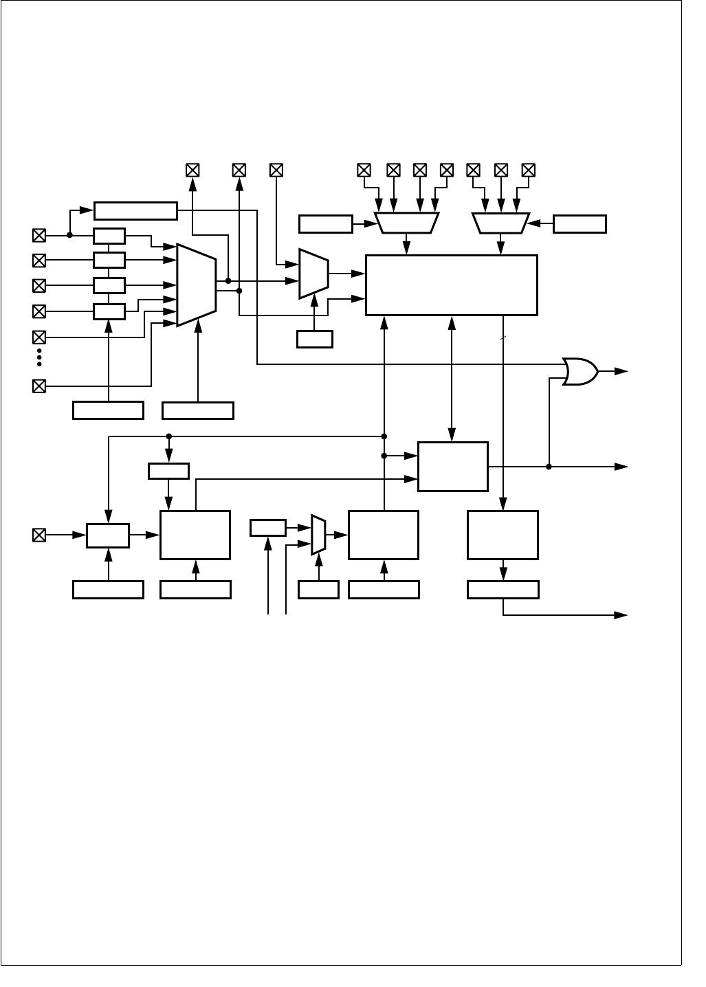
79 www.national.com
CP3BT26
16.0 12-Bit Analog to Digital Converter
The integrated 12-bit ADC provides the following features:
8-input analog multiplexer
8 single-ended channels or 4 differential channels
External filtering capability
12-bit resolution with 11-bit accuracy
Sign bit
15-microsecond conversion time
Support for resistive touchscreen interface
Internal or external start trigger
Programmable start delay after start trigger
Poll or interrupt on done
Figure 24. Analog to Digital Converter Block Diagram
16.1 FUNCTIONAL DESCRIPTION
The ADC module consists of a 12-bit ADC converter and as-
sociated state machine, together with analog multiplexers to
set up signal paths for sampling and voltage references, log-
ic to control triggering of the converter, and a bus interface.
16.1.1 Data Path
Up to 8 GPIO pins may be configured as 8 singled-ended
analog inputs or 4 differential pairs. Analog/digital data
passes through four main blocks in the ADC module be-
tween the input pins and the CPU bus:
Input Multiplexer—an analog multiplexer that selects
among the input channels.
Internal/External Multiplexer—an analog multiplexer
that selects between the output of the Input Multiplexer
and the ADCIN external analog input.
12-Bit ADC—receives the output of the Internal/External
Multiplexer and performs the analog to digital conver-
sion.
ADCRESLT Register—makes conversion results from
the 12-Bit ADC available to the on-chip bus. The AD-
CRESLT register includes the software-visible end of a 4-
word FIFO used to queue conversion results.
The configuration of the analog signal paths is controlled by
fields in the ADCGCR register. The Input Multiplexer is con-
trolled by the MUX_CFG field. The Internal/External Multi-
plexer is controlled by the ADCIN bit. The analog
multiplexers for selecting the voltage references used by the
ADC are controlled by the PREF_CFG and NREF_CFG
fields. The low-ohmic drivers used for interface to resistive
touchscreens are controlled by the TOUCH_CFG field.
DS183
DRV
12-BIT ADC
MUXOUT0
ADC_DELAY1
DRV
Start
Interrupt
(IRQ13)
12
Done
System
Clock
ADC
SEQUENCER
VREFNVREFP
+
-
TRIGGER DELAY1
Auxiliary
Clock 2
MUXOUT1 ADCIN
CLKDIV
ASYNC
ADC7
TOUCH_CFG MUX_CFG
ADC3/TSY+
DRV
ADC1/TSY-
ADC0/TSX+
ADC_DELAY2
DELAY2
DRV
ADC2/TSX-
ADC4
+
-
ADC2ADC0AVCC ADC1VREFP ADC3AGND
Control
Input
Multi-
plexer
Int/Ext
Multi-
plexer
ADC Clock
Pen-Down Detector
ADC_CONTROL
Result
Wake-Up
(WUI30)
ADCRESLT
4-Word
FIFO
System
Bus
Interface
Pen Down
CLKSEL
Clock
ADC_DIV
ADCIN
PREF_CFG NREF_CFG

www.national.com 80
CP3BT26
The output of the Input Multiplexer is available externally as
the MUXOUT0 and MUXOUT1 signals. In single-ended
mode, only MUXOUT0 is used. In differential mode,
MUXOUT0 is the positive side and MUXOUT1 is the nega-
tive side. The MUXOUT0 and MUXOUT1 outputs and the
ADCIN external analog input are provided so that external
signal conditioning circuits (such as filters) may be applied
to the analog signals before conversion. The MUXOUT0,
MUXOUT1, and ADCIN signals are alternate functions of
GPIO pins used by the Input Multiplexer, so the number of
available analog input channels is reduced when these sig-
nals are used.
16.1.2 Operation
The TRIGGER block may be configured to initiate a conver-
sion from either of these sources:
External ASYNC Input—an edge on the ASYNC input
triggers a conversion. This input may be configured to be
sensitive to rising or falling edges, as controlled by the
POL bit in the ADCCNTRL register.
ADCSTART Register—writing any value to the ADC-
START register triggers a conversion.
The TRIGGER block incorporates a glitch filter to suppress
transient spikes on the ASYNC input. The TRIGGER block
will recognize ASYNC pulse widths of 10 ns or greater.
Once a trigger event has been recognized, no further trig-
gering is recognized until the conversion is completed.
When the ASYNC input is selected as the trigger source, it
may be configured for automatic or non-automatic mode, as
controlled by the AUTO bit in the ADCCNTRL register:
Automatic Mode—a conversion is triggered by any
qualified edge on the ASYNC input (unless a conversion
is already in progress).
Non-Automatic Mode—before a conversion may be
triggered from the ASYNC input, software must “prime”
the TRIGGER block by writing the ADCSTART register.
Once the TRIGGER block is primed, a conversion is trig-
gered by any qualified edge on the ASYNC input. After
the conversion is completed, no additional trigger events
will be recognized until software once again primes the
TRIGGER block by writing the ADCSTART register.
Once a trigger event is recognized, the DELAY1 block waits
for a programmable delay specified in the ADC_DELAY1
field of the ADCSCDLY register. Then, it asserts the Start
signal to the ADC SEQUENCER block.
When the Start signal is received, the ADC SEQUENCER
block initiates the conversion in the 12-Bit ADC. After the
conversion is complete, the result is loaded into the FIFO,
and the Done signal is asserted.
The ADCRESLT register includes the software-visible end
of a 4-word FIFO, which allows up to 4 conversion results to
be queued for reading. Reading the ADCRESLT register un-
loads the FIFO. If the FIFO overflows, a bit is set in the AD-
CRESLT register, and the most recent conversion data is
lost.
The Done signal is visible to software as the ADC_DONE bit
in the ADCRESLT register. The Done signal is also an input
to the interrupt controller (IRQ13). The interrupt will be as-
serted whenever the FIFO is not empty (but will deassert for
one system clock after the ADCRESLT register is read). To-
tal conversion time is around 15 microseconds.
The Done signal is also an input to the Multi-Input Wake-Up
unit (WUI30). The MIWU input is asserted whenever the
FIFO is not empty (but will deassert for one system clock af-
ter the ADCRESLT register is read). The wake-up output is
provided so that the ADC module can bring the system out
of a power-saving mode when a conversion operation is
completed. It asserts earlier than the interrupt output. In the
pen-down detection mode of the ADC, the wake-up output
is ORed with the ADC pen-down detector output, to wake up
on a pen-down event.
16.1.3 ADC Clock Generation
The DELAY2 block generates ADC Clock, which is the clock
used internally by the ADC module. ADC Clock is derived
from either:
System Clock—a programmable divider is available to
generate the 12 MHz clock required by the ADC from the
System Clock.
Auxiliary Clock 2—may be used to perform conversions
when the System Clock is slowed down or suspended in
low-power modes.
The DELAY2 block receives the clock source selected by
the CLKSEL bit of the ADCACR register and adds a number
of asynchronous incremental delay units specified in the
ADC_DELAY2 field of the ADCSCDLY register. This de-
layed clock (ADC Clock) then drives the TRIGGER, 12-BIT
ADC, and ADC SEQUENCER blocks. ADC Clock also
drives the ADC_DIV clock divider, which generates the
clock which drives the DELAY1 block.
Because the ADCRESLT FIFO is driven by System Clock
(not ADC Clock), a conversion result will not propagate to
the output of the FIFO when the System Clock is suspend-
ed.
16.1.4 ADC Voltage References
The 12-BIT ADC block has positive and negative voltage
reference inputs, VREFP and VREFN. In single-ended
mode, only VREFP is used. An analog multiplexer allows
selecting an external VREFP pin, the analog supply voltage
AVCC, or the analog inputs ADC0 or ADC1 as the positive
voltage reference, as controlled by the PREF_CFG field of
the ADCGCR register. Another analog multiplexer allows
selecting the analog ground AGND or the analog inputs
ADC2 or ADC3 as the negative voltage reference, as con-
trolled by the NREF_CFG field of the ADCGCR register.
16.1.5 Pen-Down Detector
A pen-down detector is provided on the ADC0 (TSX+) input
of the ADC. It consists of a Schmitt-trigger receiver, with a
minimum Vil of 0.7V. When pen-down detect mode is en-
abled by loading 101b into the TOUCH_CFG field of the AD-
CGCR register, the output of this detector is visible to
software in the PEN_DOWN bit of the ADCRESLT register,
and this output is ORed with the Done signal to become the
wake-up input (WUI30) to the Multi-Input Wake-Up unit.
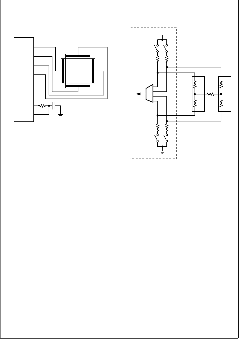
81 www.national.com
CP3BT26
16.2 TOUCHSCREEN INTERFACE
The ADC provides an interface for 4-wire resistive touch-
screens with the resolution necessary for applications such
as signature analysis. A typical touchscreen configuration is
shown in Figure 25.
Figure 25. Touchscreen Interface
A touchscreen consists of two resistive plates normally sep-
arated from each other. The TSX+ and TSX- signals are
connected to opposite ends of the X plate, while the TSY+
and TSY- signals are connected to the Y plate. If the pen is
down, the plates will be shorted together at the point of pen
contact. The location of the pen is sensed by driving one
end of a plate to VCC, driving the opposite end to ground,
and sensing the voltage at the point of pen contact using the
other plate. This is done twice, once for each coordinate.
An external RC low-pass filter is used to remove noise cou-
pled to the touchscreen signals from the display drivers.
16.2.1 Touchscreen Driver Configuration
An equivalent circuit for the touchscreen interface is shown
in Figure 26.
Figure 26. Touchscreen Driver Equivalent Circuit
Low-ohmic drivers are provided to pull the TSX+ and TSY+
signals to VCC and the TSX- and TSY- signals to GND. The
on-resistance of these drivers is specified to be 6 ohms.
Two measurements are used to produce one (x,y) position
coordinate pair. To measure the x-coordinate, the TSX+ sig-
nal is pulled to VCC, the TSX- signal is pulled to GND, and
the TSY+ and TSY- signals are undriven. A voltage divider
is formed across the X plate, with the center tap of the divid-
er being the point of pen contact, represented in Figure 26
by node A. With TSY+ and TSY- undriven, the voltage at
node A can be measured by sampling either of the TSY+ or
TSY- signals. This voltage will be proportional to the position
of the pen contact on the X plate.
The position of the pen contact on the Y plate is measured
similarly, by driving the TSY+ signal to VCC, the TSY- signal
to GND, and leaving the TSX+ and TSX- signals undriven.
The voltage at node B can be sampled from either the TSX+
or TSX- signals. The TOUCH_CFG field of the ADCGCR
register specifies the configuration of the drivers, with 010b
used to sample node A and 001b used to sample node B.
Typically, two consecutive measurements are made of each
coordinate so that any interference coupled from the LCD
column drivers is averaged out.
The plate-to-plate resistance is shown in Figure 26 as RZ.
This measurement is used as an indication of the force of
pen contact. When 100b is loaded into the TOUCH_CFG
field, the TSY+ signal is pulled to VCC and the TSX- signal
is pulled to GND, to support measuring RZ.
DS186
TSX+/ADC0
TSY+/ADC1
TSX-/ADC2
TSY-/ADC3
MUXOUT0
ADCIN
DS187
6Ω6Ω
6Ω6Ω
RX1
RZ
X Plate
TSY+
TSX+
TSX-
To ADC
TSY-
RX2
A
VCC
RY1
Y Plate
RY2
B

www.national.com 82
CP3BT26
16.2.2 Measuring Pen Force
Figure 27 shows equivalent circuits for the driver modes
used to measure the X, Y, and Z coordinates, in which Z rep-
resents pen force. In this discussion, the ohmic resistance
of the drivers is neglected (see Section 16.2.3), and series
resistance between the node of interest and the ADC is ig-
nored because it has no significant effect.
Figure 27. Touchscreen Driver Modes
In the following examples, the ADC is assumed to operate
in single-ended mode to produce conversion values be-
tween 0 and 2047, however the same principles could be
extended to differential mode to recover the full range of the
ADC.
In Sample X mode, the X plate is driven between VCC and
ground, so that a value measured at node A on the TSY+ or
TSY- inputs is the center tap of a resistor-divider network.
The end-to-end resistance RXP of the X plate is:
The value measured at node A is proportional to the ratio
between the resistance to ground and the resistance of the
X plate:
Solving for RX2, the resistance is:
Similarly, in Sample Y mode the value measured at node B
on the TSX+ or TSX- inputs is proportional to the ratio be-
tween the resistance to ground and the resistance RYP of
the Y plate:
Because end-to-end resistance RYP of the Y plate is:
The previous equation can be rewritten as:
Solving for RY1, the resistance is:
Now that the resistance values RX2 and RY1 are known, it
is possible to calculate the value of the plate-to-plate con-
tact resistance, RZ, given the value measured at node C on
the TSX+ input in Sample Z mode. Node C is a tap in a re-
sistor-divider network composed of three resistors, such
that:
Solving for RZ, the resistance is:
The resistance RZ is proportional to the force of pen con-
tact.
16.2.3 Compensation for Driver Resistance
Plate resistances between opposite electrodes range from
100 ohms to 1k ohm. Because of the 6-ohm driver resis-
tance, some significant voltage drop will be experienced be-
tween, for example, TSX- and AGND. A 200-ohm plate will
drop:
With a 2.5V supply, this is 70 mV. A 12-bit ADC has 4096
possible values, so each value covers a range of 610 µV at
2.5V. A voltage drop of 70 mV across each of the low-ohmic
drivers reduces the number of available ADC values by:
This effective loss of resolution can be handled in a number
of ways.
1. The voltages on, for example, TSY+ and TSY- can be
sampled before sampling TSX+ and TSX-. Then, scal-
ing can be applied in software to convert the samples
to the full (4096-bit) range. This technique will not re-
cover any resolution, however it is worthy of some con-
sideration because touchscreen data is typically
passed to two applications:
Signature Analysis—only the raw data is required. No
absolute positioning is necessary.
Screen Overlay—for example, for cursor positioning.
In this application, a scaling or calibration is performed
to correctly overlay the touchscreen coordinates onto
the display. Because of this calibration, it is not even
necessary to sample TSY+ and TSY-.
2. The ADC has a positive voltage reference input which
can be internally connected to the TSY+ terminal. This
means that the number of available ADC values is in-
creased to:
Software scaling could be applied to this value if re-
quired (as with technique 1, above), but no additional
resolution is achieved.
DS188
VCC
RX1
RX2
A
Sample X
TOUCH_CFG = 001
VCC
RY1
RY2
B
Sample Y
TOUCH_CFG = 010
RZ
RX2
C
VCC
RY1
Sample Z
TOUCH_CFG = 100
RXP RX1 RX2+=
A
2047
-------------RX2
RXP
-------------=
RX2 RXP A
2047
-------------
×=
B
2047
-------------RY2
RYP
-------------=
RYP RY1 RY2+=
B
2047
-------------RYP RY1–
RYP
-------------------------------=
RY1 RYP 1 B
2047
-------------
–
×=
C
2047
-------------RX2
RY1 RZ RX2++
----------------------------------------------=
RZ RX2 2047 C–
C
-----------------------
×
RY1–=
6
200 6 6++
-----------------------------
AVCC AGND–()×
70 mV 2×
610 uV
-------------------------- 230=
4096 70 mV
610 uV
--------------------
–3981=

83 www.national.com
CP3BT26
3. By extension, the ADC negative voltage reference can
be internally connected to the TSY- terminal, to recover
the full 4096 values.
The Global Configuration Register (ADCGCR) provides the
flexibility to implement any of these techniques.
16.3 ADC OPERATION IN POWER-SAVING
MODES
To reduce the level of switching noise in the environment of
the ADC, it is possible to operate the CP3BT26 in low-power
modes, in which the System Clock is slowed or switched off.
Under these conditions, Auxiliary Clock 2 can be selected
as the clock source for the ADC module, however conver-
sion results cannot be read by the system while the System
Clock is suspended. The expected operation in power-sav-
ing modes is therefore:
1. ADC is configured and a conversion is primed or trig-
gered.
2. A power-saving mode is entered.
3. ADC conversion completes and a wake-up signal is as-
serted to the MIWU unit.
4. Device wakes up and processes the conversion result.
To conserve power, the ADC should be disabled before en-
tering a low-power mode if its function is not required.
16.4 FREEZE
The ADC module provides support for an In-System Emula-
tor by means of a special FREEZE input. When FREEZE is
asserted the module will exhibit the following specific be-
havior:
The automatic clear-on-read function of the result regis-
ter (ADCRESLT) is disabled.
The FIFO is updated as usual, and an interrupt for a
completed conversion can be asserted.
16.5 ADC REGISTER SET
Table 34 lists the ADC registers.
Table 34 ADC Registers
Name Address Description
ADCGCR FF F3C0h ADC Global
Configuration Register
ADCACR FF F3C2h ADC Auxiliary
Configuration Register
ADCCNTRL FF F3C4h ADC Conversion
Control Register
ADCSTART FF F3C6h ADC Start Conversion
Register
ADCSCDLY FF F3C8h ADC Start Conversion
Delay Register
ADCRESLT FF F3CAh ADC Result Register

www.national.com 84
CP3BT26
16.5.1 ADC Global Configuration Register (ADCGCR)
The ADCGCR register controls the basic operation of the in-
terface. The CPU bus master has read/write access to the
ADCGCR register. After reset this register is set to 0000h.
CLKEN The Clock Enable bit controls whether the
ADC module is running. When this bit is clear,
all ADC clocks are disabled, the ADC analog
circuits are in a low-power state, and ADC
registers (other than the ADCGCR and AG-
CACR registers) are not writeable. Clearing
this bit reinitializes the ADC state machine
and cancels any pending trigger event. When
this bit is set, the ADC clocks are enabled and
the ADC analog circuits are powered up. The
converter is operational within 0.25 µs of be-
ing enabled.
0 – ADC disabled.
1 – ADC enabled.
ADCIN The ADCIN bit selects the source of the ADC
input. When the bit is clear, the source is the
8-channel Input Multiplexer. When the bit is
set, the source is the ADCIN pin.
0 – ADC input is from 8-channel multiplexer.
1 – ADC input is from ADCIN pin.
DIFF The Differential Operation Mode bit and the
MUX_CFG field configure the analog circuits
of the ADC module. When this bit is clear, the
ADC module operates in single-ended mode.
When this bit is set, the ADC operates in dif-
ferential mode. See Table 35 .
0 – Single-ended mode.
1 – Differential mode.
MUX_CFG The Multiplexer Configuration field and the
DIFF bit configure the analog circuits of the
ADC module, as shown in Table 35.
For best noise immunity in touchscreen appli-
cations, channel 2 should be used for sam-
pling the X plate voltage, and channel 1
should be used for sampling the Y plate volt-
age.
TOUCH_CFG
The Touchscreen Configuration field controls
the configuration of the low-ohmic drivers for
the TSX+, TSX-, TSY+, and TSY- signals, as
shown in Table 36. When TOUCH_CFG is
101b, the pen-down detector is enabled. The
output of the pen-down detector is visible to
software in the PEN_DOWN bit of the AD-
SRESLT register, and it is ORed with the
Done signal to generate the wake-up signal
WUI30 passed to the MIWU unit.
8765432 1 0
TOUCH_CFG MUX_CFG DIFF ADCIN CLKEN
15 14 13 12 11 10 9
MUXOUTEN INTEN Res. NREF_CFG PREF_CFG
Table 35 MUX_CFG Operation
MUX_CFG
Channel
Selected,
(DIFF = 0)
Channels
Selected
(DIFF = 1)
+-
000 0 0 1
001 1 1 0
010 2 2 3
011 3 3 2
100 4 4 5
101 5 5 4
110 6 6 7
111 7 7 6
Table 36 TOUCH_CFG Modes
TOUCH_CFG ADC0/TSX+ ADC1/TSY+ ADC2/TSX- ADC3/TSY- Mode
000 Inactive Inactive Inactive Inactive None
001 Inactive Driven High Inactive Driven Low Sample Y
010 Driven High Inactive Driven Low Inactive Sample X
011 Driven High Inactive Inactive Driven Low Sample Z (1),
Pre-Pen Down
100 Inactive Driven High Driven Low Inactive Sample Z (2)
101 Weakly Pulled High Inactive Inactive Driven Low Pen-Down Detect
11X Inactive Inactive Inactive inactive Reserved

85 www.national.com
CP3BT26
PREF_CFG The Positive Voltage Reference Configuration
field specifies the source of the ADC positive
voltage reference, according to the following
table:
NREF_CFG The Negative Voltage Reference Configura-
tion field specifies the source of the ADC neg-
ative voltage reference, according to the
following table:
MUXOUTEN
The MUXOUT Enable bit controls whether the
output of the Input Multiplexer is available ex-
ternally. In single-ended mode, the
MUXOUT0 pin is active and the MUXOUT1
pin is disabled (TRI-STATE). In differential
mode, both MUXOUT0 and MUXOUT1 are
active.
0 – MUXOUT0 and MUXOUT1 disabled.
1 – MUXOUT0 and MUXOUT1 enabled.
INTEN The Interrupt Enable bit controls whether the
ADC interrupt (IRQ13) is enabled. When en-
abled, the interrupt request is asserted when
valid data is available in the ADCRESLT reg-
ister. This bit has no effect on the wake_up
signal to the MIWU unit (WUI30).
0 – IRQ13 disabled.
1 – IRQ13 enabled.
16.5.2 ADC Auxiliary Configuration Register
(ADCACR)
The ADCACR register is used to control the clock configu-
ration and report the status of the ADC module. The CPU
bus master has read/write access to the ADCACR register.
After reset, this register is clear.
CLKSEL The Clock Select bit selects the clock source
used by the DELAY2 block to generate the
ADC clock.
0 – ADC clock derived from System Clock.
1 – ADC clock derived from Auxiliary Clock 2.
CLKDIV The Clock Divisor field specifies the divisor
applied to System Clock to generate the 12
MHz clock required by the ADC module. Only
the System Clock is affected by this divisor.
The divisor is not used when Auxiliary Clock 2
is selected as the clock source.
PRM The ADC Primed bit is a read-only bit that in-
dicates the ADC has been primed to perform
a conversion by writing to the ADCSTART reg-
ister. The bit is cleared after the conversion is
completed.
0 – ADC has not been primed.
1 – ADC has been primed.
TRG The ADC Triggered bit is a read-only bit that
indicates the ADC has been triggered. The bit
is set during any pre-conversion delay. The bit
is cleared after the conversion is completed.
0 – ADC has not been triggered.
1 – ADC has been triggered.
CNVT The ADC Conversion bit is a read-only bit that
indicates the ADC has been primed to per-
form a conversion, a valid internal or external
trigger event has occurred, any pre-conver-
sion delay has expired, and the ADC conver-
sion is in progress. The bit is cleared after the
conversion is completed.
0 – ADC is not performing a conversion.
1 – ADC conversion is in progress.
PREF_CFG PREF Source
00 Internal (AVCC)
01 VREFP
10 ADC0
11 ADC1
NREF_CFG NREF source
00 Internal (AGND)
01 Reserved
10 ADC2
11 ADC3
15 14 13 12 3 2 1 0
CNVT TRG PRM Reserved CLKDIV CLKSEL
CLKDIV Clock Divisor
00 1
01 2
10 4
11 Reserved

www.national.com 86
CP3BT26
16.5.3 ADC Conversion Control Register
(ADCCNTRL)
The ADCCNTRL register specifies the trigger conditions for
an ADC conversion.
POL The ASYNC Polarity bit specifies the polarity
of edges which trigger ADC conversions.
0 – ASYNC input is sensitive to rising edges.
1 – ASYNC input is sensitive to falling edges.
EXT The External Trigger bit selects whether con-
versions are triggered by writing the ADC-
START register or activity on the ASYNC
input.
0 – ADC conversions triggered by writing to
the ADCSTART register.
1 – ADC conversions triggered by qualified
edges on ASYNC input.
AUTO The Automatic bit controls whether automatic
mode is enabled, in which any qualified edge
on the ASYNC input is recognized as a trigger
event. When automatic mode is disabled, the
ADC module must be “primed” before a qual-
ified edge on the ASYNC input can trigger a
conversion. To prime the ADC module, soft-
ware must write the ADCSTART register with
any value before an edge on the ASYNC input
is recognized as a trigger event. After the con-
version is completed, the ASYNC input will be
ignored until software again writes the ADC-
START register. The AUTO bit is ignored
when the EXT bit is 0.
0 – Automatic mode disabled.
1 – Automatic mode enabled.
16.5.4 ADC Start Conversion Register (ADCSTART)
The ADCSTART register is a write-only register used by
software to initiate an ADC conversion. Writing any value to
this register will cause the ADC to initiate a conversion or
prime the ADC to initiate a conversion, as controlled by the
ADCCNTRL register.
16.5.5 ADC Start Conversion Delay Register
(ADCSCDLY)
The ADCSCDLY register controls critical timing parameters
for the operation of the ADC module.
ADC_DELAY2
The ADC Delay 2 field specifies the delay be-
tween the ADC module clock source (either
System Clock after a programmable divider or
Auxiliary Clock 2) and the ADC clock. The
range of effective values for this field is 0 to
20. Values above 20 produce the same delay
as 20, which is about 42 ns.
ADC_DELAY1
The ADC Delay 1 field specifies the number of
clock periods by which the trigger event will be
delayed before initiating a conversion. The
timebase for this delay is the ADC clock (12
MHz) divided by the ADC_DIV divisor. The
ADC_DELAY1 field has 9 bits, which corre-
sponds to a maximum delay of 511 clock peri-
ods.
ADC_DIV The ADC Clock Divisor field specifies the divi-
sor applied to the ADC clock (12 MHz) to gen-
erate the clock used to drive the DELAY1
block. A field value of n results in a division ra-
tio of n+1. With a module clock of 12 MHz, the
maximum delay which can be provided by
ADC_DIV and ADC_DELAY settings is:
15 3 2 1 0
Reserved AUTO EXT POL
15 14 13 5 4 0
ADC_DIV ADC_DELAY1 ADC_DELAY2
1
12 MHz
--------------------
4×511×170 us=

87 www.national.com
CP3BT26
16.5.6 ADC Result Register (ADCRESLT)
The ADCRESLT register includes the software-visible end
of a 4-word FIFO. Conversion results are loaded into the
FIFO from the 12-bit ADC and unloaded when software
reads the ADCRESLT register. The ADCRESLT register is
read-only. With the exception of the PEN_DOWN bit, the
fields in this register are cleared when the register is read.
ADC_RESULT
The ADC Result field holds a 12-bit value for
the conversion result. If the ADC_DONE bit is
clear, there is no valid result in this field, and
the field will have a value of 0. The
ADC_RESULT field and the SIGN bit together
form the software-visible end of the ADC
FIFO.
SIGN The Sign bit indicates whether the - input has
a voltage greater than the + input (differential
mode only). For example if AD-
CGCR.MUX_CFG is 000b, ADC0 is the + in-
put and ADC1 is the - input. If the voltage on
ADC0 is greater than the voltage on ADC1,
the SIGN bit will be 0; if the voltage on ADC0
is less than the voltage on ADC1, the SIGN bit
will be 1. In single-ended mode, this bit always
reads as 0.
0 – In differential mode, + input has a voltage
greater than the - input. In single-ended
mode, this bit is always 0.
1 – In differential mode, - input has a voltage
greater than the + input.
PEN_DOWN
The Pen-Down bit indicates whether a pen-
down condition is being sensed. To enable
pen-down detection, the TOUCH_CFG field of
the ADCGCR register must be loaded with
101b. When pen-down detection is enabled
and a pen-down condition is sensed, the
PEN_DOWN bit is set. This bit is not carried
through the FIFO, so its value represents the
current status of the pen-down detector.
When pen-down detection is enabled, the sig-
nal from the pen-down detector is ORed with
the Done signal to generate the wake-up sig-
nal (WUI30) passed to the MIWU unit. If pen-
down detection is not enabled, this bit reads
as 0.
0 – No pen-down condition is sensed, or pen-
down detection is disabled.
1 – Pen-down condition is sensed.
ADC_OFLW The ADC FIFO Overflow bit indicates whether
the 4-word FIFO behind the ADCRESLT reg-
ister has overflowed. When this occurs, the
most recent conversion result is lost. This bit
is cleared when the ADCRESLT register is
read.
0 – FIFO overflow has not occurred.
1 – FIFO overflow has occurred.
ADC_DONE The ADC Done bit indicates when an ADC
conversion has completed. When this bit is
set, the data in the ADC_RESULT field is val-
id. When this bit is clear, there is no valid data
in the ADC_RESULT field. The Done bit is
cleared when the ADCRESLT register is read,
but if there are queued conversion results in
the FIFO, the Done bit will become set again
after one System Clock period.
0 – No ADC conversion has completed since
the ADCRESLT register was last read.
1 – An ADC conversion has completed since
the ADCRESLT register was last read.
11 0
ADC_RESULT
15 14 13 12
ADC_DONE ADC_OFLW PEN_DOWN SIGN
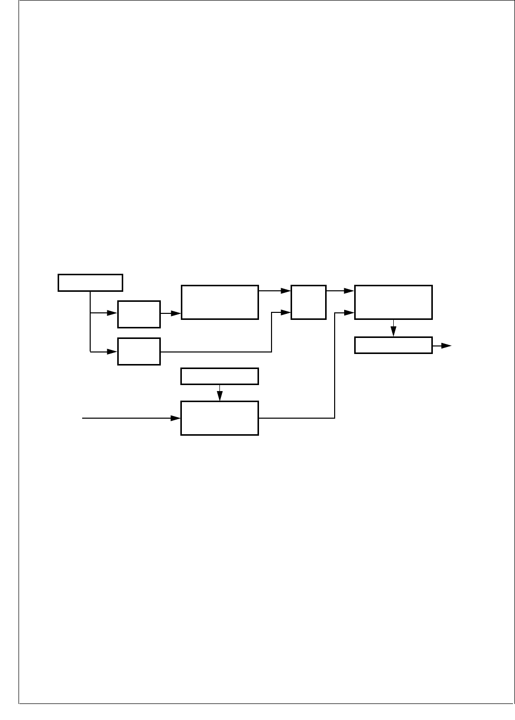
www.national.com 88
CP3BT26
17.0 Random Number Generator (RNG)
The RNG unit is a hardware “true random” number genera-
tor. When enabled, this unit provides up to 800 random bits
per second. The bits are available for reading from a 16-bit
register.
The RNG unit includes two oscillators which operate inde-
pendently of the System Clock:
Fast Oscillator—a 24 MHz oscillator which drives a lin-
ear feedback shift register (LFSR).
Slow Oscillator—an unstable oscillator which drives a
flip-flop for sampling the pseudorandom bitstream from
the LFSR. This oscillator operates at approximately 115
kHz, but it does not have a fixed frequency.
By sampling the pseudorandom bitstream at random inter-
vals, a random bitstream is synthesized. This bitstream is
clocked into a 16-bit shift register. A programmable clock di-
vider generates the clock signal for the shift register from the
System Clock.
When a new 16-bit word of random data is available, it is
loaded into the RNGD register. If enabled, an interrupt re-
quest (IRQ3) is asserted when the word is available for
reading. When software reads the RNGD register, the reg-
ister is cleared and the interrupt request is deasserted.
The RNGCST register provides control and status bits for
the RNG module:
RNG Enable—enables or disables the RNG oscillators.
Interrupt Mask—enables or disables the interrupt when
a new word of random data becomes available.
Data Valid—indicates whether a new word is available.
17.1 FREEZE
The RNG module provides support for an In-System Emu-
lator by means of a special FREEZE input. When FREEZE
is asserted, the automatic clear-on-read function of the
RNDGD register is disabled.
Figure 28. RNG Module Block Diagram
DS185
Sample Strobe
Divider
RNGDIVH/RNGDIVL
RNGD
System
Clock
31-Bit LFSR
Clock
Sample
Flip-Flop
Clock
D
16-Bit Shift Register
RNGCST
Slow Osc.
(~115 kHz)
(Unstable)
Fast Osc.
(~24 MHz) Clock
DQQ
Enable
System
Bus

89 www.national.com
CP3BT26
17.2 RANDOM NUMBER GENERATOR
REGISTER SET
Table 34 lists the RNG registers.
17.2.1 RNG Control and Status Register (RNGCST)
The RNGCST register provides control and status bits for
the RNG module. This register is cleared at reset.
RNGE The Random Number Generator Enable bit
enables the operation of the RNG. When this
bit is clear, the RNG module is disabled, and
both RNG oscillators are suspended.
0 – RNG module disabled.
1 – RNG module enabled.
DVALID The Data Valid bit indicates whether valid
(random) data is available in the RNGD regis-
ter. This bit is cleared when the RNGD regis-
ter is read.
0 – RNGD register holds invalid data.
1 – RNGD register holds valid data.
IMASK The Interrupt Mask bit controls whether an in-
terrupt request (IRQ3) will be asserted when
valid (random) data is available in the RNGD
register.
0 – RNG interrupt disabled.
1 – RNG interrupt enabled.
17.2.2 RNG Data Register (RNGD)
The RNGD register holds random data generated by the
RNG module. After reading the register, it is cleared and the
DVALID bit of the RNGCST register is cleared. When a new
word of valid (random) data becomes available in the RNGD
register, the DVALID bit is set and (if enabled) and interrupt
request is asserted.
17.2.3 RNG Divisor Register High (RNGDIVH)
This register holds the two most significant bits of the
RNGDIV clock divisor. See the description of the RNGDIVL
register.
17.2.4 RNG Divisor Register Low (RNGDIVL)
This register holds the 16 least significant bits the RNGDIV
clock divisor.
The RNGDIV clock divisor is used to generate the sampling
strobe for loading random bits into the shift register. The di-
visor is applied to the System Clock source. The maximum
frequency after division is 800 Hz. For example, a System
Clock frequency of 24 MHz would require an RNGDIV value
of 30,000 (7530h) or greater. The default RNGDIV value is
0000 83D6h.
Table 37 RNG Registers
Name Address Description
RNGCST FF F280h RNG Control and
Status Register
RNGD FF F282h RNG Data Register
RNGDIVH FF F284h RNG Divisor Register
High
RNGDIVL FF F286h RNG Divisor Register
Low
15 654 2 1 0
Reserved IMSK Reserved DVALID RNGE
15 0
RNGD15:0
15 2 1 0
Reserved RNGDIV17:16
15 0
RNGDIV15:0

www.national.com 90
CP3BT26
18.0 USB Controller
The CR16 USB node is an integrated USB node controller
that features enhanced DMA support with many automatic
data handling features. It is compatible with USB specifica-
tion versions 1.0 and 1.1.
It integrates the required USB transceiver, a Serial Interface
Engine (SIE), and USB endpoint (EP) FIFOs. Seven end-
point pipes are supported: one for the mandatory control
endpoint and six to support interrupt, bulk, and isochronous
endpoints. Each endpoint pipe has a dedicated FIFO, 8
bytes for the control endpoint and 64 bytes for the other end-
points.
18.1 FUNCTIONAL STATES
18.1.1 Line Condition Detection
At any given time, the CR16 USB node is in one of the fol-
lowing states
The NodeSuspend, NodeResume, or NodeReset line con-
dition causes a transition from one operating state to anoth-
er. These conditions are detected by specialized hardware
and reported in the Alternate Event (ALTEV) register. If in-
terrupts are enabled, an interrupt is generated on the occur-
rence of any of the specified conditions.
In addition to the dedicated input to the ICU for generating
interrupts on these USB state changes, a wake-up signal is
sent to the MIWU (see Section 13.0) when any activity is de-
tected on the USB, if the bus was in the Idle state and the
USB node is in the NodeSuspend state. The MIWU can be
programmed to generate an edge-triggered interrupt when
this occurs.
NodeOperational
This is the normal operating state of the node. In this state,
the node is configured for operation on the USB.
NodeSuspend
A USB node is expected to enter NodeSuspend state when
3 ms have elapsed without any detectable bus activity. The
CR16 USB node looks for this event and signals it by setting
the SD3 bit in the ALTEV register, which causes an inter-
rupt, to be generated (if enabled). Software should respond
by putting the CR16 USB node in the NodeSuspend state.
The CR16 USB node can resume normal operation under
software control in response to a local event in the device. It
can wake up the USB bus via a NodeResume, or when de-
tecting a resume command on the USB bus, which signals
an interrupt to the CPU.
NodeResume
If the host has enabled remote wake-ups from the node, the
CR16 USB node can initiate a remote wake-up.
Once software detects the event, which wakes up the bus,
it releases the CR16 USB node from NodeSuspend state by
initiating a NodeResume on the USB using the NFSR reg-
ister. The node software must ensure at least 5 ms of Idle
on the USB. While in NodeResume state, a constant “K” is
signalled on the USB. This should last for at least 1 ms and
no more than 5 ms, after which the USB host should contin-
ue sending the NodeResume signal for at least an addition-
al 20 ms, and then completes the NodeResume operation
by issuing the End Of Packet (EOP) sequence.
To successfully detect the EOP, software must enter the
USB NodeOperational state by setting the NFSR register.
If no EOP is received from the host within 100 ms, software
must re-initiate NodeResume.
NodeReset
When detecting a NodeResume or NodeReset signal while
in NodeSuspend state, the CR16 USB node can signal this
to the CPU by generating an interrupt.
USB specifications require that a device must be ready to
respond to USB tokens within 10 ms after wake-up or reset.
Table 38 State Descriptions
State Descriptions
NodeOperational Normal operation
NodeSuspend Device operation suspend due to
USB inactivity
NodeResume Device wake-up from suspended
state
NodeReset Device reset
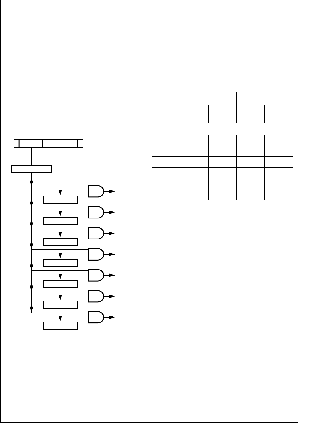
91 www.national.com
CP3BT26
18.2 ENDPOINT OPERATION
18.2.1 Address Detection
Packets are broadcast from the host controller to all nodes
on the USB network. Address detection is implemented in
hardware to allow selective reception of packets and to per-
mit optimal use of CPU bandwidth. One function address
with seven different endpoint combinations is decoded in
parallel. If a match is found, then that particular packet is re-
ceived into the FIFO; otherwise it is ignored.
The incoming USB Packet Address field and Endpoint field
are extracted from the incoming bit stream. Then the ad-
dress field is compared to the Function Address register
(FADR). If a match is detected, the Endpoint field is com-
pared to all of the Endpoint Control registers (EPCn) in par-
allel. A match then causes the payload data to be received
or transmitted using the respective endpoint FIFO.
Figure 29. USB Function Address/Endpoint Decoding
18.2.2 Transmit and Receive Endpoint FIFOs
The CR16 USB node uses a total of seven transmit and re-
ceive FIFOs: one bidirectional transmit and receive FIFO for
the mandatory control endpoint, three transmit FIFOs, and
three receive FIFOs. As shown in Table 39, the bidirectional
FIFO for the control endpoint is 8 bytes deep. The additional
unidirectional FIFOs are 64 bytes each for both transmit and
receive. Each FIFO can be programmed for one exclusive
USB endpoint, used together with one globally decoded
USB function address. Software must not enable both trans-
mit and receive FIFOs for endpoint zero at any given time.
Table 39 Endpoint FIFO Sizes
If two endpoints in the same direction are programmed with
the same endpoint number and both are enabled, data is re-
ceived or transmitted to/from the endpoint with the lower
number, until that endpoint is disabled for bulk or interrupt
transfers, or becomes full or empty for ISO transfers. For ex-
ample, if receive EP2 and receive EP4 both use endpoint 5
and are both isochronous, the first OUT packet is received
into EP2 and the second OUT packet into EP4, assuming
no software interaction in between. For ISO endpoints, this
allows implementing a ping-pong buffer scheme together
with the frame number match logic.
Endpoints in different directions programmed with the same
endpoint number operate independently.
Receive/
Transmit FIFO0
USB Packet
EPC0 Register
FADR Register
ADDR Field Endpoint Field
Match
Match
Transmit FIFO1
EPC1 Register
Receive FIFO1
EPC2 Register
Transmit FIFO2
EPC3 Register
Receive FIFO2
EPC4Register
Transmit FIFO3
EPC5 Register
Receive FIFO3
EPC6 Register DS049
Endpoint
Number
TX FIFO RX FIFO
Size
(Bytes) Name Size
(Bytes) Name
0 FIFO0 (bidirectional, 8 bytes)
1 64 TXFIFO1 - -
2 - - 64 RXFIFO1
3 64 TXFIFO2 - -
4 - - 64 RXFIFO2
5 64 TXFIFO3 - -
6 - - 64 RXFIFO3
www.national.com 92
CP3BT26
Bidirectional Control Endpoint FIFO0 Operation
FIFO0 should be used for the bidirectional control endpoint
0. It can be configured to receive data sent to the default ad-
dress with the DEF bit in the EPC0 register. Isochronous
transfers are not supported for the control endpoint.
The Endpoint 0 FIFO can hold a single receive or transmit
packet with up to 8 bytes of data. Figure 30 shows the basic
operation in both receive and transmit direction.
Note: The actual current operating state is not directly vis-
ible to software.
Figure 30. Endpoint 0 Operation
A packet written to the FIFO is transmitted if an IN token for
the respective endpoint is received. If an error condition is
detected, the packet data remains in the FIFO and transmis-
sion is retried with the next IN token.
The FIFO contents can be flushed to allow response to an
OUT token or to write new data into the FIFO for the next IN
token.
If an OUT token is received for the FIFO, software is in-
formed that the FIFO has received data only if there was no
error condition (CRC or STUFF error). Erroneous recep-
tions are automatically discarded.
Transmit Endpoint FIFO Operation (TXFIFO1, TXFIFO2,
TXFIFO3)
The Transmit FIFOs for endpoints 1, 3, and 5 support bulk,
interrupt, and isochronous USB packet transfers larger than
the actual FIFO size. Therefore, software must update the
FIFO contents while the USB packet is transmitted on the
bus. Figure 31 illustrates the operation of the transmit
FIFOs.
Figure 31. Transmit FIFO Operation
TFnS The Transmit FIFO n Size is the total number
of bytes available within the FIFO.
TXRP The Transmit Read Pointer is incremented ev-
ery time the Endpoint Controller reads from
the transmit FIFO. This pointer wraps around
to zero if TFnS is reached. TXRP is never in-
cremented beyond the value of the write
pointer TXWP. An underrun condition occurs if
TXRP equals TXWP and an attempt is made
to transmit more bytes when the LAST bit in
the TXCMDx register is not set.
TXWP The Transmit Write Pointer is incremented ev-
ery time software writes to the transmit FIFO.
This pointer wraps around to zero if TFnS is
reached. If an attempt is made to write more
bytes to the FIFO than actual space available
(FIFO overrun), the write to the FIFO is ig-
nored. If so, TCOUNT is checked for an indi-
cation of the number of empty bytes
remaining.
TXFL The Transmit FIFO Level indicates how many
bytes are currently in the FIFO. A FIFO warn-
ing is issued if TXFL decreases to a specific
value. The respective WARNn bit in the FWR
register is set if TXFL is equal to or less than
the number specified by the TFWL bit in the
TXCn register.
TCOUNT The Transmit FIFO Count indicates how many
empty bytes can be filled within the transmit
FIFO. This value is accessible by software in
the TXSn register.
FLUSH Bit, TXC0 Register FLUSH Bit, RXC0 Register
RX_EN Bit,
RXC0 Register
OUT or
SETUP
To k e n
SETUP
To k e n
FIFO0 Empty
(All Data Read)
Transmission
Done
IN Token
TX_EN Bit,
TXC0
Register
Write to TXD0
IDLE
RXWAIT
RX
TX
TXWAIT
TXFILL
TX_EN Bit,
TXC0 Register
(Zero-Length
Packet)
DS050
FLUSH (Resets TXRP and TXWP)
TXRP
TXFL = TXWP - TXRP
TXWP
TCOUNT = TXRP - TXWP (= TFnS - TXFL)
TX FIFO n
0X0TFnS - 1
+
+
+
DS051
93 www.national.com
CP3BT26
Receive Endpoint FIFO Operation (RXFIFO1, RXFIFO2,
RXFIFO3)
The Receive FIFOs for endpoints 2, 4, and 6 support bulk,
interrupt, and isochronous USB packet transfers larger than
the actual FIFO size. If the packet length exceeds the FIFO
size, software must read the FIFO contents while the USB
packet is being received on the bus. Figure 32 shows the
detailed behavior of receive FIFOs.
Figure 32. Receive FIFO Operation
RFnS The Receive FIFO n Size is the total number
of bytes available within the FIFO.
RXRP The Receive Read Pointer is incremented
with every read by software from the receive
FIFO. This pointer wraps around to zero if
RFnS is reached. RXRP is never incremented
beyond the value of RXWP. If an attempt is
made to read more bytes than are actually
available (FIFO underrun), the last byte is
read repeatedly.
RXWP The Receive Write Pointer is incremented ev-
ery time the Endpoint Controller writes to the
receive FIFO. This pointer wraps around to
zero if RFnS is reached. An overrun condition
occurs if RXRP equals RXWP and an attempt
is made to write an additional byte.
RXFL The Receive FIFO Level indicates how many
more bytes can be received until an overrun
condition occurs with the next write to the
FIFO. A FIFO warning is issued if RXFL de-
creases to a specific value. The respective
WARNn bit in the FWR register is set if RXFL
is equal to or less than the number specified
by the RFWL bit in the RXCn register.
RCOUNT The Receive FIFO Count indicates how many
bytes can be read from the receive FIFO. This
value is accessible by software via the RXSn
register.
18.3 USB CONTROLLER REGISTERS
The CR16 USB node has a set of memory-mapped regis-
ters that can be read/written from the CPU bus to control the
USB interface. Some register bits are reserved; reading
from these bits returns undefined data. Reserved register
bits must always be written with 0.
FLUSH (Resets RXRP and RXWP)
RXRP
RCOUNT = RXWP - RXRF
RXWP
RXFL = RXRP - RXWP (= RFnS - RCOUNT)
RX FIFO n
0X0RFnS - 1
+
+
+
DS052
Table 40 USB Controller Registers
Name Address Description
MCNTRL FF FD80h Main Control Register
NFSR FF FD8Ah Node Functional State
Register
MAEV FF FD8Ch Main Event Register
ALTEV FF FD90h Alternate Event
Register
MAMSK FF FD8Eh Main Mask Register
ALTMSK FF FD92h Alternate Mask
Register
TXEV FF FD94h Transmit Event
Register
TXMSK FF FD96h Transmit Mask
Register
RXEV FF FD98h Receive Event
Register
RXMSK FF FD9Ah Receive Mask
Register
NAKEV FF FD9Ch NAK Event Register
NAKMSK FF FD9Eh NAK Mask Register
FWEV FF FDA0h FIFO Warning Event
Register
FWMSK FF FDA2h FIFO Warning Mask
Register
FNH FF FDA4h Frame Number High
Byte Register
FNL FF FDA6h Frame Number Low
Byte Register
FAR FF FD88h Function Address
Register
DMACNTRL FF FDA8h DMA Control Register
DMAEV FF FDAAh DMA Event Register
DMAMSK FF FDACh DMA Mask Register
MIR FF FDAEh Mirror Register
DMACNT FF FDB0h DMA Count Register
DMAERR FF FDB2h DMA Error Register

www.national.com 94
CP3BT26
18.3.1 Main Control Register (MCNTRL)
The MCNTRL register controls the main functions of the
CR16 USB node. The MCNTRL register provides read/write
access from the CPU bus. Reserved bits must be written
with 0, and they return 0 when read. It is clear after reset.
USBEN The USB Enable controls whether the USB
module is enabled. If the USB module is dis-
abled, the 48 MHz clock within the USB node
is stopped, all USB registers are initialized to
their reset state, and the USB transceiver forc-
es SE0 on the bus to prevent the hub from de-
tected the USB node. The USBEN bit is clear
after reset.
0 – The USB module is disabled.
1 – The USB module is enabled.
EPC0 FF FDC0h Endpoint Control 0
Register
EPC1 FF FDD0h Endpoint Control 1
Register
EPC2 FF FDD8h Endpoint Control 2
Register
EPC3 FF FDE0h Endpoint Control 3
Register
EPC4 FF FDDE8h Endpoint Control 4
Register
EPC5 FF FDF0h Endpoint Control 5
Register
EPC6 FF FDF8h Endpoint Control 6
Register
TXS0 FF FDC4h Transmit Status 0
Register
TXS1 FF FDD4h Transmit Status 1
Register
TXS2 FF FDE4h Transmit Status 2
Register
TXS3 FF FDF4h Transmit Status 3
Register
TXC0 FF FDC6h Transmit Command 0
Register
TXC1 FF FDD6 Transmit Command 1
Register
TXC2 FF FDE6h Transmit Command 2
Register
TXC3 FF FDF6h Transmit Command 3
Register
TXD0 FF FDC2h Transmit Data 0
Register
TXD1 FF FDD2h Transmit Data 1
Register
TXD2 FF FDE2h Transmit Data 2
Register
TXD3 FF FDF2h Transmit Data 3
Register
RXS0 FF FDCCh Receive Status 0
Register
RXS1 FF FDDCh Receive Status 1
Register
RXS2 FF FDECh Receive Status 2
Register
Table 40 USB Controller Registers
Name Address Description
RXS3 FF FDFCh Receive Status 3
Register
RXC0 FF FDCEh Receive Command 0
Register
RXC1 FF FDDEh Receive Command 1
Register
RXC2 FF FDEEh Receive Command 2
Register
RXC3 FF FDFEh Receive Command 3
Register
RXD0 FF FDCAh Receive Data 0
Register
RXD1 FF FDDAh Receive Data 2
Register
RXD2 FF FDEAh Receive Data 2
Register
RXD3 FF FDFAh Receive Data 3
Register
7 4 3 2 1 0
Reserved NAT Reserved USBEN
Table 40 USB Controller Registers
Name Address Description

95 www.national.com
CP3BT26
NAT The Node Attached indicates that this node is
ready to be detected as attached to USB.
When clear, the transceiver forces SE0 on the
USB node controller to prevent the hub (to
which this node is connected) from detecting
an attach event. After reset or when the USB
node is disabled, this bit is cleared to give the
device time before it must respond to com-
mands. After this bit has been set, the device
no longer drives the USB and should be ready
to receive Reset signaling from the hub.
0 – Node not ready to be detected as at-
tached.
1 – Node ready to be detected as attached.
18.3.2 Node Functional State Register (NFSR)
The NFSR register reports and controls the current func-
tional state of the USB node. The NFSR register provides
read/write access. It is clear after reset.
NFS The Node Functional State bits set the node
state, as shown in Table 41. Software should
initiate all required state transitions according
to the respective status bits in the Alternate
Event (ALTEV) register.
7 2 1 0
Reserved NFS
Table 41 USB Functional States
NFS Node State Description
00 NodeReset
This is the USB Reset state. This is entered upon a module reset or by software upon
detection of a USB Reset. Upon entry, all endpoint pipes are disabled. DEF in the Endpoint
Control 0 (EPC0) register and AD_EN in the Function Address (FAR) register should be
cleared by software on entry to this state. On exit, DEF should be reset so the device
responds to the default address.
01 NodeResume
In this state, resume “K” signalling is generated. This state should be entered by software to
initiate a remote wake-up sequence by the device. The node must remain in this state for at
least 1 ms and no more than 15 ms.
10 NodeOperational This is the normal operational state for operation on the USB bus.
11 NodeSuspend
Suspend state should be entered by software on detection of a Suspend event while in
Operational state. While in Suspend state, the transceivers operate in their low-power
suspend mode. All endpoint controllers and the bits TX_EN, LAST, and RX_EN are reset,
while all other internal states are frozen. On detection of bus activity, the RESUME bit in the
ALTEV register is set. In response, software can cause entry to NodeOperational state.

www.national.com 96
CP3BT26
18.3.3 Main Event Register (MAEV)
The Main Event Register summarizes and reports the main
events of the USB transactions. This register provides read-
only access. The MAEV register is clear after reset.
WARN The Warning Event bit indicates whether one
of the unmasked bits in the FIFO Warning
Event (FWEV) register has been set. This bit
is cleared by reading the FWEV register.
0 – No warning event occurred.
1 – A warning event has occurred.
ALT The Alternate Event bit indicates whether one
of the unmasked ALTEV register bits has
been set. This bit is cleared by reading the AL-
TEV register.
0 – No alternate event has occurred.
1 – An alternate event has occurred.
TX_EV The Transmit Event bit indicates whether any
of the unmasked bits in the Transmit Event
(TXEV) register (TXFIFOn or TXUNDRNn) is
set. Therefore, it indicates that an IN transac-
tion has been completed. This bit is cleared
when all the TX_DONE bits and the TXUN-
DRN bits in each Transmit Status (TXSn) reg-
ister are cleared.
0 – No transmit event has occurred.
1 – A transmit event has occurred.
FRAME The Frame Event bit indicates whether the
frame counter has been updated with a new
value, due to receipt of a valid SOF packet on
the USB or to an artificial update if the frame
counter was unlocked or a frame was missed.
This bit is cleared when the register is read.
0 – The frame counter has not been updated.
1 – Frame counter has been updated.
NAK The Negative Acknowledge Event indicates
whether one of the unmasked NAK Event
(NAKEV) register bits has been set. This bit is
cleared when the NAKEV register is read.
0 – No unmasked NAK event has occurred.
1 – An unmasked NAK event has occurred.
UL The Unlocked/Locked Detected bit is set
when the frame timer has either entered un-
locked condition from a locked condition, or
has re-entered a locked condition from an un-
locked condition as determined by the UL bit
in the Frame Number (FNH or FNL) register.
This bit is cleared when the register is read.
0 – Frame timer has not entered an unlocked
condition from a locked condition or re-
entered a locked condition from an un-
locked condition.
1 – Frame timer has either entered an un-
locked condition from a locked condition
or re-entered a locked condition from an
unlocked condition.
RX_EV The Receive Event bit is set if any of the un-
masked bits in the Receive Event (RXEV) reg-
ister is set. It indicates that a SETUP or OUT
transaction has been completed. This bit is
cleared when all of the RX_LAST bits in each
Receive Status (RXSn) register and all RX-
OVRRN bits in the RXEV register are cleared.
0 – No receive event has occurred.
1 – A receive event has occurred.
INTR The Master Interrupt Enable bit is hardwired
to 0 in the Main Event (MAEV) register; bit 7
in the Main Mask (MAMSK) register is the
Master Interrupt Enable.
0 – USB interrupts disabled.
1 – USB interrupts enabled.
18.3.4 Main Mask Register (MAMSK)
The MAMSK register masks out events reported in the
MAEV registers. A set bit enables the interrupts for the re-
spective event in the MAEV register. If the corresponding bit
is clear, interrupt generation for this event is disabled. This
register provides read/write access. The MAMSK register is
clear after reset.
18.3.5 Alternate Event Register (ALTEV)
The ALTEV register summarizes and reports the further
events in the USB node. This register provides read-only ac-
cess. The ALTEV register is clear after reset.
DMA The DMA Event bit indicates that one of the
unmasked bits in the DMA Event (DMAEV)
register has been set. The DMA bit is read-
only and clear, when the DMAEV register is
cleared.
0 – No DMA event has occurred.
1 – A DMA event has occurred.
EOP The End of Packet bit indicates whether a val-
id EOP sequence has been detected on the
USB. It is used when this device has initiated a
Remote wake-up sequence to indicate that the
Resume sequence has been acknowledged
and completed by the host. This bit is cleared
when the register is read.
0 – No EOP sequence detected.
1 – EOP sequence detected.
7 6 5 4 3 2 1 0
INTR RX_EV ULD NAK FRAME TX_EV ALT WARN
7 6 5 4 3 2 1 0
INTR RX_EV ULD NAK FRAME TX_EV ALT WARN
7 6 5 4 3 2 1 0
RESUME RESET SD5 SD3 EOP DMA Reserved

97 www.national.com
CP3BT26
SD3 The Suspend Detect 3 ms bit is set after 3 ms
of IDLE have been detected on the upstream
port, indicating that the device should be sus-
pended. The suspend occurs under software
control by writing the suspend value to the
Node Functional State (NFSR) register. This
bit is cleared when the register is read.
0 – No 3 ms in IDLE has been detected.
1 – 3 ms in IDLE has been detected.
SD5 The Suspend Detect 5 ms bit is set after 5 ms
of IDLE have been detected on the upstream
port, indicating that this device is permitted to
perform a remote wake-up operation. The re-
sume may be initiated under software control
by writing the resume value to the NFSR reg-
ister. This bit is cleared when the register is
read.
0 – No 5 ms in IDLE has been detected.
1 – 5 ms in IDLE has been detected.
RESET The Reset bit is set when 2.5 µs of SEO have
been detected on the upstream port. In re-
sponse, the functional state should be reset
(NFS in the NFSR register is set to RESET),
where it must remain for at least 100 µs. The
functional state can then return to Operational
state. This bit is cleared when the register is
read.
0 – No 2.5 µs in SEO have been detected.
1 – 2.5 µs in SEO have been detected.
RESUME The Resume bit indicates whether resume
signalling has been detected on the USB
when the device is in Suspend state (NFS in
the NFSR register is set to SUSPEND), and a
non-IDLE signal is present on the USB, indi-
cating that this device should begin its wake-
up sequence and enter Operational state. Re-
sume signalling can only be detected when
the 48 MHz PLL clock is enabled to the USB
controller. This bit is cleared when the register
is read.
0 – No resume signalling detected.
1 – Resume signalling detected.
18.3.6 Alternate Mask Register (ALTMSK)
A set bit in the ALTMSK register enables automatic setting
of the ALT bit in the MAEV register when the respective
event in the ALTEV register occurs. Otherwise, setting
MAEV.ALT bit is disabled. The ALTMSK register is clear af-
ter reset. It provides read/write access from the CPU bus.
18.3.7 Transmit Event Register (TXEV)
The TXEV register reports the current status of the FIFOs,
used by the three Transmit Endpoints. The TXEV register is
clear after reset. It provides read-only access.
TXFIFO The Transmit FIFO n bits are copies of the
TX_DONE bits from the corresponding Trans-
mit Status registers (TXSn). A bit is set when
the IN transaction for the corresponding trans-
mit endpoint n has been completed. These
bits are cleared when the corresponding
TXSn register is read.
TXUDRRN The Transmit Underrun n bits are copies of the
respective TX_URUN bits from the corre-
sponding Transmit Status registers (TXSn).
Whenever any of the Transmit FIFOs under-
flows, the respective TXUDRRN bit is set.
These bits are cleared when the correspond-
ing Transmit Status register is read.
Note: Since Endpoint 0 implements a store
and forward principle, an underrun condition
for FIFO0 cannot occur. This results in the
TXUDRRN0 bit always being read as 0.
18.3.8 Transmit Mask Register (TXMSK)
The TXMSK register is used to select the bits of the TXEV
registers, which causes the TX_EV bit in the MAEV register
to be set. When a bit is set and the corresponding bit in the
TXEV register is set, the TX_EV bit in the MAEV register is
set. When clear, the corresponding bit in the TXEV register
does not cause TX_EV to be set. The TXMSK register pro-
vides read/write access. It is clear after reset.
7 6 5 4 3 2 1 0
RESUME RESET SD5 SD3 EOP DMA Reserved
7 4 3 0
TXUDRRN TXFIFO
7 4 3 0
TXUDRRN TXFIFO

www.national.com 98
CP3BT26
18.3.9 Receive Event Register (RXEV)
The RXEV register reports the current status of the FIFO,
used by the three Receive Endpoints. The RXEV register is
clear after reset. It provides read-only access from the CPU
bus.
RXFIFO The Receive FIFO n are set whenever either
RX_ERR or RX_LAST in the respective Re-
ceive Status registers (RXSn) are set. Read-
ing the corresponding RXSn register
automatically clears these bits. The CR16
USB node discards all packets for Endpoint 0
received with errors. This is necessary in case
of retransmission due to media errors, ensur-
ing that a good copy of a SETUP packet is
captured. Otherwise, the FIFO may potentially
be tied up, holding corrupted data and unable
to receive a retransmission of the same pack-
et (the RXFIFO0 bit only reflects the value of
RX_LAST for Endpoint 0). If data streaming is
used for the receive endpoints (EP2, EP4 and
EP6), software must check the respective
RX_ERR bits to ensure the packets received
are not corrupted by errors.
RXOVRRN The Receive Overrun n bits are set when an
overrun condition is indicated in the corre-
sponding receive FIFO n. They are cleared
when the register is read. Software must
check the respective RX_ERR bits that pack-
ets received for the other receive endpoints
(EP2, EP4 and EP6) are not corrupted by er-
rors, as these endpoints support data stream-
ing (packets which are longer than the actual
FIFO depth).
18.3.10 Receive Mask Register (RXMSK)
The RXMSK register is used to select the bits of the RXEV
register, which cause the RX_EV bit in the MAEV register to
be set. When set and the corresponding bit in the RXEV
register is set, RX_EV bit in the MAEV register is set. When
clear, the corresponding bit in the RXEV register does not
cause the RX_EV bit to be set. The RXMSK register pro-
vides read/write access. This register is clear after reset.
18.3.11 NAK Event Register (NAKEV)
A bit in the NAKEV register is set when a Negative Acknowl-
edge (NAK) was generated by the corresponding endpoint.
The NAKEV register provides read-only access from the
CPU bus. It is clear after reset.
IN The IN n bits are set when a NAK handshake
is generated for an enabled address/endpoint
combination (AD_EN in the Function Ad-
dress, FAR, register is set and EP_EN in the
Endpoint Control, EPCx, register is set) in re-
sponse to an IN token. These bits are cleared
when the register is read.
OUT The OUT n bits are set when a NAK hand-
shake is generated for an enabled address/
endpoint combination (AD_EN in the FAR reg-
ister is set and EP_EN in the EPCx register is
set) in response to an OUT token. These bits
are not set if NAK is generated as result of an
overrun condition. They are cleared when the
register is read.
18.3.12 NAK Mask Register (NAKMSK)
The NAKMSK register is used to select the bits of the NA-
KEV register, which cause the NAK bit in the MAEV register
to be set. When set and the corresponding bit in the NAKEV
register is set, the NAK bit in the MAEV register is set. When
cleared, the corresponding bit in the NAKEV register does
not cause NAK to be set. The NAKMSK register provides
read/write access. It is clear after reset.
7 4 3 0
RXOVRRN RXFIFO
7 4 3 0
RXOVRRN RXFIFO
7 4 3 0
OUT IN
7 4 3 0
OUT IN

99 www.national.com
CP3BT26
18.3.13 FIFO Warning Event Register (FWEV)
The FWEV register signals whether a receive or transmit
FIFO has reached its warning limit. It reports the status for
all FIFOs, except for the Endpoint 0 FIFO, as no warning
limit can be specified for this FIFO. The FWEV register pro-
vides read-only access from the CPU bus. It is clear after re-
set.
TXWARN3:1
The Transmit Warning n bits are set when the
respective transmit endpoint FIFO reaches
the warning limit, as specified by the TFWL
bits of the respective TXCn register, and
transmission from the respective endpoint is
enabled. These bits are cleared when the
warning condition is cleared by either writing
new data to the FIFO when the FIFO is
flushed, or when transmission is done, as in-
dicated by the TX_DONE bit in the TXSn reg-
ister.
RXWARN3:1
The Receive Warning n bits are set when the
respective receive endpoint FIFO reaches the
warning limit, as specified by the RFWL bits of
the respective EPCx register. These bits are
cleared when the warning condition is cleared
by either reading data from the FIFO or when
the FIFO is flushed.
18.3.14 FIFO Warning Mask Register (FWMSK)
The FWMSK register selects which FWEV bits are reported
in the MAEV register. A set FWMSK bit with the correspond-
ing bit in the FWEV register set, causes the WARN bit in the
MAEV register to be set. When clear, the corresponding bit
in the FWEV register does not cause WARN to be set. The
FWMSK register provides read/write access. This register is
clear after reset.
18.3.15 Frame Number High Byte Register (FNH)
The FNH register contains the three most significant bits
(MSB) of the current frame counter as well as status and
control bits for the frame counter. This register is loaded with
C0h after reset. It provides access from the CPU bus as de-
scribed below.
FN10:8 The Frame Number field holds the three most
significant bits (MSB) of the current frame
number, received in the last SOF packet. If a
valid frame number is not received within
12060 bit times (Frame Length Maximum, FL-
MAX, with tolerance) of the previous change,
the frame number is incremented artificially. If
two successive frames are missed or are in-
correct, the current FN is frozen and loaded
with the next frame number from a valid SOF
packet. If the frame number low byte was read
by software before reading the FNH register,
software actually reads the contents of a buff-
er register which holds the value of the three
frame number bits of this register when the
low byte was read. Therefore, the correct se-
quence to read the frame number is: FNL,
FNH. Read operations to the FNH register,
without first reading the Frame Number Low
Byte (FNL) register directly, read the actual
value of the three MSBs of the frame number.
The FN bits provide read-only access. On re-
set, the FN bits are cleared.
RFC The Reset Frame Count bit is used to reset
the frame number to 000h. This bit always
reads as 0. Due to the synchronization ele-
ments the frame counter reset actually occurs
a maximum of 3 USB clock cycles (12 MHz)
plus 2.5 CPU clock cycles after the write to the
RFC bit.
0 – Writing 0 has no effect.
1 – Writing 1 resets the frame counter.
UL The Unlock Flag bit indicates that at least two
frames were received without an expected
frame number, or that no valid SOF was re-
ceived within 12060 bit times. If this bit is set,
the frame number from the next valid SOF
packet is loaded in FN. The UL bit provides
read-only access. After reset, this bit is set.
This bit is set by the hardware and is cleared
by reading the FNH register.
0 – No condition indicated.
1 – At least two frames were received without
an expected frame number, or no valid
SOF was received within 12060 bit times.
7 5 4 3 1 0
RXWARN3:1 Res. TXWARN3:1 Res.
754310
RXWARN3:1 Res. TXWARN3:1 Res.
7 6 5 4 3 2 0
MF UL RFC Reserved FN10:8

www.national.com 100
CP3BT26
MF The Missed SOF bit is set when the frame
number in a valid received SOF does not
match the expected next value, or when an
SOF is not received within 12060 bit times.
The MF bit provides read-only access. On re-
set, this bit is set. This bit is set by the hard-
ware and is cleared by reading the FNH
register.
0 – No condition indicated.
1 – The frame number in a valid SOF does
not match the expected next value, or no
valid SOF was received within 12060 bit
times.
18.3.16 Frame Number Low Byte Register (FNL)
The FNL register holds the low byte of the frame number, as
described above. To ensure consistency, reading this low
byte causes the three frame number bits in the FNH register
to be locked until this register is read. The correct sequence
to read the frame number is: FNL first, followed by FNH.
This register provides read-only access. After reset, the
FNL register is clear.
Note: If the frame counter is updated due to a receipt of a
valid SOF or an artificial update (i.e. missed frame or un-
locked/locked detect), it will take the synchronization ele-
ments a maximum of 2.5 CPU clock cycles to update the
FNH and FNL registers.
18.3.17 Function Address Register (FAR)
The Function Address Register specifies the device func-
tion address. The different endpoint numbers are set for
each endpoint individually using the Endpoint Control regis-
ters. The FAR register provides read/write access. After re-
set, this register is clear. If the DEF bit in the Endpoint
Control 0 register is set, Endpoint 0 responds to the default
address.
AD The Address field holds the 7-bit function ad-
dress used to transmit and receive all tokens
addressed to this device.
AD_EN The Address Enable bit controls whether the
AD field is used for address comparison. If
not, the device does not respond to any token
on the USB bus.
0 – The device does not respond to any token
on the USB bus.
1 – The AD field is used for address compar-
ison.
18.3.18 Control Register (DMACNTRL)
The DMACNTRL register controls the main DMA functions
of the CR16 USB node. The DMACTRL register provides
read/write access. This register is clear after reset.
DSRC The DMA Source bit field holds the binary-en-
coded value that specifies which of the end-
points, 1 to 6, is enabled for DMA support. The
DSRC bits are cleared on reset. Table 42
summarizes the DSRC bit settings.
DMOD The DMA Mode bit specifies when a DMA re-
quest is issued. If clear, a DMA request is is-
sued on transfer completion. For transmit
endpoints EP1, EP3, and EP5, the data is
completely transferred, as indicated by the
TX_DONE bit (to fill the FIFO with new trans-
mit data). For receive endpoints EP2, EP4,
and EP6, this is indicated by the RX_LAST bit.
When the DMOD bit is set, a DMA request is
issued when the respective FIFO warning bit
is set. The DMOD bit is cleared after reset.
0 – DMA request is issued on transfer com-
pletion.
1 – DMA request is issued when the respec-
tive FIFO warning bit is set.
ADMA The Automatic DMA bit enables Automatic
DMA (ADMA) and automatically enables the
selected receive or transmit endpoint. Before
ADMA mode can be enabled, the DEN bit in
the DMA Control (DMACNTRL) register must
be cleared. ADMA mode functions until any bit
in the DMA Event (DMAEV) register is set, ex-
cept for NTGL. To initiate ADMA mode, all bits
in the DMAEV register must be cleared, ex-
cept for NTGL.
0 – Automatic DMA disabled.
1 – Automatic DMA enabled.
7 0
FN7:0
7 6 0
AD_EN AD
7 6 5 4 3 2 0
DEN IGNRXTGL DTGL ADMA DMOD DSRC
Table 42 DSRC Bit Description
DSRC Endpoint Number
000 1
001 2
010 3
011 4
100 5
101 6
11x Reserved

101 www.national.com
CP3BT26
DTGL The DMA Toggle bit is used to determine the
initial state of Automatic DMA (ADMA) opera-
tions. Software initially sets this bit if starting
with a DATA1 operation, and clears this bit if
starting with a DATA0 operation. Writes to this
bit also update the NTGL bit in the DMAEV
register.
IGNRXTGL The Ignore RX Toggle controls whether the
compare between the NTGL bit in the DMAEV
register and the TOGGLE bit in the respective
RXSn register is ignored during receive oper-
ations. If the compare is ignored, a mismatch
of the bits during a receive operation does not
stop ADMA operation. If the compare is not ig-
nored, the ADMA stops in case of a mismatch
of the two toggle bits. After reset, this bit is
cleared.
0 – Compare toggle bits.
1 – Ignore toggle bits.
DEN The DMA Enable bit enables DMA mode. If
DMA mode is disabled and the current DMA
cycle has been completed (or was not yet is-
sued) the DMA transfer is terminated. This bit
is cleared after reset.
0 – DMA mode disabled.
1 – DMA mode enabled.
18.3.19 DMA Event Register (DMAEV)
The DMAEV register bits are used in ADMA mode. Bits 0 to
3 may cause an interrupt if not cleared, even if the device is
not set to ADMA mode. Until all of these bits are cleared,
ADMA mode cannot be initiated. Conversely, ADMA mode
is automatically terminated when any of these bits are set.
The DMAEV register provides access from the CPU bus as
described below. It is clear after reset.
DSHLT The DMA Software Halt bit is set when ADMA
operations have been halted by software. This
bit is set by the hardware only after the DMA
engine completes any necessary cleanup op-
erations and returns to Idle state.
The DSHLST bits provide read access and
can only be written with a 0 from the CPU bus.
After reset these bits are cleared.
0 – No software ADMA halt.
1 – ADMA operations have been halted by
software.
DERR The DMA Error bit is set to indicate that a
packet has not been received or transmitted
correctly. It is also set, if the TOGGLE bit in the
RXSx/TXSx register does not equal the NTGL
bit in the DMAEV register after packet recep-
tion/transmission. (Note that this comparison
is made before the NTGL bit changes state
due to packet transfer). For receiving, the
DERR bit is equivalent to the RX_ERR bit. For
transmitting, the DERR bit is equivalent to the
TX_DONE bit (set) and the ACK_STAT bit (not
set). If the AEH bit in the DMA Error Count
(DMAERR) register is set, the DERR bit is not
set until DMAERRCNT in the DMAERR regis-
ter is cleared, and another error is detected.
Errors are handled as specified in the DMAE-
RR register. The DERR bit provides read ac-
cess and can only be written with a 0 from the
CPU bus. After reset this bit is cleared.
0 – No DMA error occurred.
1 – DMA error occurred.
DCNT The DMA Count bit is set when the DMA
Count (DMACNT) register is 0 (see the
DMACNT register for more information). The
DCNT bit provides read access and can only
be written with a 0 from the CPU bus. After re-
set this bit is cleared.
0 – DMACNT register is not 0.
1 – DMACNT register is 0.
DSIZ The DMA Size bit is only significant for DMA
receive operations. It indicates, by being set,
that a packet has been received which is less
than the full length of the FIFO. This normally
indicates the end of a multi-packet transfer.
The DSIZ bit provides read access and can
only be written with a 0 from the CPU bus. Af-
ter reset this bit is cleared.
0 – No condition indicated.
1 – A packet has been received which is less
than the full length of the FIFO.
ARDY The Automatic DMA Ready bit is set when the
ADMA mode is ready and active. After setting
the DMACNTRL.ADMA bit and the active
USB transaction (if any) is finished and the
specified endpoint (DMACNTRL.DSRC) is
flushed, the USB node enters ADMA mode.
This bit is automatically cleared when the
ADMA mode is finished and the current DMA
operation is completed. After reset the ARDY
bit is cleared.
0 – ADMA mode not ready.
1 – ADMA mode ready and active.
NTGL The Next Toggle bit determines the toggle
state of the next data packet sent (if transmit-
ting), or the expected toggle state of the next
data packet (if receiving). This bit is initialized
by writing to the DTGL bit of the DMACNTRL
register. It then changes state with every
packet sent or received on the endpoint pres-
ently selected by DSRC[2:0]. If DTGL write
operation occurs simultaneously with the bit
update operation, the write takes precedence.
If transmitting, whenever ADMA operations
are in progress the DTGL bit overrides the
corresponding TOGGLE bit in the TXCx regis-
ter. In this way, the alternating data toggle oc-
curs correctly on the USB. Note that there is
no corresponding mask bit for this event be-
cause it is not used to generate interrupts.
The NTGL bit provides read-only access from
the CPU bus and is cleared after reset.
7 6 5 4 3 2 1 0
Reserved NTGL ARDY DSIZ DCNT DERR DSHLT

www.national.com 102
CP3BT26
18.3.20 DMA Mask Register (DMAMSK)
Any set bit in the DMAMSK register enables automatic set-
ting of the DMA bit in the ALTEV register when the respec-
tive event in the DMAEV register occurs. Otherwise, setting
the DMA bit is disabled. For a description of bits 0 to 3, see
the DMAEV register. The DMAMSK register provides read/
write access. After reset it is clear. Reading reserved bits re-
turns undefined data.
18.3.21 Mirror Register (MIR)
The MIR register is a read-only register. Because reading it
does not alter the state of the TXSn or RXSn register to
which it points, software can freely check the status of the
channel. At reset it is initialized to 1Fh.
STAT The Status field mirrors the status bits of the
transmitter or receiver n selected by the
DSRC[2:0] field in the DMACNTRL register
(DMA need not be active or enabled). It corre-
sponds to TXSn or RXSn, respectively.
18.3.22 DMA Count Register (DMACNT)
The DMACNT register specifies a maximum count for
ADMA operations. The DMACNT register provides read/
write access. After reset this register is clear.
DCOUNT The DMA Count field is decremented on com-
pletion of a DMA operation until it reaches 0.
Then the DCNT bit in the DMA Event register
is set, only when the next successful DMA op-
eration is completed. This register does not
underflow. For receive operations, this count
decrements when the packet is received suc-
cessfully, and then transferred to memory us-
ing DMA. For transmit operations, this count
decrements when the packet is transferred
from memory using DMA, and then transmit-
ted successfully. Software loads DCOUNT
with (number of packets to transfer) - 1. If a
DMACNT write operation occurs simulta-
neously with the decrement operation, the
write takes precedence.
18.3.23 DMA Error Register (DMAERR)
The DMAERR register holds the 7-bit DMA error counter
and a control bit to specify DMA error handling. The DMAE-
RR register provides read/write access. It is clear after re-
set.
DMAERRCNT
The DMA Error Counter, together with the au-
tomatic error handling feature, defines the
maximum number of consecutive bus errors
before ADMA mode is stopped. Software can
set the 7-bit counter to a preset value. Once
ADMA is started, the counter decrements
from the preset value by 1 every time a bus er-
ror is detected. Every successful transaction
resets the counter back to the preset value.
When ADMA mode is stopped, the counter is
also set back to the preset value. If the
counter reaches 0 and another erroneous
packet is detected, the DERR bit in the DMA
Event register is set. This register cannot un-
derrun. Software loads DMAERRCNT with 3D
(maximum number of allowable transfer at-
tempts) - 1. A write access to this register is
only possible when ADMA is inactive. Other-
wise, it is ignored. Reading from this register
while ADMA is active returns the current
counter value. Reading from it while ADMA is
inactive returns the preset value. The counter
decrements only if the AEH bit is set (auto-
matic error handling activated).
AEH The Automatic Error Handling bit has two dif-
ferent meanings, depending on the current
mode:
Non-Isochronous mode—This mode is
used for bulk, interrupt and control trans-
fers. Setting AEH in this mode enables au-
tomatic handling of packets containing
CRC or bit-stuffing errors. If this bit is set
during transmit operations, the USB node
automatically reloads the FIFO and re-
schedules the packet to which the host did
not return an ACK. If this bit is clear, auto-
matic error handling ceases. If this bit is
set during receive operations, a packet re-
ceived with an error (as specified in the
DERR bit description in the DMAEV regis-
ter) is automatically flushed from the FIFO
being used so that the packet can be re-
ceived again. If this bit is cleared, auto-
matic error handling ceases.
Isochronous mode—Setting this bit al-
lows the USB node to ignore packets re-
ceived with errors (as specified in the
DERR bit description in the DMAMSK reg-
ister). If this bit is set during receive oper-
ations, the USB node is automatically
flushed and the receive FIFO is reset to
7 4 3 2 1 0
Reserved DSIZ DCNT DERR DSHLT
7 0
STAT
7 0
DCOUNT
7 6 0
AEH DMAERRCNT

103 www.national.com
CP3BT26
receive the next packet. The erroneous
packet is ignored and not transferred via
DMA. If this bit is cleared, automatic error
handling ceases.
18.3.24 Endpoint Control 0 Register (EPC0)
The EPC0 register controls the mandatory Endpoint 0. It is
clear after reset. Reserved bits read undefined data.
EP The Endpoint Address field holds the 4-bit
endpoint address. For Endpoint 0, these bits
are hardwired to 0000b. Writing a 1 to any of
the EP bits is ignored.
DEF The Default Address aids in the transition
from the default address to the assigned ad-
dress. When set, the device responds to the
default address without regard to the contents
of FAR6-0/EP03-0 fields. When an IN packet
is transmitted for the endpoint, the DEF bit is
automatically cleared. This bit provides read/
write access from the CPU bus. After reset,
this bit is clear. The transition from the default
address 00000000000b to an address as-
signed during bus enumeration may not occur
in the middle of the SET_ADDRESS control
sequence. This is necessary to complete the
control sequence. However, the address must
change immediately after this sequence fin-
ishes in order to avoid errors when another
control sequence immediately follows the
SET_ADDRESS command. On USB reset,
software has 10 ms for set-up, and should
write 80h to the FAR register and 00h to the
EPC0 register. On receipt of a
SET_ADDRESS command, software must
write 40h to the EPC0 register and 80h to the
FAR register. It must then queue a zero length
IN packet to complete the status phase of the
SET_ADDRESS control sequence.
0 – Do not respond to the default address.
1 – Respond to default address.
STALL The Stall bit can be used to enable STALL
handshakes under the following conditions:
The transmit FIFO is enabled and an IN
token is received.
The receive FIFO is enabled and an OUT
token is received.
A SETUP token does not cause a STALL
handshake to be generated when this bit is
set. After transmitting the STALL handshake,
the RX_LAST and the TX_DONE bits in the
respective Receive/Transmit Status registers
are set. This bit allows read/write access from
the CPU bus. After reset this bit is cleared.
0 – Disable STALL handshakes.
1 – Enable STALL handshakes.
18.3.25 Transmit Status 0 Register (TXS0)
The TXS0 register reports the transmit status of the manda-
tory Endpoint 0. It is loaded with 08h after reset. This regis-
ter allows read-only access from the CPU bus.
TCOUNT The Transmission Count field indicates the
number of empty bytes available in the FIFO.
This field is never larger than 8 for Endpoint 0.
TX_DONE The Transmission Done bit indicates whether
a packet has completed transmission. The
TX_DONE bit is cleared when this register is
read.
0 – No completion of packet transmission has
occurred.
1 – A packet has completed transmission.
ACK_STAT The Acknowledge Status bit indicates the sta-
tus, as received from the host, of the ACK for
the packet previously sent. This bit is to be in-
terpreted when TX_DONE is set. It is set
when an ACK is received; otherwise, it re-
mains cleared. This bit is cleared when this
register is read.
0 – No ACK received.
1 – ACK received.
18.3.26 Transmit Command 0 Register (TXC0)
The TXC0 register controls the mandatory Endpoint 0 when
used in transmit direction. This register allows read/write ac-
cess from the CPU bus. It is clear after reset. Reading re-
served bits returns undefined data.
TX_EN The Transmission Enable bit enables data
transmission from the FIFO. It is cleared by
hardware after transmitting a single packet, or
a STALL handshake, in response to an IN to-
ken. It must be set by software to start packet
transmission. The RX_EN bit in the Receive
Command 0 (RXC0) register takes prece-
dence over this bit; i.e. if the RX_EN bit is set,
the TX_EN bit is ignored until RX_EN is reset.
Zero length packets are indicated by setting
this bit without writing any data to the FIFO.
0 – Transmission from the FIFO disabled.
1 – Transmission from the FIFO enabled.
TOGGLE The Toggle bit specifies the PID used when
transmitting the packet. A value of 0 causes a
DATA0 PID to be generated, while a value of 1
causes a DATA1 PID to be generated. This bit
is not altered by the hardware.
0 – DATA0 PID is used.
1 – DATA1 PID is used.
7 6 5 4 3 0
STALL DEF Reserved EP
7 6 5 4 3 0
Res. ACK_STAT TX_DONE Res. TCOUNT
7 5 4 3 2 1 0
Reserved IGN_IN FLUSH TOGGLE Res. TX_EN

www.national.com 104
CP3BT26
FLUSH Writing a 1 to the Flush FIFO bit flushes all
data from the control endpoint FIFOs, resets
the endpoint to Idle state, clears the FIFO
read and write pointer, and then clears itself.
If the endpoint is currently using the FIFO0 to
transfer data on USB, flushing is delayed until
after the transfer is complete. The FLUSH bit
is cleared on reset. It is equivalent to the
FLUSH bit in the RXC0 register.
0 – Writing 0 has no effect.
1 – Writing 1 flushed the FIFOs.
IGN_IN When the Ignore IN Tokens bit is set, the end-
point will ignore any IN tokens directed to its
configured address.
0 – Do not ignore IN tokens.
1 – Ignore IN tokens.
18.3.27 Transmit Data 0 Register (TXD0)
Data written to the TXD0 register is copied into the FIFO of
Endpoint 0 at the current location of the transmit write point-
er. The register allows write-only access from the CPU bus.
TXFD The Transmit FIFO Data Byte is used to load
the transmit FIFO. Software is expected to
write only the packet payload data. The PID
and CRC16 are created automatically.
18.3.28 Receive Status 0 Register (RXS0)
The RXS0 register indicates status conditions for the bidi-
rectional Control Endpoint 0. To receive a SETUP packet af-
ter receiving a zero length OUT/SETUP packet, there are
two copies of this register in hardware. One holds the re-
ceive status of a zero length packet, and another holds the
status of the next SETUP packet with data. If a zero length
packet is followed by a SETUP packet, the first read of this
register indicates the status of the zero length packet (with
RX_LAST set and RCOUNT clear), and the second read in-
dicates the status of the SETUP packet. This register pro-
vides read-only access from the CPU bus. After reset it is
clear.
RCOUNT The Receive Count field reports the number of
bytes presently in the RX FIFO. This number
is never larger than 8 for Endpoint 0.
RX_LAST The Receive Last Bytes bit indicates that an
ACK was sent on completion of a successful
receive operation. This bit is unchanged for
zero-length packets. It is cleared when this
register is read.
0 – No ACK was sent.
1 – An ACK was sent.
TOGGLE The Toggle bit reports the PID used when re-
ceiving the packet. When clear, this bit indi-
cates that the last successfully received
packet had a DATA0 PID. When set, this bit in-
dicates that the packet had a DATA1 PID. This
bit is unchanged for zero-length packets. It is
cleared when this register is read.
0 – DATA0 PID was used.
1 – DATA1 PID was used.
SETUP The Setup bit indicates that the setup packet
has been received. This bit is unchanged for
zero-length packets. It is cleared when this
register is read.
0 – Setup packet has not been received.
1 – Setup packet has been received.
18.3.29 Receive Command 0 Register (RXC0)
The RXC0 register controls the mandatory Endpoint 0 when
used in receive direction. This register provides read/write
access from the CPU bus. It is clear after reset.
RX_EN The Receive Enable bit enables receiving
packets. OUT packet reception is disabled af-
ter every data packet is received, or when a
STALL handshake is returned in response to
an OUT token. The RX_EN bit must be set to
re-enable data reception. Reception of SET-
UP packets is always enabled. In the case of
back-to-back SETUP packets (for a given
endpoint) where a valid SETUP packet is re-
ceived with no other intervening non-SETUP
tokens, the Endpoint Controller discards the
new SETUP packet and returns an ACK hand-
shake. If any other reasons prevent the End-
point Controller from accepting the SETUP
packet, it must not generate a handshake.
This allows recovery from a condition where
the ACK of the first SETUP token was lost by
the host.
0 – Receive disabled.
1 – Receive enabled.
IGN_OUT The Ignore OUT Tokens bit controls whether
OUT tokens are ignored. When this bit is set,
the endpoint ignores any OUT tokens directed
to its configured address.
0 – Do not ignore OUT tokens.
1 – Ignore OUT tokens.
IGN_SETUP
The Ignore SETUP Tokens bit controls wheth-
er SETUP tokens are ignored. When this bit is
set, the endpoint ignores any SETUP tokens
directed to its configured address.
0 – Do not ignore SETUP tokens.
1 – Ignore SETUP tokens.
7 0
TXFD
7 6 5 4 3 0
Res. SETUP TOGGLE RX_LAST RCOUNT
7 4 3 2 1 0
Reserved FLUSH IGN_SETUP IGN_OUT RX_EN

105 www.national.com
CP3BT26
FLUSH Writing 1 to the Flush bit flushes all data from
the control endpoint FIFOs, resets the end-
point to Idle state, clears the FIFO read and
write pointer, and then clears itself. If the end-
point is currently using FIFO0 to transfer data
on USB, flushing is delayed until after the
transfer is done. This bit is cleared on reset.
This bit is equivalent to FLUSH in the TXC0
register.
0 – Writing 0 has no effect.
1 – Writing 1 flushes the FIFOs.
18.3.30 Receive Data 0 Register (RXD0)
Reading the RXD0 register returns the data located at the
current position of the receive read pointer of the Endpoint
0 FIFO. The register allows read-only access from the CPU
bus. After reset, reading this register returns undefined da-
ta.
RXFD The Receive FIFO Data Byte is used to un-
load the FIFO. Software should expect to read
only the packet payload data. The PID and
CRC16 are removed from the incoming data
stream automatically.
18.3.31 Endpoint Control Register n (EPCn)
Each unidirectional endpoint has an EPCn register. The for-
mat of the EPCn registers is defined below. These registers
provide read/write access from the CPU bus. After reset, the
EPCn registers are clear.
EP The Endpoint Address field holds the end-
point address.
EP_EN When the Endpoint Enable bit is set, the
EP[3:0] field is used in address comparison,
together with the AD[6:0] field in the FAR reg-
ister. When clear, the endpoint does not re-
spond to any token on the USB bus. (The
AD_EN bit in the FAR register is the global ad-
dress compare enable for the CR16 USB
node. If it is clear, the device does not respond
to any address, without regard to the EP_EN
state.)
0 – Address comparison is disabled.
1 – If the AD_EN bit is also set, address com-
parison is enabled.
ISO When the Isochronous bit is set, the endpoint
is isochronous. This implies that no NAK is
sent if the endpoint is not ready but enabled;
i.e. if an IN token is received and no data is
available in the FIFO to transmit, or if an OUT
token is received and the FIFO is full since
there is no USB handshake for isochronous
transfers.
0 – Isochronous mode disabled.
1 – Isochronous mode enabled.
STALL The Stall bit can be used to enable STALL
handshakes under the following conditions:
The transmit FIFO is enabled and an IN
token is received.
The receive FIFO is enabled and an OUT
token is received.
A SETUP token does not cause a STALL
handshake to be generated when this bit is
set.
0 – Disable STALL handshakes.
1 – Enable STALL handshakes.
18.3.32 Transmit Status Register n (TXSn)
Each of the three transmit endpoints has a TXSn register.
The format of the TXSn registers is given below. The regis-
ters provide read-only access from the CPU bus. They are
loaded with 1Fh at reset.
TCOUNT The Transmission Count field reports the
number of empty bytes available in the FIFO.
If this number is greater than 31, a value of 31
is reported.
TX_DONE When set, the Transmission Done bit indi-
cates that the endpoint responded to a USB
packet. Three conditions can cause this bit to
be set:
A data packet completed transmission in
response to an IN token with non-ISO op-
eration.
The endpoint sent a STALL handshake in
response to an IN token.
A scheduled ISO frame was transmitted or
discarded.
This bit is cleared when this register is read.
7 0
RXFD7:0
7 6 5 4 3 0
STALL Res. ISO EP_EN EP
7 6 5 4 0
TX_URUN ACK_STAT TX_DONE TCOUNT

www.national.com 106
CP3BT26
ACK_STAT The Acknowledge Status bit is valid when the
TX_DONE bit is set. The meaning of the
ACK_STAT bit differs depending on whether
ISO or non-ISO operation is used (as selected
by the ISO bit in the EPCn register).
Non-Isochronous mode—This bit indi-
cates the acknowledge status (from the
host) about the ACK for the previously
sent packet. This bit itself is set when an
ACK is received; otherwise, it is clear.
Isochronous mode—This bit is set if a
frame number LSB match occurs (see
Section 18.3.33), and data was sent in re-
sponse to an IN token. Otherwise, this bit
is cleared, the FIFO is flushed, and
TX_DONE is set.
The ACK_STAT bit is cleared when this regis-
ter is read.
TX_URUN The Transmit FIFO Underrun indicates wheth-
er the transmit FIFO became empty during a
transmission, and no new data was written to
the FIFO. If so, the Media Access Controller
(MAC) forces a bit stuff error followed by an
EOP. This bit is cleared when this register is
read.
0 – No transmit FIFO underrun event oc-
curred.
1 – Transmit FIFO underrun event occurred.
18.3.33 Transmit Command Register n (TXCn)
Each of the transmit endpoints (1, 3, and 5) has a Transmit
Command Register, TXCn. These registers provide read/
write access from the CPU bus. After reset the registers are
clear.
TX_EN The Transmission Enable bit enables data
transmission from the FIFO. It is cleared by
hardware after transmitting a single packet or
after a STALL handshake in response to an IN
token. It must be set by software to start pack-
et transmission.
0 – Transmission disabled.
1 – Transmission enabled.
LAST The Last Byte bit indicates whether the entire
packet has been written into the FIFO. This is
used especially for streaming data to the FIFO
while the actual transmission occurs. If the
LAST bit is not set and the transmit FIFO be-
comes empty during a transmission, a stuff er-
ror followed by an EOP is forced on the bus.
Zero length packets are indicated by setting
this bit without writing any data to the FIFO.
The transmit state machine transmits the pay-
load data, CRC16, and the EOP signal before
clearing this bit.
0 – Last byte of the packet has not been writ-
ten to the FIFO.
1 – Last byte of the packet has been written to
the FIFO.
TOGGLE The function of the Toggle bit differs depend-
ing on whether ISO or non-ISO operation is
used (as selected by the ISO bit in the EPCn
register).
Non-Isochronous mode—The TOGGLE
bit specifies the PID used when transmit-
ting the packet. A value of 0 causes a
DATA0 PID to be generated, while a value
of 1 causes a DATA1 PID to be generated.
Isochronous mode—The TOGGLE bit
and the LSB of the frame counter (FNL0)
act as a mask for the TX_EN bit to allow
pre-queueing of packets to specific frame
numbers. (I.e. transmission is enabled
only if bit 0 in the FNL register is set to
TOGGLE.) If an IN token is not received
while this condition is true, the contents of
the FIFO are flushed with the next SOF. If
the endpoint is set to ISO, data is always
transferred with a DATA0 PID.
This bit is not altered by hardware.
FLUSH Writing 1 to the Flush bit flushes all data from
the corresponding transmit FIFO, resets the
endpoint to Idle state, and clears both the
FIFO read and write pointers. If the MAC is
currently using the FIFO to transmit, data is
flushed after the transmission is complete. Af-
ter data flushing, this bit is cleared by hard-
ware.
0 – Writing 0 has no effect.
1 – Writing 1 flushes the FIFO.
RFF The Refill FIFO bit is used to repeat a trans-
mission for which no ACK was received. Set-
ting the LAST bit to 1 automatically saves the
Transmit Read Pointer (TXRP) to a buffer.
When the RFF bit is set, the buffered TXRP is
reloaded into the TXRP. This allows software
to repeat the last transaction if no ACK was re-
ceived from the host. If the MAC is currently
using the FIFO to transmit, TXRP is reloaded
only after the transmission is complete. After
reload, this bit is cleared by hardware.
0 – No action.
1 – Reload the saved TXRP.
7 6 5 4 3 2 1 0
IGN_ISOMSK TFWL RFF FLUSH
TOGGLE
LAST TX_EN

107 www.national.com
CP3BT26
TFWL The Transmit FIFO Warning Limit bits specify
how many more bytes can be transmitted from
the respective FIFO before an underrun con-
dition occurs. If the number of bytes remaining
in the FIFO is equal to or less than the select-
ed warning limit, the TXWARN bit in the
FWEV register is set. To avoid interrupts
caused by setting this bit while the FIFO is be-
ing filled before a transmission begins, TX-
WARN is only set when transmission from the
endpoint is enabled (TX_ENn in the TXCn
register is set). See Table 43.
IGN_ISOMSK
The Ignore ISO Mask bit has an effect only if
the endpoint is set to be isochronous. If set,
this bit disables locking of specific frame num-
bers with the alternate function of the TOG-
GLE bit. Therefore, data is transmitted upon
reception of the next IN token. If clear, data is
only transmitted when FNL0 matches TOG-
GLE. This bit is cleared after reset.
0 – Data transmitted only when FNL0 match-
es TOGGLE.
1 – Locking of frame numbers disabled.
18.3.34 Transmit Data Register n (TXDn)
Each transmit FIFO has one TXDn register. Data written to
the TXDn register is loaded into the transmit FIFO n at the
current location of the transmit write pointer. The TXDn reg-
isters provide write-only access from the CPU bus.
TXFD The Transmit FIFO Data Byte is used to load
the transmit FIFO. Software is expected to
write only the packet payload data. The PID
and CRC16 are inserted automatically in the
transmit data stream.
18.3.35 Receive Status Register n (RXSn)
Each receive endpoint pipe (2, 4, and 6) has one RXSn reg-
ister with the bits defined below. To allow a SETUP packet
to be received after a zero length OUT packet is received,
hardware contains two copies of this register. One holds the
receive status of a zero length packet, and another holds the
status of the next SETUP packet with data. If a zero length
packet is followed by a SETUP packet, the first read of this
register indicates the zero-length packet status, and the
second read, the SETUP packet status. This register pro-
vides read-only access from the CPU bus. After reset it is
clear.
RCOUNT The Receive Counter holds the number of
bytes presently in the endpoint receive FIFO.
If this number is greater than 15, a value of 15
is actually reported.
RX_LAST The Receive Last Bytes bit indicates that an
ACK was sent on completion of a successful
receive operation. This bit is cleared when this
register is read.
0 – No ACK was sent.
1 – An ACK was sent.
TOGGLE The function of the Toggle bit differs depend-
ing on whether ISO or non-ISO operation is
used (as controlled by the ISO bit in the EPCn
register).
Non-Isochronous mode—A value of 0 in-
dicates that the last successfully received
packet had a DATA0 PID, while a value of
1 indicates that this packet had a DATA1
PID.
Non-Isochronous mode—This bit reflects
the LSB of the frame number (FNL0) after
a packet was successfully received for this
endpoint.
This bit is cleared by reading the RXSn regis-
ter.
SETUP The Setup bit indicates that the setup packet
has been received. This bit is cleared when
this register is read.
0 – Setup packet has not been received.
1 – Setup packet has been received.
RX_ERR The Receive Error indicates a media error,
such as bit-stuffing or CRC. If this bit is set,
software must flush the respective FIFO.
0 – No receive error occurred.
1 – Receive error occurred.
Table 43 Transmit FIFO Warning Limit
TFWL Bytes Remaining in FIFO
00 TFWL disabled
01 ≤ 4
10 ≤ 8
11 ≤ 16
7 0
TXFD
7 6 5 4 3 0
RX_ERR SETUP TOGGLE RX_LAST RCOUNT
www.national.com 108
CP3BT26
18.3.36 Receive Command Register n (RXCn)
Each of the receive endpoints (2, 4, and 6) has one RXCn
register. The registers provide read/write access from the
CPU bus. Reading reserved bits returns undefined data. Af-
ter reset, it is clear.
RX_EN The Receive Enable bit enables receiving
packets. OUT packet reception is disabled af-
ter every data packet is received, or when a
STALL handshake is returned in response to
an OUT token. The RX_EN bit must be set to
re-enable data reception. Reception of SET-
UP packets is always enabled. In the case of
back-to-back SETUP packets (for a given
endpoint) where a valid SETUP packet is re-
ceived with no other intervening non-SETUP
tokens, the Endpoint Controller discards the
new SETUP packet and returns an ACK hand-
shake. If any other reasons prevent the End-
point Controller from accepting the SETUP
packet, it must not generate a handshake.
0 – Receive disabled.
1 – Receive enabled.
IGN_SETUP
The Ignore SETUP Tokens bit controls wheth-
er SETUP tokens are ignored. When this bit is
set, the endpoint ignores any SETUP tokens
directed to its configured address.
0 – Do not ignore SETUP tokens.
1 – Ignore SETUP tokens.
FLUSH Writing 1 to the Flush bit flushes all data from
the corresponding receive FIFO, resets the
endpoint to Idle state, and clears the FIFO
read and write pointers. If the endpoint is cur-
rently using FIFO to receive data, flushing is
delayed until after the transfer is complete.
0 – Writing 0 has no effect.
1 – Writing 1 flushes the FIFOs.
RFWL The Receive FIFO Warning Limit field speci-
fies how many more bytes can be received to
the respective FIFO before an overrun condi-
tion occurs. If the number of empty bytes re-
maining in the FIFO is equal to or less than
the selected warning limit, the RXWARN bit in
the FWEV register is set.
18.3.37 Receive Data Register n (RXD)
Each of the three Receive Endpoint FIFOs has one RXD
register. Reading the Receive Data register n returns the
data located in the receive FIFO n at the current position of
the receive read pointer. These registers provide read-only
access from the CPU bus.
RXFD The Receive FIFO Data Byte is used to read
the receive FIFO. Software should expect to
read only the packet payload data. The PID
and CRC16 are terminated by the receive
state machine.
18.4 TRANSCEIVER INTERFACE
Separate UVCC and UGND pins are provided for the USB
transceiver, so it can be powered at the standard USB volt-
age of 3.3V while the other parts of the device run at other
voltages. The USB transceiver is powered by the system,
not the USB cable, so these pins must be connected to a
power supply and the system ground.
The on-chip USB transceiver does not have enough imped-
ance to meet the USB specification requirement, so exter-
nal 22-ohm resistors are required in series with the D+ and
D- pins, as shown in Figure 33.
Figure 33. USB Transceiver Interface
7 6 5 4 3 2 1 0
Res. RFWL Res. FLUSH IGN_SETUP
Res.
RX_EN
Table 44 Receive FIFO Warning Limit
RFWL Bytes Remaining in FIFO
00 RFWL disabled
01 ≤ 4
10 ≤ 8
11 ≤ 16
7 0
RXFD
UVCC
3.3V
USB
Cable
D+
D-
UGND
22
DS231
22
CP3BT2x

109 www.national.com
CP3BT26
19.0 CAN Module
The CAN module contains a Full CAN class, CAN (Control-
ler Area Network) serial bus interface for low/high speed ap-
plications. It supports reception and transmission of
extended frames with a 29-bit identifier, standard frames
with an 11-bit identifier, applications that require high speed
(up to 1 MBit/s), and a low-speed CAN interface with CAN
master capability. Data transfer between the CAN bus and
the CPU is handled by 15 message buffers, which can be in-
dividually configured as receive or transmit buffers. Every
message buffer includes a status/control register which pro-
vides information about its current status and capabilities to
configure the buffer. All message buffers are able to gener-
ate an interrupt on the reception of a valid frame or the suc-
cessful transmission of a frame. In addition, an interrupt can
be generated on bus errors.
An incoming message is only accepted if the message iden-
tifier passes one of two acceptance filtering masks. The fil-
tering mask can be configured to receive a single message
ID for each buffer or a group of IDs for each receive buffer.
One of the buffers uses a separate message filtering proce-
dure. This provides the capability to establish a BASIC-CAN
path. Remote transmission requests can be processed au-
tomatically by automatic reconfiguration to a receiver after
transmission or by automated transmit scheduling upon re-
ception. A priority decoder allows any buffer to have one of
16 transmit priorities including the highest or lowest abso-
lute priority, for a total of 240 different transmit priorities.
A decided bit time counter (16-bit wide) is provided to sup-
port real time applications. The contents of this counter are
captured into the message buffer RAM on reception or
transmission. The counter can be synchronized through the
CAN network. This synchronization feature allows a reset of
the counter after the reception or transmission of a mes-
sage in buffer 0.
The CAN module is a fast CPU bus peripheral which allows
single-cycle byte or word read/write access. The CPU con-
trols the CAN module by programming the registers in the
CAN register block. This includes initialization of the CAN
baud rate, logic level of the CAN pins, and enable/disable of
the CAN module. A set of diagnostic features, such as loop-
back, listen only, and error identification, support develop-
ment with the CAN module and provide a sophisticated
error management tool.
The CAN module implements the following features:
CAN specification 2.0B
— Standard data and remote frames
— Extended data and remote frames
— 0 to 8 bytes data length
— Programmable bit rate up to 1 Mbit/s
15 message buffers, each configurable as receive or
transmit buffers
— Message buffers are 16-bit wide dual-port RAM
— One buffer may be used as a BASIC-CAN path
Remote Frame support
— Automatic transmission after reception of a Remote
Transmission Request (RTR)
— Auto receive after transmission of a RTR
Acceptance filtering
— Two filtering capabilities: global acceptance mask and
individual buffer identifiers
— One of the buffers uses an independent acceptance
filtering procedure
Programmable transmit priority
Interrupt capability
— One interrupt vector for all message buffers (receive/
transmit/error)
— Each interrupt source can be enabled/disabled
16-bit counter with time stamp capability on successful
reception or transmission of a message
Power Save capabilities with programmable Wake-Up
over the CAN bus (alternate source for the Multi-Input
Wake-Up module)
Push-pull capability of the input/output pins
Diagnostic functions
— Error identification
— Loopback and listen-only features for test and initial-
ization purposes
19.1 FUNCTIONAL DESCRIPTION
As shown in Figure 34, the CAN module consists of three
blocks: the CAN core, interface management, and a dual-
ported RAM containing the message buffers.
There are two dedicated device pins for the CAN interface,
CANTX as the transmit output and CANRX as the receive
input.
The CAN core implements the basic CAN protocol features
such as bit-stuffing, CRC calculation/checking, and error
management. It controls the transceiver logic and creates
error signals according to the bus rules. In addition, it con-
verts the data stream from the CPU (parallel data) to the se-
rial CAN bus data.
The interface management block is divided into the register
block and the interface management processor. The regis-
ter block provides the CAN interface with control information
from the CPU and provides the CPU with status information
from the CAN module. Additionally, it generates the interrupt
to the CPU.
The interface management processor is a state machine ex-
ecuting the CPU’s transmission and reception commands
and controlling the data transfer between several message
buffers and the RX/TX shift registers.
15 message buffers are memory mapped into RAM to trans-
mit and receive data through the CAN bus. Eight 16-bit reg-
isters belong to each buffer. One of the registers contains
control and status information about the message buffer
configuration and the current state of the buffer. The other
registers are used for the message identifier, a maximum of
up to eight data bytes, and the time stamp information. Dur-
ing the receive process, the incoming message will be
stored in a hidden receive buffer until the message is valid.
Then, the buffer contents will be copied into the first mes-
sage buffer which accepts the ID of the received message.
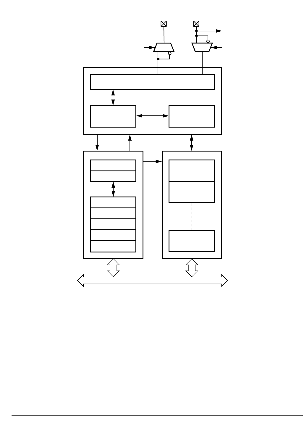
www.national.com 110
CP3BT26
Figure 34. CAN Block Diagram
19.2 BASIC CAN CONCEPTS
This section provides a generic overview of the basic con-
cepts of the Controller Area Network (CAN).
The CAN protocol is a message-based protocol that allows
a total of 2032 (211 - 16) different messages in the standard
format and 512 million (229 - 16) different messages in the
extended frame format.
Every CAN Frame is broadcast on the common bus. Each
module receives every frame and filters out the frames
which are not required for the module's task. For example,
if a dashboard sends a request to switch on headlights, the
CAN module responsible for brake lights must not process
this message.
A CAN master module has the ability to set a specific bit
called the “remote data request bit” (RTR) in a frame. Such
a message is also called a “Remote Frame”. It causes an-
other module, either another master or a slave which ac-
cepts this remote frame, to transmit a data frame after the
remote frame has been completed.
Additional modules can be added to an existing network
without a configuration change. These modules can either
perform completely new functions requiring new data, or
process existing data to perform a new functionality.
As the CAN network is message oriented, a message can
be used as a variable which is automatically updated by the
controlling processor. If any module cannot process infor-
mation, it can send an overload frame.
CPU BUS
Transceiver Logic
BTL, RX shift, TX shift, CRC
CAN CORE
INTERFACE MANAGEMENT RAM
Bit Stream Processor Error Management Logic
Interface Management
Processor
Acceptance Filtering
Interface Management
Processor
ACCEPTANCE
MASKS
CONTROL
CAN PRESCALER
BTL CONFIG
TX/RX
Message Buffer 0
TX/RX
Message Buffer 1
TX/RX
Message Buffer 14
CANRX
Wake-Up
CRX
Control Status
Control
Data
1
0
CANTX
CTX 1
0
DS018
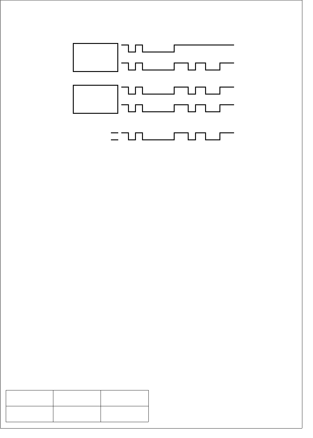
111 www.national.com
CP3BT26
The CAN protocol allows several transmitting modules to
start a transmission at the same time as soon as they detect
the bus is idle. During the start of transmission, every node
monitors the bus line to detect whether its message is over-
written by a message with a higher priority. As soon as a
transmitting module detects another module with a higher
priority accessing the bus, it stops transmitting its own frame
and switches to receive mode, as shown in Figure 35.
Figure 35. CAN Message Arbitration
If a data or remote frame loses arbitration on the bus due to
a higher-prioritized data or remote frame, or if it is destroyed
by an error frame, the transmitting module will automatically
retransmit it until the transmission is successful or software
has canceled the transmit request.
If a transmitted message loses arbitration, the CAN module
will restart transmission at the next possible time with the
message which has the highest internal transmit priority.
19.2.1 CAN Frame Types
Communication via the CAN bus is basically established by
means of four different frame types:
Data Frame
Remote Frame
Error Frame
Overload Frame
Data and remote frames can be used in both standard and
extended frame format. If no message is being transmitted,
i.e., the bus is idle, the bus is kept at the “recessive” level.
Remote and data frames are non-return to zero (NRZ) cod-
ed with bit-stuffing in every bit field, which holds computable
information for the interface, i.e., start of frame, arbitration
field, control field, data field (if present), and CRC field.
Error and overload frames are also NRZ coded, but without
bit-stuffing.
After five consecutive bits of the same value (including in-
serted stuff bits), a stuff bit of the inverted value is inserted
into the bit stream by the transmitter and deleted by the re-
ceiver. The following shows the stuffed and destuffed bit
stream for consecutive ones and zeros.
19.2.2 CAN Frame Fields
Data and remote frames consist of the following bit fields:
Start of Frame (SOF)
Arbitration Field
Control Field
Data Field
CRC Field
ACK Field
EOF Field
Start of Frame (SOF)
The Start of Frame (SOF) indicates the beginning of data
and remote frames. It consists of a single “dominant” bit. A
node is only allowed to start transmission when the bus is
idle. All nodes have to synchronize to the leading edge (first
edge after the bus was idle) caused by the SOF of the node
which starts transmission first.
Arbitration Field
The Arbitration field consists of the identifier field and the
RTR (Remote Transmission Request) bit. For extended
frames there is also a SRR (Substitute Remote Request)
and a IDE (ID Extension) bit inserted between ID18 and
ID17 of the identifier field. The value of the RTR bit is “dom-
inant” in a data frame and “recessive” in a remote frame.
Control Field
The Control field consists of six bits. For standard frames it
starts with the ID Extension bit (IDE) and a reserved bit
(RB0). For extended frames, the control field starts with two
reserved bits (RB1, RB0). These bits are followed by the 4-
bit Data Length Code (DLC).
The CAN receiver accepts all possible combinations of the
reserved bits (RB1, RB0). The transmitter must be config-
ured to send only zeros.
TxPIN
RxPIN
MODULE A
TxPIN
RECESSIVE
DOMINANT
MODULE A SUSPENDS TRANSMISSION
BUS LINE
RxPIN
MODULE B
DS019
Original or
unstuffed bit stream
10000011111 . . . 01111100000 . . .
Stuffed bit stream
(stuff bits in bold)
1000001111101 . . . 0111110000010 . . .
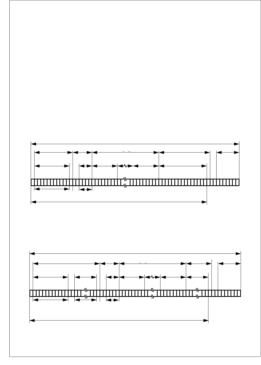
www.national.com 112
CP3BT26
Data Length Code (DLC)
The DLC field indicates the number of bytes in the data field.
It consists of four bits. The data field can be of length zero.
The admissible number of data bytes for a data frame rang-
es from 0 to 8.
Data Field
The Data field consists of the data to be transferred within a
data frame. It can contain 0 to 8 bytes. A remote frame has
no data field.
Cyclic Redundancy Check (CRC)
The CRC field consists of the CRC sequence followed by
the CRC delimiter. The CRC sequence is derived by the
transmitter from the modulo 2 division of the preceding bit
fields, starting with the SOF up to the end of the data field,
excluding stuff-bits, by the generator polynomial:
The remainder of this division is the CRC sequence trans-
mitted over the bus. On the receiver side, the module di-
vides all bit fields up to the CRC delimiter excluding stuff
bits, and checks if the result is zero. This will then be inter-
preted as a valid CRC. After the CRC sequence a single “re-
cessive” bit is transmitted as the CRC delimiter.
ACK Field
The ACK field is two bits long and contains the ACK slot and
the ACK delimiter. The ACK slot is filled with a “recessive”
bit by the transmitter. This bit is overwritten with a “domi-
nant” bit by every receiver that has received a correct CRC
sequence. The second bit of the ACK field is a “recessive”
bit called the acknowledge delimiter.
The End of Frame field closes a data and a remote frame. It
consists of seven “recessive” bits.
19.2.3 CAN Frame Formats
Data Frame
The structure of a standard data frame is shown in
Figure 36. The structure of an extended data frame is
shown in Figure 37.
Figure 36. Standard Data Frame
Figure 37. Extended Data Frame
x15 + x14 + x10 + x8 + x7 + x4 + x3 + 1
STANDARD DATA FRAME (number of bits = 44 + 8N)
Control Field Data Field END OF
FRAME
CRC Field
CRC
Arbitration Field
IDENTIFIER
10 ... 0
11 4
DATA
LENGTH CODE
START OF FRAME
ID 10
ID0
RTR
IDE
RB0
DLC3
DLC
dddd rrr rrrrrr
CRC DEL
ACK DEL
ACKNOWLEDGEMENT
Bit Stuffing
8815
16
8N (0 < N < 8)
Note:
d = dominant
r = recessive
DS020
EXTENDED DATA FRAME (number of bits = 64 + 8N)
Control Field Data Field END OF
FRAME
CRC Field
CRC
Arbitration Field
IDENTIFIER
28 ... 18
11 4
DATA
LENGTH CODE
START OF FRAME
ID 28
ID18
ID17
ID0
SRR
IDE
RTR
RB1
RB0
DLC3
DLC
drrddd rrr rrrrrr
CRC DEL
ACK DEL
SCK
Bit Stuffing
18 815
16
8N (0 < N < 0)
8
IDENTIFIER
17 ... 0
Note:
d = dominant
r = recessive
DS021
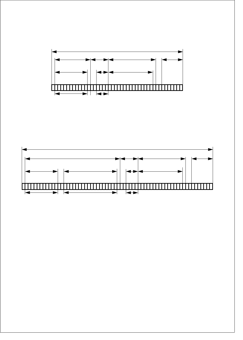
113 www.national.com
CP3BT26
A CAN data frame consists of the following fields:
Start of Frame (SOF)
Arbitration Field + Extended Arbitration
Control Field
Data Field
Cyclic Redundancy Check Field (CRC)
Acknowledgment Field (ACK)
End of Frame (EOF)
Remote Frame
Figure 38 shows the structure of a standard remote frame.
Figure 39 shows the structure of an extended remote frame.
Figure 38. Standard Remote Frame
Figure 39. Extended Remote Frame
A remote frame is comprised of the following fields, which is
the same as a data frame (see CAN Frame Fields on page
111) except for the data field, which is not present.
Start of Frame (SOF)
Arbitration Field + Extended Arbitration
Control Field
Cyclic Redundancy Check Field (CRC)
Acknowledgment field (ACK)
End of Frame (EOF)
Note that the DLC must have the same value as the corre-
sponding data frame to prevent contention on the bus. The
RTR bit is “recessive”.
STANDARD REMOTE FRAME (number of bits = 44)
Control Field END OF
FRAME
CRC Field
CRC
Arbitration Field
IDENTIFIER
10 ... 0
11
START OF FRAME
ID 10
ID0
ID3
RTR
IDE
RB0
dddd rrrrrrrrr
CRC DEL
ACK DEL
ACKNOWLEDGEMENT
154
16
DATA
LENGTH CODE
DLC3
DLC0
Note:
d = dominant
r = recessive DS022
EXTENDED REMOTE FRAME (number of bits = 64)
Control Field END OF
FRAME
CRC Field
CRC
Arbitration Field
IDENTIFIER
28 ... 18
Note:
d = dominant
r = recessive
11 4
DATA
LENGTH CODE
START OF FRAME
ID 28
ID18
ID17
ID0
SRR
IDE
RTR
RB1
RB0
DLC3
DLC0
drr rdd rrrrrrrrr
CRC DEL
ACK DEL
SCK
18 15
16
IDENTIFIER
17 ... 0
DS023
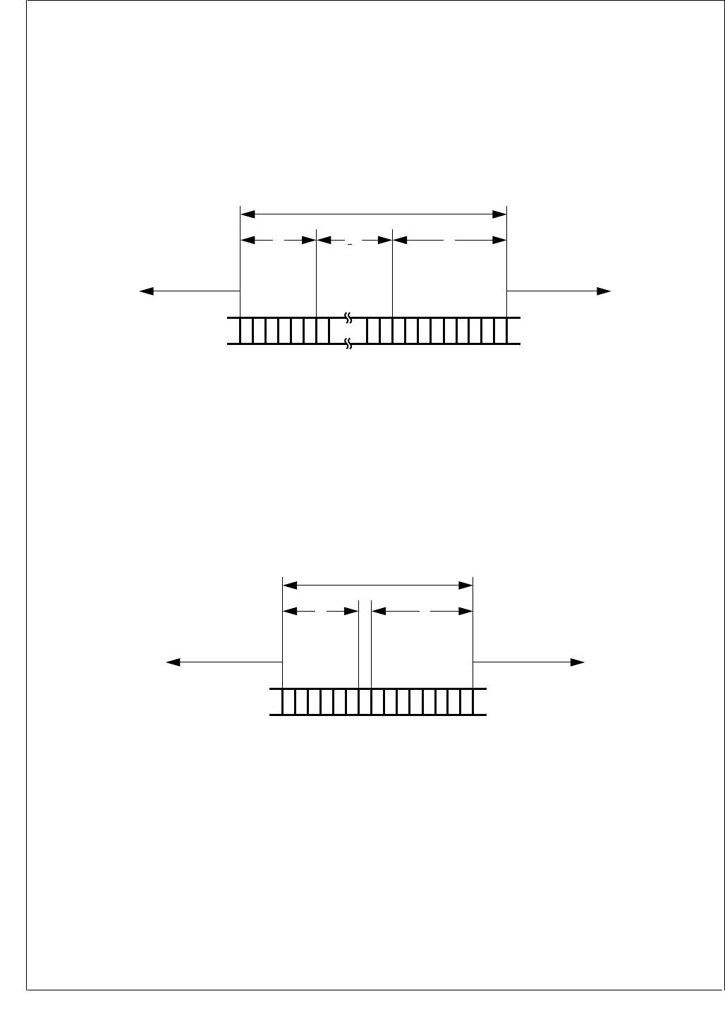
www.national.com 114
CP3BT26
Error Frame
As shown in Figure 40, the Error Frame consists of the error
flag and the error delimiter bit fields. The error flag field is
built up from the various error flags of the different nodes.
Therefore, its length may vary from a minimum of six bits up
to a maximum of twelve bits depending on when a module
has detected the error. Whenever a bit error, stuff error, form
error, or acknowledgment error is detected by a node, the
node starts transmission of an error flag at the next bit. If a
CRC error is detected, transmission of the error flag starts
at the bit following the acknowledge delimiter, unless an er-
ror flag for a previous error condition has already been start-
ed.
If a device is in the error active state, it can send a “domi-
nant” error flag, while a error passive device is only allowed
to transmit “recessive” error flags. This is done to prevent
the CAN bus from getting stuck due to a local defect. For the
various CAN device states, please refer to Error Types on
page 115.
Figure 40. Error Frame
Overload Frame
As shown in Figure 41, an overload frame consists of the
overload flag and the overload delimiter bit fields. The bit
fields have the same length as the error frame field: six bits
for the overload flag and eight bits for the delimiter. The
overload frame can only be sent after the end of frame
(EOF) field and in this way destroys the fixed form of the in-
termission field. As a result, all other nodes also detect an
overload condition and start the transmission of an overload
flag. After an overload flag has been transmitted, the over-
load frame is closed by the overload delimiter.
Note: The CAN module never initiates an overload frame
due to its inability to process an incoming message. Howev-
er, it is able to recognize and respond to overload frames ini-
tiated by other devices.
Figure 41. Overload Frame
Interframe Space
Data and remote frames are separated from every preced-
ing frame (data, remote, error and overload frames) by the
interframe space (see Figure 42). Error and overload
frames are not preceded by an interframe space; they can
be transmitted as soon as the condition occurs. The inter-
frame space consists of a minimum of three bit fields de-
pending on the error state of the node.
ERROR FRAME
6
ERROR
FLAG
< 6
ECHO
ERROR FLAG
8
ERROR
DELIMITER
DATA FRAME OR
REMOVE FRAME
An error frame can start anywhere within a frame
INTER-FRAME OR
OVERLOAD FRAME
Note:
d = dominant
r = recessive
rdddddddddrrr drrrr
DS024
OVERLOAD FRAME
6
OVERLOAD
FLAG
8
OVERLOAD
DELIMITER
END OF FRAME OR
ERROR DELIMITER OR
OVERLOAD DELIMITER
An overload frame can only start at the end of a frame
INTER-FRAME SPACE
OR ERROR FRAME
Note:
d = dominant
r = recessive
rdddddddrrr rrrr
DS025
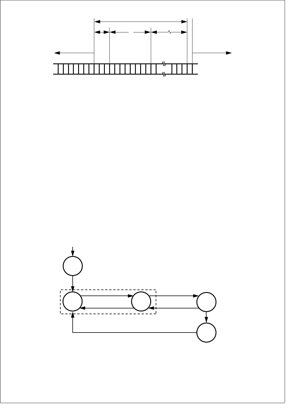
115 www.national.com
CP3BT26
Figure 42. Interframe Space
19.2.4 Error Types
Bit Error
A CAN device which is currently transmitting also monitors
the bus. If the monitored bit value is different from the trans-
mitted bit value, a bit error is detected. However, the recep-
tion of a “dominant” bit instead of a “recessive” bit during the
transmission of a passive error flag, during the stuffed bit
stream of the arbitration field, or during the acknowledge
slot is not interpreted as a bit error.
Stuff Error
A stuff error is detected if 6 consecutive bits occur without a
state change in a message field encoded with bit stuffing.
Form Error
A form error is detected, if a fixed frame bit (e.g., CRC de-
limiter, ACK delimiter) does not have the specified value. For
a receiver, a “dominant” bit during the last bit of End of
Frame does not constitute a frame error.
Bit CRC Error
A CRC error is detected if the remainder from the CRC cal-
culation of a received CRC polynomial is non-zero.
Acknowledgment Error
An acknowledgment error is detected whenever a transmit-
ting node does not get an acknowledgment from any other
node (i.e., when the transmitter does not receive a “domi-
nant” bit during the ACK frame).
Error States
The device can be in one of five states with respect to error
handling (see Figure 43).
Figure 43. Bus States
Synchronize
Once the CAN module is enabled, it waits for 11 consecu-
tive recessive bits to synchronize with the bus. After that, the
CAN module becomes error active and can participate in
the bus communication. This state must also be entered af-
ter waking-up the device using the Multi-Input Wake-Up fea-
ture. See System Start-Up and Multi-Input Wake-Up on
page 140.
INTERFRAME SPACE
8
SUSPEND
TRANSMIT
START OF FRAME
INT
3
Bus Idle
ANY FRAME
INT = Intermission
Suspend Transmission is only for error passive nodes.
DATA FRAME OR
REMOTE FRAME
Note:
d = dominant
r = recessive
rrrrrrrrrdrrrrrrrrrrrrr
DS026
SYNC
External Reset or
Enable CR16CAN
11 consecutive 'recessive" bits
received
(TEC OR REC) > 95
128 occurrences of
11 consecutive 'recessive" bits
TEC > 255
ERROR
ACTIVE
ERROR
WARNING
ERROR
PASSIVE
(TEC AND REC) < 96
(TEC OR REC) > 127
(TEC AND REC) < 128
BUS
OFF
DS027

www.national.com 116
CP3BT26
Error Active
An error active unit can participate in bus communication
and may send an active (“dominant”) error flag.
Error Warning
The Error Warning state is a sub-state of Error Active to in-
dicate a heavily disturbed bus. The CAN module behaves
as in Error Active mode. The device is reset into the Error
Active mode if the value of both counters is less than 96.
Error Passive
An error passive unit can participate in bus communication.
However, if the unit detects an error it is not allowed to send
an active error flag. The unit sends only a passive (“reces-
sive”) error flag. A device is error passive when the transmit
error counter or the receive error counter is greater than
127. A device becoming error passive will send an active er-
ror flag. An error passive device becomes error active again
when both transmit and receive error counter are less than
128.
Bus Off
A unit that is bus off has the output drivers disabled, i.e., it
does not participate in any bus activity. A device is bus off
when the transmit error counter is greater than 255. A bus
off device will become error active again after monitoring
128 × 11 “recessive” bits (including bus idle) on the bus.
When the device goes from “bus off“ to “error active“, both
error counters will have a value of 0.
19.2.5 Error Counters
There are multiple mechanisms in the CAN protocol to de-
tect errors and inhibit erroneous modules from disabling all
bus activities. Each CAN module includes two error
counters to perform error management. The receive error
counter (REC) and the transmit error counter (TEC) are 8-
bits wide, located in the 16-bit wide CANEC register. The
counters are modified by the CAN module according to the
rules listed in Table 45. This table provides an overview of
the CAN error conditions and the behavior of the CAN mod-
ule; for a detailed description of the error management and
fault confinement rules, refer to the CAN Specification 2.0B.
If the MSB (bit 7) of the REC is set, the node is error passive
and the REC will not increment any further.
The Error counters can be read by application software as
described under CAN Error Counter Register (CANEC) on
page 139.
Special error handling for the TEC counter is performed in
the following situations:
A stuff error occurs during arbitration, when a transmitted
“recessive” stuff bit is received as a “dominant” bit. This
does not lead to an increment of the TEC.
An ACK-error occurs in an error passive device and no
“dominant” bits are detected while sending the passive
error flag. This does not lead to an increment of the TEC.
If only one device is on the bus and this device transmits
a message, it will get no acknowledgment. This will be
detected as an error and the message will be repeated.
When the device goes “error passive” and detects an ac-
knowledge error, the TEC counter is not incremented.
Therefore the device will not go from ”error passive” to
the “bus off” state due to such a condition.
Table 45 Error Counter Handling
Condition Action
Receive Error Counter Conditions
A receiver detects a bit error during sending an active error flag. Increment by 8
A receiver detects a “dominant“ bit as the first bit after sending an error flag Increment by 8
After detecting the 14th consecutive “dominant“ bit following an active error flag or overload
flag, or after detecting the 8th consecutive “dominant“ bit following a passive error flag.
After each sequence of additional 8 consecutive “dominant” bits.
Increment by 8
Any other error condition (stuff, frame, CRC, ACK) Increment by 1
A valid reception or transmission Decrement by 1 unless
counter is already 0
Transmit Error Counter Conditions
A transmitter detects a bit error while sending an active error flag Increment by 8
After detecting the 14th consecutive “dominant“ bit following an active error flag or overload
flag or after detecting the 8th consecutive “dominant“ bit following a passive error flag.
After each sequence of additional 8 consecutive ‘dominant’ bits.
Increment by 8
Any other error condition (stuff, frame, CRC, ACK) Increment by 8
A valid reception or transmission Decrement by 1 unless
counter is already 0

117 www.national.com
CP3BT26
19.2.6 Bit Time Logic
In the Bit Time Logic (BTL), the CAN bus speed and the
Synchronization Jump Width can be configured by software.
The CAN module divides a nominal bit time into three time
segments: synchronization segment, time segment 1
(TSEG1), and time segment 2 (TSEG2). Figure 44 shows
the various elements of a CAN bit time.
CAN Bit Time
The number of time quanta in a CAN bit (CAN Bit Time)
ranges between 4 and 25. The sample point is positioned
between TSEG1 and TSEG2 and the transmission point is
positioned at the end of TSEG2.
Figure 44. Bit Timing
TSEG1 includes the propagation segment and the phase
segment 1 as specified in the CAN specification 2.0B. The
length of the time segment 1 in time quanta (tq) is defined
by the TSEG1[3:0] bits.
TSEG2 represents the phase segment 2 as specified in the
CAN specification 2.0B. The length of time segment 2 in
time quanta (tq) is defined by the TSEG2[3:0] bits.
The Synchronization Jump Width (SJW) defines the maxi-
mum number of time quanta (tq) by which a received CAN
bit can be shortened or lengthened in order to achieve re-
synchronization on “recessive” to “dominant” data transi-
tions on the bus. In the CAN implementation, the SJW must
be configured less or equal to TSEG1 or TSEG2, whichever
is smaller.
Synchronization
A CAN device expects the transition of the data signal to be
within the synchronization segment of each CAN bit time.
This segment has the fixed length of one time quantum.
However, two CAN nodes never operate at exactly the same
clock rate, and the bus signal may deviate from the ideal
waveform due to the physical conditions of the network (bus
length and load). To compensate for the various delays with-
in a network, the sample point can be positioned by pro-
gramming the length of TSEG1 and TSEG2 (see
Figure 44).
In addition, two types of synchronization are supported. The
BTL logic compares the incoming edge of a CAN bit with the
internal bit timing. The internal bit timing can be adapted by
either hard or soft synchronization (re-synchronization).
Hard synchronization is performed at the beginning of a new
frame with the falling edge on the bus while the bus is idle.
This is interpreted as the SOF. It restarts the internal logic.
Soft synchronization is performed during the reception of a
bit stream to lengthen or shorten the internal bit time. De-
pending on the phase error (e), TSEG1 may be increased
or TSEG2 may be decreased by a specific value, the resyn-
chronization jump width (SJW).
The phase error is given by the deviation of the edge to the
SYNC segment, measured in CAN clocks. The value of the
phase error is defined as:
e = 0, if the edge occurs within the SYNC segment
e > 0, if the edge occurs within TSEG1
e < 0, if the edge occurs within TSEG2 of the previous
bit
Resynchronization is performed according to the following
rules:
If the magnitude of e is less then or equal to the pro-
grammed value of SJW, resynchronization will have the
same effect as hard synchronization.
If e > SJW, TSEG1 will be lengthened by the value of the
SJW (see Figure 45).
If e < -SJW, TSEG2 will be shortened by the value SJW
(see Figure 46).
1 to 8 Time Quanta2 to 16 Time Quanta
4 to 25 TIme Quanta
SAMPLE
POINT
TRANSMISSION
POINT
INTERNAL
TIME QUANTA
CLOCK
ONE TIME QUANTUM
16 TIme
Quanta
A TIME SEGMENT 1 (TSEG1) TIME SEGMENT 1 (TSEG1)
A = synchronization segment (Sync)
DS028
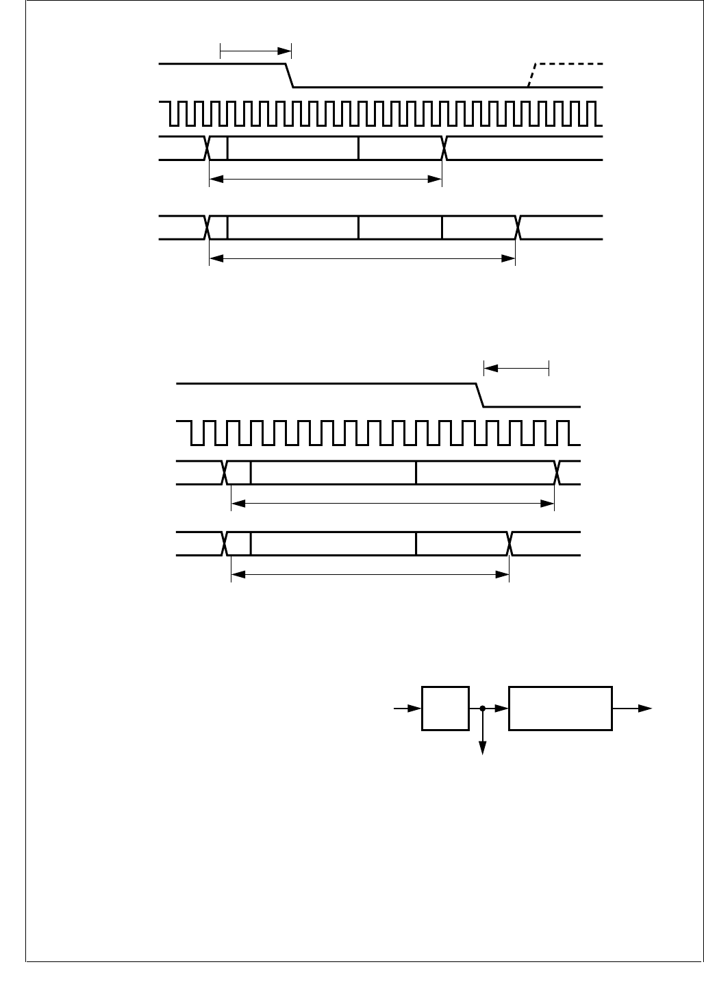
www.national.com 118
CP3BT26
Figure 45. Resynchronization (e > SJW)
Figure 46. Resynchronization (e < -SJW)
19.2.7 Clock Generator
The CAN prescaler (PSC) is shown is Figure 47. It divides
the CKI input clock by the value defined in the CTIM register.
The resulting clock is called time quanta clock and defines
the length of one time quantum (tq).
Please refer to CAN Timing Register (CTIM) on page 135
for a detailed description of the CTIM register.
Note: PSC is the value of the clock prescaler. TSEG1 and
TSEG2 are the length of time segment 1 and 2 in time quan-
ta.
The resulting bus clock can be calculated by the equation:
The values of PSC, TSEG1, and TSEG2 are specified by
the contents of the registers PSC, TSEG1, and TSEG2 as
follows:
PSC = PSC[5:0] + 2
TSEG1 = TSEG1[3:0] + 1
TSEG2 = TSEG2[2:0] + 1
Figure 47. CAN Prescaler
19.3 MESSAGE TRANSFER
The CAN module has access to 15 independent message
buffers, which are memory mapped in RAM. Each message
buffer consists of 8 different 16-bit RAM locations and can
be individually configured as a receive message buffer or as
a transmit message buffer.
A dedicated acceptance filtering procedure enables soft-
ware to configure each buffer to receive only a single mes-
sage ID or a group of messages. One buffer uses an
Bus
Signal
PREVIOUS
BIT
"NORMAL" BIT TIME
NEXT BITTSEG2TSEG1A
e
PREVIOUS
BIT NEXT BITTSEG2SJWTSEG1A
BIT TIME LENGTHENED BY SJW
CAN
Clock
DS029
PREVIOUS
BIT
"NORMAL" BIT TIME
TSEG2TSEG1A
e
PREVIOUS
BIT
BIT TIME SHORTENED BY SJW
NEXT BITTSEG2TSEG1A
Bus
Signal
CAN
Clock
DS030
busclock CKI
PSC()x 1 TSEG1 TSEG2++()
-------------------------------------------------------------------------------------=
PSC
CKI Bit Rate
Internal Time
Quanta Clock (1/tq)
÷(1+TSEG1+TSEG2)
÷
DS031
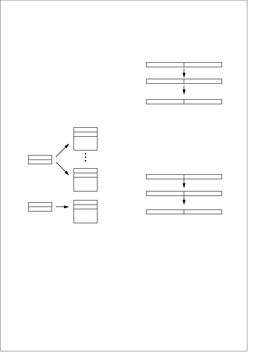
119 www.national.com
CP3BT26
independent filtering procedure, which provides the possi-
bility to establish a BASIC-CAN path.
For reception of data frame or remote frames, the CAN
module follows a “receive on first match” rule which means
that a given message is only received by one buffer: the first
one which matches the received message ID.
The transmission of a frame can be initiated by software
writing to the transmit status and priority register. An alter-
nate way to schedule a transmission is the automatic an-
swer to remote frames. In the latter case, the CAN module
will schedule every buffer for transmission to respond to re-
mote frames with a given identifier if the acceptance mask
matches. This implies that a single remote frame is able to
poll multiple matching buffers configured to respond to the
triggering remote transmission request.
19.4 ACCEPTANCE FILTERING
Two 32-bit masks are used to filter unwanted messages
from the CAN bus: GMASK and BMASK. Figure 48 shows
the mask and the buffers controlled by the masks.
Figure 48. Acceptance Filtering
Acceptance filtering of the incoming messages for the buff-
ers 0...13 is performed by means of a global filtering mask
(GMASK) and by the buffer ID of each buffer. Acceptance fil-
tering of incoming messages for buffer 14 is performed by a
separate filtering mask (BMASK) and by the buffer ID of that
buffer.
Once a received object is waiting in the hidden buffer to be
copied into a buffer, the CAN module scans all buffers con-
figured as receive buffers for a matching filtering mask. The
buffers 0 to 13 are checked in ascending order beginning
with buffer 0. The contents of the hidden buffer are copied
into the first buffer with a matching filtering mask.
Bits holding a 1 in the global filtering mask (GMASK) can be
represented as a “don’t care” of the associated bit of each
buffer identifier, regardless of whether the buffer identifier bit
is 1 or 0.
This provides the capability to accept only a single ID for
each buffer or to accept a group of IDs. The following two ex-
amples illustrate the difference.
Example 1: Acceptance of a Single Identifier
If the global mask is loaded with 00h, the acceptance filter-
ing of an incoming message is only determined by the indi-
vidual buffer ID. This means that only one message ID is
accepted for each buffer.
Figure 49. Acceptance of a Single Identifier
Example 2: Reception of an Identifier Group
Set bits in the global mask register change the correspond-
ing bit status within the buffer ID to “don’t care” (X). Messag-
es which match the non-“don’t care” bits (the bits
corresponding to clear bits in the global mask register) are
accepted.
Figure 50. Acceptance of a Group of Identifiers
A separate filtering path is used for buffer 14. For this buffer,
acceptance filtering is established by the buffer ID in con-
junction with the basic filtering mask. This basic mask uses
the same method as the global mask (set bits correspond to
“don’t care” bits in the buffer ID).
Therefore, the basic mask allows a large number of infre-
quent messages to be received by this buffer.
Note: If the BMASK register is equal to the GMASK regis-
ter, the buffer 14 can be used the same way as the buffers
0 to 13.
The buffers 0 to 13 are scanned prior to buffer 14. Subse-
quently, the buffer 14 will not be checked for a matching ID
when one of the buffers 0 to 13 has already received an ob-
ject.
By setting the BUFFLOCK bit in the configuration register,
the receiving buffer is automatically locked after reception of
one valid frame. The buffer will be unlocked again after the
CPU has read the data and has written RX_READY in the
Buffer 0
BUFFER_ID
Buffer 13
BUFFER_ID
GMASK1
GMASK2
Buffer 14
BUFFER_ID
BMASK1
BMASK2
DS032
GMASK1
0000000000000000
GMASK2
0000000000000
BUFFER_ID1
1010101010101010
BUFFER_ID2
1010110101010
1010101010101010
Accepted ID
1010110101010
DS033
GMASK1
1111111100000000
GMASK2
0000000000000
BUFFER_ID1
1010101010101010
BUFFER_ID2
1010110101010
XXXXXXXX10101010
Accepted ID Group
1010110101010
DS034
www.national.com 120
CP3BT26
buffer status field. With this lock function, software has the
capability to save several messages with the same identifier
or same identifier group into more than one buffer. For ex-
ample, a buffer with the second highest priority will receive
a message if the buffer with the highest priority has already
received a message and is now locked (provided that both
buffers use the same acceptance filtering mask).
As shown in Figure 51, several messages with the same ID
are received while BUFFLOCK is enabled. The filtering
mask of the buffers 0, 1, 13, and 14 is set to accept this mes-
sage. The first incoming frame will be received by buffer 0.
Because buffer 0 is now locked, the next frame will be re-
ceived by buffer 1, and so on. If all matching receive buffers
are full and locked, a further incoming message will not be
received by any buffer.
Figure 51. Message Storage with BUFFLOCK Enabled
19.5 RECEIVE STRUCTURE
All received frames are initially buffered in a hidden receive
buffer until the frame is valid. (The validation point for a re-
ceived message is the next-to-last bit of the EOF.) The re-
ceived identifier is then compared to every buffer ID
together with the respective mask and the status. As soon
as the validation point is reached, the whole contents of the
hidden buffer are copied into the matching message buffer
as shown in Figure 52.
Note: The hidden receive buffer must not be accessed by
the CPU.
Figure 52. Receive Buffer
The following section gives an overview of the reception of
the different types of frames.
The received data frame is stored in the first matching re-
ceive buffer beginning with buffer 0. For example, if the mes-
sage is accepted by buffer 5, then at the time the message
will be copied, the RX request is cleared and the CAN mod-
ule will not try to match the frame to any subsequent buffer.
1010101001010Received ID
GMASK
1010101010101010
1111111100000 0000000000000000
1111111100000BMASK
BUFFER14_ID Saved when buffer
is empty
Saved when buffer
is empty
Saved when buffer
is empty
Saved when buffer
is empty
0000000000000000
XXXXXXXX01010 1010101010101010
XXXXXXXX01010BUFFER1_ID
BUFFER13_ID
1010101010101010
XXXXXXXX01010 1010101010101010
BUFFER0_ID XXXXXXXX01010 1010101010101010
DS035
Hidden
Receive
Buffer
CR16CAN
Buffer 0
BUFFER_ID
Buffer 13
BUFFER_ID
Buffer 14
BUFFER_ID
DS036
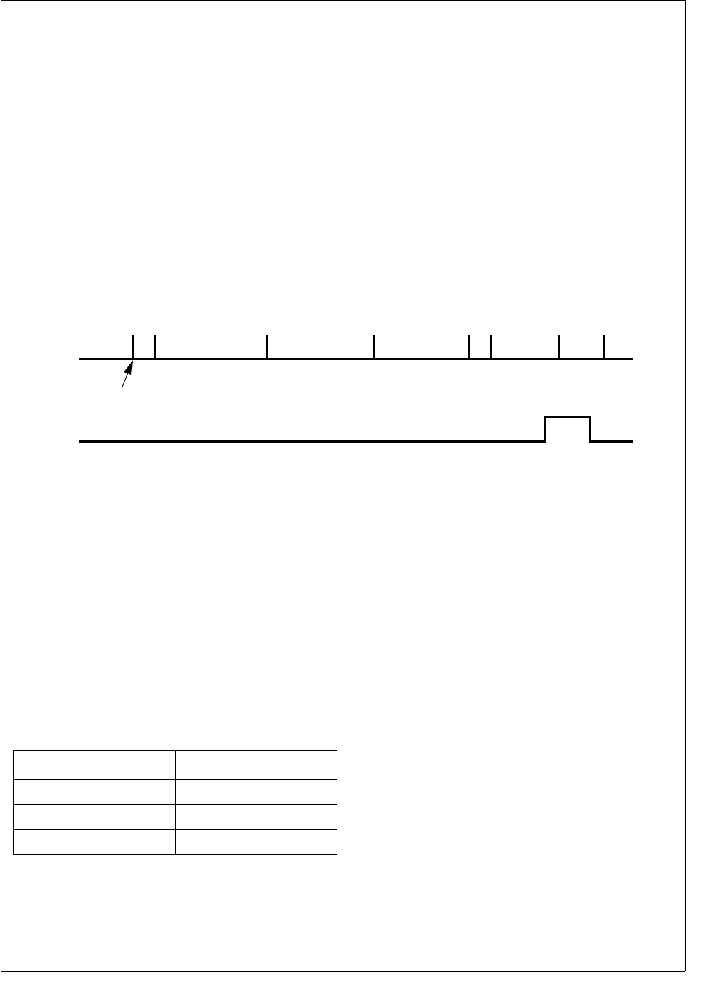
121 www.national.com
CP3BT26
All contents of the hidden receive buffer are always copied
into the respective receive buffer. This includes the received
message ID as well as the received Data Length Code
(DLC); therefore when some mask bits are set to don’t care,
the ID field will get the received message ID which could be
different from the previous ID. The DLC of the receiving buff-
er will be updated by the DLC of the received frame. The
DLC of the received message is not compared with the DLC
already present in the CNSTAT register of the message buff-
er. This implies that the DLC code of the CNSTAT register
indicates how may data bytes actually belong to the latest
received message.
The remote frames are handled by the CAN interface in two
different ways. In the first method, remote frames can be re-
ceived like data frames by configuring the buffer to be
RX_READY and setting the ID bits including the RTR bit. In
that case, the same procedure applies as described for
Data Frames. In the second method, a remote frame can
trigger one or more message buffer to transmit a data frame
upon reception. This procedure is described under To An-
swer Remote Frames on page 123.
19.5.1 Receive Timing
As soon as the CAN module receives a “dominant” bit on
the CAN bus, the receive process is started. The received
ID and data will be stored in the hidden receive buffer if the
global or basic acceptance filtering matches. After the re-
ception of the data, CAN module tries to match the buffer ID
of buffer 0...14. The data will be copied into the buffer after
the reception of the 6th EOF bit as a message is valid at this
time. The copy process of every frame, regardless of the
length, takes at least 17 CKI cycles (see also CPU Access
to CAN Registers/Memory on page 127). Figure 53 shows
the receive timing.
Figure 53. Receive Timing
To indicate that a frame is waiting in the hidden buffer, the
BUSY bit (ST[0]) of the selected buffer is set during the copy
procedure. The BUSY bit will be cleared by the CAN module
immediately after the data bytes are copied into the buffer.
After the copy process is finished, the CAN module changes
the status field to RX_FULL. In turn, the CPU should
change the status field to RX_READY when the data is pro-
cessed. When a new object has been received by the same
buffer, before the CPU changed the status to RX_READY,
the CAN module will change the status to RX_OVERRUN to
indicate that at least one frame has been overwritten by a
new one. Table 46 summarizes the current status and the
resulting update from the CAN module.
During the assertion of the BUSY bit, all writes to the receiv-
ing buffer are disabled with the exception of the status field.
If the status is changed while the BUSY bit is asserted, the
status is updated by the CAN module as shown in Table 46.
The buffer states are indicated and controlled by the ST[3:0]
bits in the CNSTAT register (see Buffer Status/Control Reg-
ister (CNSTAT) on page 128). The various receive buffer
states are explained in RX Buffer States on page 122.
19.5.2 Receive Procedure
Software executes the following procedure to initialize a
message buffer for the reception of a CAN message.
1. Configure the receive masks (GMASK or BMASK).
2. Configure the buffer ID.
3. Configure the message buffer status as RX_READY.
To read the out of a received message, the CPU must exe-
cute the following steps (see Figure 54):
Copy to Buffer
SOF
1 BIT
IFS
3 BIT
EOF
7 BIT
BUSY
rx_start
BUS
ACK
FIELD
2 BIT
CRC
FIELD
16 BIT
DATA FIELD
(IF PRESENT)
n × 8 BIT
ARBITRATION FIELD
+
CONTROL
12/29 BIT
+
6 BIT
BUS
IDLE
DS037
Table 46 Writing to Buffer Status Code During
RX_BUSY
Current Status Resulting Status
RX_READY RX_FULL
RX_NOT_ACTIVE RX_NOT_ACTIVE
RX_FULL RX_OVERRUN
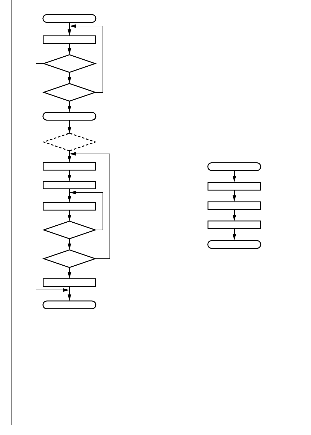
www.national.com 122
CP3BT26
Figure 54. Buffer Read Routine (BUFFLOCK Disabled)
The first step is only applicable if polling is used to get the
status of the receive buffer. It can be deleted for an interrupt
driven receive routine.
1. Read the status (CNSTAT) of the receive buffer. If the
status is RX_READY, no was the message received, so
exit. If the status is RX_BUSY, the copy process from
hidden receive buffer is not completed yet, so read CN-
STAT again.
If a buffer is configured to RX_READY and its interrupt
is enabled, it will generate an interrupt as soon as the
buffer has received a message and entered the
RX_FULL state (see also Interrupts on page 125). In
that case the procedure described below must be fol-
lowed.
2. Read the status to determine if a new message has
overwritten the one originally received which triggered
the interrupt.
3. Write RX_READY into CNSTAT.
4. Read the ID/data and object control (DLC/RTR) from
the message buffer.
5. Read the buffer status again and check it is not
RX_BUSYx. If it is, repeat this step until RX_BUSYx
has gone away.
6. If the buffer status is RX_FULL or RX_OVERRUN, one
or more messages were copied. In that case, start over
with step 2.
7. If status is still RX_READY (as set by the CPU at step
2), clear interrupt pending bit and exit.
When the BUFFLOCK function is enabled (see BUFFLOCK
on page 119), it is not necessary to check for new messag-
es received during the read process from the buffer, as this
buffer is locked after the reception of the first valid frame. A
read from a locked receive buffer can be performed as
shown in Figure 55.
Figure 55. Buffer Read Routine (BUFFLOCK Enabled)
For simplicity only the applicable interrupt routine is shown:
1. Read the ID/data and object control (DLC/RTR) from
the message buffer.
2. Write RX_READY into CNSTAT.
3. Clear interrupt pending bit and exit.
19.5.3 RX Buffer States
As shown in Figure 55, a receive procedure starts as soon
as software has set the buffer from the RX_NOT_ACTIVE
state into the RX_READY state. The status section of CN-
STAT register is set from 0000b to 0010b. When a message
is received, the buffer will be RX_BUSYx during the copy
process from the hidden receive buffer into the message
buffer. Afterwards this buffer is RX_FULL. The CPU can
then read the buffer data and either reset the buffer status
to RX_READY or receive a new frame before the CPU reads
the buffer. In the second case, the buffer state will automat-
ically change to RX_OVERRUN to indicate that at least one
message was lost. During the copy process the buffer will
again be RX_BUSYx for a short time, but in this case the
No
No
No
Ye s
Ye s
Ye s
Read buffer
Exit
Interrupt Entry Point
Read CNSTAT
Write RX_READY
Read CNSTAT
Clear RX_PND
Read buffer (id/data/control)
RX_READY?
RX_BUSYx?
RX_BUSYx?
RX_FULL or
RX_OVERRUN?
RX_OVERRUN? (optional, for information)
Ye s
No
DS038
Exit
Interrupt Entry Point
Clear RX_PND
Write RX_READY
Read buffer (id/data/control)
DS039
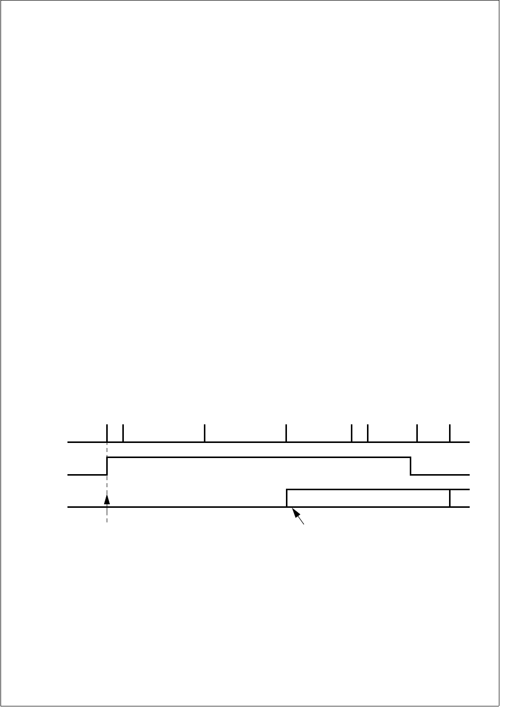
123 www.national.com
CP3BT26
CNSTAT status section will be 0101b, as the buffer was
RX_FULL (0100b) before. After finally reading the last re-
ceived message, the CPU can reset the buffer to
RX_READY.
19.6 TRANSMIT STRUCTURE
To transmit a CAN message, software must configure the
message buffer by changing the buffer status to
TX_NOT_ACTIVE. The buffer is configured for transmission
if the ST[3] bit of the buffer status code (CNSTAT) is set. In
TX_NOT_ACTIVE status, the buffer is ready to receive data
from the CPU. After receiving all transmission data (ID, data
bytes, DLC, and PRI), the CPU can start the transmission
by writing TX_ONCE into the buffer status register. During
the transmission, the status of the buffer is TX_BUSYx. Af-
ter successful transmission, the CAN module will reset the
buffer status to TX_NOT_ACTIVE. If the transmission pro-
cess fails, the buffer condition will remain TX_BUSYx for re-
transmission until the frame was successfully transmitted or
the CPU has canceled the transmission request.
To Send a Remote Frame (Remote Transmission Request)
to other CAN nodes, software sets the RTR bit of the mes-
sage identifier (see Storage of Remote Messages on page
132) and changes the status of the message buffer to
TX_ONCE. After this remote frame has been transmitted
successfully, this message buffer will automatically enter
the RX_READY state and is ready to receive the appropri-
ate answer. Note that the mask bits RTR/XRTR need to be
set to receive a data frame (RTR = 0) in a buffer which was
configured to transmit a remote frame (RTR = 1).
To answer Remote Frames, the CPU writes TX_RTR in the
buffer status register, which causes the buffer to wait for a
remote frame. When a remote frame passes the accep-
tance filtering mask of one or more buffers, the buffer status
will change to TX_ONCE_RTR, the contents of the buffer
will be transmitted, and afterwards the CAN module will
write TX_RTR in the status code register again.
If the CPU writes TX_ONCE_RTR into the buffer status, the
contents of the buffer will be transmitted, and the successful
transmission the buffer goes into the “wait for Remote
Frame” condition TX_RTR.
19.6.1 Transmit Scheduling
After writing TX_ONCE into the buffer status, the transmis-
sion process begins and the BUSY bit is set. As soon as a
buffer gets the TX_BUSY status, the buffer is no longer ac-
cessible by the CPU except for the ST[3:1] bits of the CN-
STAT register. Starting with the beginning of the CRC field
of the current frame, the CAN module looks for another buff-
er transmit request and selects the buffer with the highest
priority for the next transmission by changing the buffer
state from TX_ONCE to TX_BUSY. This transmit request
can be canceled by the CPU or can be overwritten by anoth-
er transmit request of a buffer with a higher priority as long
as the transmission of the next frame has not yet started.
This means that between the beginning of the CRC field of
the current frame and the transmission start of the next
frame, two buffers, the current buffer and the buffer sched-
uled for the next transmission, are in the BUSY status. To
cancel the transmit request of the next frame, the CPU must
change the buffer state to TX_NOT_ACTIVE. When the
transmit request has been overwritten by another request of
a higher priority buffer, the CAN module changes the buffer
state from TX_BUSY to TX_ONCE. Therefore, the transmit
request remains pending. Figure 56 further illustrates the
transmit timing.
Figure 56. Data Transmission
If the transmit process fails or the arbitration is lost, the
transmission process will be stopped and will continue after
the interrupting reception or the error signaling has finished
(see Figure 56). In that case, a new buffer select follows and
the TX process is executed again.
Note: The canceled message can be delayed by a TX re-
quest of a buffer with a higher priority. While TX_BUSY is
high, software cannot change the contents of the message
buffer object. In all cases, writing to the BUSY bit will be ig-
nored.
19.6.2 Transmit Priority
The CAN module is able to generate a stream of scheduled
messages without releasing the bus between two messag-
es so that an optimized performance can be achieved. It will
arbitrate for the bus immediately after sending the previous
message and will only release the bus due to a lost arbitra-
tion.
If more than one buffer is scheduled for transmission, the
priority is built by the message buffer number and the prior-
ity code in the CNSTAT register. The 8-bit value of the prior-
SOF
1 BIT
IFS
3 BIT
EOF
7 BIT
TX_BUSY
current buffer
CPU write TX_ONCE
in buffer status
Begin selection of next buffer
if new tx_request
TX_BUSY
next buffer
BUS
IDLE
ACK
FIELD
2 BIT
CRC
FIELD
16 BIT
DATA FIELD
(IF PRESENT)
n × 8 BIT
ARBITRATION FIELD
+ CONTROL
12/29 BIT + 6 BIT
BUS
DS040
www.national.com 124
CP3BT26
ity is combined by the 4-bit TXPRI value and the 4-bit buffer
number (0...14) as shown below. The lowest resulting num-
ber results in the highest transmit priority.
Table 47 shows the transmit priority configuration if the pri-
ority is TXPRI = 0 for all transmit buffers:
Table 48 shows the transmit priority configuration if TXPRI
is different from the buffer number:
Note: If two buffers have the same priority (PRI), the buffer
with the lower buffer number will have the higher priority.
19.6.3 Transmit Procedure
The transmission of a CAN message must be executed as
follows (see also Figure 57)
1. Configure the CNSTAT status field as
TX_NOT_ACTIVE. If the status is TX_BUSY, a previ-
ous transmit request is still pending and software has
no access to the data contents of the buffer. In that
case, software may choose to wait until the buffer be-
comes available again as shown. Other options are to
exit from the update routine until the buffer has been
transmitted with an interrupt generated, or the trans-
mission is aborted by an error.
2. Load buffer identifier and data registers. (For remote
frames the RTR bit of the identifier needs to be set and
loading data bytes can be omitted.)
3. Configure the CNSTAT status field to the desired value:
— TX_ONCE to trigger the transmission process of a
single frame.
— TX_ONCE_RTR to trigger the transmission of a sin-
gle data frame and then wait for a received remote
frame to trigger consecutive data frames.
— TX_RTR waits for a remote frame to trigger the trans-
mission of a data frame.
Writing TX_ONCE or TX_ONCE_RTR in the CNSTAT sta-
tus field will set the internal transmit request for the CAN
module.
If a buffer is configured as TX_RTR and a remote frame is
received, the data contents of the addressed buffer will be
transmitted automatically without further CPU activity.
Figure 57. Buffer Write Routine
7430
TXPRI BUFFER #
Table 47 Transmit Priority (TXPRI = 0)
TXPRI Buffer
Number PRI TX Priority
000Highest
011
:
:
:
:
:
:
:
:
01414Lowest
Table 48 Transmit Priority (TXPRI not 0)
TXPRI Buffer
Number PRI TX Priority
14 0 224 Lowest
13 1 209
12 2 194
11 3 179
10 4 164
95149
86134
77119
68104
5989
41074
31159
21244
11329
0 14 14 Highest
Exit
Write_buffer
Write
TX_ONCE
or
TX_ONCE_RTR
or
TX_RTR
Write
TX_NOT_ACTIVE
Write ID/data
TX_BUSYx? Ye s
No
DS041
125 www.national.com
CP3BT26
19.6.4 TX Buffer States
The transmission process can be started after software has
loaded the buffer registers (data, ID, DLC, PRI) and set the
buffer status from TX_NOT_ACTIVE to TX_ONCE,
TX_RTR, or TX_ONCE_RTR.
When the CPU writes TX_ONCE, the buffer will be
TX_BUSY as soon as the CAN module has scheduled this
buffer for the next transmission. After the frame could be
successfully transmitted, the buffer status will be automati-
cally reset to TX_NOT_ACTIVE when a data frame was
transmitted or to RX_READY when a remote frame was
transmitted.
If the CPU configures the message buffer to
TX_ONCE_RTR, it will transmit its data contents. During the
transmission, the buffer state is 1111b as the CPU wrote
1110b into the status section of the CNSTAT register. After
the successful transmission, the buffer enters the TX_RTR
state and waits for a remote frame. When it receives a re-
mote frame, it will go back into the TX_ONCE_RTR state,
transmit its data bytes, and return to TX_RTR. If the CPU
writes 1010b into the buffer status section, it will only enter
the TX_RTR state, but it will not send its data bytes before
it waits for a remote frame. Figure 58 illustrates the possible
transmit buffer states.
Figure 58. Transmit Buffer States
19.7 INTERRUPTS
The CAN module has one dedicated ICU interrupt vector for
all interrupt conditions. In addition, the data frame receive
event is an input to the MIWU (see Section 13.0). The inter-
rupt process can be initiated from the following sources.
CAN data transfer
— Reception of a valid data frame in the buffer. (Buffer
state changes from RX_READY to RX_FULL or
RX_OVERRUN.)
— Successful transmission of a data frame. (Buffer state
changes from TX_ONCE to TX_NOT_ACTIVE or
RX_READY.)
— Successful response to a remote frame. (Buffer state
changes from TX_ONCE_RTR to TX_RTR.)
— Transmit scheduling. (Buffer state changes from
TX_RTR to TX_ONCE_RTR.)
CAN error conditions
— Detection of an CAN error. (The CEIPND bit in the
CIPND register will be set as well as the correspond-
ing bits in the error diagnostic register CEDIAG.)
The receive/transmit interrupt access to every message
buffer can be individually enabled/disabled in the CIEN reg-
ister. The pending flags of the message buffer are located in
the CIPND register (read only) and can be cleared by reset-
ting the flags in the CICLR registers.
TX_ONCE_RTR
1110
CAN
schedules TX
RTR
received
TX done
Transmit
request cancelled
CPU writes 1000
Remote transmission
request sent - now wait
to receive a data frame
TX request delayed
by a TX request of higher
priority message
Transmit
request cancelled
CPU writes 1000
CAN
schedules TX
TX request
CPU writes 1100
TX request
CPU writes 1110
CPU writes 1010
TX_BUSY2
1111
TX done
transmit failed
TX_RTR
1010
TX_NOT_ACTIVE
1000
TX_BUSY0
1101
RX_READY
0010
TX_ONCE
1100
transmit failed
DS042
www.national.com 126
CP3BT26
19.7.1 Highest Priority Interrupt Code
To reduce the decoding time for the CIPND register, the
buffer interrupt request with the highest priority is placed as
interrupt status code into the IST[3:0] section of the CSTP-
ND register.
Each of the buffer interrupts as well as the error interrupt
can be individually enabled or disabled in the CAN Interrupt
Enable register (CIEN). As soon as an interrupt condition
occurs, every interrupt request is indicated by a flag in the
CAN Interrupt Pending register (CIPND). When the interrupt
code logic for the present highest priority interrupt request
is enabled, this interrupt will be translated into the IST3:0
bits of the CAN Status Pending register (CSTPND). An in-
terrupt request can be cleared by setting the corresponding
bit in the CAN Interrupt Clear register (CICLR).
Figure 59 shows the CAN interrupt management.
Figure 59. Interrupt Management
The highest priority interrupt source is translated into the
bits IRQ and IST3:0 as shown in Table 49.
19.7.2 Usage Hints
The interrupt code IST3:0 can be used within the interrupt
handler as a displacement to jump to the relevant subrou-
tine.
The CAN Interrupt Code Enable (CICEN) register is used in
the CAN interrupt handler if software is servicing all receive
buffer interrupts first, followed by all transmit buffer inter-
rupts. In this case, software can first enable only receive
buffer interrupts to be coded, then scan and service all
pending interrupt requests in the order of their priority. After
processing all the receive interrupts, software changes the
CICEN register to disable all receive buffers and enable all
transmit buffers, then services all pending transmit buffer in-
terrupt requests according to their priorities.
19.8 TIME STAMP COUNTER
The CAN module features a free running 16-bit timer (CT-
MR) incrementing every bit time recognized on the CAN
bus. The value of this timer during the ACK slot is captured
into the TSTP register of a message buffer after a success-
ful transmission or reception of a message. Figure 60
shows a simplified block diagram of the Time Stamp
counter.
Figure 60. Time Stamp Counter
The timer can be synchronized over the CAN network by re-
ceiving or transmitting a message to or from buffer 0. In this
case, the TSTP register of buffer 0 captures the current
CTMR value during the ACK slot of a message (as above),
and then the CTMR is reset to 0000b. Synchronization can
be enabled or disabled using the CGCR.TSTPEN bit.
Table 49 Highest Priority Interrupt Code (ICEN=FFFF)
CAN Interrupt
Request IRQ IST3 IST2 IST1 IST0
No Request 0 0 0 0 0
Error Interrupt 1 0 0 0 0
Buffer 0 1 0 0 0 1
Buffer 1 1 0 0 1 0
Buffer 2 1 0 0 1 1
Buffer 3 1 0 1 0 0
Buffer 4 1 0 1 0 1
Buffer 5 1 0 1 1 0
Buffer 6 1 0 1 1 1
Buffer 7 1 1 0 0 0
Buffer 8 1 1 0 0 1
Buffer 9 1 1 0 1 0
CICLR
CIPND
Clear interrupt flags of every
message buffer individually
ICODE
CIEN
CICEN
IRQ IST3 IST2 IST1 IST0
DS043
Buffer 10 1 1 0 1 1
Buffer 11 1 1 1 0 0
Buffer 12 1 1 1 0 1
Buffer 13 1 1 1 1 0
Buffer 14 1 1 1 1 1
Table 49 Highest Priority Interrupt Code (ICEN=FFFF)
CAN Interrupt
Request IRQ IST3 IST2 IST1 IST0
16-Bit counter
+
1
Reset
TSTP register
ACK slot
ACK slot and buffer 0 active
CAN bits on the bus
DS044
127 www.national.com
CP3BT26
19.9 MEMORY ORGANIZATION
The CAN module occupies 144 words in the memory ad-
dress space. This space is organized as 15 banks of 8
words per bank (plus one reserved bank) for the message
buffers and 14 words (plus 2 reserved words) for control and
status.
19.9.1 CPU Access to CAN Registers/Memory
All memory locations occupied by the message buffers are
shared by the CPU and CAN module (dual-ported RAM).
The CAN module and the CPU normally have single-cycle
access to this memory. However, if an access contention oc-
curs, the access to the memory is blocked every cycle until
the contention is resolved. This internal access arbitration is
transparent to software.
Both word and byte access to the buffer RAM are allowed.
If a buffer is busy during the reception of an object (copy
process from the hidden receive buffer) or is scheduled for
transmission, the CPU has no write access to the data con-
tents of the buffer. Write to the status/control byte and read
access to the whole buffer is always enabled.
All configuration and status registers can either be access-
ed by the CAN module or the CPU only. These registers pro-
vide single-cycle word and byte access without any
potential wait state.
All register descriptions within the next sections have the fol-
lowing layout:
19.9.2 Message Buffer Organization
The message buffers are the communication interfaces be-
tween CAN and the CPU for the transmission and the re-
ception of CAN frames. There are 15 message buffers
located at fixed addresses in the RAM location. As shown in
Table 50, each buffer consists of two words reserved for the
identifiers, 4 words reserved for up to eight CAN data bytes,
one word reserved for the time stamp, and one word for data
length code, transmit priority code, and the buffer status
codes.
15 0
Bit/Field Names
Reset Value
CPU Access (R = read only, W = write only, R/W = read/write)
Table 50 Message Buffer Map
Address Buffer
Register 15141312111098765 4 3210
0E F0XEh ID1 XI[28:18]/ID[10:0] SRR
/RTR IDE XI[17:15]
0E F0XCh ID0 XI[14:0] RTR
0E F0XAh DATA0 Data1[7:0] Data2[7:0]
0E F0X8h DATA1 Data3[7:0] Data4[7:0]
0E F0X6h DATA2 Data5[7:0] Data6[7:0]
0E F0X4h DATA3 Data7[7:0] Data8[7:0]
0E F0X2h TSTP TSTP[15:0]
0E F0X0h CNSTAT DLC Reserved PRI ST

www.national.com 128
CP3BT26
19.10 CAN CONTROLLER REGISTERS
Table 51 lists the CAN module registers.
19.10.1 Buffer Status/Control Register (CNSTAT)
The buffer status (ST), the buffer priority (PRI), and the data
length code (DLC) are controlled by manipulating the con-
tents of the Buffer Status/Control Register (CNSTAT). The
CPU and CAN module have access to this register.
ST The Buffer Status field contains the status in-
formation of the buffer as shown in Table 52.
This field can be modified by the CAN module.
The ST0 bits acts as a buffer busy indication.
When the BUSY bit is set, any write access to
the buffer is disabled with the exception of the
lower byte of the CNSTAT register. The CAN
module sets this bit if the buffer data is cur-
rently copied from the hidden buffer or if a
message is scheduled for transmission or is
currently transmitting. The CAN module al-
ways clears this bit on a status update.
Table 51 CAN Controller Registers
Name Address Description
CNSTAT See
Tabl e 50.
CAN Buffer Status/
Control Register
CGCR 0E F100h CAN Global
Configuration Register
CTIM 0E F102h CAN Timing Register
GMSKX 0E F104h Global Mask Register
GMSKB 0E F106h Global Mask Register
BMSKX 0E F108h Basic Mask Register
BMSKB 0E F10Ah Basic Mask Register
CIEN 0E F10Ch CAN Interrupt
Enable Register
CIPND 0E F10Eh CAN Interrupt
Pending Register
CICLR 0E F110h CAN Interrupt
Clear Register
CICEN 0E F112h CAN Interrupt Code
Enable Register
CSTPND 0E F114h CAN Status
Pending Register
CANEC 0E F116h CAN Error
Counter Register
CEDIAG 0E F118h CAN Error
Diagnostic Register
CTMR 0E F11Ah CAN Timer Register
15 12 11 8 7 4 3 0
DLC Reserved PRI ST
0
R/W

129 www.national.com
CP3BT26
Table 52 Buffer Status Section of the CNSTAT Register
ST3 (DIR) ST2 ST1 ST0 (BUSY) Buffer Status
000 0RX_NOT_ACTIVE
000 1
Reserved for RX_BUSY. (This condition indicates that soft-
ware wrote RX_NOT_ACTIVE to a buffer when the data
copy process is still active.)
001 0RX_READY
001 1
RX_BUSY0 (Indicates data is being copied for the first time
RX_READY → RX_BUSY0.)
0 1 0 0 RX_FULL
010 1
RX_BUSY1 (Indicates data is being copied for the second
time RX_FULL → RX_BUSY1.)
0 1 1 0 RX_OVERRUN
011 1
RX_BUSY2 (Indicates data is being copied for the third or
subsequent times RX_OVERRUN → RX_BUSY2.)
1 0 0 0 TX_NOT_ACTIVE
100 1
Reserved for TX_BUSY. (This state indicates that software
wrote TX_NOT_ACTIVE to a transmit buffer which is sched-
uled for transmission or is currently transmitting.)
110 0TX_ONCE
110 1
TX_BUSY0 (Indicates that a buffer is scheduled for trans-
mission or is actively transmitting; it can be due to one of
two cases: a message is pending for transmission or is cur-
rently transmitting, or an automated answer is pending for
transmission or is currently transmitting.)
1 0 1 0 TX_RTR (Automatic response to a remote frame.)
1 0 1 1 Reserved for TX_BUSY1. (This condition does not occur.)
1 1 1 0 TX_ONCE_RTR (Changes to TX_RTR after transmission.)
111 1
TX_BUSY2 (Indicates that a buffer is scheduled for trans-
mission or is actively transmitting; it can be due to one of
two cases: a message is pending for transmission or is cur-
rently transmitting, or an automated answer is pending for
transmission or is currently transmitting.)
www.national.com 130
CP3BT26
PRI The Transmit Priority Code field holds the
software-defined transmit priority code for the
message buffer.
DLC The Data Length Code field determines the
number of data bytes within a received/trans-
mitted frame. For transmission, these bits
need to be set according to the number of
data bytes to be transmitted. For reception,
these bits indicate the number of valid re-
ceived data bytes available in the message
buffer. Table 53 shows the possible bit combi-
nations for DLC3:0 for data lengths from 0 to
8 bytes.
Note: The maximum number of data bytes received/trans-
mitted is 8, even if the DLC field is set to a value greater than
8. Therefore, if the data length code is greater or equal to
eight bytes, the DLC field is ignored.
19.10.2 Storage of Standard Messages
During the processing of standard frames, the Extended-
Identifier (IDE) bit is clear. The ID1[3:0] and ID0[15:0] bits
are “don’t care” bits. A standard frame with eight data bytes
is shown in Table 54.
IDE The Identifier Extension bit determines wheth-
er the message is a standard frame or an ex-
tended frame.
0 – Message is a standard frame using 11
identifier bits.
1 – Message is an extended frame.
RTR The Remote Transmission Request bit indi-
cates whether the message is a data frame or
a remote frame.
0 – Message is a data frame.
1 – Message is a remote frame.
ID The ID field is used for the 11 standard frame
identifier bits.
Table 53 Data Length Coding
DLC Number of Data Bytes
0000 0
0001 1
0010 2
0011 3
0100 4
0101 5
0110 6
0111 7
1000 8
Table 54 Standard Frame with 8 Data Bytes
Address Buffer
Register 1514131211109876543210
0E F0XEh ID1 ID[10:0] RTR IDE Don’t Care
0E F0XCh ID0 Don’t Care
0E F0XAh DATA0 Data1[7:0] Data2[7:0]
0E F0X8h DATA1 Data3[7:0] Data4[7:0]
0E F0X6h DATA2 Data5[7:0] Data6[7:0]
0E F0X4h DATA3 Data7[7:0] Data8[7:0]
0E F0X2h TSTP TSTP[15:0]
0E F0X0h CNSTAT DLC Reserved PRI ST

131 www.national.com
CP3BT26
19.10.3 Storage of Messages with Less Than 8 Data
Bytes
The data bytes that are not used for data transfer are “don’t
cares”. If the object is transmitted, the data within these
bytes will be ignored. If the object is received, the data with-
in these bytes will be overwritten with invalid data.
19.10.4 Storage of Extended Messages
If the IDE bit is set, the buffer handles extended frames. The
storage of the extended ID follows the descriptions in
Table 55. The SRR bit is at the bit position of the RTR bit for
standard frame and needs to be transmitted as 1.
SRR The Substitute Remote Request bit replaces
the RTR bit used in standard frames at this bit
position. The SRR bit needs to be set by soft-
ware if the buffer is configured to transmit a
message with an extended identifier. It will be
received as monitored on the CAN bus.
IDE The Identifier Extension bit determines wheth-
er the message is a standard frame or an ex-
tended frame.
0 – Message is a standard frame using 11
identifier bits.
1 – Message is an extended frame.
RTR The Remote Transmission Request bit indi-
cates whether the message is a data frame or
a remote frame.
0 – Message is a data frame.
1 – Message is a remote frame.
ID The ID field is used to build the 29-bit identifier
of an extended frame.
Table 55 Extended Messages with 8 Data Bytes
Address Buffer
Register 15 14 13 12 11 10 9 8 7 6 5 4 3 2 1 0
0E F0XEh ID1 ID[28:18] SRR IDE ID17:15]
0E F0XCh ID0 ID[14:0] RTR
0E F0XAh DATA0 Data1[7:0] Data2[7:0]
0E F0X8h DATA1 Data3[7:0] Data4[7:0]
0E F0X6h DATA2 Data5[7:0] Data6[7:0]
0E F0X4h DATA3 Data7[7:0] Data8[7:0]
0E F0X2h TSTP TSTP[15:0]
0E F0X0h CNSTAT DLC Reserved PRI ST

www.national.com 132
CP3BT26
19.10.5 Storage of Remote Messages
During remote frame transfer, the buffer registers DATA0–
DATA3 are “don’t cares”. If a remote frame is transmitted,
the contents of these registers are ignored. If a remote
frame is received, the contents of these registers will be
overwritten with invalid data. The structure of a message
buffer set up for a remote frame with extended identifier is
shown in Table 56.
SRR The Substitute Remote Request bit replaces
the RTR bit used in standard frames at this bit
position. The SRR bit needs to be set by soft-
ware.
IDE The Identifier Extension bit determines wheth-
er the message is a standard frame or an ex-
tended frame.
0 – Message is a standard frame using 11
identifier bits.
1 – Message is an extended frame.
RTR The Remote Transmission Request bit indi-
cates whether the message is a data frame or
a remote frame.
0 – Message is a data frame.
1 – Message is a remote frame.
ID The ID field is used to build the 29-bit identifier
of an extended frame. The ID[28:18] field is
used for the 11 standard frame identifier bits.
Table 56 Extended Remote Frame
Address Buffer
Register 15 14 13 12 11 10 9 8 7 6 5 4 3 2 1 0
0E F0XEh ID1 ID[28:18] SRR IDE ID17:15]
0E F0XCh ID0 ID[14:0] RTR
0E F0XAh DATA0
Don’t Care
0E F0X8h DATA1
0E F0X6h DATA2
0E F0X4h DATA3
0E F0X2h TSTP TSTP
0E F0X0h CNSTAT DLC Reserved PRI ST

133 www.national.com
CP3BT26
19.10.6 CAN Global Configuration Register (CGCR)
The CAN Global Configuration Register (CGCR) is a 16-bit
wide register used to:
Enable/disable the CAN module.
Configure the BUFFLOCK function for the message buff-
er 0..14.
Enable/disable the time stamp synchronization.
Set the logic levels of the CAN Input/Output pins, CAN-
RX and CANTX.
Choose the data storage direction (DDIR).
Select the error interrupt type (EIT).
Enable/disable diagnostic functions.
CANEN The CAN Enable bit enables/disables the
CAN module. When the CAN module is dis-
abled, all internal states and the TEC and
REC counter registers are cleared. In addition
the CAN module clock is disabled. All CAN
module control registers and the contents of
the object memory are left unchanged. Soft-
ware must make sure that no message is
pending for transmission before the CAN
module is disabled.
0 – CAN module is disabled.
1 – CAN module is enabled.
CTX The Control Transmit bit configures the logic
level of the CAN transmit pin CANTX.
0 – Dominant state is 0; recessive state is 1.
1 – Dominant state is 1; recessive state is 0.
CRX The Control Receive bit configures the logic
level of the CAN receive pin CANRX.
0 – Dominant state is 0; recessive state is 1.
1 – Dominant state is 1; recessive state is 0.
BUFFLOCK The Buffer Lock bit configures the buffer lock
function. If this feature is enabled, a buffer will
be locked upon a successful frame reception.
The buffer will be unlocked again by writing
RX_READY in the buffer status register, i.e.,
after reading data.
0 – Lock function is disabled for all buffers.
1 – Lock function is enabled for all buffers.
TSTPEN The Time Sync Enable bit enables or disables
the time stamp synchronization function of the
CAN module.
0 – Time synchronization disabled. The Time
Stamp counter value is not reset upon re-
ception or transmission of a message to/
from buffer 0.
1 – Time synchronization enabled. The Time
Stamp counter value is reset upon recep-
tion or transmission of a message to/from
buffer 0.
DDIR The Data Direction bit selects the direction the
data bytes are transmitted and received. The
CAN module transmits and receives the CAN
Data1 byte first and the Data8 byte last
(Data1, Data2,...,Data7, Data8). If the DDIR
bit is clear, the data contents of a received
message is stored with the first byte at the
highest data address and the last data at the
lowest data address (see Figure 61). The
same applies for transmitted data.
0 – First byte at the highest address, subse-
quent bytes at lower addresses.
1 – First byte at the lowest address, subse-
quent bytes at higher addresses.
7 6 5 4 3 2 1 0
IGNACK LO DDIR TST
PEN
BUFF
LOCK CRX CTX CANEN
0
R/W
15 12 11 10 9 8
Reserved EIT DIAGEN INTERNAL LOOPBACK
0
R/W
www.national.com 134
CP3BT26
Figure 61. Data Direction Bit Clear
Setting the DDIR bit will cause the direction of the data stor-
age to be reversed — the last byte received is stored at the
highest address and the first byte is stored at the lowest ad-
dress, as shown in Figure 62.
Figure 62. Data Direction Bit Set
LO The Listen Only bit can be used to configure
the CAN interface to behave only as a receiv-
er. This means:
•Cannot transmit any message.
•Cannot send a dominant ACK bit.
•When errors are detected on the bus, the
CAN module will behave as in the error
passive mode.
Using this listen only function, the CAN inter-
face can be adjusted for connecting to an op-
erating network with unknown bus speed.
0 – Transmit/receive mode.
1 – Listen-only mode.
IGNACK When the Ignore Acknowledge bit is set, the
CAN module does not expect to receive a
dominant ACK bit to indicate the validity of a
transmitted message. It will not send an error
frame when the transmitted frame is not ac-
knowledged by any other CAN node. This fea-
ture can be used in conjunction with the
LOOPBACK bit for stand-alone tests outside
of a CAN network.
0 – Normal mode.
1 – The CAN module does not expect to re-
ceive a dominant ACK bit to indicate the
validity of a transmitted message.
LOOPBACK
When the Loopback bit is set, all messages
sent by the CAN module can also be received
by a CAN module buffer with a matching buff-
er ID. However, the CAN module does not ac-
knowledge a message sent by itself.
Therefore, the CAN module will send an error
frame when no other device connected to the
bus has acknowledged the message.
0 – No loopback.
1 – Loopback enabled.
Storage of Data Bytes
in the Buffer Memory
Sequence of Data Bytes on the Bus
CRCData8
t
Data7Data6Data5Data4Data3Data2Data1ID
Data2Data10A16
Data4Data30816
Data6Data50616
Data8Data70416
Data BytesADDR Offset
DS045
Storage of Data Bytes
in the Buffer Memory
Sequence of Data Bytes on the Bus
CRCData8
t
Data7Data6Data5Data4Data3Data2Data1ID
Data7Data80A16
Data5Data60816
Data3Data40616
Data1Data20416
Data BytesADDR Offset
DS046

135 www.national.com
CP3BT26
INTERNAL If the Internal function is enabled, the CANTX
and CANRX pins of the CAN module are inter-
nally connected to each other. This feature
can be used in conjunction with the LOOP-
BACK mode. This means that the CAN mod-
ule can receive its own sent messages
without connecting an external transceiver
chip to the CANTX and CANRX pins; it allows
software to run real stand-alone tests without
any peripheral devices.
0 – Normal mode.
1 – Internal mode.
DIAGEN The Diagnostic Enable bit globally enables or
disables the special diagnostic features of the
CAN module. This includes the following func-
tions:
•LO (Listen Only).
•IGNACK (Ignore Acknowledge).
•LOOPBACK (Loopback).
•INTERNAL (Internal Loopback).
•Write access to hidden receive buffer.
0 – Normal mode.
1 – Diagnostic features enabled.
EIT The Error Interrupt Type bit configures when
the Error Interrupt Pending Bit (CIPND.EIP-
ND) is set and an error interrupt is generated
if enabled by the Error Interrupt Enable
(CIEN.EIEN).
0 – The EIPND bit is set on every error on the
CAN bus.
1 – The EIPND bit is set only if the error state
(CSTPND.NS) changes as a result of in-
crementing either the receive or transmit
error counter.
19.10.7 CAN Timing Register (CTIM)
The Can Timing Register (CTIM) defines the configuration
of the Bit Time Logic (BTL).
PSC The Prescaler Configuration field specifies
the CAN prescaler. The settings are shown in
Tabl e 5 7
SJW The Synchronization Jump Width field speci-
fies the Synchronization Jump Width, which
can be programmed between 1 and 4 time
quanta (see Table 58).
Note: The settings of SJW must be configured to be small-
er or equal to TSEG1 and TSEG2
15 9 8 7 6 3 2 0
PSC SJW TSEG1 TSEG2
0
R/W
Table 57 CAN Prescaler Settings
PSC6:0 Prescaler
000000 2
000001 3
000010 4
000011 5
000100 6
::
1111101 127
1111110 128
1111111 128
Table 58 SJW Settings
SJW Synchronization Jump
Width (SJW)
00 1 time quantum
01 2 time quanta
10 3 time quanta
11 4 time quanta
www.national.com 136
CP3BT26
TSEG1 The Time Segment 1 field configures the
length of the Time Segment 1 (TSEG1). It is
not recommended to configure the time seg-
ment 1 to be smaller than 2 time quanta. (see
Ta b le 5 9 ).
TSEG2 The Time Segment 2 field specifies the num-
ber of time quanta (tq) for phase segment 2
(see Table 60).
19.10.8 Global Mask Register (GMSKB/GMSKX)
The GMSKB and GMSKX registers allow software to global-
ly mask, or “don’t care” the incoming extended/standard
identifier bits, RTR/XRTR and IDE. Throughout this docu-
ment, the GMSKB and GMSKX 16-bit registers are refer-
enced as a 32-bit register GMSK.
The following are the bits for the GMSKB register.
The following are the bits for the GMSKX register.
For all GMSKB and GMSKX register bits, the following ap-
plies:
0 – The incoming identifier bit must match the correspond-
ing bit in the message buffer identifier register.
1 – Accept 1 or 0 (“don’t care”) in the incoming ID bit inde-
pendent from the corresponding bit in the message
buffer ID registers. The corresponding ID bit in the mes-
sage buffer will be overwritten by the incoming identifier
bits.
When an extended frame is received from the CAN bus, all
GMSK bits GM[28:0], IDE, RTR, and XRTR are used to
mask the incoming message. In this case, the RTR bit in the
GMSK register corresponds to the SRR bit in the message.
The XRTR bit in the GMSK register corresponds to the RTR
bit in the message.
During the reception of standard frames only the GMSK bits
GM[28:18], RTR, and IDE are used. In this case, the
GM[28:18] bits in the GMSK register correspond to the
ID[10:0] bits in the message.
Table 59 Time Segment 1 Settings
TSEG1[3:0] Length of Time
(TSEG1)
0000 Not recommended
0001 2 time quanta
0010 3 time quanta
0011 4 time quanta
0100 5 time quanta
0101 6 time quanta
0110 7 time quanta
0111 8 time quanta
1000 9 time quanta
1001 10 time quanta
1010 11 time quanta
1011 12 time quanta
1100 13 time quanta
1101 14 time quanta
1110 15 time quanta
1111 16 time quanta
Table 60 Time Segment 2 Settings
TSEG2 Length of TSEG2
000 1 time quantum
001 2 time quanta
010 3 time quanta
011 4 time quanta
100 5 time quanta
101 6 time quanta
110 7 time quanta
111 8 time quanta
15 5 4 3 2 0
GM[28:18] RTR IDE GM[17:15]
0
R/W
15 1 0
GM[14:0] XRTR
0
R/W
Global Mask GM[28:18] RTR IDE GM[17:0] XRTR
Standard
Frame ID[10:0] RTR IDE Unused
Extended
Frame ID[28:18] SRR IDE ID[17:0] RTR

137 www.national.com
CP3BT26
19.10.9 Basic Mask Register (BMSKB/BMSKX)
The BMSKB and BMSKX registers allow masking the buffer
14, or “don’t care” the incoming extended/standard identifier
bits, RTR/XRTR, and IDE. Throughout this document, the
two 16-bit registers BMSKB and BMSKX are referenced to
as a 32-bit register BMSK.
The following are the bits for the BMSKB register.
The following are the bits for the BMSKX register.
For all BMSKB and BMSKX register bits the following ap-
plies:
0 – The incoming identifier bit must match the correspond-
ing bit in the message buffer identifier register.
1 – Accept 1 or 0 (“don’t care”) in the incoming ID bit inde-
pendent from the corresponding bit in the message
buffer ID registers. The corresponding ID bit in the mes-
sage buffer will be overwritten by the incoming identifier
bits.
When an extended frame is received from the CAN bus, all
BMSK bits BM[28:0], IDE, RTR, and XRTR are used to
mask the incoming message. In this case, the RTR bit in the
BMSK register corresponds to the SRR bit in the message.
The XRTR bit in the BMSK register corresponds to the RTR
bit in the message.
During the reception of standard frames, only the BMSK bits
BM[28:18], RTR, and IDE are used. In this case, the
BM[28:18] bits in the BMSK register correspond to the
ID[10:0] bits in the message.
19.10.10 CAN Interrupt Enable Register (CIEN)
The CAN Interrupt Enable (CIEN) register enables the
transmit/receive interrupts of the message buffers 0 through
14 as well as the CAN Error Interrupt.
EIEN The Error Interrupt Enable bit allows the CAN
module to interrupt the CPU if any kind of
CAN receive/transmit errors are detected.
This causes any error status change in the er-
ror counter registers REC/TEC is able to gen-
erate an error interrupt.
0 – The error interrupt is disabled and no er-
ror interrupt will be generated.
1 – The error interrupt is enabled and a
change in REC/TEC will cause an inter-
rupt to be generated.
IEN The Buffer Interrupt Enable bits allow software
to enable/disable the interrupt source for the
corresponding message buffer. For example,
IEN14 controls interrupts from buffer14, and
IEN0 controls interrupts from buffer0.
0 – Buffer as interrupt source disabled.
1 – Buffer as interrupt source enabled.
19.10.11 CAN Interrupt Pending Register (CIPND)
The CIPND register indicates any CAN Receive/Transmit
Interrupt Requests caused by the message buffers 0..14
and CAN error occurrences.
EIPND The Error Interrupt Pending field indicates the
status change of TEC/REC and will execute
an error interrupt if the EIEN bit is set. Soft-
ware has the responsibility to clear the EIPND
bit using the CICLR register.
0 – CAN status is not changed.
1 – CAN status is changed.
IPND The Buffer Interrupt Pending bits are set by
the CAN module following a successful trans-
mission or reception of a message to or from
the corresponding message buffer. For exam-
ple, IPND14 corresponds to buffer14, and
IPND0 corresponds to buffer0.
0 – No interrupt pending for the correspond-
ing message buffer.
1 – Message buffer has generated an inter-
rupt.
15 5 4 3 2 0
BM[28:18] RTR IDE BM[17:15]
0
R/W
15 1 0
BM[14:0] XRTR
0
R/W
Basic Mask BM[28:18] RTR IDE BM[17:0] XRTR
Standard
Frame ID[10:0] RTR IDE Unused
Extended
Frame ID[28:18] SRR IDE ID[17:0] RTR
15 14 0
EIEN IEN
0
R/W
15 14 0
EIPND IPND
0
R

www.national.com 138
CP3BT26
19.10.12 CAN Interrupt Clear Register (CICLR)
The CICLR register bits individually clear CAN interrupt
pending flags caused by the message buffers and from the
Error Management Logic. Do not modify this register with in-
structions that access the register as a read-modify-write
operand, such as the bit manipulation instructions.
EICLR The Error Interrupt Clear bit is used to clear
the EIPND bit.
0 – The EIPND bit is unaffected by writing 0.
1 – The EIPND bit is cleared by writing 1.
ICLR The Buffer Interrupt Clear bits are used to
clear the IPND bits.
0 – The corresponding IPND bit is unaffected
by writing 0.
0 – The corresponding IPND bit is cleared by
writing 1.
19.10.13 CAN Interrupt Code Enable Register (CICEN)
The CICEN register controls whether the interrupt pending
flag in the CIPND register is translated into the Interrupt
Code field of the CSTPND register. All interrupt requests,
CAN error, and message buffer interrupts can be enabled/
disabled separately for the interrupt code indication field.
EICEN The Error Interrupt Code Enable bit controls
encoding for error interrupts.
0 – Error interrupt pending is not indicated in
the interrupt code.
1 – Error interrupt pending is indicated in the
interrupt code.
ICEN The Buffer Interrupt Code Enable bits control
encoding for message buffer interrupts.
0 – Message buffer interrupt pending is not
indicated in the interrupt code.
1 – Message buffer interrupt pending is indi-
cated in the interrupt code.
19.10.14 CAN Status Pending Register (CSTPND)
The CSTPND register holds the status of the CAN Node
and the Interrupt Code.
NS The CAN Node Status field indicates the sta-
tus of the CAN node as shown in Table 61.
IRQ/IST The IRQ bit and IST field indicate the interrupt
source of the highest priority interrupt current-
ly pending and enabled in the CICEN register.
Table 62 shows the several interrupt codes
when the encoding for all interrupt sources is
enabled (CICEN = FFFFh).
15 14 0
EICLR ICLR
0
W
15 14 0
EICEN ICEN
0
R/W
15 8 7 5 4 3 0
Reserved NS IRQ IST
0
R
Table 61 CAN Node Status
NS Node Status
000 Not Active
010 Error Active
011 Error Warning Level
10X Error Passive
11X Bus Off
Table 62 Highest Priority Interrupt Code
IRQ IST3:0 CAN Interrupt
Request
0 0000 No interrupt request
1 0000 Error interrupt
10001 Buffer 0
10010 Buffer 1
10011 Buffer 2
10100 Buffer 3
10101 Buffer 4
10110 Buffer 5
10111 Buffer 6
11000 Buffer 7
11001 Buffer 8
11010 Buffer 9
1 1011 Buffer 10
1 1100 Buffer 11
1 1101 Buffer 12
1 1110 Buffer 13
1 1111 Buffer 14
139 www.national.com
CP3BT26
19.10.15 CAN Error Counter Register (CANEC)
The CANEC register reports the values of the CAN Receive
Error Counter and the CAN Transmit Error Counter.
REC The CAN Receive Error Counter field reports
the value of the receive error counter.
TEC The CAN Transmit Error Counter field reports
the value of the transmit error counter.
19.10.16 CAN Error Diagnostic Register (CEDIAG)
The CEDIAG register reports information about the last de-
tected error. The CAN module identifies the field within the
CAN frame format in which the error occurred, and it identi-
fies the bit number of the erroneous bit within the frame
field. The CPU bus master has read-only access to this reg-
ister, and all bits are cleared on reset.
EFID The Error Field Identifier field identifies the
frame field in which the last error occurred.
The encoding of the frame fields is shown in
Ta b le 6 3 .
EBID The Error Bit Identifier field reports the bit po-
sition of the incorrect bit within the erroneous
frame field. The bit number starts with the val-
ue equal to the respective frame field length
minus one at the beginning of each field and
is decremented with each CAN bit. Figure 63
shows an example on how the EBID is calcu-
lated.
Figure 63. EBID Example
For example, assume the EFID field shows
1110b and the EBID field shows 111001b.
This means the faulty field was the data field.
To calculate the bit position of the error, the
DLC of the message needs to be known. For
example, for a DLC of 8 data bytes, the bit
counter starts with the value: (8 × 8) - 1 = 63;
so when EBID[5:0] = 111001b = 57, then the
bit number was 63 - 57 = 6.
TXE The Transmit Error bit indicates whether the
CAN module was an active transmitter at the
time the error occurred.
0 – The CAN module was a receiver at the
time the error occurred.
1 – The CAN module was an active transmit-
ter at the time the error occurred.
STUFF The Stuff Error bit indicates whether the bit
stuffing rule was violated at the time the error
occurred. Note that certain bit fields do not
use bit stuffing and therefore this bit may be
ignored for those fields.
0 – No bit stuffing error.
1 – The bit stuffing rule was violated at the
time the error occurred.
CRC The CRC Error bit indicates whether the CRC
is invalid. This bit should only be checked if
the EFID field shows the code of the ACK
field.
0 – No CRC error occurred.
1 – CRC error occurred.
MON The Monitor bit shows the bus value on the
CANRX pin as sampled by the CAN module at
the time of the error.
15 8 7 0
REC TEC
0
R
15 14 13 12 11 10 9 4 3 0
Res. DRIVE MON CRC STUFF TXE EBID EFID
0
R
Table 63 Error Field Identifier
EFID3:0 Field
0000 ERROR
0001 ERROR DEL
0010 ERROR ECHO
0011 BUS IDLE
0100 ACK
0101 EOF
0110 INTERMISSION
0111 SUSPEND
TRANSMISSION
1000 SOF
1001 ARBITRATION
1010 IDE
1011 EXTENDED
ARBITRATION
1100 R1/R0
1101 DLC
1110 DATA
1111 CRC
Table 63 Error Field Identifier
EFID3:0 Field
Data Field
Incorrect
Bit
rrrrr r
DS047
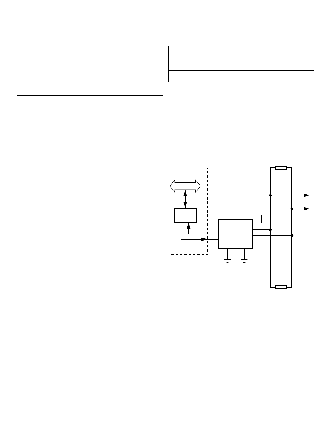
www.national.com 140
CP3BT26
DRIVE The Drive bit shows the output value on the
CANTX pin at the time of the error. Note that
a receiver will not drive the bus except during
ACK and during an active error flag.
19.10.17 CAN Timer Register (CTMR)
The CTMR register reports the current value of the Time
Stamp Counter as described in Section 19.8.
The CTMR register is a free running 16-bit counter. It con-
tains the number of CAN bits recognized by the CAN mod-
ule since the register has been cleared. The counter starts
to increment from the value 0000b after a hardware reset. If
the Timer Stamp Enable bit (TSTPEN) in the CAN global
configuration register (CGCR) is set, the counter will also be
cleared on a message transfer of the message buffer 0.
The contents of CTMR are captured into the Time Stamp
register of the message buffer after successfully sending or
receiving a frame, as described in “Time Stamp Counter” on
page 126.
19.11 SYSTEM START-UP AND MULTI-INPUT
WAKE-UP
After system start-up, all CAN-related registers are in their
reset state. The CAN module can be enabled after all con-
figuration registers are set to their desired value. The follow-
ing initial settings must be made:
Configure the CAN Timing register (CTIM). See “Bit
Time Logic” on page 117.
Configure every buffer to its function as receive/transmit.
See “Buffer Status/Control Register (CNSTAT)” on
page 128.
Set the acceptance filtering masks. See “Acceptance Fil-
tering” on page 119.
Enable the CAN interface. See “CAN Global Configura-
tion Register (CGCR)” on page 133.
Before disabling the CAN module, software must make sure
that no transmission is still pending.
Note: Activity on the CAN bus can wake up the device from
a reduced-power mode by selecting the CANRX pin as an
input to the Multi-Input Wake-Up module. In this case, the
CAN module must not be disabled before entering the re-
duced-power mode. Disabling the CAN module also dis-
ables the CANRX pin. As an alternative, the CANRX pin can
be connected to any other input pin of the Multi-Input Wake-
Up module. This input channel must then be configured to
trigger a wake-up event on a falling edge (if a dominant bit
is represented by a low level). In this case, the CAN module
can be disabled before entering the reduced-power mode.
After waking up, software must enable the CAN module
again. All configuration and buffer registers still contain the
same data they held before the reduced-power mode was
entered.
19.11.1 External Connection
The CAN module uses the CANTX and CANRX pins to con-
nect to the physical layer of the CAN interface. They provide
the functionality described in Table 64.
The logic levels are configurable by the CTX and CRX bits
of the Global Configuration Register CGCR (see “CAN Glo-
bal Configuration Register (CGCR)” on page 133).
19.11.2 Transceiver Connection
An external transceiver chip must be connected between
the CAN block and the bus. It establishes a bus connection
in differential mode and provides the driver and protection
requirements. Figure 64 shows a possible ISO-High-Speed
configuration.
Figure 64. External Transceiver
19.11.3 Timing Requirements
Processing messages and updating message buffers re-
quire a certain number of clock cycles, as shown in
Table 65. These requirements may lead to some restrictions
regarding the Bit Time Logic settings and the overall CAN
performance which are described below in more detail. Wait
cycles need to be added to the cycle count for CPU access
to the object memory as described in CPU Access to CAN
Registers/Memory on page 127. The number of occurrenc-
es per frame is dependent on the number of matching iden-
tifiers.
15 0
CTMR15:0
0
R
Table 64 External CAN Pins
Signal Name Type Description
CANTX Output Transmit data to the CAN bus
CANRX Input Receive data from the CAN bus
CR16CAN
CANRX
CANTX
5REF
4RX
1TX
VCC
VCC
To other
modules
CAN bus
signals
Termination
3
BUS_H 7
BUS_L 6
RS
8
CPU Bus
GND
Transceiver Chip
120
120
2
DS048

141 www.national.com
CP3BT26
The critical path derives from receiving a remote frame,
which triggers the transmission of one or more data frames.
There are a minimum of four bit times in-between two con-
secutive frames. These bit times start at the validation point
of received frame (reception of 6th EOF bit) and end at the
earliest possible transmission start of the next frame, which
is after the third intermission bit at 100% burst bus load.
These four bit times have to be set in perspective with the
timing requirements of the CAN module.
The minimum duration of the four CAN bit times is deter-
mined by the following Bit Time Logic settings:
PSC = PSCmin = 2
TSEG1 = TSEG1min = 2
TSEG2 = TSEG2min = 1
Bit time = Sync + Time Segment 1 + Time Segment 2
= (1 + 2 + 1) tq = 4 tq
= (4 tq × PSC) clock cycles
= (4 tq × 2) clock cycles = 8 clock cycles
For these minimum BTL settings, four CAN bit times take 32
clock cycles.
The following is an example that assumes typical case:
Minimum BTL settings
Reception and copy of a remote frame
Update of one buffer from TX_RTR
Schedule of one buffer from transmit
As outlined in Table 65, the copy process, update, and
scheduling the next transmission gives a total of 17 + 3 + 2
= 22 clock cycles. Therefore under these conditions there is
no timing restriction.
The following example assumes the worst case:
Minimum BTL settings
Reception and copy of a remote frame
Update of the 14 remaining buffers from TX_RTR
Schedule of one buffer for transmit
All these actions in total require 17 + (14 × 3) + 2 = 61 clock
cycles to be executed by the CAN module. This leads to the
limitation of the Bit Time Logic of 61 / 4 = 15.25 clock cycles
per CAN bit as a minimum, resulting in the minimum clock
frequencies listed below. (The frequency depends on the
desired baud rate and assumes the worst case scenario
can occur in the application.)
Table 66 gives examples for the minimum clock frequency in
order to ensure proper functionality at various CAN bus
speeds.
19.11.4 Bit Time Logic Calculation Examples
The calculation of the CAN bus clocks using CKI = 16 MHz
is shown in the following examples. The desired baud rate
for both examples is 1 Mbit/s.
Example 1
PSC = PSC[5:0] + 2 = 0 + 2 = 2
TSEG1 = TSEG1[3:0] + 1 = 3 + 1 = 4
TSEG2 = TSEG2[2:0] + 1 = 2 + 1 = 3
SJW = TSEG2 = 3
Sample point positioned at 62.5% of bit time
Bit time = 125 ns × (1 + 4 + 3 ± 3) = (1 ± 0.375) µs
Bus Clock = 16 MHz / (2 × (1 + 4 + 3)) = 1 Mbit/s (nomi-
nal)
Example 2
PSC = PSC[5:0] + 1 = 2 + 2 = 4
TSEG1 = TSEG1[3:0] + 1 = 1 + 1 = 2
TSEG2 = TSEG2[2:0] + 1 = 0 + 1 = 1
SJW = TSEG2 = 1
Sample point positioned at 75% of bit time
Bit time = 250 ns × (1 + 2 + 1 ± 1) = (1 ± 0.25) µs
Bus Clock = 16 MHz / (2 × (1 + 4 + 3)) = 1Mbit/s (nominal)
19.11.5 Acceptance Filter Considerations
The CAN module provides two acceptance filter masks
GMSK and BMSK, as described in “Acceptance Filtering”
on page 119, “Global Mask Register (GMSKB/GMSKX)” on
page 136, and “Basic Mask Register (BMSKB/BMSKX)” on
page 137. These masks allow filtering of up to 32 bits of the
message object, which includes the standard identifier, the
extended identifier, and the frame control bits RTR, SRR,
and IDE.
19.11.6 Remote Frames
Remote frames can be automatically processed by the CAN
module. However, to fully enable this feature, the RTR/
XRTR bits (for both standard and extended frames) within
the BMSK and/or GMSK register need to be set to “don’t
care”. This is because a remote frame with the RTR bit set
should trigger the transmission of a data frame with the RTR
bit clear and therefore the ID bits of the received message
need to pass through the acceptance filter. The same ap-
plies to transmitting remote frames and switching to receive
the corresponding data frames.
Table 65 CAN Module Internal Timing
Task Cycle
Count
Occurrence/
Frame
Copy hidden buffer to receive
message buffer 17 0–1
Update status from TX_RTR
to TX_ONCE_RTR 30–15
Schedule a message for
transmission 2 0–1
Table 66 Minimum Clock Frequency Requirements
Baud Rate Minimum Clock
Frequency
1 Mbit/sec 15.25 MHz
500 kbit/sec 7.625 MHz
250 kbit/sec 3.81 MHz

www.national.com 142
CP3BT26
19.12 USAGE HINT
Under certain conditions, the CAN module receives a frame
sent by itself, even though the loopback feature is disabled.
Two conditions must be true to cause this malfunction:
A transmit buffer and at least one receive buffer are con-
figured with the same identifier. Assume this identifier is
called ID_RX_TX. With regard to the receive buffer, this
means that the buffer identifier and the corresponding fil-
ter masks are set up in a way that the buffer is able to re-
ceive frames with the identifier ID_RX_TX.
The following sequence of events occurs:
1. A message with the identifier ID_RX_TX from an-
other CAN node is received into the receive buffer.
2. A message with the identifier ID_RX_TX is sent by
the CAN module immediately after the reception
took place.
When these conditions occur, the frame sent by the CAN
module will be copied into the next receive buffer available
for the identifier ID_RX_TX.
If a frame with an identifier different to ID_RX_TX is sent or
received in between events 1 and 2, the problem does not
occur.

143 www.national.com
CP3BT26
20.0 Advanced Audio Interface
The Advanced Audio Interface (AAI) provides a serial syn-
chronous, full duplex interface to codecs and similar serial
devices. The transmit and receive paths may operate asyn-
chronously with respect to each other. Each path uses a 3-
wire interface consisting of a bit clock, a frame synchroniza-
tion signal, and a data signal.
The CPU interface can be either interrupt-driven or DMA. If
the interface is configured for interrupt-driven I/O, data is
buffered in the receive and transmit FIFOs. If the interface is
configured for DMA, the data is buffered in registers.
The AAI is functionally similar to a MotorolaTM Synchronous
Serial Interface (SSI). Compared to a standard SSI imple-
mentation, the AAI interface does not support the so-called
“On-demand Mode”. It also does not allow gating of the shift
clocks, so the receive and transmit shift clocks are always
active while the AAI is enabled. The AAI also does not sup-
port 12- and 24-bit data word length or more than 4 slots
(words) per frame. The reduction of supported modes is ac-
ceptable, because the main purpose of the AAI is to connect
to audio codecs, rather than to other processors (DSPs).
The implementation of a FIFO as a 16-word receive and
transmit buffer is an additional feature, which simplifies
communication and reduces interrupt load. Independent
DMA is provided for each of the four supported audio chan-
nels (slots). The AAI also provides special features and op-
erating modes to simplify gain control in an external codec
and to connect to an ISDN controller through an IOM-2
compatible interface.
20.1 AUDIO INTERFACE SIGNALS
20.1.1 Serial Transmit Data (STD)
The STD pin is used to transmit data from the serial transmit
shift register (ATSR). The STD pin is an output when data is
being transmitted and is in high-impedance mode when no
data is being transmitted. The data on the STD pin changes
on the positive edge of the transmit shift clock (SCK). The
STD pin goes into high-impedance mode on the negative
edge of SCK of the last bit of the data word to be transmit-
ted, assuming no other data word follows immediately. If an-
other data word follows immediately, the STD pin remains
active rather than going to the high-impedance mode.
20.1.2 Serial Transmit Clock (SCK)
The SCK pin is a bidirectional signal that provides the serial
shift clock. In asynchronous mode, this clock is used only by
the transmitter to shift out data on the positive edge. The se-
rial shift clock may be generated internally or it may be pro-
vided by an external clock source. In synchronous mode,
the SCK pin is used by both the transmitter and the receiver.
Data is shifted out from the STD pin on the positive edge,
and data is sampled on the SRD pin on the negative edge.
20.1.3 Serial Transmit Frame Sync (SFS)
The SFS pin is a bidirectional signal which provides frame
synchronization. In asynchronous mode, this signal is used
as frame sync only by the transmitter. In synchronous mode,
this signal is used as frame sync by both the transmitter and
receiver. The frame sync signal may be generated internally,
or it may be provided by an external source.
20.1.4 Serial Receive Data (SRD)
The SRD pin is used as an input when data is shifted into
the Audio Receive Shift Register (ARSR). In asynchronous
mode, data on the SRD pin is sampled on the negative edge
of the serial receive shift clock (SRCLK). In synchronous
mode, data on the SRD pin is sampled on the negative edge
of the serial shift clock (SCK). The data is shifted into ARSR
with the most significant bit (MSB) first.
20.1.5 Serial Receive Clock (SRCLK)
The SRCLK pin is a bidirectional signal that provides the re-
ceive serial shift clock in asynchronous mode. In this mode,
data is sampled on the negative edge of SRCLK. The SR-
CLK signal may be generated internally or it may be provid-
ed by an external clock source. In synchronous mode, the
SCK pin is used as shift clock for both the receiver and
transmitter, so the SRCLK pin is available for use as a gen-
eral-purpose port pin or an auxiliary frame sync signal to ac-
cess multiple slave devices (e.g. codecs) within a network
(see Network mode).
20.1.6 Serial Receive Frame Sync (SRFS)
The SRFS pin is a bidirectional signal that provides frame
synchronization for the receiver in asynchronous mode. The
frame sync signal may be generated internally, or it may be
provided by an external source. In synchronous mode, the
SFS signal is used as the frame sync signal for both the
transmitter and receiver, so the SRFS pin is available for use
as a general-purpose port pin or an auxiliary frame sync sig-
nal to access multiple slave devices (e.g. codecs) within a
network (see Network mode).
20.2 AUDIO INTERFACE MODES
There are two clocking modes: asynchronous mode and
synchronous mode. These modes differ in the source and
timing of the clock signals used to transfer data. When the
AAI is generating the bit shift clock and frame sync signals
internally, synchronous mode must be used.
There are two framing modes: normal mode and network
mode. In normal mode, one word is transferred per frame.
In network mode, up to four words are transferred per frame.
A word may be 8 or 16 bits. The part of the frame which car-
ries a word is called a slot. Network mode supports multiple
external devices sharing the interface, in which each device
is assigned its own slot. Separate frame sync signals are
provided, so that each device is triggered to send or receive
its data during its assigned slot.
20.2.1 Asynchronous Mode
In asynchronous mode, the receive and transmit paths of
the audio interface operate independently, with each path
using its own bit clock and frame sync signal. Independent
clocks for receive and transmit are only used when the bit
clock and frame sync signal are supplied externally. If the bit
clock and frame sync signals are generated internally, both
paths derive their clocks from the same set of clock prescal-
ers.
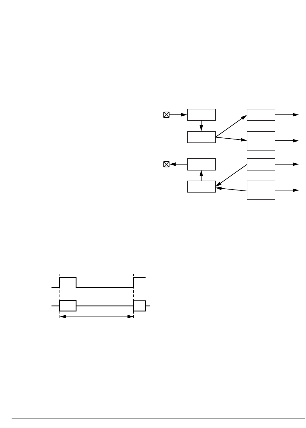
www.national.com 144
CP3BT26
20.2.2 Synchronous Mode
In synchronous mode, the receive and transmit paths of the
audio interface use the same shift clock and frame sync sig-
nal. The bit shift clock and frame sync signal for both paths
are derived from the same set of clock prescalers.
20.2.3 Normal Mode
In normal mode, each rising edge on the frame sync signal
marks the beginning of a new frame and also the beginning
of a new slot. A slot does not necessarily occupy the entire
frame. (A frame can be longer than the data word transmit-
ted after the frame sync pulse.) Typically, a codec starts
transmitting a fixed length data word (e.g. 8-bit log PCM da-
ta) with the frame sync signal, then the codec’s transmit pin
returns to the high-impedance state for the remainder of the
frame.
The Audio Receive Shift Register (ARSR) de-serializes re-
ceived on the SRD pin (serial receiver data). Only the data
sampled after the frame sync signal are treated as valid. If
the interface is interrupt-driven, valid data bits are trans-
ferred from the ARSR to the receive FIFO. If the interface is
configured for DMA, the data is transferred to the receive
DMA register 0 (ARDR0).
The serial transmit data (STD) pin is only an active output
while data is shifted out. After the defined number of data
bits have been shifted out, the STD pin returns to the high-
impedance state.
For operation in normal mode, the Slot Count Select bits
(SCS[1:0]) in the Global Configuration register (AGCR)
must be loaded with 00b (one slot per frame). In addition,
the Slot Assignment bits for receive and transmit must be
programmed to select slot 0.
If the interface is configured for DMA, the DMA slot assign-
ment bits must also be programmed to select slot 0. In this
case, the audio data is transferred to or from the receive or
transmit DMA register 0 (ARDR0/ATDR0).
Figure 65 shows the frame timing while operating in normal
mode with a long frame sync interval.
Figure 65. Normal Mode Frame
IRQ Support
If the receiver interface is configured for interrupt-driven I/O
(RXDSA0 = 0), all received data are loaded into the receive
FIFO. An IRQ is asserted as soon as the number of data
bytes or words in the receive FIFO is greater than a pro-
grammable warning limit.
If the transmitter interface is configured for interrupt-driven
I/O (TXDSA0 = 0), all data to be transmitted is read from the
transmit FIFO. An IRQ is asserted as soon as the number
data bytes or words available in the transmit FIFO is equal
or less than a programmable warning limit.
DMA Support
If the receiver interface is configured for DMA (RXDSA0 =
1), received data is transferred from the ARSR into the DMA
receive buffer 0 (ARDR0). A DMA request is asserted when
the ARDR0 register is full. If the transmitter interface is con-
figured for DMA (TXDSA0 = 1), data to be transmitted are
read from the DMA transmit buffer 0 (ATDR0). A DMA re-
quest is asserted to the DMA controller when the ATDR0
register is empty.
Figure 66 shows the data flow for IRQ and DMA mode in
normal Mode.
Figure 66. IRQ/DMA Support in Normal Mode
Network Mode
In network mode, each frame is composed of multiple slots.
Each slot may transfer 8 or 16 bits. All of the slots in a frame
must have the same length. In network mode, the sync sig-
nal marks the beginning of a new frame. Only frames with
up to four slots are supported by this audio interface.
More than two devices can communicate within a network
using the same clock and data lines. The devices connected
to the same bus use a time-multiplexed approach to share
access to the bus. Each device has certain slots assigned
to it, in which only that device is allowed to transfer data.
One master device provides the bit clock and the frame sync
signal(s). On all other (slave) devices, the bit clock and
frame sync pins are inputs.
Up to four slots can be assigned to the interface, as it sup-
ports up to four slots per frame. Any other slots within the
frame are reserved for other devices.
The transmitter only drives data on the STD pin during slots
which have been assigned to this interface. During all other
slots, the STD output is in high-impedance mode, and data
can be driven by other devices. The assignment of slots to
the transmitter is specified by the Transmit Slot Assignment
bits (TXSA) in the ATCR register. It can also be specified
whether the data to be transmitted is transferred from the
transmit FIFO or the corresponding DMA transmit register.
There is one DMA transmit register (ATDRn) for each of the
maximum four data slots. Each slot can be configured inde-
pendently.
Long Frame Sync
(SFS/SRFS)
Shift Data
(STD/SRD) Data High-impedance
Frame
Data
DS053
DMA Slot
Assignment
TXDSA = 1
TXDSA = 0
ARSR
SRD
RX
FIFO
ARDR 0
DMA
Request 1
IRQ
DMA Slot
Assignment
RXDSA = 1
RXDSA = 0
ATSR
STD
TX
FIFO
ATDR 0
DMA
Request 0
IRQ
DS054
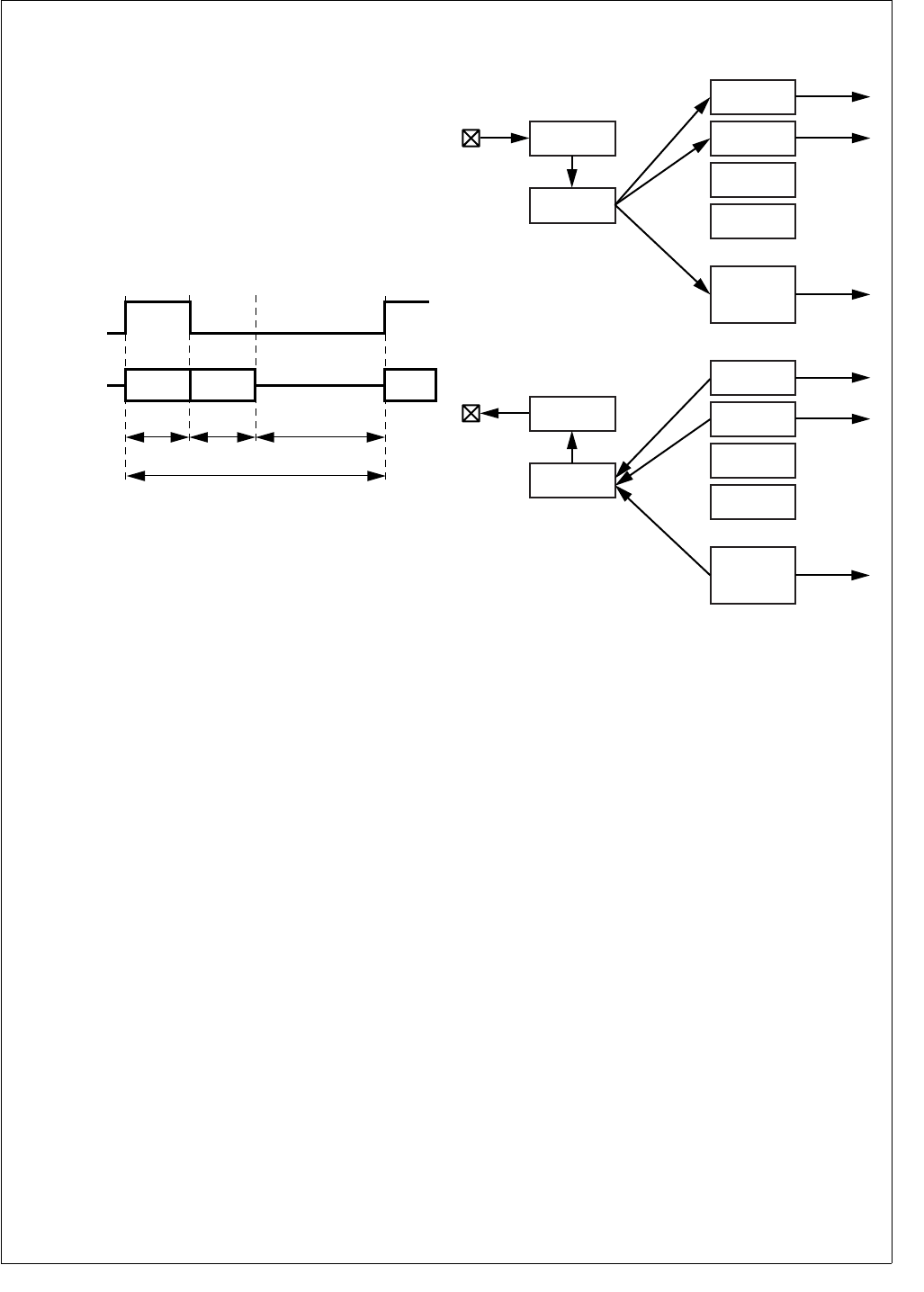
145 www.national.com
CP3BT26
On the receiver side, only the valid data bits which were re-
ceived during the slots assigned to this interface are copied
into the receive FIFO or DMA registers. The assignment of
slots to the receiver is specified by the Receive Slot Assign-
ment bits (RXSA) in the ATCR register. It can also be spec-
ified whether the received data is copied into the receive
FIFO or into the corresponding DMA receive register. There
is one DMA receive register (ARDRn) for each of the maxi-
mum four data slots. Each slot may be configured individu-
ally.
Figure 67 shows the frame timing while operating in network
mode with four slots per frame, slot 1 assigned to the inter-
face, and a long frame sync interval.
Figure 67. Network Mode Frame
IRQ Support
If DMA is not enabled for a receive slot n (RXDSAn = 0), all
data received in this slot is loaded into the receive FIFO. An
IRQ is asserted as soon as the number of data bytes or
words in the receive FIFO is greater than a configured warn-
ing limit.
If DMA is not enabled for a transmit slot n (TXDSAn = 0), all
data to be transmitted in this slot are read from the transmit
FIFO. An IRQ is asserted as soon as the number data bytes
or words available in the transmit FIFO is equal or less than
a configured warning limit.
DMA Support
If DMA support is enabled for a receive slot n (RXDSA0 =
1), all data received in this slot is only transferred from the
ARSR into the corresponding DMA receive register
(ARDRn). A DMA request is asserted when the ARDRn reg-
ister is full.
If DMA is enabled for a transmit slot n (TXDSAn = 1), all data
to be transmitted in slot n are read from the corresponding
DMA transmit register (ATDRn). A DMA request is asserted
to the DMA controller when the ATDRn register is empty.
Figure 68 illustrates the data flow for IRQ and DMA support
in network mode, using four slots per frame and DMA sup-
port enabled for slots 0 and 1 in receive and transmit direc-
tion.
Figure 68. IRQ/DMA Support in Network Mode
If the interface operates in synchronous mode, the receiver
uses the transmit bit clock (SCK) and transmit frame sync
signal (SFS). This allows the pins used for the receive bit
clock (SRCLK) and receive frame sync (SRFS) to be used
as additional frame sync signals in network mode. The extra
frame sync signals are useful when the audio interface com-
municates to more than one codec, because codecs typical-
ly start transmission immediately after the frame sync pulse.
The SRCLK pin is driven with a frame sync pulse at the be-
ginning of the second slot (slot 1), and the SRFS pin is driv-
en with a frame sync pulse at the beginning of slot 2.
Figure 69 shows a frame timing diagram for this configura-
tion, using the additional frame sync signals on SRCLK and
SRFS to address up to three devices.
Shift Data
(STD/SRD)
High-impedance
Unused SlotsSlot1
Frame
Slot0
Long Frame Sync
(SFS/SRFS)
Data
(ignored)
Data
(ignored)
Data
(valid)
DS055
DMA Slot
Assignment
Slot 1 data
Slot 0 data
Slot 2 and 3 data
ARSR
SRD
ARDR 0
DMA
Request 1
ARDR 1
DMA
Request 3
ARDR 2
ARDR 3
RX
FIFO
IRQ
DMA Slot
Assignment
Slot 1 data
Slot 0 data
ATSR
STD
ATDR 0
DMA
Request 0
ATDR 1
DMA
Request 2
ATDR 2
ATDR 3
TX
FIFO
IRQ
Slot 2 and 3 data
DS056

www.national.com 146
CP3BT26
Figure 69. Accessing Three Devices in Network Mode
20.3 BIT CLOCK GENERATION
An 8-bit prescaler is provided to divide the audio interface
input clock down to the required bit clock rate. Software can
choose between two input clock sources, a primary and a
secondary clock source.
On the CP3BT26, the two optional input clock sources are
the 12-MHz Aux1 clock (also used for the Bluetooth LLC)
and the 48-MHz PLL output clock (also used by the USB
node). The input clock is divided by the value of the prescal-
er BCPRS[7:0] + 1 to generate the bit clock.
The bit clock rate fbit can be calculated by the following
equation:
fbit = n × fSample × Data Length
n = Number of Slots per Frame
fSample = Sample Frequency in Hz
Data Length = Length of data word in multiples of 8 bits
The ideal required prescaler value Pideal can be calculated
as follows:
Pideal = fAudio In / fbit
The real prescaler must be set to an integer value, which
should be as close as possible to the ideal prescaler value,
to minimize the bit clock error, fbit_error.
f
bit_error [%] = (fbit - fAudio In/Preal) / fbit × 100
Example:
The audio interface is used to transfer 13-bit linear PCM
data for one audio channel at a sample rate of 8k samples
per second. The input clock of the audio interface is 12 MHz.
Furthermore, the codec requires a minimum bit clock of 256
kHz to operate properly. Therefore, the number of slots per
frame must be set to 2 (network mode) although actually
only one slot (slot 0) is used. The codec and the audio inter-
face will put their data transmit pins in TRI-STATE mode af-
ter the PCM data word has been transferred. The required
bit clock rate fbit can be calculated by the following equation:
fbit = n × fSample × Data Length = 2 × 8 kHz × 16 = 256 kHz
The ideal required prescaler value Pideal can be calculated
as follows:
Pideal = fAudio In / fbit = 12 MHz / 256 kHz = 46.875
Therefore, the real prescaler value is 47. This results in a bit
clock error equal to:
fbit_error = (fbit - fAudio In/Preal) / fbit × 100
= (256 kHz - 12 MHz/47) / 256 kHz × 100 = 0.27%
20.4 FRAME CLOCK GENERATION
The clock for the frame synchronization signals is derived
from the bit clock of the audio interface. A 7-bit prescaler is
used to divide the bit clock to generate the frame sync clock
for the receive and transmit operations. The bit clock is di-
vided by FCPRS + 1. In other words, the value software
must write into the ACCR.FCPRS field is equal to the bit
number per frame minus one. The frame may be longer than
the valid data word but it must be equal to or larger than the
8- or 16-bit word. Even if 13-, 14-, or 15-bit data is being
used, the frame width must always be at least 16 bits wide.
In addition, software can specify the length of a long frame
sync signal. A long frame sync signal can be either 6, 13,
14, 15, or 16 bits long, depending on the external codec be-
ing used. The frame sync length can be configured by the
Frame Sync Length field (FSL) in the AGCR register.
20.5 AUDIO INTERFACE OPERATION
20.5.1 Clock Configuration
The Aux1 clock (generated by the Clock module described
in Section 11.9) must be configured, because it is the time
base for the AAI module. Software must write an appropri-
ate divisor to the ACDIV1 field of the PRSAC register to pro-
vide a 12 MHz input clock. Software also must enable the
Aux1 clock by setting the ACE1 bit in the CRCTRL register.
For example:
PRSAC &= 0xF0;
// Set Aux1 prescaler to 1 (F = 12 MHz)
CRCTRL |= ACE1; // Enable Aux1 clk
20.5.2 Interrupts
The interrupt logic of the AAI combines up to four interrupt
sources and generates one interrupt request signal to the
Interrupt Control Unit (ICU).
The four interrupt sources are:
RX FIFO Overrun - ASCR.RXEIP = 1
RX FIFO Almost Full (Warning Level) - ASCR.RXIP = 1
TX FIFO Under run - ASCR.TXEIP = 1
TX FIFO Almost Empty (Warning Level) - ASCR.TXIP=1
In addition to the dedicated input to the ICU for handling
these interrupt sources, the Serial Frame Sync (SFS) signal
is an input to the MIWU (see Section 13.0), which can be
programmed to generate edge-triggered interrupts.
Slot1
Frame
Slot0
SFS
SRCLK
(auxiliary
frame sync)
SRFS
(auxiliary
frame sync)
STD/SRD Data from/to
Codec 1
Data from/to
Codec 3
Data from/to
Codec 2
Slot2 Slot2
DS057
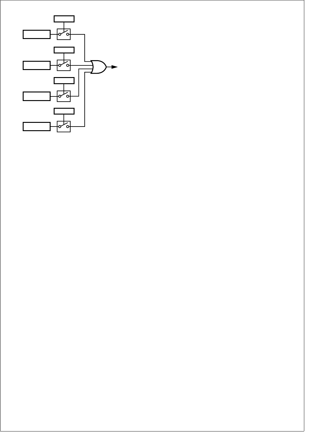
147 www.national.com
CP3BT26
Figure 70 shows the interrupt structure of the AAI.
Figure 70. AAI Interrupt Structure
20.5.3 Normal Mode
In normal mode, each frame sync signal marks the begin-
ning of a new frame and also the beginning of a new slot,
since each frame only consists of one slot. All 16 receive
and transmit FIFO locations hold data for the same (and
only) slot of a frame. If 8-bit data are transferred, only the
low byte of each 16-bit FIFO location holds valid data.
20.5.4 Transmit
Once the interface has been enabled, transmit transfers are
initiated automatically at the beginning of every frame. The
beginning of a new frame is identified by a frame sync pulse.
Following the frame sync pulse, the data is shifted out from
the ATSR to the STD pin on the positive edge of the transmit
data shift clock (SCK).
DMA Operation
When a complete data word has been transmitted through
the STD pin, a new data word is reloaded from the transmit
DMA register 0 (ATDR0). A DMA request is asserted when
the ATDR0 register is empty. If a new data word must be
transmitted while the ATDR0 register is still empty, the pre-
vious data will be re-transmitted.
FIFO Operation
When a complete data word has been transmitted through
the STD pin, a new data word is loaded from the transmit
FIFO from the current location of the Transmit FIFO Read
Pointer (TRP). After that, the TRP is automatically incre-
mented by 1.
A write to the Audio Transmit FIFO Register (ATFR) results
in a write to the transmit FIFO at the current location of the
Transmit FIFO Write Pointer (TWP). After every write oper-
ation to the transmit FIFO, TWP is automatically increment-
ed by 1.
When the TRP is equal to the TWP and the last access to
the FIFO was a read operation (a transfer to the ATSR), the
transmit FIFO is empty. When an additional read operation
from the FIFO to ATSR is performed (while the FIFO is al-
ready empty), a transmit FIFO underrun occurs. In this
event, the read pointer (TRP) will be decremented by 1 (in-
cremented by 15) and the previous data word will be trans-
mitted again. A transmit FIFO underrun is indicated by the
TXU bit in the Audio Interface Transmit Status and Control
Register (ATSCR). Also, no transmit interrupt will be gener-
ated (even if enabled).
When the TRP is equal to the TWP and the last access to
the FIFO was a write operation (to the ATFR), the FIFO is
full. If an additional write to ATFR is performed, a transmit
FIFO overrun occurs. This error condition is not prevented
by hardware. Software must ensure that no transmit overrun
occurs.
The transmit frame synchronization pulse on the SFS pin
and the transmit shift clock on the SCK pin may be generat-
ed internally, or they can be supplied by an external source.
20.5.5 Receive
At the receiver, the received data on the SRD pin is shifted
into ARSR on the negative edge of SRCLK (or SCK in syn-
chronous mode), following the receive frame sync pulse,
SRFS (or SFS in synchronous mode).
DMA Operation
When a complete data word has been received through the
SRD pin, the new data word is copied to the receive DMA
register 0 (ARDR0). A DMA request is asserted when the
ARDR0 register is full. If a new data word is received while
the ARDR0 register is still full, the ARDR0 register will be
overwritten with the new data.
FIFO Operation
When a complete word has been received, it is transferred
to the receive FIFO at the current location of the Receive
FIFO Write Pointer (RWP). Then, the RWP is automatically
incremented by 1.
A read from the Audio Receive FIFO Register (ARFR) re-
sults in a read from the receive FIFO at the current location
of the Receive FIFO Read Pointer (RRP). After every read
operation from the receive FIFO, the RRP is automatically
incremented by 1.
When the RRP is equal to the RWP and the last access to
the FIFO was a copy operation from the ARFR, the receive
FIFO is full. When a new complete data word has been shift-
ed into ARSR while the receive FIFO was already full, the
shift register overruns. In this case, the new data in the
ARSR will not be copied into the FIFO and the RWP will not
be incremented. A receive FIFO overrun is indicated by the
RXO bit in the Audio Interface Receive Status and Control
Register (ARSCR). No receive interrupt will be generated
(even if enabled).
When the RWP is equal to the RRP and the last access to
the receive FIFO was a read from the ARFR, a receive FIFO
underrun has occurred. This error condition is not prevented
by hardware. Software must ensure that no receive under-
run occurs.
The receive frame synchronization pulse on the SRFS pin
(or SFS in synchronous mode) and the receive shift clock on
the SRCLK (or SCK in synchronous mode) may be gener-
ated internally, or they can be supplied by an external
source.
AAI
Interrupt
RXEIP = 1
RXEIE
TXIP = 1
TXIE
TXEIP = 1
TXEIE
DS155
RXIP = 1
RXIE

www.national.com 148
CP3BT26
20.5.6 Network Mode
In network mode, each frame sync signal marks the begin-
ning of new frame. Each frame can consist of up to four
slots. The audio interface operates in a similar way to nor-
mal mode, however, in network mode the transmitter and re-
ceiver can be assigned to specific slots within each frame as
described below.
20.5.7 Transmit
The transmitter only shifts out data during the assigned slot.
During all other slots the STD output is in TRI-STATE mode.
DMA Operation
When a complete data word has been transmitted through
the STD pin, a new data word is reloaded from the corre-
sponding transmit DMA register n (ATDRn). A DMA request
is asserted when ATDRn is empty. If a new data word must
be transmitted in a slot n while ATDRn is still empty, the pre-
vious slot n data will be retransmitted.
FIFO Operation
When a complete data word has been transmitted through
the STD pin, a new data word is reloaded from the transmit
FIFO from the current location of the Transmit FIFO Read
Pointer (TRP). After that, the TRP is automatically incre-
mented by 1. Therefore, the audio data to be transmitted in
the next slot of the frame is read from the next FIFO loca-
tion.
A write to the Audio Transmit FIFO Register (ATFR) results
in a write to the transmit FIFO at the current location of the
Transmit FIFO Write Pointer (TWP). After every write oper-
ation to the transmit FIFO, the TWP is automatically incre-
mented by 1.
When the TRP is equal to the TWP and the last access to
the FIFO was a read operation (transfer to the ATSR), the
transmit FIFO is empty. When an additional read operation
from the FIFO to the ATSR is performed (while the FIFO is
already empty), a transmit FIFO underrun occurs. In this
case, the read pointer (TRP) will be decremented by 1 (in-
cremented by 15) and the previous data word will be trans-
mitted again. A transmit FIFO underrun is indicated by the
TXU bit in the Audio Interface Transmit Status and Control
Register (ATSCR). No transmit interrupt will be generated
(even if enabled).
If the current TRP is equal to the TWP and the last access
to the FIFO was a write operation (to the ATFR), the FIFO is
full. If an additional write to the ATFR is performed, a trans-
mit FIFO overrun occurs. This error condition is not prevent-
ed by hardware. Software must ensure that no transmit
overrun occurs.
The transmit frame synchronization pulse on the SFS pin
and the transmit shift clock on the SCK pin may be generat-
ed internally, or they can be supplied by an external source.
20.5.8 Receive
The receive shift register (ARSR) receives data words of all
slots in the frame, regardless of the slot assignment of the
interface. However, only those ARSR contents are trans-
ferred to the receive FIFO or DMA receive register which
were received during the assigned time slots. A receive in-
terrupt or DMA request is initiated when this occurs.
DMA Operation
When a complete data word has been received through the
SRD pin in a slot n, the new data word is transferred to the
corresponding receive DMA register n (ARDRn). A DMA re-
quest is asserted when the ARDRn register is full. If a new
slot n data word is received while the ARDRn register is still
full, the ARDRn register will be overwritten with the new da-
ta.
FIFO Operation
When a complete word has been received, it is transferred
to the receive FIFO at the current location of the Receive
FIFO Write Pointer (RWP). After that, the RWP is automati-
cally incremented by 1. Therefore, data received in the next
slot is copied to the next higher FIFO location.
A read from the Audio Receive FIFO Register (ARFR) re-
sults in a read from the receive FIFO at the current location
of the Receive FIFO Read Pointer (RRP). After every read
operation from the receive FIFO, the RRP is automatically
incremented by 1.
When the RRP is equal to the RWP and the last access to
the FIFO was a transfer to the ARFR, the receive FIFO is
full. When a new complete data word has been shifted into
the ARSR while the receive FIFO was already full, the shift
register overruns. In this case, the new data in the ARSR will
not be transferred to the FIFO and the RWP will not be in-
cremented. A receive FIFO overrun is indicated by the RXO
bit in the Audio Interface Receive Status and Control Regis-
ter (ARSCR). No receive interrupt will be generated (even if
enabled).
When the current RWP is equal to the TWP and the last ac-
cess to the receive FIFO was a read from ARFR, a receive
FIFO underrun has occurred. This error condition is not pre-
vented by hardware. Software must ensure that no receive
underrun occurs.
The receive frame synchronization pulse on the SRFS pin
(or SFS in synchronous mode) and the receive shift clock on
the SRCLK (or SCK in synchronous mode) may be gener-
ated internally, or they can be supplied by an external
source.
20.6 COMMUNICATION OPTIONS
20.6.1 Data Word Length
The word length of the audio data can be selected to be ei-
ther 8 or 16 bits. In 16-bit mode, all 16 bits of the transmit
and receive shift registers (ATSR and ARSR) are used. In 8-
bit mode, only the lower 8 bits of the transmit and receive
shift registers (ATSR and ARSR) are used.
20.6.2 Frame Sync Signal
The audio interface can be configured to use either long or
short frame sync signals to mark the beginning of a new
data frame. If the corresponding Frame Sync Select (FSS)
bit in the Audio Control and Status register is clear, the re-
ceive and/or transmit path generates or recognizes short
frame sync pulses with a length of one bit shift clock period.
When these short frame sync pulses are used, the transfer
of the first data bit or the first slot begins at the first positive
edge of the shift clock after the negative edge on the frame
sync pulse.
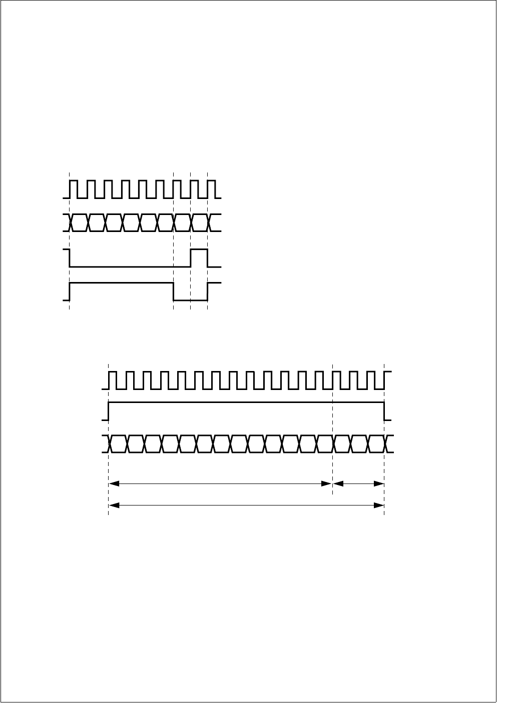
149 www.national.com
CP3BT26
If the corresponding Frame Sync Select (FSS) bit in the Au-
dio Control and Status register is set, the receive and/or
transmit path generates or recognizes long frame sync puls-
es. For 8-bit data, the frame sync pulse generated will be 6
bit shift clock periods long, and for 16-bit data the frame
sync pulse can be configured to be 13, 14, 15, or 16 bit shift
clock periods long. When receiving frame sync, it should be
active on the first bit of data and stay active for a least two
bit clock periods. It must go low for at least one bit clock pe-
riod before starting a new frame. When long frame sync
pulses are used, the transfer of the first word (first slot) be-
gins at the first positive edge of the bit shift clock after the
positive edge of the frame sync pulse. Figure 71 shows ex-
amples of short and long frame sync pulses.
Figure 71. Short and Long Frame Sync Pulses
Some codecs require an inverted frame sync signal. This is
available by setting the Inverted Frame Sync bit in the
AGCR register.
20.6.3 Audio Control Data
The audio interface provides the option to fill a 16-bit slot
with up to three data bits if only 13, 14, or 15 PCM data bits
are transmitted. These additional bits are called audio con-
trol data and are appended to the PCM data stream. The
AAI can be configured to append either 1, 2, or 3 audio con-
trol bits to the PCM data stream. The number of audio data
bits to be used is specified by the 2-bit Audio Control On
(ACO) field. If the ACO field is not equal to 0, the specified
number of bits are taken from the Audio Control Data field
(ACD) and appended to the data stream during every trans-
mit operation. The ADC0 bit is the first bit added to the
transmit data stream after the last PCM data bit. Typically,
these bits are used for gain control, if this feature is support-
ed by the external PCM codec.Figure 72 shows a 16-bit slot
comprising a 13-bit PCM data word plus three audio control
bits.
Figure 72. Audio Slot with Audio Control Data
D7D6D5D4D3D2D1D0
Long Frame
Sync Pulse
Bit Shift Clock
(SCK/SRCLK)
Shift Data
(STD/SRD)
DS156
Short Frame
Sync Pulse
D7D6D5D4D3D2D1D0
SCK
STD
DS161
SFS
ACD0ACD1ACD2D12D11D10D9D8
13-bit PCM Data Word
Audio
Control
Bits
16-bit Slot
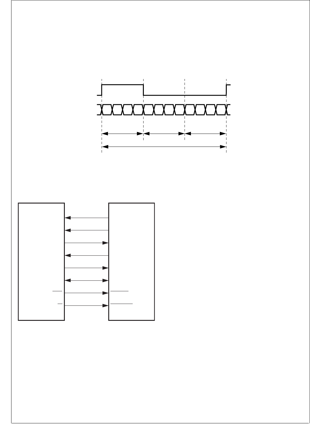
www.national.com 150
CP3BT26
20.6.4 IOM-2 Mode
The AAI can operate in a special IOM-2 compatible mode to
allow to connect to an external ISDN controller device. In
this IOM-2 mode, the AAI can only operate as a slave, i.e.
the bit clock and frame sync signal is provided by the ISDN
controller. The AAI only supports the B1 and B2 data of the
IOM-2 channel 0, but ignores the other two IOM-2 channels.
The AAI handles the B1 and B2 data as one 16-bit data
word.
The IOM-2 interface has the following properties:
Bit clock of 1536 kHz (output from the ISDN controller)
Frame repetition rate of 8 ksps (output from the ISDN
controller)
Double-speed bit clock (one data bit is two bit clocks
wide)
B1 and B2 data use 8-bit log PCM format
Long frame sync pulse
Figure 73 shows the structure of an IOM-2 Frame.
Figure 73. IOM-2 Frame Structure
Figure 74 shows the connections between an ISDN control-
ler and a CP3BT26 using a standard IOM-2 interface for the
B1/B2 data communication and the external bus interface
(IO Expansion) for controlling the ISDN controller.
Figure 74. CP3BT26/ISDN Controller Connections
To connect the AAI to an ISDN controller through an IOM-2
compatible interface, the AAI needs to be configured in this
way:
The AAI must be in IOM-2 Mode (AGCR.IOM2 = 1).
The AAI operates in synchronous mode (AGCR.ASS =
0).
The AAI operates as a slave, therefore the bit clock and
frame sync source selection must be set to external
(ACGR.IEFS = 1, ACGR.IEBC = 1).
The frame sync length must be set to long frame sync
(ACGR.FSS = 1).
The data word length must be set to 16-bit (AGCR.DWL
= 1).
The AAI must be set to normal mode (AGCR.SCS[1:0] =
0).
The internal frame rate must be 8 ksps (ACCR = 00BE).
20.6.5 Loopback Mode
In loopback mode, the STD and SRD pins are internally
connected together, so data shifted out through the ATSR
register will be shifted into the ARSR register. This mode
may be used for development, but it also allows testing the
transmit and receive path without external circuitry, for ex-
ample during Built-In-Self-Test (BIST).
CMIC2IC1CMB2B1
STD/SRD
DS162
SFS
C
IOM-2 Channel 0
IOM-2 Frame (125 µs)
IOM-2 Channel 1 IOM-2 Channel 2
C
P
3B
T
2
x
IS
DN
C
on
t
r
oll
e
r
SCK Bit Clock
DS241
SFS Frame Sync
STD Data In
SRD Data Out
A[7:0] Address
D[7:0] Data
SELIO Chip Select
RD Output Enable

151 www.national.com
CP3BT26
20.6.6 Freeze Mode
The audio interface provides a FREEZE input, which allows
to freeze the status of the audio interface while a develop-
ment system examines the contents of the FIFOs and reg-
isters.
When the FREEZE input is asserted, the audio interface be-
haves as follows:
The receive FIFO or receive DMA registers are not up-
dated with new data.
The receive status bits (RXO, RXE, RXF, and RXAF) are
not changed, even though the receive FIFO or receive
DMA registers are read.
The transmit shift register (ATSR) is not updated with
new data from the transmit FIFO or transmit DMA regis-
ters.
The transmit status bits (TXU, TXF, TXE, and TXAE) are
not changed, even though the transmit FIFO or transmit
DMA registers are written.
The time at which these registers are frozen will vary be-
cause they operate from a different clock than the one used
to generate the freeze signal.
20.7 AUDIO INTERFACE REGISTERS
Table 67 Audio Interface Registers
Name Address Description
ARFR FF FD40h Audio Receive FIFO
Register
ARDR0 FF FD42h Audio Receive DMA
Register 0
ARDR1 FF FD44h Audio Receive DMA
Register 1
ARDR2 FF FD46h Audio Receive DMA
Register 2
ARDR3 FF FD48h Audio Receive DMA
Register 3
ATFR FF FD4Ah Audio Transmit FIFO
Register
ATDR0 FF FD4Ch Audio Transmit DMA
Register 0
ATDR1 FF FD4Eh Audio Transmit DMA
Register 1
ATDR2 FF FD50h Audio Transmit DMA
Register 2
ATDR3 FF FD52h Audio Transmit DMA
Register 3
AGCR FF FD54h Audio Global
Configuration Register
AISCR FF FD56h Audio Interrupt Status
and Control Register
ARSCR FF FD58h Audio Receive Status
and Control Register
ATSCR FF FD5Ah Audio Transmit Status
and Control Register
ACCR FF FD5Ch Audio Clock Control
Register
ADMACR FF FD5Eh Audio DMA Control
Register

www.national.com 152
CP3BT26
20.7.1 Audio Receive FIFO Register (ARFR)
The Audio Receive FIFO register shows the receive FIFO
location currently addressed by the Receive FIFO Read
Pointer (RRP). The receive FIFO receives 8-bit or 16-bit
data from the Audio Receive Shift Register (ARSR), when
the ARSR is full.
In 8-bit mode, only the lower byte of the ARFR is used, and
the upper byte contains undefined data. In 16-bit mode, a
16-bit word is copied from ARSR into the receive FIFO. The
CPU bus master has read-only access to the receive FIFO,
represented by the ARFR register. After reset, the receive
FIFO (ARFR) contains undefined data.
ARFL The Audio Receive FIFO Low Byte shows the
lower byte of the receive FIFO location cur-
rently addressed by the Receive FIFO Read
Pointer (RRP).
ARFH The Audio Receive FIFO High Byte shows the
upper byte of the receive FIFO location cur-
rently addressed by the Receive FIFO Read
Pointer (RRP). In 8-bit mode, ARFH contains
undefined data.
20.7.2 Audio Receive DMA Register n (ARDRn)
The ARDRn register contains the data received within slot
n, assigned for DMA support. In 8-bit mode, only the lower
8-bit portion of the ARDRn register is used, and the upper
byte contains undefined data. In 16-bit mode, a 16-bit word
is transferred from the Audio Receive Shift Register (ARSR)
into the ARDRn register. The CPU bus master, typically a
DMA controller, has read-only access to the receive DMA
registers. After reset, these registers are clear.
ARDL The Audio Receive DMA Low Byte field re-
ceives the lower byte of the audio data copied
from the ARSR.
ARDH In 16-bit mode, the Audio Receive DMA High
Byte field receives the upper byte of the audio
data word copied from ARSR. In 8-bit mode,
the ARDH register holds undefined data.
20.7.3 Audio Transmit FIFO Register (ATFR)
The ATFR register shows the transmit FIFO location cur-
rently addressed by the Transmit FIFO Write Pointer (TWP).
The Audio Transmit Shift Register (ATSR) receives 8-bit or
16-bit data from the transmit FIFO, when the ATSR is empty.
In 8-bit mode, only the lower 8-bit portion of the ATSR is
used, and the upper byte is ignored (not transferred into the
ATSR). In 16-bit mode, a 16-bit word is copied from the
transmit FIFO into the ATSR. The CPU bus master has
write-only access to the transmit FIFO, represented by the
ATFR register. After reset, the transmit FIFO (ATFR) con-
tains undefined data.
ATFL The Audio Transmit Low Byte field represents
the lower byte of the transmit FIFO location
currently addressed by the Transmit FIFO
Write Pointer (TWP).
ATFH In 16-bit mode, the Audio Transmit FIFO High
Byte field represents the upper byte of the
transmit FIFO location currently addressed by
the Transmit FIFO Write Pointer (TWP). In 8-
bit mode, the ATFH field is not used.
20.7.4 Audio Transmit DMA Register n (ATDRn)
The ATDRn register contains the data to be transmitted in
slot n, assigned for DMA support. In 8-bit mode, only the
lower 8-bit portion of the ATDRn register is used, and the
upper byte is ignored (not transferred into the ATSR). In 16-
bit mode, the whole 16-bit word is transferred into the ATSR.
The CPU bus master, typically a DMA controller, has write-
only access to the transmit DMA registers. After reset, these
registers are clear.
ATDL The Audio Transmit DMA Low Byte field holds
the lower byte of the audio data.
ATDH In 16-bit mode, the Audio Transmit DMA High
Byte field holds the upper byte of the audio
data word. In 8-bit mode, the ATDH field is ig-
nored.
7 0
ARFL
15 8
ARFH
7 0
ARDL
15 8
ARDH
7 0
ATF L
15 8
ATF H
7 0
ATDL
15 8
ATD H

153 www.national.com
CP3BT26
20.7.5 Audio Global Configuration Register (AGCR)
The AGCR register controls the basic operation of the inter-
face. The CPU bus master has read/write access to the
AGCR register. After reset, this register is clear.
ASS The Asynchronous/Synchronous Mode Se-
lect bit controls whether the audio interface
operates in Asynchronous or in Synchronous
mode. After reset the ASS bit is clear, so the
Synchronous mode is selected by default.
0 – Synchronous mode.
1 – Asynchronous mode.
DWL The Data Word Length bit controls whether
the transferred data word has a length of 8 or
16 bits. After reset, the DWL bit is clear, so 8-
bit data words are used by default.
0 – 8-bit data word length.
1 – 16-bit data word length.
LPB The Loop Back bit enables the loop back
mode. In this mode, the SRD and STD pins
are internally connected. After reset the LPB
bit is clear, so by default the loop back mode
is disabled.
0 – Loop back mode disabled.
1 – Loop back mode enabled.
SCS The Slot Count Select field specifies the num-
ber of slots within each frame. If the number of
slots per frame is equal to 1, the audio inter-
face operates in normal mode. If the number
of slots per frame is greater than 1, the inter-
face operates in network mode. After reset all
SCS bits are cleared, so by default the audio
interface operates in normal mode.
IEFS The Internal/External Frame Sync bit controls,
whether the frame sync signal for the receiver
and transmitter are generated internally or
provided from an external source. After reset,
the IEFS bit is clear, so the frame synchroni-
zation signals are generated internally by de-
fault.
0 – Internal frame synchronization signal.
1 – External frame synchronization signal.
FSS The Frame Sync Select bit controls whether
the interface (receiver and transmitter) uses
long or short frame synchronization signals.
After reset the FSS bit is clear, so short frame
synchronization signals are used by default.
0 – Short (bit length) frame synchronization
signal.
1 – Long (word length) frame synchronization
signal.
IEBC The Internal/External Bit Clock bit controls
whether the bit clocks for receiver and trans-
mitter are generated internally or provided
from an external source. After reset, the IEBC
bit is clear, so the bit clocks are generated in-
ternally by default.
0 – Internal bit clock.
1 – External bit clock.
CRF The Clear Receive FIFO bit is used to clear
the receive FIFO. When this bit is written with
a 1, all pointers of the receive FIFO are set to
their reset state. After updating the pointers,
the CRF bit will automatically be cleared
again.
0 – Writing 0 has no effect.
1 – Writing 1 clears the receive FIFO.
CTF The Clear Transmit FIFO bit is used to clear
the transmit FIFO. When this bit is written with
a 1, all pointers of the transmit FIFO are set to
their reset state. After updating the pointers,
the CTF bit will automatically be cleared
again.
0 – Writing 0 has no effect.
1 – Writing 1 clears the transmit FIFO.
FSL The Frame Sync Length field specifies the
length of the frame synchronization signal,
when a long frame sync signal (FSS = 1) and
a 16-bit data word length (DWL = 1) are used.
If an 8-bit data word length is used, long frame
syncs are always 6 bit clocks in length.
IFS The Inverted Frame Sync bit controls the po-
larity of the frame sync signal.
0 – Active-high frame sync signal.
1 – Active-low frame sync signal.
7 6 5 4 3 2 1 0
IEBC FSS IEFS SCS LPB DWL ASS
15 14 13 12 11 10 9 8
CLKEN AAIEN IOM2 IFS FSL CTF CRF
SCS
Number of
Slots per
Frame
Mode
00 1 Normal mode
01 2 Network mode
10 3 Network mode
11 4 Network mode
FSL Frame Sync Length
00 13 bit clocks
01 14 bit clocks
10 15 bit clocks
11 16 bit clocks

www.national.com 154
CP3BT26
IOM2 The IOM-2 Mode bit selects the normal PCM
interface mode or a special IOM-2 mode used
to connect to external ISDN controller devic-
es. The AAI can only operate as a slave in the
IOM-2 mode, i.e. the bit clock and frame sync
signals are provided by the ISDN controller. If
the IOM2 bit is clear, the AAI operates in the
normal PCM interface mode used to connect
to external PCM codecs and other PCM audio
devices.
0 – IOM-2 mode disabled.
1 – IOM-2 mode enabled.
AAIEN The AAI Enable bit controls whether the Ad-
vanced Audio Interface is enabled. All AAI
registers provide read/write access while
(CLKEN = 1) AAIEN is clear. The AAIEN bit is
clear after reset.
0 – AAI module disabled.
1 – AAI module enabled.
CLKEN The Clock Enable bit controls whether the Ad-
vanced Audio Interface clock is enabled. The
CLKEN bit must be set to allow access to any
AAI register. It must also be set before any
other bit of the AGCR can be set. The CLKEN
bit is clear after reset.
0 – AAI module clock disabled.
1 – AAI module clock enabled.
20.7.6 Audio Interrupt Status and Control Register
(AISCR)
The ASCR register is used to specify the source and the
conditions, when the audio interface interrupt is asserted to
the Interrupt Control Unit. It also holds the interrupt pending
bits and the corresponding interrupt clear bits for each audio
interface interrupt source. The CPU bus master has read/
write access to the ASCR register. After reset, this register
is clear.
RXIE The Receive Interrupt Enable bit controls
whether receive interrupts are generated. If
the RXIE bit is clear, no receive interrupt will
be generated.
0 – Receive interrupt disabled.
1 – Receive interrupt enabled.
RXEIE The Receive Error Interrupt Enable bit con-
trols whether receive error interrupts are gen-
erated. Setting this bit enables a receive error
interrupt, when the Receive Buffer Overrun
(RXOR) bit is set. If the RXEIE bit is clear, no
receive error interrupt will be generated.
0 – Receive error interrupt disabled.
1 – Receive error interrupt enabled.
TXIE The Transmit Interrupt Enable bit controls
whether transmit interrupts are generated.
Setting this bit enables a transmit interrupt,
when the Transmit Buffer Almost Empty (TX-
AE) bit is set. If the TXIE bit is clear, no inter-
rupt will be generated.
0 – Transmit interrupt disabled.
1 – Transmit interrupt enabled.
TXEIE The Transmit Error Interrupt Enable bit con-
trols whether transmit error interrupts are gen-
erated. Setting this bit to 1 enables a transmit
error interrupt, when the Transmit Buffer Un-
derrun (TXUR) bit is set. If the TXEIE bit is
clear, no transmit error interrupt will be gener-
ated.
0 – Transmit error interrupt disabled.
1 – Transmit error interrupt enabled.
RXIP The Receive Interrupt Pending bit indicates
that a receive interrupt is currently pending.
The RXIP bit is cleared by writing a 1 to the
RXIC bit. The RXIP bit provides read-only ac-
cess.
0 – No receive interrupt pending.
1 – Receive interrupt pending.
RXEIP The Receive Error Interrupt Pending bit indi-
cates that a receive error interrupt is currently
pending. The RXEIP bit is cleared by writing a
1 to the RXEIC bit. The RXEIP bit provides
read-only access.
0 – No receive error interrupt pending.
1 – Receive error interrupt pending.
TXIP The Transmit Interrupt Pending bit indicates
that a transmit interrupt is currently pending.
The TXIP bit is cleared by writing a 1 to the
TXIC bit. The TXIP bit provides read-only ac-
cess.
0 – No transmit interrupt pending.
1 – Transmit interrupt pending.
TXEIP Transmit Error Interrupt Pending. This bit indi-
cates that a transmit error interrupt is currently
pending. The TXEIP bit is cleared by software
by writing a 1 to the TXEIC bit. The TXEIP bit
provides read-only access.
0 – No transmit error interrupt pending.
1 – Transmit error interrupt pending.
RXIC The Receive Interrupt Clear bit is used to
clear the RXIP bit.
0 – Writing a 0 to the RXIC bit is ignored.
1 – Writing a 1 clears the RXIP bit.
RXEIC The Receive Error Interrupt Clear bit is used
to clear the RXEIP bit.
0 – Writing a 0 to the RXEIC bit is ignored.
1 – Writing a 1 clears the RXEIP bit.
TXIC The Transmit Interrupt Clear bit is used to
clear the TXIP bit.
0 – Writing a 0 to the TXIC bit is ignored.
1 – Writing a 1 clears the TXIP bit.
TXEIC The Transmit Error Interrupt Clear bit is used
to clear the TXEIP bit.
0 – Writing a 0 to the TXEIC bit is ignored.
1 – Writing a 1 clears the TXEIP bit.
7 6 5 4 3 2 1 0
TXEIP TXIP RXEIP RXIP TXEIE TXIE RXEIE RXIE
15 12 11 10 9 8
Reserved TXEIC TXIC RXEIC RXIC

155 www.national.com
CP3BT26
20.7.7 Audio Receive Status and Control Register
(ARSCR)
The ARSCR register is used to control the operation of the
receiver path of the audio interface. It also holds bits which
report the current status of the receive FIFO. The CPU bus
master has read/write access to the ASCR register. At re-
set, this register is loaded with 0004h.
RXAF The Receive Buffer Almost Full bit is set when
the number of data bytes/words in the receive
buffer is equal to the specified warning limit.
0 – Receive FIFO below warning limit.
1 – Receive FIFO is almost full.
RXF The Receive Buffer Full bit is set when the re-
ceive buffer is full. The RXF bit is set when the
RWP is equal to the RRP and the last access
was a write to the FIFO.
0 – Receive FIFO is not full.
1 – Receive FIFO full.
RXE The Receive Buffer Empty bit is set when the
the RRP is equal to the RWP and the last ac-
cess to the FIFO was a read operation (read
from ARDR).
0 – Receive FIFO is not empty.
1 – Receive FIFO is empty.
RXO The Receive Overflow bit indicates that a re-
ceive shift register has overrun. This occurs,
when a completed data word has been shifted
into ARSR, while the receive FIFO was al-
ready full (the RXF bit was set). In this case,
the new data in ARSR will not be copied into
the FIFO and the RWP will not be increment-
ed. Also, no receive interrupt and DMA re-
quest will generated (even if enabled).
0 – No overflow has occurred.
1 – Overflow has occurred.
RXSA The Receive Slot Assignment field specifies
which slots are recognized by the receiver of
the audio interface. Multiple slots may be en-
abled. If the frame consists of less than 4
slots, the RXSA bits for unused slots are ig-
nored. For example, if a frame only consists of
2 slots, RXSA bits 2 and 3 are ignored.
The following table shows the slot assignment
scheme.
After reset the RXSA field is clear, so software
must load the correct slot assignment.
RXDSA The Receive DMA Slot Assignment field spec-
ifies which slots (audio channels) are support-
ed by DMA. If the RXDSA bit is set for an
assigned slot n (RXSAn = 1), the data re-
ceived within this slot will not be transferred
into the receive FIFO, but will instead be writ-
ten into the corresponding Receive DMA data
register (ARDRn). A DMA request n is assert-
ed, when the ARDRn is full and if the RMA bit
n is set. If the RXSD bit for a slot is clear, the
RXDSA bit is ignored. The following table
shows the DMA slot assignment scheme.
RXFWL The Receive FIFO Warning Level field speci-
fies when a receive interrupt is asserted. A re-
ceive interrupt is asserted, when the number
of bytes/words in the receive FIFO is greater
than the warning level value. An RXFWL value
of 0 means that a receive interrupt is asserted
if one or more bytes/words are in the RX
FIFO. After reset, the RXFWL bit is clear.
7 4 3 2 1 0
RXSA RXO RXE RXF RXAF
15 12 11 8
RXFWL RXDSA
RXSA Bit Slots Enabled
RXSA0 0
RXSA1 1
RXSA2 2
RXSA3 3
RXDSA Bit Slots Enabled
for DMA
RXDSA0 0
RXDSA1 1
RXDSA2 2
RXDSA3 3

www.national.com 156
CP3BT26
20.7.8 Audio Transmit Status and Control Register
(ATSCR)
The ASCR register controls the basic operation of the inter-
face. It also holds bits which report the current status of the
audio communication. The CPU bus master has read/write
access to the ASCR register. At reset, this register is loaded
with F003h.
TXAE The Transmit FIFO Almost Empty bit is set
when the number of data bytes/words in
transmit buffer is equal to the specified warn-
ing limit.
0 – Transmit FIFO above warning limit.
1 – Transmit FIFO at or below warning limit.
TXE The Transmit FIFO Empty bit is set when the
transmit buffer is empty. The TXE bit is set to
one every time the TRP is equal to the TWP
and the last access to the FIFO was read op-
eration (into ATSR).
0 – Transmit FIFO not empty.
1 – Transmit FIFO empty.
TXF The Transmit FIFO Full bit is set when the
TWP is equal to the TRP and the last access
to the FIFO was write operation (write to AT-
DR).
0 – Transmit FIFO not full.
1 – Transmit FIFO full.
TXU The Transmit Underflow bit indicates that the
transmit shift register (ATSR) has underrun.
This occurs when the transmit FIFO was al-
ready empty and a complete data word has
been transferred. In this case, the TRP will be
decremented by 1 and the previous data will
be retransmitted. No transmit interrupt and no
DMA request will be generated (even if en-
abled).
0 – Transmit underrun occurred.
1 – Transmit underrun did not occur.
TXSA The Transmit Slot Assignment field specifies
during which slots the transmitter is active and
drives data through the STD pin. The STD pin
is in high impedance state during all other
slots. If the frame consists of less than 4 slots,
the TXSA bits for unused slots are ignored.
For example, if a frame only consists of 2
slots, TXSA bits 2 and 3 are ignored. The fol-
lowing table shows the slot assignment
scheme.
After reset, the TXSA field is clear, so soft-
ware must load the correct slot assignment.
TXDSA The Transmit DMA Slot Assignment field
specifies which slots (audio channels) are
supported by DMA. If the TXDSA bit is set for
an assigned slot n (TXSAn = 1), the data to be
transmitted within this slot will not be read
from the transmit FIFO, but will instead be
read from the corresponding Transmit DMA
data register (ATDRn). A DMA request n is as-
serted when the ATDRn is empty. If the TSA
bit for a slot is clear, the TXDSA bit is ignored.
The following table shows the DMA slot as-
signment scheme.
TFWL The Transmit FIFO Warning Level field speci-
fies when a transmit interrupt is asserted. A
transmit interrupt is asserted when the num-
ber of bytes or words in the transmit FIFO is
equal or less than the warning level value. A
TXFWL value of Fh means that a transmit in-
terrupt is asserted if one or more bytes or
words are available in the transmit FIFO. At
reset, the TXFWL field is loaded with Fh.
7 4 3 2 1 0
TXSA TXU TXF TXE TXAE
15 12 11 8
TXFWL TXDSA
TXSA Bit Slots Enabled
TXSA0 0
TXSA1 1
TXSA2 2
TXSA3 3
TXDSA Bit Slots Enabled
for DMA
TXDSA0 0
TXDSA1 1
TXDSA2 2
TXDSA3 3

157 www.national.com
CP3BT26
20.7.9 Audio Clock Control Register (ACCR)
The ACCR register is used to control the bit timing of the au-
dio interface. After reset, this register is clear.
CSS The Clock Source Select bit selects one out of
two possible clock sources for the audio inter-
face. After reset, the CSS bit is clear.
0 – The Auxiliary Clock 1 is used to clock the
Audio Interface.
1 – The 48-MHz USB clock is used to clock
the Audio Interface.
FCPRS The Frame Clock Prescaler is used to divide
the bit clock to generate the frame clock for
the receive and transmit operations. The bit
clock is divided by (FCPRS + 1). After reset,
the FCPRS field is clear. The maximum al-
lowed bit clock rate to achieve an 8 kHz frame
clock is 1024 kHz. This value must be set cor-
rectly even if the frame sync is generated ex-
ternally.
BCPRS The Bit Clock Prescaler is used to divide the
audio interface clock (selected by the CSS bit)
to generate the bit clock for the receive and
transmit operations. The audio interface input
clock is divided by (BCPRS + 1). After reset,
the BCPRS[7:0] bits are clear.
20.7.10 Audio DMA Control Register (ADMACR)
The ADMACR register is used to control the DMA support
of the audio interface. In addition, it is used to configure the
automatic transmission of the audio control bits. After reset,
this register is clear.
RMD The Receive Master DMA field specify which
slots (audio channels) are supported by DMA,
i.e. when a DMA request is asserted to the
DMA controller. If the RMDn bit is set for an
assigned slot n (RXDSAn = 1), a DMA request
n is asserted, when the ARDRn is full. If the
RXDSAn bit for a slot is clear, the RMDn bit is
ignored. The following table shows the receive
DMA request scheme.
TMD The Transmit Master DMA field specifies
which slots (audio channels) are supported by
DMA, i.e. when a DMA request is asserted to
the DMA controller. If the TMD bit is set for an
assigned slot n (TXDSAn = 1), a DMA request
n is asserted, when the ATDRn register is
empty. If the TXDSA bit for a slot is clear, the
TMD bit is ignored. The following table shows
the transmit DMA request scheme.
ACD The Audio Control Data field is used to fill the
remaining bits of a 16-bit slot if only 13, 14, or
15 bits of PCM audio data are transmitted.
ACO The Audio Control Output field controls the
number of control bits appended to the PCM
data word.
00 – No Audio Control bits are appended.
01 – Append ACD0.
10 – Append ACD1:0.
11 – Append ACD2:0.
7 1 0
FCPRS CSS
15 8
BCPRS
7 4 3 0
TMD RMD
15 13 12 11 10 8
Reserved ACO ACD
RMD DMA Request Condition
0000 None
0001 ARDR0 full
0010 ARDR1 full
0011 ARDR0 full or ARDR1 full
x1xx Not supported on
CP3BT26
1xxx
TMD DMA Request Condition
0000 None
0001 ATDR0 empty
0010 ATDR1 empty
0011 ATDR0 empty or
ATDR1 empty
x1xx Not supported on
CP3BT26
1xxx
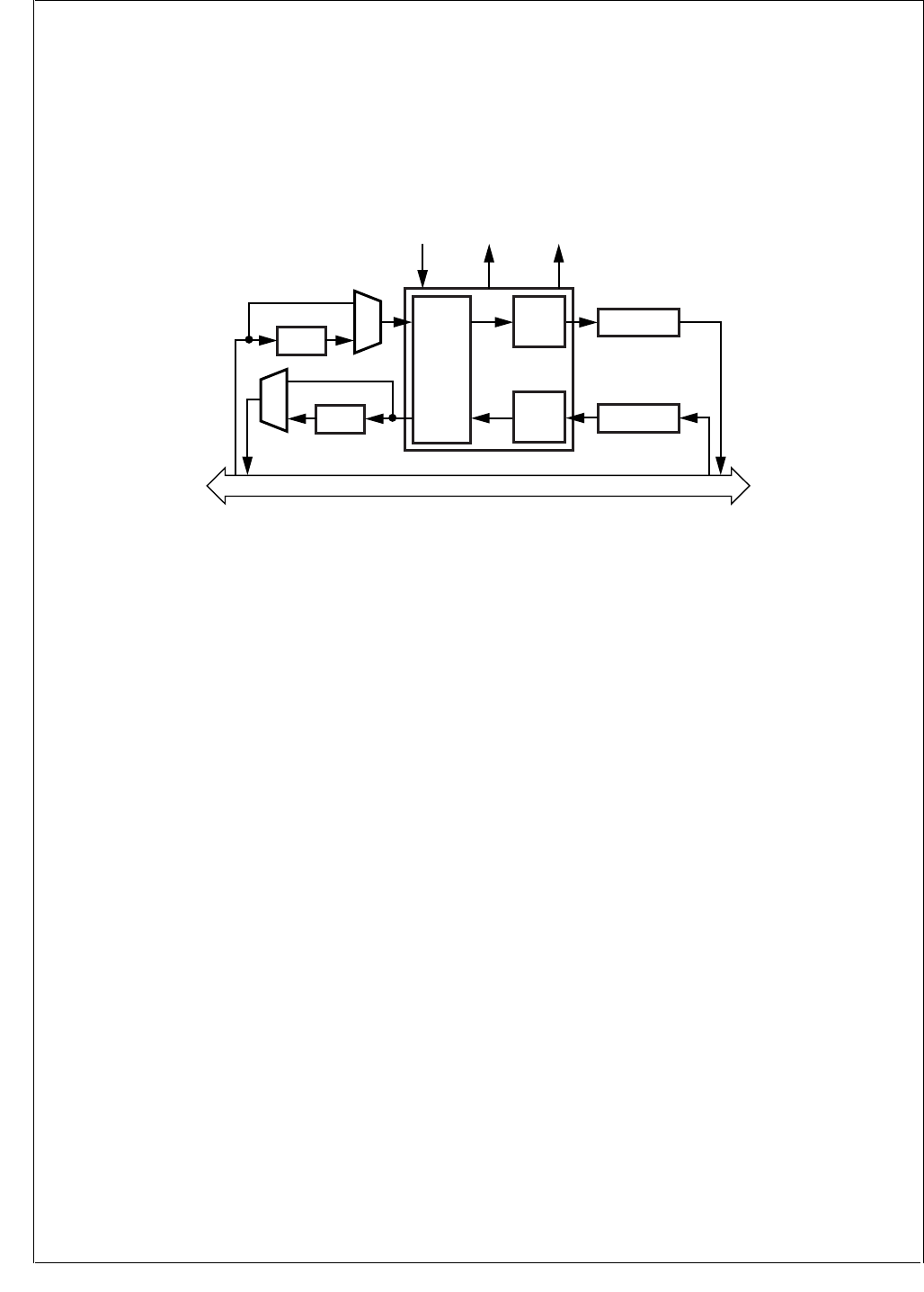
www.national.com 158
CP3BT26
21.0 CVSD/PCM Conversion Module
The CVSD/PCM module performs conversion between
CVSD data and PCM data, in which the CVSD encoding is
as defined in the Bluetooth specification and the PCM en-
coding may be 8-bit µ-Law, 8-bit A-Law, or 13-bit to 16-bit
Linear.
The CVSD conversion module operates at a fixed rate of
125 µs (8 kHz) per PCM sample. On the CVSD side, there
is a read and a write FIFO allowing up to 8 words of data to
be read or written at the same time. On the PCM side, there
is a double-buffered register requiring data to be read and
written every 125 µs. The intended use is to move CVSD
data into the module with a CVSD interrupt handler, and to
move PCM data with DMA. Figure 75 shows a block dia-
gram of the CVSD to PCM module.
Figure 75. CVSD/PCM Converter Block Diagram
21.1 OPERATION
The Aux2 clock (generated by the Clock module described
in Section 11.9) must be configured, because it drives the
CVSD module. Software must set its prescaler to provide a
2 MHz input clock based upon the System Clock (usually
12 MHz). This is done by writing an appropriate divisor to
the ACDIV2 field of the PRSAC register. Software must also
enable the Aux2 clock by setting the ACE2 bit within the
CRCTRL register. For example:
PRSAC &= 0x0f;
// Set Aux2 prescaler to generate
// 2 MHz (Fsys = 12 MHz)
PRSAC |= 0x50;
CRCTRL |= ACE2; // Enable Aux2 clk
The module converts between PCM data and CVSD data at
a fixed rate of 8 kHz per PCM sample. Due to compression,
the data rate on the CVSD side is only 4 kHz per CVSD
sample.
If PCM interrupts are enabled (PCMINT is set) every 125 µs
(8 kHz) an interrupt will occur and the interrupt handler can
operate on some or all of the four audio streams CVSD in,
CVSD out, PCM in, and PCM out. Alternatively, a DMA re-
quest is issued every 125 µs and the DMA controller is used
to move the PCM data between the CVSD/PCM module
and the audio interface.
If CVSD interrupts are enabled, an interrupt is issued when
either one of the CVSD FIFOs is almost empty or almost full.
On the PCM data side there is double buffering, and on the
CVSD side there is an eight word (8 × 16-bit) FIFO for the
read and write paths.
Inside the module, a filter engine receives the 8 kHz stream
of 16-bit samples and interpolates to generate a 64 kHz
stream of 16-bit samples. This goes into a CVSD encoder
which converts the data into a single-bit delta stream using
the CVSD parameters as defined by the Bluetooth specifi-
cation. There is a similar path that reverses this process
converting the CVSD 64 kHz bit stream into a 64 kHz 16-bit
data stream. The filter engine then decimates this stream
into an 8 kHz, 16-bit data stream.
21.2 PCM CONVERSIONS
During conversion between CVSD and PCM, any PCM for-
mat changes are done automatically depending on whether
the PCM data is µ-Law, A-Law, or Linear. In addition to this,
a separate function can be used to convert between the var-
ious PCM formats as required. Conversion is performed by
setting up the control bit CVCTL1.PCMCONV to define the
conversion and then writing to the LOGIN and LINEARIN
registers and reading from the LOGOUT and LINEAROUT
registers. There is no delay in the conversion operation and
it does not have to operate at a fixed rate. It will only convert
between µ-Law/A-Law and linear, not directly between µ-
Law and A-Law. (This could easily be achieved by convert-
ing between µ-Law and linear and between linear and A-
Law.)
If a conversion is performed between linear and µ-Law log
PCM data, the linear PCM data are treated in the left-
aligned 14-bit linear data format with the two LSBs unused.
If a conversion is performed between linear and A-Law log
PCM data, the linear PCM data are treated in the left-
aligned 13-bit linear data format with the three LSBs un-
used.
Peripheral Bus
Filter
Engine
16-Bit Shift Reg
1-Bit 64 kHz
1-Bit 64 kHz
16-Bit
16-Bit
64 kHz
64 kHz
16-Bit Shift Reg
16-Bit 8 kHz
CVSD
Encoder
DMA
Interrupt
2 MHz
Clock Input
CVSD
Decoder
u/A-Law
16-Bit 8 kHz
u/A-Law
DS058

159 www.national.com
CP3BT26
If the module is only used for PCM conversions, the CVSD
clock can be disabled by clearing the CVSD Clock Enable
bit (CLKEN) in the control register.
21.3 CVSD CONVERSION
The CVSD/PCM converter module transforms either 8-bit
logarithmic or 13- to 16-bit linear PCM samples at a fixed
rate of 8 ksps. The CVSD to PCM conversion format must
be specified by the CVSDCONV control bits in the CVSD
Control register (CVCTRL).
The CVSD algorithm is designed for 2’s complement 16-bit
data and is tuned for best performance with typical voice da-
ta. Mild distortion will occur for peak signals greater than -6
dB. The Bluetooth CVSD standard is designed for best per-
formace with typical voice signals: nominaly -6dB with occa-
sional peaks to 0dB rather than full-scale inputs. Distortion
of signals greater than -6dB is not considered detrimental to
subjective quality tests for voice-band applications and al-
lows for greater clarity for signals below -6dB. The gain of
the input device should be tuned with this in mind.
If required, the RESOLUTION field of the CVCTRL register
can be used to optimize the level of the 16-bit linear input
data by providing attenuations (right-shifts with sign exten-
tion) of 1, 2, or 3 bits.
Log data is always 8 bit, but to perform the CVSD conver-
sion, the log data is first converted to 16-bit 2’s complement
linear data. A-law and u-law conversion can also slightly af-
fect the optimum gain of the input data. The CVCTRL.RES-
OLUTION field can be used to attenuate the data if required.
If the resolution is not set properly, the audio signal may be
clipped or have reduced attenuation.
21.4 PCM TO CVSD CONVERSION
The converter core reads out the double-buffered PCMIN
register every 125 µs and writes a new 16-bit CVSD data
stream into the CVSD Out FIFO every 250 µs. If the PCMIN
buffer has not been updated with a new PCM sample be-
tween two reads from the CVSD core, the old PCM data is
used again to maintain a fixed conversion rate. Once a new
16-bit CVSD data stream has been calculated, it is copied
into the 8 × 16-bit wide CVSD Out FIFO.
If there are only three empty words (16-bit) left in the FIFO,
the nearly full bit (CVNF) is set, and, if enabled
(CVSDINT = 1), an interrupt request is asserted.
If the CVSD Out FIFO is full, the full bit (CVF) is set, and, if
enabled (CVSDERRINT = 1), an interrupt request is assert-
ed. In this case, the CVSD Out FIFO remains unchanged.
Within the interrupt handler, the CPU can read out the new
CVSD data. If the CPU reads from an already empty CVSD
Out FIFO, a lockup of the FIFO logic may occur which per-
sists until the next reset. Software must check the
CVOUTST field of the CVSTAT register to read the number
of valid words in the FIFO. Software must not use the CVNF
bit as an indication of the number of valid words in the FIFO.
21.5 CVSD TO PCM CONVERSION
The converter core reads from the CVSD In FIFO every
250 µs and writes a new PCM sample into the PCMOUT
buffer every 125 µs. If the previous PCM data has not yet
been transferred to the audio interface, it will be overwritten
with the new PCM sample.
If there are only three unread words left, the CVSD In Nearly
Empty bit (CVNE) is set and, if enabled (CVSDINT = 1), an
interrupt request is generated.
If the CVSD In FIFO is empty, the CVSD In Empty bit (CVE)
is set and, if enabled (CVSDERRINT = 1), an interrupt re-
quest is generated. If the converter core reads from an al-
ready empty CVSD In FIFO, the FIFO automatically returns
a checkerboard pattern to guarantee a minimum level of dis-
tortion of the audio stream.
21.6 INTERRUPT GENERATION
An interrupt is generated in any of the following cases:
When a new PCM sample has been written into the
PCMOUT register and the CVCTRL.PCMINT bit is set.
When a new PCM sample has been read from the
PCMIN register and the CVCTRL.PCMINT bit is set.
When the CVSD In FIFO is nearly empty
(CVSTAT.CVNE = 1) and the CVCTRL.CVSDINT bit is
set.
When the CVSD Out FIFO is nearly full
(CVSTAT.CVNF = 1) and the CVCTRL.CVSDINT bit is
set.
When the CVSD In FIFO is empty (CVSTAT.CVE = 1)
and the CVCTRL.CVSDERRINT bit is set.
When the CVSD Out FIFO is full (CVSTAT.CVF = 1) and
the CVCTRL.CVSDERRINT bit is set.
Both the CVSD In and CVSD Out FIFOs have a size of
8 × 16 bit (8 words). The warning limits for the two FIFOs is
set at 5 words. (The CVSD In FIFO interrupt will occur when
there are 3 words left in the FIFO, and the CVSD Out FIFO
interrupt will occur when there are 3 or less empty words left
in the FIFO.) The limit is set to 5 words because Bluetooth
audio data is transferred in packages composed of 10 or
multiples of 10 bytes.
21.7 DMA SUPPORT
The CVSD module can operate with any of four DMA chan-
nels. Four DMA channels are required for processor inde-
pendent operation. Both receive and transmit for CVSD
data and PCM data can be enabled individually. The CVSD/
PCM module asserts a DMA request to the on-chip DMA
controller under the following conditions:
The DMAPO bit is set and the PCMOUT register is full,
because it has been updated by the converter core with
a new PCM sample. (The DMA controller can read out
one PCM data word from the PCMOUT register.)
The DMAPI bit is set and the PCMIN register is empty,
because it has been read by the converter core. (The
DMA controller can write one new PCM data word into
the PCMIN register.)
The DMACO bit is set and a new 16-bit CVSD data
stream has been copied into the CVSD Out FIFO. (The
DMA controller can read out one 16-bit CVSD data word
from the CVSD Out FIFO.)
The DMACI bit is set and a 16-bit CVSD data stream has
been read from the CVSD In FIFO. (The DMA controller
can write one new 16-bit CVSD data word into the CVSD
In FIFO.)

www.national.com 160
CP3BT26
The CVSD/PCM module only supports indirect DMA trans-
fers. Therefore, transferring PCM data between the CVSD/
PCM module and another on-chip module requires two bus
cycles.
The trigger for DMA may also trigger an interrupt if the cor-
responding enable bits in the CVCTRL register is set.
Therefore care must be taken when setting the desired in-
terrupt and DMA enable bits. The following conditions must
be avoided:
Setting the PCMINT bit and either of the DMAPO or
DMAPI bits.
Setting the CVSDINT bit and either of the DMACO or
DMACI bits.
21.8 FREEZE
The CVSD/PCM module provides support for an In-System-
Emulator by means of a special FREEZE input. While
FREEZE is asserted the module will exhibit the following be-
havior:
CVSD In FIFO will not have data removed by the con-
verter core.
CVSD Out FIFO will not have data added by the convert-
er core.
PCM Out buffer will not be updated by the converter
core.
The Clear-on-Read function of the following status bits in
the CVSTAT register is disabled:
PCMINT
CVE
CVF
21.9 CVSD/PCM CONVERTER REGISTERS
Table 68 lists the CVSD/PCM registers.
21.9.1 CVSD Data Input Register (CVSDIN)
The CVSDIN register is a 16-bit wide, write-only register. It
is used to write CVSD data into the CVSD to PCM converter
FIFO. The FIFO is 8 words deep. The CVSDIN bit 15 repre-
sents the CVSD data bit at t = t0, CVSDIN bit 0 represents
the CVSD data bit at t = t0 - 250 ms.
21.9.2 CVSD Data Output Register (CVSDOUT)
The CVSDOUT register is a 16-bit wide read-only register.
It is used to read the CVSD data from the PCM to CVSD
converter. The FIFO is 8 words deep. Reading the CVSD-
OUT register after reset returns undefined data.
21.9.3 PCM Data Input Register (PCMIN)
The PCMIN register is a 16-bit wide write-only register. It is
used to write PCM data to the PCM to CVSD converter via
the peripheral bus. It is double-buffered, providing a 125 µs
period for an interrupt or DMA request to respond.
21.9.4 PCM Data Output Register (PCMOUT)
The PCMOUT register is a 16-bit wide read-only register. It
is used to read PCM data from the CVSD to PCM converter.
It is double-buffered, providing a 125 µs period for an inter-
rupt or DMA request to respond. After reset the PCMOUT
register is clear.
Table 68 CVSD/PCM Registers
Name Address Description
CVSDIN FF FC20h CVSD Data Input
Register
CVSDOUT FF FC22h CVSD Data Output
Register
PCMIN FF FC24h PCM Data Input
Register
PCMOUT FF FC26h PCM Data Output
Register
LOGIN FF FC28h Logarithmic PCM
Data Input Register
LOGOUT FF FC2Ah Logarithmic PCM
Data Output Register
LINEARIN FF FC2Ch Linear PCM
Data Input Register
LINEAROUT FF FC2Eh Linear PCM
Data Output Register
CVCTRL FF FC30h CVSD Control Regis-
ter
CVSTAT FF FC32h CVSD Status Register
15 0
CVSDIN
15 0
CVSDOUT
15 0
PCMIN
15 0
PCMOUT
Table 68 CVSD/PCM Registers
Name Address Description

161 www.national.com
CP3BT26
21.9.5 Logarithmic PCM Data Input Register (LOGIN)
The LOGIN register is an 8-bit wide write-only register. It is
used to receive 8-bit logarithmic PCM data from the periph-
eral bus and convert it into 13-bit linear PCM data.
21.9.6 Logarithmic PCM Data Output Register
(LOGOUT)
The LOGOUT register is an 8-bit wide read-only register. It
holds logarithmic PCM data that has been converted from
linear PCM data. After reset, the LOGOUT register is clear.
21.9.7 Linear PCM Data Input Register (LINEARIN)
The LINEARIN register is a 16-bit wide write-only register.
The data is left-aligned. When converting to A-law, bits 2:0
are ignored. When converting to µ-law, bits 1:0 are ignored.
21.9.8 Linear PCM Data Output Register
(LINEAROUT)
The LINEAROUT register is a 16-bit wide read-only register.
The data is left-aligned. When converting from A-law, bits
2:0 are clear. When converting from µ-law, bits 1:0 are clear.
After reset, this register is clear.
21.9.9 CVSD Control Register (CVCTRL)
The CVCTRL register is a 16-bit wide, read/write register
that controls the mode of operation and of the module’s in-
terrupts. At reset, all implemented bits are cleared.
CVEN The Module Enable bit enables or disables the
CVSD conversion module interface. When the
bit is set, the interface is enabled which allows
read and write operations to the rest of the
module. When the bit is clear, the module is
disabled. When the module is disabled the
status register CVSTAT will be cleared to its
reset state.
0 – CVSD module enabled.
1 – CVSD module disabled.
CLKEN The CVSD Clock Enable bit enables the 2-
MHz clock to the filter engine and CVSD en-
coders and decoders.
0 – CVSD module clock disabled.
1 – CVSD module clock enabled.
PCMINT The PCM Interrupt Enable bit controls gener-
ation of the PCM interrupt. If set, this bit en-
ables the PCM interrupt. If the PCMINT bit is
clear, the PCM interrupt is disabled. After re-
set, this bit is clear.
0 – PCM interrupt disabled.
1 – PCM interrupt enabled.
CVSDINT The CVSD FIFO Interrupt Enable bit controls
generation of the CVSD interrupt. If set, this
bit enables the CVSD interrupt that occurs if
the CVSD In FIFO is nearly empty or the
CVSD Out FIFO is nearly full. If the CVSDINT
bit is clear, the CVSD nearly full/nearly empty
interrupt is disabled. After reset, this bit is
clear.
0 – CVSD interrupt disabled.
1 – CVSD interrupt enabled.
CVSDERRINT
The CVSD FIFO Error Interrupt Enable bit
controls generation of the CVSD error inter-
rupt. If set, this bit enables an interrupt to oc-
cur when the CVSD Out FIFO is full or the
CVSD In FIFO is empty. If the CVSDERROR-
INT bit is clear, the CVSD full/empty interrupt
is disabled. After reset, this bit is clear.
0 – CVSD error interrupt disabled.
1 – CVSD error interrupt enabled.
DMACO The DMA Enable for CVSD Out bit enables
hardware DMA control for reading CVSD data
from the CVSD Out FIFO. If clear, DMA sup-
port is disabled. After reset, this bit is clear.
0 – CVSD output DMA disabled.
1 – CVSD output DMA enabled.
DMACI The DMA Enable for CVSD In bit enables
hardware DMA control for writing CVSD data
into the CVSD In FIFO. If clear, DMA support
is disabled. After reset, this bit is clear.
0 – CVSD input DMA disabled.
1 – CVSD input DMA enabled.
DMAPO The DMA Enable for PCM Out bit enables
hardware DMA control for reading PCM data
from the PCMOUT register. If clear, DMA sup-
port is disabled. After reset, this bit is clear.
0 – PCM output DMA disabled.
1 – PCM output DMA enabled.
70
LOGIN
70
LOGOUT
15 0
LINEARIN
15 0
LINEAROUT
7 6 5 4 3 2 1 0
DMA
PO
DMA
CI
DMA
CO
CVSD
ERR-
INT
CVSD
INT
PCM
INT
CLK
EN CVEN
15 14 13 12 11 10 9 8
Res. RESOLUTION PCMCONV CVSDCONV DMAPI

www.national.com 162
CP3BT26
DMAPI The DMA Enable for PCM In bit enables hard-
ware DMA control for writing PCM data into
the PCMIN register. If cleared, DMA support
is disabled. After reset, this bit is clear.
0 – PCM input DMA disabled.
1 – PCM input DMA enabled.
CVSDCONV
The CVSD to PCM Conversion Format field
specifies the PCM format for CVSD/PCM con-
versions. After reset, this field is clear.
00 – CVSD <-> 8-bit µ-Law PCM.
01 – CVSD <-> 8-bit A-Law PCM.
10 – CVSD <-> Linear PCM.
11 – Reserved.
PCMCONV The PCM to PCM Conversion Format bit se-
lects the PCM format for PCM/PCM conver-
sions.
0 – Linear PCM <-> 8-bit µ-Law PCM
1 – Linear PCM <-> 8-bit A-Law PCM
RESOLUTION
The Linear PCM Resolution field specifies the
attenuation of the PCM data for the linear
PCM to CVSD conversions by right shifting
and sign extending the data. This affects the
log PCM data as well as the linear PCM data.
The log data is converted to either left-justified
zero-stuffed 13-bit (A-law) or 14-bit (u-law).
The RESOLUTION field can be used to com-
pensate for any change in average levels re-
sulting from this conversion. After reset, these
two bits are clear.
00 – No shift.
01 – 1-bit attentuation.
10 – 2-bit attentuation.
11 – 3-bit attentuation.
21.9.10 CVSD Status Register (CVSTAT)
The CVSTAT register is a 16-bit wide, read-only register that
holds the status information of the CVSD/PCM module. At
reset, and if the CVCTL1.CVEN bit is clear, all implemented
bits are cleared.
CVNE The CVSD In FIFO Nearly Empty bit indicates
when only three CVSD data words are left in
the CVSD In FIFO, so new CVSD data should
be written into the CVSD In FIFO. If the CVS-
DINT bit is set, an interrupt will be asserted
when the CVNE bit is set. If the DMACI bit is
set, a DMA request will be asserted when this
bit is set. The CVNE bit is cleared when the
CVSTAT register is read.
0 – CVSD In FIFO is not nearly empty.
1 – CVSD In FIFO is nearly empty.
CVNF The CVSD Out FIFO Nearly Full bit indicates
when only three empty word locations are left
in the CVSD Out FIFO, so the CVSD Out
FIFO should be read. If the CVSDINT bit is
set, an interrupt will be asserted when the
CVNF bit is set. If the DMACO bit is set, a
DMA request will be asserted when this bit is
set. Software must not rely on the CVNF bit as
an indicator of the number of valid words in
the FIFO. Software must check the CVOUTST
field to read the number of valid words in the
FIFO. The CVNF bit is cleared when the
CVSTAT register is read.
0 – CVSD Out FIFO is not nearly full.
1 – CVSD Out FIFO is nearly full.
PCMINT The PCM Interrupt bit set indicates that the
PCMOUT register is full and needs to be read
or the PCMIN register is empty and needs to
be loaded with new PCM data. The PCMINT
bit is cleared when the CVSTAT register is
read, unless the device is in FREEZE mode.
0 – PCM does not require service.
1 – PCM requires loading or unloading.
CVE The CVSD In FIFO Empty bit indicates when
the CVSD In FIFO has been read by the
CVSD converter while the FIFO was already
empty. If the CVSDERRORINT bit is set, an
interrupt will be asserted when the CVE bit is
set. The CVE bit is cleared when the CVSTAT
register is read, unless the device is in
FREEZE mode.
0 – CVSD In FIFO has not been read while
empty.
1 – CVSD In FIFO has been read while emp-
ty.
CVF The CVSD Out FIFO Full bit set indicates
whether the CVSD Out FIFO has been written
by the CVSD converter while the FIFO was al-
ready full. If the CVSDERRORINT bit is set,
an interrupt will be asserted when the CVF bit
is set. The CVF bit is cleared when the
CVSTAT register is read, unless the device is
in FREEZE mode.
0 – CVSD Out FIFO has not been written
while full.
1 – CVSD Out FIFO has been written while
full.
CVINST The CVSD In FIFO Status field reports the
current number of empty 16-bit word locations
in the CVSD In FIFO. When the FIFO is emp-
ty, the CVINST field will read as 111b. When
the FIFO holds 7 or 8 words of data, the
CVINST field will read as 000b.
CVOUTST CVSD Out FIFO Status field reports the cur-
rent number of valid 16-bit CVSD data words
in the CVSD Out FIFO. When the FIFO is
empty, the CVOUTST field will read as 000b.
When the FIFO holds 7 or 8 words of data, the
CVOUTST field will read as 111b.
7 5 4 3 2 1 0
CVINST CVF CVE PCMINT CVNF CVNE
15 11 10 8
Reserved CVOUTST

163 www.national.com
CP3BT26
22.0 UART Modules
The CP3BT26 provides four UART modules. Each UART
module is a full-duplex Universal Asynchronous Receiver/
Transmitter that supports a wide range of software-pro-
grammable baud rates and data formats. It handles auto-
matic parity generation and several error detection
schemes.
All UART modules offer the following features:
Full-duplex double-buffered receiver/transmitter
Asynchronous operation
Programmable baud rate
Programmable framing formats: 7, 8, or 9 data bits; even,
odd, or no parity; one or two stop bits (mark or space)
Hardware parity generation for data transmission and
parity check for data reception
Interrupts on “transmit ready” and “receive ready” condi-
tions, separately enabled
Software-controlled break transmission and detection
Internal diagnostic capability
Automatic detection of parity, framing, and overrun errors
One module, UART0, offers the following additional fea-
tures:
Synchronous operation using the CKX external clock pin
Hardware flow control (CTS and RTS signals)
DMA capability
22.1 FUNCTIONAL OVERVIEW
Figure 76 is a block diagram of the UART module showing
the basic functional units in the UART:
Transmitter
Receiver
Baud Rate Generator
Control and Error Detection
The Transmitter block consists of an 8-bit transmit shift reg-
ister and an 8-bit transmit buffer. Data bytes are loaded in
parallel from the buffer into the shift register and then shifted
out serially on the TXD pin.
The Receiver block consists of an 8-bit receive shift register
and an 8-bit receive buffer. Data is received serially on the
RXD pin and shifted into the shift register. Once eight bits
have been received, the contents of the shift register are
transferred in parallel to the receive buffer.
The Transmitter and Receiver blocks both contain exten-
sions for 9-bit data transfers, as required by the 9-bit and
loopback operating modes.
The Baud Rate Generator generates the clock for the syn-
chronous and asynchronous operating modes. It consists of
two registers and a two-stage counter. The registers are
used to specify a prescaler value and a baud rate divisor.
The first stage of the counter divides the UART clock based
on the value of the programmed prescaler to create a slower
clock. The second stage of the counter creates the baud
rate clock by dividing the output of the first stage based on
the programmed baud rate divisor.
The Control and Error Detection block contains the UART
control registers, control logic, error detection circuit, parity
generator/checker, and interrupt generation logic. The con-
trol registers and control logic determine the data format,
mode of operation, clock source, and type of parity used.
The error detection circuit generates parity bits and checks
for parity, framing, and overrun errors.
The Flow Control Logic block provides the capability for
hardware handshaking between the UART and a peripheral
device. When the peripheral device needs to stop the flow
of data from the UART, it de-asserts the clear-to-send (CTS)
signal which causes the UART to pause after sending the
current frame (if any). The UART asserts the ready-to-send
(RTS) signal to the peripheral when it is ready to send a
character.
22.2 UART OPERATION
The UART has two basic modes of operation: synchronous
and asynchronous. Synchronous mode is only supported
for the UART0 module. In addition, there are two special-
purpose modes, called attention and diagnostic. This sec-
tion describes the operating modes of the UART.
22.2.1 Asynchronous Mode
The asynchronous mode of the UART enables the device to
communicate with other devices using just two communica-
tion signals: transmit and receive.
In asynchronous mode, the transmit shift register (TSFT)
and the transmit buffer (UnTBUF) double-buffer the data for
transmission. To transmit a character, a data byte is loaded
in the UnTBUF register. The data is then transferred to the
TSFT register. While the TSFT register is shifting out the
current character (LSB first) on the TXD pin, the UnTBUF
register is loaded by software with the next byte to be trans-
mitted. When TSFT finishes transmission of the last stop bit
of the current frame, the contents of UnTBUF are trans-
ferred to the TSFT register and the Transmit Buffer Empty
bit (UTBE) is set. The UTBE bit is automatically cleared by
the UART when software loads a new character into the
UnTBUF register. During transmission, the UXMIP bit is set
high by the UART. This bit is reset only after the UART has
sent the last stop bit of the current character and the UnT-
BUF register is empty. The UnTBUF register is a read/write
register. The TSFT register is not software accessible.
In asynchronous mode, the input frequency to the UART is
16 times the baud rate. In other words, there are 16 clock
cycles per bit time. In asynchronous mode, the baud rate
generator is always the UART clock source.
The receive shift register (RSFT) and the receive buffer (Un-
RBUF) double buffer the data being received. The UART re-
ceiver continuously monitors the signal on the RXD pin for a
low level to detect the beginning of a start bit. On sensing
this low level, the UART waits for seven input clock cycles
and samples again three times. If all three samples still in-
dicate a valid low, then the receiver considers this to be a
valid start bit, and the remaining bits in the character frame
are each sampled three times, around the mid-bit position.
For any bit following the start bit, the logic value is found by
majority voting, i.e. the two samples with the same value de-
fine the value of the data bit. Figure 77 illustrates the pro-
cess of start bit detection and bit sampling.
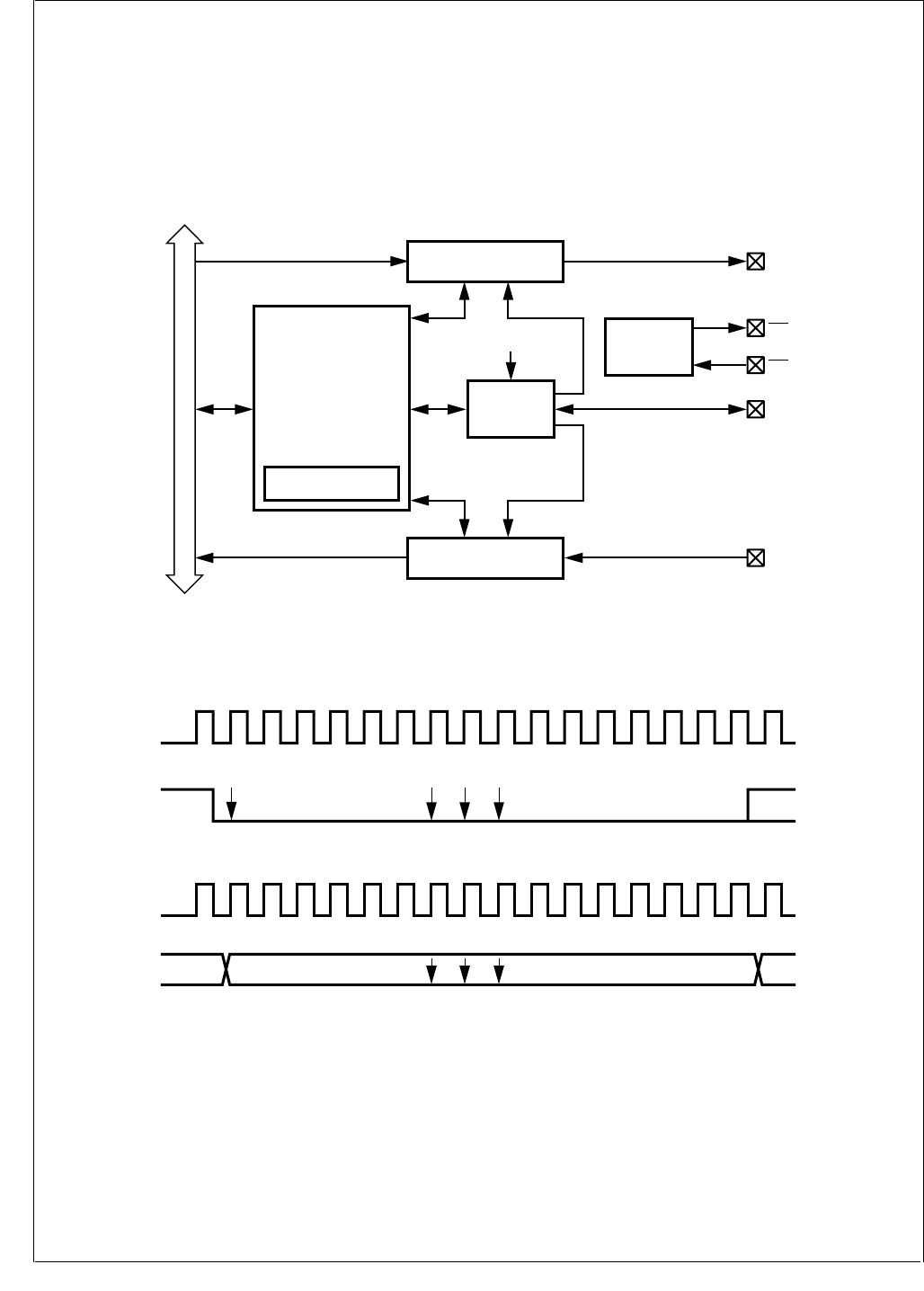
www.national.com 164
CP3BT26
Data bits are sensed by taking a majority vote of three sam-
ples latched near the midpoint of each baud (bit time). Nor-
mally, the position of the samples within the baud is
determined automatically, but software can override the au-
tomatic selection by setting the USMD bit in the UnMDSL2
register and programming the UnSPOS register.
Serial data input on the RXD pin is shifted into the RSFT
register. On receiving the complete character, the contents
of the RSFT register are copied into the UnRBUF register
and the Receive Buffer Full bit (URBF) is set. The URBF bit
is automatically cleared when software reads the character
from the URBUF register. The RSFT register is not software
accessible.
Figure 76. UART Block Diagram
Figure 77. UART Asynchronous Communication
TXD
Transmitter
Control and
Error Detection
Parity
Generator/Checker
RXD
Receiver
CKX
Baud Rate
Generator
Baud Clock
Baud Clock
System Clock
Internal Bus
DS060
RTS
CTS
Flow Control
Logic
16 1 2 3 4 5 6 7 8 9 10 11 12 13 14 15 16 1
16 1 2 3 4 5 6 7 8 9 10 11 12 13 14 15 16 1
Sample Sample
Sample
DATA (LSB)
STARTBIT
DATABIT
DS061
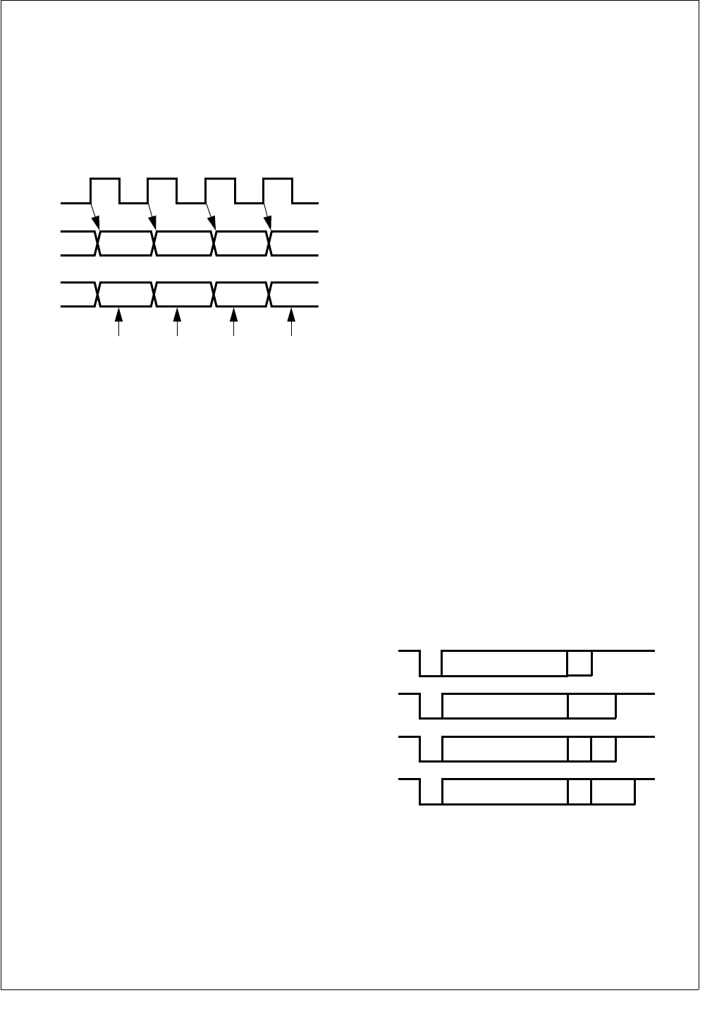
165 www.national.com
CP3BT26
22.2.2 Synchronous Mode
The synchronous mode of the UART enables the device to
communicate with other devices using three communication
signals: transmit, receive, and clock. In this mode, data bits
are transferred synchronously with the UART clock signal.
Data bits are transmitted on the rising edges and received
on the falling edges of the clock signal, as shown in
Figure 78. Data bytes are transmitted and received least
significant bit (LSB) first.
Figure 78. UART Synchronous Communication
In synchronous mode, the transmit shift register (TSFT) and
the transmit buffer (UnTBUF) double-buffer the data for
transmission. To transmit a character, a data byte is loaded
in the UnTBUF register. The data is then transferred to the
TSFT register. The TSFT register shifts out one bit of the
current character, LSB first, on each rising edge of the clock.
While the TSFT is shifting out the current character on the
TXD pin, the UnTBUF register may be loaded by software
with the next byte to be transmitted. When the TSFT finishes
transmission of the last stop bit within the current frame, the
contents of UnTBUF are transferred to the TSFT register
and the Transmit Buffer Empty bit (UTBE) is set. The UTBE
bit is automatically reset by the UART when software loads
a new character into the UnTBUF register. During transmis-
sion, the UXMIP bit is set by the UART. This bit is cleared
only after the UART has sent the last frame bit of the current
character and the UnTBUF register is empty.
The receive shift register (RSFT) and the receive buffer
(URBUF) double-buffer the data being received. Serial data
received on the RXD pin is shifted into the RSFT register on
the first falling edge of the clock. Each subsequent falling
edge of the clock causes an additional bit to be shifted into
the RSFT register. The UART assumes a complete charac-
ter has been received after the correct number of rising edg-
es on CKX (based on the selected frame format) have been
detected. On receiving a complete character, the contents
of the RSFT register are copied into the UnRBUF register
and the Receive Buffer Full bit (URBF) is set. The URBF bit
is automatically cleared when software reads the character
from the UnRBUF register.
The transmitter and receiver may be clocked by either an
external source provided to the CKX pin or the internal baud
rate generator. In the latter case, the clock signal is placed
on the CKX pin as an output.
22.2.3 Attention Mode
The Attention mode is available for networking this device
with other processors. This mode requires the 9-bit data for-
mat with no parity. The number of start bits and number of
stop bits are programmable. In this mode, two types of 9-bit
characters are sent on the network: address characters
consisting of 8 address bits and a 1 in the ninth bit position
and data characters consisting of 8 data bits and a 0 in the
ninth bit position.
While in Attention mode, the UART receiver monitors the
communication flow but ignores all characters until an ad-
dress character is received. On receiving an address char-
acter, the contents of the receive shift register are copied to
the receive buffer. The URBF bit is set and an interrupt (if
enabled) is generated. The UATN bit is automatically
cleared, and the UART begins receiving all subsequent
characters. Software must examine the contents of the UR-
BUF register and respond by accepting the subsequent
characters (by leaving the UATN bit clear) or waiting for the
next address character (by setting the UATN bit again).
The operation of the UART transmitter is not affected by the
selection of this mode. The value of the ninth bit to be trans-
mitted is programmed by setting or clearing the UXB9 bit in
the UART Frame Select register. The value of the ninth bit
received is read from URB9 in the UART Status Register.
22.2.4 Diagnostic Mode
The Diagnostic mode is available for testing of the UART. In
this mode, the TXD and RXD pins are internally connected
together, and data shifted out of the transmit shift register is
immediately transferred to the receive shift register. This
mode supports only the 9-bit data format with no parity. The
number of start and stop bits is programmable.
22.2.5 Frame Format Selection
The format shown in Figure 79 consists of a start bit, seven
data bits (excluding parity), and one or two stop bits. If parity
bit generation is enabled by setting the UPEN bit, a parity bit
is generated and transmitted following the seven data bits.
Figure 79. 7-Bit Data Frame Options
The format shown in Figure 80 consists of one start bit,
eight data bits (excluding parity), and one or two stop bits. If
parity bit generation is enabled by setting the UPEN bit, a
CKX
TDX
RDX
Sample Input
DS062
1Start
Bit 7-Bit Data 1S
1a Start
Bit 7-Bit Data 2S
1b Start
Bit 7-Bit Data 1SPA
1c Start
Bit 7-Bit Data 2SPA
DS063
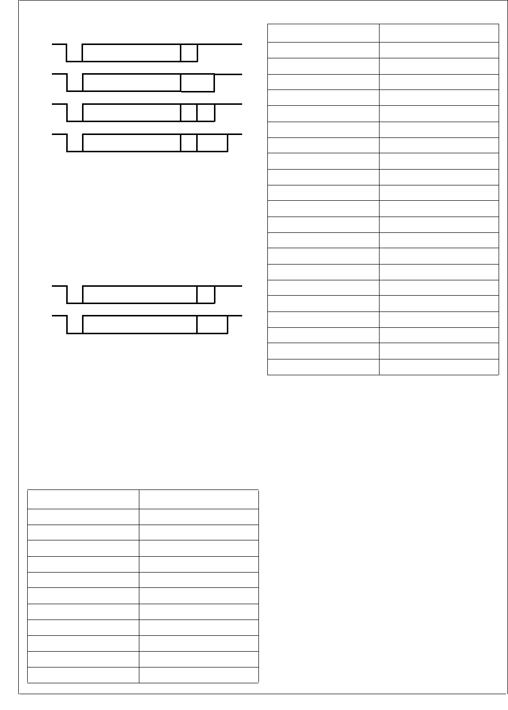
www.national.com 166
CP3BT26
parity bit is generated and transmitted following the eight
data bits.
Figure 80. 8-Bit Data Frame Options
The format shown in Figure 81 consists of one start bit, nine
data bits, and one or two stop bits. This format also supports
the UART attention feature. When operating in this format,
all eight bits of UnTBUF and UnRBUF are used for data.
The ninth data bit is transmitted and received using two bits
in the control registers, called UXB9 and URB9. Parity is not
generated or verified in this mode.
Figure 81. 9-bit Data Frame Options
22.2.6 Baud Rate Generator
The Baud Rate Generator creates the basic baud clock from
the System Clock. The System Clock is passed through a
two-stage divider chain consisting of a 5-bit baud rate pres-
caler (UnPSC) and an 11-bit baud rate divisor (UnDIV).
The relationship between the 5-bit prescaler select (UnP-
SC) setting and the prescaler factors is shown in Table 69.
A prescaler factor of zero corresponds to “no clock.” The “no
clock” condition is the UART power down mode, in which the
UART clock is turned off to reduce power consumption.
Software must select the “no clock” condition before enter-
ing a new baud rate. Otherwise, it could cause incorrect
data to be received or transmitted. The UnPSR register
must contain a value other than zero when an external clock
is used at CKX.
22.2.7 Interrupts
The UART is capable of generating interrupts on:
Receive Buffer Full
Receive Error
Transmit Buffer Empty
Table 69 Prescaler Factors
Prescaler Select Prescaler Factor
00000 No clock
00001 1
00010 1.5
00011 2
00100 2.5
00101 3
00110 3.5
00111 4
01000 4.5
01001 5
01010 5.5
2Start
Bit 8-Bit Data 1S
2a Start
Bit 8-Bit Data 2S
2b Start
Bit 8-Bit Data 1SPA
2c Start
Bit 8-Bit Data 2SPA
DS064
3Start
Bit 9-Bit Data 1S
3a Start
Bit 9-Bit Data 2S
DS065
01011 6
01100 6.5
01101 7
01110 7.5
01111 8
10000 8.5
10001 9
10010 9.5
10011 10
10100 10.5
10101 11
10110 11.5
10111 12
11000 12.5
11001 13
11010 13.5
11011 14
11100 14.5
11101 15
11110 15.5
11111 16
Table 69 Prescaler Factors (Continued)
Prescaler Select Prescaler Factor
167 www.national.com
CP3BT26
Figure 82 shows a diagram of the interrupt sources and as-
sociated enable bits.
Figure 82. UART Interrupts
The interrupts can be individually enabled or disabled using
the Enable Transmit Interrupt (UETI), Enable Receive Inter-
rupt (UERI), and Enable Receive Error Interrupt (UEER)
bits in the UnICTRL register.
A transmit interrupt is generated when both the UTBE and
UETI bits are set. To remove this interrupt, software must ei-
ther disable the interrupt by clearing the UETI bit or write to
the UnTBUF register (which clears the UTBE bit).
A receive interrupt is generated on these conditions:
Both the URBF and UERI bits are set. To remove this in-
terrupt, software must either disable the interrupt by
clearing the UERI bit or read from the URBUF register
(which clears the URBF bit).
Both the UERR and the UEEI bits are set. To remove this
interrupt, software must either disable the interrupt by
clearing the UEEI bit or read the UnSTAT register (which
clears the UERR bit).
A flow control interrupt is generated when both the UDCTS
and the UEFCI bits are set. To remove this interrupt, soft-
ware must either disable the interrupt by clearing the UEFCI
bit or reading the UnICTRL register (which clears the
UDCTS bit).
In addition to the dedicated inputs to the ICU for UART in-
terrupts, the UART receive (RXD) and Clear To Send (CTS)
signals are inputs to the MIWU (see Section 13.0), which
can be programmed to generate edge-triggered interrupts.
22.2.8 DMA Support
The UART module can operate with one or two DMA chan-
nels. Two DMA channels must be used for processor-inde-
pendent full-duplex operation. Both receive and transmit
DMA can be enabled simultaneously.
If transmit DMA is enabled (the UETD bit is set), the UART
generates a DMA request when the UTBE bit changes state
from clear to set. Enabling transmit DMA automatically dis-
ables transmit interrupts, without regard to the state of the
UETI bit.
If receive DMA is enabled (the UERD bit is set), the UART
generates a DMA request when the URBF bit changes state
from clear to set. Enabling receive DMA automatically dis-
ables receive interrupts, without regard to the state of the
UERI bit. However, receive error interrupts should be en-
abled (the UEEI bit is set) to allow detection of receive errors
when DMA is used.
22.2.9 Break Generation and Detection
A line break is generated when the UBRK bit is set in the
UnMDSL1 register. The TXD line remains low until the pro-
gram resets the UBRK bit.
A line break is detected if RXD remains low for 10 bit times
or longer after a missing stop bit is detected.
22.2.10 Parity Generation and Detection
Parity is only generated or checked with the 7-bit and 8-bit
data formats. It is not generated or checked in the diagnostic
loopback mode, the attention mode, or in normal mode with
the 9-bit data format. Parity generation and checking are en-
abled and disabled using the PEN bit in the UnFRS register.
The UPSEL bits in the UnFRS register are used to select
odd, even, or no parity.
RX
Interrupt
UERR
UEEI
TX
Interrupt
UTBE
UETI
URBF
UFE
UDOE
UPE UERI
FC
Interrupt
UDCTS
UEFCI
DS066

www.national.com 168
CP3BT26
22.3 UART REGISTERS
Software interacts with the UART modules by accessing the
UART registers, as listed in Table 70.
Table 70 UART Registers
Name Address Description
U0RBUF FF F202h UART0 Receive Data
Buffer
U0TBUF FF F200h UART0 Transmit Data
Buffer
U0PSR FF F20Eh UART0 Baud Rate
Prescaler
U0BAUD FF F20Ch UART0 Baud Rate
Divisor
U0FRS FF F208h UART0 Frame Select
Register
U0MDSL1 FF F20Ah UART0 Mode Select
Register 1
U0STAT FF F206h UART0 Status
Register
U0ICTRL FF F204h UART0 Interrupt Con-
trol Register
U0OVR FF F210h UART0 Oversample
Rate Register
U0MDSL2 FF F212h UART0 Mode Select
Register 2
U0SPOS FF F214h UART0 Sample
Position Register
U1RBUF FF F222h UART1 Receive Data
Buffer
U1TBUF FF F220h UART1 Transmit Data
Buffer
U1PSR FF F22Eh UART1 Baud Rate
Prescaler
U1BAUD FF F22Ch UART1 Baud Rate
Divisor
U1FRS FF F228h UART1 Frame Select
Register
U1MDSL1 FF F22Ah UART1 Mode Select
Register 1
U1STAT FF F226h UART1 Status
Register
U1ICTRL FF F224h UART1 Interrupt Con-
trol Register
U1OVR FF F230h UART1 Oversample
Rate Register
U1MDSL2 FF F232h UART1 Mode Select
Register 2
U1SPOS FF F234h UART1 Sample
Position Register
U2RBUF FF F242h UART2 Receive Data
Buffer
U2TBUF FF F240h UART2 Transmit Data
Buffer
U2PSR FF F24Eh UART2 Baud Rate
Prescaler
U2BAUD FF F24Ch UART2 Baud Rate
Divisor
U2FRS FF F248h UART2 Frame Select
Register
U2MDSL1 FF F24Ah UART2 Mode Select
Register 1
U2STAT FF F246h UART2 Status
Register
U2ICTRL FF F244h UART2 Interrupt Con-
trol Register
U2OVR FF F250h UART2 Oversample
Rate Register
U2MDSL2 FF F252h UART2 Mode Select
Register 2
U2SPOS FF F254h UART2 Sample
Position Register
U3RBUF FF F262h UART3 Receive Data
Buffer
U3TBUF FF F260h UART3 Transmit Data
Buffer
U3PSR FF F26Eh UART3 Baud Rate
Prescaler
U3BAUD FF F26Ch UART3 Baud Rate
Divisor
U3FRS FF F268h UART3 Frame Select
Register
U3MDSL1 FF F26Ah UART3 Mode Select
Register 1
U3STAT FF F266h UART3 Status
Register
U3ICTRL FF F264h UART3 Interrupt Con-
trol Register
Table 70 UART Registers
Name Address Description

169 www.national.com
CP3BT26
22.3.1 UART Receive Data Buffer (UnRBUF)
The UnRBUF register is a byte-wide, read/write register
used to receive each data byte.
22.3.2 UART Transmit Data Buffer (UnTBUF)
The UnTBUF register is a byte-wide, read/write register
used to transmit each data byte.
22.3.3 UART Baud Rate Prescaler (UnPSR)
The UnPSR register is a byte-wide, read/write register that
contains the 5-bit clock prescaler and the upper three bits of
the baud rate divisor. This register is cleared upon reset.
The register format is shown below.
UPSC The Prescaler field specifies the prescaler val-
ue used for dividing the System Clock in the
first stage of the two-stage divider chain. For
the prescaler factors corresponding to each 5-
bit value, see Table 69.
UDIV10:8 The Baud Rate Divisor field holds the three
most significant bits (bits 10, 9, and 8) of the
UART baud rate divisor used in the second
stage of the two-stage divider chain. The re-
maining bits of the baud rate divisor are held
in the UnBAUD register.
22.3.4 UART Baud Rate Divisor (UnBAUD)
The UnBAUD register is a byte-wide, read/write register that
contains the lower eight bits of the baud rate divisor. The
register contents are unknown at power-up and are left un-
changed by a reset operation. The register format is shown
below.
UDIV7:0 The Baud Rate Divisor field holds the eight
lowest-order bits of the UART baud rate divi-
sor used in the second stage of the two-stage
divider chain. The three most significant bits
are held in the UnPSR register. The divisor
value used is (UDIV[10:0] + 1).
22.3.5 UART Frame Select Register (UnFRS)
The UnFRS register is a byte-wide, read/write register that
controls the frame format, including the number of data bits,
number of stop bits, and parity type. This register is cleared
upon reset. The register format is shown below.
UCHAR The Character Frame Format field selects the
number of data bits per frame, not including
the parity bit, as follows:
00 – 8 data bits per frame.
01 – 7 data bits per frame.
10 – 9 data bits per frame.
11 – Loop-back mode, 9 data bits per frame.
USTP The Stop Bits bit specifies the number of stop
bits transmitted in each frame. If this bit is 0,
one stop bit is transmitted. If this bit is 1, two
stop bits are transmitted.
0 – One stop bit per frame.
1 – Two stop bits per frame.
UXB9 The Transmit 9th Data Bit holds the value of
the ninth data bit, either 0 or 1, transmitted
when the UART is configured to transmit nine
data bits per frame. It has no effect when the
UART is configured to transmit seven or eight
data bits per frame.
UPSEL The Parity Select field selects the treatment of
the parity bit. When the UART is configured to
transmit nine data bits per frame, the parity bit
is omitted and the UPSEL field is ignored.
00 – Odd parity.
01 – Even parity.
10 – No parity, transmit 1 (mark).
11 – No parity, transmit 0 (space).
U3OVR FF F270h UART3 Oversample
Rate Register
U3MDSL2 FF F272h UART3 Mode Select
Register 2
U3SPOS FF F274h UART3 Sample
Position Register
7 0
URBUF
7 0
UnTBUF
7 3 2 0
UPSC UDIV10:8
Table 70 UART Registers
Name Address Description
7 0
UDIV7:0
7 6 5 4 3 2 1 0
Reserved UPEN UPSEL UXB9 USTP UCHAR

www.national.com 170
CP3BT26
UPEN The Parity Enable bit enables or disables par-
ity generation and parity checking. When the
UART is configured to transmit nine data bits
per frame, there is no parity bit and the Un-
PEN bit is ignored.
0 – Parity generation and checking disabled.
1 – Parity generation and checking enabled.
22.3.6 UART Mode Select Register 1 (UnMDSL1)
The UnMDSL1 register is a byte-wide, read/write register
that selects the clock source, synchronization mode, atten-
tion mode, and line break generation. This register is
cleared at reset. The register format is shown below.
UMOD The Mode bit selects between synchronous
and asynchronous mode. Synchronous mode
is only available for the UART0 module.
0 – Asynchronous mode.
1 – Synchronous mode.
UATN The Attention Mode bit is used to enable At-
tention mode. When set, this bit selects the at-
tention mode of operation for the UART. When
clear, the attention mode is disabled. The
hardware clears this bit after an address
frame is received. An address frame is a 9-bit
character with a 1 in the ninth bit position.
0 – Attention mode disabled.
1 – Attention mode enabled.
UBRK The Force Transmission Break bit is used to
force the TXD output low. Setting this bit to 1
causes the TXD pin to go low. TXD remains
low until the UBRK bit is cleared by software.
0 – Normal operation.
1 – TXD pin forced low.
UCKS The Synchronous Clock Source bit controls
the clock source when the UART operates in
the synchronous mode (UMOD = 1). This
functionality is only available for the UART0
module. If the UCKS bit is set, the UART op-
erates from an external clock provided on the
CKX pin. If the UCKS bit is clear, the UART
operates from the baud rate clock produced
by the UART on the CKX pin. This bit is ig-
nored when the UART operates in the asyn-
chronous mode.
0 – Internal baud rate clock is used.
1 – External clock is used.
UETD The Enable Transmit DMA bit controls wheth-
er DMA is used for UART transmit operations.
Enabling transmit DMA automatically disables
transmit interrupts, without regard to the state
of the UETI bit.
0 – Transmit DMA disabled.
1 – Transmit DMA enabled.
UERD The Enable Receive DMA bit controls whether
DMA is used for UART receive operations.
Enabling receive DMA automatically disables
receive interrupts, without regard to the state
of the UERI bit. Receive error interrupts are
unaffected by the UERD bit.
0 – Receive DMA disabled.
1 – Receive DMA enabled.
UFCE The Flow Control Enable bit controls whether
flow control interrupts are enabled.
0 – Flow control interrupts disabled.
1 – Flow control interrupts enabled.
URTS The Ready To Send bit directly controls the
state of the RTS output.
0 – RTS output is high.
1 – RTS output is low.
22.3.7 UART Status Register (UnSTAT)
The UnSTAT register is a byte-wide, read-only register that
contains the receive and transmit status bits. This register is
cleared upon reset. Any attempt by software to write to this
register is ignored. The register format is shown below.
UPE The Parity Error bit indicates whether a parity
error is detected within a received character.
This bit is automatically cleared by the hard-
ware when the UnSTAT register is read.
0 – No parity error occurred.
1 – Parity error occurred.
UFE The Framing Error bit indicates whether the
UART fails to receive a valid stop bit at the end
of a frame. This bit is automatically cleared by
the hardware when the UnSTAT register is
read.
0 – No framing error occurred.
1 – Framing error occurred.
UDOE The Data Overrun Error bit is set when a new
character is received and transferred to the
UnRBUF register before software has read
the previous character from the UnRBUF reg-
ister. This bit is automatically cleared by the
hardware when the UnSTAT register is read.
0 – No receive overrun error occurred.
1 – Receive overrun error occurred.
UERR The Error Status bit indicates when a parity,
framing, or overrun error occurs (any time that
the UPE, UFE, or UDOE bit is set). It is auto-
matically cleared by the hardware when the
UPE, UFE, and UDOE bits are all 0.
0 – No receive error occurred.
1 – Receive error occurred.
7 6 5 4 3 2 1 0
URTS UFCE UERD
UETD UCKS UBRK
UATN
UMOD
7 6 5 4 3 2 1 0
Res.
UXMIP
URB9 UBKD UERR UDOE UFE UPE

171 www.national.com
CP3BT26
UBKD The Break Detect bit indicates when a line
break condition occurs. This condition is de-
tected if RXD remains low for at least ten bit
times after a missing stop bit has been detect-
ed at the end of a frame. The hardware auto-
matically clears the UBKD bit on reading the
UnSTAT register, but only if the break condi-
tion on RXD no longer exists. If reading the
UnSTAT register does not clear the UBKD bit
because the break is still actively driven on
the line, the hardware clears the bit as soon as
the break condition no longer exists (when the
RXD input returns to a high level).
0 – No break condition occurred.
1 – Break condition occurred.
URB9 The Received 9th Data Bit holds the ninth
data bit, when the UART is configured to op-
erate in the 9-bit data format.
UXMIP The Transmit In Progress bit indicates when
the UART is transmitting. The hardware sets
this bit when the UART is transmitting data
and clears the bit at the end of the last frame
bit.
0 – UART is not transmitting.
1 – UART is transmitting.
22.3.8 UART Interrupt Control Register (UnICTRL)
The UnICTRL register is a byte-wide register that contains
the receive and transmit interrupt status bits (read-only bits)
and the interrupt enable bits (read/write bits). The register is
initialized to 01h at reset. The register format is shown be-
low.
UTBE The Transmit Buffer Empty bit is set by hard-
ware when the UART transfers data from the
UnTBUF register to the transmit shift register
for transmission. It is automatically cleared by
the hardware on the next write to the UnTBUF
register.
0 – Transmit buffer is loaded.
1 – Transmit buffer is empty.
URBF The Receive Buffer Full bit is set by hardware
when the UART has received a complete data
frame and has transferred the data from the
receive shift register to the UnRBUF register.
It is automatically cleared by the hardware
when the UnRBUF register is read.
0 – Receive buffer is empty.
1 – Receive buffer is loaded.
UDCTS The Delta Clear To Send bit indicates whether
the CTS input has changed state since the
CPU last read this register. This functionality
is only available for the UART0 module.
0 – No change since last read.
1 – State has changed since last read.
UCTS The Clear To Send bit indicates the state on
the CTS input. This functionality is only avail-
able for the UART0 module.
0 – CTS input is high.
1 – CTS input is low.
UEFCI The Enable Flow Control Interrupt bit controls
whether a flow control interrupt is generated
when the UDCTS bit changes from clear to
set. This functionality is only available for the
UART0 module.
0 – Flow control interrupt disabled.
1 – Flow control interrupt enabled.
UETI The Enable Transmitter Interrupt bit, when
set, enables generation of an interrupt when
the hardware sets the UTBE bit.
0 – Transmit buffer empty interrupt disabled.
1 – Transmit buffer empty interrupt enabled.
UERI The Enable Receiver Interrupt bit, when set,
enables generation of an interrupt when the
hardware sets the URBF bit.
0 – Receive buffer full interrupt disabled.
1 – Receive buffer full interrupt enabled.
UEEI The Enable Receive Error Interrupt bit, when
set, enables generation of an interrupt when
the hardware sets the UERR bit in the Un-
STAT register.
0 – Receive error interrupt disabled.
1 – Receive error interrupt enabled.
22.3.9 UART Oversample Rate Register (UnOVR)
The UnOVR register is a byte-wide, read/write register that
specifies the oversample rate. At reset, the UnOVR register
is cleared. The register format is shown below.
UOVSR The Oversampling Rate field specifies the
oversampling rate, as given in the following ta-
ble.
7 6 5 4 3 2 1 0
UEEI UERI UETI UEFCI UCTS UDCTS
URBF
UTBE 7 4 3 0
Reserved UOVSR
UOVSR3:0 Oversampling Rate
0000–0110 16
0111 7
1000 8
1001 9
1010 10
1011 11
1100 12
1101 13
1110 14
1111 15

www.national.com 172
CP3BT26
22.3.10 UART Mode Select Register 2 (UnMDSL2)
The UnMDSL2 register is a byte-wide, read/write register
that controls the sample mode used to recover asynchro-
nous data. At reset, the UnOVR register is cleared. The reg-
ister format is shown below.
USMD The USMD bit controls the sample mode for
asynchronous transmission.
0 – UART determines the sample position au-
tomatically.
1 – The UnSPOS register determines the
sample position.
22.3.11 UART Sample Position Register (UnSPOS)
The UnSPOS register is a byte-wide, read/write register that
specifies the sample position when the USMD bit in the
UnMDSL2 register is set. At reset, the UnSPOS register is
initialized to 06h. The register format is shown below.
USAMP The Sample Position field specifies the over-
sample clock period at which to take the first
of three samples for sensing the value of data
bits. The clocks are numbered starting at 0
and may range up to 15 for 16× oversampling.
The maximum value for this field is (oversam-
pling rate - 3). The table below shows the
clock period at which each of the three sam-
ples is taken, when automatic sampling is en-
abled (UnMDSL2.USMD = 0).
The USAMP field may be used to override the
automatic selection, to choose any other clock
period at which to start taking the three sam-
ples.
22.4 BAUD RATE CALCULATIONS
The UART baud rate is determined by the System Clock fre-
quency and the values in the UnOVR, UnPSR, and Un-
BAUD registers. Unless the System Clock is an exact
multiple of the baud rate, there will be a small amount of er-
ror in the resulting baud rate.
22.4.1 Asynchronous Mode
The equation to calculate the baud rate in asynchronous
mode is:
where BR is the baud rate, SYS_CLK is the System Clock,
O is the oversample rate, N is the baud rate divisor + 1, and
P is the prescaler divisor selected by the UPSR register.
Assuming a System Clock of 5 MHz, a desired baud rate of
9600, and an oversample rate of 16, the N × P term accord-
ing to the equation above is:
The N × P term is then divided by each Prescaler Factor
from Table 69 to obtain a value closest to an integer. The
factor for this example is 6.5.
The baud rate register is programmed with a baud rate divi-
sor of 4 (N = baud rate divisor + 1). This produces a baud
clock of:
Note that the percent error is much lower than would be pos-
sible without the non-integer prescaler factor. Error greater
than 3% is marginal and may result in unreliable operation.
Refer to Table 71 below for more examples.
7 1 0
Reserved USMD
7 4 3 0
Reserved USAMP
Oversampling Rate
Sample Position
123
7 234
8 234
9 345
10 345
11 456
12 456
13 567
14 567
15 678
16 678
BR SYS_CLK
ONP××()
------------------------------=
NP×56
×10()
16 9600×()
-------------------------------32.552==
N32.552
6.5
------------------5.008 (N = 5)==
BR 56
×10()
16 5 6.5××()
----------------------------------- 9615.385==
%error 9615.385 9600–()
9600
-------------------------------------------------0.16==

173 www.national.com
CP3BT26
22.4.2 Synchronous Mode
Synchronous mode is only available for the UART0 module.
When synchronous mode is selected and the UCKS bit is
set, the UART operates from a clock received on the CKX
pin. When the UCKS bit is clear, the UART uses the clock
from the internal baud rate generator which is also driven on
the CKX pin. When the internal baud rate generator is used,
the equation for calculating the baud rate is:
where BR is the baud rate, SYS_CLK is the System Clock,
N is the value of the baud rate divisor + 1, and P is the pres-
caler divide factor selected by the value in the UnPSR reg-
ister. Oversampling is not used in synchronous mode.
Use the same procedure to determine the values of N and
P as in the asynchronous mode. In this case, however, only
integer prescaler values are allowed.
BR SYS_CLK
2NP××()
-----------------------------=
Table 71 Baud Rate Programming
Baud
Rate
SYS_CLK = 48 MHz SYS_CLK = 24 MHz SYS_CLK = 12 MHz SYS_CLK = 10 MHz
O N P %err O N P %err O N P %err O N P %err
300 16 2000 5.0 0.00 16 2000 2.5 0.00 16 1250 2.0 0.00 13 1282 2.0 0.00
600 16 2000 2.5 0.00 16 1250 2.0 0.00 16 1250 1.0 0.00 13 1282 1.0 0.00
1200 16 1250 2.0 0.00 16 1250 1.0 0.00 16 625 1.0 0.00 13 641 1.0 0.00
1800 7 401 9.5 0.00 8 1111 1.5 0.01 12 101 5.5 0.01 12 463 1.0 0.01
2000 16 1500 1.0 0.00 16 750 1.0 0.00 16 250 1.5 0.00 16 125 2.5 0.00
2400 16 1250 1.0 0.00 16 625 1.0 0.00 16 125 2.5 0.00 9 463 1.0 0.01
3600 8 1111 1.5 0.01 12 101 5.5 0.01 11 202 1.5 0.01 11 101 2.5 0.01
4800 16 625 1.0 0.00 16 125 2.5 0.00 10 250 1.0 0.00 7 119 2.5 0.04
7200 12 101 5.5 0.01 11 303 1.0 0.01 11 101 1.5 0.01 10 139 1.0 0.08
9600 16 125 2.5 0.00 10 250 1.0 0.00 10 125 1.0 0.00 7 149 1.0 0.13
14400 11 202 1.5 0.01 11 101 1.5 0.01 14 17 3.5 0.04 14 33 1.5 0.21
19200 10 250 1.0 0.00 10 125 1.0 0.00 10 25 2.5 0.00 16 13 2.5 0.16
38400 10 125 1.0 0.00 10 25 2.5 0.00 16 13 1.5 0.16 8 13 2.5 0.16
56000 7 49 2.5 0.04 13 33 1.0 0.10 13 11 1.5 0.10 7 17 1.5 0.04
115200 7 17 3.5 0.04 13 16 1.0 0.16 13 8 1.0 0.16 7 5 2.5 0.79
128000 15 25 1.0 0.00 15 5 2.5 0.00 11 1 8.5 0.27 12 1 6.5 0.16
230400 13 16 1.0 0.16 13 8 1.0 0.16 13 4 1.0 0.16 11 4 1.0 1.36
345600 9 1 15.5 0.44 10 7 1.0 0.79 10 1 3.5 0.79
460800 13 8 1.0 0.16 13 4 1.0 0.16 13 2 1.0 0.16 11 2 1.0 1.36
576000 8 7 1.5 0.79 12 1 3.5 0.79 14 1 1.5 0.79 7 1 2.5 0.79
691200 10 7 1.0 0.79 10 1 3.5 0.79 7 1 2.5 0.79
806400 7 1 8.5 0.04 15 2 1.0 0.79 10 1 1.5 0.79
921600 13 4 1.0 0.16 13 2 1.0 0.16 13 1 1.0 0.16
1105920 11 4 1.0 1.36 11 2 1.0 1.36 9 1 1.0 0.47
1382400 10 1 3.5 0.79 7 1 2.5 0.79
1536000 9 1 3.5 0.79 8 2 1.0 2.34

www.national.com 174
CP3BT26
Table 72 Baud Rate Programming
Baud
Rate
SYS_CLK = 8 MHz SYS_CLK = 6 MHz SYS_CLK = 5 MHz SYS_CLK = 4 MHz
O N P %err O N P %err O N P %err O N P %err
300 7 401 9.5 0.00 16 1250 1.0 0.00 11 202 7.5 0.01 12 202 5.5 0.01
600 12 1111 1.0 0.01 16 625 1.0 0.00 11 101 7.5 0.01 12 101 5.5 0.01
1200 12 101 5.5 0.01 16 125 2.5 0.00 10 119 3.5 0.04 11 202 1.5 0.01
1800 8 101 5.5 0.01 11 303 1.0 0.01 11 101 2.5 0.01 11 202 1.0 0.01
2000 16 250 1.0 0.00 16 125 1.5 0.00 10 250 1.0 0.00 16 125 1.0 0.00
2400 11 303 1.0 0.01 10 250 1.0 0.00 7 119 2.5 0.04 11 101 1.5 0.01
3600 11 202 1.0 0.01 11 101 1.5 0.01 10 139 1.0 0.08 11 101 1.0 0.01
4800 11 101 1.5 0.01 10 125 1.0 0.00 7 149 1.0 0.13 14 17 3.5 0.04
7200 11 101 1.0 0.01 14 17 3.5 0.04 14 33 1.5 0.21 15 37 1.0 0.10
9600 14 17 3.5 0.04 10 25 2.5 0.00 16 13 2.5 0.16 7 17 3.5 0.04
14400 15 37 1.0 0.10 7 17 3.5 0.04 7 33 1.5 0.21 9 31 1.0 0.44
19200 7 17 3.5 0.04 16 13 1.5 0.16 8 13 2.5 0.16 16 13 1.0 0.16
38400 16 13 1.0 0.16 8 13 1.5 0.16 13 10 1.0 0.16 16 1 6.5 0.16
56000 13 11 1.0 0.10 9 12 1.0 0.79 15 6 1.0 0.79 13 1 5.5 0.10
115200 10 7 1.0 0.79 13 4 1.0 0.16 11 4 1.0 1.36 10 1 3.5 0.79
128000 9 7 1.0 0.79 16 3 1.0 2.34 13 3 1.0 0.16 9 1 3.5 0.79
230400 10 1 3.5 0.79 13 2 1.0 0.16 11 2 1.0 1.36 7 1 2.5 0.79
345600 15 1 1.5 2.88 7 1 2.5 0.79
460800 7 1 2.5 0.79 13 1 1.0 0.16
576000 7 2 1.0 0.79 7 1 1.5 0.79
Baud
Rate
SYS_CLK = 3 MHz SYS_CLK = 2 MHz SYS_CLK = 1 MHz SYS_CLK = 500 kHz
O N P %err O N P %err O N P %err O N P %err
300 16 250 2.5 0.00 12 101 5.5 0.01 11 202 1.5 0.01 11 101 1.5 0.01
600 16 125 2.5 0.00 11 202 1.5 0.01 11 101 1.5 0.01 14 17 3.5 0.04
1200 10 250 1.0 0.00 11 101 1.5 0.01 14 17 3.5 0.04 7 17 3.5 0.04
1800 11 101 1.5 0.01 11 101 1.0 0.01 15 37 1.0 0.10 9 31 1.0 0.44
2000 15 100 1.0 0.00 16 25 2.5 0.00 10 50 1.0 0.00 10 25 1.0 0.00
2400 10 125 1.0 0.00 14 17 3.5 0.04 7 17 3.5 0.04 16 13 1.0 0.16
3600 14 17 3.5 0.04 15 37 1.0 0.10 9 31 1.0 0.44 9 1 15.5 0.44
4800 10 25 2.5 0.00 7 17 3.5 0.04 16 13 1.0 0.16 16 1 6.5 0.16
7200 7 17 3.5 0.04 9 31 1.0 0.44 9 1 15.5 0.44 10 7 1.0 0.79
9600 16 13 1.5 0.16 16 13 1.0 0.16 16 1 6.5 0.16 8 1 6.5 0.16
14400 13 16 1.0 0.16 9 1 15.5 0.44 10 7 1.0 0.79 10 1 3.5 0.79
19200 8 13 1.5 0.16 16 1 6.5 0.16 8 1 6.5 0.16 13 2 1.0 0.16
38400 13 6 1.0 0.16 8 1 6.5 0.16 13 2 1.0 0.16 13 1 1.0 0.16
56000 9 6 1.0 0.79 9 4 1.0 0.79 9 2 1.0 0.79
115200 13 2 1.0 0.16 7 1 2.5 0.79
128000 16 1 1.5 2.34 8 2 1.0 2.34
230400 13 1 1.0 0.16
175 www.national.com
CP3BT26
23.0 Microwire/SPI Interface
Microwire/Plus is a synchronous serial communications
protocol, originally implemented in National Semiconduc-
tor's COP8® and HPC families of microcontrollers to mini-
mize the number of connections, and therefore the cost, of
communicating with peripherals.
The CP3BT26 has an enhanced Microwire/SPI interface
module (MWSPI) that can communicate with all peripherals
that conform to Microwire or Serial Peripheral Interface
(SPI) specifications. This enhanced Microwire interface is
capable of operating as either a master or slave and in 8- or
16-bit mode. Figure 83 shows a typical enhanced Microwire
interface application.
The enhanced Microwire interface module includes the fol-
lowing features:
Programmable operation as a Master or Slave
Programmable shift-clock frequency (master only)
Programmable 8- or 16-bit mode of operation
8- or 16-bit serial I/O data shift register
Two modes of clocking data
Serial clock can be low or high when idle
16-bit read buffer
Busy bit, Read Buffer Full bit, and Overrun bit for polling
and as interrupt sources
Supports multiple masters
Maximum bit rate of 12M bits/second (master mode) 6M
bits/second (slave mode) at 24 MHz System Clock
Supports very low-end slaves with the Slave Ready out-
put
Echo back enable/disable (Slave only)
Figure 83. Microwire Interface
23.1 MICROWIRE OPERATION
The Microwire interface allows several devices to be con-
nected on one three-wire system. At any given time, one of
these devices operates as the master while all other devices
operate as slaves. The Microwire interface allows the device
to operate either as a master or slave transferring 8- or 16-
bits of data.
The master device supplies the synchronous clock (MSK)
for the serial interface and initiates the data transfer. The
slave devices respond by sending (or receiving) the re-
quested data. Each slave device uses the master’s clock for
serially shifting data out (or in), while the master shifts the
data in (or out).
The three-wire system includes: the serial data in signal
(MDIDO for master mode, MDODI for slave mode), the se-
rial data out signal (MDODI for master mode, MDIDO for
slave mode), and the serial clock (MSK).
In slave mode, an optional fourth signal (MWCS) may be
used to enable the slave transmit. At any given time, only
one slave can respond to the master. Each slave device has
its own chip select signal (MWCS) for this purpose.
Figure 84 shows a block diagram of the enhanced Microwire
serial interface in the device.
23.1.1 Shifting
The Microwire interface is a full duplex transmitter/receiver.
A 16-bit shifter, which can be split into a low and high byte,
is used for both transmitting and receiving. In 8-bit mode,
only the lower 8-bits are used to transfer data. The transmit-
ted data is shifted out through MDODI pin (master mode) or
MDIDO pin (slave mode), starting with the most significant
bit. At the same time, the received data is shifted in through
MDIDO pin (master mode) or MDODI pin (slave mode), also
starting with the most significant bit first.
The shift in and shift out are controlled by the MSK clock. In
each clock cycle of MSK, one bit of data is transmitted/re-
ceived. The 16-bit shifter is accessible as the MWDAT reg-
ister. Reading the MWDAT register returns the value in the
read buffer. Writing to the MWDAT register updates the 16-
bit shifter.
MDIDO MDIDO
MDODI
I/O
Lines
I/O
Lines
MDODI
MSK MSK
Master
8-Bit
A/D Slave
GPIO
CS
DO SK DI
MWCS
1K Bit
EEPROM
CS
DO SK DI
LCD
Display
Driver
CS
SK DI
VF
Display
Driver
CS
SK DI
DS067
www.national.com 176
CP3BT26
Figure 84. Microwire Block Diagram
23.1.2 Reading
The enhanced Microwire interface implements a double
buffer on read. As illustrated in Figure 84, the double read
buffer consists of the 16-bit shifter and a buffer, called the
read buffer.
The 16-bit shifter loads the read buffer with new data when
the data transfer sequence is completed and previous data
in the read buffer has been read. In master mode, an Over-
run error occurs when the read buffer is full, the 16-bit shifter
is full and a new data transfer sequence starts.
When 8-bit mode is selected, the lower byte of the shift reg-
ister is loaded into the lower byte of the read buffer and the
read buffer’s higher byte remains unchanged.
The RBF bit indicates if the MWDAT register holds valid da-
ta. The OVR bit indicates that an overrun condition has oc-
curred.
23.1.3 Writing
The BSY bit indicates whether the MWDAT register can be
written. All write operations to the MWDAT register update the
shifter while the data contained in the read buffer is not affect-
ed. Undefined results will occur if the MWDAT register is writ-
ten to while the BSY bit is set.
23.1.4 Clocking Modes
Two clocking modes are supported: the normal mode and
the alternate mode.
In the normal mode, the output data, which is transmitted on
the MDODI pin (master mode) or the MDIDO pin (slave
mode), is clocked out on the falling edge of the shift clock
MSK. The input data, which is received via the MDIDO pin
(master mode) or the MDODI pin (slave mode), is sampled
on the rising edge of MSK.
In the alternate mode, the output data is shifted out on the
rising edge of MSK on the MDODI pin (master mode) or
MDIDO pin (slave mode). The input data, which is received
via MDIDO pin (master mode) or MDODI pin (slave mode),
is sampled on the falling edge of MSK.
The clocking modes are selected with the SCM bit. The
SCIDL bit allows selection of the value of MSK when it is idle
(when there is no data being transferred). Various MSK
clock frequencies can be programmed via the MCDV bits.
Figures Figure 85, Figure 86, Figure 87, and Figure 88 show
the data transfer timing for the normal and the alternate
modes with the SCIDL bit clear and set.
Note that when data is shifted out on MDODI (master mode)
or MDIDO (slave mode) on the leading edge of the MSK
clock, bit 14 (16-bit mode) is shifted out on the second lead-
ing edge of the MSK clock. When data are shifted out on
MDODI (master mode) or MDIDO (slave mode) on the trail-
ing edge of MSK, bit 14 (16-bit mode) is shifted out on the
first trailing edge of MSK.
16-BIt Shift Register
Write
Data
Write
Data
Clock Prescaler + Select
16-BIt Read Buffer
Control + Status
Slave
Master
MWDAT
MWCS
MDODI
MSK
Interrupt
Request
System
Clock
Data Out
Data In
MSK
88
Slave
Master
Master
MDIDO
DS068
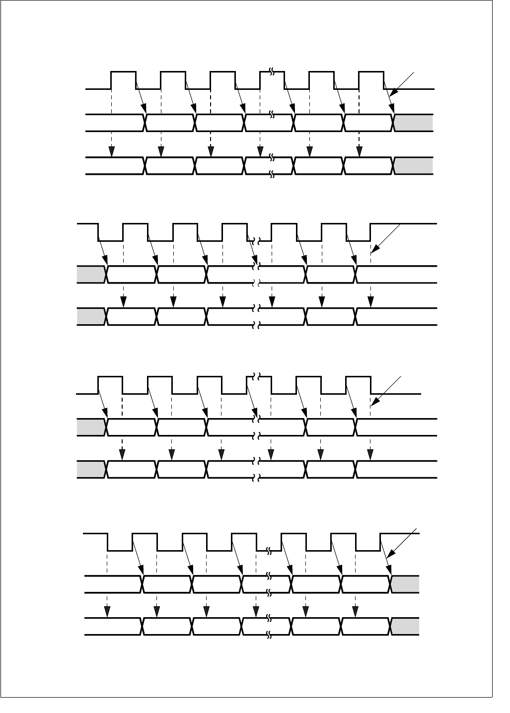
177 www.national.com
CP3BT26
23.2 MASTER MODE
In Master mode, the MSK pin is an output for the shift clock,
MSK. When data is written to the MWDAT register, eight or
sixteen MSK clocks, depending on the mode selected, are
generated to shift the 8 or 16 bits of data, and then MSK
goes idle again. The MSK idle state can be either high or
low, depending on the SCIDL bit.
Figure 85. Normal Mode (SCIDL = 0)
Figure 86. Normal Mode (SCIDL = 1)
Figure 87. Alternate Mode (SCIDL = 0)
Figure 88. Alternate Mode (SCIDL = 1)
Bit 0
(LSB)
Bit 1MSB - 2MSB - 1
MSK
End of Transfer
Sample
Point
Shift
Out
Data Out
MSB
Bit 0
(LSB)
Bit 1MSB - 2MSB - 1
Data In
MSB
DS069
Bit 0
(LSB)
Bit 1MSB - 2MSB - 1
MSK
End of Transfer
Data Out
MSB
Bit 0
(LSB)
Bit 1MSB - 2MSB - 1
Data In
MSB
Sample
Point
Shift
Out
DS070
Bit 0
(LSB)
Bit 1MSB - 2MSB - 1
MSK
End of Transfer
Data Out
MSB
Bit 0
(LSB)
Bit 1MSB - 2MSB - 1
Data In
MSB
Sample
Point
Shift
Out
DS071
Bit 0
(LSB)
Bit 1MSB - 2MSB - 1
MSK
End of Transfer
Sample
Point
Shift
Out
Data Out
MSB
Bit 0
(LSB)
Bit 1MSB - 2MSB - 1
Data In
MSB
DS072
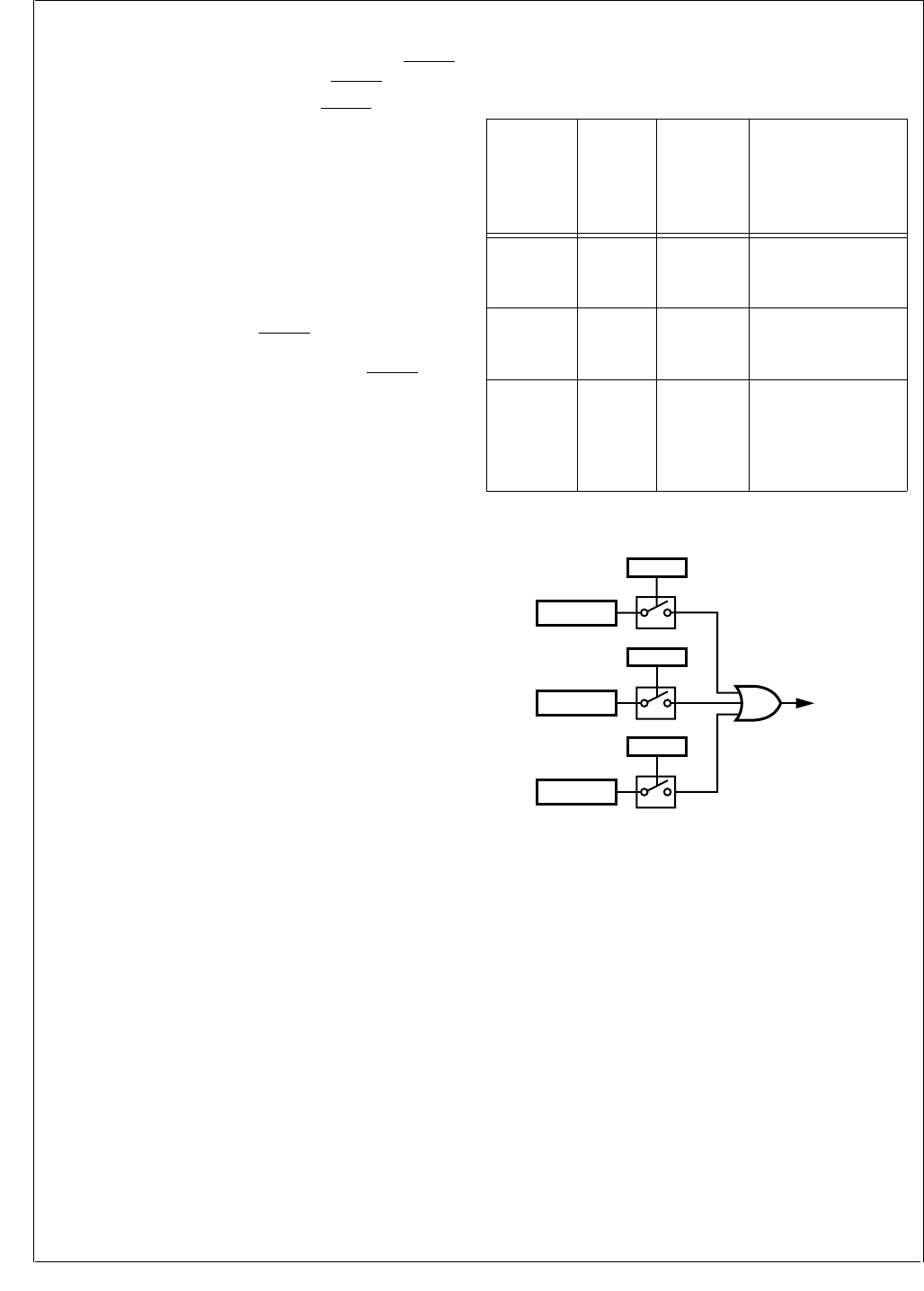
www.national.com 178
CP3BT26
23.3 SLAVE MODE
In Slave mode, the MSK pin is an input for the shift clock
MSK. MDIDO is placed in TRI-STATE mode when MWCS is
inactive. Data transfer is enabled when MWCS is active.
The slave starts driving MDIDO when MWCS is active. The
most significant bit (lower byte in 8-bit mode or upper byte
in 16-bit mode) is output onto the MDIDO pin first. After
eight or sixteen clocks (depending on the selected mode),
the data transfer is completed.
If a new shift process starts before MWDAT was written, i.e.,
while MWDAT does not contain any valid data, and the
ECHO bit is set, the data received from MDODI is transmit-
ted on MDIDO in addition to being shifted to MWDAT. If the
ECHO bit is clear, the data transmitted on MDIDO is the
data held in the MWDAT register, regardless of its validity.
The master may negate the MWCS signal to synchronize
the bit count between the master and the slave. In the case
that the slave is the only slave in the system, MWCS can be
tied to ground.
23.4 INTERRUPT GENERATION
Interrupts may be enabled for any of the conditions shown
in Table 73.
Figure 89 illustrates the interrupt generation logic of this
module.
Figure 89. MWSPI Interrupts
Table 73 Microwire Interrupt Trigger Condition
Condition
Status
Bit in the
MWSTAT
Register
Interrupt
Enable Bit
in the
MWCTRL1
Register
Description
Not Busy BSY EIW
The shifter is ready
for the next data
transfer sequence.
Read
Buffer Full RBF EIR
The read buffer is
full and waiting to be
unloaded.
Overrun OVF EIO
A new data transfer
sequence started
while both the shifter
and the read buffer
were full.
MWSPI
Interrupt
OVR = 1
EIO
RBF = 1
EIR
BSY = 0
EIW
DS073
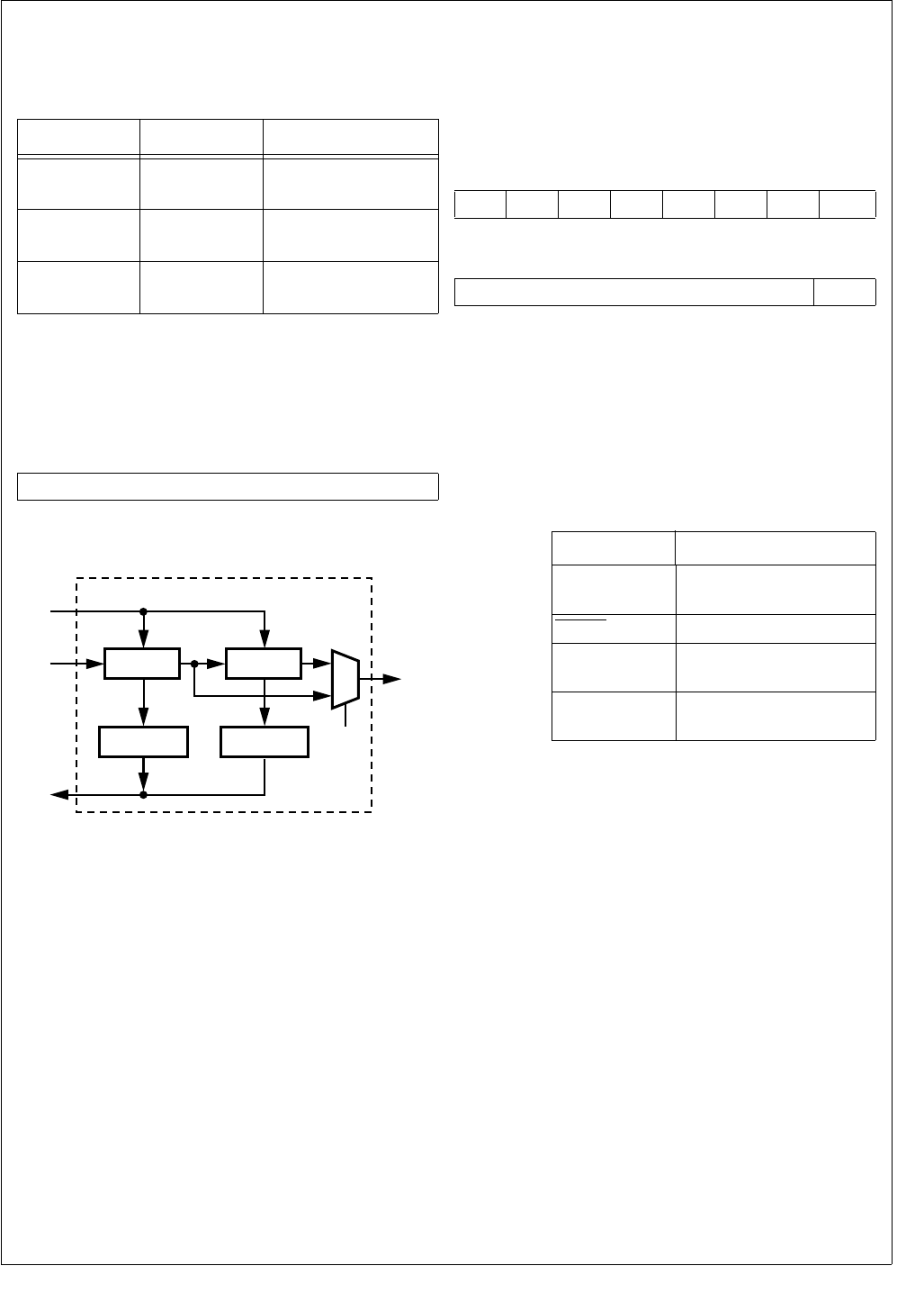
179 www.national.com
CP3BT26
23.5 MICROWIRE INTERFACE REGISTERS
Software interacts with the Microwire interface by accessing
the Microwire registers. There are three such registers:
23.5.1 Microwire Data Register (MWDAT)
The MWDAT register is a word-wide, read/write register
used to transmit and receive data through the MDODI and
MDIDO pins. The register format is shown below.
Figure 90 shows the hardware structure of the register.
Figure 90. MWDAT Register
23.5.2 MICROWIRE Control Register (MWCTL1)
The MWCTL1 register is a word-wide, read/write register
used to control the Microwire module. To avoid clock glitch-
es, the MWEN bit must be clear while changing the states
of any other bits in the register. At reset, all non-reserved
bits are cleared. The register format is shown below.
MWEN The Microwire Enable bit controls whether the
Microwire interface module is enabled.
0 – Microwire module disabled.
1 – Microwire module enabled.
Clearing this bit disables the module, clears
the status bits in the Microwire status register
(the BSY, RBF, and OVR bits in MWSTAT),
and places the Microwire interface pins in the
states described below.
MNS The Master/Slave Select bit controls whether
the CP3BT26 is a master or slave. When
clear, the device operates as a slave. When
set, the device operates as the master.
0 – CP3BT26 is slave.
1 – CP3BT26 is master.
MOD The Mode Select bit controls whether 8- or 16-
bit mode is used. When clear, the device op-
erates in 8-bit mode. When set, the device op-
erates in 16-bit mode. This bit must only be
changed when the module is disabled or idle
(MWSTAT.BSY = 0).
0 – 8-bit mode.
1 – 16-bit mode.
ECHO The Echo Back bit controls whether the echo
back function is enabled in slave mode. This
bit must be written only when the Microwire in-
terface is idle (MWSTAT.BSY=0). The ECHO
bit is ignored in master mode. The MWDAT
register is valid from the time the register has
been written until the end of the transfer. In the
echo back mode, MDODI is transmitted (ech-
oed back) on MDIDO if the MWDAT register
does not contain any valid data. With the echo
back function disabled, the data held in the
Table 74 Microwire Interface Registers
Name Address Description
MWDAT FF F3A0h Microwire Data
Register
MWCTL1 FF F3A2h Microwire Control
Register
MWSTAT FF F3A4h Microwire Status
Register
7 0
MWDAT
Shifter
(High Byte)
DIN
Write
DOUT
MOD
MWDAT
1
0
Shifter
(Low Byte)
Read Buffer
(High Byte)
Read Buffer
(Low Byte)
Read
DS074
7654321 0
SCM EIW EIR EIO ECHO MOD MNS MWEN
15 9 8
SCDV SCIDL
Pin State When Disabled
MSK Master – SCIDL Bit
Slave – Input
MWCS Input
MDIDO Master – Input
Slave – TRI-STATE
MDODI Master – Known value
Slave – Input

www.national.com 180
CP3BT26
MWDAT register is transmitted on MDIDO,
whether or not the data is valid.
0 – Echo back disabled.
1 – Echo back enabled.
EIO The Enable Interrupt on Overrun bit enables
or disables the overrun error interrupt. When
set, an interrupt is generated when the Re-
ceive Overrun Error bit (MWSTAT.OVR) is set.
Otherwise, no interrupt is generated when an
overrun error occurs. This bit must only be en-
abled in master mode.
0 – Disable overrun error interrupts.
1 – Enable overrun error interrupts.
EIR The Enable Interrupt for Read bit controls
whether an interrupt is generated when the
read buffer becomes full. When set, an inter-
rupt is generated when the Read Buffer Full
bit (MWSTAT.RBF) is set. Otherwise, no inter-
rupt is generated when the read buffer is full.
0 – No read buffer full interrupt.
1 – Interrupt when read buffer becomes full.
EIW The Enable Interrupt for Write bit controls
whether an interrupt is generated when the
Busy bit (MWSTAT.BSY) is cleared, which in-
dicates that a data transfer sequence has
been completed and the read buffer is ready
to receive the new data. Otherwise, no inter-
rupt is generated when the Busy bit is cleared.
0 – No interrupt on data transfer complete.
1 – Interrupt on data transfer complete.
SCM The Shift Clock Mode bit selects between the
normal clocking mode and the alternate clock-
ing mode. In the normal mode, the output data
is clocked out on the falling edge of MSK and
the input data is sampled on the rising edge of
MSK. In the alternate mode, the output data is
clocked out on the rising edge of MSK and the
input data is sampled on the falling edge of
MSK.
0 – Normal clocking mode.
1 – Alternate clocking mode.
SCIDL The Shift Clock Idle bit controls the value of
the MSK output when the Microwire module is
idle. This bit must be changed only when the
Microwire module is disabled (MEN = 0) or
when no bus transaction is in progress (MW-
STAT.BSY = 0).
0 – MSK is low when idle.
1 – MSK is high when idle
SCDV The Shift Clock Divider Value field specifies
the divisor used for generating the MSK shift
clock from the System Clock. The divisor is 2
× (SCDV[6:0] + 1). Valid values are 0000001b
to 1111111b, so the division ratio may range
from 3 to 256. This field is ignored in slave
mode (MWCTL1.MNS=0).
23.5.3 Microwire Status Register (MWSTAT)
The MWSTAT register is a word-wide, read-only register
that shows the current status of the Microwire interface
module. At reset, all non-reserved bits are clear. The regis-
ter format is shown below.
BSY The Busy bit, when set, indicates that the Mi-
crowire shifter is busy. In master mode, the
BSY bit is set when the MWDAT register is
written. In slave mode, the bit is set on the first
leading edge of MSK when MWCS is assert-
ed or when the MWDAT register is written,
whichever occurs first. In both master and
slave modes, this bit is cleared when the Mi-
crowire data transfer sequence is completed
and the read buffer is ready to receive the new
data; in other words, when the previous data
held in the read buffer has already been read.
If the previous data in the read buffer has not
been read and new data has been received
into the shift register, the BSY bit will not be
cleared, as the transfer could not be complet-
ed because the contents of the shift register
could not be transferred into the read buffer.
0 – Microwire shifter is not busy.
1 – Microwire shifter is busy.
RBF The Read Buffer Full bit, when set, indicates
that the Microwire read buffer is full and ready
to be read by software. It is set when the
shifter loads the read buffer, which occurs
upon completion of a transfer sequence if the
read buffer is empty. The RBF bit is updated
when the MWDAT register is read. At that
time, the RBF bit is cleared if the shifter does
not contain any new data (in other words, the
shifter is not receiving data or has not yet re-
ceived a full byte of data). The RBF bit re-
mains set if the shifter already holds new data
at the time that MWDAT is read. In that case,
MWDAT is immediately reloaded with the new
data and is ready to be read by software.
0 – Microwire read buffer is not full.
1 – Microwire read buffer is full.
OVR The Receive Overrun Error bit, when set in
master mode, indicates that a receive overrun
error has occurred. This error occurs when
the read buffer is full, the 8-bit shifter is full,
and a new data transfer sequence starts. This
bit is undefined in slave mode. The OVR bit,
once set, remains set until cleared by soft-
ware. Software clears this bit by writing a 1 to
its bit position. Writing a 0 to this bit position
has no effect. No other bits in the MWSTAT
register are affected by a write operation to
the register.
0 – No receive overrun error has occurred.
1 – Receive overrun error has occurred.
15 3 2 1 0
Reserved OVR RBF BSY
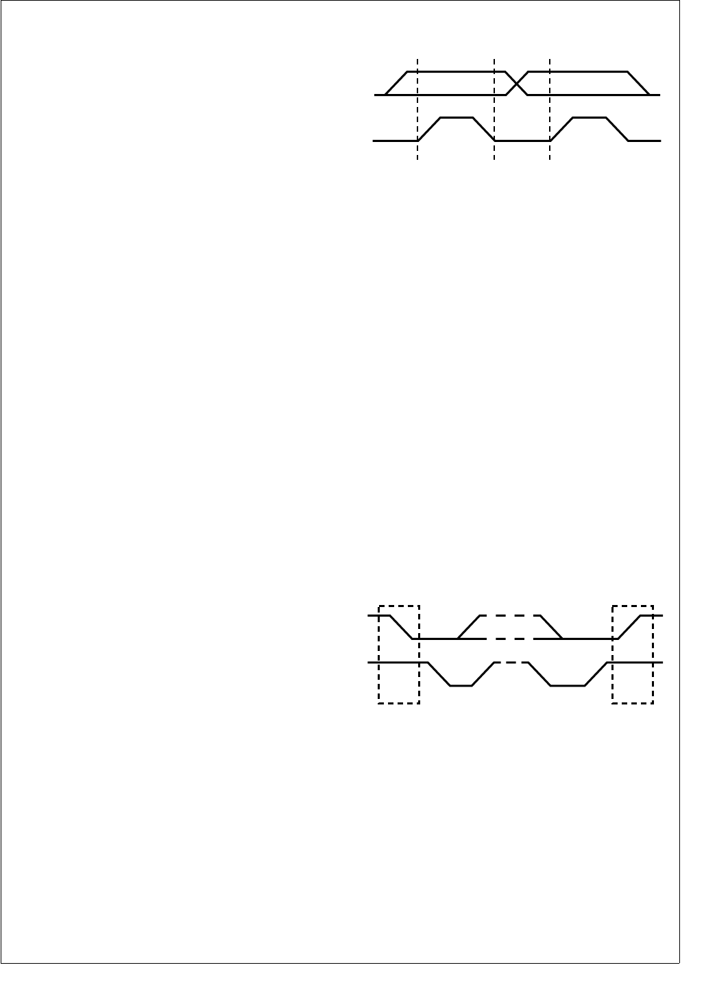
181 www.national.com
CP3BT26
24.0 ACCESS.bus Interface
The ACCESS.bus interface module (ACB) is a two-wire se-
rial interface compatible with the ACCESS.bus physical lay-
er. It permits easy interfacing to a wide range of low-cost
memories and I/O devices, including: EEPROMs, SRAMs,
timers, A/D converters, D/A converters, clock chips, and pe-
ripheral drivers. It is compatible with Intel’s SMBus and Phil-
ips’ I2C bus. The ACB module can be configured as a bus
master or slave, and can maintain bidirectional communica-
tions with both multiple master and slave devices.
This section presents an overview of the bus protocol, and
its implementation by the ACB module.
ACCESS.bus master and slave
Supports polling and interrupt-controlled operation
Generate a wake-up signal on detection of a Start Con-
dition, while in power-down mode
Optional internal pull-up on SDA and SCL pins
24.1 ACB PROTOCOL OVERVIEW
The ACCESS.bus protocol uses a two-wire interface for bi-
directional communication between the devices connected
to the bus. The two interface signals are the Serial Data Line
(SDA) and the Serial Clock Line (SCL). These signals
should be connected to the positive supply, through pull-up
resistors, to keep the signals high when the bus is idle.
The ACCESS.bus protocol supports multiple master and
slave transmitters and receivers. Each bus device has a
unique address and can operate as a transmitter or a re-
ceiver (though some peripherals are only receivers).
During data transactions, the master device initiates the
transaction, generates the clock signal, and terminates the
transaction. For example, when the ACB initiates a data
transaction with an ACCESS.bus peripheral, the ACB be-
comes the master. When the peripheral responds and
transmits data to the ACB, their master/slave (data transac-
tion initiator and clock generator) relationship is unchanged,
even though their transmitter/receiver functions are re-
versed.
24.1.1 Data Transactions
One data bit is transferred during each clock period. Data is
sampled during the high phase of the serial clock (SCL).
Consequently, throughout the clock high phase, the data
must remain stable (see Figure 91). Any change on the SDA
signal during the high phase of the SCL clock and in the
middle of a transaction aborts the current transaction. New
data must be driven during the low phase of the SCL clock.
This protocol permits a single data line to transfer both com-
mand/control information and data using the synchronous
serial clock.
Figure 91. Bit Transfer
Each data transaction is composed of a Start Condition, a
number of byte transfers (programmed by software), and a
Stop Condition to terminate the transaction. Each byte is
transferred with the most significant bit first, and after each
byte, an Acknowledge signal must follow.
At each clock cycle, the slave can stall the master while it
handles the previous data, or prepares new data. This can
be performed for each bit transferred or on a byte boundary
by the slave holding SCL low to extend the clock-low period.
Typically, slaves extend the first clock cycle of a transfer if a
byte read has not yet been stored, or if the next byte to be
transmitted is not yet ready. Some microcontrollers with lim-
ited hardware support for ACCESS.bus extend the access
after each bit, to allow software time to handle this bit.
Start and Stop
The ACCESS.bus master generates Start and Stop Condi-
tions (control codes). After a Start Condition is generated,
the bus is considered busy and it retains this status until a
certain time after a Stop Condition is generated. A high-to-
low transition of the data line (SDA) while the clock (SCL) is
high indicates a Start Condition. A low-to-high transition of
the SDA line while the SCL is high indicates a Stop Condi-
tion (Figure 92).
Figure 92. Start and Stop Conditions
In addition to the first Start Condition, a repeated Start Con-
dition can be generated in the middle of a transaction. This
allows another device to be accessed, or a change in the di-
rection of the data transfer.
SDA
Data Line
Stable:
Data Valid
Change
of Data
Allowed
SCL
DS075
Start
Condition
Stop
Condition
SDA
S
SCL
P
DS076
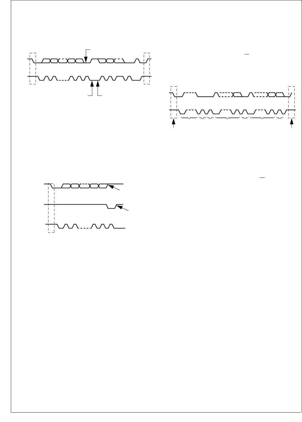
www.national.com 182
CP3BT26
Acknowledge Cycle
The Acknowledge Cycle consists of two signals: the ac-
knowledge clock pulse the master sends with each byte
transferred, and the acknowledge signal sent by the receiv-
ing device (Figure 93).
Figure 93. ACCESS.bus Data Transaction
The master generates the acknowledge clock pulse on the
ninth clock pulse of the byte transfer. The transmitter releas-
es the SDA line (permits it to go high) to allow the receiver
to send the acknowledge signal. The receiver must pull
down the SDA line during the acknowledge clock pulse,
which signals the correct reception of the last data byte, and
its readiness to receive the next byte. Figure 94 illustrates
the acknowledge cycle.
Figure 94. ACCESS.bus Acknowledge Cycle
The master generates an acknowledge clock pulse after
each byte transfer. The receiver sends an acknowledge sig-
nal after every byte received. There are two exceptions to
the “acknowledge after every byte” rule.
When the master is the receiver, it must indicate to the
transmitter an end-of-data condition by not-acknowledg-
ing (“negative acknowledge”) the last byte clocked out of
the slave. This “negative acknowledge” still includes the
acknowledge clock pulse (generated by the master), but
the SDA line is not pulled down.
When the receiver is full, otherwise occupied, or a prob-
lem has occurred, it sends a negative acknowledge to in-
dicate that it cannot accept additional data bytes.
Addressing Transfer Formats
Each device on the bus has a unique address. Before any
data is transmitted, the master transmits the address of the
slave being addressed. The slave device should send an
acknowledge signal on the SDA signal, once it recognizes
its address.
The address is the first seven bits after a Start Condition.
The direction of the data transfer (R/W) depends on the bit
sent after the address (the eighth bit). A low-to-high transi-
tion during a SCL high period indicates the Stop Condition,
and ends the transaction (Figure 95).
Figure 95. A Complete ACCESS.bus Data Transaction
When the address is sent, each device in the system com-
pares this address with its own. If there is a match, the de-
vice considers itself addressed and sends an acknowledge
signal. Depending upon the state of the R/W bit (1 = read,
0 = write), the device acts as a transmitter or a receiver.
The ACCESS.bus protocol allows sending a general call ad-
dress to all slaves connected to the bus. The first byte sent
specifies the general call address (00h) and the second byte
specifies the meaning of the general call (for example,
“Write slave address by software only”). Those slaves that
require the data acknowledge the call and become slave re-
ceivers; the other slaves ignore the call.
Arbitration on the Bus
Arbitration is required when multiple master devices attempt
to gain control of the bus simultaneously. Control of the bus
is initially determined according to address bits and clock
cycle. If the masters are trying to address the same bus de-
vice, data comparisons determine the outcome of this arbi-
tration. In master mode, the device immediately aborts a
transaction if the value sampled on the SDA lines differs
from the value driven by the device. (Exceptions to this rule
are SDA while receiving data; in these cases the lines may
be driven low by the slave without causing an abort.)
The SCL signal is monitored for clock synchronization and
allows the slave to stall the bus. The actual clock period will
be the one set by the master with the longest clock period
or by the slave stall period. The clock high period is deter-
mined by the master with the shortest clock high period.
When an abort occurs during the address transmission, the
master that identifies the conflict should give up the bus,
switch to slave mode, and continue to sample SDA to see if
it is being addressed by the winning master on the AC-
CESS.bus.
SDA
S
1
MSB
ACK ACK
Stop
Condition
Start
Condition
Clock Line Held
Low by Receiver
While Interrupt
is Serviced
Byte Complete
Interrupt Within
Receiver
Acknowledgment
Signal from Receiver
SCL 21 2 3-87
3 - 6 89 9
P
DS077
1
Transmitter Stays Off
the Bus During the
Acknowledgment Clock
Acknowledgment
Signal from Receiver
Data Output
by Transmitter
Data Output
by Receiver
SCL 27
3 - 6 89
S
Start
Condition DS078
SDA
1 - 7
ACK DataAddress
SCL
S
Stop
Condition
Start
Condition
P
89 1 - 7 89 1 - 7 8 9
R/W DataACK ACK
DS079

183 www.national.com
CP3BT26
24.2 ACB FUNCTIONAL DESCRIPTION
The ACB module provides the physical layer for an AC-
CESS.bus compliant serial interface. The module is config-
urable as either a master or slave device. As a slave, the
ACB module may issue a request to become the bus mas-
ter.
24.2.1 Master Mode
An ACCESS.bus transaction starts with a master device re-
questing bus mastership. It sends a Start Condition, fol-
lowed by the address of the device it wants to access. If this
transaction is successfully completed, software can assume
that the device has become the bus master.
For a device to become the bus master, software should
perform the following steps:
1. Set the ACBCTL1.START bit, and configure the
ACBCTL1.INTEN bit to the desired operation mode
(Polling or Interrupt). This causes the ACB to issue a
Start Condition on the ACCESS.bus, as soon as the
ACCESS.bus is free (ACBCST.BB=0). It then stalls the
bus by holding SCL low.
2. If a bus conflict is detected, (i.e., some other device
pulls down the SCL signal before this device does), the
ACBST.BER bit is set.
3. If there is no bus conflict, the ACBST.MASTER and
ACBST.SDAST bits are set.
4. If the ACBCTL1.INTEN bit is set, and either the ACB-
ST.BER bit or the ACBST.SDAST bit is set, an interrupt
is sent to the ICU.
Sending the Address Byte
Once this device is the active master of the ACCESS.bus
(ACBST.MASTER = 1), it can send the address on the bus.
The address should not be this device’s own address as
specified in the ACBADDR.ADDR field if the ACBAD-
DR.SAEN bit is set or the ACBADDR2.ADDR field if the
ACBADDR2.SAEN bit is set, nor should it be the global call
address if the ACBST.GCMTCH bit is set.
To send the address byte use the following sequence:
1. Configure the ACBCTL1.INTEN bit according to the de-
sired operation mode. For a receive transaction where
software wants only one byte of data, it should set the
ACBCTL1.ACK bit. If only an address needs to be sent,
set the ACBCTL1.STASTRE bit.
2. Write the address byte (7-bit target device address),
and the direction bit, to the ACBSDA register. This
causes the module to generate a transaction. At the
end of this transaction, the acknowledge bit received is
copied to the ACBST.NEGACK bit. During the transac-
tion, the SDA and SCL signals are continuously
checked for conflict with other devices. If a conflict is
detected, the transaction is aborted, the ACBST.BER
bit is set, and the ACBST.MASTER bit is cleared.
3. If the ACBCTL1.STASTRE bit is set, and the transac-
tion was successfully completed (i.e., both the ACB-
ST.BER and ACBST.NEGACK bits are cleared), the
ACBST.STASTR bit is set. In this case, the ACB stalls
any further ACCESS.bus operations (i.e., holds SCL
low). If the ACBCTL1.INTE bit is set, it also sends an
interrupt to the core.
4. If the requested direction is transmit, and the start
transaction was completed successfully (i.e., neither
the ACBST.NEGACK nor ACBST.BER bit is set, and no
other master has accessed the device), the ACB-
ST.SDAST bit is set to indicate that the module is wait-
ing for service.
5. If the requested direction is receive, the start transac-
tion was completed successfully, and the
ACBCTL1.STASTRE bit is clear, the module starts re-
ceiving the first byte automatically.
6. Check that both the ACBST.BER and ACBST.NEGACK
bits are clear. If the ACBCTL1.INTEN bit is set, an in-
terrupt is generated when either the ACBST.BER or
ACBST.NEGACK bit is set.
Master Transmit
After becoming the bus master, the device can start trans-
mitting data on the ACCESS.bus. To transmit a byte, soft-
ware must:
1. Check that the BER and NEGACK bits in the ACBST
register are clear and the ACBST.SDAST bit is set. Al-
so, if the ACBCTL1.STASTRE bit is set, check that the
ACBST.STASTR bit is clear.
2. Write the data byte to be transmitted to the ACBSDA
register.
When the slave responds with a negative acknowledge, the
ACBST.NEGACK bit is set and the ACBST.SDAST bit re-
mains cleared. In this case, if the ACBCTL1.INTEN bit is
set, an interrupt is sent to the core.
Master Receive
After becoming the bus master, the device can start receiv-
ing data on the ACCESS.bus. To receive a byte, software
must:
1. Check that the ACBST.SDAST bit is set and the ACB-
ST.BER bit is clear. Also, if the ACBCTL1.STASTRE bit
is set, check that the ACBST.STASTR bit is clear.
2. Set the ACBCTL1.ACK bit, if the next byte is the last
byte that should be read. This causes a negative ac-
knowledge to be sent.
3. Read the data byte from the ACBSDA register.
Master Stop
A Stop Condition may be issued only when this device is the
active bus master (ACBST.MASTRER = 1). To end a trans-
action, set the ACBCTL1.STOP bit before clearing the cur-
rent stall bit (i.e., the ACBST.SDAST, ACBST.NEGACK, or
ACBST.STASTR bit). This causes the module to send a
Stop Condition immediately, and clear the ACBCTL1.STOP
bit.

www.national.com 184
CP3BT26
Master Bus Stall
The ACB module can stall the ACCESS.bus between trans-
fers while waiting for the core’s response. The ACCESS.bus
is stalled by holding the SCL signal low after the acknowl-
edge cycle. Note that this is interpreted as the beginning of
the following bus operation. Software must make sure that
the next operation is prepared before the bit that causes the
bus stall is cleared.
The bits that can cause a stall in master mode are:
Negative acknowledge after sending a byte
(ACBSTNEGACK = 1).
ACBST.SDAST bit is set.
If the ACBCTL1.STASTRE bit is set, after a successful
start (ACBST.STASTR = 1).
Repeated Start
A repeated start is performed when this device is already
the bus master (ACBST.MASTER = 1). In this case, the AC-
CESS.bus is stalled and the ACB waits for the core handling
due to: negative acknowledge (ACBST.NEGACK = 1), emp-
ty buffer (ACBST.SDAST = 1), or a stop-after-start (ACB-
ST.STASTR = 1).
For a repeated start:
1. Set the ACBCTL1.START bit.
2. In master receive mode, read the last data item from
the ACBSDA register.
3. Follow the address send sequence, as described in
“Sending the Address Byte” on page 183.
4. If the ACB was waiting for handling due to ACB-
ST.STASTR = 1, clear it only after writing the requested
address and direction to the ACBSDA register.
Master Error Detections
The ACB detects illegal Start or Stop Conditions (i.e., a
Start or Stop Condition within the data transfer, or the ac-
knowledge cycle) and a conflict on the data lines of the AC-
CESS.bus. If an illegal action is detected, the BER bit is set,
and the MASTER mode is exited (the MASTER bit is
cleared).
Bus Idle Error Recovery
When a request to become the active bus master or a re-
start operation fails, the ACBST.BER bit is set to indicate the
error. In some cases, both this device and the other device
may identify the failure and leave the bus idle. In this case,
the start sequence may not be completed and the AC-
CESS.bus may remain deadlocked.
To recover from deadlock, use the following sequence:
1. Clear the ACBST.BER and ACBCST.BB bits.
2. Wait for a time-out period to check that there is no other
active master on the bus (i.e., the ACBCST.BB bit re-
mains clear).
3. Disable, and re-enable the ACB to put it in the non-ad-
dressed slave mode.
4. At this point, some of the slaves may not identify the
bus error. To recover, the ACB becomes the bus master
by issuing a Start Condition and sends an address
field; then issue a Stop Condition to synchronize all the
slaves.
24.2.2 Slave Mode
A slave device waits in Idle mode for a master to initiate a
bus transaction. Whenever the ACB is enabled, and it is not
acting as a master (i.e., ACBST.MASTER = 0), it acts as a
slave device.
Once a Start Condition on the bus is detected, this device
checks whether the address sent by the current master
matches either:
The ACBADDR.ADDR value if the ACBADDR.SAEN bit
is set.
The ACBADDR2.ADDR value if the ACBADDR2.SAEN
bit is set.
The general call address if the ACBCTL1.GCM bit is set.
This match is checked even when the ACBST.MASTER bit
is set. If a bus conflict (on SDA or SCL) is detected, the
ACBST.BER bit is set, the ACBST.MASTER bit is cleared,
and this device continues to search the received message
for a match. If an address match, or a global match, is de-
tected:
1. This device asserts its data pin during the acknowledge
cycle.
2. The ACBCST.MATCH, ACBCST.MATCHAF (or
ACBCST.GCMTCH if it is a global call address match,
or ACBCST.ARPMATCH if it is an ARP address), and
ACBST.NMATCH in the ACBCST register are set. If the
ACBST.XMIT bit is set (i.e., slave transmit mode), the
ACBST.SDAST bit is set to indicate that the buffer is
empty.
3. If the ACBCTL1.INTEN bit is set, an interrupt is gener-
ated if both the INTEN and NMINTE bits in the
ACBCTL1 register are set.
4. Software then reads the ACBST.XMIT bit to identify the
direction requested by the master device. It clears the
ACBST.NMATCH bit so future byte transfers are identi-
fied as data bytes.
Slave Receive and Transmit
Slave Receive and Transmit are performed after a match is
detected and the data transfer direction is identified. After a
byte transfer, the ACB extends the acknowledge clock until
software reads or writes the ACBSDA register. The receive
and transmit sequence are identical to those used in the
master routine.
Slave Bus Stall
When operating as a slave, this device stalls the AC-
CESS.bus by extending the first clock cycle of a transaction
in the following cases:
— The ACBST.SDAST bit is set.
— The ACBST.NMATCH, and ACBCTL1.NMINTE bits
are set.
Slave Error Detections
The ACB detects illegal Start and Stop Conditions on the
ACCESS.bus (i.e., a Start or Stop Condition within the data
transfer or the acknowledge cycle). When an illegal Start or
Stop Condition is detected, the BER bit is set and the
MATCH and GMATCH bits are cleared, causing the module
to be an unaddressed slave.

185 www.national.com
CP3BT26
Power Down
When this device is in Power Save, Idle, or Halt mode, the
ACB module is not active but retains its status. If the ACB is
enabled (ACBCTL2.ENABLE = 1) on detection of a Start
Condition, a wake-up signal is issued to the MIWU module.
Use this signal to switch this device to Active mode.
The ACB module cannot check the address byte for a match
following the start condition that caused the wake-up event
for this device. The ACB responds with a negative acknowl-
edge, and the device should resend both the Start Condition
and the address after this device has had time to wake up.
Check that the ACBCST.BUSY bit is inactive before entering
Power Save, Idle, or Halt mode. This guarantees that the de-
vice does not acknowledge an address sent and stop re-
sponding later.
24.2.3 SDA and SCL Pins Configuration
The SDA and SCL pins are driven as open-drain signals.
For more information, see the I/O configuration section.
24.2.4 ACB Clock Frequency Configuration
The ACB module permits software to set the clock frequen-
cy used for the ACCESS.bus clock. The clock is set by the
ACBCTL2.SCLFRQ field. This field determines the SCL
clock period used by this device. This clock low period may
be extended by stall periods initiated by the ACB module or
by another ACCESS.bus device. In case of a conflict with
another bus master, a shorter clock high period may be
forced by the other bus master until the conflict is resolved.
24.3 ACCESS.BUS INTERFACE REGISTERS
The ACCESS.bus interface uses the registers listed in
Ta b le 7 5 .
24.3.1 ACB Serial Data Register (ACBSDA)
The ACBSDA register is a byte-wide, read/write shift regis-
ter used to transmit and receive data. The most significant
bit is transmitted (received) first and the least significant bit
is transmitted (received) last. Reading or writing to the ACB-
SDA register is allowed when ACBST.SDAST is set; or for
repeated starts after setting the START bit. An attempt to
access the register in other cases produces unpredictable
results.
24.3.2 ACB Status Register (ACBST)
The ACBST register is a byte-wide, read-only register that
maintains current ACB status. At reset, and when the mod-
ule is disabled, ACBST is cleared.
XMIT The Direction Bit bit is set when the ACB mod-
ule is currently in master/slave transmit mode.
Otherwise it is cleared.
0 – Receive mode.
1 – Transmit mode.
MASTER The Master bit indicates that the module is
currently in master mode. It is set when a re-
quest for bus mastership succeeds. It is
cleared upon arbitration loss (BER is set) or
the recognition of a Stop Condition.
0 – Slave mode.
1 – Master mode.
NMATCH The New match bit is set when the address
byte following a Start Condition, or repeated
starts, causes a match or a global-call match.
The NMATCH bit is cleared when written with
1. Writing 0 to NMATCH is ignored. If the
ACBCTL1.INTEN bit is set, an interrupt is sent
when this bit is set.
0 – No match.
1 – Match or global-call match.
STASTR The Stall After Start bit is set by the successful
completion of an address sending (i.e., a Start
Condition sent without a bus error, or negative
acknowledge), if the ACBCTL1.STASTRE bit
is set. This bit is ignored in slave mode. When
the STASTR bit is set, it stalls the bus by pull-
ing down the SCL line, and suspends any oth-
er action on the bus (e.g., receives first byte in
master receive mode). In addition, if the
ACBCTL1.INTEN bit is set, it also sends an
interrupt to the core. Writing 1 to the STASTR
bit clears it. It is also cleared when the module
is disabled. Writing 0 to the STASTR bit has
no effect.
0 – No stall after start condition.
1 – Stall after successful start.
Table 75 ACCESS.bus Interface Registers
Name Address Description
ACBSDA FF F2A0h ACB Serial Data
Register
ACBST FF F2A2h ACB Status Register
ACBCST FF F2A4h ACB Control Status
Register
ACBCTL1 FF F2A6h ACB Control
Register 1
ACBCTL2 FF F2AAh ACB Control
Register 2
ACBCTL3 FF F2AEh ACB Control
Register 3
ACBADDR1 FF F2A8h ACB Own Address
Register 1
ACBADDR2 FF F2ACh ACB Own Address
Register 2
7 0
DATA
7 65 43 2 1 0
SLVSTP
SDAST
BER
NEGACK
STASTR NMATCH
MASTER
XMIT

www.national.com 186
CP3BT26
NEGACK The Negative Acknowledge bit is set by hard-
ware when a transmission is not acknowl-
edged on the ninth clock. (In this case, the
SDAST bit is not set.) Writing 1 to NEGACK
clears it. It is also cleared when the module is
disabled. Writing 0 to the NEGACK bit is ig-
nored.
0 – No transmission not acknowledged condi-
tion.
1 – Transmission not acknowledged.
BER The Bus Error bit is set by the hardware when
a Start or Stop Condition is detected during
data transfer (i.e., Start or Stop Condition dur-
ing the transfer of bits 2 through 8 and ac-
knowledge cycle), or when an arbitration
problem is detected. Writing 1 to the BER bit
clears it. It is also cleared when the module is
disabled. Writing 0 to the BER bit is ignored.
0 – No bus error occurred.
1 – Bus error occurred.
SDAST The SDA Status bit indicates that the SDA
data register is waiting for data (transmit, as
master or slave) or holds data that should be
read (receive, as master or slave). This bit is
cleared when reading from the ACBSDA reg-
ister during a receive, or when written to dur-
ing a transmit. When the ACBCTL1.START bit
is set, reading the ACBSDA register does not
clear the SDAST bit. This enables the ACB to
send a repeated start in master receive mode.
0 – ACB module is not waiting for data trans-
fer.
1 – ACB module is waiting for data to be load-
ed or unloaded.
SLVSTP The Slave Stop bit indicates that a Stop Con-
dition was detected after a slave transfer (i.e.,
after a slave transfer in which MATCH or
GCMATCH is set). Writing 1 to SLVSTP clears
it. It is also cleared when the module is dis-
abled. Writing 0 to SLVSTP is ignored.
0 – No stop condition after slave transfer oc-
curred.
1 – Stop condition after slave transfer oc-
curred.
24.3.3 ACB Control Status Register (ACBCST)
The ACBCST register is a byte-wide, read/write register that
maintains current ACB status. At reset and when the mod-
ule is disabled, the non-reserved bits of ACBCST are
cleared.
BUSY The BUSY bit indicates that the ACB module
is:
Generating a Start Condition
In Master mode (ACBST.MASTER is set)
In Slave mode (ACBCST.MATCH or
ACBCST.GCMTCH is set)
In the period between detecting a Start
and completing the reception of the ad-
dress byte. After this, the ACB either be-
comes not busy or enters slave mode.
The BUSY bit is cleared by the completion of
any of the above states, and by disabling the
module. BUSY is a read only bit. It must al-
ways be written with 0.
0 – ACB module is not busy.
1 – ACB module is busy.
BB The Bus Busy bit indicates the bus is busy. It
is set when the bus is active (i.e., a low level
on either SDA or SCL) or by a Start Condition.
It is cleared when the module is disabled, on
detection of a Stop Condition, or when writing
1 to this bit. See “Usage Hints” on page 189
for a description of the use of this bit. This bit
should be set when either the SDA or SCL sig-
nals are low. This is done by sampling the
SDA and SCL signals continuously and set-
ting the bit if one of them is low. The bit re-
mains set until cleared by a STOP condition or
written with 1.
0 – Bus is not busy.
1 – Bus is busy.
MATCH The Address Match bit indicates in slave
mode when ACBADDR.SAEN is set and the
first seven bits of the address byte (the first
byte transferred after a Start Condition)
matches the 7-bit address in the ACBADDR
register, or when ACBADDR2.SAEN is set
and the first seven bits of the address byte
matches the 7-bit address in the ACBADDR2
register. It is cleared by Start Condition or re-
peated Start and Stop Condition (including il-
legal Start or Stop Condition).
0 – No address match occurred.
1 – Address match occurred.
7 6 5 4 3 2 1 0
Reserved TGSCL TSDA GCMTCH MATCH BB BUSY

187 www.national.com
CP3BT26
GCMTCH The Global Call Match bit is set in slave mode
when the ACBCTL1.GCMEN bit is set and the
address byte (the first byte transferred after a
Start Condition) is 00h. It is cleared by a Start
Condition or repeated Start and Stop Condi-
tion (including illegal Start or Stop Condition).
0 – No global call match occurred.
1 – Global call match occurred.
TSDA The Test SDA bit samples the state of the SDA
signal. This bit can be used while recovering
from an error condition in which the SDA sig-
nal is constantly pulled low by a slave that
went out of sync. This bit is a read-only bit.
Data written to it is ignored.
TGSCL The Toggle SCL bit enables toggling the SCL
signal during error recovery. When the SDA
signal is low, writing 1 to this bit drives the SCL
signal high for one cycle. Writing 1 to TGSCL
when the SDA signal is high is ignored. The bit
is cleared when the clock toggle is completed.
0 – Writing 0 has no effect.
1 – Writing 1 toggles the SDA signal high for
one cycle.
24.3.4 ACB Control Register 1 (ACBCTL1)
The ACBCTL1 register is a byte-wide, read/write register
that configures and controls the ACB module. At reset and
while the module is disabled (ACBCTL2.ENABLE = 0), the
ACBCTL1 register is cleared.
START The Start bit is set to generate a Start Condi-
tion on the ACCESS.bus. The START bit is
cleared when the Start Condition is sent, or
upon detection of a Bus Error
(ACBST.BER = 1). This bit should be set only
when in Master mode, or when requesting
Master mode. If this device is not the active
master of the bus (ACBST.MASTER = 0), set-
ting the START bit generates a Start
Con0dition as soon as the ACCESS.bus is
free (ACBCST.BB = 0). An address send se-
quence should then be performed. If this de-
vice is the active master of the bus
(ACBST.MASTER = 1), when the START bit is
set, a write to the ACBSDA register generates
a Start Condition, then the ACBSDA data is
transmitted as the slave’s address and the re-
quested transfer direction. This case is a re-
peated Start Condition. It may be used to
switch the direction of the data flow between
the master and the slave, or to choose anoth-
er slave device without using a Stop Condition
in between.
0 – Writing 0 has no effect.
1 – Writing 1 generates a Start condition.
STOP The Stop bit in master mode generates a Stop
Condition that completes or aborts the current
message transfer. This bit clears itself after
the Stop condition is issued.
0 – Writing 0 has no effect.
1 – Writing 1 generates a Stop condition.
7 6 5 43 2 1 0
STASTRE NMINTE GCMEN ACK Res. INTEN STOP START

www.national.com 188
CP3BT26
INTEN The Interrupt Enable bit controls generating
ACB interrupts. When the INTEN bit is cleared
ACB interrupt is disabled. When the INTEN bit
is set, interrupts are enabled.
0 – ACB interrupts disabled.
1 – ACB interrupts enabled.
An interrupt is generated (the interrupt signals
to the ICU is high) on any of the following
events:
An address MATCH is detected (ACB-
ST.NMATCH = 1) and the NMINTE bit is
set.
A Bus Error occurs (ACBST.BERR = 1).
Negative acknowledge after sending a
byte (ACBST.NEGACK = 1).
An interrupt is generated on acknowledge
of each transaction (same as hardware
setting the ACBST.SDAST bit).
If ACBCTL1.STASTRE = 1, in master
mode after a successful start
(ACBST.STASTR = 1).
Detection of a Stop Condition while in
slave receive mode (ACBST.SLVSTP = 1).
ACK The Acknowledge bit holds the value this de-
vice sends in master or slave mode during the
next acknowledge cycle. Setting this bit to 1
instructs the transmitting device to stop send-
ing data, since the receiver either does not
need, or cannot receive, any more data. This
bit is cleared after the first acknowledge cycle.
This bit is ignored when in transmit mode.
GCMEN The Global Call Match Enable bit enables the
match of an incoming address byte to the gen-
eral call address (Start Condition followed by
address byte of 00h) while the ACB is in slave
mode. When cleared, the ACB does not re-
spond to a global call.
0 – Global call matching disabled.
1 – Global call matching enabled.
NMINTE The New Match Interrupt Enable controls
whether ACB interrupts are generated on new
matches. Set the NMINTE bit to enable the in-
terrupt on a new match (i.e., when ACB-
ST.NMATCH is set). The interrupt is issued
only if the ACBCTL1.INTEN bit is set.
0 – New match interrupts disabled.
1 – New match interrupts enabled.
STASTRE The Stall After Start Enable bit enables the
stall after start mechanism. When enabled,
the ACB is stalled after the address byte.
When the STASTRE bit is clear, the ACB-
ST.STASTR bit is always clear.
0 – No stall after start.
1 – Stall-after-start enabled.
24.3.5 ACB Control Register 2 (ACBCTL2)
The ACBCTL2 register is a byte-wide, read/write register
that controls the module and selects the ACB clock rate. At
reset, the ACBCTL2 register is cleared.
ENABLE The Enable bit controls the ACB module.
When this bit is set, the ACB module is en-
abled. When the Enable bit is clear, the ACB
module is disabled, the ACBCTL1, ACBST,
and ACBCST registers are cleared, and the
clocks are halted.
0 – ACB module disabled.
1 – ACB module enabled.
SCLFRQ The SCL Frequency field specifies the SCL
period (low time and high time) in master
mode. The clock low time and high time are
defined as follows:
tSCLl = tSCLh = 2 × SCLFRQ × tCLK
Where tCLK is this device’s clock period when
in Active mode. The SCLFRQ field may be
programmed to values in the range of
0001000b through 1111111b. Using any other
value has unpredictable results.
24.3.6 ACB Control Register 3 (ACBCTL3)
The ACBCTL3 register is a byte-wide, read/write register
that expands the clock prescaler field and enables ARP
matches. At reset, the ACBCTL3 register is cleared.
ARPMEN The ARP Match Enable bit enables the
matching of an incoming address byte to the
SMBus ARP address 110 0001b general call
address (Start condition followed by address
byte of 00h), while the ACB is in slave mode.
0 – ACB does not respond to ARP address-
es.
1 – ARP address matching enabled.
SCLFRQ The SCL Frequency field specifies the SCL
period (low time and high time) in master
mode. The ACBCTL3 register provides a 2-bit
expansion of this field, with the remaining 7
bits being held in the ACBCTL2 register.
7 1 0
SCLFRQ6:0 ENABLE
7 3 2 1 0
Reserved ARPMEN SCLFRQ8:7

189 www.national.com
CP3BT26
24.3.7 ACB Own Address Register 1 (ACBADDR1)
The ACBADDR1 register is a byte-wide, read/write register
that holds the module’s first ACCESS.bus address. After re-
set, its value is undefined.
ADDR The Own Address field holds the first 7-bit AC-
CESS.bus address of this device. When in
slave mode, the first 7 bits received after a
Start Condition are compared to this field (first
bit received to bit 6, and the last to bit 0). If the
address field matches the received data and
the SAEN bit is set, a match is detected.
SAEN The Slave Address Enable bit controls wheth-
er address matching is performed in slave
mode. When set, the SAEN bit indicates that
the ADDR field holds a valid address and en-
ables the match of ADDR to an incoming ad-
dress byte. When cleared, the ACB does not
check for an address match.
0 – Address matching disabled.
1 – Address matching enabled0.
24.3.8 ACB Own Address Register 2 (ACBADDR2)
The ACBADDR2 register is a byte-wide, read/write register
that holds the module’s second ACCESS.bus address. After
reset, its value is undefined.
ADDR The Own Address field holds the second 7-bit
ACCESS.bus address of this device. When in
slave mode, the first 7 bits received after a
Start Condition are compared to this field (first
bit received to bit 6, and the last to bit 0). If the
address field matches the received data and
the SAEN bit is set, a match is detected.
SAEN The Slave Address Enable bit controls wheth-
er address matching is performed in slave
mode. When set, the SAEN bit indicates that
the ADDR field holds a valid address and en-
ables the match of ADDR to an incoming ad-
dress byte. When cleared, the ACB does not
check for an address match.
0 – Address matching disabled.
1 – Address matching enabled.
24.4 USAGE HINTS
When the ACB module is disabled, the ACBCST.BB bit is
cleared. After enabling the ACB (ACBCTL2.ENABLE =
1) in systems with more than one master, the bus may be
in the middle of a transaction with another device, which
is not reflected in the BB bit. There is a need to allow the
ACB to synchronize to the bus activity status before issu-
ing a request to become the bus master, to prevent bus
errors. Therefore, before issuing a request to become the
bus master for the first time, software should check that
there is no activity on the bus by checking the BB bit after
the bus allowed time-out period.
When waking up from power down, before checking the
ACBCST.MATCH bit, test the ACBCST.BUSY bit to make
sure that the address transaction has finished.
The BB bit is intended to solve a deadlock in which two,
or more, devices detect a usage conflict on the bus and
both devices cease being bus masters at the same time.
In this situation, the BB bits of both devices are active
(because each deduces that there is another master cur-
rently performing a transaction, while in fact no device is
executing a transaction), and the bus would stay locked
until some device sends a ACBCTL1.STOP condition.
The ACBCST.BB bit allows software to monitor bus us-
age, so it can avoid sending a STOP signal in the middle
of the transaction of some other device on the bus. This
bit detects whether the bus remains unused over a cer-
tain period, while the BB bit is set.
In some cases, the bus may get stuck with the SCL or
SDA lines active. A possible cause is an erroneous Start
or Stop Condition that occurs in the middle of a slave re-
ceive session. When the SCL signal is stuck active, there
is nothing that can be done, and it is the responsibility of
the module that holds the bus to release it. When the
SDA signal is stuck active, the ACB module enables the
release of the bus by using the following sequence. Note
that in normal cases, the SCL signal may be toggled only
by the bus master. This protocol is a recovery scheme
which is an exception that should be used only in the
case when there is no other master on the bus. The re-
covery scheme is as follows:
1. Disable and re-enable the module to set it into the not
addressed slave mode.
2. Set the ACBCTL1.START bit to make an attempt to
issue a Start Condition.
3. Check if the SDA signal is active (low) by reading
ACBCST.TSDA bit. If it is active, issue a single SCL
cycle by writing 1 to ACBCST.TGSCL bit. If the SDA
line is not active, continue from step 5.
4. Check if the ACBST.MASTER bit is set, which indi-
cates that the Start Condition was sent. If not, repeat
step 3 and 4 until the SDA signal is released.
5. Clear the BB bit. This enables the START bit to be ex-
ecuted. Continue according to “Bus Idle Error Recov-
ery” on page 184.
7 6 0
SAEN ADDR
7 6 0
SAEN ADDR

www.national.com 190
CP3BT26
24.4.1 Avoiding Bus Error During Write Transaction
A Bus Error (BER) may occur during a write transaction if
the data register is written at a very specific time. The mod-
ule generates one system-clock cycle setup time of SDA to
SCL vs. the minimum time of the clock divider ratio.
The problem can be masked within the driver by dynamical-
ly dividing-by-half the SCL width immediately after the slave
address is successfully sent and before writing to the ACB-
SDA register. This has the effect of forcing SCL into the
stretch state.
The following code example is the relevant segment of the
ACCESS.bus driver addressing this issue.
/*%%%%%%%%%%%%%%%%%%%%%%%%%%%%%%%%%%%%%%%%%%%%%%%%%%%%%%%%%%%%%%%%%%%%%%%%%%%%%%%%%%%%%%%%%%%%%%%%%%%%%%%%%%%%
; NAME: ACBRead Reads "Count" byte(s) from selected I2C Slave. If read address differs from previous
; Read or Write operation (as recorded in NextAddress), a "dummy" write transaction is
; initiated to reset the address to the desired location. This is followed by a repeated
; Start sequence and the Read transaction. All transactions begin with a call to ACBStartX
; which sends the Start condition and Slave address. Checks for errors throughout process.
;
; PARAMETERS: UBYTE Slave - Slave Device Address. Must be of format 0xXXXX0000
; UWORD Addrs - Byte/Array address (extended addressing mode uses two byte address)
; UWORD Count - Number of bytes to read
; UBYTE *buf - Pointer to receive buffer
;
; CALLS: ACBStartX
;
; RETURNED: error status
;%%%%%%%%%%%%%%%%%%%%%%%%%%%%%%%%%%%%%%%%%%%%%%%%%%%%%%%%%%%%%%%%%%%%%%%%%%%%%%%%%%%%%%%%%%%%%%%%%%%%%%%%%%%%*/
UWORD ACBRead (UBYTE Slave, UWORD Addrs, UWORD Count, UBYTE *buf)
{
ACB_T *acb;
UBYTE err, *rcv;
UWORD Timeout;
acb = (ACB_T*)ACB_ADDRESS; /* Set pointer to ACB module */
/* If the indicated address differs from the last */
if (Addrs != NextAddress) {
/* recorded access (i.e. Random Read), we must first */
/* send a "dummy" write to the desired new address.. */
NextAddress = Addrs; /* Update last address placeholder */
KeyInit();
KBD_OUT &= ~BIT0;
/* Send start bit and Slave address... */
if ((err = ACBStartX (Slave | (Addrs >> 7 & 0x0E), ACB_WRITE, 0)))
return (err); /* If unsuccessful, return error code */
// KBD_OUT &= ~BIT0;
acb->ACBsda = (UBYTE)Addrs; /* Send new address byte */
KBD_OUT &= ~BIT0;
Timeout = 1000; /* Set timeout */
/* Wait for xmitter to be ready...zzzzzzzzz */
while (!(acb->ACBst & ACBSDAST) && !(acb->ACBst & ACBBER) && Timeout--);
if (acb->ACBst & ACBBER) {
/* If a bus error occurs while sending address, clear */
acb->ACBst |= ACBBER; /* the error flag and return error status */
return (ACBERR_COLLISION);
}
KBD_OUT &= ~BIT0;
if (!Timeout) /* If we timeout, return error */
return (ACBERR_TIMEOUT);
}
/* (Re)Send start bit and Slave address... */
if ((err = ACBStartX (Slave | (Addrs >> 7 & 0x0E), ACB_READ, Count)))
/* If error, return */
return (err);
rcv = buf; /* Get address of read buffer */
/* Read Count bytes into user’s buffer */
while (Count) {
if (Count-- == 1) /* If this the final byte, or only one requested, send */
acb->ACBctl1 |= ACBACK; /* the NACK bit after reception */
Timeout = 1000; /* Set timeout */
while (!(acb->ACBst & ACBSDAST) && Timeout--);
if (!Timeout) /* Timed out?? */
/* YES - return error */
return (ACBERR_TIMEOUT);
*rcv++ = acb->ACBsda; /* NO - Read byte from Recv register */
/* Adjust current address placeholder */
NextAddress++;
}

191 www.national.com
CP3BT26
acb->ACBctl1 |= ACBSTOP; /* Send STOP bit */
/* Return success status.... */
return (ACB_NOERR);
}
/*%%%%%%%%%%%%%%%%%%%%%%%%%%%%%%%%%%%%%%%%%%%%%%%%%%%%%%%%%%%%%%%%%%%%%%%%%%%%%%%%%%%%%%%%%%%%%%%%%%%%%%%%%%%%
; NAME: ACBStartX Initiates an ACB bus transaction by sending the Start bit, followed by the Slave address
; and R/W flag. Checks for any ACB errors throughout this sequence and returns status.
;
; PARAMETERS: UBYTE Slave - I2C address of Slave device
; UBYTE R_nW - Read/Write flag (0x01 or 0x00)
; UWORD Count - Desired number of bytes (read/write)
;
; CALLS:
;
; RETURNED: error/success
;%%%%%%%%%%%%%%%%%%%%%%%%%%%%%%%%%%%%%%%%%%%%%%%%%%%%%%%%%%%%%%%%%%%%%%%%%%%%%%%%%%%%%%%%%%%%%%%%%%%%%%%%%%%%*/
UWORD ACBStartX (UBYTE Slave, UBYTE R_nW, UWORD Count)
{
ACB_T *acb;
UWORD Timeout;
/* Get address of ACB module */
acb = (ACB_T*)ACB_ADDRESS;
/* If Bus is Busy and we’re NOT the Master, return err */
if (acb->ACBcst & ACBBB && !(acb->ACBst & ACBMASTER))
return (ACBERR_NOTMASTER);
/* If we’re good to go, send Start condition */
acb->ACBctl1 |= ACBSTART;
/* Check if we’re the Bus Master with timeout */
Timeout = 100;
while (!(acb->ACBst & ACBSDAST) && Timeout--) /* Related to bus error problem */
{
if (acb->ACBst & ACBBER) { /* If collision occurs, clear error and return status */
acb->ACBst |= ACBBER;
return (ACBERR_COLLISION);
}
}
if (!Timeout) /* If timeout, we must NOT be the Master...signal error */
return (ACBERR_NOTMASTER);
/* Now, send the address and R/W flag... */
acb->ACBsda = Slave | R_nW; /* Send address and R/W flag */
Timeout = 1000; /* Failsafe for lockup */
/* Wait for address to be sent and ACK’d */
while (!(acb->ACBst & ACBSDAST) &&
!(acb->ACBst & ACBNEGACK)&&
--Timeout) {
if (acb->ACBst & ACBBER) { /* If a bus error occurs while sending address, clear */
acb->ACBst |= ACBBER; /* the error flag and return error status */
return (ACBERR_COLLISION);
}
}
KBD_OUT |= BIT0; // OScope marker
if (!Timeout) /* If timeout, signal error */
return (ACBERR_TIMEOUT);
/* Or if Slave does not reply, report busy/error */
else if (acb->ACBst & ACBNEGACK)
return (ACBERR_NEGACK);
/* Otherwise return success */
else {
return (ACB_NOERR);
}
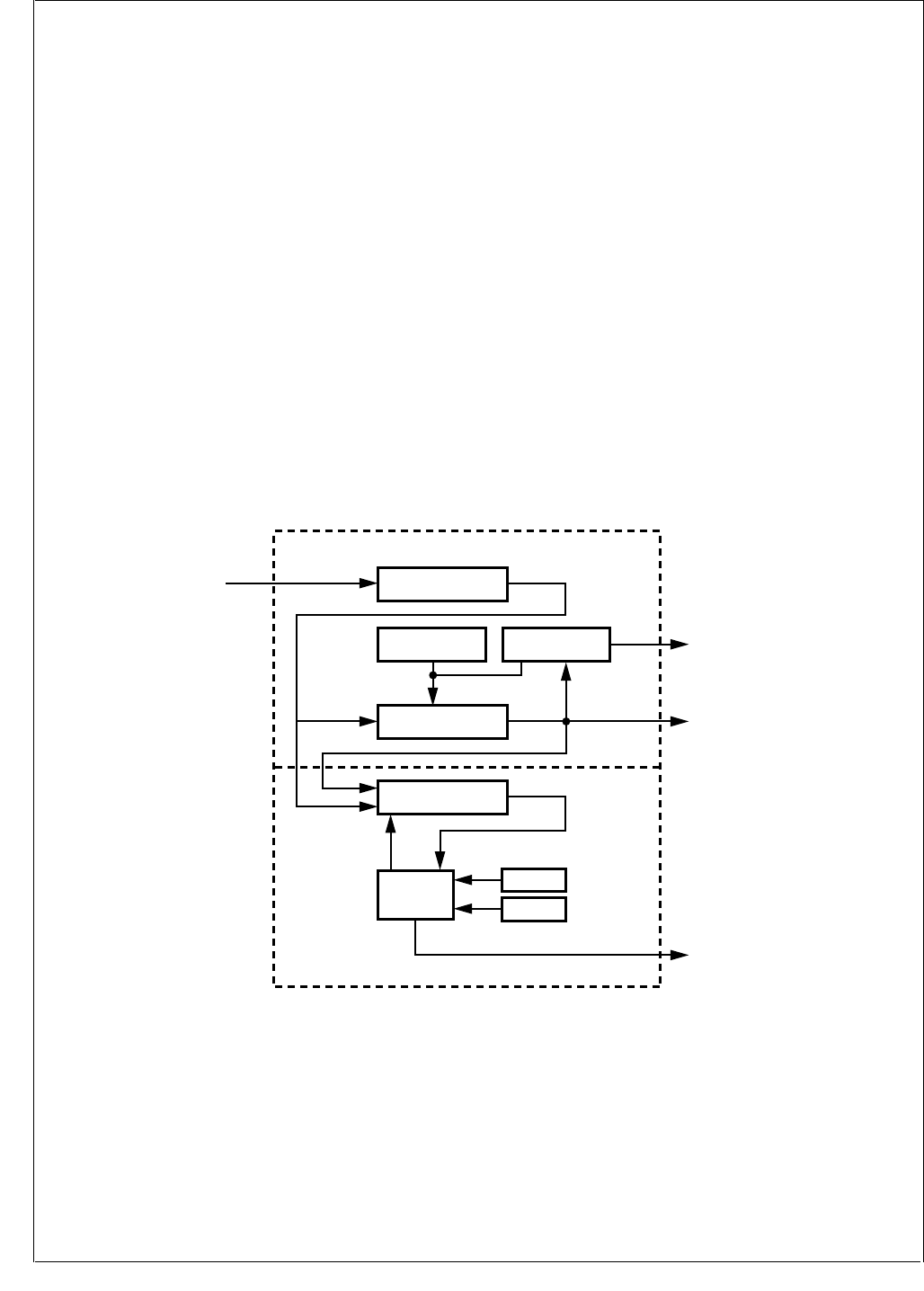
www.national.com 192
CP3BT26
25.0 Timing and Watchdog Module
The Timing and Watchdog Module (TWM) generates the
clocks and interrupts used for timing periodic functions in
the system; it also provides Watchdog protection over soft-
ware execution.
The TWM is designed to provide flexibility in system design
by configuring various clock ratios and by selecting the
Watchdog clock source. After setting the TWM configura-
tion, software can lock it for a higher level of protection
against erroneous software action. Once the TWM is
locked, only reset can release it.
25.1 TWM STRUCTURE
Figure 96 is a block diagram showing the internal structure
of the Timing and Watchdog module. There are two main
sections: the Real-Time Timer (T0) section at the top and
the Watchdog section on the bottom.
All counting activities of the module are based on the Slow
Clock (SLCLK). A prescaler counter divides this clock to
make a slower clock. The prescaler factor is defined by a 3-
bit field in the Timer and Watchdog Prescaler register, which
selects either 1, 2, 4, 8, 16, or 32 as the divisor. Therefore,
the prescaled clock period can be 2, 4, 8, 16, or 32 times the
Slow Clock period. The prescaled clock signal is called
T0IN.
25.2 TIMER T0 OPERATION
Timer T0 is a programmable 16-bit down counter that can
be used as the time base for real-time operations such as a
periodic audible tick. It can also be used to drive the Watch-
dog circuit.
The timer starts counting from the value loaded into the
TWMT0 register and counts down on each rising edge of
T0IN. When the timer reaches zero, it is automatically re-
loaded from the TWMT0 register and continues counting
down from that value. Therefore, the frequency of the timer
is:
When an external crystal oscillator is used as the SLCLK
source or when the fast clock is divided accordingly, fSLCLK
is 32.768 kHz.
The value stored in TWMT0 can range from 0001h to
FFFFh.
Figure 96. Timing and Watchdog Module Block Diagram
When the counter reaches zero, an internal timer signal
called T0OUT is set for one T0IN clock cycle. This signal
sets the TC bit in the TWMT0 Control and Status Register
(T0CSR). It also generates an interrupt (IRQ14), when en-
abled by the T0CSR.T0INTE bit. T0OUT is also an input to
the MIWU (see Section 13.0), so an edge-triggered inter-
rupt is also available through this alternative mechanism.
If software loads the TWMT0 register with a new value, the
timer uses that value the next time that it reloads the 16-bit
timer register (in other words, after reaching zero). Software
can restart the timer at any time (on the very next edge of
the T0IN clock) by setting the Restart (RST) bit in the
T0CSR register. The T0CSR.RST bit is cleared automati-
cally upon restart of the 16-bit timer.
Note: To enter Power Save or Idle mode after setting the
T0CSR.RST bit, software must wait for the reset operation
to complete before performing the switch.
fTIMER fSLCLK
TWTM0 1+()prescaler×
-----------------------------------------------------------------------
=
5-Bit Prescaler Counter
(TWCP)
REAL TIME TIMER (T0)
WATCHDOG
Restart
Restart
Underflow
Underflow
Slow
Clock
T0LINT
(to ICU)
T0OUT
(to Multi-Input-
Wake-Up)
WDERR
Watchdog Error
16-Bit Timer
(Timer0)
WATCHDOG
Timer
WATCHDOG
Service
Logic
TWW/MT0 Register T0CSR Contrl. Reg.
WDSDM
WDCNT
DS080
T0IN

193 www.national.com
CP3BT26
25.3 WATCHDOG OPERATION
The Watchdog is an 8-bit down counter that operates on the
rising edge of a specified clock source. At reset, the Watch-
dog is disabled; it does not count and no Watchdog signal is
generated. A write to either the Watchdog Count (WDCNT)
register or the Watchdog Service Data Match (WDSDM)
register starts the counter. The Watchdog counter counts
down from the value programmed in the WDCNT register.
Once started, only a reset can stop the Watchdog from op-
erating.
The Watchdog can be programmed to use either T0OUT or
T0IN as its clock source (the output and input of Timer T0,
respectively). The TWCFG.WDCT0I bit controls this clock
selection.
Software must periodically “service” the Watchdog. There
are two ways to service the Watchdog, the choice depend-
ing on the programmed value of the WDSDME bit in the
Timer and Watchdog Configuration (TWCFG) register.
If the TWCFG.WDSDME bit is clear, the Watchdog is ser-
viced by writing a value to the WDCNT register. The value
written to the register is reloaded into the Watchdog counter.
The counter then continues counting down from that value.
If the TWCFG.WDSDME bit is set, the Watchdog is ser-
viced by writing the value 5Ch to the Watchdog Service
Data Match (WDSDM) register. This reloads the Watchdog
counter with the value previously programmed into the WD-
CNT register. The counter then continues counting down
from that value.
A Watchdog error signal is generated by any of the following
events:
The Watchdog serviced too late.
The Watchdog serviced too often.
The WDSDM register is written with a value other than
5Ch when WDSDM type servicing is enabled
(TWCFG.WDSDME = 1).
A Watchdog error condition resets the device.
25.3.1 Register Locking
The Timer and Watchdog Configuration (TWCFG) register
is used to set the Watchdog configuration. It controls the
Watchdog clock source (T0IN or T0OUT), the type of
Watchdog servicing (using WDCNT or WDSDM), and the
locking state of the TWCFG, TWCPR, TIMER0, T0CSR,
and WDCNT registers. A register that is locked cannot be
read or written. A write operation is ignored and a read op-
eration returns unpredictable results.
If the TWCFG register is itself locked, it remains locked until
the device is reset. Any other locked registers also remain
locked until the device is reset. This feature prevents a run-
away program from tampering with the programmed Watch-
dog function.
25.3.2 Power Save Mode Operation
The Timer and Watchdog Module is active in both the Power
Save and Idle modes. The clocks and counters continue to
operate normally in these modes. The WDSDM register is
accessible in the Power Save and Idle modes, but the other
TWM registers are accessible only in the Active mode.
Therefore, Watchdog servicing must be carried out using
the WDSDM register in the Power Save or Idle mode.
In the Halt mode, the entire device is frozen, including the
Timer and Watchdog Module. On return to Active mode, op-
eration of the module resumes at the point at which it was
stopped.
Note: After a restart or Watchdog service through WDCNT,
do not enter Power Save mode for a period equivalent to 5
Slow Clock cycles.
25.4 TWM REGISTERS
The TWM registers controls the operation of the Timing and
Watchdog Module. There are six such registers:
The WDSDM register is accessible in both Active and Pow-
er Save mode. The other TWM registers are accessible only
in Active mode.
Table 76 TWM Registers
Name Address Description
TWCFG FF FF20h Timer and Watchdog
Configuration Register
TWCP FF FF22h
Timer and Watchdog
Clock Prescaler
Register
TWMT0 FF FF24h TWM Timer 0 Register
T0CSR FF FF26h TWMT0 Control and
Status Register
WDCNT FF FF28h Watchdog Count
Register
WDSDM FF FF2Ah Watchdog Service
Data Match Register

www.national.com 194
CP3BT26
25.4.1 Timer and Watchdog Configuration Register
(TWCFG)
The TWCFG register is a byte-wide, read/write register that
selects the Watchdog clock input and service method, and
also allows the Watchdog registers to be selectively locked.
A locked register cannot be read or written; a read operation
returns unpredictable values and a write operation is ig-
nored. Once a lock bit is set, that bit cannot be cleared until
the device is reset. At reset, the non-reserved bits of the
register are cleared. The register format is shown below.
LTWCFG The Lock TWCFG Register bit controls ac-
cess to the TWCFG register. When clear, ac-
cess to the TWCFG register is allowed. When
set, the TWCFG register is locked.
0 – TWCFG register unlocked.
1 – TWCFG register locked.
LTWCP The Lock TWCP Register bit controls access
to the TWCP register. When clear, access to
the TWCP register is allowed. When set, the
TWCP register is locked.
0 – TWCP register unlocked.
1 – TWCP register locked.
LTWMT0 The Lock TWMT0 Register bit controls access
to the TWMT0 register. When clear, access to
the TWMT0 and T0CSR registers are al-
lowed. When set, the TWMT0 and T0CSR
registers are locked.
0 – TWMT0 register unlocked.
1 – TWMT0 register locked.
LWDCNT The Lock LDWCNT Register bit controls ac-
cess to the LDWCNT register. When clear, ac-
cess to the LDWCNT register is allowed.
When set, the LDWCNT register is locked.
0 – LDWCNT register unlocked.
1 – LDWCNT register locked.
WDCT0I The Watchdog Clock from T0IN bit selects the
clock source for the Watchdog timer. When
clear, the T0OUT signal (the output of Timer
T0) is used as the Watchdog clock. When set,
the T0IN signal (the prescaled Slow Clock) is
used as the Watchdog clock.
0 – Watchdog timer is clocked by T0OUT.
1 – Watchdog timer is clocked by T0IN.
WDSDME The Watchdog Service Data Match Enable bit
controls which method is used to service the
Watchdog timer. When clear, Watchdog ser-
vicing is accomplished by writing a count val-
ue to the WDCNT register; write operations to
the Watchdog Service Data Match (WDSDM)
register are ignored. When set, Watchdog
servicing is accomplished by writing the value
5Ch to the WDSDM register.
0 – Write a count value to the WDCNT regis-
ter to service the Watchdog timer.
1 – Write 5Ch to the WDSDM register to ser-
vice the Watchdog timer.
25.4.2 Timer and Watchdog Clock Prescaler Register
(TWCP)
The TWCP register is a byte-wide, read/write register that
specifies the prescaler value used for dividing the low-fre-
quency clock to generate the T0IN clock. At reset, the non-
reserved bits of the register are cleared. The register format
is shown below.
MDIV Main Clock Divide. This 3-bit field defines the
prescaler factor used for dividing the low
speed device clock to create the T0IN clock.
The allowed 3-bit values and the correspond-
ing clock divisors and clock rates are listed be-
low.
25.4.3 TWM Timer 0 Register (TWMT0)
The TWMT0 register is a word-wide, read/write register that
defines the T0OUT interrupt rate. At reset, TWMT0 register
is initialized to FFFFh. The register format is shown below.
PRESET The Timer T0 Preset field holds the value
used to reload Timer T0 on each underflow.
Therefore, the frequency of the Timer T0 in-
terrupt is the frequency of T0IN divided by
(PRESET+1). The allowed values of PRESET
are 0001h through FFFFh.
7 6 5 4 3 2 1 0
Res.
WDSDME WDCT0I
LWDCNT LTWMT 0
LTWCP LT W C F G
7 3 2 0
Reserved MDIV
MDIV Clock Divisor
(fSCLK = 32.768 kHz)
T0IN
Frequency
000 1 32.768 kHz
001 2 16.384 kHz
010 4 8.192 kHz
011 8 4.096 kHz
100 16 2.056 kHz
101 32 1.024 kHz
Other Reserved N/A
15 0
PRESET

195 www.national.com
CP3BT26
25.4.4 TWMT0 Control and Status Register (T0CSR)
The T0CSR register is a byte-wide, read/write register that
controls Timer T0 and shows its current status. At reset, the
non-reserved bits of the register are cleared. The register
format is shown below.
RST The Restart bit is used to reset Timer T0.
When this bit is set, it forces the timer to re-
load the value in the TWMT0 register on the
next rising edge of the selected input clock.
The RST bit is reset automatically by the hard-
ware on the same rising edge of the selected
input clock. Writing a 0 to this bit position has
no effect. At reset, the non-reserved bits of the
register are cleared.
0 – Writing 0 has no effect.
1 – Writing 1 resets Timer T0.
TC The Terminal Count bit is set by hardware
when the Timer T0 count reaches zero and is
cleared when software reads the T0CSR reg-
ister. It is a read-only bit. Any data written to
this bit position is ignored. The TC bit is not
cleared if FREEZE mode is asserted by an ex-
ternal debugging system.
0 – Timer T0 did not count down to 0.
1 – Timer T0 counted down to 0.
T0INTE The Timer T0 Interrupt Enable bit enables an
interrupt to the CPU each time the Timer T0
count reaches zero. When this bit is clear,
Timer T0 interrupts are disabled.
0 – Timer T0 interrupts disabled.
1 – Timer T0 interrupts enabled.
WDLTD The Watchdog Last Touch Delay bit is set
when either WDCNT or WDSDM is written
and the data transfer to the Watchdog is in
progress (see WDCNT and WDSDM register
description). When clear, it is safe to switch to
Power Save mode.
0 – No data transfer to the Watchdog is in
progress, safe to enter Power Save mode.
1 – Data transfer to the Watchdog in
progress.
FRZT0E The Freeze Timer0 Enable bit controls wheth-
er TImer 0 is stopped in FREEZE mode. If this
bit is set, the Timer 0 is frozen (stopped) when
the FREEZE input to the TWM is asserted. If
the FRZT0E bit is clear, only the Watchdog
timer is frozen by asserting the FREEZE input
signal. After reset, this bit is clear.
0 – Timer T0 unaffected by FREEZE mode.
1 – Timer T0 stopped in FREEZE mode.
25.4.5 Watchdog Count Register (WDCNT)
The WDCNT register is a byte-wide, write-only register that
holds the value that is loaded into the Watchdog counter
each time the Watchdog is serviced. The Watchdog is start-
ed by the first write to this register. Each successive write to
this register restarts the Watchdog count with the written
value. At reset, this register is initialized to 0Fh.
25.4.6 Watchdog Service Data Match Register
(WDSDM)
The WSDSM register is a byte-wide, write-only register
used for servicing the Watchdog. When this type of servic-
ing is enabled (TWCFG.WDSDME = 1), the Watchdog is
serviced by writing the value 5Ch to the WSDSM register.
Each such servicing reloads the Watchdog counter with the
value previously written to the WDCNT register. Writing any
data other than 5Ch triggers a Watchdog error. Writing to
the register more than once in one Watchdog clock cycle
also triggers a Watchdog error signal. If this type of servic-
ing is disabled (TWCFG.WDSDME = 0), any write to the
WSDSM register is ignored.
25.5 WATCHDOG PROGRAMMING
PROCEDURE
The highest level of protection against software errors is
achieved by programming and then locking the Watchdog
registers and using the WDSDM register for servicing. This
is the procedure:
1. Write the desired values into the TWM Clock Prescaler
register (TWCP) and the TWM Timer 0 register
(TWMT0) to control the T0IN and T0OUT clock rates.
The frequency of T0IN can be programmed to any of
six frequencies ranging from 1/32 × fSLCLK to fSLCLK.
The frequency of T0OUT is equal to the frequency of
T0IN divided by (1+ PRESET), in which PRESET is the
value written to the TWMT0 register.
2. Configure the Watchdog clock to use either T0IN or
T0OUT by setting or clearing the TWCFG.WDCT0I bit.
3. Write the initial value into the WDCNT register. This
starts operation of the Watchdog and specifies the
maximum allowed number of Watchdog clock cycles
between service operations.
4. Set the T0CSR.RST bit to restart the TWMT0 timer.
5. Lock the Watchdog registers and enable the Watchdog
Service Data Match Enable function by setting bits 0, 1,
2, 3, and 5 in the TWCFG register.
6. Service the Watchdog by periodically writing the value
5Ch to the WDSDM register at an appropriate rate.
Servicing must occur at least once per period pro-
grammed into the WDCNT register, but no more than
once in a single Watchdog input clock cycle.
7 5 4 3 2 1 0
Reserved FRZT0E WDLTD T0INTETC RST 7 0
PRESET
7 0
RSTDATA
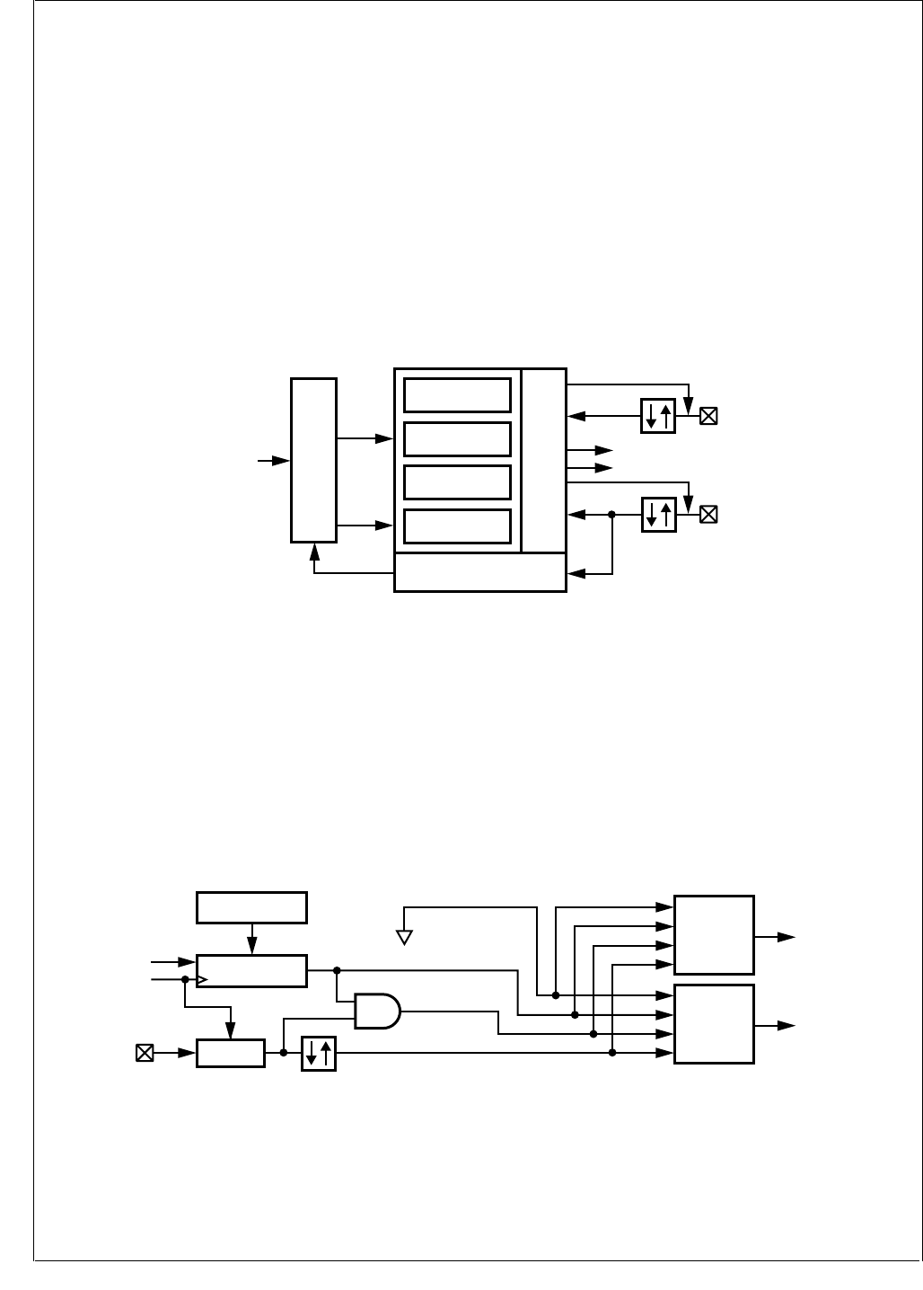
www.national.com 196
CP3BT26
26.0 Multi-Function Timer
The Multi-Function Timer module contains a pair of 16-bit
timer/counters. Each timer/counter unit offers a choice of
clock sources for operation and can be configured to oper-
ate in any of the following modes:
Processor-Independent Pulse Width Modulation (PWM)
mode, which generates pulses of a specified width and
duty cycle, and which also provides a general-purpose
timer/counter.
Dual-Input Capture mode, which measures the elapsed
time between occurrences of external events, and which
also provides a general-purpose timer/counter.
Dual Independent Timer mode, which generates system
timing signals or counts occurrences of external events.
Single-Input Capture and Single Timer mode, which pro-
vides one external event counter and one system timer.
The timer unit uses two I/O pins, called TA and TB. The tim-
er I/O pins are alternate functions of the PG7 and PE4 port
pins, respectively.
26.1 TIMER STRUCTURE
Figure 97 is a block diagram showing the internal structure
of the MFT. There are two main functional blocks: a Timer/
Counter and Action block and a Clock Source block. The
Timer/Counter and Action block contains two separate tim-
er/counter units, called Timer/Counter 1 and Timer/Counter
2.
Figure 97. Multi-Function Timer Block Diagram
26.1.1 Timer/Counter Block
The Timer/Counter block contains the following functional
blocks:
Two 16-bit counters, Timer/Counter 1 (TCNT1) and Tim-
er/Counter 2 (TCNT2)
Two 16-bit reload/capture registers, TCRA and TCRB
Control logic necessary to configure the timer to operate
in any of the four operating modes
Interrupt control and I/O control logic
In a power-saving mode that uses the low-frequency
(32.768 kHz) clock as the System Clock, the synchroniza-
tion circuit requires that the Slow Clock operate at no more
than one-fourth the speed of the 32.768 kHz System Clock.
26.1.2 Clock Source Block
The Clock Source block generates the signals used to clock
the two timer/counter registers. The internal structure of the
Clock Source block is shown in Figure 98.
Figure 98. Multi-Function Timer Clock Source
Reload/Capture A
TCRA
Timer/Counter
Clock Source Action
TA
Interrupt B
Interrupt A
Toggle/Capture/Interrupt
Clock Prescaler/Selector
Timer/Counter 1
TCNT1
Reload/Capture B
TCRB
Timer/Counter 2
TCNT2
PWM/Capture/Counter
Mode Select + Control
External Event
System
Clock
TB
DS081
Counter 1
Clock
Select
Counter 1
Clock
Counter 2
Clock
Select
Counter 2
Clock
Synchr. External Event
Pulse Accumulator
5-Bit
Prescaler Counter
Prescaler Register
TPRSC
Reset
System
Clock
TB
Prescaled Clock
No Clock
DS082
197 www.national.com
CP3BT26
Counter Clock Source Select
There are two clock source selectors that allow software to
independently select the clock source for each of the two
16-bit counters from any one of the following sources:
No clock (which stops the counter)
Prescaled System Clock
External event count based on TB
Pulse accumulate mode based on TB
Slow Clock (derived from the low-frequency oscillator or
divided from the high-speed oscillator)
Prescaler
The 5-bit clock prescaler allows software to run the timer
with a prescaled clock signal. The prescaler consists of a 5-
bit read/write prescaler register (TPRSC) and a 5-bit down
counter. The System Clock is divided by the value contained
in the prescaler register plus 1. Therefore, the timer clock
period can be set to any value from 1 to 32 divisions of the
System Clock period. The prescaler register and down
counter are both cleared upon reset.
External Event Clock
The TB I/O pin can be configured to operate as an external
event input clock for either of the two 16-bit counters. This
input can be programmed to detect either rising or falling
edges. The minimum pulse width of the external signal is
one System Clock cycle. This means that the maximum fre-
quency at which the counter can run in this mode is one-half
of the System Clock frequency. This clock source is not
available in the capture modes (modes 2 and 4) because
the TB pin is used as one of the two capture inputs.
Pulse Accumulate Mode
The counter can also be configured to count prescaler out-
put clock pulses when the TB input is high and not count
when the TB input is low, as illustrated in Figure 99. The re-
sulting count is an indicator of the cumulative time that the
TB input is high. This is called the “pulse-accumulate”
mode. In this mode, an AND gate generates a clock signal
for the counter whenever a prescaler clock pulse is generat-
ed and the TB input is high. (The polarity of the TB signal is
programmable, so the counter can count when the TB input
is low rather than high.) The pulse-accumulate mode is not
available in the capture modes (modes 2 and 4) because
the TB pin is used as one of the two capture inputs.
Figure 99. Pulse-Accumulate Mode
Slow Clock
The Slow Clock is generated by the Triple Clock and Reset
module. The clock source is either the divided fast clock or
the external 32.768 kHz crystal oscillator (if available and
selected). The Slow Clock can be used as the clock source
for the two 16-bit counters. Because the Slow Clock can be
asynchronous to the System Clock, a circuit is provided to
synchronize the clock signal to the high-frequency System
Clock before it is used for clocking the counters. The syn-
chronization circuit requires that the Slow Clock operate at
no more than one-fourth the speed of the System Clock.
Limitations in Low-Power Modes
The Power Save mode uses the Slow Clock as the System
Clock. In this mode, the Slow Clock cannot be used as a
clock source for the timers because that would drive both
clocks at the same frequency, and the clock ratio needed for
synchronization to the System Clock would not be main-
tained. However, the External Event Clock and Pulse Accu-
mulate Mode will still work, as long as the external event
pulses are at least the size of the whole slow-clock period.
Using the prescaled System Clock will also work, but at a
much slower rate than the original System Clock.
Idle and Halt modes stop the System Clock (the high-fre-
quency and/or low-frequency clock) completely. If the Sys-
tem Clock is stopped, the timer stops counting until the
System Clock resumes operation.
In the Idle or Halt mode, the System Clock stops completely,
which stops the operation of the timers. In that case, the tim-
ers stop counting until the System Clock resumes operation.
26.2 TIMER OPERATING MODES
Each timer/counter unit can be configured to operate in any
of the following modes:
Processor-Independent Pulse Width Modulation (PWM)
mode
Dual-Input Capture mode
Dual Independent Timer mode
Single-Input Capture and Single Timer mode
At reset, the timers are disabled. To configure and start the
timers, software must write a set of values to the registers
that control the timers. The registers are described in
Section 26.5.
Prescaler
Output
TB
Counter
Clock
DS083
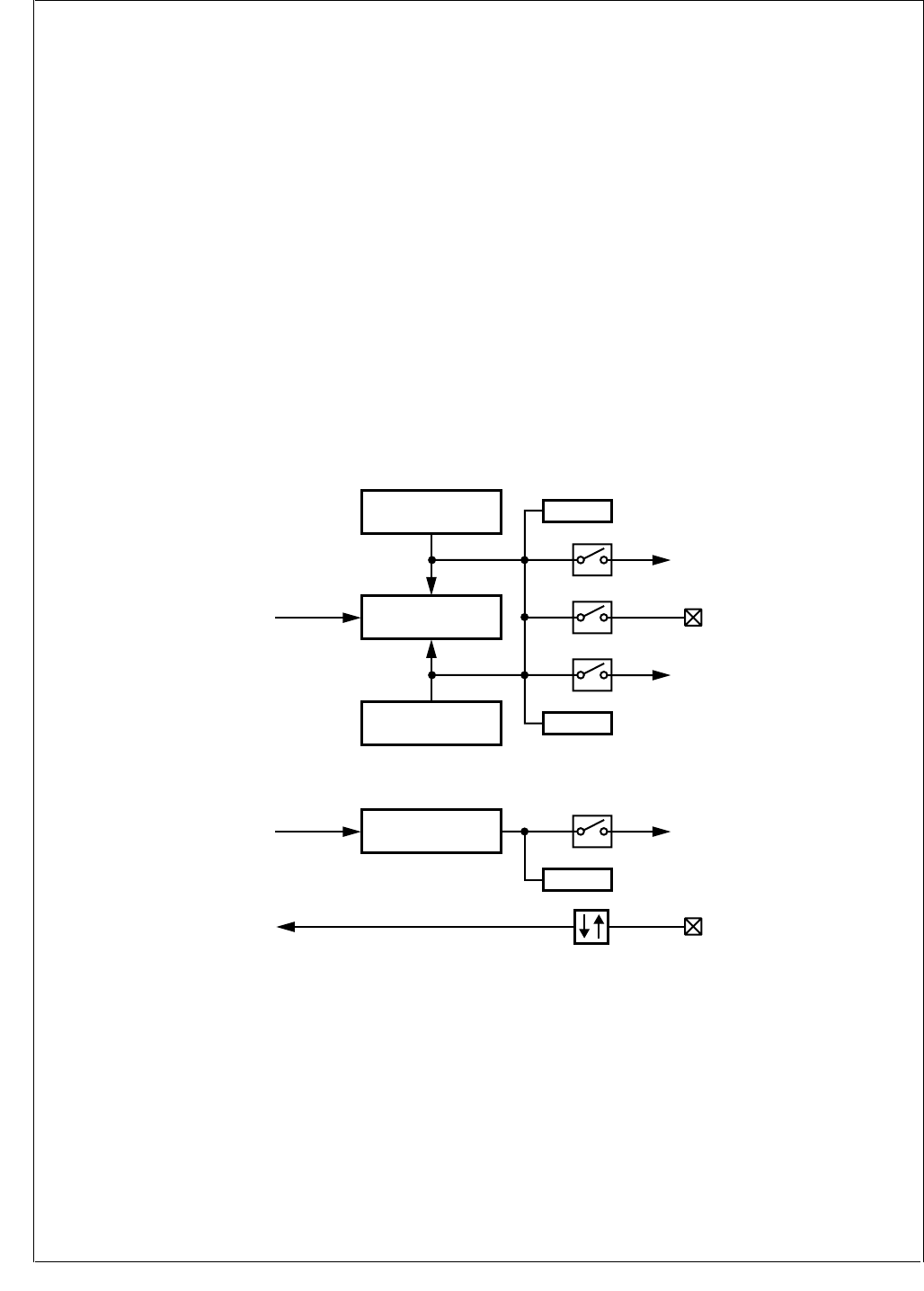
www.national.com 198
CP3BT26
26.2.1 Mode 1: Processor-Independent PWM
Mode 1 is the Processor-Independent Pulse Width Modula-
tion (PWM) mode, which generates pulses of a specified
width and duty cycle, and which also provides a separate
general-purpose timer/counter.
Figure 100 is a block diagram of the Multi-Function Timer
configured to operate in Mode 1. Timer/Counter 1 (TCNT1)
functions as the time base for the PWM timer. It counts
down at the clock rate selected for the counter. When an un-
derflow occurs, the timer register is reloaded alternately
from the TCRA and TCRB registers, and counting proceeds
downward from the loaded value.
On the first underflow, the timer is loaded from the TCRA
register, then from the TCRB register on the next underflow,
then from the TCRA register again on the next underflow,
and so on. Every time the counter is stopped and restarted,
it always obtains its first reload value from the TCRA regis-
ter. This is true whether the timer is restarted upon reset, af-
ter entering Mode 1 from another mode, or after stopping
and restarting the clock with the Timer/Counter 1 clock se-
lector.
The timer can be configured to toggle the TA output bit on
each underflow. This generates a clock signal on the TA out-
put with the width and duty cycle determined by the values
stored in the TCRA and TCRB registers. This is a “proces-
sor-independent” PWM clock because once the timer is set
up, no more action is required from the CPU to generate a
continuous PWM signal.
The timer can be configured to generate separate interrupts
upon reload from the TCRA and TCRB registers. The inter-
rupts can be enabled or disabled under software control.
The CPU can determine the cause of each interrupt by look-
ing at the TAPND and TBPND bits, which are updated by
the hardware on each occurrence of a timer reload.
In Mode 1, Timer/Counter 2 (TCNT2) can be used either as
a simple system timer, an external event counter, or a pulse-
accumulate counter. The clock counts down using the clock
selected with the Timer/Counter 2 clock selector. It gener-
ates an interrupt upon each underflow if the interrupt is en-
abled with the TDIEN bit.
Figure 100. Processor-Independent PWM Mode
Timer/Counter 1
TCNT1
Timer 1
Clock
Reload B = Time 2
TCRB
Reload A = Time 1
TCRA TAPND
TBPND
TAIEN
Timer
Interrupt A
TAEN
TA
TB
TBIEN
Timer
Interrupt B
Underflow
Underflow
TDIEN
Timer
Interrupt D
TDPND
Timer/Counter 2
TCNT2
Timer 2
Clock
Clock
Selector
DS084
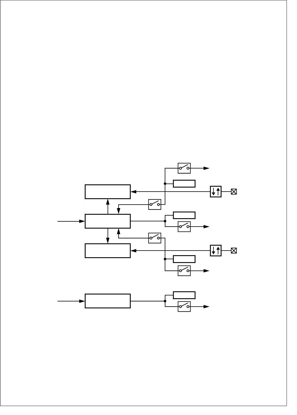
199 www.national.com
CP3BT26
26.2.2 Mode 2: Dual Input Capture
Mode 2 is the Dual Input Capture mode, which measures
the elapsed time between occurrences of external events,
and which also provides a separate general-purpose timer/
counter.
Figure 101 is a block diagram of the Multi-Function Timer
configured to operate in Mode 2. The time base of the cap-
ture timer depends on Timer/Counter 1, which counts down
using the clock selected with the Timer/Counter 1 clock se-
lector. The TA and TB pins function as capture inputs. A
transition received on the TA pin transfers the timer contents
to the TCRA register. Similarly, a transition received on the
TB pin transfers the timer contents to the TCRB register.
Each input pin can be configured to sense either rising or
falling edges.
The TA and TB inputs can be configured to preset the
counter to FFFFh on reception of a valid capture event. In
this case, the current value of the counter is transferred to
the corresponding capture register and then the counter is
preset to FFFFh. Using this approach allows software to de-
termine the on-time and off-time and period of an external
signal with a minimum of CPU overhead.
The values captured in the TCRA register at different times
reflect the elapsed time between transitions on the TA pin.
The same is true for the TCRB register and the TB pin. The
input signal on the TA or TB pin must have a pulse width
equal to or greater than one System Clock cycle.
There are three separate interrupts associated with the cap-
ture timer, each with its own enable bit and pending bit. The
three interrupt events are reception of a transition on the TA
pin, reception of a transition on the TB pin, and underflow of
the TCNT1 counter. The enable bits for these events are
TAIEN, TBIEN, and TCIEN, respectively.
In Mode 2, Timer/Counter 2 (TCNT2) can be used as a sim-
ple system timer. The clock counts down using the clock se-
lected with the Timer/Counter 2 clock selector. It generates
an interrupt upon each underflow if the interrupt is enabled
with the TDIEN bit.
Neither Timer/Counter 1 (TCNT1) nor Timer/Counter 2
(TCNT2) can be configured to operate as an external event
counter or to operate in the pulse-accumulate mode be-
cause the TB input is used as a capture input. Attempting to
select one of these configurations will cause one or both
counters to stop.
Figure 101. Dual-Input Capture Mode
Timer/Counter 1
TCNT1
Timer 1
Clock
Capture A
TCRA
TAPND
TA
TAIEN
Timer
Interrupt 1
Preset
Underflow
TAEN TCPND
TCIEN
Timer
Interrupt 1
Capture B
TCRB TB
Timer/Counter 2
TnCNT2
Timer 2
Clock Underflow
TDPND
TDIEN
Timer
Interrupt 2
TBPND
TBIEN
Timer
Interrupt 1
Preset
TBEN
DS085
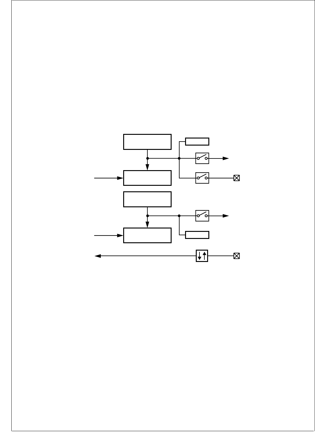
www.national.com 200
CP3BT26
26.2.3 Mode 3: Dual Independent Timer/Counter
Mode 3 is the Dual Independent Timer mode, which gener-
ates system timing signals or counts occurrences of exter-
nal events.
Figure 102 is a block diagram of the Multi-Function Timer
configured to operate in Mode 3. The timer is configured to
operate as a dual independent system timer or dual external
event counter. In addition, Timer/Counter 1 can generate a
50% duty cycle PWM signal on the TA pin. The TB pin can
be used as an external event input or pulse-accumulate in-
put and can be used as the clock source for either Timer/
Counter 1 or Timer/Counter 2. Both counters can also be
clocked by the prescaled System Clock.
Timer/Counter 1 (TCNT1) counts down at the rate of the se-
lected clock. On underflow, it is reloaded from the TCRA
register and counting proceeds down from the reloaded val-
ue. In addition, the TA pin is toggled on each underflow if this
function is enabled by the TAEN bit. The initial state of the
TA pin is software-programmable. When the TA pin is tog-
gled from low to high, it sets the TCPND interrupt pending
bit and also generates an interrupt if enabled by the TAIEN
bit.
Because the TA pin toggles on every underflow, a 50% duty
cycle PWM signal can be generated on the TA pin without
any further action from the CPU.
Timer/Counter 2 (TCNT2) counts down at the rate of the se-
lected clock. On underflow, it is reloaded from the TCRB
register and counting proceeds down from the reloaded val-
ue. In addition, each underflow sets the TDPND interrupt
pending bit and generates an interrupt if the interrupt is en-
abled by the TDIEN bit.
Figure 102. Dual-Independent Timer/Counter Mode
Timer/Counter 1
TCNT1
Timer 1
Clock
Reload A
TCRA TAPND
TAIEN
Timer
Interrupt 1
TAEN
TA
TB
Underflow
Timer/Counter 2
TCNT2
Timer 2
Clock
Reload B
TCRB
TDPND
TDIEN
Timer
Interrupt 2
Underflow
Clock
Selector
DS086
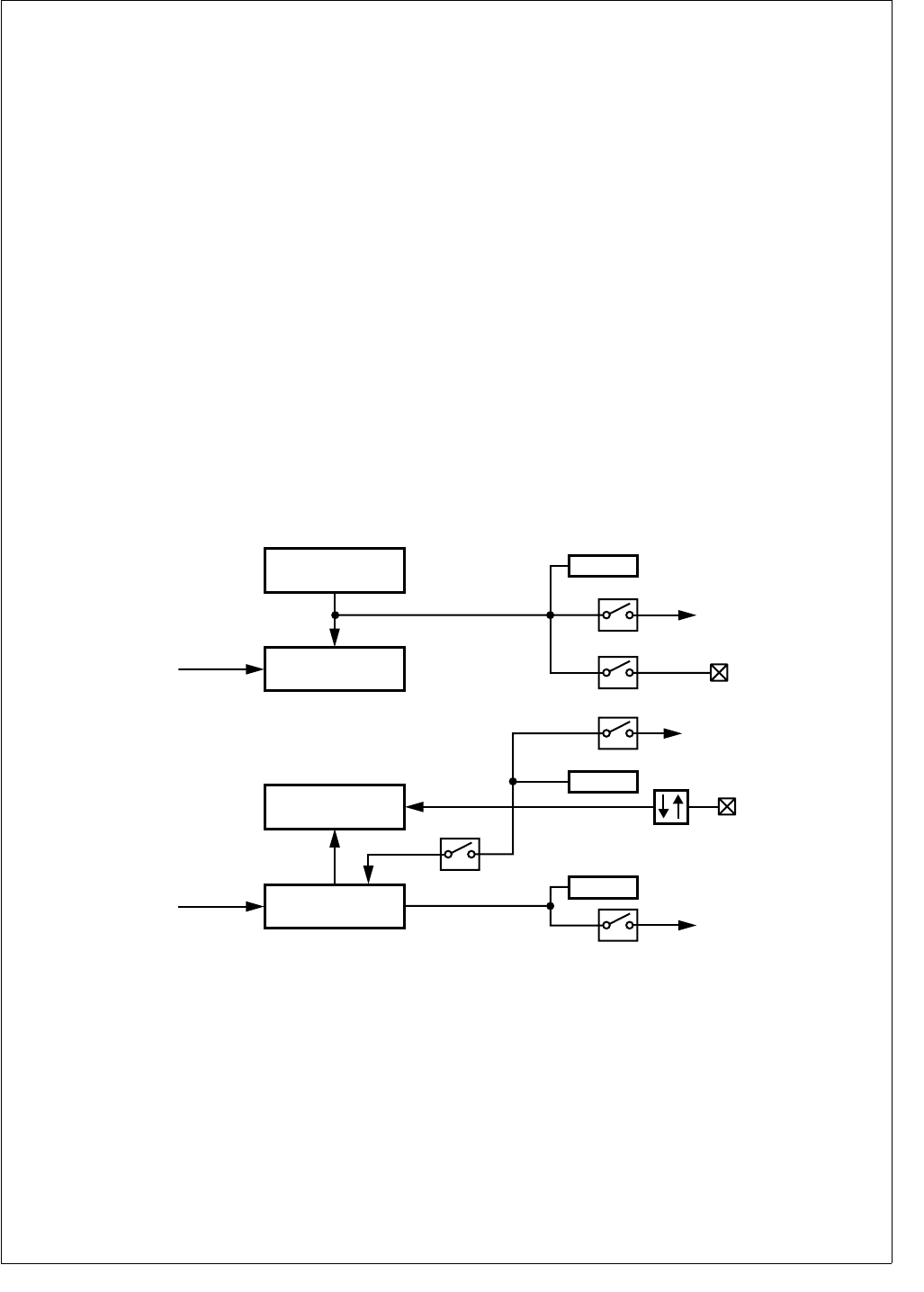
201 www.national.com
CP3BT26
26.2.4 Mode 4: Input Capture Plus Timer
Mode 4 is the Single Input Capture and Single Timer mode,
which provides one external event counter and one system
timer.
Figure 103 is a block diagram of the Multi-Function Timer
configured to operate in Mode 4. This mode offers a combi-
nation of Mode 3 and Mode 2 functions. Timer/Counter 1 is
used as a system timer as in Mode 3 and Timer/Counter 2
is used as a capture timer as in Mode 2, but with a single
input rather than two inputs.
Timer/Counter 1 (TCNT1) operates the same as in Mode 3.
It counts down at the rate of the selected clock. On under-
flow, it is reloaded from the TCRA register and counting pro-
ceeds down from the reloaded value. The TA pin is toggled
on each underflow, when this function is enabled by the
TAEN bit. When the TA pin is toggled from low to high, it sets
the TCPND interrupt pending bit and also generates an in-
terrupt if the interrupt is enabled by the TAIEN bit. A 50%
duty cycle PWM signal can be generated on TA without any
further action from the CPU.
Timer/Counter 2 (TCNT1) counts down at the rate of the se-
lected clock. The TB pin functions as the capture input. A
transition received on TB transfers the timer contents to the
TCRB register. The input pin can be configured to sense ei-
ther rising or falling edges.
The TB input can be configured to preset the counter to
FFFFh on reception of a valid capture event. In this case,
the current value of the counter is transferred to the capture
register and then the counter is preset to FFFFh.
The values captured in the TCRB register at different times
reflect the elapsed time between transitions on the TA pin.
The input signal on TB must have a pulse width equal to or
greater than one System Clock cycle.
There are two separate interrupts associated with the cap-
ture timer, each with its own enable bit and pending bit. The
two interrupt events are reception of a transition on TB and
underflow of the TCNT2 counter. The enable bits for these
events are TBIEN and TDIEN, respectively.
Neither Timer/Counter 1 (TCNT1) nor Timer/Counter 2
(TCNT2) can be configured to operate as an external event
counter or to operate in the pulse-accumulate mode be-
cause the TB input is used as a capture input. Attempting to
select one of these configurations will cause one or both
counters to stop. In this mode, Timer/Counter 2 must be en-
abled at all times.
Figure 103. Input Capture Plus Timer Mode
Timer/Counter 1
TCNT1
Timer 1
Clock
Reload A
TCRA TAPND
TAIEN
Timer
Interrupt 1
TAEN
TA
Underflow
TDPND
TDIEN
Timer
Interrupt 2
Timer/Counter 2
TnCNT2
Timer 2
Clock
Capture B
TCRB TB
TBPND
TBIEN
Timer
Interrupt 1
Preset
TBEN
DS087

www.national.com 202
CP3BT26
26.3 TIMER INTERRUPTS
The Multi-Function Timer unit has four interrupt sources,
designated A, B, C, and D. Interrupt sources A, B, and C are
mapped into a single system interrupt called Timer Interrupt
1, while interrupt source D is mapped into a system interrupt
called Timer Interrupt 2. Each of the four interrupt sources
has its own enable bit and pending bit. The enable bits are
named TAIEN, TBIEN, TCIEN, and TDIEN. The pending
bits are named TAPND, TBPND, TCPND, and TDPND.
Timer Interrupts 1 and 2 are system interrupts TA and TB
(IRQ14 and IRQ13), respectively.
Table 77 shows the events that trigger interrupts A, B, C,
and D in each of the four operating modes. Note that some
interrupt sources are not used in some operating modes.
26.4 TIMER I/O FUNCTIONS
The Multi-Function Timer unit uses two I/O pins, called TA
and TB. The function of each pin depends on the timer op-
erating mode and the TAEN and TBEN enable bits. Table 78
shows the functions of the pins in each operating mode, and
for each combination of enable bit settings.
When the TA pin is configured to operate as a PWM output
(TAEN = 1), the state of the pin is toggled on each underflow
of the TCNT1 counter. In this case, the initial value on the
pin is determined by the TAOUT bit. For example, to start
with TA high, software must set the TAOUT bit before en-
abling the timer clock. This option is available only when the
timer is configured to operate in Mode 1, 3, or 4 (in other
words, when TCRA is not used in Capture mode).
Table 77 Timer Interrupts Overview
Sys. Int.
Interrupt
Pending
Bit
Mode 1 Mode 2 Mode 3 Mode 4
PWM + Counter Dual Input Capture +
Counter Dual Counter Single Capture +
Counter
Timer
Int. 1
(TA Int.)
TAPND TCNT1 reload from
TCRA
Input capture on TA
transition
TCNT1 reload from
TCRA
TCNT1 reload from
TCRA
TBPND TCNT1 reload from
TCRB
Input Capture on TB
transition
N/A Input Capture on TB
transition
TCPND N/A TCNT1 underflow N/A N/A
Timer
Int. 2
(TB Int.)
TDPND TCNT2 underflow TCNT2 underflow TCNT2 reload from
TCRB
TCNT2 underflow
Table 78 Timer I/O Functions
I/O TAEN
TBEN
Mode 1 Mode 2 Mode 3 Mode 4
PWM + Counter Dual Input Capture +
counter Dual Counter Single Capture +
counter
TA TAEN = 0
TBEN = X
No Output Capture TCNT1 into
TCRA
No Output Toggle No Output Toggle
TAEN = 1
TBEN = X
Toggle Output on
Underflow of TCNT1
Capture TCNT1 into
TCRA and Preset
TCNT1
Toggle Output on
Underflow of TCNT1
Toggle Output on
Underflow of TCNT1
TB TAEN = X
TBEN = 0
Ext. Event or Pulse
Accumulate Input
Capture TCNT1 into
TCRB
Ext. Event or Pulse
Accumulate Input
Capture TCNT2 into
TCRB
TAEN = X
TBEN = 1
Ext. Event or Pulse
Accumulate Input
Capture TCNT1 into
TCRB and Preset
TCNT1
Ext. Event or Pulse
Accumulate Input
Capture TCNT2 into
TCRB and Preset
TCNT2

203 www.national.com
CP3BT26
26.5 TIMER REGISTERS
Table 79 lists the CPU-accessible registers used to control
the Multi-Function Timers.
26.5.1 Clock Prescaler Register (TPRSC)
The TPRSC register is a byte-wide, read/write register that
holds the current value of the 5-bit clock prescaler (CLKPS).
This register is cleared on reset. The register format is
shown below.
CLKPS The Clock Prescaler field specifies the divisor
used to generate the Timer Clock from the
System Clock. When the timer is configured to
use the prescaled clock, the System Clock is
divided by (CLKPS + 1) to produce the timer
clock. Therefore, the System Clock divisor
can range from 1 to 32.
26.5.2 Clock Unit Control Register (TCKC)
The TCKC register is a byte-wide, read/write register that
selects the clock source for each timer/counter. Selecting
the clock source also starts the counter. This register is
cleared on reset, which disables the timer/counters. The
register format is shown below.
C1CSEL The Counter 1 Clock Select field specifies the
clock mode for Timer/Counter 1 as follows:
000 – No clock (Timer/Counter 1 stopped,
modes 1, 2, and 3 only).
001 – Prescaled System Clock.
010 – External event on TB (modes 1 and 3
only).
011 – Pulse-accumulate mode based on TB
(modes 1 and 3 only).
100 – Slow Clock.*
101 – Reserved.
110 – Reserved.
111 – Reserved.
C2CSEL The Counter 2 Clock Select field specifies the
clock mode for Timer/Counter 2 as follows:
000 – No clock (Timer/Counter 2 stopped,
modes 1, 2, and 3 only).
001 – Prescaled System Clock.
010 – External event on TB (modes 1 and 3
only).
011 – Pulse-accumulate mode based on TB
(modes 1 and 3 only).
100 – Slow Clock*
101 – Reserved.
110 – Reserved.
111 – Reserved.
* Operation of the Slow Clock is determined by the CRC-
TRL.SCLK control bit, as described in Section 11.9.1.
26.5.3 Timer/Counter 1 Register (TCNT1)
The TCNT1 register is a word-wide, read/write register that
holds the current count value for Timer/Counter 1. The reg-
ister contents are not affected by a reset and are unknown
after power-up.
26.5.4 Timer/Counter 2 Register (TCNT2)
The TCNT2 register is a word-wide, read/write register that
holds the current count value for Timer/Counter 2. The reg-
ister contents are not affected by a reset and are unknown
after power-up.
Table 79 Multi-Function Timer Registers
Name Address Description
TPRSC FF FF48h Clock Prescaler
Register
TCKC FF FF4Ah Clock Unit Control
Register
TCNT1 FF FF40h Timer/Counter 1
Register
TCNT2 FF FF46h Timer/Counter 2
Register
TCRA FF FF42h Reload/Capture A
Register
TCRB FF FF44h Reload/Capture B
Register
TCTRL FF FF4Ch Timer Mode
Control Register
TICTL FF FF4Eh Timer Interrupt
Control Register
TICLR FF FF50h Timer Interrupt
Clear Register
7 5 4 0
Reserved CLKPS
7 6 5 3 2 0
Reserved C2CSEL C1CSEL
15 0
TCNT1
15 0
TCNT2

www.national.com 204
CP3BT26
26.5.5 Reload/Capture A Register (TCRA)
The TCRA register is a word-wide, read/write register that
holds the reload or capture value for Timer/Counter 1. The
register contents are not affected by a reset and are un-
known after power-up.
26.5.6 Reload/Capture B Register (TCRB)
The TCRB register is a word-wide, read/write register that
holds the reload or capture value for Timer/Counter 2. The
register contents are not affected by a reset and are un-
known after power-up.
26.5.7 Timer Mode Control Register (TCTRL)
The TCTRL register is a byte-wide, read/write register that
sets the operating mode of the timer/counter and the TA and
TB pins. This register is cleared at reset. The register format
is shown below.
MDSEL The Mode Select field sets the operating
mode of the timer/counter as follows:
00 – Mode 1: PWM plus system timer.
01 – Mode 2: Dual-Input Capture plus system
timer.
10 – Mode 3: Dual Timer/Counter.
11 – Mode 4: Single-Input Capture and Sin-
gle Timer.
TAEDG The TA Edge Polarity bit selects the polarity of
the edges that trigger the TA input.
0 – TA input is sensitive to falling edges (high
to low transitions).
1 – TA input is sensitive to rising edges (low
to high transitions).
TBEDG The TB Edge Polarity bit selects the polarity of
the edges that trigger the TB input. In pulse-
accumulate mode, when this bit is set, the
counter is enabled only when TB is high;
when this bit is clear, the counter is enabled
only when TB is low.
0 – TB input is sensitive to falling edges (high
to low transitions).
1 – TB input is sensitive to rising edges (low
to high transitions).
TAEN The TA Enable bit controls whether the TA pin
is enabled to operate as a preset input or as a
PWM output, depending on the timer operat-
ing mode. In Mode 2 (Dual Input Capture), a
transition on the TA pin presets the TCNT1
counter to FFFFh. In the other modes, TA
functions as a PWM output. When this bit is
clear, operation of the pin for the timer/counter
is disabled.
0 – TA input disabled.
1 – TA input enabled.
TBEN The TB Enable bit controls whether the TB pin
in enabled to operate in Mode 2 (Dual Input
Capture) or Mode 4 (Single Input Capture and
Single Timer). A transition on the TB pin pre-
sets the corresponding timer/counter to
FFFFh (TCNT1 in Mode 2 or TCNT2 in Mode
4). When this bit is clear, operation of the pin
for the timer/counter is disabled. This bit set-
ting has no effect in Mode 1 or Mode 3.
0 – TB input disabled.
1 – TB input enabled.
TAOUT The TA Output Data bit indicates the current
state of the TA pin when the pin is used as a
PWM output. The hardware sets and clears
this bit, but software can also read or write this
bit at any time and therefore control the state
of the output pin. In case of conflict, a software
write has precedence over a hardware up-
date. This bit setting has no effect when the
TA pin is used as an input.
0 – TA pin is low.
1 – TA pin is high.
TEN The Timer Enable bit controls whether the
Multi-Function Timer is enabled. When the
module is disabled all clocks to the counter
unit are stopped to minimize power consump-
tion. For that reason, the timer/counter regis-
ters (TCNT1 and TCNT2), the capture/reload
registers (TCRA and TCRB), and the interrupt
pending bits (TXPND) cannot be written in
this mode. Also, the 5-bit clock prescaler and
the interrupt pending bits are cleared, and the
TA I/O pin becomes an input.
0 – Multi-Function Timer is disabled.
1 – Multi-Function Timer is enabled.
15 0
TCRA
15 0
TCRB
7 6 5 4 3 2 1 0
TEN TAO U T TBEN TAEN TBEDG TAEDG MDSEL

205 www.national.com
CP3BT26
26.5.8 Timer Interrupt Control Register (TICTL)
The TICTL register is a byte-wide, read/write register that
contains the interrupt enable bits and interrupt pending bits
for the four timer interrupt sources, designated A, B, C, and
D. The condition that causes each type of interrupt depends
on the operating mode, as shown in Table 77.
This register is cleared upon reset. The register format is
shown below.
TAPND The Timer Interrupt Source A Pending bit indi-
cates that timer interrupt condition A has oc-
curred. For an explanation of interrupt
conditions A, B, C, and D, see Table 77. This
bit can be set by hardware or by software. To
clear this bit, software must use the Timer In-
terrupt Clear Register (TICLR). Attempting to
directly write a 0 to this bit is ignored.
0 – Interrupt source A has not triggered.
1 – Interrupt source A has triggered.
TBPND The Timer Interrupt Source B Pending bit indi-
cates that timer interrupt condition B has oc-
curred. For an explanation of interrupt
conditions A, B, C, and D, see Table 77. This
bit can be set by hardware or by software. To
clear this bit, software must use the Timer In-
terrupt Clear Register (TICLR). Attempting to
directly write a 0 to this bit is ignored.
0 – Interrupt source B has not triggered.
1 – Interrupt source B has triggered.
TCPND The Timer Interrupt Source C Pending bit in-
dicates that timer interrupt condition C has oc-
curred. For an explanation of interrupt
conditions A, B, C, and D, see Table 77. This
bit can be set by hardware or by software. To
clear this bit, software must use the Timer In-
terrupt Clear Register (TICLR). Attempting to
directly write a 0 to this bit is ignored.
0 – Interrupt source C has not triggered.
1 – Interrupt source C has triggered.
TDPND The Timer Interrupt Source D Pending bit in-
dicates that timer interrupt condition D has oc-
curred. For an explanation of interrupt
conditions A, B, C, and D, see Table 77. This
bit can be set by hardware or by software. To
clear this bit, software must use the Timer In-
terrupt Clear Register (TICLR). Attempting to
directly write a 0 to this bit is ignored.
0 – Interrupt source D has not triggered.
1 – Interrupt source D has triggered.
TAIEN The Timer Interrupt A Enable bit controls
whether an interrupt is generated on each oc-
currence of interrupt condition A. For an ex-
planation of interrupt conditions A, B, C, and
D, see Table 77.
0 – Condition A interrupts disabled.
1 – Condition A interrupts enabled.
TBIEN The Timer Interrupt B Enable bit controls
whether an interrupt is generated on each oc-
currence of interrupt condition B. For an ex-
planation of interrupt conditions A, B, C, and
D, see Table 77.
0 – Condition B interrupts disabled.
1 – Condition B interrupts enabled.
TCIEN The Timer Interrupt C Enable bit controls
whether an interrupt is generated on each oc-
currence of interrupt condition C. For an ex-
planation of interrupt conditions A, B, C, and
D, see Table 77.
0 – Condition C interrupts disabled.
1 – Condition C interrupts enabled.
TDIEN The Timer Interrupt D Enable bit controls
whether an interrupt is generated on each oc-
currence of interrupt condition D. For an ex-
planation of interrupt conditions A, B, C, and
D, see Table 77.
0 – Condition D interrupts disabled.
1 – Condition D interrupts enabled.
26.5.9 Timer Interrupt Clear Register (TICLR)
The TICLR register is a byte-wide, write-only register that al-
lows software to clear the TAPND, TBPND, TCPND, and
TDPND bits in the Timer Interrupt Control (TICTRL) regis-
ter. Do not modify this register with instructions that access
the register as a read-modify-write operand, such as the bit
manipulation instructions. The register reads as FFh. The
register format is shown below.
TACLR The Timer Pending A Clear bit is used to clear
the Timer Interrupt Source A Pending bit
(TAPND) in the Timer Interrupt Control regis-
ter (TICTL).
0 – Writing a 0 has no effect.
1 – Writing a 1 clears the TAPND bit.
TBCLR The Timer Pending A Clear bit is used to clear
the Timer Interrupt Source B Pending bit (TB-
PND) in the Timer Interrupt Control register
(TICTL).
0 – Writing a 0 has no effect.
1 – Writing a 1 clears the TBPND bit.
TCCLR The Timer Pending C Clear bit is used to clear
the Timer Interrupt Source C Pending bit
(TCPND) in the Timer Interrupt Control regis-
ter (TICTL).
0 – Writing a 0 has no effect.
1 – Writing a 1 clears the TCPND bit.
TDCLR The Timer Pending D Clear bit is used to clear
the Timer Interrupt Source D Pending bit (TD-
PND) in the Timer Interrupt Control register
(TICTL).
0 – Writing a 0 has no effect.
1 – Writing a 1 clears the TDPND bit.
7 6 5 4 3 2 1 0
TDIEN TCIEN TBIEN TA I EN TDPND TCPND TBPND TAPN D
7 4 3 2 1 0
Reserved TDCLR TCCLR TBCLR TAC L R
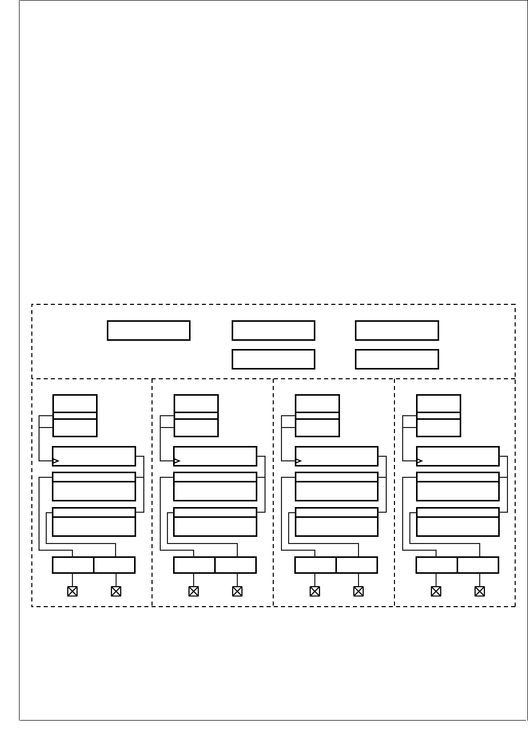
www.national.com 206
CP3BT26
27.0 Versatile Timer Unit (VTU)
The Versatile Timer Unit (VTU) contains four fully indepen-
dent 16-bit timer subsystems. Each timer subsystem can
operate either as dual 8-bit PWM timers, as a single 16-bit
PWM timer, or as a 16-bit counter with 2 input capture chan-
nels. These timer subsystems offers an 8-bit clock prescaler
to accommodate a wide range of system frequencies.
The VTU offers the following features:
The VTU can be configured to provide:
— Eight fully independent 8-bit PWM channels
— Four fully independent 16-bit PWM channels
— Eight 16-bit input capture channels
The VTU consists of four timer subsystems, each of
which contains:
— A 16-bit counter
— Two 16-bit capture / compare registers
— An 8-bit fully programmable clock prescaler
Each of the four timer subsystems can operate in the fol-
lowing modes:
— Low power mode, i.e. all clocks are stopped
— Dual 8-bit PWM mode
— 16-bit PWM mode
— Dual 16-bit input capture mode
The VTU controls a total of eight I/O pins, each of which
can function as either:
— PWM output with programmable output polarity
— Capture input with programmable event detection and
timer reset
A flexible interrupt scheme with
— Four separate system level interrupt requests
— A total of 16 interrupt sources each with a separate in-
terrupt pending bit and interrupt enable bit
27.1 VTU FUNCTIONAL DESCRIPTION
The VTU is comprised of four timer subsystems. Each timer
subsystem contains an 8-bit clock prescaler, a 16-bit up-
counter, and two 16-bit registers. Each timer subsystem
controls two I/O pins which either function as PWM outputs
or capture inputs depending on the mode of operation.
There are four system-level interrupt requests, one for each
timer subsystem. Each system-level interrupt request is
controlled by four interrupt pending bits with associated en-
able/disable bits. All four timer subsystems are fully inde-
pendent, and each may operate as a dual 8-bit PWM timer,
a 16-bit PWM timer, or as a dual 16-bit capture timer.
Figure 104 shows the main elements of the VTU.
Figure 104. Versatile Timer Unit Block Diagram
INTCTL
015
MODE
015
Count1
TIO1
015
PERCAP1
Compare - Capture
DTYCAP1
Compare - Capture
C1 PRSC
Timer Subsystem 1
= =
7
Prescaler
Counter
I/O Control
INTPND
015
IO1CTL
015
IO2CTL
015
TIO2
I/O Control
Count2
TIO3
015
PERCAP2
Compare - Capture
DTYCAP2
Compare - Capture
C2 PRSC
= =
7
Prescaler
Counter
I/O Control
TIO4
I/O Control
Count4
TIO7
015
PERCAP4
Compare - Capture
DTYCAP4
Compare - Capture
C4RSC
= =
7
Prescaler
Counter
I/O Control
TIO8
I/O Control
Count3
TIO5
015
PERCAP3
Compare - Capture
DTYCAP3
Compare - Capture
C3 PRSC
= =
7
Prescaler
Counter
I/O Control
TIO6
I/O Control
Timer Subsystem 2 Timer Subsystem 3 Timer Subsystem 4
DS088
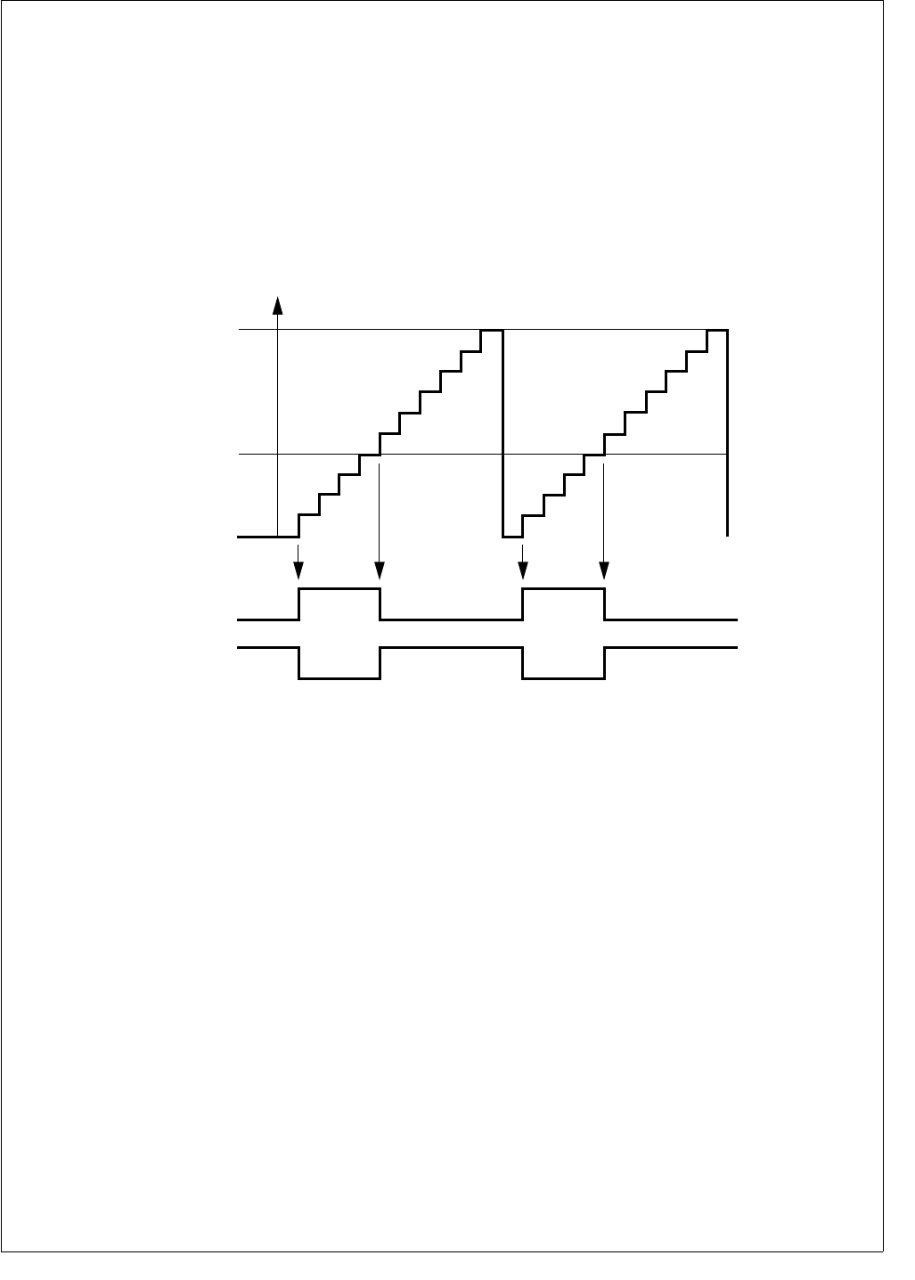
207 www.national.com
CP3BT26
27.1.1 Dual 8-bit PWM Mode
Each timer subsystem may be configured to generate two
fully independent PWM waveforms on the respective TIOx
pins. In this mode, the counter COUNTx is split and oper-
ates as two independent 8-bit counters. Each counter incre-
ments at the rate determined by the clock prescaler.
Each of the two 8-bit counters may be started and stopped
separately using the corresponding TxRUN bits. Once ei-
ther of the two 8-bit timers is running, the clock prescaler
starts counting. Once the clock prescaler counter value
matches the value of the associated CxPRSC register field,
COUNTx is incremented.
The period of the PWM output waveform is determined by
the value of the PERCAPx register. The TIOx output starts
at the default value as programmed in the IOxCTL.PxPOL
bit. Once the counter value reaches the value of the period
register PERCAPx, the counter is cleared on the next
counter increment. On the following increment from 00h to
01h, the TIOx output will change to the opposite of the de-
fault value.
The duty cycle of the PWM output waveform is controlled by
the DTYCAPx register value. Once the counter value reach-
es the value of the duty cycle register DTYCAPx, the PWM
output TIOx changes back to its default value on the next
counter increment. Figure 105 illustrates this concept.
Figure 105. VTU PWM Generation
The period time is determined by the following formula:
PWM Period = (PERCAPx + 1) × (CxPRSC + 1) × TCLK
The duty cycle in percent is calculated as follows:
Duty Cycle = (DTYCAPx / (PERCAPx + 1)) × 100
If the duty cycle register (DTYCAPx) holds a value which is
greater than the value held in the period register (PER-
CAPx) the TIOx output will remain at the opposite of its de-
fault value which corresponds to a duty cycle of 100%. If the
duty cycle register (DTYCAPx) register holds a value of 00h,
the TIOx output will remain at the default value which corre-
sponds to a duty cycle of 0%, in which case the value in the
PERCAPx register is irrelevant. This scheme allows the
duty cycle to be programmed in a range from 0% to 100%.
In order to allow fully synchronized updates of the period
and duty cycle compare values, the PERCAPx and DTY-
CAPx registers are double buffered when operating in PWM
mode. Therefore, if software writes to either the period or
duty cycle register while either of the two PWM channels is
enabled, the new value will not take effect until the counter
value matches the previous period value or the timer is
stopped.
Reading the PERCAPx or DTYCAPx register will always re-
turn the most recent value written to it.
The counter registers can be written if both 8-bit counters
are stopped. This allows software to preset the counters be-
fore starting, which can be used to generate PWM output
waveforms with a phase shift relative to each other. If the
counter is written with a value other than 00h, it will start in-
crementing from that value. The TIOx output will remain at
its default value until the first 00h to 01h transition of the
counter value occurs. If the counter is preset to values which
are less than or equal to the value held in the period register
(PERCAPx) the counter will count up until a match between
the counter value and the PERCAPx register value occurs.
The counter will then be cleared and continue counting up.
Alternatively, the counter may be written with a value which
is greater than the value held in the period register. In that
case the counter will count up to FFh, then roll over to 00h.
In any case, the TIOx pin always changes its state at the
00h to 01h transition of the counter.
Software may only write to the COUNTx register if both
TxRUN bits of a timer subsystem are clear. Any writes to the
counter register while either timer is running will be ignored.
TIOx (PxPOL = 0)
DTYCAPx
TxRUN = 1
COUNTx
00
01
02
03
04
05
06
07
08
09
0A
00
01
02
03
04
05
06
07
08
09
0A
TIOx (PxPOL = 1)
PERCAPx
DS089
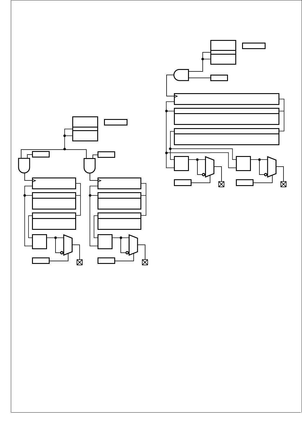
www.national.com 208
CP3BT26
The two I/O pins associated with a timer subsystem function
as independent PWM outputs in the dual 8-bit PWM mode.
If a PWM timer is stopped using its associated
MODE.TxRUN bit the following actions result:
The associated TIOx pin will return to its default value as
defined by the IOxCTL.PxPOL bit.
The counter will stop and will retain its last value.
Any pending updates of the PERCAPx and DTYCAPx
register will be completed.
The prescaler counter will be stopped and reset if both
MODE.TxRUN bits are cleared.
Figure 106 illustrates the configuration of a timer subsystem
while operating in dual 8-bit PWM mode. The numbering in
Figure 106 refers to timer subsystem 1 but equally applies
to the other three timer subsystems.
Figure 106. VTU Dual 8-Bit PWM Mode
27.1.2 16-Bit PWM Mode
Each of the four timer subsystems may be independently
configured to provide a single 16-bit PWM channel. In this
case the lower and upper bytes of the counter are concate-
nated to form a single 16-bit counter.
Operation in 16-bit PWM mode is conceptually identical to
the dual 8-bit PWM operation as outlined under Dual 8-bit
PWM Mode on page 207. The 16-bit timer may be started
or stopped with the lower MODE.TxRUN bit, i.e. T1RUN for
timer subsystem 1.
The two TIOx outputs associated with a timer subsystem
can be used to produce either two identical PWM wave-
forms or two PWM waveforms of opposite polarities. This
can be accomplished by setting the two PxPOL bits of the
respective timer subsystem to either identical or opposite
values.
Figure 107 illustrates the configuration of a timer subsystem
while operating in 16-bit PWM mode. The numbering in
Figure 107 refers to timer subsystem 1 but equally applies
to the other three timer subsystems.
Figure 107. VTU 16-bit PWM Mode
27.1.3 Dual 16-Bit Capture Mode
In addition to the two PWM modes, each timer subsystem
may be configured to operate in an input capture mode
which provides two 16-bit capture channels. The input cap-
ture mode can be used to precisely measure the period and
duty cycle of external signals.
In capture mode the counter COUNTx operates as a 16-bit
up-counter while the two TIOx pins associated with a timer
subsystem operate as capture inputs. A capture event on
the TIOx pins causes the contents of the counter register
(COUNTx) to be copied to the PERCAPx or DTYCAPx reg-
isters respectively.
Starting the counter is identical to the 16-bit PWM mode, i.e.
setting the lower of the two MODE.TxRUN bits will start the
counter and the clock prescaler. In addition, the capture
event inputs are enabled once the MODE.TxRUN bit is set.
The TIOx capture inputs can be independently configured to
detect a capture event on either a positive transition, a neg-
ative transition or both a positive and a negative transition.
In addition, any capture event may be used to reset the
counter COUNTx and the clock prescaler counter. This
avoids the need for software to keep track of timer overflow
conditions and greatly simplifies the direct frequency and
duty cycle measurement of an external signal.
COUNT1[15:8]
Res
015
[15:8]
P2POL
TIO2
PERCAP1[15:8]
Compare
DTYCAP1[15:8]
Compare
RQ
S
C1PRSC
= =
70
Prescaler
Counter
COUNT1[7:0]
Res
07
[7:0]
P1POL
TIO1
PERCAP1[7:0]
Compare
DTYCAP1[7:0]
Compare
RQ
S
T1RUN
TMOD1 = 01
T2RUN
DS090
Count1[15:0]
Restart
015
[15:0]
P2POL
TIO2
PERCAP1[15:0]
Compare
DTYCAP1[15:0]
Compare
RQ
S
C1PRSC
= =
70
Prescaler
Counter
P1POL
TIO1
RQ
S
TMOD1 = 10
T1RUN
DS091
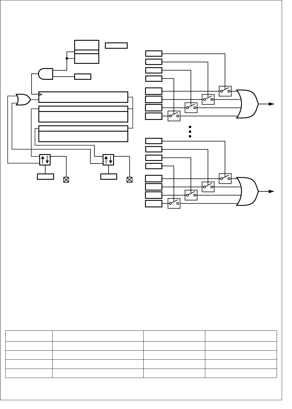
209 www.national.com
CP3BT26
Figure 108 illustrates the configuration of a timer subsystem
while operating in capture mode. The numbering in
Figure 108 refers to timer subsystem 1 but equally applies
to the other three timer subsystems.
Figure 108. VTU Dual 16-bit Capture Mode
27.1.4 Low Power Mode
In case a timer subsystem is not used, software can place it
in a low-power mode. All clocks to a timer subsystem are
stopped and the counter and prescaler contents are frozen
once low-power mode is entered. Software may continue to
write to the MODE, INTCTL, IOxCTL, and CLKxPS regis-
ters. Write operations to the INTPND register are allowed;
but if a timer subsystem is in low-power mode, its associat-
ed interrupt pending bits cannot be cleared. Software can-
not write to the COUNTx, PERCAPx, and DTYCAPx
registers of a timer subsystem while it is in low-power mode.
All registers can be read at any time.
27.1.5 Interrupts
The VTU has a total of 16 interrupt sources, four for each of
the four timer subsystems. All interrupt sources have a
pending bit and an enable bit associated with them. All in-
terrupt pending bits are denoted IxAPD through IxDPD
where “x” relates to the specific timer subsystem. There is
one system level interrupt request for each of the four timer
subsystems.
Figure 109 illustrates the interrupt structure of the versatile
timer module.
Figure 109. VTU Interrupt Request Structure
Each of the timer pending bits - IxAPD through IxDPD - is
set by a specific hardware event depending on the mode of
operation, i.e., PWM or Capture mode. Table 80 outlines the
specific hardware events relative to the operation mode
which cause an interrupt pending bit to be set.
27.1.6 ISE Mode operation
The VTU supports breakpoint operation of the In-System-
Emulator (ISE). If FREEZE is asserted, all timer counter
clocks will be inhibited and the current value of the timer reg-
isters will be frozen; in capture mode, all further capture
events are disabled. Once FREEZE becomes inactive,
counting will resume from the previous value and the cap-
ture input events are re-enabled.
Count1[15:0]
Restart
015
15:0
C1EDG
PERCAP1[15:0]
Compare
DTYCAP1[15:0]
Compare
C1PRSC
= =
70
Prescaler
Counter
2
rst
cap
0
TMOD1=11
T1RUN
C2EDG
TIO2
2
rst
cap
0
DS092
TIO1
System
Interrupt
Request 1
I1AEN
I1BEN
I1CEN
I1DEN
I1APD
I1BPD
I1CPD
I1DPD
System
Interrupt
Request 4
I4AEN
I4BEN
I4CEN
I4DEN
I4APD
I4BPD
I4CPD
I4DPD
DS093
Table 80 VTU Interrupt Sources
Pending Flag Dual 8-bit PWM Mode 16-bit PWM Mode Capture Mode
IxAPD Low Byte Duty Cycle match Duty Cycle match Capture to PERCAPx
IxBPD Low Byte Period match Period match Capture to DTYCAPx
IxCPD High Byte Duty Cycle match N/A Counter Overflow
IxDPD High Byte Period match N/A N/A

www.national.com 210
CP3BT26
27.2 VTU REGISTERS
The VTU contains a total of 19 user accessible registers, as
listed in Table 81. All registers are word-wide and are initial-
ized to a known value upon reset. All software accesses to
the VTU registers must be word accesses.
27.2.1 Mode Control Register (MODE)
The MODE register is a word-wide read/write register which
controls the mode selection of all four timer subsystems.
The register is clear after reset.
TxRUN The Timer Run bit controls whether the corre-
sponding timer is stopped or running. If set,
the associated counter and clock prescaler is
started depending on the mode of operation.
Once set, the clock to the clock prescaler and
the counter are enabled and the counter will
increment each time the clock prescaler
counter value matches the value defined in
the associated clock prescaler field (CxPR-
SC).
0 – Timer stopped.
1 – Timer running.
TMODx The Timer System Operating Mode field en-
ables or disables the Timer Subsystem and
defines its operating mode.
00 – Low-Power Mode. All clocks to the
counter subsystem are stopped. The
counter is stopped regardless of the val-
ue of the TxRUN bits. Read operations
to the Timer Subsystem will return the
last value; software must not perform
any write operations to the Timer Sub-
system while it is disabled since those
will be ignored.
01 – Dual 8-bit PWM mode. Each 8-bit
counter may individually be started or
stopped via its associated TxRUN bit.
The TIOx pins will function as PWM out-
puts.
10 – 16-bit PWM mode. The two 8-bit
counters are concatenated to form a sin-
gle 16-bit counter. The counter may be
started or stopped with the lower of the
two TxRUN bits, i.e. T1RUN, T3RUN,
T5RUN, and T7RUN. The TIOx pins will
function as PWM outputs.
11 – Capture Mode. Both 8-bit counters are
concatenated and operate as a single
16-bit counter. The counter may be start-
ed or stopped with the lower of the two
TxRUN bits, i.e., T1RUN, T3RUN,
T5RUN, and T7RUN. The TIOx pins will
function as capture inputs.
Table 81 VTU Registers
Name Address Description
MODE FF FF80h Mode Control Register
IO1CTL FF FF82h I/O Control Register 1
IO2CTL FF FF84h I/O Control Register 2
INTCTL FF FF86h Interrupt Control
Register
INTPND FF FF88h Interrupt Pending
Register
CLK1PS FF FF8Ah Clock Prescaler
Register 1
CLK2PS FF FF98h Clock Prescaler
Register 2
COUNT1 FF FF8Ch Counter 1 Register
PERCAP1 FF FF8Eh Period/Capture 1
Register
DTYCAP1 FF FF90h Duty Cycle/Capture 1
Register
COUNT2 FF FF92h Counter 2 Register
PERCAP2 FF FF94h Period/Capture 2
Register
DTYCAP2 FF FF96h Duty Cycle/Capture 2
Register
COUNT3 FF FF9Ah Counter 3 Register
PERCAP3 FF FF9Ch Period/Capture 3
Register
DTYCAP3 FF FF9Eh Duty Cycle/Capture 3
Register
COUNT4 FF FFA0h Counter 4 Register
PERCAP4 FF FFA2h Period/Capture 4
Register
DTYCAP4 FF FFA4h Duty Cycle/Capture 4
Register
7 6 5 4 3 2 1 0
TMOD2 T4RUN T3RUN TMOD1 T2RUN T1RUN
15 14 13 12 11 10 9 8
TMOD4 T8RUN T7RUN TMOD3 T6RUN T5RUN

211 www.national.com
CP3BT26
27.2.2 I/O Control Register 1 (IO1CTL)
The I/O Control Register 1 (IO1CTL) is a word-wide read/
write register. The register controls the function of the I/O
pins TIO1 through TIO4 depending on the selected mode of
operation. The register is clear after reset.
CxEDG The Capture Edge Control field specifies the
polarity of a capture event and the reset of the
counter. The value of this three bit field has no
effect while operating in PWM mode.
PxPOL The PWM Polarity bit selects the output polar-
ity. While operating in PWM mode the bit
specifies the polarity of the corresponding
PWM output (TIOx). Once a counter is
stopped, the output will assume the value of
PxPOL, i.e., its initial value. The PxPOL bit
has no effect while operating in capture mode.
0 – The PWM output goes high at the 00h to
01h transition of the counter and will go
low once the counter value matches the
duty cycle value.
1 – The PWM output goes low at the 00h to
01h transition of the counter and will go
high once the counter value matches the
duty cycle value.
27.2.3 I/O Control Register 2 (IO2CTL)
The IO2CTL register is a word-wide read/write register. The
register controls the functionality of the I/O pins TIO5
through TIO8 depending on the selected mode of operation.
The register is cleared at reset.
The functionality of the bit fields of the IO2CTL register is
identical to the ones described in the IO1CTL register sec-
tion.
27.2.4 Interrupt Control Register (INTCTL)
The INTCTL register is a word-wide read/write register. It
contains the interrupt enable bits for all 16 interrupt sources
of the VTU. Each interrupt enable bit corresponds to an in-
terrupt pending bit located in the Interrupt Pending Register
(INTPND). All INTCTL register bits are solely under soft-
ware control. The register is clear after reset.
IxAEN The Timer x Interrupt A Enable bit controls in-
terrupt requests triggered on the correspond-
ing IxAPD bit being set. The associated
IxAPD bit will be updated regardless of the
value of the IxAEN bit.
0 – Disable system interrupt request for the
IxAPD pending bit.
1 – Enable system interrupt request for the Ix-
APD pending bit.
IxBEN The Timer x Interrupt B Enable bit controls in-
terrupt requests triggered on the correspond-
ing IxBPD bit being set. The associated
IxBPD bit will be updated regardless of the
value of the IxBEN bit.
0 – Disable system interrupt request for the
IxBPD pending bit.
1 – Enable system interrupt request for the Ix-
BPD pending bit.
7 6 4 3 2 0
P2POL C2EDG P1POL C1EDG
15 14 12 11 10 8
P4POL C4EDG P3POL C3EDG
CxEDG Capture Counter Reset
000 Rising edge No
001 Falling edge No
010 Rising edge Ye s
011 Falling edge Ye s
100 Both edges No
101 Both edges Rising edge
110 Both edges Falling edge
111 Both edges Both edges
7 6 4 3 2 0
P6POL C6EDG P5POL C5EDG
15 14 12 11 10 8
P8POL C8EDG P7POL C7EDG
7 6 5 4 3 2 1 0
I2DEN I2CEN I2BEN I2AEN I1DEN I1CEN I1BEN I1AEN
15 14 13 12 11 10 9 8
I4DEN I4CEN I4BEN I4AEN I3DEN I3CEN I3BEN I3AEN

www.national.com 212
CP3BT26
IxCEN The Timer x Interrupt C Enable bit controls in-
terrupt requests triggered on the correspond-
ing IxCPD bit being set. The associated
IxCPD bit will be updated regardless of the
value of the IxCEN bit.
0 – Disable system interrupt request for the
IxCPD pending bit.
1 – Enable system interrupt request for the Ix-
CPD pending bit.
IxDEN Timer x Interrupt D Enable bit controls inter-
rupt requests triggered on the corresponding
IxDPD bit being set. The associated IxDPD bit
will be updated regardless of the value of the
IxDEN bit.
0 – Disable system interrupt request for the
IxDPD pending bit.
1 – Enable system interrupt request for the
IxDPD pending bit.
27.2.5 Interrupt Pending Register (INTPND)
The INTPND register is a word-wide read/write register
which contains all 16 interrupt pending bits. There are four
interrupt pending bits called IxAPD through IxDPD for each
timer subsystem. Each interrupt pending bit is set by a hard-
ware event and can be cleared if software writes a 1 to the
bit position. The value will remain unchanged if a 0 is written
to the bit position. All interrupt pending bits are cleared (0)
upon reset.
IxAPD The Timer x Interrupt A Pending bit indicates
that an interrupt condition for the related timer
subsystem has occurred. Table 80 on page
209 lists the hardware condition which causes
this bit to be set.
0 – No interrupt pending.
1 – Timer interrupt condition occurred.
IxBPD The Timer x Interrupt B Pending bit indicates
that an interrupt condition for the related timer
subsystem has occurred. Table 80 on page
209 lists the hardware condition which causes
this bit to be set.
0 – No interrupt pending.
1 – Timer interrupt condition occurred.
IxCPD The Timer x Interrupt C Pending bit indicates
that an interrupt condition for the related timer
subsystem has occurred. Table 80 on page
209 lists the hardware condition which causes
this bit to be set.
0 – No interrupt pending.
1 – Timer interrupt condition occurred.
IxDPD The Timer x Interrupt D Pending bit indicates
that an interrupt condition for the related timer
subsystem has occurred. Table 80 on page
209 lists the hardware condition which causes
this bit to be set.
0 – No interrupt pending.
1 – Timer interrupt condition occurred.
27.2.6 Clock Prescaler Register 1 (CLK1PS)
The CLK1PS register is a word-wide read/write register.
The register is split into two 8-bit fields called C1PRSC and
C2PRSC. Each field holds the 8-bit clock prescaler com-
pare value for timer subsystems 1 and 2 respectively. The
register is cleared at reset.
C1PRSC The Clock Prescaler 1 Compare Value field
holds the 8-bit prescaler value for timer sub-
system 1. The counter of timer subsystem is
incremented each time when the clock pres-
caler compare value matches the value of the
clock prescaler counter. The division ratio is
equal to (C1PRSC + 1). For example, 00h is a
ratio of 1, and FFh is a ratio of 256.
C2PRSC The Clock Prescaler 2 Compare Value field
holds the 8-bit prescaler value for timer sub-
system 2. The counter of timer subsystem is
incremented each time when the clock pres-
caler compare value matches the value of the
clock prescaler counter. The division ratio is
equal to (C2PRSC + 1).
27.2.7 Clock Prescaler Register 2 (CLK2PS)
The Clock Prescaler Register 2 (CLK2PS) is a word-wide
read/write register. The register is split into two 8-bit fields
called C3PRSC and C4PRSC. Each field holds the 8-bit
clock prescaler compare value for timer subsystems 3 and
4 respectively. The register is cleared at reset.
C3PRSC The Clock Prescaler 3 Compare Value field
holds the 8-bit prescaler value for timer sub-
system 3. The counter of timer subsystem is
incremented each time when the clock pres-
caler compare value matches the value of the
clock prescaler counter. The division ratio is
equal to (C3PRSC + 1).
C4PRSC The Clock Prescaler 4 Compare Value field
holds the 8-bit prescaler value for timer sub-
system 4. The counter of timer subsystem is
incremented each time when the clock pres-
caler compare value matches the value of the
clock prescaler counter. The division ratio is
equal to (C4PRSC + 1).
7 6 5 4 3 2 1 0
I2DPD I2CPD I2BPD I2APD I1DPD I1CPD I1BPD I1APD
15 14 13 12 11 10 9 8
I4DPD I4CPD I4BPD I4APD I3DPD I3CPD I3BPD I3APD
15 8 7 0
C2PRSC C1PRSC
15 8 7 0
C4PRSC C3PRSC

213 www.national.com
CP3BT26
27.2.8 Counter Register n (COUNTx)
The Counter (COUNTx) registers are word-wide read/write
registers. There are a total of four registers called COUNT1
through COUNT4, one for each of the four timer sub-
systems. Software may read the registers at any time.
Reading the register will return the current value of the
counter. The register may only be written if the counter is
stopped (i.e. if both TxRUN bits associated with a timer sub-
system are clear). The registers are cleared at reset.
27.2.9 Period/Capture Register n (PERCAPx)
The PERCAPx registers are word-wide read/write registers.
There are a total of four registers called PERCAP1 through
PERCAP4, one for each timer subsystem. The registers
hold the period compare value in PWM mode of the counter
value at the time the last associated capture event occurred.
In PWM mode the register is double buffered. If a new peri-
od compare value is written while the counter is running, the
write will not take effect until counter value matches the pre-
vious period compare value or until the counter is stopped.
Reading may take place at any time and will return the most
recent value which was written. The PERCAPx registers are
cleared at reset.
27.2.10 Duty Cycle/Capture Register n (DTYCAPx)
The Duty Cycle/Capture (DTYCAPx) registers are word-
wide read/write registers. There are a total of four registers
called DTYCAP1 through DTYCAP4, one for each timer
subsystem. The registers hold the period compare value in
PWM mode or the counter value at the time the last associ-
ated capture event occurred. In PWM mode, the register is
double buffered. If a new duty cycle compare value is written
while the counter is running, the write will not take effect un-
til the counter value matches the previous period compare
value or until the counter is stopped. The update takes effect
on period boundaries only. Reading may take place at any
time and will return the most recent value which was written.
The DTYCAPx registers are cleared at reset.
15 0
CNTx
15 0
PCAPx
15 0
DCAPx

www.national.com 214
CP3BT26
28.0 Register Map
Table 82 is a detailed memory map showing the specific
memory address of the memory, I/O ports, and registers.
The table shows the starting address, the size, and a brief
description of each memory block and register. For detailed
information on using these memory locations, see the appli-
cable sections in the data sheet.
All addresses not listed in the table are reserved and must
not be read or written. An attempt to access an unlisted ad-
dress will have unpredictable results.
Each byte-wide register occupies a single address and can
be accessed only in a byte-wide transaction. Each word-
wide register occupies two consecutive memory addresses
and can be accessed only in a word-wide transaction. Both
the byte-wide and word-wide registers reside at word
boundaries (even addresses). Therefore, each byte-wide
register uses only the lowest eight bits of the internal data
bus.
Most device registers are read/write registers. However,
some registers are read-only or write-only, as indicated in
the table. An attempt to read a write-only register or to write
a read-only register will have unpredictable results.
When software writes to a register in which one or more bits
are reserved, it must write a zero to each reserved bit unless
indicated otherwise in the description of the register. Read-
ing a reserved bit returns an undefined value.
Table 82 Detailed Device Mapping
Register Name Size Address Access
Type
Value After
Reset Comments
Bluetooth LLC Registers
PLN Byte 0E F180h Write-Only
WHITENING_CHANNEL_SELECTION Byte 0E F181h Write-Only
SINGLE_FREQUENCY_SELECTION Byte 0E F182h Write-Only
LN_BT_CLOCK_0 Byte 0E F198h Read-Only
LN_BT_CLOCK_1 Byte 0E F199h Read-Only
LN_BT_CLOCK_2 Byte 0E F19Ah Read-Only
LN_BT_CLOCK_3 Byte 0E F19Bh Read-Only
RX_CN Byte 0E F19Ch Read-Only
TX_CN Byte 0E F19Dh Read-Only
AC_ACCEPTLVL Word 0E F19Eh Write-Only
LAP_ACCEPTLVL Byte 0E F1A0h Write-Only
RFSYNCH_DELAY Byte 0E F1A1h Write-Only
SPI_READ Word 0E F1A2h Read-Only
SPI_MODE_CONFIG Byte 0E F1A4h Write-Only
M_COUNTER_0 Byte 0E F1A6h Read/Write
M_COUNTER_1 Byte 0E F1A7h Read/Write
M_COUNTER_2 Byte 0E F1A8h Read/Write
N_COUNTER_0 Byte 0E F1AAh Write-Only
N_COUNTER_1 Byte 0E F1ABh Write-Only
BT_CLOCK_WR_0 Byte 0E F1ACh Write-Only
BT_CLOCK_WR_1 Byte 0E F1ADh Write-Only
BT_CLOCK_WR_2 Byte 0E F1AEh Write-Only
BT_CLOCK_WR_3 Byte 0E F1AFh Write-Only

215 www.national.com
CP3BT26
WTPTC_1SLOT Word 0E F1B0h Write-Only
WTPTC_3SLOT Word 0E F1B2h Write-Only
WTPTC_5SLOT Word 0E F1B4h Write-Only
SEQ_RESET Byte 0E F1B6h Write-Only
SEQ_CONTINUE Byte 0E F1B7h Write-Only
RX_STATUS Byte 0E F1B8h Read-Only
CHIP_ID Byte 0E F1BAh Read-Only
INT_VECTOR Byte 0E F1BCh Read-Only
SYSTEM_CLK_EN Byte 0E F1BEh Write-Only
LINKTIMER_WR_RD Word 0E F1C0h Read-Only
LINKTIMER_SELECT Byte 0E F1C2h Read-Only
LINKTIMER_STATUS_EXP_FLAG Byte 0E F1C4h Read-Only
LINKTIMER_STATUS_RD_WR_FLAG Byte 0E F1C5h Read-Only
LINKTIMER_ADJUST_PLUS Byte 0E F1C6h Read-Only
LINKTIMER_ADJUST_MINUS Byte 0E F1C7h Read-Only
SLOTTIMER_WR_RD Byte 0E F1C8h Read-Only
USB Node Registers
MCNTRL Byte FF FD80h Read/Write 00h
FAR Byte FF FD88h Read/Write 00h
NFSR Byte FF FD8Ah Read/Write 00h
MAEV Byte FF FD8Ch Read/Write 00h
MAMSK Byte FF FD8Eh Read/Write 00h
ALTEV Byte FF FD90h Read/Write 00h
ALTMSK Byte FF FD92h Read/Write 00h
TXEV Byte FF FD94h Read/Write 00h
TXMSK Byte FF FD96h Read/Write 00h
RXEV Byte FF FD98h Read/Write 00h
RXMSK Byte FF FD9Ah Read/Write 00h
NAKEV Byte FF FD9Ch Read/Write 00h
NAKMSK Byte FF FD9Eh Read/Write 00h
FWEV Byte FF FDA0h Read/Write 00h
FWMSK Byte FF FDA2h Read/Write 00h
FNH Byte FF FDA4h Read/Write C0h
FNL Byte FF FDA6h Read/Write 00h
DMACNTRL Byte FF FDA8h Read/Write 00h
Register Name Size Address Access
Type
Value After
Reset Comments

www.national.com 216
CP3BT26
DMAEV Byte FF FDAAh Read/Write 00h
DMAMSK Byte FF FDACh Read/Write 00h
MIR Byte FF FDAEh Read/Write 1Fh
DMACNT Byte FF FDB0h Read/Write 00h
DMAERR Byte FF FDB2h Read/Write 00h
EPC0 Byte FF FDC0h Read/Write 00h
TXD0 Byte FF FDC2h Read/Write XXh
TXS0 Byte FF FDC4h Read/Write 08h
TXC0 Byte FF FDC6h Read/Write 00h
RXD0 Byte FF FDCAh Read/Write XXh
RXS0 Byte FF FDCCh Read/Write 00h
RXC0 Byte FF FDCEh Read/Write 00h
EPC1 Byte FF FDD0h Read/Write 00h
TXD1 Byte FF FDD2h Read/Write XXh
TXS1 Byte FF FDD4h Read/Write 1Fh
TXC1 Byte FF FDD6h Read/Write 00h
EPC2 Byte FF FDD8h Read/Write 00h
RXD1 Byte FF FDDAh Read/Write XXh
RXS1 Byte FF FDDCh Read/Write 00h
RXC1 Byte FF FDDEh Read/Write 00h
EPC3 Byte FF FDE0h Read/Write 00h
TXD2 Byte FF FDE2h Read/Write XXh
TXS2 Byte FF FDE4h Read/Write 1Fh
TXC2 Byte FF FDE6h Read/Write 00h
EPC4 Byte FF FDE8h Read/Write 00h
RXD2 Byte FF FDEAh Read/Write XXh
RXS2 Byte FF FDECh Read/Write 00h
RXC2 Byte FF FDEEh Read/Write 00h
EPC5 Byte FF FDF0h Read/Write 00h
TXD3 Byte FF FDF2h Read/Write XXh
TXS3 Byte FF FDF4h Read/Write 1Fh
TXC3 Byte FF FDF6h Read/Write 00h
EPC6 Byte FF FDF8h Read/Write 00h
RXD3 Byte FF FDFAh Read/Write XXh
RXS3 Byte FF FDFCh Read/Write 00h
RXC3 Byte FF FDFEh Read/Write 00h
Register Name Size Address Access
Type
Value After
Reset Comments

217 www.national.com
CP3BT26
CAN Module Message Buffers
CMB0_CNSTAT Word 0E F000h Read/Write XXXXh
CMB0_TSTP Word 0E F002h Read/Write XXXXh
CMB0_DATA3 Word 0E F004h Read/Write XXXXh
CMB0_DATA2 Word 0E F006h Read/Write XXXXh
CMB0_DATA1 Word 0E F008h Read/Write XXXXh
CMB0_DATA0 Word 0E F00Ah Read/Write XXXXh
CMB0_ID0 Word 0E F00Ch Read/Write XXXXh
CMB0_ID1 Word 0E F00Eh Read/Write XXXXh
CMB1 8-word 0E F010h–
0E F01Fh Read/Write XXXXh Same register layout
as CMB0.
CMB2 8-word 0E F020h–
0E F02Fh Read/Write XXXXh Same register layout
as CMB0.
CMB3 8-word 0E F030h–
0E F03Fh Read/Write XXXXh Same register layout
as CMB0.
CMB4 8-word 0E F040h–
0E F04Fh Read/Write XXXXh Same register layout
as CMB0.
CMB5 8-word 0E F050h–
0E F05Fh Read/Write XXXXh Same register layout
as CMB0.
CMB6 8-word 0E F060h–
0E F06Fh Read/Write XXXXh Same register layout
as CMB0.
CMB7 8-word 0E F070h–
0E F07Fh Read/Write XXXXh Same register layout
as CMB0.
CMB8 8-word 0E F080h–
0E F08Fh Read/Write XXXXh Same register layout
as CMB0.
CMB9 8-word 0E F090h–
0E F09Fh Read/Write XXXXh Same register layout
as CMB0.
CMB10 8-word 0E F0A0h–
0E F0AFh Read/Write XXXXh Same register layout
as CMB0.
CMB11 8-word 0E F0B0h–
0E F0BFh Read/Write XXXXh Same register layout
as CMB0.
CMB12 8-word 0E F0C0h–
0E F0CFh Read/Write XXXXh Same register layout
as CMB0.
CMB13 8-word 0E F0D0h–
0E F0DFh Read/Write XXXXh Same register layout
as CMB0.
CMB14 8-word 0E F0E0h–
0E F0EFh Read/Write XXXXh Same register layout
as CMB0.
Register Name Size Address Access
Type
Value After
Reset Comments

www.national.com 218
CP3BT26
CAN Registers
CGCR Word 0E F100h Read/Write 0000h
CTIM Word 0E F102h Read/Write 0000h
GMSKX Word 0E F104h Read/Write 0000h
GMSKB Word 0E F106h Read/Write 0000h
BMSKX Word 0E F108h Read/Write 0000h
BMSKB Word 0E F10Ah Read/Write 0000h
CIEN Word 0E F10Ch Read/Write 0000h
CIPND Word 0E F10Eh Read Only 0000h
CICLR Word 0E F110h Write Only 0000h
CICEN Word 0E F112h Read/Write 0000h
CSTPND Word 0E F114h Read Only 0000h
CANEC Word 0E F116h Read Only 0000h
CEDIAG Word 0E F118h Read Only 0000h
CTMR Word 0E F11Ah Read Only 0000h
DMA Controller
ADCA0 Double
Word FF F800h Read/Write 0000 0000h
ADRA0 Double
Word FF F804h Read/Write 0000 0000h
ADCB0 Double
Word FF F808h Read/Write 0000 0000h
ADRB0 Double
Word FF F80Ch Read/Write 0000 0000h
BLTC0 Word FF F810h Read/Write 0000h
BLTR0 Word FF F814h Read/Write 0000h
DMACNTL0 Word FF F81Ch Read/Write 0000h
DMASTAT0 Byte FF F81Eh Read/Write 00h
ADCA1 Double
Word FF F820h Read/Write 0000 0000h
ADRA1 Double
Word FF F824h Read/Write 0000 0000h
ADCB1 Double
Word FF F828h Read/Write 0000 0000h
ADRB1 Double
Word FF F82Ch Read/Write 0000 0000h
Register Name Size Address Access
Type
Value After
Reset Comments

219 www.national.com
CP3BT26
BLTC1 Word FF F830h Read/Write 0000h
BLTR1 Word FF F834h Read/Write 0000h
DMACNTL1 Word FF F83Ch Read/Write 0000h
DMASTAT1 Byte FF F83Eh Read/Write 00h
ADCA2 Double
Word FF F840h Read/Write 0000 0000h
ADRA2 Double
Word FF F844h Read/Write 0000 0000h
ADCB2 Double
Word FF F848h Read/Write 0000 0000h
ADRB2 Double
Word FF F84Ch Read/Write 0000 0000h
BLTC2 Word FF F850h Read/Write 0000h
BLTR2 Word FF F854h Read/Write 0000h
DMACNTL2 Word FF F85Ch Read/Write 0000h
DMASTAT2 Byte FF F85Eh Read/Write 00h
ADCA3 Double
Word FF F860h Read/Write 0000 0000h
ADRA3 Double
Word FF F864h Read/Write 0000 0000h
ADCB3 Double
Word FF F868h Read/Write 0000 0000h
ADRB3 Double
Word FF F86Ch Read/Write 0000 0000h
BLTC3 Word FF F870h Read/Write 0000h
BLTR3 Word FF F874h Read/Write 0000h
DMACNTL3 Word FF F87Ch Read/Write 0000h
DMASTAT3 Byte FF F87Eh Read/Write 00h
Bus Interface Unit
BCFG Byte FF F900h Read/Write 07h
IOCFG Word FF F902h Read/Write 069Fh
SZCFG0 Word FF F904h Read/Write 069Fh
SZCFG1 Word FF F906h Read/Write 069Fh
SZCFG2 Word FF F908h Read/Write 069Fh
Register Name Size Address Access
Type
Value After
Reset Comments

www.national.com 220
CP3BT26
System Configuration
MCFG Byte FF F910h Read/Write 00h
DBGCFG Byte FF F912h Read/Write 00h
MSTAT Byte FF F914h Read Only ENV2:0 pins
SWRESET Byte FF F918h Write Only N/A
Flash Program Memory Interface
FMIBAR Word FF F940h Read/Write 0000h
FMIBDR Word FF F942h Read/Write 0000h
FM0WER Word FF F944h Read/Write 0000h
FM1WER Word FF F946h Read/Write 0000h
FMCTRL Word FF F94Ch Read/Write 0000h
FMSTAT Word FF F94Eh Read/Write 0000h
FMPSR Byte FF F950h Read/Write 04h
FMSTART Byte FF F952h Read/Write 18h
FMTRAN Byte FF F954h Read/Write 30h
FMPROG Byte FF F956h Read/Write 16h
FMPERASE Byte FF F958h Read/Write 04h
FMMERASE0 Byte FF F95Ah Read/Write EAh
FMEND Byte FF F95Eh Read/Write 18h
FMMEND Byte FF F960h Read/Write 3Ch
FMRCV Byte FF F962h Read/Write 04h
FMAR0 Word FF F964h Read Only
FMAR1 Word FF F966h Read Only
FMAR2 Word FF F968h Read Only
Flash Data Memory Interface
FSMIBAR Word FF F740h Read/Write 0000h
FSMIBDR Word FF F742h Read/Write 0000h
FSM0WER Word FF F744h Read/Write 0000h
FSMCTRL Word FF F74Ch Read/Write 0000h
FSMSTAT Word FF F74Eh Read/Write 0000h
FSMPSR Byte FF F750h Read/Write 04h
FSMSTART Byte FF F752h Read/Write 18h
Register Name Size Address Access
Type
Value After
Reset Comments

221 www.national.com
CP3BT26
FSMTRAN Byte FF F754h Read/Write 30h
FSMPROG Byte FF F756h Read/Write 16h
FSMPERASE Byte FF F758h Read/Write 04h
FSMMERASE0 Byte FF F75Ah Read/Write EAh
FSMEND Byte FF F75Eh Read/Write 18h
FSMMEND Byte FF F760h Read/Write 3Ch
FSMRCV Byte FF F762h Read/Write 04h
FSMAR0 Word FF F764h Read Only
FSMAR1 Word FF F766h Read Only
FSMAR2 Word FF F768h Read Only
CVSD/PCM Converter
CVSDIN Word FF FC20h Write Only 0000h
CVSDOUT Word FF FC22h Read Only 0000h
PCMIN Word FF FC24h Write Only 0000h
PCMOUT Word FF FC26h Read Only 0000h
LOGIN Byte FF FC28h Write Only 0000h
LOGOUT Byte FF FC2Ah Read Only 0000h
LINEARIN Word FF FC2Ch Write Only 0000h
LINEAROUT Word FF FC2Eh Read Only 0000h
CVCTRL Word FF FC30h Read/Write 0000h
CVSTAT Word FF FC32h Read Only 0000h
CVTEST Word FF FC34h Read/Write 0000h
CVRADD Word FF FC36h Read/Write 0000h
CVRDAT Word FF FC38h Read/Write 0000h
CVDECOUT Word FF FC3Ah Read Only 0000h
CVENCIN Word FF FC3Ch Read Only 0000h
CVENCPR Word FF FC3Eh Read Only 0000h
Triple Clock + Reset
CRCTRL Byte FF FC40h Read/Write 00X0 0110b
PRSFC Byte FF FC42h Read/Write 4Fh
PRSSC Byte FF FC44h Read/Write B6h
PRSAC Byte FF FC46h Read/Write FFh
Register Name Size Address Access
Type
Value After
Reset Comments

www.national.com 222
CP3BT26
Power Management
PMMCR Byte FF FC60h Read/Write 00h
PMMSR Byte FF FC62h Read/Write 0000 0XXXb
Multi-Input Wake-Up 0
WK0EDG Word FF FC80h Read/Write 00h
WK0ENA Word FF FC82h Read/Write 00h
WK0ICTL1 Word FF FC84h Read/Write 00h
WK0ICTL2 Word FF FC86h Read/Write 00h
WK0PND Word FF FC88h Read/Write 00h
Bits may only be set;
writing 0 has no
effect.
WK0PCL Word FF FC8Ah Write Only XXh
WK0IENA Word FF FC8Ch Read/Write 00h
Multi-Input Wake-Up 1
WK1EDG Word FF FCA0h Read/Write 00h
WK1ENA Word FF FCA2h Read/Write 00h
WK1ICTL1 Word FF FCA4h Read/Write 00h
WK1ICTL2 Word FF FCA6h Read/Write 00h
WK1PND Word FF FCA8h Read/Write 00h
Bits may only be set;
writing 0 has no
effect.
WK1PCL Word FF FCAAh Write Only XXh
WK1IENA Word FF FCACh Read/Write 00h
General-Purpose I/O Ports
PBALT Byte FF FB00h Read/Write 00h
PBDIR Byte FF FB02h Read/Write 00h
PBDIN Byte FF FB04h Read Only XXh
PBDOUT Byte FF FB06h Read/Write XXh
PBWPU Byte FF FB08h Read/Write 00h
PBHDRV Byte FF FB0Ah Read/Write 00h
PBALTS Byte FF FB0Ch Read/Write 00h
PCALT Byte FF FB10h Read/Write 00h
Register Name Size Address Access
Type
Value After
Reset Comments

223 www.national.com
CP3BT26
PCDIR Byte FF FB12h Read Only 00h
PCDIN Byte FF FB14h Read/Write XXh
PCDOUT Byte FF FB16h Read/Write XXh
PCWPU Byte FF FB18h Read/Write 00h
PCHDRV Byte FF FB1Ah Read/Write 00h
PCALTS Byte FF FB1Ch Read/Write 00h
PEALT Byte FF FCC0h Read/Write 00h
PEDIR Byte FF FCC2h Read/Write 00h
PEDIN Byte FF FCC4h Read Only XXh
PEDOUT Byte FF FCC6h Read/Write XXh
PEWPU Byte FF FCC8h Read/Write 00h
PEHDRV Byte FF FCCAh Read/Write 00h
PEALTS Byte FF FCCCh Read/Write 00h
PFALT Byte FF FCE0h Read/Write 00h
PFDIR Byte FF FCE2h Read/Write 00h
PFDIN Byte FF FCE4h Read Only XXh
PFDOUT Byte FF FCE6h Read/Write XXh
PFWPU Byte FF FCE8h Read/Write 00h
PFHDRV Byte FF FCEAh Read/Write 00h
PFALTS Byte FF FCECh Read/Write 00h
PGALT Byte FF F300h Read/Write 00h
PGDIR Byte FF F302h Read/Write 00h
PGDIN Byte FF F304h Read Only XXh
PGDOUT Byte FF F306h Read/Write XXh
PGWPU Byte FF F308h Read/Write 00h
PGHDRV Byte FF F30Ah Read/Write 00h
PGALTS Byte FF F30Ch Read/Write 00h
PHALT Byte FF F320h Read/Write 00h
PHDIR Byte FF F322h Read/Write 00h
PHDIN Byte FF F324h Read Only XXh
PHDOUT Byte FF F326h Read/Write XXh
PHWPU Byte FF F328h Read/Write 00h
PHHDRV Byte FF F32Ah Read/Write 00h
PHALTS Byte FF F32Ch Read/Write 00h
PJALT Byte FF F340h Read/Write 00h
PJDIR Byte FF F342h Read/Write 00h
Register Name Size Address Access
Type
Value After
Reset Comments

www.national.com 224
CP3BT26
PJDIN Byte FF F344h Read Only XXh
PJDOUT Byte FF F346h Read/Write XXh
PJWPU Byte FF F348h Read/Write 00h
PJHDRV Byte FF F34Ah Read/Write 00h
PJALTS Byte FF F34Ch Read/Write 00h
Advanced Audio Interface
ARFR Word FF FD40h Read Only 0000h
ARDR0 Word FF FD42h Read Only 0000h
ARDR1 Word FF FD44h Read Only 0000h
ARDR2 Word FF FD46h Read Only 0000h
ARDR3 Word FF FD48h Read Only 0000h
ATFR Word FF FD4Ah Write Only XXXXh
ATDR0 Word FF FD4Ch Write Only 0000h
ATDR1 Word FF FD4Eh Write Only 0000h
ATDR2 Word FF FD50h Write Only 0000h
ATDR3 Word FF FD52h Write Only 0000h
AGCR Word FF FD54h Read/Write 0000h
AISCR Word FF FD56h Read/Write 0000h
ARSCR Word FF FD58h Read/Write 0004h
ATSCR Word FF FD5Ah Read/Write F003h
ACCR Word FF FD5Ch Read/Write 0000h
ADMACR Word FF FD5Eh Read/Write 0000h
Interrupt Control Unit
IVCT Byte FF FE00h Read Only 10h Fixed Addr.
NMISTAT Byte FF FE02h Read Only 00h
EXNMI Byte FF FE04h Read/Write XXXX 00X0b
ISTAT0 Word FF FE0Ah Read Only 0000h
ISTAT1 Word FF FE0Ch Read Only 0000h
ISTAT2 Word FF FE20h Read Only 0000h
IENAM0 Word FF FE0Eh Read/Write FFFFh
IENAM1 Word FF FE10h Read/Write FFFFh
IENAM2 Word FF FE22h Read/Write FFFFh
Register Name Size Address Access
Type
Value After
Reset Comments

225 www.national.com
CP3BT26
Microwire/SPI Interface
MWDAT Word FF F3A0h Read/Write XXXXh
MWCTL1 Word FF F3A2h Read/Write 0000h
MWSTAT Word FF F3A4h Read Only
All imple-
mented bits
are 0
UART0
U0TBUF Byte FF F200h Read/Write XXh
U0RBUF Byte FF F202h Read Only XXh
U0ICTRL Byte FF F204h Read/Write 01h Bits 0:1 read only
U0STAT Byte FF F206h Read only 00h
U0FRS Byte FF F208h Read/Write 00h
U0MDSL1 Byte FF F20Ah Read/Write 00h
U0BAUD Byte FF F20Ch Read/Write 00h
U0PSR Byte FF F20Eh Read/Write 00h
U0OVR Byte FF F210h Read/Write 00h
U0MDSL2 Byte FF F212h Read/Write 00h
U0SPOS Byte FF F214h Read/Write 06h
UART1
U1TBUF Byte FF F220h Read/Write XXh
U1RBUF Byte FF F222h Read Only XXh
U1ICTRL Byte FF F224h Read/Write 01h Bits 0:1 read only
U1STAT Byte FF F226h Read only 00h
U1FRS Byte FF F228h Read/Write 00h
U1MDSL1 Byte FF F22Ah Read/Write 00h
U1BAUD Byte FF F22Ch Read/Write 00h
U1PSR Byte FF F22Eh Read/Write 00h
U1OVR Byte FF F230h Read/Write 00h
U1MDSL2 Byte FF F232h Read/Write 00h
U1SPOS Byte FF F234h Read/Write 06h
Register Name Size Address Access
Type
Value After
Reset Comments

www.national.com 226
CP3BT26
UART2
U2TBUF Byte FF F240h Read/Write XXh
U2RBUF Byte FF F242h Read Only XXh
U2ICTRL Byte FF F244h Read/Write 01h Bits 0:1 read only
U2STAT Byte FF F246h Read only 00h
U2FRS Byte FF F248h Read/Write 00h
U2MDSL1 Byte FF F24Ah Read/Write 00h
U2BAUD Byte FF F24Ch Read/Write 00h
U2PSR Byte FF F24Eh Read/Write 00h
U2OVR Byte FF F250h Read/Write 00h
U2MDSL2 Byte FF F252h Read/Write 00h
U2SPOS Byte FF F254h Read/Write 06h
UART3
U3TBUF Byte FF F260h Read/Write XXh
U3RBUF Byte FF F262h Read Only XXh
U3ICTRL Byte FF F264h Read/Write 01h Bits 0:1 read only
U3STAT Byte FF F266h Read only 00h
U3FRS Byte FF F268h Read/Write 00h
U3MDSL1 Byte FF F26Ah Read/Write 00h
U3BAUD Byte FF F26Ch Read/Write 00h
U3PSR Byte FF F26Eh Read/Write 00h
U3OVR Byte FF F270h Read/Write 00h
U3MDSL2 Byte FF F272h Read/Write 00h
U3SPOS Byte FF F274h Read/Write 06h
Register Name Size Address Access
Type
Value After
Reset Comments
227 www.national.com
CP3BT26
ACCESS.bus
ACBSDA Byte FF F2A0h Read/Write XXh
ACBST Byte FF F2A2h Read/Write 00h
ACBCST Byte FF F2A4h Read/Write 00h
ACBCTL1 Byte FF F2A6h Read/Write 00h
ACBADDR Byte FF F2A8h Read/Write XXh
ACBCTL2 Byte FF F2AAh Read/Write 00h
ACBADDR2 Byte FF F2ACh Read/Write XXh
ACBCTL3 Byte FF F2AEh Read/Write 00h
Timing and Watchdog
TWCFG Byte FF FF20h Read/Write 00h
TWCP Byte FF FF22h Read/Write 00h
TWMT0 Word FF FF24h Read/Write FFFFh
T0CSR Byte FF FF26h Read/Write 00h
WDCNT Byte FF FF28h Write Only 0Fh
WDSDM Byte FF FF2Ah Write Only 5Fh
Multi-Function Timer
TCNT1 Word FF FF40h Read/Write XXh
TCRA Word FF FF42h Read/Write XXh
TCRB Word FF FF44h Read/Write XXh
TCNT2 Word FF FF46h Read/Write XXh
TPRSC Byte FF FF48h Read/Write 00h
TCKC Byte FF FF4Ah Read/Write 00h
TCTRL Byte FF FF4Ch Read/Write 00h
TICTL Byte FF FF4Eh Read/Write 00h
TICLR Byte FF FF50h Read/Write 00h
Register Name Size Address Access
Type
Value After
Reset Comments

www.national.com 228
CP3BT26
Versatile Timer Unit
MODE Word FF FF80h Read/Write 0000h
IO1CTL Word FF FF82h Read/Write 0000h
IO2CTL Word FF FF84h Read/Write 0000h
INTCTL Word FF FF86h Read/Write 0000h
INTPND Word FF FF88h Read/Write 0000h
CLK1PS Word FF FF8Ah Read/Write 0000h
COUNT1 Word FF FF8Ch Read/Write 0000h
PERCAP1 Word FF FF8Eh Read/Write 0000h
DTYCAP1 Word FF FF90h Read/Write 0000h
COUNT2 Word FF FF92h Read/Write 0000h
PERCAP2 Word FF FF94h Read/Write 0000h
DTYCAP2 Word FF FF96h Read/Write 0000h
CLK2PS Word FF FF98h Read/Write 0000h
COUNT3 Word FF FF9Ah Read/Write 0000h
PERCAP3 Word FF FF9Ch Read/Write 0000h
DTYCAP3 Word FF FF9Eh Read/Write 0000h
COUNT4 Word FF FFA0h Read/Write 0000h
PERCAP4 Word FF FFA2h Read/Write 0000h
DTYCAP4 Word FF FFA4h Read/Write 0000h
ADC
ADCGCR Word FF F3C0h Read/Write 0000h
ADCACR Word FF F3C2h Read/Write 0000h
ADCCNTRL Word FF F3C4h Read/Write 0000h
ADCSTART Word FF F3C6h Write Only N/A
ADCSCDLY Word FF F3C8h Read/Write 0000h
ADCRESLT Word FF F3CAh Read Only 0000h
ADCSMBC0 Word FF F3CEh Read/Write 1483h
ADCSMBC1 Word FF F3D0h Read/Write 24E6h
ADCSMBC2 Word FF F3D2h Read/Write 2508h
ADCSMBC3 Word FF F3D4h Read/Write 314Ah
ADCSMSH Word FF F3D6h Read/Write 01A2h
Register Name Size Address Access
Type
Value After
Reset Comments

229 www.national.com
CP3BT26
RNG
RNGCST Word FF F280h Read/Write 0000h
RNGD Word FF F282h Read/Write 0000h
RNGDIVH Word FF F284h Read/Write 0000h
RNGDIVL Word FF F286h Read/Write 0000h
Register Name Size Address Access
Type
Value After
Reset Comments

www.national.com 230
CP3BT26
29.0 Register Bit Fields
The following tables show the functions of the bit fields of the device registers. For more information on using these regis-
ters, see the detailed description of the applicable function elsewhere in this data sheet.
Bluetooth LLC
Registers 7654321 0
PLN Reserved PLN[2:0]
WHITENING_
CHANNEL_
SELECTION
Reserved CHANNEL_
SELECTION[1:0] WHITENING
SINGLE_FREQUENCY
_SELECTION Reserved SINGLE_FREQUENCY_SEL[6:0]
LN_BT_CLOCK_0 LN_BT_CLOCK[7:0]
LN_BT_CLOCK_1 LN_BT_CLOCK[15:8]
LN_BT_CLOCK_2 LN_BT_CLOCK[23:16]
LN_BT_CLOCK_3 Reserved LN_BT_CLOCK[27:23]
RX_CN Reserved RX_CN[6:0]
TX_CN Reserved TX_CN[6:0]
AC_ACCEPTLVL[7:0] AC_ACCEPTLVL[7:0]
AC_ACCEPTLVL[15:8] Reserved AC_ACCEPTLVL[9:8]
LAP_ACCEPTLVL Reserved LAP_ACCEPTLVL[5:0]
RFSYNCH_DELAY Reserved RFSYNCH_DELAY[5:0]
SPI_READ[7:0] SPI_READ[7:0]
SPI_READ[15:8] SPI_READ[15:8]
SPI_MODE_CONFIG Reserved SPI_CLK_CONF[1:0] SPI_LEN_
CONF
SPI_DATA
_CONF3
SPI_DATA
_CONF2
SPI_DATA_
CONF1
M_COUNTER_0 M_COUNTER[7:0]
M_COUNTER_1 M_COUNTER[15:8]
M_COUNTER_2 Reserved M_COUNTER[20:16]
N_COUNTER_0 N_COUNTER[7:0]
N_COUNTER_1 Reserved N_COUNTER[9:8]
BT_CLOCK_WR_0 BT_CLOCK_WR[7:0]
BT_CLOCK_WR_1 BT_CLOCK_WR[15:8]
BT_CLOCK_WR_2 BT_CLOCK_WR[23:16]
BT_CLOCK_WR_3 Reserved BT_CLOCK_WR[27:24]
WTPTC_1SLOT[7:0] WTPTC_1SLOT[7:0]
WTPTC_1SLOT[15:8] WTPTC_1SLOT[15:8]
WTPTC_3SLOT[7:0] WTPTC_3SLOT[7:0]
WTPTC_3SLOT[15:8] WTPTC_3SLOT[15:8]
WTPTC_5SLOT[7:0] WTPTC_5SLOT[7:0]

231 www.national.com
CP3BT26
WTPTC_5SLOT[15:8] WTPTC_5SLOT[15:8]
SEQ_RESET Reserved
SEQ_RESET
SEQ_CONTINUE Reserved SEQ_
CONTINUE
RX_STATUS Reserved HEC Error
Header
Error
Correction
AM_
ADDR
Error
Payload
CRC Error
Payload
Error
Correction
Payload
Length
Error
PAC K E T _
DONE
CHIP_ID Reserved CHIP_ID
INT_VECTOR INT_VECTOR[7:0]
SYSTEM_CLK_EN Reserved CLK_EN3 CLK_EN2 INT_SEQ_
EN CLK_EN1
LINK_TIMER_WR_RD[7:0]
LINKTIMER_WR_RD[7:0]
LINK_TIMER_WR_RD[15:8]
LINKTIMER_WR_RD[15:8]
LINK_TIMER_SELECT Reserved LINKTIMER_SELECT
LINK_TIMER_STATUS_
EXP_FLAG LINK_TIMER_STATUS_EXP_FLAG[7:0]
LINK_TIMER_STATUS_
RD_WR_FLAG Reserved
LINK_
TIMER
_WRITE_
DONE
LINK_
TIMER_
READ_
VALID
LINK_TIMER_ADJUST_
PLUS LINKTIMER_ADJUST_PLUS[7:0]
LINK_TIMER_ADJUST_
MINUS LINKTIMER_ADJUST_MINUS[7:0]
SLOTTIMER_WR_RD Reserved SLOT_TIMER_WR_RD[5:0]
Bluetooth LLC
Registers 7654321 0
USB
Registers 7654321 0
MCNTRL Reserved HOS NAT HALT Reserved USBEN
FAR AD_EN AD
NFSR Reserved NSF
MAEV INTR RX_EV ULD NAK FRAME TX_EV ALT WARN
MAMSK INTR RX_EV ULD NAK FRAME TX_EV ALT WARN
ALTEV RESUME RESET SD5 SD3 EOP DMA CLKSTB Reserved
ALTMSK RESUME RESET SD5 SD3 EOP DMA CLKSTB Reserved
TXEV TXUDRRUN TXFIFO
TXMSK TXUDRRUN TXFIFO
RXEV RXOVRRUN RXFIFO
RXMSK RXOVRRUN RXFIFO

www.national.com 232
CP3BT26
NAKEV OUT IN
NAKMSK OUT IN
FWEV RXWARN[3:1] Reserved TXWARN[3:1] Reserved
FWMSK RXWARN[3:1] Reserved TXWARN[3:1] Reserved
FNH MF UL RFC Reserved FN[10:8]
FNL FN[7:0]
DMACNTRL DEN IGNRXTGL DTGL ADMA DMOD DSRC
DMAEV Reserved NTGL ARDY DSIZ DCNT DERR DSHLT
DMAMSK Reserved DSIZ DCNT DERR DSHLT
MIR STAT
DMACNT DCOUNT
DMAERR AEH DMAERRCNT
EPC0 STALL DEF Reserved EP
TXD0 TXFD
TXS0 Reserved ACK_STAT TX_DONE TCOUNT
TXC0 Red IGN_IN FLUSH TOGGLE Reserved TX_EN
RXD0 RXFD
RXS0 Res. SETUP TOGGLE RX_LAST RCOUNT
RXC0 Reserved FLUSH IGN_
SETUP IGN_OUT RX_EN
EPC1 STALL Reserved ISO EP_EN EP
TXD1 TXFD
TXS1 TX_URUN ACK_STAT TX_DONE TCOUNT
TXC1 IGN_
ISOMSK TFWL RFF FLUSH TOGGLE LAST TX_EN
EPC2 STALL Reserved ISO EP_EN EP
RXD1 RXFD
RXS1 RX_ERR SETUP TOGGLE RX_LAST RCOUNT
RXC1 Reserved RFWL Res. FLUSH IGN_
SETUP Reserved RX_EN
EPC3 STALL Reserved ISO EP_EN EP
TXD2 TXFD
TXS2 TX_URUN ACK_STAT TX_DONE TCOUNT
TXC2 IGN_
ISOMSK TFWL RFF FLUSH TOGGLE LAST TX_EN
EPC4 STALL Reserved ISO EP_EN EP
RXD2 RXFD
USB
Registers 7654321 0

233 www.national.com
CP3BT26
RXS2 RX_ERR SETUP TOGGLE RX_LAST RCOUNT
RXC2 Reserved RFWL Reserved FLUSH IGN_
SETUP Reserved RX_EN
EPC5 STALL Reserved ISO EP_EN EP
TXD3 TXFD
TXS3 TX_URUN ACK_STAT TX_DONE TCOUNT
TXC3 IGN_
ISOMSK TFWL RFF FLUSH TOGGLE LAST TX_EN
EPC6 STALL Reserved ISO EP_EN EP
RXD3 RXFD
RXS3 RX_ERR SETUP TOGGLE RX_LAST RCOUNT
RXC3 Reserved RFWL[1:0] Reserved FLUSH IGN_
SETUP Reserved RX_EN
USB
Registers 7654321 0
CAN
Control/
Status
1514131211109876543210
CGCR Reserved EIT DIAG
EN
INTE
RNAL
LOOP
BACK
IGN
ACK LO DD
IR
TST
PEN
BUFF
LOCK
CRX CTX CAN
EN
CTIM PSC[6:0] SJW[1:0] TSEG1[3:0] TSEG2[2:0]
GMSKB GM[28:18] RTR IDE GM[17:15]
GMSKX GM[14:0]
XRTR
BMSKB BM[28:18] RTR IDE BM[17:15]
BMSKX BM[14:0]
XRTR
CIEN EI
EN IEN[14:0]
CIPND EI
PND IPND[14:0]
CICLR EI
CLR ICLR[14:0]
CICEN EI
CEN ICEN[14:0]
CSTPND Reserved NS[2:0] IRQ IST[3:0]
CANEC REC[7:0] TEC[7:0]
CEDIAG Res. DRI
VE MON CRC STU
FF TXE EBID[5:0] EFID[3:0]
CTMR CTMR[15:0]

www.national.com 234
CP3BT26
CAN
Memory
Registers
15 14 13 12 11 10 9 8 7 6 5 4 3 2 1 0
CMBn.ID1 XI28
ID10
XI27
ID9
XI26
ID8
XI25
ID7
XI24
ID6
XI23
ID5
XI22
ID4
XI21
ID3
XI20
ID2
XI19
ID1
XI18
ID0
SRR
RTR IDE XI17 XI16 XI15
CMBn.ID0 XI14 XI13 XI12 XI11 XI10 XI9 XI8 XI7 XI6 XI5 XI4 XI3 XI2 XI1 XI0 RTR
CMBn.DATA0 Data
1.7
Data
1.6
Data
1.5
Data
1.4
Data
1.3
Data
1.2
Data
1.1
Data
1.0
Data
2.7
Data
2.6
Data
2.5
Data
2.4
Data
2.3
Data
2.2
Data
2.1
Data
2.0
CMBn.DATA1 Data
3.7
Data
3.6
Data
3.5
Data
3.4
Data
3.3
Data
3.2
Data
3.1
Data
3.0
Data
4.7
Data
4.6
Data
4.5
Data
4.4
Data
4.3
Data
4.2
Data
4.1
Data
4.0
CMBn.DATA2 Data
5.7
Data
5.6
Data
5.5
Data
5.4
Data
5.3
Data
5.2
Data
5.1
Data
5.0
Data
6.7
Data
6.6
Data
6.5
Data
6.4
Data
6.3
Data
6.2
Data
6.1
Data
6.0
CMBn.DATA3 Data
7.7
Data
7.6
Data
7.5
Data
7.4
Data
7.3
Data
7.2
Data
7.1
Data
7.0
Data
8.7
Data
8.6
Data
8.5
Data
8.4
Data
8.3
Data
8.2
Data
8.1
Data
8.0
CMBn.TSTP TSTP
15
TSTP
14
TSTP
13
TSTP
12
TSTP
11
TSTP
10
TSTP
9
TSTP
8
TSTP
7
TSTP
6
TSTP
5
TSTP
4
TSTP
3
TSTP
2
TSTP
1
TSTP
0
CMBn.CNTSTAT
DLC3 DLC2 DLC1 DLC0 Reserved PRI3 PRI2 PRI1 PRI0 ST3 ST2 ST1 ST0
DMAC
Registers 20..161514131211109876543210
ADCA Device A Address Counter
ADRA Device A Address
ADCB Device B Address Counter
ADRB Device B Address
BLTC N/A Block Length Counter
BLTR N/A Block Length
DMACNTL N/A Res. INCB ADB INCA ADA SW
RQ Res. OT DIR IND TCS EO
VR ETC CH
EN
DMASTAT N/A Reserved VLD CH
AC OVR TC
235 www.national.com
CP3BT26
System Configuration
Registers 76543210
MCFG
Reserved MEM_IO_
SPEED
MISC_IO_
SPEED
USB_
ENABLE SCLKOE MCLKOE PLLCLKOE EXIOE
DBGCFG Reserved FREEZE ON
MSTAT ISPRST WDRST Reserved DPGM
BUSY PGMBUSY OENV2 OENV1 OENV0
BIU
Registers 15 12 11109876543210
BCFG Reserved EWR
IOCFG Reserved IPST Res. BW Reserved HOLD WAIT
SZCFG0 Reserved FRE IPRE IPST Res. BW WBR RBE HOLD WAIT
SZCFG1 Reserved FRE IPRE IPST Res. BW WBR RBE HOLD WAIT
SZCFG2 Reserved FRE IPRE IPST Res. BW WBR RBE HOLD WAIT
TBI Register76543210
TMODE Reserved TSTEN ENMEM TMSEL
Flash
Program
Memory
Interface
Registers
15 14 13 12 11 10 9 8 7 6 5 4 3 2 1 0
FMIBAR Reserved IBA
FMIBDR IBD
FM0WER FM0WE
FM1WER FM1WE
FM2WER FM2WE
FM3WER FM3WE
FMCTRL Reserved MER PER PE IENP
ROG
DIS
VRF Res. CWD LOW
PRW
FMSTAT Reserved DE
RR
FM
FULL
FM
BUSY PERR EERR
FMPSR Reserved FTDIV
FMSTART Reserved FTSTART
FMTRAN Reserved FTTRAN

www.national.com 236
CP3BT26
FMPROG Reserved FTPROG
FMPERASE Reserved FTPER
FMMERASE0 Reserved FTMER
FMEND Reserved FTEND
FMMEND Reserved FTMEND
FMRCV Reserved FTRCV
FMAR0 Reserved
USB_
EN-
ABLE
FMAR1 WRPROT RDPROT ISPE EMPTY BOOTAREA
FMAR2 CADR15:0
Flash
Program
Memory
Interface
Registers
15 14 13 12 11 10 9 8 7 6 5 4 3 2 1 0
Flash
Data Memory
Interface
Registers
15 14 13 12 11 10 9 8 7 6 5 4 3 2 1 0
FSMIBAR Reserved IBA
FSMIBDR IBD
FSM0WER FM0WE
FSM1WER FM1WE
FSM2WER FM2WE
FSM3WER FM3WE
FSMCTRL Reserved MER PER PE IENP
ROG
DIS
VRF Res. CWD LOW
PRW
FSMSTAT Reserved DE
RR
FM
FULL
FM
BUSY
PE
RR
EE
RR
FSMPSR Reserved FTDIV
FSMSTART Reserved FTSTART
FSMTRAN Reserved FTTRAN
FSMPROG Reserved FTPROG
FSMPERASE Reserved FTPER
FSMMERASE0
Reserved FTMER
FSMEND Reserved FTEND
FSMMEND Reserved FTMEND
FSMRCV Reserved FTRCV

237 www.national.com
CP3BT26
FSMAR0 Reserved
USB_
EN-
ABLE
FSMAR1 WRPROT RDPROT ISPE EMPTY BOOTAREA
FSMAR2 CADR15:0
Flash
Data Memory
Interface
Registers
15 14 13 12 11 10 9 8 7 6 5 4 3 2 1 0
CVSD/PCM
Registers 1514131211109876543210
CVSDIN CVSDIN
CVSDOUT CVSDOUT
PCMIN PCMIN
PCMOUT PCMOUT
LOGIN Reserved LOGIN
LOGOUT Reserved LOGOUT
LINEARIN LINEARIN
LINEAROUT LINEAROUT
CVCTRL Reserved
PCM
CO
NV
CVSD
CONV
DMA
PI
DMA
PO
DMA
CI
DMA
CO
CVS
DER
RINT
CVS
DINT
PCM
INT
CLK
EN
CV
EN
CVSTAT Reserved CVOUTST CVINST CVF CVE PCM
INT
CVN
F
CV
NE
CVTEST Reserved TEST
_VAL
ENC
_IN
DEC
_EN RT TB
CVRADD Reserved CVRADD
CVRDAT CVRDAT
CVDECOUT CVDECOUT
CVENCIN CVENCIN
CVENCPR CVENCPRT
CLK3RES
Registers 76543210
CRCTRL Reserved POR ACE2 ACE1 PLLPWD FCLK SCLK
PRSFC Reserved MODE FCDIV
PRSSC SCDIV
PRSAC ACDIV2 ACDIV1

www.national.com 238
CP3BT26
PMM Register76543210
PMMCR HCCH HCCM DHC DMC WBPSM HALT IDLE PSM
PMMSR Reserved OHC OMC OLC
MIWU16
Registers 15 14 13 12 11 10 9 8 7 6 5 4 3 2 1 0
WKEDG WKED
WKENA WKEN
WKICTL1 WKINTR7 WKINTR6 WKINTR5 WKINTR4 WKINTR3 WKINTR2 WKINTR1 WKINTR0
WKICTL2 WKINTR15 WKINTR14 WKINTR13 WKINTR12 WKINTR11 WKINTR10 WKINTR9 WKINTR8
WKPND WKPD
WKPCL WKCL
WKIENA WKIEN
GPIO Registers 7 6 5 4 3 2 1 0
PxALT Px Pins Alternate Function Enable
PxDIR Px Port Direction
PxDIN Px Port Output Data
PxDOUT Px Port Input Data
PxWPU Px Port Weak Pull-Up Enable
PxHDRV Px Port High Drive Strength Enable
PxALTS Px Pins Alternate Function Source Selection
AAI
Registers 15 14 13 12 11 10 9 8 7 6 5 4 3 2 1 0
ARSR ARSH ARSL
ATS R AT S H ATSL
ARFR ARFH ARFL
ARDR0 ARDH ARDL
ARDR1 ARDH ARDL
ARDR2 ARDH ARDL
ARDR3 ARDH ARDL
ATF R AT F H ATF L
ATDR0 ATDH ATDL

239 www.national.com
CP3BT26
ATDR1 ATDH ATDL
ATDR2 ATDH ATDL
ATDR3 ATDH ATDL
AGCR CLK
EN
AAI
EN IOM2 IFS FSL CTF CRF IEBC FSS IEFS SCS LPB DWL ASS
AISCR Reserved TX
EIC
TX
IC
RX
EIC
RX
IC
TX
EIP
TX
IP
RX
EIP
RX
IP
TX
EIE
TX
IE
RX
EIE
RX
IE
ARSCR RXFWM RXDSA RXSA RXO RXE RXF RX
AF
ATSCR TXFWM TXDSA TXSA TXU TXF TXE TXAE
ACCR BCPRS FCPRS CSS
ADMACR Reserved ACO ACD TMD RMD
AAI
Registers 15 14 13 12 11 10 9 8 7 6 5 4 3 2 1 0
ICU Registers15 . . . 1211 . . . 876543210
IVCT Reserved 0 0 INTVECT[5:0]
ISTAT0 IST(15:0)
ISTAT1 IST(31:16)
IENAM0 IENA(15:0)
IENAM1 IENA(31:16)
UART
Registers 76543210
UnTBUF UnTBUF
UnRBUF URBUF
UnICTRL UEEI UERI UETI UEFCI UCTS UDCTS URBF UTBE
UnSTAT Reserved UXMIP URB9 UBKD UERR UDOE UFE UPE
UnFRS Reserved UPEN UPSEL UXB9 USTP UCHAR
UnMDSL1 URTS UFCE UERD UETD UCKS UBRK UATN UMOD
UnBAUD UDIV7:0
UnPSR UPSC UDIV10:8
UnOVR Reserved UOVSR
UnMDSL2 Reserved USMD
UnSPOS Reserved USAMP

www.national.com 240
CP3BT26
MWSPI16
Registers 15 . . . 9876543210
MWDAT MWDAT
MWCTL1 SCDV SCIDL SCM EIW EIR EIO ECHO MOD MNS MWEN
MWSTAT Reserved OVR RBF BSY
ACB Registers76543210
ACBSDA DATA
ACBST SLVSTP SDAST BER NEGACK STASTR NMATCH MASTER XMIT
ACBCST
ARPMATCH
MATCHAF TGSCL TSDA GMATCH MATCH BB BUSY
ACBCTL1 STASTRE NMINTE GCMEN ACK Reserved INTEN STOP START
ACBADDR SAEN ADDR
ACBCTL2 SCLFRQ[6:0] ENABLE
ACBADDR2 SAEN ADDR
ACBCTL3 Reserved ARPEN SCLFRQ[8:7]
TWM Registers15 . . . 876543210
TWCFG Reserved Reserved
WDSDME
WDCT0I LWDCNT LTWMT0 LTWCP LTWCFG
TWCP Reserved Reserved MDIV
TWMT0 PRESET
T0CSR Reserved Reserved FRZT0E WDTLD T0INTE TC RST
WDCNT Reserved PRESET
WDSDM Reserved RSTDATA
MFT16
Registers 15 . . . 876543210
TCNT1 TCNT1
TCRA TCRA
TCRB TCRB
TCNT2 TCNT2
TPRSC Reserved Reserved CLKPS
TCKC Reserved Reserved C2CSEL C1CSEL
TCTRL Reserved TEN TAOUT TBEN TAEN TBEDG TAEDG TMDSEL
TICTL Reserved TDIEN TCIEN TBIEN TAIEN TDPND TCPND TBPND TAPND
TICLR Reserved Reserved TDCLR TCCLR TBCLR TACLR

241 www.national.com
CP3BT26
VTU
Registers 151413121110 9876543210
MODE TMOD4 T8
RUN
T7
RUN TMOD3 T6
RUN
T5
RUN TMOD2 T4
RUN
T3
RUN TMOD1 T2
RUN
T1
RUN
IO1CTL P4
POL C4EDG P3
POL C3EDG P2
POL C2EDG P1
POL C1EDG
IO2CTL P7
POL C7EDG P6
POL C6EDG P5
POL C5EDG P5
POL C5EDG
INTCTL
I4DEN I4CEN I4BEN I4AEN I3DEN I3CEN I3BEN I3AEN I2DEN I2CEN I2BEN I2AEN I1DEN I1CEN I1BEN I1AEN
INTPND
I4DPD I4CPD I4BPD I4APD I3DPD I3CPD I3BPD I3APD I2DPD I2CPD I2BPD I2APD I1DPD I1CPD I1BPD I1APD
CLK1PS C2PRSC C1PRSC
COUNT1 CNT1
PERCAP1 PCAP1
DTYCAP1 DCAP1
COUNT2 CNT2
PERCAP2 PCAP2
DTYCAP2 DCAP2
CLK2PS C4PRSC C3PRSC
COUNT3 CNT3
PERCAP3 PCAP3
DTYCAP3 DCAP3
COUNT4 CNT4
PERCAP4 PCAP4
DTYCAP4 DCAP4
ADC
Registers 15 14 13 12 11 10 9 8 7 6 5 4 3 2 1 0
ADCGCR MUX-
OUTEN
INTEN
Res. NREF_CFG PREF_CFG TOUCH_CFG MUX_CFG DIFF
ADCIN
CLKEN
ADCACR
CNVT
TRG PRM Reserved CLKDIV CLK-
SEL
ADCCNTRL Reserved
AUTO
EXT POL
ADCSTART Write any value.
ADCSCDLY ADC_DIV ADC_DELAY1 ADC_DELAY2
ADCRESLT ADC_
DONE
ADC_
OFLW
PEN_
DOWN
SIGN ADC_RESULT

www.national.com 242
CP3BT26
RNG
Registers 15 14 13 12 11 10 9 8 7 6 5 4 3 2 1 0
RNGCST Reserved IMSK Reserved
DVALID
RNGE
RNGD RNGD
RNGDIVH Reserved
RNGDIV17:16
RNGDIVL
RNGDIV15:0

243 www.national.com
CP3BT26
30.0 Electrical Characteristics
30.1 ABSOLUTE MAXIMUM RATINGS
If Military/Aerospace specified devices are required, please
contact the National Semiconductor Sales Office/Distribu-
tors for availability and specifications.
Note: Absolute maximum ratings indicate limits beyond
which damage to the device may occur. DC and AC electri-
cal specifications are not ensured when operating the de-
vice at absolute maximum ratings. * The latch-up tolerance
on Access Bus pins 14 and 15 exceeds 150mA.
30.2 DC ELECTRICAL CHARACTERISTICS (Temperature: -40°C ≤ TA ≤ +85°C)
Supply voltage (VCC) TBD
All input and output voltages with re-
spect to GND*
-0.5V to
IOVCC + 0.5V
ESD protection level
2 kV
(Human Body
Model)
Allowable sink/source current per
signal pin ±10 mA
Total current into IOVCC pins 200 mA
Total current into VCC pins (source) 200 mA
Total current out of GND pins (sink) 200 mA
Latch-up immunity ±200 mA
Storage temperature range -65°C to +150°C
Symbol Parameter Conditions Min Max
Units
Vcc Digital Logic Supply Voltage 2.25 2.75 V
IOVcc I/O Supply Voltage 2.25 3.63 V
AVcc Analog PLL Supply Voltage 2.25 2.75 V
ADVcc ADC Supply Voltage 2.25 2.75 V
UVcc USB Supply Voltage 3.0 3.63 V
VIL Logical 0 Input Voltage
(except X1CKI, X2CKI, and RESET)
-0.5 0.3 Vcc V
VIH Logical 1 Input Voltage
(except X1CKI, X2CKI, and RESET)
0.7 IOVcc IOVcc + 0.5 V
Vxl1 X1CKI Logical 0 Input Voltage External X1 clock -0.5 0.3 Vcc V
Vxh1 X1CKI Logical 1 Input Voltage External X1 clock 0.7 Vcc Vcc + 0.5 V
Vxl2 X2CKI Logical 0 Input Voltage External X2 clock -0.5 0.6 V
Vxh2 X2CKI Logical 1 Input Voltage External X2 clock 0.7 Vcc Vcc + 0.5 V
Vrstl RESET Logical 0 Input Voltage RESET input -0.5 0.4 V
Vrsth RESET Logical 1 Input Voltage RESET input 1.7 V
Vhys Hysteresis Loop Width
a0.1 IOVcc V
IOH Logical 1 Output Current VOH = 1.8V,
IOVcc = 2.25V
-6 mA
IOL Logical 0 Output Current VOL = 0.45V,
IOVcc = 2.25V
6mA
IOLACB SDA, SCL Logical 0 Output Current VOL = 0.4V,
IOVcc = 2.25V
3mA
IOLTS Touchscreen Logical 0 Output Current
(for ADC2/TSX- and ADC3/TSY-)
VOL = 0.15V,
ADVcc = 2.25V
18 mA
IOHTS Touchscreen Logical 1 Output Current
(for ADC0/TSX+ and ADC1/TSY+)
VOH = 2.1,
ADVcc = 2.25V
-18 mA
IOHW Weak Pull-up Current VIL = 0V,
IOVcc = 3.63V
-20 -300 µA
ILHigh Impedance Input Leakage Current 0V ≤ Vin ≤ IOVcc -2.0 2.0 µA

www.national.com 244
CP3BT26
IO(Off) Output Leakage Current
(I/O pins in input mode)
0V ≤ Vout ≤ Vcc -2.0 2.0 µA
Icca1 Digital Supply Current Active Mode bVcc = 2.75V,
IOVcc=3.63V
20 mA
Iccprog Digital Supply Current Active Mode cVcc = 2.75V,
IOVcc = 3.63V
20 mA
Iccps Digital Supply Current Power Save Mode dVcc = 2.75V,
IOVcc =3.63V
4mA
Iccid Digital Supply Current Idle Mode eVcc = 2.75V,
IOVcc = 3.63V
2mA
Iccq Digital Supply Current Halt Mode e,f Vcc = 2.75V,
IOVcc = 3.63V,
20°C
150 µA
a. Guaranteed by design
b. Run from internal memory (RAM), Iout = 0 mA, X1CKI = 12 MHz, PLL enabled (4×), internal system clock is
24 MHz, not programming Flash memory
c. Same conditions as Icca1, but programming or erasing Flash memory page
d. Running from internal memory (RAM), Iout = 0 mA, XCKI1 = 12 MHz, PLL disabled, X2CKI = 32.768 kHz,
device put in power-save mode, Slow Clock derived from XCKI1
e. Iout = 0 mA, XCKI1 = Vcc, X2CKI = 32.768 kHz
f. Halt current approximately doubles for every 20°C.
Symbol Parameter Conditions Min Max
Units

245 www.national.com
CP3BT26
30.3 USB TRANSCEIVER ELECTRICAL CHARACTERISTICS (Temperature: -40°C ≤ TA ≤ +85°C)
30.4 ADC ELECTRICAL CHARACTERISTICS (Temperature: -40°C ≤ TA ≤ +85°C)
Symbol Parameter Conditions Min Max Units
VDI Differential Input Sensitivity (D+) - (D-) -0.2 0.2 V
VCM Differential Common Mode Range 0.8 2.5 V
VSE Single-Ended Receiver Threshold 0.8 2.0 V
VOL Output Low Voltage RL = 1.5 kohm to 3.6V 0.3 V
VOH Output High Voltage 2.8 V
VOZ TRI-STATE Data Line Leakage 0V < VIN < 3.3V -10 10 µA
CTRN Transceiver Capacitance 20 pF
Symbol Parameter Conditions Min Typ Max Units
VPREF ADC Positive Reference Input 2 2.75 V
VNREF ADC Negative Reference Input 0 0.25 V
ADC Input Range VNREF VPREF V
Clock Frequency 12 MHz
tCConversion Time (12-bit result) 14 µs
INL Integral Non-Linearity ±2 LSB
DNL Differential Non-Linearity ±0.7 LSB
CADCIN Total Capacitance of ADC Input 9 20 pF
CADCINS Switched Capacitance of ADC Input 8 10 pF
RADCIN Resistance of ADC Input Path 0.1 12 kohm
CADCIN Total Capacitance of ADC Reference Input 50 100 pF
CADCINS Switched Capacitance of ADC Reference Input 8 10 pF
RADCIN Resistance of ADC Reference Input Path 0.2 0.6 kohm

www.national.com 246
CP3BT26
30.5 FLASH MEMORY ON-CHIP PROGRAMMING
Symbol Parameter Conditions Min Max Units
tSTART Program/Erase to NVSTR Setup Timea
(NVSTR = Non-Volatile Storage
a. Program/erase to NVSTR Setup Time is determined by the following equation:
tSTART = Tclk × (FTDIV + 1) × (FTSTART + 1), where Tclk is the System Clock period, FTDIV is the contents of
the FMPSR or FSMPSR register, and FTSTART is the contents of the FMSTART or FSMSTART register
5-µs
tTRAN NVSTR to Program Setup Timeb
b. NVSTR to Program Setup Time is determined by the following equation:
tTRAN = Tclk × (FTDIV + 1) × (FTTRAN + 1), where Tclk is the System Clock period, FTDIV is the contents of
the FMPSR or FSMPSR register, and FTTRAN is the contents of the FMTRAN or FSMTRAN register
10 - µs
tPROG Programming Pulse Widthc
c. Programming Pulse Width is determined by the following equation:
tPROG = Tclk × (FTDIV + 1) × 8 × (FTPROG + 1), where Tclk is the System Clock period, FTDIV is the con-
tents of the FMPSR or FSMPSR register, and FTPROG is the contents of the FMPROG or FSMPROG regis-
ter
20 40 µs
tPERASE Page Erase Pulse Widthd
d. Page Erase Pulse Width is determined by the following equation:
tPERASE = Tclk × (FTDIV + 1) × 4096 × (FTPER + 1), where Tclk is the System Clock period, FTDIV is the
contents of the FMPSR or FSMPSR register, and FTPER is the contents of the FMPERASE or FSMPER-
ASE register
20 - ms
tMERASE Module Erase Pulse Widthe
e. Module Erase Pulse Width is determined by the following equation:
tMERASE = Tclk × (FTDIV + 1) × 4096 × (FTMER + 1), where Tclk is the System Clock period, FTDIV is the
contents of the FMPSR or FSMPSR register, and FTMER is the contents of the FMMERASE0 or
FSMMERASE0 register
200 - ms
tEND NVSTR Hold Timef
f. NVSTR Hold Time is determined by the following equation:
tEND = Tclk × (FTDIV + 1) × (FTEND + 1), where Tclk is the System Clock period, FTDIV is the contents of the
FMPSR or FSMPSR register, and FTEND is the contents of the FMEND or FSMEND register
5-µs
tMEND NVSTR Hold Time (Module Erase)g
g. NVSTR Hold Time (Module Erase) is determined by the following equation:
tMEND = Tclk × (FTDIV + 1) × 8 × (FTMEND + 1), where Tclk is the System Clock period, FTDIV is the con-
tents of the FMPSR or FSMPSR register, and FTMEND is the contents of the FMMEND or FSMMEND regis-
ter
100 - µs
tRCV Recovery Timeh
h. Recovery Time is determined by the following equation:
tRCV = Tclk × (FTDIV + 1) × (FTRCV + 1), where Tclk is the System Clock period, FTDIV is the contents of the
FMPSR or FSMPSR register, and FTRCV is the contents of the FMRCV or FSMRCV register
1-µs
tHV Cumulative Program High Voltage Period For
Each Row After Erasei
i. Cumulative program high voltage period for each row after erase tHV is the accumulated duration a flash cell
is exposed to the programming voltage after the last erase cycle.
128K program blocks - 8 ms
tHV 8K data block - 4 ms
Write/Erase Endurance 20,000 - cycles
Data Retention 25°C100-years
247 www.national.com
CP3BT26
30.6 OUTPUT SIGNAL LEVELS
All output signals are powered by the digital supply (VCC).
Table 83 summarizes the states of the output signals during
the reset state (when VCC power exists in the reset state)
and during the Power Save mode.
The RESET and NMI input pins are active during the Power
Save mode. In order to guarantee that the Power Save cur-
rent not exceed 1 mA, these inputs must be driven to a volt-
age lower than 0.5V or higher than VCC - 0.5V. An input
voltage between 0.5V and (VCC - 0.5V) may result in power
consumption exceeding 1 mA.
30.7 CLOCK AND RESET TIMING
Table 83 Output Pins During Reset and Power-Save
Signals on a Pin Reset State
(with Vcc) Power Save Mode Comments
PB7:0 TRI-STATE Previous state I/O ports will maintain their values when
entering power-save mode
PC7:0 TRI-STATE Previous state
PE5:0 TRI-STATE Previous state
PF7:0 TRI-STATE Previous state
PG7:0 TRI-STATE Previous state
PH7:0 TRI-STATE Previous state
PJ7:0 TRI-STATE Previous state
Table 84 Clock and Reset Signals
Symbol
Figure
Description Reference Min (ns) Max (ns)
Clock Input Signals
tX1p 110 X1 period Rising Edge (RE) on X1 to
next RE on X1 83.33 83.33
tX1h 110 X1 high time, external clock At 2V level (Both Edges) (0.5 Tclk) - 5
tX1l 110 X1 low time, external clock At 0.8V level (Both Edges) (0.5 Tclk) - 5
tX2p 110 X2 periodaRE on X2 to next RE on X2 10,000
tX2h 110 X2 high time, external clock At 2V level (both edges) (0.5 Tclk) - 500
tX2l 110 X2 low time, external clock At 0.8V level (both edges) (0.5 Tclk) - 500
tIH 111 Input hold time (NMI, RXD1, RXD2) After RE on CLK 0
Reset and NMI Input Signals
tIW 111 NMI Pulse Width NMI Falling Edge (FE) to
RE 20
tRST 112 RESET Pulse Width RESET FE to RE 100
tR112 Vcc Rise Time 0.1 Vcc to 0.9 Vcc
a. Only when operating with an external square wave on X2CKI; otherwise a 32 kHz crystal network must be
used between X2CKI and X2CKO. If Slow Clock is internally generated from Main Clock, it may not exceed
this given limit.
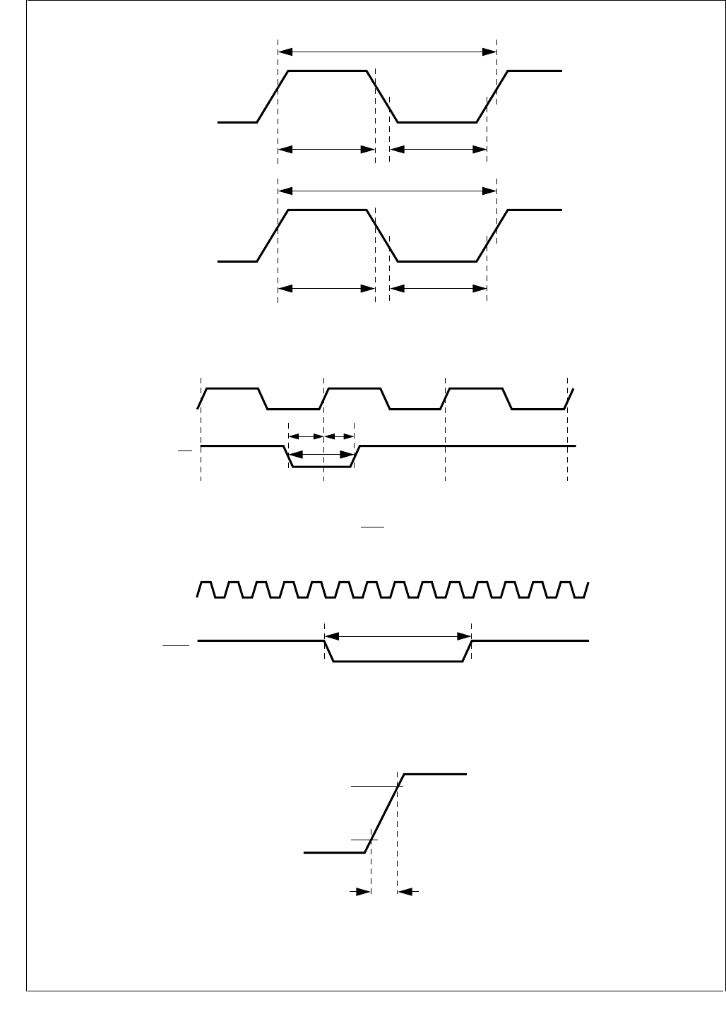
www.national.com 248
CP3BT26
Figure 110. Clock Timing
Figure 111. NMI Signal Timing
Figure 112. Non-Power-On Reset
Figure 113. Power-On Reset
X1CKI
tX1h tX1l
tX1p
X2CKI
tX2h tX2l
tX2p
DS095
CLK
tIW
t
lH
t
lS
NMI
DS096
CLK
t
RST
RESET
DS097
VCC
0.9 VCC
0.1 VCC
tDS115
R
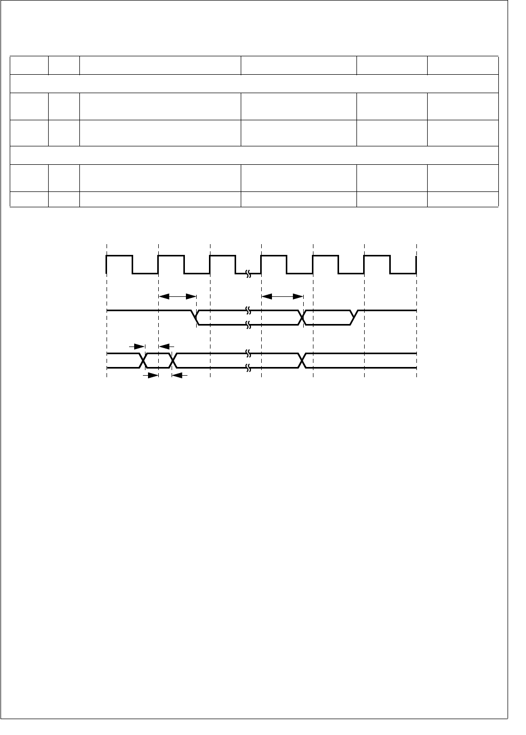
249 www.national.com
CP3BT26
30.8 UART TIMING
Figure 114. UART Asynchronous Mode Timing
Table 85 UART Signals
Symbol
Figure
Description Reference Min (ns) Max (ns)
UART Input Signals
tIs 114 Input setup time
RXD (asynchronous mode)
Before Rising Edge (RE)
on CLK -
tIh 114 Input hold time
RXD (asynchronous mode) After RE on CLK -
UART Output Signals
tCOv1 114 TXD output valid (all signals with
propagation delay from CLK RE) After RE on CLK -
tTXD 114 TXD output valid After RE on CLK - 40
CLK
TXD
RXD
1
tCOv1
tlS
tlH
tCOv1
11222111222
DS098
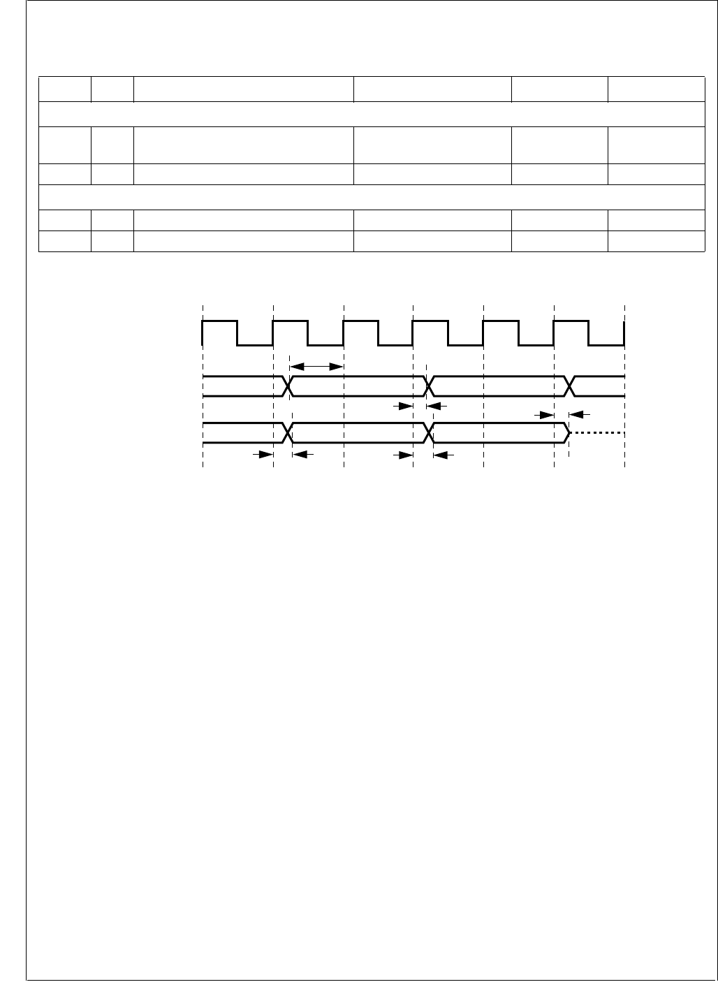
www.national.com 250
CP3BT26
30.9 I/O PORT TIMING
Figure 115. I/O Port Timing
Table 86 I/O Port Signals
Symbol
Figure
Description Reference Min (ns) Max (ns)
I/O Port Input Signals
tIS 115 Input Setup Time Before Rising Edge (RE)
on System Clock -
tIH 115 Input Hold Time After RE on System Clock -
I/O Port Output Signals
tCOv1 115 Output Valid Time After RE on System Clock -
tOF 115 Output Floating Time After RE on System Clock -
CLK
111222111222
PORTS B, C (input)
PORTS B, C (output)
tIS
tCOv1
tlH
tCOv1
tOF
DS100
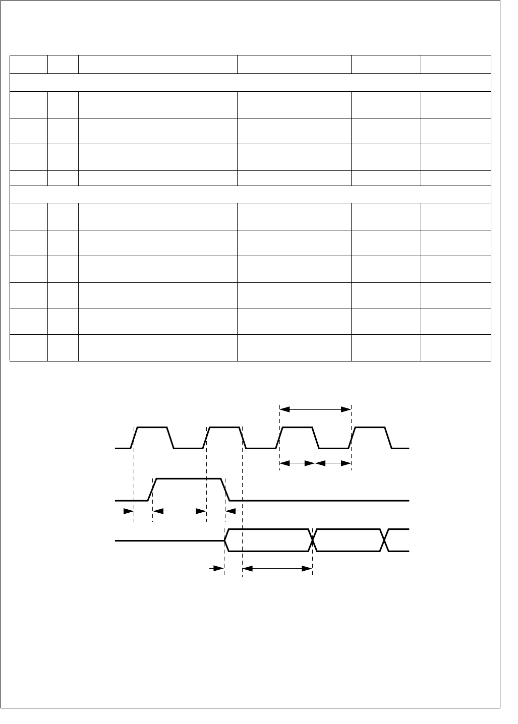
251 www.national.com
CP3BT26
30.10 ADVANCED AUDIO INTERFACE (AAI) TIMING
Figure 116. Receive Timing, Short Frame Sync
Table 87 Advanced Audio Interface (AAI) Signals
Symbol
Figure
Description Reference Min (ns) Max (ns)
AAI Input Signals
tRDS
116,
118 Receive Data Setup Time Before Falling Edge (FE)
on SRCLK 20 -
tRDH
116,
118 Receive Data Hold Time After FE on SRCLK 20 -
tFSS 116 Frame Sync Setup Time Before Rising Edge (RE)
on SRCLK 20 -
tFSH 116 Frame Sync Hold Time After RE on SRCLK 20 -
AAI Output Signals
tCP 116 Receive/Transmit Clock Period RE on SRCLK/SCK to RE
on SRCLK/SCK 976.6 -
tCL 116 Receive/Transmit Low Time FE on SRCLK/SCK to RE
on SRCLK/SCK 488.3 -
tCH 116 Receive/Transmit High Time RE on SRCLK/SCK to FE
on SRCLK/SCK 488.3 -
tFSVH
116,
118 Frame Sync Valid High RE on SRCLK/SCK to RE
on SRFS/SFS -20
tFSVL
116,
118 Frame Sync Valid Low RE on SRCLK/SCK to FE
on SRFS/SFS -20
tTDV
117,
119 Transmit Data Valid RE on SCK to STD Valid - 20
0
tCP
tCH
SRD
SRCLK
tCL
SRFS
DS116
1
012
tFSVH tFSVL
tRDH
tRDS
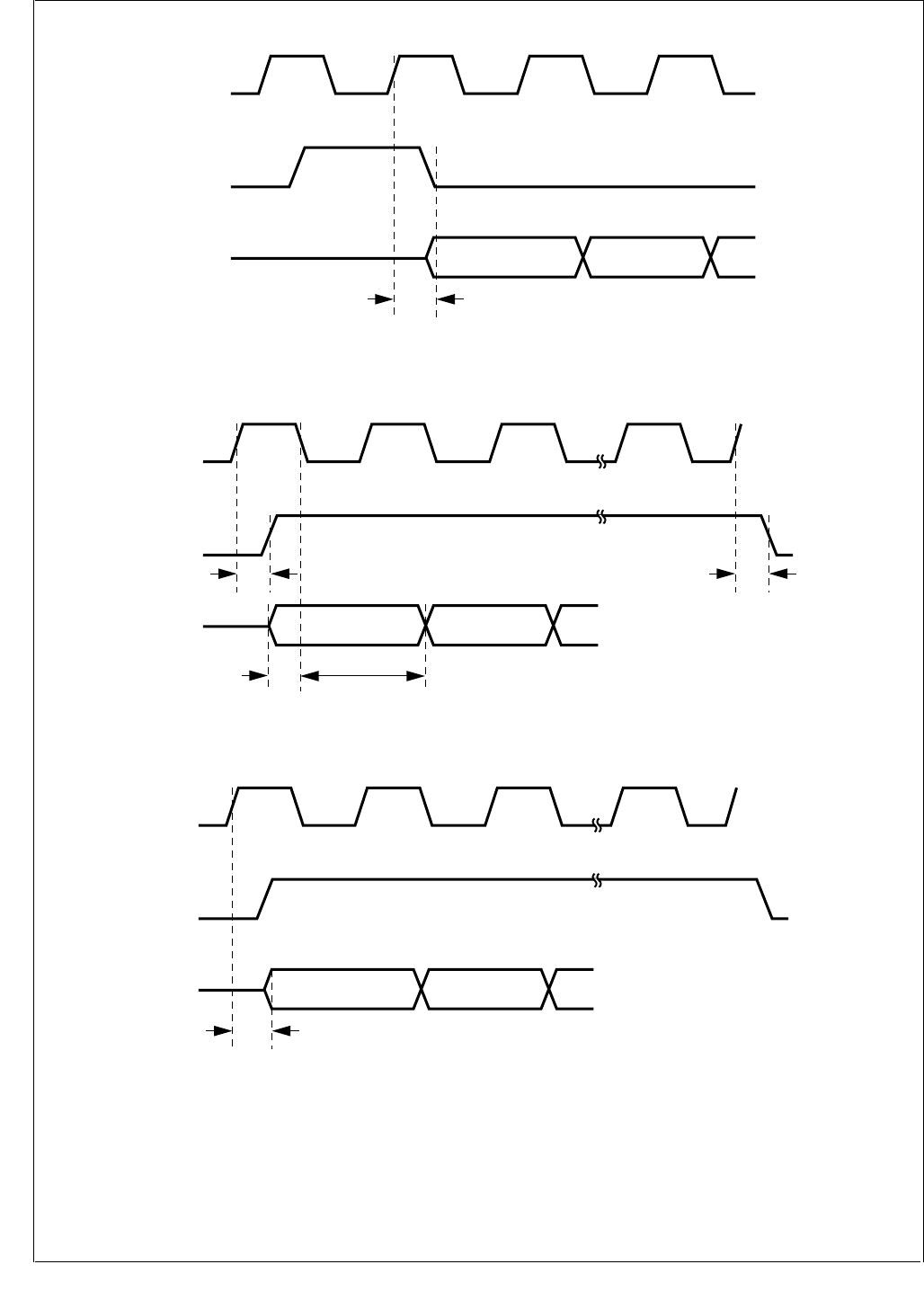
www.national.com 252
CP3BT26
Figure 117. Transmit Timing, Short Frame Sync
Figure 118. Receive Timing, Long Frame Sync
Figure 119. Transmit Timing, Long Frame Sync
0
STD
SCK
SFS
DS117
1
012
tTDV
0
SRD
SRCLK
SRFS
DS118
1
012
tFSVH tFSVL
tRDH
tRDS
N
0
STD
SCK
SFS
DS119
1
012
tTDV
N

253 www.national.com
CP3BT26
30.11 MICROWIRE/SPI TIMING
Table 88 Microwire/SPI Signals
Symbol
Figure
Description Reference Min (ns) Max (ns)
Microwire/SPI Input Signals
tMSKh 120 Microwire Clock High At 2.0V (both edges) 80 -
tMSKl 120 Microwire Clock Low At 0.8V (both edges) 80 -
tMSKp
120
Microwire Clock Period
SCIDL bit = 0; Rising Edge
(RE) MSK to next RE MSK 200
-
121 SCIDL bit = 1; Falling Edge
(FE) MSK to next FE MSK -
tMSKh 120 MSK Hold (slave only) After MWCS goes inactive 40 -
tMSKs 120 MSK Setup (slave only) Before MWCS goes active 80 -
tMWCSh
120
MWCS Hold (slave only)
SCIDL bit = 0: After FE
MSK 40
-
121 SCIDL bit = 1: After RE
MSK -
tMWCSs
120
MWCS Setup (slave only)
SCIDL bit = 0: Before RE
MSK 80
-
121 SCIDL bit = 1: Before FE
MSK -
tMDIh
120
Microwire Data In Hold (master)
Normal Mode: After RE
MSK 0
-
122 Alternate Mode: After FE
MSK -
120
Microwire Data In Hold (slave)
Normal Mode: After RE
MSK 40
-
122 Alternate Mode: After FE
MSK -
tMDIs
120
Microwire Data In Setup
Normal Mode: Before RE
MSK 80
-
122 Alternate Mode: Before FE
MSK -
Microwire/SPI Output Signals
tMSKh 120 Microwire Clock High At 2.0V (both edges) 40 -
tMSKl 120 Microwire Clock Low At 0.8V (both edges) 40 -
tMSKp
120
Microwire Clock Period
SCIDL bit = 0: Rising Edge
(RE) MSK to next RE MSK 100
-
121 SCIDL bit = 1: Falling Edge
(FE) MSK to next FE MSK -
tMSKd 120 MSK Leading Edge Delayed (master
only) Data Out Bit #7 Valid 0.5 tMSK 1.5 tMSK
tMDOf 120 Microwire Data Float b
(slave only) After RE on MWCS -25
tMDOh
120
Microwire Data Out Hold
Normal Mode: After FE
MSK 0.0
-
121 Alternate Mode: After RE
MSK
tMDOnf 124 Microwire Data No Float (slave only) After FE on MWCS 025
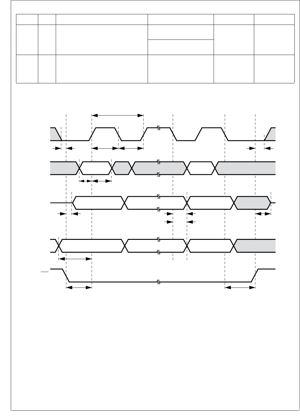
www.national.com 254
CP3BT26
Figure 120. Microwire Transaction Timing, Normal Mode, SCIDL = 0
tMDOv 120 Microwire Data Out Valid
Normal Mode: After FE on
MSK 25
Alternate Mode: After RE
on MSK
tMITOp 124 MDODI to MDIDO
(slave only)
Propagation Time
Value is the same in all
clocking modes of the
Microwire
25
Table 88 Microwire/SPI Signals
Symbol
Figure
Description Reference Min (ns) Max (ns)
lsbmsb
tMSKp
tMSKh
tMDlh
tMSKd
tMCSs tMCSh
tMDls
tMSKs
tMDOf tMDOv
tMDOff
tMDOh
tMSKhd
Data In
lsbmsb
MDODI
(master)
msb lsb
MDIDO
(slave)
MSK
MCS
(slave)
tMSKl
DS101
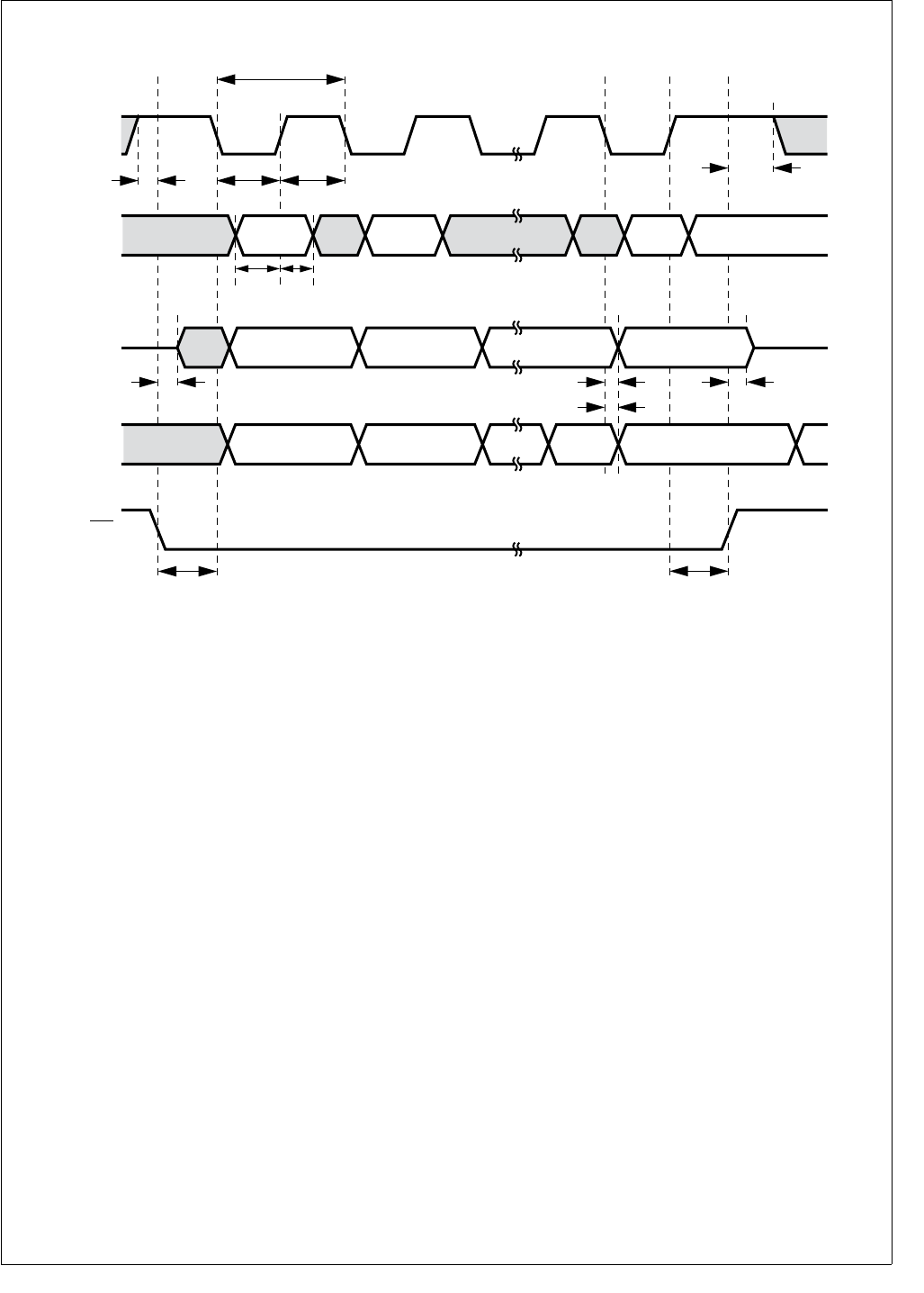
255 www.national.com
CP3BT26
Figure 121. Microwire Transaction Timing, Normal Mode, SCIDL = 1
lsb
msb
tMSKp
tMSKh
tMDlh
tMDls
tMCSs tMCSh
tMSKs
tMDOf tMDOv tMDOf
tMDOh
Data In
MSK
lsbmsb
MDODO
(master)
lsbmsb
MDIDO
(slave)
tMSKh
MCS
(slave)
tMSKhd
DS102
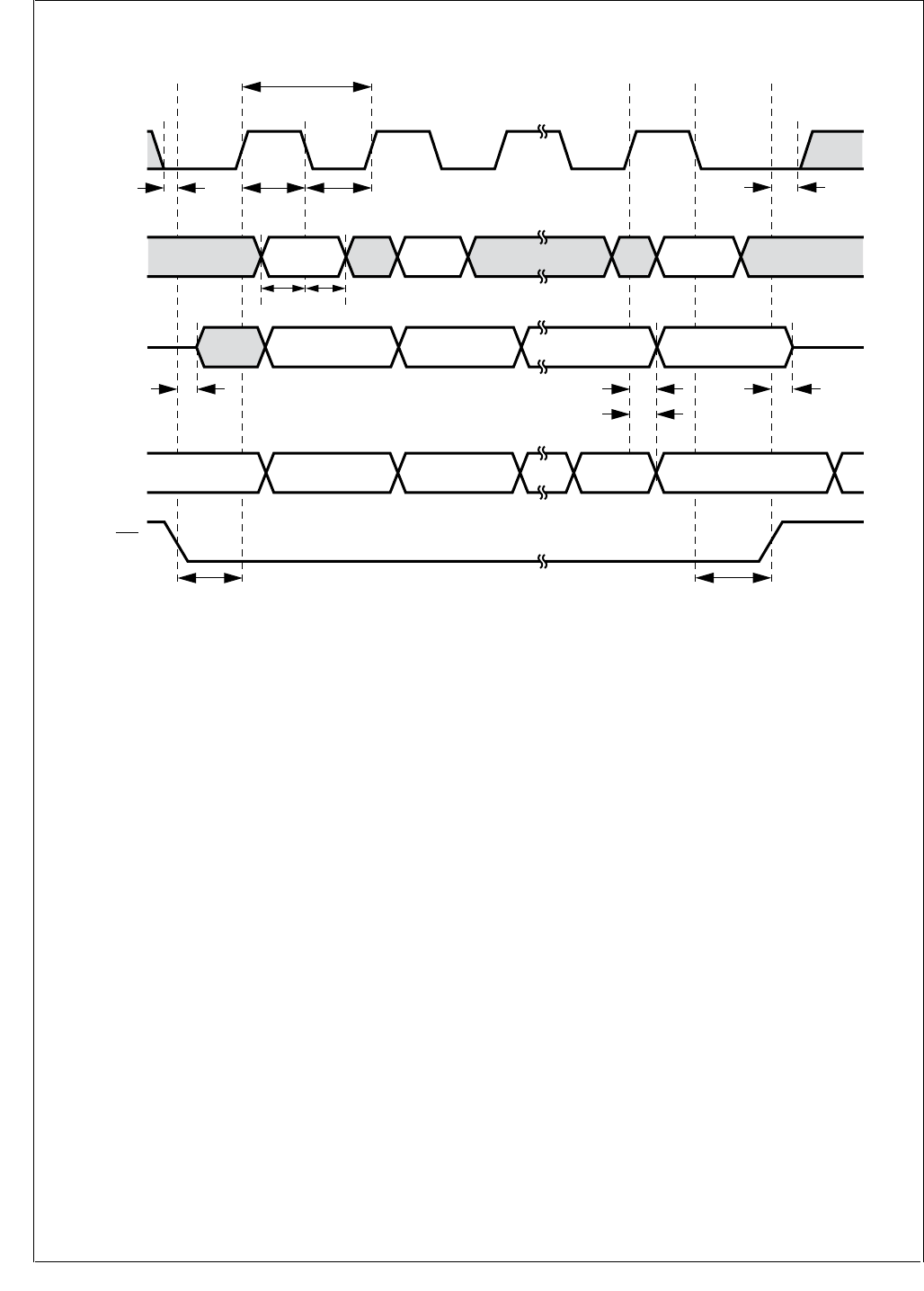
www.national.com 256
CP3BT26
Figure 122. Microwire Transaction Timing, Alternate Mode, SCIDL = 0
MSK
lsb
msb
Data In
lsbmsb
MDODO
(master)
lsbmsb
MDIDO
(slave)
MCS
(slave)
tMSKp
tMSKh
tMDlh
tMDls
tMCSs tMCSh
tMSKs
tMDOf tMDOv tMDOf
tMDOh
tMSKl
tMSKhd
DS103
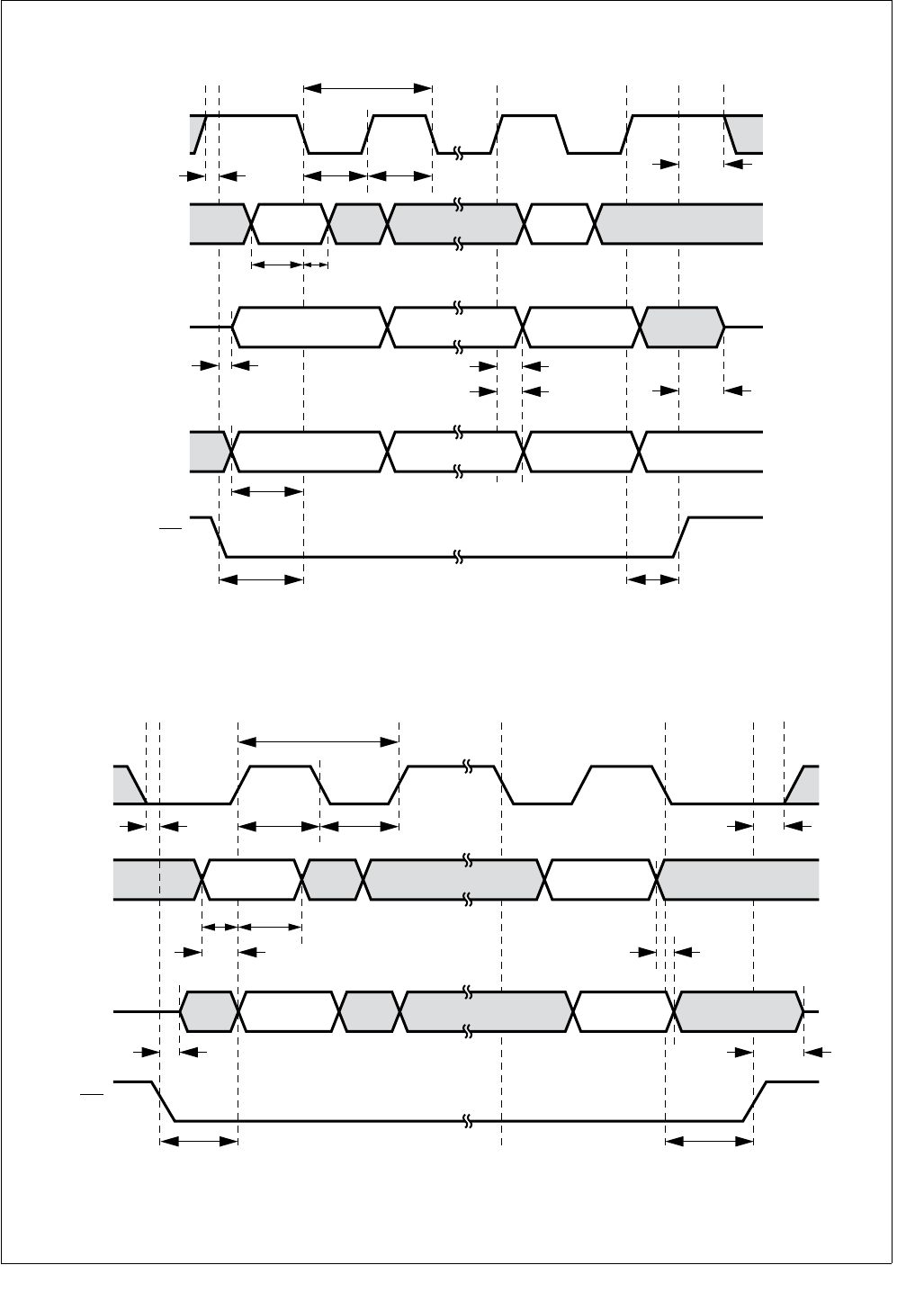
257 www.national.com
CP3BT26
Figure 123. Microwire Transaction Timing, Alternate Mode, SCIDL = 1
Figure 124. Microwire Transaction Timing, Data Echoed to Output,
Normal Mode, SCIDL = 0, ECHO = 1, Slave Mode
lsb
msb
tMSKp
tMSKh
tMDlh
tMDls
tMCSs
tSKd
tMCSh
tMSKs
tMDOf tMDOv
tMDOff
tMDOh
Data In
MSK
lsbmsb
MDODI
(master)
lsbmsb
MDIDO
(slave)
tMSKh
MCS
(slave only)
tMSKhd
DS104
MSK
Dl lsb
Dl msb
MDODI
(slave)
DO lsbDO msb
MDIDO
(slave)
MCS
tMSKp
tMSKh
tMDlh
tMDls
tMCSs tMCSh
tMSKs
tMDOnf
tMITOp
tMITOp
tMDOf
tMSKl
tMSKhd
DS105

www.national.com 258
CP3BT26
30.12 ACCESS.BUS TIMING
Table 89 ACCESS.bus Signals
Symbol
Figure
Description Reference Min (ns) Max (ns)
ACCESS.bus Input Signals
tBUFi 126 Bus free time between Stop and Start
Condition tSCLhigho -
tCSTOsi 126 SCL setup time Before Stop Condition (8 × t
CLK
)
- t
SCLri
-
tCSTRhi 126 SCL hold time After Start Condition (8 × t
CLK
)
- t
SCLri
-
tCSTRsi 126 SCL setup time Before Start Condition (8 × t
CLK
)
- t
SCLri
-
tDHCsi 127 Data High setup time Before SCL Rising Edge
(RE) 2 × tCLK -
tDLCsi 126 Data Low setup time Before SCL RE 2 × tCLK -
tSCLfi 125 SCL signal rise time - 300
tSCLri 125 SCL signal fall time - 1000
tSCLlowi 128 SCL low time After SCL Falling Edge
(FE) 16 × tCLK -
tSCLhighi 128 SCL high time After SCL RE 16 × tCLK -
tSDAri 125 SDA signal rise time - 1000
tSDAfl 125 SDA signal fall time - 300
tSDAhi 128 SDA hold time After SCL FE 0 -
tSDAsi 128 SDA setup time Before SCL RE 2 × tCLK -
ACCESS.bus Output Signals
tBUFo 126 Bus free time between Stop and Start
Condition
tSCLhigho
tCSTOso 126 SCL setup time Before Stop Condition tSCLhigho
tCSTRho 126 SCL hold time After Start Condition tSCLhigho
tCSTRso 127 SCL setup time Before Start Condition tSCLhigho
tDHCso 127 Data High setup time Before SCL R.E. tSCLhigho -tSDAro
tDLCso 126 Data Low setup time Before SCL R.E. tSCLhigho -tSDAfo
tSCLfo 125 SCL signal Fall time 300c
tSCLro 125 SCL signal Rise time - d
tSCLlowo 128 SCL low time After SCL F.E. (K × tCLK) -1e
tSCLhigh
o
128 SCL high time After SCL R.E. (K × tCLK) -1e
tSDAfo 125 SDA signal Fall time 300
tSDAro 125 SDA signal Rise time -
tSDAho 128 SDA hold time After SCL F.E.
(7 × t
CLK
) - t
SCLfo
tSDAvo 128 SDA valid time After SCL F.E. (7 × tCLK) + tRD
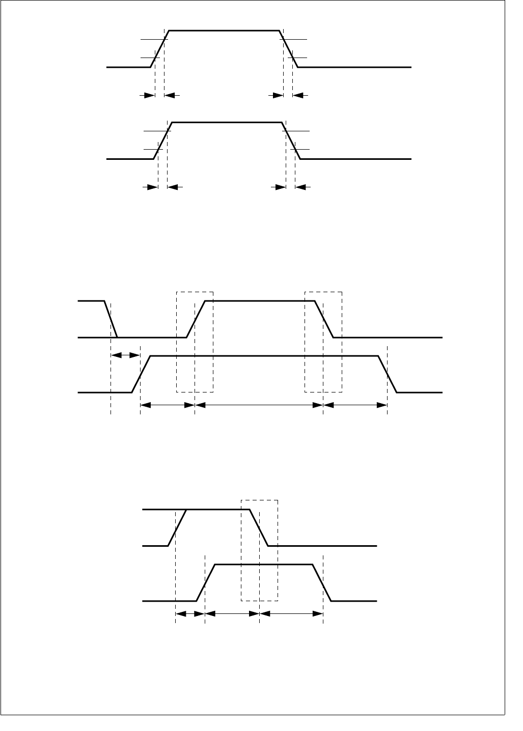
259 www.national.com
CP3BT26
Figure 125. ACB Signals (SDA and SCL) Timing
Figure 126. ACB Start and Stop Condition Timing
Figure 127. ACB Start Condition Timing
SCL
0.7VCC
Note: In the timing tables the parameter name is added with an "o" for output signal timing and "i" for input signal timing.
0.3VCC
tSCLf
0.7VCC
0.3VCC
tSCLr
SDA
0.7VCC
0.3VCC
tSDAf
0.7VCC
0.3VCC
tSDAr
DS106
SCL
SDA
tDLCs
tCSTOs tCSTRh
Stop Condition Start Condition
tBUF
Note: In the timing tables the parameter name is added with an "o" for output signal timing and "i" for input signal timing. DS107
SCL
SDA
tDHCs
tCSTRs
Start Condition
tCSTRh
Note: In the timing tables the parameter name is added with an "o" for output signal timing
and "i" for input signal timing.
DS108
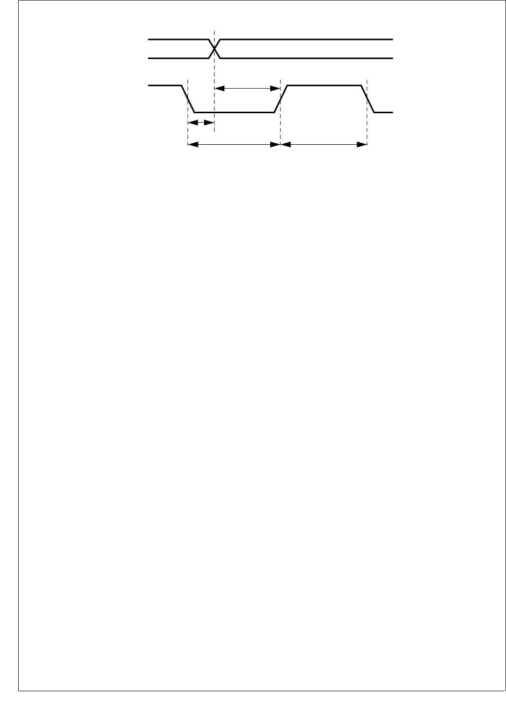
www.national.com 260
CP3BT26
Figure 128. ACB Data Timing
tSCAvo
tSDAh tCSLlow
tSDAsi
tSCLhigh
SCL
SDA
Note: In the timing tables the parameter name is added with an "o" for output signal timing
and "i" for input signal timing. unless the parameter already includes the suffix.
DS109
261 www.national.com
CP3BT26
30.13 USB PORT AC CHARACTERISTICS
30.14 MULTI-FUNCTION TIMER (MFT) TIMING
Figure 129. Multi-Function Timer Input Timing
Table 90 USB Port Signals
Symbol Description ConditionsaMin Typ Max Units
TRRise Time CL = 50 pF 4 20 ns
TFFall Time CL = 50 pF 4 20 ns
TRFM Fall/Rise Time Matching (TR/TF)C
L = 50 pF 90 110 %
VCRS Output Signal Crossover Voltage CL = 50 pF 1.3 2.0 V
ZDRV Driver Output Impedance CL = 50 pF 28 43 ohms
a. Waveforms measured at 10% to 90%.
Table 91 Multi-Function Timer Input Signals
Symbol Figure Description Reference Min (ns) Max (ns)
tTAH 129 TA High Time Rising Edge (RE) on CLK TCLK + 5
tTAL 129 TA Low Time RE on CLK TCLK + 5
tTBH 129 TB High Time RE on CLK TCLK + 5
tTBL 129 TB Low Time RE on CLK TCLK + 5
tTA L /tTBL
CLK
TA/TB
DS169
tTA L /tTBH
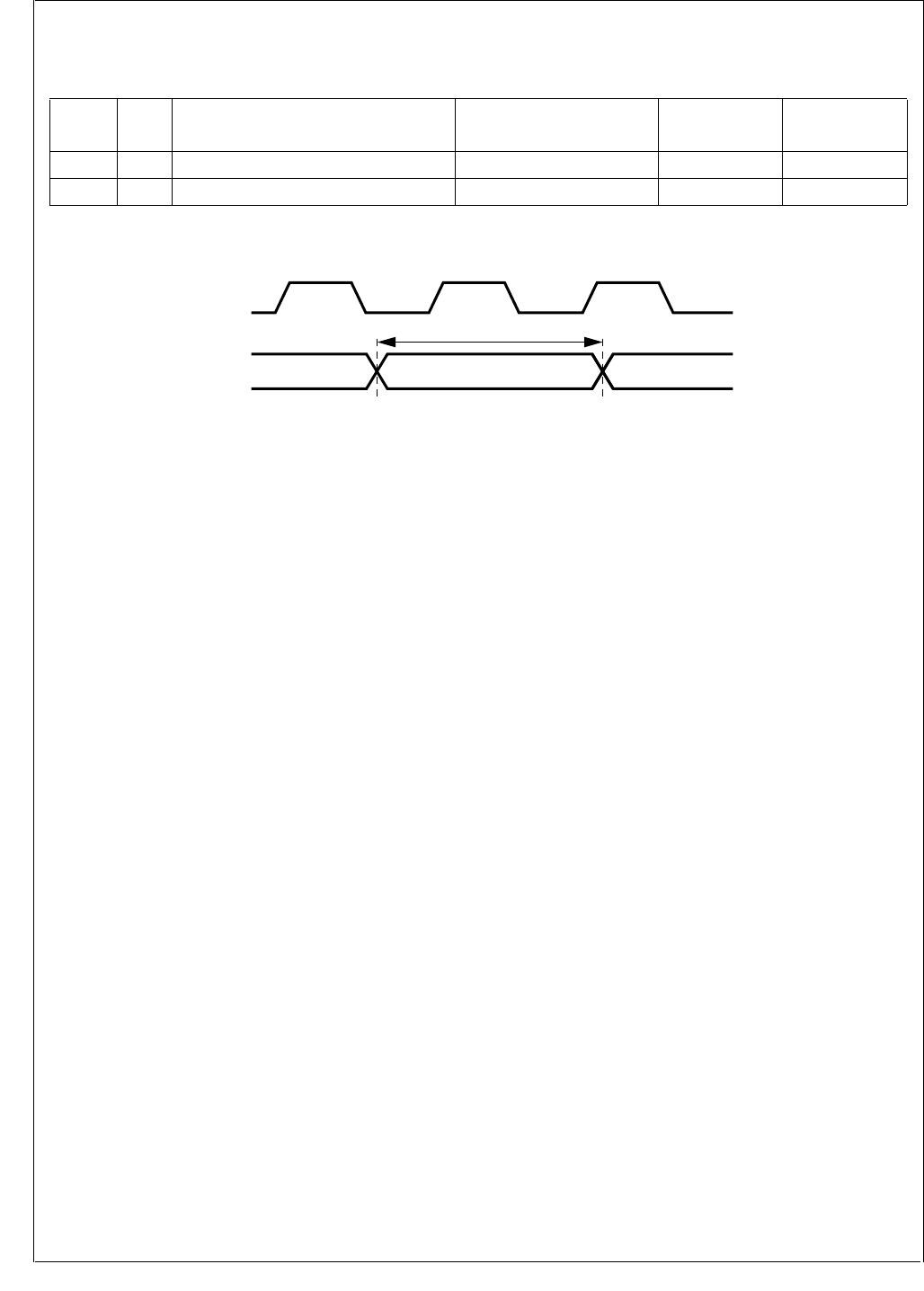
www.national.com 262
CP3BT26
30.15 VERSATILE TIMING UNIT (VTU) TIMING
Figure 130. Versatile Timing Unit Input Timing
Table 92 Versatile Timing Unit Input Signals
Symbol Figur
eDescription Reference Min (ns) Max (ns)
tTIOH 129 TIOx Input High Time Rising Edge (RE) on CLK
1.5 × T
CLK
+ 5ns
tTIOL 129 TIOx Input Low Time RE on CLK
1.5 × T
CLK
+ 5ns
tTIOL tTIOH
CLK
TIOx
DS110
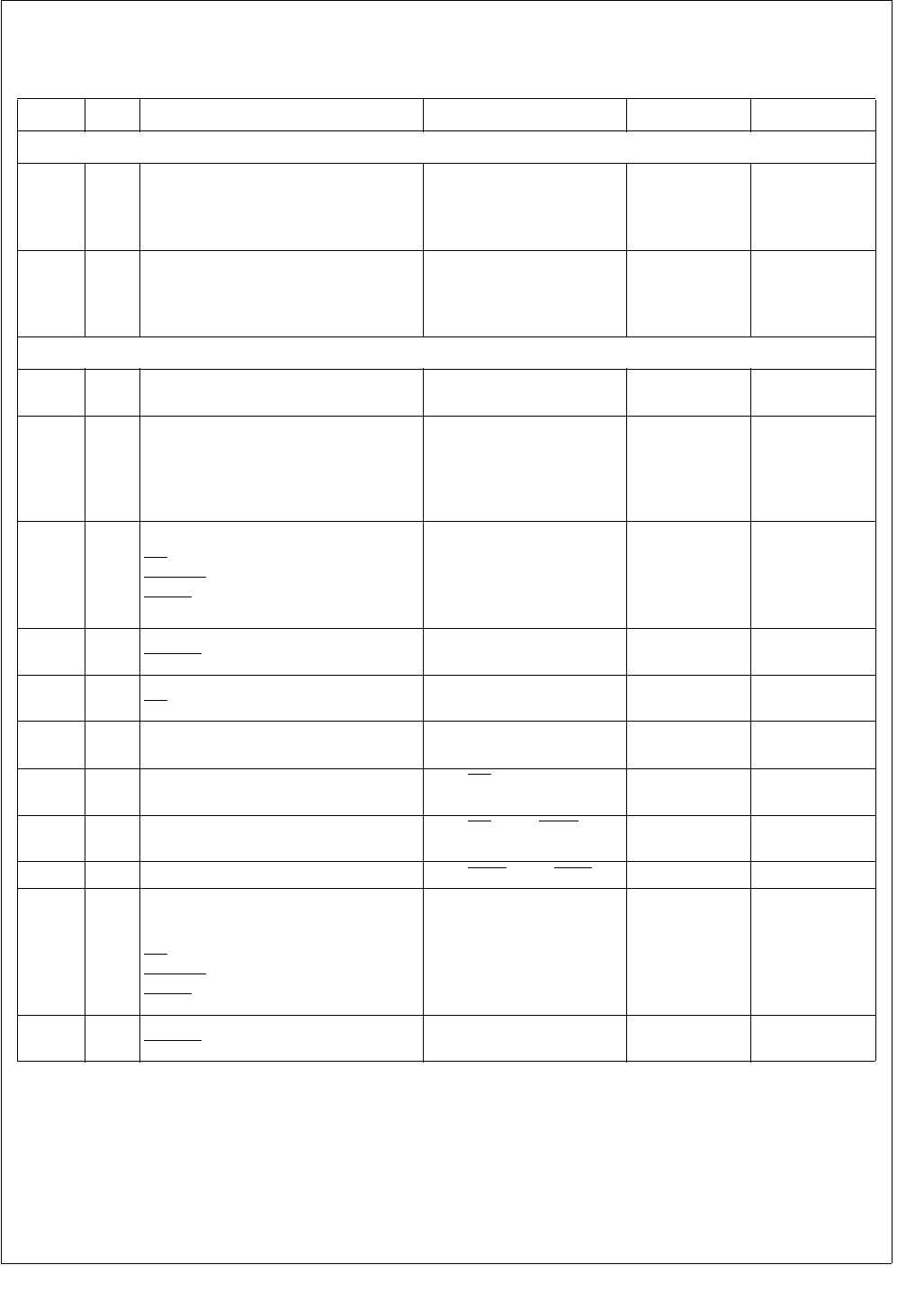
263 www.national.com
CP3BT26
30.16 EXTERNAL BUS TIMING
Table 93 External Bus Signals
Symbol
Figure
Description Reference Min (ns) Max (ns)
External Bus Input Signals
t1
131,
133,
134,
135
Input Setup Time
D[15:0]
Before Rising Edge (RE)
on CLK 8
t2
131,
133,
134,
135
Output Hold Time
D[15:0] After RE on CLK 0
External Bus Output Signals
t3
131,
132
Output Valid Time
D[15:0] After RE on CLK 8
t4
131,
132,
133,
134,
135
Output Valid Time
A[22:0] After RE on CLK 8
t5
131,
132,
133,
134,
135
Output Active/Inactive Time
RD
SEL[1:0]
SELIO
After RE on CLK 8
t6
131,
132
Output Active/Inactive Time
WR[1:0] After RE on CLK 0.5 Tclk + 8
t7133 Minimum Inactive Time
RD At 2.0V Tclk - 4
t8131 Output Float Time
D[15:0] After RE on CLK 8
t9131 Minimum Delay Time From RD Trailing Edge
(TE) to D[15:0] driven Tclk - 4
t10
131,
132 Minimum Delay Time From RD TE to SELn
Leading Edge (LE) 0
t11 132 Minimum Delay Time From SELx TE to SELy LE 0
t12
131,
132,
133,
134,
135
Output Hold Time
A[22:0]
D[15:0]
RD
SEL[2:0]
SELIO
After RE on CLK 0
t13
131,
132
Output Hold Time
WR[1:0] After RE on CLK 0.5 Tclk - 3
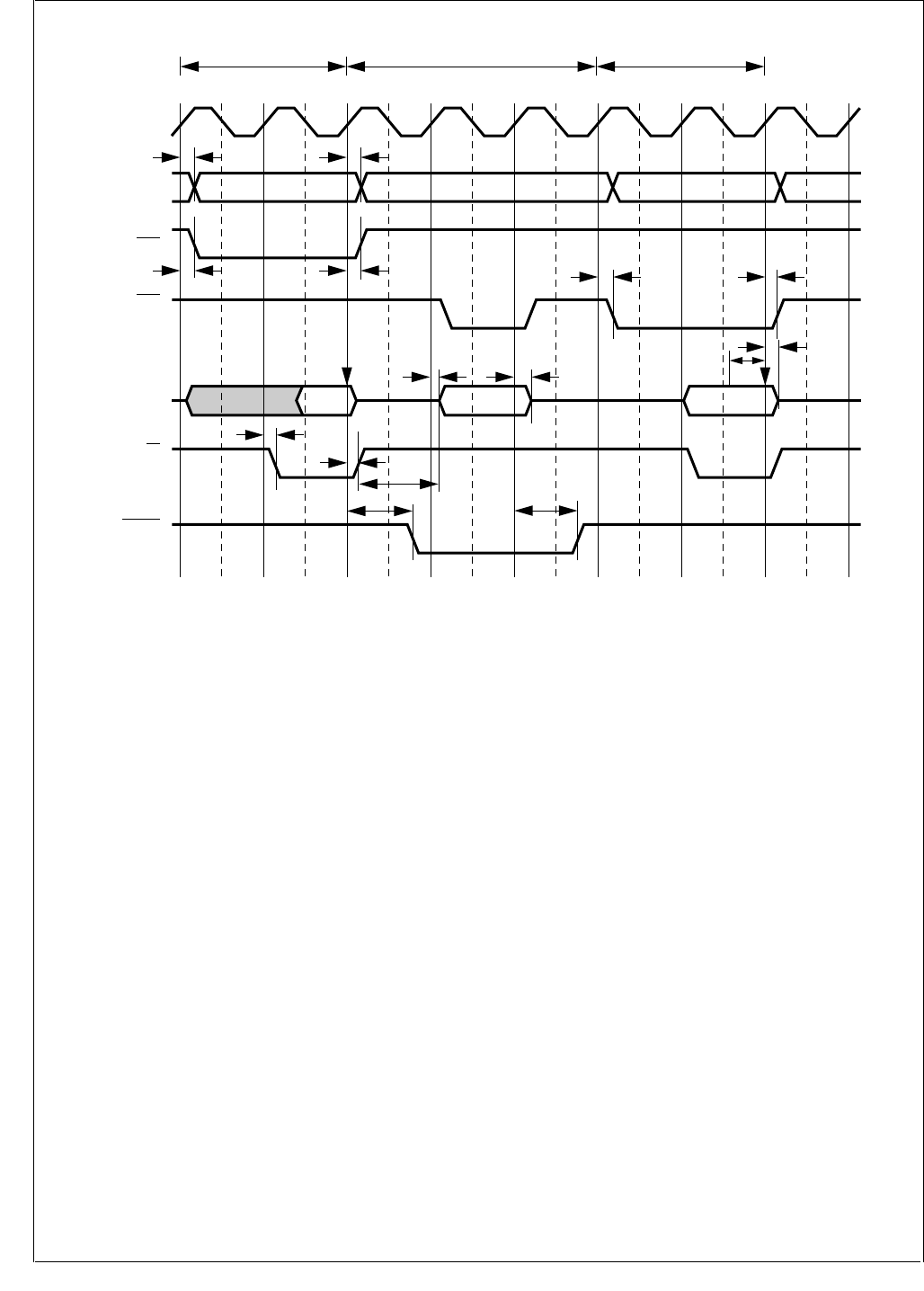
www.national.com 264
CP3BT26
Figure 131. Early Write Between Normal Read Cycles (No Wait States)
T1 T2 T1 T2 T3 T1 T2
A[21:0]
A22 ('13 only)
CLK
Normal Read Normal ReadEarly Write
SELx
D[15:0] In InOut
t4t4, t12
SELy
(y ≠ x)
RD
WR[1:0]
t5, t12
t5, t12 t5, t12
t8, t12
t3
t9
t5, t12
t5, t12
t6, t13
t5, t12
t6, t13
t2
t1
Bus State
DS124
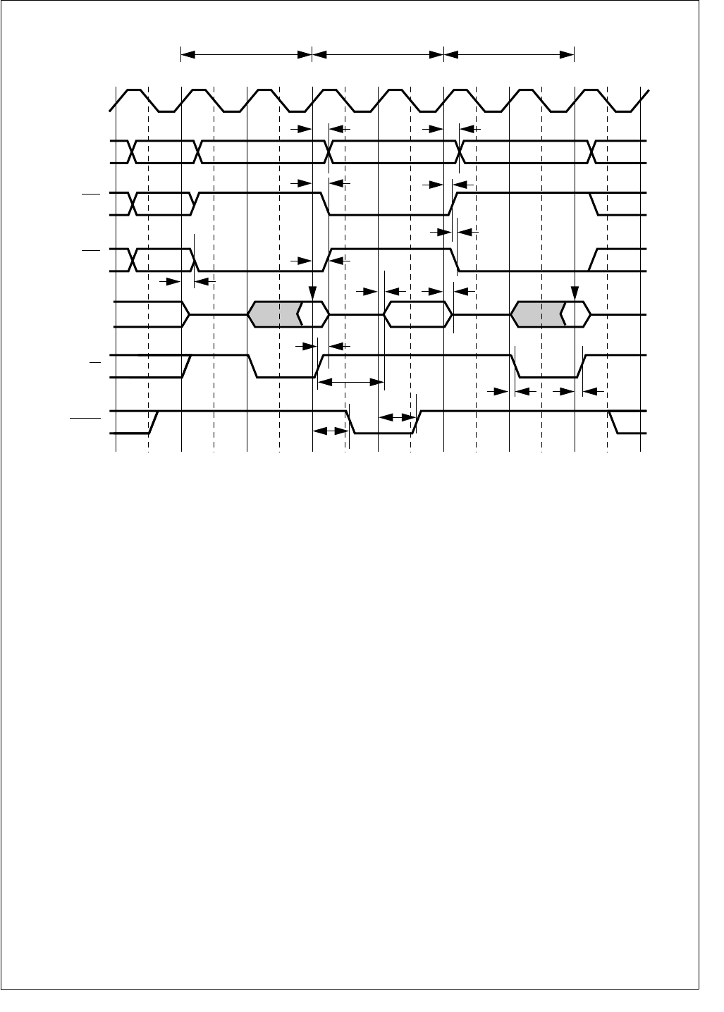
265 www.national.com
CP3BT26
Figure 132. Late Write Between Normal Read Cycles (No Wait States)
T1 T2 T1 T2 T1 T2
CLK
SELx
D[15:0] In InOut
(y ≠ x)
RD
Normal Read Normal ReadLate Write
t4, t12
t5, t12
t5, t12
t5, t12
t5, t12
t8, t12
t3
t11
t5, t12
t6, t13
t6, t13
t5, t12
t10
t9
t4, t12
SELy
(y ≠ x)
WR[1:0]
A[21:0]
A22 ('13 only)
Bus State
DS125
www.national.com 266
CP3BT26
Figure 133. Consecutive Normal Read Cycles (Burst, No Wait States)
T1 T2 T2B T1 T2 T2B
Normal Read Normal Read
CLK
SELx
SELy
WR[1:0]
D[15:0] In InInIn
(y ≠ x)
(y ≠ x)
RD
t5, t12
t5, t12
t4, t12 t4, t12
t4
t5, t12
t5, t12
t7
t5, t12
t5, t12
t2
t1
t2
t1
A[21:0]
A22 ('13 only)
Bus State
DS126
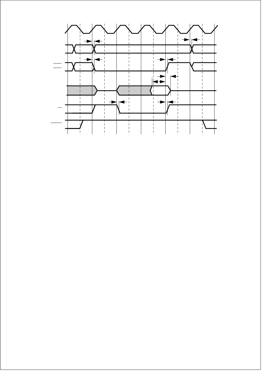
267 www.national.com
CP3BT26
Figure 134. Normal Read Cycle (Wait Cycle Followed by Hold Cycle)
T1 TW T2 TH
CLK
D[15:0]
SELn,
SELIO
WR[1:0]
RD
t4
t5, t12
t5, t12
t5, t12
t5, t12
t2
t1
t4, t12
A21:0
A22 ('13 only)
Bus State
DS127
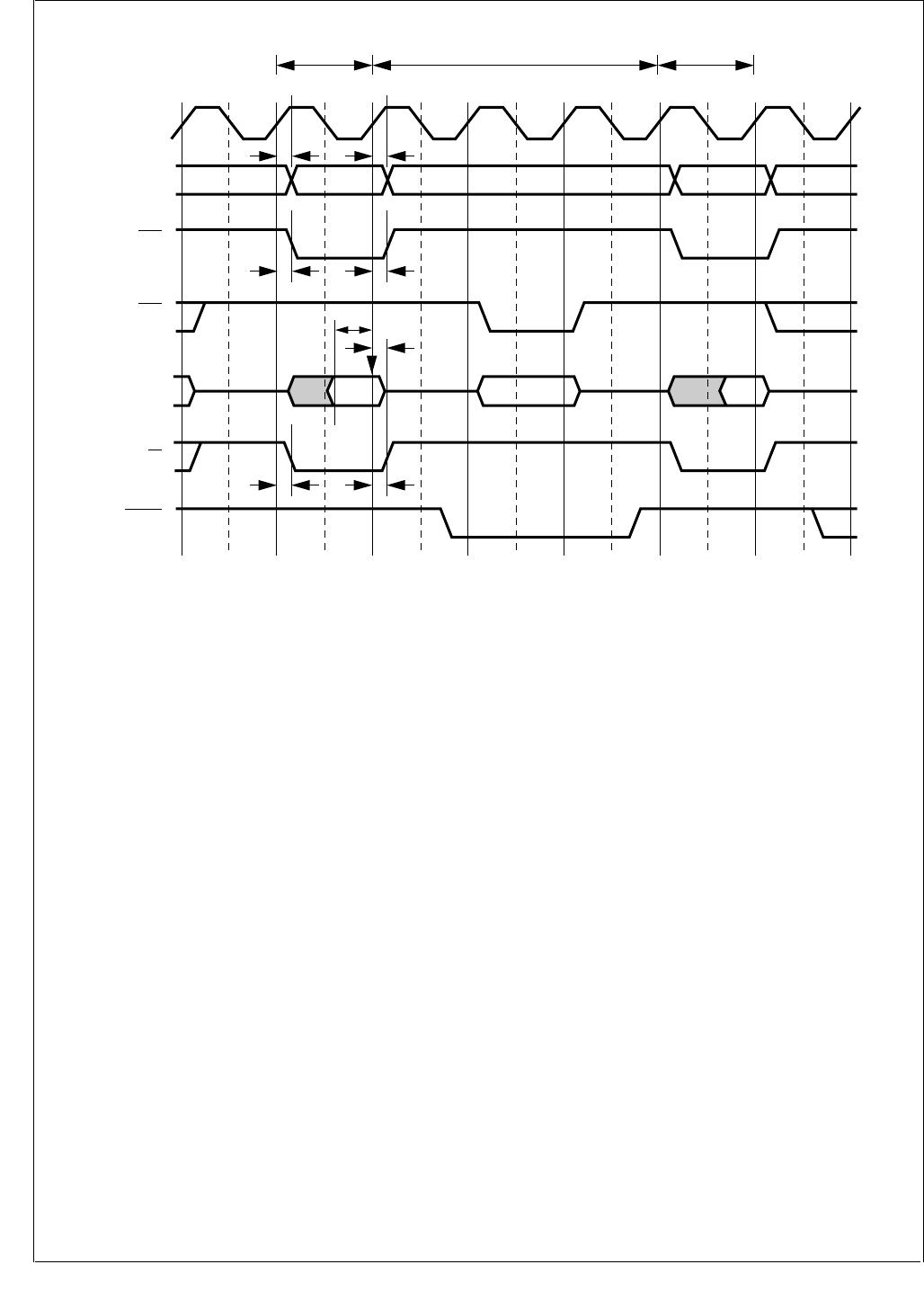
www.national.com 268
CP3BT26
Figure 135. Early Write Between Fast Read Cycles
Tidle T1-2 T1 T1T2 T3 T1-2
Fast Read Early Write
CLK
SELx
SELy
WR[1:0]
D[15:0]
(y ≠ x)
(y ≠ x)
RD
Fast Read
t5, t12
t5, t12
t2
t1
t5, t12
t5, t12
t4, t12
t4
A[21:0]
A22 ('13 only)
Bus State
DS128
In InOut

269 www.national.com
CP3BT26
31.0 Pin Assignments
31.1 LQFP-128 PACKAGE
For 128-pin devices, Figure 136 provides a pinout diagram, and Table 94 provides the pin assignments. The physical di-
mensions are provided in Section 33.0.
Figure 136. CP3BT26 in the LQFP-128 Package (Top View)
DS181
CP3BT26
(LQFP-128)
1
PJ1/WUI19
PC7
PC6
IOGND
PC5
PC4
IOVCC
PC3
PC2
IOGND
PC1
PC0
IOVCC
PB7
PB6
PB5
IOGND
PB4
PB3
PB2
IOVCC
PB1
PB0
GND
VCC
X1CKO
X1CKI/BBCLK
AGND
AVCC
X2CKI
X2CKO
VCC
GND
ENV2/SLOWCLK
ENV1/CPUCLK
ENV0/PLLCLK
PG6/BTSEQ2/WUI10
PJ2/WUI20
PJ4/WUI22
UGND
UVCC
D-
D+
PH7/CANTX
IOVCC
GND
VCC
PH5/TXD3/WUI16
IOGND
PH4/RXD3/WUI15
IOVCC
PH2/RXD2/WUI13
IOVCC
PH1/TXD1/WUI12
IOGND
IOVCC
IOGND
IOVCC
PG7/BTSEQ3/TA
IOGND
PE4/CKX/TB
PJ3/WUI21
39
TDI
TMS
RESET
ADC7/ADCIN
ADC6
ADC5/MUXOUT1
ADC4/MUXOUT0
ADC3/TSY-
ADC2/TSX-
ADC1/TSY+
ADC0/TSX+
VREF
ADGND
ADVCC
PE3/CTS
PE0/RXD0
PE2/RTS
GND
VCC
PE1/TXD0
SDA
SCL
IOVCC
IOGND
VCC
GND
IOGND
IOVCC
IOVCC
PG5/SLE
PG4/SDAT
PG3/SCLK
PG1/RFCE
PG0/RFSYNC
RFDATA
IOGND
PJ6/WUI24
PJ5/WUI23
65
TCK
PJ7/ASYNC/WUI9
PH0/RXD1/WUI11
TDO
IOVCC
RDY
PF3/MWCS/TIO4
IOGND
PF0/MSK/TIO1
GND
VCC
PF1/MDIDO/TIO2
IOVCC
PF2/MDODI/TIO3
IOGND
PG2/BTSEQ1/SRCLK
IOGND
PE5/SRFS/NMI
IOVCC
PF4/SCK/TIO5
PF5/SFS/TIO6
IOGND
PF6/STD/TIO7
PF7/SRD/TIO8
IOVCC
PJ0
103
PH3/TXD2/WUI14
PH6/CANRX/WUI17
Table 94 Pin Assignments for LQFP-128 Package
Pin Name Alternate Function(s) Pin Numbers Type
GND 24, 33, 56, 77, 85, 112 PWR
VCC 25, 32, 55, 78, 84, 113 PWR
IOGND
4, 10, 17, 43, 45, 49, 53,
67, 76, 79, 110, 117,
119, 124
PWR
IOVCC
7, 13, 21, 42, 44, 47, 51,
58, 74, 75, 80, 107, 115,
121, 127
PWR
X1CKO 26 O
X1CKI BBCLK 27 I
AGND 28 PWR

www.national.com 270
CP3BT26
AVCC 29 PWR
ADGND 90 PWR
ADVCC 89 PWR
UVCC 62 PWR
UGND 63 PWR
X2CKI 30 I
X2CKO 31 O
ENV2 SLOWCLK 34 I/O
ENV1 CPUCLK 35 I/O
ENV0 PLLCLK 36 I/O
RESET 100 I
TMS 101 I
TDI 102 I
TCK 103 I
TDO 106 O
RDY 108 O
RFDATA 68 I/O
D- 61 I/O
D+ 60 I/O
SCL 81 I/O
SDA 82 I/O
ADC0 TSX+ 92 I/O/HIZ 20mA+
ADC1 TSY+ 93 I/O/HIZ 20mA+
ADC2 TSX- 94 I/O/HIZ 20mA+
ADC3 TSY- 95 I/O/HIZ 20mA+
ADC4 MUXOUT0 96 I/O
ADC5 MUXOUT1 97 I/O
ADC6 98 I
ADC7 ADCIN 99 I
VREFP 91 I
PB0 D0 23 GPIO
PB1 D1 22 GPIO
PB2 D2 20 GPIO
PB3 D3 19 GPIO
PB4 D4 18 GPIO
PB5 D5 16 GPIO
PB6 D6 15 GPIO
PB7 D7 14 GPIO
PC0 D8 12 GPIO
PC1 D9 11 GPIO
PC2 D10 9 GPIO
PC3 D11 8 GPIO
PC4 D12 6 GPIO
Table 94 Pin Assignments for LQFP-128 Package
Pin Name Alternate Function(s) Pin Numbers Type

271 www.national.com
CP3BT26
PC5 D13 5 GPIO
PC6 D14 3 GPIO
PC7 D15 2 GPIO
PE0 RXD0 87 GPIO
PE1 TXD0 83 GPIO
PE2 RTS 86 GPIO
PE3 CTS 88 GPIO
PE4 CKX/TB 40 GPIO
PE5 SRFS/NMI 120 GPIO
PF0 MSK/TIO1 111 GPIO
PF1 MDIDO/TIO2 114 GPIO
PF2 MDODI/TIO3 116 GPIO
PF3 MWCS/TIO4 109 GPIO
PF4 SCK/TIO5 122 GPIO
PF5 SFS/TIO6 123 GPIO
PF6 STD/TIO7 125 GPIO
PF7 SRD/TIO8 126 GPIO
PG0 RFSYNC 69 GPIO
PG1 RFCE 70 GPIO
PG2 SRCLK 118 GPIO
PG3 SCLK 71 GPIO
PG4 SDAT 72 GPIO
PG5 SLE 73 GPIO
PG6 WUI10 37 GPIO
PG7 TA 41 GPIO
PH0 RXD1/WUI11 105 GPIO
PH1 TXD1/WUI12 46 GPIO
PH2 RXD2/WUI13 48 GPIO
PH3 TXD2/WUI14 50 GPIO
PH4 RXD3/WUI15 52 GPIO
PH5 TXD3/WUI16 54 GPIO
PH6 CANRX/WUI17 57 GPIO
PH7 CANTX 59 GPIO
PJ0 WUI18 128 GPIO
PJ1 WUI19 1 GPIO
PJ2 WUI20 38 GPIO
PJ3 WUI21 39 GPIO
PJ4 WUI22 64 GPIO
PJ5 WUI23 65 GPIO
PJ6 WUI24 66 GPIO
PJ7 ASYNC/WUI9 104 GPIO
Note 1: The ENV0, ENV1, ENV2, RESET, TCK, TDI, and TMS pins each have a weak pull-up to keep the input from floating.
Note 2: These functions are always enabled, due to the direct low-impedance path to these pins.
Table 94 Pin Assignments for LQFP-128 Package
Pin Name Alternate Function(s) Pin Numbers Type

www.national.com 272
CP3BT26
31.2 LQFP-144 PACKAGE
For 144-pin devices, Figure 137 provides a pinout diagram, and Table 95 provides the pin assignments. The physical di-
mensions are provided in Section 33.0.
Figure 137. CP3BT26 in the LQFP-144 Package (Top View)
DS182
1
PC7
PC6
IOGND
PC5
PC4
IOVCC
PC3
PC2
IOGND
PC1
PC0
IOVCC
PB7
PB6
PB5
IOGND
PB4
PB3
PB2
IOVCC
PB1
PB0
GND
VCC
X1CKO
X1CKI/BBCLKO
AGND
AVCC
X2CKI
X2CKO
VCC
GND
ENV2/SLOWCLK
ENV1/CPUCLK
ENV0/PLLCLK
PG6/BTSEQ2/WUI10
UVCC
D-
D+
WR1
WR0
IOGND
PH7/CANTX
IOVCC
A22
A21
A20
PH6/CANRX/WUI17
PH5/TXD3/WUI16
IOGND
A19
A18
PH4/RXD3/WUI15
IOVCC
PH3/TXD2/WUI14
IOGND
VCC
PH2/RXD2/WUI13
37
TDI
TMS
RESET
ADC7/ADCIN
ADC6
ADC5/MUXOUT1
ADC4/MUXOUT0
ADC3/TSY-
ADC2/TSX-
ADC1/TSY+
ADC0/TSX+
VREF
ADGND
ADVCC
PE3/CTS
PE0/RXD0
PE2/RTS
GND
VCC
PE1/TXD0
SDA
SCL
VCC
GND
IOGND
SELIO
SEL2
SEL1
IOVCC
PG5/SLE
PG4/SDAT
PG3/SCLK
PG1/RFCE
PG0/RFSYNC
RFDATA
73
TCK
PJ7/ASYNC/WUI9
PH0/RXD1/WUI11
TDO
PF0/MSK/TIO1
GND
VCC
PF1/MDIDO/TIO2
109
GND
RD
PH1/TXD1/WUI12
IOGND
A17
IOVCC
IOGND
A16
IOVCC
PG7/BTSEQ3/TA
PE4/CKX/TB
SEL0
RDY
A0
PF3/MWCS/TIO4
A1
IOGND
A2
A3
A4
A5
IOVCC
PF2/MDODI/TIO3
A6
A7
IOGND
A8
A9
PG2/BTSEQ1/SRCLK
PE5/SRFS/NMI
PF4/SCK/TIO5
PF5/SFS/TIO6
PF6/STD/TIO7
PF7/SRD/TIO8
A10
IOVCC
A11
A12
A13
PJ0/WUI18
A15
A14
UGND
CP3BT26
(LQFP-144)

273 www.national.com
CP3BT26
Table 95 Pin Assignments for LQFP-144 Package
Pin Name Alternate Function(s) Pin Number Type
GND 23, 32, 58, 85, 91, 121 PWR
VCC 24, 31, 57, 86, 90, 122 PWR
IOGND 3, 9, 16, 43, 46, 49, 55,
66, 84, 117, 130 PWR
IOVCC 6, 12, 20, 41, 44, 51, 63,
80, 126, 140 PWR
AGND 27 PWR
AVCC 28 PWR
ADGND 96 PWR
ADVCC 95 PWR
UVCC 71 PWR
UGND 72 PWR
X1CKI BBCLK 26 I
X1CKO 25 O
X2CKI 29 I
X2CKO 30 O
ENV2 SLOWCLK 33 I/O
ENV1 CPUCLK 34 I/O
ENV0 PLLCLK 35 I/O
RESET 106 I
TMS 107 I
TDI 108 I
TCK 109 I
TDO 112 O
RDY 113 O
RFDATA 73 I/O
D- 70 I/O
D+ 69 I/O
SCL 87 I/O
SDA 88 I/O
ADC0 TSX+ 98 I/O/HIZ 20mA+
ADC1 TSY+ 99 I/O/HIZ 20mA+
ADC2 TSX- 100 I/O/HIZ 20mA+
ADC3 TSY- 101 I/O/HIZ 20mA+
ADC4 MUXOUT0 102 I/O
ADC5 MUXOUT1 103 I/O
ADC6 104 I
ADC7 ADCIN 105 I
VREFP 97 I
PB0 D0 22 GPIO
PB1 D1 21 GPIO
PB2 D2 19 GPIO
PB3 D3 18 GPIO

www.national.com 274
CP3BT26
PB4 D4 17 GPIO
PB5 D5 15 GPIO
PB6 D6 14 GPIO
PB7 D7 13 GPIO
PC0 D8 11 GPIO
PC1 D9 10 GPIO
PC2 D10 8 GPIO
PC3 D11 7 GPIO
PC4 D12 5 GPIO
PC5 D13 4 GPIO
PC6 D14 2 GPIO
PC7 D15 1 GPIO
PE0 RXD0 93 GPIO
PE1 TXD0 89 GPIO
PE2 RTS 92 GPIO
PE3 CTS 94 GPIO
PE4 CKX/TB 37 GPIO
PE5 SRFS/NMI 134 GPIO
PF0 MSK/TIO1 120 GPIO
PF1 MDIDO/TIO2 123 GPIO
PF2 MDODI/TIO3 127 GPIO
PF3 MWCS/TIO4 115 GPIO
PF4 SCK/TIO5 135 GPIO
PF5 SFS/TIO6 136 GPIO
PF6 STD/TIO7 137 GPIO
PF7 SRD/TIO8 138 GPIO
PG0 RFSYNC 74 GPIO
PG1 RFCE 75 GPIO
PG2 SRCLK 133 GPIO
PG3 SCLK 76 GPIO
PG4 SDAT 77 GPIO
PG5 SLE 78 GPIO
PG6 WUI10 36 GPIO
PG7 TA 38 GPIO
PH0 RXD1/WUI11 111 GPIO
PH1 TXD1/WUI12 47 GPIO
PH2 RXD2/WUI13 48 GPIO
PH3 TXD2/WUI14 50 GPIO
PH4 RXD3/WUI15 52 GPIO
PH5 TXD3/WUI16 56 GPIO
PH6 CANRX/WUI17 59 GPIO
PH7 CANTX 64 GPIO
PJ0 WUI18 144 GPIO
PJ7 ASYNC 110 GPIO
Pin Name Alternate Function(s) Pin Number Type

275 www.national.com
CP3BT26
A22 62 O
A21 61 O
A20 60 O
A19 54 O
A18 53 O
A17 45 O
A16 42 O
A15 40 O
A14 39 O
A13 143 O
A12 142 O
A11 141 O
A10 139 O
A9 132 O
A8 131 O
A7 129 O
A6 128 O
A5 125 O
A4 124 O
A3 119 O
A2 118 O
A1 116 O
A0 114 O
SEL0 79 O
SEL1 81 O
SEL2 82 O
SELIO 83 O
RD 65 O
WR0 67 O
WR1 68 O
Note 1: The ENV0, ENV1, ENV2, RESET, TCK, TDI, and TMS pins each have a weak pull-up to keep the input from floating.
Note 2: These functions are always enabled, due to the direct low-impedance path to these pins.
Pin Name Alternate Function(s) Pin Number Type

www.national.com 276
CP3BT26
32.0 Revision History
Table 96 Revision History
Date Major Changes From Previous Version
4/3/03 Original release.
5/26/03
Fixed maximum boot area in Section 8.
Fixed names of clock signals in Figures 5
and 6. Fixed addresses of FSMARx
registers in Register Map section. Added
default value for RNGDIV.
6/16/03 Corrected Table 27. Changed IOH and IOL.
6/30/03
Changed NSIDs, deleted commercial
temperature range device, changed ADC
conversion time to 15 microseconds.
10/7/03
Updated DC electrical specifications.
Added ADC electrical specifications. Added
more detail to Table 7. Added Table 25.
11/14/03
Defined valid range of SCDV field in
Microwire/SPI module. Noted default
PRSSC register value generates a Slow
Clock frequency slightly higher than 32768
Hz. Clarified usage of CVSTAT register bits
and fields in CVSD/PCM module. Updated
layout of Bluetooth LLC registers. Added
usage hint for avoiding ACCESS.bus
module bus error. Added usage hint for
avoiding CAN unexpected loopback
condition.
2/28/04
Changed NSID designations in the product
selection guide. Updated Bluetooth section
for LMX5251 and LMX5252 radio chips.
Added BTSEQ[3:1] signals to pin
descriptions, GPIO alternate functions, and
package pin assignments. Added entry for
CTIM register in CAN section register list.
Changed CVSD Conversion section.
Changed definition of the RESOLUTION
field of the CVSD Control register
(CVCTRL). Changed reset values for ADC
registers. Added maximum I/O voltage in
Absolute Maximum Ratings section. Added
RESET Low minimum DC specification.
Added Iccprog DC specification. Changed
Vxl2 DC specification.
3/16/04
Changed LMX5251 interface circuit.
Updated DC specifications for clock input
low voltage, reset input high voltage, and
halt current.
5/10/04 Corrected NSIDs for no-lead solder parts.
5/12/04
Moved revision history in front of physical
dimensions. Changed back page
disclaimers.
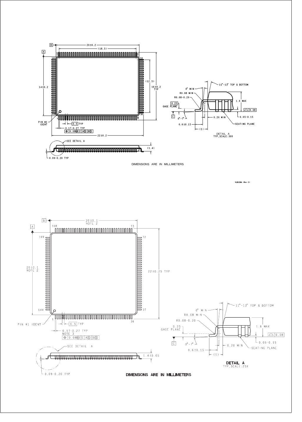
277 www.national.com
CP3BT26
33.0 Physical Dimensions (millimeters) unless otherwise noted
Figure 138. LQFP-128 Package
Figure 139. LQFP-144 Package

National Semiconductor
Americas Customer
Support Center
Email: new.feedback@nsc.com
Tel: 1-800-272-9959
National Semiconductor
Europe Customer
Support Center
Fax: +49 (0) 180-530 85 86
Email: europe.support@nsc.com
Deutsch Tel: +49 (0) 69 9508 6208
English Tel: +44 (0) 870 24 0 2171
Français Tel: +33 (0) 1 41 91 8790
National Semiconductor
Japan Customer
Support Center
Fax: 81-3-5639-7507
Email: jpn.feedback@nsc.com
Tel: 81-3-5639-7560
National Semiconductor
Asia Pacific Customer
Support Center
Email: ap.support@nsc.com
National does not assume any responsibility for use of any circuitry described, no circuit patent licenses are implied and National reserves the right at any time without notice to change said circuitry and specifications.
www.national.com
LIFE SUPPORT POLICY
NATIONAL’S PRODUCTS ARE NOT AUTHORIZED FOR USE AS CRITICAL COMPONENTS IN LIFE SUPPORT
DEVICES OR SYSTEMS WITHOUT THE EXPRESS WRITTEN APPROVAL OF THE PRESIDENT AND GENERAL
COUNSEL OF NATIONAL SEMICONDUCTOR CORPORATION. As used herein:
1. Life support devices or systems are devices or systems
which, (a) are intended for surgical implant into the body,
or (b) support or sustain life, and whose failure to per-
form when properly used in accordance with instructions
for use provided in the labeling, can be reasonably ex-
pected to result in a significant injury to the user.
2. A critical component is any component of a life support
device or system whose failure to perform can be rea-
sonably expected to cause the failure of the life support
device or system, or to affect its safety or effectiveness.
CP3BT26 Connectivity Processor with Bluetooth and Dual CAN Interfaces
BANNED SUBSTANCE COMPLIANCE
National Semiconductor certifies that the products and packing materials meet the provisions of the Customer Products
Stewardship Specification (CSP-9-111C2) and the Banned Substances and Materials of Interest Specification (CSP-9-
111S2) and contain no “Banned Substances” as defined in CSP-9-111S2.
