Nec 2400 Ipx Users Manual NEAX2400 Circuit Card
PDF NEC IPX Circuit Card Manual Issue 1 T E X T F I L E S
IPX Circuit Card Manual Iss 1(2429610w) IPX Circuit Card Manual Iss 1(2429610w)
NEC IPX Circuit Card Manual Issue 1 NEC_IPX_Circuit_Card_Manual_Issue_1 www.TelecomUserGuides.com Access User Guides, Manuals and Brochures
2400 IPX to the manual 0664b456-d22f-4a22-a36c-0ef294a737d6
2015-01-24
: Nec Nec-2400-Ipx-Users-Manual-331892 nec-2400-ipx-users-manual-331892 nec pdf
Open the PDF directly: View PDF ![]() .
.
Page Count: 644 [warning: Documents this large are best viewed by clicking the View PDF Link!]
- Table of Contents
- List of Figures
- List of Tables
- Chapter 1 Introduction
- Chapter 2 Control Circuit Card Reference
- Chapter 3 Line/Trunk Circuit Card Reference
- 1. General
- PA-CFTB
- PA-CK14
- PH-CK16
- PH-CK16-A
- PH-CK17
- PH-CK17-A
- PH-CK18
- PA-8COTBJ
- PA-16COTBE
- PA-CS02-C
- PA-CS08
- PA-CS08-B
- PA-CS33
- PA-8LCBR
- PA-16LCBE
- PA-16LCBJ-A
- PA-16LCBJ-B
- PA-16LCBW
- PA-16LCBY
- PA-16ELCJ
- PA-16ELCJ-B
- PA-FCHA
- PA-24LCBV
- PA-M69
- PA-M96
- PA-M103
- PA-8RSTK
- PA-8RSTM
- PA-8RSTY
- PA-SDTA
- PA-SDTB
- PA-2CCHA
- PA-24CCTA
- PA-2DCHA
- PA-ILCG
- PA-4ILCH
- PA-8ILCE-A
- PA-4DATA
- PA-4DATB
- PH-M16
- PA-4AMPC
- PA-8TLTR
- PA-M87
- PA-24PRTB-A
- PA-24DTR (DTI)
- PA-24DTR (DLI)

OCTOBER, 2000
NEC America, Inc.
NDA-24296
ISSUE 1
STOCK # 200774
Circuit Card Manual
®
LIABILITY DISCLAIMER
NEC America, Inc. reserves the right to change the specifications, functions, or
features, at any time, without notice.
NEC America, Inc. has prepared this document for use by its employees and
customers. The information contained herein is the property of NEC America,
Inc. and shall not be reproduced without prior written approval from NEC
America, Inc.
NEAX® and Dterm® are registered trademarks of NEC Corporation.
Copyright 2000
NEC America, Inc.
Printed in the U.S.A

ISSUE 1 ISSUE 2 ISSUE 3 ISSUE 4
DATE OCTOB ER, 20 00 DATE DATE DATE
ISSUE 5 ISSUE 6 ISSUE 7 ISSUE 8
DATE DATE DATE DATE
NEAX2400 IPX
Circuit Card Manual Revision Sheet 1/9
NDA-24296
PAGE No. ISSUE No.
12345678
i 1
ii 1
iii 1
iv 1
v 1
vi 1
vii 1
viii 1
ix 1
x 1
xi 1
xii 1
1 1
2 1
3 1
41
5 1
6 1
7 1
81
9 1
10 1
11 1
12 1
13 1
14 1
15 1
16 1
17 1
18 1
19 1
20 1
21 1
22 1
23 1
24 1
25 1
26 1
27 1
28 1
29 1
30 1
31 1
32 1
33 1
34 1
35 1
36 1
37 1
38 1
39 1
40 1
41 1
42 1
43 1
44 1
45 1
46 1
47 1
48 1
49 1
50 1
51 1
52 1
53 1
54 1
55 1
56 1
57 1
58 1
59 1
60 1
61 1
62 1
63 1
64 1
PAGE No. ISSUE No.
12345678

ISSUE 1 ISSUE 2 ISSUE 3 ISSUE 4
DATE OCTOB ER, 20 00 DATE DATE DATE
ISSUE 5 ISSUE 6 ISSUE 7 ISSUE 8
DATE DATE DATE DATE
NEAX2400 IPX
Circuit Card Manual Revision Sheet 2/9
NDA-24296
65 1
66 1
67 1
68 1
69 1
70 1
71 1
72 1
73 1
74 1
75 1
76 1
77 1
78 1
79 1
80 1
81 1
82 1
83 1
84 1
85 1
86 1
87 1
88 1
89 1
90 1
91 1
92 1
93 1
94 1
95 1
96 1
97 1
98 1
99 1
100 1
101 1
102 1
PAGE No. ISSUE No.
12345678
103 1
104 1
105 1
106 1
107 1
108 1
109 1
110 1
111 1
112 1
113 1
114 1
115 1
116 1
117 1
118 1
119 1
120 1
121 1
122 1
123 1
124 1
125 1
126 1
127 1
128 1
129 1
130 1
131 1
132 1
133 1
134 1
135 1
136 1
137 1
138 1
139 1
140 1
PAG E No. ISSUE No.
12345678

ISSUE 1 ISSUE 2 ISSUE 3 ISSUE 4
DATE OCTOB ER, 20 00 DATE DATE DATE
ISSUE 5 ISSUE 6 ISSUE 7 ISSUE 8
DATE DATE DATE DATE
NEAX2400 IPX
Circuit Card Manual Revision Sheet 3/9
NDA-24296
141 1
142 1
143 1
144 1
145 1
146 1
147 1
148 1
149 1
150 1
151 1
152 1
153 1
154 1
155 1
156 1
157 1
158 1
159 1
160 1
161 1
162 1
163 1
164 1
165 1
166 1
167 1
168 1
169 1
170 1
171 1
172 1
173 1
174 1
175 1
176 1
177 1
178 1
PAGE No. ISSUE No.
12345678
179 1
180 1
181 1
182 1
183 1
184 1
185 1
186 1
187 1
188 1
189 1
190 1
191 1
192 1
193 1
194 1
195 1
196 1
197 1
198 1
199 1
200 1
201 1
202 1
203 1
204 1
205 1
206 1
207 1
208 1
209 1
210 1
211 1
212 1
213 1
214 1
215 1
216 1
PAG E No. ISSUE No.
12345678

ISSUE 1 ISSUE 2 ISSUE 3 ISSUE 4
DATE OCTOB ER, 20 00 DATE DATE DATE
ISSUE 5 ISSUE 6 ISSUE 7 ISSUE 8
DATE DATE DATE DATE
NEAX2400 IPX
Circuit Card Manual Revision Sheet 4/9
NDA-24296
217 1
218 1
219 1
220 1
221 1
222 1
223 1
224 1
225 1
226 1
227 1
228 1
229 1
230 1
231 1
232 1
233 1
234 1
235 1
236 1
237 1
238 1
239 1
240 1
241 1
242 1
243 1
244 1
245 1
246 1
247 1
248 1
249 1
250 1
251 1
252 1
253 1
254 1
PAGE No. ISSUE No.
12345678
255 1
256 1
257 1
258 1
259 1
260 1
261 1
262 1
263 1
264 1
265 1
266 1
267 1
268 1
269 1
270 1
271 1
272 1
273 1
274 1
275 1
276 1
277 1
278 1
279 1
280 1
281 1
282 1
283 1
284 1
285 1
286 1
287 1
288 1
289 1
290 1
291 1
292 1
PAG E No. ISSUE No.
12345678

ISSUE 1 ISSUE 2 ISSUE 3 ISSUE 4
DATE OCTOB ER, 20 00 DATE DATE DATE
ISSUE 5 ISSUE 6 ISSUE 7 ISSUE 8
DATE DATE DATE DATE
NEAX2400 IPX
Circuit Card Manual Revision Sheet 5/9
NDA-24296
293 1
294 1
295 1
296 1
297 1
298 1
299 1
300 1
301 1
302 1
303 1
304 1
305 1
306 1
307 1
308 1
309 1
310 1
311 1
312 1
313 1
314 1
315 1
316 1
317 1
318 1
319 1
320 1
321 1
322 1
323 1
324 1
325 1
326 1
327 1
328 1
329 1
330 1
PAGE No. ISSUE No.
12345678
331 1
332 1
333 1
334 1
335 1
336 1
337 1
338 1
339 1
340 1
341 1
342 1
343 1
344 1
345 1
346 1
347 1
348 1
349 1
350 1
351 1
352 1
353 1
354 1
355 1
356 1
357 1
358 1
359 1
360 1
361 1
362 1
363 1
364 1
365 1
366 1
367 1
368 1
PAG E No. ISSUE No.
12345678

ISSUE 1 ISSUE 2 ISSUE 3 ISSUE 4
DATE OCTOB ER, 20 00 DATE DATE DATE
ISSUE 5 ISSUE 6 ISSUE 7 ISSUE 8
DATE DATE DATE DATE
NEAX2400 IPX
Circuit Card Manual Revision Sheet 6/9
NDA-24296
369 1
370 1
371 1
372 1
373 1
374 1
375 1
376 1
377 1
378 1
379 1
380 1
381 1
382 1
383 1
384 1
385 1
386 1
387 1
388 1
389 1
390 1
391 1
392 1
393 1
394 1
395 1
396 1
397 1
398 1
399 1
400 1
401 1
402 1
403 1
404 1
405 1
406 1
PAGE No. ISSUE No.
12345678
407 1
408 1
409 1
410 1
411 1
412 1
413 1
414 1
415 1
416 1
417 1
418 1
419 1
420 1
421 1
422 1
423 1
424 1
425 1
426 1
427 1
428 1
429 1
430 1
431 1
432 1
433 1
434 1
435 1
436 1
437 1
438 1
439 1
440 1
441 1
442 1
443 1
444 1
PAG E No. ISSUE No.
12345678

ISSUE 1 ISSUE 2 ISSUE 3 ISSUE 4
DATE OCTOB ER, 20 00 DATE DATE DATE
ISSUE 5 ISSUE 6 ISSUE 7 ISSUE 8
DATE DATE DATE DATE
NEAX2400 IPX
Circuit Card Manual Revision Sheet 7/9
NDA-24296
445 1
446 1
447 1
448 1
449 1
450 1
451 1
452 1
453 1
454 1
455 1
456 1
457 1
458 1
459 1
460 1
461 1
462 1
463 1
464 1
465 1
466 1
467 1
468 1
469 1
470 1
471 1
472 1
473 1
474 1
475 1
476 1
477 1
478 1
479 1
480 1
481 1
482 1
PAGE No. ISSUE No.
12345678
483 1
484 1
485 1
486 1
487 1
488 1
489 1
490 1
491 1
492 1
493 1
494 1
495 1
496 1
497 1
498 1
499 1
500 1
501 1
502 1
503 1
504 1
505 1
506 1
507 1
508 1
509 1
510 1
511 1
512 1
513 1
514 1
515 1
516 1
517 1
518 1
519 1
520 1
PAG E No. ISSUE No.
12345678

ISSUE 1 ISSUE 2 ISSUE 3 ISSUE 4
DATE OCTOB ER, 20 00 DATE DATE DATE
ISSUE 5 ISSUE 6 ISSUE 7 ISSUE 8
DATE DATE DATE DATE
NEAX2400 IPX
Circuit Card Manual Revision Sheet 8/9
NDA-24296
521 1
522 1
523 1
524 1
525 1
526 1
527 1
528 1
529 1
530 1
531 1
532 1
533 1
534 1
535 1
536 1
537 1
538 1
539 1
540 1
541 1
542 1
543 1
544 1
545 1
546 1
547 1
548 1
549 1
550 1
551 1
552 1
553 1
554 1
555 1
556 1
557 1
558 1
PAGE No. ISSUE No.
12345678
559 1
560 1
561 1
562 1
563 1
564 1
565 1
566 1
567 1
568 1
569 1
570 1
571 1
572 1
573 1
574 1
575 1
576 1
577 1
578 1
579 1
580 1
581 1
582 1
583 1
584 1
585 1
586 1
587 1
588 1
589 1
590 1
591 1
592 1
593 1
594 1
595 1
596 1
PAG E No. ISSUE No.
12345678

ISSUE 1 ISSUE 2 ISSUE 3 ISSUE 4
DATE OCTOB ER, 20 00 DATE DATE DATE
ISSUE 5 ISSUE 6 ISSUE 7 ISSUE 8
DATE DATE DATE DATE
NEAX2400 IPX
Circuit Card Manual Revision Sheet 9/9
NDA-24296
597 1
598 1
599 1
600 1
601 1
602 1
603 1
604 1
605 1
606 1
607 1
608 1
609 1
610 1
611 1
612 1
613 1
614 1
615 1
616 1
617 1
618 1
PAGE No. ISSUE No.
12345678 PAGE No. ISSUE No.
12345678

NDA-24296
ISSUE 1
OCTOBER, 2000
NEAX2400 IPX
Circuit Card Manual
TABLE OF CONTENTS
Page
NDA-24296 TABLE OF CONTENTS
Page i
Revision 1.0
LIST OF FIGURES . . . . . . . . . . . . . . . . . . . . . . . . . . . . . . . . . . . . . . . . . . . . . . . . . . . . . . . . . . . . . . . . . . . . . . . .iii
LIST OF TABLES. . . . . . . . . . . . . . . . . . . . . . . . . . . . . . . . . . . . . . . . . . . . . . . . . . . . . . . . . . . . . . . . . . . . . . . . . xi
CHAPTER 1 INTRODUCTION . . . . . . . . . . . . . . . . . . . . . . . . . . . . . . . . . . . . . . . . . . . . . . . . . . . . . . . . . . . . . 1
1. GENERAL. . . . . . . . . . . . . . . . . . . . . . . . . . . . . . . . . . . . . . . . . . . . . . . . . . . . . . . . . . 1
2. MOUNTING LOCATION OF CIRCUIT CARD . . . . . . . . . . . . . . . . . . . . . . . . . . . . . . . . . . . . 2
CHAPTER 2 CONTROL CIRCUIT CARD REFERENCE . . . . . . . . . . . . . . . . . . . . . . . . . . . . . . . . . . . . . . . . 19
SN1695 CPRBF-A . . . . . . . . . . . . . . . . . . . . . . . . . . . . . . . . . . . . . . . . . . . . . . . . . . . . . . . . . . . . . . . . . 20
PH-GT09 . . . . . . . . . . . . . . . . . . . . . . . . . . . . . . . . . . . . . . . . . . . . . . . . . . . . . . . . . . . . . . . . . . . . . . . . 40
PH-GT10 . . . . . . . . . . . . . . . . . . . . . . . . . . . . . . . . . . . . . . . . . . . . . . . . . . . . . . . . . . . . . . . . . . . . . . . . 43
PA-PC94 . . . . . . . . . . . . . . . . . . . . . . . . . . . . . . . . . . . . . . . . . . . . . . . . . . . . . . . . . . . . . . . . . . . . . . . . 47
PA-PW54-A . . . . . . . . . . . . . . . . . . . . . . . . . . . . . . . . . . . . . . . . . . . . . . . . . . . . . . . . . . . . . . . . . . . . . . 51
PA-PW54-B . . . . . . . . . . . . . . . . . . . . . . . . . . . . . . . . . . . . . . . . . . . . . . . . . . . . . . . . . . . . . . . . . . . . . . 56
PA-PW55-A . . . . . . . . . . . . . . . . . . . . . . . . . . . . . . . . . . . . . . . . . . . . . . . . . . . . . . . . . . . . . . . . . . . . . . 61
PA-PW55-B . . . . . . . . . . . . . . . . . . . . . . . . . . . . . . . . . . . . . . . . . . . . . . . . . . . . . . . . . . . . . . . . . . . . . . 66
PH-DK10 . . . . . . . . . . . . . . . . . . . . . . . . . . . . . . . . . . . . . . . . . . . . . . . . . . . . . . . . . . . . . . . . . . . . . . . . 71
PH-IO24 . . . . . . . . . . . . . . . . . . . . . . . . . . . . . . . . . . . . . . . . . . . . . . . . . . . . . . . . . . . . . . . . . . . . . . . . . 77
PH-M22 . . . . . . . . . . . . . . . . . . . . . . . . . . . . . . . . . . . . . . . . . . . . . . . . . . . . . . . . . . . . . . . . . . . . . . . . . 82
PH-M16 . . . . . . . . . . . . . . . . . . . . . . . . . . . . . . . . . . . . . . . . . . . . . . . . . . . . . . . . . . . . . . . . . . . . . . . . . 88
PH-PC36 . . . . . . . . . . . . . . . . . . . . . . . . . . . . . . . . . . . . . . . . . . . . . . . . . . . . . . . . . . . . . . . . . . . . . . . . 93
PH-PC20 . . . . . . . . . . . . . . . . . . . . . . . . . . . . . . . . . . . . . . . . . . . . . . . . . . . . . . . . . . . . . . . . . . . . . . . 102
PH-PC45 . . . . . . . . . . . . . . . . . . . . . . . . . . . . . . . . . . . . . . . . . . . . . . . . . . . . . . . . . . . . . . . . . . . . . . . 105
PH-PW14 . . . . . . . . . . . . . . . . . . . . . . . . . . . . . . . . . . . . . . . . . . . . . . . . . . . . . . . . . . . . . . . . . . . . . . . 112
PH-SW10 . . . . . . . . . . . . . . . . . . . . . . . . . . . . . . . . . . . . . . . . . . . . . . . . . . . . . . . . . . . . . . . . . . . . . . . 115
PH-SW12 . . . . . . . . . . . . . . . . . . . . . . . . . . . . . . . . . . . . . . . . . . . . . . . . . . . . . . . . . . . . . . . . . . . . . . . 127
PU-SW00/PU-SW00-A . . . . . . . . . . . . . . . . . . . . . . . . . . . . . . . . . . . . . . . . . . . . . . . . . . . . . . . . . . . . 134
PU-SW01 . . . . . . . . . . . . . . . . . . . . . . . . . . . . . . . . . . . . . . . . . . . . . . . . . . . . . . . . . . . . . . . . . . . . . . . 140
PZ-GT13 . . . . . . . . . . . . . . . . . . . . . . . . . . . . . . . . . . . . . . . . . . . . . . . . . . . . . . . . . . . . . . . . . . . . . . . 146
PZ-GT16 . . . . . . . . . . . . . . . . . . . . . . . . . . . . . . . . . . . . . . . . . . . . . . . . . . . . . . . . . . . . . . . . . . . . . . . 149
PZ-GT20 . . . . . . . . . . . . . . . . . . . . . . . . . . . . . . . . . . . . . . . . . . . . . . . . . . . . . . . . . . . . . . . . . . . . . . . 152
PZ-M565 . . . . . . . . . . . . . . . . . . . . . . . . . . . . . . . . . . . . . . . . . . . . . . . . . . . . . . . . . . . . . . . . . . . . . . . 155
PZ-ME44 . . . . . . . . . . . . . . . . . . . . . . . . . . . . . . . . . . . . . . . . . . . . . . . . . . . . . . . . . . . . . . . . . . . . . . . 157
PZ-PC19 . . . . . . . . . . . . . . . . . . . . . . . . . . . . . . . . . . . . . . . . . . . . . . . . . . . . . . . . . . . . . . . . . . . . . . . 159
PZ-PC22 . . . . . . . . . . . . . . . . . . . . . . . . . . . . . . . . . . . . . . . . . . . . . . . . . . . . . . . . . . . . . . . . . . . . . . . 163
PZ-PC23 . . . . . . . . . . . . . . . . . . . . . . . . . . . . . . . . . . . . . . . . . . . . . . . . . . . . . . . . . . . . . . . . . . . . . . . 167
CHAPTER 3 LINE/TRUNK CIRCUIT CARD REFERENCE . . . . . . . . . . . . . . . . . . . . . . . . . . . . . . . . . . . . . 171
1. GENERAL. . . . . . . . . . . . . . . . . . . . . . . . . . . . . . . . . . . . . . . . . . . . . . . . . . . . . . . . 171
PA-CFTB . . . . . . . . . . . . . . . . . . . . . . . . . . . . . . . . . . . . . . . . . . . . . . . . . . . . . . . . . . . . . . . . . . . . . . . 172

TABLE OF CONTENTS NDA-24296
Page ii
Revision 1.0
TABLE OF CONTENTS (CONTINUED)
Page
PA-CK14 . . . . . . . . . . . . . . . . . . . . . . . . . . . . . . . . . . . . . . . . . . . . . . . . . . . . . . . . . . . . . . . . . . . . . . . 178
PH-CK16 . . . . . . . . . . . . . . . . . . . . . . . . . . . . . . . . . . . . . . . . . . . . . . . . . . . . . . . . . . . . . . . . . . . . . . . 181
PH-CK16-A . . . . . . . . . . . . . . . . . . . . . . . . . . . . . . . . . . . . . . . . . . . . . . . . . . . . . . . . . . . . . . . . . . . . . 192
PH-CK17 . . . . . . . . . . . . . . . . . . . . . . . . . . . . . . . . . . . . . . . . . . . . . . . . . . . . . . . . . . . . . . . . . . . . . . . 209
PH-CK17-A . . . . . . . . . . . . . . . . . . . . . . . . . . . . . . . . . . . . . . . . . . . . . . . . . . . . . . . . . . . . . . . . . . . . . 220
PH-CK18 . . . . . . . . . . . . . . . . . . . . . . . . . . . . . . . . . . . . . . . . . . . . . . . . . . . . . . . . . . . . . . . . . . . . . . . 239
PA-8COTBJ . . . . . . . . . . . . . . . . . . . . . . . . . . . . . . . . . . . . . . . . . . . . . . . . . . . . . . . . . . . . . . . . . . . . 244
PA-16COTBE . . . . . . . . . . . . . . . . . . . . . . . . . . . . . . . . . . . . . . . . . . . . . . . . . . . . . . . . . . . . . . . . . . . 250
PA-CS02-C . . . . . . . . . . . . . . . . . . . . . . . . . . . . . . . . . . . . . . . . . . . . . . . . . . . . . . . . . . . . . . . . . . . . . 262
PA-CS08 . . . . . . . . . . . . . . . . . . . . . . . . . . . . . . . . . . . . . . . . . . . . . . . . . . . . . . . . . . . . . . . . . . . . . . . 268
PA-CS08-B . . . . . . . . . . . . . . . . . . . . . . . . . . . . . . . . . . . . . . . . . . . . . . . . . . . . . . . . . . . . . . . . . . . . . 275
PA-CS33 . . . . . . . . . . . . . . . . . . . . . . . . . . . . . . . . . . . . . . . . . . . . . . . . . . . . . . . . . . . . . . . . . . . . . . . 283
PA-8LCBR . . . . . . . . . . . . . . . . . . . . . . . . . . . . . . . . . . . . . . . . . . . . . . . . . . . . . . . . . . . . . . . . . . . . . . 295
PA-16LCBE . . . . . . . . . . . . . . . . . . . . . . . . . . . . . . . . . . . . . . . . . . . . . . . . . . . . . . . . . . . . . . . . . . . . . 303
PA-16LCBJ-A . . . . . . . . . . . . . . . . . . . . . . . . . . . . . . . . . . . . . . . . . . . . . . . . . . . . . . . . . . . . . . . . . . . 315
PA-16LCBJ-B . . . . . . . . . . . . . . . . . . . . . . . . . . . . . . . . . . . . . . . . . . . . . . . . . . . . . . . . . . . . . . . . . . . 325
PA-16LCBW . . . . . . . . . . . . . . . . . . . . . . . . . . . . . . . . . . . . . . . . . . . . . . . . . . . . . . . . . . . . . . . . . . . . 334
PA-16LCBY . . . . . . . . . . . . . . . . . . . . . . . . . . . . . . . . . . . . . . . . . . . . . . . . . . . . . . . . . . . . . . . . . . . . . 344
PA-16ELCJ . . . . . . . . . . . . . . . . . . . . . . . . . . . . . . . . . . . . . . . . . . . . . . . . . . . . . . . . . . . . . . . . . . . . . 354
PA-16ELCJ-B . . . . . . . . . . . . . . . . . . . . . . . . . . . . . . . . . . . . . . . . . . . . . . . . . . . . . . . . . . . . . . . . . . . 361
PA-FCHA . . . . . . . . . . . . . . . . . . . . . . . . . . . . . . . . . . . . . . . . . . . . . . . . . . . . . . . . . . . . . . . . . . . . . . 370
PA-24LCBV . . . . . . . . . . . . . . . . . . . . . . . . . . . . . . . . . . . . . . . . . . . . . . . . . . . . . . . . . . . . . . . . . . . . . 381
PA-M69 . . . . . . . . . . . . . . . . . . . . . . . . . . . . . . . . . . . . . . . . . . . . . . . . . . . . . . . . . . . . . . . . . . . . . . . . 392
PA-M96 . . . . . . . . . . . . . . . . . . . . . . . . . . . . . . . . . . . . . . . . . . . . . . . . . . . . . . . . . . . . . . . . . . . . . . . . 399
PA-M103 . . . . . . . . . . . . . . . . . . . . . . . . . . . . . . . . . . . . . . . . . . . . . . . . . . . . . . . . . . . . . . . . . . . . . . . 405
PA-8RSTK . . . . . . . . . . . . . . . . . . . . . . . . . . . . . . . . . . . . . . . . . . . . . . . . . . . . . . . . . . . . . . . . . . . . . . 409
PA-8RSTM . . . . . . . . . . . . . . . . . . . . . . . . . . . . . . . . . . . . . . . . . . . . . . . . . . . . . . . . . . . . . . . . . . . . . 417
PA-8RSTY . . . . . . . . . . . . . . . . . . . . . . . . . . . . . . . . . . . . . . . . . . . . . . . . . . . . . . . . . . . . . . . . . . . . . . 424
PA-SDTA . . . . . . . . . . . . . . . . . . . . . . . . . . . . . . . . . . . . . . . . . . . . . . . . . . . . . . . . . . . . . . . . . . . . . . . 433
PA-SDTB . . . . . . . . . . . . . . . . . . . . . . . . . . . . . . . . . . . . . . . . . . . . . . . . . . . . . . . . . . . . . . . . . . . . . . . 448
PA-2CCHA . . . . . . . . . . . . . . . . . . . . . . . . . . . . . . . . . . . . . . . . . . . . . . . . . . . . . . . . . . . . . . . . . . . . . 453
PA-24CCTA . . . . . . . . . . . . . . . . . . . . . . . . . . . . . . . . . . . . . . . . . . . . . . . . . . . . . . . . . . . . . . . . . . . . 464
PA-2DCHA . . . . . . . . . . . . . . . . . . . . . . . . . . . . . . . . . . . . . . . . . . . . . . . . . . . . . . . . . . . . . . . . . . . . . 479
PA-ILCG . . . . . . . . . . . . . . . . . . . . . . . . . . . . . . . . . . . . . . . . . . . . . . . . . . . . . . . . . . . . . . . . . . . . . . . 490
PA-4ILCH . . . . . . . . . . . . . . . . . . . . . . . . . . . . . . . . . . . . . . . . . . . . . . . . . . . . . . . . . . . . . . . . . . . . . . 499
PA-8ILCE-A . . . . . . . . . . . . . . . . . . . . . . . . . . . . . . . . . . . . . . . . . . . . . . . . . . . . . . . . . . . . . . . . . . . . . 509
PA-4DATA . . . . . . . . . . . . . . . . . . . . . . . . . . . . . . . . . . . . . . . . . . . . . . . . . . . . . . . . . . . . . . . . . . . . . . 521
PA-4DATB . . . . . . . . . . . . . . . . . . . . . . . . . . . . . . . . . . . . . . . . . . . . . . . . . . . . . . . . . . . . . . . . . . . . . . 531
PH-M16 . . . . . . . . . . . . . . . . . . . . . . . . . . . . . . . . . . . . . . . . . . . . . . . . . . . . . . . . . . . . . . . . . . . . . . . . 541
PA-4AMPC . . . . . . . . . . . . . . . . . . . . . . . . . . . . . . . . . . . . . . . . . . . . . . . . . . . . . . . . . . . . . . . . . . . . . 548
PA-8TLTR . . . . . . . . . . . . . . . . . . . . . . . . . . . . . . . . . . . . . . . . . . . . . . . . . . . . . . . . . . . . . . . . . . . . . . 554
PA-M87 . . . . . . . . . . . . . . . . . . . . . . . . . . . . . . . . . . . . . . . . . . . . . . . . . . . . . . . . . . . . . . . . . . . . . . . . 571
PA-24PRTB-A . . . . . . . . . . . . . . . . . . . . . . . . . . . . . . . . . . . . . . . . . . . . . . . . . . . . . . . . . . . . . . . . . . . 582
PA-24DTR (DTI) . . . . . . . . . . . . . . . . . . . . . . . . . . . . . . . . . . . . . . . . . . . . . . . . . . . . . . . . . . . . . . . . . 592
PA-24DTR (DLI) . . . . . . . . . . . . . . . . . . . . . . . . . . . . . . . . . . . . . . . . . . . . . . . . . . . . . . . . . . . . . . . . . 605

LIST OF FIGURES
Figure Title Page
NDA-24296 LIST OF FIGURES
Page iii
Revision 1.0
Figure 1-1 Card Mounting Slot for the 1 IMG System . . . . . . . . . . . . . . . . . . . . . . . . . . . . . . . . . . . . . . . . . . 3
Figure 1-2 Card Mounting Slot for the 4 IMG System (1/4) . . . . . . . . . . . . . . . . . . . . . . . . . . . . . . . . . . . . . . 4
Figure 1-2 Card Mounting Slot for the 4 IMG System (2/4) . . . . . . . . . . . . . . . . . . . . . . . . . . . . . . . . . . . . . . 5
Figure 1-2 Card Mounting Slot for the 4 IMG System (3/4) . . . . . . . . . . . . . . . . . . . . . . . . . . . . . . . . . . . . . . 6
Figure 1-2 Card Mounting Slot for the 4 IMG System (4/4) . . . . . . . . . . . . . . . . . . . . . . . . . . . . . . . . . . . . . . 7
Figure 1-3 Card Mounting Slot for the IPX-U System (1/5) . . . . . . . . . . . . . . . . . . . . . . . . . . . . . . . . . . . . . . 8
Figure 1-3 Card Mounting Slot for the IPX-U System (2/5) . . . . . . . . . . . . . . . . . . . . . . . . . . . . . . . . . . . . . . 9
Figure 1-3 Card Mounting Slot for the IPX-U System (3/5) . . . . . . . . . . . . . . . . . . . . . . . . . . . . . . . . . . . . . 10
Figure 1-3 Card Mounting Slot for the IPX-U System (4/5) . . . . . . . . . . . . . . . . . . . . . . . . . . . . . . . . . . . . . 11
Figure 1-3 Card Mounting Slot for the IPX-U System (5/5) . . . . . . . . . . . . . . . . . . . . . . . . . . . . . . . . . . . . . 12
Figure 1-4 Card Mounting Slot for the IPX-UMG System (1/5) . . . . . . . . . . . . . . . . . . . . . . . . . . . . . . . . . . 13
Figure 1-4 Card Mounting Slot for the IPX-UMG System (2/5) . . . . . . . . . . . . . . . . . . . . . . . . . . . . . . . . . . 14
Figure 1-4 Card Mounting Slot for the IPX-UMG System (3/5) . . . . . . . . . . . . . . . . . . . . . . . . . . . . . . . . . . 15
Figure 1-4 Card Mounting Slot for the IPX-UMG System (4/5) . . . . . . . . . . . . . . . . . . . . . . . . . . . . . . . . . . 16
Figure 1-4 Card Mounting Slot for the IPX-UMG System (5/5) . . . . . . . . . . . . . . . . . . . . . . . . . . . . . . . . . . 17
Figure 2-1 Location of SN1695 CPRBF-A (CPR) . . . . . . . . . . . . . . . . . . . . . . . . . . . . . . . . . . . . . . . . . . . . . 20
Figure 2-2 CPR Location . . . . . . . . . . . . . . . . . . . . . . . . . . . . . . . . . . . . . . . . . . . . . . . . . . . . . . . . . . . . . . . 22
Figure 2-3 The SN1695 CPRBF-A in the IPX-UMG System . . . . . . . . . . . . . . . . . . . . . . . . . . . . . . . . . . . . 23
Figure 2-4 CPR Location for IPX-UMG System . . . . . . . . . . . . . . . . . . . . . . . . . . . . . . . . . . . . . . . . . . . . . . 24
Figure 2-5 Front View of CPR . . . . . . . . . . . . . . . . . . . . . . . . . . . . . . . . . . . . . . . . . . . . . . . . . . . . . . . . . . . . 25
Figure 2-6 Front View of CPR in SP for IPX-UMG System . . . . . . . . . . . . . . . . . . . . . . . . . . . . . . . . . . . . . . 26
Figure 2-7 Front View of CPR in CMP for IPX-UMG System . . . . . . . . . . . . . . . . . . . . . . . . . . . . . . . . . . . . 26
Figure 2-8 Front View of CPR in LP for IPX-UMG System . . . . . . . . . . . . . . . . . . . . . . . . . . . . . . . . . . . . . . 27
Figure 2-9 Location of PH-GT09 (GT) Card in the System . . . . . . . . . . . . . . . . . . . . . . . . . . . . . . . . . . . . . 40
Figure 2-10 Face Layout of PH-GT09 (GT) . . . . . . . . . . . . . . . . . . . . . . . . . . . . . . . . . . . . . . . . . . . . . . . . . . 41
Figure 2-11 Location of PH-GT10 (IOGT) for IPX-U System . . . . . . . . . . . . . . . . . . . . . . . . . . . . . . . . . . . . . 43
Figure 2-12 Location of PH-GT10 (IOGT) for IPX-UMG System . . . . . . . . . . . . . . . . . . . . . . . . . . . . . . . . . . 44
Figure 2-13 Face Layout of PH-GT10 (IOGT) . . . . . . . . . . . . . . . . . . . . . . . . . . . . . . . . . . . . . . . . . . . . . . . . 45
Figure 2-14 Location of PA-PC94 (DLMX) . . . . . . . . . . . . . . . . . . . . . . . . . . . . . . . . . . . . . . . . . . . . . . . . . . . 47
Figure 2-15 Face Layout of PA-PC94 (DLMX) . . . . . . . . . . . . . . . . . . . . . . . . . . . . . . . . . . . . . . . . . . . . . . . . 49
Figure 2-16 Location of PA-PW54-A (DPWR) Card in the System . . . . . . . . . . . . . . . . . . . . . . . . . . . . . . . . . 51
Figure 2-17 Face Layout of PA-PW54-A (DPWR) Card . . . . . . . . . . . . . . . . . . . . . . . . . . . . . . . . . . . . . . . . . 53
Figure 2-18 Location of PA-PW54-B (DPWR) Card within the System . . . . . . . . . . . . . . . . . . . . . . . . . . . . . 56
Figure 2-19 Face Layout of PA-PW54-B (DPWR) Card . . . . . . . . . . . . . . . . . . . . . . . . . . . . . . . . . . . . . . . . . 58
Figure 2-20 Location of PA-PW55-A (PWR) Card in the System . . . . . . . . . . . . . . . . . . . . . . . . . . . . . . . . . . 61
Figure 2-21 Face Layout of PA-PW55-A Card . . . . . . . . . . . . . . . . . . . . . . . . . . . . . . . . . . . . . . . . . . . . . . . . 63
Figure 2-22 Location of PA-PW55-B (PWR) Card in the System . . . . . . . . . . . . . . . . . . . . . . . . . . . . . . . . . . 66
Figure 2-23 Face Layout of PA-PW55-B Card . . . . . . . . . . . . . . . . . . . . . . . . . . . . . . . . . . . . . . . . . . . . . . . . 68
Figure 2-24 Location of PH-DK10 (DSPC) . . . . . . . . . . . . . . . . . . . . . . . . . . . . . . . . . . . . . . . . . . . . . . . . . . . 72
Figure 2-25 Face Layout of PH-DK10 (DSPC) . . . . . . . . . . . . . . . . . . . . . . . . . . . . . . . . . . . . . . . . . . . . . . . . 73
Figure 2-26 Connection of Alarm Indicating Panel . . . . . . . . . . . . . . . . . . . . . . . . . . . . . . . . . . . . . . . . . . . . . 75
Figure 2-27 Location of PH-IO24 (IOC) Card in the System . . . . . . . . . . . . . . . . . . . . . . . . . . . . . . . . . . . . . 77
Figure 2-28 Face Layout of PH-IO24 (IOC) Card . . . . . . . . . . . . . . . . . . . . . . . . . . . . . . . . . . . . . . . . . . . . . . 78
Figure 2-29 External Cable Connection for PH-IO24 (IOC) . . . . . . . . . . . . . . . . . . . . . . . . . . . . . . . . . . . . . . 80
Figure 2-30 Location of PH-M22 (MMC) in IPX-U System . . . . . . . . . . . . . . . . . . . . . . . . . . . . . . . . . . . . . . . 82
Figure 2-31 Location of PH-M22 (MMC) in IPX-UMG System . . . . . . . . . . . . . . . . . . . . . . . . . . . . . . . . . . . . 83
Figure 2-32 Face Layout of PH-M22 (MMC) . . . . . . . . . . . . . . . . . . . . . . . . . . . . . . . . . . . . . . . . . . . . . . . . . . 84
Figure 2-33 Connection of Alarm Indicating Panel . . . . . . . . . . . . . . . . . . . . . . . . . . . . . . . . . . . . . . . . . . . . . 86

LIST OF FIGURES NDA-24296
Page iv
Revision 1.0
LIST OF FIGURES (CONTINUED)
Figure Title Page
Figure 2-34 Location of PH-M16 (LTST) Card Within the System . . . . . . . . . . . . . . . . . . . . . . . . . . . . . . . . . 88
Figure 2-35 Face Layout of PH-M16 (LTST) Card . . . . . . . . . . . . . . . . . . . . . . . . . . . . . . . . . . . . . . . . . . . . . 89
Figure 2-36 LT Connector Lead Accommodation . . . . . . . . . . . . . . . . . . . . . . . . . . . . . . . . . . . . . . . . . . . . . . 91
Figure 2-36 Connecting Route Diagram . . . . . . . . . . . . . . . . . . . . . . . . . . . . . . . . . . . . . . . . . . . . . . . . . . . . . 92
Figure 2-37 Location of PH-PC36 (MUX) Card in the 1 IMG System . . . . . . . . . . . . . . . . . . . . . . . . . . . . . . . 93
Figure 2-38 Location of PH-PC36 (MUX) Card in the 4 IMG System . . . . . . . . . . . . . . . . . . . . . . . . . . . . . . . 94
Figure 2-39 Location of PH-PC36 (MUX) Card in the IPX-U/IPX-UMG System . . . . . . . . . . . . . . . . . . . . . . 95
Figure 2-40 PCM Highway Running . . . . . . . . . . . . . . . . . . . . . . . . . . . . . . . . . . . . . . . . . . . . . . . . . . . . . . . . 96
Figure 2-41 Face Layout of PH-PC36 (MUX) . . . . . . . . . . . . . . . . . . . . . . . . . . . . . . . . . . . . . . . . . . . . . . . . 97
Figure 2-42 External Interface for PH-PC36 . . . . . . . . . . . . . . . . . . . . . . . . . . . . . . . . . . . . . . . . . . . . . . . . . . 99
Figure 2-43 Cable Connections between the MUX and the TSW . . . . . . . . . . . . . . . . . . . . . . . . . . . . . . . . 100
Figure 2-44 Location of PC-PH20 in the System . . . . . . . . . . . . . . . . . . . . . . . . . . . . . . . . . . . . . . . . . . . . . 102
Figure 2-45 Face Layout of the PC-PH20 Card . . . . . . . . . . . . . . . . . . . . . . . . . . . . . . . . . . . . . . . . . . . . . . 103
Figure 2-46 Location of PH-PC45 (EMA) Card in the System . . . . . . . . . . . . . . . . . . . . . . . . . . . . . . . . . . . 105
Figure 2-47 Face Layout of the PH-PC45 (EMA) Card . . . . . . . . . . . . . . . . . . . . . . . . . . . . . . . . . . . . . . . . . 106
Figure 2-48 Connection of Alarm Indicating Panel and Music on Hold . . . . . . . . . . . . . . . . . . . . . . . . . . . . 110
Figure 2-49 -48 V Output Circuit Diagram . . . . . . . . . . . . . . . . . . . . . . . . . . . . . . . . . . . . . . . . . . . . . . . . . . 112
Figure 2-50 Face Layout of the PH-PW14 Card . . . . . . . . . . . . . . . . . . . . . . . . . . . . . . . . . . . . . . . . . . . . . . 113
Figure 2-51 Location of PH-SW10 (TSW) Card in the System . . . . . . . . . . . . . . . . . . . . . . . . . . . . . . . . . . . 115
Figure 2-52 PLO Function Diagram . . . . . . . . . . . . . . . . . . . . . . . . . . . . . . . . . . . . . . . . . . . . . . . . . . . . . . . 116
Figure 2-53 Voice Prompting . . . . . . . . . . . . . . . . . . . . . . . . . . . . . . . . . . . . . . . . . . . . . . . . . . . . . . . . . . . . 117
Figure 2-54 Face Layout of PH-SW10 (TSW) . . . . . . . . . . . . . . . . . . . . . . . . . . . . . . . . . . . . . . . . . . . . . . . 118
Figure 2-55 PLO Connector Leads Location . . . . . . . . . . . . . . . . . . . . . . . . . . . . . . . . . . . . . . . . . . . . . . . . 123
Figure 2-56 Connecting Route Diagram . . . . . . . . . . . . . . . . . . . . . . . . . . . . . . . . . . . . . . . . . . . . . . . . . . . . 124
Figure 2-57 Front Cable Connections for PH-SW10 . . . . . . . . . . . . . . . . . . . . . . . . . . . . . . . . . . . . . . . . . . . 125
Figure 2-58 TSW Configuration . . . . . . . . . . . . . . . . . . . . . . . . . . . . . . . . . . . . . . . . . . . . . . . . . . . . . . . . . . 127
Figure 2-59 Music/Tone Insertion . . . . . . . . . . . . . . . . . . . . . . . . . . . . . . . . . . . . . . . . . . . . . . . . . . . . . . . . . 128
Figure 2-60 Speech Path Memory (SPM) for Voice Prompt Function . . . . . . . . . . . . . . . . . . . . . . . . . . . . . 129
Figure 2-61 Face Layout of PH-SW12 (TSW) . . . . . . . . . . . . . . . . . . . . . . . . . . . . . . . . . . . . . . . . . . . . . . . 131
Figure 2-62 Location of PU-SW00/PU-SW00-A (TSW) . . . . . . . . . . . . . . . . . . . . . . . . . . . . . . . . . . . . . . . . 134
Figure 2-63 Location of PU-SW00/PU-SW00-A (TSW) for IPX-U System . . . . . . . . . . . . . . . . . . . . . . . . . . 135
Figure 2-63 Location of PU-SW00/PU-SW00-A (TSW) for IPX-UMG System . . . . . . . . . . . . . . . . . . . . . . . 136
Figure 2-64 Face Layout of PU-SW00/PU-SW00-A (TSW) . . . . . . . . . . . . . . . . . . . . . . . . . . . . . . . . . . . . . 137
Figure 2-65 Location of PU-SW01 (HSW) . . . . . . . . . . . . . . . . . . . . . . . . . . . . . . . . . . . . . . . . . . . . . . . . . . 140
Figure 2-65 Location of PU-SW01 (HSW) for IPX-U System . . . . . . . . . . . . . . . . . . . . . . . . . . . . . . . . . . . . 141
Figure 2-65 Location of PU-SW01 (HSW) for IPX-UMG System . . . . . . . . . . . . . . . . . . . . . . . . . . . . . . . . . 142
Figure 2-66 Face Layout of PU-SW01 (HSW) . . . . . . . . . . . . . . . . . . . . . . . . . . . . . . . . . . . . . . . . . . . . . . . 143
Figure 2-67 Location of PZ-GT13 (ISAGT) . . . . . . . . . . . . . . . . . . . . . . . . . . . . . . . . . . . . . . . . . . . . . . . . . . 146
Figure 2-68 Location of PZ-GT13 (ISAGT) in the IPX-U System (ISW) . . . . . . . . . . . . . . . . . . . . . . . . . . . . 147
Figure 2-69 External Interface for PZ-GT13 . . . . . . . . . . . . . . . . . . . . . . . . . . . . . . . . . . . . . . . . . . . . . . . . . 147
Figure 2-70 Face Layout of PZ-GT13 (ISAGT) . . . . . . . . . . . . . . . . . . . . . . . . . . . . . . . . . . . . . . . . . . . . . . . 148
Figure 2-71 Location of PZ-GT16 (ISAGT) . . . . . . . . . . . . . . . . . . . . . . . . . . . . . . . . . . . . . . . . . . . . . . . . . . 149
Figure 2-72 External Interface for PZ-GT16 . . . . . . . . . . . . . . . . . . . . . . . . . . . . . . . . . . . . . . . . . . . . . . . . . 150
Figure 2-73 Face Layout of PZ-GT16 (ISAGT) . . . . . . . . . . . . . . . . . . . . . . . . . . . . . . . . . . . . . . . . . . . . . . . 151
Figure 2-74 Location of PZ-GT20 (ISAGT) . . . . . . . . . . . . . . . . . . . . . . . . . . . . . . . . . . . . . . . . . . . . . . . . . . 152
Figure 2-75 External Interface for PZ-GT20 . . . . . . . . . . . . . . . . . . . . . . . . . . . . . . . . . . . . . . . . . . . . . . . . . 153
Figure 2-76 Face Layout of PZ-GT20 (ISAGT) . . . . . . . . . . . . . . . . . . . . . . . . . . . . . . . . . . . . . . . . . . . . . . . 153
Figure 2-77 Location of PZ-M565 (ISAGT) Card in the System . . . . . . . . . . . . . . . . . . . . . . . . . . . . . . . . . . 155
Figure 2-78 External Interface for PZ-M565 . . . . . . . . . . . . . . . . . . . . . . . . . . . . . . . . . . . . . . . . . . . . . . . . . 155

NDA-24296 LIST OF FIGURES
Page v
Revision 1.0
LIST OF FIGURES (CONTINUED)
Figure Title Page
Figure 2-79 Face Layout of PZ-M565 (ISAGT) Card . . . . . . . . . . . . . . . . . . . . . . . . . . . . . . . . . . . . . . . . . . 156
Figure 2-80 Location of PZ-ME44 (PCI MEM) Card in the System . . . . . . . . . . . . . . . . . . . . . . . . . . . . . . . 157
Figure 2-81 External Interface for PZ-M44 . . . . . . . . . . . . . . . . . . . . . . . . . . . . . . . . . . . . . . . . . . . . . . . . . . 157
Figure 2-82 Face Layout of PZ-ME44 (PCI MEM) Card . . . . . . . . . . . . . . . . . . . . . . . . . . . . . . . . . . . . . . . . 158
Figure 2-83 Location of PZ-PC19 (LANI) . . . . . . . . . . . . . . . . . . . . . . . . . . . . . . . . . . . . . . . . . . . . . . . . . . . 159
Figure 2-84 External Interface for PZ-PC19 . . . . . . . . . . . . . . . . . . . . . . . . . . . . . . . . . . . . . . . . . . . . . . . . . 160
Figure 2-85 Face Layout of PZ-PC19 Card . . . . . . . . . . . . . . . . . . . . . . . . . . . . . . . . . . . . . . . . . . . . . . . . . 160
Figure 2-86 Cable Connections for PZ-PC19 . . . . . . . . . . . . . . . . . . . . . . . . . . . . . . . . . . . . . . . . . . . . . . . . 162
Figure 2-87 Location of PZ-PC22 (LANI) Card in the System . . . . . . . . . . . . . . . . . . . . . . . . . . . . . . . . . . . 163
Figure 2-88 Location of PZ-PC22 . . . . . . . . . . . . . . . . . . . . . . . . . . . . . . . . . . . . . . . . . . . . . . . . . . . . . . . . . 164
Figure 2-89 Face Layout of PZ-PC22 (LANI) Card . . . . . . . . . . . . . . . . . . . . . . . . . . . . . . . . . . . . . . . . . . . . 164
Figure 2-90 External Interface for PZ-PC22 (LANI) . . . . . . . . . . . . . . . . . . . . . . . . . . . . . . . . . . . . . . . . . . . 166
Figure 2-91 Location of PZ-PC23 (LANI) Card in the System . . . . . . . . . . . . . . . . . . . . . . . . . . . . . . . . . . . 167
Figure 2-92 Location for PZ-PC23 . . . . . . . . . . . . . . . . . . . . . . . . . . . . . . . . . . . . . . . . . . . . . . . . . . . . . . . . 168
Figure 2-93 Face Layout of PZ-PC23 (LANI) Card . . . . . . . . . . . . . . . . . . . . . . . . . . . . . . . . . . . . . . . . . . . . 168
Figure 2-94 External Interface for PZ-PC23 (LANI) . . . . . . . . . . . . . . . . . . . . . . . . . . . . . . . . . . . . . . . . . . . 170
Figure 3-1 Location of PA-CFTB (CFT) within the System . . . . . . . . . . . . . . . . . . . . . . . . . . . . . . . . . . . . . 172
Figure 3-2 Face Layout of PA-CFTB (CFT) . . . . . . . . . . . . . . . . . . . . . . . . . . . . . . . . . . . . . . . . . . . . . . . . 174
Figure 3-3 Location of PA-CK14 (OSC) Card in the System . . . . . . . . . . . . . . . . . . . . . . . . . . . . . . . . . . . 178
Figure 3-4 Face Layout of PA-CK14 (OSC) Card . . . . . . . . . . . . . . . . . . . . . . . . . . . . . . . . . . . . . . . . . . . . 179
Figure 3-5 Location of PH-CK16 (PLO) Card in the System . . . . . . . . . . . . . . . . . . . . . . . . . . . . . . . . . . . 181
Figure 3-6 Music Source . . . . . . . . . . . . . . . . . . . . . . . . . . . . . . . . . . . . . . . . . . . . . . . . . . . . . . . . . . . . . . 183
Figure 3-7 Face Layout of PH-CK16 (PLO) . . . . . . . . . . . . . . . . . . . . . . . . . . . . . . . . . . . . . . . . . . . . . . . . 184
Figure 3-8 LT Connector Lead Location of PLO (TSWM) . . . . . . . . . . . . . . . . . . . . . . . . . . . . . . . . . . . . . . 189
Figure 3-9 Connecting Route Diagram . . . . . . . . . . . . . . . . . . . . . . . . . . . . . . . . . . . . . . . . . . . . . . . . . . . . 190
Figure 3-10 Location of PH-CK16-A (PLO) in 4-IMG System . . . . . . . . . . . . . . . . . . . . . . . . . . . . . . . . . . . 192
Figure 3-11 Location of PH-CK16-A (PLO) in IPX-U/IPX-UMG System . . . . . . . . . . . . . . . . . . . . . . . . . . . 193
Figure 3-12 Face Layout of PH-CK16-A (PLO) . . . . . . . . . . . . . . . . . . . . . . . . . . . . . . . . . . . . . . . . . . . . . . 195
Figure 3-13 PLO Pin Assignments for Receiving Clock (4 IMG System) (1/2) . . . . . . . . . . . . . . . . . . . . . . . 201
Figure 3-13 PLO Pin Assignments for Receiving Clock (4 IMG System) (2/2) . . . . . . . . . . . . . . . . . . . . . . . 202
Figure 3-14 PLO Pin Assignment for Receiving Clock (ISWM) (1/2) . . . . . . . . . . . . . . . . . . . . . . . . . . . . . . 203
Figure 3-14 PLO Pin Assignment for Receiving Clock (ISWM) (2/2) . . . . . . . . . . . . . . . . . . . . . . . . . . . . . . 203
Figure 3-15 Cable Connection Diagram (ISWM) for Accepting Synchronization Clocks from an
External High-Stability Oscillator . . . . . . . . . . . . . . . . . . . . . . . . . . . . . . . . . . . . . . . . . . . . . . . . 204
Figure 3-16 Cable Connection Diagram (ISWM) for Receiving Clock from Digital Interface . . . . . . . . . . . . 205
Figure 3-17 LT Connector Lead Location of PLO (ISWM-TSWM0/1) . . . . . . . . . . . . . . . . . . . . . . . . . . . . . . 206
Figure 3-18 Cable Connection Diagram (4-IMG System/LN) for Receiving Clock from Digital Interface . . . 207
Figure 3-19 Connection of External Music-On-Hold . . . . . . . . . . . . . . . . . . . . . . . . . . . . . . . . . . . . . . . . . . . 208
Figure 3-20 Location of PH-CK17 (PLO) Card in the System . . . . . . . . . . . . . . . . . . . . . . . . . . . . . . . . . . . 209
Figure 3-21 Music Source . . . . . . . . . . . . . . . . . . . . . . . . . . . . . . . . . . . . . . . . . . . . . . . . . . . . . . . . . . . . . . 211
Figure 3-22 Face Layout of PH-CK17 (PLO) . . . . . . . . . . . . . . . . . . . . . . . . . . . . . . . . . . . . . . . . . . . . . . . . 212
Figure 3-23 LT Connector Lead Location of PLO (TSWM) . . . . . . . . . . . . . . . . . . . . . . . . . . . . . . . . . . . . . . 217
Figure 3-24 Connecting Route Diagram . . . . . . . . . . . . . . . . . . . . . . . . . . . . . . . . . . . . . . . . . . . . . . . . . . . . 218
Figure 3-25 Location of PH-CK17-A in 4-IMG System . . . . . . . . . . . . . . . . . . . . . . . . . . . . . . . . . . . . . . . . . 220
Figure 3-26 Location of PH-CK17-A (PLO) in IPX-U/IPX-UMG System . . . . . . . . . . . . . . . . . . . . . . . . . . . 221
Figure 3-27 Face Layout of PH-CK17-A (PLO) . . . . . . . . . . . . . . . . . . . . . . . . . . . . . . . . . . . . . . . . . . . . . . 223
Figure 3-28 PLO Pin Assignments for Receiving Clock (4 IMG System) (1/2) . . . . . . . . . . . . . . . . . . . . . . . 230
Figure 3-28 PLO Pin Assignments for Receiving Clock (4 IMG) (2/2) . . . . . . . . . . . . . . . . . . . . . . . . . . . . . 231
Figure 3-29 PLO Pin Assignment for Receiving Clock (ISWM) (1/2) . . . . . . . . . . . . . . . . . . . . . . . . . . . . . . 232

LIST OF FIGURES NDA-24296
Page vi
Revision 1.0
LIST OF FIGURES (CONTINUED)
Figure Title Page
Figure 3-29 PLO Pin Assignment for Receiving Clock (ISWM) (2/2) . . . . . . . . . . . . . . . . . . . . . . . . . . . . . . 232
Figure 3-30 Cable Connection Diagram (ISWM) for Accepting Synchronization Clocks from an
External High-Stability Oscillator . . . . . . . . . . . . . . . . . . . . . . . . . . . . . . . . . . . . . . . . . . . . . . . . 233
Figure 3-31 Cable Connection Diagram (ISWM) for Receiving Clock from Digital Interface . . . . . . . . . . . . 234
Figure 3-32 LT Connector Lead Location of PLO (ISWM-TSWM0/1) . . . . . . . . . . . . . . . . . . . . . . . . . . . . . . 235
Figure 3-33 Cable Connection Diagram (4-IMG System/LN) for Receiving Clock from Digital Interface . . . 236
Figure 3-34 Connection of External Music-On-Hold . . . . . . . . . . . . . . . . . . . . . . . . . . . . . . . . . . . . . . . . . . . 237
Figure 3-35 Location of PH-CK18 (CLK) . . . . . . . . . . . . . . . . . . . . . . . . . . . . . . . . . . . . . . . . . . . . . . . . . . . 239
Figure 3-36 Face Layout of PH-CK18 (CLK) . . . . . . . . . . . . . . . . . . . . . . . . . . . . . . . . . . . . . . . . . . . . . . . . 240
Figure 3-37 LT Connector Lead Location (ISWM-TSWM0/1) . . . . . . . . . . . . . . . . . . . . . . . . . . . . . . . . . . . . 242
Figure 3-38 Location of PA-8COTBJ (8COT) Card within the System . . . . . . . . . . . . . . . . . . . . . . . . . . . . . 244
Figure 3-39 Face Layout of PA-8COTBJ (8COT) . . . . . . . . . . . . . . . . . . . . . . . . . . . . . . . . . . . . . . . . . . . . . 245
Figure 3-40 LT Connector Leads Accommodation . . . . . . . . . . . . . . . . . . . . . . . . . . . . . . . . . . . . . . . . . . . . 247
Figure 3-41 Connecting Route Diagram . . . . . . . . . . . . . . . . . . . . . . . . . . . . . . . . . . . . . . . . . . . . . . . . . . . . 248
Figure 3-42 Location of PA-16COTBE (16COT) Card within the System . . . . . . . . . . . . . . . . . . . . . . . . . . . 250
Figure 3-43 Face Layout of PA-16 COTBE (16COT) . . . . . . . . . . . . . . . . . . . . . . . . . . . . . . . . . . . . . . . . . . 252
Figure 3-44 LT Connector Leads Accommodation (1/2) . . . . . . . . . . . . . . . . . . . . . . . . . . . . . . . . . . . . . . . . 258
Figure 3-44 LT Connector Leads Accommodation (2/2) . . . . . . . . . . . . . . . . . . . . . . . . . . . . . . . . . . . . . . . . 259
Figure 3-45 Connecting Route Diagram (1/2) . . . . . . . . . . . . . . . . . . . . . . . . . . . . . . . . . . . . . . . . . . . . . . . 260
Figure 3-45 Connecting Route Diagram (2/2) . . . . . . . . . . . . . . . . . . . . . . . . . . . . . . . . . . . . . . . . . . . . . . . 260
Figure 3-46 Location of PA-CS02-C (2ATI) Card within the System . . . . . . . . . . . . . . . . . . . . . . . . . . . . . . . 262
Figure 3-47 Face Layout of PA-CS02-C (2ATI) . . . . . . . . . . . . . . . . . . . . . . . . . . . . . . . . . . . . . . . . . . . . . . . 263
Figure 3-48 LT Connector Lead Accommodation . . . . . . . . . . . . . . . . . . . . . . . . . . . . . . . . . . . . . . . . . . . . . 266
Figure 3-49 Location of PA-CS08 (HMATI) Card in the System . . . . . . . . . . . . . . . . . . . . . . . . . . . . . . . . . . 268
Figure 3-50 Face Layout of PA-CS08 (HMATI) Card . . . . . . . . . . . . . . . . . . . . . . . . . . . . . . . . . . . . . . . . . . 269
Figure 3-51 LT Connector Lead Location (PIM) . . . . . . . . . . . . . . . . . . . . . . . . . . . . . . . . . . . . . . . . . . . . . . 273
Figure 3-52 Location of PA-CS08-B (HMATI) Card within the System . . . . . . . . . . . . . . . . . . . . . . . . . . . . . 275
Figure 3-53 Face Layout of PA-CS08-B (HMATI) . . . . . . . . . . . . . . . . . . . . . . . . . . . . . . . . . . . . . . . . . . . . . 277
Figure 3-54 LT Connector Lead Accommodation . . . . . . . . . . . . . . . . . . . . . . . . . . . . . . . . . . . . . . . . . . . . . 281
Figure 3-55 Location of PA-CS33 (ATI) Card in the System . . . . . . . . . . . . . . . . . . . . . . . . . . . . . . . . . . . . . 283
Figure 3-56 Face Layout of PA-CS33 (ATI) . . . . . . . . . . . . . . . . . . . . . . . . . . . . . . . . . . . . . . . . . . . . . . . . . . 284
Figure 3-57 LT Connector Lead Location (PIM) . . . . . . . . . . . . . . . . . . . . . . . . . . . . . . . . . . . . . . . . . . . . . . 288
Figure 3-58 Connecting Route Diagram . . . . . . . . . . . . . . . . . . . . . . . . . . . . . . . . . . . . . . . . . . . . . . . . . . . . 289
Figure 3-59 Desk Console Connection . . . . . . . . . . . . . . . . . . . . . . . . . . . . . . . . . . . . . . . . . . . . . . . . . . . . . 290
Figure 3-60 Distance between PBX and Modular Rosette of Desk Console . . . . . . . . . . . . . . . . . . . . . . . . 291
Figure 3-61 LT Connector Lead Location (PIM) . . . . . . . . . . . . . . . . . . . . . . . . . . . . . . . . . . . . . . . . . . . . . . 293
Figure 3-62 Location of PA-8LCBR (8LC) Card in the System . . . . . . . . . . . . . . . . . . . . . . . . . . . . . . . . . . . 295
Figure 3-63 Face Layout of PA-8LCBR (8LC) . . . . . . . . . . . . . . . . . . . . . . . . . . . . . . . . . . . . . . . . . . . . . . . . 297
Figure 3-64 LT Connector Leads Accommodation . . . . . . . . . . . . . . . . . . . . . . . . . . . . . . . . . . . . . . . . . . . . 300
Figure 3-65 Connecting Route Diagram . . . . . . . . . . . . . . . . . . . . . . . . . . . . . . . . . . . . . . . . . . . . . . . . . . . . 301
Figure 3-66 Location of PA-16LCBE (16LC) Card in the System . . . . . . . . . . . . . . . . . . . . . . . . . . . . . . . . . 303
Figure 3-67 Face Layout of PA-16LCBE (16LC) . . . . . . . . . . . . . . . . . . . . . . . . . . . . . . . . . . . . . . . . . . . . . . 305
Figure 3-68 LT Connector Leads Accommodation (1/2) . . . . . . . . . . . . . . . . . . . . . . . . . . . . . . . . . . . . . . . . 311
Figure 3-68 LT Connector Leads Accommodation (2/2) . . . . . . . . . . . . . . . . . . . . . . . . . . . . . . . . . . . . . . . . 312
Figure 3-69 Connecting Route Diagram . . . . . . . . . . . . . . . . . . . . . . . . . . . . . . . . . . . . . . . . . . . . . . . . . . . . 313
Figure 3-70 Location of PA-16LCBJ-A (16LC) Card in the System . . . . . . . . . . . . . . . . . . . . . . . . . . . . . . . 315
Figure 3-71 Face Layout of PA-16LCBJ-A (16LC) . . . . . . . . . . . . . . . . . . . . . . . . . . . . . . . . . . . . . . . . . . . . 317
Figure 3-72 LT Connector Lead Accommodation (1/2) . . . . . . . . . . . . . . . . . . . . . . . . . . . . . . . . . . . . . . . . . 321
Figure 3-72 LT Connector Lead Accommodation (2/2) . . . . . . . . . . . . . . . . . . . . . . . . . . . . . . . . . . . . . . . . . 322

NDA-24296 LIST OF FIGURES
Page vii
Revision 1.0
LIST OF FIGURES (CONTINUED)
Figure Title Page
Figure 3-73 Connecting Route Diagram . . . . . . . . . . . . . . . . . . . . . . . . . . . . . . . . . . . . . . . . . . . . . . . . . . . . 323
Figure 3-74 Location of PA-16LCBJ-B (16LC) Card in the System . . . . . . . . . . . . . . . . . . . . . . . . . . . . . . . 325
Figure 3-75 Face Layout of PA-16LCBJ-B (16LC) . . . . . . . . . . . . . . . . . . . . . . . . . . . . . . . . . . . . . . . . . . . . 327
Figure 3-76 LT Connector Leads Accommodation (1/2) . . . . . . . . . . . . . . . . . . . . . . . . . . . . . . . . . . . . . . . . 330
Figure 3-76 LT Connector Leads Accommodation (2/2) . . . . . . . . . . . . . . . . . . . . . . . . . . . . . . . . . . . . . . . . 331
Figure 3-77 Connecting Route Diagram . . . . . . . . . . . . . . . . . . . . . . . . . . . . . . . . . . . . . . . . . . . . . . . . . . . . 332
Figure 3-78 Location of PA-16LCBW (LC) within the System . . . . . . . . . . . . . . . . . . . . . . . . . . . . . . . . . . . 334
Figure 3-79 Face Layout of PA-16LCBW (LC) . . . . . . . . . . . . . . . . . . . . . . . . . . . . . . . . . . . . . . . . . . . . . . . 335
Figure 3-80 LT Connector Lead Accommodation (1/2) . . . . . . . . . . . . . . . . . . . . . . . . . . . . . . . . . . . . . . . . . 340
Figure 3-80 LT Connector Lead Accommodation (2/2) . . . . . . . . . . . . . . . . . . . . . . . . . . . . . . . . . . . . . . . . . 341
Figure 3-81 Connecting Route Diagram . . . . . . . . . . . . . . . . . . . . . . . . . . . . . . . . . . . . . . . . . . . . . . . . . . . . 342
Figure 3-82 Location of PA-16LCBY(LC) Circuit card within the System . . . . . . . . . . . . . . . . . . . . . . . . . . . 344
Figure 3-83 Face Layout of PA-16LCBY(LC) Card . . . . . . . . . . . . . . . . . . . . . . . . . . . . . . . . . . . . . . . . . . . . 345
Figure 3-84 LT Connector Lead Accommodation (1/2) . . . . . . . . . . . . . . . . . . . . . . . . . . . . . . . . . . . . . . . . . 350
Figure 3-84 LT Connector Lead Accommodation (2/2) . . . . . . . . . . . . . . . . . . . . . . . . . . . . . . . . . . . . . . . . . 351
Figure 3-85 Connecting Route Diagram . . . . . . . . . . . . . . . . . . . . . . . . . . . . . . . . . . . . . . . . . . . . . . . . . . . . 352
Figure 3-86 Location of PA-16ELCJ (ELC) Card in the System . . . . . . . . . . . . . . . . . . . . . . . . . . . . . . . . . . 354
Figure 3-87 Face Layout of PA-16ELCJ (ELC) Card . . . . . . . . . . . . . . . . . . . . . . . . . . . . . . . . . . . . . . . . . . 355
Figure 3-88 LT Connector Lead Location (16ELC Mode) (1/2) . . . . . . . . . . . . . . . . . . . . . . . . . . . . . . . . . . 358
Figure 3-88 LT Connector Lead Location (16ELC Mode) (2/2) . . . . . . . . . . . . . . . . . . . . . . . . . . . . . . . . . . 359
Figure 3-89 Location of PA-16ELCJ-B (ELC) Card within the System . . . . . . . . . . . . . . . . . . . . . . . . . . . . . 361
Figure 3-90 Face Layout of PA-16ELCJ-B (ELC) Card . . . . . . . . . . . . . . . . . . . . . . . . . . . . . . . . . . . . . . . . . 362
Figure 3-91 LT Connector Lead Accommodation (16ELC Mode) (1/2) . . . . . . . . . . . . . . . . . . . . . . . . . . . . 366
Figure 3-91 LT Connector Lead Accommodation (16ELC Mode) (2/2) . . . . . . . . . . . . . . . . . . . . . . . . . . . . 367
Figure 3-92 LT Connector Lead Accommodation (8DLC Mode) . . . . . . . . . . . . . . . . . . . . . . . . . . . . . . . . . 368
Figure 3-93 Location of PA-FCHA (FCH) Card in the System . . . . . . . . . . . . . . . . . . . . . . . . . . . . . . . . . . . 370
Figure 3-94 Face Layout of PA-FCHA (FCH) Card . . . . . . . . . . . . . . . . . . . . . . . . . . . . . . . . . . . . . . . . . . . . 371
Figure 3-95 FCH/HUB/DTI Connection . . . . . . . . . . . . . . . . . . . . . . . . . . . . . . . . . . . . . . . . . . . . . . . . . . . . 378
Figure 3-96 FCH Cascade Connection . . . . . . . . . . . . . . . . . . . . . . . . . . . . . . . . . . . . . . . . . . . . . . . . . . . . 379
Figure 3-97 Location of PA-24LCBV (LC) Card in the System . . . . . . . . . . . . . . . . . . . . . . . . . . . . . . . . . . . 381
Figure 3-98 Face Layout of PA-24LCBV (LC) Card . . . . . . . . . . . . . . . . . . . . . . . . . . . . . . . . . . . . . . . . . . . 382
Figure 3-99 LT Connector Lead Location (PIM) (1/2) . . . . . . . . . . . . . . . . . . . . . . . . . . . . . . . . . . . . . . . . . . 386
Figure 3-99 LT Connector Lead Location (PIM) (2/2) . . . . . . . . . . . . . . . . . . . . . . . . . . . . . . . . . . . . . . . . . . 387
Figure 3-100 LC Connector Lead Location (LC Cable) . . . . . . . . . . . . . . . . . . . . . . . . . . . . . . . . . . . . . . . . . 388
Figure 3-101 Connecting Route Diagram . . . . . . . . . . . . . . . . . . . . . . . . . . . . . . . . . . . . . . . . . . . . . . . . . . . . 389
Figure 3-102 Outer View of LC Cable . . . . . . . . . . . . . . . . . . . . . . . . . . . . . . . . . . . . . . . . . . . . . . . . . . . . . . . 390
Figure 3-103 Cable Running for LC Cable (Example) . . . . . . . . . . . . . . . . . . . . . . . . . . . . . . . . . . . . . . . . . . 391
Figure 3-104 Location of PA-M69 (PFT, 12NCU) within the System . . . . . . . . . . . . . . . . . . . . . . . . . . . . . . . 392
Figure 3-105 Face Layout of PA-M69 (PFT, 12NCU) . . . . . . . . . . . . . . . . . . . . . . . . . . . . . . . . . . . . . . . . . . . 394
Figure 3-106 LT Connector Leads Accommodation . . . . . . . . . . . . . . . . . . . . . . . . . . . . . . . . . . . . . . . . . . . . 396
Figure 3-107 NCU Connector Accommodation . . . . . . . . . . . . . . . . . . . . . . . . . . . . . . . . . . . . . . . . . . . . . . . 397
Figure 3-108 Connecting Route Diagram . . . . . . . . . . . . . . . . . . . . . . . . . . . . . . . . . . . . . . . . . . . . . . . . . . . . 398
Figure 3-109 Location of PA-M96 (HUB) Card in the System . . . . . . . . . . . . . . . . . . . . . . . . . . . . . . . . . . . . 399
Figure 3-110 Face Layout of PA-M96 (HUB) Card . . . . . . . . . . . . . . . . . . . . . . . . . . . . . . . . . . . . . . . . . . . . . 400
Figure 3-111 FCH/HUB/DTI/LANI Connection . . . . . . . . . . . . . . . . . . . . . . . . . . . . . . . . . . . . . . . . . . . . . . . . 403
Figure 3-112 Location of PA-M103 (HUB) Card in the System . . . . . . . . . . . . . . . . . . . . . . . . . . . . . . . . . . . 405
Figure 3-113 Face layout of PA-M103 (HUB) Card . . . . . . . . . . . . . . . . . . . . . . . . . . . . . . . . . . . . . . . . . . . . . 406
Figure 3-114 External Interface for PA-M103 (HUB) Card . . . . . . . . . . . . . . . . . . . . . . . . . . . . . . . . . . . . . . . 408
Figure 3-115 Location of PA-8RSTK (8RST) within the System . . . . . . . . . . . . . . . . . . . . . . . . . . . . . . . . . . . 409

LIST OF FIGURES NDA-24296
Page viii
Revision 1.0
LIST OF FIGURES (CONTINUED)
Figure Title Page
Figure 3-116 Face Layout of PA-8RSTK (8RST) . . . . . . . . . . . . . . . . . . . . . . . . . . . . . . . . . . . . . . . . . . . . . . 411
Figure 3-117 Location of the PA-8RSTM (8RST) Card in the System . . . . . . . . . . . . . . . . . . . . . . . . . . . . . . 417
Figure 3-118 Face Layout of PA-8RSTM (8RST) . . . . . . . . . . . . . . . . . . . . . . . . . . . . . . . . . . . . . . . . . . . . . . 418
Figure 3-119 Location of PA-8RSTY (8RST) within the System . . . . . . . . . . . . . . . . . . . . . . . . . . . . . . . . . . . 424
Figure 3-120 Face Layout of PA-8RSTY (8RST) . . . . . . . . . . . . . . . . . . . . . . . . . . . . . . . . . . . . . . . . . . . . . . 425
Figure 3-121 Location of PA-SDTA (SDT) Card in the System . . . . . . . . . . . . . . . . . . . . . . . . . . . . . . . . . . . . 433
Figure 3-122 PA-SDTA Card Mounted in the 1 IMG System . . . . . . . . . . . . . . . . . . . . . . . . . . . . . . . . . . . . . 435
Figure 3-123 Face Layout of PA-SDTA (SDT) . . . . . . . . . . . . . . . . . . . . . . . . . . . . . . . . . . . . . . . . . . . . . . . . 436
Figure 3-124 Cable Connection between PA-SDTA and PA-SDTB . . . . . . . . . . . . . . . . . . . . . . . . . . . . . . . . 439
Figure 3-125 Example of Cable Connection for 1-IMG System . . . . . . . . . . . . . . . . . . . . . . . . . . . . . . . . . . . 440
Figure 3-126 Example of Cable Connection for 4-IMG System . . . . . . . . . . . . . . . . . . . . . . . . . . . . . . . . . . . 443
Figure 3-127 Location of MUXxxx Connectors for SDT . . . . . . . . . . . . . . . . . . . . . . . . . . . . . . . . . . . . . . . . . 444
Figure 3-128 Level Diagram . . . . . . . . . . . . . . . . . . . . . . . . . . . . . . . . . . . . . . . . . . . . . . . . . . . . . . . . . . . . . . 445
Figure 3-129 LT Connector Lead Accommodation . . . . . . . . . . . . . . . . . . . . . . . . . . . . . . . . . . . . . . . . . . . . . 446
Figure 3-130 Location of PA-SDTB (SDT) Card in the System . . . . . . . . . . . . . . . . . . . . . . . . . . . . . . . . . . . 448
Figure 3-131 Face Layout of PA-SDTB (SDT) . . . . . . . . . . . . . . . . . . . . . . . . . . . . . . . . . . . . . . . . . . . . . . . . 450
Figure 3-132 Location of PA-2CCHA (CCH) within the System . . . . . . . . . . . . . . . . . . . . . . . . . . . . . . . . . . . 453
Figure 3-133 Face Layout of PA-2CCHA (CCH) . . . . . . . . . . . . . . . . . . . . . . . . . . . . . . . . . . . . . . . . . . . . . . . 455
Figure 3-134 LT Connector Lead Accommodation (1/2) . . . . . . . . . . . . . . . . . . . . . . . . . . . . . . . . . . . . . . . . . 459
Figure 3-134 LT Connector Lead Accommodation (2/2) . . . . . . . . . . . . . . . . . . . . . . . . . . . . . . . . . . . . . . . . . 460
Figure 3-135 Connecting Route Diagram (Digital CCIS) . . . . . . . . . . . . . . . . . . . . . . . . . . . . . . . . . . . . . . . . 461
Figure 3-136 Connecting Route Diagram (Analog CCIS) . . . . . . . . . . . . . . . . . . . . . . . . . . . . . . . . . . . . . . . . 462
Figure 3-137 Location of PA-24CCTA (24CCT) within the System . . . . . . . . . . . . . . . . . . . . . . . . . . . . . . . . . 464
Figure 3-138 Face Layout of PA-24CCTA (24CCT) . . . . . . . . . . . . . . . . . . . . . . . . . . . . . . . . . . . . . . . . . . . . 466
Figure 3-139 Available Locations for Loopback Testing . . . . . . . . . . . . . . . . . . . . . . . . . . . . . . . . . . . . . . . . . 468
Figure 3-140 LT Connector Lead Accommodation . . . . . . . . . . . . . . . . . . . . . . . . . . . . . . . . . . . . . . . . . . . . . 475
Figure 3-141 Connecting Route Diagram . . . . . . . . . . . . . . . . . . . . . . . . . . . . . . . . . . . . . . . . . . . . . . . . . . . . 476
Figure 3-142 Location of PA-2DCHA (2DCH) within the System . . . . . . . . . . . . . . . . . . . . . . . . . . . . . . . . . . 479
Figure 3-143 Face Layout of PA-2DCHA (2DCH) . . . . . . . . . . . . . . . . . . . . . . . . . . . . . . . . . . . . . . . . . . . . . . 481
Figure 3-144 LT Connector Leads Accommodation (1/2) . . . . . . . . . . . . . . . . . . . . . . . . . . . . . . . . . . . . . . . . 485
Figure 3-144 LT Connector Leads Accommodation (2/2) . . . . . . . . . . . . . . . . . . . . . . . . . . . . . . . . . . . . . . . . 486
Figure 3-145 Connecting Route Diagram (1/2) . . . . . . . . . . . . . . . . . . . . . . . . . . . . . . . . . . . . . . . . . . . . . . . 487
Figure 3-145 Connecting Route Diagram (2/2) . . . . . . . . . . . . . . . . . . . . . . . . . . . . . . . . . . . . . . . . . . . . . . . 488
Figure 3-146 Location of PA-ILCG (ILC) Card within the System . . . . . . . . . . . . . . . . . . . . . . . . . . . . . . . . . . 490
Figure 3-147 Face Layout of PA-ILCG (ILC) . . . . . . . . . . . . . . . . . . . . . . . . . . . . . . . . . . . . . . . . . . . . . . . . . . 492
Figure 3-148 LT Connector Lead Accommodation . . . . . . . . . . . . . . . . . . . . . . . . . . . . . . . . . . . . . . . . . . . . . 496
Figure 3-149 Connecting Route Diagram . . . . . . . . . . . . . . . . . . . . . . . . . . . . . . . . . . . . . . . . . . . . . . . . . . . . 497
Figure 3-150 Location of PA-4ILCH (4ILC) within the System . . . . . . . . . . . . . . . . . . . . . . . . . . . . . . . . . . . . 499
Figure 3-151 Face Layout of PA-4ILCH (4ILC) . . . . . . . . . . . . . . . . . . . . . . . . . . . . . . . . . . . . . . . . . . . . . . . . 501
Figure 3-152 LT Connector Leads Accommodation . . . . . . . . . . . . . . . . . . . . . . . . . . . . . . . . . . . . . . . . . . . . 506
Figure 3-153 Connecting Route Diagram . . . . . . . . . . . . . . . . . . . . . . . . . . . . . . . . . . . . . . . . . . . . . . . . . . . . 507
Figure 3-154 Location of PA-8ILCE-A (ILC) within the System . . . . . . . . . . . . . . . . . . . . . . . . . . . . . . . . . . . 509
Figure 3-155 Face Layout of PA-8ILCE-A (ILC) . . . . . . . . . . . . . . . . . . . . . . . . . . . . . . . . . . . . . . . . . . . . . . . 511
Figure 3-156 LT Connector Lead Accommodation (1/2) . . . . . . . . . . . . . . . . . . . . . . . . . . . . . . . . . . . . . . . . . 517
Figure 3-156 LT Connector Lead Accommodation (2/2) . . . . . . . . . . . . . . . . . . . . . . . . . . . . . . . . . . . . . . . . . 518
Figure 3-157 Connecting Route Diagram . . . . . . . . . . . . . . . . . . . . . . . . . . . . . . . . . . . . . . . . . . . . . . . . . . . . 519
Figure 3-158 Location of PA-4DATA (DAT) within the System . . . . . . . . . . . . . . . . . . . . . . . . . . . . . . . . . . . . 521
Figure 3-159 Face Layout of PA-4DATA (DAT) . . . . . . . . . . . . . . . . . . . . . . . . . . . . . . . . . . . . . . . . . . . . . . . . 523
Figure 3-160 LT Connector Lead Accommodation . . . . . . . . . . . . . . . . . . . . . . . . . . . . . . . . . . . . . . . . . . . . . 527

NDA-24296 LIST OF FIGURES
Page ix
Revision 1.0
LIST OF FIGURES (CONTINUED)
Figure Title Page
Figure 3-161 Location of PA-4DATB (DAT) within the System . . . . . . . . . . . . . . . . . . . . . . . . . . . . . . . . . . . . 531
Figure 3-162 Face Layout of PA-4DATB (DAT) . . . . . . . . . . . . . . . . . . . . . . . . . . . . . . . . . . . . . . . . . . . . . . . . 533
Figure 3-163 LT Connector Lead Accommodation . . . . . . . . . . . . . . . . . . . . . . . . . . . . . . . . . . . . . . . . . . . . . 537
Figure 3-164 Location of PH-M16 (LTST) card within the System (1-IMG System) . . . . . . . . . . . . . . . . . . . . 541
Figure 3-165 Face Layout of PH-M16 (LTST) Card . . . . . . . . . . . . . . . . . . . . . . . . . . . . . . . . . . . . . . . . . . . . 543
Figure 3-166 LT Connector Lead Accommodation . . . . . . . . . . . . . . . . . . . . . . . . . . . . . . . . . . . . . . . . . . . . . 545
Figure 3-167 Connecting Route Diagram . . . . . . . . . . . . . . . . . . . . . . . . . . . . . . . . . . . . . . . . . . . . . . . . . . . . 546
Figure 3-168 Location of PA-4AMPC (4AMP) within the System . . . . . . . . . . . . . . . . . . . . . . . . . . . . . . . . . . 548
Figure 3-169 Face Layout of PA-4AMPC (4AMP) . . . . . . . . . . . . . . . . . . . . . . . . . . . . . . . . . . . . . . . . . . . . . . 550
Figure 3-170 Location of PA-8TLTR (TLT) within the System . . . . . . . . . . . . . . . . . . . . . . . . . . . . . . . . . . . . . 554
Figure 3-171 Face Layout of PA-8TLTR (TLT) Card . . . . . . . . . . . . . . . . . . . . . . . . . . . . . . . . . . . . . . . . . . . . 556
Figure 3-172 LT Connector Lead Accommodation (1/2) . . . . . . . . . . . . . . . . . . . . . . . . . . . . . . . . . . . . . . . . . 564
Figure 3-172 LT Connector Lead Accommodation (2/2) . . . . . . . . . . . . . . . . . . . . . . . . . . . . . . . . . . . . . . . . . 565
Figure 3-173 Connecting Route Diagram (LD/DID • 2W E&M) . . . . . . . . . . . . . . . . . . . . . . . . . . . . . . . . . . . 566
Figure 3-174 Connecting Route Diagram (4W E&M) . . . . . . . . . . . . . . . . . . . . . . . . . . . . . . . . . . . . . . . . . . . 567
Figure 3-175 “2400 ODT CABLE” Lead Accommodation . . . . . . . . . . . . . . . . . . . . . . . . . . . . . . . . . . . . . . . . 568
Figure 3-176 “2400 ODT CABLE-A” Lead Accommodation . . . . . . . . . . . . . . . . . . . . . . . . . . . . . . . . . . . . . . 569
Figure 3-177 Location of PA-M87 (RECC/PGADP) within the System . . . . . . . . . . . . . . . . . . . . . . . . . . . . . . 571
Figure 3-178 Face Layout of PA-M87 (RECC/PGADP) . . . . . . . . . . . . . . . . . . . . . . . . . . . . . . . . . . . . . . . . . 573
Figure 3-179 REC/PGA Connector Leads . . . . . . . . . . . . . . . . . . . . . . . . . . . . . . . . . . . . . . . . . . . . . . . . . . . 576
Figure 3-180 Connecting Route Diagram (1/4) . . . . . . . . . . . . . . . . . . . . . . . . . . . . . . . . . . . . . . . . . . . . . . . 577
Figure 3-180 Connecting Route Diagram (2/4) . . . . . . . . . . . . . . . . . . . . . . . . . . . . . . . . . . . . . . . . . . . . . . . 578
Figure 3-180 Connecting Route Diagram (3/4) . . . . . . . . . . . . . . . . . . . . . . . . . . . . . . . . . . . . . . . . . . . . . . . 579
Figure 3-180 Connecting Route Diagram (4/4) . . . . . . . . . . . . . . . . . . . . . . . . . . . . . . . . . . . . . . . . . . . . . . . 580
Figure 3-181 Location of PA-24PRTB-A (24PRT) within the System . . . . . . . . . . . . . . . . . . . . . . . . . . . . . . . 582
Figure 3-182 Face Layout of PA-24PRTB-A (24PRT) . . . . . . . . . . . . . . . . . . . . . . . . . . . . . . . . . . . . . . . . . . . 583
Figure 3-183 LT Connector Lead Accommodation . . . . . . . . . . . . . . . . . . . . . . . . . . . . . . . . . . . . . . . . . . . . . 589
Figure 3-184 Connecting Route Diagram . . . . . . . . . . . . . . . . . . . . . . . . . . . . . . . . . . . . . . . . . . . . . . . . . . . . 590
Figure 3-185 Location of PA-24DTR (DTI) within the System . . . . . . . . . . . . . . . . . . . . . . . . . . . . . . . . . . . . 592
Figure 3-186 Face Layout of PA-24DTR (DTI) . . . . . . . . . . . . . . . . . . . . . . . . . . . . . . . . . . . . . . . . . . . . . . . . 594
Figure 3-187 Available Locations for Loopback Testing . . . . . . . . . . . . . . . . . . . . . . . . . . . . . . . . . . . . . . . . . 596
Figure 3-188 LT Connector Lead Accommodation . . . . . . . . . . . . . . . . . . . . . . . . . . . . . . . . . . . . . . . . . . . . . 602
Figure 3-189 Connecting Route Diagram . . . . . . . . . . . . . . . . . . . . . . . . . . . . . . . . . . . . . . . . . . . . . . . . . . . . 603
Figure 3-190 Location of PA-24DTR (DLI) within the System . . . . . . . . . . . . . . . . . . . . . . . . . . . . . . . . . . . . 605
Figure 3-191 Face Layout of PA-24DTR (DLI) . . . . . . . . . . . . . . . . . . . . . . . . . . . . . . . . . . . . . . . . . . . . . . . . 607
Figure 3-192 Available Locations for Loopback Testing . . . . . . . . . . . . . . . . . . . . . . . . . . . . . . . . . . . . . . . . . 609
Figure 3-193 LT Connector Lead Accommodation . . . . . . . . . . . . . . . . . . . . . . . . . . . . . . . . . . . . . . . . . . . . . 615
Figure 3-194 Connecting Route Diagram . . . . . . . . . . . . . . . . . . . . . . . . . . . . . . . . . . . . . . . . . . . . . . . . . . . . 616

LIST OF FIGURES NDA-24296
Page x
Revision 1.0
This page is for your notes.

LIST OF TABLES
Table Title Page
NDA-24296 (E) CHAPTER 3
Page xi
Revision 1.0
Table 3-1 Balancing Network and Terminal Impedance. . . . . . . . . . . . . . . . . . . . . . . . . . . . . . . . . . . . . . . 248
Table 3-2 ATI Card Lamp Indication. . . . . . . . . . . . . . . . . . . . . . . . . . . . . . . . . . . . . . . . . . . . . . . . . . . . . . 264
Table 3-3 Performance. . . . . . . . . . . . . . . . . . . . . . . . . . . . . . . . . . . . . . . . . . . . . . . . . . . . . . . . . . . . . . . . 354
Table 3-4 Relationship between SW01-1 and SW01-7 . . . . . . . . . . . . . . . . . . . . . . . . . . . . . . . . . . . . . . . 357
Table 3-5 Performance. . . . . . . . . . . . . . . . . . . . . . . . . . . . . . . . . . . . . . . . . . . . . . . . . . . . . . . . . . . . . . . . 361
Table 3-6 Type of 34PH MT24 TSW CA-x Cable . . . . . . . . . . . . . . . . . . . . . . . . . . . . . . . . . . . . . . . . . . . . 441
Table 3-7 Relationship between Cable Connection and Time Slot . . . . . . . . . . . . . . . . . . . . . . . . . . . . . . 442
Table 3-8 Level Margin. . . . . . . . . . . . . . . . . . . . . . . . . . . . . . . . . . . . . . . . . . . . . . . . . . . . . . . . . . . . . . . . 445
Table 3-9 PA-24CCTA (24CCT) Lamp Indication Reference . . . . . . . . . . . . . . . . . . . . . . . . . . . . . . . . . . . 467
Table 3-10 Digital PAD Setting Table . . . . . . . . . . . . . . . . . . . . . . . . . . . . . . . . . . . . . . . . . . . . . . . . . . . . . . 474
Table 3-11 PA-ILCG Lamp Indications Reference . . . . . . . . . . . . . . . . . . . . . . . . . . . . . . . . . . . . . . . . . . . . 493
Table 3-12 Switch Settings on DAT (Example 60 sec. mode) . . . . . . . . . . . . . . . . . . . . . . . . . . . . . . . . . . . 528
Table 3-13 Jumper Setting. . . . . . . . . . . . . . . . . . . . . . . . . . . . . . . . . . . . . . . . . . . . . . . . . . . . . . . . . . . . . . 536
Table 3-14 SWITCH SETTINGS ON DAT (Example <240 sec. mode>) . . . . . . . . . . . . . . . . . . . . . . . . . . . 538
Table 3-15 PA-24PRTB-A Lamp Indication Reference. . . . . . . . . . . . . . . . . . . . . . . . . . . . . . . . . . . . . . . . . 584

CHAPTER 3 NDA-24296 (E)
Page xii
Revision 1.0
This page is for your notes.

NDA-24296 CHAPTER 1
Page 1
Revision 1.0
CHAPTER 1 INTRODUCTION
1. GENERAL
This manual provides circuit card descriptions for the NEAX2400 IPX system.
This manual is for those persons involved in system setup and administration activities for the NEAX2400 IPX.
For each circuit card the following items are explained:
• General function
• Slot to mount the circuit card
• Precautions for mounting the card
• Location of the electronic devices on the card surface
• Description of the LED
• Description of the switches
• Physical interface
The circuit cards explained in this manual are divided into two categories, the Control Circuit Cards and the
Line/Trunk Circuit Cards. You can easily define the card category by the pull tab color of the circuit card.
• Control Circuit Card
White or red pull tab circuit cards are categorized as control circuit card. Also, the circuit cards in the
Central Processor Rack (CPR) have white or red pull tabs.
• Line/Trunk Circuit Card
Blue or yellow pull tab circuit cards are categorized as line/trunk circuit cards.
Note: This manual is intended to describe only the basic line/trunk interface circuit cards of the NEAX2400 IPX.
When you use circuit cards not shown in this manual, you may refer to the NEAX2400 ICS Circuit Card
Manual with the following changes:
• The line/trunk circuit card shown in the above mentioned manual is compatible with NEAX2400 IPX;
however, the exceptions are PA-CS02-C (2AT1) and PA-CS08B (H/MATI).
• The external appearance of PIM U (which is the standard port interface module of NEAX2400 IPX) is
the same as the PIM J of the NEAX2400 ICS.
• The PCM highway running in PIM is different. More details are explained in this manual’s section on
PH-PC36 (MUX).

CHAPTER 1 NDA-24296
Page 2
Revision 1.0
2. MOUNTING LOCATION OF CIRCUIT CARD
The control circuit cards for the 1 IMG system should be mounted in their dedicated slots as shown in Figure 1-
1. The control circuit cards for the 4 IMG system should be mounted in their dedicated slots as shown in Figure
1-2. The control circuit cards for the IPX-U system should be mounted in their dedicated slots as shown in
Figure 1-3 and 1-4.
As a general rule, the blue pull tab line/trunk circuit cards are mounted in the universal slots that are located in
Slots 04 - 12 and 15 - 23 of the Port Interface Module (PIM).
The yellow pull tab line/trunk circuit cards (MISC) are mounted in Slots 00 - 02 of the LPM.
Additional GT/LANI cards are mounted in the CPR.
NDA-24296 CHAPTER 1
Page 3
Revision 1.0
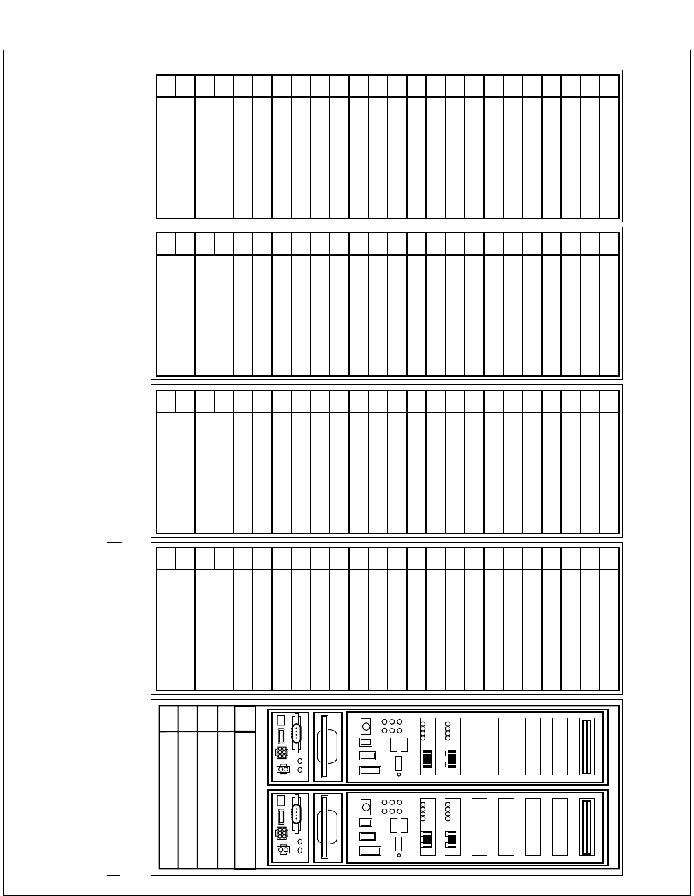
Figure 1-1 Card Mounting Slot for the 1 IMG System
00 01 02 03 04 05 06 07 08 09 10 11 12 13 14 15 16 17 18 19 20 21 22 23
PA-PW55-A(PWR)
PA-PW54-A(DPWR)
PH-PC36(MUX)
PH-PC36(MUX)
PH-SW10(TSW)
PH-SW10(TSW)
PIM3
00 01 02 03 04 05 06 07 08 09 10 11 12 13 14 15 16 17 18 19 20 21 22 23
PA-PW55-A(PWR)
PA-PW54-A(DPWR)
PH-PC36(MUX)
PH-PC36(MUX)
PIM2
00 01 02 03 04 05 06 07 08 09 10 11 12 13 14 15 16 17 18 19 20 21 22 23
PA-PW55-A(PWR)
PA-PW54-A(DPWR)
PH-PC36(MUX)
PH-PC36(MUX)
PIM1
00 01 02 03 04 05 06 07 08 09 10 11 12 13 14 15 16 17 18 19 20 21 22 23
PA-PW55-A(PWR)
PA-PW54-A(DPWR)
PIM0
BSCM
LPM
PH-IO24(IOC)
(IOC/MISC)
(MISC)
(MISC)
PH-PC40(EMA)
00 01 02 03 04
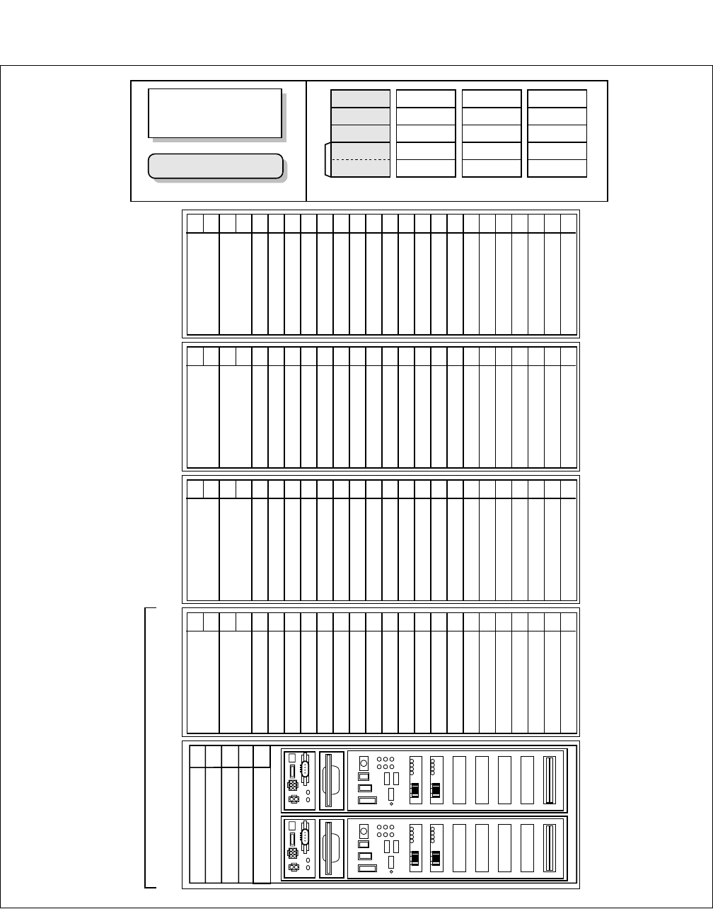
CHAPTER 1 NDA-24296
Page 4
Revision 1.0
Figure 1-2 Card Mounting Slot for the 4 IMG System (1/4)
00 01 02 03 04 05 06 07 08 09 10 11 12 13 14 15 16 17 18 19 20 21 22 23
PA-PW55-A(PWR0)
PA-PW54-A(PWR1)
PH-PC36(MUX)
PH-PC36(MUX)
PH-PC36(MUX)
PH-PC36(MUX)
PIM3
00 01 02 03 04 05 06 07 08 09 10 11 12 13 14 15 16 17 18 19 20 21 22 23
PA-PW55-A(PWR0)
PA-PW54-A(PWR1)
PH-PC36(MUX)
PH-PC36(MUX)
PIM2
00 01 02 03 04 05 06 07 08 09 10 11 12 13 14 15 16 17 18 19 20 21 22 23
PA-PW55-A(PWR0)
PA-PW54-A(PWR1)
PH-PC36(MUX)
PH-PC36(MUX)
PIM1
00 01 02 03 04 05 06 07 08 09 10 11 12 13 14 15 16 17 18 19 20 21 22 23
PA-PW55-A(PWR0)
PA-PW54-A(PWR1)
PIM0
BSCM
LPM
PH-IO24(IOC)
PH-PC40(EMA)
00 01 02 03 04
(IOC/MISC)
(MISC)
(MISC)
PIM
PIM
PIM
PIM
IMG3
Dummy/APM
PIM
PIM
PIM
PIM
IMG2
Dummy/APM
PIM
PIM
PIM
PIM
IMG1
TSWM
PIM
PIM
PIM
PIM
IMG0
LPM
B
S
C
M
IMG0
NEAX2400IMS (IPX)
4-IMG System
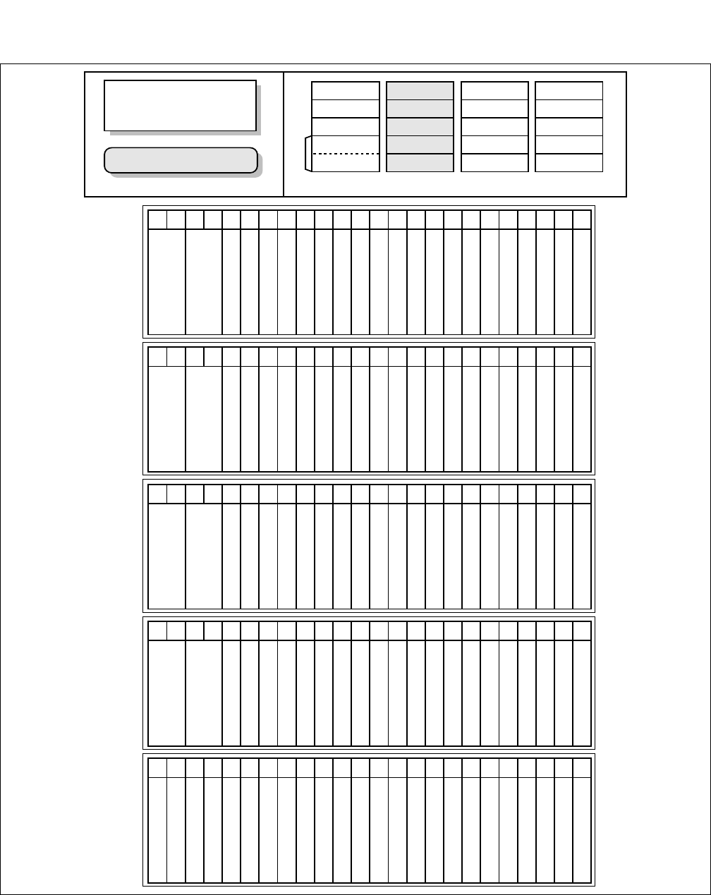
NDA-24296 CHAPTER 1
Page 5
Revision 1.0
Figure 1-2 Card Mounting Slot for the 4 IMG System (2/4)
00 01 02 03 04 05 06 07 08 09 10 11 12 13 14 15 16 17 18 19 20 21 22 23
PA-PW55-A(PWR0)
PA-PW54-A(PWR1)
PH-PC36(MUX)
PH-PC36(MUX)
PH-PC36(MUX)
PH-PC36(MUX)
PIM3
00 01 02 03 04 05 06 07 08 09 10 11 12 13 14 15 16 17 18 19 20 21 22 23
PA-PW55-A(PWR0)
PA-PW54-A(PWR1)
PH-PC36(MUX)
PH-PC36(MUX)
PIM2
00 01 02 03 04 05 06 07 08 09 10 11 12 13 14 15 16 17 18 19 20 21 22 23
PA-PW55-A(PWR0)
PA-PW54-A(PWR1)
PH-PC36(MUX)
PH-PC36(MUX)
PIM1
00 01 02 03 04 05 06 07 08 09 10 11 12 13 14 15 16 17 18 19 20 21 22 23
PA-PW55-A(PWR0)
PA-PW54-A(PWR1)
PIM0
00 01 02 03 04 05 06 07 08 09 10 11 12 13 14 15 16 17 18 19 20 21 22 23
PH-PW14(PWRSW)
PH-PW14(PWRSW)
PH-PC20(DLKC0)
PH-PC20(DLKC1)
PH-GT09(GT0)
PH-GT09(GT1)
PH-SW12(TDSW00)
PH-SW12(TDSW01)
PH-SW12(TDSW02)
PH-SW12(TDSW03)
PH-SW12(TDSW10)
PH-SW12(TDSW11)
PH-SW12(TDSW12)
PH-SW12(TDSW13)
PH-CK16/17(PLO0)
PH-CK16/17(PLO1)
(MISC)
(MISC)
(MISC)
(MISC)
(MISC)
(MISC)
TSWM
PIM
PIM
PIM
PIM
IMG3
Dummy/APM
PIM
PIM
PIM
PIM
IMG2
Dummy/APM
PIM
PIM
PIM
PIM
IMG1
TSWM
PIM
PIM
PIM
PIM
IMG0
LPM
B
S
C
M
IMG1
NEAX2400IMS (IPX)
4-IMG System
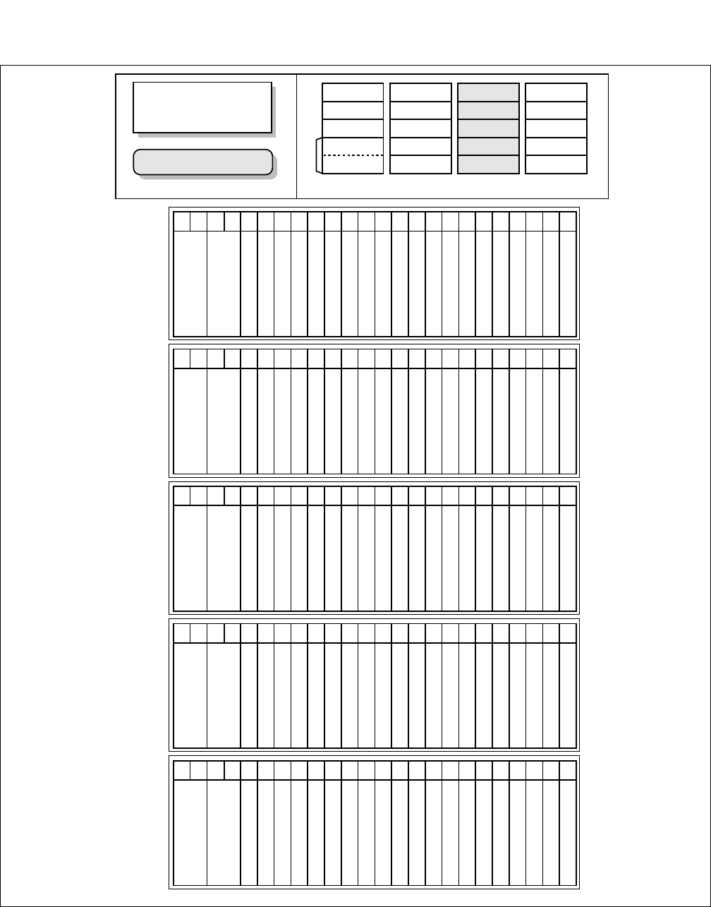
CHAPTER 1 NDA-24296
Page 6
Revision 1.0
Figure 1-2 Card Mounting Slot for the 4 IMG System (3/4)
00 01 02 03 04 05 06 07 08 09 10 11 12 13 14 15 16 17 18 19 20 21 22 23
PA-PW55-A(PWR0)
PA-PW54-A(PWR1)
PH-PC36(MUX)
PH-PC36(MUX)
PH-PC36(MUX)
PH-PC36(MUX)
PIM3
00 01 02 03 04 05 06 07 08 09 10 11 12 13 14 15 16 17 18 19 20 21 22 23
PA-PW55-A(PWR0)
PA-PW54-A(PWR1)
PH-PC36(MUX)
PH-PC36(MUX)
PIM2
00 01 02 03 04 05 06 07 08 09 10 11 12 13 14 15 16 17 18 19 20 21 22 23
PA-PW55-A(PWR0)
PA-PW54-A(PWR1)
PH-PC36(MUX)
PH-PC36(MUX)
PIM1
00 01 02 03 04 05 06 07 08 09 10 11 12 13 14 15 16 17 18 19 20 21 22 23
PA-PW55-A(PWR0)
PA-PW54-A(PWR1)
PIM0
00 01 02 03 04 05 06 07 08 09 10 11 12 13 14 15 16 17 18 19 20 21 22 23
Dummy/APM
PIM
PIM
PIM
PIM
IMG3
Dummy/APM
PIM
PIM
PIM
PIM
IMG2
Dummy/APM
PIM
PIM
PIM
PIM
IMG1
TSWM
PIM
PIM
PIM
PIM
IMG0
LPM
B
S
C
M
IMG2
NEAX2400IMS(IMX)
4IMG-SYSTEM
NEAX2400 IMS (IPX)
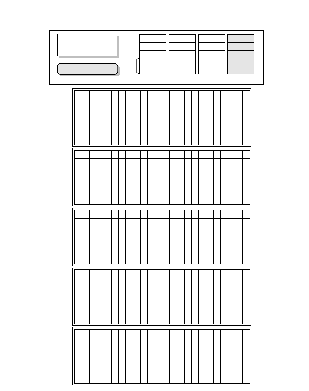
NDA-24296 CHAPTER 1
Page 7
Revision 1.0
Figure 1-2 Card Mounting Slot for the 4 IMG System (4/4)
00 01 02 03 04 05 06 07 08 09 10 11 12 13 14 15 16 17 18 19 20 21 22 23
PA-PW55-A(PWR0)
PA-PW54-A(PWR1)
PH-PC36(MUX)
PH-PC36(MUX)
PH-PC36(MUX)
PH-PC36(MUX)
PIM3
00 01 02 03 04 05 06 07 08 09 10 11 12 13 14 15 16 17 18 19 20 21 22 23
PA-PW55-A(PWR0)
PA-PW54-A(PWR1)
PH-PC36(MUX)
PH-PC36(MUX)
PIM2
00 01 02 03 04 05 06 07 08 09 10 11 12 13 14 15 16 17 18 19 20 21 22 23
PA-PW55-A(PWR0)
PA-PW54-A(PWR1)
PH-PC36(MUX)
PH-PC36(MUX)
PIM1
00 01 02 03 04 05 06 07 08 09 10 11 12 13 14 15 16 17 18 19 20 21 22 23
PA-PW55-A(PWR0)
PA-PW54-A(PWR1)
PIM0
00 01 02 03 04 05 06 07 08 09 10 11 12 13 14 15 16 17 18 19 20 21 22 23
Dummy/APM
PIM
PIM
PIM
PIM
IMG3
Dummy/APM
PIM
PIM
PIM
PIM
IMG2
Dummy/APM
PIM
PIM
PIM
PIM
IMG1
TSWM
PIM
PIM
PIM
PIM
IMG0
LPM
B
S
C
M
IMG3
NEAX2400IMS(IMX)
4IMG-SYSTEM
NEAX2400 IMS (IPX)
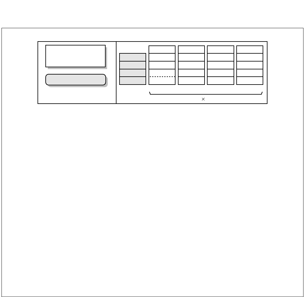
CHAPTER 1 NDA-24296
Page 8
Revision 1.0
Figure 1-3 Card Mounting Slot for the IPX-U System (1/5)
PIM
PIM
PIM
PIM
IMG3/7/11/15
Dummy
PIM
PIM
PIM
PIM
IMG2/6/10/14
TSWM1
PIM
PIM
PIM
PIM
IMG1/5/9/13
TSWM0
PIM
PIM
PIM
PIM
IMG0/4/8/12
LP
CMG
NEAX2400 IPX
IPX-UMG SYSTEM
ISWM
DUMMY
CMP
CMG
SP
LMG 4 (0~3)
Note: The 2nd IOC card (optional) may be mounted in the slot.
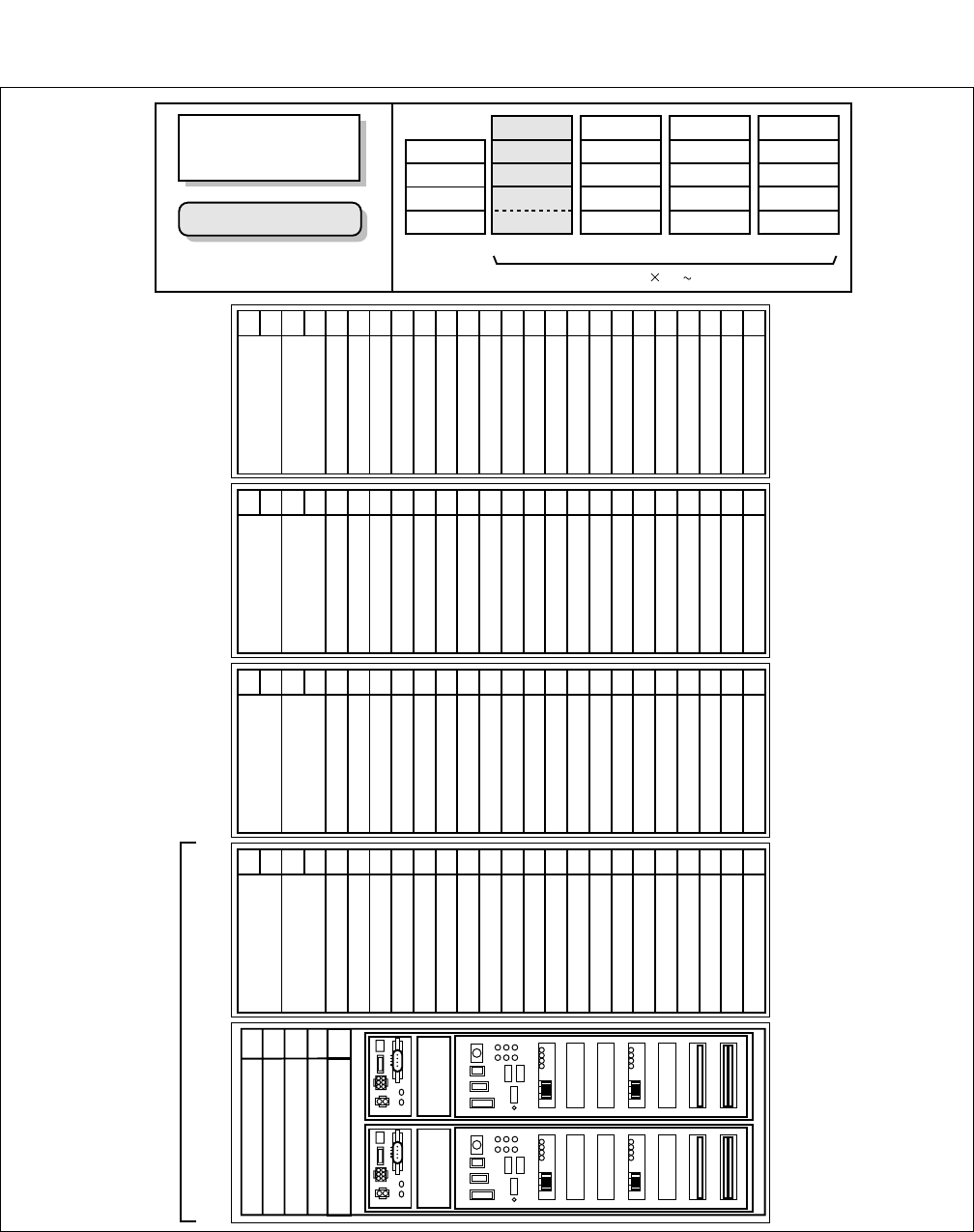
NDA-24296 CHAPTER 1
Page 9
Revision 1.0
Figure 1-3 Card Mounting Slot for the IPX-U System (2/5)
PA-PW55-B (PWR0)
PA-PW54-B (PWR1)
PH-PC36 (MUX)
PH-PC36 (MUX)
PH-PC36 (MUX)
PH-PC36 (MUX)
PIM3
PA-PW55-B (PWR0)
PA-PW54-B (PWR1)
PH-PC36 (MUX)
PH-PC36 (MUX)
PIM2
PA-PW55-B (PWR0)
PA-PW54-B (PWR1)
PH-PC36 (MUX)
PH-PC36 (MUX)
PIM1
PA-PW55-B (PWR0)
PA-PW54-B (PWR1)
PIM0
BSCM
LPM
PH-M22(MMC)
PH-PC43(EMA)
00 01 02 03 04 05 06 07 08 09 10 11 12 13 14 15 16 17 18 19 20 21 22 23
00 01 02 03 04 05 06 07 08 09 10 11 12 13 14 15 16 17 18 19 20 21 22 23
00 01 02 03 04 05 06 07 08 09 10 11 12 13 14 15 16 17 18 19 20 21 22 23
00 01 02 03 04 05 06 07 08 09 10 11 12 13 14 15 16 17 18 19 20 21 22 23
00 01 02 03 04
PIM
PIM
PIM
PIM
IMG3/7/11/15
Dummy
PIM
PIM
PIM
PIM
IMG2/6/10/14
TSWM1
PIM
PIM
PIM
PIM
IMG1/5/9/13
TSWM0
PIM
PIM
PIM
PIM
IMG0/4/8/12
LP
IMG0/4/8/12
NEAX2400 IPX
IPX-UMG SYSTEM
LMG 4 (0 3)
ISWM
DUMMY
CMP
CMG
SP
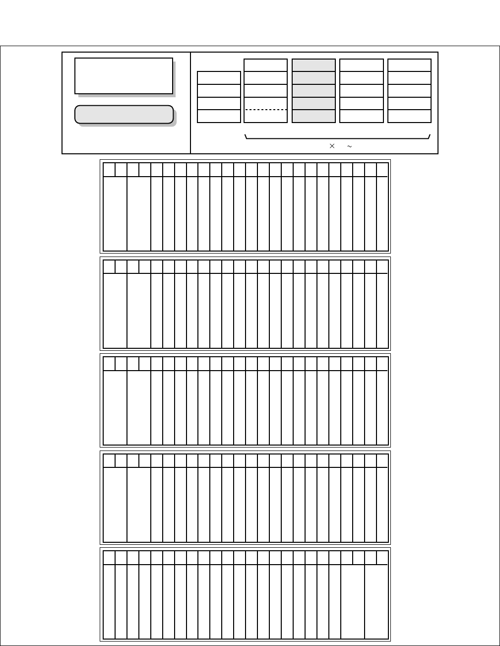
CHAPTER 1 NDA-24296
Page 10
Revision 1.0
Figure 1-3 Card Mounting Slot for the IPX-U System (3/5)
PA-PW55-B (PWR0)
PA-PW54-B (PWR1)
PH-PC36 (MUX)
PH-PC36 (MUX)
PH-PC36 (MUX)
PH-PC36 (MUX)
PIM3
PA-PW55-B (PWR0)
PA-PW54-B (PWR1)
PH-PC36 (MUX)
PH-PC36 (MUX)
PIM2
PA-PW55-B (PWR0)
PA-PW54-B (PWR1)
PH-PC36 (MUX)
PH-PC36 (MUX)
PIM1
PA-PW55-B (PWR0)
PA-PW54-B (PWR1)
PIM0
PH-PW14 (PWRSW)
PH-PW14 (PWRSW)
PH-PC20 (DLKC0)
PH-PC20 (DLKC1)
PH-GT09 (GT0)
PH-GT09 (GT1)
PH-SW12 (TSW00)
PH-SW12 (TSW01)
PH-SW12 (TSW02)
PH-SW12 (TSW03)
PH-SW12 (TSW10)
PH-SW12 (TSW11)
PH-SW12 (TSW12)
PH-SW12 (TSW13)
PH-CK16-A/17-A (PLO1)
(MISC)
(MISC)
(MISC)
(MISC)
(MISC)
(MISC)
TSWM0
PIM
PIM
PIM
PIM
IMG3/7/11/15
Dummy
PIM
PIM
PIM
PIM
IMG2/6/10/14
TSWM1
PIM
PIM
PIM
PIM
IMG1/5/9/13
TSWM0
PIM
PIM
PIM
PIM
IMG0/4/8/12
LP
IMG1/5/9/13
NEAX2400 IPX
IPX-UMG SYSTEM
PH-CK16-A/17-A (PLO0)
21 22 23201918171615141312111009080706050403020100
21 22 23201918171615141312111009080706050403020100
21 22 23201918171615141312111009080706050403020100
21 22 23201918171615141312111009080706050403020100
21 22 23201918171615141312111009080706050403020100
LMG 4 (0 3)
ISWM
DUMMY
CMP
CMG
SP
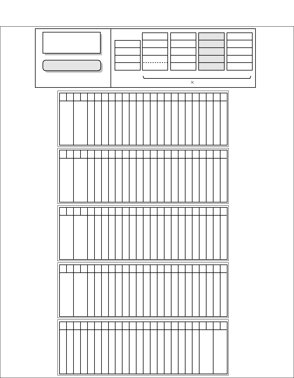
NDA-24296 CHAPTER 1
Page 11
Revision 1.0
Figure 1-3 Card Mounting Slot for the IPX-U System (4/5)
PA-PW55-B(PWR0)
PA-PW54-B(PWR1)
PH-PC36(MUX)
PH-PC36(MUX)
PH-PC36(MUX)
PH-PC36(MUX)
PIM3
PA-PW55-B(PWR0)
PA-PW54-B(PWR1)
PH-PC36(MUX)
PH-PC36(MUX)
PIM2
PA-PW55-B(PWR0)
PA-PW54-B(PWR1)
PH-PC36(MUX)
PH-PC36(MUX)
PIM1
PA-PW55-B(PWR0)
PA-PW54-B(PWR1)
PIM0
PIM
PIM
PIM
PIM
IMG3/7/11/15
Dummy
PIM
PIM
PIM
PIM
IMG2/6/10/14
TSWM1
PIM
PIM
PIM
PIM
IMG1/5/9/13
TSWM0
PIM
PIM
PIM
PIM
IMG0/4/8/12
LP
IMG2/6/10/14
NEAX2400 IPX
IPX-UMG SYSTEM
PH-PW14 (PWRSW0)
PH-PW14 (PWRSW1)
PH-GT09 (GT0)
PH-GT09 (GT1)
PH-SW12 (TSW00)
PH-SW12 (TSW01)
PH-SW12 (TSW02)
PH-SW12 (TSW03)
PH-SW12 (TSW10)
PH-SW12 (TSW11)
PH-SW12 (TSW12)
PH-SW12 (TSW13)
PH-CK18 (CLK0)
PH-CK18 (CLK1)
TSWM1
21 22 23201918171615141312111009080706050403020100
21 22 23201918171615141312111009080706050403020100
21 22 23201918171615141312111009080706050403020100
21 22 23201918171615141312111009080706050403020100
21 22 23201918171615141312111009080706050403020100
LMG 4 (0~3)
ISWM
DUMMY
CMP
CMG
SP
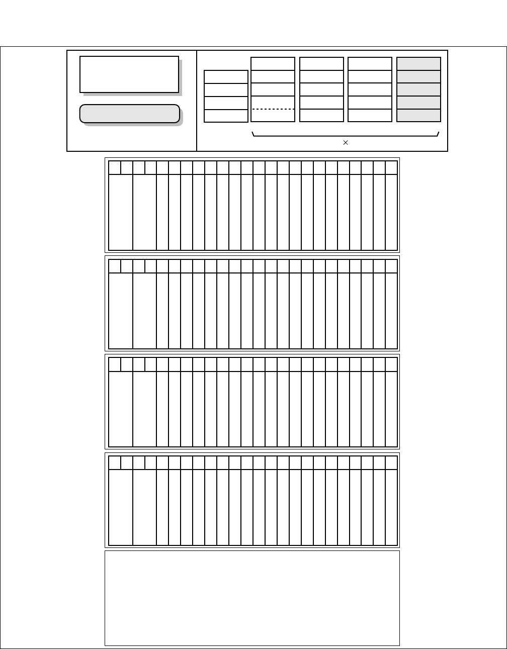
CHAPTER 1 NDA-24296
Page 12
Revision 1.0
Figure 1-3 Card Mounting Slot for the IPX-U System (5/5)
PA-PW55-B(PWR0)
PA-PW54-B(PWR1)
PH-PC36(MUX)
PH-PC36(MUX)
PH-PC36(MUX)
PH-PC36(MUX)
PIM3
PA-PW55-B(PWR0)
PA-PW54-B(PWR1)
PH-PC36(MUX)
PH-PC36(MUX)
PIM2
PA-PW55-B(PWR0)
PA-PW54-B(PWR1)
PH-PC36(MUX)
PH-PC36(MUX)
PIM1
PA-PW55-B(PWR0)
PA-PW54-B(PWR1)
PIM0
Dummy
PIM
PIM
PIM
PIM
IMG3/7/11/15
Dummy
PIM
PIM
PIM
PIM
IMG2/6/10/14
TSWM1
PIM
PIM
PIM
PIM
IMG1/5/9/13
TSWM0
PIM
PIM
PIM
PIM
IMG0/4/8/12
LP
IMG3/7/11/15
NEAX2400 IPX
IPX-UMG SYSTEM
21 22 23201918171615141312111009080706050403020100
21 22 23201918171615141312111009080706050403020100
21 22 23201918171615141312111009080706050403020100
21 22 23201918171615141312111009080706050403020100
LMG 4 (0~3)
ISWM
DUMMY
CMP
CMG
SP
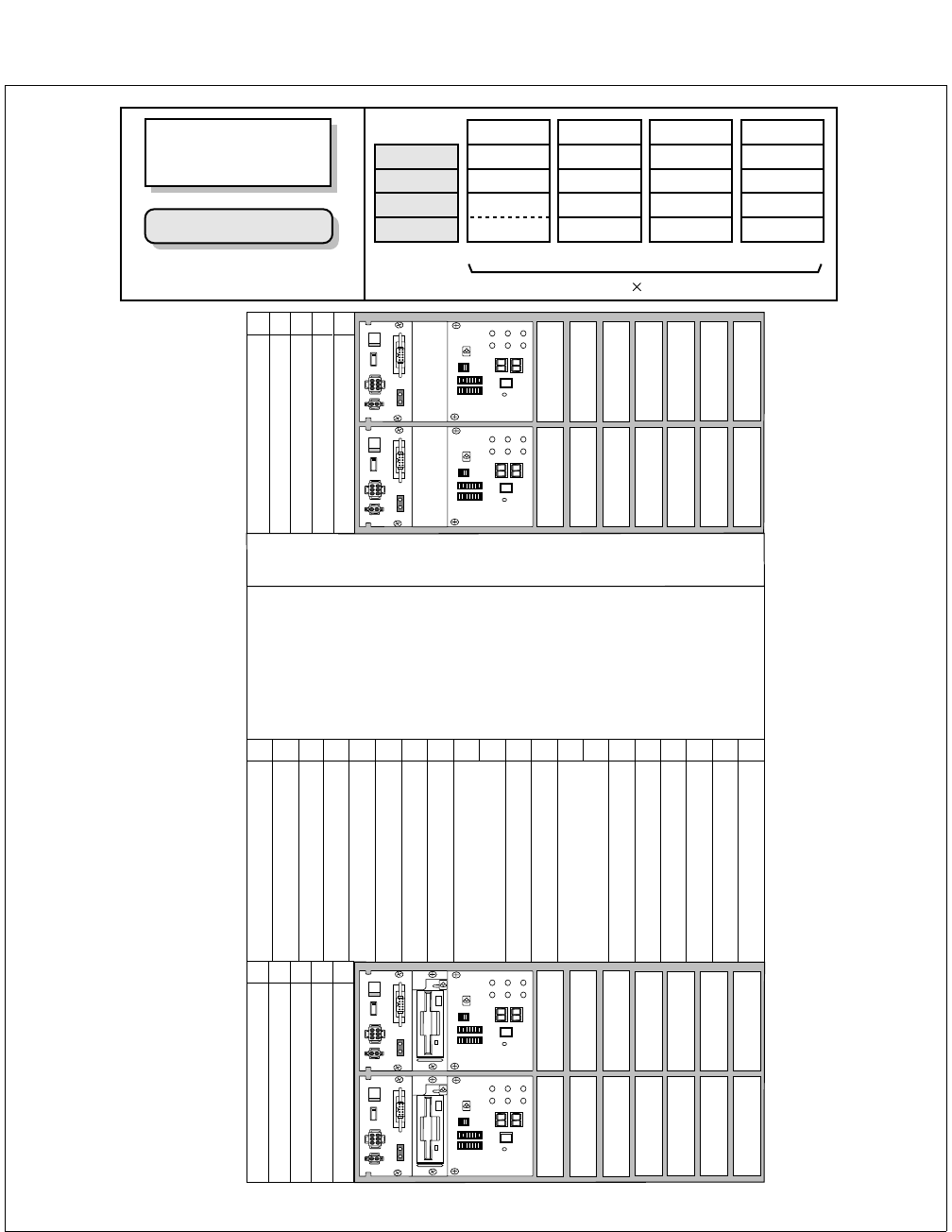
NDA-24296 CHAPTER 1
Page 13
Revision 1.0
Figure 1-4 Card Mounting Slot for the IPX-UMG System (1/5)
PIM
PIM
PIM
PIM
IMG3/7/11/15
Dummy
PIM
PIM
PIM
PIM
IMG2/6/10/14
TSWM1
PIM
PIM
PIM
PIM
IMG1/5/9/13
TSWM0
PIM
PIM
PIM
PIM
IMG0/4/8/12
LP
CMG
NEAX2400 IPX
IPX-UMG SYSTEM
ISWM
DUMMY
CMP
CMG
SP
LMG 4 (0~3)
00
00
01
01
02
02
03 04
03 04
05 06 07 08 09 10 11 12 13 14 15 16 17 18 19
SP
ISWM
DUMMY
FANU
CMP
PH-PC43 (EMA)
PZ-GT13
(ISAGT) PZ-GT13
(ISAGT)
PZ-PC23
(LANI)
PZ-PC19
(LANI)
PZ-PC19
(LANI)
PZ-PC23
(LANI)
PZ-PC23
(LANI) PZ-PC23
(LANI)
PH-DK10 (DSPC)
PH-IO24 (IOC)
PWRSW0 (PH-PW14)
PWRSW1 (PH-PW14)
HSW00 (PU-SW01) (RES)
HSW11 (PU-SW01) (RES)
HSW01 (PU-SW01)
HSW10 (PU-SW01)
TSW00 (PU-SW00-A)
TSW01 (PU-SW00-A)
TSW02 (PU-SW00-A)
TSW03 (PU-SW00-A)
TSW10 (PU-SW00-A)
TSW11 (PU-SW00-A)
TSW12 (PU-SW00-A)
TSW13 (PU-SW00-A)
IOGT0 (PH-GT10)
IOGT1 (PH-GT10)
PLO0 (PH-CK16-A/17-A)
PLO1 (PH-CK16-A/17-A)
PH-IO24 (IOC) Note
00 01 02 03 04
PH-PC43 (EMA)
PZ-GT13
(ISAGT) PZ-GT13
(ISAGT)
PZ-M565
(ISAGTA)
PZ-M565
(ISAGTA)
PZ-PC22
(LANI)
PZ-ME44
(MEM) PZ-ME44
(MEM)
PZ-PC22
(LANI)
PZ-PC22
(LANI) PZ-PC22
(LANI)
PH-M22 (MMC)
Note: The 2nd IOC card (optional) may be mounted in this slot.
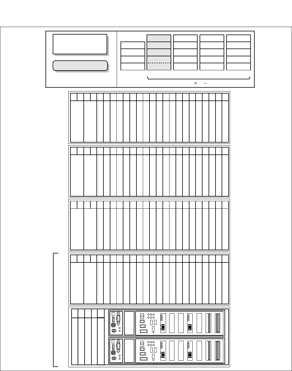
CHAPTER 1 NDA-24296
Page 14
Revision 1.0
Figure 1-4 Card Mounting Slot for the IPX-UMG System (2/5)
PA-PW55-B (PWR0)
PA-PW54-B (PWR1)
PH-PC36 (MUX)
PH-PC36 (MUX)
PH-PC36 (MUX)
PH-PC36 (MUX)
PIM3
PA-PW55-B (PWR0)
PA-PW54-B (PWR1)
PH-PC36 (MUX)
PH-PC36 (MUX)
PIM2
PA-PW55-B (PWR0)
PA-PW54-B (PWR1)
PH-PC36 (MUX)
PH-PC36 (MUX)
PIM1
PA-PW55-B (PWR0)
PA-PW54-B (PWR1)
PIM0
BSCM
LPM
PH-M22(MMC)
PH-PC43(EMA)
00 01 02 03 04 05 06 07 08 09 10 11 12 13 14 15 16 17 18 19 20 21 22 23
00 01 02 03 04 05 06 07 08 09 10 11 12 13 14 15 16 17 18 19 20 21 22 23
00 01 02 03 04 05 06 07 08 09 10 11 12 13 14 15 16 17 18 19 20 21 22 23
00 01 02 03 04 05 06 07 08 09 10 11 12 13 14 15 16 17 18 19 20 21 22 23
00 01 02 03 04
PIM
PIM
PIM
PIM
IMG3/7/11/15
Dummy
PIM
PIM
PIM
PIM
IMG2/6/10/14
TSWM1
PIM
PIM
PIM
PIM
IMG1/5/9/13
TSWM0
PIM
PIM
PIM
PIM
IMG0/4/8/12
LP
IMG0/4/8/12
NEAX2400 IPX
IPX-UMG SYSTEM
LMG 4 (0 3)
ISWM
DUMMY
CMP
CMG
SP
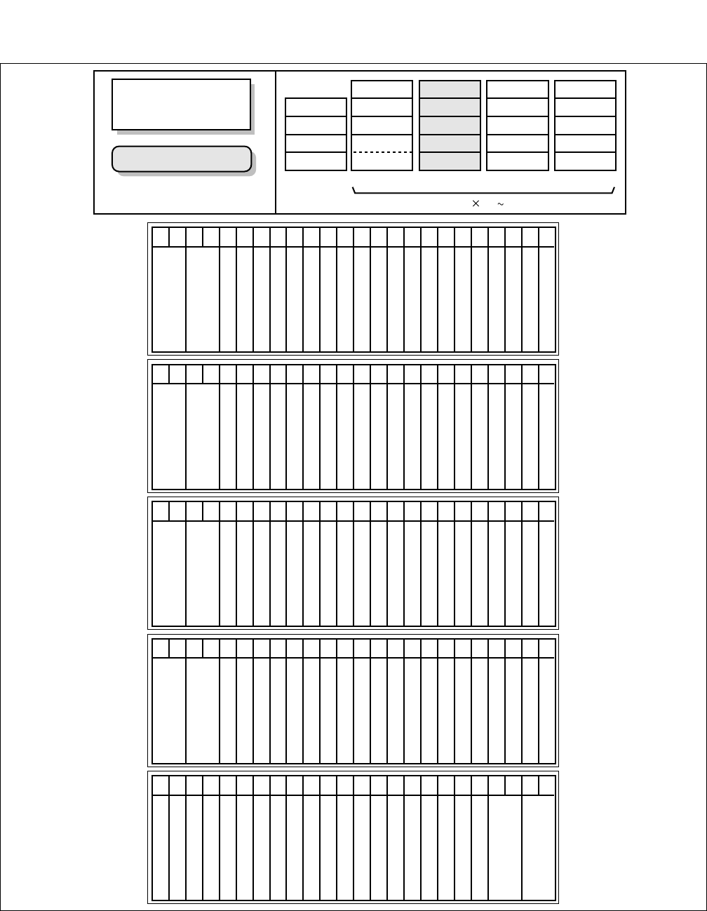
NDA-24296 CHAPTER 1
Page 15
Revision 1.0
Figure 1-4 Card Mounting Slot for the IPX-UMG System (3/5)
PA-PW55-B (PWR0)
PA-PW54-B (PWR1)
PH-PC36 (MUX)
PH-PC36 (MUX)
PH-PC36 (MUX)
PH-PC36 (MUX)
PIM3
PA-PW55-B (PWR0)
PA-PW54-B (PWR1)
PH-PC36 (MUX)
PH-PC36 (MUX)
PIM2
PA-PW55-B (PWR0)
PA-PW54-B (PWR1)
PH-PC36 (MUX)
PH-PC36 (MUX)
PIM1
PA-PW55-B (PWR0)
PA-PW54-B (PWR1)
PIM0
PH-PW14 (PWRSW)
PH-PW14 (PWRSW)
PH-PC20 (DLKC0)
PH-PC20 (DLKC1)
PH-GT09 (GT0)
PH-GT09 (GT1)
PH-SW12 (TSW00)
PH-SW12 (TSW01)
PH-SW12 (TSW02)
PH-SW12 (TSW03)
PH-SW12 (TSW10)
PH-SW12 (TSW11)
PH-SW12 (TSW12)
PH-SW12 (TSW13)
PH-CK16-A/17-A (PLO1)
(MISC)
(MISC)
(MISC)
(MISC)
(MISC)
(MISC)
TSWM0
PIM
PIM
PIM
PIM
IMG3/7/11/15
Dummy
PIM
PIM
PIM
PIM
IMG2/6/10/14
TSWM1
PIM
PIM
PIM
PIM
IMG1/5/9/13
TSWM0
PIM
PIM
PIM
PIM
IMG0/4/8/12
LP
IMG1/5/9/13
NEAX2400 IPX
IPX-UMG SYSTEM
PH-CK16-A/17-A (PLO0)
21 22 23201918171615141312111009080706050403020100
21 22 23201918171615141312111009080706050403020100
21 22 23201918171615141312111009080706050403020100
21 22 23201918171615141312111009080706050403020100
21 22 23201918171615141312111009080706050403020100
LMG 4 (0 3)
ISWM
DUMMY
CMP
CMG
SP
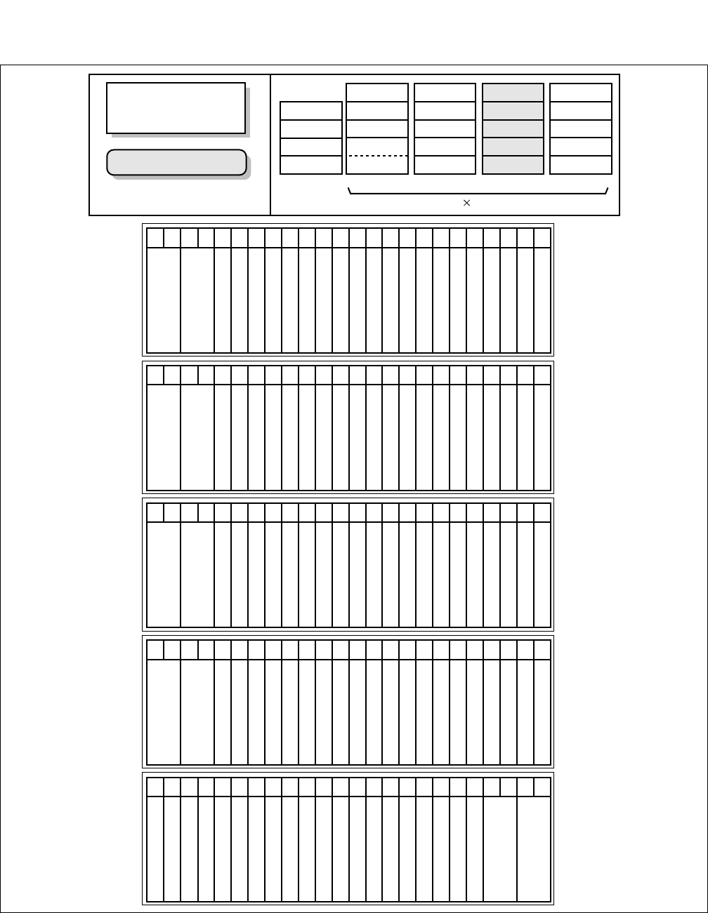
CHAPTER 1 NDA-24296
Page 16
Revision 1.0
Figure 1-4 Card Mounting Slot for the IPX-UMG System (4/5)
PA-PW55-B(PWR0)
PA-PW54-B(PWR1)
PH-PC36(MUX)
PH-PC36(MUX)
PH-PC36(MUX)
PH-PC36(MUX)
PIM3
PA-PW55-B(PWR0)
PA-PW54-B(PWR1)
PH-PC36(MUX)
PH-PC36(MUX)
PIM2
PA-PW55-B(PWR0)
PA-PW54-B(PWR1)
PH-PC36(MUX)
PH-PC36(MUX)
PIM1
PA-PW55-B(PWR0)
PA-PW54-B(PWR1)
PIM0
PIM
PIM
PIM
PIM
IMG3/7/11/15
Dummy
PIM
PIM
PIM
PIM
IMG2/6/10/14
TSWM1
PIM
PIM
PIM
PIM
IMG1/5/9/13
TSWM0
PIM
PIM
PIM
PIM
IMG0/4/8/12
LP
IMG2/6/10/14
NEAX2400 IPX
IPX-UMG SYSTEM
PH-PW14 (PWRSW0)
PH-PW14 (PWRSW1)
PH-GT09 (GT0)
PH-GT09 (GT1)
PH-SW12 (TSW00)
PH-SW12 (TSW01)
PH-SW12 (TSW02)
PH-SW12 (TSW03)
PH-SW12 (TSW10)
PH-SW12 (TSW11)
PH-SW12 (TSW12)
PH-SW12 (TSW13)
PH-CK18 (CLK0)
PH-CK18 (CLK1)
TSWM1
21 22 23201918171615141312111009080706050403020100
21 22 23201918171615141312111009080706050403020100
21 22 23201918171615141312111009080706050403020100
21 22 23201918171615141312111009080706050403020100
21 22 23201918171615141312111009080706050403020100
LMG 4 (0~3)
ISWM
DUMMY
CMP
CMG
SP
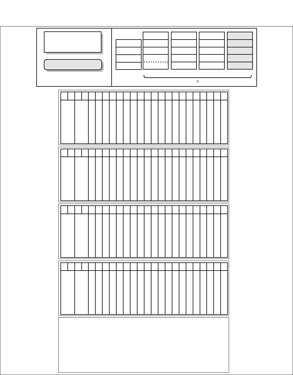
NDA-24296 CHAPTER 1
Page 17
Revision 1.0
Figure 1-4 Card Mounting Slot for the IPX-UMG System (5/5)
PA-PW55-B(PWR0)
PA-PW54-B(PWR1)
PH-PC36(MUX)
PH-PC36(MUX)
PH-PC36(MUX)
PH-PC36(MUX)
PIM3
PA-PW55-B(PWR0)
PA-PW54-B(PWR1)
PH-PC36(MUX)
PH-PC36(MUX)
PIM2
PA-PW55-B(PWR0)
PA-PW54-B(PWR1)
PH-PC36(MUX)
PH-PC36(MUX)
PIM1
PA-PW55-B(PWR0)
PA-PW54-B(PWR1)
PIM0
Dummy
PIM
PIM
PIM
PIM
IMG3/7/11/15
Dummy
PIM
PIM
PIM
PIM
IMG2/6/10/14
TSWM1
PIM
PIM
PIM
PIM
IMG1/5/9/13
TSWM0
PIM
PIM
PIM
PIM
IMG0/4/8/12
LP
IMG3/7/11/15
NEAX2400 IPX
IPX-UMG SYSTEM
21 22 23201918171615141312111009080706050403020100
21 22 23201918171615141312111009080706050403020100
21 22 23201918171615141312111009080706050403020100
21 22 23201918171615141312111009080706050403020100
LMG 4 (0~3)
ISWM
DUMMY
CMP
CMG
SP

CHAPTER 1 NDA-24296
Page 18
Revision 1.0
This page is for your notes.

NDA-24296 CHAPTER 2
Page 19
Revision 1.0
CHAPTER 2 CONTROL CIRCUIT CARD REFERENCE
This chapter explains the following items for each Control Circuit Card.
•General Function
Explains the general function and purpose of each control circuit card.
•Mounting Location/Condition
Explains the mounting location (mounting module name and slot number, etc.) for each circuit card. If there
are any conditions pertaining to mounting the circuit cards, they are also explained.
•Face Layout of Lamps, Switches, and Connectors
The locations of the lamps, switches, and connectors provided on each circuit card are illustrated by a face
layout.
•Lamp Indications
The names, colors, and indication states of lamps mounted on each circuit card are listed.
•Switch Settings
Each circuit card's switches are listed with their names, switch numbers, their setting and its meaning, stan-
dard setting, etc.
•External Interface
If the lead outputs of the circuit card are provided by an LT connector, the relation between the mounting
slots and the LT connectors is illustrated by an LT Connector Lead Face Layout. If the lead outputs are pro-
vided by other than an LT connector, or are provided by the circuit card front connector, the connector lead
locations and the connecting routes are shown.
In addition, a Switch Setting Sheet, which may be used to record the switch settings, is provided at the end of
the explanation for each circuit card.
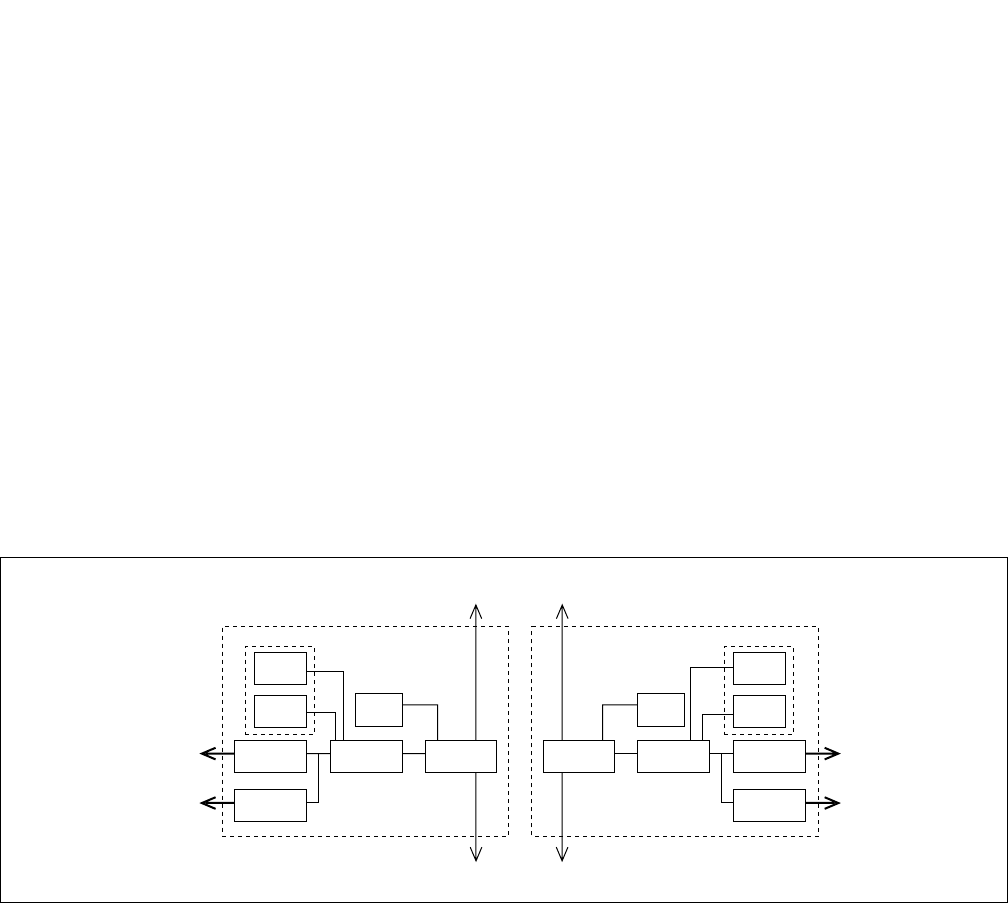
CHAPTER 2 NDA-24296
Page 20
Revision 1.0
SN1695 CPRBF-A
CPU Board
SN1695 CPRBF-A
CPU Board
1. General Function
The CPR in 1-IMG, 4-IMG, and IPX-U system consists of the following components.
(a) CPU BOARD: Contains the Main Processor Unit (MPU), ROM, and 128 to 256 Mbyte of Random
Access Memory (RAM). This board may also contain the ISAGT (PZ-GT13/PZ-
GT20) on its Industrial Standard Architecture (ISA) bus, and LANI (PZ-PC19) on
the Peripheral Component Interconnect (PCI).
(b) DSP: Contains the CPR switches and the CPR status indicator lamps.
(c) FDD/HDD: Floppy Disk Drive (FDD) and Hard Disk Drive (HDD) are mounted on a circuit
card, which, if necessary, can be extracted and/or inserted while the system is in
operation.
(d) PWR: Supplies the operating power to the CPR and also the MISC slots of the LPM.
Figure 2-1 Location of SN1695 CPRBF-A (CPR)
LANI
LANI
LANI
LANI
HDD
FDD
HDD
FDD
CPU CPU
DSP DSP
ISAGT ISAGT
CPR#0 CPR#1
To HUB
To HUB
To HUB
To HUB
To I/O local bus
To MISC bus

NDA-24296 CHAPTER 2
Page 21
Revision 1.0
SN1695 CPRBF-A
CPU Board
The CPR in IPX-UMG system consists of the following components.
(a) CPU BOARD: Contains System Processor Unit (SP)/Common Main Processor Unit (CMP)/Local
Processor Unit (LP), ROM, and 128 to 256 Mbyte of Random Access Memory
(RAM). This board may also contain PCI MEM (PZ-ME44), the ISAGT (PZ-GT13/
PZ-GT20/PZ-M565) on its Industrial Standard Architecture (ISA) bus, and LANI
(PZ-PC19/PZ-PC22/PZ-PC23) on the Peripheral Component Interconnect (PCI).
(b) DSP: Contains the CPR switches and the CPR status indicator lamps.
(c) FDD/HDD: Floppy Disk Drive (FDD) and Hard Disk Drive (HDD) are mounted on a circuit
card, which, if necessary, can be extracted and/or inserted while the system is in
operation. Note
(d) PWR: Supplies the operating power to the CPR and also the MISC slots of the SP/CMP/
LP.
Note: FDD/HDD is not mounted on the CPR of CMP/LP in IPX-UMG system.
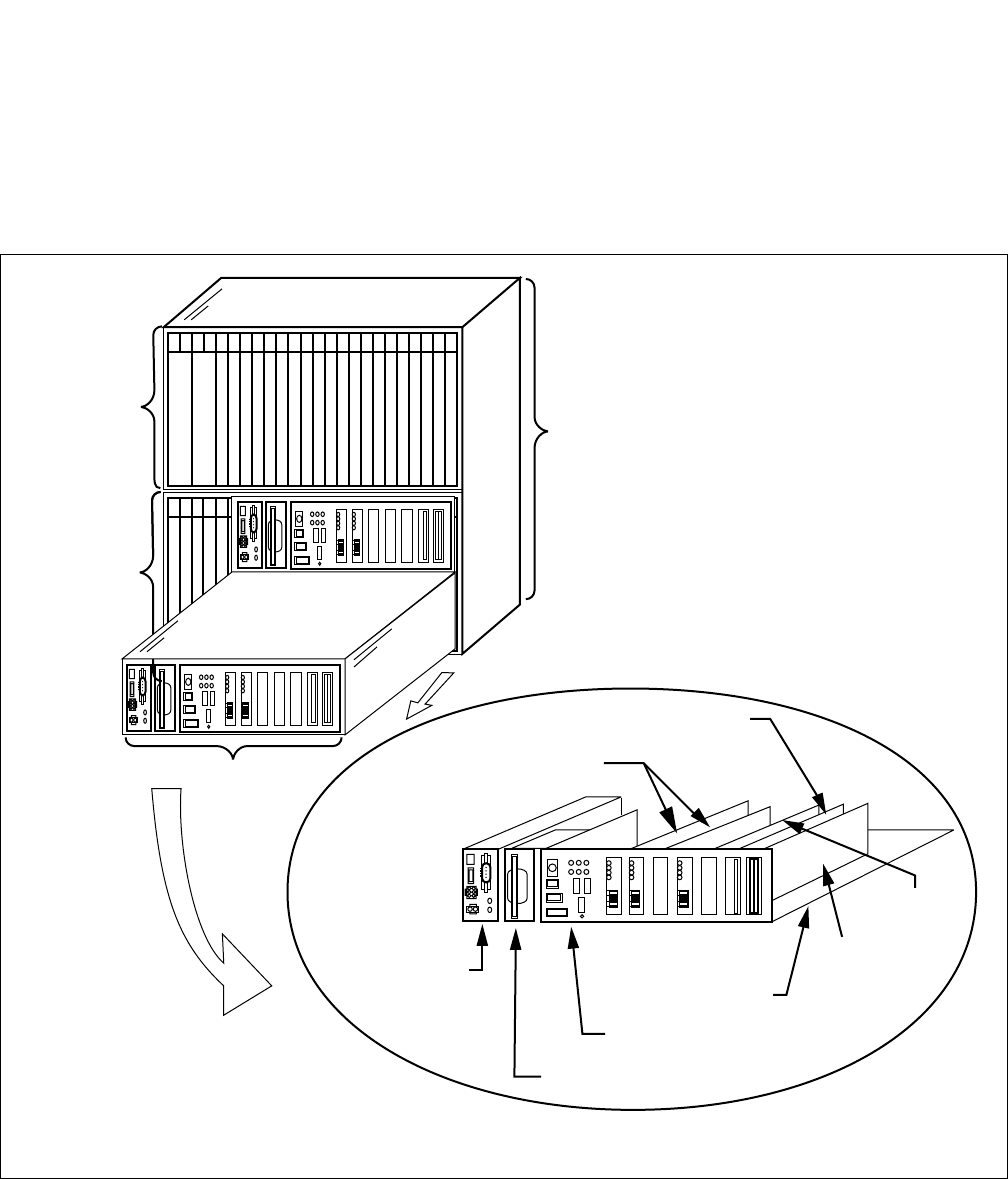
CHAPTER 2 NDA-24296
Page 22
Revision 1.0
SN1695 CPRBF-A
CPU Board
2. Mounting Location/Condition
The CPR is composed of the CPU BOARD, DSP, FDD/HDD, and PWR and is located in the Local
Processor Module (LPM) as shown in Figure 2-2. Since the CPR provides the Industrial Standard
Architecture (ISA) bus and Peripheral Component Interconnect (PCI) bus, the ISAGT and LANI cards are
located in those busses respectively.
Figure 2-2 CPR Location
PZ-GT20 (ISAGT) Note
CPU BOARD
PZ-DK224 (DSP)
PZ-PC19
(LANI)
PZ-GT13
(ISAGT)
PZ-IO27(FDD/HDD)
PZ-PC19 (LANI)
PZ-PW92 (PWR)
CPR
LPM
ISWM/PIM0 BSCM
Note: This card is mounted in the IMG0 of the IPX-U system only.
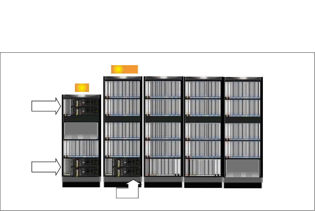
NDA-24296 CHAPTER 2
Page 23
Revision 1.0
SN1695 CPRBF-A
CPU Board
When the SN1695 CPRBF-A is used in the IPX-UMG system, the CPR is mounted on each processor mod-
ule (SP, CMP, and LPs) as shown in Figure 2-3. As to the mounting location of PWR, FDD/HDD, DSP, and
other circuit cards within the CPR, refer to Figure 2-5.
Figure 2-3 The SN1695 CPRBF-A in the IPX-UMG System
00010203 04 0506 07 08 0910 1112 1314 1516 17 18 19 20 21 22 23
000102 03 04 0506 07 08 0910 1112 1314 1516 17 18 19 20 21 22 23
000102 0304 05 06 07 0809 10 1112 1314 1516 17 18 19 2021 22 23
000102 0304 05 06 07 0809 10 1112 1314 1516 17 18 19 20 21 22 23
0001020304
LANI LANI ISAGT
LANI LANI ISAGT
000102 0304 05 06 07 0809 10 1112 1314 1516 17 18 19 2021 22 23
000102 0304 05 06 07 0809 10 1112 1314 1516 17 18 19 20 21 22 23
0001020304
LANI LANI ISAGT
LANI LANI ISAGT
0001020304 05 06 07 08 0910 1112 13 1415 16 1718 19 2021 22 23
0001020304 05 06 0708 0910 1112 13 1415 1617 18 19 202122 23
0001020304 05 06 0708 0910 1112 13 1415 1617 18 19 202122 23
0001020304 05 06 0708 0910 1112 13 1415 1617 18 19 202122 23
0001 0203 04 0506 07 08 09 10 1112 13 14 15 1617 18 19 20 21 2223
000102 0304 05 06 0708 09 10 1112 13 14 151617 18 19 20 2122 23
000102 0304 05 06 0708 0910 1112 1314 1516 17 18 1920 21 22 23
000102 03 04 0506 07 08 0910 1112 1314 1516 17 18 19 2021 22 23
000102 03 04 0506 07 08 0910 1112 13 1415 16 1718 19 2021 22 23
0001 0203 04 0506 07 08 09 10 1112 13 14 15 1617 18 19 20 21 2223
000102 0304 05 06 0708 09 10 1112 13 14 151617 18 19 20 2122 23
000102 0304 05 06 07 08 0910 1112 1314 1516 17 18 19 20 21 22 23
000102 03 04 0506 07 08 0910 1112 1314 1516 17 18 19 20 2122 23
000102 03 04 0506 07 08 0910 1112 13 1415 16 1718 19 2021 22 23
0001 0203 04 0506 07 08 09 10 1112 13 14 15 1617 18 19 20 21 2223
000102 03 04 0506 07 08 0910 1112 1314 1516 17 18 19 20 21 22 23
0001020304
LANI LANI ISAGT
LANI LANI ISAGT
CMG
LMG0
‘
3
CMP–CPR
SP–CPR
LP–CPR
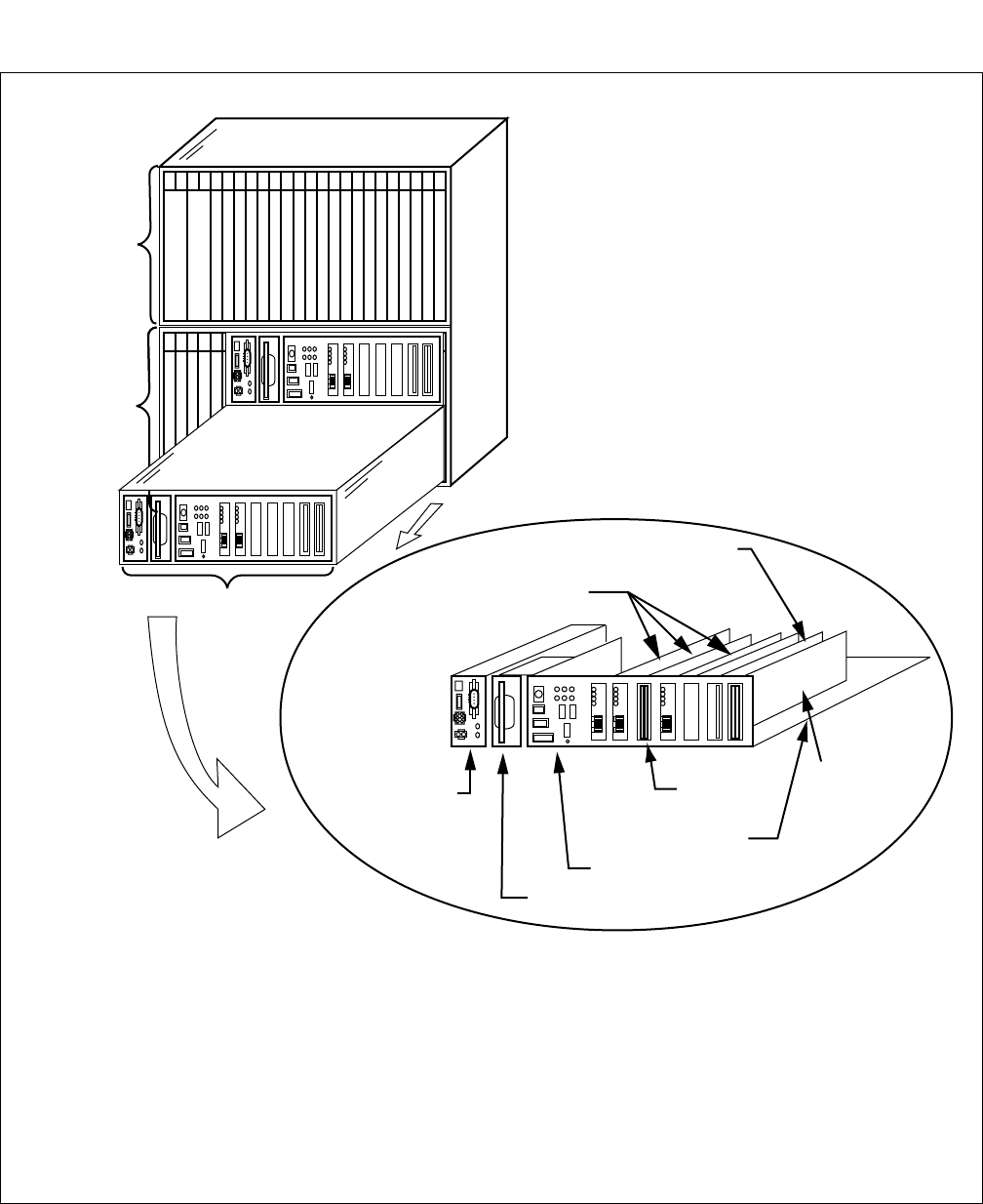
CHAPTER 2 NDA-24296
Page 24
Revision 1.0
SN1695 CPRBF-A
CPU Board
Figure 2-4 CPR Location for IPX-UMG System
PZ-GT20 (ISAGT)
/PZ-M565 (ISAGT)
CPU BOARD
PZ-DK224 (DSP)
PZ-GT13
(ISAGT)
PZ-IO27/28 (FDD/HDD)
Note 3
PZ-PC19/22/23 (LANI)
Note 2
PZ-PW92 (PWR) PZ-ME44
(PCI MEM)
Note 4
CPR
SP/CMP
/LP
ISWM
/
Dummy
/
PIM0
Note 1
Note 1: PZ-GT20 (ISAGT) card is mounted in the IMG0 of the IPX-U system or in IMG0/4/8/12 of IPX-UMG
system.
Note 2: The required LANI card and its mounting slot differs depending on each processor unit on which the
CPR is mounted within the IPX-UMG system. Refer to the explanation for PZ-PC22/PZ-PC23 card
in this manual or Installation Manual.
Note 3: FDD/HDD is not mounted on the CPR of CMP/LP in IPX-UMG System.
Note 4: PZ-ME44 (PCI MEM) and PZ-M565 (ISAGT) cards are mounted on the CMP only.
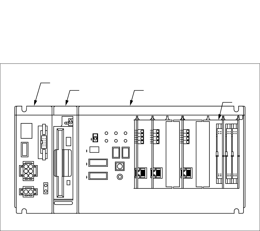
NDA-24296 CHAPTER 2
Page 25
Revision 1.0
SN1695 CPRBF-A
CPU Board
3. Face Layout of Lamps, Switches, and Connectors
The CPR contains the following lamps, switches and connectors.
Slots 0-3 provide the Peripheral Component Interconnect (PCI) bus, and Slots 4-6 are the Industrial
Standard Architecture (ISA) bus.
Figure 2-5 Front View of CPR
Note: This card is mounted in the IMG0 of the IPX-U system only.
SW
DC-40V~-58.6V
PZ-PW92
MBR CPU OPE
ON
HDD
-48V OUT
ON
OFF
5A
125V
AC/DC
I
O
PALM
ON
ALM
OUTPWR
INPWR
ON
14
IMG1
SYSTEM SELECT0 STATUS
SENSE
CPURST
SLOT NO. 0 1 2 3 4 5 6
WDT
IMG2
IMG0
AB
IMG3
ON
112
SYSTEM SELECT1
ON
13 20
SYSTEM SELECT2
PWR(PZ-PW92)
FDD/HDD(PZ-IO27/28) DSP(PZ-DK224)
Note
[CPR for 1-IMG/4-IMG/IPX-U System]
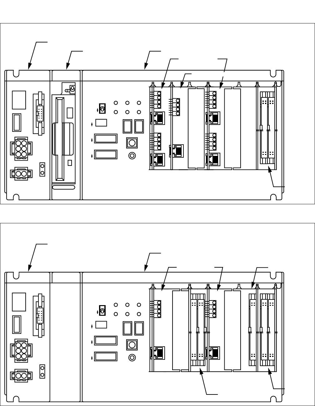
CHAPTER 2 NDA-24296
Page 26
Revision 1.0
SN1695 CPRBF-A
CPU Board
Figure 2-6 Front View of CPR in SP for IPX-UMG System
Figure 2-7 Front View of CPR in CMP for IPX-UMG System
SW
DC-40V~-58.6V
PZ-PW92
MBR CPU OPE
ON
HDD
-48V OUT
ON
OFF
5A
125V
AC/DC
I
O
PALM
ON
ALM
OUTPWR
INPWR
ON
14
IMG1
SYSTEM SELECT0 STATUS
SENSE
CPURST
SLOT NO. 0 1 2 3 4 5 6
WDT
IMG2
IMG0
AB
IMG3
ON
112
SYSTEM SELECT1
ON
13 20
SYSTEM SELECT2
PWR(PZ-PW92)
FDD/HDD(PZ-IO27/28) DSP(PZ-DK224)
LANI(PZ-PC23)
ISAGT
(PZ-GT13)
LANI(PZ-PC19)
[CPR in SP for IPX-UMG System]
SW
DC-40V~-58.6V
PZ-PW92
MBR CPU OPE
ON
-48V OUT
ON
OFF
5A
125V
AC/DC
I
O
PALM
ON
ALM
OUTPWR
INPWR
ON
14
IMG1
SYSTEM SELECT0 STATUS
SENSE
CPURST
SLOT NO. 0 1 2 3 4 5 6
WDT
IMG2
IMG0
AB
IMG3
ON
112
SYSTEM SELECT1
ON
13 20
SYSTEM SELECT2
AB
PWR(PZ-PW92)
DSP(PZ-DK224)
LANI(PZ-PC22)
ISAGTA
(PZ-M565)
ISAGT
(PZ-GT13)
MEM(PZ-ME44)
[CPR in CMP for IPX-UMG System]
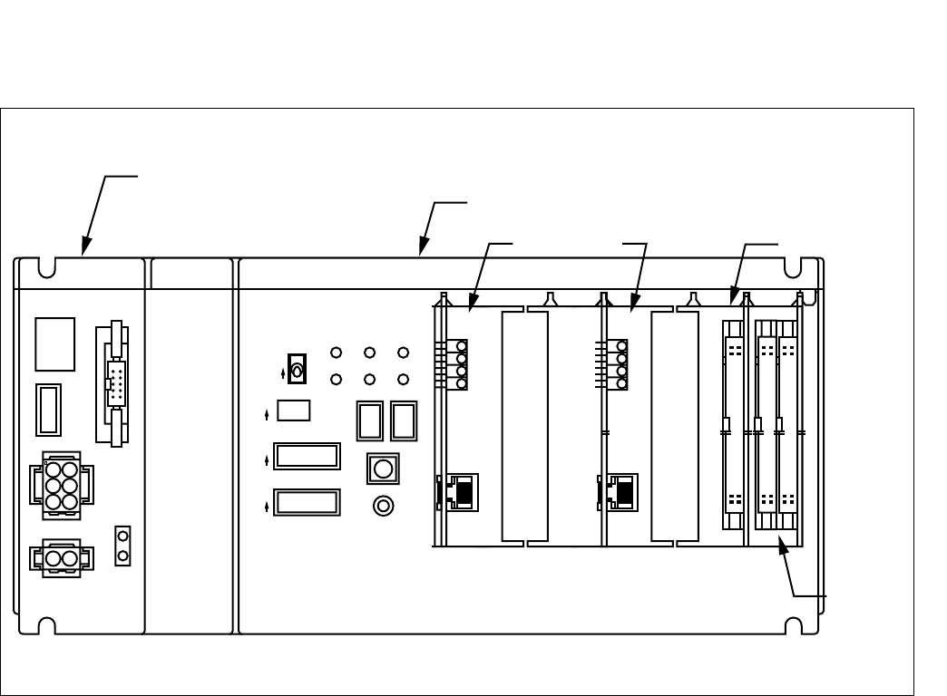
NDA-24296 CHAPTER 2
Page 27
Revision 1.0
SN1695 CPRBF-A
CPU Board
Figure 2-8 Front View of CPR in LP for IPX-UMG System
SW
DC-40V~-58.6V
PZ-PW92
MBR CPU OPE
ON
-48V OUT
ON
OFF
5A
125V
AC/DC
I
O
PALM
ON
ALM
OUTPWR
INPWR
ON
14
IMG1
SYSTEM SELECT0 STATUS
SENSE
CPURST
SLOT NO. 0 1 2 3 4 5 6
WDT
IMG2
IMG0
AB
IMG3
ON
112
SYSTEM SELECT1
ON
13 20
SYSTEM SELECT2
PWR(PZ-PW92)
DSP(PZ-DK224)
LANI(PZ-PC22)
ISAGT
(PZ-GT20)
ISAGT
(PZ-GT13)
[CPR in LP for IPX-UMG System]
Note: This card is required when IMG2/6/10/14 and/or IMG3/7/11/15 is configured.
Note

CHAPTER 2 NDA-24296
Page 28
Revision 1.0
SN1695 CPRBF-A
CPU Board
4. Lamp Indications
Lamp Indications vary depending on the node. The following shows the lamp indications for the CPR in
the IMG for 1-IMG, 4-IMG, and IPX-U system.
[Lamp Indications for 1-IMG/4-IMG/IPX-U System]
Note: No lamp indication in STBY mode.
The following shows lamp indications for the CPR in the ISW.
Note: No lamp indication in STBY mode.
LAMP NAME COLOR DESCRIPTION
ON (PWR) Green Lights green when the PWR is supplied.
ALM (PWR) Red Lights red when the PWR is abnormal.
HDD
(FDD/HDD) Red Lights red while the HDD or FDD is being accessed.
WDT (DSP) Red Lights red when Watch-dog Timer (WDT) time-out has occurred.
CPU OPE (DSP) Green Lights green when the CPU is in active state.
CPU OPE (DSP) Green Lights green when the CPU is in active state.
IMG0 (DSP) Green Flashes green when PZ-GT13 (located in Slot 6) is in operation.
IMG1 (DSP) Green Flashes green when IMG1 is mounted. Note
IMG2 (DSP) Green Flashes green when IMG2 is mounted. Note
IMG3 (DSP) Green Flashes green when IMG3 is mounted. Note
LAMP NAME COLOR DESCRIPTION
ON (PWR) Green Lights green when the PWR is supplied.
ALM (PWR) Red Lights red when the PWR is abnormal.
HDD (FDD/HDD) Red Lights red while the HDD or FDD is being accessed.
WDT (DSP) Red Lights red when Watch-dog Timer (WDT) time-out has occurred.
CPU OPE (DSP) Green Lights green when the CPU of the ISW is in active state.
IMG0 (DSP) Green Lights green when the CPU of the ISW is in active state.
Flashes green when the CPU of the ISW is in stand-by state.
IMG1 (DSP) Green Lights green when the TSW1 of the ISW is used. Note
IMG2 (DSP) Green Lights green when the TSW2 of the ISW is used. Note
IMG3 (DSP) Green Lights green when the TSW3 of the ISW is used. Note
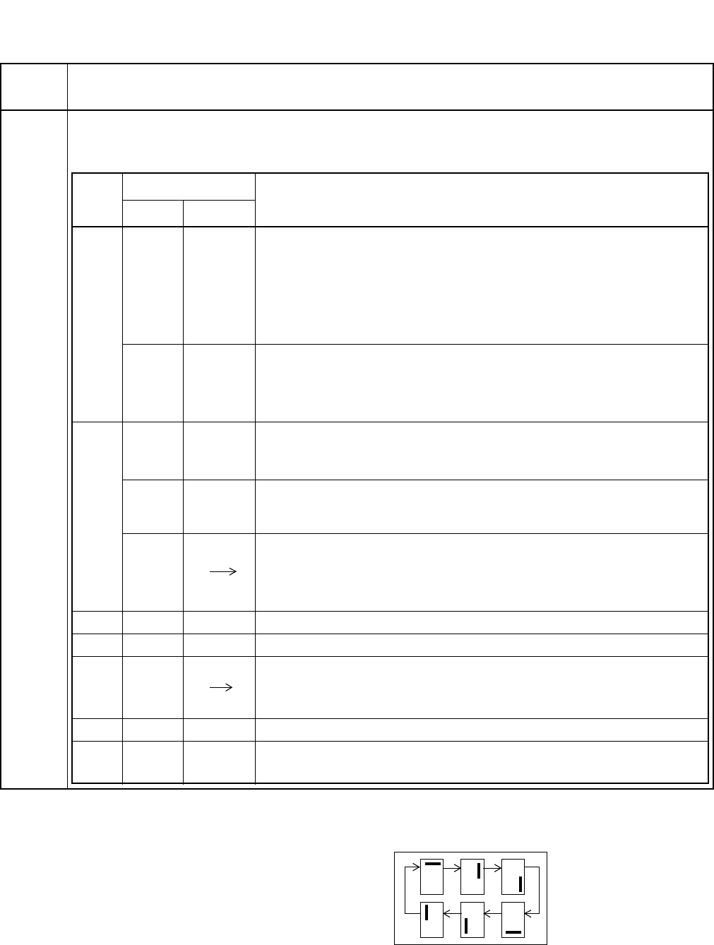
NDA-24296 CHAPTER 2
Page 29
Revision 1.0
SN1695 CPRBF-A
CPU Board
Note: The segment spinning indication shows a processing status has completed successfully, or “E” indicates
the processing failed.
LAMP
NAME DESCRIPTION
STATUS
(DSP)
Two sets of “7-segment LED” show the CPR processing status. The CPR processing status is determined by the
SENSE switch settings, and the new processing status starts when the CPURST switch is pressed. The 7-segment
LED indication on each CPR processing status is listed below.
SENSE STATUS DESCRIPTION
LEFT RIGHT
1
Not used
“F”
“c”
“d”
1. When Program Install
The HD in the CPR is initialized and the program is installed. (These three processes
execute)
“F”indicated during HD format.
“c”indicated when copying data from FD to HD
“d” indicated while making the directory on the HD
Not used “1”
2. When Program Load
After program installation, the program should be transferred from the HD to
memory.
“1” is indicated during this process.
2
“0-9”“0-9”
3. On-line active CPR
The active CPR which is in ON LINE status indicates the CPU occupancy rate by
percentage. (00-99%)
Not used
“S”
“b”
“y”
4. On-line stand-by CPR
The stand-by CPR which is in ON LINE status indicates “S,” “b,” “y”
Not used
5. Program & Office data load
“1”indicated during the Program and Office data transfer from the HD to the
memory
“0” indicated during the Office data load
3Not used “c”“c”indicated when copying the data from FD to HD
4Not used “d”“d”indicated while making the directory on the HD
5Not used
The CPR is starting-up with ON LINE (OAI memory clear restart).
“1”indicated during the Program load.
“0”indicated during the process.
6Not used “F”“F” indicated during HD format.
CNot used “H”The CPR is starting-up OFF LINE.
“H”indicated during the ROM data loading.
“1”“0”
“1”“0”
Segment Spinning Indication

CHAPTER 2 NDA-24296
Page 30
Revision 1.0
SN1695 CPRBF-A
CPU Board
The following shows the lamp indication for the CPR in the SP, CMP, and LP for IPX-UMG system.
[Lamp Indications for the CPR in SP]
[Lamp Indications for the CPR in CMP]
Note: No lamp indication in STBY mode.
LAMP NAME COLOR DESCRIPTION
ON (PWR) Green Lights green when the PWR is supplied.
ALM (PWR) Red Lights red when the PWR is abnormal.
HDD (FDD/HDD) Red Lights red while the HDD or FDD is being accessed.
WDT (DSP) Red Lights red when Watch-dog Timer (WDT) time-out has occurred.
CPU OPE (DSP) Green Lights green when the CPU of the SP is in active state.
IMG0 (DSP) Green Remains OFF when the CPU is in active state.
Flashes green when the CPU is in stand-by state.
IMG1 (DSP) Green Not used.
IMG2 (DSP) Green Not used.
IMG3 (DSP) Green Not used.
LAMP NAME COLOR DESCRIPTION
ON (PWR) Green Lights green when the PWR is supplied.
ALM (PWR) Red Lights red when the PWR is abnormal.
WDT (DSP) Red Lights red when Watch-dog Timer (WDT) time-out has occurred.
CPU OPE (DSP) Green Lights green when the CPU of the CMP is in active state.
IMG0 (DSP) Green Lights green when the CPU is in active state.
Flashes green when the CPU is in stand-by state.
IMG1 (DSP) Green Lights green when the TSW1 in the ISWM of CMG is used. Note
IMG2 (DSP) Green Lights green when the TSW2 in the ISWM of CMG is used. Note
IMG3 (DSP) Green Lights green when the TSW3 in the ISWM of CMG is used. Note

NDA-24296 CHAPTER 2
Page 31
Revision 1.0
SN1695 CPRBF-A
CPU Board
[Lamp Indications for the CPR in LP]
Note: No lamp indication in STBY mode.
LAMP NAME COLOR DESCRIPTION
ON (PWR) Green Lights green when the PWR is supplied.
ALM (PWR) Red Lights red when the PWR is abnormal.
WDT (DSP) Red Lights red when Watch-dog Timer (WDT) time-out has occurred.
CPU OPE (DSP) Green Lights green when the CPU is in active state.
IMG0 (DSP) Green Flashes green when PZ-GT13 (located in Slot 6) is in operation.
IMG1 (DSP) Green Flashes green when IMG1/5/9/13 is mounted. Note
IMG2 (DSP) Green Flashes green when IMG2/6/10/14 is mounted. Note
IMG3 (DSP) Green Flashes green when IMG3/7/11/15 is mounted. Note
CHAPTER 2 NDA-24296
Page 32
Revision 1.0
SN1695 CPRBF-A
CPU Board
Note: The segment spinning indication shows a processing status has completed successfully, or indicates “E”
meaning the processing failed.
LAMP
NAME DESCRIPTION
STATUS
(DSP)
Two sets of “7-segment LED” show the CPR processing status. The CPR processing status is determined by the
SENSE switch settings, and the new processing status starts when the CPURST switch is pressed. The 7-segment
LED indication on each CPR processing status is listed below.
SENSE STATUS DESCRIPTION
LEFT RIGHT
0
“0-9”“0-9”1. On-line active CPR
The active CPR which is in ON LINE status indicates the
CPU occupancy rate by percentage. (00-99%)
When the “EMA
SUP” switch is
“OFF” on the PH-
PC43 (EMA) card.
Not used
“S”
“b”
“y”
2. On-line stand-by CPR
The stand-by CPR which is in ON LINE status indicates
“S,” “b,” “y”
Not used “0-F”
3. Both active and stand-by CPR
The setting of SENSE switch is indicated.
When the “EMA
SUP” switch is
“ON” on the PH-
PC43 (EMA) card.
Not used
4. Program & Office data load
“1”indicated during the Program and Office data transfer from the HD to the
memory
“0” indicated during the Office data load
1
Not used
“F”
“c”
“d”
1. When Program Install
The HD in the CPR is initialized and the program is installed. (These three process-
es execute)
“F”indicated during HD format.
“c”indicated when copying data from FD (Basic Software #1) to HD
“d” indicated while making the directory on the HD
Not used “1”
2. When Program Load
After program installation, the program should be transferred from the HD to
memory.
“1” is indicated during this process.
3Not used “c”“c”indicated when copying the data from FD to HD
5Not used
The CPR is starting-up with ON LINE (OAI memory clear restart).
“1”indicated during the Program load.
“0”indicated during the process.
CNot used “H”The CPR is starting-up OFF LINE.
“H”indicated during the ROM data loading.
“1”“0”
“1”“0”
Segment Spinning In
d

NDA-24296 CHAPTER 2
Page 33
Revision 1.0
SN1695 CPRBF-A
CPU Board
5. Switch Settings
[for 1-IMG/4-IMG/IPX-U System]
Note: Make-busy of this circuit card is not allowed while the Floppy Disk Drive or Hard Disk Drive is being
accessed.
SWITCH NAME SWITCH
NO. SETTING STANDARD
SETTING MEANING
SW
(PWR) —ON ×PWR is supplied to the CPR.
OFF PWR is not supplied to the CPR.
MB Note
(FDD/HDD) —ON (Up) Make-busy of the FDD/HDD.
OFF (Down) ×Normal setting.
MBR
(DSP) —ON (Up) Make-busy Request of the CPR in which GT is
located.
OFF (Down) ×Normal setting.
CPURST
(DSP) —— Execute the CPR processing according to the
SENSE setting.
SYSTEM
SELECT0
(DSP)
1OFF ×Not used.
2OFF ×Not used.
3OFF ×Not used.
4ON Watchdog Timer time-out is not detected.
OFF ×Watchdog Timer time-out is detected.
SYSTEM
SELECT1
(DSP)
1ON PCI Card (Slot 0) MBR ON.
OFF PCI Card (Slot 0) MBR OFF.
2ON PCI Card (Slot 1) MBR ON.
OFF PCI Card (Slot 1) MBR OFF.
3ON PCI Card (Slot 2) MBR ON.
OFF PCI Card (Slot 2) MBR OFF.
4ON PCI Card (Slot 3) MBR ON.
OFF PCI Card (Slot 3) MBR OFF.
5~7 OFF ×Fixed to “OFF.”
8ON IPX-U System
OFF 1IMG/4IMG System
SYSTEM
SELECT2
(DSP)
1~8 OFF ×Not used.

CHAPTER 2 NDA-24296
Page 34
Revision 1.0
SN1695 CPRBF-A
CPU Board
Note: The SENSE switch designates the CPR processing status. The new processing status starts when the
CPRRST switch on the DSP is pressed while setting the SENSE switch.
SWITCH
NAME SETTING STANDARD
SETTING MEANING
SENSE
(DSP)
Note
1
The following three processes are executed at the FDD/HDD.
•HD formatted
•File copied from FDD to HD
•Directory created on the HD
2×On-line mode.
3 File copied from FDD to HD within the FDD/HDD.
4 Directory created on the HD of the FDD/HDD.
5OAI memory cleared, and the CPR started up in ON LINE mode by loading
the ROM data.
6 HD format of the FDD/HDD.
C The CPR starts up in OFF LINE mode by loading the ROM data.

NDA-24296 CHAPTER 2
Page 35
Revision 1.0
SN1695 CPRBF-A
CPU Board
[for IPX-UMG System]
Note: Make-busy of this circuit card is not allowed while the Floppy Disk Drive or Hard Disk Drive is being
accessed. This switch is used on the CPR mounted in SP only.
SWITCH NAME SWITC
H NO. SETTING STANDARD
SETTING MEANING
SW
(PWR) —ON ×PWR is supplied to the CPR.
OFF PWR is not supplied to the CPR.
MB Note
(FDD/HDD) —ON (Up) Make-busy of the FDD/HDD.
OFF (Down) ×Normal setting.
MBR
(DSP) —ON (Up) Make-busy Request of the CPR in which GT is
located.
OFF (Down) ×Normal setting.
CPURST
(DSP) —— Execute the CPR processing according to the
SENSE setting.
SYSTEM
SELECT0
(DSP)
1ON ×Fixed to “ON.”
2OFF ×Fixed to “OFF.”
3
ON High Density system configuration (one LP
controls two IMGs)
OFF ×Standard system configuration (one LP
controls four IMGs)
4ON Watchdog Timer time-out is not detected.
OFF ×Watchdog Timer time-out is detected.
SYSTEM
SELECT1
(DSP)
1ON PCI Card (Slot 0) MBR ON.
OFF PCI Card (Slot 0) MBR OFF.
2ON PCI Card (Slot 1) MBR ON.
OFF PCI Card (Slot 1) MBR OFF.
3ON PCI Card (Slot 2) MBR ON.
OFF PCI Card (Slot 2) MBR OFF.
4ON PCI Card (Slot 3) MBR ON.
OFF PCI Card (Slot 3) MBR OFF.
5~7 OFF ×Fixed to “OFF.”
8ON ×Fixed to “ON.”
CHAPTER 2 NDA-24296
Page 36
Revision 1.0
SN1695 CPRBF-A
CPU Board
Note: This switch setting is valid when the “EMA SUP” switch is ON (UP side).
SWITCH NAME SWITCH
NO. SETTING STANDARD
SETTING MEANING
SYSTEM
SELECT2
(DSP)
1~4 OFF ×Not used.
5~8
Physical PBI Number (Equipment Number)
Note 1: Physical PBI No. must be the same
on the CPR of system #0 and #1 in
dual configuration.
Note 2: This setting is required when the
system applies High Density system
configuration (i.e., a LP controls
two IMGs) only.
SW5 SW6 SW7 SW8 PBI No.
ON
ON
OFF
OFF
OFF
OFF
OFF
OFF
OFF
OFF
ON
ON
OFF
OFF
OFF
OFF
ON
ON
ON
ON
ON
ON
OFF
OFF
ON
ON
OFF
OFF
ON
ON
ON
OFF
OFF
ON
OFF
ON
OFF
ON
OFF
ON
PBI 02 (SP)
PBI 04 (CMP)
PBI 30 (LP 00)
PBI 38 (LP 04) Note
PBI 40 (LP 08)
PBI 48 (LP 12) Note
PBI 50 (LP 16)
PBI 58 (LP 20) Note
PBI 60 (LP 24)
PBI 68 (LP 28) Note
NDA-24296 CHAPTER 2
Page 37
Revision 1.0
SN1695 CPRBF-A
CPU Board
Note: Refer to the following figure and table for the PBI Number and the Equipment Number for IPX-UMG
system. The same PBI Number must be assigned to both #0 and #1 processors in dual configuration.
Processor Name PBI No. CPU Accommodation Equipment No.
SP 02 15
CMP 04 14
LP00 (IMG0) 30 0
LP08 (IMG4) 40 2
LP16 (IMG8) 50 4
LP24 (IMG12) 60 6
CMG
SP
CMP
IMG0
LP00
IMG1 IMG2 IMG3
IMG4
LP08
IMG5 IMG6 IMG7
IMG8
LP16
IMG9 IMG10 IMG11
IMG12
LP24
IMG13 IMG14 IMG15

CHAPTER 2 NDA-24296
Page 38
Revision 1.0
SN1695 CPRBF-A
CPU Board
Note 1: The SENSE switch designates the CPR processing status. The new processing status starts when the
CPRRST switch on the DSP is pressed while setting the SENSE switch.
Note 2: This switch is used on the CPR mounted in SP only.
Note 3: Connection Hold Restart is proceeded by initializing the system with the TOPU key.
SWITCH
NAME SETTING STANDARD
SETTING MEANING
SENSE
(DSP)
Note 1
0
Note 2 ×On-line mode.
1
Note 2
The following three processes are executed at the FDD/HDD.
•HD formatted
•File copied from FDD to HD
•Directory created on the HD
3
Note 2 File copied from FDD to HD/Connection Hold Restart. Note 3
5
Note 2 OAI memory cleared, and the CPR started up in ON LINE mode by loading
the ROM data.
C
Note 2 The CPR starts up in OFF LINE mode by loading the ROM data.
NDA-24296 CHAPTER 2
Page 39
Revision 1.0
SN1695 CPRBF-A
CPU Board
6. External Interface
See the NEAX2400 IPX Installation Manual.
7. Switch Setting Sheet
SWITCH NAME SWITCH SHAPE REMARKS
SW
(PWR)
MB
(PWR:PZ-PW106)
MB
(FDD/HDD)
MBR
(DSP)
SYSTEM
SELECT0
(DSP)
SYSTEM
SELECT1
(DSP)
SYSTEM SELECT2
(DSP)
SENSE
(DSP)
ON
OFF
ON
ON
ON
12 3 4 ON
1234 ON
56 7 8
1234 ON
56 7 8
CHAPTER 2 NDA-24296
Page 40
Revision 1.0
PH-GT09
Gate
PH-GT09
Gate
1. General Function
The PH-GT09 (GT) circuit card provides both the TSW I/O Local bus and the MISC bus interface. The
CPR controls TSW, PLO, DLKC, and MISC via the ISAGT and GT.
Figure 2-9 Location of PH-GT09 (GT) Card in the System
PLO0
PLO1
TDSW03
TDSW I/O
Local Bus
TDSW I/O
Local Bus
TDSW13
TDSW02
TDSW12
TDSW01
TDSW11
TDSW00
DLKC0
MISC
ISAGT
DSP
CPULANI
LANI
GT
TDSW10
CPR #0
To HUB
To HUB
To HUB
To HUB
ISAGT
GT
DLKC1
DSP
CPU
CPR #1
LANI
LANI
EMA
IOC/
MISC
MISC Bus
MISC Bus
MISC Bus

NDA-24296 CHAPTER 2
Page 41
Revision 1.0
PH-GT09
Gate
2. Mounting Location/Condition
This circuit card is mounted in the TSWM of the slot shown below.
3. Face Layout of Lamps, Switches, and Connectors
The face layout of lamps, switches, and connectors is shown in Figure 2-10.
Figure 2-10 Face Layout of PH-GT09 (GT)
00 01 02 03 04 05 06 07 08 09 10 11 12 13 14 15 16 17 18 19 20 21 22 23
Mounting Module TSWM
GT0
GT1
MB
MBR
OPE/MB
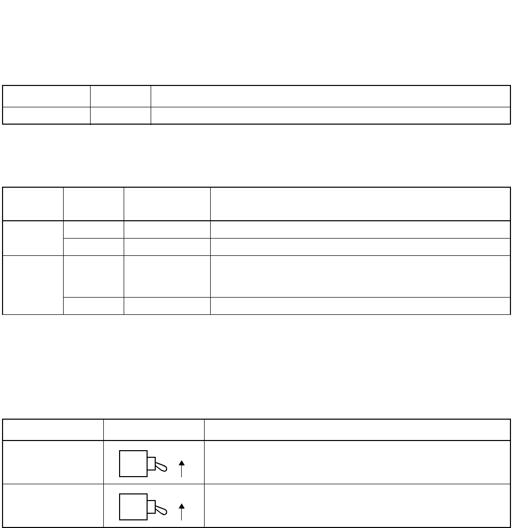
CHAPTER 2 NDA-24296
Page 42
Revision 1.0
PH-GT09
Gate
4. Lamp Indications
Lamp indications for this circuit card are shown in the table below.
5. Switch Settings
Standard settings for switches on this circuit card are shown in the table below.
Note: Prior to extracting the GT card, flip the MBR switch on and then flip the MB switch on.
6. External Interface
See the NEAX2400 IPX Installation Manual.
7. Switch Setting Sheet
LAMP NAME COLOR STATE
OPE/MB Green Remains lit while this circuit card is in ACT state.
SWITCH
NAME SETTING STANDARD
SETTING MEANING
MB UP Make-busy of circuit card
DOWN ×Normal setting
MBR
Note
UP
When the ACT side of GT’s MBR switch is flipped, the ST-BY side of
TSW, DLKC, and GT is forced to switch over the ACT side. (When
the TSW is dual configuration.)
DOWN ×Normal setting.
SWITCH NAME SWITCH SHAPE REMARKS
MB
MBR
ON
ON
NDA-24296 CHAPTER 2
Page 43
Revision 1.0
PH-GT10
Input Output Gate
PH-GT10
Input Output Gate
1. General Function
The PH-GT10 circuit card provides the TSW I/O bus interface allowing the CPU board to control the TSW,
HSW, and PLO cards in the Inter-node Switch Module (ISWM) of the ISW/CMG. This circuit card also is
equipped with the copy function to be consistent with the data of TSW I/O bus in both systems (single/
dual). This circuit card is used for the IPX-U/IPX-UMG system.
Figure 2-11 Location of PH-GT10 (IOGT) for IPX-U System
HSW01
HSW00
TSW03
TSW02
TSW01
TSW00
LANI
LANI
LANI
LANI
HSW11
HSW10
TSW13
TSW12
TSW11
TSW10
PLO 1
PLO 0
RES
CPU CPU
MISC
IOC
EMA
RES
RES RES
(IOGT1)
PH-GT10
(IOGT0)
PH-GT10
ISAGT ISAGT
MISC I/O BUS
ISAGT BUSISAGT BUS LPM
TSW I/O BUSTSW I/O BUS
ISWM
CHAPTER 2 NDA-24296
Page 44
Revision 1.0
PH-GT10
Input Output Gate
Figure 2-12 Location of PH-GT10 (IOGT) for IPX-UMG System
HSW01
HSW00
TSW03
TSW02
TSW01
TSW00
LANI
LANI
P-BUS
LANI
LANI P-BUS
HSW11
HSW10
TSW13
TSW12
TSW11
TSW10
PLO 1
PLO 0
RES
CPU CPU
MMC
MISC
EMA
RES
RES RES
(IOGT1)
PH-GT10
(IOGT0)
PH-GT10
ISAGT ISAGT
ISAGT2 ISAGT2
PCI MEM
PCI BUS PCI BUS
PCI MEM
MISC
I/O
BUS
MISC
I/O
BUS
ISAGT BUSISAGT BUS CMP
TSW I/O BUSTSW I/O BUS
ISWM
NDA-24296 CHAPTER 2
Page 45
Revision 1.0
PH-GT10
Input Output Gate
2. Mounting Location/Condition
This circuit card can be mounted in the shaded slots shown below.
3. Face Layout of Lamps, Switches, and Connectors
The face layout of lamps, switches, and connectors are shown in Figure 2-13.
Figure 2-13 Face Layout of PH-GT10 (IOGT)
Mounting Module ISWM
00 01 02 03 04 05 06 07 08 09 10 11 12 13 14 15 16 17 18 19 20 21 22 23
MB
MBR
OPE/MB
PWRALM
CA4L
COPY
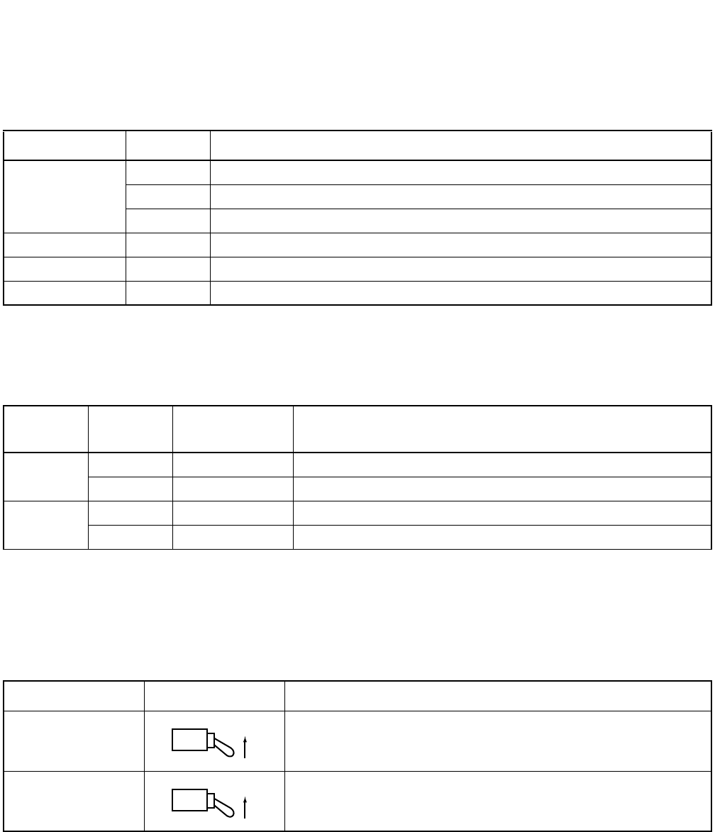
CHAPTER 2 NDA-24296
Page 46
Revision 1.0
PH-GT10
Input Output Gate
4. Lamp Indications
Lamp indications for this circuit card are shown in the table below.
5. Switch Settings
Standard settings of switches on this circuit card are shown in the table below.
6. External Interface
See the NEAX2400 IPX Installation Manual.
7. Switch Setting Sheet
LAMP NAME COLOR MEANING
OPE/MB
Green Lights when this circuit card is in ACT state.
OFF This circuit card is in ST-BY state.
Red Lights when this circuit card is in Make-busy state.
PWRALM Red Lights when On-Board Power Supply for this circuit card is abnormal.
CA4L Red Lights when 4 MHz clock supplied for Local I/O Bus is faulty.
COPY Green Lights when this circuit card is in COPY mode.
SWITCH
NAME SETTING STANDARD
SETTING MEANING
MB UP Circuit Card Make-busy
DOWN ×Circuit Card Make-busy cancel
MBR UP Make-busy request
DOWN ×Make-busy request cancel
SWITCH NAME SWITCH SHAPE REMARKS
MB
MBR
ON
ON
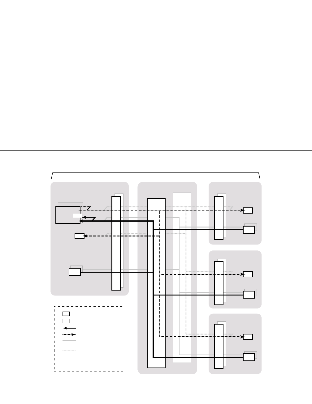
NDA-24296 CHAPTER 2
Page 47
Revision 1.0
PA-PC94
Data Link Multiplexer
PA-PC94
Data Link Multiplexer
1. General Function
This circuit card mainly provides the two functions: 1) collection of BLF/TGBL information (associated
with Attendant/Desk Console operation) from DLKC cards of all nodes in an IPX-U/IPX-UMG system,
and 2) distribution of the collected data to ATI cards of all nodes. While a DLKC card can manage this pro-
cessing solely on an accommodated node basis, the use of this card makes possible the BLF/TGBL man-
agement even on a system basis, via the Inter-node Switch (ISW). Note that this card is mounted in a PIM
of any node, and if necessary, can have an optional dual configuration.
For details on BLF/TGBL information, refer to the following service features explained in the “Feature
Programming Manual”.
•Busy Lamp Field-Flexible [B-2]
•Trunk Group Busy Lamp [T-9]
Figure 2-14 Location of PA-PC94 (DLMX)
IPX-U System/IPX-UMG System
ATI
ATI
ATI
ATI
(TSW 1) (TSW 1)
(TSW 1)
(TSW 1)
TSW/HSW 1
DLMX 0
(DLMX 1)
IN
OUT
DLKC 0
(DLKC 1)
DLKC 0
(DLKC 1)
DLKC 0
(DLKC 1)
DLKC 0
(DLKC 1)
TSW 0 TSW 0
TSW 0
TSW 0
TSW/HSW 0
LN 0/LMG0 LN 1/LMG1
LN 2/LMG2
LN 3/LMG3
ISW/CMG
Note
: Circuit Card
: Circuit Card (No. 1 System)
: BLF/TGBL data from DLKC
: BLF/TGBL data to ATI
: BLF/TGBL data to ATI
(No. 1 system)
: BLF/TGBL data from DLKC
(No. 1 system)
BLF: Busy Lamp Field - Flexible
TGBL: Trunk Group Busy Lamp
Note: IN - DLMX card gathers BLF/TGBL information from DLKC card of each node, via ISW/CMG.
OUT - DLMX card sends the collected BLF/TGBL information to ATI card(s) of each node, via ISW/
CMG.
This figure shows an example where a pair of DLMX cards (No. 0/No. 1 system) is accommodated in a PIM of
LN0/LMG0.
CHAPTER 2 NDA-24296
Page 48
Revision 1.0
PA-PC94
Data Link Multiplexer
2. Mounting Location/Condition
When this circuit card is used in a single configuration.
Mount this circuit card in any of the shaded slots:
Mounting conditions of this circuit card are as follows:
1. This circuit card cannot be mounted in the slot 05, 07, 09, 10, 11, 12, 16, 18, 20, 21, 22, 23.
2. This card is used in odd-number group (G) of the shaded slots above.
3. To used this card, be sure to assign “RT=938” on the ATRK command.
4. Do not mount another line/trunk circuit card in a slot adjoining the DLMX card within the same
Highway Block (HW) (i.e. do not mount other line/trunk card in the right side of the slot where a
DLMX card is mounted).
5. Only one DLMX card can be mounted when the system is composed of single configuration.
When this circuit card is used in a dual configuration.
Mount this circuit card in any of the shaded slots:
Mounting conditions of this circuit card are as follows:
1. A pair of DLMX card No. 0/No. 1 systems must be mounted in the same Highway Block (HW).
2. This circuit card cannot be mounted in 32-port slot (10, 11,12, 21, 22, 23).
3. This card is used in odd-number group (G) of the shaded slots above.
4. To use this card, be sure to assign “RT=938” on the ATRK command.
5. A maximum two DLMX cards (a pair of DLMX card) can be mounted when the system is a dual
configuration.
PIM
Mounting Module
HW 0 HW 1 HW 2 HW 6 HW 7 HW 8
Highway Block
00 01 02 03 04 05 06 07 08 09 10 11 12 13 14 15 16 17 1918 20 21 22 23
DLMX
DLMX
DLMX
DLMX
DLMX
DLMX
Mounting Condition
PIM
Mounting Module
HW 0 HW 1 HW 2 HW 6 HW 7 HW 8
Highway Block
00 01 02 03 04 05 06 07 08 09 10 11 12 13 14 15 16 17 1918 20 21 22 23
DLMX #0
DLMX #1
DLMX #0
DLMX #1
DLMX #0
DLMX #1
DLMX #0
DLMX #1
DLMX #0
DLMX #1
DLMX #0
DLMX #1
Mounting Condition
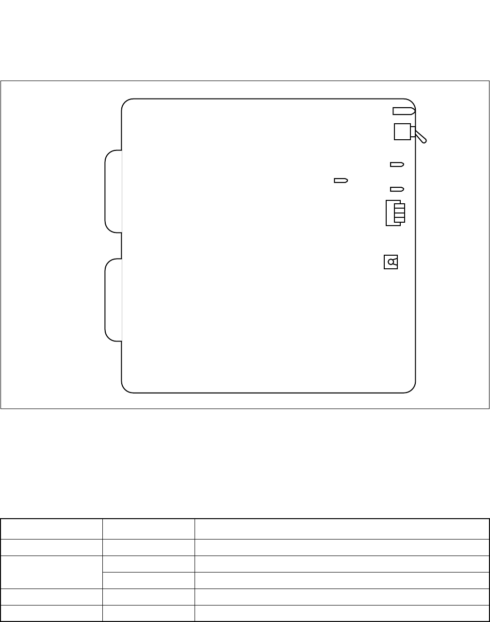
NDA-24296 CHAPTER 2
Page 49
Revision 1.0
PA-PC94
Data Link Multiplexer
3. Face Layout of Lamps and Switches
The face layout of lamps and switches is shown below.
Figure 2-15 Face Layout of PA-PC94 (DLMX)
4. Lamp Indications
The contents of lamp indications on this circuit card are shown in the table below:
PA-PC94 Lamp Indications Reference
LAMP NAME COLOR STATE
OPE Green Remains lit while this circuit card is in normal operation.
ACT Green Lights when this circuit card is in a active state.
OFF Off when this circuit card is in a stand-by state.
LOAD OFF Not used.
PWALM Red Lights when OBP alarm
ACT
PWALM
LOAD
MB KEY
OPE
MNT
MODE
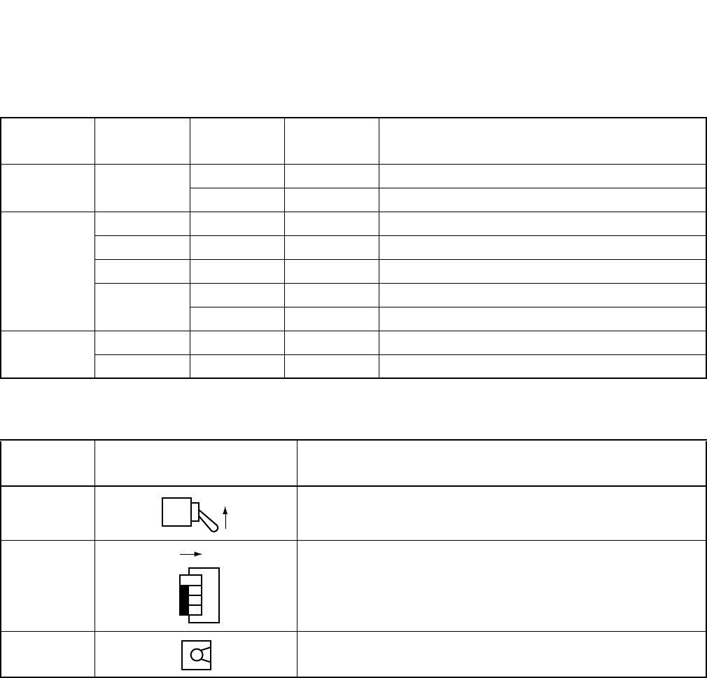
CHAPTER 2 NDA-24296
Page 50
Revision 1.0
PA-PC94
Data Link Multiplexer
5. Switch Settings
Standard settings of switches on this circuit card are shown in the table below.
6. Switch Setting Sheet
SWITCH
NAME SWITCH
No. SETTING STANDARD
SETTING MEANING
MB UP Circuit card make-busy.
DOWN Circuit card make-busy cancel
MNT
0OFF×Fixed to OFF.
1OFF×Fixed to OFF.
2OFF×Fixed to OFF.
3ON Make-busy-request.
OFF Cancel the make-busy-request.
MODE 0×Standard setting. (TSW fixed connection)
1-7 Not used.
SWITCH
NAME SWITCH SHAPE REMARKS
MB
MNT
MODE
ON
0
1
2
3
ON
0
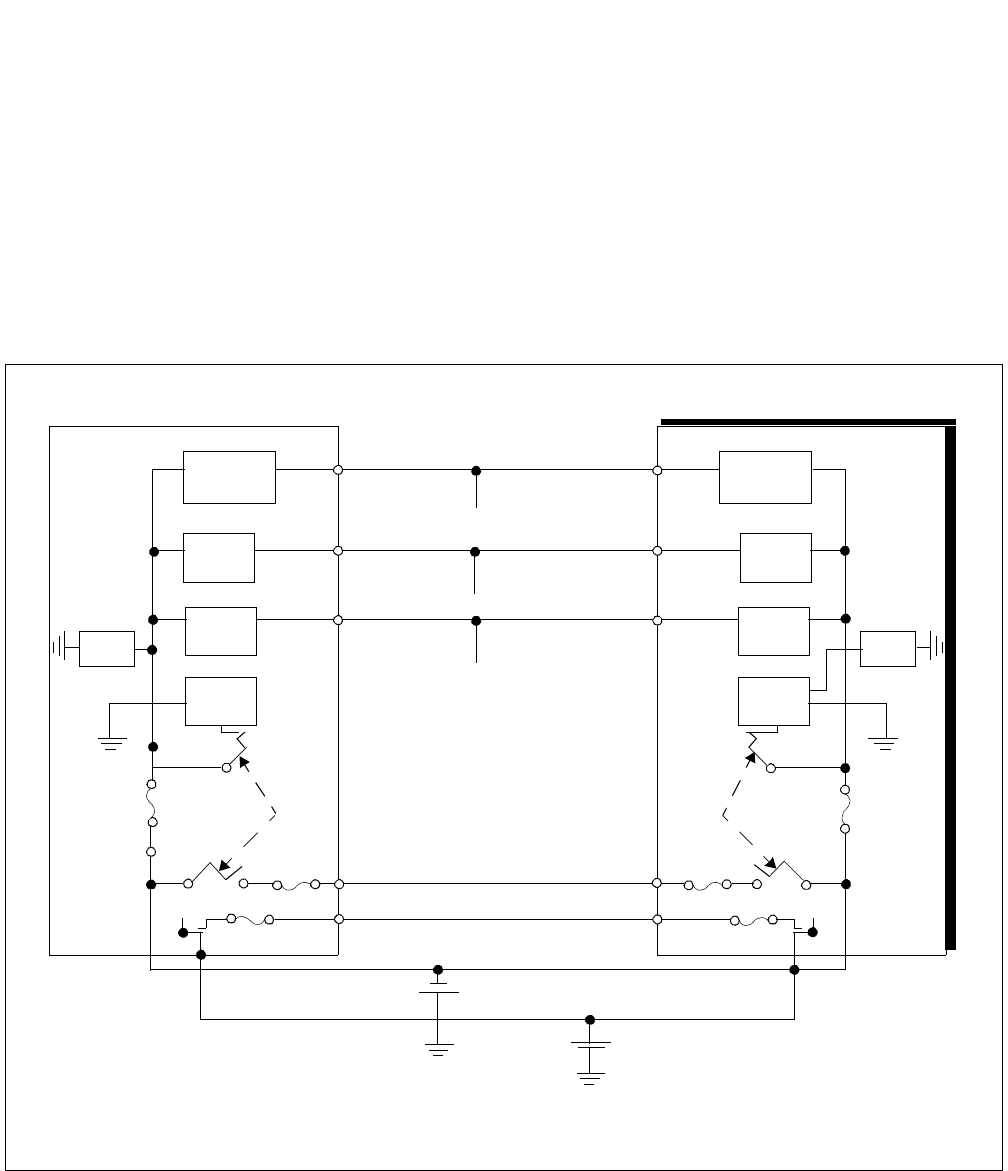
NDA-24296 CHAPTER 2
Page 51
Revision 1.0
PA-PW54-A
Dual Power
PA-PW54-A
Dual Power
1. General Function
The PA-PW54-A (DPWR) circuit card supplies operating power to circuit cards located in the PIM. The -
48 V input power source, which is converted to +5 V, -5 V, and +12 V, is distributed to each circuit card in
the PIM. This card also has a Ringing Generator Unit (RGU), whose output frequency and voltage can be
selected from 20 Hz, 25 Hz, 75 Vrms, 90 Vrms by switch setting on this card. In addition, a Howler Tone
circuit resides on this card.
Figure 2-16 Location of PA-PW54-A (DPWR) Card in the System
Note: The +80V input is required for activating Message Waiting Lamps (MWLs) .
HOW (For LC)
CR (For LC)
+5V, +12V, -5V
DC-DC
RGU
HOW
SUB
PWR
REL
NFB
PA-PW55-A ( PWR) PA-PW54-A (DPWR)
-48 V (For LC, TRK)
DC-DC
RGU
HOW
SUB
PWR
REL
NFB
-48 V
+80V (Option) Note
+80 V (For MWL)
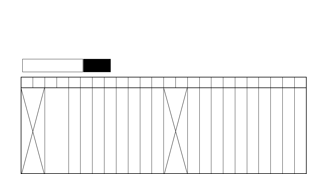
CHAPTER 2 NDA-24296
Page 52
Revision 1.0
PA-PW54-A
Dual Power
2. Mounting Location/Conditions
This circuit card is mounted in the following slot.
00 01 02 03 04 05 06 07 08 09 10 11 12 13 14 15 16 17 18 19 20 21 22 23
PIM
Mounting Module PIM
(PA-PW54-A)
DPWR
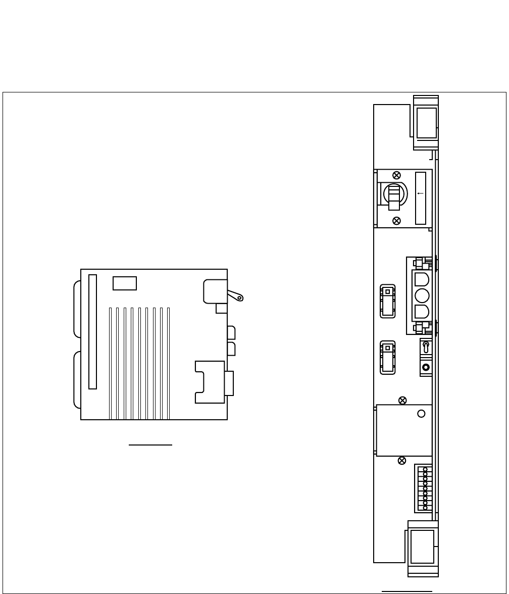
NDA-24296 CHAPTER 2
Page 53
Revision 1.0
PA-PW54-A
Dual Power
3. Face Layout of Lamps, Switches, and Connectors
The face layout of lamps, switches, and connectors on this circuit card is shown in Figure 2-17.
Figure 2-17 Face Layout of PA-PW54-A (DPWR) Card
-48V SW
FUSE
FUSE
SIDE VIEW
SW4
FRONT VIEW
PA-
PW54
-A
5.0
A
0.5
A
RGUOUT
0.5A
125V
AC/DC
+80VOUT
5A
125V
AC/DC
-48VOUT
25A
AC250V
DC125V
RST
MB
-48V
DC
INPUT
-48V
SW -48V
IN
CONN
25A
+80V ON
-48V ON
RGU ON
DC ON
OPE
DC ALM
CPU ALM
RGU ALM
HOW ALM
U
P
( )

CHAPTER 2 NDA-24296
Page 54
Revision 1.0
PA-PW54-A
Dual Power
4. Lamp Indications
Lamp indications for this circuit card are shown in the table below.
5. Switch Settings
This circuit card has the following switches.
6. External Interface
No cable connections are required.
LAMP NAME COLOR STATE
+80V ON Green Remains lit while +80 V input power is being supplied.
–48 V ON Green Remains lit while –48 V input power is being supplied.
RGU ON Green Remains lit while RGU output is in progress.
DC ON Green Remains lit while +5 V, +12 V, and –5 V are being output normally.
OPE Green Lights when information exchange with the CPU is possible.
CPUALM Red Lights when reset of the microprocessor has been activated.
DCALM Red Lights when +5 V, +12 V, or –5 V outputs alarm.
RGUALM Red Lights when RGU voltage alarm.
HOWALM Red Lights when howler alarm.
SWITCH
NAME SWITCH
No. SETTING STANDARD
SETTING DESCRIPTION
–48V SW —ON ×–48 V input power is supplied.
OFF –48 V input power is not supplied.
RESET —PUSH Hardware reset of the circuit card.
—×Normal setting.
MB —ON Make-busy of the circuit card.
OFF ×Normal setting.
SW4
1ON Frequency of Ringing Signal :25 [Hz]
OFF ×Frequency of Ringing Signal :20 [Hz]
2ON ×Voltage of Ringing Signal: 90 [Vrms]
OFF Voltage of Ringing Signal: 75 [Vrms]
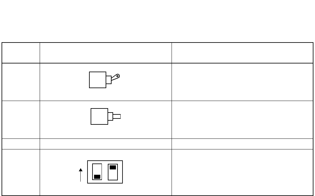
NDA-24296 CHAPTER 2
Page 55
Revision 1.0
PA-PW54-A
Dual Power
7. Switch Setting Sheet
SWITCH
NAME SWITCH SHAPE REMARKS
–48 V
RESET
MB DOWN Circuit card Make-busy cancel
SW4 20 [Hz]
90 [Vrms]
ON 12
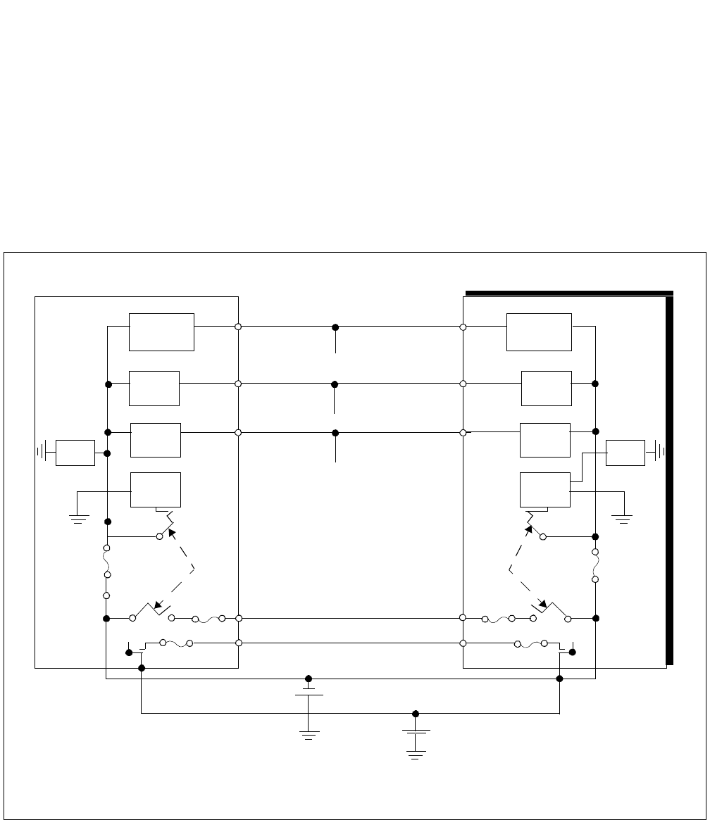
CHAPTER 2 NDA-24296
Page 56
Revision 1.0
PA-PW54-B
Dual Power
PA-PW54-B
Dual Power
1. General Function
The PA-PW54-B (DPWR) circuit card supplies operating power to circuit cards accommodated in the PIM.
The -48V input power source, which is converted to +5V, -5V, and +12V, is distributed to each circuit card
in the PIM. This card is also equipped with a Ringing Generator Unit (RGU), whose output frequency and
voltage can be selected among 20Hz, 25Hz, 75Vrms, 90Vrms by switch setting on this card. In addition, a
Howler Tone circuit resides on this card.
Figure 2-18 Location of PA-PW54-B (DPWR) Card within the System
Note: The +80V input is required for activating Message Waiting Lamps (MWLs) .
HOW (For LC)
CR (For LC)
+5V, +12V, -5V
DC-DC
RGU
HOW
SUB
PWR
REL
NFB
PA-PW55-B ( PWR) PA-PW54-B (DPWR)
-48 V (For LC, TRK)
DC-DC
RGU
HOW
SUB
PWR
REL
NFB
-48 V
+80V (Option) Note
+80 V (For MWL)

NDA-24296 CHAPTER 2
Page 57
Revision 1.0
PA-PW54-B
Dual Power
2. Mounting Location/Conditions
This circuit card is mounted in the following slot.
PIM
Mounting Module
00 01 02 03 04 05 06 07 08 09 10 11 12 13 14 15 16 17 18 19 20 21 22 23
DPWR
(PA-PW54-B)
PIM
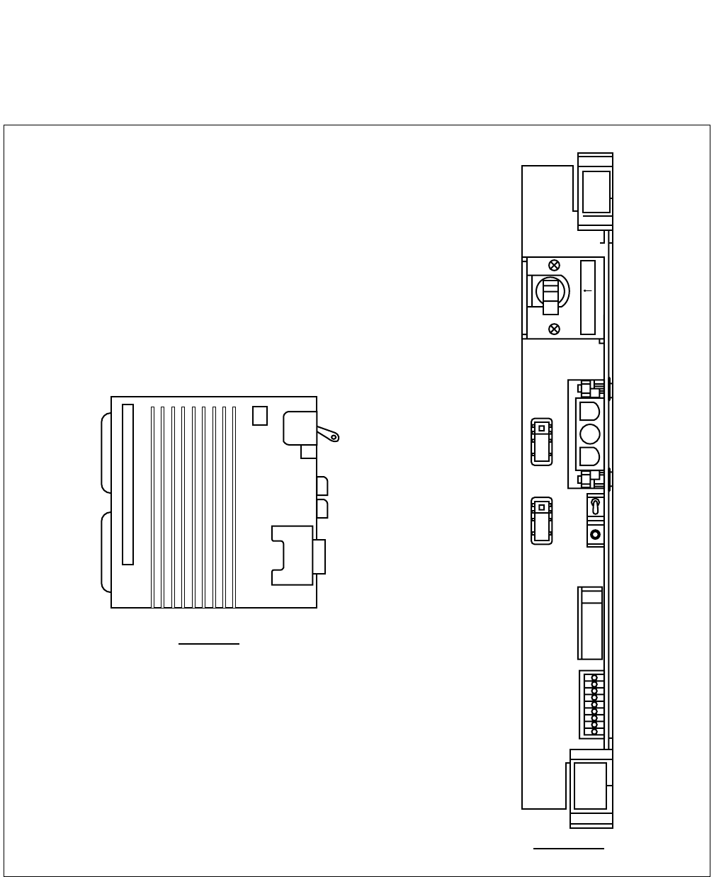
CHAPTER 2 NDA-24296
Page 58
Revision 1.0
PA-PW54-B
Dual Power
3. Face Layout of Lamps, Switches, and Connectors
The face layout of lamps, switches, and connectors on this circuit card is shown in Figure 2-19.
Figure 2-19 Face Layout of PA-PW54-B (DPWR) Card
-48V SW
FUSE
FUSE
SIDE VIEW
SW4
FRONT VIEW
PA-
PW54
- B
5.0
A
0.5
A
RGUOUT
0.5A
125V
AC/DC
+80VOUT
5A
125V
AC/DC
-48VOUT
25A
AC250V
DC125V
RST
MB
-48V
DC
INPUT
-48V
SW -48V
IN
CONN
20A
+80V ON
-48V ON
RGU ON
DC ON
OPE
DC ALM
CPU ALM
RGU ALM
HOW ALM
U
P
( )

NDA-24296 CHAPTER 2
Page 59
Revision 1.0
PA-PW54-B
Dual Power
4. Lamp Indications
The contents of lamp indications on this circuit card are shown in the table below.
5. Switch Settings
This circuit card has the following switches.
6. External Interface
No cable connections are required.
LAMP NAME COLOR STATE
+80V ON Green Remains lit while +80 V input power is being supplied.
–48 V ON Green Remains lit while –48 V input power is being supplied.
RGU ON Green Remains lit while RGU output is in progress.
DC ON Green Remains lit while +5 V, +12 V, and –5 V are being output normally.
OPE Green Lights when information exchange with the CPU is possible.
CPUALM Red Lights when reset of the microprocessor has been activated.
DCALM Red Lights in the case of +5 V, +12 V, or –5 V outputs alarm.
RGUALM Red Lights in the case of RGU voltage alarm.
HOWALM Red Lights in the case of howler alarm.
SWITCH
NAME SWITCH
No. SETTING STANDARD
SETTING DESCRIPTION
–48V SW —ON ×–48V input power is supplied.
OFF –48V input power is not supplied.
RESET —PUSH Hardware reset of the circuit card.
—×Normal setting
MB —ON Make busy of the circuit card.
OFF ×Normal setting
SW4
1ON Frequency of Ringing Signal :25 [Hz]
OFF ×Frequency of Ringing Signal :20 [Hz]
2ON ×Voltage of Ringing Signal: 90 [Vrms]
OFF Voltage of Ringing Signal: 75 [Vrms]
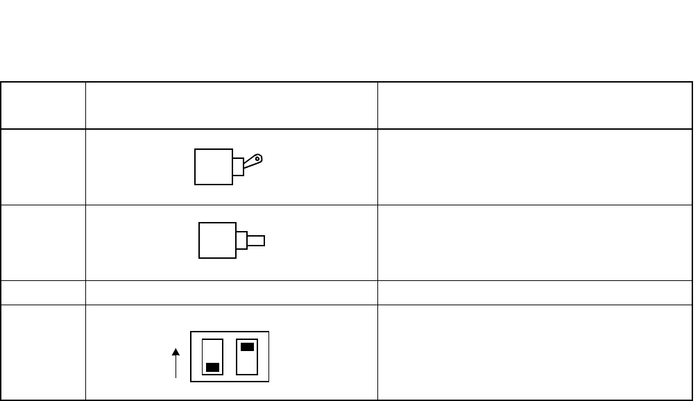
CHAPTER 2 NDA-24296
Page 60
Revision 1.0
PA-PW54-B
Dual Power
7. Switch Setting Sheet
SWITCH
NAME SWITCH SHAPE REMARKS
–48 V
RESET
MB DOWN Circuit card make busy cancel
SW4 20 [Hz]
90 [Vrms]
ON 12
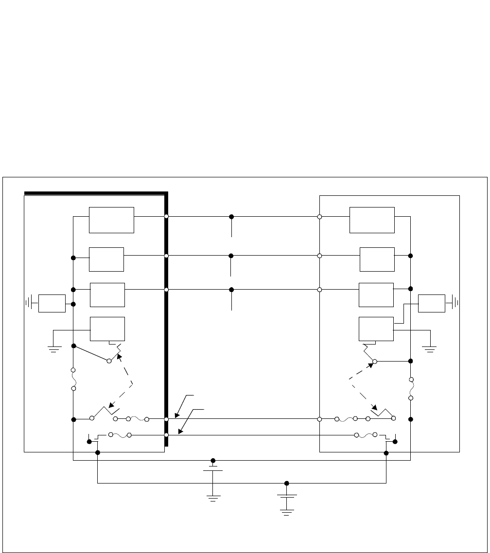
NDA-24296 CHAPTER 2
Page 61
Revision 1.0
PA-PW55-A
Power
PA-PW55-A
Power
1. General Function
The PA-PW55-A (PWR) circuit card supplies operating power to circuit cards located in the PIM. The -48
V input power source, which is converted to +5 V, -5 V, and +12 V, is distributed to each circuit card in the
associated PIM. This card also has a Ringing Generator Unit (RGU), whose output frequency and voltage
can be selected from 20 Hz, 25 Hz, 75 Vrms, 90 Vrms by switch setting on this card. In addition, a Howler
Tone circuit resides on this card.
Figure 2-20 Location of PA-PW55-A (PWR) Card in the System
Note: The +80V input is required for activating Message Waiting Lamps (MWLs) .
HOW (For LC)
CR (For LC)
+5V, +12V, -5V
DC-DC
RGU
HOW
SUB
PWR
REL
NFB
PA-PW55-A (PWR) PA-PW54-A (DPWR)
-48 V (For LC, TRK)
DC-DC
RGU
HOW
SUB
PWR
REL
NFB
-48 V
+80V (Option) Note
+80 V (For MWL)
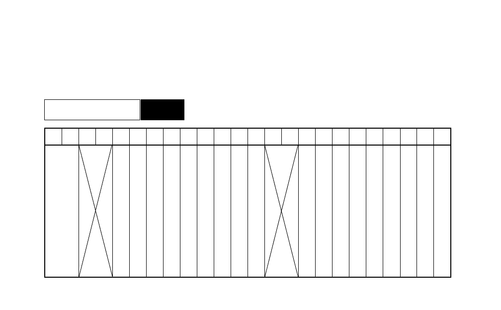
CHAPTER 2 NDA-24296
Page 62
Revision 1.0
PA-PW55-A
Power
2. Mounting Location/Conditions
This circuit card is mounted in the following slots.
00 01 02 03 04 05 06 07 08 09 10 11 12 13 14 15 16 17 18 19 20 21 22 23
PWR
(PA-PW55-A)
PIM
Mounting Module PIM
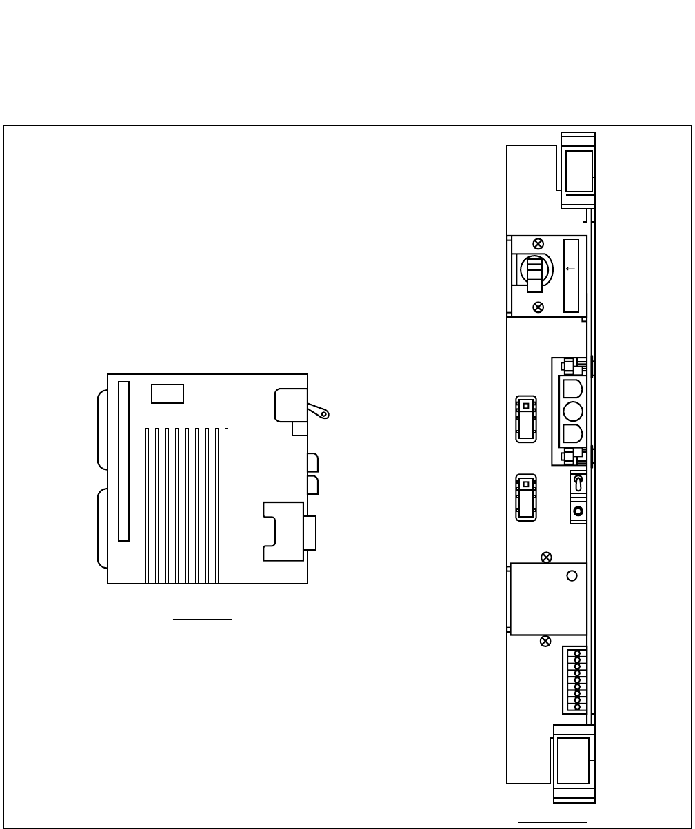
NDA-24296 CHAPTER 2
Page 63
Revision 1.0
PA-PW55-A
Power
3. Face Layout of Lamps, Switches, and Connectors
The face layout of lamps, switches, and connectors on this circuit card is shown below.
Figure 2-21 Face Layout of PA-PW55-A Card
-48V SW
FUSE
FUSE
SIDE VIEW
SW4
FRONT VIEW
PA-
PW55
-A
5.0
A
0.5
A
RGUOUT
0.5A
125V
AC/DC
+80VOUT
5A
125V
AC/DC
-48VOUT
25A
AC250V
DC125V
RST
MB
-48V
DC
INPUT
-48V
SW -48V
IN
CONN
25A
+80V ON
-48V ON
RGU ON
DC ON
OPE
DC ALM
CPU ALM
RGU ALM
HOW ALM
U
P
( )

CHAPTER 2 NDA-24296
Page 64
Revision 1.0
PA-PW55-A
Power
4. Lamp Indications
Lamp indications for this circuit card are shown in the table below.
5. Switch Settings
This circuit card has the following switches.
6. External Interface
No cable connections are required.
LAMP NAME COLOR STATE
+80V ON Green Remains lit while +80 V input power is being supplied.
–48 V ON Green Remains lit while –48 V input power is being supplied.
RGU ON Green Remains lit while RGU output is in progress.
DC ON Green Remains lit while +5 V, +12 V, and –5 V are being output normally.
OPE Green Lights when information exchange with the CPU is possible.
CPUALM Red Lights when reset of the microprocessor has been activated.
DCALM Red Lights when +5 V, +12 V, or –5 V outputs alarm.
RGUALM Red Lights when RGU voltage alarm.
HOWALM Red Lights when howler alarm.
SWITCH
NAME SWITCH
No. SETTING STANDARD
SETTING DESCRIPTION
–48 V SW ON ×–48 V input power is supplied.
OFF –48 V input power is not supplied.
RESET PUSH Hardware reset of the circuit card.
—×Normal setting
MB —ON Make-busy of the circuit card.
OFF ×Normal setting
SW4
1ON Frequency of Ringing Signal :25 [Hz]
OFF ×Frequency of Ringing Signal :20 [Hz]
2ON ×Voltage of Ringing Signal: 90 [Vrms]
OFF Voltage of Ringing Signal: 75 [Vrms]
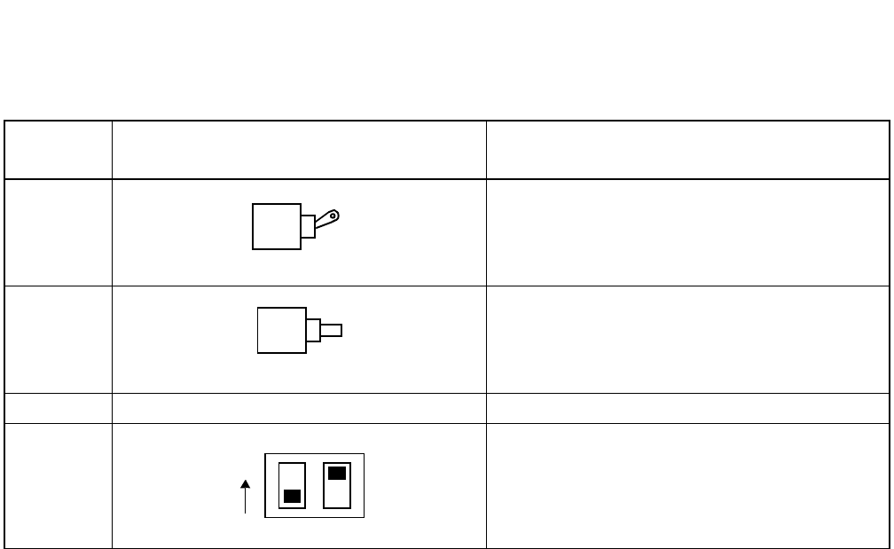
NDA-24296 CHAPTER 2
Page 65
Revision 1.0
PA-PW55-A
Power
7. Switch Setting Sheet
SWITCH
NAME SWITCH SHAPE REMARKS
–48 V
RESET
MB DOWN Circuit card Make-busy cancel.
SW4 20 [Hz]
90 [Vrms]
ON
12

CHAPTER 2 NDA-24296
Page 66
Revision 1.0
PA-PW55-B
Power
PA-PW55-B
Power
1. General Function
The PA-PW55-B (PWR) circuit card supplies operating power to circuit cards accommodated in the PIM.
The -48V input power source, which is converted to +5V, -5V, and +12V, is distributed to each circuit card
in the associated PIM. This card is also equipped with a Ringing Generator Unit (RGU), whose output
frequency and voltage can be selected among 20Hz, 25Hz, 75Vrms, 90Vrms by switch setting on this card.
In addition, a Howler Tone circuit resides on this card.
Figure 2-22 Location of PA-PW55-B (PWR) Card in the System
Note: The +80V input is required for activating Message Waiting Lamps (MWLs) .
HOW (For LC)
CR (For LC)
+5V, +12V, -5V
DC-DC
RGU
HOW
SUB
PWR
REL
NFB
PA-PW55-B (PWR) PA-PW54-B (DPWR)
-48 V (For LC, TRK)
DC-DC
RGU
HOW
SUB
PWR
REL
NFB
-48 V
+80V (Option) Note
+80 V (For MWL)
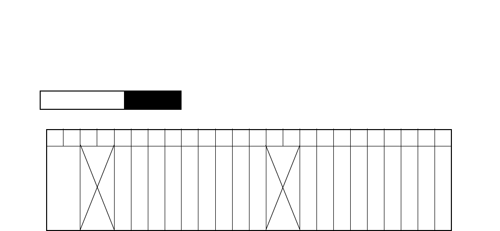
NDA-24296 CHAPTER 2
Page 67
Revision 1.0
PA-PW55-B
Power
2. Mounting Location/Conditions
This circuit card is mounted in the following slots.
PIM
Mounting Module
00 01 02 03 04 05 06 07 08 09 10 11 12 13 14 15 16 17 18 19 20 21 22 23
PWR
(PA-PW55-B)
PIM

CHAPTER 2 NDA-24296
Page 68
Revision 1.0
PA-PW55-B
Power
3. Face Layout of Lamps, Switches, and Connectors
The face layout of lamps, switches, and connectors on this circuit card is shown in Figure 2-23.
Figure 2-23 Face Layout of PA-PW55-B Card
-48V SW
FUSE
FUSE
SIDE VIEW
FRONT VIEW
PA-
PW55
-B
5.0
A
0.5
A
RGUOUT
0.5A
125V
AC/DC
+80VOUT
5A
125V
AC/DC
-48VOUT
25A
AC250V
DC125V
RST
MB
-48V
DC
INPUT
-48V
SW -48V
IN
CONN
20A
+80V ON
-48V ON
RGU ON
DC ON
OPE
DC ALM
CPU ALM
RGU ALM
HOW ALM
U
P
( )
SW4

NDA-24296 CHAPTER 2
Page 69
Revision 1.0
PA-PW55-B
Power
4. Lamp Indications
The contents of lamp indications on this circuit card are shown in the table below.
5. Switch Settings
This circuit card has the following switches.
6. External Interface
No cable connections are required.
LAMP NAME COLOR STATE
+80V ON Green Remains lit while +80 V input power is being supplied.
–48 V ON Green Remains lit while –48 V input power is being supplied.
RGU ON Green Remains lit while RGU output is in progress.
DC ON Green Remains lit while +5 V, +12 V, and –5 V are being output normally.
OPE Green Lights when information exchange with the CPU is possible.
CPUALM Red Lights when reset of the microprocessor has been activated.
DCALM Red Lights in the case of +5 V, +12 V, or –5 V outputs alarm.
RGUALM Red Lights in the case of RGU voltage alarm.
HOWALM Red Lights in the case of howler alarm.
SWITCH
NAME SWITCH
No. SETTING STANDARD
SETTING DESCRIPTION
–48V SW ON ×–48V input power is supplied.
OFF –48V input power is not supplied.
RESET PUSH Hardware reset of the circuit card.
—×Normal setting
MB —ON Make busy of the circuit card.
OFF ×Normal setting
SW4
1ON Frequency of Ringing Signal :25 [Hz]
OFF ×Frequency of Ringing Signal :20 [Hz]
2ON ×Voltage of Ringing Signal: 90 [Vrms]
OFF Voltage of Ringing Signal: 75 [Vrms]
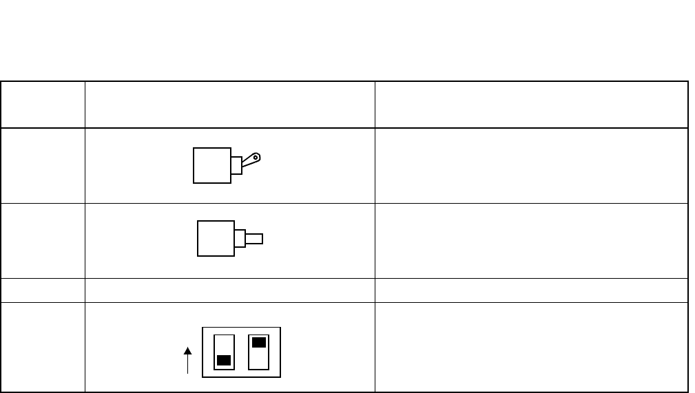
CHAPTER 2 NDA-24296
Page 70
Revision 1.0
PA-PW55-B
Power
7. Switch Setting Sheet
SWITCH
NAME SWITCH SHAPE REMARKS
–48 V
RESET
MB DOWN Circuit card make busy cancel
SW4 20 [Hz]
90 [Vrms]
ON
12

NDA-24296 CHAPTER 2
Page 71
Revision 1.0
PH-DK10
Display Panel Controller
PH-DK10
Display Panel Controller
1. General Function
The main functions of the PH-DK10 card are as follows:
(a) to send out the system operating status, alarm and clock information to the Display Panel.
(b) to collect the MJ/MN/SUP alarm information occurs on CMG and each LMG. In addition, by the
collected internal alarm information, this card controls the Audible and Visual Alarm Indicating
Panel.
(c) to collect the key information on the TOPU of CMG, then output it to EMA.
(d) to send out the Non-Maskable Interruption (NMI) signal from this card on the CMG to each LP.
Additionally, this card activates the communication between the processor in each LP and CMP, SP.
This circuit card is used in the IPX-UMG system.
Refer to the next page for the location of this circuit card within the system.
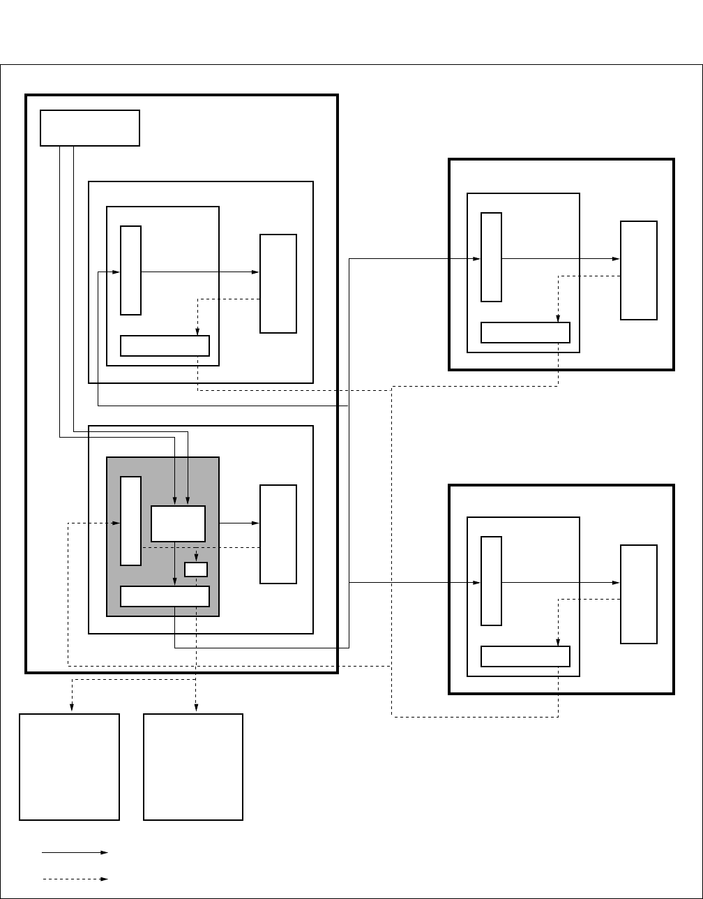
CHAPTER 2 NDA-24296
Page 72
Revision 1.0
PH-DK10
Display Panel Controller
Figure 2-24 Location of PH-DK10 (DSPC)
RELAY
RECEIVER
EMA
PH-PC43
PH-M22
CMP
ISEL
PZ-DK222
(TOP KEY)
RECEIVER
EMA
PH-PC43
PH-DK10
SP
RECEIVER
EMA
PH-PC43
PH-M22
SEL
AUDIBLE
AND
VISUAL
ALARM
INDICATING
PANEL
DISPLAY
PANEL
(DSPP)
RELAY
LMG
CMG
RECEIVER
EMA
PH-PC43
PH-M22
RELAY
LMG
RELAY
KEY INFORMATION
ALM INFORMATION
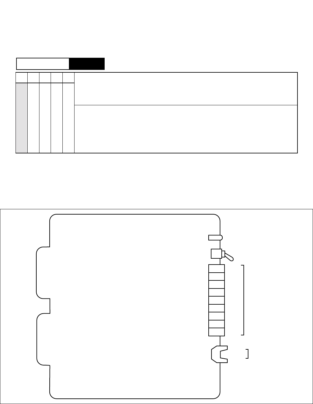
NDA-24296 CHAPTER 2
Page 73
Revision 1.0
PH-DK10
Display Panel Controller
2. Mounting Location/Condition
This circuit card can be mounted in slot No.00 on SP of CMG.
3. Face Layout of Lamps, Switches, and Connectors
The face layout of lamps, switches, and connectors are shown in Figure 2-25.
Figure 2-25 Face Layout of PH-DK10 (DSPC)
SP
Mounting Module
00 01 02 03 04
DSPC
CPRAS-A
CPRAS-A
OPE/MB
MB
To MMC on
LPR (CMP/LP)
To PZ-DK222
on the TOPU
of CMG
CN7
CN8
CN6
CN5
CN4
CN3
CN2
CN1
CN0
KEY

CHAPTER 2 NDA-24296
Page 74
Revision 1.0
PH-DK10
Display Panel Controller
4. Lamp Indications
Lamp indications for this circuit card are shown in the table below.
5. Switch Settings
Switch settings for this circuit card are shown in the table below.
LAMP NAME COLOR STATE
OPE/MB Green Lights when this circuit card is in operation.
Red Lights when this circuit card is in Make Busy state.
SWITCH
NAME SETTING STANDARD
SETTING MEANING
MB UP Circuit Card Make-busy
DOWN ×Circuit Card Make-busy cancel
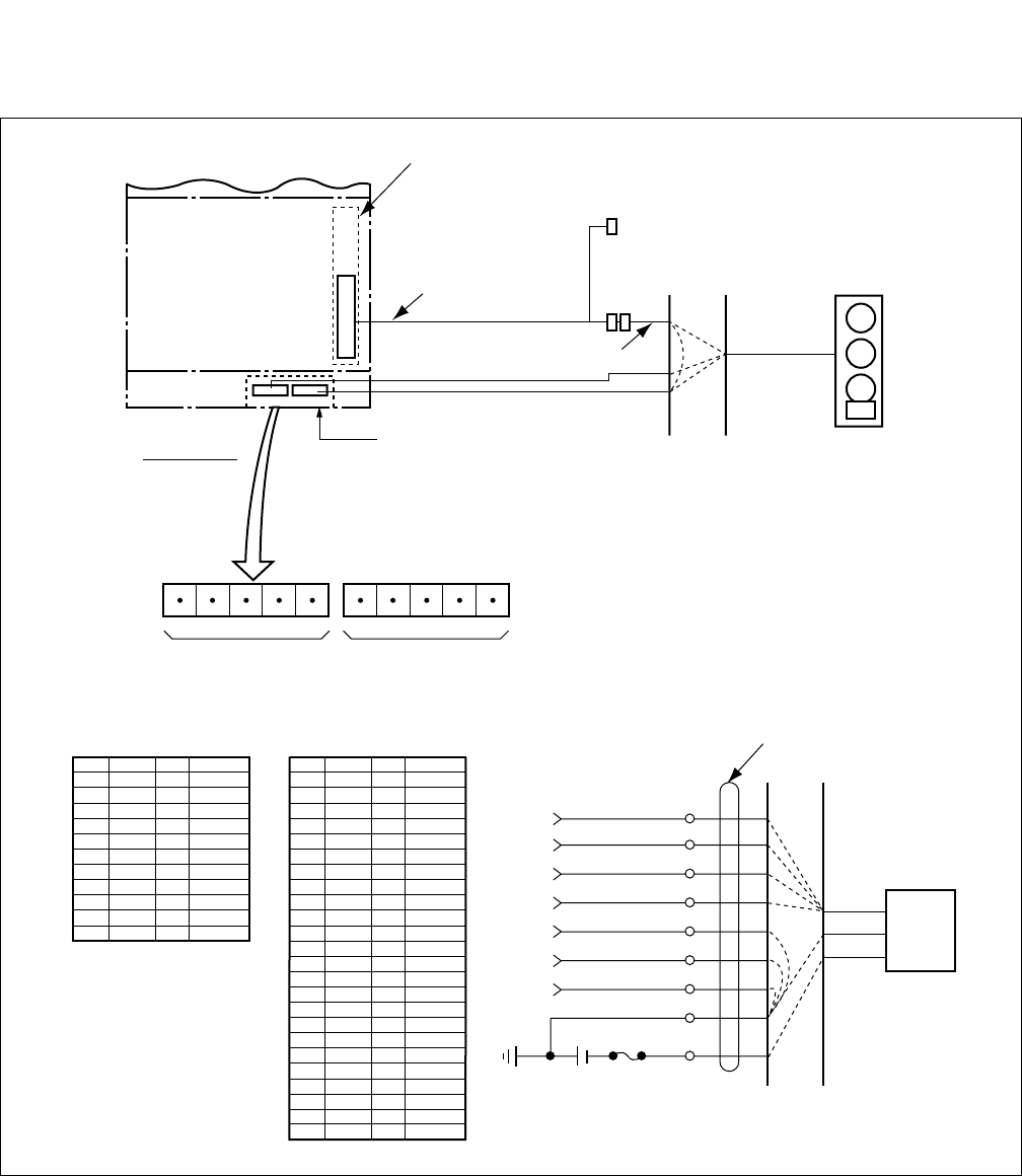
NDA-24296 CHAPTER 2
Page 75
Revision 1.0
PH-DK10
Display Panel Controller
6. External Interface
Figure 2-26 Connection of Alarm Indicating Panel
01 02 03 04 0501 02 03 04 05
6-BELL
8-MNA
9-SUPA
10-MJA
33-MNB
34-SUPB
35-MJB
RPT1(G)
RPT0(-48V)
MDF
MJ/MN/BELL
-48V
(RPT0)
G
(RPT1)
AUDIBLE AND VISUAL
ALARM INDICATING PANEL
MDF MJ
MN
BELL
(BASEU)
SP
MISC0A
Connector
RPT Terminal on front
of the BASEU
REAR VIEW
DSPC (PH-DK10) : Slot No.00
68PH DSPALM CA
Installation Cable
Connected
to DSPP
68PH DSPALM CA and
Installation Cable
68PH Connector Champ Connector
1
2
3
4
5
6
7
8
9
10
MPALM
SUPA1
EXTA
MNA1
BELL0
MJA1
SUPB1
MNB1
BELL1
MJB1
SUPA0
MJA0
MNA0 MNB0
SUPB0
MJB0
11
12
26
27
28
29
30
31
32
33
34
35
36
37
26
27
28
29
30
31
32
33
34
35
MPALM
SUPB
MJB
MNB MNA
BELL
SUPA
MJA
36
37
1
2
3
4
5
6
7
8
9
10
11
12
38
39
40
41
42
43
44
45
46
47
48
13
14
15
16
17
18
19
20
21
22
23
24
25
49
50
68PH DSPALM CA

CHAPTER 2 NDA-24296
Page 76
Revision 1.0
PH-DK10
Display Panel Controller
7. Switch Setting Sheet
SWITCH NAME SWITCH SHAPE REMARKS
MB
ON
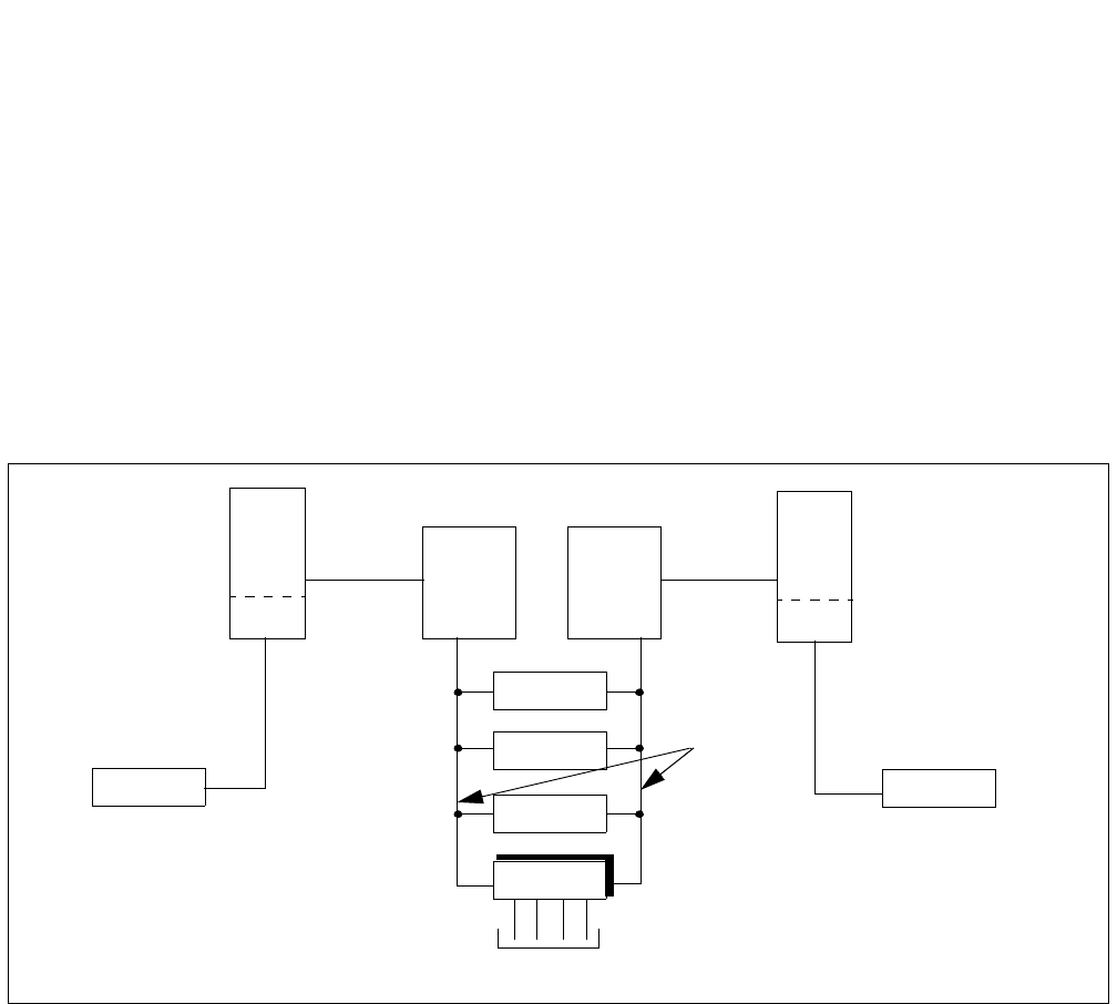
NDA-24296 CHAPTER 2
Page 77
Revision 1.0
PH-IO24
Input/Output Controller
PH-IO24
Input/Output Controller
1. General Function
The PH-IO24 (IOC) circuit card supplies the system with a serial interface, which conforms to RS-232C,
between external equipment such as the Maintenance Administration Terminal (MAT), Station Message
Detail Recording System (SMDR), Message Center Interface (MCI), Property Management System
(PMS). The relationship between the IOC card and the associated cards is as follows, when the CPU is in
dual configuration.
Note: Firmware SP-3290 IO24 LV2 PROG-A is required in the Hotel system for PMS and Hotel Printer.
Figure 2-27 Location of PH-IO24 (IOC) Card in the System
CPU
BOARD
#0
FDD/HDD #0
GT #1 GT #0
MISC
EMA
MISC/IOC
IOC
CPU
I/O
BOARD
#1
MISC I/O BUS
FDD/HDD #1
I/O
(RS-232C) x4 posts for MAT, SMDR, MCI, PMS, PRT
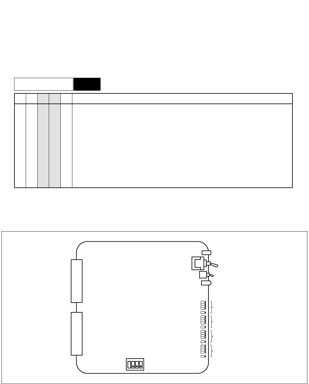
CHAPTER 2 NDA-24296
Page 78
Revision 1.0
PH-IO24
Input/Output Controller
2. Mounting Location/Condition
The IOC cards can be placed in the shaded slots (02, 03) as shown below.
Note: Firmware SP-3290 IO24 LV2 PROG-A is required in the Hotel system for PMS and Hotel Printer.
3. Face Layout of Lamps, Switches and Connectors
The face layout of lamps, switches and connectors on this circuit card is shown in Figure 2-28.
Figure 2-28 Face Layout of PH-IO24 (IOC) Card
00 01 02 03 04
Mounting Module LPM
IOC#1
IOC#0
OPE
IOC ALM
MB
PORT0
SW50
MBR
PORT1
PORT2
PORT3
NDA-24296 CHAPTER 2
Page 79
Revision 1.0
PH-IO24
Input/Output Controller
4. Lamp Indications
The table below shows lamp indications on this circuit card.
5. Switch Settings
The following is a brief description of the switches on this circuit card. When a switch has a standard
setting, it is indicated with “×” in the table below.
LAMP NAME COLOR DESCRIPTION
OPE/MB Green This circuit card is operating normally.
Red This circuit card is placed in the Make-busy state.
IOC ALM Red Clock down WDT alarm occurs to the microprocessor.
PORT0 - PORT3 RS-232C signal status indication. n = port number (0-3)
SDn Green SD: Send Data
RDn Green RD: Receive Data
ERn Green ER: Equipment Ready
DRn Green DR: Data Ready
CDn Green CD: Carrier Detect
SWITCH
NAME SWITCH
NO. SETTING STANDARD
SETTING DESCRIPTION
MB Up The circuit card is placed into Make-busy status.
Down ×Cancellation of Make-busy.
MBR Up The circuit card is placed into Make-busy request status.
Down ×Cancellation of Make-busy Request.
SW50
1ON This circuit card is used as the extended I/O circuit card #1.
OFF This circuit card is used as the extended I/O circuit card #0.
2ON Not used (For Business System Only).
OFF ×
2ON Free Wheeling with ACK signal (For Hotel System Only).
OFF ×Free Wheeling.
3ON Not used.
OFF ×
4ON Not used.
OFF ×
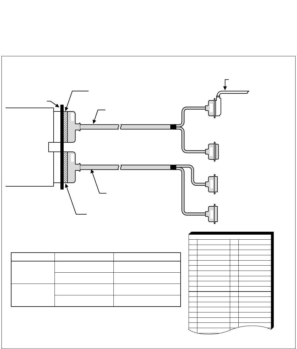
CHAPTER 2 NDA-24296
Page 80
Revision 1.0
PH-IO24
Input/Output Controller
6. External Interface
As illustrated in Figure 2-29, the 68PH S 2PORTS CA-A cable is required to connect external equipment
such as the MAT, SMDR, MCI, and PRT.
Figure 2-29 External Cable Connection for PH-IO24 (IOC)
Securely insert the connector of the 68PH S 2PORTS CA-A into the appropriate MISC connector. Refer to the table listed below.
The relationship between the MISC connectors and the mounting
slot of the IOC (PH-IO24) circuit card is shown below.
The type of cables varies depending on a connected terminal and/or
whether modems are used or not. More detailed information on the
connecting cables is explained in the “Installation Procedure
Manual”.
MISC 3B/2B (Note 1)
68PH S 2PORTS CA-A
Backplane
PH-IO24
(IOC)
Circuit #0
Circuit #1
Circuit #2
Circuit #3
RS-232C cable (Note 2)
68PH S 2PORTS CA-A
MISC 3A/2A (Note 1)
17
16
15
14
13
12
11
ST2
10
ST1
09
RT
08
PB/CI
07
ER
06
CD
05
SG
04 CS
03 RS
02 RD
01 SD
Pin Signal name
42
41
40
39
38
37
36
35
34
33
32
31
30
29
28
27
26
Pin Signal name
TYP0, 1 Connector
AMP AMP
TYP0 TYP1 TYP1TYP0
To RS-232C
Terminal
DR
TYP0, 1 Lead Accommodation
Note 1:
Note 2:
Mounting Slot
02
03
IOC Circuit Number
#0, #1
#2, #3
#0, #1
#2, #3
MISC 2B
MISC 2A
MISC 3B
MISC 3A
MISC Connector
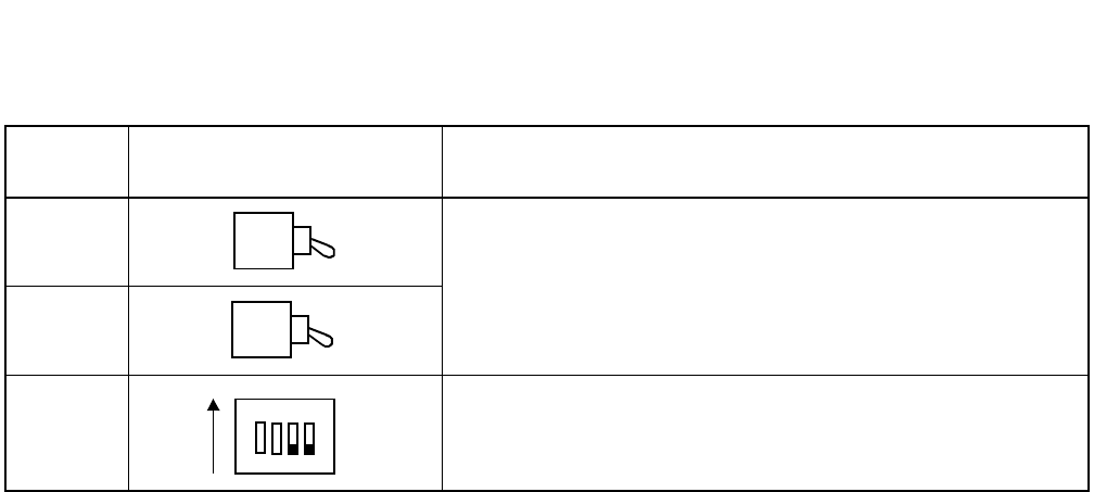
NDA-24296 CHAPTER 2
Page 81
Revision 1.0
PH-IO24
Input/Output Controller
7. Switch Setting Sheet
SWITCH
NAME SWITCH SHAPE REMARKS
MB
MBR
SW50
Meaning of SW50-1:
ON: This card is used as the No. 1 circuit card.
OFF: This card is used as the No. 0 circuit card.
1
ON
2 3 4
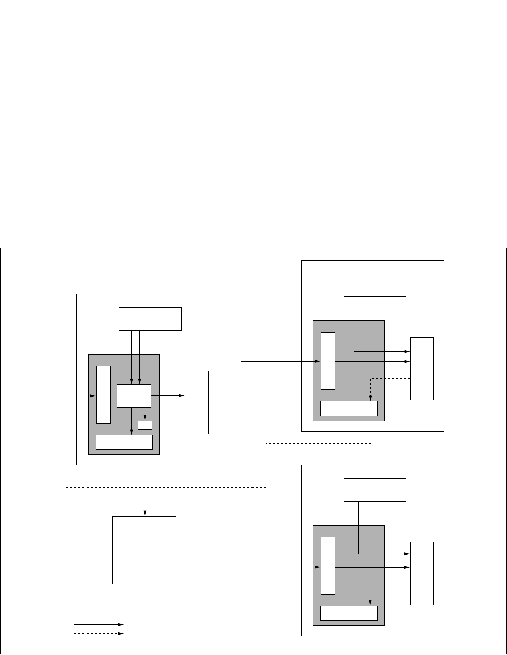
CHAPTER 2 NDA-24296
Page 82
Revision 1.0
PH-M22
MMC
PH-M22
MMC
1. General Function
The main functions of the PH-M22 circuit card are as follows:
•to collect key setting information on the TOPU of the ISW and send the information to the ISW/the
other LNs, depending on the ISEL key setting on the ISW. (for IPX-U system)
•to collect various alarm information from all the IMGs/ISW and activate MJ/MN LED on the TOPU
display. (for IPX-U system)
•to send out the key information to EMA within the same LMG (for IPX-UMG system)
•to collect the external MJ/MN alarm information output by EMA in each LMG (for IPX-UMG system)
This circuit card is used for the IPX-U/IPX-UMG system.
Figure 2-30 Location of PH-M22 (MMC) in IPX-U System
PZ-DK222
(TOP KEY)
PH-PC40
PH-M22
EMA
RELAY
RECEIVER
PZ-DK222
(TOP KEY)
PH-PC40
PH-M22
EMA
RELAY
RECEIVER
PZ-DK227
(TOP KEY)
PH-PC40
PH-M22
EMA
RELAY
RECEIVER
ISEL
ISW
LN
LN
AUDIBLE
AND
VISUAL
ALARM
INDICATING
PANEL
KEY INFORMATION
ALM INFORMATION
SEL
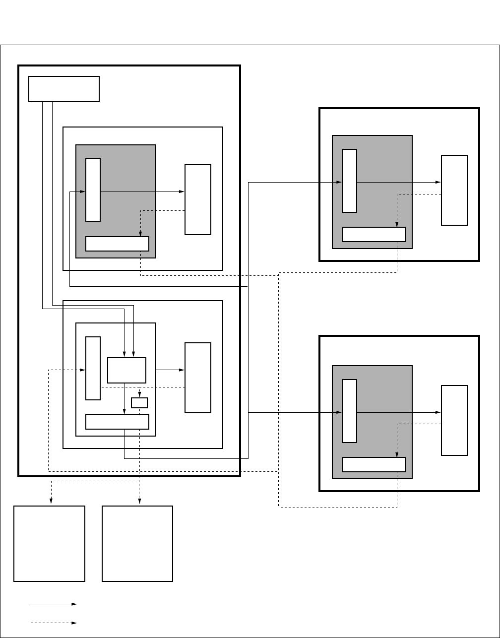
NDA-24296 CHAPTER 2
Page 83
Revision 1.0
PH-M22
MMC
Figure 2-31 Location of PH-M22 (MMC) in IPX-UMG System
RELAY
RECEIVER
EMA
PH-PC43
PH-M22
CMP
ISEL
PZ-DK222
(TOP KEY)
RECEIVER
EMA
PH-PC43
PH-DK10
SP
RECEIVER
EMA
PH-PC43
PH-M22
SEL
AUDIBLE
AND
VISUAL
ALARM
INDICATING
PANEL
DISPLAY
PANEL
(DSPP)
RELAY
LMG
CMG
RECEIVER
EMA
PH-PC43
PH-M22
RELAY
LMG
RELAY
KEY INFORMATION
ALM INFORMATION
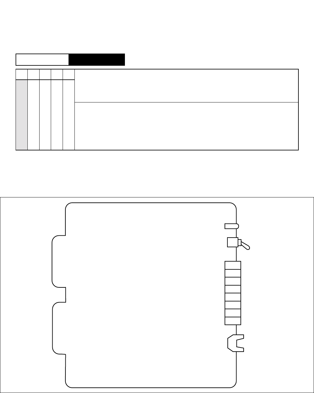
CHAPTER 2 NDA-24296
Page 84
Revision 1.0
PH-M22
MMC
2. Mounting Location/Condition
This circuit card can be mounted in the shaded slots shown below.
3. Face Layout of Lamps, Switches, and Connectors
The face layout of lamps, switches, and connectors are shown in Figure 2-32.
Figure 2-32 Face Layout of PH-M22 (MMC)
00 01 02 03 04
LPM/CMP/LP
Mounting Module
MMC
CPRAQ-A/CPRAS-A
CPRAQ-A/CPRAS-A
OPE
MB
CN7
CN6
CN5
CN4
CN3
CN2
CN1
CN0
KEY

NDA-24296 CHAPTER 2
Page 85
Revision 1.0
PH-M22
MMC
4. Lamp Indications
Lamp indications for this circuit card are shown in the table below.
5. Switch Settings
Switch settings for this circuit card are shown in the table below.
LAMP NAME COLOR STATE
OPE Green Lights when this circuit card is in operation.
SWITCH
NAME SETTING STANDARD
SETTING MEANING
MB UP Circuit Card Make-busy
DOWN ×Circuit Card Make-busy cancel
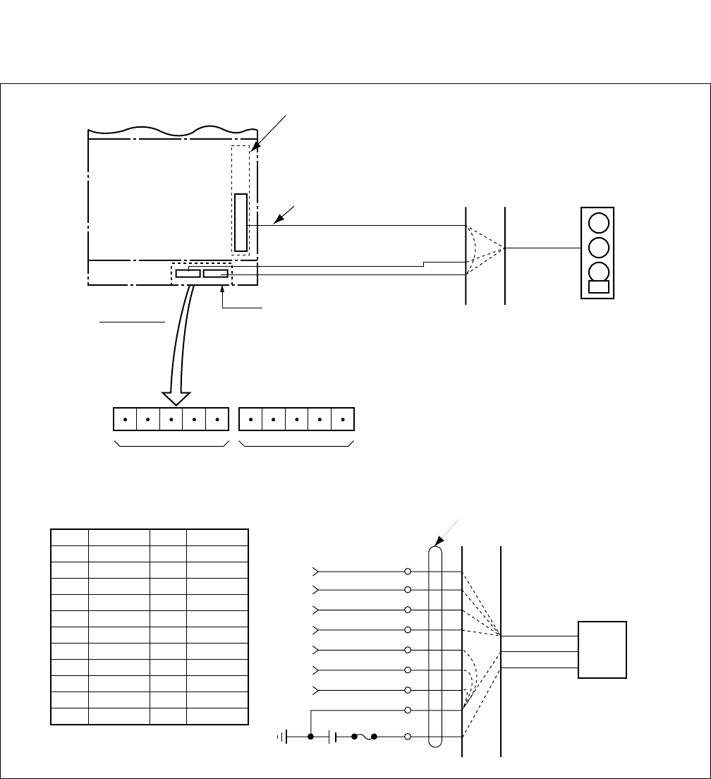
CHAPTER 2 NDA-24296
Page 86
Revision 1.0
PH-M22
MMC
6. External Interface
Figure 2-33 Connection of Alarm Indicating Panel
Note: External connection for Alarm Indicator is not used in IPX-UMG system.
01 02 03 04 0501 02 03 04 05
1
2
3
4
5
6
7
8
9
10
11
12
MPALM
EXTAA
BELAA
-
MNAA
SUPAA
MJAA
26
27
28
29
30
31
32
33
34
35
36
37
MNBA
SUPBA
MJBA
BELAA
MNAA
SUPAA
MJAA
MNBA
SUPBA
MJBA
RPT1(G)
RPT0(-48V)
MDF
MJ/MN/BELL
-48V
(RPT0)
G
(RPT1)
AUDIBLE AND VISUAL
ALARM INDICATING PANEL
MDF MJ
MN
BELL
(BASEU)
LPM
MISC0A
Connector
RPT Terminal on front
of the BASEU
REAR VIEW
MMC (PH-M22) : Slot No.00
68PH EXMISC CA
68PH EXMISC CA and
Installation Cable
68PH EXMISC CA

NDA-24296 CHAPTER 2
Page 87
Revision 1.0
PH-M22
MMC
7. Switch Setting Sheet
SWITCH NAME SWITCH SHAPE REMARKS
MB Note: Normal operating mode is down.
ON
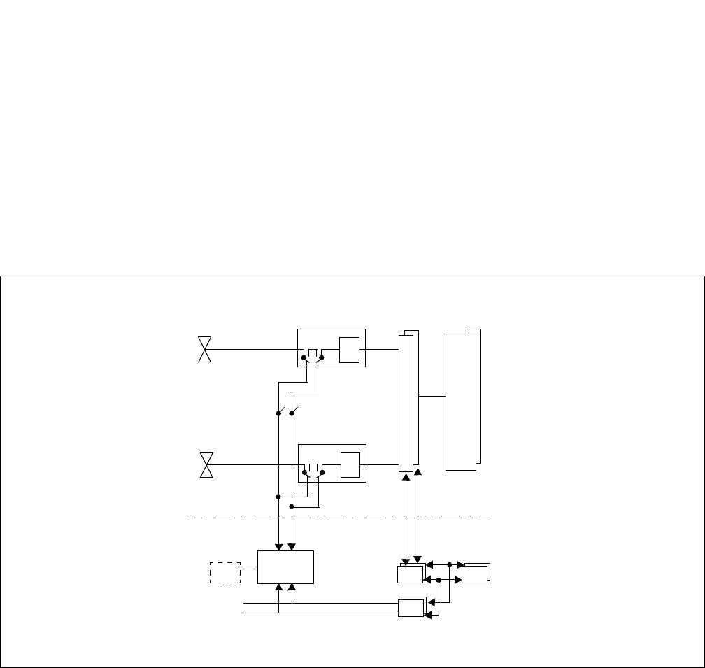
CHAPTER 2 NDA-24296
Page 88
Revision 1.0
PH-M16
Line Test
PH-M16
Line Test
1. General Function
This circuit card controlled by CPU is used for line test of a subscriber’s line. The circuit card supports
sending Howler Tone to external test equipment, besides the circuit card can detect or send various tones,
and send PB (DTMF) signal for automatic trunk test.
Note: A system cannot send Howler Tone during line test. The number of available lines within the line test/
automatic trunk test at the same time is only one.
Figure 2-34 Location of PH-M16 (LTST) Card Within the System
LC
LC
I
N
T
TSW
TEL
TEL
PIM
LPRA
LTST
TEST
EQ GT
EXGT
CPU
EXTENDED I/O BUS
EXTENDED I/O BUS
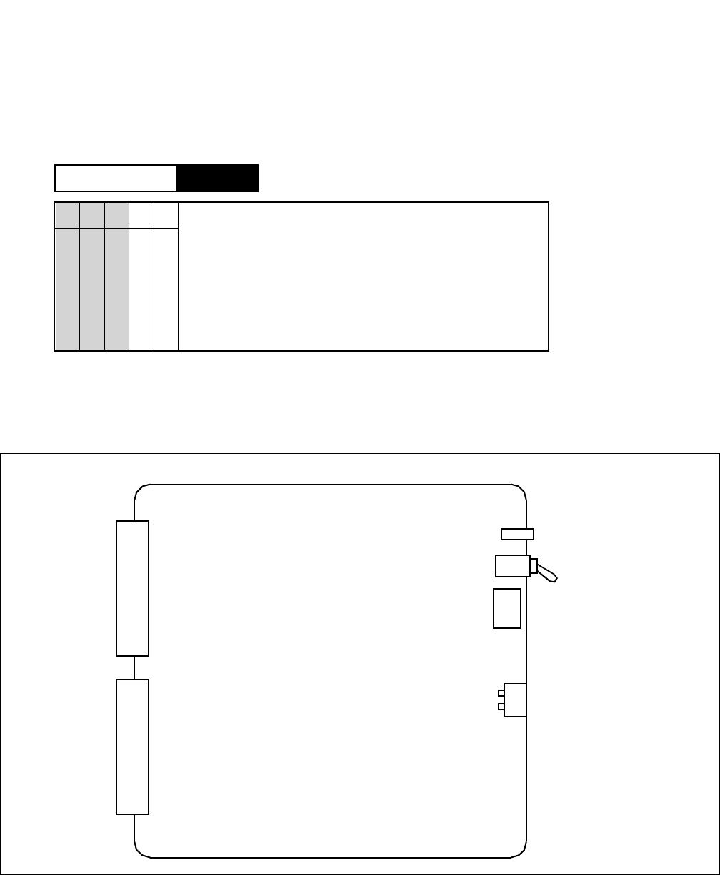
NDA-24296 CHAPTER 2
Page 89
Revision 1.0
PH-M16
Line Test
2. Mounting Location/Condition
The LTST circuit card can be accommodated in the shaded slots (00, 01, 02) as shown below:
Note: IPX: Slot 00, Slot 01, Slot 02.
IPX-U: Slot 01, Slot 02 (Considering PH-M22 MMC)
3. Face Layout of Lamps, Switches, and Connectors
The face layout of lamps, switches, and connectors on this circuit card is shown in Figure 2-35.
Figure 2-35 Face Layout of PH-M16 (LTST) Card
Note: CRIN is used to connect with CRIN test equipment.
LPM
Mounting Module
00 01 02 03 04
PH-M16
PH-M16
PH-M16
MB
OPE/MB
SW0
CRIN
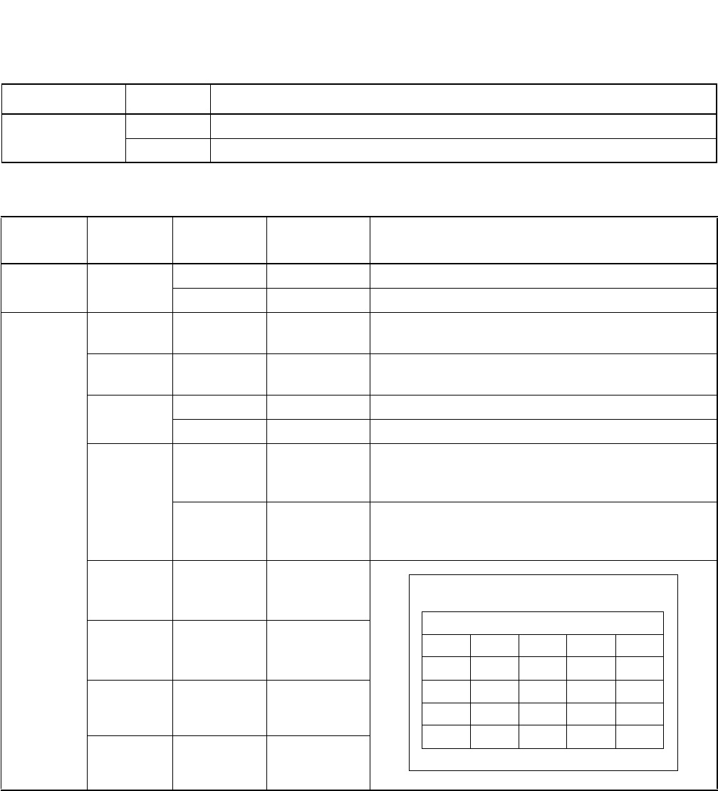
CHAPTER 2 NDA-24296
Page 90
Revision 1.0
PH-M16
Line Test
4. Lamp Indications
5. Switch Settings
LAMP NAME COLOR DESCRIPTION
OPE/MB Green This circuit card is operating in normal mode.
Red This circuit card is Make-busy.
SWITCH
NAME SWITCH
NO SETTING STANDARD
SETTING MEANING
MB UP Circuit card Make-busy
DOWN Circuit card Make-busy cancel
SW0
1ON ×Setting of a condition of DT detection
(440Hz+350Hz)
2ON ×Setting of a condition of RBT detection
(440Hz+480Hz)
3ON Time of PB (DTMF) signal sending (67 msec.)
OFF ×Time of PB (DTMF) signal sending (133 msec.)
4
ON
Setting of M-wire control which is concerned with
sending test tone of ODT
(Set soft control or E-wire loop-back)
OFF
Setting of M-wire control which is concerned with
sending test tone of ODT
(Set soft control only)
5
6
7
8
BASIC INTERVAL TIMER
SW0
5678TIME
ON OFF OFF OFF 8µ
ON ON OFF OFF 16µ
ON ON ON OFF 32µ
ON ON ON ON 64µ
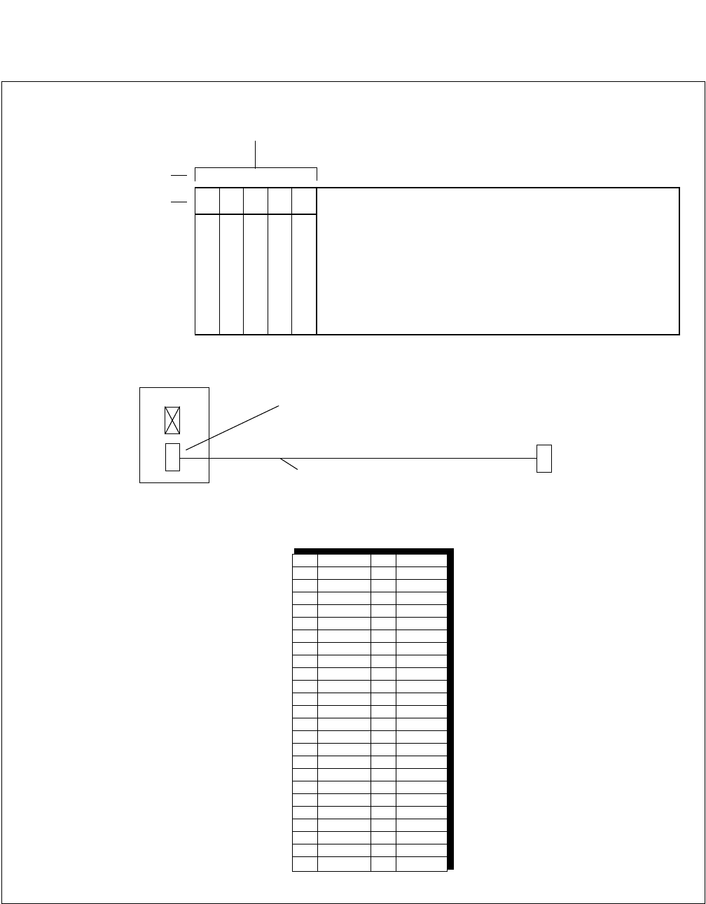
NDA-24296 CHAPTER 2
Page 91
Revision 1.0
PH-M16
Line Test
6. External Interface
Figure 2-36 LT Connector Lead Accommodation
00 01 02 03 04
PH-M16
PH-M16
PH-M16
Circuit Card Backboard Connector
Connector Name
Slot Number
LPM
LPM Backboard
MISC Circuit Card Backboard Connector
MISC CONNECTOR
68PH EXMISC CABLE
MISC Connector Accommodation
26
27
28
29
30
31
32
33
34
35
36
37
38
39
40
41
42
43
44
45
46
47
48
49
50
1
2
3
4
5
6
7
8
9
10
11
12
13
14
15
16
17
18
19
20
21
22
23
24
25
TE
TELB
LCB
THOWB
THOWS
INB
TM
TELA
LCA
THOWA
ONHK
INA
SE TCR
ATM
ATAATB OUTAOUTB TA1TB1
MISC CONNECTOR
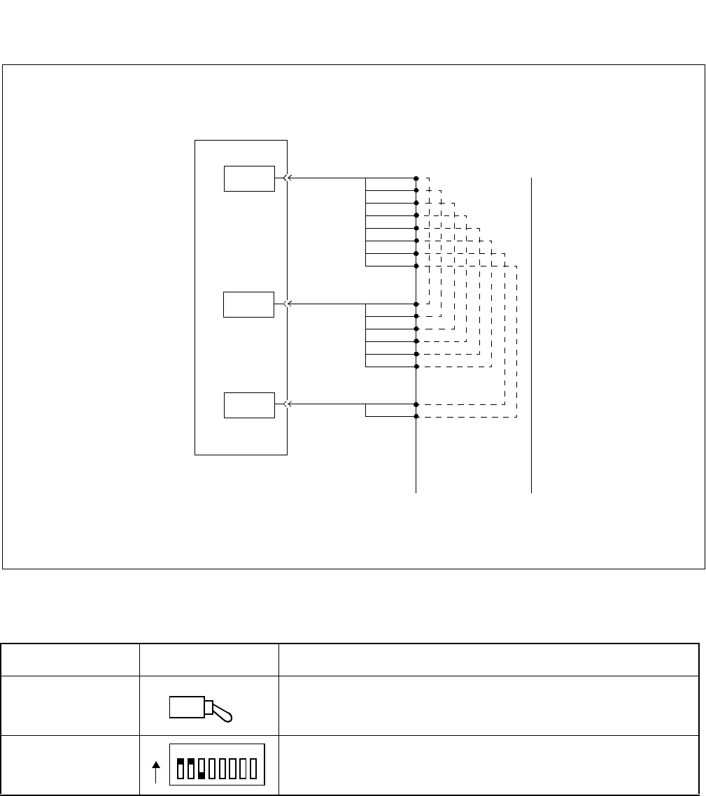
CHAPTER 2 NDA-24296
Page 92
Revision 1.0
PH-M16
Line Test
Figure 2-36 Connecting Route Diagram
7. Switch Setting Sheet
SWITCH NAME SWITCH SHAPE REMARKS
MB
SW0
OUTA
OUTA
TE
INA
INB
TA1
TB1
TM
RA
RB
M
TA
TB
E
B
A
LTST
TLT
LC
PBX MDP
ON (MB)
OFF
1
ON 2 3 45678
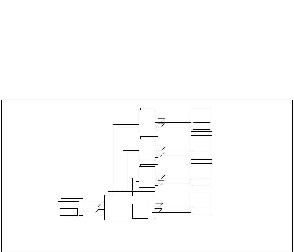
NDA-24296 CHAPTER 2
Page 93
Revision 1.0
PH-PC36
Multiplexer
PH-PC36
Multiplexer
1. General Function
The PH-PC36 (MUX) circuit card is an interface card for mounting line circuits and/or trunks. In between
the CPR and the Port Microprocessor (PM) of the line/trunk circuit, this circuit card provides an interface
for PM control and management by the CPU. Likewise in between the TSW and the line circuit/trunks, this
circuit card provides an interface for multiplexing/de-multiplexing of voice Pulse Code Modulation (PCM)
information and digital data information.
Figure 2-37 Location of PH-PC36 (MUX) Card in the 1 IMG System
MUX
MUX
MUX
CPR
GT
LC/TRK
PM
LC/TRK
PM
LC/TRK
PM
LC/TRK
PM
MUX
TSW/INT/PLO
PCM HW
PM BUS
PM BUS
PM BUS
PM BUS
PCM HW
PCM HW
PCM HW
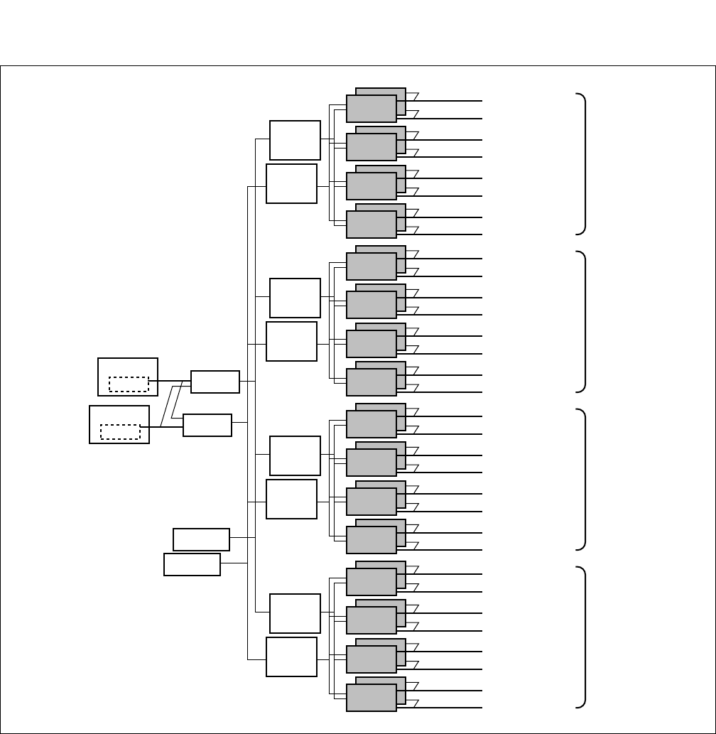
CHAPTER 2 NDA-24296
Page 94
Revision 1.0
PH-PC36
Multiplexer
Figure 2-38 Location of PH-PC36 (MUX) Card in the 4 IMG System
TDSW
13
TDSW
03
MUX
MUX
MUX
MUX
PCM HW
PM BUS
PCM HW
PM BUS
PCM HW
PM BUS
PCM HW
PM BUS
Line/Trunk PM
Line/Trunk PM
Line/Trunk PM
Line/Trunk PM
IMG 3
TDSW
12
TDSW
02
MUX
MUX
MUX
MUX
PCM HW
PM BUS
PCM HW
PM BUS
PCM HW
PM BUS
PCM HW
PM BUS
Line/Trunk PM
Line/Trunk PM
Line/Trunk PM
Line/Trunk PM
IMG 2
TDSW
11
TDSW
01
MUX
MUX
MUX
MUX
PCM HW
PM BUS
PCM HW
PM BUS
PCM HW
PM BUS
PCM HW
PM BUS
Line/Trunk PM
Line/Trunk PM
Line/Trunk PM
Line/Trunk PM
IMG 1
TDSW
10
TDSW
00
MUX
MUX
MUX
MUX
PCM HW
PM BUS
PCM HW
PM BUS
PCM HW
PM BUS
PCM HW
PM BUS
Line/Trunk PM
Line/Trunk PM
Line/Trunk PM
Line/Trunk PM
IMG 0
GT 1
GT 0
CPR 1
ISAGT
CPR 0
ISAGT
DLKC 1
DLKC 0
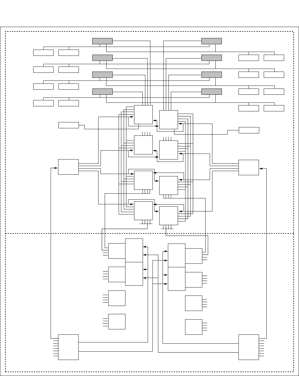
NDA-24296 CHAPTER 2
Page 95
Revision 1.0
PH-PC36
Multiplexer
Figure 2-39 Location of PH-PC36 (MUX) Card in the IPX-U/IPX-UMG System
MUX00
LC/TRK
LC/TRK
LC/TRK
LC/TRK
DLKC0
LC/TRK
LC/TRK
LC/TRK
LC/TRK
LC/TRK
LC/TRK
LC/TRK
LC/TRK
LC/TRK
LC/TRK
LC/TRK
LC/TRK
MUX01
MUX02
MUX03
MUX10
MUX11
MUX12
MUX13
TSW00 TSW10
TSW01 TSW11
TSW02 TSW12
TSW03 TSW13
PLO 0
PLO 0
DLKC1
PLO 1
PLO 1
MUX MUX
TSW00
TSW01
TSW02
TSW03
HSW00
HSW01
HSW10
HSW11
TSW10
TSW11
TSW12
TSW13
LN/LMG
ISWM
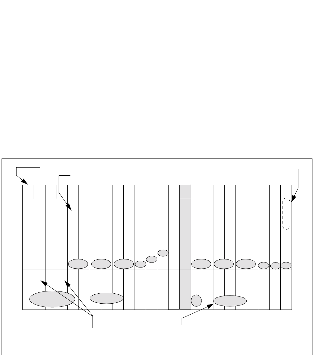
CHAPTER 2 NDA-24296
Page 96
Revision 1.0
PH-PC36
Multiplexer
The PCM highway running is illustrated in Figure 2-40. There are sixteen 2 Mbps PCM highways (HW0 -
HW15) in the PIM. Each PCM highway runs from a card slot to the MUX circuit card. For instance,
highway number zero (HW0) appears in Slot 04 and also Slot 05, thus the HW0 carries the PCM of the
Group number 0, 1, 2 and 3.
Likewise, the HW6, 7, 14, 15 cover the group numbers 24 through 31. However, the time slots of Group
number 24 and 25 are exclusively used for the Speech Path Memory (SPM).
All highways in the PIM lead to a MUX card, so 512 time slots (32 time slots per highway × 16 highways
= 512 time slots) of PCM are multiplexed/de-multiplexed at a MUX and sent/received to/from the TSW
circuit card across the 32.786 Mbps of the Low Voltage Differential Signaling (LVDS).
Also the MUX card provides the PM bus interface. The CPR controls and administrates the PM of the line/
trunk circuit card via the TSW and the MUX.
In addition, this circuit card supports 3-Party Conference (CFT) function and is equipped with eight circuits
of 3-Party Conference. The CFT appear in Time Slots 8 through 31 of the HW13 (Group 21 - 23).
Figure 2-40 PCM Highway Running
MUX#1
MUX#0
HW6
00 01 02 03 04 05 06 07 08 09 10 11 12 13 14 15 16 17 18 19 20 21 22 23
PWR
PWR
01
23
45
67
89
1011
12131415
16171819
20212223
01
2
3
4
5
67
89
10
11
12
13
1415
1617
18
19
20
21
22
23
(24)
(25)
2627
2829
31 30
2627
2829
3031
HW0 HW1 HW2
HW3 HW4
HW5
HW8 HW9 HW10
HW12
HW7
HW14
HW15
Slot number of the PIM U-A
Group (G) number of the LENS
8 circuits of CFTs
Group 24 and 25 are used
for the SPM 2 Mbps (32 time slots) of PCM highway
HW13HW11
NDA-24296 CHAPTER 2
Page 97
Revision 1.0
PH-PC36
Multiplexer
2. Mounting Location/Condition
For the 1 IMG system, the PH-PC36 (MUX) card is mounted in the PIM 1, 2, and 3.
For the 4 IMG system, the PH-PC36 (MUX) card is required in all PIMs.
3. Face Layout of Lamps, Switches, and Connectors
The face layout of lamps, switches, and connectors is shown in Figure 2-41.
Figure 2-41 Face Layout of PH-PC36 (MUX)
00 01 02 03 04 05 06 07 08 09 10 11 12 13 14 15 16 17 18 19 20 21 22 23
PIM
Mounting Module PIM
MUX #0
MUX #1
4
3
2
1
SW01
OFFON
MUXACT
MB
SYNC
RCLK ALM
PMCLK ALM
CFT OPE
MUX

CHAPTER 2 NDA-24296
Page 98
Revision 1.0
PH-PC36
Multiplexer
4. Lamp Indications
The contents of lamp indications of this circuit card are shown in the table below.
5. Switch Settings
Standard settings of switches on this circuit card are shown in the table below.
LAMP NAME COLOR STATE
MUX ACT Green Remains lit while this circuit card is in ACT state.
SYNC Green Lights when 32 Mbps Frame Head (FH) synchronization is established between the
MUX and TSW.
RCLK ALM Red Lights when the 32 Mbps clock signals (which is supplied by TSW) loss has occurred.
PMCLK ALM Red
Lights when either the following clock signals output failure has occurred.
•2 Mbps clock signals (which supplies to the line/trunks)
•Frame Head signal
•4 Mbps clock signals
CFT OPE Green Lights when the CFT circuit is valid.
SWITCH
NAME SWITCH
NO SETTING STANDARD
SETTING MEANING
MB UP Circuit card Make-busy.
DOWN ×Circuit card Make-busy cancel.
SW01
1ON 3-Party Conference Function (CFT) is valid.
OFF 3-Party Conference Function (CFT) is invalid.
2ON Setting of A-Law in the CFT function block.
OFF ×Setting µ-Law in the CFT function block.
3OFF ×Not used.
4OFF ×Not used.
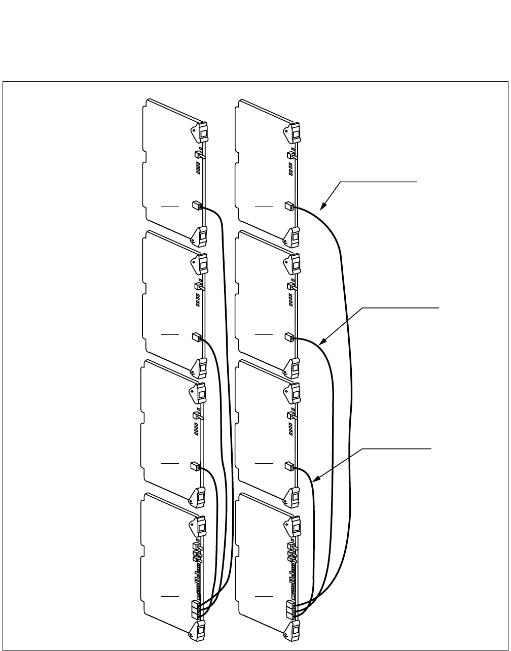
NDA-24296 CHAPTER 2
Page 99
Revision 1.0
PH-PC36
Multiplexer
6. External Interface
For the 1 IMG system, the cable connections between the MUX and the TSW are illustrated in Figure 2-42.
Figure 2-42 External Interface for PH-PC36
TSW
#0
MUX
#0
MUX
#0 MUX
#1
MUX
#1
MUX
#1
MUX
#0
TSW
#1
MT24 TSW CA-180
MT24 TSW CA-140
MT24 TSW CA-90
PIM 3
PIM 2
PIM 1
PIM 0
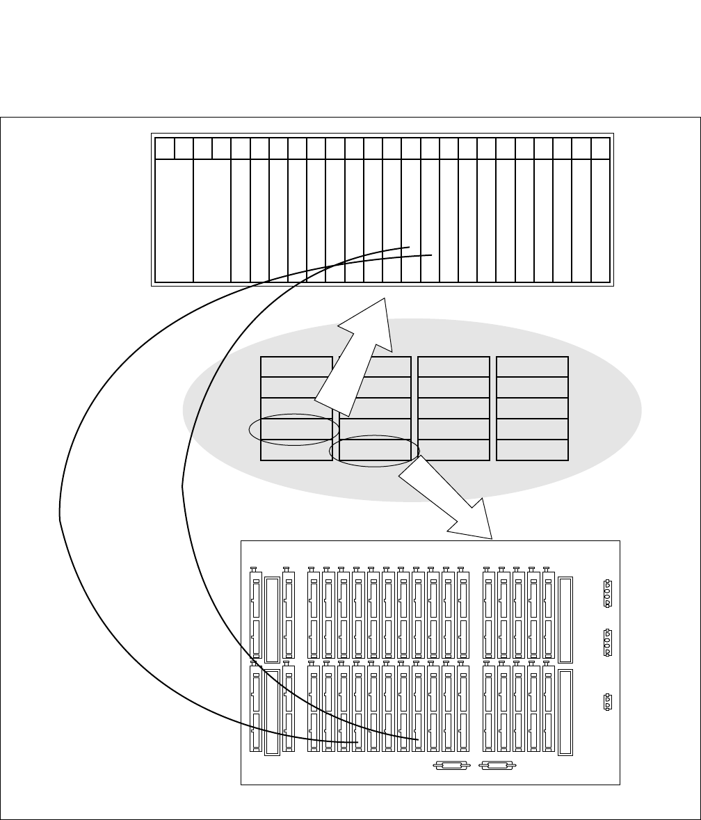
CHAPTER 2 NDA-24296
Page 100
Revision 1.0
PH-PC36
Multiplexer
The cable connections between the MUX and the TSW are illustrated in Figure 2-43. As seen in this illustration,
the cable connected to the front of the MUX leads to the “MUX###” connector on the Back Wired Board (BWB)
of the TSWM. See the NEAX2400 IPX Installation Manual for more details.
Figure 2-43 Cable Connections between the MUX and the TSW
00 01 02 03 04 05 06 07 08 09 10 11 12 13 14 15 16 17 18 19 20 21 22 23
PH-PC36(MUX)
PH-PC36(MUX)
PIM 3
PIM 2
PIM 1
PIM 0
Dummy
IMG3
PIM 3
PIM 2
PIM 1
PIM 0
Dummy/APM
IMG2
PIM 3
PIM 2
PIM 1
PIM 0
TSWM
IMG1
PIM 3
PIM 2
PIM 1
PIM 0
LPM
IMG0
PIM
BWB of TSWM
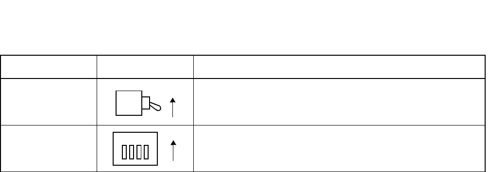
NDA-24296 CHAPTER 2
Page 101
Revision 1.0
PH-PC36
Multiplexer
7. Switch Setting Sheet
SWITCH NAME SWITCH SHAPE REMARKS
MB
SW01
ON
1ON
2 3 4
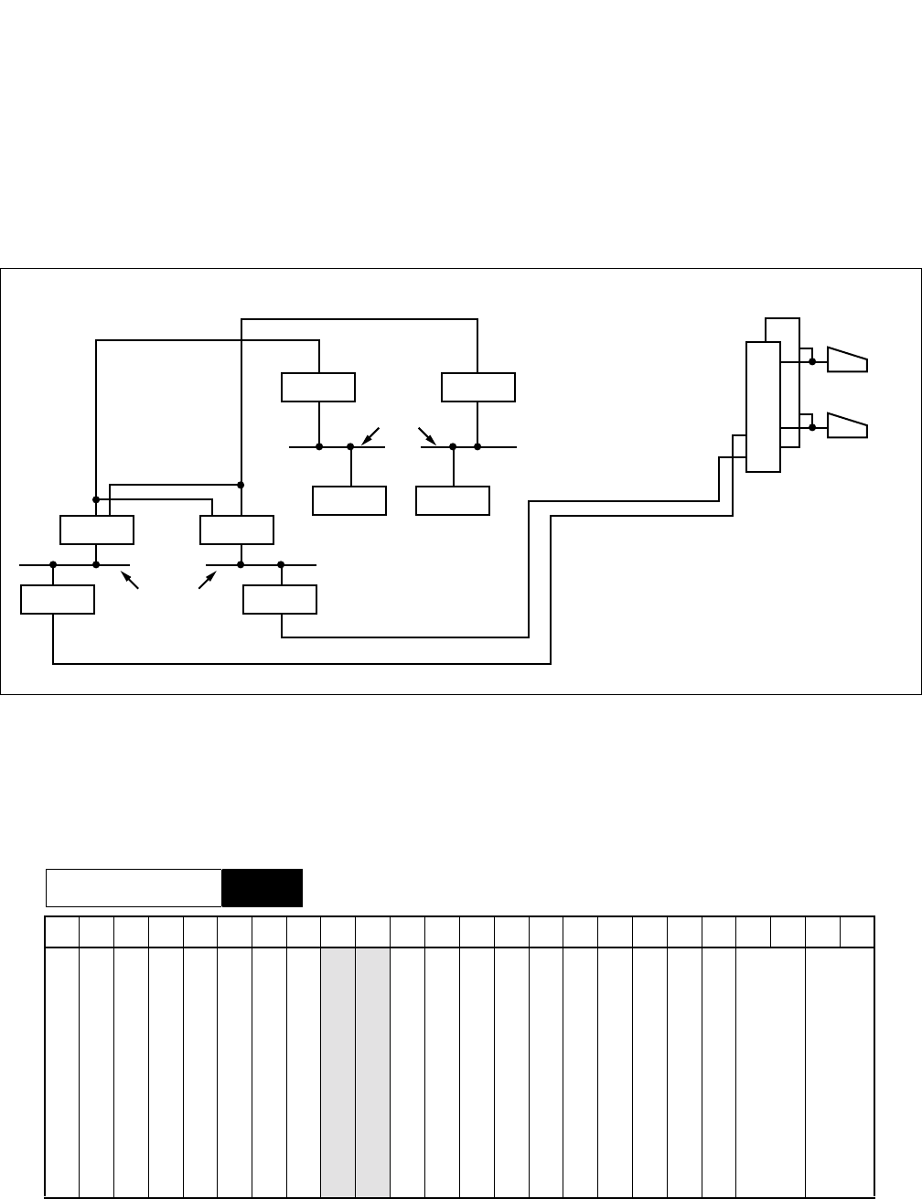
CHAPTER 2 NDA-24296
Page 102
Revision 1.0
PH-PC20
Data Link Controller
PH-PC20
Data Link Controller
1. General Function
This circuit card simultaneously provides all Attendant Consoles (ATTs) in the system (except the 1-IMG
system) with information such as the termination/answer/release (abandoned) information of ATT calls, or
the station idle/busy information through the TSW system link.
Figure 2-44 Location of PC-PH20 in the System
Note: MG = 01/03/05/07, Unit = 2, Group = 25, Level = 6-7 are used to input the information into TSW by the
DLKC.
2. Mounting Location/Conditions
DLKC0 DLKC1
GT1
ISAGT1ISAGT0
CPU0 CPU1
GT0
ATTCON
ATTCON
TSW
ISA BUS
MISC I/O BUS
Note
00 01 02 03 04 05 06 07 08 09 10 11 12 13 14 15 16 17 18 19 20 21 22 23
Mounting Module TSWM
DLKC#0
DLKC#1
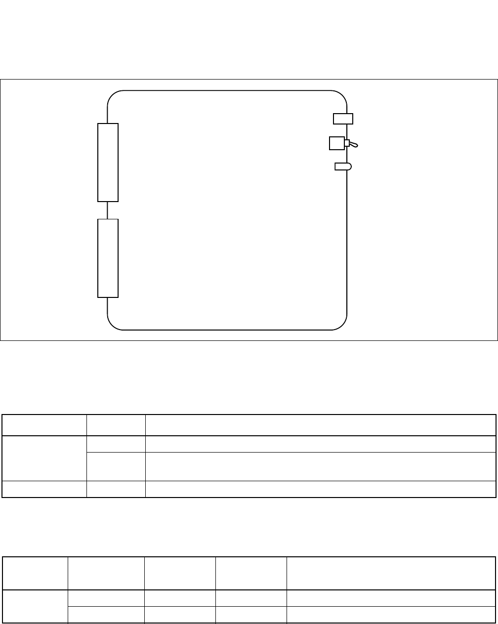
NDA-24296 CHAPTER 2
Page 103
Revision 1.0
PH-PC20
Data Link Controller
3. Face Layout of Lamps, Switches, and Connectors
The face layout of lamps, switches and connectors of this circuit card is shown in Figure 2-45.
Figure 2-45 Face Layout of the PC-PH20 Card
4. Lamp Indications
Lamp indications for this circuit card are shown in the table below.
5. Switch Settings
Standard settings of various switches on this circuit card are shown in the table below.
6. External Interface
LAMP NAME COLOR STATE
OPE/MB
Green Remains lit while this circuit card is in ACT state.
Red Remains lit while this circuit card is in Make-busy state or when the firmware is
abnormal.
PWR ALM Red Lights when the On-Board Power Supply located on this circuit card is abnormal.
SWITCH
NAME SWITCH NO. SETTING STANDARD
SETTING MEANING
MB UP Circuit card Make-busy.
DOWN Circuit card Make-busy cancel.
OPE/MB
PWR ALM
MB

CHAPTER 2 NDA-24296
Page 104
Revision 1.0
PH-PC20
Data Link Controller
No cable connections are required.
7. Switch Setting Sheet
SWITCH NAME SWITCH SHAPE REMARKS
MB
ON
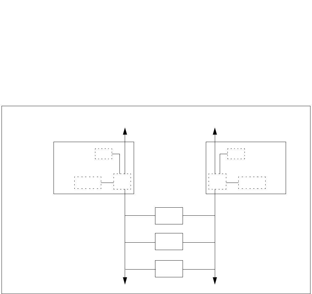
NDA-24296 CHAPTER 2
Page 105
Revision 1.0
PH-PC45
Emergency Alarm Controller
PH-PC45
Emergency Alarm Controller
1. General Function
The PH-PC45 (EMA) circuit card detects various kinds of alarms which might occur in the system, and
sends out information about the detected alarm to the circuits concerned. This circuit card can activate the
system MJ/MN LEDs on the TOPU. Additionally, this card can control the active/stand-by status of the
CPU in the case of dual configuration. For the 1 IMG system, this circuit card has the Music-On-Hold
sending function, too.
Figure 2-46 Location of PH-PC45 (EMA) Card in the System
DSP
CPU
CPR #0
EMA
IOC
MISC
GT
DSP
CPU
CPR #1
GT
I/O Local Bus I/O Local Bus
MISC Bus # 0 MISC Bus # 1
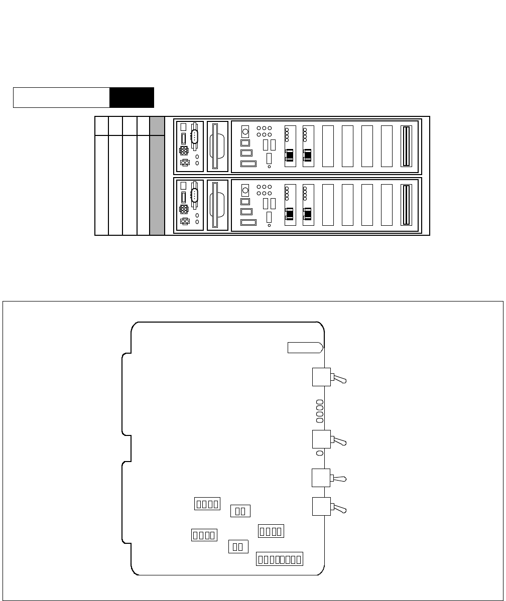
CHAPTER 2 NDA-24296
Page 106
Revision 1.0
PH-PC45
Emergency Alarm Controller
2. Mounting Location/Condition
The PH-PC45 (EMA) card is mounted in Slot 04 of the LPM, as shown below.
3. Face Layout of Lamps, Switches, and Connectors
The face layout of lamps, switches, and connectors is shown in Figure 2-47.
Figure 2-47 Face Layout of the PH-PC45 (EMA) Card
Mounting Module LPM
LPM
PH-IO24 (IOC)
PH-PC40 (EMA)
00 01 02 03 04
OPE/MB
MB
ACT1
CKERR1
ACT0
EMASUP
EMASUP
CPU SEL
NMI SEL
CKERR0
SW65
SW62
SW73
SW70
SW92
SW A0

NDA-24296 CHAPTER 2
Page 107
Revision 1.0
PH-PC45
Emergency Alarm Controller
4. Lamp Indications
Lamp indications for this circuit card are shown in the table below.
5. Switch Settings
Standard settings for switches on this circuit card are shown in the table below.
Note: Set CPUSEL switch downward, if a single CPU system.
LAMP NAME COLOR STATE
OPE/MB Green Indicates the circuit card is operating normally.
Red Indicates the circuit card is in a Make-busy state.
ACT1 Green CPU #1 is in the ACT state.
CKERR 1 Red CPU #1 clock failure has occurred.
ACT0 Green CPU #0 is in the ACT state.
CKERR 0 Red CPU #0 clock failure has occurred.
EMSUP Green Disable the CPU change-over. (When EMSUP key is set upward .)
OFF Enable to the CPU change-over.
SWITCH
NAME SETTING STANDARD
SETTING MEANING
MB UP Make-busy of the circuit card.
DOWN Normal setting.
EMASUP UP Make-busy of the CPU change-over circuit.
DOWN ×Normal setting.
CPUSEL
UP Forced activating the CPU #1.
MIDDLE ×Denial of the forced CPU selection. Note
DOWN Forced activating the CPU #0.
NMISEL UP Outputs the Non-Maskable Interruption (NMI) signal to the CPU when
a fault occurs.
DOWN ×Outputs the RST (Reset) signal to the CPU when a fault occurs.

CHAPTER 2 NDA-24296
Page 108
Revision 1.0
PH-PC45
Emergency Alarm Controller
SWITCH
NAME SWITCH
NO SETTING STANDARD
SETTING MEANING
SW62
1ON Power Shut Down (PSDN) function
(used in Australia only)
OFF ×
2ON
OFF ×
3ON
OFF ×
4ON
OFF ×
SW65
1ON ×Output the CPU-ACT Signal to the another EMA (when this
circuit card is used in the one frame stack configuration).
OFF CPU-ACT Signal does not output.
2ON Not used.
OFF ×Not used.
3ON Dual CPU configuration.
OFF Single CPU configuration.
4ON ×PZ-DK223 (or PZ-DK173) is used for the DSPP on the
TOPU.
OFF PZ-DK179 is used for the DSPP on the TOPU.
SW70
1ON External music on hold source (FM lead) is used.
OFF Internal music on hold source IC is used.
2ON Output the alarm information for the external indicator
(used in Australia only).
OFF ×Alarm information does not output.
SW73
1ON ×Power Failure Transfer (PFT) control is valid.
OFF PFT control is invalid.
2ON ×µ-law PCM CODEC is applied for the music.
OFF A-law PCM CODEC is applied for the music.
SW62 ON OFF
SW62-1 IMG#0 valid IMG0# invalid
SW62-2 IMG#1 valid IMG1# invalid
SW62-3 IMG#2 valid IMG2# invalid
SW62-4 IMG#3 valid IMG3# invalid
NDA-24296 CHAPTER 2
Page 109
Revision 1.0
PH-PC45
Emergency Alarm Controller
Note: SW92 and SWA0 are used in the 1 IMG system only.
SWITCH
NAME SWITCH
NO SETTING STANDARD
SETTING MEANING
SW92
Note
1
2
3
4
SWA0
Note
1MUSIC CH0 selection. This selection is valid when SW70-1 is OFF.
2
3
4ON Not used
OFF ×Not used
5
MUSIC CH1 selection. The kind of music varies depending on the melody IC located on this
circuit card.
6
7
8ON Not used
OFF ×Not used
SW92-1 SW92-2 Impedance of the External Music Source 0 (FM 0)
OFF OFF 600 Ω
ON OFF 8.2 Ω
OFF ON 47K Ω
SW92-1 SW92-2 Impedance of the External Music Source 1 (FM 1)
OFF OFF 600 Ω
ON OFF 8.2 Ω
OFF ON 47K Ω
SWA0-1 SWA0-2 SWA0-3 MUSIC
OFF OFF OFF Für Elise
ON OFF OFF Maiden’s prayer
Don’t care OFF ON Buzzer
Don’t care ON OFF Chime
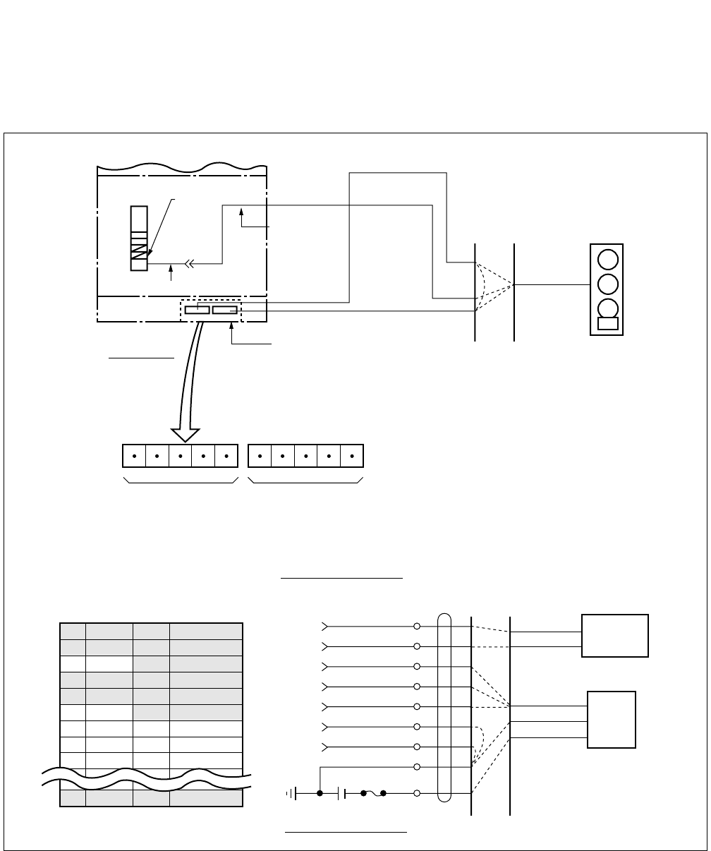
CHAPTER 2 NDA-24296
Page 110
Revision 1.0
PH-PC45
Emergency Alarm Controller
6. External Interface
External equipment may be connected to this circuit card. The physical connection diagram for the external
equipment for Music-On-Hold and External Alarm is shown in Figure 2-48.
Figure 2-48 Connection of Alarm Indicating Panel and Music on Hold
01 02 03 04 0501 02 03 04 05
26
27
28
29
30
31
32
33
34
E
E
-
MJB
MNA
-
1
2
3
4
5
6
7
8
9
FM0
FM1
MPALM
MJA
MNA
BELL
50 EXTA EXTB
25
16PH EXALM CA FM0
E
MJA
MNA
BELL
MJB
MNB
RPT1(G)
RPT0(-48V)
CABLING DIAGRAM
CROSS CONNECTION
MDF EXTERNAL
MUSIC
SOURCE
MJ/MN/BELL
-48V
(RPT0)
G
(RPT1)
AUDIBLE AND VISUAL
ALARM INDICATING PANEL
MDF MJ
MN
BELL
EALM Connector
EMA
(Slot No.04)
16PH EXALM CA
(BASEU)
LPM Installation
Cable
RPT Terminal on front
of the BASEU
REAR VIEW
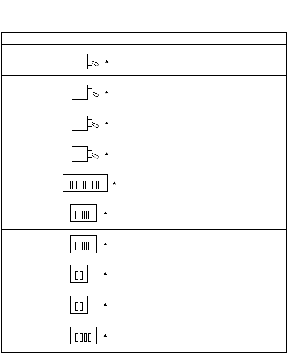
NDA-24296 CHAPTER 2
Page 111
Revision 1.0
PH-PC45
Emergency Alarm Controller
7. Switch Setting Sheet
SWITCH NAME SWITCH SHAPE REMARKS
MB
EMA-SUP
CPU-SEL
NMI-SEL
SWA0
SW62
SW65
SW70
SW73
SW92
ON
ON
ON
ON
12 3 4 ON
56 7 8
1 2 3 4 ON
1234ON
1 2 ON
12ON
1234ON
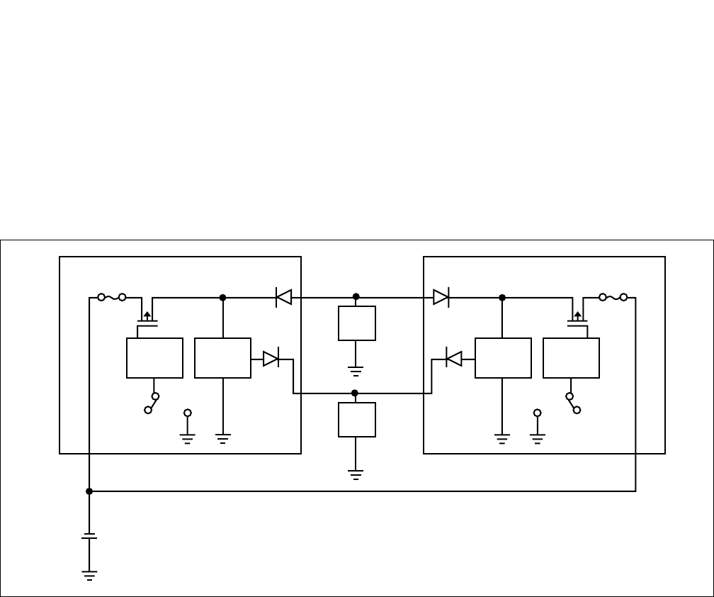
CHAPTER 2 NDA-24296
Page 112
Revision 1.0
PH-PW14
Power Switch
PH-PW14
Power Switch
1. General Function
This circuit card is a power supply card that supplies DC -48 V operating power to the circuit cards mounted
in the TSWM. It also provides the DC-DC converter function which generates output power DC +5 V, -5
V, and +12 V to MISC slots.
The two PWR SWs cards make the power supply redundant.
Figure 2-49 -48 V Output Circuit Diagram
Con-
troller Con-
troller
DC-
DC DC-
DC
Load
Load
-48V
-48V IN
Switch
FUSE FUSE
PWR SW #0
FET Switch PWR SW #1
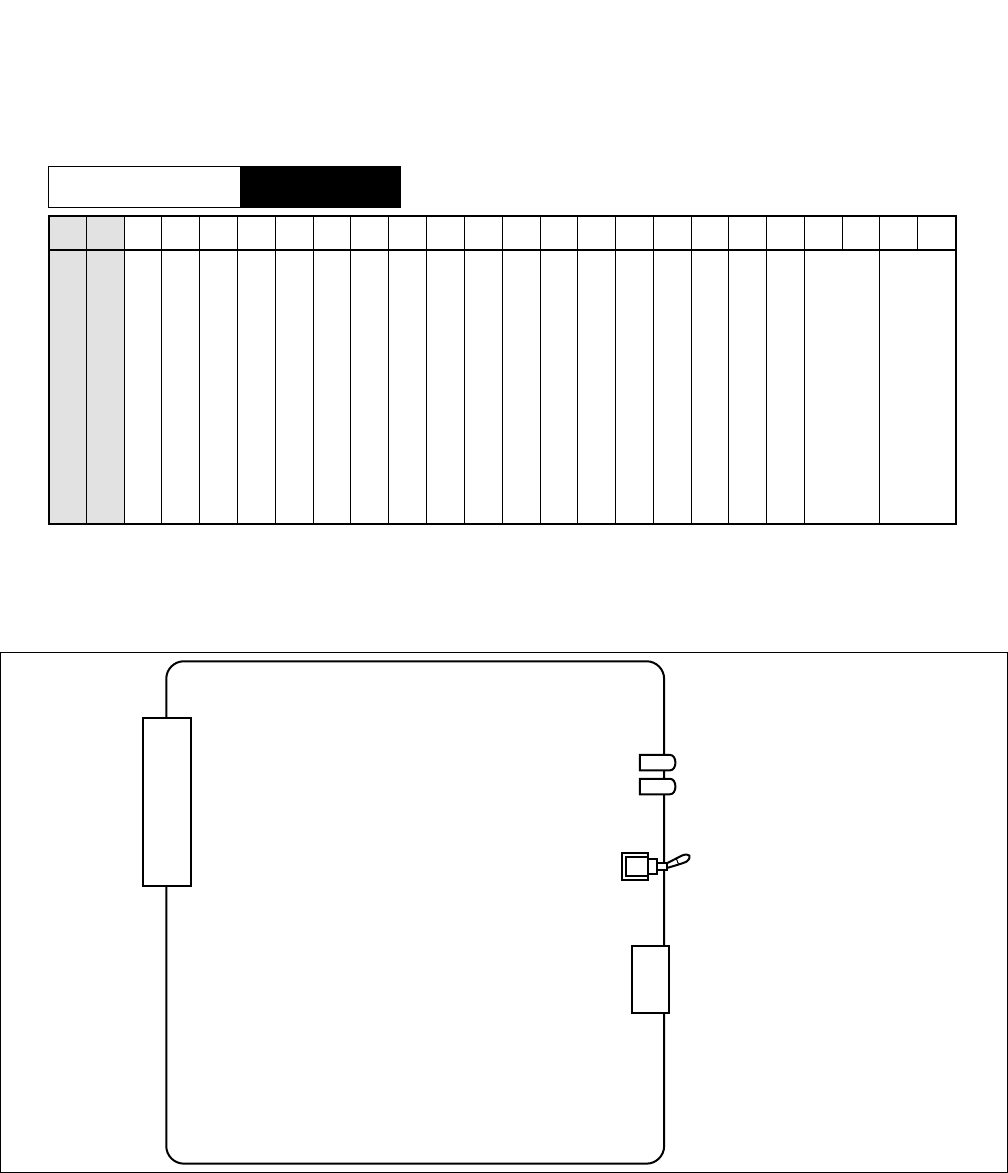
NDA-24296 CHAPTER 2
Page 113
Revision 1.0
PH-PW14
Power Switch
2. Mounting Location/Conditions
This circuit card is mounted in the following shaded slots (00, 01).
3. Face Layout of Lamps, Switches, and Connectors
The face layout of lamps, switches, and connectors for this circuit card is shown in Figure 2-50.
Figure 2-50 Face Layout of the PH-PW14 Card
00 01 02 03 04 05 06 07 08 09 10 11 12 13 14 15 16 17 18 19 20 21 22 23
Mounting Module TSWM/ISWM
PWR SW#0
PWR SW#1
P-ON
ALM
SW
-48V in Fuse
(125V AC/DC 15A)
CHAPTER 2 NDA-24296
Page 114
Revision 1.0
PH-PW14
Power Switch
4. Lamp Indications
Lamp indications for this circuit card are shown in the table below.
5. Switch Settings
Standard settings for various switches on this circuit card are shown in the table below.
6. External Interface
No cable connections are required.
7. Switch Setting Sheet
LAMP NAME COLOR STATE
P-ON Green Remains lit while this circuit card is operating.
ALM Red Lights when SW switch is set at OFF position or it is faulty.
SWITCH
NAME SWITCH
NO. SETTING STANDARD
SETTING MEANING
SW ON ×The card supplies the operating power to various circuit
cards.
OFF
MODULE SLOT NO. SWITCH
NAME SWITCH SHAPE REMARKS
00
01 SW -48 V operating power is supplied to vari-
ous circuit cards.
ON
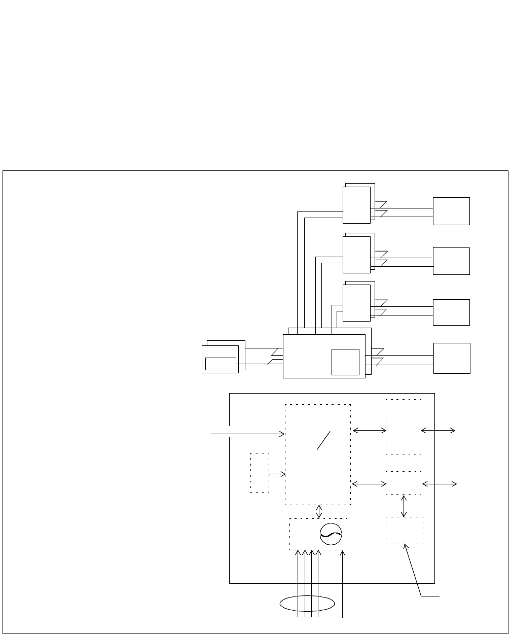
NDA-24296 CHAPTER 2
Page 115
Revision 1.0
PH-SW10
Time Division Switch
PH-SW10
Time Division Switch
1. General Function
This circuit card combines the Time Division Switch (TSW) with INT, PLO, MUX, and CFT.
The TSW capacity is 2048×2048 time slots, and it allows non-block switching for the maximum IPX
configuration. The INT is an intermediate circuit of the CPR which controls and administrates the Port
Microprocessor (PM) of line/trunk circuit cards via the PM BUS.
Figure 2-51 Location of PH-SW10 (TSW) Card in the System
[Connection diagram of the TSW]
MUX
MUX
MUX
CPR
GT
LC/TRK
LC/TRK
LC/TRK
LC/TRK
MUX
TSW/INT/PLO
PCM HW
PM BUS
PM BUS
PM BUS
PM BUS
PCM HW
PCM HW
PCM HW
[Function block diagram]
PLO
MUX
LV D S
CFT
From EMA
TSW
INT
MUSIC
D
T
G
DTI DCS
MUX
LC/TRK
PH-SW10
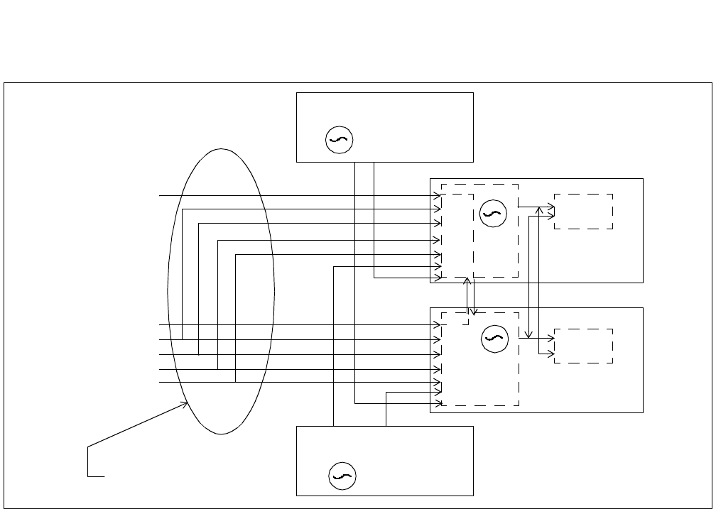
CHAPTER 2 NDA-24296
Page 116
Revision 1.0
PH-SW10
Time Division Switch
Figure 2-52 shows the clock signal routing around the Phase Locked Oscillator (PLO).
Figure 2-52 PLO Function Diagram
When the system operates as the clock source office of the digital network, the OSC (PA-CK14) card is required,
and the OSC supplies the high-precision clock signals (±0.3 ppm deviation) for the base clock of the PLO. When
the system operates as the clock subordinate office, the TSW internal oscillator (±5 ppm deviation) can be the
base clock of the PLO. The source clock of the subordinate office is either the digital clock supply (DCS) or the
digital interface clock (DIU0 - DIU3). When the clock source failure has occurred, the PLO chooses another
clock source automatically in the order of:
1. DCS0
2. DCS1
3. DIU0
4. DIU1
5. DIU2
6. DIU3
7. Drifting with the TSW internal oscillator
TSW#1
(PH-SW10)
TSW#0 (PH-SW10)
TSW
TSW
PLO
PLO
OSC#1 (PA-CK14)
OSC#0 (PA-CK14)
DCS 0 DCS 1
DCS 1
DCS 0
DIU 0
DIU 1
DIU 2
DIU 3
Multiple connection on MDF
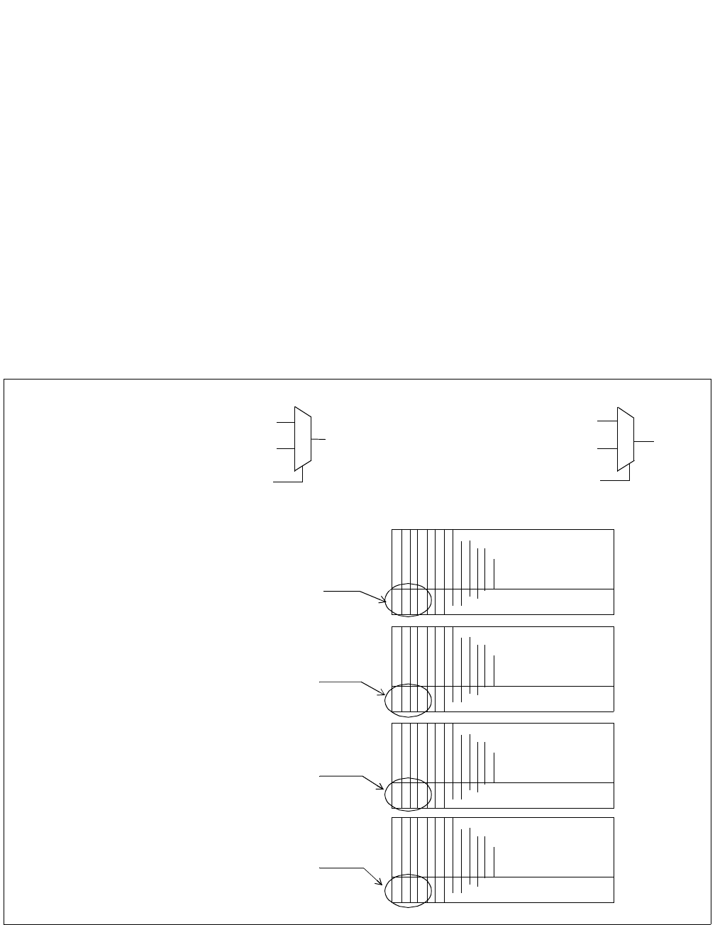
NDA-24296 CHAPTER 2
Page 117
Revision 1.0
PH-SW10
Time Division Switch
The PLO can output the clock signals (CLK) and the frame head signals (FH) as follows:
•32.768 MHz CLK
•8 KHz FH
•5 msec × “n” FH (for wireless module).
The MUX performs multiplexing/de-multiplexing of the 2 Mbps PCM highways running in PIM 0, and it
sends/receives the PCM to/from the TSW, and operates like the MUX card of PIM 1/2/3.
This circuit card includes the Digital Tone Generator (DTG) and hold tone (MUSIC) insertion circuit. The
TONE ROM located on this circuit card contains the audible tone, and the hold tone is supplied from the
EMA card. In addition, the designated time slot of PCM (Speech Path Memory: SPM) can be inserted as a
tone/music voice prompt. (For example, you can join the SPM and a DAT port by the nailed down
connection, and the DAT's voice prompt is given to the system instead of ordinary tone/music.)
Additionally, this circuit card supports the CFT (3-Party Conference) function and is equipped with eight
circuits of 3-Party Conference Trunk.
Figure 2-53 Voice Prompting
[Voice Prompt sending for Tone] [Voice Prompt sending for Music]
Speech Path MemorySpeech Path Memory
TONE ROM MUSIC from EMA
Tone source selected by office data Music source selected by office data
[Time Slot for Speech Path Memory]
[SPM for music channel 16-29]
MG=01, Unit=2, Group=24, Level=0-7
MG=01, Unit=2, Group=25, Level=0-5
[SPM for music channel 0-15]
MG=01, Unit=0, Group=24, Level=0-7
MG=01, Unit=0, Group=25, Level=0-7
[SPM for Tone channel 16-31]
MG=00, Unit=2, Group=24, Level=0-7
MG=00, Unit=2, Group=25, Level=0-7
[SPM for Tone channel 0-15]
MG=00, Unit=0, Group=24, Level=0-7
MG=00, Unit=0, Group=25, Level=0-7
PIM 3
PIM 2
PIM 1
PIM0
Tone Music
Note
Note: MG=01, Unit=2, Group=25, Level=6-7 are not used.
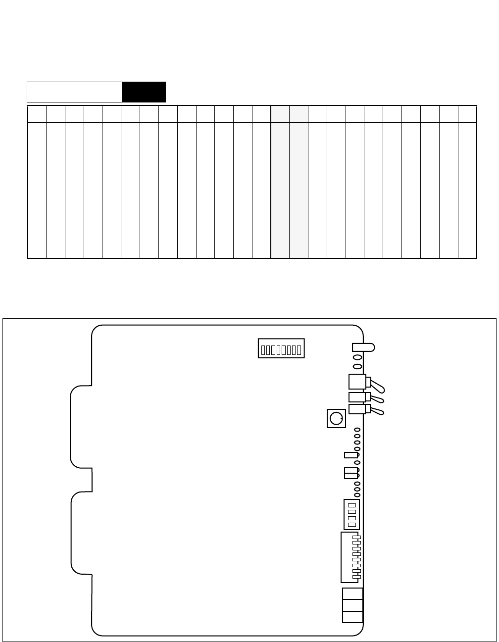
CHAPTER 2 NDA-24296
Page 118
Revision 1.0
PH-SW10
Time Division Switch
2. Mounting Location/Condition
This circuit card is mounted in PIM number zero (0) of the slot shown below.
3. Face Layout of Lamps, Switches, and Connectors
The face layout of lamps, switches and connectors is shown in Figure 2-54.
Figure 2-54 Face Layout of PH-SW10 (TSW)
00 01 02 03 04 05 06 07 08 09 10 11 12 13 14 15 16 17 18 19 20 21 22 23
Mounting Module PIM
PIM0
TSW #1
TSW #0
1 2 3 4 5 6 7 8
SW11
TSWACT
MUXACT
PLOACT
MB
TSWMBR
PLOMB
M3SY
M2SY
M1SY
M0SY
CFT
SYNC
ICK
ECK
SW03
SW04
MUX3
MUX2
MUX1
PMCA
PMJ
PMN
SW12

NDA-24296 CHAPTER 2
Page 119
Revision 1.0
PH-SW10
Time Division Switch
4. Lamp Indications
Lamp indications for this circuit card are shown in the table below.
LAMP NAME COLOR STATE
TSWACT
Green Remains lit while the TSW block is in ACT state.
Red Remains lit while the TSW block is in Make-busy state.
Off Remains off while the TSW block is ST-BY side.
MUXACT Green Remains lit while MUX block is in ACT state.
PLOACT Green Remains lit while PLO block is in ACT state.
M3SY Green Lights when MUX #3 synchronization has been established.
M2SY Green Lights when MUX #2 synchronization has been established.
M1SY Green Lights when MUX #1 synchronization has been established.
M0SY Green Lights when MUX #0 synchronization has been established.
PMCA Red Lights when the PM/PCM bus clock FH failure has occurred.
CFT Green Lights when the CFT circuit is valid.
PMJ Red
Lights when the following MJ fault has occurred:
•All of the clock supply routes have failed when the system operates as the clock
subordinate office
•32.768 MHz output clock failure
•8 KHz output FH failure
•5 msec × “n” output FH failure
•Input Frame Pulse (FP) failure (FP is supplied by the SYNC card)
•Both internal OSC (±5 ppm deviation) and high-precision clock signals (±0.3 ppm
deviation) have failed when the system operates as the clock source office
PMN Yellow
Lights when the following MN fault has occurred:
•One or more (but not all) DTI/DCS clock supply routes have failed
•Drifting failure
•Internal OSC (±5 ppm) failure
•High-precision clock signals (±0.3 ppm) failure

CHAPTER 2 NDA-24296
Page 120
Revision 1.0
PH-SW10
Time Division Switch
5. Switch Settings
Standard settings for switches on this circuit card are shown in the table below.
SYNC
Green Remains lit while the system is synchronized with the network.
OFF
Remains off when any of the following have occurred.
•DCS clock failure when receiving the clock signals from the DCS.
•DTI clock failure when receiving the clock signals from the DTI.
•Drifting failure
ICK Green
Lights when the TSW (PA-SW10) internal oscillator is operating normally.
Note 1: The ICK LED will illuminate even when the internal PLO circuit is
operational.
ECK Green
Lights when the high-precision clock signals are received from OSC circuit card
(PA-CK14).
Note 2: The ICK LED will not illuminate when the PA-CK14 is operational.
SWITCH
NAME SETTING STANDARD
SETTING MEANING
MB UP Circuit card Make-busy.
DOWN ×Circuit card Make-busy cancel.
TSWMBR UP TSW Make-busy request.
DOWN ×TSW Make-busy request cancel.
PLOMBR UP PLO Make-busy request.
DOWN ×PLO Make-busy request cancel.
SW12 1-F 1 Fixed to “1.”
LAMP NAME COLOR STATE

NDA-24296 CHAPTER 2
Page 121
Revision 1.0
PH-SW10
Time Division Switch
Note: When MUX card mode (SW03-4 ON), only MUX and CFT functions are valid. MUX 1 is used for a con-
nection to TSW (Don’t use MUX 2, 3). The LED of MUXACT, M0SY, CFT, and PMCA are valid, other LED
is not lit. In this mode, only SW03 is valid.
SWITCH
NAME SWITCH
NO SETTING STANDARD
SETTING MEANING
SW03
1ON 3-Party Conference Trunk (CFT) is valid.
OFF 3-Party Conference Trunk (CFT) is invalid.
2ON Setting of A-law in the CFT function block.
OFF ×Setting of µ-law in the CFT function block.
3OFF ×Fixed.
4
ON Only MUX function is valid (If this card is mounted in PIM
1/2/3). Note
OFF ×TSW/INT/PLO/MUX are valid (When this card is mounted in
PIM 0).
SW04
1ON DIU 0 is used as the DTI clock supply route zero.
OFF DIU 0 is not used.
2ON DIU 1 is used as the DTI clock supply route one.
OFF DIU 1 is not used.
3ON DIU 2 is used as the DTI clock supply route two.
OFF DIU 2 is not used.
4ON DIU 3 is used as the DTI clock supply route three.
OFF DIU 3 is not used.
5ON ×1.5 M clock for DIU 0
OFF 2 M clock for DIU 0
6ON ×1.5 M clock for DIU 1
OFF 2 M clock for DIU 1
7ON ×1.5 M clock for DIU 2
OFF 2 M clock for DIU 2
8ON ×1.5 M clock for DIU 3
OFF 2 M clock for DIU 3

CHAPTER 2 NDA-24296
Page 122
Revision 1.0
PH-SW10
Time Division Switch
SWITCH
NAME SWITCH
NO. SETTING STANDARD
SETTING MEANING
SW11
1ON PLO operates as the clock subordinate office.
OFF PLO operates as the clock source office.
2ON Digital Clock Supply route zero (DCS 0) is used.
OFF Digital Clock Supply route zero (DCS 0) is not used.
3ON Digital Clock Supply route one (DCS 1) is used.
OFF Digital Clock Supply route one (DCS 1) is not used.
4
ON 8 KHz of Frame Head signals are extracted from the DCS
signals (which is composed of 64 KHz + 8 KHz).
OFF 8 KHz of Frame Head signals are not extracted from the DCS
signals (which is composed of 64 KHz + 8 KHz).
5
ON When clock source failure has occurred in all supply routes,
the PLO outputs the original clock of the internal oscillator.
OFF When clock source failure has occurred in all supply routes,
the PLO continues outputting the current phase clock.
6ON This card is associated with SYNC (PA-CK16) card and 5 m
Frame Pulse (FP) is supplied by the SYNC card.
OFF This card is not associated with SYNC (PA-CK16) card.
7ON (The last byte data of the DTG ROM is “FE”)
OFF ×(The last byte data of the DTG ROM is “FF”)
8OFF ×Not used
NDA-24296 CHAPTER 2
Page 123
Revision 1.0
PH-SW10
Time Division Switch
6. External Interface
When this circuit card is used in “clock subordinate office,” clock signals from DTI, CCT, PRT must be
extracted. See Figure 2-56 for more information. When this circuit card is used in “clock source office,”
cable connections are not necessary.
Figure 2-55 PLO Connector Leads Location
26
27
28
29
30
31
32
33
34
35
36
37
38
39
40
41
42
43
44
45
46
47
48
49
50
1
2
3
4
5
6
7
8
9
10
11
12
13
14
15
16
17
18
19
20
21
22
23
24
25
DCSB0
DIU0B0
DIU1B0
DIU2B0
DIU3B0
SYN0B0
SYN1B0
DCSB1
DIU0B1
DIU1B1
DIU2B1
DIU3B1
SYN0B1
SYN1B1
DCSA0
DIU0A0
DIU1A0
DIU2A0
DIU3A0
SYN0A0
SYN1A0
DCSA1
DIU0A1
DIU1A1
DIU2A1
DIU3A1
SYN0A1
SYN1A1
Mounting Module PIM
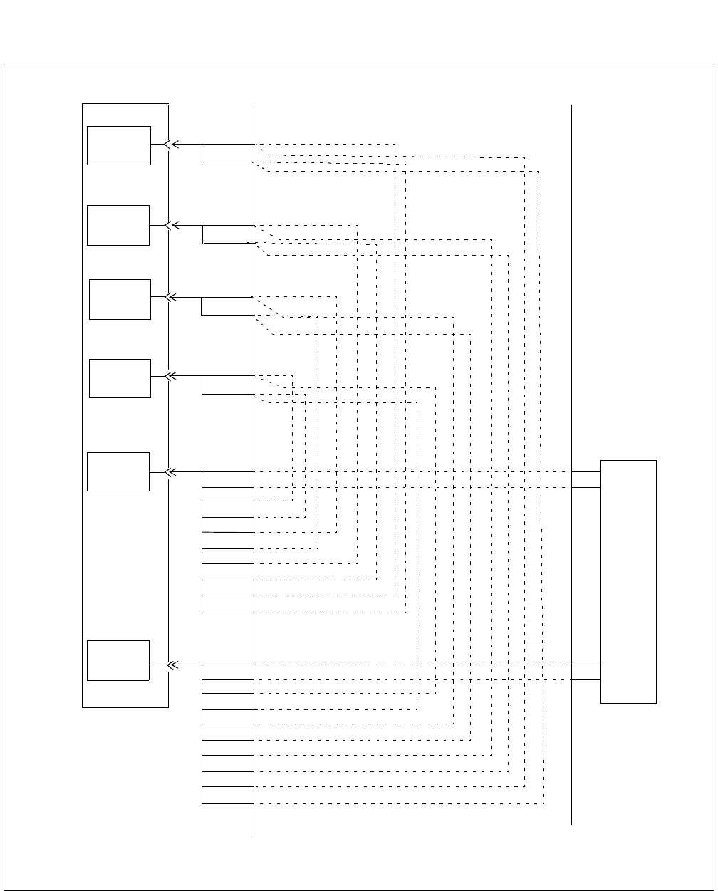
CHAPTER 2 NDA-24296
Page 124
Revision 1.0
PH-SW10
Time Division Switch
Figure 2-56 Connecting Route Diagram
DCS
TSW #1
TSW #0
/PRT
CCT/DTI
CCT/DTI
/PRT
CCT/DTI
/PRT
CCT/DTI
/PRT
POUT A
POUT B
POUT A
POUT B
POUT A
POUT B
POUT A
POUT B
DCSA0
DCSB0
DIU0A0
DIU0B0
DIU1A0
DIU1B0
DIU2A0
DIU2B0
DIU3A0
DCSA1
DCSB1
DIU0A1
DIU0B1
DIU1A1
DIU1B1
DIU2A1
DIU2B1
DIU3A1
DIU3B1
PBX MDF
Note: The following circuit cards have Clock Output leads for a PLO card: CCT (PA-24CCTA, PA30CCTB),
DTI (PA-24DTR, PA-30DTS), and PRT (A-24PRT, PA-PRTC).
DIU3B0
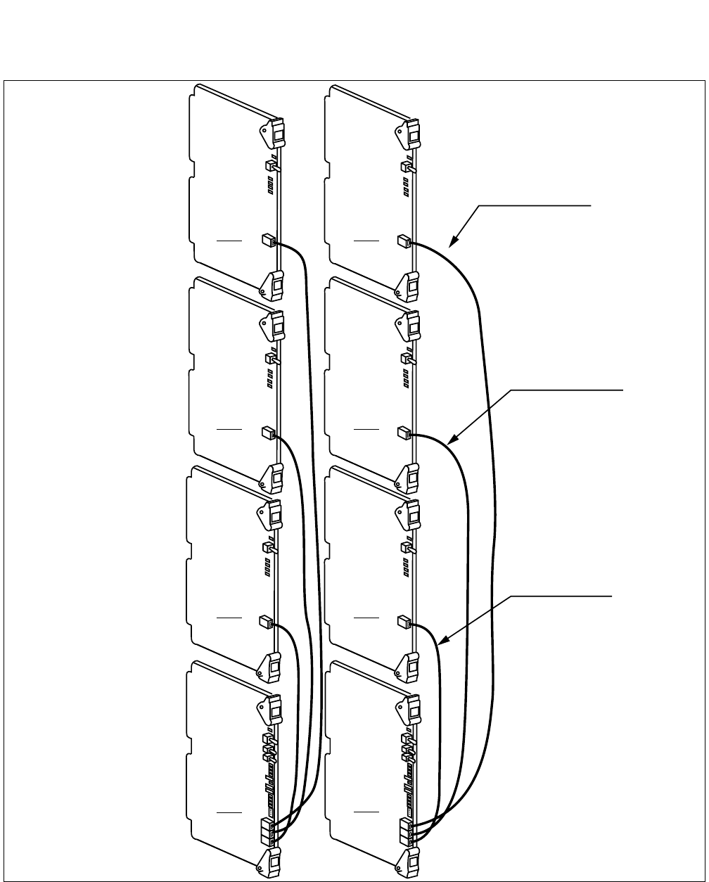
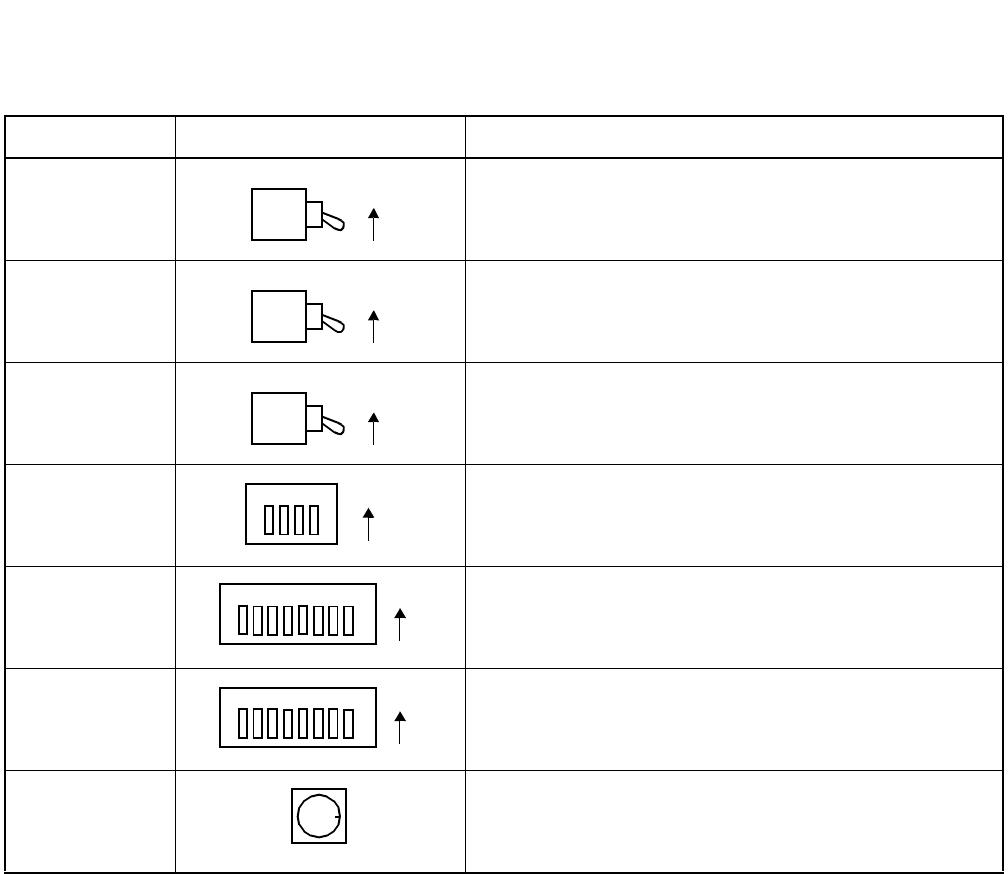
CHAPTER 2 NDA-24296
Page 126
Revision 1.0
PH-SW10
Time Division Switch
7. Switch Setting Sheet
SWITCH NAME SWITCH SHAPE REMARKS
MB
TSWMBR
PLOMB
SW03
SW04
SW11
SW12
ON
ON
ON
1 2 3 4 ON
1 2 3 4 ON
5 6 7 8
12 3 4 ON
5678
1
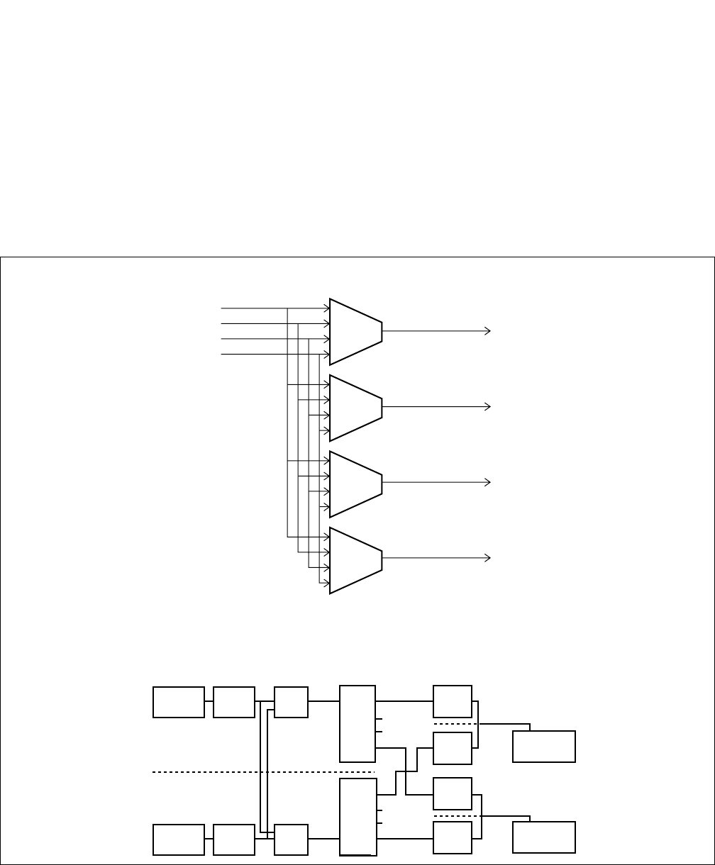
NDA-24296 CHAPTER 2
Page 127
Revision 1.0
PH-SW12
Time Division Switch
PH-SW12
Time Division Switch
1. General Function
This circuit card provides the Time Division Switch (TSW) and INT function for the system. Each TSW
card is capable of 8192 × 2048 Time Slot (TS) switching for an Interface Module Group (IMG). Four cards
allow 8192 × 8192 TS switching for the 4 IMG configuration.
The INT is an intermediate circuit of the CPR which controls and administers the Port Microprocessor
(PM) for line/trunk circuit cards.
Figure 2-58 TSW Configuration
TSW
(8Kx2K)
TSW
(8Kx2K)
TSW
(8Kx2K)
TSW
(8Kx2K)
IMG0
IMG0
IMG1
IMG1
IMG2
IMG2
IMG3
IMG3
[TSW configuration]
[INT configuration]
CPU1(LP) ISAGT1 GT1
CPU0(LP) ISAGT0 GT0
TSW1
(INT)
TSW0
(INT)
MUX01
MUX30
MUX31
MUX00 LC/TRK(PM)
LC/TRK(PM)
ISA BUS I/O BUS
ISA BUS I/O BUS
System #1
System #0
ACT
STBY
STBY
STBY
STBY
ACT ACT
ACT
PM BUS
PM BUS
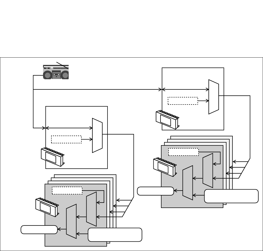
CHAPTER 2 NDA-24296
Page 128
Revision 1.0
PH-SW12
Time Division Switch
The TONE ROM located on this circuit card contains the audible tones, such as Dial Tone, Busy Tone, Ring
Back Tone, etc. The music on hold source, either the MUSIC ROM or the external source via FM lead, is
located on the PLO card. The tone and the music are inserted into their time slot at this circuit card.
Additionally, this circuit card provides the Voice Prompt function that inserts the designated time slot of
PCM (Speech Path Memory : SPM) into the tone or music time slot.
Figure 2-59 Music/Tone Insertion
SEL
SEL
SEL
Speech Path Memory
for Music/Tone
Music/Tone
MUSIC ROM
TDSW00
PLO#0
TONE ROM
SEL
SEL
SEL
Speech Path Memory
for Music/Tone
Music/Tone
MUSIC ROM
TDSW1
PLO#1
TONE ROM
FM
FM
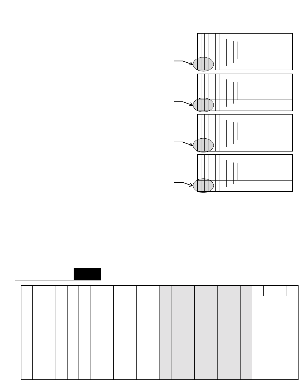
NDA-24296 CHAPTER 2
Page 129
Revision 1.0
PH-SW12
Time Division Switch
Figure 2-60 Speech Path Memory (SPM) for Voice Prompt Function
2. Mounting Location/Condition
This circuit card is mounted in the TSWM of the slot shown below. The IPX-U system accommodates two
TSWMs (TSWM0/1).
PIM 3
[SPM for music channel 16-29]
MG = 01, Unit = 2, Group = 24, Level = 0-7
MG = 01, Unit = 2, Group = 25, Level = 0-5
PIM 2
[SPM for music channel 0-15]
MG = 01, Unit = 0, Group = 24, Level = 0-7
MG = 01, Unit = 0, Group = 25, Level = 0-7
PIM 1
[SPM for tone channel 16-31]
MG = 00, Unit = 2, Group = 24, Level = 0-7
MG = 00, Unit = 2, Group = 25, Level = 0-7
PIM0
[SPM for tone channel 0-15]
MG = 00, Unit = 0, Group = 24, Level = 0-7
MG = 00, Unit = 0, Group = 25, Level = 0-7
Note :
Note
MG = 01,Unit = 2, Group = 25, Level = 6-7 are exclusively used by the DLKC.
00 01 02 03 04 05 06 07 08 09 10 11 12 13 14 15 16 17 18 19 20 21 22 23
Mounting Module TSWM
TSW 00
TSW 01
TSW 02
TSW 03
TSW 10
TSW 11
TSW 12
TSW 13
TSWM

CHAPTER 2 NDA-24296
Page 130
Revision 1.0
PH-SW12
Time Division Switch
The definitions for the TSW00 - TSW03/TSW10 - TSW13 are listed below.
•4-IMG System
•IPX-U system
This card is mounted in the TSWM0/1 for the IPX-U system.
•For the card in TSWM0
SYMBOL SYSTEM CONTROLLED IMG
TSW00
0
IMG 0
TSW01 IMG 1
TSW02 IMG 2
TSW03 IMG 3
TSW10
1
IMG 0
TSW11 IMG 1
TSW12 IMG 2
TSW13 IMG 3
SYMBOL SYSTEM FUNCTION CONTROLLED IMG
TSW00
0
Collects the PCM data IMG 0
TSW01 IMG 1
TSW02 Sends the PCM data to the ISW IMG 0
TSW03 IMG 1
TSW10
1
Collects the PCM data IMG 0
TSW11 IMG 1
TSW12 Sends the PCM data to the ISW IMG 0
TSW13 IMG 1
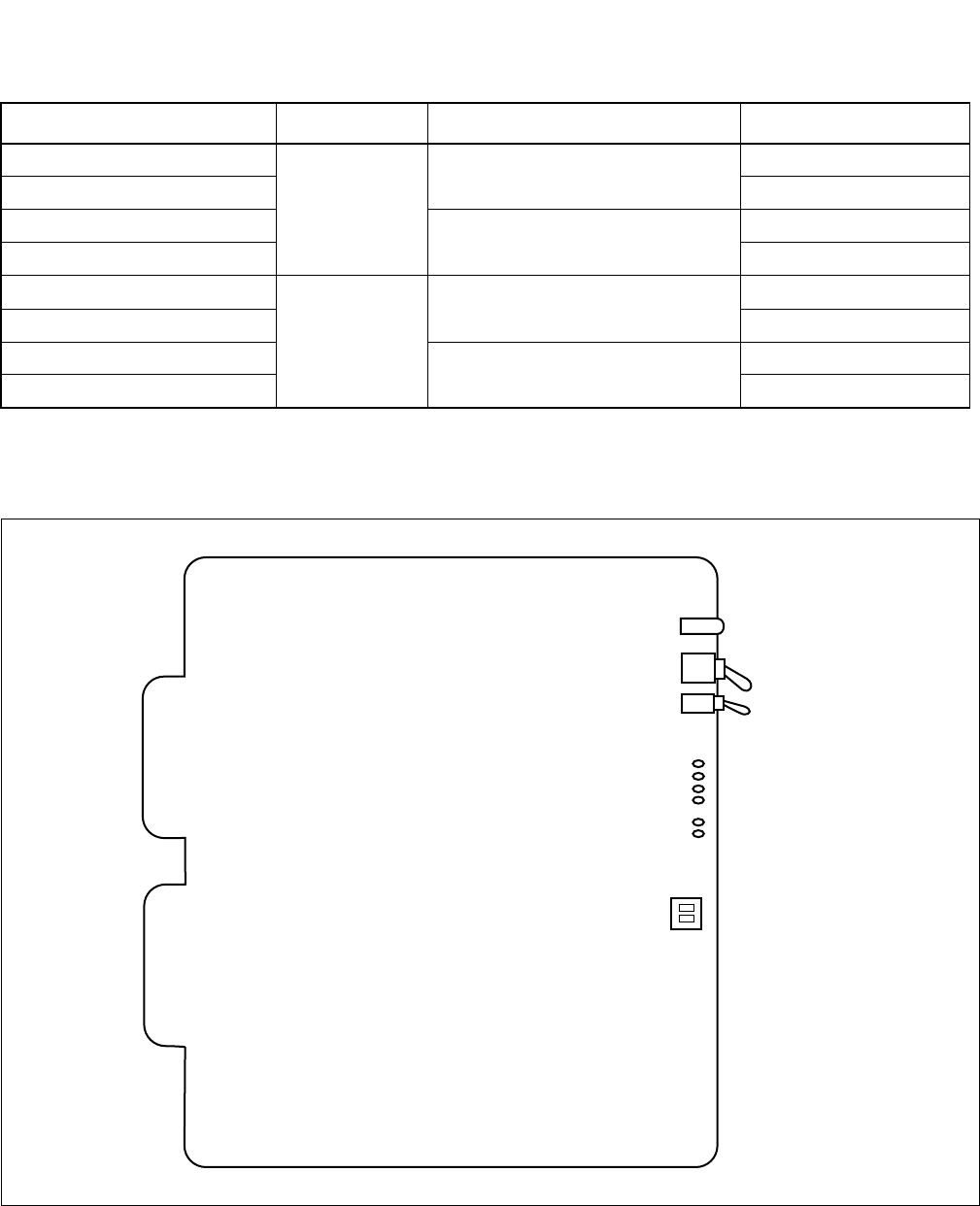
NDA-24296 CHAPTER 2
Page 131
Revision 1.0
PH-SW12
Time Division Switch
•For the card in TSWM1
3. Face Layout of Lamps, Switches, and Connectors
The face layout of lamps, switches, and connectors is shown in Figure 2-61.
Figure 2-61 Face Layout of PH-SW12 (TSW)
SYMBOL SYSTEM FUNCTION CONTROLLED IMG
TSW00
0
Collects the PCM data IMG 2
TSW01 IMG 3
TSW02 Sends the PCM data to the ISW IMG 2
TSW03 IMG 3
TSW10
1
Collects the PCM data IMG 2
TSW11 IMG 3
TSW12 Sends the PCM data to the ISW IMG 2
TSW13 IMG 3
MB
TSWMBR
TSWACT
M3SY
M2SY
M1SY
M0SY
PLO 1
PLO 0
TONE

CHAPTER 2 NDA-24296
Page 132
Revision 1.0
PH-SW12
Time Division Switch
4. Lamp Indications
Lamp indications for this circuit card are shown in the table below.
5. Switch Settings
Standard settings for switches on this circuit card are shown in the table below.
6. External Interface
See the NEAX2400 IPX Installation Manual for information about the cable connection to MUX.
LAMP NAME COLOR STATE
TSWACT
Green Remains lit while the TSW block is in ACT state.
Red Remains lit while the TSW block is in Make-busy state.
Off Remains off while the TSW block is ST-BY side.
M3SY Green Lights when MUX #3 synchronization has been established.
M2SY Green Lights when MUX#2 synchronization has been established.
M1SY Green Lights when MUX#1 synchronization has been established.
M0SY Green Lights when MUX#0 synchronization has been established.
PLO 1 Green Lights when the Frame Head signal and clock signals are received from the PLO 1.
PLO 0 Green Lights when the Frame Head signal and clock signals are received from the PLO 0.
SWITCH
NAME SETTING STANDARD
SETTING MEANING
MB UP Circuit card Make-busy.
DOWN ×Circuit card Make-busy cancel.
TSWMBR UP TSW Make-busy request.
DOWN ×TSW Make-busy request cancel.
SWITCH
NAME SWITCH
NO. SETTING STANDARD
SETTING MEANING
TONE
1OFF ×Fixed.
2ON (The last byte data of the DTG ROM is “FE.”)
OFF ×(The last byte data of the DTG ROM is “FF.”)
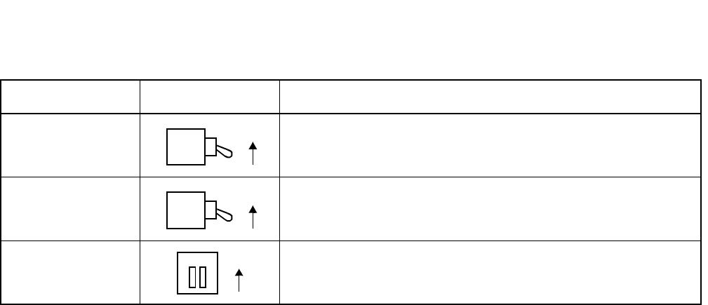
NDA-24296 CHAPTER 2
Page 133
Revision 1.0
PH-SW12
Time Division Switch
7. Switch Setting Sheet
SWITCH NAME SWITCH SHAPE REMARKS
MB
TSWMBR
TONE
ON
ON
1 2 ON
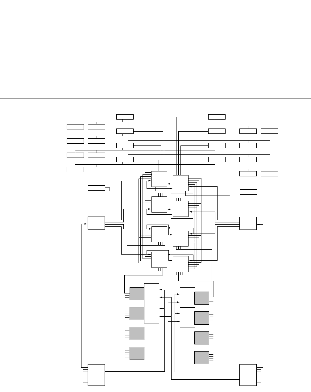
CHAPTER 2 NDA-24296
Page 134
Revision 1.0
PU-SW00/PU-SW00-A
Time Division Switch
PU-SW00/PU-SW00-A
Time Division Switch
1. General Function
The PU-SW00/PU-SW00-A circuit card provides the Time division Switch (TSW) and INT function for
the IPX-U/IPX-UMG system. Each circuit card provides switching for a Local Node (LN) and four PU-
SW00/PU-SW00-A cards and two PU-SW01 (HSW) cards achieve a maximum of 32,768 time slot (TS)
switching for four (4) LNs/LMGs. This circuit card is located in ISWM of the ISW/CMG.
Figure 2-62 Location of PU-SW00/PU-SW00-A (TSW)
MUX00
LC/TRK
LC/TRK
LC/TRK
LC/TRK
DLKC0
LC/TRK
LC/TRK
LC/TRK
LC/TRK
LC/TRK
LC/TRK
LC/TRK
LC/TRK
LC/TRK
LC/TRK
LC/TRK
LC/TRK
MUX01
MUX02
MUX03
MUX10
MUX11
MUX12
MUX13
TSW00 TSW10
TSW01 TSW11
TSW02 TSW12
TSW03 TSW13
PLO 0
PLO 0
DLKC1
PLO 1
PLO 1
MUX MUX
TSW00
TSW01
TSW02
TSW03
HSW00
HSW01
HSW10
HSW11
TSW10
TSW11
TSW12
TSW13
[TSW Configuration]
2M PCM HW x8
2M PCM HW x8
2M PCM HW x8
2M PCM HW x8
2M PCM HW x8
2M PCM HW x8
2M PCM HW x8
2M PCM HW x8
32M TSW
Matrix HW
32M SERIAL HW
32M SERIAL HW
x4
32M SERIAL HW
x4
32M SERIAL HW
x4
32M SERIAL HW
x4
64KHz
Clock
64KHz
Clock
32M TSW
Matrix HW
32.768MHz Clock
DCS
32.768MHz Clock
DCS
32.768MHz Clock 32.768MHz Clock
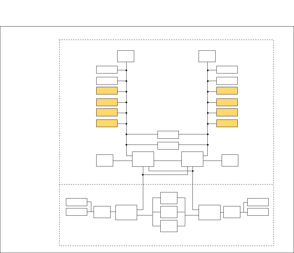
NDA-24296 CHAPTER 2
Page 135
Revision 1.0
PU-SW00/PU-SW00-A
Time Division Switch
Figure 2-63 Location of PU-SW00/PU-SW00-A (TSW) for IPX-U System
HSW01
HSW00
TSW03
TSW02
TSW01
TSW00
LANI
LANI
LANI
LANI
HSW11
HSW10
TSW13
TSW12
TSW11
TSW10
PLO 1
PLO 0
RES
CPU CPU
MISC
IOC
EMA
RES
RES RES
IOGT1
IOGT0
ISAGT ISAGT
MISC I/O BUS
ISAGT BUSISAGT BUS LPM
TSW I/O BUSTSW I/O BUS
ISWM
[INT Configuration]
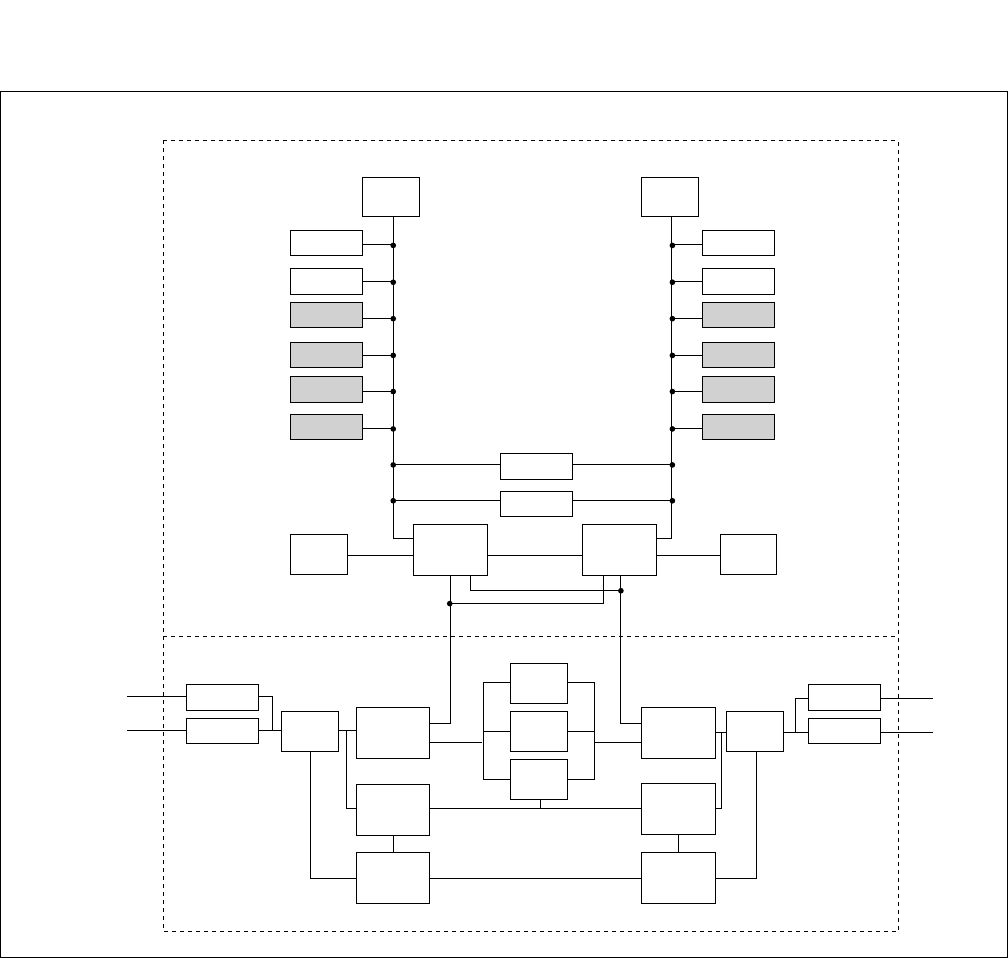
CHAPTER 2 NDA-24296
Page 136
Revision 1.0
PU-SW00/PU-SW00-A
Time Division Switch
Figure 2-63 Location of PU-SW00/PU-SW00-A (TSW) for IPX-UMG System
HSW01
HSW00
TSW03
TSW02
TSW01
TSW00
LANI
LANI
LANI
LANI
HSW11
HSW10
TSW13
TSW12
TSW11
TSW10
PLO 1
PLO 0
RES
CPU CPU
MMC
MISC
EMA
RES
RES RES
IOGT1
IOGT0
ISAGT ISAGT
ISAGT2 ISAGT2
MISC
I/O
BUS
MISC
I/O
BUS
ISAGT BUS
P-BUS
ISAGT BUS
P-BUS
CMP
TSW I/O BUSTSW I/O BUS
ISWM
[INT Configuration]
PCI MEM
PCI BUS PCI BUS
PCI MEM
NDA-24296 CHAPTER 2
Page 137
Revision 1.0
PU-SW00/PU-SW00-A
Time Division Switch
2. Mounting Location/Condition
This circuit card can be mounted in the shaded slots shown below.
3. Face Layout of lamps, Switches, and Connectors
The face layout of lamps, switches, and connectors is shown in Figure 2-64.
Figure 2-64 Face Layout of PU-SW00/PU-SW00-A (TSW)
00 01 02 03 04 05 06 07 08 09 10 11 12 13 14 15 16 17 18 19 20 21 22 23
Mounting Module ISWM
TSW (00)
TSW (01)
TSW (02)
TSW (03)
TSW (10)
TSW (11)
TSW (12)
TSW (13)
TSW MB
TSW MBR
TSWACT
1234
PWPALM
HCKALM
LN33
LN32
LN31
LN30
LN23
LN22
LN21
LN20
LN13
LN12
LN11
LN10
LN03
LN02
LN01
LN00
SWE5

CHAPTER 2 NDA-24296
Page 138
Revision 1.0
PU-SW00/PU-SW00-A
Time Division Switch
4. Lamp Indications
Lamp indications for this circuit card are shown in the table below.
LAMP NAME COLOR STATE
TSWACT Green Lights when the TDSW block is active.
Red Lights when the TDSW block is in Make-busy state.
PWPALM Red Lights when the On-Board Power Supply (+5V) for this circuit card is abnormal.
HCKALM Red Lights when clock failure (clock down or FH output failure) occurs on the HSW card.
LN33 Green Lights when this circuit card is synchronized with the corresponding TSW/MUX of LN/LMG.
LN32 Green Lights when this circuit card is synchronized with the corresponding TSW/MUX of LN/LMG.
LN31 Green Lights when this circuit card is synchronized with the corresponding TSW/MUX of LN/LMG.
LN30 Green Lights when this circuit card is synchronized with the corresponding TSW/MUX of LN/LMG.
LN23 Green Lights when this circuit card is synchronized with the corresponding TSW/MUX of LN/LMG.
LN22 Green Lights when this circuit card is synchronized with the corresponding TSW/MUX of LN/LMG.
LN21 Green Lights when this circuit card is synchronized with the corresponding TSW/MUX of LN/LMG.
LN20 Green Lights when this circuit card is synchronized with the corresponding TSW/MUX of LN/LMG.
LN13 Green Lights when this circuit card is synchronized with the corresponding TSW/MUX of LN/LMG.
LN12 Green Lights when this circuit card is synchronized with the corresponding TSW/MUX of LN/LMG.
LN11 Green Lights when this circuit card is synchronized with the corresponding TSW/MUX of LN/LMG.
LN10 Green Lights when this circuit card is synchronized with the corresponding TSW/MUX of LN/LMG.
LN03 Green Lights when this circuit card is synchronized with the corresponding TSW/MUX of LN/LMG.
LN02 Green Lights when this circuit card is synchronized with the corresponding TSW/MUX of LN/LMG.
LN01 Green Lights when this circuit card is synchronized with the corresponding TSW/MUX of LN/LMG.
LN00 Green Lights when this circuit card is synchronized with the corresponding TSW/MUX of LN/LMG.
NDA-24296 CHAPTER 2
Page 139
Revision 1.0
PU-SW00/PU-SW00-A
Time Division Switch
5. Switch Settings
Switch settings for this circuit card are shown in the table below.
6. External Interface
See the NEAX2400 IPX Installation Manual.
7. Switch Setting Sheet
SWITCH
NAME SETTING STANDARD
SETTING MEANING
TSW MB UP Circuit card Make-busy.
DOWN ×Circuit card Make-busy cancel.
TSW MBR UP Circuit card Make-busy request.
DOWN ×Circuit card Make-busy request cancel.
SWITCH
NAME SWITCH
NO. SETTING STANDARD
SETTING MEANING
SWE5
1ON ×LN (Local Node)/LMG (Local Module Group) connection mode.
OFF MUX connection mode.
2OFF ×Not used.
3OFF ×Not used.
4OFF ×Not used.
SWITCH NAME SWITCH SHAPE REMARKS
TSW MB
TSW MBR
ON
ON
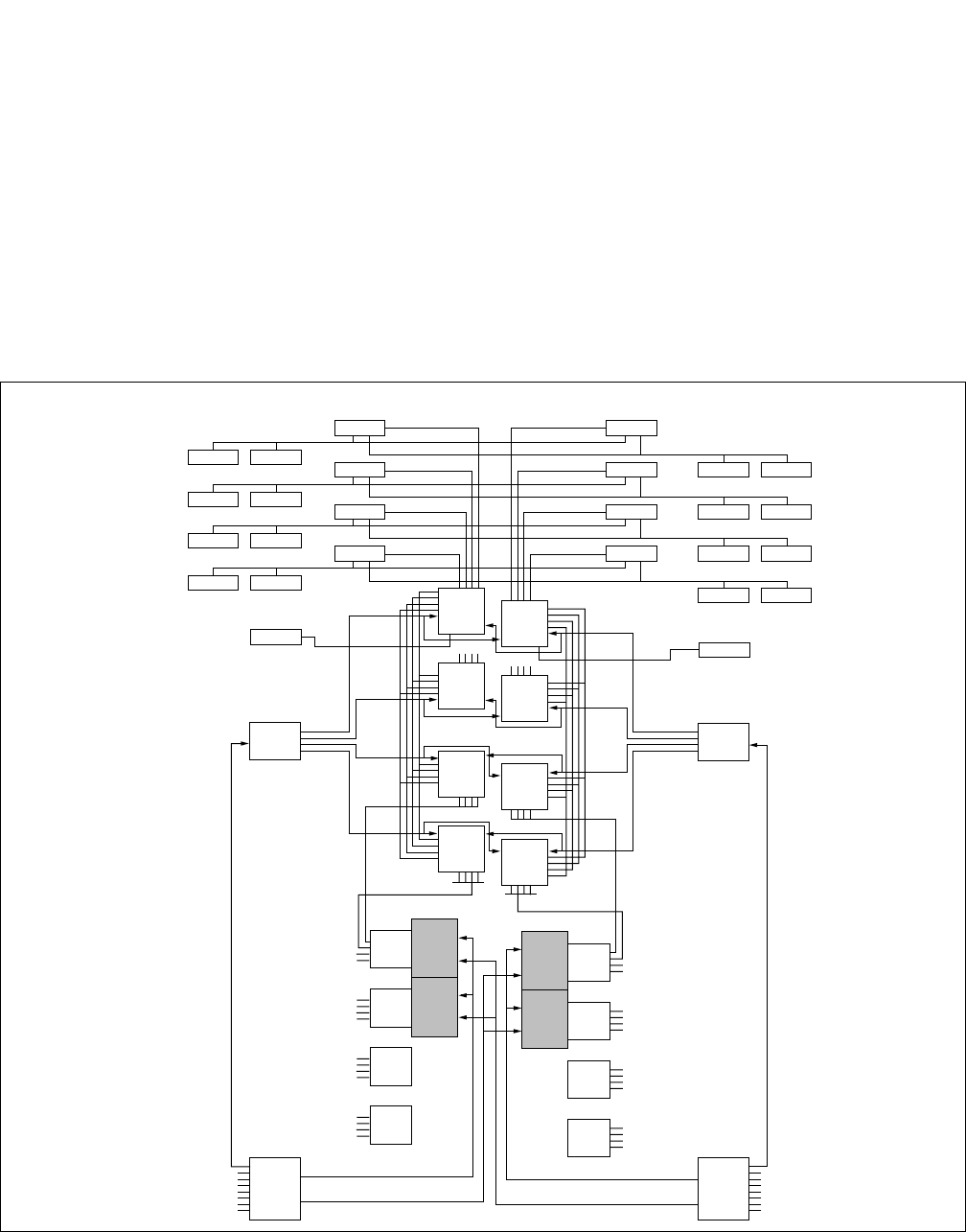
CHAPTER 2 NDA-24296
Page 140
Revision 1.0
PU-SW01
Highway Switch
PU-SW01
Highway Switch
1. General Function
The PU-SW01 circuit card, which is used for the IPX-U/IPX-UMG system, supports the following
functions.
(a) The switch composition is T-T-S-T (T: Time division, S: Space division, T: Time division), and the
space division is composed with this circuit card.
(b) This circuit card collects the 16 highways of PCM data from and sends 8 highways to TSW by one
card. It is used to perform 16 highways switching by 2 PU-SW01 cards.
Figure 2-65 Location of PU-SW01 (HSW)
MUX00
LC/TRK
LC/TRK
LC/TRK
LC/TRK
DLKC0
LC/TRK
LC/TRK
LC/TRK
LC/TRK
LC/TRK
LC/TRK
LC/TRK
LC/TRK
LC/TRK
LC/TRK
LC/TRK
LC/TRK
MUX01
MUX02
MUX03
MUX10
MUX11
MUX12
MUX13
TSW00 TSW10
TSW01 TSW11
TSW02 TSW12
TSW03 TSW13
PLO 0
PLO 0
DLKC1
PLO 1
PLO 1
MUX MUX
TSW00
TSW01
TSW02
TSW03
HSW00
HSW01
HSW10
HSW11
TSW10
TSW11
TSW12
TSW13
2M PCM HW x8
2M PCM HW x8
2M PCM HW x8
2M PCM HW x8
2M PCM HW x8
2M PCM HW x8
2M PCM HW x8
2M PCM HW x8
32M TSW
Matrix HW
32M SERIAL HW
32M SERIAL HW
x4
32M SERIAL HW
x4
32M SERIAL HW
x4
32M SERIAL HW
x4
64KHz
Clock
64KHz
Clock
32M TSW
Matrix HW
32.768MHz Clock
DCS
32.768MHz Clock
DCS
32.768MHz Clock 32.768MHz Clock
[TSW Configuration]
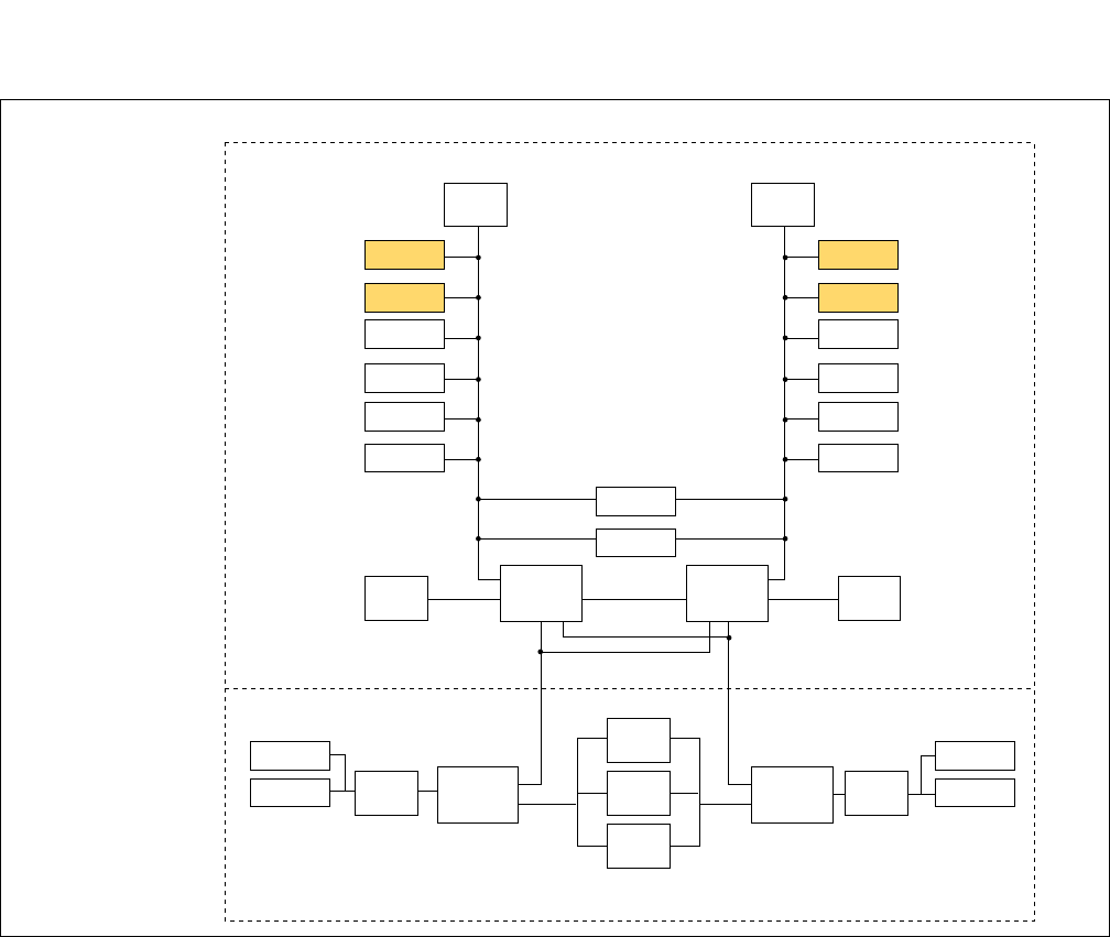
NDA-24296 CHAPTER 2
Page 141
Revision 1.0
PU-SW01
Highway Switch
Figure 2-65 Location of PU-SW01 (HSW) for IPX-U System
HSW01
HSW00
TSW03
TSW02
TSW01
TSW00
LANI
LANI
LANI
LANI
HSW11
HSW10
TSW13
TSW12
TSW11
TSW10
PLO 1
PLO 0
RES
CPU CPU
MISC
IOC
EMA
RES
RES RES
IOGT1
IOGT0
ISAGT ISAGT
MISC I/O BUS
ISAGT BUSISAGT BUS LPM
TSW I/O BUSTSW I/O BUS
ISWM
[INT Configuration]
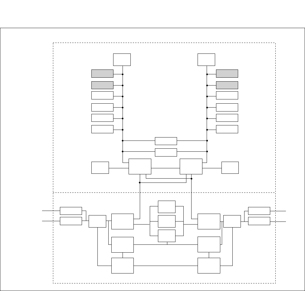
CHAPTER 2 NDA-24296
Page 142
Revision 1.0
PU-SW01
Highway Switch
Figure 2-65 Location of PU-SW01 (HSW) for IPX-UMG System
ISAGT2 ISAGT2
PCI MEM
PCI BUS PCI BUS
PCI MEM
HSW01
HSW00
TSW03
TSW02
TSW01
TSW00
LANI
LANI
LANI
LANI
HSW11
HSW10
TSW13
TSW12
TSW11
TSW10
PLO 1
PLO 0
RES
CPU CPU
MMC
MISC
EMA
RES
RES RES
IOGT1
IOGT0
ISAGT ISAGT
MISC
I/O
BUS
MISC
I/O
BUS
ISAGT BUS
P-BUS
ISAGT BUS
P-BUS
CMP
TSW I/O BUSTSW I/O BUS
ISWM
[INT Configuration]
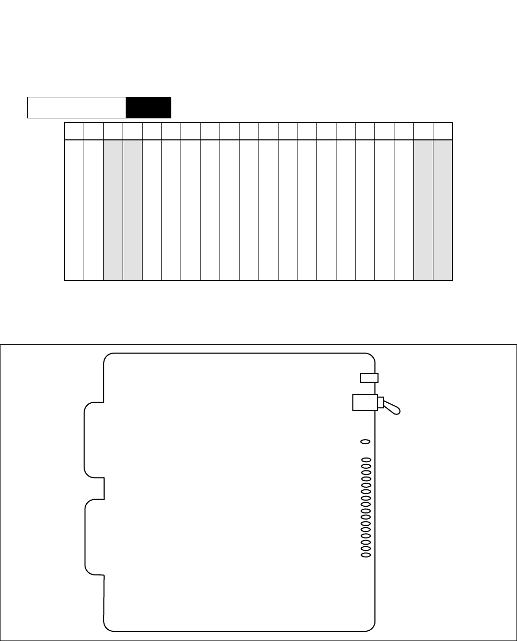
NDA-24296 CHAPTER 2
Page 143
Revision 1.0
PU-SW01
Highway Switch
2. Mounting Location/Condition
This circuit card is mounted in ISWM located in the ISW/CMG. The mounted slots are the shaded parts
shown below.
3. Face Layout of lamps, Switches, and Connectors
The face layout of lamps, switches, and connectors are shown in Figure 2-66.
Figure 2-66 Face Layout of PU-SW01 (HSW)
00 01 02 03 04 05 06 07 08 09 10 11 12 13 14 15 16 17 18 19
Mounting Module ISWM
HSW (00)
HSW (01)
HSW (10)
HSW (11)
MB
HSWACT
PWRALM
CKALF
CKALE
CKALD
CKALC
CKALB
CKALA
CKAL9
CKAL8
CKAL7
CKAL6
CKAL5
CKAL4
CKAL3
CKAL2
CKAL1
CKAL0

CHAPTER 2 NDA-24296
Page 144
Revision 1.0
PU-SW01
Highway Switch
4. Lamp Indications
Lamp indications for this circuit card are shown in the table below.
LAMP NAME COLOR STATE
HSWACT Green Lights when the HSW block is active.
Red Lights when the HSW block is in Make-busy state.
PWPALM Red Lights when the On-Board Power Supply (-48 V) for this circuit card is abnormal.
CKALF Green Lights when the clock/Frame Head signals are sent from #15 circuit of TSW in ISWM.
Off Goes off when the clock/Frame Head signals are not sent from #15 circuit of TSW in ISWM.
CKALE Green Lights when the clock/Frame Head signals are sent from #14 circuit of TSW in ISWM.
Off Goes off when the clock/Frame Head signals are not sent from #14 circuit of TSW in ISWM.
CKALD Green Lights when the clock/Frame Head signals are sent from #13 circuit of TSW in ISWM.
Off Goes off when the clock/Frame Head signals are not sent from #13 circuit of TSW in ISWM.
CKALC Green Lights when the clock/Frame Head signals are sent from #12 circuit of TSW in ISWM.
Off Goes off when the clock/Frame Head signals are not sent from #12 circuit of TSW in ISWM.
CKALB Green Lights when the clock/Frame Head signals are sent from #11 circuit of TSW in ISWM.
Off Goes off when the clock/Frame Head signals are not sent from #11 circuit of TSW in ISWM.
CKALA Green Lights when the clock/Frame Head signals are sent from #10 circuit of TSW in ISWM.
Off Goes off when the clock/Frame Head signals are not sent from #10 circuit of TSW in ISWM.
CKAL9 Green Lights when the clock/Frame Head signals are sent from #09 circuit of TSW in ISWM.
Off Goes off when the clock/Frame Head signals are not sent from #09 circuit of TSW in ISWM.
CKAL8 Green Lights when the clock/Frame Head signals are sent from #08 circuit of TSW in ISWM.
Off Goes off when the clock/Frame Head signals are not sent from #08 circuit of TSW in ISWM.
CKAL7 Green Lights when the clock/Frame Head signals are sent from #07 circuit of TSW in ISWM.
Off Goes off when the clock/Frame Head signals are not sent from #07 circuit of TSW in ISWM.
CKAL6 Green Lights when the clock/Frame Head signals are sent from #06 circuit of TSW in ISWM.
Off Goes off when the clock/Frame Head signals are not sent from #06 circuit of TSW in ISWM.
CKAL5 Green Lights when the clock/Frame Head signals are sent from #05 circuit of TSW in ISWM.
Off Goes off when the clock/Frame Head signals are not sent from #05 circuit of TSW in ISWM.
CKAL4 Green Lights when the clock/Frame Head signals are sent from #04 circuit of TSW in ISWM.
Off Goes off when the clock/Frame Head signals are not sent from #04 circuit of TSW in ISWM.
NDA-24296 CHAPTER 2
Page 145
Revision 1.0
PU-SW01
Highway Switch
5. Switch Settings
Switch settings on this circuit card are shown in the table below.
6. External Interface
No cable connections are required.
7. Switch Setting Sheet
CKAL3 Green Lights when the clock signal is sent normally from #03 circuit of TSW in ISWM.
Off Goes off when the clock failure occurs on #03 circuit of TSW in ISWM.
CKAL2 Green Lights when the clock/Frame Head signals are sent from #02 circuit of TSW in ISWM.
Off Goes off when the clock/Frame Head signals are not sent from #02 circuit of TSW in ISWM.
CKAL1 Green Lights when the clock/Frame Head signals are sent from #01 circuit of TSW in ISWM.
Off Goes off when the clock/Frame Head signals are not sent from #01 circuit of TSW in ISWM.
CKAL0 Green Lights when the clock/Frame Head signals are sent from #00 circuit of TSW in ISWM.
Off Goes off when the clock/Frame Head signals are not sent from #00 circuit of TSW in ISWM.
SWITCH
NAME SETTING STANDARD
SETTING MEANING
MB UP Circuit card Make-busy.
DOWN ×Circuit card Make-busy cancel.
SWITCH NAME SWITCH SHAPE REMARKS
MB
LAMP NAME COLOR STATE
ON
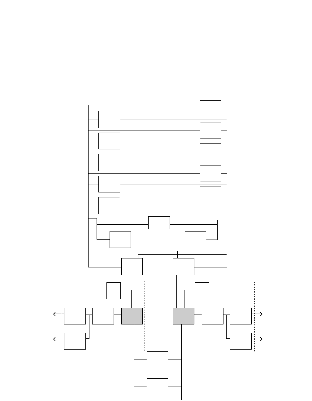
CHAPTER 2 NDA-24296
Page 146
Revision 1.0
PZ-GT13
Industrial Standard Architecture Gateway
PZ-GT13
Industrial Standard Architecture Gateway
1. General Function
The PZ-GT13 (ISAGT) circuit card controls the TSDW, DLKC, PLO etc. using the PH-GT09 (GT) in the
TSWM. This card also provides the MISC I/O bus interface, which permits a microprocessor on the CPR
to control EMA and IOC/MISC. The Industrial Standard Architecture (ISA) bus is used to connect this
circuit card onto the CPR.
Figure 2-67 Location of PZ-GT13 (ISAGT)
PLO0
PLO1
TSW03
TDSW I/O
Local Bus
TDSW I/O
Local Bus
TSW13
TSW02
TSW12
TSW01
TSW11
TSW00
DLKC0
MISC
ISAGT
DSP
CPULANI
LANI
GT
TSW10
CPR #0
To HUB
To HUB
To HUB
To HUB
ISAGT
GT
DLKC1
DSP
CPU
CPR #1
LANI
LANI
EMA
IOC/
MISC
MISC I/O Bus MISC I/O Bus
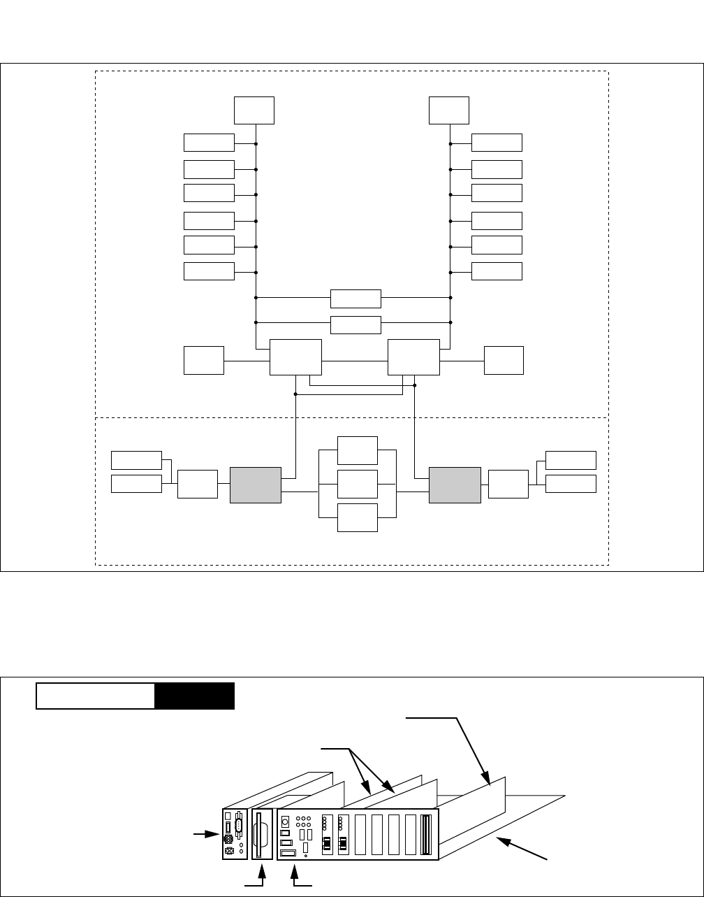
NDA-24296 CHAPTER 2
Page 147
Revision 1.0
PZ-GT13
Industrial Standard Architecture Gateway
Figure 2-68 Location of PZ-GT13 (ISAGT) in the IPX-U System (ISW)
2. Mounting Location/Condition
The PZ-GT13 is located on the ISA bus which is allocated in the CPR as shown in Figure 2-69.
Figure 2-69 External Interface for PZ-GT13
HSW01
HSW00
TSW03
TSW02
TSW01
TSW00
LANI
LANI
LANI
LANI
HSW11
HSW10
TSW13
TSW12
TSW11
TSW10
PLO 1
PLO 0
RES
CPU CPU
MISC
IOC
EMA
RES
RES RES
(IOGT1)
PH-GT10
(IOGT0)
PH-GT10
(ISAGT)
PZ-GT13 (ISAGT)
PZ-GT13
MISC I/O BUS
ISAGT BUSISAGT BUS LPM
TSW I/O BUSTSW I/O BUS
ISWM
PZ-GT13 (ISAGT)
CPU BOARD
PZ-DK224 (DSP)
PZ-PC19 (LANI)
PZ-PW92 (PWR)
PZ-IO27 (FDD/HDD)
LPM
Mounting Module
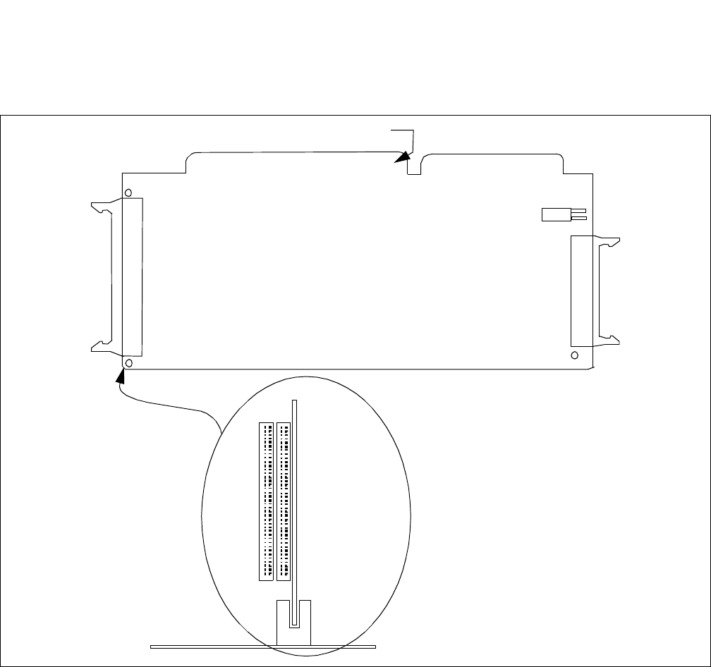
CHAPTER 2 NDA-24296
Page 148
Revision 1.0
PZ-GT13
Industrial Standard Architecture Gateway
3. Face Layout of Connectors
The face layout of connectors is shown in Figure 2-70. There are no lamps or switches on this circuit card.
Figure 2-70 Face Layout of PZ-GT13 (ISAGT)
4. External Interface
This card has no lamps.
5. Switch Settings
No switch settings are required.
6. External Interface
See the NEAX2400 IPX Installation Manual.
7. Switch Setting Sheet
No switch settings are required.
FRONT VIEW
AB
ISA BUS INTERFACE
CONN
PMG
DSPP
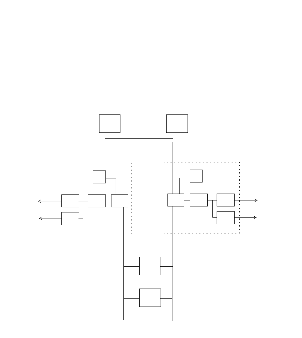
NDA-24296 CHAPTER 2
Page 149
Revision 1.0
PZ-GT16
Industrial Standard Architecture Gateway
PZ-GT16
Industrial Standard Architecture Gateway
1. General Function
The PZ-GT16 (ISAGT) circuit card provides both the I/O Local bus and the MISC bus interface, which
permits a microprocessor on the CPR to control the lower echelons of circuit cards. The Industry Standard
Architecture (ISA) bus is used to connect this circuit card onto the CPR.
Figure 2-71 Location of PZ-GT16 (ISAGT)
DSP
CPU
LANI
LANI
CPR#0
DSP
ISAGT CPU LANI
LANI
EMA
IOC/
MISC
TSW TSW
To HUB To HUB
To HUB To HUB
I/O Local Bus I/O Local Bus
CPR#1
MISC Bus MISC Bus
ISAGT
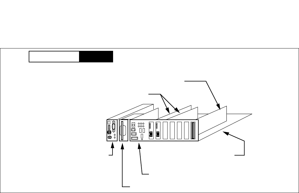
CHAPTER 2 NDA-24296
Page 150
Revision 1.0
PZ-GT16
Industrial Standard Architecture Gateway
2. Mounting Location/Condition
The PZ-GT16 (ISAGT) is located on the ISA bus, which is allocated in the CPR as shown in Figure 2-72.
Figure 2-72 External Interface for PZ-GT16
PZ-GT16 (GT)
CPU BOARD
PZ-DK224 (DSP)
PZ-PC19 (LANI)
PZ-PW92 (PWR)
PZ-IO27 (FDD/HDD)
LPM
Mounting Module
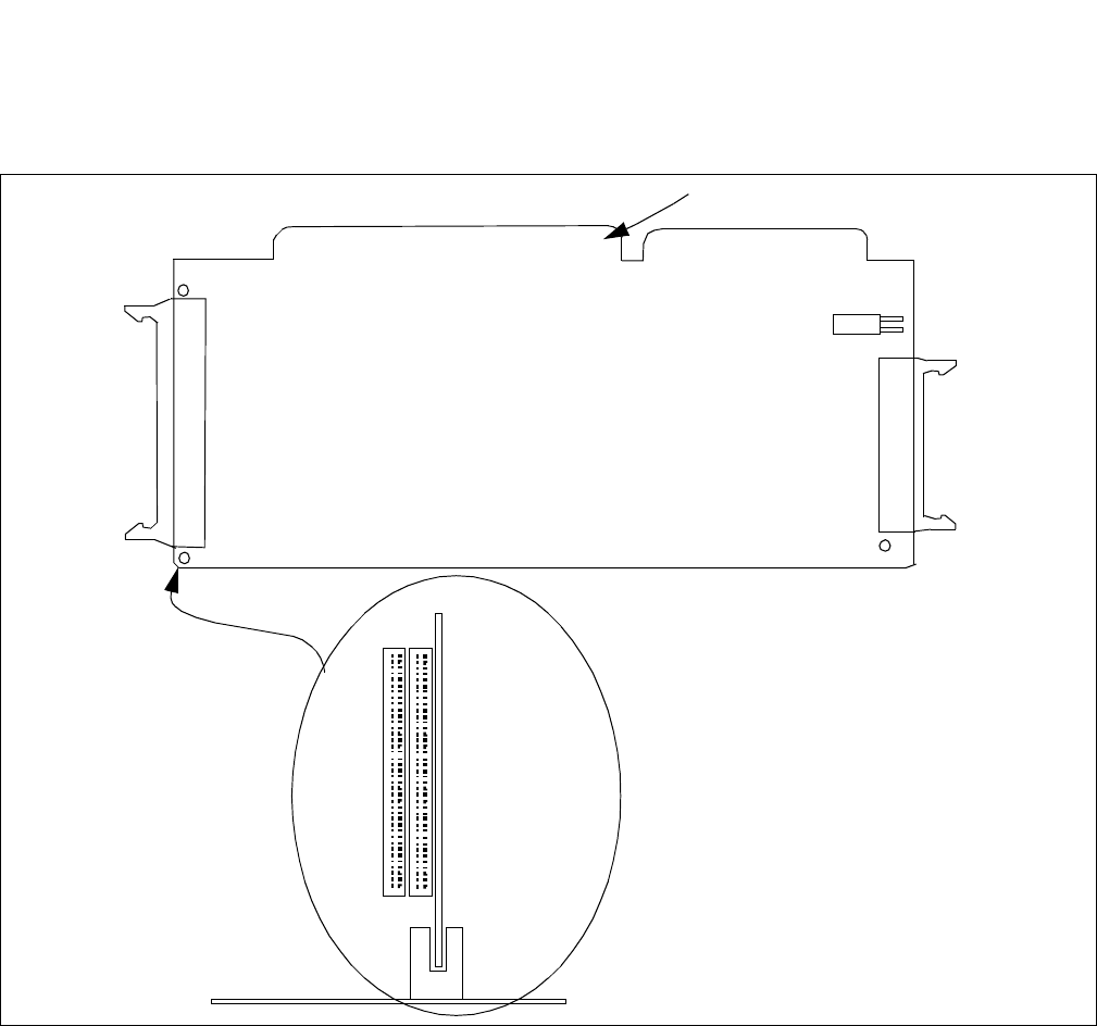
NDA-24296 CHAPTER 2
Page 151
Revision 1.0
PZ-GT16
Industrial Standard Architecture Gateway
3. Face Layout of Connectors
The face layout of connectors is shown in Figure 2-73. There are no lamps or switches on this circuit card.
Figure 2-73 Face Layout of PZ-GT16 (ISAGT)
4. Lamp Indications
This card contains no lamps.
5. Switch Settings
No switch settings are required.
6. External Interface
See the NEAX2400 IPX Installation Manual.
7. Switch Setting Sheet
No switch settings are required.
FRONT VIEW
AB
ISA BUS INTERFACE
CONN
PMG
DSPP
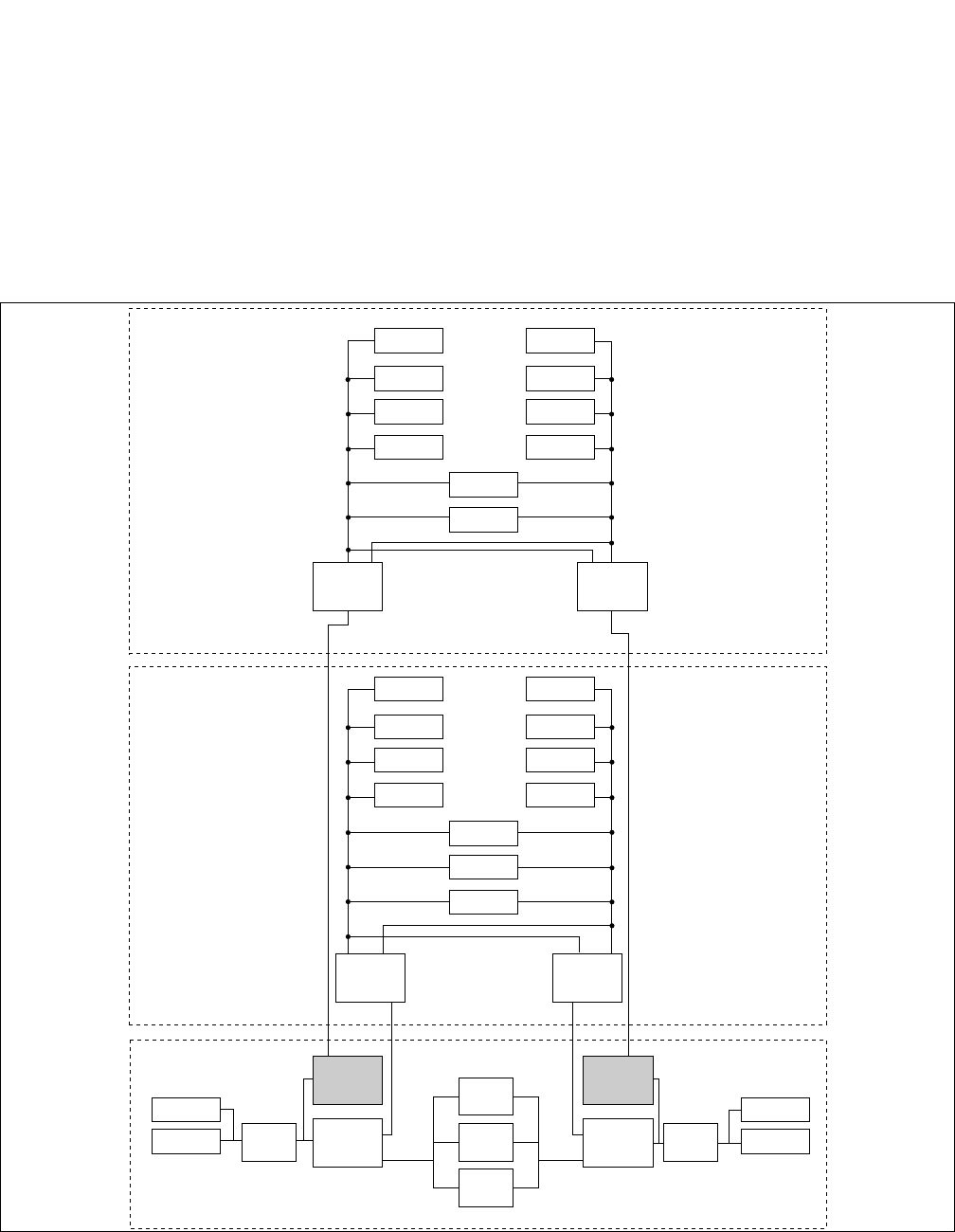
CHAPTER 2 NDA-24296
Page 152
Revision 1.0
PZ-GT20
Industry Standard Architecture Gateway
PZ-GT20
Industry Standard Architecture Gateway
1. General Function
The main function of the PZ-GT20 circuit card is to connect the Industry Standard Architecture (ISA) bus
located on the CPU and the Local I/O bus, permitting the microprocessor on the CPU to control the TSW,
MUX cards of IMG2, 3/6, 7/10, 11/14, 15 via the PH-GT09 card in the TSWM1. This circuit card is used
for the IPX-U/IPX-UMG system.
Figure 2-74 Location of PZ-GT20 (ISAGT)
TSW03
TSW02
TSW01
TSW00
LANI
LANI
LANI
LANI
TSW13
TSW12
TSW11
TSW10
PLO 1
PLO 0
CPU#0 CPU#1
EMA
MMC
PH-GT09
(IOGT1)
PH-GT09
(IOGT0)
PZ-GT13
(ISAGT)
PZ-GT20
(ISAGT) PZ-GT20
(ISAGT)
PZ-GT13
(ISAGT)
ISA BUS
ISA BUS
LPM (IMG0/4/8/12)
GT-BUS
GT-BUS
TSWM#1 (IMG2/6/10/14)
TSWM#0 (IMG1/5/9/13)
TSW03
TSW02
TSW01
TSW00
TSW13
TSW12
TSW11
TSW10
CLK 1
CLK 0
PH-GT09
(IOGT1)
PH-GT09
(IOGT0)
TSW I/O BUS
TSW I/O BUS
IOC/
MISC
MISC
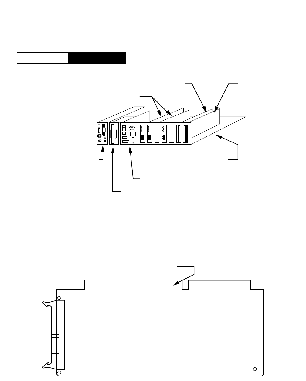
NDA-24296 CHAPTER 2
Page 153
Revision 1.0
PZ-GT20
Industry Standard Architecture Gateway
2. Mounting Location/Condition
The PZ-GT20 resides on the ISA bus that is located in the CPR as shown in Figure 2-75.
Figure 2-75 External Interface for PZ-GT20
3. Face Layout of Connectors
The face layout of connectors are shown in Figure 2-76. There are no lamps or switches on this circuit card.
Figure 2-76 Face Layout of PZ-GT20 (ISAGT)
PZ-GT20 (ISAGT) PZ-GT13 (ISAGT)
CPU BOARD
PZ-DK224 (DSP)
PZ-PC19/PC22 (LANI)
PZ-PW92 (PWR)
PZ-IO27/28 (FDD/HDD)
LP(IMG0/4/8/12)Mounting Module
Note: FDD/HDD is not mounted on the CPR of LP in IPX-UMG system.
ISA BUS INTERFACE

CHAPTER 2 NDA-24296
Page 154
Revision 1.0
PZ-GT20
Industry Standard Architecture Gateway
4. External Interface
This card contains no lamps.
5. Switch Settings
No switch settings are required.
6. External Interface
See the NEAX2400 IPX Installation Manual.
7. Switch Setting Sheet
No switch settings are required.
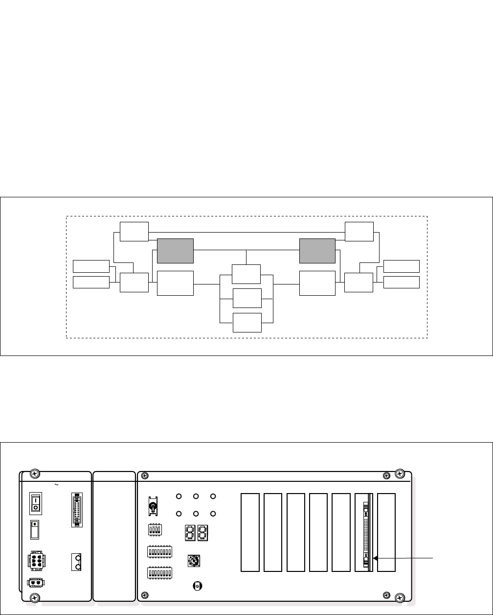
NDA-24296 CHAPTER 2
Page 155
Revision 1.0
PZ-M565
Industry Standard Architecture Gateway
PZ-M565
Industry Standard Architecture Gateway
1. General Function
This circuit card has the relay functions as mentioned below:
(a) to receive the NMI (Non-Maskable Interruption) signal from the PZ-ME44 (PCI MEM) card, then
output it to ISA Bus.
(b) to receive the ACT signal from the EMA card, then output it to PZ-ME44 (PCI MEM) card.
This card is used in IPX-UMG system connecting the two cards on CPU#0 and #1 in CMP with a bus cable.
Figure 2-77 Location of PZ-M565 (ISAGT) Card in the System
2. Mounting Location/Condition
The PZ-M565 (ISAGT) card is mounted in PCI Slot No.05 on CPU Board within the CMP of IPX-UMG
system as shown in Figure 2-78.
Figure 2-78 External Interface for PZ-M565
CMP
EMA
MISC
DSPC
/MMC
PZ-M565
(ISAGT2)
PZ-GT13
(ISAGT)
LANI
LANI CPU#0
PCI
MEM
ISA BUS
PZ-M565
(ISAGT2)
PZ-GT13
(ISAGT)
LANI
LANI
CPU#1
ISA BUS
PCI BUSPCI BUS PCI
MEM
5.0
A
CMP-CPR
PCI bus ISA bus
PZ-PW92
DC-40V -58.6
I
O
SW ON
OFF
ON
ALM
PALM
OUTPWR
INPWR
5A
125V
AC/DC
CPUOPE WDT IMG0
IMG1 IMG2 IMG3
PZ-M565
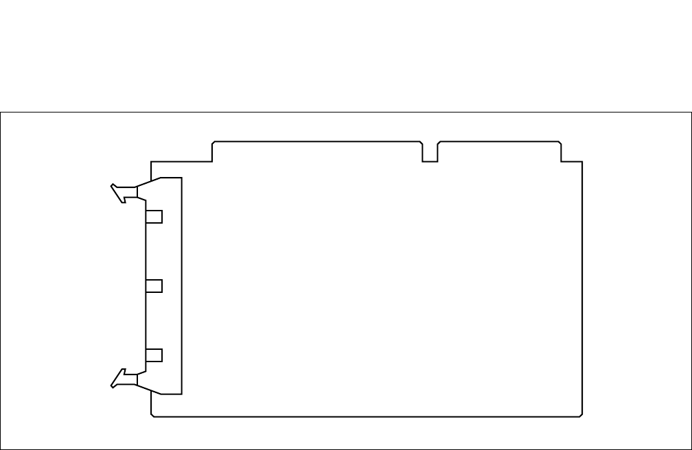
CHAPTER 2 NDA-24296
Page 156
Revision 1.0
PZ-M565
Industry Standard Architecture Gateway
3. Face Layout of Connectors
The face layout of connectors is shown below.
Figure 2-79 Face Layout of PZ-M565 (ISAGT) Card
4. Lamp Indications
This card contains no lamps.
5. Switch Settings
No switch settings are required.
6. External Interface
See the NEAX 2400 IPX-UMG Installation Manual.
7. Switch Setting Sheet
No switch settings are required.
CONN
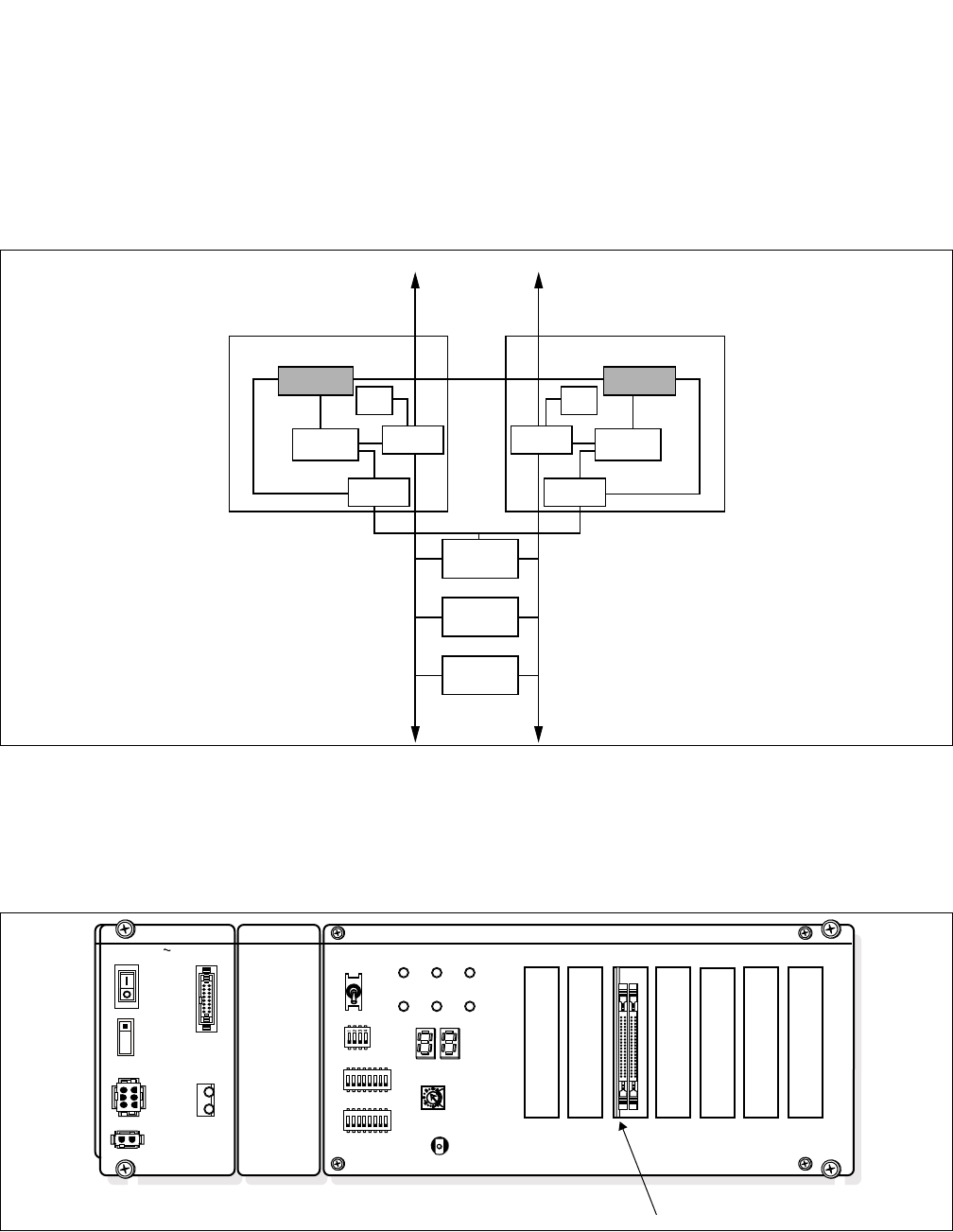
NDA-24296 CHAPTER 2
Page 157
Revision 1.0
PZ-ME44
PCI Memory
PZ-ME44
PCI Memory
1. General Function
Mounted on CPU Board of CMP in IPX-UMG system, this circuit card provides the Memory Copy
function related to ACT/ST-BY system changeover.
Figure 2-80 Location of PZ-ME44 (PCI MEM) Card in the System
2. Mounting Location/Condition
The PZ-ME44 (PCI MEM) card is mounted in PCI Slot No. 02 on CPU Board of CMP as shown in Figure
2-81.
Figure 2-81 External Interface for PZ-M44
EMA
MISC
DPSC
/MMC
I/O Local Bus I/O Local Bus
MISC Bus #0 MISC Bus #1
DSP
ISAGT
CPU
CPR #0
ISAGT2
DSP
CPU
CPR #1
ISAGT2
PCI MEMPCI MEM
ISAGT
5.0
A
PCI bus ISA bus
PZ-PW92
DC-40V -58.6
I
O
SW ON
OFF
ON
ALM
PALM
OUTPWR
INPWR
5A
125V
AC/DC
CPUOPE WDT IMG0
IMG1 IMG2 IMG3
PZ-ME44
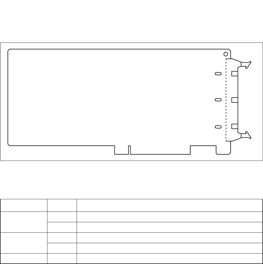
CHAPTER 2 NDA-24296
Page 158
Revision 1.0
PZ-ME44
PCI Memory
3. Face Layout of Connectors
The face layout of connectors and lamps is shown in Figure 2-82.
Figure 2-82 Face Layout of PZ-ME44 (PCI MEM) Card
4. Lamp Indications
The contents of lamp indications on this circuit card are shown in the table below.
5. Switch Settings
No switch settings are required.
6. External Interface
See the NEAX2400 IPX-UMG Installation Manual.
7. Switch Setting Sheet
No switch settings are required.
LAMP NAME COLOR DESCRIPTION
COPY Green Copy mode
OFF Self mode
SOFT Green Normally operating in copy mode (Valid when “copy” lamp lights)
OFF Remains OFF during ACT → STBY memory copy
WE Green Lights when Memory writing
CONN
COPY
SOFT
WE
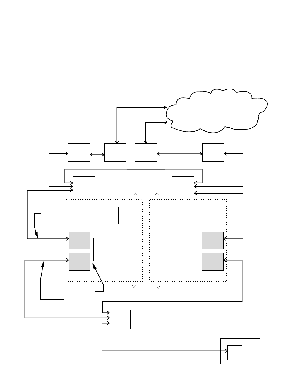
NDA-24296 CHAPTER 2
Page 159
Revision 1.0
PZ-PC19
Local Area Network Interface
PZ-PC19
Local Area Network Interface
1. General Function
The PZ-PC19 (LANI) circuit card provides the interface for the 10-BASE-T and the Peripheral Component
Interconnect (PCI) Bus. The microprocessor on the CPR sends/receives the Fusion Link Data and/or
Maintenance Administration Terminal (MAT) data across the LAN interface (LANI).
Figure 2-83 Location of PZ-PC19 (LANI)
To another Fusion Node
FCCHDTIDTIFCCH
HUB
HUB
HUB
LANI
LANI
LANI CPUISAGT
ISAGT
LANI
DSPDSP
CPR #1CPR #0
NIC
MAT
PCI
10-BASE-T
10-BASE-T
CPU
IMX
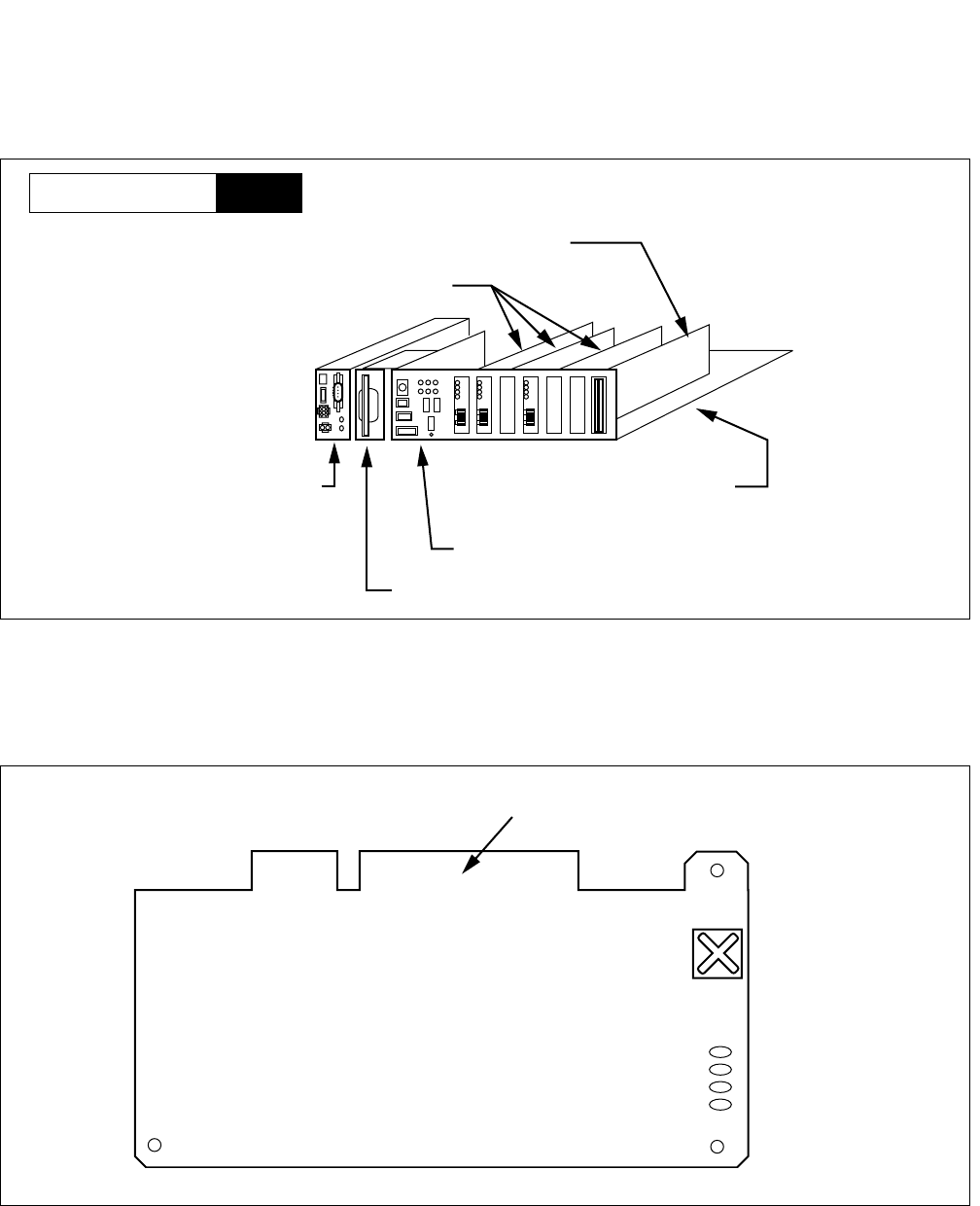
CHAPTER 2 NDA-24296
Page 160
Revision 1.0
PZ-PC19
Local Area Network Interface
2. Mounting Location/Condition
The PZ-PC19 (LANI) is located on the PCI bus in the CPR as shown in Figure 2-84.
Figure 2-84 External Interface for PZ-PC19
3. Face Layout of Lamps, Switches and Connectors
The face layout of lamps, switches and connectors is shown in Figure 2-85.
Figure 2-85 Face Layout of PZ-PC19 Card
Mounting Module LPM
PZ-GT13/GT16 (ISAGT)
CPU BOARD
PZ-DK224 (DSP)
PZ-PC19 (LANI)
PZ-PW92 (PWR)
PZ-IO27 (FDD/HDD)
10 BASE-T
EST3
EST2
EST1
EST0
PCI BUS INTERFACE

NDA-24296 CHAPTER 2
Page 161
Revision 1.0
PZ-PC19
Local Area Network Interface
4. Lamp Indications
Lamp indications for this circuit card are shown in the table below.
5. Switch Settings
No switch settings are required.
LAMP NAME COLOR DESCRIPTION
EST0 Green Layer 1 link has established.
EST1 Green Data packet sending/receiving.
EST2 Red Layer 1 link failure.
EST3 Yellow Data packet collision has occurred.
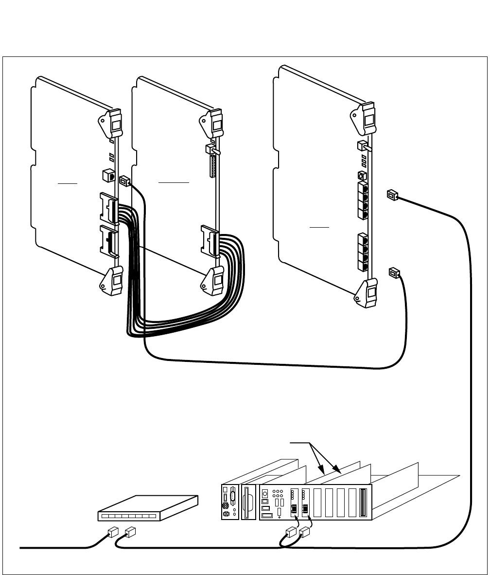
CHAPTER 2 NDA-24296
Page 162
Revision 1.0
PZ-PC19
Local Area Network Interface
6. External Interface
Figure 2-86 Cable Connections for PZ-PC19
7. Switch Setting Sheet
No switch settings are required.
24DTR
CN2
FCH
FCH
PZ-PC19(LANI)
HUB
10 BASE-T straight Cable10 BASE-T straight Cable
TO IMX MAT
10 BASE-T straight Cable
HUB
10AL (10)FLT CA
DTI
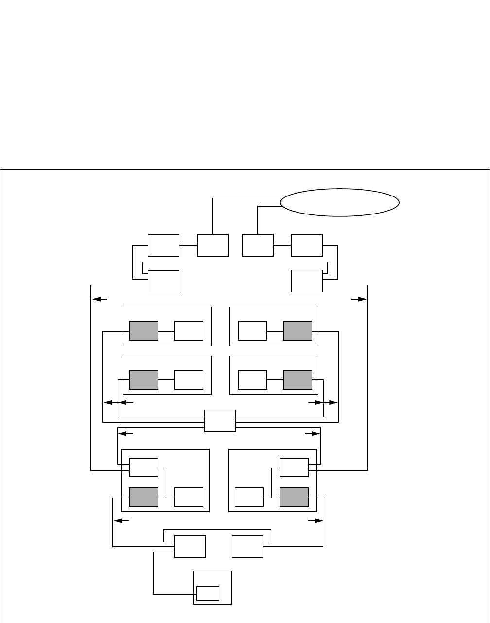
NDA-24296 CHAPTER 2
Page 163
Revision 1.0
PZ-PC22
Local Area Network Interface
PZ-PC22
Local Area Network Interface
1. General Function
The PZ-PC22 (LANI) circuit card is a single port Ether card that builds up Fusion link or Ether LAN
corresponding to 10BASE-T/100BASE-TX. The card is mounted on the Peripheral Component
Interconnect (PCI) bus slot in the CPR, and provides the interface to the Processor bus.
This card is mounted on the CPR of CMP/LP in the IPX-UMG system.
Figure 2-87 Location of PZ-PC22 (LANI) Card in the System
LAN CPU
LP#0
LAN CPU
CMP#0
LAN
LAN
CPU
SP#0
10BASE-T
10BASE-T
100BASE-TX
(P-BUS)
100BASE-TX
(P-BUS)
HUB
HUB
HUB
FCCH DTI
LANCPU
LP#1
LANCPU
CMP#1
LAN
LAN
CPU
SP#1
10BASE-T
10BASE-T
100BASE-TX
(P-BUS)
100BASE-TX
(P-BUS)
HUB
HUB
FCCHDTI
To other Fusion Node
NIC
MAT
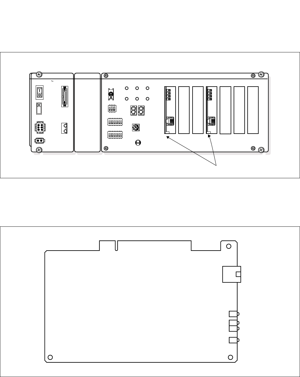
CHAPTER 2 NDA-24296
Page 164
Revision 1.0
PZ-PC22
Local Area Network Interface
2. Mounting Location/Condition
The PZ-PC22 (LANI) card is accommodated on the PCI bus in the CPR as shown in Figure 2-88.
Figure 2-88 Location of PZ-PC22
3. Face Layout of Connectors
The face layout of lamps, switches, and connectors are shown in Figure 2-89.
Figure 2-89 Face Layout of PZ-PC22 (LANI) Card
5.0
A
CMP-CPR/LP-CPR
PCI bus ISA bus
PZ-PW92
DC-40V -58.6
I
O
SW ON
OFF
ON
ALM
PALM
OUTPWR
INPWR
5A
125V
AC/DC
CPUOPE WDT IMG0
IMG1 IMG2 IMG3
PZ-PC22
100M
TXRX
LINK
COL
LAN

NDA-24296 CHAPTER 2
Page 165
Revision 1.0
PZ-PC22
Local Area Network Interface
4. Lamp Indications
The contents of lamp indications on this circuit card are shown in the table below.
5. Switch Settings
No switch settings are required.
LAMP NAME COLOR DESCRIPTION
100M Green 100MHz mode
TXRX Green Data packet sending/receiving
LINK Green Link has been established.
COL Yellow Data packet collision has occurred.
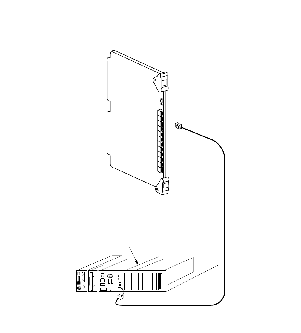
CHAPTER 2 NDA-24296
Page 166
Revision 1.0
PZ-PC22
Local Area Network Interface
6. External Interface
Figure 2-90 External Interface for PZ-PC22 (LANI)
7. Switch Setting Sheet
No switch settings are required.
PZ-PC22 (LANI)
HUB
100 BASE-TX Straight Cable
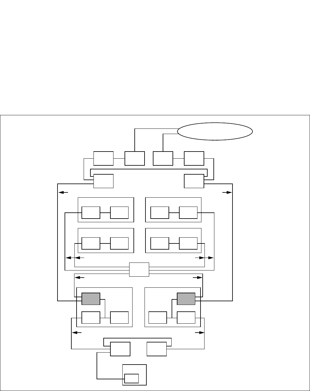
NDA-24296 CHAPTER 2
Page 167
Revision 1.0
PZ-PC23
Local Area Network Interface
PZ-PC23
Local Area Network Interface
1. General Function
The PZ-PC23 (LANI) circuit card is a multiple ports Ether card that builds up Fusion link or external Ether
LAN corresponding to 10BASE-T/100BASE-TX. In the IPX-UMG system, one connector is used for
Ethernet, and the other for Fusion link. The card is mounted on the Peripheral Component Interconnect
(PCI) bus slot within the CPR, and provides the interface to the Processor bus or Fusion link.
This card is mounted on the CPR of SP in the IPX-UMG system.
Figure 2-91 Location of PZ-PC23 (LANI) Card in the System
LAN CPU
LP#0
LAN CPU
CMP#0
LAN
LAN
CPU
SP#0
10BASE-T
10BASE-T
100BASE-TX
(P-BUS)
100BASE-TX
(P-BUS)
HUB
HUB
HUB
FCCH DTI
LANCPU
LP#1
LANCPU
CMP#1
LAN
LAN
CPU
SP#1
10BASE-T
10BASE-T
100BASE-TX
(P-BUS)
100BASE-TX
(P-BUS)
HUB
HUB
FCCHDTI
To other Fusion Node
NIC
MAT
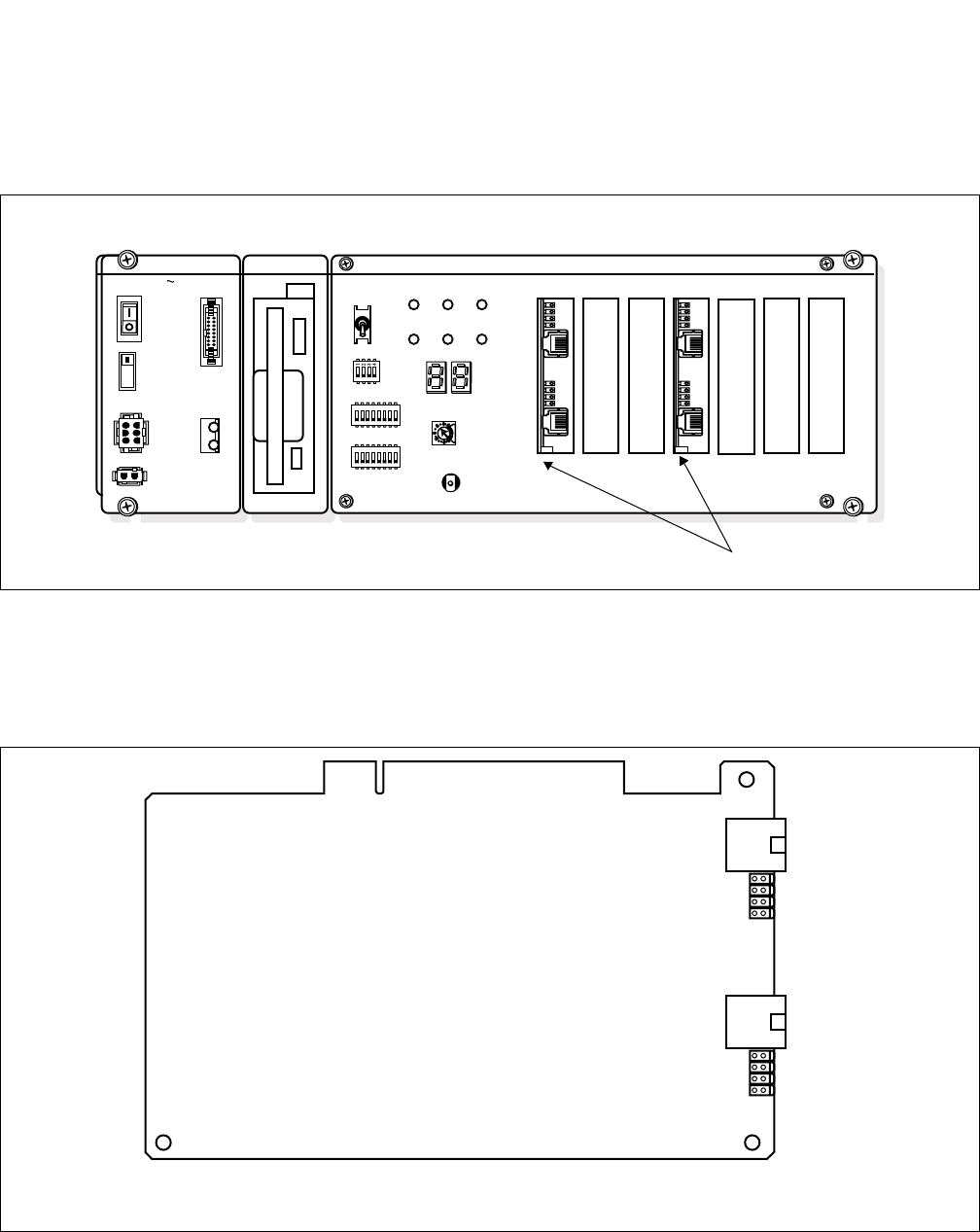
CHAPTER 2 NDA-24296
Page 168
Revision 1.0
PZ-PC23
Local Area Network Interface
2. Mounting Location/Condition
The PZ-PC23 (LANI) card is accommodated on the PCI bus Slot No.0 and No.3 in the CPR of SP as shown
in Figure 2-92.
Figure 2-92 Location for PZ-PC23
3. Face Layout of Connectors
The face layout of lamps, switches, and connectors are shown in Figure 2-93.
Figure 2-93 Face Layout of PZ-PC23 (LANI) Card
5.0
A
PCI bus ISA bus
PZ-PW92
DC-40V -58.6
I
O
SW ON
OFF
ON
ALM
PALM
OUTPWR
INPWR
5A
125V
AC/DC
CPUOPE WDT IMG0
IMG1 IMG2 IMG3
PZ-PC23
SP-CPR
100M0
TXRX0
LINK0
COL0
LAN0
Note
Note
100M1
TXRX1
LINK1
COL1
LAN1
Note: Connect the Ether cable to “LAN0” connector for Processor bus within the IPX-UMG system. When
Fusion network is used, connect the Ether cable to “LAN1” connector to establish Fusion link.

NDA-24296 CHAPTER 2
Page 169
Revision 1.0
PZ-PC23
Local Area Network Interface
4. Lamp Indications
The contents of lamp indications on this circuit card are shown in the table below.
5. Switch Settings
No switch settings are required.
LAMP NAME COLOR DESCRIPTION
100M0/1 Green 100MHz mode
LINK0/1 Green Link has been established.
TXRX0/1 Green Data packet sending/receiving
COL0/1 Yellow Data packet collision has occurred.
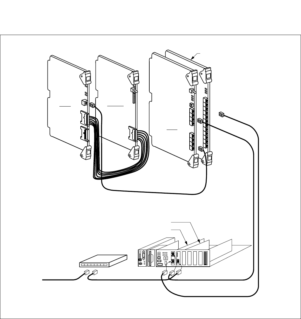
CHAPTER 2 NDA-24296
Page 170
Revision 1.0
PZ-PC23
Local Area Network Interface
6. External Interface
Figure 2-94 External Interface for PZ-PC23 (LANI)
7. Switch Setting Sheet
No switch settings are required.
24DTR
CN2
FCH
FCH
PZ-PC23(LANI)
PZ-PC19(LANI)
HUB
Connected to
the MAT
10 BASE-T Straight Cable
HUB
10AL (10)FLT CA
DTI
HUB(PH-CM103)
10 BASE-T Straight Cable 10 BASE-T Straight Cable
100 BASE-TX Straight Cable

NDA-24296 Chapter 3
Page 171
Revision 1.0
CHAPTER 3 LINE/TRUNK CIRCUIT CARD REFERENCE
1. GENERAL
This chapter explains the following items about circuit cards.
•General Function
Explains the general function and purpose for each control circuit card.
•Mounting Location/Condition
Explains the mounting location (mounting module name and slot number, etc.) of each circuit card. If there
are any conditions pertaining to mounting the circuit cards, they are also explained.
•Face Layout of Lamps, Switches, and Connectors
The locations of the lamps, switches, and connectors provided on each circuit card are illustrated by a face
layout.
•Lamp Indications
Names, colors, and indication states of lamps mounted on each circuit card are listed.
•Switch Settings
Each circuit card’s switches are listed with their names, switch numbers, setting and its meaning, standard
setting, etc.
• External Interface
If the lead outputs of the circuit card are provided by an LT connector, the relation between the mounting
slots and the LT connectors is illustrated by an LT Connector Lead Face Layout. If the lead outputs are
provided by other than an LT connector, or are provided by the circuit card front connector, the connector
lead locations and the connecting routes are shown.
In addition, a Switch Setting Sheet is provided at the end of the explanation of circuit cards.
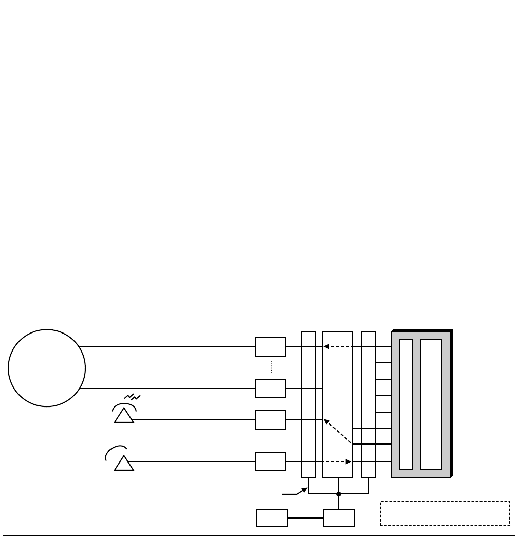
CHAPTER 3 NDA-24296
Page 172
Revision 1.0
PA-CFTB
8-party Conference Trunk
PA-CFTB
8-party Conference Trunk
1. General Function
The PA-CFTB (CFT) circuit card provides an interface for establishing a conference, which is made up of
a maximum of eight parties.
A maximum of seven Tie Lines can participate in a conference when the associated trunks can receive an
answer signal and a release signal from the distant switching system. On the other hand, in the case of a
C.O. line, one C.O. line can be connected even if the public switching system cannot send an answer signal
and/or release signal. Note that a Tie Line and a C.O. Line cannot take part in a conference at the same time.
The card adopts “N-1 addition” method for establishing a conference.
Note: This circuit card is used for following features:
•Station-Controlled Conference (Refer to Feature Programming Manual [S-56])
•Attendant-Controlled Conference (Refer to Feature Programming Manual [A-2])
•Add On Conference-8 Party (Refer to Feature Programming Manual [A-121])
•Group Call-Automatic Conference (20-party) (Refer to Wireless System Manual)
Figure 3-1 Location of PA-CFTB (CFT) within the System
NETWORK
Answer/Release Signal →
Conferee
Conference
Originator
CPU
Local I/O Bus
GT
INT SW INT PA-CFTB
7
6
5
4
3
2
1
0
PCM INT
VPROC
PCM INT: PCM Interface
VPROC: Voice Processor Block
TLT
TLT
LC
LC
CH
This diagram shows an example of a “Preset” conference involving Tie Line connections.
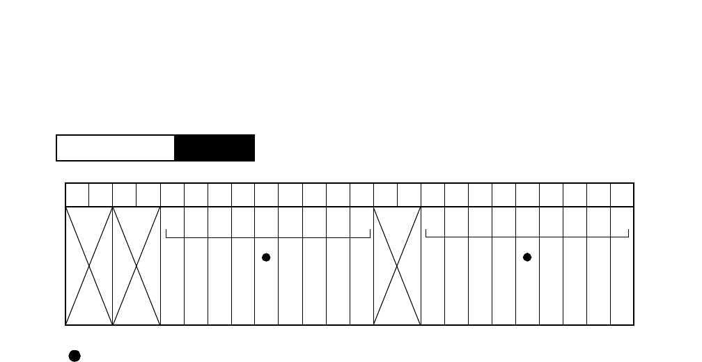
NDA-24296 CHAPTER 3
Page 173
Revision 1.0
PA-CFTB
8-party Conference Trunk
2. Mounting Location/Condition
The PA-CFTB (CFT) card can be mounted in any universal slot as shown below.
Note: Indicates universal slots for line/trunk circuit cards.
PIM
Mounting Module
00 01 02 03 04 05 06 07 08 09 10 11 12 13 14 15 16 17 18 19 20 21 22 23
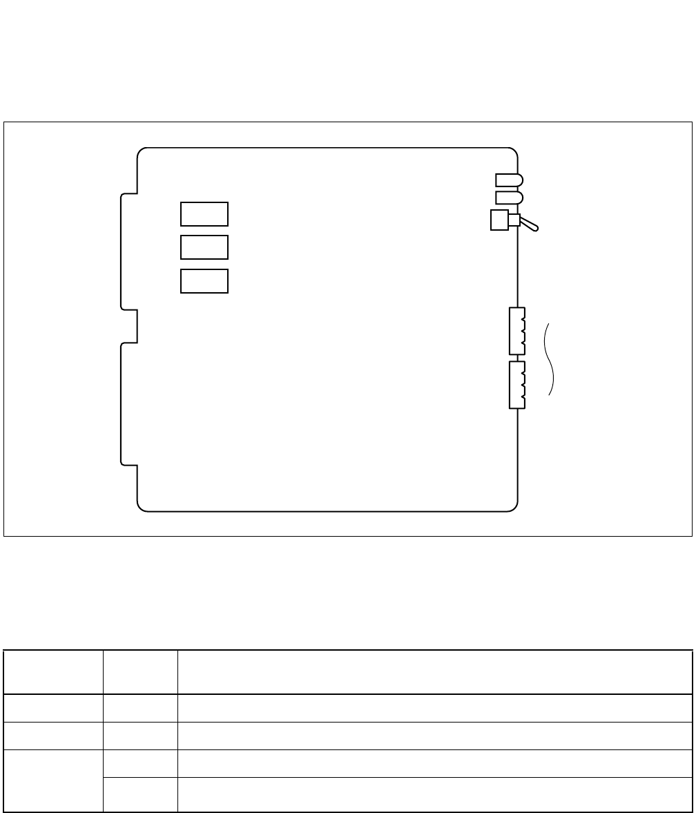
CHAPTER 3 NDA-24296
Page 174
Revision 1.0
PA-CFTB
8-party Conference Trunk
3. Face Layout of Lamps, Switches, and Connectors
The face layout of lamps, switches, and connectors on this circuit card is shown in Figure 3-2.
Figure 3-2 Face Layout of PA-CFTB (CFT)
4. Lamp Indications
The contents of lamp indications of this circuit card are shown in the table below.
LAMP
NAME COLOR STATE
OPE Green Remains lit while this circuit card is operating.
N-OPE Red Remains lit while this circuit card is in make-busy state.
BL0
BL7
Red BL-lamp remains lit while the corresponding circuit is busy.
Flash BL-lamp flashes when the corresponding circuit is busy.
OPE
N-OPE
MB
SW2
SW1
SW0
BL7
BL0
-
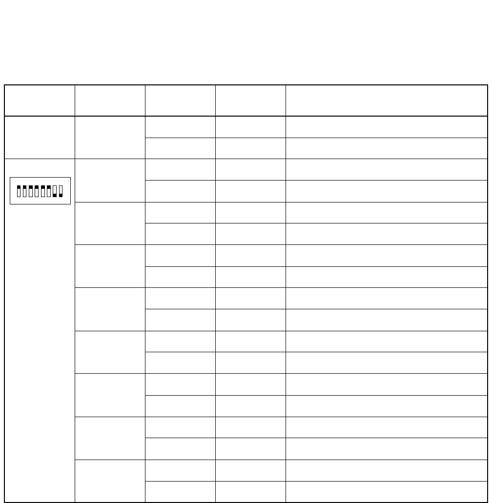
NDA-24296 CHAPTER 3
Page 175
Revision 1.0
PA-CFTB
8-party Conference Trunk
5. Switch Settings
Standard settings of switches on this circuit card are shown in the table below.
SWITCH
NAME SWITCH
NO. SETTING STANDARD
SETTING MEANING
MB UP Circuit card make busy
DOWN ×Circuit card make busy cancel
SW0
1ON ×Fixed in the system
OFF
2ON ×Fixed in the system
OFF
3ON ×Fixed in the system
OFF
4ON ×Fixed in the system
OFF
5ON ×Fixed in the system
OFF
6ON ×Fixed in the system
OFF
7ON
OFF ×Fixed in the system
8ON
OFF ×Fixed in the system
123456 78
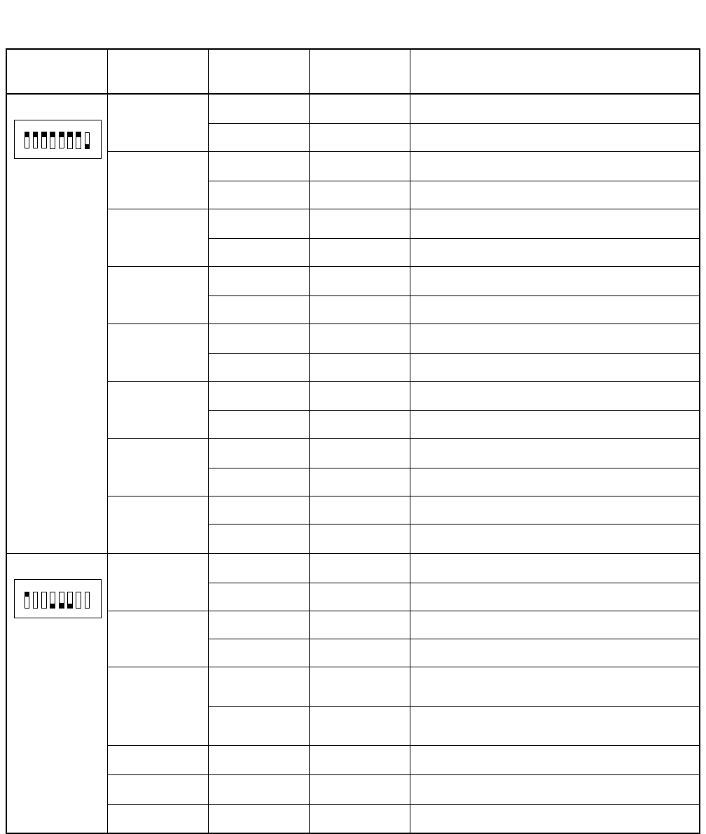
CHAPTER 3 NDA-24296
Page 176
Revision 1.0
PA-CFTB
8-party Conference Trunk
SW1
1ON ×Fixed in the system
OFF
2ON ×Fixed in the system
OFF
3ON ×Fixed in the system
OFF
4ON ×Fixed in the system
OFF
5ON ×Fixed in the system
OFF
6ON ×Fixed in the system
OFF
7ON ×Fixed in the system
OFF
8ON
OFF ×Fixed in the system
SW2
1ON ×µ-law PCM encoder
OFF A-law PCM encoder
2ON Conference connection is set up by PB tel.
OFF Conference connection is not set up by PB tel.
3
ON When port Microprocessor (PM) is SP-388, SP-
457, SP-863, SP-990, SP-1114.
OFF When Port Microprocessor (PM) is SP-519, SP-
1141.
4OFF×Not used
5OFF×Not used
6OFF×Not used
SWITCH
NAME SWITCH
NO. SETTING STANDARD
SETTING MEANING
12345678
1234 56 78
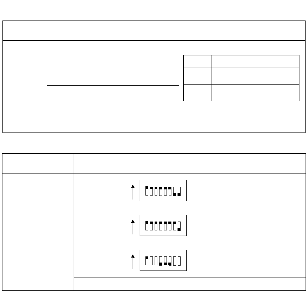
NDA-24296 CHAPTER 3
Page 177
Revision 1.0
PA-CFTB
8-party Conference Trunk
6. Switch Setting Sheet
SW2
7
ON CFTB Insertion Loss (PAD value) Setting
OFF
8
ON
OFF
MODULE SLOT
NO. SWITCH
NAME SWITCH SHAPE REMARKS
PIM
SW0
SW1
SW2
MB DOWN Circuit card make busy cancel
SWITCH
NAME SWITCH
NO. SETTING STANDARD
SETTING MEANING
SW2-7 SW2-8 PAD [dB]
OFF OFF 0
OFF ON 3
ON OFF 6
ON ON 9
123456 7 8
ON
12345678
ON
123456 7 8
ON
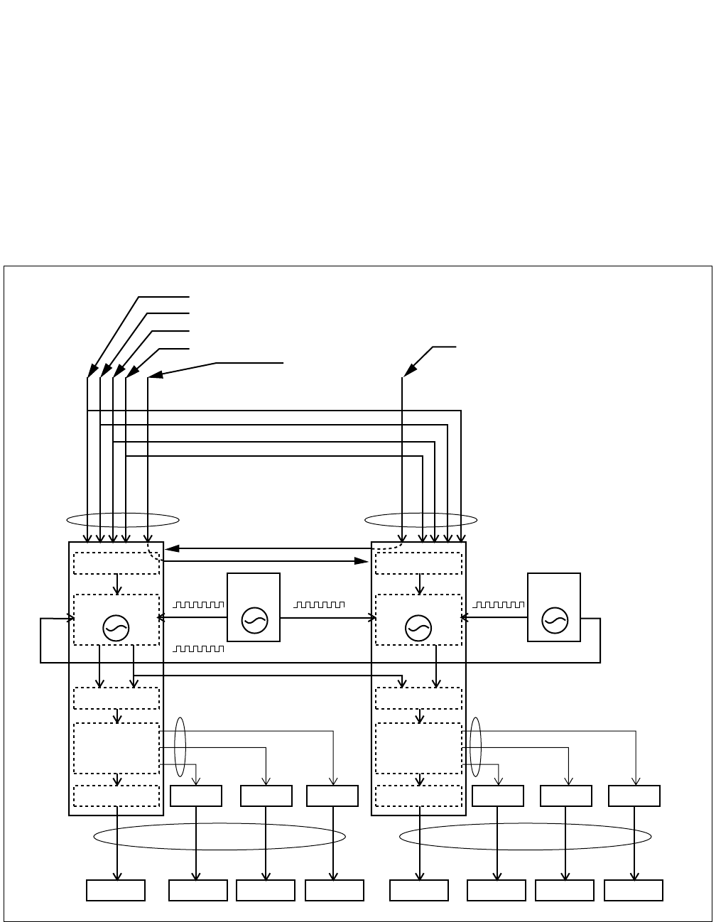
CHAPTER 3 NDA-24296
Page 178
Revision 1.0
PA-CK14
Oscillator
PA-CK14
Oscillator
1. General Function
The PLO block of the TSW card generates its base clock signals, and adjusts their phase with the source
clock signals so the PLO can send the synchronized clock signals to the TSW. When the 1 IMG system is
a clock-subordinate-office of the digital network, the base clock accuracy of the PLO/ PH-SW10 (±5 ppm
deviation) is sufficient. However, the more high-precision base clock signals are required at the clock-
source-office, as this circuit card provides --- PA-CK14 (±0.3 ppm deviation). When this circuit card is
mounted, the 1 IMG system selects the PA-CK14 (OSC) clocks as the base clock of the PLO.
Figure 3-3 Location of PA-CK14 (OSC) Card in the System
SEL
SEL
TDSW
MUX0
PLO
SEL
SEL
TDSW
MUX0
PLO
BWBBWB
BWB BWB
OSCOSC
DTI 0 CLOCK SOURCE
DTI 1 CLOCK SOURCE
DTI 2 CLOCK SOURCE
DTI 3 CLOCK SOURCE
DSC 0 DSC 1
FRONT CABLES FRONT CABLES
MUX1 MUX2 MUX3 MUX1 MUX2 MUX3
LC/TRKLC/TRKLC/TRKLC/TRKLC/TRKLC/TRKLC/TRKLC/TRK
DSC1
DSC0
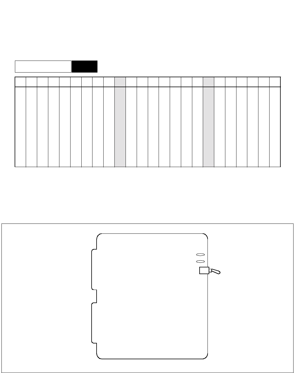
NDA-24296 CHAPTER 3
Page 179
Revision 1.0
PA-CK14
Oscillator
2. Mounting Location/Condition
The PA-CK14 (OSC) is located in Port Interface Module number zero (PIM 0). The card mounted in slot
number 09 works as the primary OSC, 17 for the secondary OSC.
Note: This card occupies two slots.
3. Face Layout of Lamps, Switches, and Connectors
The face layout of lamps, switches, and connectors is shown in Figure 3-4.
Figure 3-4 Face Layout of PA-CK14 (OSC) Card
00 01 02 03 04 05 06 07 08 09 10 11 12 13 14 15 16 17 18 19 20 21 22 23
Mounting Module PIM
OSC#0
OSC#1
PIM0
CLKOUT 0
CLKOUT 1
MB
CHAPTER 3 NDA-24296
Page 180
Revision 1.0
PA-CK14
Oscillator
4. Lamp Indications
Lamp indications for this circuit card are shown in the table below.
5. Switch Settings
Standard settings for switches on this circuit card are shown in the table below.
6. External Interface
Since the base clock signals are delivered through the printed-wiring on the Back Wired Board (BWB) of
PIM 0, this circuit card does not require any external cabling.
7. Switch Setting Sheet
LAMP NAME COLOR STATE
CLKOUT0 Green Lights when OSC card delivers the clock signals to TSW#0.
CLKOUT1 Green Lights when OSC card delivers the clock signals to TSW#1.
SWITCH
NAME SETTING STANDARD
SETTING MEANING
MB ON Make-busy of the circuit card.
OFF ×Normal setting.
SWITCH NAME SWITCH SHAPE REMARKS
MB
ON
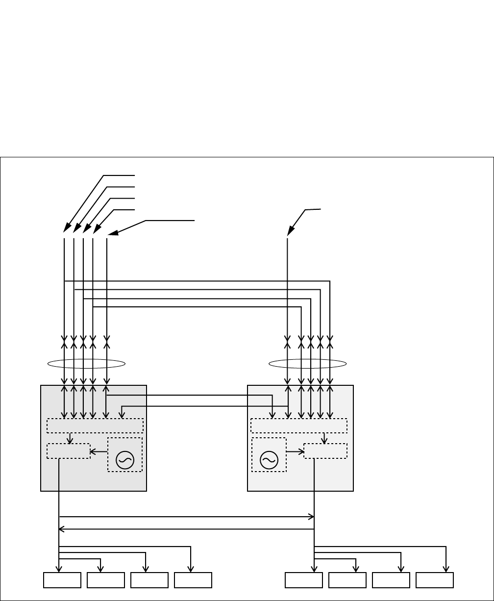
NDA-24296 CHAPTER 3
Page 181
Revision 1.0
PH-CK16
Phase Lock Oscillator
PH-CK16
Phase Lock Oscillator
1. General Function
This circuit card, used together with a direct digital interface circuit card, sets up network synchronization
with the network. With this circuit card, the 4 IMG system can be a clock subordinate office of the digital
network. As seen in Figure 3-5, the PLO can be redundant regardless of the system switching network
selection.
Figure 3-5 Location of PH-CK16 (PLO) Card in the System
TDSW00 TDSW01 TDSW02 TDSW03
SEL
PLL PLL
PLO #0 PLO #1
OSC OSC
TDSW10 TDSW11 TDSW12 TDSW13
SEL
34PH EXCLK CA-A 34PH EXCLK CA-A
MDF
MDF
BWB BWB
BWBBWB
DTI 0 CLOCK SOURCE
DTI 1 CLOCK SOURCE
DTI 2 CLOCK SOURCE
DTI 3 CLOCK SOURCE
DCS 0
DCS 1

CHAPTER 3 NDA-24296
Page 182
Revision 1.0
PH-CK16
Phase Lock Oscillator
The source clock of the clock subordinate office is either the digital clock supply (DCS) or the digital interface
clock (DIU0 - DIU3). When clock source failure has occurred, the PLO chooses another clock source
automatically in the order of:
1. DCS
2. DIU0
3. DIU1
4. DIU2
5. DIU3
6. PLO changeover or the PLO internal oscillator drifting
The PLO can output the clock signals (CLK) and the frame head signals (FH) as follows:
•32.768 MHz CLK
•8 KHz FH
•5 msec × “n” FH
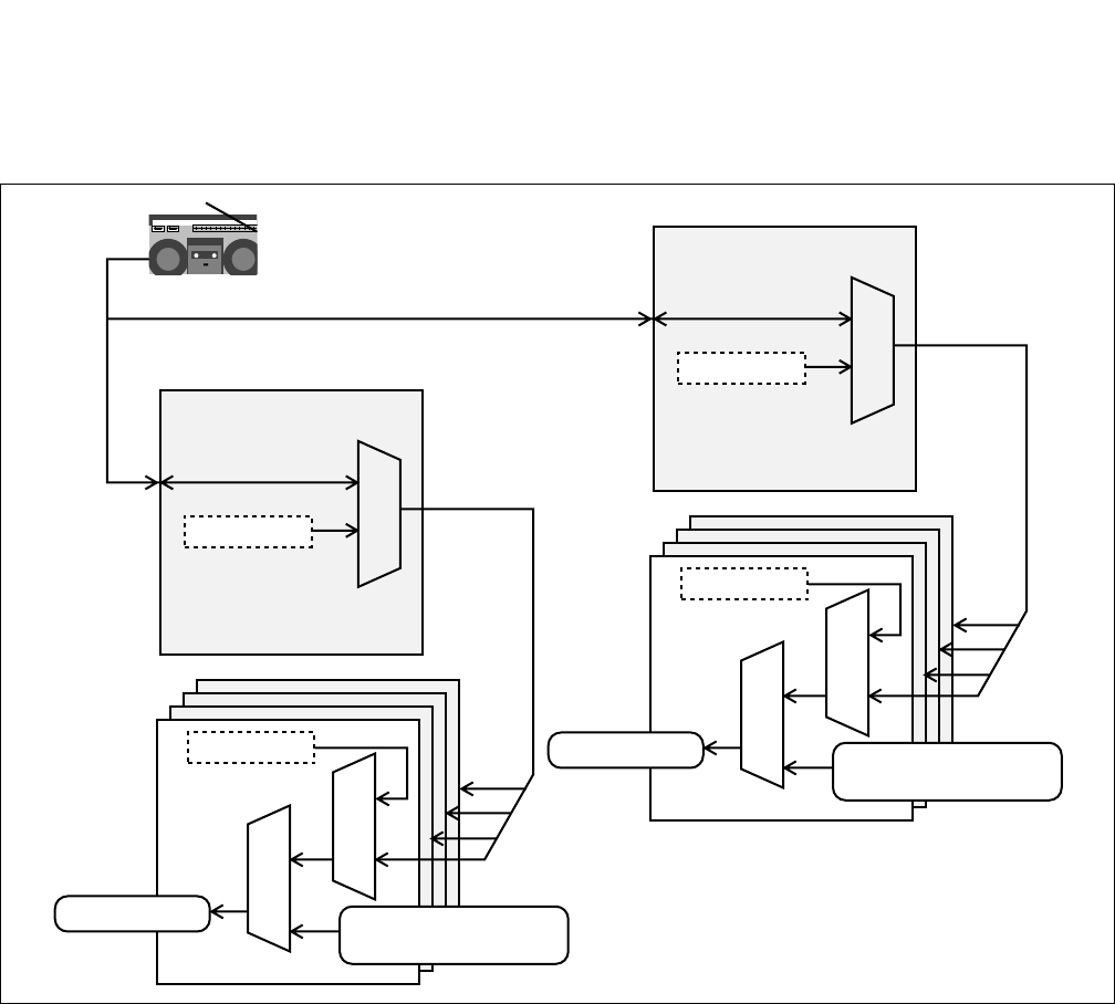
NDA-24296 CHAPTER 3
Page 183
Revision 1.0
PH-CK16
Phase Lock Oscillator
The MUSIC ROM located on this circuit card also contains the hold tone, and is supplied to the TSW circuit
card. When an external music on hold is applied to the 4 IMG system, this circuit card provides the interface for
the external hold tone source.
Figure 3-6 Music Source
SEL
SEL
SEL
Speech Path Memory
for Music/Tone
Music/Tone
MUSIC ROM
TDSW00
PLO#0
TONE ROM
SEL
SEL
SEL
Speech Path Memory
for Music/Tone
Music/Tone
MUSIC ROM
TDSW1
PLO#1
TONE ROM
FM
FM
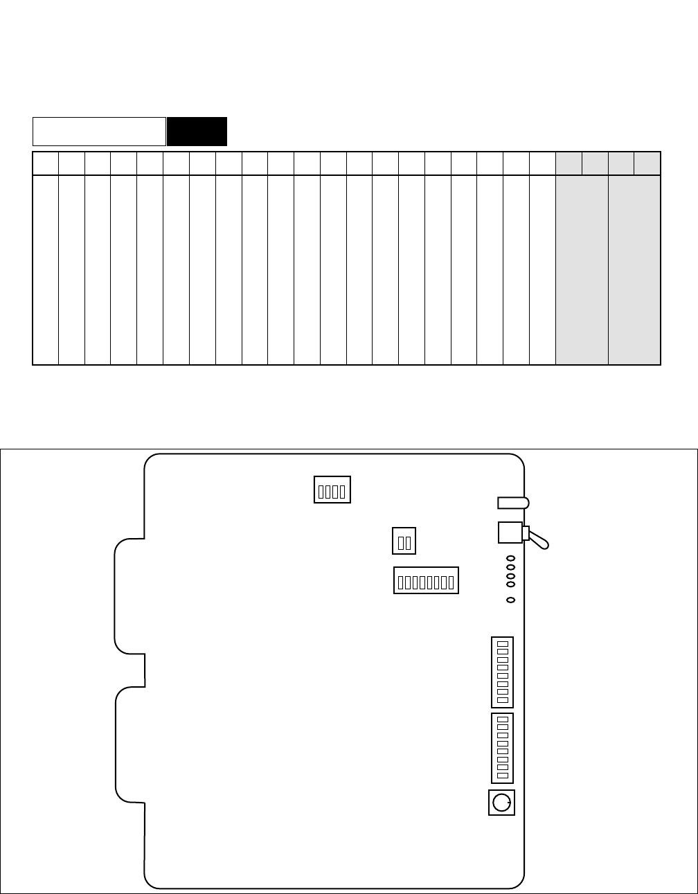
CHAPTER 3 NDA-24296
Page 184
Revision 1.0
PH-CK16
Phase Lock Oscillator
2. Mounting Location/Condition
This circuit card is mounted in the TSWM of the slot shown below.
3. Face Layout of Lamps, Switches, and Connectors
The face layout of lamps, switches, and connectors is shown in Figure 3-7.
Figure 3-7 Face Layout of PH-CK16 (PLO)
Mounting Module TSWM
00 01 02 03 04 05 06 07 08 09 10 11 12 13 14 15 16 17 18 19 20 21 22 23
PLO 0
PLO 1
1 2 3 4
1 2
SW8F
SWAC
SWAB
MB
ACT
1 2 3 4 5 6 7 8
MJ
MN
SYNC
ICK
PALM
SW01
SW02
SW03

NDA-24296 CHAPTER 3
Page 185
Revision 1.0
PH-CK16
Phase Lock Oscillator
4. Lamp Indications
Lamp indications for this circuit card are shown in the table below.
LAMP NAME COLOR STATE
ACT Green Remains lit while this circuit card is in active state.
Off Remains off while this circuit card is in stand-by state.
MJ Red
Lights when the following MJ fault has occurred:
•All of the clock supply routes have failed when the system operates as the clock
subordinate office
•32.768 MHz output clock failure
•8 KHz output FH failure
•5 msec × “n” output FH failure
•Input Frame Pulse (FP) failure (FP is supplied by the SYNC card)
•Internal OSC (±5 ppm deviation) has failed when the system operates as the clock
source office
MN Red
Lights when the following MN fault has occurred:
•One or more (but not all) DTI/DCS clock supply routes have failed
•Drifting failure
•Internal OSC (±5 ppm deviation) failure
SYNC
Green Remains lit while the system is synchronized with the network.
OFF
Remains off when either of the following has occurred:
•DCS clock failure when receiving the clock signals from the DCS.
•DTI clock failure when receiving the clock signals from the DTI.
•Drifting failure
ICK Green Lights when the internal oscillator is operating normally.
PALM Red Remains lit when power is abnormal.

CHAPTER 3 NDA-24296
Page 186
Revision 1.0
PH-CK16
Phase Lock Oscillator
5. Switch Settings
Standard settings of switches on this circuit card are shown in the table below.
SWITCH
NAME SETTING STANDARD
SETTING MEANING
MB UP Circuit card Make-busy.
DOWN ×Circuit card Make-busy cancel.
SW03 1 - F 1 Fixed to “1.”
SWITCH
NAME SWITCH
NO. SETTING STANDARD
SETTING MEANING
SW01
1ON ×Clock subordinate office.
OFF Clock source office.
2ON Digital Clock Supply route zero (DCS 0) is used.
OFF Digital Clock Supply route zero (DCS 0) is not used.
3ON Digital Clock Supply route one (DCS 1) is used.
OFF Digital Clock Supply route one (DCS 1) is not used.
4
ON 8 KHz of Frame Head signals are extracted from the DCS
signals (which is composed of 64 KHz + 8 KHz).
OFF 8 KHz of Frame Head signals are not extracted from the DCS
signals (which is composed of 64 KHz + 8 KHz).
5
ON When clock source failure has occurred in all supply routes, the
PLO outputs the original clock of the internal oscillator.
OFF When clock source failure has not occurred in all supply routes,
the PLO continues outputting the current phase clock.
6ON This circuit card is associated with SYNC (PA-CK16) card and
5 m Frame Pulse (FP) is supplied by the SYNC card.
OFF This circuit card is not associated with SYNC (PA-CK16) card.
7ON A-law CODEC is used for the hold music.
OFF ×µ-law CODEC is used for the hold music.
8OFF ×Not used.
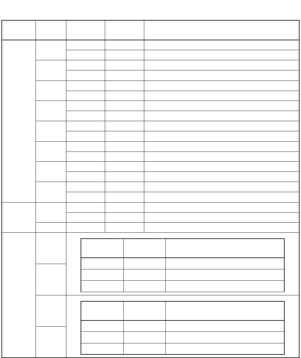
NDA-24296 CHAPTER 3
Page 187
Revision 1.0
PH-CK16
Phase Lock Oscillator
SW02
1ON DIU 0 is used as the DTI clock supply route zero.
OFF DIU 0 is not used.
2ON DIU 1 is used as the DTI clock supply route one.
OFF DIU 1 is not used.
3ON DIU 2 is used as the DTI clock supply route two.
OFF DIU 2 is not used.
4ON DIU 3 is used as the DTI clock supply route three.
OFF DIU 3 is not used.
5ON ×1.5 M clock for DIU 0
OFF 2 M clock for DIU 0
6ON ×1.5 M clock for DIU 1
OFF 2 M clock for DIU 1
7ON ×1.5 M clock for DIU 2
OFF 2 M clock for DIU 2
8ON ×1.5 M clock for DIU 3
OFF 2 M clock for DIU 3
SWAC 1ON External hold tone source is used via FM lead.
OFF ×MUSIC ROM is used as the hold tone.
2OFF ×Not used.
SW8F
1
2
3
4
SWITCH
NAME SWITCH
NO. SETTING STANDARD
SETTING MEANING
SW8F-1 SW8F-2 Impedance of the External
Music Source 0 (FM 0)
OFF OFF 600 Ω
ON OFF 8.2 Ω
OFF ON 47K Ω
SW8F-3 SW8F-4 Impedance of the External
Music Source 1 (FM 1)
OFF OFF 600 Ω
ON OFF 8.2 Ω
OFF ON 47K Ω
CHAPTER 3 NDA-24296
Page 188
Revision 1.0
PH-CK16
Phase Lock Oscillator
SWAB
1
Note: Don’t care.
2
3
4ON Not used.
OFF ×Not used.
5MUSIC CH1 selection. The kind of music varies depending on the melody IC located on this
circuit card.
6
7
8ON Not used.
OFF ×Not used.
SWITCH
NAME SWITCH
NO. SETTING STANDARD
SETTING MEANING
SWA0-1 SWA0-2 SWA0-3 MUSIC
OFF OFF OFF Für Elise
ON OFF OFF Maiden’s prayer
Note OFF ON Buzzer
Note ON OFF Chime
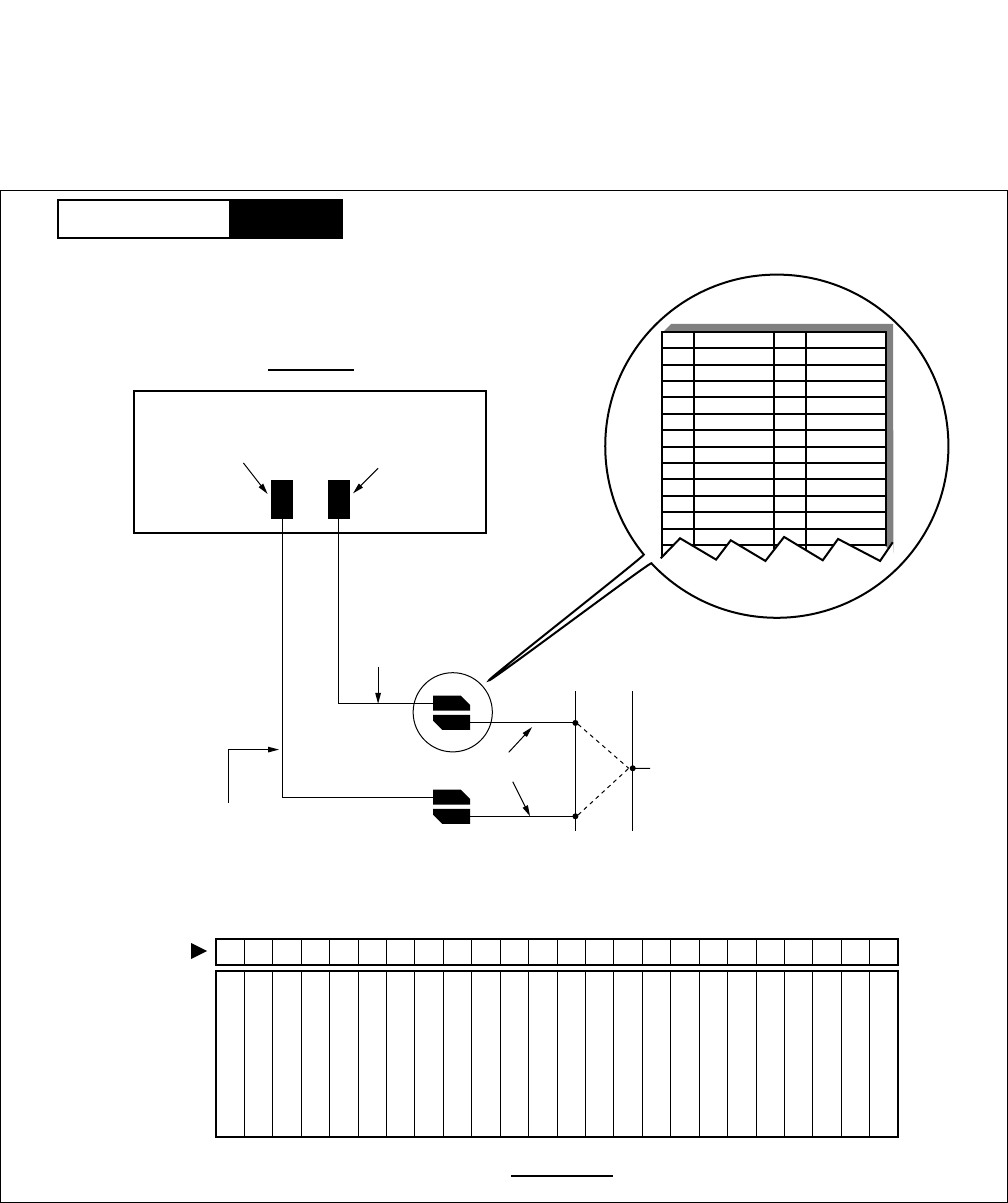
NDA-24296 CHAPTER 3
Page 189
Revision 1.0
PH-CK16
Phase Lock Oscillator
6. External Interface
When this circuit card is located in the TSWM, connect 34PH EXCLK CA-A to the EXCLK0/EXCLK1
connectors on the backplane of the TSWM.
Figure 3-8 LT Connector Lead Location of PLO (TSWM)
00 01 02 03 04 05 06 07 08 09 10 11 12 13 14 15 16 17 18 19 20 21 22 23
Slot No.
TSWM
FRONT VIEW
PLO #1
PLO #0
26 1
FM 1
27 2
FM 0
28 3
SYN 1B
E
29 4
SYN 0B
E
30 5
DIU 3B
SYN 1A
31 6
DIU 2B
SYN 0A
32 7
DIU 1B
DIU 3A
33 8
DIU 0B
DIU 2A
34 9
DCS B
DIU 1A
35 10 DIU 0A
36 11 DCS A
37 12
38 13
EXCLK0
(Slot No.21)
EXCLK1
(Slot No.23)
TSWM
REAR VIEW
34PH EXCLK
CA-A
34PH EXCLK CA-A
34PH EXCLK CA-A LEAD ACCOMMODATION
Installation Cable
MDF
To Digital Interface and/or DCS
Mounting Module TSWM
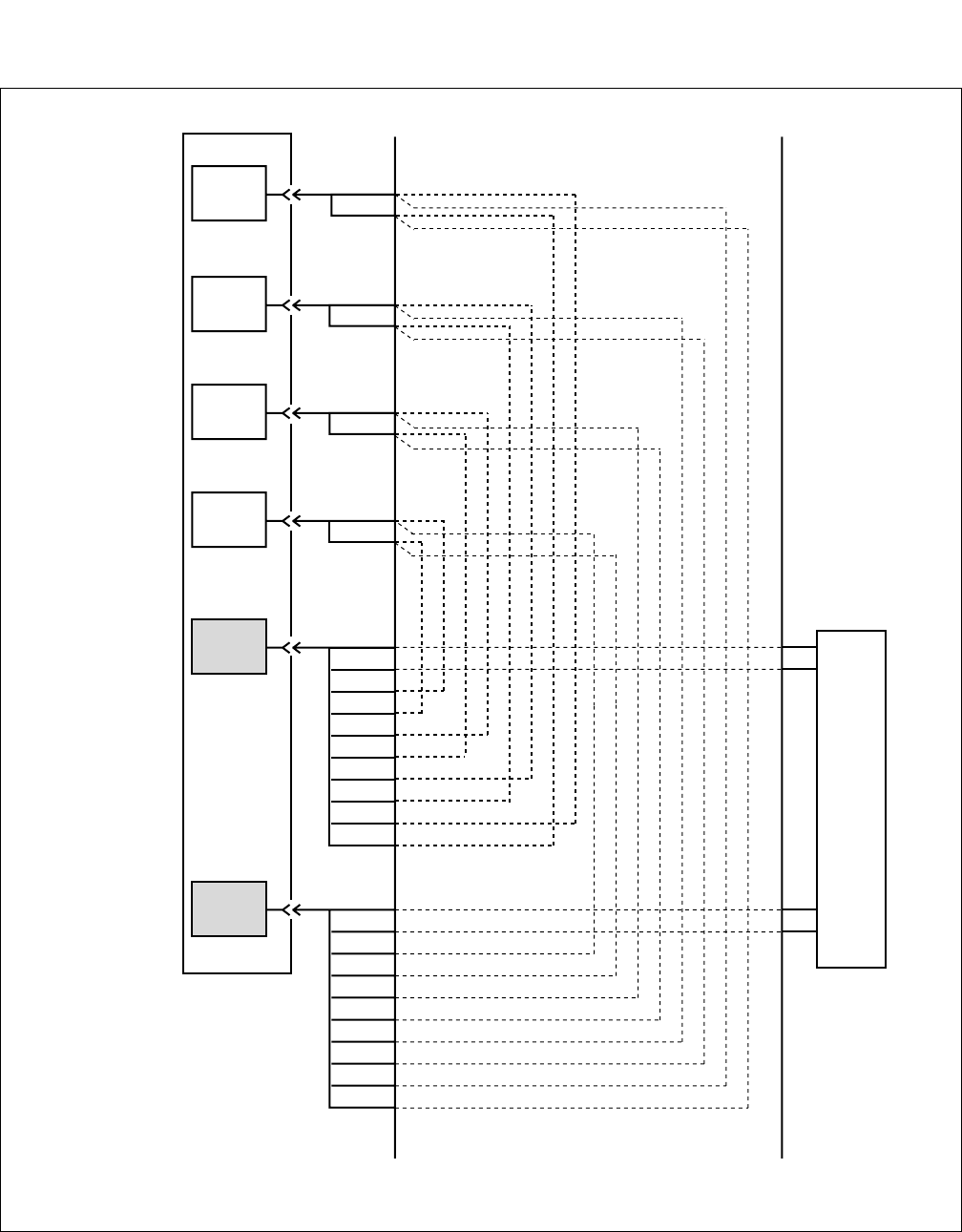
CHAPTER 3 NDA-24296
Page 190
Revision 1.0
PH-CK16
Phase Lock Oscillator
Figure 3-9 Connecting Route Diagram
DCSB1
DIU0A1
DIU0B1
DIU1A1
DIU1B1
DIU2A1
DIU2B1
DIU3A1
DIU3B1
DCSA1
DCSB0
DIU0A0
DIU0B0
DIU1A0
DIU1B0
DIU2A0
DIU2B0
DIU3A0
DIU3B0
DCSA0
POUT B
POUT A
POUT B
POUT A
POUT B
POUT A
POUT B
POUT A
CCT /DTI
/PRT
CCT /DTI
/PRT
CCT /DTI
/PRT
CCT /DTI
/PRT
PLO #0
PLO #1
DCS
Note : The following circuit cards have Clock Output Leads for a PLO card: CCT (PA-24CCTA, PA-30CCTB),
DTI (PA-24DTR, PA-30DTS), and PRT (PA-24PRT, PA-30PRTC).
MDFPBX
NDA-24296 CHAPTER 3
Page 191
Revision 1.0
PH-CK16
Phase Lock Oscillator
7. Switch Setting Sheet
SWITCH NAME SWITCH SHAPE REMARKS
MB
SW01
SW02
SW03
SWAC
SW8F
SWAB
ON
1234 ON
56 7 8
1234ON
5678
1 2 ON
1 2 3 4 ON
1234 ON
56 7 8
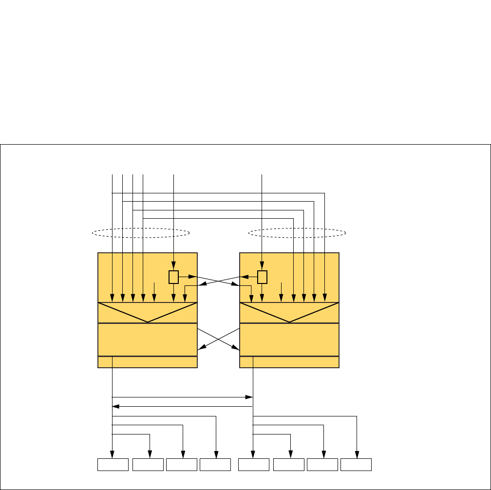
CHAPTER 3 NDA-24296
Page 192
Revision 1.0
PH-CK16-A
Phase Lock Oscillator
PH-CK16-A
Phase Lock Oscillator
1. General Function
This circuit card, used with a direct digital interface circuit card, sets up network synchronization. With this
circuit card, the system can be a clock subordinate office of the digital network. As seen in Figure 3-10, the
PLO can be redundant regardless of the system switching network selection.
Figure 3-10 Location of PH-CK16-A (PLO) in 4-IMG System
OSC 64K+8K
(BWB)
(BWB)
CLK, FH, WFH
ACT, ALM
34PH EXCLK CA-A
PLO #0
TSW 00
BWB BWB
DTI0 DCS0
(MDF)
DCS1123
PLO #1
SEL
PLL
Drv
SEL
PLL
Drv
OSC
34PH EXCLK CA-A
TSW 01 TSW 02 TSW 03 TSW 00 TSW 01 TSW 02 TSW 03
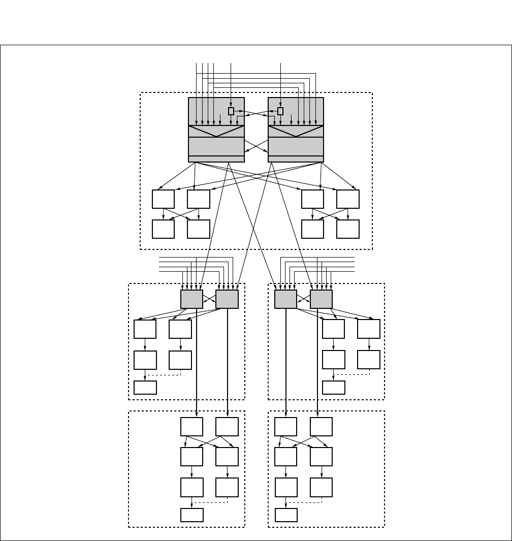
NDA-24296 CHAPTER 3
Page 193
Revision 1.0
PH-CK16-A
Phase Lock Oscillator
Figure 3-11 Location of PH-CK16-A (PLO) in IPX-U/IPX-UMG System
LN0/LMG0
(IMG2/IMG3) LN3/LMG3
(IMG2/IMG3)
/(IMG14/IMG15)
32M, FH+WFH
PLO ACT 32M, FH+WFH
PLO ACT
CLK1
(TSWM1)
TSW
10~13
CLK0
(TSWM1)
TSW
00~03
MUX
(
System1
)
MUX
(
System0
)
LC/TRK
HSW00
ISWM
HSW01
CLK1
(TSWM1)
TSW
10~13
CLK0
(TSWM1)
TSW
00~03
MUX
(
System1
)
MUX
(
System0
)
LC/TRK
LN0/LMG0
(IMG0/IMG1)
from
LN/LMG DTI from
LN/LMG DTI
32M, FH+WFH
PLO ACT
32M, FH+WFH
PLO ACT
(BWB)
32M, FH+WFH
PLO ACT
(BWB)
64K+FH, WFH
TSW ACT
(Cable)
64K+FH, WFH
TSW ACT
(Cable)
PLO 1
(TSWM0)
TSW
10~13
PLO 0
(TSWM0)
TSW
00~03
MUX
(
System1
)
MUX
(
System0
)
LC/TRK
LN3/LMG3
(IMG0/IMG1)
/(IMG12/IMG13) 32M, FH+WFH
PLO ACT
PLO 1
(TSWM0)
TSW
10~13
PLO 0
(TSWM0)
TSW
00~03
MUX
(
System1
)
MUX
(
System0
)
LC/TRK
TSW00 TSW03
HSW10
OSC 64K+8K
(BWB)
(BWB)
CLK, FH, WFH
ACT, ALM
PLO 0
DTI0 DCS0 (MDF) DCS1123
PLO 1
SEL
PLL
Drv
HSW11
TSW10 TSW13
SEL
PLL
Drv
OSC
~
~~
~
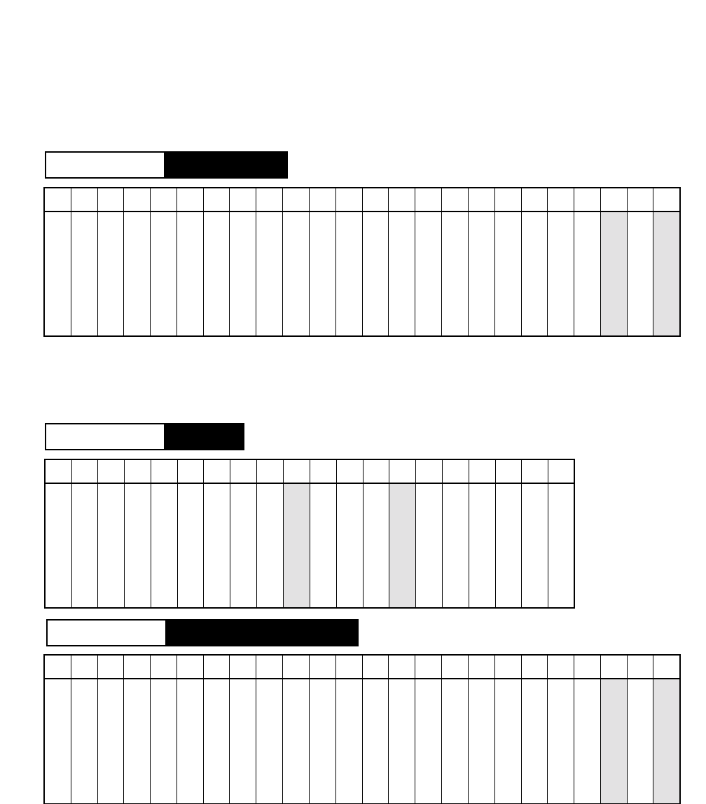
CHAPTER 3 NDA-24296
Page 194
Revision 1.0
PH-CK16-A
Phase Lock Oscillator
2. Mounting Location/Condition
This circuit card can be mounted in the shaded slots shown below.
<For 4-IMG System>
<For IPX-U/IPX-UMG System>
00 01 02 03 04 05 06 07 08 09 10 11 12 13 14 15 16 17 18 19 20 21 22 23
TSWM(IMG1)
Mounting Module
PLO (#0)
PLO (#1)
ISWM
Mounting Module
TSWM0(IMG1/5/9/13)
Mounting Module
00 01 02 03 04 05 06 07 08 09 10 11 12 13 14 15 16 17 18 19
00 01 02 03 04 05 06 07 08 09 10 11 12 13 14 15 16 17 18 19 20 21 22 23
PLO (#0)
PLO (#1)
PLO (#0)
PLO (#1)
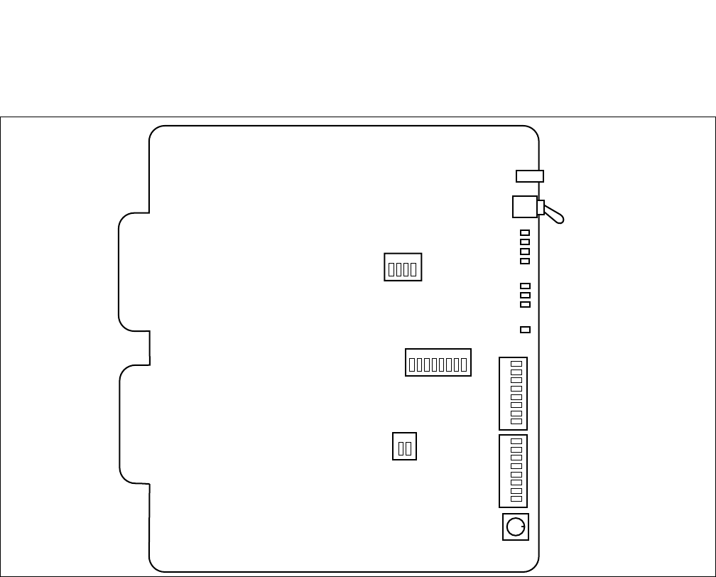
NDA-24296 CHAPTER 3
Page 195
Revision 1.0
PH-CK16-A
Phase Lock Oscillator
3. Face Layout of Lamps, Switches, and Connectors
The face layout of lamps, switches, and connectors are shown in Figure 3-12.
Figure 3-12 Face Layout of PH-CK16-A (PLO)
1 2 3 4
1 2
SW11
SW10
SW12
MB
OPE
1 2 3 4 5 6 7 8
MJ
MN
SYNC
ICK
CKPKG
ALM0
ALM1
PALM
SW01
SW02
SW03
1234567812345678

CHAPTER 3 NDA-24296
Page 196
Revision 1.0
PH-CK16-A
Phase Lock Oscillator
4. Lamp Indications
Lamp indications for this circuit card are shown in the table below:
Note: This lamp is effective when this card is mounted in TSWM0 of the IPX-U/IPX-UMG system. When this card
is mounted in ISWM, this lamp is not used.
5. Switch Settings
Standard settings for switches on this circuit card are shown in the table below.
LAMP NAME COLOR STATE
OPE Green Remains lit while this circuit card is in active state.
MJ Red
Lights when the following MJ fault has occurred:
•All of the clock supply routes have failed when the system operates as the clock
subordinate office
•32.768 MHz output clock failure (including CLK card)
•8 KHz output clock failure (including CLK card)
•Input Frame Pulse (FP) failure (FP is supplied by the SYNC card) Internal OSC (±5
ppm deviation) has failed when the system operates as the clock source office
MN Red
Lights when the following MN fault has occurred:
•One or more (but not all) DTI/DCS clock supply route has failed
•Drifting failure
•Internal OSC (±5 ppm deviation) failure
SYNC Green Remains lit while the system is synchronized with the network.
ICK Green Lights when the internal oscillator is operating normally.
CKPKG
Note Green Lights when the CLK card in TSWM1 is in normal operation.
ALM0
Note Red Lights when clock failure has occurred in the CLK card.
ALM1
Note Red Lights when FH failure has occurred in the CLK card.
PALM Red Remains lit when the On-Board Power Supply is abnormal.
SWITCH
NAME SETTING STANDARD
SETTING MEANING
MB UP Circuit card Make-busy.
DOWN ×Circuit card Make-busy cancel.
SW03 1 - F 1 Fixed to “1”.

NDA-24296 CHAPTER 3
Page 197
Revision 1.0
PH-CK16-A
Phase Lock Oscillator
The key setting of “SW01” differs depending on the mounting location.
[Mounted in ISWM of IPX-U/IPX-UMG System or TSWM of 4-IMG System]
Note: When this card is used in the 4-IMG or ISWM of the IPX-U/IPX-UMG system, specify the clock source
(DCS or DTI) according to the clock network configuration for the office.
Note 1: This standard setting is applicable when this card is mounted in ISWM of the IPX-U/IPX-UMG system.
SWITCH
NAME SWITCH
NO. SETTING STANDARD
SETTING MEANING
SW01
1ON ×
Note 1 Clock subordinate office.
OFF Clock source office.
2
ON Digital Clock Supply route zero (DCS 0) is used.
OFF ×
Note 1 Digital Clock Supply route zero (DCS 0) is not used.
3
ON Digital Clock Supply route one (DCS 1) is used.
OFF ×
Note 1 Digital Clock Supply route one (DCS 1) is not used.
4
ON 8 KHz of Frame Head signals are extracted from the DCS
signals (which is composed of 64 KHz + 8 KHz).
OFF ×
Note 1 8 KHz of Frame Head signals are not extracted from the DCS
signals (which is composed of 64 KHz + 8 KHz).
5
ON When clock source failure has occurred in all supply routes, the
PLO outputs the original clock of the internal oscillator.
OFF ×
Note 1 When clock source failure has occurred, the PLO keeps on
outputting the current phase clock.
6
ON This circuit card is used with SYNC (PA-CK16) card and 5m
Frame Pulse (FP) is supplied by the SYNC card.
OFF ×
Note 1 This circuit card is not used with SYNC (PA-CK16) card.
7ON A-law CODEC is used for Music-on-Hold.
OFF ×µ-law CODEC is used for Music-on-Hold.
8OFF ×Fixed to “OFF” (Not used).

CHAPTER 3 NDA-24296
Page 198
Revision 1.0
PH-CK16-A
Phase Lock Oscillator
[Mounted in TSWM0 of IPX-U/IPX-UMG System]
SWITCH
NAME SWITCH
NO. SETTING STANDARD
SETTING MEANING
SW01
1ON ×Clock subordinate office. (Fixed)
OFF Clock source office.
2
ON Digital Clock Supply route zero (DCS 0) is used.
(In case this circuit card is accommodated as #0 system.)
OFF Digital Clock Supply route zero (DCS 0) is not used.
(In case this circuit card is accommodated as #1 system.)
3
ON Digital Clock Supply route one (DCS 1) is used.
(In case this circuit card is accommodated as #1 system.)
OFF Digital Clock Supply route one (DCS 1) is not used.
(In case this circuit card is accommodated as #0 system.)
4
ON 8 KHz of Frame Head signals are extracted from the DCS
signals (which is composed of 64 KHz + 8 KHz).
OFF ×8 KHz of Frame Head signals are not extracted from the DCS
signals (which is composed of 64 KHz + 8 KHz).
5
ON When clock source failure has occurred in all supply routes, the
PLO outputs the original clock of the internal oscillator.
OFF ×When clock source failure has not occurred, the PLO keeps on
outputting the current phase clock.
6ON ×This circuit card is associated with SYNC (PA-CK16) card and
5m Frame Pulse (FP) is supplied by the SYNC card.
(Fixed to “ON”)
OFF This circuit card is not associated with SYNC (PA-CK16) card.
7ON A-law CODEC is used for Music-on-Hold.
OFF ×µ-law CODEC is used for Music-on-Hold.
8OFF ×Fixed OFF (Not used).

NDA-24296 CHAPTER 3
Page 199
Revision 1.0
PH-CK16-A
Phase Lock Oscillator
Note 2: When this card is mounted in TSWM0 of the IPX-U system, the DCS clock from the ISWM is used. The DTI
clock can also be used as an alternate clock supply route in case of DCS clock failure.
Note 3: When this card is mounted in ISWM, set to “ON (=CLK card is not used).”
If mounted in TSWM0 on LN/LMG,
•set to “OFF” if TSWM1 (CLK card, PH-CK18) on the same LN/LMG is used.
•set to “ON” if TSWM1 (CLK card, PH-CK18) on the same LN/LMG is not used.
SW02
Note 2
1ON DIU 0 is used as the DTI clock supply route zero.
OFF DIU 0 is not used.
2ON DIU 1 is used as the DTI clock supply route one.
OFF DIU 1 is not used.
3ON DIU 2 is used as the DTI clock supply route two.
OFF DIU 2 is not used.
4ON DIU 3 is used as the DTI clock supply route three.
OFF DIU 3 is not used.
5ON ×1.5 M clock for DIU 0.
OFF 2 M clock for DIU 0.
6ON ×1.5 M clock for DIU 1.
OFF 2 M clock for DIU 1.
7ON ×1.5 M clock for DIU 2.
OFF 2 M clock for DIU 2.
8ON ×1.5 M clock for DIU 3.
OFF 2 M clock for DIU 3.
SW10
1ON External hold tone source is used via FM lead.
OFF ×MUSIC ROM is used as the hold tone.
2
Note 3
ON CLK card is not used.
OFF CLK card is used.
SWITCH
NAME SWITCH
NO. SETTING STANDARD
SETTING MEANING
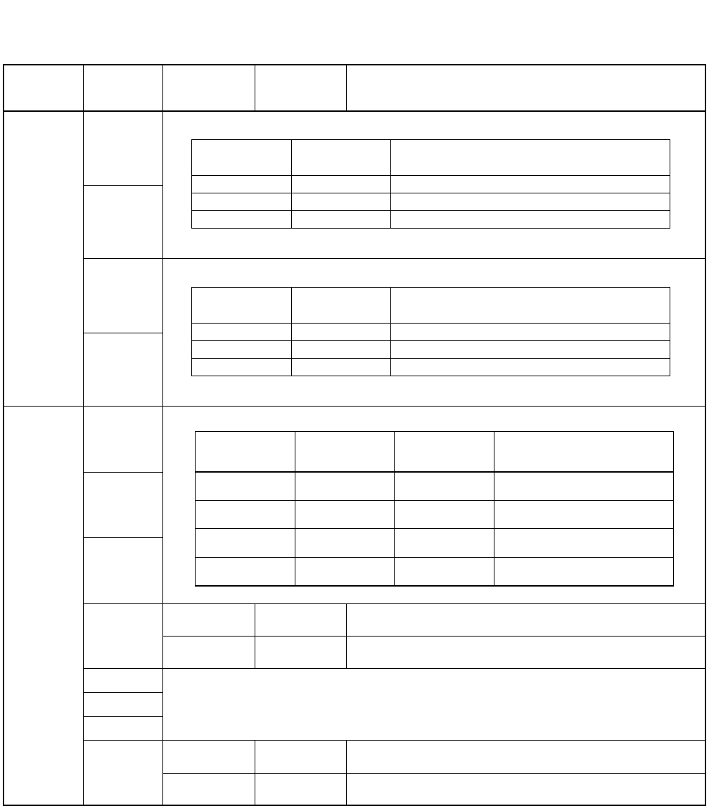
CHAPTER 3 NDA-24296
Page 200
Revision 1.0
PH-CK16-A
Phase Lock Oscillator
SWITCH
NAME SWITCH
NO. SETTING STANDARD
SETTING MEANING
SW11
1
2
3
4
SW12
1
2
3
4ON Not used.
OFF ×Not used.
5MUSIC (CH1) selection. The music varies depending on the melody IC located on this circuit
card.
6
7
8ON Not used.
OFF ×Not used.
SW11-1 SW11-2 Impedance of the External
Music Source 0 (FM 0)
OFF OFF 600 Ω
ON OFF 8.2 Ω
OFF ON 47K Ω
SW11-3 SW11-4 Impedance of the External
Music Source 1 (FM 1)
OFF OFF 600 Ω
ON OFF 8.2 Ω
OFF ON 47K Ω
SW12-1 SW12-2 SW12-3 MUSIC
OFF OFF OFF Für Elise
ON OFF OFF Maiden’s prayer
Don’t Care ON OFF Buzzer
Don’t Care OFF ON Chime
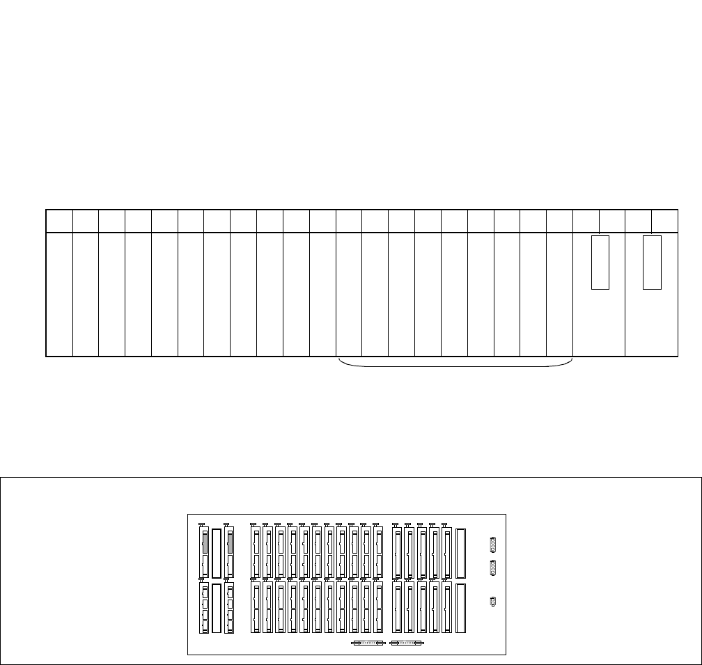
NDA-24296 CHAPTER 3
Page 201
Revision 1.0
PH-CK16-A
Phase Lock Oscillator
6. External Interface
PLO leads appear on the LT connectors labeled EXCLK0 and EXCLK1.
•PLO mounting slots
The PLO card is mounted in Slots 21 and 23 of TSWM.
•LT cable connectors
Connect the LT cables to the connectors labeled EXCLK0 and EXCLK1 on the TSWM backplane.
Figure 3-13 PLO Pin Assignments for Receiving Clock (4 IMG System) (1/2)
00 01 02 03 04 05 06 07 08 09 10 11 12 13 14 15 16 17 18 19 20 21 22 23
EXCLK0
EXCLK1 PLO
PLO
TSW
Front View
TSWM
EXCLK0
EXCLK1
TSWM
Backplane
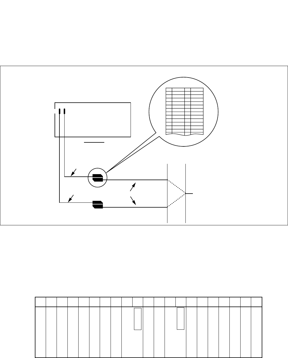
CHAPTER 3 NDA-24296
Page 202
Revision 1.0
PH-CK16-A
Phase Lock Oscillator
•EXCLK0/EXCLK1 connector Pin Assignment
Pins are assigned as follows on the EXCLK0/EXCLK1 connectors. When the clock is distributed from a
digital interface, use one pair of DIUxxx in one of the four inputs. (There are a maximum of four inputs.)
DIU leads have the following precedence: DIU0xx (high) → DIU3xx (low).
Figure 3-13 PLO Pin Assignments for Receiving Clock (4 IMG System) (2/2)
PLO input leads appear on the LT connectors labeled EXCLK0 and EXCLK1.
•PLO mounting slots
The PLO card is mounted in Slots 09 and 13 of ISWM.
34PH ISWM EXCLK CA-A
34PH ISWM EXCLK CA-A
REAR VIEW
EXCLK0
EXCLK1
TSWM
MDF
Installation Cable To Digital Interface and/or DCS
34PH ISWM EXCLK CA-A Cable Lead Location
26
27
28
29
30
31
32
33
34
35
36
37
38
1
2
3
4
5
6
7
8
9
10
11
12
13
FM1
FM0
DIU3B
DIU2B
DIU1B
DIU0B
DCSB
SYN1B
SYN0B
E
E
DIU3A
DIU2A
DIU1A
DIU0A
DCSA
SYN1A
SYN0A
00 01 02 03 04 05 06 07 08 09 10 11 12 13 14 15 16 17 18 19 23
EXCLK0
EXCLK1 PLO
PLO
Front View
ISWM
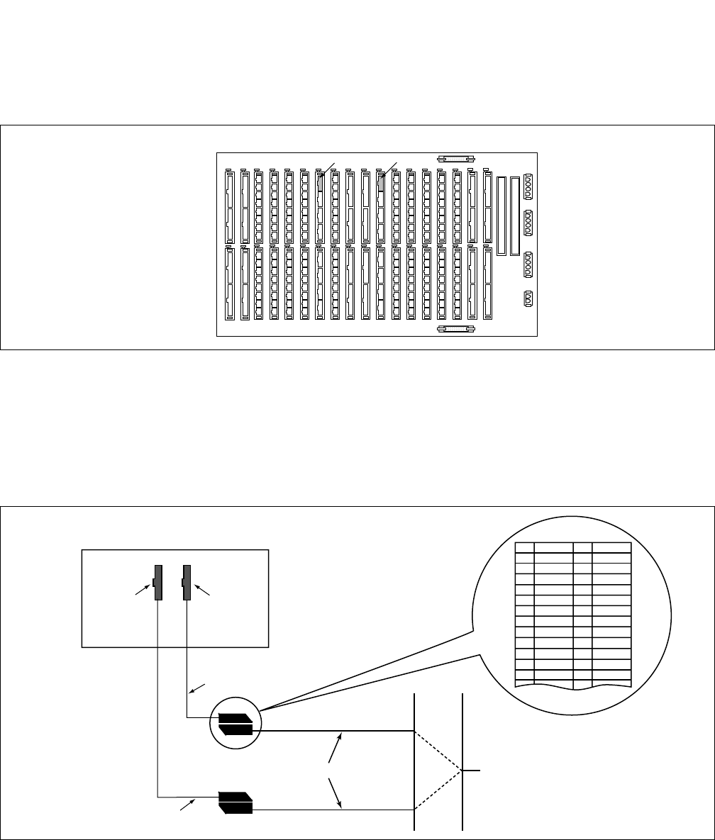
NDA-24296 CHAPTER 3
Page 203
Revision 1.0
PH-CK16-A
Phase Lock Oscillator
•LT cable connectors
Connect LT cables to the connectors labeled EXCLK0 and EXCLK1 on the ISWM backplane.
Figure 3-14 PLO Pin Assignment for Receiving Clock (ISWM) (1/2)
•EXCLK0/EXCLK1 connector Pin Assignment
Pins are assigned as follows on the EXCLK0/EXCLK1 connectors. When the clock is distributed from a
digital interface, use one pair of DIUxxx in one of four inputs. (There are a maximum of four inputs.) DIU
leads have the following precedence: DIU0xx (high) → DIU3xx (low).
Figure 3-14 PLO Pin Assignment for Receiving Clock (ISWM) (2/2)
EXCLK1 EXCLK0
Backplane
ISWM
MDF
To Digital Interface and/or DCS
Installation Cable
ISWM
EXCLK0
(Slot No.09)
EXCLK1
(Slot No.13)
34PH ISWM EXCLK CA-A
34PH ISWM EXCLK CA-A
Rear View 26
27
28
29
30
31
32
33
34
35
36
37
38
1
2
3
4
5
6
7
8
9
10
11
12
13
FM1
FM0
DIU3B
DIU2B
DIU1B
DIU0B
DCSB
SYN1B
SYN0B
E
E
DIU3A
DIU2A
DIU1A
DIU0A
DCSA
SYN1A
SYN0A
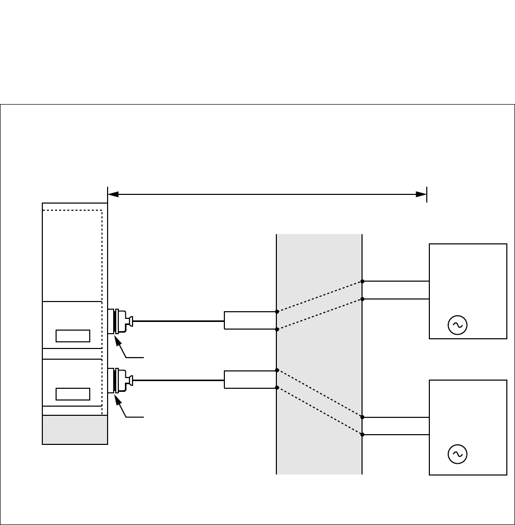
CHAPTER 3 NDA-24296
Page 204
Revision 1.0
PH-CK16-A
Phase Lock Oscillator
•Cable Connection Diagram
Provide the following wiring at the MDF. The connection diagram in Figure 3-15 shows an example of a
system with the PLO cards in dual configuration.
Figure 3-15 Cable Connection Diagram (ISWM) for Accepting Synchronization Clocks from an External
High-Stability Oscillator
MDF
ISW/CMG
External
High-Stability
Oscillator #1
CLK
External
High-Stability
Oscillator #0
CLK
PCM Cable(IP)
PCM Cable(IP)
DCSA
DCSB
LT Connector Cable
EXCLK1 DCSB
DCSA
LT Connector Cable
EXCLK0
EXCLK1
PLO#1
EXCLK0
PLO#0
BASEU
ISWM
maximum 400 meters (1320 feet) (24 AWG)
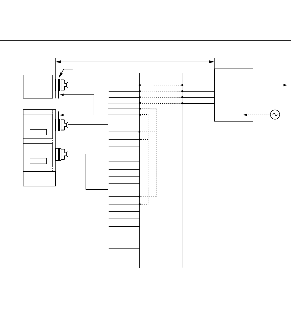
NDA-24296 CHAPTER 3
Page 205
Revision 1.0
PH-CK16-A
Phase Lock Oscillator
Figure 3-16 shows an example of distributing clock from a digital interface in LN/LMG. This example assumes
that the Digital Trunk POUT leads are used as the first clock distribution route.
Figure 3-16 Cable Connection Diagram (ISWM) for Receiving Clock from Digital Interface
MDF
ISW/CMG
LN/LMG
PCM
Carrier
Equipment
DSU
CLK
PCM Cable (2P) to other node
Installation Cable
Installation Cable
maximum 100
meters (330 feet)
(24AWG)
Installation Cable RA
RB
TA
TB
POUTA
POUTB
DIU0A0
DIU0B0
DIU1A0
DIU1B0
DIU2A0
DIU2B0
DIU3A0
DIU3B0
DIU0A1
DIU0B1
DIU1A1
DIU1B1
DIU2A1
DIU2B1
DIU3A1
DIU3B1
EXCLK0
PLO#0
LT Connector
Digital
Interface
EXCLK1
PLO#1
maximum 200 meters (660 feet) (24AWG)
Note 1:
Note 1
Note 2
PLO has a maximum 4 inputs. DIU0xx leads are used for the 1st clock distribution routes. DIU3xx
leads are used for the 4th. The first input has the highest priority.
Note 2: The connection is required for a dual PLO system.
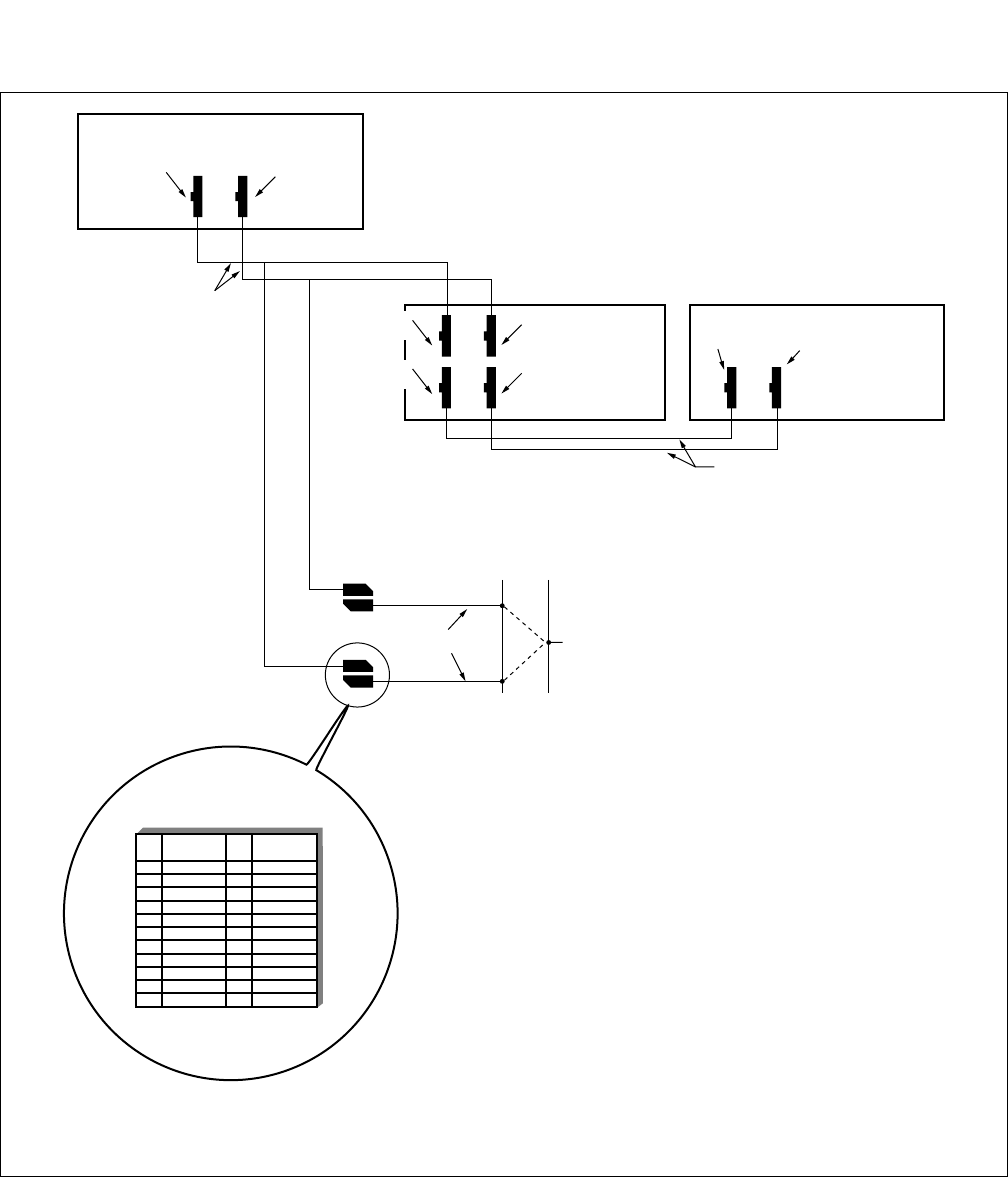
CHAPTER 3 NDA-24296
Page 206
Revision 1.0
PH-CK16-A
Phase Lock Oscillator
Figure 3-17 LT Connector Lead Location of PLO (ISWM-TSWM0/1)
26 1
LEAD
NAME LEAD
NAME
27 2
28 3
PIN
No.
PIN
No.
29 4
30 5
FM1
FM0
31 6
32 7
33 8
34 9
35
36 10
11
E
DIU 3B
DIU 2B DIU 3A
DIU 2A
E
DIU 1B DIU 1A
DIU 0B DIU 0A
CLK00
(Slot No.08)
CLK10
(Slot No.12)
TSWM1
TSWM0
ISWM
Installation Cable
DIU Connection Note MDF
To Digital Interface
EXCLK0
(Slot No.21)
PLO CLOCK0
(Slot No.21)
EXCLK1
(Slot No.23)
PLO CLOCK1
(Slot No.23)
PLO CLOCK0
(Slot No.21)
PLO CLOCK1
(Slot No.23)
ISW-LN PLO CA-A
PLO-CLK CA-A
DCS Connection
Note: For the DUI connection route diagram, see Figure 3-18.

NDA-24296 CHAPTER 3
Page 207
Revision 1.0
PH-CK16-A
Phase Lock Oscillator
Figure 3-18 shows an example of distributing clock from a digital interface. This figure assumes that the Digital
Trunk POUT leads are used as the first clock distribution route. (This connection is not required for IPX-UMG
system.)
Figure 3-18 Cable Connection Diagram (4-IMG System/LN) for Receiving Clock from Digital Interface
DIU0A1
DIU0B1
DIU1A1
DIU1B1
DIU2A1
DIU2B1
DIU3A1
DIU3B1
DIU0A0
DIU0B0
DIU1A0
DIU1B0
DIU2A0
DIU2B0
DIU3A0
DIU3B0
RA
RB
TA
TB
POUT A
POUT B
PCM Cable (2P) to other node
PCM
Carrier
Equipment
DSU
CLK
Note 1:
Note 2
Note 1
PLO has a maximum of 4 inputs. DIU0xx leads are used for the 1st clock distribution routes.
DIU3xx leads are used for the 4th. The first input has the highest priority.
Note 2: The connection is required for a dual PLO system.
MDF
maximum 100
meters (330 feet)
(24AWG)
Installation Cable
LT Connector
Installation Cable
Installation Cable
EXCLK1
PLO#1
EXCLK0
PLO#0
Digital
Interface
IMG
maximum 200 meters (660 feet) (24 AWG)
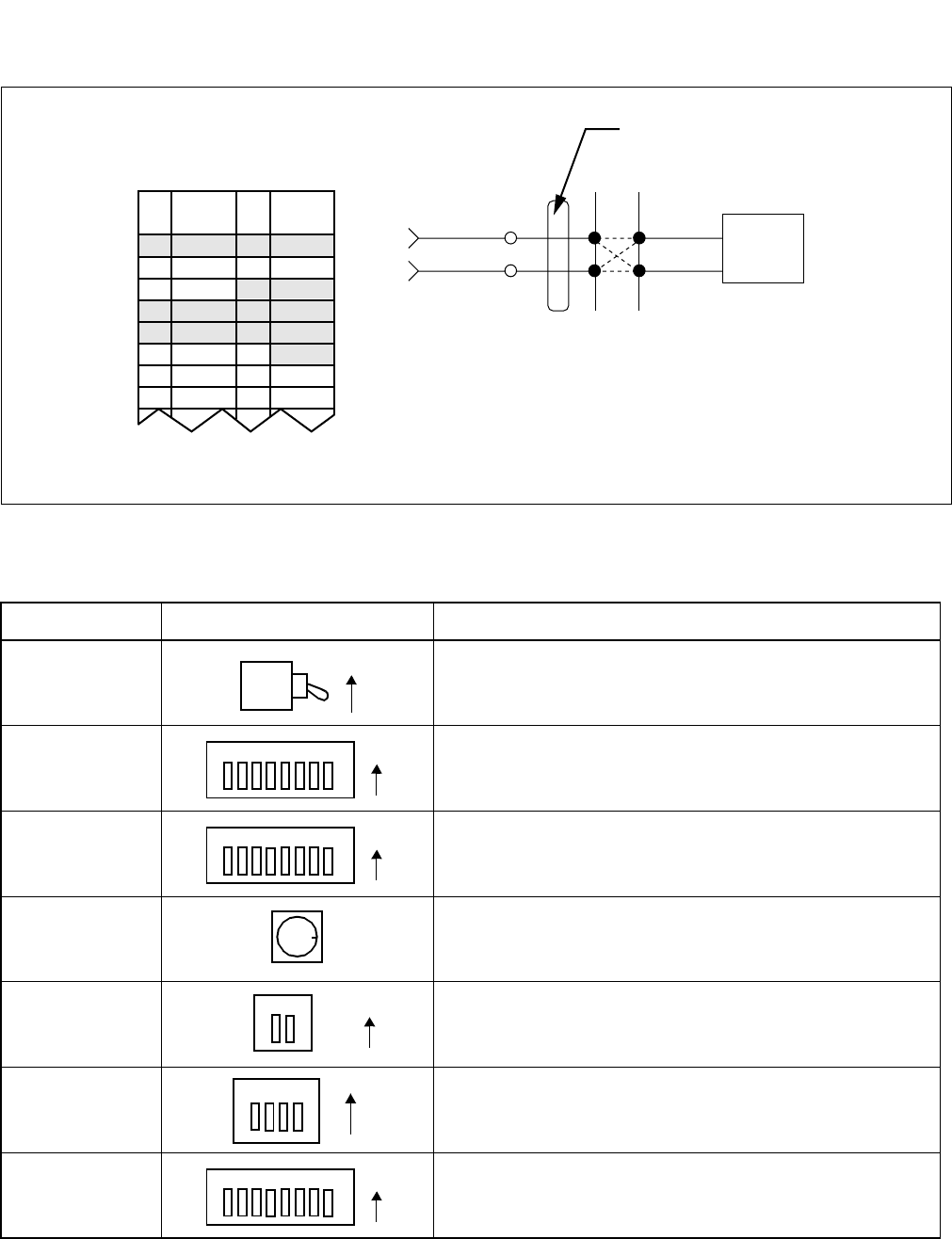
CHAPTER 3 NDA-24296
Page 208
Revision 1.0
PH-CK16-A
Phase Lock Oscillator
Figure 3-19 Connection of External Music-On-Hold
7. Switch Setting Sheet
SWITCH NAME SWITCH SHAPE
MB
SW01
SW02
SW03
SW10
SW11
SW12
ISW-LN PLO CA-A cable/
34PH ISWM EXCLK CA-A
Pin Assignment
PIN
No.
26
27
28
29
30
31
32
33
LEAD
NAME
FM1
FM0
LEAD
NAME
E
E
PIN
No.
1
2
3
4
5
6
7
8
9
MUSIC
SOURCE
MDF
ISW-LN PLO CA-A/
34PH ISWM EXCLK CA-A and
Installation Cable(25 P)
Multiple connections between systems 0 and 1
are required on the MDF.
Note
Note: FM1 is not used at this time.
ON
1234 ON
56 7 8
1234 ON
56 7 8
1 2 ON
1ON
234
1234 ON
56 7 8
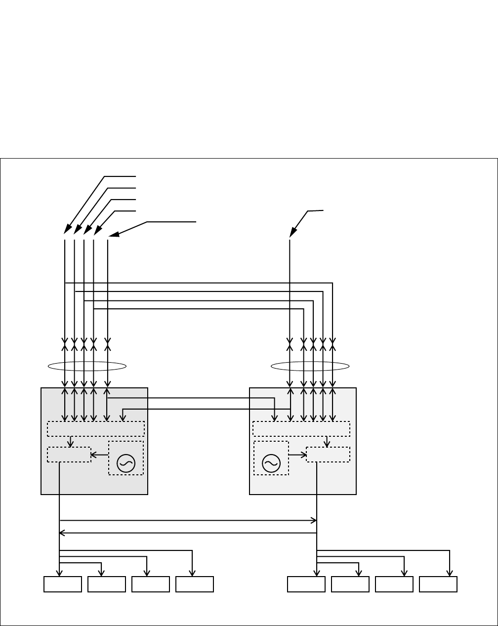
NDA-24296 CHAPTER 3
Page 209
Revision 1.0
PH-CK17
Phase Lock Oscillator
PH-CK17
Phase Lock Oscillator
1. General Function
This circuit card, used together with a direct digital interface circuit card, sets up network synchronization
with the network. Since this circuit card provides a high precision base clock oscillator, the 4 IMG system
can be a clock source office for the digital network. As seen in Figure 3-20, the PLO can be redundant
regardless of the system switching network selection.
Figure 3-20 Location of PH-CK17 (PLO) Card in the System
TDSW00 TDSW01 TDSW02 TDSW03
SEL
PLL PLL
PLO #0 PLO #1
OSC OSC
TDSW10 TDSW11 TDSW12 TDSW13
SEL
34PH EXCLK CA-A 34PH EXCLK CA-A
MDF
MDF
BWB BWB
BWBBWB
DTI 0 CLOCK SOURCE
DTI 1 CLOCK SOURCE
DTI 2 CLOCK SOURCE
DTI 3 CLOCK SOURCE
DCS 0
DCS 1

CHAPTER 3 NDA-24296
Page 210
Revision 1.0
PH-CK17
Phase Lock Oscillator
The source clock of the clock subordinate office is either the digital clock supply (DCS) or the digital interface
clock (DIU0 - DIU3). When clock source failure has occurred, the PLO chooses another clock source
automatically in the order of:
1. DCS
2. DIU0
3. DIU1
4. DIU2
5. DIU3
6. PLO changeover or the PLO internal oscillator drifting
The PLO can output the clock signals (CLK) and the frame head signals (FH) as follows:
•32.768 MHz CLK
•8 KHz FH
•5 msec × “n” FH
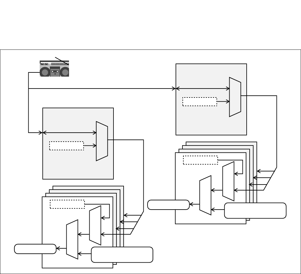
NDA-24296 CHAPTER 3
Page 211
Revision 1.0
PH-CK17
Phase Lock Oscillator
The MUSIC ROM also located on this circuit card contains the hold tone, and is supplied to the TSW circuit
card. When an external music on hold is applied to the 4 IMG system, this circuit card provides the interface for
the external hold tone source.
Figure 3-21 Music Source
SEL
SEL
SEL
Speech Path Memory
for Music/Tone
Music/Tone
MUSIC ROM
TDSW00
PLO#0
TONE ROM
SEL
SEL
SEL
Speech Path Memory
for Music/Tone
Music/Tone
MUSIC ROM
TDSW1
PLO#1
TONE ROM
FM
FM
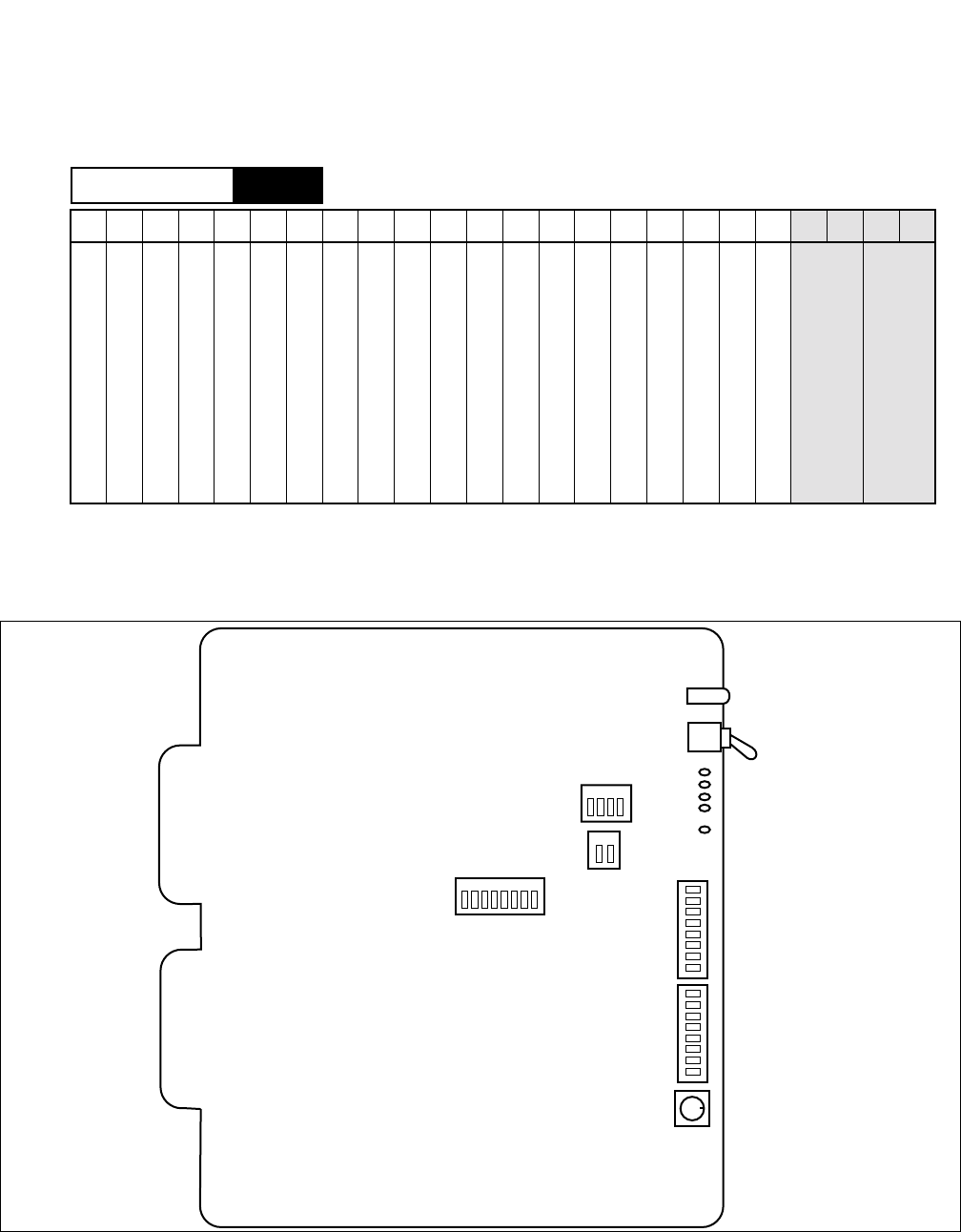
CHAPTER 3 NDA-24296
Page 212
Revision 1.0
PH-CK17
Phase Lock Oscillator
2. Mounting Location/Condition
This circuit card is mounted in the TSWM of the slot shown below.
3. Face Layout of Lamps, Switches, and Connectors
The face layout of lamps, switches, and connectors is shown in Figure 3-22.
Figure 3-22 Face Layout of PH-CK17 (PLO)
TSWM
Mounting Module
00 01 02 03 04 05 06 07 08 09 10 11 12 13 14 15 16 17 18 19 20 21 22 23
TSWM
PLO 0
PLO 1
1 2 3 4
1 2
SW06
SW05
SW04
MB
ACT
1 2 3 4 5 6 7 8
MJ
MN
SYNC
ICK
PALM
SW01
SW02
SW03

NDA-24296 CHAPTER 3
Page 213
Revision 1.0
PH-CK17
Phase Lock Oscillator
4. Lamp Indications
Lamp indications for this circuit card are shown in the table below.
LAMP NAME COLOR STATE
ACT Green Remains lit while this circuit card is in active state.
Off Remains off while this circuit card is in stand-by state.
MJ Red
Lights when the following MJ fault has occurred:
•All of the clock supply routes have failed when the system operates as the clock
subordinate office.
•32.768 MHz output clock failure.
•8 KHz output FH failure.
•5 msec × “n” output FH failure.
•Input Frame Pulse (FP) failure (FP is supplied by the SYNC card).
•Internal OSC (±0.3 ppm deviation) has failed when the system operates as the clock
source office.
MN Red
Lights when the following MN fault has occurred:
•One or more (but not all) DTI/DCS clock supply routes failed.
•Drifting failure.
•Internal OSC (±0.3 ppm deviation) failure.
SYNC
Green Remains lit while the system is synchronized with the network.
OFF
Remains off when either of the following has occurred.
•DCS clock failure when receiving the clock signals from the DCS.
•DTI clock failure when receiving the clock signals from the DTI.
•Drifting failure.
ICK Green Lights when the internal oscillator is operating normally.
PALM Red Remains lit when power is abnormal.

CHAPTER 3 NDA-24296
Page 214
Revision 1.0
PH-CK17
Phase Lock Oscillator
5. Switch Settings
Standard settings for switches on this circuit card are shown in the table below.
SWITCH
NAME SETTING STANDARD
SETTING MEANING
MB UP Circuit card Make-busy.
DOWN ×Circuit card Make-busy cancel.
SW03 1 - F 1 Fixed to “1.”
SWITCH
NAME SWITCH
NO. SETTING STANDARD
SETTING MEANING
SW01
1ON Clock subordinate office.
OFF Clock source office.
2ON Digital Clock Supply route zero (DCS 0) is used.
OFF Digital Clock Supply route zero (DCS 0) is not used.
3ON Digital Clock Supply route one (DCS 1) is used.
OFF Digital Clock Supply route one (DCS 1) is not used.
4
ON 8 KHz of Frame Head signals are extracted from the DCS signals
(which is composed of 64 KHz + 8 KHz).
OFF 8 KHz of Frame Head signals are not extracted from the DCS
signals (which is composed of 64 KHz + 8 KHz).
5
ON When clock source failure has occurred in all supply routes, the
PLO outputs the original clock of the internal oscillator.
OFF When clock source failure has occurred in all supply routes, the
PLO continues outputting the current phase clock.
6
ON This circuit card is associated with SYNC (PA-CK16 WCS) card
and 5m Frame Pulse (FP) is supplied by the SYNC card.
OFF This circuit card is not associated with SYNC (PA-CK16 WCS)
card.
7ON A-law CODEC is used for the hold music.
OFF ×µ-law CODEC is used for the hold music.
8 OFF ×Not used.
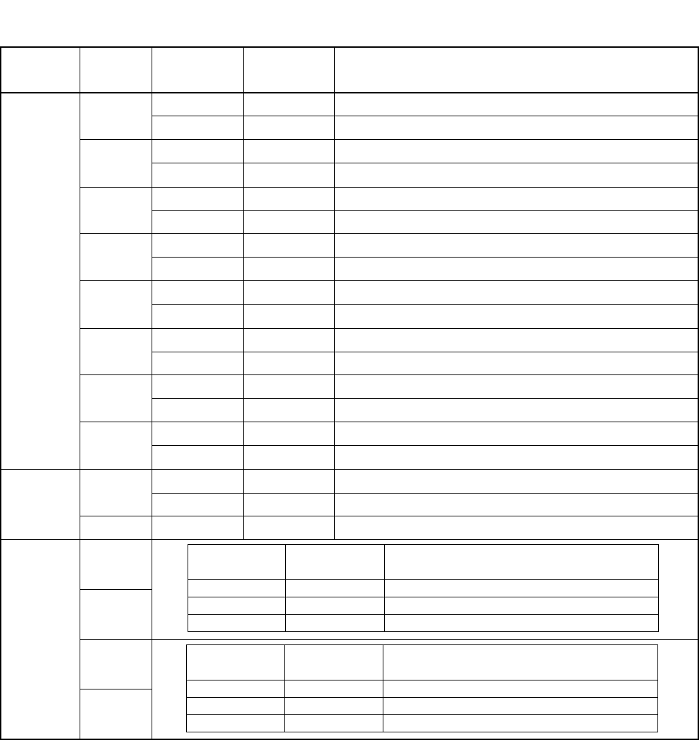
NDA-24296 CHAPTER 3
Page 215
Revision 1.0
PH-CK17
Phase Lock Oscillator
SW02
1ON DIU 0 is used as the DTI clock supply route zero.
OFF DIU 0 is not used.
2ON DIU 1 is used as the DTI clock supply route one.
OFF DIU 1 is not used.
3ON DIU 2 is used as the DTI clock supply route two.
OFF DIU 2 is not used.
4ON DIU 3 is used as the DTI clock supply route three.
OFF DIU 3 is not used.
5ON ×1.5 M clock for DIU 0
OFF 2 M clock for DIU 0
6ON ×1.5 M clock for DIU 1
OFF 2 M clock for DIU 1
7ON ×1.5 M clock for DIU 2
OFF 2 M clock for DIU 2
8ON ×1.5 M clock for DIU 3
OFF 2 M clock for DIU 3
SW05 1ON External hold tone source is used via FM lead.
OFF ×MUSIC ROM is used as the hold tone.
2OFF Not used.
SW06
1
2
3
4
SWITCH
NAME SWITCH
NO. SETTING STANDARD
SETTING MEANING
SW8F-1 SW8F-2 Impedance of the External
Music Source 0 (FM 0)
OFF OFF 600 Ω
ON OFF 8.2 Ω
OFF ON 47K Ω
SW8F-3 SW8F-4 Impedance of the External
Music Source 1 (FM 1)
OFF OFF 600 Ω
ON OFF 8.2 Ω
OFF ON 47K Ω
CHAPTER 3 NDA-24296
Page 216
Revision 1.0
PH-CK17
Phase Lock Oscillator
SW04
1
Note: Don’t care.
2
3
4ON Not used.
OFF ×Not used.
5MUSIC CH1 selection. The kind of music varies depending on the melody IC located on this
circuit card.
6
7
8ON Not used.
OFF ×Not used.
SWITCH
NAME SWITCH
NO. SETTING STANDARD
SETTING MEANING
SWA0-1 SWA0-2 SWA0-3 MUSIC
OFF OFF OFF Für Elise
ON OFF OFF Maiden’s prayer
Note OFF ON Buzzer
Note ON OFF Chime

NDA-24296 CHAPTER 3
Page 217
Revision 1.0
PH-CK17
Phase Lock Oscillator
5. External Interface
When this circuit card is located in the TSWM, connect 34PH EXCLK CA-A to the EXCLK0/EXCLK1
connectors on the backplane of the TSWM.
Figure 3-23 LT Connector Lead Location of PLO (TSWM)
00 01 02 03 04 05 06 07 08 09 10 11 12 13 14 15 16 17 18 19 20 21 22 23
Slot No.
TSWM
FRONT VIEW
PLO #1
PLO #0
26 1
FM 1
27 2
FM 0
28 3
SYN 1B
E
29 4
SYN 0B
E
30 5
DIU 3B
SYN 1A
31 6
DIU 2B
SYN 0A
32 7
DIU 1B
DIU 3A
33 8
DIU 0B
DIU 2A
34 9
DCS B
DIU 1A
35 10 DIU 0A
36 11 DCS A
37 12
38 13
EXCLK0
(Slot No.21)
EXCLK1
(Slot No.23)
TSWM
REAR VIEW
34PH EXCLK
CA-A
34PH EXCLK CA-A
34PH EXCLK CA-A LEAD ACCOMMODATION
Installation Cable
MDF
To Digital Interface and/or DCS
Mounting Module TSWM

CHAPTER 3 NDA-24296
Page 218
Revision 1.0
PH-CK17
Phase Lock Oscillator
Figure 3-24 Connecting Route Diagram
DCSB1
DIU0A1
DIU0B1
DIU1A1
DIU1B1
DIU2A1
DIU2B1
DIU3A1
DIU3B1
DCSA1
DCSB0
DIU0A0
DIU0B0
DIU1A0
DIU1B0
DIU2A0
DIU2B0
DIU3A0
DIU3B0
DCSA0
POUT B
POUT A
POUT B
POUT A
POUT B
POUT A
POUT B
POUT A
CCT /DTI
/PRT
CCT /DTI
/PRT
CCT /DTI
/PRT
CCT /DTI
/PRT
PLO #0
PLO #1
DCS
Note : The following circuit cards have Clock Output Leads for a PLO card: CCT (PA-24CCTA, PA-30CCTB),
DTI (PA-24DTR, PA-30DTS), and PRT (PA-24PRT, PA-30PRTC).
MDFPBX
NDA-24296 CHAPTER 3
Page 219
Revision 1.0
PH-CK17
Phase Lock Oscillator
6. Switch Setting Sheet
SWITCH NAME SWITCH SHAPE REMARKS
MB
SW01
SW02
SW03
SW05
SW06
SW04
ON
1234ON
5678
12 3 4 ON
56 7 8
1 2 ON
1 2 3 4 ON
12 3 4 ON
56 7 8
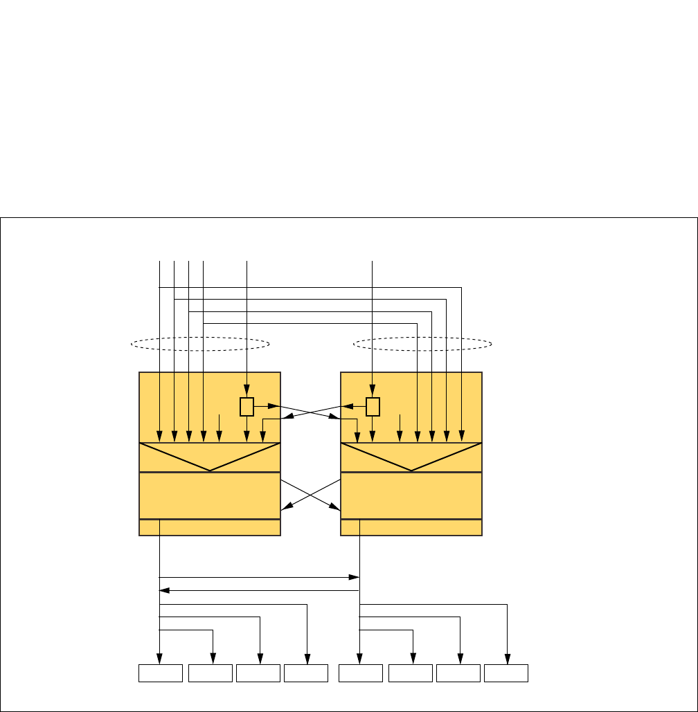
CHAPTER 3 NDA-24296
Page 220
Revision 1.0
PH-CK17-A
Phase Lock Oscillator
PH-CK17-A
Phase Lock Oscillator
1. General Function
This circuit card used with a direct digital interface circuit card, sets up network synchronization between
networks. Since this circuit card provides a high precision base clock oscillator, the system containing this
circuit card can be a clock source office of the digital network. As seen in Figure 3-25, the PLO can be
redundant regardless of the system switching network selection.
Figure 3-25 Location of PH-CK17-A in 4-IMG System
OSC 64K+8K
(BWB)
(BWB)
CLK, FH, WFH
ACT, ALM
34PH EXCLK CA-A
PLO #0
TSW 00
BWB BWB
DTI0 DCS0
(MDF)
DCS1123
PLO #1
SEL
PLL
Drv
SEL
PLL
Drv
OSC
34PH EXCLK CA-A
TSW 01 TSW 02 TSW 03 TSW 00 TSW 01 TSW 02 TSW 03
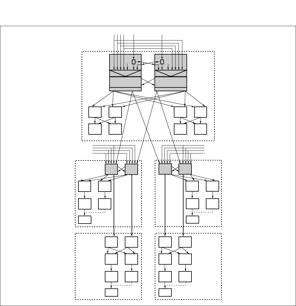
NDA-24296 CHAPTER 3
Page 221
Revision 1.0
PH-CK17-A
Phase Lock Oscillator
Figure 3-26 Location of PH-CK17-A (PLO) in IPX-U/IPX-UMG System
LN0/LMG0
(IMG2/IMG3) LN3/LMG3
(IMG2/IMG3)
/(IMG14/IMG15)
32M, FH+WFH
PLO ACT 32M, FH+WFH
PLO ACT
CLK1
(TSWM1)
TSW
10~13
CLK0
(TSWM1)
TSW
00~03
MUX
(
System1
)
MUX
(
System0
)
LC/TRK
HSW00
ISWM
HSW01
CLK1
(TSWM1)
TSW
10~13
CLK0
(TSWM1)
TSW
00~03
MUX
(
System1
)
MUX
(
System0
)
LC/TRK
LN0/LMG0
(IMG0/IMG1)
from
LN/LMG DTI from
LN/LMG DTI
32M, FH+WFH
PLO ACT
32M, FH+WFH
PLO ACT
(BWB)
32M, FH+WFH
PLO ACT
(BWB)
64K+FH, WFH
TSW ACT
(Cable)
64K+FH, WFH
TSW ACT
(Cable)
PLO 1
(TSWM0)
TSW
10~13
PLO 0
(TSWM0)
TSW
00~03
MUX
(
System1
)
MUX
(
System0
)
LC/TRK
LN3/LMG3
(IMG0/IMG1)
/(IMG12/IMG13) 32M, FH+WFH
PLO ACT
PLO 1
(TSWM0)
TSW
10~13
PLO 0
(TSWM0)
TSW
00~03
MUX
(
System1
)
MUX
(
System0
)
LC/TRK
TSW00 TSW03
HSW10
OSC 64K+8K
(BWB)
(BWB)
CLK, FH, WFH
ACT, ALM
PLO 0
DTI0 DCS0 (MDF) DCS1123
PLO 1
SEL
PLL
Drv
HSW11
TSW10 TSW13
SEL
PLL
Drv
OSC
~
~~
~
CHAPTER 3 NDA-24296
Page 222
Revision 1.0
PH-CK17-A
Phase Lock Oscillator
2. Mounting Location/Condition
This circuit card can be mounted in the shaded slots shown below.
This circuit card can be mounted in the shaded slots shown below.
<For 4-IMG System>
<For IPX-U/IPX-UMG System>
TSWM0(IMG1)
Mounting Module
00 01 02 03 04 05 06 07 08 09 10 11 12 13 14 15 16 17 18 19 20 21 22 23
TSWM(IMG1)
Mounting Module
PLO (#0)
PLO (#1)
ISWM
Mounting Module
TSWM0(IMG1/5/9/13)
Mounting Module
00 01 02 03 04 05 06 07 08 09 10 11 12 13 14 15 16 17 18 19
00 01 02 03 04 05 06 07 08 09 10 11 12 13 14 15 16 17 18 19 20 21 22 23
PLO (#0)
PLO (#1)
PLO (#0)
PLO (#1)
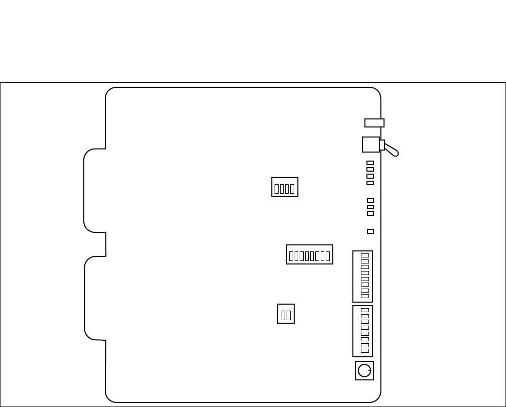
NDA-24296 CHAPTER 3
Page 223
Revision 1.0
PH-CK17-A
Phase Lock Oscillator
3. Face Layout of Lamps, Switches, and Connectors
The face layout of lamps, switches, and connectors are shown in Figure 3-27:
Figure 3-27 Face Layout of PH-CK17-A (PLO)
1 2 3 4
1 2
SW11
SW10
SW12
MB
OPE
1 2 3 4 5 6 7 8
SW01
SW02
SW03
1234567812345678
MJ
MN
SYNC
ICK
CKPKG
ALM0
ALM1
PALM

CHAPTER 3 NDA-24296
Page 224
Revision 1.0
PH-CK17-A
Phase Lock Oscillator
4. Lamp Indications
Lamp indications for this circuit card are shown in the table below:
Note: This lamp is effective when this card is mounted in TSWM0 of the IPX-U/IPX-UMG system. When this card
is mounted in ISWM, this lamp is not used.
LAMP NAME COLOR STATE
OPE Green Remains lit while this circuit card is in active state.
MJ Red
Lights when the following MJ fault has occurred:
•All of the clock supply routes have failed when the system operates as the clock
subordinate office
•32.768 MHz output clock failure (including CLK card)
•8 KHz output clock failure (including CLK card)
•Input Frame Pulse (FP) failure (FP is supplied by the SYNC card)
•Internal OSC (±5 ppm deviation) have failed when the system operates as the clock
source office
MN Red
Lights when the following MN fault has occurred:
•One or more (but not all) DTI/DCS clock supply routes have failed
•Drifting failure
•Internal OSC (±5 ppm deviation) failure
SYNC Green Remains lit while the system is synchronized with the network.
ICK Green Lights when the internal oscillator is operating normally.
CKPKG
Note Green Lights when the CLK card in TSWM1 is in normal operation.
ALM0
Note Red Lights when clock failure has occurred in the CLK card.
ALM1
Note Red Lights when FH failure has occurred in the CLK card.
PALM Red Remains lit when the On-Board Power Supply is abnormal.

NDA-24296 CHAPTER 3
Page 225
Revision 1.0
PH-CK17-A
Phase Lock Oscillator
5. Switch Settings
Standard settings for switches on this circuit card are shown in the table below.
SWITCH
NAME SETTING STANDARD
SETTING MEANING
MB UP Circuit card Make-busy.
DOWN ×Circuit card Make-busy cancel.
SW03 1 - F 1 Fixed to “1.”

CHAPTER 3 NDA-24296
Page 226
Revision 1.0
PH-CK17-A
Phase Lock Oscillator
The key setting of “SW01” differs depending on the mounting location.
[Mounted in ISWM of IPX-U/IPX-UMG System or TSWM of 4-IMG System]
Note 1: When this card is used in the 4-IMG or ISWM of IPX-U/IPX-UMG system, specify the clock source (DCS
or DTI) according to the clock network configuration for the office.
Note 2: This standard setting is applicable when this card is mounted in ISWM of the IPX-U/IPX-UMG system.
SWITCH
NAME SWITCH
NO. SETTING STANDARD
SETTING MEANING
SW01
1ON ×
Note 2 Clock subordinate office.
OFF Clock source office.
2
ON Digital Clock Supply route zero (DCS 0) is used.
OFF ×
Note 2 Digital Clock Supply route zero (DCS 0) is not used.
3
ON Digital Clock Supply route one (DCS 1) is used.
OFF ×
Note 2 Digital Clock Supply route one (DCS 1) is not used.
4
ON 8 KHz of Frame Head signals are extracted from the DCS
signals (which is composed of 64 KHz + 8 KHz).
OFF ×
Note 2 8 KHz of Frame Head signals are not extracted from the DCS
signals (which is composed of 64 KHz + 8 KHz).
5
ON When clock source failure has occurred in all supply routes, the
PLO outputs the original clock of the internal oscillator.
OFF ×
Note 2 When clock source failure has occurred, the PLO keeps on
outputting the current phase clock.
6
ON
This circuit card is used associated with SYNC (PA-CK16
WCS) card and 5 m Frame Pulse (FP) is supplied by the SYNC
card.
OFF ×
Note 2 This circuit card is not used associated with SYNC (PA-CK16
WCS) card.
7ON A-law CODEC is used for Music-on-Hold.
OFF ×µ-law CODEC is used for Music-on-Hold.
8OFF ×Fixed to “OFF” (Not used).

NDA-24296 CHAPTER 3
Page 227
Revision 1.0
PH-CK17-A
Phase Lock Oscillator
[Mounted in TSWM0 of IPX-U/IPX-UMG System]
SWITCH
NAME SWITCH
NO. SETTING STANDARD
SETTING MEANING
SW01
1ON ×Clock subordinate office. (Fixed)
OFF Clock source office.
2
ON Digital Clock Supply route zero (DCS 0) is used.
(In case this circuit card is accommodated as #0 system.)
OFF Digital Clock Supply route zero (DCS 0) is not used.
(In case this circuit card is accommodated as #1 system.)
3
ON Digital Clock Supply route one (DCS 1) is used.
(In case this circuit card is accommodated as #1 system.)
OFF Digital Clock Supply route one (DCS 1) is not used.
(In case this circuit card is accommodated as #0 system.)
4
ON 8 KHz of Frame Head signals are extracted from the DCS
signals (which is composed of 64 KHz + 8 KHz).
OFF ×8 KHz of Frame Head signals are not extracted from the DCS
signals (which is composed of 64 KHz + 8 KHz).
5
ON When clock source failure has occurred in all supply routes, the
PLO outputs the original clock of the internal oscillator.
OFF × When clock source failure has occurred in all supply routes, the
PLO continues outputting the current phase clock.
6
ON ×This circuit card is associated with SYNC (PA-CK16 WCS) card
and 5 m Frame Pulse (FP) is supplied by the SYNC card.
(Fixed to “ON” )
OFF This circuit card is not associated with SYNC (PA-CK16 WCS)
card.
7ON A-law CODEC is used for Music-On-Hold.
OFF ×µ-law CODEC is used for Music-On-Hold.
8OFF ×Fixed OFF (Not used).

CHAPTER 3 NDA-24296
Page 228
Revision 1.0
PH-CK17-A
Phase Lock Oscillator
Note 1: When this card is mounted in TSWM0 of the IPX-U/IPX-UMG system, DCS clock from the ISWM is used.
The DTI clock can also be used as an alternate clock supply route in case of DCS clock failure.
Note 2: When this card is mounted in ISWM, set to “ON (=CLK card is not used).”
If mounted in TSWM0 on LN/LMG,
•set to “OFF” if TSWM1 (CLK card, PH-CK18) on the same LN/LMG is used.
•set to “ON” if TSWM1 (CLK card, PH-CK18) on the same LN/LMG is not used.
SW02
Note 1
1ON DIU 0 is used as the DTI clock supply route zero.
OFF DIU 0 is not used.
2ON DIU 1 is used as the DTI clock supply route one.
OFF DIU 1 is not used.
3ON DIU 2 is used as the DTI clock supply route two.
OFF DIU 2 is not used.
4ON DIU 3 is used as the DTI clock supply route three.
OFF DIU 3 is not used.
5ON ×1.5 M clock for DIU 0.
OFF 2 M clock for DIU 0.
6ON ×1.5 M clock for DIU 1.
OFF 2 M clock for DIU 1.
7ON ×1.5 M clock for DIU 2.
OFF 2 M clock for DIU 2.
8ON ×1.5 M clock for DIU 3.
OFF 2 M clock for DIU 3.
SW10
1ON External hold tone source is used via FM lead.
OFF ×MUSIC ROM is used as the hold tone.
2
Note 2
ON CLK card is not used.
OFF ×CLK card is used.
SWITCH
NAME SWITCH
NO. SETTING STANDARD
SETTING MEANING
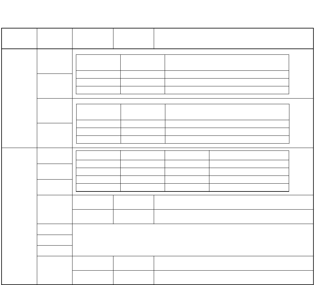
NDA-24296 CHAPTER 3
Page 229
Revision 1.0
PH-CK17-A
Phase Lock Oscillator
SWITCH
NAME SWITCH
NO. SETTING STANDARD
SETTING MEANING
SW11
1
2
3
4
SW12
1
2
3
4ON Not used.
OFF ×Not used.
5MUSIC (CH1) selection. The music varies depending on the melody IC located on this circuit
card.
6
7
8ON Not used.
OFF ×Not used.
SW11-1 SW11-2 Impedance of the External
Music Source 0 (FM 0)
OFF OFF 600 Ω
ON OFF 8.2 Ω
OFF ON 47K Ω
SW11-3 SW11-4 Impedance of the External
Music Source 1 (FM 1)
OFF OFF 600 Ω
ON OFF 8.2 Ω
OFF ON 47K Ω
SW12-1 SW12-2 SW12-3 MUSIC
OFF OFF OFF Für Elise
ON OFF OFF Maiden’s prayer
Don’t Care ON OFF Buzzer
Don’t Care OFF ON Chime

CHAPTER 3 NDA-24296
Page 230
Revision 1.0
PH-CK17-A
Phase Lock Oscillator
6. External Interface
PLO input leads appear on the LT connectors labeled EXCLK0 and EXCLK1
•PLO mounting slots
The PLO card is mounted in Slots 21 and 23 of TSWM.
•LT cable connectors
Connect the LT cables to the connectors labeled EXCLK0 and EXCLK1 on the TSWM backplane.
Figure 3-28 PLO Pin Assignments for Receiving Clock (4 IMG System) (1/2)
00 01 02 03 04 05 06 07 08 09 10 11 12 13 14 15 16 17 18 19 20 21 22 23
EXCLK0
EXCLK1 PLO
PLO
TSW
Front View
TSWM
EXCLK0
EXCLK1
TSWM
Backplane
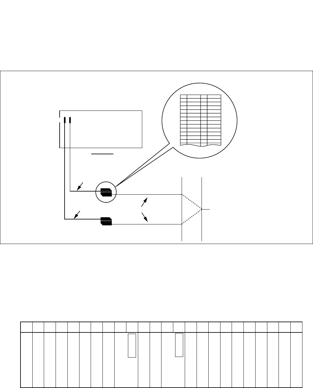
NDA-24296 CHAPTER 3
Page 231
Revision 1.0
PH-CK17-A
Phase Lock Oscillator
•EXCLK0/EXCLK1 connector Pin Assignment
Pins are assigned as follows on the EXCLK0/EXCLK1 connectors. When the clock is distributed from a
digital interface, use one pair of DIUxxx in one of the four inputs. (There are a maximum of four inputs.)
DIU leads have the following precedence: DIU0xx (high) ➝ DIU3xx (low).
Figure 3-28 PLO Pin Assignments for Receiving Clock (4 IMG) (2/2)
PLO input leads appear on the LT connectors labeled EXCLK0 and EXCLK1.
•PLO mounting slots
The PLO card is mounted in Slots 09 and 13 of ISWM.
34PH ISWM EXCLK CA-A
34PH ISWM EXCLK CA-A
REAR VIEW
EXCLK0
EXCLK1
TSWM
MDF
Installation Cable To Digital Interface and/or DCS
34PH ISWM EXCLK CA-A Cable Lead Location
26
27
28
29
30
31
32
33
34
35
36
37
38
1
2
3
4
5
6
7
8
9
10
11
12
13
FM1
FM0
DIU3B
DIU2B
DIU1B
DIU0B
DCSB
SYN1B
SYN0B
E
E
DIU3A
DIU2A
DIU1A
DIU0A
DCSA
SYN1A
SYN0A
00 01 02 03 04 05 06 07 08 09 10 11 12 13 14 15 16 17 18 19 20 21 22 23
EXCLK0
EXCLK1 PLO
PLO
Front View
ISWM

CHAPTER 3 NDA-24296
Page 232
Revision 1.0
PH-CK17-A
Phase Lock Oscillator
•LT cable connectors
Connect LT cables to the connectors labeled EXCLK0 and EXCLK1 on the ISWM backplane.
Figure 3-29 PLO Pin Assignment for Receiving Clock (ISWM) (1/2)
•EXCLK0/EXCLK1 connector Pin Assignment
Pins are assigned as follows on the EXCLK0/EXCLK1 connectors. When the clock is distributed from a
digital interface, use one pair of DIUxxx in one of the four inputs. (There are a maximum of four inputs.)
DIU leads have the following precedence: DIU0xx (high) ➝ DIU3xx (low).
Figure 3-29 PLO Pin Assignment for Receiving Clock (ISWM) (2/2)
EXCLK1 EXCLK0
Backplane
ISWM
MDF
To Digital Interface and/or DCS
Installation Cable
ISWM
EXCLK0
(Slot No.09)
EXCLK1
(Slot No.13)
34PH ISWM EXCLK CA-A
34PH ISWM EXCLK CA-A
Rear View 26
27
28
29
30
31
32
33
34
35
36
37
38
1
2
3
4
5
6
7
8
9
10
11
12
13
FM1
FM0
DIU3B
DIU2B
DIU1B
DIU0B
DCSB
SYN1B
SYN0B
E
E
DIU3A
DIU2A
DIU1A
DIU0A
DCSA
SYN1A
SYN0A
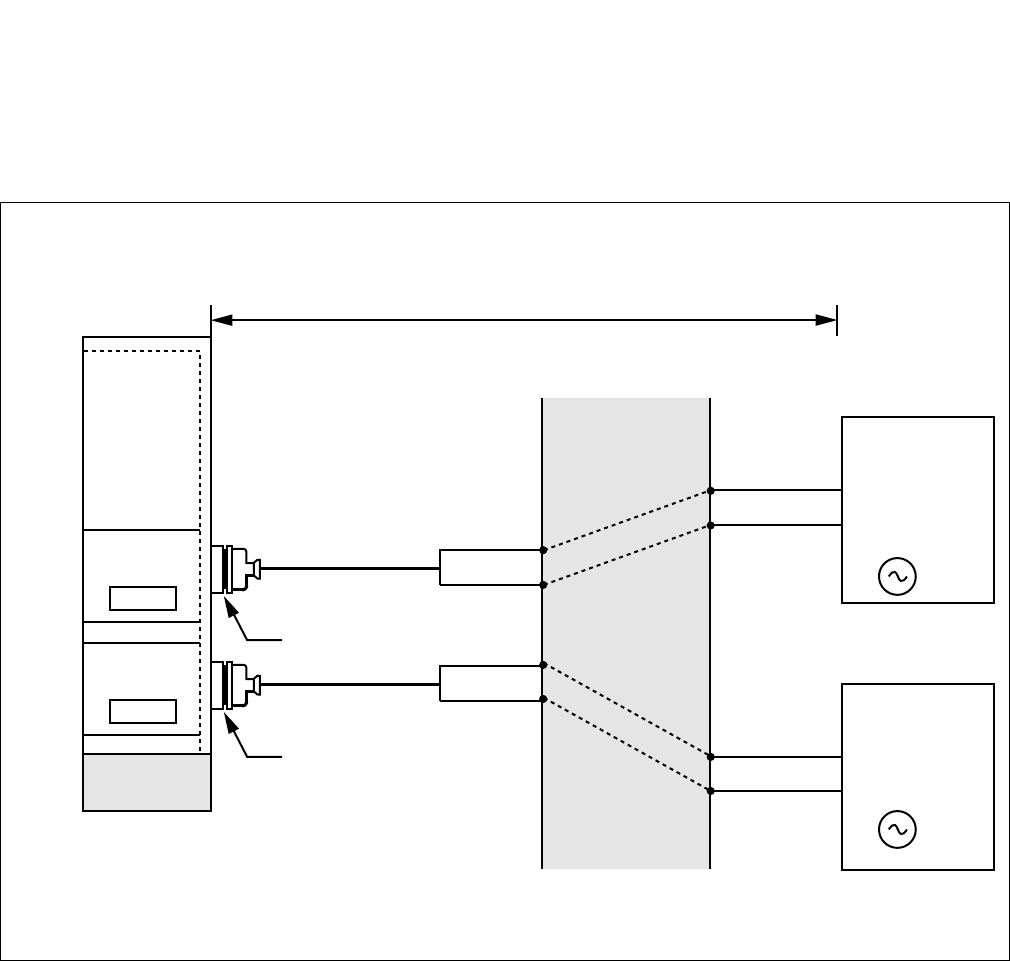
NDA-24296 CHAPTER 3
Page 233
Revision 1.0
PH-CK17-A
Phase Lock Oscillator
•Cable Connection Diagram
Provide the following wiring at the MDF. The connection diagram in Figure 3-30 shows an example of a
system that has the PLO cards in dual configuration.
Figure 3-30 Cable Connection Diagram (ISWM) for Accepting Synchronization Clocks from an External
High-Stability Oscillator
MDF
ISW/CMG
External
High-Stability
Oscillator #1
CLK
External
High-Stability
Oscillator #0
CLK
PCM Cable(IP)
PCM Cable(IP)
DCSA
DCSB
LT Connector Cable
EXCLK1 DCSB
DCSA
LT Connector Cable
EXCLK0
EXCLK1
PLO#1
EXCLK0
PLO#0
BASEU
ISWM
maximum 400 meters (1320 feet) (24 AWG)
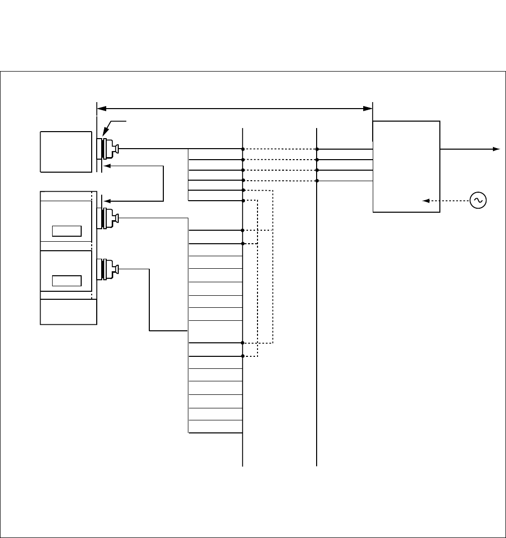
CHAPTER 3 NDA-24296
Page 234
Revision 1.0
PH-CK17-A
Phase Lock Oscillator
Figure 3-31 shows an example of distributing clock from a digital interface in LN/LMG. This example assumes
that the Digital Trunk POUT leads are used as the first clock distribution route.
Figure 3-31 Cable Connection Diagram (ISWM) for Receiving Clock from Digital Interface
MDF
ISW/CMG
LN/LMG
PCM
Carrier
Equipment
DSU
CLK
PCM Cable (2P) to other node
Installation Cable
Installation Cable
maximum 100
meters (330 feet)
(24AWG)
Installation Cable RA
RB
TA
TB
POUTA
POUTB
DIU0A0
DIU0B0
DIU1A0
DIU1B0
DIU2A0
DIU2B0
DIU3A0
DIU3B0
DIU0A1
DIU0B1
DIU1A1
DIU1B1
DIU2A1
DIU2B1
DIU3A1
DIU3B1
EXCLK0
PLO#0
LT Connector
Digital
Interface
EXCLK1
PLO#1
maximum 200 meters (660 feet) (24AWG)
Note 1:
Note 1
Note 2
PLO has a maximum 4 inputs. DIU0xx leads are used for the 1st clock distribution routes. DIU3xx
leads are used for the 4th. The first input has the highest priority.
Note 2: The connection is required for a dual PLO system.
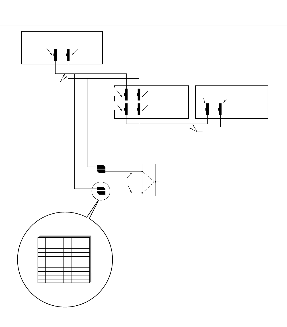
NDA-24296 CHAPTER 3
Page 235
Revision 1.0
PH-CK17-A
Phase Lock Oscillator
Figure 3-32 LT Connector Lead Location of PLO (ISWM-TSWM0/1)
CLK00
(Slot No.08)
CLK10
(Slot No.12)
TSWM1
TSWM0
ISWM
Installation Cable
DIU Connection Note MDF
To Digital Interface
EXCLK0
(Slot No.21)
PLO CLOCK0
(Slot No.21)
EXCLK1
(Slot No.23)
PLO CLOCK1
(Slot No.23)
PLO CLOCK0
(Slot No.21)
PLO CLOCK1
(Slot No.23)
ISW-LN PLO CA-A
PLO-CLK CA-A
DCS Connection
Note: For DIU connection route diagram, see the figure on the next page.
26 1
LEAD
NAME LEAD
NAME
27 2
28 3
PIN
No.
PIN
No.
29 4
30 5
FM1
FM0
31 6
32 7
33 8
34 9
35 10
E
DIU 3B
DIU 2B DIU 3A
DIU 2A
E
DIU 1B DIU 1A
DIU 0B DIU 0A
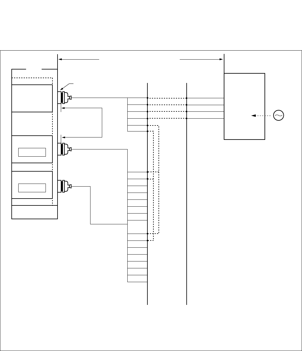
CHAPTER 3 NDA-24296
Page 236
Revision 1.0
PH-CK17-A
Phase Lock Oscillator
Figure 3-33 shows an example of distributing clock from a digital interface. This figure assumes that the Digital
Trunk POUT leads are used as the first clock distribution route. (This connection is not required for IPX-UMG
system.)
Figure 3-33 Cable Connection Diagram (4-IMG System/LN) for Receiving Clock from Digital Interface
DIU0A1
DIU0B1
DIU1A1
DIU1B1
DIU2A1
DIU2B1
DIU3A1
DIU3B1
DIU0A0
DIU0B0
DIU1A0
DIU1B0
DIU2A0
DIU2B0
DIU3A0
DIU3B0
RA
RB
TA
TB
POUT A
POUT B
PCM Cable (2P) to other node
PCM
Carrier
Equipment
DSU
CLK
Note 1:
Note 2
Note 1
PLO has a maximum of 4 inputs. DIU0xx leads are used for the 1st clock distribution routes.
DIU3xx leads are used for the 4th. The first input has the highest priority.
Note 2: The connection is required for a dual PLO system.
MDF
maximum 100
meters (330 feet)
(24AWG)
Installation Cable
LT Connector
Installation Cable
Installation Cable
EXCLK1
PLO#1
EXCLK0
PLO#0
Digital
Interface
IMG
maximum 200 meters (660 feet) (24 AWG)
NDA-24296 CHAPTER 3
Page 237
Revision 1.0
PH-CK17-A
Phase Lock Oscillator
Figure 3-34 Connection of External Music-On-Hold
ISW-LN PLO CA-A cable/
34PH ISWM EXCLK CA-A
Pin Assignment
PIN
No.
26
27
28
29
30
31
32
33
LEAD
NAME
FM1
FM0
LEAD
NAME
E
E
PIN
No.
1
2
3
4
5
6
7
8
9
MUSIC
SOURCE
MDF
ISW-LN PLO CA-A /
34PH ISWM EXCLK CA-A and
Installation Cable(25P)
Multiple connections between the systems 0 and 1
are required on the MDF.
Note
Note: FM1 is not used at this time.
CHAPTER 3 NDA-24296
Page 238
Revision 1.0
PH-CK17-A
Phase Lock Oscillator
7. Switch Setting Sheet
SWITCH NAME SWITCH SHAPE
MB
SW01
SW02
SW03
SW10
SW11
SW12
ON
1 2 3 4 ON
5 6 7 8
1 2 3 4 ON
5 6 7 8
12ON
1ON
2 3 4
1234ON
5678
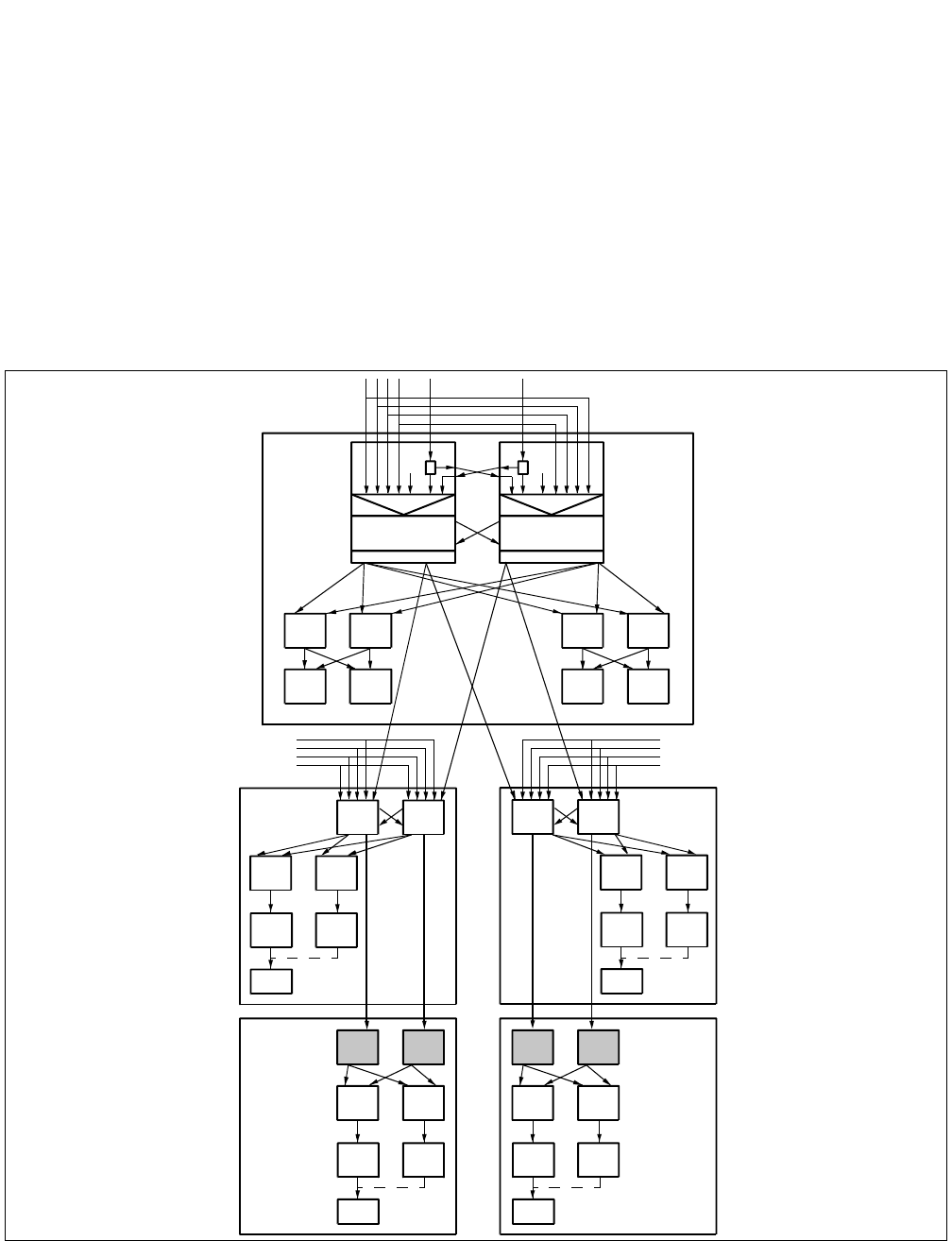
NDA-24296 CHAPTER 3
Page 239
Revision 1.0
PH-CK18
Clock
PH-CK18
Clock
1. General Function
This circuit card is used for the Local Node (LN) of the IPX-U system or used for the Local Module Group
(LMG) of the IPX-UMG system. The main function of this circuit card is to supply basic clock signals to
the system. This card receives clock signals from the Phase Lock Oscillator (PLO) located in TSWM0 of
IMG1/5/9/13, distributing the following signals to the Time Division Switch (TSW) located in TSWM1 of
IMG2/6/10/14.
•32.768 MHz CLK
•8 KHz FH
•5 msec × “n” FH (for Wireless System)
Figure 3-35 Location of PH-CK18 (CLK)
LN0/LMG0
(IMG2/IMG3) LN3/LMG3
(IMG2/IMG3)
/(IMG14/IMG15)
32M, FH+WFH
PLO ACT 32M, FH+WFH
PLO ACT
CLK1
(TSWM1)
TSW
10~13
CLK0
(TSWM1)
TSW
00~03
MUX
(System1)
MUX
(System0)
LC/TRK
HSW00
ISW
HSW01
CLK1
(TSWM1)
TSW
10~13
CLK0
(TSWM1)
TSW
00~03
MUX
(System1)
MUX
(System0)
LC/TRK
LN0/LMG0
(IMG0/IMG1)
from
LN/LMG DTI from
LN/LMG DTI
32M, FH+WFH
PLO ACT
32M, FH+WFH
PLO ACT
(BWB)
32M, FH+WFH
PLO ACT
(BWB)
64K+FH, WFH
TSW ACT
(Cable)
64K+FH, WFH
TSW ACT
(Cable)
PLO 1
(TSWM0)
TSW
10~13
PLO 0
(TSWM0)
TSW
00~03
MUX
(System1)
MUX
(System0)
LC/TRK
LN3/LMG3
(IMG0/IMG1)
/(IMG12/IMG13) 32M, FH+WFH
PLO ACT
PLO 1
(TSWM0)
TSW
10~13
PLO 0
(TSWM0)
TSW
00~03
MUX
(System1)
MUX
(System0)
LC/TRK
TSW00 TSW03
HSW10
OSC 64K+8K
(BWB)
(BWB)
CLK, FH, WFH
ACT, ALM
PLO 0
DTI0 DCS0 (MDF) DCS1123
PLO 1
SEL
PLL
Drv
HSW11
TSW10 TSW13
SEL
PLL
Drv
OSC
~
~~
~
CHAPTER 3 NDA-24296
Page 240
Revision 1.0
PH-CK18
Clock
2. Mounting Location/Condition
Mounting locations for this circuit card are shown below.
3. Face Layout of Lamps, Switches, and Connectors
The face layout of each lamp and switch on this circuit card is shown in the figure below:
Figure 3-36 Face Layout of PH-CK18 (CLK)
00 01 02 03 04 05 06 07 08 09 10 11 12 13 14 15 16 17 18 19 20 21 22 23
CLK (#0)
TSWM1(IMG2/6/10/14)
Mounting Module
CLK (#1)
MB
OPE
ALM0
ALM1
PALM

NDA-24296 CHAPTER 3
Page 241
Revision 1.0
PH-CK18
Clock
4. Lamp Indications
Lamp indications for this circuit card are shown below:
5. Switch Settings
Switch settings for this circuit card are shown below.
LAMP COLOR MEANING
OPE Green Lights when this circuit card is in ACT state.
ALM 0 Red Lights when clock signal failure has occurred.
ALM 1 Red Lights when Frame Head signal failure has occurred.
PALM Red Lights when the On Board Power Supply failure has occurred.
SWITCH
NAME SETTING STANDARD
SETTING MEANING
MB ON Circuit card Make-busy.
OFF ×Circuit card Make-busy cancel.
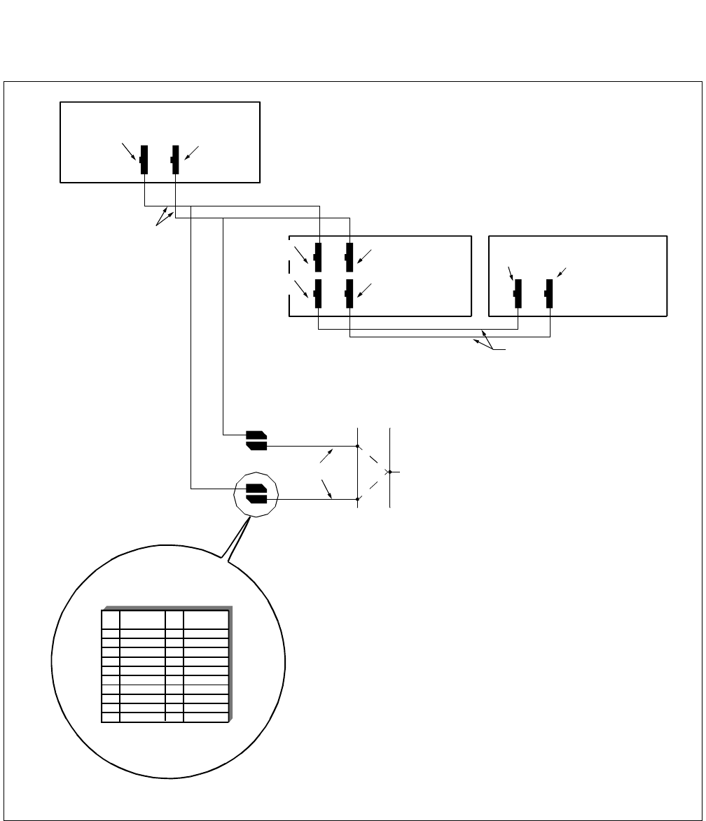
CHAPTER 3 NDA-24296
Page 242
Revision 1.0
PH-CK18
Clock
6. External Interface
Figure 3-37 LT Connector Lead Location (ISWM-TSWM0/1)
CLK00
(Slot No.08)
CLK10
(Slot No.12)
TSWM1
TSWM0
ISWM
Installation Cable
DIU Connection Note MDF
To Digital Interface and/or DCS
EXCLK0
(Slot No.21)
PLO CLOCK0
(Slot No.21)
EXCLK1
(Slot No.23)
PLO CLOCK1
(Slot No.23)
PLO CLOCK0
(Slot No.21)
PLO CLOCK1
(Slot No.23)
ISW-LN PLO CA-A
PLO-CLK CA-A
DCS Connection
26 1
LEAD
NAME LEAD
NAME
27 2
28 3
PIN
No.
PIN
No.
29 4
30 5
31 6
32 7
33 8
34 9
35 10
DIU 3B
DIU 2B
DIU 3A
DIU 2A
DIU 1B
DIU 1A
DIU 0B DIU 0A

NDA-24296 CHAPTER 3
Page 243
Revision 1.0
PH-CK18
Clock
7. Switch Setting Sheet
SWITCH NAME SWITCH SHAPE REMARKS
MB
ON
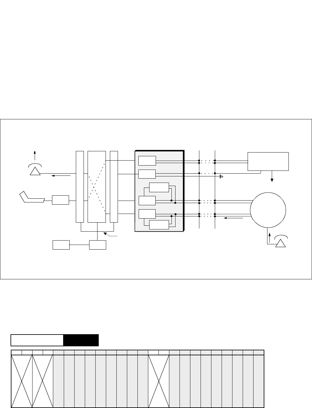
CHAPTER 3 NDA-24296
Page 244
Revision 1.0
PA-8COTBJ
Central Office Trunk
PA-8COTBJ
Central Office Trunk
1. General Function
The PA-8COTBJ (8COT) circuit card provides an interface between a maximum of 8C.O. lines and the
system. And this card also provides the caller ID service. Depending upon keys setting of this card, the first
circuit on this card can be used as an interface for Paging Equipment. In this instance, the second circuit is
also used for the purpose of activating the Paging Equipment. Example of the Paging Equipment and Caller
ID service are illustrated below. In addition, the appropriate value of Terminal Impedance and Balancing
Network (BNW) can be selected by key setting.
Figure 3-38 Location of PA-8COTBJ (8COT) Card within the System
2. Mounting Location/Condition
The PA-8COTBJ (8COT) card can be mounted in any universal slot as shown below.
00 01 02 03 04 05 06 07 08 09 10 11 12 13 14 15 16 17 18 19 20 21 22 23
This diagram shows an example where this card is used as both a PGT and COTs.
Terminal
INT
"555-1234"
Attendant
Console
ATI
SW INT
COT
circuit 1
circuit 2
circuit 7
circuit 8
PA-8COTBJ MDF
Speech Line
Control Line
G
"555-1234"
PAGING
EQUIPMENT
To Battery
PUBLIC
NETWORK
"555-1234"
Terminal
Local I/O Bus
MODEM
GT
CPU
MODEM
COT
PGT
PGT
PIM
Mounting Module
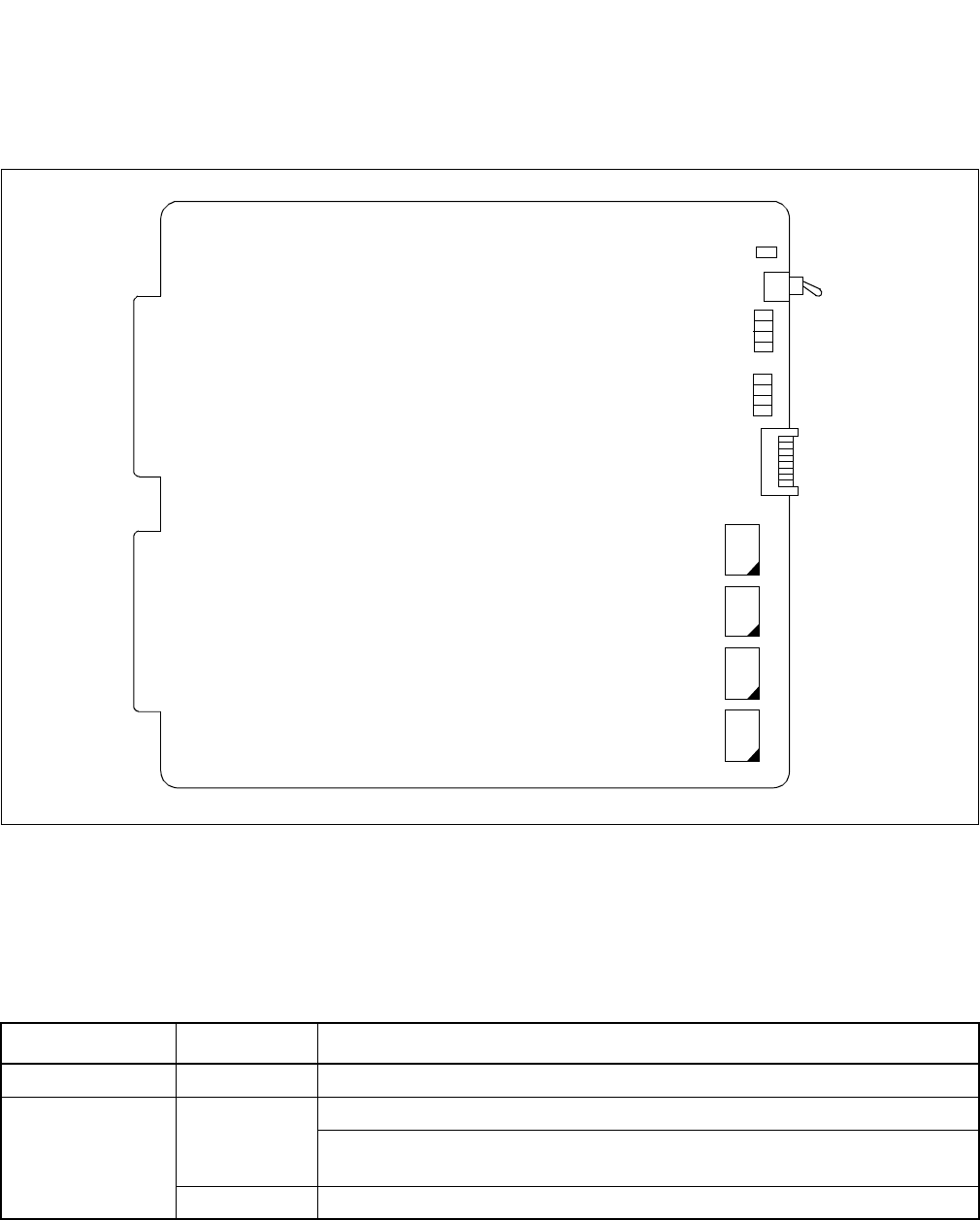
NDA-24296 CHAPTER 3
Page 245
Revision 1.0
PA-8COTBJ
Central Office Trunk
3. Face Layout of Lamps, Switches, and Connectors
The face layout of lamps, switches, and connectors of this circuit card is shown in Figure 3-39.
Figure 3-39 Face Layout of PA-8COTBJ (8COT)
4. Lamp Indications
The contents of lamp indications of this circuit card are shown in the table below.
8COT Lamp Indication Reference
LAMP NAME COLOR STATE
OPE Green Remains lit while this circuit card is operating.
BL0
BL7
Green
Lights when the corresponding circuit is busy.
Flashes to the dial pulses being sent out for an outgoing call, or the corresponding
circuit is in make busy state.
OFF BL-lamp remains off when the corresponding circuit is idle.
OPE
BL4~7
BL0~3
SW02
SW03
SW04
SW05
SW00
(MB)
SW01
(MB0-7)
-
CHAPTER 3 NDA-24296
Page 246
Revision 1.0
PA-8COTBJ
Central Office Trunk
5. Switch Settings
Standard settings of switches on this circuit card are shown in the table below.
SWITCH SWITCH
NO. SETTING STANDARD
SETTING MEANING
SW00
(MB)
UP Circuit card make busy
DOWN ×Circuit card make busy cancel
SW01
(MB0-7)
ON Request for make-busy of the trunk circuit corre-
sponding to MB switch.
OFF ×Request for cancelling the make-busy of the trunk cir-
cuit corresponding to MB switch.
SW02 1-4
Terminal Impedance and B.N.W.setting
SW03
1OFF ×Fixed to OFF (Not Used)
2OFF ×Fixed to OFF (Not Used)
3OFF ×Fixed to OFF (Not Used)
4OFF ×Fixed to OFF (Not Used)
SW04
1ON ×Fixed to ON
2OFF ×Fixed to OFF
3OFF ×Fixed to OFF
4ON Paging Trunk is available (When this switch is set to
ON, CH0 and CH1 cannot be used as CO trunks.)
OFF Paging Trunk is not available.
SW05
1OFF ×Fixed to OFF
2ON ×Fixed to ON
3OFF ×Fixed to OFF
4OFF ×Fixed to OFF
SW0 (SW10) MEANINGS
1234 B.N.W. Terminal
Impedance
OFF OFF OFF OFF EIA/TIA 464-A 600 Ω+2.16 µ
OFF ON ON OFF CCITT Q.517 900 Ω+2.16 µ
ON ON ON OFF 900 Ω
Other Combinations Inhibited
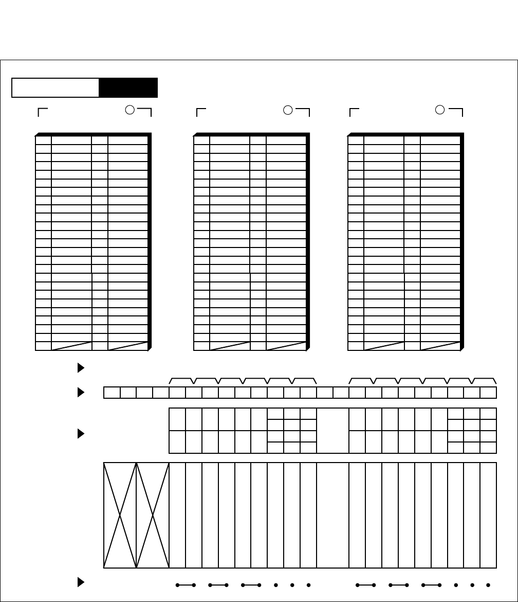
NDA-24296 CHAPTER 3
Page 247
Revision 1.0
PA-8COTBJ
Central Office Trunk
6. External Interface
Figure 3-40 LT Connector Leads Accommodation
PIM
Mounting Module
26
27
28
29
30
31
32
33
34
35
36
37
38
39
40
41
1
2
3
4
5
6
7
8
9
10
11
12
13
14
15
16
42
43
44
45
46
47
48
17
18
19
20
21
22
23
49
50 24
25
232221201918171615141312111009080706050403020100
LT6 LT7 LT8 LT9 LT10 LT11LT0 LT1 LT2 LT3 LT4 LT5
231915
221814
211713
201612
231915
221814
211713
201612
110907050301
100806040200
110907050301
100806040200
HW11HW10HW9HW8HW7HW6HW5HW4HW3HW2HW1HW0
Group No.
Slot No.
LT Connector
PIM
Highway Block
LT 1, 3, 5, 7, 9, 11 Connector
26
27
28
29
30
31
32
33
34
35
36
37
38
39
40
41
1
2
3
4
5
6
7
8
9
10
11
12
13
14
15
16
42
43
44
45
46
47
48
17
18
19
20
21
22
23
49
50 24
25
Accommodated in 2
LT 1, 3, 5, 7, 9, 11 Connector
Accommodated in 3
26
27
28
29
30
31
32
33
34
35
36
37
38
39
40
41
1
2
3
4
5
6
7
8
9
10
11
12
13
14
15
16
42
43
44
45
46
47
48
17
18
19
20
21
22
23
49
50 24
25
Accommodated in 1
LT 0, 2, 4, 6, 8, 10 Connector
B0 A0
B1 A1
B2 A2
B3 A3
B4 A4
B5 A5
B6 A6
B7 A7
B0 A0
B1 A1
B2 A2
B3 A3
B4 A4
B5 A5
B6 A6
B7 A7
B0 A0
B1 A1
B2 A2
B3 A3
B4 A4
B5 A5
B6 A6
B7 A7
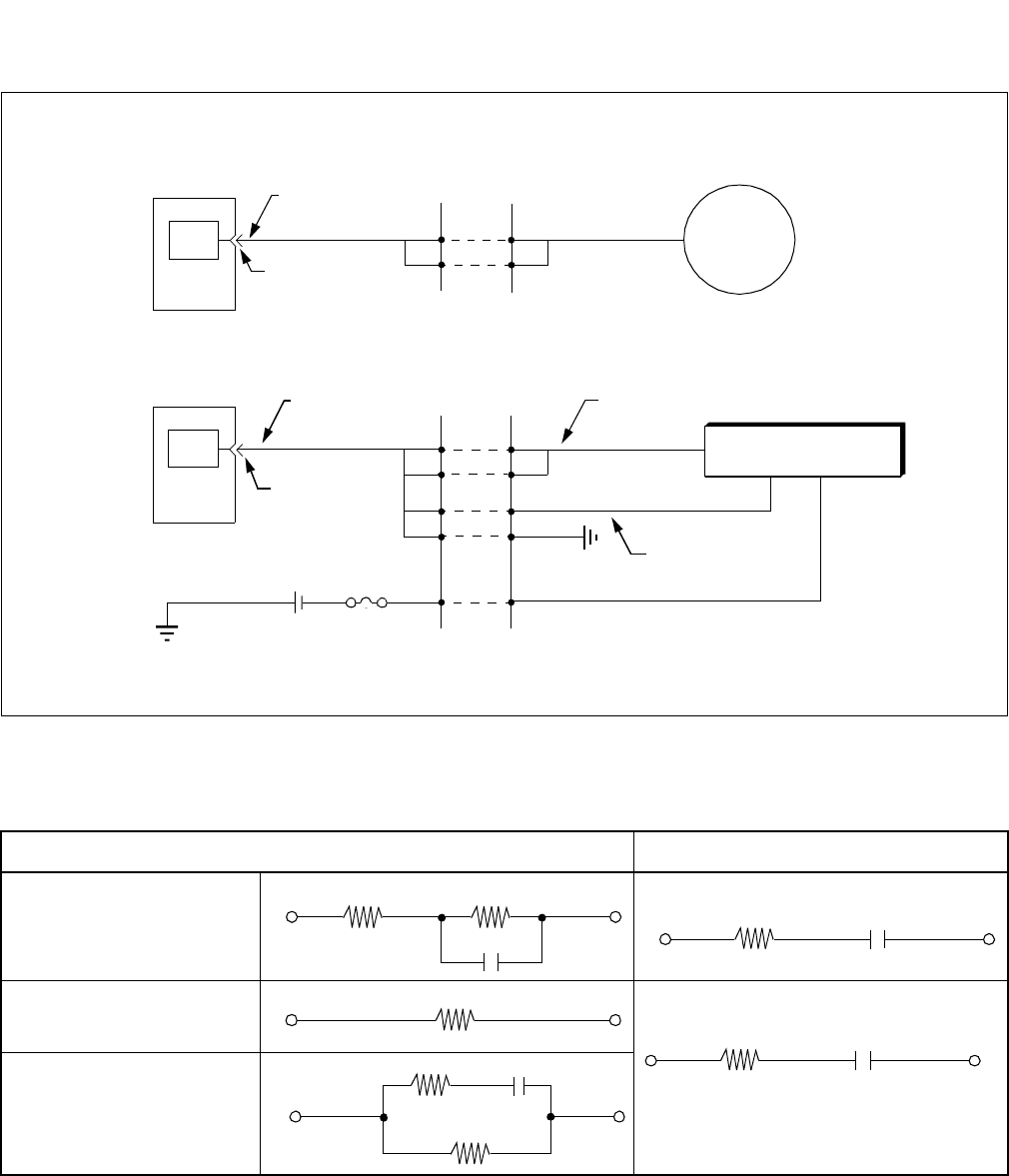
CHAPTER 3 NDA-24296
Page 248
Revision 1.0
PA-8COTBJ
Central Office Trunk
Figure 3-41 Connecting Route Diagram
Table 3-1 Balancing Network and Terminal Impedance
Balancing Network Terminal Impedance
EIA/TIA 464-A
900Ω
CCITT Q. 517
AT&T Echo Test
Network
Note: As illustrated above, two circuits (#0, #1) are required for connecting paging equipment.
•Cable Connections for Paging Equipment
PBX Installation Cable MDF
A0
B0
LT Connector
A
B
COT PUBLIC
NETWORK
PBX
COT
-48V
G
FUSE -48V
G
B
A
B1
A1
Installation Cable MDF
LT Connector
A0
B0
GControl Line
Speech Path
PAGING EQUIPMENT
•Cable Connections for a C.O. Line
0.21µF
1 k Ω
350 Ω
2.16µF
600 Ω
600+2.16µ
900 Ω
2.16µF
900 Ω
0.05µF
100 Ω
800 Ω
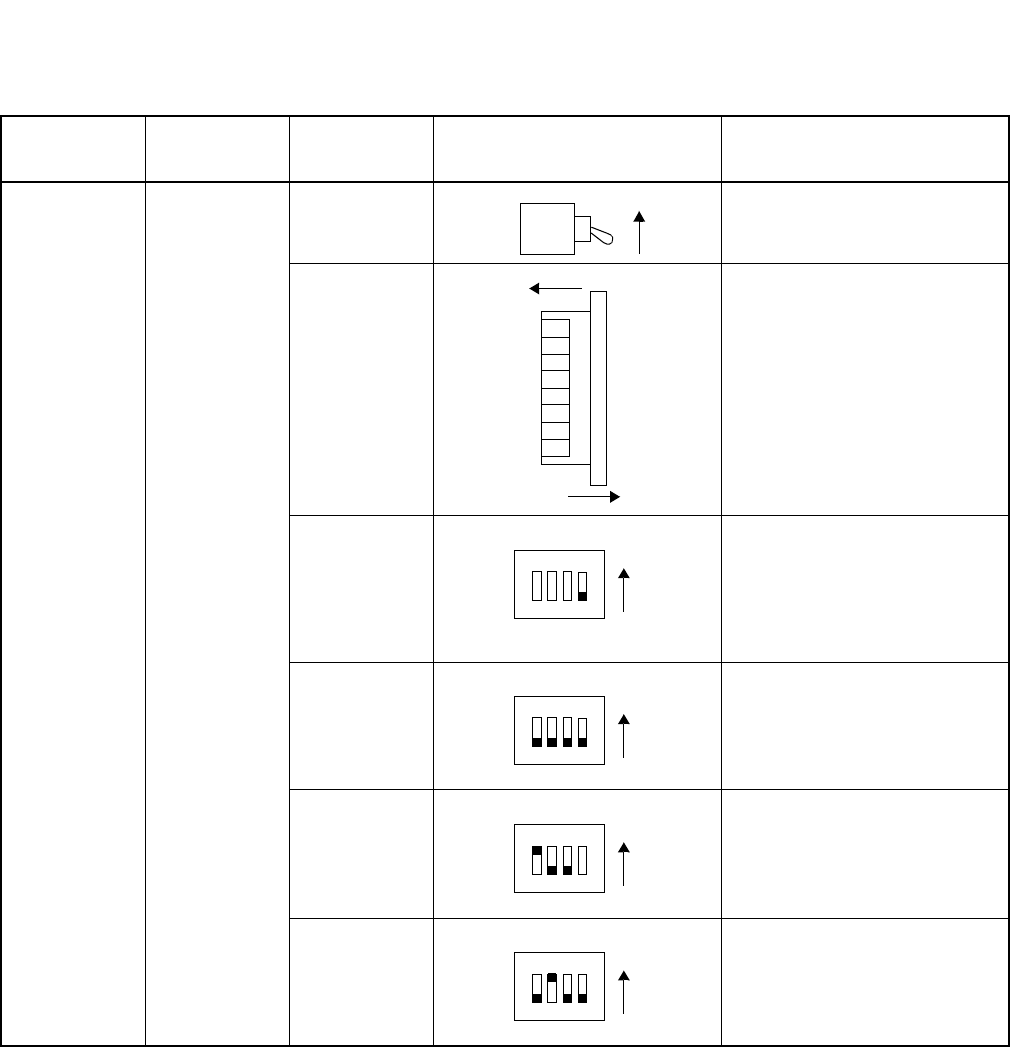
NDA-24296 CHAPTER 3
Page 249
Revision 1.0
PA-8COTBJ
Central Office Trunk
7. Switch Setting Sheet
MODULE SLOT NO. SWITCH
NAME SWITCH SHAPE REMARKS
PIM
SW00
(MB)
UP: Circuit card make busy.
DOWN: Circuit card make busy
cancel.
SW01
(MB0-7)
Make Busy switches associated
with No. 0 through No. 7
Circuits.
ON: Make busy on each
circuit basis.
OFF: Make busy cancel on
each circuit basis.
SW02
SW03
SW04
SW05
ON
ON
OFF
No.8
No.7
No.6
No.5
No.4
No.3
No.2
No.1
1234 ON
1234 ON
1234 ON
1234ON
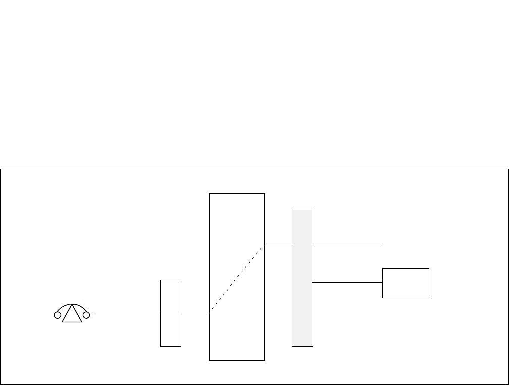
CHAPTER 3 NDA-24296
Page 250
Revision 1.0
PA-16COTBE
Central Office Trunk
PA-16COTBE
Central Office Trunk
1. General Function
This circuit card is accommodated in the PIM and supports the following interface.
(a) Interface with 16 C.O. lines
(b) Interface with 14 C.O. lines and 1 Paging Equipment line.
Figure 3-42 Location of PA-16COTBE (16COT) Card within the System
TSW
LC
Paging Equipment
C.O. Line
COT
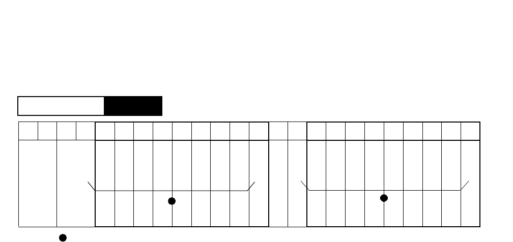
NDA-24296 CHAPTER 3
Page 251
Revision 1.0
PA-16COTBE
Central Office Trunk
2. Mounting Location/Condition
The mounting locations of this circuit card are shown below.
00 01 02 03 04 05 06 07 08 09 10 11 12 13 14 15 16 17 18 19 20 21 22 23
Note: Indicates universal slots for line/trunk circuit cards.
PIM
Mounting Module
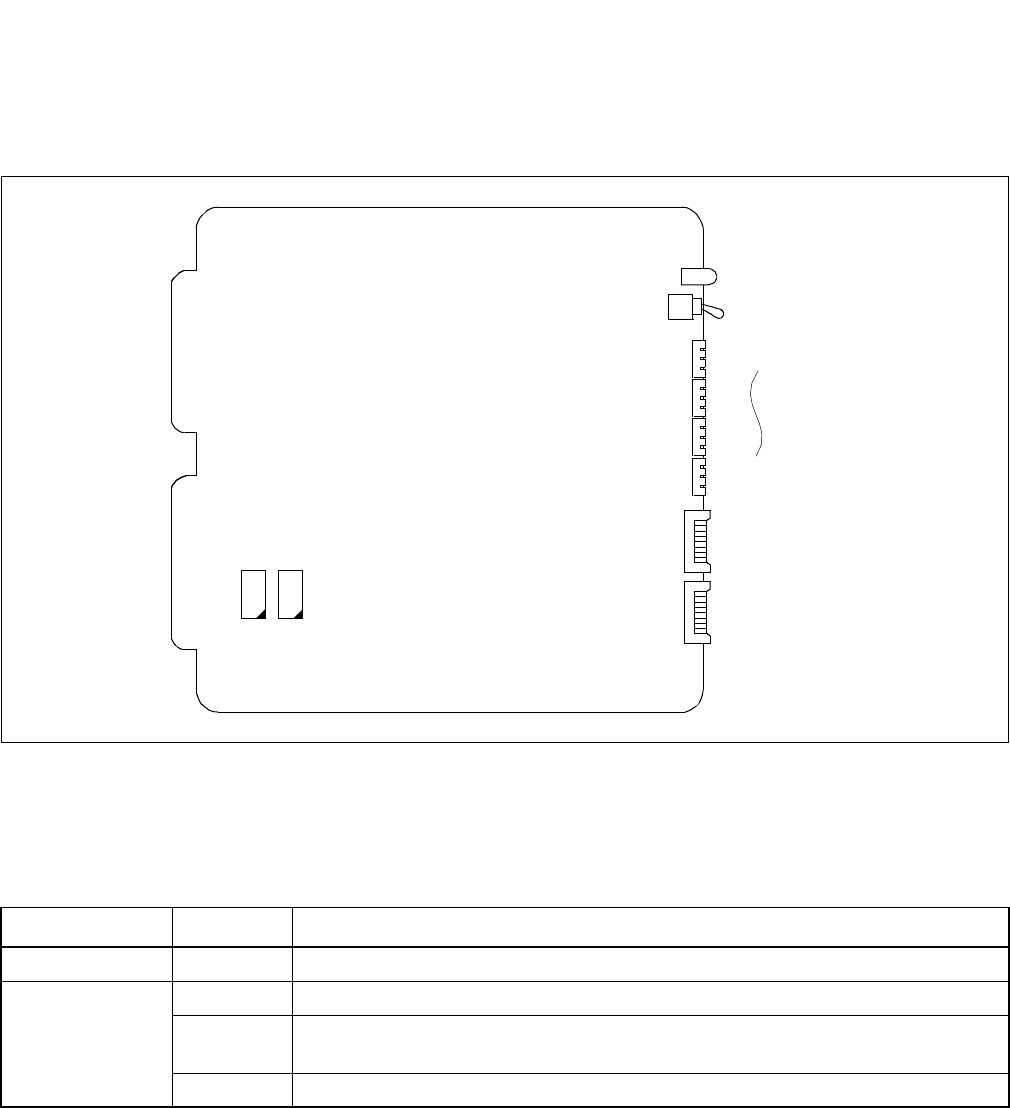
CHAPTER 3 NDA-24296
Page 252
Revision 1.0
PA-16COTBE
Central Office Trunk
3. Face Layout of Lamps, Switches, and Connectors
The face layout of lamps, switches, and connectors of this circuit card is shown in Figure 3-43.
Figure 3-43 Face Layout of PA-16 COTBE (16COT)
4. Lamp Indications
The contents of lamp indications of this circuit card are shown in the table below.
LAMP NAME COLOR STATE
OPE Green Remains lit while this circuit card is operating.
BL0
BL15
Green Lights when the corresponding circuit is busy.
Flash Flashes to the dial pulses being sent out for an outgoing call, or the corresponding circuit
is in make busy state.
OFF BL- lamp remains off when the corresponding circuit is idle.
OPE
SW00(MB)
BL15
BL0
SW02(MB8-15)
SW01(MB0-7)
SW0 SW1
~

NDA-24296 CHAPTER 3
Page 253
Revision 1.0
PA-16COTBE
Central Office Trunk
5. Switch Settings
Standard settings of various switches on this circuit card are shown in the table below.
SWITCH
NAME SWITCH
NO. SETTING STANDARD
SETTING MEANING
SW00
(MB)
UP Circuit card make busy
DOWN ×Circuit card make busy cancel
SW01
(MB0 ~ 7)
0ON No. 0 Circuit make busy
OFF ×No. 0 Circuit make busy cancel
1ON No. 1 Circuit make busy
OFF ×No. 1 Circuit make busy cancel
2ON No. 2 Circuit make busy
OFF ×No. 2 Circuit make busy cancel
3ON No. 3 Circuit make busy
OFF ×No. 3 Circuit make busy cancel
4ON No. 4 Circuit make busy
OFF ×No. 4 Circuit make busy cancel
5ON No. 5 Circuit make busy
OFF ×No. 5 Circuit make busy cancel
6ON No. 6 Circuit make busy
OFF ×No. 6 Circuit make busy cancel
7ON No. 7 Circuit make busy
OFF ×No. 7 Circuit make busy cancel

CHAPTER 3 NDA-24296
Page 254
Revision 1.0
PA-16COTBE
Central Office Trunk
SWITCH
NAME SWITCH
NO. SETTING STANDARD
SETTING MEANING
SW02
(MB8 ~ 15)
0ON No. 8 Circuit make busy
OFF ×No. 8 Circuit make busy cancel
1ON No. 9 Circuit make busy
OFF ×No. 9 Circuit make busy cancel
2ON No. 10 Circuit make busy
OFF ×No. 10 Circuit make busy cancel
3ON No. 11 Circuit make busy
OFF ×No. 11 Circuit make busy cancel
4ON No. 12 Circuit make busy
OFF ×No. 12 Circuit make busy cancel
5ON No. 13 Circuit make busy
OFF ×No. 13 Circuit make busy cancel
6ON No. 14 Circuit make busy
OFF ×No. 14 Circuit make busy cancel
7ON No. 15 Circuit make busy
OFF ×No. 15 Circuit make busy cancel
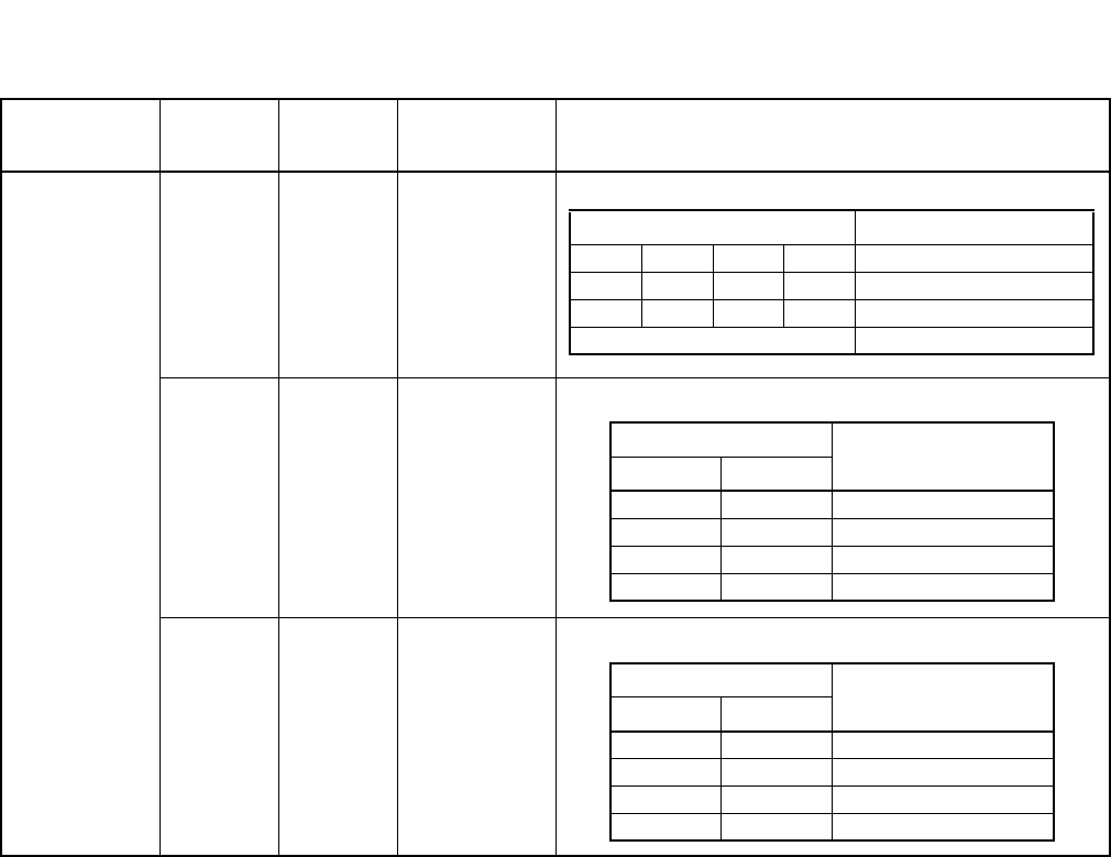
NDA-24296 CHAPTER 3
Page 255
Revision 1.0
PA-16COTBE
Central Office Trunk
Note: Switch No.5-8 is only available when SP-3331 is used for E911 service. If SP-3003 is used, these switches
are fixed to off.
SWITCH
NAME SWITCH
NO. SETTING STANDARD
SETTING MEANING
SW0
(SW10)
1 - 4
Terminal Impedance
5, 6
Wink Signal Detection Time.
7, 8
Answer Signal Detection Time.
SW0 (SW10) MEANING
1 2 3 4 Terminal impedance
OFF OFF OFF OFF 600 Ω + 2.16 µF
OFF ON ON OFF 900 Ω + 2.16 µF
Other Combinations Not used
SW0 (SW10) Detection Time
56
OFF OFF 56 ms
ON OFF 96 ms
OFF ON 136 ms
ON ON 176 ms
SW0 (SW10) Detection Time
78
OFF OFF 56 ms
ON OFF 96 ms
OFF ON 136 ms
ON ON 176 ms

CHAPTER 3 NDA-24296
Page 256
Revision 1.0
PA-16COTBE
Central Office Trunk
SWITCH
NAME SWITCH
NO. SETTING STANDARD
SETTING MEANING
SW1
(SW11)
1ON ×Fixed
OFF
2ON
OFF ×Fixed
3
ON (Call abandon detecting condition - Disconnection if ringing
signal does not arrive longer than three seconds.)
OFF ×Fixed (Call abandon detecting condition - Disconnection if
ringing signal does not arrive longer than six seconds.)
4
ON Availability of Paging Function - No. 0 Circuit is used as a
Paging trunk (No. 1 Circuit cannot be used as a C.O. trunk)
OFF Availability of Paging Function - No. 0 Circuit is used as a
C.O. trunk (No. 1 Circuit can be used as a C.O. trunk)
5ON
OFF ×Fixed
6ON ×Fixed
OFF
7ON
OFF ×Fixed
8ON
OFF ×Fixed

NDA-24296 CHAPTER 3
Page 257
Revision 1.0
PA-16COTBE
Central Office Trunk
PAD Setting
ARTD APAD TRANSMIT
(D-A) PAD RECEIVE
(A-D) PAD REMARKS
7 15 0dB 0dB
2 2 3dB 3dB
3 3 6dB 6dB
4 4 0dB -5dB
(Gain)
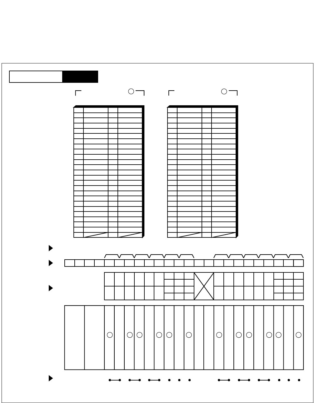
CHAPTER 3 NDA-24296
Page 258
Revision 1.0
PA-16COTBE
Central Office Trunk
6. External Interface
Accommodation of the LT connector leads of this circuit card and connecting route diagram are shown in
Figure 3-44.
Figure 3-44 LT Connector Leads Accommodation (1/2)
PIM
Mounting Module
26
27
28
29
30
31
32
33
34
35
36
37
38
39
40
41
1
2
3
4
5
6
7
8
9
10
11
12
13
14
15
16
42
43
44
45
46
47
48
17
18
19
20
21
22
23
49
50 24
25
232221201918171615141312111009080706050403020100
LT6 LT7 LT8 LT9 LT10 LT11LT0 LT1 LT2 LT3 LT4 LT5
231915
221814
211713
201612
231915
221814
211713
201612
110907050301
100806040200
110907050301
100806040200
HW11HW10HW9HW8HW7HW6HW5HW4HW3HW2HW1HW0
Group No.
Slot No.
LT Connector
PIM
Highway Block
LT 1, 3, 5, 7, 9, 11 Connector
26
27
28
29
30
31
32
33
34
35
36
37
38
39
40
41
1
2
3
4
5
6
7
8
9
10
11
12
13
14
15
16
42
43
44
45
46
47
48
17
18
19
20
21
22
23
49
50 24
25
B0
B1
Accommodated in 1
LT 0, 2, 4, 6, 8, 10 Connector
B2
B3
Accommodated in 2
B4
B5
B6
B7
B8
B9
B10
B11
B12
B13
B14
B15
A0
A1
A2
A3
A4
A5
A6
A7
A8
A9
A10
A11
A12
A13
A14
A15
B0
B1
B2
B3
B4
B5
B6
B7
B8
B9
B10
B11
B12
B13
B14
B15
A0
A1
A2
A3
A4
A5
A6
A7
A8
A9
A10
A11
A12
A13
A14
A15
1212 12
12 1212
PWR
PWR
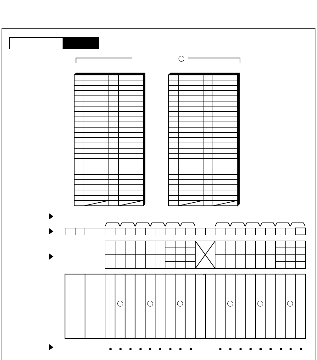
NDA-24296 CHAPTER 3
Page 259
Revision 1.0
PA-16COTBE
Central Office Trunk
Figure 3-44 LT Connector Leads Accommodation (2/2)
PIM
Mounting Module
26
27
28
29
30
31
32
33
34
35
36
37
38
39
40
41
1
2
3
4
5
6
7
8
9
10
11
12
13
14
15
16
42
43
44
45
46
47
48
17
18
19
20
21
22
23
49
50 24
25
232221201918171615141312111009080706050403020100
LT6 LT7 LT8 LT9 LT10 LT11LT0 LT1 LT2 LT3 LT4 LT5
231915
221814
211713
201612
231915
221814
211713
201612
110907050301
100806040200
110907050301
100806040200
Group No.
Slot No.
LT Connector
PIM
PWR
PWR
HW11HW10HW9HW8HW7HW6HW5HW4HW3HW2HW1HW0
Highway Block
26
27
28
29
30
31
32
33
34
35
36
37
38
39
40
41
1
2
3
4
5
6
7
8
9
10
11
12
13
14
15
16
42
43
44
45
46
47
48
17
18
19
20
21
22
23
49
50 24
25
B0
B1
Accommodated in 3
LT 1, 3, 5, 7, 9, 11 ConnectorLT 0, 2, 4, 6, 8, 10 Connector
B2
B3
B4
B5
B6
B7
A0
A1
A2
A3
A4
A5
A6
A7
B8
B9
B10
B11
B12
B13
B14
B15
A8
A9
A10
A11
A12
A13
A14
A15
3 3 3 3 3 3
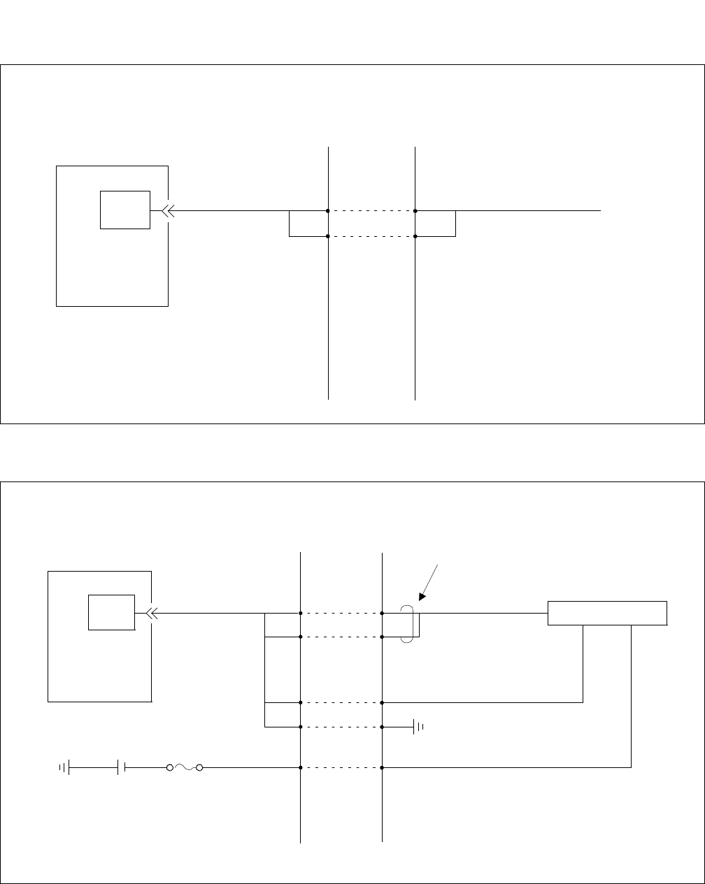
CHAPTER 3 NDA-24296
Page 260
Revision 1.0
PA-16COTBE
Central Office Trunk
Figure 3-45 Connecting Route Diagram (1/2)
Figure 3-45 Connecting Route Diagram (2/2)
NEAX2400 IPX
A0
MDF
C.O. Line
A
B
B0
COT
Connection with C.O. Line
NEAX2400 IPX
A0
MDF
A
B
B0
COT
Connection with Paging Equipment
Paging Equipment
(MR)
B0
B1 G
G
-48V
FUSE
G
Distibution Board
Speech Signal Leads
-48V
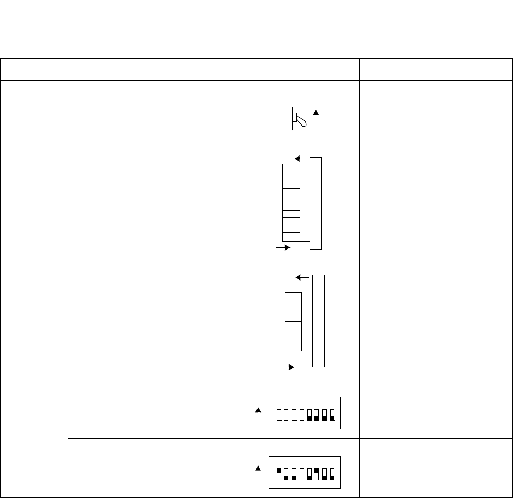
NDA-24296 CHAPTER 3
Page 261
Revision 1.0
PA-16COTBE
Central Office Trunk
7. Switch Setting Sheet
MODULE SLOT NO. SWITCH NAME SWITCH SHAPE REMARKS
PIM
SW00 (MB)
UP : Circuit card make busy
DOWN: Circuit card make busy
cancel
SW01
(MB0-7)
Make Busy Switches associated
with No. 0 through No. 7 Circuits.
ON : Make busy on each circuit
basis.
OFF: Make busy cancel on each
circuit basis.
SW02
(MB8-15)
Make Busy Switches associated
with No. 8 through No. 15 Circuits.
ON : Make busy on each circuit
basis.
OFF: Make busy cancel on each
circuit basis.
SW0
SW1
ON
OFF
ON
No.7
No.6
No.5
No.4
No.3
No.2
No.1
No.0
OFF
ON
No.7
No.6
No.5
No.4
No.3
No.2
No.1
No.0
ON 123 45678
ON 123 45678
CHAPTER 3 NDA-24296
Page 262
Revision 1.0
PA-CS02-C
Attendant Interface
PA-CS02-C
Attendant Interface
1. General Function
This circuit card is an attendant console (ATTCON) interface card which supports the interface function
for accommodating ATTCON (maximum two sets of ATTCON per card), PM function (controlling of AT-
TCON and exchanging of control commands with the CPU), PB/DP sending function (sending of PB sig-
nals or DP signals under control of the PM), receiving data (ATTCON Call Termination Information) link
interface function, etc. The PA-CS02-C card is exclusively for a system which adopts “µ-law” as its encod-
ing law.
Figure 3-46 Location of PA-CS02-C (2ATI) Card within the System
2. Mounting Location/Condition
The PA-CS02-C (ATI) card can be mounted in the following shaded slots as shown below.
CPU GATE
SW
INT
I/O Local Bus
12M PCM Highway
2M PCM Highway ×12
PM Bus ×2
ATTENDANT
CONSOLE (×2)
: Control Line
: Speech Path
IO Local Bus : Input Output Local Bus
PM Bus : Port Microprocessor Bus
ATI
PIM
Mounting Module
00 01 02 03 04 05 06 07 08 09 10 11 12 13 14 15 16 17 18 19 20 21 22 23
ATI
ATI
NDA-24296 CHAPTER 3
Page 263
Revision 1.0
PA-CS02-C
Attendant Interface
3. Face Layout of Lamps, Switches, and Connectors
The face layout of lamps, switches, and connectors on this circuit card is shown in Figure 3-47.
Figure 3-47 Face Layout of PA-CS02-C (2ATI)
OPE
N-OPE
MB
BLS1
BLS0
SW7
SW8
BLA1
BLA0
SW6
SW2
SW3
3
2
1
0
CHAPTER 3 NDA-24296
Page 264
Revision 1.0
PA-CS02-C
Attendant Interface
4. Lamp Indications
The contents of lamp indications on this circuit card are shown in the table below.
5. Switch Settings
Standard settings of switches on this circuit card are shown in the table below.
Table 3-2 ATI Card Lamp Indication
LAMP COLOR STATE
OPE Green Remains lit while this circuit card is operating.
N-OPE Red Remains lit while this circuit card is in make-busy state.
BLS0
BLS1
Red Lights when the corresponding sender circuit is in use.
Flash Flashes when the corresponding sender circuit is in make-busy state or when select signals
are being transmitted.
BLA0
BLA1
Red Lights when the corresponding circuit is busy.
Flash Flashes when the corresponding circuit is in make-busy state.
SWITCH SWITCH
NO. SETTING STANDARD
SETTING MEANING
MB —UP Circuit card make busy
DOWN ×Circuit card make busy cancel
SW2 (TAS1)
SW3 (TAS0)
1
2
3
4
SETTING OF TAS CURRENT LIMIT RESISTANCE
SW2-1/
SW3-1 SW2-2/
SW3-2 SW2-3/
SW3-3 SW2-4/
SW3-4 RESISTANCE
ON
OFF
ON
OFF
ON
OFF
ON
OFF
ON
ON
OFF
OFF
ON
ON
OFF
OFF
ON
ON
ON
ON
OFF
OFF
OFF
OFF
OFF
OFF
OFF
OFF
OFF
OFF
OFF
OFF
0 Ω
200 Ω
390 Ω
590 Ω
820 Ω
1020 Ω
1210 Ω
1410 Ω

NDA-24296 CHAPTER 3
Page 265
Revision 1.0
PA-CS02-C
Attendant Interface
SWITCH SWITCH
NO. SETTING STANDARD
SETTING MEANING
SW6 (TAS1)
SW7 (TAS0)
1
2
3
4
SW8
0ON No. 0 circuit make-busy request
OFF ×Normal setting
1ON No. 1 circuit make-busy request
OFF ×Normal setting
2OFF ×Not used
3OFF ×Not used
SETTING OF TAS SIGNALLING SYSTEM
SW6-1/
SW7-1 SW6-2/
SW7-2 SW6-3/
SW7-3 SW6-4/
SW7-4 TAS
(A WIRE) TAS
(B WIRE)
ON ON ON ON -48V G
OFF ON OFF OFF CR G
OFF ON OFF ON G G
OFF OFF OFF ON LOOP LOOP
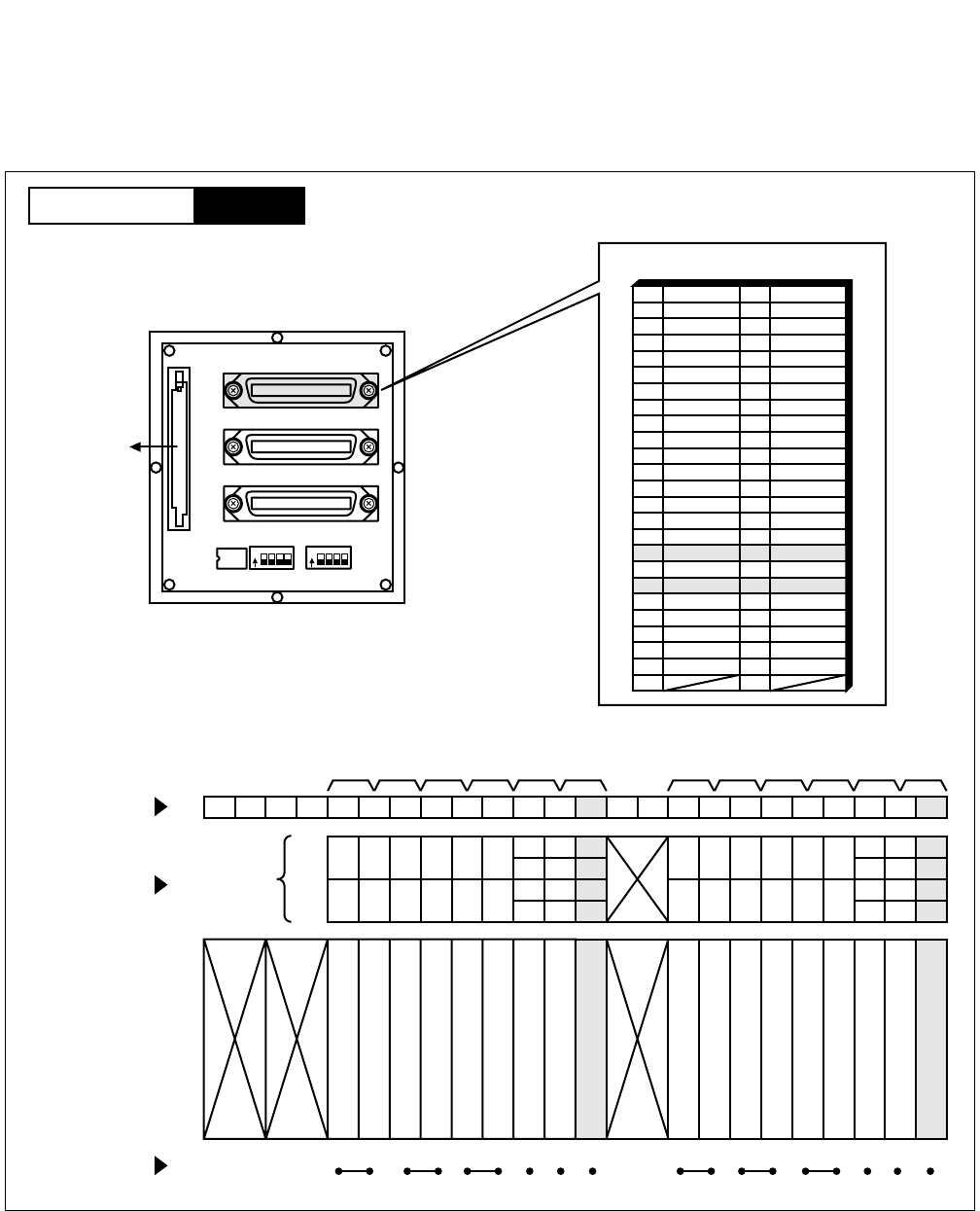
CHAPTER 3 NDA-24296
Page 266
Revision 1.0
PA-CS02-C
Attendant Interface
6. External Interface
Accommodation of the LT connector leads of this circuit card is as shown in Figure 3-48.
Figure 3-48 LT Connector Lead Accommodation
232221201918171615141312111009080706050403020100
LT6 LT7 LT8 LT9 LT10 LT11LT0 LT1 LT2 LT3 LT4 LT5
231915
221814
211713
201612
231915
221814
211713
201612
110907050301
100806040200
110907050301
100806040200
Group No.
Slot No.
PIM
Highway Block
ATI
ATI
1
2
3
4
ON
SW1
IC
ATT0
ATT1
LT
RLT
[ATT TERM (PZ-M366)]
1
2
3
4
ON
SW0
To LT5/LT11
26
27
28
29
30
31
32
33
34
35
36
37
38
39
40
41
1
2
3
4
5
6
7
8
9
10
11
12
13
14
15
16
42
43
44
45
46
47
48
17
18
19
20
21
22
23
49
50 24
25
< LT Connector on the ATT TERM>
TAS 0A
TAS 1A
TAS 0B
TAS 1B
HW11HW10HW9HW8HW7HW6HW5HW4HW3HW2HW1HW0
PIM
Mounting Module
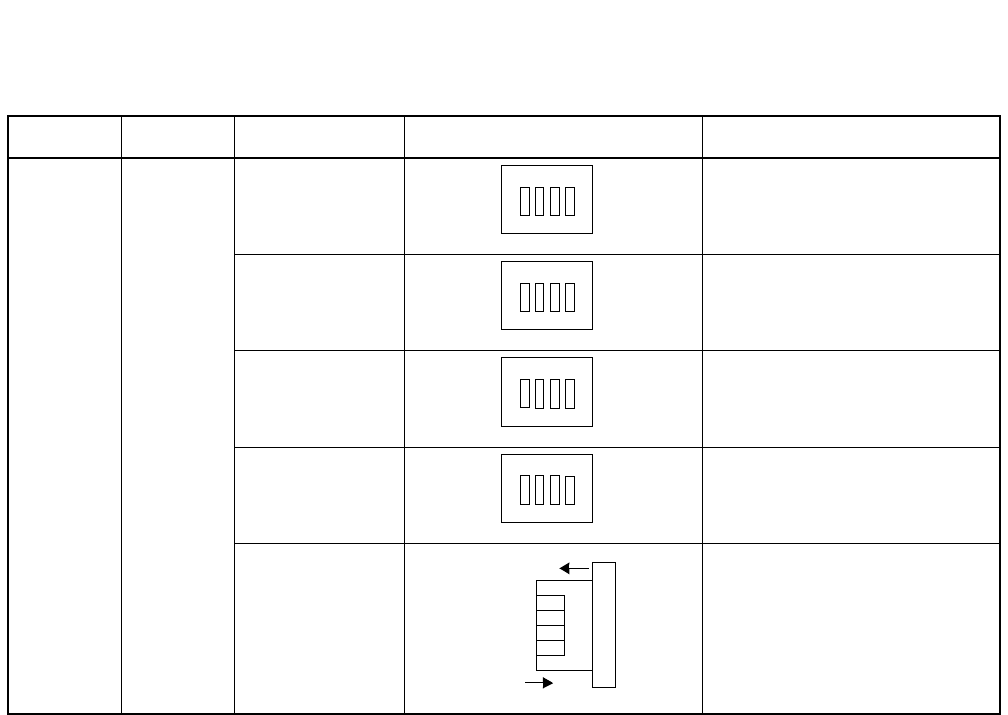
NDA-24296 CHAPTER 3
Page 267
Revision 1.0
PA-CS02-C
Attendant Interface
7. Switch Setting Sheet
MODULE SLOT NO. SWITCH NAME SWITCH SHAPE REMARKS
PIM
12, 23
SW2
SW3
SW6
SW7
SW8
1234
1234
1 2 3 4
12 3 4
ON
OFF
No.3
No.2
No.1
No.0
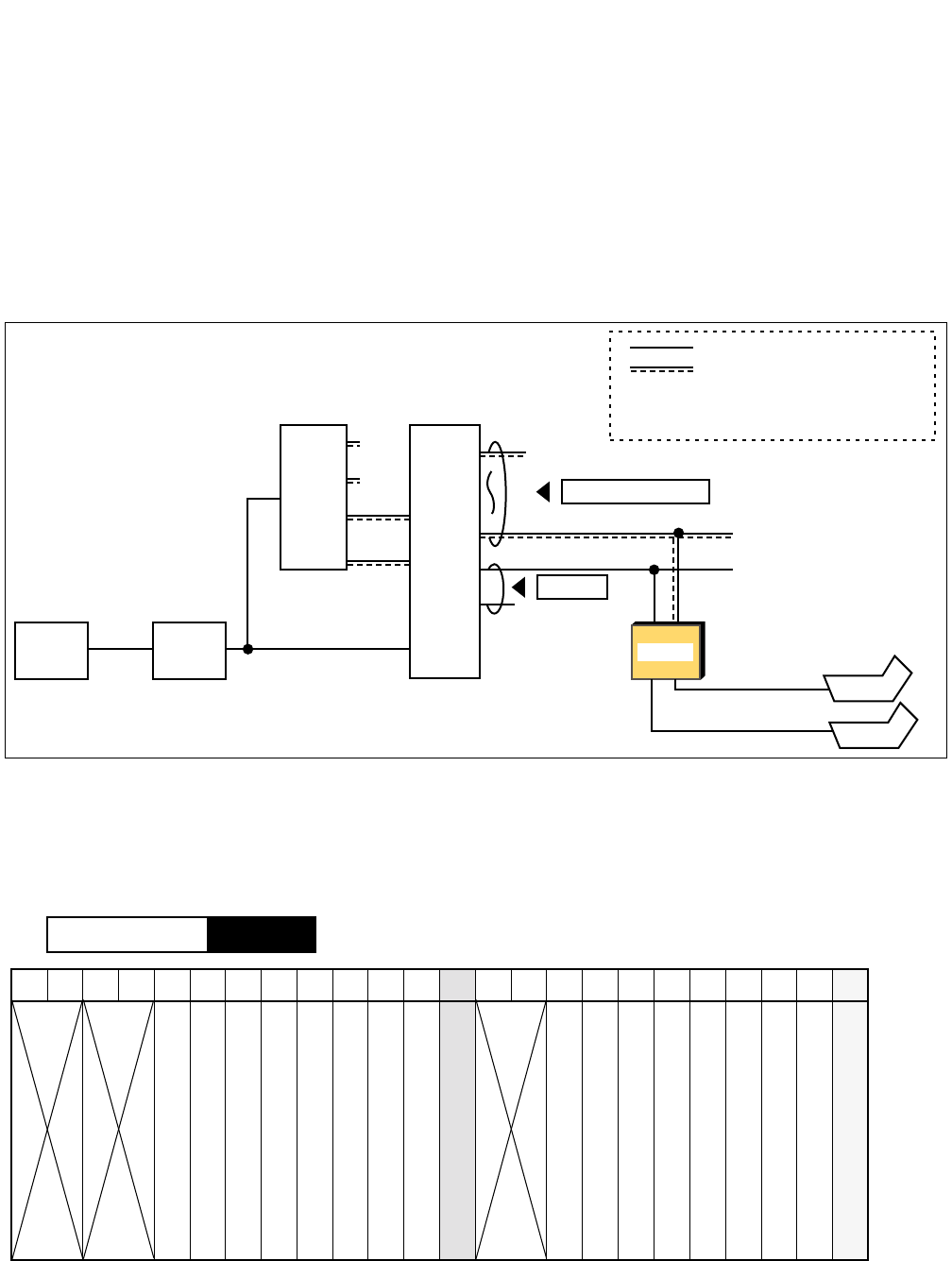
CHAPTER 3 NDA-24296
Page 268
Revision 1.0
PA-CS08
Hotel Attendant Interface
PA-CS08
Hotel Attendant Interface
1. General Function
This circuit card is the Hotel Attendant Console (Hotel ATTCON) interface card that supports the interface
function for the Hotel ATTCON (maximum two sets of Hotel ATTCON per card), PM function (controlling
of Hotel ATTCON and exchanging of control commands with the CPU), PB/DP sending function (sending
of PB signals or DP signals under control of the PM), receiving data (Hotel ATTCON Call Termination
Information) link interface function, etc.
Figure 3-49 Location of PA-CS08 (HMATI) Card in the System
2. Mounting Location/Condition
The PA-CS08 (HMATI) card can be mounted in the shaded slots as shown below.
CPU GT
TDSW
MUX
2M PCM Highway
PM Bus
ATTENDANT
CONSOLE (×2)
: Control Line
: Speech Path
I/O Local Bus: Input/Output Local Bus
PM Bus : Port Microprocessor Bus
HMATI
PIM
Mounting Module
00 01 02 03 04 05 06 07 08 09 10 11 12 13 14 15 16 17 18 19 20 21 22 23
HMATI
HMATI
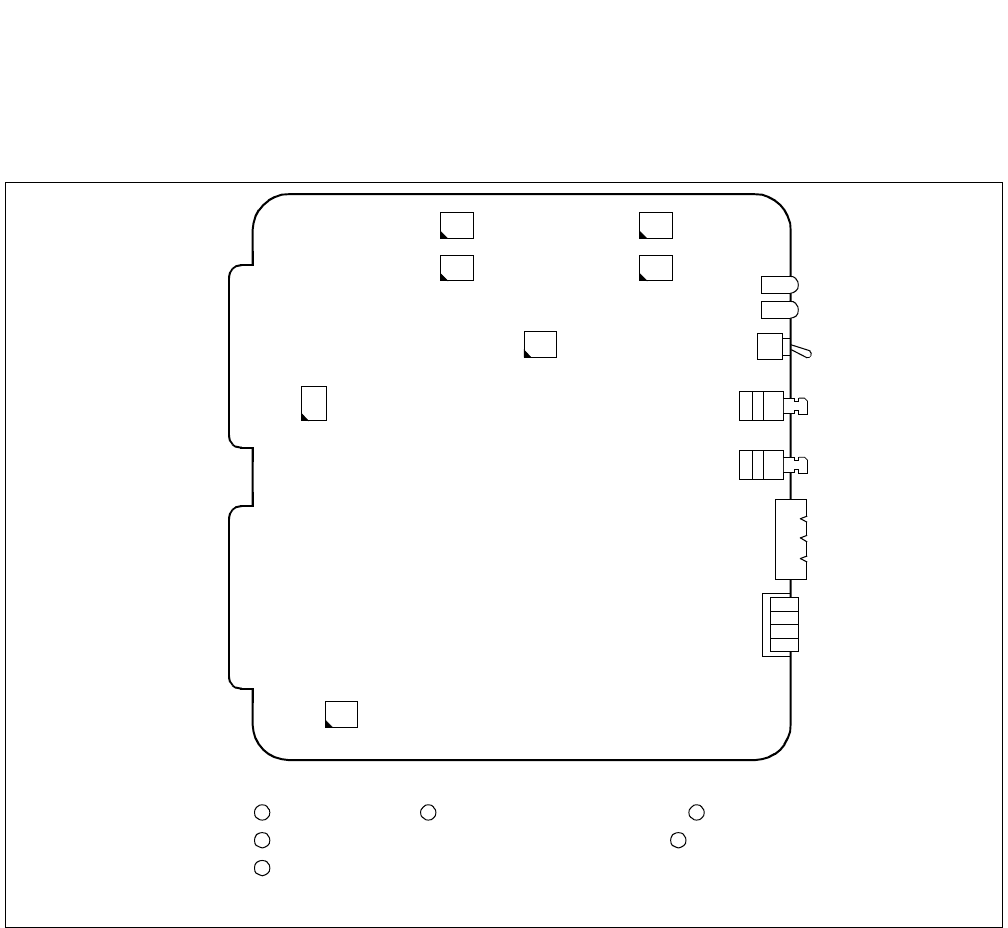
NDA-24296 CHAPTER 3
Page 269
Revision 1.0
PA-CS08
Hotel Attendant Interface
3. Face Layout of Lamps, Switches, and Connectors
The face layout of lamps, switches, and connectors on this circuit card is shown in Figure 3-50.
Figure 3-50 Face Layout of PA-CS08 (HMATI) Card
OPE
N-OPE
MB
FU0 (Note )
SW11
BLS1
BLA1
BLA0
SW04
SW03
SW02
SW08
SW07
SW09
SW12
3
2
1
0
FU1 (Note )
BLS0
Note: When extracting/inserting this card, care should be taken as to the FU0, FU1.
<Extraction> MB key → ON Remove the FU0 and FU1. Extract this card.
<Insertion> Mount this card without the FU0 and FU1. Plug in the FU0 and FU1.
MB key → OFF
1 2 3
1 2
3

CHAPTER 3 NDA-24296
Page 270
Revision 1.0
PA-CS08
Hotel Attendant Interface
4. Lamp Indications
Lamp indications for this circuit card are shown in the table below.
LAMP COLOR STATE
OPE Green Remains lit while this circuit card is operating.
N-OPE Red Remains lit while this circuit card is in Make-busy state.
BLS0
BLS1
Red Lights when the corresponding circuit is busy.
Blink
Blinks when the corresponding circuit is busy.
Note: The lamp also blinks when dial signals are being sent out.
BLA0
BLA1
Red Lights when the corresponding circuit is busy.
Blink Blinks when the corresponding circuit is in Make-busy state.
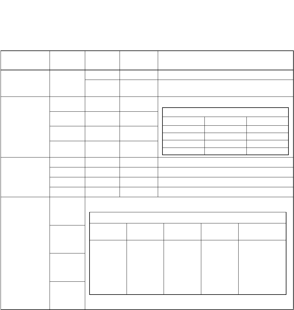
NDA-24296 CHAPTER 3
Page 271
Revision 1.0
PA-CS08
Hotel Attendant Interface
5. Switch Settings
Standard settings for various switches on this circuit card are shown in the table below.
SWITCH SWITCH
NO. SETTING STANDARD
SETTING MEANING
MB
UP Circuit card Make-busy.
DOWN Circuit card Make-busy cancel.
SW02 (TAS0)
SW03 (TAS1)
1
2
3
4
SW04
1ON ×Fixed
2OFF ×Fixed
3ON ×Fixed
4OFF ×Fixed
SW07 (TAS0)
SW08 (TAS1)
1
2
3
4
SETTING OF TAS SIGNALLING SYSTEM
SWITCH TAS (A WIRE) TAS (B WIRE)
1-48VG
2CRG
3GG
4 LOOP LOOP
SETTING OF TAS CURRENT LIMIT RESISTANCE
SW7-1/
SW8-1 SW7-2/
SW8-2 SW7-3/
SW8-3 SW7-4/
SW8-4 RESISTANCE
ON
OFF
ON
OFF
ON
OFF
ON
OFF
ON
ON
OFF
OFF
ON
ON
OFF
OFF
ON
ON
ON
ON
OFF
OFF
OFF
OFF
OFF
OFF
OFF
OFF
OFF
OFF
OFF
OFF
0 Ω
200 Ω
390 Ω
590 Ω
820 Ω
1020 Ω
1210 Ω
1410 Ω

CHAPTER 3 NDA-24296
Page 272
Revision 1.0
PA-CS08
Hotel Attendant Interface
Note: When the PB signal is sent from the Hotel ATT, set the SW 12-1~4 ON, and assign AHSY command, INDEX
114, b7 = I.
SWITCH SWITCH
NO. SETTING STANDARD
SETTING MEANING
SW11
1ON
OFF ×Fixed
2ON
OFF ×Fixed
3ON
OFF ×Fixed
4ON
OFF ×Fixed
SW12
1ON ×
Fixed (all ON)
OFF
2ON ×
OFF
3ON ×
OFF
4ON ×
OFF
SW9
0ON No. 0 System is in Make-busy request.
OFF ×Normal setting
1ON No. 1 System is in Make-busy request.
OFF ×Normal setting
2OFF ×Not used
3OFF ×Not used
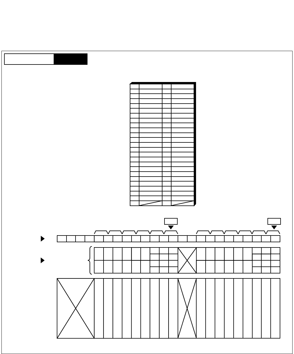
NDA-24296 CHAPTER 3
Page 273
Revision 1.0
PA-CS08
Hotel Attendant Interface
6. External Interface
The location for the LT connector leads for this circuit card is shown in Figure 3-51.
Figure 3-51 LT Connector Lead Location (PIM)
PIM
PIM
Mounting Module
232221201918171615141312111009080706050403020100
LT6 LT7 LT8 LT9 LT10LT0 LT1 LT2 LT3 LT4
LT5
1915
1814
1713
1612
231915
221814
211713
201612
110907050301
100806040200
110907050301
100806040200
23
22
21
20
HMATI
Group No.
Slot No.
PIM
26
27
28
29
30
31
32
33
34
35
36
37
38
39
40
41
1
2
3
4
5
6
7
8
9
10
11
12
13
14
15
16
42
43
44
45
46
47
48
17
18
19
20
21
22
23
49
50 24
25
LT5, 11 Connector
(LT Connector on the ATT TERM)
TAS 0A0
TAS 1A0
TAS 0B0
TAS 1B0
LT11
HMATI
CHAPTER 3 NDA-24296
Page 274
Revision 1.0
PA-CS08
Hotel Attendant Interface
7. Switch Setting Sheet
SWITCH SWITCH SHAPE REMARKS
MB UP: Circuit card Make-busy.
DOWN: Circuit card Make-busy cancel.
SW02
SW03
SW04
SW07
SW08
SW09 SW9-2, SW9-3: Not used
SW11
SW12
ON
1234
1234
1 2 3 4
ON
1 2 3 4
ON
1 2 3 4
ON
No. 3
No. 2
No. 1
No. 0
ON
OFF
(Piano Switch)
1234
ON
1 2 3 4
ON
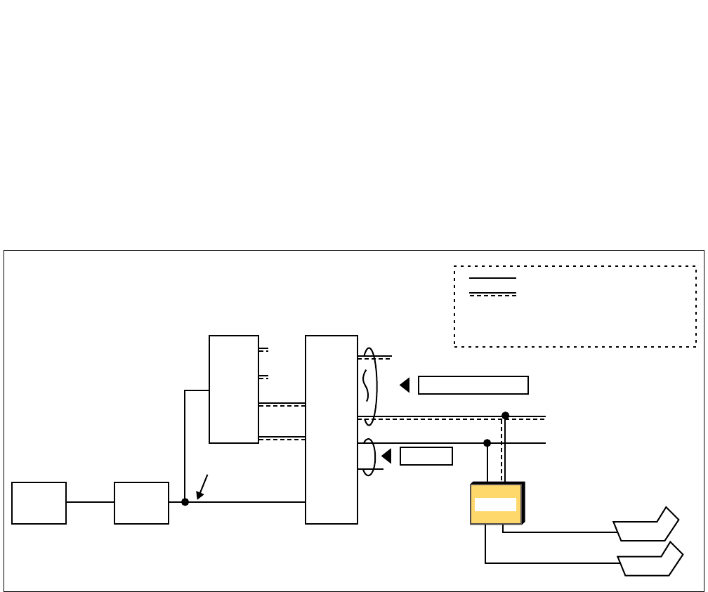
NDA-24296 CHAPTER 3
Page 275
Revision 1.0
PA-CS08-B
Hotel Attendant Interface
PA-CS08-B
Hotel Attendant Interface
1. General Function
This circuit card is Hotel attendant console (Hotel ATTCON) interface card which supports the interface
function for accommodating Hotel ATTCON (maximum two sets of Hotel ATTCON per card), PM func-
tion (controlling of Hotel ATTCON and exchanging of control commands with the CPU), PB/DP sending
function (sending of PB signals or DP signals under control of the PM), receiving data (Hotel ATTCON
Call Termination Information) link interface function, etc.
Figure 3-52 Location of PA-CS08-B (HMATI) Card within the System
CPU GT
TSW
MUX
I/O Local Bus
2M PCM Highway
PM Bus
ATTENDANT
CONSOLE (×2)
: Control Line
: Speech Path
I/O Local Bus: Input/Output Local Bus
PM Bus : Port Microprocessor Bus
HMATI
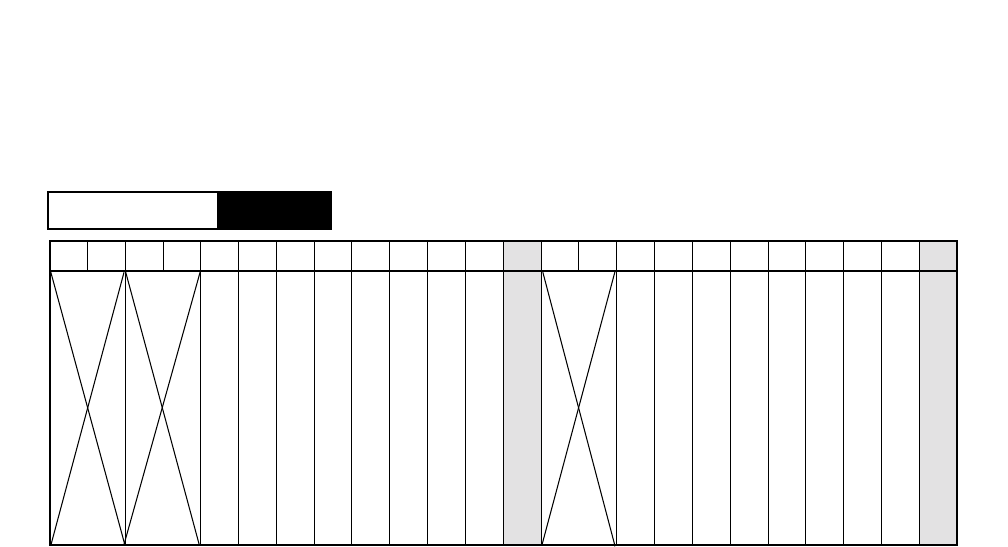
CHAPTER 3 NDA-24296
Page 276
Revision 1.0
PA-CS08-B
Hotel Attendant Interface
2. Mounting Location/Condition
The PA-CS08-B (HMATI) card can be mounted in the following shaded slots as shown below.
PIM
Mounting Module
00 01 02 03 04 05 06 07 08 09 10 11 12 13 14 15 16 17 18 19 20 21 22 23
HMATI
HMATI
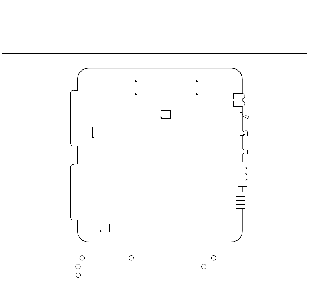
NDA-24296 CHAPTER 3
Page 277
Revision 1.0
PA-CS08-B
Hotel Attendant Interface
3. Face Layout of Lamps, Switches, and Connectors
The face layout of lamps, switches, and connectors on this circuit card is shown below.
Figure 3-53 Face Layout of PA-CS08-B (HMATI)
OPE
N-OPE
MB
FU0 (Note)
SW11
BLS1
BLA1
BLA0
SW04
SW03
SW02
SW08
SW07
SW09
SW12
3
2
1
0
FU1 (Note)
BLS0
Note: When extracting/inserting this card, care should be taken as to the FU0, FU1.
<Extraction> MB key → ON Remove the FU0 and FU1. Extract this card.
<Insertion> Mount this card without the FU0 and FU1. Plug in the FU0 and FU1.
MB key → OFF
1 2 3
1 2
3

CHAPTER 3 NDA-24296
Page 278
Revision 1.0
PA-CS08-B
Hotel Attendant Interface
4. Lamp Indications
The contents of lamp indications on this circuit card are shown in the table below.
LAMP COLOR STATE
OPE Green Remains lit while this circuit card is operating
N-OPE Red Remains lit while this circuit card is in make-busy state
BLS0
BLS1
Red Lights when the corresponding circuit is busy
Blink
Blinks when the corresponding circuit is busy
Note: The lamp also blinks when dial signals are being sent out.
BLA0
BLA1
Red Lights when the corresponding circuit is busy
Blink Blinks when the corresponding circuit is in make-busy state
NDA-24296 CHAPTER 3
Page 279
Revision 1.0
PA-CS08-B
Hotel Attendant Interface
5. Switch Settings
Standard settings of various switches on this circuit card are shown in the table below.
SWITCH SWITCH
NO. SETTING STANDARD
SETTING MEANING
MB UP Circuit card make busy
DOWN Circuit card make busy cancel
SW02 (TAS0)
SW03 (TAS1) 1
2
3
4
SW04 1ON ×Fixed
2OFF ×Fixed
3ON ×Fixed
4OFF ×Fixed
SW07 (TAS0)
SW08 (TAS1) 1
2
3
4
SETTING OF TAS SIGNALLING SYSTEM
SWITCH TAS (A WIRE) TAS (B WIRE)
1-48VG
2CRG
3GG
4 LOOP LOOP
SETTING OF TAS CURRENT LIMIT RESISTANCE
SW7-1/
SW8-1 SW7-2/
SW8-2 SW7-3/
SW8-3 SW7-4/
SW8-4 RESISTANCE
ON
OFF
ON
OFF
ON
OFF
ON
OFF
ON
ON
OFF
OFF
ON
ON
OFF
OFF
ON
ON
ON
ON
OFF
OFF
OFF
OFF
OFF
OFF
OFF
OFF
OFF
OFF
OFF
OFF
0 Ω
200 Ω
390 Ω
590 Ω
820 Ω
1020 Ω
1210 Ω
1410 Ω

CHAPTER 3 NDA-24296
Page 280
Revision 1.0
PA-CS08-B
Hotel Attendant Interface
Note: When PB signal is sent from the Hotel ATT, set the SW 12-1~ 4 ON, and assign AHSY command, INDEX
114, b7 = I.
SWITCH SWITCH
NO. SETTING STANDARD
SETTING MEANING
SW11 1ON
OFF ×Fixed
2ON
OFF ×Fixed
3ON
OFF ×Fixed
4ON
OFF ×Fixed
SW12 1ON ×
Fixed (all ON)
OFF
2ON ×
OFF
3ON ×
OFF
4ON ×
OFF
SW9 0ON No. 0 System is in make-busy request.
OFF ×Normal setting
1ON No. 1 System is in make-busy request.
OFF ×Normal setting
2OFF ×Not used
3OFF ×Not used
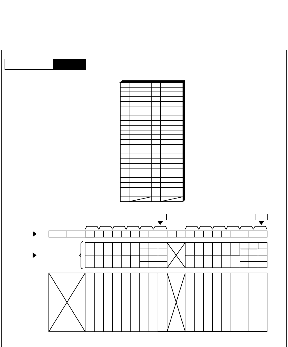
NDA-24296 CHAPTER 3
Page 281
Revision 1.0
PA-CS08-B
Hotel Attendant Interface
6. External Interface
Accommodation of the LT connector leads of this circuit card is as shown in Figure 3-54.
Figure 3-54 LT Connector Lead Accommodation
232221201918171615141312111009080706050403020100
LT6 LT7 LT8 LT9 LT10LT0 LT1 LT2 LT3 LT4
LT5
1915
1814
1713
1612
231915
221814
211713
201612
110907050301
100806040200
110907050301
100806040200
23
22
21
20
HMATI
Group No.
Slot No.
PIM
26
27
28
29
30
31
32
33
34
35
36
37
38
39
40
41
1
2
3
4
5
6
7
8
9
10
11
12
13
14
15
16
42
43
44
45
46
47
48
17
18
19
20
21
22
23
49
50 24
25
LT5, 11 Connector
(LT Connector on the ATT TERM)
TAS 0A0
TAS 1A0
TAS 0B0
TAS 1B0
LT11
HMATI
PIM
Mounting Module
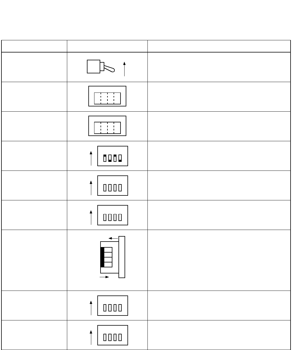
CHAPTER 3 NDA-24296
Page 282
Revision 1.0
PA-CS08-B
Hotel Attendant Interface
7. Switch Setting Sheet
SWITCH SWITCH SHAPE REMARKS
MB UP: Circuit card make busy
DOWN: Circuit card make busy cancel
SW02
SW03
SW04
SW07
SW08
SW09 SW9-2, SW9-3: Not used
SW11
SW12
ON
1234
1234
1 2 3 4
ON
1 2 3 4
ON
1 2 3 4
ON
No. 3
No. 2
No. 1
No. 0
ON
OFF
(Piano Switch)
1 2 3 4
ON
1 2 3 4
ON
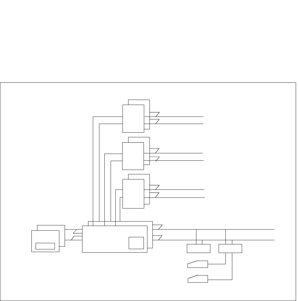
NDA-24296 CHAPTER 3
Page 283
Revision 1.0
PA-CS33
Attendant Interface
PA-CS33
Attendant Interface
1. General Function
This circuit card is a Desk Console interface which supports the interface function for accommodating two
sets of Desk Consoles, PB/DP sender function and Trunk Answer from any Station (TAS) function.
Figure 3-55 Location of PA-CS33 (ATI) Card in the System
MUX
MUX
MUX
TSW/INT/PLO
MUX
CPR
GT
PCM HW
PM BUS
PCM HW
PM BUS
PCM HW
PM BUS
PCM HW
PM BUS
LC/TRK ATI
DESK
CONSOLE
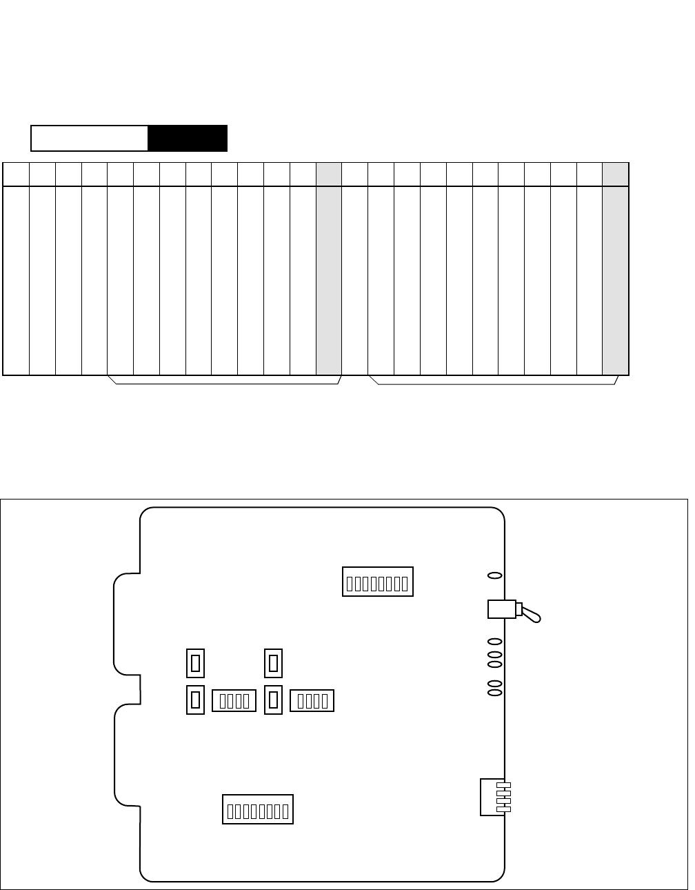
CHAPTER 3 NDA-24296
Page 284
Revision 1.0
PA-CS33
Attendant Interface
2. Mounting Location/Condition
The PA-CS33 (ATI) can be mounted in either Slot 12 or 23 of the PIM.
3. Face Layout of Lamps, Switches, and Connectors
The face layout of lamps, switches and connectors is shown in Figure 3-56.
Figure 3-56 Face Layout of PA-CS33 (ATI)
PIM
Mounting Module
00 01 02 03 04 05 06 07 08 09 10 11 12 13 14 15 16 17 18 19 20 21 22 23
ATI
ATI
Universal Slots Universal Slots
SW00
OPE
1 2 3 4 5 6 7 8
1 2 3 4 5 6 7 8
SW17
SW16
SW11 SW14
SW10
SW12 SW15
SW13
PALM
BLA1
BLA0
SW01
BLS1
BLS0
NDA-24296 CHAPTER 3
Page 285
Revision 1.0
PA-CS33
Attendant Interface
4. Lamp Indications
Lamp indications for this circuit card are shown in the table below.
5. Switch Setting
Standard settings for switches on this circuit card are shown in the table below.
LAMP NAME COLOR STATE
OPE Green Remains lit while circuit card is operating normally.
OFF Off when circuit card is not operating.
PALM Red Lights when the power feeding circuit failure has occurred.
OFF Off when the power feeding circuit operates normally.
BLA0
BLA1
Red Lights when the corresponding circuit is busy (At the same time, turns off PA lamp on
the Desk Console).
Flash
(60 IPM) Flashes when the corresponding circuit is in Make-busy state.
OFF Off when the corresponding circuit is in idle (At the same time, turns on PA lamp on the
Desk console).
BLS0
BLS1
Red Lights when the corresponding sender circuit is in use.
Flash
(60 IPM)
Flashes when the corresponding sender circuit is in Make-busy state or when select sig-
nals are being transmitted.
OFF Off when the corresponding sender circuit is in idle.
SWITCH
NAME SETTING STANDARD
SETTING MEANING
SW00 UP Circuit card is Make-busy.
DOWN ×Circuit card is cancel for Make-busy.
SWITCH
NAME SWITCH
NO SETTING STANDARD
SETTING MEANING
SW01
0ON ×Make-busy cancel for #0 Desk Console.
OFF Make-busy request for #0 Desk Console.
1ON ×Make-busy cancel for #1 Desk Console.
OFF Make-busy request for #1 Desk Console.
2OFF ×Not used.
3OFF ×Not used.
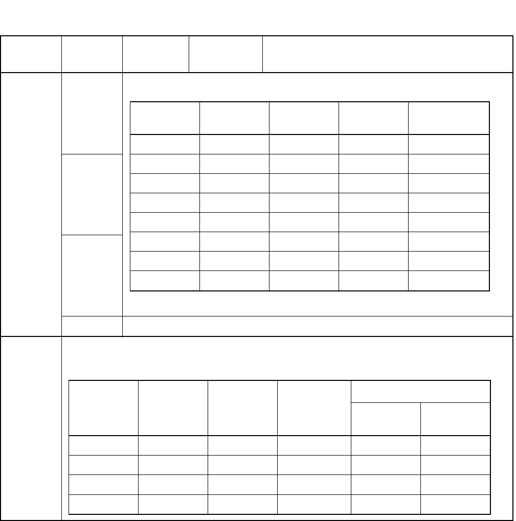
CHAPTER 3 NDA-24296
Page 286
Revision 1.0
PA-CS33
Attendant Interface
SW10
(TAS#0)
SW13
(TAS#1)
1
SW10 and SW13 designate the current limit resistance for TAS#0 and TAS#1 respectively.
2
3
4 This switch designates the TAS signaling system in conjunction with SW 11/12 and SW14/15.
SW11/
SW12
(TAS#0)
SW14/
SW15
(TAS#1)
SW11/12 and SW14/15 designate the TAS#0 and TAS#1 signaling system (in conjunction with SW10-4
(TAS#0)/SW13-4 (TAS#1).
SWITCH
NAME SWITCH
NO SETTING STANDARD
SETTING MEANING
SW10-3/
SW13-3 SW10-2/
SW13-2 SW10-1/
SW13-1 STANDARD
SETTING RESISTANCE
ON ON ON 0 Ω
ON ON OFF 220 Ω
ON OFF ON 398 Ω
ON OFF OFF 618 Ω
OFF ON ON 800 Ω
OFF ON OFF 1020 Ω
OFF OFF ON 1198 Ω
OFF OFF OFF ×1418 Ω
SW12/
SW15 SW11/
SW14 SW10-4/
SW13-4 STANDARD
SETTING
SIGNAL WHEN SEIZED
TAS 0A/
TAS 1A TAS 0B/
TAS 1B
ON ON ON CR G
OFF ON ON -48V G
OFF OFF OFF ×LOOP LOOP
OFF OFF ON G G
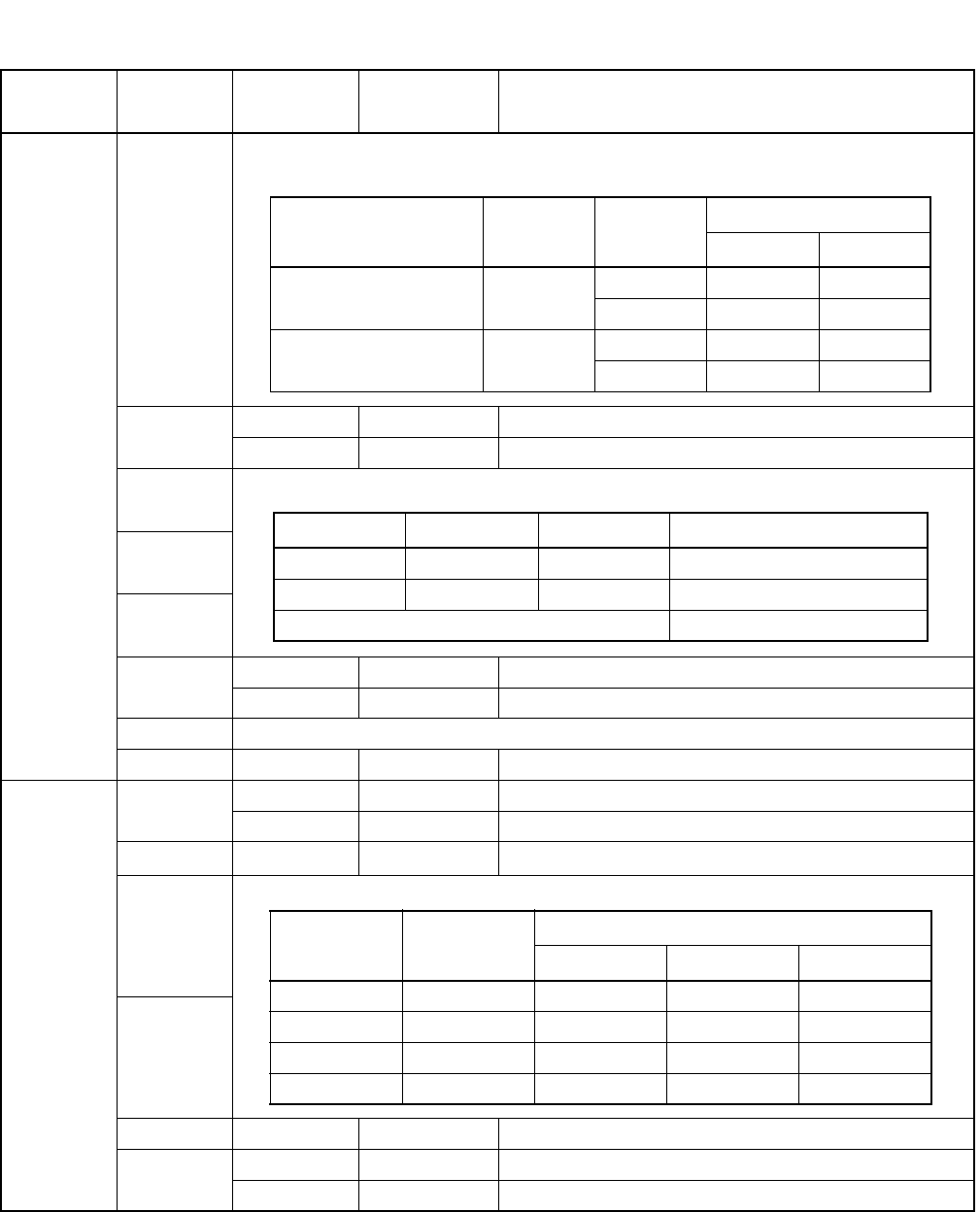
NDA-24296 CHAPTER 3
Page 287
Revision 1.0
PA-CS33
Attendant Interface
Note: DESK CONSOLE starts up in Day or Night mode according to this setting after the circuit card
initialization, regardless of the mode before the initialization.
SWITCH
NAME SWITCH
NO SETTING STANDARD
SETTING MEANING
SW16
1
For Business system, set SW16-1 and SW16-7 to OFF. When the system has Hotel applica-
tion, set SW16-1 and SW16-7 according to system data as shown below.
2ON Desk Console Expanded LCD Display available.
OFF Desk Console Expanded LCD Display not available.
3SW16-3/4/5 designates the nation code as shown below.
4
5
6ON A-law PCM coding.
OFF ×µ-law PCM coding.
7 Refer to SW16-1.
8OFF ×Not used (Fixed to OFF).
SW17
1ON Denial of PCM receiving while transmitting PB signals.
OFF ×PCM receives irrespective of PB signals transmission.
2ON ×Fixed to ON.
3
Desk Console Key Pattern. Set SW17-3 and SW17-4 according to SYS 1, Index 6.
4
5~7 OFF ×Fixed to OFF.
8
Note ON Start up in Night mode after circuit card initialization.
OFF ×Start up in Day mode after circuit card initialization.
Desk Console
Key pattern
to be used
SW16-1 SW16-7 SYS 1 INDEX 160
Bit 1 Bit 0
Hotel type ON ON 1 1
OFF 0 1
Business type OFF ON —1
OFF —0
SW16-5 SW16-4 SW16-3 COUNTRY
ON ON OFF NORTH AMERICA
ON OFF ON AUSTRALIA
Other combinations Not used
SW17-3 SW17-4 SYS 1 INDEX 6
Bit 6 Bit 5 Bit 4
OFF OFF 0 0 0
ON OFF 0 0 1
OFF ON 0 1 0
ON ON 1 0 0
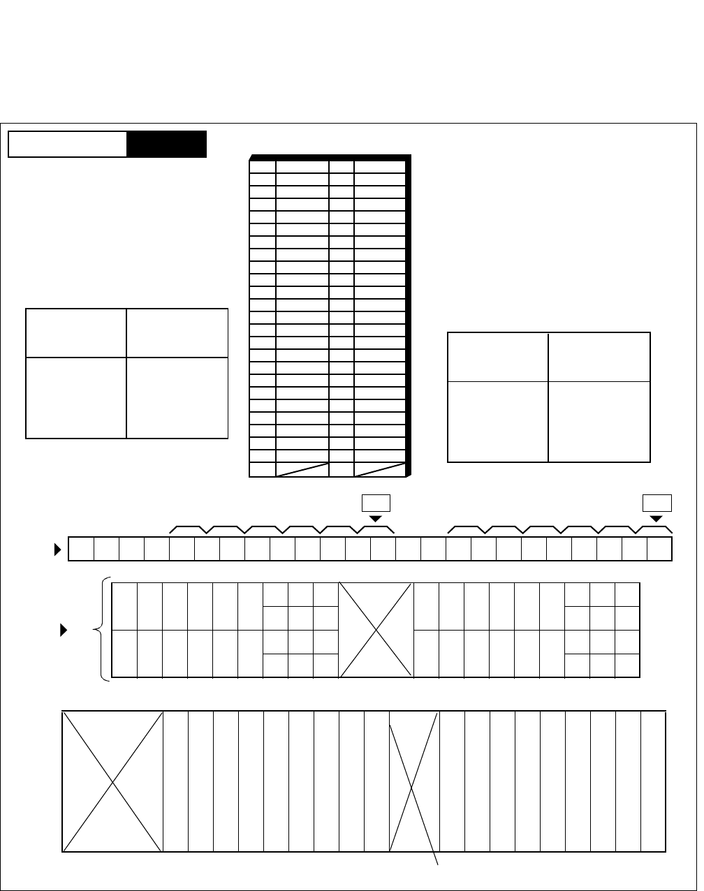
CHAPTER 3 NDA-24296
Page 288
Revision 1.0
PA-CS33
Attendant Interface
6. External Interface
Location of the LT connector leads for the DESK CONSOLE interface is as shown in Figure 3-57.
Figure 3-57 LT Connector Lead Location (PIM)
26
27
28
29
30
31
32
33
34
35
36
37
38
39
40
41
42
43
44
45
46
47
48
49
50
1
2
3
4
5
6
7
8
9
10
11
12
13
14
15
16
17
18
19
20
21
22
23
BN4800 BN4801
BN4820 BN4821
BN4830 BN4831
B0
B1
B3
A0
A2
A3
A1
B2
BN4810 BN4811
LT5, 11 Connector
PIM
Mounting Module
00 01 02 03 04 05 06 07 08 09 10 11 12 13 14 15 16 17 18 19 20 21 22 23
01 03 05 07 09 11 15 19 23 01 03 05 07 09 11 15 19 23
14 18 22 14 18 22
00 02 04 06 08 10 13 17 21 00 02 04 06 08 10 13 17 21
12 16 20 12 16 20
LT0 LT1 LT2 LT3 LT4 LT5
Slot No.
Group No.
ATI
ATI
PIM
LT11
LT 6 LT 7 LT 8 LT 9 LT 1 0
#0 ADD ON
MODULE
#1 ADD ON
MODULE
A0
B0
BN4800 - 48v
BN4801 - 48v
A1
B1
BN4810 - 48v
BN4811 - 48v
#0 DESK
CONSOLE
#1 DESK
CONSOLE
A2
B2
BN4820 - 48v
BN4821 - 48v
A3
B3
BN4830 - 48v
BN4831 - 48v
Note: The lead for each
DESK CONSOLE is
shown below.
Note: The lead for each ADD
ON CONSOLE is
shown below.
24
25
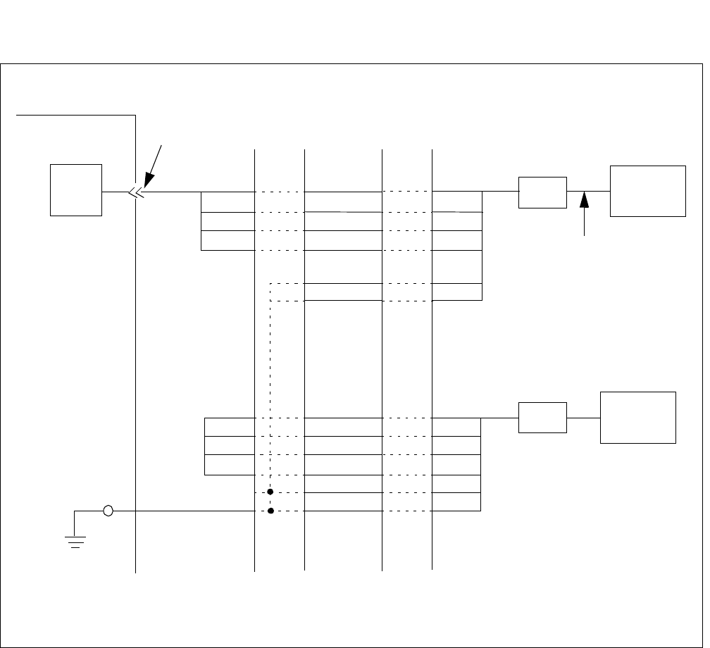
NDA-24296 CHAPTER 3
Page 289
Revision 1.0
PA-CS33
Attendant Interface
Figure 3-58 Connecting Route Diagram
Note: The power feeding wires (BN4820/BN4821/BN4830/BN4831/GND) are not required when the power is
supplied to the DESK CONSOLE locally.
ATI
B2
BN4820
BN4821
B3
BN4830
BN4831
B3
BN4830
BN4831
GND
GND
B2
BN4820
BN4821
GND
GND
PBX
Installation
Cable
A2
MDF IDF 6-PIN MODULAR
ROSETTE
#0 DESK
CONSOLE
6-PIN MODULAR
CABLE
#1 DESK
CONSOLE
A2
A3
A3
GND
(PZ-M377)
(-48V)
(-48V)
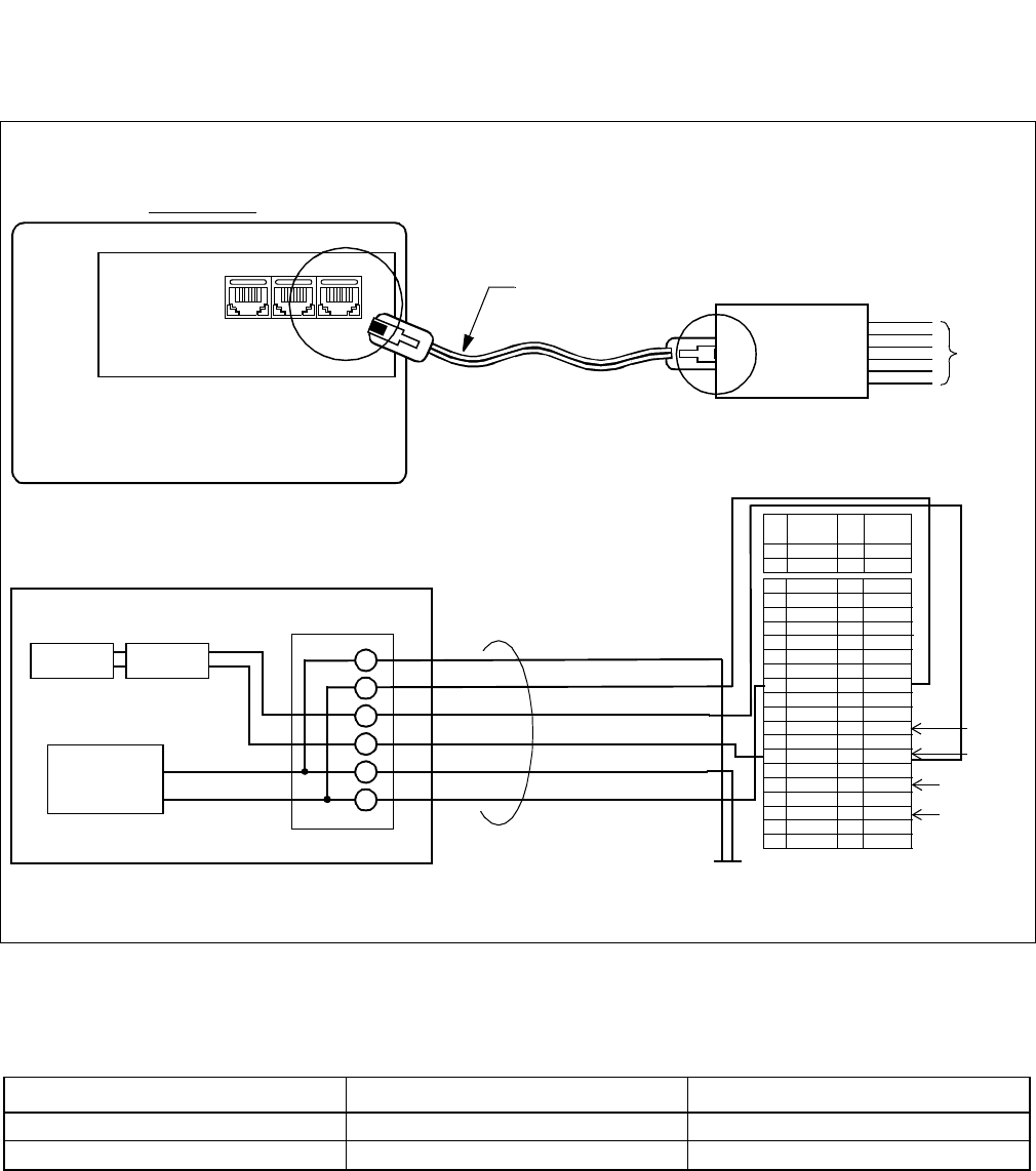
CHAPTER 3 NDA-24296
Page 290
Revision 1.0
PA-CS33
Attendant Interface
Figure 3-59 shows how to connect Desk Console.
Figure 3-59 Desk Console Connection
Power supply and the maximum distance between the ATI and Desk Console. The maximum distance between
the ATI circuit card and Desk Console is as shown below.
Source 0.5 φ Cable 0.65 φ Cable
PBX 1,148 ft. (350 m) 1,640 ft. (500 m)
Local Power Supply 3,937 ft. (1,200 m) 4,921 ft. (1,500 m)
Wire the cables to the Modular Block as shown below.
Bottom View
DESK CONSOLE
PAG E
(8-core) LINE
(6-core)
REC
(8-core)
6-core Modular Cable 6-core Modular Block IDF/MDF
DESK CONSOLE
Transformer Surge
Protection
DC/DC
Convertor
GND
–48V/–24V
Desk Console
Modular Jack 6-core Modular Cable
PIN
No.
26
27
LEAD
NAME PIN
No.
1
2
LEAD
NAME
32
33
34
35
36
37
38
39
40
41
42
43
44
45
46
47
48
49
50
7
8
9
10
11
12
13
14
15
16
17
18
19
20
21
22
23
24
25
BN4800
BN4820
BN4810
BN4830
B0
B3
BN4801
BN4821
BN4811
BN4831
A2
A3
PA-CS33 Pin Assignment
G
B1 A1
GND
- 48 V
A1
B1
GND
- 48 V
B2 A0 Add-on for
Console 0
Console 0
Console 1
Console 1
Add-on for
Note: GND wires should be connected to PZ-M77. (BASE-U)
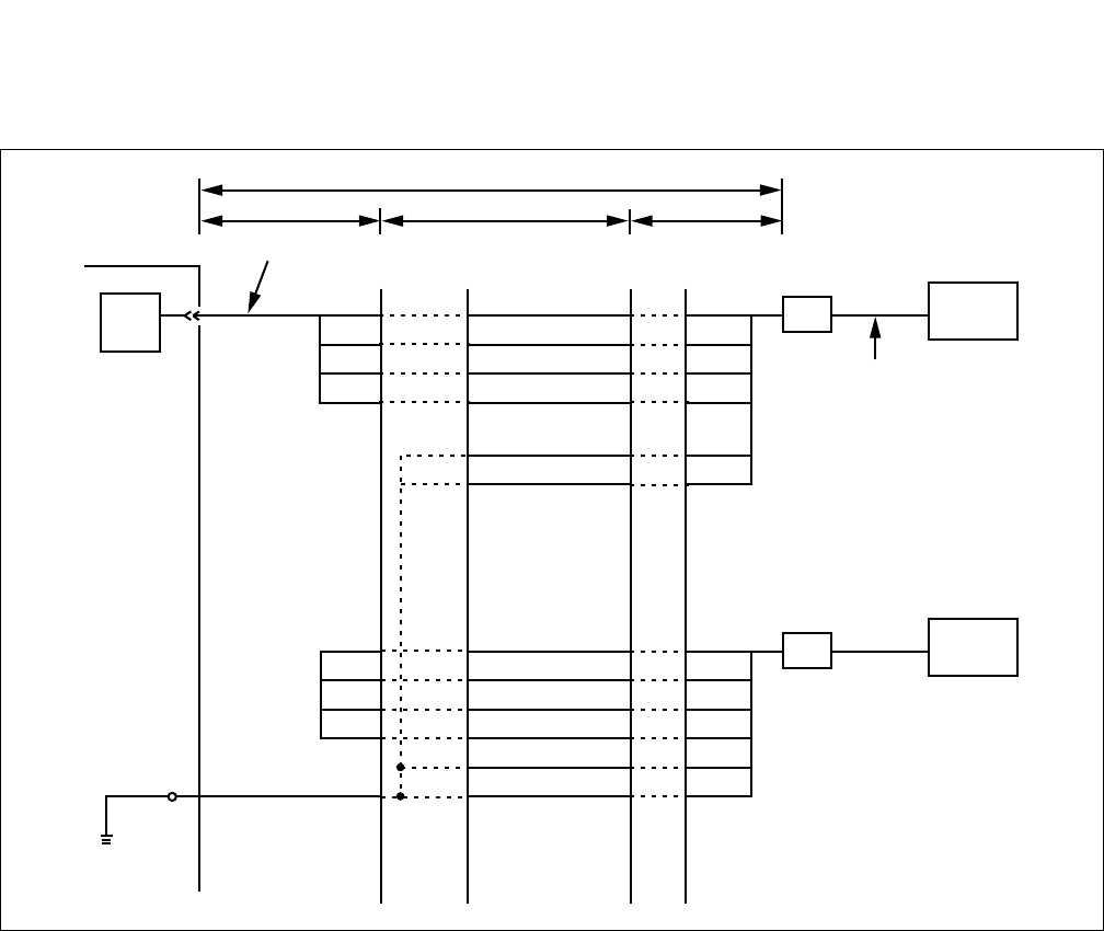
NDA-24296 CHAPTER 3
Page 291
Revision 1.0
PA-CS33
Attendant Interface
If the distance exceeds the above, estimate it according to the calculation after Figure 3-60.
Figure 3-60 Distance between PBX and Modular Rosette of Desk Console
A
B
BN4830
BN4831
GND
GND
A3
B3
BN4830
BN4831
A2
B2
BN4820
BN4821
A
B
BN4820
BN4821
GND
GND
ATI
PBX
GND
(PZ-M377)
Installation
Cable MDF IDF
(-48V)
(-48V)
6-pin Modular
rosette
6-pin Modular
Cable
#0 DESK
CONSOLE
#1 DESK
CONSOLE
AB
m
C

CHAPTER 3 NDA-24296
Page 292
Revision 1.0
PA-CS33
Attendant Interface
Calculation of the distance between the ATI circuit card and Modular Rosette
The distance M in the figure above is determined according to the Direct-Current resistance of power
supply cables (-48V and GND). Note that the maximum resistance is 26 Ω as shown in the following
formula:
m = a + b + c 26Ω
m: Maximum Direct-Current resistance between the ATI circuit card and Modular Rosette
a: Direct-Current resistance of power supply cables (-48V and GND) in the range of A
b: Direct-Current resistance of power supply cables (-48V and GND) in the range of B
c: Direct-Current resistance of power supply cables (-48V and GND) in the range of C
Example of Calculation
a, b, and c are calculated by the following formulae:
Note: You are not required to use cable lengths in meters in the following formulae. You may use cable lengths in
feet, yards, or whatever units you prefer. However, the units of resistance you use must match the units of
length you use. For example, if you use distance in feet, you must also use DC resistance per foot.
Cable resistance of DC -48V cables Cable resistance on GND cables
u (Ω/m) × x (m) u (Ω/m) × x (m)
a = +
21
No. of DC -48V cablesNo. of GND cables
Cable resistance of DC -48V cables Cable resistance on GND cables
v (Ω/m) × y (m) v (Ω/m) × y (m)
b = +
22
No. of DC -48V cablesNo. of GND cables
Cable resistance of DC -48V cables Cable resistance on GND cables
w (Ω/m) × z (m) w (Ω/m) × z (m)
c = +
22
No. of DC -48V cablesNo. of GND cables
u: DC resistance per meter in the range of A (Ω/m)
v: DC resistance per meter in the range of B (Ω/m)
w: DC resistance per meter in the range of C (Ω/m)
x: Cable length (m) in the range of A
y: Cable length (m) in the range of B
z: Cable length (m) in the range of C
<
=
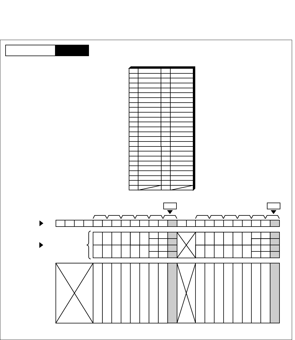
NDA-24296 CHAPTER 3
Page 293
Revision 1.0
PA-CS33
Attendant Interface
The location of the LT connector leads for the TAS interface is as shown in Figure 3-61.
Figure 3-61 LT Connector Lead Location (PIM)
PIM
232221201918171615141312111009080706050403020100
LT6 LT7 LT8 LT9 LT10LT0 LT1 LT2 LT3 LT4
LT5
1915
1814
1713
1612
231915
221814
211713
201612
110907050301
100806040200
110907050301
100806040200
23
22
21
20
ATI
Group No.
Slot No.
PIM
26
27
28
29
30
31
32
33
34
35
36
37
38
39
40
41
1
2
3
4
5
6
7
8
9
10
11
12
13
14
15
16
42
43
44
45
46
47
48
17
18
19
20
21
22
23
49
50 24
25
LT5, 11 Connector
TAS0A
TAS1ATAS1B
TAS0B
LT11
ATI
PIM
Mounting Module
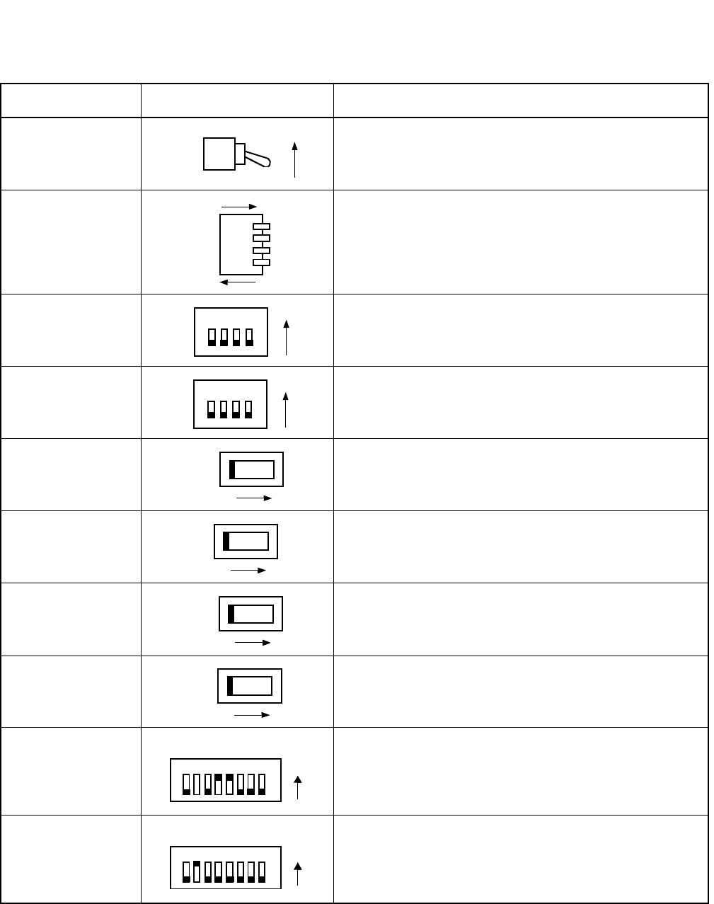
CHAPTER 3 NDA-24296
Page 294
Revision 1.0
PA-CS33
Attendant Interface
7. Switch Setting Sheet
SWITCH NAME SWITCH SHAPE REMARKS
SW00
SW01
SW10 (TAS #0)
SW13 (TAS #1)
SW11 (TAS #0)
SW12 (TAS #0)
SW14 (TAS #1)
SW15 (TAS #1)
SW16
SW17
ON
ON
OFF
1234 ON
1234 ON
ON
OFF
ON
OFF
ON
OFF
ON
OFF
12 3 4 ON
56 7 8
12 3 4 ON
56 7 8
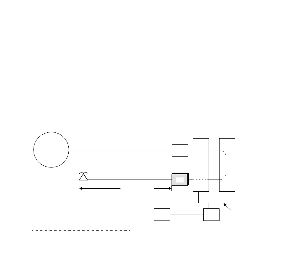
NDA-24296 CHAPTER 3
Page 295
Revision 1.0
PA-8LCBR
Line Circuit
PA-8LCBR
Line Circuit
1. General Function
The PA-8LCBR circuit card provides an interface between a maximum of eight analog voice terminals and
the system with a range of 1200 (0hm) inclusive of terminal resistance. This card can send “Stutter Dial
Tone”, which is not a continuous tone, to an associated terminal which has no Message Waiting Lamp
(MWL) instead of activating the MWL if required. In addition, polarity reverse function is provided for
each channel. This card can be used for Caller ID service.
Figure 3-62 Location of PA-8LCBR (8LC) Card in the System
PUBLIC C.O. Line
NETWORK
INT
COT
LC
Local I/O Bus
GT
CPU
max. 1200 [Ω]
Analog Terminal
•Loop Resistance : Max. 1200 [Ω]
(inclusive of terminal resistance)
•Reverse Function : x 8 circuits
•Stutter Dial Tone / Message Waiting Lamp
(selectable)
SW
(PA-8LC BR)
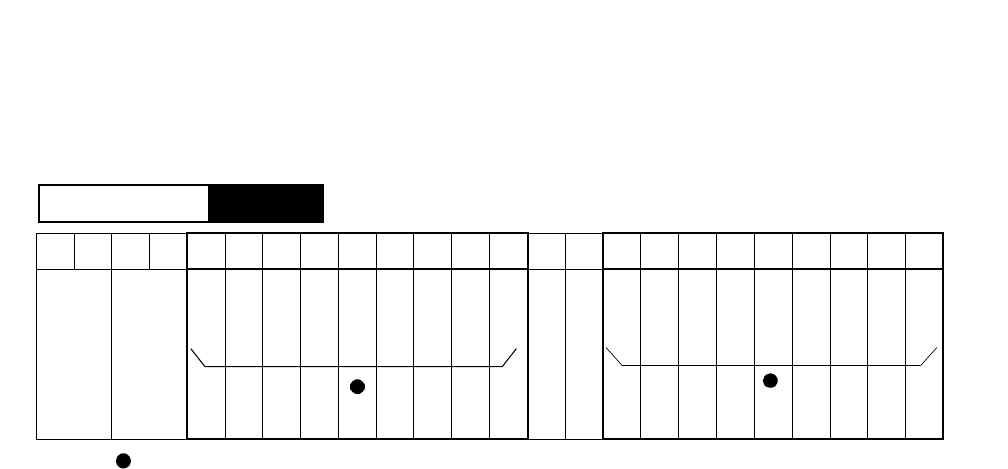
CHAPTER 3 NDA-24296
Page 296
Revision 1.0
PA-8LCBR
Line Circuit
2. Mounting Location/Condition
The mounting locations of this circuit card and the conditions related to mounting are shown below.
00 01 02 03 04 05 06 07 08 09 10 11 12 13 14 15 16 17 18 19 20 21 22 23
Note: Indicates universal slots for line/trunk circuit cards.
PIM
Mounting Module
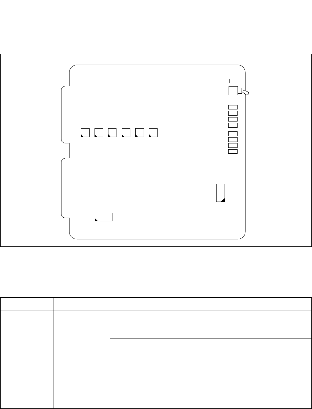
NDA-24296 CHAPTER 3
Page 297
Revision 1.0
PA-8LCBR
Line Circuit
3. Face Layout of Lamps, Switches, and Connectors
The face layout of lamps and switches on this circuit card is shown in Figure 3-63.
Figure 3-63 Face Layout of PA-8LCBR (8LC)
4. Lamp Indications
The contents of lamp indications of this circuit card are shown in the table below.
LAMP NAME COLOR STATUS MEANING
OPE Green Steady Lighting The circuitry of the circuit card is operating nor-
mally.
BL0
BL7
Green
Steady Lighting Line loop exists.
Flashing
1)Ringing signal is being transmitted. Busy LED
keeps flashing in synchronizing with on/off of
the ringing signal.
2)Dial pulses are being received. While dial pulses
from a line are being received, Busy LED keeps
flashing in synchronizing with the dial pulses
coming from the line.
3) Line is in make-busy state.
Busy LED keeps flashing at 60 ipm.
SW11
SW12
SW13
SW14
SW15
SW16
SW01
SW10
OPE
SW00
(MB)
BL7
6
5
4
3
2
1
0
~

CHAPTER 3 NDA-24296
Page 298
Revision 1.0
PA-8LCBR
Line Circuit
5. Switch Settings
Switches on this circuit card have the following meanings.
Note 1: When Caller ID is in service, set SW16-1 to OFF (Separate mode).
Note 2: Valid when SW16-1 is set to ON (Common mode).
SWITCH
NAME SWITCH
NO. SETTING STANDARD
SETTING MEANING
SW00
(MB)
UP Circuit card make busy
DOWN Circuit card make busy cancel
SW10
1ON×
Fixed
2OFF×
3OFF×
4OFF×
SW11 1OFF×Fixed
2OFF×
SW12 1OFF×Fixed
2OFF×
SW13 1OFF×Fixed
2OFF×
SW14
1ON Momentary Open
OFF Polarity Reverse
2
ON Message Waiting Lamp flashes
(1-sec. ON, 1-sec. OFF)
OFF Message Waiting Lamp lights or flashes
(Selected and Controlled by software)
SW15
1OFF×Fixed
2ON Stutter Dial Tone is available
OFF Stutter Dial Tone is not available
SW16
1
Note 1
ON Ringer Timer mode: Common mode
OFF Ringer Timer mode: Separate mode
2
Note 2
ON Pre-ringing is not available
OFF Pre-ringing is available
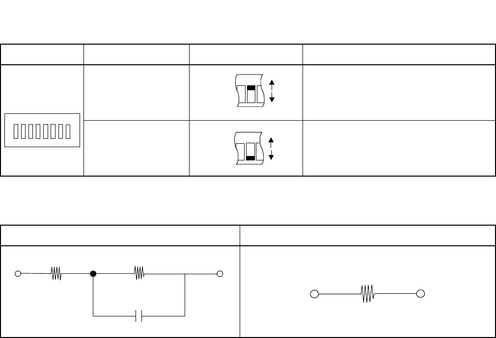
NDA-24296 CHAPTER 3
Page 299
Revision 1.0
PA-8LCBR
Line Circuit
Note: Compromise Impedance (EIA/TIA-464A) and 600 Ω are composed as follows.
SWITCH SETTING
SW01
(BNW0 - 7)
Balancing Network
Designation
• Each element corre-
sponds to circuits 0 - 7.
BNW: Compromise Impedance
(EIA/TIA-464A)
For long distance
BNW: 600 Ω
For short distance
BNW2 (ON) BNW1 (OFF)
12345678
ON
OFF
ON
OFF
350Ω1000Ω
0.21 µ
600Ω
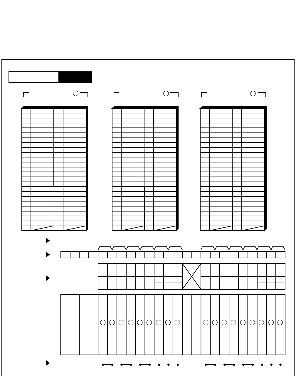
CHAPTER 3 NDA-24296
Page 300
Revision 1.0
PA-8LCBR
Line Circuit
6. External Interface
Accommodation of the LT connector leads of this circuit card and connecting route diagram are shown
Figure 3-64.
Figure 3-64 LT Connector Leads Accommodation
PIM
Mounting Module
26
27
28
29
30
31
32
33
34
35
36
37
38
39
40
41
1
2
3
4
5
6
7
8
9
10
11
12
13
14
15
16
42
43
44
45
46
47
48
17
18
19
20
21
22
23
49
50 24
25
232221201918171615141312111009080706050403020100
LT6 LT7 LT8 LT9 LT10 LT11LT0 LT1 LT2 LT3 LT4 LT5
231915
221814
211713
201612
231915
221814
211713
201612
110907050301
100806040200
110907050301
100806040200
HW11HW10HW9HW8HW7HW6HW5HW4HW3HW2HW1HW0
Group No.
Slot No.
LT Connector
PIM
PWR
PWR
Highway Block
LT 1, 3, 5, 7, 9, 11 Connector
26
27
28
29
30
31
32
33
34
35
36
37
38
39
40
41
1
2
3
4
5
6
7
8
9
10
11
12
13
14
15
16
42
43
44
45
46
47
48
17
18
19
20
21
22
23
49
50 24
25
Accommodated in 2
LT 1, 3, 5, 7, 9, 11 Connector
Accommodated in 3
26
27
28
29
30
31
32
33
34
35
36
37
38
39
40
41
1
2
3
4
5
6
7
8
9
10
11
12
13
14
15
16
42
43
44
45
46
47
48
17
18
19
20
21
22
23
49
50 24
25
Accommodated in 1
LT 0, 2, 4, 6, 8, 10 Connector
B0 A0
B1 A1
B2 A2
B3 A3
B4 A4
B5 A5
B6 A6
B7 A7
B0 A0
B1 A1
B2 A2
B3 A3
B4 A4
B5 A5
B6 A6
B7 A7
B0 A0
B1 A1
B2 A2
B3 A3
B4 A4
B5 A5
B6 A6
B7 A7
21 3 2 1 3 21 31 2
231231 3
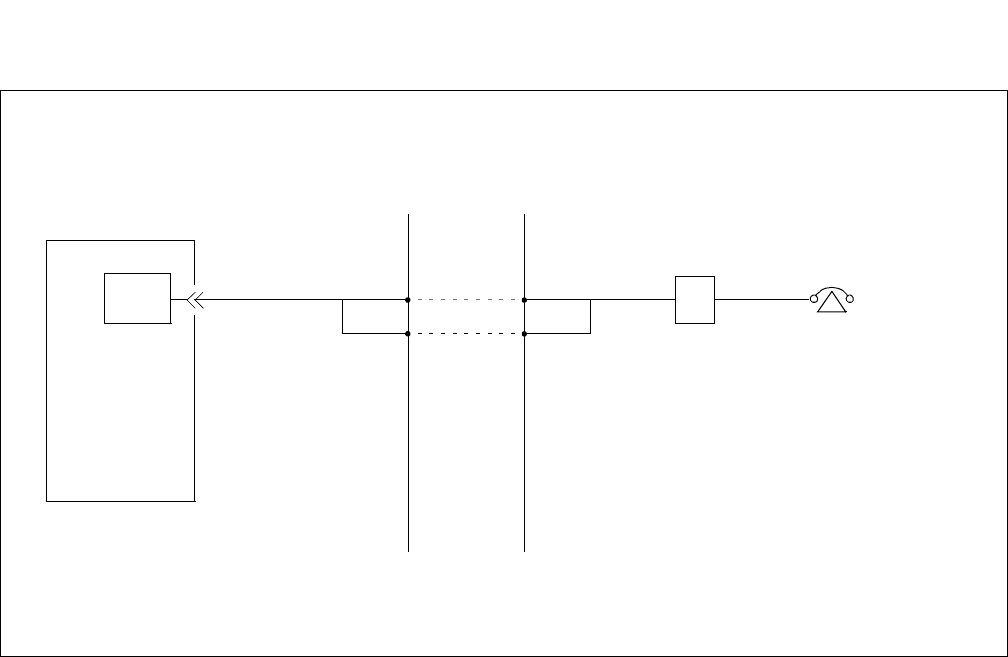
NDA-24296 CHAPTER 3
Page 301
Revision 1.0
PA-8LCBR
Line Circuit
Figure 3-65 Connecting Route Diagram
NEAX2400 IPX
A0
MDF
Telephone
L1
L2
B0
Rosette
LC
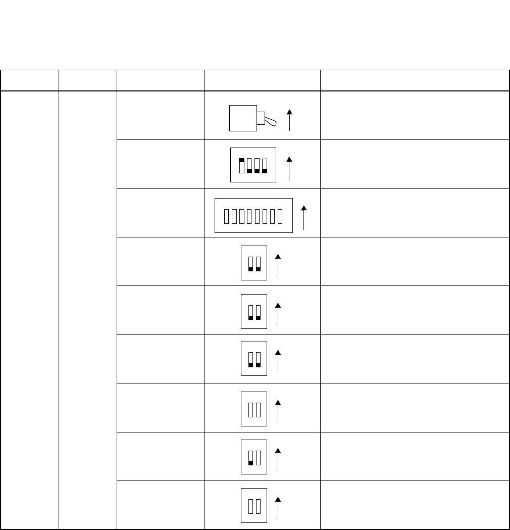
CHAPTER 3 NDA-24296
Page 302
Revision 1.0
PA-8LCBR
Line Circuit
7. Switch Setting Sheet
MODULE SLOT NO. SWITCH NAME SWITCH SHAPE REMARKS
PIM
SW00
(MB)
SW10
SW01
(BNW 0 - 7)
SW11 Fixed
SW12 Fixed
SW13 Fixed
SW14
SW15
SW16
ON
12 3 4 ON
12345678ON
1 2 ON
1 2 ON
1 2 ON
12ON
1 2 ON
1 2 ON
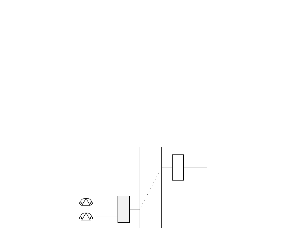
NDA-24296 CHAPTER 3
Page 303
Revision 1.0
PA-16LCBE
Line Circuit
PA-16LCBE
Line Circuit
1. General Function
This circuit card provides the interface for 16 station lines. This circuit card is provided with functions for
supervising each user's call origination, call answering, release, detection of switch hook flashing, relaying
of DP/PB signals, transmission of ringing signals to the called side, and bothway transmissions of voice
band signals. For use of this circuit card, there are the following limitations.
(a) There are four kinds of balancing network, each of which is set up according to the line conditions
involved.
(b) PAD is only for receiving side 5 dB (at the time of station to station call).
Figure 3-66 Location of PA-16LCBE (16LC) Card in the System
TSW
16LC
COT
(MAX. 16 Stations)
C.O. Line
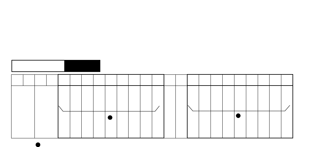
CHAPTER 3 NDA-24296
Page 304
Revision 1.0
PA-16LCBE
Line Circuit
2. Mounting Location/Condition
•The mounting locations of this circuit card and the conditions related to mounting are shown below.
00 01 02 03 04 05 06 07 08 09 10 11 12 13 14 15 16 17 18 19 20 21 22 23
Note: Indicates universal slots for line/trunk circuit cards.
PIM
Mounting Module
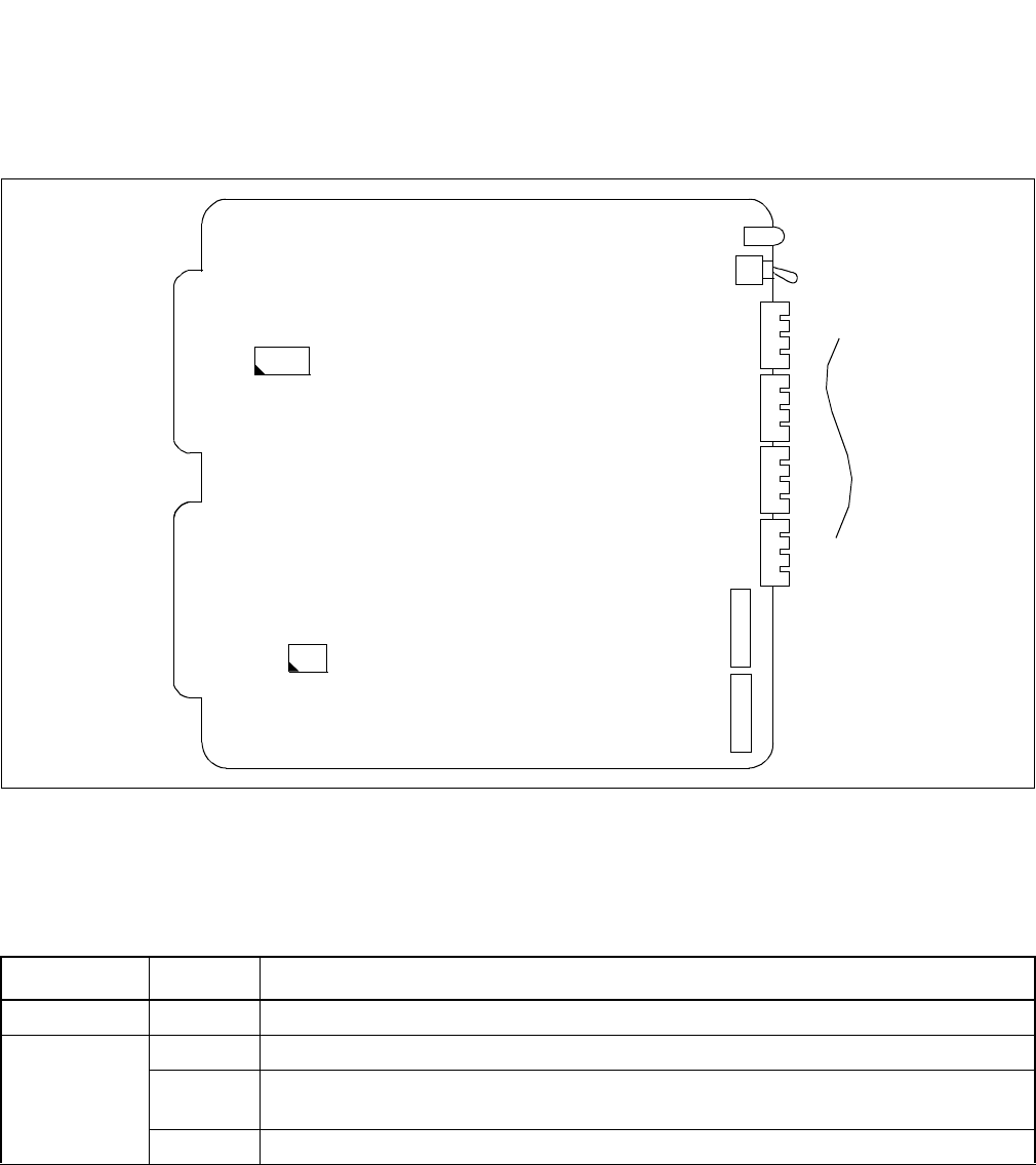
NDA-24296 CHAPTER 3
Page 305
Revision 1.0
PA-16LCBE
Line Circuit
3. Face Layout of Lamps, Switches, and Connectors
The face layout of lamps, switches, and connectors of this circuit card is shown below.
Figure 3-67 Face Layout of PA-16LCBE (16LC)
4. Lamp Indications
The contents of lamp indications of this circuit card are shown in the table below.
LAMP NAME COLOR STATE
OPE Green Remains lit while this circuit card is opening.
BL0
BL1S
Green Lights when the corresponding circuit is busy.
Flash Flashes (60 IPM) to dial pulses at the time of an outgoing call or when the corresponding
circuit is in make-busy state.
OFF Remains off when the corresponding circuit is idle.
OPE
MB
BL15
BL0
BNW8-15
BNW0-7
SW1
SW0
~

CHAPTER 3 NDA-24296
Page 306
Revision 1.0
PA-16LCBE
Line Circuit
5. Switch Settings
Standard settings of various switches on this circuit card are shown in the table below.
SWITCH
NAME SWITCH
NO. SETTING STANDARD
SETTING MEANING
MB UP Circuit card make busy.
DOWN ×Circuit card make busy cancel.
SW0
1OFF ×Fixed
2OFF ×Fixed
3OFF ×Fixed
4OFF ×Fixed
NDA-24296 CHAPTER 3
Page 307
Revision 1.0
PA-16LCBE
Line Circuit
SWITCH
NAME SWITCH
NO. SETTING STANDARD
SETTING MEANING
BNW0 ~ 7
1ON Balancing network of No. 0 Circuit ; For long distance.
OFF ×Balancing network of No. 0 Circuit ; For short distance.
2ON Balancing network of No. 1 Circuit ; For long distance.
OFF ×Balancing network of No. 1 Circuit ; For short distance.
3ON Balancing network of No. 2 Circuit ; For long distance.
OFF ×Balancing network of No. 2 Circuit ; For short distance.
4ON Balancing network of No. 3 Circuit ; For long distance.
OFF ×Balancing network of No. 3 Circuit ; For short distance.
5ON Balancing network of No. 4 Circuit ; For long distance.
OFF ×Balancing network of No. 4 Circuit ; For short distance.
6ON Balancing network of No. 5 Circuit ; For long distance.
OFF ×Balancing network of No. 5 Circuit ; For short distance.
7ON Balancing network of No. 6 Circuit ; For long distance.
OFF ×Balancing network of No. 6 Circuit ; For short distance.
8ON Balancing network of No. 7 Circuit ; For long distance.
OFF ×Balancing network of No. 7 Circuit ; For short distance.
Note: Normally, switches are all to be set to OFF.
However, when the station line is long (PBX -
Telephone Set), rearrange the switch setting re-
ferring to the following table.
TERMINAL RESISTANCE IS NOT INCLUDED IN
THE LINE RESISTANCE
BALANCING
NETWORK LINE
RESISTANCE SWITCH
Short Distance 0 ~ 100 ΩOFF
Long Distance More than 100 ΩON
CHAPTER 3 NDA-24296
Page 308
Revision 1.0
PA-16LCBE
Line Circuit
SWITCH
NAME SWITCH
NO. SETTING STANDARD
SETTING MEANING
BNW8 ~ 15
1ON Balancing network of No. 8 Circuit ; For long distance.
OFF ×Balancing network of No. 8 Circuit ; For short distance.
2ON Balancing network of No. 9 Circuit ; For long distance.
OFF ×Balancing network of No. 9 Circuit ; For short distance.
3ON Balancing network of No. 10 Circuit ; For long distance.
OFF ×Balancing network of No. 10 Circuit ; For short distance.
4ON Balancing network of No. 11 Circuit ; For long distance.
OFF ×Balancing network of No. 11 Circuit ; For short distance.
5ON Balancing network of No. 12 Circuit ; For long distance.
OFF ×Balancing network of No. 12 Circuit ; For short distance.
6ON Balancing network of No. 13 Circuit ; For long distance.
OFF ×Balancing network of No. 13 Circuit ; For short distance.
7ON Balancing network of No. 14 Circuit ; For long distance.
OFF ×Balancing network of No. 14 Circuit ; For short distance.
8ON Balancing network of No. 15 Circuit ; For long distance.
OFF ×Balancing network of No. 15 Circuit ; For short distance.
Note: Normally, switches are all to be set to OFF.
However, when the station line is long (PBX -
Telephone Set), rearrange the switch setting
referring to the following table.
TERMINAL RESISTANCE IS NOT INCLUDED IN
THE LINE RESISTANCE
BALANCING
NETWORK LINE
RESISTANCE SWITCH
Short Distance 0 ~ 100 ΩOFF
Long Distance More than 100 ΩON
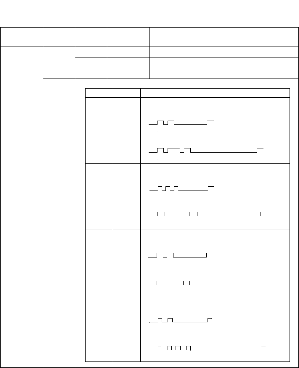
NDA-24296 CHAPTER 3
Page 309
Revision 1.0
PA-16LCBE
Line Circuit
SWITCH
NAME SWITCH
NO. SETTING STANDARD
SETTING MEANING
SW1
1ON Polarity Reversal as Disconnect Signal
OFF ×Momentary Open as Disconnect Signal
2OFF ×Fixed
3
4
SW1-3 SW1-4 INTERRUPTED RINGER PATTERN
OFF
(standard)
OFF
(standard)
OFF ON
ON OFF
ON ON
0.4/0.2/0.4-ON/OFF/ON
• Incoming call from C. O. line/station
0.4 0.4
0.2
2.0
• Rering
0.4 0.8
0.2
4.00.4
0.2
0.2/0.2/0.2/0.2-ON/OFF/ON/OFF/ON
• Incoming call from C. O. line/station
0.2 0.2
0.2
2.0
• Rering
0.2 0.2
0.2
4.00.4
0.2
0.2
0.2
0.2 0.2
0.20.2
0.35/0.3/0.35-ON/OFF/ON
• Incoming call from C. O. line/station
0.35 0.35
0.3
2.0
• Rering
0.35 0.7
0.3
4.00.35
0.3
0.2/0.4/0.2-ON/OFF/ON
• Incoming call from C. O. line/station
0.2 0.2
0.4
2.2
• Rering
0.2 0.2
0.4
4.2
0.2 0.4
0.2 0.2

CHAPTER 3 NDA-24296
Page 310
Revision 1.0
PA-16LCBE
Line Circuit
SWITCH
NAME SWITCH
NO. SETTING STANDARD
SETTING MEANING
SW1
5
6
7ON Stutter Dial Tone Available
OFF ×Stutter Dial Tone Not Available
8ON Pre-signaling is not performed.
OFF ×Pre-signaling is performed.
SW1-5 SW1-6 SWITCH SETTING FOR MW
LAMP CONTROLLING
OFF OFF In the case of lighting (normal setting)
OFF ON In the case of 60 IPM flashing
ON OFF In the case of lighting or flashing
(As controlled by the software)
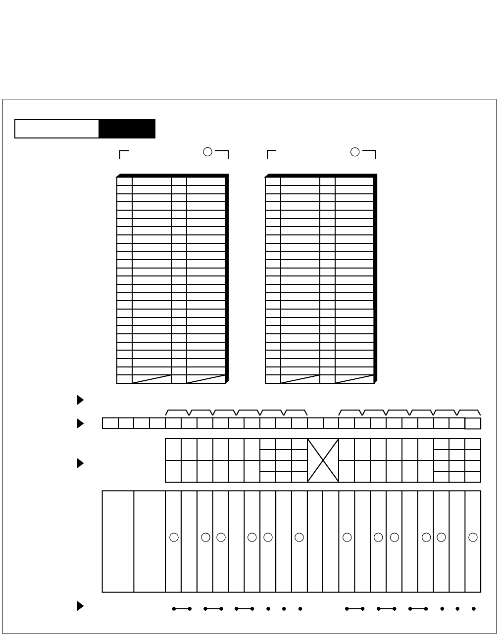
NDA-24296 CHAPTER 3
Page 311
Revision 1.0
PA-16LCBE
Line Circuit
6. External Interface
Accommodation of the LT connector leads of this circuit card and connecting route diagram are shown in
Figure 3-68 below.
Figure 3-68 LT Connector Leads Accommodation (1/2)
PIM
Mounting Module
26
27
28
29
30
31
32
33
34
35
36
37
38
39
40
41
1
2
3
4
5
6
7
8
9
10
11
12
13
14
15
16
42
43
44
45
46
47
48
17
18
19
20
21
22
23
49
50 24
25
232221201918171615141312111009080706050403020100
LT6 LT7 LT8 LT9 LT10 LT11LT0 LT1 LT2 LT3 LT4 LT5
231915
221814
211713
201612
231915
221814
211713
201612
110907050301
100806040200
110907050301
100806040200
HW11HW10HW9HW8HW7HW6HW5HW4HW3HW2HW1HW0
Group No.
Slot No.
LT Connector
PIM
Highway Block
LT 1, 3, 5, 7, 9, 11 Connector
26
27
28
29
30
31
32
33
34
35
36
37
38
39
40
41
1
2
3
4
5
6
7
8
9
10
11
12
13
14
15
16
42
43
44
45
46
47
48
17
18
19
20
21
22
23
49
50 24
25
B0
B1
Accommodated in 1
LT 0, 2, 4, 6, 8, 10 Connector
B2
B3
Accommodated in 2
B4
B5
B6
B7
B8
B9
B10
B11
B12
B13
B14
B15
A0
A1
A2
A3
A4
A5
A6
A7
A8
A9
A10
A11
A12
A13
A14
A15
B0
B1
B2
B3
B4
B5
B6
B7
B8
B9
B10
B11
B12
B13
B14
B15
A0
A1
A2
A3
A4
A5
A6
A7
A8
A9
A10
A11
A12
A13
A14
A15
1212 12
12 1212
PWR
PWR

CHAPTER 3 NDA-24296
Page 312
Revision 1.0
PA-16LCBE
Line Circuit
Figure 3-68 LT Connector Leads Accommodation (2/2)
PIM
Mounting Module
26
27
28
29
30
31
32
33
34
35
36
37
38
39
40
41
1
2
3
4
5
6
7
8
9
10
11
12
13
14
15
16
42
43
44
45
46
47
48
17
18
19
20
21
22
23
49
50 24
25
232221201918171615141312111009080706050403020100
LT6 LT7 LT8 LT9 LT10 LT11LT0 LT1 LT2 LT3 LT4 LT5
231915
221814
211713
201612
231915
221814
211713
201612
110907050301
100806040200
110907050301
100806040200
HW11HW10HW9HW8HW7HW6HW5HW4HW3HW2HW1HW0
Group No.
Slot No.
LT Connector
PIM
Highway Block
26
27
28
29
30
31
32
33
34
35
36
37
38
39
40
41
1
2
3
4
5
6
7
8
9
10
11
12
13
14
15
16
42
43
44
45
46
47
48
17
18
19
20
21
22
23
49
50 24
25
B0
B1
Accommodated in 3
LT 1, 3, 5, 7, 9, 11 ConnectorLT 0, 2, 4, 6, 8, 10 Connector
B2
B3
B4
B5
B6
B7
A0
A1
A2
A3
A4
A5
A6
A7
B8
B9
B10
B11
B12
B13
B14
B15
A8
A9
A10
A11
A12
A13
A14
A15
3 3 3 3 3 3
PWR
PWR
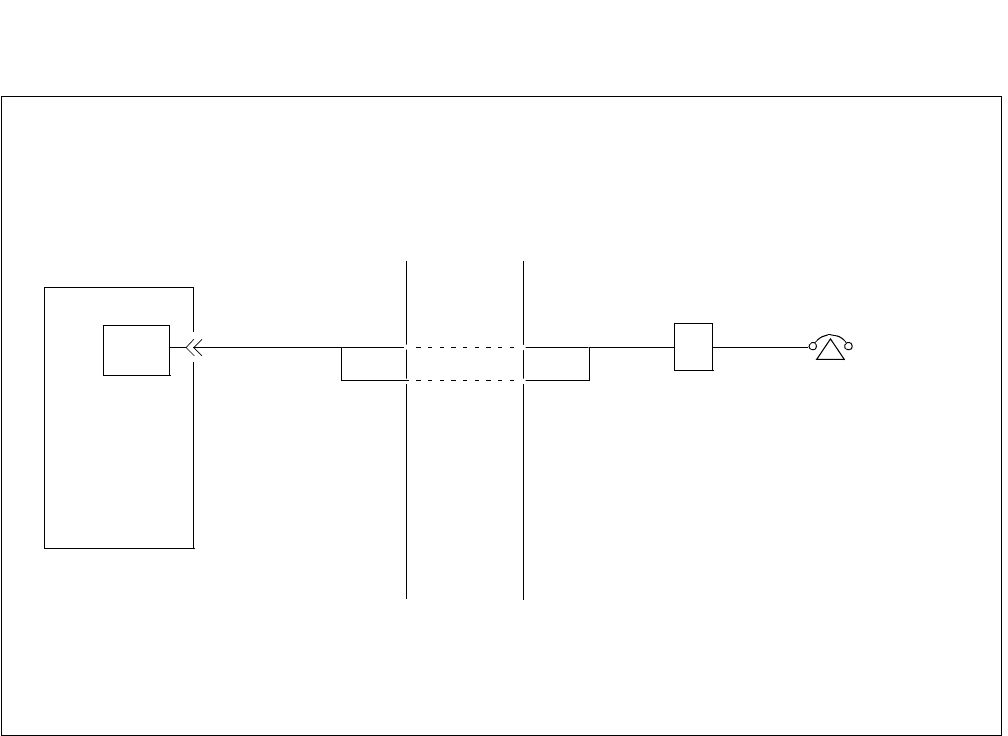
NDA-24296 CHAPTER 3
Page 313
Revision 1.0
PA-16LCBE
Line Circuit
Figure 3-69 Connecting Route Diagram
NEAX2400 IPX
A0
MDF
Ordinary Telephone
L1
L2
B0 Rosette
LC
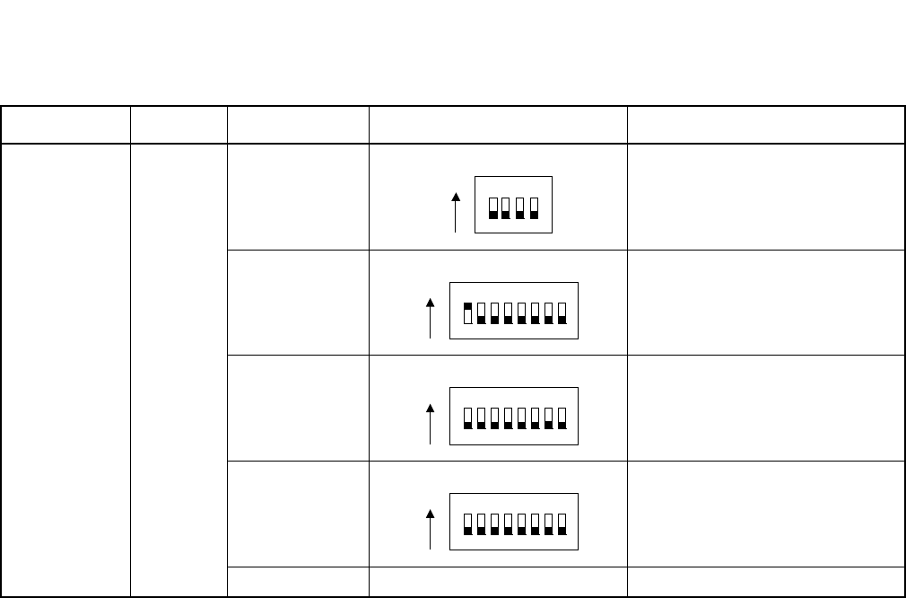
CHAPTER 3 NDA-24296
Page 314
Revision 1.0
PA-16LCBE
Line Circuit
7. Switch Setting Sheet
MODULE SLOT NO. SWITCH NAME SWITCH SHAPE REMARKS
PIM
SW0
SW1
BNW0-7
BNW8-15
MB DOWN Circuit card make busy cancel.
ON 1234
ON 12345678
ON 12345678
ON 12345678
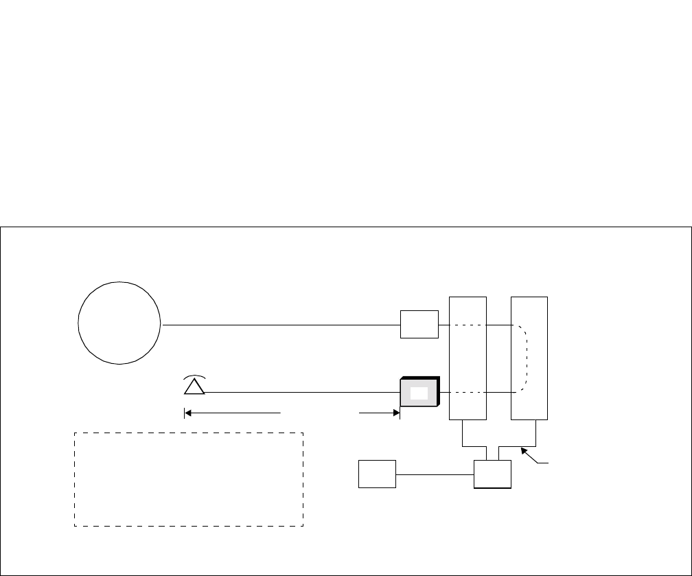
NDA-24296 CHAPTER 3
Page 315
Revision 1.0
PA-16LCBJ-A
Line Circuit
PA-16LCBJ-A
Line Circuit
1. General Function
The PA-16LCBJ-A circuit card,which is exclusively used in a µ-law system, provides an interface between
a maximum of 16 analog terminals and the system with a range of 600 (Ohm) inclusive of terminal resis-
tance.This card also can send “Stutter Dial Tone”, which is not a continuous tone, to an associated terminal
which has no Message Waiting Lamp (MWL) instead of activating the MWL if required.
Figure 3-70 Location of PA-16LCBJ-A (16LC) Card in the System
PUBLIC C.O. Line
NETWORK
INT
COT
LC
Local I/O Bus
GT
CPU
max. 600 [Ω]
Analog Terminal
•Loop Resistance : Max. 600 [Ω]
(inclusive of terminal resistance)
•Reverse Function : x 1 circuits
•Stutter Dial Tone / Message Waiting Lamp
(selectable)
•Encoding Law : µ-law.
SW
(PA-16LC BJ-A)

CHAPTER 3 NDA-24296
Page 316
Revision 1.0
PA-16LCBJ-A
Line Circuit
2. Mounting Location/Condition
The mounting locations of this circuit card and the conditions related to mounting are shown below.
00 01 02 03 04 05 06 07 08 09 10 11 12 13 14 15 16 17 18 19 20 21 22 23
Note: Indicates universal slots for line/trunk circuit cards.
PIM
Mounting Module
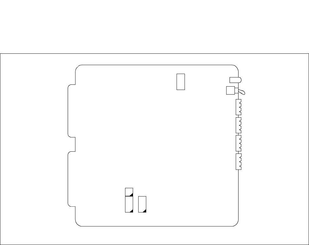
NDA-24296 CHAPTER 3
Page 317
Revision 1.0
PA-16LCBJ-A
Line Circuit
3. Face Layout of Lamps, Switches, and Connectors
The face layout of lamps, switches, and connectors of this circuit card is shown in Figure 3-71.
Figure 3-71 Face Layout of PA-16LCBJ-A (16LC)
SW13
SW12
SW11
(BNW8-15) SW10
(BNW0-7)
OPE
SW00 (MB)
BL12-15
BL8-11
BL4-7
BL0-3

CHAPTER 3 NDA-24296
Page 318
Revision 1.0
PA-16LCBJ-A
Line Circuit
4. Lamp Indications
The contents of lamp indications of this circuit card are shown in the table below.
LAMP NAME COLOR STATUS MEANING
OPE Green Steady Lighting The circuitry of the circuit card is operating
normally.
BL0
BL15
Green
Steady Lighting Line loop exists.
Flashing
1)Ringing signal is being transmitted. Busy LED
keeps flashing in synchronizing with on/off of
the ringing signal.
2)Dial pulses are being received. While dial
pulses from a line are being received, Busy
LED keeps flashing in synchronizing with the
dial pulses coming from the line.
3)Line is in make-busy state.
Busy LED keeps flashing at 60 ipm.
~

NDA-24296 CHAPTER 3
Page 319
Revision 1.0
PA-16LCBJ-A
Line Circuit
5. Switch Settings
Standard settings of various switches on this circuit card are shown in the table below.
SWITCH
NAME SWITCH
NO. SETTING STANDARD
SETTING MEANING
SW00
(MB)
UP Circuit card make busy.
DOWN Circuit card make busy cancel.
SW10
(BNW0~7)
CIRCUIT NO. KIND OF BALANCING NETWORK
1ON No. 0 Compromise
OFF ×600 Ω
2ON No. 1 Compromise
OFF ×600 Ω
3ON No. 2 Compromise
OFF ×600 Ω
4ON No. 3 Compromise
OFF ×600 Ω
5ON No. 4 Compromise
OFF ×600 Ω
6ON No. 5 Compromise
OFF ×600 Ω
7ON No. 6 Compromise
OFF ×600 Ω
8ON No. 7 Compromise
OFF ×600 Ω

CHAPTER 3 NDA-24296
Page 320
Revision 1.0
PA-16LCBJ-A
Line Circuit
SWITCH
NAME SWITCH
NO. SETTING STANDARD
SETTING
MEANING
CIRCUIT NO. KIND OF BALANCING NETWORK
SW11
(BNW8~15)
1ON No. 8 Compromise
OFF ×600 Ω
2ON No. 9 Compromise
OFF ×600 Ω
3ON No. 10 Compromise
OFF ×600 Ω
4ON No. 11 Compromise
OFF ×600 Ω
5ON No. 12 Compromise
OFF ×600 Ω
6ON No. 13 Compromise
OFF ×600 Ω
7ON No. 14 Compromise
OFF ×600 Ω
8ON No. 15 Compromise
OFF ×600 Ω
SW12
1ON Immediate is not available.
OFF Immediate is available.
2ON Stutter dial tone is available
OFF Message Waiting Lamp is available
SW13 ON Momentary Open
OFF Polarity Reverse

NDA-24296 CHAPTER 3
Page 321
Revision 1.0
PA-16LCBJ-A
Line Circuit
6. External Interface
Accommodation of the LT connector leads of this circuit card and connecting route diagram are shown in
Figure 3-72.
Figure 3-72 LT Connector Lead Accommodation (1/2)
PIM
Mounting Module
26
27
28
29
30
31
32
33
34
35
36
37
38
39
40
41
1
2
3
4
5
6
7
8
9
10
11
12
13
14
15
16
42
43
44
45
46
47
48
17
18
19
20
21
22
23
49
50 24
25
232221201918171615141312111009080706050403020100
LT6 LT7 LT8 LT9 LT10 LT11LT0 LT1 LT2 LT3 LT4 LT5
231915
221814
211713
201612
231915
221814
211713
201612
110907050301
100806040200
110907050301
100806040200
HW11HW10HW9HW8HW7HW6HW5HW4HW3HW2HW1HW0
Group No.
Slot No.
LT Connector
PIM
Highway Block
LT 1, 3, 5, 7, 9, 11 Connector
26
27
28
29
30
31
32
33
34
35
36
37
38
39
40
41
1
2
3
4
5
6
7
8
9
10
11
12
13
14
15
16
42
43
44
45
46
47
48
17
18
19
20
21
22
23
49
50 24
25
B0
B1
Accommodated in 1
LT 0, 2, 4, 6, 8, 10 Connector
B2
B3
Accommodated in 2
B4
B5
B6
B7
B8
B9
B10
B11
B12
B13
B14
B15
A0
A1
A2
A3
A4
A5
A6
A7
A8
A9
A10
A11
A12
A13
A14
A15
B0
B1
B2
B3
B4
B5
B6
B7
B8
B9
B10
B11
B12
B13
B14
B15
A0
A1
A2
A3
A4
A5
A6
A7
A8
A9
A10
A11
A12
A13
A14
A15
1212 12
12 1212
PWR
PWR
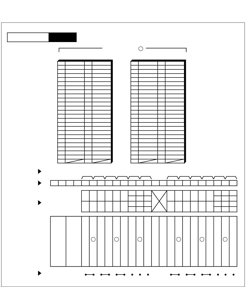
CHAPTER 3 NDA-24296
Page 322
Revision 1.0
PA-16LCBJ-A
Line Circuit
Figure 3-72 LT Connector Lead Accommodation (2/2)
PIM
Mounting Module
26
27
28
29
30
31
32
33
34
35
36
37
38
39
40
41
1
2
3
4
5
6
7
8
9
10
11
12
13
14
15
16
42
43
44
45
46
47
48
17
18
19
20
21
22
23
49
50 24
25
232221201918171615141312111009080706050403020100
LT6 LT7 LT8 LT9 LT10 LT11LT0 LT1 LT2 LT3 LT4 LT5
231915
221814
211713
201612
231915
221814
211713
201612
110907050301
100806040200
110907050301
100806040200
HW11HW10HW9HW8HW7HW6HW5HW4HW3HW2HW1HW0
Group No.
Slot No.
LT Connector
PIM
Highway Block
26
27
28
29
30
31
32
33
34
35
36
37
38
39
40
41
1
2
3
4
5
6
7
8
9
10
11
12
13
14
15
16
42
43
44
45
46
47
48
17
18
19
20
21
22
23
49
50 24
25
B0
B1
Accommodated in 3
LT 1, 3, 5, 7, 9, 11 ConnectorLT 0, 2, 4, 6, 8, 10 Connector
B2
B3
B4
B5
B6
B7
A0
A1
A2
A3
A4
A5
A6
A7
B8
B9
B10
B11
B12
B13
B14
B15
A8
A9
A10
A11
A12
A13
A14
A15
3 3 3 3 3 3
PWR
PWR
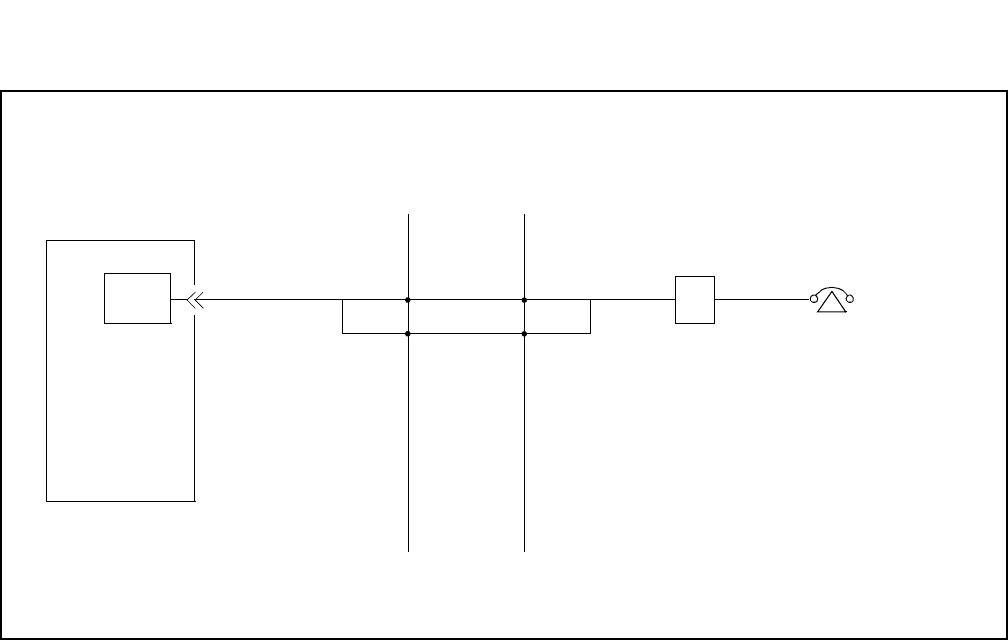
NDA-24296 CHAPTER 3
Page 323
Revision 1.0
PA-16LCBJ-A
Line Circuit
Figure 3-73 Connecting Route Diagram
NEAX2400 IPX
A0
MDF
Ordinary Telephone
L1
L2
B0 Rosette
LC
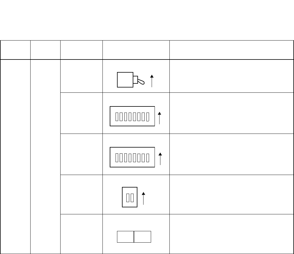
CHAPTER 3 NDA-24296
Page 324
Revision 1.0
PA-16LCBJ-A
Line Circuit
7. Switch Setting Sheet
MODULE SLOT No. SWITCH
NAME SWITCH SHAPE REMARKS
PIM
SW00
(MB) UP : Circuit card make busy
SW10
(BNW 0 - 7)
SW11
(BNW 8 - 15)
SW12
SW13
ON
012345 6 7 ON
01234567 ON
1 2 ON
OFF ON
(RVS) (OPEN)
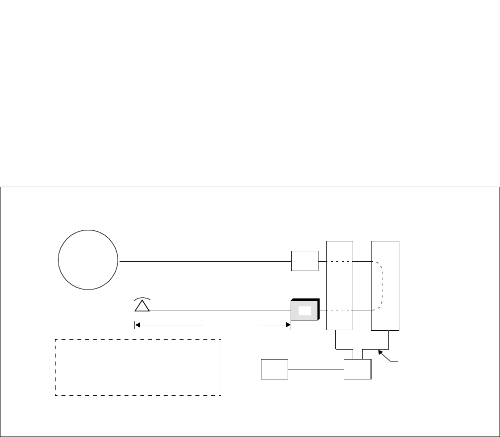
NDA-24296 CHAPTER 3
Page 325
Revision 1.0
PA-16LCBJ-B
Line Circuit
PA-16LCBJ-B
Line Circuit
1. General Function
The PA-16LCBJ-B circuit card, which is exclusively used in a µ-law system, provides an interface between
a maximum of 16 analog terminals and the system with a range of 600 (0hm) inclusive of terminal
resistance.
This card also can send “Stutter Dial Tone”, which is not a continuous tone, to an associated terminal which
has no Message Waiting Lamp (MWL) instead of activating the MWL if required.
Figure 3-74 Location of PA-16LCBJ-B (16LC) Card in the System
PUBLIC C.O. Line
NETWORK
INT
COT
LC
Local I/O Bus
GT
CPU
max. 600 [Ω]
Analog Terminal
•Loop Resistance : Max. 600 [Ω]
(inclusive of terminal resistance)
•Reverse Function : x 1 circuit
•Stutter Dial Tone / Message Waiting Lamp
•Encoding Law : µ-law
SW
(PA-16LC BJ-B)

CHAPTER 3 NDA-24296
Page 326
Revision 1.0
PA-16LCBJ-B
Line Circuit
2. Mounting Location/Condition
The mounting locations of this circuit card are shown below.
00 01 02 03 04 05 06 07 08 09 10 11 12 13 14 15 16 17 18 19 20 21 22 23
Note: Indicates universal slots for line/trunk circuit cards.
PIM
Mounting Module
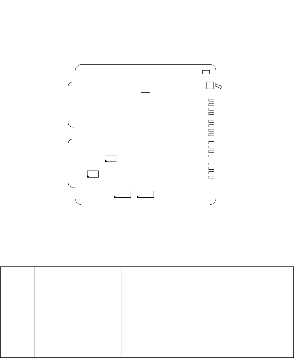
NDA-24296 CHAPTER 3
Page 327
Revision 1.0
PA-16LCBJ-B
Line Circuit
3. Face Layout of Lamps, Switches, and Connectors
The face layout of lamps and switches on this circuit card is shown in Figure 3-75.
Figure 3-75 Face Layout of PA-16LCBJ-B (16LC)
4. Lamp Indications
The contents of lamp indications of this circuit card are shown in the table below.
LAMP
NAME COLOR STATE MEANING
OPE Green Steady Lighting The circuitry of the circuit card is operating normally.
BL0
BL15
Green
Steady Lighting Line loop exists.
Flashing
1)Ringing signal is being transmitted. Busy LED keeps flashing in syn-
chronizing with on/off of the ringing signal.
2)Dial pulses are being received. While dial pulses from a line are be-
ing received, Busy LED keeps flashing in synchronizing with the dial
pulses coming from the line.
3)Line is in make-busy state.
Busy LED keeps flashing at 60 ipm.
OPE
MB
BL15
SW10
14
13
12
3
2
1
0
11
10
9
8
7
6
5
4
SW11
SW13
SW15
SW16
~
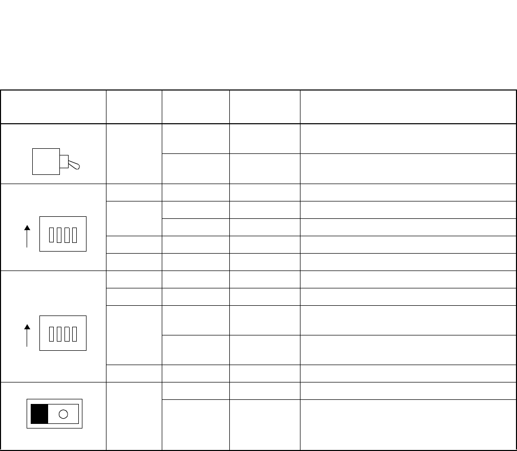
CHAPTER 3 NDA-24296
Page 328
Revision 1.0
PA-16LCBJ-B
Line Circuit
5. Switch Settings
Switches on the PA-16LC BJ-B card have the following meanings.
SWITCH NAME SWITCH
NO. SETTING STANDARD
SETTING MEANING
SW00(MB) UP Card make-busy
(Inserted state)
DOWN Card make-busy cancel
(Operating state)
SW13
1OFF ×Fixed to OFF
2ON Stutter dial tone is available
OFF ×Stutter dial tone is not available
3OFF ×Fixed to OFF
4OFF ×Fixed to OFF
SW15
1OFF ×Fixed to OFF
2OFF ×Fixed to OFF
3
ON Message waiting lamp flashes
(1-sec. ON/1-sec. OFF)
OFF ×Message waiting lamp lights or flashes
(controlled by software)
4OFF ×Fixed to OFF
SW16 ON Momentary open
OFF ×Polarity reverse
1 2 3 4
ON
1234
ON
OFF
(RVS) ON
(OPEN)
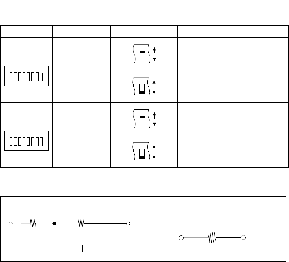
NDA-24296 CHAPTER 3
Page 329
Revision 1.0
PA-16LCBJ-B
Line Circuit
Note: Compromise Impedance (EIA/TIA-464A) and 600 Ω are composed as follows.
SWITCH NAME SETTING
SW-10
(BNW0 - 7) Balancing Network
Designation
• Each element
corresponds to
circuits 0 - 7.
BNW: Compromise Impedance
(EIA/TIA-464A)
for long distance
BNW: 600 Ω
for short distance
SW-11
(BNW8 - 15) Balancing Network
Designation
• Each element
corresponds to
circuits 8 - 15.
BNW: Compromise Impedance
(EIA/TIA-464A)
for long distance
BNW: 600 Ω
for short distance
ON OFF
123456 7 8
ON
OFF
▼
ON
OFF
▼
12 3 4 5 6 7 8
ON
OFF
▼
ON
OFF
▼
compromise impedance (EIA/TIA-464A)
350Ω1000Ω
0.21 µ
600Ω
CHAPTER 3 NDA-24296
Page 330
Revision 1.0
PA-16LCBJ-B
Line Circuit
6. External Interface
Accommodation of the LT connector leads of this circuit card and connecting route diagram are shown in
Figure 3-76.
Figure 3-76 LT Connector Leads Accommodation (1/2)
PIM
Mounting Module
26
27
28
29
30
31
32
33
34
35
36
37
38
39
40
41
1
2
3
4
5
6
7
8
9
10
11
12
13
14
15
16
42
43
44
45
46
47
48
17
18
19
20
21
22
23
49
50 24
25
232221201918171615141312111009080706050403020100
LT6 LT7 LT8 LT9 LT10 LT11LT0 LT1 LT2 LT3 LT4 LT5
231915
221814
211713
201612
231915
221814
211713
201612
110907050301
100806040200
110907050301
100806040200
HW11HW10HW9HW8HW7HW6HW5HW4HW3HW2HW1HW0
Group No.
Slot No.
LT Connector
PIM
Highway Block
LT 1, 3, 5, 7, 9, 11 Connector
26
27
28
29
30
31
32
33
34
35
36
37
38
39
40
41
1
2
3
4
5
6
7
8
9
10
11
12
13
14
15
16
42
43
44
45
46
47
48
17
18
19
20
21
22
23
49
50 24
25
B0
B1
Accommodated in 1
LT 0, 2, 4, 6, 8, 10 Connector
B2
B3
Accommodated in 2
B4
B5
B6
B7
B8
B9
B10
B11
B12
B13
B14
B15
A0
A1
A2
A3
A4
A5
A6
A7
A8
A9
A10
A11
A12
A13
A14
A15
B0
B1
B2
B3
B4
B5
B6
B7
B8
B9
B10
B11
B12
B13
B14
B15
A0
A1
A2
A3
A4
A5
A6
A7
A8
A9
A10
A11
A12
A13
A14
A15
1212 12
12 1212
PWR
PWR

NDA-24296 CHAPTER 3
Page 331
Revision 1.0
PA-16LCBJ-B
Line Circuit
Figure 3-76 LT Connector Leads Accommodation (2/2)
PIM
Mounting Module
26
27
28
29
30
31
32
33
34
35
36
37
38
39
40
41
1
2
3
4
5
6
7
8
9
10
11
12
13
14
15
16
42
43
44
45
46
47
48
17
18
19
20
21
22
23
49
50 24
25
232221201918171615141312111009080706050403020100
LT6 LT7 LT8 LT9 LT10 LT11LT0 LT1 LT2 LT3 LT4 LT5
231915
221814
211713
201612
231915
221814
211713
201612
110907050301
100806040200
110907050301
100806040200
HW11HW10HW9HW8HW7HW6HW5HW4HW3HW2HW1HW0
Group No.
Slot No.
LT Connector
PIM
Highway Block
26
27
28
29
30
31
32
33
34
35
36
37
38
39
40
41
1
2
3
4
5
6
7
8
9
10
11
12
13
14
15
16
42
43
44
45
46
47
48
17
18
19
20
21
22
23
49
50 24
25
B0
B1
Accommodated in 3
LT 1, 3, 5, 7, 9, 11 ConnectorLT 0, 2, 4, 6, 8, 10 Connector
B2
B3
B4
B5
B6
B7
A0
A1
A2
A3
A4
A5
A6
A7
B8
B9
B10
B11
B12
B13
B14
B15
A8
A9
A10
A11
A12
A13
A14
A15
3 3 3 3 3 3
PWR
PWR
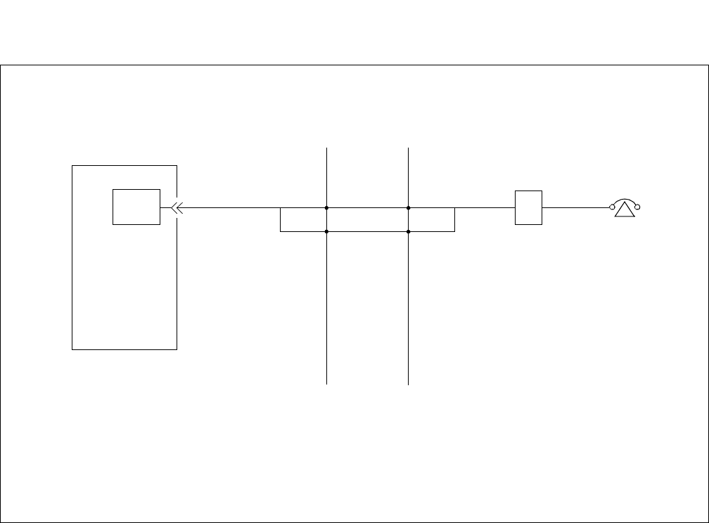
CHAPTER 3 NDA-24296
Page 332
Revision 1.0
PA-16LCBJ-B
Line Circuit
Figure 3-77 Connecting Route Diagram
NEAX2400 IPX
A0
MDF
Telephone
L1
L2
B0
Rosette
LC
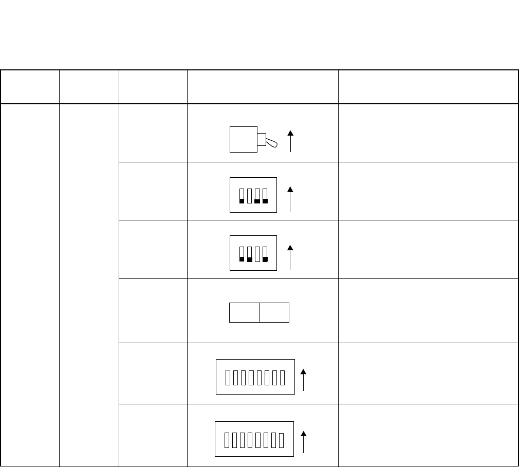
NDA-24296 CHAPTER 3
Page 333
Revision 1.0
PA-16LCBJ-B
Line Circuit
7. Switch Setting Sheet
MODULE SLOT NO. SWITCH
NAME SWITCH SHAPE REMARKS
PIM
SW00
(MB)
SW13
SW15
SW16
SW10
(BNW0-7)
SW11
(BNW8-15)
ON
12 3 4 ON
1 2 3 4 ON
OFF ON
(RVS) (OPEN)
01234567ON
012345 6 7 ON
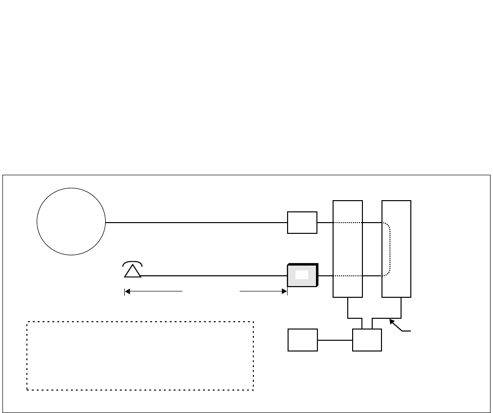
CHAPTER 3 NDA-24296
Page 334
Revision 1.0
PA-16LCBW
Line Circuit
PA-16LCBW
Line Circuit
1. General Function
The PA-16LCBW circuit card provides an interface between a maximum of 16 analog voice terminals and
the system with a range of 1200 inclusive of terminal resistance. This card also can send “Stutter Dial
Tone”, which is not a continuous tone, to an associated terminal which has no Message Waiting Lamp
(MWL) instead of activating the MWL if required. In addition momentary open/reverse battery function is
provided for 16 channels on this card. This is a -48V card.
Figure 3-78 Location of PA-16LCBW (LC) within the System
max. 1200 [Ω]
COT
INT SW
GT
I/O Local Bus
(PA-16LCBW)
C. O. line
Loop Resistance: Max. 1200 [Ω] (inclusive of
terminal Resistance)
Open Function: x 15 circuits
Reverse / Open Function: x 1 circuit (selectable)
Stutter Dial Tone/Message Waiting Lamp (selectable)
Encoding Law: µ-law
•
•
•
•
•
PUBLIC
NETWORK
Analog Terminal
CPU
LC
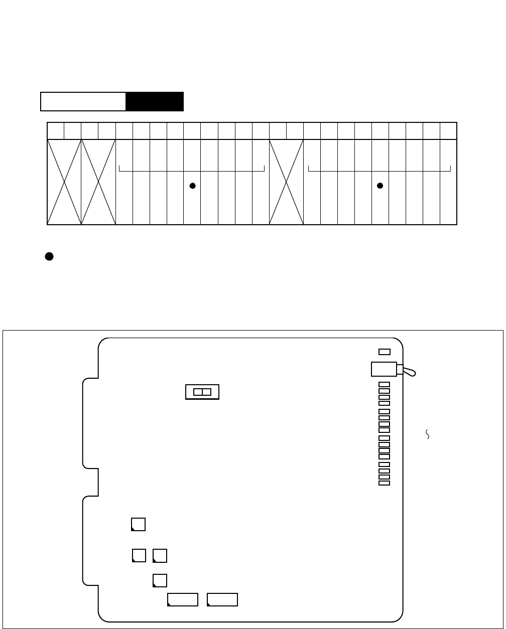
NDA-24296 CHAPTER 3
Page 335
Revision 1.0
PA-16LCBW
Line Circuit
2. Mounting Location/Condition
The PA-16LCBW (LC) circuit card can be mounted in the following universal slots.
Note: Indicates universal slots for line/trunk circuit cards.
3. Face Layout of Lamps, Switches, and Connectors
The face layout of lamps, switches on this circuit card is shown in Figure 3-79.
Figure 3-79 Face Layout of PA-16LCBW (LC)
PIM
Mounting Module
00 01 02 03 04 05 06 07 08 09 10 11 12 13 14 15 16 17 18 19 20 21 22 23
OPE
BL15
BL0
SW00 (MB)
SW10
SW16
SW11
SW14
SW17
SW18
SW15

CHAPTER 3 NDA-24296
Page 336
Revision 1.0
PA-16LCBW
Line Circuit
4. Lamp Indications
The contents of lamp indications of this circuit card are shown in the table below.
LAMP NAME LAMP
COLOR LAMP STATUS MEANING OF INDICATION
OPE Green Steady Lighting The circuitry of the circuit card is operating normally.
BL0
BL15
Green
Steady Lighting Line loop exists.
Flashing
1) Ringing signal is being transmitted. Busy Lamp keeps flashing in
synchronizing with on/off of the ringing signal.
2) Dial pulses are being received. While dial pulses from a line are
being received, Busy Lamp keeps flashing in synchronizing with
the dial pulses coming from the line.
3) Line is in make-busy state.
Busy Lamp keeps flashing at 60 ipm.
-
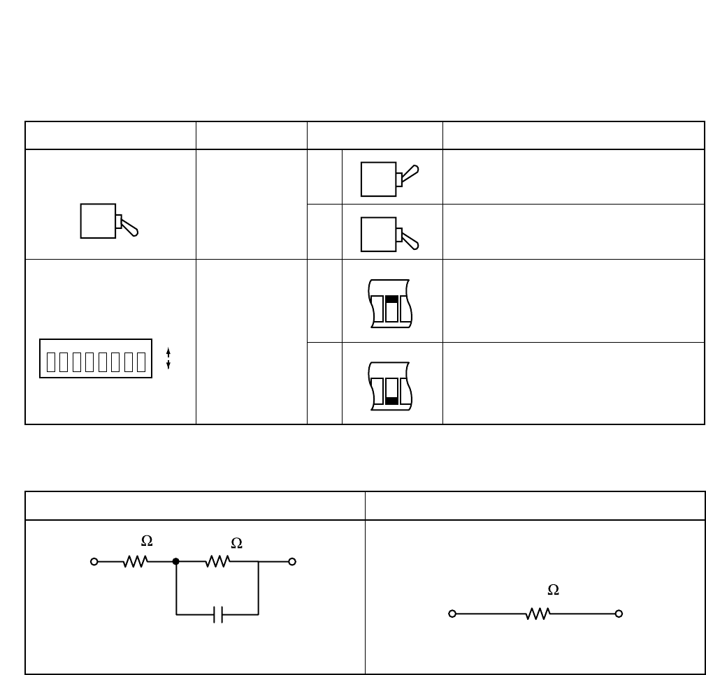
NDA-24296 CHAPTER 3
Page 337
Revision 1.0
PA-16LCBW
Line Circuit
5. Switch Settings
Switches on the PA-16LCBW card have the following meanings.
Note: Compromise Impedance (EIA/TIA-464B) and 600 Ω.
(For North America, Other Country (µ Law))
SWITCH FUNCTION SWITCH SETTING MEANING
SW00
(MB) Circuit Card
Make-busy Key
ON Circuit card make-busy
OFF Circuit card make-busy cancel
(Normal operating mode)
SW10
(BNW0-7)
Balancing
Network
Designation
• Each element on
this switch
corresponds to
circuit #0-#7.
ON
North America, Other Country (µ Law)
BNW : Compromise Impedance
(EIA/TIA-464B) (Note)
for long distance.
OFF
North America, Other Country (µ Law)
BNW : 600
Ω (Note)
for short distance
ON OFF
12345678
ON
OFF
350 1000
0.21µ
Compromise Impedance(EIA/TIA-464B)
600
CHAPTER 3 NDA-24296
Page 338
Revision 1.0
PA-16LCBW
Line Circuit
SWITCH SWITCH
No. FUNCTION SWITCH
SETTING MEANING
SW11
(BNW8-15)
Balancing Network
Designation
• Each element on this
switch corresponds to
circuit #8-#15.
(This same as previous page)
SW14 1 OFF Fixed to OFF
2ONFixed to ON
3 OFF Fixed to OFF
4 OFF Fixed to OFF
SW15 1 OFF Fixed to OFF
2ON Stutter Dial Tone Available
OFF Stutter Dial Tone not Available
3 OFF Fixed to OFF
4 OFF Fixed to OFF
12345678
ON
OFF
1234
ON
OFF
1234
ON
OFF
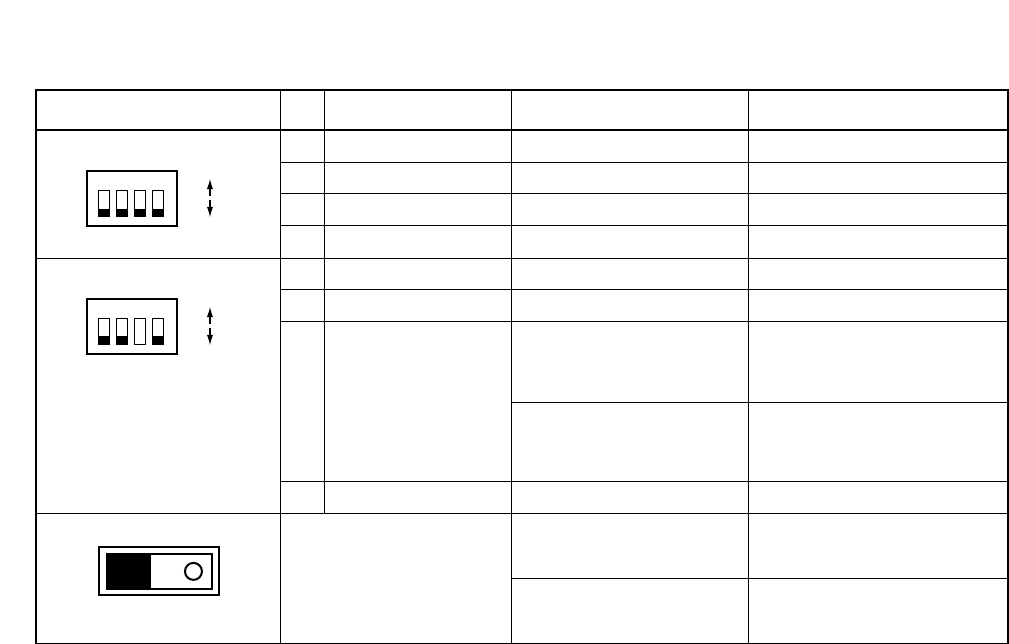
NDA-24296 CHAPTER 3
Page 339
Revision 1.0
PA-16LCBW
Line Circuit
SWITCH No. FUNCTION SWITCH SETTING MEANING
SW16 1 OFF Fixed to OFF
2 OFF Fixed to OFF
3 OFF Fixed to OFF
4 OFF Fixed to OFF
SW17 1 OFF Fixed to OFF
2 OFF Fixed to OFF
3Message Waiting
Lamp
ON
Message Waiting Lamp
Flashing
(Controlled by Firmware)
OFF
Message Waiting Lamp lit or
Flashing (Selected and
Controlled by Software)
4 OFF Fixed to OFF
SW18
Polarity reverse or
Momentary Open
(circuit #15 Only )
ON Momentary open
OFF Polarity reverse
1234
ON
OFF
1234
ON
OFF
OFF
Slide switch
(RVS) (OPEN)
ON
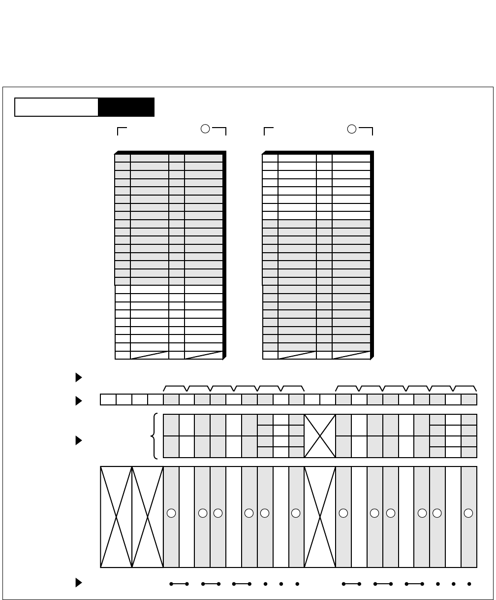
CHAPTER 3 NDA-24296
Page 340
Revision 1.0
PA-16LCBW
Line Circuit
6. External Interface
Accommodation of the LT connector leads for this circuit card is shown in Figure 3-80.
Figure 3-80 LT Connector Lead Accommodation (1/2)
See also Connecting Route Diagram (Figure 3-81).
PIM
Mounting Module
26
27
28
29
30
31
32
33
34
35
36
37
38
39
40
41
1
2
3
4
5
6
7
8
9
10
11
12
13
14
15
16
42
43
44
45
46
47
48
17
18
19
20
21
22
23
49
50 24
25
232221201918171615141312111009080706050403020100
LT6 LT7 LT8 LT9 LT10 LT11LT0 LT1 LT2 LT3 LT4 LT5
231915
221814
211713
201612
231915
221814
211713
201612
110907050301
100806040200
110907050301
100806040200
HW11HW10HW9HW8HW7HW6HW5HW4HW3HW2HW1HW0
PIM
LT 1, 3, 5, 7, 9, 11 Connector
26
27
28
29
30
31
32
33
34
35
36
37
38
39
40
41
1
2
3
4
5
6
7
8
9
10
11
12
13
14
15
16
42
43
44
45
46
47
48
17
18
19
20
21
22
23
49
50 24
25
B0
B1 A0
Accommodated in 1
LT 0, 2, 4, 6, 8, 10 Connector
A1
A2
A3
B2
B3
Accommodated in 2
B4
B5 A4
A5
A6
A7
B6
B7
B8
B9 A8
A9
A10
A11
B10
B11
B12
B13 A12
A13
A14
A15
B14
B15
B0
B1 A0
A1
A2
A3
B2
B3
B4
B5 A4
A5
A6
A7
B6
B7
B8
B9 A8
A9
A10
A11
B10
B11
B12
B13 A12
A13
A14
A15
B14
B15
121 21 2 1 21 21 2
Group No.
Slot No.
LT Connector
Highway Block

NDA-24296 CHAPTER 3
Page 341
Revision 1.0
PA-16LCBW
Line Circuit
Figure 3-80 LT Connector Lead Accommodation (2/2)
PIM
Mounting Module
26
27
28
29
30
31
32
33
34
35
36
37
38
39
40
41
1
2
3
4
5
6
7
8
9
10
11
12
13
14
15
16
42
43
44
45
46
47
48
17
18
19
20
21
22
23
49
50 24
25
232221201918171615141312111009080706050403020100
LT6 LT7 LT8 LT9 LT10 LT11LT0 LT1 LT2 LT3 LT4 LT5
231915
221814
211713
201612
231915
221814
211713
201612
110907050301
100806040200
110907050301
100806040200
HW11HW10HW9HW8HW7HW6HW5HW4HW3HW2HW1HW0
PIM
LT 1, 3, 5, 7, 9, 11 Connector
26
27
28
29
30
31
32
33
34
35
36
37
38
39
40
41
1
2
3
4
5
6
7
8
9
10
11
12
13
14
15
16
42
43
44
45
46
47
48
17
18
19
20
21
22
23
49
50 24
25
B0
B1 A0
Accommodated in 3
LT 0, 2, 4, 6, 8, 10 Connector
A1
A2
A3
B2
B3
B4
B5 A4
A5
A6
A7
B6
B7
B8
B9 A8
A9
A10
A11
B10
B11
B12
B13 A12
A13
A14
A15
B14
B15
3 3 3 3 3 3
Group No.
Slot No.
LT Connector
Highway Block
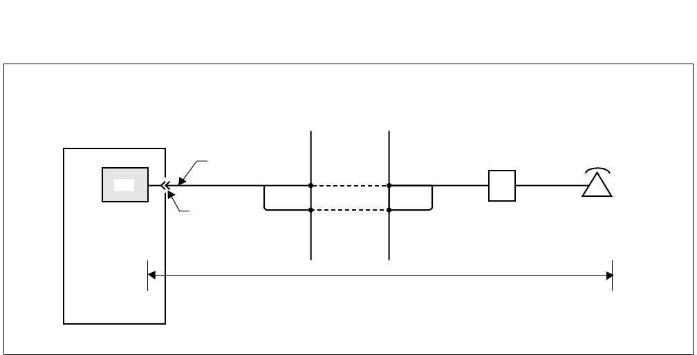
CHAPTER 3 NDA-24296
Page 342
Revision 1.0
PA-16LCBW
Line Circuit
Figure 3-81 Connecting Route Diagram
A
B
L1
L2
PBX MDF
Jack Analog Terminal
LC
Maximum 1200 [Ω] (inclusive of terminal resistance)
Installation Cable
LT Connector
Connecting Route Diagram for the PA-16 LCBW (LC) is as follows.
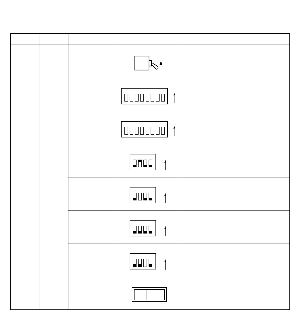
NDA-24296 CHAPTER 3
Page 343
Revision 1.0
PA-16LCBW
Line Circuit
7. Switch Setting Sheet
MODULE SLOT No. SWITCH NAME SWITCH SHAPE REMARKS
PIM
SW00
(MB)
SW10
(BNW0-7)
SW11
(BNW8-15)
SW14
SW15
SW16
SW17
SW18
ON
12345678
ON
12345678
ON
1234
ON
ON
1234
1234
ON
1234
ON
OFF
(RVS) (OPEN)
ON
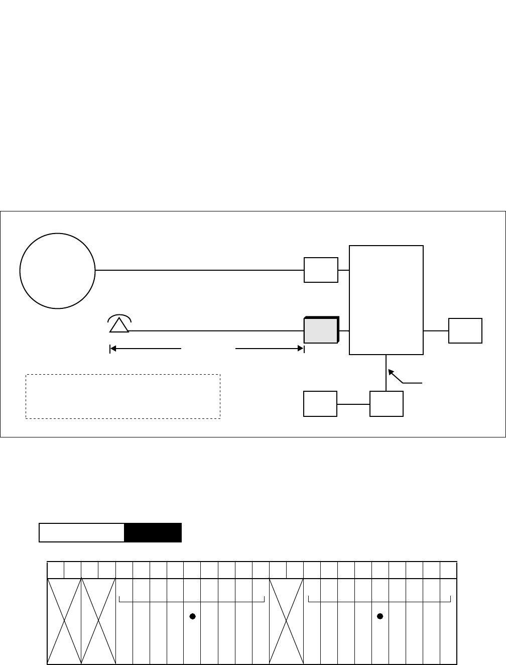
CHAPTER 3 NDA-24296
Page 344
Revision 1.0
PA-16LCBY
Line Circuit
PA-16LCBY
Line Circuit
1. General Function
The PA-16LCBY circuit card provides an interface between a maximum of 16 analog voice terminals and
the system with a range of 1200 (Ohm) inclusive of terminal resistance. This card also can send “Stutter
Dial Tone”, which is not a continuous tone, to an associated terminal which has no Message Waiting Lamp
(MWL) instead of activating the MWL if required. In addition polarity reverse function is provided for 16
channels on this card. The card can be used for Caller ID service. This is a -48V card.
Note: The PA-16LCBY card requires Series 7400 or later software.
Figure 3-82 Location of PA-16LCBY(LC) Circuit card within the System
2. Mounting Location/Condition
The PA-16LCBY(LC) circuit card can be mounted in the following universal slots.
max. 1200 [Ω]
Analog Terminal
COT
RST
LC
TSW/INT
(PA-8RSTY)
CPU GT
Local I/O Bus
(PA-16LCBY)
C. O. LINE
• Loop Resistance : Max 1200[Ω]
(inclusive of terminal resistance)
• Reverse Function : x 16 circuits
• Stutter Dial Tone/Message Waiting Lamp (selectable)
• Encoding Law : µ-law
PUBLIC
NETWORK
PIM
Mounting Module
00 01 02 03 04 05 06 07 08 09 10 11 12 13 14 15 16 17 18 19 20 21 22 23
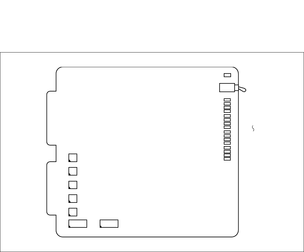
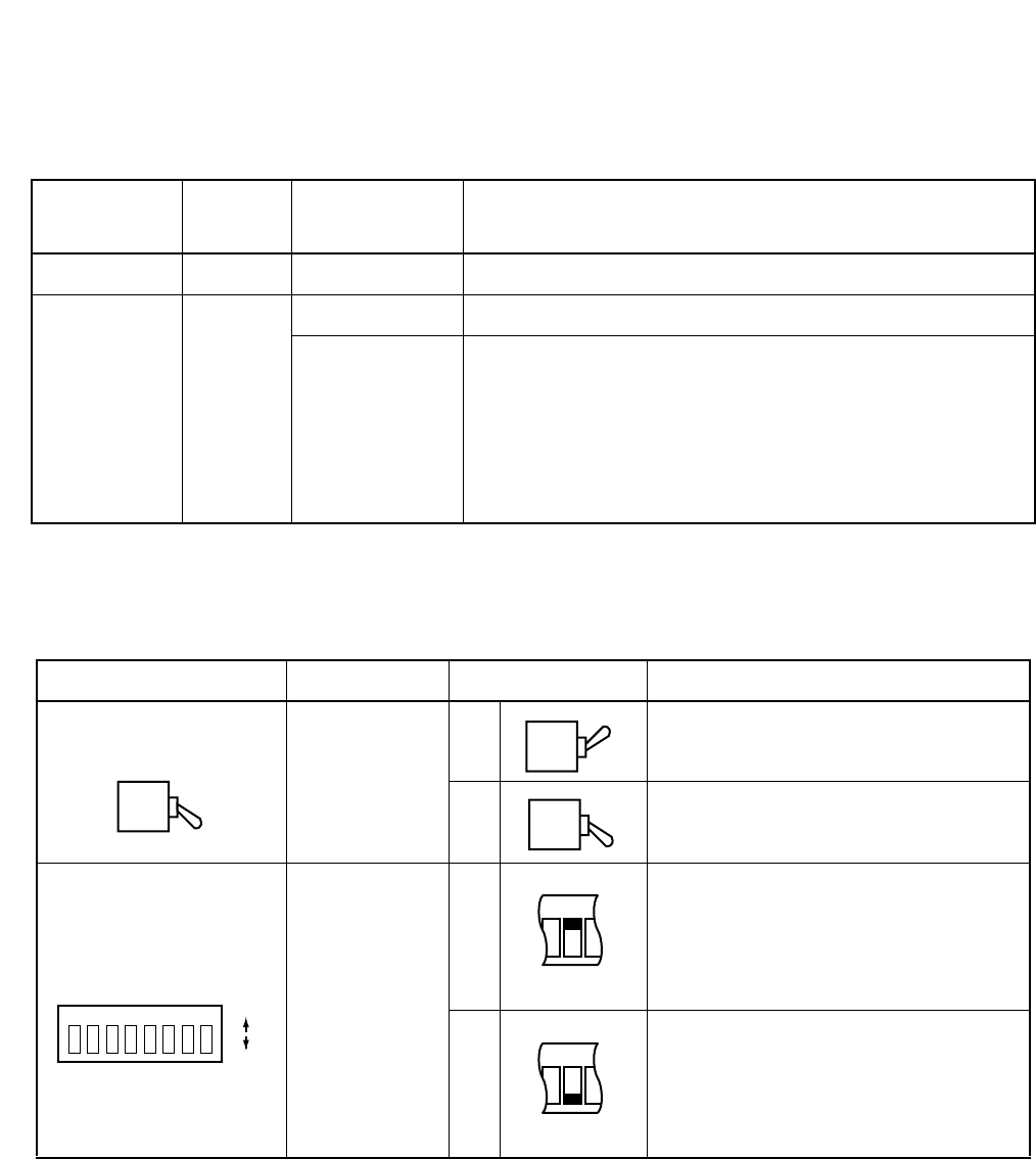
CHAPTER 3 NDA-24296
Page 346
Revision 1.0
PA-16LCBY
Line Circuit
4. Lamp Indications
The contents of lamp indications of this circuit card are shown in the table below.
5. Switch Settings
Switches on the PA-16LCBY (LC) card have the following meanings.
LAMP NAME LAMP
COLOR LAMP STATUS MEANING OF INDICATION
OPE Green Steady Lighting The circuitry of the circuit card is operating normally.
BL0
BL15
Green
Steady Lighting Line loop exists.
Flashing
1) Ringing signal is being transmitted. Busy Lamp keeps flashing
in synchronizing with on/off of the ringing signal.
2) Dial pulses are being received. While dial pulses from a line are
being received, Busy Lamp keeps flashing in synchronizing with
the dial pulses coming from the line.
3) Line is in make-busy state.
Busy Lamp keeps flashing at 60 ipm.
SWITCH FUNCTION SWITCH SETTING MEANING
SW00
(MB) Circuit Card
Make-busy Key
OFF Circuit card make-busy cancel
ON Circuit card make-busy
SW10
(BNW0-7)
Balancing
Network
Designation
•Each element on
this switch
corresponds to
circuit #0-#7.
When this switch
has been set, see
SW14.
ON
North America, Other Country (µ Law)
BNW : Compromise Impedance
(EIA/TIA-464B) (Note )
for long distance
OFF North America, Other Country (µ Law)
BNW : 600
Ω (Note )
for short distance
~
12345678
ON
OFF
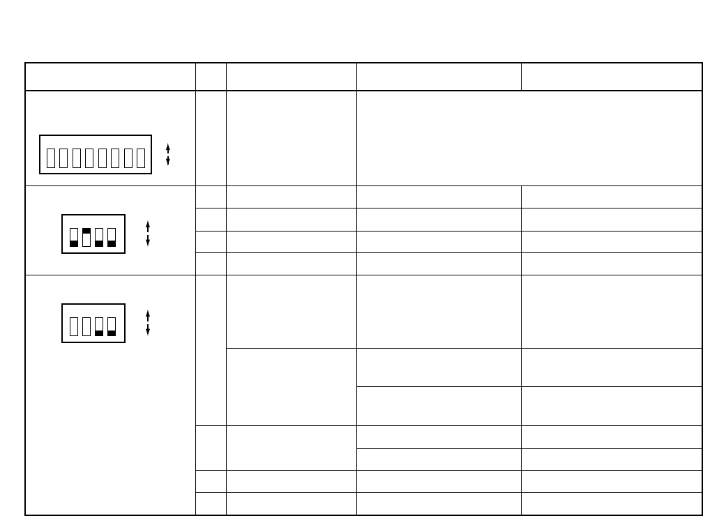
NDA-24296 CHAPTER 3
Page 347
Revision 1.0
PA-16LCBY
Line Circuit
SWITCH No. FUNCTION SWITCH SETTING MEANING
SW11
(BNW8-15)
Balancing Network
Designation
• Each element on this
switch corresponds
to circuit #8-#15.
[the same as previous page]
SW14 1 OFF Fixed to OFF
2ONFixed to ON
3 OFF Fixed to OFF
4 OFF Fixed to OFF
SW15
1
North America
Brazil
China
Other Country
OFF Fixed to OFF
PAD (Australia Only)
ON NEAX 2400 PAD
PAD ON/OFF = 9dB/0dB
OFF ICS-PBX PAD
PAD ON/OFF = 9dB/6dB
2ON Stutter Dial Tone Available
OFF Stutter Dial Tone not Available
3 OFF Fixed to OFF
4 OFF Fixed to OFF
12345678
ON
OFF
1234
ON
OFF
1234
ON
OFF
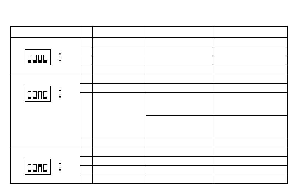
CHAPTER 3 NDA-24296
Page 348
Revision 1.0
PA-16LCBY
Line Circuit
SWITCH No. FUNCTION SWITCH SETTING MEANING
SW16 1 OFF Fixed to OFF
2 OFF Fixed to OFF
3 OFF Fixed to OFF
4 OFF Fixed to OFF
SW17 1 OFF Fixed to OFF
2 OFF Fixed to OFF
3Message Waiting
Lamp
ON
Message Waiting Lamp
Flashing
(Controlled by Firmware)
OFF
Message Waiting Lamp lit or
Flashing (Selected and
Controlled by Software)
4 OFF Fixed to OFF
SW19 1 OFF Fixed to OFF
2 OFF Fixed to OFF
3ONFixed to ON
4 OFF Fixed to OFF
1234
ON
OFF
1234
ON
OFF
1234
ON
OFF
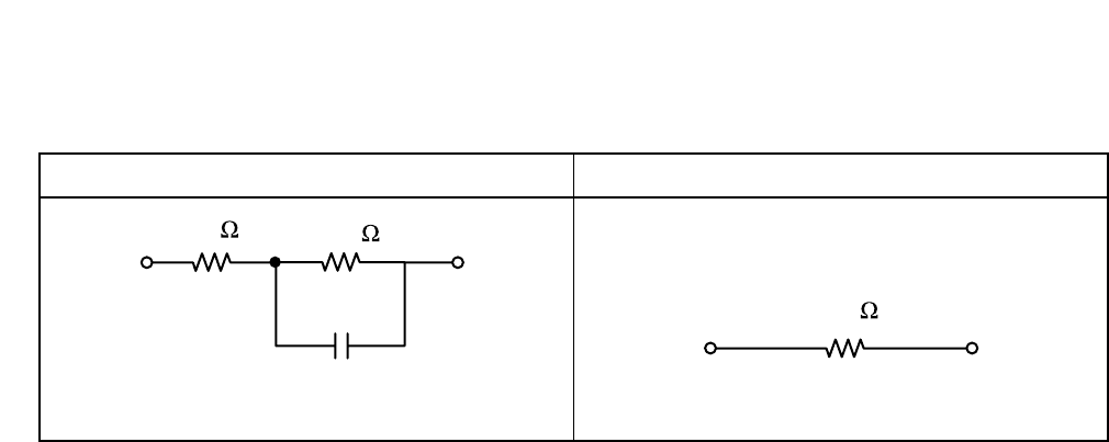
NDA-24296 CHAPTER 3
Page 349
Revision 1.0
PA-16LCBY
Line Circuit
Note: Compromise Impedance (EIA/TIA-464B) and 600Ω.
(For North America, Other Country (µ Law))
ON OFF
350 1000
0.21µ
Compromise Impedance(EIA/TIA-464B)
600
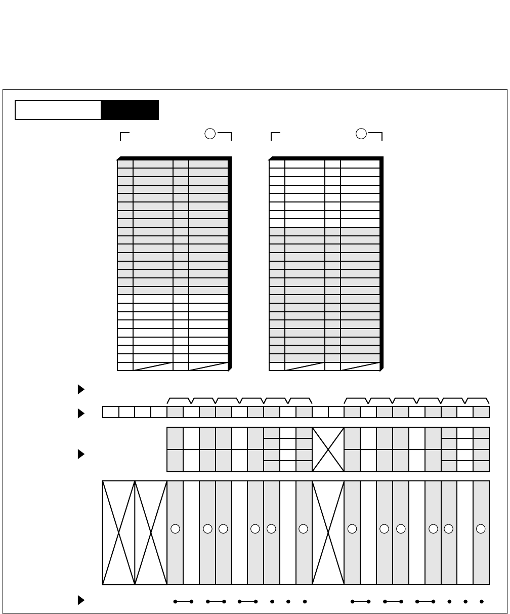
CHAPTER 3 NDA-24296
Page 350
Revision 1.0
PA-16LCBY
Line Circuit
6. External Interface
Accommodation of the LT connector leads for this circuit card is shown in Figure 3-84.
Figure 3-84 LT Connector Lead Accommodation (1/2)
26
27
28
29
30
31
32
33
34
35
36
37
38
39
40
41
1
2
3
4
5
6
7
8
9
10
11
12
13
14
15
16
42
43
44
45
46
47
48
17
18
19
20
21
22
23
49
50 24
25
232221201918171615141312111009080706050403020100
LT6 LT7 LT8 LT9 LT10 LT11LT0 LT1 LT2 LT3 LT4 LT5
231915
221814
211713
201612
231915
221814
211713
201612
110907050301
100806040200
110907050301
100806040200
HW11HW10HW9HW8HW7HW6HW5HW4HW3HW2HW1HW0
PIM
LT 1, 3, 5, 7, 9, 11 Connector
26
27
28
29
30
31
32
33
34
35
36
37
38
39
40
41
1
2
3
4
5
6
7
8
9
10
11
12
13
14
15
16
42
43
44
45
46
47
48
17
18
19
20
21
22
23
49
50 24
25
B0
B1 A0
Accommodated in 1
LT 0, 2, 4, 6, 8, 10 Connector
A1
A2
A3
B2
B3
Accommodated in 2
B4
B5 A4
A5
A6
A7
B6
B7
B8
B9 A8
A9
A10
A11
B10
B11
B12
B13 A12
A13
A14
A15
B14
B15
B0
B1 A0
A1
A2
A3
B2
B3
B4
B5 A4
A5
A6
A7
B6
B7
B8
B9 A8
A9
A10
A11
B10
B11
B12
B13 A12
A13
A14
A15
B14
B15
121 21 2 1 21 21 2
Group No.
Slot No.
LT Connector
Highway Block
PIM
Mounting Module
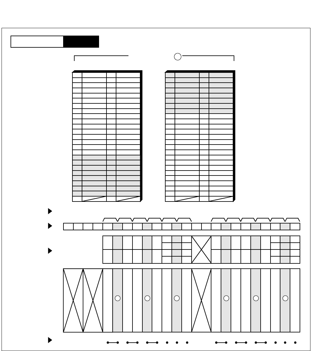
NDA-24296 CHAPTER 3
Page 351
Revision 1.0
PA-16LCBY
Line Circuit
Figure 3-84 LT Connector Lead Accommodation (2/2)
26
27
28
29
30
31
32
33
34
35
36
37
38
39
40
41
1
2
3
4
5
6
7
8
9
10
11
12
13
14
15
16
42
43
44
45
46
47
48
17
18
19
20
21
22
23
49
50 24
25
232221201918171615141312111009080706050403020100
LT6 LT7 LT8 LT9 LT10 LT11LT0 LT1 LT2 LT3 LT4 LT5
231915
221814
211713
201612
231915
221814
211713
201612
110907050301
100806040200
110907050301
100806040200
HW11HW10HW9HW8HW7HW6HW5HW4HW3HW2HW1HW0
PIM
LT 1, 3, 5, 7, 9, 11 Connector
26
27
28
29
30
31
32
33
34
35
36
37
38
39
40
41
1
2
3
4
5
6
7
8
9
10
11
12
13
14
15
16
42
43
44
45
46
47
48
17
18
19
20
21
22
23
49
50 24
25
B0
B1 A0
Accommodated in 3
LT 0, 2, 4, 6, 8, 10 Connector
A1
A2
A3
B2
B3
B4
B5 A4
A5
A6
A7
B6
B7
B8
B9 A8
A9
A10
A11
B10
B11
B12
B13 A12
A13
A14
A15
B14
B15
3 3 3 3 3 3
Group No.
Slot No.
LT Connector
Highway Block
PIM
Mounting Module

CHAPTER 3 NDA-24296
Page 352
Revision 1.0
PA-16LCBY
Line Circuit
Figure 3-85 Connecting Route Diagram
A
B
L1
L2
PBX MDF
Jack Analog Terminal
LC
Maximum 1200 [Ω] (inclusive of terminal resistance)
Installation Cable
LT Connector
Connecting Route Diagram for the PA-16 LCBY (LC) is as follows.
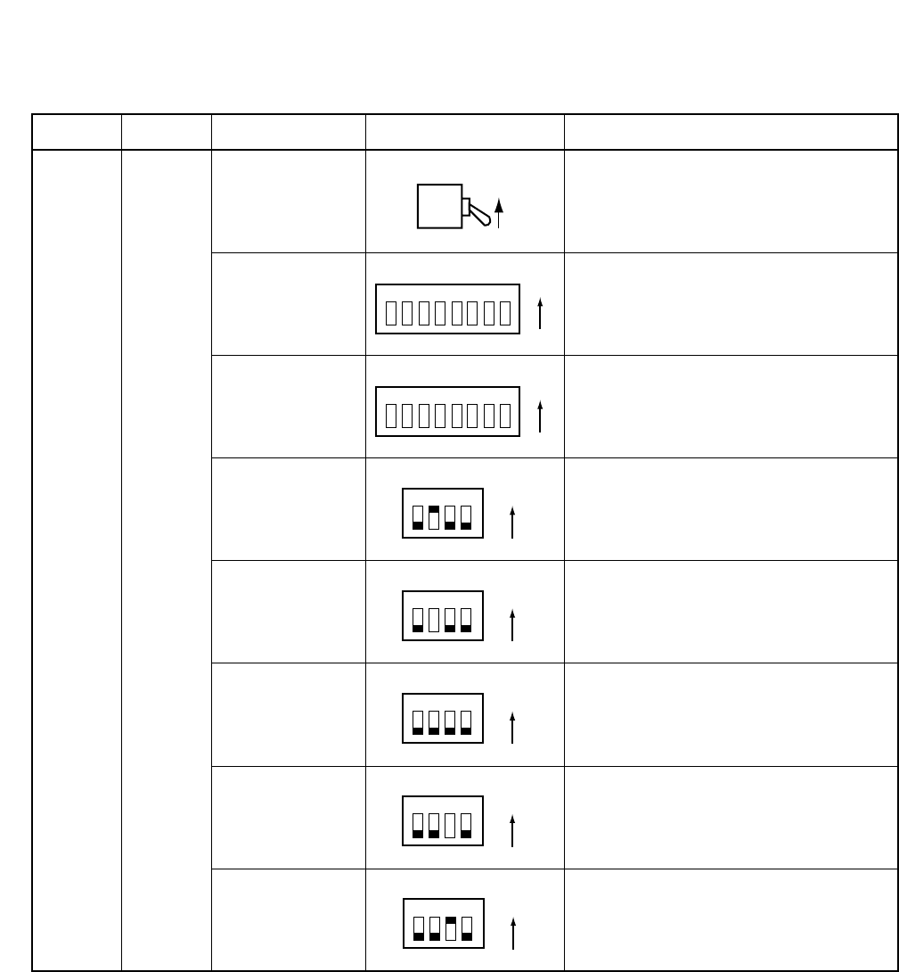
NDA-24296 CHAPTER 3
Page 353
Revision 1.0
PA-16LCBY
Line Circuit
7. Switch Setting Sheet
MODULE SLOT No. SWITCH NAME SWITCH SHAPE REMARKS
PIM
SW00
(MB) Note: Normal operating mode is down.
SW10
(BNW0-7)
SW11
(BNW8-15)
SW14
SW15
SW16
SW17
SW19
ON
12345678
ON
12345678
ON
1234
ON
ON
1234
1234
ON
1234
ON
1234
ON
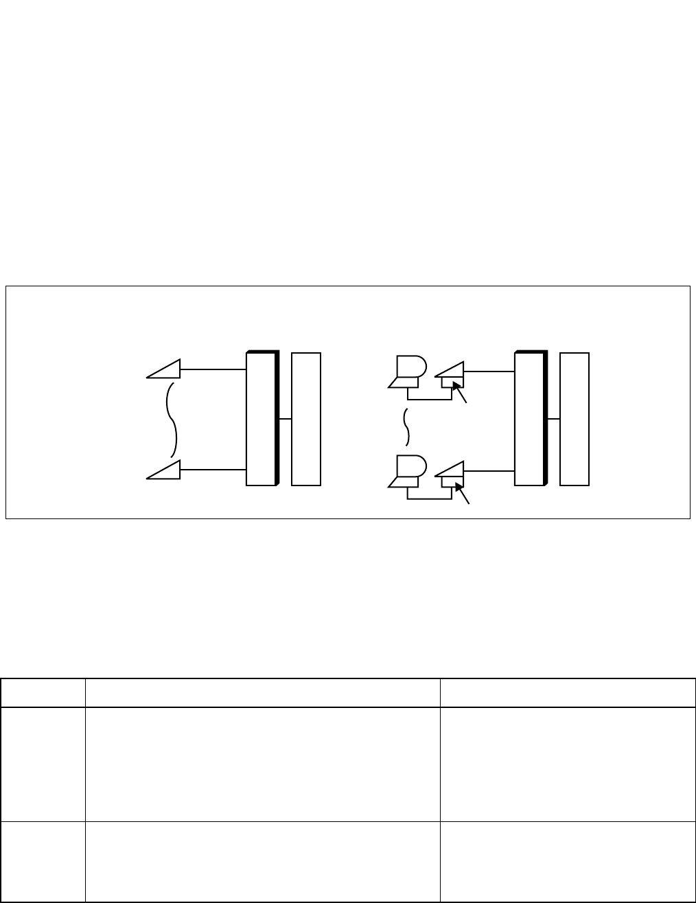
CHAPTER 3 NDA-24296
Page 354
Revision 1.0
PA-16ELCJ
Electric Line Current
PA-16ELCJ
Electric Line Current
1. General Function
The PA-16ELCJ (ELC) circuit card provides an interface between the Dterm and the IPX. Depending on the
switch settings, this card works in the following two modes.
•16 ELC mode: A maximum of 16 sets of Dterms can be connected to this card. (voice communications
only)
•8 DLC mode: A maximum of eight sets of Dterms can be connected to this card. (simultaneous voice
and data communications)
Figure 3-86 Location of PA-16ELCJ (ELC) Card in the System
There are two different kinds of firmware EPROMs are located on the PA-16ELCJ (ELC) circuit card. SP-
3295 16ELCJ PROG-B provides the full performance interface for Dterm Series E, and SP-3270 16ELCJ
PROG-A provides Dterm Series III interface. The following table shows the Dterm performance depending
on each firmware EPROM.
Table 3-3 Performance
FIRMWARE Dterm SERIES E Dterm SERIES III
SP-3295
16ELC J
PROG-B
•24 digits wide of Liquid Crystal Display (LCD).
•Month and year (last two digits) also displayed following
the time and date.
•Software keys are available and the software keys are con-
trolled by the system. Thus, key function data can be changed
by office data.
•16 digits wide of LCD.
•Month and year are not displayed.
•Software key is not available.
SP-3270
16ELC J
PROG-A
•16 digits wide of LCD.
•Month and year are not displayed.
•Software keys are available. However, key function is
fixed (Off-hook Ringing, Mute, Microphone, Headset).
•16 digits wide of LCD.
•Month and year are not displayed.
•Software key is not available.
Dterm #0
DTE
Data Adapter
Dterm #7
DTE
Data Adapter
Dterm #0
Dterm #15
IMX IMX
16 ELC MODE 8 DLC MODE
ELC
ELC
IPX
IPX
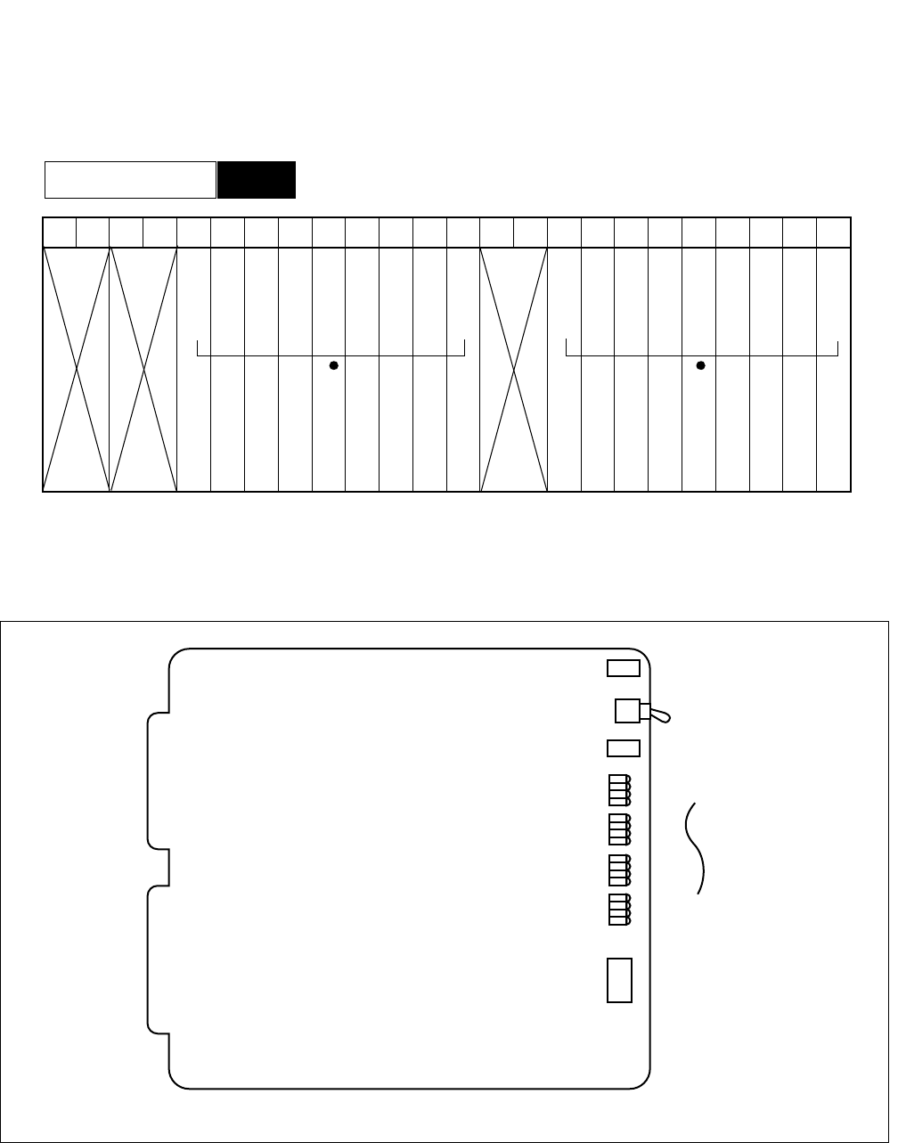
NDA-24296 CHAPTER 3
Page 355
Revision 1.0
PA-16ELCJ
Electric Line Current
2. Mounting Location/Condition
The PA-16ELCJ (ELC) card can be mounted in any universal slot as shown below.
3. Face Layout of Lamps, Switches, and Connectors
The face layout of lamps, switches, and connectors on this circuit card is shown in Figure 3-87.
Figure 3-87 Face Layout of PA-16ELCJ (ELC) Card
00 01 02 03 04 05 06 07 08 09 10 11 12 13 14 15 16 17 18 19 20 21 22 23
Mounting Module PIM
PALM
SW00 (MB)
BL15
OPE
BL0
SW01

CHAPTER 3 NDA-24296
Page 356
Revision 1.0
PA-16ELCJ
Electric Line Current
4. Lamp Indications
Lamp indications for this circuit card are shown in the table below.
Note: When the PALM lamp lights red, observe the following instructions.
i) Identify the location where any in-house wires have a short circuit in all lines which belong to the
PA-16ELCJ card whose PALM is on.
ii) Repair the short-circuited wires of the associated Dterm.
iii) Disconnect the Dterm from the rosette, then leave it disconnected for at least one minute.
iv) Connect the Dterm again.
LAMP NAME COLOR STATE
OPE Green Remains lit while on-line operations are normal.
OFF Off when on-line operations are abnormal.
PALM Red Lights red when power supply circuit(s) is abnormal. Note
OFF Off when all the power supply circuits are normal.
BL0
BL15
Green Lights when the corresponding circuit is busy.
Flash Flashes when the corresponding circuit is in Make-busy state or station data has not been
assigned.
OFF Off when the corresponding circuit is idle.
-
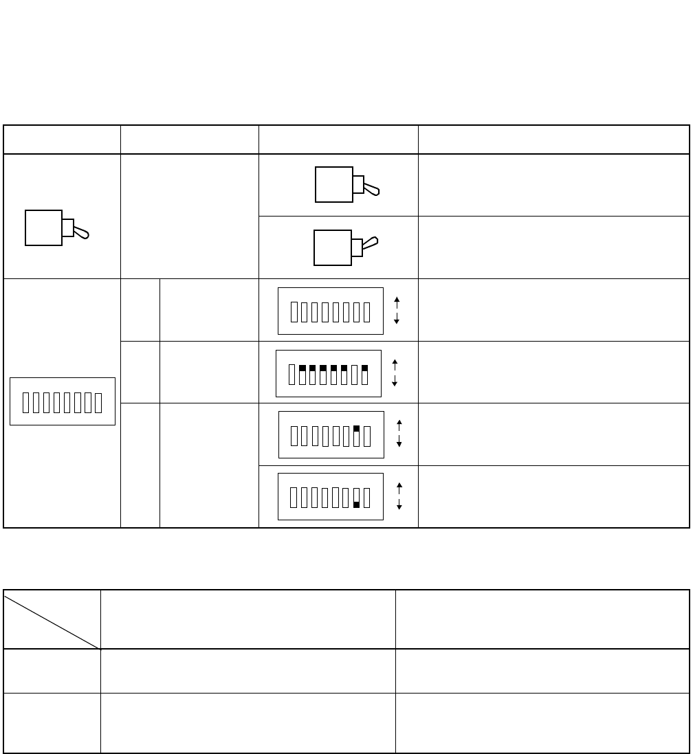
NDA-24296 CHAPTER 3
Page 357
Revision 1.0
PA-16ELCJ
Electric Line Current
5. Switch Settings
Switches on the PA-16ELCJ card have the following meanings.
SWITCH FUNCTION SWITCH SETTING MEANING
SW00 (MB)
Circuit Card Make-
busy key
Circuit card Make-busy Cancel.
Circuit card Make-busy.
SW01
1
See Table 3-4 below.
—Always ON (fixed).
7
ELC/DLC
mode
Designation
16ELC mode.
8DLC mode.
Table 3-4 Relationship between SW01-1 and SW01-7
ON OFF
ON •16 sets of Dterms per card.
•Voice Communication only.
•8 sets of Dterms per card.
•Data Adapter is used.
OFF
•16 sets of Dterms per card.
•Analog Port Adapter is used, but not at the
same time.
•8 sets of Dterms per card.
•Analog Port Adapter is used (Both Dterm and
Analog terminal can be used at the same time).
12345678
1ON
2 3 4 5 6 7 8
OFF
2
-
6
8
-
1ON
2345678
OFF
123456 7 8 ON
OFF
12 3 4 5 6 7 8 ON
OFF
SW01-7
SW01-1
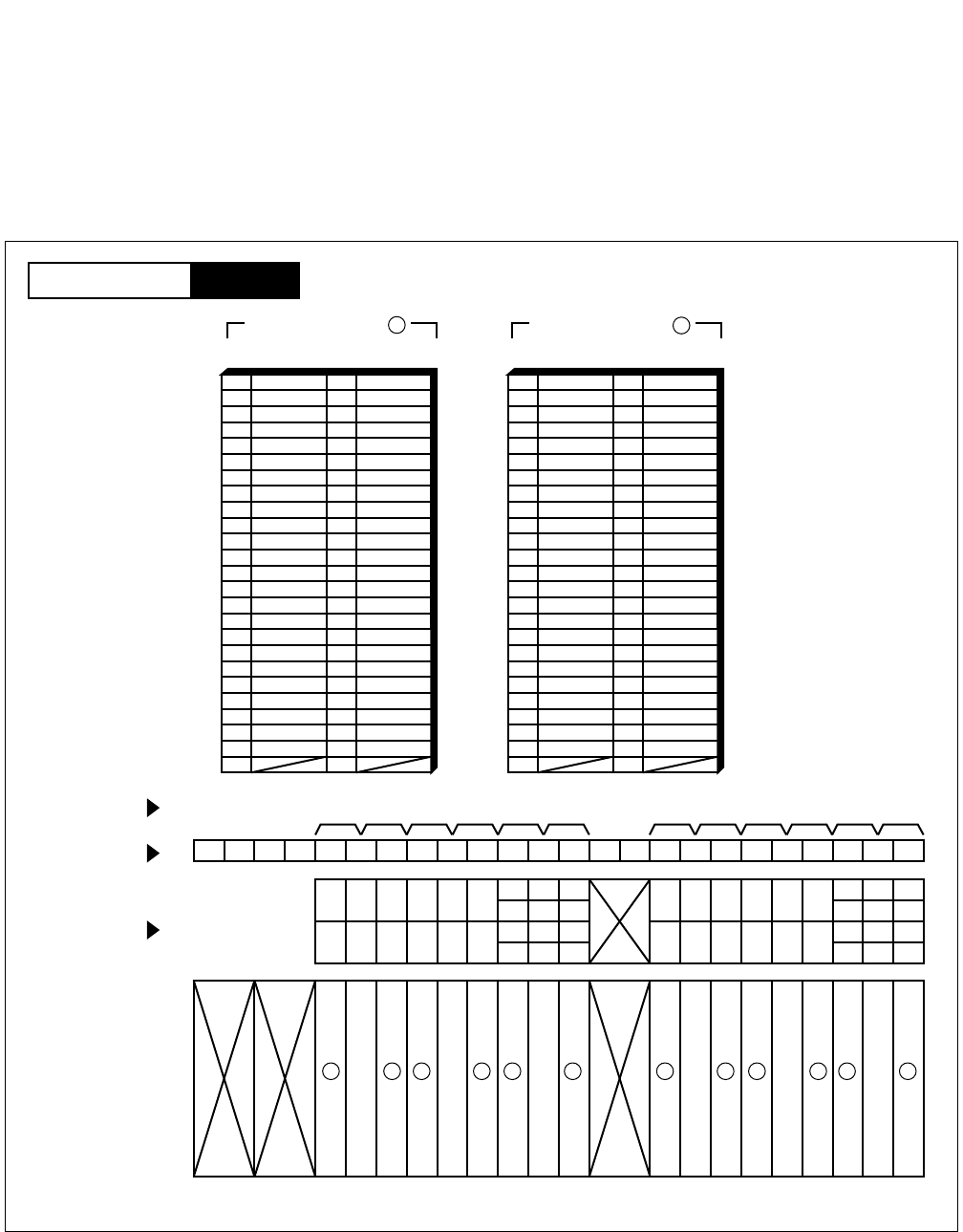
CHAPTER 3 NDA-24296
Page 358
Revision 1.0
PA-16ELCJ
Electric Line Current
6. External Interface
Depending on the applied mode (16ELC/8 DLC mode), external interface leads appear on the LT
connectors as follows.
•6ELC mode
Figure 3-88 LT Connector Lead Location (16ELC Mode) (1/2)
26
27
28
29
30
31
32
33
34
35
36
37
38
39
40
41
1
2
3
4
5
6
7
8
9
10
11
12
13
14
15
16
42
43
44
45
46
47
48
17
18
19
20
21
22
23
49
50 24
25
232221201918171615141312111009080706050403020100
LT6 LT7 LT8 LT9 LT10 LT11LT0 LT1 LT2 LT3 LT4 LT5
231915
221814
211713
201612
231915
221814
211713
201612
110907050301
100806040200
110907050301
100806040200
PIM
LT 1, 3, 5, 7, 9, 11 Connector
26
27
28
29
30
31
32
33
34
35
36
37
38
39
40
41
1
2
3
4
5
6
7
8
9
10
11
12
13
14
15
16
42
43
44
45
46
47
48
17
18
19
20
21
22
23
49
50 24
25
B0
B1 A0
Accommodated in 1
LT 0, 2, 4, 6, 8, 10 Connector
A1
A2
A3
B2
B3
Accommodated in 2
B4
B5 A4
A5
A6
A7
B6
B7
B8
B9 A8
A9
A10
A11
B10
B11
B12
B13 A12
A13
A14
A15
B14
B15
B0
B1 A0
A1
A2
A3
B2
B3
B4
B5 A4
A5
A6
A7
B6
B7
B8
B9 A8
A9
A10
A11
B10
B11
B12
B13 A12
A13
A14
A15
B14
B15
121 21 2 1 21 21 2
Group No.
Slot No.
LT Connector
PIM
Mounting Module
NDA-24296 CHAPTER 3
Page 359
Revision 1.0
PA-16ELCJ
Electric Line Current
•16ELC mode
Figure 3-88 LT Connector Lead Location (16ELC Mode) (2/2)
26
27
28
29
30
31
32
33
34
35
36
37
38
39
40
41
1
2
3
4
5
6
7
8
9
10
11
12
13
14
15
16
42
43
44
45
46
47
48
17
18
19
20
21
22
23
49
50 24
25
232221201918171615141312111009080706050403020100
LT6 LT7 LT8 LT9 LT10 LT11LT0 LT1 LT2 LT3 LT4 LT5
231915
221814
211713
201612
231915
221814
211713
201612
110907050301
100806040200
110907050301
100806040200
PIM
LT 1, 3, 5, 7, 9, 11 Connector
26
27
28
29
30
31
32
33
34
35
36
37
38
39
40
41
1
2
3
4
5
6
7
8
9
10
11
12
13
14
15
16
42
43
44
45
46
47
48
17
18
19
20
21
22
23
49
50 24
25
B0
B1 A0
Accommodated in 3
LT 0, 2, 4, 6, 8, 10 Connector
A1
A2
A3
B2
B3
B4
B5 A4
A5
A6
A7
B6
B7
B8
B9 A8
A9
A10
A11
B10
B11
B12
B13 A12
A13
A14
A15
B14
B15
3 3 3 3 3 3
Group No.
Slot No.
LT Connector
PIM
Mounting Module

CHAPTER 3 NDA-24296
Page 360
Revision 1.0
PA-16ELCJ
Electric Line Current
7. Switch Setting Sheet
MODULE SLOT No. SWITCH NAME SWITCH SHAPE REMARKS
PIM
SW00
(MB)
SW01
ON
12 3 4 5 6 7 8 ON
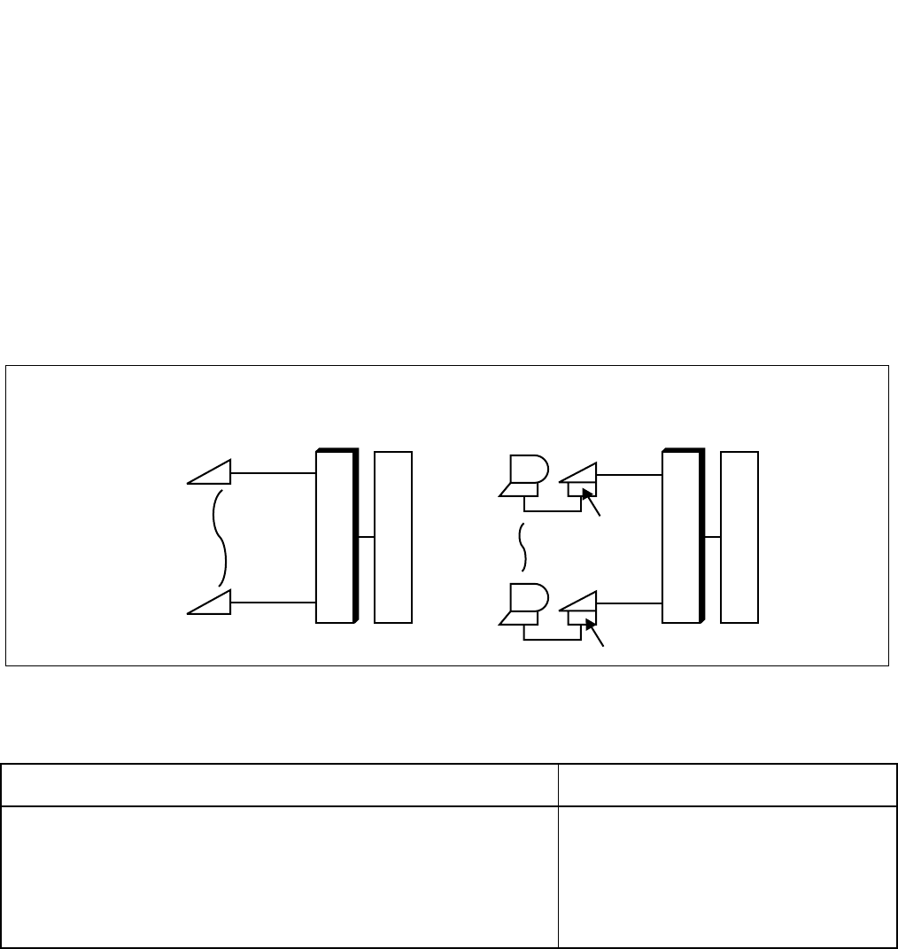
NDA-24296 CHAPTER 3
Page 361
Revision 1.0
PA-16ELCJ-B
Electronic Line Circuit
PA-16ELCJ-B
Electronic Line Circuit
1. General Function
The PA-16ELCJ-B (ELC) circuit card provides an interface between Dterm and IPX. Depending upon the
switch settings, this card works in the following two modes.
•16 ELC mode: A maximum of 16 sets of Dterms can be connected to this card. (voice communications
only)
•8 DLC mode: A maximum of eight sets of Dterms can be connected to this card. (simultaneous voice
and data communications)
Figure 3-89 Location of PA-16ELCJ-B (ELC) Card within the System
Table 3-5 Performance
Dterm SERIES E Dterm SERIES III
•24 digits wide of Liquid Crystal Display (LCD).
•Month and year is displayed following the time and date.
•Software keys are available and the software keys are controlled by the
system. Thus, key function data can be changed by office data.
•16 digits wide of LCD.
•Month and year are not displayed.
•Software key is not available.
Dterm #0
DTE
Data Adapter
Dterm #7
DTE
Data Adapter
Dterm #0
Dterm #15
IPX IPX
16 ELC MODE 8 DLC MODE
ELC
ELC
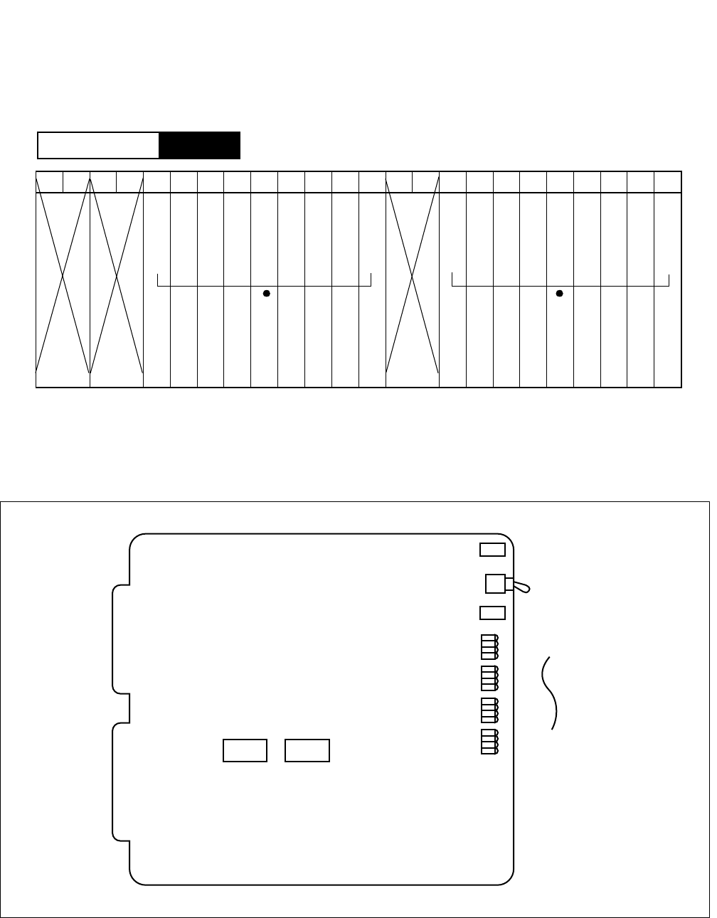
CHAPTER 3 NDA-24296
Page 362
Revision 1.0
PA-16ELCJ-B
Electronic Line Circuit
2. Mounting Location/Condition
The PA-16ELCJ-B (ELC) card can be mounted in any universal slots as shown below.
3. Face Layout of Lamps, Switches, and Connectors
The face layout of lamps, switches, and connectors on this circuit card is shown in Figure 3-90.
Figure 3-90 Face Layout of PA-16ELCJ-B (ELC) Card
00 01 02 03 04 05 06 07 08 09 10 11 12 13 14 15 16 17 18 19 20 21 22 23
PIM
Mounting Module
PALM
SW00 (MB)
BL15
OPE
SW10 SW11
BL0

NDA-24296 CHAPTER 3
Page 363
Revision 1.0
PA-16ELCJ-B
Electronic Line Circuit
4. Lamp Indications
The contents of lamp indications on this circuit card are shown in the table below.
Note: When the PALM lamp lights red, observe the following instructions.
i) Identify the location where any in-house wires have a short circuit to all lines belonging to the
PA-16ELCJ-B card whose PALM is on.
ii) Repair the short-circuited wires of the associated Dterm.
iii) Disconnect the Dterm from the rosette, then leave it disconnected for at least one minute.
iv) Connect the Dterm again.
LAMP NAME COLOR STATE
OPE Green Remains lit while on-line operations are normal.
OFF Off when on-line operations are abnormal.
PALM Red Lights red when power supply circuit(s) is abnormal. Note
OFF Off when all the power supply circuits are normal.
BL0
BL15
Green Lights when the corresponding circuit is busy.
Flash Flashes when the corresponding circuit is in make-busy state or station data has not been
assigned.
OFF Off when the corresponding circuit is idle.
-
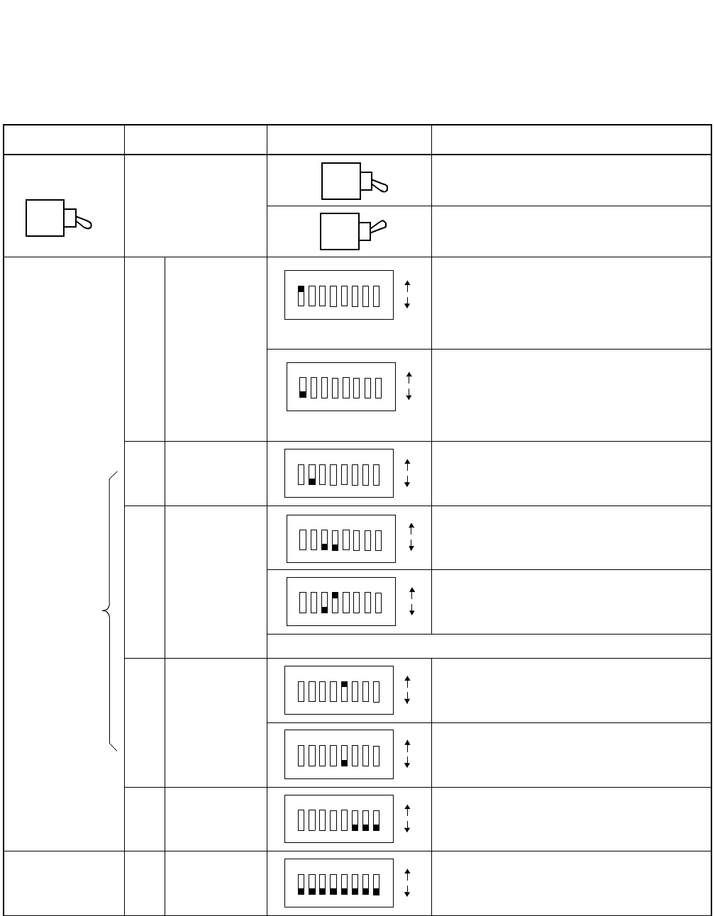
CHAPTER 3 NDA-24296
Page 364
Revision 1.0
PA-16ELCJ-B
Electronic Line Circuit
5. Switch Settings
Switches on the PA-16ELCJ-B card have the following meanings.
SWITCH FUNCTION SWITCH SETTING MEANING
SW00 (MB)
Circuit Card Make-
busy key
Circuit Card Make-busy Cancel.
Circuit Card Make-busy.
SW10
1
LP-PM
Interface
mode setting
When firmware SP-3419 is used, and your
system uses software Series 7300 Release 7 or
earlier.
Expanded Multiple Line Operation-Dterm is
not available.
When firmware SP-3514 is used, and your
system uses software Series 7400 Release 8 or
later.
Expanded Multiple Line Operation-Dterm is
available.
2—Not used.
3-4 ELC/DLC
mode setting
This circuit card is operated in 16 ELC mode.
This circuit card is operated in 8 DLC mode.
Do not set another combination.
5
Analog Port
Adapter
setting
Analog Port Adapter is available.
Analog Port Adapter is not available.
6-8 —Fixed to “OFF”.
SW11
1-8 —Fixed to all “OFF”.
Details
are shown
in the next
table.
1ON
2345678
OFF
1ON
2 3 4 5 6 7 8
OFF
1ON
2345678
OFF
12 3 4 5 6 7 8 ON
OFF
123456 7 8 ON
OFF
1ON
23456 7 8
OFF
1ON
23456 7 8
OFF
1ON
2345678
OFF
1ON
23456 7 8
OFF

NDA-24296 CHAPTER 3
Page 365
Revision 1.0
PA-16ELCJ-B
Electronic Line Circuit
SW10-3: OFF, SW10-4: OFF SW10-3: OFF, SW10-4: ON
SW10-5: OFF •16 set of Dterms per card.
•Voice Communication only.
•8 set of Dterms per card.
•Data Adapter is used.
SW10-5: ON
•16 set of Dterms per card.
•Analog Port Adapter is used (Either Dterm or
Analog terminal can be used at the same time).
•8 set of Dterms per card.
•Analog Port Adapter is used (Both Dterm and
Analog terminal can be used at the same time).
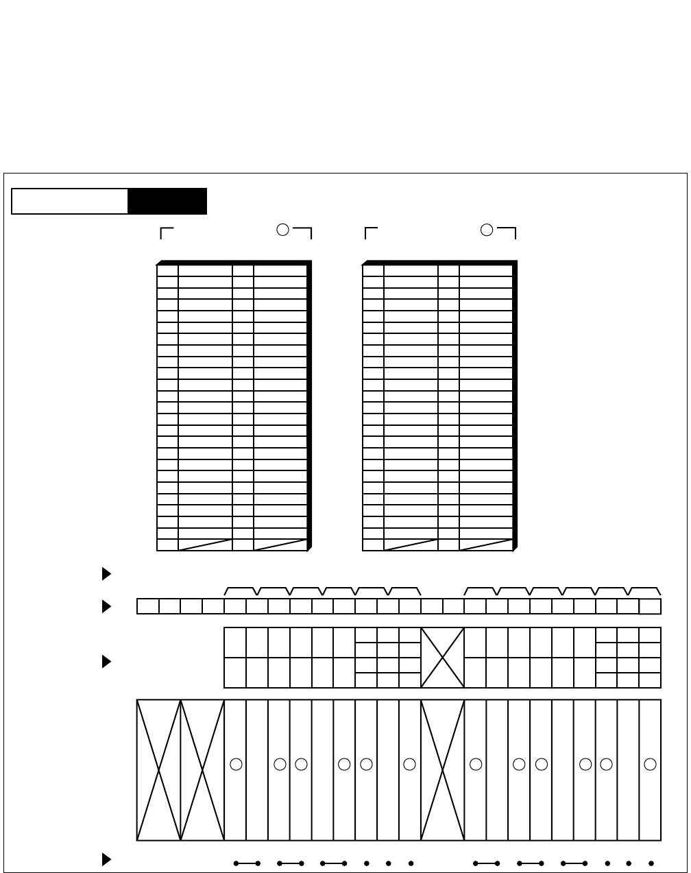
CHAPTER 3 NDA-24296
Page 366
Revision 1.0
PA-16ELCJ-B
Electronic Line Circuit
6. External Interface
Depending upon the applied mode (16ELC/8 DLC mode), external interface leads appear on the LT
connectors as follows.
•16ELC mode
Figure 3-91 LT Connector Lead Accommodation (16ELC Mode) (1/2)
PIM
Mounting Module
26
27
28
29
30
31
32
33
34
35
36
37
38
39
40
41
1
2
3
4
5
6
7
8
9
10
11
12
13
14
15
16
42
43
44
45
46
47
48
17
18
19
20
21
22
23
49
50 24
25
232221201918171615141312111009080706050403020100
LT6 LT7 LT8 LT9 LT10 LT11LT0 LT1 LT2 LT3 LT4 LT5
231915
221814
211713
201612
231915
221814
211713
201612
110907050301
100806040200
110907050301
100806040200
HW11HW10HW9HW8HW7HW6HW5HW4HW3HW2HW1HW0
Group No.
Slot No.
LT Connector
PIM
Highway Block
LT 1, 3, 5, 7, 9, 11 Connector
26
27
28
29
30
31
32
33
34
35
36
37
38
39
40
41
1
2
3
4
5
6
7
8
9
10
11
12
13
14
15
16
42
43
44
45
46
47
48
17
18
19
20
21
22
23
49
50 24
25
B0
B1
Accommodated in 1
LT 0, 2, 4, 6, 8, 10 Connector
B2
B3
Accommodated in 2
B4
B5
B6
B7
B8
B9
B10
B11
B12
B13
B14
B15
A0
A1
A2
A3
A4
A5
A6
A7
A8
A9
A10
A11
A12
A13
A14
A15
B0
B1
B2
B3
B4
B5
B6
B7
B8
B9
B10
B11
B12
B13
B14
B15
A0
A1
A2
A3
A4
A5
A6
A7
A8
A9
A10
A11
A12
A13
A14
A15
1212 12
12 1212
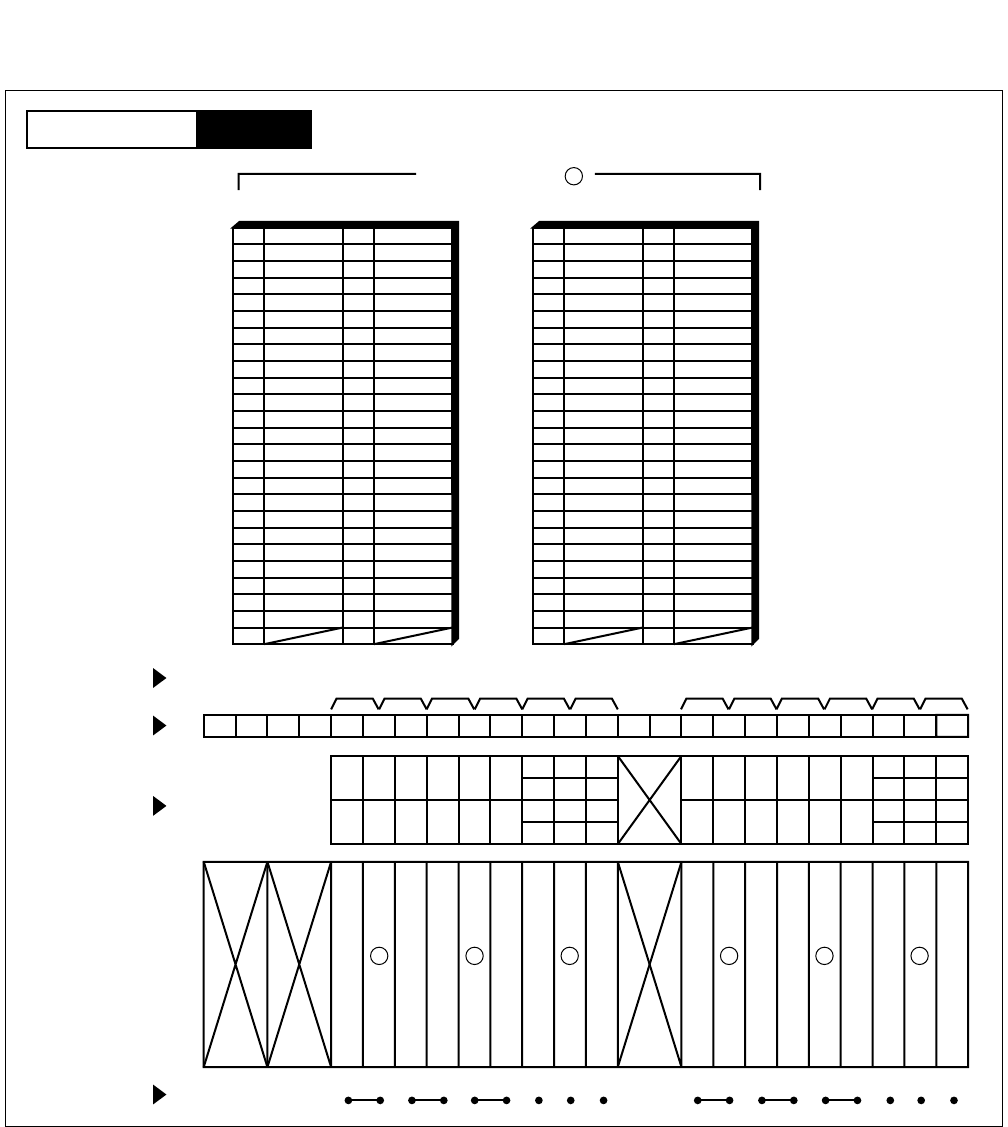
NDA-24296 CHAPTER 3
Page 367
Revision 1.0
PA-16ELCJ-B
Electronic Line Circuit
Figure 3-91 LT Connector Lead Accommodation (16ELC Mode) (2/2)
PIM
Mounting Module
26
27
28
29
30
31
32
33
34
35
36
37
38
39
40
41
1
2
3
4
5
6
7
8
9
10
11
12
13
14
15
16
42
43
44
45
46
47
48
17
18
19
20
21
22
23
49
50 24
25
232221201918171615141312111009080706050403020100
LT6 LT7 LT8 LT9 LT10 LT11LT0 LT1 LT2 LT3 LT4 LT5
231915
221814
211713
201612
231915
221814
211713
201612
110907050301
100806040200
110907050301
100806040200
HW11HW10HW9HW8HW7HW6HW5HW4HW3HW2HW1HW0
Group No.
Slot No.
LT Connector
PIM
Highway Block
26
27
28
29
30
31
32
33
34
35
36
37
38
39
40
41
1
2
3
4
5
6
7
8
9
10
11
12
13
14
15
16
42
43
44
45
46
47
48
17
18
19
20
21
22
23
49
50 24
25
B0
B1
Accommodated in 3
LT 1, 3, 5, 7, 9, 11 ConnectorLT 0, 2, 4, 6, 8, 10 Connector
B2
B3
B4
B5
B6
B7
A0
A1
A2
A3
A4
A5
A6
A7
B8
B9
B10
B11
B12
B13
B14
B15
A8
A9
A10
A11
A12
A13
A14
A15
3 3 3 3 3 3
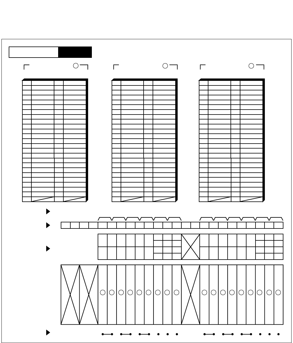
CHAPTER 3 NDA-24296
Page 368
Revision 1.0
PA-16ELCJ-B
Electronic Line Circuit
•8DLC mode
Figure 3-92 LT Connector Lead Accommodation (8DLC Mode)
26
27
28
29
30
31
32
33
34
35
36
37
38
39
40
41
1
2
3
4
5
6
7
8
9
10
11
12
13
14
15
16
42
43
44
45
46
47
48
17
18
19
20
21
22
23
49
50 24
25
232221201918171615141312111009080706050403020100
LT6 LT7 LT8 LT9 LT10 LT11LT0 LT1 LT2 LT3 LT4 LT5
231915
221814
211713
201612
231915
221814
211713
201612
110907050301
100806040200
110907050301
100806040200
HW11HW10HW9HW8HW7HW6HW5HW4HW3HW2HW1HW0
Group No.
Slot No.
LT Connector
PIM
Highway Block
LT 1, 3, 5, 7, 9, 11 Connector
26
27
28
29
30
31
32
33
34
35
36
37
38
39
40
41
1
2
3
4
5
6
7
8
9
10
11
12
13
14
15
16
42
43
44
45
46
47
48
17
18
19
20
21
22
23
49
50 24
25
Accommodated in 2
LT 1, 3, 5, 7, 9, 11 Connector
Accommodated in 3
26
27
28
29
30
31
32
33
34
35
36
37
38
39
40
41
1
2
3
4
5
6
7
8
9
10
11
12
13
14
15
16
42
43
44
45
46
47
48
17
18
19
20
21
22
23
49
50 24
25
Accommodated in 1
LT 0, 2, 4, 6, 8, 10 Connector
B0 A0
B1 A1
B2 A2
B3 A3
B4 A4
B5 A5
B6 A6
B7 A7
B0 A0
B1 A1
B2 A2
B3 A3
B4 A4
B5 A5
B6 A6
B7 A7
B0 A0
B1 A1
B2 A2
B3 A3
B4 A4
B5 A5
B6 A6
B7 A7
21 3 2 1 3 21 31 2
231231 3
PIM
Mounting Module
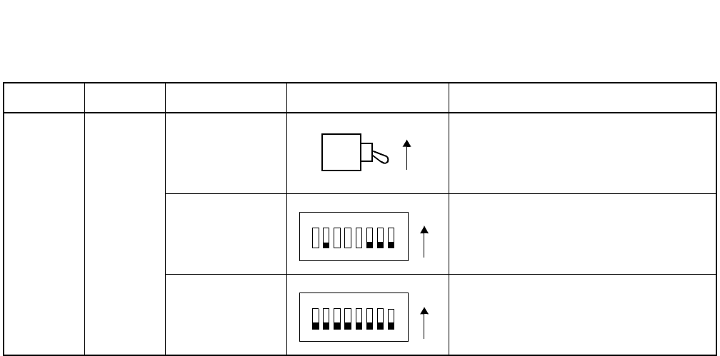
NDA-24296 CHAPTER 3
Page 369
Revision 1.0
PA-16ELCJ-B
Electronic Line Circuit
7. Switch Setting Sheet
MODULE SLOT No. SWITCH NAME SWITCH SHAPE REMARKS
PIM
SW00
(MB)
SW10
SW11
ON
12345678ON
123456 7 8 ON
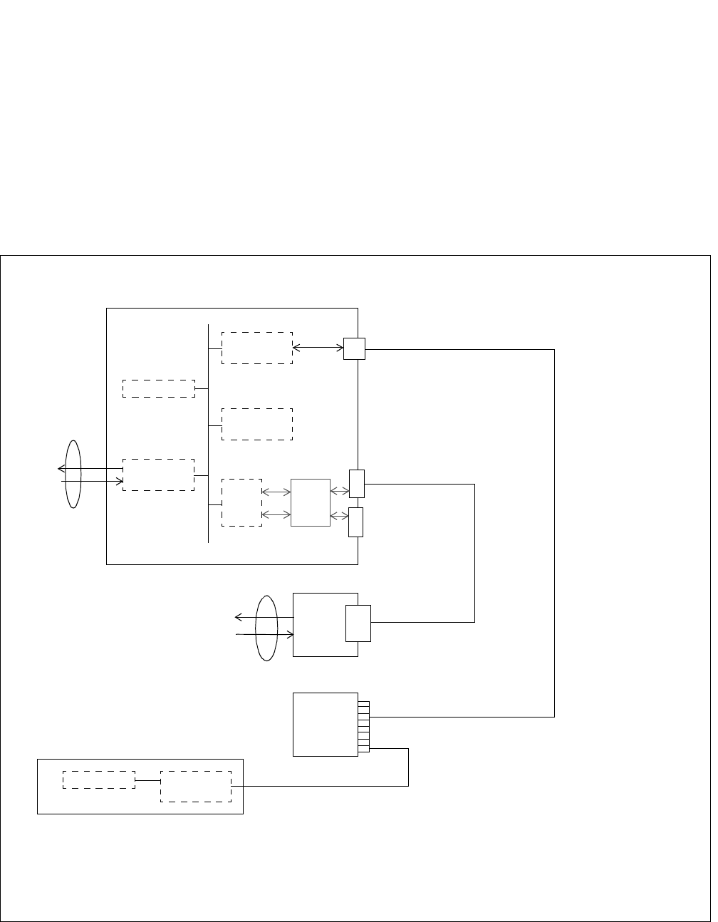
CHAPTER 3 NDA-24296
Page 370
Revision 1.0
PA-FCHA
Fusion Call Control Handler
PA-FCHA
Fusion Call Control Handler
1. General Function
This circuit card is a protocol converter to carry the fusion-link-data from/to the other node. The Fusion-
Link-Data is received/transferred from/to the CPR via HUB (PA-M96) across the TCP/IP interface. Once
the FCH has received the fusion-link-data from the CPR, the HDLC CONT part of the FCH converts it to
the High Level Data Link Controller (HDLC) format, then drops and inserts (D/I) onto a particular channel
(or channels) of the ITU-T G.703 digital interface.
Figure 3-93 Location of PA-FCHA (FCH) Card in the System
BWB
CPU
LP-PM
INT
ETHER NET
CONT
HDLC
CONT
D/I
CONT DTI
CONT
DTI
HUB
(PA-M96)
LANI
(PZ-PC19)
CPU
CPR
TO/FROM THE OTHER FUSION NODE
RJ-45
FRONT CABLE
Note
FCH
Note: This connector is used when multiple numbers of FCH cards are cascaded.
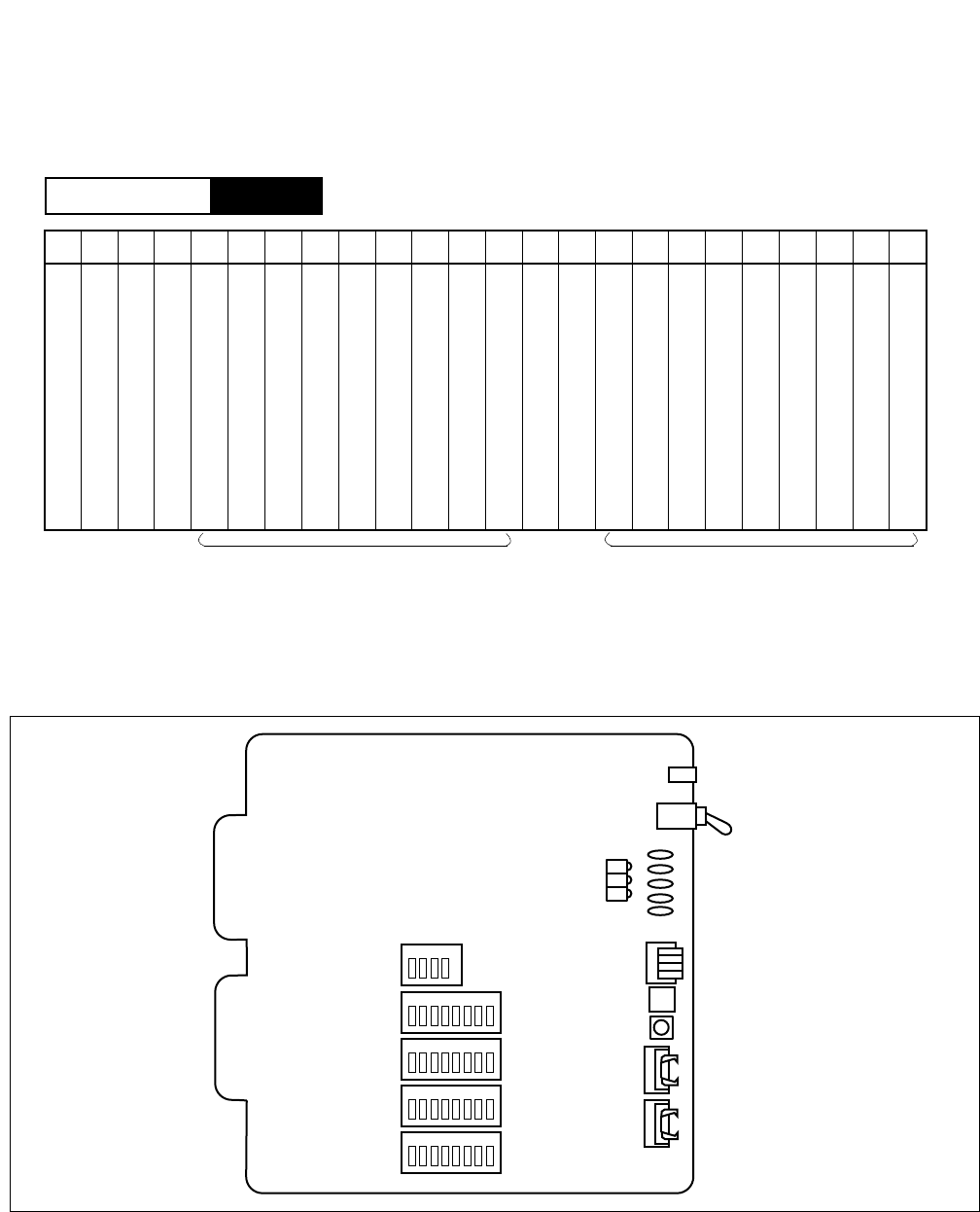
NDA-24296 CHAPTER 3
Page 371
Revision 1.0
PA-FCHA
Fusion Call Control Handler
2. Mounting Location/ Condition
The FCH can be mounted in a universal slot of the PIM.
3. Face Layout of Lamps, Switches, and Connectors
The face layout of lamps, switches, and connectors is shown in Figure 3-94.
Figure 3-94 Face Layout of PA-FCHA (FCH) Card
00 01 02 03 04 05 06 07 08 09 10 11 12 13 14 15 16 17 18 19 20 21 22 23
PIM
Mounting Module
PIM
PIM
Universal Slots
Universal Slots
MB
OPE
EST3
EST2
EST1
EST0
PWALM
LYR
LB
LOAD
MNT
10-BASE-T
MODE
DTI
FCH
1 2 3 4 5 6 7 8
1 2 3 4
1 2 3 4 5 6 7 8
1 2 3 4 5 6 7 8
1 2 3 4 5 6 7 8
SW14
SW13
SW12
SW11
SW10

CHAPTER 3 NDA-24296
Page 372
Revision 1.0
PA-FCHA
Fusion Call Control Handler
4. Lamp Indications
Lamp indications for this circuit card are shown in the table below.
LAMP NAME COLOR STATE
OPE Green Remains lit while this circuit card is operating.
LYR
Green Remains lit while the Fusion link is established.
Flash Flashes when the Fusion link test result is fair. (60IPM)
OFF Remains off when either the Fusion link is not established or the Fusion link test
result is not fair.
LB Green Remains lit while 10-BASE-T port is ready to use.
OFF Remains off when 10-BASE-T port is not ready.
LOAD
Green Remains lit while this circuit card is ready to broadcast data packets.
(Forwarding Status)
Flash
(60 IPM)
Remains lit while this circuit card is ready to broadcast data packets.
(Blocking Status)
Flash
(120 IPM)
Remains lit while this circuit card is stand-by to broadcast data packets.
(Learning Status)
OFF Remains off when this circuit card is stand-by to broadcast data packets.
(Null Status)
EST3 Green Remains lit while sending data.
EST2 Green Remains lit when receiving pair cable polarity is normal.
EST1 Green Remains lit while receiving data.
EST0 Green Remains lit while the link is established.
PWALM Red Remains lit when power supply failure (from the BWB) has occurred.
NDA-24296 CHAPTER 3
Page 373
Revision 1.0
PA-FCHA
Fusion Call Control Handler
5. Switch setting
Standard settings for switches on this circuit card are shown in the table below.
Note: The following operations are required prior to extracting the card.
(1.) Turn on the MNT3 switch.
(2.) Flip the MB switch.
When the D/I DTI (1.5M) is connected with the card front cable.
Note: T203 timer designates the maximum idle time which does not transmit any data frames. As a basic rule, the
shorter T203 timer value, the earlier link failure detection will be obtained.
SWITCH
NAME SWITCH
NO. SETTING STANDARD
SETTING DESCRIPTION
MB
Note
UP Circuit card Make-busy.
DOWN ×Circuit card Make-busy cancel.
MNT
0OFF ×Not used.
1OFF ×Not used.
2OFF ×Not used.
3
Note
ON Make-busy-request.
OFF ×Cancel the Make-busy-request.
SWITCH
NAME SETTING STANDARD
SETTING DESCRIPTION
MODE
0 - 7 Not used.
8×Standard setting.
(When the DTI is connected with the card front cable.)
9Fusion link test mode.
(When the DTI is connected with the card front cable.)
A - F Not used.
SWITCH
NAME SWITCH
NO. SETTING STANDARD
SETTING DESCRIPTION
SW10
1
Note
ON T203 timer value is variable.
OFF ×T203 timer value is fixed at 10 seconds.
2~8 OFF ×Not used.
CHAPTER 3 NDA-24296
Page 374
Revision 1.0
PA-FCHA
Fusion Call Control Handler
SWITCH
NAME SWITCH
NO. SETTING STANDARD
SETTING DESCRIPTION
SW11
Note 1
1ON
This SW designates the D/I channel of the
Fusion-Link-Data. (The number of D/I channels = n)
Set the corresponding SW(s) to “ON” for D/I, “OFF” for
denial.
OFF
2ON
OFF
3ON
OFF
4ON
OFF
5ON
OFF
6ON
OFF
7ON
OFF
8ON
OFF
SW11 D/I channel of T1
SW11-1 CH 0
SW11-2 CH 1
SW11-3 CH2
SW11-4 CH 3
SW11-5 CH 4
SW11-6 CH 5
SW11-7 CH 6
SW11-8 CH 7

NDA-24296 CHAPTER 3
Page 375
Revision 1.0
PA-FCHA
Fusion Call Control Handler
Note 1: When “n” is bigger than 1, the Time Slot Sequence Integrity (TSSI) must be guaranteed at the network.
When “n” is one or more, the corresponding D channels as “n” must be designated by SW11-SW12.
SW12
Note 1
1ON This SW designates the D/I channel of the
Fusion-Link-Data. (The number of D/I channels = n)
Set the corresponding SW(s) to “ON” for D/I, “OFF” for
denial.
OFF
2ON
OFF
3ON
OFF
4ON
OFF
5ON
OFF
6ON
OFF
7ON
OFF
8
ON
OFF
SWITCH
NAME SWITCH
NO. SETTING STANDARD
SETTING DESCRIPTION
SW12 D/I channel of T1
SW12-1 CH 8
SW12-2 CH 9
SW12-3 CH 10
SW12-4 CH 11
SW12-5 CH 12
SW12-6 CH 13
SW12-7 CH 14
SW12-8 CH 15
CHAPTER 3 NDA-24296
Page 376
Revision 1.0
PA-FCHA
Fusion Call Control Handler
SWITCH
NAME SWITCH
NO. SETTING STANDARD
SETTING DESCRIPTION
SW13
1ON This SW designates the D/I channel of the
Fusion-Link-Data. (The number of D/I channels = n)
Set the corresponding SW(s) to “ON” for D/I, “OFF” for
denial.
OFF
2ON
OFF
3ON
OFF
4ON
OFF
5ON
OFF
6ON
OFF
7ON
OFF
8ON
OFF
SW14
1ON ×Positive logic for the D/I CONT
OFF Negative logic for the D/I CONT
2
Note 2
ON ×The fusion data link speed inserted onto the T1 interface.
OFF
3
Note 2
ON ×
OFF
4
Note 3
ON Link Access Protocol D-channel (LAPD) signal link
performs as the “network.”
OFF LAPD signal link performs as the “user.”
SW13 D/I channel of T1
SW13-1 CH 16
SW13-2 CH 17
SW13-3 CH 18
SW13-4 CH 19
SW13-5 CH 20
SW13-6 CH 21
SW13-7 CH 22
SW13-8 CH 23
SW14-2 SW14-3 SPEED
ON ON 64 Kbps × n
ON OFF 56 Kbps × n
OFF ON 48 Kbps × n
OFF OFF Not used

NDA-24296 CHAPTER 3
Page 377
Revision 1.0
PA-FCHA
Fusion Call Control Handler
Note 2: Data speed 64 kbps is used for the T1 or E1 interface.
Data speed 56 kbps is used for the T1 interface with bit stealing.
Data speed 48 kbps is used for the T1 interface with both bit stealing and the Zero Code
Suppression (or Bit 7 Stuffing).
Note 3: When a node is set “network,” the distant node over the fusion link should be set “user,” and vice versa.
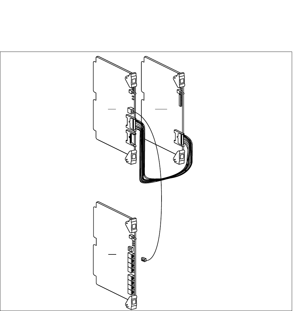
CHAPTER 3 NDA-24296
Page 378
Revision 1.0
PA-FCHA
Fusion Call Control Handler
6. External Interface
The cable connections among the FCH, HUB, 24DTR are shown below.
Figure 3-95 FCH/HUB/DTI Connection
24DTRFCH
10AL (10) FLT CA
10 BASE-T
straight cable
DTI
FCH CN2
HUB
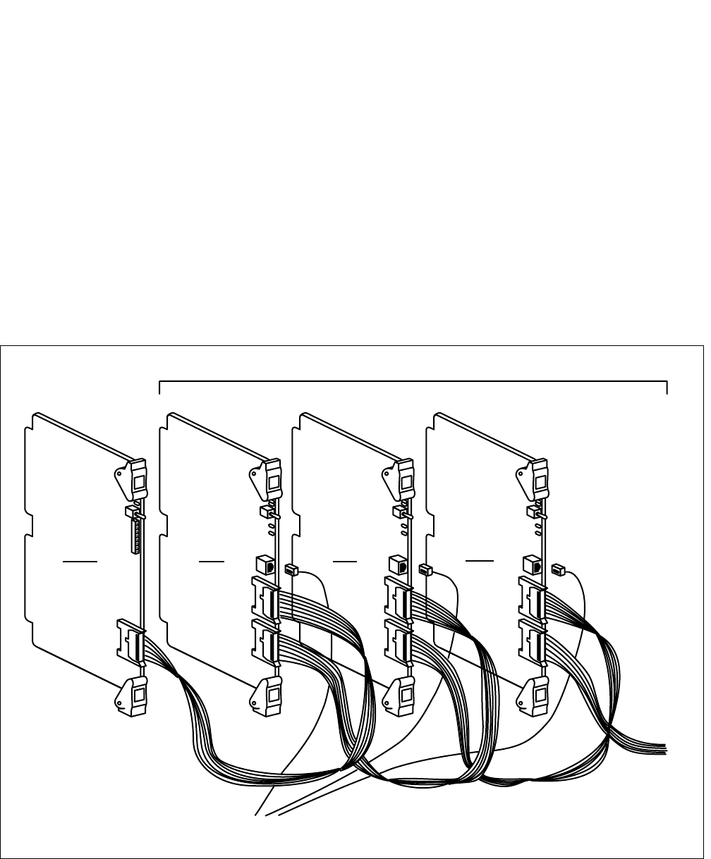
NDA-24296 CHAPTER 3
Page 379
Revision 1.0
PA-FCHA
Fusion Call Control Handler
See Figure 3-96 when multiple numbers of FCH circuit cards are connected to a 24DTR as a cascade con-
nection. The FCH can be combined with CCH/DCH on a cascade connection.
One DTI card can have a maximum of five (5) Handler circuits cascaded within the FCH card, the CCH
card, and/or DCH card. Since the FCH card contains one Handler circuit per card, a maximum of five (5)
FCH cards can be cascaded to a DTI card.
As an example, the following (a), (b) and (c) can coexist on a cascade connection.
(a) FCH card (One (1) Handler circuit card per card)
(b) CCH card (Two (2) Handler circuits per card)
(c) DCH card (Two (2) Handler circuits per card)
Also, you must consider the cascading cable length. (Note)
Figure 3-96 FCH Cascade Connection
Note: A maximum cable distance between DTI and the last cascaded FCH (or CCH/DCH) is 50 cm (1’ 7.6 ”).
24DTR FCH FCH FCH
Max. 5 handling circuits of FCH/CCH/DCH Note
To the next
FCH/CCH/DCH
CN2
DTI
FCH
DTI
FCH
DTI
FCH
To HUB
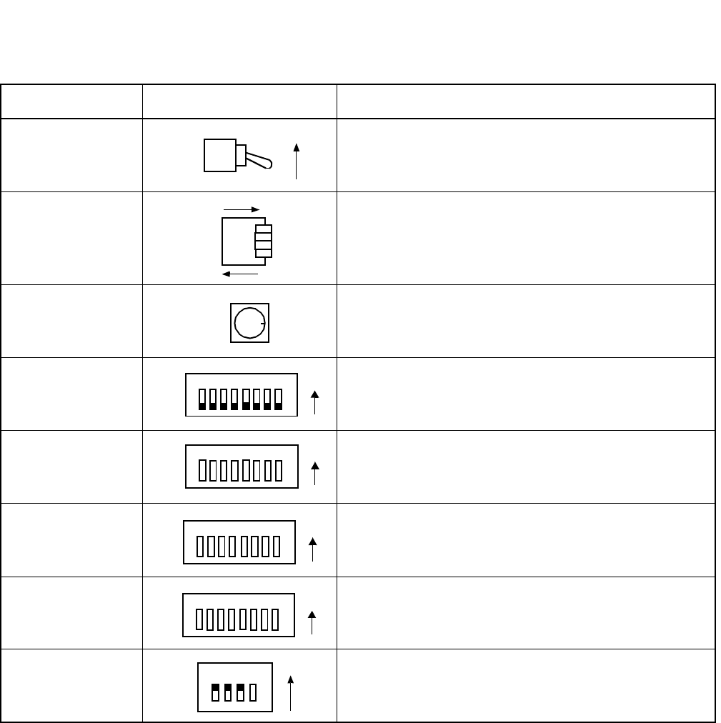
CHAPTER 3 NDA-24296
Page 380
Revision 1.0
PA-FCHA
Fusion Call Control Handler
7. Switch Setting Sheet
SWITCH NAME SWITCH SHAPE REMARKS
MB
MNT
MODE
SW10
SW11
SW12
SW13
SW14
ON
ON
OFF
8
1 2 3 4 ON
5 6 7 8
1234ON
5678
1234ON
5678
1234 ON
56 7 8
1 2 3 4 ON
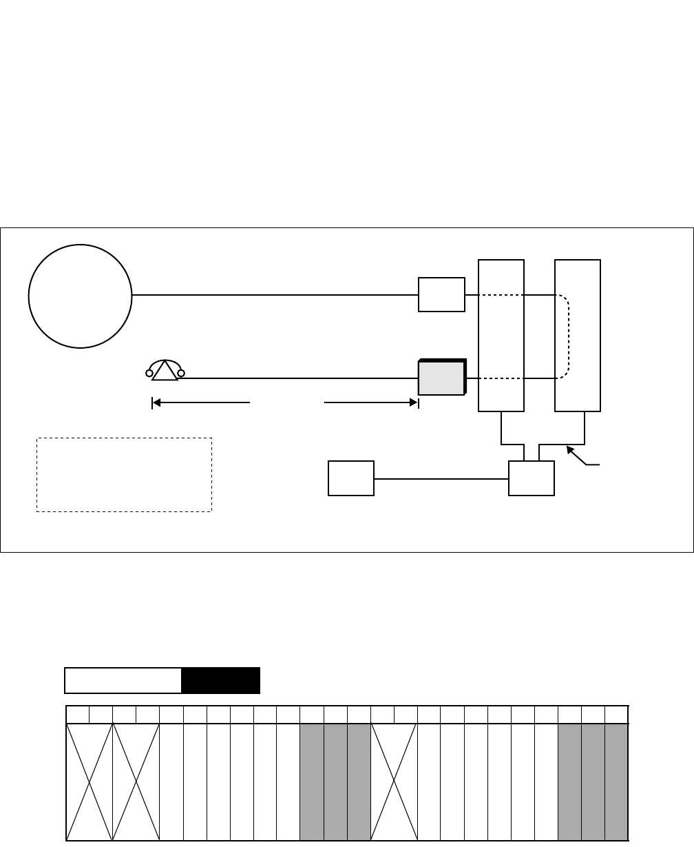
NDA-24296 CHAPTER 3
Page 381
Revision 1.0
PA-24LCBV
Line Circuit
PA-24LCBV
Line Circuit
1. General Function
The PA-24LCBV circuit card provides an interface between a maximum of 24-analog terminals and the
system with a range of 600 (Ohm) inclusive of terminal resistance. This card also can send “Stutter Dial
Tone,” which is not a continuous tone, to an associated terminal which has no Message Waiting Lamp
(MWL) instead of activating the MWL if required.
Figure 3-97 Location of PA-24LCBV (LC) Card in the System
2. Mounting Location/Condition
The PA-24LCBV(LC) circuit card can be mounted in the following shaded slots.
max. 600 [Ω]
Analog Terminal
COT
LC
INT SW
CPU GT
I/O Local Bus
(PA-24LCBV)
C. O. LINE
• Loop Resistance : Max 600[Ω]
(inclusive of terminal resistance)
• Reverse Function : x 1 circuit
• Stutter Dial Tone
• Message Waiting Lamp
• Encoding Law : µ-law
PUBLIC
NETWORK
00 01 02 03 04 05 06 07 08 09 10 11 12 13 14 15 16 17 18 19 20 21 22 23
PIM
Mounting Module
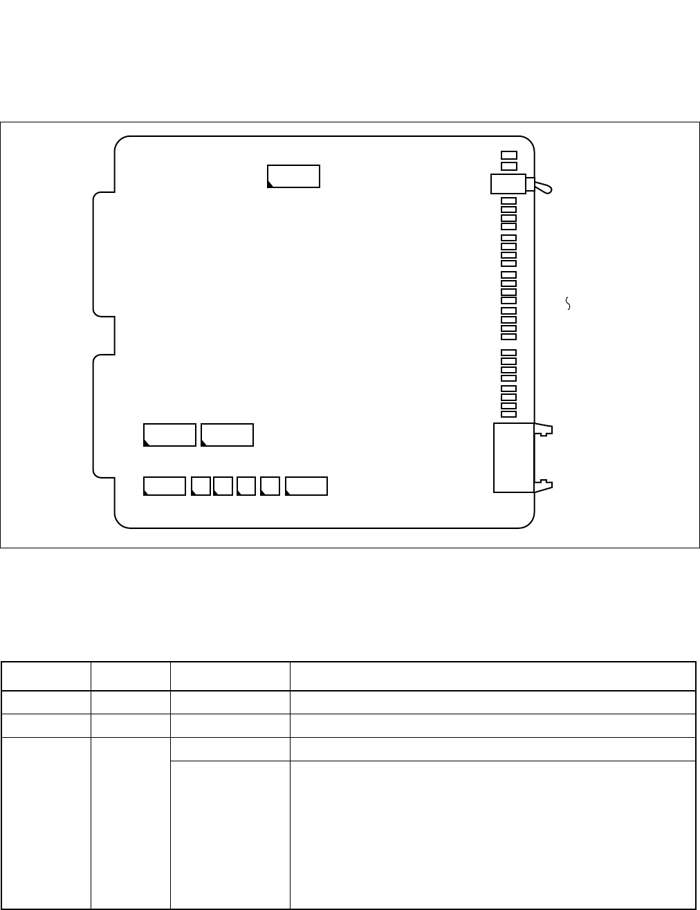
CHAPTER 3 NDA-24296
Page 382
Revision 1.0
PA-24LCBV
Line Circuit
3. Face Layout of Lamps, Switches and Connectors
The face layout of lamps, switches on this card is shown in Figure 3-98.
Figure 3-98 Face Layout of PA-24LCBV (LC) Card
4. Lamp Indications
Lamp indications for this card are shown below.
LED NAME COLOR LED STATUS DESCRIPTION
OPE1 Green Steady Lighting The circuitry of circuit #0-#7 is operating normally.
OPE2 Green Steady Lighting The circuitry of circuit #8-#23 is operating normally.
BL0
BL23
Green
Steady Lighting Line loop exists.
Flashing
1. Ringing signal is being transmitted. Busy LED keeps flashing in
synchronizing with on/off of the ringing signal.
2. Dial pulses are being received. While dial pulses from a line are
being received. Busy LED keeps flashing in synchronizing with the
dial pulses coming from the line.
3. Line is in Make-busy state.
4. Busy LED keeps flashing at 60 ipm.
OPE2
OPE1
BL23
BL0
SW00 (MB)
BL23
22
21
20
19
18
17
16
15
14
13
12
11
10
9
8
7
6
5
4
3
2
1
0
CN
SW18
SW10
(BNW0-7)
SW11
(BNW8-15)
SW12
(BNW16-23)
SW17
SW13
SW14
SW15
SW16
~
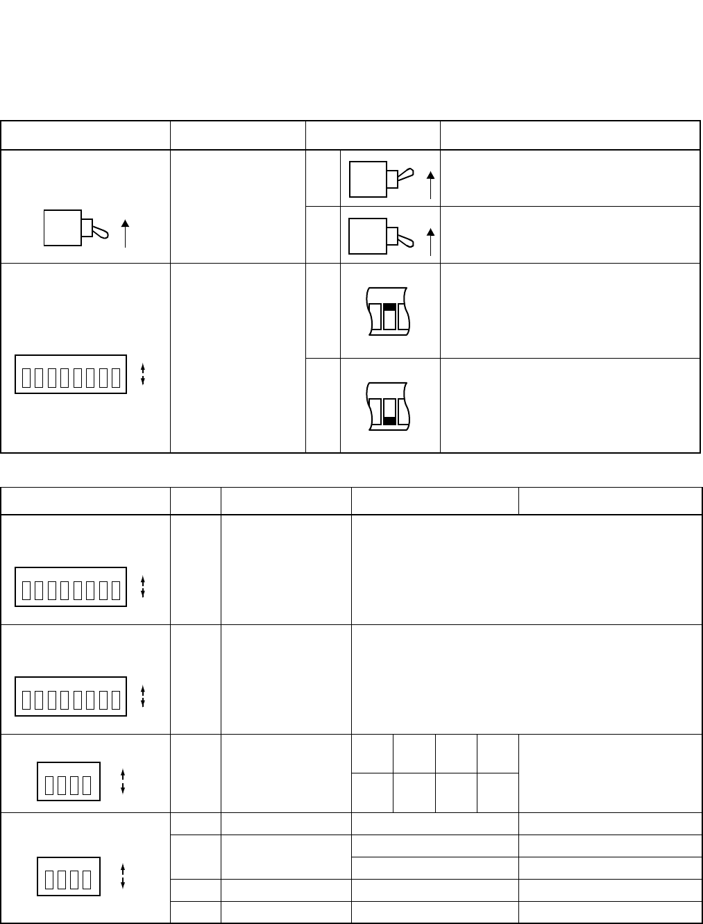
NDA-24296 CHAPTER 3
Page 383
Revision 1.0
PA-24LCBV
Line Circuit
5. Switch Settings
Switches on the PA-24LCBV (LC) card have the following meanings.
SWITCH FUNCTION SWITCH SETTING MEANING
SW00
(MB) Circuit Card
Make-busy Key
OFF Circuit card Make-busy cancel
ON Circuit card Make-busy
SW10
(BNW0-7)
Balancing Network
Designation
•Each element on
this switch
corresponds to
circuit #0-#7.
ON
North America, Other Country (A/µ Law)
BNW: Compromise Impedance
(EIA/TIA-464A) (Note 1)
for long distance.
OFF
North America, Other Country (A/µ Law)
BNW : 600 Ω (Note 1)
for short distance
SWITCH No. FUNCTION SWITCH SETTING MEANING
SW11
(BNW8-15)
Balancing Network
Designation
• Each element
on this switch
corresponds to
circuit #8-#15.
The same as previous table.
SW12
(BMW16-23)
Balancing Network
Designation
• Each element
on this switch
corresponds to
circuit #16-#23.
The same as previous table.
SW13
Selection of the User
SW13
-1
SW13
-2
SW13
-3
SW13
-4 North America
ON OFF OFF OFF
SW14 1 OFF Fixed to OFF
2Stutter
Dial Tone
ON Stutter Dial tone Available
OFF Stutter Dial tone not Available
3 OFF Fixed to OFF
4 OFF Fixed to OFF
ON
ON
ON
12345678
ON
OFF
12345678
ON
OFF
12345678
ON
OFF
1234
ON
OFF
1234
ON
OFF
CHAPTER 3 NDA-24296
Page 384
Revision 1.0
PA-24LCBV
Line Circuit
Note 1: Compromise Impedance (EIA/TIA-464A) and 600 Ω are as follows.
SWITCH No. FUNCTION SWITCH SETTING MEANING
SW15 1 OFF Fixed to OFF
2 OFF Fixed to OFF
3 OFF Fixed to OFF
4 OFF Fixed to OFF
SW16
1 OFF Fixed to OFF
2 OFF Fixed to OFF
3Message Waiting
Lamp
ON
Message Waiting Lamp
Flashing
(Controlled by Firmware)
OFF
Message Waiting Lamp lit or
Flashing (Selected and Controlled
by Software)
4 OFF Fixed to OFF
SW17
1 OFF Fixed to OFF
2 OFF Fixed to OFF
3 OFF Fixed to OFF
4 OFF Fixed to OFF
5 OFF Fixed to OFF
6 OFF Fixed to OFF
7 OFF Fixed to OFF
8 OFF Fixed to OFF
SWITCH No. FUNCTION SWITCH SETTING MEANING
SW18
Polarity reverse or
Momentary Open
ON Momentary open
OFF Polarity reverse
ON OFF
1234
ON
OFF
1234
ON
OFF
12345678
ON
OFF
OFF
Slide switch
(RVS) (OPEN)
ON
350 1000
0.21
Compromise Impedance(EIA/TIA-464A)
600
NDA-24296 CHAPTER 3
Page 385
Revision 1.0
PA-24LCBV
Line Circuit
6. Switch Setting Sheet
MODULE SLOT No. SWITCH NAME SWITCH SHAPE REMARKS
PIM
SW00
(MB) Note: Normal operating mode is down.
SW10
(BNW0-7)
SW11
(BNW8-15)
SW12
(BNW16-23)
SW13
SW14
SW15
SW16
SW17
SW18
ON
1234ON
5678
12 3 4 ON
56 7 8
1 2 3 4 ON
5 6 7 8
1ON
2 3 4
1ON
2 3 4
1ON
2 3 4
1ON
2 3 4
1 2 3 4 ON
5 6 7 8
OFF
(RVS) (OPEN)
ON
CHAPTER 3 NDA-24296
Page 386
Revision 1.0
PA-24LCBV
Line Circuit
7. External Interface
Location of the LT connector leads and LC connector leads for this circuit card is shown in Figure 3-99.
(a) PIM
When this circuit card is mounted in PIM, necessary leads appear on the LT connectors as follows.
Figure 3-99 LT Connector Lead Location (PIM) (1/2)
26
27
28
29
30
31
32
33
34
35
36
37
38
39
40
41
1
2
3
4
5
6
7
8
9
10
11
12
13
14
15
16
42
43
44
45
46
47
48
17
18
19
20
21
22
23
49
50 24
25
232221201918171615141312111009080706050403020100
LT6 LT7 LT8 LT9 LT10 LT11LT0 LT1 LT2 LT3 LT4 LT5
231915
221814
211713
201612
231915
221814
211713
201612
110907050301
100806040200
110907050301
100806040200
HW11HW10HW9HW8HW7HW6HW5HW4HW3HW2HW1HW0
Group No.
Slot No.
LT Connector
PIM
Highway Block
26
27
28
29
30
31
32
33
34
35
36
37
38
39
40
41
1
2
3
4
5
6
7
8
9
10
11
12
13
14
15
16
42
43
44
45
46
47
48
17
18
19
20
21
22
23
49
50 24
25
B8
B9
Accommodated in 1 Accommodated in 2
LT 5, 11 ConnectorLT 4, 10 Connector
B10
B11
B12
B13
B14
B15
B16
B17
B18
B19
B20
B21
B22
B23
A16
A17
A18
A19
A20
A21
A22
A23
A8
A9
A10
A11
A12
A13
A14
A15 B8
B9
B10
B11
B12
B13
B14
B15
B16
B17
B18
B19
B20
B21
B22
B23
A16
A17
A18
A19
A20
A21
A22
A23
A8
A9
A10
A11
A12
A13
A14
A15
1 2 1 2
NDA-24296 CHAPTER 3
Page 387
Revision 1.0
PA-24LCBV
Line Circuit
Figure 3-99 LT Connector Lead Location (PIM) (2/2)
26
27
28
29
30
31
32
33
34
35
36
37
38
39
40
41
1
2
3
4
5
6
7
8
9
10
11
12
13
14
15
16
42
43
44
45
46
47
48
17
18
19
20
21
22
23
49
50 24
25
232221201918171615141312111009080706050403020100
LT6 LT7 LT8 LT9 LT10 LT11LT0 LT1 LT2 LT3 LT4 LT5
231915
221814
211713
201612
231915
221814
211713
201612
110907050301
100806040200
110907050301
100806040200
HW11HW10HW9HW8HW7HW6HW5HW4HW3HW2HW1HW0
Group No.
Slot No.
LT Connector
PIM
Highway Block
26
27
28
29
30
31
32
33
34
35
36
37
38
39
40
41
1
2
3
4
5
6
7
8
9
10
11
12
13
14
15
16
42
43
44
45
46
47
48
17
18
19
20
21
22
23
49
50 24
25
B8
B9
Accommodated in 3
LT 5, 11 ConnectorLT 4, 10 Connector
B10
B11
B12
B13
B14
B15
A8
A9
A10
A11
A12
A13
A14
A15
B16
B17
B18
B19
B20
B21
B22
B23
A16
A17
A18
A19
A20
A21
A22
A23
3 3
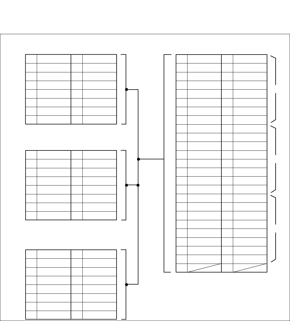
CHAPTER 3 NDA-24296
Page 388
Revision 1.0
PA-24LCBV
Line Circuit
(b) LC Connector Leads
Figure 3-100 LC Connector Lead Location (LC Cable)
1A
2A
3A
4A
5A
6A
7A
8A
1B
2B
3B
4B
5B
6B
7B
8B
B0
B1
B2
B3
B4
B5
B6
B7
A0
A1
A2
A3
A4
A5
A6
A7
1A
2A
3A
4A
5A
6A
7A
8A
1B
2B
3B
4B
5B
6B
7B
8B
B0
B1
B2
B3
B4
B5
B6
B7
A0
A1
A2
A3
A4
A5
A6
A7
1A
2A
3A
4A
5A
6A
7A
8A
1B
2B
3B
4B
5B
6B
7B
8B
B0
B1
B2
B3
B4
B5
B6
B7
A0
A1
A2
A3
A4
A5
A6
A7
26
27
28
29
30
31
32
33
34
35
36
37
38
39
40
41
42
43
44
45
46
47
48
49
50
1
2
3
4
5
6
7
8
9
10
11
12
13
14
15
16
17
18
19
20
21
22
23
24
25
B0
B1
B2
B3
B4
B5
B6
B7
B0
B1
B2
B3
B4
B5
B6
B7
B0
B1
B2
B3
B4
B5
B6
B7
A0
A1
A2
A3
A4
A5
A6
A7
A0
A1
A2
A3
A4
A5
A6
A7
A0
A1
A2
A3
A4
A5
A6
A7
LC CABLE
LC Connector (1)
CONN1 Champ Connector
LT
LC Connector (2)
CONN2
LC Connector (3)
CONN3
PKG1
PKG2
PKG3
PKG1
PKG2
PKG3
NDA-24296 CHAPTER 3
Page 389
Revision 1.0
PA-24LCBV
Line Circuit
8. Connecting Route Diagram
Connecting Route Diagram for the PA-24LCBV(LC) is as follows.
A and B leads for channels #0 - #7 appear from the LC Connector located on the front edge of the card.
Figure 3-101 Connecting Route Diagram
MDF
L1
L2
L1
L2
L1
L2
L1
L2
Jack
Jack
Jack
Jack
Analog
Terminal
Analog
Terminal
Analog
Terminal
Analog
Terminal
A7
B7
A0
B0
A23
B23
A8
B8
PBX
LT Connector
Installation
Cable
Maximum 600 [Ω] (inclusive of terminal resistance)
Maximum 600 [Ω] (inclusive of terminal resistance)
Installation Cable
LT Connector
LC Cable
PA-24LCBV
CHAPTER 3 NDA-24296
Page 390
Revision 1.0
PA-24LCBV
Line Circuit
9. LC Cable Connection
Figure 3-102 Outer View of LC Cable
Earth Cable
3m (9.8 feet)
NDA-24296 CHAPTER 3
Page 391
Revision 1.0
PA-24LCBV
Line Circuit
Figure 3-103 Cable Running for LC Cable (Example)
FRONT
REAR
LC Cable
LC Cable LC Cable
LT Cable
PA-24LCBV
Earth Plate
Earth Cable
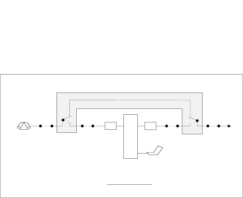
CHAPTER 3 NDA-24296
Page 392
Revision 1.0
PA-M69
Power Failure Transfer
PA-M69
Power Failure Transfer
1. General Function
This circuit card executes a C.O. line to the telephone or the release of a C.O. line due to a power supply
failure, system down, software order, etc. This circuit card is also provided with the change circuit of 12
circuits.
Figure 3-104 Location of PA-M69 (PFT, 12NCU) within the System
TEL
MDF
TEL
(AO, BO)
MDF
LC
(AI, BI)
LC TSW COT MDF
TRK
(TI, RI)
NCU
MDF
CO
(TO, RO)
(NITE KEY)
Position within the System
ATTCON
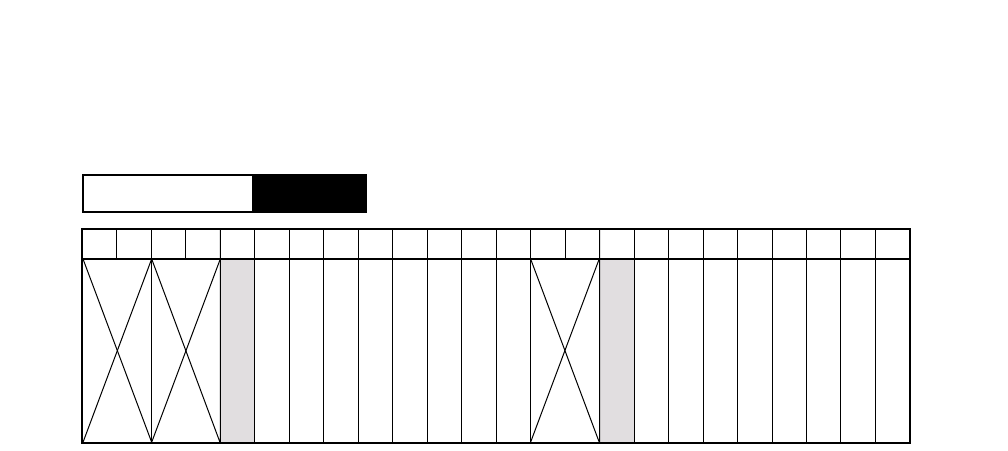
NDA-24296 CHAPTER 3
Page 393
Revision 1.0
PA-M69
Power Failure Transfer
2. Mounting Location/Condition
The mounting locations of this circuit card and the conditions related to mounting are shown below.
PIM
Mounting Module
PA-M69
PA-M69
00 01 02 03 04 05 06 07 08 09 10 11 12 13 14 15 16 17 1918 20 21 22 23
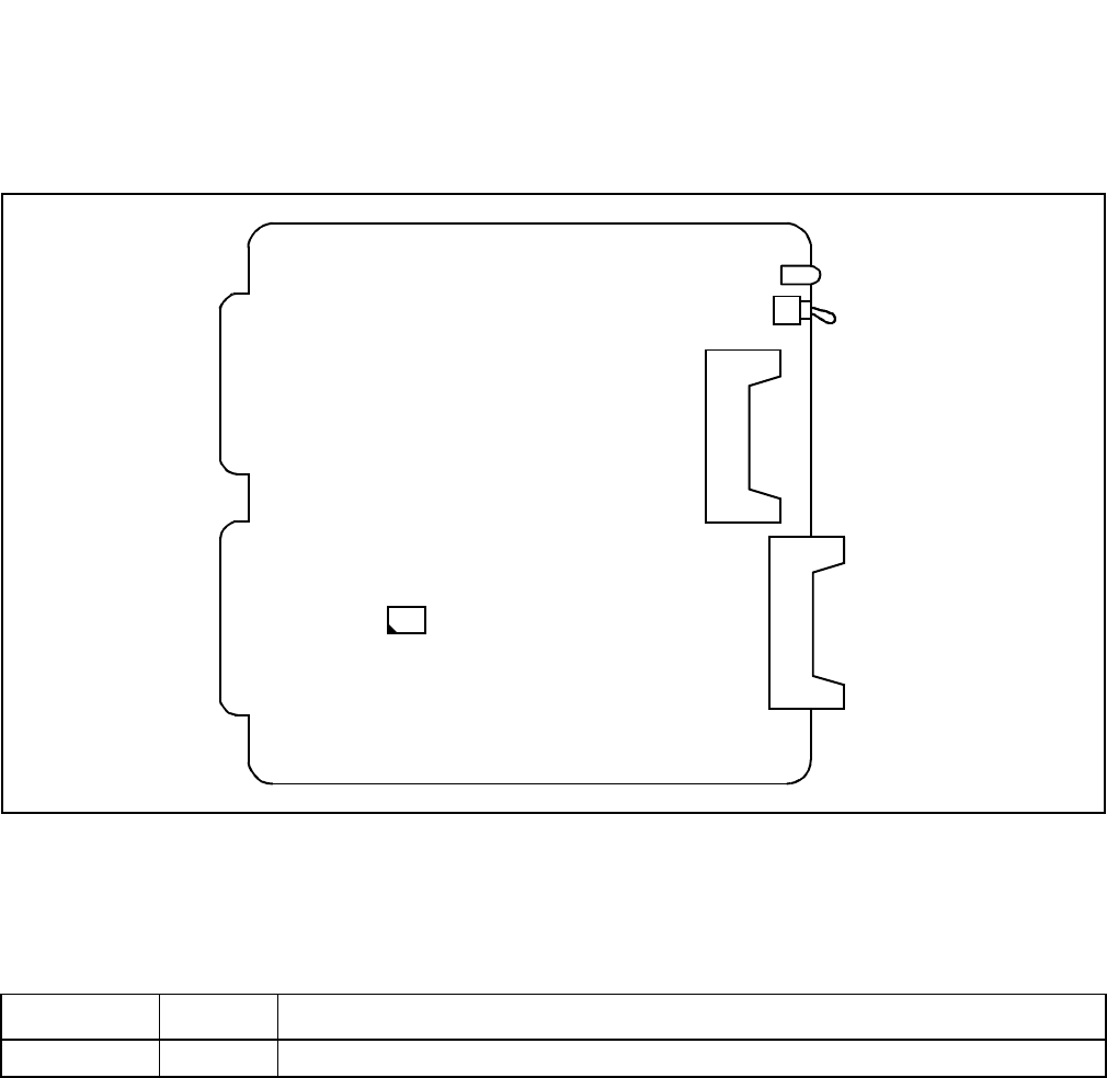
CHAPTER 3 NDA-24296
Page 394
Revision 1.0
PA-M69
Power Failure Transfer
3. Face Layout of Lamp, Switches, and Connectors
The face layout of lamp, switches, and connectors of this circuit card is shown in Figure 3-105.
Figure 3-105 Face Layout of PA-M69 (PFT, 12NCU)
4. Lamp Indication
The contents of lamp indication of this circuit card are shown in the table below.
LAMP NAME COLOR STATE
OPE Green Remains lit even when PFT is being activated on any one of the 12 circuits.
OPE
MB
NCU1
NCU0
SW0

NDA-24296 CHAPTER 3
Page 395
Revision 1.0
PA-M69
Power Failure Transfer
5. Switch Settings
Standard settings of various switches on this circuit card are shown in the table below.
SWITCH NAME SWITCH
NO. SETTING STANDARD
SETTING MEANING
MB UP Circuit card make busy
DOWN ×Circuit card make busy cancel
SW0
1ON ×Fixed
2OFF ×Fixed
3OFF ×Fixed
4OFF ×Fixed
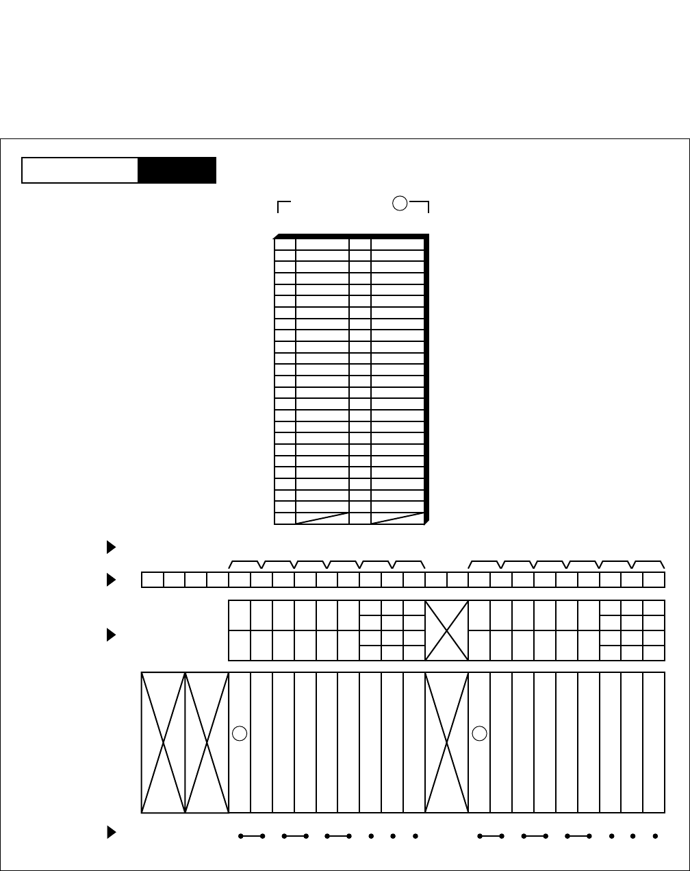
CHAPTER 3 NDA-24296
Page 396
Revision 1.0
PA-M69
Power Failure Transfer
6. External Interface
Accommodation of the LT connector leads of this circuit card, accommodation of the NCU connector on
the front side of the circuit card, and connecting route diagram are shown in Figure 3-106.
Figure 3-106 LT Connector Leads Accommodation
PIM
Mounting Module
232221201918171615141312111009080706050403020100
LT6 LT7 LT8 LT9 LT10 LT11LT0 LT1 LT2 LT3 LT4 LT5
231915
221814
211713
201612
231915
221814
211713
201612
110907050301
100806040200
110907050301
100806040200
Group No.
Slot No.
LT Connector
PIM
26
27
28
29
30
31
32
33
34
35
36
37
38
39
40
41
1
2
3
4
5
6
7
8
9
10
11
12
13
14
15
16
42
43
44
45
46
47
48
17
18
19
20
21
22
23
49
50 24
25
KY1
KY3 KY0
Accommodated in 1
LT 0, 6 Connector
KY2
KY4
KY6
KY5
KY7
1 1
HW11HW10HW9HW8HW7HW6HW5HW4HW3HW2HW1HW0
Highway Block
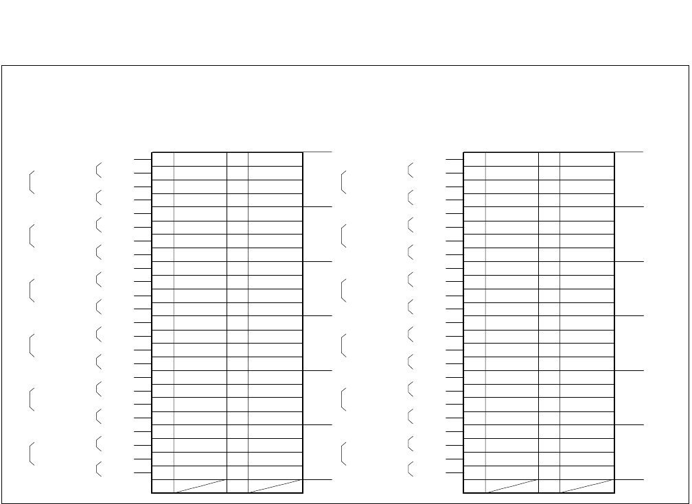
NDA-24296 CHAPTER 3
Page 397
Revision 1.0
PA-M69
Power Failure Transfer
Figure 3-107 NCU Connector Accommodation
NCU Connector Accommodation
26
27
28
29
30
31
32
33
34
35
36
37
38
39
40
41
42
43
44
45
46
47
48
49
50
NCU0
BO00
BI00
TO00
TI00
BO01
BI01
TO01
TI01
BO02
BI02
TO02
TI02
BO03
BI03
TO03
TI03
BO04
BI04
TO04
TI04
BO05
BI05
TO05
TI05
AO00
AI00
RO00
RI00
AO01
AI01
RO01
RI01
AO02
AI02
RO02
RI02
AO03
AI03
RO03
RI03
AO04
AI04
RO04
RI04
AO05
AI05
RO05
RI05
CHAMP Connector
1
2
3
4
5
6
7
8
9
10
11
12
13
14
15
16
17
18
19
20
21
22
23
24
25
TEL
LC
CO
TRK
TEL
LC
CO
TRK
TEL
LC
CO
TRK
TEL
LC
CO
TRK
TEL
LC
CO
TRK
TEL
LC
CO
TRK
No. 0
No. 1
No. 2
No. 3
No. 4
No. 5
Station
C.O. Line
Station
C.O. Line
Station
C.O. Line
Station
C.O. Line
Station
C.O. Line
Station
C.O. Line
26
27
28
29
30
31
32
33
34
35
36
37
38
39
40
41
42
43
44
45
46
47
48
49
50
NCU1
BO06
BI06
TO06
TI06
BO07
BI07
TO07
TI07
BO08
BI08
TO08
TI08
BO09
BI09
TO09
TI09
BO10
BI10
TO10
TI10
BO11
BI11
TO11
TI11
AO06
AI06
RO06
RI06
AO07
AI07
RO07
RI07
AO08
AI08
RO08
RI08
AO09
AI09
RO09
RI09
AO10
AI10
RO10
RI10
AO11
AI11
RO11
RI11
CHAMP Connector
1
2
3
4
5
6
7
8
9
10
11
12
13
14
15
16
17
18
19
20
21
22
23
24
25
TEL
LC
CO
TRK
TEL
LC
CO
TRK
TEL
LC
CO
TRK
TEL
LC
CO
TRK
TEL
LC
CO
TRK
TEL
LC
CO
TRK
No. 6
No. 7
No. 8
No. 9
No. 10
No. 11
Station
C.O. Line
Station
C.O. Line
Station
C.O. Line
Station
C.O. Line
Station
C.O. Line
Station
C.O. Line
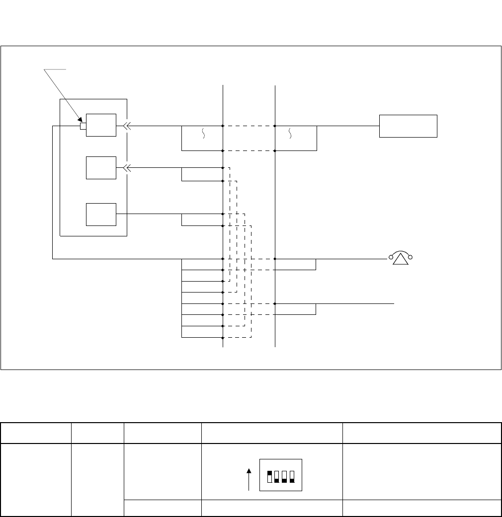
CHAPTER 3 NDA-24296
Page 398
Revision 1.0
PA-M69
Power Failure Transfer
Figure 3-108 Connecting Route Diagram
7. Switch Setting Sheet
MODULE SLOT NO. SWITCH NAME SWITCH SHAPE REMARKS
PIM SW0
MB DOWN Circuit card make busy cancel
NEAX2400 IPX
MDF
KY7
Front Connector NCU
KY0
KY7
KY0
LC
COT
A
B
A
B
A
B
A
B
External
Key Box
C.O. Line
AO00
BO00
AI00
BI00
RO00
TO00
RI00
TI00
Station
PFT
ON 1 2 3 4
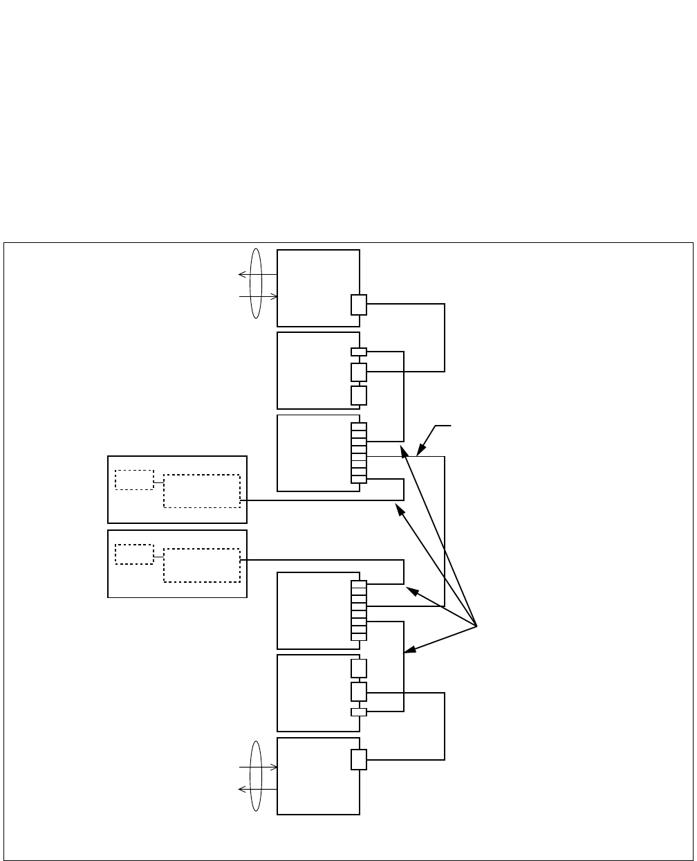
NDA-24296 CHAPTER 3
Page 399
Revision 1.0
PA-M96
HUB
PA-M96
HUB
1. General Function
This circuit card provides the repeater function which is based on ANSI/IEEE 802.3. Eight (8) of the
10BASE-T ports are located on a HUB card.
As seen from the functional connection diagram below, the HUB card is located between the CPR (LANI)
and the FCH card. The HUB card distributes the Fusion link data onto FCH cards.
Figure 3-109 Location of PA-M96 (HUB) Card in the System
CPU LANI
(PZ-PC19)
CPR #0
CPU LANI
(PZ-PC19)
CPR #1
TO/FROM
THE OTHER FUSION
NODE
TO/FROM
THE OTHER FUSION
NODE
DTI
DTI
FCH
FCH
HUB
(PA-M96)
HUB
(PA-M96)
10BASE-T cross cable is used
for cascade connection
10BASE-T straight cable
Note: This figure shows the fusion link with full redundancy (N+1) configuration.
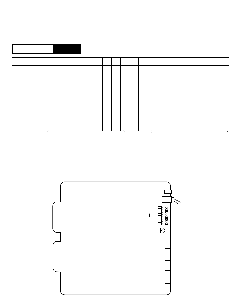
CHAPTER 3 NDA-24296
Page 400
Revision 1.0
PA-M96
HUB
2. Mounting Location/Condition
The PA-M96 (HUB) card can be mounted in any universal slot of PIM0 as shown below.
3. Face Layout of Lamps, Switches, and Connectors
The face layout of lamps, switches, and connectors is shown in Figure 3-110.
Figure 3-110 Face Layout of PA-M96 (HUB) Card
00 01 02 03 04 05 06 07 08 09 10 11 12 13 14 15 16 17 18 19 20 21 22 23
PIM
Mounting Module
PIM0
Universal Slots Universal Slots
MB
OPE
CRS7
CRS0
SENS
TP7-X
TP6-X
TP5-X
TP4-X
TP3-X
TP2-X
TP1-X
TP0-X
x
x
x
x
x
x
x
x
ST7
ST0

NDA-24296 CHAPTER 3
Page 401
Revision 1.0
PA-M96
HUB
4. Lamp Indications
Lamp indications for this circuit card are shown in the table below.
Note 1: This lamp is used to indicate the status of the TPn-X port. Therefore, the circuit card operates normally
regardless of the cable polarity.
Note 2: This circuit card can detect data packet collisions at a TPn-X port when it would be a collision of 2048 bit-
times (2.048 ms) or when the packet collides 32 times consecutively. The port is then locked-out until the
collision is over.
LAMP NAME COLOR STATE
OPE Green Remains lit while this circuit card is in normal operation.
CRS0~CRS7 Green Lights when the circuit card detects the carrier signal form the TPn-X port.
ST0~ST7 Green
The meanings of the ST0~ST7 lamps vary depending on the SEL switch settings as
shown in the table below.
SEL SWITCH MEANINGS
0Lights when the receiving pair cable polarity of the TPn-X port is
reversed. (n = 0~7) Note 1
2
Lights when the 10 BASE-T (RJ-45) cable is attached to the TPn-X
port, and the TCP/IP link has been established. The lamp may light
regardless of the receiving pair cable polarity. (n = 0~7)
3
Lights when the TPn-X port is normal.
Remains off when collisions have occurred at the TPn-X port.
(n = 0~7) Note 2

CHAPTER 3 NDA-24296
Page 402
Revision 1.0
PA-M96
HUB
5. Switch Setting
Standard settings for switches on this circuit card are shown in the table below.
SWITCH
NAME SETTING STANDARD
SETTING DESCRIPTION
MB UP Circuit card Make-busy.
DOWN ×Circuit card Make-busy cancel.
SENSE
0 Polarity indication on the STn lamps for TPn-X ports (n = 0~7).
1 Not used.
2×TPn-X ports operate as a repeater HUB. (n = 0~7).
3Data-Packet-Collision indication on the STn lamps for TPn-X ports
(n = 0~7).
4 - F Not used.
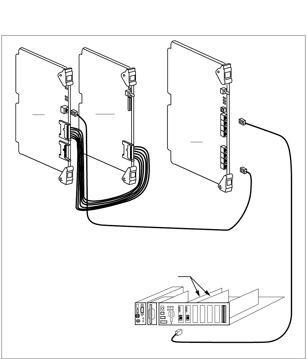
NDA-24296 CHAPTER 3
Page 403
Revision 1.0
PA-M96
HUB
6. External Interface
Figure 3-111 FCH/HUB/DTI/LANI Connection
24DTR
CN2
FCH
FCH
PZ-PC19 (LANI)
10 BASE-T straight Cable
10 BASE-T straight Cable
HUB
10AL (10) FLT CA
DTI
CHAPTER 3 NDA-24296
Page 404
Revision 1.0
PA-M96
HUB
7. Switch Setting Sheet
SWITCH NAME SWITCH SHAPE REMARKS
MB
SEL
ON
2
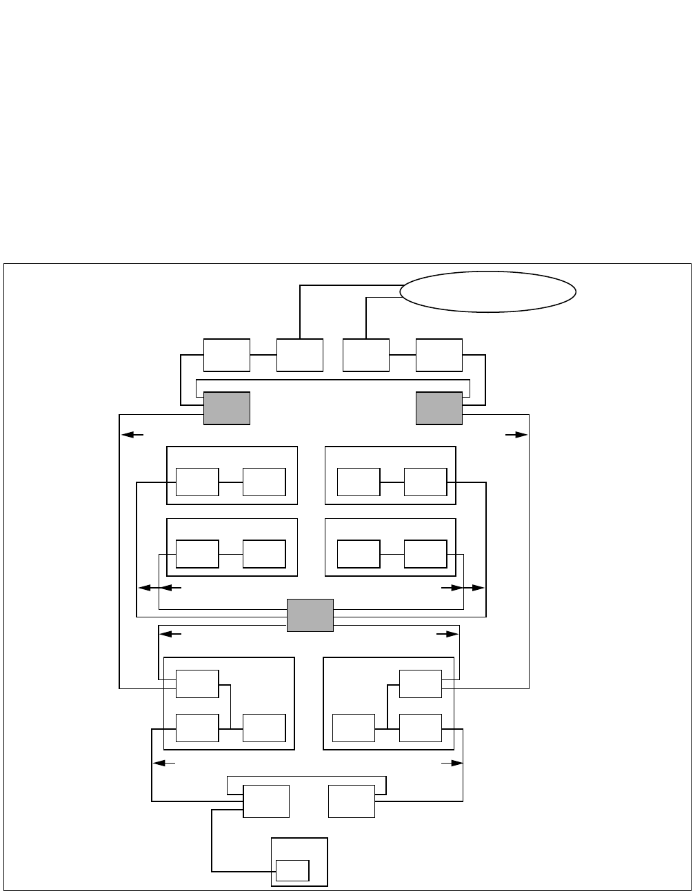
NDA-24296 CHAPTER 3
Page 405
Revision 1.0
PA-M103
HUB
PA-M103
HUB
1. General Function
This circuit card is a class II HUB card based on IEEE802.3 (10BASE-T)/IEEE802.3u (100BASE-TX),
which is located between 100M Ether card (PZ-PC22/PZ-PC23) and FCCH card that establishes Fusion
link to the system.
This circuit card provides the repeater function, and 12 ports 10BASE-T/100BASE-TX are accommodated
on one HUB card. The state of each port is indicated on the LED.
This card is used in IPX-UMG system.
Figure 3-112 Location of PA-M103 (HUB) Card in the System
LAN CPU
LP#0
LAN CPU
CMP#0
LAN
LAN
CPU
SP#0
10BASE-T
10BASE-T
100BASE-TX
(P-BUS)
100BASE-TX
(P-BUS)
HUB
HUB
HUB
FCCH DTI
LANCPU
LP#1
LANCPU
CMP#1
LAN
LAN
CPU
SP#1
10BASE-T
10BASE-T
100BASE-TX
(P-BUS)
100BASE-TX
(P-BUS)
HUB
HUB
FCCHDTI
To other Fusion Node
NIC
MAT
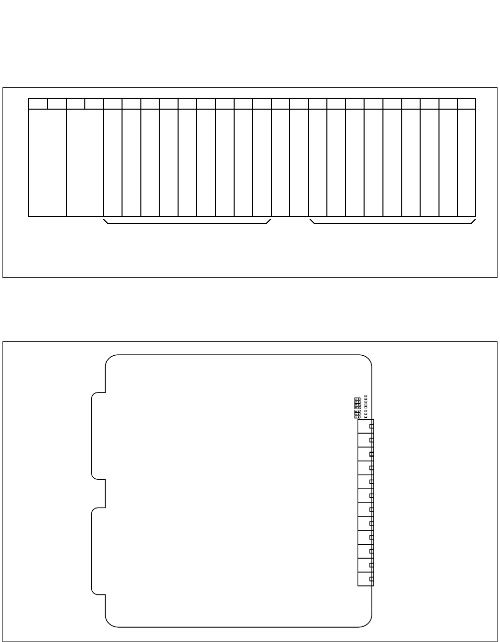
CHAPTER 3 NDA-24296
Page 406
Revision 1.0
PA-M103
HUB
2. Mounting Location/Condition
The PA-M103 (HUB) card can be mounted in any universal slot of PIM as shown below.
3. Face Layout of Connectors
The face layout of lamps, switches, and connectors are shown in Figure 3-113.
Figure 3-113 Face layout of PA-M103 (HUB) Card
00 01 02 03 04 05 06 07 08 09 10 11 12 13 14 15 16 17 18 19 20 21 22 23
Universal Slots Universal Slots
Note: Related to the length of Ether cable, it is recommended that this card ought to be mounted on the PIM
within IMG0/4/8/12 (LPR accommodated IMGs).
TPB
TPA
TP9
TP8
TP7
TP6
TP5
TP4
TP3
TP2
TP1
TP0
L3
LA L9
L8 L7
L6 L2
L1 L0
L5 L4
L3
OPEPWALM
TXRX

NDA-24296 CHAPTER 3
Page 407
Revision 1.0
PA-M103
HUB
4. Lamp Indications
The contents of lamp indications on this circuit card are shown in the table below.
5. Switch Settings
No switch settings are required.
LAMP NAME COLOR DESCRIPTION
OPE Green Remains lit while this circuit card is in normal operation
PWALM Red Lights when the OBP (On Board Power) output voltage blownout
L0-L9, LA, LB Green Link has been established
TXRX Green Data packet sending/receiving
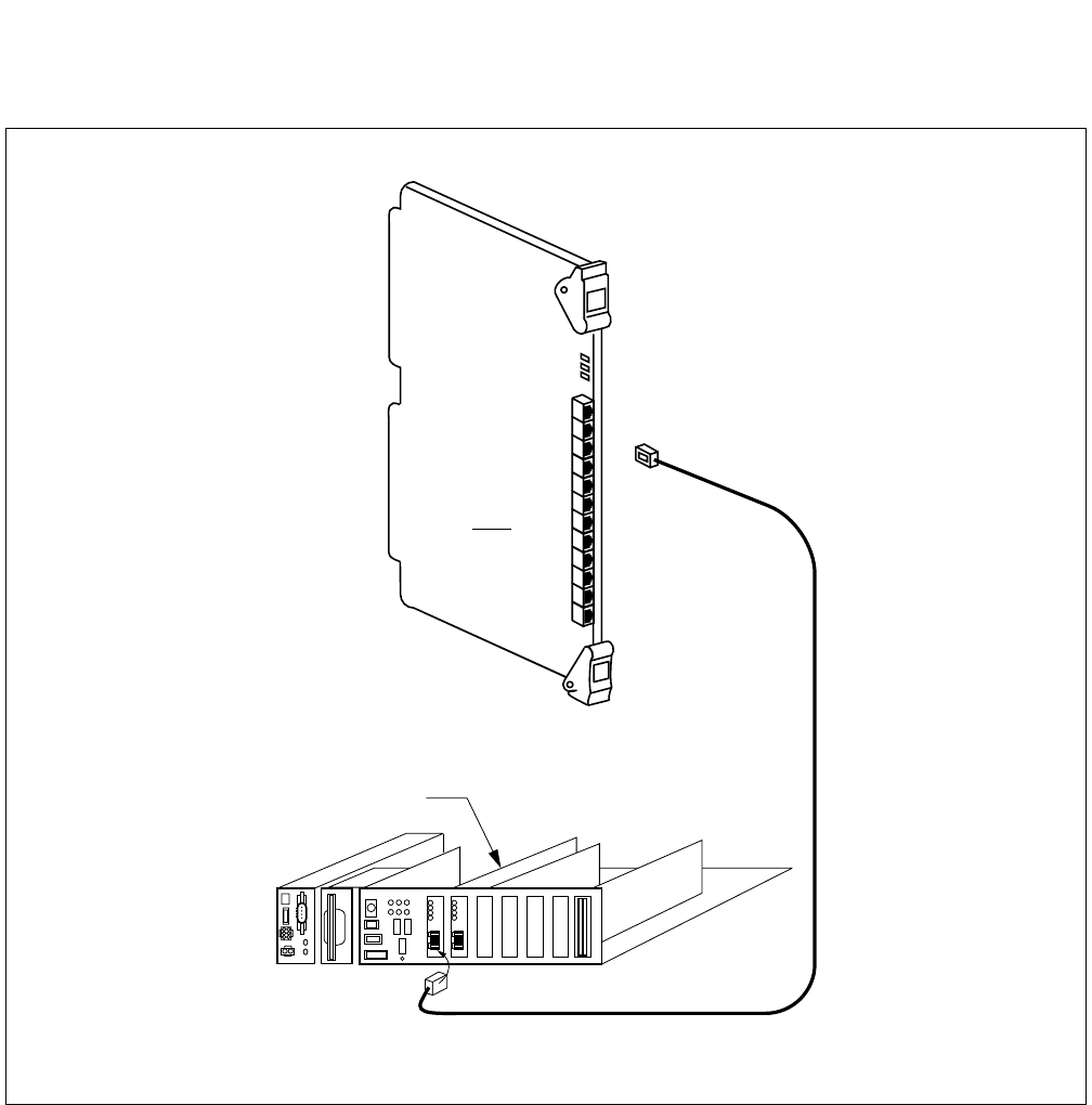
CHAPTER 3 NDA-24296
Page 408
Revision 1.0
PA-M103
HUB
6. External Interface
Figure 3-114 External Interface for PA-M103 (HUB) Card
7. Switch Setting Sheet
No switch settings are required.
PZ-PC22(LANI)
HUB
100 BASE-TX Straight Cable
(PA-M103)
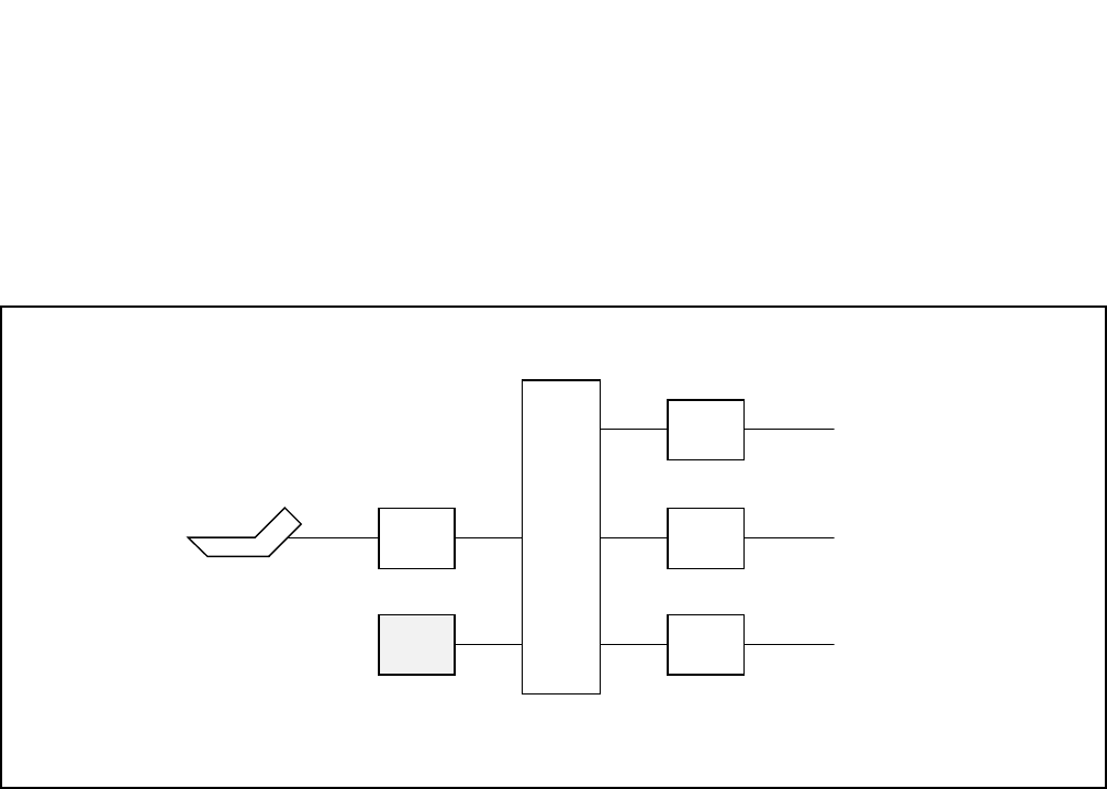
NDA-24296 CHAPTER 3
Page 409
Revision 1.0
PA-8RSTK
Register Sender Trunk
PA-8RSTK
Register Sender Trunk
1. General Function
This circuit card is an 8-circuit register sender trunk card which transmits and sends selective signals (DP
signals, PB signals, MF signals).
Figure 3-115 Location of PA-8RSTK (8RST) within the System
ATT
LC
COT
TLT
TSW
ATI
Station
C.O. Line
Tie Line
RST

CHAPTER 3 NDA-24296
Page 410
Revision 1.0
PA-8RSTK
Register Sender Trunk
2. Mounting Location/Condition
The mounting locations of this circuit card and the conditions related to mounting are shown below.
00 01 02 03 04 05 06 07 08 09 10 11 12 13 14 15 16 17 18 19 20 21 22 23
Note: Indicates universal slots for line/trunk circuit cards.
PIM
Mounting Module
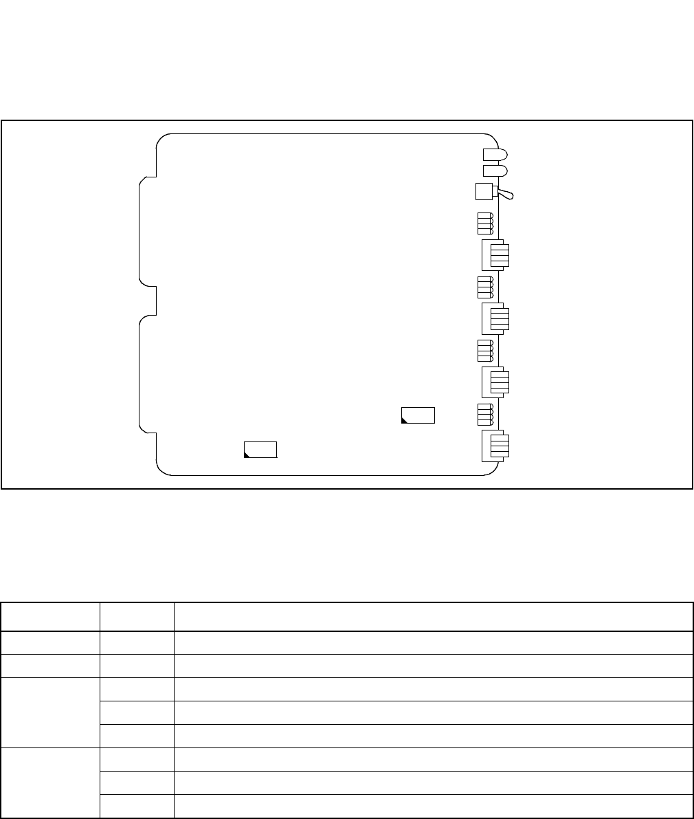
NDA-24296 CHAPTER 3
Page 411
Revision 1.0
PA-8RSTK
Register Sender Trunk
3. Face Layout of Lamps, Switches, and Connectors
The face layout of lamps, switches, and connectors of this circuit card is shown in Figure 3-116.
Figure 3-116 Face Layout of PA-8RSTK (8RST)
4. Lamp Indications
The contents of lamp indications of this circuit card are shown in the table below.
LAMP NAME COLOR STATE
OPE Green Remains lit while this circuit card is operating.
N-OPE Red Remains lit while this circuit card is in make-busy state.
BLR0
BLR7
Red Lights when the corresponding circuit has received the selective signals.
Flash Flashes (60 IPM) while the corresponding circuit is in make-busy state.
OFF Remains off while the corresponding circuit is idle.
BLS0
BLS7
Red Lights when the corresponding circuit has sent the selective signals.
Flash Flashes (60 IPM) while the corresponding circuit is in make-busy state.
OFF Remains off while the corresponding circuit is idle.
OPE
N-OPE
MB
BLS7
BLS4
MBS7
MBS4
BLR7
BLR4
MBR7
MBR4
BLS3
BLS0
MBS3
MBS0
BLR3
BLR0
MBR3
MBR0
SW0
SW1
~
~
~
~
~
~~~
~~

CHAPTER 3 NDA-24296
Page 412
Revision 1.0
PA-8RSTK
Register Sender Trunk
5. Switch Settings
Standard settings of various switches on this circuit card are shown in the table below.
SWITCH
NAME SWITCH NO. SETTING STANDARD
SETTING MEANING
MB UP Circuit card make busy.
DOWN ×Circuit card make busy cancel.
MBR0~3
0ON Register make busy of the corresponding circuit.
OFF ×Register make busy cancel of the corresponding circuit.
1ON Register make busy of the corresponding circuit.
OFF ×Register make busy cancel of the corresponding circuit.
2ON Register make busy of the corresponding circuit.
OFF ×Register make busy cancel of the corresponding circuit.
3ON Register make busy of the corresponding circuit.
OFF ×Register make busy cancel of the corresponding circuit.
MBR4~7
4ON Register make busy of the corresponding circuit.
OFF ×Register make busy cancel of the corresponding circuit.
5ON Register make busy of the corresponding circuit.
OFF ×Register make busy cancel of the corresponding circuit.
6ON Register make busy of the corresponding circuit.
OFF ×Register make busy cancel of the corresponding circuit.

NDA-24296 CHAPTER 3
Page 413
Revision 1.0
PA-8RSTK
Register Sender Trunk
SWITCH
NAME SWITCH NO. SETTING STANDARD
SETTING MEANING
MBR4~7 7 ON Register make busy of the corresponding circuit.
OFF ×Register make busy cancel of the corresponding circuit.
MBS0~3
0ON Sender make busy of the corresponding circuit.
OFF ×Sender make busy cancel of the corresponding circuit.
1ON Sender make busy of the corresponding circuit.
OFF ×Sender make busy cancel of the corresponding circuit.
2ON Sender make busy of the corresponding circuit.
OFF ×Sender make busy cancel of the corresponding circuit.
3ON Sender make busy of the corresponding circuit.
OFF ×Sender make busy cancel of the corresponding circuit.
MBS4~7
4ON Sender make busy of the corresponding circuit.
OFF ×Sender make busy cancel of the corresponding circuit.
5ON Sender make busy of the corresponding circuit.
OFF ×Sender make busy cancel of the corresponding circuit.
6ON Sender make busy of the corresponding circuit.
OFF ×Sender make busy cancel of the corresponding circuit.
7ON Sender make busy of the corresponding circuit.
OFF ×Sender make busy cancel of the corresponding circuit.
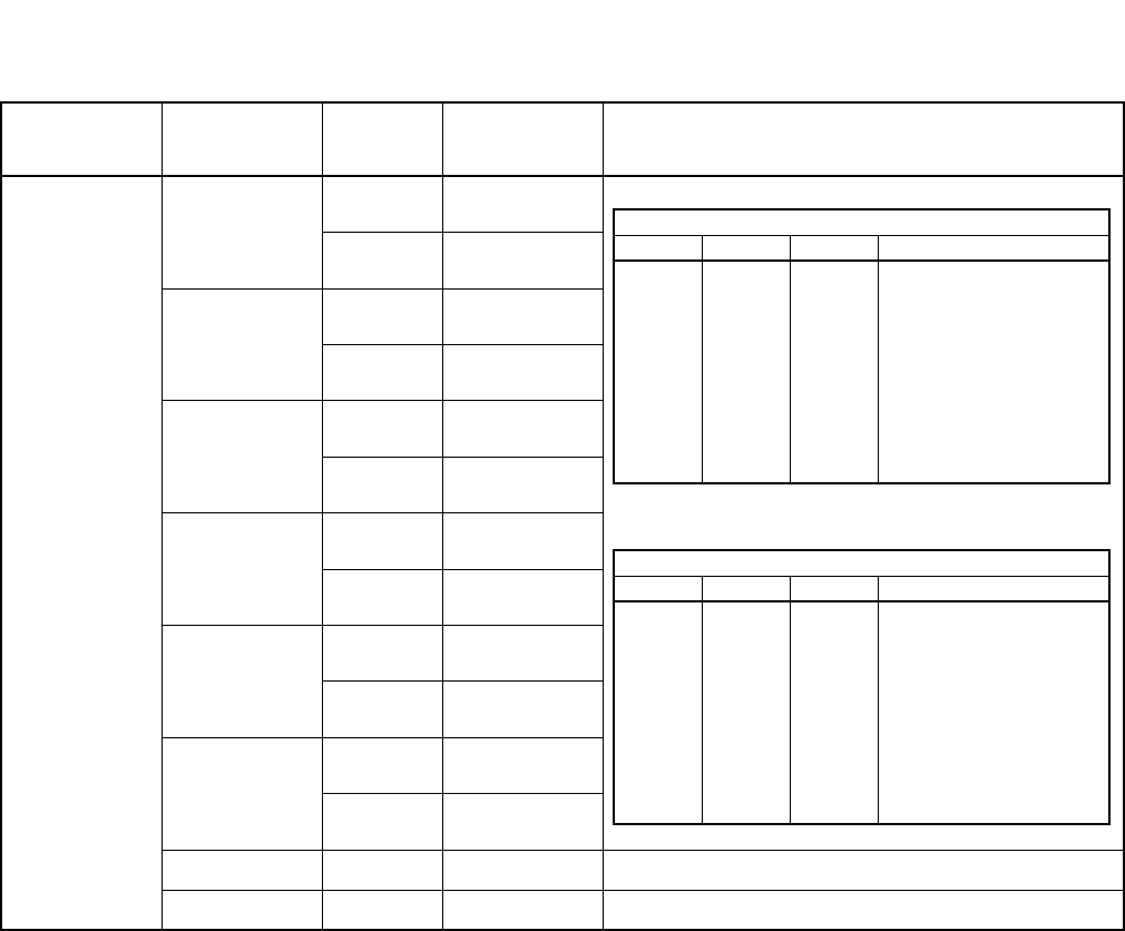
CHAPTER 3 NDA-24296
Page 414
Revision 1.0
PA-8RSTK
Register Sender Trunk
SWITCH
NAME SWITCH NO. SETTING STANDARD
SETTING MEANING
SW0
1
ON
OFF
2
ON
OFF
3
ON
OFF
4
ON
OFF
5
ON
OFF
6
ON
OFF
7OFF×Threshold value is not selected (Fixed to OFF).
8ON×Fixed.
SELECTION OF PBR THRESHOLD VALUE
SW0-1 SW0-2 SW0-3 PBR THRESHOLD VALUE
ON ON ON -21.7 dBm0
OFF ON ON -23.7 dBm0
ON OFF ON -25.7 dBm0
OFF OFF ON -27.7 dBm0
ON ON OFF -28.7 dBm0
OFF ON OFF -31.7 dBm0
ON OFF OFF -33.7 dBm0
OFF OFF OFF -35.7 dBm0
SELECTION OF MFR THRESHOLD VALUE
SW0-4 SW0-5 SW0-6 MFR THRESHOLD VALUE
ON ON ON -21 dBm0
OFF ON ON -23 dBm0
ON OFF ON -25 dBm0
OFF OFF ON -27 dBm0
ON ON OFF -28 dBm0
OFF ON OFF -31 dBm0
ON OFF OFF -33 dBm0
OFF OFF OFF -35 dBm0

NDA-24296 CHAPTER 3
Page 415
Revision 1.0
PA-8RSTK
Register Sender Trunk
SWITCH
NAME SWITCH NO. SETTING STANDARD
SETTING MEANING
SW1
1ON MFR Receive Specification; AT&T
OFF MFR Receive Specification; CCITT No. 5
2
ON
PBR PULSE TIMER (Momentary Signal Shut
Down Protect Timer)
SHORT (Shorter than 10 ms.)
OFF
PBR PULSE TIMER (Momentary Signal Shut
Down Protect Timer)
LONG (Shorter than 20 ms.)
3OFF×Fixed
4ON Register Selection; REG0, 1, 4, 5 of MFR.
OFF Register Selection; REG0, 1, 4, 5 of PBR.
5ON Register Selection; REG2, 3, 6, 7 of MFR.
OFF Register Selection; REG2, 3, 6, 7 of PBR.
6ON ×DPR Receive Specification; General Spec.
OFF DPR Receive Specification; Australian Spec.
7OFF×No setting (Fixed to OFF)
8OFF×Fixed

CHAPTER 3 NDA-24296
Page 416
Revision 1.0
PA-8RSTK
Register Sender Trunk
6. Switch Setting Sheet
MODULE SLOT NO. SWITCH NAME SWITCH SHAPE REMARKS
PIM
MBR0-3
MBR4-7
MBS0-3
MBS4-7
SW0
SW1
MB DOWN Circuit card make busy cancel
ON
3
2
1
0
ON
3
2
1
0
ON
3
2
1
0
ON
3
2
1
0
ON 12345678
ON 12345678
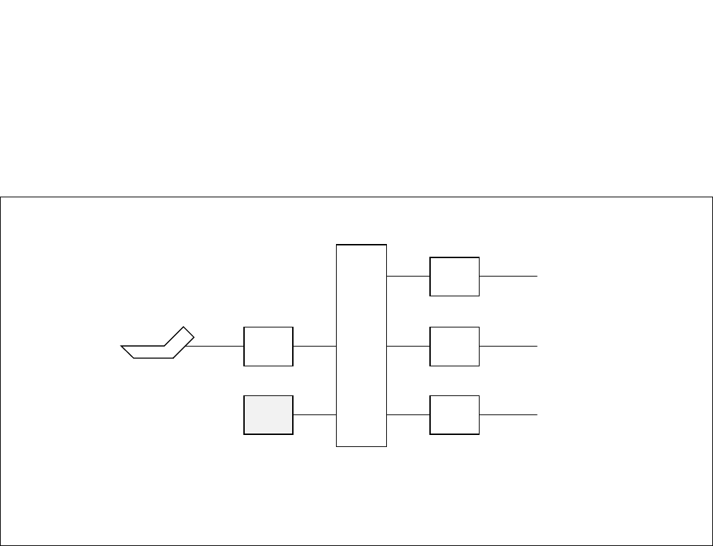
NDA-24296 CHAPTER 3
Page 417
Revision 1.0
PA-8RSTM
Register Sender Trunk
PA-8RSTM
Register Sender Trunk
1. General Function
This circuit card is an 8-circuit register sender trunk card that transmits and sends selective signals (DP sig-
nals, PB signals, MF signals).
Figure 3-117 Location of the PA-8RSTM (8RST) Card in the System
ATT
LC
COT
TLT
TSW
ATI
Station
C.O. Line
Tie Line
RST
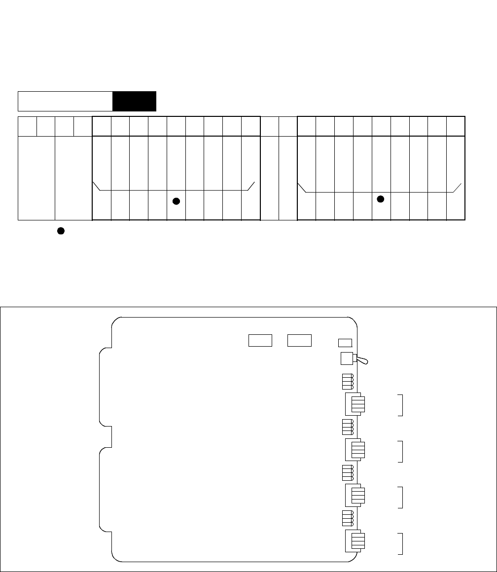
CHAPTER 3 NDA-24296
Page 418
Revision 1.0
PA-8RSTM
Register Sender Trunk
2. Mounting Location/Condition
The mounting locations for this circuit card and the conditions related to mounting are shown below.
3. Face Layout of Lamps, Switches, and Connectors
The face layout of lamps, switches, and connectors for this circuit card is shown below.
Figure 3-118 Face Layout of PA-8RSTM (8RST)
00 01 02 03 04 05 06 07 08 09 10 11 12 13 14 15 16 17 18 19 20 21 22 23
Note: Indicates universal slots for line/trunk circuit cards.
Mounting Module PIM
OPE
MB
BLS7
BLS4
MBS7
MBS4
BLR7
BLR4
MBR7
MBR4
BLS3
BLS0
MBS3
MBS0
BLR3
BLR0
MBR3
MBR0
SW11
~
~
~
~
~
~~~
SW10
SW04
SW03
SW02
SW01

NDA-24296 CHAPTER 3
Page 419
Revision 1.0
PA-8RSTM
Register Sender Trunk
4. Lamp Indications
Lamp indications for this circuit card are shown in the table below.
5. Switch Settings
Standard settings for various switches on this circuit card are shown in the table below.
LAMP NAME COLOR STATE
OPE Green Remains lit while this circuit card is operating.
BLR0
BLR7
Red Lights when the corresponding circuit has received the selective signals.
Flash Flashes (60 IPM) while the corresponding circuit is in Make-busy state.
OFF Remains off when the corresponding circuit is idle.
BLS0
BLS7
Red Lights when the corresponding circuit has sent the selective signals.
Flash Flashes (60 IPM) when the corresponding circuit is in Make-busy state.
OFF Remains off while the corresponding circuit is idle.
SWITCH
NAME SWITCH NO. SETTING STANDARD
SETTING MEANING
MB UP Circuit card Make-busy.
DOWN ×Circuit card Make-busy cancel.
MBR0~3
(SW01)
0ON Register Make-busy of the corresponding circuit.
OFF ×Register Make-busy cancel of the corresponding circuit.
1ON Register Make-busy of the corresponding circuit.
OFF ×Register Make-busy cancel of the corresponding circuit.
2ON Register Make-busy of the corresponding circuit.
OFF ×Register Make-busy cancel of the corresponding circuit.
3ON Register Make-busy of the corresponding circuit.
OFF ×Register Make-busy cancel of the corresponding circuit.
MBR4~7
(SW03)
4ON Register Make-busy of the corresponding circuit.
OFF ×Register Make-busy cancel of the corresponding circuit.
5ON Register Make-busy of the corresponding circuit.
OFF ×Register Make-busy cancel of the corresponding circuit.
6ON Register Make-busy of the corresponding circuit.
OFF ×Register Make-busy cancel of the corresponding circuit.
~~

CHAPTER 3 NDA-24296
Page 420
Revision 1.0
PA-8RSTM
Register Sender Trunk
SWITCH
NAME SWITCH NO. SETTING STANDARD
SETTING MEANING
MBR4~7
(SW03) 7ON Register Make-busy of the corresponding circuit.
OFF ×Register Make-busy cancel of the corresponding circuit.
MBS0~3
(SW02)
0ON Sender Make-busy of the corresponding circuit.
OFF ×Sender Make-busy cancel of the corresponding circuit.
1ON Sender Make-busy of the corresponding circuit.
OFF ×Sender Make-busy cancel of the corresponding circuit.
2ON Sender Make-busy of the corresponding circuit.
OFF ×Sender Make-busy cancel of the corresponding circuit.
3ON Sender Make-busy of the corresponding circuit.
OFF ×Sender Make-busy cancel of the corresponding circuit.
MBS4~7
(SW04)
4ON Sender Make-busy of the corresponding circuit.
OFF ×Sender Make-busy cancel of the corresponding circuit.
5ON Sender Make-busy of the corresponding circuit.
OFF ×Sender Make-busy cancel of the corresponding circuit.
6ON Sender Make-busy of the corresponding circuit.
OFF ×Sender Make-busy cancel of the corresponding circuit.
7ON Sender Make-busy of the corresponding circuit.
OFF ×Sender Make-busy cancel of the corresponding circuit.
NDA-24296 CHAPTER 3
Page 421
Revision 1.0
PA-8RSTM
Register Sender Trunk
SWITCH
NAME SWITCH NO. SETTING STANDARD
SETTING MEANING
SW10
1
ON ×
OFF
2
ON ×
OFF
3
ON
OFF ×
4
ON
OFF ×
5
ON
OFF ×
6
ON ×
OFF
7OFF×Threshold value is not selected (Fixed to OFF).
8ON×Fixed.
SELECTION OF PBR THRESHOLD VALUE
SW10-1 SW10-2 SW10-3 PBR THRESHOLD VALUE
ON ON ON -21 dBm0
OFF ON ON -23 dBm0
ON OFF ON -25 dBm0
OFF OFF ON -27 dBm0
ON ON OFF -29 dBm0 (standard setting)
OFF ON OFF -31 dBm0
ON OFF OFF -33 dBm0
OFF OFF OFF -35 dBm0
SELECTION OF MFR THRESHOLD VALUE
SW10-4 SW10-5 SW10-6 MFR THRESHOLD
VALUE
ON ON ON -17 dBm0
OFF ON ON -19 dBm0
ON OFF ON -21 dBm0
OFF OFF ON -23 dBm0 (standard setting)
ON ON OFF -25 dBm0
OFF ON OFF -27 dBm0
ON OFF OFF -29 dBm0
OFF OFF OFF -31 dBm0

CHAPTER 3 NDA-24296
Page 422
Revision 1.0
PA-8RSTM
Register Sender Trunk
SWITCH
NAME SWITCH NO. SETTING STANDARD
SETTING MEANING
SW11
1ON MFR Receive Specification; AT&T
OFF MFR Receive Specification; ITU-T No. 5
2
ON
PBR PULSE TIMER (Momentary Signal Shut
Down Protect Timer)
SHORT (Shorter than 10 ms.)
OFF
PBR PULSE TIMER (Momentary Signal Shut
Down Protect Timer)
LONG (Shorter than 20 ms.)
3OFF×Fixed
4ON Register Selection; REG 0, 1, 2, 3 of MFR.
OFF Register Selection; REG 0, 1, 2, 3 of PBR.
5ON Register Selection; REG 4, 5, 6, 7 of MFR.
OFF Register Selection; REG 4, 5, 6, 7 of PBR.
6ON ×DPR Receive Specification; General Spec.
OFF DPR Receive Specification; Australian Spec.
7OFF×No setting (Fixed to OFF)
8OFF×Fixed
NDA-24296 CHAPTER 3
Page 423
Revision 1.0
PA-8RSTM
Register Sender Trunk
6. Switch Setting Sheet
MODULE SLOT NO. SWITCH NAME SWITCH SHAPE REMARKS
PIM
MBR0-3
(SW01)
MBR4-7
(SW03)
MBS0-3
(SW02)
MBS4-7
(SW04)
SW10
SW11
MB DOWN Circuit card Make-busy cancel
ON
3
2
1
0
ON
3
2
1
0
ON
3
2
1
0
ON
3
2
1
0
ON 12345678
ON 12345678
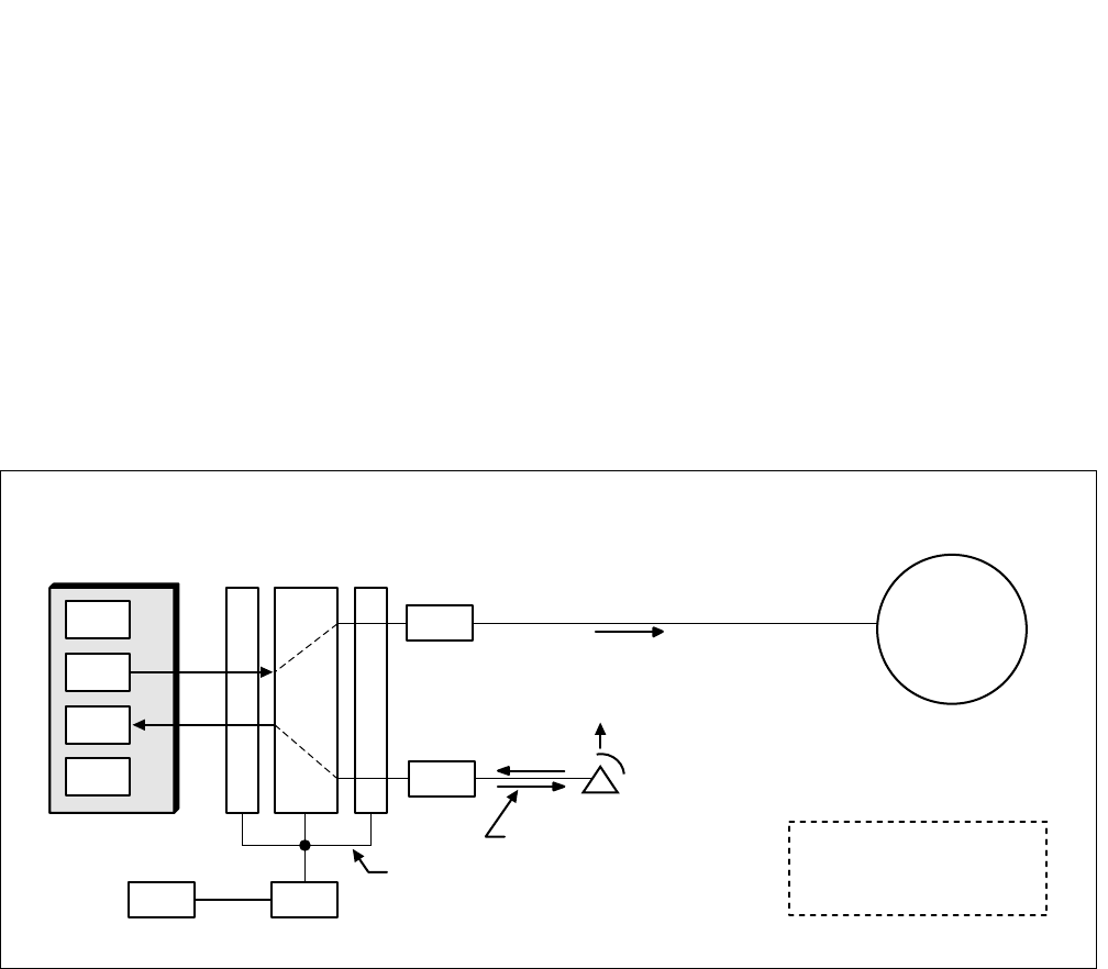
CHAPTER 3 NDA-24296
Page 424
Revision 1.0
PA-8RSTY
Register Sender Trunk
PA-8RSTY
Register Sender Trunk
1. General Function
The PA-8RSTY circuit card is equipped with eight circuits of Registers and Senders. More specifically, this
card contains Dial Pulse Register (DPR), Push Button Receiver (PBR) for receiving digits from extensions
and/or the associated incoming trunks and Dial Pulse Sender (DPS), PB Signal Sender (PBS) for sending
digits to a distant switching system. In addition, this card has “Register Sender” function, by which inter-
digit pause can be changed and PB signals may be converted to DP signals and vice versa without
intervention of the CPU. The card can be used for caller ID service.
Note: The PA-8RSTY card requires Series 7400 or later software.
Figure 3-119 Location of PA-8RSTY (8RST) within the System
GTCPU
TSWINT INT
PB line
PBR
DPR
DPS
PBS
LC
I/O Local Bus
DP Telephone
Caller ID signals
NETWORK
PA-8RSTY
OFF HOOK
(LC for Calling
Number Delivery)
PBR:
PBS:
DPR:
DPS:
Push Button Receiver
PB Signal Sender
Dial Pulse Register
Dial Pulse Sender
PB Signal
DP Signal
OGT
This figure shows “Register Sender” function as an example.
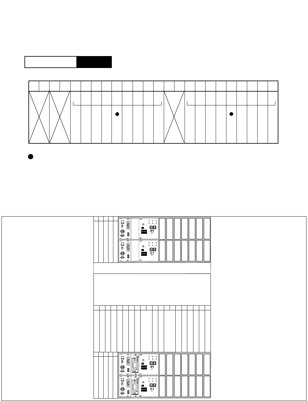
NDA-24296 CHAPTER 3
Page 425
Revision 1.0
PA-8RSTY
Register Sender Trunk
2. Mounting Location/Condition
The PA-8RSTY (RST) card can be mounted any universal slots as shown below.
Note: Indicates universal slots for line/trunk circuit cards.
3. Face Layout of Lamps, Switches, and Connectors
The face layout of lamps, switches, and connectors on this circuit card is shown in Figure 3-120.
Note: Layout of Lamps and switches differ from other RST cards.
Figure 3-120 Face Layout of PA-8RSTY (8RST)
PIM
Mounting Module
00 01 02 03 04 05 06 07 08 09 10 11 12 13 14 15 16 17 18 19 20 21 22 23
00
00
01
01
02
02
03 04
03 04
05 06 07 08 09 10 11 12 13 14 15 16 17 18 19
SP
ISWM
DUMMY
FANU
CMP
PH-PC43 (EMA)
PZ-GT13
(ISAGT) PZ-GT13
(ISAGT)
PZ-PC23
(LANI)
PZ-PC19
(LANI)
PZ-PC19
(LANI)
PZ-PC23
(LANI)
PZ-PC23
(LANI) PZ-PC23
(LANI)
PH-DK10 (DSPC)
PH-IO24 (IOC)
PWRSW0 (PH-PW14)
PWRSW1 (PH-PW14)
HSW00 (PU-SW01) (RES)
HSW11 (PU-SW01) (RES)
HSW01 (PU-SW01)
HSW10 (PU-SW01)
TSW00 (PU-SW00-A)
TSW01 (PU-SW00-A)
TSW02 (PU-SW00-A)
TSW03 (PU-SW00-A)
TSW10 (PU-SW00-A)
TSW11 (PU-SW00-A)
TSW12 (PU-SW00-A)
TSW13 (PU-SW00-A)
IOGT0 (PH-GT10)
IOGT1 (PH-GT10)
PLO0 (PH-CK16-A/17-A)
PLO1 (PH-CK16-A/17-A)
PH-IO24 (IOC) Note
00 01 02 03 04
PH-PC43 (EMA)
PZ-GT13
(ISAGT) PZ-GT13
(ISAGT)
PZ-M565
(ISAGTA)
PZ-M565
(ISAGTA)
PZ-PC22
(LANI)
PZ-ME44
(MEM) PZ-ME44
(MEM)
PZ-PC22
(LANI)
PZ-PC22
(LANI) PZ-PC22
(LANI)
PH-M22 (MMC)

CHAPTER 3 NDA-24296
Page 426
Revision 1.0
PA-8RSTY
Register Sender Trunk
4. Lamp Indications
The contents of lamp indications on this circuit card are shown in the table below.
LAMP NAME COLOR STATE
OPE Green Remains lit while this circuit card is operating.
BLR0
BLR7
Green Lights when the corresponding circuit has received the selective signals.
Flash Flashes (60 IPM) while the corresponding circuit is in make-busy state.
OFF Remains off when the corresponding circuit is idle.
BLS0
BLS7
Green Lights when the corresponding circuit has sent the selective signals.
Flash Flashes (60 IPM) while the corresponding circuit is in make-busy state.
OFF Remains off when the corresponding circuit is idle.
--

NDA-24296 CHAPTER 3
Page 427
Revision 1.0
PA-8RSTY
Register Sender Trunk
5. Switch Settings
Standard settings of switches on this circuit card are shown in the table below.
SWITCH
NAME SWITC
H NO. SETTING STANDARD
SETTING MEANING
MB
(SW00)
UP Circuit card make busy
DOWN ×Circuit card make busy cancel
SW01
(MBR0-7) 0ON Register make busy of the corresponding circuit
OFF ×Register make busy cancel of the corresponding circuit
1ON Register make busy of the corresponding circuit
OFF ×Register make busy cancel of the corresponding circuit
2ON Register make busy of the corresponding circuit
OFF ×Register make busy cancel of the corresponding circuit
3ON Register make busy of the corresponding circuit
OFF ×Register make busy cancel of the corresponding circuit
4ON Register make busy of the corresponding circuit
OFF ×Register make busy cancel of the corresponding circuit
5ON Register make busy of the corresponding circuit
OFF ×Register make busy cancel of the corresponding circuit
6ON Register make busy of the corresponding circuit
OFF ×Register make busy cancel of the corresponding circuit
7ON Register make busy of the corresponding circuit
OFF ×Register make busy cancel of the corresponding circuit
SW02
(MBS0-7) 0ON Sender make busy of the corresponding circuit
OFF ×Sender make busy cancel of the corresponding circuit
1ON Sender make busy of the corresponding circuit
OFF ×Sender make busy cancel of the corresponding circuit
2ON Sender make busy of the corresponding circuit
OFF ×Sender make busy cancel of the corresponding circuit
3ON Sender make busy of the corresponding circuit
OFF ×Sender make busy cancel of the corresponding circuit
4ON Sender make busy of the corresponding circuit
OFF ×Sender make busy cancel of the corresponding circuit
5ON Sender make busy of the corresponding circuit
OFF ×Sender make busy cancel of the corresponding circuit
6ON Sender make busy of the corresponding circuit
OFF ×Sender make busy cancel of the corresponding circuit
7ON Sender make busy of the corresponding circuit
OFF ×Sender make busy cancel of the corresponding circuit
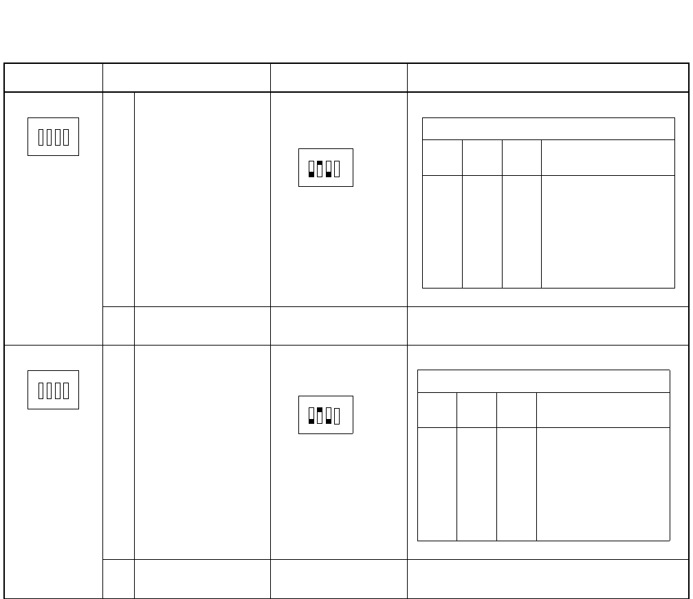
CHAPTER 3 NDA-24296
Page 428
Revision 1.0
PA-8RSTY
Register Sender Trunk
SWITCH FUNCTION SWITCH SETTING MEANING
SW10
1
3
DTMF Signal Receiver
Threshold Value [Standard Setting]
4OFF Fixed to OFF
SW11
1
3
MFR Signal Receiver
Threshold Value [Standard Setting]
4OFF Fixed to OFF
1234
-
1234 ON
OFF
Selection of PBR Threshold Value
SW10-
1SW10-
2SW10-
3DTMF Threshold Value
ON
OFF
ON
OFF
ON
OFF
ON
OFF
ON
ON
OFF
OFF
ON
ON
OFF
OFF
ON
ON
ON
ON
OFF
OFF
OFF
OFF
-21.0 dBm0
-23.0 dBm0
-25.0 dBm0
-27.0 dBm0
-29.0 dBm0
-31.0 dBm0
-33.0 dBm0
-35.0 dBm0
1234
-
123 4 ON
OFF
Selection of MFR Threshold Value
SW11-
1SW11-
2SW11-
3MFR Threshold Value
ON
OFF
ON
OFF
ON
OFF
ON
OFF
ON
ON
OFF
OFF
ON
ON
OFF
OFF
ON
ON
ON
ON
OFF
OFF
OFF
OFF
-17.0 dBm0
-19.0 dBm0
-21.0 dBm0
-23.0 dBm0
-25.0 dBm0
-27.0 dBm0
-29.0 dBm0
-31.0 dBm0
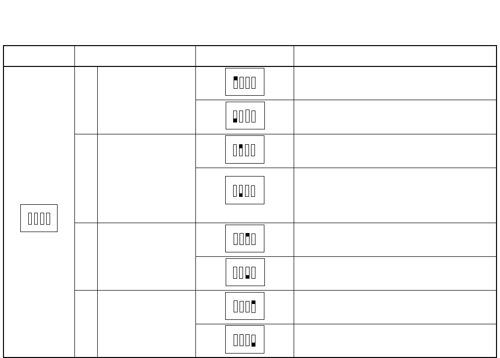
NDA-24296 CHAPTER 3
Page 429
Revision 1.0
PA-8RSTY
Register Sender Trunk
SWITCH FUNCTION SWITCH SETTING MEANING
SW12
1
Designation of MFR
Specification •AT & T specification
•ITU-T No. 5 specification
2
DTMF Signal
Cut-off Guard Timer •SHORT (less than 10 ms)
[Standard Setting]
•
LONG (less than 20 ms)
3
Register Selection
(MFR/PBR) •REG #0, #1, #2, #3 function as MFR.
•REG #0, #1, #2, #3 function as PBR.
4
Register Selection
(MFR/PBR) •REG #4, #5, #6, #7 function as MFR.
•REG #4, #5, #6, #7 function as PBR.
1234
1234
1234
1234
123 4
1234
1234
1234
1234

CHAPTER 3 NDA-24296
Page 430
Revision 1.0
PA-8RSTY
Register Sender Trunk
SWITCH SWITCH
NO. SETTING STANDARD
SETTING MEANING
SW13 1ON MF Transmission Level:-9dBm
OFF MF Transmission Level:-5dBm
2OFF ×Fixed to OFF
3OFF ×Fixed to OFF
4OFF ×Fixed to OFF
SW14 1OFF ×Fixed to OFF
2OFF ×Fixed to OFF
3OFF ×Fixed to OFF
4OFF ×Fixed to OFF
SW15 1OFF ×Fixed to OFF
2OFF ×Fixed to OFF
3OFF ×Fixed to OFF
4OFF ×Fixed to OFF
SW16 1ON ×Fixed to ON
2OFF ×Fixed to OFF
3OFF ×Fixed to OFF
4OFF ×Fixed to OFF
SW17 1OFF ×Fixed to OFF
2OFF ×Fixed to OFF
3OFF ×Fixed to OFF
4OFF ×Fixed to OFF
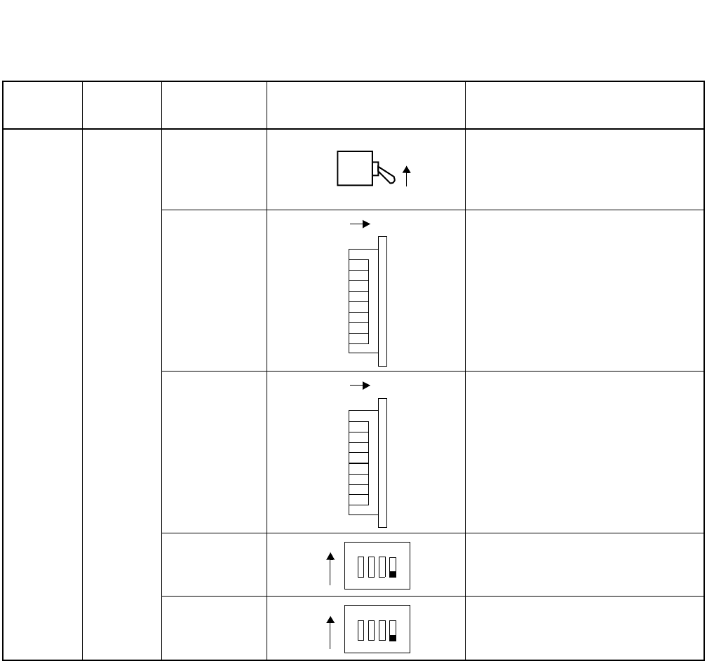
NDA-24296 CHAPTER 3
Page 431
Revision 1.0
PA-8RSTY
Register Sender Trunk
6. Switch Setting Sheet
MODULE SLOT NO. SWITCH
NAME SWITCH SHAPE REMARKS
PIM
SW00
(MB)
Circuit card make busy cancel
Standard Setting : Down
SW01
(MBR0-7)
SW02
(MBS0-7)
SW10
SW11
ON
7
6
5
4
ON
3
2
1
8
7
6
5
4
ON
3
2
1
8
1
ON 2 3 4
1
ON 2 3 4
CHAPTER 3 NDA-24296
Page 432
Revision 1.0
PA-8RSTY
Register Sender Trunk
PIM
SW12
SW13
SW14
SW15
SW16
SW17
MODULE SLOT NO. SWITCH
NAME SWITCH SHAPE REMARKS
1
ON 2 3 4
1
ON 2 3 4
1
ON 2 3 4
1
ON 2 3 4
1
ON 2 3 4
1
ON 2 3 4
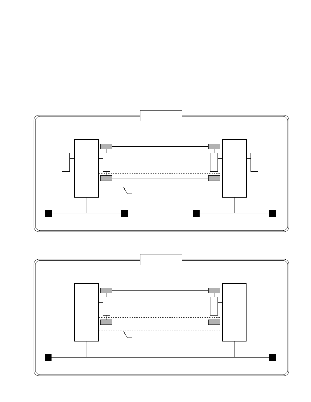
NDA-24296 CHAPTER 3
Page 433
Revision 1.0
PA-SDTA
SDH/SONET Digital Trunk
PA-SDTA
SDH/SONET Digital Trunk
1. General Function
The PA-SDTA circuit card provides a maximum of 28 interface (1.5 Mbps) used with the fiber optic cable.
This card has also the MUX function and is connected directly to the TSW card. This card is used with the
PA-SDTB card.
Figure 3-121 Location of PA-SDTA (SDT) Card in the System
F u s i o n
Node-A
Fiber Optic Cable
Fiber Optic Cable
For Dual Configuration
Connection Link (Data Link)
Connection Trunk (Speech Path)
Internal LAN
FCH
S
D
T
B
Node-B
Internal LAN
S
D
T
B
FCH
+
Fusion Link with FCCH
Fusion Link without FCCH
F u s i o n
Node-A
Internal LAN
Node-B
) SDT: SDH/SONET Digital Trunk
FCH: Fusion Call Control Handler
*
Fiber Optic Cable
Fiber Optic Cable
For Dual Configuration
Connection Trunk (Speech Path)
S
D
T
B
S
D
T
B
SDTA
SDTA
SDTA
SDTA
SDTA
SDTA
SDTA
SDTA
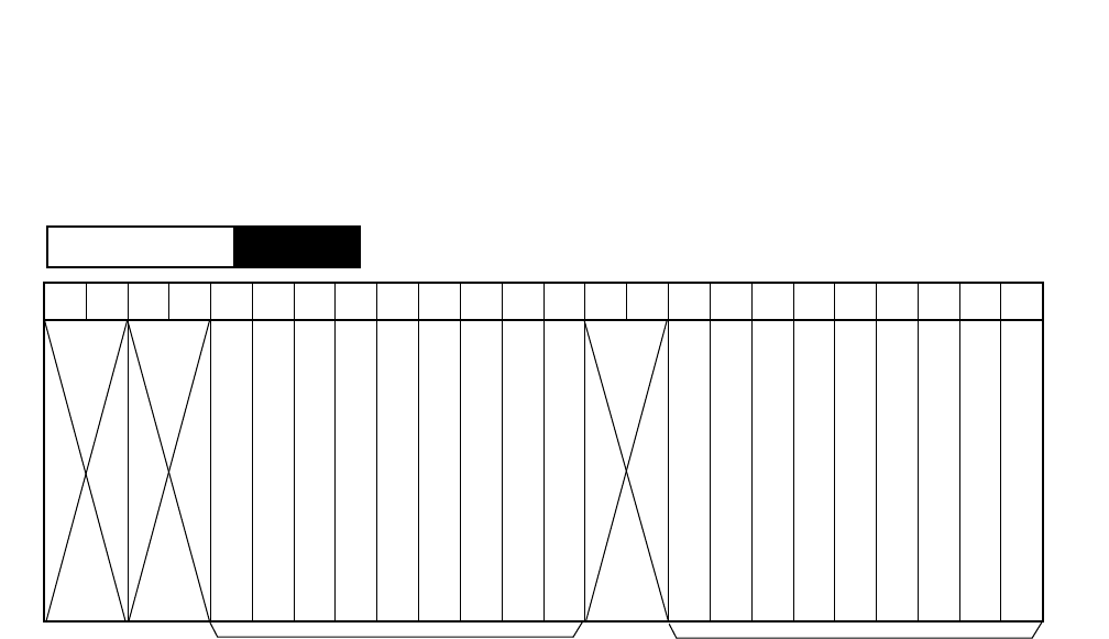
CHAPTER 3 NDA-24296
Page 434
Revision 1.0
PA-SDTA
SDH/SONET Digital Trunk
2. Mounting Location/Condition
This circuit card is mounted in a universal slot next to (either left or right side of) PA-SDTB. When this
card is provided in a dual configuration, mount this card on both sides of PA-SDTB.
Mounting conditions are shown below.
•Only the power is supplied from Back Wiring Board (BWB).
•This card is connected to the PA-SDTB card using the following front cables.
•For single configuration: SDT CABLEB <S>
•For dual configuration: SDT CABLEA <D>
•Fiber optic cables are connected to this card.
•Time slots used for this circuit card are determined by the cable connection between the PA-SDTB and
TSW.
00 01 02 03 04 05 06 07 08 09 10 11 12 13 14 15 16 17 18 19 20 21 22 23
Universal Slots Universal Slots
PIM
Mounting Module
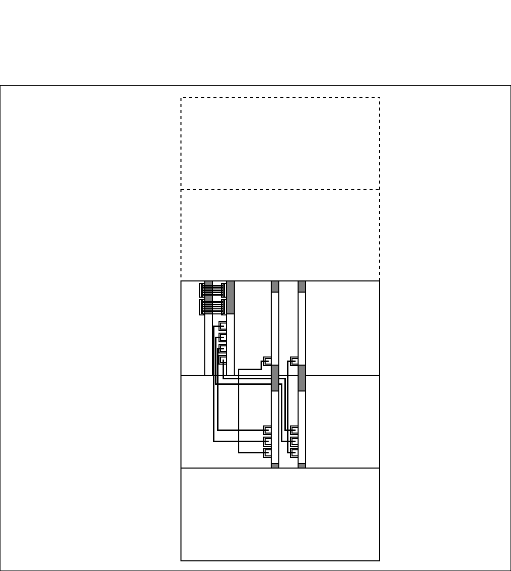
NDA-24296 CHAPTER 3
Page 435
Revision 1.0
PA-SDTA
SDH/SONET Digital Trunk
Example: When the PA-SDTA card is mounted in the 1-IMG system
In Figure 3-122, time slots of Module Group 01 are used. AUNT data is required even if PIM2/PIM3 is
not actually mounted.
Figure 3-122 PA-SDTA Card Mounted in the 1 IMG System
( TS of PIM3 is used for SDT. )
( TS of PIM2 is used for SDT. )
PH-PC30 (MUX)
PH-SW10 (TSW)
MUX3
MUX2
MUX1
MUX
PH-PC30 (MUX)
PH-SW10 (TSW)
MUX3
MUX2
MUX1
MUX
PA-SDTB (SDTB)
MUX1A
MUX0A
MUX0B
MUX1B
PA-SDTA (SDTA)
PIM3
(Not actually
mounted)
PIM2
(Not actually
mounted)
PIM1
PIM0
LPM
I/O
PCM
I/O
PCM
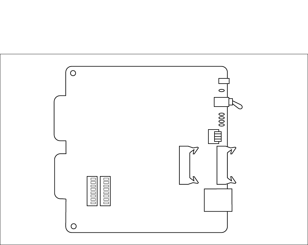

NDA-24296 CHAPTER 3
Page 437
Revision 1.0
PA-SDTA
SDH/SONET Digital Trunk
4. Lamp Indications
Lamp indications for this circuit card are shown in the table below.
LAMP NAME COLOR STATE
OPE Green Remains lit while this circuit card is operating normally.
Red Remains lit while this circuit card is in Make-busy state.
PALM Red Lights when the OBP in this circuit card is abnormal.
OPT Red Lights when the optical input signals are cut off.
SYNC Red Lights when receiving 52 Mbps clock comes off synchronization.
LPB Green Lights when Loop-back is designated.
ACT Green Remains lit while this circuit card is in active state.
Off Remains off while this circuit card is in stand-by state.

CHAPTER 3 NDA-24296
Page 438
Revision 1.0
PA-SDTA
SDH/SONET Digital Trunk
5. Switch Settings
Switch settings on this circuit card are shown in the table below.
.
SWITCH
NAME SWITCH
NO. SETTING STANDARD
SETTING MEANING
MB UP Circuit card Make-busy
DOWN ×Circuit card Make-busy cancel
SW11
1OFF ×Fixed
2ON ×Fixed
3ON ×Fixed
4OFF ×Fixed
5OFF ×Not used
6ON PAD function is effective.
OFF ×PAD function is not effective.
7ON Setting of A-law
OFF ×Setting of µ-law
8ON ×OPT#0 Act (This card is used for System 0)
OFF OPT#1 Act (This card is used for System 1)
SW12 1-8 OFF ×Not used
P-SW
1ON Designation of OLLPB (OPT Local Loop-back)
OFF ×Designation of OLLPB cancel
2ON Designation of ORLPB (OPT Remote Loop-back)
OFF ×Designation of ORLPB cancel.
3OFF ×Not used
4ON Make-busy request
OFF ×Make-busy request cancel
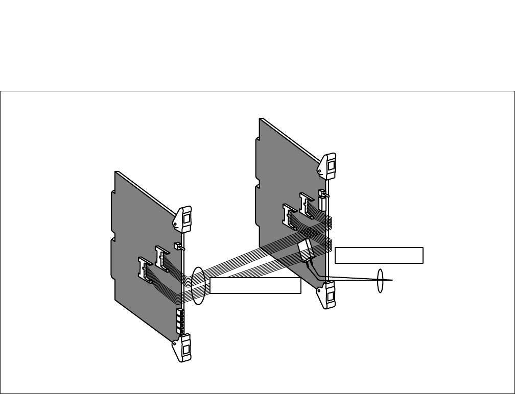
NDA-24296 CHAPTER 3
Page 439
Revision 1.0
PA-SDTA
SDH/SONET Digital Trunk
6. External Interface
•Cable Connection
Figure 3-124 Cable Connection between PA-SDTA and PA-SDTB
PA-SDTB
PA-SDTA
Fiber optic cable
Note1
SDT CABLEB <S>
Note 1: When the PA-SDTA card is provided in a dual configuration, SDT CABLEA (D) is used.
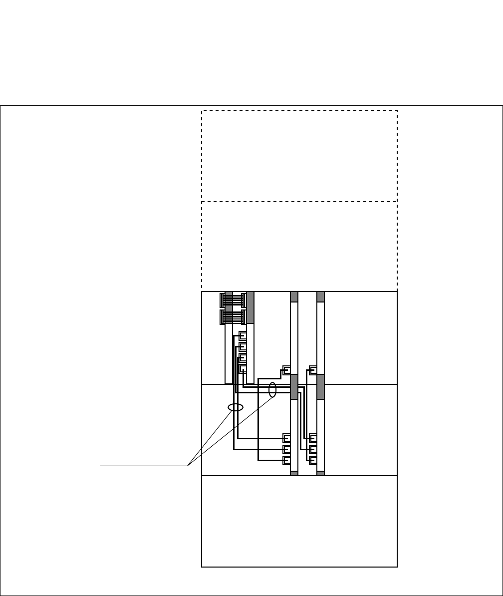
CHAPTER 3 NDA-24296
Page 440
Revision 1.0
PA-SDTA
SDH/SONET Digital Trunk
•When the PA-SDTA/PA-SDTB card is mounted in the 1-IMG system
As shown in Figure 3-125, time slots of Module Group 01 are used. AUNT data is required even if PIM2/
PIM3 is not actually mounted.
Figure 3-125 Example of Cable Connection for 1-IMG System
( TS of PIM3 is used for SDT. )
( TS of PIM2 is used for SDT. )
PH-PC30 (MUX)
PH-SW10 (TSW)
MUX3
MUX2
MUX1
MUX
PH-PC30 (MUX)
PH-SW10 (TSW)
MUX3
MUX2
MUX1
MUX
PA-SDTB (SDTB)
MUX1A
MUX0A
MUX0B
MUX1B
PA-SDTA (SDTA)
PIM3
(Not actually
mounted)
PIM2
(Not actually
mounted)
PIM1
PIM0
MT24 TSW CA-140
LPM
I/O
PCM
I/O
PCM
Note
Note: When the PA-SDTA and PA-SDTB cards are mounted in PIM0, MT24 TSW CA-90 is used.

NDA-24296 CHAPTER 3
Page 441
Revision 1.0
PA-SDTA
SDH/SONET Digital Trunk
•When the PA-SDTA and PA-SDTB cards are mounted in the 4-IMG system
(a) When to use the 34PH MT24 TSW CA-x cable
When the PA-SDTA and PA-SDTB cards are mounted in the 4-IMG system, the 34PH MT24 TSW
CA-x cable is used for connection between the PA-SDTB and TSW. The type of cable varies depend-
ing on the mounting location of the PA-SDTA/PA-SDTB card(s).
Table 3-6 Type of 34PH MT24 TSW CA-x Cable
IMG0 IMG1 IMG2 IMG3
PIM3 34PH MT24 TSW CA-H 34PH MT24 TSW CA-G 34PH MT24 TSW CA-H 34PH MT24 TSW CA-J
PIM2 34PH MT24 TSW CA-H 34PH MT24 TSW CA-F 34PH MT24 TSW CA-H 34PH MT24 TSW CA-I
PIM1 34PH MT24 TSW CA-F 34PH MT24 TSW CA-E 34PH MT24 TSW CA-G 34PH MT24 TSW CA-H
PIM0 34PH MT24 TSW CA-F 34PH MT24 TSW CA-D 34PH MT24 TSW CA-F 34PH MT24 TSW CA-H

CHAPTER 3 NDA-24296
Page 442
Revision 1.0
PA-SDTA
SDH/SONET Digital Trunk
(b) Relationship between the cable connection and the time slot
Trunk data for SDT is assigned to an odd-number Module Group. The module group is determined
by the connection of the 34PH MT24 TSW CA-x cable as shown in the table below.
Note 1: MUX1x on PA-SDTB and MUX1xx on BWB of TSWM are used when the system is a dual configuration.
Note 2: When half of the time slots are used in a module group, time slots for PIM2 must be used. However, the
remaining time slots (for PIM3) cannot be used for other circuit cards.
Table 3-7 Relationship between Cable Connection and Time Slot
MODULE
GROUP
Assigned for
SDT
TIME SLOTS
Assigned for
SDT
CABLE CONNECTIONS
REMARKS
FROM
(Connectors on
PA-SDTB)
TO
(Connectors on
BWB of TSWM)
MG01
PIM2 of IMG0 MUX0A MUX002 In this case, PIM2 and PIM3
of IMG0 are not actually
mounted; However, AUNT
data for PIM2/PIM3 is
required.
MUX1A MUX102
PIM3 of IMG0 MUX0B MUX003
MUX1B MUX103
MG03
PIM2 of IMG1 MUX0A MUX012 In this case, PIM2 and PIM3
of IMG1 are not actually
mounted; However, AUNT
data for PIM2/PIM3 is
required.
MUX1A MUX112
PIM3 of IMG1 MUX0B MUX013
MUX1B MUX113
MG05
PIM2 of IMG2 MUX0A MUX022 In this case, PIM2 and PIM3
of IMG2 are not actually
mounted; However, AUNT
data for PIM2/PIM3 is
required.
MUX1A MUX122
PIM3 of IMG2 MUX0B MUX023
MUX1B MUX123
MG07
PIM2 of IMG3 MUX0A MUX032 In this case, PIM2 and PIM3
of IMG3 are not actually
mounted; However, AUNT
data for PIM2/PIM3 is
required.
MUX1A MUX132
PIM3 of IMG3 MUX0B MUX033
MUX1B MUX133
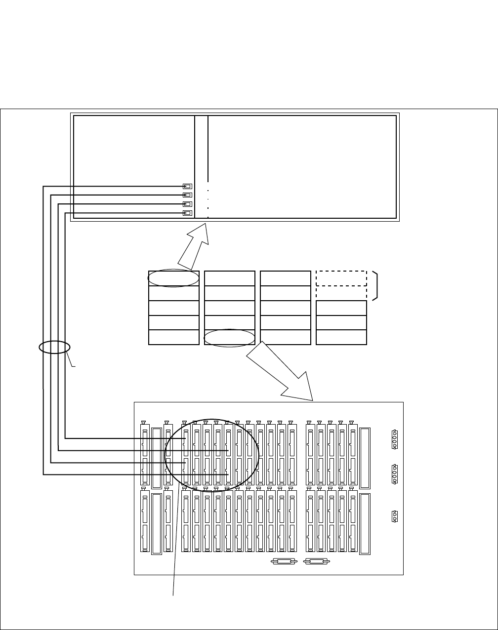
NDA-24296 CHAPTER 3
Page 443
Revision 1.0
PA-SDTA
SDH/SONET Digital Trunk
Example: When the PA-SDTA and PA-SDTB circuit cards are mounted in PIM3 of IMG0, and MG07 (PIM2 and
PIM3 of IMG3) is assigned for the SDT interface, the type of cable and connector locations are as shown
in the following figure. The mounting location of PA-SDTA/PA-SDTB circuit card has no relationship
to the time slots assigned for the SDT interface so the PA-SDTA and PA-SDTB circuit cards can be
mounted in any PIM.
Figure 3-126 Example of Cable Connection for 4-IMG System
PA-SDTB
PIM 3 Time slots assigned
for SDT (MG07).
PIM2 and PIM3 of
IMG3 are not actually
mounted.
34PH MT24 TSW CA-H
(Refer to Table 3-3.)
To MUX133
To MUX033
To MUX132
To MUX032
PIM 2
PIM 1
PIM 0
Dummy
IMG3
PIM 3
PIM 2
PIM 1
PIM 0
Dummy
IMG2
PIM 3
PIM 2
PIM 1
PIM 0
TSWM
IMG1
PIM 3
PIM 2
PIM 1
PIM 0
LPM
IMG0
PIM3
BWB of TSWM
MUX0A
MUX1A
MUX0B
MUX1B
Connect the cables according to the time slots assigned for SDT.
(Refer to Table 3-8 and Figure 3-133.)
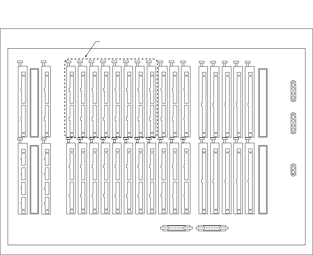
CHAPTER 3 NDA-24296
Page 444
Revision 1.0
PA-SDTA
SDH/SONET Digital Trunk
Figure 3-127 Location of MUXxxx Connectors for SDT
MUX003 MUX002
MUX013 MUX012
MUX023 MUX022
MUX033 MUX032
MUX103 MUX102
MUX113 MUX112
MUX123 MUX122
MUX133 MUX132
MUXxxx Connectors for SDT
NDA-24296 CHAPTER 3
Page 445
Revision 1.0
PA-SDTA
SDH/SONET Digital Trunk
(c) Length of Fiber Optic Cable
The maximum length of the fiber optic cable is approximately 15 kilometers (9.3 miles). Figure 3-
128 shows the level diagram of the fiber optic interface.
Figure 3-128 Level Diagram
Level margin in the case of 15 kilometers (9.3 miles) is as shown in the following table.
Note: Maximum cable length varies depending on the type of cable and the number of connection points.
Table 3-8 Level Margin
CONDITION LEVEL MARGIN
Worst case 4.0 dB
Best case 11.0 dB
0.00 2.00 4.00 6.00 8.00 10.00 12.00 14.00 16.00 18.00 20.00 (km)
0.00
-5.00
-10.00
-15.00
-20.00
-25.00
-30.00
-35.00
Minimum Receiver Sensitivity : -31.00 dBm
Maximum Receiver Sensitivity : -8.00 dBm
: Best Case
: Worst Case
: Maximum Receiver Sensitivity
: Minimum Receiver Sensitivity
Cable Length
1.20 2.40 3.70 4.40 6.20 7.40 8.60 9.90 11.00 12.00 (miles)
Receiver Sensitivity (dBm)
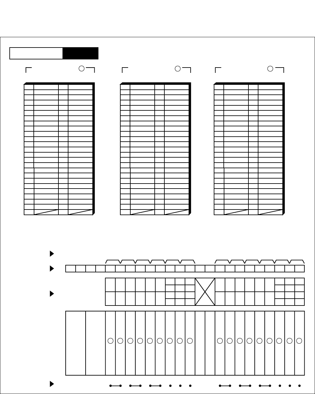
CHAPTER 3 NDA-24296
Page 446
Revision 1.0
PA-SDTA
SDH/SONET Digital Trunk
•Accommodation for the LT connector leads of this circuit card is shown in Figure 3-129.
Figure 3-129 LT Connector Lead Accommodation
26
27
28
29
30
31
32
33
34
35
36
37
38
39
40
41
1
2
3
4
5
6
7
8
9
10
11
12
13
14
15
16
42
43
44
45
46
47
48
17
18
19
20
21
22
23
49
50 24
25
232221201918171615141312111009080706050403020100
LT6 LT7 LT8 LT9 LT10 LT11LT0 LT1 LT2 LT3 LT4 LT5
231915
221814
211713
201612
231915
221814
211713
201612
110907050301
100806040200
110907050301
100806040200
HW11HW10HW9HW8HW7HW6HW5HW4HW3HW2HW1HW0
Group No.
Slot No.
LT Connector
PIM
Highway Block
LT 3, 5, 9, 11 Connector
26
27
28
29
30
31
32
33
34
35
36
37
38
39
40
41
1
2
3
4
5
6
7
8
9
10
11
12
13
14
15
16
42
43
44
45
46
47
48
17
18
19
20
21
22
23
49
50 24
25
Accommodated in 2
LT 1, 5, 7, 11 Connector
Accommodated in 3
26
27
28
29
30
31
32
33
34
35
36
37
38
39
40
41
1
2
3
4
5
6
7
8
9
10
11
12
13
14
15
16
42
43
44
45
46
47
48
17
18
19
20
21
22
23
49
50 24
25
Accommodated in 1
LT 2, 4, 8, 10 Connector
POUT B POUT A
POUT B POUT A
POUT B POUT A
21 3 2 1 3 21 31 2
231231 3
Note: The output of POUT A/B is 1,544 MHz.
PIM
Mounting Module
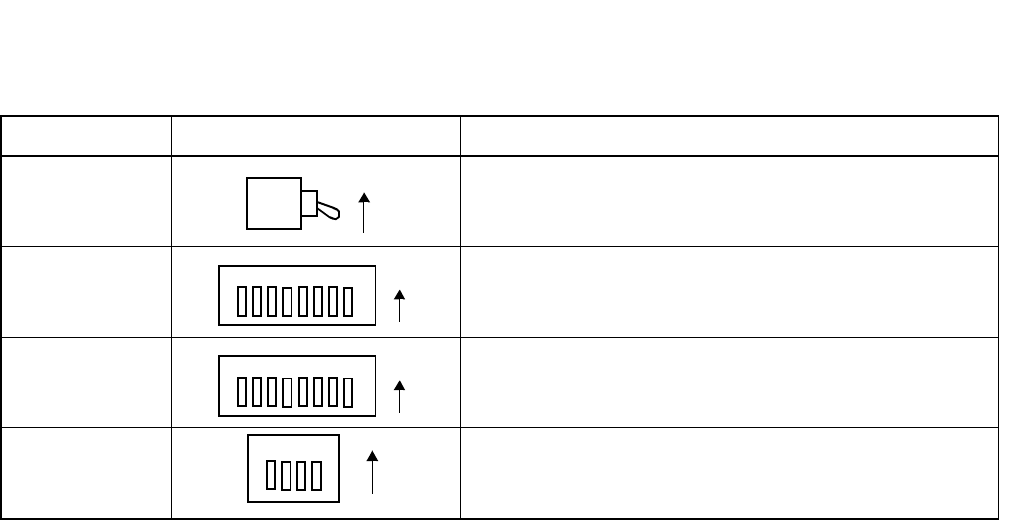
NDA-24296 CHAPTER 3
Page 447
Revision 1.0
PA-SDTA
SDH/SONET Digital Trunk
7. Switch Setting Sheet
SWITCH NAME SWITCH SHAPE REMARKS
MB
SW11
SW12
P-SW
ON
1234 ON
56 7 8
1234 ON
56 7 8
1ON
234
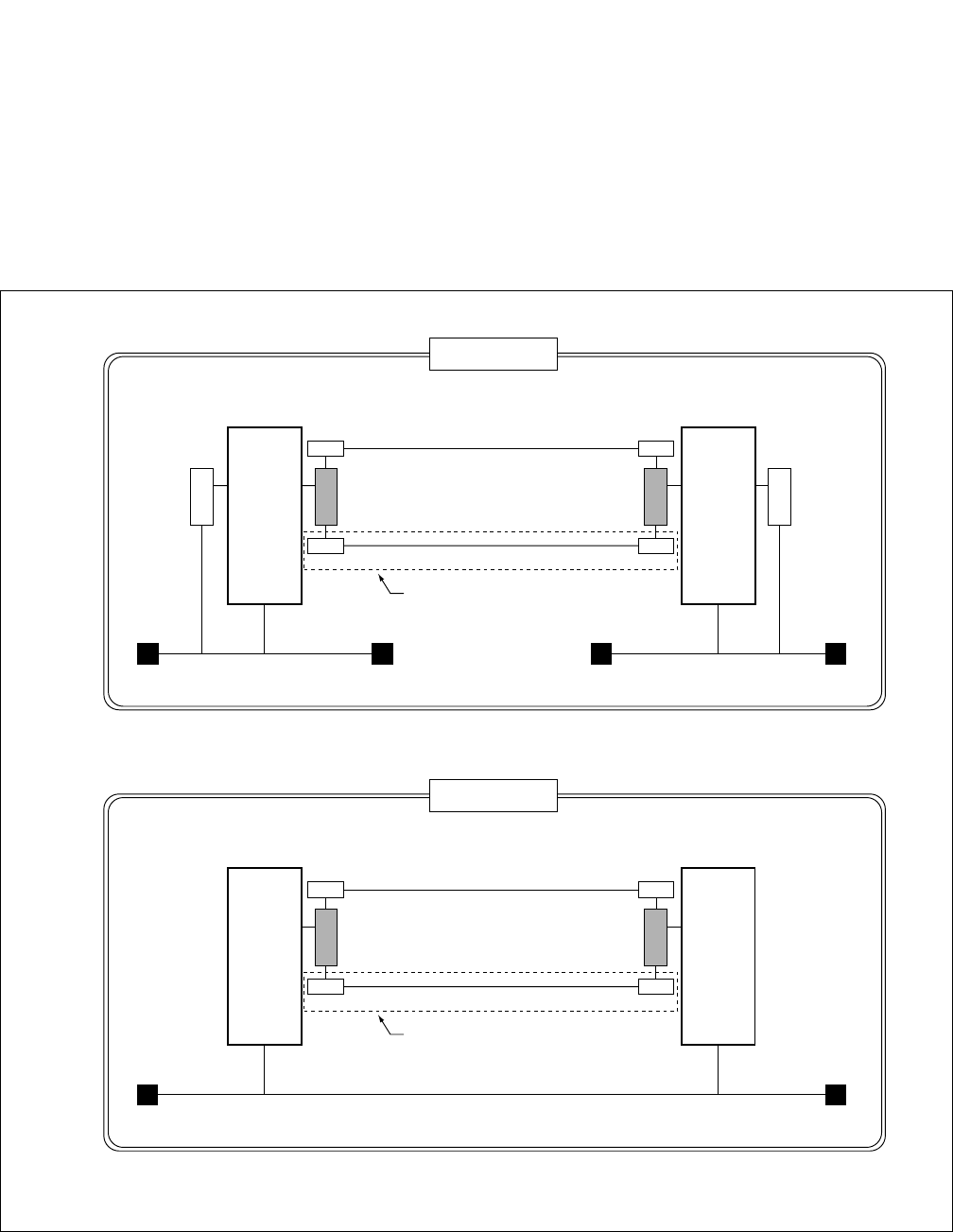
CHAPTER 3 NDA-24296
Page 448
Revision 1.0
PA-SDTB
SDH/SONET Digital Trunk
PA-SDTB
SDH/SONET Digital Trunk
1. General Function
The PA-SDTA circuit card provides a maximum of 28 interface (1.5 Mbps) used with the fiber optic cable.
This card also has the MUX function and is connected directly to the TSW card. This card is used with the
PA-SDTA card.
Figure 3-130 Location of PA-SDTB (SDT) Card in the System
F u s i o n
Node-A
Fiber Optic Cable
Fiber Optic Cable
For Dual Configuration
Connection Link (Data Link)
Connection Trunk (Speech Path)
Internal LAN
FCH
S
D
T
B
Node-B
Internal LAN
S
D
T
B
FCH
+
Fusion Link with FCCH
Fusion Link without FCCH
F u s i o n
Node-A
Internal LAN
Node-B
) SDT: SDH/SONET Digital Trunk
FCH: Fusion Call Control Handler
*
Fiber Optic Cable
Fiber Optic Cable
For Dual Configuration
Connection Trunk (Speech Path)
S
D
T
B
S
D
T
B
SDTA
SDTA
SDTA
SDTA
SDTA
SDTA
SDTA
SDTA
NDA-24296 CHAPTER 3
Page 449
Revision 1.0
PA-SDTB
SDH/SONET Digital Trunk
2. Mounting Location/Condition
This circuit card can be mounted in any universal slots.
Mounting conditions are shown below.
•Only the power is supplied from Back Wiring Board (BWB).
•This card is connected to the PA-SDTA card using the following front cables.
•For single configuration: SDT CABLEB <S>
•For dual configuration: SDT CABLEA <D>
•This card is connected to the TSW card.
•Time slots used for this circuit card are determined by the cable connection between the PA-SDTB and
TSW.
00 01 02 03 04 05 06 07 08 09 10 11 12 13 14 15 16 17 18 19 20 21 22 23
PIM
Mounting Module
Universal Slots Universal Slots
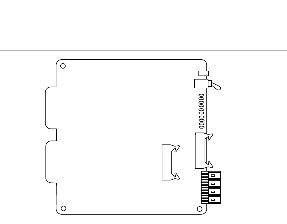
CHAPTER 3 NDA-24296
Page 450
Revision 1.0
PA-SDTB
SDH/SONET Digital Trunk
3. Face Layout of Lamps, Switches, and Connectors
The face layout of lamps, switches, and connectors are shown in the figure in Figure 3-131.
Figure 3-131 Face Layout of PA-SDTB (SDT)
MB
PCM
MUX0A
MUX1A
MUX0B
MUX1B
I/O
OPE
2MALA
2MALB
32MALA
32MALB
ACT0
ACT1
SYC0A
SYC1A
SYC0B
SYC1B

NDA-24296 CHAPTER 3
Page 451
Revision 1.0
PA-SDTB
SDH/SONET Digital Trunk
4. Lamp Indications
Lamp indications for this circuit card are shown in the table below:
Note: A-side MUX means the card located in UNIT0/1 and B-side MUX means the card located in UNIT2/3.
LAMP NAME COLOR STATE
OPE Green Remains lit when this circuit card is in operation.
Red Remains lit when this circuit card is in non-operation.
2MALA Red Lights when 2 M clock and FH from A-side MUX is abnormal.
2MALB Red Lights when 2 M clock and FH from B-side MUX is abnormal.
32MALA Red Lights when 32 M clock from A-side MUX is abnormal.
32MALB Red Lights when 32 M clock from B-side MUX is abnormal.
ACT0 Green Remains lit when MUX#0 is operating normally.
Off Remains off when MUX#0 is in stand-by state.
ACT1 Green Remains lit when MUX#1 is operating normally.
Off Remains off when MUX#1 is in stand-by state.
SYC0A Green Lights when MUX#0 synchronization with TSW is established in A-side.
Off Goes off when the synchronization is not established.
SYC1A Green Lights when MUX#1 synchronization with TSW is established in A-side.
Off Goes off when the synchronization is not established.
SYC0B Green Lights when MUX#0 synchronization with TSW is established in B-side.
Off Goes off when the synchronization is not established.
SYC1B Green Lights when MUX#1 synchronization with TSW is established in B-side.
Off Goes off when the synchronization is not established.
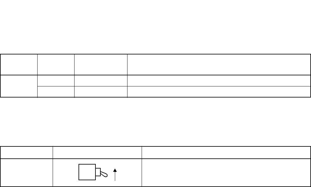
CHAPTER 3 NDA-24296
Page 452
Revision 1.0
PA-SDTB
SDH/SONET Digital Trunk
5. Switch Settings
Switch settings for this circuit card are shown in the table below:
6. External Interface
Refer to the PA-SDTA circuit card.
7. Switch Setting Sheet
SWITCH
NAME SETTING STANDARD
SETTING MEANING
MB UP Circuit card Make-busy
DOWN ×Circuit card Make-busy cancel
SWITCH NAME SWITCH SHAPE
MB
ON
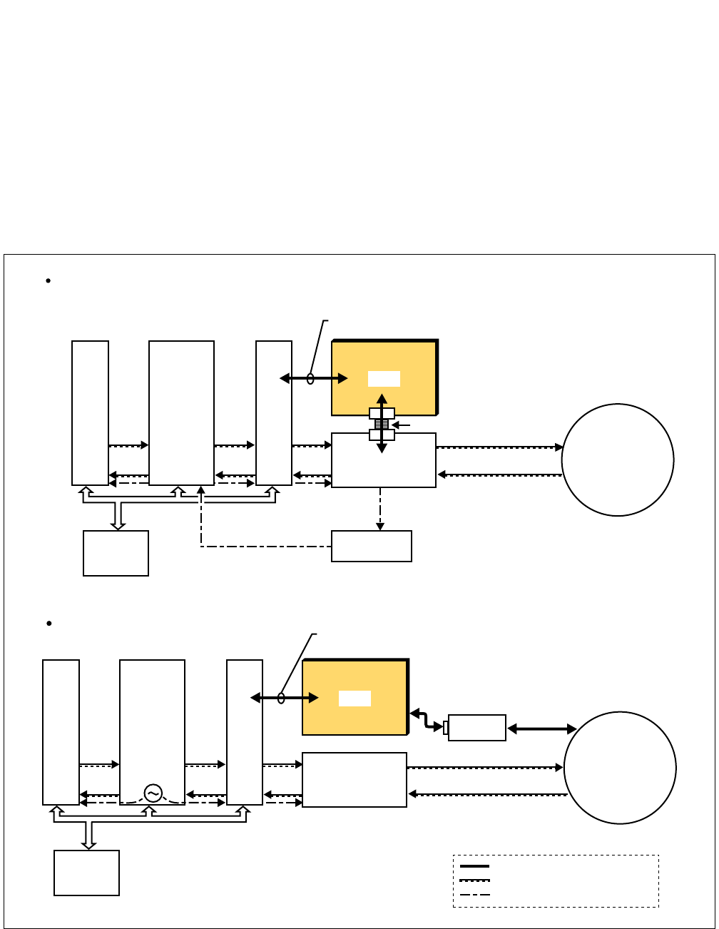
NDA-24296 CHAPTER 3
Page 453
Revision 1.0
PA-2CCHA
Common Channel Handler
PA-2CCHA
Common Channel Handler
1. General Function
Equipped with two circuits of Common Channel Handlers (CCHs), the PA-2CCH A circuit card provides
two signaling links for a digital/analog Common Channel Interoffice Signaling (CCIS) system, which can
be selected by key settings on this card. If a digital CCIS system, this card is connected to a Digital Trunk
Interface (DTI) card with a flat cable to exchange common channel signals as illustrated below. To support
an analog CCIS system, this card also has an RS-232c interface for Modem(s).
Figure 3-132 Location of PA-2CCHA (CCH) within the System
CPU System Clock
INT SW INT
2-wire
2-wire
PLO
Clock Extraction
(For a PLO-SECONDARY switch)
CCH
DTI
Common Channel Signaling Link (x2)
I/O Local Bus
Flat Cable
CPU
INT SW INT
Analog Tie Line
CCH
TLT
Common Channel Signaling Link (x2)
I/O Local Bus
CLK
MODEM
Digital CCIS
Analog CCIS (with MODEM)
CCIS
NETWORK
CCIS
NETWORK
: Common Channel Signaling Link
: Speech Path (PCM Signal)
: Clock Signal
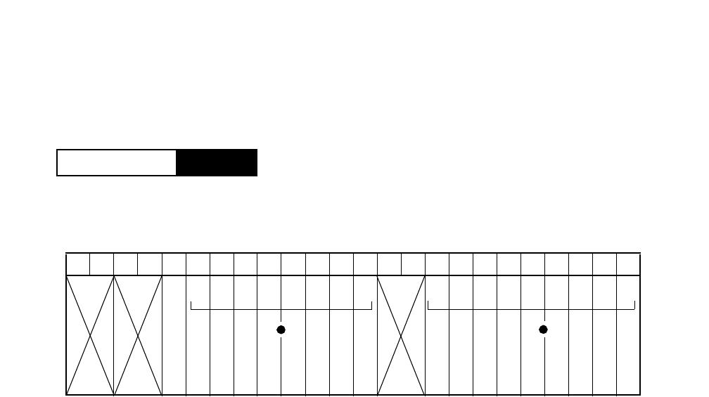
CHAPTER 3 NDA-24296
Page 454
Revision 1.0
PA-2CCHA
Common Channel Handler
2. Mounting Location/Condition
The PA-2CCHA (CCH) card can be mounted in any universal slots as shown below. The DTI and CCH
card, however, cannot coexist in the same Highway Block.
The PA-2CCHA (CCH) card can be mounted in the following universal slots shown below. Note that this
card cannot be mounted in slot 04.
Note: When this card is mounted in slot No.4, the LENS data for the first circuit of the CCH card must be assigned
as “000 000”, which is rejected by the ATRK command.
PIM
Mounting Module
00 01 02 03 04 05 06 07 08 09 10 11 12 13 14 15 16 17 18 19 20 21 22 23
Note
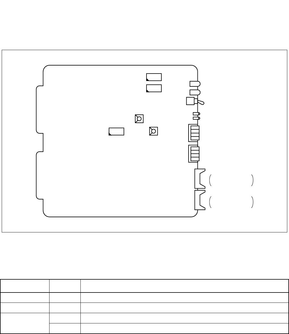
NDA-24296 CHAPTER 3
Page 455
Revision 1.0
PA-2CCHA
Common Channel Handler
3. Face Layout of Lamps, Switches, and Connectors
The face layout of lamps, switches, and connectors on this circuit card is shown in Figure 3-133.
Figure 3-133 Face Layout of PA-2CCHA (CCH)
4. Lamp Indications
The contents of lamp indications of this circuit card are shown in the table below.
LAMP NAME COLOR STATE
OPE Green Remains lit while this circuit card is operating.
N-OPE Red Remains lit while this circuit card is in make-busy state.
DOPE0
DOPE1
Red Lights when the common channel signalling link is set up.
Flash Flashes when CCH is started up.
OPE
N-OPE
MB
DOPE0
DOPE1
SW01
SW02
SW14
SW13
SW12
SW11
SW10
TRK
To "CN2" connector
on CCT/DTI
DCH/CCH
To "TRK" connector
on other DCH/CCH

CHAPTER 3 NDA-24296
Page 456
Revision 1.0
PA-2CCHA
Common Channel Handler
5. Switch Settings
Standard settings of various switches on this circuit card are shown in the table below.
SWITCH
NAME SWITCH
NO. SETTING STANDARD
SETTING MEANING
MB ON Circuit card make busy
OFF ×Circuit card make busy cancel
SW01 0ON No. 0 Circuit make busy request
OFF ×No. 0 Circuit make busy request cancel
1ON No. 1 Circuit make busy request
OFF ×No. 1 Circuit make busy request cancel
2OFF ×Not used
3OFF ×Not used
SW02 0ON Loop back of No. 0 Circuit is performed.
OFF ×Loop back of No. 0 Circuit is not performed.
1ON Loop back of No. 1 Circuit is performed.
OFF ×Loop back of No. 1 Circuit is not performed.
2ON Drop/Insert of No. 0 Circuit is performed.
OFF Drop/Insert of No. 0 Circuit is not performed.
3ON Drop/Insert of No. 1 Circuit is performed.
OFF Drop/Insert of No. 1 Circuit is not performed.
SW10
1
2
3
SETTING OF TRANSFER SPEED OF DROP/INSERT IN NO.0 CIRCUIT
SW10-1 SW10-2 SW10-3 TRANSFER SPEED
ON ON ON 64 kbps
OFF ON ON 32 kbps (Forward)
ON OFF ON 16 kbps (Forward)
OFF OFF ON 8 kbps (Forward)
ON ON OFF 64 kbps
OFF ON OFF 32 kbps (Backward)
ON OFF OFF 16 kbps (Backward)
OFF OFF OFF 8 kbps (Backward)
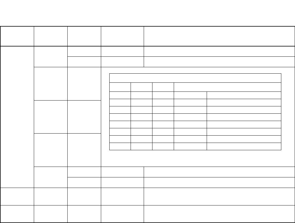
NDA-24296 CHAPTER 3
Page 457
Revision 1.0
PA-2CCHA
Common Channel Handler
Note: When SW10-4 is set ON, SW10-1, SW10-2 and 10-3 should be set ON.
When SW10-8 is set ON, SW10-5, 10-6 and 10-7 should be set ON.
SWITCH
NAME SWITCH
NO. SETTING STANDARD
SETTING MEANING
SW10
4ON Modem is used in No. 0 Circuit
OFF Modem is not used in No. 0 Circuit
5
6
7
8ON Modem is used in No. 1 Circuit.
OFF Modem is not used in No. 1 Circuit.
SW11
(MODE0) 0×Standard setting
SW12
(MODE1) 0×Standard setting
SETTING OF TRANSFER SPEED OF DROP/INSERT IN NO.1 CIRCUIT
SW10-5 SW10-6 SW10-7 TRANSFER SPEED
ON ON ON 64 kbps
OFF ON ON 32 kbps (Forward)
ON OFF ON 16 kbps (Forward)
OFF OFF ON 8 kbps (Forward)
ON ON OFF 64 kbps
OFF ON OFF 32 kbps (Backward)
ON OFF OFF 16 kbps (Backward)
OFF OFF OFF 8 kbps (Backward)
CHAPTER 3 NDA-24296
Page 458
Revision 1.0
PA-2CCHA
Common Channel Handler
SWITCH
NAME SWITCH
NO. SETTING STANDARD
SETTING MEANING
SW13
(for No. 0
Circuit)
SW14
(for No. 1
Circuit)
1
2
3
4
5
6ON Mode setting; No. 7 PCR (Preventive Cyclic Retransmission method)
OFF Mode setting; No. 7 CCIS
7
8
SETTING OF TIME SLOT NUMBER OF DROP/INSERT
SW13-1/
SW14-1 SW13-2/
SW14-2 SW13-3/
SW14-3 SW13-4/
SW14-4 SW13-5/
SW14-5 TIME SLOT NO.
OFF
ON
OFF
ON
OFF
ON
OFF
ON
OFF
ON
OFF
ON
OFF
ON
OFF
ON
OFF
ON
OFF
ON
OFF
ON
OFF
ON
OFF
ON
OFF
ON
OFF
ON
OFF
ON
OFF
OFF
ON
ON
OFF
OFF
ON
ON
OFF
OFF
ON
ON
OFF
OFF
ON
ON
OFF
OFF
ON
ON
OFF
OFF
ON
ON
OFF
OFF
ON
ON
OFF
OFF
ON
ON
OFF
OFF
OFF
OFF
ON
ON
ON
ON
OFF
OFF
OFF
OFF
ON
ON
ON
ON
OFF
OFF
OFF
OFF
ON
ON
ON
ON
OFF
OFF
OFF
OFF
ON
ON
ON
ON
OFF
OFF
OFF
OFF
OFF
OFF
OFF
OFF
ON
ON
ON
ON
ON
ON
ON
ON
OFF
OFF
OFF
OFF
OFF
OFF
OFF
OFF
ON
ON
ON
ON
ON
ON
ON
ON
OFF
OFF
OFF
OFF
OFF
OFF
OFF
OFF
OFF
OFF
OFF
OFF
OFF
OFF
OFF
OFF
ON
ON
ON
ON
ON
ON
ON
ON
ON
ON
ON
ON
ON
ON
ON
ON
CH0
CH1
CH2
CH3
CH4
CH5
CH6
CH7
CH8
CH9
CH10
CH11
CH12
CH13
CH14
CH15
CH16
CH17
CH18
CH19
CH20
CH21
CH22
CH23
CH24
CH25
CH26
CH27
CH28
CH29
CH30
CH31
SETTING OF SPEED OF MODE
SW13-7/
SW14-7 SW13-8/
SW14-8 SPEED
OFF OFF 2400 bps
OFF ON 4800 bps
ON OFF 9600 bps
ON ON Inhibit
NDA-24296 CHAPTER 3
Page 459
Revision 1.0
PA-2CCHA
Common Channel Handler
6. External Interface
In analog CCIS, necessary leads for Modems appear on LT connectors as follows.
See also Connecting Route Diagram for Digital/Analog CCIS.
Figure 3-134 LT Connector Lead Accommodation (1/2)
PIM
Mounting Module
26
27
28
29
30
31
32
33
34
35
36
37
38
39
40
41
1
2
3
4
5
6
7
8
9
10
11
12
13
14
15
16
42
43
44
45
46
47
48
17
18
19
20
21
22
23
49
50 24
25
232221201918171615141312111009080706050403020100
LT6 LT7 LT8 LT9 LT10 LT11LT0 LT1 LT2 LT3 LT4 LT5
231915
221814
211713
201612
231915
221814
211713
201612
110907050301
100806040200
110907050301
100806040200
HW11HW10HW9HW8HW7HW6HW5HW4HW3HW2HW1HW0
Group No.
Slot No.
LT Connector
PIM
Highway Block
Accommodated in 2
LT 0, 2, 4, 6, 8, 10 Connector
26
27
28
29
30
31
32
33
34
35
36
37
38
39
40
41
1
2
3
4
5
6
7
8
9
10
11
12
13
14
15
16
42
43
44
45
46
47
48
17
18
19
20
21
22
23
49
50 24
25
SG 0
RT 0
RS 0
RD 0
ER 0
ST2 0
Accommodated in 1
LT 0, 2, 4, 6, 8, 10 Connector
26
27
28
29
30
31
32
33
34
35
36
37
38
39
40
41
1
2
3
4
5
6
7
8
9
10
11
12
13
14
15
16
42
43
44
45
46
47
48
17
18
19
20
21
22
23
49
50 24
25
LT 1, 3, 5, 7, 9, 11 Connector
SD 0
RD 1
ER 1
ST2 1
SD 1
SCKA 0
TDA 0
RDA 0
SCKA 1
TDA 1
RDA 1
SG 1
RT 1
RS 1
SCKB 0
TDB 0
RDB 0
SCKB 1
TDB 1
RDB 1
SG 0
RT 0
RS 0
SG 1
RT 1
RS 1
RD 0
ER 0
ST2 0
SD 0
RD 1
ER 1
ST2 1
SD 1
SCKA 0
TDA 0
RDA 0
SCKA 1
TDA 1
RDA 1
SCKB 0
TDB 0
RDB 0
SCKB 1
TDB 1
RDB 1
2 21 21 21 21 211
CHAPTER 3 NDA-24296
Page 460
Revision 1.0
PA-2CCHA
Common Channel Handler
Figure 3-134 LT Connector Lead Accommodation (2/2)
PIM
Mounting Module
232221201918171615141312111009080706050403020100
LT6 LT7 LT8 LT9 LT10 LT11LT0 LT1 LT2 LT3 LT4 LT5
231915
221814
211713
201612
231915
221814
211713
201612
110907050301
100806040200
110907050301
100806040200
HW11HW10HW9HW8HW7HW6HW5HW4HW3HW2HW1HW0
Group No.
Slot No.
LT Connector
PIM
Highway Block
26
27
28
29
30
31
32
33
34
35
36
37
38
39
40
41
1
2
3
4
5
6
7
8
9
10
11
12
13
14
15
16
42
43
44
45
46
47
48
17
18
19
20
21
22
23
49
50 24
25
SG 0
RT 0
RS 0
RD 0
ER 0
ST2 0
Accommodated in 3
LT 1, 3, 5, 9, 11 Connector
SD 0
RD 1
ER 1
ST2 1
SD 1
SCKA 0
TDA 0
RDA 0
SCKA 1
TDA 1
RDA 1
SG 1
RT 1
RS 1
SCKB 0
TDB 0
RDB 0
SCKB 1
TDB 1
RDB 1
3 3 3 3 3 3
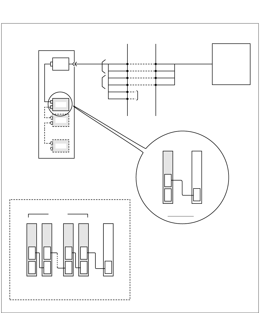
NDA-24296 CHAPTER 3
Page 461
Revision 1.0
PA-2CCHA
Common Channel Handler
Figure 3-135 Connecting Route Diagram (Digital CCIS)
DTI TA
TB
TA
TB
PBX
MDF
RA RA
RB RB
POUTA
POUTB To PLO
TRK DCH/
CCH
TRK DCH/
CCH
TRK DCH/
CCH
TRK DCH/
CCH
CN2
CCH Note
DTI
Note: A maximum of 7CCH cards
can be connected to a DTI card.
CCH Multiple Connection
CCH
CCH
CCH
PCM
CARRIER
EQUIPMENT
TRK DCH/
CCH
CN2
DTICCH
FRONT VIEW
OUT
IN
• Digital CCIS
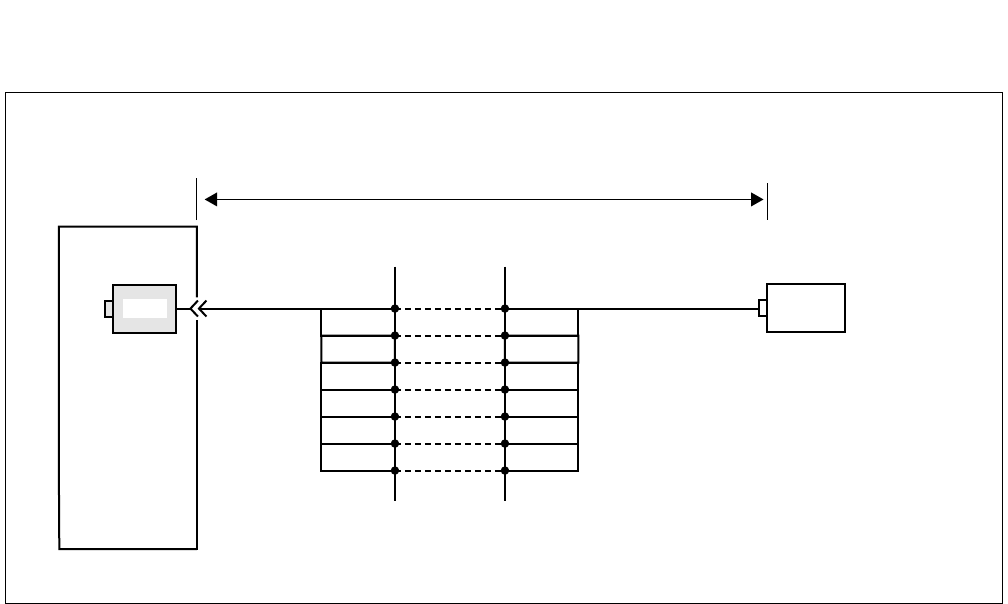
CHAPTER 3 NDA-24296
Page 462
Revision 1.0
PA-2CCHA
Common Channel Handler
Figure 3-136 Connecting Route Diagram (Analog CCIS)
RD
SG
RD
SG
PBX
MDF
ER ER
RT RT
ST2
RS
MODEM
ST2
RS
SD SD
15-m (50-foot) cable limit
<Available MODEM>
• synchronous
• 2400, 4800, 9600 bps
• 4-wire
• Full Duplex
CCH
• Analog CCIS (with MODEM)
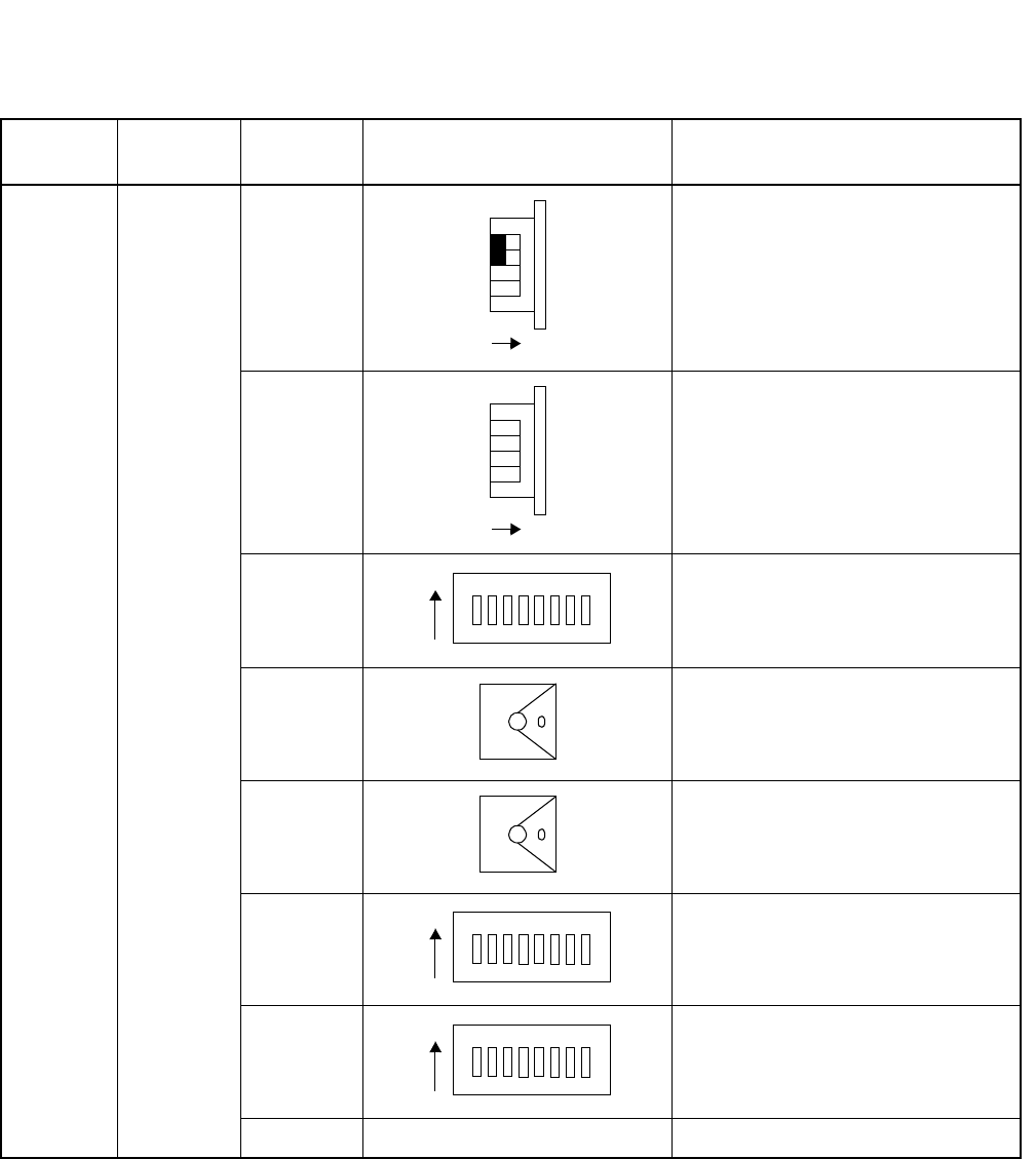
NDA-24296 CHAPTER 3
Page 463
Revision 1.0
PA-2CCHA
Common Channel Handler
7. Switch Setting Sheet
MODULE SLOT NO. SWITCH
NAME SWITCH SHAPE REMARKS
PIM
SW01 SW01-2 and 3: Not used
SW02
SW10
SW11 Standard Setting
SW12 Standard Setting
SW13
SW14
MB DOWN Circuit card make busy cancel
ON
3
2
1
0
ON
3
2
1
0
12345678
ON
12345678
ON
12345678
ON
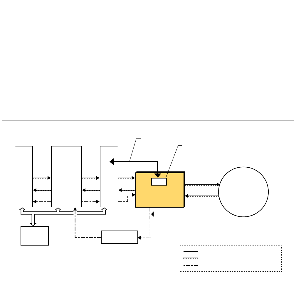
CHAPTER 3 NDA-24296
Page 464
Revision 1.0
PA-24CCTA
Common Channel Trunk
PA-24CCTA
Common Channel Trunk
1. General Function
The PA-24CCTA (24CCT) circuit card provides an interface between 24 digital trunks and the system at
1.5 M bit/s. Being equipped with a Common Channel Handler (CCH), which can be allocated to a desired
channel among the existing 24 channels by key setting and programming, this card can be used as an inter-
face for a Common Channel Interoffice Signaling (CCIS) system. A built-in resonance circuit can be used
for the purpose of extracting clock signals when the PBX functions as a PLO-secondary switch. To obtain
appropriate speech level, this card is equipped with a mask ROM in which typical PAD patterns have been
already written. A desired PAD value can be easily selected by key setting and programming.
Figure 3-137 Location of PA-24CCTA (24CCT) within the System
I/O Local Bus
CPU
System Clock
INT TSW INT
Common Channel Signaling Link
PLO
1.544 MHz Clock Extraction
(For PLO-secondary switch)
CCH
Built-in Common Channel Handler (x1)
T
R
24CCT
: Common Channel Signaling Link
: Speech Path (PCM Signal)
: Clock Signal
CCIS
NETWORK
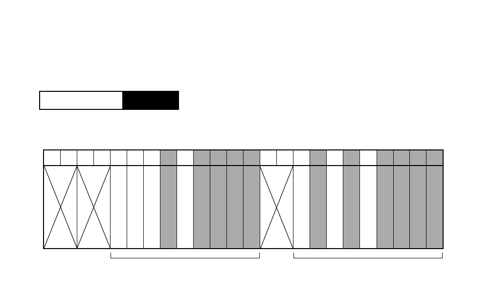
NDA-24296 CHAPTER 3
Page 465
Revision 1.0
PA-24CCTA
Common Channel Trunk
2. Mounting Location/Condition
The PA-24CCTA (24CCT) card can be mounted in the following universal slots as shown below.
This card is mounted in the following shaded slots.
PIM
Mounting Module
00 01 02 03 04 05 06 07 08 09 10 11 12 13 14 15 16 17 18 19 20 21 22 23
Universal Slots Universal Slots
Note: This card cannot be mounted in Slot 05.
Note
CHAPTER 3 NDA-24296
Page 466
Revision 1.0
PA-24CCTA
Common Channel Trunk
3. Face Layout of Lamps, Switches, and Connectors
The face layout of lamps, switches, and connector on this circuit card is shown in Figure 3-138. Note that
there are two types of PA-24 CCTA cards which differ in their face layouts.
Figure 3-138 Face Layout of PA-24CCTA (24CCT)
3
2
1
0
SW6G
SW5DSW4D
SW6C
SW39
SW58
SW25
SW11B
SW138
SW13B
MODE
OPE
N-OPE
MB
PCM
BER
AIS
DOPE
LB
FRM
RMT
LYR
BL23
BL00
CN2
To "TRK" Connector
on CCH/DCH
3
2
1
0
SW18
SW19
SW15 SW14
SW13
OPE
N-OPE
MB
PCM
BER
AIS
DOPE
LB
FRM
RMT
LYR
BL23
BL00
CN2
To "TRK" Connector
on CCH/DCH
SW17 SW00
SW01
SW02
SW12
SW11
SW10

NDA-24296 CHAPTER 3
Page 467
Revision 1.0
PA-24CCTA
Common Channel Trunk
4. Lamp Indications
The contents of lamp indications on this circuit card are shown in Table 3-9.
Table 3-9 PA-24CCTA (24CCT) Lamp Indication Reference
LAMP NAME COLOR STATE
OPE Green Remains lit while this circuit card is in normal operation.
N-OPE Red Remains lit while this circuit card is in make-busy state.
PCM Red Lights when an input signal is down (PCM LOSS).
FRM Red Lights when a frame alignment loss is detected.
BER Red Lights when frequent bit errors occur in the case of 12-multi frame and when a CRC error
occurs frequently in the case of 24-multiframe.
RMT Red Lights on receipt of remote alarm indication.
AIS Yellow Lights on receipt of Alarm Information Signal (AIS).
D-OPE Green Remains lit while Common Channel Handler (CCH) block is active.
LYR Green Remains lit while CCIS signal link is set up.
LB Green Remains lit while the CCIS signal is being looped back.
BL00
BL23
Green Lights when the corresponding circuit is busy.
Flash Flashes while DP signals are being sent out or received (Flashes to dial pulses) or
corresponding circuit is in make-busy state (60IPM)
OFF Remains off when the corresponding circuit is idle.
-
CHAPTER 3 NDA-24296
Page 468
Revision 1.0
PA-24CCTA
Common Channel Trunk
5. Switch Settings
Standard settings of switches on this circuit card are shown in the table below.
Figure 3-139 Available Locations for Loopback Testing
SWITCH SWITCH
NO. SETTING STANDARD
SETTING MEANING
SW00/MB UP Circuit card make busy
DOWN ×Circuit card make busy cancel
SW01/13B
0
ON
OFF ×
1
ON
OFF ×
2
ON
OFF ×
3
ON
OFF ×Note: For more information on loopback, see below.
SW01/SW13B Internal
Loopback
CCH
Control
MBR
CCH
Loopback
03
ON ON —— ×
OFF ON —×—
ON OFF ×——
OFF OFF ———
SW01/SW13B External
Loopback Payload
Loopback All Circuit
MBR
12
ON ON —— ×
OFF ON —×—
ON OFF ×——
OFF OFF ———
Switch
TSW Interface
PAD
Speech Path
Control Block
Framer
Line Interface
NETWORK
External Loopback
(Line Loopback)
Payload Loopback
Internal Loopback
PA-24CCTA
R
T
As illustrated below, loopback testing can be performed at three locations on this card.

NDA-24296 CHAPTER 3
Page 469
Revision 1.0
PA-24CCTA
Common Channel Trunk
SWITCH
NAME SWITCH
NO. SETTING STANDARD
SETTING MEANING
SW02/
MODE
Transmission Guard Timer Setting (sec.)
0×4 (sec.)
15 (sec.)
26 (sec.)
37 (sec.)
48 (sec.)
59 (sec.)
6 10 (sec.)
7 11 (sec.)
8 12 (sec.)
9 13 (sec.)
A 14 (sec.)
B 15 (sec.)
C 16 (sec.)
D 17 (sec.)
E 18 (sec.)
F 19 (sec.)
SW10/4D 1ON Logic of Signal Channel A (Receive): Negative
OFF ×Logic of Signal Channel A (Receive): Positive
2ON Logic of Signal Channel A (Send): Negative
OFF ×Logic of Signal Channel A (Send): Positive
3ON RMT Alarm Sending: Not to be sent out
OFF RMT Alarm Sending: To be sent out
4ON Simultaneous Seizure Supervision: Not to be controlled
OFF Simultaneous Seizure Supervision: To be controlled
5ON Data Link Control: MOS
OFF Data Link Control: BOS
6ON Multiframe Selection: 12-Multiframe
OFF Multiframe Selection: 24-Multiframe
7ON Coding Type: AMI (Alternate Mark Inversion)
OFF Coding Type: B8ZS (Bipolar with 8 Zeros Substitution)
8ON Fixed to ON. When this switch is set to ON, Alarm Processing
is selected for North America specification.
OFF
CHAPTER 3 NDA-24296
Page 470
Revision 1.0
PA-24CCTA
Common Channel Trunk
SW11/39
1
ON PAD Control
OFF ×
2
ON ×
OFF
3
ON ×Data PAD Control
OFF
4
ON ×
OFF
5
ON ×T Signal Control
OFF
6
ON
OFF ×
7
ON ×R Signal Control
OFF
8
ON
OFF ×
SW12/58
1ON Equalizer Setting
OFF
2ON
OFF
3ON
OFF
SWITCH
NAME SWITCH
NO. SETTING STANDARD
SETTING MEANING
SW11/39-1 SW11/39-2 PAD Control
ON ON Bothway
OFF ON Receive only (Send 0dB)
ON OFF Send only (Receive 0dB)
OFF OFF Fixed to ARTD command
SW11/39-3 SW11/39-4 Data PAD Value
ON ON 64 Kbps
OFF ON 56 Kbps
ON OFF 48 Kbps
OFF OFF 64 Kbps INV
SW11/39-5 SW11/39-6 T Signal Control
ON ON ABCD
OFF ON ABAB
ON OFF Bit Steal Inhibited
OFF OFF AAAA
SW11/39-7 SW11/39-8 T Signal Control
ON ON ABCD
OFF ON ABAB
ON OFF Bit Steal Inhibited
OFF OFF AAAA
SW12/58-1 SW12/58-2 SW12/58-3 Distance (feet)
ON ON ON 0 ~ 40 m
ON ON OFF 40 ~ 80 m
ON OFF ON 80 ~ 120 m
ON OFF OFF 120 ~ 160 m
OFF ON ON 160 ~ 200 m
Other Combinations Impossible
NDA-24296 CHAPTER 3
Page 471
Revision 1.0
PA-24CCTA
Common Channel Trunk
SWITCH
NAME SWITCH
NO. SETTING STANDARD
SETTING MEANING
SW12/58
4
ON PAD Pattern Selection
Note: When setting this key, refer to Digital PAD Setting Table.
OFF ×
5
ON ×
OFF
6
ON ×
OFF
7
ON ×Alarm Sending when this circuit card is in N-OPE state.
OFF
8
ON ×
OFF
SW13/6C 1 ON
—Fixed to all ON (Not used)
2ON
3ON
4ON
5ON
6ON
7ON
8ON ×Netfusing : Not used
OFF Netfusing : Used
SW14/5D
1
ON Digital PAD ROM Selection: Special Specification (PROM
Spec.)
OFF ×Digital PAD ROM Selection: Standard Specification (MASK
ROM Spec.)
2ON ×LAYER2 Signal Logic: Positive
OFF LAYER2 Signal Logic: Negative
3
ON In the event of a line fault, the upper CPU is:
Not to be notified
OFF ×In the event of a line fault, the upper CPU is:
To be notified
4ON Zero Suppress: Not to be suppressed
OFF Zero Suppress: To be suppressed
SW12/58-4 SW12/58-5 SW12/58-6 PAD Pattern
OFF ON ON PAD Pattern 1
OFF ON OFF PAD Pattern 2
ON OFF ON A→µ Loss (Bothway)
ON OFF OFF A→µ Loss (Receive)
OFF OFF ON µ→A Loss (Bothway)
OFF OFF OFF µ→A Loss (Receive)
Other Combinations Impossible
SW12/58-7 SW12/58-8 MODE
ON ON Alarm is not sent out
ON OFF
OFF ON All “1”
OFF OFF RMT Alarm
CHAPTER 3 NDA-24296
Page 472
Revision 1.0
PA-24CCTA
Common Channel Trunk
SW15/25 1ON ×Impedance Setting: 100 Ω
OFF Impedance Setting: 110 Ω
2ON Setting of Transmission Transformer Middle Point: Ground
OFF ×Setting of Transmission Transformer Middle Point: Open
3ON Setting of Receiving Transformer Middle Point: Ground
OFF ×Setting of Receiving Transformer Middle Point: Open
4ON Idle Code Sending: To be sent out
OFF ×Idle Code Sending: Not to be sent out
SW17/6G
1ON Common Channel Signal Transfer Speed Selection
OFF
2ON
OFF
3ON
OFF
4
ON Signal Channel Designation
OFF
5
ON
OFF
6
ON
OFF
7
ON
OFF
8
ON
OFF
SWITCH
NAME SWITCH
NO. SETTING STANDARD
SETTING MEANING
SW17/6G-1 SW17/6G-2 SW17/6G-3 PAD Pattern
ON ON ON 64 Kbps
OFF ON ON 32 Kbps (Forward)
ON OFF ON 16 Kbps (Forward)
OFF OFF ON 8 Kbps (Forward)
ON ON OFF 64 Kbps
OFF ON OFF 32 Kbps (Backward)
ON OFF OFF 16 Kbps (Backward)
OFF OFF OFF 8 Kbps (Backward)
Signal
Channel
SW17/6G
45678
0 OFF OFF OFF ON OFF
1 ON OFF OFF ON OFF
2 OFF ON OFF ON OFF
3 ON ON OFF ON OFF
4 OFF OFF ON ON OFF
5 ON OFF ON ON OFF
6 OFF ON ON ON OFF
7 ONONONONOFF
8 OFF OFF OFF OFF ON
9 ON OFF OFF OFF ON
10 OFF ON OFF OFF ON
11 ON ON OFF OFF ON
12 OFF OFF ON OFF ON
13 ON OFF ON OFF ON
14 OFF ON ON OFF ON
15 ON ON ON OFF ON
16 OFF OFF OFF ON ON
17 ON OFF OFF ON ON
18 OFF ON OFF ON ON
19 ON ON OFF ON ON
20 OFF OFF ON ON ON
21 ON OFF ON ON ON
22 OFFONONONON
23 ON ON ON ON ON
NDA-24296 CHAPTER 3
Page 473
Revision 1.0
PA-24CCTA
Common Channel Trunk
SWITCH
NAME SWITCH
NO. SETTING STANDARD
SETTING MEANING
SW18/11B 1 ON
Fixed to all ON
2ON
3ON
4ON
5
ON Selection of CCH: Built-in CCH
OFF Selection of CCH: External CCH
(To be used together with PA-2CCHA card)
6ON Selection of Common Channel Signal Speed
OFF
7ON
OFF
8ON
OFF
SW19/138 1ON COP Alarm: Inhibited
OFF COP Alarm: Allowed
2
ON Operating Mode Setting
OFF
3
ON
OFF
4ON —Fixed to ON
SW18/11B Transfer Speed
678
OFF ON ON 56Kbps
ON OFF ON As per SW17/6G-1 - 3
ON ON OFF 48Kbps
Other Combinations Impossible
SW19/138 Operating Mode
23
OFF OFF When No.7 CCIS is set
ON OFF When No.7 CCIS PCR is set
Other
Combinations Not used
Note: PCR (Preventive Cyclic Retransmission method)
Note

CHAPTER 3 NDA-24296
Page 474
Revision 1.0
PA-24CCTA
Common Channel Trunk
Digital PAD Setting Table for PA-24CCTA
As mentioned in General Function, this card is equipped with a mask ROM in which the following typical PAD
patterns have been already written. PAD value is determined by selecting a desired PAD pattern, which can be done
by key setting of the SW 12/58 (elements 4, 5, 6) on this card, and programming of the PAD data by the ARTD
command - PAD. The selected PAD pattern and the programmed ARTD PAD data correspond as listed below.
Note: - represents “GAIN” in this table.
Table 3-10 Digital PAD Setting Table
PAD DATA
ARTD
PAD Pattern (selected by key setting)
PAD Pattern 1 PAD Pattern 2 A→µ Loss
(Bothway) A→µ Loss
(Receive) µ→A Loss
(Bothway) µ→A Loss
(Receive)
SEND RECIEVE SEND RECIEVE SEND RECIEVE SEND RECIEVE SEND RECIEVE SEND RECIEVE
1 2 [dB] 2 [dB] -3 [dB]
Note 3 [dB] 0 [dB] 0 [dB] 0 [dB] 0 [dB] 0 [dB] 0 [dB] 0 [dB] 0 [dB]
2 4 [dB] 4 [dB] 3 [dB] 3 [dB] 4 [dB] 4 [dB] 0 [dB] 4 [dB] 4 [dB] 4 [dB] 0 [dB] 4 [dB]
3 6 [dB] 6 [dB] 0 [dB] 6 [dB] 6 [dB] 6 [dB] 0 [dB] 12 [dB] 6 [dB] 6 [dB] 0 [dB] 12 [dB]
4 8 [dB] 8 [dB] 3 [dB] 9 [dB] 8 [dB] 8 [dB] 0 [dB] 8 [dB] 8 [dB] 8 [dB] 0 [dB] 8 [dB]
5 Key settings of SW11/39-3,4 correspond to PAD values. (Regardless of PAD Patterns)
7 0 [dB] 0 [dB] 0 [dB] 0 [dB] Through Through Through Through Through Through Through Through
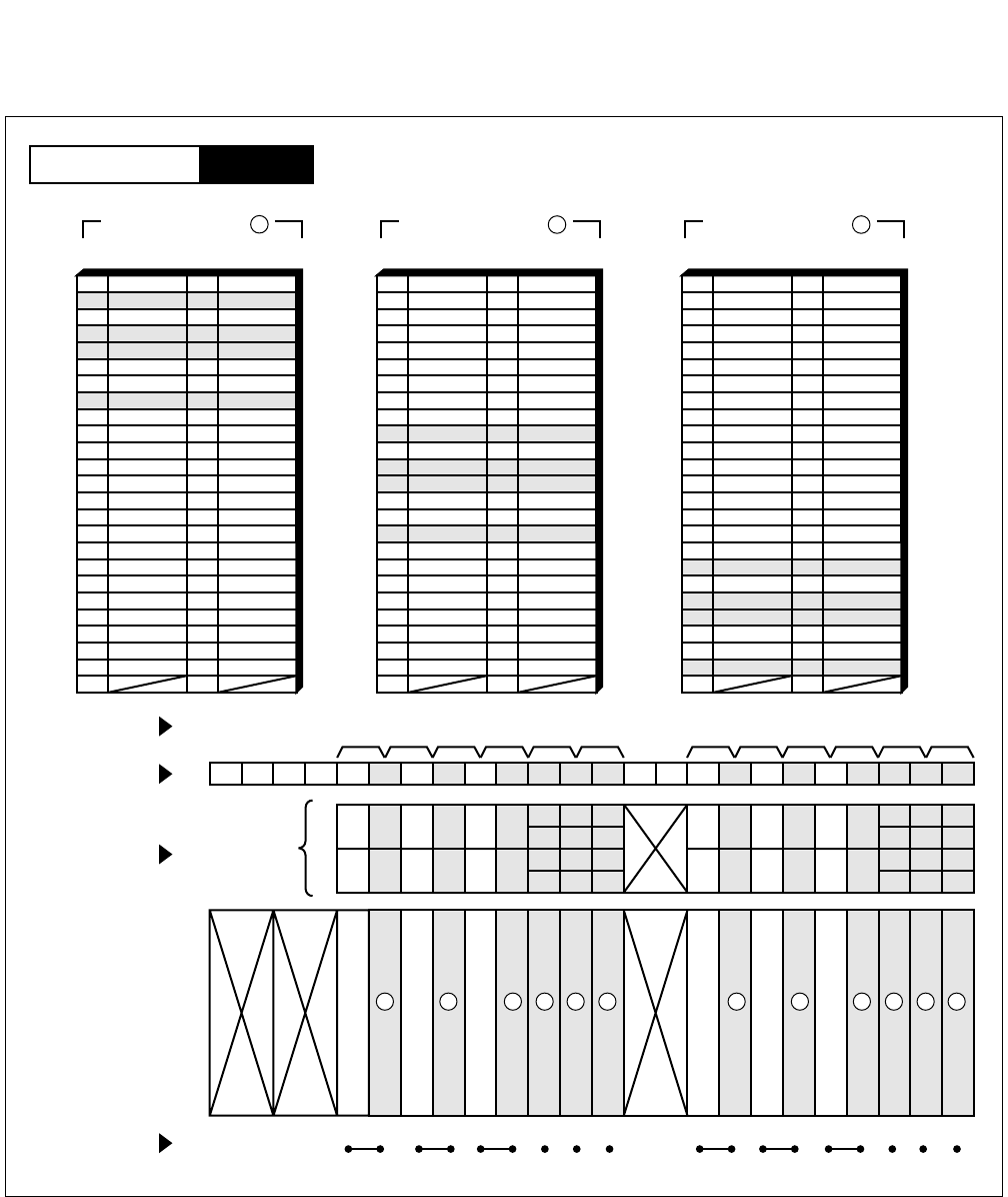
NDA-24296 CHAPTER 3
Page 475
Revision 1.0
PA-24CCTA
Common Channel Trunk
6. External Interface
Figure 3-140 LT Connector Lead Accommodation
See also Connecting Route Diagram (Figure 3-141).
PIM
Mounting Module
26
27
28
29
30
31
32
33
34
35
36
37
38
39
40
41
1
2
3
4
5
6
7
8
9
10
11
12
13
14
15
16
42
43
44
45
46
47
48
17
18
19
20
21
22
23
49
50 24
25
232221201918171615141312111009080706050403020100
LT6 LT7 LT8 LT9 LT10 LT11LT0 LT1 LT2 LT3 LT4 LT5
231915
221814
211713
201612
231915
221814
211713
201612
110907050301
100806040200
110907050301
100806040200
HW11HW10HW9HW8HW7HW6HW5HW4HW3HW2HW1HW0
Group No.
Slot No.
LT Connector
PIM
Highway Block
LT 2, 4, 8, 10 Connector
26
27
28
29
30
31
32
33
34
35
36
37
38
39
40
41
1
2
3
4
5
6
7
8
9
10
11
12
13
14
15
16
42
43
44
45
46
47
48
17
18
19
20
21
22
23
49
50 24
25
E
RB
E
Accommodated in
1
LT 1, 5, 7, 11 Connector
26
27
28
29
30
31
32
33
34
35
36
37
38
39
40
41
1
2
3
4
5
6
7
8
9
10
11
12
13
14
15
16
42
43
44
45
46
47
48
17
18
19
20
21
22
23
49
50 24
25
LT 3, 5, 9, 11 Connector
RA
POUTA
TA
POUTB
TB
E
RB
POUTB
TB
Accommodated in
2 Accommodated in
3
E
RA
POUTA
TA
E
RB
POUTB
TB
E
RA
POUTA
TA
123213 123213
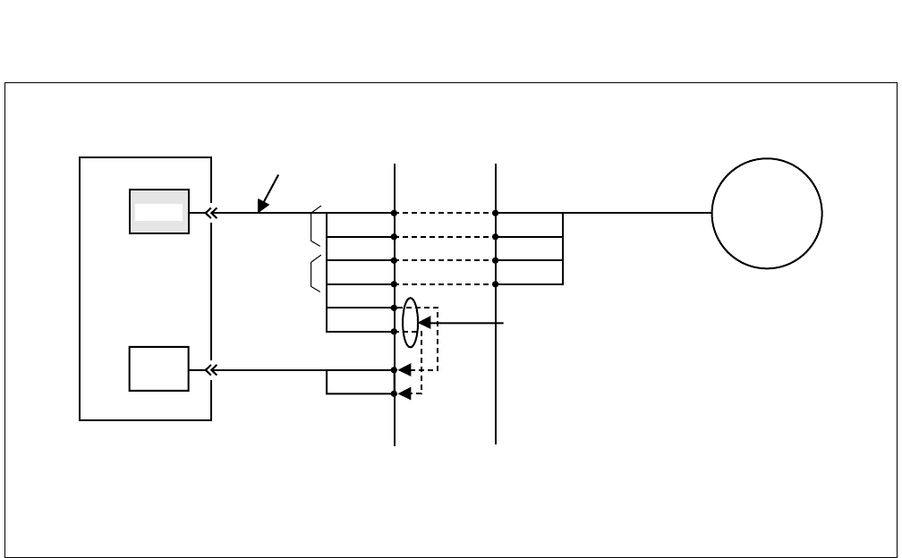
CHAPTER 3 NDA-24296
Page 476
Revision 1.0
PA-24CCTA
Common Channel Trunk
Figure 3-141 Connecting Route Diagram
TA
TB
RA
RB
POUTA
POUTB
TA
RA
RB
TB
DIU1A
DIU1B
PLO
PBX MDF
1.5 MHz Clock Extraction Note 1
Installation Cable
24CCT CCIS
NETWORK
Note 2
OUT
IN
Note 1: This cable connection is required when clock signals must be extracted from the network side.
Note 2: As an example, DIU1A and DIU1B leads are used in this diagram. For more information about these
leads, see Chapter 2 in this manual.
Connecting Route Diagram for the PA-24CCTA (24CCT) circuit card is as follows.
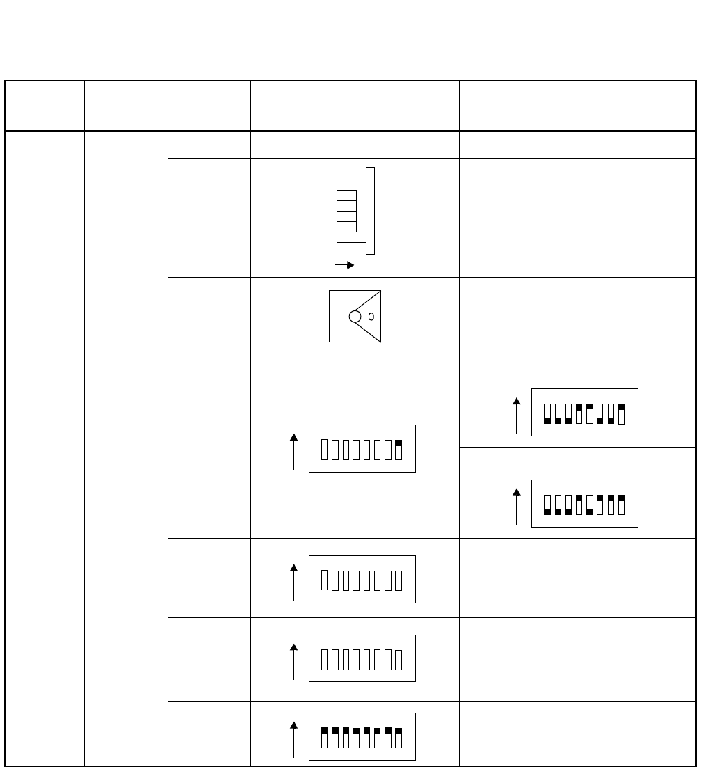
NDA-24296 CHAPTER 3
Page 477
Revision 1.0
PA-24CCTA
Common Channel Trunk
7. Switch Setting Sheet
MODULE SLOT NO. SWITCH
NAME SWITCH SHAPE REMARKS
PIM SW00/MB DOWN Circuit card make busy cancel
SW01/13B
SW02
(MODE) Standard Setting
SW10/4D
24-multiframe CCT Standard
12-multiframe CCT Standard
SW11/39
SW12/58
SW13/6C • Fixed to all ON.
3
2
1
0
ON
1
ON 2345678
1
ON 2 3 456 7 8
1
ON 2 3 4 5 6 7 8
1
ON 2345678
1
ON 23456 7 8
1
ON 2345678
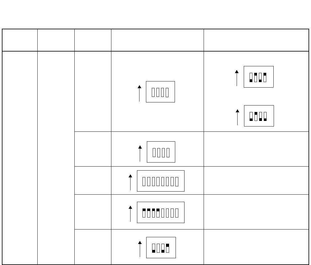
CHAPTER 3 NDA-24296
Page 478
Revision 1.0
PA-24CCTA
Common Channel Trunk
MODULE SLOT NO. SWITCH
NAME SWITCH SHAPE REMARKS
PIM
SW14/5D
• 24-multiframe CCT Standard
• 12-multiframe CCT Standard
SW15/25
SW17/6G
SW18/11B
SW19/138
1
ON 2 3 4
1234
ON
1
ON 2 3 4
1 2 3 4
ON
1
ON 23456 7 8
1
ON 2345678
1
ON 2 3 4
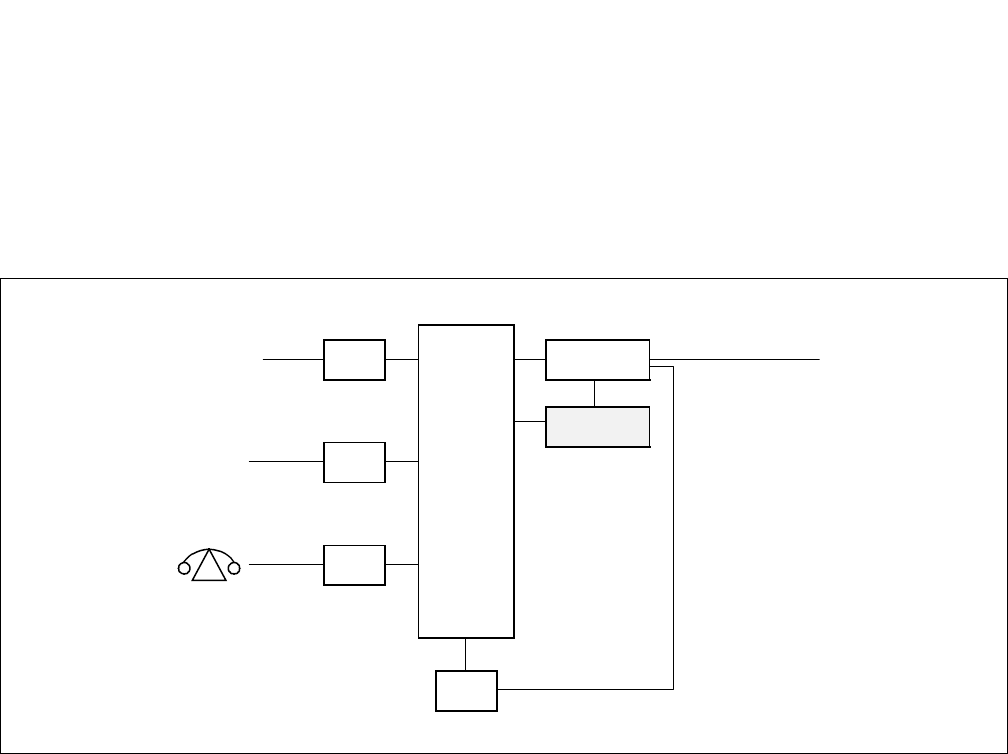
NDA-24296 CHAPTER 3
Page 479
Revision 1.0
PA-2DCHA
D-Channel Handler
PA-2DCHA
D-Channel Handler
1. General Function
This circuit card controls D channels of ISDN Line. This circuit card provides 2-circuit D-channel Handler
(DCH).
Figure 3-142 Location of PA-2DCHA (2DCH) within the System
ILC
TSW
DLC
LC
24DTI
DCH
PLO
DSU
ISDN
Terminal
Dterm
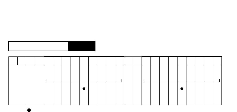
CHAPTER 3 NDA-24296
Page 480
Revision 1.0
PA-2DCHA
D-Channel Handler
2. Mounting Location/Condition
The mounting locations of this circuit card and the conditions related to mounting are shown below.
•This circuit card must be mounted in a slot on the left side of the slot in which DTI card is mounted.
•This circuit card cannot be mounted in Slot 04 of PIM0.
Mounting Module PIM
00 01 02 03 04 05 06 07 08 09 10 11 12 13 14 15 16 17 18 19 20 21 22 23
Note: Indicates universal slots for line/trunk circuit cards.
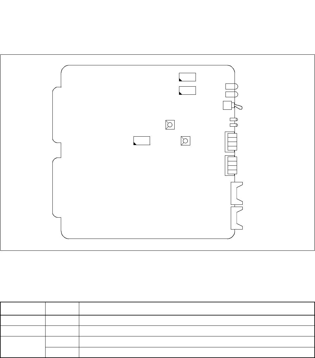
NDA-24296 CHAPTER 3
Page 481
Revision 1.0
PA-2DCHA
D-Channel Handler
3. Face Layout of Lamps, Switches, and Connectors
The face layout of lamps, switches, and connectors of this circuit card is shown in Figure 3-143.
Figure 3-143 Face Layout of PA-2DCHA (2DCH)
4. Lamp Indications
The contents of lamp indications of this circuit card are shown in the table below.
LAMP NAME COLOR STATE
OPE Green Remains lit while this circuit card is operating.
N-OPE Red Remains lit while this circuit card is in make-busy state.
DOPE0
DOPE1
Green Lights when the common channel signaling link is set up.
Flash Flashes when DCH is started up.
OPE
N-OPE
MB
DOPE0
DOPE1
SW14
SW13
SW12
SW10 SW11 SW01
SW02
~

CHAPTER 3 NDA-24296
Page 482
Revision 1.0
PA-2DCHA
D-Channel Handler
5. Switch Settings
Standard settings of various switches on this circuit card are shown in the table below.
SWITCH
NAME
SWITCH
NO. SETTING STANDARD
SETTING MEANING
MB UP Circuit card make busy
DOWN ×Circuit card make busy cancel
SW01
0ON No. 0 Circuit make busy request
OFF ×No. 0 Circuit make busy request cancel
1ON No. 1 Circuit make busy request
OFF ×No. 1 Circuit make busy request cancel
2OFF×Not used
3OFF×Not used
SW02
0ON Loop back of No. 0 Circuit is performed.
OFF ×Loop back of No. 0 Circuit is not performed.
1ON Loop back of No. 1 Circuit is performed.
OFF ×Loop back of No. 1 Circuit is not performed.
2ON Drop/Insert of No. 0 Circuit is performed.
OFF Drop/Insert of No. 0 Circuit is not performed.
3ON Drop/Insert of No. 1 Circuit is performed.
OFF Drop/Insert of No. 1 Circuit is not performed.
NDA-24296 CHAPTER 3
Page 483
Revision 1.0
PA-2DCHA
D-Channel Handler
Note: When SW10-4 is set ON, SW10-1, 10-2 and 10-3 should be set ON.
When SW10-8 is set ON, SW10-5, 10-6 and 10-7 should be set ON.
SW10
1
2
3
4ON Modem is used in No. 0 Circuit
OFF Modem is not used in No. 0 Circuit.
5
6
7
8ON Modem is used in No. 1 Circuit.
OFF Modem is not used in No. 1 Circuit.
SW11
(MODE0)
1AT & T Bell
5 AT & T Communication
SW12
(MODE1)
1AT & T Bell
5 AT & T Communication
SWITCH
NAME
SWITCH
NO. SETTING STANDARD
SETTING MEANING
SETTING OF TRANSFER SPEED OF DROP/
INSERT IN NO. 0 CIRCUIT
SW10-1 SW10-2 SW10-3 TRANSFER SPEED
ON ON ON 64 kbps
OFF ON ON 32 kbps (Forward)
ON OFF ON 16 kbps (Forward)
OFF OFF ON 8 kbps (Forward)
ON ON OFF 64 kbps
OFF ON OFF 32 kbps (Backward)
ON OFF OFF 16 kbps (Backward)
OFF OFF OFF 8 kbps (Backward)
SETTING OF TRANSFER SPEED OF DROP/
INSERT IN NO. 1 CIRCUIT
SW10-5 SW10-6 SW10-7 TRANSFER SPEED
ON ON ON 64 kbps
OFF ON ON 32 kbps (Forward)
ON OFF ON 16 kbps (Forward)
OFF OFF ON 8 kbps (Forward)
ON ON OFF 64 kbps
OFF ON OFF 32 kbps (Backward)
ON OFF OFF 16 kbps (Backward)
OFF OFF OFF 8 kbps (Backward)
CHAPTER 3 NDA-24296
Page 484
Revision 1.0
PA-2DCHA
D-Channel Handler
SWITCH
NAME SWITCH
NO. SETTING STANDARD
SETTING MEANING
SW13
(for No. 0
Circuit)
SW14
(for No. 1
Circuit)
1
2
3
4
5
6ON D Channel Mode Selection; Network Side
OFF D Channel Mode Selection; User Side
7
8
SETTING OF TIME SLOT NUMBER OF DROP/INSERT
SW13-1/
SW14-1 SW13-2/
SW14-2 SW13-3
SW14-3 SW13-4/
SW14-4 SW13-5/
SW14-5 TIME SLOT NO.
OFF OFF OFF OFF OFF CH0
ON OFF OFF OFF OFF CH1
OFF ON OFF OFF OFF CH2
ON ON OFF OFF OFF CH3
OFF OFF ON OFF OFF CH4
ON OFF ON OFF OFF CH5
OFF ON ON OFF OFF CH6
ON ON ON OFF OFF CH7
OFF OFF OFF ON OFF CH8
ON OFF OFF ON OFF CH9
OFF ON OFF ON OFF CH10
ON ON OFF ON OFF CH11
OFF OFF ON ON OFF CH12
ON OFF ON ON OFF CH13
OFFONONONOFF CH14
ON ON ON ON OFF CH15
OFF OFF OFF OFF ON CH16
ON OFF OFF OFF ON CH17
OFF ON OFF OFF ON CH18
ON ON OFF OFF ON CH19
OFF OFF ON OFF ON CH20
ON OFF ON OFF ON CH21
OFF ON ON OFF ON CH22
ON ON ON OFF ON CH23
OFF OFF OFF ON ON CH24
ON OFF OFF ON ON CH25
OFF ON OFF ON ON CH26
ON ON OFF ON ON CH27
OFF OFF ON ON ON CH28
ON OFF ON ON ON CH29
OFFONONONON CH30
ON ON ON ON ON CH31
SETTING OF SPEED MODE
SW13-7/SW14-7 SW13-8/SW14-8 SPEED
OFF OFF 2400 bps
OFF ON 4800 bps
ON OFF 9600 bps
ON ON Inhibit
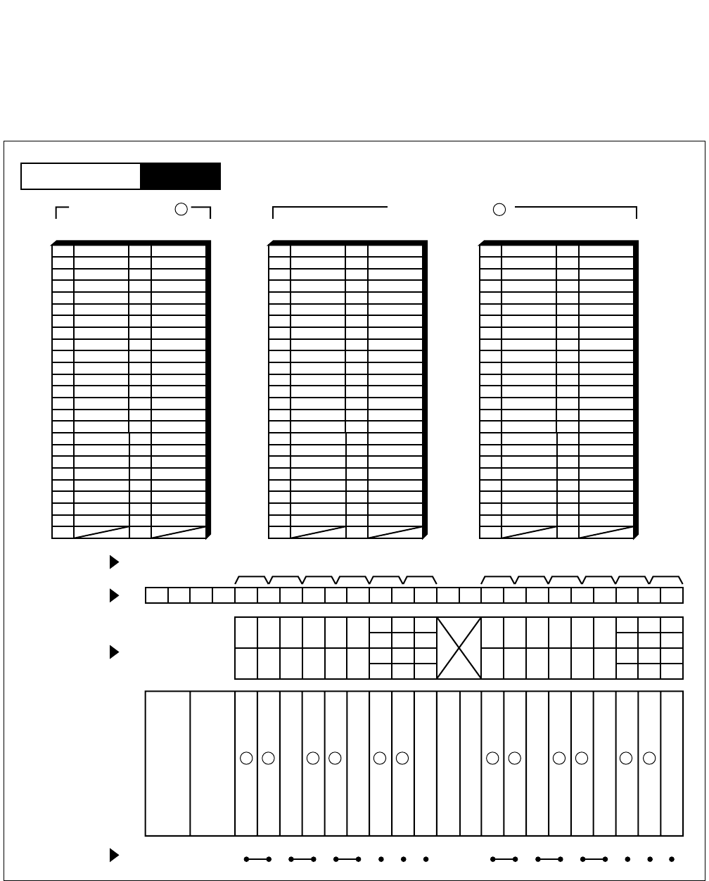
NDA-24296 CHAPTER 3
Page 485
Revision 1.0
PA-2DCHA
D-Channel Handler
6. External Interface
Accommodation of the LT connector leads of this circuit card and connecting route diagram are shown in
Figure 3-144.
Figure 3-144 LT Connector Leads Accommodation (1/2)
PIM
Mounting Module
26
27
28
29
30
31
32
33
34
35
36
37
38
39
40
41
1
2
3
4
5
6
7
8
9
10
11
12
13
14
15
16
42
43
44
45
46
47
48
17
18
19
20
21
22
23
49
50 24
25
232221201918171615141312111009080706050403020100
LT6 LT7 LT8 LT9 LT10 LT11LT0 LT1 LT2 LT3 LT4 LT5
231915
221814
211713
201612
231915
221814
211713
201612
110907050301
100806040200
110907050301
100806040200
HW11HW10HW9HW8HW7HW6HW5HW4HW3HW2HW1HW0
Group No.
Slot No.
LT Connector
PIM
Highway Block
LT 1, 3, 5, 7, 9, 11 Connector
26
27
28
29
30
31
32
33
34
35
36
37
38
39
40
41
1
2
3
4
5
6
7
8
9
10
11
12
13
14
15
16
42
43
44
45
46
47
48
17
18
19
20
21
22
23
49
50 24
25
Accommodated in 2
LT 0, 2, 4, 6, 8, 10 Connector
26
27
28
29
30
31
32
33
34
35
36
37
38
39
40
41
1
2
3
4
5
6
7
8
9
10
11
12
13
14
15
16
42
43
44
45
46
47
48
17
18
19
20
21
22
23
49
50 24
25
Accommodated in 1
LT 0, 2, 4, 6, 8, 10 Connector
SG 0 ER 0
RD 0
RT 0 ST2 0
RS 0 SD 0
RD 1
SG 1 ER 1
RT 1 ST2 1
RS 1 SD 1
SG 0 ER 0
RD 0
RT 0 ST2 0
RS 0 SD 0
RD 1
SG 1 ER 1
RT 1 ST2 1
RS 1 SD 1
SCKB 0 SCKA 0
TDB 0 TDA 0
RDB 0 RDA 0
SCKB 1 SCKA 1
TDB 1 TDA 1
RDB 1 RDA 1
SCKB 0 SCKA 0
TDB 0 TDA 0
RDB 0 RDA 0
SCKB 1 SCKA 1
TDB 1 TDA 1
RDB 1 RDA 1
21 2 1 21 12
2121
PWR
PWR
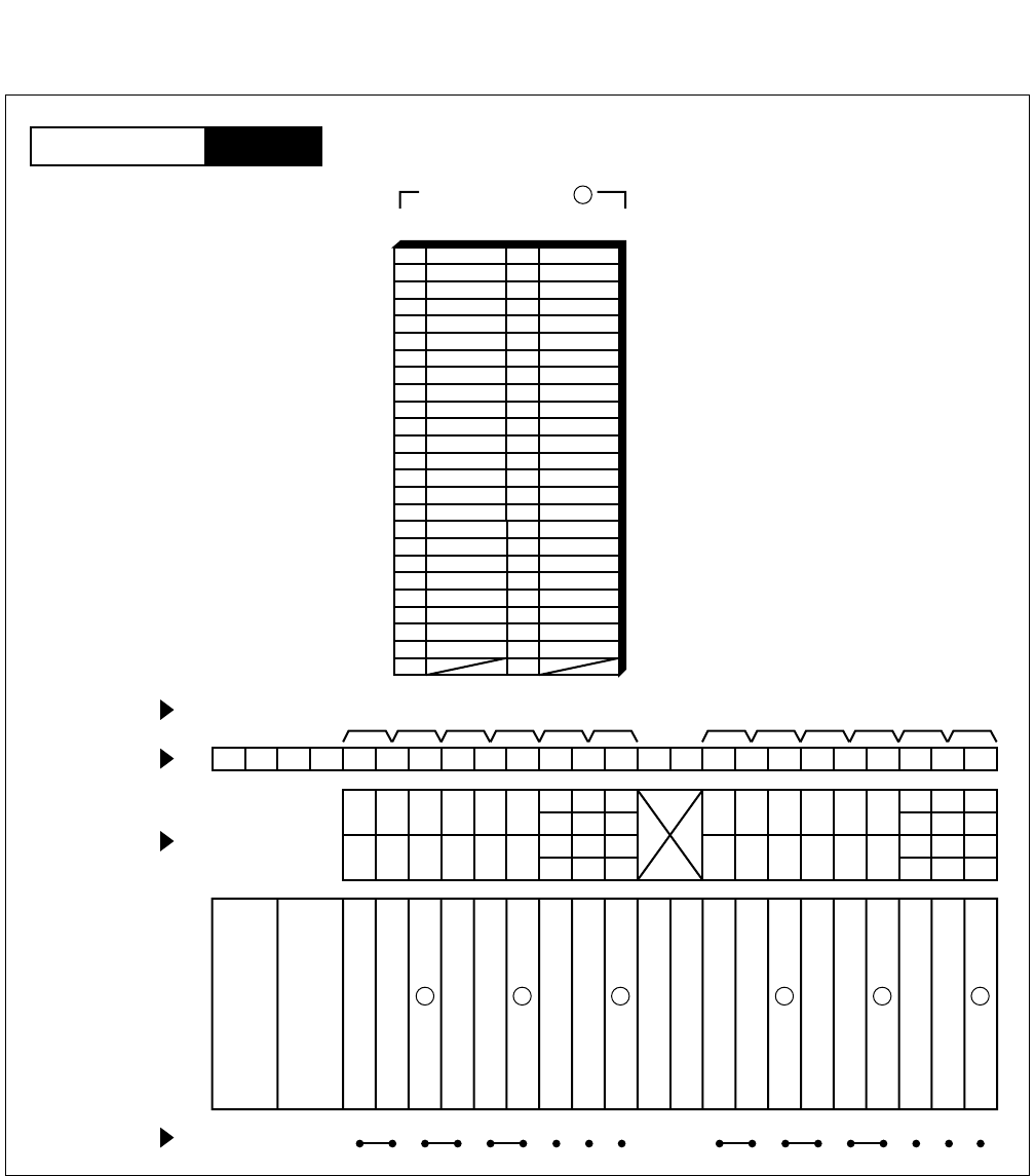
CHAPTER 3 NDA-24296
Page 486
Revision 1.0
PA-2DCHA
D-Channel Handler
Figure 3-144 LT Connector Leads Accommodation (2/2)
PIM
Mounting Module
232221201918171615141312111009080706050403020100
LT6 LT7 LT8 LT9 LT10 LT11LT0 LT1 LT2 LT3 LT4 LT5
231915
221814
211713
201612
231915
221814
211713
201612
110907050301
100806040200
110907050301
100806040200
HW11HW10HW9HW8HW7HW6HW5HW4HW3HW2HW1HW0
Group No.
Slot No.
LT Connector
PIM
Highway Block
26
27
28
29
30
31
32
33
34
35
36
37
38
39
40
41
1
2
3
4
5
6
7
8
9
10
11
12
13
14
15
16
42
43
44
45
46
47
48
17
18
19
20
21
22
23
49
50 24
25
Accommodated in 3
LT 1, 3, 5, 7, 9, 11 Connector
SG 0 ER 0
RD 0
RT 0 ST2 0
RS 0 SD 0
RD 1
SG 1 ER 1
RT 1 ST2 1
RS 1 SD 1
SCLB 0 SCKA 0
TDB 0 TDA 0
RDB 0 RDA 0
SCLB 1 SCKA 1
TDB 1 TDA 1
RDB 1 RDA 1
3 3 3 3 3 3
PWR
PWR
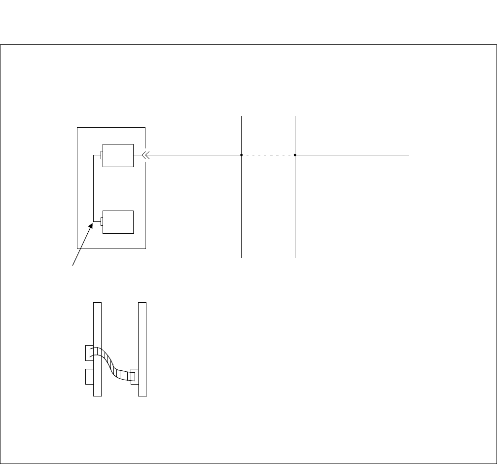
NDA-24296 CHAPTER 3
Page 487
Revision 1.0
PA-2DCHA
D-Channel Handler
Figure 3-145 Connecting Route Diagram (1/2)
NEAX2400 IPX MDF
DSU
DCH
DTI
Front Cable connection
DCH DTI/CCT
TRK CN2
Front
• When modem is not used
Note: For cross connections between DTI and D-channel common channel signalling line, refer to the expla-
nations of 24DTI circuit card.
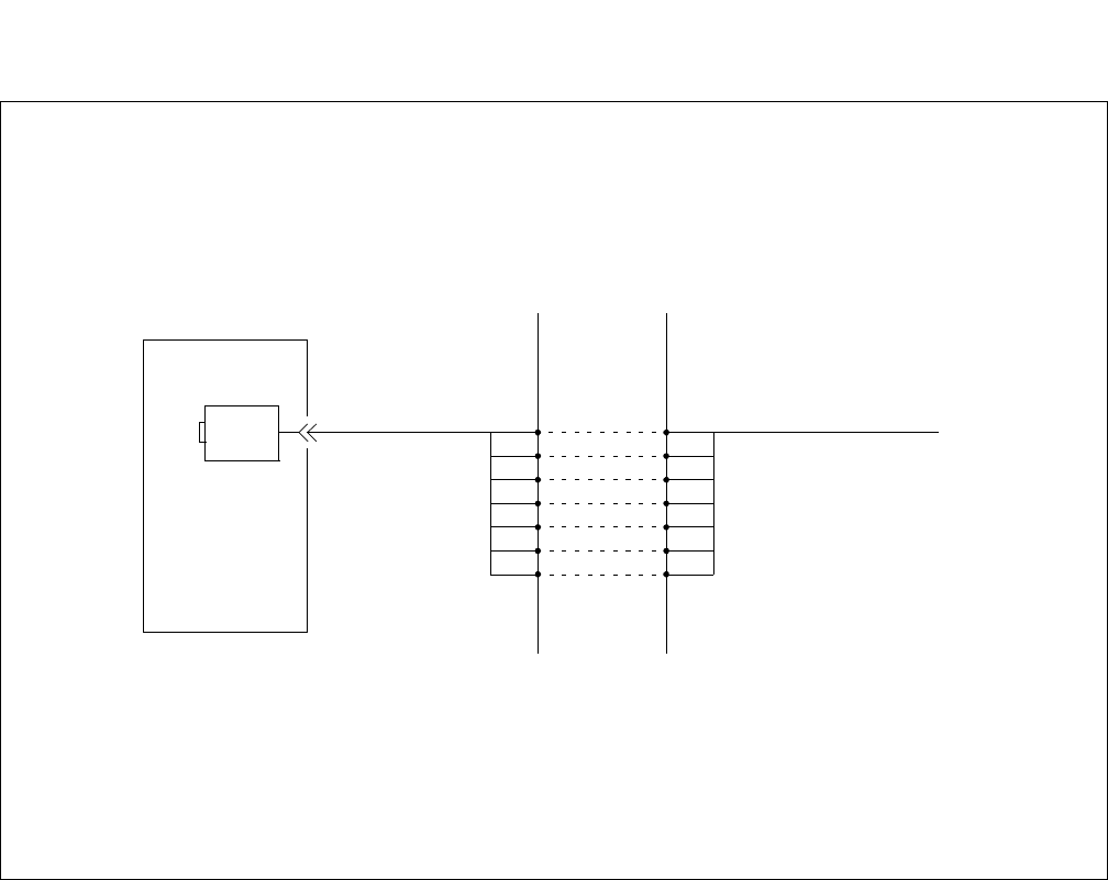
CHAPTER 3 NDA-24296
Page 488
Revision 1.0
PA-2DCHA
D-Channel Handler
Figure 3-145 Connecting Route Diagram (2/2)
NEAX2400 IPX MDF
MODEM
DCH
• When modem is used
SG
RD
ER
RT
ST2
RS
SD
SG
RD
ER
RT
ST2
RS
SD
•Cable length is maximum 15 meters (50 feet).
• The modem to be used is a synchronous modem of 2400, 4800, or 9600 bps, and the communication
method is limited to 4-wire full duplex communications.
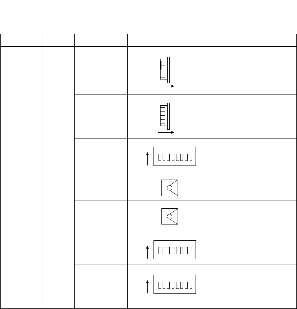
NDA-24296 CHAPTER 3
Page 489
Revision 1.0
PA-2DCHA
D-Channel Handler
7. Switch Setting Sheet
MODULE SLOT NO. SWITCH NAME SWITCH SHAPE REMARKS
PIM
SW01 SW01-2, 3 : Not used
SW02
SW10
SW11 1 : AT & T Bell
5 : AT & T Communication
SW12 1 : AT & T Bell
5 : AT & T Communication
SW13
SW14
MB DOWN Circuit card make busy cancel
3
2
1
0
ON
3
2
1
0
ON
ON 12345678
ON 12345678
ON 12345678
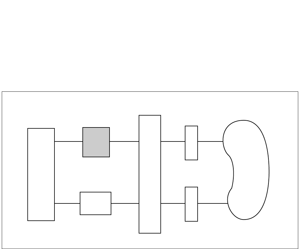
CHAPTER 3 NDA-24296
Page 490
Revision 1.0
PA-ILCG
ISDN Terminal Line Circuit
PA-ILCG
ISDN Terminal Line Circuit
1. General Function
This circuit card, which is for ISDN, is used in conjunction with PA-24DTR/PA-24PRTB-A to provide
H11 terminal (1.536 Mbps) with D-channel signal. ISDN BRI (Basic Rate Interface) terminal (64 Kbps),
incidentally, cannot be connected to this circuit card.
Figure 3-146 Location of PA-ILCG (ILC) Card within the System
PA-24DTR/
PA-24PRTB-A
H11
Terminal/
Terminal
Adapter
ILC
TSW
PRT
PRT
ISDN
NETWORK
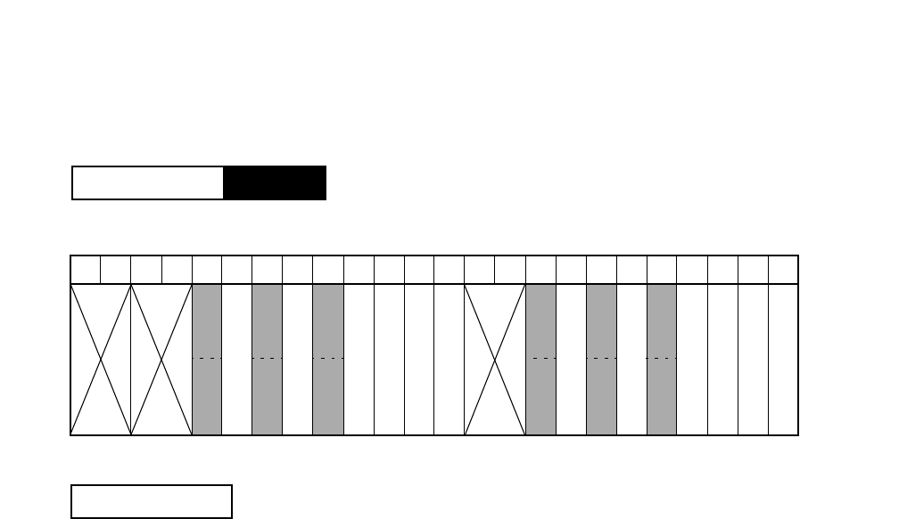
NDA-24296 CHAPTER 3
Page 491
Revision 1.0
PA-ILCG
ISDN Terminal Line Circuit
2. Mounting Location/Condition
The PA-ILCG (ILC) card can be mounted in the following shaded slots.
Mounting conditions for this circuit card are as follows:
1. This circuit card cannot be mounted in the slot 05, 07, 09, 10, 11, 12, 16, 18, 20, 21, 22, 23.
2. Mount this circuit card so that its leads and the leads of any other analog line/trunk circuit card may
not come out to the same LT cable.
3. This circuit card is not used in even-number module group (MG), unit (U)=0 and group (G)=0.
4. When registering this circuit card in the shaded slots, user must assign B-channels to odd-number
group (G) and D-channel to even-number group(G).
5. Do not mount other line/trunk card in just right side of the slot where a PA-ILCG card is mounted.
PIM
Mounting Module
00 01 02 03 04 05 06 07 08 09 10 11 12 13 14 15 16 17 18 19 20 21 22 23
B-ch
B-ch
D-ch
D-ch
B-ch D-ch
B-ch
B-ch
B-ch
D-ch
D-ch
D-ch
Mounting Condition
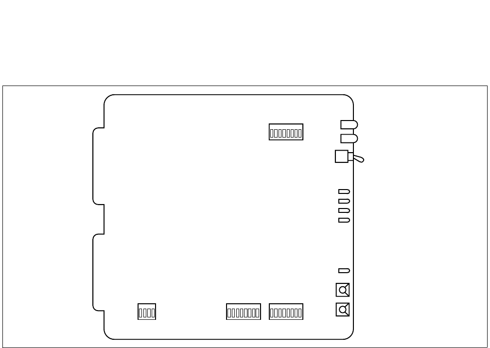
CHAPTER 3 NDA-24296
Page 492
Revision 1.0
PA-ILCG
ISDN Terminal Line Circuit
3. Face Layout of Lamps and Switches
The face layout of lamps and switches is shown in Figure 3-147.
Figure 3-147 Face Layout of PA-ILCG (ILC)
OPE
N-OPE
MB KEY
MODE 0
MODE 1
SW06
12345678
PKT
PWR4
LYR4
BL41
BL42
SW05
12345678
SW04
12345678
SW01
1234

NDA-24296 CHAPTER 3
Page 493
Revision 1.0
PA-ILCG
ISDN Terminal Line Circuit
4. Lamp Indications
The contents of lamp indications on this circuit card are shown in the table below:
Table 3-11 PA-ILCG Lamp Indications Reference
LAMP NAME COLOR STATE
OPE Green Remains lit while this circuit card is in normal operation.
N-OPE Red Remains lit while this circuit card is in make-busy state.
BL42
Green Lights green when B2-channel is being accessed and in operation.
Flash (60IPM) The corresponding channel is in a make-busy state.
OFF The corresponding channel is idle.
BL41
Green Lights green when B1-channel is being accessed and in operation.
Flash (60IPM) The corresponding channel is in a make-busy state.
OFF The corresponding channel is idle.
LYR4
Green Remains lit while Layer 2 of the corresponding channel is active.
Flash (120IPM) Flashes while Layer 1 synchronization of the corresponding channel is established.
OFF Layer 1 and/or Layer 2 have not been established.
PWR4 Red Lights red when overvoltage protection function for the corresponding circuit is activat-
ed; the corresponding line is short-circuited.
PKT Green Lights green when D channel Packet is in operation.
OFF Remains off when D channel Packet is not in operation.
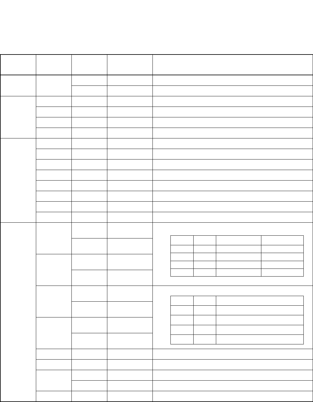
CHAPTER 3 NDA-24296
Page 494
Revision 1.0
PA-ILCG
ISDN Terminal Line Circuit
5. Switch Settings
Standard settings of switches on this circuit card are shown in the table below.
SWITCH
NAME SWITCH
NO. SETTING STANDARD
SETTING MEANING
MB UP Circuit card make-busy
DOWN Circuit card make-busy cancel
SW01
1ON ×Fixed to ON
2ON ×Fixed to ON
3ON ×Not used (Fixed to ON)
4ON ×Not used (Fixed to ON)
SW04
1ON ×Not used (Fixed to ON)
2ON ×Not used (Fixed to ON)
3ON ×Not used (Fixed to ON)
4ON ×Not used (Fixed to ON)
5ON ×Fixed to ON (Wiring Mode)
6ON ×Not used (Fixed to ON)
7ON ×Not used (Fixed to ON)
8ON ×Not used (Fixed to ON)
SW05
1
ON
OFF ×
2
ON
OFF ×
3
ON
OFF
4
ON
OFF
5OFF ×Not used (Fixed to ON)
6OFF ×Not used (Fixed to ON)
7ON D-channel Packet Service: Available
OFF D-channel Packet Service: Not available
8ON ×Not used (Fixed to ON)
SW05-1 SW05-2 Receiving Pad Sending Pad
OFF OFF 0 dB 0 dB
OFF ON 0 dB 2 dB
ON OFF 0 dB 5 dB
ON ON 0 dB 8 dB
PAD Value Selection
SW05-3 SW05-4 Length of Call Reference Value
OFF OFF Basic Rate Interface 1, Primary Rate
OFF ON Basic Rate Interface 1, Primary Rate
ON OFF Basic Rate Interface 2, Primary Rate
ON ON Basic Rate Interface 2, Primary Rate
Length of Call Reference Value Selection

NDA-24296 CHAPTER 3
Page 495
Revision 1.0
PA-ILCG
ISDN Terminal Line Circuit
Note: The terms Point-to-Point (P-P) used in this table have no relation to the actual wiring configuration.
SW06
1ON ×Not used (Fixed to ON)
2ON ×Not used (Fixed to ON)
3ON ×Not used (Fixed to ON)
4ON ×Not used (Fixed to ON)
5ON ×Data link mode for Layer 2: Point-to-Point (P-P)
(Fixed to ON) Note
6ON ×Not used (Fixed to ON)
7ON ×Not used (Fixed to ON)
8ON ×Not used (Fixed to ON)
MODE 0 0×Fixed to 0
1~F Not used
MODE 1
0~5 Not used
6×Fixed to 6
7~F Not used
SWITCH
NAME SWITCH
NO. SETTING STANDARD
SETTING MEANING
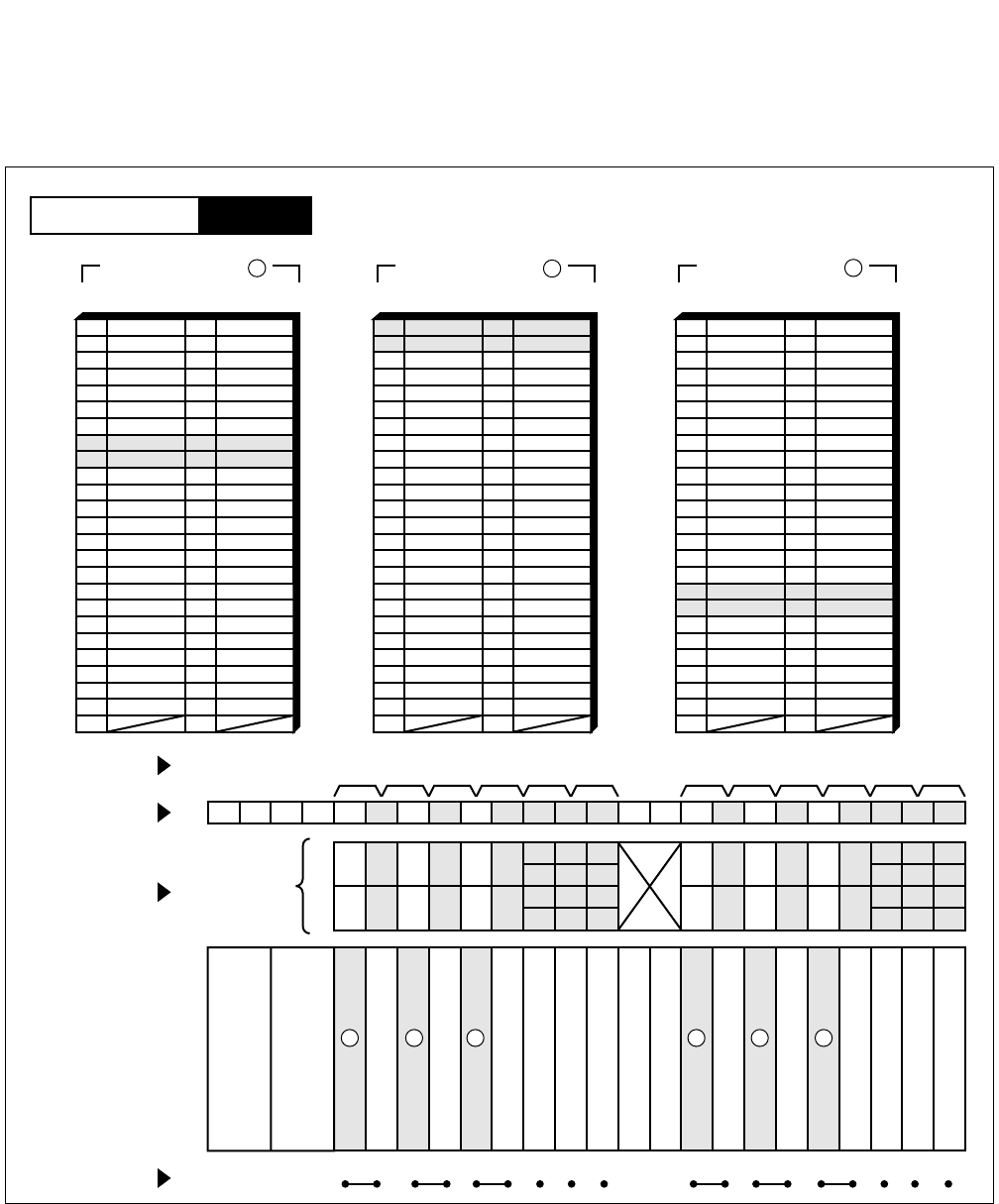
CHAPTER 3 NDA-24296
Page 496
Revision 1.0
PA-ILCG
ISDN Terminal Line Circuit
6. External Interface
Accommodation of the LT connector leads for this circuit card is shown in Figure 3-148.
Figure 3-148 LT Connector Lead Accommodation
See also Connecting Route Diagram (Figure 3-149).
26
27
28
29
30
31
32
33
34
35
36
37
38
39
40
41
1
2
3
4
5
6
7
8
9
10
11
12
13
14
15
16
42
43
44
45
46
47
48
17
18
19
20
21
22
23
49
50 24
25
232221201918171615141312111009080706050403020100
LT6 LT7 LT8 LT9 LT10 LT11LT0 LT1 LT2 LT3 LT4 LT5
231915
221814
211713
201612
231915
221814
211713
201612
110907050301
100806040200
110907050301
100806040200
HW11HW10HW9HW8HW7HW6HW5HW4HW3HW2HW1HW0
Group No.
Slot No.
LT Connector
PIM
Highway Block
LT 3, 9, 11 Connector
26
27
28
29
30
31
32
33
34
35
36
37
38
39
40
41
1
2
3
4
5
6
7
8
9
10
11
12
13
14
15
16
42
43
44
45
46
47
48
17
18
19
20
21
22
23
49
50 24
25
RB
Accommodated in
1
LT 0, 2, 6 Connector
26
27
28
29
30
31
32
33
34
35
36
37
38
39
40
41
1
2
3
4
5
6
7
8
9
10
11
12
13
14
15
16
42
43
44
45
46
47
48
17
18
19
20
21
22
23
49
50 24
25
LT 1, 7 Connector
RA
TA
TB
RB
TB
Accommodated in
2 Accommodated in
3
RA
TA
RB
TB RA
TA
132 1 23
PIM
Mounting Module
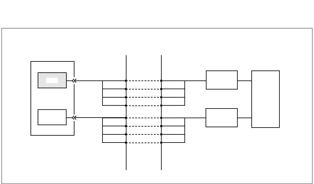
NDA-24296 CHAPTER 3
Page 497
Revision 1.0
PA-ILCG
ISDN Terminal Line Circuit
Figure 3-149 Connecting Route Diagram
RA
RB
TA
TB
TA
RA
RB
TB
24DTR/
24PRTB-A
PBX MDF
ILC
Modular
Rosette
Modular
Rosette
ISDN
Terminal
H11 Terminal/
Terminal Adapter
MJ-8SR
MJ-8S
RA
RB
TA
TB
TA
RA
RB
TB
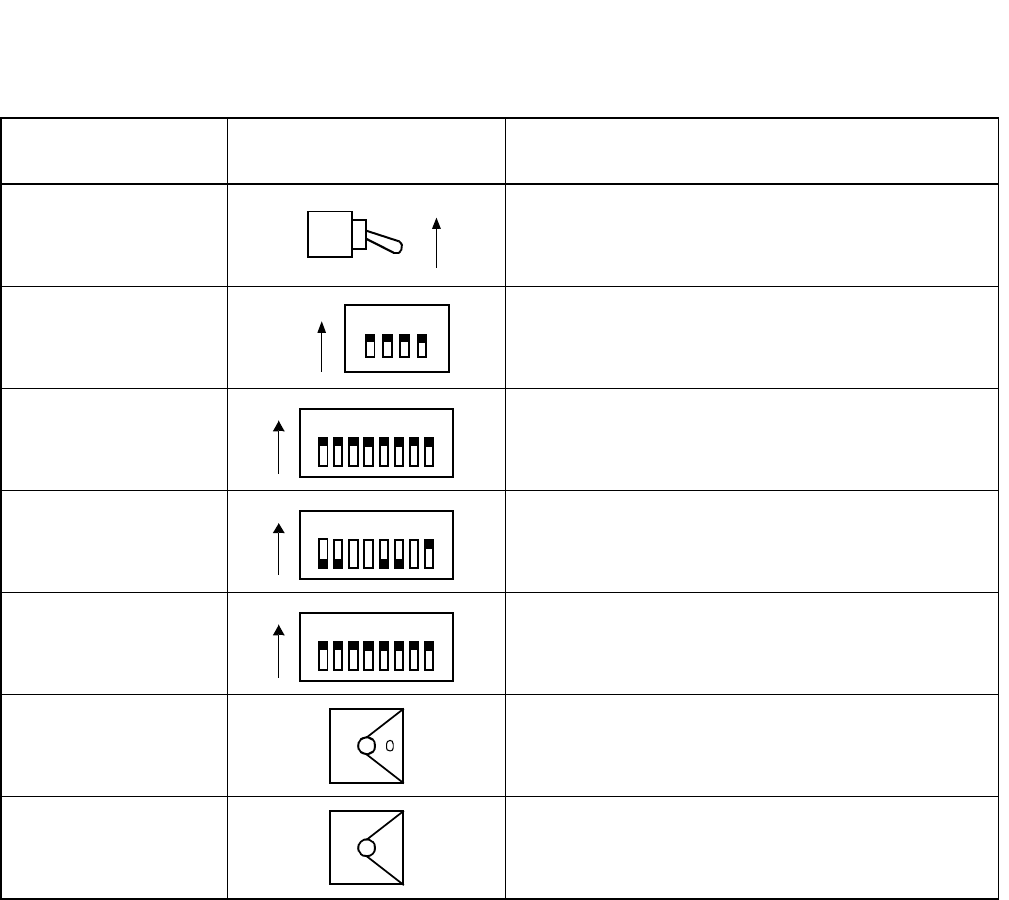
CHAPTER 3 NDA-24296
Page 498
Revision 1.0
PA-ILCG
ISDN Terminal Line Circuit
7. Switch Setting Sheet
SWITCH
NAME SWITCH SHAPE REMARKS
MB
SW01
SW04
SW05
SW06
MODE 0
MODE 1
ON
1 2 3 4
ON
1
ON 2 3 4 5 6 7 8
1
ON 2 3 4 5 6 7 8
1
ON 2 3 456 7 8
6
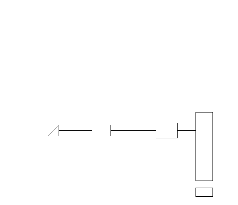
NDA-24296 CHAPTER 3
Page 499
Revision 1.0
PA-4ILCH
ISDN Line Circuit
PA-4ILCH
ISDN Line Circuit
1. General Function
The PA-4ILCH is a line circuit card which accommodates ISDN Terminal via NT1. The main features of
this circuit card are shown below:
•A maximum of four Basic Rate Interface (BRI) terminals can be accommodated.
•This card and NT1 are connected using 2-wire U Interface.
•Sealing current (Maximum 15mA) can be supplied for keeping cables from rusting.
Figure 3-150 Location of PA-4ILCH (4ILC) within the System
TSW
I.430
PLO
NT1
ANSI T1.601
PA-4ILCH
TE
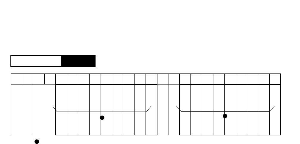
CHAPTER 3 NDA-24296
Page 500
Revision 1.0
PA-4ILCH
ISDN Line Circuit
2. Mounting Location/Condition
The PA-4ILCH (4ILC) card can be mounted in any universal slot as shown below.
00 01 02 03 04 05 06 07 08 09 10 11 12 13 14 15 16 17 18 19 20 21 22 23
Note: Indicates universal slots for line/trunk circuit cards.
PIM
Mounting Module
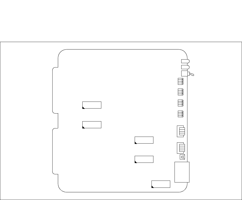
NDA-24296 CHAPTER 3
Page 501
Revision 1.0
PA-4ILCH
ISDN Line Circuit
3. Face Layout of Lamps, Switches, and Connectors
The face layout of each lamp, switch and connector on this circuit card is shown in Figure 3-151.
Figure 3-151 Face Layout of PA-4ILCH (4ILC)
BER3
LYR3
BL32
BL31
BER2
LYR2
BL21
BL22
BER1
BL12
LYR1
BL11
BER0
BL02
LYR0
BL01
OPE
MB
MODE
NOPE
MBR
L3
L2
L1
L0
LPB
L3
L2
L1
L0
MONITOR (Not used)
SW21
SW12
SW11
SW20
SW10

CHAPTER 3 NDA-24296
Page 502
Revision 1.0
PA-4ILCH
ISDN Line Circuit
4. Lamp Indications
The contents of lamp indication on this circuit card are shown below.
Note: Establishment of synchronization on U Reference Point may require 30 seconds or more.
LAMP NAME COLOR MEANING
OPE Green Lights when the card is in normal operation.
NOPE Red Lights when the card is in make-busy state.
BLn2
n=0~3
Green Lights when B2 channel of line #n is communicating.
Flashing Flashes during make-busy state (60 IPM).
Off During idle state.
BLn1
n=0~3
Green Lights when B1 channel of the line #n is communicating.
Flashing Flashes during make-busy state (60 IPM).
Off During idle state.
LYRn
n=0~3
Green Lights when layer 2 link of the line #n is established.
Flashing
Flashes when synchronization is established on Layer 1 of S Reference Point (60
IPM). Note
Flashes when synchronization is established on Layer 1 of U Reference Point (120
IPM). Note
Off Synchronization is not established on either Layer 1 or Layer 2.
BERn
n=0~3
Red Two or more CRC errors occur per second and the condition lasts for 10 seconds.
Off One or no CRC error occurs per second.

NDA-24296 CHAPTER 3
Page 503
Revision 1.0
PA-4ILCH
ISDN Line Circuit
5. Switch Settings
Switches on this card have the following meanings.
SWITCH
NAME SWITCH
NO. SETTING STANDARD
SETTING MEANING
MB UP Circuit card make busy
DOWN ×Circuit card make busy cancel
MBR
0ON Line 0 make busy request
OFF ×Line 0 make busy request cancel
1ON Line 1 make busy request
OFF ×Line 1 make busy request cancel
2ON Line 2 make busy request
OFF ×Line 2 make busy request cancel
3ON Line 3 make busy request
OFF ×Line 3 make busy request cancel
LPB
0ON Loop back is set on NT1 for line 0.
OFF ×Loop back is canceled on NT1 for line 0.
1ON Loop back is set on NT1 for line 1.
OFF ×Loop back is canceled on NT1 for line 1.
2ON Loop back is set on NT1 for line 2.
OFF ×Loop back is canceled on NT1 for line 2.
3ON Loop back is set on NT1 for line 3.
OFF ×Loop back is canceled on NT1 for line 3.
MODE
0-2 Not used
3×Fixed
4-F Not used
SW10
1ON ×Fixed
2ON ×D-channel Packet Service Available
OFF D-channel Packet Service Not Available
3ON ×Fixed
4ON ×Fixed
CHAPTER 3 NDA-24296
Page 504
Revision 1.0
PA-4ILCH
ISDN Line Circuit
Note: PAD control is shown below.
SW11
1ON ×Fixed
2ON ×Fixed
3ON ×Fixed
4ON ×Fixed
5ON ×Fixed
6ON ×Fixed
7ON ×Fixed
8ON Sealing Current is not supplied.
OFF ×Sealing Current is supplied.
SW12
1 ~ 3
4ON ×Fixed
5ON ×Fixed
6ON ×Fixed
7ON ×Fixed
8ON ×Fixed
SWITCH
NAME SWITCH
NO. SETTING STANDARD
SETTING MEANING
PAD Control (TSW Side PAD Value) Note
SW1 SW2 SW3 TSW Side PAD Value
OFF OFF OFF Not used
ON OFF OFF PAD2=0dB, PAD1=-5dB
OFF ON OFF PAD2=0dB, PAD1=-3dB
ON ON OFF PAD2=0dB, PAD1=0dB
OFF OFF ON Not used
ON OFF ON PAD2=0dB, PAD1=5dB
(Standard Setting)
OFF ON ON PAD2=0dB, PAD1=3dB
ON ON ON PAD2=0dB, PAD1=0dB
PAD1
PAD2
Line Side
TSW Side

NDA-24296 CHAPTER 3
Page 505
Revision 1.0
PA-4ILCH
ISDN Line Circuit
Note 1: The terms Point-to-Point (P-P) and Point-to-Multipoint (P-mP) used in this table have no relation to the
actual wiring configuration.
Note 2: This switch must be set according to the specification of the ISDN terminal.
SWITCH
NAME SWITCH
NO. SETTING STANDARD
SETTING MEANING
SW20
Note 1
Note 2
1
ON Data link mode for Layer 2 of line 0:
Point-to-Multipoint (P-mP)
OFF Data link mode for Layer 2 of line 0:
Point-to-Point (P-P)
2
ON Data link mode for Layer 2 of line 1:
Point-to-Multipoint (P-mP)
OFF Data link mode for Layer 2 of line 1:
Point-to-Point (P-P)
3
ON Data link mode for Layer 2 of line 2:
Point-to-Multipoint (P-mP)
OFF Data link mode for Layer 2 of line 2
Point-to-Point (P-P)
4
ON Data link mode for Layer 2 of line 3:
Point-to-Multipoint (P-mP)
OFF Data link mode for Layer 2 of line 3:
Point-to-Point (P-P)
SW21
Note 2
1
ON On line 0, Layer 1 of S Reference Point is activated on a call basis.
OFF On line 0, Layer 1 of S Reference Point is always activated.
2
ON On line 1, Layer 1 of S Reference Point is activated on a call basis.
OFF On line 1, Layer 1 of S Reference Point is always activated.
3
ON On line 2, Layer 1 of S Reference Point is activated on a call basis.
OFF On line 2, Layer 1 of S Reference Point is always activated.
4
ON On line 3, Layer 1 of S Reference Point is activated on a call basis.
OFF On line 3, Layer 1 of S Reference Point is always activated.
5ON ×Fixed
6ON ×Fixed
7ON ×Fixed
8ON ×Fixed
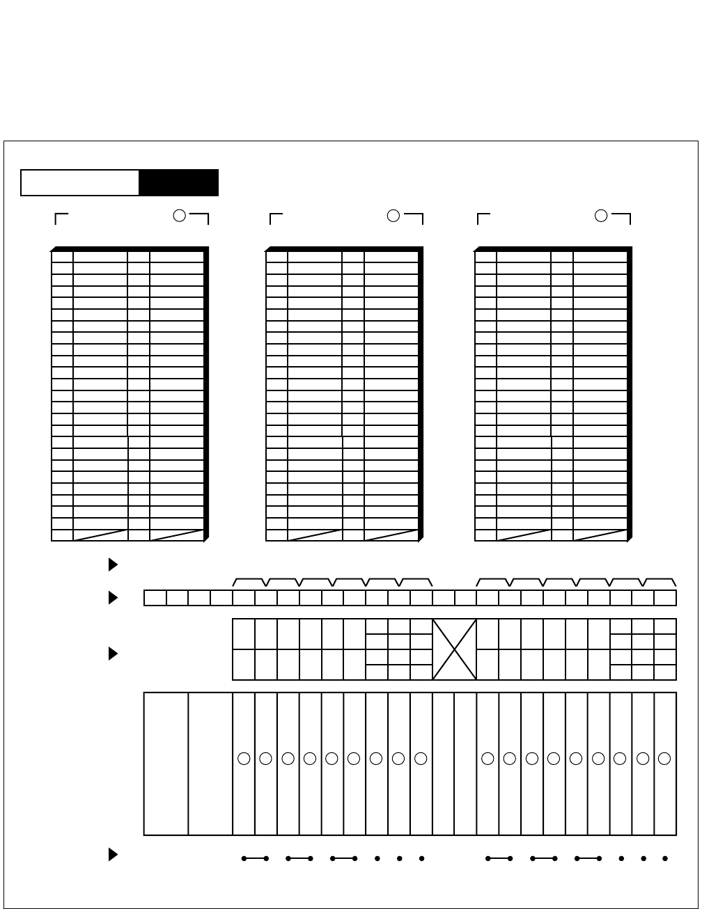
CHAPTER 3 NDA-24296
Page 506
Revision 1.0
PA-4ILCH
ISDN Line Circuit
6. External Interface
Accommodation of the LT connector leads of this circuit card and connecting route diagram are shown in
Figure 3-152.
Figure 3-152 LT Connector Leads Accommodation
PIM
Mounting Module
26
27
28
29
30
31
32
33
34
35
36
37
38
39
40
41
1
2
3
4
5
6
7
8
9
10
11
12
13
14
15
16
42
43
44
45
46
47
48
17
18
19
20
21
22
23
49
50 24
25
232221201918171615141312111009080706050403020100
LT6 LT7 LT8 LT9 LT10 LT11LT0 LT1 LT2 LT3 LT4 LT5
231915
221814
211713
201612
231915
221814
211713
201612
110907050301
100806040200
110907050301
100806040200
HW11HW10HW9HW8HW7HW6HW5HW4HW3HW2HW1HW0
Group No.
Slot No.
LT Connector
PIM
PWR
PWR
Highway Block
LT 1, 3, 5, 7, 9, 11 Connector
26
27
28
29
30
31
32
33
34
35
36
37
38
39
40
41
1
2
3
4
5
6
7
8
9
10
11
12
13
14
15
16
42
43
44
45
46
47
48
17
18
19
20
21
22
23
49
50 24
25
Accommodated in 2
LT 1, 3, 5, 7, 9, 11 Connector
Accommodated in 3
26
27
28
29
30
31
32
33
34
35
36
37
38
39
40
41
1
2
3
4
5
6
7
8
9
10
11
12
13
14
15
16
42
43
44
45
46
47
48
17
18
19
20
21
22
23
49
50 24
25
Accommodated in 1
LT 0, 2, 4, 6, 8, 10 Connector
B0 A0
B1 A1
B2 A2
B3 A3
B0 A0
B1 A1
B2 A2
B3 A3
B0 A0
B1 A1
B2 A2
B3 A3
21 3 2 1 3 21 31 2
231231 3
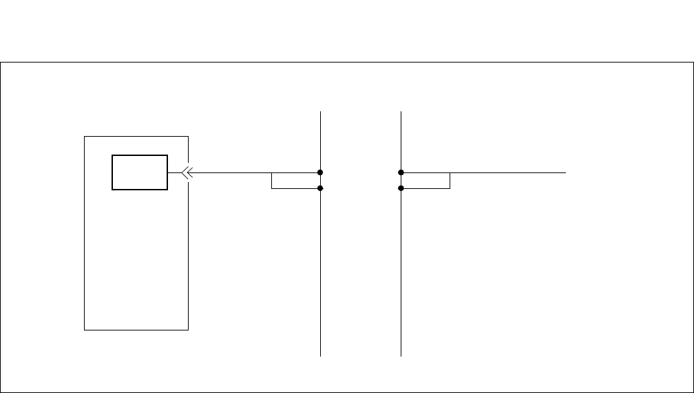
NDA-24296 CHAPTER 3
Page 507
Revision 1.0
PA-4ILCH
ISDN Line Circuit
Figure 3-153 Connecting Route Diagram
MDF
PIM
NT1
A
B
ILC A
B
CHAPTER 3 NDA-24296
Page 508
Revision 1.0
PA-4ILCH
ISDN Line Circuit
7. Switch Setting Sheet
MODULE SLOT NO. SWITCH
NAME SWITCH SHAPE REMARKS
PIM
MB UP: Circuit card make busy
DOWN: Circuit card make busy cancel
MBR
LPB
MODE
SW10
SW11
SW12
SW20
SW21
ON
OFF
ON
No. 3
No. 2
No. 1
No. 0
OFF
ON
No. 3
No. 2
No. 1
No. 0
3
12 3 4
ON
12345678
ON
12345678
ON
1234
ON
12345678
ON
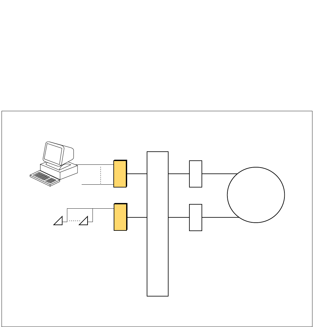
NDA-24296 CHAPTER 3
Page 509
Revision 1.0
PA-8ILCE-A
ISDN Terminal Line Circuit
PA-8ILCE-A
ISDN Terminal Line Circuit
1. General Function
The PA-8ILCE-A (ILC) circuit card provides an interface between the system and a maximum of eight
ISDN BRI (Basic Rate Interface) terminals, allowing the system to use eight ISDN BRIs, which are made
up of two B channels at 64 kbps and one D channel at 16 kbps (2B+D × 8), on the same bus. In addition,
this card supports D channel packet function. For this feature, however, available channels are seven
channels, ranging from No. 0 to No. 6.
Figure 3-154 Location of PA-8ILCE-A (ILC) within the System
SW
PRT
PRT
ILC
ILC
(MAX. 8 terminals)
(MAX. 8 circuits) ISDN
NETWORK
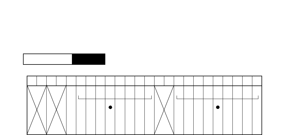
CHAPTER 3 NDA-24296
Page 510
Revision 1.0
PA-8ILCE-A
ISDN Terminal Line Circuit
2. Mounting Location/Condition
The PA-8ILCE-A card can be mounted in any universal slots as shown below.
Note: The circuit card cannot be mounted in slot No. 04 of PIM0. This card cannot use Group0 (G=00) of Unit0
(U=0) of even-number Module Group.
PIM
Mounting Module
00 01 02 03 04 05 06 07 08 09 10 11 12 13 14 15 16 17 18 19 20 21 22 23
Note
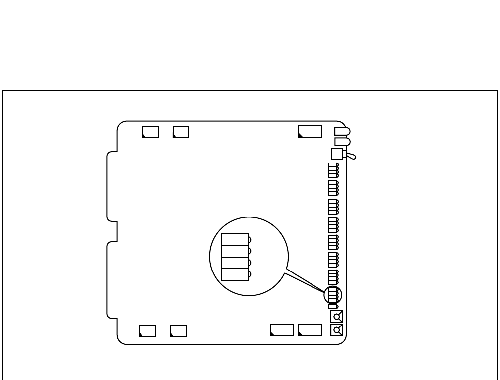
NDA-24296 CHAPTER 3
Page 511
Revision 1.0
PA-8ILCE-A
ISDN Terminal Line Circuit
3. Face Layout of Lamps, Switches, and Connectors
The face layout of lamps, switches, and connectors on the circuit card is shown in Figure 3-155.
Figure 3-155 Face Layout of PA-8ILCE-A (ILC)
OPE
MB
SW02 SW03 SW06
SW04 SW05
N-OPE
BL02
BL01
LYR0
PWR0
CH #7
CH #6
CH #5
CH #4
CH #3
CH #2
CH #1
CH #0
SW00 SW01
MODE1
MODE0
PKT
BL72
LYR7
BL62
LYR6
BL52
LYR5
BL42
LYR4
BL32
LYR3
BL22
LYR2
BL12
LYR1
BL02
LYR0
BL71
PWR7
BL61
PWR6
BL51
PWR5
BL41
PWR4
BL31
PWR3
BL21
PWR2
BL11
PWR1
BL01
PWR0

CHAPTER 3 NDA-24296
Page 512
Revision 1.0
PA-8ILCE-A
ISDN Terminal Line Circuit
4. Lamp Indications
The contents of lamp indications on the circuit card are shown in the table below.
Note: Depending on the type of the connected ISDN terminal, whose Layer2 is not always active, this lamp may
flash when the terminal is idle and lights green at the time of call set-up.
LAMP NAME COLOR DESCRIPTION
OPE Green Remains lit while the circuit card is operating.
N-OPE Red Remains lit while the circuit card is in make-busy state.
BL n1
(n=0-7)
Green Lights green when B1 channel is being accessed and in operation.
Flash (60IPM) The corresponding channel is in make-busy state.
OFF The corresponding channel is idle.
BL n2
(n=0-7)
Green Lights green when B2 channel is being accessed and in operation.
Flash (60IPM) The corresponding channel is in make-busy state.
OFF The corresponding channel is idle.
LYR n
(n=0-7)
Green Remains lit while Layer2 of the corresponding channel is active.
Note
Flash (120IPM) Flashes while Layer1 synchronization of the corresponding channel is
established.
OFF Layer1 and/or Layer2 have not been established.
PWR n
(n=0-7) Red Lights red when overvoltage protection function for the corresponding
circuit is activated; the corresponding line is short-circuited.
PKT Green Lights green when D channel Packet is in operation.
OFF Remains off when D channel Packet is not in operation.

NDA-24296 CHAPTER 3
Page 513
Revision 1.0
PA-8ILCE-A
ISDN Terminal Line Circuit
5. Switch Settings
Standard settings of switches on the circuit card are shown in the table below.
SWITCH SWITCH
NO. SETTING STANDARD
SETTING MEANING
MB ON Make busy of the circuit card.
OFF ×Normal setting
SW00
1ON ×
Fixed to all ON.
2ON ×
3ON ×
4ON ×
SW01
1ON ×
Fixed to all ON.
2ON ×
3ON ×
4ON ×
SW02
1ON ×
Fixed to all ON.
2ON ×
3ON ×
4ON ×
SW03
1ON ×
Fixed to all ON.
2ON ×
3ON ×
4ON ×
SW04
Note
1ON Circuit #0: Wiring other than Short Passive Connection
OFF Circuit #0: Short Passive Connection
2ON Circuit #1: Wiring other than Short Passive Connection
OFF Circuit #1: Short Passive Connection
3ON Circuit #2: Wiring other than Short Passive Connection
OFF Circuit #2: Short Passive Connection
4ON Circuit #3: Wiring other than Short Passive Connection
OFF Circuit #3: Short Passive Connection
5ON Circuit #4: Wiring other than Short Passive Connection
OFF Circuit #4: Short Passive Connection
6ON Circuit #5: Wiring other than Short Passive Connection
OFF Circuit #5: Short Passive Connection
7ON Circuit #6: Wiring other than Short Passive Connection
OFF Circuit #6: Short Passive Connection
8ON Circuit #7: Wiring other than Short Passive Connection
OFF Circuit #7: Short Passive Connection
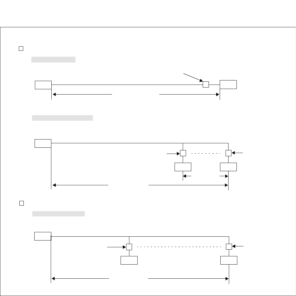
CHAPTER 3 NDA-24296
Page 514
Revision 1.0
PA-8ILCE-A
ISDN Terminal Line Circuit
OFF
•Short Passive Bus mode: This mode is also a point-to-multipoint mode, in which a maximum of eight terminals can be
connected anywhere on the bus. Note that the bus length is limited to 200 m in this case.
•Extended Passive Bus mode: This mode is a point-to-multipoint mode, in which up to eight terminals can be connected.
Note that the terminals must be connected within 50 m from the end of the bus cables as shown below.
max 600 m
Modular Rossete
ILC TE
max 400m
Modular Rossete
TE TE
max 50m
max 200 m
Modular Rossete
ILC
TE
TE
Modular Rossete
Modular Rossete
Terminals can be connected any location on the bus.
Note: Set the SW04 to determine the 4-wire bus mode referring to the following.
ILC
(in the case of 0.5φ [mm])
(in the case of 0 .5φ [mm])
(in the case of 0.5φ [mm])
(with terminating
resistor (100Ω))
(with terminating
resistor (100Ω))
(with terminating
resistor (100Ω))
ON
•Point-to-Point mode: In this mode one Terminal Equipment (TE) can be connected at the end of up to a maximum of 600
m of cable as shown below.
NDA-24296 CHAPTER 3
Page 515
Revision 1.0
PA-8ILCE-A
ISDN Terminal Line Circuit
Note: Adjust each key according to the specification of each ISDN terminal.
SWITCH SWITCH
NO. SETTING STANDARD
SETTING MEANING
SW05
1
ON PAD Level Adjustment:
OFF ×
2
ON
OFF ×
3OFF ×Fixed to OFF.
4OFF ×Fixed to OFF.
5OFF ×Not used
6OFF ×Not used
7ON Packet Access via D channel: In Service
OFF Packet Access via D channel: Out of Service
8ON ×Fixed to ON.
SW06
Note
1ON Bus Mode in Layer2 (circuit #0): Point-to-Point
OFF Bus Mode in Layer2 (circuit #0): Point-to-Multipoint
2ON Bus Mode in Layer2 (circuit #1): Point-to-Point
OFF Bus Mode in Layer2 (circuit #1): Point-to-Multipoint
3ON Bus Mode in Layer2 (circuit #2): Point-to-Point
OFF Bus Mode in Layer2 (circuit #2): Point-to-Multipoint
4ON Bus Mode in Layer2 (circuit #3): Point-to-Point
OFF Bus Mode in Layer2 (circuit #3): Point-to-Multipoint
5ON Bus Mode in Layer2 (circuit #4): Point-to-Point
OFF Bus Mode in Layer2 (circuit #4): Point-to-Multipoint
6ON Bus Mode in Layer2 (circuit #5): Point-to-Point
OFF Bus Mode in Layer2 (circuit #5): Point-to-Multipoint
7ON Bus Mode in Layer2 (circuit #6): Point-to-Point
OFF Bus Mode in Layer2 (circuit #6): Point-to-Multipoint
8ON Bus Mode in Layer2 (circuit #7): Point-to-Point
OFF Bus Mode in Layer2 (circuit #7): Point-to-Multipoint
SW1 SW2 RECEIVE (dB) SEND (dB)
OFF
OFF
ON
ON
OFF
ON
OFF
ON
0
0
0
0
0
2
5
8

CHAPTER 3 NDA-24296
Page 516
Revision 1.0
PA-8ILCE-A
ISDN Terminal Line Circuit
SWITCH SWITCH
NO. SETTING STANDARD
SETTING MEANING
MODE0
0×Fixed to 0.
1
F
Not used
MODE1
0
5
Not used
6×Fixed to 6.
7
F
Not used
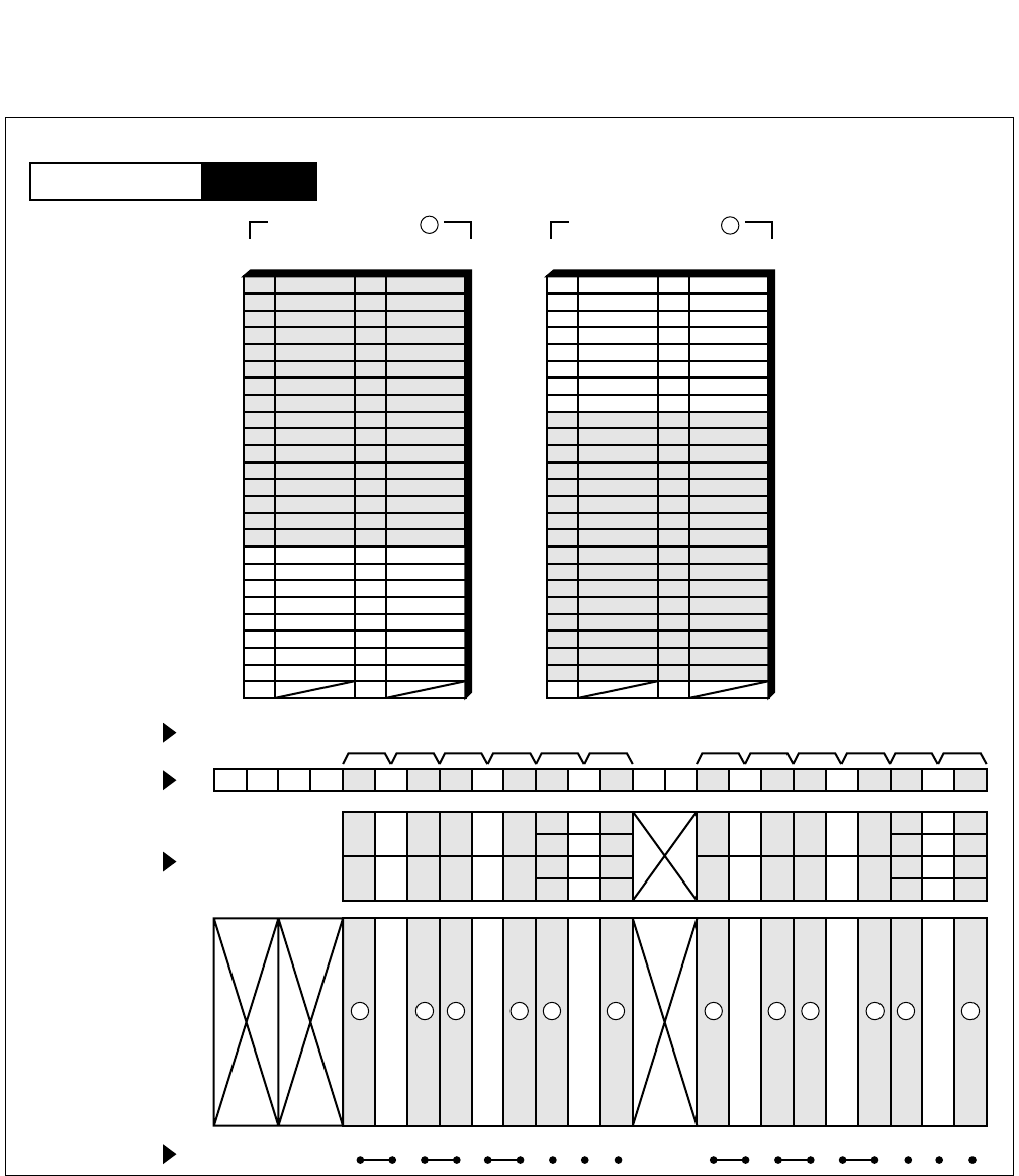
NDA-24296 CHAPTER 3
Page 517
Revision 1.0
PA-8ILCE-A
ISDN Terminal Line Circuit
6. External Interface
Figure 3-156 LT Connector Lead Accommodation (1/2)
See also Connecting Route Diagram. (Figure 3-157)
PIM
Mounting Module
26
27
28
29
30
31
32
33
34
35
36
37
38
39
40
41
1
2
3
4
5
6
7
8
9
10
11
12
13
14
15
16
42
43
44
45
46
47
48
17
18
19
20
21
22
23
49
50 24
25
232221201918171615141312111009080706050403020100
LT6 LT7 LT8 LT9 LT10 LT11LT0 LT1 LT2 LT3 LT4 LT5
231915
221814
211713
201612
231915
221814
211713
201612
110907050301
100806040200
110907050301
100806040200
HW11HW10HW9HW8HW7HW6HW5HW4HW3HW2HW1HW0
Group No.
Slot No.
LT Connector
PIM
Highway Block
LT 1, 3, 5, 7, 9, 11 Connector
26
27
28
29
30
31
32
33
34
35
36
37
38
39
40
41
1
2
3
4
5
6
7
8
9
10
11
12
13
14
15
16
42
43
44
45
46
47
48
17
18
19
20
21
22
23
49
50 24
25
Accommodated in 1
LT 0, 2, 4, 6, 8, 10 Connector
Accommodated in 2
1212 12
12 1212
RB0
TB0
RB1
TB1
RB2
TB2
RB3
TB3
RB4
TB4
RB5
TB5
RB6
TB6
RB7
TB7
RA0
TA0
RA1
TA1
RA2
TA2
RA3
TA3
RA4
TA4
RA5
TA5
RA6
TA6
RA7
TA7
RA0
TA0
RA1
TA1
RA2
TA2
RA3
TA3
RA4
TA4
RA5
TA5
RA6
TA6
RA7
TA7
RB0
TB0
RB1
TB1
RB2
TB2
RB3
TB3
RB4
TB4
RB5
TB5
RB6
TB6
RB7
TB7
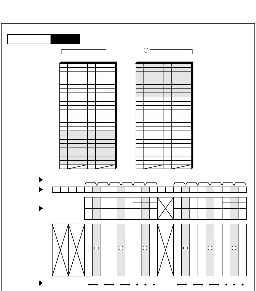
CHAPTER 3 NDA-24296
Page 518
Revision 1.0
PA-8ILCE-A
ISDN Terminal Line Circuit
Figure 3-156 LT Connector Lead Accommodation (2/2)
PIM
Mounting Module
26
27
28
29
30
31
32
33
34
35
36
37
38
39
40
41
1
2
3
4
5
6
7
8
9
10
11
12
13
14
15
16
42
43
44
45
46
47
48
17
18
19
20
21
22
23
49
50 24
25
232221201918171615141312111009080706050403020100
LT6 LT7 LT8 LT9 LT10 LT11LT0 LT1 LT2 LT3 LT4 LT5
231915
221814
211713
201612
231915
221814
211713
201612
110907050301
100806040200
110907050301
100806040200
HW11HW10HW9HW8HW7HW6HW5HW4HW3HW2HW1HW0
Group No.
Slot No.
LT Connector
PIM
Highway Block
LT 1, 3, 5, 7, 9, 11 Connector
26
27
28
29
30
31
32
33
34
35
36
37
38
39
40
41
1
2
3
4
5
6
7
8
9
10
11
12
13
14
15
16
42
43
44
45
46
47
48
17
18
19
20
21
22
23
49
50 24
25
Accommodated in 3
LT 0, 2, 4, 6, 8, 10 Connector
333333
RA4
TA4
RA5
TA5
RA6
TA6
RA7
TA7
RB4
TB4
RB5
TB5
RB6
TB6
RB7
TB7
RA0
TA0
RA1
TA1
RA2
TA2
RA3
TA3
RB0
TB0
RB1
TB1
RB2
TB2
RB3
TB3

NDA-24296 CHAPTER 3
Page 519
Revision 1.0
PA-8ILCE-A
ISDN Terminal Line Circuit
Figure 3-157 Connecting Route Diagram
RA
RB
TA
TB
TA
RA
RB
TB
MDF
ILC
Modular
Rossete
with terminating
resistor (100Ω)
TE
RA
RB
TA
TB
TA
RA
RB
TB
MDF
ILC
Modular
Rossete
TE TE
TA
RA
RB
TB
RA
TA
TA
RB
RA
TA
TA
RB
Modular
Rossete
with terminating
resistor (100Ω)
• Point-to-Point
• Point-to-Multipoint
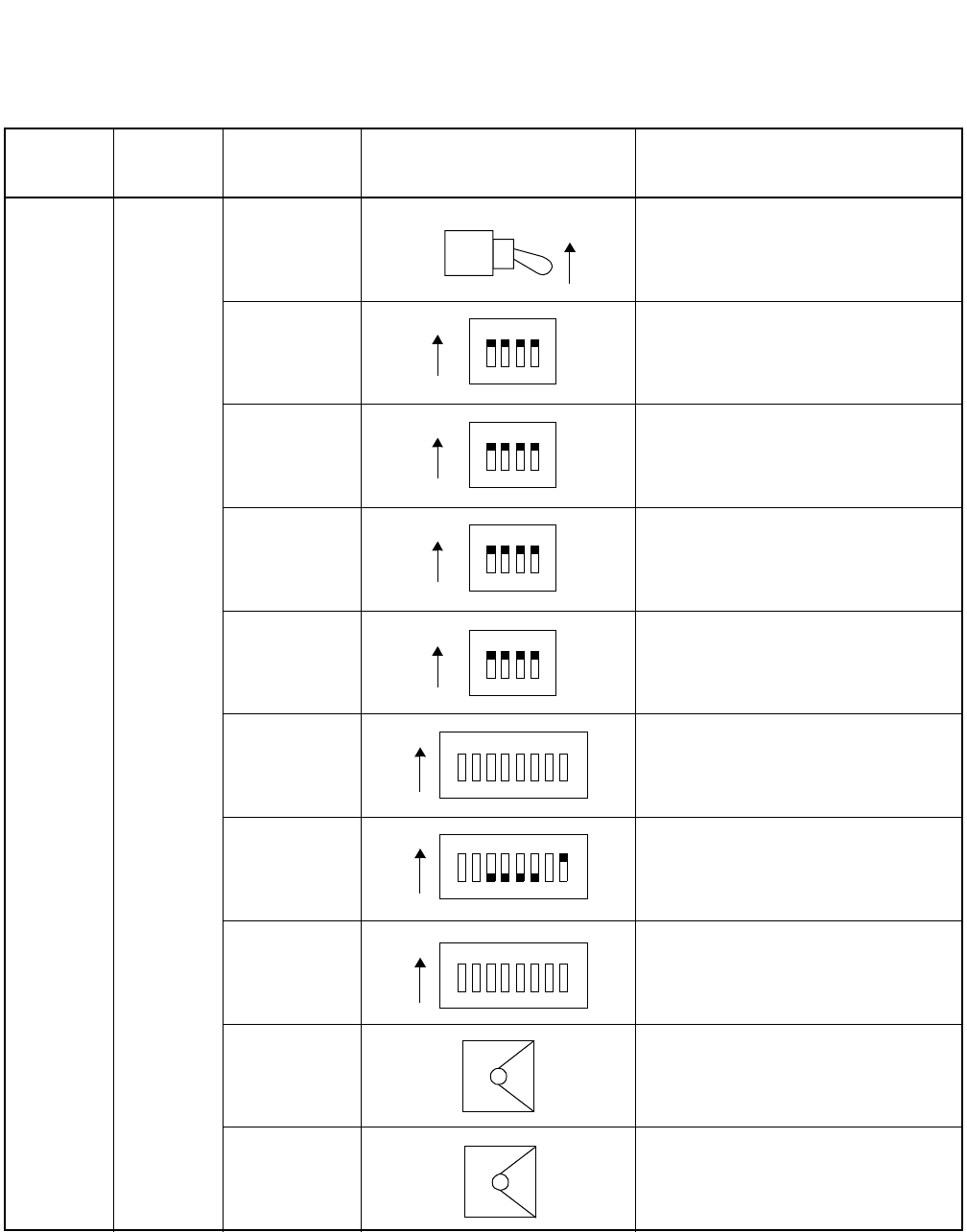
CHAPTER 3 NDA-24296
Page 520
Revision 1.0
PA-8ILCE-A
ISDN Terminal Line Circuit
7. Switch Setting Sheet
MODULE SLOT
NO. SWITCH
NAME SWITCH SHAPE REMARKS
PIM
MB
SW00
SW01
SW02
SW03
SW04
SW05
SW06
MODE0
MODE1
ON
1
ON 2 3 4
1
ON 2 3 4
1
ON 2 3 4
1
ON 2 3 4
1
ON 2 3 4 5 6 7 8
1
ON 2 3 456 7 8
1
ON 2 3 456 7 8
0
6
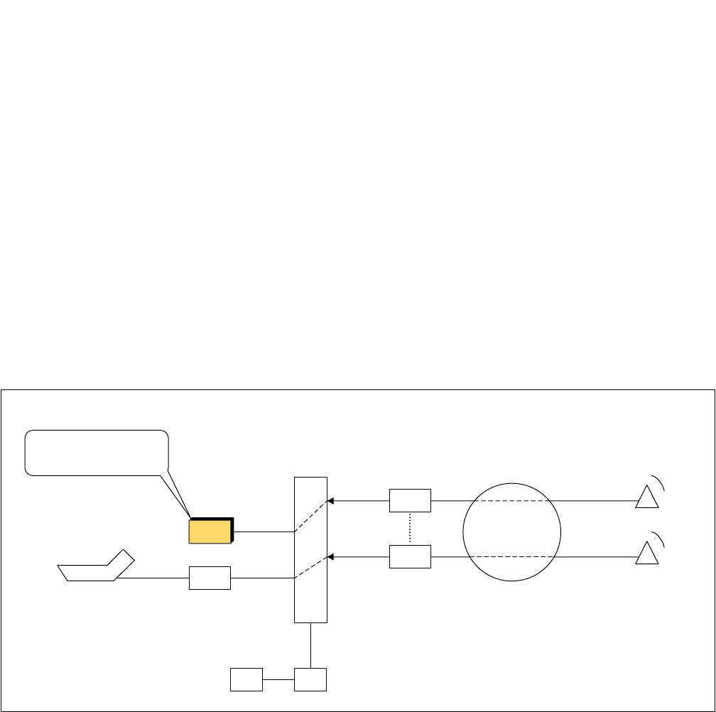
NDA-24296 CHAPTER 3
Page 521
Revision 1.0
PA-4DATA
Digital Announcement Trunk
PA-4DATA
Digital Announcement Trunk
1. General Function
The PA-4DATA (DAT) circuit card is used as a Digital Announcement Trunk supporting service features
related to announcement function such as Automated Attendant, Delay Announcement Attendant,
Announcement Service (for Hotel System). Depending upon the switch setting, this circuit card works in
one of the following three modes.
•16-sec. mode (maximum 4 CHs/card)
•32-sec. mode (maximum 2 CHs/card)
•60-sec. mode (maximum 1 CH/card)
A message can be recorded from either a tape recorder or a telephone set (See the Reference). In addition,
this circuit card can be used as an external music source.
Figure 3-158 Location of PA-4DATA (DAT) within the System
COT
COT
GTCPU
ATI INCOMING CALL
INCOMING CALL
PUBLIC
NETWORK
CALLING PARTY
CALLING PARTY
TSW
ATTCON
(Busy)
(PRERECORDED MESSAGE)
We are sorry, the line is
busy now. Please stay on
the line for a while.
DAT
This diagram shows an example when this card is used for Delay Announcement Attendant.
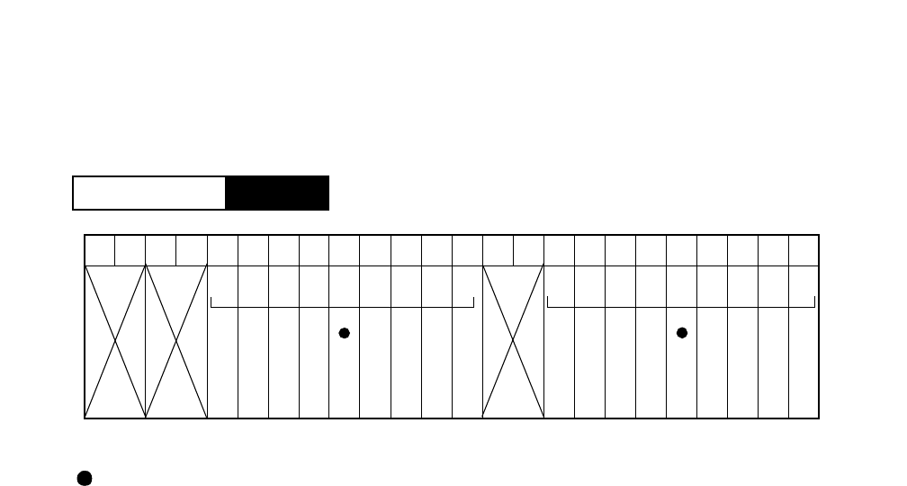
CHAPTER 3 NDA-24296
Page 522
Revision 1.0
PA-4DATA
Digital Announcement Trunk
2. Mounting Location/Condition
The PA-4DATA (DAT) card can be mounted in any universal slot as shown below.
Note: Indicates universal slots for line/trunk circuit cards.
PIM
Mounting Module
00 01 02 03 04 05 06 07 08 09 10 11 12 13 14 15 16 17 18 19 20 21 22 23
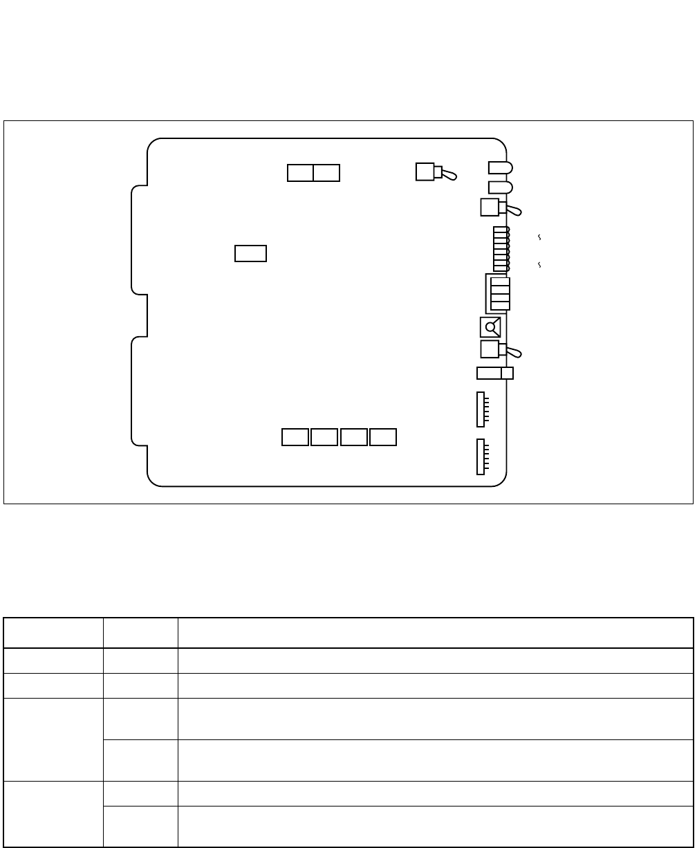
NDA-24296 CHAPTER 3
Page 523
Revision 1.0
PA-4DATA
Digital Announcement Trunk
3. Face Layout of Lamps, Switches, and Connectors
The face layout of lamps, switches, and connectors on this circuit card is shown in Figure 3-159.
Figure 3-159 Face Layout of PA-4DATA (DAT)
4. Lamp Indications
The contents of lamp indications of this circuit card are shown in the table below.
LAMP COLOR STATE
OPE Green Remains lit while this circuit card is operating.
N-OPE Red Remains lit while this circuit card is in make-busy state.
BL4
BL7
Green Lights when the corresponding circuit (No 0 through No. 3 circuits) is connected to a
recording source.
Flash Flashes while message recording is in progress on the corresponding circuit (No. 0 through
No. 3 circuit).
BL0
BL3
Red Lights when the corresponding circuit (No 0 through No. 3 circuits) is busy.
Flash Flashes when the corresponding circuit (No. 0 though No. 3 circuits) is in make-busy state
or has not been assigned in the system.
OPE
N-OPE
MB
BL7 (G)
BL4 (G)
(SW11)
(SW9)
BL3 (R)
BL0 (R)
2
3
0
1
(SW10)
(SW8)
JACK
(SW12)
SW5 SW7
SW6
SW1 SW2 SW3 SW4
MBRQ
MRCS
START
WR
--
CHAPTER 3 NDA-24296
Page 524
Revision 1.0
PA-4DATA
Digital Announcement Trunk
5. Switch Settings
Standard settings of various switches on this circuit card are shown in the table below.
Note 4: Valid in the case of recording or playback from a telephone set.
SWITCH SWITCH
NO. SETTING STANDARD
SETTING MEANING
MB (SW11) UP Circuit card make busy
DOWN ×Circuit card make busy cancel
SW1 (for No. 0
Circuit)
SW2 (for No. 1
Circuit)
SW3 (for No. 2
Circuit)
SW4 (for No. 3
Circuit)
1
2
3
4
SW5
1
2
3
Note 4
ON ×Compression Law: µ-law
OFF Compression Law: A-law
4ON When using as an external music-on-hold source
OFF When using as announcement equipment only
Note 1: 16-sec. mode = 4 recording circuits
32-sec. mode = 2 recording circuits
60-sec. mode = 1 recording circuit
Note 2: For each circuit, SW1 - SW4 must be set in
the same way (Two different modes cannot
be mixed assigned.).
SETTING OF TIMER FOR EACH CIRCUIT
1234TIMER (MODE)
ON
ON
OFF
ON
ON
OFF
OFF
ON
OFF
ON
OFF
OFF
16-sec. mode
32-sec. mode
60-sec. mode
Note 3: Set the Recording/Playback Timer in the same way as set
by SW1-SW4.
SETTING OF ANNOUNCEMENT RECORDING/PLAYBACK TIME
SW5-1 SW5-2 RECORDING/PLAYBACK TIME
OFF
ON
OFF
ON
OFF
OFF
16-sec. Recording/Playback
32-sec. Recording/Playback
60-sec. Recording/Playback

NDA-24296 CHAPTER 3
Page 525
Revision 1.0
PA-4DATA
Digital Announcement Trunk
SWITCH SWITCH
NO. SETTING STANDARD
SETTING MEANING
SW6
1ON Single playback by No. 0 Circuit Note 5
OFF Multiple playback by No. 0 Circuit
2ON Single playback by No. 1 Circuit Note 5
OFF Multiple playback by No. 1 Circuit
3ON Single playback by No. 2 Circuit Note 5
OFF Multiple playback by No. 2 Circuit
4ON Single playback by No. 3 Circuit Note 5
OFF Multiple playback by No. 3 Circuit
5OFF ×Fixed
6OFF ×Fixed
7OFF ×Not used
8ON Recording from a telephone set
OFF ×Normal setting
Note 5: For Automated Attendant and Delay Announcement-Attendant, set single playback
(ON).
SW7
1OFF ×Fixed
2OFF ×Fixed
3OFF ×Not used
4OFF ×Not used
START (SW8) UP Setting for recording start from a tape recorder or for
playback start.
DOWN ×Normal setting

CHAPTER 3 NDA-24296
Page 526
Revision 1.0
PA-4DATA
Digital Announcement Trunk
Note 6: When this circuit card is using an external music-on-hold source, set 0, 4 or 6 by timer mode.
SWITCH SWITCH
NO. SETTING STANDARD
SETTING MEANING
MRCS
(SW9) Note 6
ESet to E while the circuit card is using as announcement
equipment only.
0Designation of No. 0 Circuit.
The timer is 16-sec. mode.
1Designation of No. 1 Circuit.
The timer is 16-sec. mode.
2Designation of No. 2 Circuit.
The timer is 16-sec. mode.
3Designation of No. 3 Circuit.
The timer is 16-sec. mode.
4Designation of No. 0 and No. 1 Circuit.
The timer is 32-sec. mode.
5Designation of No. 2 and No. 3 Circuit.
The timer is 32-sec. mode.
6Designation of All Circuits.
The timer is 60-sec. mode.
F Recording from a telephone set.
MBRQ
(SW10)
0ON No. 0 Circuit make busy request
No. 0 Circuit is designated during a recording.
OFF ×No. 0 Circuit make busy request cancel
1ON No. 1 Circuit make busy request
No. 1 Circuit is designated during a recording.
OFF ×No. 1 Circuit make busy request cancel
2ON No. 2 Circuit make busy request
No. 2 Circuit is designated during a recording.
OFF ×No. 2 Circuit make busy request cancel
3ON No. 3 Circuit make busy request
No. 3 Circuit is designated during a recording.
OFF ×No. 3 Circuit make busy request cancel
WR
(SW12)
UP Recording from a tape recorder (WRITE mode)
DOWN ×Normal setting
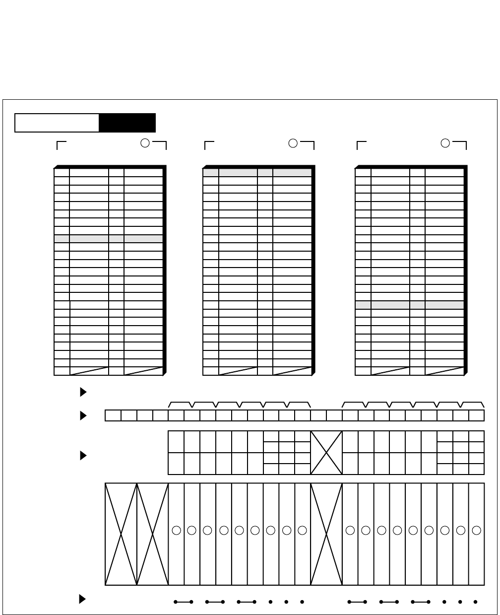
NDA-24296 CHAPTER 3
Page 527
Revision 1.0
PA-4DATA
Digital Announcement Trunk
6. External Interface
When this circuit card is used as an external music-on-hold source, the following leads (FM, E) appear from
the LT connector.
Figure 3-160 LT Connector Lead Accommodation
PIM
Mounting Module
26
27
28
29
30
31
32
33
34
35
36
37
38
39
40
41
1
2
3
4
5
6
7
8
9
10
11
12
13
14
15
16
42
43
44
45
46
47
48
17
18
19
20
21
22
23
49
50 24
25
232221201918171615141312111009080706050403020100
LT6 LT7 LT8 LT9 LT10 LT11LT0 LT1 LT2 LT3 LT4 LT5
231915
221814
211713
201612
231915
221814
211713
201612
110907050301
100806040200
110907050301
100806040200
1
Group No.
Slot No.
LT Connector
PIM
LT 1, 3, 5, 7, 9, 11 Connector
26
27
28
29
30
31
32
33
34
35
36
37
38
39
40
41
1
2
3
4
5
6
7
8
9
10
11
12
13
14
15
16
42
43
44
45
46
47
48
17
18
19
20
21
22
23
49
50 24
25
Accommodated in 1
LT 0, 2, 4, 6, 8, 10 Connector
Accommodated in 2
FM
26
27
28
29
30
31
32
33
34
35
36
37
38
39
40
41
1
2
3
4
5
6
7
8
9
10
11
12
13
14
15
16
42
43
44
45
46
47
48
17
18
19
20
21
22
23
49
50 24
25
LT 1, 3, 5, 7, 9, 11 Connector
Accommodated in 3
FM
FM
23123123
E
E
E
123123123
HW11HW10HW9HW8HW7HW6HW5HW4HW3HW2HW1HW0
Highway Block
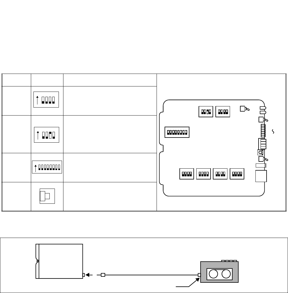
CHAPTER 3 NDA-24296
Page 528
Revision 1.0
PA-4DATA
Digital Announcement Trunk
[Reference]
How to Record a Message
•Prior to your recording, set switches on the DAT card according to the following example.
•Connect a tape recorder to the DAT card with a cable.
•Turn On the MBRQ key to make busy a channel to be recorded.
(To record a message in the 60 sec. mode, all circuits must be placed into MB state.)
•Turn the WR key upwards.
(The corresponding BL lamp lights green indicating the tape recorder is connected to the circuit.)
•Turn the START key upwards.
(The corresponding BL lamp starts flashing.)
Table 3-12 Switch Settings on DAT (Example 60 sec. mode)
SWITCH SETTING DESCRIPTION
SW1
SW4
Timer Value for Channel 0-3: 60 sec.
SW5
Circuit Card Timer: 60 sec.
A-law/µ-law: µ-law
External Music Source/Announcement
Equipment:
Announcement Equipment
SW6 Single/Repeated Playback:
Repeated Playback
MRCS Channel Designation:
60 sec. mode
OPE
N-OPE
MB
12345678
SW6
1234
SW5
1234
SW7
1234
SW1
1234
SW2
1234
SW3
1234
SW4
BL7
BL0
MBRQ
MRCS
START
JACK
BATTERY
PACK
WR
3
2
1
0
~
1234
ON
1 2 3 4
ON
12345678
ON
6
DAT
Jack
Front
Earphone Jack (3.6 )
φ
Tape Recorder

NDA-24296 CHAPTER 3
Page 529
Revision 1.0
PA-4DATA
Digital Announcement Trunk
•Start the tape recorder and record your message in the designated channel.
- recording -
•The corresponding BL lamp (BL0 ~ BL7) lights steadily. (Recording ends.)
•Return the START, WR key to the previous position.
How to Play Back the Recorded Message
•Playback from a telephone set
•Set the related switches on the PA-4DATA (DAT) card.
•Seize a specific channel by “Individual Trunk Access.”
•Hear the recorded message.
•Playback from the phone jack on PA-4DATA (DAT) card
•Connect a earphone to the phone jack on the PA-4DATA (DAT) card.
•Select your desired channel (0-3) by the MRCS switch.
•Turn the START key upwards.
•Hear the recorded message.
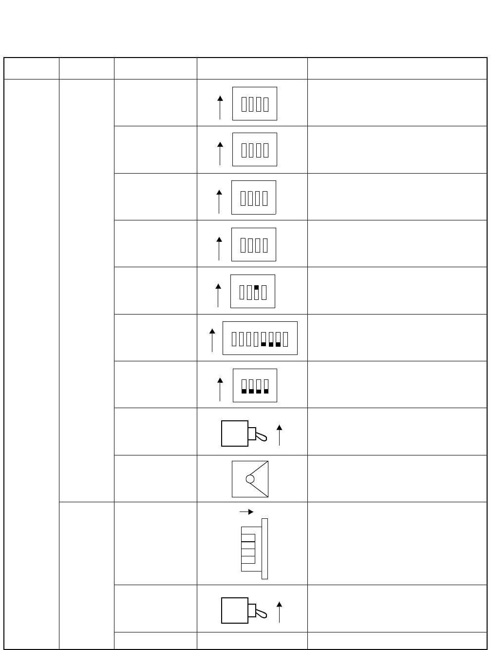
CHAPTER 3 NDA-24296
Page 530
Revision 1.0
PA-4DATA
Digital Announcement Trunk
7. Switch Setting Sheet
MODULE SLOT NO. SWITCH NAME SWITCH SHAPE REMARKS
PIM
SW1
SW2
SW3
SW4
SW5
SW6
SW7
START
(SW8)
MRCS
(SW9)
MBREQ
(SW10)
WE
(SW12)
MB DOWN Circuit card make busy cancel
12 3 4
ON
1234
ON
1234
ON
1 2 3 4
ON
1 2 3 4
ON
12345678
ON
1234
ON
ON
3
2
1
0
ON
ON
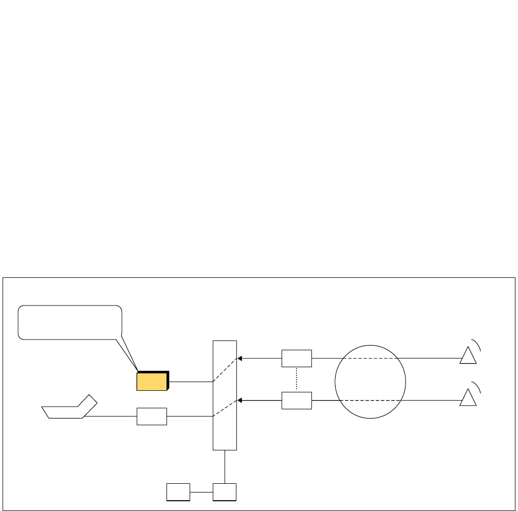
NDA-24296 CHAPTER 3
Page 531
Revision 1.0
PA-4DATB
Digital Announcement Trunk
PA-4DATB
Digital Announcement Trunk
1. General Function
The PA-4DATB (DAT) circuit card is used as a Digital Announcement Trunk supporting service features
related to announcement function such as Automated Attendant, Delay Announcement Attendant,
Announcement Service (for Hotel System). Depending upon the switch setting, this circuit card works in
one of the following three modes.
• 64-sec. mode (maximum 4 CHs/card)
•128-sec. mode (maximum 2 CHs/card)
•240-sec. mode (maximum 1 CH/card)
A message can be recorded from either a tape recorder or a telephone set. (See the Reference).
In addition, this circuit card can be used as an external music source.
Figure 3-161 Location of PA-4DATB (DAT) within the System
COT
COT
GTCPU
ATI INCOMING CALL
INCOMING CALL
PUBLIC
NETWORK
CALLING PARTY
CALLING PARTY
TSW
ATTCON
(Busy)
(PRERECORDED MESSAGE)
We are sorry, the line is
busy now. Please stay on
the line for a while.
DAT
This diagram shows an example when this card is used for Delay Announcement Attendant.

CHAPTER 3 NDA-24296
Page 532
Revision 1.0
PA-4DATB
Digital Announcement Trunk
2. Mounting Location/Condition
The PA-4DATB (DAT) card can be mounted in any universal slots as shown below.
Note: Indicates universal slots for line/trunk circuit cards.
PIM
Mounting Module
00 01 02 03 04 05 06 07 08 09 10 11 12 13 14 15 16 17 18 19 20 21 22 23
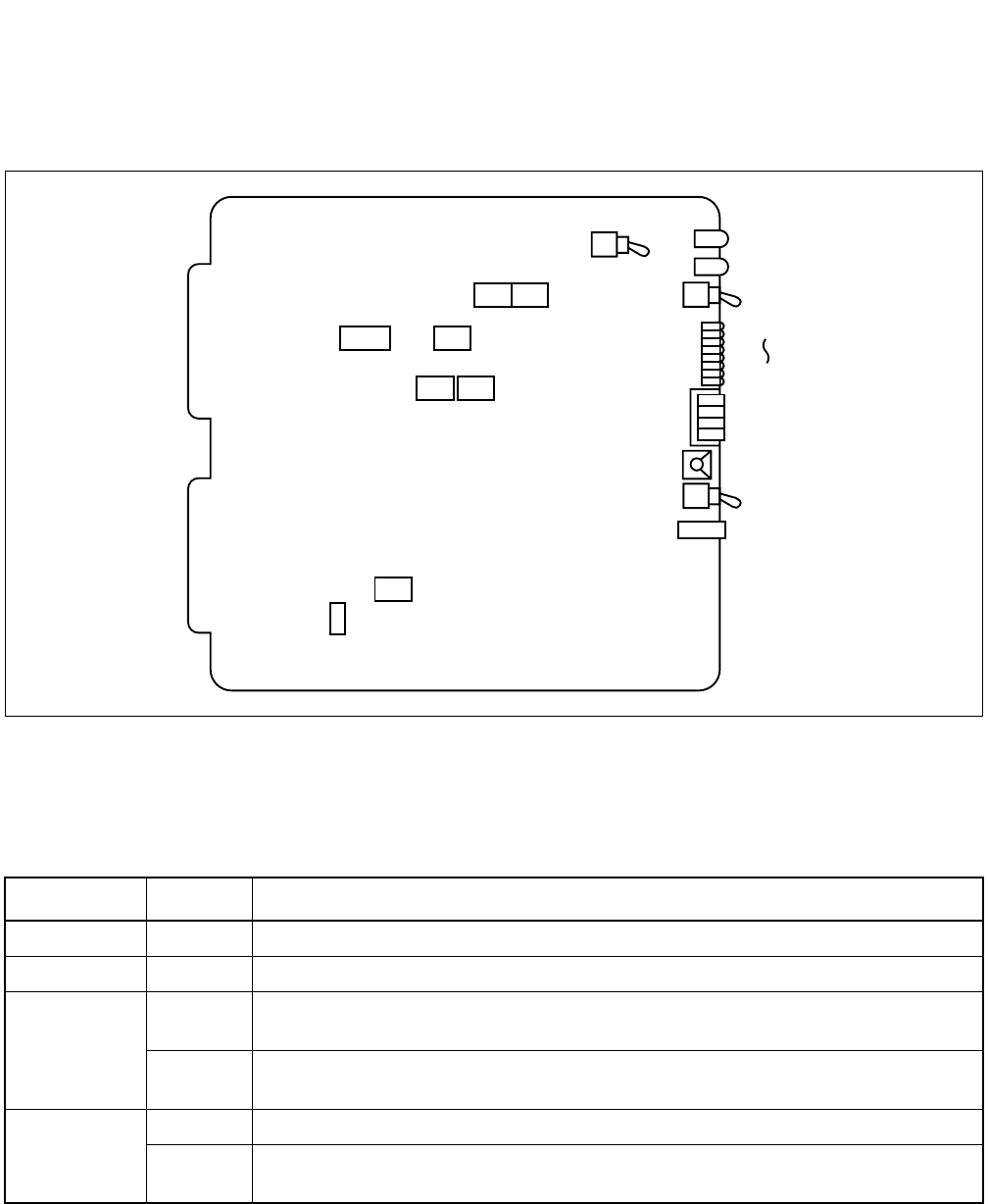
NDA-24296 CHAPTER 3
Page 533
Revision 1.0
PA-4DATB
Digital Announcement Trunk
3. Face Layout of Lamps, Switches, and Connectors
The face layout of lamps, switches, and connectors on this circuit card is shown in Figure 3-162.
Figure 3-162 Face Layout of PA-4DATB (DAT)
4. Lamp Indications
The contents of lamp indications of this circuit card are shown in the table below.
LAMP COLOR STATE
OPE Green Remains lit while this circuit card is operating.
N-OPE Red Remains lit while this circuit card is in make-busy state.
BL4
BL7
Green Lights when the corresponding circuit (No 0 through No. 3 circuits) is connected to a record-
ing source.
Flash Flashes while message recording is in progress on the corresponding circuit (No. 0 through
No. 3 circuit)
BL0
BL3
Red Lights when the corresponding circuit (No 0 through No. 3 circuits) is busy.
Flash Flashes when the corresponding circuit (No. 0 though No. 3 circuits) is in make-busy state
or has not been assigned in the system.
OPE
N-OPE
MB
BL7
BL0
2
3
0
1
JACK
WR
SW5 SW3
MBRQ
MRCS
START
SW6 SW1
SW7 SW2
SW4
JP0
--
CHAPTER 3 NDA-24296
Page 534
Revision 1.0
PA-4DATB
Digital Announcement Trunk
5. Switch Settings
Standard settings of switches on this circuit card are shown in the table below.
SWITCH SWITCH
NO. SETTING STANDARD
SETTING MEANING
MB UP Circuit card make busy
DOWN ×Circuit card make busy cancel
MBRQ
1-4 ON Make busy request on a channel basis
(Channel Designation for Recording/Playback)
OFF ×Make busy request cancel on a channel basis
MRCS 0
1
2
3
4
5
6
7
SW1
SW4
Each Switch corresponds to each channel
of
DAT: channel
SW1: channel #0
SW2: channel #1
SW3: channel #2
SW4: channel #3
Setting of Recording Mode
SWITCH NO. Mode Channel
0
64-sec. mode
0
11
22
33
4128-sec. mode 0, 1
52, 3
6 240-sec. mode 0, 1, 2, 3
-
SETTING OF TIMER FOR EACH CIRCUIT
1234TIMER (MODE)
ON
ON
OFF
ON
ON
OFF
OFF
ON
OFF
ON
OFF
OFF
64-sec. mode
128-sec. mode
240-sec. mode
ON ON ON ON Not available
NDA-24296 CHAPTER 3
Page 535
Revision 1.0
PA-4DATB
Digital Announcement Trunk
SWITCH SWITCH
NO. SETTING STANDARD
SETTING MEANING
SW5
1
2
3ON ×Compression Law: µ-law
OFF Compression Law: A-law
4ON To be used as external hold tone source
OFF To be used as announcement equipment
SW6
1ON Single playback of No. 0 channel Note 3
OFF Multiple playback of No. 0 channel Note 2
2ON Single playback of No. 1 channel Note 3
OFF Multiple playback of No. 1 channel Note 2
3ON Single playback of No. 2 channel Note 3
OFF Multiple playback of No. 2 channel Note 2
4ON Single playback of No. 3 channel Note 3
OFF Multiple playback of No.3 channel Note 2
5ON RAM Test data-clear
OFF ×RAM Test data-store
6OFF ×Not used
7OFF ×Not used
8OFF ×Not used
Note 2: When this card is used as announcement equipment, SW6-1~ 6-4 should be set OFF.
Note 3: For Automated Attendant and Delay Announcement-Attendant, set single playback (ON).
Note 1: Setting of Recording/Playback Timer should
correspond to that of SW1-SW4.
SETTING OF ANNOUNCEMENT RECORDING/PLAYBACK TIME
SW5-1 SW5-2 RECORDING/PLAYBACK TIME
OFF
ON
OFF
ON
OFF
OFF
64-sec. Recording/Playback
128-sec. Recording/Playback
240-sec. Recording/Playback
CHAPTER 3 NDA-24296
Page 536
Revision 1.0
PA-4DATB
Digital Announcement Trunk
SWITCH SWITCH
NO. SETTING STANDARD
SETTING MEANING
SW7 1ON Activation of RAM Test
OFF ×Normal Setting
2ON Port Microprocessor is reset when MBR key is ON.
OFF ×Port Microprocessor is not reset when MBR key is ON.
3OFF ×Not used
4OFF ×Not used
WR UP For Recording from the phone jack
DOWN ×Normal setting
START UP When starting recording from the phone jack or playback.
DOWN ×Normal setting
Table 3-13 Jumper Setting
SWITCH SWITCH
SHAPE SETTING DESCRIPTION
JP0 LEFT Compression Law: µ-law
RIGHT Compression Law: A-law
LEFT RIGHT
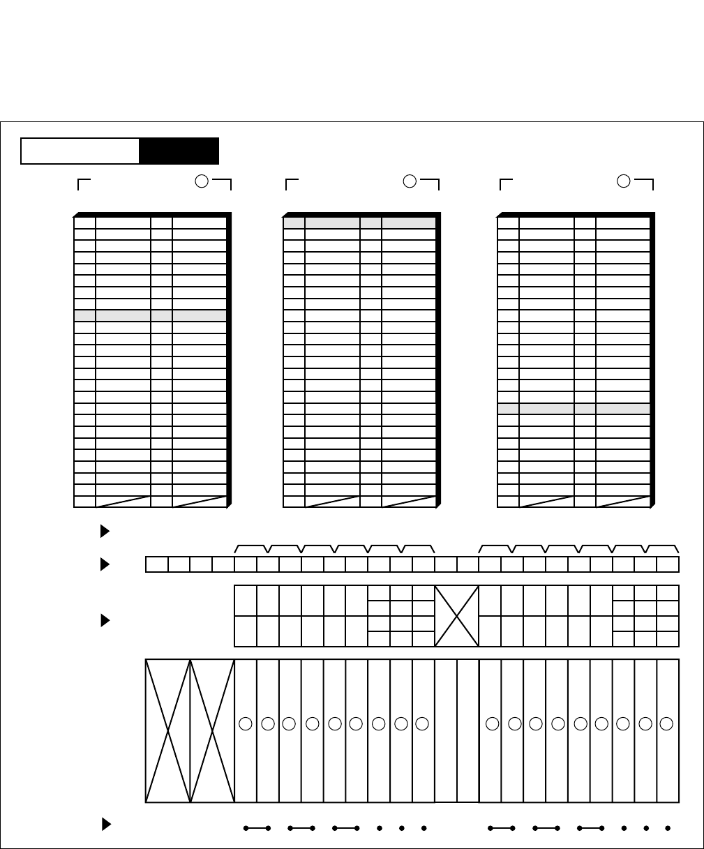
NDA-24296 CHAPTER 3
Page 537
Revision 1.0
PA-4DATB
Digital Announcement Trunk
6. External Interface
When this card is used as an external music-on-hold source, the following cable connection is required.
Figure 3-163 LT Connector Lead Accommodation
PIM
Mounting Module
26
27
28
29
30
31
32
33
34
35
36
37
38
39
40
41
1
2
3
4
5
6
7
8
9
10
11
12
13
14
15
16
42
43
44
45
46
47
48
17
18
19
20
21
22
23
49
50 24
25
232221201918171615141312111009080706050403020100
LT6 LT7 LT8 LT9 LT10 LT11LT0 LT1 LT2 LT3 LT4 LT5
231915
221814
211713
201612
231915
221814
211713
201612
110907050301
100806040200
110907050301
100806040200
1
Group No.
Slot No.
LT Connector
PIM
LT 1, 3, 5, 7, 9, 11 Connector
26
27
28
29
30
31
32
33
34
35
36
37
38
39
40
41
1
2
3
4
5
6
7
8
9
10
11
12
13
14
15
16
42
43
44
45
46
47
48
17
18
19
20
21
22
23
49
50 24
25
Accommodated in 1
LT 0, 2, 4, 6, 8, 10 Connector
Accommodated in 2
FM
26
27
28
29
30
31
32
33
34
35
36
37
38
39
40
41
1
2
3
4
5
6
7
8
9
10
11
12
13
14
15
16
42
43
44
45
46
47
48
17
18
19
20
21
22
23
49
50 24
25
LT 1, 3, 5, 7, 9, 11 Connector
Accommodated in 3
FM
FM
23
E
E
E
123123 123123123
HW11HW10HW9HW8HW7HW6HW5HW4HW3HW2HW1HW0
Highway Block
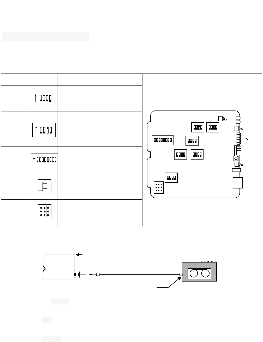
CHAPTER 3 NDA-24296
Page 538
Revision 1.0
PA-4DATB
Digital Announcement Trunk
[Reference]
•Prior to your recording, set switches on the DAT card according to the following example.
•Connect a tape recorder to the DAT card with a cable.
•Turn On the key to make busy a channel to be recorded.
(To record a message in the 240 sec mode, all circuits must be placed into MB state.)
•Turn the key upwards.
(The corresponding BL lamp lights green indicating the tape recorder has been connected to the circuit.)
•Turn the key upwards.
(The corresponding BL lamp starts flashing.)
Table 3-14 SWITCH SETTINGS ON DAT (Example <240 sec. mode>)
SWITCH SETTING DESCRIPTION
SW1
SW4
Timer Value for Channel 0-3 240 sec.
SW5
Circuit Card Timer: 240 sec.
A-law/µ-law: µ-law
External Music Source/Announcement
Equipment:
Announcement Equipment
SW6 Single/Repeated Playback:
Repeated Playback
MRCS Channel Designation:
240 sec. mode
JP0 A-law/µ-law: µ-law
HOW TO RECORD A MESSAGE
OPE
N-OPE
MB
12345678
SW6
1234
SW7
1234
SW2
1234
SW1
1234
SW5
1234
SW3
1234
SW4
JP0
BL7
BL0
MBRQ
MRCS
START
JACK
WR
3
2
1
0
BATTERY
PACK
-
1234
ON
1234
ON
12345678
ON
6
LEFT
(DAT)
jack
Front
earphone jack (3.6 )
φ
Tape Recorder
MBRQ
WR
START

NDA-24296 CHAPTER 3
Page 539
Revision 1.0
PA-4DATB
Digital Announcement Trunk
•Start the tape recorder and record your message in the designated channel.
- recording -
•The corresponding BL lamp (BL0 - BL7) lights steadily. (Recording ends.)
•Return the START, WR key to the previous position.
Playback from a telephone set
•Set the related switches on the PA-4DATB (DAT) card.
•Seize a specific channel by “Individual Trunk Access”.
•Hear the recorded message.
Playback from the phone jack on PA-4DATB (DAT) card
•Connect a earphone to the phone jack on the PA-4DATB (DAT) card.
•Select your desired channel (0-3) by the MRCS switch.
•Turn the START key upwards.
•Hear the recorded message.
HOW TO PLAY BACK THE RECORDED MESSAGE
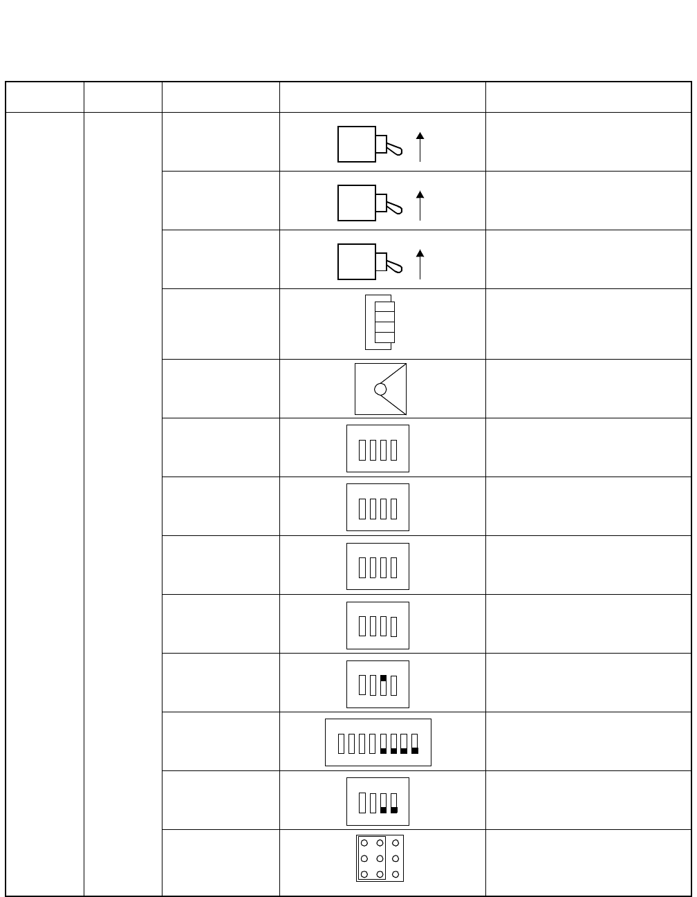
CHAPTER 3 NDA-24296
Page 540
Revision 1.0
PA-4DATB
Digital Announcement Trunk
7. Switch Setting Sheet
MODULE SLOT NO. SWITCH NAME SWITCH SHAPE REMARKS
MB
START
WR
MBRQ
MRCS
SW1
SW2
SW3
SW4
SW5
SW6
SW7
JP0
ON
ON
ON
3
1
0
2
1 2 3 4
1234
1234
12 3 4
12 3 4
12345678
1234
RIGHTLEFT
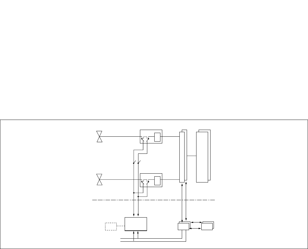
NDA-24296 CHAPTER 3
Page 541
Revision 1.0
PH-M16
Line Test
PH-M16
Line Test
1. General Function
This circuit card controlled by CPU is used for line test of a subscriber’s line. The circuit card supports to
send howler tone to external test equipment, besides the circuit card can detect or send various tones, and
send PB (DTMF) signal for automatic trunk test.
Note: A system cannot send Howler Tone during line test. The number of line available the line test/automatic
trunk test at the same time is only one.
Figure 3-164 Location of PH-M16 (LTST) card within the System (1-IMG System)
TEL
TEL
PIM
LPRA
TEST
EQ LTST GT CPU
M
U
X
TSW
LC
LC
EXTENDED I/O BUS
EXTENDED I/O BUS

CHAPTER 3 NDA-24296
Page 542
Revision 1.0
PH-M16
Line Test
2. Mounting Location/Condition
The LTST circuit card can be accommodated in the shaded slots (00, 01, 02) as shown below.
Note: This circuit card is used for 1-IMG System.
00 01 02 03 04
PH-M16
PH-M16
PH-M16
LPM
Mounting Module
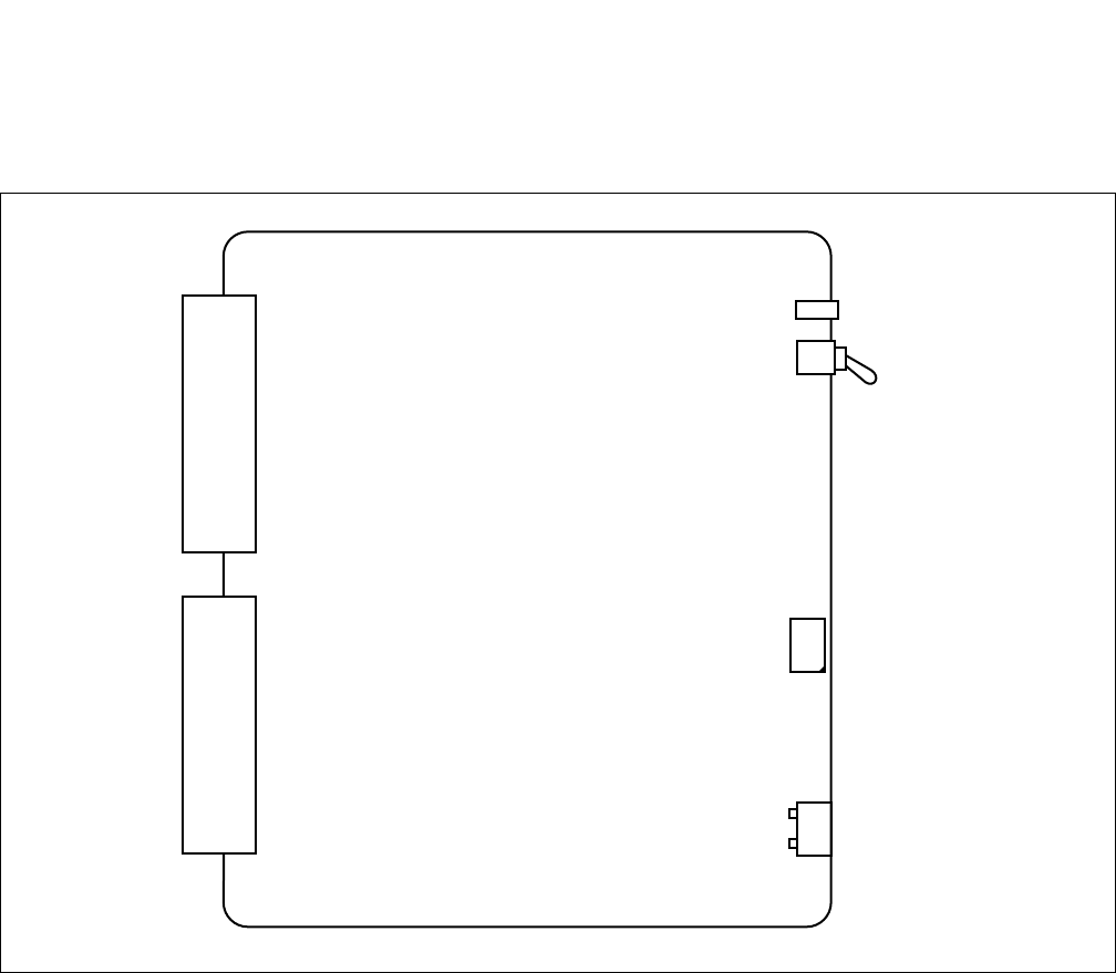
NDA-24296 CHAPTER 3
Page 543
Revision 1.0
PH-M16
Line Test
3. Face Layout of Lamps, Switches and Connectors
The face layout of lamps, switches and connectors on this circuit card is shown in Figure 3-165.
Figure 3-165 Face Layout of PH-M16 (LTST) Card
Note: CRIN is used to connect with CRIN test equipment.
MB
SW0
OPE/MB
CRIN
CHAPTER 3 NDA-24296
Page 544
Revision 1.0
PH-M16
Line Test
4. Lamp Indications
The table below shows lamp indications on this circuit card.
5. Switch Settings
The following is a brief description of the switches on this circuit card. When a switch has a standard
setting, it is indicated with “X” in the table below.
LAMP
NAME COLOR DESCRIPTION
OPE/MB Green This circuit card is operating.
Red This circuit card is make-busy.
SWITCH SWITCH
NO. SETTING STANDARD
SETTING MEANING
MB UP Circuit card make-busy.
DOWN Circuit card make-busy cancel
SW0
1ON ×Setting of a condition of DT detection
(440Hz+350Hz)
2ON ×Setting of a condition of RBT detection
(440Hz+480Hz)
3ON Time of PB (DTMF) signal sending (67msc.)
OFF ×Time of PB (DTMF) signal sending (133msec.)
4
ON
Setting of M-wire control which is concerned with sending
test tone to ODT
(Set soft control or E-wire loop back)
OFF
Setting of M-wire control which is concerned with sending
test tone to ODT
(Set soft control only)
5
6
7
8
BASIC INTERVAL TIMER
SW0
5678TIME
ON OFF OFF OFF 8µ
ON ON OFF OFF 16µ
ON ON ON OFF 32µ
ON ON ON ON 64µ
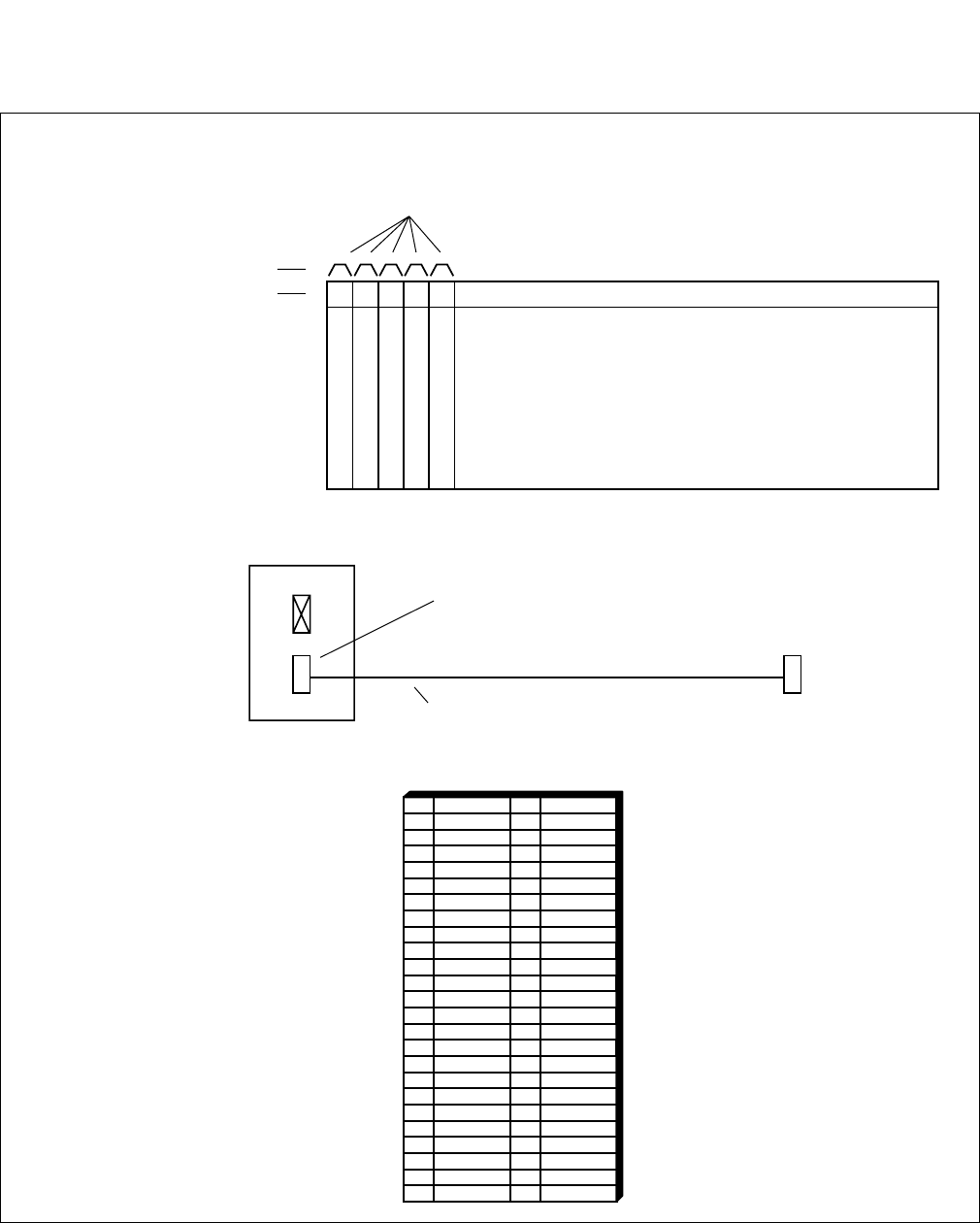
NDA-24296 CHAPTER 3
Page 545
Revision 1.0
PH-M16
Line Test
6. External Interface
Figure 3-166 LT Connector Lead Accommodation
26
27
28
29
30
31
32
33
34
35
36
37
38
39
40
41
1
2
3
4
5
6
7
8
9
10
11
12
13
14
15
16
42
43
44
45
46
47
48
17
18
19
20
21
22
23
49
50 24
25
TM
BELL0A
BELL1A
TELA
LCA
THOWA
ONHK
TCR
ATM
ATA
OUTA
TA1
EXMN
MJ0A
MN0A
MJ1A
MN1A
INA
TE
BELL0B
BELL1B
TELB
LCB
THOWB
THOWS
SE
ATB
OUTB
TB1
BELL
EXMJ
MJ0B
MN0B
MJ1B
MN1B
INB
MISC CONNECTOR
00 01 02 03 04
MISC Connector Accommodation
Circuit Card Backboard Connector
Connector Name
Slot Number
LPM
LPM Backboard
Circuit Card Backboard Connector
68PH EXMISC CABLE
MISC
MISC CONNECTOR
(PH-M16)
PH-M16
PH-M16
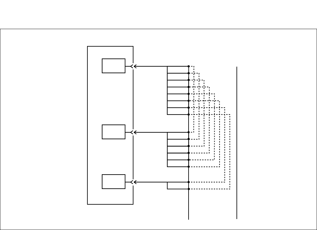
CHAPTER 3 NDA-24296
Page 546
Revision 1.0
PH-M16
Line Test
Figure 3-167 Connecting Route Diagram
B
A
E
M
RA
RB
TA
TB
TM
TE
OUTA
OUTB
INA
INB
TA1
TB1
LTST
ODT
LC
MDFPBX
NDA-24296 CHAPTER 3
Page 547
Revision 1.0
PH-M16
Line Test
7. Switch Setting Sheet
SWITCH NAME SWITCH SHAPE REMARKS
MB
SW0
ON(MB)
OFF
1234 56 78
ON
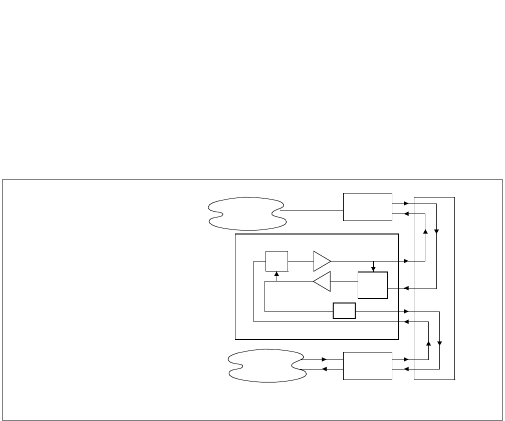
CHAPTER 3 NDA-24296
Page 548
Revision 1.0
PA-4AMPC
AMP Pool Trunk
PA-4AMPC
AMP Pool Trunk
1. General Function
This circuit card is bidirectional amplifier circuitry to be used for such a purpose as level guaranteeing in
a public line—tie line connection. The circuit card is provided with four bidirectional amplifier circuits and
controls gains to speech loss which may vary with the kind of line involved in the connection. Also, this
circuit card is provided with the function to disable the AGC when modem signals such as FAX signals
have arrived.
Figure 3-168 Location of PA-4AMPC (4AMP) within the System
AGC
Fix AMP
C.O. Trunk
ECa
PA-4AMPC
Tie Line N.W Tie Line Trunk
TSW
ECa:
ECb:
AGC:
FixAMP:
Echo Canceller which suppresses echo
in the hybrid circuit of a C.O. trunk.
Echo Canceller which suppresses echo
in the tie-line side.
Automatic Gain Control circuit (amplifies
voice signals arriving from the public
network.)
voice signals arriving from the tie-line
network.)
Public N.W
ECb
PAD
Fixed Gain Amplifier Circuit (amplifies
voice signals arriving from the public
network)
Fixed Gain Amplifier Circuit (amplifies
PAD:
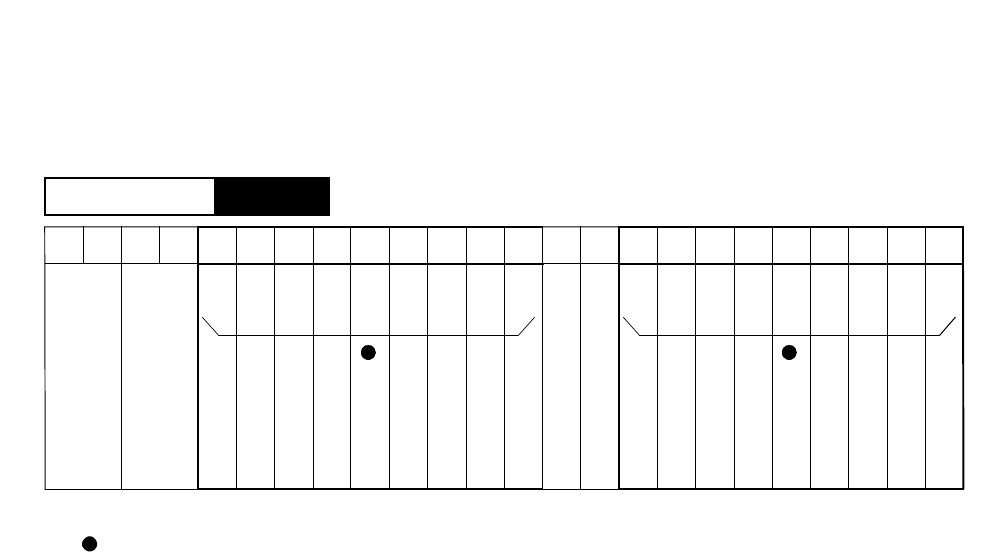
NDA-24296 CHAPTER 3
Page 549
Revision 1.0
PA-4AMPC
AMP Pool Trunk
2. Mounting Location/Condition
The mounting locations of this circuit card are shown below.
Note: Indicates universal slots for line/trunk circuit cards.
01 02 03 04 05 06 07 08 09 10 11 12 13 14 15 16 17 18 19 20 21 22 2300
PIM
Mounting Module
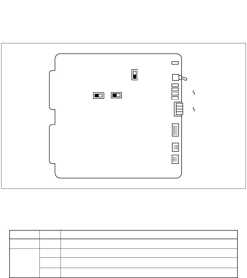
CHAPTER 3 NDA-24296
Page 550
Revision 1.0
PA-4AMPC
AMP Pool Trunk
3. Face Layout of Lamps, Switches, and Connectors
The face layout of lamps, switches, and connectors of this circuit card is shown in Figure 3-169.
Figure 3-169 Face Layout of PA-4AMPC (4AMP)
4. Lamp Indications
The contents of lamp indications of this circuit card are shown in the table below.
OPE
MB
BL3
BL0
MB3
MB0
SW11
SW02
SW01
SW00
SW03
SW04
SW10 SW12
LAMP NAME COLOR STATE
OPE Green Remains lit while this circuit card is operating.
BL0 Green BL-lamp remains lit while the corresponding circuit is busy.
Flash BL-lamp flashes when the corresponding circuit is in make-busy state.
BL3 OFF BL-lamp remains off when the corresponding circuit is in idle state.
~

NDA-24296 CHAPTER 3
Page 551
Revision 1.0
PA-4AMPC
AMP Pool Trunk
5. Switch Settings
Standard settings of various switches on this circuit card are shown in the table below.
SWITCH
SWITCH SETTING STANDARD MEANING
NAME NO. SETTING
(MB)
UP Circuit card make busy
DOWN ×Circuit card make busy cancel
0ON The corresponding circuit is in make busy state.
OFF ×Make busy of the corresponding circuit is canceled.
SW01
1ON The corresponding circuit is in make busy state.
OFF ×Make busy of the corresponding circuit is canceled.
2ON The corresponding circuit is in make busy state.
OFF ×Make busy of the corresponding circuit is canceled.
3ON The corresponding circuit is in make busy state.
OFF ×Make busy of the corresponding circuit is canceled.
1OFF ×Fixed
2OFF ×Fixed
3OFF ×Fixed
Both ECa (Public Line) side and ECb (Tie Line)
ON side operate. (When this switch has been set to ON,
set SW10, SW11, and SW12 to right side.)
4
SW02 Only ECa (Public Line) side operates.
OFF ×(When this switch has been set to OFF, set SW10, SW11,
and SW12 to left side.)
5OFF ×Fixed
6OFF ×Fixed
7OFF ×Fixed
8OFF ×Fixed
SW00
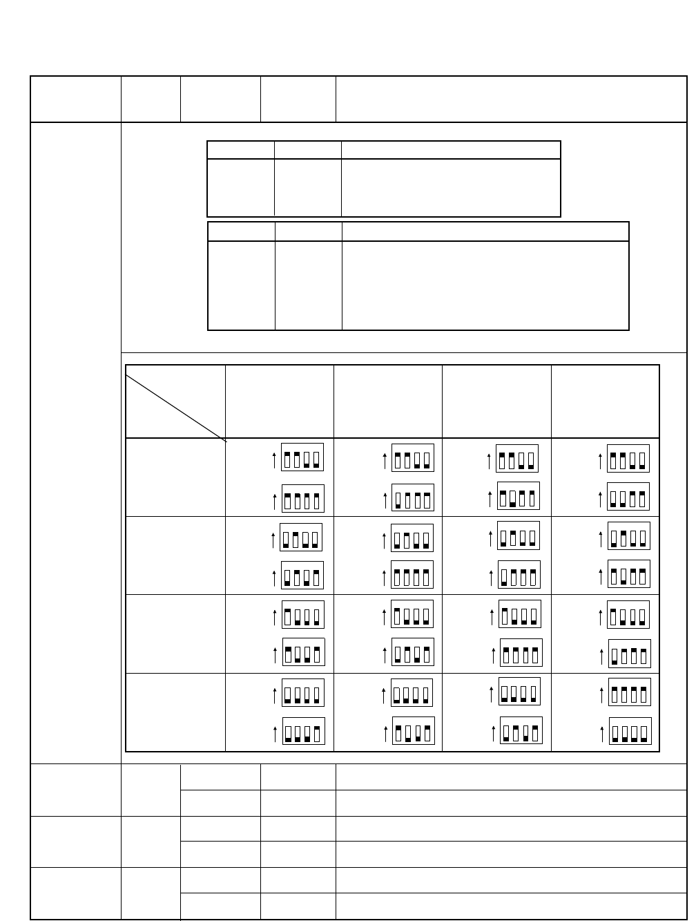
CHAPTER 3 NDA-24296
Page 552
Revision 1.0
PA-4AMPC
AMP Pool Trunk
SWITCH SWITCH SETTING STANDARD MEANING
NAME NO. SETTING
SW03
SW04 is set to all ON.
SW10 Right (SIG) Both ECa (Public Line) side and ECb (Tie Line) side operate.
Left (CAS) ×Only ECa (Public Line) side operates.
SW11 Right (SIG) Both ECa (Public Line) side and ECb (Tie Line) side operate.
Left (CAS) ×Only ECa (Public Line) side operates.
SW12 Right (SIG) Both ECa (Public Line) side and ECb (Tie Line) side operate.
Left (CAS) ×Only ECa (Public Line) side operates.
SW03-1 SW03-2
ON ON 0 dB (Standard)
SETTING OF FIXED GAIN OF FIX AMP
OFF ON 4 dB
ON OFF 8 dB
OFF OFF 12 dB
SW03-3 SW03-4
ON ON [Signals ranging from -35dBm0 to -15dBm0
are adjusted to -15dBm0] (Standard)
SETTING OF GAIN OF BY AGC
0dBr
OFF ON [Signals ranging from -35dBm0 to -11dBm0
are adjusted to -11dBm0]
+4dBr
ON OFF [Signals ranging from -35dBm0 to -19dBm0
are adjusted to -19dBm0]
-4dBr
SW04
When this card does not work as AGC:
Amplification of
voice from the
public network
Amplification
of voice from the
tie-line network
0 dB 4 dB 8 dB 12 dB
0 dB
SW03
SW04
SW03
SW04
SW03
SW04
SW03
SW04
4 dB
SW03
SW04
SW03
SW04
SW03
SW04
SW03
SW04
8 dB
SW03
SW04
SW03
SW04
SW03
SW04
SW03
SW04
12 dB
SW03
SW04
SW03
SW04
SW03
SW04
SW03
SW04
12 34ON
12 34ON
12 34ON
12 34ON
12 34ON
12 34ON
12 34ON
12 34ON
12 34ON
12 34ON
12 34ON
12 34ON
12 34ON
12 34ON
12 34ON
12 34ON
12 34ON
12 34ON
12 34ON
12 34ON
12 34ON
12 34ON
12 34ON
12 34ON
12 34ON
12 34ON
12 34ON
12 34ON
12 34ON
12 34ON 12 34ON
12 34ON
When this card works as AGC:
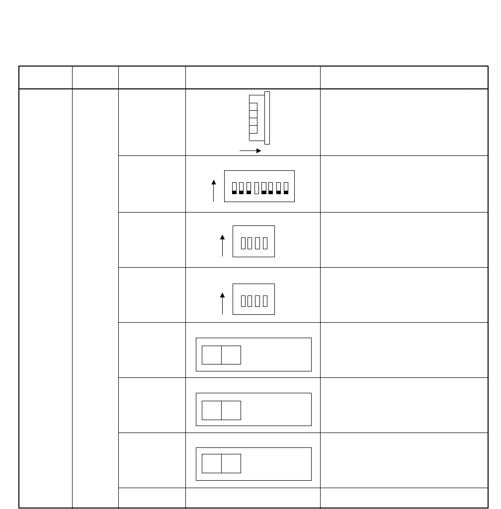
NDA-24296 CHAPTER 3
Page 553
Revision 1.0
PA-4AMPC
AMP Pool Trunk
6. Switch Setting Sheet
MODULE SLOT NO. SWITCH NAME SWITCH SHAPE REMARKS
PIM SW01
SW02
SW00 (MB)
SW03
Circuit card make busy cancel
ON 1234
ON 12345678
3
2
1
0
SW04
SW11
SW12
DOWN
Make busy switch of the corresponding
circuit (No. 0 ~ No. 3 circuits)
ON : Make busy of each circuit
OFF : Make busy cancel of each circuit
ON
Left Right
Left Right
Left Right
SW04 ON 1234
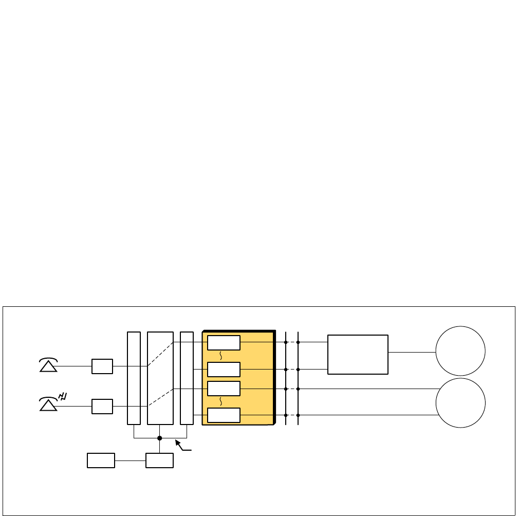
CHAPTER 3 NDA-24296
Page 554
Revision 1.0
PA-8TLTR
Tie Line Trunk
PA-8TLTR
Tie Line Trunk
1. General Function
The PA-8TLTR(TLT) circuit card provides eight trunks whose interface can be selected among the
following four types by key setting on a 4-channel basis.
•Loop Dialing (LD)
•Direct Inward Dialing (DID)
•2-wire E & M
•4-wire E & M
In addition, programmable PADs, whose value can be adjusted by key setting, are equipped with a 4-wire
E & M interface. Note that a cable, which is connected to the “ODT” connector on the front edge of this
card, is necessary when circuits #4 through #7 are used as 2-wire/4-wire E & M trunks. A typical example
of channel allocation is illustrated in Figure 3-170.
Figure 3-170 Location of PA-8TLTR (TLT) within the System
GTCPU
LC
LC
ODT #0
ODT #3
DID #0
DID #3
I/O Local Bus
Terminal
Terminal
SWINT INT PA-8TLTR MDF
2W/4W
Carrier
Equipment
circuit #0
circuit #3
circuit #4
circuit #7
PRIVATE
NETWORK
PUBLIC
NETWORK
Note: This diagram shows an example when the PA-8TLTR is used as four 2W/4W E&M and four DID trunks.
In this instance, a flat cable connection is not required.
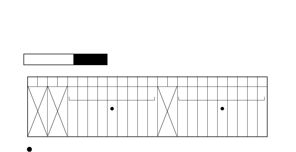
NDA-24296 CHAPTER 3
Page 555
Revision 1.0
PA-8TLTR
Tie Line Trunk
2. Mounting Location / Condition
The PA-8TLTR (TLT) card can be mounted in any universal slots as shown below.
Note: Indicates universal slots for line/trunk circuit cards.
PIM
Mounting Module
00 01 02 03 04 05 06 07 08 09 10 11 12 13 14 15 16 17 18 19 20 21 22 23
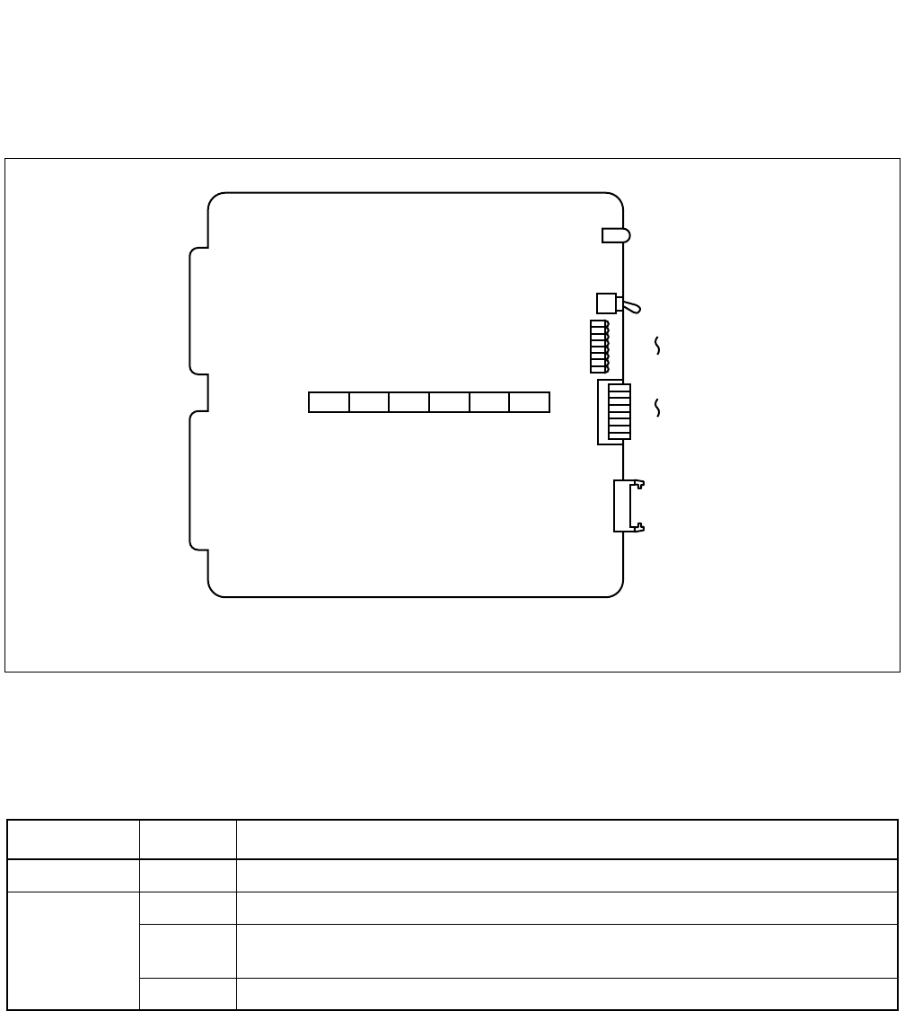
CHAPTER 3 NDA-24296
Page 556
Revision 1.0
PA-8TLTR
Tie Line Trunk
3. Face Layout of Lamps, Switches, and Connectors
The face layout of lamps, switches, and connectors of this circuit card is shown in Figure 3-171.
Figure 3-171 Face Layout of PA-8TLTR (TLT) Card
4. Lamp Indications
The contents of lamp indications of this circuit card are shown in the table below.
LAMP NAME COLOR STATE
OPE Green Remains lit while this circuit card is operating.
BL0
BL7
Green Lights when the corresponding circuit is busy.
Flash Flashes when the corresponding circuit is in make-busy state or while DP signals are being
received (flashes to the dial pulses)
OFF Remains off when the corresponding circuit is idle.
OPE
MB
BL7
BL0
SW0 SW1 SW2 SW3 SW4 SW5 MB7
MB0
ODT
Note
Note: This connector is used when “E & M” is selected for circuits #4 through #7.
-

NDA-24296 CHAPTER 3
Page 557
Revision 1.0
PA-8TLTR
Tie Line Trunk
5. Switch Settings
Standard settings of switches on this circuit card are shown in the table below.
SWITCH SWITCH
NO. SETTING STANDARD
SETTING MEANING
MB
(SW00)
UP Circuit card make busy
DOWN ×Circuit card make busy cancel
MB0 - 7
(SW01) 0ON Make busy of the No. 0 circuit
OFF ×Make busy cancel of the No. 0 circuit
1ON Make busy of the No. 1 circuit
OFF ×Make busy cancel of the No. 1 circuit
2ON Make busy of the No. 2 circuit
OFF ×Make busy cancel of the No. 2 circuit
3ON Make busy of the No. 3 circuit
OFF ×Make busy cancel of the No. 3 circuit
4ON Make busy of the No. 4 circuit
OFF ×Make busy cancel of the No. 4 circuit
5ON Make busy of the No. 5 circuit
OFF ×Make busy cancel of the No. 5 circuit
6ON Make busy of the No. 6 circuit
OFF ×Make busy cancel of the No. 6 circuit
7ON Make busy of the No. 7 circuit
OFF ×Make busy cancel of the No. 7 circuit
CHAPTER 3 NDA-24296
Page 558
Revision 1.0
PA-8TLTR
Tie Line Trunk
SWITCH SWITCH
NO. SETTING STANDARD
SETTING MEANING
SW0
(SW10)
1
2
3
4OFF ×Not used
5OFF ×Fixed
6ON ×Fixed
7OFF ×Fixed
8OFF ×Not used
SW1
(SW15)
1ON Programmable PAD P0 Value
0.5 dB P0 value is determined as
a sum of selected PAD
values of SW1 (elements
1-5). Note that this setting
is valid for 4W E&M
system.
-Example-
In this case P0 value is
12.5 dB.
OFF Programmable PAD P0 Value 0 dB
2ON Programmable PAD P0 Value 1 dB
OFF Programmable PAD P0 Value 0 dB
3ON Programmable PAD P0 Value 2 dB
OFF Programmable PAD P0 Value 0 dB
4ON Programmable PAD P0 Value 4 dB
OFF Programmable PAD P0 Value 0 dB
5ON Programmable PAD P0 Value 8 dB
OFF Programmable PAD P0 Value 0 dB
6 OFF Fixed
<Setting Range of Programmable PAD Values>
7OFF Not used
8OFF Not used
SW0-1 SW0-2 SW0-3 0-3 CIRCUIT
TRUNK KIND 4-7 CIRCUIT
TRUNK KIND
OFF
ON
OFF
ON
OFF
OFF
ON
ON
OFF
OFF
OFF
OFF
LD/DID
EMT
Not used
2W/4W E&M
LD/DID
LD/DID
Not used
2W/4W E&M
SW1-1: ON (0.5 dB)
SW1-2: OFF ( 0 dB)
SW1-3: OFF ( 0 dB)
SW1-4: ON ( 4 dB)
SW1-5: ON ( 8 dB)
PAD VALUE [dB]
SEND RECEIVE
Possible Setting
Range P0: 0 - +15.5
0.5 step P1: 0 - +15.5
0.5 step
P2: 0 - +7.5
0.5 step P3: 0 - +7.5
0.5 step

NDA-24296 CHAPTER 3
Page 559
Revision 1.0
PA-8TLTR
Tie Line Trunk
SWITCH SWITCH
NO. SETTING STANDARD
SETTING MEANING
SW2
(SW20) 1ON Programmable PAD P1 Value 0.5 dB P1 value is determined as a
sum of selected PAD values
of SW2 (elements 1-5). Note
that this setting is valid for
4W E&M system.
- Example -
In this case P1 value is 12.5
dB.
OFF Programmable PAD P1 Value 0 dB
2ON Programmable PAD P1 Value 1 dB
OFF Programmable PAD P1 Value 0 dB
3ON Programmable PAD P1 Value 2 dB
OFF Programmable PAD P1 Value 0 dB
4ON Programmable PAD P1 Value 4 dB
OFF Programmable PAD P1 Value 0 dB
5ON Programmable PAD P1 Value 8 dB
OFF Programmable PAD P1 Value 0 dB
6OFF ×Fixed
7OFF ×Fixed
8OFF ×Fixed
SW2-1: ON (0.5 dB)
SW2-2: OFF ( 0 dB)
SW2-3: OFF ( 0 dB)
SW2-4: ON ( 4 dB)
SW2-5: ON ( 8 dB)

CHAPTER 3 NDA-24296
Page 560
Revision 1.0
PA-8TLTR
Tie Line Trunk
Note: For the setting range of Programmable PAD Values, see the “Setting Range of Programmable PAD
Values” shown for SW1.
SWITCH SWITCH
NO. SETTING STANDARD
SETTING MEANING
SW3
(SW25) 1ON Programmable PAD P2 Value 0.5 dB
P2 Values is total
of PAD Values
Note
(Valid when 4W
E&M system)
(Ex)
SW3-1: OFF
SW3-2: ON
SW3-3: OFF
SW3-4: OFF
in this case P2
value is 1 dB.
P3 Values is total
of PAD Values
Note
(Valid when 4W
E&M system)
(Ex)
SW3-5: OFF
SW3-6: ON
SW3-7: OFF
SW3-8: OFF
in this case P3
value is 1 dB.
OFF Programmable PAD P2 Value 0 dB
2ON Programmable PAD P2 Value 1 dB
OFF Programmable PAD P2 Value 0 dB
3ON Programmable PAD P2 Value 2 dB
OFF Programmable PAD P2 Value 0 dB
4ON Programmable PAD P2 Value 4 dB
OFF Programmable PAD P2 Value 0 dB
5ON Programmable PAD P3 Value 0.5 dB
OFF Programmable PAD P3 Value 0 dB
6ON Programmable PAD P3 Value 1 dB
OFF Programmable PAD P3 Value 0 dB
7ON Programmable PAD P3 Value 2 dB
OFF Programmable PAD P3 Value 0 dB
8ON Programmable PAD P3 Value 4 dB
OFF Programmable PAD P3 Value 0 dB
NDA-24296 CHAPTER 3
Page 561
Revision 1.0
PA-8TLTR
Tie Line Trunk
SWITCH SWITCH
NO. SETTING STANDARD
SETTING MEANING
SW4
(SW30
[No.0-3
Circuit]
SW5
(SW40)
[No. 4-7
Circuit]
(When
Trunk Kind
has been set
as LD/DID)
1 ~ 4
Setting of Terminating Impedance and Balancing Network
(Valid for LD/DID)
5OFF ×Fixed
6OFF ×Not used
7OFF ×Not used
8OFF ×Not used
SW4/5 Terminating
Impedance Balancing Network
1234
OFF OFF OFF OFF
ON OFF OFF OFF
2.16µ F
600Ω
350Ω
1KΩ
0.21µ F
(EIA/TIA -464A)
600Ω
CHAPTER 3 NDA-24296
Page 562
Revision 1.0
PA-8TLTR
Tie Line Trunk
SWITCH SWITCH
NO. SETTING STANDARD
SETTING MEANING
SW4
(SW30
[No.0-3
Circuit]
SW5
(SW40)
[No. 4-7
Circuit]
(When
Trunk Kind
has been set
as 2W
E&M)
1 ~ 4, 6
Setting of Terminating Impedance and Balancing Network
(Valid for E&M)
5OFF ×Not used
6ON Speech Line: 2-wire
OFF Speech Line: 4-wire
7OFF ×Fixed
8
ON E&M Control
Idle: Ground Busy: Battery
OFF E&M Control
Idle: Open Busy: Ground
SW4/5 Terminating Imped-
ance Balancing Network
12346
OFF OFF OFF OFF ON
ON OFF OFF OFF ON
2.16µ F
600Ω
350Ω
1KΩ
0.21µ F
(EIA/TIA -464A)
600Ω
NDA-24296 CHAPTER 3
Page 563
Revision 1.0
PA-8TLTR
Tie Line Trunk
Reference : Table of Fixed PADs
:When SW2-8 is set to “ON”. (other than the case of )
:When SW2-8 is set to “OFF”. (i.e PAD for TS003 is provided; only for Australia)
ARTD COMMAND
PAD DATA
PAD VALUE [dB]
4W E&M LD/2W E&M
SEND RECEIVE SEND RECEIVE SEND RECEIVE
0P0P1000-6
1
2
3
4
3
6
12
16
3
6
11
11
3
6
6
0
3
6
-6
-6
6
0
0
0
-6
-6
-6
-6
5P2P3000-6
7 00000-6
APAD COMMAND
PAD DATA
PAD VALUE [dB]
4W E&M LD/2W E&M
SEND RECEIVE SEND RECEIVE SEND RECEIVE
1
2
3
4
3
6
12
16
3
6
11
11
3
6
6
0
3
6
-6
-6
6
6
0
0
-6
-6
-6
-6
5P2P3000-6
15 00000-6
1 2
1 2
1 2
2
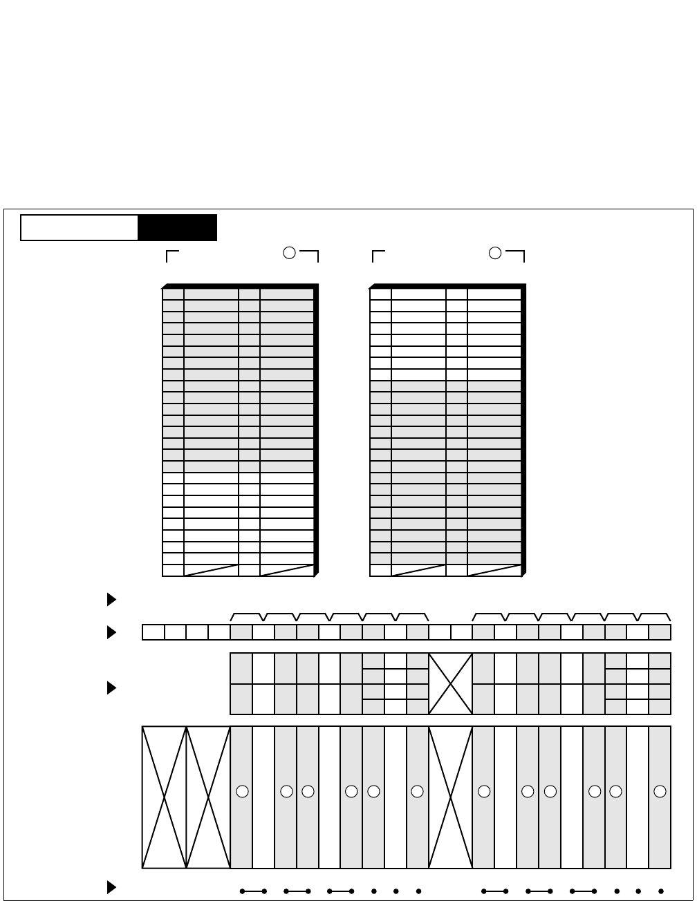
CHAPTER 3 NDA-24296
Page 564
Revision 1.0
PA-8TLTR
Tie Line Trunk
6. External Interface
Accommodation of LT connector leads of this circuit card is shown in Figure 3-172.
See also: Connecting Route Diagram (LD/DID ∞ 2W E&M)
Connecting Route Diagram (4W E&M)
2400 ODT CABLE Lead Accommodation
2400 ODT CABLE-A Lead Accommodation
Figure 3-172 LT Connector Lead Accommodation (1/2)
PIM
Mounting Module
26
27
28
29
30
31
32
33
34
35
36
37
38
39
40
41
1
2
3
4
5
6
7
8
9
10
11
12
13
14
15
16
42
43
44
45
46
47
48
17
18
19
20
21
22
23
49
50 24
25
232221201918171615141312111009080706050403020100
LT6 LT7 LT8 LT9 LT10 LT11LT0 LT1 LT2 LT3 LT4 LT5
231915
221814
211713
201612
231915
221814
211713
201612
110907050301
100806040200
110907050301
100806040200
HW11HW10HW9HW8HW7HW6HW5HW4HW3HW2HW1HW0
Group No.
Slot No.
LT Connector
PIM
Highway Block
LT 1, 3, 5, 7, 9, 11 Connector
26
27
28
29
30
31
32
33
34
35
36
37
38
39
40
41
1
2
3
4
5
6
7
8
9
10
11
12
13
14
15
16
42
43
44
45
46
47
48
17
18
19
20
21
22
23
49
50 24
25
B0 (TB0)
B1 (TB1) A0 (TA0)
Accommodated in 1
LT 0, 2, 4, 6, 8, 10 Connector
A1 (TA1)
A2 (TA2)
A3 (TA3)
B2 (TB2)
B3 (TB3)
Accommodated in 2
B4 (TB4)
B5 (TB5) A4 (TA4)
A5 (TA5)
A6 (TA6)
A7 (TA7)
B6 (TB6)
B7 (TB7)
RB0
RB1 RA0
RA1
RA2
RA3
RB2
RB3
M0
M1 E0
E1
E2
E3
M2
M3
B0 (TB0)
B1 (TB1) A0 (TA0)
A1 (TA1)
A2 (TA2)
A3 (TA3)
B2 (TB2)
B3 (TB3)
B4 (TB4)
B5 (TB5) A4 (TA4)
A5 (TA5)
A6 (TA6)
A7 (TA7)
B6 (TB6)
B7 (TB7)
RB0
RB1 RA0
RA1
RA2
RA3
RB2
RB3
M0
M1 E0
E1
E2
E3
M2
M3
1212 12
12 1212
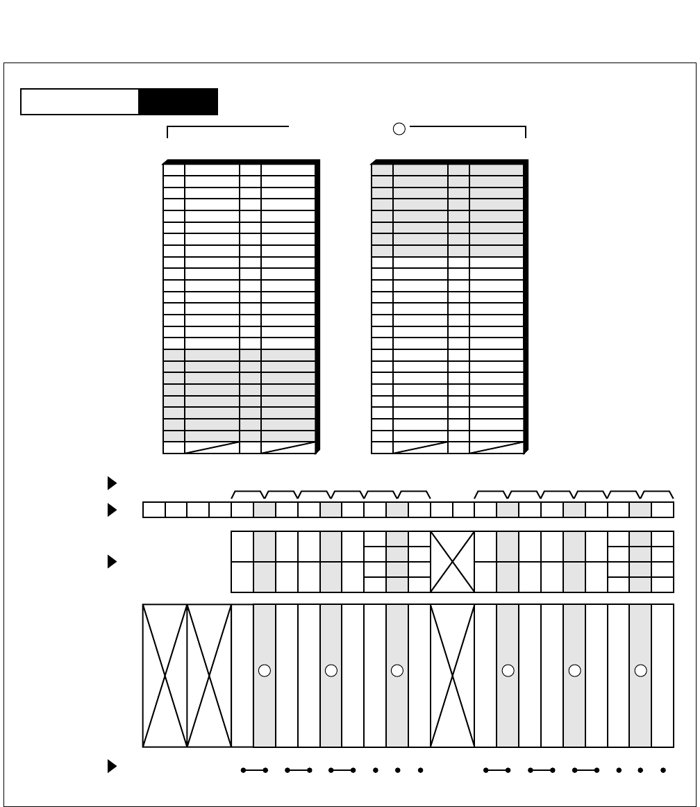
NDA-24296 CHAPTER 3
Page 565
Revision 1.0
PA-8TLTR
Tie Line Trunk
Figure 3-172 LT Connector Lead Accommodation (2/2)
PIM
Mounting Module
26
27
28
29
30
31
32
33
34
35
36
37
38
39
40
41
1
2
3
4
5
6
7
8
9
10
11
12
13
14
15
16
42
43
44
45
46
47
48
17
18
19
20
21
22
23
49
50 24
25
232221201918171615141312111009080706050403020100
LT6 LT7 LT8 LT9 LT10 LT11LT0 LT1 LT2 LT3 LT4 LT5
231915
221814
211713
201612
231915
221814
211713
201612
110907050301
100806040200
110907050301
100806040200
HW11HW10HW9HW8HW7HW6HW5HW4HW3HW2HW1HW0
Group No.
Slot No.
LT Connector
PIM
Highway Block
LT 1, 3, 5, 7, 9, 11 Connector
26
27
28
29
30
31
32
33
34
35
36
37
38
39
40
41
1
2
3
4
5
6
7
8
9
10
11
12
13
14
15
16
42
43
44
45
46
47
48
17
18
19
20
21
22
23
49
50 24
25
B0 (TB0)
B1 (TB1) A0 (TA0)
Accommodated in 3
LT 0, 2, 4, 6, 8, 10 Connector
A1 (TA1)
A2 (TA2)
A3 (TA3)
B2 (TB2)
B3 (TB3)
B4 (TB4)
B5 (TB5) A4 (TA4)
A5 (TA5)
A6 (TA6)
A7 (TA7)
B6 (TB6)
B7 (TB7)
RB0
RB1 RA0
RA1
RA2
RA3
RB2
RB3
M0
M1 E0
E1
E2
E3
M2
M3
333333
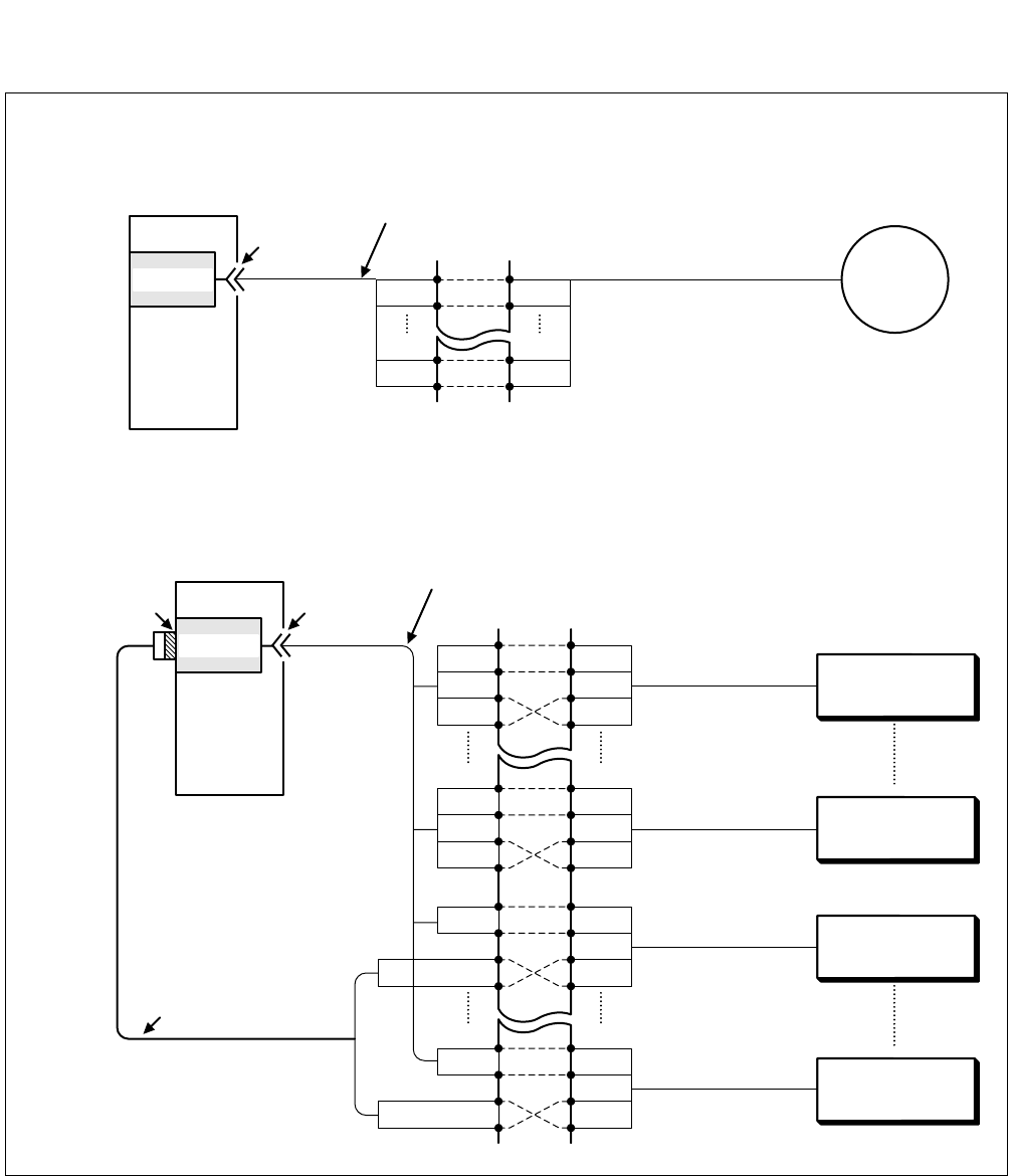
CHAPTER 3 NDA-24296
Page 566
Revision 1.0
PA-8TLTR
Tie Line Trunk
Figure 3-173 Connecting Route Diagram (LD/DID • 2W E&M)
PBX
A0
B0
A7
B7
A
B
A
B
NETWORK
LT Connector
Installation Cable
PA-8TLTR
• LD/DID
• 2W E&M
PBX
A0
B0
A
B
LT Connector
Installation Cable
PA-8TLTR
E0 E
M0 M
A3
B3
A
B
E3 E
M3 M
A4
B4
A
B
E4 E
M4 M
A7
B7
A
B
E7 E
M7 M
2-WIRE
CARRIER
EQUIPMENT
2-WIRE
CARRIER
EQUIPMENT
2-WIRE
CARRIER
EQUIPMENT
2-WIRE
CARRIER
EQUIPMENT
2400 ODT CABLE
This diagram shows connecting route diagram when the PA-8TLTR is used as a LD or DID trunk.
This diagram shows connecting route diagram when the PA-8TLTR is used as a 2-wire E&M trunk. In this instance, E&M leads
for channels #4 - #7 appear from the "ODT" connector equipped on the front edge of this card.
ODT Connector
MDF
MDF
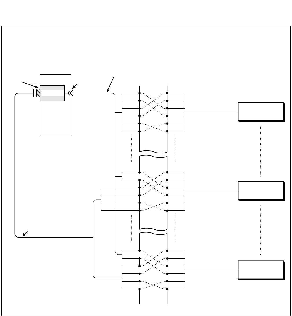
NDA-24296 CHAPTER 3
Page 567
Revision 1.0
PA-8TLTR
Tie Line Trunk
Figure 3-174 Connecting Route Diagram (4W E&M)
• 4W E&M
PBX
A0(TA0)
B0(TB0)
TA
TB
LT Connector
Installation Cable
PA-8TLTR
RA0 RA
RB0 RB
4-WIRE
CARRIER
EQUIPMENT
4-WIRE
CARRIER
EQUIPMENT
4-WIRE
CARRIER
EQUIPMENT
2400 ODT CABLE
ODT connector
E0 E
M0 M
A4(TA4)
B4(TB4)
TA
TB
RA4 RA
RB4 RB
E4 E
M4 M
A7(TA7)
B7(TB7)
TA
TB
RA7 RA
RB7 RB
E7 E
M7 M
This diagram shows connecting route diagram when the PA-8TLTR is used as a 4-wire E&M trunk. In this instance, RA, RB, and
E&M leads for channels #4 - #7 appear from the "ODT" connector equipped on the front edge of this card.
MDF
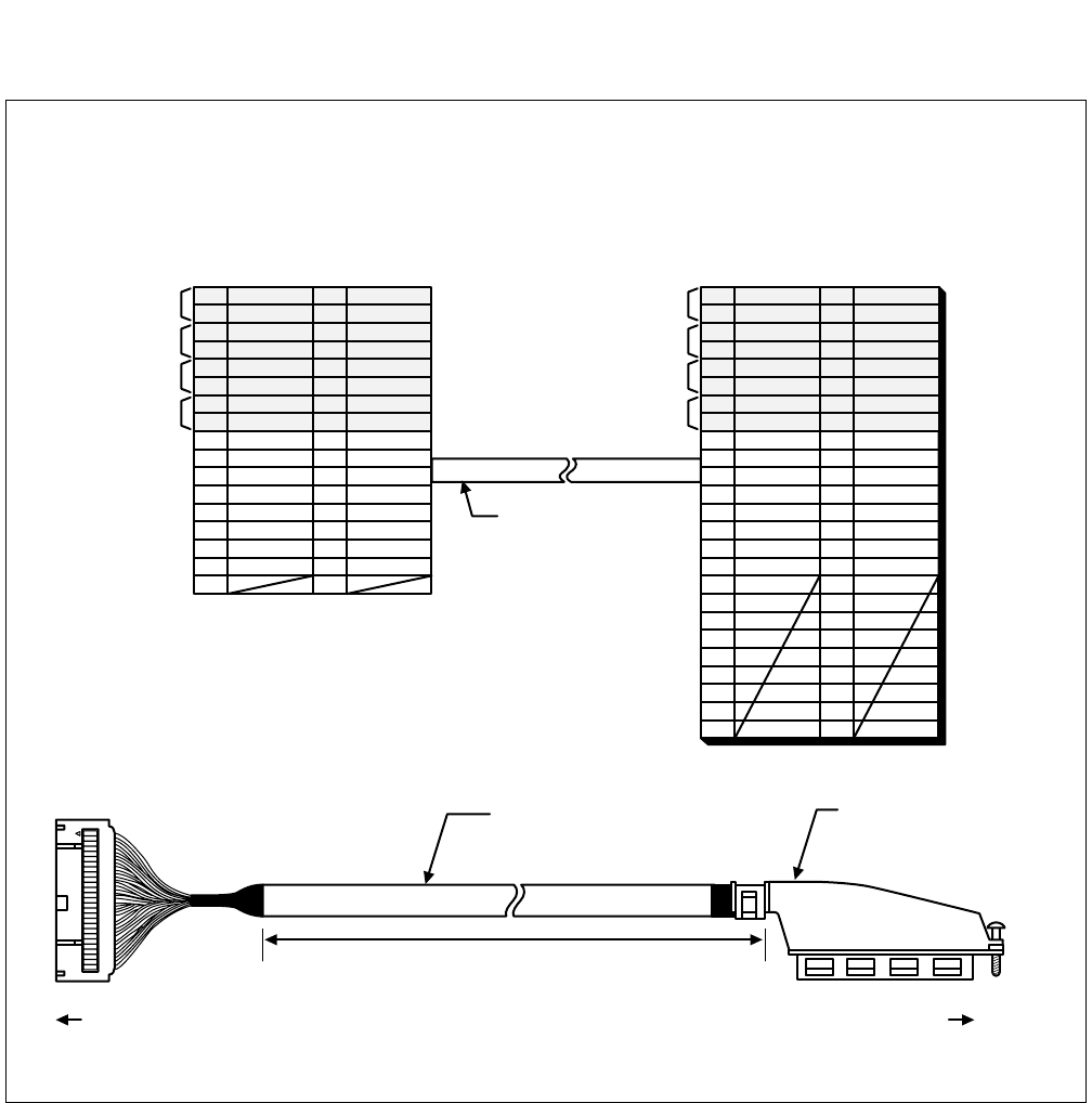
CHAPTER 3 NDA-24296
Page 568
Revision 1.0
PA-8TLTR
Tie Line Trunk
Figure 3-175 “2400 ODT CABLE” Lead Accommodation
26
27
28
29
30
31
32
33
34
35
36
37
38
39
40
41
42
43
44
45
46
47
48
49
50
1
2
3
4
5
6
7
8
9
10
11
12
13
14
15
16
17
18
19
20
21
22
23
24
25
RA4
E4
RA5
E5
RA6
E6
RA7
E7
(AS0)
(AS1)
(AS2)
(AS3)
(AS4)
(AS5)
(AS6)
(AS7)
(AL0)
(AL1)
(AL2)
(AL3)
(AL4)
(AL5)
(AL6)
(AL7)
To "ODT" connector To MDF
Champ Connector (Female)
"2400 ODT CABLE"
3m (10 feet)
channel #4
channel #5
channel #6
channel #7
Champ Connector
1A
2A
3A
4A
5A
6A
7A
8A
9A
10A
11A
12A
13A
14A
15A
16A
17A
1B
2B
3B
4B
5B
6B
7B
8B
9B
10B
11B
12B
13B
14B
15B
16B
17B
RB4
M4
RB5
M5
RB6
M6
RB7
M7
(AL0)
(AL1)
(AL2)
(AL3)
(AL4)
(AL5)
(AL6)
(AL7)
(AS0)
(AS1)
(AS2)
(AS3)
(AS4)
(AS5)
(AS6)
(AS7)
channel #4
channel #5
channel #6
channel #7
ODT Connector
"2400 ODT CABLE"
• 2400 ODT CABLE
The "2400 ODT CABLE" has one ODT connector whose lead accommodation is shown below.
RA4
E4
RA5
E5
RA6
E6
RA7
E7
RB4
M4
RB5
M5
RB6
M6
RB7
M7
34
LT
Note: Leads in round brackets are not used for the time being.
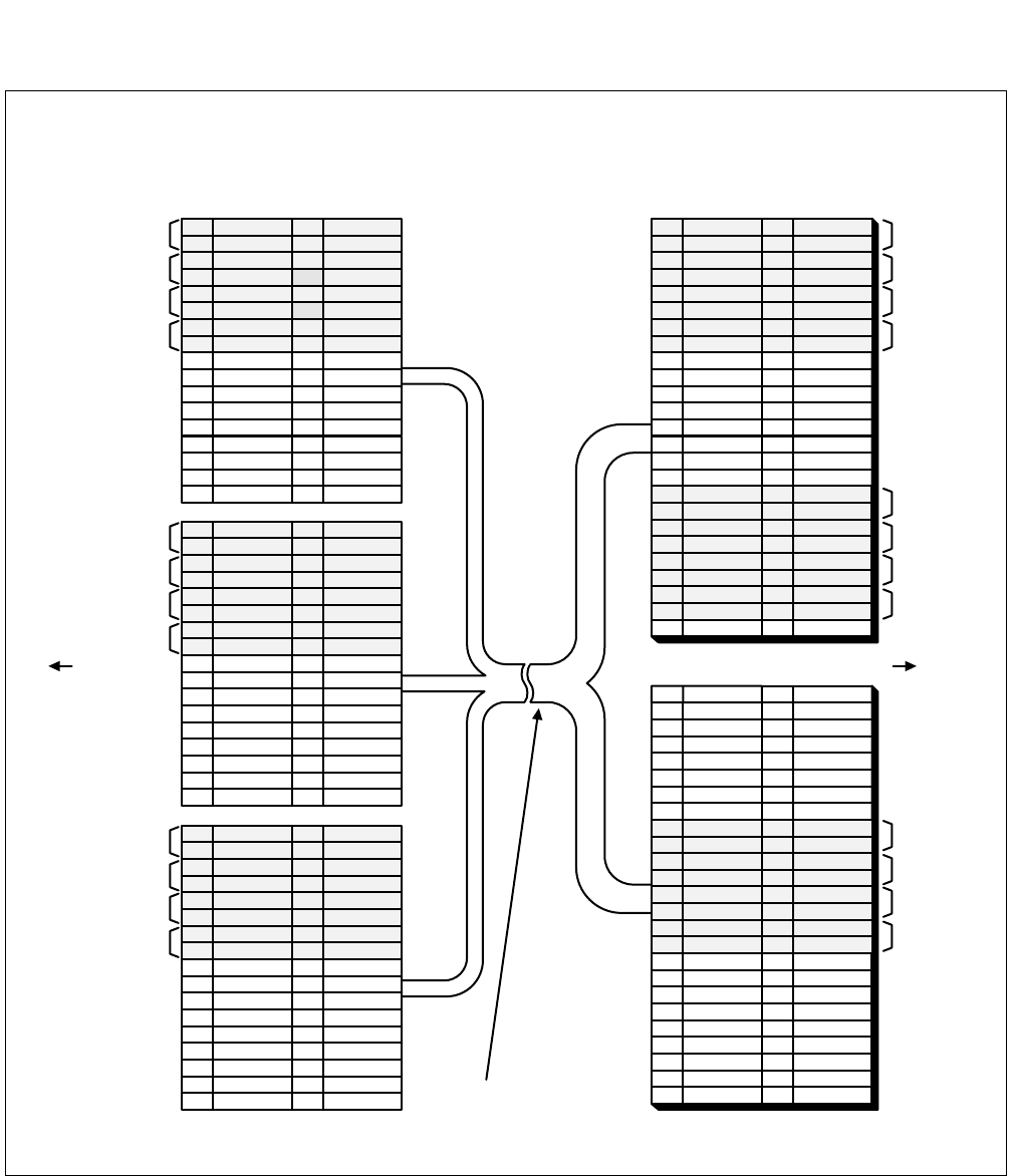
NDA-24296 CHAPTER 3
Page 569
Revision 1.0
PA-8TLTR
Tie Line Trunk
Figure 3-176 “2400 ODT CABLE-A” Lead Accommodation
RB4
M4
RB5
M5
RB6
M6
RB7
M7
26
27
28
29
30
31
32
33
34
35
36
37
38
39
40
41
42
43
44
45
46
47
48
49
50
1
2
3
4
5
6
7
8
9
10
11
12
13
14
15
16
17
18
19
20
21
22
23
24
25
RA4
E4
RA5
E5
RA6
E6
RA7
E7
(AS0)
(AS1)
(AS2)
(AS3)
(AS4)
(AS5)
(AS6)
(AS7)
(AL0)
(AL1)
(AL2)
(AL3)
(AL4)
(AL5)
(AL6)
(AL7)
channel #4
channel #5
channel #6
channel #7
Champ Connectors
RA4
E4
RA5
E5
RA6
E6
RA7
E7
1A
2A
3A
4A
5A
6A
7A
8A
9A
10A
11A
12A
13A
14A
15A
16A
17A
1B
2B
3B
4B
5B
6B
7B
8B
9B
10B
11B
12B
13B
14B
15B
16B
17B
RB4
M4
RB5
M5
RB6
M6
RB7
M7
(AL0)
(AL1)
(AL2)
(AL3)
(AL4)
(AL5)
(AL6)
(AL7)
(AS0)
(AS1)
(AS2)
(AS3)
(AS4)
(AS5)
(AS6)
(AS7)
channel #4
channel #5
channel #6
channel #7
ODT Connectors
"2400 ODT CABLE-A"
26
27
28
29
30
31
32
33
34
35
36
37
38
39
40
41
42
43
44
45
46
47
48
49
50
1
2
3
4
5
6
7
8
9
10
11
12
13
14
15
16
17
18
19
20
21
22
23
24
25
RA4
E4
RA5
E5
RA6
E6
RA7
E7
(AS0)
(AS1)
(AS2)
(AS3)
(AS4)
(AS5)
(AS6)
(AS7)
(AL0)
(AL1)
(AL2)
(AL3)
(AL4)
(AL5)
(AL6)
(AL7)
channel #4
channel #5
channel #6
channel #7
RA4
E4
RA5
E5
RA6
E6
RA7
E7
1A
2A
3A
4A
5A
6A
7A
8A
9A
10A
11A
12A
13A
14A
15A
16A
17A
1B
2B
3B
4B
5B
6B
7B
8B
9B
10B
11B
12B
13B
14B
15B
16B
17B
RB4
M4
RB5
M5
RB6
M6
RB7
M7
(AL0)
(AL1)
(AL2)
(AL3)
(AL4)
(AL5)
(AL6)
(AL7)
(AS0)
(AS1)
(AS2)
(AS3)
(AS4)
(AS5)
(AS6)
(AS7)
channel #4
channel #5
channel #6
channel #7
RB4
M4
RB5
M5
RB6
M6
RB7
M7
RA4
E4
RA5
E5
RA6
E6
RA7
E7
(DE) (DE)
channel #4
channel #5
channel #6
channel #7
(AS0)
(AS1)
(AS2)
(AS3)
(AS4)
(AS5)
(AS6)
(AS7)
(AL0)
(AL1)
(AL2)
(AL3)
(AL4)
(AL5)
(AL6)
(AL7)
(DE) (DE)
RB4
M4
RB5
M5
RB6
M6
RB7
M7
To ODT Connector
To MDF
• 2400 ODT CABLE-A
The "2400 ODT CABLE-A" has three ODT connectors whose lead accommodation is shown below.
(NC) (NC)
(NC) (NC)
(
NC
)(
NC
)
Note: Leads in round brackets are not used for the time being.
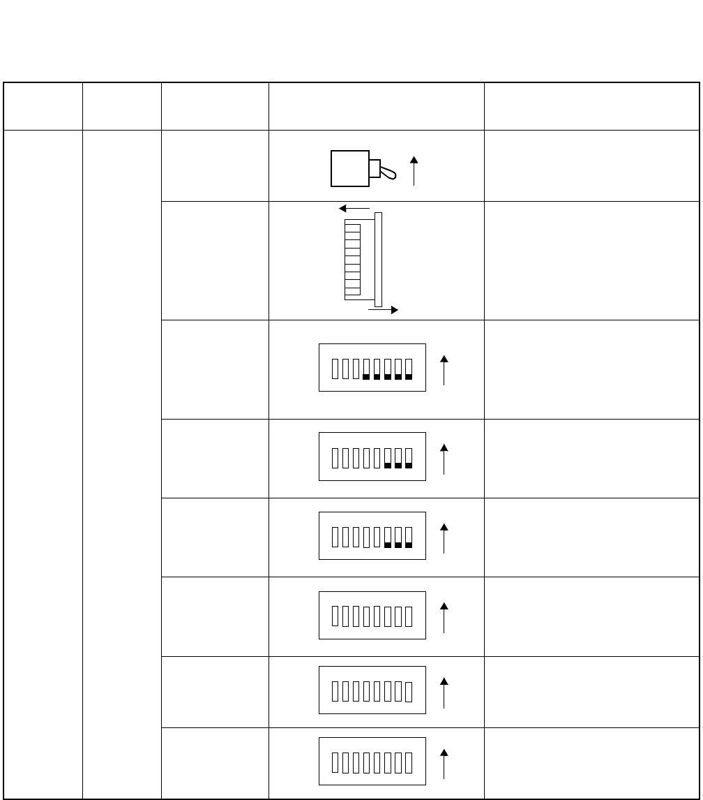
CHAPTER 3 NDA-24296
Page 570
Revision 1.0
PA-8TLTR
Tie Line Trunk
7. Switch Setting Sheet
MODULE SLOT NO. SWITCH
NAME SWITCH SHAPE REMARKS
PIM MB
(SW00)
MB0-7
(SW01)
SW0
(SW10)
SW1
(SW15)
SW2
(SW20)
SW3
(SW25)
SW4
(SW30)
SW5
(SW40)
ON
8
ON
7
6
5
4
3
2
1
0
OFF
12 3 4 5 6 7 8 ON
12345678 ON
12 3 4 5 6 7 8 ON
12 3 4 5 6 7 8 ON
12345678 ON
12 3 4 5 6 7 8 ON
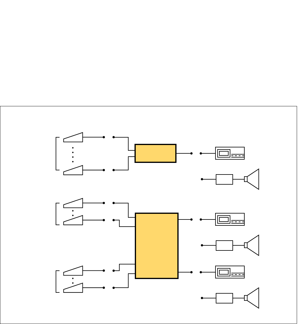
NDA-24296 CHAPTER 3
Page 571
Revision 1.0
PA-M87
Recording / Paging Device Adapter
PA-M87
Recording / Paging Device Adapter
1. General Function
This circuit card is used to provide an interface between the Attendant Console(s) and the external
recording/paging equipment as shown in the figure below. Occupying every two slots within a PIM, a
single interface adapter can handle a maximum of six ATTCONs and one-or two-circuit recording/paging
equipment to combine. The connection patterns for the devices and service activation via ATTCONs can
vary, depending on key settings on the card (see Section 5, 'Switch Settings' for details).
Figure 3-177 Location of PA-M87 (RECC/PGADP) within the System
MDF
Max.6
Max.3
Max.3
RECC/PGADP
MDF Recording Device
or
Paging Device
or
Paging Device
or
Paging Device
Recording Device
Recording Device
MDF
RECC/PGADP
MDF
MDF
ATTCON
ATTCON
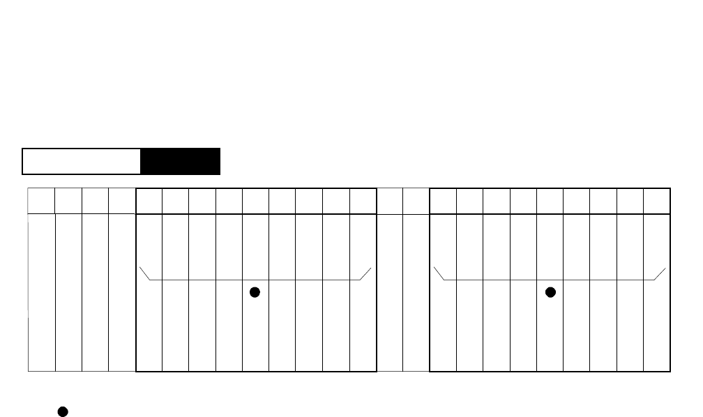
CHAPTER 3 NDA-24296
Page 572
Revision 1.0
PA-M87
Recording / Paging Device Adapter
2. Mounting Location/Condition
The mounting locations of this circuit card are shown below. Note that this circuit card requires a vacancy
of two consecutive slots.
Note: Indicates universal slots for line/trunk circuit cards.
PIM
Mounting Module
01 02 03 04 05 06 07 08 09 10 11 12 13 14 15 16 17 18 19 20 21 22 2300
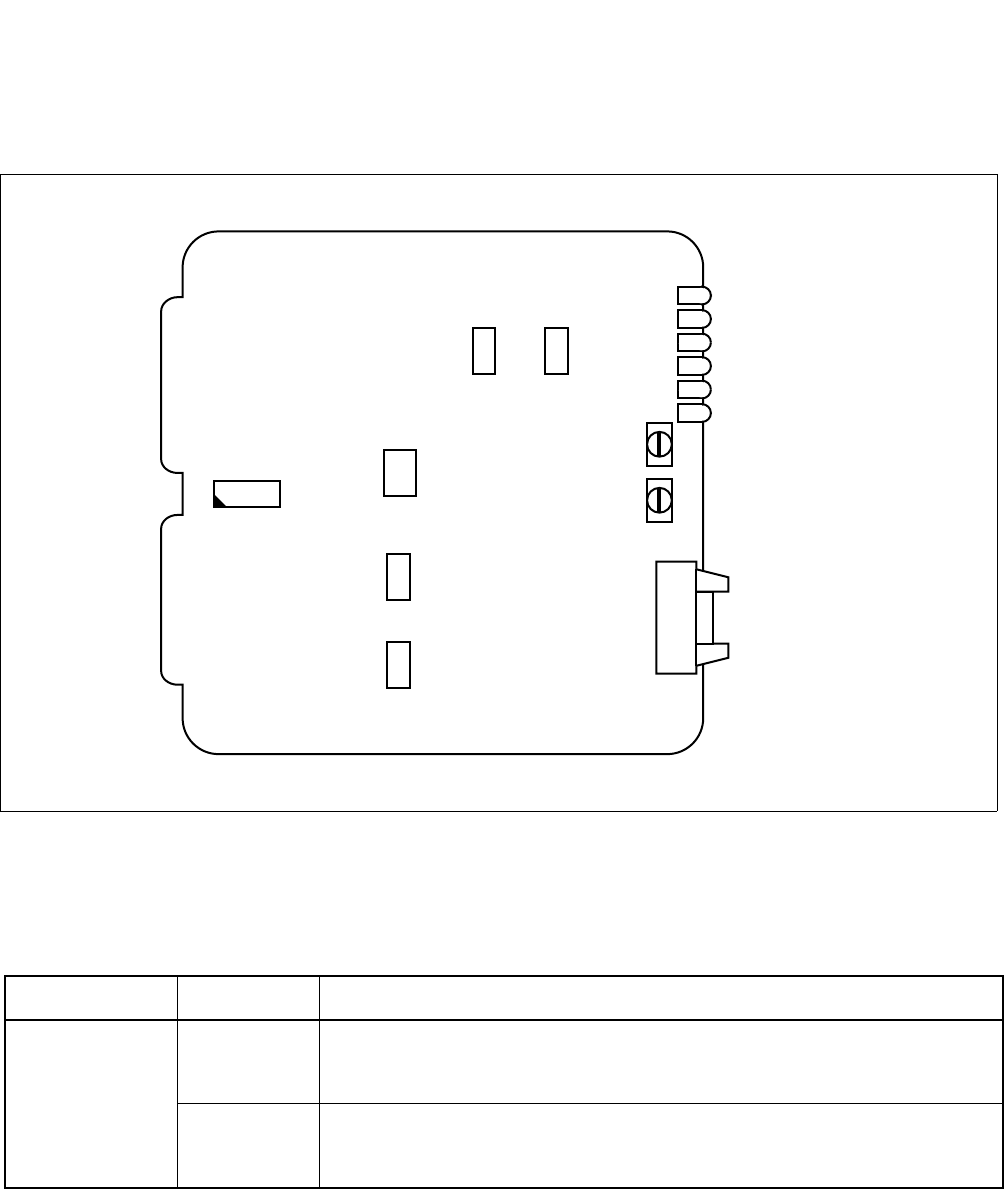
NDA-24296 CHAPTER 3
Page 573
Revision 1.0
PA-M87
Recording / Paging Device Adapter
3. Face Layout of Lamps, Switches, and Connectors
Face layout of each lamp, switch and connector on this circuit card is shown in Figure 3-178.
Figure 3-178 Face Layout of PA-M87 (RECC/PGADP)
4. Lamp Indications
The table below shows the meaning of lamp indications.
LAMP NAME COLOR MEANING
ATT0 ~ ATT5
Green
(Steady-“ON”)
Provided that any of the ATTCONs has a connection to the Recording/Paging
equipment via the card, the lamp(s) corresponding to the cited ATTCON number(s)
emit(s) steady light.
Green
(Flash)
Provided that any of the ATTCONs has not established a connection with the
Recording/Paging equipment, the lamp(s) corresponding to the cited ATTCON
number(s) emit(s) flashing light.
ATT5
ATT4
ATT3
ATT2
ATT1
VR0
SW12 SW13
SW11
SW10
SW14
SW15
REC/PGA
(To MDF)
VR1
ATT0
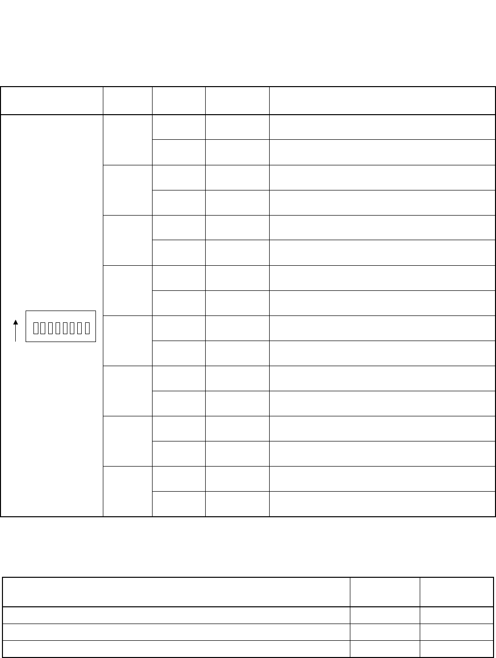
CHAPTER 3 NDA-24296
Page 574
Revision 1.0
PA-M87
Recording / Paging Device Adapter
5. Switch Settings
Switch settings on the card and their detailed meanings are as follows:
Note 1: This switch setting becomes effective parallel with the key operations of SW12 and SW13.
Note 2: To validate this switch setting, also operate the following keys (SW10-8, SW14, SW15) as required.
SWITCH NAME SWITCH
NO. SETTING STANDARD
SETTING MEANING
SW10
1
ON Recording/Paging start control at ATTCON #0 by loop
start (momentary)
OFF Recording/Paging start control at ATTCON #0 by loop
start (constant)
2
ON Recording/Paging start control at ATTCON #1 by loop
start (momentary)
OFF Recording/Paging start control at ATTCON #1 by loop
start (constant)
3
ON Recording/Paging start control at ATTCON #2 by loop
start (momentary)
OFF Recording/Paging start control at ATTCON #2 by loop
start (constant)
4
ON Recording/Paging start control at ATTCON #3 by loop
start (momentary)
OFF Recording/Paging start control at ATTCON #3 by loop
start (constant)
5
ON Recording/Paging start control at ATTCON #4 by loop
start (momentary)
OFF Recording/Paging start control at ATTCON #4 by loop
start (constant)
6
ON Recording/Paging start control at ATTCON #5 by loop
start (momentary)
OFF Recording/Paging start control at ATTCON #5 by loop
start (constant)
7
ON No. of ATTCONs: Recording/Paging machine
= 6 : 1 Note 1
OFF No. of ATTCONs: Recording/Paging machine
= 3 : 1 × 2 sets Note 1
8
ON Recording/Paging activation by loop/ground start signal
sending (momentary) Note 2
OFF Recording/Paging activation by loop/ground start signal
sending (constant) Note 2
PATTERN FOR START SIGNAL TRANSMISSION KEY SETTING
(SW10-8) KEY SETTING
(SW14, SW15)
Momentary Loop Start/Momentary Ground Start ON Up
Constant Loop Start/Constant Ground Start OFF Up
Telephone Loop (Handset lifting) OFF Down
ON 12345678
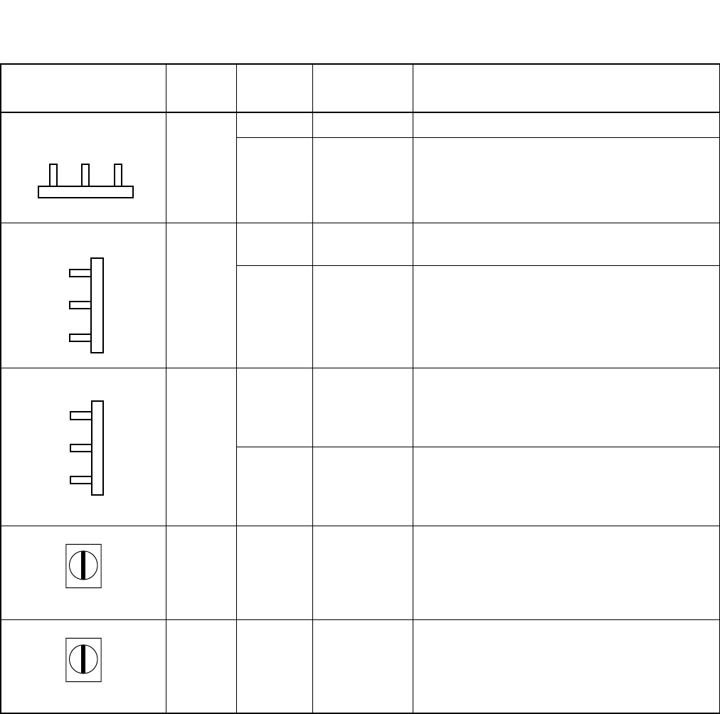
NDA-24296 CHAPTER 3
Page 575
Revision 1.0
PA-M87
Recording / Paging Device Adapter
Warning: When the Remote Phone is not used, be sure to turn the SW11 to the left side. If the switch key is left on
the right side, the machine components may be damaged by over current.
Note 3: To validate this switch setting, also operate the following keys (SW10-8, SW14, SW15) as required.
Note 4: This switch setting becomes effective parallel with the key operations of SW10-7.
SWITCH NAME SWITCH
NO. SETTING STANDARD
SETTING MEANING
SW11 RIGHT Remote Phone is used.
LEFT Remote Phone is not used.
SW12
SW13 UP No. of ATTCONs: Recording/Paging machine
= 6 : 1 Note 4
DOWN No. of ATTCONs: Recording/Paging machine
= 3 : 1 × 2 sets Note 4
SW14
SW15 UP
Patterns for Recording/Paging activation:
by loop start/ground start signal sending
Note 3
DOWN
Patterns for Recording/Paging activation:
via the telephone loop (handset lifting)Note 3
VR0
(Volume Resistance)
Voice output adjustment - GAIN (0 ~ +20dB) - for
1st circuit of Recording/Paging machine.
VR1
(Volume Resistance)
Voice output adjustment - GAIN (0 ~ +20dB) - for
2nd circuit of Recording/Paging machine.
321
Left Ri
g
ht
3
2
1
UP
DOWN
1
2
3
UP
DOWN
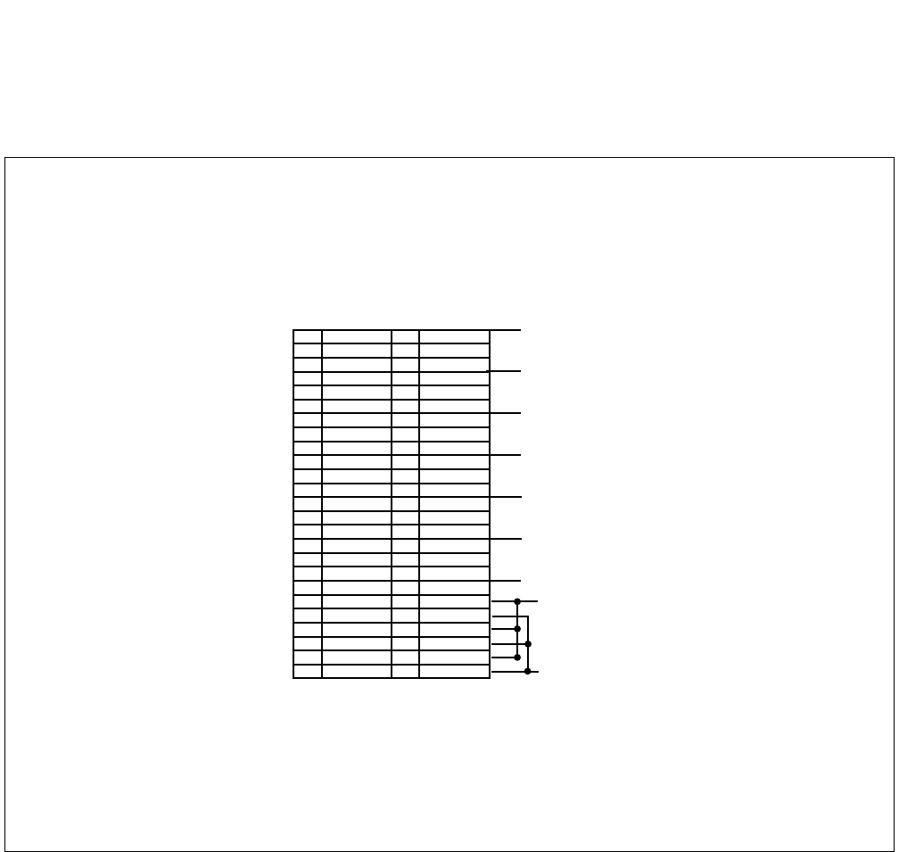
CHAPTER 3 NDA-24296
Page 576
Revision 1.0
PA-M87
Recording / Paging Device Adapter
6. External Interface
The location of REC/PGA connector leads and their connection diagram are shown in Figure 3-179.
Figure 3-179 REC/PGA Connector Leads
See also Connecting Route Diagram. (Figure 3-180)
Location of REC/PGA Connector Leads
26
27
28
29
30
31
32
33
34
35
36
37
38
39
40
41
1
2
3
4
5
6
7
8
9
10
11
12
13
14
15
16
42
43
44
45
46
47
48
17
18
19
20
21
22
23
49
50 24
25
CHAMP Connector (J)
REC/PGA
K1B
B0
M0B
K0B
B1
B2
M2B
M1B
K2B
K4B
B3
M3B
K3B
B4
B5
M5B
M4B
K5B
L0B
L1B
T0B
ZB
T1B
K1A
A0
M0A
K0A
A1
A2
M2A
M1A
K2A
K4A
A3
M3A
K3A
A4
A5
M5A
M4A
K5A
L0A
L1A
T0A
ZA
T1A
T0C
T1C
For Recording/Paging Machine #0
For Recording/Paging Machine #1 Note
For ATT #0
For ATT #1
For ATT #2
For ATT #3
For ATT #4
For ATT #5
Note: These leads are used when the two - circuit system is adopted for the Recording/Paging service features
(No. of ATTCON: Output Equipment = 3 : 1 × 2 circuits).
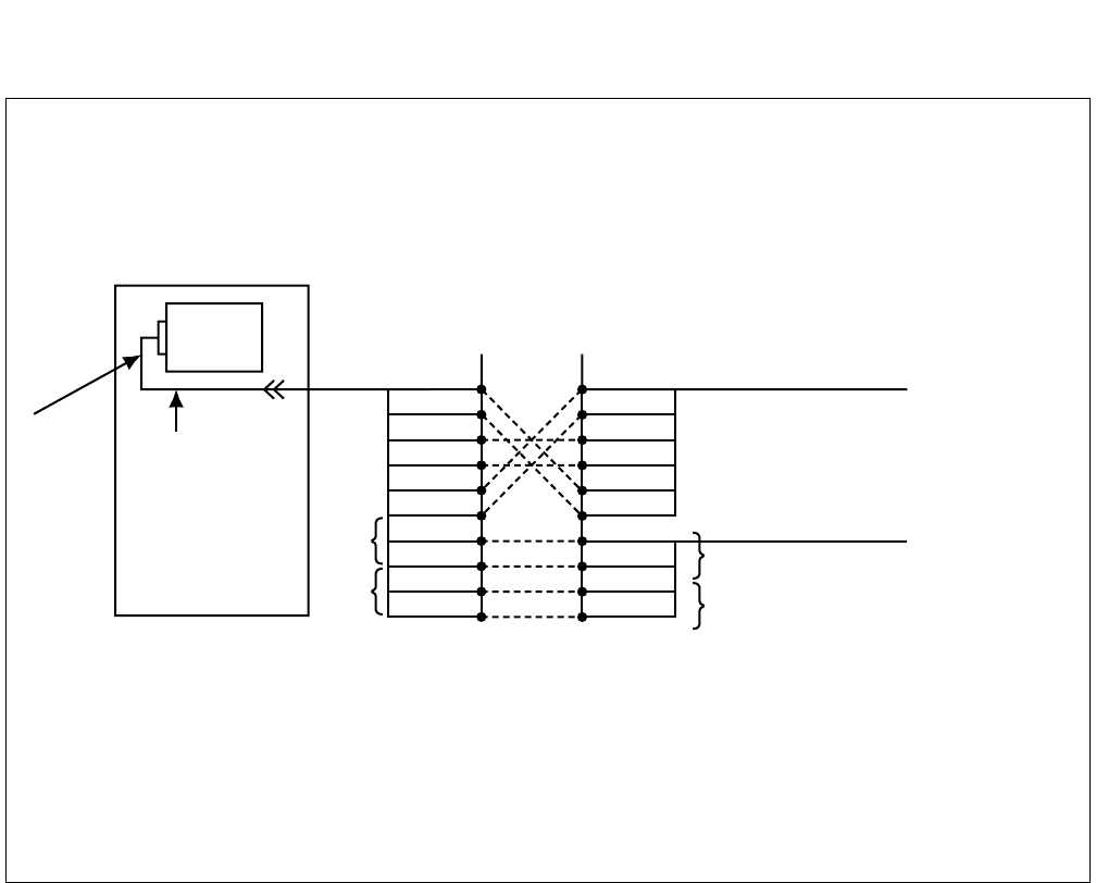
NDA-24296 CHAPTER 3
Page 577
Revision 1.0
PA-M87
Recording / Paging Device Adapter
Figure 3-180 Connecting Route Diagram (1/4)
PBX
RECC/
PGADP
B0
A0
M0A
M0B
K0A
K0B
L0A
L0B
T0A
T0B
KB
LA
LB
A
B
KA
MDF
To ATT
To Recording/
Paging machine
Note 3
50FLT-CHAMP
CABLE
Front
connector
[ In case telephone set loop is used for Recording/Paging activation]
Telephone Terminal
Side Leads
Speech Signal
Leads
Note 1
Note 2
Note 1: For speech signal output leads toward Recording/Paging equipment.
Note 2: For control signal output leads toward Recording/Paging equipment.
Note 3: There is restriction here in case a Recording machine is used: The Recording machine should be the type
which is fixed between the Central Office and telephone terminals.
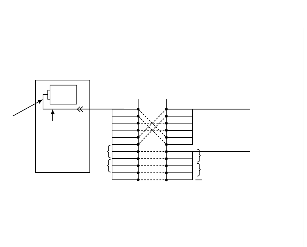
CHAPTER 3 NDA-24296
Page 578
Revision 1.0
PA-M87
Recording / Paging Device Adapter
Figure 3-180 Connecting Route Diagram (2/4)
PBX
RECC/
PGADP
B0
A0
M0A
M0B
K0A
K0B
L0A
L0B
T0A
T0B
KB
LA
LB
A
B
T0C
KA
MDF
To ATT
50FLT-CHAMP
CABLE
[ In case Recording/Paging is activated by the loop start or ground start signal sending ]
Speech Signal
Leads
Loop Start Leads
Ground Start Leads
To Recording/
Paging machine
Note 1: For speech signal leads toward Recording/Paging equipment.
Note 2: For control signal leads toward Recording/Paging equipment.
Front
connector
Note 1
Note 2
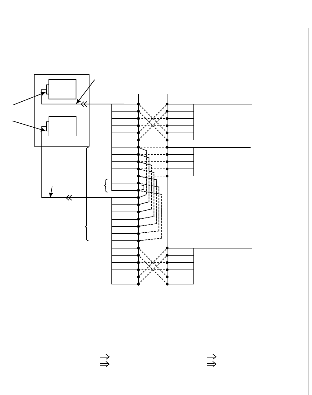
NDA-24296 CHAPTER 3
Page 579
Revision 1.0
PA-M87
Recording / Paging Device Adapter
Figure 3-180 Connecting Route Diagram (3/4)
PBX
RECC/
PGADP
B0
A0
M0A
M0B
K0A
K0B
L0A
L0B
T0A
T0B
KB
LA
LB
T0C
ZA
ZB
L0A
L0B
T0A
T0B
T0C
ZA
ZB
A0
KA
MDF
To ATT
50FLT-CHAMP
CABLE
RECC/
PGADP
50FLT-CHAMP
CABLE
B0
M0A
M0B
K0A
K0B
KA
KB
LA
LB
A
B
A
B
To ATT
[ In case 7 or more ATTCONs are connected to a single Recording/Paging machine ]
Front
connector
Note 1
Note 2
To Recording/
Paging machine
Note 1: To use a single Recording/Paging machine for 7 or more ATTCONs, the necessary number of PA-M87
card(s) must be reinforced, according the ATT number, on the side of the ICS. If this is the case, provide
relevant multiple connections between the first-card connector leads and the leads due for the reinforced
circuit card(s). Note that the connection should be performed on the MDF and each connector lead name must
be identical in each connection proccess.
(example) L0A (below) L0A (above)
T0A (below) T0A (above) L0B (below) L0B (above)
T0B (below) T0B (above)
Note 2: When performing the multiple connections, the leads here (“ZA” and “ZB”) must be given another multiple
connection in addition to that required in a normal pattern (refer to Note 1).
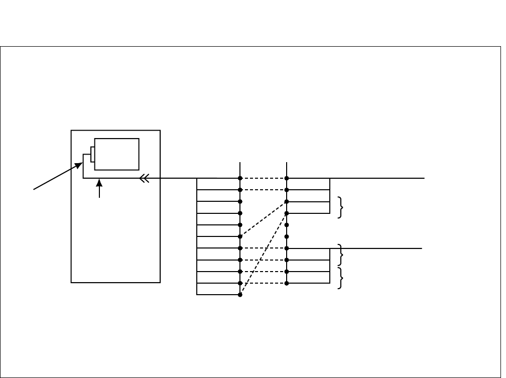
CHAPTER 3 NDA-24296
Page 580
Revision 1.0
PA-M87
Recording / Paging Device Adapter
Figure 3-180 Connecting Route Diagram (4/4)
PBX
RECC/
PGADP
B0
A0
M0A
M0B
K0A
K0B
L0A
L0B
T0A
T0B
B
M
E
T0C
A
MDF
To TLT
50FLT-CHAMP
CABLE
[ In case the TLT card (analog station) is connected instead of ATTCONs ]
Front
connector
To Paging
Machine
E&M Signal Leads
Speech Signal
Leads
Loop Start Leads
Note
Note : When the Paging machine is to be activated by the ground start, connect the T0B lead to the ground.
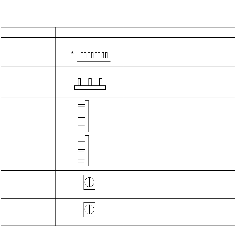
NDA-24296 CHAPTER 3
Page 581
Revision 1.0
PA-M87
Recording / Paging Device Adapter
7. Switch Setting Sheet
SWITCH NAME SWITCH SHAPE REMARKS
SW10
SW11
SW12
SW13
SW14
SW15
VR0
(Volume Resistance)
VR1
(Volume Resistance)
ON 12345678
321
Left Ri
g
ht
3
2
1
UP
DOWN
3
2
1
UP
DOWN
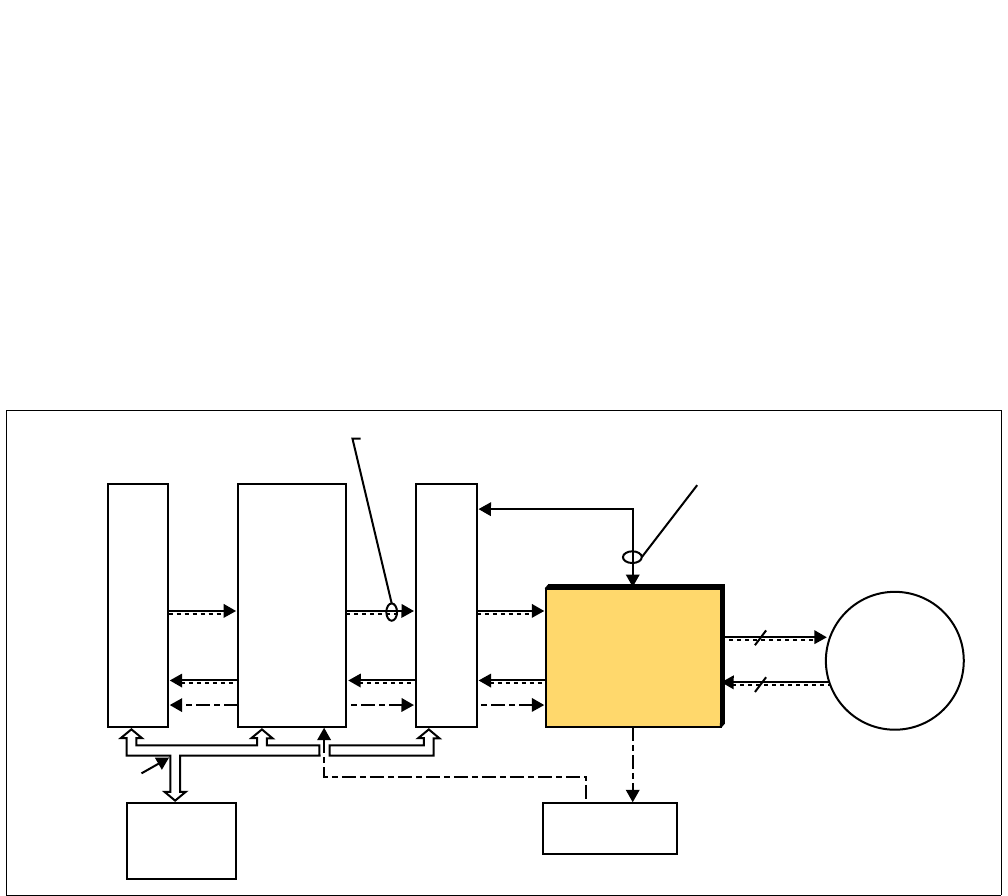
CHAPTER 3 NDA-24296
Page 582
Revision 1.0
PA-24PRTB-A
Primary Rate Interface Trunk
PA-24PRTB-A
Primary Rate Interface Trunk
1. General Function
The PA-24PRTB-A (PRT) circuit card is a digital interface supporting voice and data communications at
1.5 M bit/sec. Being equipped with a Link Access Procedure for a D channel (LAP D) controller based on
the ITU-T I/Q series, this card provides a Primary Rate Access Interface (PRI) with the system. A built-in
resonance circuit extracts clock signals, which are supplied from the network, so that the system may be in
exact synchronization with the network. To obtain appropriate speech level, this card is also equipped with
a mask ROM in which typical PAD patterns have been already written. A desired PAD value can be easily
selected by key settings and programming from the MAT.
Figure 3-181 Location of PA-24PRTB-A (24PRT) within the System
I/O Local Bus
CPU
System Clock
INT TSW INT
Speech Path (PCM Signal)
D-channel Signaling Link
2-wire
2-wire
PLO
1.544MHz Clock
Extraction from Network
24ch
T
R
ISDN
NETWORK
24PRT
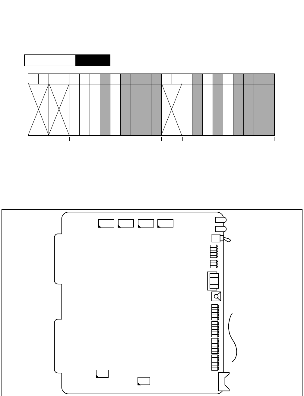
NDA-24296 CHAPTER 3
Page 583
Revision 1.0
PA-24PRTB-A
Primary Rate Interface Trunk
2. Mounting Location / Condition
The PA-24PRTB-A (24PRT) card can be mounted in the following shaded universal slots as shown below.
Note: This card cannot be mounted in slot 5.
This card cannot use Group0 (G=00) of Unit0 (U=0) of even-number Module Group.
3. Face Layout of Lamps, Switches, and Connectors
The face layout of lamps, switches, and connectors of this circuit card is shown in Figure 3-182.
Figure 3-182 Face Layout of PA-24PRTB-A (24PRT)
PIM
Mounting Module
00 01 02 03 04 05 06 07 08 09 10 11 12 13 14 15 16 17 18 19 20 21 22 23
Universal Slots Universal Slots
Note
OPE
N-OPE
MB
BL23
BL00
MODE
CN2
2
3
0
1LB
PCM
BER
AIS
FRM
RMT
DOPE
PKT LYR
SW0
SW2 SW3 SW4 SW5
SW1

CHAPTER 3 NDA-24296
Page 584
Revision 1.0
PA-24PRTB-A
Primary Rate Interface Trunk
4. Lamp Indications
The contents of lamp indications on this circuit card are shown in the table below.
Table 3-15 PA-24PRTB-A Lamp Indication Reference
LAMP NAME COLOR STATE
OPE Green Remains lit while this circuit card is in normal operation.
N-OPE Red Remains lit while this circuit card is in make-busy state.
PCM Red Lights when input signal down is detected (PCM LOSS).
FRM Red Lights when frame alignment loss is detected.
PER Red Lights when a CRC error occur frequently.
RMT Red Lights on receiving Remote Alarm Indication (RAI).
AIS Yellow Lights on detection of AIS.
DOPE Green Remains lit while the D Channel Controller is on.
LYR Green Lights when the link of the D channel is set up.
RKT Green Lights when the packet of the D channel is in use.
BL00
BL23
Green Lights when the corresponding circuit is busy.
Flash Flashes while the corresponding circuit is in make-busy state (60 IPM).
OFF Remains off when the corresponding circuit is idle.
(When BL23 is in used as D channel, lamp is always on.)
-

NDA-24296 CHAPTER 3
Page 585
Revision 1.0
PA-24PRTB-A
Primary Rate Interface Trunk
5. Switch Settings
Standard settings of switches on this circuit card are shown in the table below.
SWITCH
NAME SWITCH
NO. SETTING STANDARD
SETTING MEANING
MB UP Circuit card make busy
DOWN ×Circuit card make busy cancel
MODE 5 AT&T (#4/#5 ESS)
7 NT DMS 100/DMS 250
10 Q-SIG. (ETS 300 172)
LB 0ON Internal loop back set
OFF ×Internal loop back cancel
1ON Line loop back set
OFF ×Line loop back cancel
2ON Payload loop back set
OFF ×Payload loop back cancel
3ON D-channel Handler (DCH) make busy request
OFF ×D-channel Handler (DCH) make busy request cancel
SW0 1ON ×Impedance 100 Ω
OFF Impedance 110 Ω
2ON Send transformer middle point Ground
OFF ×Send transformer middle point Open
3ON Receive transformer middle point Ground
OFF ×Receive transformer middle point Open
4ON ×Fixed
CHAPTER 3 NDA-24296
Page 586
Revision 1.0
PA-24PRTB-A
Primary Rate Interface Trunk
SWITCH
NAME SWITCH
NO. SETTING STANDARD
SETTING MEANING
SW1 1OFF ×Standard setting (Digital PAD/ROM selection)
2ON ×Fixed
3ON Interface structure: 24B
OFF ×Interface structure: 23B + D
4ON D channel packet service is provided.
OFF ×D channel packet service is not provided.
SW2
1
2
3
4ON ×24-Multiframe
5ON ×Zero Suppress Select B8ZS (24-multiframe)
6ON ×Standard setting
7OFF ×Standard setting
8ON ×Line fault is notified to the upper CPU.
OFF Line fault is not notified to the upper CPU.
SW3 1OFF ×Fixed
2OFF ×Fixed
3OFF ×Alarm processing select Fixed to OFF
4OFF ×Main Signal All 1 supervision is not made.
5ON ×Fixed
6ON ×Fixed
7ON ×Fixed
8ON ×Fixed
SETTING OF EQUALIOZER
SW2-1 SW2-2 SW2-3 DISTANCE
ON
ON
ON
ON
OFF
ON
ON
OFF
OFF
ON
ON
OFF
ON
OFF
ON
0 ~
40 ~
80 ~
120 ~
160 ~
40m
80m
120m
160m
200m
Other combinations Not allowed
NDA-24296 CHAPTER 3
Page 587
Revision 1.0
PA-24PRTB-A
Primary Rate Interface Trunk
SWITCH
NAME SWITCH
NO. SETTING STANDARD
SETTING MEANING
SW4 1OFF ×Fixed (D channel)
2ON ×D Channel Mode Selection; Used Side
OFF D Channel Mode Selection; Network Side
3ON D Channel Signal Logic; Negative
OFF ×D Channel Signal Logic; Positive (Standard)
4ON ×
5ON ×
6ON ×Fixed
7ON ×Fixed
8ON ×Fixed
SW5
1
ON ×PAD Pattern Selection
Note: When setting this switch, refer to Digital PAD
Setting Table.
OFF
2
ON
OFF ×
3
ON ×
OFF
4ON ×
OFF
5ON
OFF ×
6ON ×
OFF
7ON ×
OFF
8ON IDLE code is sent out.
OFF ×IDLE code is not sent out.
SW4-4 SW4-5 D-channel Speed
ON
OFF
ON
OFF
ON
ON
OFF
OFF
64 kbps (Standard)
Not used
56 kbps
Not used
SW5-1 SW5-2 SW5-3 PAD Pattern
ON OFF ON PAD Pattern 1
OFF OFF ON PAD Pattern 2
ON ON OFF A→µ Loss (Bothway)
OFF ON OFF A→µ Loss (Receive)
ON OFF OFF µ→A Loss (Bothway)
OFF OFF OFF µ→A Loss (Receive)
SW5-4 SW5-5 DIGITAL PAD CONTROL
ON
ON
OFF
OFF
ON
OFF
ON
OFF
Both directions
Receive only (Standard)
Send only
ARTD Fixed
SW5-6 SW5-7 DATA PAD CONTROL
ON
ON
OFF
OFF
ON
OFF
ON
OFF
64 k (Standard)
56 k AT & T
64 k INV.
48 k PROTIMS

CHAPTER 3 NDA-24296
Page 588
Revision 1.0
PA-24PRTB-A
Primary Rate Interface Trunk
Digital PAD Setting Table for PA-24PRTB-A
This card is equipped with a mask ROM in which the following typical PAD patterns have been already
written. PAD value is determined by selecting a desired PAD pattern, which can be done by key setting of
the SW 5 (elements 1, 2, 3) on this card, and programming of the PAD data by the ARTD command - PAD.
The selected PAD pattern and the programmed ARTD PAD data correspond as listed below.
Note: - represents “GAIN” in this table.
PAD DATA
ARTD
PAD
PAD Pattern (selected by key setting)
PAD Pattern 1 PAD Pattern 2 µ→A Loss
(Bothway) µ→A Loss
(Receive) A→µ Loss
(Bothway) A→µ Loss
(Receive)
SEND RECEIVE SEND RECEIVE SEND RECEIVE SEND RECEIVE SEND RECEIVE SEND RECEIVE
1 2 [dB] 2 [dB] -3 [dB]
Note 3 [dB] 0 [dB] 0 [dB] 0 [dB] 0 [dB] 0 [dB] 0 [dB] 0 [dB] 0 [dB]
2 4 [dB] 4 [dB] 3 [dB] 3 [dB] 4 [dB] 4 [dB] 0 [dB] 4 [dB] 4 [dB] 4 [dB] 0 [dB] 4 [dB]
3 6 [dB] 6 [dB] 0 [dB] 6 [dB] 6 [dB] 6 [dB] 0 [dB] 12 [dB] 6 [dB] 6 [dB] 0 [dB] 12 [dB]
4 8 [dB] 8 [dB] 3 [dB] 9 [dB] 8 [dB] 8 [dB] 0 [dB] 8 [dB] 8 [dB] 8 [dB] 0 [dB] 8 [dB]
5 PAD value complies with key settings of SW5-6,7. (Irrelevant to PAD patterns)
7 0 [dB] 0 [dB] 0 [dB] 0 [dB] Through Through Through Through Through Through Through Through
NDA-24296 CHAPTER 3
Page 589
Revision 1.0
PA-24PRTB-A
Primary Rate Interface Trunk
6. External Interface
Figure 3-183 LT Connector Lead Accommodation
See also Connecting Route Diagram (Figure 3-184).
PIM
Mounting Module
26
27
28
29
30
31
32
33
34
35
36
37
38
39
40
41
1
2
3
4
5
6
7
8
9
10
11
12
13
14
15
16
42
43
44
45
46
47
48
17
18
19
20
21
22
23
49
50 24
25
232221201918171615141312111009080706050403020100
LT6 LT7 LT8 LT9 LT10 LT11LT0 LT1 LT2 LT3 LT4 LT5
231915
221814
211713
201612
231915
221814
211713
201612
110907050301
100806040200
110907050301
100806040200
HW11HW10HW9HW8HW7HW6HW5HW4HW3HW2HW1HW0
Group No.
Slot No.
LT Connector
PIM
Highway Block
LT 3, 5, 9, 11 Connector
26
27
28
29
30
31
32
33
34
35
36
37
38
39
40
41
1
2
3
4
5
6
7
8
9
10
11
12
13
14
15
16
42
43
44
45
46
47
48
17
18
19
20
21
22
23
49
50 24
25
Accommodated in 2
LT 2, 4, 8, 10 Connector
Accommodated in 3
26
27
28
29
30
31
32
33
34
35
36
37
38
39
40
41
1
2
3
4
5
6
7
8
9
10
11
12
13
14
15
16
42
43
44
45
46
47
48
17
18
19
20
21
22
23
49
50 24
25
E
Accommodated in 1
LT 1, 5, 7, 11 Connector
RB
POUTB
TB
E
RA
POUTA
TA
E
RB
POUTB
TB
E
RA
POUTA
TA
E
RB
POUTB
TB
E
RA
POUTA
TA
1232 1
132132 3
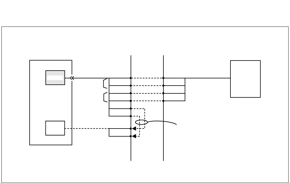
CHAPTER 3 NDA-24296
Page 590
Revision 1.0
PA-24PRTB-A
Primary Rate Interface Trunk
Figure 3-184 Connecting Route Diagram
RA
RB
TA
TB
POUTA
POUTB
RA
TA
TB
RB
DIU1A
DIU1B
PLO
PBX MDF
clock extraction
24 PRT To DSU
(Digital
Service
Unit)
Note
IN
OUT
Connecting Route Diagram for the PA-24PRTB-A circuit card is as follows.
Note: As an example, DIU1A and DIU1B leads are used in this diagram. For more information on
the PLO card, see Chapter 2 in this manual.
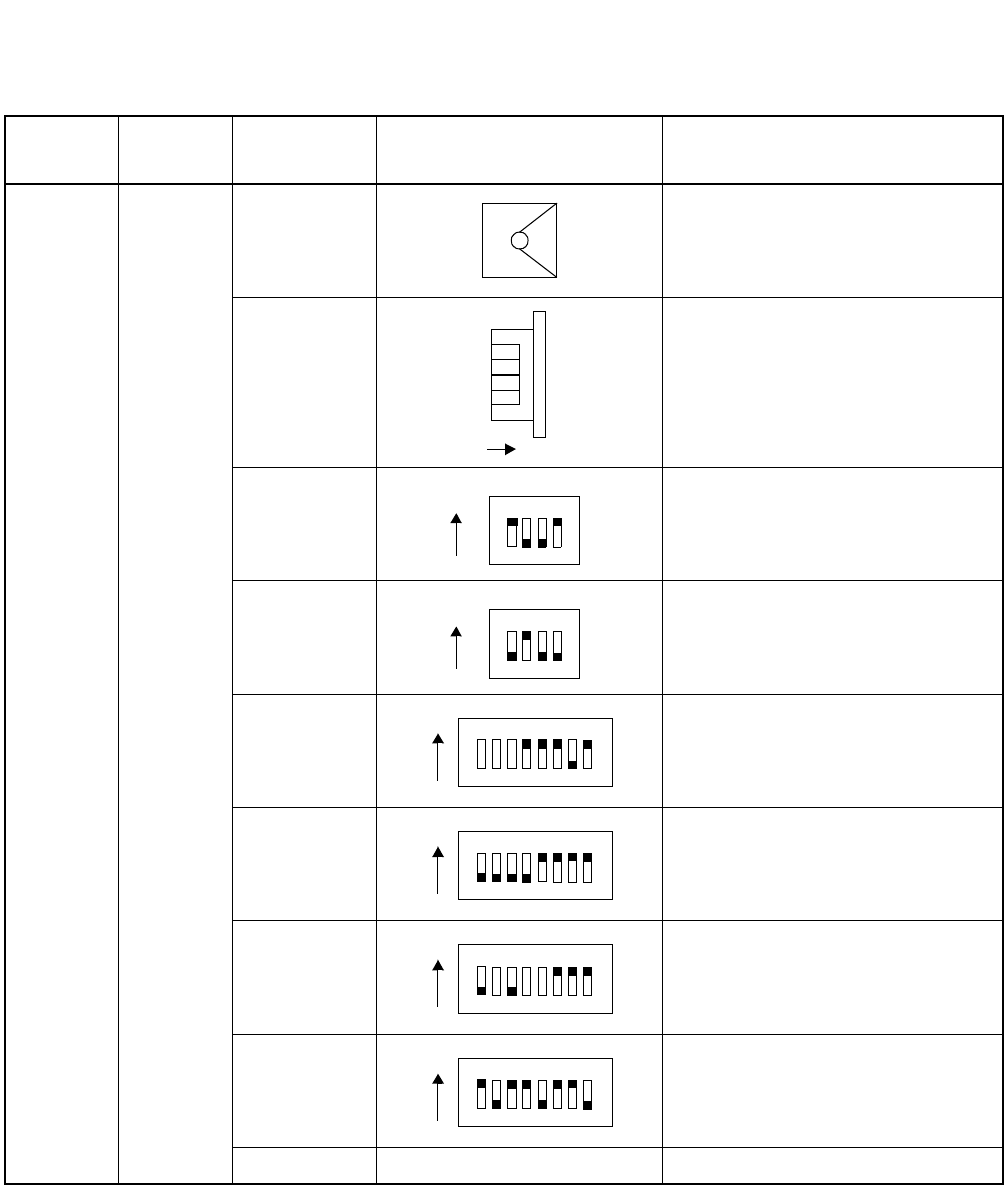
NDA-24296 CHAPTER 3
Page 591
Revision 1.0
PA-24PRTB-A
Primary Rate Interface Trunk
7. Switch Setting Sheet
MODULE SLOT NO. SWITCH
NAME SWITCH SHAPE REMARKS
PIM
MODE
LB
SW0
SW1
SW2
SW3
SW4
SW5
MB DOWN Circuit card make busy cancel
3
2
1
0
ON
1
ON 2 3 4
1
ON 2 3 4
1
ON 2 3 456 7 8
1
ON 2 3 4 5 6 7 8
1
ON 2 3 4 5 6 7 8
1
ON 2 3 4 5 6 7 8
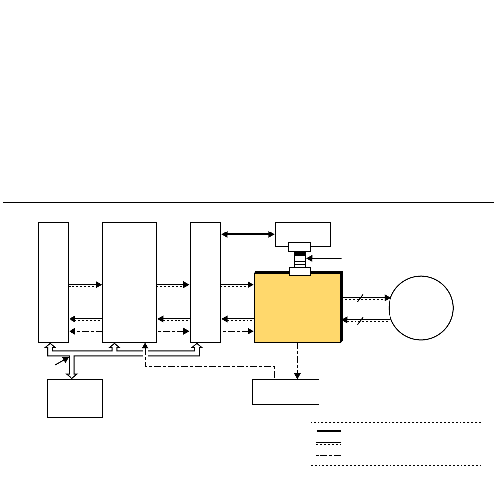
CHAPTER 3 NDA-24296
Page 592
Revision 1.0
PA-24DTR (DTI)
Digital Trunk Interface
PA-24DTR (DTI)
Digital Trunk Interface
1. General Function
The PA-24DTR (24DTI) circuit card provides an interface between 24 digital trunks and the system at
1.544 Mbit/s. This card can be also used as an interface for a Common Channel Interoffice Signaling
(CCIS) or an ISDN network when being connected to an additional CCH or DCH circuit card with a flat
cable as illustrated below. A built-in resonance circuit can be used for the purpose of extracting clock sig-
nals when the PBX functions as a PLO-secondary switch. To obtain appropriate speech level, this card is
equipped with a mask ROM in which typical PAD patterns have been already written. A desired PAD value
can be easily selected by key settings and programming from the MAT.
Figure 3-185 Location of PA-24DTR (DTI) within the System
I/O Local
Bus
CPU
System Clock
INT TSW INT
CCH/DCH
Flat Cable
2
2
PLO
1.544MHz Clock Extraction
(for a PLO-secondary office)
24ch
T
R
DIGITAL
NETWORK
Note
DTI(PA-24DTR)
: Common Channel Signaling Link
: Speech Path (PCM signal)
: Clock Signal
Note: When PA-24DTR is used in an Associated Channel Interoffice Signaling (ACIS) system, CCH/DCH is not required.
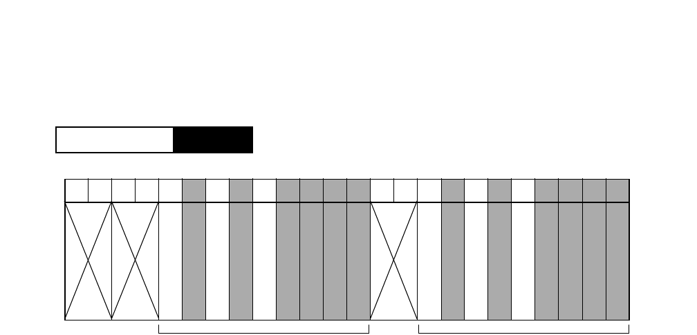
NDA-24296 CHAPTER 3
Page 593
Revision 1.0
PA-24DTR (DTI)
Digital Trunk Interface
2. Mounting Location/Condition
The PA-24DTR (DTI) card can be mounted in the following shaded slots as shown below.
PIM
Mounting Module
00 01 02 03 04 05 06 07 08 09 10 11 12 13 14 15 16 17 18 19 20 21 22 23
Universal Slots Universal Slots

CHAPTER 3 NDA-24296
Page 594
Revision 1.0
PA-24DTR (DTI)
Digital Trunk Interface
3. Face Layout of Lamps, Switches, and Connectors
The face layout of lamps, switches, and connectors on this circuit card is shown in Figure 3-186. Note that
there are two types of PA-24DTR (DTI) cards which differ in their face layouts.
Figure 3-186 Face Layout of PA-24DTR (DTI)
OPE
N-OPE
MB
PCM
BL23
BER
AIS
FRM
RMT
3
2
1
0
CN2
BL00
SW15
SW13B
SW13
SW12
SW11
SW10
OPE
N-OPE
SW00
PCM
BL23
BER
AIS
FRM
RMT
3
2
1
0
CN2
BL00
SW01
SW6C
SW4D
SW14
SW5D
SW25
SW39
SW58

NDA-24296 CHAPTER 3
Page 595
Revision 1.0
PA-24DTR (DTI)
Digital Trunk Interface
4. Lamp Indications
The contents of lamp indications on this circuit card are shown in the table below.
LAMP NAME COLOR STATE
OPE Green Remains lit while this circuit card is in normal operation.
N-OPE Red Remains lit while this circuit card is in make-busy state.
PCM Red Lights in the case of input signal down (PCM LOSS).
FRM Red Lights in the case of frame alignment loss.
BER Red Lights when frequent bit errors occur in the case of 12-multiframe and when a CRC error
occurs frequently in the case of 24-multiframe.
RMT Red Lights on receipt of remote alarm indication.
AIS Yellow Lights on receipt of Alarm Information Signal (AIS).
BL00
BL23
Green Lights when the corresponding circuit is busy.
Flash Flashes while DP signals are being sent out or received (Flashes to dial pulses), or the
corresponding circuit is in make-busy state (60IPM).
OFF Remains off when the corresponding circuit is idle.
-
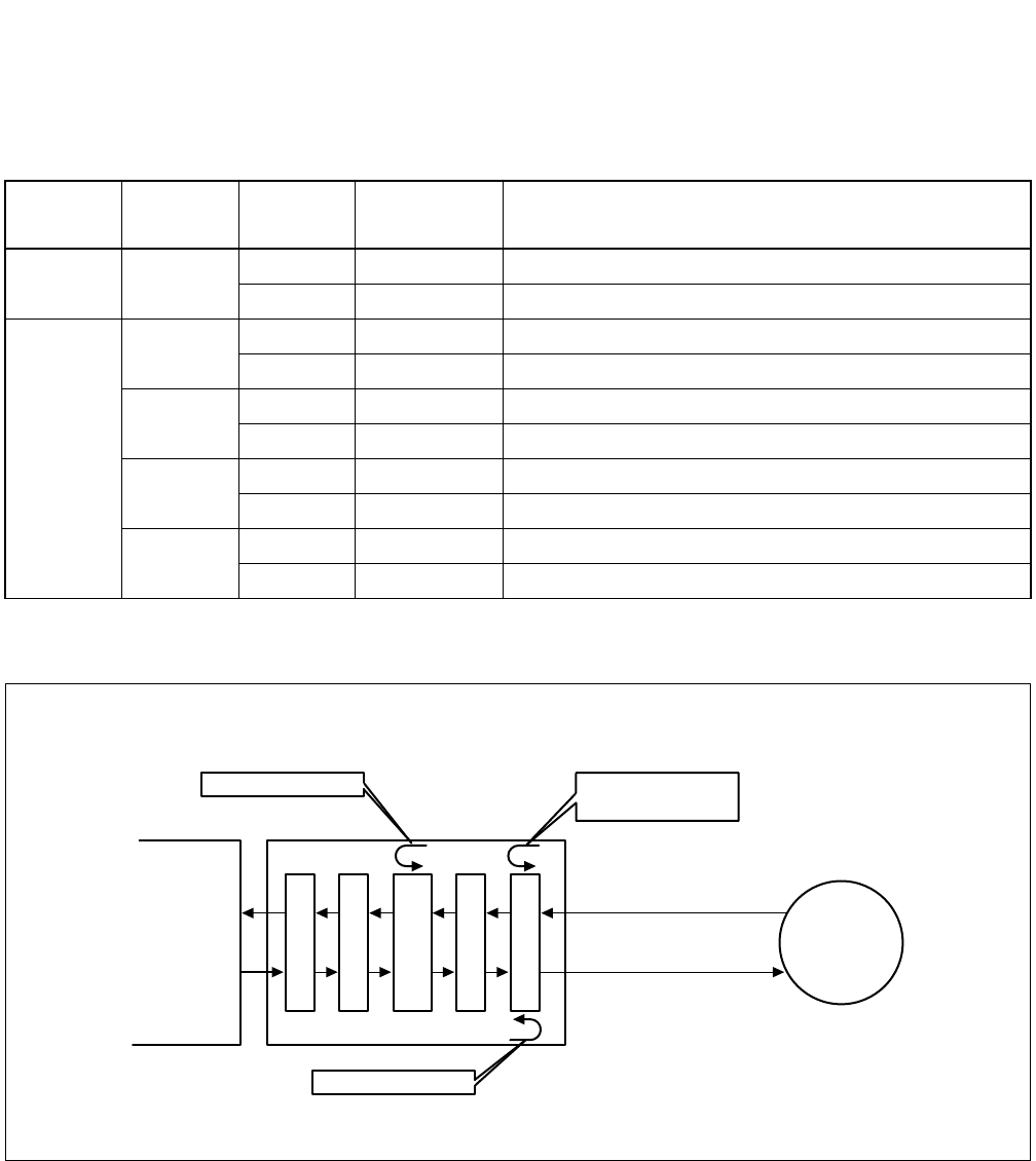
CHAPTER 3 NDA-24296
Page 596
Revision 1.0
PA-24DTR (DTI)
Digital Trunk Interface
5. Switch Settings
Standard settings of switches on this circuit card are shown in the table below.
Note: This switch setting is applicable for a system adopts Associated Channel Interoffice Signalling (ACIS).
Figure 3-187 Available Locations for Loopback Testing
SWITCH
NAME SWITCH
NO. SETTING STANDARD
SETTING MEANING
SW00
(MB)
UP Circuit card make busy
DOWN ¥Circuit card make busy cancel
SW01/13B 0ON Internal Loopback : Set
OFF ¥Internal Loopback : Cancel
1ON External Loopback : Set
OFF ¥External Loopback : Cancel
2ON Payload Loopback : Set
OFF ¥Payload Loopback : Cancel
3ON All Channel Make Busy : Set Note
OFF ¥All Channel Make Busy : Cancel
Switch
TDSW Interface
PAD
Speech Path
Control Block
Framer
Line Interface
DIGITAL
NETWORK
External Loopback
(Line Loopback)
Payload Loopback
Internal Loopback
R
T
Speech Path
PA-24 DTR (DTI)
As illustrated below, loopback testing can be performed at three locations on this card by key setting of the
SW01/13B.
NDA-24296 CHAPTER 3
Page 597
Revision 1.0
PA-24DTR (DTI)
Digital Trunk Interface
SWITCH
NAME SWITCH
NO. SETTING STANDARD
SETTING MEANING
SW15/25 1ON ×Impedance Setting: 100 [Ω]
OFF Impedance Setting: 110 [Ω]
2ON Transformer at Middle Point - Transmission: Ground
OFF ×Transformer at Middle Point - Transmission: Open
3ON Transformer at Middle Point - Receive: Ground
OFF ×Transformer at Middle Point - Receive: Open
4ON Idle Code: To be sent out
OFF ×Not to be sent out
SW11/39
1
ON PAD Control
OFF ×
2
ON ×
OFF
3
ON ×Data PAD Control
OFF
4
ON ×
OFF
5
ON T Signal Control
OFF
6
ON ×
OFF
7
ON R Signal Control
OFF
8
ON ×
OFF
SW11/39-1 SW11/39-2 PAD Control
ON ON Bothway
OFF ON Receive only (Send 0dB)
ON OFF Send only (Receive 0dB)
OFF OFF Fixed to ARTD command
SW11/39-3 SW11/39-4 Data PAD Value
ON ON 64 Kbps
OFF ON 56 Kbps
ON OFF 48 Kbps
OFF OFF 64 Kbps INV
SW11/39-5 SW11/39-6 T Signal Control
ON ON ABCD
OFF ON ABAB
ON OFF Bit Steal Inhibited
OFF OFF AAAA
SW11/39-7 SW11/39-8 R Signal Control
ON ON ABCD
OFF ON ABAB
ON OFF Bit Steal Inhibited
OFF OFF AAAA

CHAPTER 3 NDA-24296
Page 598
Revision 1.0
PA-24DTR (DTI)
Digital Trunk Interface
SWITCH
NAME SWITCH
NO. SETTING STANDARD
SETTING MEANING
SW10/4D 1ON Transmission Signal A Logic: Negative
OFF ×Transmission Signal A Logic: Positive
2ON Receiving Signal A Logic: Negative
OFF ×Receiving Signal A Logic: Positive
3ON RMT Alarm Sending: Not to be sent out
OFF ×RMT Alarm Sending: To be sent out
4ON ×Simultaneous Seizure Supervision: Not to be controlled
OFF Simultaneous Seizure Supervision: To be controlled
5ON ×Data Link Control: MOS
OFF Data Link Control: BOS (For NEAX2400 ICS)
6ON Multiframe Selection: 12-Multiframe
OFF Multiframe Selection: 24-Multiframe
7
ON Signal Selection: AMI (Alternate Mark Inversion)
OFF Signal Selection: B8ZS (Bipolar with 8 Zeros Substitution)
8ON When this switch is set to ON, Alarm Processing is selected for
North America specification.
(For NEAX2400 ICS, this Switch Setting is OFF.)
OFF
SW12/58
1ON Equalizer Setting
OFF
2ON
OFF
3ON
OFF
SW12/58-1 SW12/58-2 SW12/58-3 Distance
ON ON ON 0~133 (ft)/0~40 (m)
ON ON OFF 133~267 (ft)/40~80 (m)
ON OFF ON 267~400 (ft)/80~120 (m)
ON OFF OFF 400~533(ft)/120~160 (m)
OFF ON ON 533~667(feet)/
160~200(m)
Other Combinations Impossible
NDA-24296 CHAPTER 3
Page 599
Revision 1.0
PA-24DTR (DTI)
Digital Trunk Interface
SWITCH
NAME SWITCH
NO. SETTING STANDARD
SETTING MEANING
SW12/58
4
ON PAD Pattern Selection
Note: When setting this key, refer to Digital PAD Setting
Table.
OFF ×
5
ON ×
OFF
6
ON ×
OFF
7
ON ×Alarm Sending when this circuit card is in N-OPE state.
(For NEAX2400 ICS, Switch 12/58-7 Setting is OFF.)
OFF
8
ON ×
OFF
SW14/5D
1
ON Digital PAD ROM Selection: Special Specification (PROM
Spec.)
OFF ×Digital PAD ROM Selection: Standard Specification (MASK
ROM Spec.)
2ON ×LAYER 2 Signal Logic: Positive
OFF LAYER 2 Signal Logic: Negative
3ON Send a notice in the event of a line fault.
OFF ×Do not send a notice in the event of a line fault.
4ON Zero Code Suppression is not provided.
OFF Zero Code Suppression is provided.
SW12/58-4 SW12/58-5 SW12/58-6 PAD Pattern
OFF ON ON PAD Pattern 1
OFF ON OFF PAD Pattern 2
ON OFF ON A→ µ Loss (Bothway)
ON OFF OFF A→ µ Loss (Receive)
OFF OFF ON µ→Α Loss (Bothway)
OFF OFF OFF µ→Α Loss (Receive)
Other Combinations Impossible
SW12/58-7 SW12/58-8 Kind of Alarm
ON ON Alarm is not sent out
ON OFF
OFF ON All “1”
OFF OFF RMT
Note:

CHAPTER 3 NDA-24296
Page 600
Revision 1.0
PA-24DTR (DTI)
Digital Trunk Interface
SWITCH
NAME SWITCH
NO. SETTING STANDARD
SETTING MEANING
SW13/6C 1ON ×
Fixed to all ON.
OFF
2ON ×
OFF
3ON ×
OFF
4ON ×
OFF
5ON ×
OFF
6ON ×
OFF
7ON ×
OFF
8ON ×Netfusing : Not used
OFF Netfusing : used

NDA-24296 CHAPTER 3
Page 601
Revision 1.0
PA-24DTR (DTI)
Digital Trunk Interface
Digital PAD Setting Table for PA-24DTR (DTI)
As mentioned in General Function, this card is equipped with a mask ROM in which the following typical PAD pat-
terns have been already written. PAD value is determined by selecting a desired PAD pattern, which can be done by
key setting of the SW 12/58 (elements 4, 5, 6) on this card, and programming of the PAD data by the ARTD com-
mand - CDN=30(PAD). The PAD patterns and ARTD data correspond as listed below.
Note: - represents “GAIN” in this table.
PAD DATA
ARTD
CDN=30
PAD Pattern (selected by key setting)
PAD Pattern 1 PAD Pattern 2 A→µ Loss
(Bothway) A→µ Loss
(Receive) µ→A Loss
(Bothway) µ→A Loss
(Receive)
SEND RECEIVE SEND RECEIVE SEND RECEIVE SEND RECEIVE SEND RECEIVE SEND RECEIVE
1 2 [dB] 2 [dB] -3 [dB]
Note 3 [dB] 0 [dB] 0 [dB] 0 [dB] 0 [dB] 0 [dB] 0 [dB] 0 [dB] 0 [dB]
2 4 [dB] 4 [dB] 3 [dB] 3 [dB] 4 [dB] 4 [dB] 0 [dB] 4 [dB] 4 [dB] 4 [dB] 0 [dB] 4 [dB]
3 6 [dB] 6 [dB] 0 [dB] 6 [dB] 6 [dB] 6 [dB] 0 [dB] 12 [dB] 6 [dB] 6 [dB] 0 [dB] 12 [dB]
4 8 [dB] 8 [dB] 3 [dB] 9 [dB] 8 [dB] 8[dB] 0 [dB] 8 [dB] 8 [dB] 8 [dB] 0 [dB] 8 [dB]
5 Key settings of SW 11/39 - 3,4 correspond to PAD values. (Regardless of PAD patterns).
7 0 [dB] 0 [dB] 0 [dB] 0 [dB] Through Through Through Through Through Through Through Through

CHAPTER 3 NDA-24296
Page 602
Revision 1.0
PA-24DTR (DTI)
Digital Trunk Interface
6. External Interface
The leads appear as follows on the LT connectors.
Figure 3-188 LT Connector Lead Accommodation
See also Connecting Route Diagram (Figure 3-189).
26
27
28
29
30
31
32
33
34
35
36
37
38
39
40
41
1
2
3
4
5
6
7
8
9
10
11
12
13
14
15
16
42
43
44
45
46
47
48
17
18
19
20
21
22
23
49
50 24
25
232221201918171615141312111009080706050403020100
LT6 LT7 LT8 LT9 LT10 LT11LT0 LT1 LT2 LT3 LT4 LT5
231915
221814
211713
201612
231915
221814
211713
201612
110907050301
100806040200
110907050301
100806040200
HW11HW10HW9HW8HW7HW6HW5HW4HW3HW2HW1HW0
Group No.
Slot No.
LT Connector
PIM
Highway Block
LT 3, 5, 9, 11 Connector
26
27
28
29
30
31
32
33
34
35
36
37
38
39
40
41
1
2
3
4
5
6
7
8
9
10
11
12
13
14
15
16
42
43
44
45
46
47
48
17
18
19
20
21
22
23
49
50 24
25
Accommodated in 2
LT 2, 4, 8, 10 Connector
Accommodated in 3
26
27
28
29
30
31
32
33
34
35
36
37
38
39
40
41
1
2
3
4
5
6
7
8
9
10
11
12
13
14
15
16
42
43
44
45
46
47
48
17
18
19
20
21
22
23
49
50 24
25
E
Accommodated in 1
LT 1, 5, 7, 11 Connector
E
RB RA
POUTB POUTA
TB TA
EE
RB RA
POUTB POUTA
TB TA
EE
RB RA
POUTB POUTA
TB TA
11
22
33 1 1
223 3
PIM
Mounting Module
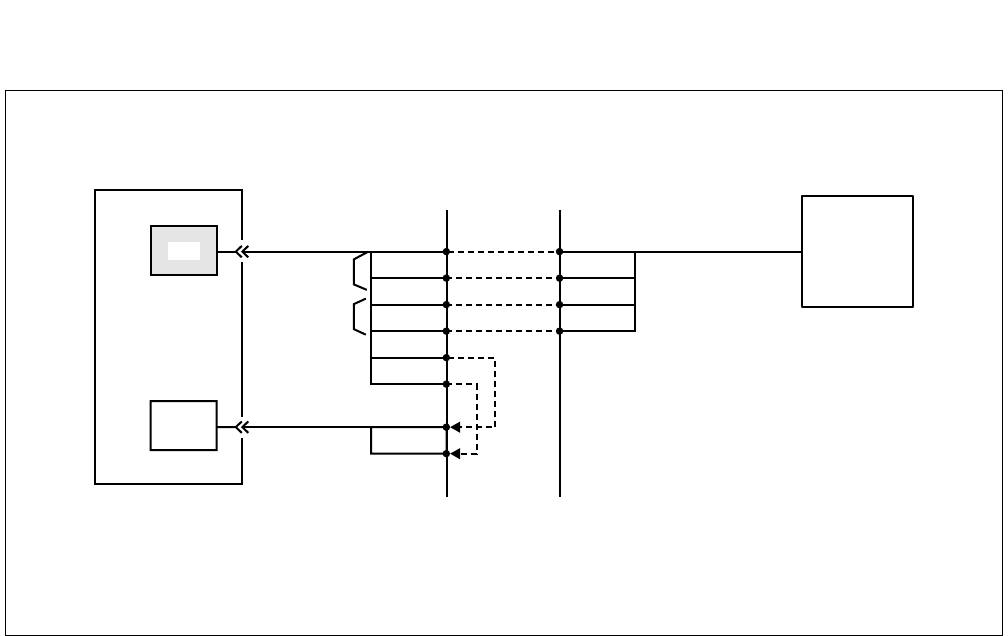
NDA-24296 CHAPTER 3
Page 603
Revision 1.0
PA-24DTR (DTI)
Digital Trunk Interface
Figure 3-189 Connecting Route Diagram
TA
TB
RA
RB
POUTA
POUTB
TA
RA
RB
TB
DIU1A
DIU1B
PLO
PBX
MDF
Note 1
DTI CARRIER
EQUIPMENT
Note 2
OUT
IN
Note 1: This cable connection is required when clock signals must be extracted from the network side.
Note 2: As an example, DIU1A and DIU1B leads are used in this diagram. For more information about these
leads, see Chapter 2 in this manual.
Connecting Route Diagram for the PA-24DTR (DTI) circuit card is as follows.
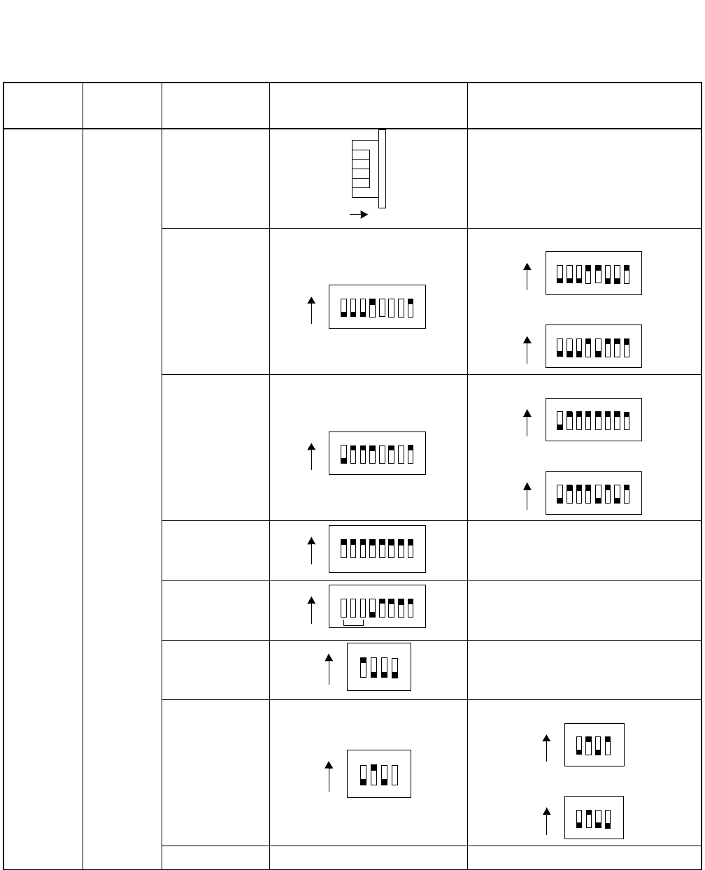
CHAPTER 3 NDA-24296
Page 604
Revision 1.0
PA-24DTR (DTI)
Digital Trunk Interface
7. Switch Setting Sheet
MODULE SLOT NO. SWITCH
NAME SWITCH SHAPE REMARKS
PIM SW01/13B
SW10/4D •4-multiframe DTI Standard
•12-multiframe DTI Standard
SW11/39 •24-multiframe DTI Standard
•12-multiframe DTI Standard
SW13/6C •Fixed to all ON.
SW12/58 Note: Equalizer Setting
SW15/25
SW14/5D •24-multiframe DTI Standard
•12-multiframe DTI Standard
SW00/MB DOWN Circuit card make busy cancel
ON
3
2
1
0
12345678
ON
123456 7 8
ON
12345678
ON
12345678
ON
12345678
ON
12345678
ON
12345678
ON
12345678
ON
Note
1
ON 2 3 4
1
ON 2 3 4
1234
ON
12 3 4
ON
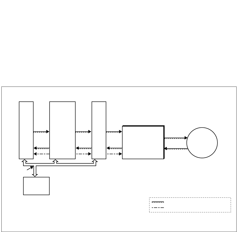
NDA-24296 CHAPTER 3
Page 605
Revision 1.0
PA-24DTR (DLI)
Digital Line Interface
PA-24DTR (DLI)
Digital Line Interface
1. General Function
The PA-24DTR (24DLI) circuit card provides an interface between 24 digital lines and the system at 1.544
Mbit/s. To obtain appropriate speech level, this card is equipped with a mask ROM in which typical PAD
patterns have been already written. A desired PAD value can be easily selected by key settings.
Note: The key settings become valid when SYS1 INDEX4 bit5=1.
Figure 3-190 Location of PA-24DTR (DLI) within the System
I/O Local
Bus
CPU
INT TSW INT
24ch
T
R
TERMINAL
EQUIPMENT
DLI(PA-24DTR)
: Speech Path (PCM signal)
: Clock Signal
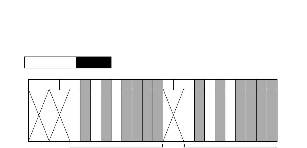
CHAPTER 3 NDA-24296
Page 606
Revision 1.0
PA-24DTR (DLI)
Digital Line Interface
2. Mounting Location/Condition
The PA-24DTR (DLI) card can be mounted in the following shaded slots as shown below.
PIM
Mounting Module
00 01 02 03 04 05 06 07 08 09 10 11 12 13 14 15 16 17 18 19 20 21 22 23
Universal Slots Universal Slots
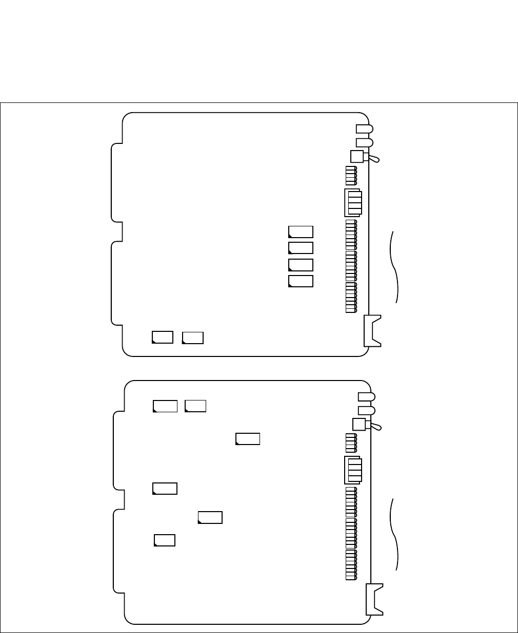
NDA-24296 CHAPTER 3
Page 607
Revision 1.0
PA-24DTR (DLI)
Digital Line Interface
3. Face Layout of Lamps, Switches, and Connectors
The face layout of lamps, switches, and connectors on this circuit card is shown in Figure 3-191. Note that
there are two types of PA-24DTR (DLI) cards which differ in their face layouts.
Figure 3-191 Face Layout of PA-24DTR (DLI)
OPE
N-OPE
MB
PCM
BER
AIS
FRM
RMT
CN2
SW15
SW13
SW12
SW11
SW10
OPE
N-OPE
SW00
PCM
BL23
BER
AIS
FRM
RMT
3
2
1
0
CN2
BL00
SW01
BL23
3
2
1
0
BL00
SW01
SW6C
SW4D
SW14
SW5D
SW25
SW39
SW58

CHAPTER 3 NDA-24296
Page 608
Revision 1.0
PA-24DTR (DLI)
Digital Line Interface
4. Lamp Indications
The contents of lamp indications on this circuit card are shown in the table below.
LAMP NAME COLOR STATE
OPE Green Remains lit while this circuit card is in normal operation.
N-OPE Red Remains lit while this circuit card is in make-busy state.
PCM Red Lights in the case of input signal down (PCM LOSS).
FRM Red Lights in the case of frame alignment loss.
BER Red Lights when frequent bit errors occur in the case of 12-multiframe and when a CRC error
occurs frequently in the case of 24-multiframe.
RMT Red Lights on receipt of remote alarm indication.
AIS Yellow Lights on receipt of Alarm Information Signal (AIS).
BL00
BL23
Green Lights when the corresponding circuit is busy.
Flash Flashes while DP signals are being sent out or received (Flashes to dial pulses), or the
corresponding circuit is in make-busy state (60 IPM).
OFF Remains off when the corresponding circuit is idle.
-
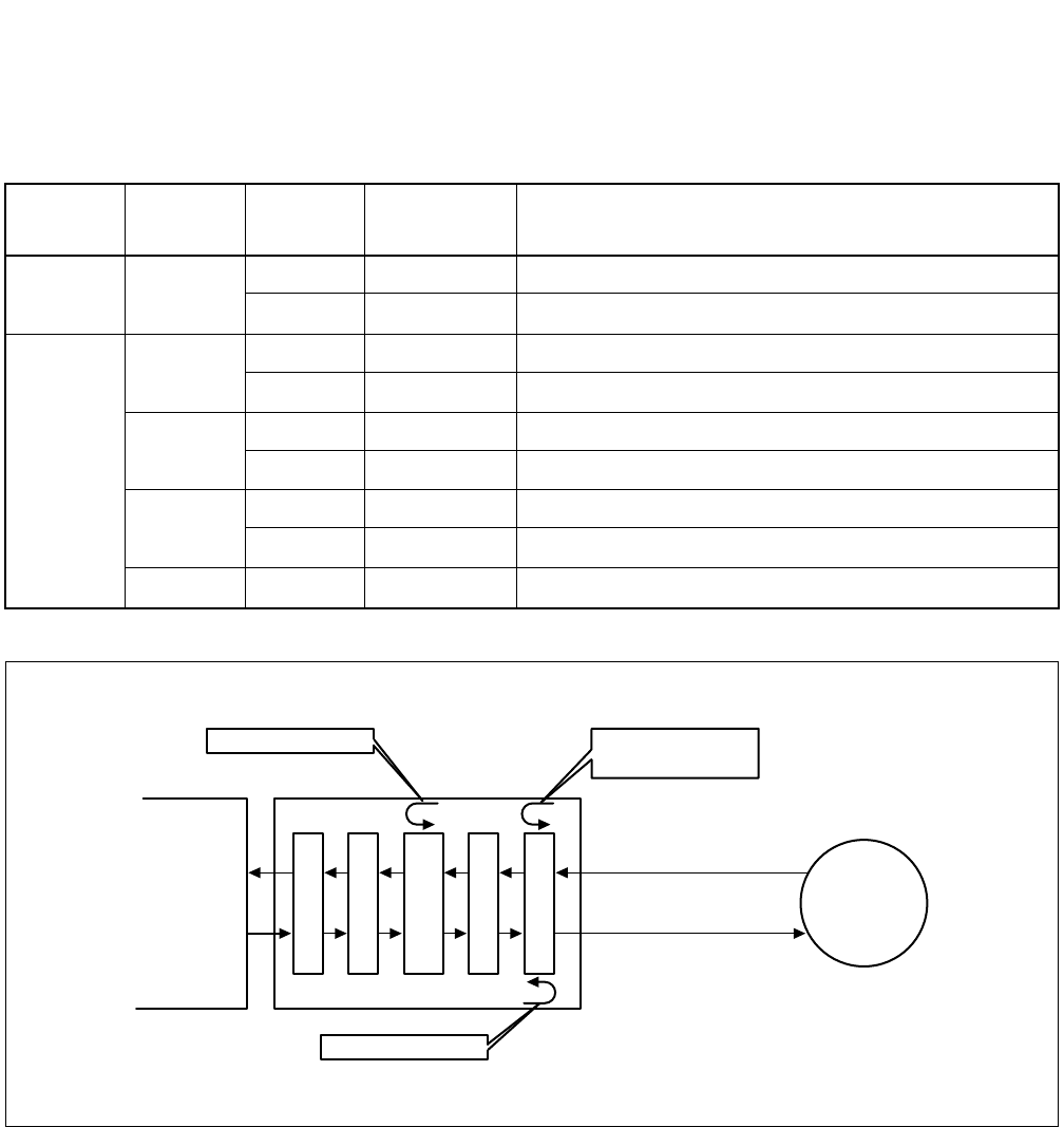
NDA-24296 CHAPTER 3
Page 609
Revision 1.0
PA-24DTR (DLI)
Digital Line Interface
5. Switch Settings
Standard settings of switches on this circuit card are shown in the table below.
Figure 3-192 Available Locations for Loopback Testing
SWITCH
NAME SWITCH
NO. SETTING STANDARD
SETTING MEANING
SW00
(MB)
UP Circuit card make busy
DOWN ×Circuit card make busy cancel
SW01/13B 0ON Internal Loopback : Set
OFF ×Internal Loopback : Cancel
1ON External Loopback : Set
OFF ×External Loopback : Cancel
2ON Payload Loopback : Set
OFF ×Payload Loopback : Cancel
3OFF ×Not used (Fixed to OFF)
Switch
TDSW Interface
PAD
Speech Path
Control Block
Framer
Line Interface
TERMINAL
EQUIPMENT
External Loopback
(Line Loopback)
Payload Loopback
Internal Loopback
R
T
Speech Path
PA-24 DTR (DLI)
As illustrated below, loopback testing can be performed at three locations on this card by key setting of the SW01/13B.
CHAPTER 3 NDA-24296
Page 610
Revision 1.0
PA-24DTR (DLI)
Digital Line Interface
SWITCH
NAME SWITCH
NO. SETTING STANDARD
SETTING MEANING
SW15/25
1ON ×Impedance Setting: 100 [Ω]
OFF Impedance Setting: 110 [Ω]
2ON Transformer at Middle Point - Transmission: Ground
OFF ×Transformer at Middle Point - Transmission: Open
3ON Transformer at Middle Point - Receive: Ground
OFF ×Transformer at Middle Point - Receive: Open
4ON Idle Code: To be sent out
OFF ×Not to be sent out
SW11/39
1
ON One Digit Dialing: Valid
OFF ×One Digit Dialing: Invalid
2OFF ×Not used (Fixed to OFF)
3OFF ×Not used (Fixed to OFF)
4OFF ×Not used (Fixed to OFF)
5
ON T Signal Control
OFF
6
ON ×
OFF
7
ON R Signal Control
OFF
8
ON ×
OFF
SW11/39-5 SW11/39-6 T Signal Control
ON ON ABCD
OFF ON ABAB
ON OFF Bit Steal Inhibited
OFF OFF AAAA
SW11/39-7 SW11/39-8 R Signal Control
ON ON ABCD
OFF ON ABAB
ON OFF Bit Steal Inhibited
OFF OFF AAAA
NDA-24296 CHAPTER 3
Page 611
Revision 1.0
PA-24DTR (DLI)
Digital Line Interface
SWITCH
NAME SWITCH
NO. SETTING STANDARD
SETTING MEANING
SW10/4D 1ON Transmission Signal A Logic: Negative
OFF ×Transmission Signal A Logic: Positive
2ON Receiving Signal A Logic: Negative
OFF ×Receiving Signal A Logic: Positive
3ON RMT Alarm Sending: Not to be sent out
OFF ×RMT Alarm Sending: To be sent out
4OFF ×Not used (Fixed to OFF)
5ON ×Data Link Control: MOS
OFF Data Link Control: BOS
6ON Multiframe Selection: 12-Multiframe
OFF Multiframe Selection: 24-Multiframe
7
ON Signal Selection: AMI (Alternate Mark Inversion)
OFF Signal Selection: B8ZS (Bipolar with 8 Zeros Substitution)
8ON When this switch is set to ON, Alarm Processing is selected for
North America specification.
(For NEAX2400 ICS, this Switch Setting is OFF.)
OFF
SW12/58
1ON Equalizer Setting
OFF
2ON
OFF
3ON
OFF
SW12/58-1 SW12/58-2 SW12/58-3 Distance
ON ON ON 0~133 (feet)/0~40 (m)
ON ON OFF 133~267 (feet)/40~80 (m)
ON OFF ON 267~400 (feet)/80~120 (m)
ON OFF OFF 400~533 (feet)/120~160 (m)
OFF ON ON 533~667 (feet)/160~200 (m)
Other Combinations Impossible
CHAPTER 3 NDA-24296
Page 612
Revision 1.0
PA-24DTR (DLI)
Digital Line Interface
SWITCH
NAME SWITCH
NO. SETTING STANDARD
SETTING MEANING
SW12/58
4
ON PAD Pattern Selection
Note: When setting this key, refer to Digital PAD Setting
Table.
OFF ×
5
ON ×
OFF
6
ON ×
OFF
7
ON ×Alarm Sending when this circuit card is in N-OPE state.
(For NEAX2400 ICS, Switch 12/58-7 standard Setting is
OFF.)
OFF
8
ON ×
OFF
SW14/5D
1
ON Digital PAD ROM Selection: Special Specification (PROM
Spec.)
OFF ×Digital PAD ROM Selection: Standard Specification (MASK
ROM Spec.)
2ON ×LAYER 2 Signal Logic: Positive
OFF LAYER 2 Signal Logic: Negative
3ON Send a notice in the event of a line fault.
OFF ×Do not send a notice in the event of a line fault.
4ON Zero Code Suppression is not provided.
OFF Zero Code Suppression is provided.
SW12/58-4 SW12/58-5 SW12/58-6 PAD Pattern
OFF ON ON PAD Pattern 1
OFF ON OFF PAD Pattern 2
ON OFF ON A→ µ Loss (Bothway)
ON OFF OFF A→ µ Loss (Receive)
OFF OFF ON µ→Α Loss (Bothway)
OFF OFF OFF µ→Α Loss (Receive)
Other Combinations Impossible
SW12/58-7 SW12/58-8 Kind of Alarm
ON ON Alarm is not sent out
ON OFF
OFF ON All “1”
OFF OFF RMT

NDA-24296 CHAPTER 3
Page 613
Revision 1.0
PA-24DTR (DLI)
Digital Line Interface
Note: This PAD value table is PAD pattern 1. If other PAD pattern is required, assign PAD pattern by elements
4~6 of SW12/58. The elements become valid when assigning ASYD SYS1 INDEX4 bit5=1. When ASYD
SYS1 INDEX4 bit5=0, PAD value is “0dB”.
SWITCH
NAME SWITCH
NO. SETTING STANDARD
SETTING MEANING
SW13/6C 1ON Main Signal All 1 Supervision: Valid
OFF ×Main Signal All 1 Supervision: Invalid
2ON ×Ringer Control: Continuous
OFF Ringer Control: Intermittent
3
ON Sending PAD Value Selection (PAD Pattern1) Note
OFF ×
4
ON
OFF ×
5
ON ×
OFF
6
ON Receiving PAD Value Selection (PAD Pattern1) Note
OFF ×
7
ON
OFF ×
8
ON
OFF ×
SW13/6C-3 SW13/6C-4 SW13/6C-5 PAD Value
OFF OFF OFF 0 dB
OFF OFF ON 2 dB
OFF ON OFF 4 dB
OFF ON ON 6 dB
ON OFF OFF 8 dB
ON OFF ON 0 dB
ON ON OFF 0 dB
ON ON ON 0 dB
SW13/6C-6 SW13/6C-7 SW13/6C-8 PAD Value
OFF OFF OFF 0 dB
OFF OFF ON 2 dB
OFF ON OFF 4 dB
OFF ON ON 6 dB
ON OFF OFF 8 dB
ON OFF ON 0 dB
ON ON OFF 0 dB
ON ON ON 0 dB

CHAPTER 3 NDA-24296
Page 614
Revision 1.0
PA-24DTR (DLI)
Digital Line Interface
Digital PAD Setting Table for PA-24DTR (DLI)
As mentioned in General Function, this card is equipped with a mask ROM in which the following typical PAD pat-
terns have been already written. PAD value is determined by selecting a desired PAD pattern, which can be done by
key setting of the SW 12/58 (elements 4, 5, 6) on this card.
Note: - represents “GAIN” in this table.
SW13/6C
SEND-3,4,5
RECEIVE-6,7,8
PAD Pattern (selected by key setting)
PAD Pattern 1 PAD Pattern 2 A→µ Loss
(Bothway) A→µ Loss
(Receive) µ→A Loss
(Bothway) µ→A Loss
(Receive)
345
SEND RECEIVE SEND RECEIVE SEND RECEIVE SEND RECEIVE SEND RECEIVE SEND RECEIVE
678
OFF OFF OFF 0 [dB] 0 [dB] 0 [dB] 0 [dB] Through Through Through Through Through Through Through Through
OFF OFF ON 2 [dB] 2 [dB] -3 [dB]
Note 3 [dB] 0 [dB] 0 [dB] 0 [dB] 0 [dB] 0 [dB] 0 [dB] 0 [dB] 0 [dB]
OFF ON OFF 4 [dB] 4 [dB] 3 [dB] 3 [dB] 4 [dB] 4 [dB] 0 [dB] 4 [dB] 4 [dB] 4 [dB] 0 [dB] 4 [dB]
OFF ON ON 6 [dB] 6 [dB] 0 [dB] 6 [dB] 6 [dB] 6 [dB] 0 [dB] 12 [dB] 6 [dB] 6 [dB] 0 [dB] 12 [dB]
ON OFF OFF 8 [dB] 8 [dB] 3 [dB] 9 [dB] 8 [dB] 8 [dB] 0 [dB] 8 [dB] 8 [dB] 8 [dB] 0 [dB] 8 [dB]
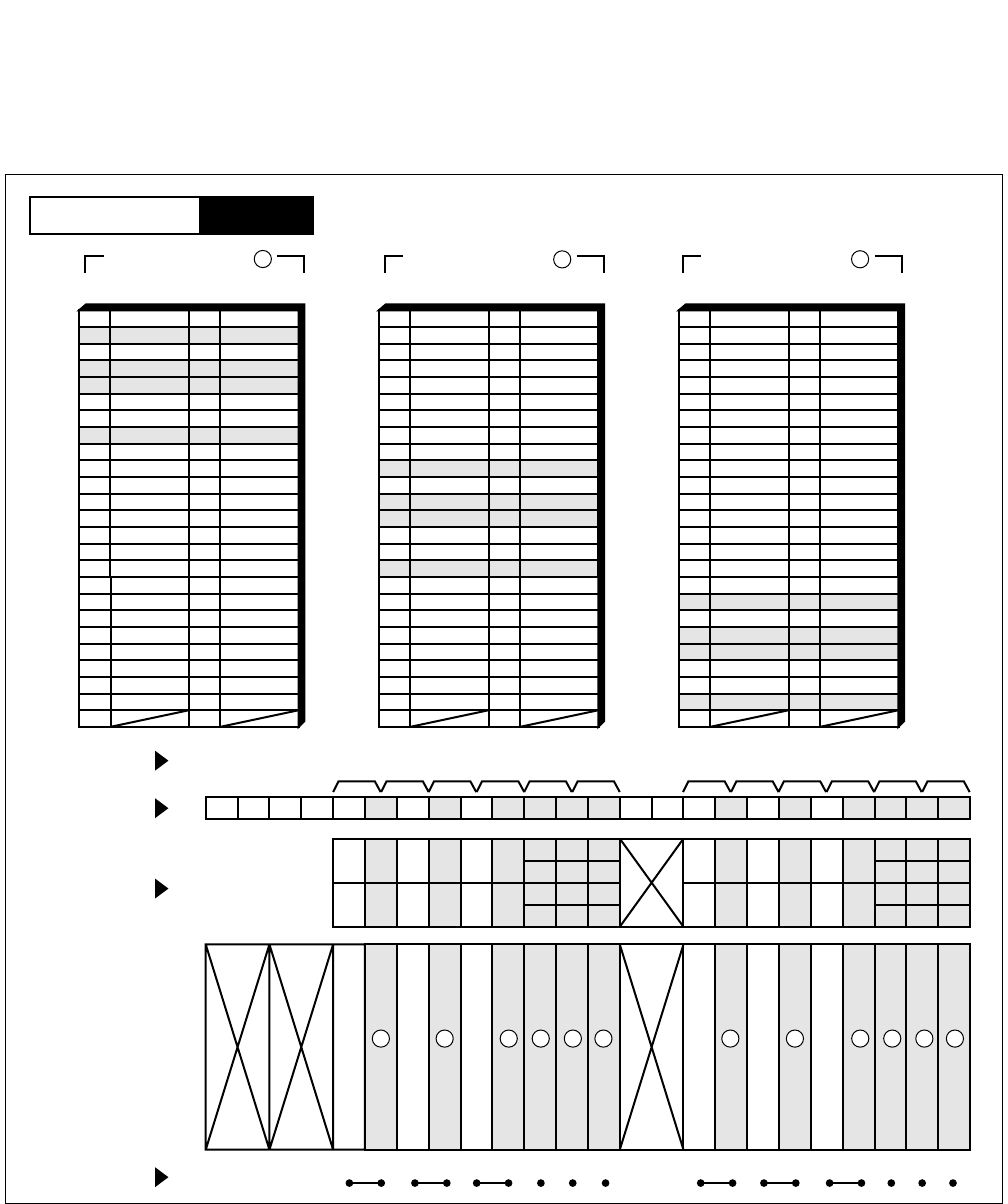
NDA-24296 CHAPTER 3
Page 615
Revision 1.0
PA-24DTR (DLI)
Digital Line Interface
6. External Interface
The leads appear as follows on the LT connectors.
Figure 3-193 LT Connector Lead Accommodation
See also Connecting Route Diagram (Figure 3-194).
PIM
Mounting Module
26
27
28
29
30
31
32
33
34
35
36
37
38
39
40
41
1
2
3
4
5
6
7
8
9
10
11
12
13
14
15
16
42
43
44
45
46
47
48
17
18
19
20
21
22
23
49
50 24
25
232221201918171615141312111009080706050403020100
LT6 LT7 LT8 LT9 LT10 LT11LT0 LT1 LT2 LT3 LT4 LT5
231915
221814
211713
201612
231915
221814
211713
201612
110907050301
100806040200
110907050301
100806040200
HW11HW10HW9HW8HW7HW6HW5HW4HW3HW2HW1HW0
Group No.
Slot No.
LT Connector
PIM
Highway Block
LT 3, 5, 9, 11 Connector
26
27
28
29
30
31
32
33
34
35
36
37
38
39
40
41
1
2
3
4
5
6
7
8
9
10
11
12
13
14
15
16
42
43
44
45
46
47
48
17
18
19
20
21
22
23
49
50 24
25
Accommodated in 2
LT 2, 4, 8, 10 Connector
Accommodated in 3
26
27
28
29
30
31
32
33
34
35
36
37
38
39
40
41
1
2
3
4
5
6
7
8
9
10
11
12
13
14
15
16
42
43
44
45
46
47
48
17
18
19
20
21
22
23
49
50 24
25
E
Accommodated in 1
LT 1, 5, 7, 11 Connector
E
RB RA
POUTB POUTA
TB TA
EE
RB RA
POUTB POUTA
TB TA
EE
RB RA
POUTB POUTA
TB TA
11
22
33 1 1
223 3
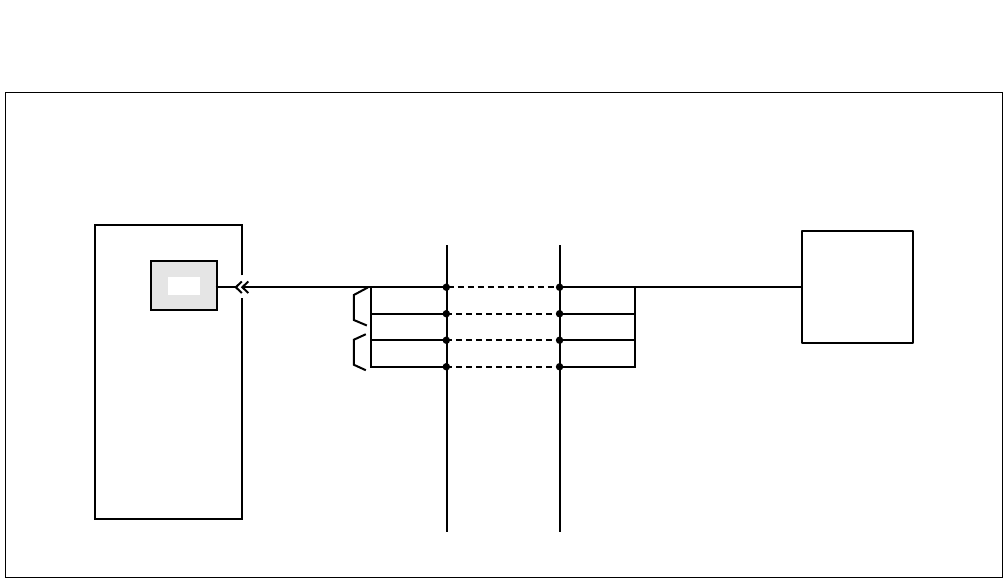
CHAPTER 3 NDA-24296
Page 616
Revision 1.0
PA-24DTR (DLI)
Digital Line Interface
Figure 3-194 Connecting Route Diagram
TA
TB
RA
RB
TA
RA
RB
TB
PBX
MDF
DLI TERMINAL
EQUIPMENT
OUT
IN
Connecting Route Diagram for the PA-24DTR (DLI) circuit card is as follows.
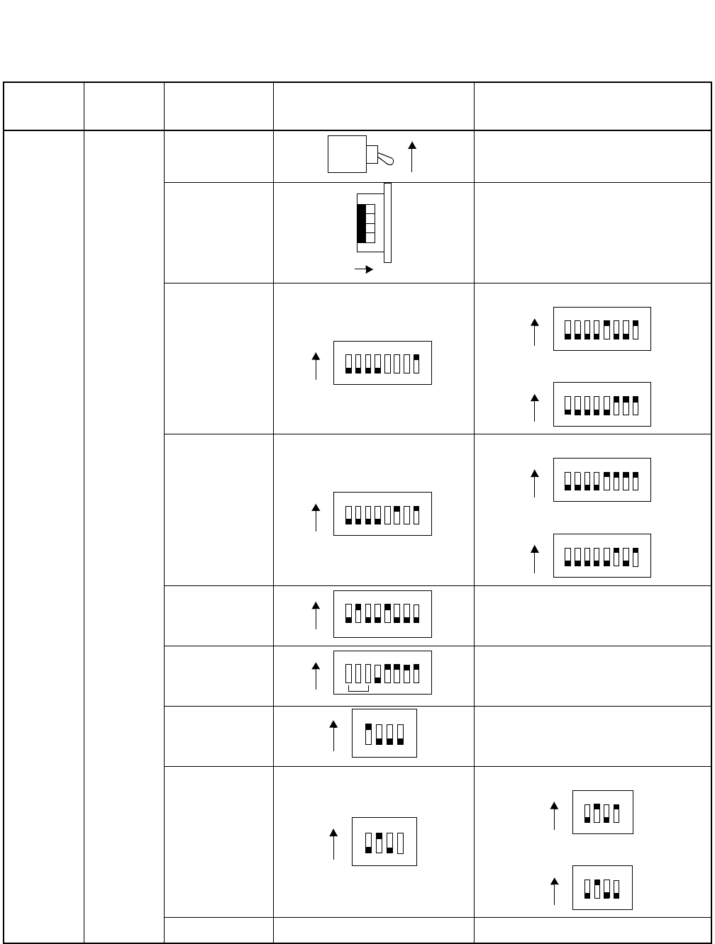
NDA-24296 CHAPTER 3
Page 617
Revision 1.0
PA-24DTR (DLI)
Digital Line Interface
7. Switch Setting Sheet
MODULE SLOT NO. SWITCH
NAME SWITCH SHAPE REMARKS
PIM SW00 (MB)
SW01/13B
SW10/4D •24-multiframe DLI Standard
•12-multiframe DLI Standard
SW11/39 •24-multiframe DLI Standard
•12-multiframe DLI Standard
SW13/6C
SW12/58 Note: Equalizer Setting
SW15/25
SW14/5D •24-multiframe DLI Standard
•12-multiframe DLI Standard
SW00/MB DOWN Circuit card make busy cancel
ON
ON
3
2
1
0
12345678
ON
12345678
ON
123456 7 8
ON
12345678
ON
12345678
ON
12345678
ON
12345678
ON
12345678
ON
Note
1
ON 2 3 4
1
ON 2 3 4
1234
ON
1234
ON

CHAPTER 3 NDA-24296
Page 618
Revision 1.0
This page is for your notes.
