Nec V850 Sc1 Users Manual IE 703089 MC EM1 In Circuit Emulator Option Board UM
V850SC1 to the manual 87b563de-522a-4dc3-ba61-cf1936a90293
2015-01-24
: Nec Nec-V850-Sc1-Users-Manual-331814 nec-v850-sc1-users-manual-331814 nec pdf
Open the PDF directly: View PDF ![]() .
.
Page Count: 35

User’s Manual
Target Devices
V850/SC1™
V850/SC2™
V850/SC3™
IE-703089-MC-EM1
In-Circuit Emulator Option Board
Document No. U15776EJ1V0UM00 (1st edition)
Date Published June 2002 N CP(K)
Printed in Japan
©2002
User’s Manual U15776EJ1V0UM
2
[MEMO]

User’s Manual U15776EJ1V0UM 3
V850/SC1, V850/SC2, and V850/SC3 are trademarks of NEC Corporation.
Windows is either a registered trademark or a trademark of Microsoft Corporation in the United States
and/or other countries.
PC/AT is a trademark of International Business Machines Corporation.
Ethernet is a trademark of Xerox Corporation.
M8E 00. 4
The information in this document is current as of May, 2002. The information is subject to change
without notice. For actual design-in, refer to the latest publications of NEC's data sheets or data
books, etc., for the most up-to-date specifications of NEC semiconductor products. Not all products
and/or types are available in every country. Please check with an NEC sales representative for
availability and additional information.
No part of this document may be copied or reproduced in any form or by any means without prior
written consent of NEC. NEC assumes no responsibility for any errors that may appear in this document.
NEC does not assume any liability for infringement of patents, copyrights or other intellectual property rights of
third parties by or arising from the use of NEC semiconductor products listed in this document or any other
liability arising from the use of such products. No license, express, implied or otherwise, is granted under any
patents, copyrights or other intellectual property rights of NEC or others.
Descriptions of circuits, software and other related information in this document are provided for illustrative
purposes in semiconductor product operation and application examples. The incorporation of these
circuits, software and information in the design of customer's equipment shall be done under the full
responsibility of customer. NEC assumes no responsibility for any losses incurred by customers or third
parties arising from the use of these circuits, software and information.
While NEC endeavours to enhance the quality, reliability and safety of NEC semiconductor products, customers
agree and acknowledge that the possibility of defects thereof cannot be eliminated entirely. To minimize
risks of damage to property or injury (including death) to persons arising from defects in NEC
semiconductor products, customers must incorporate sufficient safety measures in their design, such as
redundancy, fire-containment, and anti-failure features.
NEC semiconductor products are classified into the following three quality grades:
"Standard", "Special" and "Specific". The "Specific" quality grade applies only to semiconductor products
developed based on a customer-designated "quality assurance program" for a specific application. The
recommended applications of a semiconductor product depend on its quality grade, as indicated below.
Customers must check the quality grade of each semiconductor product before using it in a particular
application.
"Standard": Computers, office equipment, communications equipment, test and measurement equipment, audio
and visual equipment, home electronic appliances, machine tools, personal electronic equipment
and industrial robots
"Special": Transportation equipment (automobiles, trains, ships, etc.), traffic control systems, anti-disaster
systems, anti-crime systems, safety equipment and medical equipment (not specifically designed
for life support)
"Specific": Aircraft, aerospace equipment, submersible repeaters, nuclear reactor control systems, life
support systems and medical equipment for life support, etc.
The quality grade of NEC semiconductor products is "Standard" unless otherwise expressly specified in NEC's
data sheets or data books, etc. If customers wish to use NEC semiconductor products in applications not
intended by NEC, they must contact an NEC sales representative in advance to determine NEC's willingness
to support a given application.
(Note)
(1) "NEC" as used in this statement means NEC Corporation and also includes its majority-owned subsidiaries.
(2) "NEC semiconductor products" means any semiconductor product developed or manufactured by or for
NEC (as defined above).
•
•
•
•
•
•
User’s Manual U15776EJ1V0UM
4
Regional Information
Some information contained in this document may vary from country to country. Before using any NEC
product in your application, pIease contact the NEC office in your country to obtain a list of authorized
representatives and distributors. They will verify:
•
Device availability
•
Ordering information
•
Product release schedule
•
Availability of related technical literature
•
Development environment specifications (for example, specifications for third-party tools and
components, host computers, power plugs, AC supply voltages, and so forth)
•
Network requirements
In addition, trademarks, registered trademarks, export restrictions, and other legal issues may also vary
from country to country.
NEC Electronics Inc. (U.S.)
Santa Clara, California
Tel: 408-588-6000
800-366-9782
Fax: 408-588-6130
800-729-9288
NEC Electronics Hong Kong Ltd.
Hong Kong
Tel: 2886-9318
Fax: 2886-9022/9044
NEC Electronics Hong Kong Ltd.
Seoul Branch
Seoul, Korea
Tel: 02-528-0303
Fax: 02-528-4411
NEC Electronics Shanghai, Ltd.
Shanghai, P.R. China
Tel: 021-6841-1138
Fax: 021-6841-1137
NEC Electronics Taiwan Ltd.
Taipei, Taiwan
Tel: 02-2719-2377
Fax: 02-2719-5951
NEC Electronics Singapore Pte. Ltd.
Novena Square, Singapore
Tel: 253-8311
Fax: 250-3583
NEC do Brasil S.A.
Electron Devices Division
Guarulhos-SP, Brasil
Tel: 11-6462-6810
Fax: 11-6462-6829
J02.4
NEC Electronics (Europe) GmbH
Duesseldorf, Germany
Tel: 0211-65 03 01
Fax: 0211-65 03 327
• Sucursal en España
Madrid, Spain
Tel: 091-504 27 87
Fax: 091-504 28 60
Vélizy-Villacoublay, France
Tel: 01-30-67 58 00
Fax: 01-30-67 58 99
• Succursale Française
• Filiale Italiana
Milano, Italy
Tel: 02-66 75 41
Fax: 02-66 75 42 99
• Branch The Netherlands
Eindhoven, The Netherlands
Tel: 040-244 58 45
Fax: 040-244 45 80
• Branch Sweden
Taeby, Sweden
Tel: 08-63 80 820
Fax: 08-63 80 388
• United Kingdom Branch
Milton Keynes, UK
Tel: 01908-691-133
Fax: 01908-670-290

User’s Manual U15776EJ1V0UM 5
INTRODUCTION
Target Readers This manual is intended for users who design and develop application systems using
the V850/SC1, V850/SC2, and V850/SC3.
Purpose The purpose of this manual is to describe the proper operation of the IE-703089-MC-
EM1 and its basic specifications.
Organization This manual is divided into the following parts.
•Overview
• Names and functions of components
• Cautions
How to Read This Manual It is assumed that the reader of this manual has general knowledge in the fields of
electrical engineering, logic circuits, and microcontrollers.
The IE-703089-MC-EM1 is used connected to the IE-703002-MC in-circuit emulator.
This manual explains the basic setup procedure and switch settings of the IE-
703002-MC when it is connected to the IE-703089-MC-EM1. For the names and
functions of parts, and the connection of elements, refer to the IE-703002-MC User’s
Manual (U11595E).
To learn about the basic specifications and operation methods
→ Read this manual in the order of the CONTENTS.
To learn the operation methods and command functions, etc., of the IE-703002-MC
and IE-703089-MC-EM1
→ Read the user’s manual of the debugger (sold separately) that is used.
Conventions Note: Footnote for item marked with Note in the text
Caution: Information requiring particular attention
Remark: Supplementary information
Numeral representation: Binary … xxxx or xxxxB
Decimal … xxxx
Hexadecimal … xxxxH
Prefix indicating the power of 2 (address space, memory capacity):
K (kilo): 210 = 1024
M (mega): 220 = 10242
Terminology The meanings of terms used in this manual are listed below.
Emulation CPU The CPU that executes the program prepared by the user in the
emulator.
Target device The device that is targeted for emulation.
Target system The system (user-built system) that is targeted for debugging. This
includes the target program and user-configured hardware.
IE system The combination of the IE-703002-MC and IE-703089-MC-EM1

User’s Manual U15776EJ1V0UM
6
Related Documents When using this manual, refer to the following manuals.
The related documents indicated in this publication may include preliminary versions.
However, preliminary versions are not marked as such.
{Documents related to development tools (user’s manuals)
Document Name Document
Number
IE-703002-MC In-circuit emulator U11595E
IE-703089-MC-EM1 In-circuit emulator option board This manual
Operation To be prepared
C Language U16054E
PM Plus To be prepared
CA850 C Compiler package Ver. 2.40
Assembly Language U16042E
ID850 Integrated debugger Ver.2.40 Operation WindowsTM based U15181E
SM850 System simulator Ver.2.40 Operation Windows based U15182E
SM850 System simulator Ver.2.00 or
later
External Part User Open
Interface Specifications
U14873E
Basics U13430E
Installation U13410E
RX850 Real-time OS Ver.3.13 or later
Technical U13431E
Basics U13773E
Installation U13774E
RX850 Pro Real-time OS Ver.3.13
Technical U13772E
RD850 Task debugger Ver.3.01 U13737E
RD850 Pro Task debugger Ver.3.01 U13916E
AZ850 System performance analyzer Ver.3.0 U14410E
PG-FP4 Flash Memory Programmer U15260E
User’s Manual U15776EJ1V0UM 7
CONTENTS
CHAPTER 1 OVERVIEW.........................................................................................................................10
1.1 Hardware Configuration............................................................................................................................... 10
1.2 Features (When Connected to IE-703002-MC) ........................................................................................... 11
1.3 Function Specifications (When Connected to IE-703002-MC).................................................................. 11
1.4 System Configuration .................................................................................................................................. 12
1.5 Contents in Carton ....................................................................................................................................... 13
1.6 Connection Between IE-703002-MC and IE-703089-MC-EM1.................................................................... 15
CHAPTER 2 NAMES AND FUNCTIONS OF COMPONENTS ...............................................................19
2.1 Component Names and Functions of IE-703089-MC-EM1 ........................................................................ 20
2.2 Clock Settings............................................................................................................................................... 23
2.2.1 Main clock setting ............................................................................................................................. 23
2.2.2 Subclock setting ............................................................................................................................... 24
2.3 Illegal Access Detection ROM Setting ........................................................................................................ 25
2.4 CPU Operation Voltage Range Switching Setting ..................................................................................... 25
2.5 Address Output Setting of Separate Bus ................................................................................................... 26
CHAPTER 3 FACTORY SETTINGS........................................................................................................27
CHAPTER 4 CAUTIONS .........................................................................................................................28
4.1 VDD and PORTVDD of Target System............................................................................................................ 28
4.2 I/O Signal ....................................................................................................................................................... 29
4.3 VPP Signal ...................................................................................................................................................... 29
4.4 NMI Signal Mask Function ........................................................................................................................... 29
CHAPTER 5 DIFFERENCES BETWEEN TARGET DEVICE AND TARGET INTERFACE CIRCUIT....30
APPENDIX PACKAGE DRAWINGS ........................................................................................................33

User’s Manual U15776EJ1V0UM
8
LIST OF FIGURES
Figure No. Title Page
1-1 System Configuration ........................................................................................................................................12
1-2 Contents in Carton.............................................................................................................................................13
1-3 Accessories .......................................................................................................................................................14
1-4 Connection Between IE-703002-MC and IE-703089-MC-EM1..........................................................................16
1-5 Connection of IE-703089-MC-EM1 and SWEX-144SD-1..................................................................................18
2-1 IE-703089-MC-EM1 ...........................................................................................................................................20
2-2 SW5 ...................................................................................................................................................................26
4-1 Schematic Diagram of Power Supply Acquisition ..............................................................................................28
4-2 I/O Signal Flow Path ..........................................................................................................................................29
5-1 Equivalent Circuit of Emulation Circuit...............................................................................................................31

User’s Manual U15776EJ1V0UM 9
LIST OF TABLES
Table No. Title Page
2-1 Main Clock Setting.............................................................................................................................................23
2-2 Subclock Setting................................................................................................................................................24
2-3 JP1 Setting in IE-703002-MC ............................................................................................................................25
2-4 JP3 and JP4 Setting in IE-703002-MC..............................................................................................................25
2-5 SW5 Setting.......................................................................................................................................................26
User’s Manual U15776EJ1V0UM
10
Option board
(IE-703089-MC-EM1)
By adding this board, the IE-703002-MC can be used as in-circuit
emulator for V850/SC1, V850/SC2, and V850/SC3.
Probe SWEX-144SD-1Note 1 General-purpose probe made by TOKYO ELETECH CORPORATION
PC interface board
IE-70000-PC-IF-C Note 2
IE-70000-98-IF-C Note 2
IE-70000-PCI-IF-A
IE-70000-CD-IF-A
This board is used to connect the IE-703002-MC to a personal
computer. This board is inserted in the expansion slot of the
personal computer.
IE-70000-PC-IF-C: For IBM PC/ATTM compatible ISA bus
IE-70000-98-IF-C: For PC-9800 series C bus
IE-70000-PCI-IF-A: For PCI bus
IE-70000-CD-IF-A: For PCMCIA socket
Network module
(IE-70000-MC-SV3)
This module is used when a workstation controls the IE-703002-MC
via Ethernet™.
Power adapter
(IE-70000-MC-PS-B)
AC adapter for in-circuit emulator made by NEC Corporation.
Separately-sold hardware
CHAPTER 1 OVERVIEW
The IE-703089-MC-EM1 is an option board for the IE-703002-MC in-circuit emulator. By connecting the IE-
703089-MC-EM1 and IE-703002-MC, hardware and software can be debugged efficiently in system development
using the V850/SC1, V850/SC2, and V850/SC3.
In this manual, the basic setup procedure and switch settings of the IE-703002-MC when the IE-703089-MC-EM1
is connected are described. For the names and functions of the parts of the IE-703002-MC, and for the connection of
elements, refer to the IE-703002-MC User’s Manual (U11595E).
1.1 Hardware Configuration
Notes 1. For further information, contact Daimaru Kogyo Co., Ltd.
Tokyo Electronics Department (TEL +81-3-3820-7112)
Osaka Electronics Department (TEL +81-6-6244-6672)
2. Cannot be used for PC98-NX series
Optional hardware
Separately-sold hardware
In-circuit emulator (IE-703002-MC)

CHAPTER 1 OVERVIEW
User’s Manual U15776EJ1V0UM 11
1.2 Features (When Connected to IE-703002-MC)
{Maximum operating frequency: 20 MHz (at 5.0 V operation)
{The following pins can be masked.
RESET, NMI, WAIT, HLDRQ
{External bus interface
{Connected to target system via following method:
• Attach a probe (sold separately) to the pod tip for connection
{The dimensions of the IE-703089-MC-EM1 are as follows.
Parameter Value
Power consumption (max. value at 5.0 V supply voltage) 2.5 W (at 20 MHz operation frequency)Note
Height 50 mm
Length 180 mm
External dimensions
(Refer to APPENDIX PACKAGE
DRAWINGS)Width 250 mm
Weight 300 g
Note 12.5 W when the IE-703002-MC is connected to the IE-703089-MC-EM1
1.3 Function Specifications (When Connected to IE-703002-MC)
Parameter Specification
Internal ROM 512 KB
In ROMless mode 2 MB
Emulation memory capacity
External memory
When using iROM 1 MB
Internal ROM 512 KB
In ROMless mode 2 MB
Coverage memory capacity for
execution/pass detection External memory
When using iROM 1 MB
Coverage memory capacity for
memory access detection
External memory 1 MB
Internal ROM 512 KB
In ROMless mode 2 MB
Coverage memory capacity for
branching entry number counting External memory
When using iROM 1 MB
Trace memory capacity 150 bits × 32 K frames
Time measurement function Measurement possible by time tag or 3 timers
4-bit external trace possibleExternal logic probe
Event setting of trace/break possible
Event break
Step execution break
Forcible break
Break function
Fail safe break
•Illegal access to peripheral I/O
•Access to guard space
•Write to ROM space
Caution Some of the functions may not be supported, depending on the debugger used.

CHAPTER 1 OVERVIEW
User’s Manual U15776EJ1V0UM
12
1.4 System Configuration
The system configuration when connecting the IE-703002-MC to the IE-703089-MC-EM1 and a personal computer
is shown below.
Figure 1-1. System Configuration
[Magnified drawing: Example of use
of connector for target connection]
Target
system
<13>
<14>
<12>
<5> <6> <7>
<4>
<3>
<1>, <2>
<9>
<11>
Target system
<10>
<11>
<8>
<15>
<12>
Remark
<1> Personal computer
<2> Debugger (ID850: Sold separately)
<3> PC interface board
(IE-70000-98-IF-C/IE-70000-PC-IF-C, IE-70000-PCI-IF-A/IE-70000-CD-IF-A: Sold separately)
<4> PC interface cable (included with IE-703002-MC)
<5> In-circuit emulator (IE-703002-MC: Sold separately)
<6> In-circuit emulator option board (IE-703089-MC-EM1: This product)
<7> External logic probe (included with IE-703002-MC)
<8> Socket for target connection (YQSOCKET144SDN: Sold separately)
<9> Probe (SWEX-144SD-1)
<10> Guide screw (YQGUIDE: Included)
<11> Connector for emulator connection (YQPACK144SD: Included)
<12> Connector for target connection (NQPACK144SD: Included)
<13> Power adapter (IE-70000-MC-PS-B: Sold separately)
<14> AC100V power cable (sold separately: Included with IE-70000-MC-PS-B)
<15> AC220V power cable (sold separately: Included with IE-70000-MC-PS-B)

CHAPTER 1 OVERVIEW
User’s Manual U15776EJ1V0UM 13
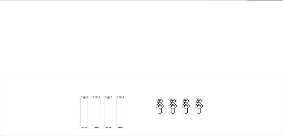
1.5 Contents in Carton
The carton of the IE-703089-MC-EM1 contains the main unit, guarantee card, packing list, and accessory bag.
Make sure that the accessory bag contains this manual and the connector accessories. If there are missing or
damaged items, please contact an NEC sales representative or an NEC distributor.
Return the guarantee card included in the carton after filling in all the items.
Figure 1-2. Contents in Carton
<1> IE-703089-MC-EM1
<2> Accessory bag
<3> Guarantee card
<4> Packing list
<1> IE-703089-MC-EM1 × 1
<2> Accessory bag × 1
<3> Guarantee card × 1
<4> Packing list × 1
CHAPTER 1 OVERVIEW
User’s Manual U15776EJ1V0UM
14
Check that the accessory bag contains this manual, an accessory list (× 1), and the following accessories.
(a) Spacers × 4
(b) SEMS screws × 4
Figure 1-3. Accessories
(a) Spacers (b) SEMS screws

CHAPTER 1 OVERVIEW
User’s Manual U15776EJ1V0UM 15
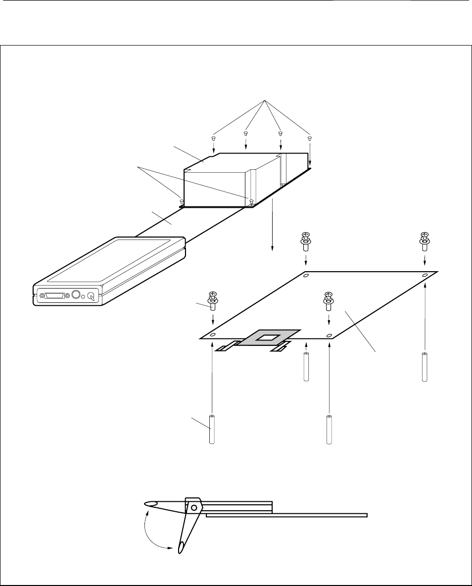
1.6 Connection Between IE-703002-MC and IE-703089-MC-EM1
The procedure for connecting the IE-703002-MC and IE-703089-MC-EM1 is described below.
Caution Connect carefully so as not to break or bend connector pins.
<1> Remove the pod cover (lower) of the IE-703002-MC.
<2> Set the PGA socket lever of the IE-703089-MC-EM1 to the OPEN position as shown in Figure 1-4 (b).
<3> Connect the IE-703089-MC-EM1 to the PGA socket at the back of the IE-703002-MC pod (refer to Figure 1-4
(c)). When connecting, position the IE-703002-MC and IE-703089-MC-EM1 so that they are horizontal.
<4> Set the PGA socket lever of the IE-703089-MC-EM1 to the CLOSE position as shown in Figure 1-4 (b).
<5> When connecting the probe (SWEX-144SD-1) to the IE-703089-MC-EM1, attach it to CN1 on the rear of the
IE-703089-MC-EM1, aligning each pin 1 (refer to Figure 1-5).
<6> Place the supplied spacers in the four corner holes of the IE-703089-MC-EM1. Fix the spacers with the
supplied SEMS screws.
<7> Fix the IE-703002-MC pod cover (upper) with nylon rivets.
CHAPTER 1 OVERVIEW
User’s Manual U15776EJ1V0UM
16
Figure 1-4. Connection Between IE-703002-MC and IE-703089-MC-EM1 (1/2)
(a) Overview
IE-703002-MC
IE-703089-MC-EM1
Nylon rivets
Upper cover
SEMS screw
Spacer
Nylon rivets
(b) PGA socket lever of IE-703089-MC-EM1
CLOSE
OPEN
CHAPTER 1 OVERVIEW
User’s Manual U15776EJ1V0UM 17
Figure 1-4. Connection Between IE-703002-MC and IE-703089-MC-EM1 (2/2)
(c) Connecting part (CN2 of IE-703089-MC-EM1)
Pin A1 position
: Insertion guide
: IE-703002-MC insertion area

CHAPTER 1 OVERVIEW
User’s Manual U15776EJ1V0UM
18
Figure 1-5. Connection of IE-703089-MC-EM1 and SWEX-144SD-1
CN1
IE-703089-MC-EM1
SWEX-144SD-1
Mount on the rear
1
1
User’s Manual U15776EJ1V0UM 19
CHAPTER 2 NAMES AND FUNCTIONS OF COMPONENTS
This chapter describes the names, functions, and switch settings of components in the IE-703089-MC-EM1.
For the details of the pod, jumper, and switch positions, etc., refer to the IE-703002-MC User’s Manual
(U11595E).
CHAPTER 2 NAMES AND FUNCTIONS OF COMPONENTS
User’s Manual U15776EJ1V0UM
20
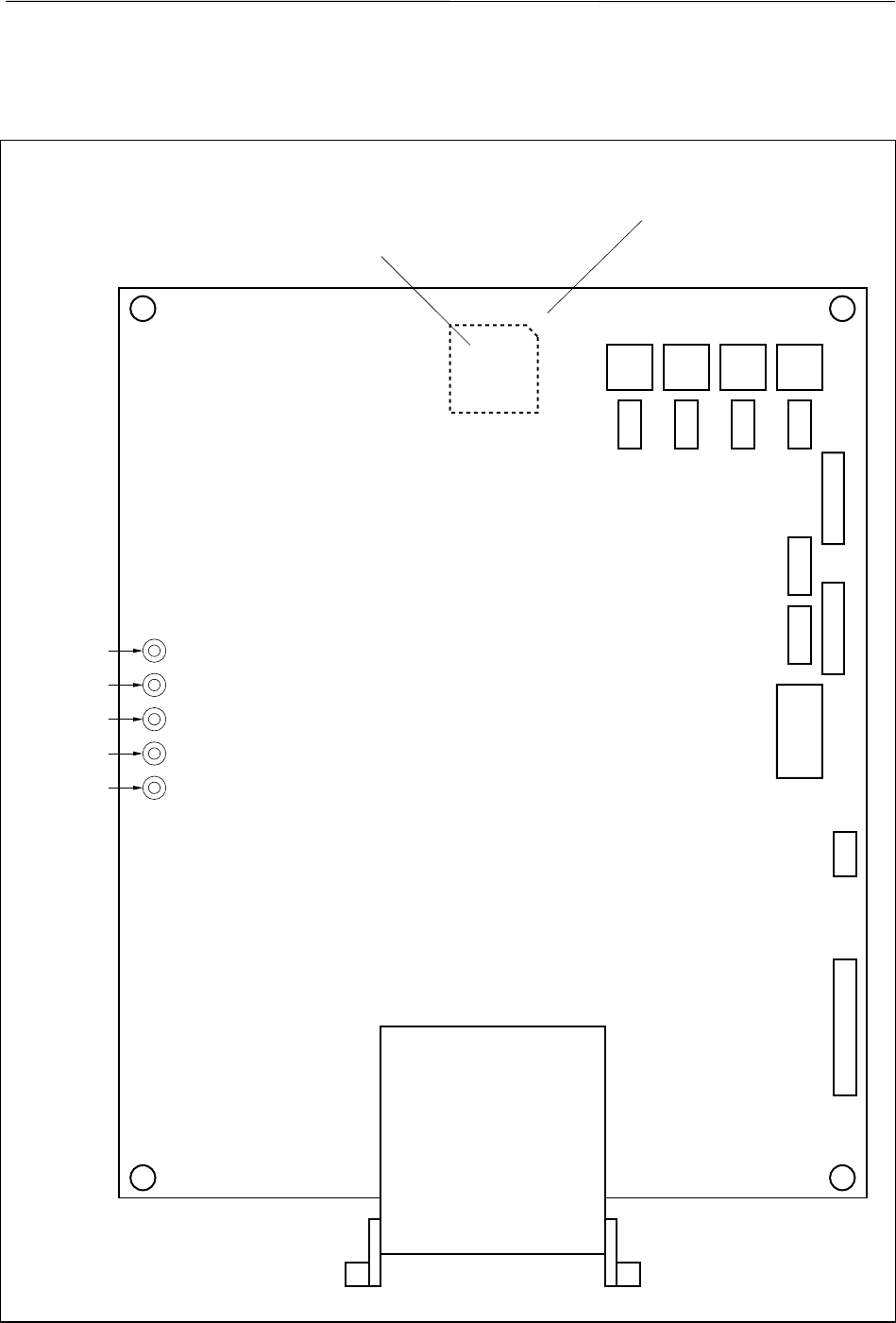
2.1 Component Names and Functions of IE-703089-MC-EM1
Figure 2-1. IE-703089-MC-EM1
<Top view>
JP1 SW1
CN1
CN2
JP4
OSC1
JP5JP6SW5
VER.1.
IE-703089-MC-EM1
No.
SW4
JP3 SW3
JP2 SW2
OSC2
LED5
Direction of pin 1 of connector
for target connection
ADCV
DD
Connector for target connection (rear)
LED4
LED3
LED2
LED1
Connector for
IE-703002-MC
connection
PORTV
DD2
PORTV
DD1
PORTV
DD0
V
DD

CHAPTER 2 NAMES AND FUNCTIONS OF COMPONENTS
User’s Manual U15776EJ1V0UM 21
(1) OSC1
OSC1 is a socket for the main clock crystal oscillator and for mounting capacitors. (For details, refer to 2.2.1
Main clock setting).
(2) JP5
JP5 is a jumper to switch the main clock supply source. (For details, refer to 2.2.1 Main clock setting.)
(3) OSC2
OSC2 is a socket for the main clock crystal oscillator and for mounting capacitors. (For details, refer to 2.2.2
Subclock setting.)
(4) JP6
JP6 is a jumper to switch the subclock supply source. (For details, refer to 2.2.2 Subclock setting.)
(5) JP1
Reserved. Use this jumper with the factory setting (2-3 shorted).
(6) SW1
Reserved. Use this switch with the factory setting (3-6 side).
(7) JP2
Reserved. Use this jumper with the factory setting (2-3 shorted).
(8) SW2
Reserved. Use this switch with the factory setting (3-6 side).
(9) JP3
Reserved. Use this jumper with the factory setting (2-3 shorted).
(10) SW3
Reserved. Use this switch with the factory setting (3-6 side).
(11) JP4
Reserved. Use this jumper with the factory setting (2-3 shorted).
(12) SW4
Reserved. Use this switch with the factory setting (3-6 side).
(13) SW5
SW5 is a switch to output the addresses (A1 to A15) of the separate bus. (For details, refer to 2.5 Address
Output Setting of Separate Bus.)

CHAPTER 2 NAMES AND FUNCTIONS OF COMPONENTS
User’s Manual U15776EJ1V0UM
22
(14) LED1 to LED5
Lit: Power is supplied by the target system.
Not lit: Power is supplied by the power supply inside the emulator.
LED1: VDD
LED2: PORTVDD0
LED3: PORTVDD1
LED4: PORTVDD2
LED5: ADCVDD
(15) Connector for IE-703002-MC connection (CN2)
CN2 is a connector to connect the IE-703089-MC-EM1 to the IE-703002-MC.
(16) Connector for target connection (CN1)
CN1 is a connector to connect the IE-703089-MC-EM1 to the probe.
CHAPTER 2 NAMES AND FUNCTIONS OF COMPONENTS
User’s Manual U15776EJ1V0UM 23
2.2 Clock Settings
This section describes the clock settings.
For the position of OSC1 and JP5 in the IE-703089-MC-EM1, refer to Figure 2-1.
For the jumper and switch positions in the IE-703002-MC, refer to the IE-703002-MC User’s Manual (U11595E).
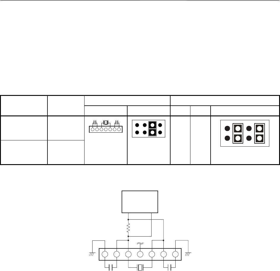
2.2.1 Main clock setting
Table 2-1. Main Clock Setting
IE-703089-MC-EM1 Setting IE-703002-MC SettingEmulator Usage
Environment
Clock Supply
Method OSC1 JP5 SW1 SW2 JP2
When using
emulator as
standalone unit
Internal clock
When using
emulator with
target system
Internal clock
17
(Oscillator mounted)
7
8
1
2
(3-4 shorted: Fixed)
ON OFF
1
7
82
Caution Emulation cannot be performed by inputting a clock from the target system.
The specifications of OSC1 are as follows.
GND
1 MΩ
GND
V850/SCx
I/O
chip
X1 X2
1
10 pF 20 MHz
7
10 pF
CHAPTER 2 NAMES AND FUNCTIONS OF COMPONENTS
User’s Manual U15776EJ1V0UM
24
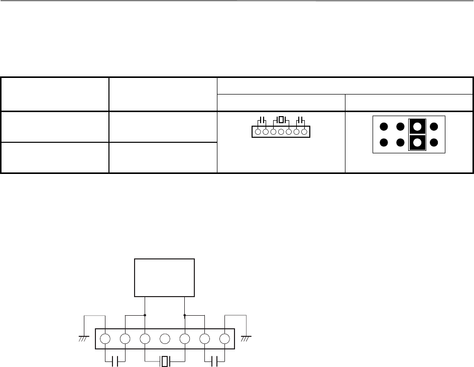
2.2.2 Subclock setting
Table 2-2. Subclock Setting
IE-703089-MC-EM1 SettingEmulator Usage
Environment
Clock Supply Method
OSC2Note 2 JP6
When using emulator as
standalone unit
Internal clockNote 1
When using emulator with
target system
Internal clockNote 1 17
(Oscillator mounted)
7
8
1
2
(3-4 shorted: Fixed)
Notes 1. A clock input by an oscillator cannot be used for the internal clock.
2. To use a subclock frequency other than 32.768 kHz, remove the resonator on OSC2 and mount an
oscillator.
The specifications of OSC2 are as follows.
GND GND
V850/SCx
I/O chip
XT2 XT1
1
27 pF 32.768 kHz
7
27 pF
Caution Emulation cannot be performed by inputting a clock from the target system.
CHAPTER 2 NAMES AND FUNCTIONS OF COMPONENTS
User’s Manual U15776EJ1V0UM 25
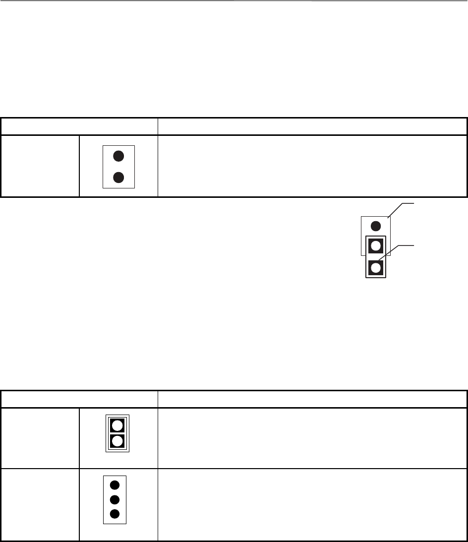
2.3 Illegal Access Detection ROM Setting
If using the IE-703002-MC for an in-circuit emulator for the V850/SCx by connecting the IE-703089-MC-EM1, set
JP1 of the IE-703002-MC as follows.
Table 2-3. JP1 Setting in IE-703002-MC
JP1 Description
OpenNote Illegal access detection ROM (mounted on IE-703089-MC-EM1) for V850/SCx is
used.
Note When JP1 is set to open, keep the removed jumper contact attached to one
pin as shown in the drawing on the right.
JP1
Jumper
contact
2.4 CPU Operation Voltage Range Switching Setting
If using the IE-703002-MC for an in-circuit emulator for the V850/SCx by connecting the IE-703089-MC-EM1, set
JP3 and JP4 of the IE-703002-MC as follows.
Table 2-4. JP3 and JP4 Setting in IE-703002-MC
JP3, JP4 Description
JP3
(Shorted)
1
2
The operation voltage range of the IE-703002-MC is 3.0 to 5.5 V.
JP4
1
2
3
(Open)
The power supply for PORTVDD is generated on the IE-703089-MC-EM1.
CHAPTER 2 NAMES AND FUNCTIONS OF COMPONENTS
User’s Manual U15776EJ1V0UM
26
2.5 Address Output Setting of Separate Bus
When using the separate bus function while debugging using the IE-703089-MC-EM1, switching to the separate
bus output function is not possible by setting the memory address output register (MAM) by software.
Use DIP switch SW5 to output the address of the separate bus function while debugging using the IE-703089-MC-
EM1.
The switches of SW5 and their corresponding ports are shown in Table 2-5.
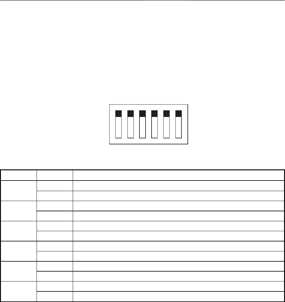
Figure 2-2. SW5
163425
ON
OFF
Table 2-5. SW5 Setting
Switch Setting Selection of Alternate-Function Pin
ON P113 to P110 (port mode)1
OFF A4 to A1 output to P113 to P110 (memory address output function of separate bus)
ON P103 to P100 (port mode)2
OFF A8 to A5 output to P103 to P100 (memory address output function of separate bus)
ON P107 to P104 (port mode)3
OFF A12 to A9 output to P107 to P104 (memory address output function of separate bus)
ON P34 (port mode)4
OFF A13 output to P34 (memory address output function of separate bus)
ON P35 (port mode)5
OFF A14 output to P35 (memory address output function of separate bus)
ON P33 (port mode)6
OFF A15 output to P33 (memory address output function of separate bus)

User’s Manual U15776EJ1V0UM 27
CHAPTER 3 FACTORY SETTINGS
Item Description Remark
OSC1
GND
1 MΩ
GND
V850/SCx
I/O chip
X1 X2
1
10 pF 20 MHz
7
10 pF
Pins 1 and 2: For mounting capacitor (10 pF)
Pins 6 and 7: For mounting capacitor (10 pF)
Pins 3 to 5: Crystal oscillator (20 MHz)
Pin 4: Open
20 MHz clock supplied for main clock
OSC2
GND GND
V850/SCx
I/O chip
XT2 XT1
1
27 pF 32.768 kHz
7
27 pF
Pins 1 and 2: For mounting capacitor (27 pF)
Pins 6 and 7: For mounting capacitor (27 pF)
Pins 3 to 5: Crystal oscillator (32.768 MHz)
Pin 4: Open
32.768 MHz clock supplied for subclock
JP1 to JP4
123
(2-3 shorted)
Pins 2 and 3: Short
Pin 1: Open
Use these jumpers with the factory settings.
JP5, JP6
1
2
7
8
(3-4 shorted)
Pins 1 and 2: Open
Pins 3 and 4: Shorted
Pins 5 and 6: Open
Pins 7 and 8: Open
Use these jumpers with the factory settings.
SW1 to SW4
1
6
3
4
(3-6 side)
3-6 side
Use these switches with the factory settings.
SW5
163425
ON
OFF
All bits ON (port mode)
User’s Manual U15776EJ1V0UM
28
CHAPTER 4 CAUTIONS
4.1 VDD and PORTVDD of Target System
(1) VDD in the target system is used to sense the level for target system power supply ON/OFF.
• When VDD is lower than 3.5 V, it is judged that the target system is not connected, and mapping of the
target memory cannot be performed with a debugger (FCAN cannot be used).
• When VDD is 3.5 V or higher, it is judged that the target system is connected, and mapping of the target
memory can be performed with a debugger (FCAN can be used).
(2) PORTVDDn (n = 0 to 2) in the target system is not supplied directly to the emulator chip; it is connected to the
target voltage emulation circuit.
• When PORTVDDn is lower than 3.3 V, VCC (5 V) in the internal emulator is supplied to the emulator chip.
• When PORTVDDn is 3.3 V or higher, a voltage of the same potential as PORTVDDn in the target system is
generated and supplied to the emulator chip.
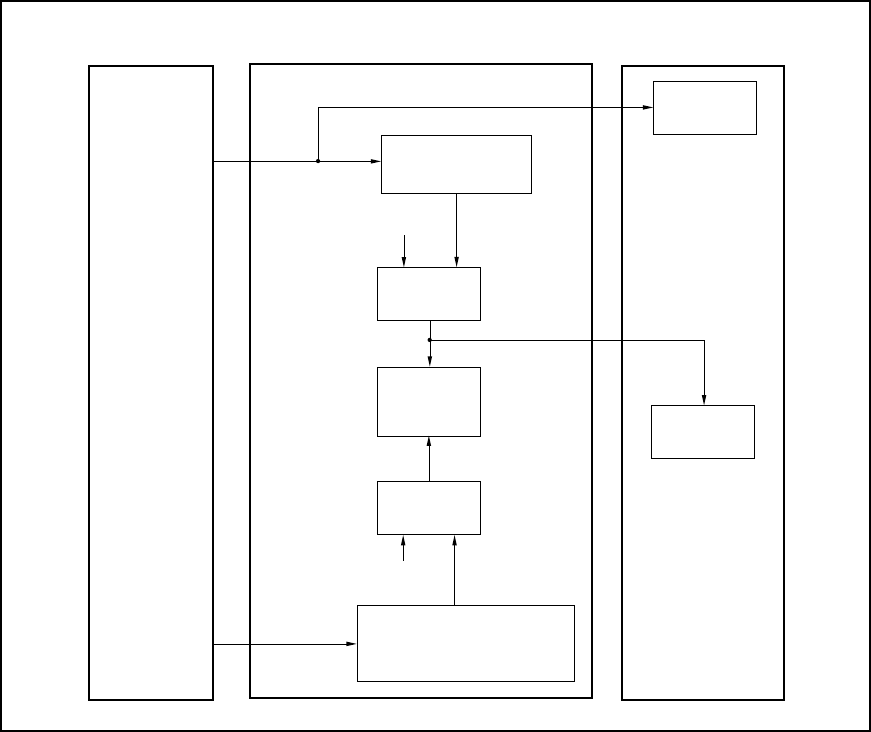
Figure 4-1. Schematic Diagram of Power Supply Acquisition
Relay n
(n = 0 to 2)
V850/SC3
I/O chip
Target voltage emulation n
(n = 0 to 2)
ON/OFF?
V
CC
(5 V)
PORTV
DDn
(n = 0 to 2)
V
DD0
IE-703089-MC-EM1 IE-703002-MC
Relay
Target voltage
emulation
V
CC
(5 V)
Evaluation
chip
Target system
CHAPTER 4 CAUTIONS
User’s Manual U15776EJ1V0UM 29
(3) The VDD1 signal from the target system is left open in the IE-703089-MC-EM1.
(4) The following conditions must be satisfied when other than VDD0 = VDD1 = ADCVDD = PORTVDD1 = PORTVDD2.
1. When FCAN is used, PORTVDD1 ≤ PORTVDD2 (restricted by the power supply voltage conditions of the in-
circuit emulator)
2. When ADC is used, VDD0 = ADCVDD = 4.5 to 5.5 V
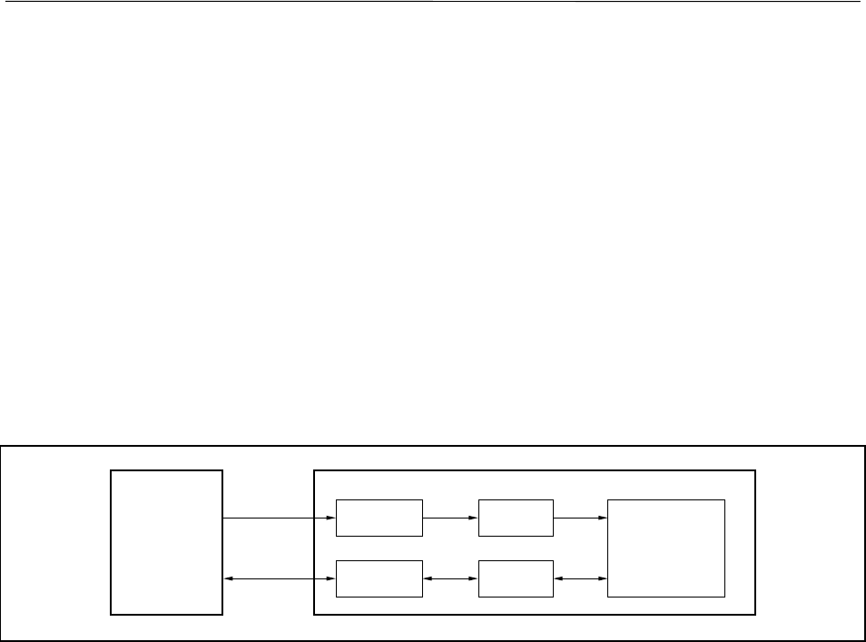
4.2 I/O Signal
The input signal (NMI signal) from the target system, the I/O signals for ports 4, 5, 6, and 11, and the I/O signal for
port 9 are all delayed (tPD = 0.25 ns (typ.)) because they pass through Q switches QS3125, QS3384, and QS3244,
respectively, before being input to the emulator chip.
The DC characteristics also change. The input voltage becomes VIH = 2.0 V (MIN.), VIL = 0.8 V (MAX.), and the
input current becomes IIN = ±0.5
µ
A (MAX.).
Figure 4-2. I/O Signal Flow Path
NMI pin QS3125
IE-703089-MC-EM1
Port pin QS3384/
QS3244
Target
system Emulator chip
NMI signal
Port signal
4.3 VPP Signal
The VPP signal from the target system is left open in the emulator.
4.4 NMI Signal Mask Function
When using the P00/NMI pin in the port mode, do not mask the NMI signal.

User’s Manual U15776EJ1V0UM
30
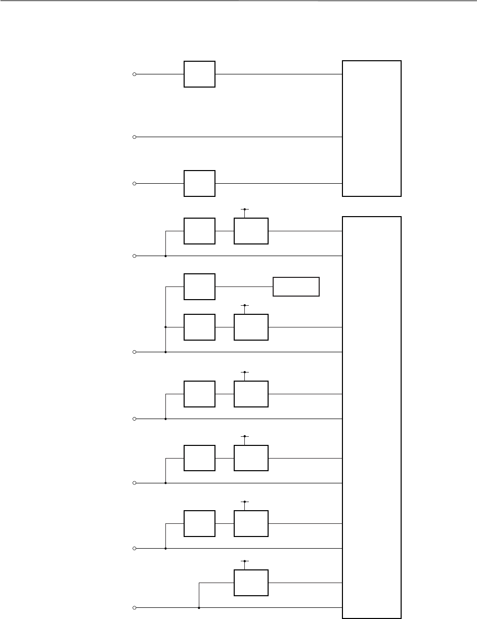
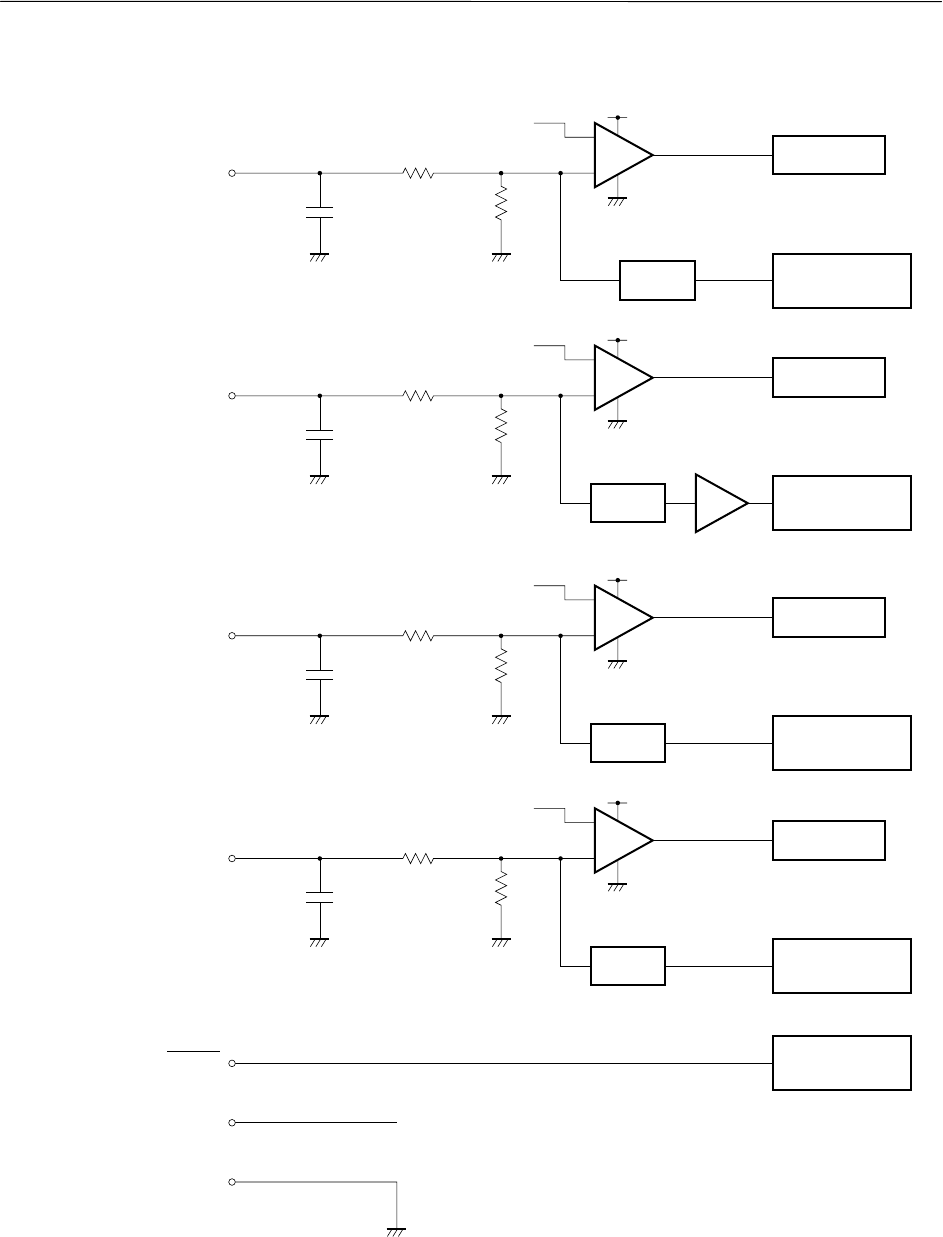
CHAPTER 5 DIFFERENCES BETWEEN TARGET DEVICE AND TARGET INTERFACE CIRCUIT
Differences between the signal lines of the target device and the signal lines of the IE-703089-MC-EM1 target
interface circuit are described in this chapter.
The target device is a CMOS circuit, whereas the target interface circuit of the IE-703089-MC-EM1 is configured
with an emulation circuit such as a gate array TTL or CMOS-IC.
When debugging the IE system connected to the target system, the IE system emulates as if the real target device
is operating on the target system.
Small differences occur however, because the IE system is emulating actual operation.
(1) Signals input/output to/from the emulation gate array
• P47 to P40
• P57 to P50
• P67 to P60
• P97 to P90
• P117 to P110
• P133 to P130
(2) Other signals
• P07 to P00
• P17 to P10
• P27 to P20
• P37 to P30
• P77 to P70
• P83 to P80
• P107 to P100
• P127 to P120
• P147 to P140
• P157 to P150
• P176 to P170
• V
DD0
• PORTVDD0, PORTVDD1, PORTVDD2, ADCVDD
• CLKOUT
• RESET
• VDD1
• MODE/VPP
• CPUREG
• X1, X2, XT1, XT2
• GND0, GND1, GND2, PORTGND0, PORTGND1, ADCGND
Figure 5-1 shows the signals in (1) and (2) above in the circuit for the IE system.
CHAPTER 5 DIFFERENCES BETWEEN TARGET DEVICE AND TARGET INTERFACE CIRCUIT
User’s Manual U15776EJ1V0UM 31
Figure 5-1. Equivalent Circuit of Emulation Circuit (1/2)
QS3125
QS3244
VHC125
PORTV
DD0
IN/OUT
IN/OUT
QS3257
IN/OUT
IN
OUT
PORTV
DD0
PORTV
DD0
PORTV
DD1
PORTV
DD1
PORTV
DD2
QS3244
VHC244
VHC125
IN
OUT
QS3384
OR3T125
(FPGA)
IE system sideProbe side
P00,
P36 to P34
P107 to P100
P67 to P60
P96 to P90
P113 to P110
P117 to P114
P133 to P130
P47 to P40,
P57 to P50
P07 to P01,
P17 to P10,
P27 to P20,
P37 to P30,
P77 to P70,
P83 to P80,
P127 to P120,
P147 to P140,
P157 to P150,
P176 to P170
VHC125
IN
OUT
QS3257
VHC125
IN
OUT
QS3244
VHC125
IN
OUT
VHC125
IN
OUT
PD703091
PD70F3089Y
emulation
CPU
µ
µ
CHAPTER 5 DIFFERENCES BETWEEN TARGET DEVICE AND TARGET INTERFACE CIRCUIT
User’s Manual U15776EJ1V0UM
32
Figure 5-1. Equivalent Circuit of Emulation Circuit (2/2)
PORTV
DD1
PORTV
DD2
V
CC
V
DD0
V
DD
100 Ω
3.5 V
1 MΩ
PC339
PC741
PD70F3089Y
emulation CPU
PD70F3089Y
emulation CPU
PD70F3089Y
emulation CPU
PD703091
emulation CPU
100 F
V
CC
PORTV
DD0
100 Ω
3.3 V
1 MΩ
PC393
100 F
V
CC
PORTV
DD1
PORTV
DD2
100 Ω
3.3 V
1 MΩ
PC339
100 F
V
CC
ADCV
DD
V
DD1
, MODE, CPUREG,
X1, X2, XT1, XT2
GND0, GND1, GND2,
PORTGND0, PORTGND1,
ADCGND
CLKOUT, RESET
ADCV
DD
100 Ω
3.3 V
1 MΩ
PC393
Open
100 F
IE system sideProbe side
LED
LED
Internal power
supply circuit
LED
LED
Relay
Relay
Relay
RELEY
µ
µ
µ
µ
µ
µ
µ
µ
µ
µ
µ
µ
µ
User’s Manual U15776EJ1V0UM 33
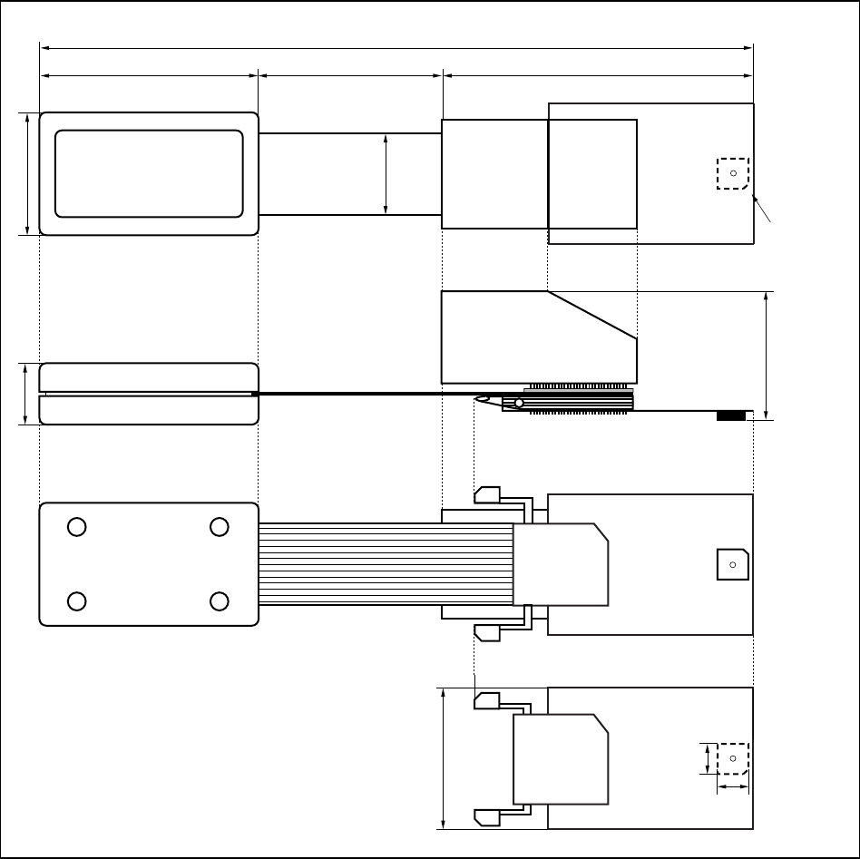
APPENDIX PACKAGE DRAWINGS
IE-703002-MC + IE-703089-MC-EM1 (Unit: mm)
571
103166
58.8
50
9027
302
Top view
Side view
IE-703089-MC-EM1
IE-703002-MC
Bottom view
Top view
33.0
180
33.0
Pin 1 direction
User’s Manual U15776EJ1V0UM
34
[MEMO]
Although NEC has taken all possible steps
to ensure that the documentation supplied
to our customers is complete, bug free
and up-to-date, we readily accept that
errors may occur. Despite all the care and
precautions we've taken, you may
encounter problems in the documentation.
Please complete this form whenever
you'd like to report errors or suggest
improvements to us.
Hong Kong, Philippines, Oceania
NEC Electronics Hong Kong Ltd.
Fax: +852-2886-9022/9044
Korea
NEC Electronics Hong Kong Ltd.
Seoul Branch
Fax: +82-2-528-4411
P.R. China
NEC Electronics Shanghai, Ltd.
NEC Electronics Taiwan Ltd.
Fax: +86-21-6841-1137
Address
North America
NEC Electronics Inc.
Corporate Communications Dept.
Fax: +1-800-729-9288
+1-408-588-6130
Europe
NEC Electronics (Europe) GmbH
Market Communication Dept.
Fax: +49-211-6503-274
South America
NEC do Brasil S.A.
Fax: +55-11-6462-6829
Taiwan
Asian Nations except Philippines
NEC Electronics Singapore Pte. Ltd.
Fax: +886-2-2719-5951
Fax: +65-250-3583
Japan
NEC Semiconductor Technical Hotline
Fax: +81- 44-435-9608
I would like to report the following error/make the following suggestion:
Document title:
Document number: Page number:
Thank you for your kind support.
If possible, please fax the referenced page or drawing.
Excellent Good Acceptable PoorDocument Rating
Clarity
Technical Accuracy
Organization
CS 02.3
Name
Company
From:
Tel. FAX
Facsimile
Message
