Nedap N V PAGSLS Remote Alarm Notification device User Manual MD Pager Transmitter v1 00
N. V. Nederlandsche Apparatenfabriek NEDAP Remote Alarm Notification device MD Pager Transmitter v1 00
user manual

Date: 27 May 2004 Version 1.00
This information is furnished for guidance, and with no guarantee as to its accuracy or completeness; its publication conveys no license under any patent or other right, nor does
the publisher assume liability for any consequence of its use; specifications and availability of goods mentioned in it are subject to change without notice; it is not to be
reproduced in any way, in whole or in part, without the written consent of the publisher.
_________________________________________________________________________________________________________
© Nedap Retail Support P.O. Box 102 NL-7140 AC Groenlo the Netherlands
Metal Detection Pager - Transmitter

2
MD Pager - Transmitter V1.00 | Nedap Retail Support
- support-rs@nedap.com
- H. Hammer
+31 (0) 544-47 15 19
hans.hammer@nedap.com
- H. Broekhuis
+31 (0) 544-47 15 02
han.broekhuis@nedap.com
Visitor’s address:
Nedap Retail Support
Parallelweg 2d
Groenlo
Netherlands
Postal address:
Nedap Retail Support
Postbus 102
7140 AC Groenlo
Fax
+31 (0) 544-46 58 14
© 2004 Nedap Retail Support - Netherlands
Parallelweg 2d, 7141 DC Groenlo
The software / hardware described in this book / file is furnished under a license agreement and may be used only in accordance with the terms of
the agreement.
Documentation version 1.00
Copyright Notice
All Rights Reserved.
Any technical documentation that is made available by Nedap Retail Support is the copyrighted work of Nedap Retail Support and is owned by Nedap
Retail Support.
NO WARRANTY. The technical documentation is being delivered to you and Nedap Retail Support makes no warranty as to its accuracy or use. Any
use of the technical documentation or the information contained therein is at the risk of the user.
Documentation may include technical or other inaccuracies or typographical errors.
Nedap Retail Support reserves the right to make changes without prior notice.
No part of this publication may be copied without the express written permission of Nedap Retail Support, Parallelweg 2d, 7141 DC Groenlo,
Netherlands.
Trademarks
Nedap, the Nedap logo, Nedap EASi/Net and the Nedap EASi/Net are registered trademarks of Nedap N.V. Groenlo.
Other product names mentioned in this manual may be trademarks or registered trademarks of their respective companies and are hereby
acknowledged.
Printed in the Netherlands
Technical Support:

3
MD Pager - Transmitter V1.00 | Nedap Retail Support
Technical Support: 2
Visitor’s address: 2
Postal address: 2
Fax 2
Table of content 3
General 4
Block diagram 5
Wireless Alarm Transmitter art. No. 8008272 5
Wireless Alarm Receiver art. No. 8008299 5
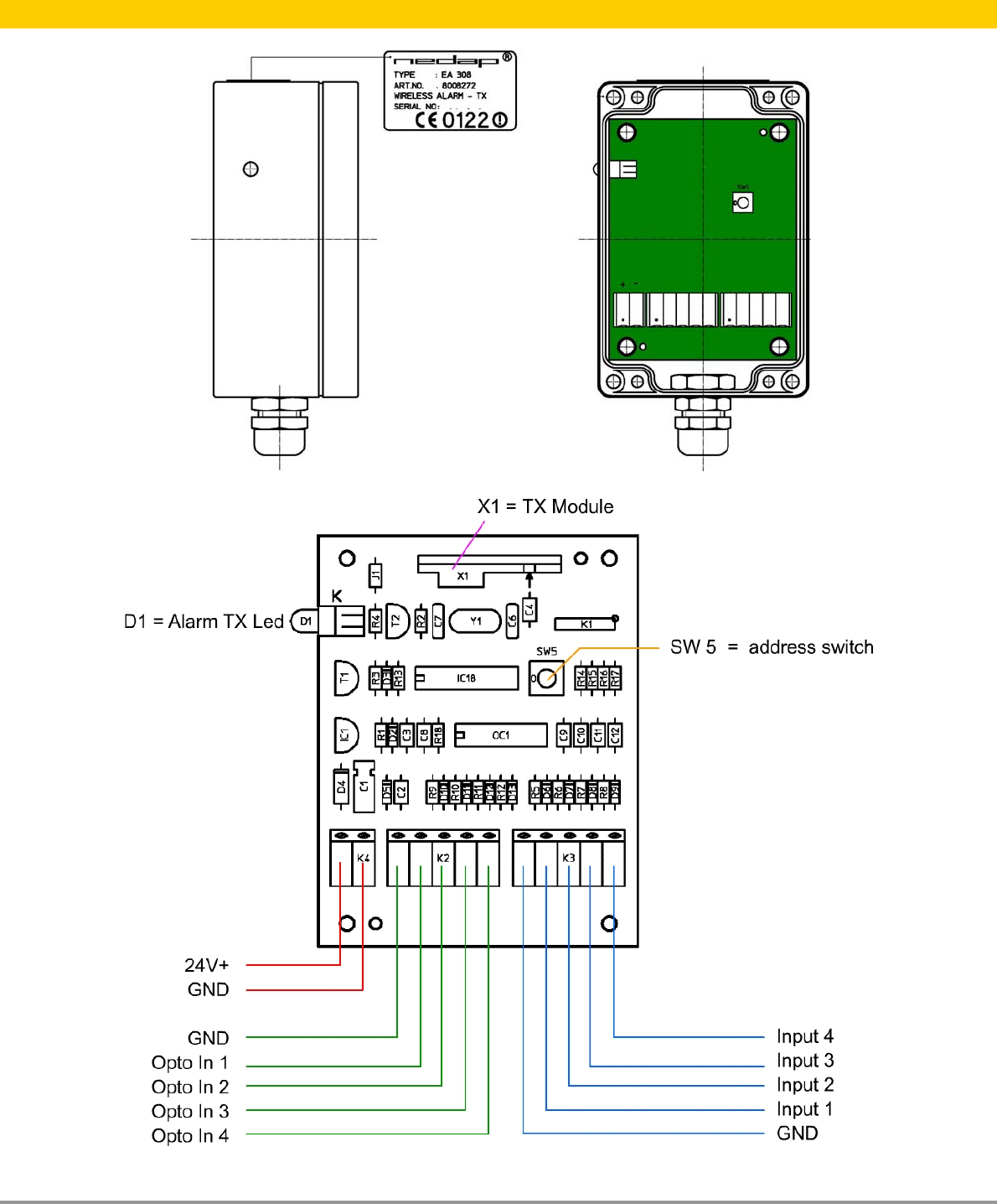
Transmitter Unit and PCB 6
RX Pager Unit and PCB 7
Datasheet TXM 433 Transmitter Module 8
Datasheet SILRX Receiver Module 19
Table of content

4
MD Pager - Transmitter V1.00 | Nedap Retail Support
The Wireless Alarm unit is intended to transmit an alarm, OST or MD, to a small
handheld receiver unit. The Transmitter unit is supplied with 24Vdc from the NCC or IQ
or EQ unit. One of the alarm relays on the NCC , IQ or EQ unit is then wired tot the input
of the transmitter board, for instance connector K3 between GND and input 1. A short
pulse of a normally open contact is enough to trigger a short burst of data onto 433Mc.
This data consists of an address and alarm number (1, 2, 3 or 4).
In the handheld receiver this burst is detected and the alarm will sound in addition one of
the led’s will light for a couple of seconds which indicates the alarm input that is
triggered.
If necessary an opto coupled input is also available on the transmitter. In this case 24V
has to be supplied to the appropriate input.
Both, the transmitter and the receiver are equipped with an address switch to its possible
to use more than one transmitter receiver combinations in the same “shop”.
The battery in the receiver has to be charged regularly, for this purpose the receiver has
a battery charge input with charge led. While charging the pager does not function.
The working range depends on the location of the transmitter and the total construction
of the building. A range of 10 to 20 meters is practical and must give a sure alarm.
General
5
MD Pager - Transmitter V1.00 | Nedap Retail Support
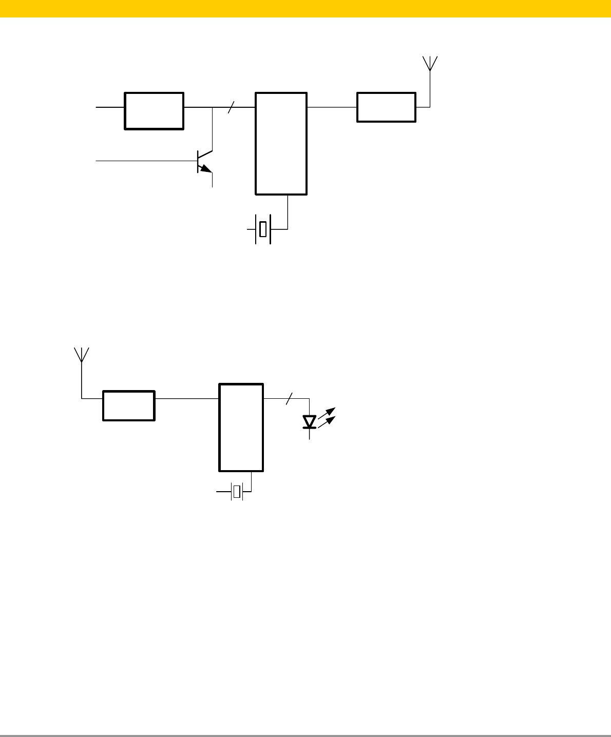
Wireless Alarm Transmitter art. No. 8008272
pic
16c84
TX mod.
TXM-433
opto
coupler
oc in
in
4x
3,84MHz
Either an opto coupled or a normal input is triggered and translated in a code by the pic.
This code will be transmitted via a standard transmitter module on 433 MHz.
Wireless Alarm Receiver art. No. 8008299
pic
16c84
RX mod.
SILRX-433
4x
3,84MHz
A standard 433 MHz receiver module receives the alarm data and output it to a pic
16c84. The pic will read the code and will turn on the appropriate led and gives audible
alarm.
Block diagram
6
MD Pager - Transmitter V1.00 | Nedap Retail Support
Transmitter Unit and PCB
7
MD Pager - Transmitter V1.00 | Nedap Retail Support
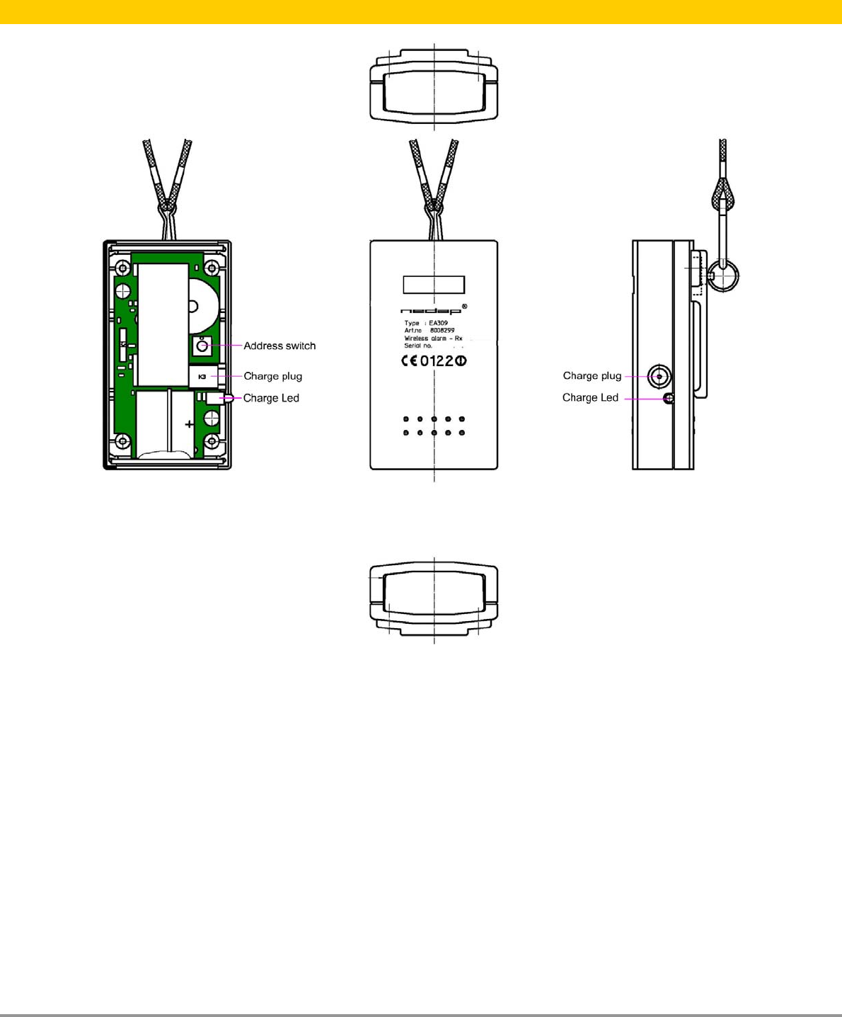
RX Pager Unit and PCB

8
MD Pager - Transmitter V1.00 | Nedap Retail Support
Datasheet TXM 433 Transmitter Module

Radiometrix Ltd, TXM Data Sheet page 1
Typical features include:
CE Certified by independent Notified Body
Verified to comply with harmonised radio standard ETSI EN 300 220-3 and EMC
standard ETSI EN 301 489-3 by accredited Test Laboratory
PCB Mounting, space saving SIL style
SAW controlled wide band FM transmission
High data rates, 5kbps and 10kbps versions
Analogue or Digital data input
Wide supply range 2.7V-4.0 or 6.0V-9.0V @ <17mA
The transmitter modules are most commonly employed in Wireless Security systems. The transmitter
and the matching receiver (RX2) are approved to harmonised radio standard ETSI EN 300 220-3 and
EMC standard ETSI EN 301 489-3. The TXM and RX2 modules will suit one-to-one and multi-node
wireless links in applications including car and building security, EPOS and inventory tracking, remote
industrial process monitoring and computer networking. Because of their small size and low power
requirements, both modules are ideal for use in portable, battery-powered applications such as hand-
held terminals.
Typical applications include :-
Domestic and commercial security
Guard patrol / lone worker protection
Medical Alert / Nurse Call systems
Mobile panic attack
Computer networking
Remote industrial process monitoring
Data transfer through hazardous environments
Lighting control, Garage door openers
Fire alarms
Picture / antique protection alarms
Remote control, Access control
The TXM-433-5 and TXM-433-10 integrate a low
power FM UHF radio transmitter on a small
module. Together with the matching RX2-433-14 or
RX2-433-40 receiver a one-way radio data link can be
achieved over a distance up to 200 metres on open
ground.
TXM-433-10 transmitter (back & front view)
Radiometrix
Hartcran House, Gibbs Couch, Watford, WD19 5EZ, England
Issue 5, February 2002 TXM-433
UHF Radio Telemetry Transmit Module
UHF Radio Telemetry Transmit ModuleUHF Radio Telemetry Transmit Module
UHF Radio Telemetry Transmit Module
Tel: +44
(
0
)
20 8428 1220, Fax: +44
(
0
)
20 8428 1221
Radiometrix Ltd, TXM Data Sheet page 2
Brief description
The TXM is designed to work with the matching SILRX receiver. With the addition of simple antenna
the pair may be used to transfer serial data up to 200m. The range of the radio link is very variable and
depends upon many factors, principally, the type of antenna employed and the operating environment.
The 200m quoted range is a reliable operating distance over open ground using 1/4 whip antenna at
both ends of the link at 1.5m above ground. Smaller antenna, interference or obstacles (e.g. building
etc.) will reduce the reliable working range (down to 30m in extreme cases). Increased antenna height,
slow data or a larger receive antenna will increase the range (our best is 3km).
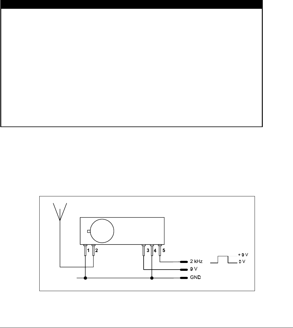
Pin Description
pin 1 RF GND This pin should be connected to the ground plane against which
the integral antenna radiates. It is internally connected to pin 4.
pin 2 RF OUT Connects to the integral antenna. Output impedance is 50Ω.
pin 3 Vcc Positive supply , supply voltages from +6V to +9V may be used.
pin 4 Vss 0V connection for the modulation and supply.
pin 5 DATA IN Should be driven directly by a CMOS logic device running on the
same supply voltage as the module.
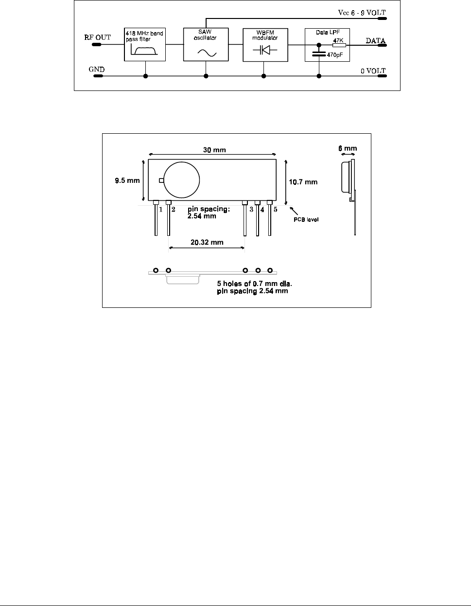
figure 1: TXM’s block diagram
figure 2: mechanical dimensions
Radiometrix Ltd, TXM Data Sheet page 3
Performance data TXM-433-5
Absolute Maximum Ratings:
Supply voltage Vcc pin 3 -0.7V to + 12V
Modulation input pin 5 -0.7V to + 9V
Operating temperature -10 °C to + 55 °C
Storage temperature -40 °C to + 100 °C
Performance Data:
ambient temperature: 20°C
supply voltage: +8.0V, unless noted otherwise
test circuit: figure 3
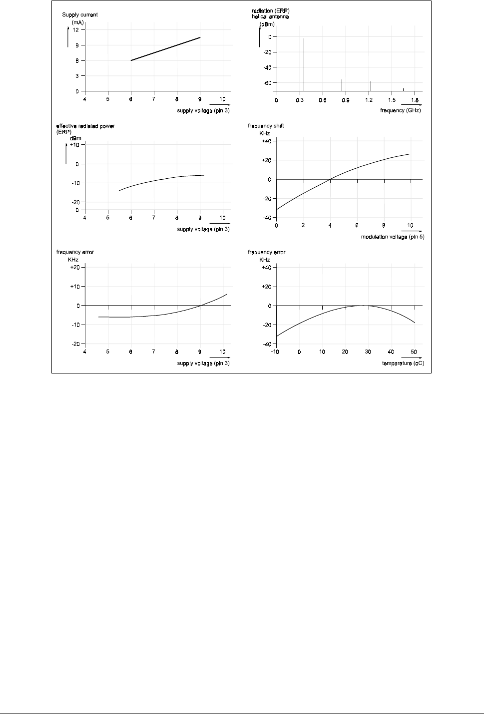
Parameter Min Typical Max Units Notes
Operating supply range (Vcc) 6.0 - 9.0 V -
Supply current, Vcc = 6.0V 3.0 6.0 10.0 mA -
Vcc = 9.0V 5.0 10.0 17.0 mA -
Radiated power (ERP) Vcc = 6.0V -16 -10 -7 dBm 1
Vcc = 9.0V -13 -8 -5 dBm 1
Transmit frequency (Frf) 418.00 / 433.92 MHz -
Initial frequency accuracy -80 - +80 kHz -
Overall frequency accuracy -95 - +95 kHz 2
Spurious radiation Meets the EN300 220-1 standard 3
FM deviation (+/-) 15 25 40 kHz 4
Modulation Bandwidth (-3dB) analogue DC - 10 kHz 4
Modulation digital pulse width 100 - - µs 5
Notes
1. Module on 50mm square ground plane, helical antenna
2. Supply 6V to 9V, temp -10°C to +55°C.
3. <-54 dBm in bands 41-68, 87.5-118, 162-230 & 470-862 MHz
<-36 dBm else where below 1GHz , <-30dBm above 1GHz
4. Standard modulation: 2kHz square wave, 0 to Vcc
5. High or Low pulse.
figure 3: TXM 5kbps version test circuit

Radiometrix Ltd, TXM Data Sheet page 4
Performance data TXM-418-10 and TXM-433-10
Absolute Maximum Ratings:
Supply voltage Vcc pin 3 -0.7 to + 6V
Modulation input pin 5 -0.7 to + 13V
Operating temperature -10°C to + 55°C
Storage temperature -40°C to + 100°C
Performance Data:
ambient temperature: 20 °C
supply voltage: 3.0V, unless noted otherwise
test circuit: figure 4
Parameter Min Typical Max Units Notes
Operating supply range (Vcc) 2.7 3.2 4 V -
Supply current,Vcc = 2.7V 3.0 6.0 13.0 mA -
Vcc = 4.0V 5.0 10.0 17.0 mA -
Conducted power in to 50 Ω, Vcc = 2.7V - -5 - dBm 1
Vcc = 3.6V - 0 - dBm 1
Transmit frequency (Frf) 433.92 MHz -
Initial frequency accuracy -85 0 +85 kHz -
Overall frequency accuracy -95 0 +95 kHz 1
Spurious radiation 2
FM deviation (+/-) 15 25 40 kHz 3
Modulation Bandwidth (-3dB) analogue DC - 20 kHz 3
Modulation digital pulse width 50 - - µs 4
Notes
1. Supply 2V to 3.6V, temp -10°C to +55°C.
2. <-54 dBm in bands 41-68, 87.5-118, 162-230 & 470-862 MHz
<-36 dBm else where below 1GHz , <-30dBm above 1GHz
3. Standard modulation: 2kHz square wave, 0 to Vcc
4. High or Low pulse.
Radiometrix Ltd, TXM Data Sheet page 5
The TXM-UHF transmitter requires only a data modulation input, supply, ground and an antenna.
Power supply requirements
• The module will operate over the range 6V to 9V and is typically powered by either 9 Volt 'PP3'.
• The module is not reverse polarity protected. Reverse supply voltages higher than 2V will cause
damage and must therefor be externally protected against.
Modulation requirements
• The TXM-UHF transmitter has a DC to 10kHz modulation bandwidth and will accept direct
analogue (AFSK) or digital data. A modulation low-pass filter (10kHz @ -6dB, 1st order) is use
internally.
• Although the modulation bandwidth of the transmitter extends down to DC as does the AF output of
the receivers, it is not possible to pass data with a DC component due to frequency errors & drifts
between the transmitter and receiver. Frequency differences between the transmitter and receiver
will produce a DC offset error which causes the data slicer in the receiver module to give errors on
long high or low pulses which exceed the maximum pulse width, see the receiver's data sheet for
more detailed information.
figure 4: TXM 10kbps version test circuit
figure 5: Typical performance curves

Radiometrix Ltd, TXM Data Sheet page 6
• Data Input, pin 5, is normally driven directly by CMOS logic levels from a data encoder IC. There is
a wide range of encoder/decoder IC’s available which may be used with the modules:
MM57C200, 57410 National Semiconductor
UM3750 UMC
HT12 series Holtek
MC14026 Motorola
AS2787 Austria Systeme International GmbH
• The encoder normally being run on the same supply voltage as the transmitter. Analogue drive eg. 2
tone FSK, is also possible, the pk to pk level should be between 5V and 9V peak to peak and must not
drive pin 5 below 0V. There will be some 2nd harmonic distortion due to the varactor modulator (typ.
<15%), this may be reduced if necessary by predistortion of the analogue waveform
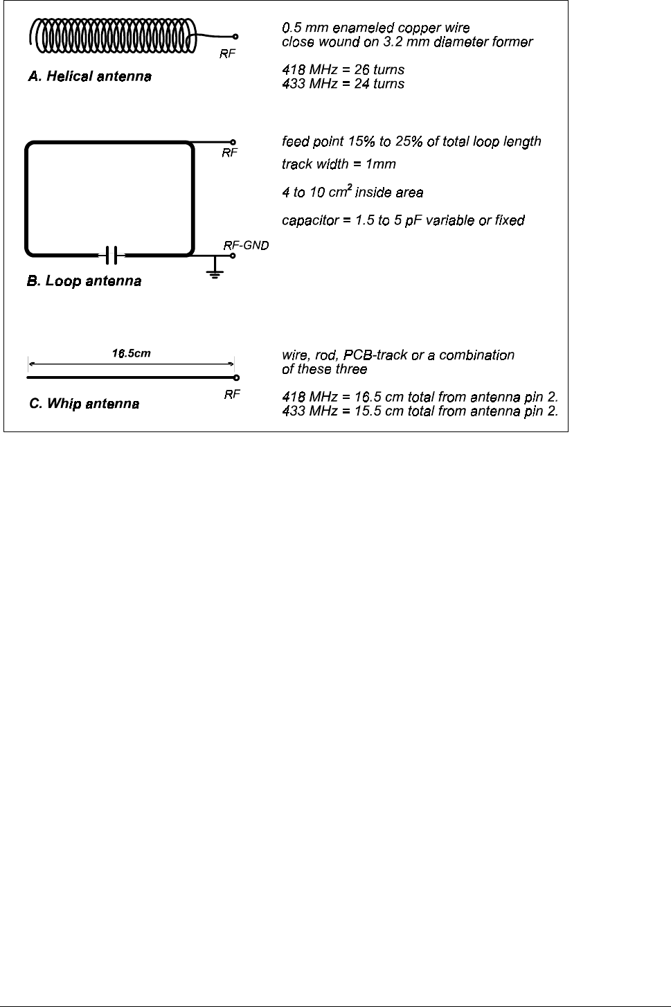
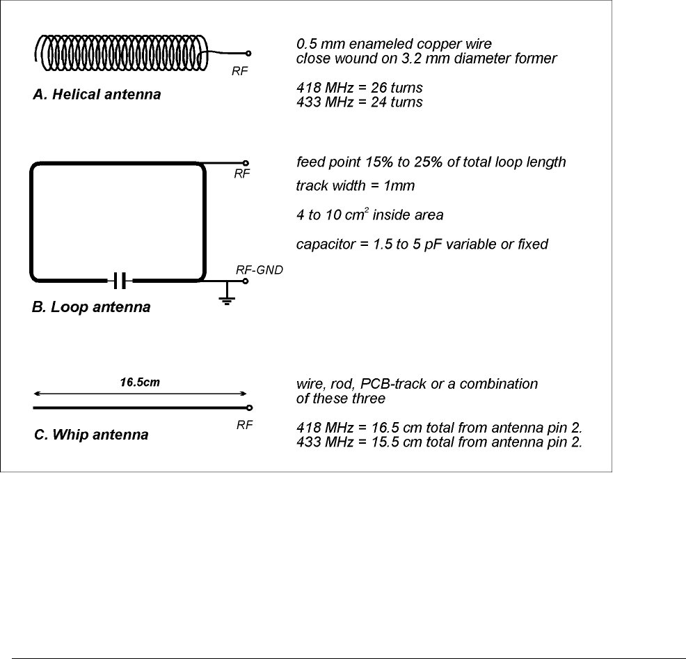
Antenna requirements
Three types of integral antenna are recommended and approved for use with the module:
A) Helical: Wire coil, connected directly to pin 2, open circuit at other end. This antenna is very
efficient given it's small size (20mm x 4mm dia.). The helical is a high Q antenna, trim
the wire length or expand the coil for optimum results. The helical de-tunes badly with
proximity to other conductive objects.
B) Loop, A loop of PCB track tuned by a fixed or variable capacitor to ground at the 'hot' end and
fed from pin 2 at a point 20% from the ground end. Loops have high immunity to
proximity de-tuning.
C) Whip This is a wire, rod ,PCB track or combination connected directly to pin 2 of the module.
Optimum total length is 17cm (1/4 wave @ 418MHz) Keep he open circuit (hot) end well
away from metal components to prevent serious de-tuning. Whips are ground plane
sensitive and will benefit from internal 1/4 wave earthed radial(s) if the product is small
and plastic cased
Antenna selection chart
A B C
helical loop whip
Ultimate performance ** * ***
Easy of design set-up ** * ***
Size *** ** *
Immunity proximity effects ** *** *
Range open ground to similar antenna 80m 50m 120m
The antenna choice and position directly controls the system range. Keep it clear of other metal in the
system, particularly the 'hot' end. The best position by far, is sticking out the top of the product. This is
often not desirable for practical/ergonomic reasons thus a compromise may need to be reached. If an
internal antenna must be used try to keep it away from other metal components, particularly large ones
like transformers, batteries and PCB tracks/earth plane. The space around the antenna is as important
as the antenna itself.
Radiometrix Ltd, TXM Data Sheet page 7
Duty Cycle requirements
The duty cycle is defined as the ratio, expressed as a percentage, of the maximum transmitter “on” time
on one or more carrier frequencies, relative to a one hour period. Where an acknowledgement message
is required, the additional transmitter “on” time shall be included.
There is a 10% duty cycle restriction on 433.050-434.790 MHz band in most of the EU member states.
The TXM-433 is a RF module intended to be incorporated into a wide variety of applications and
finished products, Radiometrix has no control over the end use of the TXM-433.The harmonised band
433.050 to 434.790 MHz as detailed in Annex 1 Band E of CEPT/ERC Recommendation 70-03 (which
can be downloaded at http://www.ero.dk/scripts/docmanag98/dm.dll/QueryDoc?Cat=Recommendation)
has list of countries where Duty Cycle restriction apply.
Module users should, therefore, ensure that they comply with the stated Duty Cycle requirements of the
version of CEPT/ERC Recommendation 70-03 in place at the time of incorporation of the TXM-433 into
their product. It should be noted that the stated Duty Cycle must not be exceeded otherwise any
approval granted for the TXM-433 will be invalidated.
figure 6: Antenna configurations

Radiometrix Ltd, TXM Data Sheet page 8
Ordering information
The following are standard:
TXM-433-5 5kbps data rate Transmitter
RX2-433-14-5V 14kbps data rate matching Receiver
RX2-433-40-5V 40kbps data rate matching Receiver
SILRX-433-5 5kbps data rate matching Receiver
TXM-433-10 10kbps data rate Transmitter
RX2-433-14-5V 14kbps data rate matching Receiver
RX2-433-40-5V 40kbps data rate matching Receiver
SILRX-433-10 10kbps data rate matching Receiver
3V versions of the RX2 receivers are available and should be ordered with a -3V suffix on the part
number. (e.g. RX2-433-14-3V is set-up for 3V to 4V operation)
All modules are available in a 418MHz version for UK use.

Radiometrix Ltd, TXM Data Sheet page 9
CE Certificate of TXM and its variants

Radiometrix Ltd
Hartcran House, Gibbs Couch,
Watford, WD19 5EZ, ENGLAND
Tel: +44 (0)20 8428 1220,
Fax: +44 (0)20 8428 1221
info@radiometrix.co.uk
www.radiometrix.co.uk
Copyright notice
This product data sheet is the original work and copyrighted property of Radiometrix Ltd.
Reproduction in whole or in part must give clear acknowledgement to the copyright owner.
Limitation of liability
The information furnished by Radiometrix Ltd is believed to be accurate and reliable.
Radiometrix Ltd reserves the right to make changes or improvements in the design, specification
or manufacture of its subassembly products without notice. Radiometrix Ltd does not assume
any liability arising from the application or use of any product or circuit described herein, nor
for any infringements of patents or other rights of third parties which may result from the use of
its products. This data sheet neither states nor implies warranty of any kind, including fitness
for any particular application. These radio devices may be subject to radio interference and may
not function as intended if interference is present. We do NOT recommend their use for life
critical applications.
The Intrastat commodity code for all our modules is: 8542 6000
R&TTE Directive
After 7 April 2001 the manufacturer can only place finished product on the market under the
provisions of the R&TTE Directive. Equipment within the scope of the R&TTE Directive may
demonstrate compliance to the essential requirements specified in Article 3 of the Directive, as
appropriate to the particular equipment.
Further details are available on Radiocommunications Agency (RA) web site:
http://www.radio.gov.uk/topics/conformity/conform-index.htm
The Library and Information Service
The Radiocommunications Agency
Wyndham House
189 Marsh Wall
London
United Kingdom
E14 9SX
Tel: +44 (0)20 7211 0502/0505
Fax: +44 (0)20 7211 0507
library@ra.gsi.gov.uk
For further information on radio matters
contact the Agency's 24 Hour Telephone
Enquiry Point: +44 (0)20 7211 0211
European Radiocommunications Office (ERO)
Midtermolen 1
DK 2100 Copenhagen
Denmark
Tel. +45 35250300
Fax +45 35250330
ero@ero.dk
www.ero.dk

9
MD Pager - Transmitter V1.00 | Nedap Retail Support
Datasheet SILRX Receiver Module

Radiometrix Ltd, SILRX-UHF Data Sheet page 1
Typical features include:
• PCB mounting, space saving SIL style
• 418 MHz SAW controlled wide band FM reception
• Selective double conversion superhet
• Sensitive typ. 0.5µV (-113 dBm) for 20 dB S/N
• High data rates, 5kbps and 10kbps
• Analogue and Digital data outputs
• Carrier detect output
• Fast enable time,< 3ms for duty cycle power save use
• Wide supply range, 4.0V to 9.0V
• Low current, 13 mA continuous, 130µA on power save (100:1)
• The SILRX radio receiver and the matching DTI (RA) approved transmitter (TXM-418-5) are self
contained, PCB mounting modules capable of transferring analogue or digital data up to a distance
of 200m.
The SILRX receiver module is particularly suitable for battery powered portable applications where it’s
low power requirements and small size are of advantage. It may also be used as a lower cost option to
the RXM-418-10 in fixed applications where the higher data rates and signal strength output of the
RXM-418-10 are not required.
Typical applications include:-
Site paging receivers Paging car alarms
Line powered telephone auto diallers Domestic and commercial security
Guard patrol/lone worker protection Medical Alert/Nurse Call system
Mobile panic attack Remote industrial process monitoring
Battery powered half duplex data networks Data transfer through hazardous environments
Lighting control, Garage door openers Fire alarms
Picture/antique protection alarms Remote control, Access control
The SILRX-418-5 and SILRX-433-5 integrate a
c
omplete FM superhet UHF radio receiver on a
small module. Together with the matching TXM-
418-5 or TXM-433-5 transmitter a one-way radio
d
ata link can be achieved over a distance upto 200
metres on open ground
UK version: SILRX-418-5 / SILRX-418-10
Euro version: SILRX-433-5 / SILRX-433-10
left: TXM-418-5 transmitter right: SILRX-418-5 receiver
Radiometrix
Hartcran House, Gibbs Couch, Watford, WD19 5EZ, England
Issue 3, 13 April 2001 SILRX-UHF
UHF Radio Telemetr
y
Receiver Module
Tel: +44 (0) 20 8428 1220, Fax: +44 (0) 20 8428
Radiometrix Ltd, SILRX-UHF Data Sheet page 2
Brief description
The SILRX receiver is a double conversion FM superhet with a data slicer driven by the AF output.
Additionally a fast acting carrier detect signal is available to indicate to external circuits that a signal is
present. This signal is extremely useful when implementing duty cycle power save circuits (see fig 4) or
to indicate to external logic that a signal is being received. It is internally derived from the degree of
noise quieting due to the presence of a receive carrier.
The SILRX-418 is designed to work with the matching transmitter (TXM-418). With the addition of
simple antenna the pair may be used to transfer serial data up to 200m. The range of the radio link is
very variable and depends upon many factors, principally, the type of antenna employed and the
operating environment. The 200m quoted range is a reliable operating distance over open ground using
1/4 whip antenna at both ends of the link at 1.5m above ground. Smaller antenna, interference or
obstacles (e.g. building etc.) will reduce the reliable working range (down to 30m in extreme cases).
Increased antenna height, slow data or a larger receive antenna will increase the range (our best is
3km).
We recommend that the module evaluation kit, EVAL-418-A, can be used to assess the reliable working
range under the anticipated conditions of use.
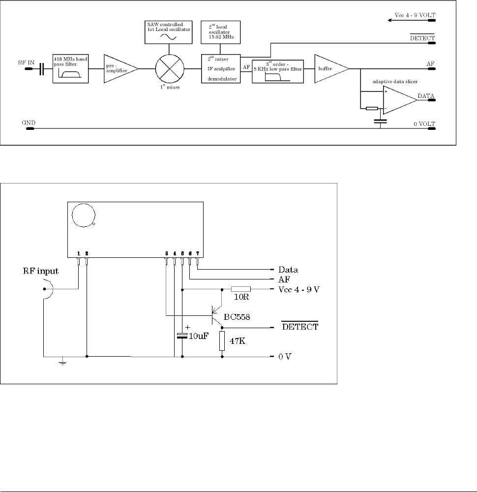
The following figure shows the receiver’s block diagram.
figure 1: Block diagram
figure 2: Test cicuit
Radiometrix Ltd, SILRX-UHF Data Sheet page 3
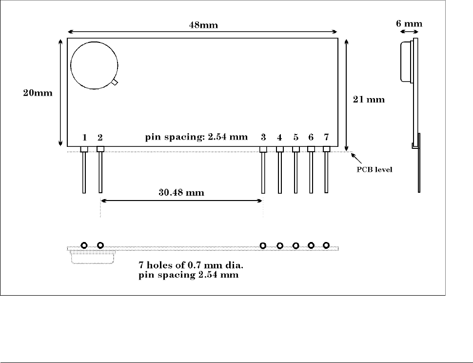
Pin Description
pin 1 RF IN The receiver antenna connects to this input. It has nominal RF
impedance of 50Ω and is capacitively isolated from the internal circuit
pin 2 RF GROUND This pin should be connected to any ground plane against which the
antenna works. It is internally connected to pin 4.
pin 3 DETECT This pin may be used to derive a carrier detect to enable external circuits
when a signal is being received. If the detect function is not being used a
10 kΩ pull-up to pin 5 (Vcc) should be connected. Refer to applications
note for further details on the use of this pin.
pin 4 0 volt Ground for supply.
pin 5 Vcc Positive supply of 4V to 9V 13 mA. The supply must be clean (<2mV pp)
stable and free of high frequency digital noise. A supply filter is
recommended unless the module is driven from it’s own regulated supply.
pin 6 AF This is the FM demodulator output. It has an standing DC bias of
approximately 1.4V and may be used to drive analogue data detectors
such as modem chips or DTMF decoders. Load impedances as low as 2 kΩ
and up to 100 pF can be driven
pin 7 DATA This digital output from the internal data slicer is a squared version of
the signal on pin 6 (AF) This signal is used to drive external digital
decoders, it is true data (i.e. as fed to the transmitters data input). Load
impedances as low as 1 kΩ and up to 1 nF can be driven
.
figure 3: Mechanical Dimensions:

Radiometrix Ltd, SILRX-UHF Data Sheet page 4
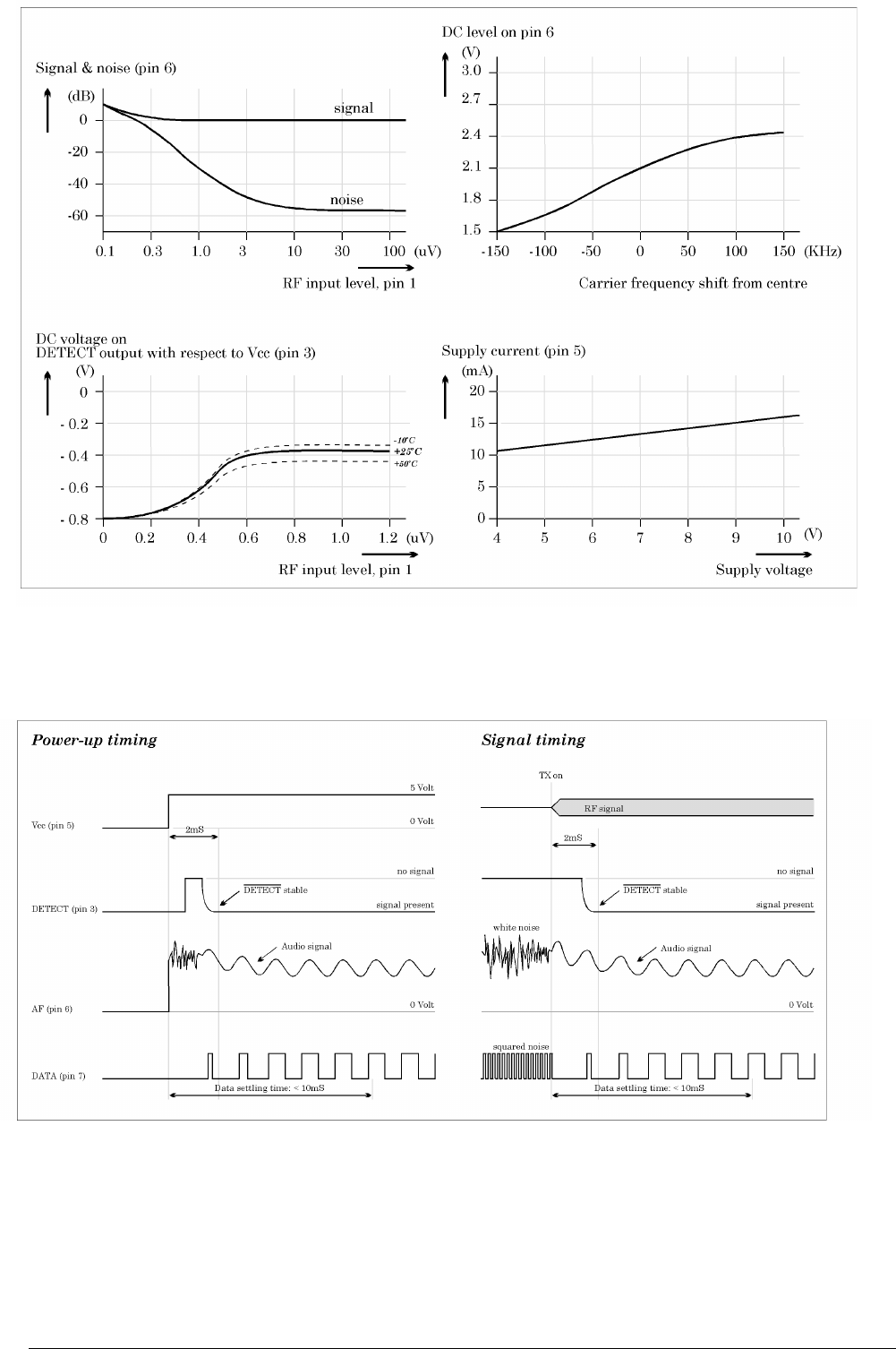
Performance data SILRX-418-5 and SILRX-433-5
ambient temperature: 20°C
supply voltage: + 5 Volt
test circuit: fig. 2
Parameter Min. Typical Max. Units Notes
O
p
eratin
g
volta
g
e ran
g
e
(
Vcc
)
p
in 5 4.0 5.0 9.0 V -
Supply current pin 5 11 14 17 mA -
Receive frequency - 433.92 - MHz -
Overall frequency accuracy - 100 0 + 100 kHz 1
Sensitivity for 20 dB S/N pin 1 - 0.5 1.0 µV 2
Carrier detect, threshold pin 1 - 0.5 2.0 µV -
RF input impedance pin 1 - 50 - Ω -
IF bandwidth - 250 - kHz 3
AF output level pin 6 - 500 - mVpp 2, 3
AF bandwidth pin 6 DC - 5 kHz 3
Frequency/voltage conversion pin 6 - 10 - mV/kHz -
Data output, Logic low pin 7 0 0.2 0.8 V 4
Logic high pin 7 4.0 4.5 5 V 5
Data bit duration 0.2 - 20 ms 6
Data Mark:Space 20 % - 80 % 7
Data settling time pin 7 - - 15 ms 8
(minimum preamble duration)
Enable time pin 3 - - 2.5 ms 3, 9
Signal detect time pin 3 - - 0.5 ms 3, 9
Notes: 1. over supply and temperature range
2. ±25kHz deviation, 1 kHz tone
3. 3µV input
4. 1mA sink
5. 1mA source
6. time between transitions
7. (time high / time low) * 100 %, averaged over any 20 ms period
8. time from valid carrier detect to stable data output
9. from application of supply to carrier detect low (active)
10. from application of signal to carrier detect low (active)
Absolute maximum ratings:
Supply voltage Vcc, pin 5 - 0.3 to + 10 V
Operating temperature - 10°C to + 50°C
Storage temperature - 40°C to + 100°C
RF input, pin 1 0 dBm
Any input or output pin - 0.3 to Vcc V, ±10 mA

Radiometrix Ltd, SILRX-UHF Data Sheet page 5
Performance data SILRX-418-10 and SILRX-433-10
ambient temperature: 20°C
supply voltage: +5V
test circuit: fig. 2
Parameter Min. Typical Max. Units Notes
Operating voltage range (Vcc) pin 5 4.0 5.0 9.0 V -
Supply current pin 5 11 14 17 mA -
Receive frequency - 433.92 - MHz -
Overall frequency accuracy - 100 0 + 100 kHz 1
Sensitivity for 20 dB S/N pin 1 - 1.0 2.0 µV 2
Carrier detect, threshold pin 1 - 2.0 4.0 µV -
RF input impedance pin 1 - 50 - Ω -
IF bandwidth - 250 - kHz 3
AF output level pin 6 - 500 - mVpp 2, 3
AF bandwidth pin 6 DC - 20 kHz 3
Frequency/voltage conversion pin 6 - 10 - mV/kHz -
Data output, Logic low pin 7 0 0.2 0.8 V 4
Logic high pin 7 4.0 4.5 5 V 5
Data bit duration 0.05 - 2 ms 6
Data Mark:Space 20 % - 80 % 7
Data settling time pin 7 - - 5 ms 8
(minimum preamble duration)
Enable time pin 3 - - 1 ms 3, 9
Signal detect time pin 3 - - 0.3 ms 3, 10
Notes: 1. over supply and temperature range
2. ±25 kHz deviation, 1 kHz tone
3. 3 µV input
4. 1mA sink
5. 1mA source
6. time between transitions
7. (time high / time low) * 100 %, averaged over any 20 ms period
8. time from valid carrier detect to stable data output
9. from application of supply to carrier detect low (active)
10. from application of signal to carrier detect low (active)
Absolute maximum ratings:
Supply voltage Vcc, pin 5 - 0.3 to + 10 V
Operating temperature - 10°C to + 50°C
Storage temperature - 40°C to + 100°C
RF input, pin 1 0 dBm
Any input or output pin - 0.3 to Vcc V, ±10 mA
Radiometrix Ltd, SILRX-UHF Data Sheet page 6
figure 4: Typical performance curves
figure 5: Timing wave forms
Radiometrix Ltd, SILRX-UHF Data Sheet page 7
Antenna configurations
The positioning of the antenna is of the up most importance and is one of the main factors in
determining system range.
The following notes should assist in obtaining optimum performance:-
1. Keep it clear of other metal in the system, particularly the ‘hot’ (top) end.
2. The best position by far, is sticking out the top of the product. This is often not desirable for
practical/ergonomic reasons thus a compromise my need to be reached.
3. If an internal antenna must be used try to keep it away from other metal components, particularly
large ones like transformers, batteries and PCB tracks/earth plane. The space around the antenna is
as important as the antenna itself.
4. Keep it away from interference sources, bad interference can easily reduce system range by a factor
of 5. High speed logic is one of the worst in this respect fast logic edges have harmonics which extend
into the UHF band and the PCB tracks radiate these harmonics most efficiently. Single chip
microprocessors and ground planed logic boards reduce this problem significantly.
The next diagrams (fig 6) show three different antenna configurations which can be used on both the
transmitter and the receiver. Additionally a coax fed external dipole or 1/4 wave ground plane antenna
may be considered if system range is paramount.
figure 6: Antenna configurations

Radiometrix Ltd, SILRX-UHF Data Sheet page 8
Module Mounting considerations
1. The module may be mounted vertically or bent horizontal to the motherboard.
2. No conductive items should be placed within 4 mm of the modules’ component side to prevent
detuning.
3. Observe RF layout practice between the module and it’s antenna i.e. < 10 mm unscreened track,
use 50Ω microstrip or coax for >10mm
4. It is desirable, but not essential, to earth plane all unused area around the module.
5. Mount as far as possible from high frequency interference sources, Microprocessors with
external busses are totally incompatible with sensitive radio receivers and must be keep at least
1 metre from the receive antenna. Single chip micros are not a problem.
6. In some applications it is advantageous to remote the receiver and it’s antenna away from the
main equipment. This avoids any interference problems and allows flexibility in the sighting of
the receive antenna for optimum RF performance.
Using the DETECT output
Pin 3 of the module may be used in several ways:-
1. Pulled up to pin 5 (Vcc) with a 47 kΩ resistor unmutes the AF and DATA outputs for normal
operation.
2. Pulled down to 0 Volts with a 47 kΩ mutes the AF and DATA Outputs (both go to 0V).
3. To drive the base of a PNP transistor (see fig 2) to derive a logic compatible carrier detect. The
data detect output on pin 3 may be used for duty cycle power saving control in portable
equipment where battery life is a problem. By pulsing the receiver on/off the average supply
current may often be reduced by a factor of 20 or more depending upon the system
requirements the data detect output is valid 1.5 ms (2.5 ms worst case) after application
of the supply and is used to inhibit the power saving while data decoding is done.
Internal data slicer
A CMOS compatible data output is available on pin 7, this output is normally used to drive a digital
decoder IC or a microprocessor which is performing the data decoding. The data slicer in the receive
module is designed to accept data with a wide range of pulse widths and mark: space ratio’s, see
specification table for limiting values. The data slicer has a 10 ms transient response time this is the
settling time of the adaptive comparator, i.e. the first 10 ms of signal may be corrupt at the data output.
System coding
The transmit and receive modules have no internal digital coding/decoding thus allowing the flexibility
to send many types of data. Encoder and decoder IC’s are required to give the system a high degree of
protection from false triggers due to noise/interference/neighbouring systems and often for security
reasons. There are wide range of suitable encoder/decoder IC’s which may be used with the modules,
including :-
MM57C200, MM57410,National Semiconductor
UM3750, UMC
HT12 series, Holtek
MC145026 series, Motorola
AS2787, Austria Mikro Systeme International GmbH
Additionally IR. remote control, DTMF, Selcall and modem IC’s can be easily interfaced to the modules.

Radiometrix Ltd, SILRX-UHF Data Sheet page 9
AF output
This output is the FM demodulator’s output after buffering and filtering. Since it is taken before the
data slicer in the module, it may be used to drive external data slicers / demodulator’s in cases where
the internal data slicer is not suitable. This is the case where an analogue subcarrier is being employed
e.g. 2 tone AFSK or DTMF tones. In these cases the AF output is used to drive the FSK / DTMF decoder
directly.
The AF output is also a very useful test point for monitoring signals or interference. The AF output is
DC coupled to the FM demodulator thus the DC level Varies with the frequency of the incoming signal.
Supply requirements
The module requires a clean supply. Noise and ‘hash’ in the 5 to 500 kHz band and 16 MHz ±1 MHz
must be less than 2 mV, We recommend a 10 µF capacitor to ground on pin 5 (Vcc) and a 10Ω series feed
resistor in cases where the cleanness of the supply is in doubt.
.
Additional Reading
BS 0799 British standard for Wire-free intruder alarm systems
BS 4737 British standard for intruder alarm systems in buildings from British standards
institution - Tel. 44 171 629 900
MPT1340 DTI type approval specification for 418 MHz Telemetry from department of
Trade and Industry - 44 171 211 0502/0505
ARRL Handbook Excellent radio engineering text
ARRL Antenna Book Practical antenna design book
Warning: Don’t be tempted to adjust the trimmer on the module, it controls the receive
frequency and can only be correctly set-up with an accurate RF signal generator!
Radiometrix Ltd, SILRX-UHF Data Sheet page 10
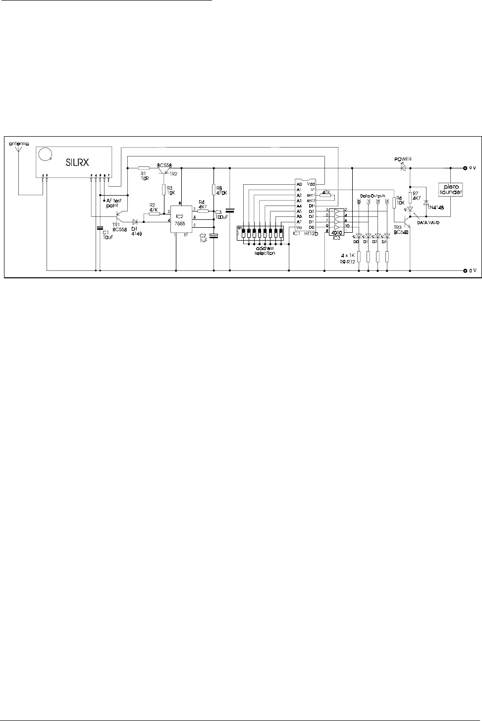
Applications note
Four Channel Receiver with battery saver
Fig 7 shows a simple four channel paging receiver with 256 setable codes. The CMOS 555 timer
provides a duty cycle power save circuit which latches ON when a signal is present. The values used in
the example give 4ms ON; 400 ms OFF, i.e. 1:100 duty cycle. The total quiescent current is less than
200µA, thus a 9V alkaline battery (500 mA/hr) will give a life of over 2000 hours. The ON time is
determined by the receiver’s power up settling time (3 ms worst case) + any tolerance of the duty cycle
oscillator. The OFF time is controlled by R8 in the circuit and should be selected to suit the application
depending upon the required response time and any limits imposed upon the duration of the
transmission. It is recommended that the OFF time be no longer than 1/2 for the transmission
preamble duration.
Ordering information
SAW based OEM Transmit and Receive modules.
TXM-418-5 UK Transmitter on 418 MHz, Type approved to MPT1340
TXM-418-10 Fast transmitter on 418 MHz, Type approved to MPT1340
RXM-418-5 matching UK receiver module on 418 MHz
SILRX-418-5 Low current UK receiver module on 418 MHz
BiM-418-10 Bi-directional short range module on 418 MHz
RPC-418-5 Self-contained module wich integrates the BiM transceiver with a Radio Packet
Controller
EVAL-418-A Evaluation kit for TXM & RXM
EVAL-418-B SILRX supplementary PCB for EVAL-418-A
BiM-KIT Evaluation kit for BiM-UHF modules.
All modules are available in a 433.92 MHz version for use in other European countries.
figure 7: Four Channel Receiver with power save

Radiometrix Ltd
Hartcran House
Gibbs Couch
Watford
WD19 5EZ
ENGLAND
Tel: +44 (0)20 8428 1220
Fax: +44 (0)20 8428 1221
info@radiometrix.co.uk
www.radiometrix.co.uk
Copyright notice
This product data sheet is the original work and copyrighted property of Radiometrix
Ltd. Reproduction in whole or in part must give clear acknowledgement to the
copyright owner.
Limitation of liability
The information furnished by Radiometrix Ltd is believed to be accurate and reliable.
Radiometrix Ltd reserves the right to make changes or improvements in the design, specification
or manufacture of its subassembly products without notice. Radiometrix Ltd does not assume
any liability arising from the application or use of any product or circuit described herein, nor
for any infringements of patents or other rights of third parties which may result from the use of
its products. This data sheet neither states nor implies warranty of any kind, including fitness
for any particular application. These radio devices may be subject to radio interference and may
not function as intended if interference is present. We do NOT recommend their use for life
critical applications.
The Intrastat commodity code for all our modules is: 8542 6000
R&TTE Directive
After 7 April 2001 the manufacturer can only place finished product on the market under the
provisions of the R&TTE Directive. Equipment within the scope of the R&TTE Directive may
demonstrate compliance to the essential requirements specified in Article 3 of the Directive, as
appropriate to the particular equipment.
Further details are available on Radiocommunications Agency (RA) web site:
http://www.radio.gov.uk/topics/conformity/conform-index.htm
The Library and Information Service
The Radiocommunications Agency
Wyndham House
189 Marsh Wall
London
United Kingdom
E14 9SX
Tel: +44 (0)20 7211 0502/0505
Fax: +44 (0)20 7211 0507
library@ra.gsi.gov.uk
For further information on radio matters
contact the Agency's 24 Hour Telephone
Enquiry Point: +44 (0)20 7211 0211
European Radiocommunications Office (ERO)
Midtermolen 1
DK 2100 Copenhagen
Denmark
Tel. +45 35250300
Fax +45 35250330
ero@ero.dk
www.ero.dk