Neoway Technology 1150 GPRS+GPS Module User Manual
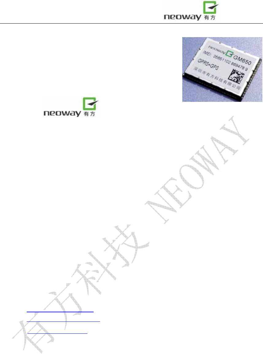
Shenzhen Neoway Technology Co., Ltd GPRS+GPS Module
Users manual

Neo_GM650
User Manual
Version V1.0
Shenzhen Neoway Technology Co.,Ltd
Neo_GM650 User Manual V1.0
All rights reserved by Shenzhen Neoway Technology Co., Ltd Page 2 Total 14
Copyright Statement
Copyright © 2008 Neoway Technology
All rights reserved by Shenzhen Neoway Technology Co.,Ltd.
The trademark belongs to Shenzhen Neoway Technology Co.,Ltd. Other
trademarks in this manual belongs to their owners.
Clarification
This specification is for system engineer, research engineer and test engineer.
As the upgrading of the product version or some other reasons, we’ll do some necessity
updating to the content of this specification without advance notice.
Unless we have other additional assumpsit, all statements, information and suggestions in
this manual do not constitute any express or implied guarantees.
Shenzhen Neoway Technology Co.,Ltd can supply all the technological support. If you have
any problem, please feel free to contact to the sales representative or send E-mail to these
two mailboxes:
Sales@neoway.com.cn
Support@neoway.com.cn
Website: www.neoway.com.cn
Neo_GM650 User Manual V1.0
All rights reserved by Shenzhen Neoway Technology Co., Ltd Page 3 Total 14
Contents
1 Overview ............................................. 5
2 Figuration ............................................ 5
3 Block Diagram ........................................ 6
4 Character............................................. 6
5 Pin Definition & Encapsulation ......................... 9
5.1 Pin Definition ...........................................................................9
5.2 PCB Packaging .....................................................................12
6 General AT Commends ............................... 13
7 Call Control Commends .............................. 13
8 TCP/UDP AT Commends.............................. 13
9 GPS AT Commends .................................. 13
10 Assembling.......................................... 13
Neo_GM650 User Manual V1.0
All rights reserved by Shenzhen Neoway Technology Co., Ltd Page 4 Total 14
Revision Record
Version Content Revised Effective date
V1.0 Initial version 2012-06
Neo_GM650 User Manual V1.0
All rights reserved by Shenzhen Neoway Technology Co., Ltd Page 5 Total 14
1 Overview
GM650 is an open platform that supports GSM/GPRS+GPS wireless industry module,
reserved CPU resources and a wealth of hardware interface which is widely used in
various industrial and commercial fields to provide high quality voice, message, data
business, GPS Location and other functions.
GM650 provide two kinds of GPS data interface mode: single-port and dual-port. If the
user’s MCU has only one UART interface, while need to support both GPRS
communications and GPS positioning function, that GM650 single-port mode provides the
perfect solution.
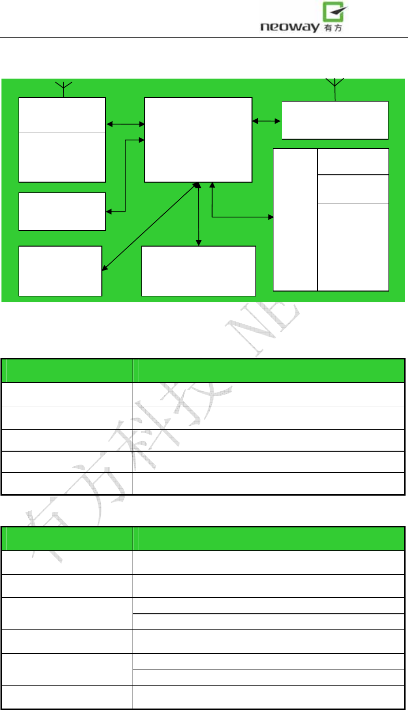
2 Figuration
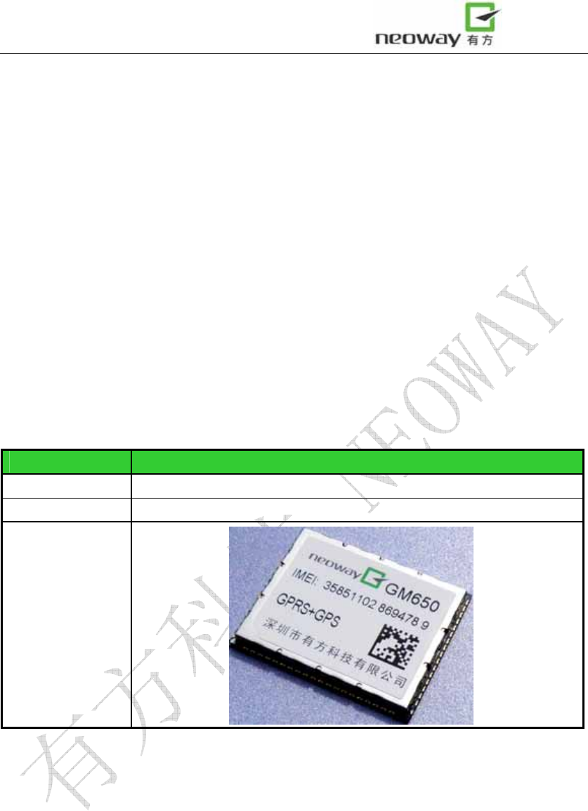
Table 2-1 GM650 Figuration Specification
Specifications Description
Dimensions 30.0mm*24.0mm*2.7mm(length*width*height)
Weight 3.7g
Overview
Neo_GM650 User Manual V1.0
All rights reserved by Shenzhen Neoway Technology Co., Ltd Page 6 Total 14
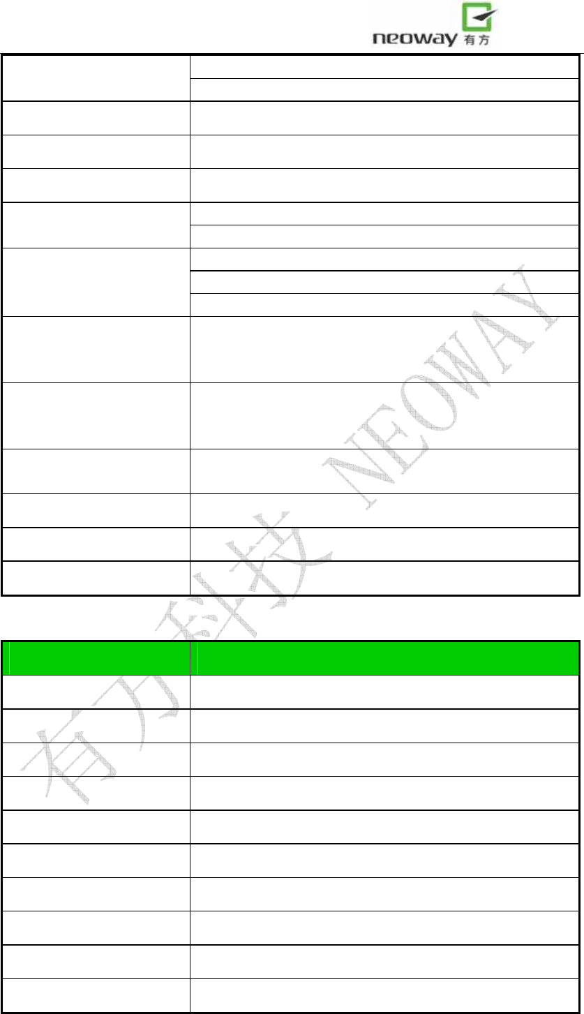
3 Block Diagram
4 Character
Table 4-1
General parameters Description
Operating temperature -30℃~+70℃
Operating voltage 3.5V~4.3V(recommendation 3.9V )
Operating Current See table 4-2 and 4-3
Storage temperature -40℃~+80℃
Humidity range 0%~95%
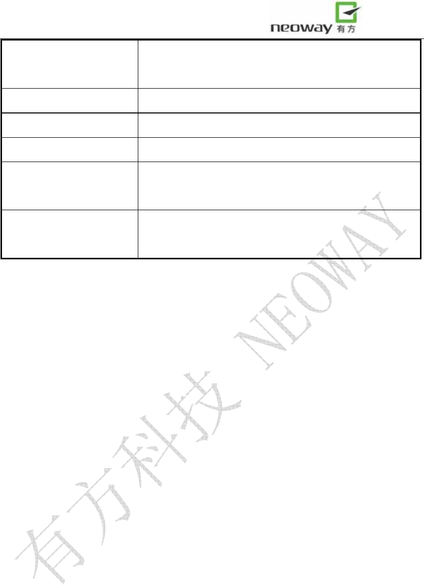
Table 4-2
GSM Specifications Description
Frequency 900/1800/850/1900
Sensitivity < -106dBm
850/900 Class4(2W)
The Maximum transmission
Power 1800/1900 Class1(1W)
Protocol Compatible with GSM/GPRS Phase2/2+
GSM07.07 AT
Extended command sets
Audio FR、EFR、HR、AMR voice coding
GSM
Baseband
Controller
PA
Power
Manager
Application Interface
RF
Section
GPS
S
ection
Audio
Section
SIM x
2
UART x 2
I2C
MMC
USB
ADC/PW
LCD
Flash
Neo_GM650 User Manual V1.0
All rights reserved by Shenzhen Neoway Technology Co., Ltd Page 7 Total 14
TEXT/PDU
SMS
Point to point/cell broadcast
Grouped Data GPRS CLASS 12
Coding scheme CS1~CS4
Mobile Station type Class B
Support CSD data service Circuit Switched Data
Support USSD
Call forward(CFB,CFNA,CFU)
Call waiting
Supplement Service
Threeway calling
Main Processor ARM7-EJ@104MHz, 32Mbits SRAM,32~64Mbits Nor
Flash
Reserved software
resource
16Mbits RAM,16~32Mbits Flash
Reserved software
resource
UART x 2,I2C,LCD(SPI),MMC,USB,ADC,PWM,
GPIO x 20,Keypad
Instantaneous Current Max 1.8A
Average working Current < 300mA
Standby Current 2.5mA typ.
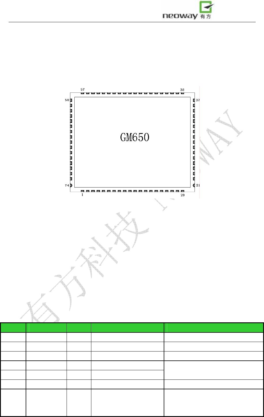
Table 4-3
GPS Specifications Description
GPS C/A coding 1.023 MHz chip rate
GPS Channel 48 channels tracking
GPS Sensitivity -162dBm
Position Accuracy 10m
Speed Accuracy 0.01 m/s
Time Accuracy Synchro with GPS Satellite time(<60ns)
Time of hot start <1s
Time of warm start <35s
Time of cold start <35s
Time of recapture <0.1s
Neo_GM650 User Manual V1.0
All rights reserved by Shenzhen Neoway Technology Co., Ltd Page 8 Total 14
GPS data updating
frequency
2HZ
Height limit 18288m
Speed limit 515 m/s or 1854Km/h
Acceleration limit <4g
Average working current
(tracking mode)
< 38mA
Average working current
(getting posotion)
< 45mA
Note: The starting time, working current and other parameters of GPS is related to
testing environment, including whether is under open sky, the thickness of the clouds and
so on.
Neo_GM650 User Manual V1.0
All rights reserved by Shenzhen Neoway Technology Co., Ltd Page 9 Total 14
5 Pin Definition & Encapsulation
5.1 Pin Definition
The signal connection uses 74pin SMD pad of stamp hole(half hole).
Note: GM650 module IO interface level is 2.8V.
Because the module IO uses 2.8V power supply system, the maximum input voltage of all
the IO interface can not exceed the maximum 3.3V, otherwise it may damage the module
IO. Considering the signal integrality designing reasons,while the external circuit use 3.3V
power system the IO interface output voltage will exceed 3.3V because of overshoot
phenomenon, sometimes can even reach 3.5V.Therefore,the IO pin of the module will be
damaged if 3.3V IO signal is connected to 2.8V IO of the module directly.So it is needed to
adopt level matching measures.Please refer to chapter 6.2.
Table 5-1 GM650 Pin Definition
Pin Signal Name I/O Function Description Remark
1 GND PWR Ground
2 Reserved Reserved
3 Reserved Reserved
4 URXD1 DI UART1 data receiving
5 UTXD1 DO UART1 data transmitting
Used to GPRS communications
and AT commands
6 NC Reserved suspend, without any signal input.
7 UTXD2 DO UART2 data
transmitting, baud rate
= 9600
Dual-port mode, used to receive
GPS data;
Single-port mode, suspend.

Neo_GM650 User Manual V1.0
All rights reserved by Shenzhen Neoway Technology Co., Ltd Page 10 Total 14
8 Reserved DO PWM output Must externally connect 100k
pulldown resistor
9 GND PWR Ground
10 Reserved Reserved
11 Reserved Reserved
12 VCCIO AO 2.8V output Can be supplied to IO level shift
circuit,loading capacity<50mA
13 VRTC PWR RTC power 2.8V,the highest output current is
2mA
14 BACK_LIGH
T
DO working station
indicator,output square
signal of 0.5S high
level,1.5Slow level
High level light LED ,need to
parallel connect a capacitor of
0.1uF
15 Reserved Reserved
16 Reserved Reserved
17 RESET DI Reset Soft reset input,low level reset
18 Reserved Reserved
19 Reserved Reserved
20 GND PWR Ground
21 ANT_GSM I/O GSM antenna RF
interface
22 GND PWR
Ground
23 DTR DI
Low power consumption
set
24 Reserved Reserved
25 Reserved Reserved
26 Reserved Reserved
27 KCOL0 DI Keyboard column scan 0 While using the serial interface to
update software version,pin27
KCOL0 must be high level
28 ON/OFF DI ON/OFF input low level pulse can change
ON/OFF state。
29 Reserved Reserved
30 Reserved Reserved
31 Reserved Reserved
32 RING DO Ring output
33 Reserved Reserved
34 Reserved Reserved
35 Reserved Reserved
36 Reserved Reserved
37 GND PWR Ground
38,39 VBAT PWR Main Power 3.5V~4.3V,recommend 3.9V

Neo_GM650 User Manual V1.0
All rights reserved by Shenzhen Neoway Technology Co., Ltd Page 11 Total 14
40 Reserved Reserved
41 Reserved Reserved
42 Reserved Reserved
43 Reserved Reserved
44 GND PWR
Ground
45 Reserved Reserved
46 Reserved Reserved
47 Reserved Reserved
48 Reserved Reserved
49 VSIM1 PWR Power of SIM card 1 Compatible to 1.8/3.0V SIM card
50 SIM1_CLK DO Clock of SIM card 1
51 SIM1_RST DO SIM card 1 reset
52 SIM1_DATA DIO Data input&output of
SIM card 1
Built-in 5K pull-up resistor
53 GND PWR
Ground
54 MICP AI Positive electrode of
MIC audio input
Alternating peak voltage≤200mV
55 MICN AI Negative electrode of
MIC audio input
Alternating peak voltage≤200mV
56 EARN AO Positive electrode of
earphone audio output
32Ω earphone driving output
57 EARP AO Negative electrode of
earphone audio output
32Ω earphone driving output
58 SPKN0 AO Negative electrode of
speaker output
Maximum 0.9W@8Ω
59 SPKP0 AO Positive electrode of
speaker output
Maximum 0.9W@8Ω
60 Reserved Reserved Build-in internal 100k pull-up
resistor.
61 Reserved Reserved
62 Reserved Reserved
63 Reserved Reserved
64 Reserved Reserved
65 GND PWR Ground
66 Reserved Reserved
67 Reserved Reserved
68 Reserved Reserved
69 Reserved Reserved
70 CLK32K DO 32.768kHZ real time
clock output
71 Reserved Reserved
72 Reserved Reserved
Neo_GM650 User Manual V1.0
All rights reserved by Shenzhen Neoway Technology Co., Ltd Page 12 Total 14
73 GND PWR Ground
74 ANT_GPS I/O GPS antenna RF
interface
5.2 PCB Packaging
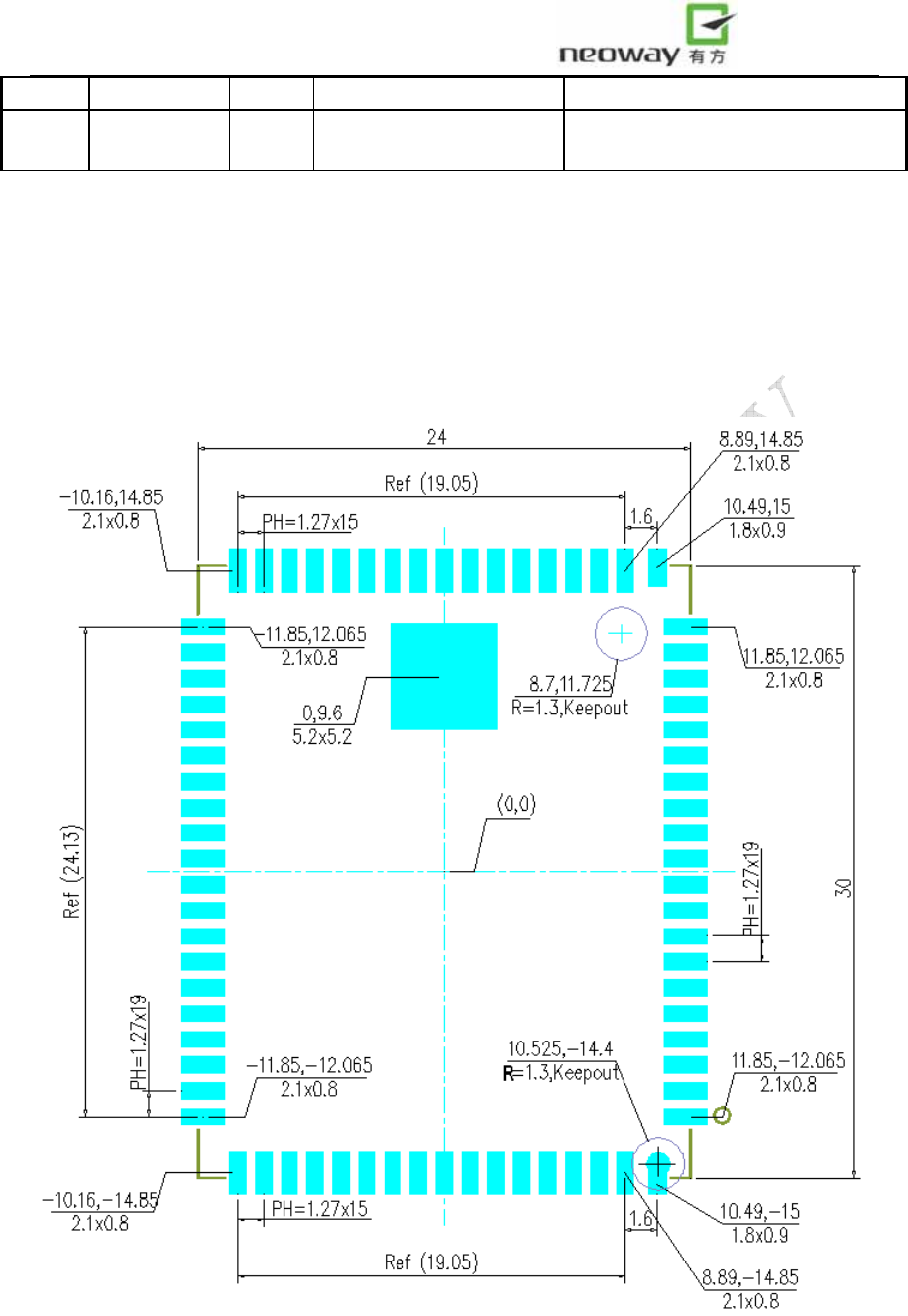
The signal connection use 74pin SMD pad.The pin is stamp hole(half hole).The pitch is
1.27mm.The PCB encapsulation we recommend is as chart 5-1.Unit:mm
Chart 5-1 Recommend PCB packaging(topview)
Note:The number in the brackets stand for coordinate figure of the pad.The original point is

Neo_GM650 User Manual V1.0
All rights reserved by Shenzhen Neoway Technology Co., Ltd Page 13 Total 14
the center of the mudule.
The number below the coordinate figure stand for shape size of the pad’s LxW.
The top right corner and the bottom right corner is two circle regions(R=1.3).The circle
regions are route keep out regions.
6 General AT Commends
CHECK THE MANUFACTURE AT+CGMI
QUERY MODULE MODEL AT+CGMM
QUERY VERSION AT+GETVERS
GET SEQUENCE NUMBER AT+CGSN
GET INTERNATIONAL MOBILE
SUBSCRIBER IDENTIFICATION
AT+CIMI
GET SIM CARD IDENTIFICATION AT+CCID
7 Call Control Commends
CALL ANSWERING ATA
DIALING COMMENDS ATD
HAND UP CALLS ATH
8 TCP/UDP AT Commends
ESTABLISH PPP LINK AT+XIIC
ESTABLISH TCP LINK AT+TCPSETUP
SEND TCP DATA AT+TCPSEND
CLOSE TCP LINK AT+TCPCLOSE
ESTABLISH UDP LINK AT+UDPSETUP
SEND UDP DATA AT+UDPSEND
CLOSE UDP LINK AT+UDPCLOSE
9 GPS AT Commends
GPS ON&OFF AT+GPSPWR
OBTAIN THE GPS DATA AT+GPSFETCH
10 Assembling
In order to prevent the product of GM650 from being affected with damp, caused by
Neo_GM650 User Manual V1.0
All rights reserved by Shenzhen Neoway Technology Co., Ltd Page 14 Total 14
using the SMT way to perform the furnace welding, in the process of production and use of
the costumer, we employ the way of damp-proof packing, such as Aluminum Foil Bag,
desiccating agent, Humidity Indicator Cards, Suck plastic trays, and vacuolization. As a
result the product is kept dry and its life span will be long.
In order to make the SMT way easy, we use the tray to load the product. The user only
needs to install it in the chip mounter according to the fixed direction.
GM650 storage and SMT notes, please refer to <Neoway module SMT reflow
production recommendation_V1.0>.
FCC Caution
Any Changes or modifications not expressly approved by the party responsible for
compliance could void the user’s authority to operate the equipment.
This device complies with part 15 of the FCC Rules. Operation is subject to the
following two conditions: (1) This device may not cause harmful interference, and
(2) this device must accept any interference received, including interference that
may cause undesired operation.
Note: This equipment has been tested and found to comply with the limits for a
Class B digital device, pursuant to part 15 of the FCC Rules. These limits are
designed to provide reasonable protection against harmful interference in a
residential installation. This equipment generates uses and can radiate radio
frequency energy and, if not installed and used in accordance with the instructions,
may cause harmful interference to radio communications. However, there is no
guarantee that interference will not occur in a particular installation. If this equipment
does cause harmful interference to radio or television reception, which can be
determined by turning the equipment off and on, the user is encouraged to try to
correct the interference by one or more of the following measures:
—Reorient or relocate the receiving antenna.
—Increase the separation between the equipment and receiver.
—Connect the equipment into an outlet on a circuit different from that to which the
receiver is connected.
—Consult the dealer or an experienced radio/TV technician for help.
FCC Radiation Exposure Statement:
This equipment complies with FCC radiation exposure limits set forth for
an uncontrolled environment .This equipment should be installed and
operated with minimum distance 20cm between the radiator & your body.
This transmitter must not be co-located or operating in conjunction with any
other antenna or transmitter.