Neoway Technology 1232 GPRS Module User Manual
Shenzhen Neoway Technology Co., Ltd GPRS Module
User Manual

Neo_M680
Hardware User Guide
Version 1.0
Let's enjoy the wireless life

Neo_M680 Hardware User Guide V1.0
Copyright Neoway Techlology Co., Ltd. Page 2 of 31
Copyright
Copyright © 2008 Neoway Technology
All rights reserved.
is a trade mark of Neoway Technology Co., Ltd.
Notice
This document is intended for the customer engineers.
This document is subject to change without any notice.
No responsibility is assumed by Neoway Technology for the use of this document.
Neoway Technology always provides the best supports.
For pricing, delivery, and ordering information please contact:
Sales@neoway.com.cn
For any technical support requests please contact:
Support@neoway.com.cn
For further information please visit:
http://www.neoway.com.cn

Neo_M680 Hardware User Guide V1.0
Copyright Neoway Techlology Co., Ltd. Page 3 of 31
Contents
Copyright ............................................................................................................................................ 2
1. Introduction ................................................................................................................................ 6
2. General Description ................................................................................................................... 6
3. Simplified Block Diagram ......................................................................................................... 6
4. Key Features ............................................................................................................................... 7
5. Product Specifications ............................................................................................................... 8
5.1 Variants ................................................................................................................................. 8
5.2 Dimension & Package ........................................................................................................... 8
5.3 Pin Description ...................................................................................................................... 9
5.4 PCB foot print ..................................................................................................................... 12
6. Application Interface ............................................................................................................... 13
6.1 Power Supply Requirements ................................................................................................ 13
6.1.1 Power Supply Basic Design Rules ........................................................................ 13
6.1.2 Extended Design Rules for Power Supply: ........................................................... 15
6.2 ON/OFF Procedure ............................................................................................................. 17
6.2.1 Turning on the module: ......................................................................................... 18
6.2.2 Turning off the module: ........................................................................................ 18
6.2.3 RESET .................................................................................................................. 19
6.2.4 VMC ..................................................................................................................... 19
6.3 UART .................................................................................................................................. 20
6.3.1 Basic Descriptions of UART ................................................................................. 20
6.3.2 Level Translators for UART .................................................................................. 20
6.4 Sleep mode .......................................................................................................................... 22
6.4.1 DTR ....................................................................................................................... 22
6.4.2 RING ..................................................................................................................... 23
6.5 SIM interface ...................................................................................................................... 23
6.6 Running LED Indicator ....................................................................................................... 25
6.7 Audio Interface ................................................................................................................... 26
6.8 Antenna Interface ................................................................................................................ 28
7. Mounting the Module onto the Application Board ............................................................... 30

Neo_M680 Hardware User Guide V1.0
Copyright Neoway Techlology Co., Ltd. Page 4 of 31
8. Package ..................................................................................................................................... 30
9. Terms and Abbreviations ......................................................................................................... 31

Neo_M680 Hardware User Guide V1.0
Copyright Neoway Techlology Co., Ltd. Page 5 of 31
Document History
Revision History
Version Remarks Date Issue
V1.0 Initial Version 2013-9
Neo_M680 Hardware User Guide V1.0
Copyright Neoway Techlology Co., Ltd. Page 6 of 31
1. Introduction
This document describes the hardware features of M680, and guides for the relevant
application design.
2. General Description
With the ultra-compact design, M680 is intended to be used in a wide range of applications,
including industrial and consumer devices. M680 is a GSM/GPRS module with EDGE of
downlink. It features with voice, SMS, and data services.
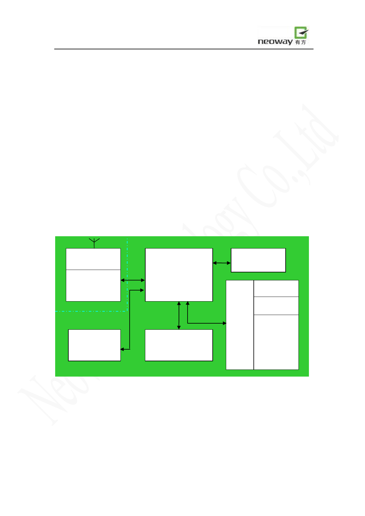
3. Simplified Block Diagram
Figure 1 M680 Block Diagram
Baseband
Controller
PA
Power
Manager
Application Interface
RF
Section
FLASH
Audio
Section
SIM
UART x 2
ADC/PWM
I2C

Neo_M680 Hardware User Guide V1.0
Copyright Neoway Techlology Co., Ltd. Page 7 of 31
4. Key Features
Table 1 M680 Key Features
Feature Implementation
Frequency Bands 850/900/1800/1900 MHz quad-band
Compliant with GSM/GPRS Phase2/2+
Sensitivity < -107dBm
Transmit Power 850/900 Class4(2W)
1800/1900 Class1(1W)
AT GSM07.07
Extended AT commands
Audio CODEC FR、EFR、HR、AMR
SMS TEXT/PDU
Point-to-point / cell broadcast
DATA GPRS: Class 12
Supplementary Service
Call forwarding(CFB, CFNA, CFU)
Call waiting & Call hold
Multiparty call
USSD
CPU ARM7-EJ@260MHz, 32Mbits SRAM, 16~32Mbits Nor Flash
Open Resources 16Mbits RAM, 0.3~16Mbits Flash
Interfaces UART x 2, I2C, SPI, ADC, PWM, GPIO
Operational Temperature -40℃~+85℃
Operating Voltage 3.5V
~
4.2V
(
typical 3.9V
)
Peak Current Max 1.8A
Power Consumption < 2mA @DRX5 (Sleep mode)
Neo_M680 Hardware User Guide V1.0
Copyright Neoway Techlology Co., Ltd. Page 8 of 31
5. Product Specifications
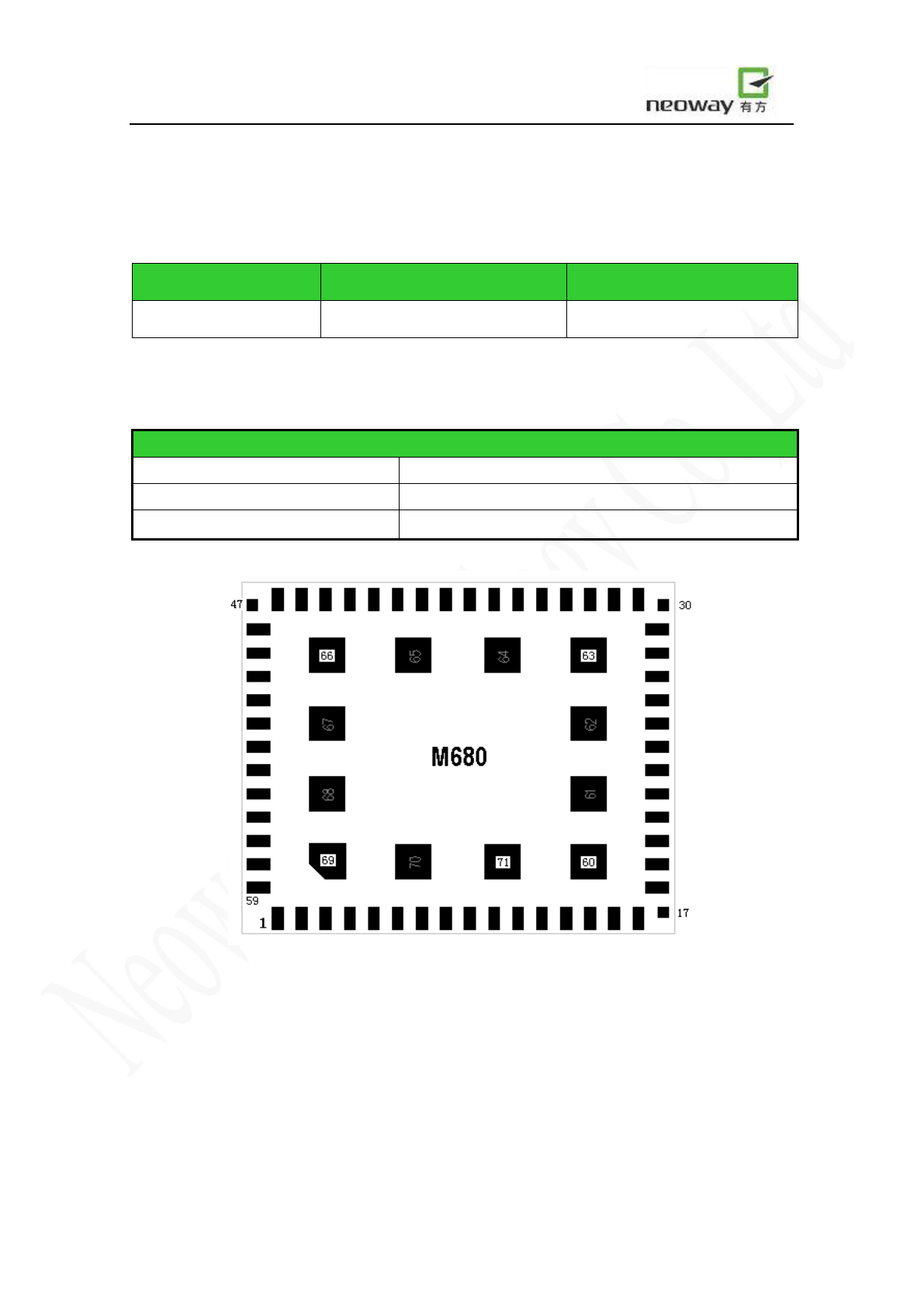
5.1 Variants
Variants Frequencies Packages
M680-QUAD-AA0/A00 850/900/1800/1900MHz Quad-band 71 Pin LCC
5.2 Dimension & Package
Physical Characteristics
Dimensions 15mm*18mm*2.1
mm (Length*Width*Thickness)
Weight 2 g
Package 71 Pin LCC
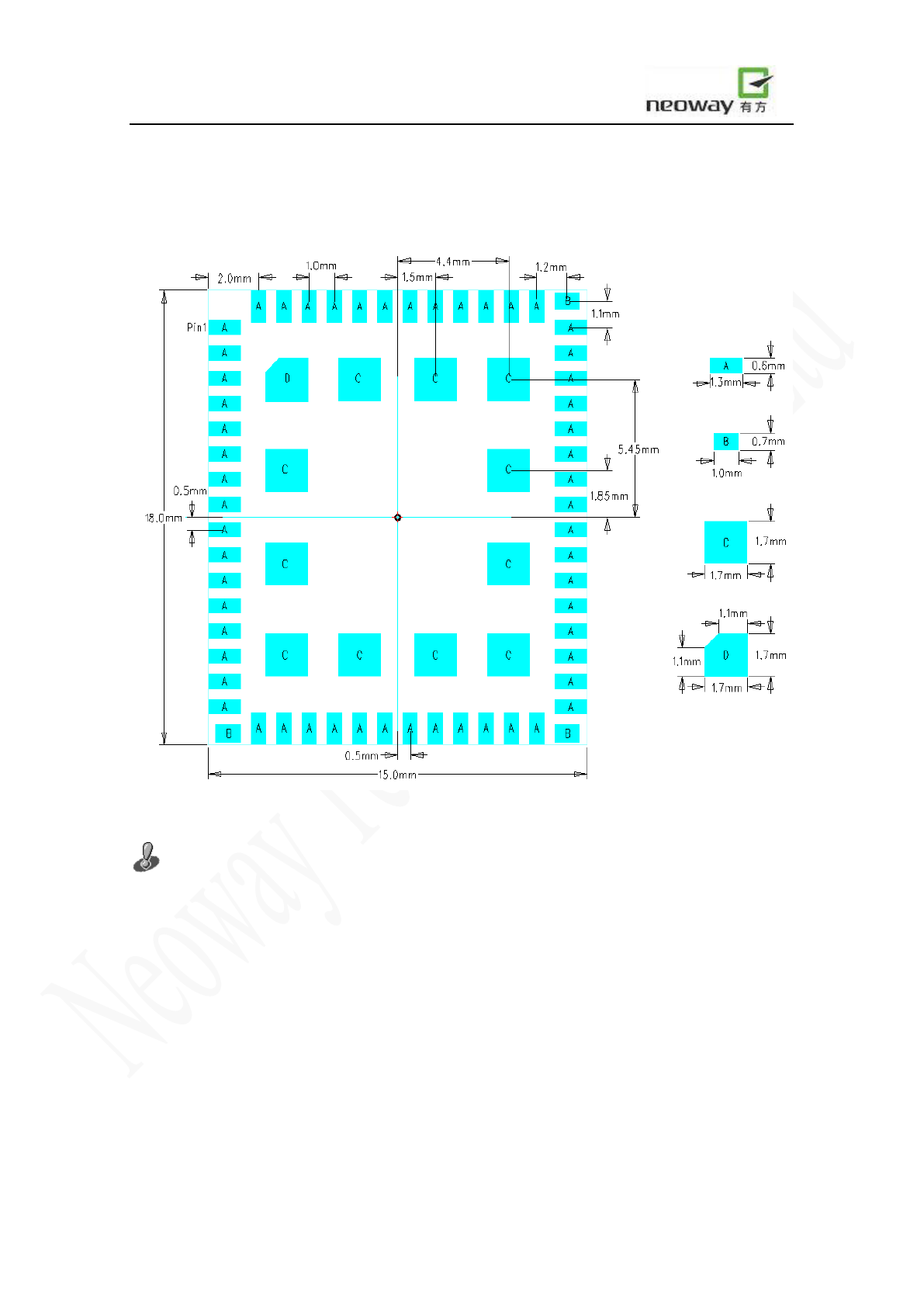
Figure 2 M680 Sketch

Neo_M680 Hardware User Guide V1.0
Copyright Neoway Techlology Co., Ltd. Page 9 of 31
5.3 Pin Description
Table2 M680 pin definition
M680
Pin Signal I/O Function Note
1 ON/OFF DI Switch the module on/off Low level pulse triggered
2 SPKP AO Speaker output P Use AT command to open and
0.9W@8Ω
3 SPKN AO Speaker output N
4
MICP0
AI
MIC+
Vi ≤ 200mVpp
5
MICN0
AI
MIC-
Vi ≤ 200mVpp
6 EAR-L AO Earpiece output L
Signal Ended Output. Can
drive a 16Ω/32Ω earpiece
directly.
7 EAR-R AO Earpiece output R
Signal Ended Output. Can
drive a 16Ω/32Ω earpiece
directly.
8
MICN1
AI
MIC-
Vi ≤ 200mVpp
9
MICP1
AI
MIC+
Vi ≤ 200mVpp
10 RECN AO Receiver output N 32Ω receiver output
11 RECP AO Receiver output P
12 Reserved Reserved
13 Reserved Reserved
14 Reserved Reserved
15 Reserved Reserved
16 Reserved Reserved
17 Reserved Reserved
18 GND PWR GND
19 SIM_CLK DO SIM clock
20
SIM_DATA
DIO
SIM data
5KΩ internal pull-up
21 SIM_RST DO SIM reset Prompted by module
22 VSIM
PWR
SIM supply voltage 1.8/3.0V compatible.
23 DAISYNC DO Digital audio synchronization
24 DAIPCMIN DI Digital audio input
25 DAIPCMOUT DO Digital audio output
26 DAICLK DO Digital audio signal clock
27 Reserved Reserved
28 Reserved Reserved
29 GND PWR GND
30 BT_ANT I/O Antenna interface for BT Connect 50Ω antenna
31 GND PWR GND
32 Reserved Reserved

Neo_M680 Hardware User Guide V1.0
Copyright Neoway Techlology Co., Ltd. Page 10 of 31
33 Reserved Reserved
34 Reserved Reserved
35 Reserved Reserved
36 VMC PWR Output 2.8V Can be used to power the level
translators. Imax=50mA
37 URXD DI Serial data input of module
38
UTXD
DO
Serial data output of module
39 Reserved Reserved
40 Reserved Reserved
41
VRTC
PWR
RTC power
2.8V, Imax=2mA
42 DTR DI Data Terminal Ready
Can be used to control sleep
mode.
43 RING DO Output for RING indicator
Can be used to indicate an
incoming voice call or SMS.
44 LIGHT DO Status LED 2.8V/4mA output
Can drive a LED directly
45
Reset
DI Reset input Active low
46 GND PWR GND
47
GPRS_ANT
I/O GPRS antenna interface Connect 50Ω antenna
48 GND PWR GND
49 Reserved Reserved
50 Reserved Reserved
51 Reserved Reserved
52 Reserved Reserved
53 Reserved Reserved
54 Reserved Reserved
55 Reserved Reserved
56
ADC
AI
ADC input
0V<Vin<2.8V
61
USB_DM
I/O
Software download interface
62
USB_DP
I/O
57
VBAT PWR Main power supply 3.5V~4.3V (typical 3.9V)
58
59
68
VBAT
PWR
Main power supply
3.5V~4.3V (typical 3.9V)
60
GND PWR GND
63
64
65
66
67
69

Neo_M680 Hardware User Guide V1.0
Copyright Neoway Techlology Co., Ltd. Page 11 of 31
70
71
Neo_M680 Hardware User Guide V1.0
Copyright Neoway Techlology Co., Ltd. Page 12 of 31
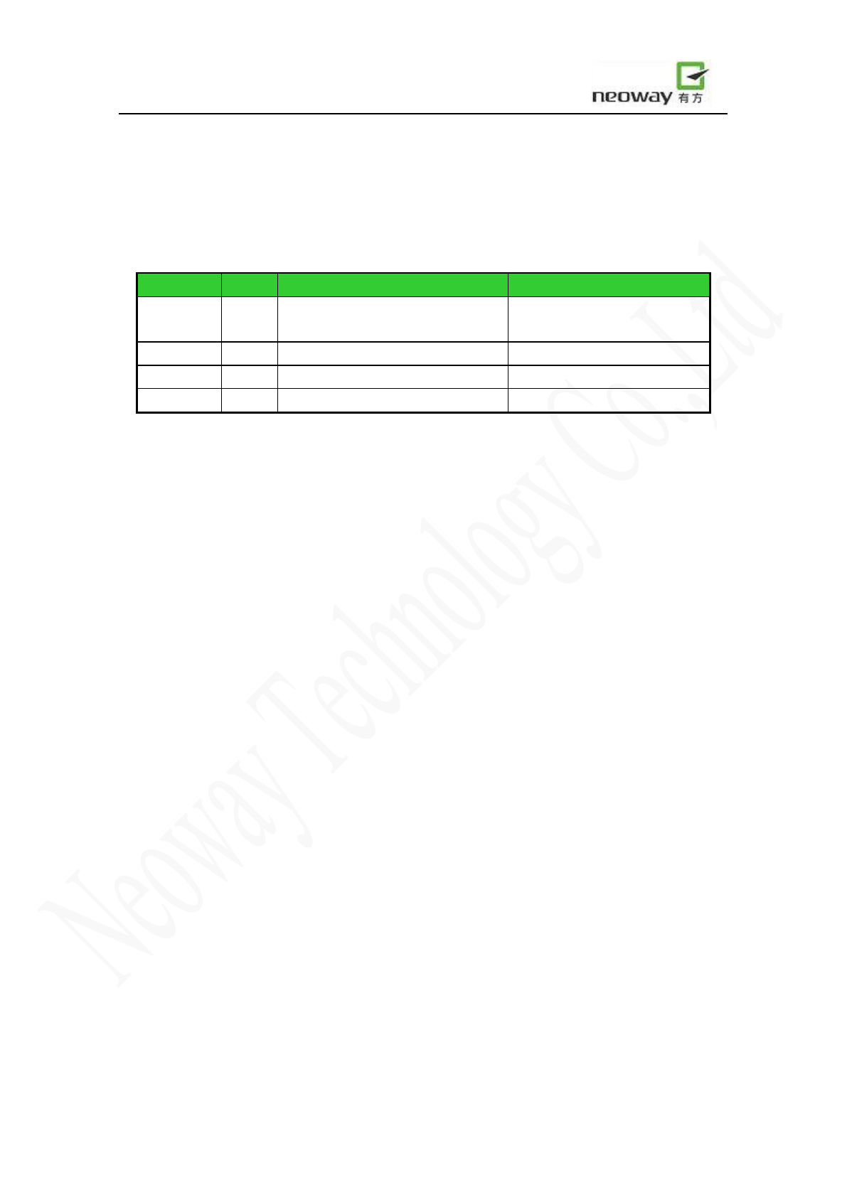
5.4 PCB foot print
Recommended foot print:
Figure 3 Recommended foot print of M680 (all dimensions in millimeters)
Note:
There may be some masks on the bottom of the module PCB, created by hollowing the solder resist
layer, causing reveal of copper. To avoid short circuits, it is recommended to cover the application
PCB with a silkscreen block at the area under the module, but excluding soldering area.
Neo_M680 Hardware User Guide V1.0
Copyright Neoway Techlology Co., Ltd. Page 13 of 31
6. Application Interface
6.1 Power Supply Requirements
Table3 Power Supply and ON/OFF Control
Signal I/O Function Note
VMC PWR 2.8V power output Can be used to power the level
translators. Imax=5mA
Reset DI Reset input Active low > 60mS.
ON/OFF DI Switch the module on/off Low level pulse triggered.
VBAT
PWR
Main Power Supply
3.5V~4.3V(typical 3.9V)
6.1.1 Power Supply Basic Design Rules
VBAT is the main power supply for internal base band and radio PA of the module, in a range of
3.5V-4.3V. A 3.9V voltage is preferable.
The performance of power supply issued, is a critical path to module’s performance and stability.
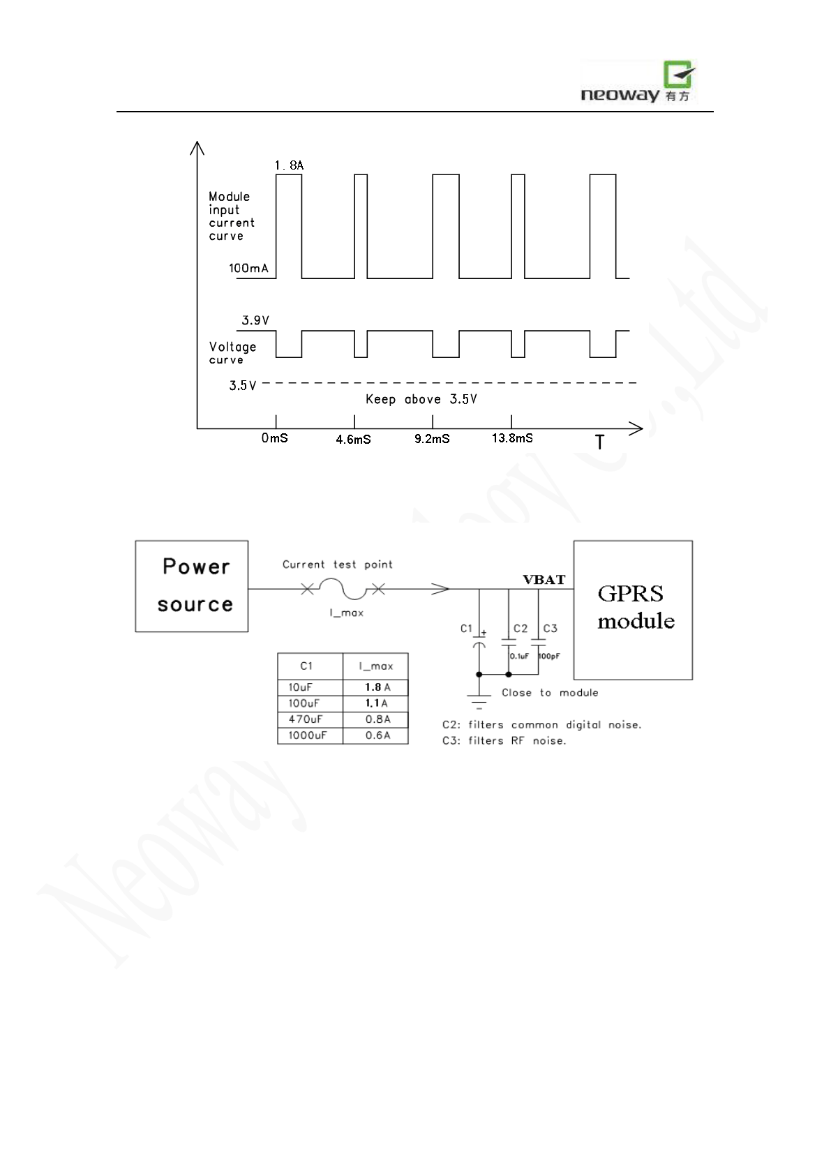
The GSM bursts can cause current peaks up to 1.8A, therefore large bypass capacitors are expected
to reduce voltage drops during the bursts. The biggest current occurs when the received signal is
very low. It’s very important to ensure that the voltage of supply rail never drops below 3.5V
while any burst occurs.
Figure 4 shows how the GSM bursts and voltage drops.
Figure 5 shows how the capacitor helps to improve peak current performance:
Neo_M680 Hardware User Guide V1.0
Copyright Neoway Techlology Co., Ltd. Page 14 of 31
Figure 4 Burst Caused Current Peaks and Voltage Drops
Figure 5 Test Circuit and Peak Current
Results may vary depending on the ESR of capacitors, and the impedance of power source.
A low ESR 1000uF aluminum capacitor for C1 can be selected. As an alternative, a 470uF
tantalum capacitor is also suited. In case of Li-Ion cell battery used, 220uF or even 100uF
tantalum capacitor may be applicable because of the battery’s low internal impedance and the
ability to provide high transient current.
Use a low impedance power source, and keep the resistance of the power supply lines as low as
possible.
Neo_M680 Hardware User Guide V1.0
Copyright Neoway Techlology Co., Ltd. Page 15 of 31
The power source should be able to output an average current greater than 1A.
Some small capacitors, with values of 0.1uF, 100pF, 33pF, placed close to the module’s power
pin, are very helpful to suppress high frequency disturbances.
The voltage range of power supply must never be exceeded. Over-voltage can even destroy the
module permanently.
Ensure the trace for VBAT to be wide enough, in order to pass the current peaks without
significant voltage drops. The width of 2mm is preferable.
6.1.2 Extended Design Rules for Power Supply:
6.1.2.1 Power Control
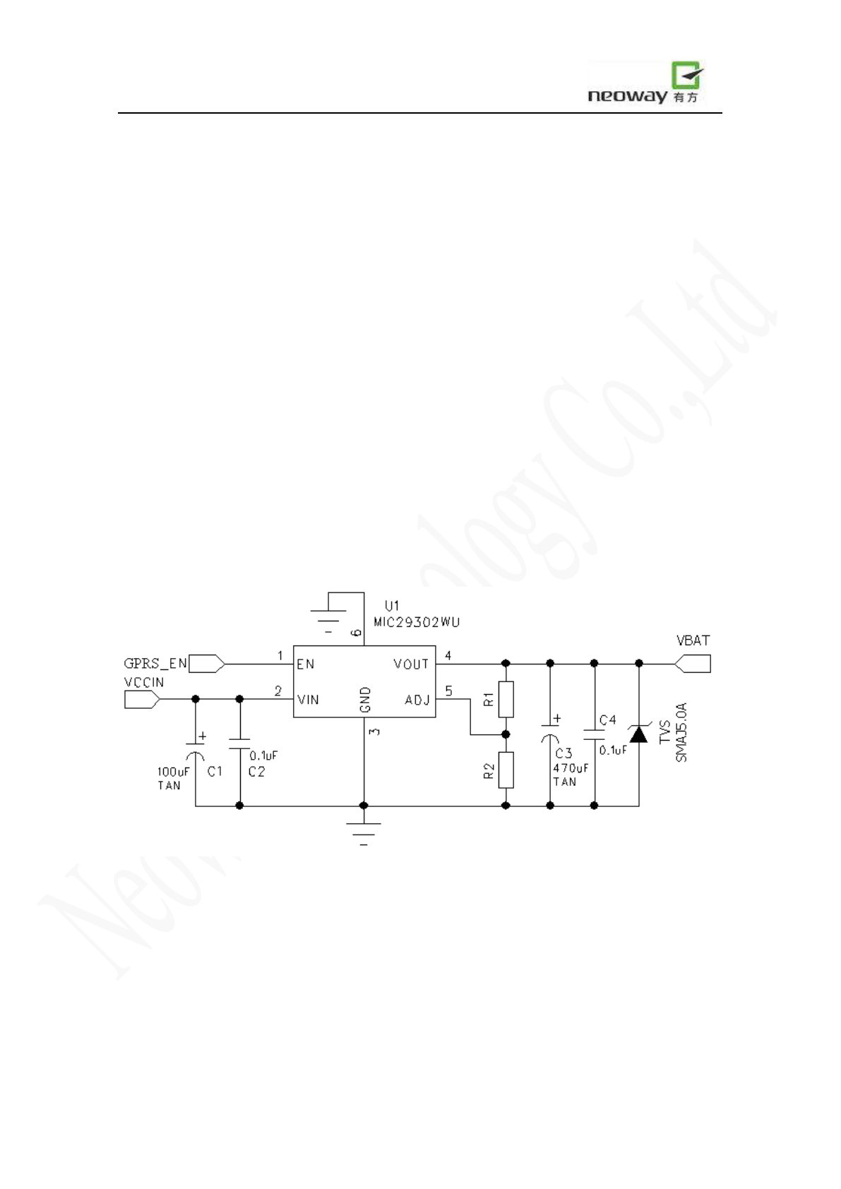
A controlled power supply is preferable if used in harsh conditions. RESET pin may be not
functioning under strong disturbance. The output enable pin of LDO or DC/DC chipset could be
used for emergency power control of the module, as shown in Figure 6.
Figure 6 Using LDO’s enable pin for emergency power control
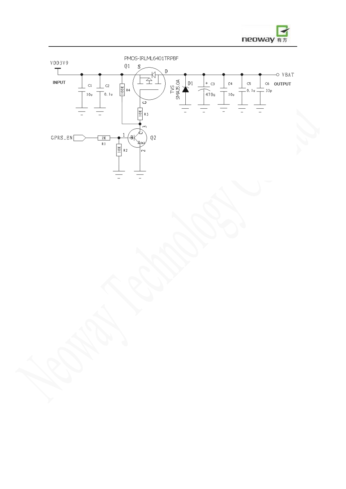
The alternative way is to use a P-MOSFET to control the module’s power, as shown in Figure 7. The
GPRS_EN signal is routed to host GPIO, controlling the ON/OFF of the P-MOSFET. The host can
cut off and then switch on the power supply in case of abnormal conditions, such as no response
from the module or the disconnection of GPRS.
Neo_M680 Hardware User Guide V1.0
Copyright Neoway Techlology Co., Ltd. Page 16 of 31
Figure 7 Using PMOS for power control
Q2 is for eliminating the need for a high enough voltage level of the host GPIO. In case that the
GPIO can output a high voltage greater than VDD3V9 - |VGS(th)|, where VGS(th) is the Gate Threshold
Voltage, Q2 is not needed.
Reference components:
Q1: IRML6401
Q2: MMBT3904
C4: 470uF tantalum capacitor rated at 6.3V; or 1000uF aluminum capacitor.
It’s strongly recommended to place a TVS diode on VBAT to ground, in order to absorb the power
surges subjected. The SMAJ5.0A from Vishay can be as a choice.
6.1.2.2 Power Separating
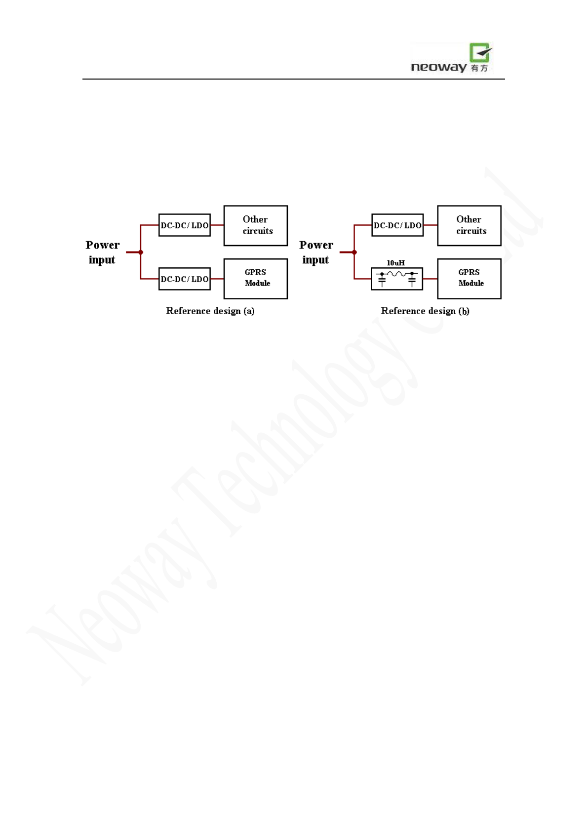
As described in section 6.1.1, the GSM device works in burst mode generating voltage drops on
power supply. And furthermore this results in a 217Hz TDD noise through power (One of the way
generating noise. Another way is through RF radiation). Analog parts, especially the audio circuits,
are subjected to this noise, known as a “buzz noise” in GSM systems. To prevent other parts from
being affected, it’s better to use separated power supplies. The module shall be supplied by an
Neo_M680 Hardware User Guide V1.0
Copyright Neoway Techlology Co., Ltd. Page 17 of 31
independent power, like a DC/DC or LDO.
The inductor used in Reference Design (b), should be a power inductor and have a very low
resistance. The value of 10uH, with average current ability>1.2A and low DC resistance, is
recommended.
Figure 8 Using separated power supply for module
Never use a diode to make the drop voltage between a higher input and module power. It will
obviously decrease the module performances, or result in unexpected restarts, due to the forward
voltage of diode will vary greatly in different temperature and current.
6.1.2.3 EMC Considerations for Power Supply
Place transient overvoltage protection components like TVS diode on power supply, to absorb the
power surges. SMAJ5.0A could be a choice.
6.1.2.4 Power-on Sequence
Prior to turning on the module, turn on the host MCU and finish the UART initialization. Otherwise
conflictions may occur during initialization, due to unstable conditions.
6.2 ON/OFF Procedure
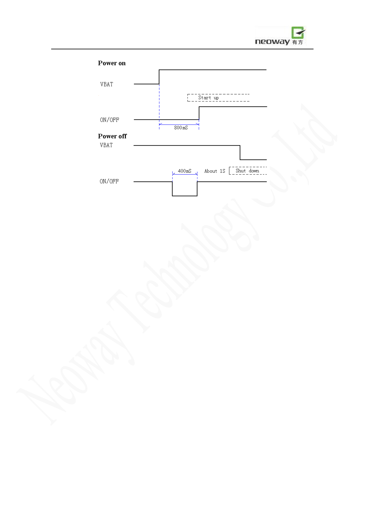
ON/OFF is a low level pulse active input, used to turn on or off the module.
Neo_M680 Hardware User Guide V1.0
Copyright Neoway Techlology Co., Ltd. Page 18 of 31
Figure 9 Turning on /off the module using ON/OFF
6.2.1 Turning on the module:
While the module is off, drive the ON/OFF pin to ground for at least 600mS (800mS is
recommended) and then release, the module will start. An unsolicited message will be sent to host
through AT port (“+EIND: 1”), indicating the powering up of the module and the AT commands can
respond.
It’s recommended to drive the ON/OFF to low before applying the VBAT to module. 300mS
(400mS is recommended) later from the VBAT applied, release the ON/OFF. Therefore the module
starts up. The simplest way to power on the module, is to directly tie the ON/OFF to ground, issuing
to an auto-power-on feature.
After the module is operating, keep ON/OFF being high level.
6.2.2 Turning off the module:
While the module is on, drive the ON/OFF pin to ground for at least 500mS and then release, the
module will try to detach to network and normally 1 second later it will shut down. Another
approach to turn off the module is with AT command.
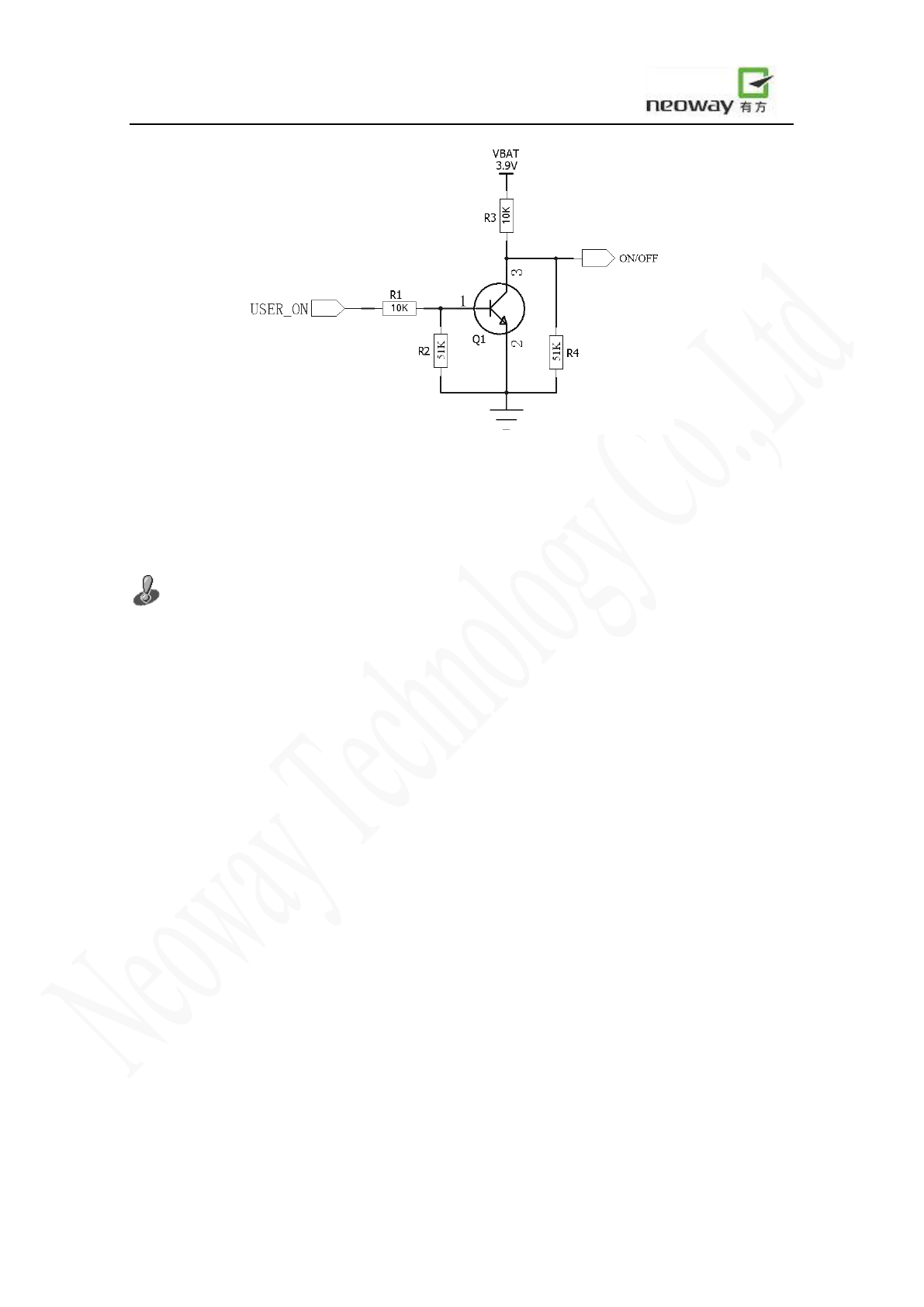
Figure 10 shows a reference circuits for ON/OFF control with inverted control logic.
Neo_M680 Hardware User Guide V1.0
Copyright Neoway Techlology Co., Ltd. Page 19 of 31
Figure 10 Reference circuit for ON/OFF control
Reference Components:
Q1: MMBT3904, or to use digital transistor with bias resistors built in, like DTC123/114
The combination of R3 and R4, should limit the high voltage of ON/OFF less than 3.0V.
Note:
If the host itself is not initialized before turning on the module, some abnormal conditions on
IO or UART may affect the power on procedure.
The better way to rescue the module from abnormal condition, is to apply a power OFF-ON
procedure, rather than using the ON/OFF control signal. In fact ON/OFF signal is
software-dependent.
6.2.3 RESET
Pull the Reset signal to low level for at least 60mS to reset the module. A pull-up resistor is
internally included. Reset pin can be left open if not used.
6.2.4 VMC
VMC is provided to power the level translators, with a 2.8V / 5mA output.
VMC can also be used to monitor the on/off state of module. It outputs 2.8V high level while the
module is on, and low level while the module is off.
Neo_M680 Hardware User Guide V1.0
Copyright Neoway Techlology Co., Ltd. Page 20 of 31
6.3 UART
6.3.1 Basic Descriptions of UART
Table 4 UART
Signal
I/O
Function
Note
URXD1 DI Serial input of module
UTXD1
DO
Serial output of module
DTR
DI
Signal for controlling sleep mode
RING
DO
Ringing output
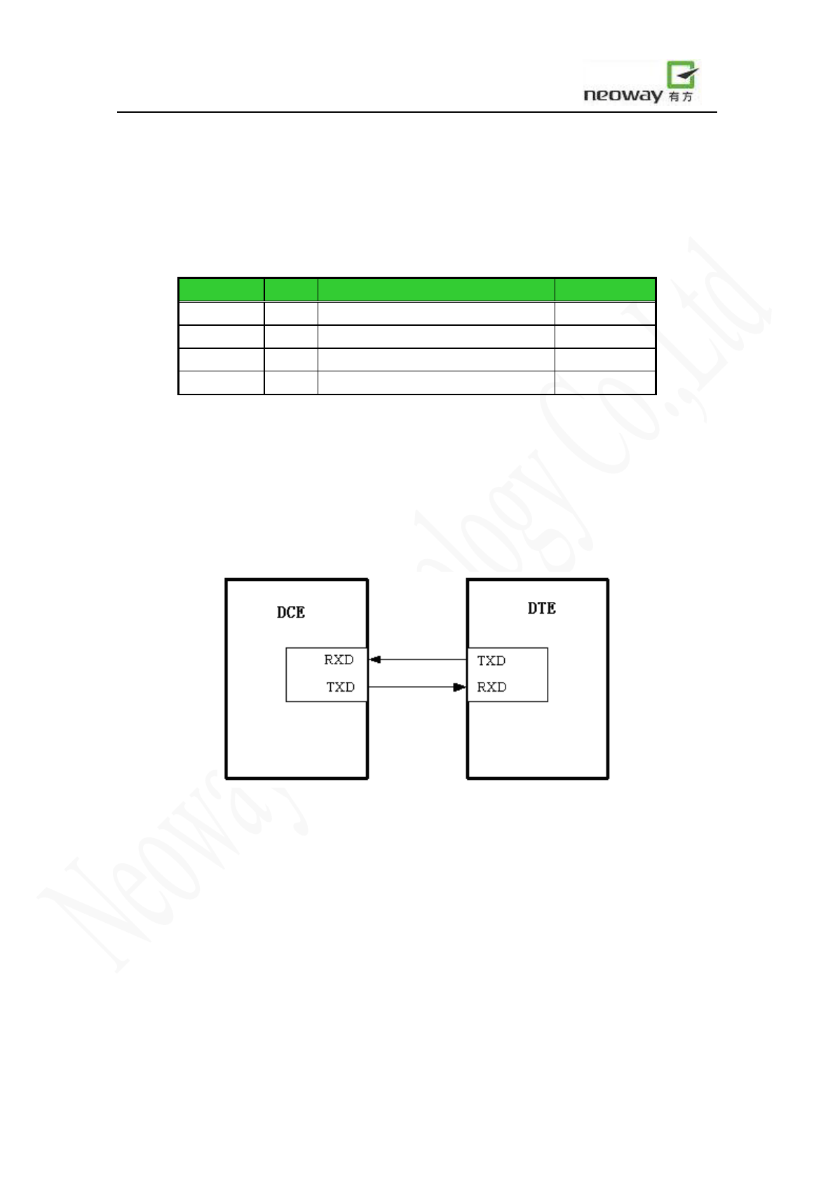
UART1 is for AT commands, data sending/receiving, firmware updating, etc.
As a DCE device, the module is connected to DTE as shown in Figure 11.
Supported baud rates are 1200, 2400, 4800, 9600, 19200, 38400, 57600, 115200, 230400bps, and the
default is 115200.
Figure 11 Connection between DCE (module) and DTE
The UART of M680 works at 2.8V CMOS logic level. The voltages for input high level should not
exceed 3.0V.
6.3.2 Level Translators for UART
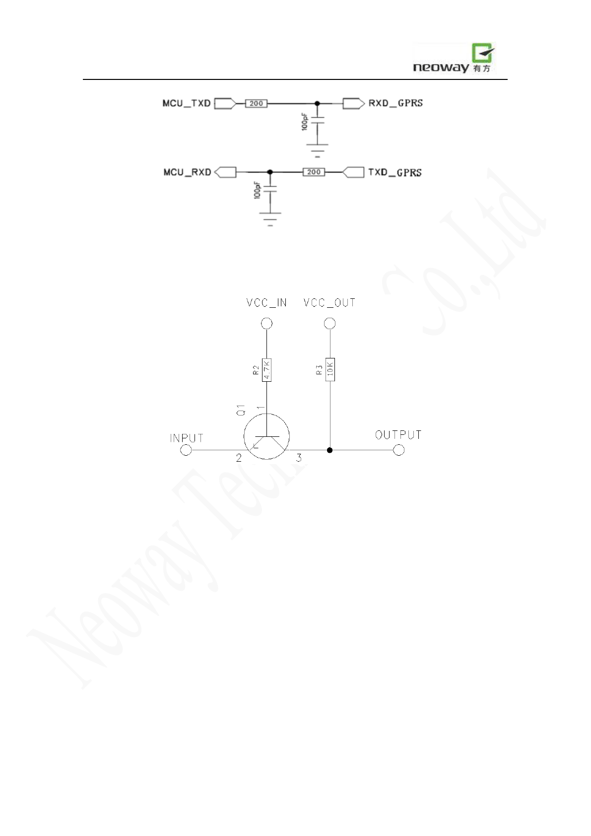
If the UART is interfacing with a MCU that has 3.3V logic levels, resistors should be connected in
series with the signals.
Neo_M680 Hardware User Guide V1.0
Copyright Neoway Techlology Co., Ltd. Page 21 of 31
Figure 12 Interfacing with 3.3V logic levels of MCU
If the UART is interfacing with a MCU that has 5V logic levels, general level translators are
required, for both inputs and outputs. As shown in Figure 13.
Figure 13 Interfacing with 5V logic levels of MCU
Reference components:
R2: 2K-10K. The higher rate the UART works at, the smaller value used
R3: 4.7K-10K. The higher rate the UART works at, the smaller value used
Q1: MMBT3904 or MMBT2222. High-speed transistors preferred.
Used for 5V logic -> 2.8V logic:
While this circuit used between MCU TXD and module URXD1, the INPUT signal is connected to
MCU TXD, and OUTPUT connected to module URXD1. VCC_IN powered from 5V and
VCC_OUT powered from 2.8V (module’s VMC can be used). This applies to DTR control as well.
Used for 2.8V logic -> 5V logic:
It can be used between module UTXD1 and MCU RXD as well, with INPUT connected to module
UTXD1, and OUTPUT connected to MCU RXD. VCC_IN powered from 2.8V (module’s VMC)
and VCC_OUT powered from 5V. This applies to RING signal as well.

Neo_M680 Hardware User Guide V1.0
Copyright Neoway Techlology Co., Ltd. Page 22 of 31
Note:
Avoid sparks and glitches on UART signals while the module is in a turning on procedure.
Avoid sending any data to UART during the beginning of 2 seconds after the module being turned
on.
6.4 Sleep mode
6.4.1 DTR
Generally DTR is used for sleep mode control. For details, see AT commands manual. Based on the
setting of the selected mode, pulling DTR low will bring the module into relevant power saving
mode. Working in this mode, the power consumption is around 2mA, depending on the DRX setting
of network.
In sleep mode, the module can also respond to the incoming call, SMS, and GPRS data. The host
MCU can also control the module to exit sleep mode by controlling DTR.
The controlling of sleep mode:
1) Keep DTR high in normal working mode. Activate the sleep mode by using the AT command
AT+ENPWRSAVE=1.
2) Pull DTR low, the module will enter sleep mode, but only after process and pending data
finished.
3) UART is not available in sleep mode.
4) In sleep mode, the module can be woken up by the events of incoming voice call, received data,
or SMS. Meanwhile the module will send out the unsolicited messages by the interface of RING
or UART.
Upon receipt of the unsolicited messages, the host MCU should pull DTR high firstly, otherwise
the module will resume sleep mode shortly. And then the host MCU can process the voice call,
received data, or SMS. After processing is finished, pull DTR low again to put the module into
Neo_M680 Hardware User Guide V1.0
Copyright Neoway Techlology Co., Ltd. Page 23 of 31
sleep mode.
5) Pull DTR high, the module will exit from sleep mode actively, and furthermore enable the
UART. Thus the voice call, received data, or SMS can be processed through UART. After
processing finished pull it low again, to take the module back to sleep mode.
6.4.2 RING
1) Once the incoming voice call, the module sends out “ring” message through UART and
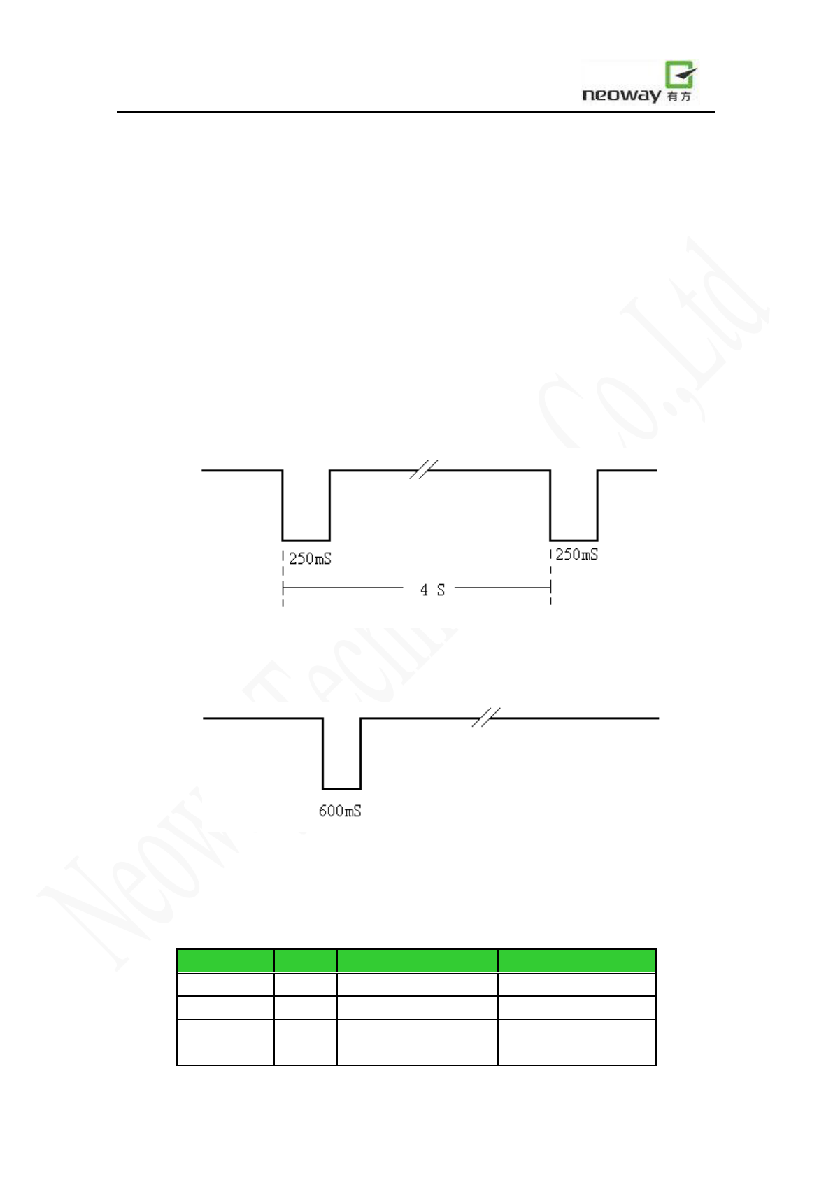
meanwhile outputs 250mS low pulses at 4S period on RING signal. See Figure 14.
Figure 14 RING indicator for incoming call
2) Upon receipt of SMS, the module outputs one 600mS low pulse. See Figure 15.
Figure 15 RING Indicator for SMS
6.5 SIM interface
Table 5 SIM Interface
Signal I/O Function Note
VSIM PWR SIM supply voltage 1.8/3.0V
SIM_CLK
DO
SIM clock
SIM_RST DO SIM reset
SIM_DATA
DIO
SIM data
Internal pull up
Neo_M680 Hardware User Guide V1.0
Copyright Neoway Techlology Co., Ltd. Page 24 of 31
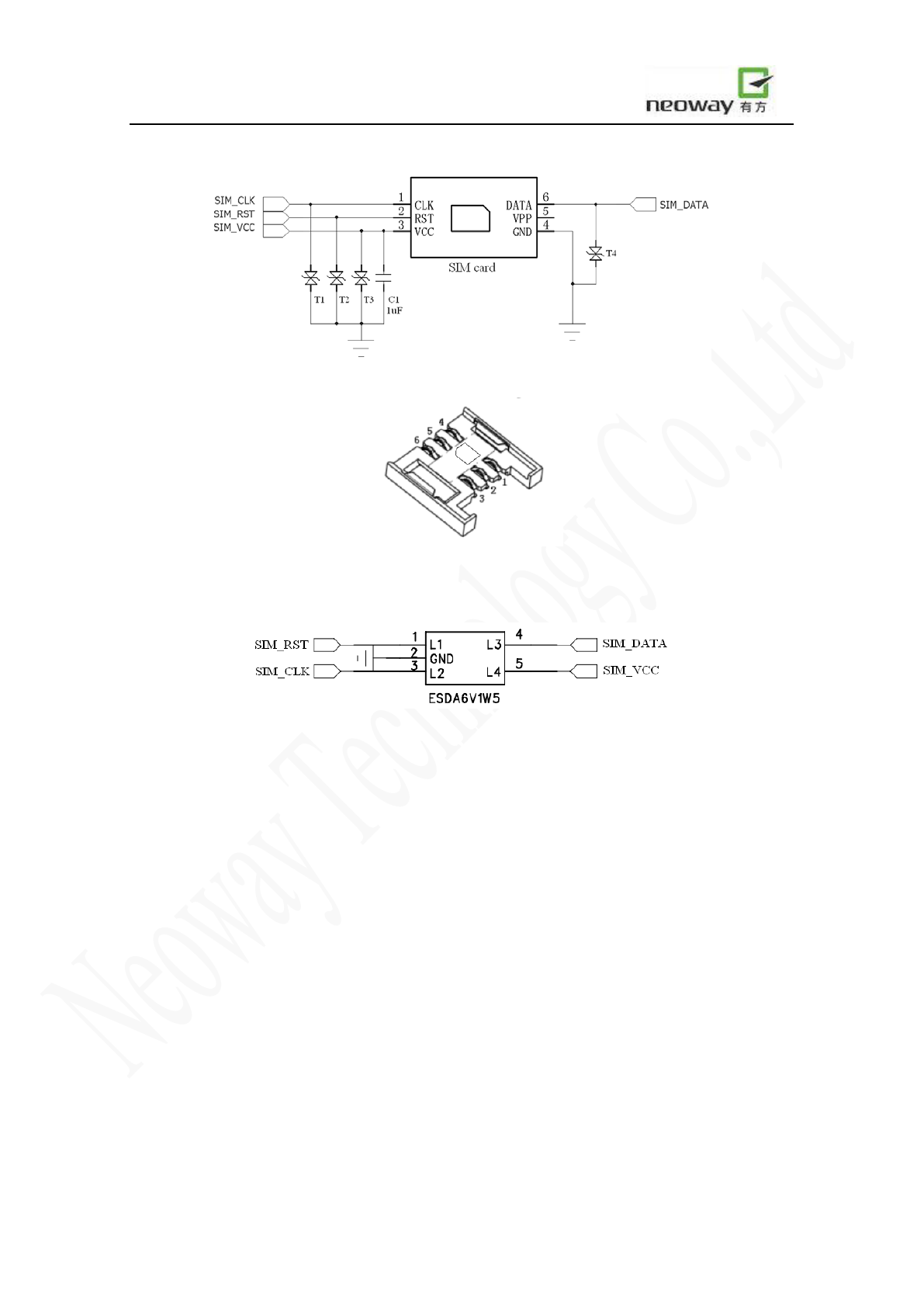
Figure 16a Reference design of SIM interface
Pin1=VCC, Pin2=RST, Pin3=CLK, Pin4=GND, Pin5=VPP, Pin6=DATA
Figure 16b a sample of SIM card socket
Figure 16c the recommended ESD diode array
M680 SIM interface is 3V/1.8V compatible. VSIM is for SIM power and can supply a 30mA
current.
SIM_DATA is internally pulled up with a 5KΩ resistor. External pull-up resistor is not needed.
SIM_CLK can work at several frequencies, but at 3.25MHz typically.
ESD protectors, such as ESD diodes or ESD Varistors, are recommended on the SIM signals,
especially in automotive electronics or other applications with badly ESD. The total equivalent
capacitance on any SIM signal, include the junction capacitance of the ESD diode and the distributed
capacitance of PCB trace, can’t be higher than 120pF.
If the SIM card is installed in a closed case without human touch or ESD, 22~33pF MLCC
capacitors can replace the ESD diodes for cost down.
SIM card is sensitive to GSM TDD noise and RF interference. So, the rule is very important in the
PCB design, listed as the following.
Neo_M680 Hardware User Guide V1.0
Copyright Neoway Techlology Co., Ltd. Page 25 of 31
☆ The antenna should be installed a long distance away from the SIM card and SIM card traces,
especially to the build-in antenna.
☆ The PCB traces of SIM should be as short as possible and shielded with GND copper.
☆ The ESD diodes or small capacitors should be closed to SIM card.
Note:
Small capacitors and the junction capacitance of the ESD diode are to avoid the interference from/to
antenna, ensuring the correct SIM access and good RF performance.
6.6 Running LED Indicator
Table 6 Running Indicator
Signal I/O Function Note
BACK_LIGHT DO Running Status Can drive a LED directly
The various blink behaviors of LED indicate different of module status.
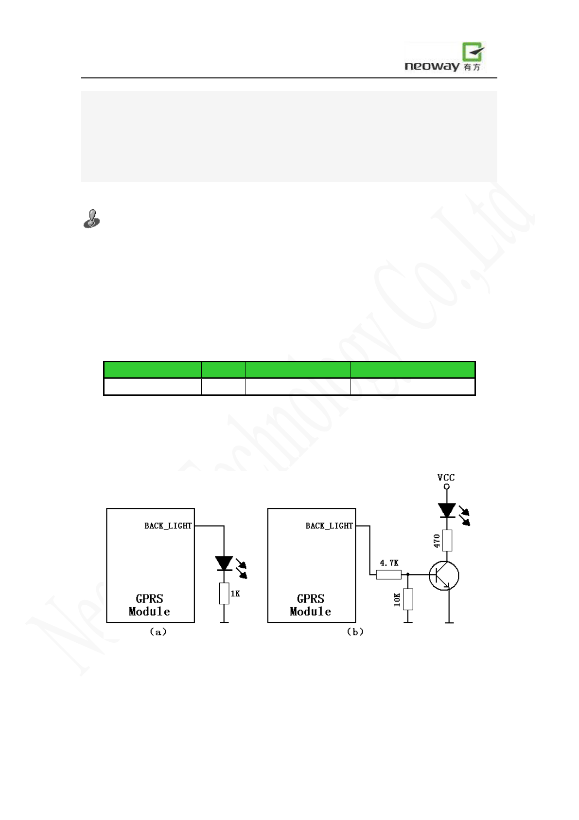
It can output a 4mA current and 2.8V voltage, therefore a LED can be directly connected to this pin
with a resistor in series. For better luminance, drive the LED with a transistor instead, see Figure 17.
Figure 17 LED Indicator
Neo_M680 Hardware User Guide V1.0
Copyright Neoway Techlology Co., Ltd. Page 26 of 31
6.7 Audio Interface
Table 7 Audio Interface
Signal I/O Function Note
SPKP AO Speaker output P Use AT command to open
and 0.9W@8Ω
SPKN AO Speaker output N
MICP0
AI
MIC+ input
Vpp≤ 200mV
MICN0
AI
MIC- input
EAR-L AO Earpiece output L Can drive a 16Ω/32Ω earpiece
directly
EAR-R AO Earpiece output R Can drive a 16Ω/32Ω earpiece
directly
MICN1
AI
MIC-
Vpp≤ 200mVpp
MICP1
AI
MIC+
RECN AO Receiver output N 32Ω receiver output
RECP AO Receiver output P 32Ω receiver output
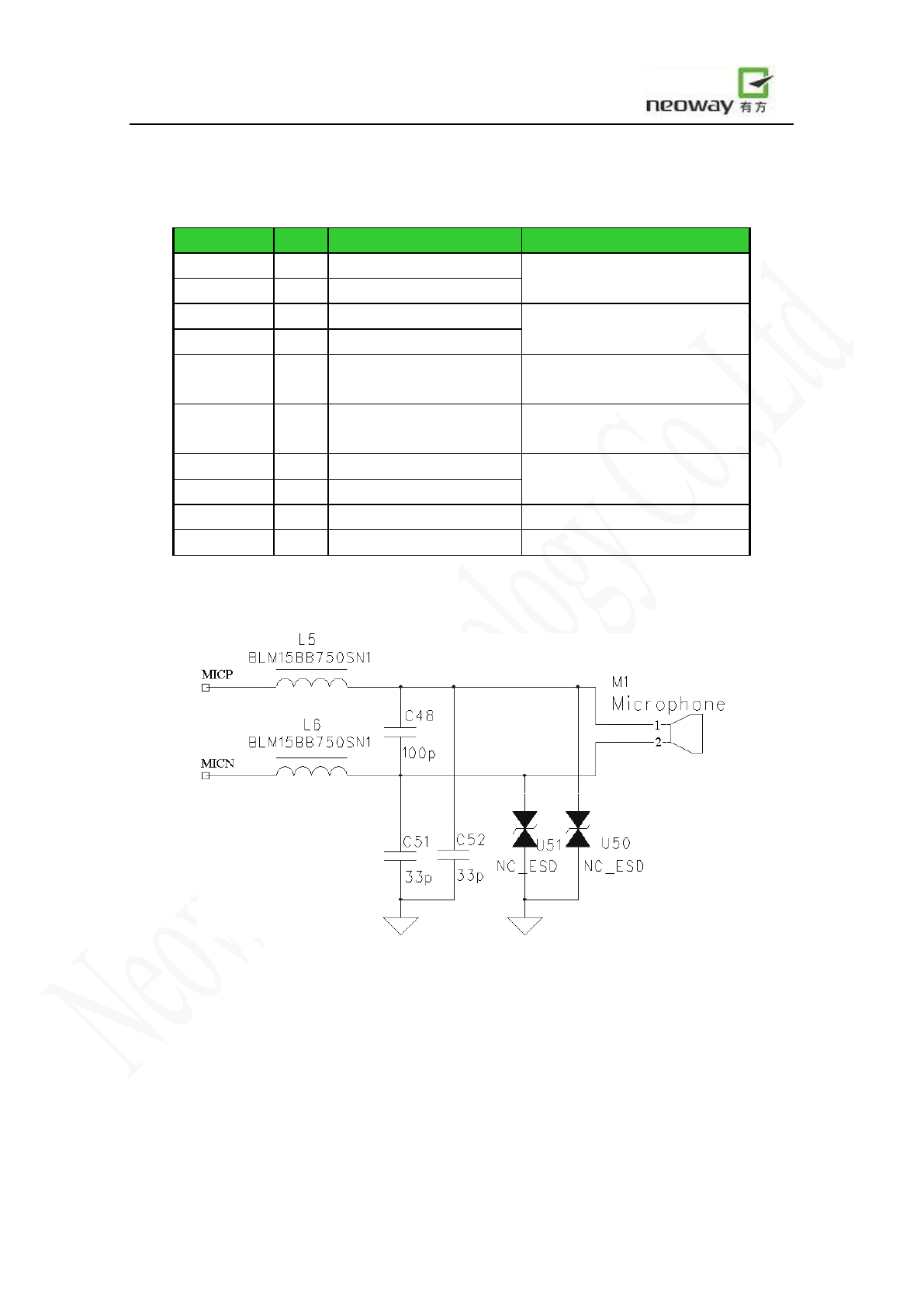
For reference audio interface see Figure 18. The peak-peak voltage routed to MIC+/MIC- should not
exceed 200mV. AGC circuit is integrated inside the module. Electret microphone is suited.
Figure 18 Reference design of microphone interface
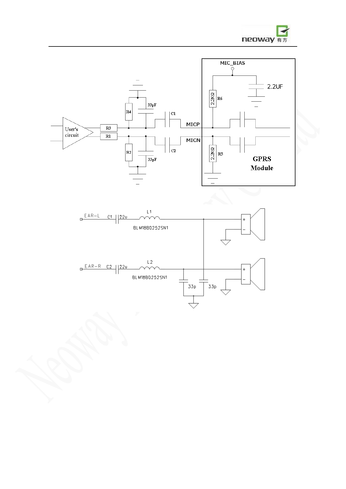
A bias voltage for microphone is provided through MICP and MICN, as shown in Figure 19. But if
an amplifier is used between the microphone and module, capacitors like C1 and C2, should be
placed between the outputs of amplifier and module, to block the bias voltage.
For a peak-peak voltage greater than 200mV, an attenuation circuit comprised of R1-R4 should be
used.
Neo_M680 Hardware User Guide V1.0
Copyright Neoway Techlology Co., Ltd. Page 27 of 31
Figure 19 Reference design for MIC interface
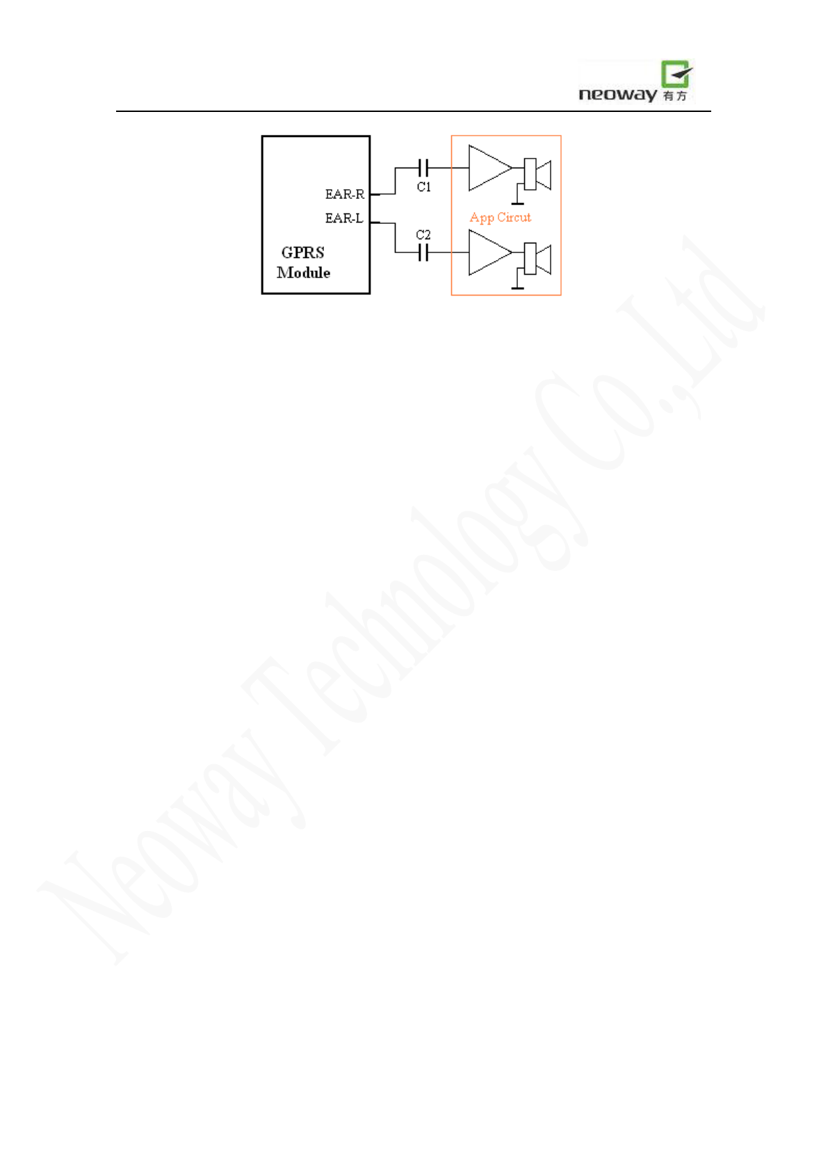
Figure 20 Reference design for Ear interface
Figure 20 shows a reference design for earpiece interface. A 16Ω/32Ω earpiece can be directly
driven by the module. To pass the low frequency audio, use large capacitors for C1 and C2.
If an external amplifier is used for driving the speakers, 1uF~4.7uF coupling capacitors should be
used to block the DC voltage, as shown in Figure 21.
Neo_M680 Hardware User Guide V1.0
Copyright Neoway Techlology Co., Ltd. Page 28 of 31
Figure 21 Using capacitors to couple audio outputs
As the description of TDD noise before, the GSM radio frequency is modulated at 217Hz. The
217Hz and its derivative frequency is well within audio band, therefore a TDD noise often affect the
audio performance through power and air. Some small capacitors between 27pF-100pF and ferrite
beads, placed on the audio path can attenuate TDD noise.
For Suppressing the TDD noise, differential audio interface is preferable. The PCB trace of audio
signal should be routed as differential line.
In particular, the microphone interface is a pair of small signal, peak-peak voltage <200mV, must
comply the rule of differential line. The microphone interface should be routed as short as possible.
6.8 Antenna Interface
A 50Ω antenna is required. VSWR < 1.5. The antenna should be well matched to achieve best
performance. It should be installed far away from high speed logic circuits, DC/DC power, or any
other strong disturbing sources.
ESD protection is built in module. For special ESD protection, a ESD diode can be placed close to
the antenna. But ensure to use a low junction capacitance one. The junction capacitance should be
less than 0.5pF, otherwise the RF signal will be attenuated. RCLAMP0521P from Semtech, or
ESD5V3U1U from Infineon, can be used here. See Figure 22.
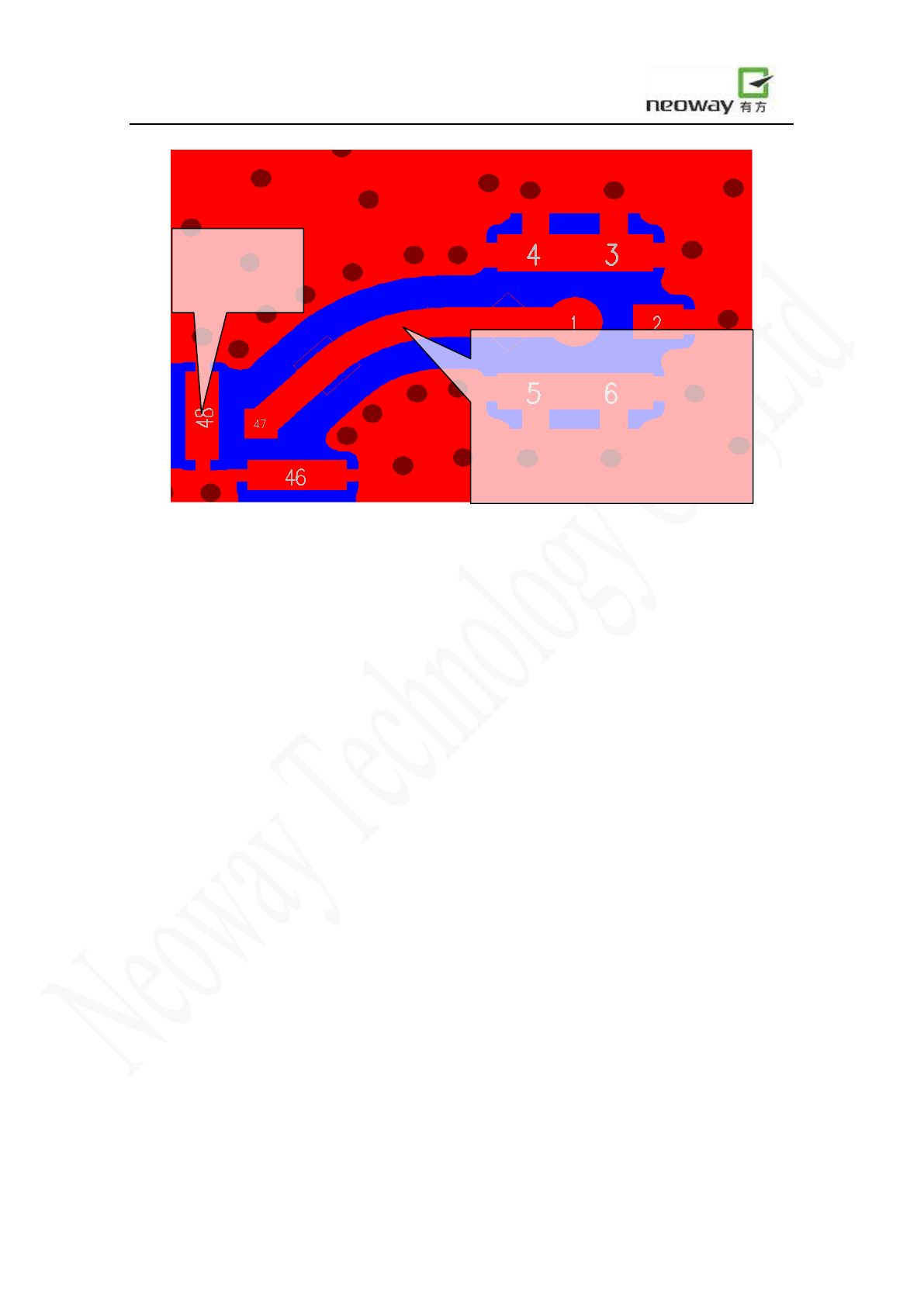
The trace between the antenna pad of module and the antenna connector, should have a 50Ω
characteristic impedance, and be as short as possible. The trace should be surrounded by ground
copper. Place plenty of via holes to connect this ground copper to main ground plane, at the copper
edge.
Neo_M680 Hardware User Guide V1.0
Copyright Neoway Techlology Co., Ltd. Page 29 of 31
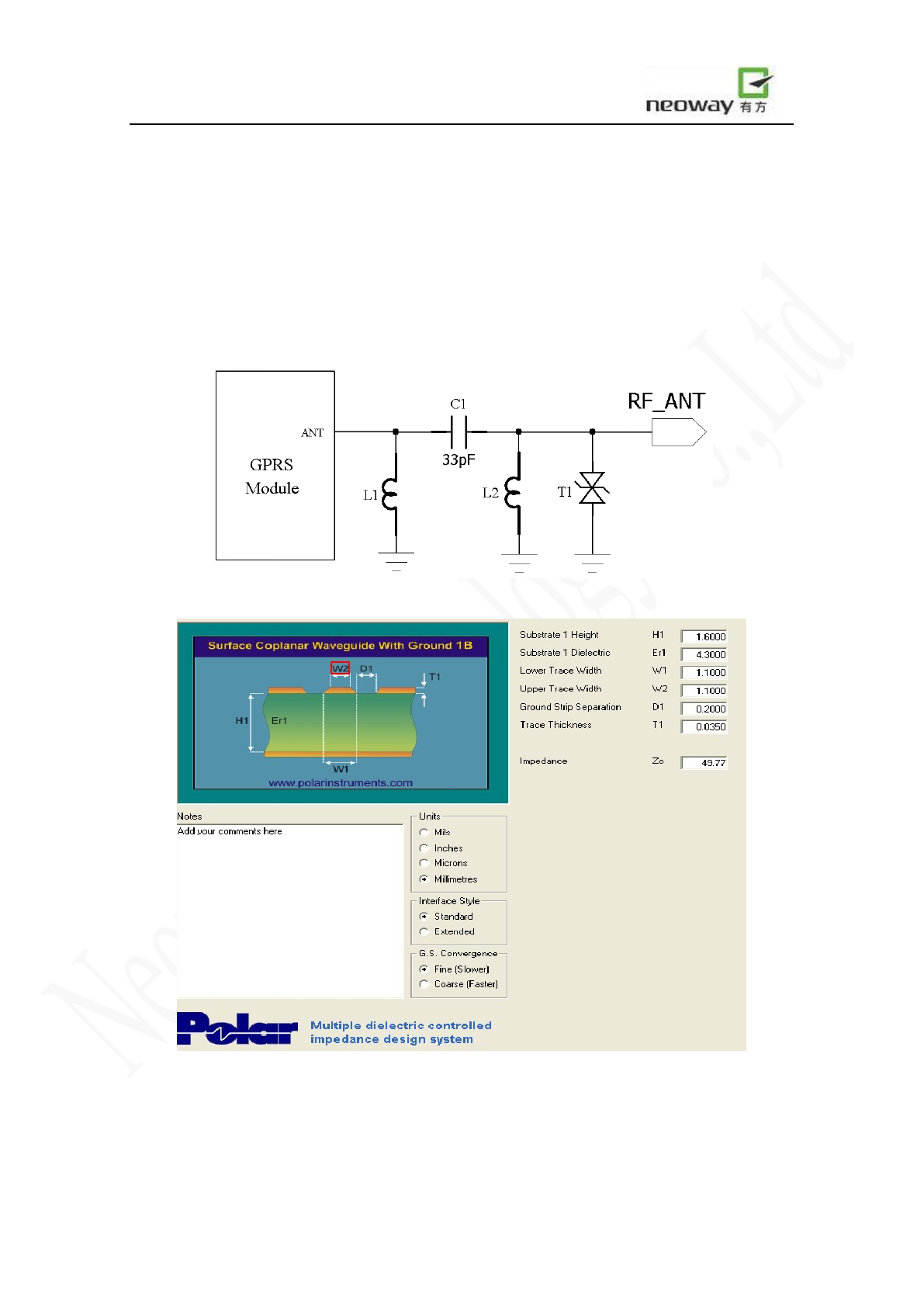
If the trace between the module and connector has to be longer, or built-in antenna is used, a π-type
matching circuit should be needed, as shown in Figure 22. The types and values of C1, L1, and L2
should be verified by testing using network analyzer instrument. If the characteristic impedance is
well matched, and VSWR requirement is met, just use a 0Ω resistor for C1 and leave L1, L2
un-installed.
Avoid any other traces crossing the antenna trace on neighboring layer.
Figure 22 Reference design for antenna interface
Figure 23 Reference parameters for 50Ω trace on a 1.6mm double layer PCB
Neo_M680 Hardware User Guide V1.0
Copyright Neoway Techlology Co., Ltd. Page 30 of 31
Figure 24 Reference layout for antenna interface
7. Mounting the Module onto the Application Board
M680 is compatible with industrial standard reflow profile for lead-free SMT process.
The reflow profile is process dependent, so the following recommendation is just a start point
guideline:
Only one flow is supported.
Quality of the solder joint depends on the solder volume. Minimum of 0.15mm stencil thickness
is recommended.
Use bigger aperture size of the stencil than actual pad size.
Use a low-residue, no-clean type solder paste.
8. Package
M680 modules are packaged in sealed bags on delivery to guarantee a long shelf life. Package the
modules again in case of opening for any reasons.
If exposed in air for more than 48 hours at conditions not worse than 30°C/60% RH, a baking
procedure should be done before SMT. Or, if the indication card shows humidity greater than 20%,
This GND Pad
should be well
routed to ground
Antenn
a trace should be surrounded by
ground which is
connected to main
ground plane with plenty of via holes.
The trace width and the space to ground
should be decided by calculating of 50Ω
impedance match.

Neo_M680 Hardware User Guide V1.0
Copyright Neoway Techlology Co., Ltd. Page 31 of 31
the baking procedure is also required.
The baking should last for at least 24 hours at 90℃.
9. Terms and Abbreviations
ADC
Analog-Digital Converter
AGC Automatic Gain Control
AMR Acknowledged multirate (speech coder)
CSD Circuit Switched Data
CPU Central Processing Unit
DCE Data Communication Equipment
DTE Data Terminal Equipment
DTR Data Terminal Ready
EFR Enhanced Full Rate
EMC Electromagnetic Compatibility
EMI Electro Magnetic Interference
ESD Electronic Static Discharge
FR Full Rate
GPRS General Packet Radio Service
GSM Global Standard for Mobile Communications
HR Half Rate
IC Integrated Circuit
IMEI International Mobile Equipment Identity
LED Light Emitting Diode
PCB Printed Circuit Board
RAM Random Access Memory
RF Radio Frequency
SIM Subscriber Identification Module
SMS Short Message Service
SMT Surface Mounted Technology
SRAM Static Random Access Memory
TDMA Time Division Multiple Access
UART Universal asynchronous receiver-transmitter
Varistor Voltage Dependent Resistor
VSWR Voltage Standing Wave Ratio
ESDprotection
EADSrequiresthattheM680GPRSModule'sservicepointshavesufficientESDprotection
(againststaticelectricity)whenservicingtheproduct.Anyproductwhichhasitscoversremoved
mustbehandledwithESDprotection.Toreplacethecovers,ESDprotectionmustbeapplied.All
electronicpartsoftheproductaresusceptibletoESD.
AllESD‐sensitivepartsmustbepackedinmetallizedprotectivebagsduringshippingandhandling
outsideanyESDProtectedArea(EPA).
Everyrepairactioninvolvingopeningtheproductorhandlingtheproductcomponentsmustbe
doneunderESDprotection.
ESD‐protectedsparepartpackagesMUSTNOTbeopened/closedoutsideofanESDProtected
Area.
EURegulatoryConformance
Ascertifiedbythequalifiedlaboratory,theproductisincompliancewiththeessential
requirementsandotherrelevantprovisionsoftheDirective1999/5/EC.Pleasenotethatthe
aboveinformationisapplicabletoEUcountriesonly.
AntennaInstallation:InstalltheGPRSmoduleantennaatleast20cmawayfromyourbody,in
accordancewiththerequirementsoftheantennamanufacturer/supplier.
FCCStatment
Thisdevicecomplieswithpart15oftheFCCRules.Operationissubjecttothefollowingtwo
conditions:(1)Thisdevicemaynotcauseharmfulinterference,and(2)thisdevicemustaccept
anyinterferencereceived,includinginterferencethatmaycauseundesiredoperation.
AnyChangesormodificationsnotexpresslyapprovedbythepartyresponsibleforcompliance
couldvoidtheuser'sauthoritytooperatetheequipment.
Note:ThisequipmenthasbeentestedandfoundtocomplywiththelimitsforaClassBdigital
device,pursuanttopart15oftheFCCRules.Theselimitsaredesignedtoprovidereasonable
protectionagainstharmfulinterferenceinaresidentialinstallation.Thisequipmentgenerates,
usesandcanradiateradiofrequencyenergyand,ifnotinstalledandusedinaccordancewith
theinstructions,maycauseharmfulinterferencetoradiocommunications.However,thereis
noguaranteethatinterferencewillnotoccurinaparticularinstallation.Ifthisequipmentdoes
causeharmfulinterferencetoradioortelevisionreception,equipmentgenerates,usesandcan
radiateradiofrequencyenergyand,ifnotinstalledandusedinaccordancewiththe
instructions,maycauseharmfulinterferencetoequipmentdoescauseharmfulinterferenceto
radioortelevisionreception,
—Reorientorrelocatethereceivingantenna.
—Increasetheseparationbetweentheequipmentandreceiver.
—Connecttheequipmentintoanoutletonacircuitdifferentfromthattowhichthereceiveris
connected.
—Consultthedealeroranexperiencedradio/TVtechnicianforhelp.
LabelofTheEndProduct
Thefinalendproductmustbelabeledinavisiblearewiththefollowing“ContainsTXFCC
ID:PJ7‐1232”.TheFCCpart15.19statementbelowhastoalsobeavailableonthelabel:Thisdevice
complieswithPart15ofFCCrules.Operationissubjecttothefollowingtwoconditions:
(1)Thisdevicemaynotcauseharmfulinterference,and(2)thisdevicemustacceptany
interferencereceived,includinginterferencethatmaycauseundesiredoperation.
TocomplywithFCCregulationslimitingbothmaximumRFoutputpowerandhumanexposureto
RFradiation,themaximumantennagainincludingcablelossinamobile‐onlyexposurecondition
mustnotexceed1dBiforbothGSM850andPCS1900.
Ausermanualwiththeendproductmustclearlyindicatetheoperatingrequirementsand
conditionsthatmustbeobservedtoensurecompliancewithcurrentFCCRFexposureguidelines.
TheendproductwithanembeddedM680GPRSModulemayalsoneedtopasstheFCCPart15
unintentionalemissiontestingrequirementsandbeproperlyauthorizedperFCCPart15.
Note:Ifthismoduleisintendedforuseinaportabledevice,youareresponsibleforseparate
approvaltosatifytheSARrequirementsofFCCPart2.1093.