Neoway Technology 1901 eMTC Module User Manual UM V2
Shenzhen Neoway Technology Co., Ltd. eMTC Module UM V2
UM-V2

N720 (Cat1) Hardware User Guide ()
N20 User Manual
V1.0

N20 Hardware User Guide
Copyright © Neoway Technology Co., Ltd
i
Copyright
Copyright © 2018 Neoway Technology Co., Ltd. All rights reserved.
No part of this document may be reproduced or transmitted in any form or by any means without
prior written consent of Neoway Technology Co., Ltd.
is the trademark of Neoway Technology Co., Ltd.
All other trademarks and trade names mentioned in this document are the property of their respective
holders.
Notice
This document provides guide for users to use theN20.
This document is intended for system engineers (SEs), development engineers, and test engineers.
The information in this document is subject to change without notice due to product version update
or other reasons.
Every effort has been made in preparation of this document to ensure accuracy of the contents, but all
statements, information, and recommendations in this document do not constitute a warranty of any
kind, express or implied.
Neoway provides customers complete technical support. If you have any question, please contact
your account manager or email to the following email addresses:
Sales@neoway.com
Support@neoway.com
Website: http://www.neoway.com

N20 Hardware User Guide
Copyright © Neoway Technology Co., Ltd
ii
Revision Record
Issue
Changes
Revised By
Date
V1.0
Initial draft
He Zhizhong
2017-10

N20 Hardware User Guide
Copyright © Neoway Technology Co., Ltd
iii
Contents
1 Introduction to N20 ........................................................................................................... 1
1.1 Overview ............................................................................................................................................ 1
1.2 Block Diagram ................................................................................................................................... 2
1.3 Specifications ..................................................................................................................................... 2
1.4 FCC Compliance and Caution ............................................................................................................ 3
2 N20 Pins ............................................................................................................................... 5
2.1 Pin Definition ..................................................................................................................................... 5
2.2 Pin Description ................................................................................................................................... 6
3 Application Interfaces .................................................................................................... 11
3.1 Power and ControlInterfaces ............................................................................................................ 11
3.1.1 VBAT ...................................................................................................................................... 11
3.1.2 VDDIO_1P8 ............................................................................................................................ 15
3.1.3 ON/OFF .................................................................................................................................. 15
3.1.4 RESET_N ................................................................................................................................ 18
3.1.5 DTR ......................................................................................................................................... 19
3.1.6 NETLIGHT ............................................................................................................................. 19
3.1.7 RING ....................................................................................................................................... 20
3.2 USB Interface ................................................................................................................................... 21
3.3 UIM Card Interface .......................................................................................................................... 23
3.4 SDIOInterface .................................................................................................................................. 24
3.5 PCM Interface .................................................................................................................................. 25
3.6 I2C Interface ..................................................................................................................................... 28
3.7 SPIInterface ...................................................................................................................................... 28
3.8 UARTInterfaces ................................................................................................................................ 29
3.9 ADCInterfaces .................................................................................................................................. 32
3.10 GPIOInterfaces ............................................................................................................................... 32
3.11 Commissioning Interface ................................................................................................................ 33
3.12 Other Interfaces .............................................................................................................................. 33
4 RF Interface ....................................................................................................................... 34
4.1 2G/4G RF Design and PCB Layout ................................................................................................. 34
4.2 GNSS RF Design and PCB Layout .................................................................................................. 36

N20 Hardware User Guide
Copyright © Neoway Technology Co., Ltd
iv
4.2.1 GNSS Impedance .................................................................................................................... 36
4.2.2 Active GNSS Antenna Design ................................................................................................. 37
5 Electrical Features and Reliability ............................................................................... 39
5.1 Electrical Features ............................................................................................................................ 39
5.2 Temperature ...................................................................................................................................... 39
5.3 ESD .................................................................................................................................................. 40
6 RF Features........................................................................................................................ 41
6.1 Operating Band ................................................................................................................................. 41
6.2 TX Power and RX Sensitivity .......................................................................................................... 41
7 Mechanical Features........................................................................................................ 42
7.1 Dimensions ....................................................................................................................................... 42
7.2 PCB Foot Print ................................................................................................................................. 43
7.3 Recommended PCB Foot Print......................................................................................................... 44
8 Mounting and Packaging ............................................................................................... 45
8.1 Mounting the Module onto the Application Board ........................................................................... 45
8.2 Packaging ......................................................................................................................................... 45
9 SMT TemperatureCurve ................................................................................................ 46
10 Abbreviations ................................................................................................................. 47

N20 Hardware User Guide
Copyright © Neoway Technology Co., Ltd
v
Table of Figures
Figure 1-1 N20 block diagram ................................................................................................................ 2
Figure 2-1 N20module pin definition (Top View)................................................................................... 5
Figure 3-1 Current peaks and voltage drops ......................................................................................... 12
Figure 3-2 Capacitors used for the power supply .................................................................................. 12
Figure 3-3 Reference design of power supply control .......................................................................... 13
Figure 3-4 Reference design of power supply controlled by p-MOSFET ............................................. 13
Figure 3-5 Reference designs of separated power supply ..................................................................... 15
Figure 3-6 Push switch control ............................................................................................................. 16
Figure 3-7 MCU control........................................................................................................................ 16
Figure 3-8 Automatic power on ............................................................................................................ 16
Figure 3-9 N20 power-on timing........................................................................................................... 17
Figure 3-10 N20 power-off timing ........................................................................................................ 17
Figure 3-11 Reset controlled by button ................................................................................................. 18
Figure 3-12 Reset circuit with triode separating ................................................................................... 18
Figure 3-13 N20 reset sequence ............................................................................................................ 19
Figure 3-14 LED indicator driven by transistor .................................................................................... 20
Figure 3-15 RING indicator for incoming call ...................................................................................... 20
Figure 3-16 RING indicator for SMS ................................................................................................... 21
Figure 3-17 USB connection ................................................................................................................. 22
Figure 3-18 USBconnection for OTG ................................................................................................... 22
Figure 3-19 Reference design of SIM card interface ............................................................................ 23
Figure 3-20 SDIO SDRtiming .............................................................................................................. 24
Figure 3-21 SDIO DDRtiming .............................................................................................................. 25
Figure 3-22 PCM connection ................................................................................................................ 26
Figure 3-23 I2Sconnection .................................................................................................................... 26
Figure 3-24 PCM SYN timing .............................................................................................................. 26
Figure 3-25 PCM data input timing ...................................................................................................... 27
Figure 3-26 PCM data output sequence ................................................................................................ 27
Figure 3-27 SPI interface timing ........................................................................................................... 28
Figure 3-28 Reference design of the UART interface ........................................................................... 29
Figure 3-29 Recommended level shifting circuit 1 ............................................................................... 30
Figure 3-30 Recommended level shifting circuit 2 ............................................................................... 31
Figure 3-31 Reference design of the fastboot interface ......................................................................... 33
Figure 4-1 Reference designs of antenna matching .............................................................................. 34

N20 Hardware User Guide
Copyright © Neoway Technology Co., Ltd
vi
Figure 4-2 Recommended RF PCB design ........................................................................................... 35
Figure 4-3 Encapsulation specifications of Murata RF connector ........................................................ 35
Figure 4-4 RF connections .................................................................................................................... 35
Figure 4-5 GNSS RF structure .............................................................................................................. 37
Figure 4-6 Power supply reference for active antenna .......................................................................... 38
Figure 7-1 Dimensions of N20(unit: mm) ............................................................................................. 42
Figure 7-2 N20PCBfoot print(Top View)(unit: mm) ............................................................................ 43
Figure 7-3 Recommended N20PCB foot print(unit:mm) ...................................................................... 44
Figure 9-1 Temperature curve ............................................................................................................... 46

N20 Hardware User Guide
Copyright © Neoway Technology Co., Ltd
vii
Table of Tables
Table 1-1 N20 specifications and features .............................................................................................. 2
Table 2-1 IO types and level feature description..................................................................................... 6
Table 2-2 N20 pin description ................................................................................................................. 7
Table 3-1 Timing parameters of SDIO interface ................................................................................... 25
Table 3-2 Timing parameters of PCM interface .................................................................................... 27
Table 3-3 Timingparameters of SPIinterface ........................................................................................ 28
Table 3-4 GPIO pins ............................................................................................................................. 32
Table 4-1 2G/4G Antenna Parameters .................................................................................................. 36
Table 5-1 N20electric features .............................................................................................................. 39
Table 5-2 Temperature feature .............................................................................................................. 39
Table 5-3 N20 ESD features ................................................................................................................. 40
Table 6-1 N20 operating band ............................................................................................................... 41
Table 6-2 N20 RF TX power ................................................................................................................ 41
Table 6-3 N20Cat M1 QPSK RX sensitivity ........................................................................................ 41

N20 Hardware User Guide
Copyright © Neoway Technology Co., Ltd
1
1 Introduction to N20
1.1 Overview
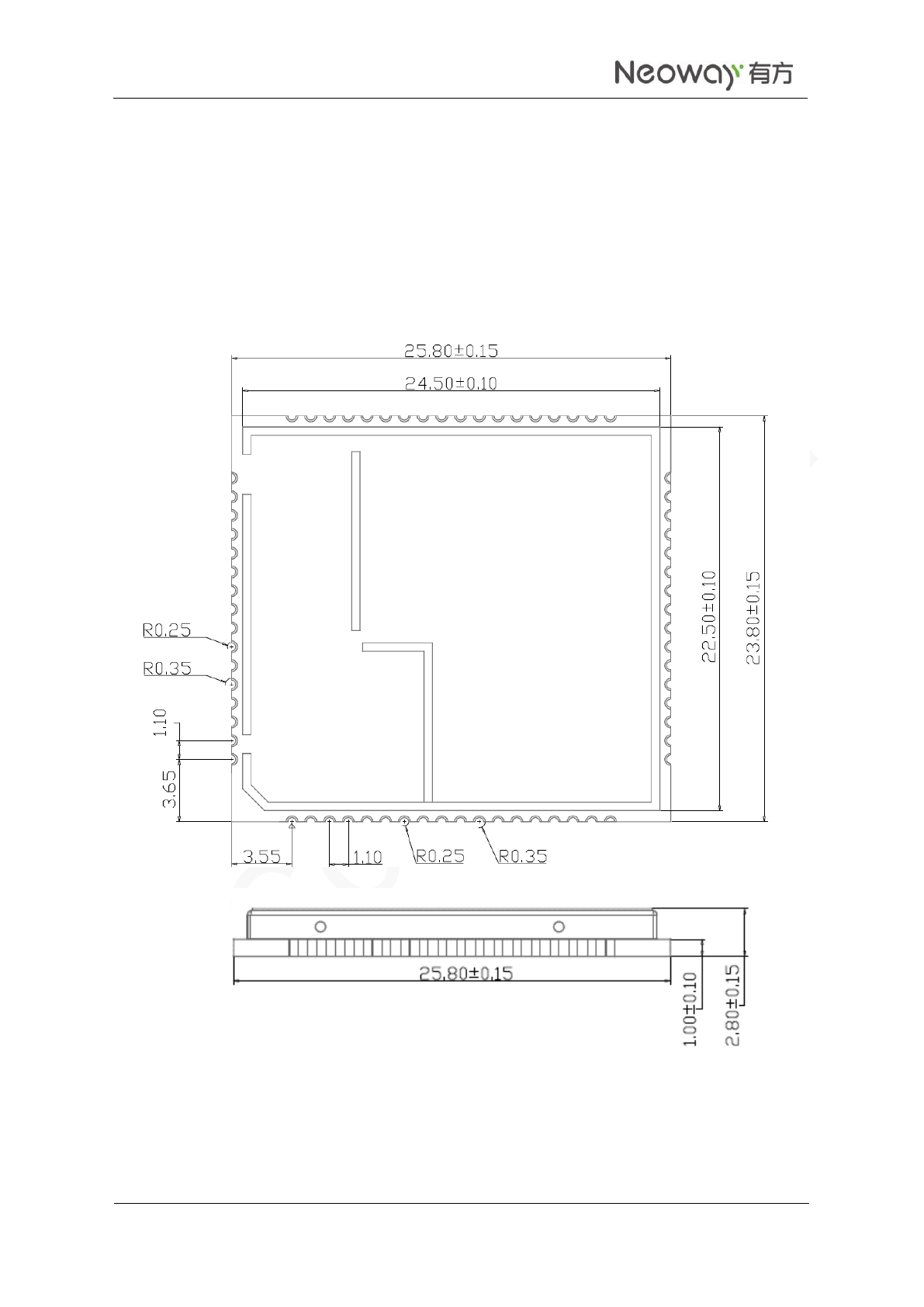
N20 is an industrial-grade module developed on Qualcomm platform. Its dimensions are 23.8mm x
25.8mm x 2.8mm. This module has an ultra-wide operating temperature range of -40 °C to +85 °C and
electrostatic capacity of 8kV.N20 is well applicable to develop low-power IoT terminals with the
following features:
ARM Cortex-A7 processors, 1.3 GHz main frequency, 256 KB L2 cache, 28 nm process technology
Cat M1/GNSS(optional)
USB2.0/UIM/ADC/UART/SPI/I2C/PCM/SDIO/GPIO
N20 meets the band requirements: B2/B4/B12/B13.
N20 Hardware User Guide
Copyright © Neoway Technology Co., Ltd
2
1.2 Block Diagram
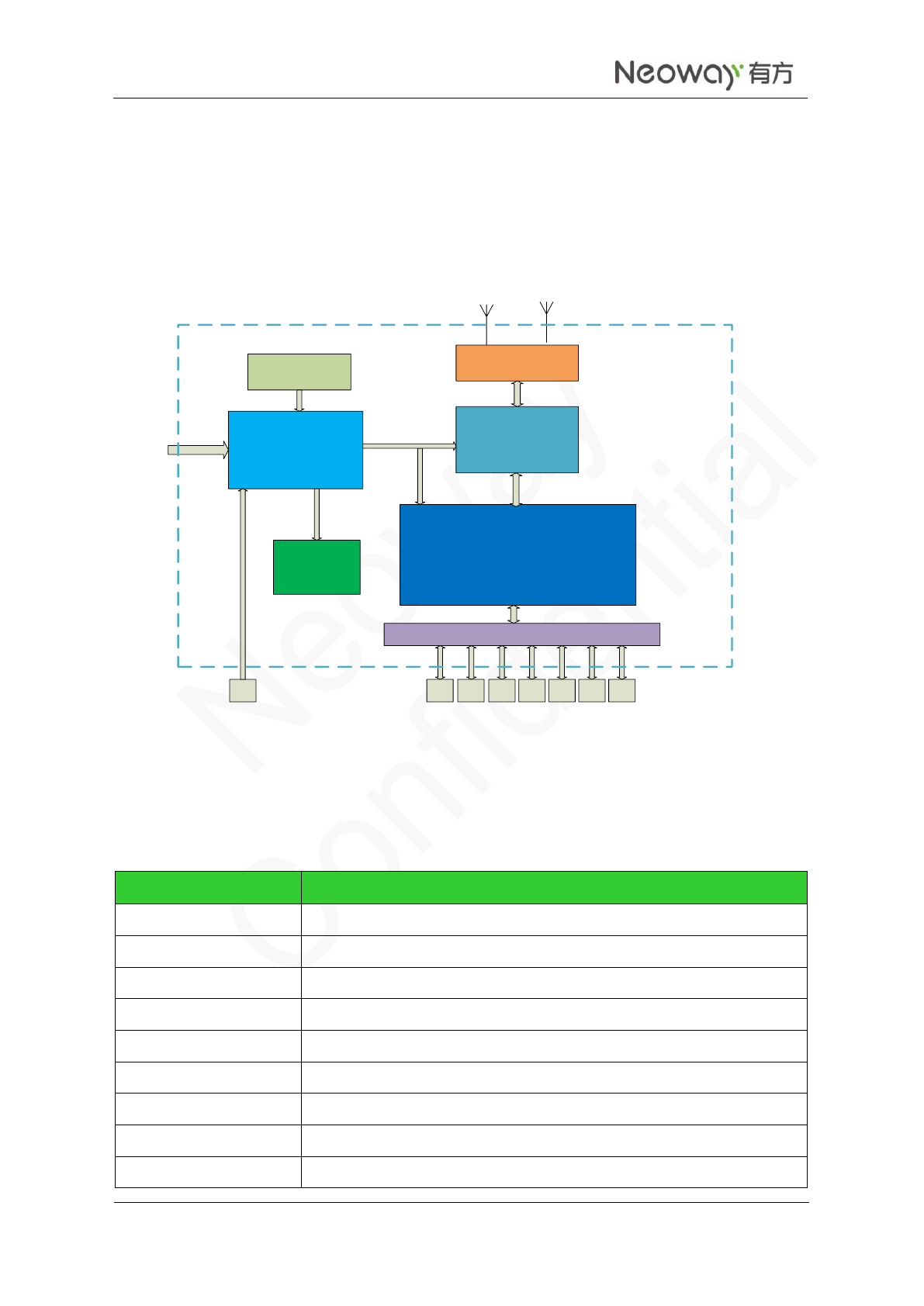
Figure 1-1shows the block diagram of N20.
Figure 1-1 N20 block diagram
Base Band
RF transceiver
RF
Power Manager
MCP
VBAT
Interface
ADC
MAIN GNSS
GPIO
I2C
SDIOSPI
UART
USB
SIM
XO
19.2MHz
1.3 Specifications
Table 1-1 N20 specifications and features
Specifications
Description
Dimensions (H x W x D)
23.8±0.15 mm x 25.8±0.15 mm x 2.8±0.15 mm
Weight
3.5g
Package
68-pin LCC
Power supply
VBAT: 3.3V to 4.3 V;Typical value: 3.8 V
Current in idle mode
LTE Cat M1:1.7mA(@DRX cycle=1.28s)
Current in eDRXmode
LTE Cat M1:1.0mA(@eDRX cycle=61.44s, PTW=10.24s)
Current in PSM mode
LTE Cat M1:7.7 μA
Operating temperature
-40°C to +85°C
Processor
ARM Cortex-A7 processor

N20 Hardware User Guide
Copyright © Neoway Technology Co., Ltd
3
Main frequency: 1.3 GHz
256kB L2 cache
Memory
ROM: 128MB
RAM: 64 MB
Or
ROM: 256 MB
RAM: 128 MB
Rate
LTE Cat M1: 300 Kbps(DL)/375 Kbps(UL)
Transmit power
LTE: +23dBm (Power Class 3)
Antenna feature
2G/4G antenna, GNSS antenna, 50Ω impedance
UART
At most 4 Mbps, 2UART interfaces
UIM
1UIM interface, 1.8V/2.85V dual-voltage adaptive
USB
1 high-speed USB2.0 interface
ADC
2 15-bit ADC interfaces, detectable voltage ranging from 0.1 V to 1.7V
SPI
1 SPI interface, supporting only host mode
At most 50 Mbps
I2C
1 I2C interface, used to control external sensor
PCM
1PCM interface, used to transmit digital audio
SDIO
1SDIO interface, used to control 4-bit WLAN interface
GPIO
3GPIOs, 1 SIM SELECT
1.4 FCC Compliance and Caution
FCC compliance statement:
This device complies with Part 15 of the FCC Rules. Operation is subject to the following two conditions:
(1) This device may not cause harmful interference.
(2) This device must accept any interference received, including interference that may cause undesired
operation.
FCC Caution:
(1) Exposure to Radio Frequency Radiation. This equipment must be installed and operated in accordance
with provided instructions and the antenna(s) used for this transmitter must be installed to provide a
separation distance of at least 20cm from all persons and must not be collocated or operating in
conjunction with any other antenna or transmitter. End-users and installers must be provided with antenna
installation instructions and transmitter operation conditions for satisfying RF exposure compliance.

N20 Hardware User Guide
Copyright © Neoway Technology Co., Ltd
4
(2) Any changes or modifications not expressly approved by the grantee of this device could void the
user's authority to operate the equipment.
(3) This transmitter must not be co-located or operating in conjuction with any other antenna or
transmitter.
(4) Changes or modifications not expressly approved by the party responsible for compliance could void
the user's authority to operate the equipment.
(5) The module FCC ID is not visible when installed in the host, or if the host is marketed so that end
users do not have straight forward commonly used methods for access to remove the module so that the
FCC ID of the module is visible; then an additional permanent label referring to the enclosed module:
Contains Transmitter Module FCC ID: PJ7-1901 or Contains FCC ID: PJ7-1901.
N20 Hardware User Guide
Copyright © Neoway Technology Co., Ltd
5
2 N20 Pins
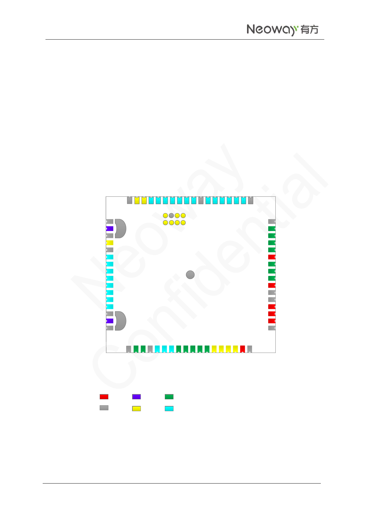
N20 adopts 68-pin LCC encapsulation package.
2.1 Pin Definition
Figure 2-1 N20module pin definition (Top View)
GND
GND
GND
GND
GND
GND
GND
GND
GND
GND
GND
GND
GND
GND
GND
RF_ANT_MAIN
RF_ANT_GNSS
EXT_GNSS_LNA_EN
UART1_RTS
UART1_CTS
UART1_RX
UART1_TX
UART0_RTS
UART0_CTS
UART0_RX
UART0_TX
SPI_CLK
SPI_MISO
SPI_MOSI
SPI_CS_N
ADC1
ADC2
GPIO1
GPIO2
GPIO3
SIM_SELECT
RESET_N
PWRKEY
DTR
FORCE_USB_BOOT
VDDIO_1P8
NETLIGHT
RING
I2S_MCLK
PCM_DOUT
PCM_DIN
PCM_CLK
PCM_SYNC
I2C_SCL
I2C_SDA
SDC_DATA_3
SDC_DATA_2
SDC_DATA_1
SDC_DATA_0
SDC_CLK
SDC_CMD
UIM_PRESENT
UIM_RESET
UIM_CLK
UIM_DATA
VUIM
USB_ID
USB_HS_DP
USB_HS_DM
USB_VBUS
VBAT
VBAT
VBAT
1
2
3
4
5
6
7
8
9
10
11
12
13
14
15
16
17
18
19
20
21
22
23
24
25
26
27
28
29
30
31
32
33
34
35
36
37
38
39
40
41
42
43
44
45
46
47
48
49
50
51
52
53
54
55
56
57
58
59
60
61
63
62
64
66
68
67
65
Power Interface(Standard)
Interface(Open ThreadX)
GND
ANT
Others
For how to use interfaces supported by OpenThreadX, see Neoway_N20_Open ThreadX_User_Guide.
N20 Hardware User Guide
Copyright © Neoway Technology Co., Ltd
6
2.2 Pin Description
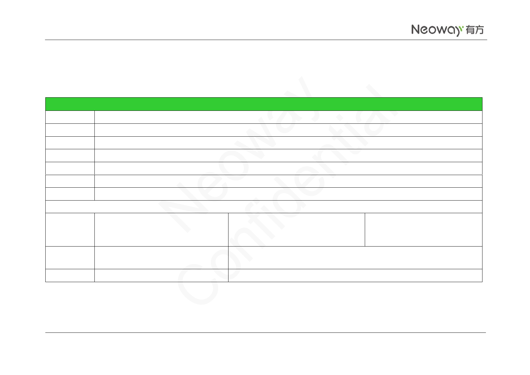
Table 2-1 IO types and level feature description
IO Type
B
Digital I/O, COMS logic level
DO
Digital output, COMS logic level
DI
Digital input,COMS logic level
PO
Power output
PI
Power input
AO
Analog output
AI
Analog input
Level feature
P1
Dual-voltage, 1.8Vor 2.85V
1.8Vlevel feature:
VIH=1.26V~2.1V, VIL=-0.3V~0.36V
VOH=1.44V~1.8V, VOL=0V~0.4V
2.85Vlevel feature
VIH=2V~3.15V, VIL=-0.3V~0.57V
VOH=2.28V~2.85V, VOL=0V~0.4V
P3
1.8Vdigital IOvoltage
VIH min=1.2V, VIL max= 0.3V
VOH min=1.35V, VOLmax=0.45V
P6
Level for USB2.0 data interface
Vmin=2.97V, V max=3.5V, V typ=3.08V
N20 Hardware User Guide
Copyright © Neoway Technology Co., Ltd
7
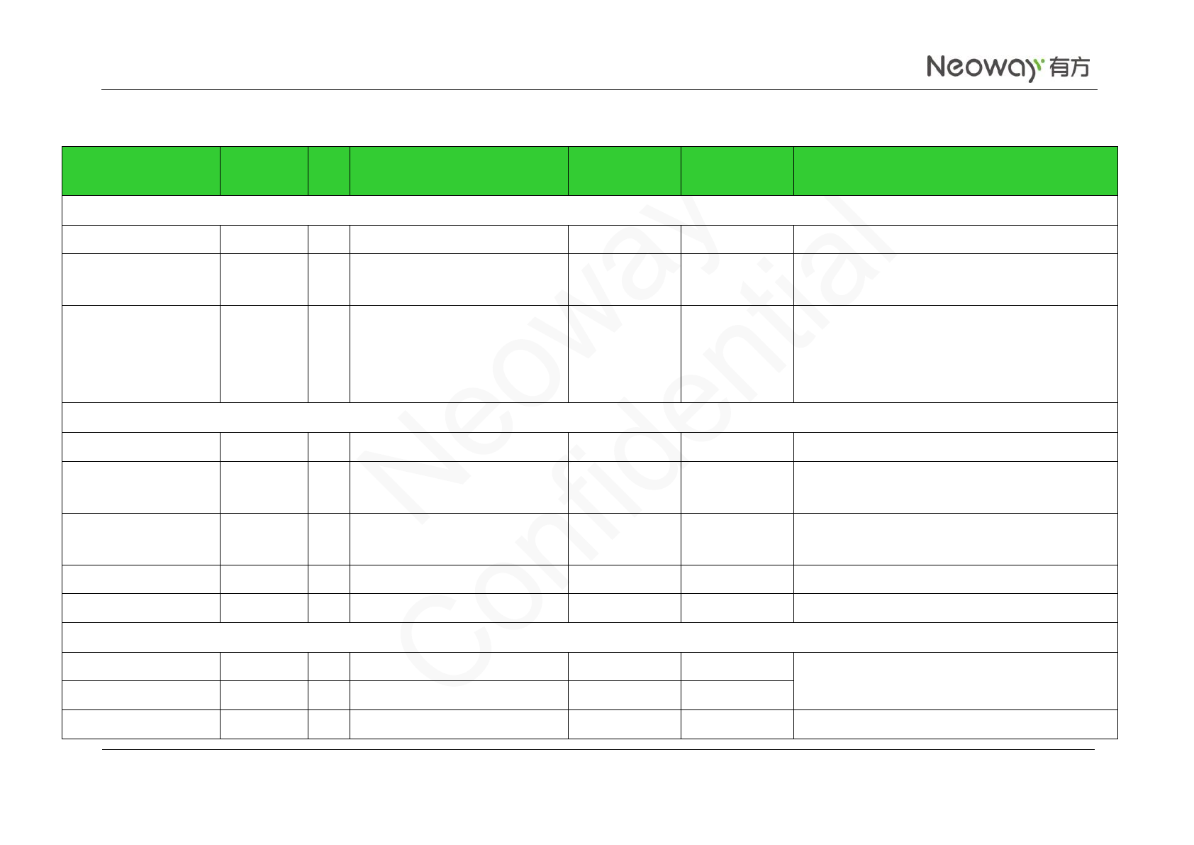
Table 2-2 N20 pin description
Name
Pin
I/O
Function
Level Feature
(V)
Power
Domain
Remarks
Power Supply
VBAT
20, 21, 22
PI
Main power supply
Vmax=4.3V
Supply a maximum current of 2A.
VDDIO _1P8
17
PO
1.8 V power supply
Vnorm=1.8V;
Imax=50mA;
1.8V
Used for level shifting and to supply power for IO.
Leave this pinunconnected if it is not used.
GND
1, 4, 18, 19,
23, 24, 34,
35, 42, 52,
53, 55, 57,
66, 68
GND
Ensure that all GND pins are grounded.
Control Interfaces
RESET_N
13
DI
Reset input
P3
1.8V
Low level triggers the reset.
PWRKEY
14
DI
Power ON/OFF
P3
1.8V
Low level triggers the ON state.
The level at the pin is 0.8 V by default.
DTR
15
DI
Sleep mode control
P3
1.8V
Low level triggers sleep mode.
Leave this pin unconnected if it is not used.
RING
50
DO
Incoming call ring
P3
1.8V
Leave this pin unconnected if it is not used.
NETLIGHT
51
DO
Network status indicator control
P3
1.8V
Leave this pin unconnected if it is not used.
UART0
UART0_TX
9
DO
UART data transmit
P3
1.8V
Data transmission
Leave these pins unconnected if they are not used.
UART0_RX
10
DI
UART data receive
P3
1.8V
UART0_RTS
11
DI
Request to send
P3
1.8V
Leave these pins unconnected if they are not used.
N20 Hardware User Guide
Copyright © Neoway Technology Co., Ltd
8
UART0_CTS
12
DO
Clear to send
P3
1.8V
UART1 (supported by Open ThreadX)
UART1_RTS
58
DI
Request to send
P3
1.8V
Leave these pins unconnected if they are not used.
UART1_CTS
59
DO
Clear to send
P3
1.8V
UART1_RX
60
DI
UART data receive
P3
1.8V
Data transmission
Leave these pins unconnected if they are not used.
UART1_TX
61
DO
UART data transmit
P3
1.8V
UIM
VUIM
29
PO
UIM1 power supply output
IO max =50 mA
1.8 V/2.85 V
UIM_DATA
30
IO
UIM1 data I/O
P1
1.8 V/2.85 V
Connected to UIM1_VCC through a 10 kΩ pull-up
resistor
UIM_CLK
31
DO
UIM1 clock output
P1
1.8 V/2.85 V
UIM_RESET
32
DO
UIM1 reset
P1
1.8 V/2.85 V
UIM_PRESENT
33
DI
UIM1 detect
P3
1.8V
USB
USB_VBUS
25
PI
USB voltage test
3.3V~5.2V,
typically 5V
Used for firmware download and data transmission
Differential trace for DM and DP with 90Ω
impedance
USB_HS_DM
26
IO
USB data negative signal
P6
USB_HS_DP
27
IO
USB data positive signal
P6
USB _ID
28
AI
Master and slave device detect
P3
1.8V
Leave this pin unconnected if it is not used.
ADC
ADC1
2
AI
Analog-to-digital signal
conversion
Vmax=1.7 V;
Vmin=0.1 V
1.8V
15-bit, detectable voltage range: 0.1 V to 1.7 V
Leave these pins unconnected if they are not used.
N20 Hardware User Guide
Copyright © Neoway Technology Co., Ltd
9
ADC2
3
AI
Analog-to-digital signal
conversion
Vmax=1.7 V;
Vmin=0.1 V
1.8V
I2C(supported by Open ThreadX)
I2C_SCL
44
B
I2C clock
P3
1.8V
Pulled up by a 2.2 kΩ resistor internally
I2C_SDA
43
B
I2C data
P3
1.8V
Pulled up by a 2.2 kΩ resistor internally
PCM (supported by Open ThreadX)
PCM_SYNC
45
B
PCM sync signal
P3
1.8V
Leave this pin unconnected if it is not used.
PCM_CLK
46
DO
PCM clock signal
P3
1.8V
Leave this pin unconnected if it is not used.
PCM_DIN
47
DI
PCM data input
P3
1.8V
Leave this pin unconnected if it is not used.
PCM_DOUT
48
DO
PCM data output
P3
1.8V
Leave this pin unconnected if it is not used.
I2S_MCLK
49
DO
I2S main clock
P3
1.8V
Default frequency:12.288MHz
SDIO(supported by Open ThreadX)
SDC_CMD
36
B
Control signal of SDIO interface
P3
1.8V
Leave this pin unconnected if it is not used.
SDC_CLK
37
DO
Clock signal of SDIO interface
P3
1.8V
Leave this pin unconnected if it is not used.
SDC_DATA_0
38
B
SDIO data bit 0
P3
1.8V
Leave this pin unconnected if it is not used.
SDC_DATA_1
39
B
SDIO data bit 1
P3
1.8V
Leave this pin unconnected if it is not used.
SDC_DATA_2
40
B
SDIO data bit 2
P3
1.8V
Leave this pin unconnected if it is not used.
SDC_DATA_3
41
B
SDIO data bit 3
P3
1.8V
Leave this pin unconnected if it is not used.
SPI(supported by Open ThreadX)
SPI_CLK
62
DO
Clock signal
P3
1.8V
Leave this pin unconnected if it is not used.
SPI_MISO
63
DI
Master input, slave output
P3
1.8V
Leave this pin unconnected if it is not used.
N20 Hardware User Guide
Copyright © Neoway Technology Co., Ltd
10
SPI_MOSI
64
DO
Master output, slave input
P3
1.8V
Leave this pin unconnected if it is not used.
SPI_CS_N
65
DO
Chip select
P3
1.8V
Leave this pin unconnected if it is not used.
GPIO
GPIO_1
5
B
GPIO with interrupt
P3
1.8V
Leave this pin unconnected if it is not
used.supported by Open ThreadX
GPIO_2
6
B
GPIO with interrupt
P3
1.8V
Leave this pin unconnected if it is not
used.supported by Open ThreadX
GPIO_3
7
B
GPIO with interrupt
P3
1.8V
Leave this pin unconnected if it is not
used.supported by Open ThreadX
SIM SELECT
8
B
GPIO
P3
1.8V
To support dual-SIM single standby.
Do not connect this pin to the power supply
through a pull-up resistor before the module is
started.
Leave this pin unconnected if it is not used.
Antenna
RF_ANT_GNSS
54
GNSS antenna
50 Ω impedance
RF_ANT_MAIN
67
Main antenna
50 Ω impedance
Other Pins
EXT_GNSS_LNA_EN
56
DO
GNSS LNA enable
P3
1.8V
Leave this pin unconnected if it is not used.
FORCE_USB_BOOT
48
DI
Forcible upgrade control
P3
1.8V
Connect a 10 kΩ pull-up resistor to 1.8V, and the
module enters USB download mode
Leave this pin unconnected if it is not used.
N20 Hardware User Guide
Copyright © Neoway Technology Co., Ltd
11
3 Application Interfaces
3.1 Power and ControlInterfaces
Name
Pin
I/O
Function
Remarks
VBAT
20, 21, 22
PI
Power supply input
3.3 V to 4.3V (typical value: 3.8 V)
VDDIO_1P8
17
PO
1.8 V power supply
output
Power supply for IO level shifting circuit.
Load capability: <50 mA
Added ESD protection when using this pin.
RESET_N
13
DI
Reset input
Low level triggers reset
PWRKEY
14
DI
Power ON/OFF
Low level triggers the ON status
DTR
15
DI
Sleep mode control
Low level triggers sleep mode.
Leave this pin unconnected if it is not used.
RING
50
DO
Incoming call ring
Leave this pin unconnected if it is not used.
NETLIGHT
51
DO
Network status
indicator control
Leave this pin unconnected if it is not used.
3.1.1 VBAT
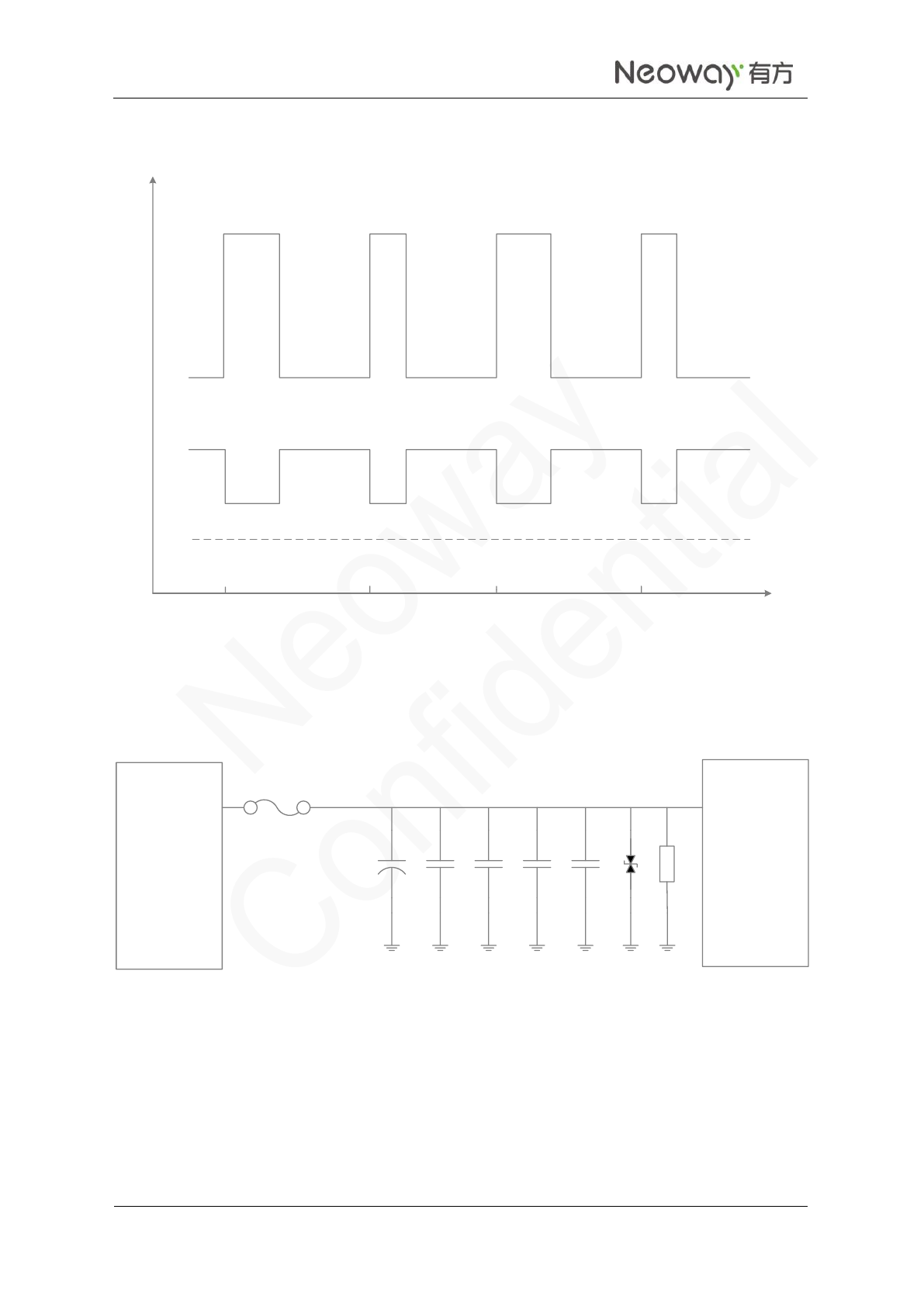
VBAT is the power supply input pin of the module. Its input voltage ranges from 3.3 V to 4.3V and the
typical value is 3.8V. In addition to baseband, it supplies power to RF power amplifier. The performance
of the VBAT power supply is a critical path to module's performance and stability. The peak input current
at the VBAT pin can exceed 2A when the signal is weak and the module works at the maximum
transmitting power. The voltage will encounter a drop in such a situation. The module might restart if the
voltage drops lower than 3.3 V.
N20 Hardware User Guide
Copyright © Neoway Technology Co., Ltd
12
Figure 3-1 Current peaks and voltage drops
Keep the voltage above 3.3 V
3.3 V
0 ms 3.7 ms 7.4 ms 11.1 ms T
2 A
Voltage
Input
current
3.8 V
The reference design of the VBAT power supply is shown as below:
Figure 3-2 Capacitors used for the power supply
Power
Supply N20
VBAT
R1
D1
C1 C2 C3 C4 C5
Test point
In Figure 3-2, use TVS at D1 to enhance the performance of the module during a burst. SMF5.0AG
(Vrwm=5V&Pppm=200W) is recommended. Place it close to the module. A large bypass tantalum
capacitor (220 μF or 100 μF) or aluminum capacitor (470 μF or 1000 μF) is expected at C1 to reduce
voltage drops during bursts together with C2 (10 μF ceramics capacitor).In addition,add 0.1 μF, 100 pF,
and 33 pF filter capacitors to enhance the stability of the power supply.R1 is a bleeder resistor that is used
in scenarios with high requirements for the switch of power supply.
N20 Hardware User Guide
Copyright © Neoway Technology Co., Ltd
13
The module might fail to reset or power on/off in remote or unattended applications, or in an environment
with great electromagnetic interference (EMI). A controllable power supply is preferable if used in harsh
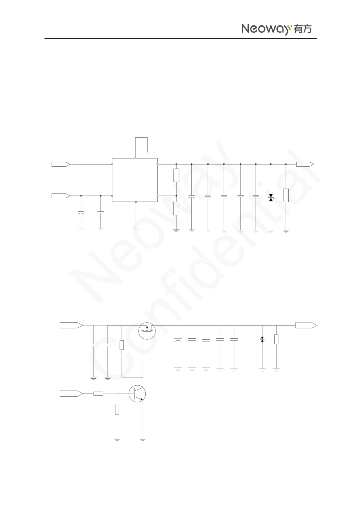
conditions. Use the EN pin on the LDO or DC/DC chipset to control the switch of the power supply as
shown in Figure 3-3 if a 5 V power supply is used.
MIC29302WU in Figure 3-3is an LDO and outputs a maximum current of 3 A to ensure that the module
works properly.
Figure 3-3 Reference design of power supply control
VDC_5V
VBAT
100 uF
TAN 0.1 uF
TVS
5V
10 uF
470uF
TAN
100K
47.5K
VOUT
MIC29302WU
EN
VIN ADJ 0.1 uF 100pF 33pF
PWR_EN
R1
The alternative way is to use an enhancement-mode p-MOSFET and NPN triode to control the module's
power, as shown inFigure 3-4.
InFigure 3-4, the module is turned on when PWR_EN is set to high level.
Figure 3-4 Reference design of power supply controlled by p-MOSFET
VCCIN_3V9
PWR_EN
VBAT
Q1
Q2
10uF 0.1uF 33pF100pF
0.1uF
10uF
470uF
D1 R3
R1
R2
R4
100kΩ
2kΩ
10kΩ
C1 C2 C3 C4 C5 C6 C7
S D
G
BC
E

N20 Hardware User Guide
Copyright © Neoway Technology Co., Ltd
14
VGSacross Q1 is equal to the voltage across R4. When high level is input at PWR_EN, the circuit is open
at Q2 and there is current at R4. VCE across Q2 is very small while VGSis almost equal to that of
VCCIN_3V9. VS is greater than VGand VGS is smaller than VGS(th)(where VGS(th) is the Gate Threshold
Voltage), so the circuit is open at Q1 and the current travels from source to drain.
In case that the MCU can supply a high voltage greater than VCCIN_3V9|, Q2 is not needed.
Reference components:
Q1 can be IRML6401 or low Rds(on) p-MOSFET, which has higher, withstand voltage and drain
current.
Q2: a common NPN tripolar transistor, e.g. MMBT3904; or a digital NPN tripolar transistor, e.g.
DTC123. If digital tripolar transistor is used, delete R1 and R2.
C3: 470μF tantalum capacitor rated at 6.3V, or 1000μF aluminum capacitor. If lithium battery is used
to supply power, C3 can be 220μF tantalum capacitor.
Power Supply Protection
Add TVS diodes (VRWM=5V)to the VBAT power supply, especially in automobile applications. For
some stable power supplies, Zener diodes can decrease the power supply overshoot. SMF5.0AG from
ONSEMI is an option.
Line Rules
The width of primary loop lines for VBAT on PCB must be able to support the safe transmission of 2 A
current and ensure no obvious loop voltage decrease. Therefore, the line width of VBAT is required 2mm
and the ground should be as complete as possible.
Separation
The module works in burst mode that generates voltage drops on power supply. Furthermore, this results
in a 217Hz TDD noise through power (One of the way generating noise. Another way is through RF
radiation). Analog parts, especially the audio circuits, are subjected to this noise, known as a "buzz noise"
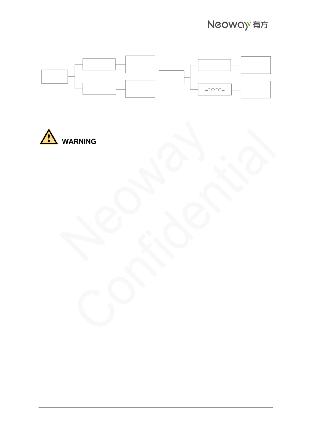
in GSM systems. To prevent other parts from being affected, use separated power supplies. The module
shall be supplied by an independent power, like a DC/DC or LDO. SeeFigure 3-5.
DC/DC or LDO should output rated peak current larger than 2A.
The inductor used in Reference Design (b), should be a power inductor and have very low resistance. The
value of 10μH, with average current ability greater than1.2A and low DC resistance, is recommended.
N20 Hardware User Guide
Copyright © Neoway Technology Co., Ltd
15
Figure 3-5 Reference designs of separated power supply
Other
circuit
DC-DC/LDO
N20DC-DC/LDO
Power
Input
Other
circuit
DC-DC/LDO
N20
Power
Input 10 uF
Reference design (a) Reference design (b)
Never use a diode to make the drop voltage between a higher input and module power. Otherwise,
Neoway will not provide warranty for product issues caused by this. In this situation, the diode will
obviously decrease the module performances, or result in unexpected restarts, due to the forward
voltage of diode will vary greatly in different temperature and current.
Place transient overvoltage protection components like TVS diode on power supply, to absorb the
power surges, SMAJ5.0A/C could be a choice.
3.1.2 VDDIO_1P8
VDDIO_1P8 outputsa voltage of 1.8V. It is recommended that VDDIO_1.8V@50mAbe used only for
interface level shifting and to add ESD protector while using it. VDDIO_1P8 is enabled automatically
when the module wakes up or is working.
3.1.3 ON/OFF
Power-On
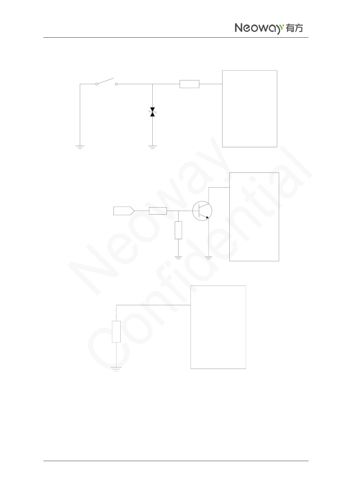
After powering on the VBAT pin, use PWRKEY to start the module by inputting low-level pulse for more
than 100ms (a value longer than 200ms is recommended). The PWRKEY pin is internally connected to
the power supply through a 200 kΩ pull-up resistor. Do not connect an external large resistor to ground
directly. Otherwise, the module cannot be powered on since the PWRKEY is pulled up all the time
internally. If users do not have to control the ON/OFF state of the module, connect a 1.5 kΩ pull down
resistor to the ground. Therefore, the module can start automatically once it is turned on. Leave this pin
unconnected if not used.
The circuits in Figure 2-7 or Figure 2-8 are recommended to control PWRKEY.
N20 Hardware User Guide
Copyright © Neoway Technology Co., Ltd
16
Figure 3-6 Push switch control
N20
PWRKEY
S1 kΩ
Figure 3-7 MCU control
N20
PWRKEY
Q
R1
R2
MCU_PWR_ON
Figure 3-8 Automatic power on
N20
PWRKEY
1.5 kΩ
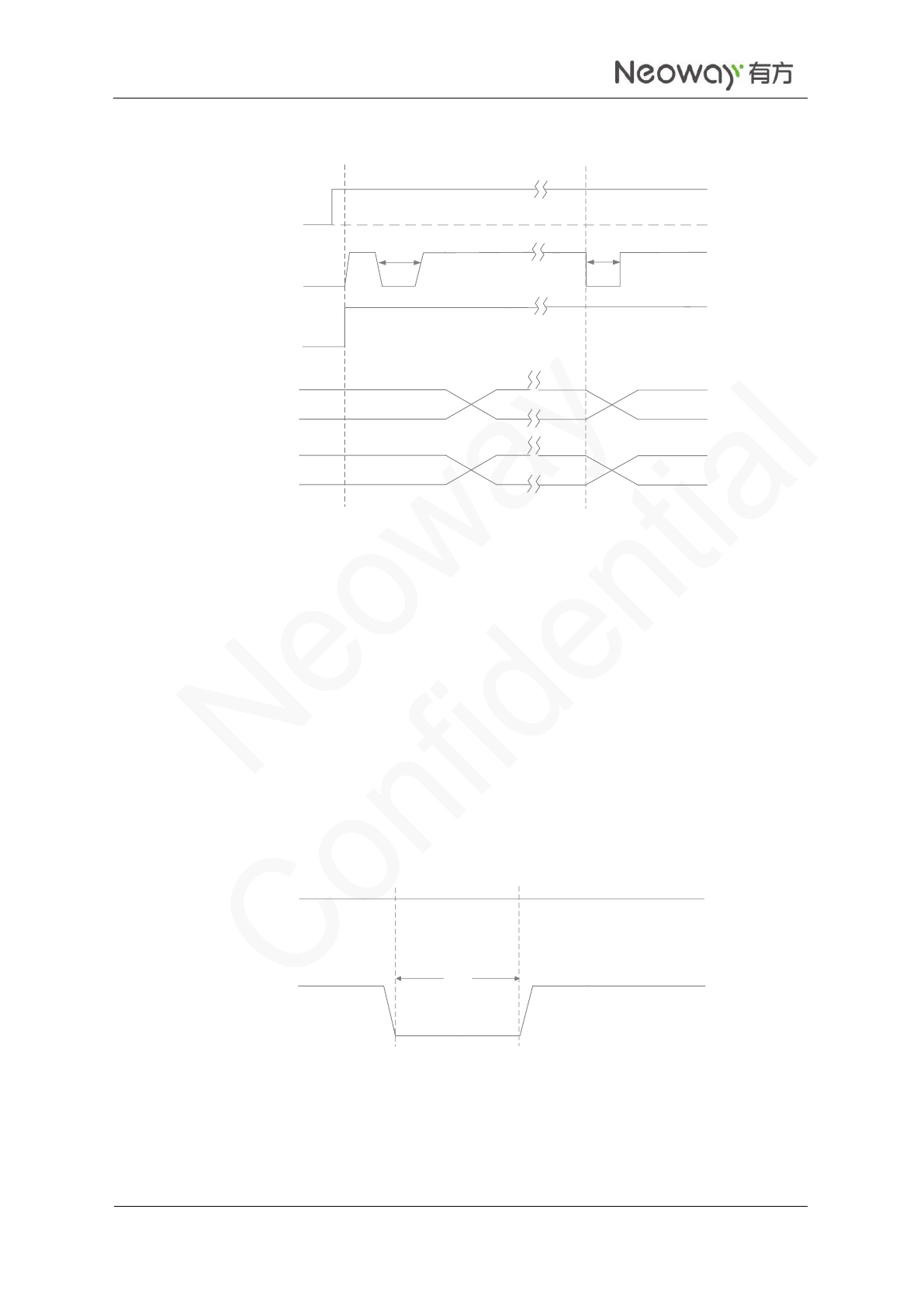
Perform other operations on the module only after it is initialized completely. If the module is powered on
but the power-on sequence has not been completed, the states of each pin are uncertain. The power-on
timing of the module is shown inFigure 3-9.
N20 Hardware User Guide
Copyright © Neoway Technology Co., Ltd
17
Figure 3-9 N20 power-on timing
VBAT
RESET_N
t >200ms
VL<0.6V
USB
t >2s
Inactive Active Inactive
Inactive Active Inactive
All Interfaces
PWRKEY
Power-off
The module can be powered off in two ways: hardware power off and software power off.
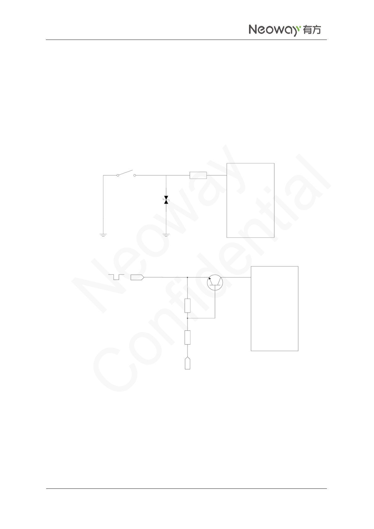
Inputting a low-level pulse for 2 seconds toPWRKEYcan trigger the power-off state of the module. Leave
this pin unconnected if it isnot used.
For how to power off the module through software, please refer to the AT command manual.
If 2.8V/3.3V IO system is adopted, use external triode isolation. For details, refer to 3.1.4 RESET. Figure
3-10shows the hard power-off timing.
Figure 3-10 N20 power-off timing
VBAT
t>2s
PWRKEY
N20 Hardware User Guide
Copyright © Neoway Technology Co., Ltd
18
3.1.4 RESET_N
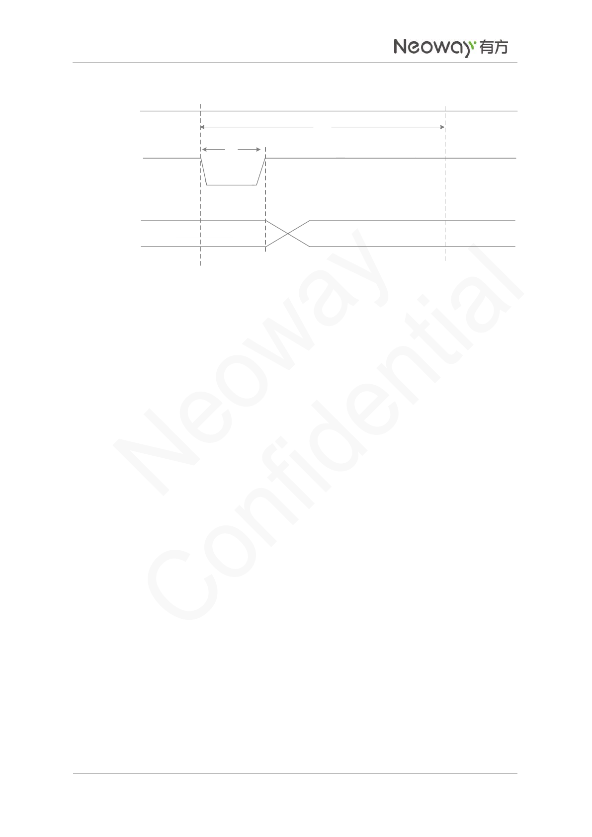
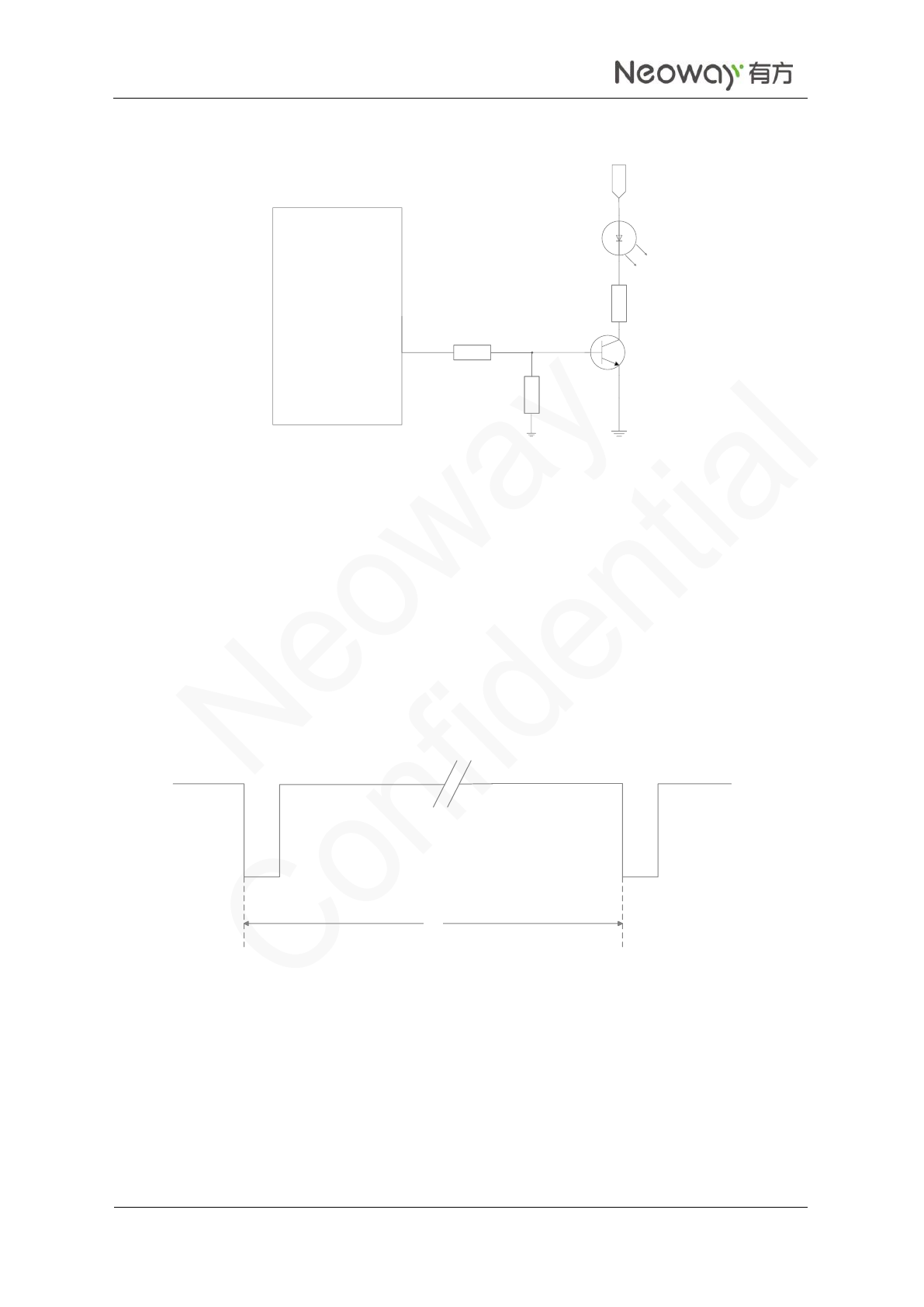
The RESET_N pin is used to reset the module. Low level for more than 1 second at this pin triggers reset
of the module. This pin is pulled up internally. Its typical high-level voltage is 1.8V. Leave this pin
unconnected ifit is not used. If 2.8V/3.0 V/3.3V IO system is used, separate it by adding a triode. Refer to
the following design.
To reset the module through high level, refer to Figure 3-7.
Figure 3-11 Reset controlled by button
N20
RESET_N
1KΩ
S
Figure 3-12 Reset circuit with triode separating
R3
R2
VDD_1P8
2V8/3V3/3V0
N20
RESET_N
Q1
In a circuit shown inFigure 3-12, VDD_EXT=2.8V/3.3V/3.0V, R2=4.7K, R3=47K. The recommended
voltage supplied to the base of the NPN transistor is VDD_1P8. If a voltage higher than 1.8 V is supplied,
the voltage across RESET_N might be higher than the threshold 2.1 V once inputting high level.
Figure 3-13shows the reset sequence.
N20 Hardware User Guide
Copyright © Neoway Technology Co., Ltd
19
Figure 3-13 N20 reset sequence
VBAT
RESET_N
Inactive Active
USB
All Interface
10 s
1 s
3.1.5 DTR
Generally, the DTR pin is used to control sleep mode together with AT commands. Enable the sleep mode
function by AT command.Then pulling DTR low will bring the module into sleep mode if the module is
idle. In this mode, the idle current is less than 2mA, depending on the DRX setting of network.
In sleep mode, the module can respond to the incoming call, SMS, and data.The host MCU can also
control the module to exit sleep mode by controlling DTR.
Process of entering sleep mode:
1. Keep DTR high level in normal working mode. Activate the sleep mode by using the
AT+ENPWRSAVE=1 command.
2. Pull DTR low, and the module will enter sleep mode, but only after process and pending data
finished.
3. In sleep mode, the external MCUcan pull DTR high so that the module will exit from sleep mode
actively. Then the module can transmit data and initiate calls. After processing is finished, pull DTR
low again to take the module back to sleep mode.
4. In sleep mode, the module can be woken up by the events of incoming voice call, received data, or
SMS. Meanwhile the module will send out the unsolicited messages through the UART.
Upon receipt of the unsolicited messages, the host MCU should pull DTR high firstly, otherwise the
module will resume sleep mode in two minutes after the service processing. Then the host MCU can
process the voice call, received data, or SMS.After processing is finished, pull DTR low again to put
the module into sleep mode.
3.1.6 NETLIGHT
NETLIGHT can output 1.8 V high level. Do not use it to drive LED directly. Drive the LED with a
transistor instead.
N20 Hardware User Guide
Copyright © Neoway Technology Co., Ltd
20
Figure 3-14 LED indicator driven by transistor
NETLIGHT
N20
10 kΩ
VCC
470
4.7 kΩ
When the module is running, the LED indicator is driven by the NET_LIGHT pin to indicate different
module status with its various blink behaviors. N20 supports multiple blink style and users can configure
it using AT commands.
3.1.7 RING
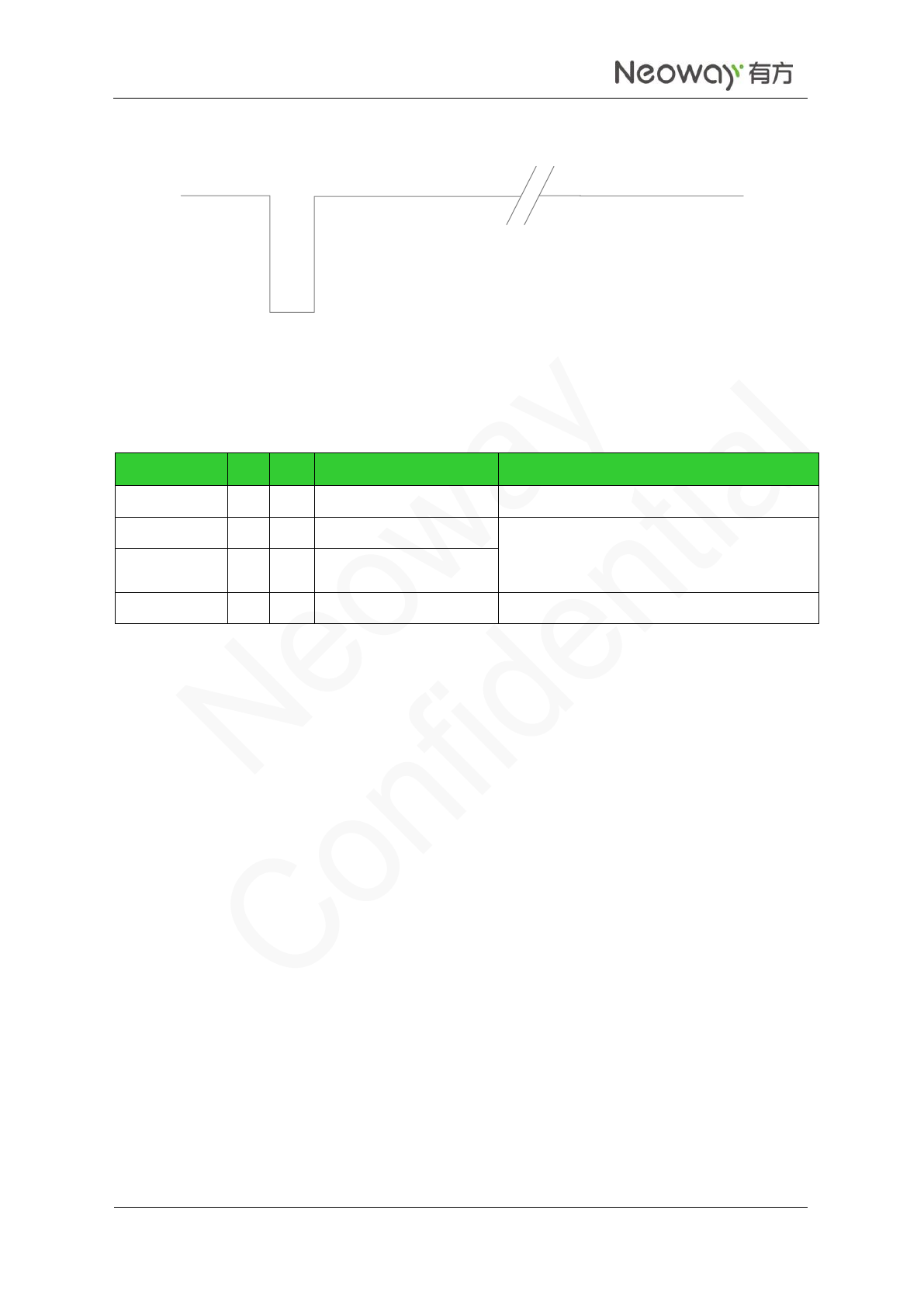
Calling: Once a voice call is incoming, UART outputs "RING" character strings and meanwhile the
RING pin outputs 30ms low pulses in a period of 5 second. After the call is answered, the high level
restores.
Figure 3-15 RING indicator for incoming call
5 s
30 ms 30 ms
SMS: Upon receipt of SMS, the module outputs one 35ms low pulse.
N20 Hardware User Guide
Copyright © Neoway Technology Co., Ltd
21
Figure 3-16 RING indicator for SMS
35 ms
3.2 USB Interface
Name
Pin
I/O
Function
Remarks
VBUS
25
P
USB voltage test
3.3V to 5.2V, typically 5V
USB_HS_DM
26
B
USB data negative signal
USB2.0, used for firmware download and
data transmission
90Ω impedance for differential trances
USB_HS_DP
27
B
USB data positive signal
USB_ID
28
DI
USB ID
Used for OTG function
USB can be used to download firmware for N20 and establish data communication for commissioning. If
the module is used only as USB
Connect a 1μF and a 22pF filter capacitors in parallel to the VBUS pin and place themas close to the pin
as possible. TVS diodes are required for the USB_VBUS power line. The junction capacitance of the TVS
diodes for USB_DP and USB_DM should be lower than 1pF as possible. USB data lines adopt differential
trace design, in which the differential impedance is limited to 90 Ω. Isolate the traces from other signal
traces.
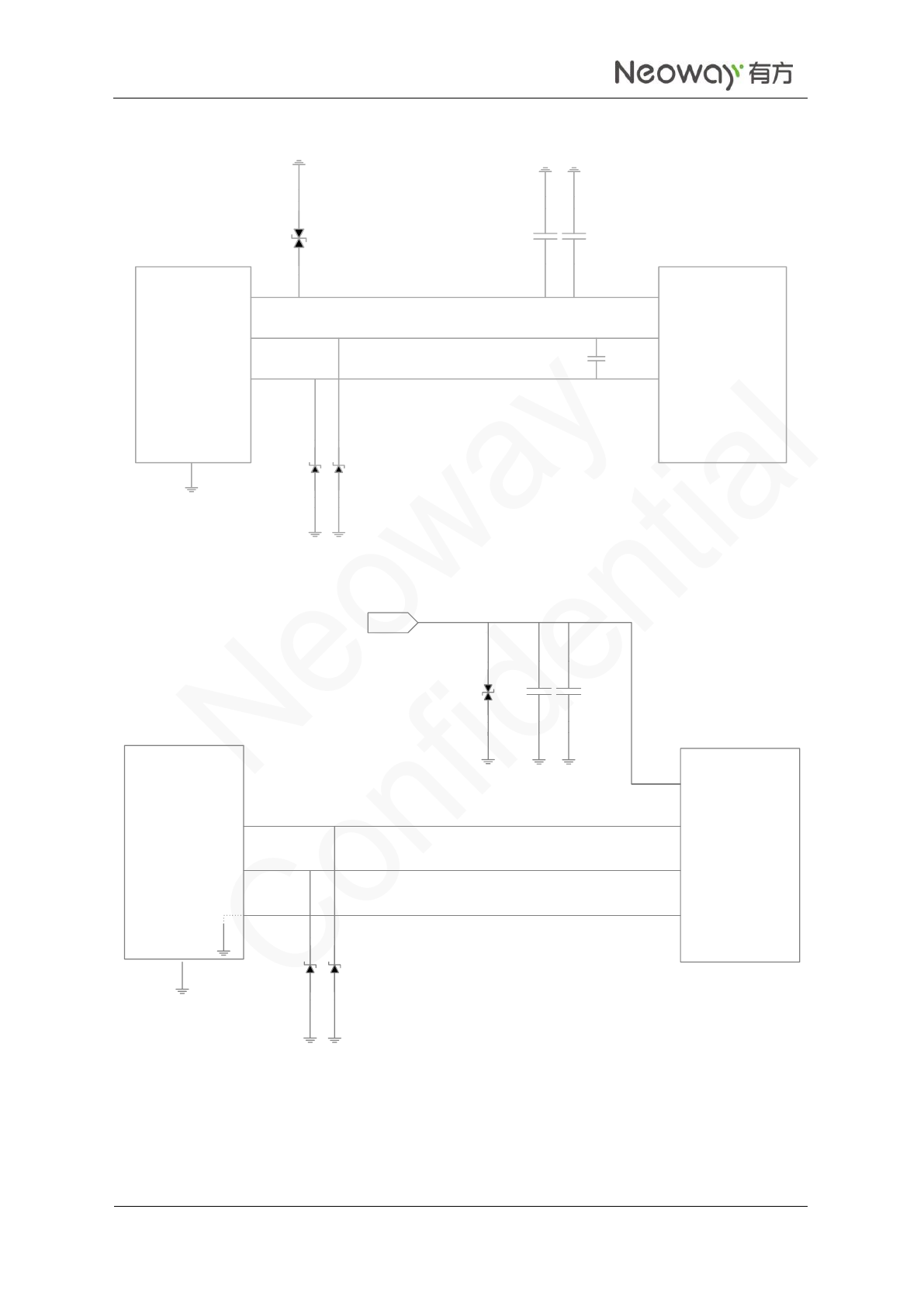
USB_ID is used for the OTG function. Pull USB_ID to low level, and the module will work in host mode.
To use the OTG function, supply a voltage to USB_VBUS. For voltage requirements, see the pin
description. Figure 3-17 shows the connection of USB pins.
N20 Hardware User Guide
Copyright © Neoway Technology Co., Ltd
22
Figure 3-17 USB connection
USB_VBUS
USB_DM
USB_DP
USB_ID
GND
USB_ID
USB_HS_DP
USB_HS_DM
USB_VBUS
D1 C1 C2
D2 D3
DNI
USB N20
Figure 3-18 USBconnection for OTG
USB_DM
USB_DP
USB_ID
GND
USB_ID
USB_HS_DP
USB_HS_DM
USB_VBUS
D1 C1 C2
D2 D3
N20
USB
VCC(3.3V-5.2V)
N20 Hardware User Guide
Copyright © Neoway Technology Co., Ltd
23
3.3 UIM Card Interface
Name
Pin
I/O
Function
Remarks
VUIM
29
PO
UIM power supply
Compatible with 1.8 V/3 V UIM card
UIM_DATA
30
IO
UIMdata
A 10 kΩresistor is required between
VIM_VCC and UIM_DATA.
UIM_CLK
31
DO
UIMclock
UIM_RESET
32
DO
UIMreset
UIM_PRESENT
33
DI
UIM detect
A pull-up resistor is recommended
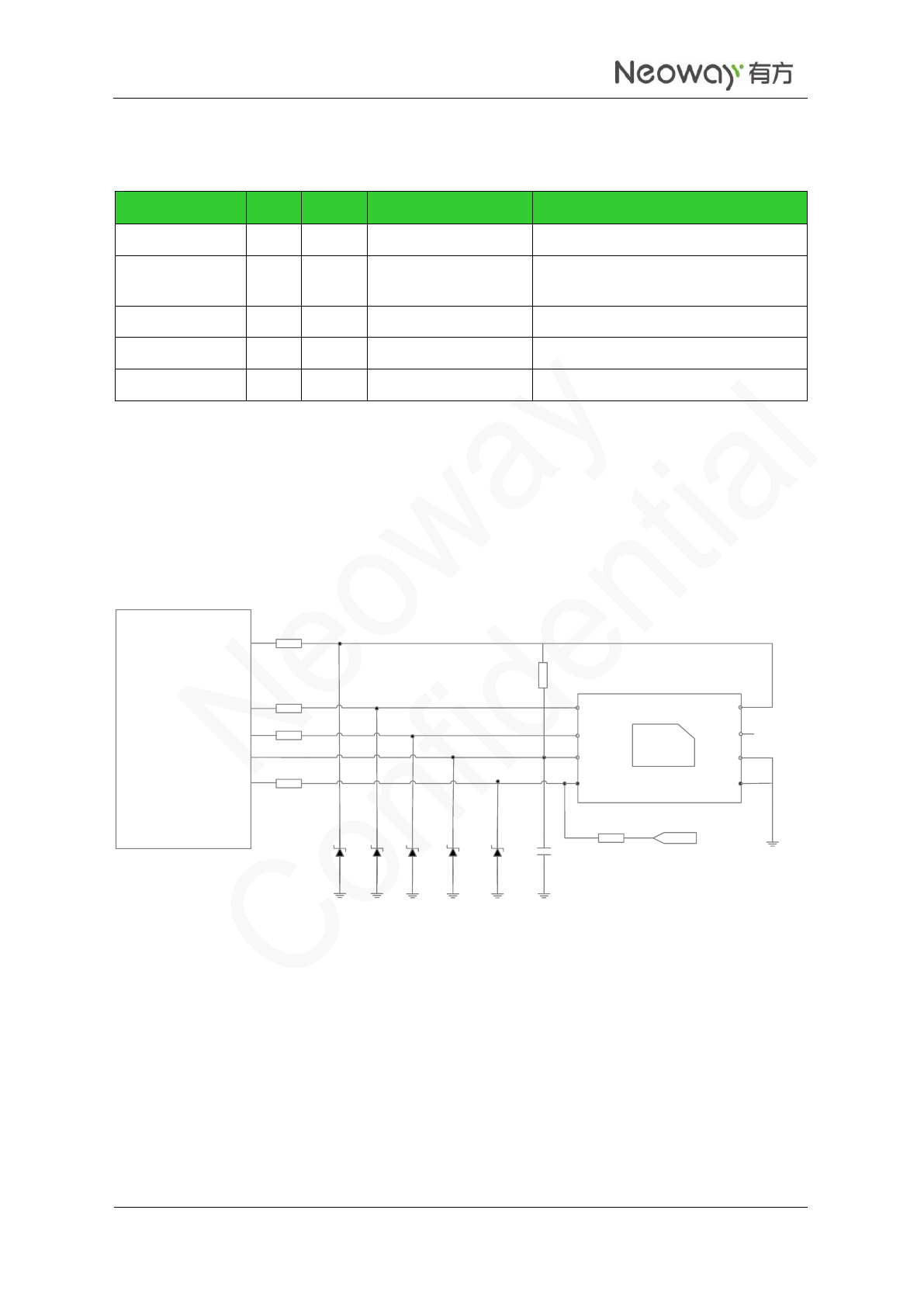
N20 supports 1.8V/2.85 VUIM cards. VUIM is the power supply pin of the UIM card and its maximum
load is 30mA. The UIM_DATA pin is not pulled up internally, so reserve a pull-up resistor externally in
design. UIM_CLK is the clock signal pin, supporting 3.25GHz of clock frequency.Figure 3-19 shows the
reference design of the UIM card interface.
Figure 3-19 Reference design of SIM card interface
1 uF
CLK
RST
VCC
VPP
GND
UIM card
DATA
GND
SIM-DET
20Ω
47KΩ VDD_1P8
UIM_DATA
UIM_CLK
UIM_RESET
VUIM
UIM_PRESENT
N20
UIM
20Ω
20Ω
20Ω
10KΩ
ESD protectors, such as ESD diodes or TVS diodes (with a junction capacitance of less than 33pF), are
recommended to be added on the SIM signals,in most applications with a high requirement of ESD
protection.Add a 20 Ω resistor respectively to UIM_DATA,UIM_RESET, UIM_CLK, and
UIM_PRESENT to enhance the ESD performance.
N20 supports UIM card detection. UIM_PRESENT isa 1.8V interrupt pin. The UIM detection circuit
works by checking the level across the UIM_PRESENT pin before and after a UIM card is inserted. In the
reference circuit, SIM-DET is not connected before a UIM card is inserted and is grounded after a UIM
card is inserted.Low level means UIM card detected while high level mean no UIM card detected.
N20 Hardware User Guide
Copyright © Neoway Technology Co., Ltd
24
The antenna should be installed far away from the UIM card and UIM card traces, especially to the
built-in antenna.
The UIM traces on the PCB should be as short as possible and shielded with GND copper.
The ESD protection diodes or small capacitors should be close to UIM card on the PCB.
3.4 SDIOInterface
Name
Pin
I/O
Function
Remarks
SDC_CMD
36
B
Control signal of SDIO interface
SDC_CLK
37
DO
Clock signal of SDIO interface
SDC_DATA_0
38
B
SDIO data bit 0
SDC_DATA_1
39
B
SDIO data bit 1
SDC_DATA_2
40
B
SDIO data bit 2
SDC_DATA_3
41
B
SDIO data bit 3
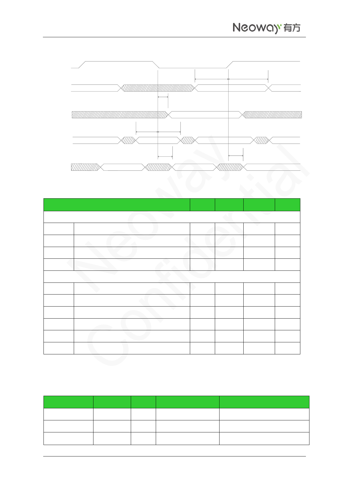
The SDIO interface supports a maximum clock frequency of SDR 200 MHz or DDR 50 MHz, and it is
compatible DS, HS, SDR12, SDR25, SDR50, and SDR104.
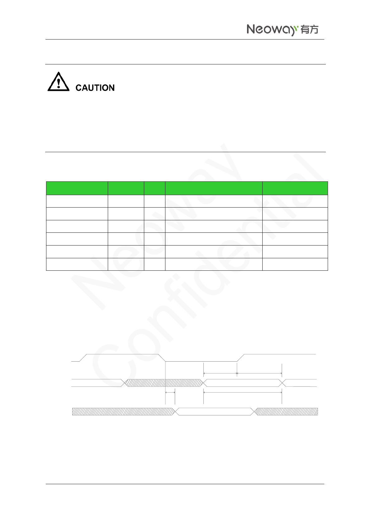
The following figures and table shows the sequences and parameters of SDR and DDR modes
respectively.
Figure 3-20 SDIO SDRtiming
SDC_CLK
Read
Write
t(pddwr)
t(pdcwr) t(cdvrd)
t(dvrd)
t(csurd)
t(dsurd) t(chrd)
t(dhrd)
N20 Hardware User Guide
Copyright © Neoway Technology Co., Ltd
25
Figure 3-21 SDIO DDRtiming
Command
Read
Command
Write
t(pdcwr)
t(csurd) t(chrd)
SDC_CLK
DATA
Read
DATA
Write
t(dsurd) t(dhrd)
t(pddwr) t(pddwr)
Table 3-1 Timing parameters of SDIO interface
Timing Parameter
Min.
Typical
Max.
Unit
SDR mode (max. 200 MHz)
t(cvdrd)
Command valid time
2.4
/
/
ns
t(dvdrd)
Data valid time
2.4
/
/
ns
t(pddwr)
Delay time from data write to transmit
-1.45
/
0.85
ns
t(pdcwr)
Delay time from command write to transmit
-1.45
/
0.85
ns
DDR mode (max. 50 MHz)
t(chrd)
Command hold time
1.5
/
/
ns
t(csurd)
Command set-up time
5.53
/
/
ns
t(dhrd)
Data hold time
1.5
/
/
ns
t(dsurd)
Data set-up time
1.65
/
/
ns
t(pddwr)
Delay time from data write to transmit
2.5
/
6.15
ns
t(pdcwr)
Delay time from command write to transmit
-7.85
/
2.65
ns
3.5 PCM Interface
Name
Pin
I/O
Function
Remarks
PCM_SYNC
45
B
PCM sync signal
PCM_CLK
46
DO
PCM clock signal
PCM_DIN
47
DI
PCM data input
N20 Hardware User Guide
Copyright © Neoway Technology Co., Ltd
26
PCM_DOUT
48
DO
PCM data output
I2S_MCLK
49
DO
I2S main clock
Default frequency: 12.288MHz
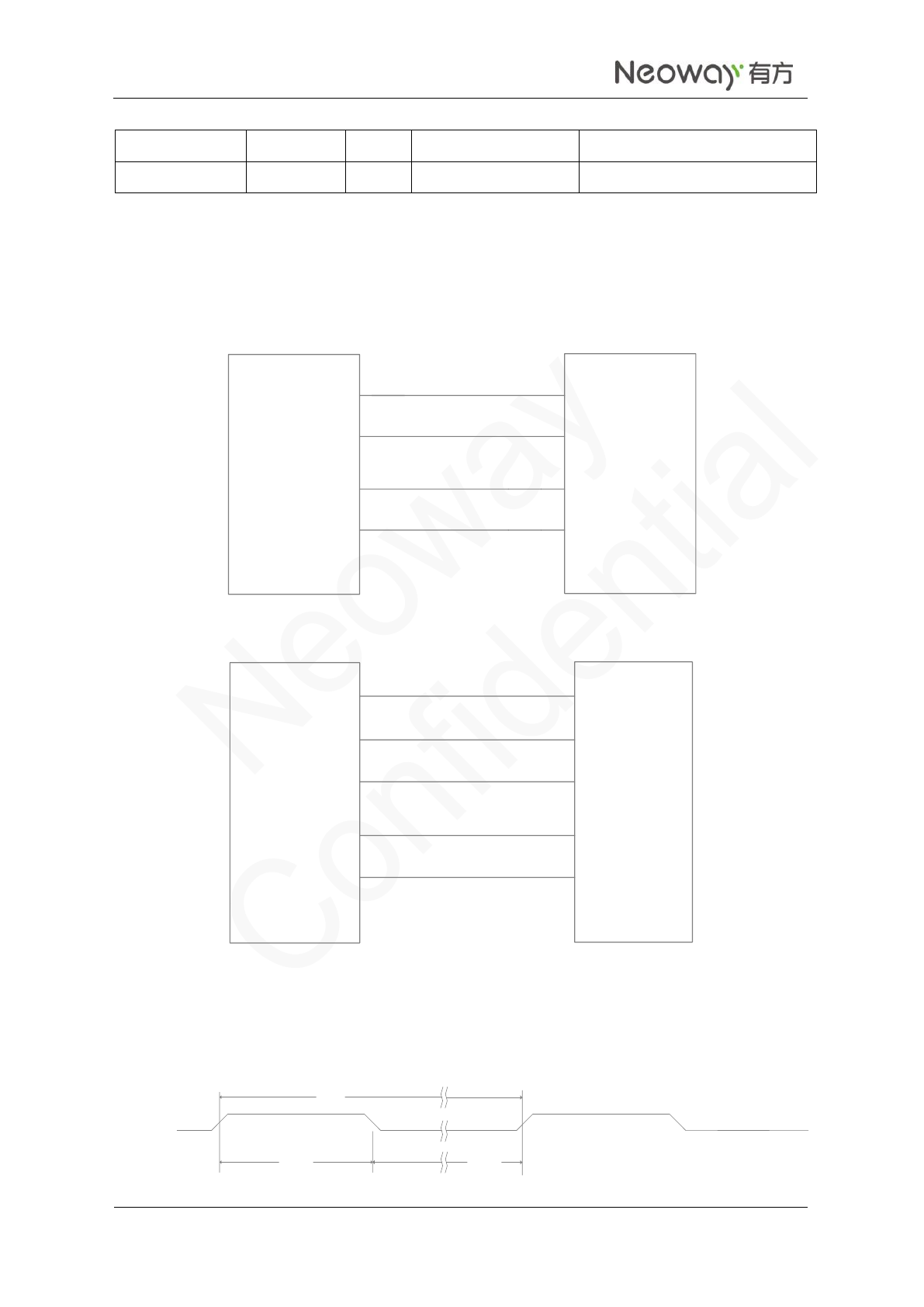
N20 provides one I2S/PCM MUX interface that supports 1.8 V. Figure 3-22 shows the connection of
PCM.
Figure 3-22 PCM connection
PCM_DOUT
PCM_DIN
PCM_SYNC
PCM_CLK
N20 CODEC
PCM_DIN
PCM_DOUT
PCM_SYNC
PCM_CLK
Figure 3-23 I2Sconnection
I2S_TX
I2S_RX
I2S_WS
I2S_SCLK
N20 CODEC
I2S_MCLK I2S_MCLK
I2S_DIN
I2S_DOUT
I2S_LRCLK
I2S_BCLK
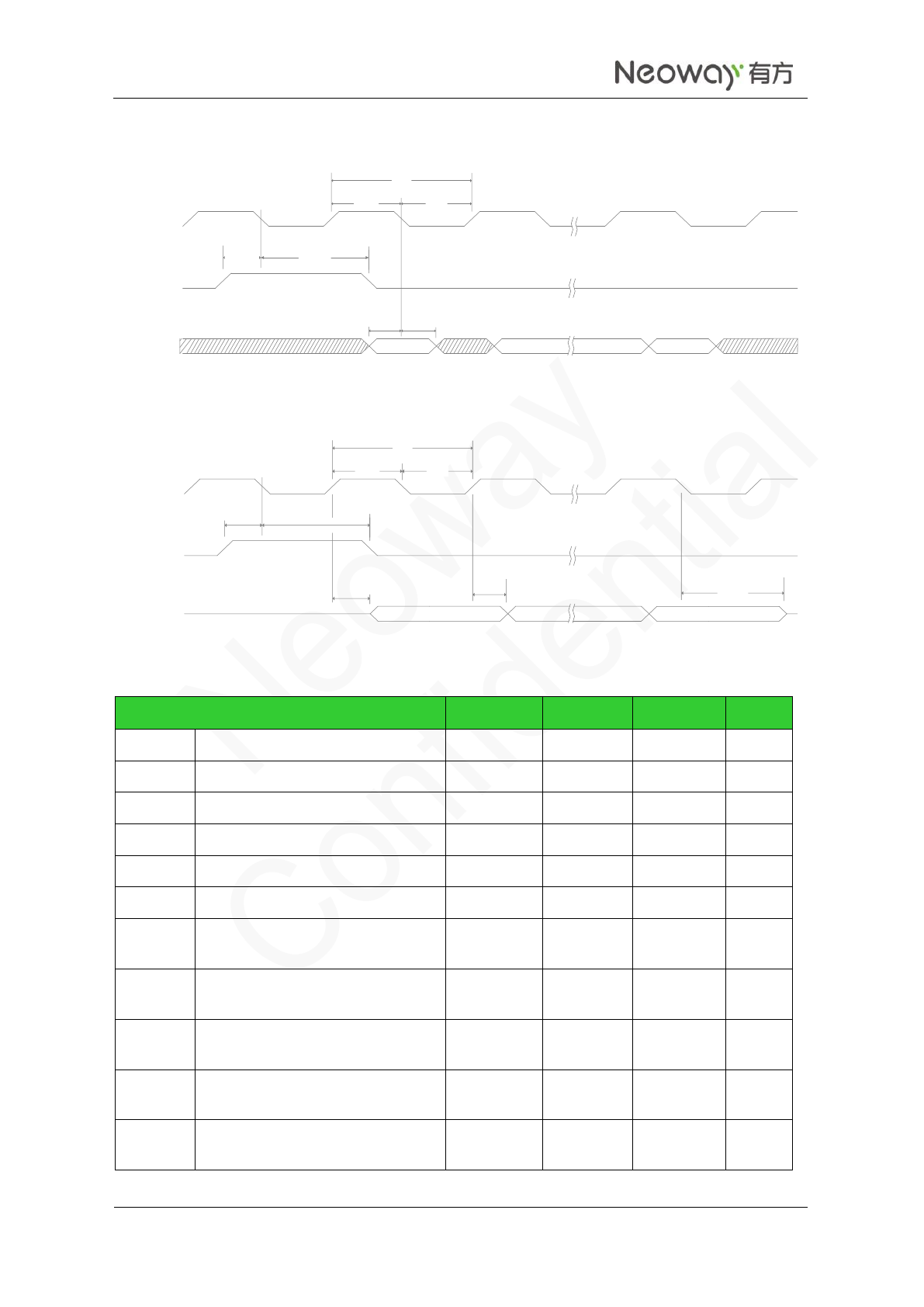
The clock frequency of the PCM interface is be 2018 KHz at most. The following figures show the
sequences of PCM.
Figure 3-24 PCM SYN timing
PCM_SYNC
t(sync)
t(syncd)
t(synca)
N20 Hardware User Guide
Copyright © Neoway Technology Co., Ltd
27
Figure 3-25 PCM data input timing
t(susyn
c) t(hsync)
t(clk)
t(clkh) t(clkl)
PCM_CLK
PCM_SYNC
PCM_DIN MSB LSB
t(sudin) t(hdin)
Figure 3-26 PCM data output sequence
t(clk)
t(clkh) t(clkl)
PCM_CLK
PCM_SYNC
PCM_DOUT MSB LSB
t(zdout)
t(susync) t(hsync)
t(pdout) t(pdout)
Table 3-2 Timing parameters of PCM interface
Timing Parameter
Min.
Typical
Max.
Unit
t(sync)
PCM_SYNCcycle
/
125
/
ns
t(synca)
PCM_SYNCvalid time
/
488
/
ns
t(syncd)
PCM_SYNC invalid time
/
124.5
/
ns
t(clk)
PCM_CLKcycle
/
488
/
ns
t(clkh)
PCM_CLK high time
/
244
/
ns
t(clkl)
PCM_CLK low time
/
244
/
ns
t(susync)
Set-up time from PCM_SYNChigh
PCM_CLK low
/
122
/
ns
t(sudin)
Set-up time from PCM_DINhigh to
PCM_CLKlow
60
/
/
ns
t(hdin)
Hold time from PCM_CLK low to
PCM_DIN high
10
/
/
ns
t(pdout)
Delay time from PCM_CLK high
to PCM_DOUTlow
/
/
60
ns
t(zdout)
Delay time from PCM_CLK low to
PCM_DOUT high impedance
/
160
/
ns
N20 Hardware User Guide
Copyright © Neoway Technology Co., Ltd
28
3.6 I2C Interface
Name
Pin
I/O
Function
Remarks
I2C_SCL
44
DO
I2Cclock
Pulled up by a 2.2 kΩ resistor internally.
I2C_SDA
43
B
I2C data
Pulled up by a 2.2 kΩ resistor internally.
The I2C interface can be used directory because it is pulled up by a 2.2 kΩ resistor internally.
3.7 SPIInterface
Name
Pin
I/O
Function
Remarks
SPI_CLK
62
DO
Clock signal
Max. 50MHz
SPI_MISO
63
DI
Master input
SPI_MOSI
64
DO
Master output
SPI_CS_N
65
DO
Chip select
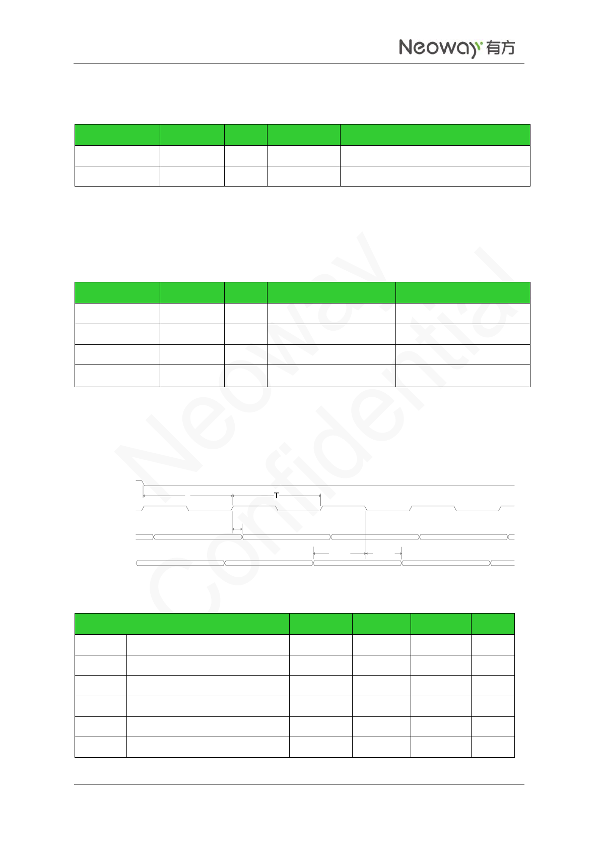
The SPI interface supports 1.8 V and only master mode.
Figure 3-27 SPI interface timing
T
t(mov)
t(mis) t(mih)
SPI_CS_N
SPI_CLK
SPI_MOSI
SPI_MISO
Table 3-3 Timingparameters of SPIinterface
Timing Parameter
Min.
Typical
Max.
Unit
T
Clock cycle (max. 50MHz)
20.0
/
/
ns
t(ch)
Hold time for clock high
9.0
/
/
ns
t(cl)
Hold time for clock low
9.0
/
/
ns
t(mov)
Output valid time
-5.0
/
5.0
ns
t(mis)
Input set-up time
5.0
/
/
ns
t(mih)
Input hold time
1.0
/
/
ns
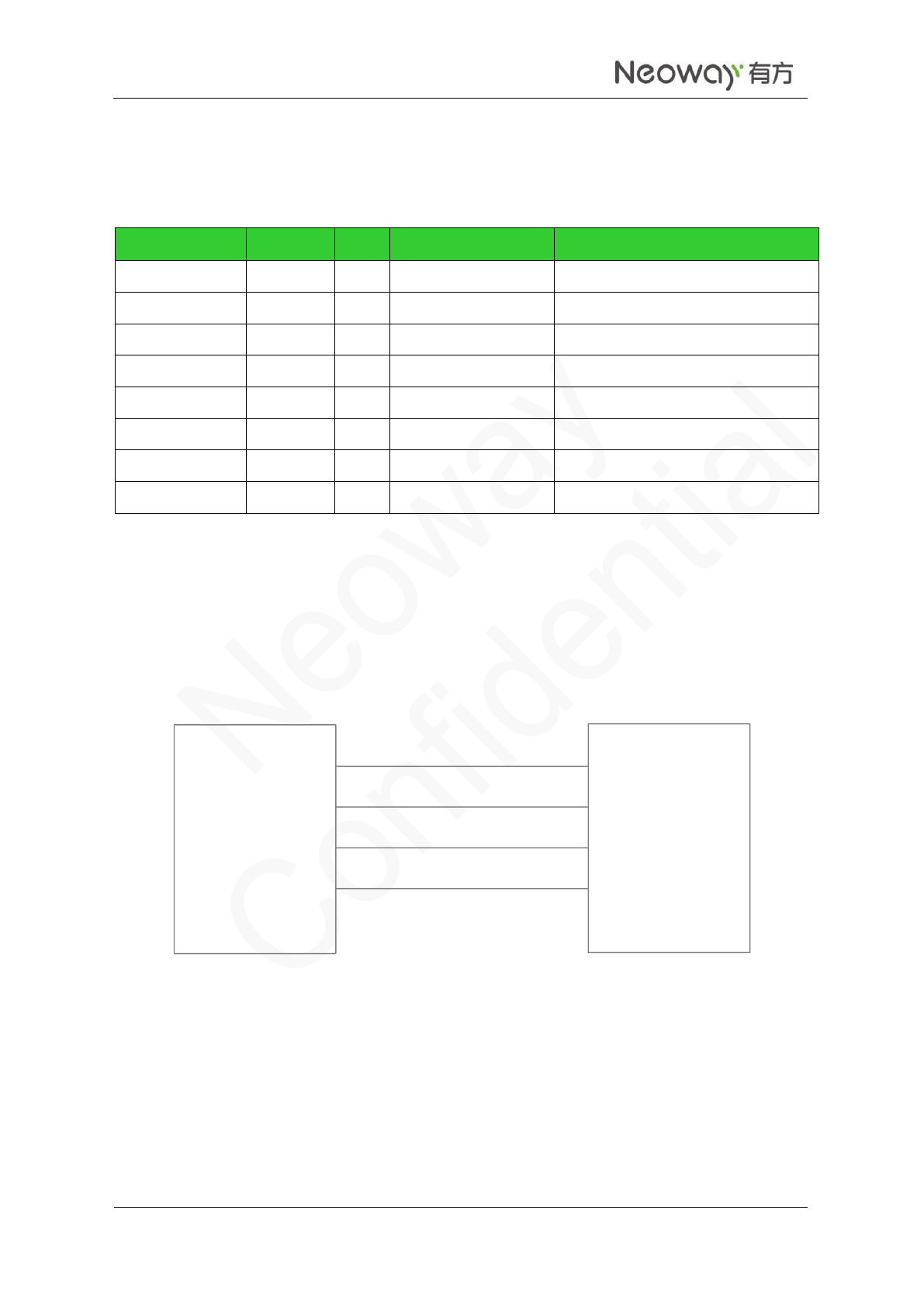
N20 Hardware User Guide
Copyright © Neoway Technology Co., Ltd
29
3.8 UARTInterfaces
Name
Pin
I/O
Function
Remarks
UART0_TX
9
DO
UART data transmit
UART0_RX
10
DI
UART data receive
UART0_RTS
11
DO
Request to send
UART0_CTS
12
DI
Clear to send
UART1_RTS
58
DO
Request to send
UART1_CTS
59
DI
Clear to send
UART1_RX
60
DI
UART data receive
UART1_TX
61
DO
UART data transmit
N20 provides 2 UART interfaces, one of which support hardware flow control. The UART interfaces
support 4 Mbps at most. The level at the interfaces is 1.8V. Figure 3-28shows the reference design of the
UART interface.
Figure 3-28 Reference design of the UART interface
UART_RXD
UART_CTS
UART_RTS
N20
UART_TXD RXD
TXD
CTS
RTS
UART (MCU)
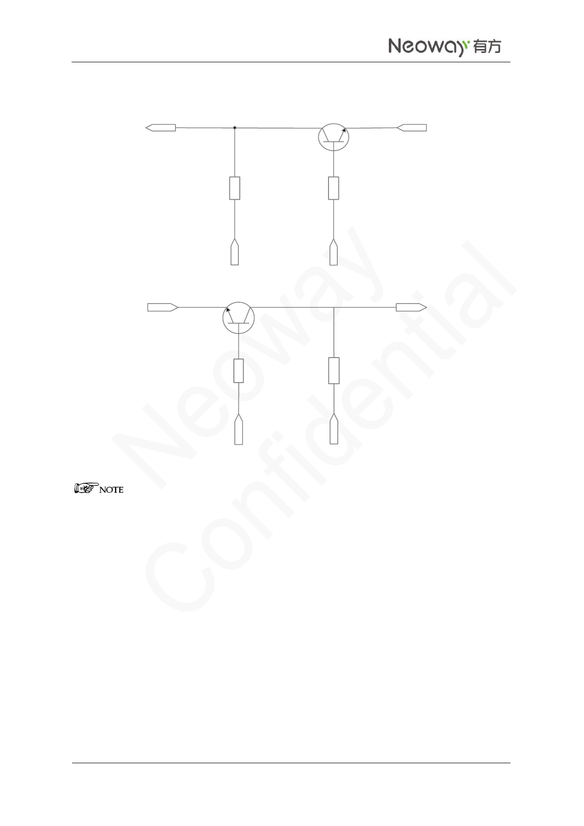
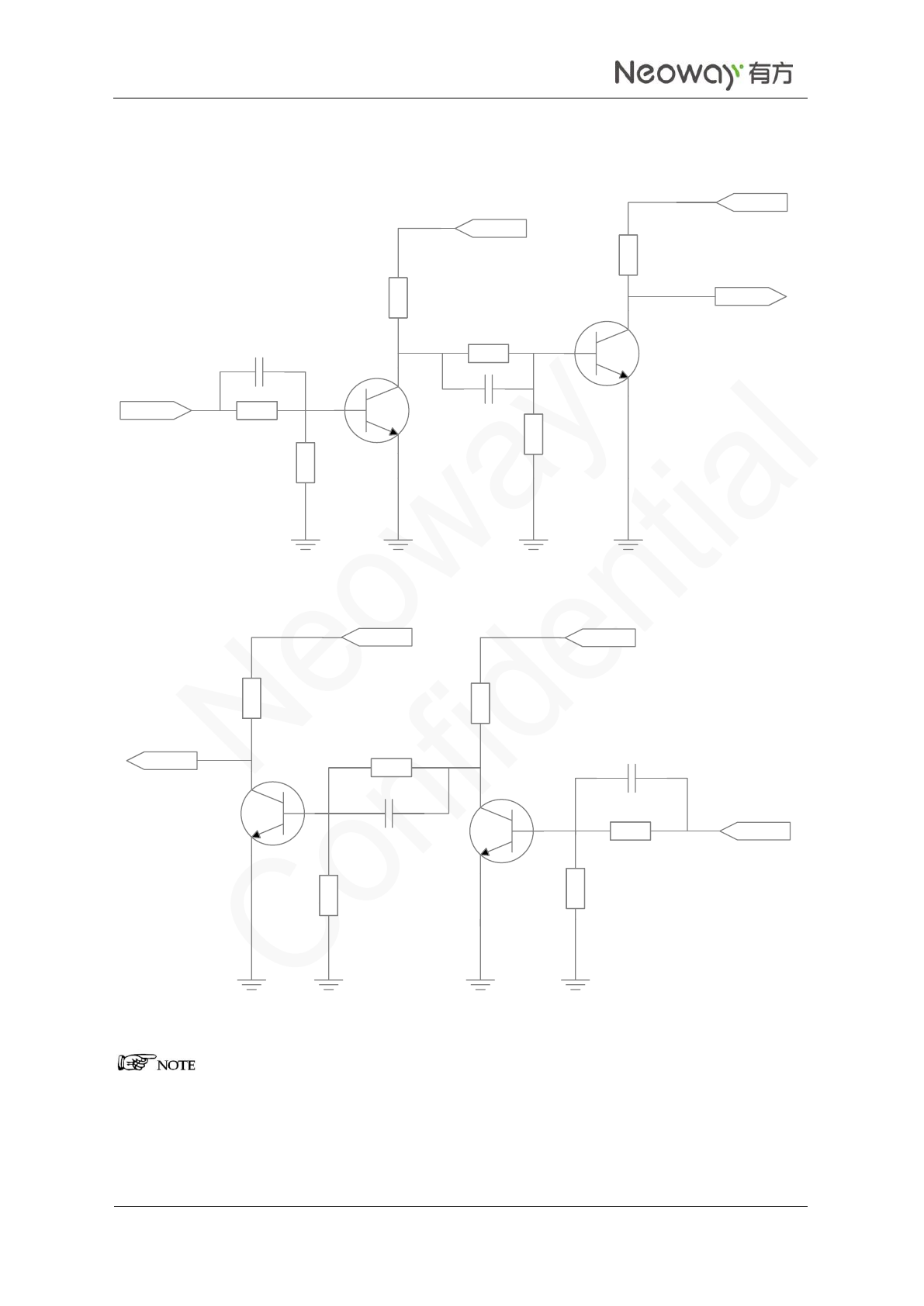
If the UART does not match the logic voltage of the MCU, add a level shifting circuit outside of the
module as shown inFigure 3-29 (for VIL≤200 mV) and Figure 3-30 (for VIL>200 mV).
N20 Hardware User Guide
Copyright © Neoway Technology Co., Ltd
30
Figure 3-29 Recommended level shifting circuit 1
TXD
VDD_1P8
VCC_IO
4.7K
10K
Q
1
R2
R3
MCU_RXD
MCU_TXD Q2 RXD
10KR1
4.7K R4
VDD_1P8
VDD_1P8
Components:
R2/R4: 2K-10K. The greater the UART baud rate is, the lower the R2/R4 values are.
R1/R3: 4.7K-10K The greater the UART baud rate is, the lower the R/R3R3 value is.
Q1/Q2: MMBT3904 or MMBT2222. High-speed transistor is better.
MCU_TXD and MCU_RXD are respectively the TX and RX ports of the MCU while TXD and RXD are
respectively the TX and RX ports of the module.
Voltage at VCC_IO is the voltage at the UART of the MCU while voltage at VDD_1V8 is the voltage at
the UART of the module.
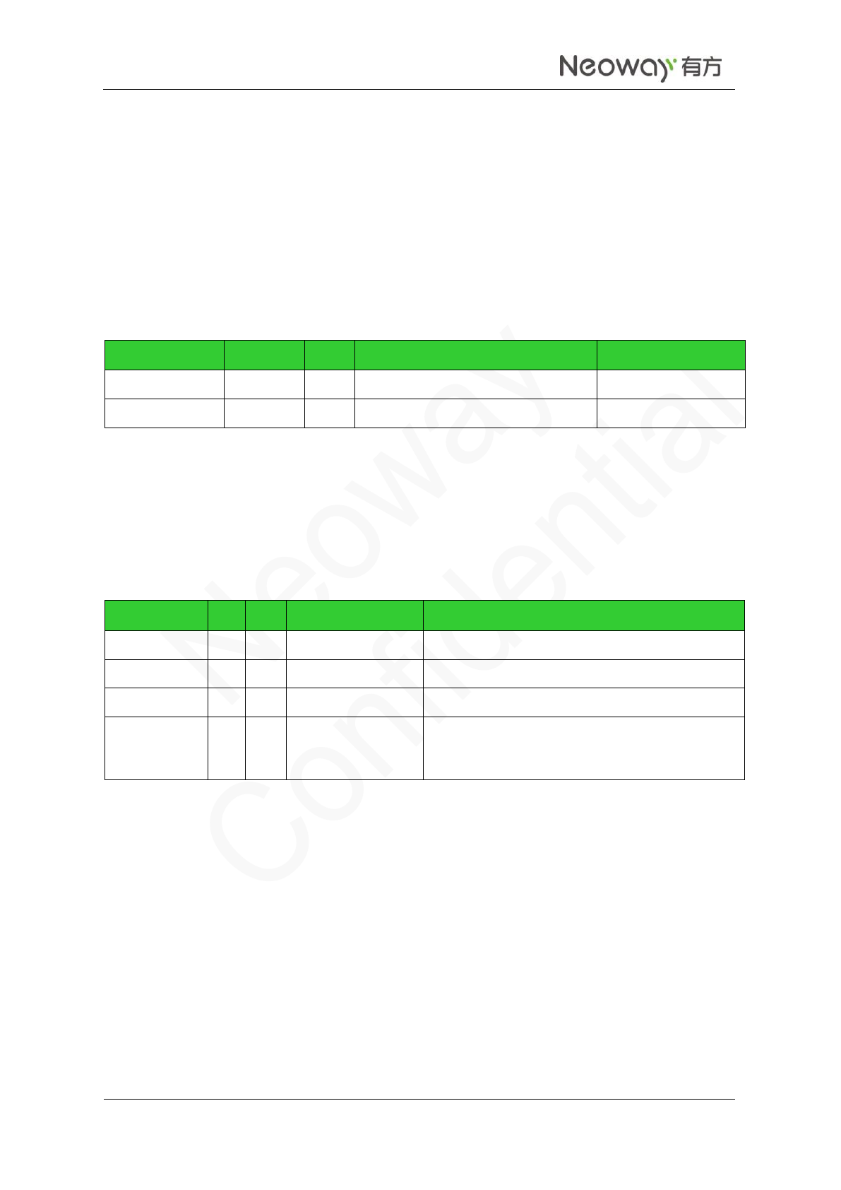
Figure 3-30 shows another recommended level shifting circuit.
N20 Hardware User Guide
Copyright © Neoway Technology Co., Ltd
31
Figure 3-30 Recommended level shifting circuit 2
C1 220pF
TXD
R1 5.6 kΩ
R2 47 kΩ
R3 4.7 kΩ
VDD_1P8
R4 2.2 kΩ
C2 220pF
R5 47 kΩ
R6 10 kΩ
Q1
Q2
MCU_RXD
VCC_IO
C1 220pF
RXD
R1 10 kΩ
R2 10 kΩ
R3 5.6 kΩ
VCC_IO
R4 10 kΩ
C2 220pF
R5 47 kΩ
R6 4.7 kΩ
Q1
Q2
MCU_TXD
VDD_1P8
Components:
Q1/Q2: MMBT3904 or MMBT2222.High-speed transistors are better.
N20 Hardware User Guide
Copyright © Neoway Technology Co., Ltd
32
MCU_TXD and MCU_RXD are respectively the TX and RX ports of the MCU, while TXD and RXD are
respectively the TX and RX ports of the module.
Voltage at VCC_IO is the voltage at the UART of the MCU while voltage at VDD_1P8 is the voltage at
the UART of the module.
3.9 ADCInterfaces
N20 provides two ADC channels, and the input voltage ranges from 0.1 V to 1.7 V. ADC pin supports
highest precision of 15 bit and it can be used for temperature and other check.
Name
Pin
I/O
Function
Remarks
ADC1
2
AI
Analog-to-digital signal conversion
ADC2
3
AI
Analog-to-digital signal conversion
3.10 GPIOInterfaces
Table 3-4lists GPIO pins.
Table 3-4 GPIO pins
Name
Pin
I/O
Function
Remarks
GPIO1
5
B
GPIO with interrupt
GPIO2
6
B
GPIOwith interrupt
GPIO3
7
B
GPIOwith interrupt
SIM_SELECT
8
B
GPIO, to support
Dual-SIM Single
Standby
Do not connect this pin to the power supply
through a pull-up resistor before the module is
started.
N20 provides 4 GPIO pins, three among which support interrupt. Do not connect SIM_SELECT to the
power supply through a pull-up resistor before the module is started. If high level is detected at this pin or
any current is input at this pin during the startup of the module, the module will be forced to enter the
download mode.
N20 does not support dual-SIM function. To support dual-SIM single standby, add an external analog
switch to switch SIM cards. SIM_SELECT is used to control the analog switch. If low level is detected at
this pin, switch to SIM1; if high level is detected, switch to SIM2.
SIM1 is selected by default after the module is enabled. To switch to SIM2, send AT+SIMSWITCH=2.
For details, see Neoway_N20_ AT_Command_Mannual.
For how to design the function, see Neoway_N20_Dual_SIM_Single_Standby_Application_Guide.
N20 Hardware User Guide
Copyright © Neoway Technology Co., Ltd
33
3.11 Commissioning Interface
To facilitate software update and commissioning, reserve the commissioning interface.
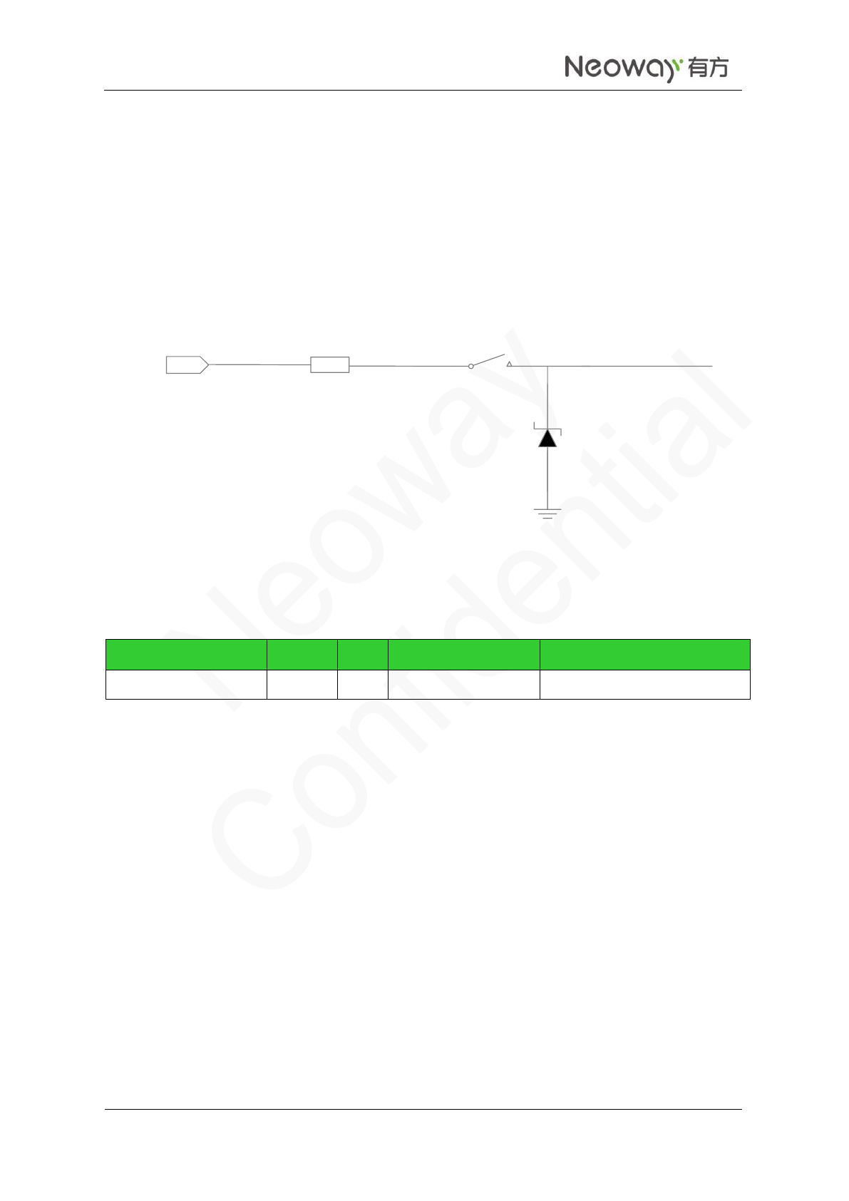
The module can enter the fastboot mode by connecting the FORCE_USB_BOOT pin to VDDIO_1P8
during the startup. This is the last method to troubleshoot the abnormality that the module cannot start or
operation properly.
Figure 3-31 Reference design of the fastboot interface
FORCE_USB_BOOT
S1
VDDIO_1P8 10 KΩ
3.12 Other Interfaces
Name
Pin
I/O
Function
Remarks
EXT_GNSS_LNA_EN
56
DO
GNSS_LNA enable
Used for externalGNSS_LNA
N20 Hardware User Guide
Copyright © Neoway Technology Co., Ltd
34
4 RF Interface
Name
Pin
I/O
Function
Remarks
RF_ANT_MAIN
67
2G/4G main antenna
50Ω characteristic impedance
RF_ANT_GNSS
54
GNSSantenna
4.1 2G/4G RF Design and PCB Layout
RF_ANT_MAIN isthe antenna pins of N20. A 50 Ω antenna is required. VSWR ranges from 1.1 to 1.5.
The antenna should be well matched to achieve best performance. It should be installed far away from
high-speed logic circuits, DC/DC power or any other strong disturbing sources.
A 50 Ω antenna is required. VSWR ranges from 1.1 to 1.5. The antenna should be well matched to
achieve best performance.
For multiple-layer PCB, the trace between the antenna pad of module and the antenna connector, should
have a 50 Ω characteristic impedance, and be as short as possible. The trace should be surrounded by
ground copper. Place plenty of via holes to connect this ground copper to main ground plane, at the copper
edge.
For dual-layer PCB, the width of recommended impedance trace is 0.8 mm to 1 mm and the grounding
copper should away from the trace for 1 to 1.5 time of the trace width.
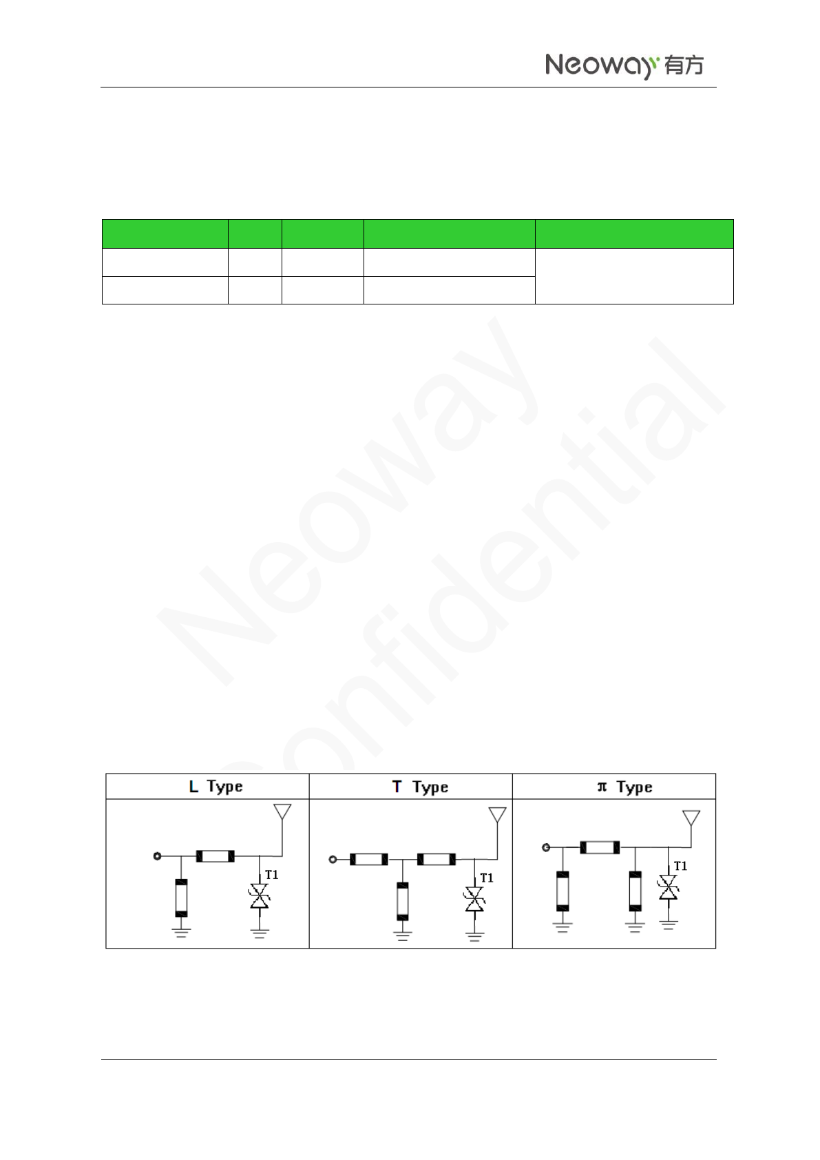
If the trace between the module and connector has to be longer, or built-in antenna is used, add a matching
as shown in Figure 4-1.
Figure 4-1 Reference designs of antenna matching
The elements in the matching circuits must be capacitor, inductor, or 0Ω resistor. It is recommended to
add ESD protector if the antenna might generate static electricity. The protector can be TVS with a
N20 Hardware User Guide
Copyright © Neoway Technology Co., Ltd
35
maximum junction capacitance of lower than 0.5 pF. Ensure that the reverse breakdown voltage of the
TVS is greater than 10V (above 15 V is recommended).
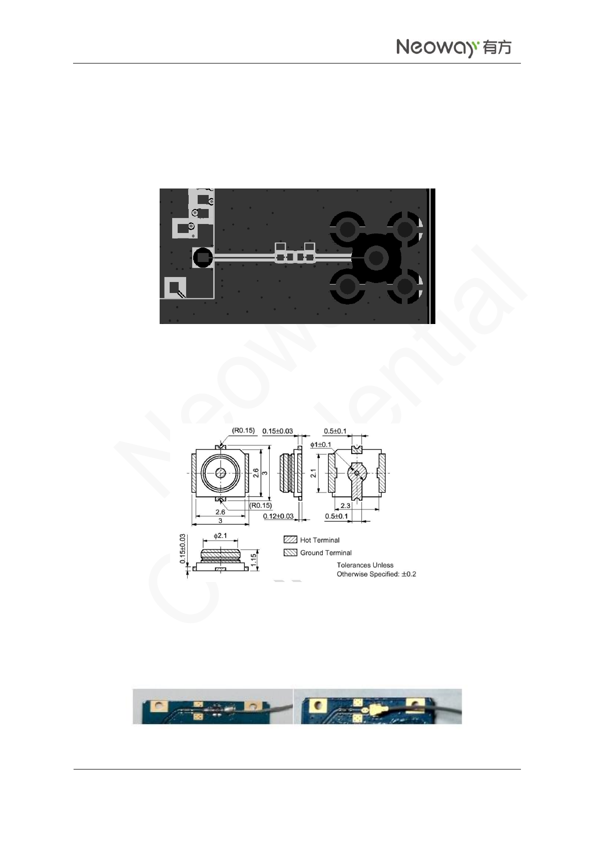
Big RF solder pad can result in great parasitic capacitance, which will affect the antenna performance.
Remove the copper on the first and second layers under the RF solder pad.
Figure 4-2 Recommended RF PCB design
To adopt RF antenna connections, the GSC RF connector MM9329-2700RA1 from Murata is
recommended.Figure 4-3shows the encapsulation specifications.
Figure 4-3 Encapsulation specifications of Murata RF connector
RF antenna can also be connected to the module by soldering. In this manner, ensure proper soldering in
case of damage that lowers RF performance. Figure 4-4shows the pictures of these two connections.
Figure 4-4 RF connections
The antenna model of CS-G10-3F3-LE has been recommended in 2G/4G applications, and its
specification is listed in Table 4-1.

N20 Hardware User Guide
Copyright © Neoway Technology Co., Ltd
36
Table 4-1 2G/4G Antenna Parameters
Model
Specification
CS-G10-3F3-LE
Frequency Range
824-960/1710-2690 MHz
Bandwidth
1116 MHz
Polarization
Vertical Polarization
Nominal Impedance
50 Ω
Gain
820/960 MHz
4.44 dBi
Without compensation
1710/2170 MHz
4.89 dBi
2300/2690 MHz
6.41 dBi
Connector
SMA
Antenna Dimension
Φ=67.8 mm, 269 mm
Cable length
3 m
The Work Temperature
-40~85 ℃
Material
TPEE
Screw torque
≤5 kg
Others
The appearance is solid and can bear harsh environment conditions.
4.2 GNSS RF Design and PCB Layout
4.2.1 GNSS Impedance
The 54th pin is the GNSS interface of the module, which also requires a 50 Ω. The PCB layout for GNSS
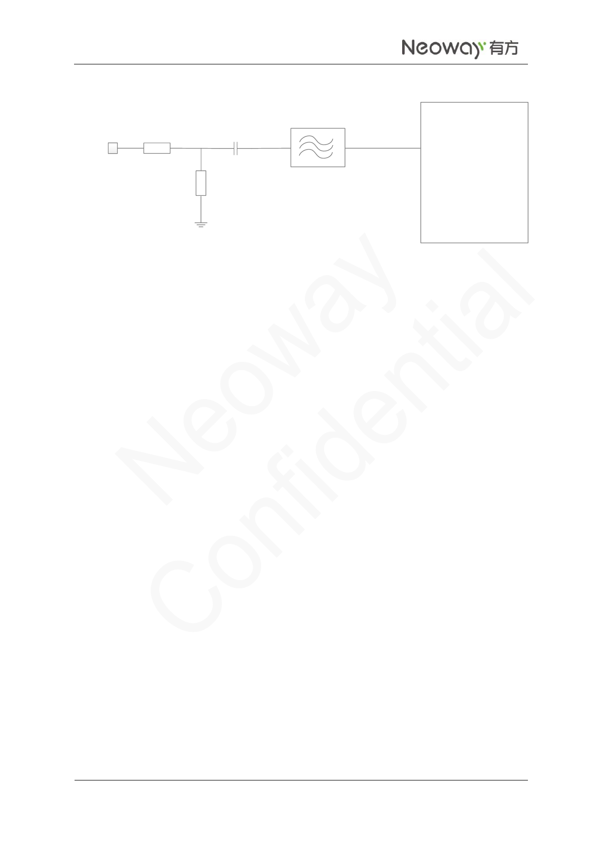
is similar to that for GPRS. For details, refer to the previous section. Figure 4-5shows the internal
structure of the GNSS RF.
N20 Hardware User Guide
Copyright © Neoway Technology Co., Ltd
37
Figure 4-5 GNSS RF structure
WTR GPS Interface
RF_ANT_GNSS SAW
In addition to the basic rules, the GNSS routing has higher requirements because the air wireless GNSS
signal has lower strength, which results in weaker electrical signal after the antenna receives. Weaker
signals are more susceptible to interference. Therefore, active antenna are commonly used for GNSS. The
active GNSS antenna amplifies the weak signals received to stronger signals through the low-noise
amplifier (LNA) and then transmits the signals through the feeder.
If using a passive antenna, add LNA near the feeder because the module does not embed one
internally.EXT_GNSS_LNA_EN is used to enable GNSS_LNA.
If the antenna and layout are not designed reasonably, the GNSS will be insensitive, resulting in long time
on positioning or inaccurate position.
Keep the GPRS and GNSS far away from each other in layout and antenna layout design.
4.2.2 Active GNSS Antenna Design
Ceramic GNSS chip antenna is mainly used. In general, using the active ceramic antenna is recommended.
After the antenna receives GNSS satellite signals, the LNA amplifies them first and then they are
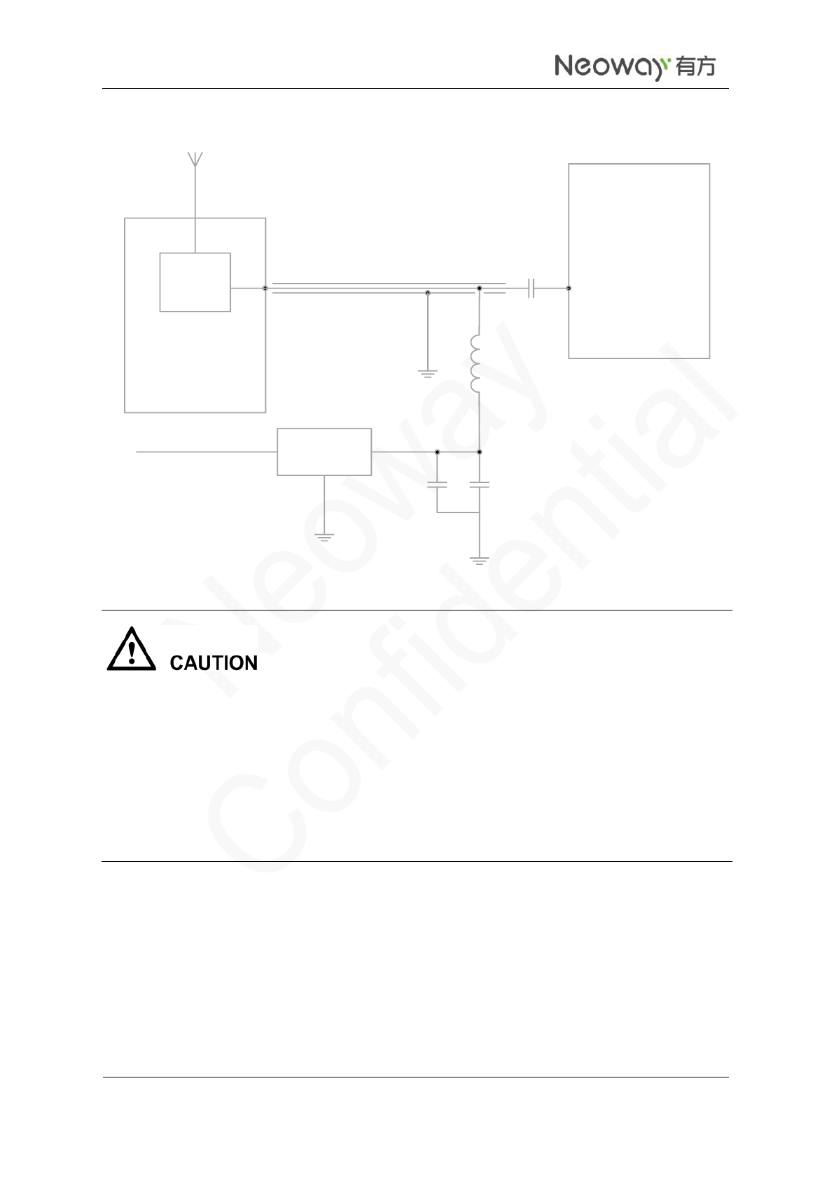
transmitted to the 54thpin (RF_ANT_GNSS) through the feeder and PCB traces. 50Ω impedance is
required for both the feeder and PCB traces and the traces should be as short as possible. The power
supply of the active antenna is fed by the 100nH inductance through the signal traces.
Common active antenna requires 3.3V to 5V power supply. Though the active antenna has a low power
consumption, it requires stable and clean power supply. It is recommendedthat high-performance LDO is
used to supply power for the antenna through a 100nH inductance, as shown inFigure 4-6.
N20 Hardware User Guide
Copyright © Neoway Technology Co., Ltd
38
Figure 4-6 Power supply reference for active antenna
LNA
Active
Antenna
N20
LDO
PWR_input
22 uF 33 pF
100 nH
33 pF
50Ω impedance line
It is recommended that an ESD protection diode is added to the antenna interface in an environment with
great electromagnetic interference and other applications with bad ESD. The ESD protection diode must
have ultra-low capacitance (lower than 0.5pF). Otherwise, it will affect the impedance of the RF loop or
result in attenuation of RF signals. RCLAMP0521P from Semtech or ESD5V3U1U from Infineon is
recommended.
On the PCB, keep the RF signals and RF components away from high-speed circuits, power supplies,
transformers, great inductors, the clock circuit of single-chip host, etc.
N20 Hardware User Guide
Copyright © Neoway Technology Co., Ltd
39
5 Electrical Features and Reliability
5.1 Electrical Features
Table 5-1 N20electric features
Module Status
Minimum Value
Typical Value
Maximum Value
VBAT
Vin
3.3V
3.8V
4.3V
Iin
/
/
2A
If the voltage is too low, the module might fail to start. If the voltage is too high or there is a voltage burst
during the startup, the module might be damaged permanently.
If LDO or DC-DC is used to supply power for the module, ensure that it outputs at least 2A current.
5.2 Temperature
Table 5-2 Temperature feature
Module Status
Minimum Value
Typical Value
Maximum Value
Work
-40°C
25°C
85°C
Storage
-45°C
90°C
If the module works in temperature exceeding the thresholds, some of its RF performance indicator might
be worse but it can still work properly.
N20 Hardware User Guide
Copyright © Neoway Technology Co., Ltd
40
5.3 ESD
Electronic products need to pass several ESD tests. The following table shows the ESD capability of key
pins of our module. Add ESD protection to those pins in accordance to the application to ensure product
quality when designing better products.
Humidity: 45%Temperature: 25°C
Table 5-3 N20 ESD features
Testing Point
Contact Discharge
Air Discharge
VBAT
±8 kV
±15 kV
GND
±8 kV
±15 kV
ANT
±8 kV
±15 kV
Cover
±8 kV
±15 kV
Others
±2 kV
±4 kV
N20 Hardware User Guide
Copyright © Neoway Technology Co., Ltd
41
6 RF Features
6.1 Operating Band
Table 6-1 N20 operating band
OperatingBand
Uplink
Downlink
FDD-LTE B2
1850~1910 MHz
1930~1990 MHz
FDD-LTE B4
1710~1755 MHz
2110~2155 MHz
FDD-LTE B12
699~716 MHz
729~746 MHz
FDD-LTE B13
777~787 MHz
746~756 MHz
6.2 TX Power and RX Sensitivity
Table 6-2 N20 RF TX power
Band
Max Power
Min. Power
HD-FDD LTE B2
23dBm+2/-2dB
<-40dBm
HD-FDD LTE B4
23dBm+2/-2dB
<-40dBm
HD-FDD LTE B12
23dBm+2/-2dB
<-40dBm
HD-FDD LTE B13
23dBm+2/-2dB
<-40dBm
Table 6-3 N20Cat M1 QPSK RX sensitivity
Band
REFSENS
Duplex Mode
LTE B2
≤-103dBm
HD-FDD
LTE B4
≤-103dBm
HD-FDD
LTE B12
≤-103dBm
HD-FDD
LTE B13
≤-103dBm
HD-FDD
All the values above are obtained in the lab environment. In actual applications, there might be a
difference because of the network environment.
N20 Hardware User Guide
Copyright © Neoway Technology Co., Ltd
42
7 Mechanical Features
7.1 Dimensions
Figure 7-1 Dimensions of N20(unit: mm)
N20 Hardware User Guide
Copyright © Neoway Technology Co., Ltd
43
7.2 PCB Foot Print
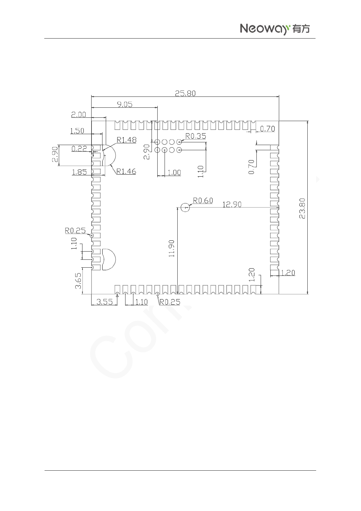
Figure 7-2 N20PCBfoot print(Top View)(unit: mm)
N20 Hardware User Guide
Copyright © Neoway Technology Co., Ltd
44
7.3 Recommended PCB Foot Print
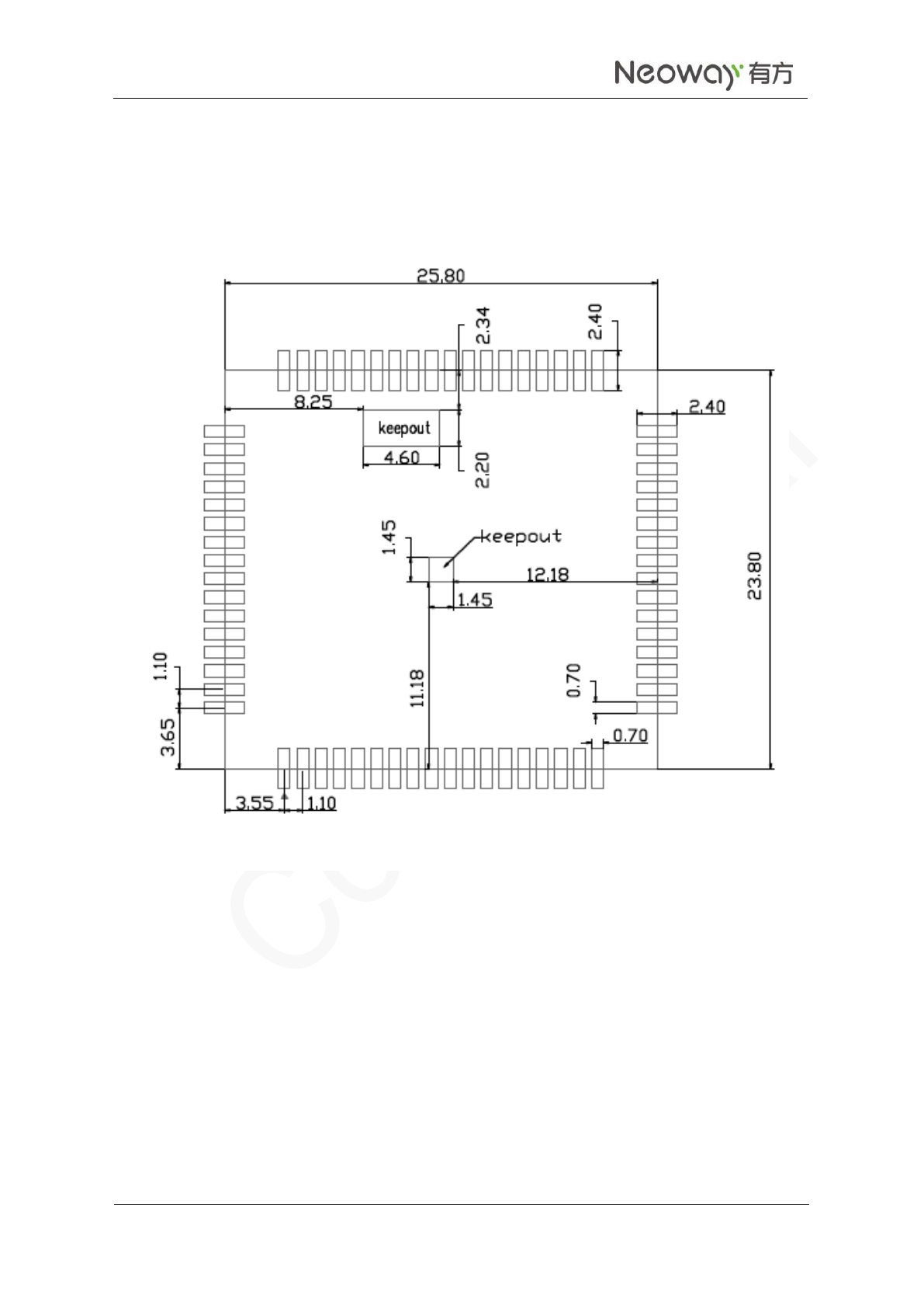
Figure 7-3 Recommended N20PCB foot print(unit:mm)

N20 Hardware User Guide
Copyright © Neoway Technology Co., Ltd
45
8 Mounting and Packaging
8.1 Mounting the Module onto the Application Board
N20 is compatible with industrial standard reflow profile for lead-free SMT process.
The reflow profile is process dependent, so the following recommendation is just a start point guideline:
Only one flow is supported.
Quality of the solder joint depends on the solder volume. Minimum of 0.12 mm to 0.15mmstencil
thickness is recommended.
Use bigger aperture size of the stencil than actual pad size.
Use a low-residue, no-clean type solder paste.
For information about cautions in N20 storage and mounting, refer to Neoway Module Reflow
Manufacturing Recommendations.
When maintaining and manually desoldering it, use heat guns with great opening, adjust the temperature
to 250 degrees (depending on the type of the solder paste), and heat the module till the solder paste is melt.
Then remove the module using tweezers. Do not shake the module in high temperature when removing it.
Otherwise, the components inside the module might get misplaced.
8.2 Packaging
N20 modules are packaged in sealed bags on delivery to guarantee a long shelf life. Package the modules
again in case of opening for any reasons.
If exposed to air for more than 48 hours at conditions not worse than 30°C/60% RH, a baking procedure
should be done before SMT.Or if the indication card shows humidity greater than 20%, the baking
procedure is also required. Do not bake modules with the package tray directly.
N20 Hardware User Guide
Copyright © Neoway Technology Co., Ltd
46
9 SMT TemperatureCurve
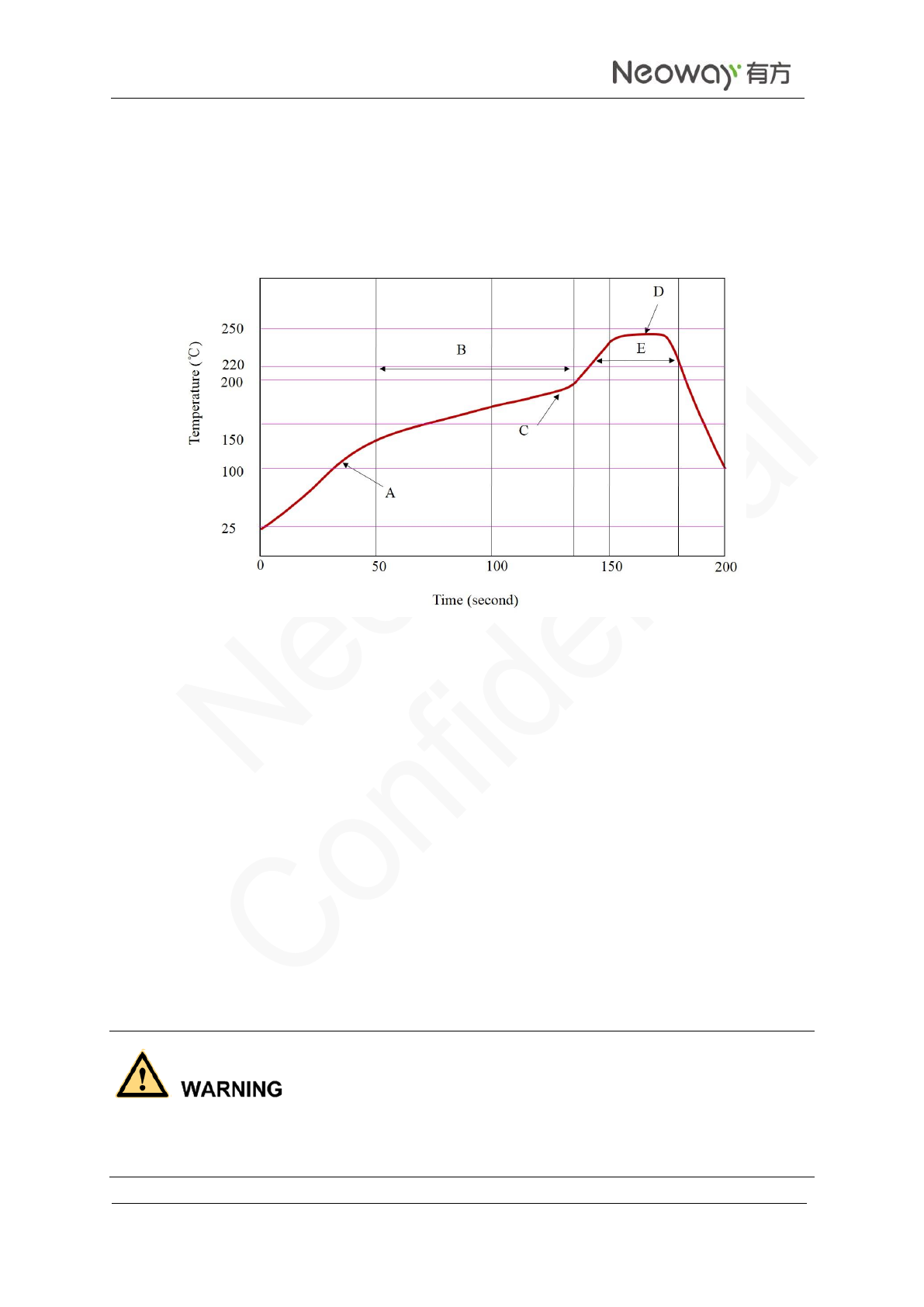
Figure 9-1 Temperature curve
X: Time (s) Y: Temperature (°C )
Technicalparameters:
Ramp up rate: 1to 4°C /sec
Ramp down rate: -3 to-1°C /sec
Soaking zone: 150-180°C , Time: 60-100s
Reflow zone:>220°C , Time: 40-90s
Peak temperature: 235-250°C
Do not use the kind of solder paste different from our module technique.
The melting temperature of solder paste with lead is 35°C lower than that of solder paste without lead.
It is easy to cause faulty joints for LCC inside the module after second reflow soldering.
When using only solder pastes with lead, please ensure that the reflow temperature is kept at 220°C
for more than 45 seconds and the peak temperature reaches 240°C .
Neoway will not provide warranty for heat-responsive element abnormalities caused by improper
temperature control.

N20 Hardware User Guide
Copyright © Neoway Technology Co., Ltd
47
10 Abbreviations
ADC
Analog-Digital Converter
DRX
Discontinuous Reception
DTR
Data Terminal Ready
eDRX
Extended Discontinuous Reception
EGSM
Enhanced GSM
ESD
Electronic Static Discharge
FDD
Frequency Division Duplex
GNSS
Global Navigation Satellite System
GPRS
General Packet Radio Service
GPIO
General-Purpose Input/Output
GPS
Global Positioning System
GSM
Global Standard for Mobile Communications
I2C
Interintegrated Circuit
LDO
Low Dropout Regulator
LNA
Low Noise Amplifier
LTE
Long-Term Evolution
Mbps
Million bits per second
MCU
Micro Controller Unit
PCB
Printed Circuit Board
PCM
Pulse-Coded Modulation
SDC
Secure Digital Controller
SDR
Single Data Rate
SIM
Subscriber Identification Module
SPI
Serial Peripheral Interface
TBD
To Be Determined
TDD
Time Division Duplex
TVS
Transient Voltage Suppressor
UART
Universal Asynchronous Receiver-Transmitter
UIM
User Identity Module