Nokia Solutions and Networks T5CR1 48V SC4812T 800 MHz CDMA BTS Frame User Manual Exhibit
Nokia Solutions and Networks 48V SC4812T 800 MHz CDMA BTS Frame Users Manual Exhibit
UserManual.wiki
>
Nokia Solutions and Networks
>
T5CR1 User Manual
Users Manual Exhibit
Navigation menu
Upload a User Manual
Namespaces
Wiki Guide
HTML
PDF
Info
Views
User Manual
Discussion / Help
Navigation

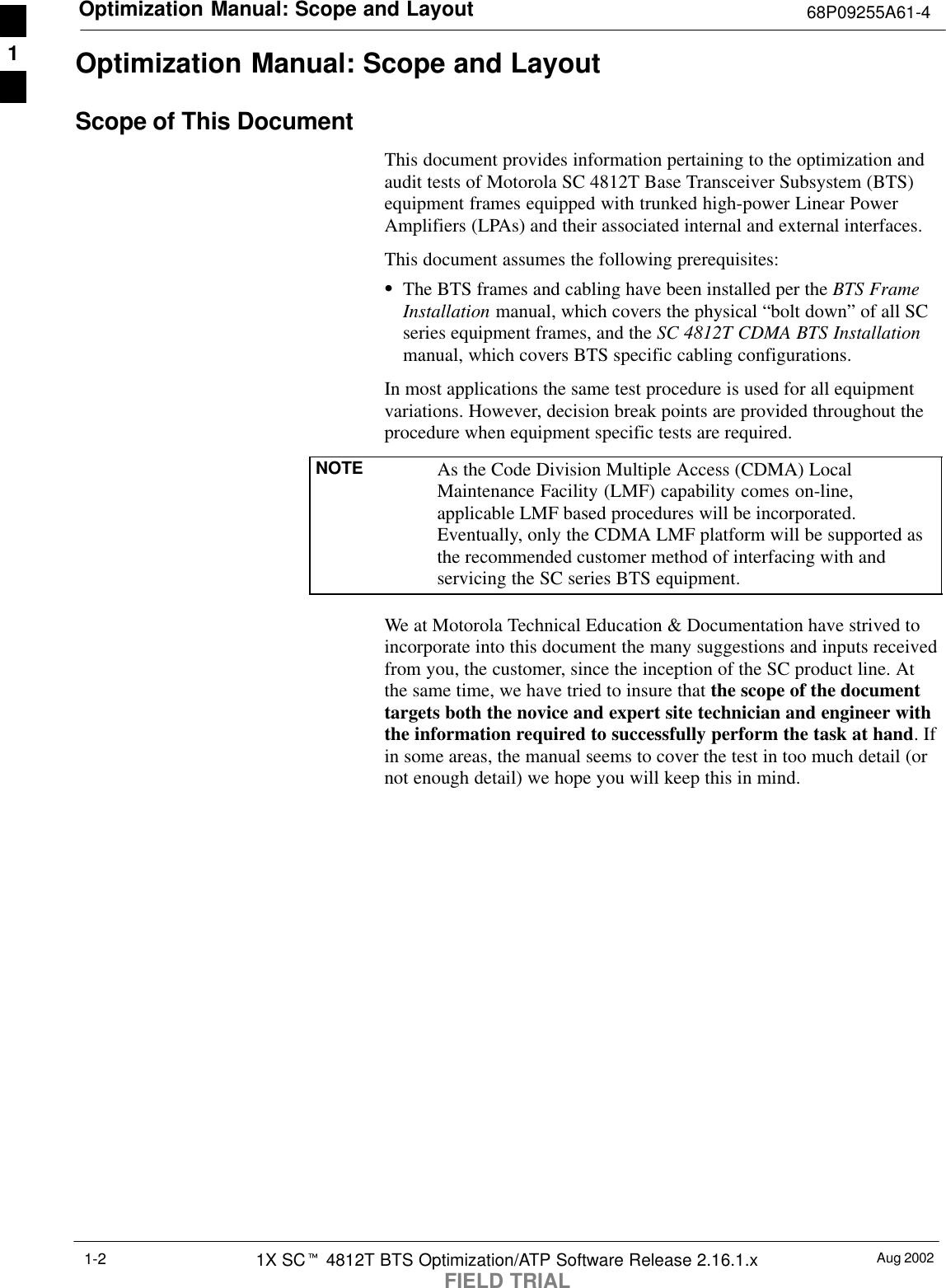
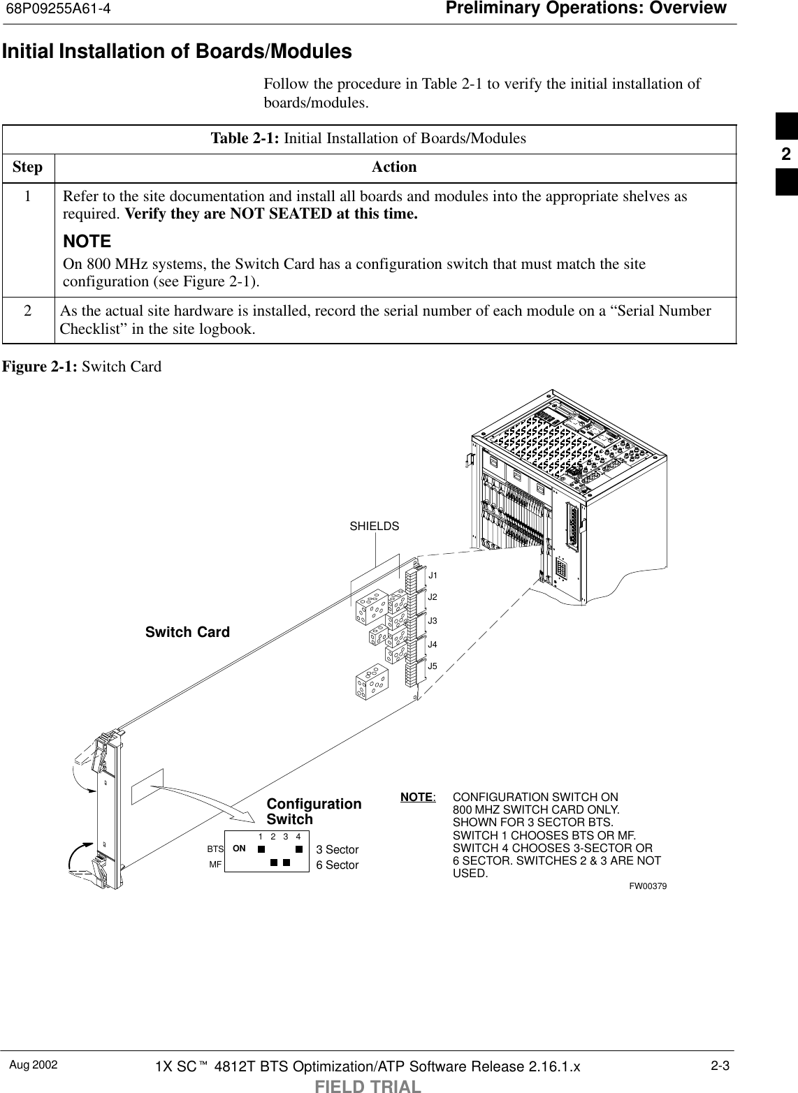
![Required Test Equipment68P09255A61-4Aug 2002 1X SCt 4812T BTS Optimization/ATP Software Release 2.16.1.xFIELD TRIAL1-13Directional CouplerSNarda Model 30661 30 dB (Motorola part no. 58D09732W01)1900 MHz coupler terminated with two Narda Model 375BN-Mloads, or equivalent.SNarda Model 30445 30 dB (Motorola Part No. 58D09643T01 )800 MHz coupler terminated with two Narda Model 375BN-M loads,or equivalent.RF AttenuatorS20 dB fixed attenuator, 20 W (Narda 768-20); used with 1.7/1.9 GHztest cable calibrations or during general troubleshooting procedures.RF Terminations/LoadsSAt least three 100-Watt (or larger) non-radiating RFterminations/loads.Miscellaneous RF Adapters, Loads, etcSAs required to interface test cables and BTS equipment and forvarious test set ups. Should include at least two 50 Ohm loads (typeN) for calibration and one RF short, two N-Type Female-to-FemaleAdapters.LAN CableSBNC-to BNC 50 ohm coaxial cable [.91 m (3 ft) maximum] with anF-to-F adapter, used to connect the 10BaseT-to-coaxial adapter tothe BTS LAN connector.High-impedance Conductive Wrist StrapSMotorola Model 42-80385A59; used to prevent damage fromElectrostatic Discharge (ESD) when handling or working withmodules.Optional EquipmentNOTE Not all optional equipment specified here will be supported bythe LMF in automated tests or when executing various measuretype command line interface (CLI) commands. It is meant toserve as a list of additional equipment that might be requiredduring maintenance and troubleshooting operations.Frequency CounterSStanford Research Systems SR620 or equivalent. If directmeasurement of the 3 MHz or 19.6608 MHz references is required.Spectrum AnalyzerSSpectrum Analyzer (HP8594E with CDMA personality card) orequivalent; required for manual tests.Local Area Network (LAN) TesterSModel NETcat 800 LAN troubleshooter (or equivalent); used tosupplement LAN tests using the ohmmeter.1](https://usermanual.wiki/Nokia-Solutions-and-Networks/T5CR1/User-Guide-276585-Page-39.png)
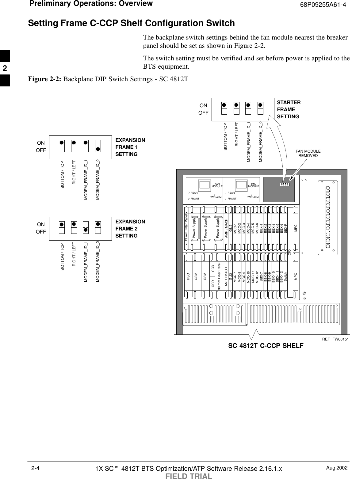
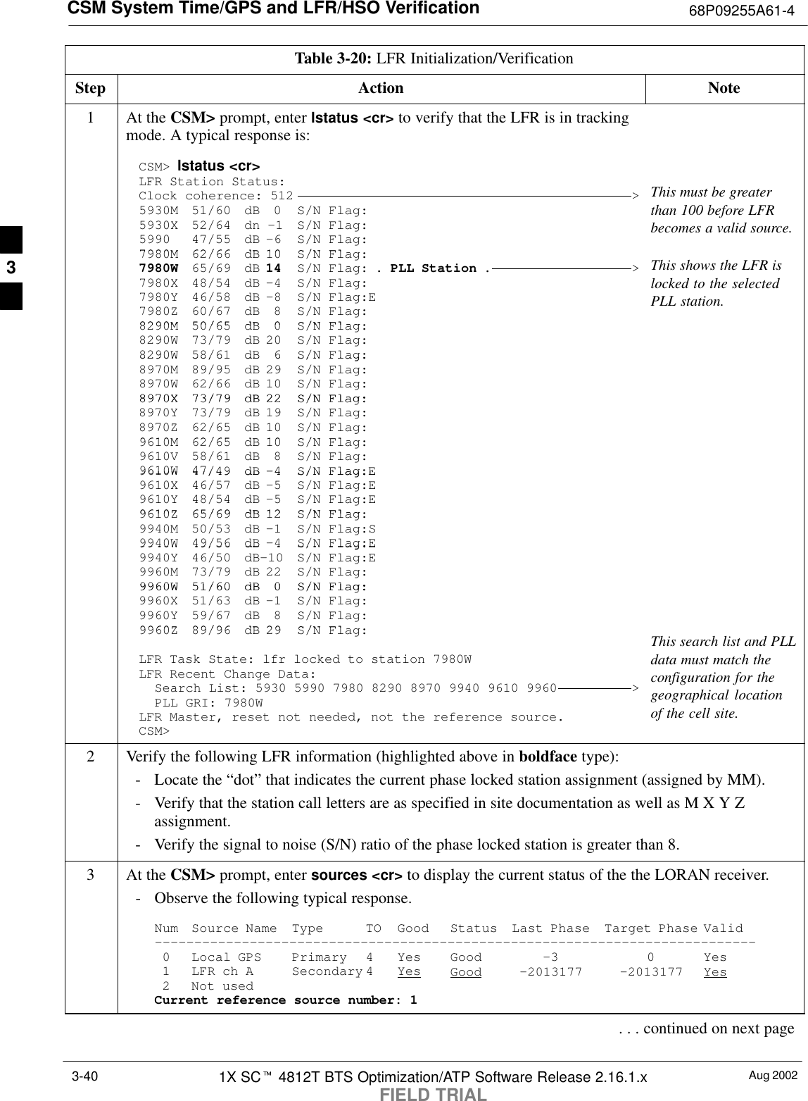
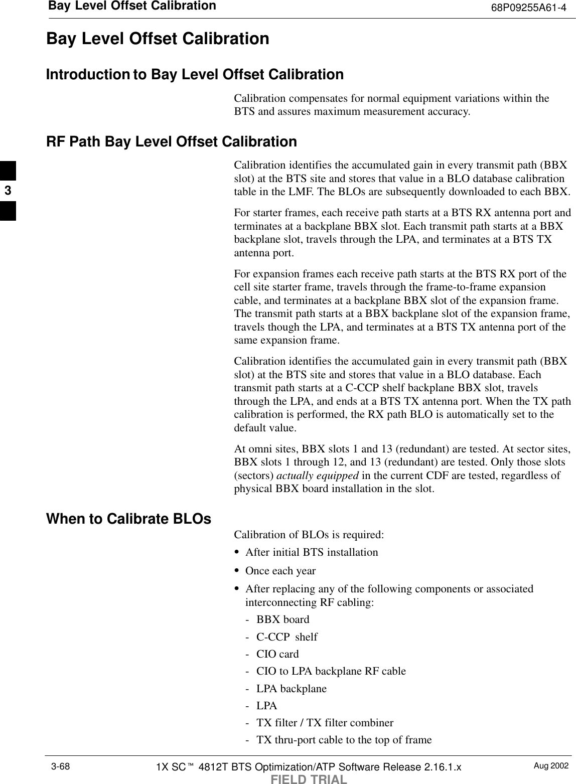
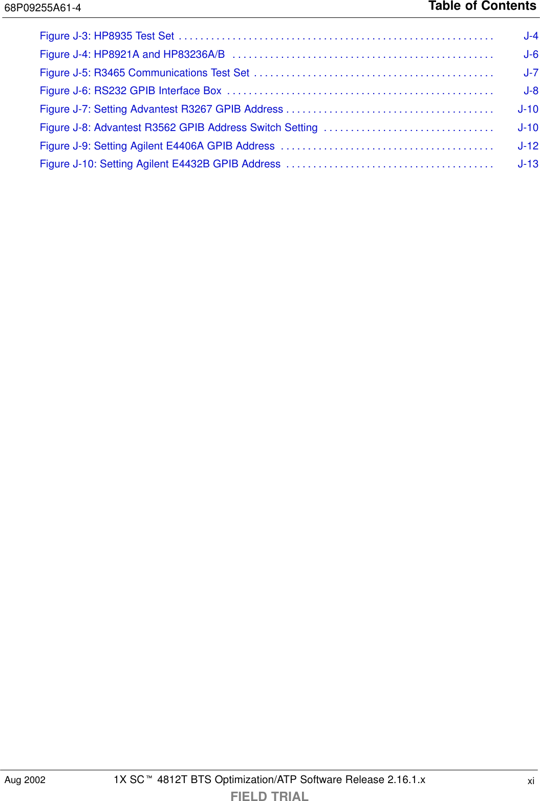
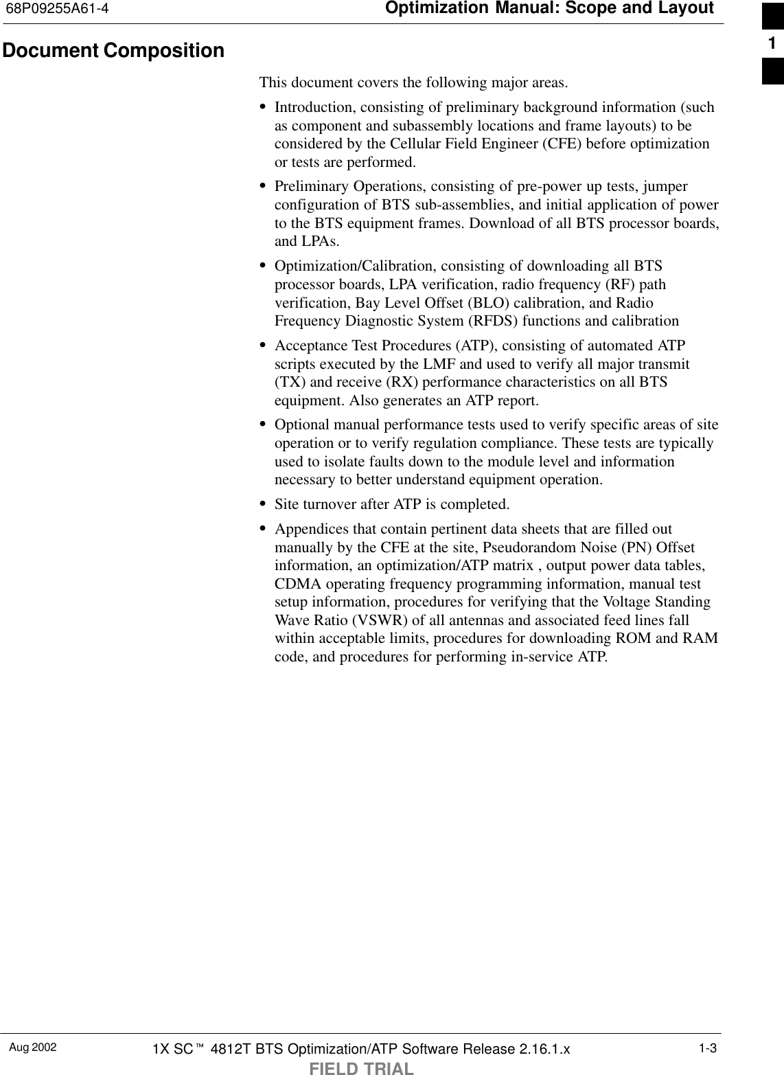
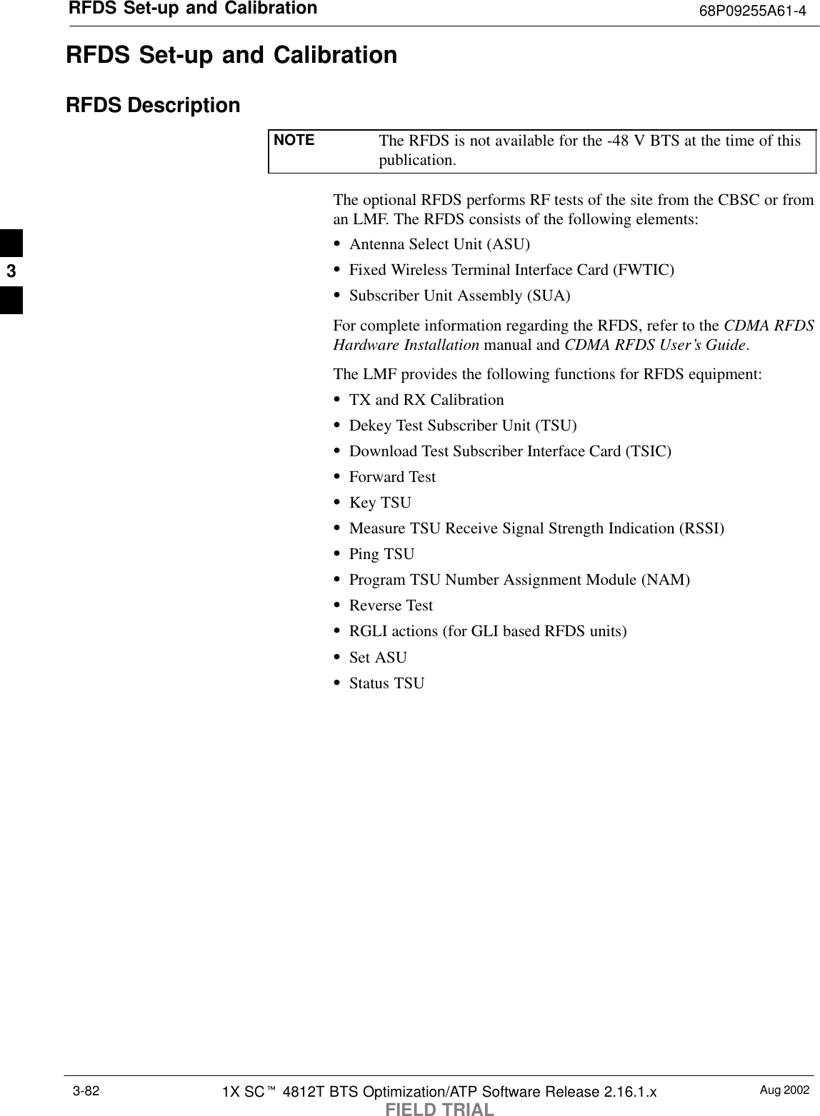
![Bay Level Offset Calibration 68P09255A61-4Aug 20021X SCt 4812T BTS Optimization/ATP Software Release 2.16.1.xFIELD TRIAL3-70SThe calibration data for a BBX is organized as a large flat array. Thearray is organized by branch, sector, and calibration point.- The first breakdown of the array indicates which branch thecontained calibration points are for. The array covers transmit, mainreceive and diversity receive offsets as follows:Table 3-33: BLO BTS.cal File Array AssignmentsRange AssignmentC[1]-C[240] TransmitC[241]-C[480] Main ReceiveC[481]-C[720] Diversity ReceiveNOTE Slot 385 is the BLO for the RFDS.- The second breakdown of the array is per sector. Configurationssupported are Omni, 3-sector or 6-sector.Table 3-34: BTS.cal File Array (Per Sector)BBX Sectorization TX RX RX DiversitySlot[1] (Primary BBXs 1 through 12)1 (Omni) 3-Sector, C[1]-C[20] C[241]-C[260] C[481]-C[500]23-Sector,1st C[21]-C[40] C[261]-C[280] C[501]-C[520]36 Sector, Carrier C[41]-C[60] C[281]-C[300] C[521]-C[540]41stCarrier 3-Sector, C[61]-C[80] C[301]-C[320] C[541]-C[560]5Carrier 3-Sector,3rd C[81]-C[100] C[321]-C[340] C[561]-C[580]6Carrier C[101]-C[120] C[341]-C[360] C[581]-C[600]73-Sector, C[121]-C[140] C[361]-C[380] C[601]-C[620]83-Sector,2nd C[141]-C[160] C[381]-C[400] C[621]-C[640]96 Sector, Carrier C[161]-C[180] C[401]-C[420] C[641]-C[660]10 2ndCarrier 3-Sector, C[181]-C[200] C[421]-C[440] C[661]-C[680]11 Carrier 3-Sector,4th C[201]-C[220] C[441]-C[460] C[681]-C[700]12 Carrier C[221]-C[240] C[461]-C[480] C[701]-C[720]Slot[20]] (Redundant BBX-13)1 (Omni) 3-Sector, C[1]-C[20] C[241]-C[260] C[481]-C[500]23-Sector,1st C[21]-C[40] C[261]-C[280] C[501]-C[520]36 Sector, Carrier C[41]-C[60] C[281]-C[300] C[521]-C[540]41stCarrier 3-Sector, C[61]-C[80] C[301]-C[320] C[541]-C[560]5Carrier 3-Sector,3rd C[81]-C[100] C[321]-C[340] C[561]-C[580]6Carrier C[101]-C[120] C[341]-C[360] C[581]-C[600] . . . continued on next page3](https://usermanual.wiki/Nokia-Solutions-and-Networks/T5CR1/User-Guide-276585-Page-148.png)
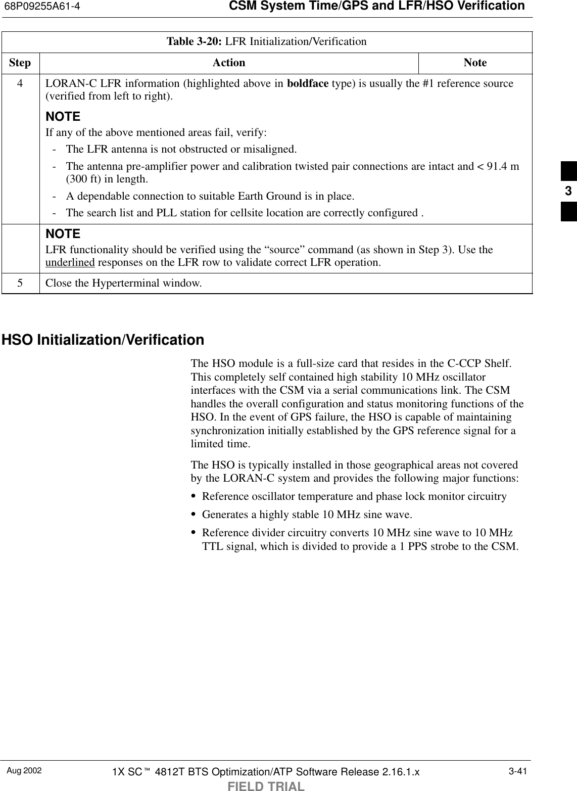
![Bay Level Offset Calibration68P09255A61-4Aug 2002 1X SCt 4812T BTS Optimization/ATP Software Release 2.16.1.xFIELD TRIAL3-71Table 3-34: BTS.cal File Array (Per Sector)BBX RX DiversityRXTXSectorization73-Sector, C[121]-C[140] C[361]-C[380] C[601]-C[620]83-Sector,2nd C[141]-C[160] C[381]-C[400] C[621]-C[640]96 Sector, Carrier C[161]-C[180] C[401]-C[420] C[641]-C[660]10 2ndCarrier 3-Sector, C[181]-C[200] C[421]-C[440] C[661]-C[680]11 Carrier 3-Sector,4th C[201]-C[220] C[441]-C[460] C[681]-C[700]12 Carrier C[221]-C[240] C[461]-C[480] C[701]-C[720]STen calibration points per sector are supported for each branch. Twoentries are required for each calibration point.SThe first value (all odd entries) refer to the CDMA channel(frequency) where the BLO is measured. The second value (all evenentries) is the power set level. The valid range for PwrLvlAdj is from2500 to 27500 (2500 corresponds to -125 dBm and 27500corresponds to +125 dBm).SThe 20 calibration entries for each sector/branch combination must bestored in order of increasing frequency. If less than 10 points(frequencies) are calibrated, the largest frequency that is calibrated isrepeated to fill out the 10 points.Example:C[1]=384, odd cal entry = 1 ‘‘calibration point”C[2]=19102, even cal entryC[3]=777,C[4]=19086,..C[19]=777,C[20]=19086, (since only two cal points were calibrated this would be repeated for the next 8 points)SWhen the BBX is loaded with image = data, the cal file data for theBBX is downloaded to the device in the order it is stored in the calfile. TxCal data is sent first, C[1] - C[240]. Sector 1’s ten calibrationpoints are sent (C[1] - C[20]) followed by sector 2’s ten calibrationpoints (C[21] - C[40]), etc. The RxCal data is sent next (C[241] -C[480]), followed by the RxDCal data (C[481] - C[720]).STemperature compensation data is also stored in the cal file for eachset.3](https://usermanual.wiki/Nokia-Solutions-and-Networks/T5CR1/User-Guide-276585-Page-149.png)
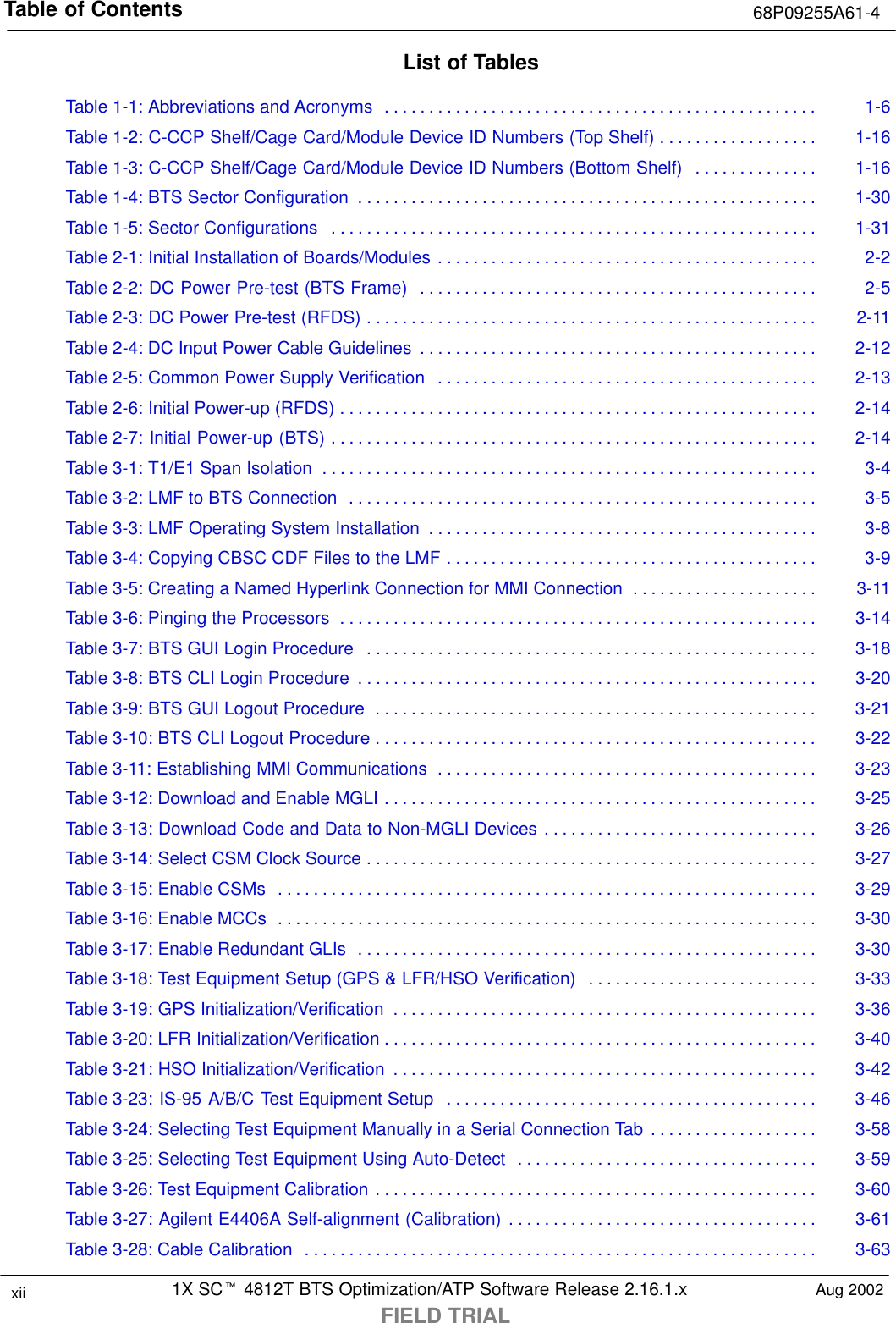
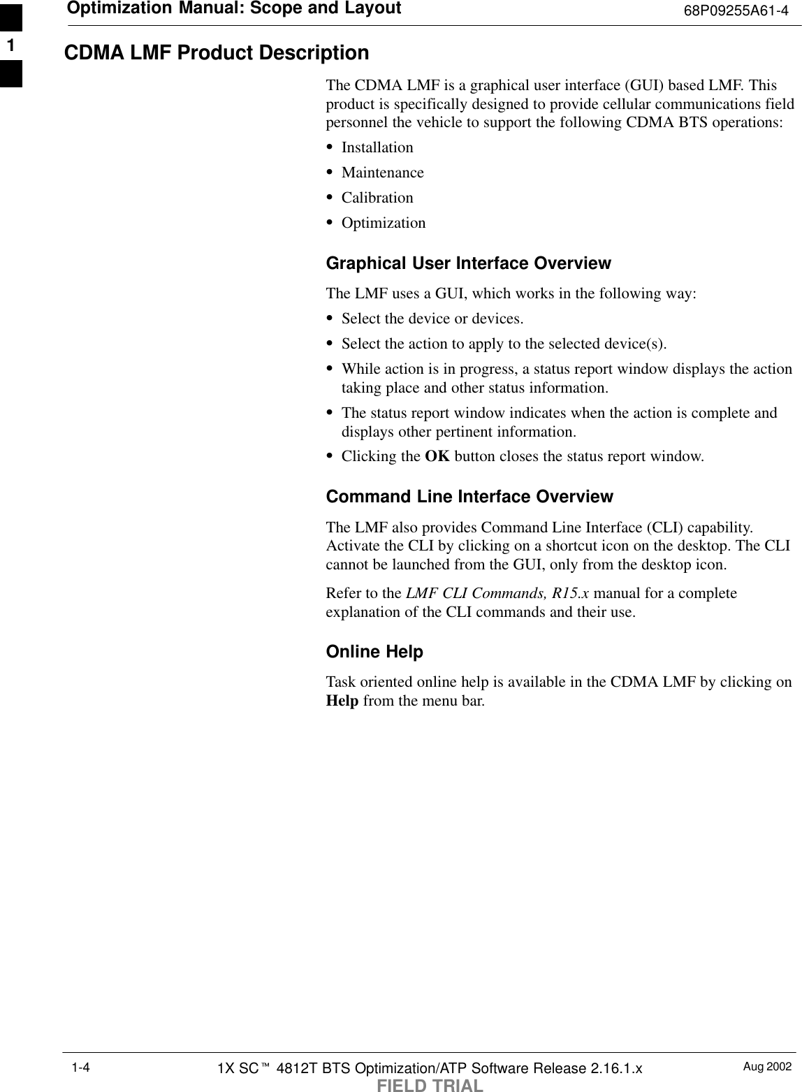
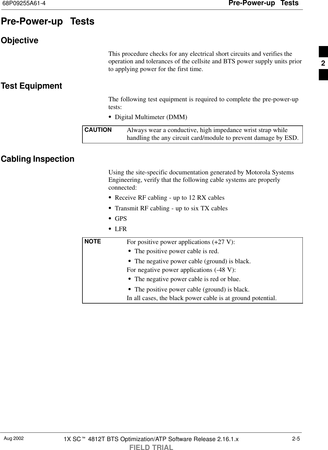
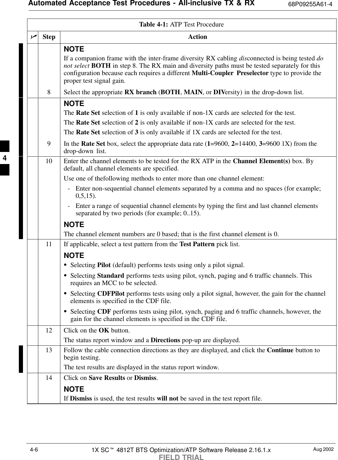
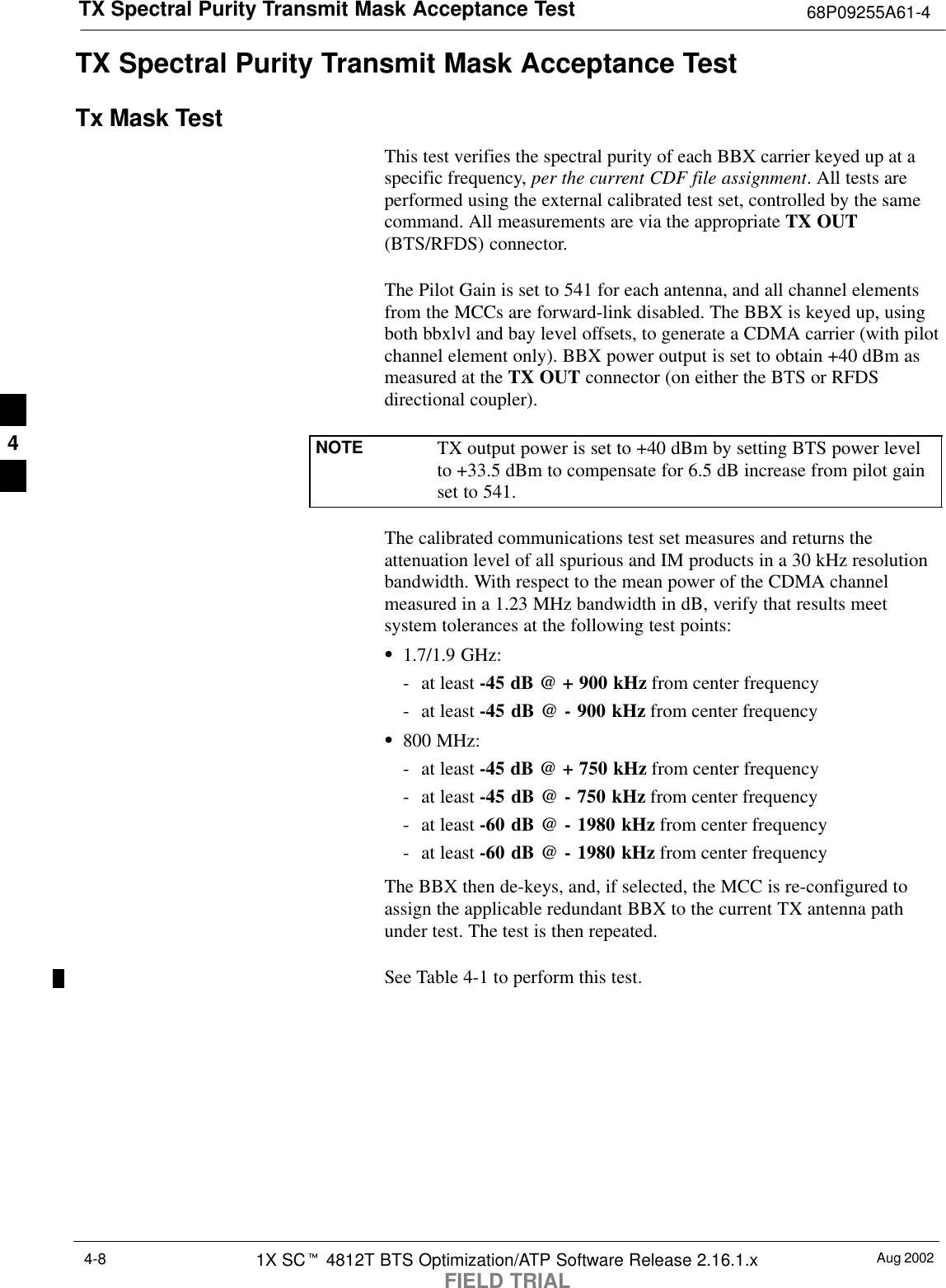
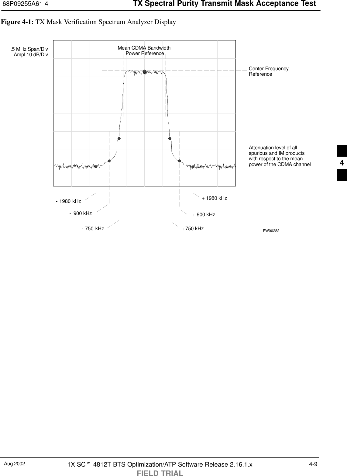
![Automated Acceptance Test Procedures - All-inclusive TX & RX68P09255A61-4Aug 2002 1X SCt 4812T BTS Optimization/ATP Software Release 2.16.1.xFIELD TRIAL4-5SAll RX: RX tests verify the performance of the BTS receiver line up.These include the MPC (for starter frames), EMPC (for expansionframes), CIO, BBX, MCC, and GLI cards and the passive componentsincluding RX filters (starter frame only), and RF cables.SFull Optimization: Executes the TX calibration, downloads the BLO,and executes the TX audit before running all of the TX and RX tests.NOTE The Full Optimization test can be run if you want the TX pathcalibrated before all the TX and RX tests are run.If manual testing has been performed with the HP analyzer,remove the manual control/system memory card from the cardslot and set the I/O Config to the Talk & Lstn mode beforestarting the automated testing.Follow the procedure in Table 4-1 to perform any ATP test.NOTE The STOP button can be used to stop the testing process.Table 4-1: ATP Test ProcedurenStep Action1Ensure that all pre-requisites have been met.NOTEIf the LMF has been logged into the BTS with a different Multi-Channel Preselector setting thanthe one to be used for this test, the LMF must be logged out of the BTS and logged in again withthe new Multi-Channel Preselector setting. Using the wrong MPC setting can cause a false testfailure.2AUTHOR NOTE:Is this step necessary for the T and ET? As it stands now,the additional test equipment set−up table is not in the Tand ET books.If a companion frame is being tested and either BOTH or DIV is to be selected in step 8, performthe additional test equipment set-up in Table ??? for the diversity RX portion of the ATP.3Select the device(s) to be tested.4From the Tests menu, select the test you want to run.5Select the appropriate carrier(s) (carrier-bts#-sector#-carrier#) displayed in the Channels/Carrierpick list.NOTETo select multiple items, hold down the <Shift> or <Ctrl> key while making the selections.6Enter the appropriate channel number in the Carrier n Channels box.The default channel number displayed is determined by the CdmaChans[n] number in thecbsc-n.cdf file for the BTS.NOTESingle-sided BLO is only used when checking non-redundant transceivers.7If applicable, select Verify BLO (default) or Single-sided BLO.. . . continued on next page4](https://usermanual.wiki/Nokia-Solutions-and-Networks/T5CR1/User-Guide-276585-Page-191.png)
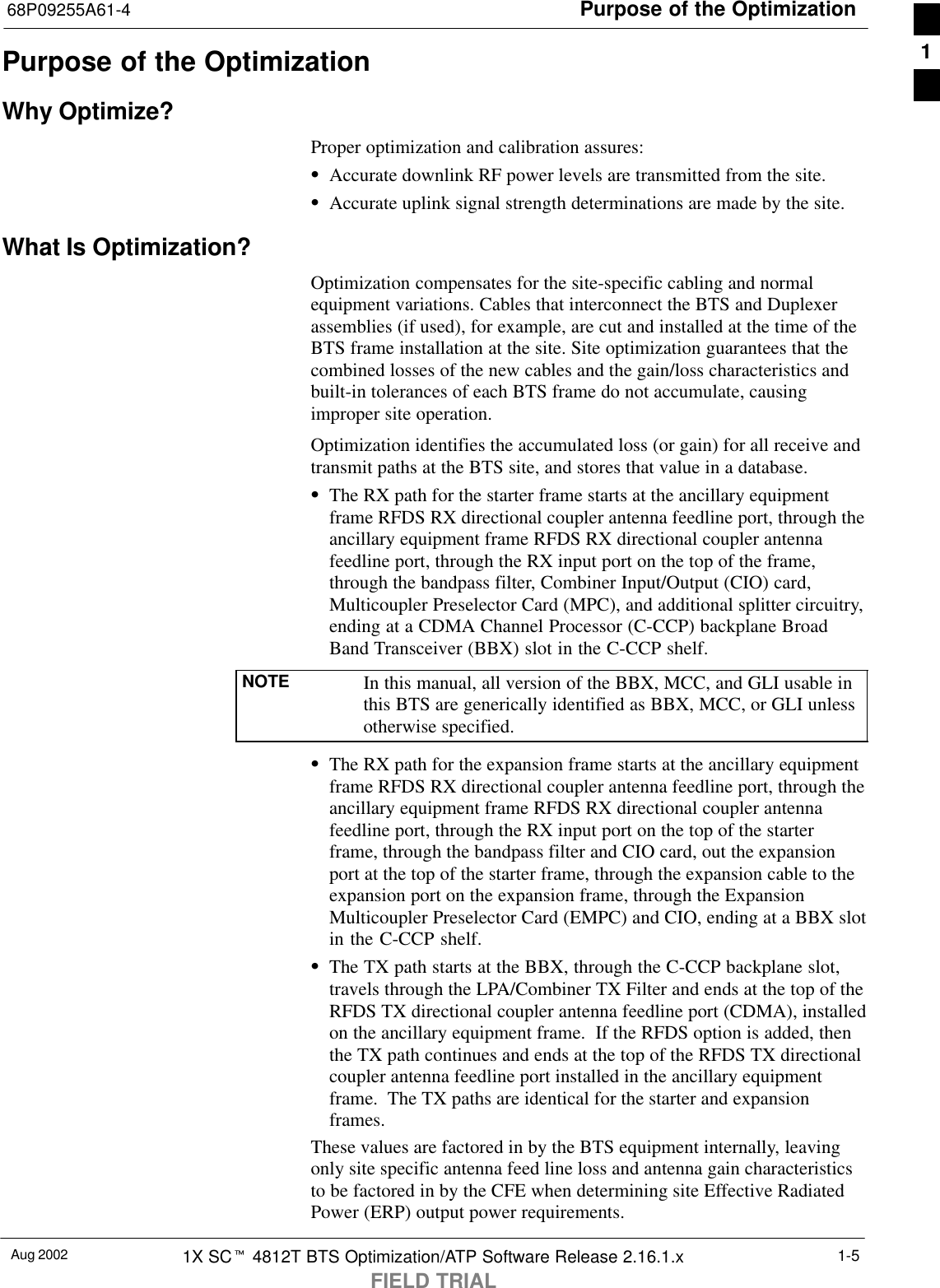
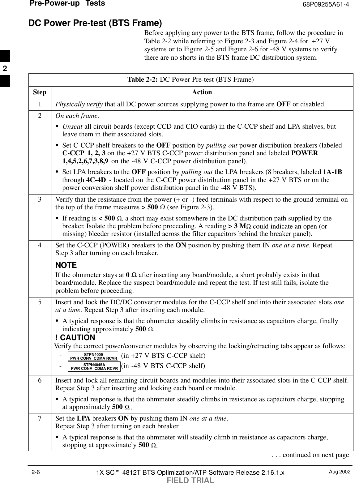
![RX Frame Error Rate (FER) Acceptance Test 68P09255A61-4Aug 20021X SCt 4812T BTS Optimization/ATP Software Release 2.16.1.xFIELD TRIAL4-14RX Frame Error Rate (FER) Acceptance TestFER TestThis test verifies the BTS FER on all traffic channel elements currentlyconfigured on all equipped MCCs (full rate at 1% FER) at an RF inputlevel of -119 dBm [or -116 dBm if using Tower TopAmplifier (TMPC)]. All tests are performed using the external calibratedtest set as the signal source controlled by the same command. Allmeasurements are via the LMF.The Pilot Gain is set to 262 for each TX antenna, and all channelelements from the MCCs are forward-link disabled. The BBX is keyedup, using only bbxlvl level offsets, to generate a CDMA carrier (withpilot channel element only). BBX power output is set to -20 dBm asmeasured at the TX OUT connector (on either the BTS or RFDSdirectional coupler). The BBX must be keyed to enable the RX receivecircuitry.The LMF prompts the MCC/CE under test to measure all zero longcodeand provide the FER report on the selected active MCC on the reverselink for both the main and diversity RX antenna paths, verifying thatresults meet the following specification:SFER returned less than 1% and total frames measured is 1500All MCC/CEs selected are tested on the specified RX antenna path. TheBBX then de-keys and, if selected, the MCC is re-configured to assignthe applicable redundant BBX to the current RX antenna paths undertest. The test is then repeated.See Table 4-1 to perform this test.4](https://usermanual.wiki/Nokia-Solutions-and-Networks/T5CR1/User-Guide-276585-Page-200.png)

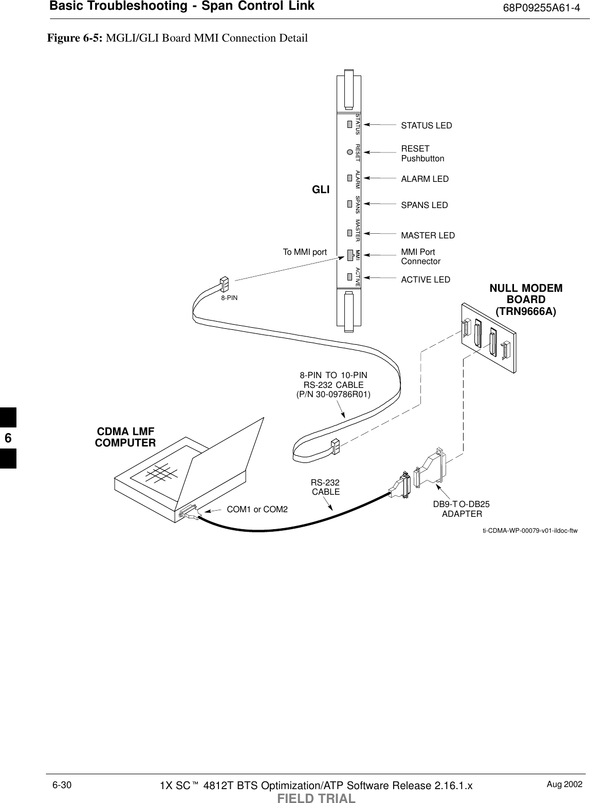
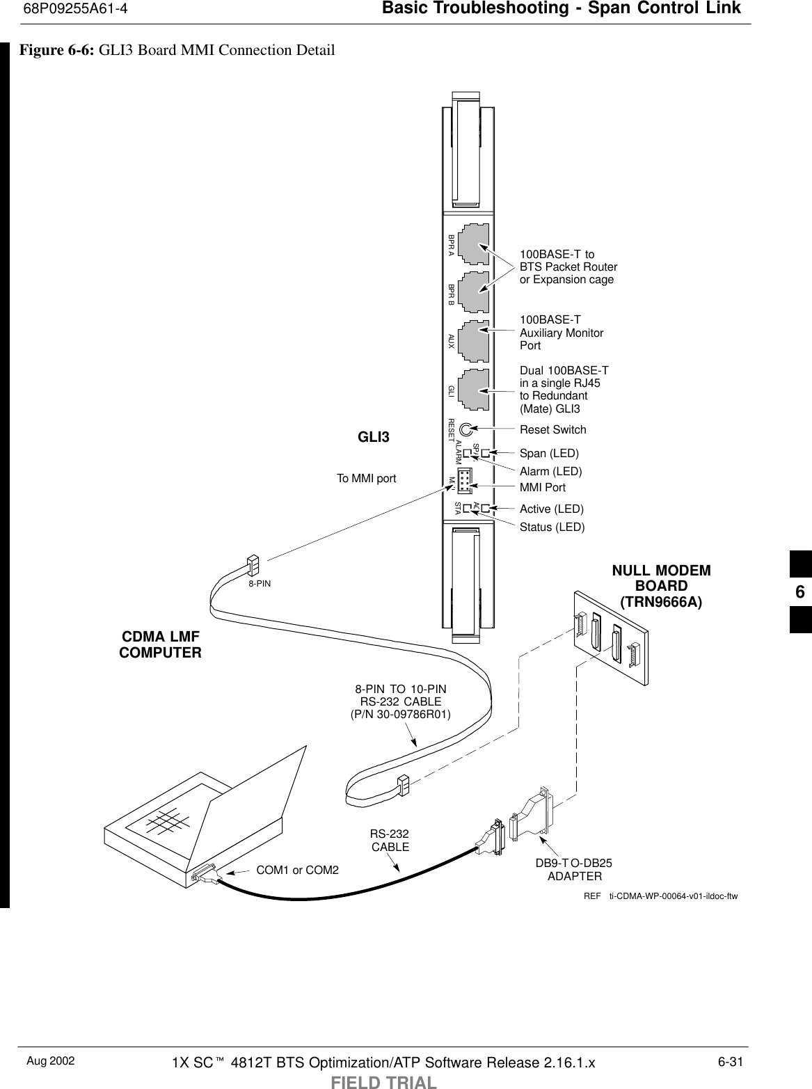
![Troubleshooting: Installation68P09255A61-4Aug 2002 1X SCt 4812T BTS Optimization/ATP Software Release 2.16.1.xFIELD TRIAL6-3Troubleshooting: InstallationCannot Log into Cell-SiteFollow the procedure in Table 6-1 to troubleshoot a login failure.Table 6-1: Login Failure Troubleshooting ProceduresnStep Action1If the MGLI LED is solid RED, it implies a hardware failure. Reset the MGLI by re-seating it. Ifthis persists, install a known good MGLI card in the MGLI slot and retry. A Red LED may alsoindicate no Ethernet termination at top of frame.2Verify that T1 is disconnected (see Table 3-1 on page 3-5).If T1 is still connected, verify the CBSC has disabled the BTS.3Try pinging the MGLI (see Table 3-6 on page 3-14).4Verify the LMF is connected to the Primary LMF port (LAN A) in the front of the BTS (seeTable 3-2 on page 3-6).5Verify the LMF was configured properly (see Preparing the LMF section starting on page 3-6).6Verify the BTS-LMF cable is RG-58 [flexible black cable of less than 76 cm (2.5 feet) length].7Verify the Ethernet ports are terminated properly (see Figure 3-4 on page 3-13).8Verify a T-adapter is not used on the LMF side port if connected to the BTS front LMF primaryport.9Try connecting to the I/O panel (top of frame). Use BNC T-adapters at the LMF port for thisconnection.10 Re-boot the LMF and retry.11 Re-seat the MGLI and retry.12 Verify IP addresses are configured properly.Cannot Communicate to Power MeterFollow the procedure in Table 6-2 to troubleshoot a power metercommunication failure.Table 6-2: Troubleshooting a Power Meter Communication FailurenStep Action1Verify the Power Meter is connected to the LMF with a GPIB adapter.2Verify the cable setup as specified in Chapter 3.3Verify the GPIB address of the power meter is set to the same value displayed in the applicableGPIB address box of the LMF Options window Test Equipment tab. Refer to Table 3-24 orTable 3-25 and the GPIB Addresses section of Appendix J for details.4Verify the GPIB adapter DIP switch settings are correct. Refer to the CDMA 2000 Test EquipmentPreparation section of Appendix F for details.. . . continued on next page6](https://usermanual.wiki/Nokia-Solutions-and-Networks/T5CR1/User-Guide-276585-Page-215.png)


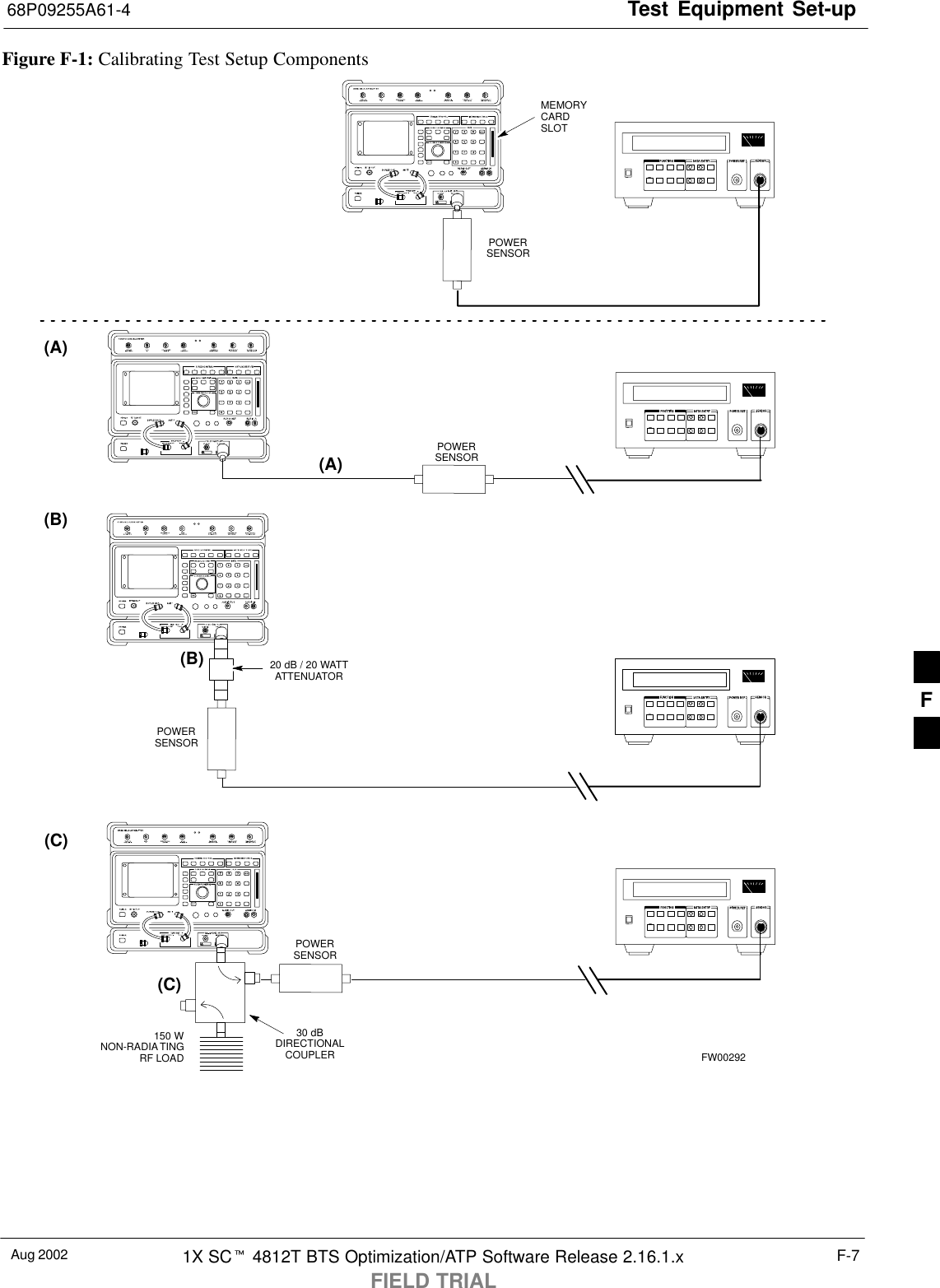
![Test Equipment Set-up68P09255A61-4Aug 2002 1X SCt 4812T BTS Optimization/ATP Software Release 2.16.1.xFIELD TRIALF-3HP8921A System Connectivity TestFollow the steps in Table F-1 to verify that the connections between thePCS Interface and the HP8921A are correct, and cables are intact. Thesoftware also performs basic functionality checks of each instrument.NOTE Disconnect other GPIB devices, especially system controllers,from the system before running the connectivity software.Table F-1: System ConnectivityStep ActionNOTE- Perform this procedure after test equipment has been allowed to warm-up and stabilize for aminimum of 60 minutes.1Insert HP 83236A Manual Control/System card into memory card slot.2Press the [PRESET] pushbutton.3Press the Screen Control [TESTS] pushbutton to display the “Tests” Main Menu screen.4Position the cursor at Select Procedure Location and select by pressing the cursor control knob.In the Choices selection box, select Card.5Position the cursor at Select Procedure Filename and select by pressing the cursor control knob.In the Choices selection box, select SYS_CONN.6Position the cursor at RUN TEST and select it.The software will prompt you through the connectivity setup.7When the test is complete, position the cursor on STOP TEST and select it; OR press the [K5]pushbutton.8To return to the main menu, press the [K5] pushbutton. F](https://usermanual.wiki/Nokia-Solutions-and-Networks/T5CR1/User-Guide-276585-Page-303.png)
![Test Equipment Set-up 68P09255A61-4Aug 20021X SCt 4812T BTS Optimization/ATP Software Release 2.16.1.xFIELD TRIALF-4Manual Cable Calibration using HP8921 with HP PCS Interface (HP83236)Perform the procedure in Table F-2 to calibrate the test equipment usingthe HP8921 Cellular Communications Analyzer equipped with theHP83236 PCS Interface.NOTE This calibration method must be executed with great care. Somelosses are measured close to the minimum limit of the powermeter sensor (-30 dBm).PrerequisitesEnsure the following prerequisites have been met before proceeding:STest equipment to be calibrated has been connected correctly for cablecalibration.STest equipment has been selected and calibrated.Refer to Figure F-1 for location of the components on the PCS Interfaceand Communications Test Set.Table F-2: Manual Cable Calibration Test Equipment Setup (using the HP PCS Interface)Step ActionNOTEVerify that GPIB controller is turned off.1Insert HP 83236A Manual Control System card into memory card slot (see Figure F-1).2Press the Preset pushbutton.3 Under Screen Controls, press the TESTS pushbutton to display the TESTS (Main Menu) screen.4Position the cursor at Select Procedure Location and select it. In the Choices selection box, selectCARD.5Position the cursor at Select Procedure Filename and select it. In the Choices selection box, selectMANUAL.6Position the cursor at RUN TEST and select it. HP must be in Control Mode Select YES.7If using HP 83236A:Set channel number=<chan#>:- Position cursor at ChannelNumber and select it.- Enter the chan# using the numerickeypad; press [Enter] and thescreen will go blank.- When the screen reappears, thechan# will be displayed on thechannel number line.If using HP 83236B:Set channel frequency:- Position cursor at Frequency Band and press Enter.- Select User Defined Frequency.- Go Back to Previous Menu.- Position the cursor to 83236 generator frequency andenter actual RX frequency.- Position the cursor to 83236 analyzer frequency andenter actual TX frequency.8Set RF Generator level:- Position the cursor at RF Generator Level and select it.- Enter -10 using the numeric keypad; press [Enter] and the screen will go blank.- When the screen reappears, the value -10 dBm will be displayed on the RF Generator Level line.. . . continued on next pageF](https://usermanual.wiki/Nokia-Solutions-and-Networks/T5CR1/User-Guide-276585-Page-304.png)
![Test Equipment Set-up68P09255A61-4Aug 2002 1X SCt 4812T BTS Optimization/ATP Software Release 2.16.1.xFIELD TRIALF-5Table F-2: Manual Cable Calibration Test Equipment Setup (using the HP PCS Interface)Step Action9Set the user fixed Attenuation Setting to 0 dBm:- Position cursor at Analyzer Attenuation and select it- Position cursor at User Fixed Atten Settings and select it.- Enter 0 (zero) using the numeric keypad and press [Enter].10 Select Back to Previous Menu.11 Record the HP83236 Generator Frequency Level:Record the HP83236B Generator Frequency Level:- Position cursor at Show Frequency and Level Details and select it.- Under HP83236 Frequencies and Levels, record the Generator Level.- Under HP83236B Frequencies and Levels, record the Generator Frequency Level(1850 - 1910 MHz for 1.9 GHz or 1750 - 1780 for 1.7 GHz).- Position cursor at Prev Menu and select it.12 Click on Pause for Manual Measurement.13 Connect the power sensor directly to the RF OUT ONLY port of the PCS Interface.14 On the HP8921A, under To Screen, select CDMA GEN.15 Move the cursor to the Amplitude field and click on the Amplitude value.16 Increase the Amplitude value until the power meter reads 0 dBm ±0.2 dB.NOTEThe Amplitude value can be increased coarsely until 0 dBM is reached; then fine tune the amplitudeby adjusting the Increment Set to 0.1 dBm and targeting in on 0 dBm.17 Disconnect the power sensor from the RF OUT ONLY port of the PCS Interface.NOTEThe Power Meter sensor’s lower limit is -30 dBm. Thus, only components having losses ≤30 dBshould be measured using this method. For further accuracy, always re-zero the power meterbefore connecting the power sensor to the component being calibrated. After connecting thepower sensor to the component, record the calibrated loss immediately.18 Disconnect all components in the test setup and calibrate each one separately by connecting eachcomponent, one-at-a-time, between the RF OUT ONLY PORT and the power sensor (see Figure F-1,Setups A, B, or C). Record the calibrated loss value displayed on the power meter.SExample: (A) Test Cable(s) = -1.4 dB(B) 20 dB Attenuator = -20.1 dB(B) Directional Coupler = -29.8 dB19 After all components are calibrated, reassemble all components together and calculate the total testsetup loss by adding up all the individual losses:SExample: Total test setup loss = -1.4 -29.8 -20.1 = -51.3 dB.This calculated value will be used in the next series of tests.20 Under Screen Controls press the TESTS button to display the TESTS (Main Menu) screen.21 Select Continue (K2).22 Select RF Generator Level and set to -119 dBm.. . . continued on next pageF](https://usermanual.wiki/Nokia-Solutions-and-Networks/T5CR1/User-Guide-276585-Page-305.png)
![Test Equipment Set-up 68P09255A61-4Aug 20021X SCt 4812T BTS Optimization/ATP Software Release 2.16.1.xFIELD TRIALF-6Table F-2: Manual Cable Calibration Test Equipment Setup (using the HP PCS Interface)Step Action23 Click on Pause for Manual Measurement.24 Verify the HP8921A Communication Analyzer/83203A CDMA interface setup is as follows (fieldsnot indicated remain at default):SVerify the GPIB (HP-IB) address:- under To Screen, select More- select IO CONFIG- Set HP-IB Adrs to 18- set Mode to Talk&LstnSVerify the HP8921A is displaying frequency (instead of RF channel)- Press the blue [SHIFT] button, then press the Screen Control [DUPLEX] button; this switches tothe CONFIG (CONFIGURE) screen.- Use the cursor control to set RF Display to Freq25 Refer to Table 3-31 for assistance in manually setting the cable loss values into the LMF. F](https://usermanual.wiki/Nokia-Solutions-and-Networks/T5CR1/User-Guide-276585-Page-306.png)
![Test Equipment Set-up 68P09255A61-4Aug 20021X SCt 4812T BTS Optimization/ATP Software Release 2.16.1.xFIELD TRIALF-8HP PCS Interface Test Equipment Setup for Manual TestingFollow the procedure in Table F-3 to setup the HP PCS Interface Box formanual testing.Table F-3: HP PCS Interface Test Equipment Setup for Manual TestingnStep ActionNOTEVerify GPIB controller is turned off.1Insert HP83236B Manual Control/System card into the memory card slot.2 Under Screen Controls, press the [TESTS] push-button to display the TESTS (Main Menu)screen.3Position the cursor at Select Procedure Location and select. In the Choices selection box, selectCARD.4Position the cursor at Select Procedure Filename and select. In the Choices selection box, selectMANUAL.5Position the cursor at RUN TEST and select OR press the K1 push-button.6Set channel number=<chan#>:- Position cursor at Channel Number and select.- Enter the chan# using the numeric keypad and then press [Enter] (the screen will blank).- When the screen reappears, the chan# will be displayed on the channel number line.NOTEIf using a TMPC with Tower Top Amplifier (TTA) skip Step 7.7SSet RF Generator level= -119 dBm + Cal factorExample: -119 dBm + 2 dB = -117 dBmSContinue with Step 9 (skip Step 8).8Set RF Generator level= -116 dBm + Cal factor.Example: -116 dBm + 2 dB = -114 dBm9Set the user fixed Attenuation Setting to 0 dB:- Position cursor at RF Generator Level and select.- Position cursor at User Fixed Atten Settings and select.- Enter 0 (zero) using the numeric keypad and press [Enter].10 Select Back to Previous Menu.11 Select Quit, then select Yes.F](https://usermanual.wiki/Nokia-Solutions-and-Networks/T5CR1/User-Guide-276585-Page-308.png)
![In-Service Calibration 68P09255A61-4Aug 20021X SCt 4812T BTS Optimization/ATP Software Release 2.16.1.xFIELD TRIALI-18Table I-5: In-Service CalibrationStep Action! CAUTIONPerform the In-service Calibration procedure on OOS devices only.8Select the desired test:- Select the target BBX(s) on the C-CCP cage picture.- Click Tests>[desired test] from the menu bar at the main window.- Select the target carrier and confirm the channel number in the pop up window.- Leave the Verify BLO check box checked.- From the Test Pattern pick list, select a test pattern.- Click the OK button to start calibration.- Follow the on-screen instructions, except, do not connect to the BTS antenna port, connect to thedirectional coupler (fwd) port associated with the on screen prompt antenna port.NOTESSelecting Pilot (default) performs tests using a pilot signal only.SSelecting Standard performs tests using pilot, synch, paging and six traffic channels. This requiresan MCC to be selected.SSelecting CDFPilot performs tests using a pilot signal, however, the gain for the channel elementsis specified in the CDF file.SSelecting CDF performs tests using pilot, synch, paging and six traffic channels, however, the gainfor the channel elements is specified in the CDF file.9Save the result and download the BLO data to the target BBX(s):- Click the Save Result button on the result screen.The window closes automatically.10 Logout from the BTS and close the LMF session:- Click BTS>Logout to close the BTS connection.- Close the LMF window.11 Restore the new “bts-*.cal” file to the CBSC.12 Enable the target device(s) from the CBSC. I](https://usermanual.wiki/Nokia-Solutions-and-Networks/T5CR1/User-Guide-276585-Page-342.png)