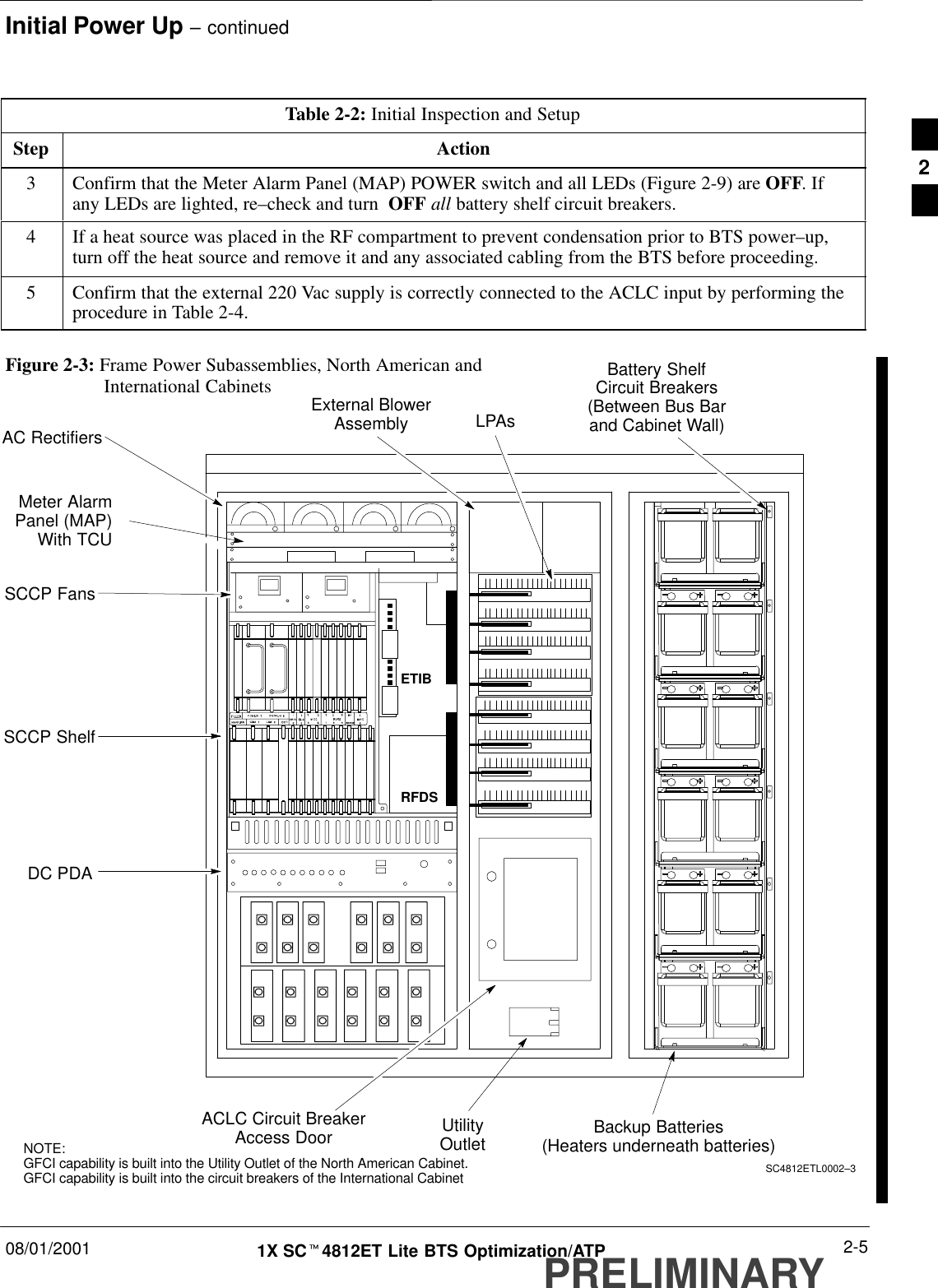
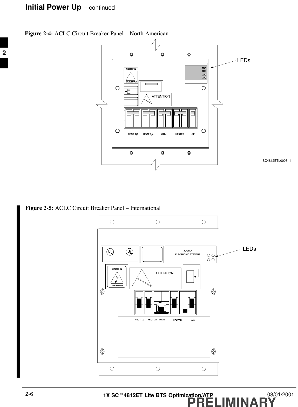
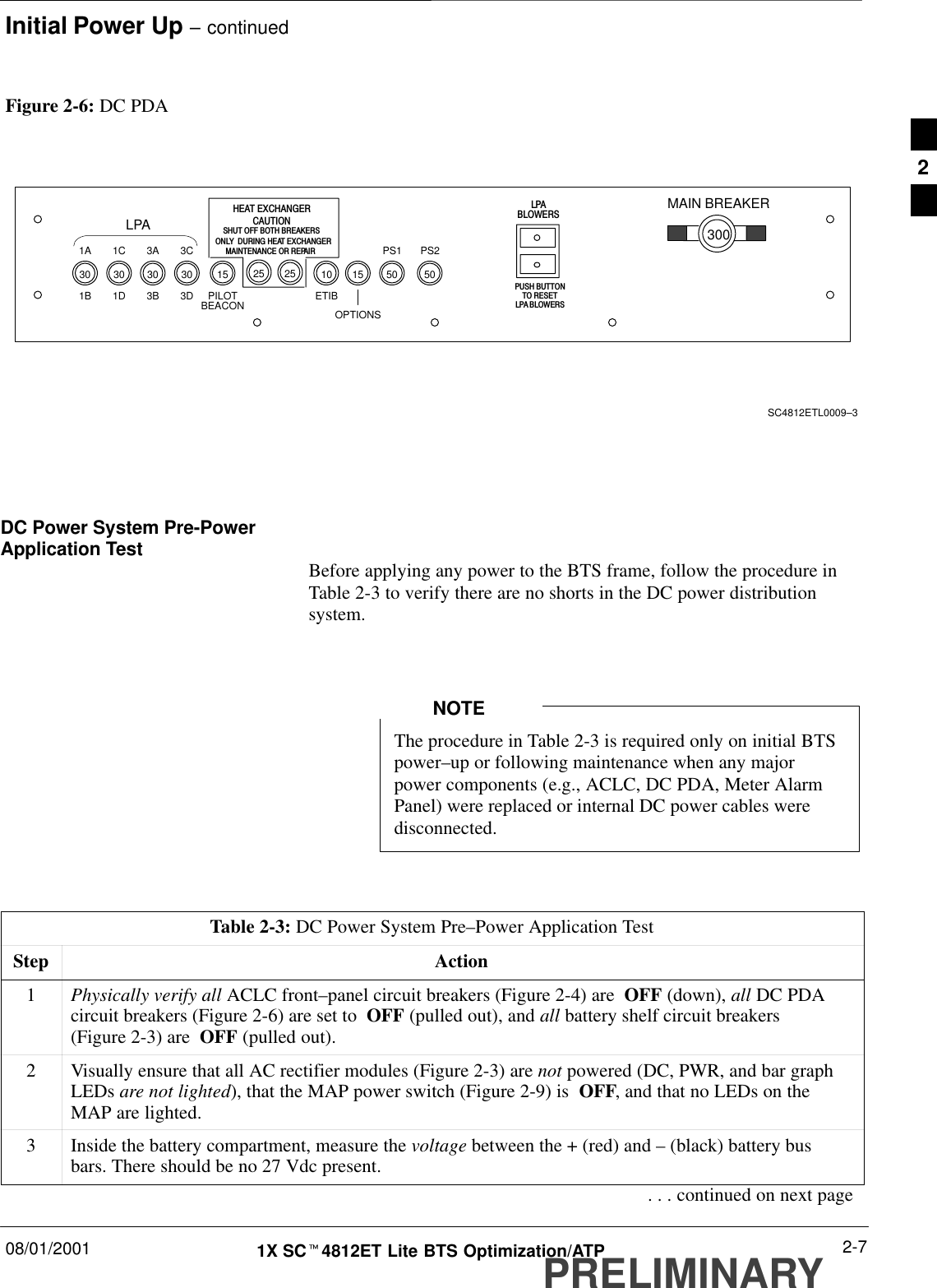
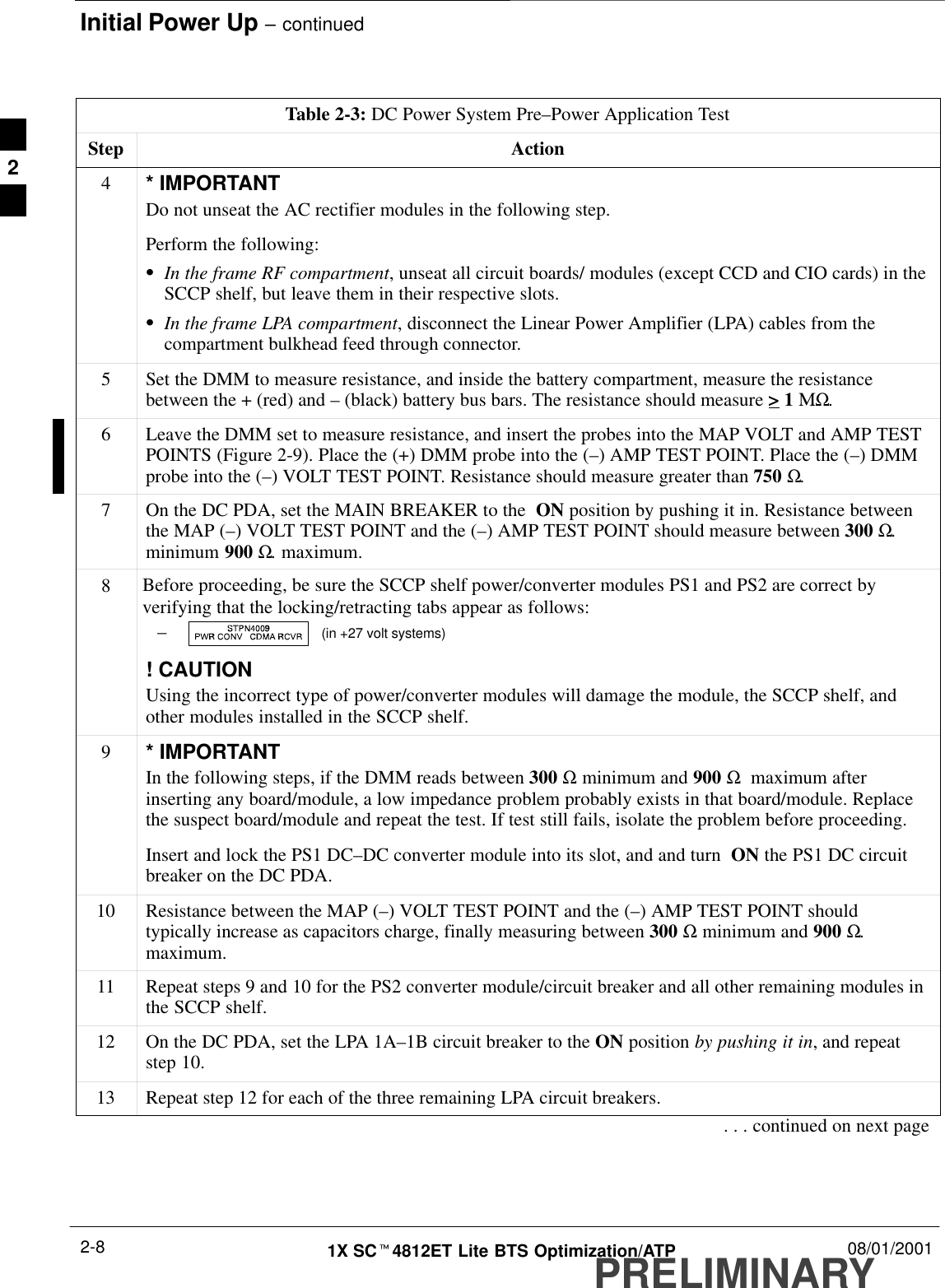
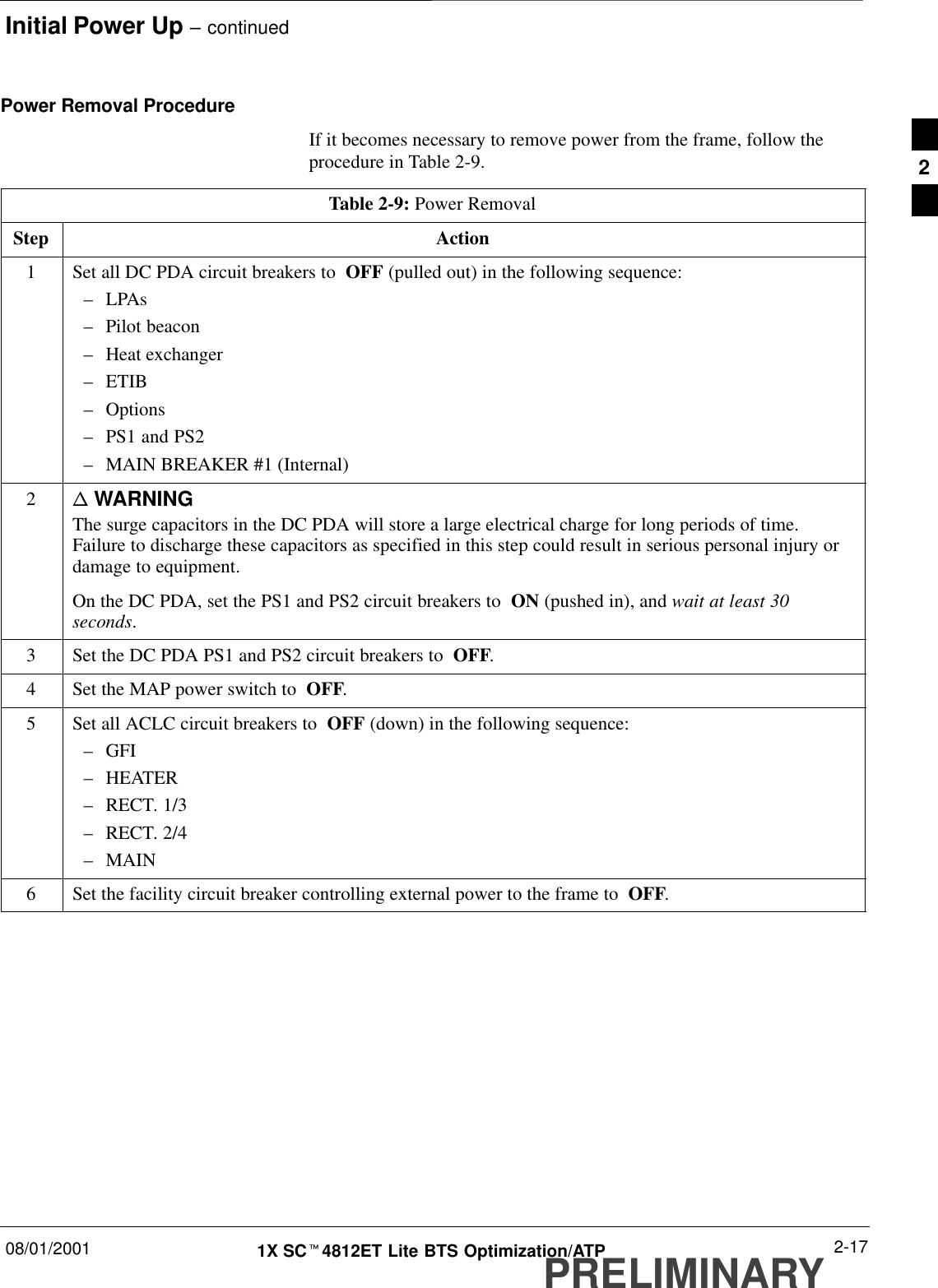
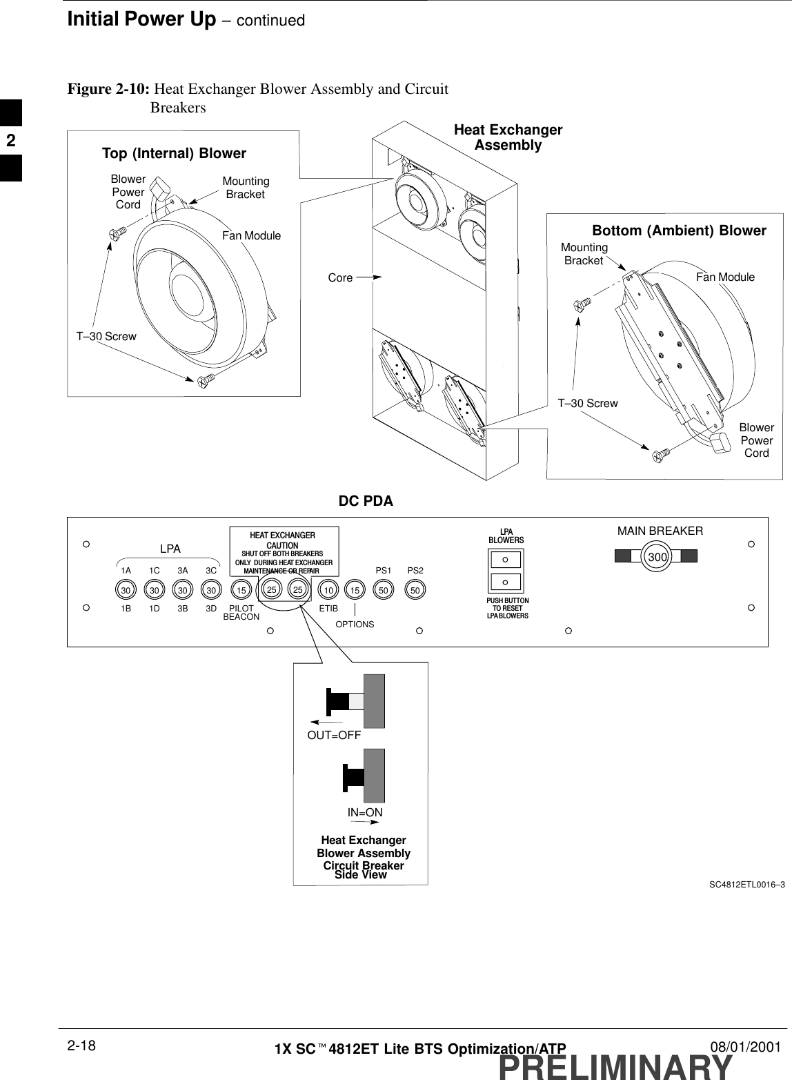
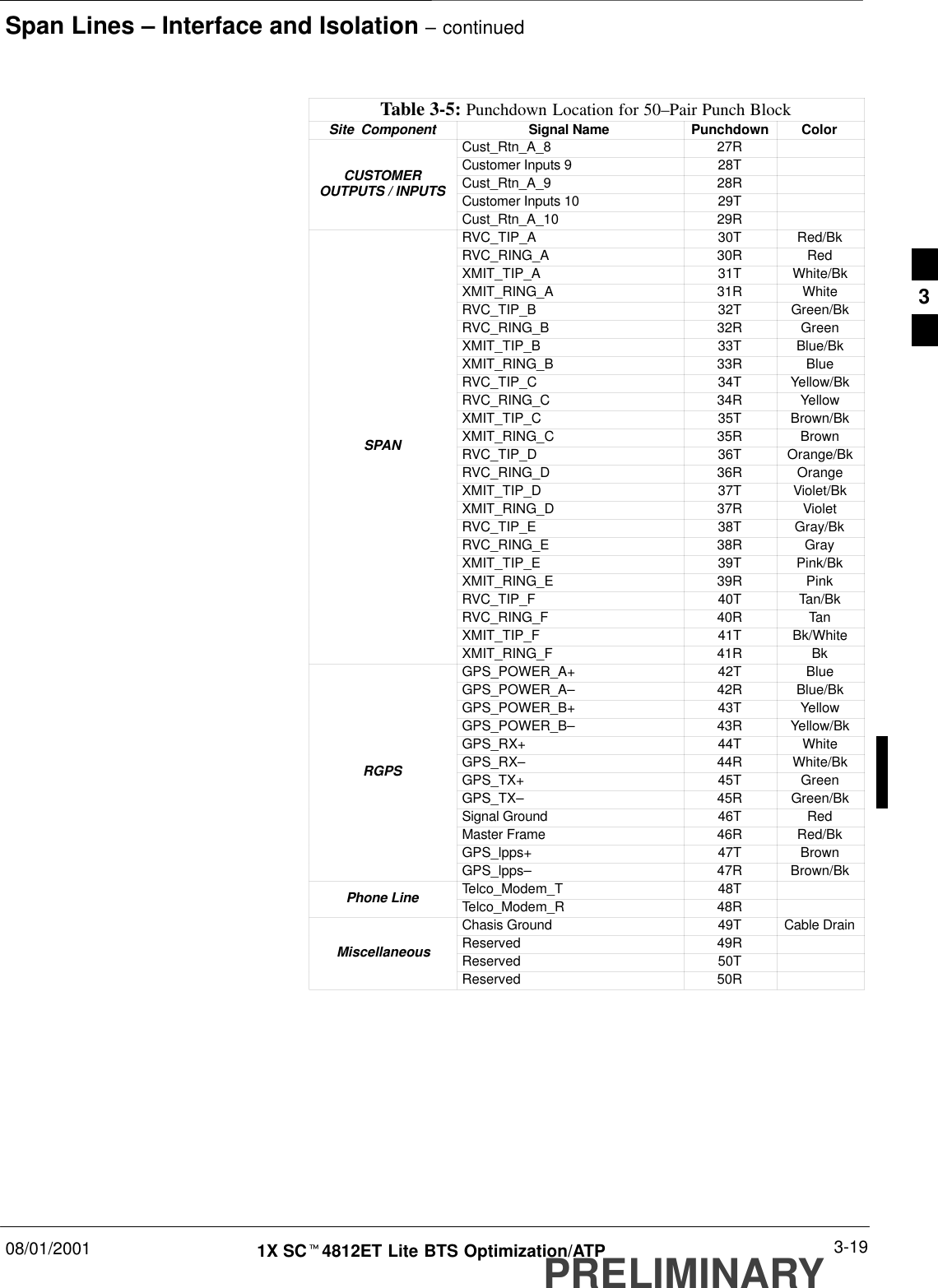
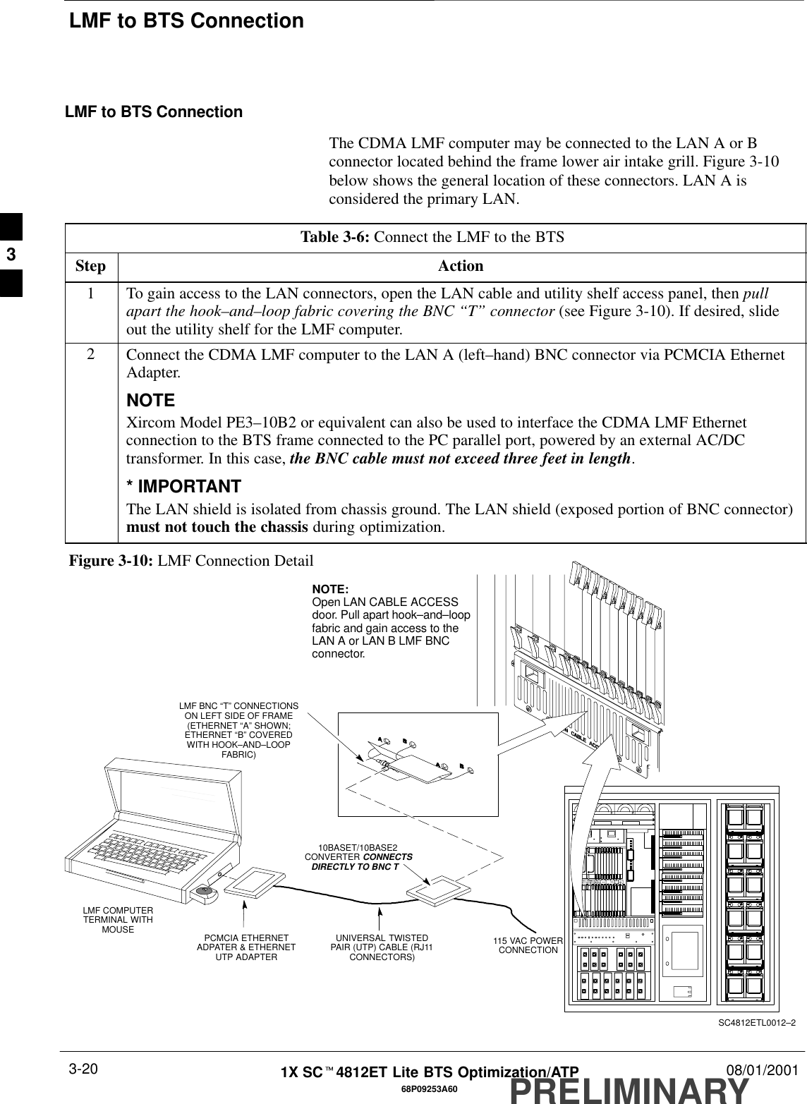
Nokia Solutions and Networks T5CS1 Cellular CDMA Base Station User Manual IHET5CS1 GLI2 1 of 4

Nokia Solutions and Networks Cellular CDMA Base Station IHET5CS1 GLI2 1 of 4

IHET5CS1 GLI2 User Manual 1 of 4
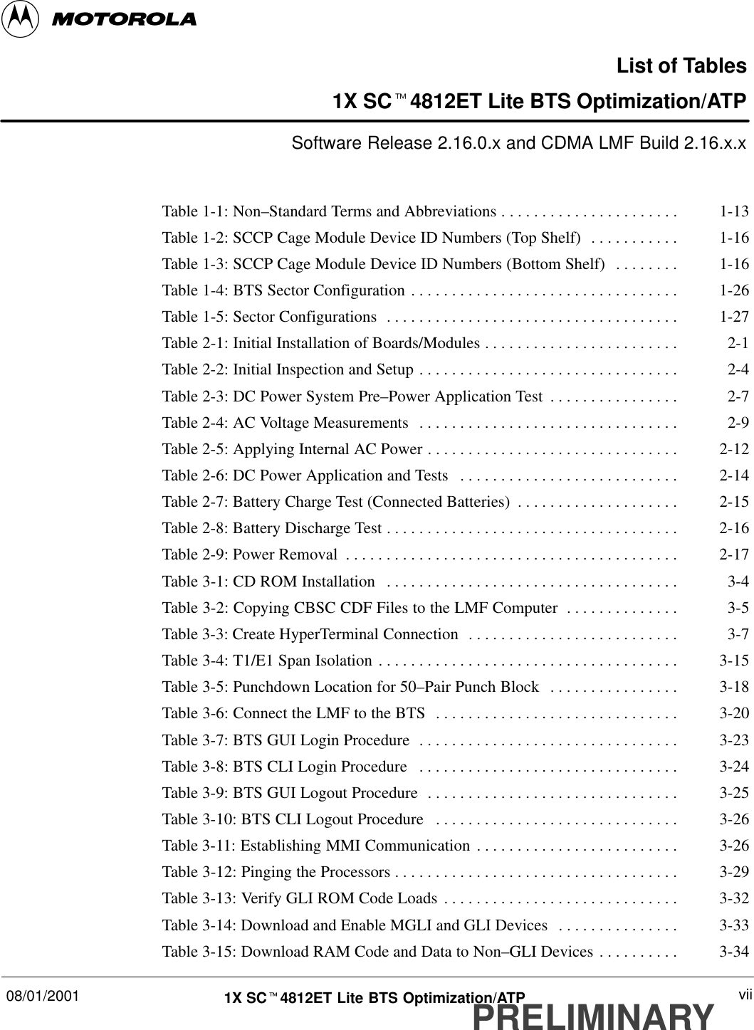
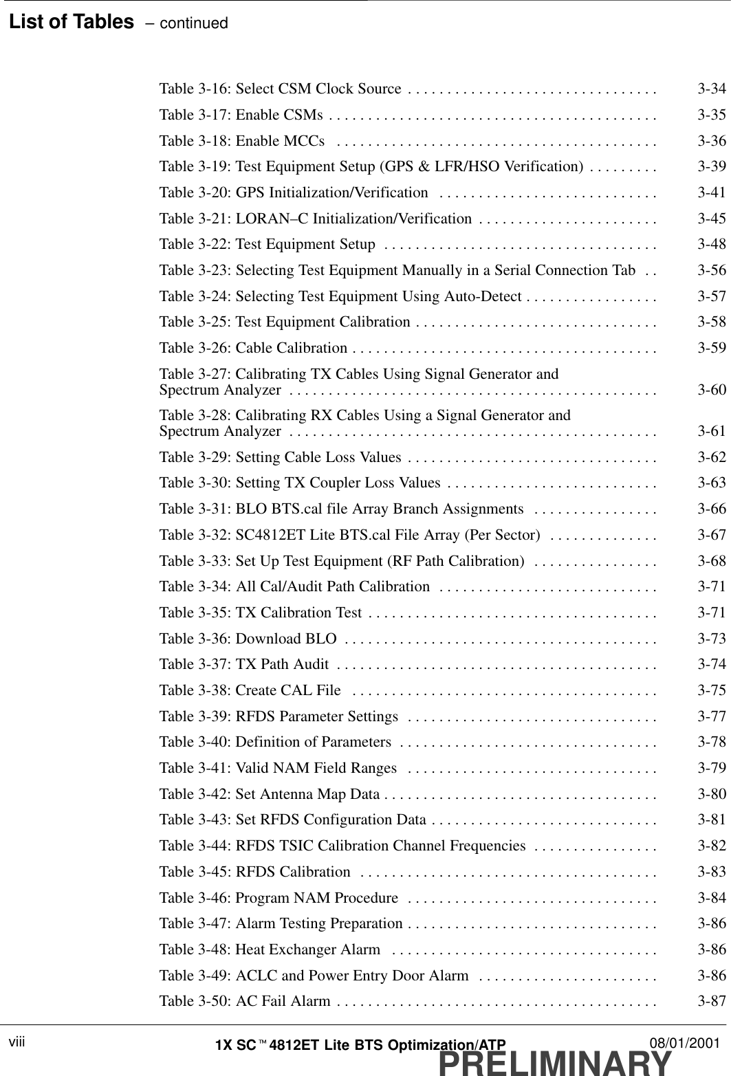
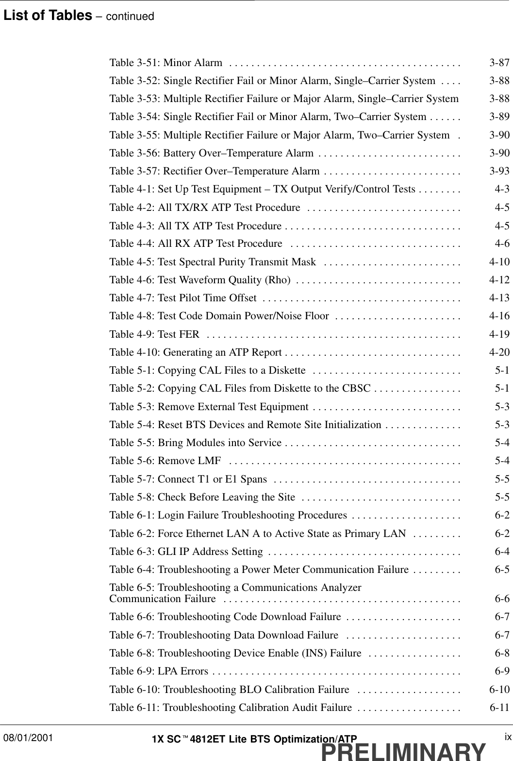
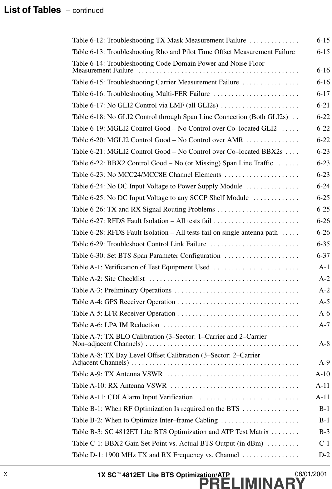
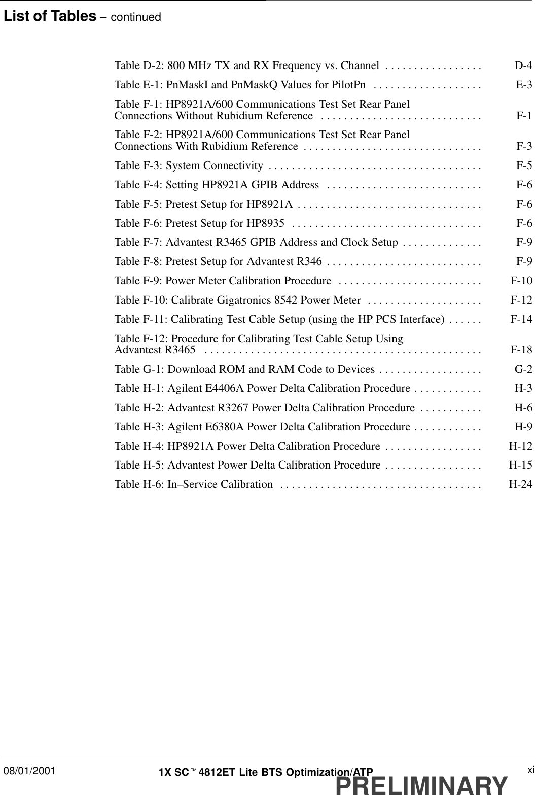
1X SCt4812ET Lite BTSOptimization/ATPSoftware Release 2.16.0.x and CDMA LMF Build 2.16.x.x800 MHz and 1.9 GHzCDMAEnglish08/01/200168P09253A60–1PRELIMINARY
FOANoticeWhile reasonable efforts have been made to assure the accuracy of this document, Motorola, Inc. assumes no liability resulting from anyinaccuracies or omissions in this document, or from use of the information obtained herein. The information in this document has beencarefully checked and is believed to be entirely reliable. However, no responsibility is assumed for inaccuracies or omissions. Motorola,Inc. reserves the right to make changes to any products described herein and reserves the right to revise this document and to makechanges from time to time in content hereof with no obligation to notify any person of revisions or changes. Motorola, Inc. does notassume any liability arising out of the application or use of any product, software, or circuit described herein; neither does it conveylicense under its patent rights or the rights of others.It is possible that this publication may contain references to, or information about Motorola products (machines and programs),programming, or services that are not announced in your country. Such references or information must not be construed to meanthat Motorola intends to announce such Motorola products, programming, or services in your country.CopyrightsThis instruction manual, and the Motorola products described in this instruction manual may be, include or describe copyrightedMotorola material, such as computer programs stored in semiconductor memories or other media. Laws in the United States andother countries preserve for Motorola certain exclusive rights for copyrighted material, including the exclusive right to copy,reproduce in any form, distribute and make derivative works of the copyrighted material. Accordingly, any copyrighted Motorolamaterial contained herein or in the Motorola products described in this instruction manual may not be copied, reproduced,distributed, merged or modified in any manner without the express written permission of Motorola. Furthermore, the purchase ofMotorola products shall not be deemed to grant either directly or by implication, estoppel, or otherwise, any license under thecopyrights, patents or patent applications of Motorola, as arises by operation of law in the sale of a product.Usage and Disclosure RestrictionsLicense AgreementThe software described in this document is the property of Motorola, Inc. It is furnished by express license agreement only and maybe used only in accordance with the terms of such an agreement.Copyrighted MaterialsSoftware and documentation are copyrighted materials. Making unauthorized copies is prohibited by law. No part of the software ordocumentation may be reproduced, transmitted, transcribed, stored in a retrieval system, or translated into any language orcomputer language, in any form or by any means, without prior written permission of Motorola, Inc.High Risk ActivitiesComponents, units, or third–party products used in the product described herein are NOT fault–tolerant and are NOT designed,manufactured, or intended for use as on–line control equipment in the following hazardous environments requiring fail–safecontrols: the operation of Nuclear Facilities, Aircraft Navigation or Aircraft Communication Systems, Air Traffic Control, LifeSupport, or Weapons Systems (“High Risk Activities”). Motorola and its supplier(s) specifically disclaim any expressed or impliedwarranty of fitness for such High Risk Activities.Trademarks and Motorola are registered trademarks of Motorola, Inc.Product and service names profiled herein are trademarks of Motorola, Inc. Other manufacturers’ products or services profiledherein may be referred to by trademarks of their respective companies.Copyright Copyright 2001 Motorola, Inc.  All Rights ReservedPrinted on    Recyclable PaperREV012501SPECIFICATIONS SUBJECT TO CHANGE WITHOUT NOTICE
08/01/2001 i1X SCt4812ET Lite BTS Optimization/ATPPRELIMINARYTable of Contents1X SCt4812ET Lite BTS Optimization/ATPSoftware Release 2.16.0.x and CDMA LMF Build 2.16.x.xList of Figures iv. . . . . . . . . . . . . . . . . . . . . . . . . . . . . . . . . . . . . . . . . . . . . . . . . . . List of Tables vii. . . . . . . . . . . . . . . . . . . . . . . . . . . . . . . . . . . . . . . . . . . . . . . . . . . Foreword xii. . . . . . . . . . . . . . . . . . . . . . . . . . . . . . . . . . . . . . . . . . . . . . . . . . . . . . . FCC Requirements xv. . . . . . . . . . . . . . . . . . . . . . . . . . . . . . . . . . . . . . . . . . . . . . . General Safety xviii. . . . . . . . . . . . . . . . . . . . . . . . . . . . . . . . . . . . . . . . . . . . . . . . . . . Revision History xx. . . . . . . . . . . . . . . . . . . . . . . . . . . . . . . . . . . . . . . . . . . . . . . . . Patent Notification xxi. . . . . . . . . . . . . . . . . . . . . . . . . . . . . . . . . . . . . . . . . . . . . . . Chapter 1: IntroductionOptimization Manual Scope and Layout 1-1. . . . . . . . . . . . . . . . . . . . . . . . . . . . . . Purpose of the Optimization 1-3. . . . . . . . . . . . . . . . . . . . . . . . . . . . . . . . . . . . . . . . When to Optimize 1-4. . . . . . . . . . . . . . . . . . . . . . . . . . . . . . . . . . . . . . . . . . . . . . . . Required Test Equipment and Software 1-5. . . . . . . . . . . . . . . . . . . . . . . . . . . . . . . Required Documents and Related Publications 1-12. . . . . . . . . . . . . . . . . . . . . . . . . Terms and Abbreviations 1-13. . . . . . . . . . . . . . . . . . . . . . . . . . . . . . . . . . . . . . . . . . BTS Equipment Identification 1-15. . . . . . . . . . . . . . . . . . . . . . . . . . . . . . . . . . . . . . Cabinet Identification 1-17. . . . . . . . . . . . . . . . . . . . . . . . . . . . . . . . . . . . . . . . . . . . . Internal Assembly Location and Identification 1-18. . . . . . . . . . . . . . . . . . . . . . . . . BTS Sector Configurations 1-26. . . . . . . . . . . . . . . . . . . . . . . . . . . . . . . . . . . . . . . . . Chapter 2: Preliminary OperationsPreliminary Operations: Overview 2-1. . . . . . . . . . . . . . . . . . . . . . . . . . . . . . . . . . . Ethernet LAN 2-3. . . . . . . . . . . . . . . . . . . . . . . . . . . . . . . . . . . . . . . . . . . . . . . . . . . Initial Power Up 2-4. . . . . . . . . . . . . . . . . . . . . . . . . . . . . . . . . . . . . . . . . . . . . . . . . Chapter 3: Optimization/CalibrationOptimization/Calibration – Introduction 3-1. . . . . . . . . . . . . . . . . . . . . . . . . . . . . . Preparing the LMF 3-4. . . . . . . . . . . . . . . . . . . . . . . . . . . . . . . . . . . . . . . . . . . . . . . Span Lines – Interface and Isolation 3-14. . . . . . . . . . . . . . . . . . . . . . . . . . . . . . . . . . LMF to BTS Connection 3-20. . . . . . . . . . . . . . . . . . . . . . . . . . . . . . . . . . . . . . . . . . Using CDMA LMF 3-21. . . . . . . . . . . . . . . . . . . . . . . . . . . . . . . . . . . . . . . . . . . . . .
Table of Contents – continuedPRELIMINARY1X SCt4812ET Lite BTS Optimization/ATP 08/01/2001iiPinging the Processors 3-28. . . . . . . . . . . . . . . . . . . . . . . . . . . . . . . . . . . . . . . . . . . . Download the BTS 3-31. . . . . . . . . . . . . . . . . . . . . . . . . . . . . . . . . . . . . . . . . . . . . . . CSM System Time – GPS & LFR/HSO Verification 3-37. . . . . . . . . . . . . . . . . . . . . Test Equipment Setup 3-47. . . . . . . . . . . . . . . . . . . . . . . . . . . . . . . . . . . . . . . . . . . . . Test Set Calibration 3-55. . . . . . . . . . . . . . . . . . . . . . . . . . . . . . . . . . . . . . . . . . . . . . . Bay Level Offset Calibration 3-64. . . . . . . . . . . . . . . . . . . . . . . . . . . . . . . . . . . . . . . RFDS Setup and Calibration 3-76. . . . . . . . . . . . . . . . . . . . . . . . . . . . . . . . . . . . . . . Alarms Testing 3-85. . . . . . . . . . . . . . . . . . . . . . . . . . . . . . . . . . . . . . . . . . . . . . . . . . Chapter 4: Automated Acceptance Test Procedure (ATP)Automated Acceptance Test Procedure – Introduction 4-1. . . . . . . . . . . . . . . . . . . . Acceptance Tests – Test Set Up 4-3. . . . . . . . . . . . . . . . . . . . . . . . . . . . . . . . . . . . . Abbreviated (All–inclusive) Acceptance Tests 4-4. . . . . . . . . . . . . . . . . . . . . . . . . . Individual Acceptance Tests–Introduction 4-7. . . . . . . . . . . . . . . . . . . . . . . . . . . . . TX Spectral Purity Transmit Mask Acceptance Test 4-9. . . . . . . . . . . . . . . . . . . . . TX Waveform Quality (Rho) Acceptance Test 4-12. . . . . . . . . . . . . . . . . . . . . . . . . . TX Pilot Time Offset Acceptance Test 4-13. . . . . . . . . . . . . . . . . . . . . . . . . . . . . . . . TX Code Domain Power/Noise Floor Acceptance Test 4-15. . . . . . . . . . . . . . . . . . . RX FER Acceptance Test 4-18. . . . . . . . . . . . . . . . . . . . . . . . . . . . . . . . . . . . . . . . . . Generating an ATP Report 4-20. . . . . . . . . . . . . . . . . . . . . . . . . . . . . . . . . . . . . . . . . Chapter 5: Leaving the SiteUpdating Calibration Data Files 5-1. . . . . . . . . . . . . . . . . . . . . . . . . . . . . . . . . . . . . Prepare to Leave the Site 5-3. . . . . . . . . . . . . . . . . . . . . . . . . . . . . . . . . . . . . . . . . . Chapter 6: Basic TroubleshootingBasic Troubleshooting Overview 6-1. . . . . . . . . . . . . . . . . . . . . . . . . . . . . . . . . . . . Troubleshooting: Installation 6-2. . . . . . . . . . . . . . . . . . . . . . . . . . . . . . . . . . . . . . . Troubleshooting: Download 6-7. . . . . . . . . . . . . . . . . . . . . . . . . . . . . . . . . . . . . . . . Troubleshooting: Calibration 6-10. . . . . . . . . . . . . . . . . . . . . . . . . . . . . . . . . . . . . . . Basic Troubleshooting – RF Path Fault Isolation 6-12. . . . . . . . . . . . . . . . . . . . . . . . Troubleshooting: Transmit ATP 6-15. . . . . . . . . . . . . . . . . . . . . . . . . . . . . . . . . . . . . Troubleshooting: Receive ATP 6-17. . . . . . . . . . . . . . . . . . . . . . . . . . . . . . . . . . . . . . Troubleshooting: CSM Checklist 6-18. . . . . . . . . . . . . . . . . . . . . . . . . . . . . . . . . . . . SCCP Backplane Troubleshooting 6-20. . . . . . . . . . . . . . . . . . . . . . . . . . . . . . . . . . . RFDS – Fault Isolation 6-26. . . . . . . . . . . . . . . . . . . . . . . . . . . . . . . . . . . . . . . . . . . . Module Front Panel LED Indicators and Connectors 6-28. . . . . . . . . . . . . . . . . . . . . Basic Troubleshooting – Span Control Link 6-35. . . . . . . . . . . . . . . . . . . . . . . . . . .
Table of Contents – continued08/01/2001 iii1X SCt4812ET Lite BTS Optimization/ATPPRELIMINARYAppendix A: Data SheetsOptimization (Pre–ATP) Data Sheets A-1. . . . . . . . . . . . . . . . . . . . . . . . . . . . . . . . . Site Serial Number Check List A-13. . . . . . . . . . . . . . . . . . . . . . . . . . . . . . . . . . . . . . Appendix B: FRU Optimization/ATP Test MatrixFRU Optimization/ATP Test Matrix B-1. . . . . . . . . . . . . . . . . . . . . . . . . . . . . . . . . . Appendix C: BBX Gain Set Point vs. BTS Output ConsiderationsBBX2 Gain Set Point vs. BTS Output Considerations C-1. . . . . . . . . . . . . . . . . . . Appendix D: CDMA Operating Frequency InformationCDMA Operating Frequency Programming Information – North American PCS Bands . D-1Appendix E: PN Offset/I & Q Offset Register Programming InformationPN Offset Programming Information E-1. . . . . . . . . . . . . . . . . . . . . . . . . . . . . . . . . Appendix F: Test Equipment PreparationTest Equipment Preparation F-1. . . . . . . . . . . . . . . . . . . . . . . . . . . . . . . . . . . . . . . . Manual Cable Calibration F-14. . . . . . . . . . . . . . . . . . . . . . . . . . . . . . . . . . . . . . . . . . Appendix G: Download ROM CodeDownloading ROM Code with the LMF G-1. . . . . . . . . . . . . . . . . . . . . . . . . . . . . . Appendix H: In–Service CalibrationIntroduction H-1. . . . . . . . . . . . . . . . . . . . . . . . . . . . . . . . . . . . . . . . . . . . . . . . . . . . . Power Delta Calibration H-3. . . . . . . . . . . . . . . . . . . . . . . . . . . . . . . . . . . . . . . . . . . In–Service Calibration H-18. . . . . . . . . . . . . . . . . . . . . . . . . . . . . . . . . . . . . . . . . . . . Index
PRELIMINARY1X SCt4812ET Lite BTS Optimization/ATP 08/01/2001ivList of Figures1X SCt4812ET Lite BTS Optimization/ATPSoftware Release 2.16.0.x and CDMA LMF Build 2.16.x.xFigure 1-1: SC4812ET Lite Logical BTS Span Cabling 1-16. . . . . . . . . . . . . . . . . . Figure 1-2: SC4812ET Lite BTS Frame 1-17. . . . . . . . . . . . . . . . . . . . . . . . . . . . . . Figure 1-3: Internal Assemblies and FRUs(Cabinet doors not shown for clarity) 1-18. . . . . . . . . . . . . . . . . . . . . . . . . . . . . . . . . Figure 1-4: 50–Pair Punchblock 1-20. . . . . . . . . . . . . . . . . . . . . . . . . . . . . . . . . . . . . Figure 1-5: SCCP Shelf, IS–95A/B and 1X Devices 1-22. . . . . . . . . . . . . . . . . . . . . Figure 1-6: RF Interface Panel, DRDCs Installed 1-23. . . . . . . . . . . . . . . . . . . . . . . Figure 1-7: RF Interface Panel, TRDCs Installed 1-24. . . . . . . . . . . . . . . . . . . . . . . Figure 1-8: RFDS, DRDC, and TRDC Details 1-25. . . . . . . . . . . . . . . . . . . . . . . . . Figure 1-9: SC4812ET Lite LPA Configuration with Bandpass Filters(Starter Frame Mapping Only) 1-27. . . . . . . . . . . . . . . . . . . . . . . . . . . . . . . . . . . . . . Figure 2-1: Backplane DIP Switch Settings 2-2. . . . . . . . . . . . . . . . . . . . . . . . . . . . Figure 2-2: External Ethernet LAN Connectors 2-3. . . . . . . . . . . . . . . . . . . . . . . . . Figure 2-3: Frame Power Subassemblies, North American and International Cabinets 2-5. . . . . . . . . . . . . . . . . . . . . . . . . . . . . . . . . . . . . . . . . . . . . Figure 2-4: ACLC Circuit Breaker Panel – North American 2-6. . . . . . . . . . . . . . . Figure 2-5: ACLC Circuit Breaker Panel – International 2-6. . . . . . . . . . . . . . . . . . Figure 2-6: DC PDA 2-7. . . . . . . . . . . . . . . . . . . . . . . . . . . . . . . . . . . . . . . . . . . . . . Figure 2-7: ACLC Voltage Measurement Probe Points – North American 2-11. . . . Figure 2-8: ACLC Voltage Measurement Probe Points – International 2-12. . . . . . . Figure 2-9: Meter Alarm Panel (MAP) 2-13. . . . . . . . . . . . . . . . . . . . . . . . . . . . . . . Figure 2-10: Heat Exchanger Blower Assembly and Circuit Breakers 2-18. . . . . . . Figure 3-1: CDMA LMF Folder Structure 3-9. . . . . . . . . . . . . . . . . . . . . . . . . . . . . Figure 3-2: BTS Folder Name Syntax Example 3-10. . . . . . . . . . . . . . . . . . . . . . . . . Figure 3-3: CAL File Name Syntax Example 3-10. . . . . . . . . . . . . . . . . . . . . . . . . . Figure 3-4: CDF Name Syntax Example 3-10. . . . . . . . . . . . . . . . . . . . . . . . . . . . . . Figure 3-5: Code Load File Name Syntax Example 3-12. . . . . . . . . . . . . . . . . . . . . . Figure 3-6: DDS File Name Syntax Example 3-13. . . . . . . . . . . . . . . . . . . . . . . . . . Figure 3-7: Disconnecting Span Lines 3-14. . . . . . . . . . . . . . . . . . . . . . . . . . . . . . . . Figure 3-8: Rear and Front View of CSU Shelf 3-16. . . . . . . . . . . . . . . . . . . . . . . . .
List of Figures – continued08/01/2001 v1X SCt4812ET Lite BTS Optimization/ATPPRELIMINARYFigure 3-9: 50–Pair Punchblock 3-17. . . . . . . . . . . . . . . . . . . . . . . . . . . . . . . . . . . . . Figure 3-10: LMF Connection Detail 3-20. . . . . . . . . . . . . . . . . . . . . . . . . . . . . . . . . Figure 3-11: CDMA LMF Computer Common MMI Connections 3-27. . . . . . . . . . Figure 3-12:  BTS Ethernet LAN Interconnect Diagram 3-28. . . . . . . . . . . . . . . . . . Figure 3-13: CSM MMI Terminal Connection 3-40. . . . . . . . . . . . . . . . . . . . . . . . . . Figure 3-14: Cable Calibration Test Setup 3-50. . . . . . . . . . . . . . . . . . . . . . . . . . . . . Figure 3-15: TX Calibration Test Setup (CyberTest and HP 8935) 3-51. . . . . . . . . . Figure 3-16: TX Calibration Test Setup HP 8921A and Advantest 3-52. . . . . . . . . . Figure 3-17: Optimization/ATP Test Setup Calibration (CyberTest, HP 8935 andAdvantest) 3-53. . . . . . . . . . . . . . . . . . . . . . . . . . . . . . . . . . . . . . . . . . . . . . . . . . . . . . Figure 3-18: Optimization/ATP Test Setup HP 8921A 3-54. . . . . . . . . . . . . . . . . . . Figure 3-19:  Calibrating Test Equipment Setup for TX Cable Calibration(Using Signal Generator and Spectrum Analyzer) 3-60. . . . . . . . . . . . . . . . . . . . . . . Figure 3-20:  Calibrating Test Equipment Setup for RX ATP Test(Using Signal Generator and Spectrum Analyzer) 3-61. . . . . . . . . . . . . . . . . . . . . . . Figure 3-21: Battery Over–Temperature Sensor 3-92. . . . . . . . . . . . . . . . . . . . . . . . . Figure 3-22: MAP Connector J8 (Rear of MAP) 3-93. . . . . . . . . . . . . . . . . . . . . . . . Figure 4-1: TX Mask Verification Spectrum Analyzer Display 4-11. . . . . . . . . . . . . Figure 4-2: Code Domain Analyzer CD Power/Noise Floor Display Examples 4-17Figure 6-1: TX Output Fault Isolation Flowchart 6-14. . . . . . . . . . . . . . . . . . . . . . . Figure 6-2: CSM Front Panel Indicators & Monitor Ports 6-29. . . . . . . . . . . . . . . . . Figure 6-3: GLI2 Front Panel Operating Indicators 6-32. . . . . . . . . . . . . . . . . . . . . . Figure 6-4: MCC24 Front Panel LEDs and LED Indicators 6-34. . . . . . . . . . . . . . . Figure 6-5: MGLI/GLI Board MMI Connection Detail 6-36. . . . . . . . . . . . . . . . . . . Figure D-1: North America PCS Frequency Spectrum (CDMA Allocation) D-1. . . Figure D-2: North American Cellular Telephone System Frequency Spectrum (CDMA Allocation). D-4. . . . . . . . . . . . . . . . . . . . . . . . . . . . . . . . . . . . . . . . . . . . . . Figure F-1: HP8921A/600 Cables Connection for 10 MHz Signal and GPIB without Rubidium Reference F-2. . . . . . . . . . . . . . . . . . . . . . . . . . . . . . . Figure F-2: HP8921A Cables Connection for 10 MHz Signal and GPIB with Rubidium Reference F-4. . . . . . . . . . . . . . . . . . . . . . . . . . . . . . . . . . . . . . . . . . Figure F-3: Cable Connections for Test Set without 10 MHz Rubidium Reference F-7. . . . . . . . . . . . . . . . . . . . . . . . . . . . . . . . . . . . . . . . . . . . . . . . . . . . . . Figure F-4: Cable Connections for Test Set with 10 MHz Rubidium Reference F-8. . . . . . . . . . . . . . . . . . . . . . . . . . . . . . . . . . . . . . . . . . . . . . Figure F-5: Power Meter Detail F-10. . . . . . . . . . . . . . . . . . . . . . . . . . . . . . . . . . . . . Figure F-6: Gigatronics 8542C Power Meter Detail F-13. . . . . . . . . . . . . . . . . . . . . Figure F-7: Cable Calibration Using HP8921 with PCS Interface F-17. . . . . . . . . . . Figure F-8: Cable Calibration Using Advantest R3465 F-20. . . . . . . . . . . . . . . . . . . Figure H-1: Delta Calibration Setup – Agilent E4432B to HP437 H-5. . . . . . . . . .
List of Figures – continuedPRELIMINARY1X SCt4812ET Lite BTS Optimization/ATP 08/01/2001viFigure H-2: Delta Calibration Setup – Agilent E4432B to Agilent E4406A H-5. . . Figure H-3: Delta Calibration Setup – Advantest R3562 to HP437 H-8. . . . . . . . . Figure H-4: Delta Calibration Setup – Advantest R3562 to R3267 H-8. . . . . . . . . . Figure H-5: Delta Calibration Setup – E6380A to HP437 H-10. . . . . . . . . . . . . . . . . Figure H-6: Delta Calibration Setup – E6380A to E6380A H-11. . . . . . . . . . . . . . . . Figure H-7: Delta Calibration Setup – HP8921A to HP437 H-13. . . . . . . . . . . . . . . Figure H-8: Delta Calibration Setup – HP8921A to HP8921A H-14. . . . . . . . . . . . . Figure H-9: Delta Calibration Setup – R3561L to HP437 H-17. . . . . . . . . . . . . . . . . Figure H-10: Delta Calibration Setup – R3561L to R3465 H-17. . . . . . . . . . . . . . . . Figure H-11: Optimization/ATP Test Setup Using Directional Coupler – Agilent Test Equipment H-20. . . . . . . . . . . . . . . . . . . . . . . . . . . . . . . . . . . . . . . . . . . Figure H-12: Optimization/ATP Test Setup Using Directional Coupler – Advantest R3267/R3562 Test Equipment H-21. . . . . . . . . . . . . . . . . . . . . . . . . . . . . Figure H-13: Optimization/ATP Test Setup Using RFDS – Agilent Test Equipment H-22. . . . . . . . . . . . . . . . . . . . . . . . . . . . . . . . . . . . . . . . . . . Figure H-14: Optimization/ATP Test Setup Using RFDS – Advantest R3267/R3562 Test Equipment H-23. . . . . . . . . . . . . . . . . . . . . . . . . . . . .
08/01/2001 vii1X SCt4812ET Lite BTS Optimization/ATPPRELIMINARYList of Tables1X SCt4812ET Lite BTS Optimization/ATPSoftware Release 2.16.0.x and CDMA LMF Build 2.16.x.xTable 1-1: Non–Standard Terms and Abbreviations 1-13. . . . . . . . . . . . . . . . . . . . . . Table 1-2: SCCP Cage Module Device ID Numbers (Top Shelf) 1-16. . . . . . . . . . . Table 1-3: SCCP Cage Module Device ID Numbers (Bottom Shelf) 1-16. . . . . . . . Table 1-4: BTS Sector Configuration 1-26. . . . . . . . . . . . . . . . . . . . . . . . . . . . . . . . . Table 1-5: Sector Configurations 1-27. . . . . . . . . . . . . . . . . . . . . . . . . . . . . . . . . . . . Table 2-1: Initial Installation of Boards/Modules 2-1. . . . . . . . . . . . . . . . . . . . . . . . Table 2-2: Initial Inspection and Setup 2-4. . . . . . . . . . . . . . . . . . . . . . . . . . . . . . . . Table 2-3: DC Power System Pre–Power Application Test 2-7. . . . . . . . . . . . . . . . Table 2-4: AC Voltage Measurements 2-9. . . . . . . . . . . . . . . . . . . . . . . . . . . . . . . . Table 2-5: Applying Internal AC Power 2-12. . . . . . . . . . . . . . . . . . . . . . . . . . . . . . . Table 2-6: DC Power Application and Tests 2-14. . . . . . . . . . . . . . . . . . . . . . . . . . . Table 2-7: Battery Charge Test (Connected Batteries) 2-15. . . . . . . . . . . . . . . . . . . . Table 2-8: Battery Discharge Test 2-16. . . . . . . . . . . . . . . . . . . . . . . . . . . . . . . . . . . . Table 2-9: Power Removal 2-17. . . . . . . . . . . . . . . . . . . . . . . . . . . . . . . . . . . . . . . . . Table 3-1: CD ROM Installation 3-4. . . . . . . . . . . . . . . . . . . . . . . . . . . . . . . . . . . . Table 3-2: Copying CBSC CDF Files to the LMF Computer 3-5. . . . . . . . . . . . . . Table 3-3: Create HyperTerminal Connection 3-7. . . . . . . . . . . . . . . . . . . . . . . . . . Table 3-4: T1/E1 Span Isolation 3-15. . . . . . . . . . . . . . . . . . . . . . . . . . . . . . . . . . . . . Table 3-5: Punchdown Location for 50–Pair Punch Block 3-18. . . . . . . . . . . . . . . . Table 3-6: Connect the LMF to the BTS 3-20. . . . . . . . . . . . . . . . . . . . . . . . . . . . . . Table 3-7: BTS GUI Login Procedure 3-23. . . . . . . . . . . . . . . . . . . . . . . . . . . . . . . . Table 3-8: BTS CLI Login Procedure 3-24. . . . . . . . . . . . . . . . . . . . . . . . . . . . . . . . Table 3-9: BTS GUI Logout Procedure 3-25. . . . . . . . . . . . . . . . . . . . . . . . . . . . . . . Table 3-10: BTS CLI Logout Procedure 3-26. . . . . . . . . . . . . . . . . . . . . . . . . . . . . . Table 3-11: Establishing MMI Communication 3-26. . . . . . . . . . . . . . . . . . . . . . . . . Table 3-12: Pinging the Processors 3-29. . . . . . . . . . . . . . . . . . . . . . . . . . . . . . . . . . . Table 3-13: Verify GLI ROM Code Loads 3-32. . . . . . . . . . . . . . . . . . . . . . . . . . . . . Table 3-14: Download and Enable MGLI and GLI Devices 3-33. . . . . . . . . . . . . . . Table 3-15: Download RAM Code and Data to Non–GLI Devices 3-34. . . . . . . . . .
List of Tables  – continuedPRELIMINARY1X SCt4812ET Lite BTS Optimization/ATP 08/01/2001viiiTable 3-16: Select CSM Clock Source 3-34. . . . . . . . . . . . . . . . . . . . . . . . . . . . . . . . Table 3-17: Enable CSMs 3-35. . . . . . . . . . . . . . . . . . . . . . . . . . . . . . . . . . . . . . . . . . Table 3-18: Enable MCCs 3-36. . . . . . . . . . . . . . . . . . . . . . . . . . . . . . . . . . . . . . . . . Table 3-19: Test Equipment Setup (GPS & LFR/HSO Verification) 3-39. . . . . . . . . Table 3-20: GPS Initialization/Verification 3-41. . . . . . . . . . . . . . . . . . . . . . . . . . . . Table 3-21: LORAN–C Initialization/Verification 3-45. . . . . . . . . . . . . . . . . . . . . . . Table 3-22: Test Equipment Setup 3-48. . . . . . . . . . . . . . . . . . . . . . . . . . . . . . . . . . . Table 3-23: Selecting Test Equipment Manually in a Serial Connection Tab 3-56. . Table 3-24: Selecting Test Equipment Using Auto-Detect 3-57. . . . . . . . . . . . . . . . . Table 3-25: Test Equipment Calibration 3-58. . . . . . . . . . . . . . . . . . . . . . . . . . . . . . . Table 3-26: Cable Calibration 3-59. . . . . . . . . . . . . . . . . . . . . . . . . . . . . . . . . . . . . . . Table 3-27: Calibrating TX Cables Using Signal Generator and Spectrum Analyzer 3-60. . . . . . . . . . . . . . . . . . . . . . . . . . . . . . . . . . . . . . . . . . . . . . . Table 3-28: Calibrating RX Cables Using a Signal Generator and Spectrum Analyzer 3-61. . . . . . . . . . . . . . . . . . . . . . . . . . . . . . . . . . . . . . . . . . . . . . . Table 3-29: Setting Cable Loss Values 3-62. . . . . . . . . . . . . . . . . . . . . . . . . . . . . . . . Table 3-30: Setting TX Coupler Loss Values 3-63. . . . . . . . . . . . . . . . . . . . . . . . . . . Table 3-31: BLO BTS.cal file Array Branch Assignments 3-66. . . . . . . . . . . . . . . . Table 3-32: SC4812ET Lite BTS.cal File Array (Per Sector) 3-67. . . . . . . . . . . . . . Table 3-33: Set Up Test Equipment (RF Path Calibration) 3-68. . . . . . . . . . . . . . . . Table 3-34: All Cal/Audit Path Calibration 3-71. . . . . . . . . . . . . . . . . . . . . . . . . . . . Table 3-35: TX Calibration Test 3-71. . . . . . . . . . . . . . . . . . . . . . . . . . . . . . . . . . . . . Table 3-36: Download BLO 3-73. . . . . . . . . . . . . . . . . . . . . . . . . . . . . . . . . . . . . . . . Table 3-37: TX Path Audit 3-74. . . . . . . . . . . . . . . . . . . . . . . . . . . . . . . . . . . . . . . . . Table 3-38: Create CAL File 3-75. . . . . . . . . . . . . . . . . . . . . . . . . . . . . . . . . . . . . . . Table 3-39: RFDS Parameter Settings 3-77. . . . . . . . . . . . . . . . . . . . . . . . . . . . . . . . Table 3-40: Definition of Parameters 3-78. . . . . . . . . . . . . . . . . . . . . . . . . . . . . . . . . Table 3-41: Valid NAM Field Ranges 3-79. . . . . . . . . . . . . . . . . . . . . . . . . . . . . . . . Table 3-42: Set Antenna Map Data 3-80. . . . . . . . . . . . . . . . . . . . . . . . . . . . . . . . . . . Table 3-43: Set RFDS Configuration Data 3-81. . . . . . . . . . . . . . . . . . . . . . . . . . . . . Table 3-44: RFDS TSIC Calibration Channel Frequencies 3-82. . . . . . . . . . . . . . . . Table 3-45: RFDS Calibration 3-83. . . . . . . . . . . . . . . . . . . . . . . . . . . . . . . . . . . . . . Table 3-46: Program NAM Procedure 3-84. . . . . . . . . . . . . . . . . . . . . . . . . . . . . . . . Table 3-47: Alarm Testing Preparation 3-86. . . . . . . . . . . . . . . . . . . . . . . . . . . . . . . . Table 3-48: Heat Exchanger Alarm 3-86. . . . . . . . . . . . . . . . . . . . . . . . . . . . . . . . . . Table 3-49: ACLC and Power Entry Door Alarm 3-86. . . . . . . . . . . . . . . . . . . . . . . Table 3-50: AC Fail Alarm 3-87. . . . . . . . . . . . . . . . . . . . . . . . . . . . . . . . . . . . . . . . .
List of Tables – continued08/01/2001 ix1X SCt4812ET Lite BTS Optimization/ATPPRELIMINARYTable 3-51: Minor Alarm 3-87. . . . . . . . . . . . . . . . . . . . . . . . . . . . . . . . . . . . . . . . . . Table 3-52: Single Rectifier Fail or Minor Alarm, Single–Carrier System 3-88. . . . Table 3-53: Multiple Rectifier Failure or Major Alarm, Single–Carrier System 3-88Table 3-54: Single Rectifier Fail or Minor Alarm, Two–Carrier System 3-89. . . . . . Table 3-55: Multiple Rectifier Failure or Major Alarm, Two–Carrier System 3-90. Table 3-56: Battery Over–Temperature Alarm 3-90. . . . . . . . . . . . . . . . . . . . . . . . . . Table 3-57: Rectifier Over–Temperature Alarm 3-93. . . . . . . . . . . . . . . . . . . . . . . . . Table 4-1: Set Up Test Equipment – TX Output Verify/Control Tests 4-3. . . . . . . . Table 4-2: All TX/RX ATP Test Procedure 4-5. . . . . . . . . . . . . . . . . . . . . . . . . . . . Table 4-3: All TX ATP Test Procedure 4-5. . . . . . . . . . . . . . . . . . . . . . . . . . . . . . . . Table 4-4: All RX ATP Test Procedure 4-6. . . . . . . . . . . . . . . . . . . . . . . . . . . . . . . Table 4-5: Test Spectral Purity Transmit Mask 4-10. . . . . . . . . . . . . . . . . . . . . . . . . Table 4-6: Test Waveform Quality (Rho) 4-12. . . . . . . . . . . . . . . . . . . . . . . . . . . . . . Table 4-7: Test Pilot Time Offset 4-13. . . . . . . . . . . . . . . . . . . . . . . . . . . . . . . . . . . . Table 4-8: Test Code Domain Power/Noise Floor 4-16. . . . . . . . . . . . . . . . . . . . . . . Table 4-9: Test FER 4-19. . . . . . . . . . . . . . . . . . . . . . . . . . . . . . . . . . . . . . . . . . . . . . Table 4-10: Generating an ATP Report 4-20. . . . . . . . . . . . . . . . . . . . . . . . . . . . . . . . Table 5-1: Copying CAL Files to a Diskette 5-1. . . . . . . . . . . . . . . . . . . . . . . . . . . Table 5-2: Copying CAL Files from Diskette to the CBSC 5-1. . . . . . . . . . . . . . . . Table 5-3: Remove External Test Equipment 5-3. . . . . . . . . . . . . . . . . . . . . . . . . . . Table 5-4: Reset BTS Devices and Remote Site Initialization 5-3. . . . . . . . . . . . . . Table 5-5: Bring Modules into Service 5-4. . . . . . . . . . . . . . . . . . . . . . . . . . . . . . . . Table 5-6: Remove LMF 5-4. . . . . . . . . . . . . . . . . . . . . . . . . . . . . . . . . . . . . . . . . . Table 5-7: Connect T1 or E1 Spans 5-5. . . . . . . . . . . . . . . . . . . . . . . . . . . . . . . . . . Table 5-8: Check Before Leaving the Site 5-5. . . . . . . . . . . . . . . . . . . . . . . . . . . . . Table 6-1: Login Failure Troubleshooting Procedures 6-2. . . . . . . . . . . . . . . . . . . . Table 6-2: Force Ethernet LAN A to Active State as Primary LAN 6-2. . . . . . . . . Table 6-3: GLI IP Address Setting 6-4. . . . . . . . . . . . . . . . . . . . . . . . . . . . . . . . . . . Table 6-4: Troubleshooting a Power Meter Communication Failure 6-5. . . . . . . . . Table 6-5: Troubleshooting a Communications Analyzer Communication Failure 6-6. . . . . . . . . . . . . . . . . . . . . . . . . . . . . . . . . . . . . . . . . . . Table 6-6: Troubleshooting Code Download Failure 6-7. . . . . . . . . . . . . . . . . . . . . Table 6-7: Troubleshooting Data Download Failure 6-7. . . . . . . . . . . . . . . . . . . . . Table 6-8: Troubleshooting Device Enable (INS) Failure 6-8. . . . . . . . . . . . . . . . . Table 6-9: LPA Errors 6-9. . . . . . . . . . . . . . . . . . . . . . . . . . . . . . . . . . . . . . . . . . . . . Table 6-10: Troubleshooting BLO Calibration Failure 6-10. . . . . . . . . . . . . . . . . . . Table 6-11: Troubleshooting Calibration Audit Failure 6-11. . . . . . . . . . . . . . . . . . .
List of Tables  – continuedPRELIMINARY1X SCt4812ET Lite BTS Optimization/ATP 08/01/2001xTable 6-12: Troubleshooting TX Mask Measurement Failure 6-15. . . . . . . . . . . . . . Table 6-13: Troubleshooting Rho and Pilot Time Offset Measurement Failure 6-15Table 6-14: Troubleshooting Code Domain Power and Noise Floor Measurement Failure 6-16. . . . . . . . . . . . . . . . . . . . . . . . . . . . . . . . . . . . . . . . . . . . . Table 6-15: Troubleshooting Carrier Measurement Failure 6-16. . . . . . . . . . . . . . . . Table 6-16: Troubleshooting Multi-FER Failure 6-17. . . . . . . . . . . . . . . . . . . . . . . . Table 6-17: No GLI2 Control via LMF (all GLI2s) 6-21. . . . . . . . . . . . . . . . . . . . . . Table 6-18: No GLI2 Control through Span Line Connection (Both GLI2s) 6-22. . Table 6-19: MGLI2 Control Good – No Control over Co–located GLI2 6-22. . . . . Table 6-20: MGLI2 Control Good – No Control over AMR 6-22. . . . . . . . . . . . . . . Table 6-21: MGLI2 Control Good – No Control over Co–located BBX2s 6-23. . . . Table 6-22: BBX2 Control Good – No (or Missing) Span Line Traffic 6-23. . . . . . . Table 6-23: No MCC24/MCC8E Channel Elements 6-23. . . . . . . . . . . . . . . . . . . . . Table 6-24: No DC Input Voltage to Power Supply Module 6-24. . . . . . . . . . . . . . . Table 6-25: No DC Input Voltage to any SCCP Shelf Module 6-25. . . . . . . . . . . . . Table 6-26: TX and RX Signal Routing Problems 6-25. . . . . . . . . . . . . . . . . . . . . . . Table 6-27: RFDS Fault Isolation – All tests fail 6-26. . . . . . . . . . . . . . . . . . . . . . . . Table 6-28: RFDS Fault Isolation – All tests fail on single antenna path 6-26. . . . . Table 6-29: Troubleshoot Control Link Failure 6-35. . . . . . . . . . . . . . . . . . . . . . . . . Table 6-30: Set BTS Span Parameter Configuration 6-37. . . . . . . . . . . . . . . . . . . . . Table A-1: Verification of Test Equipment Used A-1. . . . . . . . . . . . . . . . . . . . . . . . Table A-2: Site Checklist A-2. . . . . . . . . . . . . . . . . . . . . . . . . . . . . . . . . . . . . . . . . . Table A-3: Preliminary Operations A-2. . . . . . . . . . . . . . . . . . . . . . . . . . . . . . . . . . . Table A-4: GPS Receiver Operation A-5. . . . . . . . . . . . . . . . . . . . . . . . . . . . . . . . . . Table A-5: LFR Receiver Operation A-6. . . . . . . . . . . . . . . . . . . . . . . . . . . . . . . . . . Table A-6: LPA IM Reduction A-7. . . . . . . . . . . . . . . . . . . . . . . . . . . . . . . . . . . . . . Table A-7: TX BLO Calibration (3–Sector: 1–Carrier and 2–Carrier Non–adjacent Channels) A-8. . . . . . . . . . . . . . . . . . . . . . . . . . . . . . . . . . . . . . . . . . . Table A-8: TX Bay Level Offset Calibration (3–Sector: 2–Carrier Adjacent Channels) A-9. . . . . . . . . . . . . . . . . . . . . . . . . . . . . . . . . . . . . . . . . . . . . . . Table A-9: TX Antenna VSWR A-10. . . . . . . . . . . . . . . . . . . . . . . . . . . . . . . . . . . . . Table A-10: RX Antenna VSWR A-11. . . . . . . . . . . . . . . . . . . . . . . . . . . . . . . . . . . . Table A-11: CDI Alarm Input Verification A-11. . . . . . . . . . . . . . . . . . . . . . . . . . . . . Table B-1: When RF Optimization Is required on the BTS B-1. . . . . . . . . . . . . . . . Table B-2: When to Optimize Inter–frame Cabling B-1. . . . . . . . . . . . . . . . . . . . . . Table B-3: SC 4812ET Lite BTS Optimization and ATP Test Matrix B-3. . . . . . . . Table C-1: BBX2 Gain Set Point vs. Actual BTS Output (in dBm) C-1. . . . . . . . . Table D-1: 1900 MHz TX and RX Frequency vs. Channel D-2. . . . . . . . . . . . . . . .
List of Tables – continued08/01/2001 xi1X SCt4812ET Lite BTS Optimization/ATPPRELIMINARYTable D-2: 800 MHz TX and RX Frequency vs. Channel D-4. . . . . . . . . . . . . . . . . Table E-1: PnMaskI and PnMaskQ Values for PilotPn E-3. . . . . . . . . . . . . . . . . . . Table F-1: HP8921A/600 Communications Test Set Rear Panel Connections Without Rubidium Reference F-1. . . . . . . . . . . . . . . . . . . . . . . . . . . . Table F-2: HP8921A/600 Communications Test Set Rear Panel Connections With Rubidium Reference F-3. . . . . . . . . . . . . . . . . . . . . . . . . . . . . . . Table F-3: System Connectivity F-5. . . . . . . . . . . . . . . . . . . . . . . . . . . . . . . . . . . . . Table F-4: Setting HP8921A GPIB Address F-6. . . . . . . . . . . . . . . . . . . . . . . . . . . Table F-5: Pretest Setup for HP8921A F-6. . . . . . . . . . . . . . . . . . . . . . . . . . . . . . . . Table F-6: Pretest Setup for HP8935 F-6. . . . . . . . . . . . . . . . . . . . . . . . . . . . . . . . . Table F-7: Advantest R3465 GPIB Address and Clock Setup F-9. . . . . . . . . . . . . . Table F-8: Pretest Setup for Advantest R346 F-9. . . . . . . . . . . . . . . . . . . . . . . . . . . Table F-9: Power Meter Calibration Procedure F-10. . . . . . . . . . . . . . . . . . . . . . . . . Table F-10: Calibrate Gigatronics 8542 Power Meter F-12. . . . . . . . . . . . . . . . . . . . Table F-11: Calibrating Test Cable Setup (using the HP PCS Interface) F-14. . . . . . Table F-12: Procedure for Calibrating Test Cable Setup Using Advantest R3465 F-18. . . . . . . . . . . . . . . . . . . . . . . . . . . . . . . . . . . . . . . . . . . . . . . . Table G-1: Download ROM and RAM Code to Devices G-2. . . . . . . . . . . . . . . . . . Table H-1: Agilent E4406A Power Delta Calibration Procedure H-3. . . . . . . . . . . . Table H-2: Advantest R3267 Power Delta Calibration Procedure H-6. . . . . . . . . . . Table H-3: Agilent E6380A Power Delta Calibration Procedure H-9. . . . . . . . . . . . Table H-4: HP8921A Power Delta Calibration Procedure H-12. . . . . . . . . . . . . . . . . Table H-5: Advantest Power Delta Calibration Procedure H-15. . . . . . . . . . . . . . . . . Table H-6: In–Service Calibration H-24. . . . . . . . . . . . . . . . . . . . . . . . . . . . . . . . . . .
ForewordPRELIMINARY1X SCt4812ET Lite BTS Optimization/ATP 08/01/2001xiiScope of manualThis manual is intended for use by cellular telephone systemcraftspersons in the day-to-day operation of Motorola cellular systemequipment and ancillary devices. It is assumed that the user of thisinformation has a general understanding of telephony, as used in theoperation of the Public Switched Telephone Network (PSTN), and isfamiliar with these concepts as they are applied in the cellularmobile/portable radiotelephone environment. The user, however, is notexpected to have any detailed technical knowledge of the internaloperation of the equipment.This document covers only the steps required to verify the functionalityof the RF Base Transceiver Subsystem (BTS) equipment prior to systemlevel testing, and is intended to supplement site specific applicationinstructions. It also should be used in conjunction with existing productmanuals. Additional steps may be required.This manual is not intended to replace the system and equipmenttraining offered by Motorola, although it can be used to supplement orenhance the knowledge gained through such training.Text conventionsThe following special paragraphs are used in this manual to point outinformation that must be read. This information may be set-off from thesurrounding text, but is always preceded by a bold title in capital letters.The four categories of these special paragraphs are:Presents additional, helpful, non-critical information thatyou can use.NOTEPresents information to help you avoid an undesirablesituation or provides additional information to help youunderstand a topic or concept.IMPORTANT*Presents information to identify a situation in whichequipment damage could occur, thus avoiding damage toequipment.CAUTIONPresents information to warn you of a potentiallyhazardous situation in which there is a possibility ofpersonal injury.WARNING
Foreword – continued08/01/2001 xiii1X SCt4812ET Lite BTS Optimization/ATPPRELIMINARYThe following special paragraphs are used in tables in the manual topoint out information that must be read.NOTEPresents additional, helpful non-critical information that you can use.* IMPORTANTPresents information to help you avoid an undesirable situation orprovide additional information to help you understand a topic orconcept.! CAUTIONPresents information to identify a situation where equipment damagecould occur and help you avoid damaging your equipment.n WARNINGPresents information to warn you of a potentially hazardous situationwhere there is a possibility of personal injury (serious or otherwise).Changes to manualChanges that occur after the printing date are incorporated into yourmanual by Cellular Manual Revisions (CMRs). The information in thismanual is updated, as required, by a CMR when new options andprocedures become available for general use or when engineeringchanges occur. The cover sheet(s) that accompany each CMR should beretained for future reference. Refer to the Revision History page for a listof all applicable CMRs contained in this manual.Receiving updatesTechnical Education & Documentation (TED) maintains a customerdatabase that reflects the type and number of manuals ordered or shippedsince the original delivery of your Motorola equipment. Also identifiedin this database is a “key” individual (such as DocumentationCoordinator or Facility Librarian) designated to receive manual updatesfrom TED as they are released.To ensure that your facility receives updates to your manuals, it isimportant that the information in our database is correct and up-to-date.Therefore, if you have corrections or wish to make changes to theinformation in our database (i.e., to assign a new “key” individual),please contact Technical Education & Documentation at:MOTOROLA, INC.Technical Education & Documentation1 Nelson C. White ParkwayMundelein, Illinois  60060U.S.A.Phone: Within U.S.A. and Canada   800-872-8225. . . . . Outside of U.S.A. and Canada   +1-847-435–5700. . FAX:    +1-847-435–5541. . . . . . . . . . . . . . . . . . . . . .
Foreword – continuedPRELIMINARY1X SCt4812ET Lite BTS Optimization/ATP 08/01/2001xivReporting manual errorsIn the event that you locate an error or identify a deficiency in yourmanual, please take time to write to us at the address above. Be sure toinclude your name and address, the complete manual title and partnumber (located on the manual spine, cover, or title page), the pagenumber (found at the bottom of each page) where the error is located,and any comments you may have regarding what you have found. Weappreciate any comments from the users of our manuals.
FCC Requirements08/01/2001 xv1X SCt4812ET Lite BTS Optimization/ATPPRELIMINARYContentThis section presents Federal Communications Commission (FCC)Rules Parts 15 and 68 requirements and compliance information for theSCt4812T/ET/ET Lite series RF Base Transceiver Stations (BTS).FCC Part 15 RequirementsPart 15.19a(3) – INFORMATION TO USERThis device complies with Part 15 of the FCC Rules.Operation is subject to the following two conditions:(1) this device may not cause harmful interference, and(2) this device must accept any interference received,including interference that may cause undesired operation.NOTEPart 15.21 – INFORMATION TO USERChanges or modifications not expressly approved byMotorola could void your authority to operate theequipment.CAUTION
FCC Requirements – continuedPRELIMINARY1X SCt4812ET Lite BTS Optimization/ATP 08/01/2001xvi15.105(b) – INFORMATION TO USERThis equipment has been tested and found to comply withthe limits for a Class B digital device, pursuant to Part 15of the FCC Rules. These limits are designed to providereasonable protection against harmful interference in aresidential installation. This equipment generates, uses andcan radiate radio frequency energy and, if not installed andused in accordance with the instructions, may causeharmful interference to radio communications. However,there is no guarantee that interference will not occur in aparticular installation. If this equipment does cause harmfulinterference to radio or television reception, which can bedetermined by turning the equipment OFF and ON, theuser is encouraged to try to correct the interference by oneor more of the following measures:–Reorient or relocate the receiving antenna.–Increase the separation between the equipment and re-ceiver.–Connect the equipment into an outlet on a circuit differ-ent from that to which the receiver is connected.–Consult the dealer or an experienced radio/TV technicianfor help.NOTEFCC Part 68 RequirementsThis equipment complies with Part 68 of the Federal CommunicationsCommission (FCC) Rules. A label inside the cabinet frame easily visiblewith the door open in the upper portion of the cabinet contains, amongother information, the FCC Registration Number and RingerEquivalence Number (REN) for this equipment. If requested, thisinformation must be provided to the telephone company.The REN is useful to determine the quantity of the devices which mayconnect to the telephone line. Excessive RENs on the telephone line mayresult in the devices not ringing in response to incoming calls. In most,but not all areas, the sum of the RENs should not exceed five (5.0). Tobe certain of the number of devices that may be connected to the line asdetermined by the total RENs, contact the telephone company todetermine the maximum REN for the calling area.If the dial–in site access modem causes harm to the telephone network,the telephone company will notify you in advance that temporarydiscontinuance of service may be required. If advance notice is notpractical, the telephone company will notify you of the discontinuance assoon as possible. Also, you will be advised of your right to file acomplaint with the FCC if you believe it is necessary.The telephone company may make changes in its facilities, equipment,operations, or procedures that could affect the operation of your dial–in
FCC Requirements – continued08/01/2001 xvii1X SCt4812ET Lite BTS Optimization/ATPPRELIMINARYsite access modem. If this happens, the telephone company will provideadvance notice so that you can modify your equipment as required tomaintain uninterrupted service.If you experience trouble with the dial–in site access modem, pleasecontact:Global Customer Network Resolution Center (CNRC)1501 W. Shure Drive, 3436NArlington Heights, Illinois 60004Phone Number: (847) 632–5390for repair and/or warranty information. If the trouble is causing harm tothe telephone network, the telephone company may request you todisconnect the equipment from the network until the problem is solved.You should not attempt to repair this equipment yourself. Thisequipment contains no customer or user–serviceable parts.Changes or modifications not expressly approved by Motorola couldvoid your authority to operate this equipment.
General SafetyPRELIMINARY1X SCt4812ET Lite BTS Optimization/ATP 08/01/2001xviiiRemember! . . . Safetydepends on you!!The following general safety precautions must be observed during allphases of operation, service, and repair of the equipment described inthis manual. Failure to comply with these precautions or with specificwarnings elsewhere in this manual violates safety standards of design,manufacture, and intended use of the equipment. Motorola, Inc. assumesno liability for the customer’s failure to comply with these requirements.The safety precautions listed below represent warnings of certain dangersof which we are aware. You, as the user of this product, should followthese warnings and all other safety precautions necessary for the safeoperation of the equipment in your operating environment.Ground the instrumentTo minimize shock hazard, the equipment chassis and enclosure must beconnected to an electrical ground. If the equipment is supplied with athree-conductor ac power cable, the power cable must be either pluggedinto an approved three-contact electrical outlet or used with athree-contact to two-contact adapter. The three-contact to two-contactadapter must have the grounding wire (green) firmly connected to anelectrical ground (safety ground) at the power outlet. The power jack andmating plug of the power cable must meet International ElectrotechnicalCommission (IEC) safety standards.Do not operate in an explosiveatmosphereDo not operate the equipment in the presence of flammable gases orfumes. Operation of any electrical equipment in such an environmentconstitutes a definite safety hazard.Keep away from live circuitsOperating personnel must:Snot remove equipment covers. Only Factory Authorized ServicePersonnel or other qualified maintenance personnel may removeequipment covers for internal subassembly, or componentreplacement, or any internal adjustment.Snot replace components with power cable connected. Under certainconditions, dangerous voltages may exist even with the power cableremoved.Salways disconnect power and discharge circuits before touching them.Do not service or adjust aloneDo not attempt internal service or adjustment, unless another person,capable of rendering first aid and resuscitation, is present.
General Safety – continued08/01/2001 xix1X SCt4812ET Lite BTS Optimization/ATPPRELIMINARYUse caution when exposing orhandling the CRTBreakage of the Cathode–Ray Tube (CRT) causes a high-velocityscattering of glass fragments (implosion). To prevent CRT implosion,avoid rough handling or jarring of the equipment. The CRT should behandled only by qualified maintenance personnel, using approved safetymask and gloves.Do not substitute parts ormodify equipmentBecause of the danger of introducing additional hazards, do not installsubstitute parts or perform any unauthorized modification of equipment.Contact Motorola Warranty and Repair for service and repair to ensurethat safety features are maintained.Dangerous procedurewarningsWarnings, such as the example below, precede potentially dangerousprocedures throughout this manual. Instructions contained in thewarnings must be followed. You should also employ all other safetyprecautions that you deem necessary for the operation of the equipmentin your operating environment.Dangerous voltages, capable of causing death, are present in thisequipment. Use extreme caution when handling, testing, andadjusting.WARNING
Revision HistoryPRELIMINARY1X SCt4812ET Lite BTS Optimization/ATP 08/01/2001xxManual Number68P09253A60Manual Title1X SCt4812ET Lite BTS Optimization/ATP Software Release 2.16.0.x and CDMA LMF Build 2.16.x.xVersion InformationThe following table lists the manual version, date of version, andremarks on the version.VersionLevel Date ofIssue Remarks1 08/2/2001 Preliminary version of manual for R2.16.0 1X BTS
Patent Notification08/01/2001 xxi1X SCt4812ET Lite BTS Optimization/ATPPRELIMINARYPatent numbersThis product is manufactured and/or operated under one or more of thefollowing patents and other patents pending:4128740 4661790 4860281 5036515 5119508 5204876 5247544 53013534193036 4667172 4866710 5036531 5121414 5204977 5251233 53013654237534 4672657 4870686 5038399 5123014 5207491 5255292 53032404268722 4694484 4872204 5040127 5127040 5210771 5257398 53032894282493 4696027 4873683 5041699 5127100 5212815 5259021 53034074301531 4704734 4876740 5047762 5128959 5212826 5261119 53054684302845 4709344 4881082 5048116 5130663 5214675 5263047 53070224312074 4710724 4885553 5055800 5133010 5214774 5263052 53075124350958 4726050 4887050 5055802 5140286 5216692 5263055 53094434354248 4729531 4887265 5058136 5142551 5218630 5265122 53095034367443 4737978 4893327 5060227 5142696 5220936 5268933 53111434369516 4742514 4896361 5060265 5144644 5222078 5271042 53111764369520 4751725 4910470 5065408 5146609 5222123 5274844 53115714369522 4754450 4914696 5067139 5146610 5222141 5274845 53134894375622 4764737 4918732 5068625 5152007 5222251 5276685 53197124485486 4764849 4941203 5070310 5155448 5224121 5276707 53217054491972 4775998 4945570 5073909 5157693 5224122 5276906 53217374517561 4775999 4956854 5073971 5159283 5226058 5276907 53233914519096 4797947 4970475 5075651 5159593 5228029 5276911 53253944549311 4799253 4972355 5077532 5159608 5230007 5276913 53275754550426 4802236 4972432 5077741 5170392 5233633 5276915 53295474564821 4803726 4979207 5077757 5170485 5235612 5278871 53296354573017 4811377 4984219 5081641 5170492 5235614 5280630 53393374581602 4811380 4984290 5083304 5182749 5239294 5285447 D3373284590473 4811404 4992753 5090051 5184349 5239675 5287544 D3422494591851 4817157 4998289 5093632 5185739 5241545 5287556 D3422504616314 4827507 5020076 5095500 5187809 5241548 5289505 D3470044636791 4829543 5021801 5105435 5187811 5241650 5291475 D3496894644351 4833701 5022054 5111454 5193102 5241688 5295136 RE318144646038 4837800 5023900 5111478 5195108 5243653 52971614649543 4843633 5028885 5113400 5200655 5245611 52992284654655 4847869 5030793 5117441 5203010 5245629 53010564654867 4852090 5031193 5119040 5204874 5245634 5301188
Patent Notification – continuedPRELIMINARY1X SCt4812ET Lite BTS Optimization/ATP 08/01/2001xxiiNotes
08/01/2001 1X SCt4812ET Lite BTS Optimization/ATPPRELIMINARYChapter 1: IntroductionTable of ContentsOptimization Manual Scope and Layout 1-1. . . . . . . . . . . . . . . . . . . . . . . . . . . . . . Manual Scope and Layout 1-1. . . . . . . . . . . . . . . . . . . . . . . . . . . . . . . . . . . Assumptions and Prerequisites 1-1. . . . . . . . . . . . . . . . . . . . . . . . . . . . . . . Document Composition 1-2. . . . . . . . . . . . . . . . . . . . . . . . . . . . . . . . . . . . . Purpose of the Optimization 1-3. . . . . . . . . . . . . . . . . . . . . . . . . . . . . . . . . . . . . . . . Why Optimize? 1-3. . . . . . . . . . . . . . . . . . . . . . . . . . . . . . . . . . . . . . . . . . . What Is Optimization? 1-3. . . . . . . . . . . . . . . . . . . . . . . . . . . . . . . . . . . . . . What Happens During Optimization 1-3. . . . . . . . . . . . . . . . . . . . . . . . . . . When to Optimize 1-4. . . . . . . . . . . . . . . . . . . . . . . . . . . . . . . . . . . . . . . . . . . . . . . . New Installations 1-4. . . . . . . . . . . . . . . . . . . . . . . . . . . . . . . . . . . . . . . . . . Site Expansion 1-4. . . . . . . . . . . . . . . . . . . . . . . . . . . . . . . . . . . . . . . . . . . . Periodic Optimization 1-4. . . . . . . . . . . . . . . . . . . . . . . . . . . . . . . . . . . . . . Repaired Sites 1-4. . . . . . . . . . . . . . . . . . . . . . . . . . . . . . . . . . . . . . . . . . . . Required Test Equipment and Software 1-5. . . . . . . . . . . . . . . . . . . . . . . . . . . . . . . Policy 1-5. . . . . . . . . . . . . . . . . . . . . . . . . . . . . . . . . . . . . . . . . . . . . . . . . . . Test Equipment Calibration 1-5. . . . . . . . . . . . . . . . . . . . . . . . . . . . . . . . . . Test Cable Calibration 1-5. . . . . . . . . . . . . . . . . . . . . . . . . . . . . . . . . . . . . . Equipment Warm–up 1-5. . . . . . . . . . . . . . . . . . . . . . . . . . . . . . . . . . . . . . . Required Test Equipment and Software 1-6. . . . . . . . . . . . . . . . . . . . . . . . Optional Equipment 1-10. . . . . . . . . . . . . . . . . . . . . . . . . . . . . . . . . . . . . . . . Required Documents and Related Publications 1-12. . . . . . . . . . . . . . . . . . . . . . . . . Required Documents 1-12. . . . . . . . . . . . . . . . . . . . . . . . . . . . . . . . . . . . . . . Related Publications 1-12. . . . . . . . . . . . . . . . . . . . . . . . . . . . . . . . . . . . . . . Terms and Abbreviations 1-13. . . . . . . . . . . . . . . . . . . . . . . . . . . . . . . . . . . . . . . . . . Standard and Non–standard Terms and Abbreviations 1-13. . . . . . . . . . . . . BTS Equipment Identification 1-15. . . . . . . . . . . . . . . . . . . . . . . . . . . . . . . . . . . . . . Equipment Overview 1-15. . . . . . . . . . . . . . . . . . . . . . . . . . . . . . . . . . . . . . . Logical BTS Numbering 1-15. . . . . . . . . . . . . . . . . . . . . . . . . . . . . . . . . . . . Cabinet Identification 1-17. . . . . . . . . . . . . . . . . . . . . . . . . . . . . . . . . . . . . . . . . . . . . Major Components 1-17. . . . . . . . . . . . . . . . . . . . . . . . . . . . . . . . . . . . . . . . Internal Assembly Location and Identification 1-18. . . . . . . . . . . . . . . . . . . . . . . . . Internal Assemblies and FRUs 1-18. . . . . . . . . . . . . . . . . . . . . . . . . . . . . . . SCCP Cage Configuration and the 1X Devices 1-26. . . . . . . . . . . . . . . . . . BTS Sector Configurations 1-27. . . . . . . . . . . . . . . . . . . . . . . . . . . . . . . . . . . . . . . . . Sector Configuration 1-27. . . . . . . . . . . . . . . . . . . . . . . . . . . . . . . . . . . . . . . 1
Table of Contents  – continuedPRELIMINARY1X SCt4812ET Lite BTS Optimization/ATP 08/01/2001Notes1
Optimization Manual Scope and Layout08/01/2001 1-11X SCt4812ET Lite BTS Optimization/ATPPRELIMINARYManual Scope and LayoutThis document provides information pertaining to the optimization andaudit tests of the Motorola SC4812ET Lite RF Base Transceiver Station(BTS) equipment frame and its associated internal and externalinterfaces. The following subjects are addressed: preliminary backgroundinformation; optimization, and alarm/redundancy tests; Acceptance TestProcedures (ATP) to verify site operation and regulation compliance; siteturnover; troubleshooting.Most applications use the same test procedure for all equipmentvariations. However, decision break points are provided throughout theprocedure when equipment–specific tests are required. For example,when tests using external test equipment are performed instead of thoseusing the RFDS, additional test procedures and illustrations are providedto cover both applications.This optimization procedure consists of a group of task-oriented tests.Each major test category (Audit, Initial power–up, Calibration tests, etc.)is described in chapters which are broken down into multi-page “maps.”Each “map” typically consists of pages containing all the informationnecessary to perform the test (including all required input levels, outputlevels, CDMA Local Maintenance Facility (CDMA LMF) commands,and test points required). Also described are some of the main conceptsyou must understand in the test process. Whenever possible, graphics,flowcharts, or other examples complement the information/steps.Assumptions and PrerequisitesThis document assumes that the BTS frames and cabling have beeninstalled per the Frame Mounting Guide Analog/CDMA/TDMA;68P09226A18, which covers the physical “bolt down” of all SC seriesequipment frames, and the SC4812ET Lite Installation; 68P09253A36,which covers BTS–specific cabling configurations.1
Optimization Manual Scope and Layout – continuedPRELIMINARY1X SCt4812ET Lite BTS Optimization/ATP 08/01/20011-2Document CompositionThis document covers the following major areas:SIntroduction, consisting of preliminary background information (suchas component and subassembly locations and frame layouts) to beconsidered by the Cellular Field Engineer (CFE) before performingoptimization or tests.SPreliminary Operations, consisting of jumper configuration of BTSsub–assemblies, pre–power–up tests, initial application of power tothe BTS equipment frames, and initial power–up tests.SOptimization/Calibration, consisting of procedures for downloadingall BTS processor boards, test equipment set–up, RF path verification,BLO calibration and calibration audit, and Radio FrequencyDiagnostic System (RFDS) calibration.SAcceptance Test Procedures (ATP), consisting of automated ATP tests,executed by the CDMA LMF, and used to verify all major TX and RXperformance characteristics on all BTS equipment. This chapter alsocovers generating an ATP report.SPrepare to Leave the Site, discussing site turnover after ATP iscompleted.SBasic Troubleshooting, consisting of procedures to perform when anATP fails, as well as when incorrect results are obtained during logon,test equipment operation, calibration, and GPS operation.SAppendices that contain pertinent PN offset, frequency programming,and output power data tables, along with additional data sheets that arefilled out manually by the CFE at the site.1
Purpose of the Optimization08/01/2001 1-31X SCt4812ET Lite BTS Optimization/ATPPRELIMINARYWhy Optimize?Proper optimization and calibration ensures that:SAccurate downlink RF power levels are transmitted from the site.SAccurate uplink signal strength determinations are made by the site.What Is Optimization?Optimization compensates for the site-specific cabling and normalequipment variations. Site optimization guarantees that the combinedlosses of the new cables and the gain/loss characteristics and built-intolerances of each BTS frame do not accumulate and cause improper siteoperation.What Happens DuringOptimizationOptimization identifies the accumulated loss (or gain) for each receiveand transmit path at the BTS site, and stores these values in a database.SA receive path (RX) starts at the Duplexer Directional Coupler(DRDC) or Transmit & Receive Dual Directional Coupler (TRDC)antenna feedline port and travels through the DRDC/TRDC, theMulti–coupler Preselector Card (MPC) and additional splittercircuitry, ending at a Broad Band Transceiver (BBX) backplane slot inthe Small CDMA Channel Processor (SCCP) shelf.SA transmit path (TX) starts at the SCCP shelf BBX backplane slot, isrouted to the Linear Power Amplifier (LPA) Trunking Module,through the LPAs, back through the LPA Trunking Module, throughthe bandpass filter or 2–cavity combiner, and ends at theDRDC/TRDC antenna feedline port.Six of the seven BBX2 boards in each SCCP shelf are optimized tospecific RX and TX antenna ports. The seventh BBX2 board acts in aredundant capacity for BBX2 boards 1 through 6, and is optimized to allantenna ports. A single value is generated for each complete path,thereby eliminating the accumulation of error that would occur fromindividually measuring and summing the gain and loss of each elementin the path.BTS equipment factors in these values internally, leaving onlysite–specific antenna feed line loss and antenna gain characteristics to befactored in by the CFE when determining site Effective Radiated Power(ERP) output power requirements.1
When to OptimizePRELIMINARY1X SCt4812ET Lite BTS Optimization/ATP 08/01/20011-4New InstallationsAfter the initial site installation, the BTS must be prepared for operation.This preparation includes verifying hardware installation, initialpower–up, downloading of operating code, verifying GPS operation andverifying transmit and receive paths.Next, the optimization is performed. Optimization includes performanceverification and calibration of all transmit and receive RF paths, anddownload of accumulated calibration data.A calibration audit of all RF transmit paths may be performed any timeafter optimization to verify BTS calibration.After optimization, a series of manual pre–Acceptance Test Procedure(ATP) verification tests are performed to verify alarm/redundancyperformance.After manual pre–ATP verification tests, a series of ATPs are performedto verify BTS performance. An ATP is also required before the site canbe placed in service.Site ExpansionOptimization is also required after expansion of a site with additional,interconnected BTS frames.Periodic OptimizationPeriodic optimization of a site may also be required, depending on therequirements of the overall system.Repaired SitesRefer to Appendix B for a detailed FRU Optimization/ATPTest Matrix outlining the minimum tests that must beperformed any time a BTS subassembly or RF cableassociated with it is replaced.IMPORTANT*1
Required Test Equipment and Software08/01/2001 1-51X SCt4812ET Lite BTS Optimization/ATPPRELIMINARYPolicyTo ensure consistent, reliable, and repeatable optimization test results,test equipment and software meeting the following technical criteriashould be used to optimize the BTS equipment. Test equipment can, ofcourse, be substituted with other test equipment models if the equipmentmeets the same technical specifications.It is the responsibility of the customer to account for any measurementvariances and/or additional losses/inaccuracies that can be introducedas a result of these substitutions. Before beginning optimization ortroubleshooting, make sure that the test equipment needed is on handand operating properly.Test Equipment CalibrationOptimum system performance and capacity depend on regular equipmentservice, calibration, and characterization prior to BTS optimization.Follow the original equipment manufacture (OEM) recommendedmaintenance and calibration schedules closely.Test Cable CalibrationEquipment test cables are very important in optimization. It isrecommended that the cable calibration be run at every BTS with the testcables attached. This method compensates for test cable insertion losswithin the test equipment itself. No other allowance for test cableinsertion loss needs to be made during the performance of tests.Another method is to account for the loss by entering it into the CDMALMF during the optimization procedure. This method requires accuratetest cable characterization in a shop. The cable should be tagged with thecharacterization information prior to field optimization.Equipment Warm–upAfter arriving at a site, the test equipment should be plugged in andturned on to allow warm up and stabilization to occur for as long aspossible. The following pieces of test equipment must be warmed up fora minimum of 60 minutes prior to using for BTS optimization or RFDScalibration procedures:SCommunications test set.SRubidium time base.SPower meter.1
Required Test Equipment and Software – continuedPRELIMINARY1X SCt4812ET Lite BTS Optimization/ATP 08/01/20011-6Required Test Equipment andSoftwareThe following test equipment and software is required for theoptimization procedure. Common assorted tools such as screwdriversand frame keys are also needed. Read the owner’s manual for all of thetest equipment to understand its individual operation before using thetool in the optimization.Always refer to specific OEM test equipmentdocumentation for detailed operating instructions.NOTECDMA LMF Hardware RequirementsA CDMA LMF computer platform that meets the followingrequirements (or better) is recommended:SNotebook computerS266 MHz (32 bit CPU) Pentium processorS4 Gbyte internal hard disk driveSSVGA 12.1–inch active matrix color display with 1024 x 768(recommended) or 800 x 600 pixel resolution and capability to displaymore than 265 colorsS64 MB RAM minimum (128 MB recommended)S20X CD–ROM driveS3 1/2 inch floppy driveS56kbps V.90 modemSSerial port (COM 1)SParallel port (LPT 1)SPCMCIA Ethernet interface card (for example, 3COM Etherlink III)with a 10BaseT–to–coax adapterSMSr Windows 98R Second Edition (SE) operating systemIf 800 x 600 pixel resolution is used, the CDMA LMFwindow must be maximized after it is displayed.NOTECDMA LMF SoftwareThe CDMA LMF is a graphical user interface (GUI) based LocalMaintenance Facility (LMF). This software product is specificallydesigned to provide cellular communications field personnel with thecapability to support the following CDMA Base Transceiver Stations(BTS) operations:1
Required Test Equipment and Software – continued08/01/2001 1-71X SCt4812ET Lite BTS Optimization/ATPPRELIMINARYSInstallationSMaintenanceSCalibrationSOptimizationEthernet LAN Transceiver (part of CGDSLMFCOMPAQNOV96)SPCMCIA Ethernet Adpater + Ethernet UTP Adapter3COM Model – Etherlink III 3C589Bused withSTransition Engineering Model E–CX–TBT–03 10BaseT/10Base2Converter (or equivalent)Xircom Model PE3–10B2 or its equivalent can also be usedto interface the CDMA LMF Ethernet connection to theRFM frame.NOTEEthernet LAN External In/Out Port AdapterTrompeter Electronics, Inc., AD–BJ20–E1–PL75 or equivalent BNC (F)to TRB (M) adapter is required if it is necessary to connect the CDMALMF computer to the LAN external interface triaxial connectors locatedin the power entry compartment.RS–232 to GPIB interfaceSNational Instruments GPIB–232–CT with Motorola CGDSEDN04XRS232 serial cable or equivalent; used to interface the CDMA LMF tothe test equipment.SA standard RS–232 cable can be used with the followingmodifications:–Pin 8 (CTS) does not have to be jumpered/shorted to the others as itis a driver output. The DTR is already a driver output signal. Theother pins are to receivers. Short pins 7, 1, 4, 6 on each cable end:9–pin D (female) 9–pin D (female)GND 5 5 GNDRX 33 RXTX 22 TXRTS 7 7 RTSRSD/DCD 1 1 RSD/DCDDTR 4 4 DTRDSR 6 6 DSR1
Required Test Equipment and Software – continuedPRELIMINARY1X SCt4812ET Lite BTS Optimization/ATP 08/01/20011-8Model SLN2006A MMI interface kitSMotorola Model TRN9666A null modem board. Connectors onopposite sides of the board must be used as this performs a nullmodem transformation between cables. This board can be used for25–pin to 8–pin, 25–pin to 25–pin, and 10–pin to 10–pin conversions.SMotorola 30–09786R01 MMI cable or equivalent; used to interfacethe CDMA LMF serial port connection to the GLI, CSM, ETIB board,and module debug serial ports.Communications system analyzer CDMA/analog The following communications system analyzers are supported by theLMF:SMotorola CyberTestSAdvantest R3465 Analyzer with R3561L Signal GeneratorSHewlett Packard Model HP 8921A/600 Analyzer including 83203BCDMA Interface, manual control system card, and 83236A/B PCSInterface for 1900 MHz BTSs.SHewlett Packard Model HP 8935 Analyzeror a combination of test equipment supported by the CDMA LMF andused during optimization and testing of the RF communications portionof BTS equipment.The analyzer provides the following functions:SFrequency counter.SDeviation meter.SRF power meter (average and code domain).SRF signal generator (capable of DSAT/CDMA modulation).SAudio signal generator.SAC voltmeter (with 600–ohm balanced audio input and highimpedance input mode).SNoise measurement meter.SC–Message filter.SSpectrum analyzer.SCDMA code domain analyzer.GPIB cablesHewlett Packard 10833A or equivalent; one or two meters long, used tointerconnect test equipment and CDMA LMF terminal.Power meterSHewlett Packard Model HP437B with HP8481A power sensor capableof measuring from –30 dBm to 20 dBm,or1
Required Test Equipment and Software – continued08/01/2001 1-91X SCt4812ET Lite BTS Optimization/ATPPRELIMINARYSGigatronics 8542B power meter.Timing reference cablesSTwo Huber & Suhner 16MCX/11BNC/K02252D or equivalent; rightangle MCX–male to standard BNC–male RG316 cables; 10 ft. longare required to interconnect the communications system analyzer toSGLN4132A and SGLN1145A CSM board timing references,orSTwo BNC–male to BNC–male RG316 cables; 3 meters (10 feet) long,used to interconnect the communications system analyzer toSGLN4132B and SGLN1145B (and later) CSM front panel timingreferences in the RF Modem Frame.Digital multimeterFluke Model 8062A with Y8134 test lead kit or equivalent; used forprecision DC and AC measurements to four decimal places.Directional coupler Narda Model 3020A 20 dB coupler terminated with two Narda Model375BN–M loads, or equivalent.RF attenuatorsS20 dB Fixed attenuator, 20 Watt (Narda 768–20), used in conjunctionwith calibration of test cables or during general troubleshootingprocedures.S10 dB Fixed attenuator, 20 Watt (Narda 768–10), for  cable calibrationwith a Cybertest CDMA analyzer.Clamp–on DC current probeAmprobe CT600, or equivalent, 600 amp capability with jaw size whichaccommodates 2/0 cable. Used with the DMM for back–up batterycharging testing.Miscellaneous RF adapters, loads, etc.As required to interface test cables and BTS equipment and for varioustest setups. Should include at least (2) 50 Ohm loads (type N) forcalibration and (1) RF short.RF load100W non–radiating RF load used (as required) to provide dummy RFloading during BTS transmit tests.High–impedance conductive wrist strap Motorola Model 42–80385A59; used to prevent damage from ESD whenhandling or working with modules.1
Required Test Equipment and Software – continuedPRELIMINARY1X SCt4812ET Lite BTS Optimization/ATP 08/01/20011-10Driver bit for tamper–resistant fastenersTorx tamper–resistant insert bit set, Grainger 5F530 or equivalent, toremove tamper–resistant fasteners securing the frame rear access cover.Optional EquipmentThis section provides a list of additional equipment that might berequired during maintenance and troubleshooting operations.Not all optional equipment specified in this section will besupported by the CDMA LMF in automated tests.NOTEDuplexerFiltronics Low IM Duplexer (Cm035–f2) or equivalent; used duringSpectral Purity Receive band noise tests.Frequency counterStanford Research Systems SR620 or equivalent; used if directmeasurement of the 3 MHz or 19.6608 MHz references is required.Spectrum analyzerSpectrum Analyzer (HP8594E with CDMA personality card) orequivalent; required for manual tests other than standard Receive bandspectral purity and TX LPA IM reduction verification tests performed bythe CDMA LMF.LAN testerModel NETcat 800 LAN troubleshooter (or equivalent); used tosupplement LAN tests using the ohm meter.Span line (T1/E1) verification equipmentAs required for the local application.RF test cable (if not provided with test equipment)Motorola Model TKN8231A; used to connect test equipment to the BTStransmitter output during optimization or during general troubleshootingprocedures.Oscilloscope Tektronics Model 2445 or equivalent; used for waveform viewing,timing, and measurements, or during general troubleshooting procedures.2–way splitterMini–Circuits Model ZFSC–2–2500 or equivalent; used to provide thediversity receive input to the BTS.1
Required Test Equipment and Software – continued08/01/2001 1-111X SCt4812ET Lite BTS Optimization/ATPPRELIMINARYCDMA subscriber mobile or portable radiotelephone Safco Model 2136–150 with power supply and antenna; used to providetest transmission and reception during BTS maintenance andtroubleshooting. Do not substitute other models that do not featurespecial test modes. Two radios will be required for system anddrive–around testing after optimization and BTS ATP are completed.RF circulatorCirculator (FERROCOM 5809866C01) or equivalent; can substitute fora duplexer during Receive sensitivity FER testing in conjunction withSafco CDMA mobile.High stability 10 MHz rubidium standardStanford Research Systems SR625 or equivalent. Required for CSM andLFR/HSO frequency verification.1
Required Documents and Related PublicationsPRELIMINARY1X SCt4812ET Lite BTS Optimization/ATP 08/01/20011-1268P09253A60Required DocumentsThe following documents are required to perform optimization of thecell site equipment:SSite Document (generated by Motorola Systems Engineering), whichincludes:–General site information–Floor plan–RF power levels–Frequency plan (includes Site PN and operating frequencies)–Channel allocation (paging, traffic, etc.)–Board placement–Site wiring list–Site–specific CDF fileSDemarcation Document (Scope of Work Agreement)SEquipment manuals for non-Motorola test equipmentRelated PublicationsAdditional, detailed information about the installation, operation, andmaintenance of the SC4812ET Lite BTS and its components is includedin the following publications:SCDMA RFDS User’s Guide; 68P64114A51SLMF Help functionSLMF CLI Reference; 68P09253A56SCDMA RFDS Hardware Installation; 68P64113A93SSC4812ET Lite Installation; 68P09253A36SSC4812ET Lite Field Replaceable Units; 68P09253A49SSC4812T/ET/ET Lite Troubleshooting; 68P09252A93SFrame Mounting Guide Analog/CDMA/TDMA; 68P09226A18SCellular Glossary of Terms and Acronyms; 68P09213A95SM–PATHt T1 Channel Service Unit User’s Guide, ADC Kentroxpart number 65–77538101SM–PATHt E1 Channel Service Unit Installation Guide, ADCKentrox  part number 1174662S2–Slot Universal Shelf Installation Guide, ADC Kentrox part number65–780700011
Terms and Abbreviations08/01/2001 1-131X SCt4812ET Lite BTS Optimization/ATPPRELIMINARYStandard and Non–standardTerms and AbbreviationsStandard terms and abbreviations used in this manual are defined inCellular Glossary of Terms and Acronyms; 68P09213A95. Anynon–standard terms or abbreviations included in this manual are listed inTable 1-1.Table 1-1: Non–Standard Terms and AbbreviationsTerm or Abbreviation DefinitionACLC AC Load Center. An SC4812ET Lite RF Base Transceiver Station (BTS)subassembly which provides the frame interface for external AC powerconnection and internal AC circuit control and protection.CCD Clock Combining and Distribution. SC4812–series BTS CDMA ChannelProcessor (CCP) shelf module which accepts timing signals from the activesource and distributes them to other CCP shelf modules.CIO Combiner Input/Output.DMAC Digital Metering, Alarm, Control. Part of the Meter Alarm Panel (MAP) whichprovides control of and status information for the AC power rectifiers as well asback–up battery monitoring and test capability. Term is used interchangeably withMAP (see below).DRDC Duplexer, Receive Filter, Dual Directional Coupler. Provides duplexing of BTStransmit and receive signals to a single antenna and antenna signal sampling ineither the forward (transmit) or reflected (receive) direction for use by an RFDiagnostic Subsystem (RFDS).EMPC Expansion Multi–coupler Preselector Card. BTS expansion frame MPC modulewhich is used to receive, amplify, and distribute RX signals from the starter frameMPC.ETIB External Trunked Interface Board. Module providing status indicators and MMIinterface connections for LPAs in SC4812ET and SC4812ET Lite BTS frames.HSO High Stability Oscillator. Module providing backup timing source for a BTS whenthe timing signal from the GPS or RGPS module is unavailable.HSOX HSO Expansion. Module used in a BTS expansion frame to interface with thestarter frame HSO or LFR and distribute the timing signals to the expansion frameCSM modules.LPAC Linear Power Amplifier ControllerMAP Meter Alarm Panel. SC4812ET Lite Field Replaceable Unit (FRU) whichcontains the functions of both the Temperature Compensation Panel (TCP) andthe DMAC. Term is used interchangeably with DMAC.MPC Multi–coupler Preselector Card. BTS CCP shelf module used to amplify anddistribute RX signals to BBX modules.PDA Power Distribution Assembly. Assembly in an SC4812ET Lite BTS providinginternal DC power distribution and circuit protection.. . . continued on next page1
Terms and Abbreviations – continuedPRELIMINARY1X SCt4812ET Lite BTS Optimization/ATP 08/01/20011-14Table 1-1: Non–Standard Terms and AbbreviationsTerm or Abbreviation DefinitionRGD Remote Global Positioning System (GPS) DistributionSCCP Small CDMA Channel Processor. The type of CCP shelf used in the SC4812ETLite BTS.test equipment set The CDMA LMF computer, communications test set, directional couplers,attenuators, termination loads, associated test cables, and adapters needed for thecomplete calibration and acceptance testing of a BTS. The test equipment set iscalibrated and maintained as a unit. When one component of a set is replaced, thecomplete set must be recallibrated to ensure measurement errors are notintroduced during BTS optimization and ATP.TCP Temperature Compensation Panel. A function of the SC4812ET Lite MAP whichprovides the capability to adjust DC voltage output of the rectifiers to compensatefor variations resulting from temperature changes.TRDC Transmit & Receive Dual Directional Coupler (Non–duplexed, Receive Filter).TRDCs contains separate transmit and receive paths and bandpass filters whichare not connected electrically. Transmit and receive antenna signals are notduplexed and must be handled by separate antennas. Each RF path contains a dualdirectional coupler on the antenna port which allows sampling of antenna signalsin the forward (transmit) and reflected (receive) directions for use by an RFDS. 1
BTS Equipment Identification08/01/2001 1-151X SCt4812ET Lite BTS Optimization/ATPPRELIMINARYEquipment OverviewThe SC4812ET Lite BTS frame consists of a single, outdoor,weatherized cabinet containing RF and power components. The BTS isfunctionally similar to the two–cabinet SC4812ET, but provides moreflexibility in site selection because of its smaller footprint and lighterweight. The BTS is powered by 240 Vac, rectified internally to +27 Vdc,and can support up to two carriers in a 3–sector configuration. AnSC4812ET Lite starter frame with the maximum of one SC4812ET Liteexpansion frame can support a maximum of four carriers in a 3–sectorconfiguration. Six–sector operation is not supported with any SC4812ETLite configuration.The BTS frame houses the fan modules, RF compartment heatexchanger, Small CDMA Channel Processor shelf (SCCP), RF LinearPower Amplifier (LPA) modules, LPA trunking modules, bandpassfilters or 2:1 combiners, and Duplexer Directional Couplers (DRDC) orTriplexer Directional Couplers (TRDC). Power components include anAC Load Center (ACLC), rectifiers, a +27 Vdc Power DistributionAssembly (PDA), backup batteries, battery heaters, and one duplexGFCI 115 Vac utility outlet.Logical BTS NumberingAn SC4812ET Lite logical BTS can consist of up to two SC4812ET Liteframes. In a logical BTS, all frames located at a site are identified asparts of a single, numbered BTS (for example, BTS–812). Each frame isassigned a unique frame number. The first, or starter, frame of a logicalBTS has a –1 suffix (for example, BTS–812–1) and the second, orexpansion, frame of the logical BTS is numbered with the suffix, –101(e. g. BTS–812–101).Figure 1-1 shows the frame configuration for a logical BTS consisting oftwo SC4812ET Lite frames. The figure also shows the BTS–to–CBSCTranscoder and inter–frame span configurations  which can be employedwith an SC4812ET Lite logical BTS.1
BTS Equipment Identification – continuedPRELIMINARY1X SCt4812ET Lite BTS Optimization/ATP 08/01/20011-16Figure 1-1: SC4812ET Lite Logical BTS Span CablingBTSSPAN 1BTSSPAN 101TO XC TO XC(Optional)BTSSPAN 102(Optional)AB A BFrame 101(ExpansionFrame)Frame 1(StarterFrame)SCCP Shelf Card/Module Device ID NumbersAll Ethernet LAN–addressable modules in the logical BTS frames at asingle site are also identified with unique Device ID numbers dependentupon the Frame ID number in which they are located. Refer to Table 1-2,Table 1-3, and Figure 1-5 for specific SCCP Shelf Device ID numbers.Table 1-2: SCCP Cage Module Device ID Numbers (Top Shelf)Frame Module ID Number (Left to Right)#Power(PS–1) Power(PS–2) AMR–1GLI2–1MCC2 BBX2 BBX2–RMPC/EMPC–11– – 1 1 1 2 1 2 3 R1 –101 – – 101 101 101 102 101 102 103 R101 –Table 1-3: SCCP Cage Module Device ID Numbers (Bottom Shelf)Frame Module ID Number (Left to Right)#HSO/LFR CSM–1CSM–2CCDACCDBAMR–2GLI2–2MCC2 BBX2 SW MPC/EMPC–21–1 2 – – – 2 2 3 4 4 5 6 – –101 –101 102 – – – 102 102 103 104 104 105 106 – –1
Cabinet Identification08/01/2001 1-171X SCt4812ET Lite BTS Optimization/ATPPRELIMINARYMajor ComponentsFigure 1-2 illustrates the features of the BTS frame, the single majorcomponent of the Motorola SC4812ET Lite.Figure 1-2: SC4812ET Lite BTS FrameBattery Compartment Door(Can only be opened after Main Door is open) RF Interface PanelSCCP Shelf BackplaneRear Access PanelPower EntryandNetwork Interface CompartmentSC4812ETL0001–1Main Doorwith Heat Exchanger1
Internal Assembly Location and IdentificationPRELIMINARY1X SCt4812ET Lite BTS Optimization/ATP 08/01/20011-18Internal Assemblies and FRUsFigure 1-3 shows the location of  the internal assemblies and FieldReplaceable Units (FRU). A brief description of each item is found inthe following paragraphs.Figure 1-3: Internal Assemblies and FRUs(Cabinet doors not shown for clarity)LPAsSCCP FansLPA TrunkingModuleRFDSSCCP ShelfFilter/CombinerShelf (Bandpassfilters shown)ETIBDRDC/TRDCShelfCSU ShelfMAPRectifiersDC PDAGFCI UtilityOutletLPACBack–up Batteries(Heaters underneath batteries)ExternalBlowerAssemblySC4812ETL0002–4ACLCSpan I/OASpan I/OBCSUsESD GroundingJack1
Internal Assembly Location and Identification – continued08/01/2001 1-191X SCt4812ET Lite BTS Optimization/ATPPRELIMINARYAC Load Center (ACLC)The ACLC is the frame entry point for AC power. It incorporates ACpower control, distribution, and surge protection (Figure 1-3).Back–up BatteriesThe batteries (Figure 1-3) provide +24 Vdc back–up for the frame shouldAC power be interrupted. The frame can accommodate a total of 12 12Vbatteries grouped in six strings. Each string consists of two batteriesconnected in series for 24 Vdc output. The six strings are connected inparallel to meet the current–draw requirements of the frame. Themaximum time duration of the back–up capability depends on systemconfiguration.Battery HeatersThe battery heater pads warm the batteries to provide improvedcold–weather performance. A separate heater pad is required for eachbattery string and is located between each battery string and itsrespective support shelf.Channel Service Units (CSU) (Optional)The SC4812ET Lite can be equipped with up to two M–PATH 537 CSUor two M–PATH 437 CSU modules which install in the CSU shelf(Figure 1-3). These modules allow monitoring of span performance andprovide capability for remote network management.CSU ShelfThe CSU shelf is an ADC Kentrox 2–slot Universal Shelf which canaccommodate two M–PATH 537 or two M–PATH 437 CSU modules.When the optional CSU modules are not installed, cover plates areinstalled over the CSU card slots (Figure 1-3).DC Power Distribution Assembly (PDA)Both rectifier output voltage and back–up battery voltage are routed tothe PDA (Figure 1-3) where they are combined into system DC busvoltage. The PDA provides distribution of DC power and system DCbus protection from the loads with MAIN BREAKER and the smallerpost–distribution circuit breakers. MAIN BREAKER permits removal ofall frame loading from the bus. The 13 post–distribution circuit breakerspermit removal of individual loads.Duplexer, Receive filter, Dual Directional Coupler (DRDC)DRDCs permit duplexing of sector transmit and receive signals on asingle antenna. The DRDCs also incorporate a receive bandpass filterand dual directional couplers which permit signal monitoring by the RFDiagnostic Subsystem.ET Interface Board (ETIB) and LPA Control (LPAC) BoardThe ETIB is an interconnect module with status LEDs, MMI recepticles,and secondary surge protection for the LPA modules. The LPAC boardprovides the interface for the LPA connections (Figure 1-3).1
Internal Assembly Location and Identification – continuedPRELIMINARY1X SCt4812ET Lite BTS Optimization/ATP 08/01/20011-20Filter/Combiner Shelf (Bandpass Filters or 2:1 Combiners)The filter/combiner shelf (Figure 1-3) holds the transmit bandpass filtersor 2:1 combiners, depending on system configuration.Heat ExchangerThe heat exchanger provides cooling to the frame RF compartment. Thefan speed of the heat exchanger adjusts automatically with temperature.The heat exchanger is located in the frame main door (Figure 1-2).PunchblockThe punchblock (Figure 1-4) is the interface between the frame and theT1/E1 span lines. It is located on the right–hand side of the power entrycompartment at the rear of the frame. The punchblock provides theinitial interconnection between the spans and the Customer–defined I/O,alarms, multi–frame timing source (RGPS and RHSO), and pilot beaconcontrol (optional).Figure 1-4: 50–Pair PunchblockSC4812ETL0024–1Rear of Frame(Power Entry CompartmentDoor Open)Section of Network Interface Panel(Rotated 30_ Right)50–PinPunchblock(Cabling notshown forclarity)1
Internal Assembly Location and Identification – continued08/01/2001 1-211X SCt4812ET Lite BTS Optimization/ATPPRELIMINARYRectifiersThe rectifiers (Figure 1-3) convert AC power supplied to the frame to+27.4 Vdc which powers the frame and maintains the charge of theback–up batteries. Rectifier positions are numbered 1 through 4 from leftto right when facing the frame. Single–carrier frames are equipped withthree rectifiers installed in positions 1, 2, and 3. Two–carrier frames areequipped with four rectifiers. The number of rectifiers supplied witheach configuration provides N+1 redundancy.RF Diagnostic Subsystem (RFDS)The RFDS (Figure 1-5) provides the capability for remotely monitoringthe status of the SC4812ET Lite transmit and receive paths. ForIS–95A/B operation, the RFDS is a COBRA model. To support 1Xoperation, the RFDS must the 1X–capable COBRA–II.Small CDMA Channel Processor (SCCP) ShelfThe SCCP shelf has provisions for the following types and quantities ofmodules (Figure 1-3 and Figure 1-5):SAlarm Monitoring and Reporting (AMR) cards (2)SBroadband Transceiver (BBX2 or BBX–1X) cards, primary (6)SBBX2 or BBX–1X card, redundant (1)SCDMA Clock Distribution (CCD) cards (2)SClock Synchronization Manager (CSM) on two cards (one with GPSreceiver, if ordered)SCombiner Input/Output (CIO) card (1)SFan modules (2)SFiller panel (as required)SGroup Line Interface (GLI2) cards (2)SHigh Stability Oscillator (HSO)/Low Frequency Receiver (LFR) card(Optional) (1)SMulti–coupler Preselector Cards (MPC3) (2)SMulti–Channel CDMA (MCC8E, MCC24, or MCC–1X) cards (4)SPower supply cards (2)SSwitch card (1)1
Internal Assembly Location and Identification – continuedPRELIMINARY1X SCt4812ET Lite BTS Optimization/ATP 08/01/20011-22FILLER POWER 1         POWER 2HSO/LFR CSM 1         CSM 2 CCD AMR GLI21        23        4MCC1        2        34        5        6BBX2 R1SWITCH121212MPCFILLER POWER 1         POWER 2HSO/LFR CSM 101    CSM 102 CCD AMR GLI2101   102MCC101   102   103BBX2 R101SWITCH10212MPC101 101102 103   104 104   105   106MPCCSMPower SupplyPower SupplyMPCCSMCCDCCDAMRHSOAMRGLI2 GLI2MCC8 E or MCC24BBX2BBX2BBX2BBX2BBX2BBX2SWITCH19mm Filler PanelBBX2CIOFRAME 1FRAME 101(Expansion Frame)MCC8 E or MCC24 MCC8 E or MCC24MCC8 E or MCC24Figure 1-5: SCCP Shelf, IS–95A/B and 1X DevicesSC4812ETL0003–4NOTES:1. MCCs may be MCC8Es, MCC24s, orMCC–1Xx2. BBXx may be BBX2s or BBX–1XsSpan I/O BoardsThe two span I/O boards, Span I/O A and Span I/O B (Figure 1-3),provide the span line interface from the punchblock or the CSUmodules, if equipped, to the SCCP backplane.Transmit & receive, non–duplexed, Receive filter, DualDirectional Coupler (TRDC)TRDCs provide separate, bandpass–filtered sector transmit and receivepaths. When TRDCs are used separate transmit and receive antennas arerequired for each sector. As with DRDCs, TRDCs dual directionalcouplers for each antenna path which permit signal monitoring by theRFDS.1
Internal Assembly Location and Identification – continued08/01/2001 1-231X SCt4812ET Lite BTS Optimization/ATPPRELIMINARYFigure 1-6: RF Interface Panel, DRDCs InstalledTX INGROUND1231A 2A 3A 1B 2B 3BANTENNASREMOTE   ASU12TX  OUT123 1A 2A 3A 1B 2B 3BRX  EXPANSIONSC4812ETL0018–2NOTE: Plugs are installedwhen TX IN combinersare not fitted.DUPLEXED TX &RX PORTSNOTES:1. CARRIER 1 TX/RXUSES ANTENNAPORTS 1A, 2A, 3A;RX DIVERSITYFROM PORTS 1B,2B, 3B.2. CARRIER 2 TX/RXUSES ANTENNAPORTS 1B, 2B, 3B;RX DIVERSITYFROM PORTS 1A,2A, 3A.1
Internal Assembly Location and Identification – continuedPRELIMINARY1X SCt4812ET Lite BTS Optimization/ATP 08/01/20011-24Figure 1-7: RF Interface Panel, TRDCs InstalledGROUND1A 2A 3A 1B 2B 3BREMOTE   ASU1 2TX  OUT1 2 3 1A 2A 3A 1B 2B 3BRX  EXPANSIONRX PORTSTX PORTSNOTES:1. CARRIER 1 TX USESTX PORTS  1A, 2A, 3A;CARRIER 1 RX USESRX PORTS 1A, 2A, 3A;CARRIER 1 RXDIVERSITY USES RXPORTS 1B, 2B, 3B2. CARRIER 2 TX USESTX PORTS 1B, 2B, 3B;CARRIER 2 RX USESRX PORTS 1B, 2B, 3B;CARRIER 2 RXDIVERSITY USES RXPORTS 1A, 2A, 3ASC4812ETL0019–2NOTE: Plugs are installedwhen TX IN combinersare not fitted.1
Internal Assembly Location and Identification – continued08/01/2001 1-251X SCt4812ET Lite BTS Optimization/ATPPRELIMINARYFigure 1-8: RFDS, DRDC, and TRDC DetailsBTSCPLDANTCPLDDRDCRFDSSC4812ETL0005–3TRDCTX BTSCPLDRX BTSCPLDTX ANTCPLDRX ANTCPLDTXRXDUPLEXEDTX & RX ANTENNATXANTENNARXANTENNATXRX1A1B 2A2B3B 3ADRDC/TRDCANTENNA CONNECTORASSIGNMENTS1
Internal Assembly Location and Identification – continuedPRELIMINARY1X SCt4812ET Lite BTS Optimization/ATP 08/01/20011-26SCCP Cage Configuration andthe 1X DevicesSC4812ET Lite frames have one SCCP cage which will support up to 4MCC cards and 6 BBX cards.MCC CardsA BTS may be configured with a mix of MCC–8E, MCC–24, andMCC–1X cards. Any MCC card slot will support any of the three MCCtypes. For 1X capability under R16.0, at least one MCC card must be anMCC–1X which can be installed in any MCC card slot.BBX CardsUp to 6 BBX cards of mixed BBX2s and BBX–1Xs can also besupported. BBX card slots 1 through 6 are carrier– andsector–dependent. As a result, the BBX slots dedicated to the sectors forone carrier should be populated with the same type of cards. Refer toTable 1-5 for BBX card slot carrier and sector correlations.The BBX–R1 card slot is dedicated to the redundant BBX. This slot willsupport either a BBX2 or a BBX–1X. If a cage has BBX–1X carriers,the redundant BBX (BBXR) must be a BBX–1X card to provide 1Xredundancy support.1
BTS Sector Configurations08/01/2001 1-271X SCt4812ET Lite BTS Optimization/ATPPRELIMINARYSector ConfigurationThere are a number of ways to configure the BTS frame. Table 1-4outlines the basic requirements. For more detailed information also seeTable 1-5 and Figure 1-9. Bandpass filters are used for single–carrierconfigurations and two–carrier systems when carriers are either adjacentor not adjacentTable 1-4: BTS Sector ConfigurationNumber ofCarriers Number ofSectors Channel Spacing Filter/Combiner Requirements1 3 N/A Bandpass Filter2 3 Adjacent orNon–adjacent Bandpass FilterThe matrix in Table 1-5 shows the correlation between the various sectorconfigurations and BBX cards.1
BTS Sector Configurations – continuedPRELIMINARY1X SCt4812ET Lite BTS Optimization/ATP 08/01/20011-28Table 1-5: Sector ConfigurationsConfiguration Description3–Sector / 1 CarrierThe configuration below maps RX and TX with bandpass filters for a 3–sector/1–carrier frame.ANT 1A ANT 2A ANT 3A ANT 1B ANT 2B ANT 3B1TX1 / RX1A TX2 / RX2A TX3 / RX3A RX1B RX2B RX3B Carrier #BBX2–1 BBX2–2 BBX2–3 BBX2–1(diversityRX)BBX2–2(diversityRX)BBX2–3(diversityRX)13–Sector / 2–ADJACENT or 2–NON–ADJACENT CarriersThe configuration below maps RX and TX with bandpass filters for 3–sectors/2–carriers for bothadjacent and non–adjacent channels.ANT 1A ANT 2A ANT 3A ANT 1B ANT 2B ANT 3BTX1 / RX1A TX2 / RX2A TX3 / RX3A TX4 / RX1B TX5 / RX2B TX6 / RX3B Carrier #2BBX2–1 BBX2–2 BBX2–3 BBX2–1(diversityRX)BBX2–2(diversityRX)BBX2–3(diversityRX)1BBX2–4(RX) BBX2–5(RX) BBX2–6(RX) BBX2–4(TX &diversityRX)BBX2–5(TX &diversityRX)BBX2–6(TX &diversityRX)2Figure 1-9: SC4812ET Lite LPA Configuration with Bandpass Filters(Starter Frame Mapping Only)Table 1-5Configuration Numbers 1 and 23–SectorBandpass FiltersCARRIER 1SECTOR 1, 2, 3CARRIER 2SECTOR 1, 2, 3SC4812ETL0011–31
08/01/2001 1X SCt4812ET Lite BTS Optimization/ATPPRELIMINARYChapter 2: Preliminary OperationsTable of ContentsPreliminary Operations: Overview 2-1. . . . . . . . . . . . . . . . . . . . . . . . . . . . . . . . . . . Introduction 2-1. . . . . . . . . . . . . . . . . . . . . . . . . . . . . . . . . . . . . . . . . . . . . . Cellsite Types 2-1. . . . . . . . . . . . . . . . . . . . . . . . . . . . . . . . . . . . . . . . . . . . . CDF 2-1. . . . . . . . . . . . . . . . . . . . . . . . . . . . . . . . . . . . . . . . . . . . . . . . . . . . Site Equipage Verification 2-1. . . . . . . . . . . . . . . . . . . . . . . . . . . . . . . . . . . Initial Installation of Boards/Modules 2-1. . . . . . . . . . . . . . . . . . . . . . . . . . Setting Frame SCCP Configuration Switch 2-2. . . . . . . . . . . . . . . . . . . . . Ethernet LAN 2-3. . . . . . . . . . . . . . . . . . . . . . . . . . . . . . . . . . . . . . . . . . . . . . . . . . . Ethernet LAN Termination 2-3. . . . . . . . . . . . . . . . . . . . . . . . . . . . . . . . . . Initial Power Up 2-4. . . . . . . . . . . . . . . . . . . . . . . . . . . . . . . . . . . . . . . . . . . . . . . . . Introduction 2-4. . . . . . . . . . . . . . . . . . . . . . . . . . . . . . . . . . . . . . . . . . . . . . Required Tools 2-4. . . . . . . . . . . . . . . . . . . . . . . . . . . . . . . . . . . . . . . . . . . . Cabling Inspection 2-4. . . . . . . . . . . . . . . . . . . . . . . . . . . . . . . . . . . . . . . . . Initial Inspection and Setup 2-4. . . . . . . . . . . . . . . . . . . . . . . . . . . . . . . . . . DC Power System Pre-Power Application Test 2-7. . . . . . . . . . . . . . . . . . External AC Power Connection Verification 2-9. . . . . . . . . . . . . . . . . . . . . Applying AC Power 2-12. . . . . . . . . . . . . . . . . . . . . . . . . . . . . . . . . . . . . . . DC Power Application and Testing 2-14. . . . . . . . . . . . . . . . . . . . . . . . . . . . Battery Charge Test (Connected Batteries) 2-15. . . . . . . . . . . . . . . . . . . . . . Battery Discharge Test 2-16. . . . . . . . . . . . . . . . . . . . . . . . . . . . . . . . . . . . . . Power Removal Procedure 2-17. . . . . . . . . . . . . . . . . . . . . . . . . . . . . . . . . . . 2
Table of Contents  – continuedPRELIMINARY1X SCt4812ET Lite BTS Optimization/ATP 08/01/2001Notes2
Preliminary Operations: Overview08/01/2001 2-11X SCt4812ET Lite BTS Optimization/ATPPRELIMINARYIntroductionThis section first verifies proper frame equipage. This includes verifyingmodule placement, jumper, and dual in–line package (DIP) switchsettings against the site-specific documentation supplied for each BTSapplication. Next, pre-power up and initial power-up procedures arepresented.Cellsite TypesSites are configured as 3–sector with one or two carriers. Each type hasunique characteristics and must be optimized accordingly.CDFThe Cell-site Data File (CDF) contains site type and equipage datainformation and passes it directly to the CDMA Local MaintenanceFacility (LMF) during optimization. The number of BTS frames, BBX2and MCC24 boards, and linear power amplifier assignments are some ofthe equipage data included in the CDF.Site Equipage VerificationReview the site documentation. Match the site engineering equipage datato the actual boards and modules shipped to the site. Physically inspectand verify the equipment provided for the frame.Always wear a conductive, high impedance wrist strapwhile handling any circuit card/module to prevent damageby ESD. After removal, the card/module should be placedon a conductive surface or back into the anti–static bag itwas shipped in.CAUTIONInitial Installation ofBoards/ModulesTable 2-1: Initial Installation of Boards/ModulesStep Action1Refer to the site documentation and, if it was not previously done, slide all boards and modules intothe appropriate shelves as required. DO NOT SEAT the boards and modules at this time.2As the actual site hardware is installed, record the serial number of each module on a “Serial NumberChecklist” in the site logbook.2
Preliminary Operations: Overview  – continuedPRELIMINARY1X SCt4812ET Lite BTS Optimization/ATP 08/01/20012-2Setting Frame SCCPConfiguration SwitchThe backplane configuration switch is located behind the frame rearaccess panel. It must be set for the frame type as shown in Figure 2-1.The switch setting must be verified and set before power is applied to theBTS equipment.Figure 2-1: Backplane DIP Switch SettingsSC4812ETL0022–1ONOFFSTARTERFRAME SETTING(FRAME 1)ONOFFBOTTOM / TOPRIGHT / LEFTMODEM_FRAME_ID_1MODEM_FRAME_ID_0EXPANSIONFRAME SETTING(FRAME 101)REAR ACCESSPANELT–27 BUTTON HEAD ORT–30 PAN HEADTAMPER–RESISTANTFASTENER (14)2
Ethernet LAN08/01/2001 2-31X SCt4812ET Lite BTS Optimization/ATPPRELIMINARYEthernet LAN TerminationFor proper operation, each end of the primary and redundant BTSEthernet Local Area Networks (LAN) must be terminated with a50–ohm load. For a BTS consisting of a single frame, this is done byplacing 50–ohm triaxial terminations on the LAN A and B external INand OUT connectors located in the power entry compartment(Figure 2-2). When the LAN links multiple frames in a logical BTS, the50–ohm triaxial terminations must be installed on all uncabled LAN Aand B external connectors on each frame.Check the LAN A and B external IN and OUT connectors in the powerentry compartment of each frame, and be sure terminations are installedon all the uncabled external LAN connectors.Figure 2-2: External Ethernet LAN ConnectorsSC4812ETL0024–2Rear of Frame(Power Entry CompartmentDoor Open)Section of Network Interface Panel(Rotated 30_ Right)LAN A OUTLAN B OUTLAN A INLAN B IN2
Initial Power UpPRELIMINARY1X SCt4812ET Lite BTS Optimization/ATP 08/01/20012-4IntroductionThe following information is used to check for any electrical shortcircuits and to verify the operation and tolerances of the cell site andBTS power supply units before applying power for the first time. Itcontains instructional information on the proper initial power upprocedures for the SC4812ET Lite for both the North American versionand the International version. If directions are different for either version,they are called out within the procedure. Please pay attention to allcautions and warning statements in order to prevent accidental injury topersonnel.Required ToolsThe following tools are used in the procedures.SClamp–on DC current probe (600 amp capability with jaw size toaccommodate 2/0 cable).SDigital Multimeter (DMM) with standard 2mm (.080”) tip probesSHot Air Gun – (optional for part of the Alarm Verification)Cabling InspectionUsing the site-specific documentation generated by Motorola SystemsEngineering, verify that the following cable systems are properlyconnected:SReceive RF cabling – up to six RX cablesSTransmit RF cabling – up to six TX cablesFor DC power applications (+27 V):SThe positive power cable is red.SThe negative power cable is black. (The black powercable is at ground potential.)IMPORTANT*Initial Inspection and SetupEnsure all battery shelf circuit breakers (Figure 2-3) forunused battery positions are off (pulled out) before andduring the entire power up process. Leave these breakers inthe off position when leaving the site.CAUTIONTable 2-2: Initial Inspection and SetupStep Action1Be sure that the facility circuit breaker controlling external AC power supplied to the frame is set toOFF.2Be sure that all AC Load Center (ACLC), all DC Power Distribution Assembly (PDA), and all batteryshelf circuit breakers are turned  OFF.. . . continued on next page2
Initial Power Up – continued08/01/2001 2-51X SCt4812ET Lite BTS Optimization/ATPPRELIMINARYTable 2-2: Initial Inspection and SetupStep Action3Confirm that the Meter Alarm Panel (MAP) POWER switch and all LEDs (Figure 2-9) are OFF. Ifany LEDs are lighted, re–check and turn  OFF all battery shelf circuit breakers.4If a heat source was placed in the RF compartment to prevent condensation prior to BTS power–up,turn off the heat source and remove it and any associated cabling from the BTS before proceeding.5Confirm that the external 220 Vac supply is correctly connected to the ACLC input by performing theprocedure in Table 2-4. Figure 2-3: Frame Power Subassemblies, North American andInternational CabinetsLPAsSCCP FansRFDSSCCP ShelfETIBMeter AlarmPanel (MAP)With TCUAC RectifiersDC PDABackup Batteries(Heaters underneath batteries)External BlowerAssemblySC4812ETL0002–3Battery ShelfCircuit Breakers(Between Bus Barand Cabinet Wall)UtilityOutletACLC Circuit BreakerAccess DoorNOTE:GFCI capability is built into the Utility Outlet of the North American Cabinet.GFCI capability is built into the circuit breakers of the International Cabinet2
Initial Power Up – continuedPRELIMINARY1X SCt4812ET Lite BTS Optimization/ATP 08/01/20012-6Figure 2-4: ACLC Circuit Breaker Panel – North AmericanLEDsSC4812ETL0008–1ATTENTIONCAUTIONLIVE TERMINALSRECT. 1/3 RECT. 2/4 GFIHEATERMAINATTENTIONCAUTIONLIVE TERMINALSFigure 2-5: ACLC Circuit Breaker Panel – InternationalLEDsRECT 1/3 RECT 2/4 MAIN HEATER GFIJOCYLNELECTRONIC SYSTEMS2
Initial Power Up – continued08/01/2001 2-71X SCt4812ET Lite BTS Optimization/ATPPRELIMINARYFigure 2-6: DC PDASC4812ETL0009–3LPA1B 1D 3B 3D1A 1C 3A 3C PS1 PS2ETIBOPTIONS25 25HEAT EXCHANGERCAUTIONSHUT OFF BOTH BREAKERSONLY  DURING HEAT EXCHANGERMAINTENANCE OR REPAIRLPABLOWERSPUSH BUTTONTO RESETLPA BLOWERSMAIN BREAKER30050 5010 1530 30 30 30 15PILOTBEACONDC Power System Pre-PowerApplication Test Before applying any power to the BTS frame, follow the procedure inTable 2-3 to verify there are no shorts in the DC power distributionsystem.The procedure in Table 2-3 is required only on initial BTSpower–up or following maintenance when any majorpower components (e.g., ACLC, DC PDA, Meter AlarmPanel) were replaced or internal DC power cables weredisconnected.NOTETable 2-3: DC Power System Pre–Power Application TestStep Action1Physically verify all ACLC front–panel circuit breakers (Figure 2-4) are  OFF (down), all DC PDAcircuit breakers (Figure 2-6) are set to  OFF (pulled out), and all battery shelf circuit breakers(Figure 2-3) are  OFF (pulled out).2Visually ensure that all AC rectifier modules (Figure 2-3) are not powered (DC, PWR, and bar graphLEDs are not lighted), that the MAP power switch (Figure 2-9) is  OFF, and that no LEDs on theMAP are lighted.3Inside the battery compartment, measure the voltage between the + (red) and – (black) battery busbars. There should be no 27 Vdc present.. . . continued on next page2
Initial Power Up – continuedPRELIMINARY1X SCt4812ET Lite BTS Optimization/ATP 08/01/20012-8Table 2-3: DC Power System Pre–Power Application TestStep Action4* IMPORTANTDo not unseat the AC rectifier modules in the following step.Perform the following:SIn the frame RF compartment, unseat all circuit boards/ modules (except CCD and CIO cards) in theSCCP shelf, but leave them in their respective slots.SIn the frame LPA compartment, disconnect the Linear Power Amplifier (LPA) cables from thecompartment bulkhead feed through connector.5Set the DMM to measure resistance, and inside the battery compartment, measure the resistancebetween the + (red) and – (black) battery bus bars. The resistance should measure > 1 ΜΩ.6Leave the DMM set to measure resistance, and insert the probes into the MAP VOLT and AMP TESTPOINTS (Figure 2-9). Place the (+) DMM probe into the (–) AMP TEST POINT. Place the (–) DMMprobe into the (–) VOLT TEST POINT. Resistance should measure greater than 750 Ω.7On the DC PDA, set the MAIN BREAKER to the  ON position by pushing it in. Resistance betweenthe MAP (–) VOLT TEST POINT and the (–) AMP TEST POINT should measure between 300 Ω.minimum 900 Ω. maximum.8Before proceeding, be sure the SCCP shelf power/converter modules PS1 and PS2 are correct byverifying that the locking/retracting tabs appear as follows:–  (in +27 volt systems)! CAUTIONUsing the incorrect type of power/converter modules will damage the module, the SCCP shelf, andother modules installed in the SCCP shelf.9* IMPORTANTIn the following steps, if the DMM reads between 300 Ω minimum and 900 Ω  maximum afterinserting any board/module, a low impedance problem probably exists in that board/module. Replacethe suspect board/module and repeat the test. If test still fails, isolate the problem before proceeding.Insert and lock the PS1 DC–DC converter module into its slot, and and turn  ON the PS1 DC circuitbreaker on the DC PDA.10 Resistance between the MAP (–) VOLT TEST POINT and the (–) AMP TEST POINT shouldtypically increase as capacitors charge, finally measuring between 300 Ω minimum and 900 Ω.maximum.11 Repeat steps 9 and 10 for the PS2 converter module/circuit breaker and all other remaining modules inthe SCCP shelf.12 On the DC PDA, set the LPA 1A–1B circuit breaker to the ON position by pushing it in, and repeatstep 10.13 Repeat step 12 for each of the three remaining LPA circuit breakers.. . . continued on next page2
Initial Power Up – continued08/01/2001 2-91X SCt4812ET Lite BTS Optimization/ATPPRELIMINARYTable 2-3: DC Power System Pre–Power Application TestStep Action14 Carefully reconnect each LPA cable one at a time. Repeat step 10 after reconnecting each cable.SA typical response is that the ohmmeter will steadily climb in resistance as module input capacitorscharge, finally indicating between 300 Ω minimum and 900 Ω. maximum.15 Set the Pilot Beacon, both Heat Exchanger, ETIB, and Options circuit breakers to  ON one at a time.Repeat step 10 after pushing in each circuit breaker.16 Set all DC PDA circuit breakers to  OFF (pulled out). Failure to properly connect the external AC power cablewill damage the surge protection module inside the ACLC.CAUTIONExternal AC Power ConnectionVerificationFollowing verification of frame DC power system integrity, external ACpower connections must be verified. To accomplish this, the series of ACvoltage measurements specified in Table 2-4 is required.Table 2-4: AC Voltage MeasurementsStep Action1NOTEThis procedure is required only after external AC power wiring has been initially connected orremoved and reconnected to the frame.n WARNINGEnsure the frame is unpowered by setting the facility circuit breaker controlling external AC powersupplied to the frame to  OFF.Physically verify all DC PDA circuit breakers are set to  OFF (pulled out), and all battery shelf circuitbreakers are  OFF (pulled out).2Open the ACLC circuit breaker access door, and set all ACLC circuit breakers to OFF (down).3Remove the four screws securing the ACLC front panel assembly, and remove the ACLC front panelassembly to gain access to the AC circuit breaker input terminals (Figure 2-8).4Apply external AC power to the frame by setting the facility circuit breaker to ON.. . . continued on next page2
Initial Power Up – continuedPRELIMINARY1X SCt4812ET Lite BTS Optimization/ATP 08/01/20012-10Table 2-4: AC Voltage MeasurementsStep Action5! CAUTIONNorth AMERICAN Cabinet only:If the AC voltages measured in the following steps exceed 120 V when measuring from terminals L1or L2 to neutral or ground, STOP and DO NOT proceed until the cause of the higher voltages aredetermined. The frame will be damaged if the Main breaker is turned on with excessive voltage on theinputs.Measure the AC voltage from terminal L1 to neutral.North American Cabinet:SVoltage should be in the nominal range of 115 to 120 Vac.International Cabinet:SVoltage should be in the nominal range of 210 to 240 Vac.6Measure the AC voltage from terminal L1 to ground.North American Cabinet:SVoltage should be in the nominal range of 115 to 120 Vac.International Cabinet:SVoltage should be in the nominal range of 210 to 240 Vac.7Steps 7a through 7c apply to the North American cabinet only. If working on a International cabinetcontinue to step 8.7a Measure the AC voltage from terminal L2 to neutral on the North American cabinet.SVoltage should be in the nominal range of 115 to 120 Vac.7b Measure the AC voltage from terminal L2 to ground on the North American cabinet.SVoltage should be in the nominal range of 115 to 120 Vac.7c ! CAUTIONIf the AC voltages measured (on the North American cabinet) in the following step exceeds 240 Vwhen measuring between terminals L1 and L2, STOP and DO NOT proceed until the cause of thehigher voltages are determined. The frame will be damaged if the Main breaker is turned on withexcessive voltage on the inputs.Measure from terminal L1 to terminal L2.SVoltage should be in the nominal range from 208 to 240 Vac.8Remove external AC power from the frame by setting the facility circuit breaker to  OFF.9Install the ACLC front panel assembly and secure with the four screws removed in step 1.10 Apply external AC power to the frame by setting the facility circuit breaker to  ON. 2
Initial Power Up – continued08/01/2001 2-111X SCt4812ET Lite BTS Optimization/ATPPRELIMINARYFigure 2-7: ACLC Voltage Measurement Probe Points – North AmericanG= GroundN  = NeutralL1 = Line 1L2 = Line 2GNL2 L1(ACLC front panel assemblyremoved.)2
Initial Power Up – continuedPRELIMINARY1X SCt4812ET Lite BTS Optimization/ATP 08/01/20012-12Figure 2-8: ACLC Voltage Measurement Probe Points – InternationalG= GroundN  = NeutralL1 = Line 1GNL1(ACLC front panel assemblyremoved.)Applying AC PowerOnce the external AC power connections are verified, AC power may beapplied internally to the frame. Table 2-5 provides the procedure forapplying internal AC power.Table 2-5: Applying Internal AC PowerStep Action1Be sure the requirements of Table 2-4 for AC input power connection verification have been met.2Be sure all DC PDA circuit breakers are set to  OFF (pulled out), all ACLC front–panel circuitbreakers are  OFF (down), and all battery shelf circuit breakers are  OFF (pulled out).. . . continued on next page2
Initial Power Up – continued08/01/2001 2-131X SCt4812ET Lite BTS Optimization/ATPPRELIMINARYTable 2-5: Applying Internal AC PowerStep Action3Be sure the MAP power switch, TCP switch, and BATT TEST switch are all set to  OFF.4If it has not already been done, set the facility circuit breaker supplying AC power to the frame to  ON.5Set the ACLC MAIN circuit breaker  ON.SFor the North American cabinet:Observe that all eight (8) green LEDs on the front of the ACLC are illuminated (Figure 2-4).SFor the International cabinet:Observe that all four (4) green LEDs on the front of the ACLC are illuminated (Figure 2-4).6On the ACLC, set RECT. 1/3 and RECT. 2/4 branch circuit breakers  ON. All the installed rectifiermodules (Figure 2-3) will start up, and the green DC and PWR LEDs should light on each.7Set the MAP power switch to  ON. The MAP VOLT display should read 27.4 + 0.2 VDC with theTCP switch  OFF.! CAUTIONOnce power is applied to the MAP, be careful not to short either of the VOLT TEST POINTS toground. Failure to comply will result in severe damage to the MAP.8On the MAP, set the TCP switch (Figure 2-9) to  ON. Verify no alarm LEDs are lighted on the MAP.NOTEDepending on battery compartment temperature, the rectifier voltage displayed on the MAP VOLTindicator may change by as much as +1.5 V when the TCP is set to on.9Check the rectifier current bar graph displays (green LED display on the rectifier module). Noneshould be lighted at this time.10 If batteries are fitted, set the ACLC HEATER circuit breaker to  ON.NOTEThe GFCI AC circuit breaker should remain  OFF unless the GFCI outlet is in use. Figure 2-9: Meter Alarm Panel (MAP)POWERSWITCHPOWERINDICATORTCPSWITCH VOLT TESTPOINTS25_C SETMASTERVOLTAGEADJ.BATT TESTSWITCHSC4812ETL0015–2TO DISABLESENSOR FAILSENSOR 2SENSOR 1COMM2
Initial Power Up – continuedPRELIMINARY1X SCt4812ET Lite BTS Optimization/ATP 08/01/20012-14DC Power Application andTestingTable 2-6 lists the step–by–step instructions for applying DC power andensuring the DC power system components are correctly functioning.Table 2-6: DC Power Application and TestsStep Action1Be sure all DC PDA and battery shelf circuit breakers are  OFF (pulled out).2Be sure the procedures in Table 2-3 (if applicable) and Table 2-5 have been performed.3! CAUTIONWhen measuring voltage at the VOLT TEST POINTS, be careful not to short either of the test pointsto ground. Failure to comply will result in severe damage to the MAP.Measure voltage at the MAP VOLT TEST POINTS while pressing the 25° C SET button(Figure 2-9). The voltage should read 27.4 + 0.2 Vdc. Adjust with the MASTER VOLTAGE ADJ. onthe MAP, if necessary, to obtain an indicated 27.4+0.2 Vdc. Release the 25° C SET button.4Depending on the ambient temperature, the voltage reading may now change by up to + 1.5 Vcompared to the reading just measured. If it is cooler than 25_C, the voltage will be higher, and if it iswarmer than 25_C, the voltage will be lower.5Inside the battery compartment, measure the voltage between the cable connection point at the bottomof the + (red) battery bus bar and chassis ground, observing that the polarity is correct. The voltageshould be the same as the measurement in step 4.6Measure the voltage between the + (red) and – (black) battery bus bars in the battery compartment.Place the probe at the bottom of the bus bars where the cables are connected. The DC voltage shouldmeasure the same as in step 4.7Close (push in) DC PDA MAIN BREAKER.8On the DC PDA(Figure 2-6), set the PS1 and PS2 circuit breakers to the  ON position by pushingthem in one at a time while observing the rectifier output current indicated on the MAP AMP display.–The  display should indicate between 20 and 60 amps.9On the DC PDA), set the remaining circuit breakers to the  ON position by pushing them in one at atime in the following sequence:SLPA circuit breakers (four breakers, labeled 1A–1B through 3C–3D).SHEAT EXCHANGER circuit breakers (two breakers)SETIB circuit breakerSPILOT BEACON circuit breakerSOPTION circuit breaker. . . continued on next page2
Initial Power Up – continued08/01/2001 2-151X SCt4812ET Lite BTS Optimization/ATPPRELIMINARYTable 2-6: DC Power Application and TestsStep Action10 Confirm that the MAP AMP display continues to indicate between 20 and 60 amps during the initialpower application.NOTENo battery charging or heavy RF loading is present at this point.11 If the frame is not equipped with the pilot beacon option, set the PILOT BEACON circuit breaker to  OFF. Battery Charge Test(Connected Batteries)Table 2-7 lists the step–by–step instructions for testing the batterycharging performance.Table 2-7: Battery Charge Test (Connected Batteries)Step Action1Close the battery shelf circuit breakers (Figure 2-3) for connected batteries only. This process shouldbe completed quickly to avoid individual battery strings drawing excess charge currentNOTEIf the batteries are sufficiently discharged, the battery circuit breakers may not engage individuallydue to the surge current. If this condition occurs, disconnect the batteries from the 27Vdc bus bysetting the MAP power switch to  OFF, and then engage all the connected battery circuit breakers.The MAP power switch should then be turned ON.2Using the clamp–on DC current probe and DMM, measure the current in each of the battery stringconnections to the battery bus bars. The charge current may initially be high but should quicklyreduce in a few minutes if the batteries have a typical new–battery charge level.NOTEThe MAP AMP display will indicate the total current output of the rectifiers during this procedure.As an alternative, the bar graph meters on the AC rectifier modules can be used as a rough estimate ofthe total battery charge current. Each rectifier module bar graph has eight (8) LED elements torepresent the output current. Each illuminated LED element indicates that approximately 12.5% (1/8or 8.75 Amps) of an individual rectifier’s maximum current output (70 Amps) is flowing.RECTIFIER BAR GRAPH EXAMPLE:Question: A system fitted with three (3) rectifier modules each have three bar graph LED elementsilluminated. What is the total output current into the batteries?Answer: Each bar graph is indicating approximately 12.5% of 70 amps, therefore, 3 x 8.75 equals26.25 amps per rectifier. As there are three rectifiers, the total charge current is equal to (3 x 26.25 A)78.75 amps.This charge current calculation is only valid when the RF and LPA compartment electronics are notpowered on, and the RF compartment heat exchanger is turned off. This can only be accomplished ifthe DC PDA MAIN BREAKER is set to  OFF.. . . continued on next page2
Initial Power Up – continuedPRELIMINARY1X SCt4812ET Lite BTS Optimization/ATP 08/01/20012-16Table 2-7: Battery Charge Test (Connected Batteries)Step Action3The current in each string should be approximately equal (within + 5 amps).4Allow a few minutes to ensure that the battery charge current stabilizes before taking any furtheraction. Recheck the battery current in each string. If the batteries had a reasonable charge, the currentin each string should reduce to less than 5 amps.5Recheck the DC output voltage. It should remain the same as measured in step 4 of the frame DCPower Application and Test (Table 2-6).NOTEIf discharged batteries are installed, the MAP AMP display may indicate approximately 288 amps fora two–carrier frame (four rectifiers) or 216 amps for a single–carrier frame (three rectifiers).Alternately, all bar graph elements may be lighted on the rectifiers during the charge test. Eitherindication shows that the rectifiers are at full capacity and are rapidly charging the batteries. It isrecommended in this case that the batteries are allowed to charge and stabilize as in the above stepbefore commissioning the site. This could take several hours. Battery Discharge TestPerform the test procedure in Table 2-8 only when the battery current isless than 5 Amps per string. Refer to Table 2-7 on the procedures forchecking current levels.Table 2-8: Battery Discharge TestStep Action1Turn the BATT TEST switch on the MAP  ON (Figure 2-9). The rectifier output voltage and currentshould decrease by approximately 10% as the batteries assume the load. Alarms for the MAP mayoccur.2Measure the individual battery string current using the clamp–on DC current probe and DMM. Thebattery discharge current in each string should be approximately the same (within + 5 amps).3Turn BATT TEST switch OFF. Failure to turn off the MAP BATT TEST switch beforeleaving the site will result in low battery capacity andreduce battery life.CAUTION2
Initial Power Up – continued08/01/2001 2-171X SCt4812ET Lite BTS Optimization/ATPPRELIMINARYPower Removal ProcedureIf it becomes necessary to remove power from the frame, follow theprocedure in Table 2-9.Table 2-9: Power RemovalStep Action1Set all DC PDA circuit breakers to  OFF (pulled out) in the following sequence:–LPAs–Pilot beacon–Heat exchanger–ETIB–Options–PS1 and PS2–MAIN BREAKER #1 (Internal)2n WARNINGThe surge capacitors in the DC PDA will store a large electrical charge for long periods of time.Failure to discharge these capacitors as specified in this step could result in serious personal injury ordamage to equipment.On the DC PDA, set the PS1 and PS2 circuit breakers to  ON (pushed in), and wait at least 30seconds.3Set the DC PDA PS1 and PS2 circuit breakers to  OFF.4Set the MAP power switch to  OFF.5Set all ACLC circuit breakers to  OFF (down) in the following sequence:–GFI–HEATER–RECT. 1/3–RECT. 2/4–MAIN6Set the facility circuit breaker controlling external power to the frame to  OFF. 2
Initial Power Up – continuedPRELIMINARY1X SCt4812ET Lite BTS Optimization/ATP 08/01/20012-18CoreHeat ExchangerAssemblyBlowerPowerCordBottom (Ambient) BlowerFan ModuleT–30 ScrewMountingBracketFigure 2-10: Heat Exchanger Blower Assembly and CircuitBreakersDC PDAMountingBracketT–30 ScrewTop (Internal) BlowerFan ModuleBlowerPowerCordOUT=OFFIN=ONHeat ExchangerBlower AssemblyCircuit BreakerSide View SC4812ETL0016–3LPA1B 1D 3B 3D1A 1C 3A 3C PS1 PS2ETIBOPTIONS25 25HEAT EXCHANGERCAUTIONSHUT OFF BOTH BREAKERSONLY  DURING HEAT EXCHANGERMAINTENANCE OR REPAIRLPABLOWERSPUSH BUTTONTO RESETLPA BLOWERSMAIN BREAKER30050 5010 1530 30 30 30 15PILOTBEACON2
08/01/2001 1X SCt4812ET Lite BTS Optimization/ATPPRELIMINARYChapter 3: Optimization/CalibrationTable of ContentsOptimization/Calibration – Introduction 3-1. . . . . . . . . . . . . . . . . . . . . . . . . . . . . . Introduction 3-1. . . . . . . . . . . . . . . . . . . . . . . . . . . . . . . . . . . . . . . . . . . . . . Optimization Process Overview 3-1. . . . . . . . . . . . . . . . . . . . . . . . . . . . . . Cell Site Types 3-2. . . . . . . . . . . . . . . . . . . . . . . . . . . . . . . . . . . . . . . . . . . . Cell Site Data File (CDF) 3-2. . . . . . . . . . . . . . . . . . . . . . . . . . . . . . . . . . . CDF Site Equipage Verification 3-3. . . . . . . . . . . . . . . . . . . . . . . . . . . . . . BTS System Release Software Download 3-3. . . . . . . . . . . . . . . . . . . . . . . Preparing the LMF 3-4. . . . . . . . . . . . . . . . . . . . . . . . . . . . . . . . . . . . . . . . . . . . . . . Overview 3-4. . . . . . . . . . . . . . . . . . . . . . . . . . . . . . . . . . . . . . . . . . . . . . . . LMF Installation and Update Procedures 3-4. . . . . . . . . . . . . . . . . . . . . . . Copy CBSC CDF Files to the LMF Computer 3-5. . . . . . . . . . . . . . . . . . . Creating a Named HyperTerminal Connection for MMI Communication 3-7. . . . . . . . . . . . . . . . . . . . . . . . . . . . . . . . . . . . . . Folder Structure Overview 3-9. . . . . . . . . . . . . . . . . . . . . . . . . . . . . . . . . . . wlmf Folder 3-9. . . . . . . . . . . . . . . . . . . . . . . . . . . . . . . . . . . . . . . . . . . . . . cdma Folder 3-9. . . . . . . . . . . . . . . . . . . . . . . . . . . . . . . . . . . . . . . . . . . . . . bts–nnn Folders 3-9. . . . . . . . . . . . . . . . . . . . . . . . . . . . . . . . . . . . . . . . . . . bts–nnn.cal File 3-10. . . . . . . . . . . . . . . . . . . . . . . . . . . . . . . . . . . . . . . . . . . bts–nnn.cdf File 3-10. . . . . . . . . . . . . . . . . . . . . . . . . . . . . . . . . . . . . . . . . . . cbsc File 3-11. . . . . . . . . . . . . . . . . . . . . . . . . . . . . . . . . . . . . . . . . . . . . . . . . loads Folder 3-11. . . . . . . . . . . . . . . . . . . . . . . . . . . . . . . . . . . . . . . . . . . . . . version Folder 3-11. . . . . . . . . . . . . . . . . . . . . . . . . . . . . . . . . . . . . . . . . . . . code Folder 3-11. . . . . . . . . . . . . . . . . . . . . . . . . . . . . . . . . . . . . . . . . . . . . . data Folder 3-12. . . . . . . . . . . . . . . . . . . . . . . . . . . . . . . . . . . . . . . . . . . . . . . Span Lines – Interface and Isolation 3-14. . . . . . . . . . . . . . . . . . . . . . . . . . . . . . . . . . T1/E1 Span Interface 3-14. . . . . . . . . . . . . . . . . . . . . . . . . . . . . . . . . . . . . . . Isolate BTS from T1/E1 Spans 3-14. . . . . . . . . . . . . . . . . . . . . . . . . . . . . . . T1/E1 Span Isolation 3-15. . . . . . . . . . . . . . . . . . . . . . . . . . . . . . . . . . . . . . . Configure Optional Channel Service Units 3-15. . . . . . . . . . . . . . . . . . . . . . Alarm and Span Line Cable Pin/Signal Information 3-17. . . . . . . . . . . . . . . LMF to BTS Connection 3-20. . . . . . . . . . . . . . . . . . . . . . . . . . . . . . . . . . . . . . . . . . LMF to BTS Connection 3-20. . . . . . . . . . . . . . . . . . . . . . . . . . . . . . . . . . . . Using CDMA LMF 3-21. . . . . . . . . . . . . . . . . . . . . . . . . . . . . . . . . . . . . . . . . . . . . . Basic CDMA LMF Operation 3-21. . . . . . . . . . . . . . . . . . . . . . . . . . . . . . . . CDMA LMF and Logical BTS 3-21. . . . . . . . . . . . . . . . . . . . . . . . . . . . . . . Logging Into a BTS 3-22. . . . . . . . . . . . . . . . . . . . . . . . . . . . . . . . . . . . . . . . 3
Table of Contents  – continuedPRELIMINARY1X SCt4812ET Lite BTS Optimization/ATP 08/01/2001Logging Out 3-24. . . . . . . . . . . . . . . . . . . . . . . . . . . . . . . . . . . . . . . . . . . . . . Establishing an MMI Communication Session 3-26. . . . . . . . . . . . . . . . . . . Online Help 3-27. . . . . . . . . . . . . . . . . . . . . . . . . . . . . . . . . . . . . . . . . . . . . . Pinging the Processors 3-28. . . . . . . . . . . . . . . . . . . . . . . . . . . . . . . . . . . . . . . . . . . . Pinging the BTS 3-28. . . . . . . . . . . . . . . . . . . . . . . . . . . . . . . . . . . . . . . . . . Download the BTS 3-31. . . . . . . . . . . . . . . . . . . . . . . . . . . . . . . . . . . . . . . . . . . . . . . Overview 3-31. . . . . . . . . . . . . . . . . . . . . . . . . . . . . . . . . . . . . . . . . . . . . . . . Verify GLI ROM Code Loads 3-32. . . . . . . . . . . . . . . . . . . . . . . . . . . . . . . . Download RAM Code and Data to MGLI and GLI 3-33. . . . . . . . . . . . . . . Download RAM Code and Data to Non–GLI Devices 3-33. . . . . . . . . . . . . Select CSM Clock Source 3-34. . . . . . . . . . . . . . . . . . . . . . . . . . . . . . . . . . . Enable CSMs 3-35. . . . . . . . . . . . . . . . . . . . . . . . . . . . . . . . . . . . . . . . . . . . . Enable MCCs 3-36. . . . . . . . . . . . . . . . . . . . . . . . . . . . . . . . . . . . . . . . . . . . . CSM System Time – GPS & LFR/HSO Verification 3-37. . . . . . . . . . . . . . . . . . . . . Clock Synchronization Manager (CSM) System Time 3-37. . . . . . . . . . . . . Low Frequency Receiver/High Stability Oscillator 3-37. . . . . . . . . . . . . . . . . . . . . . . . . . . . . . . . . . . . CSM Frequency Verification 3-39. . . . . . . . . . . . . . . . . . . . . . . . . . . . . . . . . Test Equipment Setup (GPS & LFR/HSO Verification) 3-39. . . . . . . . . . . . . . . . . . . . . . . . . . . . . . GPS Initialization/Verification 3-40. . . . . . . . . . . . . . . . . . . . . . . . . . . . . . . . LORAN–C Initialization/Verification 3-45. . . . . . . . . . . . . . . . . . . . . . . . . . Test Equipment Setup 3-47. . . . . . . . . . . . . . . . . . . . . . . . . . . . . . . . . . . . . . . . . . . . . Connecting Test Equipment to the BTS 3-47. . . . . . . . . . . . . . . . . . . . . . . . Equipment Warm-up 3-49. . . . . . . . . . . . . . . . . . . . . . . . . . . . . . . . . . . . . . . Test Set Calibration 3-55. . . . . . . . . . . . . . . . . . . . . . . . . . . . . . . . . . . . . . . . . . . . . . . Background 3-55. . . . . . . . . . . . . . . . . . . . . . . . . . . . . . . . . . . . . . . . . . . . . . Purpose 3-55. . . . . . . . . . . . . . . . . . . . . . . . . . . . . . . . . . . . . . . . . . . . . . . . . Selecting Test Equipment 3-56. . . . . . . . . . . . . . . . . . . . . . . . . . . . . . . . . . . Manually Selecting Test Equipment in a Serial Connection Tab 3-56. . . . . Automatically Selecting Test Equipment in a Serial Connection Tab 3-57. . Calibrating Test Equipment 3-58. . . . . . . . . . . . . . . . . . . . . . . . . . . . . . . . . . Calibrating Cables – Overview 3-58. . . . . . . . . . . . . . . . . . . . . . . . . . . . . . . Calibrating Cables with a CDMA Analyzer 3-59. . . . . . . . . . . . . . . . . . . . . Calibrating TX Cables Using a Signal Generator and Spectrum Analyzer 3-60. . . . . . . . . . . . . . . . . . . . . . . . . . . . . . . . . . . . . . . . Calibrating RX Cables Using a Signal Generator and Spectrum Analyzer 3-61. . . . . . . . . . . . . . . . . . . . . . . . . . . . . . . . . . . . . . . . Setting Cable Loss Values 3-62. . . . . . . . . . . . . . . . . . . . . . . . . . . . . . . . . . . Setting TX Coupler Loss Value 3-63. . . . . . . . . . . . . . . . . . . . . . . . . . . . . . . Bay Level Offset Calibration 3-64. . . . . . . . . . . . . . . . . . . . . . . . . . . . . . . . . . . . . . . Introduction 3-64. . . . . . . . . . . . . . . . . . . . . . . . . . . . . . . . . . . . . . . . . . . . . . RF Path Bay Level Offset Calibration 3-64. . . . . . . . . . . . . . . . . . . . . . . . . . When to Calibrate BLOs 3-64. . . . . . . . . . . . . . . . . . . . . . . . . . . . . . . . . . . . TX Path Calibration 3-65. . . . . . . . . . . . . . . . . . . . . . . . . . . . . . . . . . . . . . . . RX Path Calibration 3-65. . . . . . . . . . . . . . . . . . . . . . . . . . . . . . . . . . . . . . . . 3
Table of Contents  – continued08/01/2001 1X SCt4812ET Lite BTS Optimization/ATPPRELIMINARYBLO Calibration Data File 3-66. . . . . . . . . . . . . . . . . . . . . . . . . . . . . . . . . . Test Equipment Setup: RF Path Calibration 3-68. . . . . . . . . . . . . . . . . . . . . Transmit (TX) Path Calibration 3-69. . . . . . . . . . . . . . . . . . . . . . . . . . . . . . . TX Calibration Test 3-71. . . . . . . . . . . . . . . . . . . . . . . . . . . . . . . . . . . . . . . . Download BLO Procedure 3-72. . . . . . . . . . . . . . . . . . . . . . . . . . . . . . . . . . . Calibration Audit Introduction 3-73. . . . . . . . . . . . . . . . . . . . . . . . . . . . . . . Transmit (TX) Path Audit 3-73. . . . . . . . . . . . . . . . . . . . . . . . . . . . . . . . . . . TX Audit Test 3-74. . . . . . . . . . . . . . . . . . . . . . . . . . . . . . . . . . . . . . . . . . . . Create CAL File 3-75. . . . . . . . . . . . . . . . . . . . . . . . . . . . . . . . . . . . . . . . . . . RFDS Setup and Calibration 3-76. . . . . . . . . . . . . . . . . . . . . . . . . . . . . . . . . . . . . . . RFDS Description 3-76. . . . . . . . . . . . . . . . . . . . . . . . . . . . . . . . . . . . . . . . . RFDS Parameter Settings 3-76. . . . . . . . . . . . . . . . . . . . . . . . . . . . . . . . . . . RFDS TSU NAM Programming 3-78. . . . . . . . . . . . . . . . . . . . . . . . . . . . . . Explanation of Parameters used when Programming the TSU NAM 3-78. . Valid NAM Ranges 3-79. . . . . . . . . . . . . . . . . . . . . . . . . . . . . . . . . . . . . . . . Set Antenna Map Data 3-80. . . . . . . . . . . . . . . . . . . . . . . . . . . . . . . . . . . . . . Set RFDS Configuration Data 3-81. . . . . . . . . . . . . . . . . . . . . . . . . . . . . . . . RFDS Calibration 3-82. . . . . . . . . . . . . . . . . . . . . . . . . . . . . . . . . . . . . . . . . Program TSU NAM 3-84. . . . . . . . . . . . . . . . . . . . . . . . . . . . . . . . . . . . . . . . Alarms Testing 3-85. . . . . . . . . . . . . . . . . . . . . . . . . . . . . . . . . . . . . . . . . . . . . . . . . . Alarm Verification 3-85. . . . . . . . . . . . . . . . . . . . . . . . . . . . . . . . . . . . . . . . . Alarm Reporting Display 3-85. . . . . . . . . . . . . . . . . . . . . . . . . . . . . . . . . . . . Alarm Testing Set–up 3-86. . . . . . . . . . . . . . . . . . . . . . . . . . . . . . . . . . . . . . Heat Exchanger Alarm Test 3-86. . . . . . . . . . . . . . . . . . . . . . . . . . . . . . . . . . Door Alarm 3-86. . . . . . . . . . . . . . . . . . . . . . . . . . . . . . . . . . . . . . . . . . . . . . AC Fail Alarm 3-87. . . . . . . . . . . . . . . . . . . . . . . . . . . . . . . . . . . . . . . . . . . . Minor Alarm 3-87. . . . . . . . . . . . . . . . . . . . . . . . . . . . . . . . . . . . . . . . . . . . . Rectifier Alarms 3-87. . . . . . . . . . . . . . . . . . . . . . . . . . . . . . . . . . . . . . . . . . . Single Rectifier Failure (Three Rectifier System) 3-87. . . . . . . . . . . . . . . . . . . . . . . . . . . . . . . . . . . . Multiple Rectifier Failure (Three Rectifier System) 3-88. . . . . . . . . . . . . . . . . . . . . . . . . . . . . . . . . . . . Single Rectifier Failure (Four Rectifier System) 3-89. . . . . . . . . . . . . . . . . . . . . . . . . . . . . . . . . . . . . Multiple Rectifier Failure (Four Rectifier System) 3-90. . . . . . . . . . . . . . . . . . . . . . . . . . . . . . . . . . . . . Battery Over Temperature Alarm (Optional) 3-90. . . . . . . . . . . . . . . . . . . . . Rectifier Over Temperature Alarm 3-93. . . . . . . . . . . . . . . . . . . . . . . . . . . . Before Leaving the site 3-93. . . . . . . . . . . . . . . . . . . . . . . . . . . . . . . . . . . . . 3
Table of Contents  – continuedPRELIMINARY1X SCt4812ET Lite BTS Optimization/ATP 08/01/2001Notes3
Optimization/Calibration – Introduction08/01/2001 3-11X SCt4812ET Lite BTS Optimization/ATPPRELIMINARYIntroductionThis chapter provides procedures for downloading system operatingsoftware, set up of the supported test equipment, CSM referenceverification/optimization, and transmit/receive path verification.Before using the LMF, use an editor to view the”CAVEATS” section in the ”readme.txt” file in the c:\wlmffolder for any applicable information.IMPORTANT*Optimization Process OverviewAfter a BTS is physically installed and the preliminary operations, suchas power up, have been completed, the CDMA LMF is used to calibrateand optimize the BTS. The basic optimization process consists of thefollowing:SDownload MGLI2 (GLI2–<bts#>–1) with application code and dataand then enable MGLI2.SUse the CDMA LMF status function and verify that all of the installeddevices of the following types respond with status information:CSM2, BBX2, GLI2, and MCC (and TSU if RFDS is installed). If adevice is installed and powered up but is not responding and iscolored gray in the BTS display, the device is not listed in the CDFfile. The CDF file will have to be corrected before the device can beaccessed by CDMA LMF.SDownload device application code and data to all devices of thefollowing types:–CSM2–BBX2–Remaining GLI2 (GLI2–<bts#>–2)–MCCSDownload the RFDS TSIC (if installed).SVerify the operation of the GPS and HSO signals.SEnable the following devices (in the order listed):–Secondary CSM (slot 2)–Primary CSM (slot 1)–All MCCsSUsing the CDMA LMF test equipment selection function, select thetest equipment to be used for the calibration.SCalibrate the TX and RX test cables if they have not previously beencalibrated using the CDMA LMF that is going to be used for theoptimization/calibration. Cable calibration values can be enteredmanually, if required.SConnect the required test equipment for a full optimization.3
Optimization/Calibration – Introduction – continuedPRELIMINARY1X SCt4812ET Lite BTS Optimization/ATP 08/01/20013-2SSelect all of the BBXs and all of the MCCs and use the fulloptimization function. The full optimization function performs TXcalibration, BLO download, TX audit, all TX tests, and all RX testsfor all selected devices.SIf the TX calibration fails, repeat the full optimization for any failedpaths.SIf the TX calibration fails again, correct the problem that caused thefailure and repeat the full optimization for the failed path.SIf the TX calibration and audit portion of the full optimization passesfor a path but some of the TX or RX tests fail, correct the problem thatcaused the failure and run the individual tests as required until all TXand RX tests have passed for all paths.Cell Site TypesSites are configured as Omni/Omni or Sector/Sector (TX/RX). Each typehas unique characteristics and must be optimized accordingly.Cell Site Data File (CDF)Before using the CDMA LMF for optimization/ATP, thecorrect bts–#.cdf and cbsc–#.cdf files for the BTS must beobtained from the CBSC and put in a bts–# folder in theLMF. Failure to use the correct CDF files can causeunreliable or improper site operation. Failure to use thecorrect CDF files to log into a live (traffic carrying) sitecan shut down the site.IMPORTANT* The CDF includes the following information:SDownload instructions and protocolSSite specific equipage informationSSCCP shelf allocation plan–BBX2 equipage (based on cell–site type) including redundancy–CSM equipage including redundancy–Multi Channel Card 24 or 8E (MCC24 or MCC8E) channel elementallocation plan. This plan indicates how the SCCP shelf isconfigured, and how the paging, synchronization, traffic, and accesschannel elements (and associated gain values) are assigned amongthe (up to 4) MCC24s or MCC8Es in the shelf.SCSM equipage including redundancySEffective Rated Power (ERP) table for all TX channels to antennasrespectively. Motorola System Engineering specifies the ERP of atransmit antenna based on site geography, antenna placement, andgovernment regulations. Working from this ERP requirement, theantenna gain, (dependent on the units of measurement specified) and3
Optimization/Calibration – Introduction – continued08/01/2001 3-31X SCt4812ET Lite BTS Optimization/ATPPRELIMINARYantenna feed line loss can be combined to determine the requiredpower at the frame antenna connections. The corresponding BBX2output level required to achieve that power level on any channel/sectorcan then be determined based on Bay Level Offset (BLO) datadetermined during the optimization process.Refer to the Figure 3-1 and the LMF Help function foradditional information on the layout of the LMF directorystructure (including CDF file locations and formats).NOTEThe CDF is normally obtained from the CBSC on a DOS formatteddiskette, or through a file transfer protocol (ftp), if the LMF computerhas ftp capability. Refer to the LMF Help function, and the LMF Helpfunction, for more information.CDF Site Equipage VerificationIf it has not already been done, review and verify the site equipage datain the CDF with the actual site hardware and the site engineeringdocumentation. Use a text editor to view the CDF contents.Use extreme care not to make any changes to the CDFcontent while viewing the file. Changes to the CDF cancause the site to operate unreliably or render it incapable ofoperation.CAUTIONAlways wear a conductive, high impedance wrist strapwhile handling any circuit card/module to prevent damageby ESD. Extreme care should be taken during the removaland installation of any card/module. After removal, thecard/module should be placed on a conductive surface orback into the anti–static bag in which it was shipped.CAUTIONBTS System Release SoftwareDownloadThe System Release software (for example R2.15.x.x) being used by theBase Station System (BSS) must be successfully downloaded to the BTSprocessor boards before optimization can be performed. Deviceinitialization code is normally downloaded to the processor boards fromthe CBSC. Device application code and data is loaded from the CDMALMF computer terminal.3
Preparing the LMFPRELIMINARY1X SCt4812ET Lite BTS Optimization/ATP 08/01/20013-4OverviewBefore optimization can be performed, the CDMA LMF must beinstalled and configured on a computer platform meetingMotorola–specified requirements (see Recommended Test Equipmentand Software in Chapter 1).For the CDMA LMF graphics to display properly, thecomputer platform must be configured to display morethan 256 colors. See the operating system softwareinstructions for verifying and configuring the displaysettings.IMPORTANT*Software and files for installing and updating the CDMA LMF areprovided on CD ROM disks. The following items must be available:SCDMA LMF Program on CD ROMSCDMA LMF Binaries on CD ROMSConfiguration Data File (CDF) for each supported BTS (on floppydisk)SCBSC File for each supported BTS (on floppy disk)The following section provides information and instructions forinstalling and updating CDMA LMF software and files.LMF Installation and Update ProceduresFirst Time Installation Sequence:1. Install Java Runtime Environment (JRE)2. Install U/WIN K–shell emulator3. Install LMF software4. Install BTS Binaries5. Install/create BTS foldersNOTEFollow the procedure in Table 3-1 to:1. Install the CDMA LMF program using the CDMA LMF CD ROM2. Install binary files using the CDMA LMF CD ROMTable 3-1: CD ROM InstallationnStep Action1Insert the CDMA LMF CD ROM disk into your disk drive.SIf the Setup screen appears, follow the instructions displayed on the screen.SIf the Setup screen is not displayed, proceed to Step 2.2Click on the Start button3
Preparing the LMF – continued08/01/2001 3-51X SCt4812ET Lite BTS Optimization/ATPPRELIMINARYTable 3-1: CD ROM InstallationnActionStep3 Select Run.4 Enter d:\autorun in the Open box and click OK.NOTE(If applicable, replace the letter d with the correct CD ROM drive letter.)5Follow the directions displayed in the Setup screen.Copy CBSC CDF Files to theLMF ComputerBefore logging on to a BTS with the CDMA LMF computer to executeoptimization/ATP procedures, the correct bts-#.cdf andcbsc-#.cdf files must be obtained from the CBSC and put in abts-# folder in the CDMA LMF computer. This requires creatingversions of the CBSC CDF files on a DOS–formatted floppy disketteand using the diskette to install the CDF files on the CDMA LMFcomputer.When copying CDF files, comply with the following toprevent BTS login problems with the Windows LMF:SThe numbers used in the bts-#.cdf andcbsc-#.cdf filenames must correspond to thelocally–assigned numbers for each BTS and itscontrolling CBSC.SThe generic cbsc–1.cdf file supplied with the WindowsLMF will work with locally numbered BTS CDF files.Using this file will not provide a valid optimizationunless the generic file is edited to replace defaultparameters (e.g., channel numbers) with the operationalparameters used locally.IMPORTANT*The procedure in Table 3-2 lists the steps required to transfer the CDFfiles from the CBSC to the CDMA LMF computer. For any furtherinformation, refer to the CDMA LMF Operator’s Guide (Motorola partno. 68P64114A21) or the CDMA LMF Help screen.Table 3-2: Copying CBSC CDF Files to the LMF ComputerStep Action1Login to the CBSC workstation.2Insert a DOS–formatted floppy diskette in the workstation drive.3 Type eject –q and press the Enter key.. . . continued on next page3
Preparing the LMF – continuedPRELIMINARY1X SCt4812ET Lite BTS Optimization/ATP 08/01/20013-6Table 3-2: Copying CBSC CDF Files to the LMF ComputerStep Action4 Type mount and press the Enter key.NOTESLook for the “floppy/no_name” message on the last line displayed.SIf the eject command was previously entered, floppy/no_name will be appended with a number.Use the explicit floppy/no_name reference displayed when performing step 7.5Change to the directory, where the files to be copied reside, by typing cd <directoryname>(e.g., cd bts–248) and pressing the Enter key.6 Type ls and press the Enter key to display the list of files in the directory.7 With Solaris versions of Unix, create DOS–formatted versions of the bts–#.cdf and cbsc–#.cdf files onthe diskette by entering the following command:unix2dos <source filename>  /floppy/no_name/<target filename> (e.g., unix2dos bts–248.cdf  /floppy/no_name/bts–248.cdf).NOTESOther versions of Unix do not support the unix2dos and dos2unix commands. In these cases, usethe Unix cp (copy) command. The copied files will be difficult to read with a DOS or Windows texteditor because Unix files do not contain line feed characters. Editing copied CDF files on theCDMA LMF computer is, therefore, not recommended.SUsing cp, multiple files can be copied in one operation by separating each filename to be copiedwith a space and ensuring the destination directory (floppy/no_name) is listed at the end of thecommand string following a space (e.g., cp  bts–248.cdf  cbsc–6.cdf  /floppy/no_name).8Repeat steps 5 through 7 for each bts–# which must be supported by the CDMA LMF computer.9When all required files have been copied to the diskette type eject and press the Enter key.10 Remove the diskette from the CBSC drive.11 If it is not running, start the Windows operating system on the CDMA LMF computer.12 Insert the diskette containing the bts–#.cdf and cbsc–#.cdf files into the CDMA LMF computer.13 Using MS Windows Explorer, create a corresponding bts–# folder in the wlmf\cdma directory for eachbts–#.cdf/cbsc–#.cdf file pair copied from the CBSC.14 Use MS Windows Explorer to transfer the cbsc–#.cdf and bts–#.cdf files from the diskette to thecorresponding wlmf\cdma\bts–# folders created in step 13. 3
Preparing the LMF – continued08/01/2001 3-71X SCt4812ET Lite BTS Optimization/ATPPRELIMINARYCreating a NamedHyperTerminal Connection forMMI CommunicationConfirming or changing the configuration data of certain BTS FieldReplaceable Units (FRU) requires establishing an MMI communicationsession between the CDMA LMF computer and the FRU. Using featuresof the Windows operating system, the connection properties for an MMIsession can be saved on the CDMA LMF computer as a named WindowsHyperTerminal connection. This eliminates the need for setting upconnection parameters each time an MMI session is required to supportoptimization.Once the named connection is saved, a shortcut for it can be created onthe Windows desktop. Double–clicking the shortcut icon will start theconnection without the need to negotiate multiple menu levels.Follow the procedures in Table 3-3 to establish a named HyperTerminalconnection and create a Windows desktop shortcut for it.Table 3-3: Create HyperTerminal ConnectionStep Action1From the Windows Start menu, select:Programs > Accessories2 Select Communications, double click the Hyperterminal folder, and then double click on theHypertrm.exe icon in the window which opens.NOTESIf a Location Information Window appears, enter the required information, then click on theClose button. (This is required the first time, even if a modem is not to be used.)SIf a You need to install a modem..... message appears, click on NO.3When the Connection Description box opens:–Type a name for the connection being defined (e.g., MMI Session) in the Name: window,–Highlight any icon preferred for the named connection in the Icon: chooser window, and–Click  OK.NOTEFor CDMA LMF computer configurations where COM1 is used by another interface such as testequipment and a physical port is available for COM2, select COM2 in the following step to preventconflicts.4From the Connect using: pick list in the Connect To box displayed, select Direct to Com 1 or Directto Com 2 for the RS–232 connection port, and click OK.. . . continued on next page3
Preparing the LMF – continuedPRELIMINARY1X SCt4812ET Lite BTS Optimization/ATP 08/01/20013-8Table 3-3: Create HyperTerminal ConnectionStep Action5In the Port Settings tab of the COM# Properties window displayed, configure the RS–232 portsettings as follows:SBits per second:  9600SData bits:  8SParity:  NoneSStop bits:  1SFlow control:  None6 Click OK.7Save the defined connection by selecting:File > Save8Close the HyperTerminal window by selecting:File > Exit9Click the Yes button to disconnect when prompted.10 If the Hyperterminal folder window is still open, proceed to step 12.11 Select Communications and double click the Hyperterminal folder.12 Highlight the newly–created connection icon by clicking on it.13 Right click and drag the highlighted connection icon to the Windows desktop and release the rightmouse button.14 From the popup menu which appears, select Create Shortcut(s) Here.15 If desired, reposition the shortcut icon for the new connection by dragging it to another location on theWindows desktop.16 Close the Hyperterminal folder window by selecting:File > Close 3
Preparing the LMF – continued08/01/2001 3-91X SCt4812ET Lite BTS Optimization/ATPPRELIMINARYFolder Structure OverviewThe CDMA LMF uses a wlmf folder that contains all of the essentialdata for installing and maintaining the BTS. The following list outlinesthe folder structure for CDMA LMF. Except for the bts-nnn folders,these folders are created as part of the CDMA LMF installation.Figure 3-1: CDMA LMF Folder Structureversion folder (A separate folder isrequired for each different version; forexample, a folder name 2.8.1.1.1.5.)loads folder(C:)wlmf foldercdma foldercode folderdata folderBTS–nnn folders (A separate folder isrequired for each BTS where bts–nnn is theunique BTS number; for example, bts–163.)wlmf FolderThe wlmf folder contains the CDMA LMF program files.cdma FolderThe cdma folder contains the bts–nnn folders and the loads folder. It alsocontains a default cbsc–1.cdf file that can be copied to a bts–nnn folderfor use, if one cannot be obtained from the CBSC (Centralized BaseStation Controller) when needed.bts–nnn FoldersEach bts–nnn folder contains a CAL file, a CDF file and a cbsc file forthe BTS. Other files required by CDMA LMF may also be located in thebts–nnn folder. A bts–nnn folder must be created for each BTS that is tobe logged in to. The bts–nnn folder must be correctly named (forexample: bts–273) and must be placed in the cdma folder. Figure 3-2shows an example of the file naming syntax for a BTS folder.3
Preparing the LMF – continuedPRELIMINARY1X SCt4812ET Lite BTS Optimization/ATP 08/01/20013-10Figure 3-2: BTS Folder Name Syntax Examplebts–259BTS Numberbts–nnn.cal FileThe CAL (Calibration) file contains the bay level offset data (BLO) thatis used for BLO downloads to the BBX devices. The CAL file isautomatically created and updated by the CDMA LMF when TXcalibration is performed. Figure 3-3 details the file name syntax for theCAL file.Figure 3-3: CAL File Name Syntax Examplebts–259.calBTS Numberbts–nnn.cdf FileThe CDF file contains data that defines the BTS and data that is used todownload data to the devices. A CDF file must be placed in theapplicable BTS folder before the CDMA LMF can be used to log intothat BTS. CDF files are normally obtained from the CBSC using afloppy disk. A file transfer protocol (ftp) method can be used if theCDMA LMF computer has that capability. Figure 3-4 details the filename syntax for the CDF file.Figure 3-4: CDF Name Syntax Examplebts–259.cdfBTS Number3
Preparing the LMF – continued08/01/2001 3-111X SCt4812ET Lite BTS Optimization/ATPPRELIMINARYcbsc FileThe cbsc–#.cdf (Centralized Base Station Controller) file contains datafor the BTS. If one is not obtained from the CBSC, a copy of the defaultcbsc–1.cdf file located in the cdma folder can be used.Using the generic cbsc–1.cdf file will not provide a validoptimization unless the generic file is edited to replacedefault parameters with local operational parameters (e.g.,CDMA channel numbers must be changed from the default“384” to those used locally by the BTS).IMPORTANT*loads FolderThe loads folder contains the version folder(s). It does not contain anyfiles.version FolderThe version folder(s) contains the code and data folders. It does notcontain any files. The name of version folders is the software versionnumber of the code files that are included in its code folder. Versionfolders are created as part of the CDMA LMF installation and CDMALMF updates. Each time the CDMA LMF is updated, another versionfolder will be created with the number of the software version for thecode files being installed.code FolderThe code folder contains the binary files used to load code into thedevices. A unique binary code file is required for each device type in theBTS to be supported with the CDMA LMF. Current version code filesfor each supported device created in this folder from the CDMA LMFCD ROM as part of the CDMA LMF installation/update process.Figure 3-5 shows an example of the file naming syntax for a code loadfile.3
Preparing the LMF – continuedPRELIMINARY1X SCt4812ET Lite BTS Optimization/ATP 08/01/20013-12Figure 3-5: Code Load File Name Syntax Examplebbx_ram.bin.0600Device Type Hardware bin numberIf this number matchesthe bin number of thedevice, the code file willautomatically be usedfor the download*GLI=0100LCI=0300MCC=0C00BBX=0600BDC=0700CSM=0800TSU=0900LPAC=0B00MAWI=0D00The device bin number can be determined by using the Statusfunction after logging into a BTS. If the device does not have abin number, one of the following default numbers must be used.*If a code file with the correct version and bin numbers is not found, a fileselection window will appear.data FolderThe data folder contains a DDS (Device Definition Structure) data filefor each supported device type. The DDS files are used to specify theCDF file data that is used to download data to a device. Current versionDDS files for each supported device type are created in this folder fromthe CDMA LMF CD ROM as part of the CDMA LMF installation orupdate process. Figure 3-6 shows an example of the file naming syntaxfor a code load file.3
Preparing the LMF – continued08/01/2001 3-131X SCt4812ET Lite BTS Optimization/ATPPRELIMINARYFigure 3-6: DDS File Name Syntax Examplecsm.dds.0800Device Type Device Bin Type NumberIf this number matches the binnumber of the device, the DDS filewill automatically be used for thedownload*GLI=0100LCI=0300MCC=0C00BBX=0600BDC=0700CSM=0800TSU=0900LPAC=0B00The device bin number can be determined by using the Statusfunction after logging into a BTS. If the device does not have abin number, one of the following default numbers must be used.*3
Span Lines – Interface and IsolationPRELIMINARY1X SCt4812ET Lite BTS Optimization/ATP 08/01/20013-14T1/E1 Span InterfaceAt active sites, the OMC–R/CBSC must disable the BTSand place it out of service (OOS). DO NOT remove thespan line cable conectors until the OMC–R/CBSC hasdisabled the BTS.IMPORTANT*Each frame is equipped with one 50–pair punchblock for spans,customer alarms, remote GPS, and BTS frame alarms. See Figure 3-9and refer to Table 3-5 for the physical location and punchdown locationinformation.Before connecting the LMF computer to the frame LAN, theOMC–R/CBSC must disable the BTS and place it OOS to allow theLMF to control the BTS. This prevents the CBSC from inadvertentlysending control information to the BTS during LMF–based tests.Isolate BTS from T1/E1 SpansOnce the OMC–R/CBSC has disabled the BTS, the spans must bedisabled to ensure the LMF will maintain control of the BTS. To disablethe spans, disconnect the cable connector for the BTS–to–CBSCTranscoder span at the Span I/O card (Figure 3-7).If the BTS is a multi–frame logical BTS, do not disconnectthe inter–frame span.IMPORTANT*Figure 3-7: Disconnecting Span Lines Span Line CableConnectors4812ETL0020–13
Span Lines – Interface and Isolation – continued08/01/2001 3-151X SCt4812ET Lite BTS Optimization/ATPPRELIMINARYT1/E1 Span IsolationTable 3-4 describes the action required for span isolation.Table 3-4: T1/E1 Span IsolationStep Action1Have the OMCR/CBSC place the BTS OOS.2To disable the span lines, locate the connector for the span or spans which must be disabled andremove the respective connector from the applicable SCCP cage Span I/O board (Figure 3-7).Configure Optional ChannelService UnitsThe M–PATH 537 Channel Service Unit (CSU) module providesin–band SNMP–managed digital service access to T1 and fractional T1lines. The M–PATH 437 Channel Service Unit (CSU) module providesin–band SNMP–managed digital service access to E1 and fractional E1lines. CSU modules units plug into the CSU shelf (see Figure 3-8).The CSU shelf can support two M–PATH 537 or two M–PATH 437 CSUmodules. The 537 CSU module supports a single T1 span connection.The 437 CSU module supports a single E1 span connection.Remote M–PATH  management is available via SNMP over an in–banddata link on the span line (using a facility data link or 8–64 Kbps of aDS0 channel). The unit at the near end of the management path can bean SNMP manager or another M–PATH CSU.Programming of the M–PATH is accomplished through the DCE 9–pinconnector on the front panel of the CSU shelf. Manuals and a MicrosoftWindows programming disk are supplied with each unit.For more information refer to M–PATH T1 Channel Service Unit User’sGuide, ADC Kentrox part number 65–77538101 or the M–PATH  E1Channel Service Unit User’s Guide, ADC Kentrox part number TBD.Setting the Control PortWhichever control port is chosen, it must first be configured so thecontrol port switch settings match the communication parameters beingused by the control device. If using the rear–panel DTE control port, setthe SHELF ADDRESS switch SA5 to “up.” If using the rear–panel DCEcontrol port, position the SHELF ADDRESS switch down.For more information, refer to the 2–Slot Universal Shelf InstallationGuide, ADC Kentrox part number 65–78070001.Plug one of the cables listed below into the Control Port connectors:Part Number Description of Cable01–95006–022 (six feet) DB–9S to DB–9P01–95010–022 (ten feet)The control port cables can be used to connect the shelf to:3
Span Lines – Interface and Isolation – continuedPRELIMINARY1X SCt4812ET Lite BTS Optimization/ATP 08/01/20013-16SA PC using the AT 9–pin interfaceSA modem using the 9–pin connectorSOther shelves in a daisy chainFigure 3-8: Rear and Front View of CSU ShelfREF. FW00212Front ViewSLOT 1 SLOT 2DCE Connector(Craft Port)Rear ViewTo/FromNetwork To/FromGLI2 To/FromNetwork To/FromGLI2CSU Modules3
Span Lines – Interface and Isolation – continued08/01/2001 3-171X SCt4812ET Lite BTS Optimization/ATPPRELIMINARYAlarm and Span Line CablePin/Signal InformationSee Figure 3-9 and refer to Table 3-5 for the physical location andpunchdown location information for the 50–pair punchblock.Figure 3-9: 50–Pair Punchblock TOP VIEW OF PUNCHBLOCKSTRAIN RELIEVE INCOMINGCABLE TO BRACKET WITHTIE WRAPS2T1T1R2T2R121R2RLEGEND1T = PAIR 1 – TIP1R = PAIR 1 –RING          ”                ”          ”                ”          ”                ”Frame Power EntryCompartment50R50T49R49T1TTO SPAN I/OCONNECTORTO ALARMCONNECTOR TO MODEMCONNECTORTO RGD/RGPSCONNECTORSC4812ETL0010–13
Span Lines – Interface and Isolation – continuedPRELIMINARY1X SCt4812ET Lite BTS Optimization/ATP 08/01/20013-18Table 3-5: Punchdown Location for 50–Pair Punch BlockSite  Component Signal Name Punchdown Color1T1R2T2R3T3RNOT 4TUSED 4R5T5R6T6R7TLFR_HSO_GND 7R OrangeEXT_IPPS_POS 8T RedEXT_IPPS_NEG 8R WhiteLFR/HSO CAL_+ 9T RedCAL_–9R GreenLORAN_ + 10T RedLORAN_ –10R BluePilot Beacon Alarm – Minor 11TPilot Beacon Alarm – Rtn 11RPilot Beacon Alarm – Major 12TPILOT BEACON Pilot Beacon Control – NO 12RPilot Beacon Control–COM 13TPilot Beacon Control – NC 13RCustomer Outputs 1 – NO 14TCustomer Outputs 1 – COM 14RCustomer Outputs 1 – NC 15TCustomer Outputs 2 – NO 15RCustomer Outputs 2 – COM 16TCustomer Outputs 2 – NC 16RCustomer Outputs 3 – NO 17TCustomer Outputs 3 – COM 17RCustomer Outputs 3 – NC 18TCustomer Outputs 4 – NO 18RCustomer Outputs 4–COM 19TCustomer Outputs 4 – NC 19RCustomer Inputs 1 20TCUSTOMER Cust_Rtn_A_1 20ROUTPUTS / INPUTS Customer Inputs 2 21TCust_Rtn_A_2 21RCustomer Inputs 3 22TCust_Rtn_A_3 22RCustomer Inputs 4 23TCust_Rtn_A_4 23RCustomer Inputs 5 24TCust_Rtn_A_5 24RCustomer Inputs 6 25TCust_Rtn_A_6 25RCustomer Inputs 7 26TCust_Rtn_A_7 26RCustomer Inputs 8 27T. . . continued on next page3
Span Lines – Interface and Isolation – continued08/01/2001 3-191X SCt4812ET Lite BTS Optimization/ATPPRELIMINARYTable 3-5: Punchdown Location for 50–Pair Punch BlockSite  Component ColorPunchdownSignal NameCust_Rtn_A_8 27RCustomer Inputs 9 28TCUSTOMER Cust_Rtn_A_9 28ROUTPUTS / INPUTS Customer Inputs 10 29TCust_Rtn_A_10 29RRVC_TIP_A 30T Red/BkRVC_RING_A 30R RedXMIT_TIP_A 31T White/BkXMIT_RING_A 31R WhiteRVC_TIP_B 32T Green/BkRVC_RING_B 32R GreenXMIT_TIP_B 33T Blue/BkXMIT_RING_B 33R BlueRVC_TIP_C 34T Yellow/BkRVC_RING_C 34R YellowXMIT_TIP_C 35T Brown/BkXMIT_RING_C 35R BrownSPAN RVC_TIP_D 36T Orange/BkRVC_RING_D 36R OrangeXMIT_TIP_D 37T Violet/BkXMIT_RING_D 37R VioletRVC_TIP_E 38T Gray/BkRVC_RING_E 38R GrayXMIT_TIP_E 39T Pink/BkXMIT_RING_E 39R PinkRVC_TIP_F 40T Tan/BkRVC_RING_F 40R TanXMIT_TIP_F 41T Bk/WhiteXMIT_RING_F 41R BkGPS_POWER_A+ 42T BlueGPS_POWER_A–42R Blue/BkGPS_POWER_B+ 43T YellowGPS_POWER_B–43R Yellow/BkGPS_RX+ 44T WhiteGPS_RX–44R White/BkRGPS GPS_TX+ 45T GreenGPS_TX–45R Green/BkSignal Ground 46T RedMaster Frame 46R Red/BkGPS_lpps+ 47T BrownGPS_lpps–47R Brown/BkTelco_Modem_T 48TPhone Line Telco_Modem_R 48RChasis Ground 49T Cable DrainReserved 49RMiscellaneous Reserved 50TReserved 50R  3
LMF to BTS ConnectionPRELIMINARY1X SCt4812ET Lite BTS Optimization/ATP 08/01/20013-2068P09253A60LMF to BTS ConnectionThe CDMA LMF computer may be connected to the LAN A or Bconnector located behind the frame lower air intake grill. Figure 3-10below shows the general location of these connectors. LAN A isconsidered the primary LAN.Table 3-6: Connect the LMF to the BTS Step Action1To gain access to the LAN connectors, open the LAN cable and utility shelf access panel, then pullapart the hook–and–loop fabric covering the BNC “T” connector (see Figure 3-10). If desired, slideout the utility shelf for the LMF computer.2Connect the CDMA LMF computer to the LAN A (left–hand) BNC connector via PCMCIA EthernetAdapter.NOTEXircom Model PE3–10B2 or equivalent can also be used to interface the CDMA LMF Ethernetconnection to the BTS frame connected to the PC parallel port, powered by an external AC/DCtransformer. In this case, the BNC cable must not exceed three feet in length.* IMPORTANTThe LAN shield is isolated from chassis ground. The LAN shield (exposed portion of BNC connector)must not touch the chassis during optimization.LMF BNC “T” CONNECTIONSON LEFT SIDE OF FRAME(ETHERNET “A” SHOWN;ETHERNET “B” COVEREDWITH HOOK–AND–LOOPFABRIC)LMF COMPUTERTERMINAL WITHMOUSE PCMCIA ETHERNETADPATER & ETHERNETUTP ADAPTERUNIVERSAL TWISTEDPAIR (UTP) CABLE (RJ11CONNECTORS)10BASET/10BASE2CONVERTER CONNECTSDIRECTLY TO BNC T   115 VAC POWERCONNECTIONNOTE:Open LAN CABLE ACCESSdoor. Pull apart hook–and–loopfabric and gain access to theLAN A or LAN B LMF BNCconnector.Figure 3-10: LMF Connection DetailSC4812ETL0012–23
Using CDMA LMF08/01/2001 3-211X SCt4812ET Lite BTS Optimization/ATPPRELIMINARYBasic CDMA LMF OperationThe CDMA LMF allows the user to work in the two following operatingenvironments which are accessed using the specified desktop icons:SGraphical User Interface (GUI) using the WinLMF iconSCommand Line Interface (CLI) using the WinLMF CLI iconThe GUI is the primary optimization and acceptance testing operatingenvironment. The CLI environment provides additional capability to theuser to perform manually controlled acceptance tests and audit theresults of optimization and calibration actions.Basic operation of the CDMA LMF in either environment includesperforming the following:SSelecting and Deselecting BTS devicesSEnabling devicesSDisabling devicesSResetting devicesSObtaining device statusThe following additional basic operation can be performed in a GUIenvironment:SSorting a status report windowFor detailed information on performing these and other CDMA LMFoperations, refer to the LMF Help function and the LMF CLI Reference;68P09253A56.Unless otherwise noted, LMF procedures in this manualare performed using the GUI environment.IMPORTANT*CDMA LMF and Logical BTSAn SC4812ET Lite logical BTS can consist of up to two SC4812ET Liteframes. When the CDMA LMF is connected to a frame 1 Ethernet portof a logical BTS, access is available to all devices in all of the framesthat make up the logical BTS. A logical BTS CDF file that includesequipage information for all of the logical BTS frames and their devicesis required for proper LMF interface. A CBSC CDF file that includeschannel data for all of the logical BTS frames is also required.The first frame of a logical BTS has a –1 suffix (for example,BTS–812–1) and the second frame of the logical BTS is numbered withthe suffix, –101 (e. g. BTS–812–101). When the CDMA LMF is loggedinto a BTS, a FRAME tab is displayed for each frame. If there is onlyone frame for the BTS, there will only be one tab (e.g., FRAME–282–1for BTS–282). If a logical BTS has more than one frame, there will be a3
Using CDMA LMF – continuedPRELIMINARY1X SCt4812ET Lite BTS Optimization/ATP 08/01/20013-22separate FRAME tab for each frame(for example, FRAME–438–1, andFRAME–438–101 for BTS–438 that has both frames). If an RFDS isincluded in the CDF file, an RFDS tab (e.g., RFDS–438–1) will bedisplayed.Actions, such as ATP tests, can be initiated for selected devices in one ormore frames of a logical BTS. Refer to the CDMA LMF Select deviceshelp screen for information on how to select devices.Logging Into a BTSBe sure that the correct bts–#.cdf and cbsc–#.cdf file isused for the BTS. These should be the CDF files that areprovided for the BTS by the CBSC. Failure to use thecorrect CDF files can result in invalid optimization.Failure to use the correct CDF files to log into a live(traffic–carrying) site can shut down the site.CAUTIONLogging into a BTS establishes a communications link between the BTSand the CDMA LMF. You may be logged into one or more BTSs at atime, but only one CDMA LMF may be logged into each BTS.Before attempting to start the CDMA LMF computer and the CDMALMF software, confirm the CDMA LMF computer is properly connectedto the BTS (see Table 3-6). Follow the procedures in Table 3-7 to loginto a BTS.PrerequisitesBefore attempting to log into a BTS, ensure the following have beencompleted:SThe CDMA LMF is correctly installed and prepared.SA bts-nnn folder with the correct CDF and CBSC files exists.SThe CDMA LMF computer was connected to the BTS before startingthe Windows operating system and the CDMA LMF software. Ifnecessary, restart the computer after connecting it to the BTS inaccordance with Table 3-6 and Figure 3-10.3

Navigation menu