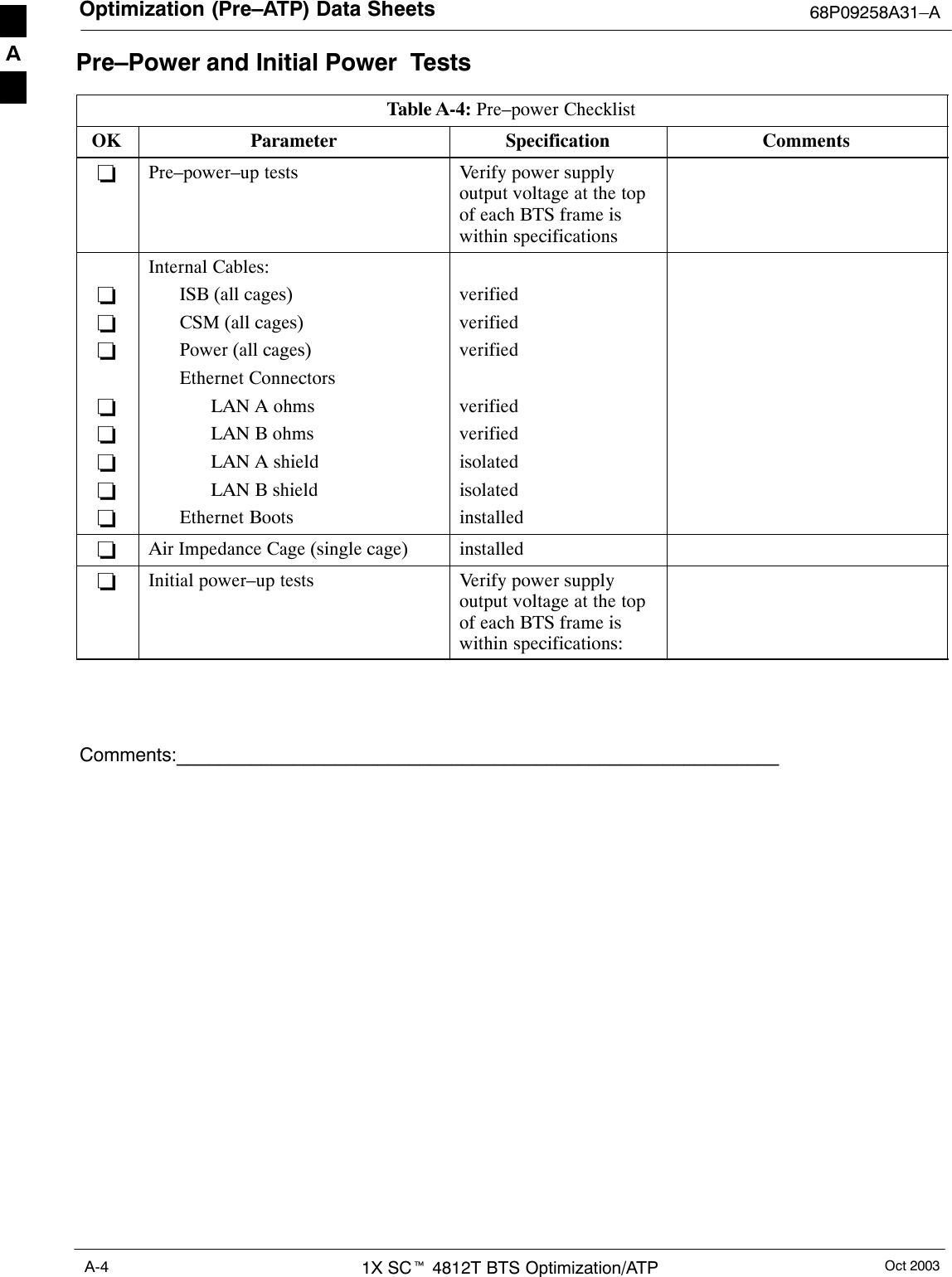
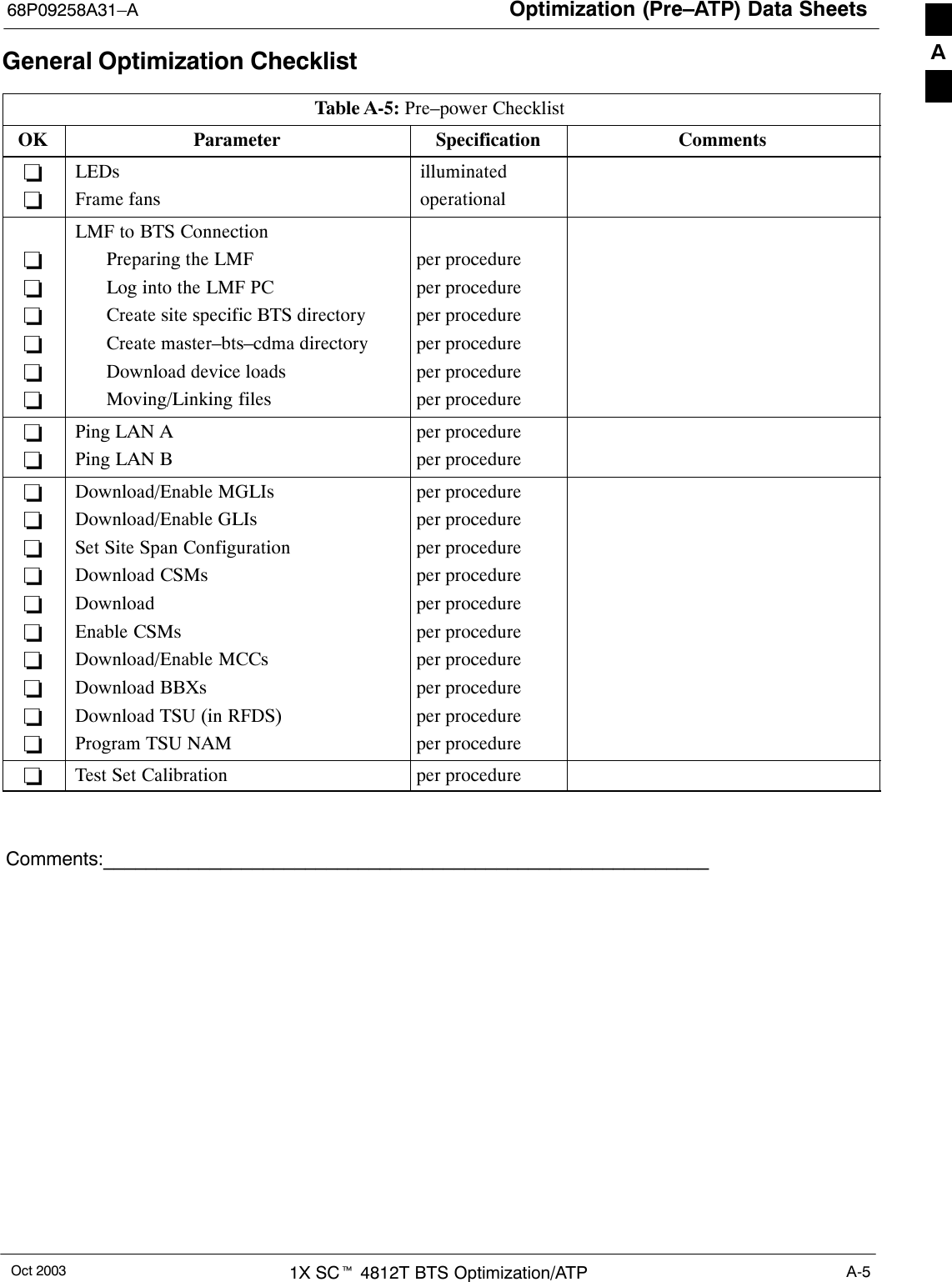
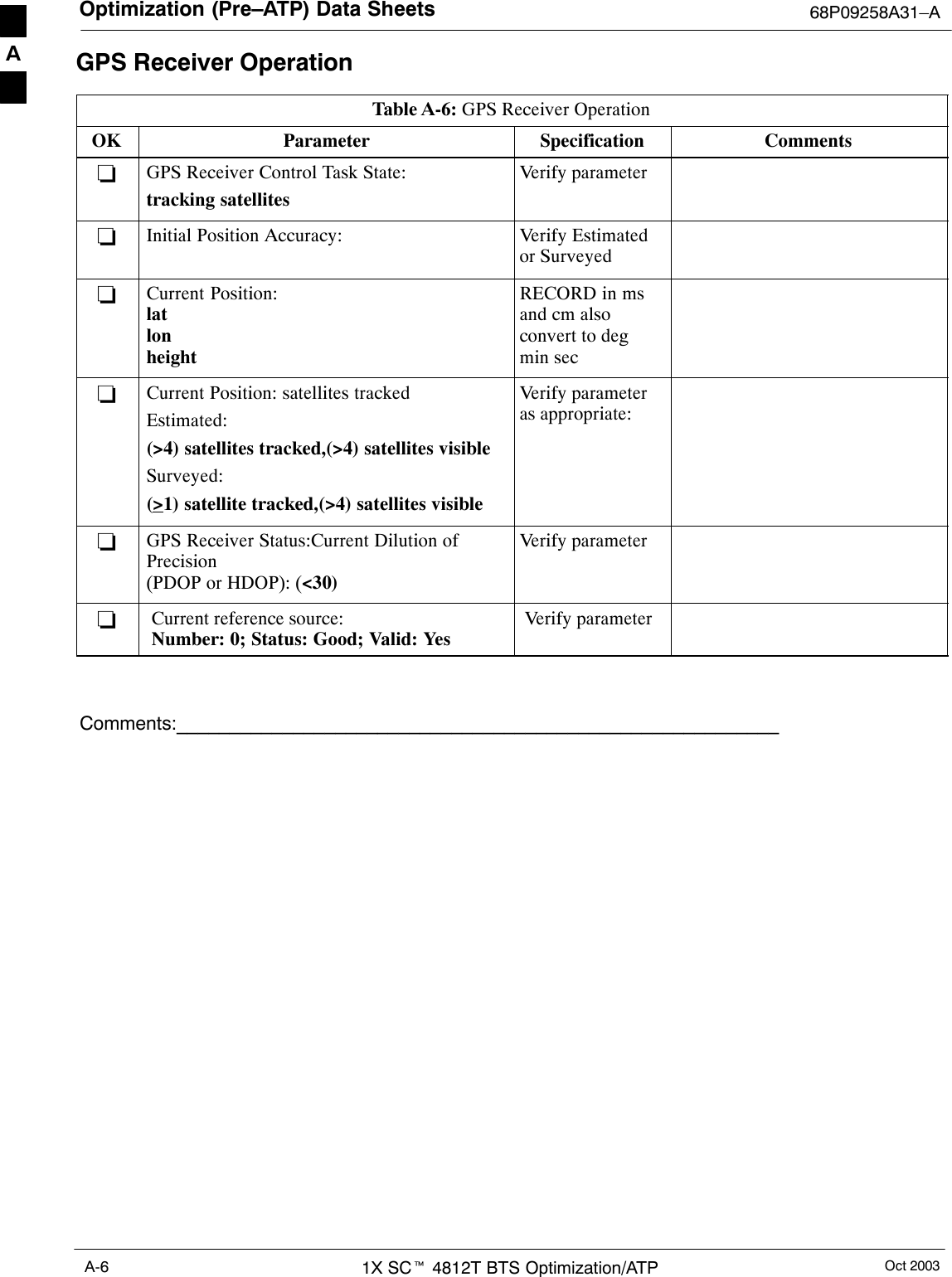
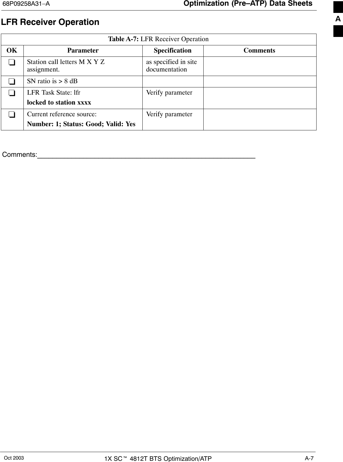
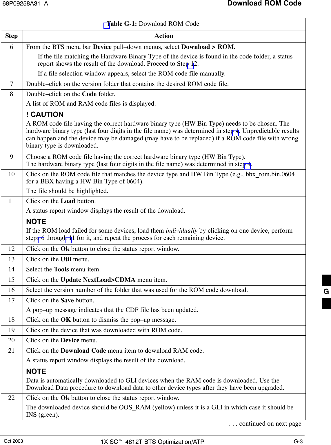
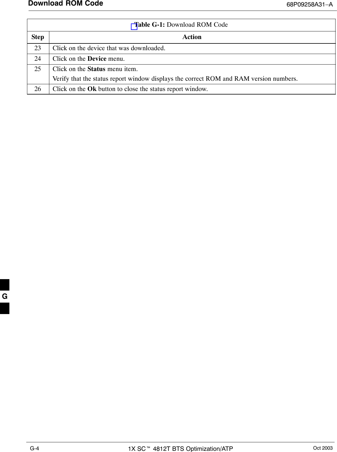
Nokia Solutions and Networks T5DS1 Cellular CDMA base station User Manual 1X SC4812T BTS Optimization ATP Release 2 16 3 x
Nokia Solutions and Networks Cellular CDMA base station 1X SC4812T BTS Optimization ATP Release 2 16 3 x
Contents
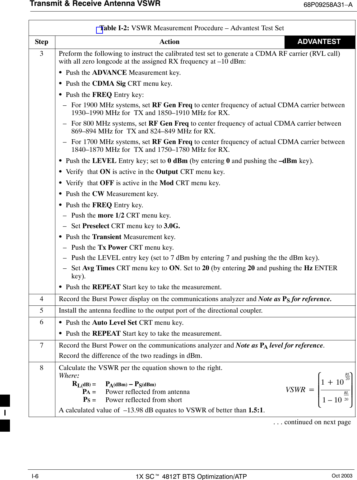
- 1. User Manual 1
- 2. User Manual 2
- 3. User Manual 3
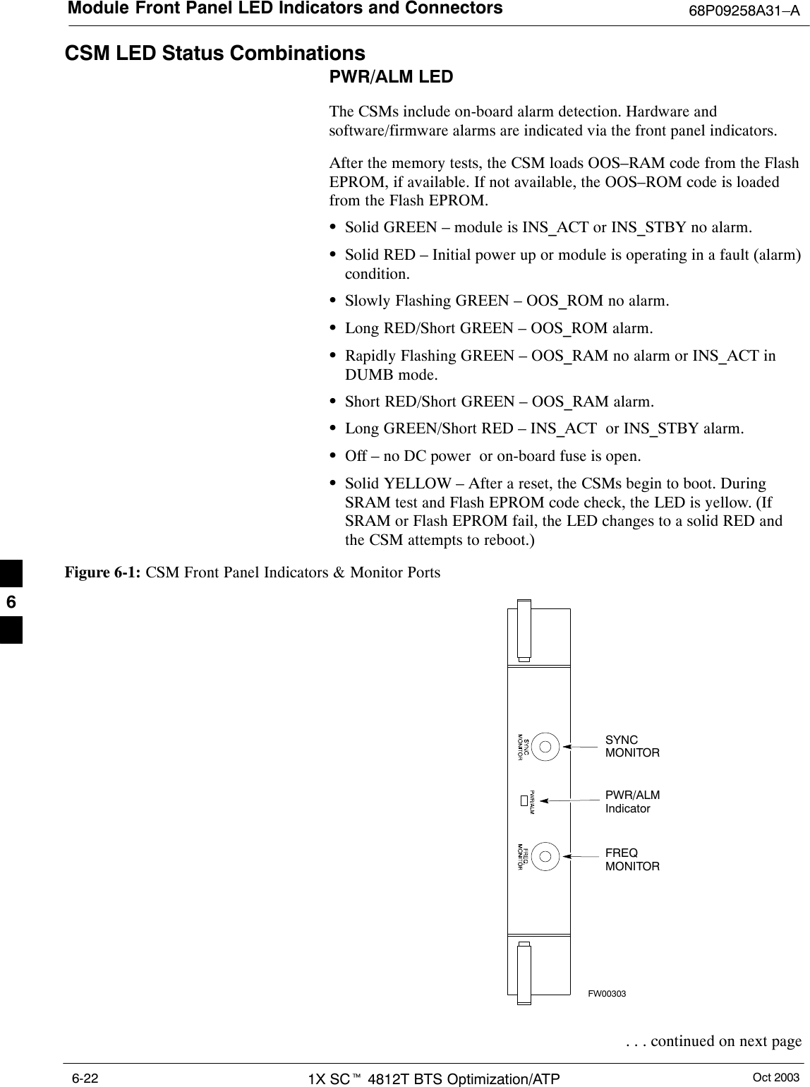
User Manual 3
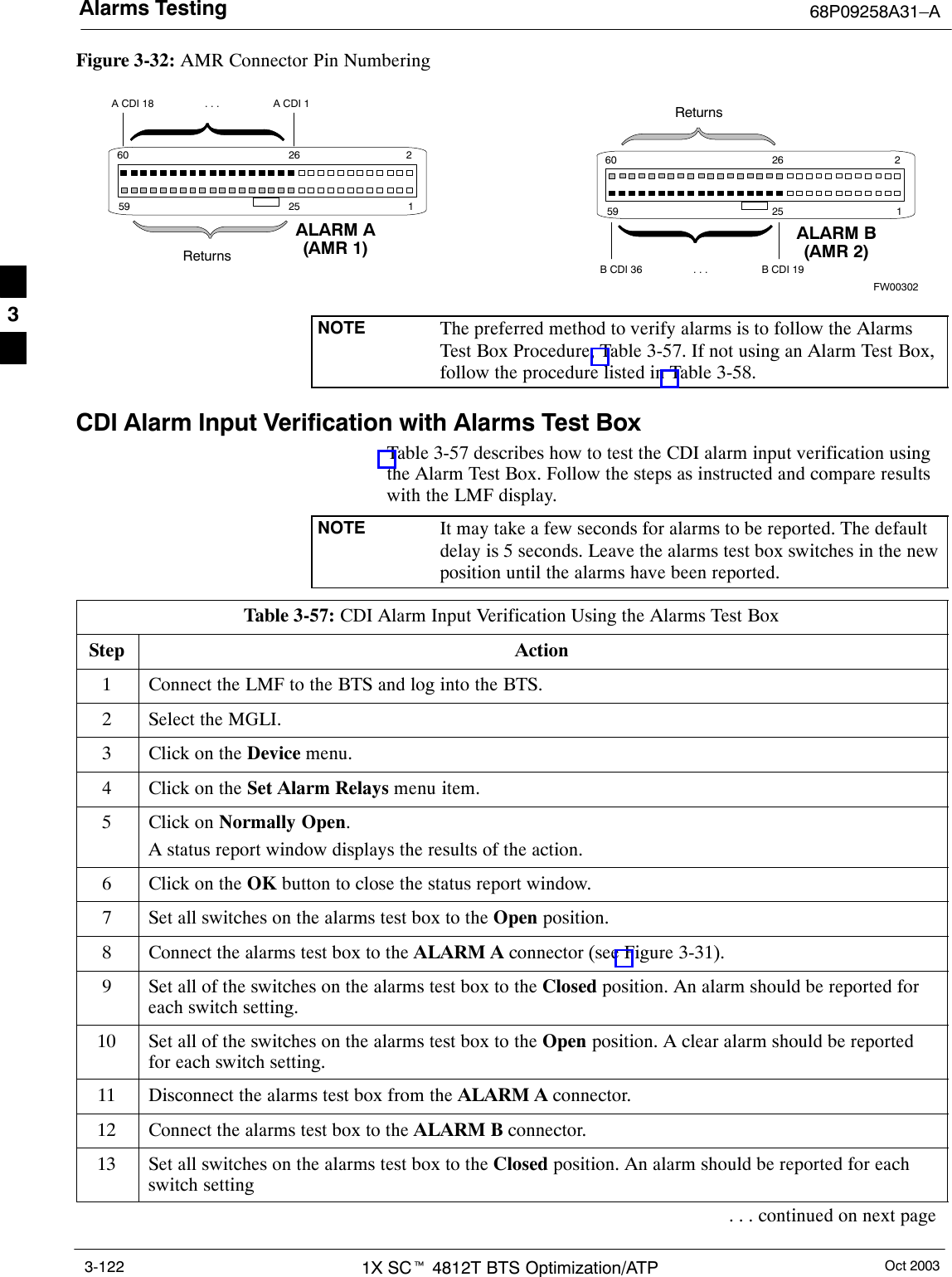
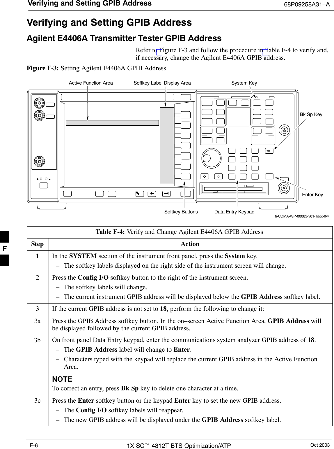
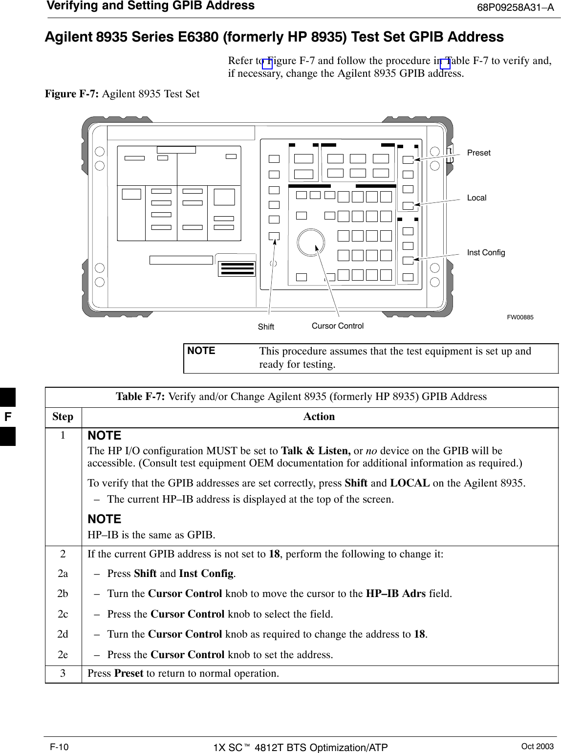
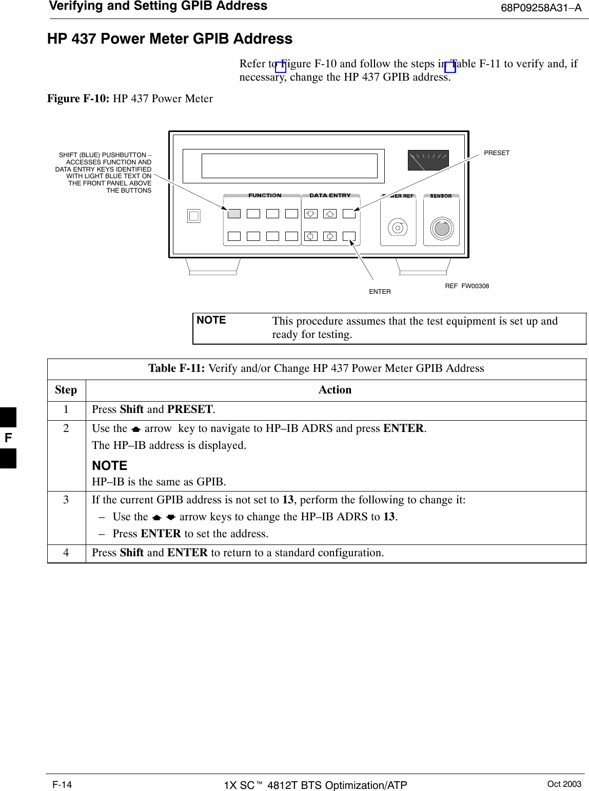
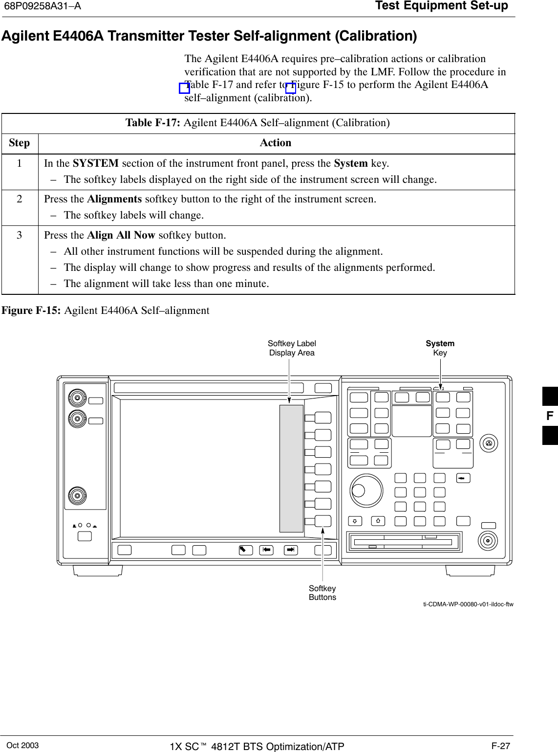
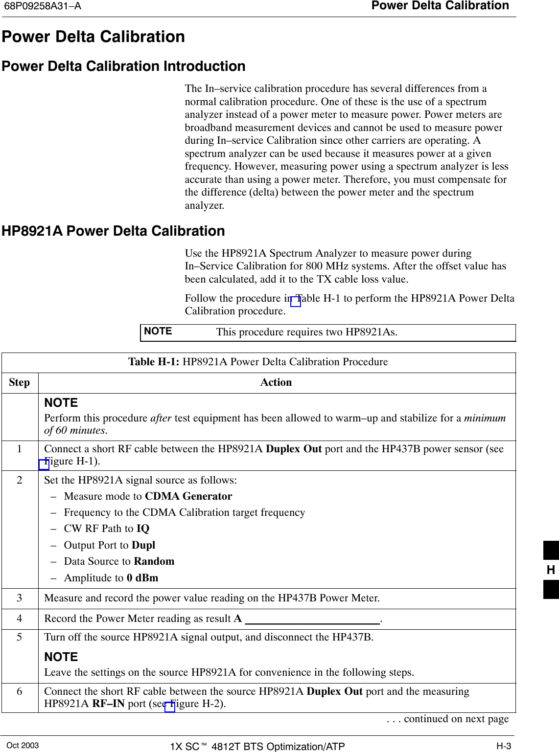
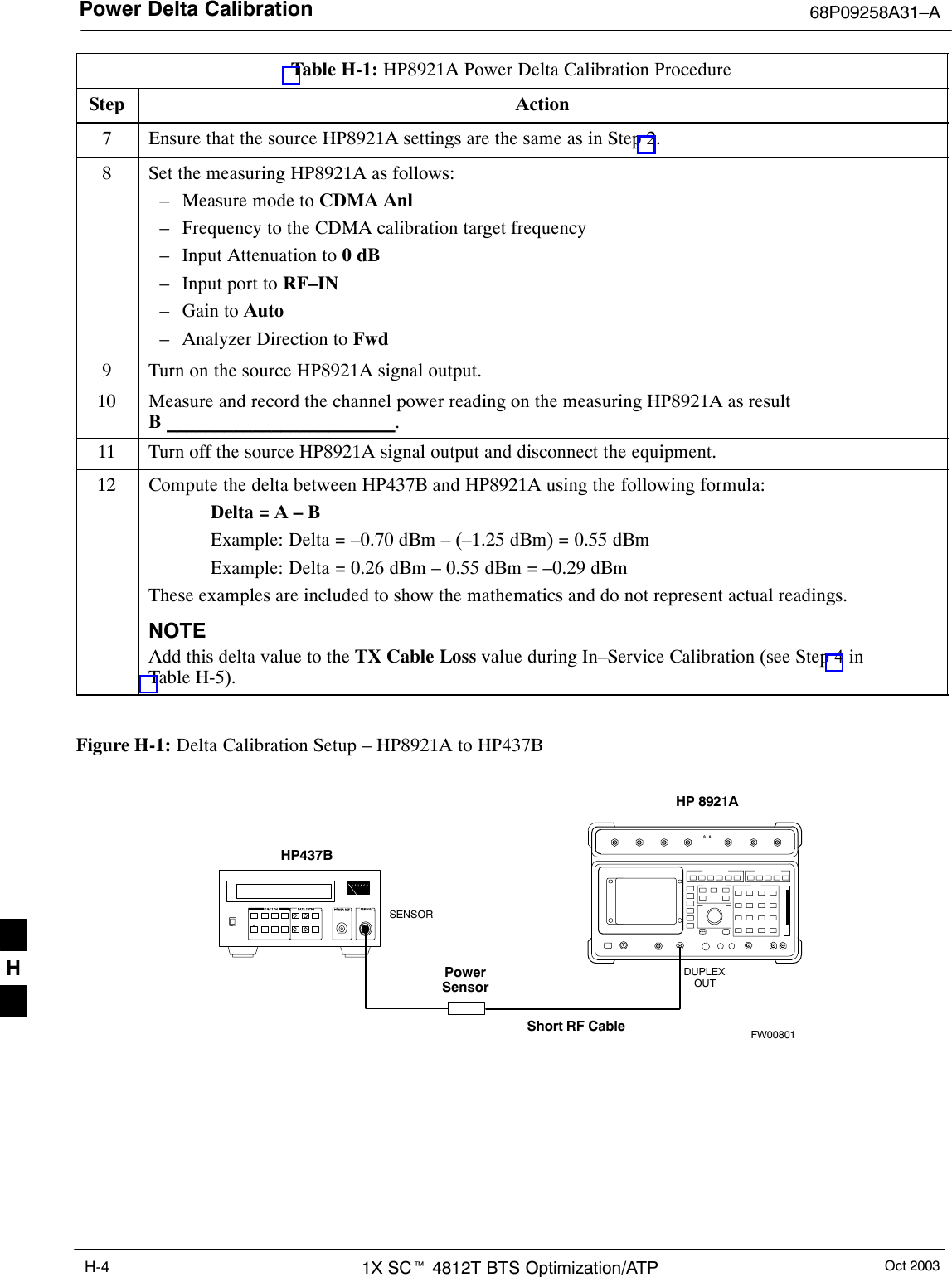
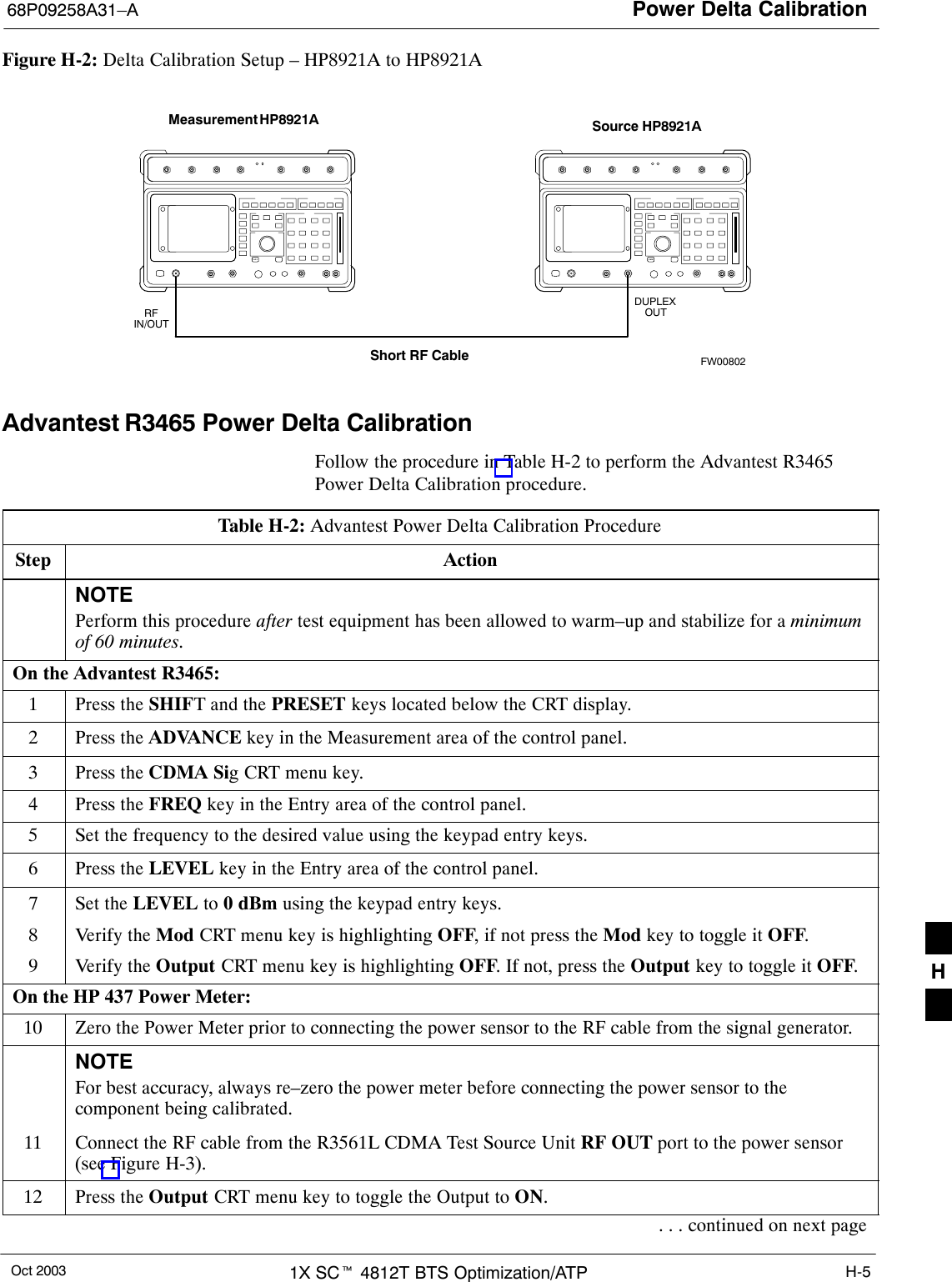
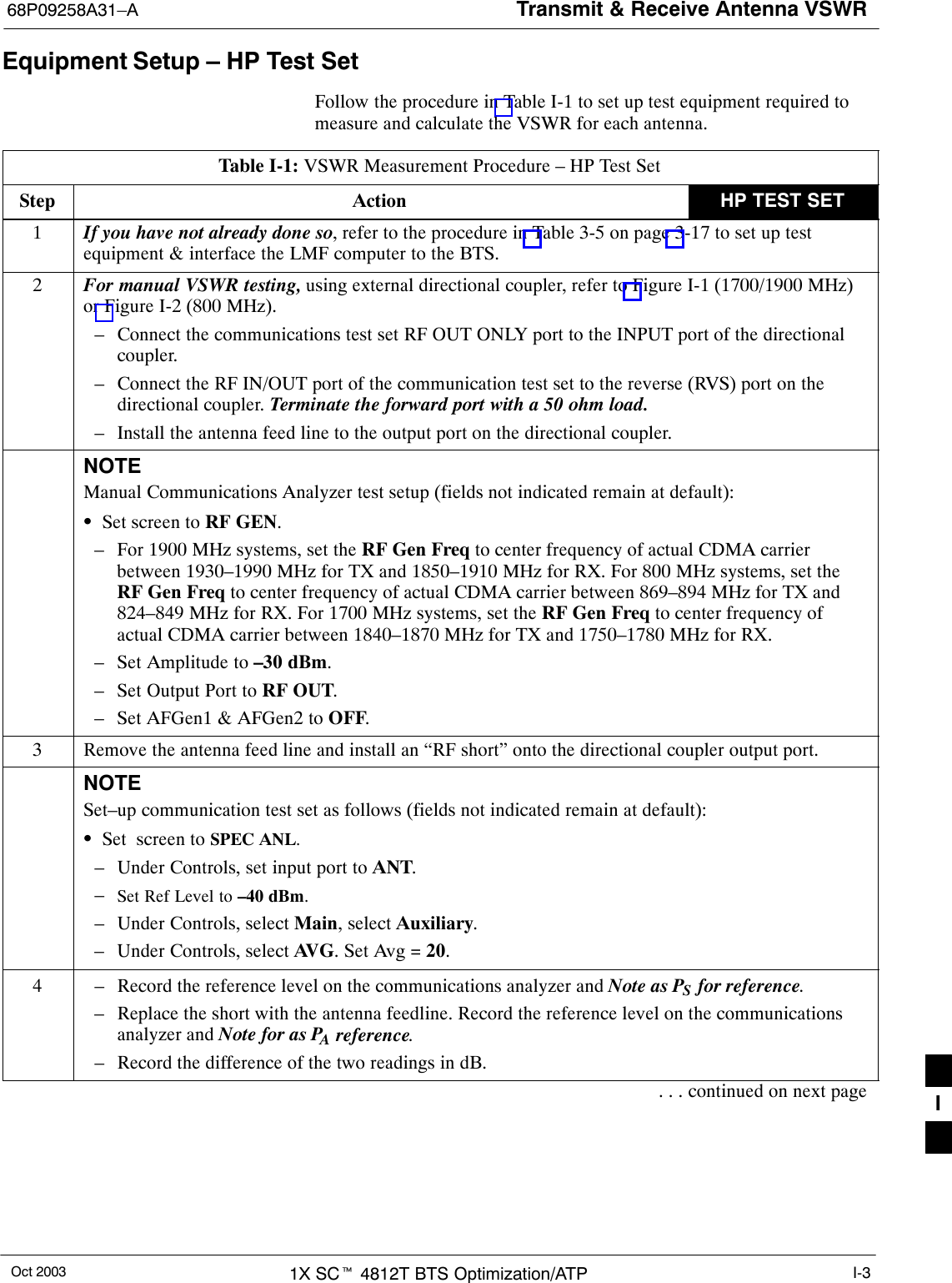
![RFDS Set–up and Calibration68P09258A31–AOct 2003 1X SCt 4812T BTS Optimization/ATP 3-105Set RFDS Configuration DataIf an RFDS is installed, the RFDS configuration data must be manuallyentered.PrerequisiteSLMF is logged into the BTSNOTE The entered antenna# index numbers must correspond to theantenna# index numbers used in the antenna maps.Follow the procedure in Table 3-46 to set the RFDS Configuration Data.Table 3-46: Set RFDS Configuration DataStep Action1Click on Util in the BTS menu bar, and select Edit > RFDS Configuration... from the pull–downmenus. A tabbed data entry pop–up window will appear.2In the data entry pop–up window, click on the TX RFDS Configuration or RX RFDS Configurationtab, as required.3To add a new antenna number, perform the following:3a – Click on the Add Row button.3b – Click in the Antenna #, Cal Antenna, Scap Antenna, or Populate [Y/N] columns, as required.3c – Enter the desired data.4To edit existing values, click in the data box to be changed and change the value.NOTERefer to the CDMA Help > Utility Menu > Edit–RFDS Configuration... section of LMF Helpfunction on–line documentation for RFDS configuration data examples.5To delete a row, click on the row and then click on the Delete Row button.6For each tab with changes, click on the Save button to save displayed values.7Click on the Dismiss button to close the window.NOTESValues entered or changed after the Save button was used will be lost when the window isdismissed.SEntered values will be used by the LMF as soon as they are saved. It is not necessary to log out andlog back into the LMF for changes to take effect.3](https://usermanual.wiki/Nokia-Solutions-and-Networks/T5DS1.User-Manual-3/User-Guide-383443-Page-17.png)
![RFDS Set–up and Calibration 68P09258A31–AOct 20031X SCt 4812T BTS Optimization/ATP3-106RFDS CalibrationThe RFDS Calibration option is used to calibrate the RFDS TX and RXpaths.TX Path Calibration – For a TX antenna path calibration the BTSXCVR is keyed at a pre–determined power level and the BTS poweroutput level is measured by the RFDS. The power level is then measuredat the TX antenna directional coupler by the power measuring testequipment item being used (power meter or analyzer). The difference(offset) between the power level at the RFDS and the power level at theTX antenna directional coupler is used as the TX RFDS calibrationoffset value.RX Path Calibration – For an RX antenna path calibration the RFDS iskeyed at a pre–determined power level and the power input level ismeasured by the BTS BBX. A CDMA signal at the same power levelmeasured by the BTS BBX is then injected at the RX antenna directionalcoupler by the communications system analyzer. The difference (offset)between the RFDS–keyed power level and power level measured at theBTS BBX is the RFDS RX calibration offset value.RFDS calibration and the CAL file – The TX and RX RFDScalibration offset values are written to the CAL file in the slot[385]Block.TSIC channel frequency – For each RFDS TSIC, the channelfrequency is determined at the lower third and upper third of theappropriate band using the frequencies listed in Table 3-47.Table 3-47: RFDS TSIC Calibration Channel FrequenciesSystem Channel Calibration Points800 MHz (A and B) 341 and 6821.9 GHz 408 and 791WARNING Before installing any test equipment directly to any TX OUTconnector, verify that there are no CDMA channels keyed.Failure to do so can result in serious personal injury and/orequipment damage.PrerequisitesSTest equipment has been selected.STest equipment and test cables have been calibrated.STX calibration has been performed and BLO data has beendownloaded to the BBXs.STest equipment and test cables are connected for TX calibration.SAntenna map data has been entered for the site.SBBXs are OOS–RAM.3](https://usermanual.wiki/Nokia-Solutions-and-Networks/T5DS1.User-Manual-3/User-Guide-383443-Page-18.png)


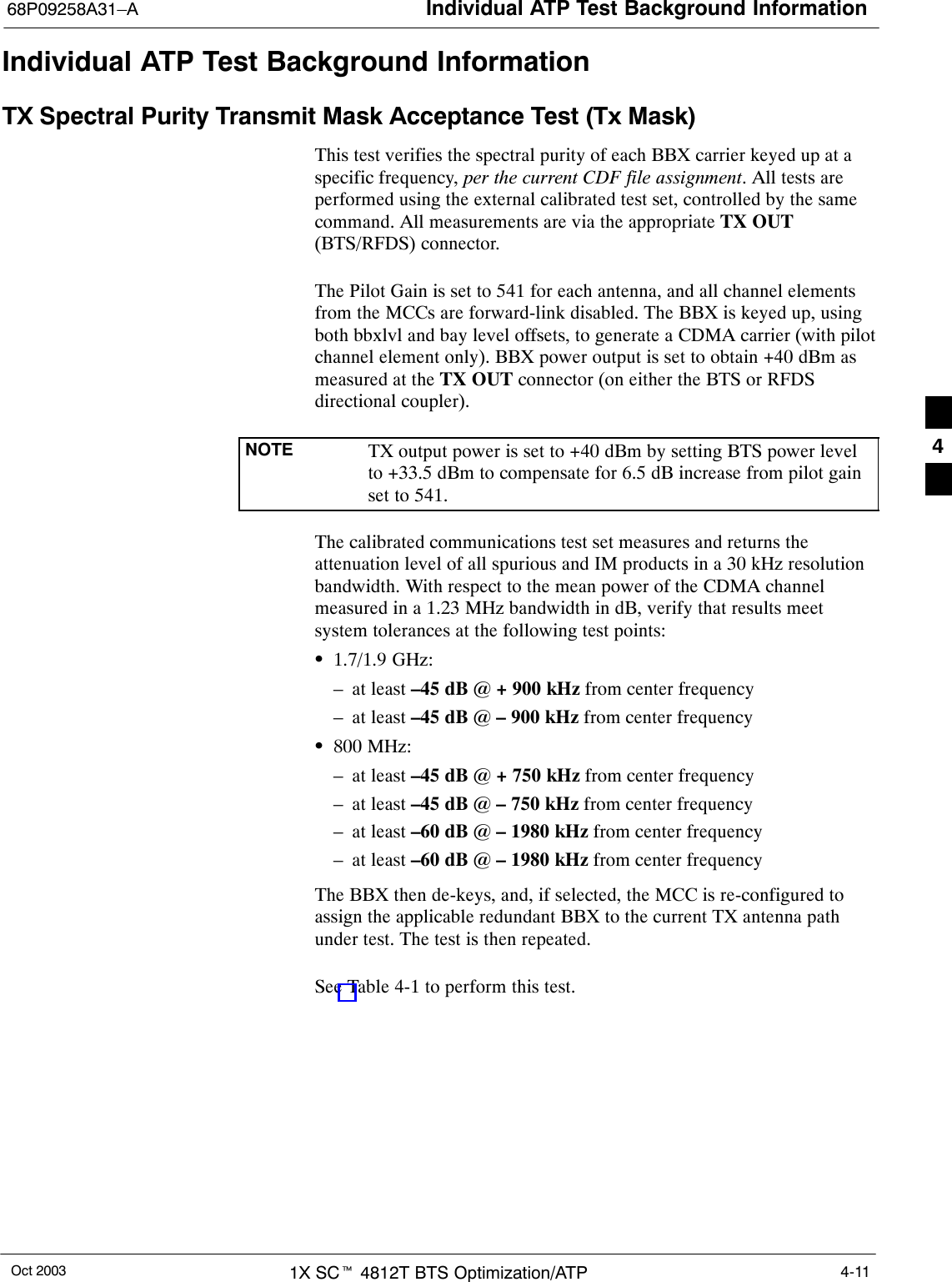
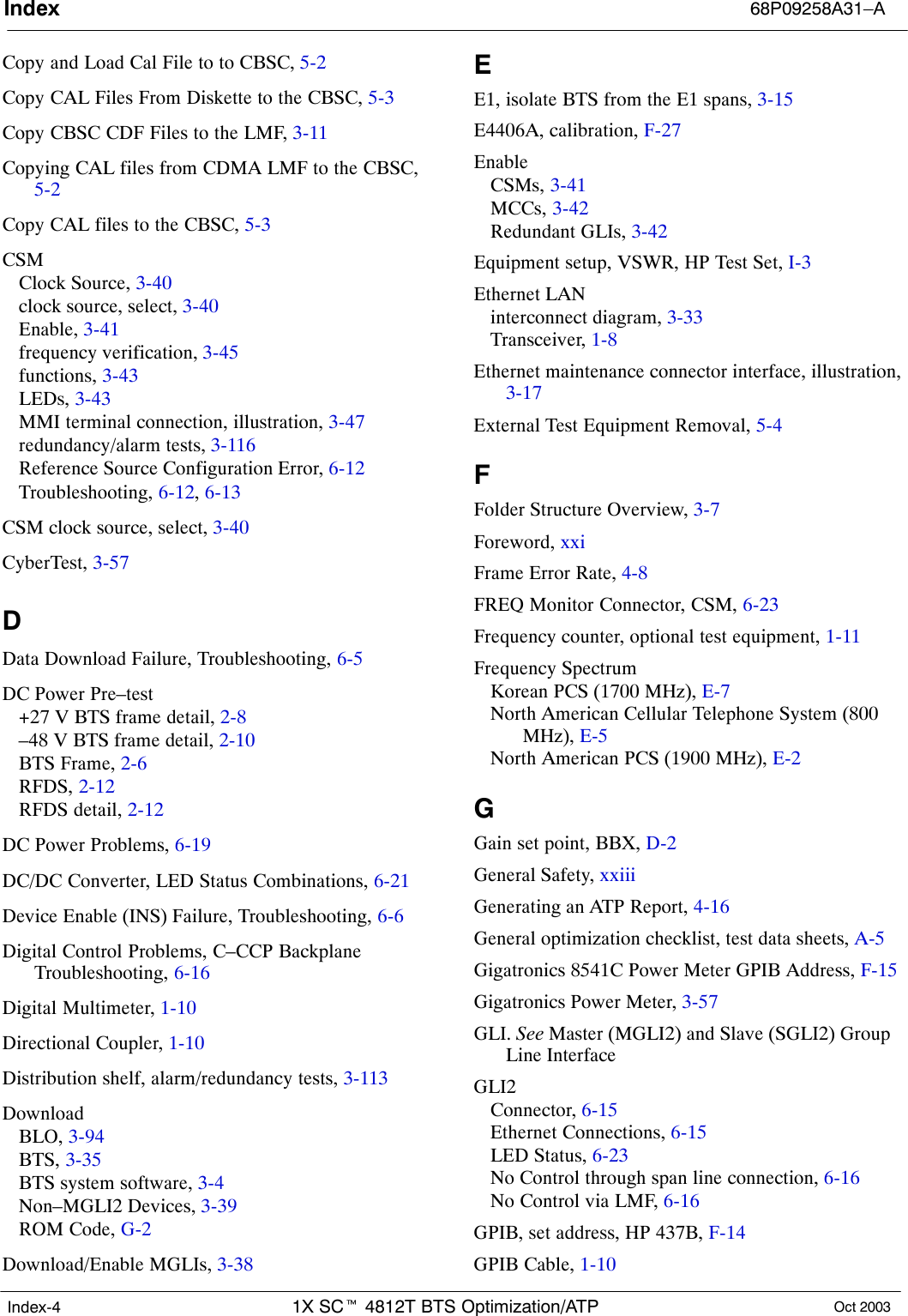
![Individual ATP Test Background Information 68P09258A31–AOct 20031X SCt 4812T BTS Optimization/ATP4-14The BBX then de-keys and, if selected, the MCC is re-configured toassign the applicable redundant BBX to the current TX antenna pathunder test. The test is then repeated. Upon completion of the test, theOCNS is disabled on the specified MCC/CE.See Table 4-1 to perform this test.Figure 4-2: Code Domain Power and Noise Floor LevelsPilot ChannelActive channelsPILOT LEVELMAX OCNS SPEC.MIN OCNS SPEC.MAXIMUM NOISE FLOOR: < –27 dB SPEC.Inactive channelsWalsh 0 1 2 3 4 5 6 7 ... 64MAX OCNSCHANNELMIN OCNSCHANNEL8.2 dB 12.2 dBMAX NOISEFLOORPilot ChannelActive channelsPILOT LEVELMAX OCNS SPEC.MIN OCNS SPEC.MAXIMUM NOISE FLOOR:< –27 dBInactive channelsWalsh 0 1 2 3 4 5 6 7 ... 64FAILURE – DOES NOTMEET MIN OCNS SPEC.FAILURE – EXCEEDSMAX OCNS SPEC. 8.2 dB 12.2 dBFAILURE – EXCEEDS MAXNOISE FLOOR SPEC. Showing all OCNS Passing Indicating Failures FW00283RX Frame Error Rate (FER) Acceptance TestThis test verifies the BTS FER on all traffic channel elements currentlyconfigured on all equipped MCCs (full rate at 1% FER) at an RF inputlevel of –119 dBm [or –116 dBm if using Tower TopAmplifier (TMPC)]. All tests are performed using the external calibratedtest set as the signal source controlled by the same command. Allmeasurements are via the LMF.The Pilot Gain is set to 262 for each TX antenna, and all channelelements from the MCCs are forward-link disabled. The BBX is keyed4](https://usermanual.wiki/Nokia-Solutions-and-Networks/T5DS1.User-Manual-3/User-Guide-383443-Page-52.png)


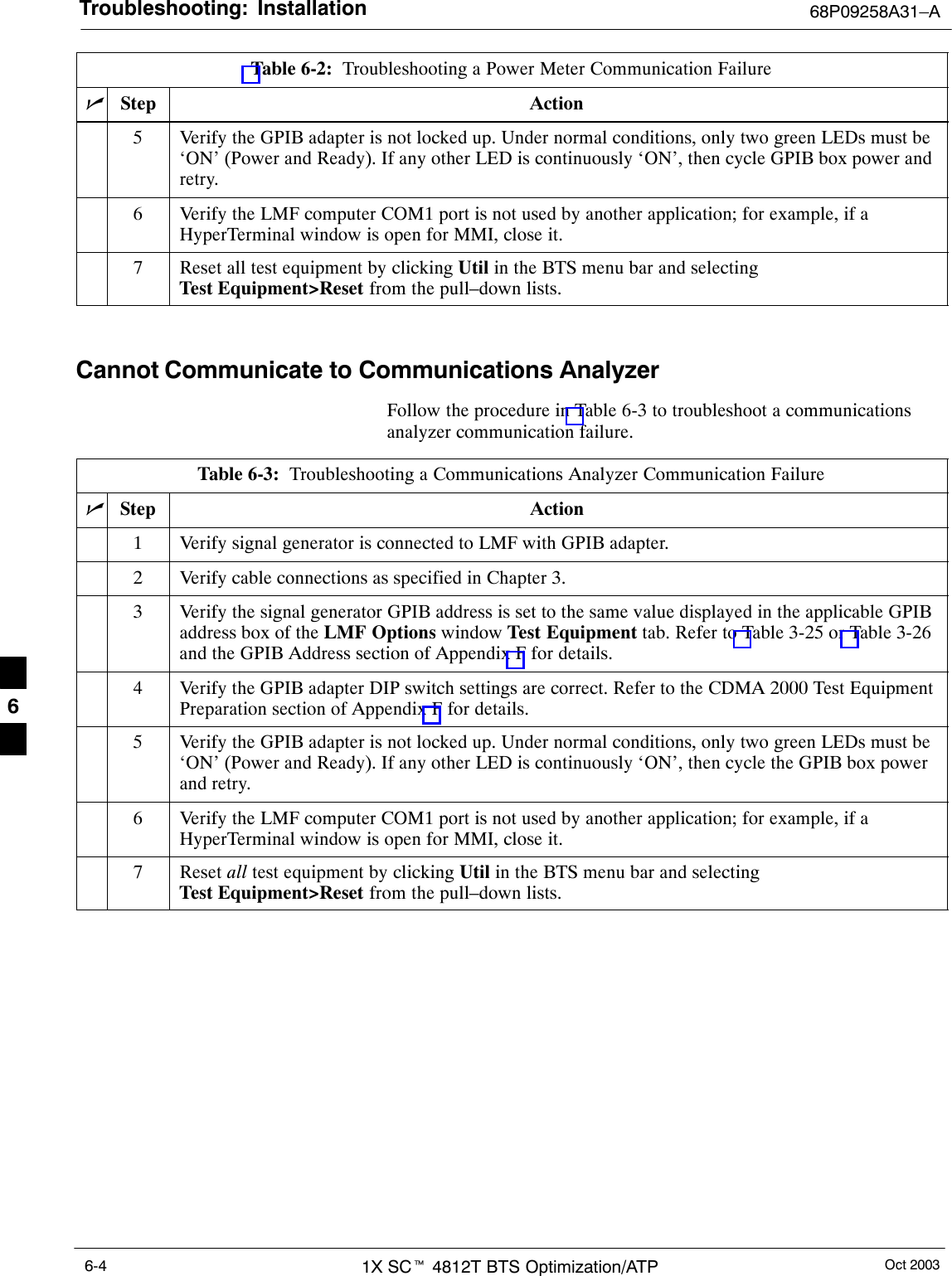
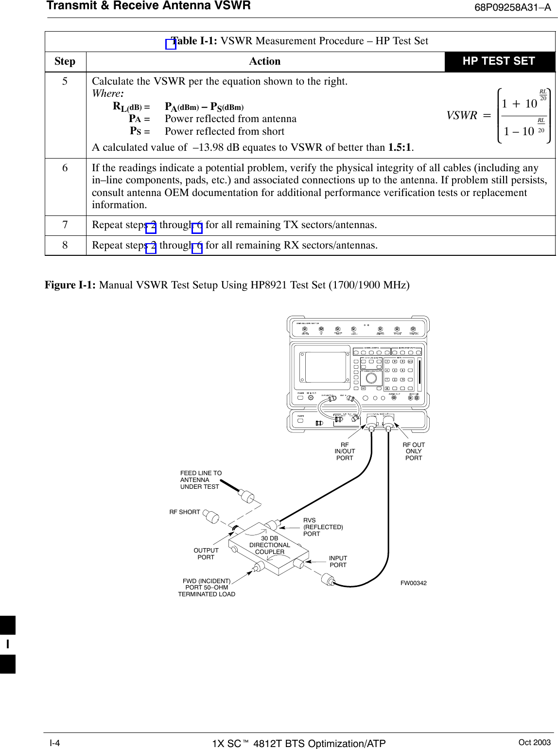
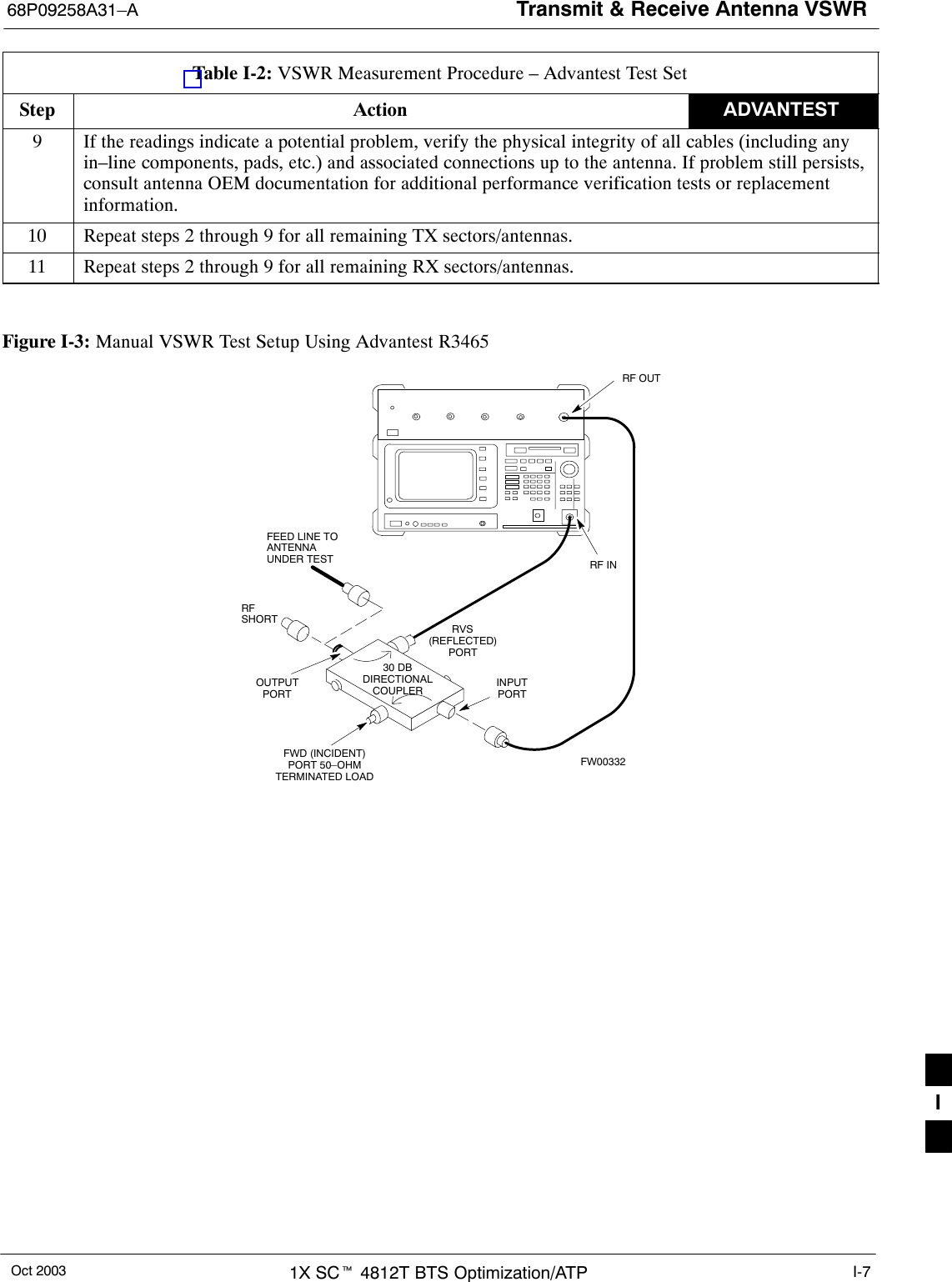
![Troubleshooting: Installation68P09258A31–AOct 2003 1X SCt 4812T BTS Optimization/ATP 6-3Troubleshooting: InstallationCannot Log into Cell-SiteFollow the procedure in Table 6-1 to troubleshoot a login failure.Table 6-1: Login Failure Troubleshooting ProceduresnStep Action1If the MGLI LED is solid RED, it implies a hardware failure. Reset the MGLI by re-seating it. Ifthis persists, install a known good MGLI card in the MGLI slot and retry. A Red LED may alsoindicate no Ethernet termination at top of frame.2Verify that T1 is disconnected (see Table 3-4 on page 3-16).If T1 is still connected, verify the CBSC has disabled the BTS.3Try pinging the MGLI (see Table 3-11 on page 3-34).4Verify the LMF is connected to the Primary LMF port (LAN A) in the front of the BTS (seeTable 3-5 on page 3-17).5Verify the LMF was configured properly (see Preparing the LMF section starting on page 3–6).6Verify the BTS-LMF cable is RG-58 [flexible black cable of less than 76 cm (2.5 feet) length].7Verify the Ethernet ports are terminated properly (see Figure 3-9 on page 3-33).8Verify a T-adapter is not used on the LMF side port if connected to the BTS front LMF primaryport.9Try connecting to the I/O panel (top of frame). Use BNC T-adapters at the LMF port for thisconnection.10 Re-boot the LMF and retry.11 Re-seat the MGLI and retry.12 Verify IP addresses are configured properly.Cannot Communicate to Power MeterFollow the procedure in Table 6-2 to troubleshoot a power metercommunication failure.Table 6-2: Troubleshooting a Power Meter Communication FailurenStep Action1Verify the Power Meter is connected to the LMF with a GPIB adapter.2Verify the cable setup as specified in Chapter 3.3Verify the GPIB address of the power meter is set to the same value displayed in the applicableGPIB address box of the LMF Options window Test Equipment tab. Refer to Table 3-25 orTable 3-26 and the GPIB Addresses section of Appendix F for details.4Verify the GPIB adapter DIP switch settings are correct. Refer to the CDMA 2000 Test EquipmentPreparation section of Appendix F for details.. . . continued on next page6](https://usermanual.wiki/Nokia-Solutions-and-Networks/T5DS1.User-Manual-3/User-Guide-383443-Page-69.png)


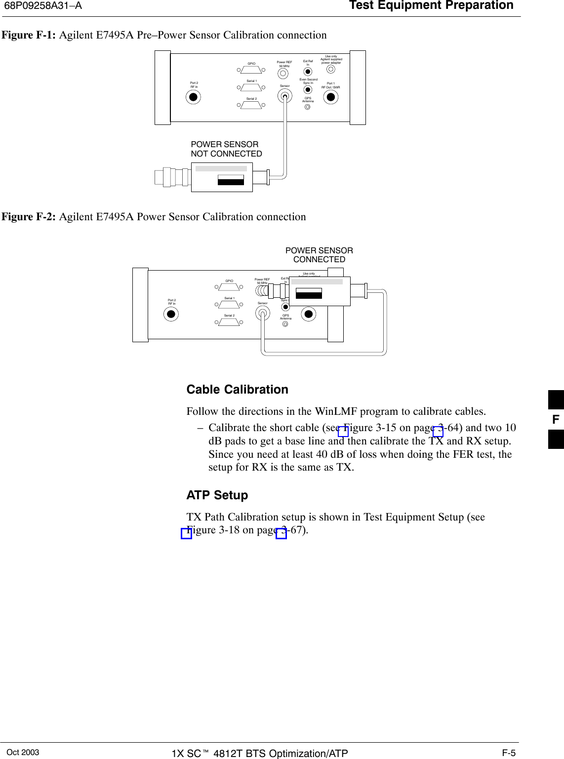
![Test Equipment Preparation68P09258A31–AOct 2003 1X SCt 4812T BTS Optimization/ATP F-3Agilent R7495A Test Equipment SetupThis test equipment requires a warm-up period of at least 30 minutesbefore BTS testing or calibration begins.Using the Agilent E7495A with the LMFThe Agilent E7495A does not require the use of the 19MHz frequencyreference; if connected, it will be ignored. The Even Sec SYNCconnection is required.The Agilent E7495A signal generator is only calibrated down to –80db.In order to achieve accurate FER testing, be sure the RX setup includesat least 40db of attenuation. This will ensure the signal generator willoutput sufficient power to operate in the calibrated range.Set the IP Address as described in Table F-1.Table F-1: Set IP Address on Agilent E7495A test setnStep Action1Use the System Button > Controls >IPAdmin to set anIP address on the E7495A as 128.0.0.49, and Netmask to255.255.255.128. ConnectionsIt is recommended that you use a hub with BNC and RJ–45 connections.[Suggested models: Netgear model EN104 (4 port) or EN108 (8 port).Do NOT use model numbers ending with “TP”; those have no BNCconnectors.]The LMF will connect to the hub which in turn is connected to the BTSand to the Agilent E7495A.Agilent E7495A to Hub – This is an Ethernet cable, RJ–45 to RJ–45.LMF to Hub – Use one of the following cables to connect the LMF tothe Hub:– Ethernet cable, RJ–45 to RJ–45 (be sure that the LAN card is set foreither AUTO or to use the RJ–45 only).– Coax cable between LAN card and Hub. (Use a “T” on the hub andconnect a cable between the other end of the “T” and the BTS LANconnection).Hub to BTS – Use BNC “T” connector on the hub. [If your hub doesn’thave BNC ports, use a BNC to UTP adapter.]F](https://usermanual.wiki/Nokia-Solutions-and-Networks/T5DS1.User-Manual-3/User-Guide-383443-Page-157.png)
![Test Equipment Set-up 68P09258A31–AOct 20031X SCt 4812T BTS Optimization/ATPF-18HP8921A System Connectivity TestFollow the steps in Table F-13 to verify that the connections between thePCS Interface and the HP8921A are correct, and cables are intact. Thesoftware also performs basic functionality checks of each instrument.NOTE Disconnect other GPIB devices, especially system controllers,from the system before running the connectivity software.Table F-13: System ConnectivityStep ActionNOTE– Perform this procedure after test equipment has been allowed to warm–up and stabilize for aminimum of 60 minutes.1Insert HP 83236A Manual Control/System card into memory card slot.2Press the [PRESET] pushbutton.3Press the Screen Control [TESTS] pushbutton to display the “Tests” Main Menu screen.4Position the cursor at Select Procedure Location and select by pressing the cursor control knob.In the Choices selection box, select Card.5Position the cursor at Select Procedure Filename and select by pressing the cursor control knob.In the Choices selection box, select SYS_CONN.6Position the cursor at RUN TEST and select it.The software will prompt you through the connectivity setup.7When the test is complete, position the cursor on STOP TEST and select it; OR press the [K5]pushbutton.8To return to the main menu, press the [K5] pushbutton.F](https://usermanual.wiki/Nokia-Solutions-and-Networks/T5DS1.User-Manual-3/User-Guide-383443-Page-172.png)
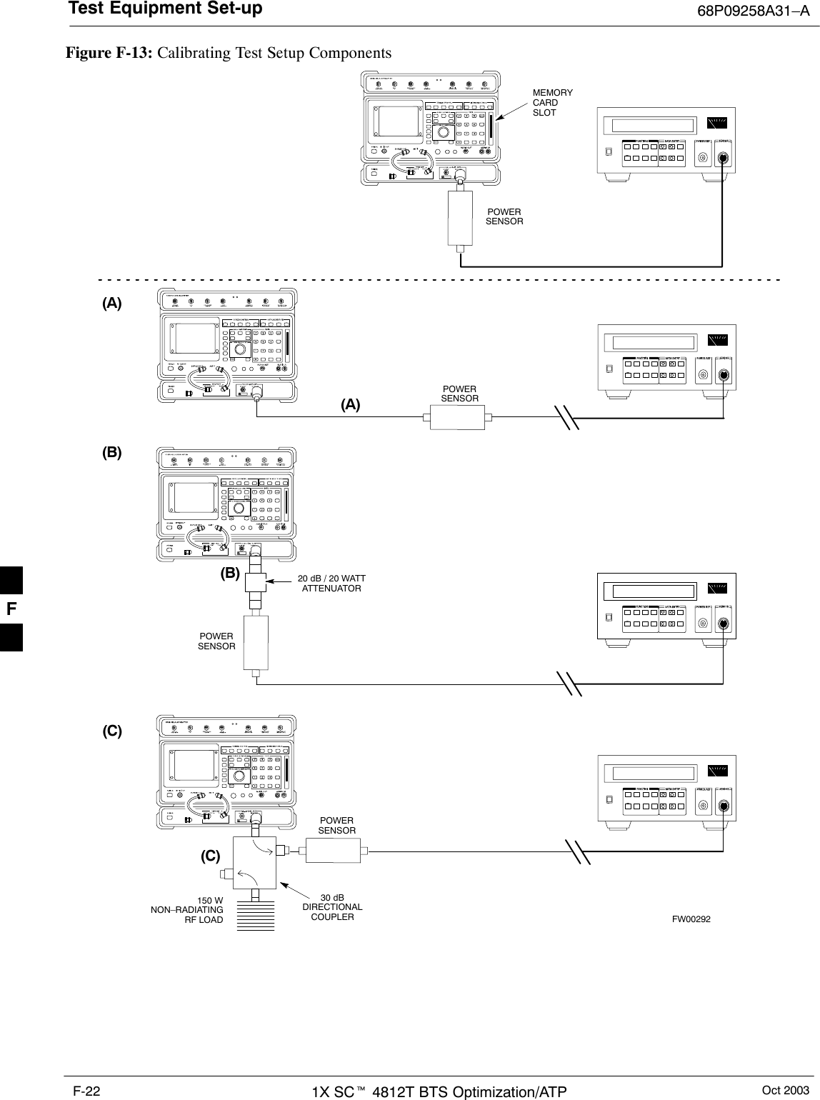
![Test Equipment Set-up68P09258A31–AOct 2003 1X SCt 4812T BTS Optimization/ATP F-19Manual Cable Calibration using HP8921 with HP PCS Interface (HP83236)NOTEThis calibration method must be executed with great care. Somelosses are measured close to the minimum limit of the powermeter sensor (–30 dBm).PrerequisitesEnsure the following prerequisites have been met before proceeding:STest equipment to be calibrated has been connected correctly for cablecalibration.STest equipment has been selected and calibrated.Refer to Figure F-13 for location of the components on the PCSInterface and Communications Test Set.Test Equipment Set-upPerform the procedure in Table F-14 to calibrate the test equipmentusing the HP8921 Cellular Communications Analyzer equipped with theHP83236 PCS Interface.Table F-14: Manual Cable Calibration Test Equipment Setup (using the HP PCS Interface)Step ActionNOTEVerify that GPIB controller is turned off.1Insert HP 83236A Manual Control System card into memory card slot (see Figure F-13).2Press the Preset pushbutton.3 Under Screen Controls, press the TESTS pushbutton to display the TESTS (Main Menu) screen.4Position the cursor at Select Procedure Location and select it. In the Choices selection box, selectCARD.5Position the cursor at Select Procedure Filename and select it. In the Choices selection box, selectMANUAL.6Position the cursor at RUN TEST and select it. HP must be in Control Mode Select YES.7If using HP 83236A:Set channel number=<chan#>:– Position cursor at ChannelNumber and select it.– Enter the chan# using the numerickeypad; press [Enter] and thescreen will go blank.– When the screen reappears, thechan# will be displayed on thechannel number line.If using HP 83236B:Set channel frequency:– Position cursor at Frequency Band and press Enter.– Select User Defined Frequency.– Go Back to Previous Menu.– Position the cursor to 83236 generator frequency andenter actual RX frequency.– Position the cursor to 83236 analyzer frequency andenter actual TX frequency.8Set RF Generator level:– Position the cursor at RF Generator Level and select it.– Enter –10 using the numeric keypad; press [Enter] and the screen will go blank.– When the screen reappears, the value –10 dBm will be displayed on the RF Generator Level line.. . . continued on next pageF](https://usermanual.wiki/Nokia-Solutions-and-Networks/T5DS1.User-Manual-3/User-Guide-383443-Page-173.png)
![Test Equipment Set-up 68P09258A31–AOct 20031X SCt 4812T BTS Optimization/ATPF-20Table F-14: Manual Cable Calibration Test Equipment Setup (using the HP PCS Interface)Step Action9Set the user fixed Attenuation Setting to 0 dBm:– Position cursor at Analyzer Attenuation and select it– Position cursor at User Fixed Atten Settings and select it.– Enter 0 (zero) using the numeric keypad and press [Enter].10 Select Back to Previous Menu.11 Record the HP83236 Generator Frequency Level:Record the HP83236B Generator Frequency Level:– Position cursor at Show Frequency and Level Details and select it.– Under HP83236 Frequencies and Levels, record the Generator Level.– Under HP83236B Frequencies and Levels, record the Generator Frequency Level(1850 – 1910 MHz for 1.9 GHz or 1750 – 1780 for 1.7 GHz).– Position cursor at Prev Menu and select it.12 Click on Pause for Manual Measurement.13 Connect the power sensor directly to the RF OUT ONLY port of the PCS Interface.14 On the HP8921A, under To Screen, select CDMA GEN.15 Move the cursor to the Amplitude field and click on the Amplitude value.16 Increase the Amplitude value until the power meter reads 0 dBm ±0.2 dB.NOTEThe Amplitude value can be increased coarsely until 0 dBM is reached; then fine tune the amplitudeby adjusting the Increment Set to 0.1 dBm and targeting in on 0 dBm.17 Disconnect the power sensor from the RF OUT ONLY port of the PCS Interface.NOTEThe Power Meter sensor’s lower limit is –30 dBm. Thus, only components having losses ≤30 dBshould be measured using this method. For further accuracy, always re-zero the power meterbefore connecting the power sensor to the component being calibrated. After connecting thepower sensor to the component, record the calibrated loss immediately.18 Disconnect all components in the test setup and calibrate each one separately by connecting eachcomponent, one-at-a-time, between the RF OUT ONLY PORT and the power sensor (see Figure F-13,Setups A, B, or C). Record the calibrated loss value displayed on the power meter.SExample: (A) Test Cable(s) = –1.4 dB(B) 20 dB Attenuator = –20.1 dB(B) Directional Coupler = –29.8 dB19 After all components are calibrated, reassemble all components together and calculate the total testsetup loss by adding up all the individual losses:SExample: Total test setup loss = –1.4 –29.8 –20.1 = –51.3 dB.This calculated value will be used in the next series of tests.20 Under Screen Controls press the TESTS button to display the TESTS (Main Menu) screen.21 Select Continue (K2).22 Select RF Generator Level and set to –119 dBm.. . . continued on next pageF](https://usermanual.wiki/Nokia-Solutions-and-Networks/T5DS1.User-Manual-3/User-Guide-383443-Page-174.png)
![Test Equipment Set-up68P09258A31–AOct 2003 1X SCt 4812T BTS Optimization/ATP F-21Table F-14: Manual Cable Calibration Test Equipment Setup (using the HP PCS Interface)Step Action23 Click on Pause for Manual Measurement.24 Verify the HP8921A Communication Analyzer/83203A CDMA interface setup is as follows (fieldsnot indicated remain at default):SVerify the GPIB (HP–IB) address:– under To Screen, select More– select IO CONFIG– Set HP–IB Adrs to 18– set Mode to Talk&LstnSVerify the HP8921A is displaying frequency (instead of RF channel)– Press the blue [SHIFT] button, then press the Screen Control [DUPLEX] button; this switches tothe CONFIG (CONFIGURE) screen.– Use the cursor control to set RF Display to Freq25 Refer to Table 3-31 for assistance in manually setting the cable loss values into the LMF. F](https://usermanual.wiki/Nokia-Solutions-and-Networks/T5DS1.User-Manual-3/User-Guide-383443-Page-175.png)
![Test Equipment Set-up68P09258A31–AOct 2003 1X SCt 4812T BTS Optimization/ATP F-23HP PCS Interface Test Equipment Setup for Manual TestingFollow the procedure in Table F-15 to setup the HP PCS Interface Boxfor manual testing.Table F-15: HP PCS Interface Test Equipment Setup for Manual TestingnStep ActionNOTEVerify GPIB controller is turned off.1Insert HP83236B Manual Control/System card into the memory card slot.2 Under Screen Controls, press the [TESTS] push-button to display the TESTS (Main Menu)screen.3Position the cursor at Select Procedure Location and select. In the Choices selection box, selectCARD.4Position the cursor at Select Procedure Filename and select. In the Choices selection box, selectMANUAL.5Position the cursor at RUN TEST and select OR press the K1 push-button.6Set channel number=<chan#>:– Position cursor at Channel Number and select.– Enter the chan# using the numeric keypad and then press [Enter] (the screen will blank).– When the screen reappears, the chan# will be displayed on the channel number line.NOTEIf using a TMPC with Tower Top Amplifier (TTA) skip Step 7.7SSet RF Generator level= –119 dBm + Cal factorExample: –119 dBm + 2 dB = –117 dBmSContinue with Step 9 (skip Step 8).8Set RF Generator level= –116 dBm + Cal factor.Example: –116 dBm + 2 dB = –114 dBm9Set the user fixed Attenuation Setting to 0 dB:– Position cursor at RF Generator Level and select.– Position cursor at User Fixed Atten Settings and select.– Enter 0 (zero) using the numeric keypad and press [Enter].10 Select Back to Previous Menu.11 Select Quit, then select Yes.F](https://usermanual.wiki/Nokia-Solutions-and-Networks/T5DS1.User-Manual-3/User-Guide-383443-Page-177.png)
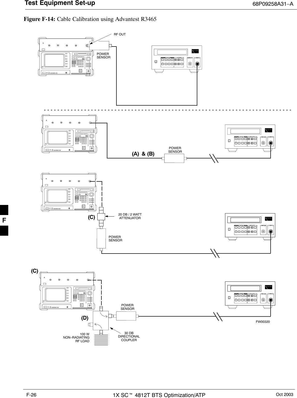
![In–Service Calibration 68P09258A31–AOct 20031X SCt 4812T BTS Optimization/ATPH-18Table H-5: In–Service CalibrationStep Action! CAUTIONPerform the In–service Calibration procedure on OOS devices only.8Select the desired test:– Select the target BBX(s) on the C–CCP cage picture.– Click Tests>[desired test] from the menu bar at the main window.– Select the target carrier and confirm the channel number in the pop up window.– Leave the Verify BLO check box checked.– From the Test Pattern pick list, select a test pattern.– Click the OK button to start calibration.– Follow the on–screen instructions, except, do not connect to the BTS antenna port, connect to thedirectional coupler (fwd) port associated with the on screen prompt antenna port.NOTESSelecting Pilot (default) performs tests using a pilot signal only.SSelecting Standard performs tests using pilot, synch, paging and six traffic channels. This requiresan MCC to be selected.SSelecting CDFPilot performs tests using a pilot signal, however, the gain for the channel elementsis specified in the CDF file.SSelecting CDF performs tests using pilot, synch, paging and six traffic channels, however, the gainfor the channel elements is specified in the CDF file.9Save the result and download the BLO data to the target BBX(s):– Click the Save Result button on the result screen.The window closes automatically.10 Logout from the BTS and close the LMF session:– Click BTS>Logout to close the BTS connection.– Close the LMF window.11 Restore the new “bts–*.cal” file to the CBSC.12 Enable the target device(s) from the CBSC. H](https://usermanual.wiki/Nokia-Solutions-and-Networks/T5DS1.User-Manual-3/User-Guide-383443-Page-204.png)

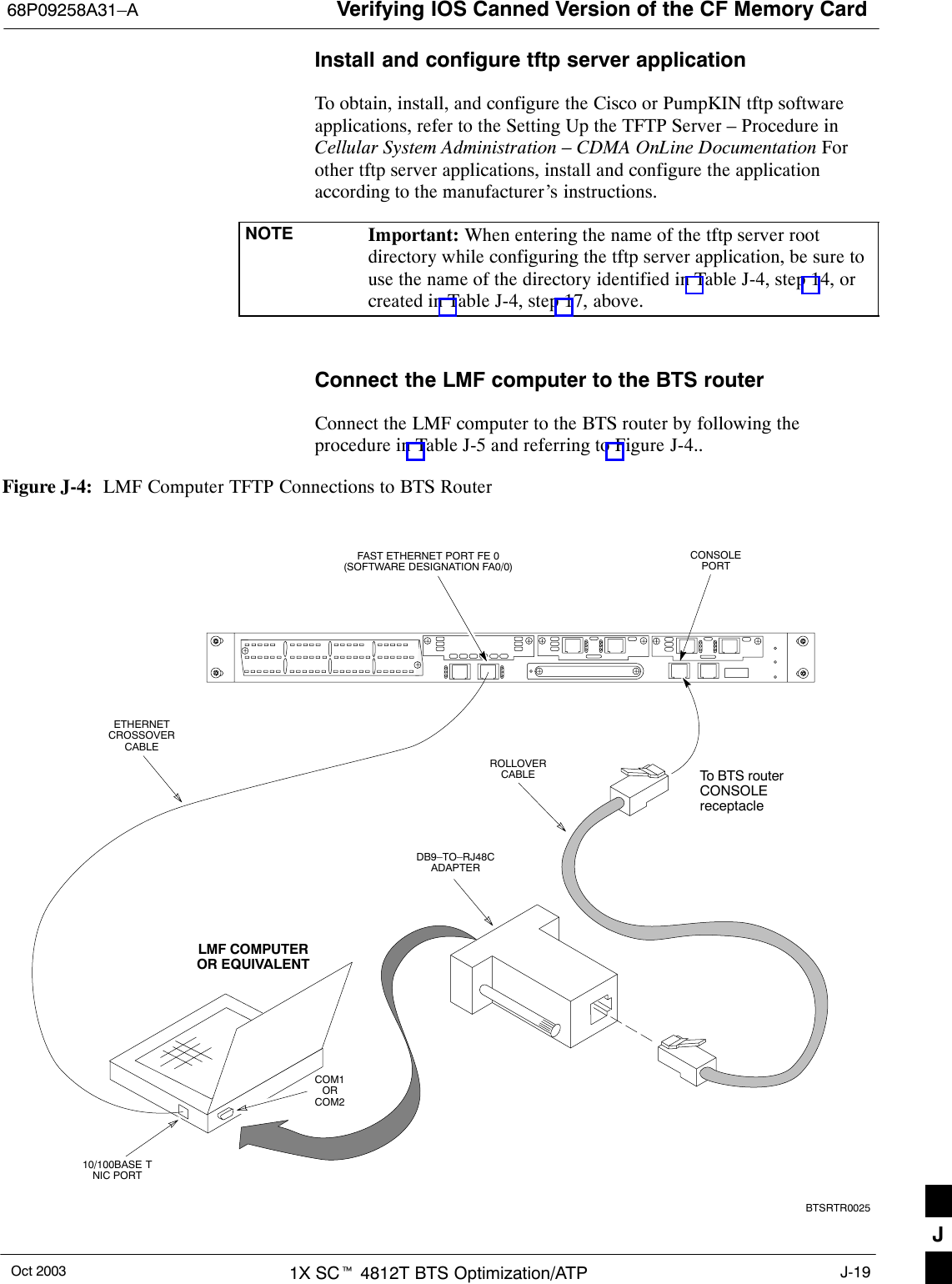
![Verifying IOS Canned Version of the CF Memory Card68P09258A31–AOct 2003 1X SCt 4812T BTS Optimization/ATP J-21Table J-6: BTS Router Power–up and Initial Ethernet ConfigurationStep Action4If a message similar to the following, is displayed type no and press the Enter key:Basic management setup configures only enough connectivityfor management of the system, extended setup will ask youto configure each interface on the systemWould you like to enter basic management setup? [yes/no]:A response similar to the following will be displayed:Would you like to enter basic management setup? [yes/no]: noCisco Internetwork Operating System SoftwareIOS (tm) 1941 Software (MWR1941–I–M), Version 12.2(20020127:101239Copyright (c) 1986–2002 by cisco Systems, Inc.Compiled Sun 27–Jan–02 06:08 by walrobinRouter>5At the Router> user EXEC mode prompt, enter the following to access the privileged EXEC mode:enableA response similar to the following will be displayed:Router>enableRouter#6At the Router# privileged EXEC mode prompt, enter the following to access the configure submode:configure terminalA response similar to the following will be displayed:Router#conf tEnter configuration commands, one per line. End with CNTL/Z.Router(config)#The router is now in the global configuration mode and ready to accept configuration changes enteredfrom the keyboard.. . . continued on next pageJ](https://usermanual.wiki/Nokia-Solutions-and-Networks/T5DS1.User-Manual-3/User-Guide-383443-Page-233.png)
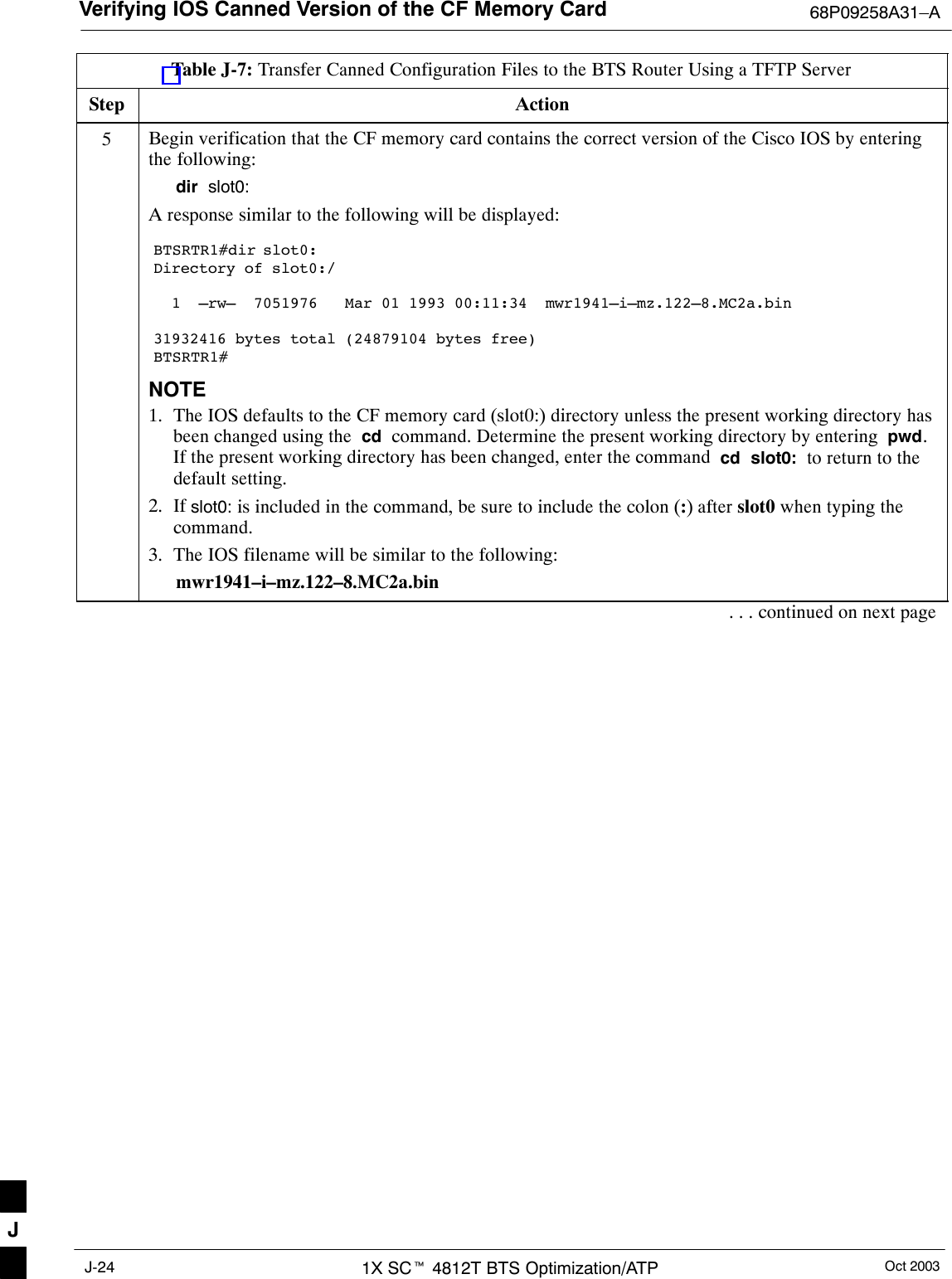
![Verifying IOS Canned Version of the CF Memory Card68P09258A31–AOct 2003 1X SCt 4812T BTS Optimization/ATP J-25Table J-7: Transfer Canned Configuration Files to the BTS Router Using a TFTP ServerStep Action6Direct the router to show the version information by entering the following:show versionA response similar to the following will be displayed:BTSRTR1#sh verCisco Internetwork Operating System Software IOS (tm) 1941 Software (MWR1941–I–M), Version 12.2(8)MC2a, EARLY DEPLOYMENT RELEASESOFTWARE (fc1)TAC Support: http://www.cisco.com/tacCopyright (c) 1986–2002 by cisco Systems, Inc.Compiled Mon 05–Aug–02 11:07 by nmasaImage text–base: 0x60008940, data–base: 0x60B54000ROM: System Bootstrap, Version 12.2(20020113:235343) [sbose–wilma 109], DEVELOPMENTSOFTWAREROM: 1941 Software (MWR1941–I–M), Version 12.2(8)MC2a, EARLY DEPLOYMENT RELEASE SOFT-WARE (fc1)Router uptime is 1 minuteSystem returned to ROM by power–onSystem image file is ”slot0:mwr1941–i–mz.122–8.MC2a.bin”cisco mwr1941 (R7000) processor (revision 0.1) with 121856K/18432K bytes of memory.Processor board ID JMX0611K5TSR7000 CPU at 240Mhz, Implementation 39, Rev 3.3, 256KB L2 CacheBridging software.X.25 software, Version 3.0.0.Primary Rate ISDN software, Version 1.1.Toaster processor tmc is running.2 FastEthernet/IEEE 802.3 interface(s)2 Serial network interface(s)2 Channelized T1/PRI port(s)DRAM configuration is 64 bits wide with parity disabled.55K bytes of non–volatile configuration memory.31360K bytes of ATA Slot0 CompactFlash (Read/Write)Configuration register is 0x101BTSRTR1#7Compare the IOS filename returned in step 5 and the second line of the version information in step 6.Note the correspondence between the filename and IOS version information.8If the IOS filename from the CF memory card returned in step 5 is different than the filename of therequired IOS version loaded in the LMF computer default tftp directory, perform the procedure inTable J-13 to load the required version, and then return to step 9, below.. . . continued on next pageJ](https://usermanual.wiki/Nokia-Solutions-and-Networks/T5DS1.User-Manual-3/User-Guide-383443-Page-237.png)
![Verifying IOS Canned Version of the CF Memory Card 68P09258A31–AOct 20031X SCt 4812T BTS Optimization/ATPJ-26Table J-7: Transfer Canned Configuration Files to the BTS Router Using a TFTP ServerStep ActionCAUTIONThe file sequence on the CF memory card can not be verified with application programs which placethe listed file names in alphabetical order (for example, certain Unix telnet applications, Unixdirectory listing commands, and Windows file managers such as Windows Explorer). This portion ofthe procedure is intended for use only with applications, such as HyperTerminal, which do not listdirectory contents alphabetically.9If the IOS version is correct and there is more than one file loaded on the CF memory card, be sure theIOS file is the first file listed in the directory content display. If it is not, perform the following:9a – Backup all files on the CF memory card to the LMF computer default tftp directory by performingsteps 3 through 10 of Table J-13.9b – Perform steps 25 through 29 of Table J-13, as applicable.9c – Type the following to delete a possible boot system line in the startup–config file, pressing theEnter key after the command and at each prompt to confirm the filename and deletion operation:del nvram:startup–configA response similar to the following will be displayed:BTSRTR1#del nvram:startup–configDelete filename [startup–config]? Delete nvram:startup–config? [confirm][OK]BTSRTR1#NOTEBe sure to include the colon (:) after nvram when typing the command.9d – Verify the startup–config file size has been reduced to a minimum by entering the following:dir nvram:A response similar to the following will be displayed:Router#dir nvram:Directory of nvram:/ 53 –rw– 5 <no date> startup–config 54 –––– 5 <no date> private–config57336 bytes total (57274 bytes free)BTSRTR1#10 At the privileged EXEC mode prompt, enter the following:copy tftp:btsrtr_canned.color slot0:canned–configWhere color = blue or red, as applicable.A response similar to the following will be displayed:BTSRTR1#copy tftp:btsrtr_canned.blue slot0:canned–configAddress or name of remote host []?. . . continued on next pageJ](https://usermanual.wiki/Nokia-Solutions-and-Networks/T5DS1.User-Manual-3/User-Guide-383443-Page-238.png)
![Verifying IOS Canned Version of the CF Memory Card68P09258A31–AOct 2003 1X SCt 4812T BTS Optimization/ATP J-27Table J-7: Transfer Canned Configuration Files to the BTS Router Using a TFTP ServerStep Action11 At the prompt for the remote host address or name, enter the IP address of the LMF computer NIC:100.100.100.1A response similar to the following will be displayed:BTSRTR1#copy tftp:btsrtr_canned.blue slot0:canned–configAddress or name of remote host []? 100.100.100.1Destination filename [canned–config]?12 At the prompt for the destination filename, press the Enter key. A response similar to the followingwill be displayed:BTSRTR1#copy tftp:btsrtr_canned.blue slot0:canned–configAddress or name of remote host []? 100.100.100.1Destination filename [canned–config]?Loading btsrtr_canned.blue from 100.100.100.1 (via Ethernet0/0): ![OK – 2457/4096 bytes]2457 bytes copied in 84.724 secs (29 bytes/sec)BTSRTR1#13 Verify that the canned configuration file is saved on the CF memory card by entering dir command. Aresponse similar to the following will be displayed:Directory of slot0:/ 1 –rw– 7051976 Mar 01 1993 00:11:34 mwr1941–i–mz.122–8.MC2a.bin 2 –rw– 2457 Mar 01 1993 00:14:48 canned–config31932416 bytes total (24877983 bytes free)BTSRTR1#14 To allow the BTS router to boot using the canned configuration, enter the following:copy canned–config startup–configA response similar to the following will be displayed:BTSRTR1#copy canned–config startDestination filename [startup–config]?15 When prompted for the destination file name, press the Enter key. A response similar to the followingwill be displayed:BTSRTR1#copy canned–config startDestination filename [startup–config]?2457 bytes copied in 3.52 secsBTSRTR1#16 Display and note the file size of startup–config by entering the following:dir nvram:A response similar to the following will be displayed:Directory of nvram:/ 26 –rw– 2457 <no date> startup–config 27 –––– 5 <no date> private–config29688 bytes total (24774 bytes free)BTSRTR1#. . . continued on next page J](https://usermanual.wiki/Nokia-Solutions-and-Networks/T5DS1.User-Manual-3/User-Guide-383443-Page-239.png)
![Verifying IOS Canned Version of the CF Memory Card 68P09258A31–AOct 20031X SCt 4812T BTS Optimization/ATPJ-28Table J-7: Transfer Canned Configuration Files to the BTS Router Using a TFTP ServerStep Action17 Scroll the HyperTerminal window back to the slot0: directory display obtained in step 13, above.18 Compare the file size of startup–config to the canned configuration file to verify the copy operation.File sizes should be the same.19 If desired, the contents of the startup–config file may be verified against the file listings at the end ofthis appendix for the blue or red canned configuration, as applicable, by entering the following:show startup–configNOTEPressing the space bar at the MORE prompt will scroll another screen–full of data. Pressing the Enterkey will scroll the screen one line at a time.20 Verify the router will boot properly on the IOS and revised startup–config files by entering thefollowing:reloadA response similar to the following will be displayed:BTSRTR1#reloadSystem configuration has been modified. Save? [yes/no]: nProceed with reload? [confirm]21 If prompted to save a modified configuration, enter n for “no,” and press the Enter key.22 When prompted to proceed with reload, press the Enter key to continue the reload operation.23 Verify the router reboots without displaying the rommon 1 > prompt or error messages related to portconfigurations. If the router boots to the rommon prompt, proceed to the Recovery from BTS RouterBoot to rommon section of this appendix.24 Using the tagging materials, tag the router to clearly identify the installed configuration (blue(BTSRTR1) or red (BTSRTR2)).25 Remove the CF memory from the router following the procedure in the 1X SC 4812T BTS FRU Guide, mark the installed configuration (blue or red) on the card label, and install the card in the routerfollowing the procedure in the FRU Guide.26 If an additional router must have the canned configuration installed, perform the following:26a – Disconnect the cabling from the BTS router.26b – Remove power from the router and disconnect it from the power supply.26c – Repeat the procedures in Table J-5, Table J-6, and this table (Table J-7) using the additional router.27 If no additional routers must be configured, perform steps 26a and 26b.28 On the LMF computer, shut down the tftp server application and exit the HyperTerminal session.29 If no additional tftp transfer activities will be performed, change the NIC IP address and subnet maskback to those for LMF–BTS communication recorded in Table J-4, step 9b.CAUTIONIf the BTS 10base–2 LAN IP address and subnet mask for the LMF computer’s NIC are not restored,the LMF can not log into a BTS when attempting to perform a BTS optimization or ATP. J](https://usermanual.wiki/Nokia-Solutions-and-Networks/T5DS1.User-Manual-3/User-Guide-383443-Page-240.png)
![Verifying IOS Canned Version of the CF Memory Card68P09258A31–AOct 2003 1X SCt 4812T BTS Optimization/ATP J-31Table J-8: Transfer Canned Configuration File to CF Memory Card with CF Memory Card ReaderStep Action2Connect the LMF computer to the BTS router and start a HyperTerminal communication session withthe router by following the procedure in Table J-2.3If it has not been done, be sure the +27 Vdc power supply output is OFF, and connect the BTS routerto the +27 Vdc power supply.4* IMPORTANTIn this step do not touch the computer keyboard until the router completes the boot process. The routerwill buffer any keystrokes made during the boot process and interpret them as commands to beexecuted immediately following boot completion.Apply power to the router and allow it to complete boot–up.5If a message similar to the following, is displayed, press the Enter key and proceed to step 7:Press RETURN to get started!6If a message similar to the following, is displayed type no and press the Enter key:Basic management setup configures only enough connectivityfor management of the system, extended setup will ask youto configure each interface on the systemWould you like to enter basic management setup? [yes/no]:A response similar to the following will be displayed:Would you like to enter basic management setup? [yes/no]: noCisco Internetwork Operating System SoftwareIOS (tm) 1941 Software (MWR1941–I–M), Version 12.2(20020127:101239Copyright (c) 1986–2002 by cisco Systems, Inc.Compiled Sun 27–Jan–02 06:08 by walrobinRouter>7CAUTIONUse only a card reader specifically designed for CF memory cards to perform this procedure. Cardreaders for other non–volatile, solid–state memory devices such as Smart Media cards will not workwith the CF memory cards used in the MWR 1941 routers.If it has not been done, follow the CF memory card reader manufacturer’s instructions to load the CFmemory card driver application for the operating system being used onto the LMF computer.8Connect the CF memory card reader to the LMF computer following the card reader manufacturer’sinstructions.9Remove the CF memory card from the BTS router by following the procedure in the 1X SC 4812T BTS FRU Guide 10 Insert the CF memory card into the card reader as specified by the card reader manufacturer’sinstructions.11 On the LMF computer, click Start > Programs > Windows Explorer to open Windows Explorer.. . . continued on next pageJ](https://usermanual.wiki/Nokia-Solutions-and-Networks/T5DS1.User-Manual-3/User-Guide-383443-Page-243.png)
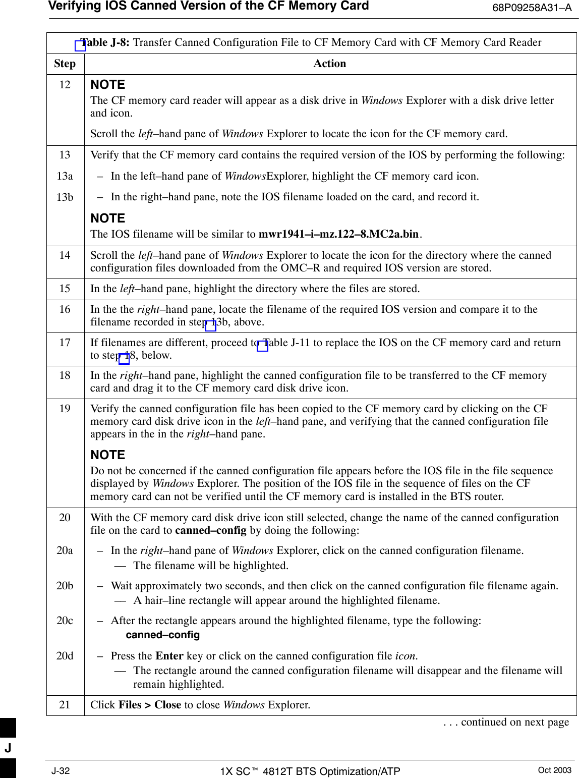
![Verifying IOS Canned Version of the CF Memory Card 68P09258A31–AOct 20031X SCt 4812T BTS Optimization/ATPJ-34Table J-9: Copy Canned Configuration File to BTS Router Startup Configuration and Verify IOS File PositionStep Action4NOTEThe IOS defaults to the CF memory card (slot0:) directory unless the present working directory hasbeen changed using the cd command. Determine the present working directory by entering pwd. Ifthe present working directory has been changed, enter the command cd slot0: to return to the defaultsetting.Display the directory listing of the CF memory card by entering the following:dirA response similar to the following will be displayed:Router#dir slot0:Directory of slot0:/ 1 –rw– 7051976 Sep 23 2002 07:24:18 mwr1941–i–mz.122–8.MC2a.bin 2 –rw– 2212 Mar 01 1993 00:14:48 canned–config31932416 bytes total (24885606 bytes free)Router#5Be sure the IOS file is the first file listed in the directory content display. If it is not, perform theprocedure in Table J-12, and then return to step 6, below.6Copy the canned configuration to the BTS router’s startup configuration file by entering the following:copy slot0:canned–config startup–configA response similar to the following will be displayed:Router#copy slot0:canned–config startDestination filename [startup–config]?7When prompted for the destination file name, press the Enter key. A response similar to the followingwill be displayed:Router#copy slot0:canned–config startDestination filename [startup–config]?2218 bytes copied in 3.52 secsRouter1#8Check the file size of the startup–config to verify the copy operation by entering the following:dir nvram:A response similar to the following will be displayed:Directory of nvram:/ 26 –rw– 2218 <no date> startup–config 27 –––– 5 <no date> private–config29688 bytes total (25247 bytes free)Router#NOTEBe sure to include the colon (:) after nvram when typing the command.. . . continued on next pageJ](https://usermanual.wiki/Nokia-Solutions-and-Networks/T5DS1.User-Manual-3/User-Guide-383443-Page-246.png)
![Verifying IOS Canned Version of the CF Memory Card68P09258A31–AOct 2003 1X SCt 4812T BTS Optimization/ATP J-35Table J-9: Copy Canned Configuration File to BTS Router Startup Configuration and Verify IOS File PositionStep Action9If desired, the contents of the startup–config file may be verified against the file listings at the end ofthis appendix for the blue or red canned configuration, as applicable, by entering the following:show startup–configNOTEPressing the space bar at the MORE prompt will scroll another screen–full of data. Pressing the Enterkey will scroll the screen one line at a time.10 Verify the router will boot properly on the IOS and revised startup–config files by entering thefollowing:reloadA response similar to the following will be displayed:Router#reloadSystem configuration has been modified. Save? [yes/no]: nProceed with reload? [confirm]11 If prompted to save a modified configuration, enter n for “no,” and press the Enter key.12 When prompted to proceed with reload, press the Enter key to continue the reload operation.13 Verify the router reboots without displaying the rommon 1 > prompt or error messages related to portconfigurations. If the router boots to the rommon prompt, proceed to the Recovery from BTS RouterBoot to rommon section of this appendix.14 Using the tagging materials, tag the router to clearly identify the installed configuration (blue(BTSRTR1) or red (BTSRTR2)).15 If an additional router must have the canned configuration installed, perform the following:15a – Disconnect the cabling for the HyperTerminal communications session from the BTS router, andminimize the HyperTerminal window on the LMF computer.15b – Remove power from the router and disconnect it from the power supply.15c – Repeat the procedures in Table J-8 and this table (Table J-9) using the additional router.16 If no additional routers must be configured, perform steps 15a and 15b.17 On the LMF computer, exit the HyperTerminal session. J](https://usermanual.wiki/Nokia-Solutions-and-Networks/T5DS1.User-Manual-3/User-Guide-383443-Page-247.png)
![Replacing Installed BTS Router CF Memory Card IOS Version 68P09258A31–AOct 20031X SCt 4812T BTS Optimization/ATPJ-38Table J-10: Using a TFTP Server Application for Replacing Loaded IOS Version and Verifying File Sequence PositionStep Action* IMPORTANTThis procedure does not cover all aspects of BTS router operation and programming. Before performing thisprocedure, review BTS router initialization, operation, and programming information and procedures inMWR1941 Wireless Mobile Edge Router Software Configuration Guide; part number 78–13983–01. Have thispublication available for reference while performing this procedure.1This procedure assumes the LMF computer and BTS router are configured, connected, and operatingas they would be after performing the procedures in Table J-4, Table J-5, Table J-6, and steps 1through 8 of Table J-7. If necessary, perform these procedures now.2NOTEThe IOS present working directory defaults to the CF memory card (slot0:) directory unless thepresent working directory has been changed using the cd command. Determine the present workingdirectory by entering pwd. If the present working directory has been changed, enter the command cdslot0: to return to the default setting.Identify the filename of the currently loaded IOS which must be replaced by entering dir command. Aresponse similar to the following will be displayed:BTSRTR1#dirDirectory of slot0:/ 1 –rw– 7051844 Sep 23 2002 07:15:08 mwr1941–i–mz.07022002.bin 2 –rw– 2212 Mar 01 1993 00:11:00 canned–config31932416 bytes total (24878360 bytes free)BTSRTR1#3Begin to backup the currently installed version of the router’s IOS to the LMF computer’s default tftpdirectory by entering the following:copy old_IOS_filename tftp:Where old_IOS_filename = the filename of the IOS currently loaded on the BTS router CF memorycard.A response similar to the following will be displayed:BTSRTR1#copy mwr1941–i–mz.07022002.bin tftp:Address or name of remote host []?4At the remote host prompt, enter the following:100.100.100.1A response similar to the following will be displayed:Address or name of remote host []? 100.100.100.1Destination filename [mwr1941–i–mz.07022002.bin]?. . . continued on next pageJ](https://usermanual.wiki/Nokia-Solutions-and-Networks/T5DS1.User-Manual-3/User-Guide-383443-Page-250.png)
![Replacing Installed BTS Router CF Memory Card IOS Version68P09258A31–AOct 2003 1X SCt 4812T BTS Optimization/ATP J-39Table J-10: Using a TFTP Server Application for Replacing Loaded IOS Version and Verifying File Sequence PositionStep Action5If the default filename displayed in the prompt is correct, press the Enter key to accept it. If it ismissing or not correct, enter the correct filename.A response similar to the following will be displayed if the default filename is selected:Address or name of remote host []? 100.100.100.1Destination filename [mwr1941–i–mz.07022002.bin]?!!!!!!!!!!!!!!!!!!!!!!!!!!!!!!!!!!!!!!!!!!!!!!!!!!!!!!!!!!!!!!!!!!!!!!!!!!!!!!!!!!!!!!!!!!!!!!!!!!!!!!!!!!!!!!!!!!!!!!!!!!!!!!!!!!!!!!!!!!!!!!!!!!!!!!!!!!!!!!!!!!!!!!!!!!!!!!!!!!!!!!!!!!!!!!!!!!!!!!!!!!!!!!!!!!!!!!!!!!!!!!!!!!!!!!!!!!!!!!!!!!!!!!!!!!!!!!!!!!!!!!!!!!!!!!!!!!!!!!!!!!!!!!!!!!!!!!!!!!!!!!!!!!!!!!!!!!!!!!!!!!!!!!!!!!!!!!!!!!!!!!!!!!!!!!!!!!!!!!!!!!!!!!!!!!!!!!!!!!!!!!!!!!!!!!!!!!!!!!!!!!!!!!!!!!!!!!!!!!!!!!!!!!!!!!!!!!!!!!!!!!!!!!!!!!!!!!!!!!!!!!!!!!!!!!!!!!!!!!!!!!!!!!!!!!!!!!!!!!!!!!!!!!!!!!!!!!!!!!!!!!!!!!!!!!!!!!!!!!!!!!!!!!!!!!!!!!!!!!!!!!!!!!!!!!!!!!!!!!!!!!!!!!!!!!!!!!!!!!!!!!!!!!!!!!!!!!!!!!!!!!!!!!!!!!!!!!!!!!!!!!!!!!!!!!!!!!!!!!!!!!!!!!!!!!!!!!!!!!!!!!!!!!!!!!!!!!!!!!!!!!!!!!!!!!!!!!!!!!!!!!!!!!!!!!!!!!!!!!!!!!!!!!!!!!!!!!!!!!!!!!!!!!!!!!!!!!!!!!!!!!!!!!!!!!!!!!!!!!!!!!!!!!!!!!!!!!!!!!!!!!!!!!!!!!!!!!!!!!!!!!!!!!!!!!!!!!!!!!!!!!!!!!!!!!!!!!!!!!!!!!!!!!!!!!!!!!!!!!!!!!!!!!!!!!!!!!!!!!!!!!!!!!!!!!!!!!!!!!!!!!!!!!!!!!!!!!!!!!!!!!!!!!!!!!!!!!!!!!!!!!!!!!!!!!!!!!!!!!!!!!!!!!!!!!!!!!!!!!!!!!!!!!!!!!!!!!!!!!!!!!!!!!!!!!!!!!!!!!!!!!!!!!!!!!!!!!!!!!!!!!!!!!!!!!!!!!!!!!!!!!!!!!!!!!!!!!!!!!!!!!!!!!!!!!!!!!!!!!!!!!!!!!!!!!!!!!!!!!!!!!!!!!!!!!!!!!!!!!!!!!!!!!!!!!!!!!!!!!!!!!!!!!!!!!!!!!!!!!!!!!!!!!!!!!!!!!!!!!!!!!!!!!!!!!!!!!!!!!!!!!!!!!!!!!!!!!!!!!!!!!!!!!!!!!!!!!!!!!!!!!!!!!!!!!!!!!!!!!!!!!!!!!!!!!!!!!!!!!!!!!!!!!!!!!!!!!!!!!!!!!!!!!!!!!!!!!!!!!!7051844 bytes copied in 109.92 secs (64697 bytes/sec)BTSRTR1#6If additional files are stored on the CF memory card, begin backing them up to the LMF computer’sdefault tftp directory by entering the following:copy additional_filename tftp:Where additional_filename = the filename of an additional file loaded on the BTS router CF memorycard.A response similar to the following will be displayed:BTSRTR1#copy canned–config tftp:Address or name of remote host [100.100.100.1]?7If the default IP address displayed in the prompt is correct, press the Enter key to accept it. If it ismissing or not correct, enter the correct IP address for the LMF computer.A response similar to the following will be displayed if the default filename is selected:Address or name of remote host [100.100.100.1]? Source filename [canned–config]?8If the default filename displayed in the prompt is correct, press the Enter key to accept it. If it ismissing or not correct, enter the correct filename.A response similar to the following will be displayed if the default filename is selected:Source filename [canned–config]? Destination filename [canned–config]?. . . continued on next pageJ](https://usermanual.wiki/Nokia-Solutions-and-Networks/T5DS1.User-Manual-3/User-Guide-383443-Page-251.png)
![Replacing Installed BTS Router CF Memory Card IOS Version 68P09258A31–AOct 20031X SCt 4812T BTS Optimization/ATPJ-40Table J-10: Using a TFTP Server Application for Replacing Loaded IOS Version and Verifying File Sequence PositionStep Action9If the default filename displayed in the prompt is correct, press the Enter key to accept it. If it ismissing or not correct, enter the correct filename. A response similar to the following will bedisplayed:Destination filename [canned–config]?![OK – 2212/4096 bytes]2212 bytes copied in 0.152 secsBTSRTR1#10 If more files are stored on the CF memory card, repeat steps 6 through 9 until all files have beenbacked up to the LMF computer.11 Delete all files from the CF memory card by entering the following command:format slot0:A response similar to the following will be displayed:BTSRTR1#format slot0:Format operation may take a while. Continue? [confirm]12 Press the Enter key to continue the format operation. A response similar to the following will bedisplayed:Format operation may take a while. Continue? [confirm]Format operation will destroy all data in ”slot0:”. Continue? [confirm]13 Press the Enter key to continue the format operation. A response similar to the following will bedisplayed:Format operation will destroy all data in ”slot0:”. Continue? [confirm]Format: Drive communication & 1st Sector Write OK...Writing Monlibsectors....................................................................................Monlib write complete.Format: All system sectors written. OK...Format: Total sectors in formatted partition: 62560Format: Total bytes in formatted partition: 32030720Format: Operation completed successfully.Format of slot0 completeBTSRTR1#14 Verify all files have been deleted from the CF memory card by entering the dir command. A responsesimilar to the following will be displayed:Directory of slot0:/No files in directory31932416 bytes total (31932416 bytes free)BTSRTR1#. . . continued on next pageJ](https://usermanual.wiki/Nokia-Solutions-and-Networks/T5DS1.User-Manual-3/User-Guide-383443-Page-252.png)
![Replacing Installed BTS Router CF Memory Card IOS Version68P09258A31–AOct 2003 1X SCt 4812T BTS Optimization/ATP J-41Table J-10: Using a TFTP Server Application for Replacing Loaded IOS Version and Verifying File Sequence PositionStep Action15 Begin to copy the required version of the IOS from the LMF computer to the BTS router by entering thefollowing:copy tftp:new_IOS_filename slot0:Where new_IOS_filename = the filename of the required IOS for the BTS router.A response similar to the following will be displayed:BTSRTR1#copy tftp:mwr1941–i–mz.122–8.MC2a.bin slot0:Address or name of remote host [100.100.100.1]?16 If the default IP address displayed in the prompt is correct, press the Enter key to accept it. If it ismissing or not correct, enter the correct IP address for the LMF computer. A response similar to thefollowing will be displayed if the default filename is selected:Address or name of remote host [100.100.100.1]? Source filename [mwr1941–i–mz.122–8.MC2a.bin]?17 If the default filename displayed in the prompt is correct, press the Enter key to accept it. If it ismissing or not correct, enter the correct filename. A response similar to the following will bedisplayed if the default filename is selected:Source filename [mwr1941–i–mz.122–8.MC2a.bin]? Destination filename [mwr1941–i–mz.122–8.MC2a.bin]?18 If the default filename displayed in the prompt is correct, press the Enter key to accept it. If it is notcorrect, enter the correct filename. A response similar to the following will be displayed if the defaultfilename is selected:Destination filename [mwr1941–i–mz.122–8.MC2a.bin]? Accessing tftp://100.100.100.1/mwr1941–i–mz.122–8.MC2a.bin...Loading mwr1941–i–mz.122–8.MC2a.bin from 100.100.100.1 (via FastEthernet0/0): !!!!Loading mwr1941–i–mz.122–8.MC2a.bin from 100.100.100.1 (via FastEthernet0/0):!!!!!!!!!!!!!!!!!!!!!!!!!!!!!!!!!!!!!!!!!!!!!!!!!!!!!!!!!!!!!!!!!!!!!!!!!!!!!!!!!!!!!!!!!!!!!!!!!!!!!!!!!!!!!!!!!!!!!!!!!!!!!!!!!!!!!!!!!!!!!!!!!!!!!!!!!!!!!!!!!!!!!!!!!!!!!!!!!!!!!!!!!!!!!!!!!!!!!!!!!!!!!!!!!!!!!!!!!!!!!!!!!!!!!!!!!!!!!!!!!!!!!!!!!!!!!!!!!!!!!!!!!!!!!!!!!!!!!!!!!!!!!!!!!!!!!!!!!!!!!!!!!!!!!!!!!!!!!!!!!!!!!!!!!!!!!!!!!!!!!!!!!!!!!!!!!!!!!!!!!!!!!!!!!!!!!!!!!!!!!!!!!!!!!!!!!!!!!!!!!!!!!!!!!!!!!!!!!!!!!!!!!!!!!!!!!!!!!!!!!!!!!!!!!!!!!!!!!!!!!!!!!!!!!!!!!!!!!!!!!!!!!!!!!!!!!!!!!!!!!!!!!!!!!!!!!!!!!!!!!!!!!!!!!!!!!!!!!!!!!!!!!!!!!!!!!!!!!!!!!!!!!!!!!!!!!!!!!!!!!!!!!!!!!!!!!!!!!!!!!!!!!!!!!!!!!!!!!!!!!!!!!!!!!!!!!!!!!!!!!!!!!!!!!!!!!!!!!!!!!!!!!!!!!!!!!!!!!!!!!!!!!!!!!!!!!!!!!!!!!!!!!!!!!!!!!!!!!!!!!!!!!!!!!!!!!!!!!!!!!!!!!!!!!!!!!!!!!!!!!!!!!!!!!!!!!!!!!!!!!!!!!!!!!!!!!!!!!!!!!!!!!!!!!!!!!!!!!!!!!!!!!!!!!!!!!!!!!!!!!!!!!!!!!!!!!!!!!!!!!!!!!!!!!!!!!!!!!!!!!!!!!!!!!!!!!!!!!!!!!!!!!!!!!!!!!!!!!!!!!!!!!!!!!!!!!!!!!!!!!!!!!!!!!!!!!!!!!!!!!!!!!!!!!!!!!!!!!!!!!!!!!!!!!!!!!!!!!!!!!!!!!!!!!!!!!!!!!!!!!!!!!!!!!!!!!!!!!!!!!!!!!!!!!!!!!!!!!!!!!!!!!!!!!!!!!!!!!!!!!!!!!!!!!!!!!!!!!!!!!!!!!!!!!!!!!!!!!!!!!!!!!!!!!!!!!!!!!!!!!!!!!!!!!!!!!!!!!!!!!!!!!!!!!!!!!!!!!!!!!!!!!!!!!!!!!!!!!!!!!!!!!!!!!!!!!!!!!!!!!!!!!!!!!!!!!!!!!!!!!!!!!!!!!!!!!!!!!!!!!!!!!!!!!!!!!!!!!!!!!!!!!!!!!!!!!!!!!!!!!!!!!!!!!!!!!!!!!!!!!!!!!!!!!!!!!!!!!!!!!!!!!!!!!!!!!!!!!!!!!!!!!!!!!!!!!!!!!![OK – 7051976/14103552 bytes]7051976 bytes copied in 145.108 secs (48634 bytes/sec)BTSRTR1#. . . continued on next pageJ](https://usermanual.wiki/Nokia-Solutions-and-Networks/T5DS1.User-Manual-3/User-Guide-383443-Page-253.png)
![Replacing Installed BTS Router CF Memory Card IOS Version 68P09258A31–AOct 20031X SCt 4812T BTS Optimization/ATPJ-42Table J-10: Using a TFTP Server Application for Replacing Loaded IOS Version and Verifying File Sequence PositionStep Action19 Display the CF memory card directory to verify that the new IOS file is there by entering the dircommand. A response similar to the following will be displayed:BTSRTR1#dirDirectory of slot0:/ 1 –rw– 7051976 Sep 23 2002 07:25:36 mwr1941–i–mz.122–8.MC2a.bin31932416 bytes total (24880440 bytes free)BTSRTR1#20 If any additional files previously stored on the CF memory card are to be copied to the card, performthe following:copy tftp:filename slot0:Where filename = the filename of the file to be copied to the CF memory cardA response similar to the following will be displayed:BTSRTR1#copy tftp:canned–config slot0:Address or name of remote host [100.100.100.1]?21 If the default IP address displayed in the prompt is correct, press the Enter key to accept it. If it ismissing or not correct, enter the correct IP address for the LMF computer. A response similar to thefollowing will be displayed if the default IP address is selected:Address or name of remote host [100.100.100.1]? Destination filename [canned–config]?22 If the default filename displayed in the prompt is correct, press the Enter key to accept it. If it ismissing or not correct, enter the correct filename. A response similar to the following will bedisplayed if the default filename is selected:Destination filename [canned–config]? Accessing tftp://100.100.100.1/canned–config...Loading basic_config from 100.100.100.1 (via FastEthernet0/0): ![OK – 2212/4096 bytes]2212 bytes copied in 0.152 secsBTSRTR1#23 After the additional file is copied to the CF memory card, display the CF memory card directory byentering the dir command. A response similar to the following will be displayed:BTSRTR1#dirDirectory of slot0:/1 –rw– 7051976 Sep 23 2002 07:24:18 mwr1941–i–mz.122–8.MC2a.bin2 –rw– 2212 Mar 01 1993 00:09:06 canned–config24 The IOS file must be the first file listed for the BTS router to boot properly. If it is, proceed to step 29.. . . continued on next pageJ](https://usermanual.wiki/Nokia-Solutions-and-Networks/T5DS1.User-Manual-3/User-Guide-383443-Page-254.png)
![Replacing Installed BTS Router CF Memory Card IOS Version68P09258A31–AOct 2003 1X SCt 4812T BTS Optimization/ATP J-43Table J-10: Using a TFTP Server Application for Replacing Loaded IOS Version and Verifying File Sequence PositionStep ActionCAUTIONThe file sequence on the CF memory card can not be verified with application programs which placethe listed file names in alphabetical order (for example, certain Unix telnet applications, Unixdirectory listing commands, and Windows file managers such as Windows Explorer). This portion ofthe procedure is intended for use only with applications, such as HyperTerminal, which do not listdirectory contents alphabetically.25 If another file is listed before the IOS file, delete the file by performing steps 11 through 13 anddisplay the directory of the CF memory card as described in step 23 to be sure the file is deleted.26 Copy the file from the LMF computer to the CF memory card again by performing steps 20 through23.27 If the file is again listed before the IOS file in the CF memory card directory display, format the CFmemory card by performing steps 11 through 14 of this table.28 Copy the IOS file and any other required file to the formatted CF memory card by performing steps 15through 24.29 If additional files are to be transferred to the CF memory card, perform steps 20 through 24 for eachone.30 After making sure the IOS file is the first file on the CF memory card, restart the BTS router with thenew IOS version by entering the following:reloadA response similar to the following will be displayed:BTSRTR1#reloadSystem configuration has been modified. Save? [yes/no]: nProceed with reload? [confirm]31 If prompted to save a modified configuration, enter n for “no,” and press the Enter key.32 When prompted to proceed with reload, press the Enter key to continue the reload operation.33 Once the router has completed rebooting, change to the privileged EXEC mode and confirm thebooted IOS version is correct by entering the following:show versionA response similar to the following partial example will be displayed:BTSRTR1#sh verCisco Internetwork Operating System Software IOS (tm) 1941 Software (MWR1941–I–M), Version 12.2(8)MC2a, EARLY DEPLOYMENT RELEASESOFTWARE (fc1)...BTSRTR1#34 Verify the version number displayed in the second line of the version information is the correct IOSversion.35 If this procedure was entered from step 8 of Table J-7, return to Table J-7, step 9.. . . continued on next page J](https://usermanual.wiki/Nokia-Solutions-and-Networks/T5DS1.User-Manual-3/User-Guide-383443-Page-255.png)
![Replacing Installed BTS Router CF Memory Card IOS Version68P09258A31–AOct 2003 1X SCt 4812T BTS Optimization/ATP J-47Table J-11: Using a CF Memory Card Reader for Replacing Loaded IOS Version and Verifying File Sequence PositionStep ActionNOTEThe IOS present working directory defaults to the CF memory card (slot0:) directory unless thepresent working directory has been changed using the cd command. Determine the present workingdirectory by entering pwd. If the present working directory has been changed, enter the command cdslot0: to return to the default setting.19 Display the directory listing of the CF memory card by entering the following:dirA response similar to the following will be displayed:Router#dir slot0:Directory of slot0:/1 –rw– 7051976 Sep 23 2002 07:24:18 mwr1941–i–mz.122–8.MC2a.bin2 –rw– 2212 Mar 01 1993 00:14:48 canned–config31932416 bytes total (24885606 bytes free)Router#CAUTIONThe file sequence on the CF memory card can not be verified with application programs which placethe listed file names in alphabetical order (for example, certain Unix telnet applications, Unixdirectory listing commands, and Windows file managers such as Windows Explorer). This portion ofthe procedure is intended for use only with applications, such as HyperTerminal, which do not listdirectory contents alphabetically.20 Be sure the IOS file is the first file listed in the directory content display. If it is not, perform theprocedure in Table J-12, and then return to step 21, below.21 Verify the router will boot properly on the IOS and revised startup–config files by entering thefollowing:reloadA response similar to the following will be displayed:Router#reloadSystem configuration has been modified. Save? [yes/no]: nProceed with reload? [confirm]22 If prompted to save a modified configuration, enter n for “no,” and press the Enter key.23 When prompted to proceed with reload, press the Enter key to continue the reload operation.24 Verify the router reboots without displaying the rommon 1 > prompt or error messages related to portconfigurations.25 If no other BTS router file operations or configuration actions are required, perform the following:25a – Remove power from the router and disconnect it from the power supply.25b – Disconnect all cabling from the BTS router.25c – On the LMF computer, exit the HyperTerminal communications session. J](https://usermanual.wiki/Nokia-Solutions-and-Networks/T5DS1.User-Manual-3/User-Guide-383443-Page-259.png)
![Replacing Installed BTS Router CF Memory Card IOS Version68P09258A31–AOct 2003 1X SCt 4812T BTS Optimization/ATP J-51Table J-12: Use CF Memory Card Reader to Place IOS File First in CF Memory Card File SequenceStep Action7e – Verify port FE 0 (fa0/0) is configured with the correct IP address by entering the following:show ip interface briefA response similar to the following will be displayed:BTSRTR1#sh ip int brInterface IP Address OK? Method Status ProtocolFastEthernet0/0 100.100.100.2 YES manual up upSerial0:0 unassigned YES unset administratively down downFastEthernet0/1 unassigned YES unset administratively down downSerial1:0 unassigned YES unset administratively down downBTSRTR1#8Be sure the required IOS file and canned configuration file for the BTS router are located in the tftpserver root directory (refer to Table J-4, step 14 or step 17, as applicable)9Delete files from the CF memory card by entering the del filename command. A response similar tothe following will be displayed:Router#del canned–configDelete filename [canned–config]?10 If the default filename displayed in the prompt is correct, press the Enter key to accept it. If it ismissing or not correct, enter the correct filename. A response similar to the following will bedisplayed if the default filename is selected:Delete filename [canned–config]? Delete slot0:canned–config? [confirm]11 Press the Enter key to confirm the deletion.A response similar to the following will be displayed if the default filename is selected:Delete filename [canned–config]? Delete slot0:canned–config? [confirm]Router#12 Confirm the file deletion by entering the dir command. A response similar to the following will bedisplayed:Router#dirDirectory of slot0:/ 1 –rw– 7051976 Sep 23 2002 07:24:18 mwr1941–i–mz.122–8.MC2a.bin31932416 bytes total (24887818 bytes free)Router#13 Repeat steps 9 through 12 for each file until all files have been deleted from the CF memory card.. . . continued on next pageJ](https://usermanual.wiki/Nokia-Solutions-and-Networks/T5DS1.User-Manual-3/User-Guide-383443-Page-263.png)
![Replacing Installed BTS Router CF Memory Card IOS Version 68P09258A31–AOct 20031X SCt 4812T BTS Optimization/ATPJ-52Table J-12: Use CF Memory Card Reader to Place IOS File First in CF Memory Card File SequenceStep Action14 Use the tftp server to copy the IOS file from the LMF computer to the CF memory card by enteringthe fol-lowing:copy tftp:IOS_filename slot0:Where IOS_filenamer = required IOS version filename in the LMF computer tftp server rootdirectory.A response similar to the following will be displayed:BTSRTR1#copy tftp:mwr1941–i–mz.122–8.MC2a.bin slot0:Address or name of remote host []?15 At the prompt for the remote host address or name, enter the IP address of the LMF computer NIC:100.100.100.1A response similar to the following will be displayed:BTSRTR1#copy tftp:mwr1941–i–mz.122–8.MC2a.bin slot0:Address or name of remote host []? 100.100.100.1Destination filename [mwr1941–i–mz.122–8.MC2a.bin]?16 At the prompt for the destination filename, press the Enter key. A response similar to the followingwill be displayed:BTSRTR1#copy tftp:mwr1941–i–mz.122–8.MC2a.bin slot0:Address or name of remote host []? 100.100.100.1Destination filename [mwr1941–i–mz.122–8.MC2a.bin]?Accessing tftp://100.100.100.1/mwr1941–i–mz.122–8.MC2a.bin...Loading mwr1941–i–mz.122–8.MC2a.bin from 100.100.100.1 (via FastEthernet0/0): !!!!Loading mwr1941–i–mz.122–8.MC2a.bin from 100.100.100.1 (via FastEthernet0/0):!!!!!!!!!!!!!!!!!!!!!!!!!!!!!!!!!!!!!!!!!!!!!!!!!!!!!!!!!!!!!!!!!!!!!!!!!!!!!!!!!!!!!!!!!!!!!!!!!!!!!!!!!!!!!!!!!!!!!!!!!!!!!!!!!!!!!!!!!!!!!!!!!!!!!!!!!!!!!!!!!!!!!!!!!!!!!!!!!!!!!!!!!!!!!!!!!!!!!!!!!!!!!!!!!!!!!!!!!!!!!!!!!!!!!!!!!!!!!!!!!!!!!!!!!!!!!!!!!!!!!!!!!!!!!!!!!!!!!!!!!!!!!!!!!!!!!!!!!!!!!!!!!!!!!!!!!!!!!!!!!!!!!!!!!!!!!!!!!!!!!!!!!!!!!!!!!!!!!!!!!!!!!!!!!!!!!!!!!!!!!!!!!!!!!!!!!!!!!!!!!!!!!!!!!!!!!!!!!!!!!!!!!!!!!!!!!!!!!!!!!!!!!!!!!!!!!!!!!!!!!!!!!!!!!!!!!!!!!!!!!!!!!!!!!!!!!!!!!!!!!!!!!!!!!!!!!!!!!!!!!!!!!!!!!!!!!!!!!!!!!!!!!!!!!!!!!!!!!!!!!!!!!!!!!!!!!!!!!!!!!!!!!!!!!!!!!!!!!!!!!!!!!!!!!!!!!!!!!!!!!!!!!!!!!!!!!!!!!!!!!!!!!!!!!!!!!!!!!!!!!!!!!!!!!!!!!!!!!!!!!!!!!!!!!!!!!!!!!!!!!!!!!!!!!!!!!!!!!!!!!!!!!!!!!!!!!!!!!!!!!!!!!!!!!!!!!!!!!!!!!!!!!!!!!!!!!!!!!!!!!!!!!!!!!!!!!!!!!!!!!!!!!!!!!!!!!!!!!!!!!!!!!!!!!!!!!!!!!!!!!!!!!!!!!!!!!!!!!!!!!!!!!!!!!!!!!!!!!!!!!!!!!!!!!!!!!!!!!!!!!!!!!!!!!!!!!!!!!!!!!!!!!!!!!!!!!!!!!!!!!!!!!!!!!!!!!!!!!!!!!!!!!!!!!!!!!!!!!!!!!!!!!!!!!!!!!!!!!!!!!!!!!!!!!!!!!!!!!!!!!!!!!!!!!!!!!!!!!!!!!!!!!!!!!!!!!!!!!!!!!!!!!!!!!!!!!!!!!!!!!!!!!!!!!!!!!!!!!!!!!!!!!!!!!!!!!!!!!!!!!!!!!!!!!!!!!!!!!!!!!!!!!!!!!!!!!!!!!!!!!!!!!!!!!!!!!!!!!!!!!!!!!!!!!!!!!!!!!!!!!!!!!!!!!!!!!!!!!!!!!!!!!!!!!!!!!!!!!!!!!!!!!!!!!!!!!!!!!!!!!!!!!!!!!!!!!!!!!!!!!!!!!!!!!!!!!!!!!!!!!!!!!!!!!!!!!!!!!!!!!!!!!!!!!!!!!!!!!!!!!!!!!!!!!!!!!!!!!!!!!!!!!!!!!!!!!!!!!![OK – 7051976/14103552 bytes]7051976 bytes copied in 145.108 secs (48634 bytes/sec). . . continued on next pageJ](https://usermanual.wiki/Nokia-Solutions-and-Networks/T5DS1.User-Manual-3/User-Guide-383443-Page-264.png)
![Replacing Installed BTS Router CF Memory Card IOS Version68P09258A31–AOct 2003 1X SCt 4812T BTS Optimization/ATP J-53Table J-12: Use CF Memory Card Reader to Place IOS File First in CF Memory Card File SequenceStep Action17 Display the directory of the CF memory card to confirm the IOS file transfer by entering the dircommand. A response similar to the following will be displayed:Router#dirDirectory of slot0:/ 1 –rw– 7051976 Sep 23 2002 07:24:18 mwr1941–i–mz.122–8.MC2a.bin31932416 bytes total (248880440 bytes free)Router#18 Copy the canned configuration file to the CF memory card by entering the following:copy tftp:btsrtr_canned.color slot0:canned–configWhere color = blue or red, as applicable.A response similar to the following will be displayed:BTSRTR1#copy tftp:btsrtr_canned.blue slot0:canned–configAddress or name of remote host [100.100.100.1]?19 If the default IP address for the LMF computer displayed in the prompt is correct, press the Enter keyto accept it. If it is missing or not correct, enter the correct IP address.A response similar to the following will be displayed if the default filename is accepted:Destination filename [canned–config]? 2212 bytes copied in 0.208 secsRouter#20 At the prompt for the destination filename, press the Enter key. A response similar to the followingwill be displayed:BTSRTR1#copy tftp:btsrtr_canned.blue slot0:canned–configAddress or name of remote host []? 100.100.100.1Destination filename [canned–config]?Loading btsrtr_canned.blue from 100.100.100.1 (via Ethernet0/0): ![OK – 2457/4096 bytes]2457 bytes copied in 84.724 secs (29 bytes/sec)BTSRTR1#21 Determine if the IOS file is now the first file displayed in the directory listing by entering the dircommand. A response similar to the following will be displayed:Router#dirDirectory of slot0:/ 1 –rw– 7051976 Mar 01 1993 00:14:48 mwr1941–i–mz.122–8.MC2a.bin 2 –rw– 2212 Sep 23 2002 07:24:18 canned–config31932416 bytes total (24878228 bytes free)Router#22 If the IOS file is the first file displayed, as shown in step 21, above, proceed to step 30.. . . continued on next pageJ](https://usermanual.wiki/Nokia-Solutions-and-Networks/T5DS1.User-Manual-3/User-Guide-383443-Page-265.png)
![Replacing Installed BTS Router CF Memory Card IOS Version 68P09258A31–AOct 20031X SCt 4812T BTS Optimization/ATPJ-54Table J-12: Use CF Memory Card Reader to Place IOS File First in CF Memory Card File SequenceStep Action23 If the IOS is not the first file displayed, as shown in step 2, above, format the CF memory card byentering the following:format slot0:A response similar to the following will be displayed:BTSRTR1#format slot0:Format operation may take a while. Continue? [confirm]24 Press the Enter key to continue the format operation. A response similar to the following will bedisplayed:Format operation may take a while. Continue? [confirm]Format operation will destroy all data in ”slot0:”. Continue? [confirm]25 Press the Enter key to continue the format operation. A response similar to the following will bedisplayed:Format operation will destroy all data in ”slot0:”. Continue? [confirm]Format: Drive communication & 1st Sector Write OK...Writing Monlibsectors....................................................................................Monlib write complete.Format: All system sectors written. OK...Format: Total sectors in formatted partition: 62560Format: Total bytes in formatted partition: 32030720Format: Operation completed successfully.Format of slot0 completeBTSRTR1#26 If a tftp server is available on the LMF computer, repeat steps 14 through 22 to transfer the IOS andcanned configuration files to the CF memory card.27 Once the format operation is completed, remove the CF memory card from the router following theprocedure in the 1X SC 4812T BTS FRU Guide , insert it in the card reader connected to the LMFcomputer, and copy the IOS file to the card by performing step 4 and steps 6 through 11 of Table J-11,as required.28 Remove the CF memory card from the card reader and install it in the router following the procedurein the BTS FRU Guide.29 Be sure that the IOS file is now the first file displayed in the directory listing by entering the dircommand. A response similar to the following will be displayed:Router#dirDirectory of slot0:/ 1 –rw– 7051976 Sep 23 2002 07:24:18 mwr1941–i–mz.122–8.MC2a.bin 2 –rw– 2212 Mar 01 1993 00:14:48 canned–config31932416 bytes total (24885606 bytes free)Router#30 If this procedure was entered from step 5 of Table J-9, return to Table J-9, step 6.. . . continued on next pageJ](https://usermanual.wiki/Nokia-Solutions-and-Networks/T5DS1.User-Manual-3/User-Guide-383443-Page-266.png)
![Verify and Upgrade rommon Version 68P09258A31–AOct 20031X SCt 4812T BTS Optimization/ATPJ-58Table J-13: Verify and Replace Installed rommon Version Using a tftp ServerStep Action* IMPORTANTThis procedure does not cover all aspects of BTS router operation and programming. Before performing thisprocedure, review BTS router initialization, operation, and programming information and procedures inMWR1941 Wireless Mobile Edge Router Software Configuration Guide; part number 78–13983–01. Have thispublication available for reference while performing this procedure.1This procedure assumes the LMF computer and BTS router are configured, connected, and operatingas they would be after performing the procedures in Table J-4, Table J-5, Table J-6, and steps 1through 4 of Table J-7. If necessary, perform these procedures now.2Determine the currently installed rommon version by entering the following at the router privilegedEXEC mode prompt:show versionA response similar to the following will be displayed:BTSRTR1#sh verCisco Internetwork Operating System Software IOS (tm) 1941 Software (MWR1941–I–M), Version 12.2(8)MC2b, EARLY DEPLOYMENT RELEASESOFTWARE (fc3)TAC Support: http://www.cisco.com/tacCopyright (c) 1986–2002 by cisco Systems, Inc.Compiled Mon 05–Aug–02 11:07 by nmasaImage text–base: 0x60008940, data–base: 0x60B54000ROM: System Bootstrap, Version 12.2(20020113:235343) [sbose–wilma 109], DEVELOPMENTSOFTWAREROM: 1941 Software (MWR1941–I–M), Version 12.2(8)MC2b, EARLY DEPLOYMENT RELEASE SOFT-WARE (fc3)Router uptime is 1 minuteSystem returned to ROM by power–onSystem image file is ”slot0:mwr1941–i–mz.122–8.MC2b.bin”cisco mwr1941 (R7000) processor (revision 0.1) with 121856K/18432K bytes of memory.Processor board ID JMX0611K5TSR7000 CPU at 240Mhz, Implementation 39, Rev 3.3, 256KB L2 CacheBridging software.X.25 software, Version 3.0.0.Primary Rate ISDN software, Version 1.1.Toaster processor tmc is running.2 FastEthernet/IEEE 802.3 interface(s)2 Serial network interface(s)2 Channelized T1/PRI port(s)DRAM configuration is 64 bits wide with parity disabled.55K bytes of non–volatile configuration memory.31360K bytes of ATA Slot0 CompactFlash (Read/Write)Configuration register is 0x101BTSRTR1#3To determine the currently installed rommon version, examine the ROM: System Bootstrap line in theresponse.. . . continued on next pageJ](https://usermanual.wiki/Nokia-Solutions-and-Networks/T5DS1.User-Manual-3/User-Guide-383443-Page-270.png)
![Verify and Upgrade rommon Version68P09258A31–AOct 2003 1X SCt 4812T BTS Optimization/ATP J-59Table J-13: Verify and Replace Installed rommon Version Using a tftp ServerStep Action4Compare the installed rommon version information with the filename of the rommon version requiredfor the network.NOTE1. Rommon filename format is similar to the following:MWR1941_RM2.srec.122–8r.MC3.bin2. The rommon filename reflects the version number of the software (122–8r.MC3).5If the installed version is the one required for the network skip to step 26.6If the installed rommon version is not the one required for the network, backup the current BTS routerconfiguration to the LMF computer by entering the following:copy nvram:startup–config tftpA response similar to the following will be displayed:BTSRTR1#copy nvram:start tftpAddress or name of remote host []?NOTEBe sure to include the colon (:) after nvram when typing the command.7At the prompt for the remote host address or name, enter the IP address of the LMF computer NIC:100.100.100.1A response similar to the following will be displayed:BTSRTR1#copy copy nvram:start tftpAddress or name of remote host []? 100.100.100.1Source filename [startup–config]?8If the default filename displayed in the prompt is correct, press the Enter key to accept it. If it ismissing or not correct, enter the correct filename. A response similar to the following will bedisplayed if the default filename is selected:Source filename [startup–config]? Destination filename [startup–config]?9If the default filename displayed in the prompt is correct, press the Enter key to accept it. If it ismissing or not correct, enter the correct filename. A response similar to the following will bedisplayed:Destination filename [startup–config]?![OK – 2212/4096 bytes]2212 bytes copied in 0.152 secsBTSRTR1#. . . continued on next pageJ](https://usermanual.wiki/Nokia-Solutions-and-Networks/T5DS1.User-Manual-3/User-Guide-383443-Page-271.png)
![Verify and Upgrade rommon Version 68P09258A31–AOct 20031X SCt 4812T BTS Optimization/ATPJ-60Table J-13: Verify and Replace Installed rommon Version Using a tftp ServerStep Action10 NOTEThe IOS defaults to the CF memory card (slot0:) directory unless the present working directory hasbeen changed using the cd command. Determine the present working directory by entering pwd. Ifthe present working directory has been changed, enter the command cd slot0: to return to the defaultsetting.Determine the amount of memory available (bytes free) on the CF memory card by entering the dircommand. A response similar to the following will be displayed:BTSRTR1#dirDirectory of slot0:/1 –rw– 7051976 Sep 23 2002 07:24:18 mwr1941–i–mz.122–8.MC2b.bin2 –rw– 2212 Mar 01 1993 00:14:48 canned–config31932416 bytes total (24885606 bytes free)Router#11 Be sure there is at least 1 MB (1048580) of free memory.NOTEA rommon version file requires approximately 0.7 MB.12 Begin to copy the required version of the rommon file from the LMF computer to the BTS router by enteringthe following:copy tftp:new_rommon_filename slot0:Where new_rommon_filename = the filename of the required rommon version for the BTS router.A response similar to the following will be displayed:BTSRTR1#copy tftp:MWR1941_RM2.srec.122–8r.MC3.bin slot0:Address or name of remote host [100.100.100.1]?13 If the default IP address displayed in the prompt is correct, press the Enter key to accept it. If it ismissing or not correct, enter the correct IP address for the LMF computer. A response similar to thefollowing will be displayed if the default filename is selected:Address or name of remote host [100.100.100.1]? Source filename [MWR1941_RM2.srec.122–8r.MC3.bin]?14 If the default filename displayed in the prompt is correct, press the Enter key to accept it. If it ismissing or not correct, enter the correct filename. A response similar to the following will bedisplayed if the default filename is selected:Source filename [MWR1941_RM2.srec.122–8r.MC3.bin]? Destination filename [MWR1941_RM2.srec.122–8r.MC3.bin]?. . . continued on next pageJ](https://usermanual.wiki/Nokia-Solutions-and-Networks/T5DS1.User-Manual-3/User-Guide-383443-Page-272.png)
![Verify and Upgrade rommon Version68P09258A31–AOct 2003 1X SCt 4812T BTS Optimization/ATP J-61Table J-13: Verify and Replace Installed rommon Version Using a tftp ServerStep Action15 If the default filename displayed in the prompt is correct, press the Enter key to accept it. If it is notcorrect, enter the correct filename. A response similar to the following will be displayed if the defaultfilename is selected:Destination filename [MWR1941_RM2.srec.122–8r.MC3.bin]? Accessing tftp://100.100.100.1/MWR1941_RM2.srec.122–8r.MC3.bin...Loading MWR1941_RM2.srec.122–8r.MC3.bin from 100.100.100.1 (via FastEthernet0/0): !!!!Loading MWR1941_RM2.srec.122–8r.MC3.bin from 100.100.100.1 (via FastEthernet0/0):!!!!!!!!!!!!!!!!!!!!!!!!!!!!!!!!!!!!!!!!!!!!!!!!!!!!!!!!!!!!!!!!!!!!!!!!!!!!!!!!!!!!!!!!!!!!!!!!!!!!!!!!!!!!!!!!!!!!!!!!!![OK – 614306/14103552 bytes]614306 bytes copied in 13.059 secs (48634 bytes/sec)BTSRTR1#16 Display the CF memory card directory to verify that the new rommon version file is there by enteringthe dir command. A response similar to the following will be displayed:BTSRTR1#dirDirectory of slot0:/ 1 –rw– 7051976 Sep 23 2002 07:25:36 mwr1941–i–mz.122–8.MC2b.bin 2 –rw– 2212 Mar 01 1993 00:09:06 canned–config 3 –rw– 614306 Dec 13 2002 14:59:36 MWR1941_RM2.srec.122–8r.MC3.bin31932416 bytes total (24263922 bytes free)BTSRTR1#17 Replace the existing rommon version with the new one copied to the CF memory card by entering thefollowing:upgrade rom–monitor file slot0:MWR1941_RM2.srec.122–8r.MC3A response similar to the following will be displayed:BTSRTR1#This command will reload the router. Continue?[yes/no]18 When prompted to continue, enter yes and press the Enter key. A response similar to the followingwill be displayed:BTSRTR1#This command will reload the router. Continue?[yes/no] yesROMMON image upgrade in progressErasing boot flasheeeeeeeeeeeeeeeeeeeeeeeeeeeeeeeeeeeeeeeeeeeeeeeeeeeeeeeeeeeeeeeeeeProgramming boot flash ppppNow reloading19 When the router has completed initialization, change to the router privileged EXEC mode by enteringthe following:enableA response similar to the following will be displayed:BTSRTR1>enableBTSRTR1#. . . continued on next pageJ](https://usermanual.wiki/Nokia-Solutions-and-Networks/T5DS1.User-Manual-3/User-Guide-383443-Page-273.png)
![Verify and Upgrade rommon Version 68P09258A31–AOct 20031X SCt 4812T BTS Optimization/ATPJ-62Table J-13: Verify and Replace Installed rommon Version Using a tftp ServerStep Action20 Verify the router has initialized with the new rommon version by entering the following:show versionA response similar to the following partial response will be displayed:BTSRTR1#sh verCisco Internetwork Operating System Software IOS (tm) 1941 Software (MWR1941–I–M), Version 12.2(8)MC2b, EARLY DEPLOYMENT RELEASESOFTWARE (fc3)TAC Support: http://www.cisco.com/tacCopyright (c) 1986–2002 by cisco Systems, Inc.Compiled Mon 05–Aug–02 11:07 by nmasaImage text–base: 0x60008940, data–base: 0x60B54000ROM: System Bootstrap, Version 12.2(8r)MC3 RELEASE SOFTWARE (fc1)21 Compare the version displayed in the response ROM: System Bootstrap line to the filename of thenew rommon version file copied to the CF memory card.22 If the router successfully rebooted with the new rommon version, the rommon file can be deleted fromthe CF memory card by entering the following:delete slot0:new_rommon_filenameWhere new_rommon_filename = the filename of the required rommon version copied to the CFmemory card in steps 12 through 15, above.A response similar to the following will be displayed:BTSRTR1#del slot0:MWR1941_RM2.srec.122–8r.MC3.binDelete filename [MWR1941_RM2.srec.122–8r.MC3.bin]?23 If the default filename displayed in the prompt is correct, press the Enter key to accept it. If it ismissing or not correct, enter the correct filename. A response similar to the following will bedisplayed if the default filename is selected:Delete filename [MWR1941_RM2.srec.122–8r.MC3.bin]? Delete slot0:MWR1941_RM2.srec.122–8r.MC3.bin? [confirm]24 Press the Enter key to confirm the deletion. A response similar to the following will be displayed ifthe default filename is selected:Delete filename [MWR1941_RM2.srec.122–8r.MC3.bin]? Delete slot0:MWR1941_RM2.srec.122–8r.MC3.bin? [confirm]BTSRTR1#CAUTIONIn this step, do not delete the IOS and canned–config files from the CF memory card. The BTS routermust have these files on the card to properly boot or switch between packet and circuit mode.25 If additional unnecessary files, such as a backup of the startup–config file, are also on the CFmemory card, delete them by repeating steps 22 through 24 for each file.26 If no other BTS router file operations or configuration actions are required, perform the following:26a – Remove power from the router and disconnect it from the power supply.26b – Disconnect all cabling from the BTS router.26c – On the LMF computer, exit the HyperTerminal communications session.. . . continued on next pageJ](https://usermanual.wiki/Nokia-Solutions-and-Networks/T5DS1.User-Manual-3/User-Guide-383443-Page-274.png)
![Verify and Upgrade rommon Version 68P09258A31–AOct 20031X SCt 4812T BTS Optimization/ATPJ-64Verifying and replacing installed rommon versionFollow the procedure in Table J-14 to verify and, if necessary replace theinstalled rommon version using a CF memory card reader.Table J-14: Verify and Replace Installed rommon Version Using a CF Memory Card ReaderStep Action* IMPORTANTThis procedure does not cover all aspects of BTS router operation and programming. Before performing thisprocedure, review BTS router initialization, operation, and programming information and procedures inMWR1941 Wireless Mobile Edge Router Software Configuration Guide; part number 78–13983–01. Have thispublication available for reference while performing this procedure.1This procedure assumes the LMF computer and BTS router are configured, connected, and operatingas they would be after performing the procedures in steps 1 through 8 of Table J-8. If necessary,perform these procedures now.2Determine the currently installed rommon version by entering the following at the router privilegedEXEC mode prompt:show versionA response similar to the following will be displayed:BTSRTR1#sh verCisco Internetwork Operating System Software IOS (tm) 1941 Software (MWR1941–I–M), Version 12.2(8)MC2b, EARLY DEPLOYMENT RELEASESOFTWARE (fc3)TAC Support: http://www.cisco.com/tacCopyright (c) 1986–2002 by cisco Systems, Inc.Compiled Mon 05–Aug–02 11:07 by nmasaImage text–base: 0x60008940, data–base: 0x60B54000ROM: System Bootstrap, Version 12.2(20020113:235343) [sbose–wilma 109], DEVELOPMENTSOFTWAREROM: 1941 Software (MWR1941–I–M), Version 12.2(8)MC2b, EARLY DEPLOYMENT RELEASE SOFT-WARE (fc3)Router uptime is 1 minuteSystem returned to ROM by power–onSystem image file is ”slot0:mwr1941–i–mz.122–8.MC2b.bin”cisco mwr1941 (R7000) processor (revision 0.1) with 121856K/18432K bytes of memory.Processor board ID JMX0611K5TSR7000 CPU at 240Mhz, Implementation 39, Rev 3.3, 256KB L2 CacheBridging software.X.25 software, Version 3.0.0.Primary Rate ISDN software, Version 1.1.Toaster processor tmc is running.2 FastEthernet/IEEE 802.3 interface(s)2 Serial network interface(s)2 Channelized T1/PRI port(s)DRAM configuration is 64 bits wide with parity disabled.55K bytes of non–volatile configuration memory.31360K bytes of ATA Slot0 CompactFlash (Read/Write)Configuration register is 0x101BTSRTR1#3To determine the currently installed rommon version, examine the ROM: System Bootstrap line inthe response.. . . continued on next pageJ](https://usermanual.wiki/Nokia-Solutions-and-Networks/T5DS1.User-Manual-3/User-Guide-383443-Page-276.png)
![Verify and Upgrade rommon Version68P09258A31–AOct 2003 1X SCt 4812T BTS Optimization/ATP J-65Table J-14: Verify and Replace Installed rommon Version Using a CF Memory Card ReaderStep Action4Compare the installed rommon version information with the filename of the rommon version requiredfor the network.NOTE1. Rommon filename format is similar to the following:MWR1941_RM2.srec.122–8r.MC3.bin2. The rommon filename reflects the version number of the software (122–8r.MC3).5If the installed version is the one required for the network skip to step 25.6NOTEThe IOS defaults to the CF memory card (slot0:) directory unless the present working directory hasbeen changed using the cd command. Determine the present working directory by entering pwd. Ifthe present working directory has been changed, enter the command cd slot0: to return to the defaultsetting.If the installed rommon version is not the one required for the network, determine the amount ofmemory available (bytes free) on the CF memory card by entering the following:dirA response similar to the following will be displayed:BTSRTR1#dirDirectory of slot0:/ 1 –rw– 7051976 Sep 23 2002 07:24:18 mwr1941–i–mz.122–8.MC2b.bin 2 –rw– 2212 Mar 01 1993 00:14:48 canned–config31932416 bytes total (24885606 bytes free)Router#7Be sure there is at least 1 MB (1048580) of free memory.NOTEA rommon version file requires approximately 0.7 MB, and space must also be available for a backupof the router’s startup–config file.8Create a backup of the current BTS router configuration on the CF memory card by entering thefollowing:copy nvram:startup–config slot:0A response similar to the following will be displayed:BTSRTR1#copy nvram:startup–config slot0:Destination filename [startup–config]?9If the default filename displayed in the prompt is correct, press the Enter key to accept it. If it ismissing or not correct, enter the correct filename. A response similar to the following will bedisplayed:Destination filename [startup–config]? 2212 bytes copied in 4.96 secs (553 bytes/sec)BTSRTR1#10 Remove the CF memory card from the router by following the procedure in the 1X SC 4812T BTSFRU Guide .. . . continued on next pageJ](https://usermanual.wiki/Nokia-Solutions-and-Networks/T5DS1.User-Manual-3/User-Guide-383443-Page-277.png)
![Recovery From BTS Router Boot to rommon68P09258A31–AOct 2003 1X SCt 4812T BTS Optimization/ATP J-69Table J-15: Simple Recovery from BTS Router rommon BootStep Action3Note the IOS filename, and enter the following to begin recovery to an IOS boot:boot slot0:IOS_filenameWhere IOS_filename = the filename of the IOS noted in step 2, above.A successful IOS re–boot operation will result in display of a response which begins and ends similarto the following:rommon 2 > boot slot0:mwr1941–i–mz.122–8.MC2a.binprogram load complete, entry point: 0x80008000, size: 0xb2a0program load complete, entry point: 0x80008000, size: 0x6b99acSelf decompressing the image :################################################################### [OK]Smart Init is enabledsmart init is sizing iomem ID MEMORY_REQ TYPE00031A 0X005F3C00 MWR1941 Mainboard 0X000F3BB0 public buffer pools 0X00211000 public particle poolsTOTAL: 0X008F87B0...Press RETURN to get started!4If the router successfully reboots with the IOS, proceed to step 7.5If the router does not reboot with the IOS, perform the following:5a – Scroll the HyperTerminal display down until the directory display from step 2, above, is visible.5b – Compare the IOS filename from the directory display with the filename entered in performing step3, above.5c – If the filename was typed incorrectly, repeat step 3, using care to type the filename correctly.6If the router does not reboot with the IOS after typing the filename correctly, proceed to Table J-16 andperform the extended recovery procedure.. . . continued on next pageJ](https://usermanual.wiki/Nokia-Solutions-and-Networks/T5DS1.User-Manual-3/User-Guide-383443-Page-281.png)
![Recovery From BTS Router Boot to rommon68P09258A31–AOct 2003 1X SCt 4812T BTS Optimization/ATP J-71Table J-15: Simple Recovery from BTS Router rommon BootStep Action7f – Verify the correct IOS filename is now included in the listing by entering the following:show startup–configA response which begins similar to the following will be displayed:BTSRTR1#sh startUsing 1589 out of 57336 bytes!version 12.2service timestamps debug uptimeservice timestamps log uptimeno service password–encryption!hostname BTSRTR1!boot system slot0:mwr1941–i–mz.122–8.MC2a.binno logging console!username cisco password 0 cisco!redundancy mode y–cable standalone!7g – If the filename is correctly written, enter the following to determine if the router will reboot toIOS:reloadA response similar to the following will be displayed:BTSRTR1#reloadSystem configuration has been modified. Save? [yes/no]: nProceed with reload? [confirm]8If prompted to save a modified configuration, enter n for “no,” and press the Enter key.9When prompted to proceed with reload, press the Enter key to continue the reload operation.10 After a successful reboot with IOS, proceed with other BTS router activities or remove power from therouter and disconnect it11 If the router still will not successfully boot with IOS, proceed to Table J-16 and perform the extendedrecovery procedure. Extended Recovery from Boot to rommonRequirementsIf rommon boot recovery attempts fail using the simple recoverymethod, this method must be used to reboot a BTS router which hasinitialized with rommon. This method requires additional equipmentbeyond the items necessary to load canned configuration files into theBTS router. Extended recovery requires formatting the CF memory cardfrom the rommon–initialized router and reloading the reformatted CFmemory card with the required IOS version. J](https://usermanual.wiki/Nokia-Solutions-and-Networks/T5DS1.User-Manual-3/User-Guide-383443-Page-283.png)
![Recovery From BTS Router Boot to rommon68P09258A31–AOct 2003 1X SCt 4812T BTS Optimization/ATP J-73Table J-16: Extended Recovery from BTS Router rommon BootStep Action6Enter the following to initialize the router with the IOS on the additional CF memory card:boot slot0:IOS_filenameWhere IOS_filename = the filename of the IOS noted in step 5, above.A successful IOS re–boot operation will result in display of a response which begins and ends similarto the following:rommon 2 > boot slot0:mwr1941–i–mz.122–8.MC2a.binprogram load complete, entry point: 0x80008000, size: 0xb2a0program load complete, entry point: 0x80008000, size: 0x6b99acSelf decompressing the image :################################################################### [OK]Smart Init is enabledsmart init is sizing iomem ID MEMORY_REQ TYPE00031A 0X005F3C00 MWR1941 Mainboard 0X000F3BB0 public buffer pools 0X00211000 public particle poolsTOTAL: 0X008F87B0... ––– System Configuration Dialog –––Would you like to enter the initial configuration dialog? [yes/no]: n7If the router prompts with a question to enter the initial dialog as shown in step 6, above, type no andpress the Enter key to obtain the user EXEC mode prompt.8If the router prompts with Press RETURN to get started!, press the Enter key to obtain the userEXEC mode prompt.9At the user EXEC mode prompt, enter the following to access the privileged EXEC mode:enableA response similar to the following will be displayed:Router> enableRouter#10 Remove the additional CF memory card from the BTS router following the procedure in the 1X SC4812T BTS FRU Guide .11 Install the original CF memory card in the router following the procedure in the BTS FRU Guide.. . . continued on next pageJ](https://usermanual.wiki/Nokia-Solutions-and-Networks/T5DS1.User-Manual-3/User-Guide-383443-Page-285.png)
![Recovery From BTS Router Boot to rommon 68P09258A31–AOct 20031X SCt 4812T BTS Optimization/ATPJ-74Table J-16: Extended Recovery from BTS Router rommon BootStep Action12 Format the original CF memory card by entering the following:format slot0:A response similar to the following will be displayed:Router#format slot0:Format operation may take a while. Continue? [confirm]13 Press the Enter key to continue the format operation. A response similar to the following will bedisplayed:Format operation may take a while. Continue? [confirm]Format operation will destroy all data in ”slot0:”. Continue? [confirm]14 Press the Enter key to continue the format operation. A response similar to the following will bedisplayed:Format operation will destroy all data in ”slot0:”. Continue? [confirm]Format: Drive communication & 1st Sector Write OK...Writing Monlibsectors....................................................................................Monlib write complete.Format: All system sectors written. OK...Format: Total sectors in formatted partition: 62560Format: Total bytes in formatted partition: 32030720Format: Operation completed successfully.Format of slot0 completeRouter#15 Copy the required IOS version to the formatted original CF memory card by performing one of thefollowing:SUse the LMF computer and a tftp server following the procedure in Table J-10SUse the LMF computer and a CF memory card reader following the procedure in Table J-1116 If applicable, perform IOS initialization troubleshooting as described in Table J-15, steps 7 through 10. J](https://usermanual.wiki/Nokia-Solutions-and-Networks/T5DS1.User-Manual-3/User-Guide-383443-Page-286.png)
![Entering or Changing Router FE Interface IP Address 68P09258A31–AOct 20031X SCt 4812T BTS Optimization/ATPJ-78Table J-17: Enter/Change BTS Router FE Interface IP Addresses & Operating ParametersStep Action14 Save the interface configuration changes to the startup configuration file on the CF memory card byentering the following:copy running–config startup–configA response similar to the following will be displayed:BTSRTR–bts#–1–1# copy run startBTSRTR–bts#–1–1# Destination filename [startup–config]?15 Press Enter. A response similar to the following will be displayed:BTSRTR–bts#–1–1# copy run startBTSRTR–bts#–1–1# Destination filename [startup–config]?Building configuration...!!!!!!!!!!!!!!!!!!!!!!!!!!!!!!!!!!!!!!!!!!!!!!!!!!!!!!!!!!!!!!!!!!!!!!!!!!!!!!!!!![OK]BTSRTR–bts#–1–1#16 If all FE IP address entries/changes for the router are complete, enter the following to return the routerto user EXEC mode:disableA response similar to the following will be displayed:BTSRTR–bts#–1–1# disableBTSRTR–bts#–1–1>17 If no other router requires the FE interfaces to be assigned/changed, proceed to step 20.18 If FE interfaces on another router must be assigned/changed, disconnect the 8–contact modular plugfrom the current router CONSOLE port and connect it to the CONSOLE port of the other router.19 Press the Enter key, and when the router user EXEC mode prompt appears repeat steps 3 through 16for the other router.20 When the router is in user EXEC mode, close the HyperTerminal session and disconnect the LMFcomputer and additional components from the BTS router. J](https://usermanual.wiki/Nokia-Solutions-and-Networks/T5DS1.User-Manual-3/User-Guide-383443-Page-290.png)