Nokia Solutions and Networks T5EG1 SC4812ET 800 MHz 1X/EVDO User Manual Exhibit 8
Nokia Solutions and Networks SC4812ET 800 MHz 1X/EVDO Exhibit 8
UserManual.wiki
>
Nokia Solutions and Networks
>
T5EG1 User Manual
Exhibit 8
Navigation menu
Upload a User Manual
Namespaces
Wiki Guide
HTML
PDF
Info
Views
User Manual
Discussion / Help
Navigation

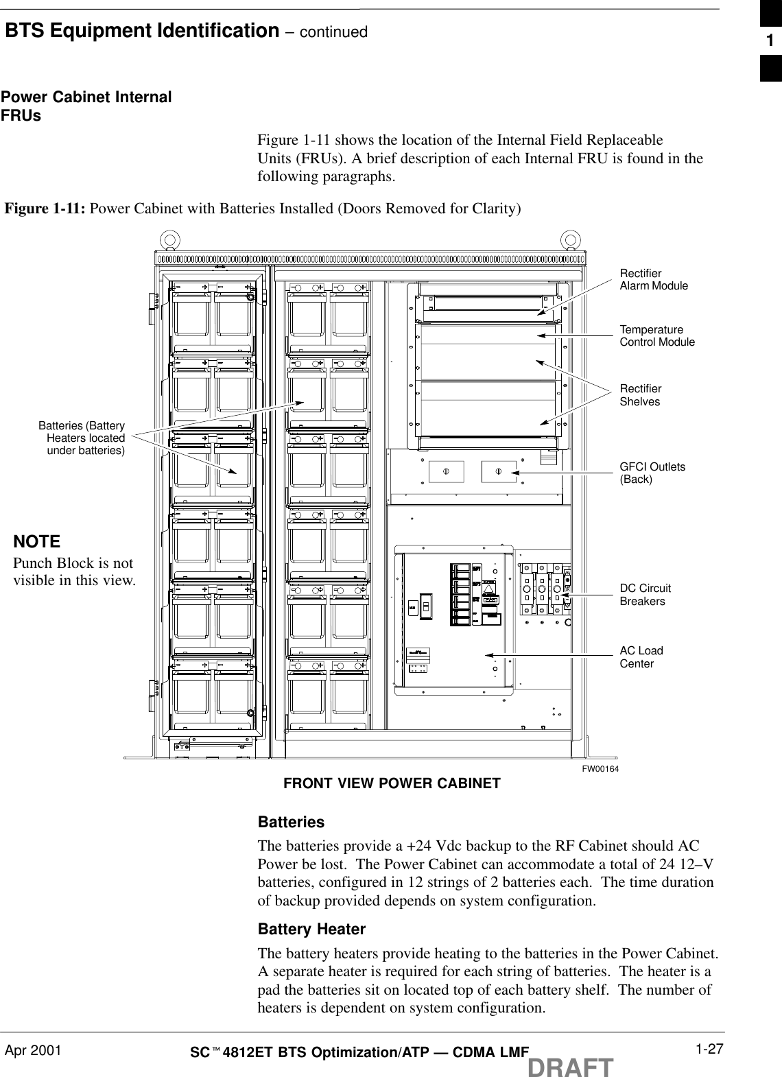


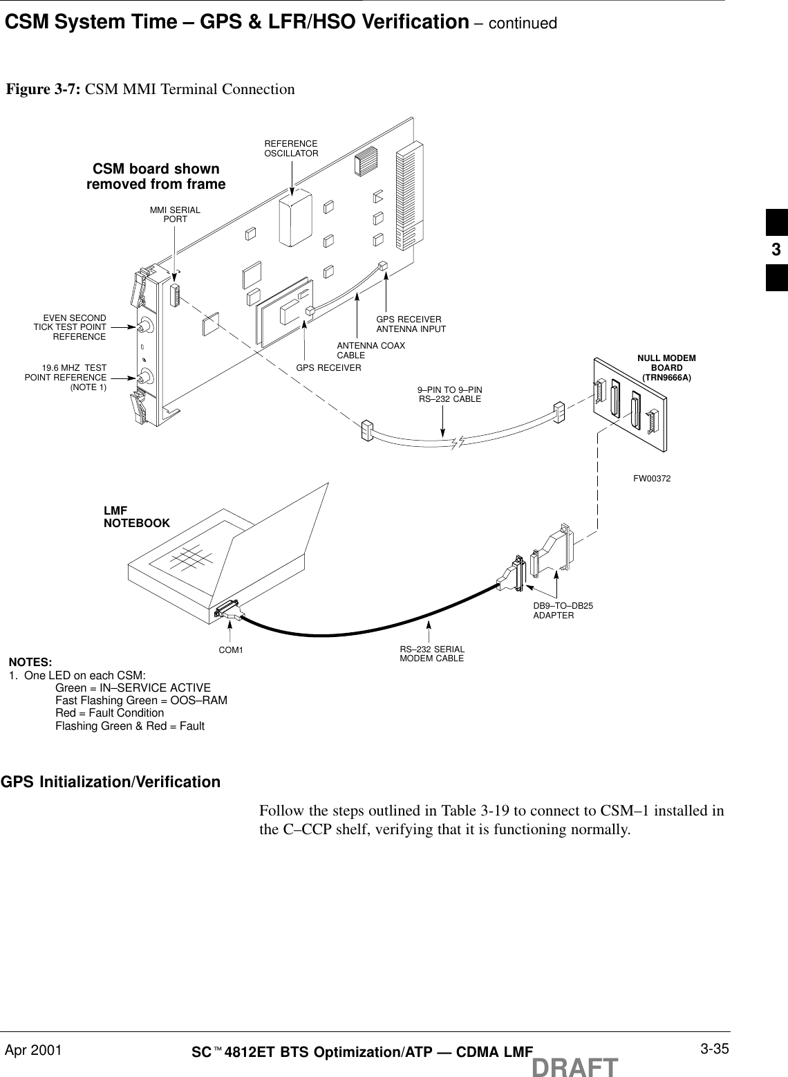
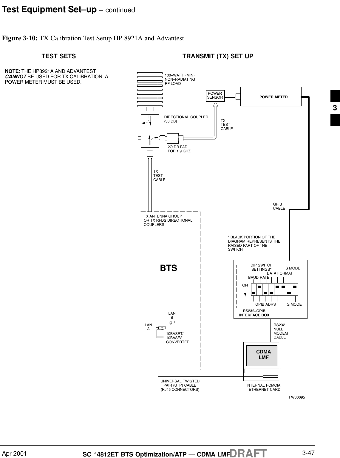
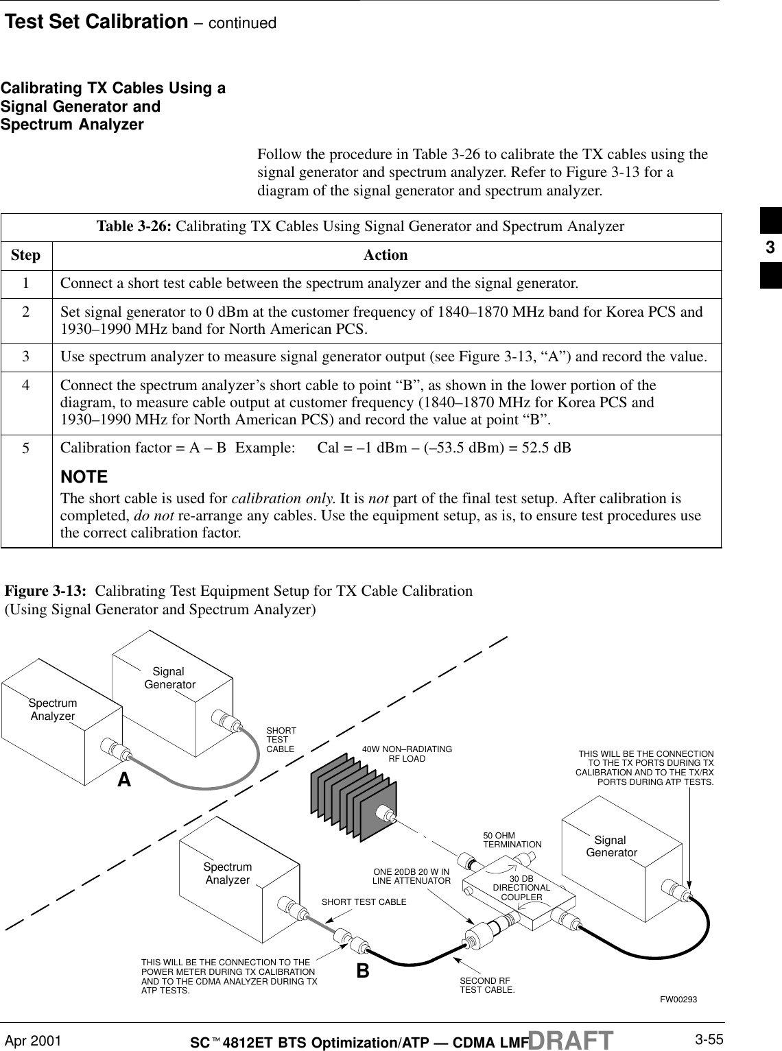
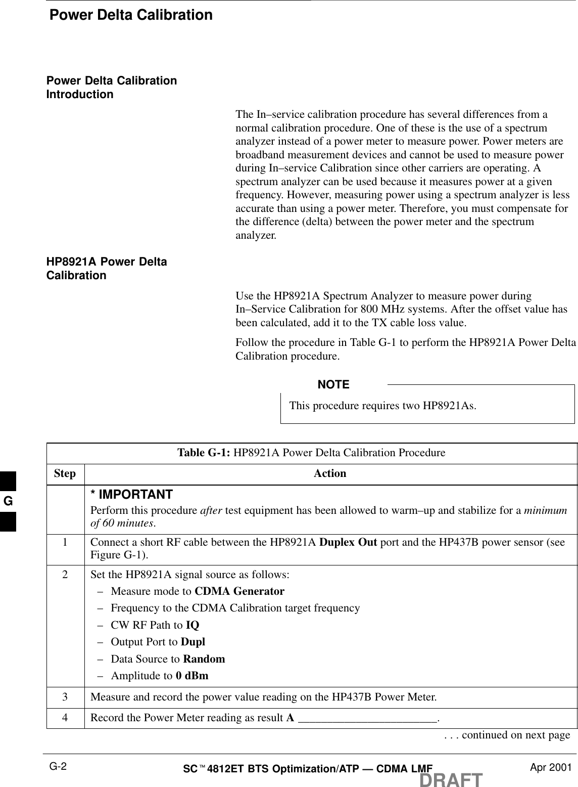
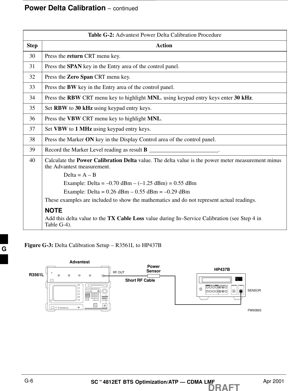
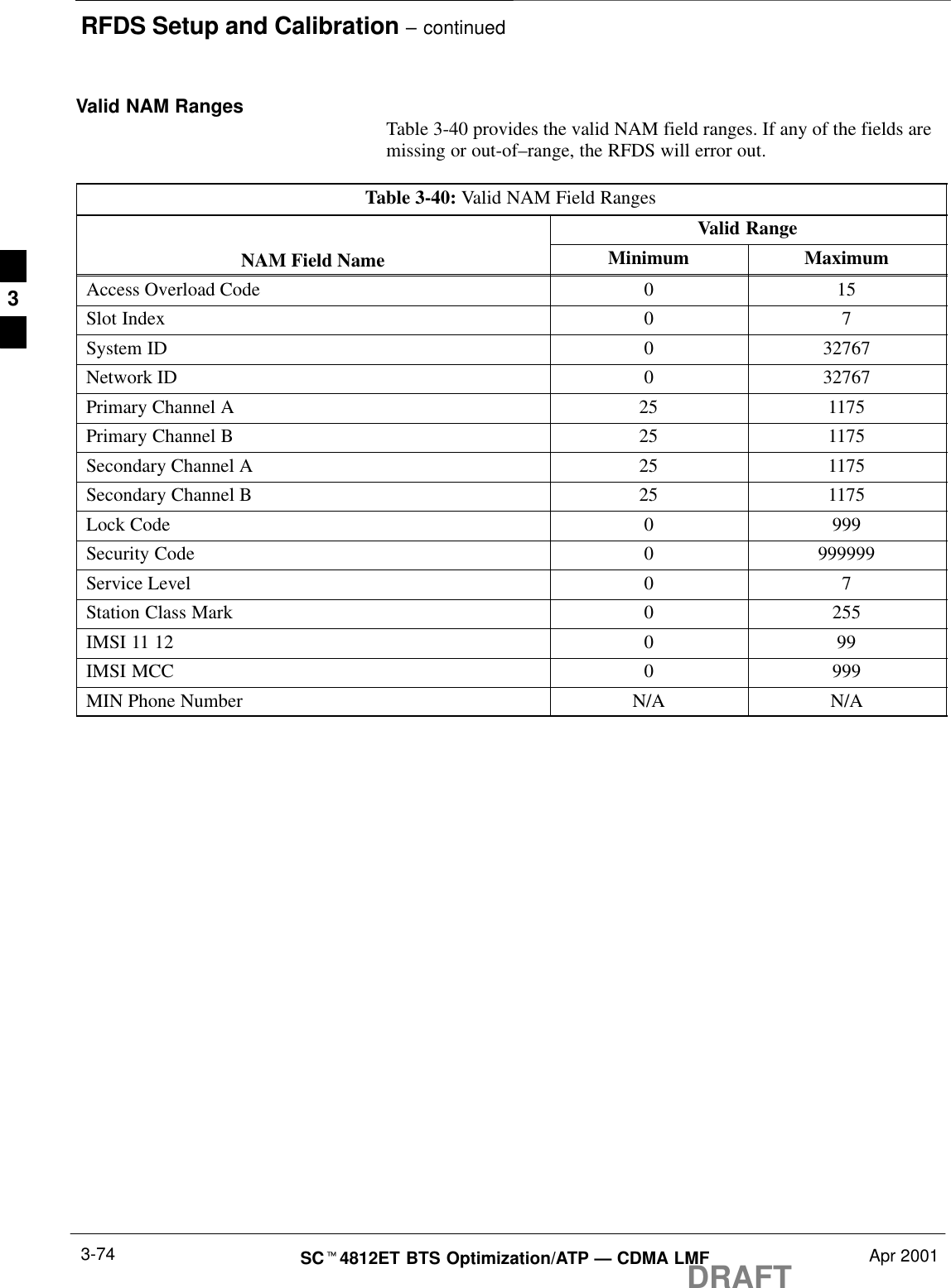
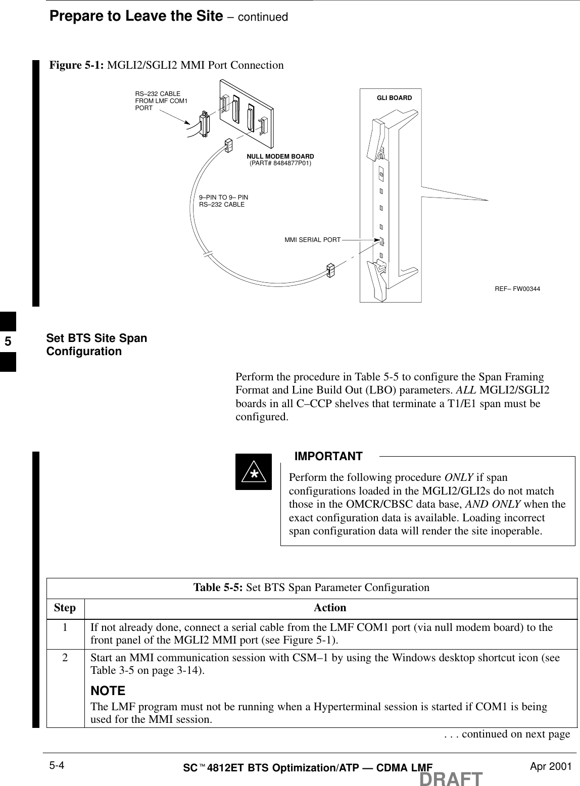
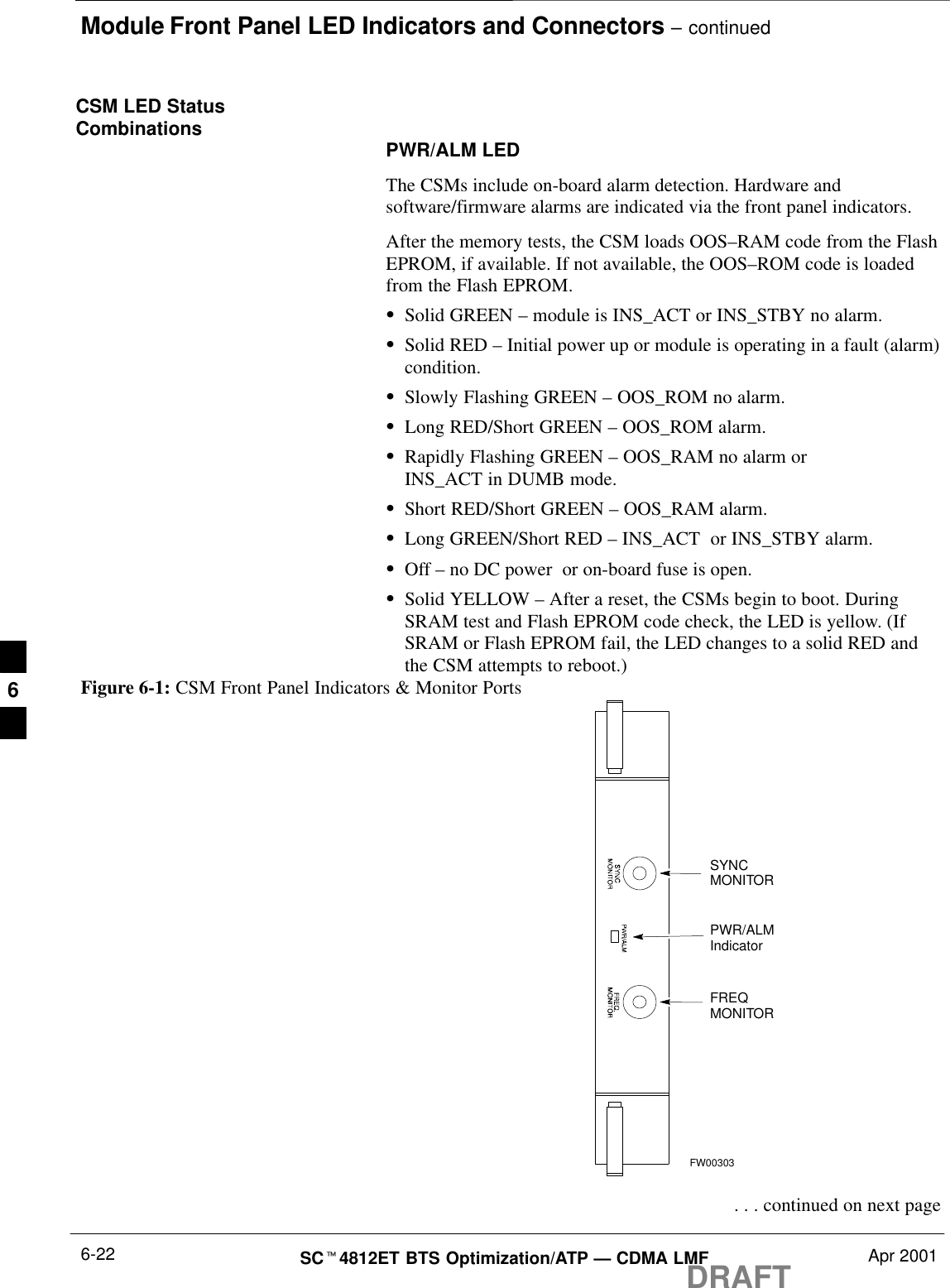
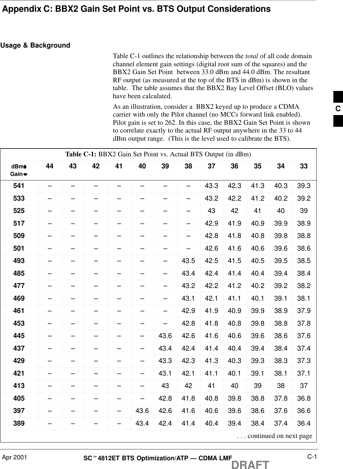
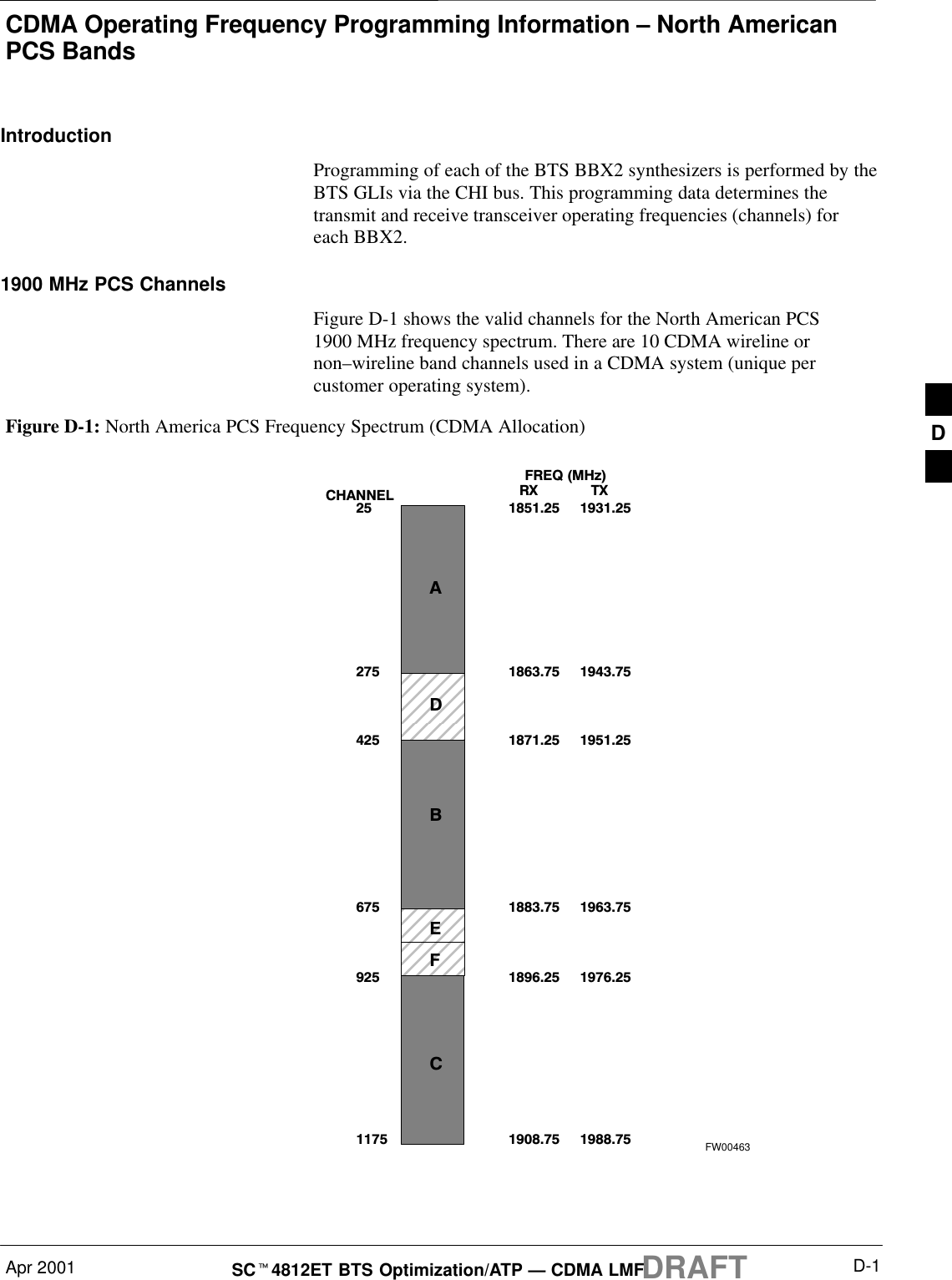
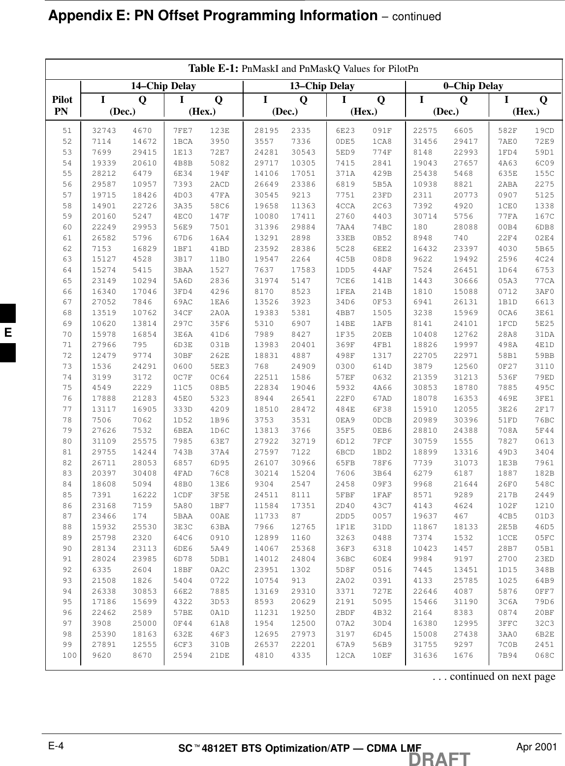
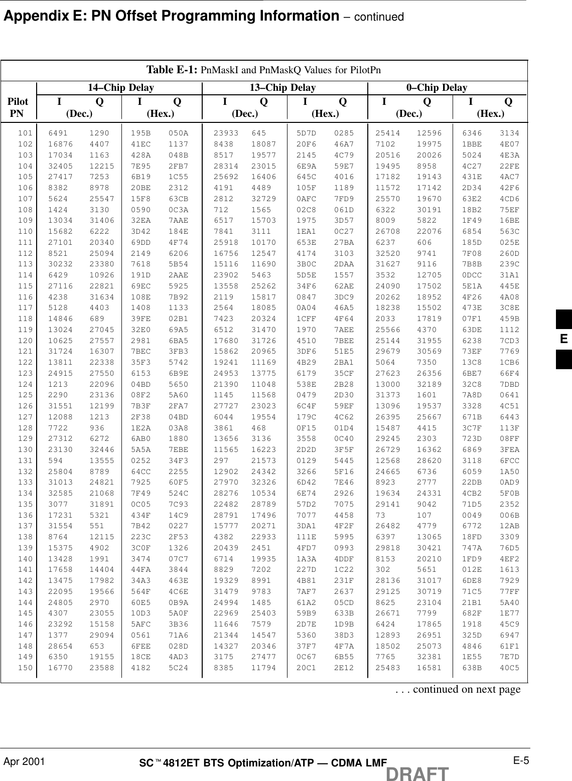
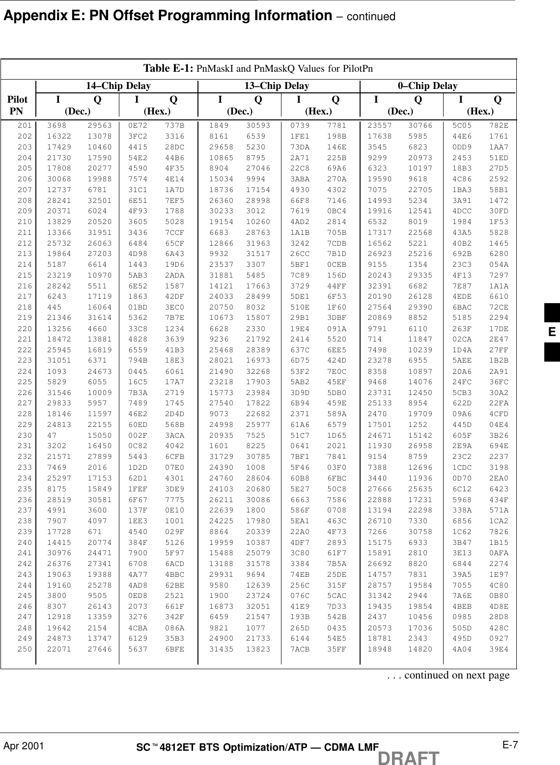
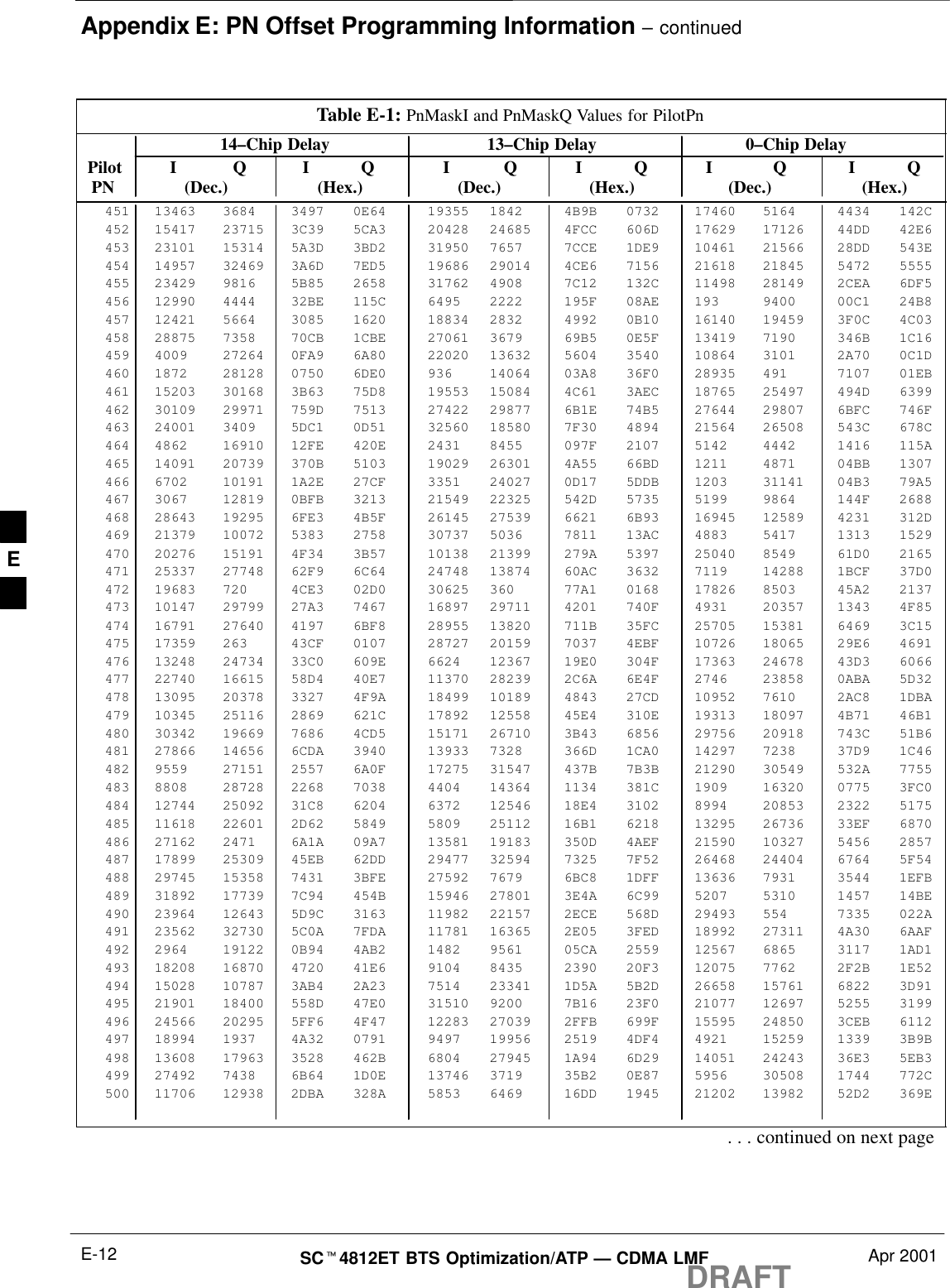
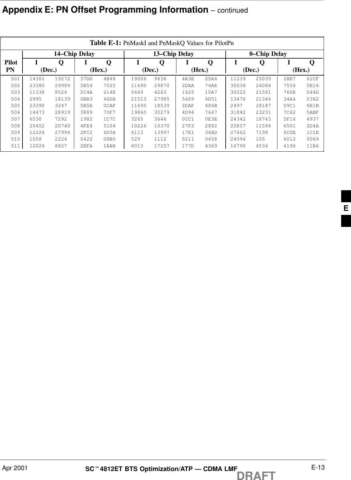
![Bay Level Offset Calibration – continuedApr 2001 3-61SCt4812ET BTS Optimization/ATP — CDMA LMFDRAFTBLO Calibration Data FileDuring the calibration process, the LMF creates a calibration (BLO) datafile. After calibration has been completed, this offset data must bedownloaded to the BBX2s using the Download BLO function. Anexplanation of the file is shown below.Due to the size of the file, Motorola recommends that youprint out a hard copy of a bts.cal file and refer to it for thefollowing descriptions.NOTEThe CAL file is subdivided into sections organized on a per slot basis (aslot Block).Slot 1 contains the calibration data for the 12 BBX2 slots. Slot 20contains the calibration data for the redundant BBX2 (see Table 3-31).Each BBX2 slot header block contains:SA creation Date and Time – broken down into separate parameters ofcreateMonth, createDay, createYear, createHour, and createMin.SThe number of calibration entries – fixed at 720 entries correspondingto 360 calibration points of the CAL file including the slot header andactual calibration data.SThe calibration data for a BBX2 is organized as a large flat array. Thearray is organized by branch, BBX2 slot, and calibration point.–The first breakdown of the array indicates which branch thecontained calibration points are for. The array covers transmit, mainreceive and diversity receive offsets as follows:Table 3-30: BLO BTS.cal file Array Branch AssignmentsRange AssignmentC[1]–C[240] TransmitC[241]–C[480] ReceiveC[481]–C[720] Diversity Receive3](https://usermanual.wiki/Nokia-Solutions-and-Networks/T5EG1/User-Guide-492635-Page-137.png)
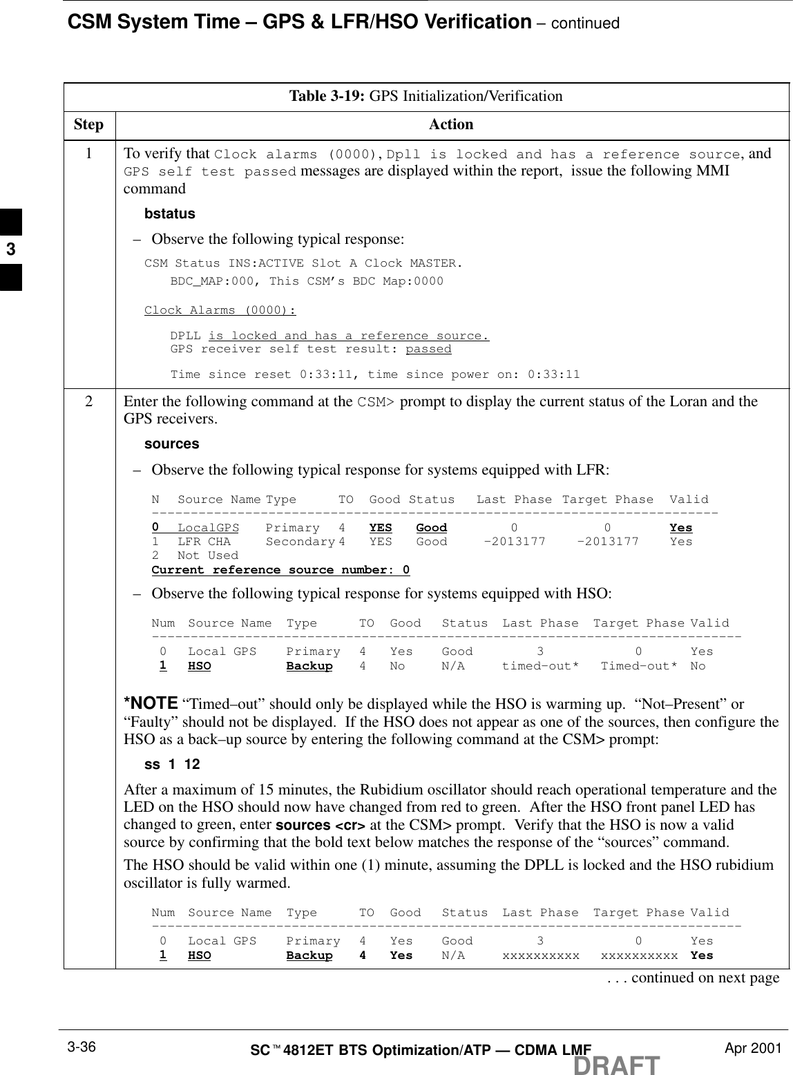
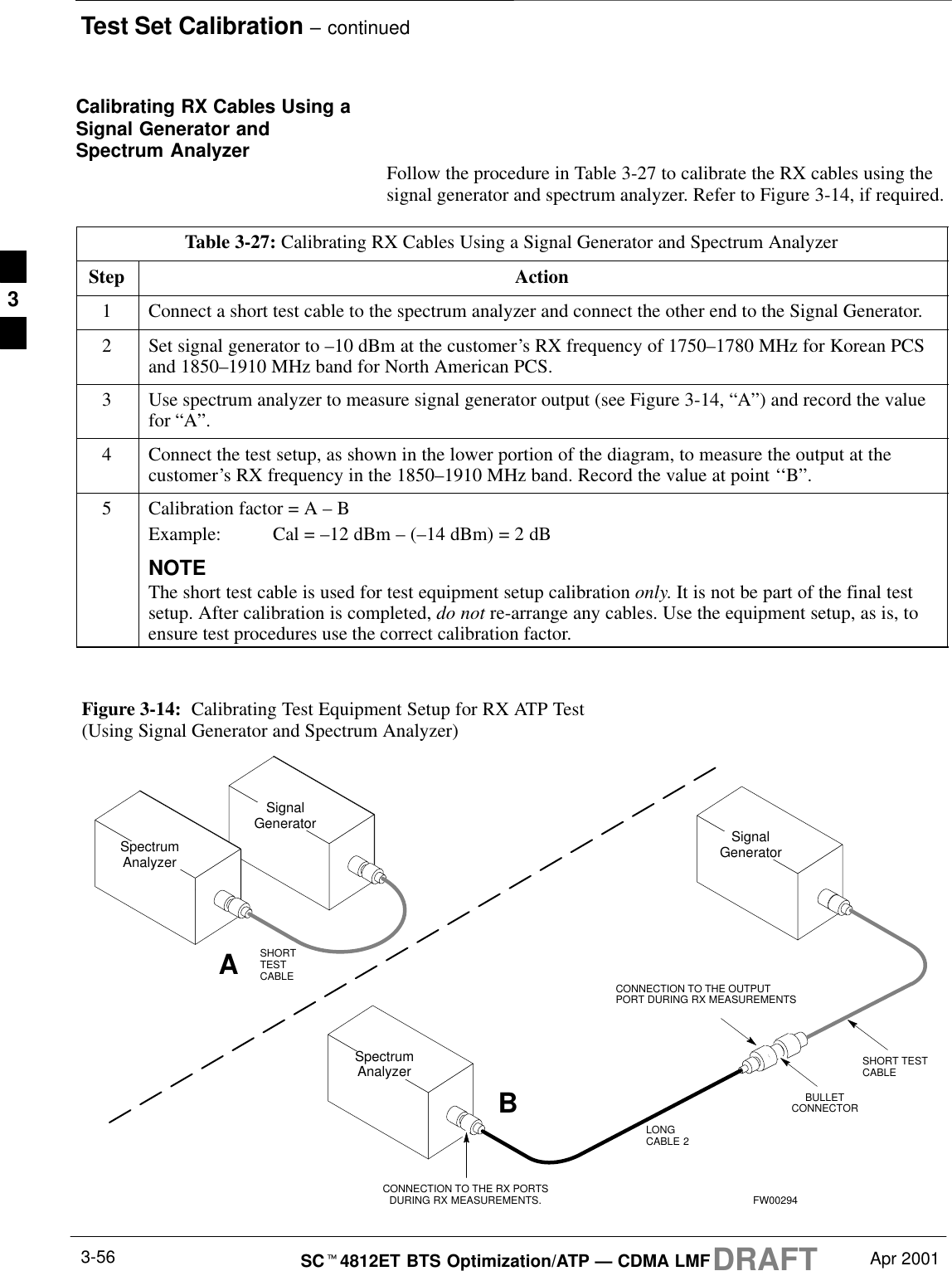
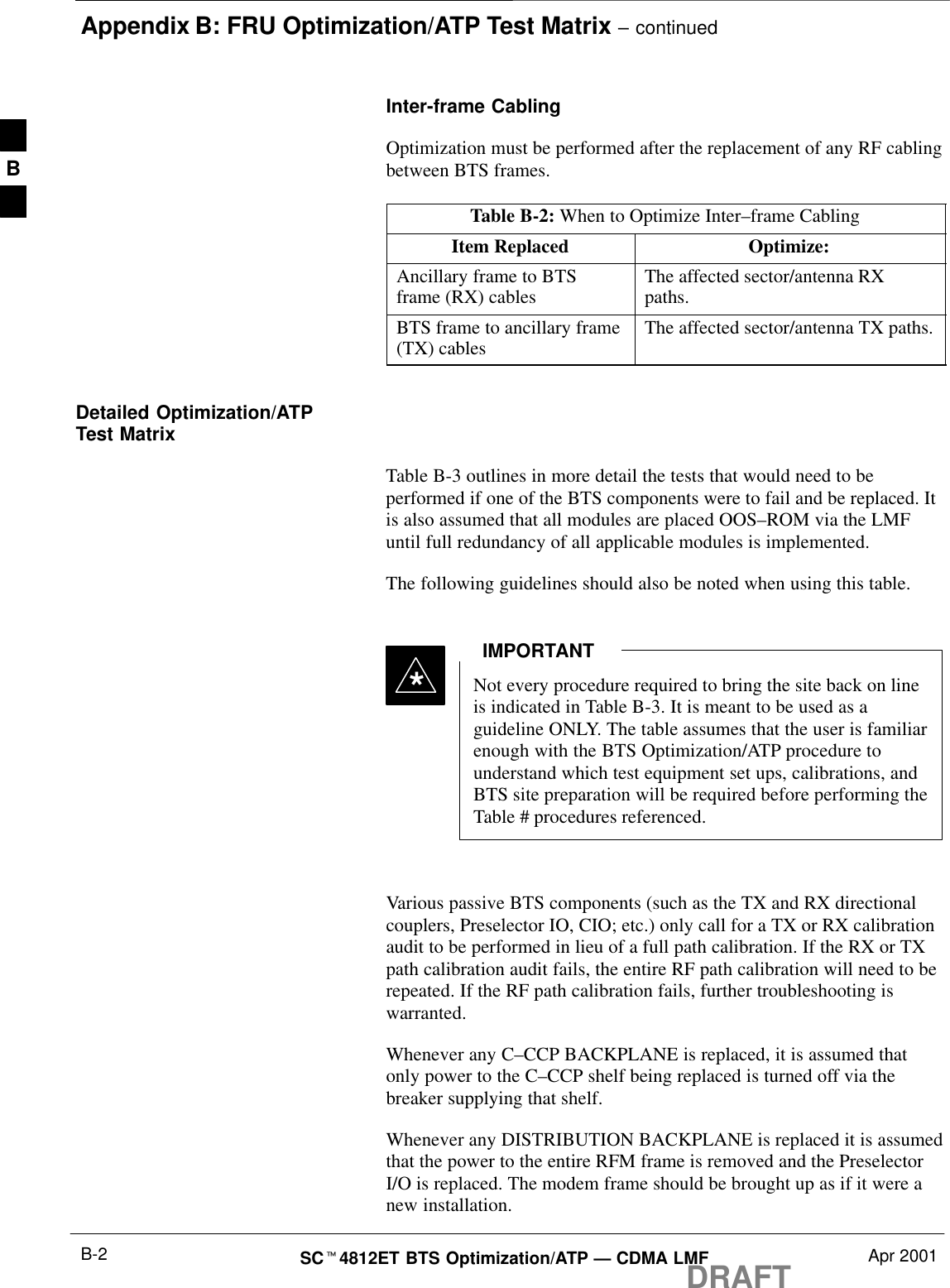
![Bay Level Offset Calibration – continuedDRAFTSCt4812ET BTS Optimization/ATP — CDMA LMF Apr 20013-62–The second breakdown of the array is per sector. Three sectors areallowed.Table 3-31: BTS.cal File Array (Per Sector)BBX2 Sectorization TX RX RX DiversitySlot[1] (Primary BBX2s 1 through 12)1 (Omni) 3–Sector, C[1]–C[20] C[241]–C[260] C[481]–C[500]23–Sector,1st C[21]–C[40] C[261]–C[280] C[501]–C[520]36 Sector, Carrier C[41]–C[60] C[281]–C[300] C[521]–C[540]41stCarrier 3–Sector, C[61]–C[80] C[301]–C[320] C[541]–C[560]5Carrier 3–Sector,3rd C[81]–C[100] C[321]–C[340] C[561]–C[580]6Carrier C[101]–C[120] C[341]–C[360] C[581]–C[600]73–Sector, C[121]–C[140] C[361]–C[380] C[601]–C[620]83–Sector,2nd C[141]–C[160] C[381]–C[400] C[621]–C[640]96 Sector, Carrier C[161]–C[180] C[401]–C[420] C[641]–C[660]10 2ndCarrier 3–Sector, C[181]–C[200] C[421]–C[440] C[661]–C[680]11 Carrier 3–Sector,4th C[201]–C[220] C[441]–C[460] C[681]–C[700]12 Carrier C[221]–C[240] C[461]–C[480] C[701]–C[720]Slot[20] (Redundant BBX2–13)1 (Omni) 3–Sector, C[1]–C[20] C[241]–C[260] C[481]–C[500]23–Sector,1st C[21]–C[40] C[261]–C[280] C[501]–C[520]36 Sector, Carrier C[41]–C[60] C[281]–C[300] C[521]–C[540]41stCarrier 3–Sector, C[61]–C[80] C[301]–C[320] C[541]–C[560]5Carrier 3–Sector,3rd C[81]–C[100] C[321]–C[340] C[561]–C[580]6Carrier C[101]–C[120] C[341]–C[360] C[581]–C[600]73–Sector, C[121]–C[140] C[361]–C[380] C[601]–C[620]83–Sector,2nd C[141]–C[160] C[381]–C[400] C[621]–C[640]96 Sector, Carrier C[161]–C[180] C[401]–C[420] C[641]–C[660]10 2ndCarrier 3–Sector, C[181]–C[200] C[421]–C[440] C[661]–C[680]11 Carrier 3–Sector,4th C[201]–C[220] C[441]–C[460] C[681]–C[700]12 Carrier C[221]–C[240] C[461]–C[480] C[701]–C[720]SRefer to the hard copy of the file. As you can see, 10 calibrationpoints per sector are supported for each branch. Two entries arerequired for each calibration point.SThe first value (all odd entries) refer to the CDMA channel(frequency) the BLO is measured at. The second value (all evenentries) is the power set level. The valid range for PwrLvlAdj is from2500 to 27500 (2500 corresponds to –125 dBm and 27500corresponds to +125 dBm).3](https://usermanual.wiki/Nokia-Solutions-and-Networks/T5EG1/User-Guide-492635-Page-138.png)
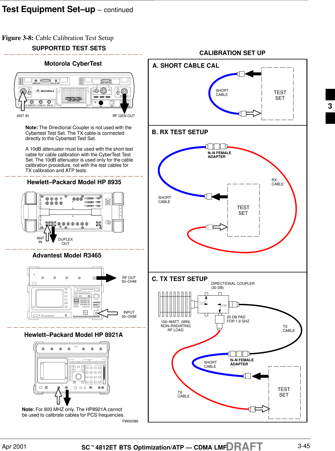
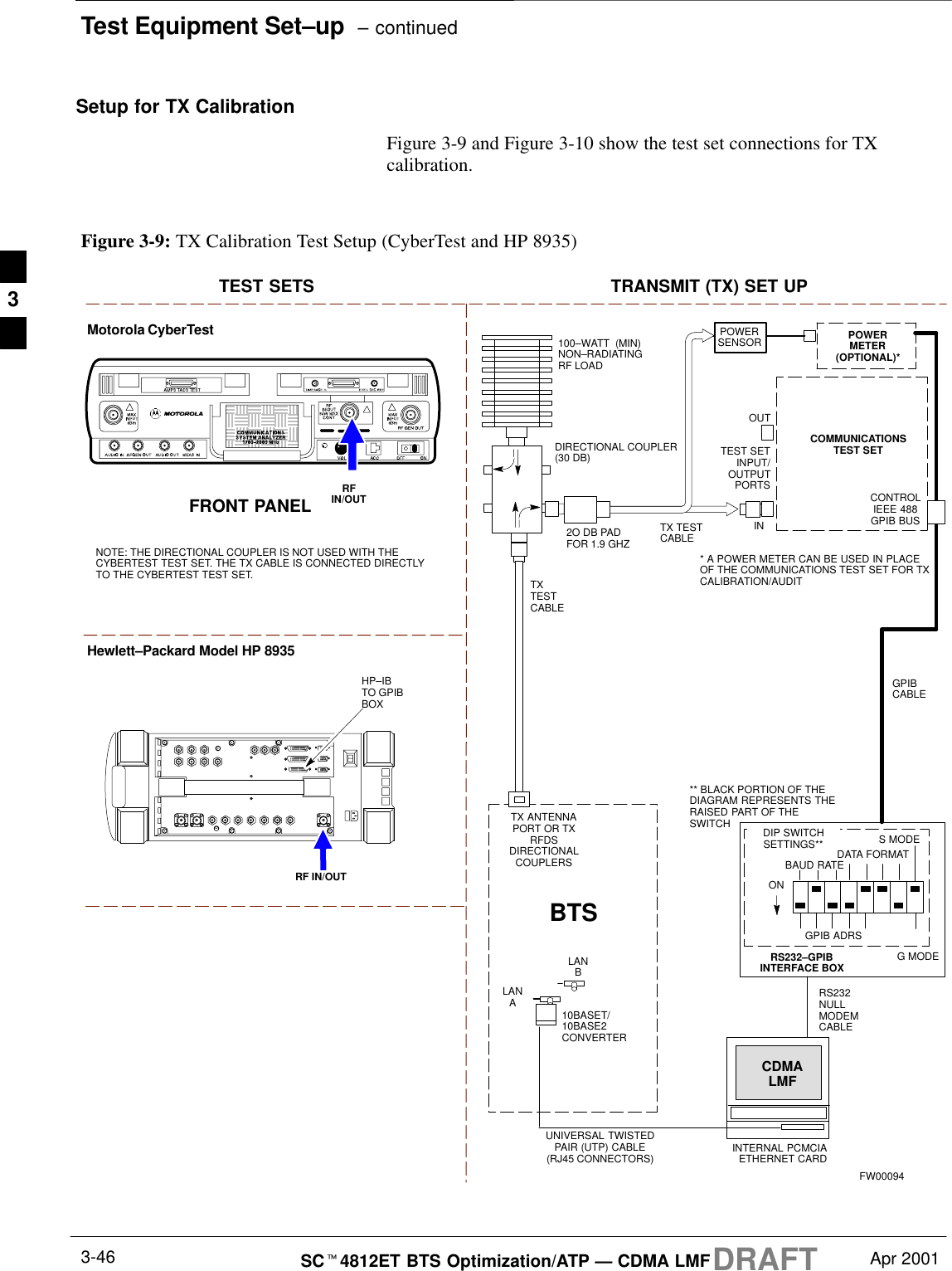
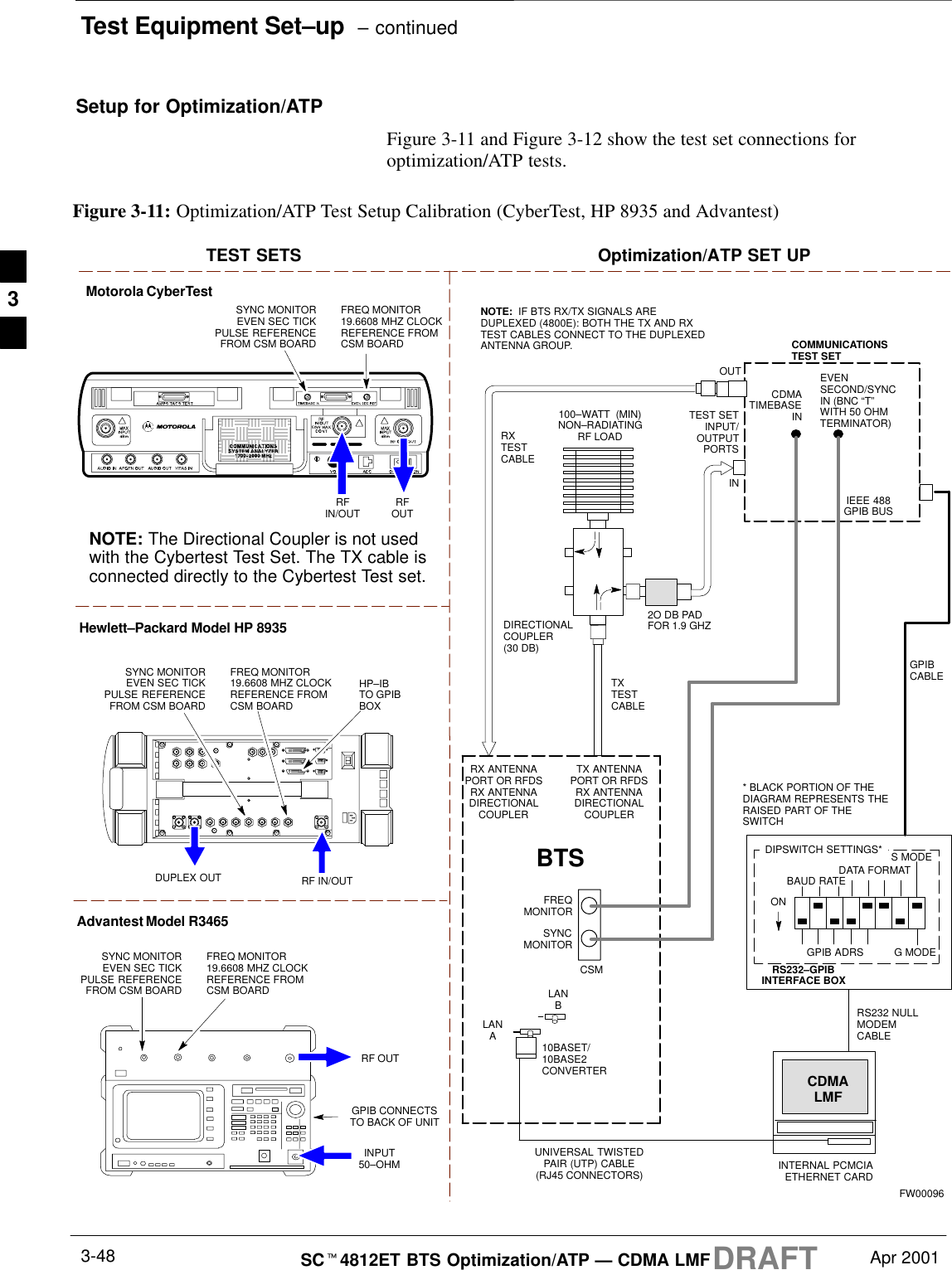
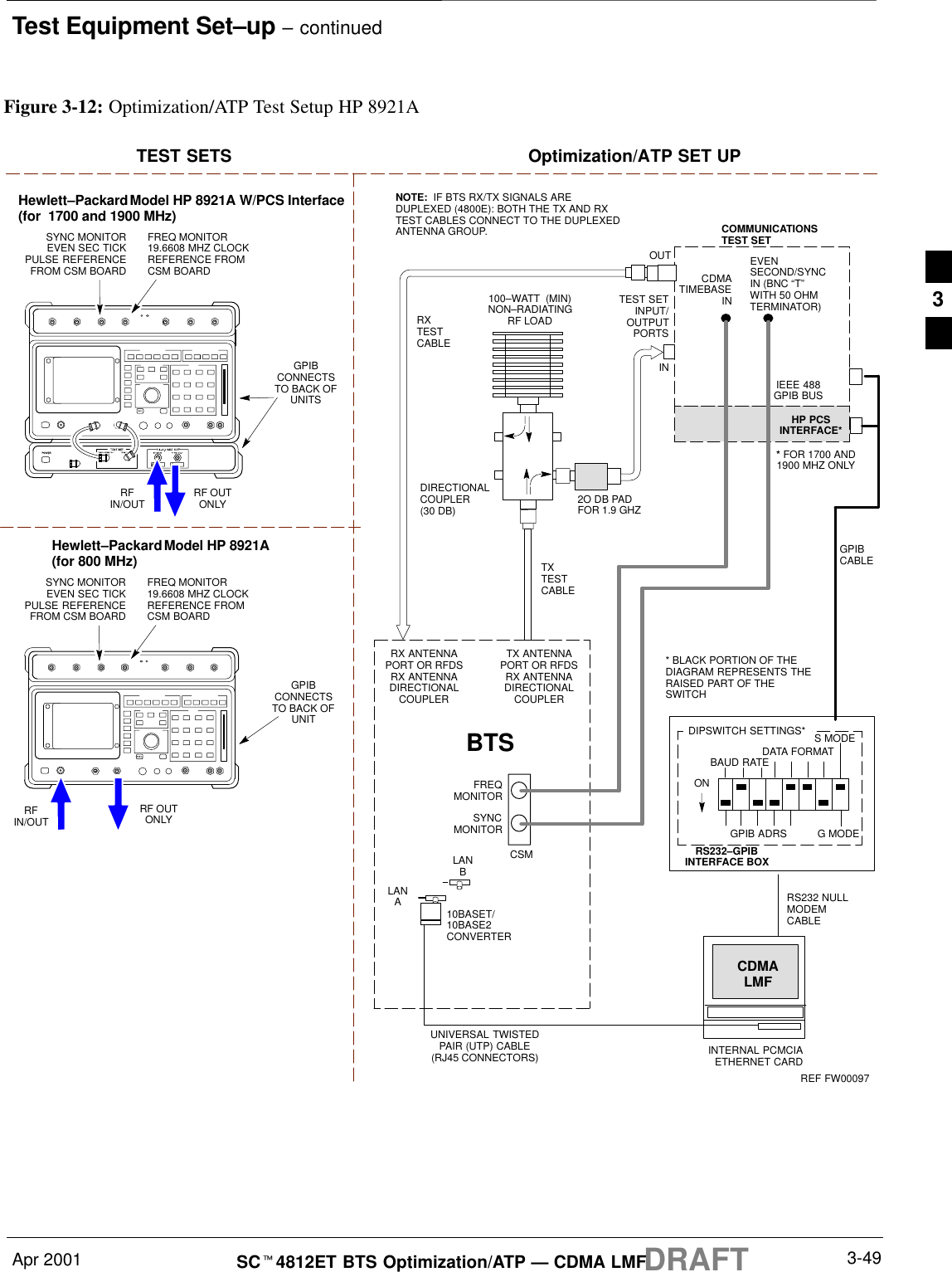
![Bay Level Offset Calibration – continuedApr 2001 3-63SCt4812ET BTS Optimization/ATP — CDMA LMFDRAFTSThe 20 calibration entries for each slot/branch combination must bestored in order of increasing frequency. If less than 10 points(frequencies) are calibrated, the largest frequency that is calibrated isrepeated to fill out the 10 points.Example:C[1]=384, odd cal entry = 1 ‘‘calibration point”C[2]=19102, even cal entryC[3]=777,C[4]=19086,..C[19]=777,C[20]=19086, (since only two cal points were calibrated this would be repeated for the next 8 points)SWhen the BBX2 is loaded with BLO data, the cal file data for theBBX2 is downloaded to the device in the order it is stored in the CALfile. TxCal data is sent first, C[1] – C[60]. BBX2 slot 1’s 10calibration points are sent (C[1] – C[20]), followed by BBX2 slot 2’s10 calibration points (C[21] – C[40]), etc. The RxCal data is sent next,followed by the RxDCal data.STemperature compensation data is also stored in the cal file for eachslot.Test Equipment Setup:RF Path CalibrationFollow the steps outlined in Table 3-32 to set up test equipment.Table 3-32: Test Equipment Setup (RF Path Calibration)Step ActionNOTEVerify the GPIB is properly connected and turned on.! CAUTIONTo prevent damage to the test equipment, all transmit (TX) test connections must be via the 30 dBdirectional coupler for 800 MHz or via a 30 dB coupler with a 20 dB in–line attenuator for 1900 MHz.1Connect the LMF computer terminal to the BTS LAN A connector on the BTS (if you have notalready done so). Refer to the procedure in Table 3-6.SIf required, calibrate the test equipment per the procedure in Table 3-24.SConnect the test equipment as shown in Figure 3-9 and Figure 3-10.3](https://usermanual.wiki/Nokia-Solutions-and-Networks/T5EG1/User-Guide-492635-Page-139.png)

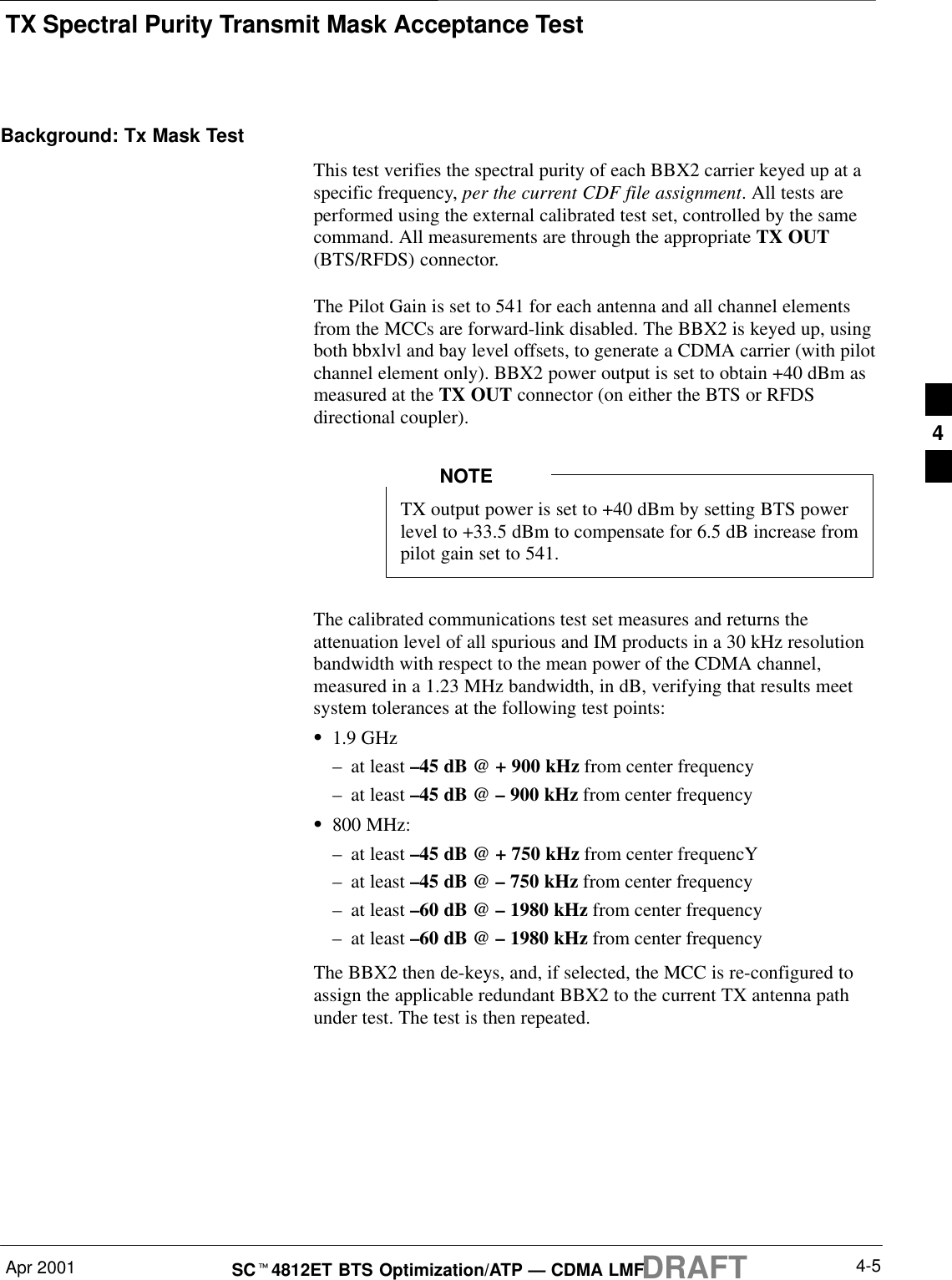
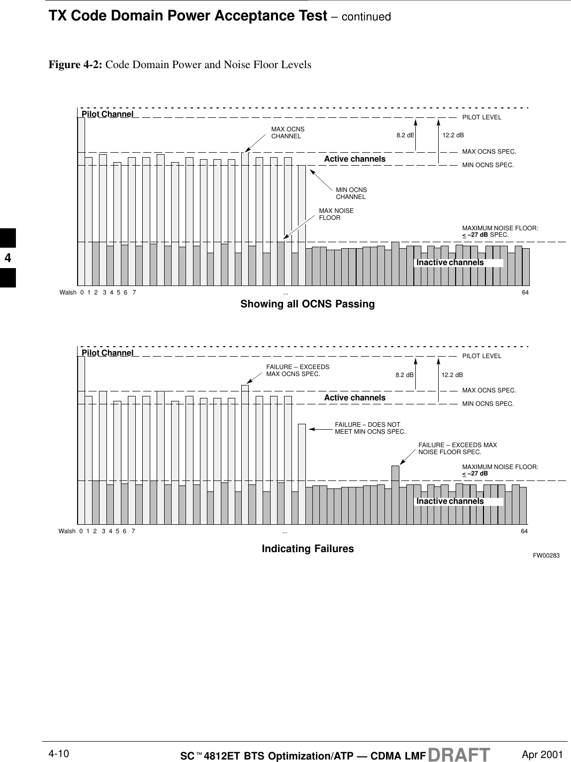
![Automated Acceptance Test Procedure – Overview – continuedDRAFTSCt4812ET BTS Optimization/ATP — CDMA LMF Apr 20014-4Waveform Quality (rho)This test verifies that the transmitted Pilot channel element digitalwaveform quality (rho) exceeds the minimum specified value inANSI–J_STD–019. “Rho” represents the correlation between actual andperfect CDMA modulation spectrum. A rho value of 1.0000 represents100% (or perfect correlation).Pilot Time OffsetThe Pilot Time Offset is the difference between the CDMA analyzermeasurement interval (based on the BTS system time reference) and theincoming block of transmitted data from the BTS (Pilot only, PilotGain = 262, PN Offset = 0).Code Domain PowerThis test verifies code domain power levels, which have been set for allODD numbered Walsh channels, using the OCNS command. This isdone by verifying that the ratio of PILOT divided by OCNS is equal to10.2 + 2 dB, and, that the noise floor of all EVEN numbered “OFF”Walsh channels measures < –27 dB .Frame Error RateThe Frame Error Rate (FER) test verifies RX operation of the entireCDMA Reverse Link using all equipped MCCs assigned to allrespective sector/antennas. The test verifies the BTS sensitivity on alltraffic channel elements currently configured on all equipped MCCs atan RF input level of –119 dBm (or –116 dBm if using TMPC). Followthe procedure in Table 4-1 to perform any ATP test.The STOP button can be used to stop the testing process.NOTETable 4-1: ATP Test ProcedureStep Action1Select the BBX2(s) and MCC(s) to be tested.2From the Tests menu, select the desired test.3Select the appropriate carrier(s) (carrier – bts# – sector# – carrier#) displayed in the Channels/Carrierpick list.To select multiple items, hold down the <Shift> or <Ctrl> key while making the selections.4Type the appropriate channel number in the Carrier n Channels box.The default channel number displayed is determined by the CdmaChans[n] number in the cbsc–n.cdffile for the BTS.5 Click OK.6Follow the cable connection directions as they are displayed.7 Click Save Results or Dismiss to close the status report window. If Dismiss is used the test results will not be saved in the test report file. 4](https://usermanual.wiki/Nokia-Solutions-and-Networks/T5EG1/User-Guide-492635-Page-172.png)
![RX Frame Error Rate (FER) Acceptance TestApr 2001 4-11SCt4812ET BTS Optimization/ATP — CDMA LMFDRAFTBackground: FER TestThis test verifies the BTS Frame Error Rate (FER) on all traffic channelelements currently configured on all equipped MCCs (full rate at 1%FER) at an RF input level of –119 dBm [or –116 dBm if using TowerTop Amplifier (TMPC)]. All tests are performed using the externalcalibrated test set as the signal source controlled by the same command.All measurements will be via the LMF.The pilot gain is set to 262 for each TX antenna and all channel elementsfrom the MCCs are forward-link disabled. The BBX2 is keyed up usingonly bbxlvl level offsets, to generate a CDMA carrier (with pilot channelelement only). BBX2 power output is set to –20 dBm as measured at theTX OUT connector (on either the BTS or RFDS directional coupler).The BBX2 must be keyed in order to enable the RX receive circuitry.The LMF prompts the MCC/CE under test to measure all zero longcodeand provide the FER report on the selected active MCC on the reverselink for both the main and diversity RX antenna paths, verifying theresults meet the following specification: FER returned less than 1% andtotal frames measured is 1500.All MCC/CEs selected are tested on the specified RX antenna path. TheBBX then de-keys and, the applicable redundant BBX2 is assigned tothe current RX antenna paths under test. The test is then repeated.4](https://usermanual.wiki/Nokia-Solutions-and-Networks/T5EG1/User-Guide-492635-Page-179.png)


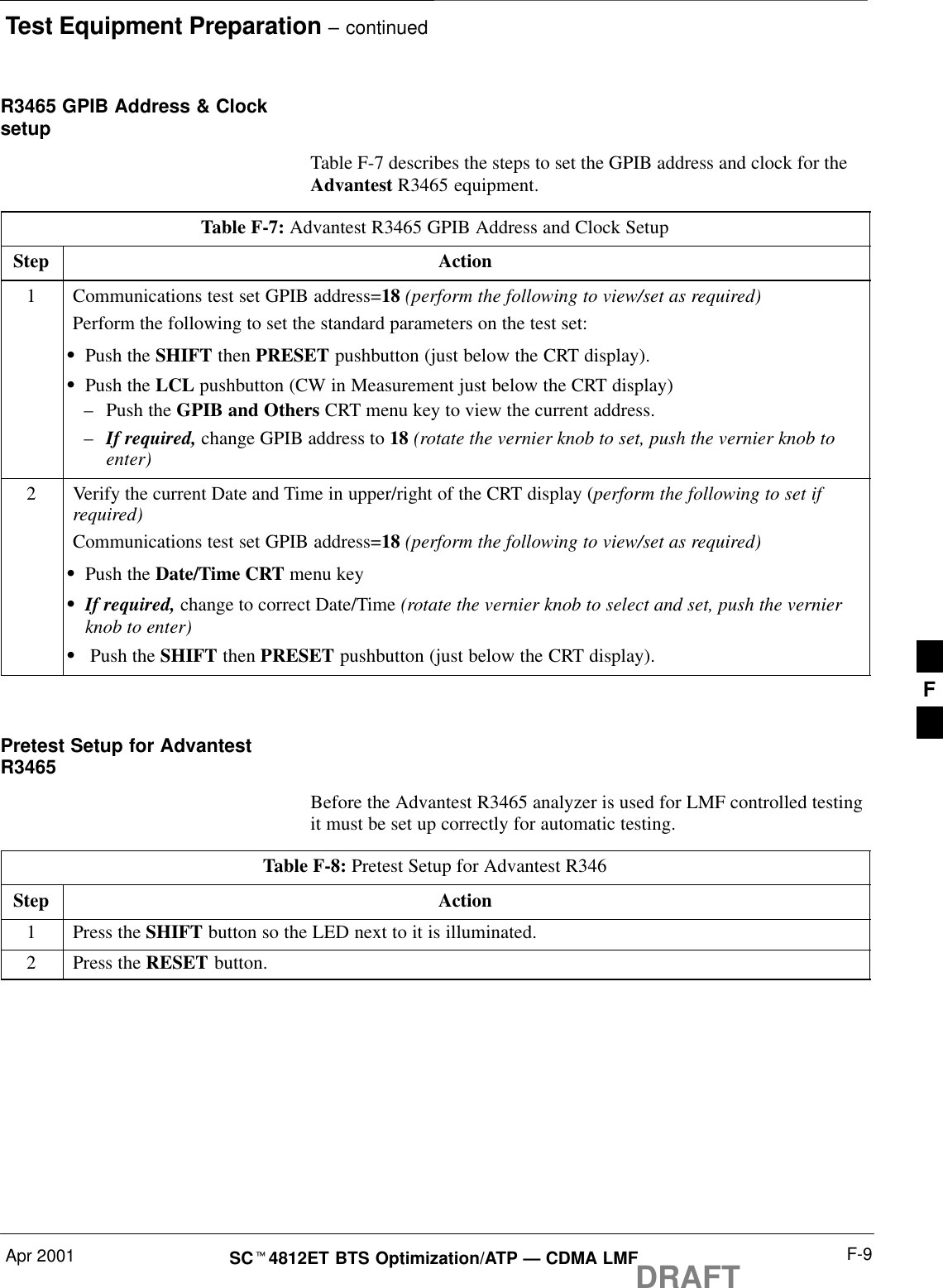
![Test Equipment Preparation – continuedApr 2001 F-5SCt4812ET BTS Optimization/ATP — CDMA LMFDRAFTHP8921A System ConnectivityTestFollow the steps outlined in Table F-3 to verify that the connectionsbetween the PCS Interface and the HP8921A are correct and cables areintact. The software also performs basic functionality checks of eachinstrument.Disconnect other GPIB devices, especially systemcontrollers, from the system before running theconnectivity software.IMPORTANT*Table F-3: System ConnectivityStep Action* IMPORTANT–Perform this procedure after test equipment has been allowed to warm–up and stabilize for aminimum of 60 minutes.1Insert HP 83236A Manual Control/System card into memory card slot.2Press the [PRESET] pushbutton.3Press the Screen Control [TESTS] pushbutton to display the “Tests” Main Menu screen.4Position the cursor at Select Procedure Location and select it by pressing the cursor control knob. Inthe Choices selection box, select Card.5Position the cursor at Select Procedure Filename and select it by pressing the cursor control knob. Inthe Choices selection box, select SYS_CONN.6Position the cursor at RUN TEST and select it. The software will prompt you through theconnectivity setup.7Do the following when the test is complete,Sposition cursor on STOP TEST and select itSOR press the [K5] pushbutton.8To return to the main menu, press the [K5] pushbutton.9Press the [PRESET] pushbutton.F](https://usermanual.wiki/Nokia-Solutions-and-Networks/T5EG1/User-Guide-492635-Page-281.png)
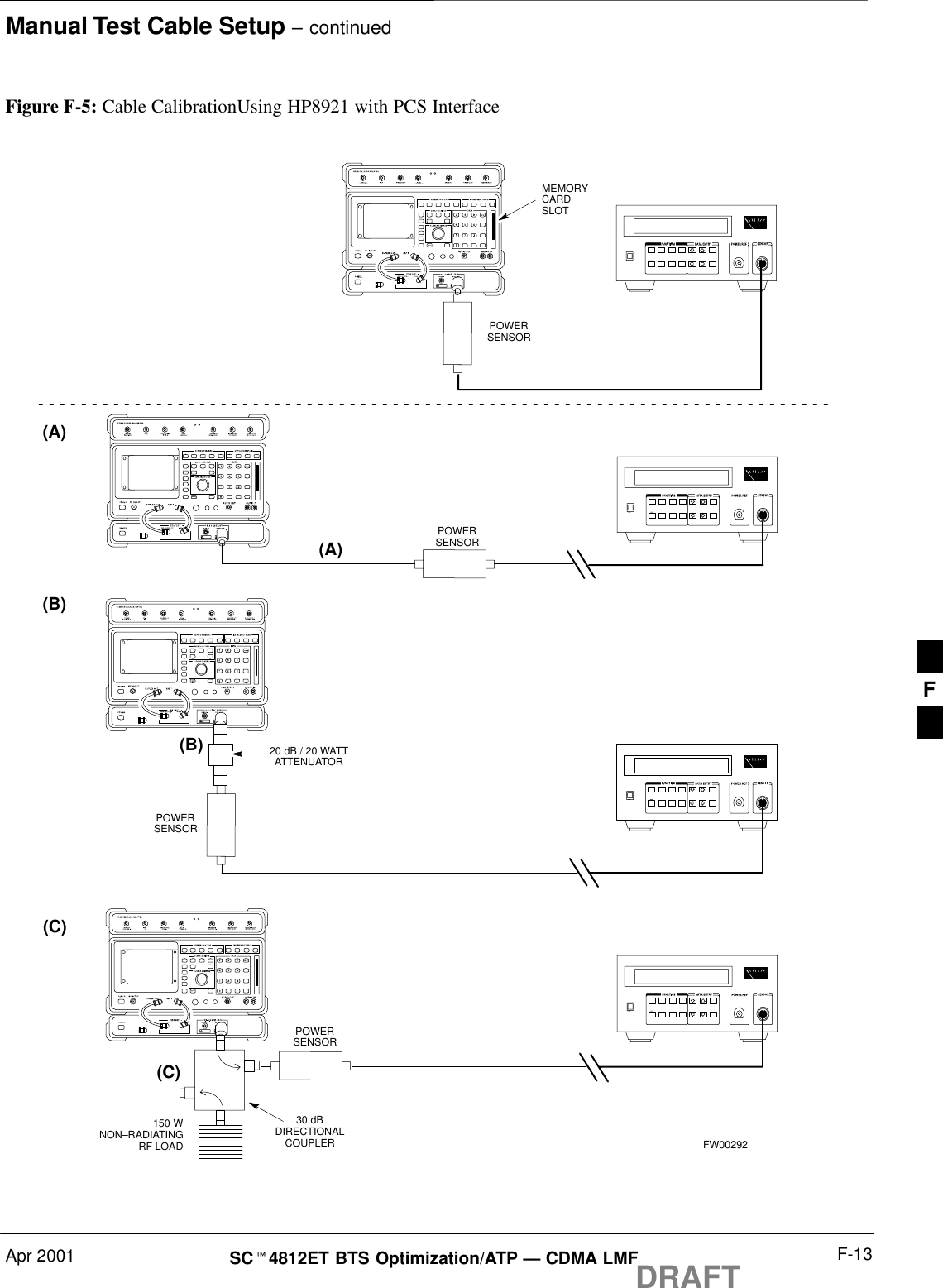
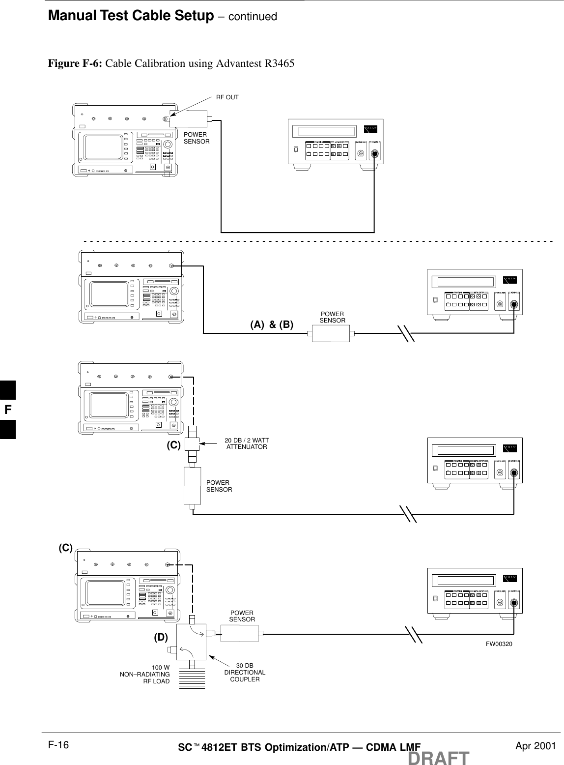
![Manual Cable CalibrationDRAFTSCt4812ET BTS Optimization/ATP — CDMA LMF Apr 2001F-10Calibrating Test Cable Setupusing HP PCS Interface (HP83236)Table F-9 covers the procedure to calibrate the test equipment using the HP8921 Cellular Communications Analyzer equipped with theHP83236 PCS Interface.This calibration method must be executed with great care.Some losses are measured close to the minimum limit ofthe power meter sensor (–30 dBm).NOTEPrerequisitesEnsure the following prerequisites have been met before proceeding:STest equipment to be calibrated has been connected correctly for cablecalibration.STest equipment has been selected and calibrated.Table F-9: Calibrating Test Cable Setup (using the HP PCS Interface)Step ActionNOTEVerify that GPIB controller is turned off.1Insert HP83236 Manual Control System card into memory card slot.2Press the Preset pushbutton.3 Under Screen Controls, press the TESTS pushbutton to display the TESTS (Main Menu) screen.4Position the cursor at Select Procedure Location and select it. In the Choices selection box, selectCARD.5Position the cursor at Select Procedure Filename and select it. In the Choices selection box, selectMANUAL.6Position the cursor at RUN TEST and select it. HP must be in Control Mode Select YES.7If using HP 83236A:Set channel number=<chan#>:–Position cursor at ChannelNumber and select it.–Enter the chan# using the numerickeypad; press [Enter] and thescreen will go blank.–When the screen reappears, thechan# will be displayed on thechannel number line.If using HP 83236B:Set channel frequency:–Position cursor at Frequency Band and press Enter.–Select User Defined Frequency.–Go Back to Previous Menu.–Position the cursor to 83236 generator frequency andenter actual RX frequency.–Position the cursor to 83236 analyzer frequency andenter actual TX frequency.. . . continued on next pageF](https://usermanual.wiki/Nokia-Solutions-and-Networks/T5EG1/User-Guide-492635-Page-286.png)
![Manual Test Cable Setup – continuedApr 2001 F-11SCt4812ET BTS Optimization/ATP — CDMA LMFDRAFTTable F-9: Calibrating Test Cable Setup (using the HP PCS Interface)Step Action8Set RF Generator level:–Position the cursor at RF Generator Level and select it.–Enter –10 using the numeric keypad; press [Enter] and the screen will go blank.–When the screen reappears, the value –10 dBm will be displayed on the RF Generator Level line.9Set the user fixed Attenuation Setting to 0 dBm:–Position cursor at Analyzer Attenuation and select it–Position cursor at User Fixed Atten Settings and select it.–Enter 0 (zero) using the numeric keypad and press [Enter].10 Select Back to Previous Menu.11 Record the HP83236 Generator Frequency Level:Record the HP83236B Generator Frequency Level:–Position cursor at Show Frequency and Level Details and select it.–Under HP83236 Frequencies and Levels, record the Generator Level.–Under HP83236B Frequencies and Levels, record the Generator Frequency Level (1850 – 1910MHz).–Position cursor at Prev Menu and select it.12 Click on Pause for Manual Measurement.13 Connect the power sensor directly to the RF OUT ONLY port of the PCS Interface.14 On the HP8921A, under To Screen, select CDMA GEN.15 Move the cursor to the Amplitude field and click on the Amplitude value.16 Increase the Amplitude value until the power meter reads 0 dBm ±0.2 dB.NOTEThe Amplitude value can be increased coarsely until 0 dBM is reached; then fine tune the amplitudeby adjusting the Increment Set to 0.1 dBm and targeting in on 0 dBm.17 Disconnect the power sensor from the RF OUT ONLY port of the PCS Interface.* IMPORTANTThe Power Meter sensor’s lower limit is –30 dBm. Thus, only components having losses ≤30 dBshould be measured using this method. For further accuracy, always re-zero the power meterbefore connecting the power sensor to the component being calibrated. After connecting thepower sensor to the component, record the calibrated loss immediately.18 Disconnect all components in the test setup and calibrate each one separately by connecting eachcomponent, one-at-a-time, between the RF OUT ONLY PORT and the power sensor. Record thecalibrated loss value displayed on the power meter.SExample: (A) Test Cable(s) = –1.4 dB(B) 20 dB Attenuator = –20.1 dB(B) Directional Coupler = –29.8 dB. . . continued on next pageF](https://usermanual.wiki/Nokia-Solutions-and-Networks/T5EG1/User-Guide-492635-Page-287.png)
![Manual Test Cable Setup – continuedDRAFTSCt4812ET BTS Optimization/ATP — CDMA LMF Apr 2001F-12Table F-9: Calibrating Test Cable Setup (using the HP PCS Interface)Step Action19 After all components are calibrated, reassemble all components together and calculate the total testsetup loss by adding up all the individual losses:SExample: Total test setup loss = –1.4 –29.8 –20.1 = –51.3 dB.This calculated value will be used in the next series of tests.20 Under Screen Controls press the TESTS button to display the TESTS (Main Menu) screen.21 Select Continue (K2).22 Select RF Generator Level and set to –119 dBm.23 Click on Pause for Manual Measurement.24 Verify the HP8921A Communication Analyzer/83203A CDMA interface setup is as follows (fieldsnot indicated remain at default):SVerify the GPIB (HP–IB) address:–under To Screen, select More–select IO CONFIG–Set HP–IB Adrs to 18–set Mode to Talk&LstnSVerify the HP8921A is displaying frequency (instead of RF channel)–Press the blue [SHIFT] button, then press the Screen Control [DUPLEX] button; this switches tothe CONFIG (CONFIGURE) screen.–Use the cursor control to set RF Display to Freq25 Refer toChapter 3 for assistance in setting the cable loss values into the LMF. F](https://usermanual.wiki/Nokia-Solutions-and-Networks/T5EG1/User-Guide-492635-Page-288.png)
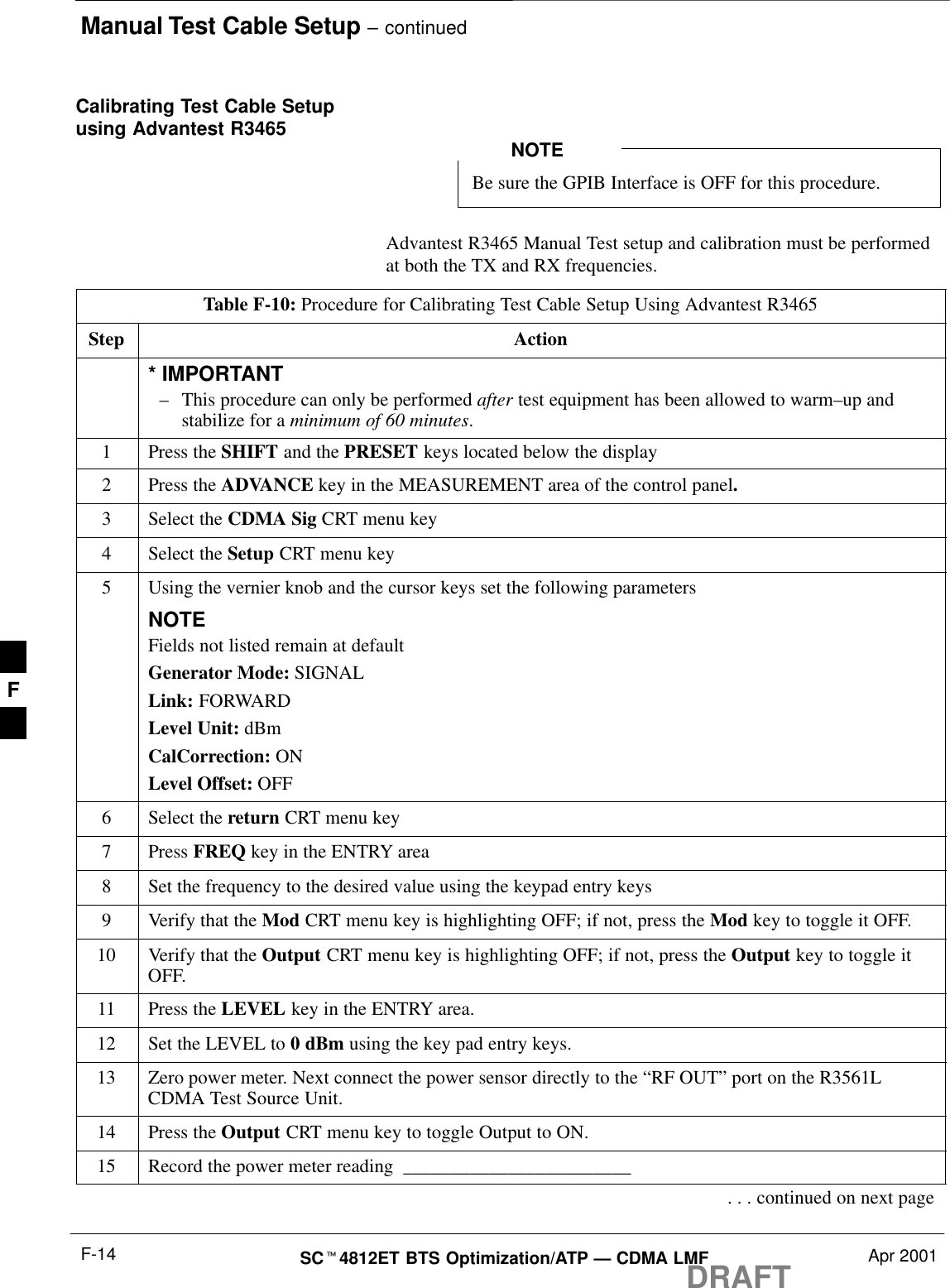
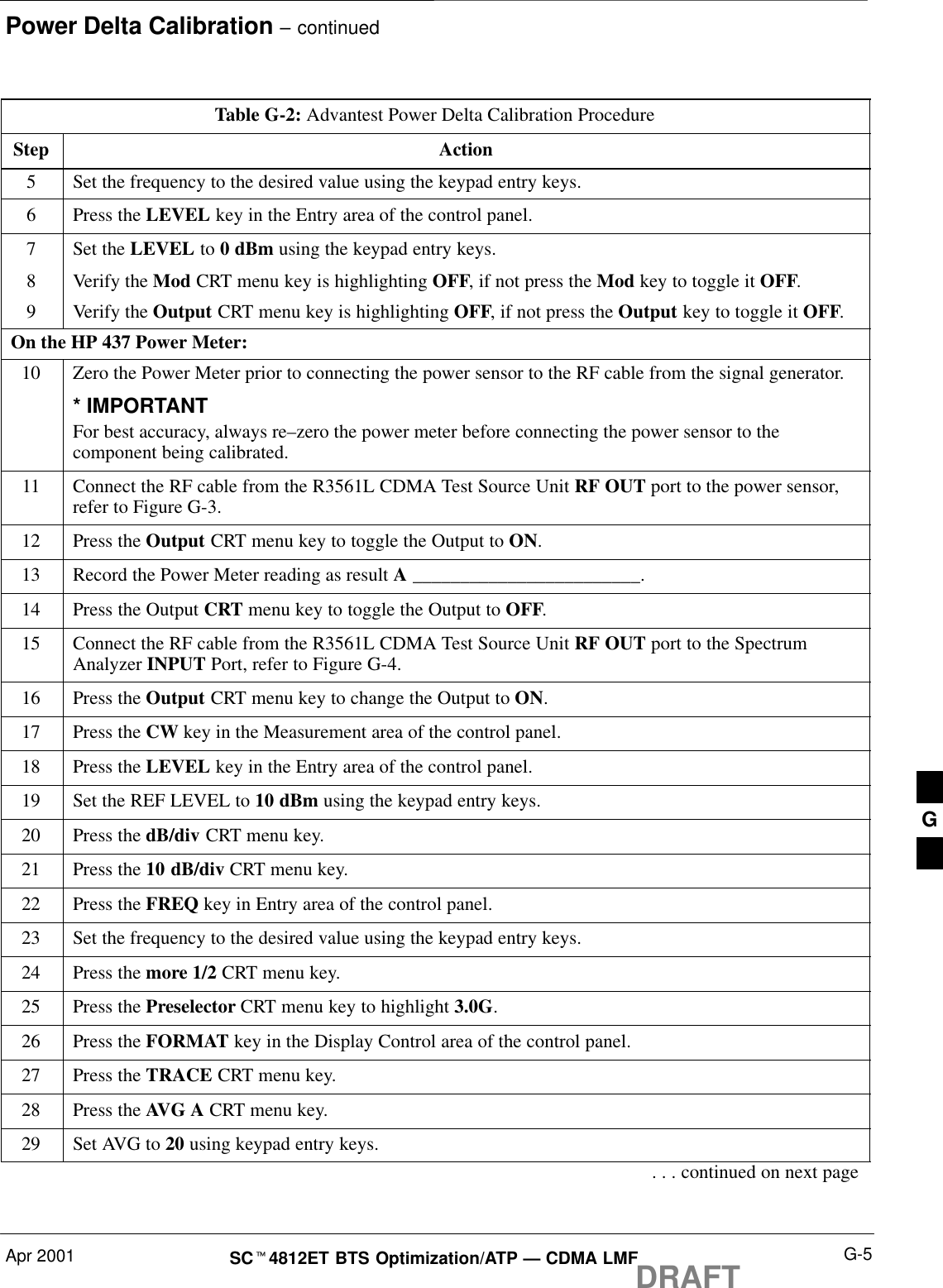
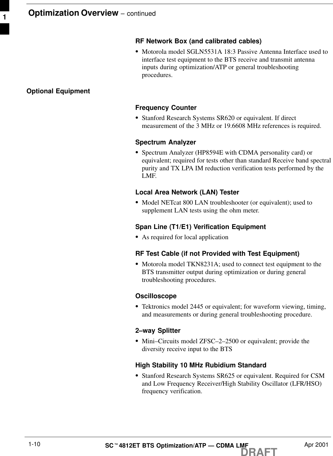
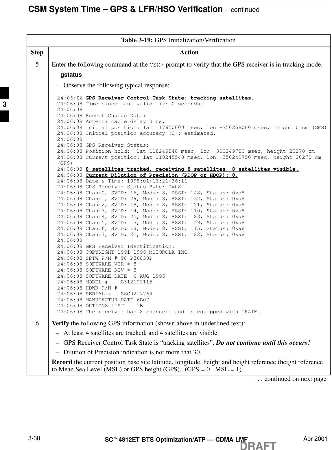
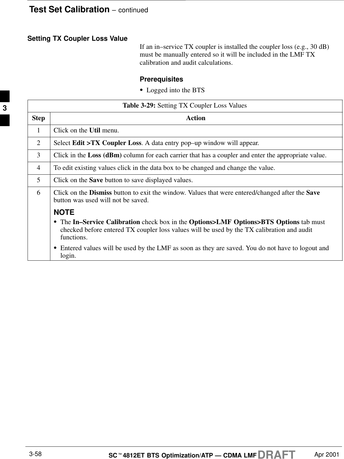
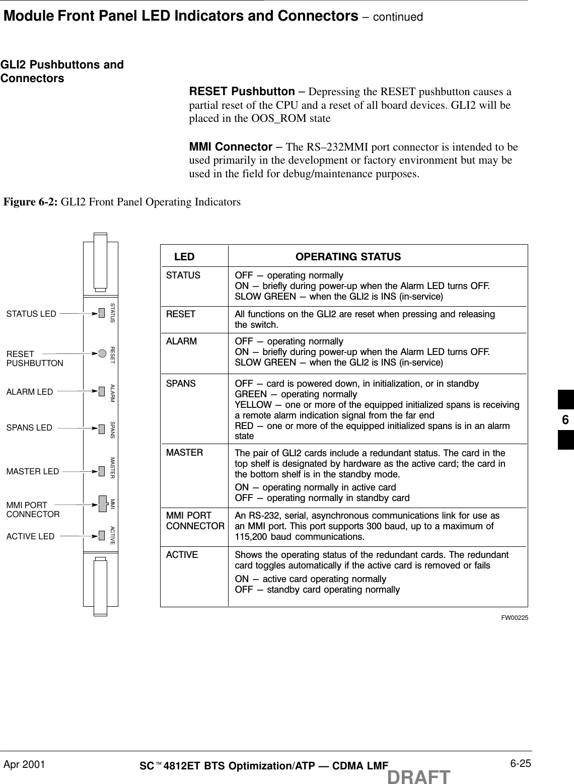
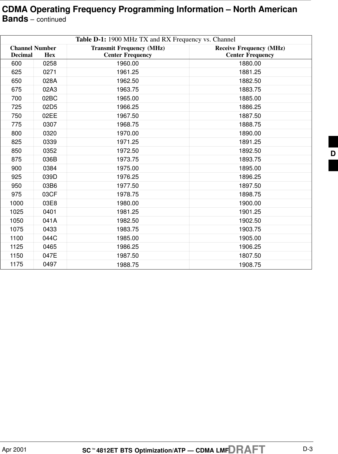
![Manual Test Cable Setup – continuedApr 2001 F-17SCt4812ET BTS Optimization/ATP — CDMA LMFDRAFTCalibrating HP 437 PowerMeterPrecise transmit output power calibration measurements are made usinga bolometer–type broadband power meter with a sensitive power sensor.Follow the steps outlined in Table F-11 to enter information unique tothe power sensor before calibrating the test setup. Refer to Figure F-7 asrequired.This procedure must be done in conjunction with theautomated calibration to enter power sensor specificcalibration values.IMPORTANT*CONNECT POWERSENSOR WITH POWERMETER TURNED OFFCONNECT POWER SENSORTO POWER REFERENCEWHEN CALIBRATING UNIT.POWER REFERENCE ISENABLED USING THE SHIFT 'KEYSSHIFT (BLUE) PUSHBUTTON –ACCESSES FUNCTION ANDDATA ENTRY KEYS IDENTIFIEDWITH LIGHT BLUE TEXT ONTHE FRONT PANEL ABOVETHE BUTTONSFW00308Figure F-7: Power Meter DetailTable F-11: Power Meter Calibration ProcedureStep Action! CAUTIONDo not connect/disconnect the power meter sensor cable with ac power applied to the meter.Disconnection could result in destruction of the sensing element or mis–calibration.1–Make sure the power meter AC LINE pushbutton is OFF.–Connect the power sensor cable to the SENSOR input.2Set the AC LINE pushbutton to ON.NOTEThe calibration should be performed only after the power meter and sensor have been allowed towarm–up and stabilize for a minimum of 60 minutes.3Perform the following to set or verify the GPIB address:–To enter the SPECIAL data entry function, press [SHIFT] then [PRESET].–Use the [y] or [b] button to select HP–IB ADRS; then press [ENTER].–Use the [y] or [b] button to select HP–IB ADRS 13; then press [ENTER].–To EXIT the SPECIAL data entry function press [SHIFT] then [ENTER].. . . continued on next pageF](https://usermanual.wiki/Nokia-Solutions-and-Networks/T5EG1/User-Guide-492635-Page-293.png)
![Manual Test Cable Setup – continuedDRAFTSCt4812ET BTS Optimization/ATP — CDMA LMF Apr 2001F-18Table F-11: Power Meter Calibration ProcedureStep Action4Perform the following to set or verify the correct power sensor model:–Press [SHIFT] then [a] to select SENSOR.–Identify the power sensor model number from the sensor label. Use the [y] or [b] button toselect the appropriate model; then press [ENTER].NOTEBe sure the PWR REF (power reference) output is OFF (observe that the triangular indicator is NOTdisplayed as shown in Step 7). If on, press [SHIFT] then ['] to turn it off.5 Press [ZERO]. Display will show “Zeroing ******.” Wait for process to complete.6Connect the power sensor to the POWER REF output.7To turn on the PWR REF, perform the following:–Press [SHIFT] then ['].–Verify that the triangular indicator (below) appears in the display above “PWR REF”.8Perform the following to set the REF CF %:–Press ([SHIFT] then [ZERO]) for CAL.–Enter the sensor’s REF CF % from the sensor’s decal using the arrow keys and press [ENTER].(The power meter will display ”CAL *****” for a few seconds.)NOTEIf the REF CAL FACTOR (REF CF) is not shown on the power sensor, assume it to be 100%.9Perform the following to set the CAL FAC %:–Press [SHIFT] then [FREQ] for CAL FAC.–On the sensor's decal, locate an approximate calibration percentage factor (CF%) at 2 GHz. Enterthe sensor’s calibration % (CF%) using the arrow keys and press [ENTER].When complete, the power meter will typically display 0.05 dBm. (Any reading between 0.00 and0.10 is normal.)10 To turn off the PWR REF, perform the following:–Press [SHIFT] then ['].–Disconnect the power sensor from the POWER REF output. F](https://usermanual.wiki/Nokia-Solutions-and-Networks/T5EG1/User-Guide-492635-Page-294.png)