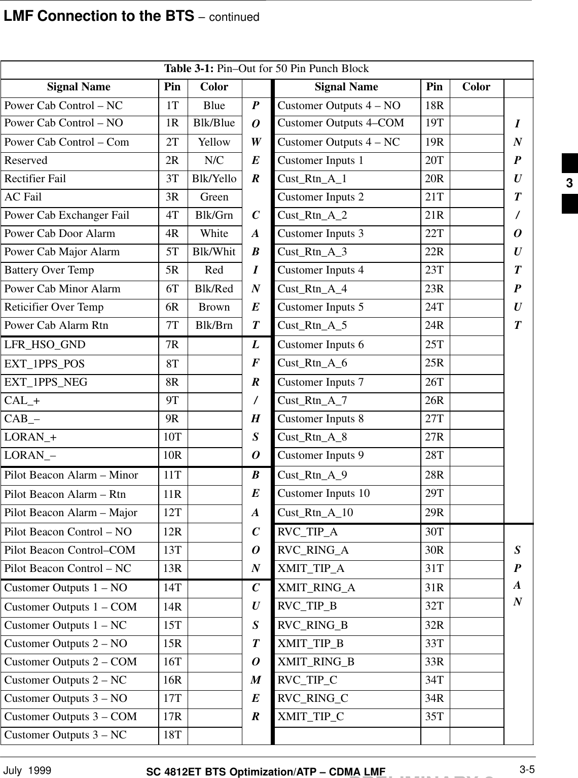
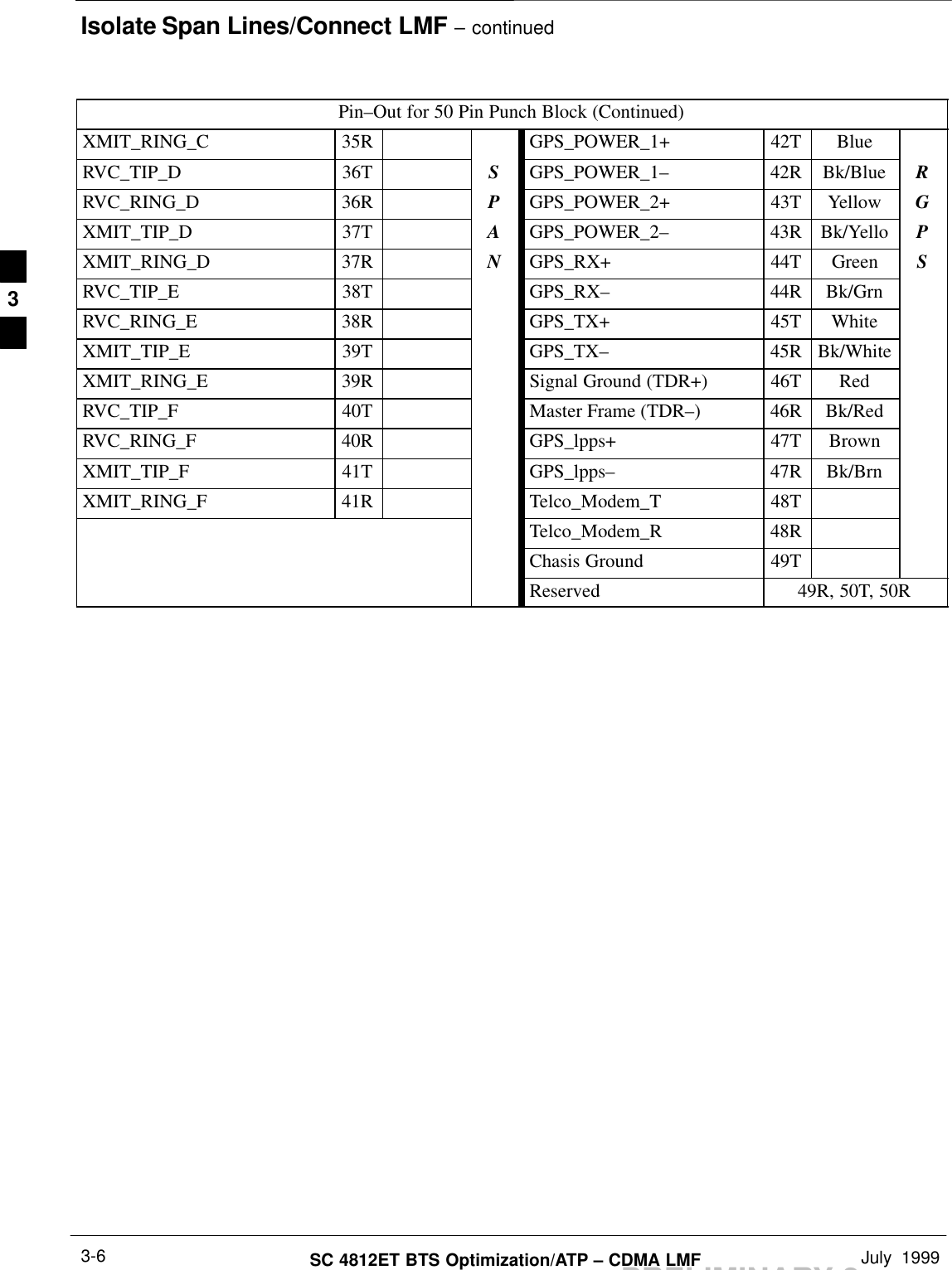
Nokia Solutions and Networks T5ZR1 SC4812ET 800 MHz CDMA BTS Frame User Manual Users BTS Optimization Manual
Nokia Solutions and Networks SC4812ET 800 MHz CDMA BTS Frame Users BTS Optimization Manual
UserManual.wiki
>
Nokia Solutions and Networks
>
T5ZR1 User Manual
Users BTS Optimization Manual
Navigation menu
Upload a User Manual
Namespaces
Wiki Guide
HTML
PDF
Info
Views
User Manual
Discussion / Help
Navigation
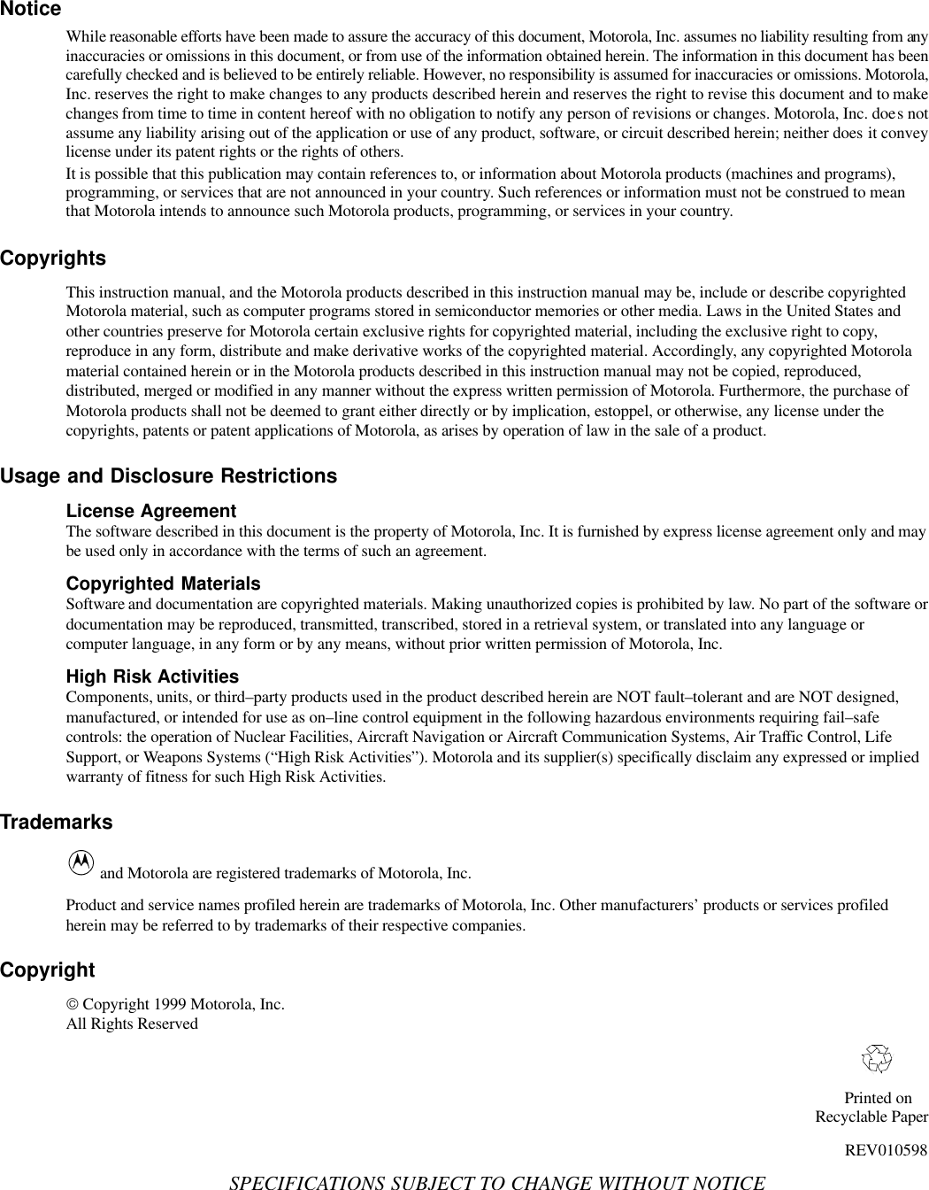
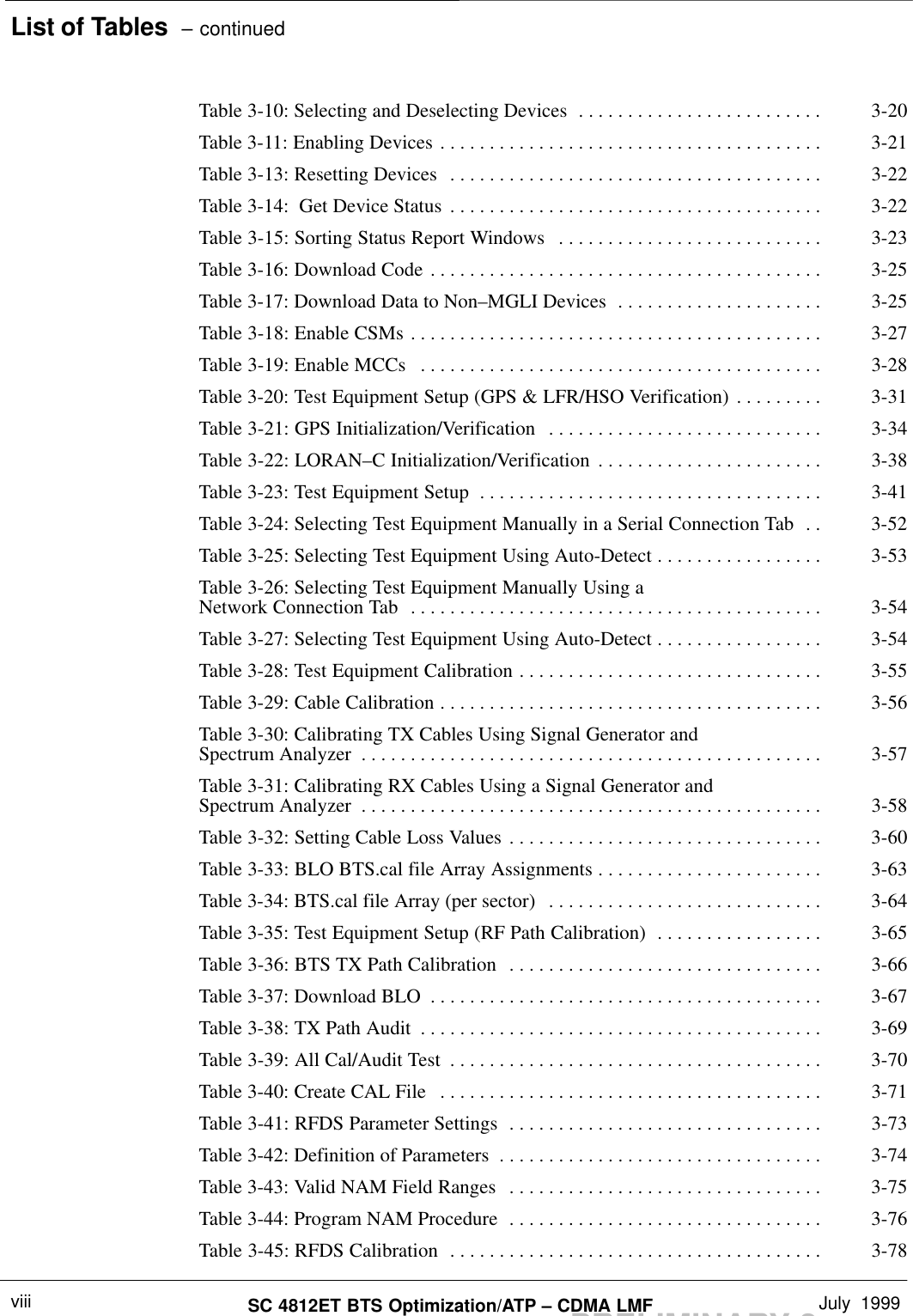

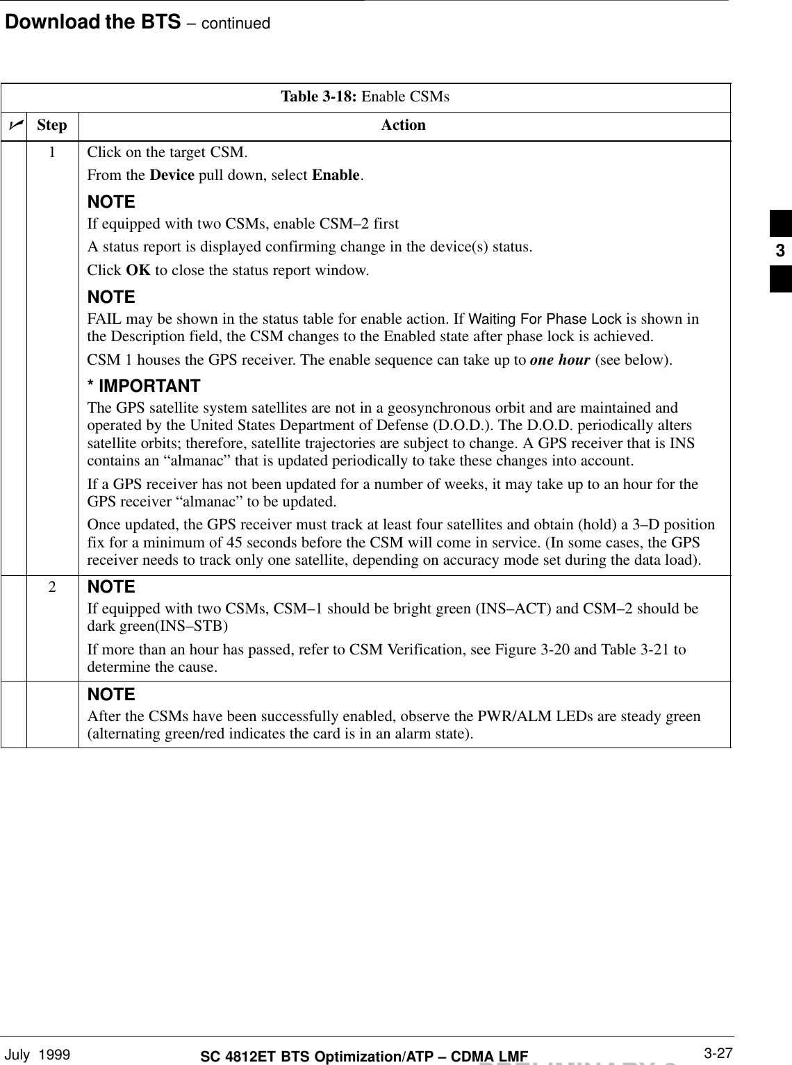
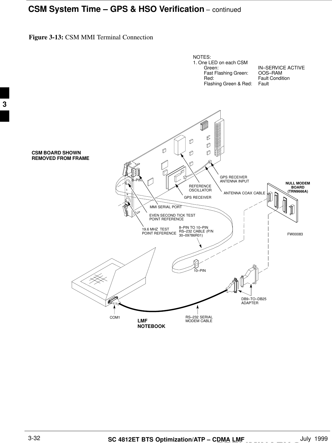
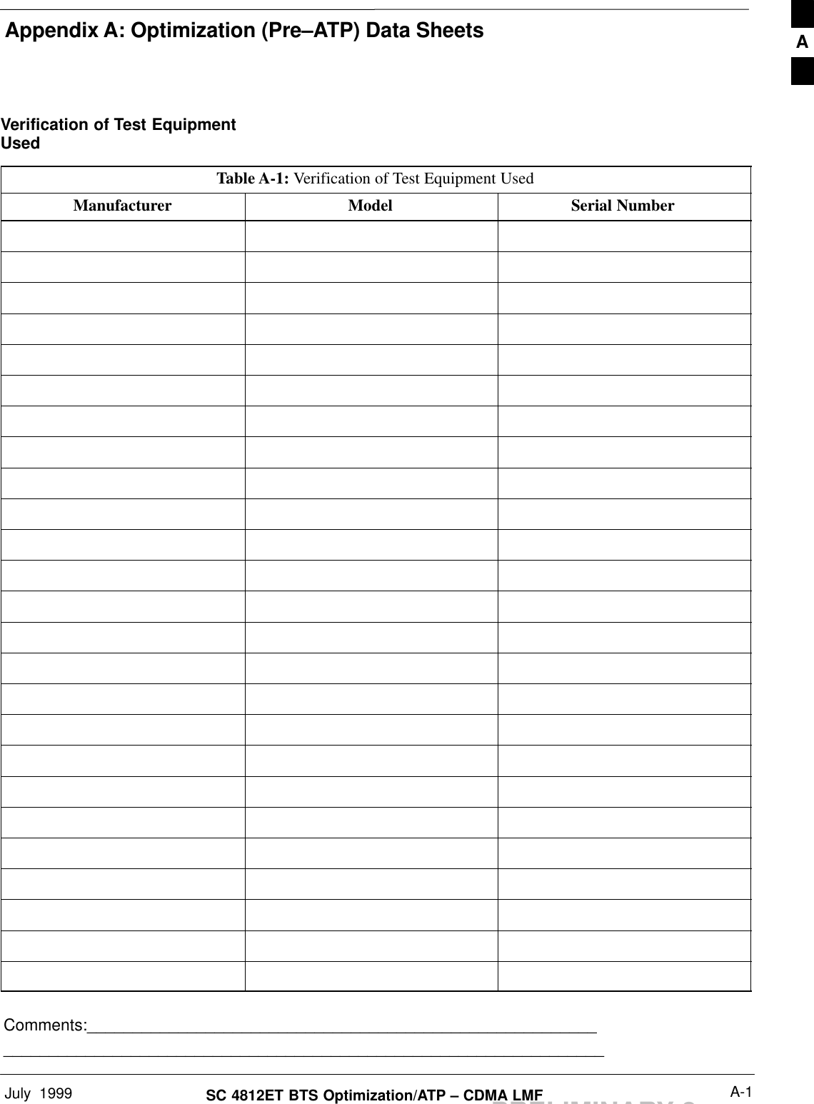
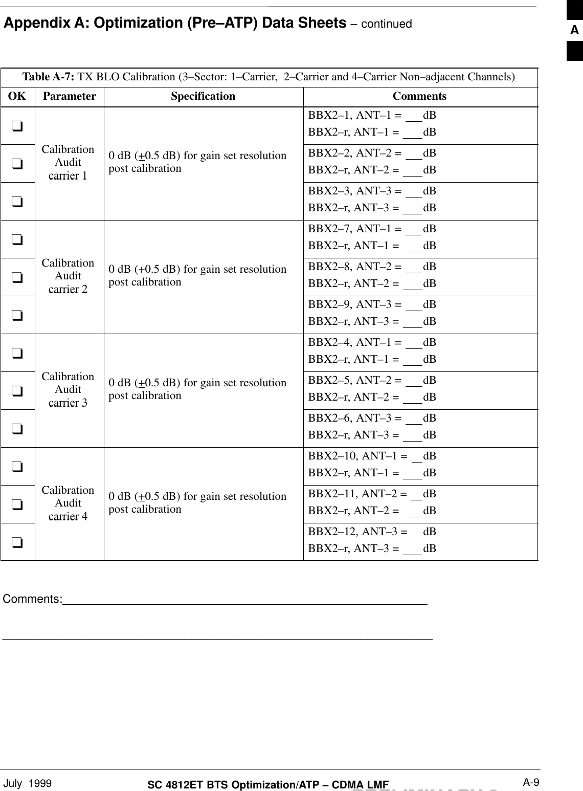
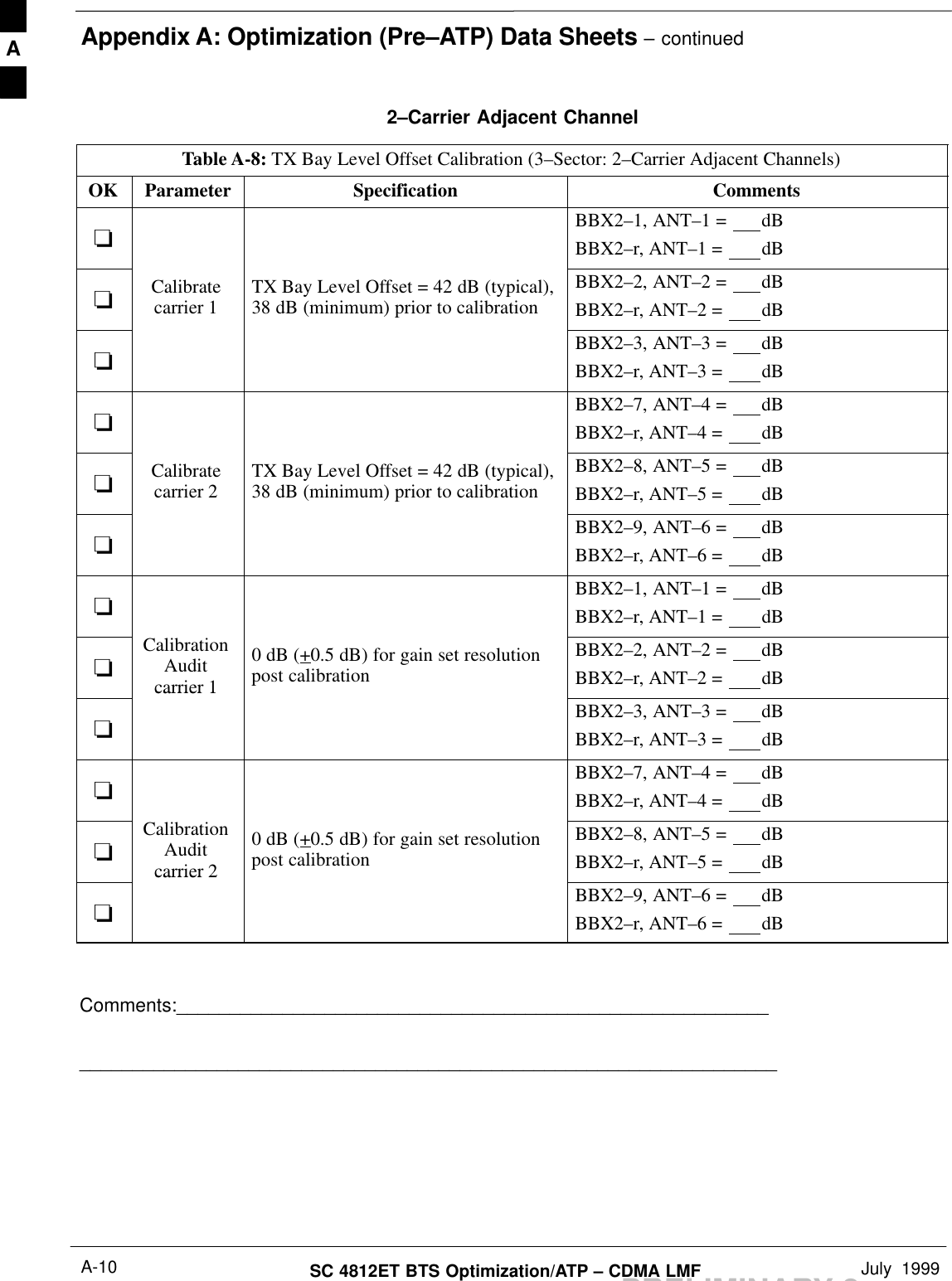
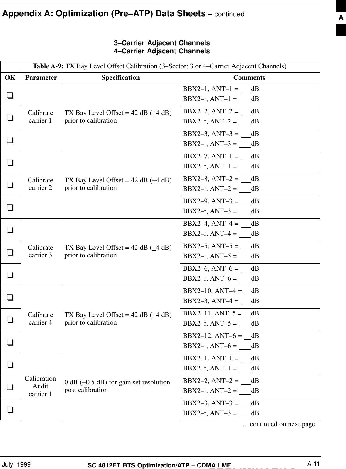
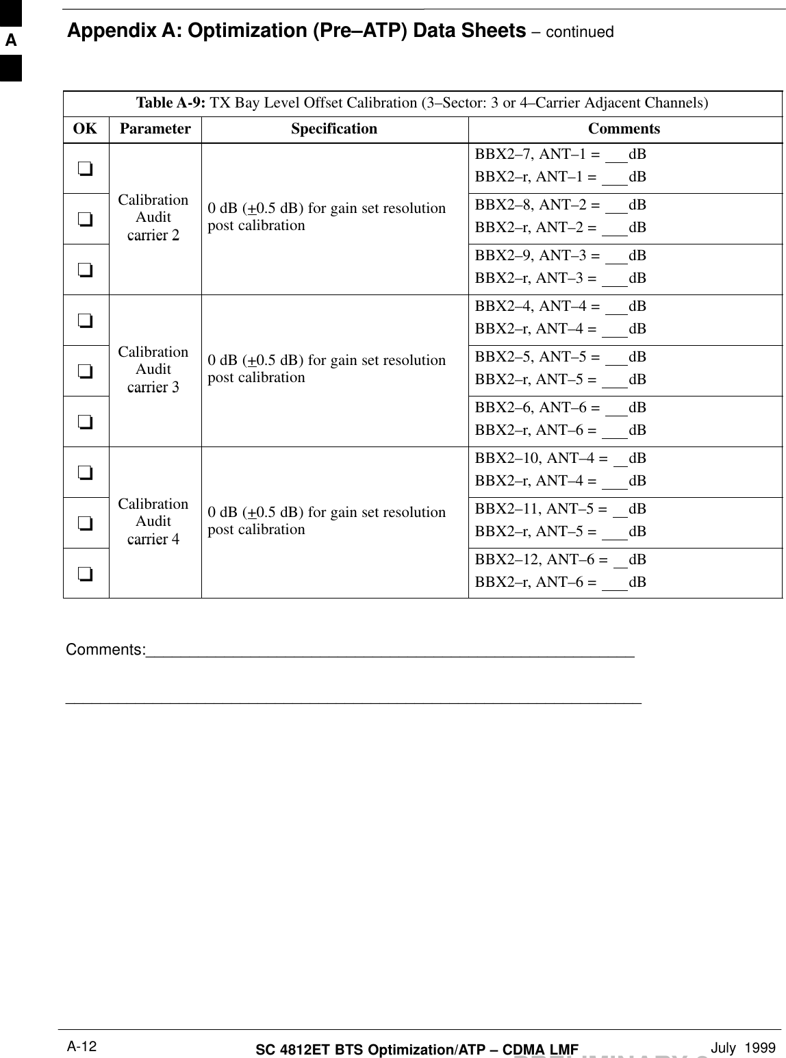
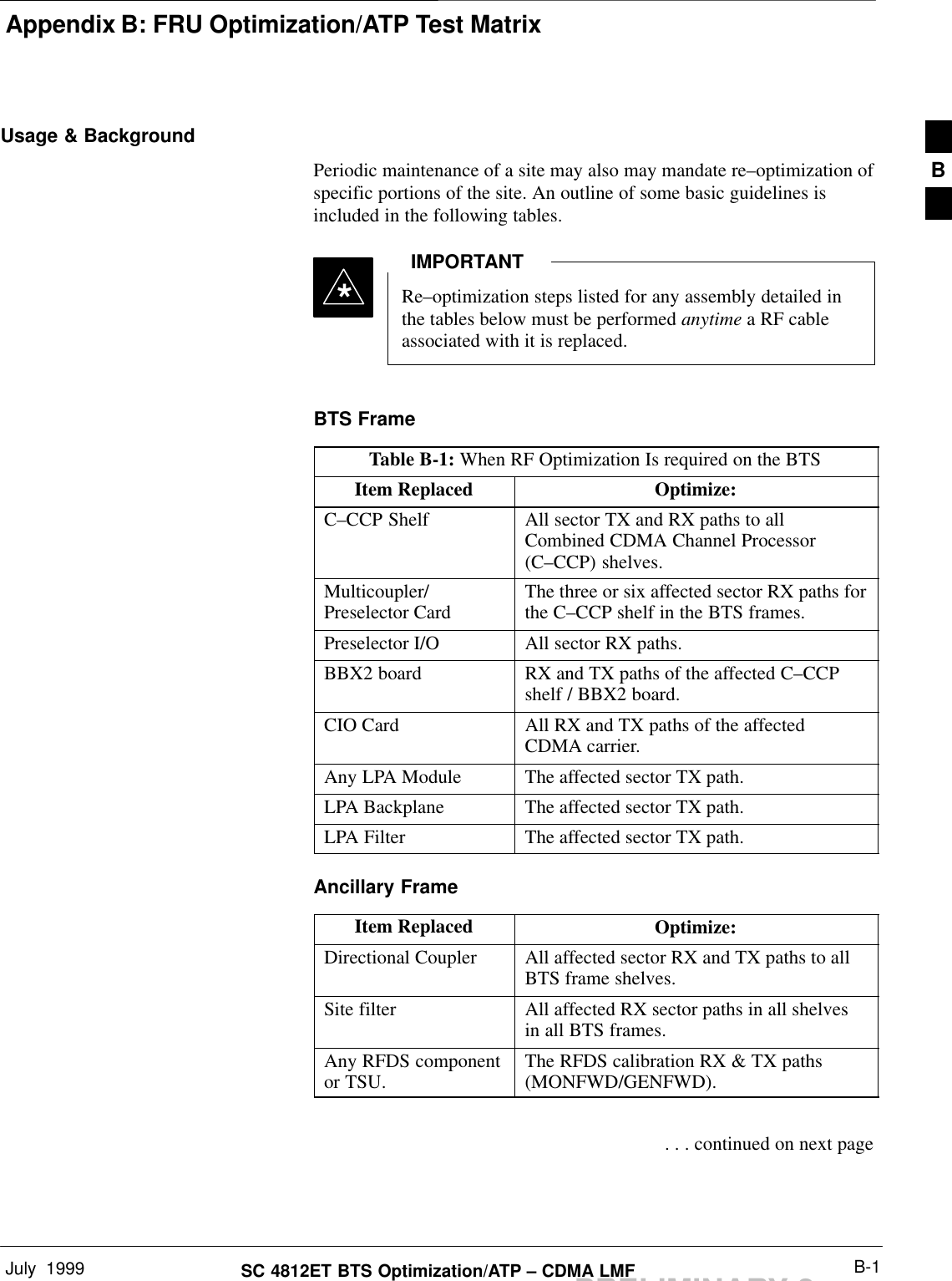
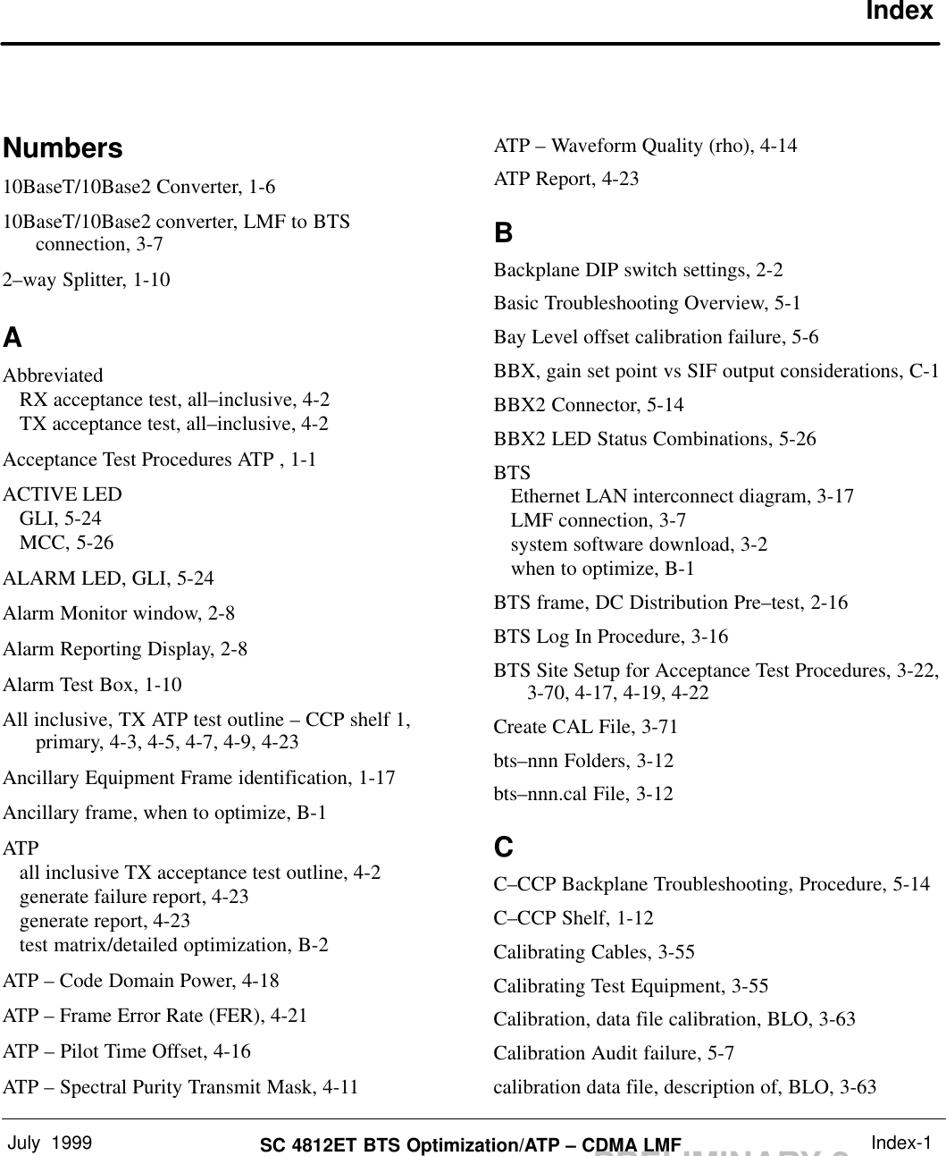
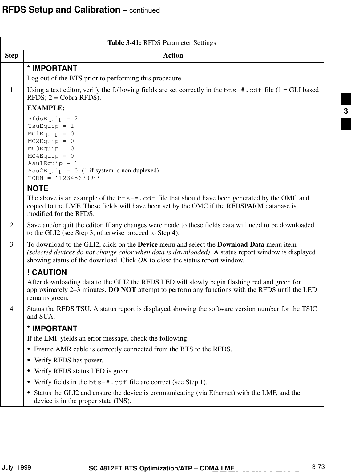
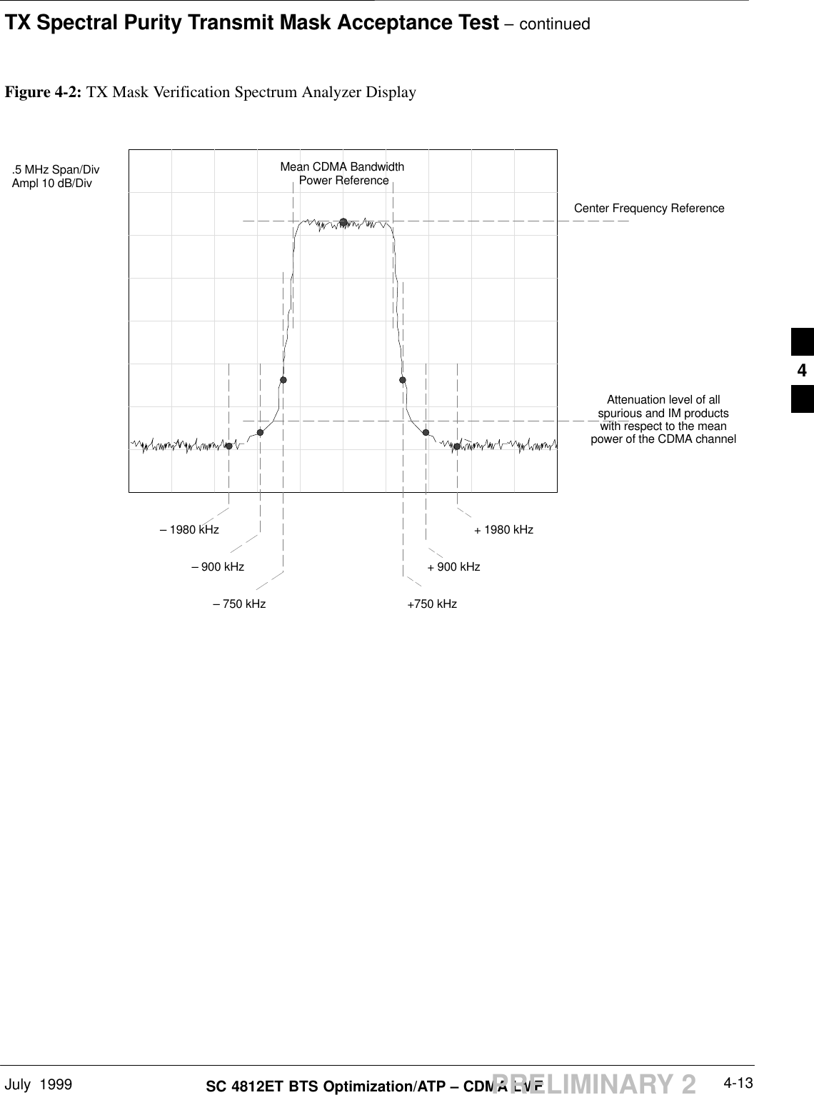
![Bay Level Offset Calibration – continuedJuly 1999 3-63SC 4812ET BTS Optimization/ATP – CDMA LMFPRELIMINARY 2BLO Calibration Data FileDuring the calibration process, the LMF creates a calibration (BLO) datafile. After calibration has been completed, this offset data must bedownloaded to the BBX2s using the Download BLO function. Anexplanation of the file is shown below.Due to the size of the file, Motorola recommends that youprint out a hard copy of a bts.cal file and refer to it for thefollowing descriptions.NOTEThe CAL file is subdivided into sections organized on a per slot basis (aslot Block).Slot 1 contains the calibration data for the 12 BBX2 slots. Slot 20contains the calibration data for the redundant BBX2. Each BBX2 slotheader block contains:SA creation Date and Time – broken down into separate parameters ofcreateMonth, createDay, createYear, createHour, and createMin.SThe number of calibration entries – fixed at 720 entries correspondingto 360 calibration points of the CAL file including the slot header andactual calibration data.SThe calibration data for a BBX2 is organized as a large flat array. Thearray is organized by branch, sector, and calibration point.– The first breakdown of the array indicates which branch thecontained calibration points are for. The array covers transmit, mainreceive and diversity receive offsets as follows:Table 3-33: BLO BTS.cal file Array AssignmentsRange AssignmentC[1]–C[240] TransmitC[241]–C[480] ReceiveC[481]–C[720] Diversity Receive3](https://usermanual.wiki/Nokia-Solutions-and-Networks/T5ZR1/User-Guide-55673-Page-126.png)
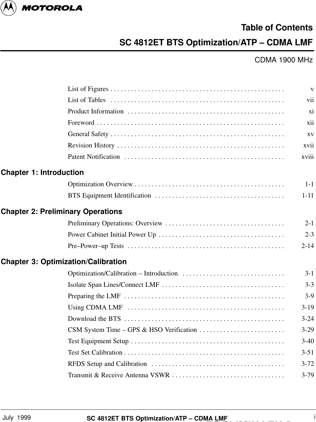
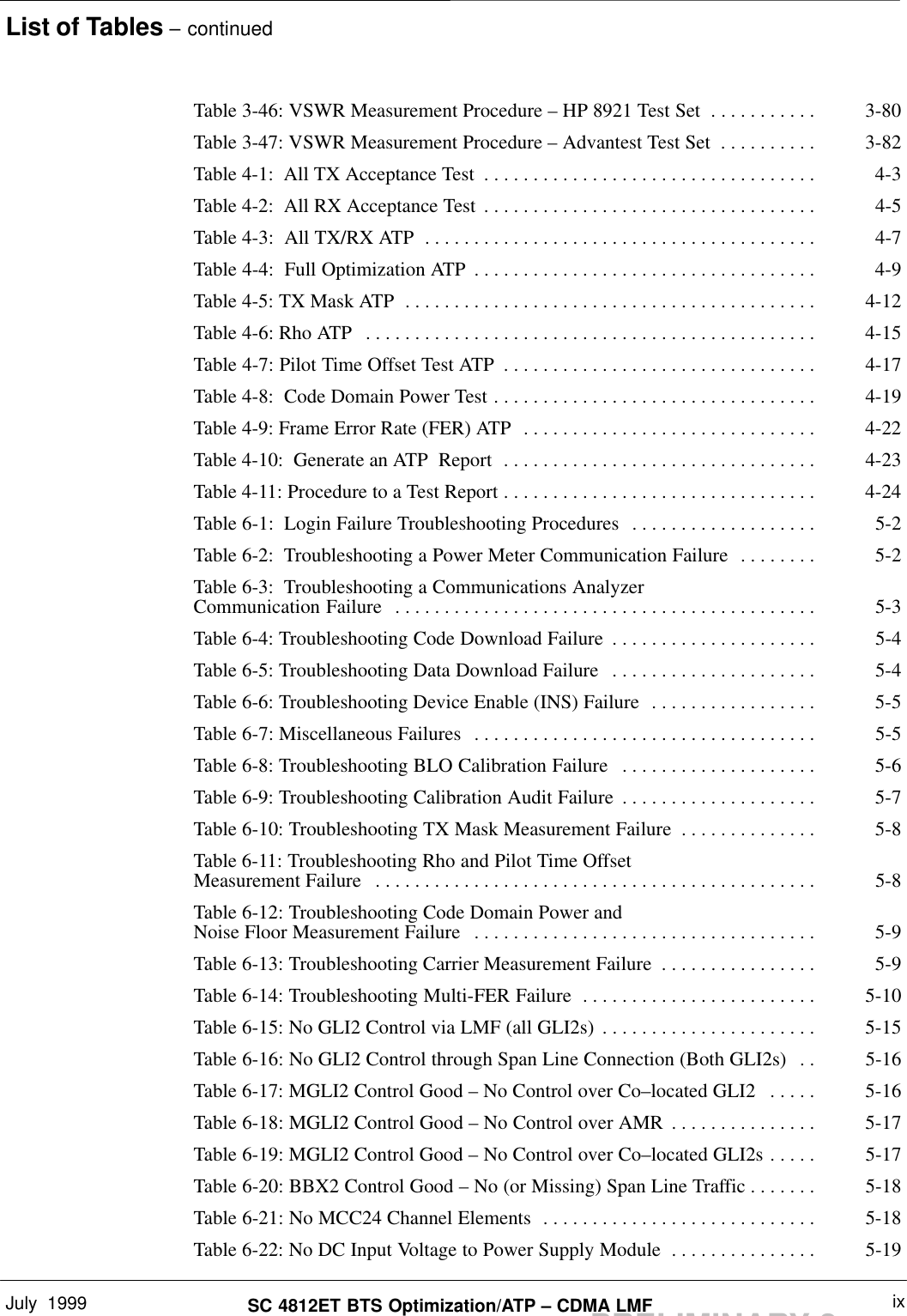
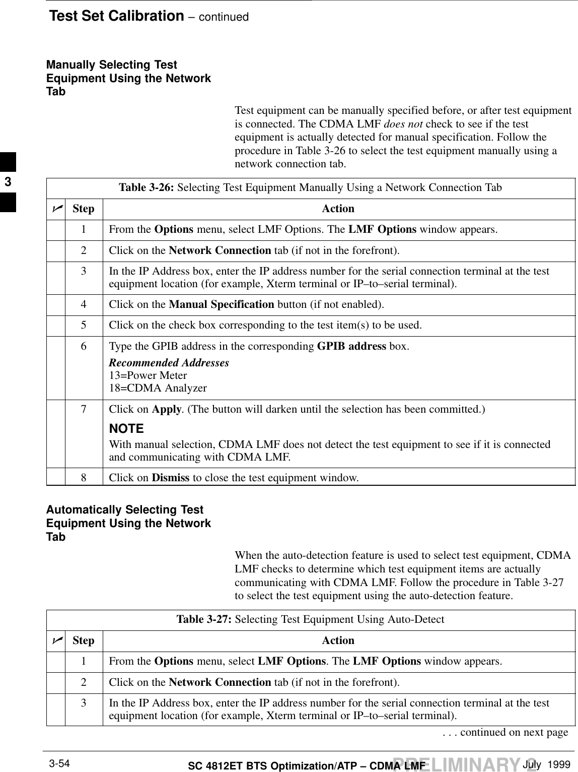
![Bay Level Offset Calibration – continuedPRELIMINARY 2SC 4812ET BTS Optimization/ATP – CDMA LMF July 19993-64– The second breakdown of the array is per sector. Three sectors areallowed.Table 3-34: BTS.cal file Array (per sector)Sector TX RX RX Diversity1 (Omni) C[1]–C[20] C[241]–C[260] C[481]–C[500]2 C[21]–C[40] C[261]–C[280] C[501]–C[520]3 C[41]–C[60] C[281]–C[300] C[521]–C[540]4 C[61]–[80] C[301]–C[320] C[541]–C[560]5 C[81]–[100] C[321]–C[340] C[561]–C[580]6 C[101]–[120] C[341]–C[360] C[581]–C[600]SRefer to the hard copy of the file. As you can see, 10 calibrationpoints per sector are supported for each branch. Two entries arerequired for each calibration point.SThe first value (all odd entries) refer to the CDMA channel(frequency) the BLO is measured at. The second value (all evenentries) is the power set level. The valid range for PwrLvlAdj is from2500 to 27500 (2500 corresponds to –125 dBm and 27500corresponds to +125 dBm).SThe 20 calibration entries for each sector/branch combination must bestored in order of increasing frequency. If less than 10 points(frequencies) are calibrated, the largest frequency that is calibrated isrepeated to fill out the 10 points.Example:C[1]=384, odd cal entry = 1 ‘‘calibration point”C[2]=19102, even cal entryC[3]=777,C[4]=19086,..C[19]=777,C[20]=19086, (since only two cal points were calibrated this would be repeated for the next 8 points)SWhen the BBX2 is loaded with BLO data, the cal file data for theBBX2 is downloaded to the device in the order it is stored in the CALfile. TxCal data is sent first, C[1] – C[60]. Sector 1’s 10 calibrationpoints are sent (C[1] – C[20]), followed by sector 2’s 10 calibrationpoints (C[21] – C[40]), etc. The RxCal data is sent next, followed bythe RxDCal data.STemperature compensation data is also stored in the cal file for eachslot.3](https://usermanual.wiki/Nokia-Solutions-and-Networks/T5ZR1/User-Guide-55673-Page-127.png)


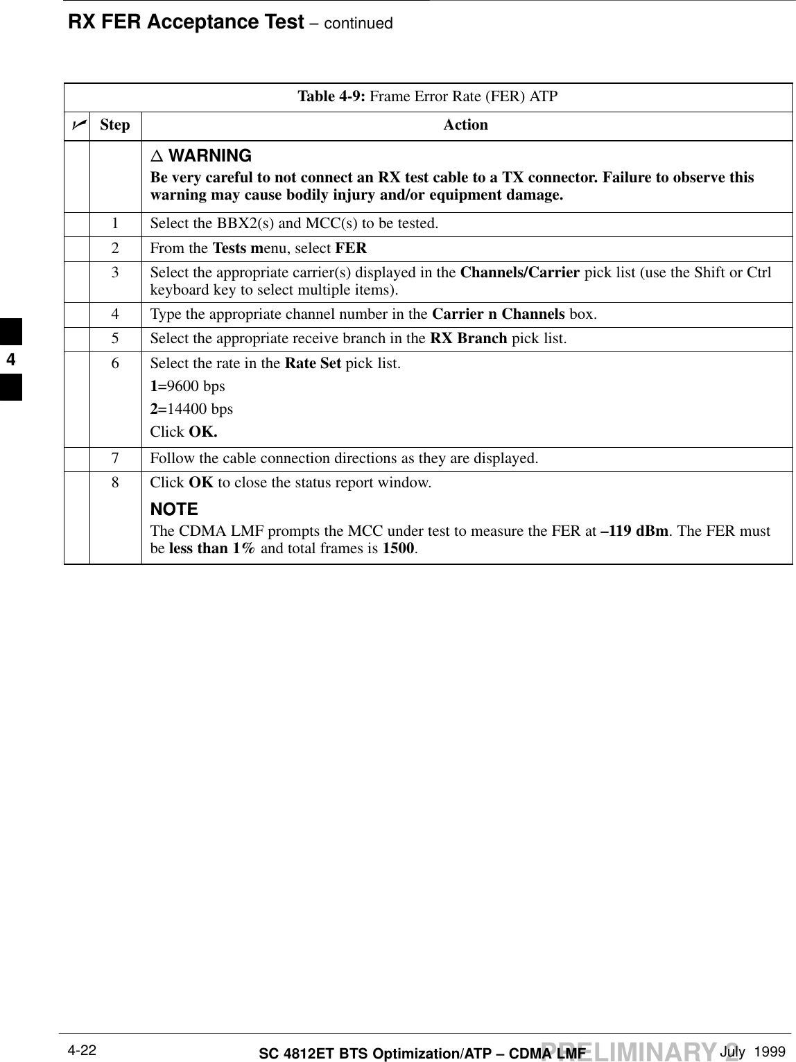
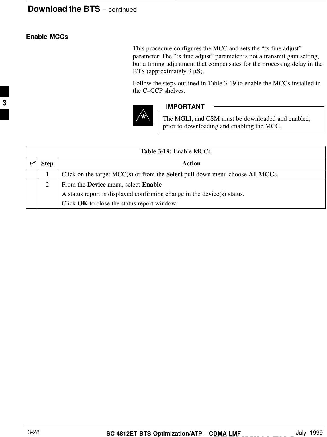
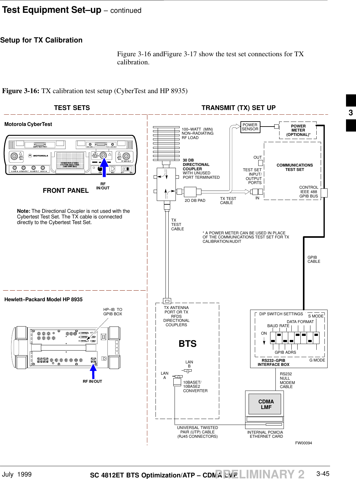
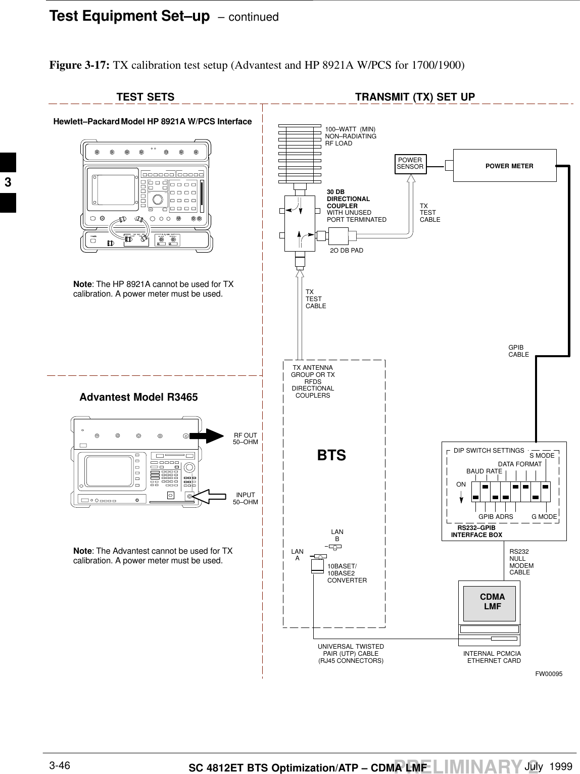
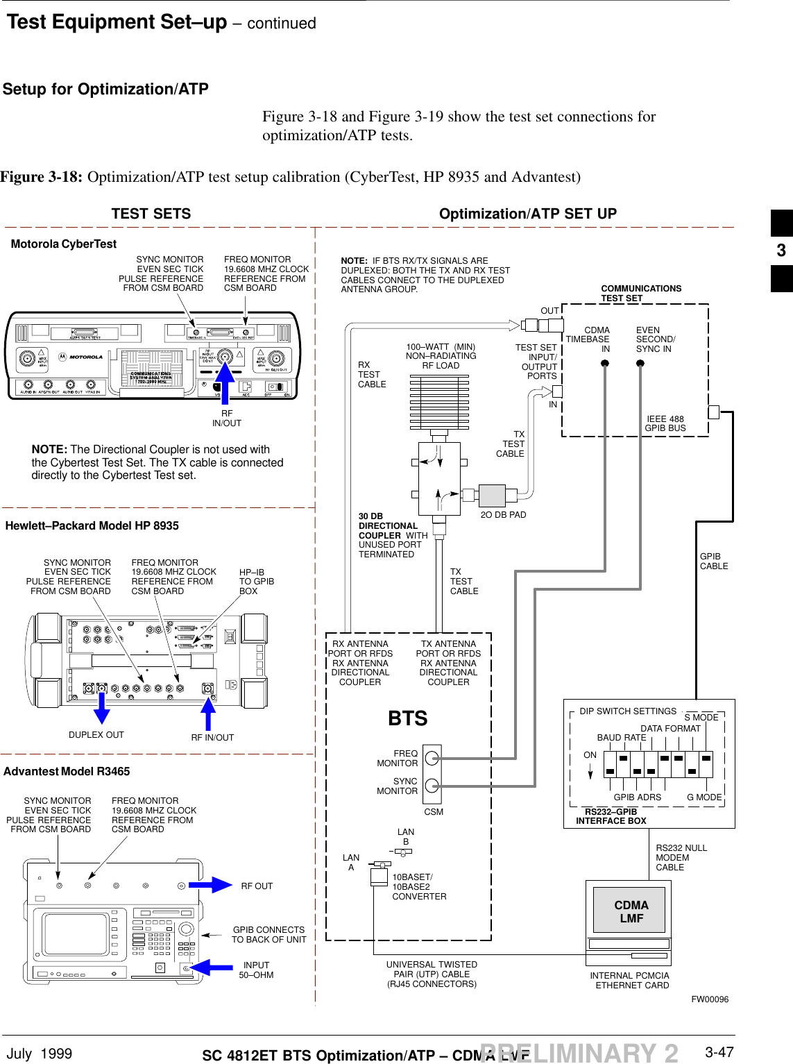
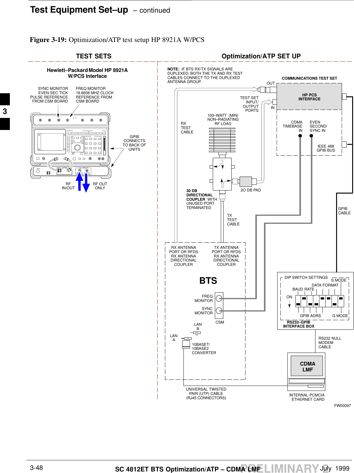
![RX Frame Error Rate (FER) Acceptance TestJuly 1999 4-21SC 4812ET BTS Optimization/ATP – CDMA LMFPRELIMINARY 2Background: FER TestThis test verifies the BTS Frame Error Rate (FER) on all traffic channelelements currently configured on all equipped MCCs (full rate at 1%FER) at an RF input level of –119 dBm [or –116 dBm if using TowerTop Amplifier (TMPC)]. All tests are performed using the externalcalibrated test set as the signal source controlled by the same command.All measurements will be via the LMF.The pilot gain is set to 262 for each TX antenna and all channel elementsfrom the MCCs are forward-link disabled. The BBX2 is keyed up usingonly bbxlvl level offsets, to generate a CDMA carrier (with pilot channelelement only). BBX2 power output is set to –20 dBm as measured at theTX OUT connector (on either the BTS or RFDS directional coupler).The BBX2 must be keyed in order to enable the RX receive circuitry.The LMF prompts the MCC/CE under test to measure all zero longcodeand provide the FER report on the selected active MCC on the reverselink for both the main and diversity RX antenna paths, verifying theresults meet the following specification: FER returned less than 1% andtotal frames measured is 1500.All MCC/CEs selected are tested on the specified RX antenna path. TheBBX then de-keys and, the applicable redundant BBX2 is assigned tothe current RX antenna paths under test. The test is then repeated.FER testThe CDMA LMF Tests menu list item, FER, performs the Frame ErrorRate (FER) test for a XCVR(s). All measurements are made through theappropriate RX output connector using the calibrated RX cable setup.This test is included in the All TX, All TX/RX and Full Optimizationtests.PrerequisitesBefore attempting to run any ATP tests, ensure the following have beencompleted:SCSMs, GLI2s, BBX2s, and MCCs have correct code load and dataloadSPrimary CSM, GLI2, and MCCs are INSSBTS has been Optimized/CalibratedSBBXs are OOS–RAMSTest equipment is connected for ATP tests (see Figure 3-16 throughFigure 3-19).STest equipment is warmed up 60 minutes and calibratedSTest cables are calibrated and GPIB is onSLMF is logged into the BTS4](https://usermanual.wiki/Nokia-Solutions-and-Networks/T5ZR1/User-Guide-55673-Page-170.png)