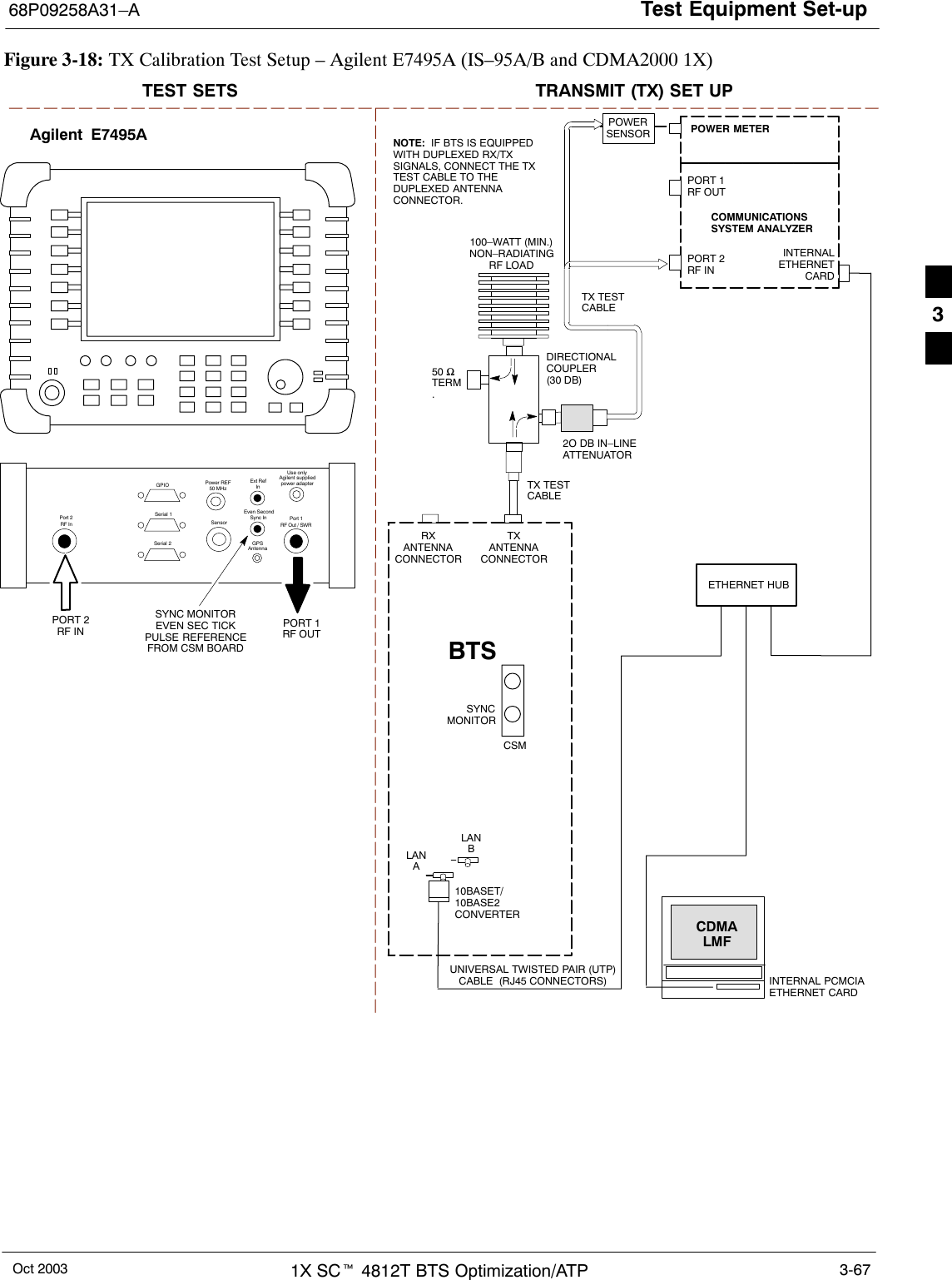
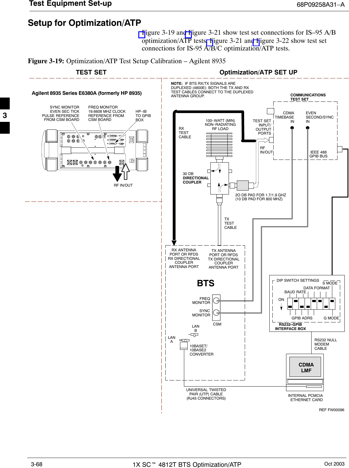
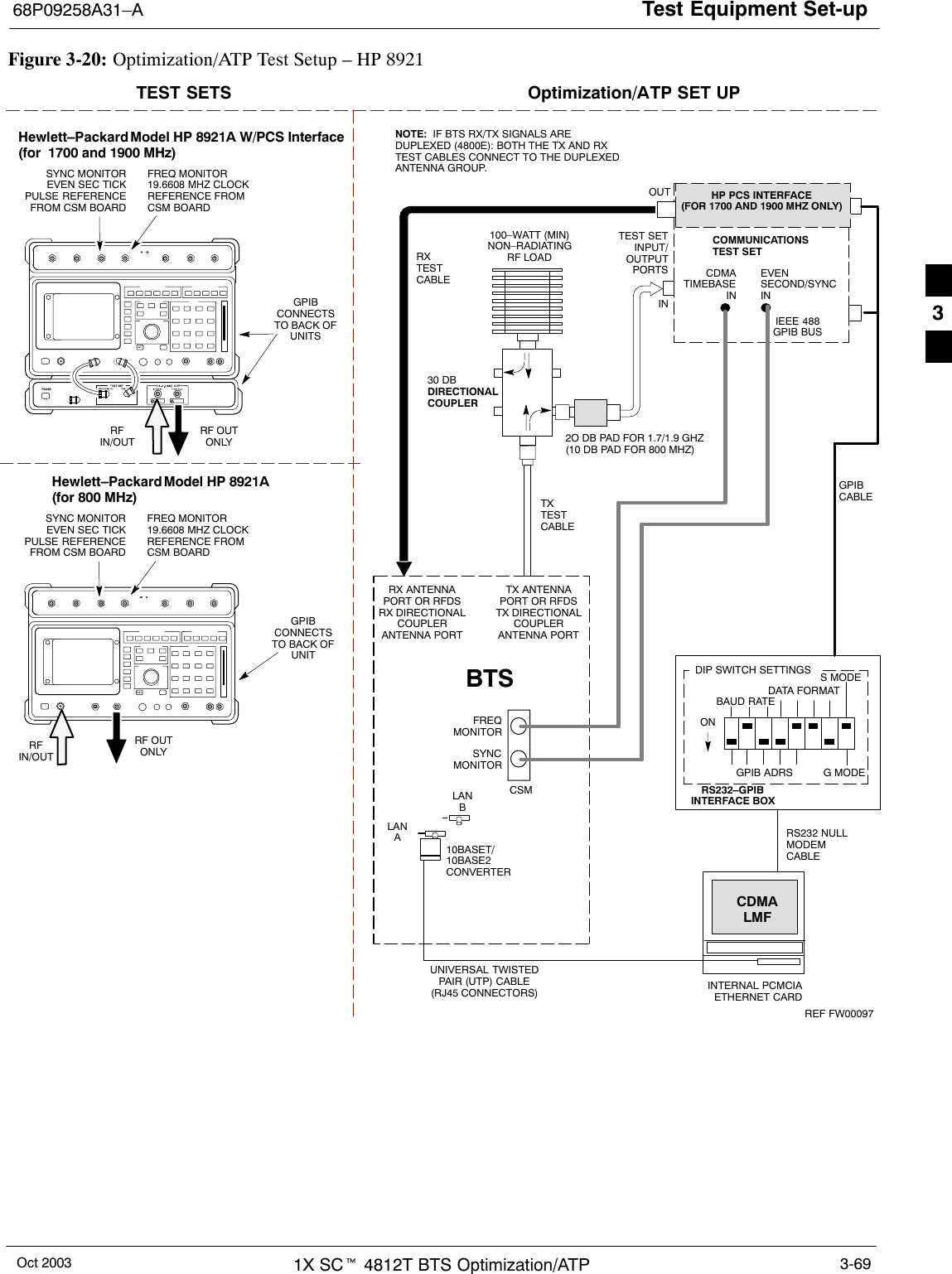
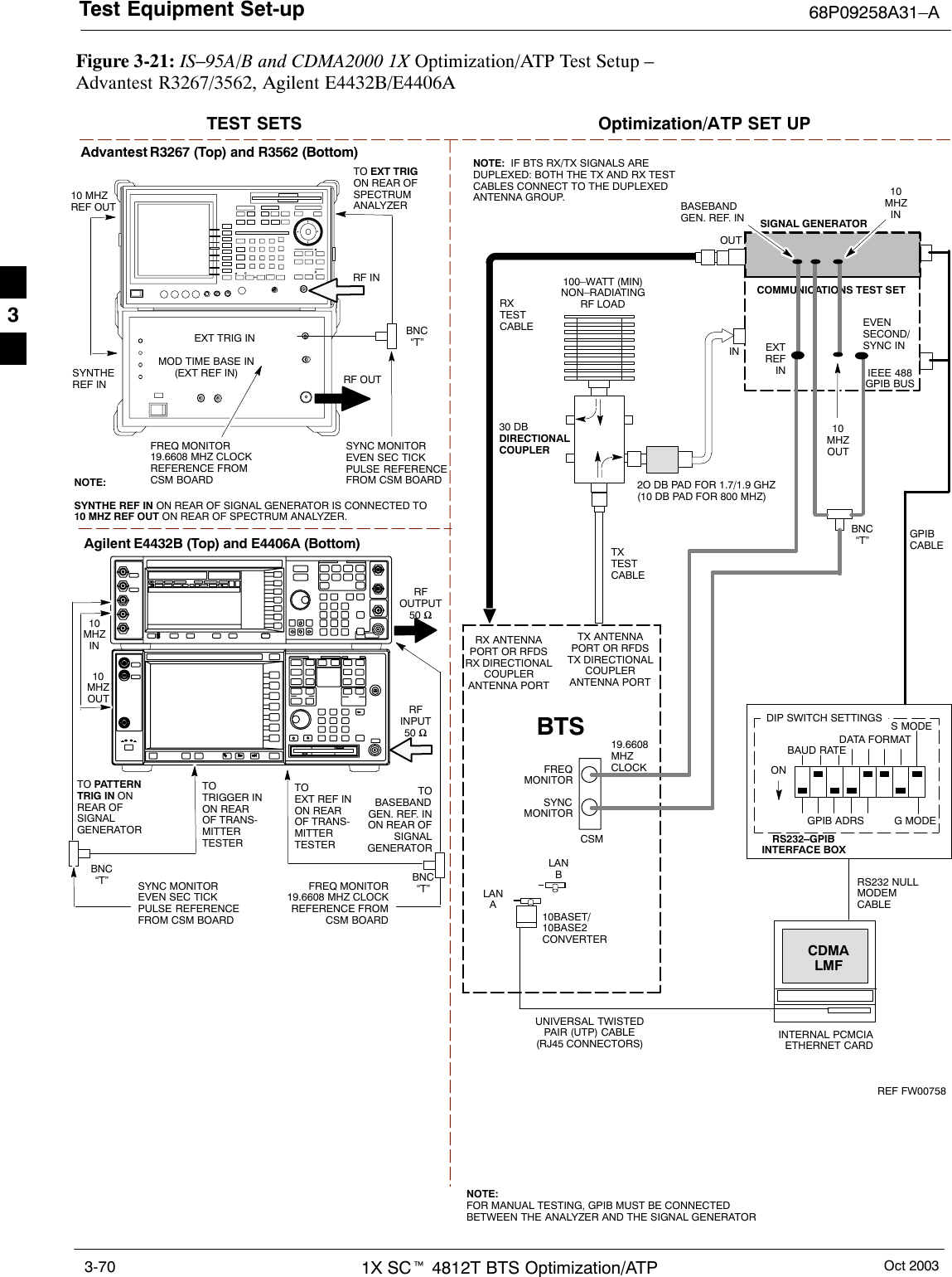
Nokia Solutions and Networks T6EF1 CDMA Base station transmitter User Manual 1X SC4812T BTS Optimization ATP Release 2 16 3 x
Nokia Solutions and Networks CDMA Base station transmitter 1X SC4812T BTS Optimization ATP Release 2 16 3 x
Contents
- 1. Users Manual 1
- 2. Users Manual 2
- 3. Users Manual 3
Users Manual 2

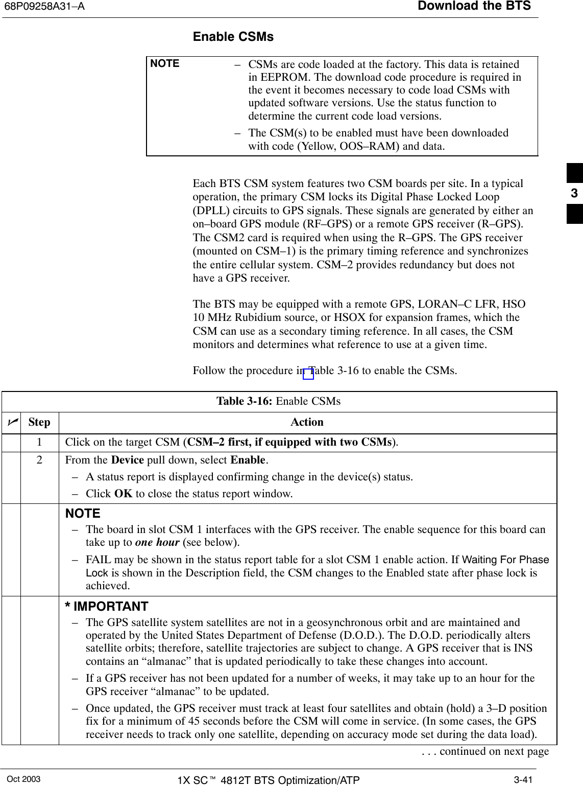
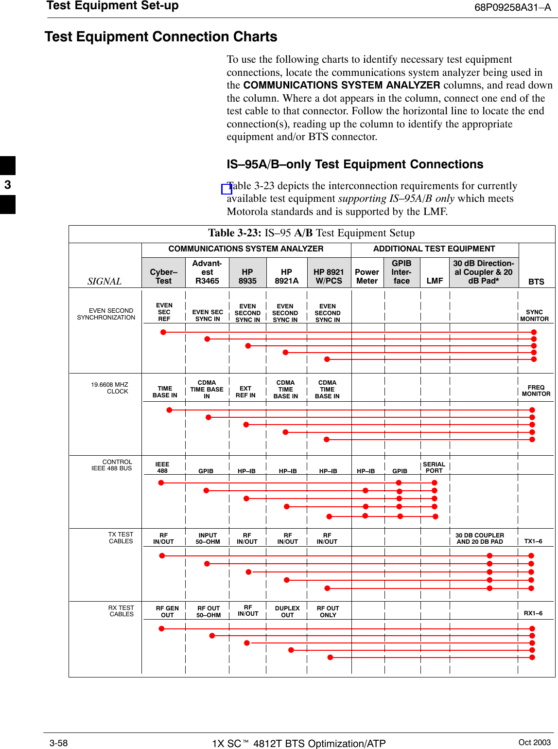
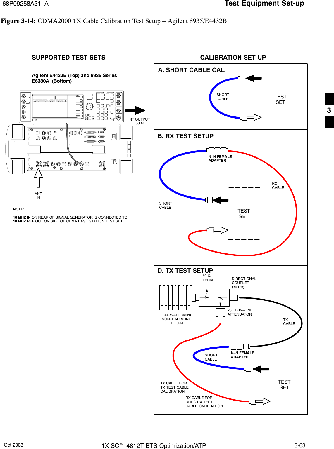
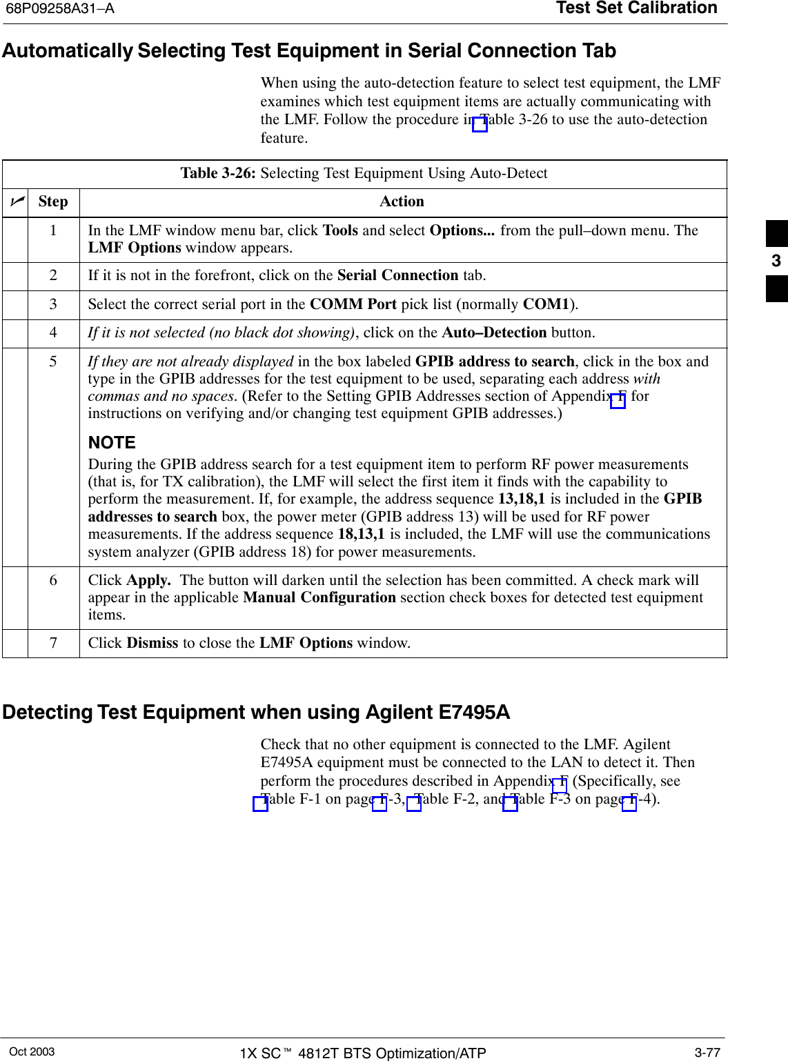
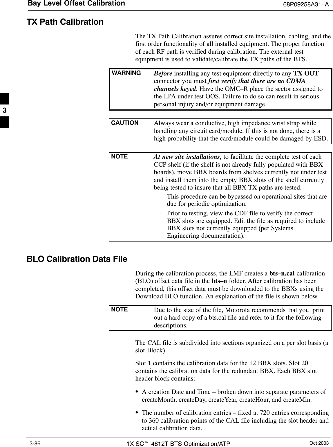
![Bay Level Offset Calibration68P09258A31–AOct 2003 1X SCt 4812T BTS Optimization/ATP 3-87SThe calibration data for a BBX is organized as a large flat array. Thearray is organized by branch, sector, and calibration point.– The first breakdown of the array indicates which branch thecontained calibration points are for. The array covers transmit, mainreceive and diversity receive offsets as follows:Table 3-33: BLO BTS.cal File Array AssignmentsRange AssignmentC[1]–C[240] TransmitC[241]–C[480] Main ReceiveC[481]–C[720] Diversity ReceiveNOTE Slot 385 is the BLO for the RFDS.– The second breakdown of the array is per sector. Configurationssupported are Omni, 3–sector or 6–sector.Table 3-34: BTS.cal File Array (Per Sector)BBX Sectorization TX RX RX DiversitySlot[1] (Primary BBXs 1 through 12)1 (Omni) 3–Sector,C[1]–C[20] C[241]–C[260] C[481]–C[500]23–Sector,1stCiC[21]–C[40] C[261]–C[280] C[501]–C[520]36 Sector,1stCarrier C[41]–C[60] C[281]–C[300] C[521]–C[540]41stCarrier 3–Sector,C[61]–C[80] C[301]–C[320] C[541]–C[560]5Carrier3–Sector,3rdCiC[81]–C[100] C[321]–C[340] C[561]–C[580]6Carrier C[101]–C[120] C[341]–C[360] C[581]–C[600]73–Sector,C[121]–C[140] C[361]–C[380] C[601]–C[620]83–Sector,2ndCiC[141]–C[160] C[381]–C[400] C[621]–C[640]96 Sector,2ndCarrier C[161]–C[180] C[401]–C[420] C[641]–C[660]102ndCarrier 3–Sector,C[181]–C[200] C[421]–C[440] C[661]–C[680]11Carrier3–Sector,4thCiC[201]–C[220] C[441]–C[460] C[681]–C[700]12 Carrier C[221]–C[240] C[461]–C[480] C[701]–C[720] . . . continued on next page3](https://usermanual.wiki/Nokia-Solutions-and-Networks/T6EF1.Users-Manual-2/User-Guide-426543-Page-78.png)
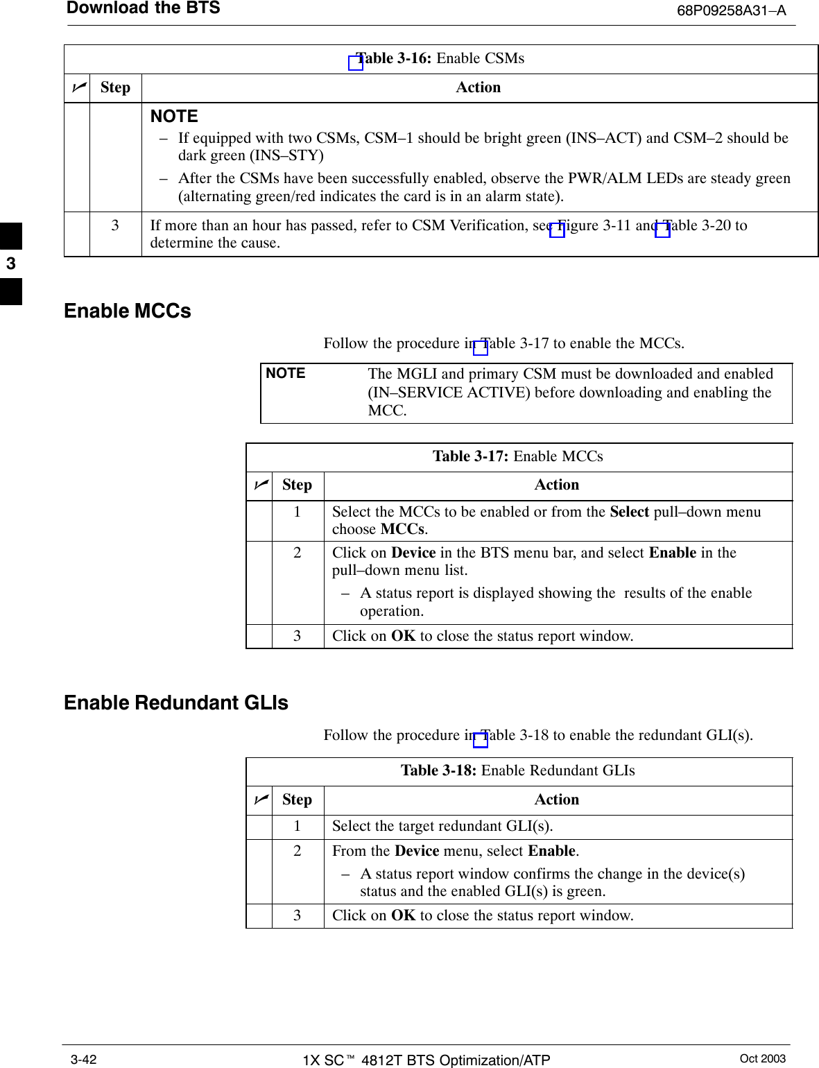
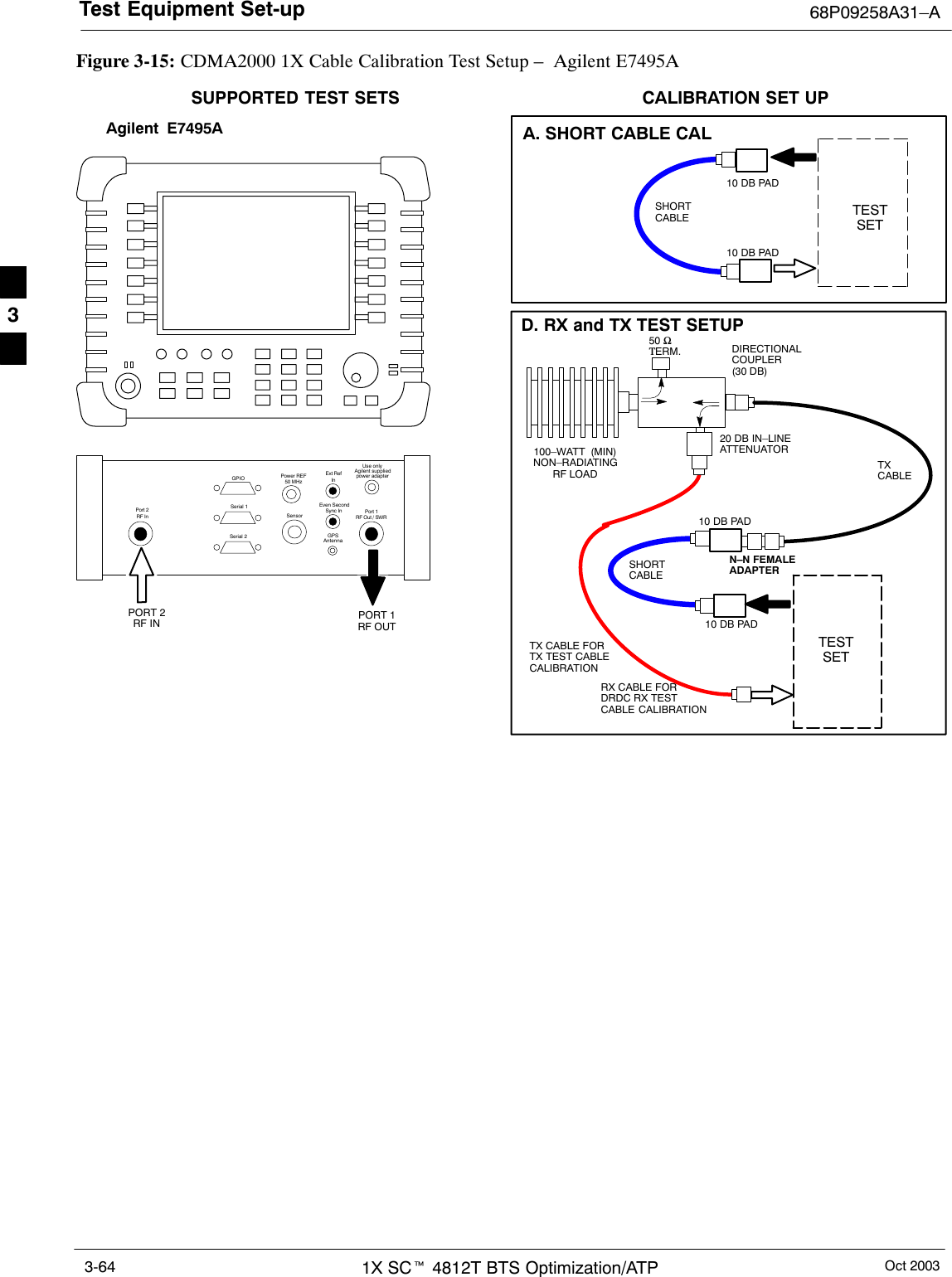
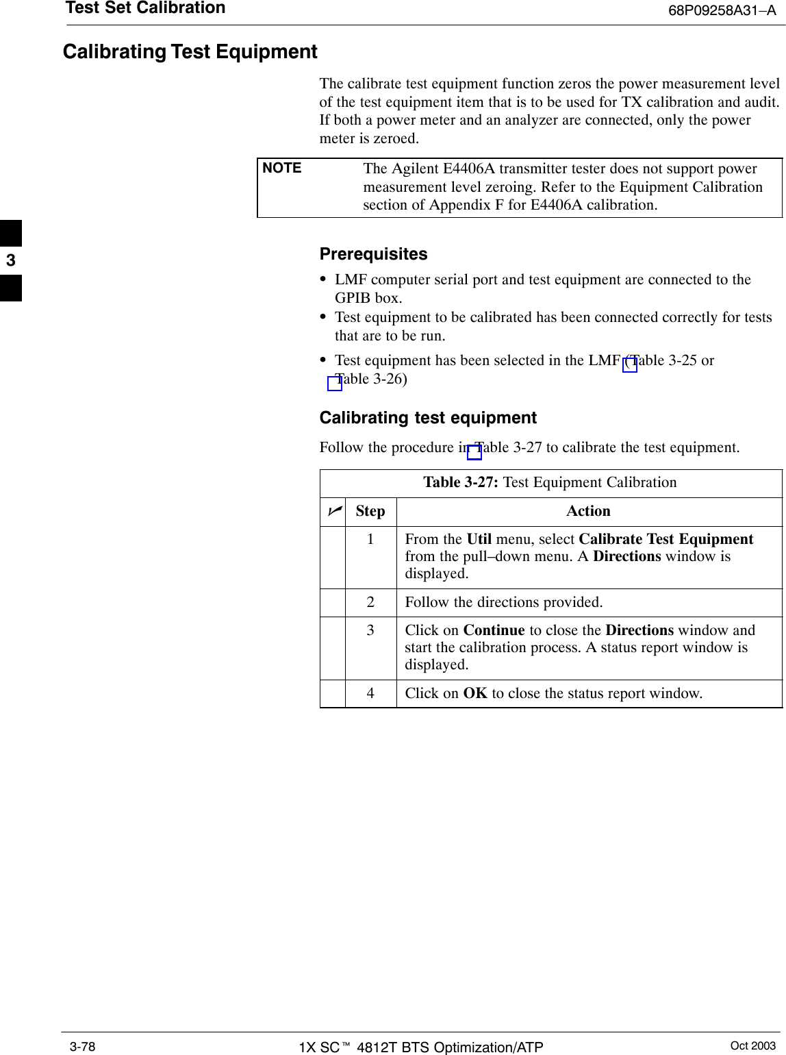
![Bay Level Offset Calibration 68P09258A31–AOct 20031X SCt 4812T BTS Optimization/ATP3-88Table 3-34: BTS.cal File Array (Per Sector)BBX RX DiversityRXTXSectorizationSlot[20] (Redundant BBX–13)1 (Omni) 3–Sector,C[1]–C[20] C[241]–C[260] C[481]–C[500]23–Sector,1stCiC[21]–C[40] C[261]–C[280] C[501]–C[520]36 Sector,1stCarrier C[41]–C[60] C[281]–C[300] C[521]–C[540]41stCarrier 3–Sector,C[61]–C[80] C[301]–C[320] C[541]–C[560]5Carrier3–Sector,3rdCiC[81]–C[100] C[321]–C[340] C[561]–C[580]6Carrier C[101]–C[120] C[341]–C[360] C[581]–C[600] . . . continued on next page73–Sector,C[121]–C[140] C[361]–C[380] C[601]–C[620]83–Sector,2ndCiC[141]–C[160] C[381]–C[400] C[621]–C[640]96 Sector,2ndCarrier C[161]–C[180] C[401]–C[420] C[641]–C[660]102ndCarrier 3–Sector,C[181]–C[200] C[421]–C[440] C[661]–C[680]11Carrier3–Sector,4thCiC[201]–C[220] C[441]–C[460] C[681]–C[700]12 Carrier C[221]–C[240] C[461]–C[480] C[701]–C[720]STen calibration points per sector are supported for each branch. Twoentries are required for each calibration point.SThe first value (all odd entries) refer to the CDMA channel(frequency) where the BLO is measured. The second value (all evenentries) is the power set level. The valid range for PwrLvlAdj is from2500 to 27500 (2500 corresponds to –125 dBm and 27500corresponds to +125 dBm).SThe 20 calibration entries for each sector/branch combination must bestored in order of increasing frequency. If less than 10 points(frequencies) are calibrated, the largest frequency that is calibrated isrepeated to fill out the 10 points.Example:C[1]=384, odd cal entry= 1 ‘‘calibration point”C[2]=19102, even cal entryC[3]=777,C[4]=19086,..C[19]=777,C[20]=19086, (since only two cal points were calibrated this would be repeated for the next 8 points)SWhen the BBX is loaded with image = data, the cal file data for theBBX is downloaded to the device in the order it is stored in the calfile. TxCal data is sent first, C[1] – C[240]. Sector 1’s ten calibrationpoints are sent (C[1] – C[20]) followed by sector 2’s ten calibrationpoints (C[21] – C[40]), etc. The RxCal data is sent next (C[241] –C[480]), followed by the RxDCal data (C[481] – C[720]).STemperature compensation data is also stored in the cal file for eachset.3](https://usermanual.wiki/Nokia-Solutions-and-Networks/T6EF1.Users-Manual-2/User-Guide-426543-Page-79.png)