Nokia Solutions and Networks T6EQ1 SC4812ET 1X/1X-EVDO @ 1.9 GHz CDMA BTS User Manual Exhibit 8
Nokia Solutions and Networks SC4812ET 1X/1X-EVDO @ 1.9 GHz CDMA BTS Exhibit 8
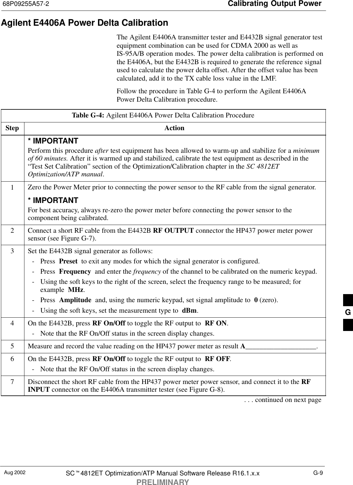
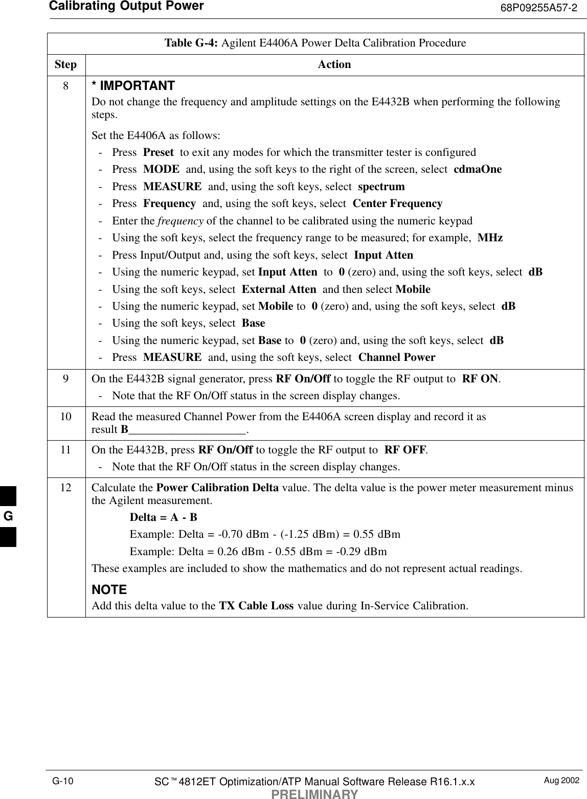
UserManual.wiki
>
Nokia Solutions and Networks
>
T6EQ1 User Manual
Exhibit 8
Navigation menu
Upload a User Manual
Namespaces
Wiki Guide
HTML
PDF
Info
Views
User Manual
Discussion / Help
Navigation

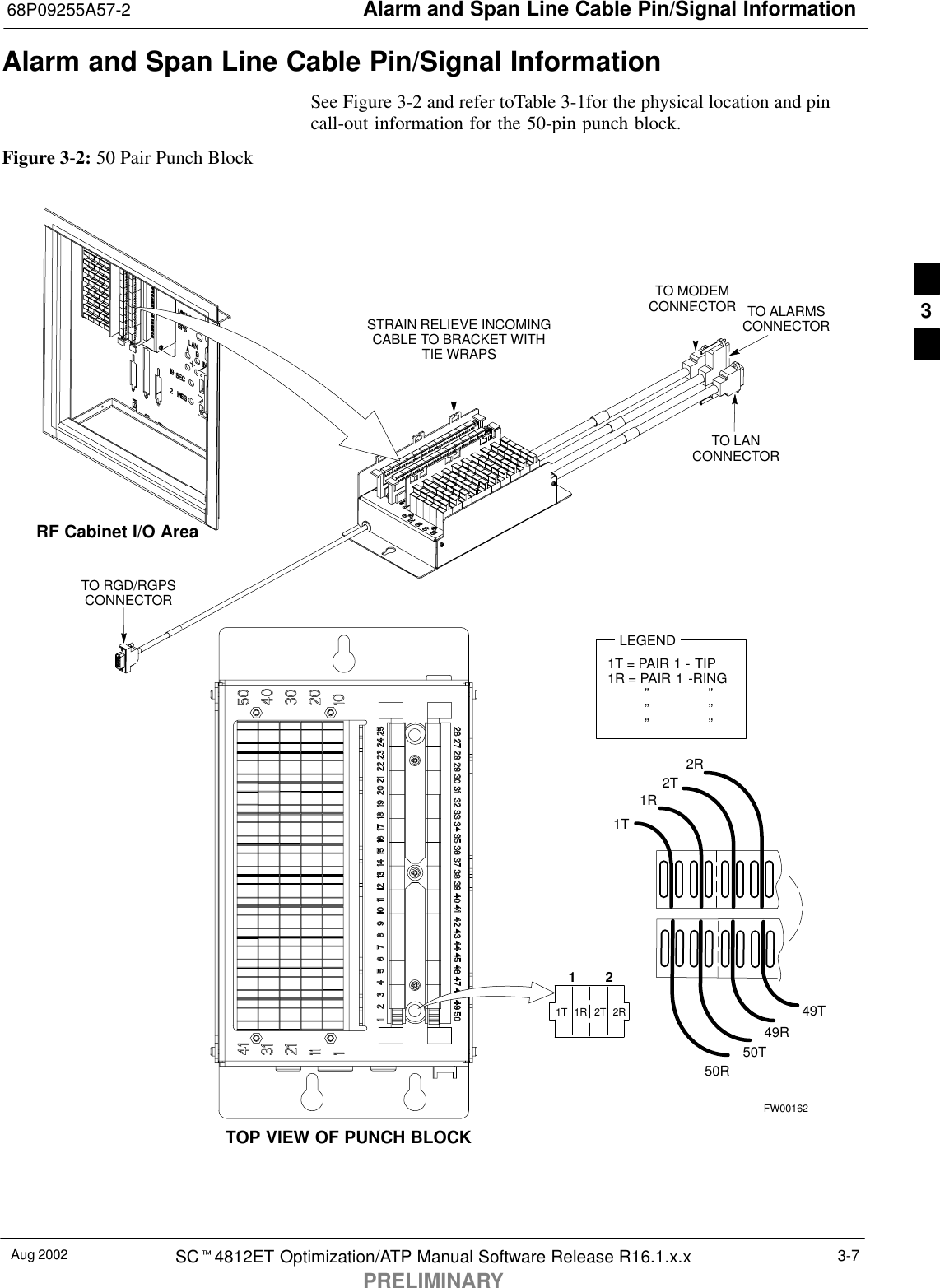
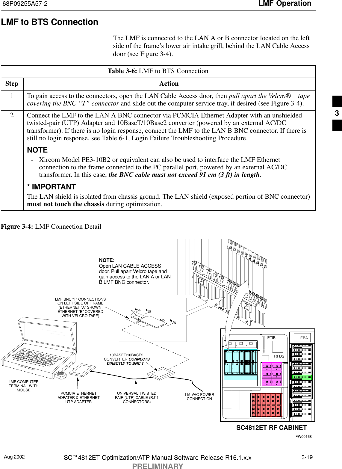
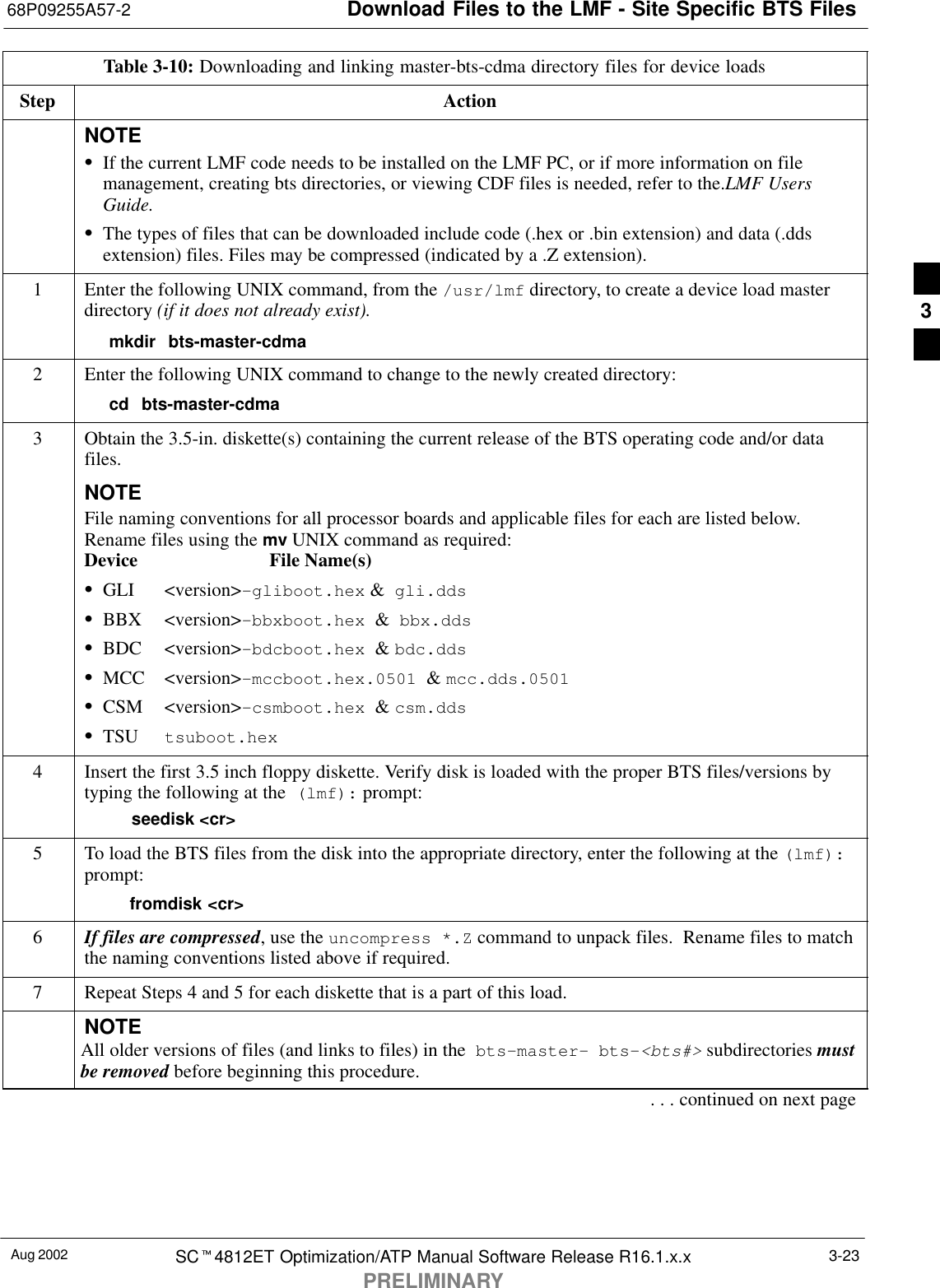
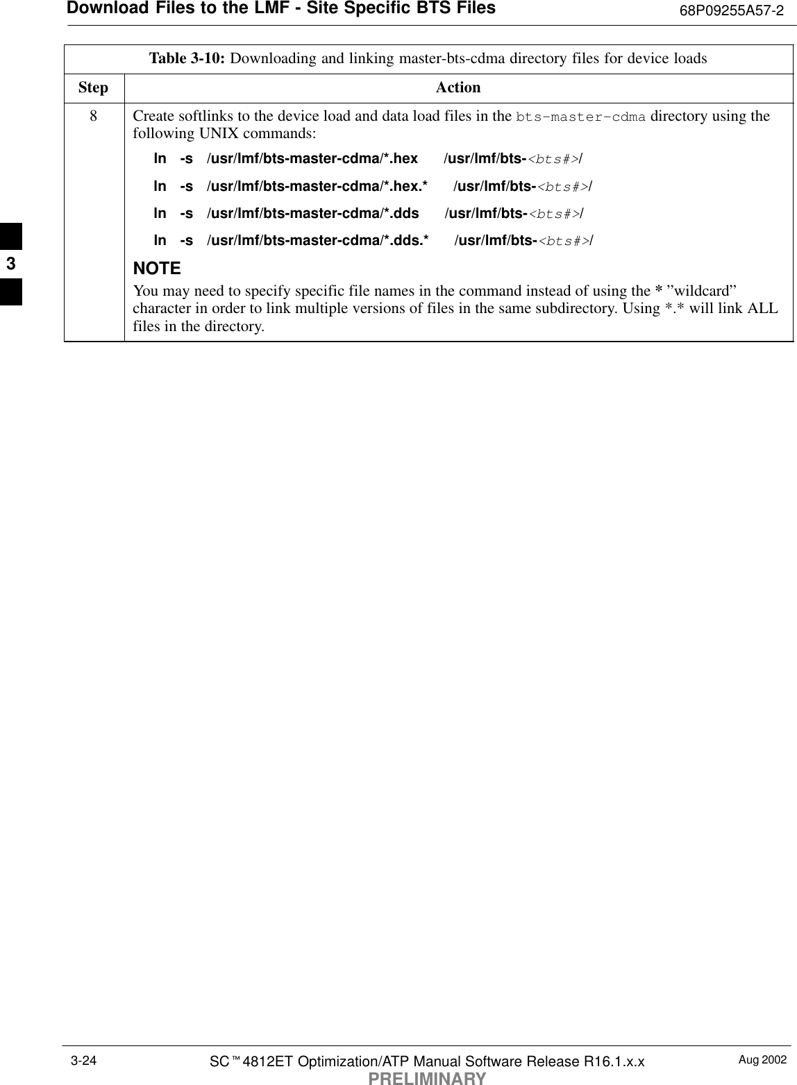
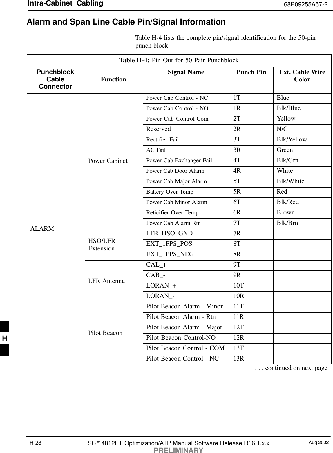
![Download Files to the LMF - Site Specific BTS Files 68P09255A57-2Aug 2002SCt4812ET Optimization/ATP Manual Software Release R16.1.x.xPRELIMINARY3-26Table 3-12: Update BTS Specific CDF File Device Load VersionStep Action! CAUTIONIf you are not familiar with the UNIX vi editor, create a “dummy” CDF file, and practice makingchanges to it, prior to altering the “real” one.* IMPORTANTCDF files obtained from the OMCR/CBSC are modified by DELTA information being appended tothe end of the CDF file. The information in the DELTA fields take precedence over information in the“core CDF file” For example: If NextLoad=‘‘1.2.3.4.5” for BBX 1 was specified in the CDF file, andthere was a DELTA entry specifying NextLoad=‘‘2.3.4.5.6” appended to the CDF file for the sameBBX, 2.3.4.5.6 would be the version used.There are two ways resolve this. Edit both the DELTA and “core” areas of the file to reflect the sameversion, or make sure the delta information is transferred to the main CDF file and delete all DELTACDF file entries.1Globally change the device load version number in the new CDF file using the following UNIXcommands:vi bts-new_<bts#>.cdf:1,$ s/x.x.x.x.x/y.y.y.y.yWhere: x.x.x.x.x and y.y.y.y.y represent the old and new version number, respectively.:wqNOTEYou should now be able to download all devices at the BTS with the current device load version.2Verify the SiteType and SSType entries in the CDF file (under the BTS subheading) reflect thefollowing information. See example of applicable fields of CDF file below.(CDMA only; 1900 MHz example shown):BTS[#] = {....,SiteType=3,SSType=16...},Valid SiteTypes (SC9600=1, SC9600(Mixed)=2, SC2400=3, SC2400(Mixed)=4, SC600=5)Valid SSTypes (CDMA800MHz=8, CDMA1900MHz=16, CDMA900MHz=32)Update Antenna Mapping FilesEarlier release versions may require the antenna.map file to beupdated. There are two antenna mapping files. These areantenna.map and antenna.asu.Follow the steps outlined in Table 3-13 to check the antenna mappingfile and update as needed.3](https://usermanual.wiki/Nokia-Solutions-and-Networks/T6EQ1/User-Guide-486577-Page-96.png)
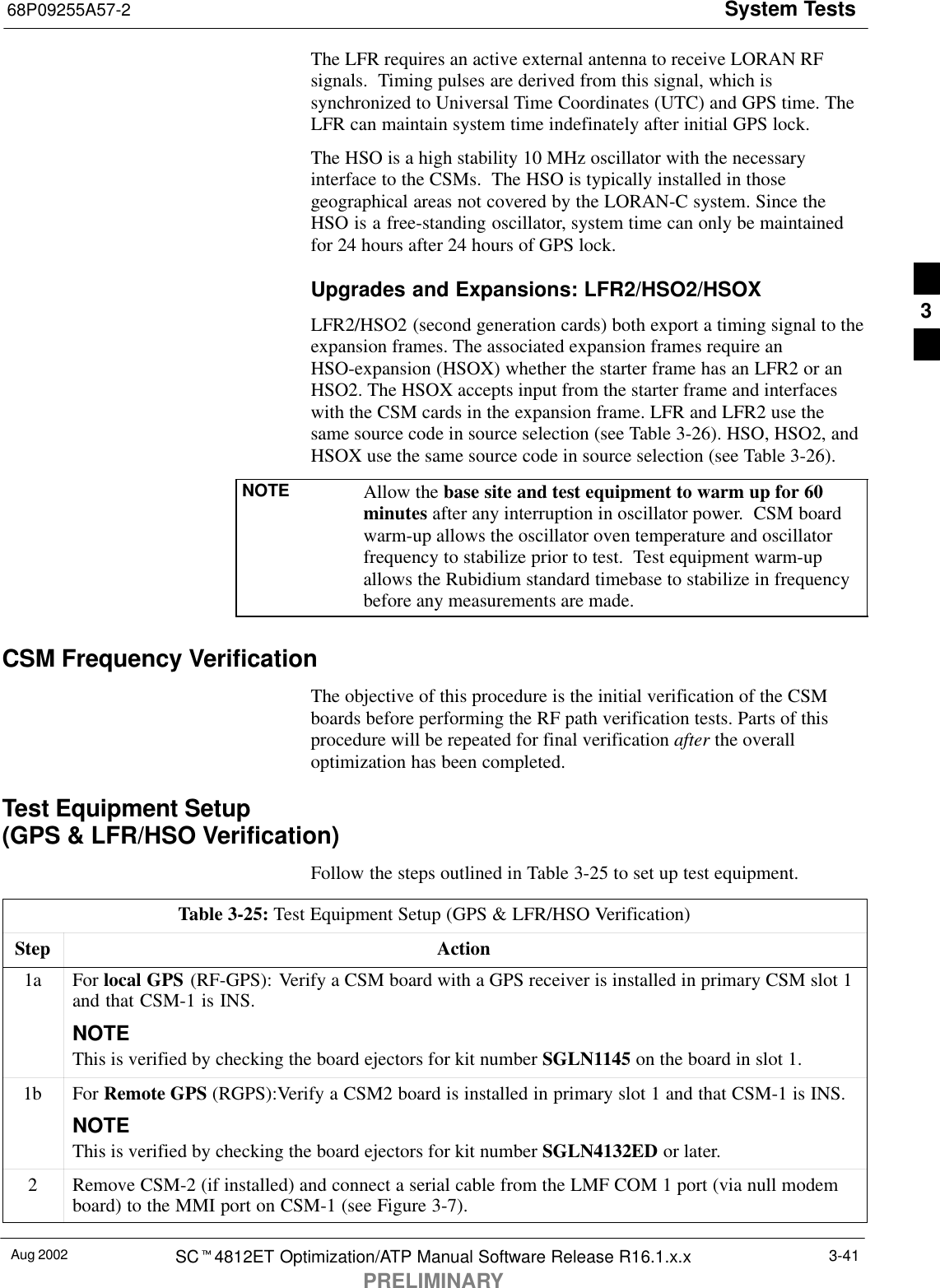
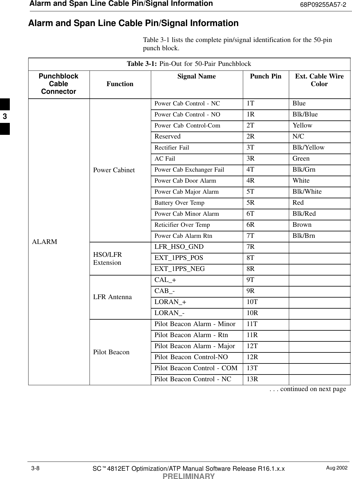
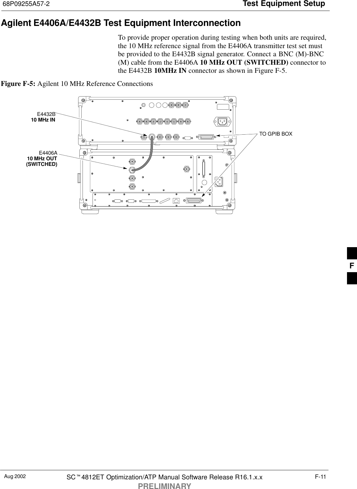
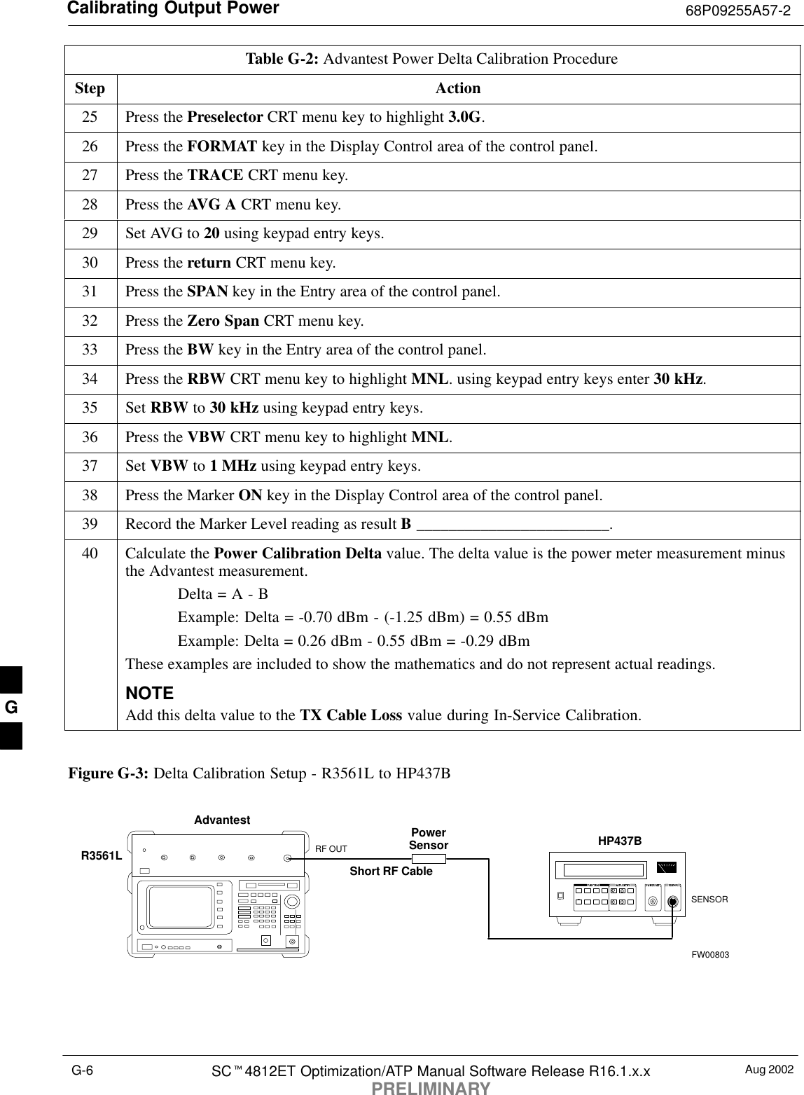
![Adjusting for loss 68P09255A57-2Aug 2002SCt4812ET Optimization/ATP Manual Software Release R16.1.x.xPRELIMINARY3-76CAUTION Always wear a conductive, high impedance wrist strap whilehandling any circuit card/module. If this is not done, there is ahigh probability that the card/module could be damaged by ESD.NOTE At new site installations, to facilitate the complete test of eachCCP shelf (if the shelf is not already fully populated with BBXboards), move BBX boards from shelves currently not under testand install them into the empty BBX slots of the shelf currentlybeing tested to insure that all BBX TX paths are tested.- This procedure can be bypassed on operational sites that aredue for periodic optimization.- Prior to testing, view the CDF file to verify the correctBBX slots are equipped. Edit the file as required to includeBBX slots not currently equipped (per SystemsEngineering documentation).BLO Calibration Data FileDuring the calibration process, the LMF creates a calibration (BLO) datafile. After calibration has been completed, this offset data must bedownloaded to the BBXs using the Download BLO function. Anexplanation of the file is shown below.NOTE Due to the size of the file, Motorola recommends that you printout a hard copy of a bts.cal file and refer to it for the followingdescriptions.The CAL file is subdivided into sections organized on a per slot basis (aslot Block).Slot 1 contains the calibration data for the 12 BBX slots. Slot 20contains the calibration data for the redundant BBX (see Table 3-39).Each BBX slot header block contains:SA creation Date and Time - broken down into separate parameters ofcreateMonth, createDay, createYear, createHour, and createMin.SThe number of calibration entries - fixed at 720 entries correspondingto 360 calibration points of the CAL file including the slot header andactual calibration data.SThe calibration data for a BBX is organized as a large flat array. Thearray is organized by branch, BBX slot, and calibration point.- The first breakdown of the array indicates which branch thecontained calibration points are for. The array covers transmit, mainreceive and diversity receive offsets as follows:Table 3-38: BLO BTS.cal file Array Branch AssignmentsRange AssignmentC[1]-C[240] TransmitC[241]-C[480] ReceiveC[481]-C[720] Diversity Receive3](https://usermanual.wiki/Nokia-Solutions-and-Networks/T6EQ1/User-Guide-486577-Page-146.png)
![Adjusting for loss68P09255A57-2Aug 2002 SCt4812ET Optimization/ATP Manual Software Release R16.1.x.xPRELIMINARY3-77- The second breakdown of the array is per sector. Three sectors areallowed.Table 3-39: BTS.cal File Array (Per Sector)BBX Sectorization TX RX RX DiversitySlot[1] (Primary BBXs 1 through 12)1 (Omni)3-Sector,C[1]-C[20] C[241]-C[260] C[481]-C[500]23-Sector,1st C[21]-C[40] C[261]-C[280] C[501]-C[520]36 Sector, Carrier C[41]-C[60] C[281]-C[300] C[521]-C[540]41stCarrier3-Sector,C[61]-C[80] C[301]-C[320] C[541]-C[560]5Carrier 3-Sector,3rd C[81]-C[100] C[321]-C[340] C[561]-C[580]6Carrier C[101]-C[120] C[341]-C[360] C[581]-C[600]73-Sector,C[121]-C[140] C[361]-C[380] C[601]-C[620]83-Sector,2nd C[141]-C[160] C[381]-C[400] C[621]-C[640]96 Sector, Carrier C[161]-C[180] C[401]-C[420] C[641]-C[660]10 2ndCarrier3-Sector,C[181]-C[200] C[421]-C[440] C[661]-C[680]11 Carrier 3-Sector,4th C[201]-C[220] C[441]-C[460] C[681]-C[700]12 Carrier C[221]-C[240] C[461]-C[480] C[701]-C[720]Slot[20] (Redundant BBX-13)1 (Omni)3-Sector,C[1]-C[20] C[241]-C[260] C[481]-C[500]23-Sector,1st C[21]-C[40] C[261]-C[280] C[501]-C[520]36 Sector, Carrier C[41]-C[60] C[281]-C[300] C[521]-C[540]41stCarrier3-Sector,C[61]-C[80] C[301]-C[320] C[541]-C[560]5Carrier 3-Sector,3rd C[81]-C[100] C[321]-C[340] C[561]-C[580]6Carrier C[101]-C[120] C[341]-C[360] C[581]-C[600]73-Sector,C[121]-C[140] C[361]-C[380] C[601]-C[620]83-Sector,2nd C[141]-C[160] C[381]-C[400] C[621]-C[640]96 Sector, Carrier C[161]-C[180] C[401]-C[420] C[641]-C[660]10 2ndCarrier3-Sector,C[181]-C[200] C[421]-C[440] C[661]-C[680]11 Carrier 3-Sector,4th C[201]-C[220] C[441]-C[460] C[681]-C[700]12 Carrier C[221]-C[240] C[461]-C[480] C[701]-C[720]SRefer to the hard copy of the file. As you can see, 10 calibrationpoints per sector are supported for each branch. Two entries arerequired for each calibration point.SThe first value (all odd entries) refer to the CDMA channel(frequency) the BLO is measured at. The second value (all evenentries) is the power set level. The valid range for PwrLvlAdj is from2500 to 27500 (2500 corresponds to -125 dBm and 27500corresponds to +125 dBm).SThe 20 calibration entries for each slot/branch combination must bestored in order of increasing frequency. If less than 10 points(frequencies) are calibrated, the largest frequency that is calibrated isrepeated to fill out the 10 points.3](https://usermanual.wiki/Nokia-Solutions-and-Networks/T6EQ1/User-Guide-486577-Page-147.png)
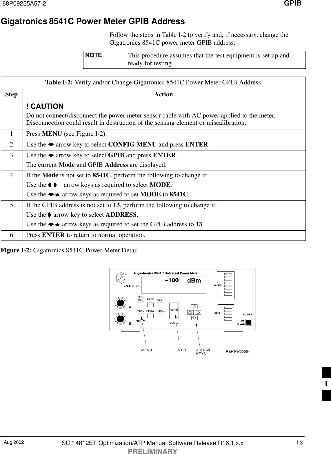
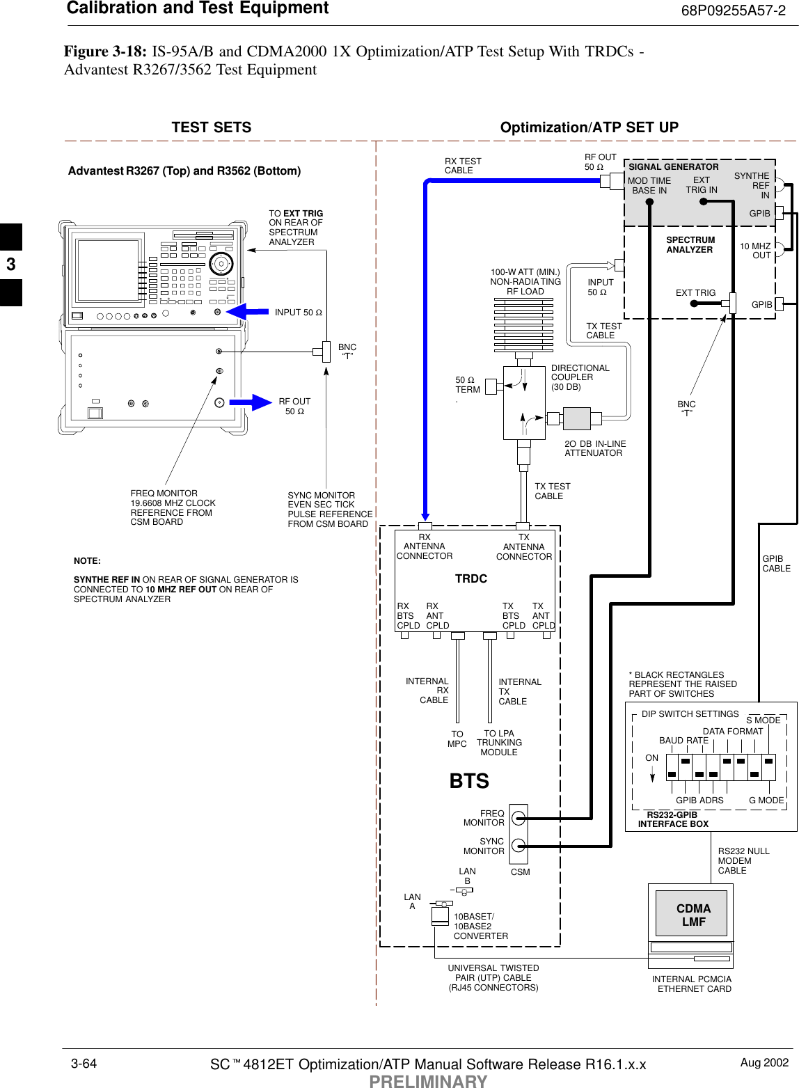
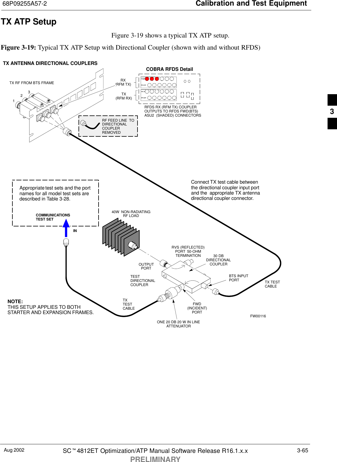
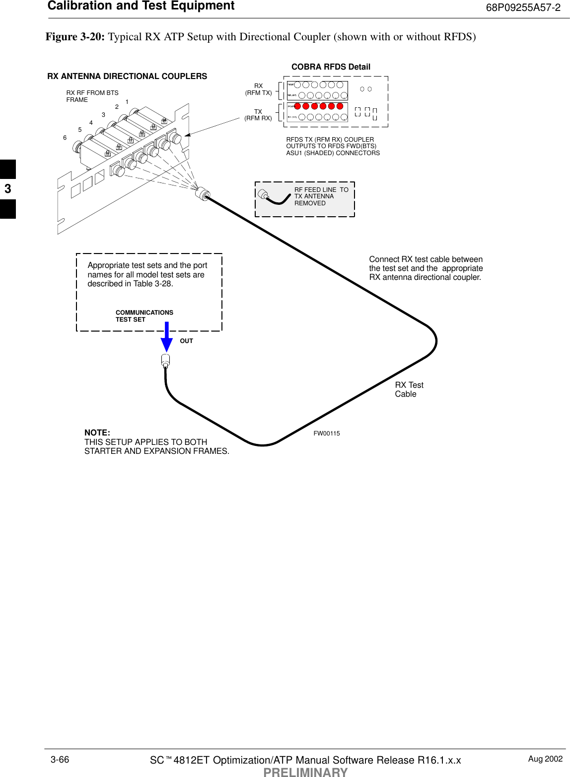
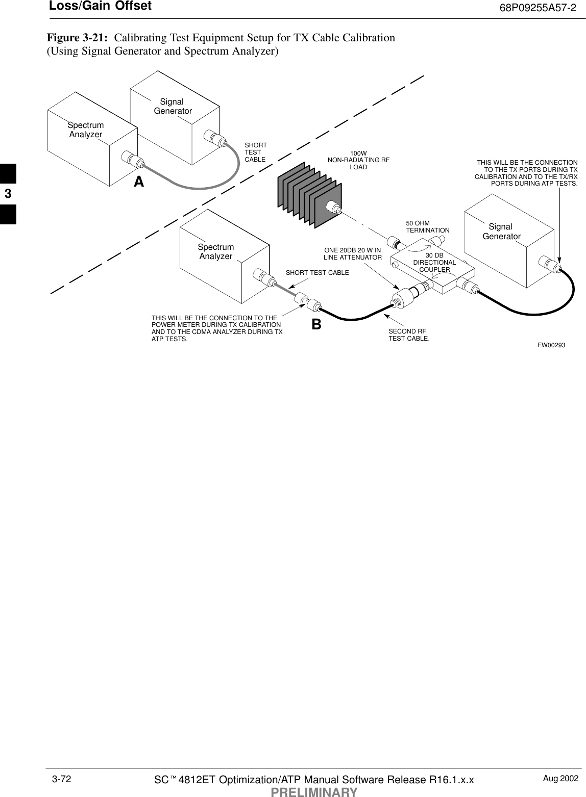
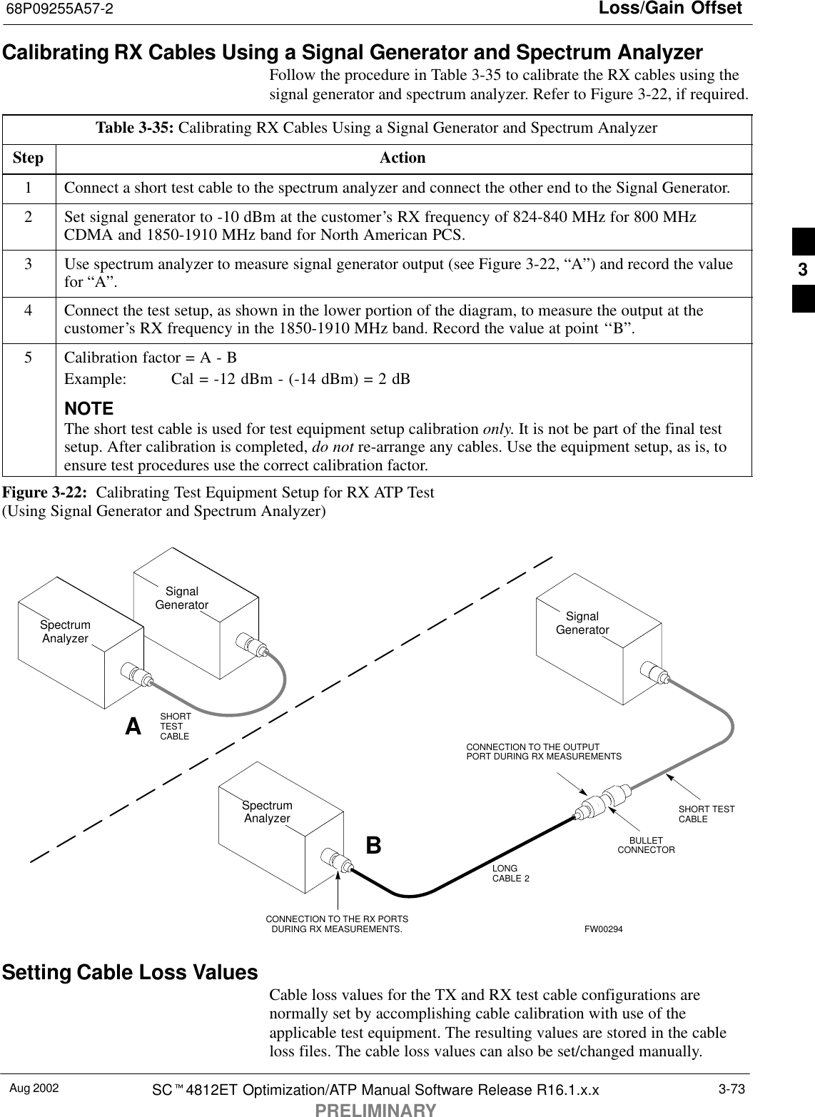
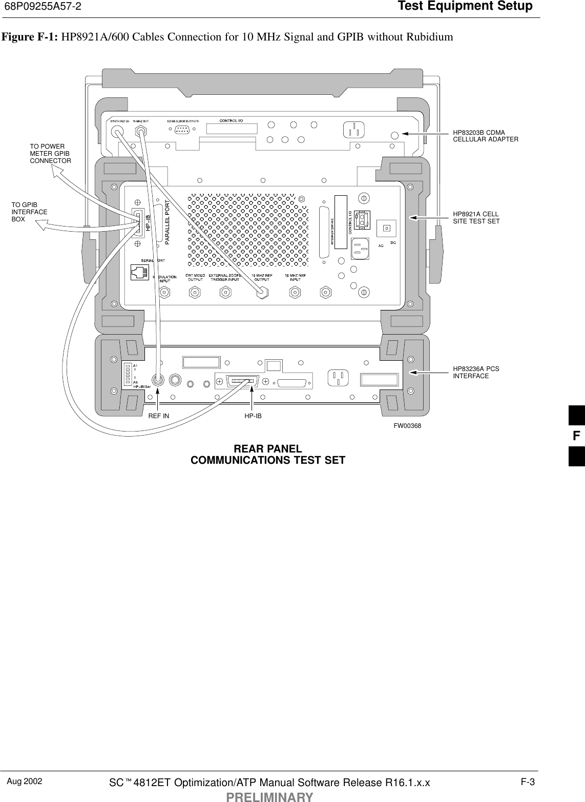
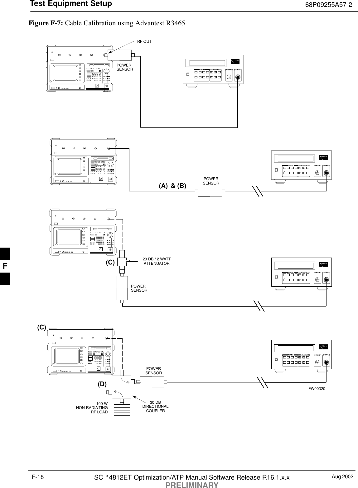
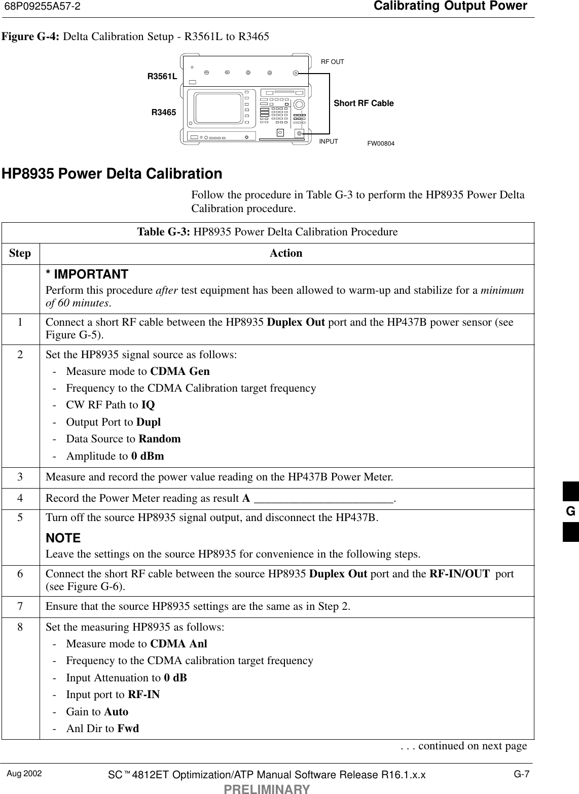
![Adjusting for loss 68P09255A57-2Aug 2002SCt4812ET Optimization/ATP Manual Software Release R16.1.x.xPRELIMINARY3-78Example:C[1]=384, odd cal entry = 1 ‘‘calibration point”C[2]=19102, even cal entryC[3]=777,C[4]=19086,..C[19]=777,C[20]=19086, (since only two cal points were calibrated this would be repeated for the next 8 points)SWhen the BBX is loaded with BLO data, the cal file data for the BBXis downloaded to the device in the order it is stored in the CAL file.TxCal data is sent first, C[1] - C[60]. BBX slot 1’s 10 calibrationpoints are sent (C[1] - C[20]), followed by BBX slot 2’s 10calibration points (C[21] - C[40]), etc. The RxCal data is sent next,followed by the RxDCal data.STemperature compensation data is also stored in the cal file for eachslot.Test Equipment Setup: RF Path CalibrationFollow the steps in Table 3-40 to set up test equipment.Table 3-40: Test Equipment Setup (RF Path Calibration)Step ActionNOTEVerify the GPIB is properly connected and turned on.! CAUTIONTo prevent damage to the test equipment, all transmit (TX) test connections must be via the 30 dBdirectional coupler for 800 MHz or via a 30 dB coupler with a 20 dB in-line attenuator for 1900 MHz.1Connect the LMF computer terminal to the BTS LAN A connector on the BTS (if you have notalready done so). Refer to the procedure in Table 3-6.SIf required, calibrate the test equipment per the procedure in Table 3-32.SConnect the test equipment as shown in Figure 3-16, Figure 3-17 and Figure 3-18.Transmit (TX) Path CalibrationThe assigned channel frequency and power level (as measured at the topof the frame) for transmit calibration is derived from the site CDF file.For each BBX, the channel frequency is specified in the ChannelListCDF file parameter and the power is specified in the SIFPilotPwrCDF file parameter for the sector associated with the BBX (locatedunder the ParentSECTOR field of the ParentCARRIER CDF fileparameter).The calibration procedure attempts to adjust the power to within +0.5 dBof the desired power. The calibration will pass if the error is less than+1.5 dB.The TX Bay Level Offset at sites WITHOUT the directional coupleroption, is approximately 42.0 dB ±3.0 dB.3](https://usermanual.wiki/Nokia-Solutions-and-Networks/T6EQ1/User-Guide-486577-Page-148.png)
![Adjusting for loss68P09255A57-2Aug 2002 SCt4812ET Optimization/ATP Manual Software Release R16.1.x.xPRELIMINARY3-91Table 3-49: Set Antenna Map DataStep Action1Click on Util in the BTS menu bar, and select Edit > Antenna Map... from the pull-down menus.-A tabbed data entry pop-up window will appear.2In the data entry pop-up window, click on the TX Antenna Map or RX Antenna Map tab to selectthe antenna map to be edited.3Locate the carrier and sector number for which data is to be entered or edited, and click in the columnwhere entry or editing is needed.4Enter/edit Antenna # and Antenna Label column data as needed for each carrier.NOTERefer to the CDMA Help > Utility Menu > Edit-Antenna Map... section of LMF Help functionon-line documentation for antenna map examples.5For each tab with changes, click on the Save button to save displayed values.6Click on the Dismiss button to close the window.NOTESValues entered or changed after the Save button was used will be lost when the window isdismissed.SEntered values will be used by the LMF as soon as they are saved. It is not necessary to log out andlog back into the LMF for changes to take effect. Set RFDS Configuration DataIf an RFDS is installed, the RFDS configuration data must be manuallyentered.PrerequisiteSLMF is logged into the BTSNOTE The entered antenna# index numbers must correspond to theantenna# index numbers used in the antenna maps.Follow the procedure in Table 3-50 to set RFDS configuration data.Table 3-50: Set RFDS Configuration DataStep Action1Click on Util in the BTS menu bar, and select Edit > RFDS Configuration... from the pull-downmenus.-A tabbed data entry pop-up window will appear.2In the data entry pop-up window, click on the TX RFDS Configuration or RX RFDS Configurationtab, as required.3To add a new antenna number, perform the following:3a - Click on the Add Row button.3b - Click in the Antenna #, Cal Antenna, Scap Antenna, or Populate [Y/N] columns, as required.. . . continued on next page3](https://usermanual.wiki/Nokia-Solutions-and-Networks/T6EQ1/User-Guide-486577-Page-161.png)
![Adjusting for loss 68P09255A57-2Aug 2002SCt4812ET Optimization/ATP Manual Software Release R16.1.x.xPRELIMINARY3-92Table 3-50: Set RFDS Configuration DataStep Action3c - Enter the desired data.4To edit existing values click in the data box to be changed and change the value.NOTERefer to the CDMA Help > Utility Menu > Edit-RFDS Configuration... section of LMF Helpfunction on-line documentation for RFDS configuration data examples.5To delete a row, click on the row and then click on the Delete Row button.6For each tab with changes, click on the Save button to save displayed values.7Click on the Dismiss button to close the window.NOTESValues entered or changed after the Save button was used will be lost when the window isdismissed.SEntered values will be used by the LMF as soon as they are saved. It is not necessary to log out andlog back into the LMF for changes to take effect. RFDS CalibrationThe RFDS Calibration option is used to calibrate the RFDS TX and RXpaths.TX Path Calibration - For a TX antenna path calibration the BTSXCVR is keyed at a pre-determined power level and the BTS poweroutput level is measured by the RFDS. The power level is then measuredat the TX antenna directional coupler by the power measuring testequipment item being used (power meter or analyzer). The difference(offset) between the power level at the RFDS and the power level at theTX antenna directional coupler is used as the TX RFDS calibrationoffset value.RX Path Calibration - For an RX antenna path calibration the RFDS iskeyed at a pre-determined power level and the power input level ismeasured by the BTS BBX. A CDMA signal at the same power levelmeasured by the BTS BBX is then injected at the RX antenna directionalcoupler by the communications system analyzer. The difference (offset)between the RFDS-keyed power level and power level measured at theBTS BBX is the RFDS RX calibration offset value.RFDS calibration and the CAL file - The TX and RX RFDScalibration offset values are written to the CAL file in the slot[385]Block.TSIC channel frequency - For each RFDS TSIC, the channelfrequency is determined at the lower third and upper third of theappropriate band using the frequencies listed in Table 3-51.3](https://usermanual.wiki/Nokia-Solutions-and-Networks/T6EQ1/User-Guide-486577-Page-162.png)
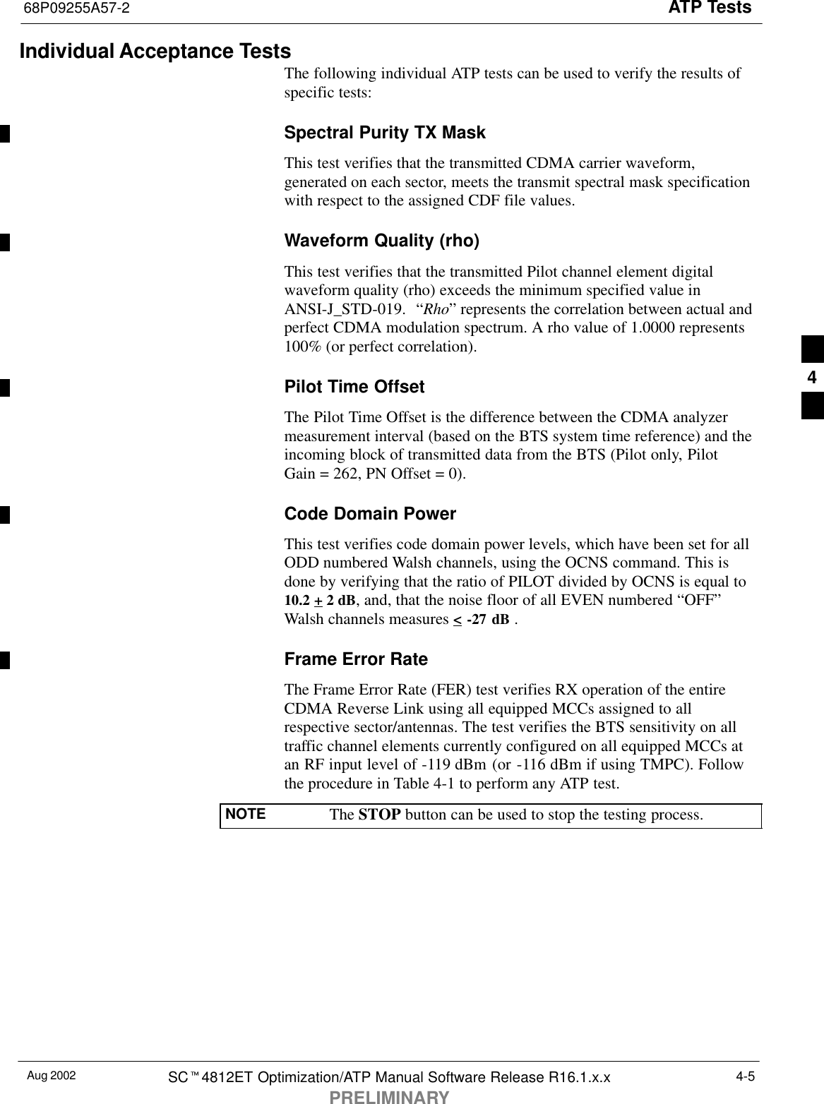
![ATP Tests 68P09255A57-2Aug 2002SCt4812ET Optimization/ATP Manual Software Release R16.1.x.xPRELIMINARY4-6ATP Test Procedure Table 4-1 describes the step-by-step procedures to run any APT Test.Table 4-1: ATP Test ProcedureStep Action1Select the device(s) to be tested.2From the Tests menu, select the desired test.3Select the appropriate carrier(s) (carrier - bts# - sector# - carrier#) displayed in the Channels/Carrierpick list.To select multiple items, hold down the <Shift> or <Ctrl> key while making the selections.4Type the appropriate channel number in the Carrier n Channels box.The default channel number displayed is determined by the CdmaChans[n] number in the cbsc-n.cdffile for the BTS.5If applicable, select Verify BLO (default) or Single-sided BLO.NOTESingle-sided BLO is only used when checking non-redundant transceivers.6For RX select the appropriate RX branch (Both, Main, or Diversity) in the drop-down list.7In the Rate Set box, select the appropriate data rate (1=9600, 2=14400, 3=9600 1X) from thedrop-down list.NOTEThe Rate Set selection of 3 is only available if 1X cards are selected for the test.8In the Test Pattern box, select the test pattern to use for the calibration from the drop-down list: Pilot(default), CDF, CDFPilot or Standard.9 Click OK.The status report window and a Directions pop-up are displayed.10 Follow the cable connection directions as they are displayed.11 Click Save Results or Dismiss to close the status report window. If Dismiss is used the test results will not be saved in the test report file. Background: Tx Mask TestThis test verifies the spectral purity of each BBX2 carrier keyed up at aspecific frequency, per the current CDF file assignment. All tests areperformed using the external calibrated test set, controlled by the samecommand. All measurements are through the appropriate TX OUT(BTS/RFDS) connector.The Pilot Gain is set to 541 for each antenna and all channel elementsfrom the MCCs are forward-link disabled. The BBX2 is keyed up, usingboth bbxlvl and bay level offsets, to generate a CDMA carrier (with pilotchannel element only). BBX2 power output is set to obtain +40 dBm asmeasured at the TX OUT connector (on either the BTS or RFDSdirectional coupler).4](https://usermanual.wiki/Nokia-Solutions-and-Networks/T6EQ1/User-Guide-486577-Page-180.png)
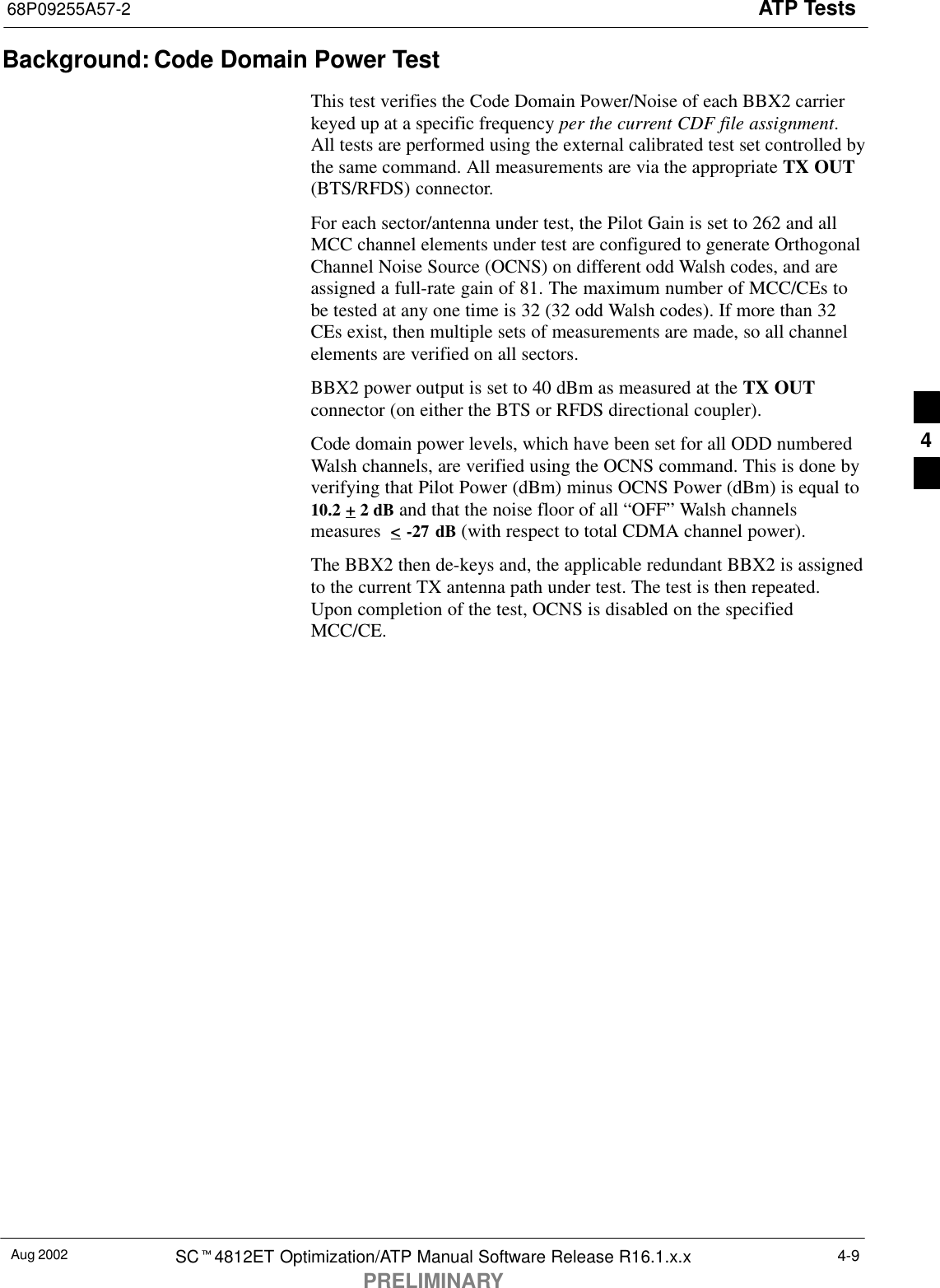
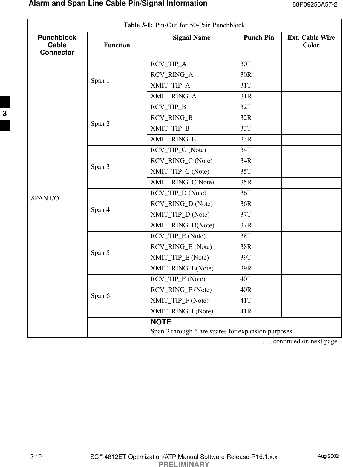
![ATP Tests 68P09255A57-2Aug 2002SCt4812ET Optimization/ATP Manual Software Release R16.1.x.xPRELIMINARY4-10Figure 4-2: Code Domain Power and Noise Floor LevelsPilot ChannelActive channelsPILOT LEVELMAX OCNS SPEC.MIN OCNS SPEC.MAXIMUM NOISE FLOOR: < -27 dB SPEC.Inactive channelsWalsh 0 1 2 3 4 5 6 7 ... 64MAX OCNSCHANNELMIN OCNSCHANNEL8.2 dB 12.2 dBMAX NOISEFLOORPilot ChannelActive channelsPILOT LEVELMAX OCNS SPEC.MIN OCNS SPEC.MAXIMUM NOISE FLOOR:< -27 dBInactive channelsWalsh 0 1 2 3 4 5 6 7 ... 64FAILURE - DOES NOTMEET MIN OCNS SPEC.FAILURE - EXCEEDSMAX OCNS SPEC. 8.2 dB 12.2 dBFAILURE - EXCEEDS MAXNOISE FLOOR SPEC. Showing all OCNS Passing Indicating Failures FW00283Background: FER TestThis test verifies the BTS FER on all traffic channel elements currentlyconfigured on all equipped MCCs (full rate at 1% FER) at an RF inputlevel of -119 dBm [or -116 dBm if using Tower Top Amplifier(TMPC)]. All tests are performed using the external calibrated test set asthe signal source controlled by the same command. All measurementswill be via the LMF.The pilot gain is set to 262 for each TX antenna and all channel elementsfrom the MCCs are forward-link disabled. The BBX2 is keyed up usingonly bbxlvl level offsets, to generate a CDMA carrier (with pilot channelelement only). BBX2 power output is set to -20 dBm as measured at theTX OUT connector (on either the BTS or RFDS directional coupler).The BBX2 must be keyed in order to enable the RX receive circuitry.4](https://usermanual.wiki/Nokia-Solutions-and-Networks/T6EQ1/User-Guide-486577-Page-184.png)


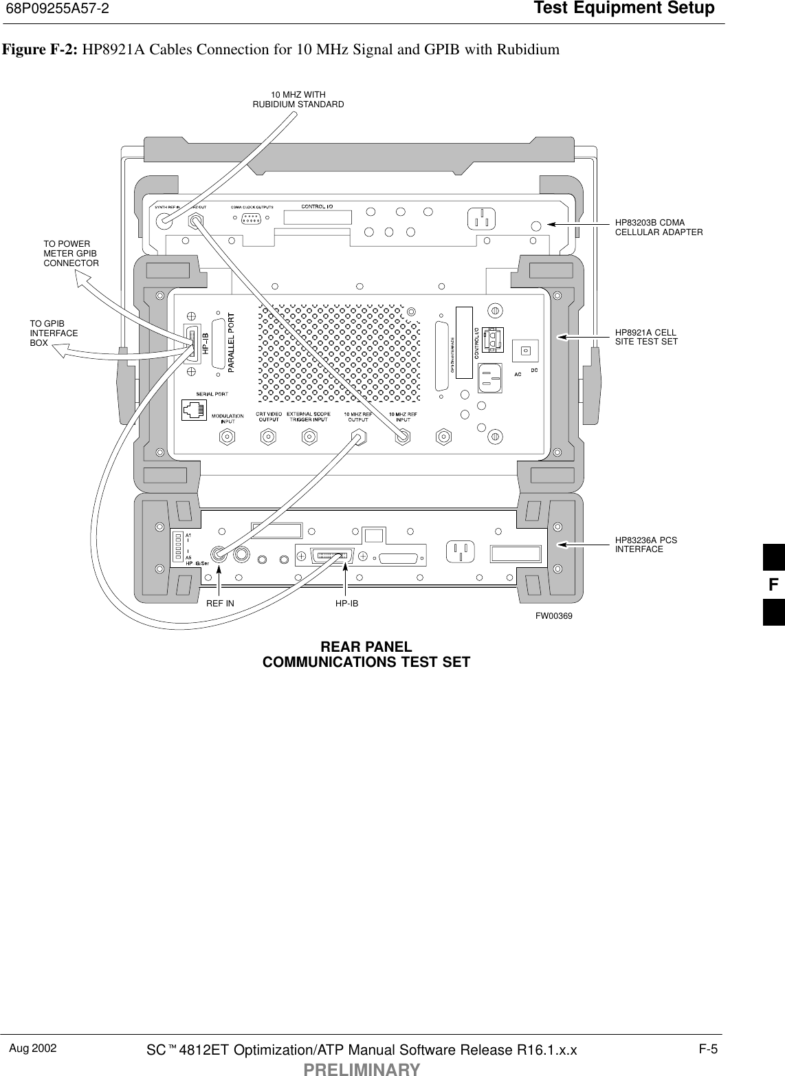
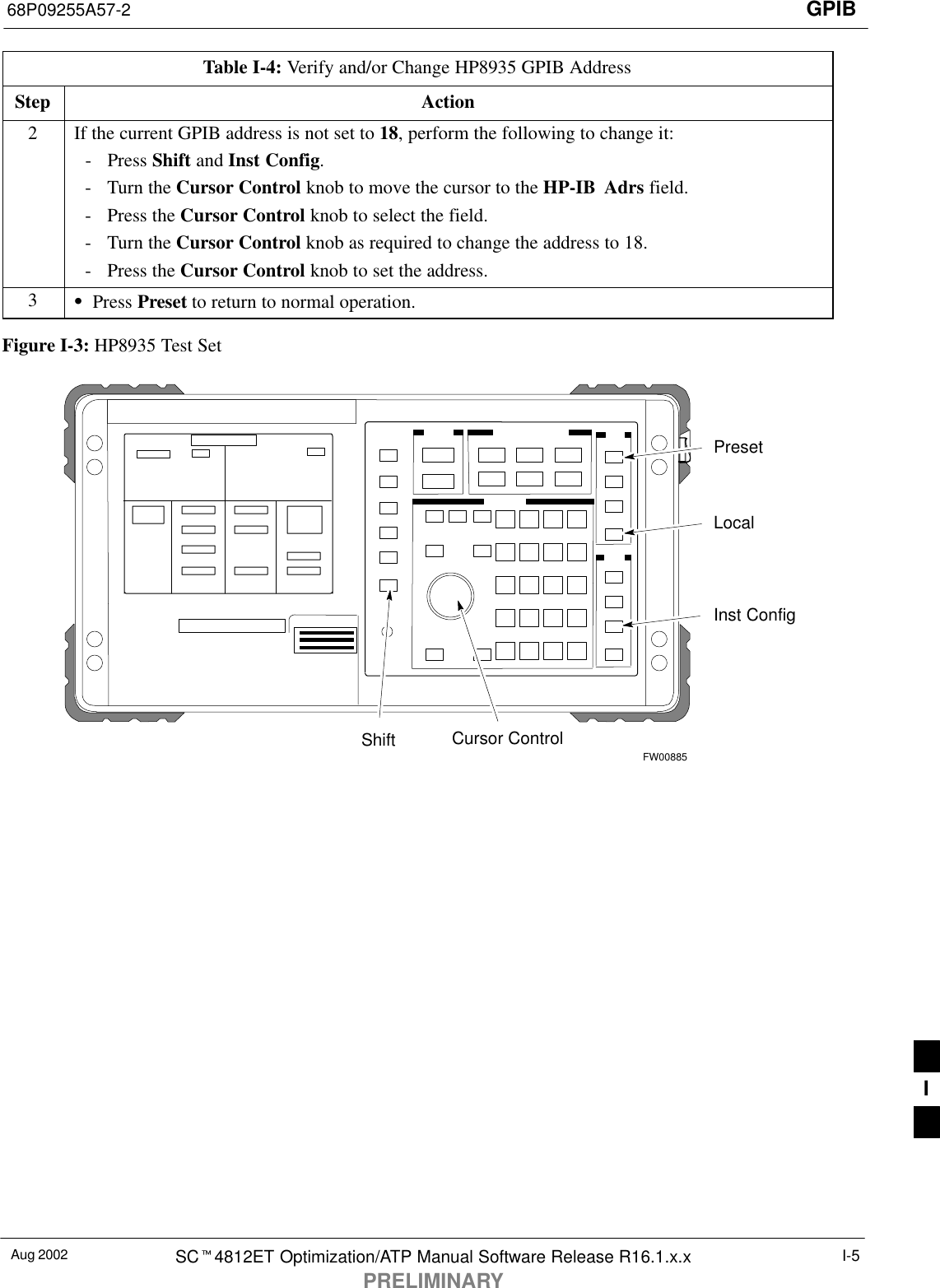
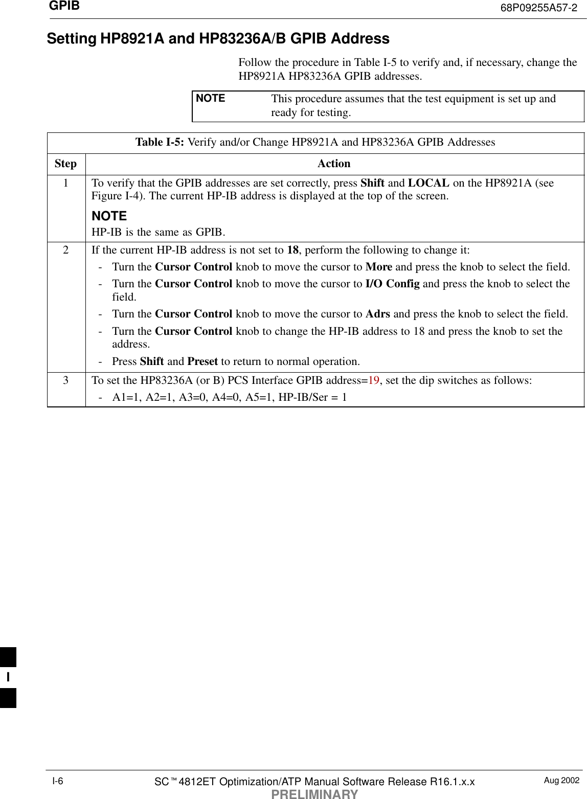
![Test Equipment Setup 68P09255A57-2Aug 2002SCt4812ET Optimization/ATP Manual Software Release R16.1.x.xPRELIMINARYF-6HP8921A System Connectivity TestFollow the steps in Table F-3 to verify that the connections between thePCS Interface and the HP8921A are correct and cables are intact. Thesoftware also performs basic functionality checks of each instrument.NOTE Disconnect other GPIB devices, especially system controllers,from the system before running the connectivity software.Table F-3: System ConnectivityStep Action* IMPORTANT- Perform this procedure after test equipment has been allowed to warm-up and stabilize for aminimum of 60 minutes.1Insert HP 83236A Manual Control/System card into memory card slot.2Press the [PRESET] pushbutton.3Press the Screen Control [TESTS] pushbutton to display the “Tests” Main Menu screen.4Position the cursor at Select Procedure Location and select it by pressing the cursor control knob. Inthe Choices selection box, select Card.5Position the cursor at Select Procedure Filename and select it by pressing the cursor control knob. Inthe Choices selection box, select SYS_CONN.6Position the cursor at RUN TEST and select it. The software will prompt you through theconnectivity setup.7Do the following when the test is complete,Sposition cursor on STOP TEST and select itSOR press the [K5] pushbutton.8To return to the main menu, press the [K5] pushbutton.9Press the [PRESET] pushbutton.Setting HP8921A and HP83236A/B GPIB AddressFollow the steps in Table F-4 to set the HP8921A GPIB address.Table F-4: Setting HP8921A GPIB AddressStep Action1If you have not already done so, turn the HP8921A power on.2Verify that the GPIB addresses are set correctly.SHP8921A HP-IB Adrs = 18, accessed by pushing LOCAL and selecting More and I/O Configureon the HP8921A/600. (Consult test equipment OEM documentation for additional info as required).SHP83236A (or B) PCS Interface GPIB address=19. Set dip switches as follows:- A1=1, A2=1, A3=0, A4=0, A5=1, HP-IB/Ser = 1F](https://usermanual.wiki/Nokia-Solutions-and-Networks/T6EQ1/User-Guide-486577-Page-272.png)
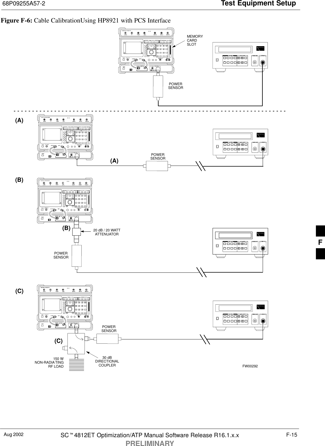
![Test Equipment Setup 68P09255A57-2Aug 2002SCt4812ET Optimization/ATP Manual Software Release R16.1.x.xPRELIMINARYF-12Calibrating Test Cable Setupusing HP PCS Interface (HP83236)Table F-9 covers the procedure to calibrate the test equipment using the HP8921 Cellular Communications Analyzer equipped with theHP83236 PCS Interface.NOTE Table:note. Note 10pt HelveticaThis calibration method must be executed with great care. Somelosses are measured close to the minimum limit of the powermeter sensor (-30 dBm).PrerequisitesEnsure the following prerequisites have been met before proceeding:STest equipment to be calibrated has been connected correctly for cablecalibration.STest equipment has been selected and calibrated.Table F-9: Calibrating Test Cable Setup (using the HP PCS Interface)Step ActionNOTEVerify that GPIB controller is turned off.1Insert HP83236 Manual Control System card into memory card slot.2Press the Preset pushbutton.3 Under Screen Controls, press the TESTS pushbutton to display the TESTS (Main Menu) screen.4Position the cursor at Select Procedure Location and select it. In the Choices selection box, selectCARD.5Position the cursor at Select Procedure Filename and select it. In the Choices selection box, selectMANUAL.6Position the cursor at RUN TEST and select it. HP must be in Control Mode Select YES.7If using HP 83236A:Set channel number=<chan#>:- Position cursor at ChannelNumber and select it.- Enter the chan# using the numerickeypad; press [Enter] and thescreen will go blank.- When the screen reappears, thechan# will be displayed on thechannel number line.If using HP 83236B:Set channel frequency:- Position cursor at Frequency Band and press Enter.- Select User Defined Frequency.- Go Back to Previous Menu.- Position the cursor to 83236 generator frequency andenter actual RX frequency.- Position the cursor to 83236 analyzer frequency andenter actual TX frequency.8Set RF Generator level:- Position the cursor at RF Generator Level and select it.- Enter -10 using the numeric keypad; press [Enter] and the screen will go blank.- When the screen reappears, the value -10 dBm will be displayed on the RF Generator Level line.. . . continued on next pageF](https://usermanual.wiki/Nokia-Solutions-and-Networks/T6EQ1/User-Guide-486577-Page-278.png)
![Test Equipment Setup68P09255A57-2Aug 2002 SCt4812ET Optimization/ATP Manual Software Release R16.1.x.xPRELIMINARYF-13Table F-9: Calibrating Test Cable Setup (using the HP PCS Interface)Step Action9Set the user fixed Attenuation Setting to 0 dBm:- Position cursor at Analyzer Attenuation and select it- Position cursor at User Fixed Atten Settings and select it.- Enter 0 (zero) using the numeric keypad and press [Enter].10 Select Back to Previous Menu.11 Record the HP83236 Generator Frequency Level:Record the HP83236B Generator Frequency Level:- Position cursor at Show Frequency and Level Details and select it.- Under HP83236 Frequencies and Levels, record the Generator Level.- Under HP83236B Frequencies and Levels, record the Generator Frequency Level (1850 - 1910MHz).- Position cursor at Prev Menu and select it.12 Click on Pause for Manual Measurement.13 Connect the power sensor directly to the RF OUT ONLY port of the PCS Interface.14 On the HP8921A, under To Screen, select CDMA GEN.15 Move the cursor to the Amplitude field and click on the Amplitude value.16 Increase the Amplitude value until the power meter reads 0 dBm ±0.2 dB.NOTEThe Amplitude value can be increased coarsely until 0 dBM is reached; then fine tune the amplitudeby adjusting the Increment Set to 0.1 dBm and targeting in on 0 dBm.17 Disconnect the power sensor from the RF OUT ONLY port of the PCS Interface.* IMPORTANTThe Power Meter sensor’s lower limit is -30 dBm. Thus, only components having losses ≤30 dBshould be measured using this method. For further accuracy, always re-zero the power meterbefore connecting the power sensor to the component being calibrated. After connecting thepower sensor to the component, record the calibrated loss immediately.18 Disconnect all components in the test setup and calibrate each one separately by connecting eachcomponent, one-at-a-time, between the RF OUT ONLY PORT and the power sensor. Record thecalibrated loss value displayed on the power meter.SExample: (A) Test Cable(s) = -1.4 dB(B) 20 dB Attenuator = -20.1 dB(B) Directional Coupler = -29.8 dB19 After all components are calibrated, reassemble all components together and calculate the total testsetup loss by adding up all the individual losses:SExample: Total test setup loss = -1.4 -29.8 -20.1 = -51.3 dB.This calculated value will be used in the next series of tests.20 Under Screen Controls press the TESTS button to display the TESTS (Main Menu) screen.21 Select Continue (K2).22 Select RF Generator Level and set to -119 dBm.. . . continued on next pageF](https://usermanual.wiki/Nokia-Solutions-and-Networks/T6EQ1/User-Guide-486577-Page-279.png)
![Test Equipment Setup 68P09255A57-2Aug 2002SCt4812ET Optimization/ATP Manual Software Release R16.1.x.xPRELIMINARYF-14Table F-9: Calibrating Test Cable Setup (using the HP PCS Interface)Step Action23 Click on Pause for Manual Measurement.24 Verify the HP8921A Communication Analyzer/83203A CDMA interface setup is as follows (fieldsnot indicated remain at default):SVerify the GPIB (HP-IB) address:- under To Screen, select More- select IO CONFIG- Set HP-IB Adrs to 18- set Mode to Talk&LstnSVerify the HP8921A is displaying frequency (instead of RF channel)- Press the blue [SHIFT] button, then press the Screen Control [DUPLEX] button; this switches tothe CONFIG (CONFIGURE) screen.- Use the cursor control to set RF Display to Freq25 Refer toChapter 3 for assistance in setting the cable loss values into the LMF. F](https://usermanual.wiki/Nokia-Solutions-and-Networks/T6EQ1/User-Guide-486577-Page-280.png)
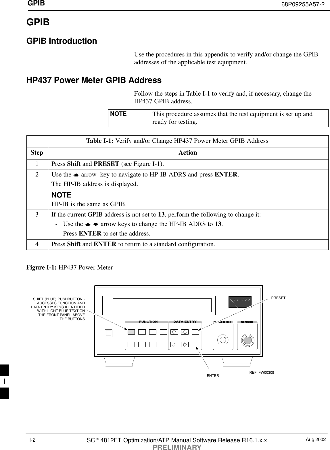
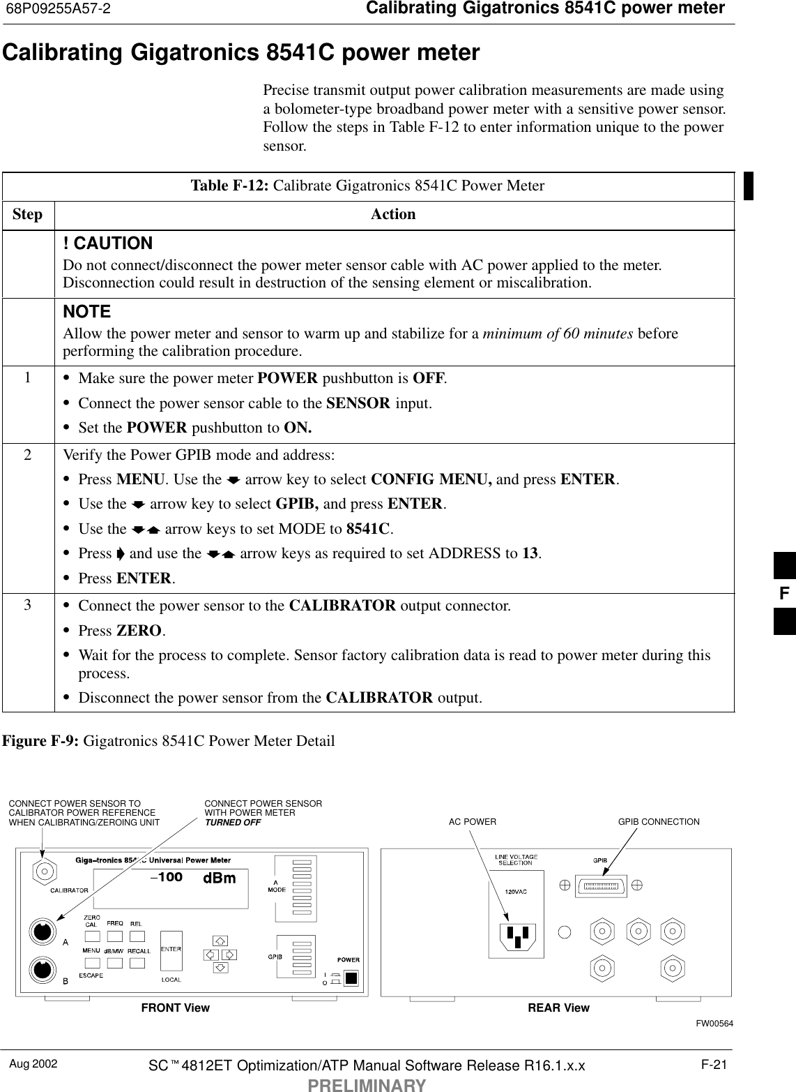
![Test Equipment Setup68P09255A57-2Aug 2002 SCt4812ET Optimization/ATP Manual Software Release R16.1.x.xPRELIMINARYF-19Calibrating HP 437 Power MeterPrecise transmit output power calibration measurements are made usinga bolometer-type broadband power meter with a sensitive power sensor.Follow the steps outlined in Table F-11 to enter information unique tothe power sensor before calibrating the test setup. Refer to Figure F-8 asrequired.NOTE Table:note. Note 10pt HelveticaThis procedure must be done in conjunction with the automatedcalibration to enter power sensor specific calibration values.Figure F-8: Power Meter DetailCONNECT POWERSENSOR WITH POWERMETER TURNED OFFCONNECT POWER SENSORTO POWER REFERENCEWHEN CALIBRATING UNIT.POWER REFERENCE ISENABLED USING THE SHIFT 'KEYSSHIFT (BLUE) PUSHBUTTON -ACCESSES FUNCTION ANDDATA ENTRY KEYS IDENTIFIEDWITH LIGHT BLUE TEXT ONTHE FRONT PANEL ABOVETHE BUTTONSFW00308Table F-11: Power Meter Calibration ProcedureStep Action! CAUTIONDo not connect/disconnect the power meter sensor cable with ac power applied to the meter.Disconnection could result in destruction of the sensing element or mis-calibration.1- Make sure the power meter AC LINE pushbutton is OFF.- Connect the power sensor cable to the SENSOR input.2Set the AC LINE pushbutton to ON.NOTEThe calibration should be performed only after the power meter and sensor have been allowed towarm-up and stabilize for a minimum of 60 minutes.3Perform the following to set or verify the GPIB address:- To enter the SPECIAL data entry function, press [SHIFT] then [PRESET].- Use the [y] or [b] button to select HP-IB ADRS; then press [ENTER].- Use the [y] or [b] button to select HP-IB ADRS 13; then press [ENTER].-To EXIT the SPECIAL data entry function press [SHIFT] then [ENTER].. . . continued on next pageF](https://usermanual.wiki/Nokia-Solutions-and-Networks/T6EQ1/User-Guide-486577-Page-285.png)
![Test Equipment Setup 68P09255A57-2Aug 2002SCt4812ET Optimization/ATP Manual Software Release R16.1.x.xPRELIMINARYF-20Table F-11: Power Meter Calibration ProcedureStep Action4Perform the following to set or verify the correct power sensor model:- Press [SHIFT] then [a] to select SENSOR.- Identify the power sensor model number from the sensor label. Use the [y] or [b] button toselect the appropriate model; then press [ENTER].NOTEBe sure the PWR REF (power reference) output is OFF (observe that the triangular indicator is NOTdisplayed as shown in Step 7). If on, press [SHIFT] then ['] to turn it off.5 Press [ZERO]. Display will show “Zeroing ******.” Wait for process to complete.6Connect the power sensor to the POWER REF output.7To turn on the PWR REF, perform the following:- Press [SHIFT] then ['].- Verify that the triangular indicator (below) appears in the display above “PWR REF”.8Perform the following to set the REF CF %:- Press ([SHIFT] then [ZERO]) for CAL.- Enter the sensor’s REF CF % from the sensor’s decal using the arrow keys and press [ENTER].(The power meter will display ”CAL *****” for a few seconds.)NOTEIf the REF CAL FACTOR (REF CF) is not shown on the power sensor, assume it to be 100%.9Perform the following to set the CAL FAC %:- Press [SHIFT] then [FREQ] for CAL FAC.-On the sensor’s decal, locate an approximate calibration percentage factor (CF%) at 2 GHz. Enterthe sensor’s calibration % (CF%) using the arrow keys and press [ENTER].When complete, the power meter will typically display 0.05 dBm. (Any reading between 0.00 and0.10 is normal.)10 To turn off the PWR REF, perform the following:- Press [SHIFT] then ['].- Disconnect the power sensor from the POWER REF output. F](https://usermanual.wiki/Nokia-Solutions-and-Networks/T6EQ1/User-Guide-486577-Page-286.png)
![Calibrating Output Power68P09255A57-2Aug 2002 SCt4812ET Optimization/ATP Manual Software Release R16.1.x.xPRELIMINARYG-17Table G-5: In-Service CalibrationStep Action! CAUTIONPerform the In-service Calibration procedure on OOS devices only.8Select the desired test:- Select the target BBX(s) on the C-CCP cage picture.- Click Tests>[desired test] from the menu bar at the main window.- Select the target carrier and confirm the channel number in the pop up window.- Leave the Verify BLO check box checked.- From the Test Pattern pick list, select a test pattern.- Click the OK button to start calibration.- Follow the on-screen instructions, except, do not connect to the BTS antenna port, connect to thedirectional coupler (fwd) port associated with the on screen prompt antenna port.NOTESSelecting Pilot (default) performs tests using a pilot signal only.SSelecting Standard performs tests using pilot, synch, paging and six traffic channels. This requiresan MCC to be selected.SSelecting CDFPilot performs tests using the CDF value for pilot gain and IS-97 gain values for allthe other channels included in the Standard pattern setting (paging, synch, and six traffic). Usingthis pattern setting requires the selection of both a BBX and at least one MCC.SSelecting CDF performs tests using pilot, synch, paging and six traffic channels, however, the gainfor the channel elements is specified in the CDF file.9Save the result and download the BLO data to the target BBX(s):- Click the Save Result button on the result screen.The window closes automatically.10 Logout from the BTS and close the LMF session:- Click BTS>Logout to close the BTS connection.- Close the LMF window.11 Restore the new “bts-*.cal” file to the CBSC.12 Enable the target device(s) from the CBSC. G](https://usermanual.wiki/Nokia-Solutions-and-Networks/T6EQ1/User-Guide-486577-Page-305.png)