Nokia Solutions and Networks T6ER1 SC4812ETLite 1.9 GHz 1X/EVDO User Manual
Nokia Solutions and Networks SC4812ETLite 1.9 GHz 1X/EVDO Users Manual
UserManual.wiki
>
Nokia Solutions and Networks
>
T6ER1 User Manual
Users Manual
Navigation menu
Upload a User Manual
Namespaces
Wiki Guide
HTML
PDF
Info
Views
User Manual
Discussion / Help
Navigation
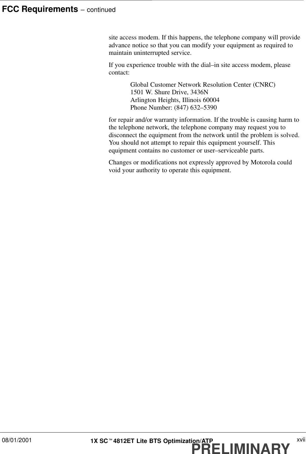
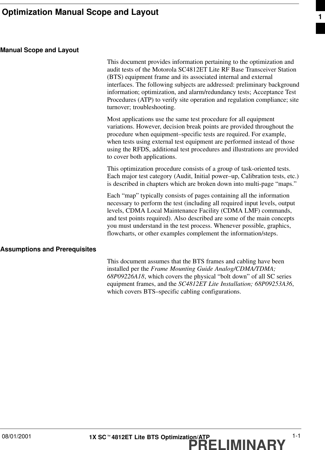
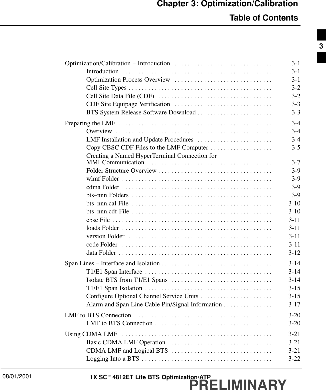

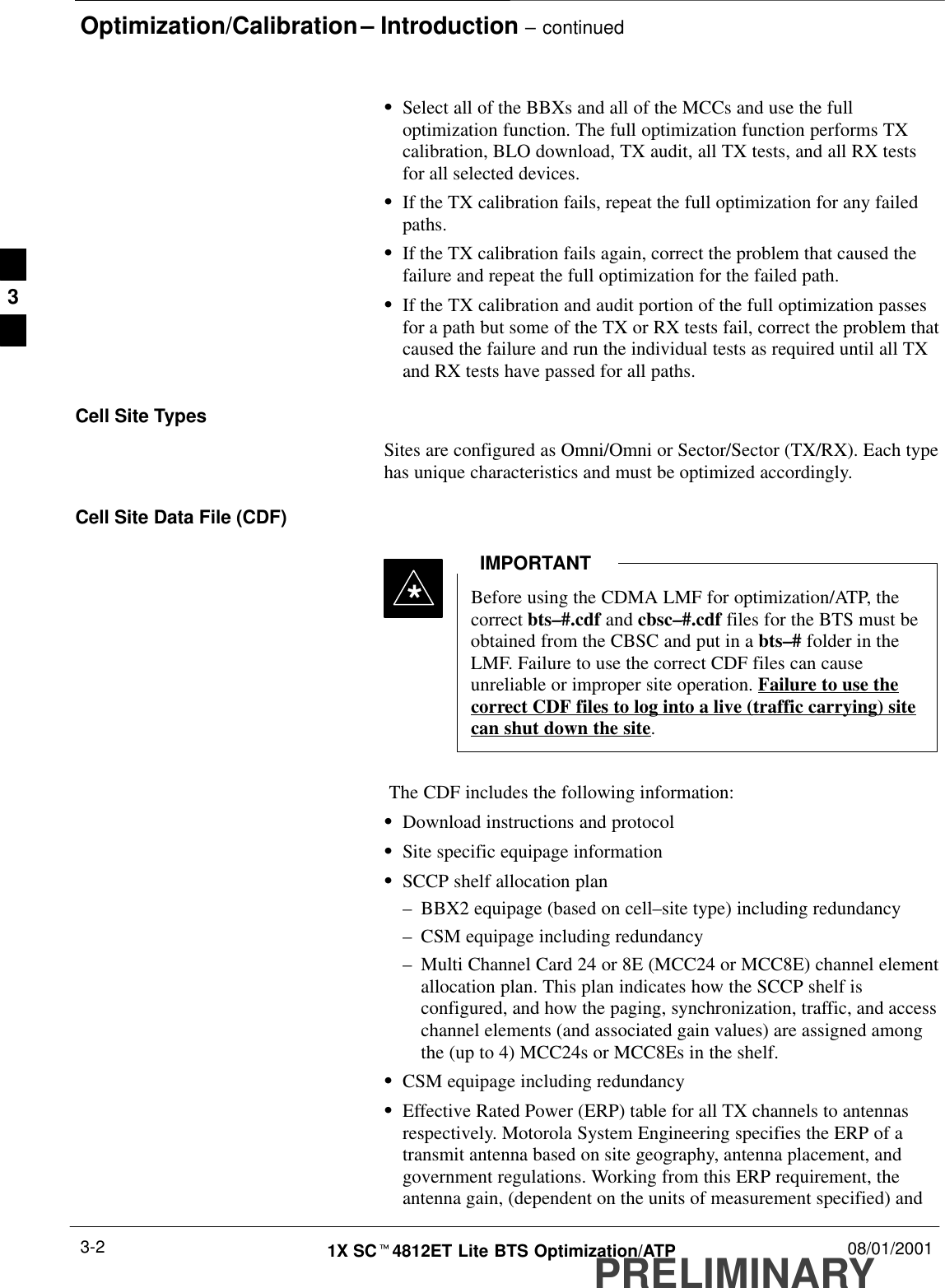
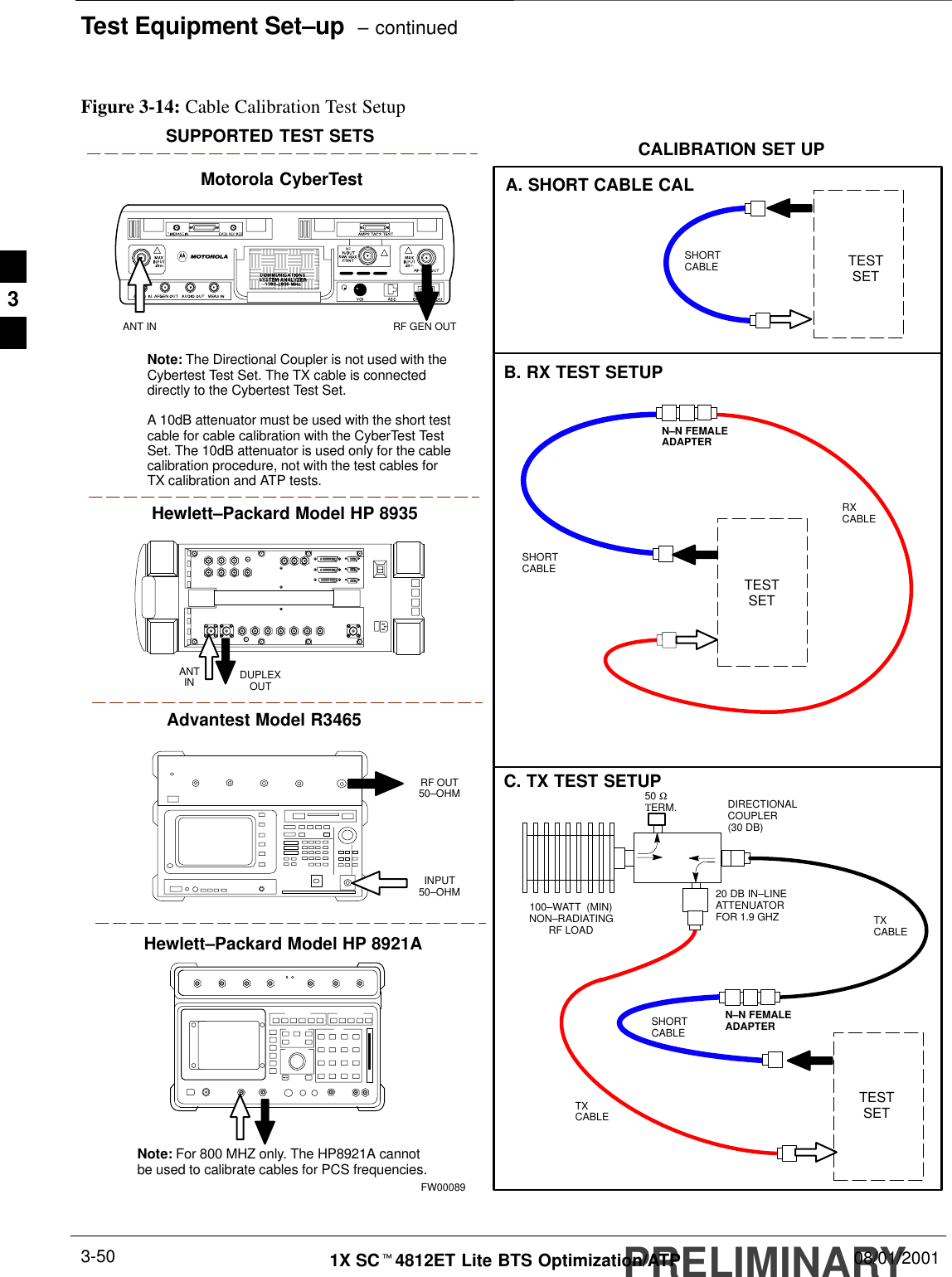
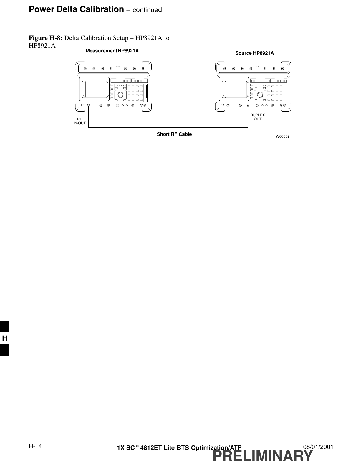
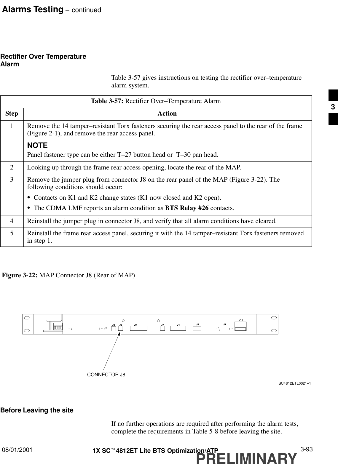
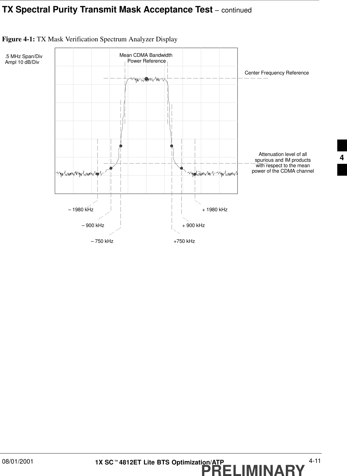
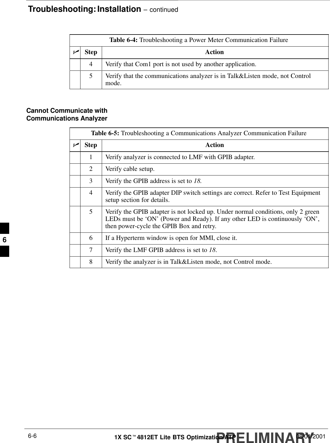
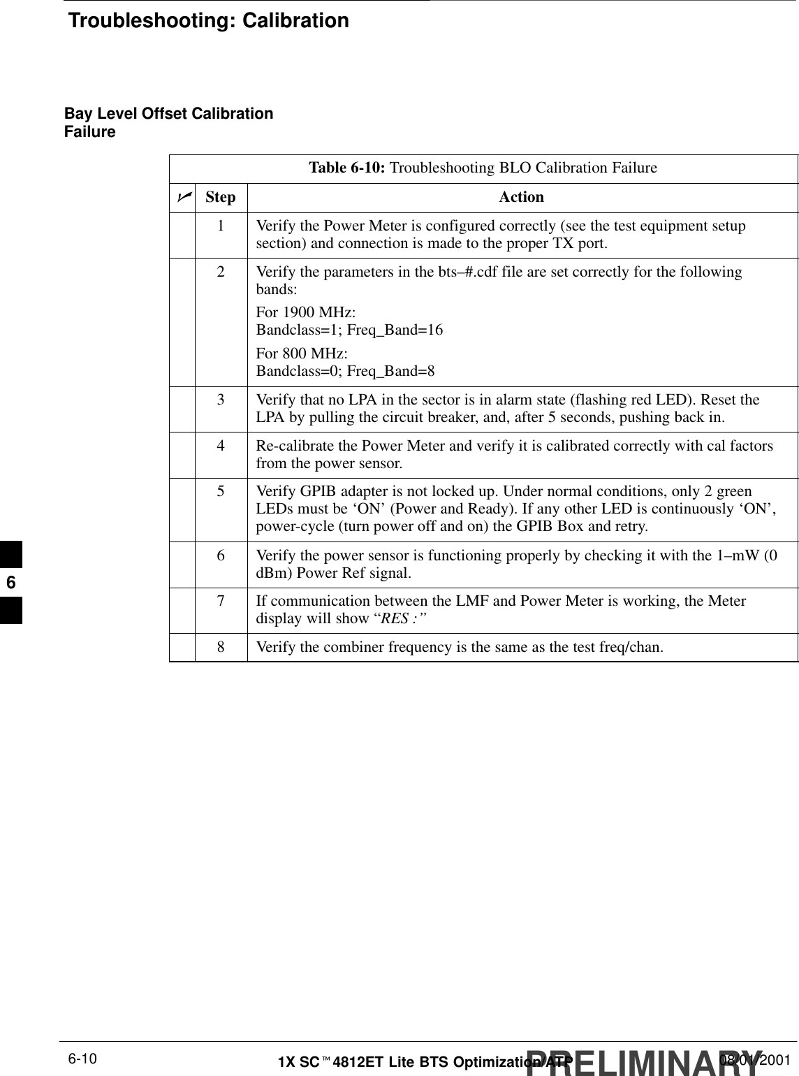
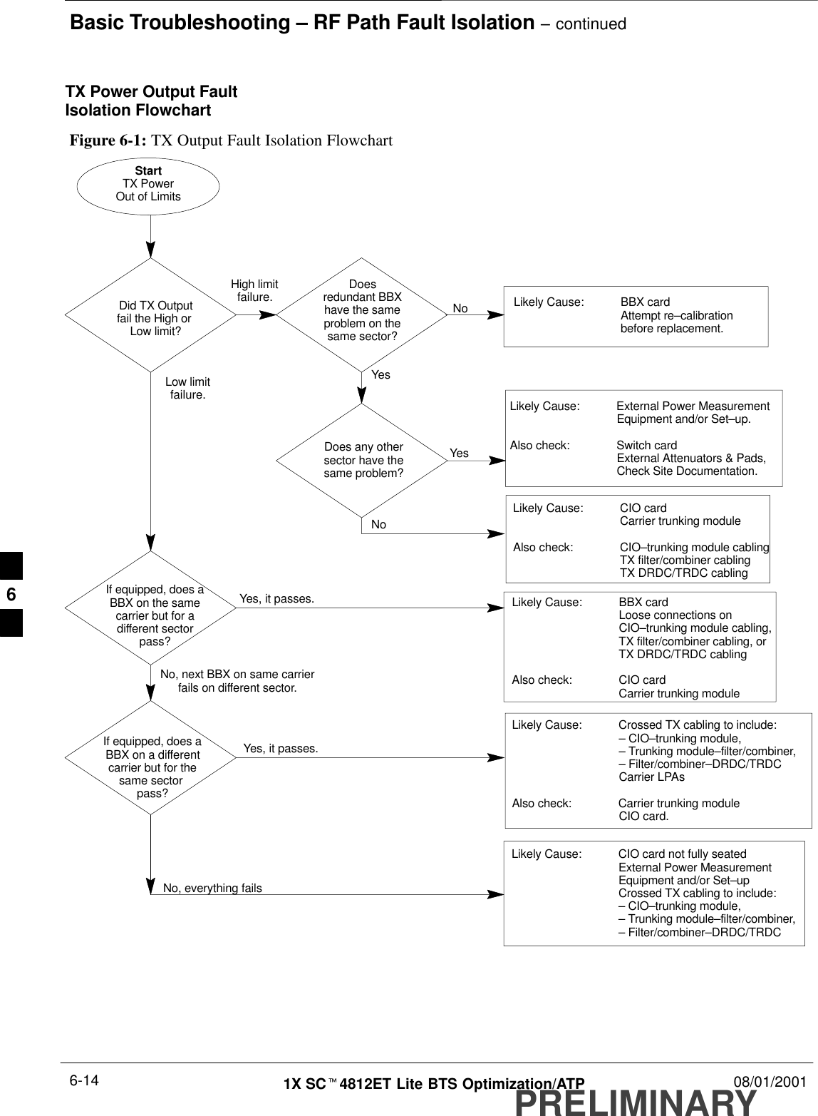
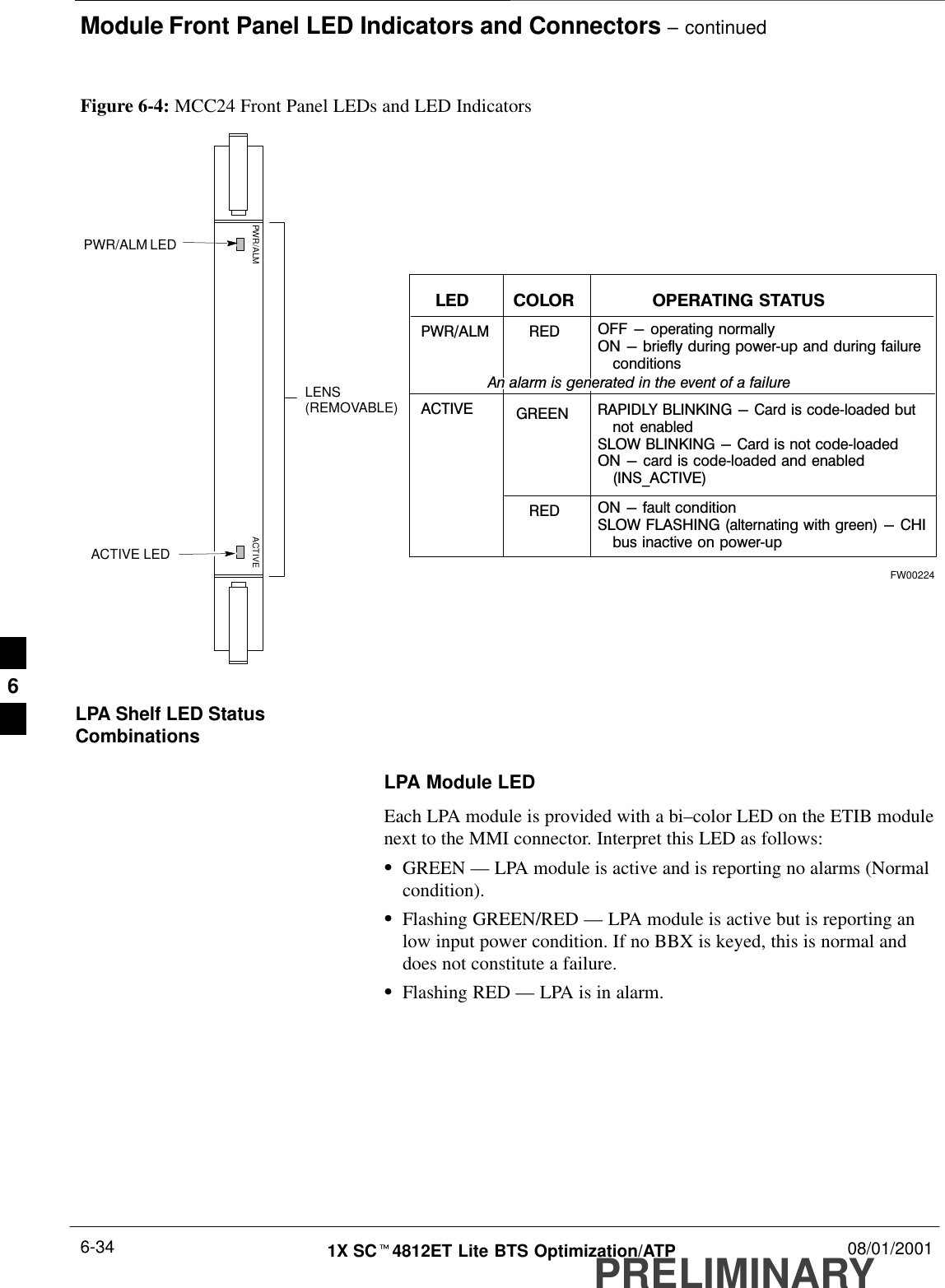
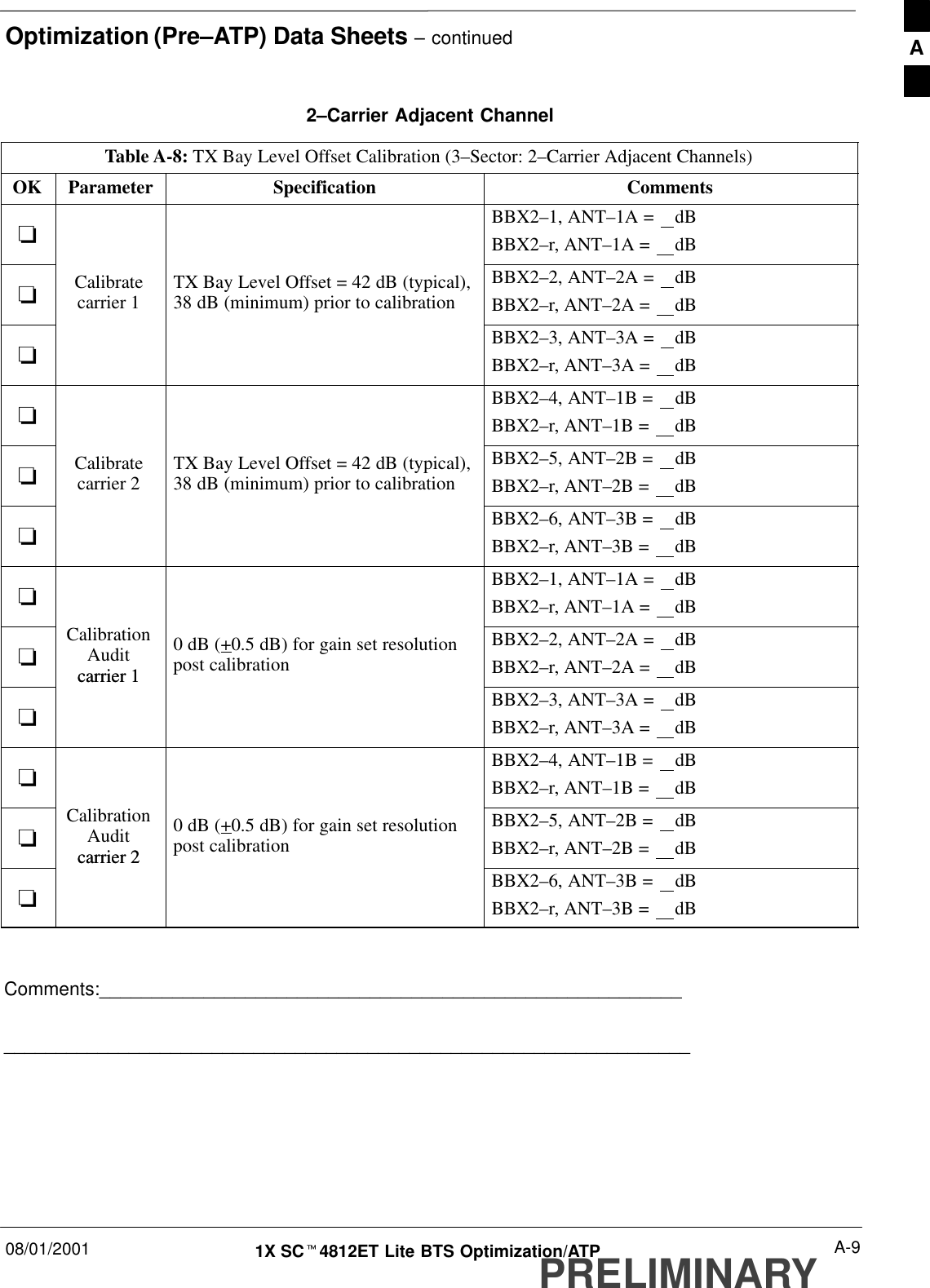
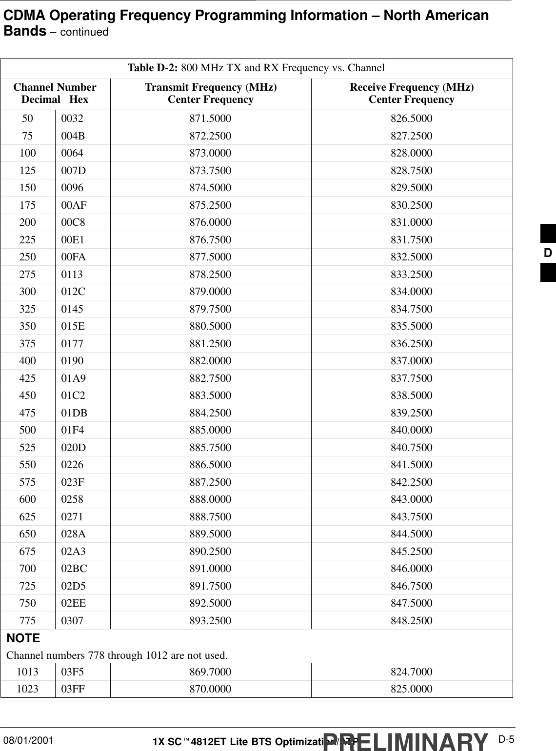
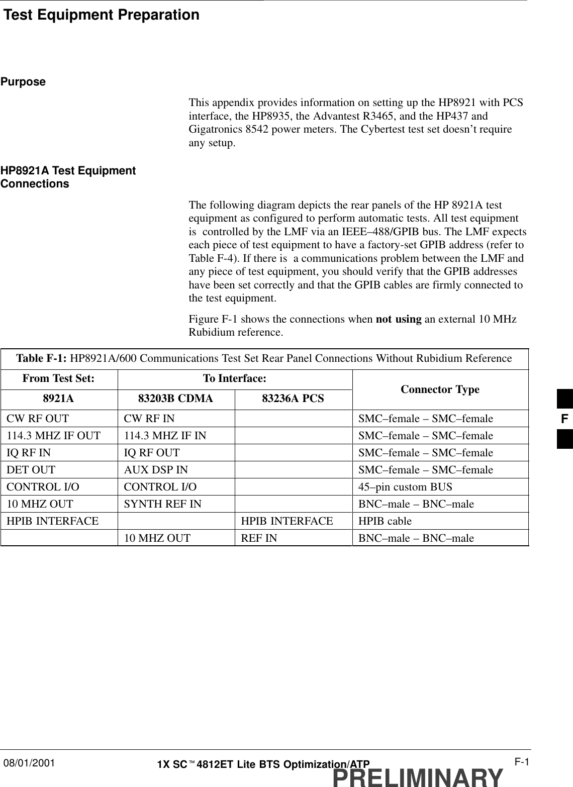
![Bay Level Offset Calibration – continuedPRELIMINARY1X SCt4812ET Lite BTS Optimization/ATP 08/01/20013-66BLO Calibration Data FileDuring the calibration process, the CDMA LMF creates a calibration(CAL) data file where BLO values are stored. After calibration has beencompleted, this offset data must be downloaded to the BBX2s using theCDMA LMF Download BLO function. An explanation of the file isshown below.Due to the size of the file, Motorola recommends printingout a copy of a bts.cal file and referring to it for thefollowing descriptions.NOTEThe CAL file is subdivided into sections organized on a per–slot basis (aslot Block).The Slot 1 Block contains the calibration data for the six BBX2 slots.The Slot 20 Block contains the calibration data for the redundant BBX2(see Table 3-32). Each BBX2 slot Block header contains:SA creation Date and Time – broken down into separate parameters ofcreateMonth, createDay, createYear, createHour, and createMin.SThe number of calibration entries – fixed at 720 entries correspondingto 360 calibration points of the CAL file – plus the slot Block format.Within the slot Block body, the BBX2 calibration data (BayLevelCal) isorganized as a large flat array. The array is organized by branch, BBX2SCCP cage slot, and calibration point.SThe first breakdown of the array indicates which branch the containedcalibration points are for. The array covers transmit, main receive, anddiversity receive offsets as follows:Table 3-31: BLO BTS.cal file Array Branch AssignmentsRange Branch AssignmentC[1]–C[120] TransmitC[121]–C[240] No SC4812ET Lite BLO calpoint entries (default only)C[241]–C[360] ReceiveC[361]–C[480] No SC4812ET Lite BLO calpoint entries (default only)C[481]–C[600] Diversity ReceiveC[601]–C[720] No SC4812ET Lite BLO calpoint entries (default only)3](https://usermanual.wiki/Nokia-Solutions-and-Networks/T6ER1/User-Guide-498554-Page-144.png)
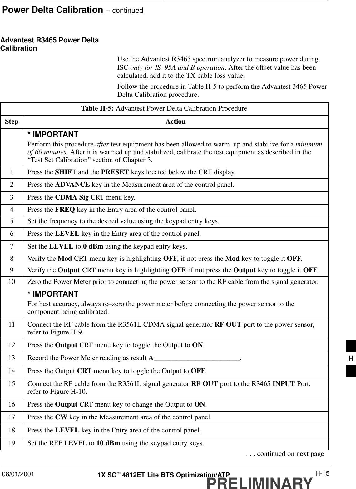
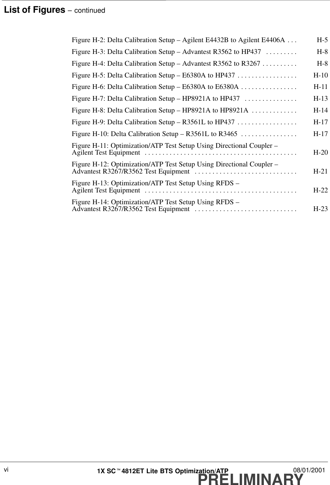
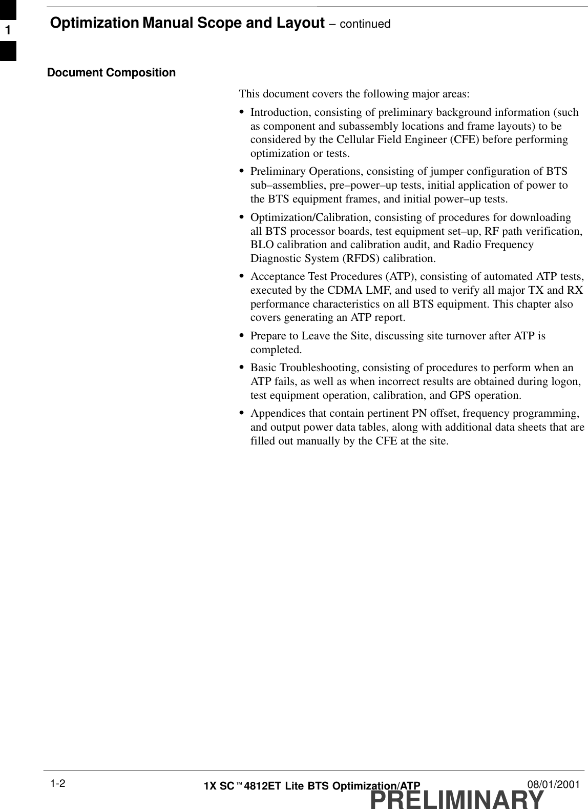
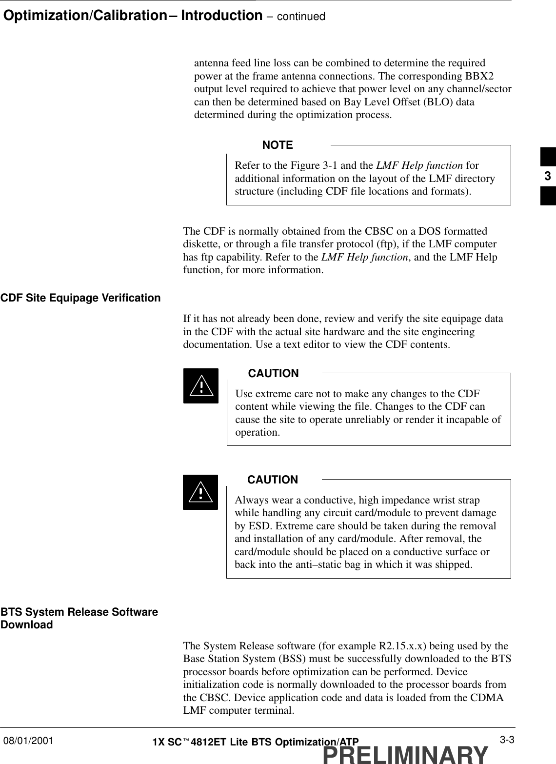
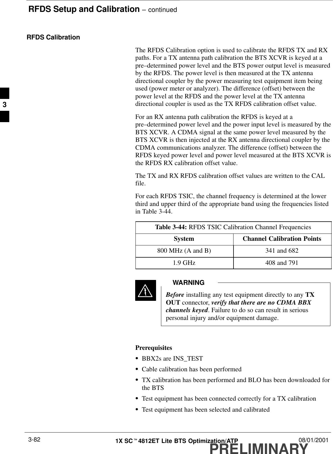
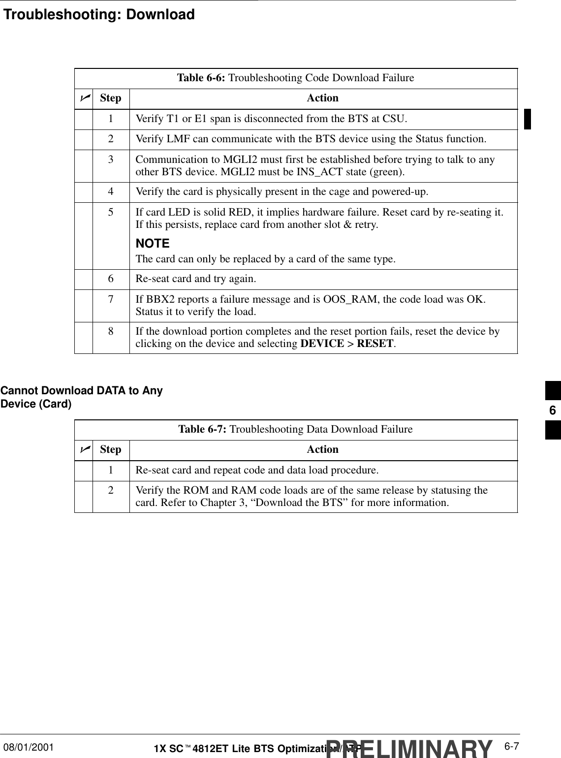
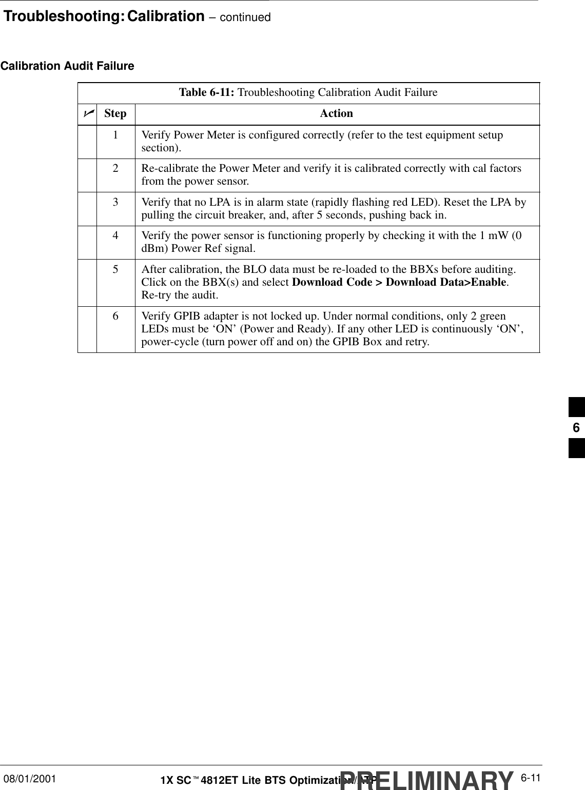
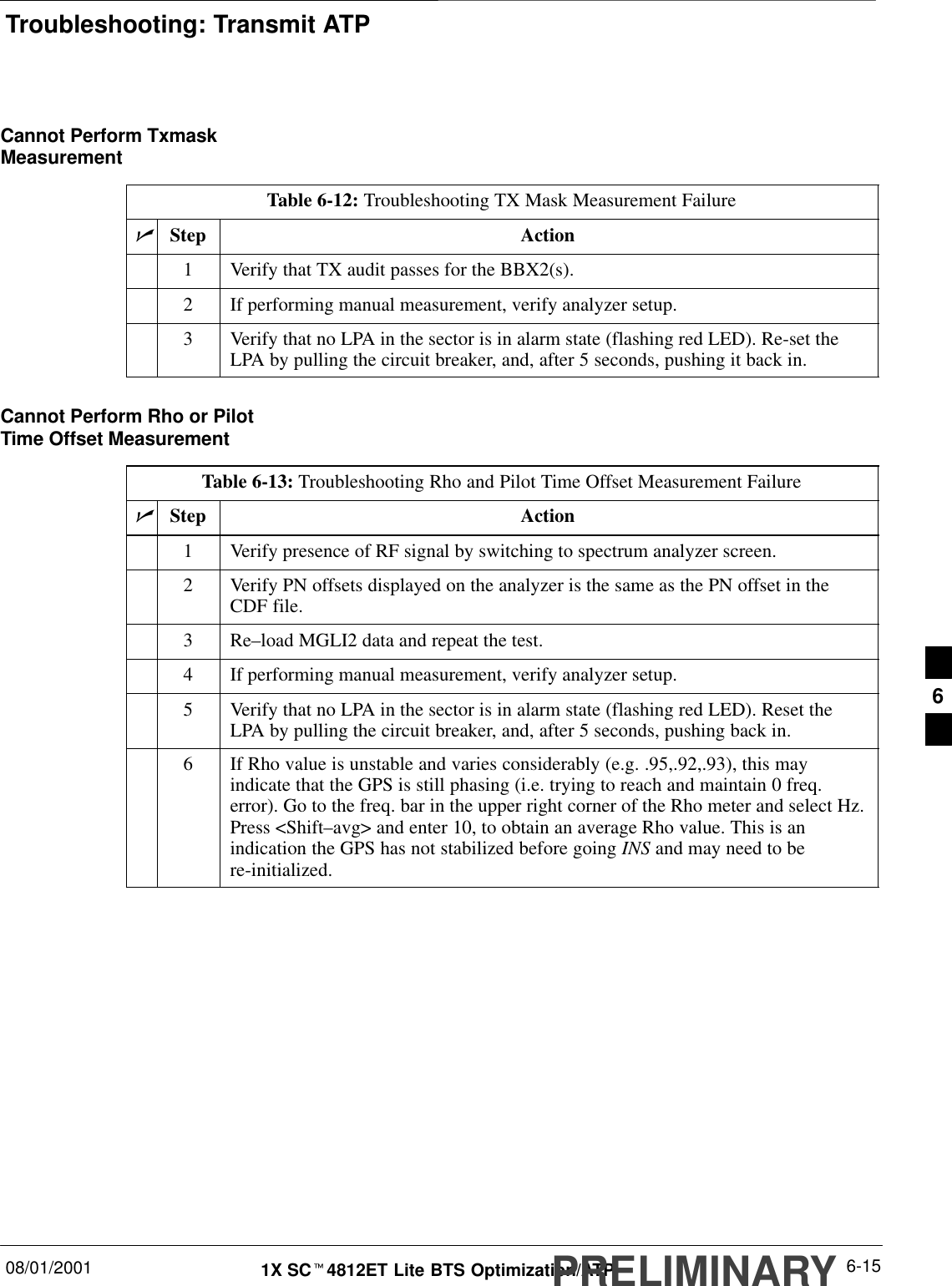
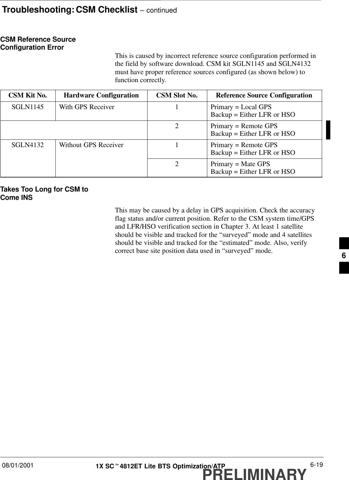
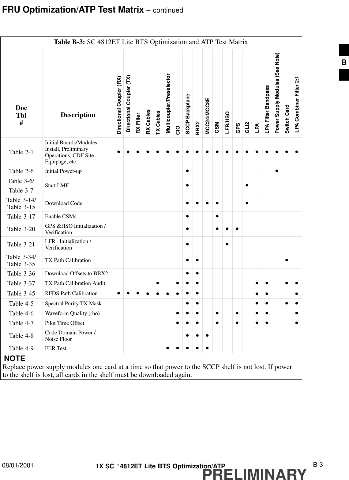
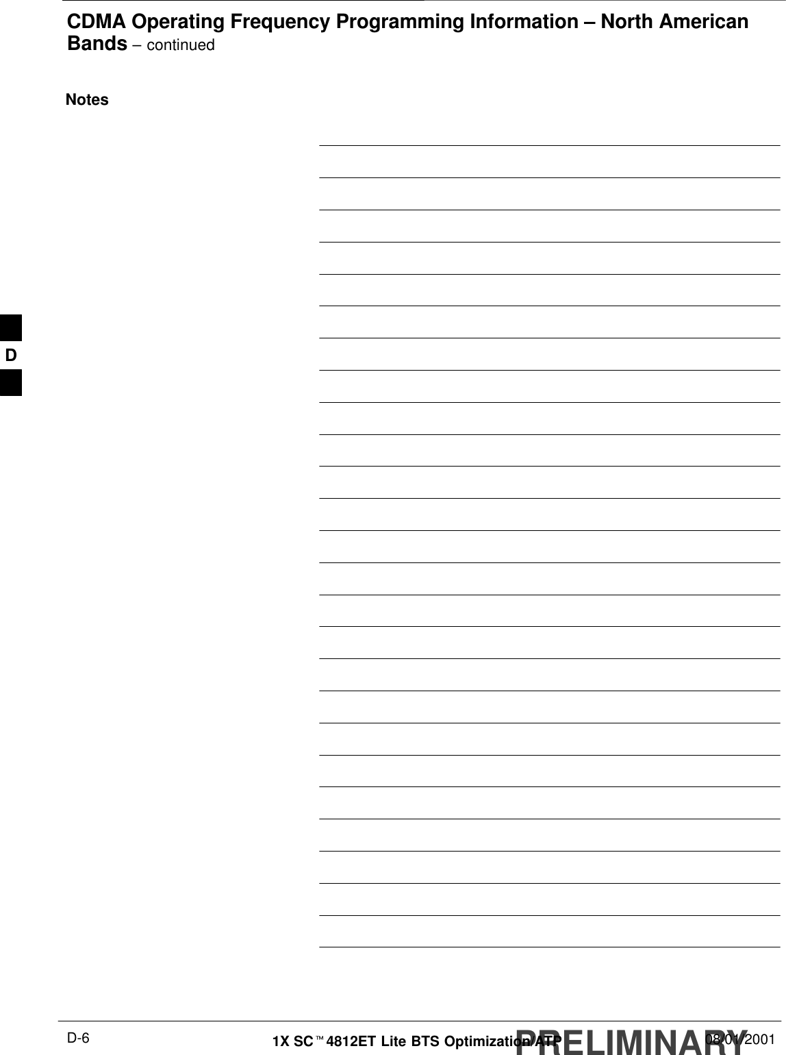
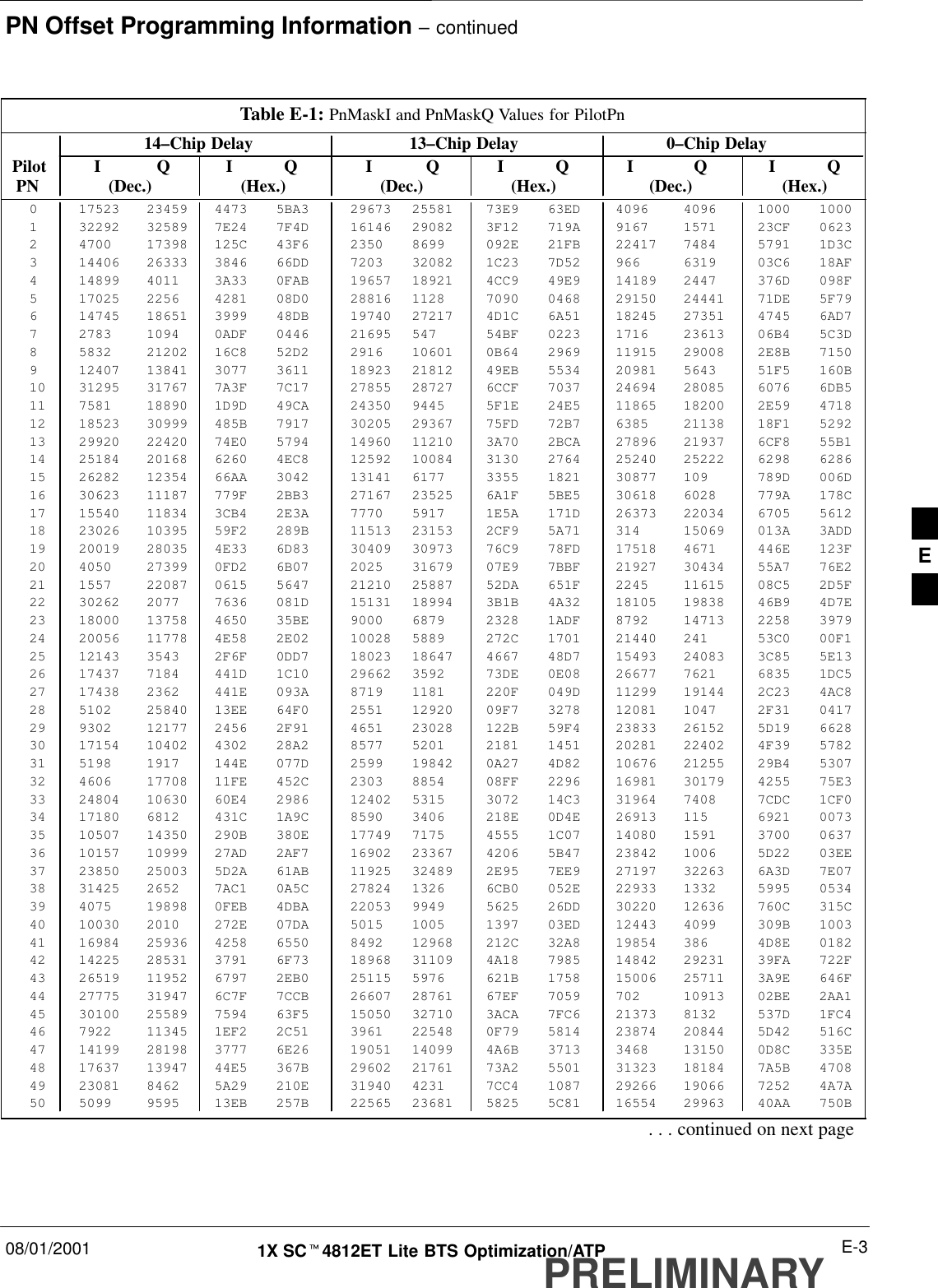
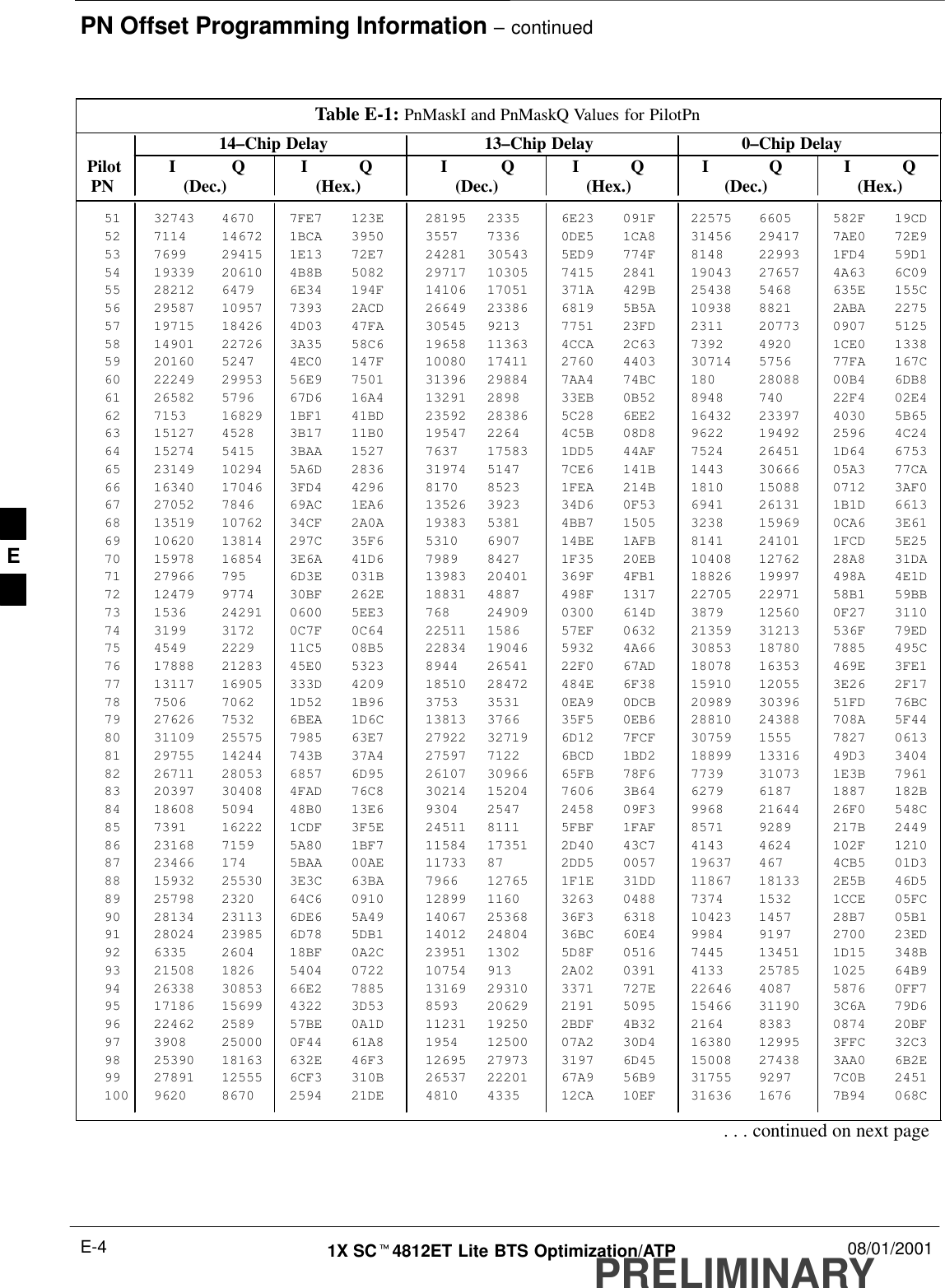
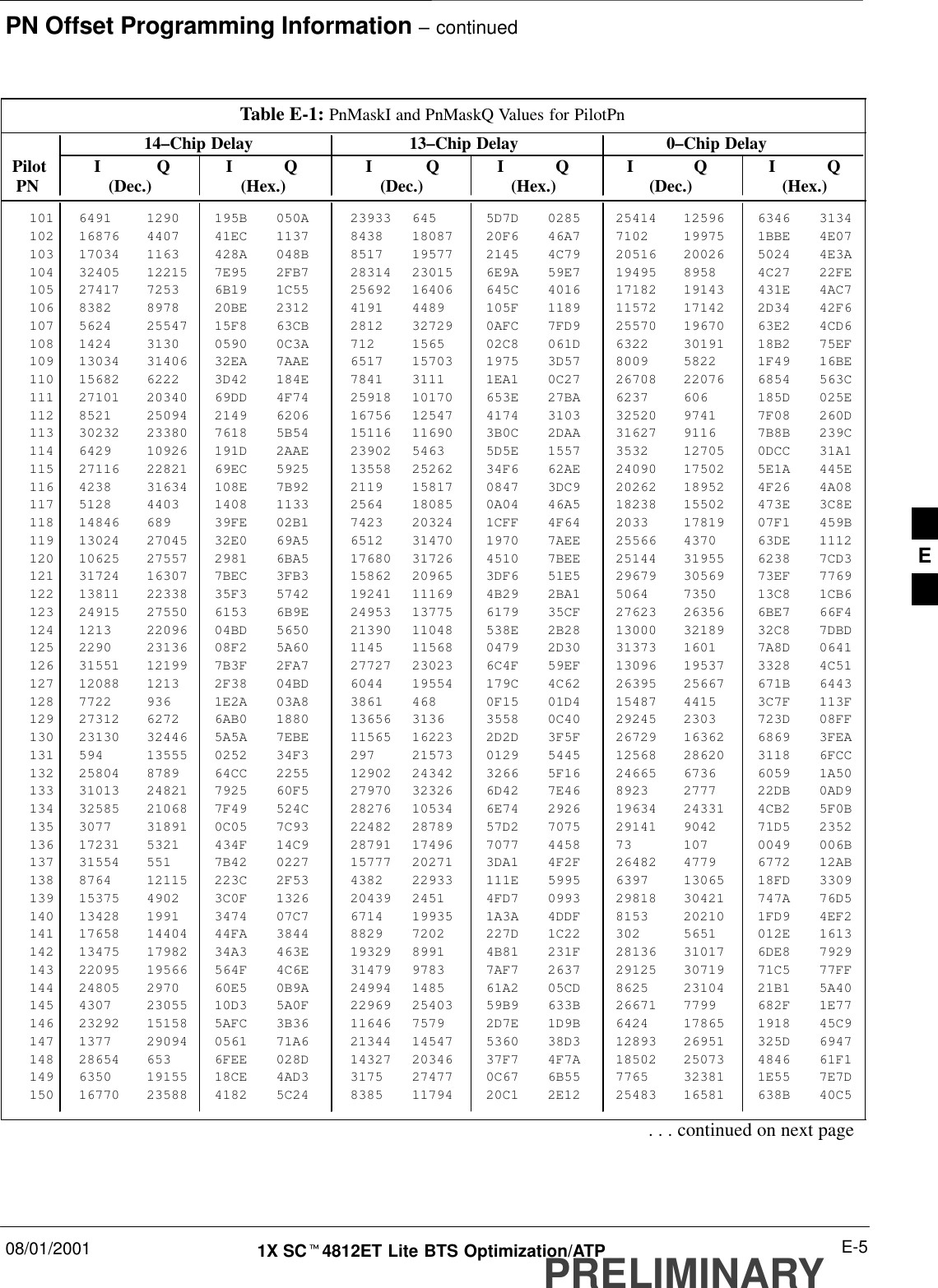
![Bay Level Offset Calibration – continued08/01/2001 3-671X SCt4812ET Lite BTS Optimization/ATPPRELIMINARYSThe second breakdown of the array is by BBX by sector. Three sectorsare allowed.Table 3-32: SC4812ET Lite BTS.cal File Array (Per Sector)BBX2 Sectorization TX Branch RX Branch RX DiversityBranchSlot[1] (Primary BBX2s 1 through 6)1 (Omni) C[1]–C[20] C[241]–C[260] C[481]–C[500]23–Sector, C[21]–C[40] C[261]–C[280] C[501]–C[520]31st Carrier C[41]–C[60] C[281]–C[300] C[521]–C[540]4 C[61]–C[80] C[301]–C[320] C[541]–C[560]53–Sector, C[81]–C[100] C[321]–C[340] C[561]–C[580]62nd Carrier C[101]–C[120] C[341]–C[360] C[581]–C[600]C[121]–C[140] C[361]–C[380] C[601]–C[620]C[141]–C[160] C[381]–C[400] C[621]–C[640]Not Used in SC4812ET Lite(CAL file entries are C[161]–C[180] C[401]–C[420] C[641]–C[660](CAL file entries are Channel 0 with default C[181]–C[200] C[421]–C[440] C[661]–C[680]power set level.) C[201]–C[220] C[441]–C[460] C[681]–C[700]C[221]–C[240] C[461]–C[480] C[701]–C[720]Slot[20] (Redundant BBX2–R1)1 (Omni) C[1]–C[20] C[241]–C[260] C[481]–C[500]23–Sector, C[21]–C[40] C[261]–C[280] C[501]–C[520]31st Carrier C[41]–C[60] C[281]–C[300] C[521]–C[540]4 C[61]–C[80] C[301]–C[320] C[541]–C[560]53–Sector, C[81]–C[100] C[321]–C[340] C[561]–C[580]62nd Carrier C[101]–C[120] C[341]–C[360] C[581]–C[600]C[121]–C[140] C[361]–C[380] C[601]–C[620]C[141]–C[160] C[381]–C[400] C[621]–C[640]Not Used in SC4812ET Lite(CAL file entries are C[161]–C[180] C[401]–C[420] C[641]–C[660](CAL file entries are Channel 0 with default C[181]–C[200] C[421]–C[440] C[661]–C[680]power set level.) C[201]–C[220] C[441]–C[460] C[681]–C[700]C[221]–C[240] C[461]–C[480] C[701]–C[720]SRefer to the CAL file print–out and Table 3-32. It can be seen thatthere is one BBX2 slot per sector, and 10 calibration points for eachBBX2 (sector) are supported for each branch. Each “calibration point”consists of two entries.SThe first entry for a calibration point (all odd entries) identifies theCDMA channel (frequency) where the BLO is measured. The secondcalibration point entry (all even entries) is the power set level(PwrLvlAdj). The valid range for PwrLvlAdj is from 2500 to 275003](https://usermanual.wiki/Nokia-Solutions-and-Networks/T6ER1/User-Guide-498554-Page-145.png)
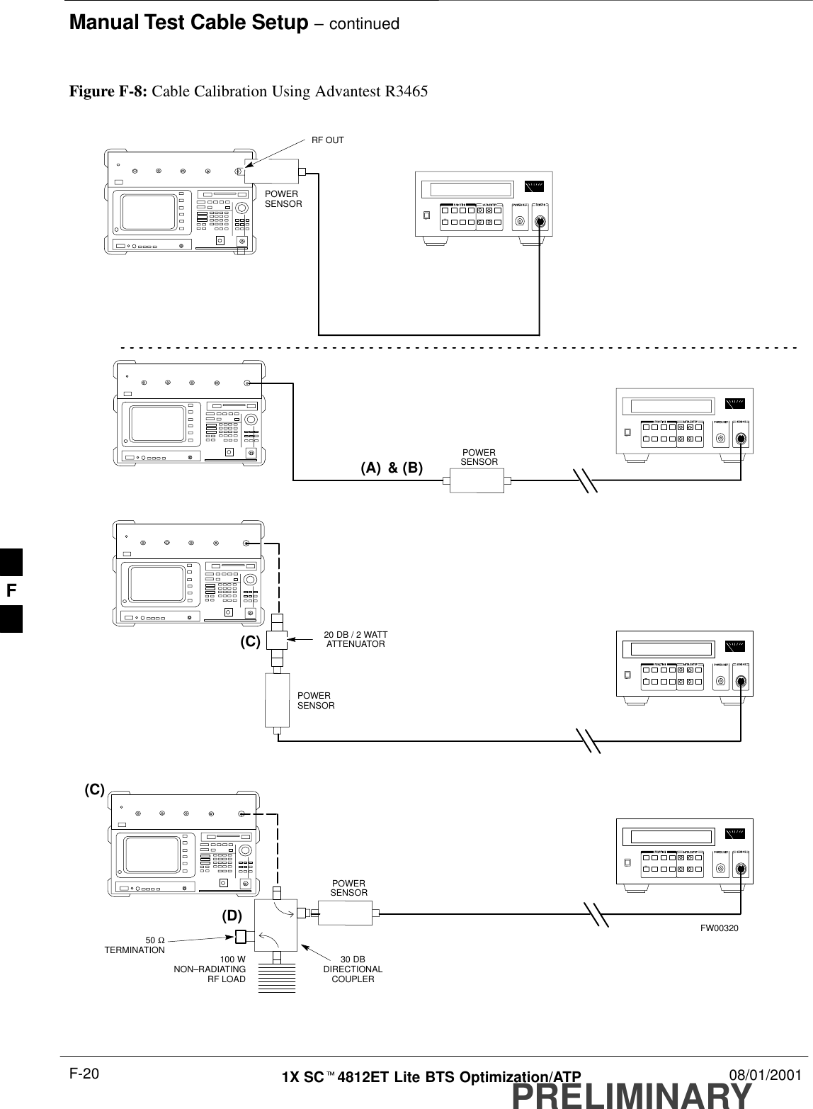
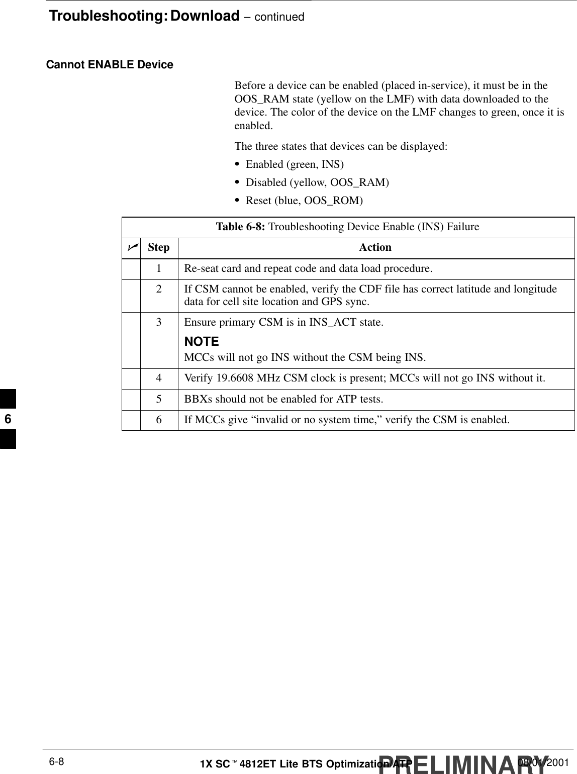
![Bay Level Offset Calibration – continuedPRELIMINARY1X SCt4812ET Lite BTS Optimization/ATP 08/01/20013-68(2500 corresponds to –125 dBm and 27500 corresponds to +125dBm).SThe 10 calibration points for each slot/branch combination must bestored in order of increasing frequency. If less than 10 points(frequencies) are calibrated, the BLO data for the highest frequencycalibrated is written into the remainder of the 10 points for thatslot/branch.Example:C[1]=384 (odd cal entry)C[2]=19102 (even cal entry)C[3]=777 (odd cal entry)C[4]=19086 (even cal entry)C[19]=777 (odd cal entry)C[20]=19086 (even cal entry)...= 1 “calibration point”In the example above, BLO was measured at only two frequencies(channels 384 and 777) for SCCP slot BBX–1 transmit (Table 3-32).The BLO data for the highest frequency measured (777) will bewritten to the remaining eight transmit calibration points (defined byentries C[5] through C[20]) for BBX2–1.SWhen BLO data is downloaded to the BBXs, the data is downloadedto the devices in the order it is stored in the CAL file. TxCal data(C[1] – C[60]) is sent first. BBX2 slot 1’s 10 calibration points (C[1]– C[20]) are sent initially, followed by BBX2 slot 2’s 10 calibrationpoints (C[21] – C[40]), and so on. The RxCal data is sent next,followed by the RxDCal data.STemperature compensation data (TempLevelCal) is also stored in theCAL file for each slot Block.Test Equipment Setup:RF Path CalibrationFollow the steps outlined in Table 3-33 and refer as needed toFigure 3-15 or Figure 3-16 to set up test equipment.Table 3-33: Set Up Test Equipment (RF Path Calibration)Step Action1If it has not already been done, refer to the procedure in Table 3-6 to interface the CDMA LMFcomputer terminal to the frame LAN A connector.2If it has not already been done, refer to Table 3-7 to start a GUI LMF session.3If required, calibrate the test equipment per the procedure in Table 3-25.3](https://usermanual.wiki/Nokia-Solutions-and-Networks/T6ER1/User-Guide-498554-Page-146.png)
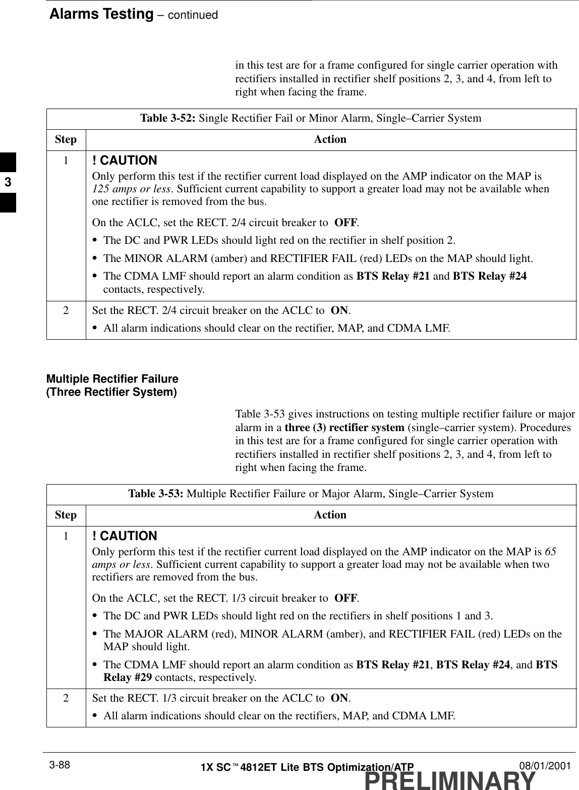


![Test Equipment Preparation – continued08/01/2001 F-51X SCt4812ET Lite BTS Optimization/ATPPRELIMINARYHP8921A System ConnectivityTestFollow the steps outlined in Table F-3 to verify that the connectionsbetween the PCS Interface and the HP8921A are correct and cables areintact. The software also performs basic functionality checks of eachinstrument.Disconnect other GPIB devices, especially systemcontrollers, from the system before running theconnectivity software.IMPORTANT*Table F-3: System ConnectivityStep Action* IMPORTANT–Perform this procedure after test equipment has been allowed to warm–up and stabilize for aminimum of 60 minutes.1Insert HP 83236A Manual Control/System card into memory card slot.2Press the [PRESET] pushbutton.3Press the Screen Control [TESTS] pushbutton to display the “Tests” Main Menu screen.4Position the cursor at Select Procedure Location and select it by pressing the cursor control knob. Inthe Choices selection box, select Card.5Position the cursor at Select Procedure Filename and select it by pressing the cursor control knob. Inthe Choices selection box, select SYS_CONN.6Position the cursor at RUN TEST and select it. The software will prompt you through theconnectivity setup.7Do the following when the test is complete,Sposition cursor on STOP TEST and select itSOR press the [K5] pushbutton.8To return to the main menu, press the [K5] pushbutton.9Press the [PRESET] pushbutton.F](https://usermanual.wiki/Nokia-Solutions-and-Networks/T6ER1/User-Guide-498554-Page-301.png)
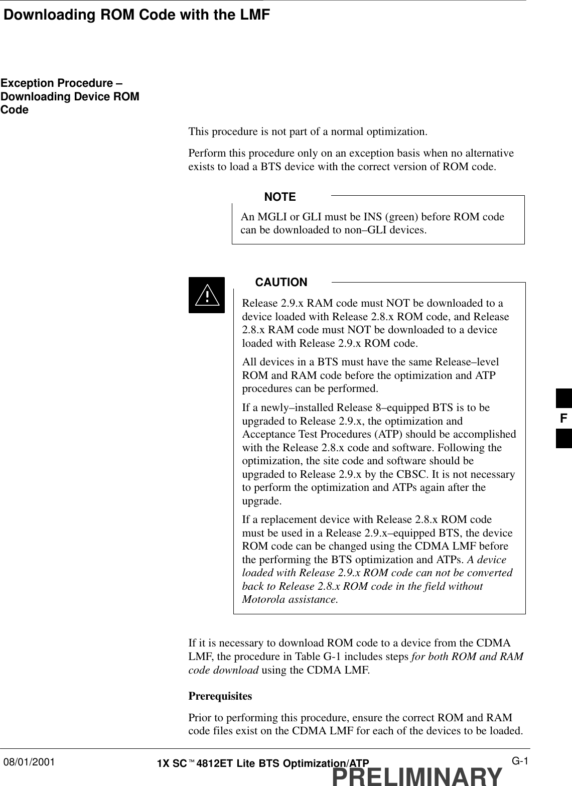
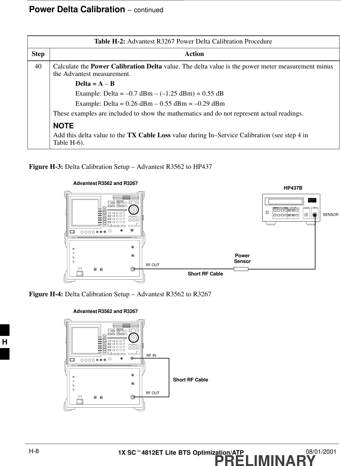
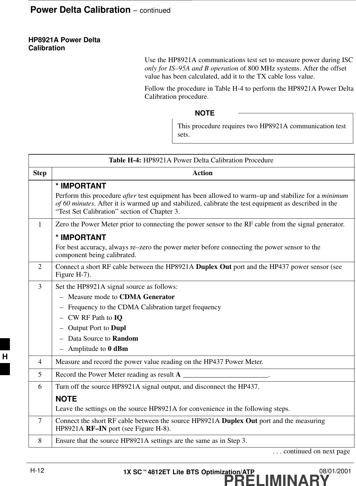
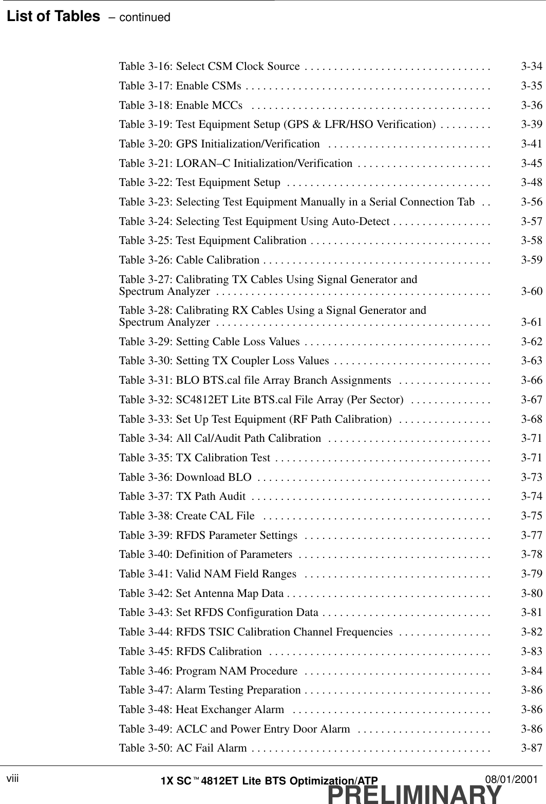
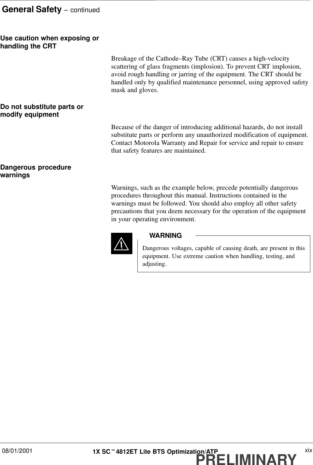
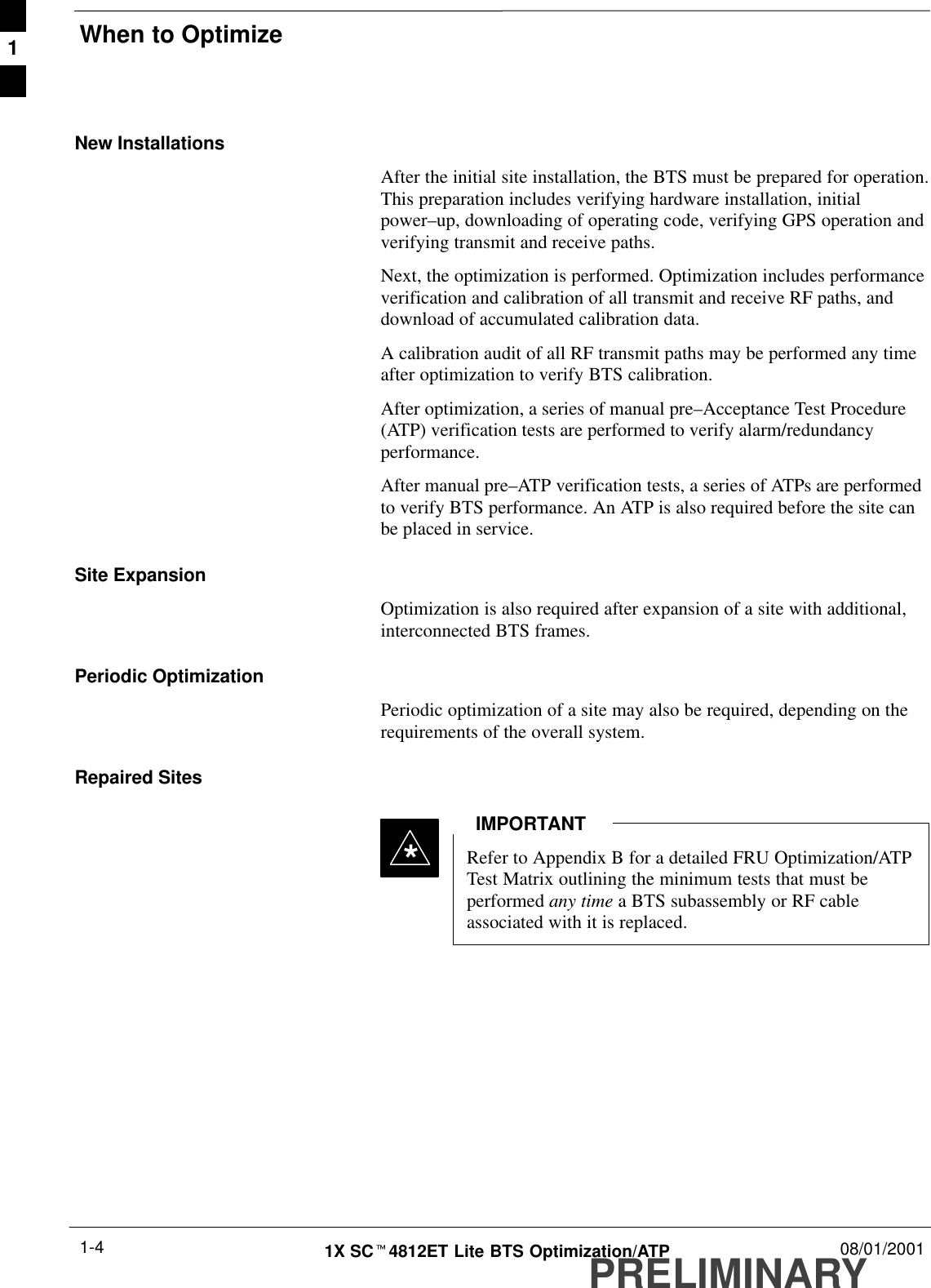
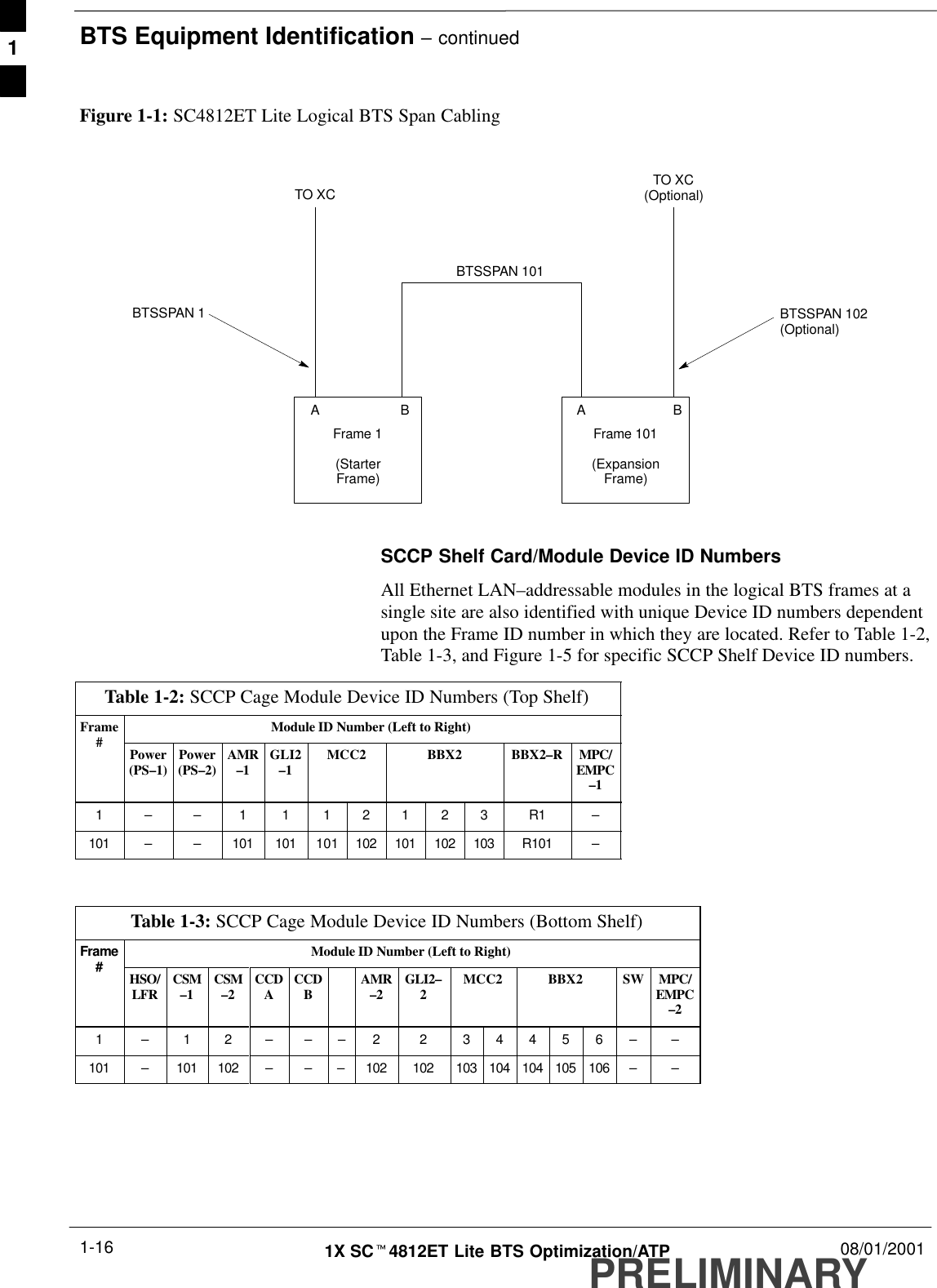
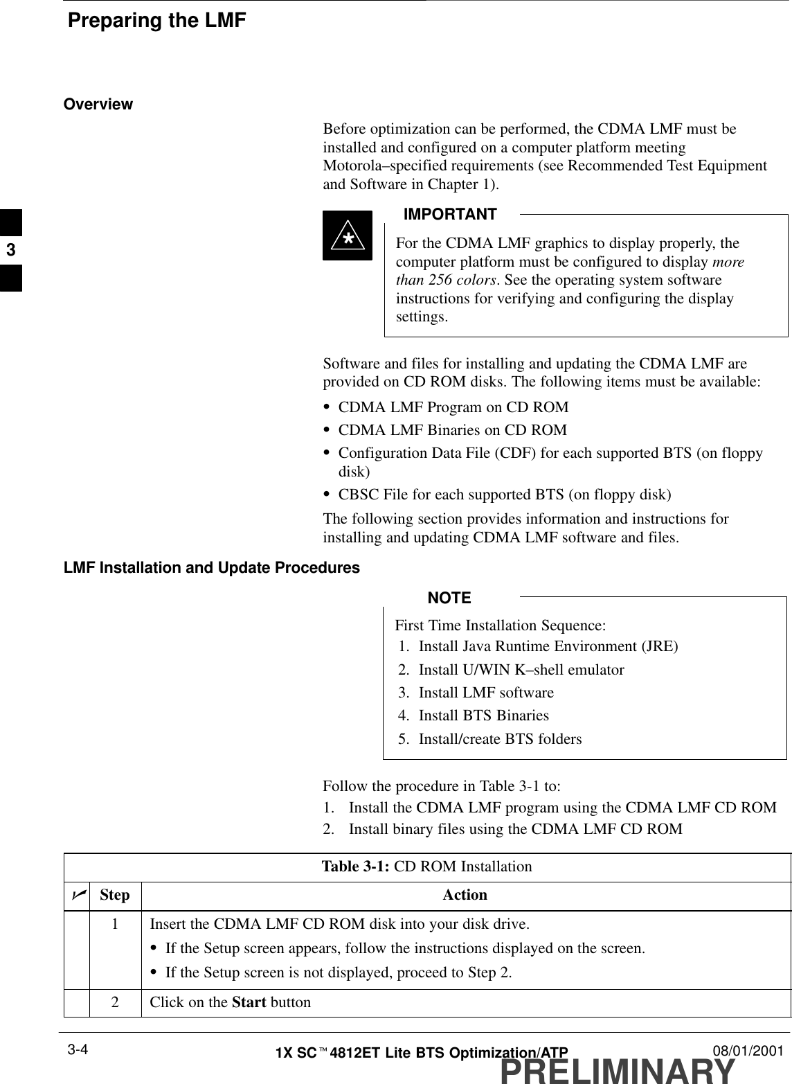
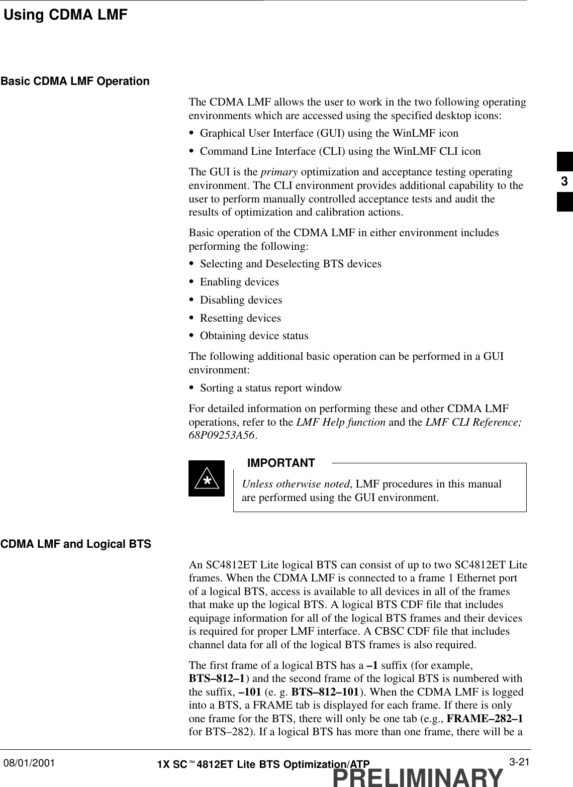
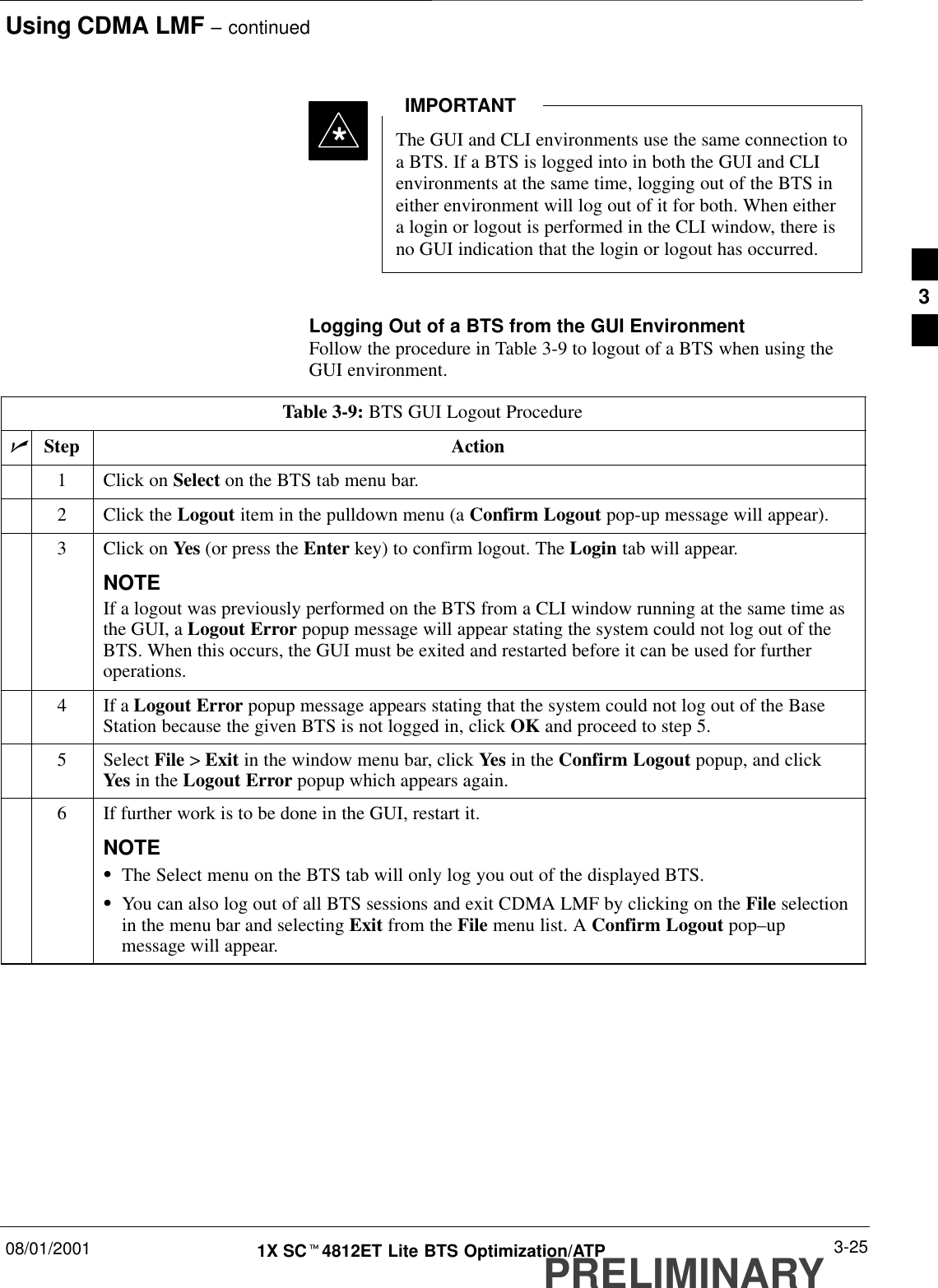
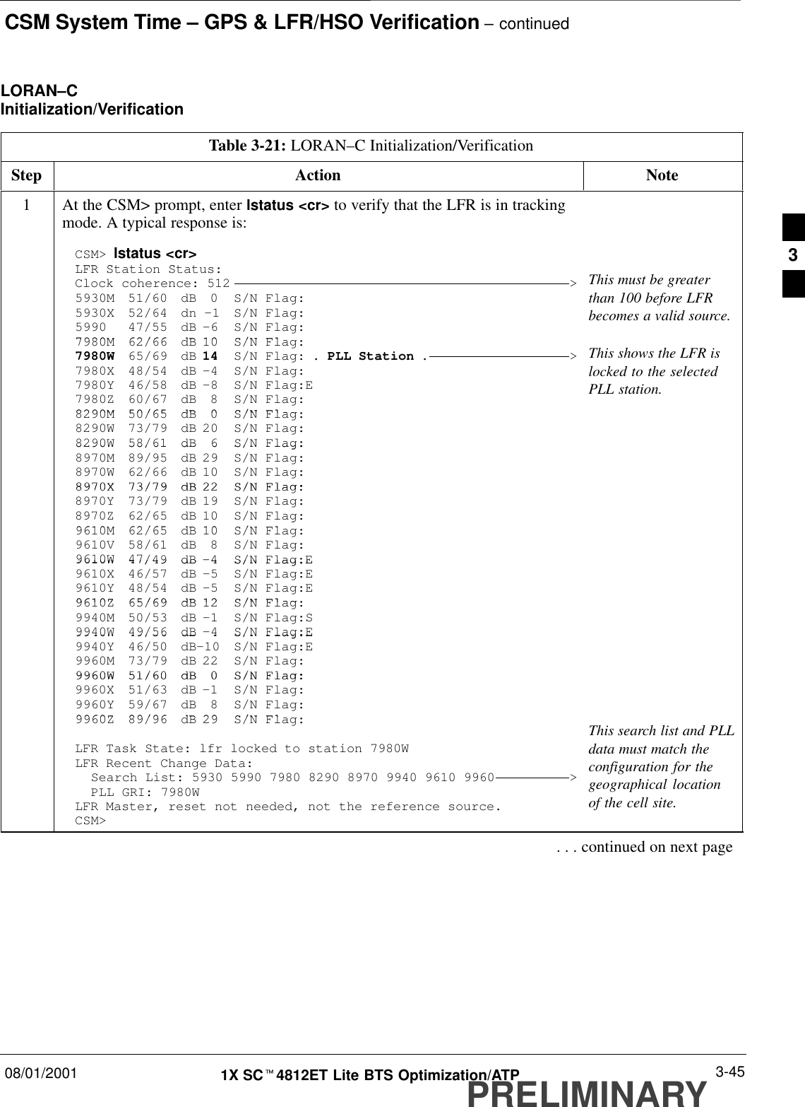
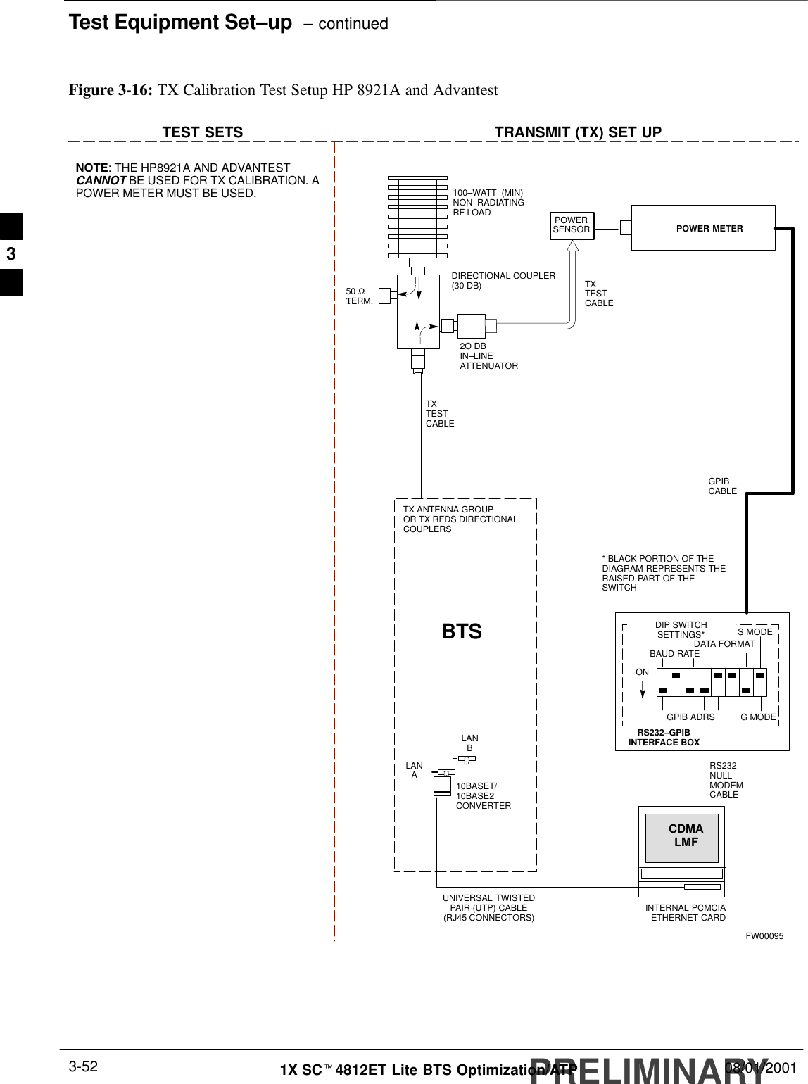
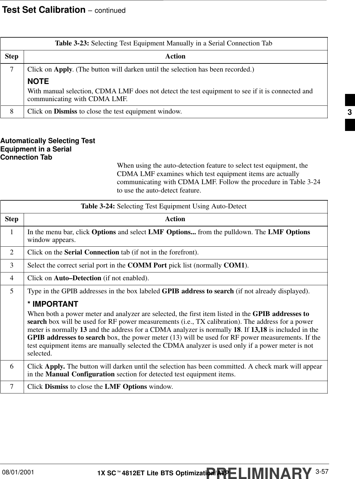
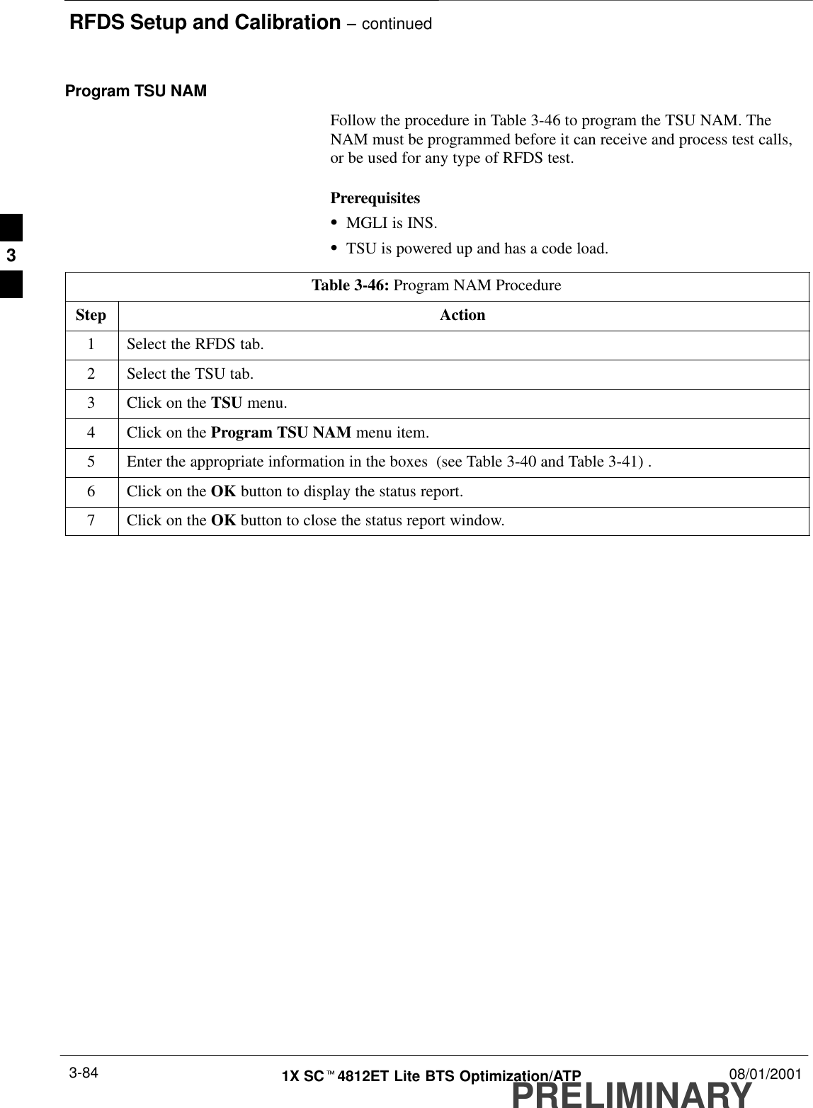
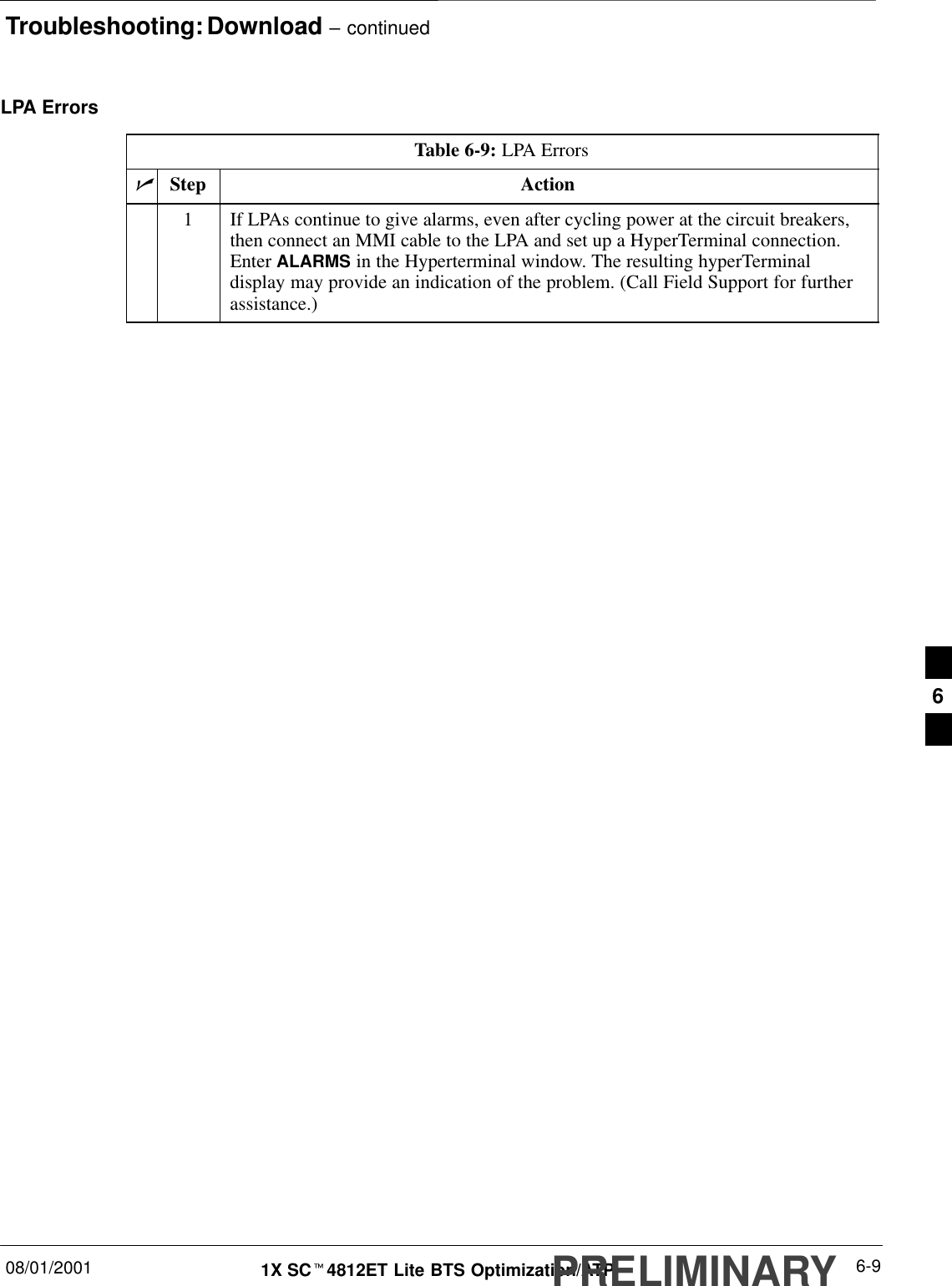
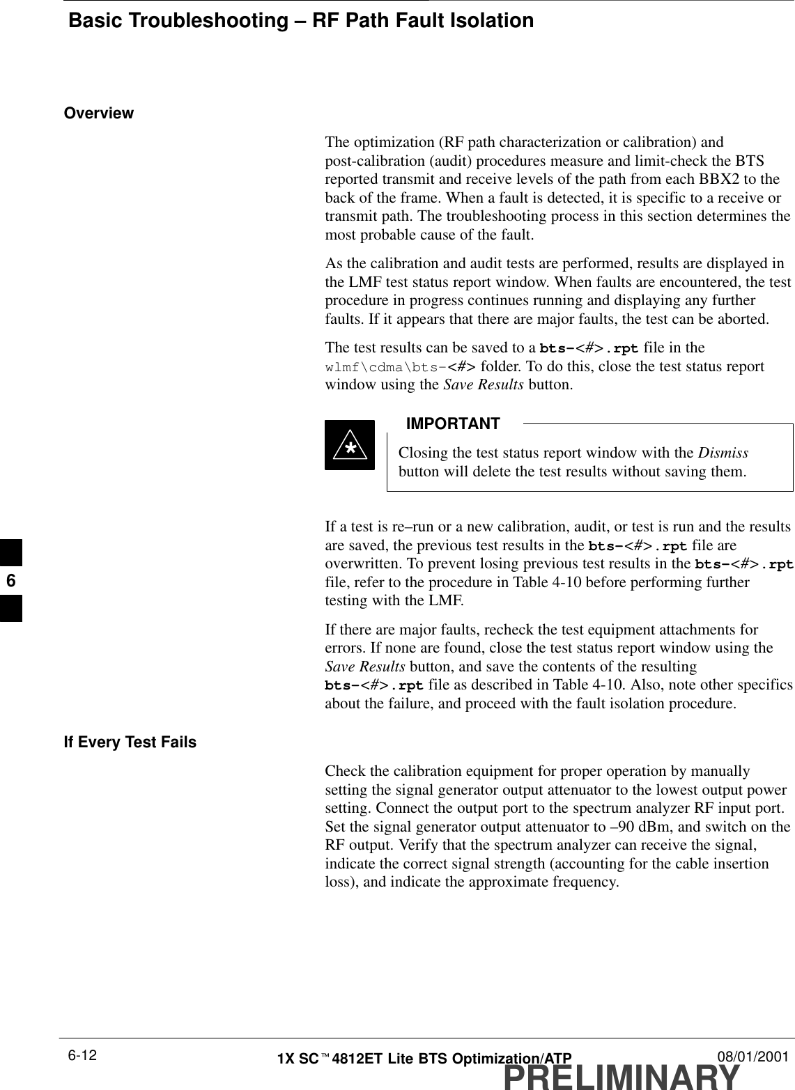
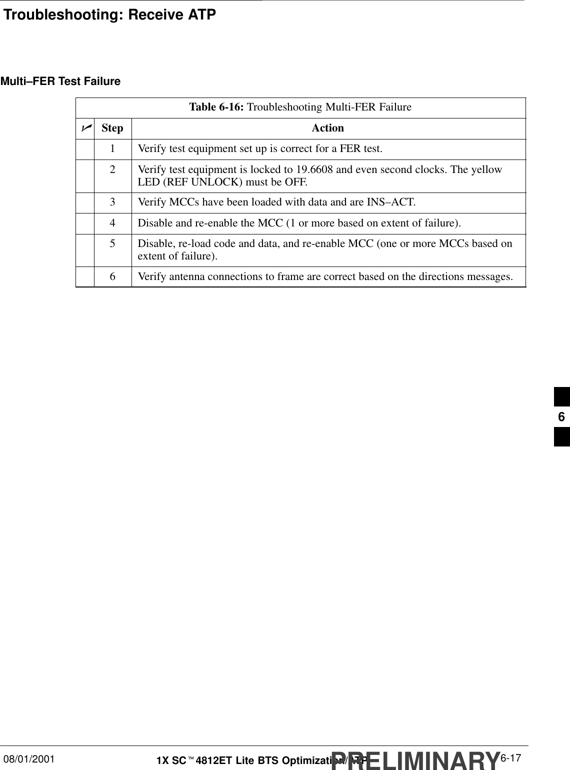
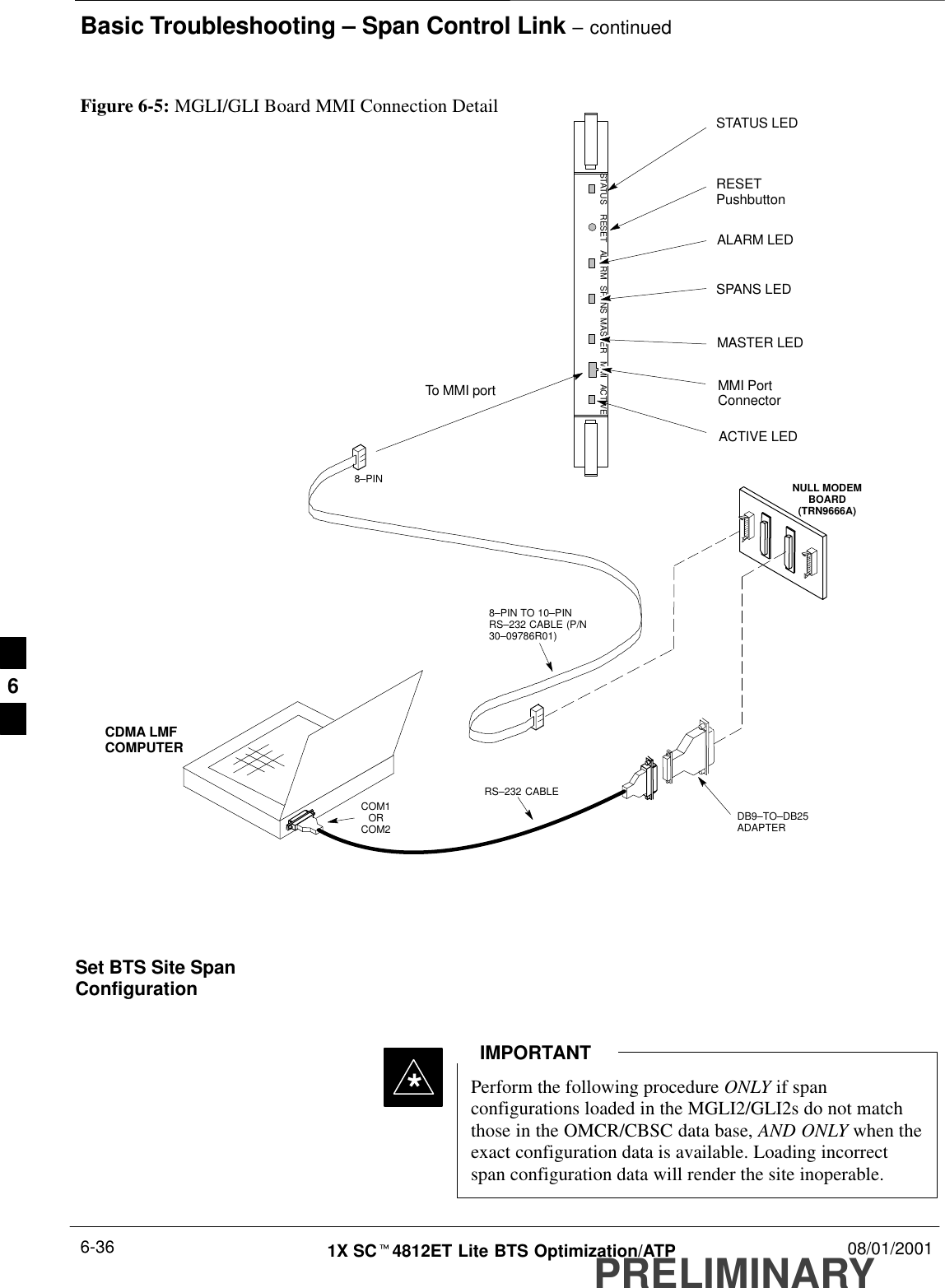
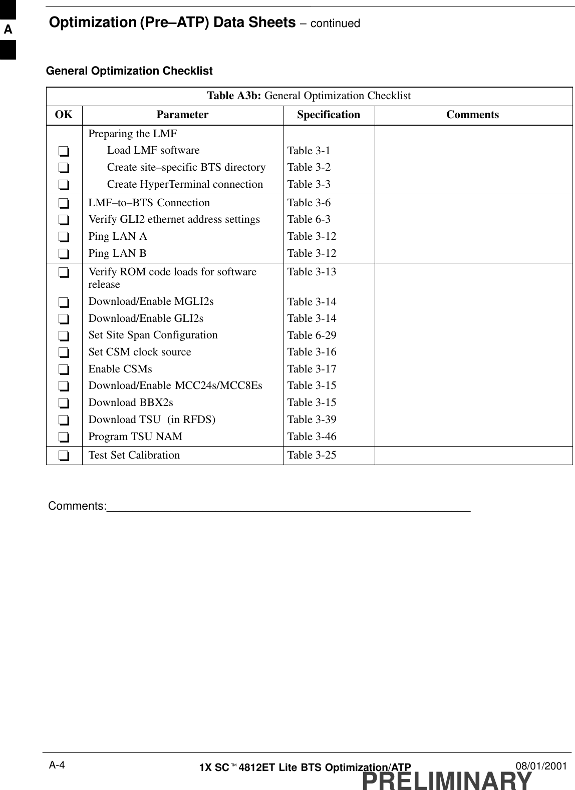
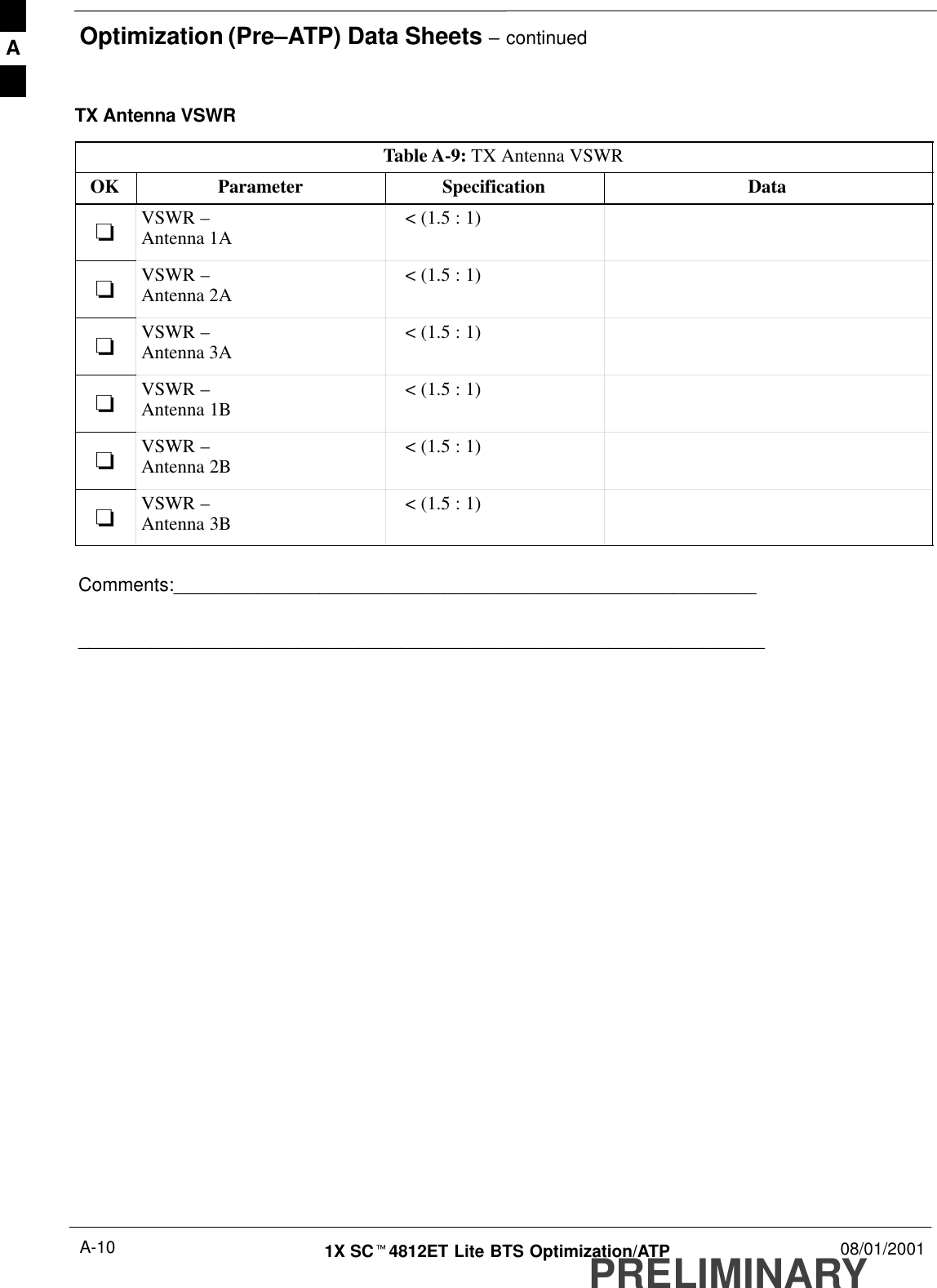
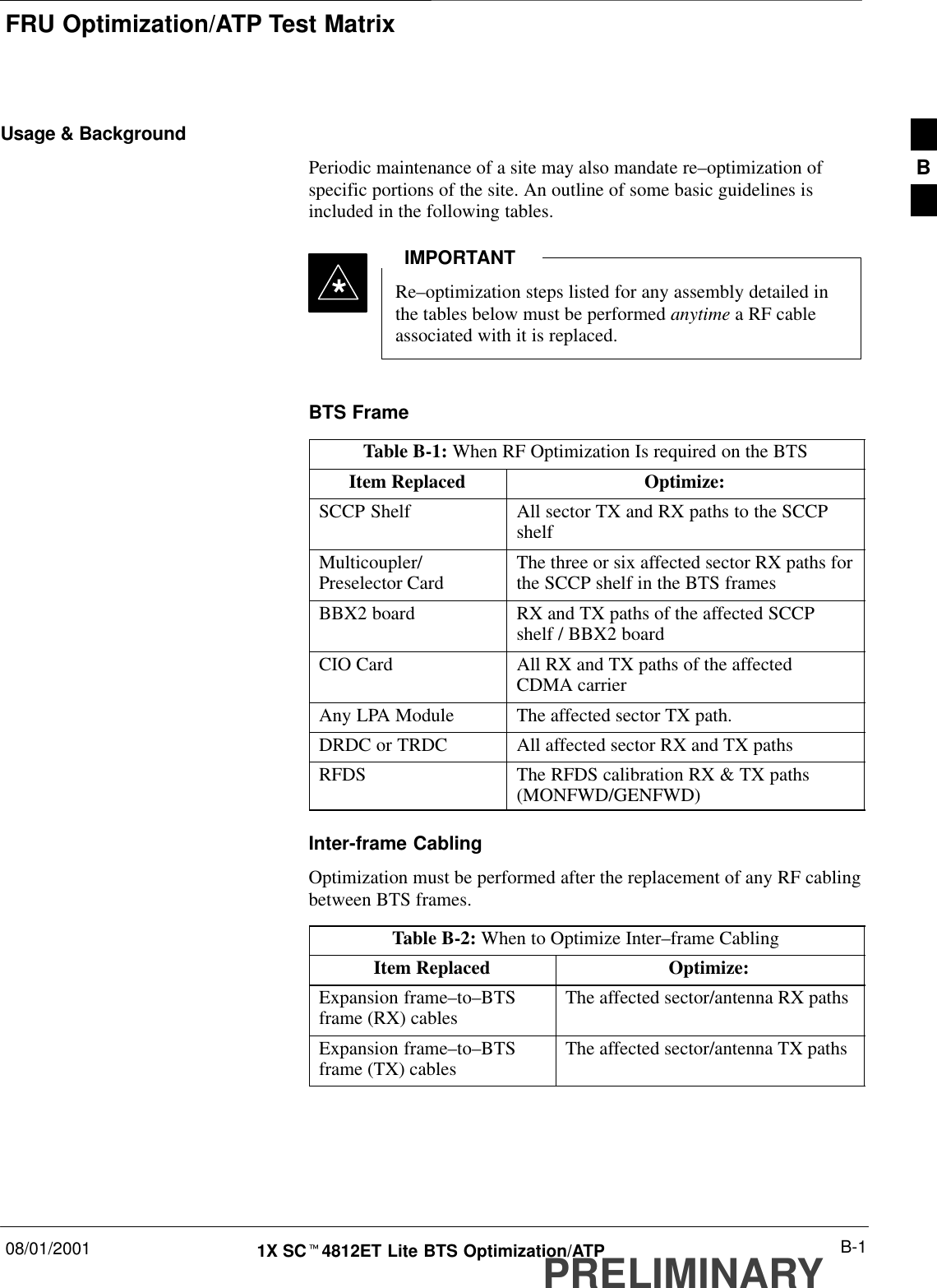
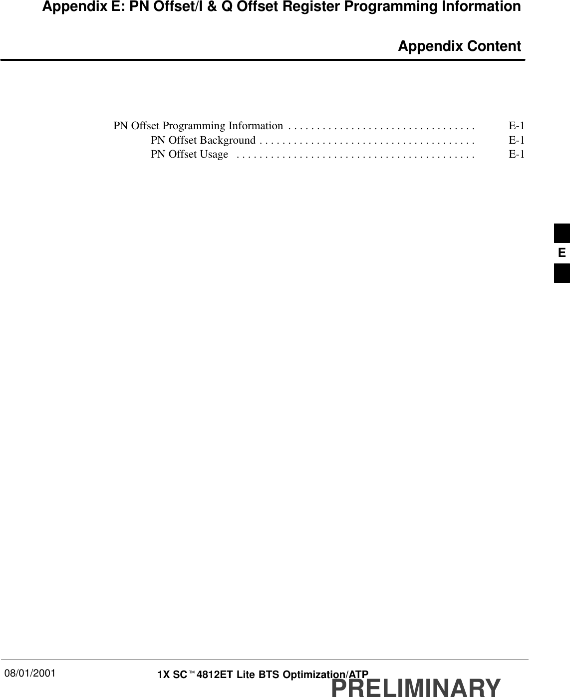
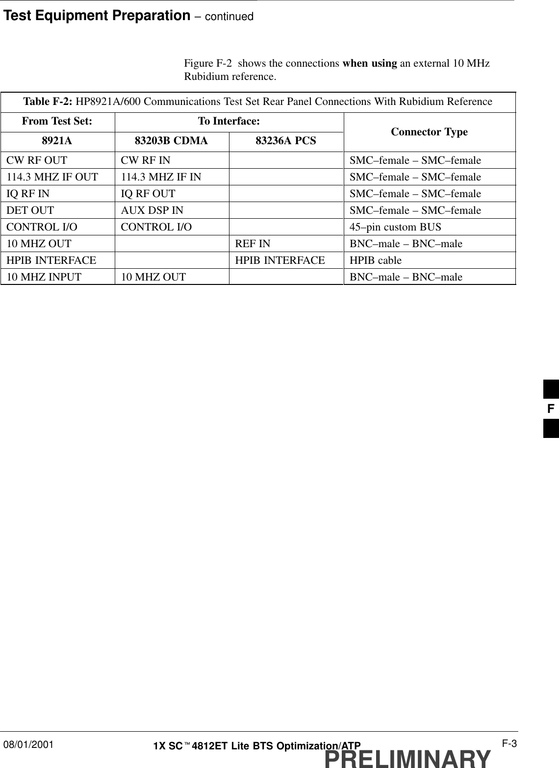
![Test Equipment Preparation – continuedPRELIMINARY1X SCt4812ET Lite BTS Optimization/ATP 08/01/2001F-10Calibrating HP437 Power MeterPrecise transmit output power calibration measurements are made usinga bolometer–type broadband power meter with a sensitive power sensor.Follow the steps outlined in Table F-9 to enter information unique to thepower sensor before calibrating the test setup. Refer to Figure F-5 asrequired.This procedure must be done in conjunction with theautomated calibration to enter power sensor specificcalibration values.IMPORTANT*CONNECT POWERSENSOR WITH POWERMETER TURNED OFFCONNECT POWER SENSORTO POWER REFERENCEWHEN CALIBRATING UNIT.POWER REFERENCE ISENABLED USING THE SHIFT 'KEYSSHIFT (BLUE) PUSHBUTTON –ACCESSES FUNCTION ANDDATA ENTRY KEYS IDENTIFIEDWITH LIGHT BLUE TEXT ONTHE FRONT PANEL ABOVETHE BUTTONSFW00308Figure F-5: Power Meter DetailTable F-9: Power Meter Calibration ProcedureStep Action! CAUTIONDo not connect/disconnect the power meter sensor cable with ac power applied to the meter.Disconnection could result in destruction of the sensing element or mis–calibration.1–Make sure the power meter AC LINE pushbutton is OFF.–Connect the power sensor cable to the SENSOR input.2Set the AC LINE pushbutton to ON.NOTEThe calibration should be performed only after the power meter and sensor have been allowed towarm–up and stabilize for a minimum of 60 minutes.3Perform the following to set or verify the GPIB address:–To enter the SPECIAL data entry function, press [SHIFT] then [PRESET].–Use the [y] or [b] button to select HP–IB ADRS; then press [ENTER].–Use the [y] or [b] button to select HP–IB ADRS 13; then press [ENTER].–To EXIT the SPECIAL data entry function press [SHIFT] then [ENTER].. . . continued on next pageF](https://usermanual.wiki/Nokia-Solutions-and-Networks/T6ER1/User-Guide-498554-Page-306.png)
![Test Equipment Preparation – continued08/01/2001 F-111X SCt4812ET Lite BTS Optimization/ATPPRELIMINARYTable F-9: Power Meter Calibration ProcedureStep Action4Perform the following to set or verify the correct power sensor model:–Press [SHIFT] then [a] to select SENSOR.–Identify the power sensor model number from the sensor label. Use the [y] or [b] button toselect the appropriate model; then press [ENTER].NOTEBe sure the PWR REF (power reference) output is OFF (observe that the triangular indicator is NOTdisplayed as shown in Step 7). If on, press [SHIFT] then ['] to turn it off.5 Press [ZERO]. Display will show “Zeroing ******.” Wait for process to complete.6Connect the power sensor to the POWER REF output.7To turn on the PWR REF, perform the following:–Press [SHIFT] then ['].–Verify that the triangular indicator (below) appears in the display above “PWR REF”.8Perform the following to set the REF CF %:–Press ([SHIFT] then [ZERO]) for CAL.–Enter the sensor’s REF CF % from the sensor’s decal using the arrow keys and press [ENTER].(The power meter will display ”CAL *****” for a few seconds.)NOTEIf the REF CAL FACTOR (REF CF) is not shown on the power sensor, assume it to be 100%.9Perform the following to set the CAL FAC %:–Press [SHIFT] then [FREQ] for CAL FAC.–On the sensor's decal, locate an approximate calibration percentage factor (CF%) at 2 GHz. Enterthe sensor’s calibration % (CF%) using the arrow keys and press [ENTER].When complete, the power meter will typically display 0.05 dBm. (Any reading between 0.00 and0.10 is normal.)10 To turn off the PWR REF, perform the following:–Press [SHIFT] then ['].–Disconnect the power sensor from the POWER REF output. F](https://usermanual.wiki/Nokia-Solutions-and-Networks/T6ER1/User-Guide-498554-Page-307.png)
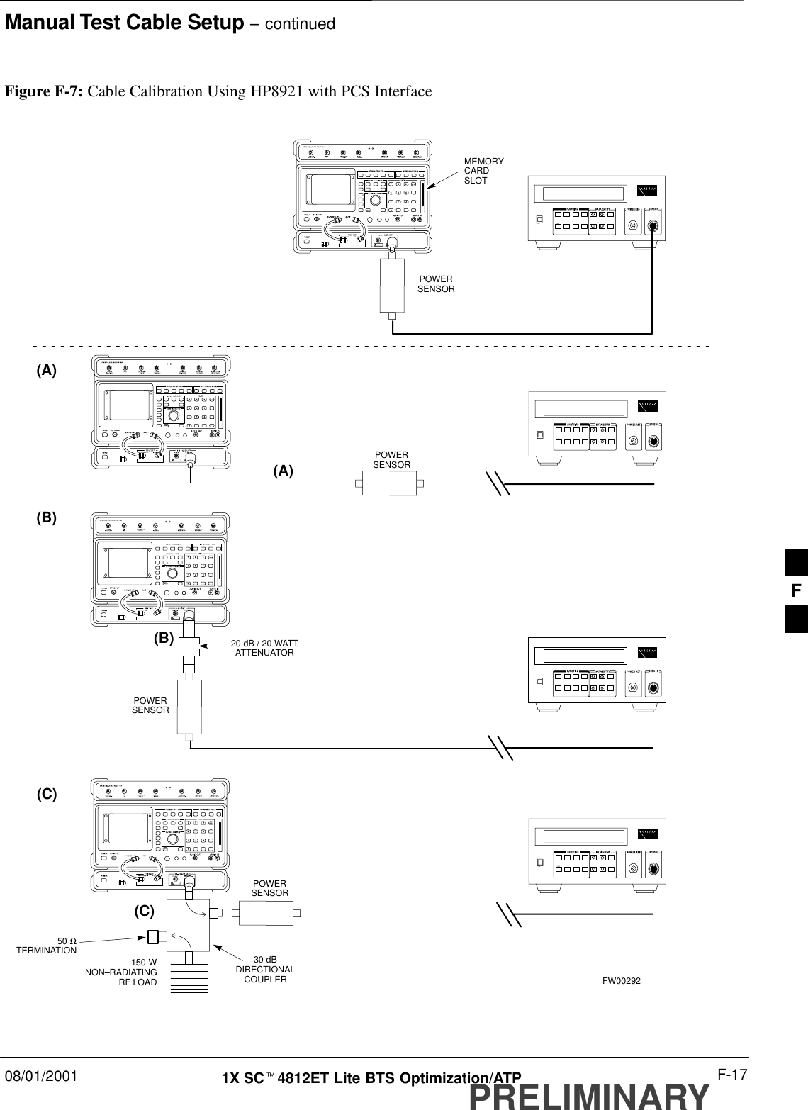
![Manual Cable CalibrationPRELIMINARY1X SCt4812ET Lite BTS Optimization/ATP 08/01/2001F-14Calibrating Test Cable Setupusing HP PCS Interface (HP83236)Table F-11 covers the procedure to calibrate the test equipment using the HP8921 Cellular Communications Analyzer equipped with theHP83236 PCS Interface.This calibration method must be executed with great care.Some losses are measured close to the minimum limit ofthe power meter sensor (–30 dBm).NOTEPrerequisitesEnsure the following prerequisites have been met before proceeding:STest equipment to be calibrated has been connected correctly for cablecalibration.STest equipment has been selected and calibrated.Table F-11: Calibrating Test Cable Setup (using the HP PCS Interface)Step ActionNOTEVerify that GPIB controller is turned off.1Insert HP83236 Manual Control System card into memory card slot.2Press the Preset pushbutton.3 Under Screen Controls, press the TESTS pushbutton to display the TESTS (Main Menu) screen.4Position the cursor at Select Procedure Location and select it. In the Choices selection box, selectCARD.5Position the cursor at Select Procedure Filename and select it. In the Choices selection box, selectMANUAL.6Position the cursor at RUN TEST and select it. HP must be in Control Mode Select YES.7If using HP83236A:Set channel number=<chan#>:–Position cursor at ChannelNumber and select it.–Enter the chan# using the numerickeypad; press [Enter] and thescreen will go blank.–When the screen reappears, thechan# will be displayed on thechannel number line.If using HP83236B:Set channel frequency:–Position cursor at Frequency Band and press Enter.–Select User Defined Frequency.–Go Back to Previous Menu.–Position the cursor to 83236 generator frequency andenter actual RX frequency.–Position the cursor to 83236 analyzer frequency andenter actual TX frequency.. . . continued on next pageF](https://usermanual.wiki/Nokia-Solutions-and-Networks/T6ER1/User-Guide-498554-Page-310.png)
![Manual Test Cable Setup – continued08/01/2001 F-151X SCt4812ET Lite BTS Optimization/ATPPRELIMINARYTable F-11: Calibrating Test Cable Setup (using the HP PCS Interface)Step Action8Set RF Generator level:–Position the cursor at RF Generator Level and select it.–Enter –10 using the numeric keypad; press [Enter] and the screen will go blank.–When the screen reappears, the value –10 dBm will be displayed on the RF Generator Level line.9Set the user fixed Attenuation Setting to 0 dBm:–Position cursor at Analyzer Attenuation and select it–Position cursor at User Fixed Atten Settings and select it.–Enter 0 (zero) using the numeric keypad and press [Enter].10 Select Back to Previous Menu.11 Record the HP83236 Generator Frequency Level:Record the HP83236B Generator Frequency Level:–Position cursor at Show Frequency and Level Details and select it.–Under HP83236 Frequencies and Levels, record the Generator Level.–Under HP83236B Frequencies and Levels, record the Generator Frequency Level (1850 – 1910MHz).–Position cursor at Prev Menu and select it.12 Click on Pause for Manual Measurement.13 Connect the power sensor directly to the RF OUT ONLY port of the PCS Interface.14 On the HP8921A, under To Screen, select CDMA GEN.15 Move the cursor to the Amplitude field and click on the Amplitude value.16 Increase the Amplitude value until the power meter reads 0 dBm ±0.2 dB.NOTEThe Amplitude value can be increased coarsely until 0 dBM is reached; then fine tune the amplitudeby adjusting the Increment Set to 0.1 dBm and targeting in on 0 dBm.17 Disconnect the power sensor from the RF OUT ONLY port of the PCS Interface.* IMPORTANTThe Power Meter sensor’s lower limit is –30 dBm. Thus, only components having losses ≤30 dBshould be measured using this method. For further accuracy, always re-zero the power meterbefore connecting the power sensor to the component being calibrated. After connecting thepower sensor to the component, record the calibrated loss immediately.18 Disconnect all components in the test setup and calibrate each one separately by connecting eachcomponent, one-at-a-time, between the RF OUT ONLY PORT and the power sensor. Record thecalibrated loss value displayed on the power meter.SExample: (A) Test Cable(s) = –1.4 dB(B) 20 dB Attenuator = –20.1 dB(B) Directional Coupler = –29.8 dB. . . continued on next pageF](https://usermanual.wiki/Nokia-Solutions-and-Networks/T6ER1/User-Guide-498554-Page-311.png)
![Manual Test Cable Setup – continuedPRELIMINARY1X SCt4812ET Lite BTS Optimization/ATP 08/01/2001F-16Table F-11: Calibrating Test Cable Setup (using the HP PCS Interface)Step Action19 After all components are calibrated, reassemble all components together and calculate the total testsetup loss by adding up all the individual losses:SExample: Total test setup loss = –1.4 –29.8 –20.1 = –51.3 dB.This calculated value will be used in the next series of tests.20 Under Screen Controls press the TESTS button to display the TESTS (Main Menu) screen.21 Select Continue (K2).22 Select RF Generator Level and set to –119 dBm.23 Click on Pause for Manual Measurement.24 Verify the HP8921A Communication Analyzer/83203A CDMA interface setup is as follows (fieldsnot indicated remain at default):SVerify the GPIB (HP–IB) address:–under To Screen, select More–select IO CONFIG–Set HP–IB Adrs to 18–set Mode to Talk&LstnSVerify the HP8921A is displaying frequency (instead of RF channel)–Press the blue [SHIFT] button, then press the Screen Control [DUPLEX] button; this switches tothe CONFIG (CONFIGURE) screen.–Use the cursor control to set RF Display to Freq25 Refer toChapter 3 for assistance in setting the cable loss values into the LMF. F](https://usermanual.wiki/Nokia-Solutions-and-Networks/T6ER1/User-Guide-498554-Page-312.png)