Nortel Networks Circuit Card Users Manual Description And Installation
Circuit Card to the manual 136e3032-2f9a-4338-a8c4-93b68b26ef3c
2015-01-26
: Nortel-Networks Nortel-Networks-Circuit-Card-Users-Manual-346081 nortel-networks-circuit-card-users-manual-346081 nortel-networks pdf
Open the PDF directly: View PDF ![]() .
.
Page Count: 908 [warning: Documents this large are best viewed by clicking the View PDF Link!]
- Title page
- Revision history
- Contents
- LIst of procedures
- About this document
- Overview
- Circuit card installation
- Acceptance tests
- Option settings
- Contents
- Circuit card grid
- NT1R20 Off-Premise Station card
- NT5D12AA Dual DTI/PRI (DDP) card
- NT6D42 Ringing Generator DC
- NT5D2101/NT9D1102 Core/Network module backplane
- NT6D68 Core module backplane
- NT6D80 Multi-purpose Serial Data Link card
- NT8D14 Universal Trunk card
- NT8D15 E&M Trunk card
- NT8D17 Conference/TDS card
- NT8D21 Ringing Generator AC
- NT8D22 System Monitor
- NT8D41BA Quad Serial Data Interface Paddle Board
- NT8D72 Primary Rate Interface card
- QPC43 Peripheral Signaling card
- QPC71 E&M/DX Signaling and Paging Trunk cards
- QPC414 Network card
- QPC441 3-Port Extender cards
- QPC559, QPC560 Loop Signaling Trunk cards
- QPC528 CO/FX/WATS Trunk cards
- QPC471 Clock Controller card
- QPC525, QPC526, QPC527, QPC777 CO Trunk card
- QPC550 Direct Inward Dial Trunk card
- QPC551 Radio Paging Trunk card
- QPC595 Digitone Receiver cards
- QPC577, QPC596 Digitone Receiver daughterboards
- QPC720 Primary Rate Interface card
- QPC775 Clock Controller card
- QPC841 4-Port Serial Data Interface card
- NT1R20 Off-Premise Station Analog Line card
- NT4N39AA CP Pentium IV Card
- NT5D11 and NT5D14 Lineside T1 Interface cards
- NT5D33 and NT5D34 Lineside E1 Interface cards
- NT5D60/80 CLASS Modem card (XCMC)
- NT5D97 Dual-port DTI2/PRI2 card
- NT5K02 Flexible Analog Line card
- NT5K21 XMFC/MFE card
- NT6D70 SILC Line card
- NT6D71 UILC Line card
- NT6D80 MSDL card
- NT7D16 Data Access card
- Content list
- Introduction
- Features
- Controls and indicators
- Dialing operations
- Operating modes
- Selecting the proper mode for Modem connectivity
- Mode 0
- Mode 1
- Mode 2
- Mode 3
- Selecting the proper mode for Gateway connectivity
- Mode 4
- Mode 5
- Mode 6
- Mode 7
- Selecting the proper mode for Host connectivity
- Mode 8
- Mode 9
- Mode 10
- Mode 11
- Selecting the proper mode for Terminal connectivity
- Mode 12
- Mode 13
- Mode 14
- Mode 15
- Mode selection baud rates
- Keyboard dialing
- Hayes dialing
- Specifications
- System database requirements
- Power supply
- Installing the Data Access card
- Port configuration
- Cabling
- Backplane pinout and signaling
- Configuring the Data Access card
- Connecting Apple Macintosh to the DAC
- Upgrading systems
- NT8D02 and NTDK16 Digital Line cards
- NT8D03 Analog Line card
- NT8D09 Analog Message Waiting Line card
- NT8D14 Universal Trunk card
- NT8D15 E&M Trunk card
- NT8D41AA Serial Data Interface Paddle Board
- NT8D41BA Quad Serial Data Interface Paddle Board
- NTAG26 XMFR card
- NTAK02 SDI/DCH card
- NTAK09 1.5 Mb DTI/PRI card
- NTAK10 2.0 Mb DTI card
- NTAK20 Clock Controller daughterboard
- NTAK79 2.0 Mb PRI card
- NTAK93 D-channel Handler Interface daughterboard
- NTBK22 MISP card
- NTBK50 2.0 Mb PRI card
- NTBK51 Downloadable D-channel Handler daughterboard
- NTCK16 Generic Central Office Trunk cards
- NTDK20 Small System Controller card
- NTRB21 DTI/PRI/DCH TMDI card
- NTVQ01xx Media Card
- NTVQ55AA ITG Pentium card
- QPC513 Enhanced Serial Data Interface card
- QPC841 Quad Serial Data Interface card
- The TDS/DTR card
- Appendix A: LAPB Data Link Control protocol
- Back page

Nortel Communication Server 1000
Nortel Communication Server 1000 Release 4.5
Circuit Card
Description and Installation
Document Number: 553-3001-211
Document Release: Standard 3.00
Date: August 2005
Year Publish FCC TM
Copyright © Nortel Networks Limited 2005
All Rights Reserved
Produced in Canada
Information is subject to change without notice. Nortel Networks reserves the right to make changes in design
or components as progress in engineering and manufacturing may warrant.
Nortel, Nortel (Logo), the Globemark, This is the Way, This is Nortel (Design mark), SL-1, Meridian 1, and
Succession are trademarks of Nortel Networks.
Title page

Page 3 of 906
Circuit Card Description and Installation
4
Revision history
August 2005
Standard 3.00. This document is up-issued to support Communication
Server 1000 Release 4.5.
September 2004
Standard 2.00. This document is up-issued for Communication Server 1000
Release 4.0.
October 2003
Standard 1.00. This document is a new NTP for Succession 3.0. It was created
to support a restructuring of the Documentation Library, which resulted in the
merging of multiple legacy NTPs. This new document consolidates
information previously contained in the following legacy documents, now
retired:
•Line Cards: Description (553-3001-105)
•Trunk Cards: Description (553-3001-106)
•Serial Data Interface Cards: Description (553-3001-107)
•NT7D16 Data Access Card: Description and operation (553-3001-191)
•Multi-purpose Serial Data Link: Description (553-3001-195)
•Circuit Cards: Installation and Testing (553-3001-211)
•Option 11C and 11C mini Technical Reference Guide (553-3011-100)
(Content from Option 11C and 11C mini Technical Reference Guide
(553-3011-100) also appears in Telephones and Consoles: Description,
Installation, and Operation (553-3001-367).)
•Circuit Card Reference (553-3023-211)


Page 5 of 906
Circuit Card Description and Installation
18
Contents
LIst of procedures . . . . . . . . . . . . . . . . . . . . . . . . . . 19
About this document . . . . . . . . . . . . . . . . . . . . . . . 21
Subject .. . . . . . . . . . . . . . . . . . . . . . . . . . . . . . . . . . . . . . . . . . . . . . . . . 21
Applicable systems . . . . . . . . . . . . . . . . . . . . . . . . . . . . . . . . . . . . . . . . 22
Intended audience . . . . . . . . . . . . . . . . . . . . . . . . . . . . . . . . . . . . . . . . . 23
Conventions .. . . . . . . . . . . . . . . . . . . . . . . . . . . . . . . . . . . . . . . . . . . . . 24
Related information .. . . . . . . . . . . . . . . . . . . . . . . . . . . . . . . . . . . . . . . 25
Overview . . . . . . . . . . . . . . . . . . . . . . . . . . . . . . . . . 27
Contents .. . . . . . . . . . . . . . . . . . . . . . . . . . . . . . . . . . . . . . . . . . . . . . . . 27
Line cards . . . . . . . . . . . . . . . . . . . . . . . . . . . . . . . . . . . . . . . . . . . . . . . 28
Trunk cards . . . . . . . . . . . . . . . . . . . . . . . . . . . . . . . . . . . . . . . . . . . . . . 59
Installation .. . . . . . . . . . . . . . . . . . . . . . . . . . . . . . . . . . . . . . . . . . . . . . 61
Operation .. . . . . . . . . . . . . . . . . . . . . . . . . . . . . . . . . . . . . . . . . . . . . . . 63
Serial Data Interface (SDI) cards . . . . . . . . . . . . . . . . . . . . . . . . . . . . . 72
Circuit card installation . . . . . . . . . . . . . . . . . . . . . 79
Contents .. . . . . . . . . . . . . . . . . . . . . . . . . . . . . . . . . . . . . . . . . . . . . . . . 79
Card slots — Large System .. . . . . . . . . . . . . . . . . . . . . . . . . . . . . . . . . 79
Circuit card installation . . . . . . . . . . . . . . . . . . . . . . . . . . . . . . . . . . . . . 80
Precautions . . . . . . . . . . . . . . . . . . . . . . . . . . . . . . . . . . . . . . . . . . . . . . 84
Installing a circuit card . . . . . . . . . . . . . . . . . . . . . . . . . . . . . . . . . . . . . 86

Page 6 of 906 Contents
553-3001-211 Standard 3.00 August 2005
Acceptance tests . . . . . . . . . . . . . . . . . . . . . . . . . . 89
Contents . . . . . . . . . . . . . . . . . . . . . . . . . . . . . . . . . . . . . . . . . . . . . . . . 89
Introduction .. . . . . . . . . . . . . . . . . . . . . . . . . . . . . . . . . . . . . . . . . . . . . 89
Conference cards .. . . . . . . . . . . . . . . . . . . . . . . . . . . . . . . . . . . . . . . . . 90
Digitone receiver cards . . . . . . . . . . . . . . . . . . . . . . . . . . . . . . . . . . . . . 92
Line cards . . . . . . . . . . . . . . . . . . . . . . . . . . . . . . . . . . . . . . . . . . . . . . . 93
Multifrequency sender cards .. . . . . . . . . . . . . . . . . . . . . . . . . . . . . . . . 94
Multifrequency signaling cards . . . . . . . . . . . . . . . . . . . . . . . . . . . . . . 95
Network cards . . . . . . . . . . . . . . . . . . . . . . . . . . . . . . . . . . . . . . . . . . . . 95
Trunk cards . . . . . . . . . . . . . . . . . . . . . . . . . . . . . . . . . . . . . . . . . . . . . . 96
Tone and digit switch cards . . . . . . . . . . . . . . . . . . . . . . . . . . . . . . . . . 97
Option settings . . . . . . . . . . . . . . . . . . . . . . . . . . . . 101
Contents . . . . . . . . . . . . . . . . . . . . . . . . . . . . . . . . . . . . . . . . . . . . . . . . 101
Circuit card grid . . . . . . . . . . . . . . . . . . . . . . . . . . . . . . . . . . . . . . . . . . 102
NT1R20 Off-Premise Station card . . . . . . . . . . . . . . . . . . . . . . . . . . . . 104
NT5D12AA Dual DTI/PRI (DDP) card . . . . . . . . . . . . . . . . . . . . . . . . 107
NT6D42 Ringing Generator DC .. . . . . . . . . . . . . . . . . . . . . . . . . . . . . 114
NT5D2101/NT9D1102 Core/Network module backplane .. . . . . . . . . 117
NT6D68 Core module backplane . . . . . . . . . . . . . . . . . . . . . . . . . . . . . 117
NT6D80 Multi-purpose Serial Data Link card . . . . . . . . . . . . . . . . . . . 118
NT8D14 Universal Trunk card . . . . . . . . . . . . . . . . . . . . . . . . . . . . . . . 119
NT8D15 E&M Trunk card . . . . . . . . . . . . . . . . . . . . . . . . . . . . . . . . . . 124
NT8D17 Conference/TDS card . . . . . . . . . . . . . . . . . . . . . . . . . . . . . . 125
NT8D21 Ringing Generator AC .. . . . . . . . . . . . . . . . . . . . . . . . . . . . . 126
NT8D22 System Monitor . . . . . . . . . . . . . . . . . . . . . . . . . . . . . . . . . . . 127
NT8D41BA Quad Serial Data Interface Paddle Board . . . . . . . . . . . . 132
NT8D72 Primary Rate Interface card .. . . . . . . . . . . . . . . . . . . . . . . . . 134
QPC43 Peripheral Signaling card . . . . . . . . . . . . . . . . . . . . . . . . . . . . . 136
QPC71 E&M/DX Signaling and Paging Trunk cards . . . . . . . . . . . . . 136

Contents Page 7 of 906
Circuit Card Description and Installation
QPC414 Network card . . . . . . . . . . . . . . . . . . . . . . . . . . . . . . . . . . . . . 137
QPC441 3-Port Extender cards . . . . . . . . . . . . . . . . . . . . . . . . . . . . . . . 138
QPC559, QPC560 Loop Signaling Trunk cards . . . . . . . . . . . . . . . . . 141
QPC528 CO/FX/WATS Trunk cards .. . . . . . . . . . . . . . . . . . . . . . . . . 143
QPC471 Clock Controller card . . . . . . . . . . . . . . . . . . . . . . . . . . . . . . . 144
QPC525, QPC526, QPC527, QPC777 CO Trunk card .. . . . . . . . . . . . 145
QPC550 Direct Inward Dial Trunk card . . . . . . . . . . . . . . . . . . . . . . . . 146
QPC551 Radio Paging Trunk card . . . . . . . . . . . . . . . . . . . . . . . . . . . . 149
QPC595 Digitone Receiver cards . . . . . . . . . . . . . . . . . . . . . . . . . . . . . 150
QPC577, QPC596 Digitone Receiver daughterboards . . . . . . . . . . . . . 150
QPC720 Primary Rate Interface card . . . . . . . . . . . . . . . . . . . . . . . . . . 150
QPC775 Clock Controller card . . . . . . . . . . . . . . . . . . . . . . . . . . . . . . . 152
QPC841 4-Port Serial Data Interface card . . . . . . . . . . . . . . . . . . . . . . 153
NT1R20 Off-Premise Station
Analog Line card . . . . . . . . . . . . . . . . . . . . . . . . . . 157
Contents .. . . . . . . . . . . . . . . . . . . . . . . . . . . . . . . . . . . . . . . . . . . . . . . . 157
Introduction . . . . . . . . . . . . . . . . . . . . . . . . . . . . . . . . . . . . . . . . . . . . . . 157
Physical description .. . . . . . . . . . . . . . . . . . . . . . . . . . . . . . . . . . . . . . . 158
Functional description . . . . . . . . . . . . . . . . . . . . . . . . . . . . . . . . . . . . . . 160
Electrical specifications .. . . . . . . . . . . . . . . . . . . . . . . . . . . . . . . . . . . . 165
Operation .. . . . . . . . . . . . . . . . . . . . . . . . . . . . . . . . . . . . . . . . . . . . . . . 168
Connector pin assignments . . . . . . . . . . . . . . . . . . . . . . . . . . . . . . . . . . 172
Configuring the OPS analog line card .. . . . . . . . . . . . . . . . . . . . . . . . . 174
Application . . . . . . . . . . . . . . . . . . . . . . . . . . . . . . . . . . . . . . . . . . . . . . 175
NT4N39AA CP Pentium IV Card . . . . . . . . . . . . . . . 183
Contents .. . . . . . . . . . . . . . . . . . . . . . . . . . . . . . . . . . . . . . . . . . . . . . . . 183
Introduction . . . . . . . . . . . . . . . . . . . . . . . . . . . . . . . . . . . . . . . . . . . . . . 183
Physical description .. . . . . . . . . . . . . . . . . . . . . . . . . . . . . . . . . . . . . . . 183
Functional description . . . . . . . . . . . . . . . . . . . . . . . . . . . . . . . . . . . . . . 186

Page 8 of 906 Contents
553-3001-211 Standard 3.00 August 2005
Front panel connector pin assignments .. . . . . . . . . . . . . . . . . . . . . . . . 187
NT5D11 and NT5D14 Lineside T1
Interface cards . . . . . . . . . . . . . . . . . . . . . . . . . . . . 193
Contents . . . . . . . . . . . . . . . . . . . . . . . . . . . . . . . . . . . . . . . . . . . . . . . . 193
Introduction .. . . . . . . . . . . . . . . . . . . . . . . . . . . . . . . . . . . . . . . . . . . . . 193
Physical description . . . . . . . . . . . . . . . . . . . . . . . . . . . . . . . . . . . . . . . 194
Functional description .. . . . . . . . . . . . . . . . . . . . . . . . . . . . . . . . . . . . . 198
Electrical specifications . . . . . . . . . . . . . . . . . . . . . . . . . . . . . . . . . . . . 202
Installation and configuration . . . . . . . . . . . . . . . . . . . . . . . . . . . . . . . . 204
Man-Machine T1 maintenance interface software . . . . . . . . . . . . . . . . 225
Applications . . . . . . . . . . . . . . . . . . . . . . . . . . . . . . . . . . . . . . . . . . . . . 244
NT5D33 and NT5D34 Lineside E1
Interface cards . . . . . . . . . . . . . . . . . . . . . . . . . . . . 249
Contents . . . . . . . . . . . . . . . . . . . . . . . . . . . . . . . . . . . . . . . . . . . . . . . . 249
Introduction .. . . . . . . . . . . . . . . . . . . . . . . . . . . . . . . . . . . . . . . . . . . . . 249
Physical description . . . . . . . . . . . . . . . . . . . . . . . . . . . . . . . . . . . . . . . 250
Functional description .. . . . . . . . . . . . . . . . . . . . . . . . . . . . . . . . . . . . . 255
Electrical specifications . . . . . . . . . . . . . . . . . . . . . . . . . . . . . . . . . . . . 261
Installation and Configuration . . . . . . . . . . . . . . . . . . . . . . . . . . . . . . . 263
Installation . . . . . . . . . . . . . . . . . . . . . . . . . . . . . . . . . . . . . . . . . . . . . . 271
Man-Machine E1 maintenance interface software . . . . . . . . . . . . . . . . 284
Applications . . . . . . . . . . . . . . . . . . . . . . . . . . . . . . . . . . . . . . . . . . . . . 310
NT5D60/80 CLASS Modem card (XCMC) . . . . . . . 313
Contents . . . . . . . . . . . . . . . . . . . . . . . . . . . . . . . . . . . . . . . . . . . . . . . . 313
Introduction .. . . . . . . . . . . . . . . . . . . . . . . . . . . . . . . . . . . . . . . . . . . . . 313
Physical description . . . . . . . . . . . . . . . . . . . . . . . . . . . . . . . . . . . . . . . 313
Functional description .. . . . . . . . . . . . . . . . . . . . . . . . . . . . . . . . . . . . . 314
Electrical specifications . . . . . . . . . . . . . . . . . . . . . . . . . . . . . . . . . . . . 317
Configuration . . . . . . . . . . . . . . . . . . . . . . . . . . . . . . . . . . . . . . . . . . . . 318

Contents Page 9 of 906
Circuit Card Description and Installation
NT5D97 Dual-port DTI2/PRI2 card . . . . . . . . . . . . . 319
Contents .. . . . . . . . . . . . . . . . . . . . . . . . . . . . . . . . . . . . . . . . . . . . . . . . 319
Introduction . . . . . . . . . . . . . . . . . . . . . . . . . . . . . . . . . . . . . . . . . . . . . . 319
Physical description .. . . . . . . . . . . . . . . . . . . . . . . . . . . . . . . . . . . . . . . 320
Functional description . . . . . . . . . . . . . . . . . . . . . . . . . . . . . . . . . . . . . . 340
Architecture .. . . . . . . . . . . . . . . . . . . . . . . . . . . . . . . . . . . . . . . . . . . . . 353
Operation .. . . . . . . . . . . . . . . . . . . . . . . . . . . . . . . . . . . . . . . . . . . . . . . 359
NT5K02 Flexible Analog Line card . . . . . . . . . . . . 367
Contents .. . . . . . . . . . . . . . . . . . . . . . . . . . . . . . . . . . . . . . . . . . . . . . . . 367
Introduction . . . . . . . . . . . . . . . . . . . . . . . . . . . . . . . . . . . . . . . . . . . . . . 367
Applications . . . . . . . . . . . . . . . . . . . . . . . . . . . . . . . . . . . . . . . . . . . . . 368
NT5K21 XMFC/MFE card . . . . . . . . . . . . . . . . . . . . . 369
Contents .. . . . . . . . . . . . . . . . . . . . . . . . . . . . . . . . . . . . . . . . . . . . . . . . 369
Introduction . . . . . . . . . . . . . . . . . . . . . . . . . . . . . . . . . . . . . . . . . . . . . . 369
MFC signaling .. . . . . . . . . . . . . . . . . . . . . . . . . . . . . . . . . . . . . . . . . . . 369
MFE signaling .. . . . . . . . . . . . . . . . . . . . . . . . . . . . . . . . . . . . . . . . . . . 372
Sender and receiver mode . . . . . . . . . . . . . . . . . . . . . . . . . . . . . . . . . . . 373
Physical specifications . . . . . . . . . . . . . . . . . . . . . . . . . . . . . . . . . . . . . 376
NT6D70 SILC Line card . . . . . . . . . . . . . . . . . . . . . . 379
Contents .. . . . . . . . . . . . . . . . . . . . . . . . . . . . . . . . . . . . . . . . . . . . . . . . 379
Introduction . . . . . . . . . . . . . . . . . . . . . . . . . . . . . . . . . . . . . . . . . . . . . . 379
Physical description .. . . . . . . . . . . . . . . . . . . . . . . . . . . . . . . . . . . . . . . 380
Functional description . . . . . . . . . . . . . . . . . . . . . . . . . . . . . . . . . . . . . . 380
NT6D71 UILC Line card . . . . . . . . . . . . . . . . . . . . . . 385
Contents .. . . . . . . . . . . . . . . . . . . . . . . . . . . . . . . . . . . . . . . . . . . . . . . . 385
Introduction . . . . . . . . . . . . . . . . . . . . . . . . . . . . . . . . . . . . . . . . . . . . . . 385
Physical description .. . . . . . . . . . . . . . . . . . . . . . . . . . . . . . . . . . . . . . . 385
Functional description . . . . . . . . . . . . . . . . . . . . . . . . . . . . . . . . . . . . . . 386

Page 10 of 906 Contents
553-3001-211 Standard 3.00 August 2005
NT6D80 MSDL card . . . . . . . . . . . . . . . . . . . . . . . . 389
Contents . . . . . . . . . . . . . . . . . . . . . . . . . . . . . . . . . . . . . . . . . . . . . . . . 389
Introduction .. . . . . . . . . . . . . . . . . . . . . . . . . . . . . . . . . . . . . . . . . . . . . 389
Physical description . . . . . . . . . . . . . . . . . . . . . . . . . . . . . . . . . . . . . . . 390
Functional description .. . . . . . . . . . . . . . . . . . . . . . . . . . . . . . . . . . . . . 392
Engineering guidelines . . . . . . . . . . . . . . . . . . . . . . . . . . . . . . . . . . . . . 397
Installation . . . . . . . . . . . . . . . . . . . . . . . . . . . . . . . . . . . . . . . . . . . . . . 404
Maintenance . . . . . . . . . . . . . . . . . . . . . . . . . . . . . . . . . . . . . . . . . . . . . 413
Replacing MSDL cards .. . . . . . . . . . . . . . . . . . . . . . . . . . . . . . . . . . . . 421
Symptoms and actions . . . . . . . . . . . . . . . . . . . . . . . . . . . . . . . . . . . . . 422
System disabled actions . . . . . . . . . . . . . . . . . . . . . . . . . . . . . . . . . . . . 423
NT7D16 Data Access card . . . . . . . . . . . . . . . . . . . 427
Content list . . . . . . . . . . . . . . . . . . . . . . . . . . . . . . . . . . . . . . . . . . . . . . 427
Introduction .. . . . . . . . . . . . . . . . . . . . . . . . . . . . . . . . . . . . . . . . . . . . . 428
Features .. . . . . . . . . . . . . . . . . . . . . . . . . . . . . . . . . . . . . . . . . . . . . . . . 428
Controls and indicators . . . . . . . . . . . . . . . . . . . . . . . . . . . . . . . . . . . . . 429
Dialing operations .. . . . . . . . . . . . . . . . . . . . . . . . . . . . . . . . . . . . . . . . 430
Operating modes . . . . . . . . . . . . . . . . . . . . . . . . . . . . . . . . . . . . . . . . . . 435
Keyboard dialing .. . . . . . . . . . . . . . . . . . . . . . . . . . . . . . . . . . . . . . . . . 472
Hayes dialing . . . . . . . . . . . . . . . . . . . . . . . . . . . . . . . . . . . . . . . . . . . . 485
Specifications . . . . . . . . . . . . . . . . . . . . . . . . . . . . . . . . . . . . . . . . . . . . 497
System database requirements . . . . . . . . . . . . . . . . . . . . . . . . . . . . . . . 500
Power supply .. . . . . . . . . . . . . . . . . . . . . . . . . . . . . . . . . . . . . . . . . . . . 504
Installing the Data Access card .. . . . . . . . . . . . . . . . . . . . . . . . . . . . . . 505
Port configuration . . . . . . . . . . . . . . . . . . . . . . . . . . . . . . . . . . . . . . . . . 507
Cabling . . . . . . . . . . . . . . . . . . . . . . . . . . . . . . . . . . . . . . . . . . . . . . . . . 509
Backplane pinout and signaling . . . . . . . . . . . . . . . . . . . . . . . . . . . . . . 514
Configuring the Data Access card . . . . . . . . . . . . . . . . . . . . . . . . . . . . 517
Connecting Apple Macintosh to the DAC . . . . . . . . . . . . . . . . . . . . . . 522

Contents Page 11 of 906
Circuit Card Description and Installation
Upgrading systems . . . . . . . . . . . . . . . . . . . . . . . . . . . . . . . . . . . . . . . . 522
NT8D02 and NTDK16 Digital Line cards . . . . . . . . 527
Contents .. . . . . . . . . . . . . . . . . . . . . . . . . . . . . . . . . . . . . . . . . . . . . . . . 527
Introduction . . . . . . . . . . . . . . . . . . . . . . . . . . . . . . . . . . . . . . . . . . . . . . 527
Physical description .. . . . . . . . . . . . . . . . . . . . . . . . . . . . . . . . . . . . . . . 528
Functional description . . . . . . . . . . . . . . . . . . . . . . . . . . . . . . . . . . . . . . 530
Electrical specifications .. . . . . . . . . . . . . . . . . . . . . . . . . . . . . . . . . . . . 536
Digital line interface specifications .. . . . . . . . . . . . . . . . . . . . . . . . . . . 537
Connector pin assignments . . . . . . . . . . . . . . . . . . . . . . . . . . . . . . . . . . 539
Configuration . . . . . . . . . . . . . . . . . . . . . . . . . . . . . . . . . . . . . . . . . . . . 541
NT8D03 Analog Line card . . . . . . . . . . . . . . . . . . . . 545
Overview . . . . . . . . . . . . . . . . . . . . . . . . . . . . . . . . . . . . . . . . . . . . . . . . 545
NT8D09 Analog Message Waiting
Line card . . . . . . . . . . . . . . . . . . . . . . . . . . . . . . . . . 547
Contents .. . . . . . . . . . . . . . . . . . . . . . . . . . . . . . . . . . . . . . . . . . . . . . . . 547
Introduction . . . . . . . . . . . . . . . . . . . . . . . . . . . . . . . . . . . . . . . . . . . . . . 547
Physical description .. . . . . . . . . . . . . . . . . . . . . . . . . . . . . . . . . . . . . . . 549
Functional description . . . . . . . . . . . . . . . . . . . . . . . . . . . . . . . . . . . . . . 549
Connector pin assignments . . . . . . . . . . . . . . . . . . . . . . . . . . . . . . . . . . 558
Configuration . . . . . . . . . . . . . . . . . . . . . . . . . . . . . . . . . . . . . . . . . . . . 561
NT8D14 Universal Trunk card . . . . . . . . . . . . . . . . 565
Contents .. . . . . . . . . . . . . . . . . . . . . . . . . . . . . . . . . . . . . . . . . . . . . . . . 565
Introduction . . . . . . . . . . . . . . . . . . . . . . . . . . . . . . . . . . . . . . . . . . . . . . 565
Physical description .. . . . . . . . . . . . . . . . . . . . . . . . . . . . . . . . . . . . . . . 567
Functional description . . . . . . . . . . . . . . . . . . . . . . . . . . . . . . . . . . . . . . 570
Operation .. . . . . . . . . . . . . . . . . . . . . . . . . . . . . . . . . . . . . . . . . . . . . . . 573
Electrical specifications .. . . . . . . . . . . . . . . . . . . . . . . . . . . . . . . . . . . . 609
Connector pin assignments . . . . . . . . . . . . . . . . . . . . . . . . . . . . . . . . . . 614

Page 12 of 906 Contents
553-3001-211 Standard 3.00 August 2005
Configuration . . . . . . . . . . . . . . . . . . . . . . . . . . . . . . . . . . . . . . . . . . . . 615
Applications . . . . . . . . . . . . . . . . . . . . . . . . . . . . . . . . . . . . . . . . . . . . . 624
NT8D15 E&M Trunk card . . . . . . . . . . . . . . . . . . . . 627
Contents . . . . . . . . . . . . . . . . . . . . . . . . . . . . . . . . . . . . . . . . . . . . . . . . 627
Introduction .. . . . . . . . . . . . . . . . . . . . . . . . . . . . . . . . . . . . . . . . . . . . . 627
Physical description . . . . . . . . . . . . . . . . . . . . . . . . . . . . . . . . . . . . . . . 629
Functional description .. . . . . . . . . . . . . . . . . . . . . . . . . . . . . . . . . . . . . 631
Operation . . . . . . . . . . . . . . . . . . . . . . . . . . . . . . . . . . . . . . . . . . . . . . . 641
Electrical specifications . . . . . . . . . . . . . . . . . . . . . . . . . . . . . . . . . . . . 652
Connector pin assignments . . . . . . . . . . . . . . . . . . . . . . . . . . . . . . . . . . 655
Configuration . . . . . . . . . . . . . . . . . . . . . . . . . . . . . . . . . . . . . . . . . . . . 658
Applications . . . . . . . . . . . . . . . . . . . . . . . . . . . . . . . . . . . . . . . . . . . . . 664
NT8D41AA Serial Data Interface
Paddle Board . . . . . . . . . . . . . . . . . . . . . . . . . . . . . 667
Contents . . . . . . . . . . . . . . . . . . . . . . . . . . . . . . . . . . . . . . . . . . . . . . . . 667
Introduction .. . . . . . . . . . . . . . . . . . . . . . . . . . . . . . . . . . . . . . . . . . . . . 667
Physical description . . . . . . . . . . . . . . . . . . . . . . . . . . . . . . . . . . . . . . . 668
Functional description .. . . . . . . . . . . . . . . . . . . . . . . . . . . . . . . . . . . . . 670
Connector pin assignments . . . . . . . . . . . . . . . . . . . . . . . . . . . . . . . . . . 671
Configuring the SDI paddle board . . . . . . . . . . . . . . . . . . . . . . . . . . . . 672
Applications . . . . . . . . . . . . . . . . . . . . . . . . . . . . . . . . . . . . . . . . . . . . . 678
NT8D41BA Quad Serial Data Interface
Paddle Board . . . . . . . . . . . . . . . . . . . . . . . . . . . . . 681
Contents . . . . . . . . . . . . . . . . . . . . . . . . . . . . . . . . . . . . . . . . . . . . . . . . 681
Introduction .. . . . . . . . . . . . . . . . . . . . . . . . . . . . . . . . . . . . . . . . . . . . . 681
Physical description . . . . . . . . . . . . . . . . . . . . . . . . . . . . . . . . . . . . . . . 682
Functional description .. . . . . . . . . . . . . . . . . . . . . . . . . . . . . . . . . . . . . 682
Connector pin assignments . . . . . . . . . . . . . . . . . . . . . . . . . . . . . . . . . . 685
Configuring the QSDI paddle board .. . . . . . . . . . . . . . . . . . . . . . . . . . 687

Contents Page 13 of 906
Circuit Card Description and Installation
Applications . . . . . . . . . . . . . . . . . . . . . . . . . . . . . . . . . . . . . . . . . . . . . 692
NTAG26 XMFR card . . . . . . . . . . . . . . . . . . . . . . . . 695
Contents .. . . . . . . . . . . . . . . . . . . . . . . . . . . . . . . . . . . . . . . . . . . . . . . . 695
Introduction . . . . . . . . . . . . . . . . . . . . . . . . . . . . . . . . . . . . . . . . . . . . . . 695
Physical specifications . . . . . . . . . . . . . . . . . . . . . . . . . . . . . . . . . . . . . 700
NTAK02 SDI/DCH card . . . . . . . . . . . . . . . . . . . . . . 701
Contents .. . . . . . . . . . . . . . . . . . . . . . . . . . . . . . . . . . . . . . . . . . . . . . . . 701
Introduction . . . . . . . . . . . . . . . . . . . . . . . . . . . . . . . . . . . . . . . . . . . . . . 701
NTAK02 SDI/DCH card .. . . . . . . . . . . . . . . . . . . . . . . . . . . . . . . . . . . 701
NTAK09 1.5 Mb DTI/PRI card . . . . . . . . . . . . . . . . . 709
Contents .. . . . . . . . . . . . . . . . . . . . . . . . . . . . . . . . . . . . . . . . . . . . . . . . 709
Introduction . . . . . . . . . . . . . . . . . . . . . . . . . . . . . . . . . . . . . . . . . . . . . . 709
Physical description .. . . . . . . . . . . . . . . . . . . . . . . . . . . . . . . . . . . . . . . 710
Functional description . . . . . . . . . . . . . . . . . . . . . . . . . . . . . . . . . . . . . . 714
Architecture .. . . . . . . . . . . . . . . . . . . . . . . . . . . . . . . . . . . . . . . . . . . . . 715
NTAK10 2.0 Mb DTI card . . . . . . . . . . . . . . . . . . . . . 721
Contents .. . . . . . . . . . . . . . . . . . . . . . . . . . . . . . . . . . . . . . . . . . . . . . . . 721
Introduction . . . . . . . . . . . . . . . . . . . . . . . . . . . . . . . . . . . . . . . . . . . . . . 721
Physical description .. . . . . . . . . . . . . . . . . . . . . . . . . . . . . . . . . . . . . . . 722
Functional description . . . . . . . . . . . . . . . . . . . . . . . . . . . . . . . . . . . . . . 723
Architecture .. . . . . . . . . . . . . . . . . . . . . . . . . . . . . . . . . . . . . . . . . . . . . 724
NTAK20 Clock Controller daughterboard . . . . . . . 735
Contents .. . . . . . . . . . . . . . . . . . . . . . . . . . . . . . . . . . . . . . . . . . . . . . . . 735
Introduction . . . . . . . . . . . . . . . . . . . . . . . . . . . . . . . . . . . . . . . . . . . . . . 735
Physical description .. . . . . . . . . . . . . . . . . . . . . . . . . . . . . . . . . . . . . . . 738
Functional description . . . . . . . . . . . . . . . . . . . . . . . . . . . . . . . . . . . . . . 739

Page 14 of 906 Contents
553-3001-211 Standard 3.00 August 2005
NTAK79 2.0 Mb PRI card . . . . . . . . . . . . . . . . . . . . 745
Contents . . . . . . . . . . . . . . . . . . . . . . . . . . . . . . . . . . . . . . . . . . . . . . . . 745
Introduction .. . . . . . . . . . . . . . . . . . . . . . . . . . . . . . . . . . . . . . . . . . . . . 745
Physical description . . . . . . . . . . . . . . . . . . . . . . . . . . . . . . . . . . . . . . . 746
Functional description .. . . . . . . . . . . . . . . . . . . . . . . . . . . . . . . . . . . . . 751
Architecture . . . . . . . . . . . . . . . . . . . . . . . . . . . . . . . . . . . . . . . . . . . . . 752
NTAK93 D-channel Handler
Interface daughterboard . . . . . . . . . . . . . . . . . . . . 763
Contents . . . . . . . . . . . . . . . . . . . . . . . . . . . . . . . . . . . . . . . . . . . . . . . . 763
Introduction .. . . . . . . . . . . . . . . . . . . . . . . . . . . . . . . . . . . . . . . . . . . . . 763
Physical description . . . . . . . . . . . . . . . . . . . . . . . . . . . . . . . . . . . . . . . 764
Functional description .. . . . . . . . . . . . . . . . . . . . . . . . . . . . . . . . . . . . . 765
NTBK22 MISP card . . . . . . . . . . . . . . . . . . . . . . . . . 769
Contents . . . . . . . . . . . . . . . . . . . . . . . . . . . . . . . . . . . . . . . . . . . . . . . . 769
Introduction .. . . . . . . . . . . . . . . . . . . . . . . . . . . . . . . . . . . . . . . . . . . . . 769
Physical description . . . . . . . . . . . . . . . . . . . . . . . . . . . . . . . . . . . . . . . 769
Functional description .. . . . . . . . . . . . . . . . . . . . . . . . . . . . . . . . . . . . . 770
NTBK50 2.0 Mb PRI card . . . . . . . . . . . . . . . . . . . . 773
Contents . . . . . . . . . . . . . . . . . . . . . . . . . . . . . . . . . . . . . . . . . . . . . . . . 773
Introduction .. . . . . . . . . . . . . . . . . . . . . . . . . . . . . . . . . . . . . . . . . . . . . 773
Physical description . . . . . . . . . . . . . . . . . . . . . . . . . . . . . . . . . . . . . . . 774
Functional description .. . . . . . . . . . . . . . . . . . . . . . . . . . . . . . . . . . . . . 777
Architecture . . . . . . . . . . . . . . . . . . . . . . . . . . . . . . . . . . . . . . . . . . . . . 778
NTBK51 Downloadable D-channel Handler
daughterboard . . . . . . . . . . . . . . . . . . . . . . . . . . . . 785
Contents . . . . . . . . . . . . . . . . . . . . . . . . . . . . . . . . . . . . . . . . . . . . . . . . 785
Introduction .. . . . . . . . . . . . . . . . . . . . . . . . . . . . . . . . . . . . . . . . . . . . . 785
Physical description . . . . . . . . . . . . . . . . . . . . . . . . . . . . . . . . . . . . . . . 786

Contents Page 15 of 906
Circuit Card Description and Installation
Functional description . . . . . . . . . . . . . . . . . . . . . . . . . . . . . . . . . . . . . . 787
Download operation . . . . . . . . . . . . . . . . . . . . . . . . . . . . . . . . . . . . . . . 789
NTCK16 Generic Central Office
Trunk cards . . . . . . . . . . . . . . . . . . . . . . . . . . . . . . . 791
Contents .. . . . . . . . . . . . . . . . . . . . . . . . . . . . . . . . . . . . . . . . . . . . . . . . 791
Introduction . . . . . . . . . . . . . . . . . . . . . . . . . . . . . . . . . . . . . . . . . . . . . . 791
Physical description .. . . . . . . . . . . . . . . . . . . . . . . . . . . . . . . . . . . . . . . 793
Functional description . . . . . . . . . . . . . . . . . . . . . . . . . . . . . . . . . . . . . . 793
Operation .. . . . . . . . . . . . . . . . . . . . . . . . . . . . . . . . . . . . . . . . . . . . . . . 794
Electrical specifications .. . . . . . . . . . . . . . . . . . . . . . . . . . . . . . . . . . . . 796
Connector pin assignments . . . . . . . . . . . . . . . . . . . . . . . . . . . . . . . . . . 797
Configuration . . . . . . . . . . . . . . . . . . . . . . . . . . . . . . . . . . . . . . . . . . . . 797
Applications . . . . . . . . . . . . . . . . . . . . . . . . . . . . . . . . . . . . . . . . . . . . . 807
NTDK20 Small System
Controller card . . . . . . . . . . . . . . . . . . . . . . . . . . . . . 811
Contents .. . . . . . . . . . . . . . . . . . . . . . . . . . . . . . . . . . . . . . . . . . . . . . . . 811
Introduction . . . . . . . . . . . . . . . . . . . . . . . . . . . . . . . . . . . . . . . . . . . . . . 811
Memory . . . . . . . . . . . . . . . . . . . . . . . . . . . . . . . . . . . . . . . . . . . . . . . . . 814
100BaseT IP daughterboards . . . . . . . . . . . . . . . . . . . . . . . . . . . . . . . . 815
PC card interface . . . . . . . . . . . . . . . . . . . . . . . . . . . . . . . . . . . . . . . . . . 818
Security device . . . . . . . . . . . . . . . . . . . . . . . . . . . . . . . . . . . . . . . . . . . 819
SDI ports . . . . . . . . . . . . . . . . . . . . . . . . . . . . . . . . . . . . . . . . . . . . . . . . 820
Conferencing . . . . . . . . . . . . . . . . . . . . . . . . . . . . . . . . . . . . . . . . . . . . . 820
MG 1000S/Expansion card slot assignment . . . . . . . . . . . . . . . . . . . . . 821
NTRB21 DTI/PRI/DCH TMDI card . . . . . . . . . . . . . . 825
Contents .. . . . . . . . . . . . . . . . . . . . . . . . . . . . . . . . . . . . . . . . . . . . . . . . 825
Introduction . . . . . . . . . . . . . . . . . . . . . . . . . . . . . . . . . . . . . . . . . . . . . . 825
Physical description .. . . . . . . . . . . . . . . . . . . . . . . . . . . . . . . . . . . . . . . 826
Functional description . . . . . . . . . . . . . . . . . . . . . . . . . . . . . . . . . . . . . . 830

Page 16 of 906 Contents
553-3001-211 Standard 3.00 August 2005
Software description . . . . . . . . . . . . . . . . . . . . . . . . . . . . . . . . . . . . . . . 831
Hardware description . . . . . . . . . . . . . . . . . . . . . . . . . . . . . . . . . . . . . . 831
Architecture . . . . . . . . . . . . . . . . . . . . . . . . . . . . . . . . . . . . . . . . . . . . . 831
NTVQ01xx Media Card . . . . . . . . . . . . . . . . . . . . . . 839
Contents . . . . . . . . . . . . . . . . . . . . . . . . . . . . . . . . . . . . . . . . . . . . . . . . 839
Physical description . . . . . . . . . . . . . . . . . . . . . . . . . . . . . . . . . . . . . . . 839
Hardware architecture .. . . . . . . . . . . . . . . . . . . . . . . . . . . . . . . . . . . . . 841
Functional description .. . . . . . . . . . . . . . . . . . . . . . . . . . . . . . . . . . . . . 843
Survivability . . . . . . . . . . . . . . . . . . . . . . . . . . . . . . . . . . . . . . . . . . . . . 843
NTVQ55AA ITG Pentium card . . . . . . . . . . . . . . . . 845
Contents . . . . . . . . . . . . . . . . . . . . . . . . . . . . . . . . . . . . . . . . . . . . . . . . 845
Physical description . . . . . . . . . . . . . . . . . . . . . . . . . . . . . . . . . . . . . . . 845
Functional description .. . . . . . . . . . . . . . . . . . . . . . . . . . . . . . . . . . . . . 846
QPC513 Enhanced Serial Data
Interface card . . . . . . . . . . . . . . . . . . . . . . . . . . . . . 851
Contents . . . . . . . . . . . . . . . . . . . . . . . . . . . . . . . . . . . . . . . . . . . . . . . . 851
Introduction .. . . . . . . . . . . . . . . . . . . . . . . . . . . . . . . . . . . . . . . . . . . . . 851
Physical description . . . . . . . . . . . . . . . . . . . . . . . . . . . . . . . . . . . . . . . 852
Functional description .. . . . . . . . . . . . . . . . . . . . . . . . . . . . . . . . . . . . . 854
Connector pin assignments . . . . . . . . . . . . . . . . . . . . . . . . . . . . . . . . . . 859
Configuring the ESDI card . . . . . . . . . . . . . . . . . . . . . . . . . . . . . . . . . . 862
Applications . . . . . . . . . . . . . . . . . . . . . . . . . . . . . . . . . . . . . . . . . . . . . 867
QPC841 Quad Serial Data Interface card . . . . . . . 869
Contents . . . . . . . . . . . . . . . . . . . . . . . . . . . . . . . . . . . . . . . . . . . . . . . . 869
Introduction .. . . . . . . . . . . . . . . . . . . . . . . . . . . . . . . . . . . . . . . . . . . . . 869
Physical description . . . . . . . . . . . . . . . . . . . . . . . . . . . . . . . . . . . . . . . 870
Functional description .. . . . . . . . . . . . . . . . . . . . . . . . . . . . . . . . . . . . . 872
Connector pin assignments . . . . . . . . . . . . . . . . . . . . . . . . . . . . . . . . . . 874

Contents Page 17 of 906
Circuit Card Description and Installation
Configuring the QSDI card . . . . . . . . . . . . . . . . . . . . . . . . . . . . . . . . . . 876
Applications . . . . . . . . . . . . . . . . . . . . . . . . . . . . . . . . . . . . . . . . . . . . . 882
The TDS/DTR card . . . . . . . . . . . . . . . . . . . . . . . . . . 885
Contents .. . . . . . . . . . . . . . . . . . . . . . . . . . . . . . . . . . . . . . . . . . . . . . . . 885
Introduction . . . . . . . . . . . . . . . . . . . . . . . . . . . . . . . . . . . . . . . . . . . . . . 885
Features . . . . . . . . . . . . . . . . . . . . . . . . . . . . . . . . . . . . . . . . . . . . . . . . . 886
Appendix A: LAPB Data Link Control
protocol . . . . . . . . . . . . . . . . . . . . . . . . . . . . . . . . . . 901
Contents .. . . . . . . . . . . . . . . . . . . . . . . . . . . . . . . . . . . . . . . . . . . . . . . . 901
Introduction . . . . . . . . . . . . . . . . . . . . . . . . . . . . . . . . . . . . . . . . . . . . . . 901
Operation .. . . . . . . . . . . . . . . . . . . . . . . . . . . . . . . . . . . . . . . . . . . . . . . 901
Frame structure . . . . . . . . . . . . . . . . . . . . . . . . . . . . . . . . . . . . . . . . . . . 902
LAPB balanced class of procedure . . . . . . . . . . . . . . . . . . . . . . . . . . . . 903
Commands and responses . . . . . . . . . . . . . . . . . . . . . . . . . . . . . . . . . . . 904
Description of procedure .. . . . . . . . . . . . . . . . . . . . . . . . . . . . . . . . . . . 905


Page 19 of 906
Circuit Card Description and Installation
20
LIst of procedures
Procedure 1
Installation . . . . . . . . . . . . . . . . . . . . . . . . . . . . . . . . . . . . 86
Procedure 2
Testing conference cards . . . . . . . . . . . . . . . . . . . . . . . . 90
Procedure 3
Testing digitone receiver cards . . . . . . . . . . . . . . . . . . . 92
Procedure 4
Testing line cards . . . . . . . . . . . . . . . . . . . . . . . . . . . . . . 93
Procedure 5
Testing multifrequency sender cards . . . . . . . . . . . . . . 94
Procedure 6
Testing multifrequency signaling cards . . . . . . . . . . . . 95
Procedure 7
Testing network cards . . . . . . . . . . . . . . . . . . . . . . . . . . 95
Procedure 8
Testing a trunk card using a maintenance telephone . 96
Procedure 9
Testing a trunk card using a system terminal . . . . . . . 96
Procedure 10
Testing tone and digit switch cards . . . . . . . . . . . . . . . 97

Page 20 of 906 LIst of procedures
553-3001-211 Standard 3.00 August 2005
Procedure 11
Connecting to the MDF . . . . . . . . . . . . . . . . . . . . . . . . . . 215
Procedure 12
Connecting two or more lineside T1 cards to the
MMI terminal . . . . . . . . . . . . . . . . . . . . . . . . . . . . . . . . . . 220
Procedure 13
Connecting two or more LEIs to the MMI terminal . . . 279
Procedure 14
Installing the NT5D97 . . . . . . . . . . . . . . . . . . . . . . . . . . . 363
Procedure 15
Removing the NT5D97 . . . . . . . . . . . . . . . . . . . . . . . . . . 364
Procedure 16
Installing the MSDL card . . . . . . . . . . . . . . . . . . . . . . . . 407
Procedure 17
Cabling the MSDL card to the PRI card . . . . . . . . . . . . 410
Procedure 18
Cabling the MSDL card to the I/O panel . . . . . . . . . . . . 411
Procedure 19
Replacing an MSDL card . . . . . . . . . . . . . . . . . . . . . . . . 421

Page 21 of 906
Circuit Card Description and Installation
26
About this document
This document is a global document. Contact your system supplier or your
Nortel representative to verify that the hardware and software described are
supported in your area.
Subject
This document outlines the functions, specifications, applications, and
operation of the various circuit cards.
Note 1: Line cards – This information is intended to be used as a guide
when connecting the line cards to customer-provided station equipment.
Note 2: Trunk cards – This information is intended to be used as a guide
when connecting the trunk cards to customer-provided equipment and
central office trunk facilities.
Note 3: MSDL card – This card provides multiple interface types with
four full-duplex serial I/O ports that can be independently configured for
various operations. Peripheral software downloaded to the MSDL
controls functionality for each port.
Note 4: Synchronous operation is permitted on all MSDL ports. Port 0
can be configured as an asynchronous Serial Data Interface (SDI).
For detailed procedures for removing a specific circuit card and installing a
replacement, see Communication Server 1000M and Meridian 1:
Large System Maintenance (553-3021-500).
For a description of all administration programs and maintenance programs,
see the Software Input/Output: Administration (553-3001-311). For

Page 22 of 906 About this document
553-3001-211 Standard 3.00 August 2005
information about system messages, see the Software Input/Output: System
Messages (553-3001-411).
Note on legacy products and releases
This NTP contains information about systems, components, and features that
are compatible with Nortel Communication Server 1000 Release 4.5
software. For more information on legacy products and releases, click the
Technical Documentation link under Support & Training on the Nortel
home page:
www.nortel.com
Applicable systems
This document applies to the following systems:
• Communication Server 1000S (CS 1000S)
• Communication Server 1000M Chassis (CS 1000M Chassis)
• Communication Server 1000M Cabinet (CS 1000M Cabinet)
• Communication Server 1000M Half Group (CS 1000M HG)
• Communication Server 1000M Single Group (CS 1000M SG)
• Communication Server 1000M Multi Group (CS 1000M MG)
• Communication Server 1000E (CS 1000E)
• Meridian 1 PBX 11C Chassis
• Meridian 1 PBX 11C Cabinet
• Meridian 1 PBX 51C
• Meridian 1 PBX 61C
•Meridian1 PBX81
• Meridian 1 PBX 81C
Note: When upgrading software, memory upgrades may be required on
the Signaling Server, the Call Server, or both.
About this document Page 23 of 906
Circuit Card Description and Installation
System migration
When particular Meridian 1 systems are upgraded to run CS 1000
Release 4.5 software and configured to include a Signaling Server, they
become CS 1000M systems. Table 1 lists each Meridian 1 system that
supports an upgrade path to a CS 1000M system.
For more information, see one or more of the following NTPs:
•Communication Server 1000M and Meridian 1: Small System Upgrade
Procedures (553-3011-258)
•Communication Server 1000M and Meridian 1: Large System Upgrade
Procedures (553-3021-258)
•Communication Server 1000S: Upgrade Procedures (553-3031-258)
•Communication Server 1000E: Upgrade Procedures (553-3041-258)
Intended audience
This document is intended for individuals responsible for maintaining
Internet Enabled systems.
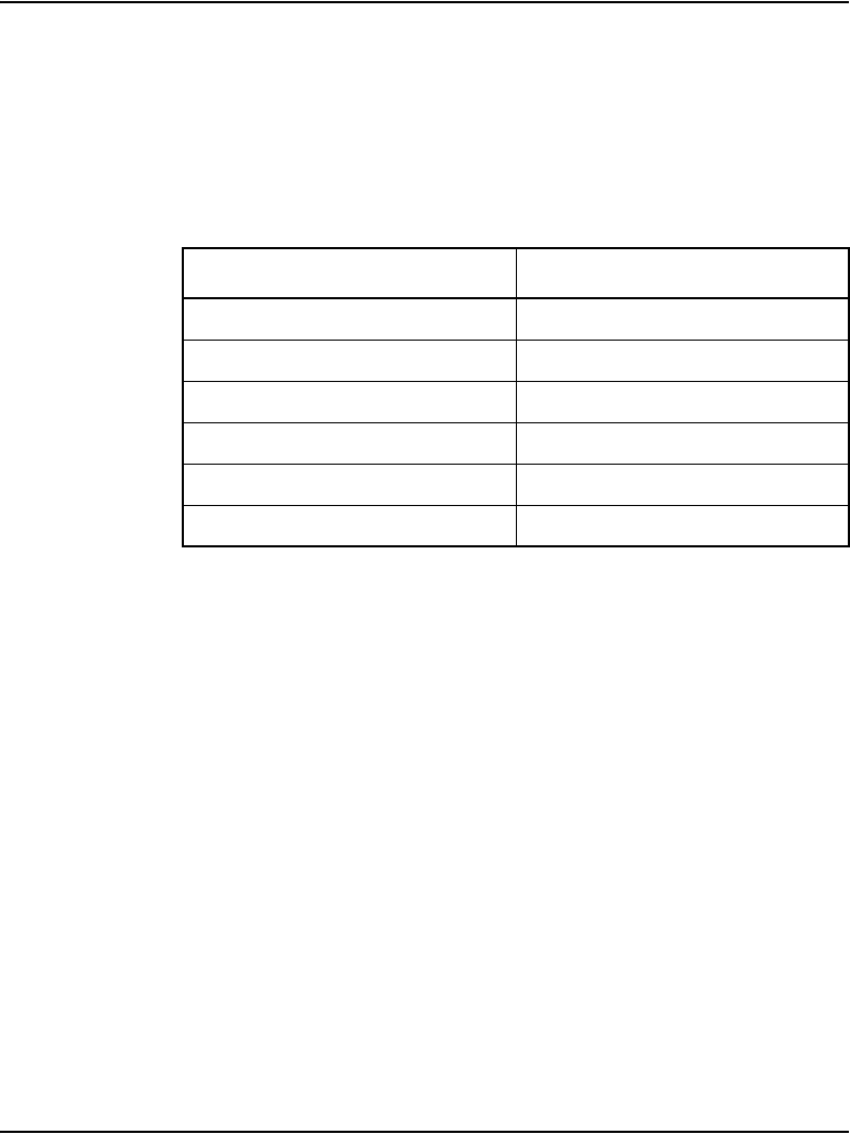
Table 1
Meridian 1 systems to CS 1000M systems
This Meridian 1 system... Maps to this CS 1000M system
Meridian 1 PBX 11C Chassis CS 1000M Chassis
Meridian 1 PBX 11C Cabinet CS 1000M Cabinet
Meridian 1 PBX 51C CS 1000M Half Group
Meridian 1 PBX 61C CS 1000M Single Group
Meridian 1 PBX 81 CS 1000M Multi Group
Meridian 1 PBX 81C CS 1000M Multi Group

Page 24 of 906 About this document
553-3001-211 Standard 3.00 August 2005
Conventions
Terminology
In this document, the following systems are referred to generically as
“system”:
• Communication Server 1000S (CS 1000S)
• Communication Server 1000M (CS 1000M)
• Communication Server 1000E (CS 1000E)
•Meridian1
The following systems are referred to generically as “Small System”:
• Communication Server 1000M Chassis (CS 1000M Chassis)
• Communication Server 1000M Cabinet (CS 1000M Cabinet)
• Meridian 1 PBX 11C Chassis
• Meridian 1 PBX 11C Cabinet
The following systems are referred to generically as “Large System”:
• Communication Server 1000M Half Group (CS 1000M HG)
• Communication Server 1000M Single Group (CS 1000M SG)
• Communication Server 1000M Multi Group (CS 1000M MG)
• Meridian 1 PBX 51C
• Meridian 1 PBX 61C
•Meridian1 PBX81
• Meridian 1 PBX 81C

About this document Page 25 of 906
Circuit Card Description and Installation
Related information
This section lists information sources that relate to this document.
NTPs
The following NTPs are referenced in this document:
•Meridian Link ISDN/AP General Guide (553-2901-100)
•Spares Planning (553-3001-153)
•Equipment Identification (553-3001-154)
•Transmission Parameters (553-3001-182)
•System Management (553-3001-300)
•Features and Services (553-3001-306)
•Software Input/Output: Administration (553-3001-311)
•Telephones and Consoles: Description, Installation, and Operation
(553-3001-367)
•Software Input/Output: System Messages (553-3001-411)
•Software Input/Output: Maintenance (553-3001-511)
•Communication Server 1000M and Meridian 1: Large System Planning
and Engineering (553-3021-120)
•Communication Server 1000M and Meridian 1: Large System
Installation and Configuration (553-3021-210)
•Communication Server 1000M and Meridian 1: Large System
Maintenance (553-3021-500)
•Communication Server 1000S: Installation and Configuration
(553-3031-210)
•Meridian Link description (553-3201-110)
Online
To access Nortel documentation online, click the Technical Documentation
link under Support & Training on the Nortel home page:
www.nortel.com


Page 27 of 906
Circuit Card Description and Installation
78
Overview
Contents
This section contains information on the following topics:
Line cards . . . . . . . . . . . . . . . . . . . . . . . . . . . . . . . . . . . . . . . . . . . . . . . 28
Installation . . . . . . . . . . . . . . . . . . . . . . . . . . . . . . . . . . . . . . . . . . . . 30
Operation . . . . . . . . . . . . . . . . . . . . . . . . . . . . . . . . . . . . . . . . . . . . . 31
Analog line interface units . . . . . . . . . . . . . . . . . . . . . . . . . . . . . . . . 37
Digital line interface units . . . . . . . . . . . . . . . . . . . . . . . . . . . . . . . . 40
Analog line call operation . . . . . . . . . . . . . . . . . . . . . . . . . . . . . . . . 42
Digital line call operation . . . . . . . . . . . . . . . . . . . . . . . . . . . . . . . . . 46
Lineside T1 call operation . . . . . . . . . . . . . . . . . . . . . . . . . . . . . . . . 46
Voice frequency audio level. . . . . . . . . . . . . . . . . . . . . . . . . . . . . . . 57
Off-premise line protection . . . . . . . . . . . . . . . . . . . . . . . . . . . . . . . 57
Line protectors . . . . . . . . . . . . . . . . . . . . . . . . . . . . . . . . . . . . . . . . . 57
Line protection grounding . . . . . . . . . . . . . . . . . . . . . . . . . . . . . . . . 58
Line and telephone components . . . . . . . . . . . . . . . . . . . . . . . . . . . . 59
Trunk cards . . . . . . . . . . . . . . . . . . . . . . . . . . . . . . . . . . . . . . . . . . . . . . 59
Host interface bus. . . . . . . . . . . . . . . . . . . . . . . . . . . . . . . . . . . . . . . 63
Trunk interface unit . . . . . . . . . . . . . . . . . . . . . . . . . . . . . . . . . . . . . 69
Serial Data Interface (SDI) cards . . . . . . . . . . . . . . . . . . . . . . . . . . . . . 72
Uses . . . . . . . . . . . . . . . . . . . . . . . . . . . . . . . . . . . . . . . . . . . . . . . . . 73
Features. . . . . . . . . . . . . . . . . . . . . . . . . . . . . . . . . . . . . . . . . . . . . . . 73
Specifications . . . . . . . . . . . . . . . . . . . . . . . . . . . . . . . . . . . . . . . . . . 74
Installation . . . . . . . . . . . . . . . . . . . . . . . . . . . . . . . . . . . . . . . . . . . . 76
Maintenance . . . . . . . . . . . . . . . . . . . . . . . . . . . . . . . . . . . . . . . . . . . 76

Page 28 of 906 Overview
553-3001-211 Standard 3.00 August 2005
Line cards
The following line cards are designed using the Intelligent Peripheral
Equipment (IPE) architecture and are recommended for use in all new system
designs.
Each of the line cards was designed to fit a specific system need. Table 2 lists
the line card characteristics.
Table 2
Line card characteristics
Part
Number Description Lines
Line
Type
Message
Waiting
Super-
vised
Analog
Lines Architecture
NT1R20 Off-premise station
analog line card
8Analog Interrupted dial
tone
Yes IPE
NT5D11 Lineside T1 Interface
card
24 T1 None Yes IPE
NT5D33/34 Lineside E1 Interface
card
30 E1 None Yes IPE
NT8D02 Digital Line card
(16 voice/16 data)
16 Digital Message waiting
signal forwarded
to digital phone
for display
No IPE
NT8D09 Analog Message
Waiting Line card
16 Analog Lamp No IPE

Overview Page 29 of 906
Circuit Card Description and Installation
NT1R20 Off-Premise Station Analog Line card
The NT1R20 Off-Premise Station (OPS) Analog Line card is an intelligent
eight-channel analog line card designed to be used with 2-wire analog
terminal equipment such as analog (500/2500-type) telephones and analog
modems. Each line has integral hazardous and surge voltage protection to
protect the system from damage due to lightning strikes and accidental power
line connections. This card is normally used whenever the phone lines have
to leave the building in which the switch is installed. The OPS line card
supports message waiting notification by interrupting the dial tone when the
receiver is first picked up. It also provides battery reversal answer and
disconnect analog line supervision and hook flash disconnect analog line
supervision features.
NT5D11 lineside T1 interface card
The NT5D11 lineside T1 Interface card is an intelligent 24-channel digital
line card that is used to connect the switch to T1 compatible terminal
equipment on the lineside. T1 compatible terminal equipment includes voice
mail systems, channel banks containing FXS cards, and key systems such as
the Nortel Norstar. The lineside T1 card differs from trunk T1 cards in that it
supports terminal equipment features such as hook-flash, transfer, hold, and
conference. It emulates an analog line card to the system software.
NT5D33 and NT5D34 Lineside E1 Interface card
The NT5D33/34 Lineside E1 Interface card is an intelligent 30-channel
digital line card that is used to connect the switch to E1 compatible terminal
equipment on the lineside. E1 compatible terminal equipment includes voice
mail systems. The lineside E1 card emulates an analog line card to the system
software.
NT8D02 digital line card
The NT8D02 Digital Line card is an intelligent 16-channel digital line card
that provides voice and data communication links between a CS 1000S,
CS 1000M, and Meridian 1 switch and modular digital telephones. Each of
the 16 channels support voice-only or simultaneous voice and data service
over a single twisted pair of standard telephone wire.
Page 30 of 906 Overview
553-3001-211 Standard 3.00 August 2005
NT8D09 analog message waiting line card
The NT8D09 Analog Message Waiting Line card is an intelligent 16-channel
analog line card designed to be used with 2-wire terminal equipment such as
analog (500/2500-type) telephones, modems, and key systems. This card can
also provide a high-voltage, low-current signal on the Tip and Ring pair of
each line to light the message waiting lamp on phones equipped with that
feature.
Installation
This section provides a high-level description of how to install and test line
cards.
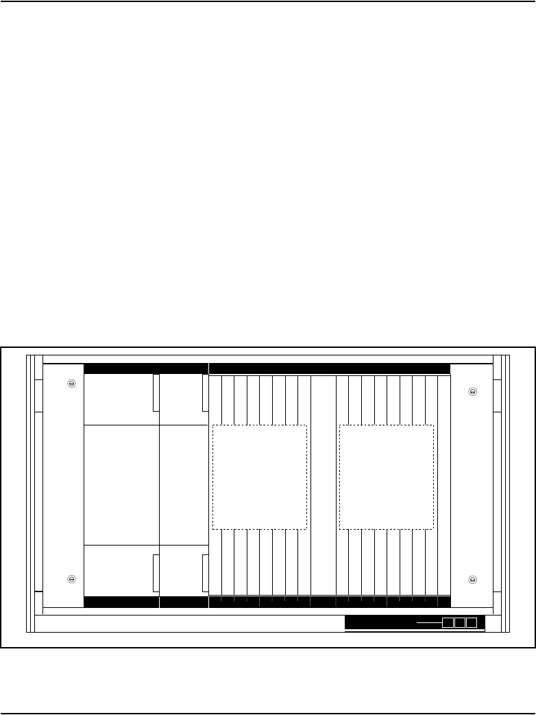
IPE line cards can be installed in any slot of the NT8D37 IPE module.
Figure 1 shows where an IPE line card can be installed in an NT8D37 IPE
module.
Figure 1
IPE line cards shown installed in an NT8D37 IPE module
Intelligent
Peripheral Equipment
Superloop
Shelf
IPEPE Module
PE Pwr Sup Rng Gen
Intelligent line cards
Intelligent trunk cards
BRSC
Intelligent line cards
Intelligent trunk cards
BRSC
NT8D01 Controller Card
553-3092
0 2 3 4 5 6 7 Cont 9 11 12 13 15181410

Overview Page 31 of 906
Circuit Card Description and Installation
When installing line cards, follow these general procedures:
• Configure the jumpers and switches on the line card (if any) to meet
system needs.
• Install the line card into the selected slot.
• Install the cable that connects the backplane connector on the IPE
module to the module I/O panel.
• Connect a 25-pair cable from the module I/O panel connector to the Main
Distribution Frame (MDF).
• Connect the line card output to the selected terminal equipment at the
MDF.
• Configure the individual line interface unit using the Analog (500/
2500-type) Telephone Administration program LD 10 for analog line
interface units and Multi-line Telephone Administration program LD 11
for digital line interface units.
Once these steps have been completed, the terminal equipment is ready
for use.
Operation
This section describes how line cards fit into the CS 1000S, CS 1000M, and
Meridian 1 architecture, the busses that carry signals to and from the line
cards, and how they connect to terminal equipment. These differences are
summarized in Table 3 on page 32.
Host interface bus
Cards based on the IPE bus have a built-in microcontroller. The IPE
microcontroller is used to do the following:
• perform local diagnostics (self-test)

Page 32 of 906 Overview
553-3001-211 Standard 3.00 August 2005
• configure the card according to instructions issued by the system
• report back to the system information such as card identification (type,
vintage, and serial number), firmware version, and programmed
configuration status)
Intelligent Peripheral Equipment
IPE line cards all have a similar architecture. Figure 2 on page 34 shows a
typical IPE line card architecture. The various line cards differ only in the
number and types of line interface units.
The switch communicates with IPE modules over two separate interfaces.
Voice and signaling data are sent and received over DS-30X loops, and
maintenance data is sent over a separate asynchronous communication link
called the card LAN link.
Signaling data is information directly related to the operation of the telephone
line. Some examples of signaling commands include:
• off-hook/on-hook
Table 3
IPE module architecture
Parameter IPE
Card Dimensions 31.75 x 25.4 x 2.2 cm.
(12.5 x10.0 x 0.875 in.)
Network Interface DS-30X Loops
Communication Interface card LAN Link
Microcontroller 8031 / 8051 Family
Peripheral
Interface card
NT8D01 Controller card
Network Interface card NT8D04 Superloop Network card
Modules NT8D37 IPE module

Overview Page 33 of 906
Circuit Card Description and Installation
• ringing signal on/off
• message waiting lamp on/off
Maintenance data is data relating to the configuration and operation of the
IPE card, and is carried on the card LAN link. Some examples of maintenance
data include:
• polling
• reporting of self-test status
• CP initiated card reset
• reporting of card ID (card type and hardware vintage)
• reporting of firmware version
• downloading line interface unit parameters
• reporting of line interface unit configuration
• enabling/disabling of the DS-30X network loop bus
• reporting of card status or T1 link status
Page 34 of 906 Overview
553-3001-211 Standard 3.00 August 2005
Figure 2
Typical IPE analog line card architecture
Input/output
interface
control
Codec
PCM
Micro-
controller
DS-30X
interface
5.12 MHz
clock
Tx PCM
Async card
LAN link
Front
panel
LED
Card LAN
interface
Tip
Ring
Codec
PCM
Line interface unit power
Rx PCM
1 kHz
frame sync
Card slot
address
Back-
plane
Con-
troller
card Line
signaling
interface
Control
logic
Signaling
and status
Control
Address/
data bus
553-6150
Power supplies
Analog or digital telephone linesAnalog or digital telephone lines
Tip
Ring
Line
Interface
Unit
Line
Interface
Unit

Overview Page 35 of 906
Circuit Card Description and Installation
DS-30X loops
The line interfaces provided by the line cards connect to conventional 2-wire
(tip and ring) line facilities. IPE analog line cards convert the incoming
analog voice and signaling information to digital form and route it to the Call
Server over DS-30X network loops. Conversely, digital voice and signaling
information from the Call Server is sent over DS-30X network loops to the
analog line cards where it is converted to analog form and applied to the line
facility.
IPE digital line cards receive the data from the digital phone terminal as
512 kHz Time Compressed Multiplexed (TCM) data. The digital line card
converts that data to a format compatible with the DS-30X loop and transmits
it in the next available timeslot. When a word is received from the DS-30X
loop, the digital line card converts it to the TCM format and transmits it to the
digital phone terminal over the digital line facility.
A separate dedicated DS-30X network loop is extended between each IPE
line/trunk card and the controller cards within an IPE module. A DS-30X
network loop is composed of two synchronous serial data buses. One bus
transports in the Transmit (Tx) direction towards the line facility and the other
in the Receive (Rx) direction towards the CS 1000S, CS 1000M, and
Meridian 1.
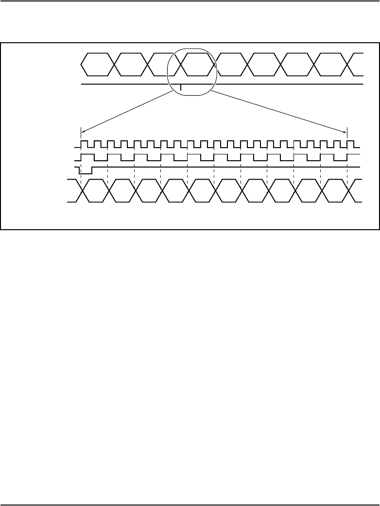
Each bus has 32 channels for Pulse Code Modulated (PCM) voice data. Each
channel consists of a 10-bit word. See Figure 3 on page 36. Eight of the 10
bits are for PCM data, one bit is the call signaling bit, and the last bit is a data
valid bit. The eight-bit PCM portion of a channel is called a timeslot. The
DS-30X loop is clocked at 2.56 Mbps (one-half the 5.12 MHz clock
frequency supplied by the controller card). Thus, the timeslot repetition rate
for a single channel is 8 kHz. The controller card also supplies a locally
generated 1 kHz frame sync signal for channel synchronization.
Signaling data is transmitted to and from the line cards using the call signaling
bit within the 10-bit channel. When the line card detects a condition that the
switch needs to know about, it creates a 24-bit signaling word. This word is
shifted out on the signaling bit for the associated channel one bit at a time
during 24 successive DS-30X frames. Conversely, when the switch sends
signaling data to the line card, it is sent as a 24-bit word divided among 24
successive DS-30X frames.
Page 36 of 906 Overview
553-3001-211 Standard 3.00 August 2005
DS-30Y network loops extend between controller cards and superloop
network cards in the Common Equipment (CE). They function in a manner
similar to DS-30X loops. See Figure 5 on page 41.
A DS-30Y loop carries the PCM timeslot traffic of a DS-30X loop. Four
DS-30Y network loops form a superloop with a capacity of 128 channels (120
usable timeslots). See Communication Server 1000M and Meridian 1:
Large System Planning and Engineering (553-3021-120) for more
information on superloops.
Card LAN link
Maintenance communication is the exchange of control and status data
between IPE line or trunk cards and the Call Server by way of the NT8D01
Controller card. Maintenance data is transported through the card LAN link.
This link is composed of two asynchronous serial buses (called the Async
card LAN link in Figure 2 on page 34). The output bus is used by the system
controller for output of control data to the line card. The input bus is used by
the system controller for input of line card status data.
Figure 3
DS-30X loop data format
29
W0B7W31DV
DS-30X loop
data words
Frame
sync
Frame sync
DS-30X loop
data bits
5.12 MHz
2.56 MHz
SB = SIGNALING BIT DV = DATA VALID
30 31 01234
W0B6 W0B5 W0B4 W0B3 W0B2 W0B1 W0B0 W0SB W0DV W1B7
553-6151

Overview Page 37 of 906
Circuit Card Description and Installation
A card LAN link bus is common to all of the line/trunk card slots within an
IPE module. This bus is arranged in a master/slave configuration where the
controller card is the master and all other cards are slaves. The module
backplane provides each line/trunk card slot with a unique hardwired slot
address. This slot address enables a slave card to respond when addressed by
the controller card. The controller card communicates with only one slave at
a time.
In normal operation, the controller card continually scans (polls) all of the
slave cards connected to the card LAN to monitor their presence and
operational status. The slave card sends replies to the controller on the input
bus along with its card slot address for identification. In its reply, the slave
informs the controller if any change in card status has taken place. The
controller can then prompt the slave for specific information. Slaves only
respond when prompted by the controller; they do not initiate exchange of
control or status data on their own.
When an IPE line card is first plugged into the backplane, it runs a self-test.
When the self-test is completed, a properly functioning card responds to the
next controller card poll with the self-test status. The controller then queries
for card identification and other status information. The controller then
downloads all applicable configuration data to the line card, initializes it, and
puts it into an operational mode.
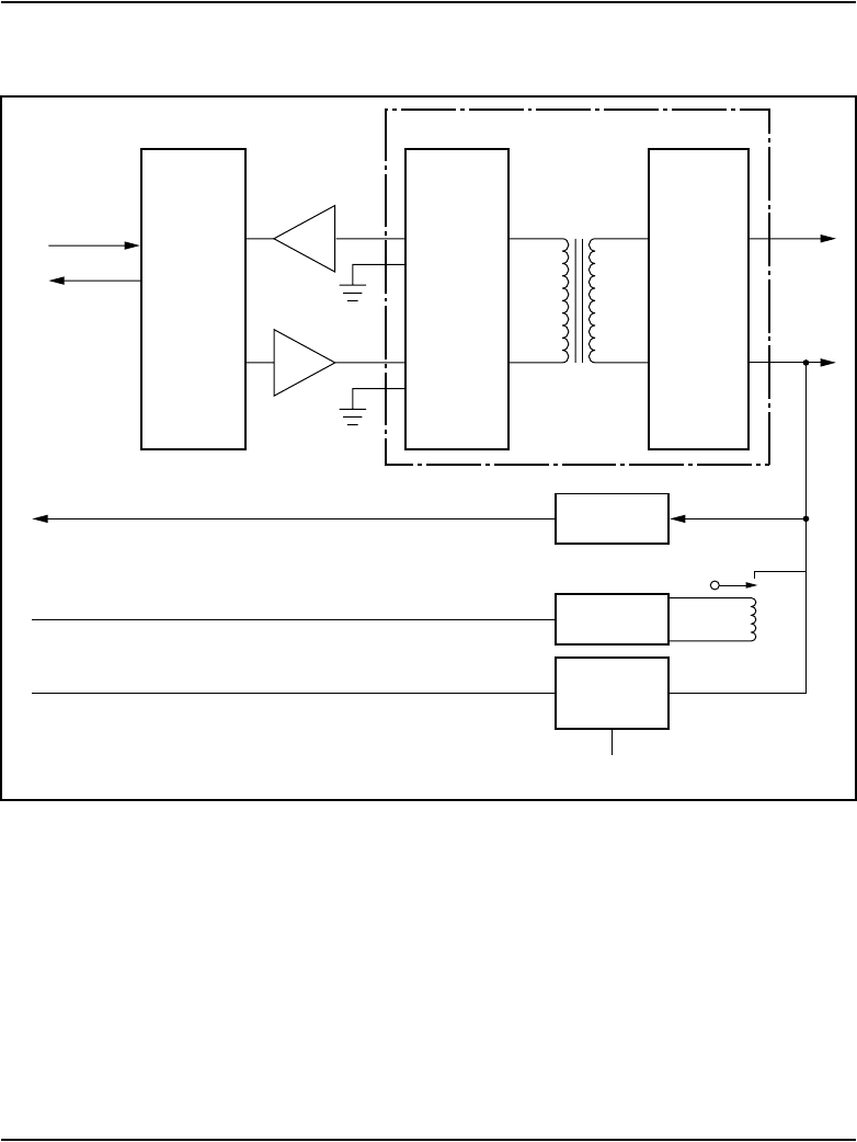
Analog line interface units
Once the 8-bit digital voice signal has been received by the analog line card,
it must be converted back into an analog signal, filtered, converted from a
4-wire transmission path to a 2-wire transmission path, and driven onto the
analog telephone line.
Figure 4 on page 38 shows a typical example of the logic that performs these
functions. Each part of the analog line interface unit is discussed in the
following section.
Page 38 of 906 Overview
553-3001-211 Standard 3.00 August 2005
Figure 4
Typical analog line interface unit block diagram
CODEC
2-wire
to
4-wire
conversion
Line
interface
and
protection
Message
waiting
Variable gain
filters Impedance
matching
transformer
Balancing Network
Tip
Ring
DS-30X or
SL-1 network
loop
Message
waiting
circuit
–150V dc
553-6153
Message
waiting
Ringing
circuit
Ring voltage
Ringing
Off-hook
detector
Off-hook
Tx PCM
Rx PCM

Overview Page 39 of 906
Circuit Card Description and Installation
Coder/Decoder circuit
The Coder/Decoder (CODEC) performs Analog to Digital (A/D) and Digital
to Analog (D/A) conversion of the line analog voiceband signal to and from
a digital PCM signal. This signal can be coded and decoded using either the
A-Law or the µ-Law companding algorithm.
On some analog line cards, the decoding algorithm depends of the type of
CODEC installed when the board is built. On others, it is an option selected
using a software overlay.
Variable gain filters
Audio signals received from the analog phone line are passed through a
low-pass A/D monolithic filter that limits the frequency spread of the input
signal to a nominal 200 to 3400 Hz bandwidth. The audio signal is then
applied to the input of the CODEC. Audio signals coming from the CODEC
are passed through a low-pass A/D monolithic filter that integrates the
amplitude modulated pulses coming from the CODEC, and then filters and
amplifies the result. On some of the line cards, the gain of these filters can be
programmed by the system controller. This allows the system to make up for
line losses according to the loss plan.
Balancing network
Depending on the card type, the balancing network provides a 600 ¾, 900 ¾,
3COM or 3CM2 impedance matching network. It also converts the 2-wire
transmission path (tip and ring) to a 4-wire transmission path (Rx/ground and
Tx/ground). The balancing network is usually a transformer/analog (hybrid)
circuit combination, but can also be a monolithic Subscriber Line Interface
Circuit (SLIC) on the newer line cards.
Line interface and foreign voltage protection
The line interface unit connects the balancing network to the telephone tip
and ring pairs. The off-premise line card (NT1R20) has circuitry that protects
the line card from foreign voltage surges caused by accidental power line
connections and lightning surges. This protection is necessary if the
telephone line leaves the building where the switch is installed.
The line interface unit has a relay that applies the ringing voltage onto the
phone line. See Figure 4 on page 38. The RSYNC signal from the 20 Hz

Page 40 of 906 Overview
553-3001-211 Standard 3.00 August 2005
(nominal) ringing voltage power supply is used to prevent switching of the
relay during the current peak. This eliminates switching glitches and extends
the life of the switching relay.
The off-hook detection circuit monitors the current draw on the phone line.
When the current draw exceeds a preset value, the circuit generates an
off-hook signal that is transmitted back to the system controller.
The message waiting circuit on message waiting line cards monitors the status
of the message waiting signal and applies –150 V dc power to the tip lead
when activated. This voltage is used to light the message waiting lamps on
phones that are equipped with that feature. The high voltage supply is
automatically disconnected when the phone goes off-hook. Newer line cards
can sense when the message waiting lamp is not working and can report that
information back to the system controller.
Digital line interface units
The NT8D02 digital line card provides voice and data communication links
between a switch and modular digital telephones. These lines carry
multiplexed PCM voice, data and signaling information as Time
Compression Multiplexed (TCM) loops. Each TCM loop can be connected to
a Nortel “Meridian Modular Digital” telephone.
The digital line interface card contains one or more digital line interface units.
See Figure 5 on page 41. Each digital line interface unit contains a Digital
Line Interface Circuit (DLIC). The purpose of each DLIC is to demultiplex
data from the DS-30X Tx channel into integrated voice and data bitstreams
and transmit those bitstreams as Bi-Polar Return to Zero, Alternate Mark
Inversion (BPRZ-AMI) data to the TCM loop. It also does the opposite:
receives BPRZ-AMI bitstreams from the TCM loop and multiplexes the
integrated voice and data bitstream onto the DS-30X Rx channel.
The 4-wire to 2-wire conversion circuit converts the 2-wire tip and ring leads
into a 4-wire (Tx and ground and RX and ground) signal that is compatible
with the digital line interface circuit.
TCM loop interfaces
Each digital phone line terminates on the digital line card at a TCM loop
interface circuit. The circuit provides transformer coupling and foreign
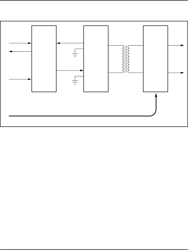
Overview Page 41 of 906
Circuit Card Description and Installation
voltage protection between the TCM loop and the digital line interface circuit.
It also provides power for the digital telephone.
To prevent undesirable side effects from occurring when the TCM loop
interface cannot provide the proper signals on the digital phone line, the
system controller can remove the ±15 V dc power supply from the TCM loop
interface. This happens when either the card gets a command from the
NT8D01 Controller card to shut down the channel, or when the digital line
card detects a loss of the 1 KHz frame synchronization signal.
Each TCM loop interface circuit can service loops up to 3500 ft. in length
when using 24 gauge wire. The circuit allows for a maximum ac signal loss
of 15.5 dB at 256 KHz and a maximum DC loop resistance of 210 ohms.
Signaling
The digital line interface units also contain signaling and control circuits that
establish, monitor, and take down call connections. These circuits work with
Figure 5
Digital line interface unit block diagram
4-wire
to
2-wire
conversion
Digital
line
interface
circuit
TCM loop
interface
and
protection
Tip
Ring
DS-30X loop
Tx PCM
1 kHz frame
sync
Rx PCM
553-6154
±15 V dc power supply

Page 42 of 906 Overview
553-3001-211 Standard 3.00 August 2005
the system controller to operate the digital line interface circuits during calls.
The circuits receive outgoing call signaling messages from the controller and
return incoming call status information to the controller over the DS-30X
network loop.
Analog line call operation
The applications, features, and signalling arrangements for each line interface
unit are configured in software and implemented on the card through software
download messages. When an analog line interface unit is idle, it provides a
voltage near ground on the tip lead and a voltage near –48 V dc on the ring
lead to the near-end station. (The near-end station is the telephone or device
that is connected to the analog line card by the tip and ring leads.) An on-hook
telephone presents a high impedance toward the line interface unit on the
card.
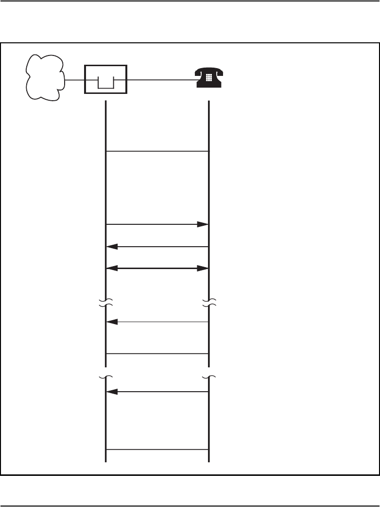
Incoming calls
Incoming calls to a telephone that is connected to an analog line card can
originate either from stations that are local (served by the PBX), or remote
(served through the Public Switched Telephone Network (PSTN)). The
alerting signal to a telephone is 20 Hz (nominal) ringing. When an incoming
call is answered by the near-end station going off-hook, a low-resistance dc
loop is placed across the tip and ring leads (towards the analog line card) and
ringing is tripped. See Figure 6 on page 43.
Outgoing calls
For outgoing calls from the near-end station, a line interface unit is seized
when the station goes off-hook, placing a low-resistance loop across the tip
and ring leads towards the analog line card. See Figure 7 on page 44. When
the card detects the low-resistance loop, it prepares to receive digits. When
the system is ready to receive digits, it returns dial tone. Outward address
signaling is then applied from the near-end station in the form of loop
(interrupting) dial pulses or DTMF tones.
Overview Page 43 of 906
Circuit Card Description and Installation
Figure 6
Call connection sequence – near-end station receiving call
553-AAA1113
High-
resistance
loop
Line card unit idle
(2-way voice
connection)
Remarks
Ground on tip/
battery on ring
Signal/directionState
System
Ground on tip/
battery on ring
High-resistance loop
Ground on tip/
battery on ring
Far-end station
on hook
Near-end station
on hook
If near-end station hangs up first, the
following occurs: Line card detects drop
in loop current. CPU removes timeslot
assignments.
If far-end station hangs up first, the
following occurs: The system detects
disconnect signaling from trunk. CPU
removes timeslot assignments. Person
at near-end station recognizes end of
call and hangs up.
No battery current drawn.
Far-end station goes off hook and
addresses (dials up) near-end station.
The system receives the incoming
call on a trunk and determines that the
call is for a specific unit terminal number
(TN) and assigns message timeslots.
The system applies 20 Hz ringing to
ring lead.
Ringing
Low-resistance loop
Near-end station
off hook Near-end station goes off hook.
Near-end
station
The system detects increase in loop
current, trips ringing, and cuts call
through to near-end station.
Line card unit is ready for the next call.
High-
resistance
loop
Line card unit is ready for the next call.
High-
resistance
loop
Line card unit idle
Line card unit idle
High-resistance loop
Far-end
station
through
PSTN
Alert
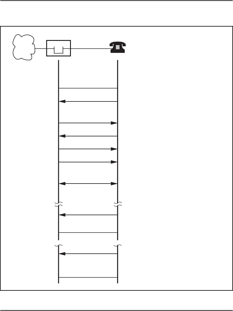
Page 44 of 906 Overview
553-3001-211 Standard 3.00 August 2005
Figure 7
Call connection sequence – near-end originating call
553-AAA1114
High-
resistance
loop
Line card unit idle
(2-way voice
connection)
Remarks
Ground on tip/
battery on ring
Signal/directionState
System
Ground on tip/
battery on ring
High-resistance loop
Ground on tip/
battery on ring
Far-end station
on hook
Near-end station
on hook If near-end station hangs up first, the following
occurs: Line card detects drop in loop current.
CPU removes timeslot assignments.
If far-end station hangs up first, the following
occurs: The system detects disconnect signaling
from trunk. CPU removes timeslot assignments.
Person at near-end station recognizes end of
call and hangs up.
No battery current drawn.
Near-end station goes off hook. Battery current
is drawn causing detection of off-hook state.
CPU determines unit terminal number (TN) and
assigns message timeslots.
Low-resistance loop
Dial tone is applied to the near-end station from
the system.
Call request
Dial tone
Addressing signals
Outpulsing Near-end station dials number (loop pulsing or
DTMF tones).
Near-end
station
Dial tone The system detects start of dialing and
removes dial tone.
Ringback (or busy) The system decodes addressing, routes call, and
supplies ringback tone to near-end station if far-
end station is on hook. (Busy tone supplied if
far-end station is busy.)
When call is answered, ringback tone is
removed , and call is cut through to far-end
station.
Line card unit is ready for the next call.
High-
resistance
loop
Line card unit is ready for the next call.
High-
resistance
loop
Line card unit idle
Line card unit idle
High-resistance loop
Far-end
station
through
PSTN

Overview Page 45 of 906
Circuit Card Description and Installation
Message waiting
Line cards that are equipped with the message waiting feature receive
notification that a message is waiting across the Card LAN link (IPE cards).
On cards that drive a message waiting light, the light is turned on by
connecting the ring side of the telephone line to the –150 V dc power supply.
When the line card senses that the telephone has gone off-hook, it removes
the –150 V dc voltage until the telephone goes back on-hook. Line cards that
use an interrupted dial tone to indicate message waiting do nothing until the
receiver is picked up. The line card then interrupts the dial tone at a regular
interval to indicate that a message is waiting.
In both cases, the message waiting indication will continue until the user
checks his or her messages. At that time, the system will cancel the message
waiting indication by sending another message across the Card LAN link or
network loop.
Analog line supervision
Analog line supervision features are used to extend the answer supervision
and disconnect supervision signals when the line card is connected to an
intelligent terminal device (Key system or intelligent pay phone). Two types
of analog line supervision are provided:
• battery reversal answer and disconnect supervision
• hook flash disconnect supervision
Battery reversal answer and disconnect supervision
Battery reversal answer and disconnect supervision is only used for calls that
originate from the terminal device. It provides both far-end answer
supervision and far-end disconnect supervision signals to the terminal device.
In an intelligent pay phone application, these signals provide the information
necessary to accurately compute toll charges.
In the idle state, and during dialing and ringing at the far end, the line card
provides a ground signal on the tip lead and battery on the ring lead. See
Figure 8 on page 47. When the far-end answers, these polarities are reversed.
The reversed battery connection is maintained as long as the call is
established. When the far-end disconnects, the system sends a message that

Page 46 of 906 Overview
553-3001-211 Standard 3.00 August 2005
causes the line card to revert the battery and ground signals to the normal state
to signal that the call is complete.
Hook Flash disconnect supervision
Hook flash disconnect supervision is only used for incoming calls that
terminate at the terminal device (typically a Key system). See Figure 9 on
page 48. The disconnect signal is indicated by the removal of the ground
connection to the tip lead for a specific length of time. The length of time is
programmed in LD10, and ranges from a minimum of 10 milliseconds to a
maximum of 2.55 seconds. See Software Input/Output: Administration
(553-3001-311) for more information.
Digital line call operation
Digital line call operation is controlled entirely by use of messages between
the digital telephone and the system. These messages are carried across the
TCM loop interface. There is no call connection sequence similar to the one
used for analog telephone line operation.
Lineside T1 call operation
The lineside T1 card’s call operation is performed differently depending on
whether the T1 link is configured to process calls in loop start mode or ground
start mode. Configuration is performed through dip switch settings on the
lineside T1 card.
The lineside T1 card performs calls processing separately on each of its 24
channels. Signaling is performed using the “A/B robbed bit” signaling
standard for T1 communication.
A/B robbed bit signaling simulates standard analog signaling by sending a
meaningful combination of ones and zeros across the line that correlates to
the electrical impulses that standard analog signaling sends. For example, to
represent that an analog line interface unit is idle, the analog line card
provides a ground on the tip lead and –48Vdc on the ring lead. The lineside
T1 card accomplishes the same result by sending its A bit as 0 (translated as
ground on the tip lead) and its B bit as 1 (translated as –48V dc on the ring
lead). However, measuring the voltage of the ring lead on the T1 line would
not return –48V dc, since actual electrical impulses are not being sent.
Overview Page 47 of 906
Circuit Card Description and Installation
Figure 8
Battery reversal answer and disconnect supervision sequence
System
High-
resistance
loop
Line card unit idle
(2-way voice
connection)
Remarks
Ground on tip/
battery on ring
Signal/directionState
Ground on tip/
battery on ring
High-
resistance
loop
Ground on tip/
battery on ring
Far-end station
on hook
Near-end station
on hook If near-end station hangs up first, a high-resistance loop is
presented to the system.
If far-end station hangs up first, the system detects
disconnect signalling from the far end, removes timeslot
assignments, and restores normal ground/battery polarity
to the near-end station.
No battery current drawn.
Near-end station goes off hook. Battery current is drawn
causing detection of off-hook state. The system
determines unit terminal number (TN) and assigns
message timeslots.
Low-resistance loop
Dial tone is applied to the near-end station from the
system.
Call request
Dial tone
Addressing signals
Outpulsing Near-end station dials number (loop pulsing or DTMF
tones).
Dial tone removed The system detects start of dialing and removes dial tone.
Ringback (or busy) The system decodes addressing, routes call, and supplies
ringback tone to near-end station if far-end station is on
hook. (Busy tone supplied if far-end station is busy.)
When call is answered (either absolute or assumed
answer, as programmed), ringback tone is removed, call
is cut through to far-end station, and battery is reversed
to near-end station for duration of call.
The system detects drop in loop current, removes timeslot
assignments, sends disconnect signal to far-end station,
and restores normal ground/battery polarity to the near-
end station. Line card unit is then ready for the next call.
High-
resistance
loop
Near-end station detects battery reversal and goes on
hook. Line card unit is then ready for the next call.
High-
resistance
loop
Line card unit idle
Line card unit idle
Low-
resistance
loop
Line
card Near-end
station
Far-end
station
Battery on tip/
ground on ring
Low-
resistance
loop
Battery on tip/
ground on ring
Ground on tip/
battery on ring
Note 1:
Battery reversal signalling is a supervisory feature that is only used when the near-end station
originates the call. 553-AAA1115
Page 48 of 906 Overview
553-3001-211 Standard 3.00 August 2005
Figure 9
Hook flash disconnect supervision sequence
High-
resistance
loop
Line card unit idle
(2-way voice
connection)
Remarks
Ground on tip/
battery on ring
Signal/directionState
System
No battery current drawn.
Far-end station goes off hook and addresses
(dials up) near-end station. The system
receives the incoming call and determines that
the call is for a specific unit terminal number
(TN) and assigns message timeslots.
The system applies 20 Hz ringing to the ring
lead.
Ringing
Low-resistance loop
Near-end station
off hook Near-end station goes off hook.
The system detects increase in loop current,
trips ringing, and cuts call through to near-end
station.
Alert
Call request
Line
card
Low-
resistance
loop
Far-end station
on hook
When the far-end station hangs up, the
following happens: The system detects
disconnect signalling from the far end, removes
the timeslot assignments, and sends a hook
flash (tip removed from ground) to the near-end
station.
Near-end
station on hook
Tip open/
battery on ring
Tip open/
battery on ring The near-end station responds by going on
hook, presenting a high-resistance loop to the
system.
High-
resistance
loop
Line card unit idle
Ground on tip/
battery on ring At the end of the hook-flash interval, the
system returns the tip to ground. The line
card unit is then ready for the next call. (Note 2)
High-
resistance
loop
Note 1:
Hook-flash signalling is a supervisory feature that is only used when the far-end station
originates and terminates the call. If the far-end station originates the call but the near-end
hangs up first, a hook flash is not sent.
Note 2:
If the end of the hook-flash interval occurs before the near-end station goes on hook, the
system waits until the near-end station does so before placing the line card unit in the
idle state. 553-AAA1116
Near-end
station
Far-end
station
Ground on tip/
battery on ring
Low-
resistance
loop

Overview Page 49 of 906
Circuit Card Description and Installation
Call operation will be described by categorizing the operation into the
following main states:
• Idle (on-hook)
• Incoming calls
• Outgoing calls
• Calls disconnected by the CO
• Calls disconnected by the telephone
Loop Start Mode
In Loop Start mode , the A and B bits have the following meaning:
Transmit from LTI:A bit = 0 (tip ground on)
B bit = Ringing (0=on, 1=off)
Receive to LTI: A bit = Loop (0=open, 1=closed)
B bit = 1 (no ring ground)
When a T1 channel is idle, the lineside T1 card simulates a ground on the tip
lead and –48Vdc on the ring lead to the terminal equipment by setting its
transmit A bit to 0 and transmit B bit to 1. Accordingly, an on-hook channel
on the terminal equipment simulates an open loop toward the lineside T1
card, causing the lineside T1 card’s receive bits to be set to A = 0 and receive
B = 1.
Incoming calls
Incoming calls to terminal equipment attached to the lineside T1 card can
originate either from stations that are local (served by the PBX), or remote
(served through the PSTN). To provide the ringing signal to a telephone the
lineside T1 card simulates an additional 90V on the ring lead to the terminal
equipment by alternating the transmit B bit between 0 and 1 (0 during ring on,
1 during ring off). When an incoming call is answered by the terminal
equipment going off-hook, the terminal equipment simulates tripping the
ringing and shutting off ringing, causing the lineside T1 card’s receive A bit
to be changed from 0 to 1.

Page 50 of 906 Overview
553-3001-211 Standard 3.00 August 2005
Outgoing calls
During outgoing calls from the terminal equipment, a channel is seized when
the station goes off-hook. This simulates a low-resistance loop across the tip
and ring leads toward the lineside T1 card, causing the lineside T1’s receive
A bit to be changed from 0 to 1. This bit change prepares the lineside T1 to
receive digits. Outward address signaling is then applied from the terminal
equipment in the form of DTMF tones or loop (interrupting) dial pulses that
are signaled by the receive A bit pulsing between 1 and 0.
Call disconnect from far end (PSTN, private network or local
Station)
When a call is in process, the central office may disconnect the call from the
CS 1000S, CS 1000M, and Meridian 1. If the lineside T1 port has been
configured with the supervised analog line (SAL) feature, the lineside T1 card
will respond to the distant end disconnect message by momentarily changing
its transmit A bit to 1 and then returning it to 0. The duration of time that the
transmit A bit remains at 1 before returning to 0 depends upon the setting that
was configured using the SAL. If the terminal equipment is capable of
detecting distant end disconnect, it will respond by changing the lineside T1
card's receive A bit to 0 (open loop).The call is now terminated and the
interface is in the idle (on-hook) state.
For the lineside T1 card to support distant end disconnect in loop start mode,
the following configuration parameters must exist:
• The Supervised Analog Line (SAL) feature must be configured for each
lineside T1 port.
Note: By default, the SAL feature opens the tip side for 750 m/s in loop
start operation. This is configurable in 10 m/s increments.
• For outgoing trunk calls, the trunk facility must provide far end
disconnect supervision.
• In order to detect distant end disconnect for calls originating on the
lineside T1 card, the battery reversal feature within the SAL software
must be enabled. Enabling the battery reversal feature will not provide
battery reversal indication but will only provide a momentary
interruption of the tip ground by asserting the A bit to 1 for the specified
duration.
Overview Page 51 of 906
Circuit Card Description and Installation
• In order to detect distant end disconnect for calls terminating on the
lineside T1 card, the hook flash feature within the SAL software must be
enabled.
• In order to detect distant end disconnect for calls originating and
terminating on the lineside T1 card, both the battery reversal and hook
flash features must be enabled within the SAL software.
Call disconnect from lineside T1 terminal equipment
Alternatively, while a call is in process, the terminal equipment may
disconnect by going on-hook. The terminal equipment detects no loop current
and sends signaling to the lineside T1 card that causes its receive A bit to
change from 1 to 0. The call is now released.
Table 4 outlines the lineside T1’s A and B bit settings in each state of call
processing.
Table 4
Loop Start Call Processing A/B Bit Settings (Part 1 of 2)
State
Transmit Receive
A B A B
Idle 0 1 0 1
Incoming Calls:
•Idle 0 1 0 1
• Ringing is applied from lineside T1 card 01/0 0 1
• Terminal equipment goes off-hook 01/0 1 1
• Lineside T1 card stops ringing 0 1 1 1
Outgoing Calls:
•Idle 0 1 0 1
• Terminal equipment goes off-hook 0 1 1 1
Call Disconnect from far end:
Page 52 of 906 Overview
553-3001-211 Standard 3.00 August 2005
Ground Start Mode
In ground start mode, the A and B bits have the following meaning:
Transmit from LTI:A bit = Tip ground (0=grounded, 1=not grounded)
B bit = Ringing (0=on, 1=off)
Receive to LTI: A bit = Loop (0=open, 1=closed)
B bit = Ring ground (0=grounded, 1=not grounded)
When a T1 channel is idle, the lineside T1 card simulates a ground on the tip
lead and -48V dc on the ring lead to the terminal equipment by setting the
transmit A bit to 1 and transmit B bit to 1. Accordingly, an on-hook telephone
simulates an open loop toward the lineside T1 card, causing the lineside T1
card’s receive bits to be set to A = 0 and B = 1.
• Steady state (call in progress) 0 1 1 1
• Far end disconnects by dropping loop current and lineside T1
card changes Transmit A bit to 1 momentarily.
1 1 1 1
• Terminal equipment responds causing Receive A bit to
change to 0.
1 1 0 1
• Lineside T1 responds by changing its Transmit A bit to 0. Call
is terminated and set to idle state.
0 1 0 1
Call disconnect from terminal equipment:
• Steady state (call in progress) 0 1 1 1
• Terminal equipment goes on-hook causing the Receive A bit
to change to 0. Call is terminated and set to idle state.
0 1 0 1
Table 4
Loop Start Call Processing A/B Bit Settings (Part 2 of 2)
State
Transmit Receive
A B A B

Overview Page 53 of 906
Circuit Card Description and Installation
Incoming Calls
Incoming calls to terminal equipment that is connected to the lineside T1 card
can originate either from stations that are local (served by the PBX), or
remote (served through the public switched telephone network). To provide
the ringing signal to the terminal equipment the lineside T1 card simulates the
90V ring signal on the ring lead by alternating the transmit B bit between 0
and 1 (0 during ring on, 1 during ring off), and ground on the tip lead by
setting the transmit A bit to 0. When an incoming call is answered (by the
terminal equipment going off-hook), the terminal equipment simulates
tripping the ringing and shutting off ringing by causing the lineside T1’s
receive A bit to change from 0 to 1. The lineside T1 card responds to this
message by simulating loop closure by holding the transmit B bit constant
at 1.
Outgoing Calls
During outgoing calls from the terminal equipment, a channel is seized when
the terminal equipment goes off-hook, simulating a ground to the ring lead
toward the lineside T1 card by causing the lineside T1’s receive B bit to
change from 1 to 0. In turn, the lineside T1 card simulates grounding its tip
lead by changing the transmit A bit to 0. The terminal equipment responds to
this message by removing the ring ground (lineside T1’s receive B bit is
changed to 1) and simulating open loop at the terminal equipment (lineside
T1’s receive A bit is changed to 0).
Call disconnect from far end (PSTN, private network or local
station
While a call is in process, the far end might disconnect the call. If the lineside
T1 port has been configured with the Supervised Analog Line (SAL) feature,
the lineside T1 will respond to the distant end disconnect message by opening
tip ground. This causes the lineside T1 card to change the transmit A bit to 1.
When the terminal equipment sees the transmit A bit go to 1, it responds by
simulating open loop causing the lineside T1’s receive A bit to change to 0.
The call is terminated and the interface is once again in the idle condition.
For the lineside T1 card to support distant end disconnect in ground start
mode, the following configuration parameters must exist:
• The Supervised Analog Line (SAL) feature must be configured for each
lineside T1 port.

Page 54 of 906 Overview
553-3001-211 Standard 3.00 August 2005
Note: By default, the SAL feature opens the tip side for 750 m/s in loop
start operation. This is configurable in 10 m/s increments.
• In order to detect distant end disconnect for calls originating on the
lineside T1 card, the “battery reversal” feature within the SAL software
must be enabled. Enabling the “battery reversal” feature will not provide
battery reversal indication when a call is answered; it will only provide
battery reversal indication when a call is disconnected.
• In order to detect distant end disconnect for calls terminating on the
lineside T1 card, the “hook flash” feature within the SAL software must
be enabled.
• In order to detect distant end disconnect for calls originating and
terminating on the lineside T1 card, both the “battery reversal” and “hook
flash” features within the SAL software must be enabled.
Call disconnect from lineside T1 terminal equipment
Alternatively, while a call is in process, the terminal equipment may
disconnect by going on-hook, causing the lineside T1’s receive A bit to
change to 0. The lineside T1 card responds to this message by simulating the
removal of ground from the tip by changing its transmit A bit to 1. The call is
now terminated and the interface is once again in the idle condition.
Table 5 outlines the lineside T1’s A and B bit settings in each state of call
processing.
Table 5
Ground Start Call Processing A/B Bit Settings (Part 1 of 2)
State
Transmit Receive
A B A B
Idle 1 1 0 1
Incoming Calls (to terminal equipment):
•Idle 1 1 0 1
• Ringing is applied from lineside T1 card by simulating ground
on tip lead and ringing on ring lead.
00/1 0 1

Overview Page 55 of 906
Circuit Card Description and Installation
Ground Start Restrictions
If the lineside T1 card is used in ground start mode, certain restrictions should
be considered. Because the system treats the lineside T1 card as a standard
loop start analog line card, the ground start operation of the lineside T1 card
has operational limitations compared to typical ground start interface
equipment relating to start of dialing, distant end disconnect and glare
potential.
• Terminal equipment goes off-hook by simulating ground on tip
lead and ringing on ring lead.
00/1 1 1
Outgoing Calls (from terminal equipment):
•Idle 1 1 0 1
• Terminal equipment goes off-hook. 1 1 0 0
• The lineside T1 simulates grounding its tip lead 0 1 0 0
• Terminal equipment opens ring ground and closes loop 0 1 1 1
Call Disconnect from far end:
• Steady state (call in progress) 0 1 1 1
• The lineside T1 ungrounds tip 1 1 1 1
• Terminal equipment opens loop current 1 1 0 1
Call disconnect from terminal equipment:
• Steady state (call in progress) 0 1 1 1
• Terminal equipment goes open loop current 0 1 0 1
• Lineside T1 card opens tip ground 1 1 0 1
Table 5
Ground Start Call Processing A/B Bit Settings (Part 2 of 2)
State
Transmit Receive
A B A B

Page 56 of 906 Overview
553-3001-211 Standard 3.00 August 2005
Distant end disconnect restrictions
If the SAL feature is not available in the CS 1000 Release 4.5 software, the
lineside T1 card is not capable of indicating to the Customer Premise
Equipment (CPE) when a call has been terminated by the distant end. In this
case, the lineside T1 card will continue to provide a grounded tip indication
(A=0) to the CPE until it detects an open loop indication (A=0) from the CPE,
at which time it will provide an open tip indication (A=1). Therefore, without
SAL software, the lineside T1 card is not capable of initiating the termination
of a call to the CPE.
With the SAL software configured for each lineside T1 line, the lineside T1
card will provide an open tip indication to the CPE when it receives an
indication of supervised analog line from the system. This provides normal
ground start protocol call termination.
Glare restrictions
In telephone lines or trunks, glare occurs when a call origination attempt
results in the answering of a terminating call that is being presented by the far
end simultaneously with the call origination attempt by the near end.
The lineside T1 detects presentation of a terminating call (outgoing to lineside
T1 terminal equipment) by detecting ringing voltage. If application of the
ringing voltage is delayed due to traffic volume and ringing generator
capacity overload, the lineside T1 ground start operation cannot connect the
tip side to ground to indicate the line has been seized by the system.
In ground start mode, glare conditions need to be considered if both incoming
and outgoing calls to the Customer Premise Equipment (CPE) are going to be
encountered. If the system and the CPE simultaneously attempt to use a
lineside T1 line, the system will complete the call termination. It does not
back down and allow the CPE to complete the call origination, as in normal
ground start operation.
If both incoming and outgoing calls are to be handled through the lineside T1
interface, separate channels should be configured in the system and the CPE
for each call direction. This eliminates the possibility of glare conditions on
call origination.

Overview Page 57 of 906
Circuit Card Description and Installation
Voice frequency audio level
The digital pad for lineside T1 card audio level is fixed for all types of call
connection (0 dB insertion loss in both directions), and differs from the
analog line. Audio level adjustments, if required, must be made in the lineside
T1 terminal equipment.
Off-premise line protection
Off-premise applications are installations where the telephone lines are
extended outside the building where the PBX system is housed, but the lines
are not connected to public access facilities. This application is commonly
referred to as a “campus installation.”
In off-premise applications, special protection devices and grounding are
required to protect PBX and telephone components from any abnormal
conditions, such as lightning strikes and power line crosses.
The NT1R20 Off-Premise Station Line card has built-in protection against
lightning strikes and power line crosses. These should be the preferred cards
for an off-premise application. Other cards can be used when external line
protectors are installed.
When using the lineside T1 card for an off-premise or network application,
external line protectors must be installed. Install an isolated type Channel
Service Unit (CSU) as part of the terminal equipment, to provide the
necessary isolation and outside line protection. The CSU should be an FCC
part 68 or CSA certified unit.
Line protectors
Line protectors are voltage-absorbing devices that are installed at the
cross-connect terminals at both the main building and the remote building.
The use of line protectors will ensure that system and telephone components
are not damaged from accidental voltages that are within the limit of the
capacity of the protection device. Absolute protection from lightning strikes
and other stray voltages cannot be guaranteed, but the use of line protection
devices significantly reduces the possibility of damage.

Page 58 of 906 Overview
553-3001-211 Standard 3.00 August 2005
Nortel has tested line protection devices from three manufacturers. See
Table 6. Each manufacturer offers devices for protection of digital as well as
analog telephone lines.
These devices are compatible with 66 type M1-50 split blocks or equivalent.
Consult the device manufacturer if more specific compatibility information is
required.
Line protection grounding
In conjunction with line protectors, proper system (PBX) grounding is
essential to minimize equipment damage. Nortel recommends following the
Table 6
Line protection device ordering information
Device order code
Analog
Line
Digital
Line Manufacturer
UP2S-235 UP2S-75 ITW Linx Communication
201 Scott Street
Elk Grove Village, IL 60007
(708) 952-8844 or (800) 336-5469
6AP 6DP Oneac Corporation
27944 North Bradley Road
Libertyville, IL 60048-9700
(800) 553-7166 or (800) 327-8801 x555
ESP-200 ESP-050 EDCO Inc. of Florida
1805 N.E. 19th Avenue
P.O. Box 1778
Ocala, FL 34478
(904) 732-3029 or (800) 648-4076

Overview Page 59 of 906
Circuit Card Description and Installation
grounding connection requirements as described in System installation
(553-3001-210). This requirement includes connecting the ground for the
protection devices to the approved building earth ground reference. Any
variances to these grounding requirements could limit the functionality of the
protection device.
Line and telephone components
Because testing of the line protectors was limited to the line cards and
telephones shown below, only these components should be used for
off-premise installations.
Telephones
• Meridian Modular Telephones (digital)
• Meridian Digital Telephones
• Standard analog (500/2500-type) telephones
Line cards
• NT1R20 Off-Premise Station Line card
• NT8D02 Digital Line card
• NT8D03 Analog Line card
Trunk cards
The following trunk cards are designed using the IPE architecture, and are
recommended for use in all new system designs.

Page 60 of 906 Overview
553-3001-211 Standard 3.00 August 2005
Each of the trunk cards was designed to fit a specific system need. Use
Table 7 to help select the trunk card that will best meet system needs.
NT8D14 Universal Trunk card
The NT8D14 Universal Trunk card is an intelligent four-channel trunk card
that is designed to be used in a variety of applications. It supports the
following five trunk types:
• Central office (CO), Foreign Exchange (FEX), and Wide Area
Telephone Service (WATS) trunks
• Direct Inward Dial (DID) trunks
• TIE trunks: two-way Loop Dial Repeating (LDR) and two-way loop
Outgoing Automatic Incoming Dial (OAID)
• Recorded Announcement (RAN) trunks
• Paging (PAG) trunks
Table 7
Trunk card characteristics
Part
Number Description Trunks Trunk Types Architecture
NT8D14 Universal Trunk card 8CO/FX/WATS trunks*,
direct inward dial trunks,
TIE trunks,
Loop Dial Repeating trunks
Recorded Announcement
trunks,
Paging trunks
IPE
NT8D15 E&M Trunk card 42-wire E&M trunks,
4-wire E&M trunks,
4-wire DX trunks,
Paging trunks
IPE
NTCK16 Generic Central Office
Trunk card
8CO trunks IPE
* Central office (CO), Foreign Exchange (FX), and Wide Area Telephone Service (WATS) trunks.

Overview Page 61 of 906
Circuit Card Description and Installation
The universal trunk card also supports Music, Automatic Wake Up, and
Direct Inward System Access (DISA) features.
NT8D15 E&M Trunk card
The NT8D15 E&M Trunk card is an intelligent four-channel trunk card that
is designed to be used when connecting to the following types of trunks:
• 2-wire E&M Type I signaling trunks
• 4-wire E&M trunks with:
— Type I or Type II signaling
— Duplex (DX) signaling
• Paging (PAG) trunks
The trunk type and function can be configured on a per port basis. Dialing
outpulsing is provided on the card. Make and break ratios are defined in
software and downloaded by software commands.
NTCK16 Generic Central Office Trunk card
The NTCK16 generic central office trunk cards support up to eight analog
central office trunks. They can be installed in any IPE slot that supports IPE.
The cards are available with or without the Periodic Pulse Metering (PPM)
feature. The cards are also available in numerous countries.
Installation
This section provides a high-level description of how to install and test trunk
cards.
IPE trunk cards can be installed in any IPE slot of the NT8D37 IPE module.
Figure 10 on page 62 shows where an IPE trunk card can be installed in an
NT8D37 IPE module.
When installing trunk cards, these general procedures should be used:
1Configure the jumpers and switches on the trunk card (if any) to meet the
system needs.
2Install the trunk card into the selected slot.
Page 62 of 906 Overview
553-3001-211 Standard 3.00 August 2005
3Install the cable that connects the backplane connector on the IPE
module to the module I/O panel.
4Connect a 25-pair cable from the module I/O panel connector to the Main
Distribution Frame (MDF).
5Connect the trunk card output to the selected terminal equipment at the
MDF.
6Configure the individual trunk interface unit using the Trunk
Administration program (LD 14) and the Trunk Route Administration
program (LD 16).
Once these steps have been completed, the trunk card is ready for use.
Figure 10
IPE trunk cards installed in an NT8D37 IPE module
Intelligent
Peripheral Equipment
Superloop
Shelf
IPEPE Module
PE Pwr Sup Rng Gen
Intelligent line cards
Intelligent trunk cards
BRSC
Intelligent line cards
Intelligent trunk cards
BRSC
NT8D01 Controller Card
553-6321
0 2 3 4 5 6 7 Cont 9 11 12 13 15181410

Overview Page 63 of 906
Circuit Card Description and Installation
Operation
This section describes how trunk cards fit into the CS 1000S, CS 1000M, and
Meridian 1 architecture, the buses that carry signals to and from the trunk
cards, and how they connect to terminal equipment. See Table 8 for IPE
parameters.
Host interface bus
Cards based on the IPE bus have a built-in microcontroller. The IPE
microcontroller is used for the following:
• to perform local diagnostics (self-test)
• to configure the card according to instructions issued by the system
processor
• to report back to the system processor information such as card
identification (type, vintage, and serial number), firmware version, and
programmed configuration status.
Intelligent Peripheral Equipment
IPE trunk cards all have a similar architecture. Figure 11 on page 64 shows a
typical IPE trunk card architecture. The various trunk cards differ only in the
number and types of trunk interface units.
Table 8
Differences between IPE parameters
Parameter IPE
Card Dimensions 31.75 x 25.4 x 2.2 cm. (12.5 x10.0 x 0.875 in.)
Network Interface DS-30X Loops
Communication Interface card LAN Link
Microcontroller 8031
Peripheral Interface card NT8D01 Controller card
Network Interface card NT8D04 Superloop Network card
Modules NT8D37 IPE module
Page 64 of 906 Overview
553-3001-211 Standard 3.00 August 2005
Figure 11
Typical IPE trunk card architecture
Input/output
interface
control
Codec
PCM
Micro-
controller
DS-30X
interface
5.12 MHz
clock
Tx PCM
Async card
LAN link
Front
panel
LED
Card LAN
interface
Tip
Ring
Codec
PCM
Trunk interface unit power
Rx PCM
1 kHz
frame sync
Card slot
address
Back-
plane
Con-
troller
card Trunk
signaling
interface
Control
logic
Signaling
and status
Control
Address/
data bus
553-6156
Power Supplies
Trunk lines
Tip
Ring
Trunk lines
Trunk
Interface
Unit
Trunk
Interface
Unit

Overview Page 65 of 906
Circuit Card Description and Installation
The switch communicates with IPE modules over two separate interfaces.
Voice and signaling data are sent and received over DS-30X loops and
maintenance data is sent over a separate asynchronous communication link
called the card LAN link.
Signaling data is information directly related to the operation of the telephone
line. Some examples of signaling commands are as follows:
• off hook/on hook
• ringing signal on/off
• message waiting lamp on/off
Maintenance data is data relating to the configuration and operation of the
IPE card, and is carried on the card LAN link. Some examples of maintenance
data are as follows:
• polling
• reporting of self-test status
• CPU initiated card reset
• reporting of card ID (card type and hardware vintage)
• reporting of firmware version
• downloading trunk interface unit configuration
• reporting of trunk interface unit configuration
• enabling/disabling of the DS-30X network loop bus
• reporting of card status

Page 66 of 906 Overview
553-3001-211 Standard 3.00 August 2005
DS-30X loops
The interfaces provided by the line and trunk cards connect to conventional
2-wire (tip and ring) line facilities. IPE analog line and trunk cards convert
the incoming analog voice and signaling information to digital form, and
route it to the Common Equipment (CE) CPU over DS-30X network loops.
Conversely, digital voice and signaling information from the CPU is sent over
DS-30X network loops to the analog line and trunk cards where it is
converted to analog form and applied to the line or trunk facility.
IPE digital line cards receive the data from the digital phone terminal as
512 kHz Time Compressed Multiplexed (TCM) data. The digital line card
converts that data to a format compatible with the DS-30X loop, and transmits
it in the next available timeslot. When a word is received from the DS-30X
loop, the digital line card converts it to the TCM format and transmits it to the
digital phone terminal over the digital line facility.
A separate dedicated DS-30X network loop is extended between each IPE
line/trunk card and the controller cards within an IPE module (or the
controller circuits on a network/DTR card in a CE module). A DS-30X
network loop is composed of two synchronous serial data buses. One bus
transports in the transmit (Tx) direction toward the line facility and the other
in the receive (Rx) direction toward the common equipment.
Each bus has 32 channels for pulse code modulated (PCM) voice data. Each
channel consists of a 10-bit word. See Figure 12 on page 67.
Eight of the 10 bits are for PCM data, one bit is the call signaling bit, and the
last bit is a data valid bit. The 8-bit PCM portion of a channel is called a
timeslot. The DS-30X loop is clocked at 2.56 Mbps (one-half the 5.12 MHz
clock frequency supplied by the controller card). Thus, the timeslot repetition
rate for a single channel is 8 kHz. The controller card also supplies a locally
generated 1 kHz frame sync signal for channel synchronization.
Signaling data is transmitted to and from the line cards using the call signaling
bit within the 10-bit channel. When the line card detects a condition that the
switch needs to know about, it creates a 24-bit signaling word. This word is
shifted out on the signaling bit for the associated channel one bit at a time
during 24 successive DS-30X frames. Conversely, when the switch sends
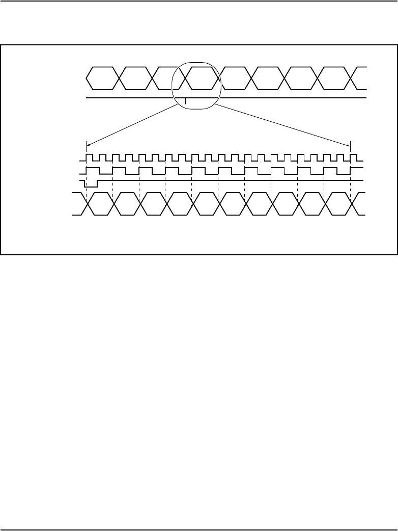
Overview Page 67 of 906
Circuit Card Description and Installation
signaling data to the line card, it is sent as a 24-bit word divided among 24
successive DS-30X frames.
DS-30Y network loops extend between controller cards and superloop
network cards in the common equipment, and function in a manner similar to
DS-30X loops. See Figure 13 on page 68.
Essentially, a DS-30Y loop carries the PCM timeslot traffic of a DS-30X
loop. Four DS-30Y network loops form a superloop with a capacity of 128
channels (120 usable timeslots).
See Communication Server 1000M and Meridian 1: Large System Planning
and Engineering (553-3021-120) for more information on superloops.
Card LAN link
Maintenance communication is the exchange of control and status data
between IPE line or trunk cards and the CE CPU by way of the NT8D01
Controller Card. Maintenance data is transported via the card LAN link. This
Figure 12
DS-30X loop data format
29
W0B7W31DV
DS-30X loop
data words
Frame
sync
Frame sync
DS-30X loop
data bits
5.12 MHz
2.56 MHz
SB = SIGNALING BIT DV = DATA VALID
30 31 0 1 2 3 4
W0B6 W0B5 W0B4 W0B3 W0B2 W0B1 W0B0 W0SB W0DV W1B7
553-6151
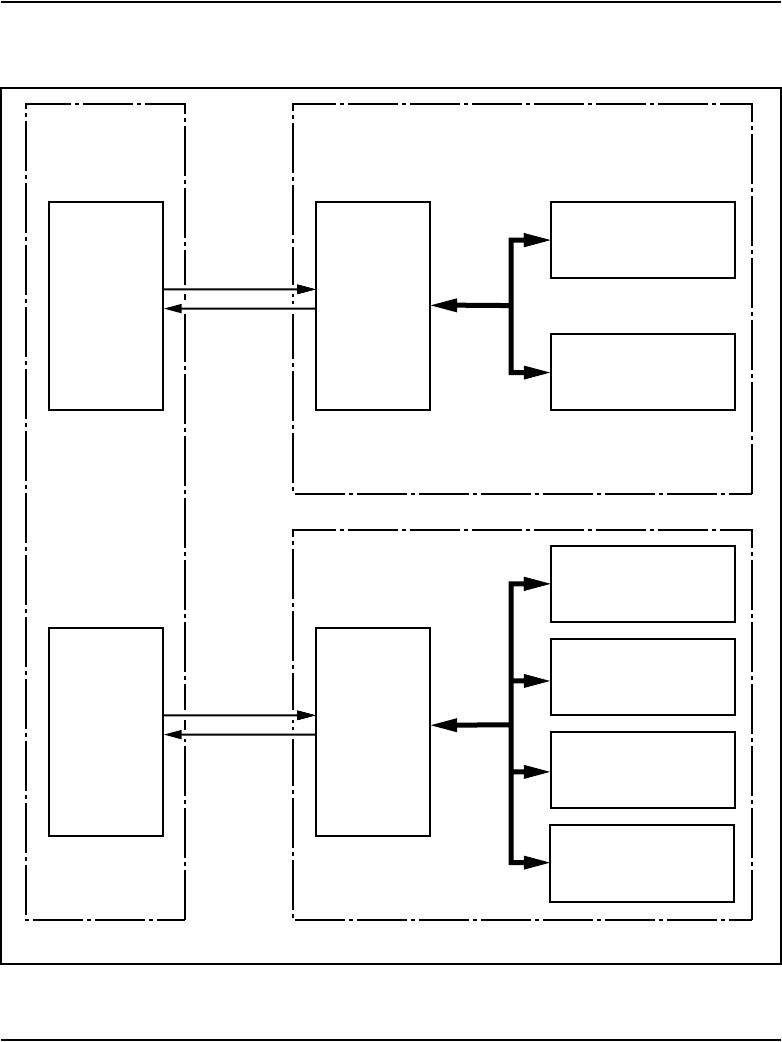
Page 68 of 906 Overview
553-3001-211 Standard 3.00 August 2005
Figure 13
Network connections to IPE modules
NT8D04
Superloop
Network
Card
NT8D01
Controller
Card
NT8D14
Universal
Trunk Card
DS-30X
DS-30Y
loop
NT8D37 IPE ModuleCommon
Equipment
(Network)
NT8D13 PE Module
NT8D15
E&M
Trunk Card
QPC414
Network
Card
QPC659
Dual-Loop
Peripheral
Buffer Card
QPC71 E&M
Signaling and
Paging Trunk Card
553-6158
Large
System
Network
loop
QPC74 Recorded
Announcement
Trunk Card
QPC250
Release Link
Trunk Card
QPC449
Loop Signaling
Trunk Card

Overview Page 69 of 906
Circuit Card Description and Installation
link is composed of two asynchronous serial buses (called the Async card
LAN link in Figure 11 on page 64). The output bus is used by the controller
for output of control data to the trunk card. The input bus is used by the
controller for input of trunk card status data.
A card LAN link bus is common to all of the line/trunk card slots within an
IPE module (or IPE section of a CE module). This bus is arranged in a master/
slave configuration where the controller card is the master and all other cards
are slaves. The module backplane provides each line/trunk card slot with a
unique hardwired slot address. This slot address enables a slave card to
respond when addressed by the controller card. The controller card
communicates with only one slave at a time.
In normal operation, the controller card continually scans (polls) all of the
slave cards connected to the card LAN to monitor their presence and
operational status. The slave card sends replies to the controller on the input
bus along with its card slot address for identification. In this reply, the slave
informs the controller if any change in card status has taken place. The
controller can then prompt the slave for specific information. Slaves only
respond when prompted by the controller; they do not initiate exchange of
control or status data on their own.
When an IPE line or trunk card is first plugged into the backplane, it runs a
self-test. When the self test is completed, a properly functioning card
responds to the next controller card poll with the self-test status. The
controller then queries for card identification and other status information.
The controller then downloads all applicable configuration data to the line/
trunk card, initializes it, and puts it into an operational mode.
The network card regularly polls the IPE cards during TS0 to see if any of
them has a message to be sent. When an IPE card has a message waiting it
responds to the poll by sending a series of 1s during the next five successive
timeslot 0s. The network card responds by sending a “message send enable”
message (all 1s). The IPE card replies by sending 1, 1, 1, 0, and then the
message in successive timeslot 0s.
Trunk interface unit
Once the 8-bit digital voice signal has been received by the trunk card, it must
be converted back into an analog signal, filtered, and driven onto the analog
Page 70 of 906 Overview
553-3001-211 Standard 3.00 August 2005
trunk line through an impedance matching and balance network. The trunk
interface also includes the logic necessary to place outgoing call signaling
onto the trunk, or the logic to connect to special services such as recorded
announcement and paging equipment.
Figure 14 shows a typical example of the logic that performs these functions.
Each part of the trunk interface unit is discussed in the following section.
Coder/Decoder circuit
The coder/decoder (codec) performs Analog to Digital (A/D) and Digital to
Analog (D/A) conversion of the line analog voiceband signal to and from a
digital PCM signal. This signal can be coded and decoded using either the
A-Law or the µ-Law companding algorithm. On some trunk cards the
decoding algorithm depends of the type of codec installed when the board is
built. On others, it is an option selected using a software overlay.
Figure 14
Typical trunk interface unit block diagram
CODEC
2-wire
to
4-wire
conversion
and
balance
network
Interface
(protection)
Variable gain
filters Isolation
transformer
Ring
TS0
Tip
DS-30X
Network loop
553-6159
Signaling
leads
(E&M,
DX, etc.)
Signaling
logic

Overview Page 71 of 906
Circuit Card Description and Installation
Variable gain filters
Audio signals received from the analog phone trunk are passed through a
low-pass A/D monolithic filter that limits the frequency spread of the input
signal to a nominal 200–3400 Hz bandwidth. The audio signal is then applied
to the input of the codec. Audio signals coming from the CODEC are passed
through a low-pass A/D monolithic filter that integrates the amplitude
modulated pulses coming from the CODEC, and then filters and amplifies the
result.
On some of the trunk cards, the gain of these filters can be programmed by
the system controller. This allows the system to make up for line losses
according to the loss plan.
Balancing network
Depending on the card type, the balancing network is capable of providing
either a 600 ohm or a 900 ohm (or both) impedance matching network. It also
converts the 2-wire transmission path (tip and ring) to a 4-wire transmission
path (Rx/ground and Tx/ground). The balancing network is a transformer/
analog (hybrid) circuit combination.
Signaling circuits
Signaling circuits are relays that place outgoing call signaling onto the trunk.
Signal detection circuits monitor the incoming call signaling.
Control signals
Control signals and logic are provided when the trunk is going to be
connected to special services such as recorded announcement and paging
equipment.
Page 72 of 906 Overview
553-3001-211 Standard 3.00 August 2005
Serial Data Interface (SDI) cards
The NT8D41BA QSDI paddle board provides four bidirectional
asynchronous serial ports for the system processor, and the QPC841 QSDI
card also provides four. Any device that conforms to the RS-232-C serial
communication standard can be connected to these serial ports.
The QPC513 ESDI card provides two fully synchronous serial ports for the
system processor. The ESDI card communicates using the Link Access
Procedure Balanced (LAP-B) synchronous communication protocol.
The electrical interface uses either standard RS-232-C signals or a special
high-speed interface that combines the high-speed differential interface of the
RS-422-A standard with the handshake signals of the RS-232-C standard.
The RS-232-C interface is normally used when data rates are less than 19.2
Kbps, and the cable length is less than 15.24 m (50 ft). The high-speed
interface is used when the signal rates are greater than 19.2 kbps (up to 64
kbps) and/or when the cable length is greater than 15.24 m (50 ft).
Table 9 shows compatibility between the three SDI cards and the various
switch options.
The NT8D41BA QSDI paddle board does not have a front panel. It mounts
to the rear of the backplane in the NT5D21 Core/Network module, and does
Table 9
Serial data interface cards
Compatible System Options
Card Ports Port types 51C, 61C 81C
NT8D41BA 4RS-232-C asynchronous X X
QPC841 4RS-232-C asynchronous X X
QPC513 2RS-232-C synchronous or
high-speed synchronous*
X X
*See the section on the QPC513 card in this manual for details on the high-speed interface

Overview Page 73 of 906
Circuit Card Description and Installation
not consume a module slot. The RS-232-C connections are brought out
through special cables to the backplane I/O panel.
The QPC841 Quad SDI card and the QPC513 Enhanced SDI card mount in
standard backplane slots, and their serial interface connectors are located on
the card front panels. A list of the modules that they can be mounted in is
given in the following sections on the individual cards.
Uses
Examples of asynchronous devices that can be connected to the system
processor using the NT8D41BA QSDI paddle board and the QPC841 Quad
SDI card are:
• an administration and maintenance terminal
• a background terminal for use in a hotel/motel
• the Automatic Call Distribution (ACD) feature
• the Call Detail Recording (CDR) feature
Examples of synchronous devices that can be connected to the system
processor using the QPC513 Enhanced SDI card are:
• a host computer (DEC, Tandem, for example) using the Meridian Link
communication program
• the Meridian Mail voice-mail option
Features
The NT8D41 QSDI paddle board and the QPC841 QSDI card provide the
following features:
• asynchronous serial data interface ports, each supporting
— RS-232-C interface
— 8–bit ASCII data with parity and stop bit
— Asynchronous, start-stop operation
— Data rates of 150, 300, 600, 1200, 2400, 4800, and 9600 baud

Page 74 of 906 Overview
553-3001-211 Standard 3.00 August 2005
— Data terminal equipment (DTE) emulation mode
— Data communication equipment (DCE) emulation mode
• enable/disable switch and LED
• input/output (I/O) device address selectable by on-board switches.
The QPC513 ESDI card provides these features:
• fully synchronous serial data interface ports, each supporting
— RS-232-C or modified RS-422-A interface
— LAPB subset of the HDLC synchronous protocol
— Data rates of 1200, 2400, 4800, 9600, 19200, 48000, 56000, and
64000 baud
— Data terminal equipment (DTE) emulation mode
— Data communication equipment (DCE) emulation mode
• enable/disable switch and LED
• input/output (I/O) device address selectable by on-board switches.
Specifications
This section lists the specifications shared by all of the SDI cards. See the
appropriate section in this document for information specific to any particular
card.

Overview Page 75 of 906
Circuit Card Description and Installation
Power consumption
The SDI cards obtain their power directly from the module backplane. Power
consumption for each of the cards is shown in Table 10.
Environmental
The SDI cards operate without degradation under the conditions listed in
Table 11.
Electrostatic discharge
The SDI cards meet the requirements of the IEC 801-2, clause 8.0 procedure.
They can withstand a direct discharge of ±5 to ±20 kV without being
damaged.
Table 10
Power consumption
Voltag e
Maximum power consumption
NT8D41BA QPC513 QPC841
+5 VDC ±5% 1.0 Amp 3.0 Amp 1.5 Amp
+12 VDC ±5% 100 mA 50 mA 100 mA
–12 VDC ±5% 100 mA 50 mA 100 mA
Table 11
Environmental specifications
Specification Operation Storage
Ambient temperature 0° to 50°C;
(32° to 122°F)
–55° to +70°C;
(–58° to 158°F)
Relative humidity
(non-condensing)
5% to 95% 0% to 95%
Altitude 3500m;
(11000 ft)
15000m;
(50000 ft)

Page 76 of 906 Overview
553-3001-211 Standard 3.00 August 2005
Electromagnetic interference
The CS 1000S, CS 1000M, and Meridian 1 systems meet the requirements of
FCC Part 15 and CSA C108.8 electromagnetic interference (EMI) standards
as a class “A” computing device. To accomplish this, the SDI cables must exit
the module through EMI filters on the I/O panel.
Reliability
The Mean Time Between Failure (MTBF) for all SDI cards is 55 years at
40°C and 29 years at 55°C.
Installation
To use a serial data interface card in a CS 1000S, CS 1000M, or Meridian 1
system, first install the card in the system, and then configure the system
software to recognize it. These steps are discussed in the following sections.
Instructions for cabling the serial data interface cards to the various system
consoles and peripherals are found in Communication Server 1000M and
Meridian 1: Large System Installation and Configuration (553-3021-210).
Configuring the system software
Once an SDI card has been installed in the system, the system software needs
to be configured to recognize it. This is done using the Configuration Record
program LD 17. Instructions for the Configuration Record program are found
in Software Input/Output: Administration (553-3001-311).
Maintenance
The following maintenance programs are used to maintain individual SDI
asynchronous ports. The program used depends on the application of the port.
• LD 37 Input/Output Diagnostics – Used for system terminal, printer,
background terminal ports, and system monitor status.
• LD 42 Call Detail Recording (CDR) Diagnostic – For checking CDR
links and CDR system terminals.

Overview Page 77 of 906
Circuit Card Description and Installation
The following maintenance program is used to maintain individual SDI
synchronous ports.
• LD 48 Link Diagnostic – For checking Automatic Call Distribution
(ACD) and Meridian Link ports.
Instructions for running the various maintenance programs are found in
Software Input/Output: Administration (553-3001-311). System messages
are interpreted in Software Input/Output: System Messages (553-3001-411).


Page 79 of 906
Circuit Card Description and Installation
88
Circuit card installation
Contents
This section contains information on the following topics:
Card slots — Large System. . . . . . . . . . . . . . . . . . . . . . . . . . . . . . . . . . 79
Circuit card installation . . . . . . . . . . . . . . . . . . . . . . . . . . . . . . . . . . . . . 80
Precautions . . . . . . . . . . . . . . . . . . . . . . . . . . . . . . . . . . . . . . . . . . . . . . 84
Installing a circuit card . . . . . . . . . . . . . . . . . . . . . . . . . . . . . . . . . . . . . 86
Card slots — Large System
The following table in this chapter identifies card slot compatibility in the
following modules:
• NT4N41 Core/Network module required for CS 1000M SG,
CS 1000M MG, Meridian 1 PBX 61C Call Processor (CP) PII, CP PIV,
and Meridian 1 PBX 81C
• NT4N46 Core/Network module required for CS 1000M MG and Option
81C CP PII, CP PIV
• NT6D60 Core/Network module required for the CS 1000M MG and
Option 81C only
• NT8D35 Network module required for CS 1000M MG and Meridian 1
PBX 81C
• NT8D37 Intelligent Peripheral Equipment (IPE) module
required for CS 1000M HG, CS 1000M SG, CS 1000M MG, Meridian 1
Option 51, Meridian 1 PBX 61C, and Meridian 1 PBX 81C

Page 80 of 906 Circuit card installation
553-3001-211 Standard 3.00 August 2005
Circuit card installation
Table 12
Large System card slots (Part 1 of 4)
Component Large System
A0786611 Call Processor Pentium II® card 81C Core/Net: “CP”
A0810486 Call Processor Pentium II 81C Core/Net: “CP”
NT1P61 Fiber Superloop Network card Core/Net: 0–7
NT1P62 Fiber Peripheral Controller card IPE: “Contr”
NT1R52 Remote Carrier Interface IPE: “Contr”
NT1R20 Off-Premise Station IPE: any slot but “Contr”
NT4D18 Hybrid Bus Terminator Core/Net: between 11 and 12
NT4D19 and NT423 Hybrid Bus Terminator Core/Net: between 0 and 1
NT4D20 and NT422 Hybrid Bus Terminator Core/Net: between 1 and 2
NT4N43 Multi-Medium DIsk Unit 81C Core/Net:
NT4N64 Call Processor Pentium II card 61C Core/Net: CP PII
NT4N64 Call Processor Pentium II card 81C Core/Net: CP PII
NT4N39 Call Processor Pentium IV card 61C Core/Net: CP PIV
NT4N39 Call Processor Pentium IV card 81C Core/Net: CP PIV
NT4N65 cPCI® Core to Network Interface card 81C Core/Net: c9–c12
NT4N66 cPCI Core to Network Interface Transition
card 81C Core/Net cPCI Core backplane: 9–12
NT4N67 System Utility card 81C Core/Net: c15
NT4N68 System Utility Transition card 81C Core/Net cPCI Core backplane:
NT5D11 and
NT5D14 Line side T1 Line card IPE: any slot but “Contr”
NT5D12AA Dual DTI/PRI card Core/Net: 0–7
NT5D61 Input/Output Disk Unit with CD-ROM
(MMDU) 61C Core/Net: 17, 18 and 19

Circuit card installation Page 81 of 906
Circuit Card Description and Installation
NT5K02 Analog Line card IPE: any slot but “Contr”
NT5K07 Universal Trunk card IPE: any slot but “Contr”
NT5K17 Direct Dial Inward Trunk card IPE: any slot but “Contr”
NT5K18 Central Office Trunk card IPE: any slot but “Contr”
NT5K19 E&M Trunk card IPE: any slot but “Contr”
NT5K35 D-channel Handler Interface Core/Net: 0-7
Net: 5-12
NT5K36 Direct Inward/Direct Outward Dial Trunk
card IPE: any slot but “Contr”
NT5K70 Central Office Trunk card IPE: any slot but “Contr”
NT5K71 Central Office Trunk card IPE: any slot but “Contr”
NT5K72 E&M Trunk card IPE: any slot but “Contr”
NT5K82 Central Office Trunk card IPE: any slot but “Contr”
NT5K83 E&M Trunk card IPE: any slot but “Contr”
NT5K84 Direct Inward Dial Trunk card IPE: any slot but “Contr”
NT5K90 Central Office Trunk card IPE: any slot but “Contr”
NT5K93 Central Office Trunk card IPE: any slot but “Contr”
NT5K96 Analog Line card IPE: any slot but “Contr”
NT5K99 Central Office Trunk card IPE: any slot but “Contr”
NT5K20 Extended Tone Detector IPE: any slot but “Contr”
NT6D65 Core to Network Interface 61C Core/Net: 12
NT6D66 Call Processor card 61C Core/Net: 15 and 16
NT6D70
S/T Interface Line card IPE: any slot but “Contr”
Table 12
Large System card slots (Part 2 of 4)
Component Large System

Page 82 of 906 Circuit card installation
553-3001-211 Standard 3.00 August 2005
NT6D71
U Interface Line card IPE: any slot but “Contr”
NT6D72
Basic Rate Signal Concentrator card IPE: any slot but “Contr”
NT6D73
Multi-purpose ISDN Signaling Processor card Core/Net: 0–7
NT6D80 MSDL Core/Net: 0–7
NT7D16 Data Access card IPE: any slot but “Contr”
NT7R51 Local Carrier Interface Core/Net: 0–7
NT8D01 Controller card IPE: “Contr”
NT8D02 Digital Line card IPE: any slot but “Contr”
NT8D04 Superloop Network card Core/Net: 0–7
Net: 5-12
NT8D09 Analog Message Waiting Line card IPE: any slot but “Contr”
NT8D14 Universal Trunk card IPE: any slot but “Contr”
NT8D15 E&M Trunk card IPE: any slot but “Contr”
NT8D16 Digitone Receiver card IPE: any slot but “Contr”
NT8D17 Conference/TDS card Core/Net: 0–7
NT8D41 Dual Port Serial Data Interface card Serial Port back of Core/Net module
NT9D19 Call Processor card 61C Core/Net: 15 and 16
NTAG03 Central Office Trunk card IPE: any slot but “Contr”
NTAG04 Central Office/Direct Inward Dial Trunk
card IPE: any slot but “Contr”
NTAG36 Nortel Integrated Recorded Announcer IPE: any slot but “Contr”
NTBK51 Downloadable D-channel daughterboard Connects to DDP card
NTCK16 Generic Central Office Trunk card IPE: any slot but “Contr”
Table 12
Large System card slots (Part 3 of 4)
Component Large System

Circuit card installation Page 83 of 906
Circuit Card Description and Installation
NTCK43AA Primary Rate Interface card Core/Net: 0-7
Net: 5-11, 13-14
NTRB33 FIber Junctor Interface card For 81C: Core/Net: 8 and 9, Net module: 2 and 3
NTRE39 Optical Cable Management card For 81C: Net module: the slot to the right side of 14,
the slot to the left of the 3PE in slot 1
QPC43 Peripheral Signaling card Core/Net: 10
Net: 4
QPC71 E&M/DX Trunk card IPE: any slot but “Contr”
QPC414 Network card Core/Net: 0–7
Net: 5-12
QPC441 3-Port Extender card Core/Net: 11
Net: 1
QPC471 Clock Controller card 61C Core/Net: 9
Net: 5 -12
For 81C, use NT8D35 Net slot 13; in QSD39 shelf,
use Net slot 2; in QSD40 shelf, use slot 13
QPC513 Enhanced Serial Data Interface card Core/Net: 9, 13
QPC578 Integrated Services Digital Line card IPE: any slot but “Contr”
QPC659 Dual Loop Peripheral Buffer card IPE: “DLB”
QPC720 Primary Rate Interface card Core/Net: 0–7
Net: 5–11, 13–14
QPC775 Clock Controller 61C Core/Net: slot 14.
For 81C use NT8D35 Net slot 13; in QSD39 shelf,
use Net slot 2; in QSD40 shelf, use slot 13.
QPC789 16-Port 500/2500 Message Waiting Line
card IPE: any slot but “Contr”
QPC841 4-Port Serial Data Interface card Core/Net: 0-7
Table 12
Large System card slots (Part 4 of 4)
Component Large System
Page 84 of 906 Circuit card installation
553-3001-211 Standard 3.00 August 2005
Precautions
To avoid personal injury and equipment damage, review the following
guidelines before handling system equipment.
To avoid damage to circuit cards from static discharge, wear a properly
connected antistatic wrist strap when you work on system equipment. If a
wrist strap is not available, regularly touch one of the bare metal strips in a
module to discharge static. Figure 15 on page 85 shows the recommended
connection points for the wrist strap and the bare metal strips you should
touch.
Handle circuit cards as follows:
• Unpack or handle cards away from electric motors, transformers, or
similar machinery.
• Handle cards by the edges only. Do not touch the contacts or
components.
• Set cards on a protective antistatic bag. If an antistatic bag is not
available, hand-hold the card, or set it in a card cage unseated from the
connectors.
• Store cards in protective packing. Do not stack cards on top of each other
unless they are packaged.
WARNING
Module covers are not hinged; do not let go of the covers.
Lift covers away from the module and set them out of your
work area.
WARNING
Circuit cards may contain a lithium battery. There is a
danger of explosion if the battery is incorrectly replaced.
Do not replace components on any circuit card; you must
replace the entire card.
Dispose of circuit cards according to the manufacturer’s
instructions.
Circuit card installation Page 85 of 906
Circuit Card Description and Installation
• Keep cards installed in the system as much as possible to avoid dirty
contacts and unnecessary wear.
• Store cards in a cool, dry, dust-free area.
During repair and maintenance procedures do the following:
• Turn off the circuit breaker or switch for a module power supply before
the power supply is removed or inserted.
• In AC-powered systems, capacitors in the power supply must discharge.
Wait five full minutes between turning off the circuit breaker and
removing the power supply from the module.
• Software disable cards, if applicable, before they are removed or
inserted.
Figure 15
Static discharge points
Wrist strap
connection point Bare metal strip
553-5000
Wrist strap
connection point
Bare metal strip
Power supply slot
Module
front
Module
rear
Page 86 of 906 Circuit card installation
553-3001-211 Standard 3.00 August 2005
• Hardware disable cards, whenever there is an enable/disable switch,
before they are removed or inserted.
• Return defective or heavily contaminated cards to a repair center. Do not
try to repair or clean them.
Installing a circuit card
This procedure provides detailed installation instructions for circuit cards.
Procedure 1
Installation
1Open the protective carton and remove the circuit card from the antistatic
bag. Return the antistatic bag to the carton and store it for future use.
2Inspect the card components, faceplate, locking devices, and connectors
for damage. If damaged, tag the card with a description of the problem
and package it for return to a repair center.
3Refer to the work order to determine the module and slot location for the
card.
4If there is an enable/disable (Enb/Dis) switch on the faceplate, set it to Dis.
5If there are option switches or jumpers on the card, set them according to
the work order (see “Option settings” on page 101).
6Squeeze the ends of the locking devices on the card and pull the tabs
away from the latch posts and faceplate (see Figure 16).
DANGER
To avoid personal injury and equipment damage, read all
of the guidelines in “Circuit card installation” on page 80
before you begin installation and follow all guidelines
throughout the procedure.
CAUTION
System Failure
Incorrectly set switches on common equipment
circuit cards may cause a system failure.
Circuit card installation Page 87 of 906
Circuit Card Description and Installation
7Insert the card into the card aligning guides in the card cage. Gently push
the card into the slot until you feel resistance. The tip of the locking device
must be behind the edge of the card cage (see Figure 16).
8Lock the card into position by simultaneously pushing the ends of the
locking devices against the faceplate.
Note: When IPE cards are installed, the red LED on the faceplate
remains lit for two to five seconds as a self-test runs. If the self-test
completes successfully, the LED flashes three times and remains lit until
the card is configured and enabled in software, then the LED goes out. If
the LED does not follow the pattern described or operates in any other
manner (such as continually flashing or remaining weakly lit), replace the
card.
Figure 16
Installing the circuit card in the card cage
553-5002
Card locking
device
Tab
Latch post
Edge of
card cage
Card
guides

Page 88 of 906 Circuit card installation
553-3001-211 Standard 3.00 August 2005
9If there is an enable/disable switch, set it to Enb.
Note: Do not enable the switch on an NT8D04 Superloop Network card
or QPC414 Network card until network loop cables are installed.
10 If you are adding a voice, conference, or tone and digit loop, press the
manual initialize (Man Int) button on the NT5D03 or the NT5D10 Call
Processor if the card is associated with the active Call Processor:
Note: An initialization causes a momentary interruption in call
processing.
11 If you are installing the card in a working system, refer to the work order
and the Software Input/Output: Administration (553-3001-311) to add the
required office data to the system memory.
12 Go to the appropriate test procedure in “Acceptance tests” on page 89.

Page 89 of 906
Circuit Card Description and Installation
100
Acceptance tests
Contents
This section contains information on the following topics:
Introduction . . . . . . . . . . . . . . . . . . . . . . . . . . . . . . . . . . . . . . . . . . . . . . 89
Conference cards . . . . . . . . . . . . . . . . . . . . . . . . . . . . . . . . . . . . . . . . . . 90
Digitone receiver cards . . . . . . . . . . . . . . . . . . . . . . . . . . . . . . . . . . . . . 92
Line cards . . . . . . . . . . . . . . . . . . . . . . . . . . . . . . . . . . . . . . . . . . . . . . . 93
Multifrequency sender cards . . . . . . . . . . . . . . . . . . . . . . . . . . . . . . . . . 94
Multifrequency signaling cards. . . . . . . . . . . . . . . . . . . . . . . . . . . . . . . 95
Network cards . . . . . . . . . . . . . . . . . . . . . . . . . . . . . . . . . . . . . . . . . . . . 95
Trunk cards . . . . . . . . . . . . . . . . . . . . . . . . . . . . . . . . . . . . . . . . . . . . . . 96
Tone and digit switch cards. . . . . . . . . . . . . . . . . . . . . . . . . . . . . . . . . . 97
Introduction
Test procedures for most circuit cards require that internal and external
cabling be installed. See the appropriate installation document for your
system and Telephones and Consoles: Description, Installation, and
Operation (553-3001-367) for cabling procedures.

Page 90 of 906 Acceptance tests
553-3001-211 Standard 3.00 August 2005
Conference cards
Procedure 2
Testing conference cards
Use this procedure to test a conference card or to test the conference function
of an NT8D17 Conference/TDS card.
1Log into the system:
LOGI (password)
2Request the status of a loop on the conference card:
LD 38
STAT loop
Conference status is formatted as follows:
CNFC n DSBL n BUSY
“n” represents the number of conference groups disabled and busy
CHAN n DSBL n BUSY
“n” represents the number of channels disabled and busy
UNEQ
card is not equipped in the system
DSBL
card is disabled in software
3If the conference card loop is disabled, enable it.
For an NT8D17 Conference/TDS card, enter:
ENLX loop
(the conference loop is the odd loop of the conference/TDS loop pair)
Note: The conference/TDS card is not enabled automatically when it is
inserted. You must enable the card with the command ENLX. (This
command is used in LD 34 and LD 46 to address even loops and in LD 38
to address odd loops.) Enabling the loops with the command ENLL does
not enable the hardware for the card.
For other than an NT8D17 Conference/TDS card, enter:
ENLL loop
(the conference loop must be an even loop for cards other than the
NT8D17)
If the system response is other than OK, see the Software Input/Output:
Administration (553-3001-311) to analyze the messages.

Acceptance tests Page 91 of 906
Circuit Card Description and Installation
4Test the conference loop for channel, group, and switching faults:
CNFC loop
If the conference loop passes the tests, the output is OK.
If the system response is other than OK, see the Software Input/Output:
Administration (553-3001-311) to analyze the messages.
5Prepare the system for a manual conference call on a specified loop:
CNFC MAN loop c
Where “c” is the manual conference group (1-15)
A manual conference test is performed by stepping through conference
channels and groups, listening for noise that indicates a faulty card.
The manual conference test can be performed through a system terminal
or BCS maintenance telephone. If commands are entered from a
maintenance telephone, this telephone automatically becomes part of the
manual conference call.
Only one manual conference call is allowed at one time. A manual
conference consists of only two telephones, where one telephone acts as
a signal source while the other acts as a listening monitor.
After you enter the CNFC command, any two telephones (one may
already be the maintenance telephone) dialing the special service prefix
code (SPRE) and the digits 93 will enter the manual conference call. The
prime directory number (PDN) indicator, if equipped, will light on each
telephone.
Going on-hook takes the telephone out of the manual conference call, and
the test must be restarted.
See LD 38 in the Software Input/Output: Administration (553-3001-311)
for more detailed information on using this command.
6Test various channels and conference groups audibly with the command
CNFC STEP
When stepping through channels and groups, a clicking followed by
silence is normal. Any distortion or other noises indicates a faulty card.
Once the CNFC STEP command has been entered, entering C on the
system terminal or maintenance telephone steps through the conference
channels. Entering G steps through the conference groups. There are 15
channels per group and 15 groups per conference card.
Entering an asterisk (*) and END stops the test.

Page 92 of 906 Acceptance tests
553-3001-211 Standard 3.00 August 2005
Again, see “LD 38” in the Software Input/Output: Maintenance
(553-3001-511) for detailed information on using this command.
7End the session in LD 38:
****
End of Procedure
Digitone receiver cards
Procedure 3
Testing digitone receiver cards
Use this procedure to test a Digitone receiver (DTR) card, a DTR
daughterboard, or the DTR function on the NT8D18 Network/DTR card.
Note: The DTR daughterboard connected to a QPC659 Dual Loop
Peripheral Buffer card cannot be assigned when the IPE shelf is used in
single loop mode.
1Log into the system:
LOGI (password)
2See if the Digitone receiver to be tested is disabled:
LD 34
STAT
The system responds with the terminal number (TN), or numbers, of any
disabled Digitone receivers.
3If the Digitone receiver is disabled, enable it:
ENLR l s c uloop, shelf, card, and unit numbers
4Test the Digitone receiver:
DTR l s c uloop, shelf, card, and unit numbers
If the system response is other than OK, see the Software Input/Output:
Administration (553-3001-311) to analyze the messages.
5End the session in LD 34:
****
End of Procedure

Acceptance tests Page 93 of 906
Circuit Card Description and Installation
Line cards
Procedure 4
Testing line cards
Use this procedure to test a line card.
1Log into the system:
LOGI (password)
2Perform a network memory test, continuity test, and signaling test on a
specific loop and shelf:
LD 30
SHLF l sloop and shelf numbers
If the system response is other than OK, see the Software Input/Output:
Administration (553-3001-311) to analyze the messages.
3For a line card on a superloop, perform a signaling test on a specific card
or unit:
UNTT l s c loop, shelf, and card numbers
For the NT8D02 Digital Line card, enter:
UNTT l s c u loop, shelf, card, and unit numbers
If the system response is other than OK, see the Software Input/Output:
Administration (553-3001-311) to analyze the messages.
4End the session in LD 30:
****
End of Procedure

Page 94 of 906 Acceptance tests
553-3001-211 Standard 3.00 August 2005
Multifrequency sender cards
Procedure 5
Testing multifrequency sender cards
Use this procedure to test a multifrequency sender (MFS) card or the MFS
function of an NT8D17 Conference/TDS card.
1Log into the system:
LOGI (password)
2Test and enable an MFS loop:
LD 46
MFS loop
(on the NT8D17 Conference/TDS card, the TDS/MFS loop is the even
loop of the conference/TDS loop pair)
Note: The conference/TDS card is not enabled automatically when it is
inserted. You must enable the card with the command ENLX. (This
command is used in LD 34 and LD 46 to address even loops and in LD 38
to address odd loops.) Enabling the loops with the command ENLL does
not enable the hardware for the card.
If the system response is other than OK, see the Software Input/Output:
Administration (553-3001-311) to analyze the messages.
3Access the system from a maintenance telephone; then enter:
LD 46
Give the system approximately 20 seconds to load the program.
See “Communicating with the Meridian 1” in the Software Input/Output:
Administration (553-3001-311) for details on accessing the system from a
maintenance telephone.
4Obtain 10-second bursts of digits 1 to 9, 0, and 11 to 15 (in that order) for
all digits on the specified loop:
TONE loop ALL
Each burst should sound different. If the bursts do not sound different,
replace the card.
5End the session in LD 46:
****
End of Procedure

Acceptance tests Page 95 of 906
Circuit Card Description and Installation
Multifrequency signaling cards
Procedure 6
Testing multifrequency signaling cards
Use this procedure to test a multifrequency signaling card.
1Log into the system:
LOGI (password)
2Test and enable the specified unit:
LD 54
ATST l s c u loop, shelf, card, and unit numbers
If the system response is other than OK, see the Software Input/
Output: Administration (553-3001-311) to analyze the messages.
3End the session in LD 54:
****
End of Procedure
Network cards
Procedure 7
Testing network cards
Use this procedure to test a network card.
1Log into the system:
LOGI (password)
2Perform a network memory test, continuity test, and signaling test:
LD 30
LOOP loop can be a specific loop number or ALL
If ALL is specified, all enabled loops (except attendant console loops) and
all shelves on each loop are tested.
If only one loop is being tested and it is disabled, enter ENLL loop to
enable and test a network card associated with the specified loop. (This
command cannot enable network cards disabled by LD 32.)
If the system response is other than OK, see the Software Input/Output:
Administration (553-3001-311) to analyze the messages.

Page 96 of 906 Acceptance tests
553-3001-211 Standard 3.00 August 2005
3End the session in LD 30:
****
End of Procedure
Trunk cards
Use the following procedures to test a trunk card.
Procedure 8
Testing a trunk card using a maintenance telephone
1Access the system from a maintenance telephone.
See “Communicating with the Meridian 1” in the Software Input/Output:
Administration (553-3001-311) for details on accessing the system from a
maintenance telephone.
2Test the trunk unit:
LD 36
TRK l s c u loop, shelf, card, and unit numbers
3If the maintenance telephone is hooked up to a monitor and the system
response is other than OK, see the Software Input/Output: Administration
(553-3001-311) to analyze the messages.
End of Procedure
Procedure 9
Testing a trunk card using a system terminal
1Log into the system:
LOGI (password)
2Enter:
LD 36
3To test a trunk from a remote test center, seize a central office (CO)
monitor trunk:
CALL
or
CALL l s c u
Seize the automatic number identification (ANI) trunk:
TRK l s c u loop, shelf, card, and unit numbers

Acceptance tests Page 97 of 906
Circuit Card Description and Installation
When you see the DN? prompt, enter the directory number (DN) you want
the system to dial.
If the system response is other than OK, see the Software Input/Output:
Administration (553-3001-311) to analyze the messages.
4End the session in LD 36:
****
5Test an automatically identified outward dialing (AIOD) trunk card:
LD 41
AIOD l s c loop, shelf, and card numbers
If the system response is other than OK, see the Software Input/Output:
Administration (553-3001-311) to analyze the messages.
6End the session in LD 41:
****
End of Procedure
Tone and digit switch cards
Procedure 10
Testing tone and digit switch cards
Use this procedure to test a tone and digit switch (TDS) card or to test the TDS
function of an NT8D17 Conference/TDS card.
1Log into the system:
LOGI (password)
2Obtain a list of terminal numbers (TNs) for disabled TDS cards:
LD 34
STAD
3If the TDS loop to be tested is disabled, enable it.
For an NT8D17 Conference/TDS card, enter:
ENLX loop
(the TDS/MFS loop is the even loop of the conference/TDS loop pair)
Note: The conference/TDS card is not enabled automatically when it is
inserted. You must enable the card with the command ENLX. (This
command is used in LD 34 and LD 46 to address even loops and in LD 38
to address odd loops.) Enabling the loops with the command ENLL does
not enable the hardware for the card.

Page 98 of 906 Acceptance tests
553-3001-211 Standard 3.00 August 2005
For other than an NT8D17 Conference/TDS card, enter:
ENLL loop
4Test the TDS loop:
TDS loop
If the system response is other than OK, see the Software Input/Output:
Administration (553-3001-311) to analyze the messages.
5End the session in LD 34:
****
6Using a maintenance telephone, log into the system.
See “Communicating with the Meridian 1” in the Software Input/Output:
Administration (553-3001-311) for details on accessing the system using
a maintenance telephone.
7From the maintenance telephone, enter:
LD#34##
To test outpulsers and channels for the TDS loop, see Table 13 on
page 98 for a sample of the input commands used with the maintenance
telephone. See the Software Input/Output: Administration
(553-3001-311) for all tones that can be tested.
8Exit LD 34 from the maintenance telephone:
****
End of Procedure
Table 13
TDS tone tests
Input command
Dial pad
equivalent Description
BSY#loop## 279#loop## Provides busy tone from TDS loop specified.
C## 2## Removes any active tone.
DIA#loop## 342#loop## Provides dial tone from TDS loop specified.
OVF#loop## 683#loop## Provides overflow tone from TDS loop specified.
RBK#loop## 725#loop## Provides ringback tone from TDS loop specified.


Page 101 of 906
Circuit Card Description and Installation
156
Option settings
Contents
This section contains information on the following topics:
Circuit card grid . . . . . . . . . . . . . . . . . . . . . . . . . . . . . . . . . . . . . . . . . . 102
NT1R20 Off-Premise Station card . . . . . . . . . . . . . . . . . . . . . . . . . . . . 104
General purpose switch settings . . . . . . . . . . . . . . . . . . . . . . . . . . . . . . 107
NT6D42 Ringing Generator DC . . . . . . . . . . . . . . . . . . . . . . . . . . . . . . 114
NT5D2101/NT9D1102 Core/Network module backplane . . . . . . . . . . 117
NT6D68 Core module backplane . . . . . . . . . . . . . . . . . . . . . . . . . . . . . 117
NT6D80 Multi-purpose Serial Data Link card . . . . . . . . . . . . . . . . . . . 118
NT8D14 Universal Trunk card . . . . . . . . . . . . . . . . . . . . . . . . . . . . . . . 119
NT8D15 E&M Trunk card . . . . . . . . . . . . . . . . . . . . . . . . . . . . . . . . . . 124
NT8D17 Conference/TDS card. . . . . . . . . . . . . . . . . . . . . . . . . . . . . . . 125
NT8D21 Ringing Generator AC . . . . . . . . . . . . . . . . . . . . . . . . . . . . . . 126
NT8D22 System Monitor . . . . . . . . . . . . . . . . . . . . . . . . . . . . . . . . . . . 127
NT8D41BA Quad Serial Data Interface Paddle Board. . . . . . . . . . . . . 132
NT8D72 Primary Rate Interface card . . . . . . . . . . . . . . . . . . . . . . . . . . 134
QPC43 Peripheral Signaling card . . . . . . . . . . . . . . . . . . . . . . . . . . . . . 136
QPC71 E&M/DX Signaling and Paging Trunk cards. . . . . . . . . . . . . . 136
QPC414 Network card . . . . . . . . . . . . . . . . . . . . . . . . . . . . . . . . . . . . . 137
QPC441 3-Port Extender cards . . . . . . . . . . . . . . . . . . . . . . . . . . . . . . . 138
QPC559, QPC560 Loop Signaling Trunk cards . . . . . . . . . . . . . . . . . . 141

Page 102 of 906 Option settings
553-3001-211 Standard 3.00 August 2005
QPC528 CO/FX/WATS Trunk cards . . . . . . . . . . . . . . . . . . . . . . . . . . 143
QPC471 Clock Controller card. . . . . . . . . . . . . . . . . . . . . . . . . . . . . . . 144
QPC525, QPC526, QPC527, QPC777 CO Trunk card . . . . . . . . . . . . 145
QPC550 Direct Inward Dial Trunk card. . . . . . . . . . . . . . . . . . . . . . . . 146
QPC551 Radio Paging Trunk card . . . . . . . . . . . . . . . . . . . . . . . . . . . . 149
QPC595 Digitone Receiver cards . . . . . . . . . . . . . . . . . . . . . . . . . . . . . 150
QPC577, QPC596 Digitone Receiver daughterboards . . . . . . . . . . . . . 150
QPC720 Primary Rate Interface card . . . . . . . . . . . . . . . . . . . . . . . . . . 150
QPC775 Clock Controller card. . . . . . . . . . . . . . . . . . . . . . . . . . . . . . . 152
QPC841 4-Port Serial Data Interface card . . . . . . . . . . . . . . . . . . . . . . 153
Circuit card grid
Some circuit cards contain option switches or jumpers, or both, that define
specific functions. A switch or jumper can be identified by an alphanumeric
coordinate (such as D29) that indicates a location on the card, or by a switch
number (such as SW2) printed on the circuit board (see Figure 17). Positions
on a switch (for example, positions 1, 2, 3, and 4 on SW2) are labeled on the
switch block.
On a circuit card:
• ON may be indicated by the word “on,” the word “up,” the word
“closed,” the number “1,” an arrow pointing up, or a solid dot (•).
• OFF may be indicated by the word “down,” the word “open,” the number
“0,” or an arrow pointing down.
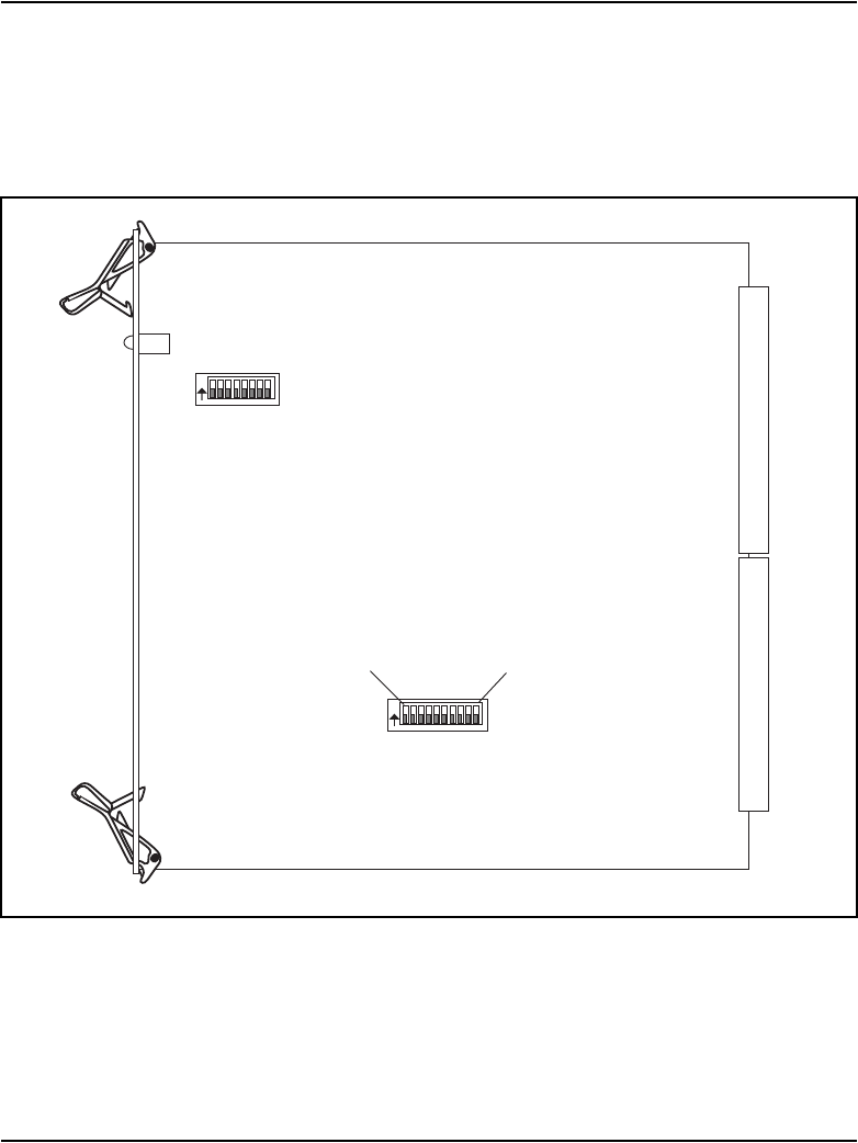
Option settings Page 103 of 906
Circuit Card Description and Installation
Throughout this document, if neither ON nor OFF is given (there is a blank
space) for a position on a switch, that position may be set to either ON or OFF
because it has no function for the option described.
Figure 17
Circuit card grid
S4
(switch 4
at coordinate
B11)
S8
(switch 8
at coordinate
F30)
ON
553-5491
33
37 35 31 29 27 25 23 21 19 17 15 13 11 975
A
B
C
D
E
F
G
ON
Positions
1 2 3 4 5 6 7 8 9 10
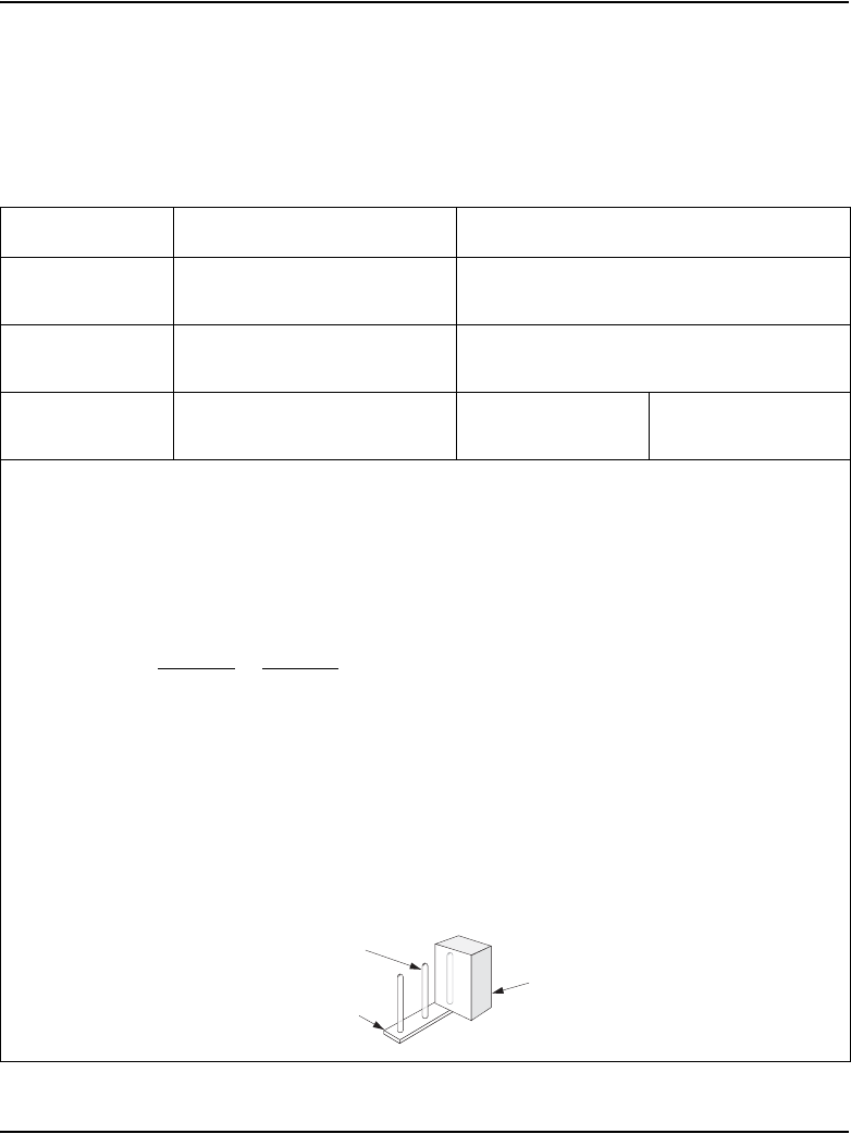
Page 104 of 906 Option settings
553-3001-211 Standard 3.00 August 2005
NT1R20 Off-Premise Station card
Table 14 lists option settings for the NT1R20 Off-Premise Station analog
card.
Table 14
OPS analog line card configuration (Part 1 of 3)
Application On-premise station (ONS) Off-premise station (OPS)
Class of Service
(CLS) (Note 1)
ONP OPX
Loop resistance
(ohms)
0–460 0–2300 (Note 2)
Jumper strap
setting (Note 6)
Both JX.0 and JX.1
off
Both JX.0 and JX.1
off
Both JX.0 and JX.1
on
Note 1: Configured in the Analog (500/2500-type) Telephone Administration program (LD 10).
Note 2: The maximum signaling range supported by the OPS analog line card is 2300 ohms.
Note 3: Loss of untreated (no gain devices) metallic line facility. Upper loss limits correspond to
loop resistance ranges for 26 AWG wire.
Note 4: Default software impedance settings are:
ONP CLS OPX CLS
TIMP: 600 ohms 600 ohms
BIMP: 600 ohms 3COM2
Note: Gain treatment, such as a voice frequency repeater (VFR) is required to limit the actual
OPS loop loss to 4.5 dB, maximum. VFR treatment of metallic loops having untreated loss
greater than 15 dB (equivalent to a maximum signaling range of 2300 ohms on 26 AWG wire) is
not recommended.
Note: Jumper strap settings JX.0 and JX.1 apply to all eight units; “X” indicates the unit
number, 0–7. “Off” indicates that a jumper strap is not installed across both pins on a jumper
block. Store unused straps on the OPS analog line card by installing them on a single jumper
pin as shown below:
553-5924
Jumper block
Jumper strap
Jumper pin
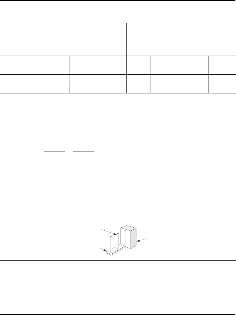
Option settings Page 105 of 906
Circuit Card Description and Installation
Loop loss (dB)
(Note 3)
0–1.5 >1.5–2.5 >2.5–3.0 0–1.5 >1.5–2.5 >2.5–4.5 >4.5–15
TIMP
(Notes 1, 4)
600
ohms
600
ohms
600
ohms
600
ohms
600
ohms
600
ohms
600
ohms
Table 14
OPS analog line card configuration (Part 2 of 3)
Application On-premise station (ONS) Off-premise station (OPS)
Class of Service
(CLS) (Note 1)
ONP OPX
Note 1: Configured in the Analog (500/2500-type) Telephone Administration program (LD 10).
Note 2: The maximum signaling range supported by the OPS analog line card is 2300 ohms.
Note 3: Loss of untreated (no gain devices) metallic line facility. Upper loss limits correspond to
loop resistance ranges for 26 AWG wire.
Note 4: Default software impedance settings are:
ONP CLS OPX CLS
TIMP: 600 ohms 600 ohms
BIMP: 600 ohms 3COM2
Note: Gain treatment, such as a voice frequency repeater (VFR) is required to limit the actual
OPS loop loss to 4.5 dB, maximum. VFR treatment of metallic loops having untreated loss
greater than 15 dB (equivalent to a maximum signaling range of 2300 ohms on 26 AWG wire) is
not recommended.
Note: Jumper strap settings JX.0 and JX.1 apply to all eight units; “X” indicates the unit
number, 0–7. “Off” indicates that a jumper strap is not installed across both pins on a jumper
block. Store unused straps on the OPS analog line card by installing them on a single jumper
pin as shown below:
553-5924
Jumper block
Jumper strap
Jumper pin
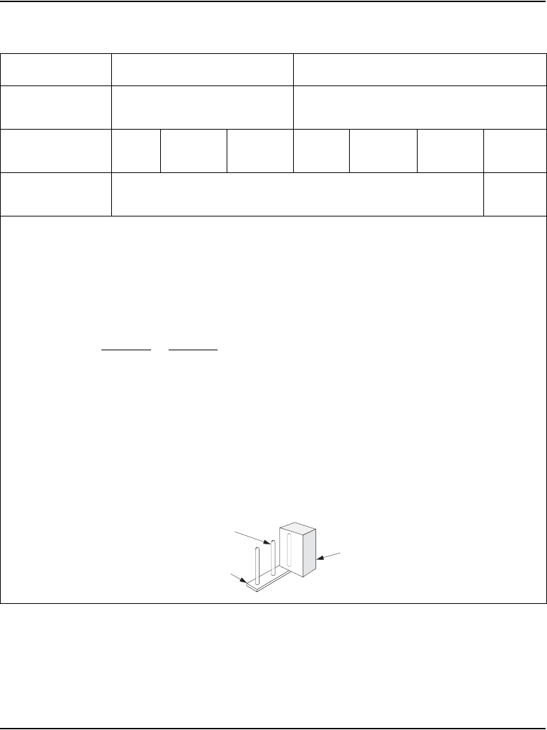
Page 106 of 906 Option settings
553-3001-211 Standard 3.00 August 2005
BIMP
(Notes 1, 4)
600
ohms
3COM1 3COM2 600
ohms
3COM1 3COM2 3COM2
Gain treatment
(Note 5)
No Yes
Table 14
OPS analog line card configuration (Part 3 of 3)
Application On-premise station (ONS) Off-premise station (OPS)
Class of Service
(CLS) (Note 1)
ONP OPX
Note 1: Configured in the Analog (500/2500-type) Telephone Administration program (LD 10).
Note 2: The maximum signaling range supported by the OPS analog line card is 2300 ohms.
Note 3: Loss of untreated (no gain devices) metallic line facility. Upper loss limits correspond to
loop resistance ranges for 26 AWG wire.
Note 4: Default software impedance settings are:
ONP CLS OPX CLS
TIMP: 600 ohms 600 ohms
BIMP: 600 ohms 3COM2
Note: Gain treatment, such as a voice frequency repeater (VFR) is required to limit the actual
OPS loop loss to 4.5 dB, maximum. VFR treatment of metallic loops having untreated loss
greater than 15 dB (equivalent to a maximum signaling range of 2300 ohms on 26 AWG wire) is
not recommended.
Note: Jumper strap settings JX.0 and JX.1 apply to all eight units; “X” indicates the unit
number, 0–7. “Off” indicates that a jumper strap is not installed across both pins on a jumper
block. Store unused straps on the OPS analog line card by installing them on a single jumper
pin as shown below:
553-5924
Jumper block
Jumper strap
Jumper pin

Option settings Page 107 of 906
Circuit Card Description and Installation
NT5D12AA Dual DTI/PRI (DDP) card
Switch setting tables for this card are listed in subsections according to their
function. Bold font designates factory (default) settings.
General purpose switches
Use switch set SW9 for Trunk 0; use switch set SW15 for Trunk 1
(see Table 15).
Trunk interface switches
A switch provides selection of T1 transmission. Use switch SW4 for Trunk 0;
use switch SW10 for Trunk 1 (see Table 16).
Table 15
General purpose switch settings
Switch Description
SW9/SW15
switch setting
1 Framing Mode off - ESF
on - SF
2 Yellow Alarm Method off - FDL
on - Digit2
3 Zero Code Suppression Mode off - B8ZS
on - AMI
4Unused off
Table 16
Trunk interface transmission mode switch settings
Description SW4/SW10 switch setting
For future use off
T1 on
Page 108 of 906 Option settings
553-3001-211 Standard 3.00 August 2005
A set of three switches provides selection of dB values. Use SW5, SW6, and
SW7 for Trunk 0; use SW11, SW12, and SW13 for Trunk 1 (see Table 17).
A set of four DIP switches provides selection among three values for receiver
impedance. Use SW8 for Trunk 0; use SW14 for Trunk 1 (see Table 18).
Table 17
Trunk interface line build out switch settings
Switch Setting
Description SW5/SW11 SW6/SW12 SW7/SW13
0 dB off off off
7.5 dB on on off
15 dB on off on
Table 18
Trunk interface impedance switch settings
Description SW8/SW14 Switch Settings
75 Ωoff off on off
100 Ωon off off on
120 Ωoff off off on

Option settings Page 109 of 906
Circuit Card Description and Installation
Ring ground switches
A set of four DIP switches selects which Ring lines are connected to ground
(see Table 19).
Table 19
Ring ground switch settings
Switch Description S2 switch setting
1 Trunk 0 Transmit off - Ring line is not grounded
on- Ring line is grounded
2 Trunk 0 Receive off - Ring line is not grounded
on - Ring line is grounded
3 Trunk 1 Transmit off - Ring line is not grounded
on - Ring line is grounded
4 Trunk 1 Receive off - Ring line is not grounded
on - Ring line is grounded

Page 110 of 906 Option settings
553-3001-211 Standard 3.00 August 2005
DCH mode and address select switches
One switch selects an on-board NTBK51AA D-Channel daughterboard and
an external MSDL/DCHI card. Four other switches provide the
daughterboard address (see Table 20).
Table 20
DCH mode and address select switch settings
Switch Description S3 Switch Setting
1-4 D-Channel daughterboard
Address
See the next table.
5-7 For future use off
8 External DCH or Onboard
DDCH
off - MSDL or DCHI card
on - Onboard DDCH
daughterboard
Table 21
NTBK51AA daughterboard address select switch settings (Part 1 of 2)
Device Address1Switch Setting
02off off off off
1on off off off
2off on off off
3on on off off
4off off on off
5on off on off
6off on on off
7on on on off
8off off off on
Option settings Page 111 of 906
Circuit Card Description and Installation
Illustrations of switch locations and settings
Figure 18 on page 112 displays functional areas for switches on the
NT5D12AA DDP card.
9on off off on
10 off on off on
11 on on off on
12 off off on on
13 on off on on
14 off on on on
15 on on on on
Note 1: The maximum number of DCHI, MSDL, and DDCH devices in the system is 16.
The Device Addresses are equivalent to the MSDL DNUM designations. For programming information on
the MSDL, refer to NTP Software Input/Output: Administration (553-3001-311) guide.
Note 2: Device address 0 is commonly assigned to the System Monitor.
Table 21
NTBK51AA daughterboard address select switch settings (Part 2 of 2)
Device Address1Switch Setting
Page 112 of 906 Option settings
553-3001-211 Standard 3.00 August 2005
Figure 18
Switch functions and areas
J5
J6
Port 0 Port 1
S3
S2 S4
S5
S6
S7
S8
S9
1 2 3 4
1 2 3 4 1 2 3 4
General Purpose Switches
Receiver Impedence
Line
Build Out
Switches
Transmission Mode
DCH Mode and Address Select
DDP
Faceplate
1 2 3 4 5 6 7 8
S15
S14
S13
S12
S11
S10
553-7308

Page 114 of 906 Option settings
553-3001-211 Standard 3.00 August 2005
NT6D42 Ringing Generator DC
Tables 22 through 27 list option settings for the NT6D42 Ringing Generator.
Table 22
NT6D42 recommended options for North American and British Telecom
Application
Ringing
frequency
Ringing
voltage Jumper locations Ringing output
North America 20 Hz 86 V ac P5
High voltage
message waiting
Low impedance
British Telecom 25 Hz 80 V ac P4
No high voltage
message waiting
Low impedance
Table 23
NT6D42 jumper locations P4 and P5
High voltage message waiting Pin location
Disable Jumper in P4
Enable Jumper in P5
Note: One jumper must be installed.
Table 24
NT6D42 jumper location J7
Ringing output Jumper location J7
Low impedance (normal) Connect pins 1 and 2
High impedance (Australia) Connect pins 2 and 3
Option settings Page 115 of 906
Circuit Card Description and Installation
Table 25
NT6D42 SW1
Ringing frequency (Hz) Position SW1
20 1
25 2
50 3
Table 26
NT6D42CB SW2
SW2
Ringing
voltage
Message waiting
voltage 1234
86 V ac –120 V dc off off off off
86 V ac –150 V dc off off off on
80 V ac –120 V dc on off off off
80 V ac –150 V dc on off off on
75 V ac –120 V dc off on off off
75 V ac –150 V dc off on off on
70 V ac –120 V dc off off on off
70 V ac –150 V dc off off on on
Page 116 of 906 Option settings
553-3001-211 Standard 3.00 August 2005
Table 27
NT6D42CC SW2
SW2
Ringing
voltage
Message waiting
voltage 1234
86 V ac –100 V dc off off off off
86 V ac –150 V dc off off off on
80 V ac –100 V dc on off off off
80 V ac –150 V dc on off off on
75 V ac –100 V dc off on off off
75 V ac –150 V dc off on off on
70 V ac –100 V dc off off on off
70 V ac –150 V dc off off on on

Option settings Page 117 of 906
Circuit Card Description and Installation
NT5D2101/NT9D1102 Core/Network module backplane
NT6D68 Core module backplane
Table 28
NT5D2101/NT9D1102 Core/Network module backplane
Jumper
Location
(between slots) Core/Network 1 Core/Network 0
JB1 14/15 Jumper plug not installed Plug installed
Note: Berg jumper is located at the bottom of the primary side of the backplane. (This is inside
the card cage assembly.)
Table 29
NT6D68 Core module backplane
Jumper
Location
(between slots) Core 1 Core 0
JB4
JB3
JB2
JB1
9 / 10
10 / 11
11 / 12
12 / 13
Jumper plug not installed
Plug installed
Plug installed
Plug installed
Plug installed
Plug installed
Plug installed
Plug installed
Note: Berg jumpers are located along the bottom of the primary side of the backplane. (This is
inside the card cage assembly.)

Page 118 of 906 Option settings
553-3001-211 Standard 3.00 August 2005
NT6D80 Multi-purpose Serial Data Link card
Table 30
NT6D80 Multi-purpose Serial Data Link card
Port 0—SW4 Port 0—SW8
RS-232-D DTE or DCE*
RS-422-A DTE (terminal)
RS-422-A DCE (modem)
all off
all off
all on
all off
all on
all off
Port 1—SW3 Port 1—SW7
RS-232-D DTE or DCE*
RS-422-A DTE
RS-422-A DCE
all off
all off
all on
all off
all on
all off
Port 2—SW2 Port 2—SW6
RS-232-D DTE or DCE*
RS-422-A DTE
RS-422-A DCE
all off
all off
all on
all off
all on
all off
Port 3—SW1 Port 3—SW5
RS-232-D DTE or DCE*
RS-422-A DTE
RS-422-A DCE
all off
all off
all on
all off
all on
all off
* RS-232-D DTE and DCE modes are software configured. RS-422-A DTE and DEC modes are switch
configured.
Note: The device number for the MSDL card is configured in LD17 at the prompt DNUM. You
must also set the device number, using switches S9 and S10, on the MSDL card. S9 designates
ones and S10 designates tens. To set the device number as 14, for example, set S10 to 1 and
S9 to 4.

Option settings Page 119 of 906
Circuit Card Description and Installation
NT8D14 Universal Trunk card
Tables 31 through 35 list option settings for the NT8D14 Universal Trunk
card.
Table 31
NT8D14 vintage AA jumper strap settings
Modes Location Jumper strap
Central Office (CO) J1, J2 off
2-way tie trunk (loop dial repeat) J1, J2 off
2-way tie trunk (outgoing/incoming dial) J1, J2 off
Recorded announcement (RAN) J1, J2 off
Paging trunk J1, J2 off
Japan CO/DID operation J1, J2 off
DID operation: loop length > = 2000 ¾ J1, J2 on
DID operation: loop length < 2000 ¾ J1, J2 off
Note 1: off = no strap present.
Note 2: Locations (J1, J2) apply to all eight units.
Page 120 of 906 Option settings
553-3001-211 Standard 3.00 August 2005
Table 32
NT8D14 vintages BA/BB jumper strap settings—factory standard
Trunk types Loop length
Jumper strap settings
J1.X J2.X J3.X J4.X
CO/FX/WATS Zero–1524 m (5000 ft) Off Off 1–2 1–2
2-way tie (LDR)
2-way tie (OAID)
DID Zero–600 ohms
RAN: continuous
operation mode
Not applicable: RAN
and paging trunks
should not leave the
building.
Paging
Note: Jumper strap settings J1.X, J2.X, J3.X, and J4.X apply to all eight units; “X” indicates the
unit number, 0–7. “Off” indicates that no jumper strap is installed on a jumper block. Store
unused straps on the universal trunk card by installing them on a single jumper pin as shown
below:
553-5924
Jumper block
Jumper strap
Jumper pin
Option settings Page 121 of 906
Circuit Card Description and Installation
Table 33
NT8D14 vintages BA/BB jumper strap settings—extended range
Trunk types Loop length
Jumper strap settings
J1.X J2.X J3.X J4.X
CO/FX/WATS > 1524 m (5000 ft) Off Off 1–2 2–3
2-way tie (LDR)
2-way tie (OAID)
DID > 600 ohms On On 1–2 2–3
RAN: pulse start or
level start modes
Not applicable: RAN
trunks should not leave
the building.
Off Off 2–3 1–2
Note: Jumper strap settings J1.X, J2.X, J3.X, and J4.X apply to all eight units; “X” indicates the
unit number, 0–7. “Off” indicates that no jumper strap is installed on a jumper block.
Table 34
NT8D14 vintages BA/BB trunk types—termination impedance and balance network
(Part 1 of 2)
Trunk types
Terminating
impedance
(Note 1)
Balance network for loop lengths (Note 2)
Zero–915 m
(zero–3000 ft)
915–1524 m
(3000–5000 ft)
> 1524 m
(> 5000 ft)
CO/FX/WATS 600 or 900
ohms
600 ohms 3COM1 3COM2
2-way tie (LDR) 600 or 900
ohms
600 ohms 3COM1 3COM2
Note 1: The terminating impedance of each trunk unit is software selectable in LD 14 and
should match the nominal impedance of the connecting equipment.
Note 2: The balance network of each trunk unit is software selectable between resistive 600 or
900 ohms or 3COM and is jumper selectable between 3COM1 and 3COM2.

Page 122 of 906 Option settings
553-3001-211 Standard 3.00 August 2005
2-way tie (OAID) 600 or 900
ohms
600 ohms 3COM1 3COM2
DID (loop < 600
ohms)
600 or 900
ohms
600 ohms 3COM1 3COM2
DID (loop Š 600
ohms)
600 or 900
ohms
600 ohms N/A 3COM2
RAN: continuous
operation mode
600 or 900
ohms
600 or 900 ohms N/A N/A
Paging 600 ohms 600 ohms N/A N/A
Table 34
NT8D14 vintages BA/BB trunk types—termination impedance and balance network
(Part 2 of 2)
Trunk types
Terminating
impedance
(Note 1)
Balance network for loop lengths (Note 2)
Zero–915 m
(zero–3000 ft)
915–1524 m
(3000–5000 ft)
> 1524 m
(> 5000 ft)
Note 1: The terminating impedance of each trunk unit is software selectable in LD 14 and
should match the nominal impedance of the connecting equipment.
Note 2: The balance network of each trunk unit is software selectable between resistive 600 or
900 ohms or 3COM and is jumper selectable between 3COM1 and 3COM2.
Option settings Page 123 of 906
Circuit Card Description and Installation
Table 35
NT8D14 vintages BA/BB cable loop resistance and loss
Cable length
Cable loop resistance (ohms)
Cable loop loss (dB)
(non-loaded at 1kHz)
22 AWG 24 AWG 26 AWG 22 AWG 24 AWG 26 AWG
915 m (3000 ft) 97 155 251 0.9 1.2 1.5
1524 m (5000 ft) 162 260 417 1.6 2.0 2.5
2225 m (7300 ft) 236 378 609 2.3 3.0 3.7
3566 m (11700 ft) 379 607 977 3.7 4.8 6.0
5639 m (18500 ft) 600 960 1544 5.9 7.6 9.4
Page 124 of 906 Option settings
553-3001-211 Standard 3.00 August 2005
NT8D15 E&M Trunk card
Table 36
NT8D15 E&M Trunk card
Jumper
(Note 1)
Mode of operation (Note 2)
2-wire trunk 4-wire trunk
Type I Paging Type I Type II
DX tip & ring pair
M—rcv
M—xmt
E—rcv
M—xmt
J1.X off off off off Pins 1–2 Pins 2–3
J2.X on on
(Note 3)
on on off off
J3.X off off off off (Note 4) (Note 4)
J4.X off off off off Pins 2–3 Pins 1–2
J5.X off off off off (Note 4) (Note 4)
J6.X off off off off on on
J7.X off off off off on on
J8.X off off off off on on
J9.X Pins 2–3 Pins 2–3 Pins 2–3 Pins 2–3 Pins 1–2 Pins 1–2
Note 1: Jumper strap settings J1.X through J9.X apply to all 4 units; “X” indicates the unit
number, 0–3.
Note 2: Off indicates that no jumper strap is installed on a jumper block.
Note 3: Paging trunk mode is not zone selectable.
Note 4: Jumper strap installed in this location only if external loop resistance exceeds 2500
ohms.
Note 5: Dot next to the jumper block indicates pin 1.
Option settings Page 125 of 906
Circuit Card Description and Installation
NT8D17 Conference/TDS card
Switch and jumper settings are used to select the companding law and to
change the conference attenuation PAD levels. These PAD levels are used if
prompt CPAD = 1 in LD97. The J1 connector on the faceplate is reserved for
future use.
You can enable or disable a warning tone for conference calls. When the
option is enabled, the tone lets callers know they are entering a conference
call. The switch for this option is preset to disable the warning tone.
Companding law Jumper at J3
µ-law (North America), A-law connect pins 2 and 3
Special cases connect pins 1 and 2
Attenuation levels
SW2 (see Note)
1 2 3
10.2 db on on on
8.5 db on off on
6 db off on on
6 db off off on
4.5 db on on off
3 db on off off
0 db off on off
0 db off off off
Note: Set position 4 to ON to disable the warning tone option. When the warning tone is
enabled, select the warning tone level as shown below.
Level Jumper at J2
24 db connect pins 1 and 2
30 db connect pins 2 and 3

Page 126 of 906 Option settings
553-3001-211 Standard 3.00 August 2005
NT8D21 Ringing Generator AC
Frequency Amplitude
Settings
P1 P2 P3
20 Hz 86 V ac open open 2–5
8–11
25 Hz 70 V ac open 1–4
7–10
open
25 Hz 80 V ac open 3–6
9–12
open
25 Hz 86 V ac open 2–5
8–11
open
50 Hz 70 V ac 1–4
7–10
open open
50 Hz 80 V ac 3–6
9–12
open open

Option settings Page 127 of 906
Circuit Card Description and Installation
NT8D22 System Monitor
The master system monitor, located in the column with CP 0, must be
numbered 0. Slave system monitors are numbered from 1 to 63.
For examples of system monitor option settings in basic configurations, see
“Sample settings for NT8D22 System Monitors.”

Page 128 of 906 Option settings
553-3001-211 Standard 3.00 August 2005
Configure the system monitor in Remote Peripheral Equipment (RPE)
columns as slaves. There is no serial connection between RPE columns.
Table 37
NT8D22 SW1
SW1 function
Position
12345678
Not used
Meridian 1 columns only on
off
Position 1 is OFF (Meridian 1 columns only)
Not used
Position 1 is ON, master column contains CP:master
slaves
off
off
on
off
DC-powered system
AC-powered system on
off
PFTU is activated by this column due to over-temperature
PFTU is not activated by this column on
off
Position 1 is OFF (Meridian 1 columns only)
Not used
Not used
off
on
off
Position 1 is OFF (Meridian 1 columns only)
Not used
Not used
off
on
off
Not used
Not used
Not used
Meridian 1 columns only
on
on
off
off
on
off
on
off

Option settings Page 129 of 906
Circuit Card Description and Installation
Table 38
NT8D22 SW2
SW2 indication
Position
12345678
Master system monitor
Slave system monitor
on
off
Not used
All other operation
on
off
For master, indicates total number of
slaves
Configure 3–8 according to the Table 40
on page 130.
For each slave, indicates the slave
address
Configure 3–8 according to the Table 41
on page 131.
Table 39
NT8D22 SW3
SW3 indication
Position
1 2 3 4
CTA master
slave
on
off
CTR master
slave
on
off
FAIL master
slave
on
off
MAJOR master
slave
on
off

Page 130 of 906 Option settings
553-3001-211 Standard 3.00 August 2005
Table 40
NT8D22 settings for total number of slaves—SW2 on master
How many
slave units
Switch position How many
slave units
Switch position
3 4 5 6 7 8 3 4 5 6 7 8
0on on on on on on 32 off on on on on on
1on on on on on off 33 off on on on on off
2on on on on off on 34 off on on on off on
3on on on on off off 35 off on on on off off
4on on on off on on 36 off on on off on on
5on on on off on off 37 off on on off on off
6on on on off off on 38 off on on off off on
7on on on off off off 39 off on on off off off
8on on off on on on 40 off on off on on on
9on on off on on off 41 off on off on on off
10 on on off on off on 42 off on off on off on
11 on on off on off off 43 off on off on off off
12 on on off off on on 44 off on off off on on
13 on on off off on off 45 off on off off on off
14 on on off off off on 46 off on off off off on
15 on on off off off off 47 off on off off off off
16 on off on on on on 48 off off on on on on
17 on off on on on off 49 off off on on on off
18 on off on on off on 50 off off on on off on
19 on off on on off off 51 off off on on off off
20 on off on off on on 52 off off on off on on
21 on off on off on off 53 off off on off on off
22 on off on off off on 54 off off on off off on
23 on off on off off off 55 off off on off off off
24 on off off on on on 56 off off off on on on
25 on off off on on off 57 off off off on on off
26 on off off on off on 58 off off off on off on
27 on off off on off off 59 off off off on off off
28 on off off off on on 60 off off off off on on
29 on off off off on off 61 off off off off on off
30 on off off off off on 62 off off off off off on
31 on off off off off off 63 off off off off off off

Option settings Page 131 of 906
Circuit Card Description and Installation
Table 41
NT8D22 slave address—SW2 on slave
Slave unit
address
Position Slave unit
address
Position
3 4 5 6 7 8 3 4 5 6 7 8
1on on on on on off 33 off on on on on off
2on on on on off on 34 off on on on off on
3on on on on off off 35 off on on on off off
4on on on off on on 36 off on on off on on
5on on on off on off 37 off on on off on off
6on on on off off on 38 off on on off off on
7on on on off off off 39 off on on off off off
8on on off on on on 40 off on off on on on
9on on off on on off 41 off on off on on off
10 on on off on off on 42 off on off on off on
11 on on off on off off 43 off on off on off off
12 on on off off on on 44 off on off off on on
13 on on off off on off 45 off on off off on off
14 on on off off off on 46 off on off off off on
15 on on off off off off 47 off on off off off off
16 on off on on on on 48 off off on on on on
17 on off on on on off 49 off off on on on off
18 on off on on off on 50 off off on on off on
19 on off on on off off 51 off off on on off off
20 on off on off on on 52 off off on off on on
21 on off on off on off 53 off off on off on off
22 on off on off off on 54 off off on off off on
23 on off on off off off 55 off off on off off off
24 on off off on on on 56 off off off on on on
25 on off off on on off 57 off off off on on off
26 on off off on off on 58 off off off on off on
27 on off off on off off 59 off off off on off off
28 on off off off on on 60 off off off off on on
29 on off off off on off 61 off off off off on off
30 on off off off off on 62 off off off off off on
31 on off off off off off 63 off off off off off off
32 off on on on on on
Page 132 of 906 Option settings
553-3001-211 Standard 3.00 August 2005
NT8D41BA Quad Serial Data Interface Paddle Board
Baud rate
Switches SW13, SW10, SW11, and SW12 determine the baud rate for ports
1, 2, 3, and 4, respectively. See the configuration for these switches in
Table 42.
* For future use.
Address
Switch SW15 or SW16 and logic on the card always address the four UARTs
using a pair of addresses: 0 and 1, 2 and 3 through 14 and 15. The
Table 42
QSDI paddle board baud rate switch settings
Baud
rate
Baud Clock
(kHz)
SW13 (port 1), SW10 (port 2),
SW11 (port 3), SW12 (port 4)
1234
150 2.40 on off on on
300 4.80 on on off on
600 9.60 on off off on
1,200 19.20 on on on off
2,400 38.40 on off on off
4,800 76.80 on on off off
9,600 153.60 on off off off
19,200* 307.20 on on on on

Option settings Page 133 of 906
Circuit Card Description and Installation
configurations for both switches are shown in Table 43. To avoid system
problems, switches SW15 and SW16 must not be configured identically.
* To enable ports 1 and 2, set SW15 position 1 to ON. To enable ports 3 and 4, set SW16 position 1 to ON.
+ For each X, the setting for this switch makes no difference, because it is not used.
DTE/DCE mode
Each serial port can be configured to connect to a terminal (DTE equipment)
or a modem (DCE equipment). Instructions for configuring the DTE/DCE
switches SW2, SW3, SW4, SW5, SW6, SW7, SW8, and SW9 are shown in
Table 44.
Example: Port 1 is changed from DTE to DCE by reversing every switch
position on SW3 and SW2; i.e., switches that were off for DTE are turned on
for DCE, and switches that were on for DTE are turned off for DCE.
Table 43
QSDI paddle board address switch settings
SW15 Port 1 Port 2 Switch settings
SW16 Port 3 Port 4 1* 2+345678
Device
pair
addresses
0 1 E X off off off off off off
2 3 E X off off off off off on
4 5 E X off off off off on off
6 7 E X off off off off on on
8 9 E X off off off on off off
10 11 E X off off off on off on
12 13 E X off off off on on off
14 15 E X off off off on on on
Page 134 of 906 Option settings
553-3001-211 Standard 3.00 August 2005
NT8D72 Primary Rate Interface card
The NT8D72 Primary Rate Interface card allows the configuration of
interface impedance by way of DIP switches.
Table 44
QSDI paddle board DTE/DCE mode switch settings
Mode
Port 1 — SW 3 Port 1 —SW 2
123456123456
DTE (terminal) on on on off on off off on off on off on
DCE (modem) off off off on off on on off on off on off
Port 2 — SW 5 Port 2 — SW4
DTE (terminal) on on on off on off off on off on off on
DCE (modem) off off off on off on on off on off on off
Port 3 — SW 7 Port 3— SW 6
DTE (terminal) on on on off on off off on off on off on
DCE (modem) off off off on off on on off on off on off
Port 4 — SW 9 Port 4 — SW 8
DTE (terminal) on on on off on off off on off on off on
DCE (modem) off off off on off on on off on off on off
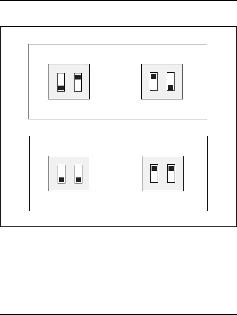
Option settings Page 135 of 906
Circuit Card Description and Installation
Figure 20
NT8D72 DIP switch settings
S1 S2
1122
or
75 ohm switch setting 120 ohm switch setting (default)
NT8D72AA, NT8D72AB
NT8D72BA
S1 S2
OFF
ON
OFF
ON
S1 S2
1122
or
75 ohm switch setting 120 ohm switch setting (default)
S1 S2
OFF
ON
OFF
ON
553-7463

Page 136 of 906 Option settings
553-3001-211 Standard 3.00 August 2005
QPC43 Peripheral Signaling card
QPC71 E&M/DX Signaling and Paging Trunk cards
Options (minimum vintage N) Plug location
NT5D21 Core/Network module
NT8D35 Network module
F13
Application
Unit 0 E35 switch Unit 1 E5 switch
1234567812345678
E&M off off off on off off on off off off off on off off on off
Paging off off off off off off off off off off off off off off off off
DX 2-wire
(conductor
loop <
2.5 K ¾)
on on off off off on off on on on off off off on off on
DX 2-wire
(conductor
loop >
2.5 K ¾)
on on on on off on off on on on on on off on off on
DX 4-wire
(conductor
loop <
2.5 K ¾)
off off off off on on off on off off off off on on off on
DX 4-wire
(conductor
loop >
2.5 K ¾)
off off on on on on off on off off on on on on off on
Note: DX trunks must be balanced correctly. If the loop is <2.5 K ¾, far-end balancing is
standard. If the loop is >2.5 K ¾, far end balancing requires standard plus 2.5 K ¾. To connect
PBX to PBX, switches should be arranged for loops to be >2.5 K ¾ at one end and <2.5 K ¾ at
the other. Apply similar treatment when connecting to Pulse QPJ69 trunks.

Option settings Page 137 of 906
Circuit Card Description and Installation
QPC414 Network card
Application
Pin connection
J3/S2 and J4/S1
T-1 facilities (including PRI/DTI),* channel service
unit
connect pins 1 and 2
(pin 1 is next to the white dot)
Note 1: Possible jumper locations for vintage B (for different styles/series):
J3—E11 or H11
J4—H17 or E7
S1 and S2—E33
Note 2: Possible jumper locations for vintage A (for different styles/series). These cards do not
have the option selection and can only be used in the option A setting:
J3—H5 or E11
J4—H17 or E7
S1 and S2—E33
Note 3: Connectors and loop relations:
Even loop: J1 faceplate connector, jumper at J4 or S1
Odd loop: J2 faceplate connector, jumper at J3 or S2
Page 138 of 906 Option settings
553-3001-211 Standard 3.00 August 2005
QPC441 3-Port Extender cards
For CS 1000M SG and Multi Group systems, QPC441 vintage F or later must
be used in all modules.
Table 45
QPC441 3PE card installed in the NT4N41CP PII Core/Net modules
Jumper Settings: Set Jumper RN27 at E35 to “A”.
Switch Settings
Module D20 switch position
NT4N41 CP Core/Net modules only 1 2 3 4 5 6 7 8
Core/Net 0
(Shelf 0)
Group 0 off on on off on on on on
Group 1 off on on off on on off on
Group 2 off on on off on off on on
Group 3 off on on off on off off on
Group 4 off on on off off on on on
Group 5 off on on off off on off on
Group 6 off on on off off off on on
Group 7 off on on off off off off on
Core/Net 1
(Shelf 1)
Group 0 off on on off on on on off
Group 1 off on on off on on off off
Group 2 off on on off on off on off
Group 3 off on on off on off off off
Group 4 off on on off off on on off
Group 5 off on on off off on off off
Group 6 off on on off off off on off
Group 7 off on on off off off off off
Option settings Page 139 of 906
Circuit Card Description and Installation
Table 46
QPC441 3PE card installed in the NT5D21 modules
Jumper Settings: Set Jumper RN27 at E35 to “A”.
Switch Settings
Module D20 switch position
1 2 3 4 5 6 7 8
NT5D21 (Option 61C)
Core/Network 0 off on on off on on on on
Core/Network 1 off on on off on on on off
NT5D21 (Option 81C)
Core/Net 0
(Shelf 0)
Group 0 off on on off on on on on
Group 1 off on on off on on off on
Group 2 off on on off on off on on
Group 3 off on on off on off off on
Group 4 off on on off off on on on
Group 5 off on on off off on off on
Group 6 off on on off off off on on
Group 7 off on on off off off off on
Core/Net 1
(Shelf 1)
Group 0 off on on off on on on off
Group 1 off on on off on on off off
Group 2 off on on off on off on off
Group 3 off on on off on off off off
Group 4 off on on off off on on off
Group 5 off on on off off on off off
Group 6 off on on off off off on off
Group 7 off on on off off off off off
Page 140 of 906 Option settings
553-3001-211 Standard 3.00 August 2005
Table 47
QPC441 3PE card installed in the NT8D35 module
Jumper Settings: Set Jumper RN27 at E35 to “A”.
Switch Settings
Modules
D20 switch position
1 2 3 4
Option 81, 81C (Note 1) off on on on
Shelf Group 5 6 7 8
0on on on on
1on on off on
0 2 on off on on
3on off off on
4off on on on
5off on off on
6off off on on
7off off off on
0on on on off
1on on off off
1 2 on off on off
3on off off off
4off on on off
5off on off off
6off off on off
7off off off off
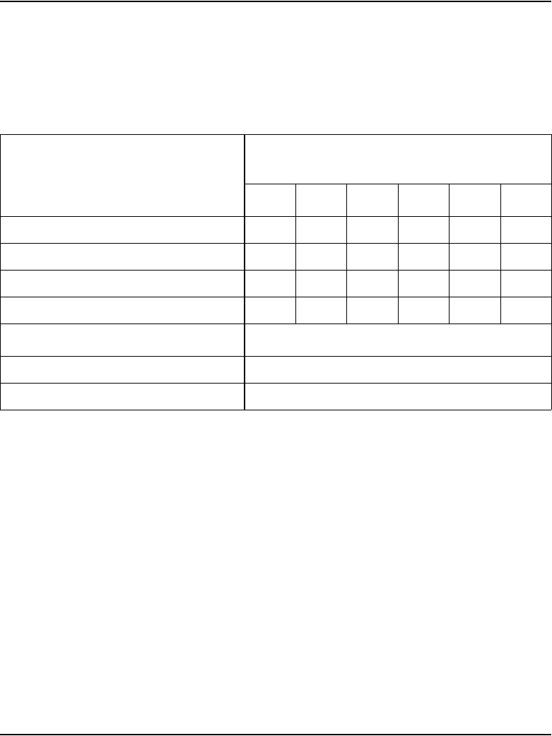
Option settings Page 141 of 906
Circuit Card Description and Installation
QPC559, QPC560 Loop Signaling Trunk cards
Table 48 and Table 49 on page 142 list option settings for loop signaling
trunk cards.
Table 48
QPC559, QPC560 single density
Application
Single density—Unit 0/1
F30/F8 switch
123456
Outgoing ANI only:
loop pulsing off off off off off off
battery and ground pulsing off off off off on off
Other than outgoing ANI on off on off on off
Jumpers (QPC560) Units 0/1/2/3
600 ¾ resistive impedance connect pins 1 and 2
3-component complex impedance connect pins 2 and 3
Page 142 of 906 Option settings
553-3001-211 Standard 3.00 August 2005
Table 49
QPC559, QPC560 double density
Application
Double density—Unit 0/1/2/3
H17/H3/A17/A3 switch
123456
Outgoing ANI only:
loop pulsing off off off off off off
battery and ground pulsing off off off off on off
Other than outgoing ANI on off on off on off
Jumpers (QPC560) Units 0/1/2/3
600 ¾ resistive impedance connect pins 1 and 2
3-component complex impedance connect pins 2 and 3
Option settings Page 143 of 906
Circuit Card Description and Installation
QPC528 CO/FX/WATS Trunk cards
Table 50 lists switch and jumper settings for options available.
Table 50
QPC528 Trunk cards switch and jumper settings
Switch Settings
Switch position:
Switch S1 (location A23)
12345678
on off on off on off on off
Switch position:
Unit 0, Switch S2 (Location E29)
Unit 1, Switch S3 (Location E9)
Unit 2, Switch S4 (Location A28)
Unit 3, Switch S5 (Location A10)
12345678910
Trunk type:
Loop start off on off off on off off off
Ground start off on on on on off off off
Metering:
Second pair (M, MM) or off off
Third wire, battery on M or off on
Third wire, ground on M on off
Jumper Settings
Unit 0 jumper (Location E27)
Unit 1 jumper (Location E11)
Unit 2 jumper (Location D29)
Unit 3 jumper (Location D9)
Jumper: Unit 0
Jumper
Unit 1
Jumper
Unit 2
Jumper
Unit 3
Jumper
600 ¾ resistive impedance Pin 1 to 2 Pin 1 to 2 Pin 1 to 2 Pin 1 to 2
3-component complex
impedance
Pin 2 to 3 Pin 2 to 3 Pin 2 to 3 Pin 2 to 3
Page 144 of 906 Option settings
553-3001-211 Standard 3.00 August 2005
QPC471 Clock Controller card
Table 51 lists option settings for the QPC471 Clock Controller card.
Table 51
QPC471 vintage H
System
SW1 SW2 SW4
1 2 3 4 1 2 3 4 1 2 3 4
61C on on on on off off off off off on * *
81 off off off off off off off off off on * *
81C on off off off off off off off ** on * *
81C with Fiber Network on off off off off off off off ** on * *
*Cable length between the J3
faceplate connectors:
0–4.3 m (0–14 ft) off off
4.6–6.1 m (15–20 ft) off on
6.4–10.1 m (21–33 ft) on off
10.4–15.2 m (34–50 ft) on on
*If there is only one Clock Controller card in the system, set to OFF. If there are two Clock Controller
cards, determine the total cable length between the J3 connectors (no single cable can exceed 25 ft.)
and set these two switch positions for this cable length, as shown above. The maximum total (combined)
length is 50 ft. Set the switches on both cards to the same settings.
** Set to ON for clock controller 0. Set to OFF for clock controller 1.
Note: FNF based-systems the total clock path length is equal to the length of the NTRC49
cable used to connect between the two clock controller cards.
Option settings Page 145 of 906
Circuit Card Description and Installation
QPC525, QPC526, QPC527, QPC777 CO Trunk card
Note 1: There is no ground start signalling for QPC777 CO trunk cards.
Always select loop start signalling for QPC777 CO trunk cards.
Note 2: On QPC777 CO trunk cards, the pads are in for short line
lengths and the pads are out for long line lengths.
Application
Switches at E29/E9/A29/A11 Units 0/1/2/3
1 2 3 4 5 6 7 8
Zero ohm outpulsing on off off
Standard outpulsing off on off
Ground start on on off
Loop start off off off
Loop start, automatic guard detection off on off
PPM daughterboard not installed on off
PPM daughterboard installed off off
Battery on M operation off on off
Ground on M operation on off off
Second pair M&MM off off off
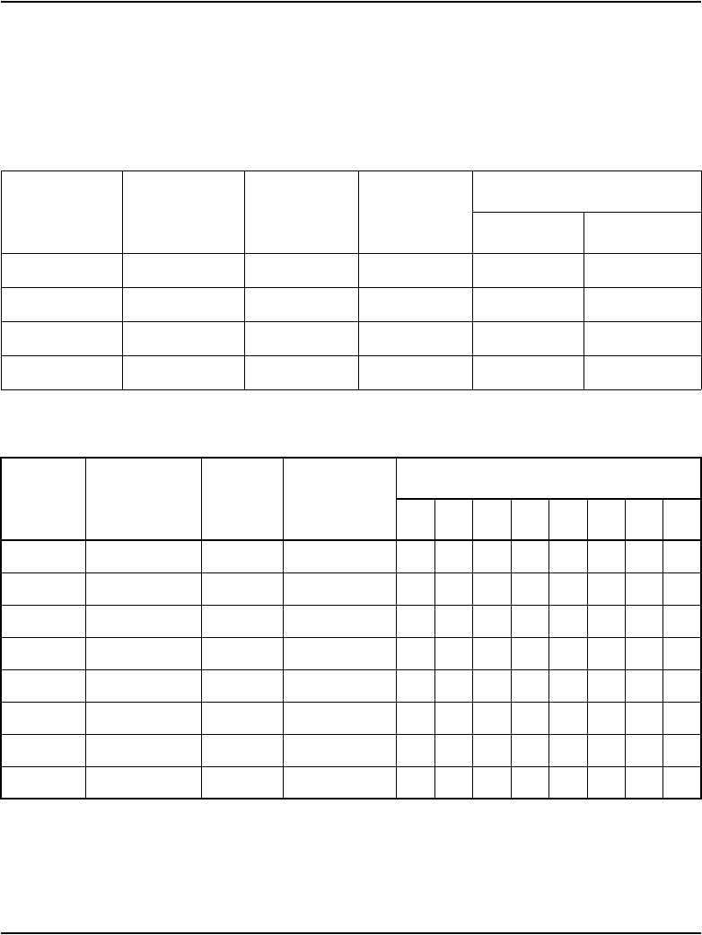
Page 146 of 906 Option settings
553-3001-211 Standard 3.00 August 2005
QPC550 Direct Inward Dial Trunk card
Tables 52 through 56 give the option settings for the QPC550 DID Trunk
card.
Table 52
QPC550 vintages A and B—real/complex balance impedance selection
Device
location
Device
designation
Switch
number
Unit
number
Impedance type
Real Complex
F31 S4.0 1 0 on off
F24 S4.1 1 1 on off
F16 S4.2 1 2 on off
F11 S4.3 1 3 on off
Table 53
QPC550 vintage A—600/900 Ohm impedance selection
Device
location
Device
designation
Unit
number
Impedance
(ohms)
Switch number
12345678
G29(a) S3.0 0600 off on on off off on on off
900 on off off on on off off on
G29(b) S3.1 1600 off on on off off on on off
900 on off off on on off off on
G8(a) S3.2 2600 off on on off off on on off
900 on off off on on off off on
G8(b) S3.3 3600 off on on off off on on off
900 on off off on on off off on
Option settings Page 147 of 906
Circuit Card Description and Installation
Table 54
QPC550 vintage A—software/hardware control for 2dB pad
Device
location
Device
designation
Unit
number
Switch
number S/W
2 dB pad control
H/W
(pad in) (pad out)
F38 S1 0 1 off off on
2on off off
1 3 on off off
4off off on
F1 S2 0 1 off off on
2on off off
1 3 on off off
4off off on
Table 55
QPC550 vintage B—attenuation level control
Device
location
Device
designation
Unit
number
Switch number
2 dB option1 2 3 4 5 6 7 8
D39 S2.0/1 0on on on on on
1off off off off off
D1 S2.2/3 2on on on on on
3off off off off off

Page 148 of 906 Option settings
553-3001-211 Standard 3.00 August 2005
Table 56
QPC550 vintage B—software control for 2dB pad
Device
location
Device
designation
Unit
number
Switch
number
2 dB pad control
H/W
(pad in) (pad out)
F38 S1.0/1 1 1 on off
2off off
0 3 off off
4on off
F1 S1.2/3 3 1 on off
2off off
2 3 off off
4on off

Option settings Page 149 of 906
Circuit Card Description and Installation
QPC551 Radio Paging Trunk card
Signal duration on the 18-pair faceplate S1 (F33)
1 2 3 4 5 6
Binary value (.1 second) 1 2 4 8 16 32
Note: This switch determines the length of time a signal stays on the 18-pair data bus. The time
is set in binary to the nearest tenth second. For example, to keep data on the bus for 5 seconds,
the switch settings total 50 by closing S1.2, S1.5, and S1.6.
Signal duration and pause time S2 (G33)
1 2 3 4 5 6 7
Binary value (.1 second) 1 2 4 8 16 32 64
Note: This switch determines the time data must stay on the 18-pair data bus plus the pause
time between the removal of data and the reappearance of subsequent data. The time is set in
binary to the nearest tenth second. For example, to keep data on the bus for 5 seconds and have
a pause time of 3.2 seconds, the switch settings should total 82 by closing S2.2, S2.5, and S2.7.
Application S3 (E2) S4 (F2)
Unit 0, Unit 1
1 2 Address 3 4 5 6 Address 3456
Paging 0off off off off 8off off off on
single on 1on off off off 9on off off on
multiple off 2off on off off 10 off on off on
3on on off off 11 on on off on
Timer* 4on off on off 12 on off on on
enabled on 5on on on off 13 on off on on
disabled off 6off on on off 14 off on on on
7on on on off 15 on on on on
* When enabled, this switch prevents a signal from being sent from a paging unit until 5 seconds have
elapsed since the beginning of the previous signal on that same unit.
S5 (E38)
Unit 0
S6 (D1)
Unit 1
Impedance termination 1
Real on
Complex off

Page 150 of 906 Option settings
553-3001-211 Standard 3.00 August 2005
QPC595 Digitone Receiver cards
QPC577, QPC596 Digitone Receiver daughterboards
QPC720 Primary Rate Interface card
Location Connection
12 DTMF tones E9 Center to E3
16 DTMF tones E9 Center to E2
16/12 tone options jumper Jumper at P1
16 tone (4 x 4) connect pins 1 and 2
12 tone (3 x 4) connect pins 2 and 3
Note: When a DTR daughterboard is installed, check YES on the faceplate of the QPC659 Dual
Loop Peripheral Buffer.
Table 57
QPC720 Primary Rate Interface card (Part 1 of 2)
Switch S2 settings To repeater facility To cross-connect point
5 on 0–45 m
(0–150 ft)
0–30 m
(0–100 ft)
2, 4, 6 on 46–135 m
(151–450 ft)
31–100 m
(101–355 ft)
Note 1: All positions on S2 (location B22) are OFF except as shown under the column labeled
“Switch S2 settings.”
Note 2: Framing format, line encoding, and method of yellow alarm are selectable for both DTI
and PRI in LD17 with the DLOP, LCMT, and YALM prompts. All SW3 switch positions should be
OFF.

Option settings Page 151 of 906
Circuit Card Description and Installation
1, 3, 7 on 136–225 m
(451–750 ft)
101–200 m
(356–655 ft)
Switch 3 option for DTI with ESF
SW3-1 on = extended superframe format (ESF)
off = superframe format (SF)
Table 57
QPC720 Primary Rate Interface card (Part 2 of 2)
Switch S2 settings To repeater facility To cross-connect point
Note 1: All positions on S2 (location B22) are OFF except as shown under the column labeled
“Switch S2 settings.”
Note 2: Framing format, line encoding, and method of yellow alarm are selectable for both DTI
and PRI in LD17 with the DLOP, LCMT, and YALM prompts. All SW3 switch positions should be
OFF.
Page 152 of 906 Option settings
553-3001-211 Standard 3.00 August 2005
QPC775 Clock Controller card
Tables 58 and 59 give option settings for the QPC775 Clock Controller
card.
Table 58
QPC775 (before vintage E) switch settings
System
SW2 SW3 SW4
1 2 3 4 1 2 3 4 1 2 3 4
CS 1000M MG off off off off off off off off on on on on
CS 1000M SG on on on on off off off off on on on on
Table 59
QPC775 vintage E switch settings
System
SW1 SW2 SW4
1 2 3 4 1 2 3 4 1 2 3 4
CS 1000M SG on on on on off off off off off on * *
CS 1000M MG on off off off off off off off ** on * *
*Cable length between the J3
faceplate connectors:
0–4.3 m (0–14 ft) off off
4.6–6.1 m (15–20 ft) off on
6.4–10.1 m (21–33 ft) on off
10.4–15.2 m (34–50 ft) on on
*If there is only one Clock Controller card in the system, set to OFF. If there are two Clock Controller
cards, determine the total cable length between the J3 connectors (no single cable can exceed 25 ft.)
and set these two switch positions for this cable length, as shown above. The maximum total (combined)
length is 50 ft. Set the switches on both cards to the same settings.
** Set to ON for clock controller 0. Set to OFF for clock controller 1.

Option settings Page 153 of 906
Circuit Card Description and Installation
QPC841 4-Port Serial Data Interface card
Tables 60 through 62 list option settings for the QPC841 4-Port SDI card.
Table 60
QPC841 port 1 and 2 address selection
Device number SW14
Port 1 Port 2 1 2 3 4 5 6 7 8
0 1 off off off off off on on on
2 3 off off off off off on on off
4 5 off off off off off on off on
6 7 off off off off off on off off
8 9 off off off off off off on on
10 11 off off off off off off on off
12 13 off off off off off off off on
14 15 off off off off off off off off
Note 1: On SW16, positions 1, 2, 3, and 4 must be OFF.
Note 2: To avoid address conflicts, SW14 and SW15 can never have identical setting.
Note 3: To disable ports 1 and 2, set SW14 position 1 to ON.
Page 154 of 906 Option settings
553-3001-211 Standard 3.00 August 2005
Device number SW15
Port 3 Port 4 1 2 3 4 5 6 7 8
0 1 off off off off off on on on
2 3 off off off off off on on off
4 5 off off off off off on off on
6 7 off off off off off on off off
8 9 off off off off off off on on
10 11 off off off off off off on off
12 13 off off off off off off off on
14 15 off off off off off off off off
Note 1: On SW16, positions 1, 2, 3, and 4 must be OFF.
Note 2: To avoid address conflicts, SW14 and SW15 can never have identical setting.
Note 3: To disable ports 3 and 4, set SW15 position 1 to ON.
Table 61
QPC841 baud rate
Baud
rate
Port 1 SW10 Port 2 SW11 Port 3 SW12 Port 4 SW13
1 2 3 4 1 2 3 4 1 2 3 4 1 2 3 4
150 off off on on off off on on off off on on off off on on
300 off on off on off on off on off on off on off on off on
600 off off off on off off off on off off off on off off off on
1200 off on on off off on on off off on on off off on on off
2400 off off on off off off on off off off on off off off on off
4800 off on off off off on off off off on off off off on off off
9600 off off off off off off off off off off off off off off off off

Option settings Page 155 of 906
Circuit Card Description and Installation
Table 62
QPC841 DTE or DCE selection
Mode Port 1—SW8 Port 1—SW9
123456123456
DTE (terminal) on on on on on on off off off off off off
DCE (modem)
NT1P61 (Fiber)
off
on
off
off
off
off
off
on
off
off
off
off
on
on
on
off
on
off
on
off
on
on
on
on
Port 2—SW6 Port 2—SW7
DTE on on on on on on off off off off off off
DCE off off off off off off on on on on on on
NT1P61 (Fiber) on off off on off off on off off off on on
Port 3—SW4 Port 3—SW5
DTE on on on on on on off off off off off off
DCE off off off off off off on on on on on on
Port 4—SW2 Port 4—SW3
DTE on on on on on on off off off off off off
DCE off off off off off off on on on on on on


Page 157 of 906
Circuit Card Description and Installation
182
NT1R20 Off-Premise Station
Analog Line card
Contents
This section contains information on the following topics:
Introduction . . . . . . . . . . . . . . . . . . . . . . . . . . . . . . . . . . . . . . . . . . . . . . 157
Physical description. . . . . . . . . . . . . . . . . . . . . . . . . . . . . . . . . . . . . . . . 158
Functional description . . . . . . . . . . . . . . . . . . . . . . . . . . . . . . . . . . . . . . 160
Electrical specifications. . . . . . . . . . . . . . . . . . . . . . . . . . . . . . . . . . . . . 165
Operation. . . . . . . . . . . . . . . . . . . . . . . . . . . . . . . . . . . . . . . . . . . . . . . . 168
Connector pin assignments . . . . . . . . . . . . . . . . . . . . . . . . . . . . . . . . . . 172
Configuring the OPS analog line card. . . . . . . . . . . . . . . . . . . . . . . . . . 174
Application . . . . . . . . . . . . . . . . . . . . . . . . . . . . . . . . . . . . . . . . . . . . . . 175
Introduction
The NT1R20 Off-Premise Station (OPS) analog line card is an intelligent
eight-channel analog line card designed to be used with 2-wire analog
terminal equipment such as analog (500/2500-type) telephones and analog
modems.
The NT1R20 Off-Premise Station (OPS) analog line card provides eight
full-duplex analog telephone line interfaces. Each line has integral hazardous
and surge voltage protection to protect the system from damage due to
lightning strikes and accidental power line connections. This card is normally

Page 158 of 906 NT1R20 Off-Premise Station Analog Line card
553-3001-211 Standard 3.00 August 2005
used whenever the phone lines have to leave the building in which the switch
is installed.
The NT1R20 OPS analog line card provides:
• line supervision
• hookflash
• battery reversal
Each unit is independently configured by software control in the Analog (500/
2500 type) Telephone Administration program LD 10.
You can install this card in any IPE slot.
Physical description
The line interface and common multiplexing circuitry is mounted on a 31.75
cm by 25.40 cm (12.5 in. by 10 in.) printed circuit board.
The OPS analog line card connects to the IPE backplane through a 160-pin
connector shroud. A 25-pair amphenol connector below the card is cabled to
the cross connect terminal (also called the Main Distribution Frame (MDF)).
Telephone lines from station equipment cross connect to the OPS analog line
card at the cross connect using a wiring plan similar to trunk cards.
Self Test
The faceplate of the NT1R20 OPS analog line card is equipped with a red
LED. When an OPS analog line card is installed, the LED remains lit for two
to five seconds while the self-test runs. If the self-test completes successfully,
the LED flashes three times and remains lit. When the card is configured and
enabled in software; then the LED goes out. If the LED continues to flash or
remains weakly lit, replace the card. See Figure 21 on page 159.
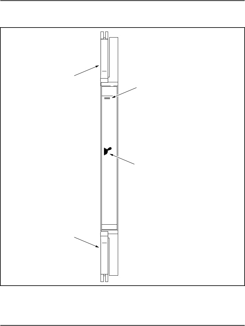
Page 160 of 906 NT1R20 Off-Premise Station Analog Line card
553-3001-211 Standard 3.00 August 2005
Functional description
This functional description of the NT1R20 Off-Premise Station (OPS) analog
line card is divided into two parts. First, a description of the card’s control,
signaling, and power interfaces is given, followed by a description of how the
card itself functions. See Figure 22.
Figure 22
OPS analog line card – block diagram
Input/output
interface
control
Codec
PCM
Micro-
controller
DS-30X
interface
5.12 MHz
clock
Tx PCM
Async card
LAN link
Front
panel
LED
Card LAN
interface
Tip
Line interface units 0–3
Ring
Codec
PCM Analog
hybrid XFMR
Signaling relays
(ringing, battery
reversal)
Line interface units 4–7
Line interface unit power
Rx PCM
1 kHz
frame sync
Controller
card
Line
signaling
interface
Control
logic
Reg
Signaling
and status
Address/
data bus
553-6193
Power
supplies
+5 V dc
analog
hybrid
±15 V dc
analog
power
+8.5 V dc +5 V dc logic power
Ringing
– 48 V dc
battery
Rsync
Analog
telephone
lines
Tip
Ring
Analog
telephone
lines
Loop current/
dialpulse detect
Analog
hybrid XFMR
Signaling relays
(ringing, battery
reversal)
Loop current/
dialpulse detect
Card slot
address
Backplane

NT1R20 Off-Premise Station Analog Line card Page 161 of 906
Circuit Card Description and Installation
Card interfaces
Voice and signaling interfaces
The eight line interfaces provided by the NT1R20 OPS analog line card
connect to conventional, 2-wire (tip and ring), analog line facilities. Incoming
analog voice and signaling information from a line facility is converted by the
OPS analog line card to digital form and routed to the CPU over DS-30
network loops. Conversely, digital voice and signaling information from the
CPU is sent over DS-30 network loops to the OPS analog line card where it
is converted to analog form and applied to the line facility.
The OPS analog line card uses only eight of the 30 available timeslots for its
eight line interfaces. The OPS analog line card can be configured in software
to format PCM data in the µ-law or A-law conventions.
Maintenance communication
Maintenance communication is the exchange of control and status data
between line or trunk cards and the CPU. Maintenance data is transported
through the card LAN link.
The card LAN link supports the following functions on the NT1R20 OPS
analog line card:
• polling
• reporting of self-test status
• CPU initiated card reset
• reporting of card ID (card type and hardware vintage)
• reporting of firmware version
• reporting of line interface unit configuration
• enabling/disabling of the DS-30X network loop busy
• reporting of card status
Power interface
Power is provided to the NT1R20 OPS analog line card by the NTAK78
ac/dc or NTAK72 DC power supply.

Page 162 of 906 NT1R20 Off-Premise Station Analog Line card
553-3001-211 Standard 3.00 August 2005
Line interface units
The NT1R20 OPS analog line card contains eight independently configurable
interface units. Relays are provided in each unit to apply ringing onto the line.
Signal detection circuits monitor on-hook/off-hook signaling. Two codecs
are provided for performing Analog/Digital (A/D) and Digital/Analog (D/A)
conversion of analog voiceband signals to digital PCM signals.
Each codec supports four interface units and contains switchable pads for
control of transmission loss on a per unit basis. The following features are
common to all units on the card:
• OPS or ONS service configurable on a per unit basis
• terminating impedance (600 or 900 ohms) selectable on a per unit basis
• standard or complex balance impedance (600 or 900 ohms, 3COM1 or
3COM2) selectable on a per unit basis
• loopback of PCM signals over DS-30X network loop for diagnostic
purposes
Signaling and control
This portion of the card provides circuits that establish, supervise, and take
down call connections. These circuits work with the CPU to operate line
interface circuits during calls. The circuits receive outgoing call signaling
messages from the CPU and return incoming call status information over the
DS-30X network loop.
Card control functions
Control functions are provided by a microcontroller, a card LAN interface,
and signaling and control circuits on the NT1R20 OPS analog line card.
Microcontroller
The NT1R20 OPS analog line card contains a microcontroller that controls
the internal operation of the card and the serial card LAN link to the controller
card. The microcontroller controls the following:
• reporting to the CPU through the card LAN link:
— card identification (card type, vintage, and serial number)

NT1R20 Off-Premise Station Analog Line card Page 163 of 906
Circuit Card Description and Installation
— firmware version
— self-test status
— programmed configuration status
• receipt and implementation of card configuration:
— programming of the codecs
— enabling/disabling of individual units or entire card
— programming of input/output interface control circuits for
administration of line interface unit operation
— maintenance diagnostics
— transmission loss levels
Card LAN interface
Maintenance data is exchanged with the CPU over a dedicated asynchronous
serial network called the Card LAN link. The Card LAN link is described in
the section “Intelligent Peripheral Equipment” on page 32.
The NT1R20 OPS analog line card has the capability of providing an
interrupted dial tone to indicate that a message is waiting or that call
forwarding is enabled. The line card (optionally) receives messages stating
that these conditions exist over the Card LAN Interface and interrupts the dial
tone when either of these conditions are detected.
Software service changes
Individual line interface units on the NT1R20 OPS analog line card are
configured to either OPS (for OPS application) or On-premises Station
(ONS) (for ONS application) Class of Service (CLS) in the Analog (500/
2500-type) Telephone Administration program LD 10. See Table 63.
LD 10 is also used to select unit terminating impedance and balance network
impedance at the TIMP and BIMP prompts, respectively.
The message waiting interrupted dial tone and call forward reminder tone
features are enabled by entering data into the customer data block using
LD 15.

Page 164 of 906 NT1R20 Off-Premise Station Analog Line card
553-3001-211 Standard 3.00 August 2005
See Software Input/Output: Administration (553-3001-311) for LD 10
service change instructions.
Table 63
OPS analog line card configuration
Application On-premise station (ONS) Off-premise station (OPS)
Class of service ONS OPS
Loop resistance 0 - 460 ohm 0 - 2300 ohm
Jumper strap
settingbBoth JX. 0 and JX 1 off Both JX. 0 and JX.
1 off
Both JX. 0 and JX.
1 on
Loop loss dBc0-1.5 >1.5-2.
5
>2.5-3.
0
0-1.5 >1.5-2.
5
>2.5-4.
5
>4.5-15
TIMP 600
ohm
600
ohm
600
ohm
600
ohm
600
ohm
600
ohm
600
ohm
BIMP 600
ohm
3COM 3CM2 600
ohm
3COM 3CM2 3CM2
Gain treatment eNo Yes
a. Configured in the Analog (500/2500-type) Telephone Administration program (LD 10).
b. Jumper strap settings JX 0 and JX. 1 apply to all eight units; “X” indicates the unit number,
0-7. “OFF” indicates that a jumper strap is not installed across both pins on a jumper block.
Store unused straps on the OPS analog line card by installing them on a single jumper pin.
c. Loss of untreated (no gain devices) metallic line facility. Upper loss limits correspond to loop
resistance ranges for 26 AWG wire.
d. Default software impedance settings are:
ONS CLSOPS CLS
TIMP:600 ohm600 ohm
BIMP:600 ohm3COM2
e. Gain treatment, such as a voice frequency repeater (VFR) is required to limit the actual OPS
loop loss to 4.5 dB, maximum. VFR treatment of metallic loops having untreated loss greater
than 15dB (equivalent to a maximum signaling range of 2300 ohm on 26 AWG wire) is not
recommended.

NT1R20 Off-Premise Station Analog Line card Page 165 of 906
Circuit Card Description and Installation
Port-to-port loss configuration
The loss plan for the NT1R20 OPS analog line card determines port-to-port
loss for connections between an OPS analog line card unit (port) and other
ports.
The transmission properties of each line unit are characterized by the OPS or
ONS class of service assigned in the Analog (500/2500-type) Telephone
Administration program LD 10.
The OPS analog line card provides transmission loss switching for control of
end-to-end connection loss. Control of loss is a major element in controlling
transmission performance parameters such as received volume, echo, noise,
and crosstalk. The loss plan for the OPS analog line card determines
port-to-port loss for connections between an OPS analog line card unit (port)
and other IPE ports. LD 97 is used to configure systems for port-to-port loss.
See Software Input/Output: Administration (553-3001-311) for LD 97
service change instructions.
Electrical specifications
This section lists the electrical characteristics of the NT1R20 OPS analog line
card.
Circuit power
The +8.5 V dc input is regulated down to +5 V dc for use by the digital logic
circuits. All other power to the card is used by the line interface circuits.
The ±15.0 V dc inputs to the card are used to power the analog circuits. The
+5 V dc from the module power supply is used for the analog hybrid. The
–48.0 V dc input is for the telephone battery. Ringing power for telephones is
86 Vrms ac at 20 Hz on –48 V dc. The Rsync signal is used to switch the
20 Hz ringing on and off at the zero cross-over point to lengthen the life of
the switching circuits.

Page 166 of 906 NT1R20 Off-Premise Station Analog Line card
553-3001-211 Standard 3.00 August 2005
Analog line interface
Table 64 lists the electrical characteristics of NT1R20 OPS analog line card
line interface units.
Table 64
OPS analog line card – electrical characteristics
Characteristic Specification
Terminal impedance (TIMP) 600 or 900 ohms
Balance impedance (BIMP) 600 or 900 ohms, 3COM, or 3CM2
DC signaling loop length (max) 2300 ohm loop (including resistance
of telephone) with nominal battery of
–48 V dc
Battery supply voltage –42 to –52.5 V dc
Minimum detected loop current 16 mA
Ground potential difference ± 3 V
Line leakage > 30k ohms, tip-to-ring,
tip-to-ground, ring-to-ground
AC induction rejection 10 V rms, tip-to-ring,
tip-to-ground, ring-to-ground

NT1R20 Off-Premise Station Analog Line card Page 167 of 906
Circuit Card Description and Installation
Power requirements
Table 65 shows the maximum power consumed by the card from each system
power supply.
Foreign and surge voltage protection
The NT1R20 OPS analog line card meets UL-1489 and CS03 over-voltage
(power cross) specifications and FCC Part 68 requirements for hazardous and
surge voltage limits.
Ringer limitations
The OPS line card supports up to three NE-C4A (3 REN) ringers on each line
for either ONS or OPS applications. See Table 66.
Table 65
OPS analog line card – power requirements
Voltage Tolerance Current (max.)
±15.0 V dc ± 5% 150 mA
+8.5 V dc ± 2% 200 mA
+5.0 V dc ± 5% 100 mA
–48.0 V dc ± 5% 350 mA
Table 66
OPS analog line card – ringer limitations (Part 1 of 2)
ONS Loop Range
Maximum Number of
Ringers (REN)
0–10 ohms 3
> 10–460 ohms 2
Page 168 of 906 NT1R20 Off-Premise Station Analog Line card
553-3001-211 Standard 3.00 August 2005
Environmental specifications
Table 67 shows the environmental specifications of the OPS analog line
card.
Operation
The applications, features, and signaling arrangements for each unit on the
NT1R20 OPS analog line card are assigned through LD 10 and/or jumper
strap settings on the card.
The operation of each unit is configured in software and implemented in the
card through software download messages. When the NT1R20 OPS analog
line card unit is idle, it provides a ground on the tip lead and –48 V dc on the
ring lead. The on-hook telephone presents a high impedance toward the line
interface unit on the card.
OPS Loop Range
Maximum Number of
Ringers (REN)
0 – 10 ohms 3
> 10 – 900 ohms 2
> 900 – 2300 ohms 1
Table 67
OPS analog line card – environmental specifications
Parameter Specifications
Operating temperature 0° to +60° C (+32 to +140° F),
ambient
Operating humidity 5 to 95% RH (non-condensing)
Storage temperature –40° to +70° C (–40° to +158° F)
Table 66
OPS analog line card – ringer limitations (Part 2 of 2)
NT1R20 Off-Premise Station Analog Line card Page 169 of 906
Circuit Card Description and Installation
Incoming calls
Incoming calls to a telephone connected to the NT1R20 OPS analog line card
originate from stations that can be local (served by the PBX) or remote
(served through the public switched telephone network). The alerting signal
to telephones is 20 Hz (nominal) ringing. When an incoming call is answered,
ringing is tripped as the telephone goes off-hook, placing a low-resistance dc
loop across the tip and ring leads toward the OPS analog line card. (see
Table 68).
Table 68
Call connection sequence—near-end station receiving call (Part 1 of 2)
State
Signal / Direction
Far-end / Near-end Remarks
Line card unit idle Group on tip, battery on ring
High resistance loop
No battery current drawn.
Far-end station goes off-hook and
addresses (dials-up) the near-end
station. The system receives the
incoming call on a trunk and determine
the TN.
Incoming call Ringing The system applies 20 Hz ringing to ring
lead.
Near-end station
off-hook
Low resistance loop
Two-way voice
connection
The system detects increase in loop
current, tips ringing, and put call through
to near-end station.
Near end station
hangs up first
High-resistance loop If near end station hangs-up first, the
line card detects the drop in loop
current.
Line card unit idle Group on tip, battery on ring
High resistance loop
Line card unit is ready for the next call.
Page 170 of 906 NT1R20 Off-Premise Station Analog Line card
553-3001-211 Standard 3.00 August 2005
Outgoing calls
For outgoing calls from a telephone, a line unit is seized when the telephone
goes off-hook, placing a low-resistance loop across the tip and ring leads
towards the NT1R20 OPS analog line card (see Table 69 on page 170). When
the card detects the low-resistance loop, it prepares to receive digits. When
the system is ready to receive digits, it returns a dial tone. Outward address
signaling is then applied from the telephone in the form of loop (interrupting)
dial pulses or DTMF tones.
Far end station
hangs up first
High resistance loop If the far-end hangs-up first, the system
detects disconnect signalling from the
trunk. The person at the near-end
recognizes the end of the call and
hangs-up.
Line card unit idle Ground on tip/battery on ring
High resistance loop
Line card unit is ready for the next call.
Table 69
Call connection sequence—near-end station receiving call (Part 1 of 2)
State
Signal / Direction
Far-end / Near-end Remarks
Line card unit idle Group on tip, battery on ring
High resistance loop
No battery current drawn.
Call request Low resistance loop Near-end station goes off-hook.
Battery current is drawn, causing
detection of off-hook state.
Dial Tone Dial tone is applied to the near end
station from the system.
Table 68
Call connection sequence—near-end station receiving call (Part 2 of 2)
State
Signal / Direction
Far-end / Near-end Remarks
NT1R20 Off-Premise Station Analog Line card Page 171 of 906
Circuit Card Description and Installation
Outpulsing Addressing signals Near-end station dials number (loop
pulsing or DTMF tones).
The system detects start of dialing and
remove dial tone.
Ringback (or busy) The system decodes addressing, route
calls, and supply ringback tone to
near-end station if far-end is on-hook.
(Busy tone is supplied if far-end is
off-hook).
Two-way voice
connection
When call is answered, ringback tone is
removed, and call is put through to
far-end station.
Near-end station
hangs-up first
High resistance loop If near end station hangs-up first, the
line card detects the drop in loop
current.
Line card unit idle Group on tip, battery on ring
High resistance loop
Line card unit is ready for the next call.
Far end station
hangs up first
High resistance loop If the far-end hangs-up first, the system
detects disconnect signalling from the
trunk. The person at the near-end
recognizes the end of the call and
hangs-up.
Line card unit idle Ground on tip/battery on ring
High resistance loop
Line card unit is ready for the next call.
Table 69
Call connection sequence—near-end station receiving call (Part 2 of 2)
State
Signal / Direction
Far-end / Near-end Remarks

Page 172 of 906 NT1R20 Off-Premise Station Analog Line card
553-3001-211 Standard 3.00 August 2005
Connector pin assignments
The OPS analog line card brings the eight analog telephone lines to the IPE
backplane through a 160-pin connector shroud. The backplane is cabled to the
input/output (I/O) panel on the rear of the module, which is then connected to
the Main Distribution Frame (MDF) by 25-pair cables.
Telephone lines from station equipment cross connect to the OPS analog line
card at the MDF using a wiring plan similar to that used for trunk cards. A
typical connection example is shown in Figure 23 on page 173, and a list of
the connections to the analog line card is shown in Table 70. See
Communication Server 1000M and Meridian 1: Large System Installation
and Configuration (553-3021-210) for more detailed I/O panel connector
information and wire assignments for each tip/ring pair.
Table 70
OPS analog line card – backplane pinouts
Backplane
Connector
Pin Signal
Backplane
Connector
Pin Signal
12A Unit 0, Ring 12B Unit 0, Tip
13A Unit 1, Ring 13B Unit 1, Tip
14A Unit 2, Ring 14B Unit 2, Tip
15A Unit 3, Ring 15B Unit 3, Tip
16A Unit 4, Ring 16B Unit 4, Tip
17A Unit 5, Ring 17B Unit 5, Tip
18A Unit 6, Ring 18B Unit 6, Tip
19A Unit 7, Ring 19B Unit 7, Tip
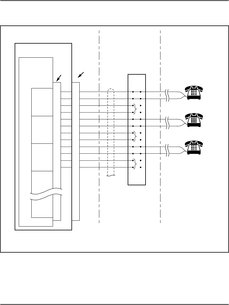
NT1R20 Off-Premise Station Analog Line card Page 173 of 906
Circuit Card Description and Installation
Figure 23
OPS analog line card – typical cross connection example
553-AAA1117
NT8D37
IPE Module
Slot 0
NT1R20
Off-premise
Station
Line Card
Unit 0
Unit 7
0T
0R 26
1
27
2
System Cross-connect OPS or ONS
telephone
connections
AMDF
Unit 1
Unit 2
Unit 3
Tip
Ring
Tip
Ring
28
3
29
4
2T
2R
1T
1R
30
5
31
6
Tip
Ring
NC
NC
NC
Module
I/O Panel
Connector
Part of
25-pair
cable
Note:
Actual pin numbers may vary depending on the vintage of
the card cage and the slot where the card is installed.
(W-BL)
(BL-W)
(W-O)
(O-W)
(W-G)
(G-W)
(W-BR)
(BR-W)
(W-S)
(S-W)
(R-BL)
(BL-R)

Page 174 of 906 NT1R20 Off-Premise Station Analog Line card
553-3001-211 Standard 3.00 August 2005
Configuring the OPS analog line card
The line type, terminating impedance, and balance network configuration for
each unit on the card is selected by software service change entries at the
system terminal and by jumper strap settings on the card.
Jumper strap settings
Each line interface unit on the card is equipped with two jumper blocks that
are used to select the proper loop current depending upon loop length. See
Table 71.
For units connected to loops of 460 to 2300 ohms, both jumper blocks for that
unit must have jumper blocks installed. For loops that are 460 ohms or less,
jumper blocks are not installed. Figure 24 on page 176 shows the location of
the jumper blocks on the OPS analog line card.
Table 71
OPS analog line card – configuration (Part 1 of 2)
Application On-premise station (ONS) Off-premise station (OPS)
Class of Service
(CLS) (Note 1)
ONP OPX
Loop resistance
(ohms)
0–460 0–2300 (Note 2)
Jumper strap
setting (Note 6)
Both JX.0 and JX.1
off
Both JX.0 and JX.1
off
Both JX.0 and JX.1
on
Loop loss (dB)
(Note 3)
0–1.5 >0–3.0 >2.5–3.0 0–1.5 >1.5–2.5 >2.5–4.5 >4.5–15
TIMP
(Notes 1, 4)
600
ohms
600
ohms
600
ohms
600
ohms
600
ohms
600
ohms
600
ohms
BIMP
(Notes 1, 4)
600
ohms
3COM 3CM2 600
ohms
3COM 3CM2 3CM2

NT1R20 Off-Premise Station Analog Line card Page 175 of 906
Circuit Card Description and Installation
Before the appropriate balance network can be selected, the loop length
between the near-end and the far-end station must be known. To assist in
determining loop length, “Port-to-port loss” on page 180 describes some
typical resistance and loss values for the most common cable lengths for
comparison with values obtained from actual measurements.
Application
Off-premise station application
The NT1R20 OPS analog line card is designed primarily to provide an
interface for off-premise station lines. An OPS line serves a terminal – usually
a telephone – remote from the PBX either within the same serving area as the
Gain treatment
(Note 5)
No Yes
Note 1: Configured in the Analog (500/2500-type) Telephone Administration program LD 10.
Note 2: The maximum signaling range supported by the OPS analog line card is 2300 ohms.
Note 3: Loss of untreated (no gain devices) metallic line facility. Upper loss limits correspond to
loop resistance ranges for 26 AWG wire.
Note 4: The following are the default software impedance settings:
ONP CLS OPX CLS
Termination Impedance (TIMP): 600 ohms 600 ohms
Balanced Impedance (BIMP): 600 ohms 3CM2
Note 5: Gain treatment, such as a Voice Frequency Repeater (VFR) is required to limit the
actual OPS loop loss to 4.5 dB, maximum. VFR treatment of metallic loops having untreated
loss greater than 15 dB (equivalent to a maximum signaling range of 2300 ohms on 26 AWG
wire) is not recommended.
Note 6: Jumper strap settings JX.0 and JX.1 apply to all eight units; “X” indicates the unit
number, 0 – 7. “Off” indicates that a jumper strap is not installed across both pins on a jumper
block. Store unused straps on the OPS analog line card by installing them on a single jumper.
Table 71
OPS analog line card – configuration (Part 2 of 2)
Application On-premise station (ONS) Off-premise station (OPS)
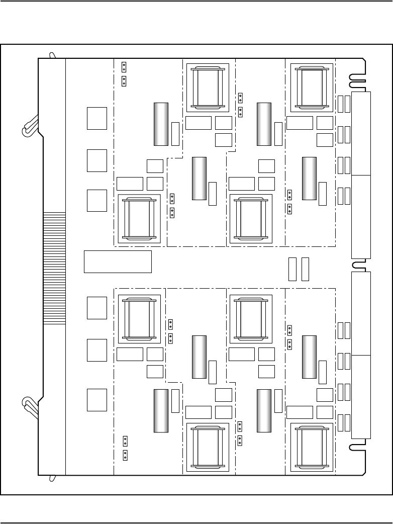

NT1R20 Off-Premise Station Analog Line card Page 177 of 906
Circuit Card Description and Installation
local office, or through a distant office. The line is not switched at these
offices; however, depending on the facilities used, the local office serving the
OPS station can provide line functions such as battery and ringing. Facilities
are generally provided by the local exchange carrier (usually, OPS pairs are
in the same cable as the PBX-CO trunks). The traditional OPS scenario
configuration is shown in Figure 25 on page 178.
Note: Do not confuse OPS service with Off-Premise Extension (OPX)
service. OPX service is the provision of an extension to a main subscriber
loop bridged onto the loop at the serving CO or PBX. Do not confuse
CLS OPS (assigned in the Analog (500/2500-type) Telephone
Administration program LD 10) with OPX, which denotes Off-Premise
Extension service.
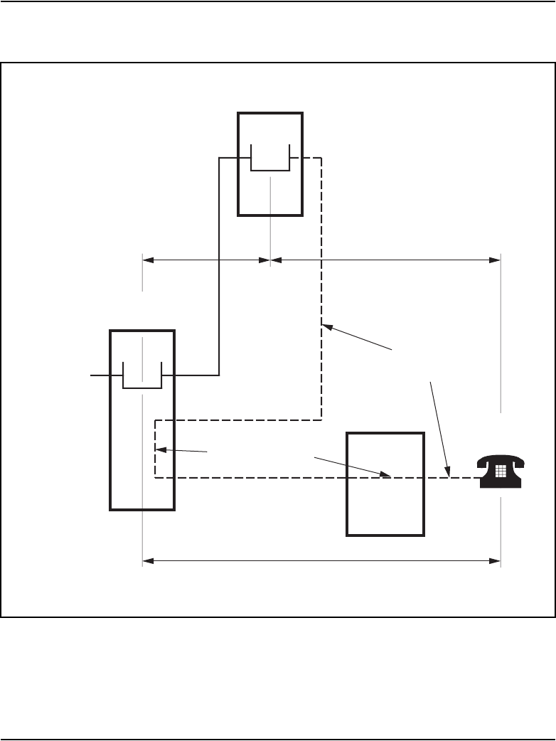
Page 178 of 906 NT1R20 Off-Premise Station Analog Line card
553-3001-211 Standard 3.00 August 2005
Figure 25
Traditional OPS application configuration
553-AAA1118
System
Public
Network
Non-switched
thru connections
OPS analog
line card port
CO trunk
card port
OPS
termination
Local
CO
Distant
CO
0–3.5 dB 4.5 dB maximum
7.0 dB total maximum
OPS line
facility

NT1R20 Off-Premise Station Analog Line card Page 179 of 906
Circuit Card Description and Installation
Other applications
The operating range and built-in protection provisions of the NT1R20 OPS
analog line card make it suitable for applications which are variants on the
traditional configuration shown in Figure 25 on page 178. Examples of such
applications are:
• a PBX in a central building serving stations in other buildings in the
vicinity, such as in an industrial park, often called a campus environment.
Facilities can be provided by the local exchange carrier or can be
privately owned. Protection could be required.
• termination to other than a telephone, such as to a fax machine or a key
telephone system.
• individual circuits on the NT1R20 OPS analog line card can also be
configured as On-Premise Station (ONS) ports in LD 10:
— to have ONS service with hazardous and surge voltage protection
(not available on other analog line cards)
— to use otherwise idle NT1R20 OPS analog line card ports
Transmission considerations
The transmission performance of OPS lines depends on the following factors:
• the port-to-port loss for connections between OPS ports and other ports
• the transmission parameters of the facilities between the OPS port and
the off-premise station or termination
• the electrical and acoustic transmission characteristics of the termination
These factors must be considered when planning applications using the
NT1R20 OPS analog line card. They are important when considering
configurations other than the traditional OPS application as shown in
Figure 25 on page 178. The following provides basic transmission planning
guidelines for various OPS applications.

Page 180 of 906 NT1R20 Off-Premise Station Analog Line card
553-3001-211 Standard 3.00 August 2005
Port-to-port loss
Loss is inserted between OPS analog line card ports and other ports in
accordance with the loss plan. This plan determines the port-to-port loss for
each call.
When a port is configured for CLS OPS, loss is programmed into the OPS
analog line card on a call-by-call basis. When configured for CLS ONS, an
OPS analog line card port is programmed to a value that is fixed for all calls.
The loss in the other port involved in the call can vary on a call-by-call basis
to achieve the total loss scheduled by the plan.
For satisfactory transmission performance, particularly on connections
between the public network and an OPS termination, it is recommended that
facilities conform to the following:
• Total 1 kHz loss from the local serving CO to the OPS terminal should
not exceed 7.0 dB. The total loss in the facility between the PBX and the
terminal must not exceed 4.5 dB. See Figure 25 on page 178.
The following requirements are based on historic Inserted Connection
Loss (ICL) objectives:
— PBX – CO trunk: 5 dB with gain; 0 – 4.0 dB without gain
— OPS line: 4.0 dB with gain; 0 – 4.5 dB without gain
Economic and technological changes have led to modifications of
these objectives. But since the loss provisions in the PBX for OPS
are constrained by regulatory requirements as well as industry
standards, they are not designed to compensate for modified ICL
designs in the connecting facilities.
• Nortel recommends that the attenuation distortion (frequency response)
of the OPS facility be within ±3.0 dB over the frequency range from 300
to 3000 Hz. It is desirable that this bandwidth extend from 200 to 3200
Hz.
• The terminating impedance of the facility at the OPS port be
approximately that of 600 ohms cable.
If the OPS line facility loss is greater than 4.5 dB but does not exceed 15 dB,
line treatment using a switched-gain Voice Frequency Repeater (VFR) will
extend the voice range.

NT1R20 Off-Premise Station Analog Line card Page 181 of 906
Circuit Card Description and Installation
The overall range achievable on an OPS line facility is limited by the
signaling range (2300 ohms loop including telephone resistance). The
signaling range is unaffected by gain treatment; thus, gain treatment can be
used to extend the voice range to the limit of the signaling range. For
example, on 26 AWG wire, the signaling range of 2300 ohms corresponds to
an untreated metallic loop loss of 15 dB. Gain treatment (such as a VFR) with
10.5 dB of gain would maintain the OPS service loss objective of 4.5 dB
while extending the voice range to the full limit of the signaling range.
The use of dial long line units to extend signaling range of OPS analog line
cards beyond 15 dB is not recommended.
Termination transmission characteristics
The loss plan for OPS connections is designed so that a connection with an
OPS termination provides satisfactory end-to-end listener volume when the
OPS termination is a standard telephone. The listener volume at the distant
end depends on the OPS termination transmit loudness characteristics; the
volume at the OPS termination end depends on the OPS termination receive
loudness characteristics.
A feature of many (though not all) standard telephones is that the loudness
increases with decreased current. Thus, as the line (PBX to OPS termination)
facility gets longer and loss increases, the increased loudness of the telephone
somewhat compensates for the higher loss, assuming direct current feed from
the PBX with constant voltage at the feeding bridge. However, this
compensation is not available when:
• the termination is a non-compensating telephone
• the OPS port is served by a line card using a constant-current feeding
bridge
• the OPS termination is to telephones behind a local switch providing
local current feed, such as a fax machine or a key telephone system
15.0 dB (loss corresponding to the maximum signaling range)
– 4.5 dB (OPS service loss objective)
= 10.5 dB (required gain treatment)

Page 182 of 906 NT1R20 Off-Premise Station Analog Line card
553-3001-211 Standard 3.00 August 2005
OPS line terminations with loudness characteristics designed for other
applications can also impact transmission performance. For example,
wireless portables loudness characteristics are selected for connections to
switching systems for wireless communication systems; if used in an OPS
arrangement without consideration for these characteristics, the result could
be a significant deviation from optimum loudness performance.

Page 183 of 906
Circuit Card Description and Installation
192
NT4N39AA CP Pentium IV Card
Contents
This section contains information on the following topics:
Introduction . . . . . . . . . . . . . . . . . . . . . . . . . . . . . . . . . . . . . . . . . . . . . . 183
Physical description. . . . . . . . . . . . . . . . . . . . . . . . . . . . . . . . . . . . . . . . 183
Functional description . . . . . . . . . . . . . . . . . . . . . . . . . . . . . . . . . . . . . . 186
Front panel connector pin assignments . . . . . . . . . . . . . . . . . . . . . . . . . 187
Introduction
The NT4N39AA Call Processor Pentium IV (CP PIV) Large System
processor card is introduced for CS 1000 Release 4.5. It features the
following:
• a PCI-based design that is compatible with current CP PII architecture
• an Intel Pentium processor
• two Compact Flash (CF) sockets (one on-board and one hot-swappable
on the faceplate). The on-board CF is referred to as the Fixed Media Disk
(FMD), and the faceplate CF is referred to as the Removable Media Disk
(RMD). See Figure 26 on page 185 and Figure 27 on page 186.
• 512 MBytes of Double Data Rate (DDR) memory
Physical description
The NT4N39AA card measures 23 cm by 16 cm (9,2 in. by 6.3 in.). See
Figure 26 on page 185 and Figure 27 on page 186.

Page 184 of 906 NT4N39AA CP Pentium IV Card
553-3001-211 Standard 3.00 August 2005
The CP PIV front panel is equipped with an EMC gasket and two ejector/
injector handles. A reset button and two double LED packages (four LEDs in
total) are placed at the front panel as well. The front panel features the
following:
• stacked dual standard DB9 Serial ports
• USB Connector
• stacked dual RJ-45 Ethernet ports with LEDs
• power good LED
• LEDs indication for activity on Compact flashes and secondary IDE
interface
• reset Switch
• INI switch
• front panel handle part# 3688785, 3688784 (replacement for customer
suggested parts 3686134, 3686135 which are now obsolete)
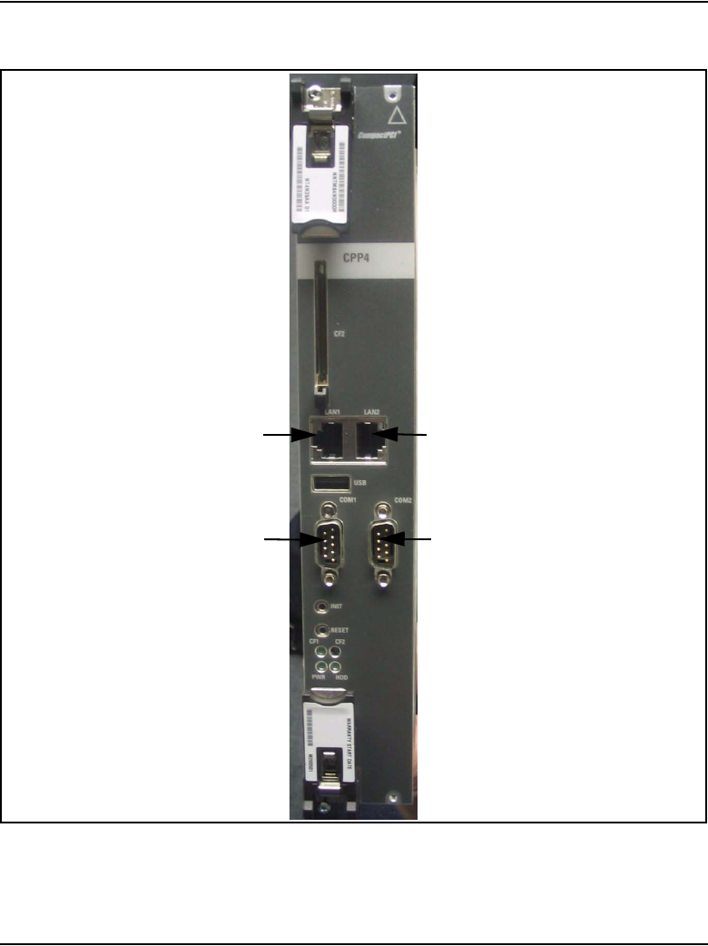
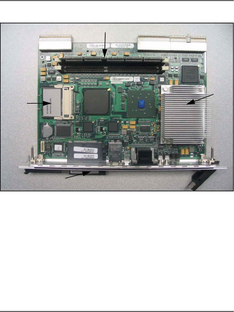
Page 186 of 906 NT4N39AA CP Pentium IV Card
553-3001-211 Standard 3.00 August 2005
Figure 27
CP PIV card (side)
Functional description
The card employs an Intel Pentium Processor as the central processing unit.
The internal core clock frequency reaches from 600MHz to1.1GHz. The
processor is manufactured in 0.09 um process technology and provides 32 KB
of on die data and instruction cache as well as 1 MB of on die L2 cache
running at core clock frequency. The processor is a mobile processor with a
478 pin FCBGA package with a maximum junction temperature of 100 °C.
Processor power dissipation must not exceed 12 W.
The front side bus runs at 400 MHz and uses an AGTL+ signaling
technology. The quad pumped data interface (data running at 4*100 MHz =
400 MHz) is 64 bit wide providing a total bandwidth of 3.2 GBytes/s. The
512 MBytes DDR memory
Fixed
Media
Drive (FMD)
Removable Media Drive (RMD)
CPU
Front
Rear

NT4N39AA CP Pentium IV Card Page 187 of 906
Circuit Card Description and Installation
double pumped address bus (addresses running at 2*100 MHz = 200 MHz) is
32 bit wide supporting an address range of up to 4 GBytes. The processor
voltage specification is compliant with IMVP IV specification.
Memory
CP PIV memory uses DDR SDRAM technology. The CP PIV provides a
maximum of two GBytes using two vertical DIMM sockets to install
off-the-shelf DIMM modules. CP PIV only supports DDR SDRAM DIMM
memory with a supply voltage of +2.5V.
The memory data path is 72-bit wide. The Intel 855GME Host Bridge
supports 128 MByte, 256 MByte and 512 Mbyte SDRAM technologies with
a maximum ROW page size of 16 Kbytes and CAS latency of 2 or 2.5. The
maximum height of the DIMM modules possible on CP PIV is one inch or
25.4 mm.
The DDR interface runs at 100 MHz synchronously to the front side bus
frequency. The SPD (Serial Presents Detect) -SROM available on DIMM
modules provide all necessary information (speed, size, and type) to the
boot-up software. The SPD-SROM can be read via SMBUS connected to the
Intel Hance Rapids South Bridge.
Front panel connector pin assignments
COM1 and COM2 ports
The physical interface for the COM1 and COM2 ports to the front panel is
through a stacked dual Male DB9 Connector. The corresponding pin details
are shown in Table 72.
Table 72
COM1 and COM2 pin assignments
Pin number Pin name
1DCD
2RXD
3TXD
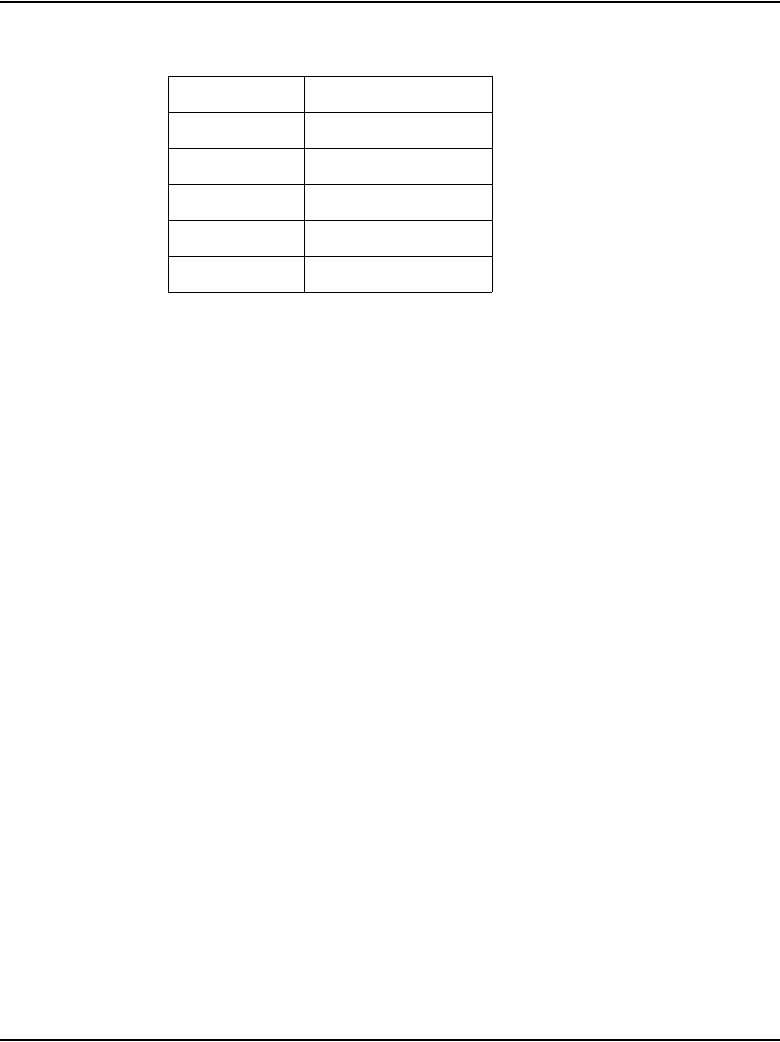
NT4N39AA CP Pentium IV Card Page 189 of 906
Circuit Card Description and Installation
USB port
The physical interface for the USB port to the front panel is through a
standard USB connector. The corresponding Pin details are shown in
Table 73.
10/100/1000 Mbps Ethernet ports
The physical interface for the two 10/100/1000 Mbps Ethernet ports to the
front panel is through a stacked dual RJ 45 connector with magnetics and
LEDs. The corresponding pin details are shown in Table 74.
Table 73
USB connector pin outs
Pin number Pin name
1USB VCC
2USB-
3USB+
4USB GND
Table 74
Ethernet connector pin outs
Pin number Pin name
1AX+
2AX-
3BX+
4CX+
5CX-
6BX-
7DX+
8DX-
Page 190 of 906 NT4N39AA CP Pentium IV Card
553-3001-211 Standard 3.00 August 2005
Front panel LED indicators
The CP PIV card has a total of five LEDS on the front panel which are 15 KV
ESD protected and can be controlled via CPLD. Table 75 explains the
function of each LED.
Author’s note:
Are there 5 or 4?
Table 75
Front panel LED functionality
LED Color Functionality Default
LED1 Green Power ON LED Off
LED2 Green Secondary IDE HD activity Off
LED3 Green Compact Flash activity Off
LED4 Green Compact Flash activity Off

NT4N39AA CP Pentium IV Card Page 191 of 906
Circuit Card Description and Installation
ITP connector (25 PIN, Debug Only)
Post 80 Debug LEDs (Optional)
CP PIV has post 80 debug LEDs to assist in debugging the board and solving
boot related problems. Using a GPCS from Super I/O X-bus, data lines are
latched using latch 74F374. These help identify Post 80 codes. This feature is
available only in debug boards.
Figure 28
ITP connector pin outs
Pin Signal Name Pin Signal Name
P1 GND P2 GND
P3 BPM0N P4 NC
P5 BPM1N P6 RESETN
P7 BPM2N P8 GND
P9 BPM3N P10 TDI
P11 BPM4N P12 TMS
P13 BPM5N P14 TRSTN
P15 ITP_CPURSTN P16 TCK
P17 TCK P18 NC
P19 CLK P20 GND
P21 CLKN P22 PWR
P23 BPM5N P24 TDO
P25 GND


Page 193 of 906
Circuit Card Description and Installation
248
NT5D11 and NT5D14 Lineside T1
Interface cards
Contents
This section contains information on the following topics:
Introduction . . . . . . . . . . . . . . . . . . . . . . . . . . . . . . . . . . . . . . . . . . . . . . 193
Physical description. . . . . . . . . . . . . . . . . . . . . . . . . . . . . . . . . . . . . . . . 194
Functional description . . . . . . . . . . . . . . . . . . . . . . . . . . . . . . . . . . . . . . 198
Electrical specifications. . . . . . . . . . . . . . . . . . . . . . . . . . . . . . . . . . . . . 202
Installation and configuration . . . . . . . . . . . . . . . . . . . . . . . . . . . . . . . . 204
Man-Machine T1 maintenance interface software . . . . . . . . . . . . . . . . 225
Applications . . . . . . . . . . . . . . . . . . . . . . . . . . . . . . . . . . . . . . . . . . . . . 244
Introduction
This section describes the two lineside T1 interface cards:
• NT5D11 – applicable for Large Systems only
• NT5D14 – applicable for Small Systems only
Note: Unless otherwise stated, the information in this section applies to
both the NT5D11 and NT5D14 lineside T1 interface cards.
The NT5D11 lineside T1 Interface card is an intelligent 24-channel digital
line card that is used to connect the switch to T1 compatible terminal
equipment on the lineside. T1 compatible terminal equipment includes voice

Page 194 of 906 NT5D11 and NT5D14 Lineside T1 Interface cards
553-3001-211 Standard 3.00 August 2005
mail systems, channel banks containing FXS cards, and key systems such as
the Nortel Norstar. The lineside T1 card differs from trunk T1 cards in that it
supports terminal equipment features such as hookflash, transfer, hold, and
conference.
This card occupies two card slots in the main or expansion cabinets. The
lineside T1 card can be installed in the system’s main cabinet or one of the
expansion cabinets (there are no limitations on the number of cards that can
be installed in the Cabinet system).
The lineside T1 card emulates an analog line card to the system software;
therefore, each channel is independently configurable by software control in
LD 10. The lineside T1 card also comes equipped with a Man-Machine
Interface (MMI) maintenance program. This feature provides diagnostic
information regarding the status of the T1 link.
Physical description
The lineside T1 card mounts into any two consecutive IPE slots. The card
consists of a motherboard and a daughterboard. The motherboard circuitry is
contained on a standard 31.75 by 25.40 cm. (12.5 by 10.0 in) printed circuit
board. The daughterboard is contained on a 5.08 by 15.24 cm (2.0 by 6.0 in)
printed circuit board and mounts to the motherboard on six standoffs.
Card connections
The lineside T1 card uses the NT8D81AA Tip and Ring cable to connect from
the IPE backplane to the 25-pair amphenol connector on the IPE I/O input/
output (I/O) panel. The I/O panel connector then connects directly to a T1
line, external alarm, and an MMI terminal or modem using the NT5D13AA
lineside T1 I/O cable available from Nortel.
Faceplate
The faceplate of the card is twice as wide as the other standard analog and
digital line cards, and occupies two card slots. It comes equipped with four
LED indicators. See Figure 29 on page 195.
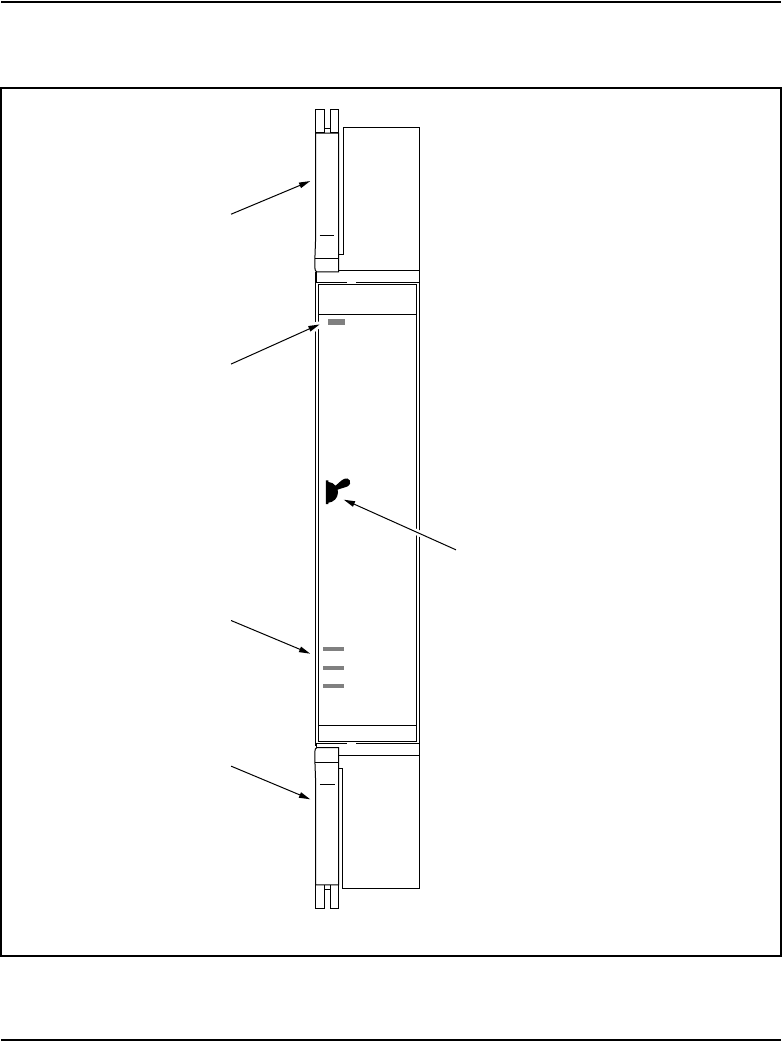
NT5D11 and NT5D14 Lineside T1 Interface cards Page 195 of 906
Circuit Card Description and Installation
Figure 29
Lineside T1 card faceplate
YEL ALM
RED ALM
MAINT
S
LTI
Rlse 0x
NT5D11
Card lock latch
Card lock latch
Warning LEDs
This symbol indicates
that field-selectable
switch settings are
located on this card
Card status LED
553-6478

Page 196 of 906 NT5D11 and NT5D14 Lineside T1 Interface cards
553-3001-211 Standard 3.00 August 2005
In general, the LEDs operate as shown in Table 76.
The STATUS LED indicates that the lineside T1 card has successfully passed
its self test, and is functional. When the card is installed, this LED remains lit
for two to five seconds as the self-test runs. If the self-test completes
successfully, the LED flashes three times and remains lit. When the card is
configured and enabled in software, the LED goes out. If the LED flashes
continuously, or remains weakly lit, replace the card.
Table 76
NT5D14AA Lineside T1 faceplate LEDs
LED State Definition
STATUS On (Red) The NT5D14AA card either failed its self-test or it
hasn’t yet been configured in software.
Off The card is in an active state.
RED On (Red) A red alarm has been detected from the T1 link.
(This includes, but is not limited to: not receiving a
signal, the signal has exceeded bit error thresholds
or frame slip thresholds.)
Off No red alarm exists.
YEL On (Yellow) A yellow alarm state has been detected from the
terminal equipment side of the T1 link. If the terminal
equipment detects a red alarm condition, it may
send a yellow alarm signal to the lineside T1 card
(this depends on whether or not your terminal
equipment supports this feature).
Off No yellow alarm.
MAINT On (Red) The card detects whether tests are being run or that
alarms have been disabled through the
Man-Machine Interface. The LED will remain lit until
these conditions are no longer detected.
Off The lineside T1 card is fully operational.

NT5D11 and NT5D14 Lineside T1 Interface cards Page 197 of 906
Circuit Card Description and Installation
Note: Note: The STATUS LED indicates the enabled/disabled status of
both card slots of the lineside T1 card simultaneously. To properly enable
the card, both the motherboard and the daughterboard slots must be
enabled. The STATUS LED will turn off as soon as either one of the
lineside T1 card slots have been enabled. No LED operation will be
observed when the second card slot is enabled. To properly disable the
card, both card slots must be disabled. The LED will not turn on until
both card slots have been disabled.
The RED ALARM LED indicates that the lineside T1 card has detected an
alarm condition from the T1 link. Alarm conditions can include such
conditions as not receiving a signal or the signal has exceeded bit error
thresholds or frame slip thresholds. See “Man-Machine T1 maintenance
interface software” on page 225 for information on T1 link maintenance.
If one of these alarm conditions is detected, this red LED will light. Yellow
alarm indication is sent to the far-end as long as the near-end remains in a red
alarm condition. Depending on how the Man-Machine Interface (MMI) is
configured, this LED remains lit until the following actions occur:
• If the “Self-Clearing” function has been enabled in the MMI, the LED
clears the alarm when the alarm condition is no longer detected. This is
the factory default.
• If the “Self-Clearing” function has not been enabled or it has been
subsequently disabled in the MMI, the LED will stay lit until the
command “Clear Alarm” has been typed in the MMI, even though the
carrier automatically returned to service when the alarm condition was
no longer detected.
The YELLOW ALARM LED indicates that the lineside T1 card has detected a
yellow alarm signal from the terminal equipment side of the T1 link. See the
“Man-Machine T1 maintenance interface software” on page 225 for
information on T1 link maintenance. If the terminal equipment detects a red
alarm condition, such as not receiving a signal or the signal has exceeded bit
error thresholds or frame slip thresholds, it can send a yellow alarm signal to
the lineside T1 card, depending on whether or not the terminal equipment
supports this feature. If a yellow alarm signal is detected, this LED will light.
The MAINT LED indicates if the lineside T1 card is fully operational because
of certain maintenance commands being issued through the MMI. See
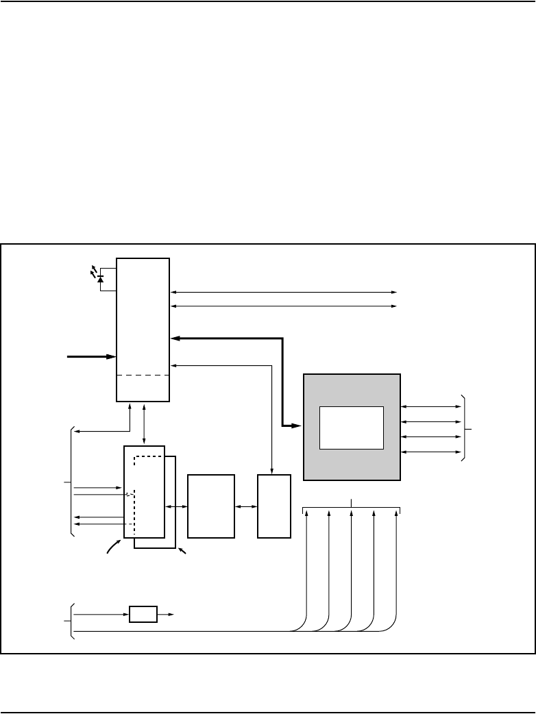
Page 198 of 906 NT5D11 and NT5D14 Lineside T1 Interface cards
553-3001-211 Standard 3.00 August 2005
“Man-Machine T1 maintenance interface software” on page 225 for
information on T1 link maintenance. If the card detects that tests are being run
or that alarms have been disabled through the MMI, this LED will light and
will remain lit until these conditions are no longer detected, then it will turn
off.
Functional description
Figure 30 shows a block diagram of the major functions contained on the
lineside T1 card. Each of these functions is described on the following pages.
Figure 30
Lineside T1 card – block diagram
Micro-
controller
Tx PCM
Async card
LAN link
Front
panel
LEDs
Card LAN
interface
T1 Interface
(One for all
24 channels)
Line interface unit power
Rx PCM
Controller
card
Digital
Gain/Loss
Pads
Slot 1
Motherboard
(16 channels)
Slot 2
Daughterboard
(8 channels)
Mux
Seq.
Reg 553-6476
Power
supplies
+8.5 V dc +5 V dc logic power
T1 Tx Tip
Man/Machine Interface
External Alarm Interface
T1 Tx Ring
T1 Rx Tip
T1 Rx Ring
Backplane
Common
Peripheral
Equipment
connector
Card slot
addresses
Backplane
DS-30X
interface

NT5D11 and NT5D14 Lineside T1 Interface cards Page 199 of 906
Circuit Card Description and Installation
The lineside T1 card is an IPE line card that provides a cost-effective
all-digital connection between T1 compatible terminal equipment (such as
voice mail systems, voice response units, and trading turrets) and the system.
The terminal equipment is assured access to analog (500/2500-type)
telephone type line functionality such as hook flash, SPRE codes and
ringback tones generated from the switch. Usually, the lineside T1 card
eliminates the need for channel bank type equipment normally placed
between the switch and the terminal equipment. This provides a more robust
and reliable end-to-end connection. The lineside T1 card supports line
supervision features such as loop and ground start protocols. It can also be
used in an off-premise arrangement where analog (500/2500-type) telephones
are extended over T1 with the use of channel bank equipment.
The lineside T1 interface offers significant improvement over the previous
alternatives. For example, if a digital trunk connection were used, such as
with the DTI/PRI interface card, lineside functionality would not be
supported. Previously, the only way to achieve the lineside functionality was
to use analog ports and channel bank equipment. No channel bank equipment
is required, resulting in a more robust and reliable connection.
The lineside T1 interface offers a number of benefits when used to connect to
third-party applications equipment:
• It is a more cost-effective alternative for connection because it eliminates
the need for expensive channel bank equipment.
• The lineside T1 supports powerful T1 monitoring and diagnostic
capability.
• Overall costs for customer applications can also be reduced because the
T1-compatible IPE is often more attractively priced than the analog-port
alternatives.
The lineside T1 card is compatible with all IPE based systems and standard
public or private DSX-1 type carrier facilities. Using A/B robbed bit
signaling, it supports D4 or ESF channel framing formats as well as AMI or
B8ZS coding. Because it uses standard PCM in standard T1 timeslots,
existing T1 test equipment remains compatible for diagnostic and fault
isolation purposes.

Page 200 of 906 NT5D11 and NT5D14 Lineside T1 Interface cards
553-3001-211 Standard 3.00 August 2005
Card interfaces
The lineside T1 card passes voice and signaling data over DS-30X loops
through the DS-30X Interfaces circuits and maintenance data over the card
LAN link.
T1 interface circuit
The lineside T1 card contains one T1 line interface circuit which provides 24
individually configurable voice interfaces to one T1 link in 24 different time
slots. The circuit demultiplexes the 2.56 Mbps DS-30X Tx signaling
bitstreams from the DS-30X network loop and converts it into 1.544 mHz T1
Tx signaling bitstreams onto the T1 link. It also does the opposite, receiving
Rx signaling bitstreams from the T1 link and transmitting Rx signaling
bitstreams onto the DS-30X network loop.
The T1 interface circuit performs the following:
• Provides an industry standard DSX-1 (0 to 655 ft./200 meters) interface.
• Converts DS-30X signaling protocol into FXO A and B robbed bit
signaling protocol.
• Provides switch-selectable transmission and reception of T1 signaling
messages over a T1 link in either loop or ground start mode.
Signaling and control
The lineside T1 card also contains signaling and control circuits that
establish, supervise, and take down call connections. These circuits work
with the system controller to operate the T1 line interface circuit during calls.
The circuits receive outgoing call signaling messages from the controller and
return incoming call status information to the controller over the DS-30X
network loop.
Card control functions
Control functions are provided by a microcontroller and a Card LAN link on
the lineside T1 card. A sanity timer is provided to automatically reset the card
if the microcontroller stops functioning for any reason.

NT5D11 and NT5D14 Lineside T1 Interface cards Page 201 of 906
Circuit Card Description and Installation
Microcontrollers
The lineside T1 card contains a microcontroller that controls the internal
operation of the card and the serial card LAN link to the controller card. The
microcontroller controls the following:
• reporting to the CPU via the card LAN link:
— card identification (card type, vintage, serial number)
— firmware version
— self-test results
— programmed unit parameter status
• receipt and implementation of card configuration:
— control of the T1 line interface
— enabling/disabling of individual units or entire card
— programming of loop interface control circuits for administration of
channel operation
— maintenance diagnostics
• interface with the line card circuit:
— converts on/off-hook, and ringer control messages from the DS-30X
loop into A/B bit manipulations for each time slot in the T1 data
stream, using robbed bit signaling.
• the front panel LED when the card is enabled or disabled by instructions
from the NT8D01 controller card.
Card LAN interface
Maintenance data is exchanged with the CPU over a dedicated asynchronous
serial network called the Card LAN link.
Sanity timer
The lineside T1 card also contains a sanity timer that resets the
microcontroller in the event of a loss of program control. The microcontroller
must service the sanity timer every 1.2 seconds. If the timer is not properly
serviced, it times out and causes the microcontroller to be hardware reset.

Page 202 of 906 NT5D11 and NT5D14 Lineside T1 Interface cards
553-3001-211 Standard 3.00 August 2005
Man-Machine Interface
The lineside T1 card provides an optional Man-Machine Interface (MMI) that
is primarily used for T1 link performance monitoring and problem diagnosis.
The MMI provides alarm notification, T1 link performance reporting and
fault isolation testing. The interface is accessed through connections from the
I/O panel to a terminal or modem.
The MMI is an optional feature since all T1 configuration settings are
performed through dip switch settings or preconfigured factory default
settings.
Electrical specifications
T1 channel specifications
Table 77 provides specifications for the 24 T1channels. Each characteristic is
configured by dip switches.
Table 77
Lineside T1 card – line interface unit electrical characteristics
Characteristics Description
Framing ESF or D4
Coding AMI or B8ZS
Signaling Loop or ground start A/B robbed-bit
Distance to Customer Premise
Equipment (CPE) or Channel
Service Unit
0-199.6 meters (0–655 feet)

NT5D11 and NT5D14 Lineside T1 Interface cards Page 203 of 906
Circuit Card Description and Installation
Power requirements
The lineside T1 card requires +15 V, –15 V, and +5 V from the backplane.
One NT8D06 IPE Power Supply AC or NT6D40 IPE Power Supply DC can
supply power to a maximum of eight lineside T1 cards. See Table 78.
Foreign and surge voltage protections
In-circuit protection against power line crosses or lightning is not provided on
the lineside T1 card. It does have protection against accidental shorts to –52 V
dc analog lines.
When the card is used to service off-premise terminal equipment through the
public telephone network, install a Channel Service Unit (CSU) as part of the
terminal equipment to provide external line protection.
Table 78
Lineside T1 card – power required
Voltage Current (max.)
+ 5.0 V dc 1.6 Amp
+15.0 V dc 150 mA.
–15.0 V dc 150 mA.

Page 204 of 906 NT5D11 and NT5D14 Lineside T1 Interface cards
553-3001-211 Standard 3.00 August 2005
Environmental specifications
Table 79 lists the environmental specifications of the lineside T1 card.
Installation and configuration
Installation and configuration of the lineside T1 card consists of six basic
steps:
1Configure the dip switches on the lineside T1 card for the environment.
2Install the lineside T1 card into the selected card slots in the IPE shelf.
3Cable from the I/O panel to the Customer Premise Equipment (CPE) or
CSU, MMI terminal or modem (optional), external alarm (optional), and
other lineside T1 cards for daisy chaining use of MMI terminal
(optional).
4Configure the MMI terminal.
5Configure the lineside T1 card through the system software and verify
self-test results.
6Verify initial T1 operation and configure MMI (optional).
Steps 1-5 are explained in this section. Step 6 is covered in “Man-Machine T1
maintenance interface software” on page 225.
Table 79
Lineside T1 card – environmental specifications
Parameter Specifications
Operating temperature-normal 15° to +30° C (+59° to 86°F), ambient
Operating temperature-short term 10° to +45° C (+50° to 113°F), ambient
Operating humidity-normal 20% to 55% RH (non-condensing)
Operating humidity-short term 20% to 80% RH (non-condensing)
Storage temperature –50° to +70° C (–58° to 158°F), ambient
Storage humidity 5% to 95% RH (non-condensing)

NT5D11 and NT5D14 Lineside T1 Interface cards Page 205 of 906
Circuit Card Description and Installation
Dip switch settings
Begin the installation and configuration of the lineside T1 card by selecting
the proper dip switch settings for the environment. The lineside T1 card
contains two dip switches, each containing eight switch positions. They are
located in the upper right corner of the motherboard circuit card as shown in
Figure 31 on page 206. The configuration for these switches are shown in
Tables 80 through 83.
When the line-side T1 card is oriented as shown in Figure 31 on page 206, the
dip switches are ON when they are up, and OFF when they are down. The dip
switch settings configure the card for the following parameters:
MMI port speed selection
This dip switch setting selects the appropriate baud rate for the terminal or
modem (if any) that is connected to the MMI.
Line Supervisory Signaling protocol
As described in “Lineside T1 call operation” on page 46, the lineside T1 card
is capable of supporting loop start or ground start call processing modes.
Make the selection for this dip switch position based on what type of line
signaling the CPE equipment supports.
Address of lineside T1 card to the MMI
The address of the lineside T1 card to the MMI is made up of two
components:
• The address of the card within the shelf
• The address of the shelf in which the card resides
These two addresses are combined to create a unique address for the card. The
MMI reads the address of the card within the shelf from the card firmware;
however the address of the shelf must be set by this dip switch.
The shelf address dip switch can be from 0 – 15. 16 is the maximum number
of lineside T1 IPE shelves (a maximum of 64 lineside T1 cards) capable of
daisy chaining to a single MMI terminal. For ease, it is recommended that this
address be set the same as the address of the peripheral controller identifier in
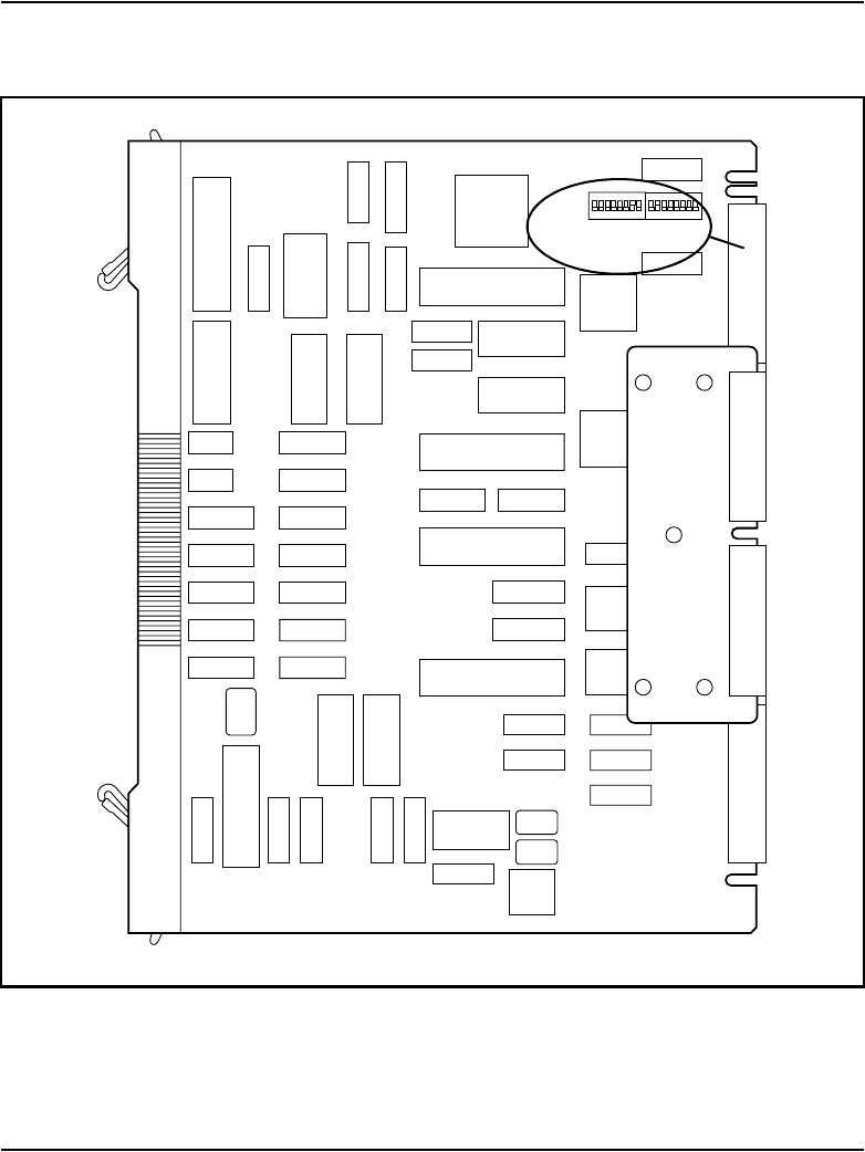
Page 206 of 906 NT5D11 and NT5D14 Lineside T1 Interface cards
553-3001-211 Standard 3.00 August 2005
LD 97 for type: XPE. However, this is not mandatory, and, since the dip
switch is limited to 16, this will not always be possible.
Figure 31
Lineside T1 card – T1 protocol dip switch locations
553-6479
S1
S2
dip
switches

NT5D11 and NT5D14 Lineside T1 Interface cards Page 207 of 906
Circuit Card Description and Installation
T1 framing
The lineside T1 card is capable of interfacing with CPE or CSU equipment
either in D4 or ESF framing mode. Make the selection for this dip switch
position based on what type of framing the CPE or CSU equipment supports.
T1 coding
The lineside T1 card is capable of interfacing with CPE or CSU equipment
using either AMI or B8ZS coding. Make the selection for this dip switch
position based on what type of coding the CPE or CSU equipment supports.
DSX-1 length
Estimate the distance between the lineside T1 card and the hardwired local
CPE, or the Telco demarc RJ48, for the carrier facility connecting the lineside
T1 and the remote CPE. Make the selection for this dip switch position based
on this distance.
Line supervision on T1 failure
This setting determines in what state all 24 ports of the lineside T1 card
appears to the CS 1000S, CS 1000M, and Meridian 1 in case of T1 failure.
Ports can appear as either in the on-hook or off-hook states on T1 failure.
Note: All idle lineside T1 lines will go off-hook and seize a Digitone
Receiver when the off-hook line processing is invoked on T1 failure.
This may prevent DID trunks from receiving incoming calls until the
lineside T1 lines time-out and release the DTRs.
Daisy-chaining to MMI
If two or more lineside T1 cards are installed and the MMI is used,
daisy-chain the cards together to use one MMI terminal or modem, See
Figure 33 on page 221. Make the selection for this dip switch position based
on how many lineside T1 cards will be installed.
MMI master or slave
This setting is used only if daisy-chaining the cards to the MMI terminal or
modem. This setting determines whether this card is a master or a slave in the
MMI daisy-chain. Select the master setting if this card is the card that is

Page 208 of 906 NT5D11 and NT5D14 Lineside T1 Interface cards
553-3001-211 Standard 3.00 August 2005
cabled directly into the MMI terminal or modem; select the slave setting if
this card is cabled to another lineside T1 card in a daisy chain.
Tables 80 through 83 describes the proper dip switch settings for each type of
T1 link. After the card has been installed, the MMI displays the DIP switch
settings the command Display Configuration is used. See “Man-Machine T1
maintenance interface software” on page 225 for details on how to invoke this
command.
Table 80
Lineside T1 card—T1 Switch 1 (S1) dip switch settings
Dip Switch
Number Characteristic Selection
1MMI port speed selection On = 1200 baud
Off = 2400 baud
2T1 signaling On = Ground start
Off = Loop start
3–6 XPEC Address for the lineside T1 card See Table 81
7Not Used Leave Off
8Reserved for SL-100 use Leave Off
Table 81
Lineside T1 card – XPEC address dip switch settings (Switch S1, positions 3 – 6)
(Part 1 of 2)
XPEC
Address
S1 Switch
Position 3
S1 Switch
Position 4
S1 Switch
Position 5
S1 Switch
Position 6
00 Off Off Off Off
01 Off Off Off On
02 Off Off On Off
03 Off Off On On
04 Off On Off Off

NT5D11 and NT5D14 Lineside T1 Interface cards Page 209 of 906
Circuit Card Description and Installation
05 Off On Off On
06 Off On On Off
07 Off On On On
08 On Off Off Off
09 On Off Off On
10 On Off On Off
11 On Off On On
12 On On Off Off
13 On On Off On
14 On On On Off
15 On On On On
Table 82
Lineside T1 card – T1 Switch 2 (S2) dip switch settings (Part 1 of 2)
Dip Switch
Number Characteristic Selection
1T1 framing On = D4
Off = ESF
2T1 Coding On = AMI
Off = B8ZS
3–5 CPE or CSU distance See Table 83 on page 210
6Line processing on T1 link failure On = On-hook
Off = Off-hook
Table 81
Lineside T1 card – XPEC address dip switch settings (Switch S1, positions 3 – 6)
(Part 2 of 2)
XPEC
Address
S1 Switch
Position 3
S1 Switch
Position 4
S1 Switch
Position 5
S1 Switch
Position 6

Page 210 of 906 NT5D11 and NT5D14 Lineside T1 Interface cards
553-3001-211 Standard 3.00 August 2005
Installation
This section describes how to install and test the lineside T1 card.
When installed, the lineside T1 card occupies two card slots. It can be
installed into an NT8D37 IPE module.
When installing the lineside T1 card into NT8D37 IPE module, determine the
vintage level module. If the 25-pair I/O connectors are partially split between
adjacent IPE card slots, the lineside T1 card works only in card slots where
Unit 0 of the motherboard card slot appears on the first pair of the 25-pair I/
O connector.
7Daisy-chaining to MMI On = Yes
Off = No
8MMI Master or Slave On = Master
Off = Slave
Table 83
Lineside T1 card – CPE or CSU distance dip switch settings (Switch S2, positions 3 – 5)
Distance
S2 Switch
Position 3
S2 Switch
Position 4
S2 Switch
Position 5
0–133 On Off Off
134–266 Off On On
267–399 Off On Off
400–533 Off Off On
534–655 Off Off Off
Table 82
Lineside T1 card – T1 Switch 2 (S2) dip switch settings (Part 2 of 2)
Dip Switch
Number Characteristic Selection
NT5D11 and NT5D14 Lineside T1 Interface cards Page 211 of 906
Circuit Card Description and Installation
Certain vintage levels have dedicated 25-pair I/O connectors only for card
slots 0, 4, 8, and 12. These vintage levels are cabled with only 16 pairs of
wires from each card slot to the I/O panel. Some of the 25-pair I/O connectors
are split between adjacent card slots. Other vintage levels cable each card slot
to the I/O panel using a unique, 24-pair connector on the I/O panel. In these
vintage levels, the lineside T1 card can be installed in any available pair of
card slots. However, because of the lower number of wire pairs cabled to the
I/O panel in the lower vintage level, only certain card slots are available to the
lineside T1 card.
See Table 84 for the vintage level information for the NT8D37 IPE
modules.
Vintage levels cabling 24 ports
For modules with vintage levels that cabled 24 ports to the I/O panel, the
lineside T1 card can be installed in any pair of card slots 015.
Table 84
Lineside T1 card – NT8D37 IPE module vintage level port cabling
Vintage Level
Number of ports
cabled to I/O panel
NT8D37AA 16 ports
NT8D37BA 24 ports
NT8D37DC 16 ports
NT8D37DE 16 ports
NT8D37EC 24 ports

Page 212 of 906 NT5D11 and NT5D14 Lineside T1 Interface cards
553-3001-211 Standard 3.00 August 2005
Vintage levels cabling 16 ports
For modules with vintage levels that cabled 16 ports to the I/O panel, the
lineside T1 card can be installed into the following card slot pairs:
The lineside T1 card cannot be installed into the following card slot pairs:
If the lineside T1 card must be installed into one of the restricted card slot
pairs, rewire the IPE module card slot to the I/O panel by installing an
additional NT8D81 cable from the lineside T1 card motherboard slot to the I/
O panel. Re-arrange the three backplane connectors for the affected card
slots. This will permit the connection of the NT5D13AA lineside T1 card
carrier and maintenance external I/O cable at the IPE module I/O panel
connector for card slots that are otherwise restricted.
Also, all lineside T1 card connections can be made at the main distribution
frame instead of connecting the NT5D13 lineside T1 card external I/O cable
at the I/O panel. This eliminates these card slots restrictions.
Available: Motherboard/Daughterboard
0 and 1
1 and 2
4 and 5
7 and 8
8 and 9
9 and 10
12 and 13
13 and 14
Restricted: Motherboard/Daughterboard
2 and 3
3 and 4
6 and 7
10 and 11
11 and 12
14 and 15

NT5D11 and NT5D14 Lineside T1 Interface cards Page 213 of 906
Circuit Card Description and Installation
Cabling the lineside T1 card
After configuring the dip switches and installing the lineside T1 card into the
selected card slots, the lineside T1 card is ready to be cabled to the CPE or
CSU equipment. Connections can also be made to the MMI terminal or
modem (optional), an external alarm (optional), and other lineside T1 cards
for daisy-chain use of the MMI terminal (optional).
The lineside T1 card is cabled from its backplane connector through
connections from the motherboard circuit card only (no cable connections are
made from the daughterboard circuit card) to the input/output (I/O) panel on
the rear of the IPE module. The connections from the lineside T1 card to the
I/O panel are made with the NT8D81AA Tip and Ring cables provided with
the IPE module.
Cabling from the I/O panel with the NT5D13AA lineside T1 I/O
cable
Usually, the I/O panel is connected to the T1 link and other external devices
through the NT5D13AA lineside T1 I/O cable. See Figure 32 on page 214.
This cable consists of a 25-pair amphenol connector (P1) on one end which
plugs into the I/O panel. The other end has 4 connectors:
1a DB15 male connector (P2) which plugs into the T1 line
2a DB9 male connector (P3) which plugs into an external alarm system
3a second DB9 male connector (P5) which connects to an MMI terminal
or modem
4a DB9 female connector (P4) that connects to the next lineside T1 card’s
P4 connector for MMI daisy chaining
Cabling from the I/O panel at the Main Distribution Frame
All lineside T1 connections can be made at the main distribution frame
(MDF) if it is preferred to not use the NT5D13AA lineside T1 I/O cable at the
I/O panel.
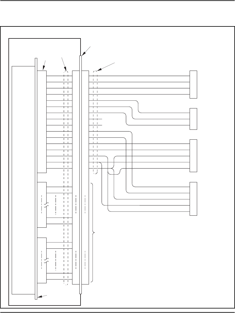
Page 214 of 906 NT5D11 and NT5D14 Lineside T1 Interface cards
553-3001-211 Standard 3.00 August 2005
Figure 32
Lineside T1 card – connection using the NT5D13AA lineside T1 cable
553-AAA1119
NT8D37
IPE
Module Slot 0
Module
I/O panel
1
26
2
27
3
28
4
29
5
30
6
31
7
32
8
33
9
34
16
41
17
42
24
49
System
A
(bl-w)
(w-bl)
(o-w)
(w-o)
(g-w)
(w-g)
(br-w)
(w-br)
(s-w)
(w-s)
(bl-r)
(r-bl)
(or-r)
(r-or)
(gr-r)
(r-gr)
NT8D81
Tip & Ring
Cable
12A
12B
13A
13B
14A
14B
15A
15B
16A
16B
17A
17B
18A
18B
19A
19B
62A
62B
69A
69B
73A
73B
80A
80B
Line
Side T-1
Card
Not used
T-1 tip receive data
T-1 ring receive data
T-1 tip transmit data
T-1 ring transmit data
Alarm out normally open
Alarm out common
Alarm out normally closed
MMI in transmit data
MMI in receive data
Ground
Control 1
Control 2
MMI out receive data
MMI out transmit data
Ground
Control 1
Control 2
11
3
1
9
1
2
3
3
2
5
7
9
2
3
5
7
9
1
26
2
27
3
28
4
29
5
30
6
31
7
32
8
33
9
34
16
41
17
42
24
49
P2
P3
P5
P4
To
CPE or CSU
(DB15 male)
(CPE)
To external
alarm
indicator
(DB9 male)
Toward
MMI
(DB9 male)
(DCE)
Away from
MMI
(DB9 female)
(DTE)
NT5D13
Maintenance
Interface Cable
Module
backplane
NC
NC
P1

NT5D11 and NT5D14 Lineside T1 Interface cards Page 215 of 906
Circuit Card Description and Installation
Procedure 11
Connecting to the MDF
To make the connections at the MDF, follow this procedure:
1Punch down the first eight pairs of a standard telco 25-pair
female-connectorized cross-connect tail starting with the first tip and ring
pair of the lineside T1 motherboard card slot on the cross-connect side of
the MDF terminals.
2Plug the NT5D13AA lineside T1 I/O cable into this 25-pair cross-connect
tail at the MDF, regardless of the card slot restrictions that exist from the
vintage level of IPE or CE module used. This connection can also be
made at the MDF without using the NT5D13 lineside T1 I/O cable, by
cross-connecting according to the pinouts in Table 85.
3Turn over the T1 transmit and receive pairs, where required for hardwiring
the lineside T1 card to local CPE T1 terminal equipment.
End of Procedure
The backplane connector is arranged as an 80-row by 2-column array of pins.
Table 85 shows the I/O pin designations for the backplane connector and the
25-pair Amphenol connector from the I/O panel. Although the connections
from the I/O panel only use 14 of the available 50 pins, the remaining pins are
reserved and cannot be used for other signaling transmissions.
The information in Table 85 is provided as a reference and diagnostic aid at
the backplane, since the cabling arrangement can vary at the I/O panel. See
Communication Server 1000M and Meridian 1: Large System Installation
and Configuration (553-3021-210) for cable pinout information for the I/O
panel.
Table 85
Lineside T1 card – backplane pinouts (Part 1 of 2)
Backplane
Connector Pin
I/O Panel
Connector Pin Signal
12A 1 T1 Tip, Receive Data
12B 26 T1 Ring, Receive Data

Page 216 of 906 NT5D11 and NT5D14 Lineside T1 Interface cards
553-3001-211 Standard 3.00 August 2005
13A 2 T1 Tip, Transmit Data
13B 27 T1 Ring, Transmit Data
14A 3 Alarm out, Normally open
14B 28 Alarm out, Common
15A 4 Alarm out, Normally closed
15B 29 No Connection
16A 5 No Connection
16B 30 Away from MMI terminal,
Receive Data
17A 6 Away from MMI terminal,
Transmit Data
17B 31 Towards MMI terminal,
Transmit Data
18A 7 Towards MMI terminal,
Receive Data
18B 32 Daisy-chain Control 2
19A 8 Daisy-chain Control 1
19B 33 Ground
Table 85
Lineside T1 card – backplane pinouts (Part 2 of 2)
Backplane
Connector Pin
I/O Panel
Connector Pin Signal
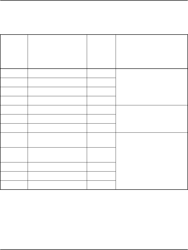
NT5D11 and NT5D14 Lineside T1 Interface cards Page 217 of 906
Circuit Card Description and Installation
Table 86 shows the pin assignments when using the NT5D13AA lineside T1
I/O cable.
Table 86
Lineside T1 card – NT5D13AA connector pinouts (Part 1 of 2)
I/O panel
connector
pin Lead designations
NT5D13AA
Lineside
T1 I/O
connector
pin
Lineside T1 cable
connector to external
equipment
1T1 Tip Receive Data 11 DB15 male to T1 (P2)
Lineside T1 card is CPE
transmit to network and
receive from network
26 T1 Ring Receive Data 3
2T1 Tip Transmit Data 1
27 T1 Ring Transmit Data 9
3Alarm out common 1DB9 male to external alarm (P3)
28 Alarm out (normally open) 2
4Alarm out (normally closed) 3
7Towards MMI terminal
Receive Data
2DB9 male towards MMI (P5)
Wired as DCE
Data is transmitted on pin 2 (RXD)
and received on pin 3 (TXD)
31 Towards MMI terminal
Transmit Data
3
33 Ground 5
8Control 1 7
32 Control 2 9
Page 218 of 906 NT5D11 and NT5D14 Lineside T1 Interface cards
553-3001-211 Standard 3.00 August 2005
T1 connections
T1 signaling for all 24 channels is transmitted over P2 connector pins 1, 3, 9,
and 11 as shown in Table 86 on page 217. Plug the DB15 male connector
labeled “P2” into the T1 link. T1 transmit and receive pairs must be turned
over between the lineside T1 card and CPE equipment that is hardwired
without carrier facilities. If the lineside T1 card is connected through T1
carrier facilities, the transmit and receive pairs must be wired straight through
to the RJ48 at the Telco demarc, the CSU, or other T1 carrier equipment. The
T1 CPE equipment at the far end will also have transmit and receive wired
straight from the RJ48 demarc at the far end of the carrier facility.
External alarm connections
P3 connector pins 3, 4, and 28 can be plugged into any external alarm
hardware. Plug the male DB9 connector labeled “P3” into the external alarm.
These connections are optional, and the functionality of the lineside T1 card
is not affected if they are not made.
The MMI (described in detail in “Man-Machine T1 maintenance interface
software” on page 225) monitors the T1 link for specified performance
criteria and reports on problems detected.
33 Ground 5DB9 female away from MMI (P4)
Wired as DTE
Data is transmitted on pin 2 (TXD)
and received on pin 3 (RXD)
8Control 1 7
32 Control 2 9
30 Away from MMI terminal
Transmit Data
3
6Away from MMI terminal
Receive Data
2
Table 86
Lineside T1 card – NT5D13AA connector pinouts (Part 2 of 2)
I/O panel
connector
pin Lead designations
NT5D13AA
Lineside
T1 I/O
connector
pin
Lineside T1 cable
connector to external
equipment

NT5D11 and NT5D14 Lineside T1 Interface cards Page 219 of 906
Circuit Card Description and Installation
One of the ways it can report information is through this external alarm
connection. If connected, the lineside T1 card’s microprocessor activates the
external alarm hardware if it detects certain T1 link problems that it has
classified as alarm levels 1 or 2. See “Man-Machine T1 maintenance interface
software” on page 225 for a detailed description of alarm levels and
configuration. If an alarm level 1 or 2 is detected by MMI, the lineside T1
card will close the contact that is normally open, and will open the contact that
is normally closed. The MMI command Clear Alarm will return the alarm
contacts to their normal state.
MMI connections
P5 connector pins 2, 3, 5, 7 and 9 are used to connect the lineside T1 card to
the MMI terminal and daisy chain lineside T1 cards together for access to a
shared MMI terminal. When logging into a lineside T1 card, “control 2” is
asserted by that card, which informs all of the other cards not to talk on the
bus, but rather to pass the data straight through. The pins labeled “control 1”
are reserved for future use. As with the external alarm connections, MMI
connections are optional. Up to 128 lineside T1 cards, located in up to 16
separate IPE shelves, can be linked to one MMI terminal using the daisy
chaining approach.
If only one lineside T1 card is being installed, cable from the DB9 female
connector labeled “P5” (towards MMI terminal) to one of the COM ports on
the back of any TTY, a PC running a terminal emulation program, or a
modem. For installations of only one card, no connection is made to the DB9
male connector labeled “P4” (away from MMI terminal).
If two or more lineside T1 cards are being installed into the system, the MMI
port connections can be daisy-chained together so that only one MMI
terminal is required for up to 128 lineside T1 cards. See Figure 33 on
page 221. Cards can be located in up to 16 separate IPE shelves. Any card slot
in the IPE shelf can be connected to any other card slot; the card slots
connected together do not need to be consecutive.

Page 220 of 906 NT5D11 and NT5D14 Lineside T1 Interface cards
553-3001-211 Standard 3.00 August 2005
Procedure 12
Connecting two or more lineside T1 cards to the MMI terminal
Follow this procedure for connecting two or more lineside T1 cards to the MMI
terminal:
1Cable the DB9 male connector labeled “P5” (towards MMI terminal) to
one of the COM ports on the back of any TTY, a PC running a terminal
emulation program, or a modem.
2Make the connection from the first card to the second card by plugging the
DB9 female connector labeled “P4” (away from MMI terminal) from the
first card into the DB9 male connector of the second card labeled “P5”
(towards MMI terminal).
3Repeat Step 2 for the remaining cards.
4When the last card in the daisy chain is reached, make no connection to
the DB9 male connector labeled “P4” (away from MMI terminal).
5If two lineside T1 cards are located too far apart to connect the “P4” and
“P5” connectors together, connect them together with an off-the-shelf
DB-9 female to DB-9 male straight-through extension cable, available at
any PC supply store.
End of Procedure
NT5D11 and NT5D14 Lineside T1 Interface cards Page 221 of 906
Circuit Card Description and Installation
Figure 33
Lineside T1 card – connecting two or more cards to the MMI
553-6481
No
connection
LTI card
no. 1 LTI card
no. 2 LTI card
no. 3
Last LTI
card in
daisy chain
MMI
terminal
IPE module
backplane
I/O panel
on rear
of IPE
module
NT5D13
Maintenance
Interface
Cable
(typ)
LTI
Tx & Rx
(tip & ring)
Alarm
out
Toward
MMI
Away from
MMI
NT8D81
Tip & Ring
Cable
(typ)
P1
P2 P3 P4P5

Page 222 of 906 NT5D11 and NT5D14 Lineside T1 Interface cards
553-3001-211 Standard 3.00 August 2005
Terminal configuration
For the MMI terminal to be able to communicate to the lineside T1 card, the
interface characteristics must be configured to the following:
• Speed – 1200 or 2400 bps, depending on the setting of switch position 1
of Switch 1
• Character width – 8 bits
• Parity bit – none
• Stop bits – one
• Software handshake (XON/XOFF) – off
Software configuration
Although much of the architecture and many of the features of the lineside T1
card differ from the analog line card, the lineside T1 card has been designed
to emulate an analog line card to the CS 1000 Release 4.5 software. Because
of this, the lineside T1 card software configuration is performed the same as
two adjacent analog line cards.
All 24 T1 channels carried by the lineside T1 card are individually configured
using the Analog (500/2500-type) Telephone Administration program
LD 10. Use Table 87 on page 223 to determine the correct unit number and
the NTP Software Input/Output: Administration (553-3001-311) for LD 10
service change instructions.
The lineside T1 card circuitry routes 16 units (0-15) on the motherboard and
eight (0-7) units on the daughterboard to 24 T1 channels. The motherboard
circuit card is located in the left card slot, and the daughterboard circuit card
is located in right card slot. For example, if the lineside T1 card is installed
into card slots 0 and 1, the motherboard would reside in card slot 0 and the
daughterboard would reside in card slot 1. In order to configure the terminal
equipment through the switch software, the T1 channel number must be

NT5D11 and NT5D14 Lineside T1 Interface cards Page 223 of 906
Circuit Card Description and Installation
cross-referenced to the corresponding card unit number. This mapping is
shown in Table 87.
Table 87
DX-30 to T1 time slot mapping (Part 1 of 2)
Item TN T1 Channel Number
Motherboard 0 1
Motherboard 1 2
Motherboard 2 3
Motherboard 3 4
Motherboard 4 5
Motherboard 5 6
Motherboard 6 7
Motherboard 7 8
Motherboard 8 9
Motherboard 9 10
Motherboard 10 11
Motherboard 11 12
Motherboard 12 13
Motherboard 13 14
Motherboard 14 15
Motherboard 15 16
Daughterboard 0 17
Daughterboard 1 18
Daughterboard 2 19
Daughterboard 3 20
Page 224 of 906 NT5D11 and NT5D14 Lineside T1 Interface cards
553-3001-211 Standard 3.00 August 2005
Disconnect supervision
The lineside T1 card supports far-end disconnect supervision by opening the
tip side toward the terminal equipment upon the system's detecting a
disconnect signal from the far-end on an established call. The Supervised
Analog Line feature (SAL) must be configured in LD 10 for each lineside T1
port. At the prompt FTR, respond:
OSP <CR>
and against FTR respond:
ISP <CR>
The lineside T1 card treats OSP and ISP for both originating and terminating
calls as hook flash disconnect supervision, also known as cut-off disconnect.
Originating calls are outgoing from the terminal equipment. Terminating
calls are incoming to the terminal equipment. The lineside T1 card does not
support battery reversal answer and disconnect supervision on originating
calls.
After the software is configured, power up the card and verify the self test
results. The STATUS LED on the faceplate indicates whether or not the
lineside T1 card has passed its self test, and is functional. When the card is
installed, this LED remains lit for two to five seconds as the self-test runs. If
the self-test completes successfully, the LED flashes three times and remains
lit. When the card is configured and enabled in software, the LED goes out.
The LED goes out if either the motherboard or daughterboard is enabled by
the software. If the LED flashes continuously or remains weakly lit, replace
the card.
Daughterboard 4 21
Daughterboard 5 22
Daughterboard 6 23
Daughterboard 7 24
Table 87
DX-30 to T1 time slot mapping (Part 2 of 2)
Item TN T1 Channel Number

NT5D11 and NT5D14 Lineside T1 Interface cards Page 225 of 906
Circuit Card Description and Installation
Man-Machine T1 maintenance interface software
Description
The Man-Machine Interface (MMI) supplies a maintenance interface to a
terminal that provides T1 link diagnostics and historical information. See
“Installation and configuration” on page 204 for instructions on how to install
the cabling and configure the terminal for the MMI.
This section describes the features of MMI and explains how to configure and
use the MMI firmware.
The MMI provides the following maintenance features:
• default and reconfigurable alarm parameters
• notification of T1 link problems by activating alarms
• Reports on current and historical T1 link performance
• T1 tests for T1 verification and fault isolation to lineside T1 card, T1
link, or CPE equipment
Alarms
MMI activates alarms for the following T1 link conditions:
• excessive bit error rate
• frame slip errors
• out of frame condition
• loss of signal condition
• blue alarm condition
The alarms are activated in response to pre-set thresholds and error durations.
Descriptions of each of these T1 link alarm conditions, instructions on how
to configure alarm parameters, and access alarm reporting can be found in
“Alarm operation and reporting” on page 236.

Page 226 of 906 NT5D11 and NT5D14 Lineside T1 Interface cards
553-3001-211 Standard 3.00 August 2005
Two levels of alarm severity exist for bit errors and frame slip errors. For
these conditions, two different threshold and duration configurations are
established.
When the first level of severity is reached (alarm level 1), the MMI will do
the following:
• activate the external alarm hardware
• light the appropriate LED on the faceplate (either RED ALARM or
YELLOW ALARM)
• display an alarm message on the MMI terminal
• create entry in the alarm log
When the second level of severity is reached (alarm level 2), the MMI will
perform all of the same functions as alarm level 1, and in addition, force the
lineside T1 card to enter trunk processing mode. In this mode, the terminal
equipment will be sent either “on-hook” or “off-hook” signals for all 24 ports
to the CS 1000S, CS 1000M, and Meridian 1, depending on how the dip
switch for trunk processing was set (dip switch #2, position #6).
If the MMI detects T1 link failures for any of the remainder of the conditions
monitored (out of frame condition, loss of signal condition, and blue alarm
condition), the lineside T1 card automatically performs all alarm level 2
functions. The MMI also sends a yellow alarm to the distant end CPE or CSU.
Alarms can be configured to self-clear or not self-clear when the alarm
condition is no longer detected.
All alarms activated produce a record in an alarm log. The alarm log
maintains records for the most recent 100 alarms and can be displayed,
printed and cleared. The alarm log displays or prints the alarms listing the
most recent first in descending chronological order. The alarms are stamped
with the date and time they occurred.
T1 performance counters and reports
The MMI maintains performance error counters for the following T1
conditions:
• errored seconds

NT5D11 and NT5D14 Lineside T1 Interface cards Page 227 of 906
Circuit Card Description and Installation
• bursty seconds
• unavailable seconds
• framer slip seconds
• loss of frame seconds
It retains the T1 performance statistics for the current hour, and for each hour
for the previous 24 hours. Descriptions of each of these performance error
counters, and instructions on how to report on them and clear them can be
found in “Performance counters and reporting” on page 239.
T1 verification and fault isolation testing
The MMI performs various tests to verify that the T1 is working adequately,
or help to isolate a problem to the lineside T1 card, the T1 link, or the CPE
equipment. Descriptions of all of these tests and instructions on how to run
them can be found in “Testing” on page 241.
Login and password
The MMI can be accessed through a TTY, a PC running a terminal emulation
program, or a modem. After installing the MMI terminal and card cables, the
MMI firmware can be accessed.
For single card installations, log in by entering:
L<CR>
For multiple card installations connected in a daisy-chain, log in by entering:
L <address>
where the four-digit address is the two-digit address of the IPE shelf as set by
dip switch positions (dip switch #1, positions 3-6) on the card (as opposed to
the address set in the CS 1000 Release 4.5 software), plus the two-digit
address of the card slot that the motherboard occupies. For example, to login
to a card located in shelf 13, card slot 4, type:
L 13 4 <CR>

Page 228 of 906 NT5D11 and NT5D14 Lineside T1 Interface cards
553-3001-211 Standard 3.00 August 2005
A space is inserted between the login command (L), the shelf address, and the
card slot address.
The MMI then prompts for a password. The password is “LTILINK”, and it
must be typed all in capital letters.
After logging in, the prompt will then look like this:
•LTI:::> for single-card installations
•LTI:ss cc> for multi-card installations, where ss represents the two-digit
address, and cc represents the two-digit card slot address
Basic commands
MMI commands can now be executed. There are seven basic commands that
can be combined together to form a total of 19 command sets. They are:
•Alarm
• Clear
•Display
•Set
•Test
•Help
• Quit

NT5D11 and NT5D14 Lineside T1 Interface cards Page 229 of 906
Circuit Card Description and Installation
If ?<CR> is typed, the MMI will list the above commands along with an
explanation of their usage A screen similar to the following will appear. The
help screen can also appear by typing H<CR>, or HELP<CR>.
Each of these commands can be executed by typing the first letter of the
command or by typing the entire command. Command sets are entered by
typing the first letter of the first command, a space, and the first letter of the
second command or by typing the entire command. Table 88 shows all the
possible command sets, listed in alphabetical order. These commands are
described by subject later in this section.
ALARM USAGE: Alarm [Enable | Disable]
CLEAR USAGE: Clear [Alarm] | [Error counter] [Log]
DISPLAY USAGE: Display [Alarm | Status | Perform |
History] [Pause]
HELP USAGE: Help | ?
SET USAGE: Set [Time | Date | Alarm | Clearing |
Name | Memory]
TEST USAGE: Test [Carrier All]
QUIT USAGE: Quit
Notation Used:
CAPS - Required Letters [ ] -
Optional | - Either/
Or
Table 88
MMI commands and command sets (Part 1 of 3)
Command Description
A D Alarm Disable
Disables all alarms.
A E Alarm Enable
Enables all alarms.
C A Clear Alarm
Clears all alarms, terminates line processing, and resets the T1 bit error rate and
frame slip counters.
C A L Clear Alarm Log
Clears the alarm log.

Page 230 of 906 NT5D11 and NT5D14 Lineside T1 Interface cards
553-3001-211 Standard 3.00 August 2005
C E Clear Error
Clears the error counter for the T1.
D A [P] Display Alarms [Pause]
Displays the alarm log – a list of the most recent 100 alarms along with time and
date stamps.
D C Display Configuration
Displays the configuration settings for the cards including:
• the serial number of the card
• MMI firmware version
• date and time
• alarm enable/disable setting
• self-clearing enable/disable setting
• settings entered in Set Configuration
• dip switch settings
D H [P] Display History [Pause]
Displays performance counters for the past 24 hours.
D P Display Performance
Displays performance counters for the current hour.
D S [P] Display Status [Pause]
Displays carrier status, including whether the card is in the alarm state, and what
alarm level is currently active.
H or ? Help
Displays the help screen.
LLogin
Logs into the MMI terminal when the system has one lineside T1 card.
Table 88
MMI commands and command sets (Part 2 of 3)
Command Description

NT5D11 and NT5D14 Lineside T1 Interface cards Page 231 of 906
Circuit Card Description and Installation
QQuit
Logs the terminal user out. If multiple lineside T1 cards share a single terminal,
logout after using the MMI. Because of the shared daisy-chained link, if a lineside
T1 card is logged in, it occupies the bus and no other lineside T1 cards are able to
notify the MMI of alarms.
S A Set Alarm parameters
Alarm parameters include the allowable bit errors per second threshold and alarm
duration.
S C Set Clearing
Sets the alarm self-clearing function to either enable or disable.
S D Set Date
Sets date or verifies current date.
S T Set time
Sets time or verifies current time.
T x Test
Initiates the T1 carrier test function. To terminate a test in process, enter the
STOP TEST (S) command at any time.
Table 88
MMI commands and command sets (Part 3 of 3)
Command Description

Page 232 of 906 NT5D11 and NT5D14 Lineside T1 Interface cards
553-3001-211 Standard 3.00 August 2005
Configuring parameters
The MMI has been designed with default settings so that no configuration is
necessary. However, it can be configured to suit a specific environment.
Set Time
Before configuring the MMI, login to the system and enter the current time.
Do this by typing in the Set Time (S T) command set. The MMI will then
display the time it has registered. Enter a new time or press “Enter” to leave
it unchanged. The time is entered in the “hh:mm:ss” military time format.
Set Date
The current date must be set. Do this by typing in the Set Date (S D) command
set. MMI will then display the date it has registered. Enter a new date or press
“Enter” to leave it unchanged. The date is entered in the “mm/dd/yy” format.
Alarm parameters
The Set Alarm (S A) command set establishes the parameters by which an
alarm is activated, and its duration. There are three alarm activation levels:
•Alarm Level 0 (AL0) consists of activity with an error threshold below
the AL1 setting. This is a satisfactory condition and no alarm is activated.
•Alarm Level 1 (AL1) consists of activity with an error threshold above
the AL1 setting but below AL2 setting. This is a minor unsatisfactory
condition. In this situation, the external alarm hardware will be activated
by closing the normally open contact, the RED ALARM LED on the
faceplate will light, and an alarm message will be created in the alarm log
and the MMI terminal.
•Alarm Level 2 (AL2) consists of activity with an error threshold above
the AL2 setting. This is an unsatisfactory condition. In this situation, the
external alarm hardware will be activated by closing the normally open
contact, the RED ALARM LED on the faceplate will light, an alarm
message will be created in the alarm log and the MMI terminal, the
lineside T1 card will enter line processing mode, and a yellow alarm
message will be sent to the CPE/CSU. Line processing will send the
CS 1000S, CS 1000M, and Meridian 1 either all “on-hook” or all
“off-hook” signals, depending on the dip switch setting of the card.

NT5D11 and NT5D14 Lineside T1 Interface cards Page 233 of 906
Circuit Card Description and Installation
When the Set Alarm command is used, a prompt appears to configure the
threshold level and duration period for alarm levels 1 and 2.
The threshold value indicates the number of bit errors detected per second
that is necessary to activate the alarm. The T1 link processes at a rate of
approximately 1.5 mb/s. The threshold value can be set between 3 and 9 and
can be different for each alarm level. Any other value entered will cause the
software to display a “Parameter Invalid” message. The threshold number
entered represents the respective power of 10 as shown in Table 89.
Note: The error rate threshold for a level 2 alarm must be greater (a
smaller power of 10) than for a level 1 alarm.
The duration value is set in seconds and can be set from 1 to 3600 seconds
(1 hour). This duration value indicates how long the alarm will last. Low bit
error rates (10-7 through 10-9) are restricted to longer durations since it takes
more than one second to detect an alarm condition above 10-6. Higher bit
error rates are restricted to shorter durations because the MMI error counter
fills at 65,000 errors.
The alarm indications (LEDs and external alarm contacts) clear automatically
after the duration period has expired, if the Set Clearing (S C) “Enable Self
Table 89
T1 bit error rate threshold settings
Alarm threshold
bit errors per second
in power of 10
Threshold
to set alarm
Allowable
duration periods
10–3 1,500/second 1–21 seconds
10–4 150/second 1–218 seconds
10–5 15/second 1–2148 seconds
10–6 1.5/second 1–3600 seconds
10–7 1.5/10 seconds 10–3600 seconds
10–8 1.5/100 seconds 100–3600 seconds
10–9 1.5/1000 seconds 1000–3600 seconds

Page 234 of 906 NT5D11 and NT5D14 Lineside T1 Interface cards
553-3001-211 Standard 3.00 August 2005
Clearing” option has been set. Otherwise, the alarm will continue until the
command set Clear Alarm (C A) has been entered.
When an alarm is cleared, the following activity caused by the alarm will be
cleared:
• the external alarm hardware will be deactivated (the contact normally
open will be reopened)
• the LED light will go out
• an entry will be made in the alarm log of the date and time the alarm was
cleared
• carrier fail line supervision will cease (for alarm level 2 only)
If self-clearing alarm indications have been disabled, carrier fail line
supervision will terminate when the alarm condition has ceased, but the alarm
contact and faceplate LED will remain active until the alarm is cleared.
Note: A heavy bit error rate can cause 150 bit errors to occur in less than
100 seconds. This will cause the alarm to be activated sooner.
An alarm will not be automatically cleared until the system no longer detects
the respective bit error threshold during the corresponding duration period.
For example, if an AL1 threshold of 6 (representing 10–6) and a duration
period of 100 seconds is specified, an alarm will be activated if more than 150
bit errors occur in any 100 second period (1.5 seconds X 100 seconds = 150/
100 seconds). As soon as the alarm is activated, the bit counter is reset to 0.
If the next 100 seconds pass, and less than 150 bit errors are detected, then the
alarm will clear after the duration period. However, if more than 150 bit errors
are detected in the next 100 seconds, the alarm continues for the designated
duration period. The alarm will finally clear when the alarm condition is no
longer detected for the designated duration period either by self-clearing (if
this function is enabled), or when the Clear Alarm (C A) command set is
entered.
In addition to bit errors, the Set Alarm function configures parameters for
detecting frame slip errors, by establishing a threshold necessary to activate
an alarm. If the threshold value is exceeded, a level 2 alarm will be activated.
The frame slip threshold can be specified from 1 to 255 frame slips per time
period. The duration time period can be specified from 1 to 24 hours.

NT5D11 and NT5D14 Lineside T1 Interface cards Page 235 of 906
Circuit Card Description and Installation
When entering the Set Alarm command set, the MMI will scroll through the
previously described series of alarm options. These options are displayed
along with their current value. Enter a new value or press Enter to retain the
current value. Table 90 outlines the options available in the Set Alarm
function.
Note: If the duration period is set too long, the lineside T1 card will be
slow to return to service automatically even when the carrier is no longer
experiencing any errors. The Clear Alarm command will have to be
entered manually to restore service promptly. To avoid this, the duration
period should normally be set to 10 seconds.
Set Clearing
Use the Set Clearing (S C) command set to enable or disable alarm
self-clearing. Answer Y or N to the question: “Enable Self Clearing? (YES or
NO)”. If “Enable Self-Clearing” is chosen (the factory default condition), the
system will automatically clear alarms after the alarm condition is no longer
detected for the corresponding duration period.
Table 90
Set alarm options
Option Description
AL1 Threshold Sets the allowable bit errors per second (from 3 to 9) before alarm
level 1 is activated. Factory default is 10–6.
AL1 Duration Sets the duration in seconds (from 1 to 3,600 seconds) that alarm
level 1 is activated. Factory default is 10 seconds.
AL2 Threshold Sets the allowable bit errors per second (from 3 to 9) before alarm
level 2 is activated. Factory default is 10-5.
AL2 Duration Sets the duration in seconds (from 1 to 3,600 seconds) that alarm
level 2 is activated. Factory default is 10 seconds.
Frame Slip Threshold Sets the allowable frame slips per time period (from 1 to 255) before
alarm level 2 is activated. Factory default is 5.
Frame Slip Duration Sets the duration in hours (from 1 to 24) that the frame slips are
counted. After this time period, the counter is reset to 0. Factory default
is 2 hours.

Page 236 of 906 NT5D11 and NT5D14 Lineside T1 Interface cards
553-3001-211 Standard 3.00 August 2005
The “Disable Self-Clearing” option causes the system to continue the alarm
condition until the Clear Alarm (C A) command set is entered. Line
processing and the yellow alarm indication to the CPE is terminated as soon
as the alarm condition clears, even if “Disable Self-Clearing” is set.
Display Configuration
The Display Configuration (D C) command set displays the various
configuration settings established for the lineside T1 card. Entering the
Display Configuration (D C) command set causes a screen similar to the
following to appear:
LTI S/N 1103 Software Version 1.01 3/03/95 1:50
Alarms Enabled: YES Self Clearing Enabled: YES
Alarm Level 1 threshold value: E-7 Threshold duration
(in seconds): 10
Alarm Level 2 threshold value: E-5 Threshold duration
(in seconds): 1
Frame slips alarm level threshold: 5 Threshold duration
(in hours): 2
Current dip switch S1 settings (S1..S8) On Off Off On Off
Off Off On
Current dip switch S2 settings (S1..S8) On Off On Off Off
Off On Off
Alarm operation and reporting
The MMI monitors the T1 link according to the parameters established
through the Set Alarm command set for the following conditions:
• Excessive bit error rate
• Frame slip errors
• Out of frame condition
• Loss of signal condition
• Blue alarm (AIS) condition

NT5D11 and NT5D14 Lineside T1 Interface cards Page 237 of 906
Circuit Card Description and Installation
Descriptions of the excessive bit error rate and frame slip errors conditions
can be found in “Configuring parameters” on page 232. Bit errors may
activate either a level 1 or level 2 alarm. The remaining conditions, when
detected, will always cause the system to activate a level 2 alarm.
An out of frame condition will be declared if two out of four frame bits are in
error. If this condition occurs, the hardware will immediately attempt to
reframe. During the reframe time, the T1 link will be declared out of frame,
and silence will be sent on all receive timeslots.
A loss of signal condition is declared if a full frame (192 bits) of consecutive
zeros has been detected at the receive inputs. If this condition occurs, the T1
link will automatically attempt to resynchronize with the distant end. If this
condition lasts for more than two seconds, a level 2 alarm will be declared,
and silence will be sent on all receive timeslots. The alarm will be cleared if,
after two seconds, neither a loss of signal, out of frame condition, nor blue
alarm condition occurs.
If a repeating device loses signal, it immediately begins sending an unframed
all 1’s signal to the far-end to indicate an alarm condition. This condition is
called a blue alarm, or an Alarm Indication Signal (AIS). If an AIS is detected
for more than two seconds, a level 2 alarm will be declared, and silence will
be sent on all receive timeslots. The alarm will be cleared if, after two
seconds, neither a loss of signal, out of frame condition, nor blue alarm
condition occurs.
Alarm Disable
The Alarm Disable (A D) command disables the external alarm contacts.
When this command is typed, the MMI will display the message “Alarms
Disabled” and the MAINT LED will light. In this mode, no yellow alarms are
sent and the lineside T1 card will not enter line processing mode. Alarm
messages will still be sent to the MMI terminal and the LED light will
continue to indicate alarm conditions.
Alarm Enable
The Alarm Enable (A E) command set does the opposite of the Alarm Disable
command set. It enables the external alarm contacts. When this command set
is typed in, the MMI will display the message “Alarms Enabled.” In this

Page 238 of 906 NT5D11 and NT5D14 Lineside T1 Interface cards
553-3001-211 Standard 3.00 August 2005
mode, yellow alarms can be sent and the lineside T1 card can enter line
processing mode.
Clear Alarm
The Clear Alarm (C A) command set will clear all activity initiated by an
alarm: the external alarm hardware will be deactivated (the contact normally
open will be reopened), the LED light will go out, an entry will be made in
the alarm log of the date and time the alarm was cleared, and line processing
will cease (for alarm level 2 only). When this command set is typed in, the
MMI will display the message “Alarm acknowledged.” If the alarm condition
still exists, the alarm will be declared again.
Display Alarms
A detailed report of the most recent 100 alarms with time and date stamps can
be displayed by entering the Display Alarms (D A) command set into the
MMI. Entering the Display Alarms (D A) command set will cause a screen
similar to the following to appear:
The Pause command can be used to display a full screen at a time by entering
D A P.
Clear Alarm Log
Clear all entries in the alarm log by typing in the Clear Alarm Log
(C A L) command set.
Display Status
The Display Status (D S) command set displays the current alarm condition
of the T1 link as well as the on-hook or off-hook status of each of the 24 ports
Alarm Log
3/03/95 1:48 Yellow alarm on T1 carrier
3/03/95 1:50 Initialized Memory
3/03/95 2:33 T1 carrier level 1 alarm
3/03/95 3:47 T1 carrier level 2 alarm
3/03/95 4:43 T1 carrier performance within
thresholds
3/03/95 15:01 Log Cleared

NT5D11 and NT5D14 Lineside T1 Interface cards Page 239 of 906
Circuit Card Description and Installation
of the lineside T1 card. Entering the Display Status (D S) command set will
cause a screen similar to the following to appear:
Performance counters and reporting
The MMI monitors the performance of the T1 link according to several
performance criteria including errored, bursty, unavailable, loss of frame and
frame slip seconds. It registers the performance of these criteria by reading
their status every second and counting their results. These counts are
accumulated for an hour, and then they are reset to 0. Previous hour count
results are maintained for each hour for the previous 24 hours.
Performance counts are maintained for the following:
• Errored seconds – one or more CRC-6 errors, or one or more out of frame
errors in a second.
• Bursty seconds – more than one and less than 320 CRC-6 errors in a
second.
• Unavailable seconds – unavailable state starts with 10 consecutive
severely errored seconds and ends with 10 consecutive severely errored
seconds (excluding the final 10 non-severely errored seconds). Severely
errored seconds are defined as more than 320 CRC-6 errors, or one or
more out of frames in a second.
LTI S/N Software Version 1.01 3/03/95 1:50
In alarm state: NO
T1 link at alarm level 0
Port 0 off hook, Port 1 on hook, Port 2 on hook,
Port 3 on hook,
Port 4 on hook, Port 5 on hook, Port 6 off hook,
Port 7 off hook,
Port 8 off hook, Port 9 on hook, Port 10 on hook,
Port 11 on hook,
Port 12 off hook, Port 13 on hook, Port 14 on hook,
Port 15 on hook,
Port 16 on hook, Port 17 on hook, Port 18 off hook,
Port 19 off hook,
Port 20 off hook, Port 21 on hook, Port 22 on hook,
Port 23 on hook

Page 240 of 906 NT5D11 and NT5D14 Lineside T1 Interface cards
553-3001-211 Standard 3.00 August 2005
• Loss of frame seconds – loss of frame or loss of signal for three
consecutive seconds.
• Framer slip seconds – one ore more frame slips in a second.
The MMI also maintains an overall error counter that is a sum of all the errors
counted for the five performance criteria listed above. The error counter can
only be cleared by entering the “Clear Error” command. It will stop counting
at 65,000. The error counter provides an easy method to determine if an alarm
condition has been corrected. Simply clear the error counter, wait a few
minutes, and display performance to see if any errors have occurred since the
counter was cleared.
Display the reports on these performance counters by entering the Display
Performance (D P) or the Display History (D H) command sets into the MMI.
Display Performance
Enter the Display Performance (D P) command set to display performance
counters for the past hour. A screen similar to the following will appear:
Each column, except the error counter, indicates the number of errors in the
current hour and is reset to zero every hour on the hour. When these counters
are reset to zero, the performance counter values are put into the history log.
The error counter indicates the number of errors that occurred since the error
counter was cleared.
LTI T1 Interface Performance Log
3/03/95 1:37
Data for the past 37 Minutes
Errored Bursty Unavaila
ble Loss
Frame Frame
Slip Error
Seconds Seconds Seconds Seconds Seconds Counter
2263 0 2263 2263 352 321

NT5D11 and NT5D14 Lineside T1 Interface cards Page 241 of 906
Circuit Card Description and Installation
Display History
Enter the Display History (D H) command set to display performance
counters for each hour for the past 24 hours. A screen similar to the following
will appear:
Use the pause command to display a full screen at a time by entering D H P.
Clear Error
Reset the error counter to zero by entering the Clear Error (C E) command set.
The error counter provides a convenient way to determine if the T1 link is
performing without errors since it can be cleared and examined at any time.
Testing
The Test Carrier (T C) command set enables tests to be run on the lineside T1
card, the T1 link, or the CPE device. These three tests provide the capability
to isolate faulty conditions in any one of these three sources. See Table 91 on
page 242 for additional information on these three test types.
After entering the T C command set, select which test to start. The prompt
appears, similar to the following:
Test 1: Local Loopback Test
Test 2: External Loopback Test
Test 3: Network Loopback Test
(1,2,3 or S to cancel):
LTI T1 Interface History Performance Log
3/03/95 1:35
Hour Errore
dBursty Unavaila
ble Loss
Frame Frame
Slip Error
Endin
gSecond
sSecond
sSeconds Seconds Seconds Counte
r
20:00 139 0 129 139 23 162
19:00 0 0 0 0 0 0
18:00 0 0 0 0 0 0
17:00 0 0 0 0 0 0
16:00 0 0 0 0 0 0

Page 242 of 906 NT5D11 and NT5D14 Lineside T1 Interface cards
553-3001-211 Standard 3.00 August 2005
Tests can be performed once (for 1 through 98 minutes), or continuously
(selected by entering 99 minutes) until a “Stop Test” command is entered.
Tests continue for the duration specified even if a failure occurs, and
terminate at the end of the time period or when a “Stop Test” command is
issued. Only a “Stop Test” command will stop a test with a duration selection
of 99. After entering the test number selection, a prompt similar to the
following will appear:
Enter Duration of Test (1-98 Mins, 0 = Once, 99 =
Forever)
Verify DS-30A Links are disabled.
Hit Q to quit or any Key to Continue
Before a test is run, verify that DS-30A links are disabled since the tests will
interfere with calls currently in process.
During a test, if an invalid word is received, a failure peg counter is
incremented. The peg counter saturates at 65,000 counts. At the end of the
test, the Test Results message will indicate how many failures, if any,
occurred during the test.
Table 91 shows which test to run for the associated equipment.
Test 1, local loopback, loops the T1 link signaling toward itself at the
backplane connector, and test data is generated and received on all timeslots.
If this test fails, it indicates that the lineside T1 card is defective. Figure 34 on
page 243 demonstrates how the signaling is looped back toward itself.
Table 91
MMI Tests
Test number Equipment tested Test description
1 Lineside T1 card Local loopback
2 T1 link, lineside T1 card
and T1 network
External loopback
3 CPE device and T1
network
Network loopback
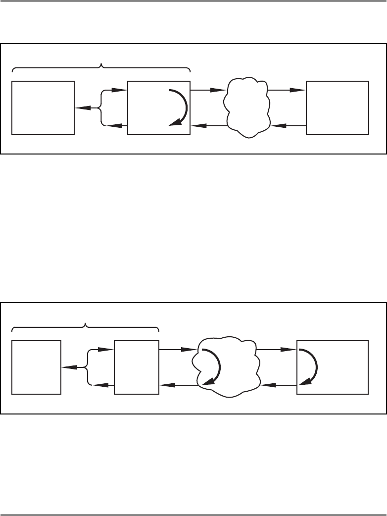
NT5D11 and NT5D14 Lineside T1 Interface cards Page 243 of 906
Circuit Card Description and Installation
Test 2, external loopback, assumes an external loopback is applied to the T1
link. Test data is generated and received by the lineside T1 card on all
timeslots. If test 1 passes but test 2 fails, it indicates that the T1 link is
defective between the lineside T1 card and the external loopback location. If
test 1 was not run and test 2 fails, the T1 link or the lineside T1 card could be
defective. To isolate the failure to the T1 link, tests 1 and 2 must be run in
tandem. Figure 35 demonstrates how an external loopback is applied to the
T1 link.
Test 3, network loopback, loops the received T1 data back toward the CPE
equipment. No test data is generated or received by the lineside T1 card. If
test 2 passes but test 3 fails, it indicates that the CPE device is defective. If
test 2 was not run and test 3 fails, the T1 link or the CPE device could be
defective. To isolate the failure to the CPE device, tests 2 and 3 must be run
Figure 34
MMI local loopback test
Figure 35
MMI external loopback test
T-1 link
Line side
T-1
interface
card
Customer
premise
equipment
(CPE)
Common
Equipment
System
External
network T-1 link
553-AAA1120
T-1 link
Line side
T-1
interface
card
Customer
premise
equipment
(CPE)
Common
Equipment
System
External
network T-1 link
553-AAA1121
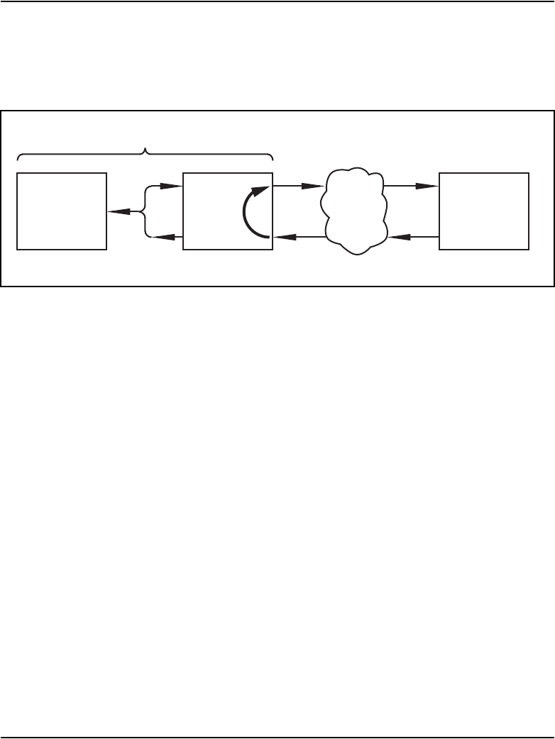
Page 244 of 906 NT5D11 and NT5D14 Lineside T1 Interface cards
553-3001-211 Standard 3.00 August 2005
in tandem. Figure 36 demonstrates how the signaling is looped back toward
the CPE equipment.
Applications
The lineside T1 interface is an IPE line card that provides cost-effective
connection between T1-compatible IPE and a system or off-premise
extensions over long distances.
Some examples of applications where a lineside T1 card can be interfaced to
a T1 link are:
• T1 compatible Voice Response Unit (VRU) equipment
• T1 compatible turret systems
• T1 compatible wireless systems
• Remote analog (500/2500-type) telephones through T1 to a channel bank
• Remote Norstar sites behind CS 1000S, CS 1000M, and Meridian 1 over
T1
The lineside T1 card is appropriate for any application where both T1
connectivity and “lineside” functionality is required. This includes
connections to T1-compatible voice response units, voice messaging and
trading turret (used in stock market applications) systems. See Figure 37.
Figure 36
MMI network loopback test
T-1 link
Line side
T-1
interface
card
Customer
premise
equipment
(CPE)
Common
Equipment
System
External
network T-1 link
553-AAA1122
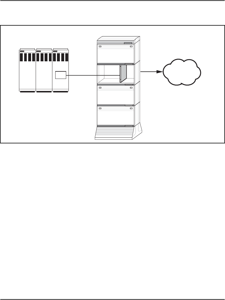
NT5D11 and NT5D14 Lineside T1 Interface cards Page 245 of 906
Circuit Card Description and Installation
For example, the lineside T1 card can be used to connect the system to a
T1-compatible VRU. An example of this type of equipment is Nortel Open
IVR system. In this way, the system can send a call to the VRU. Because the
lineside T1 card supports analog (500/2500-type) telephones, the VRU is able
to send the call back to the system for further handling.
The lineside T1 card can also be used to provide off-premise extensions to
remote locations (up to 500 miles from the system). In this application, the
analog telephone functionality is extended over T1 facilities, providing a
telephone at a remote site with access to analog (500/2500-type) telephone
lines. See Figure 38 on page 246. An audible message-waiting indicator can
be provided as well.
Figure 37
Lineside T1 interface connection to IPE
553-AAA1123
Line-side T1
interface LTI
System
Public
network
T1
Trunks
Third-party
peripheral equipment
with T1 interface
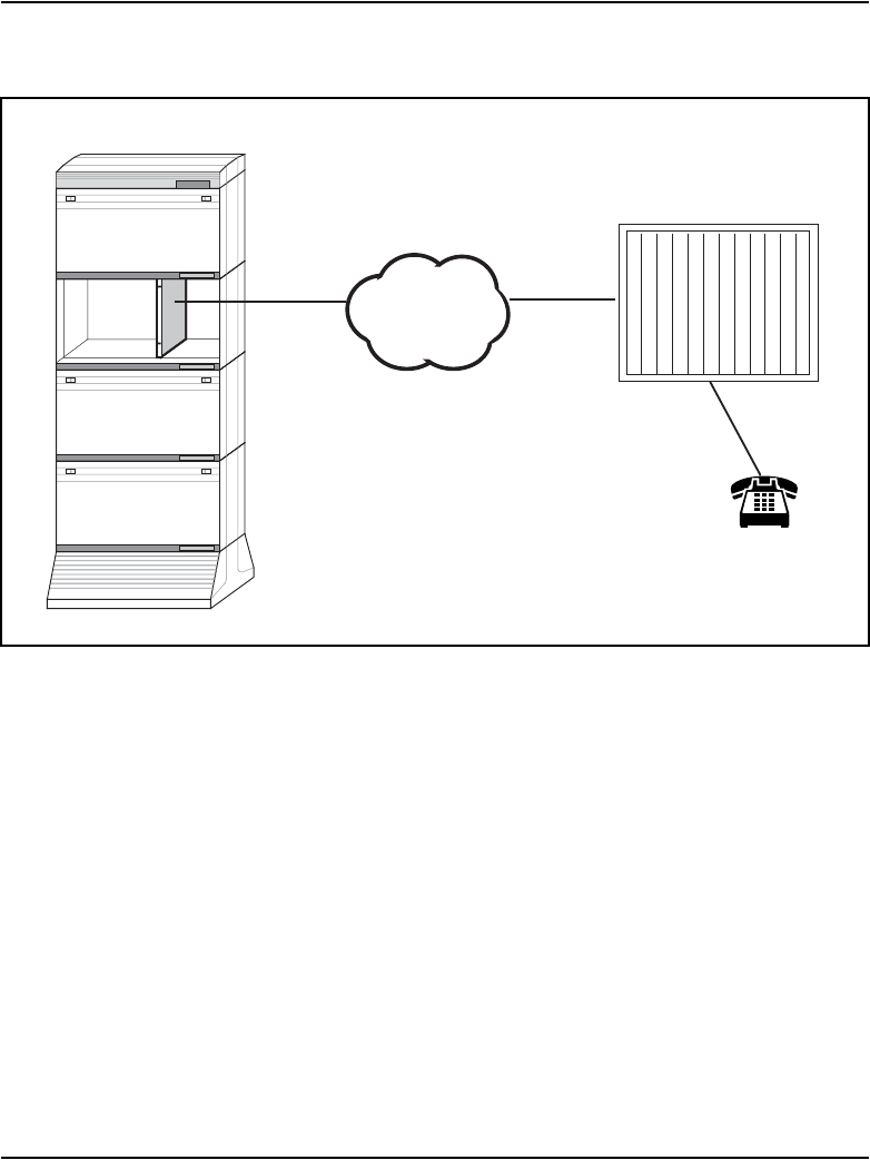
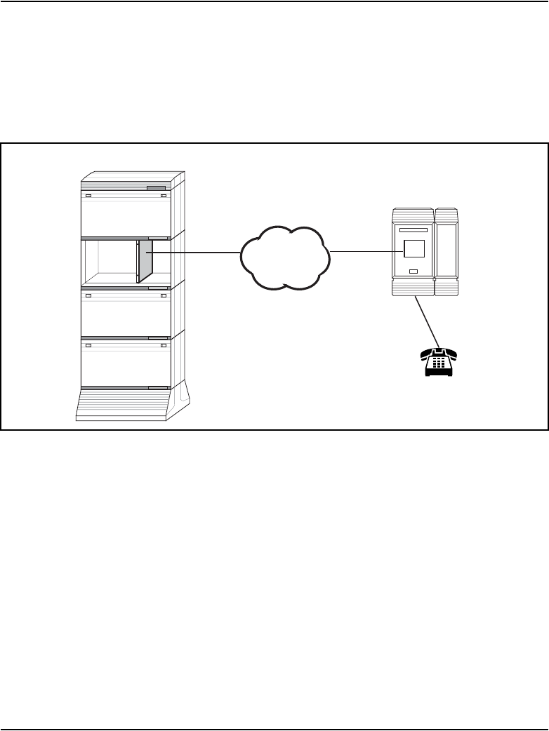
NT5D11 and NT5D14 Lineside T1 Interface cards Page 247 of 906
Circuit Card Description and Installation
Similarly, the lineside T1 can be used to provide a connection between the
system and a remote Norstar system. See Figure 39. In this case, channel
banks would not be required if the Norstar system is equipped with a T1
interface.
Note: The lineside T1 card audio levels must be considered when
determining the appropriateness of an application.
Figure 39
Lineside T1 interface connection to Norstar system
553-AAA1125
T1
Norstar
T1 T1
LTI
System
Public
network T1


Page 249 of 906
Circuit Card Description and Installation
312
NT5D33 and NT5D34 Lineside E1
Interface cards
Contents
This section contains information on the following topics:
Introduction . . . . . . . . . . . . . . . . . . . . . . . . . . . . . . . . . . . . . . . . . . . . . . 249
Physical description. . . . . . . . . . . . . . . . . . . . . . . . . . . . . . . . . . . . . . . . 250
Functional description . . . . . . . . . . . . . . . . . . . . . . . . . . . . . . . . . . . . . . 255
Electrical specifications. . . . . . . . . . . . . . . . . . . . . . . . . . . . . . . . . . . . . 261
Installation and Configuration. . . . . . . . . . . . . . . . . . . . . . . . . . . . . . . . 263
Installation. . . . . . . . . . . . . . . . . . . . . . . . . . . . . . . . . . . . . . . . . . . . . . . 271
Man-Machine E1 maintenance interface software . . . . . . . . . . . . . . . . 284
Applications . . . . . . . . . . . . . . . . . . . . . . . . . . . . . . . . . . . . . . . . . . . . . 310
Introduction
Two vintages of NT5D33 and NT5D34 cards are supported:
• NT5D33AB/NT5D34AB – standard Lineside E1 Interface (LEI) cards
The LEI card is an IPE line card that provides an all-digital connection
between E1–compatible terminal equipment (such as a voice mail
system) and CS 1000S, CS 1000M, or Meridian 1.
The LEI interfaces one E1 line, carrying 30 channels, to the CS 1000S,
CS 1000M, or Meridian 1, and emulates an analog line card to the system
software. Each channel is independently configured by software control

Page 250 of 906 NT5D33 and NT5D34 Lineside E1 Interface cards
553-3001-211 Standard 3.00 August 2005
in the Analog (500/2500-type) Telephone Administration program
LD 10. The LEI also comes equipped with a Man-Machine Interface
(MMI) maintenance program, which provides diagnostic information
regarding the status of the E1 link.
• NT5D33AC/NT5D34AC – Enhanced Lineside E1 Interface (ELEI)
cards
The ELEI card is similar to an LEI card, but has been enhanced to allow
the capability of transporting caller information using the proprietary
signaling interface Channel Associated Signaling (CAS+).
ELEI cards can operate in one of two modes: LEI mode, or enhanced
(ELEI) mode. In LEI mode, this card is fully compatible with, and
provides the same functionality as, the standard LEI card. In ELEI mode,
this card can be connected to any CAS+ compliant systems. This
includes wireless server hosting Digital Enhanced Cordless Telephones
(DECTs), voice response units, voice messaging systems, and trading
turret systems (used in stock market applications). More information
regarding CAS+ can be obtained through Nortel Development Partner
program.
Note: As the ELEI cards provide identical functionality to LEI cards,
references to LEI cards in this chapter also apply to ELEI cards unless
specified otherwise.
Install the NT5D33 version of the LEI/ELEI card in the NT8D37 IPE module.
Install the NT5D34 version of the LEI/ELEI card in:
• the NTAK11 Cabinet
• the NTAK12 Expansion Cabinet
• the NT1P70 Small Remote IPE Main Cabinet
• the NTAK12 Small Remote IPE Expansion Cabinet
Physical description
The LEI mounts in two consecutive card slots in the IPE shelf. It uses 16
channels on the first slot and 14 channels on the second. The LEI includes a

NT5D33 and NT5D34 Lineside E1 Interface cards Page 251 of 906
Circuit Card Description and Installation
motherboard (31.75 by 25.40 cm (12.5 by 10 in) and a daughterboard (5.08
by 15.24 cm (2 by 6 in).
Card connections
The LEI uses the NT8D81AA Tip and Ring cable to connect from the IPE
backplane to the 25-pair Amphenol connector on the IPE Input/Output (I/O)
panel. The I/O panel connector connects to a E1 line, external alarm and an
MMI terminal or modem, using the NT5D35 or NT5D36 lineside I/O cable
available from Nortel.
Faceplate
The LEI faceplate is twice as wide as the other standard analog and digital
line cards. It occupies two card slots. The LE1 faceplate has four LEDs. See
Figure 40 on page 252 (IPE version), and Figure 41 on page 253 (Cabinet
system).
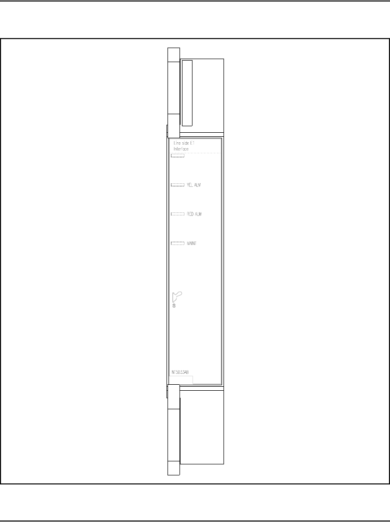
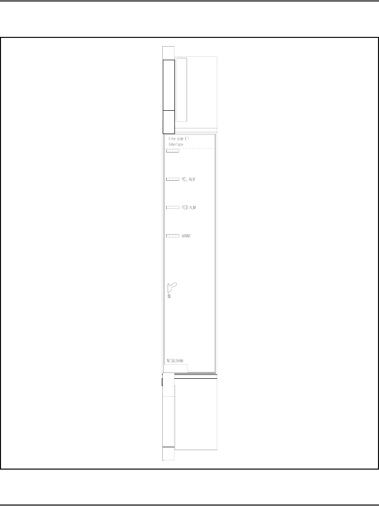
Page 254 of 906 NT5D33 and NT5D34 Lineside E1 Interface cards
553-3001-211 Standard 3.00 August 2005
The LEDs give status indications on the operations as described in Table 92.
The STATUS LED indicates if the LEI has successfully passed its self test,
and therefore, if it is functional. When the card is installed, this LED remains
lit for two to five seconds as the self-test runs. If the self-test completes
successfully, the LED flashes three times and remains lit. When the card is
configured and enabled in software, the LED goes out. If the LED continually
flashes or remains weakly lit, replace the card.
The STATUS LED indicates the enabled/disabled status of both card slots of
the LEI simultaneously. To properly enable the card, both the motherboard
and the daughterboard slots must be enabled. The STATUS LED will turn off
as soon as either one of the LEI slots have been enabled. No LED operation
will be observed when the second card slot is enabled. To properly disable the
card, both card slots must be disabled. The LED will not turn on until both
card slots have been disabled.
The RED ALARM LED indicates if the LEI has detected an alarm condition
from the E1 link. Alarm conditions can include such conditions as not
receiving a signal, the signal has exceeded bit error thresholds or frame slip
thresholds. See “Man-Machine E1 maintenance interface software” on
page 284 for information on E1 link maintenance.
If one of these alarm conditions is detected, this LED will light. Yellow alarm
indication is sent to the far end as long as the near end remains in a red alarm
Table 92
LEI card LED operation
LED Operation
Status Line card
Red alarm E1 near end
Yellow alarm E1 far end
Maint Maintenance

NT5D33 and NT5D34 Lineside E1 Interface cards Page 255 of 906
Circuit Card Description and Installation
condition. Depending on how the Man Machine Interface (MMI) is
configured, this LED will remain lit until one the following actions occur:
• If the “Self-Clearing” function is enabled in the MMI, the LED will clear
the alarm when the alarm condition is no longer detected. This is the
factory default configuration.
• If the “Self-Clearing” function has not been enabled or it has been
subsequently disabled in the MMI, the LED alarm indication will stay lit
until the command “Clear Alarm” has been typed in the MMI, even
though the carrier automatically returned to service when the alarm
condition was no longer detected.
The YELLOW ALARM LED indicates that the LEI has detected a yellow
alarm signal from the terminal equipment side of the E1 link. See
“Man-Machine E1 maintenance interface software” on page 284 for
information on E1 link maintenance. If the terminal equipment detects a red
alarm condition such as not receiving a signal, or the signal exceeds bit-error
thresholds or frame-slip thresholds, a yellow alarm signal is sent to the LEI,
if the terminal equipment supports this feature. If a yellow alarm signal is
detected, this LED will light.
The MAINT LED indicates if LEI is fully operational because of certain
maintenance commands that are issued through the MMI. See “Man-Machine
E1 maintenance interface software” on page 284 for information on E1 link
maintenance. If the card detects that tests are being run or that alarms have
been disabled through the MMI, this LED will light and will remain lit until
these conditions are no longer detected, then it turns off.
Functional description
Figure 42 on page 256 shows a block diagram of the major functions
contained on the LEI card. Each of these functions is described on the
following pages.
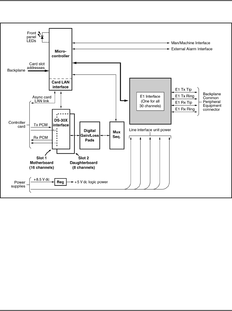

NT5D33 and NT5D34 Lineside E1 Interface cards Page 257 of 906
Circuit Card Description and Installation
Overview
The LEI card is an IPE line card that provides a cost-effective, all-digital
connection between E1 compatible terminal equipment (such as voice mail
systems, voice response units, trading turrets, etc.) and the system. In this
application, the terminal equipment can be assured access to analog (500/
2500-type) telephone line functionality such as hook flash, SPRE codes and
ringback tones. The LEI supports line supervision features such as loop and
ground start protocols. It can also be used in an off-premise arrangement
where analog (500/2500-type) telephones are extended over twisted-pair or
coaxial E1 with the use of channel bank equipment.
The LEI offers significant improvement over the previous alternatives. For
example, if a digital “trunk-side” connection were used, such as with the DTI/
PRI interface card, “lineside” functionality would not be supported.
Previously, the only way to achieve lineside functionality was to use analog
ports and channel bank equipment. With the LEI, a direct connection is
provided to the IPE. No channel bank equipment is required, resulting in a
more robust and reliable connection.
When used for connecting to third-party applications equipment, the LEI
offers a number of benefits. It is a more cost-effective alternative for
connection because it eliminates the need for expensive channel bank
equipment. The LEI card supports powerful E1 monitoring, and diagnostic
capability. Overall costs for customer applications may also be reduced
because the E1-compatible IPE is often more attractively priced than the
analog-port alternatives.
The LEI is compatible with all IPE-based systems and with standard public
or private CEPT-type carrier facilities. It supports CRC-4- or FAS only
framing formats as well as AMI or HDB3 coding. Because it uses standard
PCM in standard E1 timeslots, existing E1 test equipment remains
compatible for diagnostic and fault isolation purposes. A/B Bit signaling may
be customized according to the user’s system, including the Australian P2
signaling scheme.
Card interfaces
The LEI passes voice and signaling data over DS-30X loops through the
DS-30X Interface circuits and maintenance data over the card LAN link.

Page 258 of 906 NT5D33 and NT5D34 Lineside E1 Interface cards
553-3001-211 Standard 3.00 August 2005
E1 interface circuit
The LEI contains one E1 line-interface circuit which provides 30 individually
configurable voice interfaces to one E1 link in 30 different time slots. The
circuit demultiplexes the 2.56 Mbps DS-30X transmit signaling bitstreams
from the DS-30X network loop and converts it into 2.048 mHz E1 transmit
signaling bitstreams onto the E1 link. It also does the opposite, receiving
receive signaling bitstreams from the E1 link and transmitting receive
signaling bitstreams onto the DS-30X network loop.
The E1 interface circuit provides the following:
• An industry standard CEPT (0 to 655 feet) interface
• DS-30X signaling protocol into FXO A- and B-channel-associated
signaling protocol
• Switch-selectable transmission and reception of E1 signaling messages
over an E1 link in either loop or ground start mode
• Switch-selectable call processing between the Australian P2, North
American Standard, or other user-configurable schemes
Signaling and control
The LEI also contains signaling and control circuits that establish, supervise,
and take down call connections. These circuits work with the system
controller to operate the E1 line interface circuit during calls. The circuits
receive outgoing call signaling messages from the controller and return
incoming call status information to the controller over the DS-30X network
loop.
Card control functions
Control functions are provided by a microcontroller and a card LAN link on
the LEI. A sanity timer is provided to automatically reset the card if the
microcontroller stops functioning for any reason.
Microcontrollers
The LEI contains a microcontroller that controls the internal operation of the
card and the serial card LAN link to the controller card. The microcontroller
controls the following:
• reporting to the CE CP through the card LAN link

NT5D33 and NT5D34 Lineside E1 Interface cards Page 259 of 906
Circuit Card Description and Installation
— card identification (card type, vintage, serial number)
— firmware version
— self-test results
— programmed unit parameter status
• receipt and implementation of card configuration
— control of the E1 line interface
— enabling/disabling of individual units or entire card
— programming of loop interface control circuits for administration of
channel operation
— maintenance diagnostics
• interface with the line card circuit
— converts on/off-hook, and ringer control messages from the DS-30X
loop into A/B bit manipulations for each time slot in the E1 data
stream, using channel associated signaling.
• the front panel LED when the card is enabled or disabled by instructions
from the NT8D01 controller card.
Card LAN interface
Maintenance data is exchanged with the Common Equipment CPU over a
dedicated asynchronous serial network called the Card LAN link. The Card
LAN link is described in “Card LAN link” on page 36.
Sanity Timer
The LEI also contains a sanity timer that resets the microcontroller in the
event of a loss of program control. If the timer is not properly serviced by the
microcontroller, it times out and causes the microcontroller to be
hardware-reset. If the microcontroller loses control and fails to service the
sanity timer at least once per second, the sanity timer will automatically reset
the microcontroller, restoring program control.
Man-Machine Interface
The LEI provides an optional Man-Machine Interface (MMI) that is primarily
used for E1 link performance monitoring and problem diagnosis. The MMI
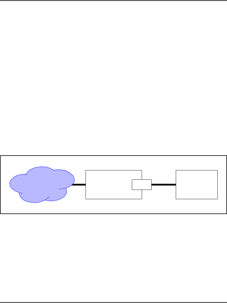
Page 260 of 906 NT5D33 and NT5D34 Lineside E1 Interface cards
553-3001-211 Standard 3.00 August 2005
provides alarm notification, E1 link performance reporting, and fault
isolation testing. The interface is accessed through connections from the I/O
panel to a terminal or modem. Multiple cards (up to 64) can be served through
one MMI terminal or modem by linking the LEIs through a daisy chain.
The MMI is an optional feature, since all E1 configuration settings are
performed through dip switch settings or preconfigured factory default
settings. Available MMI commands, and their functionality, are discussed
in-depth in “Man-Machine E1 maintenance interface software” on page 284.
ELEI additional functionality
As mentioned earlier, ELEI cards are enhanced to allow CAS+ compliance,
as shown in Figure 43. This enhancement provides several additional benefits
for systems with ELEI cards installed.
Note: MDECTS and ELEI (operating in enhanced mode) cannot be
configured on the same system.
Figure 43
CAS+ compliance
Key Benefits of using CAS+ signaling (ELEI mode) over traditional A/B bit
signaling (LEI mode) include:
1Calling Line ID Presentation (CLIP)
When an incoming call over the TDM/IP network or a CS 1000
originated call is directed towards the CAS+ compliant system, Calling
Line ID can be provided over the CAS+ interface. This is assuming that
the incoming call has the CLID without any presentation restrictions.
ELEI
CAS
TDM or IP
public/private
network
Nortel
Meridian 1
or CS 1000S
CAS+
compliant
system
NT5D33 and NT5D34 Lineside E1 Interface cards Page 261 of 906
Circuit Card Description and Installation
2Redirecting Line ID Presentation (RLIP)
When an incoming call over the TDM/IP network or a CS 1000
originated call which has undergone redirections is directed towards the
CAS+ compliant system, Redirecting Line ID can be provided over the
CAS+ interface. This is assuming that the incoming call has the
Redirecting Line ID without any presentation restrictions.
3Message waiting indication (MWI)
Message waiting indication can be provided over the CAS+ interface.
Electrical specifications
Table 93 provides a technical summary of the E1 line interface. Table 94 on
page 262 lists the maximum power consumed by the card.
E1 channel specifications
Table 93 provides specifications for the 30 E1 channels. Each characteristic
is set by a dip switch. See “Installation and Configuration” on page 263. for
a discussion of the corresponding dip switch settings.
Table 93
LEI card — line interface unit electrical characteristics
Characteristics Description
Framing CRC-4 or FAS, only
Coding AMI or HDB3
Signaling Loop or ground start
A/B robbed-bit
Distance to LTU 0-199.6 meters (0-655 feet)
Page 262 of 906 NT5D33 and NT5D34 Lineside E1 Interface cards
553-3001-211 Standard 3.00 August 2005
Power requirements
Table 94 shows the voltage and maximum current that the LEI requires from
the backplane. One NT8D06 IPE Power Supply AC or NT6D40 IPE Supply
DC can supply power to a maximum of eight LEIs.
Foreign and surge voltage protections
In-circuit protection against power line crosses or lightning strikes is not
provided on the LEI. It does, however, have protection against accidental
shorts to –52 V dc analog lines.
When the card is used to service off-premise terminal equipment through the
public telephone network, install a Line Termination Unit (LTU) as part of
the terminal equipment to provide external line protection.
Environmental specifications
Table 95 shows the environmental specifications of the LEI.
Table 94
LEI card – power required
Voltage Max. Current
5.0 V dc 1.6 Amp
+15.0 V dc 150 mA
-15.0 V dc 150 mA
Table 95
LEI card – environmental specifications (Part 1 of 2)
Parameter Specifications
Operating temperature – normal 15° to +30° C (+59° to 86° F), ambient
Operating temperature – short term 10° to +45° C (+50 to 113° F), ambient
Operating humidity – normal 20% to 55% RH (non-condensing)
Operating humidity – short term 20% to 80% RH (non condensing)

NT5D33 and NT5D34 Lineside E1 Interface cards Page 263 of 906
Circuit Card Description and Installation
Installation and Configuration
Installation and configuration of the LEI consists of six basic steps:
1Configure the dip switches on the LEI for the call environment.
2Install the LEI into the selected card slots.
3Cable from the I/O panel to the LTU, MMI terminal or modem
(optional), external alarm (optional), and other LEIs for daisy chaining
use of MMI terminal (optional).
4Configure the MMI terminal.
5Configure the LEI through the CS 1000 Release 4.5 software and verify
self-test results.
6Verify initial E1 operation and configure MMI (optional).
Steps 1-5 are explained in this section. Step 6 is covered in “Man-Machine E1
maintenance interface software” on page 284.
Installation and configuration of the ELEI follows the same steps. If enhanced
functionality is required, then one additional step is required:
7The Meridian 1 line unit(s) associated with the lineside E1 must be
programmed for wireless operation (set WTYP=DECT, and WRLS=Yes
in LD 10) in non–concentrated mode. Refer to Software Input/Output:
Administration (553-3001-311) details on LD 10.
Dip switch settings
Begin the installation and configuration of the LEI by selecting the proper dip
switch settings for the environment. The LEI contains two dip switches, each
containing eight switch positions. They are located in the upper right corner
Storage temperature –50° to + 70° C (–58° to 158° F), ambient
Storage humidity 5% to 95% RH (non-condensing)
Table 95
LEI card – environmental specifications (Part 2 of 2)
Parameter Specifications

Page 264 of 906 NT5D33 and NT5D34 Lineside E1 Interface cards
553-3001-211 Standard 3.00 August 2005
of the motherboard circuit card as shown in Figure 44 on page 266. The
settings for these switches are shown in Table 96 on page 267 through
Table 99 on page 270.
When the LEI card is oriented as shown in Figure 44 on page 266, the dip
switches are ON when they are up, and OFF when they are down. The dip
switch settings configure the card for the following parameters:
MMI port speed selection
This dip switch setting selects the appropriate baud rate for the terminal or
modem (if any) that is connected to the MMI.
Line Supervisory Signaling protocol
The LEI is capable of supporting loop start or ground start call processing
modes. Make the selection for this dip switch position based on what type of
line signaling the Customer Premise Equipment (CPE) supports.
Address of LEI to the MMI
The address of the LEI to the MMI is made up of two components:
• the address of the card within the shelf
• the address of the shelf in which the card resides
These two addresses are combined to create a unique address for the card. The
MMI reads the address of the card within the shelf from the card firmware;
the address of the shelf must be set by this dip switch.
The shelf address dip switch can be from 0 to 15, 16 being the maximum
number of lineside E1 IPE shelves (a maximum of 64 LEI cards) capable of
daisy chaining to a single MMI terminal. For ease, it is recommended that this
address be set the same as the address of the peripheral controller identifier in
LD 97 for type: XPE. However, this is not mandatory, and, since the dip
switch is limited to 16, this will not always be possible.
E1 framing
The LEI is capable of interfacing with LTU equipment either in CRC-4 or
FAS only framing mode. Make the selection for this dip switch position based
on what type of framing the LTU equipment supports.

NT5D33 and NT5D34 Lineside E1 Interface cards Page 265 of 906
Circuit Card Description and Installation
E1 Coding
The LEI is capable of interfacing with LTU equipment using either AMI or
HDB3 coding. Make the selection for this dip switch position based on the
type of coding the LTU equipment supports.
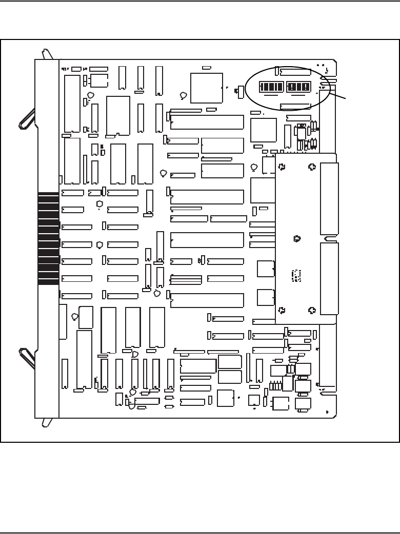
Page 266 of 906 NT5D33 and NT5D34 Lineside E1 Interface cards
553-3001-211 Standard 3.00 August 2005
Figure 44
LEI card – E1 protocol dip switch locations
U7 8
U7 7
C4 6
U6 4
U6 6
U7 9
U63
U6 5
U6 2 RP1 6
C4 1
C3 6
U6 1
C3 5
U6 0
U48
U4 9
U4 7
U25
U26
U2 9
R2 5
R2 6
C2 5C3 4
R2 0
R1 9
C3 7
C7 1
RP8
RP7
C4 2
C6 9
C6 7
C6 8 U3 1
U3 0
U2 8
U2 7
U2 4
RP 5
RP9
U1 3
U14
U1 5
U16
U1 7
C1 5
C7 0
C1 3
X1
T2
R1 8 R1 7R1 6R1 5
C14
R2 7
T1
K1
K2
K3R1R2
C7 7
C3 U2
U1
C7 6
D1
D2
D3
R3
R4
C1
C2
RP6
C1 6
U1 8
U1 9
U20
U2 1
C1 7
C2 0
C19 C22
C2 1
Y1
U22
C1 8
U2 3
U9
C10
C9 R12
D4D5
R1 4
T3
R1 3
D6D7
U1 0
U1 1
C7 5 U12
U4 0
U42
U4 6
C3 1
C3 0
RP1 4
U3 2
U3 3
U3 4U3 5
U3 6
U3 8 U3 7
U39
U4 1
C2 8
U5 2
U5 0
C2 6
C2 7
C2 9
RP10
RP11
RP1 2
RP1 3
C4 0
C3 8
U5 3
U5 1
C3 9
C7 4
U5 4
U5 5
U7 4
C5 8
U6 8
U6 9
U7 0
U71
U72
U73
U4 3
U4 4
U4 5
U56U57
C7 2
C3 3
C3 2
U5 8
U5 9
U7 6
U7 5
C7 3
RP1 5
C6 0 C5 9
Y2
C6 3
C6 4
U9 1
U8 9
C6 2
U8 8
U9 0
U9 2
RP17
C5 7
C6 1
U8 7 U8 6 C5 6
C5 3
U8 4
U8 5
C5 4
U8 3
U8 2
U81
C5 1
C4 9
C4 7
U6 7
C4 3C4 5
C4 4
U8 0
ON
OFF
18
18
S1 S2
dip
switches

NT5D33 and NT5D34 Lineside E1 Interface cards Page 267 of 906
Circuit Card Description and Installation
Line supervision on E1 failure
This setting determines in what state all 30 LEI ports will appear to the
CS 1000S, CS 1000M, and Meridian 1 in case of E1 failure. Ports can appear
as either in the “on-hook” or “off-hook” states on E1 failure.
Note: All idle LEI lines will go off-hook and seize a Digitone Receiver
when the off-hook line processing is invoked on E1 failure. This may
prevent DID trunks from receiving incoming calls until the LEI lines
time-out and release the DTRs.
Daisy-Chaining to MMI
If two or more LEIs will be installed and the MMI used, daisy-chain the cards
together to use one MMI terminal or modem. Make the selection for this dip
switch position based on how many LEIs are being installed.
MMI Master or Slave
This setting is used only if daisy-chaining the cards to the MMI terminal or
modem. It determines whether this card is a master or a slave in the daisy
chain. Select the master setting if there are no LEIs between this card and the
MMI terminal or modem. Select the slave setting if there are other cards in
the daisy chain between this card and the MMI.
Tables 96 through 98 show the dip switch settings for Switch #1. Table 99 on
page 270 shows the dip switch settings for Switch #2.
Table 96
LEI card – Switch #1 dip switch settings (Part 1 of 2)
Characteristic Selection
Switch
Position
Switch
Setting
Factory
Default
MMI port speed selection 1200 baud
2400 baud
1
1
ON
OFF
OFF
E1 signaling Ground start
Loop start
2
2
ON
OFF
OFF
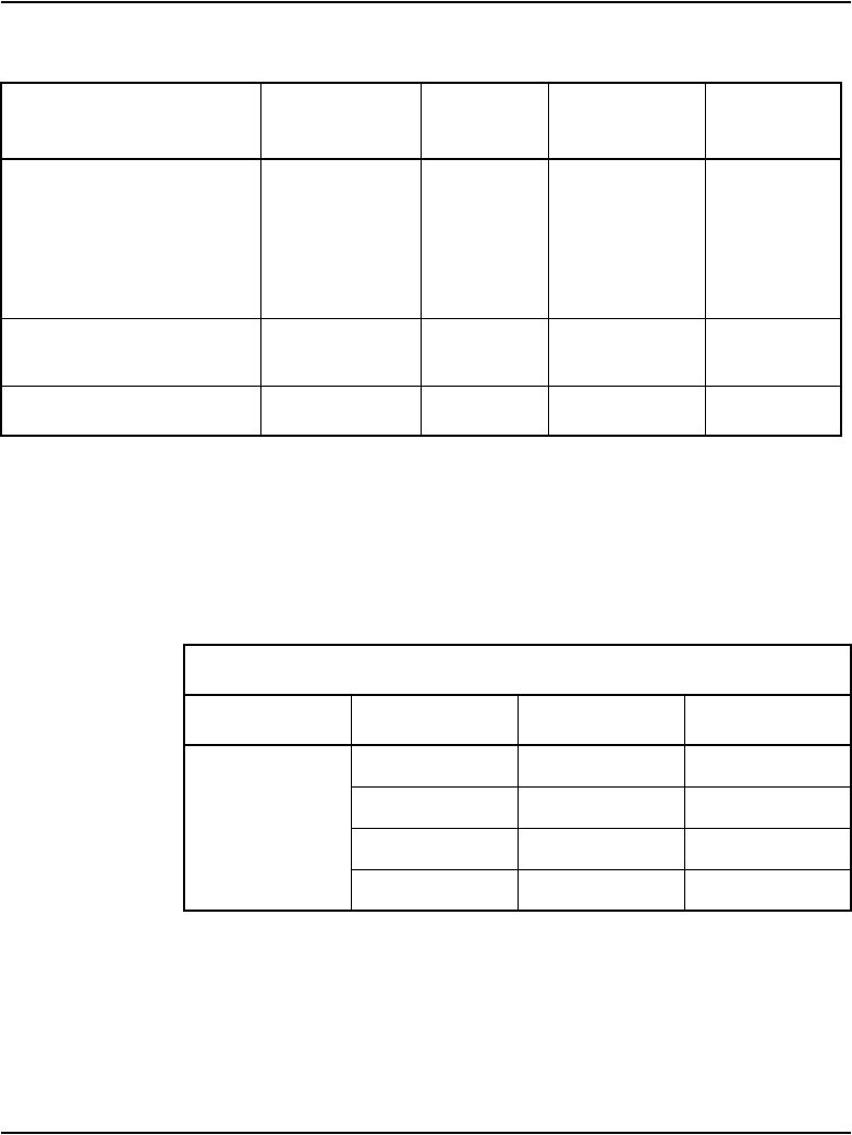
Page 268 of 906 NT5D33 and NT5D34 Lineside E1 Interface cards
553-3001-211 Standard 3.00 August 2005
When dip switch #1, positions 2 and 8 are set to “Table,” AB Bits are
configured by the user through the Set Mode MMI command (see “Set Mode”
on page 295). Otherwise, the signaling scheme selected by dip switch 1,
positions 2 and 8 will be used.
IPE Shelf address for LEI See Table 98 3
4
5
6
See Table 98 OFF
OFF
OFF
OFF
Card type for ringer
allocation
XTI = 19
XMLC = 18
7
7
ON
OFF
OFF
E1 signaling See Table 97 8OFF OFF
Table 97
LEI card – signaling-type dip switch settings
Switch #1
Characteristic Selection Position 2 Position 8
Signaling Type Loop start OFF OFF
Ground start ON OFF
Australian P2 OFF ON
Table ON ON
Table 96
LEI card – Switch #1 dip switch settings (Part 2 of 2)
Characteristic Selection
Switch
Position
Switch
Setting
Factory
Default

NT5D33 and NT5D34 Lineside E1 Interface cards Page 269 of 906
Circuit Card Description and Installation
Table 98
LEI card – XPEC address dip switch settings (Switch S1, positions 3-6)
XPEC
Address
S1 Switch
Position 3
S1 Switch
Position 4
S1 Switch
Position 5
S1 Switch
Position 6
00 OFF OFF OFF OFF
01 ON OFF OFF OFF
02 OFF ON OFF OFF
03 ON ON OFF OFF
04 OFF OFF ON OFF
05 ON OFF ON OFF
06 OFF ON ON OFF
07 ON ON ON OFF
08 OFF OFF OFF ON
09 ON OFF OFF ON
10 OFF ON OFF ON
11 ON ON OFF ON
12 OFF OFF ON ON
13 ON OFF ON ON
14OFFONONON
15 ON ON ON ON

Page 270 of 906 NT5D33 and NT5D34 Lineside E1 Interface cards
553-3001-211 Standard 3.00 August 2005
When setting E1 Switch 2 dip switch settings, there are differences between
vintages. For NT5D33AB or NT5D34AB cards, use Table 99. For
NT5D33AC or NT5D34AC cards, use Table 99 on page 270.
Table 99
LEI card – E1 Switch 2 (S2) dip switch settings
Characteristic Selection
Switch
Position
Switch
Setting
Factory
Default
E1 framing CRC-4 Disabled
CRC-4 Enabled
1ON
OFF
OFF
E1 coding AMI
HDB3
2ON
OFF
OFF
NOT USED leave ON 3ON ON
NOT USED leave ON 4OFF OFF
NOT USED leave ON 5OFF OFF
Line processing on E1
link failure
On-hook
Off-hook
6ON
OFF
ON
Daisy-chaining to MMI YES
NO
7ON
OFF
OFF
MMI master or slave Master
Slave
8ON
OFF
ON

NT5D33 and NT5D34 Lineside E1 Interface cards Page 271 of 906
Circuit Card Description and Installation
After the card has been installed, display the dip switch settings using the
MMI command Display Configuration (D C). See “Man-Machine E1
maintenance interface software” on page 284 for details on this and the rest
of the available MMI commands.
Installation
Because of the wiring in some of the system modules and cabinets, the LEI
will only work in certain card slot pairs. These restrictions depend on the type
Table 100
ELEI card – E1 Switch 2 (S2) dip switch settings
Characteristic Selection
Switch
Position
Switch
Setting
Factory
Default
E1 framing CRC-4 Disabled
CRC-4 Enabled
1ON
OFF
ON
E1 coding AMI
HDB3
2ON
OFF
OFF
NOT USED leave ON 3ON ON
NOT USED leave ON 4OFF OFF
Mode LEI Mode
ELEI Mode
5OFF
ON
OFF
Line processing on E1
link failure
On-hook
Off-hook
6ON
OFF
OFF
Daisy-chaining to MMI YES
NO
7ON
OFF
OFF
MMI master or slave Master
Slave
8ON
OFF
ON
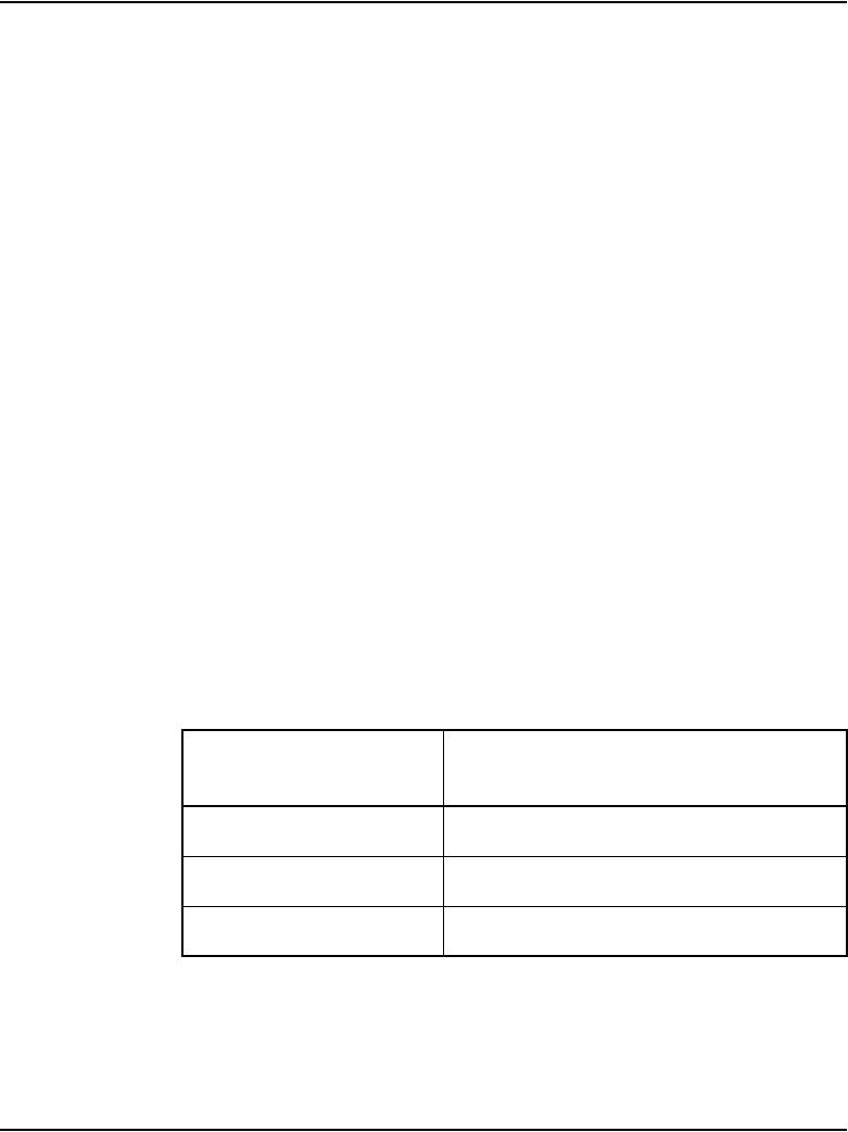
Page 272 of 906 NT5D33 and NT5D34 Lineside E1 Interface cards
553-3001-211 Standard 3.00 August 2005
of module or cabinet. In all other modules or cabinets where the conditions
listed below do not exist, the LEI will work in any two adjacent card slots:
• In the NTAK12 Small Remote IPE Expansion Cabinet only card slots
10-15 are available.
• In the NT8D37 IPE module, if the 25-pair I/O connectors are partially
split between adjacent IPE card slots, the LEI works only in card slots
where Unit 0 of the motherboard card slot appear on the first pair of the
25-pair I/O connector.
If installing the LEI into the NT8D37 IPE module, determine the vintage level
model. Certain vintage levels have dedicated 25-pair I/O connectors only for
card slots 0, 4, 8, and 12. These vintage levels are cabled with only 16 pairs
of wires from each card slot to the I/O panel. Some of the 25-pair I/O
connectors are split between adjacent card slots.
Other vintage levels cable each card slot to the I/O panel using a unique,
24-pair connector on the I/O panel. In these vintage levels, the LEI can be
installed in any available pair of card slots. However, because of the lower
number of wire pairs cabled to the I/O panel in the lower vintage level, only
certain card slots are available to the LEI.
See Table 101 for the vintage level information for the NT8D37 IPE
modules.
Available and restricted card slots in the NT8D37 IPE module
If installing the LEI into an NT8D37 IPE module, the card slots available
depend on the vintage level module.
Table 101
LEI card – NT8D37 IPE module vintage level port cabling
Vintage Level
Number of ports
cabled to I/O panel
NT8D37BA 30 ports
NT8D37DE 16 ports
NT8D37EC 30 ports

NT5D33 and NT5D34 Lineside E1 Interface cards Page 273 of 906
Circuit Card Description and Installation
Vintage levels cabling 30 ports:
For modules with vintage levels that cabled 30 ports to the I/O panel, the LEI
can be installed in any pair of card slots 0-15.
Vintage levels cabling 16 ports:
For modules with vintage levels that cable 16 ports to the I/O panel, the LEI
can be installed into the card slot pairs shown in the following card slots:
LEIs must not be installed into the following card slot pairs:
If the LEI must be installed into one of the restricted card slot pairs, rewire
the IPE module card slot to the I/O panel by installing an additional NT8D81
cable from the LEI motherboard slot to the I/O panel, and re-arranging the
three backplane connectors for the affected card slots. This will permit the
connection of the NT5D35AA or NT5D36AA LEI card carrier and
maintenance external I/O cable at the IPE and CE module I/O panel connector
for card slots that are otherwise restricted.
Available: Motherboard/Daughterboard
0 and 1
1 and 2
4 and 5
5 and 6
8 and 9
9 and 10
12 and 13
13 and 14
Restricted: Motherboard/Daughterboard
2 and 3
3 and 4
6 and 7
10 and 11
11 and 12
14 and 15

Page 274 of 906 NT5D33 and NT5D34 Lineside E1 Interface cards
553-3001-211 Standard 3.00 August 2005
Alternatively, all LEI connections can be made at the main distribution frame
instead of connecting the NT5D35AA or NT5D36AA LEI card external I/O
cable at the I/O panel. This eliminates these card slot restrictions.
Cabling the LEI card
After the dip switches are configured and the LEI installed into the selected
card slots, the LEI can be cabled to the LTU equipment, the MMI terminal or
modem (optional), an external alarm (optional), and other LEIs for daisy
chaining use of the MMI terminal (optional).
The LEI is cabled from its backplane connector through connections from the
motherboard circuit card only to the I/O panel on the rear of the IPE module.
No cable connections are made from the daughterboard circuit card. The
connections from the LEI to the I/O panel are made with the NT8D81AA Tip
and Ring cables provided with the IPE module.
Cabling from the I/O panel with the NT5D35AA or NT5D36AA
lineside E1 I/O cable
In a twisted-pair E1 installation, make the connection from the I/O panel to
the E1 link and other external devices with the NT5D35AA lineside E1 I/O
cable.
This cable consists of a 25-pair amphenol connector (P1) on one end which
plugs into the I/O panel. The other end has four connectors:
1a DB15 male connector (P2), which plugs into the E1 line
2a DB9 male connector (P3), which plugs into an external alarm system
3a second DB9 male connector (P5), which connects to an MMI terminal
or modem
4a DB9 female connector (P4), which connects to the next LEI’s P4
connector for MMI daisy chaining
In a coaxial E1 installation, make the connection from the I/O panel to the E1
link and other external devices through the NT5D36AA lineside E1 I/O cable.
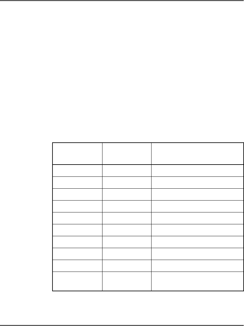
NT5D33 and NT5D34 Lineside E1 Interface cards Page 275 of 906
Circuit Card Description and Installation
This cable consists of a 25-pair amphenol connector (P1) on one end which
plugs into the I/O panel. The other end has 4 connectors:
1a DB15 female connector (P2) with an adapter that breaks out Tx
(transmit) and Rx (receive) connectors, which that plug into the E1 line
2a DB9 male connector (P3), which plugs into an external alarm system
3a second DB9 male connector (P5), which connects to an MMI terminal
or modem
4a DB9 female connector (P4), which connects to the next LEI’s P4
connector for MMI daisy chaining. The Tx marking on the adapter at P2
is the LEI output. The E1 data stream coming from the network into the
LEI connects at the Rx coaxial connector
Table 102 shows the pin assignments of the LEI backplane and I/O Panel.
Table 102
LEI card – LEI backplane and I/O panel pinouts (Part 1 of 2)
Backplane
connector pin
I/O Panel
connector pin Signal
12A 1 E1 Tip, Receive data
12B 26 E1 Ring, Receive data
13A 2 E1 Tip, Transmit data
13B 27 E1 Ring, Transmit data
14A 3 Alarm out, normally open
14B 28 Alarm out, common
15A 4 Alarm out, normally closed
15B 29 No connection
16A 5 No connection
16B 30 Away from MMI terminal, receive
data
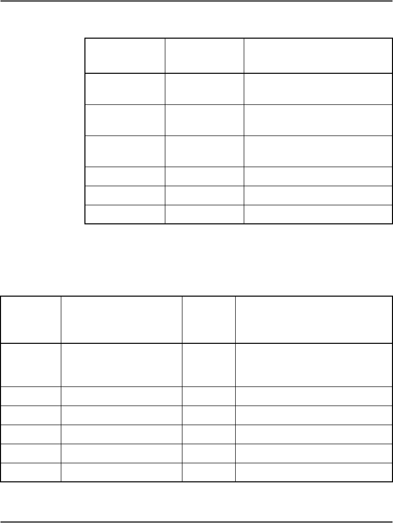
Page 276 of 906 NT5D33 and NT5D34 Lineside E1 Interface cards
553-3001-211 Standard 3.00 August 2005
Table 103 shows the pin assignments from the I/O panel relating to the pin
assignments of the lineside E1 I/O cable.
17A 6 Away from MMI terminal, transmit
data
17B 31 Toward MMI terminal, transmit
data
18A 7 Toward MMI terminal, receive
data
18B 32 Daisy chain control 2
19A 8 Daisy chain control 1
19B 33 Ground
Table 103
LEI card – lineside E1 I/O cable pinouts (Part 1 of 2)
I/O Panel
Connector
Pin Lead Designations
LEI
Connect
or Pin
LEI Cable Connector to External
Equipment
1E1 Tip Receive data 11
DB15 male to E1 (P2). LEI is CPE
transmit and receive to network
26 E1 Ring Receive data 3
2E1 Tip Transmit data 1
27 E1 Ring Transmit data 9
3Alarm out, common 1
28 Alarm out (normally open) 2DB9 male to external alarm (P3)
Table 102
LEI card – LEI backplane and I/O panel pinouts (Part 2 of 2)
Backplane
connector pin
I/O Panel
connector pin Signal
NT5D33 and NT5D34 Lineside E1 Interface cards Page 277 of 906
Circuit Card Description and Installation
E1 Connections
For twisted-pair installations, E1 signaling for all 30 channels is transmitted
over P2 connector pins 1, 3, 9, and 11, as shown in Table 103 on page 276.
Plug the DB 15 male connector labeled “P2” into the E1 link. E1 transmit and
receive pairs must be turned over between the LEI and the CPE that is
hardwired without carrier facilities. If the LEI is connected through E1 carrier
facilities, the transmit and receive pairs must be wired straight through to the
RJ48 at the Telco demarc, the LTU, or other E1 carrier equipment. The E1
4Alarm out (normally
closed)
3
7Toward MMI terminal,
receive data
2
DB9 male toward MMI (P5).
Wired as DCE.
Data is transmitted on pin 2 (RXD)
and received on pin 3 (TXD)
31 Toward MMI terminal,
transmit data
3
33 Ground 5
8Control 1 7
32 Control 2 9
33 Ground 5
DB9 female away from MMI terminal
(P4)
8Control 1 7
32 Control 2 9
30 Away from MMI terminal,
transmit data
3
6Away from MMI terminal,
receive data
2
Table 103
LEI card – lineside E1 I/O cable pinouts (Part 2 of 2)
I/O Panel
Connector
Pin Lead Designations
LEI
Connect
or Pin
LEI Cable Connector to External
Equipment

Page 278 of 906 NT5D33 and NT5D34 Lineside E1 Interface cards
553-3001-211 Standard 3.00 August 2005
CPE at the far-end will likewise have transmit and receive wired straight from
the RJ48 demarc at the far-end of the carrier facility.
For 75 ohm coaxial installations, E1 signaling for all 30 channels is
transmitted over P2 connector pins 1, 3, 9, and 11 though an adapter and out
two coaxial connectors Tx (transmit) and Rx (receive). Tx is the LEI output,
and Rx is the LEI input from the E1 stream. E1 transmit and receive pairs
must be turned over between the LEI and the CPE that is hardwired without
carrier facilities. If the LEI is connected through E1 carrier facilities, the
transmit and receive pairs must be wired straight through to the RJ48 at the
Telco demarc, the LTU, or other E1 carrier equipment. The E1 CPE at the far
end will likewise have Tx and Rx wired straight from the RJ48 demarc at the
far end of the carrier facility.
External Alarm Connections
P3 connector pins 1, 2 and 3 can be plugged into any external alarm-sensing
hardware. Plug the DB9 male connector labeled “P3” into an external alarm.
These connections are optional, and the LEI functionality is not affected if
they are not made.
The MMI monitors the E1 link for specified performance criteria and reports
on problems detected. One of the ways it can report information is through
this external alarm connection. If connected, the LEI’s microprocessor will
activate the external alarm hardware if it detects certain E1 link problems it
has classified as alarm levels 1 or 2. See “Man-Machine E1 maintenance
interface software” on page 284 for a detailed description of alarm levels and
configuration. If an alarm level 1 or 2 is detected by the MMI, the LEI will
close the contact that is normally open, and will open the contact that is
normally closed. The MMI command “Clear Alarm” will return the alarm
contacts to their normal state.
MMI Connections
P5 connector pins 2, 3, 5, 7 and 9 are used to connect the LEI to the MMI
terminal, connecting LEIs in a daisy chain for access to a shared MMI
terminal. When logging into a LEI, “control 2” is asserted by that card, which
informs all of the other cards not to talk on the bus, but rather to pass the data
straight through. The pins labeled “control 1” are reserved for future use. As
with the external alarm connections, MMI connections are optional. Up to

NT5D33 and NT5D34 Lineside E1 Interface cards Page 279 of 906
Circuit Card Description and Installation
128 LEIs can be linked, located in up to 16 separate IPE shelves, to one MMI
terminal using the daisy chain approach.
If only one LEI is will be installed, cable from the DB9 male connector
labeled “P5” (toward MMI terminal) to one of the COM ports on the back of
any TTY, a PC running a terminal emulation program, or a modem. For
installations of only one card, no connection is made to the DB9 female
connector labeled “P4” (away from MMI terminal).
If two or more LEIs are being installed into the system, the MMI port
connections can be daisy-chained together so that only one MMI terminal is
required for up to 128 LEIs. See Figure 45 on page 280. Cards can be located
in up to 15 separate IPE shelves. Start with any card slot in the IPE shelf and
connect to any other card slot. Connected card slots do not need to be
consecutive.
Procedure 13
Connecting two or more LEIs to the MMI terminal
Follow this procedure for connecting two or more LEIs to the MMI terminal:
1Cable the DB9 male connector labeled “P5” (toward MMI terminal) to one
of the COM ports on the back of any TTY, a PC running a terminal
emulation program, or a modem.
2Make the connection from the first card to the second card by plugging the
DB9 female connector labeled “P4” (away from MMI terminal) from the
first card into the DB9 male connector of the second card labeled “P5”
(toward MMI terminal).
3Repeat step 2 for the remaining cards.
4At the last card of the daisy chain, make no connection from the DB9
female connector labeled “P4” (away from MMI terminal).
5If two LEIs are too far apart to connect the “P4” and “P5” connectors
connect them with an off-the-shelf DB9 female to DB9 male
straight-through extension cable, available at any PC supply store.
End of Procedure
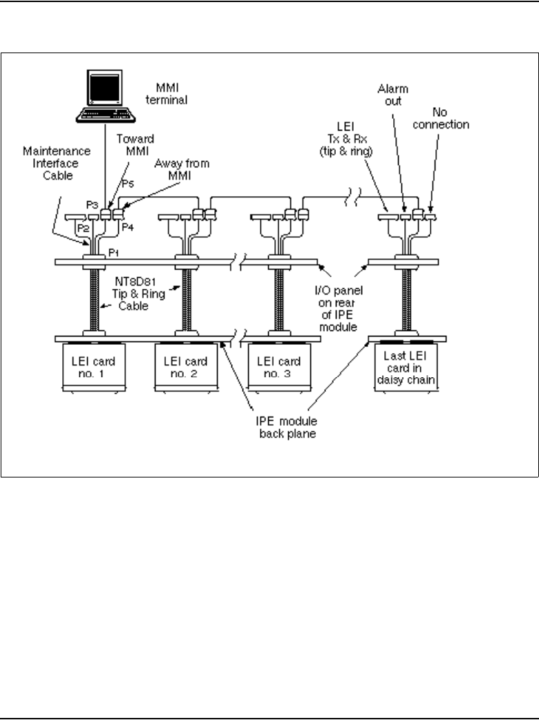
Page 280 of 906 NT5D33 and NT5D34 Lineside E1 Interface cards
553-3001-211 Standard 3.00 August 2005
Figure 45
LEI card – connecting two or more cards to the MMI
Terminal configuration
For the MMI terminal to be able to communicate to the LEI, the interface
characteristics must be set to:
• speed – 1200 or 2400 bps
• character width – 7 bits
• parity bit – mark

NT5D33 and NT5D34 Lineside E1 Interface cards Page 281 of 906
Circuit Card Description and Installation
• stop bits – one
• software handshake (XON/XOFF) – off
Software Configuration
Although much of the architecture and many features of the LEI card are
different from the analog line card, the LEI has been designed to emulate an
analog line card to the CS 1000 Release 4.5 software. Because of this, the LEI
software configuration is the same as for two adjacent analog line cards.
All 30 E1 channels carried by the LEI are individually configured using the
analog (500/2500-type) Telephone Administration program LD 10. Use
Table 104 to determine the correct unit number and Software Input/Output:
Administration (553-3001-311) for LD 10 service-change instructions.
LEI circuitry routes 16 units (0 – 15) on the motherboard and 14 (0 – 13) units
on the daughterboard to 30 E1 channels. The motherboard circuit card is
located in the left card slot, and the daughterboard circuit card is located in
right card slot. For example, if installing the LEI into card slots 0 and 1, the
motherboard would reside in card slot 0 and the daughterboard would reside
in card slot 1. In order to configure the terminal equipment through the switch
software, the E1 channel number will need to be cross-referenced to the
corresponding card unit number. This mapping is shown in Table 104.
Table 104
Card unit number to E1 channel mapping (Part 1 of 3)
Item TN E1 Channel Number
Motherboard 0 1
Motherboard 1 2
Motherboard 2 3
Motherboard 3 4
Motherboard 4 5
Motherboard 5 6
Motherboard 6 7

Page 282 of 906 NT5D33 and NT5D34 Lineside E1 Interface cards
553-3001-211 Standard 3.00 August 2005
Motherboard 7 8
Motherboard 8 9
Motherboard 9 10
Motherboard 10 11
Motherboard 11 12
Motherboard 12 13
Motherboard 13 14
Motherboard 14 15
Motherboard 15 17
Daughterboard 0 18
Daughterboard 1 19
Daughterboard 2 20
Daughterboard 3 21
Daughterboard 4 22
Daughterboard 5 23
Daughterboard 6 24
Daughterboard 7 25
Daughterboard 8 26
Daughterboard 9 27
Daughterboard 10 28
Daughterboard 11 29
Table 104
Card unit number to E1 channel mapping (Part 2 of 3)
Item TN E1 Channel Number

NT5D33 and NT5D34 Lineside E1 Interface cards Page 283 of 906
Circuit Card Description and Installation
Disconnect supervision
The LEI supports far-end disconnect supervision by opening the tip side
toward the terminal equipment upon the system’s detecting a disconnect
signal from the far-end on an established call. The Supervised Analog Line
feature (SAL) must be configured in LD 10 for each LEI port. At the prompt
FTR respond:
OSP <CR>
Against FTR respond:
ISP <CR>
The LEI treats OSP and ISP for both originating and terminating calls as hook
flash disconnect supervision, also known as cut-off disconnect. Originating
calls are outgoing from the terminal equipment. Terminating calls are
incoming to the terminal equipment. The LEI does not support battery
reversal answer and disconnect supervision on originating calls.
After the software is configured, power-up the card and verify the self-test
results. The STATUS LED on the faceplate indicates whether or not the LEI
has successfully passed its self test, and is, therefore, functional. When the
card is installed, this LED remains lit for two to five seconds as the self-test
runs. If the self-test completes successfully, the LED flashes three times and
remains lit. When the card is configured and enabled in software, the LED
goes out. The LED will go out if either the motherboard or daughterboard is
enabled by the software. If the LED continually flashes or remains weakly lit,
replace the card.
Daughterboard 12 30
Daughterboard 13 31
Table 104
Card unit number to E1 channel mapping (Part 3 of 3)
Item TN E1 Channel Number

Page 284 of 906 NT5D33 and NT5D34 Lineside E1 Interface cards
553-3001-211 Standard 3.00 August 2005
Man-Machine E1 maintenance interface software
Description
The Man-Machine Interface (MMI) provides E1-link diagnostics and
historical information for the LEI system. See “Installation and
Configuration” on page 263 for instructions on how to install the cabling and
configure the terminal for the MMI. The following sections will describe the
options available through the LEI’s MMI terminal and will explain how to
set-up, configure, and use the MMI.
The MMI provides the following maintenance features:
• configurable alarm parameters
• E1-link problem indicator
• current and historical E1-link performance reports
• E1 verification and fault isolation testing
• configuration of A\B bits (North American Standard, Australian P2, or
customized settings are available)
Alarms
The MMI may be used to activate alarms for the following E1-link
conditions:
• excessive bit-error rate,
• frame-slip errors,
• out-of-frame,
• loss-of-signal, and
• blue alarm.
Pre-set thresholds and error durations trip LEI alarm notifications. For
descriptions of each of these E1-link alarm conditions, see “Performance
counters and reporting” on page 304. For instructions on how to set alarm
parameters, see “Set Alarm” on page 290. For information on accessing
alarm reporting, see “Display Alarms” on page 302, “Display Status” on
page 303 and “Display Performance” on page 305.

NT5D33 and NT5D34 Lineside E1 Interface cards Page 285 of 906
Circuit Card Description and Installation
Two levels of alarm severity exist for bit errors. Different threshold and
duration settings must be established for each level.
When the first level of severity is reached (alarm level 1), the MMI causes the
following:
• the external alarm hardware activates
• he RED ALARM LED on the faceplate will be lit
• an alarm message will be displayed on the MMI terminal
• an entry will be created in the alarm log and printed to the MMI port
When the second level of severity is reached (alarm level 2), the MMI will
perform all functions at alarm level 1. In addition, the LEI enters
line-conditioning mode. In this mode, the LEI sends either “on-hook” or
“off-hook” signals for all 30 ports to the CS 1000S, CS 1000M, and
Meridian 1, depending on how the dip switch for line processing is set (dip
switch 2, position 6). See Table 99 on page 270.
If the MMI detects E1-link failures for any of the other conditions monitored
(out-of-frame, excess frame slips, loss-of-signal, and blue alarm condition),
the LEI automatically performs all alarm level 2 functions. The MMI also
sends a yellow alarm to the far-end LTU. Alarms may be configured to
self-clear when the alarm condition is no longer detected. See “Set Clearing”
on page 294.
All alarms activated produce a record in the alarm log. The alarm log
maintains records for the most recent 100 alarms, and can be displayed,
printed, and cleared. The alarm log displays or prints the alarms in descending
chronological order, beginning with the most recent alarm. Notifications in
the alarm log include the date and time of the alarm’s occurrence.
E1 Performance Counters and Reports
The MMI maintains performance error counters for the following E1
conditions:
• errored seconds
• bursty seconds
• unavailable seconds

Page 286 of 906 NT5D33 and NT5D34 Lineside E1 Interface cards
553-3001-211 Standard 3.00 August 2005
• framer-slip seconds
• loss-of-frame seconds
The MMI retains E1 performance statistics for the current hour, and for each
hour for the previous 24. For descriptions of these performance error counters
and instructions on how to create a report on them and clear them, see
“Performance counters and reporting” on page 304.
E1 Verification and Fault Isolation Testing
The MMI enables various tests to be performed that either verify that the E1
is working adequately, or help to isolate a problem to the LEI, the E1 link, or
the CPE. For descriptions of all of these tests and instructions on how to run
them, see “Testing” on page 307.
Login and Password
The MMI can be accessed through any TTY, PC running a terminal emulation
program, or modem. After installing the MMI terminal and card cables, the
MMI can be configured.
For single-card installations, it is accessed by entering L<CR> to login.
For multiple-card installations connected in a daisy chain, it is accessed by
entering L <address>, where the four-digit address is a combination of the
two-digit address of the IPE shelf as set by dip switch positions on the card
Switch 1, positions 3-6, plus the address of the card slot the motherboard
occupies. See Table 101 on page 272.
For example, to login to a card located in shelf 13, card slot 4, type:
L 13 4 <CR>
Spaces are inserted between the login command (L), the shelf address, and the
card slot address.
The MMI prompts for a password. The password is “LEILINK,” and it must
be typed in all capital letters.
After logging in, the prompt looks like this:
LEI::> (for single-card installations)

NT5D33 and NT5D34 Lineside E1 Interface cards Page 287 of 906
Circuit Card Description and Installation
LEI::ss cc> (for multi-card installations, where ss represents the shelf
address and cc represents the card slot address.)
Basic commands
MMI commands can now be executed. The seven basic commands are:
•Help
•Alarm
• Clear
•Display
•Set
•Test
• Quit
Type ? <CR> to list these commands, along with an explanation of their
usage. A screen similar to Figure 46 will appear. The help screen will also
appear by typing H<CR>, or HELP<CR>.
Figure 46
HELP (H, ?) screen
ALARM USAGE: Alarm [Enable | Disable]
CLEAR USAGE: Clear [Alarm] | [Error counter] [Log]
DISPLAY USAGE: Display [Alarm | Status | Perform | History] [Pause]
HELP USAGE: Help | ?
SET USAGE: Set[Time | Date | Alarm | Clearing | Name Memory | Mode | Simpl
e
TEST USAGE: Test [Carrier All]
QUIT USAGE: Quit
Notation Used:
CAPS - Required Letters [ ] - Optional | - Either/Or

Page 288 of 906 NT5D33 and NT5D34 Lineside E1 Interface cards
553-3001-211 Standard 3.00 August 2005
Each of these commands can be executed by entering the first letter of the
command or by entering the entire command. Commands with more than one
word are entered by entering the first letter of the first word, a space, and the
first letter of the second word or by entering the entire command. Table 105
shows all possible MMI commands in alphabetical order. These commands
are also described later in this section.
Table 105
MMI commands and command sets (Part 1 of 2)
Command Description
A D Alarm Disable. Disables all alarms.
A E Alarm Enable. Enables all alarms.
C A Clear Alarm. Clears all alarms, terminates time processing, and resets
the E1 bit error rate and frame slip counters.
C A L Clear Alarm Log. Clears alarm log.
C E Clear Error. Clears the E1 error counter.
D A(P) Display Alarms. Displays the alarm log, which is a list of the 100 most
recent alarms with time and date stamps. (Momentarily stop the
scrolling display by typing P. Continue scrolling by typing any other key.)
D C(P) Display Configuration. Displays the configuration settings for the
LEI(s), single- or multiple-card system. Display includes each card’s
serial number, MMI firmware version, date and time, alarm
disable/enable setting, self-clearing disable/enable setting, values
entered through the Set Configuration command, and dip switch
settings.(Momentarily stop the scrolling display by typing P. Continue
scrolling by typing any other key.)
D H(P) Display History. Displays performance counters for the past 24 hours.
(Momentarily stop the scrolling display by typing P. Continue scrolling by
typing any other key.)
D P Display Performance. Displays performance counters for the current
hour.

NT5D33 and NT5D34 Lineside E1 Interface cards Page 289 of 906
Circuit Card Description and Installation
D S(P) Display Status. Displays carrier status, including alarm state and, if
active, alarm level. (Momentarily stop the scrolling display by typing P.
Continue scrolling by typing any other key.)
H or ? Help. Displays the Help screen.
LLogin. Logs into the MMI terminal in a single-LEI system.
Lxx Login. Logs into the MMI terminal in a daisy-chained system, where xx
represents the address of the card to be configured.
QQuit. Logs out of the MMI terminal.
Note: If it is a daisy-chained system, be certain to log out when
finished with configuration. In a daisy-chained system, only one card
may occupy the bus at a given time and all other LEIs will be unable to
notify the MMI of alarms unless logged-out of configuration mode.
S A Set Alarm. Sets alarm parameters, such as the allowable bit-errors per
second, threshold, and alarm duration.
S C Set Clearing. Sets the alarm self-clearing function, ”enable” or
”disable.”
S D Set Date. Sets the date or verifies the current date.
S M Set Mode. Sets the A/B Bits mode.
S S Set Simple. Sets whether or not the LEI waits for the terminal
equipment to return an idle-state message before returning the channel
to idle at call disconnect from the far-end.
S T Set Time. Sets the time or verifies current time.
TTest. Initiates the E1 carrier test function. To terminate a test
in-process, enter the STOP TEST command at any time.
Table 105
MMI commands and command sets (Part 2 of 2)
Command Description

Page 290 of 906 NT5D33 and NT5D34 Lineside E1 Interface cards
553-3001-211 Standard 3.00 August 2005
Configuring parameters
The MMI has been designed with default settings so that no configuration is
necessary. However, it can be configured based on the call environment.
Set Time
Before beginning to configure the MMI, login to the system and verify the
current time. Do this by entering the Set Time (S T) command. The
MMI displays the time it has registered. Enter a new time or hit Enter to
leave it unchanged. The time is entered in the “hh:mm:ss,” the 24-hour, or
military, format.
Set Date
Verify the current date. Do this by entering the Set Date (S D)
command. The MMI then displays the date it has registered. Enter a new date
or hit Enter to leave it unchanged. The date is entered in the “mm/dd/yy”
format.
Set Alarm
The Set Alarm (S A) command sets the parameters by which an alarm
is activated and the duration of the alarm after it is activated. There are three
alarm levels as described below:
•Alarm Level 0 (AL0) consists of activity with an error threshold below
the AL1 setting, which is a satisfactory condition and no alarm is
activated.
•Alarm Level 1 (AL1) consists of activity with an error threshold above
the AL1 setting, but below the AL2 setting that is deemed to be of minor
importance. In this situation, the external alarm hardware is activated by
closing the normally open contact, the RED ALARM LED on the
faceplate lights, and an alarm message is created in the alarm log and the
MMI terminal.
•Alarm Level 2 (AL2) consists of activity with an error threshold above
the AL2 setting which is deemed to be of major importance. In this
situation, the following happens:
— the external alarm hardware is activated by closing the normally
open contact
— the RED ALARM LED on the faceplate lights

NT5D33 and NT5D34 Lineside E1 Interface cards Page 291 of 906
Circuit Card Description and Installation
— an alarm message is created in the alarm log and the MMI terminal
— the LEI card enters line-conditioning mode
— a yellow alarm message is sent to the CPE/LTU
Line processing sends the CS 1000S, CS 1000M, and Meridian 1 either all
“on-hook” or all “off-hook” signals, depending on the dip switch setting of
the card. See Table 99 on page 270.
When the Set Alarm command is selected, the prompt appears for setting
the threshold level and duration for alarm levels 1 and 2.
The E1 link processes at a rate of approximately 2.0 mb/s. The threshold
value indicates the ratio of the total number of bits that must be detected as
being in error per second before the LEI activates an alarm. It can be set
between 3 and 9 and can be different for each alarm level. Any other value
entered will cause the MMI to display a “Parameter Invalid”
message. The digit entered as the threshold value is a number representing a
negative power of 10 as shown in Table 106.
Note: The error-rate threshold for a level 2 alarm must be greater (a
smaller power of 10) than for a level 1 alarm. Remember that the
numbers being represented are negative numbers. Since 3 represents –3,
and 4 represents –4, 4 represents a smaller number than 3 does.
Table 106
E1 bit error rate threshold settings (Part 1 of 2)
Alarm threshold bit
errors per second in
power of 10
Threshold to set
alarm
Allowable Duration
Periods
10-3 2,000/ second 1-21 seconds
10-4 200/second 1-218 seconds
10-5 20/second 1-2148 seconds
10-6 2.0/second 1-3600 seconds
10-7 2.0/10 seconds 10-3600 seconds

Page 292 of 906 NT5D33 and NT5D34 Lineside E1 Interface cards
553-3001-211 Standard 3.00 August 2005
The duration value is set in seconds and can be set from 1 to 3,600 seconds (1
hour). This duration value indicates how long the alarm condition must last
before an alarm will be declared. Low bit-error rates (107 through 109) are
restricted to longer durations since it takes more than one second to detect an
alarm condition above106. Higher bit-error rates are restricted to shorter
durations because the MMI error counter fills at 65,000 errors.
The alarm indications (LEDs and external alarm contacts) will clear
automatically after the specified period, or duration, has expired if the Set
Clearing (S C) “Enable Self Clearing” option has been set. Otherwise, the
alarm will continue until the command Clear Alarm (C A) has been
entered.
When an alarm is cleared, all activity caused by the alarm indications is
cleared:
• the external alarm hardware is deactivated (the contact normally open
will be reopened)
• the LED goes out
• an entry is made in the alarm log of the date and time the alarm was
cleared
• carrier-fail line supervision ceases (for alarm level 2 only)
If self-clearing alarm indications have been disabled, carrier-fail line
supervision terminates when the alarm condition has ceased, but the external
alarm contact and faceplate LED remain active until the alarm is cleared.
A heavy bit-error rate can cause 200 bit errors to occur much more quickly
than100 seconds. This causes the alarm to be declared sooner.
10-8 2.0/100 seconds 100-3600 seconds
10-9 2.0/1000 seconds 1000-3600 seconds
Table 106
E1 bit error rate threshold settings (Part 2 of 2)
Alarm threshold bit
errors per second in
power of 10
Threshold to set
alarm
Allowable Duration
Periods

NT5D33 and NT5D34 Lineside E1 Interface cards Page 293 of 906
Circuit Card Description and Installation
An alarm condition is not automatically cleared until the system no longer
detects the respective bit error threshold during the corresponding duration
period.
For example, if AL1 threshold of 6 (representing 10-6) is specified, and a
duration period of 100 seconds is specified, an alarm is activated if more than
200 bit errors occur in any 100 second period. As soon as the alarm is
activated, the bit counter is reset to 0. If the next 100 seconds pass, and less
than 200 bit errors are detected, then the alarm clears after the alarm’s
duration period. However, if more than 200 bit errors are detected in the next
100 seconds, the alarm condition continues for the designated time period.
The alarm finally clears when the alarm condition is no longer detected for
the designated period, either by self-clearing (if this function is enabled), or
when the Clear Alarm (C A) command is entered.
In addition to bit errors, the Set Alarm function sets parameters for detecting
frame-slip errors by establishing a threshold necessary to activate an alarm. If
the threshold value is exceeded, a level 2 alarm is activated. The frame slip
threshold can be specified from 1 to 255 frame slips per time period. The
duration time period can be specified from 1 to 24 hours.
When entering the Set Alarm (S A) command, the MMI scrolls through the
previously described series of alarm options. These options are displayed
along with their current value, at which point a new value can be entered or
enter <CR> to retain the current value. Table 107 outlines the options
available in the Set Alarm (S A) function.
Table 107
Set alarm options (Part 1 of 2)
Option Description
AL1 Threshold Sets the allowable bit errors per second before
alarm level 1 is activated. Factory default is 6.
AL1 Duration Sets the duration in seconds (from 1 to 3,600
seconds) that alarm level 1 is activated. Factory
default is 10 seconds.
Page 294 of 906 NT5D33 and NT5D34 Lineside E1 Interface cards
553-3001-211 Standard 3.00 August 2005
Note: If the duration period set is too long, the LEI card is slow to return
to service automatically even when the carrier is no longer experiencing
errors. The CLEAR ALARM (C A) command has to be entered
manually to restore service promptly. To avoid this, an alarm’s duration
period is normally set to 10 seconds.
Set Clearing
The SET CLEARING (S C) command allows self-clearing of alarms by
responding to the question: Enable Self Clearing? (YES or NO). If YES is
chosen (the factory default setting), the system automatically clears (resets)
alarms after the alarm condition is no longer detected. Choosing the NO
option causes the system to continue the alarm condition until the Clear
Alarm (C A) command is entered. Line processing and yellow alarm
indication to the CPE terminates as soon as the alarm condition clears, even
if self-clearing is disabled.
Set Simple
The SET SIMPLE command controls call tear-down signaling when the
far-end disconnects from a call.
AL2 Threshold Sets the allowable bit errors per second (from 3 to
9) before alarm level 2 is activated. Factory
default is 10-5.
AL2 Duration Sets the duration in seconds (from 1 to 3,600
seconds) that alarm level 2 is activated. Factory
default is 10 seconds.
Frame Slip
Threshold
Sets the allowable frame slips per time period
(from 1 to 255) before alarm level 2 is activated.
Factory default is 5.
Frame Slip Duration Sets the duration in hours (from 1 to 24) that the
frame slips are counted. After this time period, the
counter is reset to 0. Factory default is 2 hours.
Table 107
Set alarm options (Part 2 of 2)
Option Description

NT5D33 and NT5D34 Lineside E1 Interface cards Page 295 of 906
Circuit Card Description and Installation
When the far-end terminates a call, Release 1 of LEI’s AB vintage sends a
disconnect message to the terminal equipment and waits for the terminal
equipment to go idle before going idle itself. A NO response to the S S
command configures Release 2 (and later) boards to operate in this way. See
Figure 47.
Release 2 of AB vintage LEIs gives the administrator the option of using the
signaling described above, or configuring the LEI to take its channel idle
immediately after sending the call-disconnect message. A YES response to
the S S command, the default configuration for Release 2 (and later) boards,
configures the LEI to operate in this way. See Figure 48.
Set Mode
At the SET MODE (S M) command, the MMI prompts the user with the
current signaling mode, either Default (Australian P2) or Table (of bit
values.) Entering a <CR> accepts the current value, or the user can type in 1
to revert to the Default, or 2 to edit the table entries. See Figure 49 on
page 296. If the user selects default, then the A/B Bit values is reset to the
Default values.
Responding to the MMI’s Set Mode prompt with “1” also results in the line,
“Signaling Bits set to Default,” as in Figure 49.
Figure 47
Set Simple (S S) no screen
Figure 48
Set Simple (S S) yes screen
LEI::>S S
Enable Simplified Call Tear Down? (YES or NO)N
Simplified Call Tear Down Disabled.
LEI::>
LEI::>S S
Enable Simplified Call Tear Down? (YES or NO)Y
Simplified Call Tear Down Enabled.
LEI::>

Page 296 of 906 NT5D33 and NT5D34 Lineside E1 Interface cards
553-3001-211 Standard 3.00 August 2005
However, responding to this prompt with 2 selects “Table” and allows the
user to set the A/B Bit Mode to whatever configuration the user chooses.
If “Table” is selected, the individual table values will is prompted for. See
Figure 50 on page 297 and Figure 51 on page 298. After each value is
displayed, enter <CR> to do the following:
• accept the current value
• enter just the AB bits (which will be copied to the CD bits)
• enter a complete ABCD bit pattern
• in the case of optional states, a ‘N’ or ‘n’ can be entered to indicate that
the state is not needed
Note that in D4 Framing for E1, there are no CD bits, so they will be ignored.
The user is prompted for ABCD bit values for the following states when the
table mode is selected.
Send and Receive refer to the LEI sending ABCD bits to the CPE (Customer
Provided Equipment) or receiving ABCD bits from the CPE.
Incoming and Outgoing refer to E1 digital link from the CPE point of view.
Incoming is thus an external call arriving over the digital link and accepted
by the CPE. Outgoing is a call originated by the CPE over the digital link.
Configuring the A/B Bit Signaling table is illustrated in Figure 50 and
Figure 51 on page 298.
Figure 49
Set Mode (S M): <CR> screen
LEI:>S M
1)
Default
2)
Table
Hit <CR> to accept current value or type in a new one.
Current Mode : 1 New Mode :
Signaling Bits set to Default.
LEI:>

NT5D33 and NT5D34 Lineside E1 Interface cards Page 297 of 906
Circuit Card Description and Installation
Idle SEND – This is the value that the LEI sends (acting as the CO or PSTN)
when the circuit is in the idle state. This value is required.
Idle RECEIVE – This is the value that the LEI expects to see from the CPE
when it is in the idle state. This value is required.
Blocking RECEIVE – This is the value that the LEI expects to see from the
CPE when the customer equipment is in the blocking or fault state and is
Figure 50
Set Mode (S M): Table screen
Outgoing call SEIZE RECEIVE: Current: 0001 New: 111
Error: Note enough values specified. Enter either 2 or 4
values.
Outgoing call SEIZE RECEIVE: Current: 0001 New: 11
Outgoing call SEIZE RECEIVE bits changed to: 1111
Outgoing call SEIZE ACK SEND enabled? (Y/N): N
Outgoing call SEIZE ACK SEND is disabled.
Outgoing call DIAL MAKE RECEIVE: Current: 1111 New:
Outgoing call DIAL MAKE RECEIVE bits not changed.
Outgoing call DIAL BREAK RECEIVE: Current: 1010 New:
Outgoing call DIAL BREAK RECEIVE bits not changed.
Outgoing call ANSWERED SEND: Current: 0101 New:
Outgoing call ANSWERED SEND bits not changed.
Outgoing call (CPE) DISCONNECT RECEIVE: Current: 0101 New:
Outgoing call (CPE) DISCONNECT RECEIVE bits not changed.
Outgoing call (Far End) DISCONNECT SEND: Current: 1111 New:
Outgoing call (Far End) DISCONNECT SEND bits not changed.
Disconnect Time (0 to 4000 ms): 1000
Disconnect Time not changed.
Intercall Time (0 to 2000 ms): 800
Intercall Time not changed.
LEI:>

Page 298 of 906 NT5D33 and NT5D34 Lineside E1 Interface cards
553-3001-211 Standard 3.00 August 2005
unable to accept new calls. Set this value to N if this state is not needed. If this
value is not set to N, then dip switch #2 position 6 will determine whether
off-hook or on-hook is sent to the M1/SL100 when this state is entered. See
Table 99 on page 270.
Figure 51
Set Mode (S M): Table screen
LEI:>S M
1) Default
2) Table
Hit <CR> to accept current value or type in a new one.
Current Mode : 1 New Mode : 2
Signaling Bits set to Table.
Incoming and outgoing calls are in reference to the CPE.
A
ll ABCD bits are with respect to SENDing from LEI/M1 to CPE
or RECEIVing from CPE to LEI/M1.
Please enter new ABCD bits or hit <CR> to accept. You may
enter 2 or 4 values. If only 2 values are entered, the A and
B bits will be copied to the C and D bits.
IDLE SEND: Current: 0000 New: 0101
IDLE SEND bits changed to: 0101
IDLE RECEIVE: Current: 0101 New:
IDLE RECEIVE bits unchanged.
BLOCKING RECEIVE enabled? (Y/N): N
BLOCKING RECEIVE is disabled.
Incoming call RINGER-ON SEND: Current: 0000 New:
Incoming call RINGER-ON SEND bits not changed.
Incoming call RINGER-OFF SEND: Current: 0101 New: 0101
Incoming call RINGER-OFF SEND bits not changed.
Incoming call OFFHOOK RECEIVE: Current: 1111 New: 11
Incoming call OFFHOOK RECEIVE bits not changed.
Incoming call CONNECTED SEND: Current: 0101 New:
Incoming call CONNECTED SEND bits not changed.
Incoming call (Far End) DISCONNECT SEND: Current: 1111 New:
Incoming call (Far End) DISCONNECT SEND bits not changed.
Incoming call (CPE) DISCONNECT RECEIVE: Current: 0101 New:
Incoming call (CPE) DISCONNECT RECEIVE not changed.

NT5D33 and NT5D34 Lineside E1 Interface cards Page 299 of 906
Circuit Card Description and Installation
Incoming call Ringer ON SEND – This is the value that the LEI sends to
indicate that a call is incoming to the CPE and that ringing voltage should be
applied at the CPE. This value is required.
Incoming call Ringer OFF SEND – This is the value that the LEI sends
to indicate that a call is incoming to the CPE and that the ring cycle is in the
off portion of the cadence. This value is required.
Incoming call Offhook RECEIVE – This is the value that the LEI expects
to see from the CPE when the customer equipment has gone to an off hook
state which indicates that the incoming call has been answered. This value is
required.
Incoming call CONNECTED SEND – This is the value that the LEI sends
to the CPE to indicate that it has seen and recognized the off hook indication
sent by the CPE. The call is considered fully connected at this point. This
value is required.
Incoming call (Far-end) DISCONNECT SEND – This is the value that
the LEI sends to indicate that the far-end has released the call. This value is
required.
Incoming call (CPE) DISCONNECT RECEIVE – This is the value that
the LEI expects to see from the CPE when the customer equipment wishes to
end the call. This value is required.
Outgoing call SEIZE RECEIVE – This is the value that the LEI expects
to see when the CPE goes to an off hook condition and wishes to initiate a
call. This value is required.
Outgoing call SEIZE ACK SEND – This is the value that the LEI will
send to indicate that the seized condition has been noted and the M-1 is ready
for dial digits. This value can be set to N if it is not required such as in a loop
start case.
Outgoing call DIAL MAKE RECEIVE – This is the value that the LEI
expects to see from the CPE during the make part of the digit. This value is
required.

Page 300 of 906 NT5D33 and NT5D34 Lineside E1 Interface cards
553-3001-211 Standard 3.00 August 2005
Outgoing call DIAL BREAK RECEIVE – This is the value that the LEI
expects to see from the CPE during the break part of the digit. This value is
required.
Outgoing call ANSWERED SEND – This is the value that the LEI will
send to indicate that the far-end has answered the call. This value is required.
Outgoing call (CPE) DISCONNECT RECEIVE – This is the value that
the LEI expects to see from the CPE when the customer equipment wishes to
end the call. This value is required.
Outgoing call (Far-end) DISCONNECT SEND – This is the value that
the LEI will send to indicate that the far-end has released the call This value
is required.
Disconnect Time – This is the number of milliseconds that the LEI will
send the disconnect signal to the CPE before reverting to the idle state. If the
CPE reverts to a connected state during this time, it is ignored. This value is
only used when disconnect supervision is available and is needed for the
signaling type in use. It is used when the far-end initiates the disconnect. For
loop start cases, this value is not used.
Intercall (release guard) Time – This is the number of milliseconds that
the LEI maintains the idle signal to the CPE before initiating a new call. The
CPE should not initiate a new call during this time. If it does so, the off-hook
indication is ignored until the release guard time has expired. This value
defaults to 0 which relies on the M-1 to observe the proper guard time. If a
non-zero value is entered, off-hook from the CPE and Ringer-On commands
from the M1/SL100 is ignored until this timer has expired.
Display Configuration (D C)
The Display Configuration (D C) command displays the various
configuration settings established for the LEI. Entering this command causes
a screen similar to Figure 52 to appear.

NT5D33 and NT5D34 Lineside E1 Interface cards Page 301 of 906
Circuit Card Description and Installation
Figure 52
Display Configuration (D C) screen
Alarm operation and reporting
The MMI monitors the E1 link according to parameters established through
the Set Alarm command for the following conditions:
• Excessive bit error rate
• Frame slip errors
• Out of frame condition
• Loss of signal condition
• Blue alarm (AIS) condition
Descriptions of the excessive bit error rate and frame slip errors conditions
are found in “Configuring parameters” on page 290. Bit errors activate either
a level 1 or level 2 alarm. The remaining conditions, when detected, always
cause the system to activate a level 2 alarm.
An out-of-frame condition will be declared if 3 consecutive frame bits are in
error. If this condition occurs, the hardware immediately attempts to reframe.
During the reframe time, the E1 link is declared out-of-frame, and silence is
sent on all receive timeslots.
A loss of signal condition is declared if a full frame (255 bits) of consecutive
zeros has been detected at the receive inputs. If this condition occurs, the E1
link automatically attempts to resynchronize with the far-end. If this
condition lasts for more than two seconds, a level 2 alarm is declared, and
silence is sent on all receive timeslots. The alarm is cleared if, after two
LEI S/N 1103 Software Version 1.01 3/03/95 1:50
Alarms Enabled: YES Self Clearing Enabled: YES
Alarm Level 1 threshold value: E-7 Threshold duration (in
seconds): 10
Alarm Level 2 threshold value: E-5 Threshold duration (in
seconds): 1
Frame slips alarm level threshold: 5 Threshold duration (in hours
)
2
Current dip switch S1 settings (S1..S8) On Off Off On Off Off Off On
Current dip switch S2 settings (S1..S8) On Off On Off Off Off On Off

Page 302 of 906 NT5D33 and NT5D34 Lineside E1 Interface cards
553-3001-211 Standard 3.00 August 2005
seconds, neither a loss of signal, out-of-frame condition, or blue alarm
condition occurs.
If a repeating device loses signal, it immediately begins sending an unframed
signal of all ones to the far-end to indicate an alarm condition. This condition
is called a blue alarm, or an Alarm Indication Signal (AIS). If an AIS is
detected for more than two seconds, a level 2 alarm is declared, and silence is
sent on all receive timeslots. The alarm is cleared if, after two seconds, neither
a loss of signal, out-of-frame condition, or blue alarm condition occurs.
Alarm Disable
The Alarm Disable (A D) command disables the external alarm contacts.
When this command is typed, the MMI displays the message Alarms
Disabled and the MAINT LED lights. In this mode, no yellow alarms are sent
and the LEI does not enter line processing mode. Alarm messages are sent on
the MMI terminal and the LED continues to indicate alarm conditions.
Alarm Enable
The Alarm Enable (A E) command does the reverse of the Alarm Disable
(A D) command. It enables the external alarm contacts. When this command
is typed in, the MMI will display the message Alarms Enabled. In this mode,
yellow alarms can be sent and the LEI can enter line processing mode.
Clear Alarm
The Clear Alarm (C A) command clears all activity initiated by an alarm:
the external alarm hardware is deactivated (the contact normally open is
reopened), the LED goes out, an entry is made in the alarm log of the date and
time the alarm was cleared, and line processing ceases (for alarm level 2
only). When this command is typed, MMI displays the message Alarm
acknowledged. If the alarm condition still exists, an alarm is declared again.
Display Alarms
A detailed report of the most recent 100 alarms with time and date stamps can
be displayed by entering the Display Alarms (D A) command into the MMI,
which will cause a screen similar to Figure 53 on page 303 to appear.

NT5D33 and NT5D34 Lineside E1 Interface cards Page 303 of 906
Circuit Card Description and Installation
Figure 53
Display Alarm (D A) screen
The Pause command can be used to display a full screen at a time, by entering
D A P. If there is more than one screen in the log, the MMI scrolls the log
until the screen is full, then stops. When ready to see the next screen, press
any key. The display shows another screen and stops again. This continues
until the entire log has been displayed.
Clear Alarm Log
Clear all entries in the alarm log by typing the Clear Alarm Log (C A L)
command.
Display Status
The Display Status (D S) command displays the current alarm condition of
the E1 link as well as the on-hook or off-hook status of each of the 30 ports
of the LEI. Entering this command causes a screen similar to Figure 54 on
page 304 to appear.
The Pause command can be used to display a full screen at a time, by entering
D S P. If there is more than one screen, the MMI scrolls until the screen is
full, then stops. When ready to see the next screen, press any key. The display
shows one more screen, and stops again. This continues until the entire E1
link has been reported on.
Alarm Log
2/03/99 1:48 Yellow alarm on E1 carrier
2/03/99 2:33 E1 carrier level 1 alarm
2/03/99 3:47 E1 carrier level 2 alarm
2/03/99 4:43 E1 carrier performance within thresholds
2/03/99 15:01 Log Cleared

Page 304 of 906 NT5D33 and NT5D34 Lineside E1 Interface cards
553-3001-211 Standard 3.00 August 2005
Figure 54
Display Status (D S) screen
Performance counters and reporting
The MMI monitors the performance of the E1 link according to several
performance criteria including errored, bursty, unavailable, loss-of-frame and
frame-slip seconds. It registers the performance of these criteria by reading
their status every second and counting their results. These counts are
accumulated for an hour, then reset to 0. Previous hour count results are
maintained for each of the previous 24 hours.
The LEI counts CRC-4 errors when CRC-4 is enabled and Bipolar Violations
(BPV) when CRC-4 is disabled. The performance criteria for which these
counts are maintained as follows:
• Errored seconds are seconds in which one or more CRC-4 / BPV errors,
or one or more out-of-frame errors in one second.
• Bursty seconds are seconds in which more than one and less than 320
CRC-4 / BPV errors in a second.
• Severely errored seconds are seconds in which more than
320 CRC-4 / BPV errors, or one or more out-of-frames in a second.
• Unavailable seconds are seconds in which unavailable state starts with 10
consecutive severely errored seconds and ends with 10 consecutive
non-severely errored seconds (excluding the final 10 non-severely
errored seconds).
LEI S/N Software Version 1.01 3/03/95 1:50
In alarm state: NO
E1 link at alarm level 0
Port 0 off hook, Port 1 on hook, Port 2 on hook, Port 3 on hook,
Port 4 on hook, Port 5 on hook, Port 6 off hook, Port 7 off hook,
Port 8 off hook, Port 9 on hook, Port 10 on hook, Port 11 on hook,
Port 12 off hook, Port 13 on hook, Port 14 on hook, Port 15 on hook,
Port 16 on hook, Port 17 on hook, Port 18 off hook, Port 19 off hook
,
Port 20 off hook, Port 21 on hook, Port 22 on hook, Port 23 on hook
Port 21 off hook, Port 22 on hook, Port 23 on hook, Port 24 on hook,
Port 25 on hook, Port 26 on hook, Port 27 off hook, Port 28 off hook
,
Port 29 off hook

NT5D33 and NT5D34 Lineside E1 Interface cards Page 305 of 906
Circuit Card Description and Installation
• Loss-of-frame seconds are seconds in which loss-of-frame or
loss-of-signal conditions have existed for three consecutive seconds.
• Frame slip seconds are seconds in which one or more frame slips occur.
The MMI also maintains an overall error counter which is the sum of all
errors counted for the performance criteria listed above. The error counter can
only be cleared by entering the Clear Error (C E) command. It stops
counting at 65,000. The error counter provides an easy method to determine
if an alarm condition has been corrected. Clear the error counter, wait a few
minutes, and display the performance to see if any errors have occurred since
the counter was cleared.
The MMI display reports on these performance counters through the Display
Performance (D P) or the Display History (D H) commands.
Display Performance
Entering the Display Performance (D P) command displays performance
counters for the past hour. A screen similar to Figure 55 will appear.
Each column, except the error counter, indicates the number of errors in the
current hour and is reset to zero every hour on the hour. Just before the
performance counters are reset to zero, the values are put into the history log.
The error counter indicates the number of errors since the error counter was
cleared.
Figure 55
Display Performance (D P) screen
LEI E1 Interface Performance Log
3/03/95 1:37 PM
Data for the past 37 Minutes
Errored Bursty Unavailable Loss Frame Frame Slip Error
Seconds Seconds Seconds Seconds Seconds Counter
2263 0 2263 2263 352 321

Page 306 of 906 NT5D33 and NT5D34 Lineside E1 Interface cards
553-3001-211 Standard 3.00 August 2005
The Pause command can be used to display a full screen at a time, by entering
D P P. If more than one screen is to be displayed, the MMI scrolls until the
screen is full, then stops. When ready to see the next screen, press any key.
The display shows one more screen, and stops again. This continues until the
entire display has been shown.
Display History
Entering the Display History (D H) command displays performance
counters for each hour of the past 24 in reverse chronological order,
beginning with the last full hour. A screen similar to Figure 56 will appear.
The Pause command works the same for Display History as it does for the
other display commands. Simply enter D H P to see a report on the
performance counters, one screen at a time.
As with all Display commands, the Pause command can be used to
display a full screen of the history report at a time, by entering D H P.
Clear Error
Reset the error counter to zero by entering the Clear Error (C E) command.
The error counter provides a convenient way to determine if the E1 link is
performing without errors since it can be cleared and examined at any time.
Figure 56
Display History (D H) screen
LEI E1 Interface History Performance Log
1/03/99 8:37 PM
Hour Errored Bursty Unavailable Loss Frame Frame Slip Error
Ending Seconds Seconds Seconds Seconds Seconds Count
20:00 139 0 129 139 23 162
19:00 0 0 0 0 0 0
18:00 0 0 0 0 0 0
17:00 0 0 0 0 0 0
16:00 0 0 0 0 0 0

NT5D33 and NT5D34 Lineside E1 Interface cards Page 307 of 906
Circuit Card Description and Installation
Testing
The Test Carrier (T) command allows tests to be run on the LEI, the E1 link,
or the CPE device. The three tests are designed to provide the capability to
isolate faulty conditions in any of these three sources. See Table 108 on
page 308 for additional information on these three test types. Enter the T
command, and at the prompt, enter which of these three tests is to be initiated.
The prompt is similar to Figure 57.
Tests can be performed once, for one through 98 minutes, or continuously
(selected by entering 99 minutes), until a Stop Test command is entered.
Tests continue for the duration specified even if a failure occurs, and
terminate at the end of the time period or when a Stop Test command is
issued. Only Stop Test stops a test with a duration selection of 99; however,
the STOP command terminates a test set to any duration from one to 99. After
entering the test number, a prompt similar to Figure 58 appears.
Before a test is run, be sure to verify that the card is disabled, as the tests
interfere with calls currently in process.
During a test, if an invalid word is received, this is recorded by a failure peg
counter. The peg counter has a limit of 65,000. At the end of the test, the Test
Results message indicates how many failures, if any, occurred during the test.
Figure 57
Test Carrier (T) screen
Figure 58
Test parameters screen
Test 1: Local Loopback Test
Test 2: External Loopback Test
Test 3: Network Loopback Test
(1,2,3 or S to cancel):
Enter Duration of Test (1-98 Mins, 0 = Once, 99 = Forever)
Test will interfere with traffic. Hit Q to quit or any Key to Continue
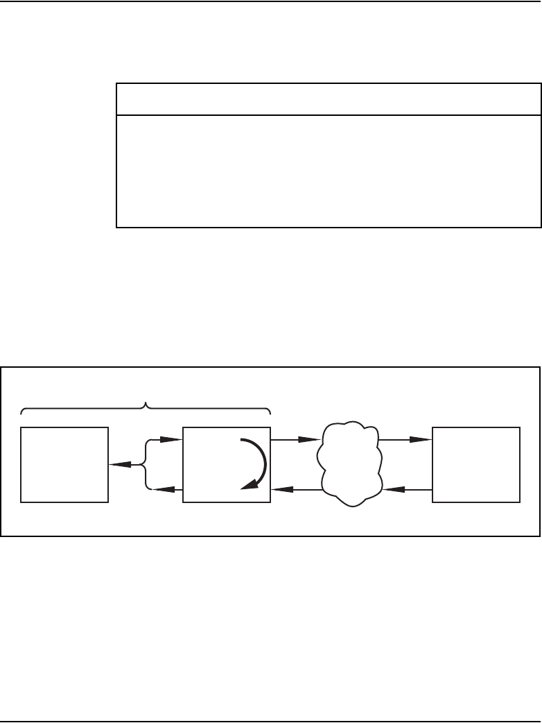
Page 308 of 906 NT5D33 and NT5D34 Lineside E1 Interface cards
553-3001-211 Standard 3.00 August 2005
Table 108 shows which test to run for the associated equipment.
Test 1, local loopback, loops the E1 link signaling toward itself at the
backplane connector. Test data is generated and received on all timeslots. If
this test fails, it indicates that the LEI is defective. Figure 59 illustrates how
the signaling is looped back toward itself.
Figure 59
MMI Local loopback test
Test 2, external loopback, applies an external loopback to the E1 link. Test
data is generated and received by the LEI on all timeslots. If test 1 passes but
test 2 fails, it indicates that the E1 link is defective between the LEI and the
external loopback location. If test 1 was not run and test 2 fails, the E1 link or
the LEI could be defective. To isolate the failure to the E1 link, tests 1 and 2
must be run in tandem. Figure 60 on page 309 demonstrates how an external
loopback is applied to the E1 link.
Table 108
MMI Tests
Test number Equipment Tested Test Description
1 LEI Local loopback
2 E1 link, LEI, and E1
network
External loopback
3 CPE device and E1
network
Network loopback
E-1 link
Line side
E-1
interface
card
Customer
premise
equipment
(CPE)
Common
Equipment
System
External
network E-1 link
553-1160
NT5D33 and NT5D34 Lineside E1 Interface cards Page 309 of 906
Circuit Card Description and Installation
Figure 60
MMI External loopback test
Test 3, network loopback, loops the LEI's received E1 data back toward the
CPE. No test data is generated or received by the LEI. If test 2 passes but test
3 fails, it indicates that the CPE device is defective. If test 2 was not run and
test 3 fails, the E1 link or the CPE device could be defective. To isolate the
failure to the CPE device, tests 2 and 3 must be run in tandem. Figure 61
illustrates how the signaling is looped back toward the CPE.
Figure 61
MMI Network loopback test
E-1 link
Line side
E-1
interface
card
Customer
premise
equipment
(CPE)
Common
Equipment
System
External
network E-1 link
553-1161
E-1 link
Line side
E-1
interface
card
Customer
premise
equipment
(CPE)
Common
Equipment
System
External
network E-1 link
553-1162
Page 310 of 906 NT5D33 and NT5D34 Lineside E1 Interface cards
553-3001-211 Standard 3.00 August 2005
Applications
The LEI is an IPE line card that provides cost-effective connection between
E1-compatible IPE and a CS 1000S, CS 1000M, and Meridian 1 system or
off-premise extensions over long distances.
Some examples of applications where an LEI can be interfaced to an E1 link
are:
• E1-compatible VRU equipment
• E1-compatible turret systems
• E1-compatible wireless systems
• Remote analog (500/2500-type) telephones through E1 to channel bank
• Remote Norstar sites behind CS 1000S, CS 1000M, and Meridian 1 over
E1
The LEI is appropriate for any application where both E1 connectivity and
“lineside” functionality are required. This includes connections to
E1-compatible voice response units, voice messaging and trading turret (used
in stock market applications) systems. See Figure 62.
Figure 62
LEI connection to IPE
For example, the LEI can be used to connect the system to an E1-compatible
Voice Response Unit (VRU). An example of this type of equipment is Nortel
Open IVR system. In this way, the CS 1000S, CS 1000M, and Meridian 1 can
NT5D33 and NT5D34 Lineside E1 Interface cards Page 311 of 906
Circuit Card Description and Installation
send a call to the VRU, and, because the LEI supports analog (500/2500-type)
telephone functionality, the VRU is able to send the call back to the system
for further handling.
The LEI can also be used to provide off-premise extensions to remote
locations, up to 500 miles from the system. In this application, analog
telephone functionality is extended over E1 facilities, providing a telephone
at a remote site with access to analog (500/2500-type) telephone line
functionality. See Figure 63. Audible Message Waiting Indicator can be
provided as well.
Figure 63
LEI in off-premise extension application
Similarly, use the LEI to provide a connection between the system and a
remote Norstar system. See Figure 64 on page 312. In this case, channel
banks are not required if the Norstar system is equipped with an E1 interface.
Note: Consider LEI audio levels when determining the appropriateness
of an application.

Page 313 of 906
Circuit Card Description and Installation
318
NT5D60/80 CLASS Modem card (XCMC)
Contents
This section contains information on the following topics:
Introduction . . . . . . . . . . . . . . . . . . . . . . . . . . . . . . . . . . . . . . . . . . . . . . 313
Physical description. . . . . . . . . . . . . . . . . . . . . . . . . . . . . . . . . . . . . . . . 313
Functional description . . . . . . . . . . . . . . . . . . . . . . . . . . . . . . . . . . . . . . 314
Electrical specifications. . . . . . . . . . . . . . . . . . . . . . . . . . . . . . . . . . . . . 317
Configuration . . . . . . . . . . . . . . . . . . . . . . . . . . . . . . . . . . . . . . . . . . . . 318
Introduction
The NT5D60/80 CLASS Modem card supports the Custom Local Area
Signaling Services (CLASS) feature. The CLASS Modem card receives
Calling Number and Calling Name Delivery (CND) data and time/date data
from the CS 1000S, CS 1000M, and Meridian 1and transmits it to a line port,
such as a port on an Analog Line card, which delivers the CND data to a
CLASS telephone when presenting the telephone with a new call.
For information about the CLASS: Calling Number and Name Delivery
feature, please refer to the Features and Services (553-3001-306). For
administration and maintenance commands, see the Software Input/Output:
Administration (553-3001-311).
Physical description
CLASS Modem cards are housed in NT8D37 IPE modules.

Page 314 of 906 NT5D60/80 CLASS Modem card (XCMC)
553-3001-211 Standard 3.00 August 2005
The CLASS modem card circuitry is mounted on a 31.75 cm by 25.40 cm
(12.5 in. by 10 in.) double-sided printed circuit board. The card connects to
the backplane through a 160-pin edge connector.
The faceplate of the CLASS modem card is equipped with a red LED that
lights when the card is disabled. When the card is installed, the LED remains
lit for two to five seconds as a self-test runs. If the self-test completes
successfully, the LED flashes three times and remains lit until the card is
configured and enabled in software, then the LED goes out. If the LED
continually flashes or remains weakly lit, replace the card.
Functional description
The CLASS Modem card is designed to plug into any one of the peripheral
card slots of the IPE module. The CLASS modem card supports up to 32
transmit-only modem resources, using a DS30X interface. Up to 255 modems
can be configured per system.
The CND transmission process begins with the CS 1000 Release 4.5 software
sending an initiating message to the CLASS Modem card indicating the
length of the CND information and the type of the CND information flow to
be transmitted. In response, the CLASS Modem card assigns a message
buffer to capture the CND information from the CS 1000 Release 4.5
software.
System software then sends the CND information to the CLASS Modem
card, one byte at a time, where it is stored in the message buffer. If the CLASS
Modem card receives more bytes than were specified in the initiating
message, then the additional bytes will be discarded and will not be included
in the CND memory buffer.
Once all of the CND information has been stored in the memory buffer, the
CLASS Modem card begins transmission when requested by the system
software. Data is sent one ASCII character at a time. The CLASS Modem
card inserts a start and stop bit to each ASCII character sent.
The transmission of the calling party name/number to the terminating
telephone is accomplished through asynchronous FSK simplex-mode
transmission at 1200 bits/second over a 2-wire loop, in accordance with the

NT5D60/80 CLASS Modem card (XCMC) Page 315 of 906
Circuit Card Description and Installation
Bell 202 standard. The transmission is implemented by the appropriate PCM
equivalent of 1200 or 2200 Hz.
Upon completion of transmitting the CND data, the CLASS Modem card
sends a message to the system software to indicate successful transmission of
the CND data.
Eight modems can be associated with each module. Table 109 shows time
slot mapping for the CLASS modem card.
Table 109
Time slot mapping (Part 1 of 2)
XCMC mapping of TNs
Modem units on the CLASS
Modem cardTNs
DS30X
timeslot
00
01
02
03
00
01
02
03
module 0, 00
01
02
03
04
05
06
07
04
05
06
07
04
05
06
07
08
09
10
11
08
09
10
11
module 1, 00
01
02
03

Page 316 of 906 NT5D60/80 CLASS Modem card (XCMC)
553-3001-211 Standard 3.00 August 2005
12
13
14
15
12
13
14
15
04
05
06
07
16
17
18
19
16
17
18
19
module 2, 00
01
02
03
20
21
22
23
20
21
22
23
04
05
06
07
24
25
26
27
24
25
26
27
module 3, 00
01
02
03
28
29
30
31
28
29
30
31
04
05
06
07
Table 109
Time slot mapping (Part 2 of 2)
XCMC mapping of TNs
Modem units on the CLASS
Modem cardTNs
DS30X
timeslot
NT5D60/80 CLASS Modem card (XCMC) Page 317 of 906
Circuit Card Description and Installation
Electrical specifications
This section lists the electrical characteristic of the CLASS modem card.
Data transmission specifications
Table 110 provides specifications for the 32 transmit-only modem resources.
The CLASS modem card has no direct connection to the Public Network.
Power requirements
The CLASS modem card requires less than 1.0 Amps of +5V dc ± 1% supply
supplied by the power converter in the IPE shelf.
Environmental specifications
Table 111 shows the environmental specifications of the card.
Table 110
CLASS modem card—data transmission electrical characteristics
Characteristics Description
Units per card 32 transmit only modem resources
Transmission rate 1200 ± 12 baud
Table 111
CLASS modem card – environmental specifications
Parameter Specifications
Operating temperature 0° C to +65° C (+32 ° F to +149 ° F)
Operating humidity 5 to 95% RH (non-condensing)
Storage temperature –50° C to +70° C (–58 ° F to +158 ° F)

Page 318 of 906 NT5D60/80 CLASS Modem card (XCMC)
553-3001-211 Standard 3.00 August 2005
Configuration
The NT5D60/80 CLASS Modem card has no user-configurable jumpers or
switches. The card derives its address from its position in the backplane and
reports that information back to the CS 1000S, CS 1000M, and Meridian 1
CPU through the Card LAN interface.
Software service changes
On systems equipped with either CNUMB (package 332) or CNAME
(package 333), up to 255 CLASS Modem (CMOD) units can be configured
in LD 13, and analog (500/2500-type) telephones can be assigned as CLASS
telephones in LD 10 by assigning them CNUS, or CNUA and CNAA class of
service. See the Software Input/Output: Administration (553-3001-311) for
LD 10 and LD 13 service change instructions.

Page 319 of 906
Circuit Card Description and Installation
366
NT5D97 Dual-port DTI2/PRI2 card
Contents
The following are the topics in this section:
Introduction . . . . . . . . . . . . . . . . . . . . . . . . . . . . . . . . . . . . . . . . . . . . . . 319
Physical description. . . . . . . . . . . . . . . . . . . . . . . . . . . . . . . . . . . . . . . . 320
Functional description . . . . . . . . . . . . . . . . . . . . . . . . . . . . . . . . . . . . . . 340
Architecture. . . . . . . . . . . . . . . . . . . . . . . . . . . . . . . . . . . . . . . . . . . . . . 353
Operation. . . . . . . . . . . . . . . . . . . . . . . . . . . . . . . . . . . . . . . . . . . . . . . . 359
Introduction
This section contains information required to install the NT5D97 Dual-port
DTI2/PRI2 (DDP2) card.
The NT5D97 is a dual-port 2.0 Mb DTI2/PRI2 card (the DDP2 firmware
functions in DTI2 or PRI2 mode, depending on DIP switch settings) that
integrates the functionality of two NT8D72BA PRI2 cards, and one QPC414
ENET card into a single CE card. The NT5D97 occupies a single slot in the
Network shelf and provides two DTI2/PRI2 network connections: an
interface to an external D-Channel Handler (the NT6D11AF) or the NT6D80
Multi-purpose Serial Data Link card, and an optional plug-on NTBK51AA
Downloadable D-Channel daughterboard (DDCH) with two DCH interface
ports.
The NT5D97 DDP2 card can be mixed in the same machine with PRI2
NT8D72BA cards.
Page 320 of 906 NT5D97 Dual-port DTI2/PRI2 card
553-3001-211 Standard 3.00 August 2005
The NT5D97 DDP2 card hardware design uses a B57 ASIC E1/T1 framer.
The carrier specifications comply with the ANSI TI.403 specification. The
NT5D97 provides an interface to the 2.048 Mbps external digital line either
directly or through an office repeater, Network Channel Terminating
Equipment (NCTE), or Line Terminating Unit (LTU).
Physical description
External D-Channel Interface DCH or MSDL
The connection between the DDP2 card and the external DCH or MSDL is
through a 26-pin female D type connector. The data signals conform to the
electrical characteristics of the EIA standard RS-422.
Two control signals are used to communicate the D-channel link status to the
DCH or MSDL. These are:
• Receiver Ready (RR), originating at the DDP2 card, to indicate to the
DCH or MSDL that the D-channel link is operational.
• Transmitter Ready (TR), originating at the DCH or MSDL, to indicate to
the DDP2 card that the DCH are ready to use the D-channel link.
DANGER OF ELECTRIC SHOCK
The NT5D97 DDP2 card is not designed to be
connected directly to the Public Switched Network, or
other exposed plant networks. Such a connection
should only be done using an isolating-type
networking terminating device that provides voltage
surge protection, such as a Line Terminating Unit
(LTU), Network Channel Terminating Equipment
(NCTE), or Network Termination 1 (NT1), as certified
by your local, regional, or national safety agency and
telecommunication authority.

NT5D97 Dual-port DTI2/PRI2 card Page 321 of 906
Circuit Card Description and Installation
Table 112 indicates how the RR control signal operates with regard to the
DDP2 status.
NT5D97 faceplate
Figure 65 on page 322 illustrates the faceplate layout for the NT5D97 DDP
card. The faceplate contains an enable/disable switch; a DDCH status LED;
6 x 2 trunk port status LEDs; and six external connectors. Table 113 on
page 323 shows the name of each connector, its designation with respect to
the faceplate and the name and description of the card it is connected to. Also
shown are the names of the LEDs.
Table 112
DCH/MSDL Receiver Ready control signals
RR State Condition
ON D-Channel data rate selected at 64 Kbps
and
PRI2 loop is enabled
and
PRI2 link is not in OOS or Local Alarm mode state
and
PRI2 link is not transmitting a Remote Alarm pattern
and
PRI2 link is not receiving a Remote Alarm Indication
from a remote facility
OFF All other conditions
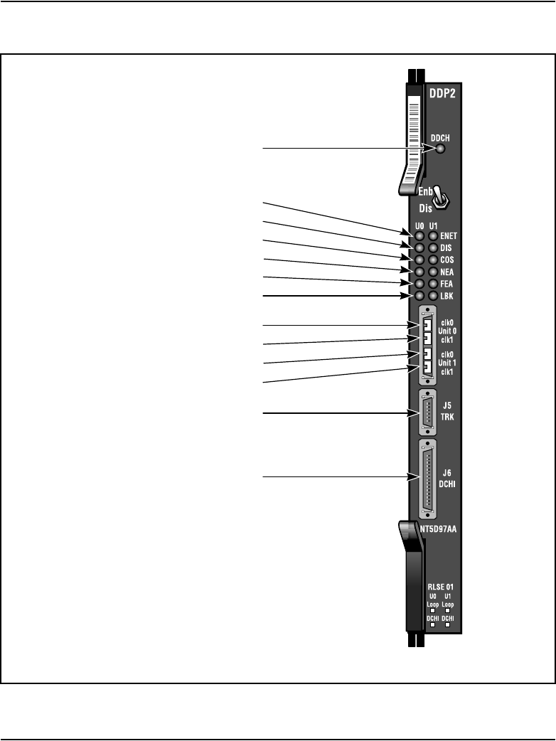
Page 322 of 906 NT5D97 Dual-port DTI2/PRI2 card
553-3001-211 Standard 3.00 August 2005
Figure 65
NT5D97 faceplate
D-Channel LED
ENET LED
Trunk Disable LED
Trunk Out of Service LED
Near End Alarm LED
Far End Alarm LED
Loop Back LED
Recovered Clock0#1
Recovered Clock0#2
Recovered Clock1#1
Recovered Clock1#2
External DCHI/MSDL
Trunk0 / Trunk1
553-7380
Enb
Dis
NT5D97 Dual-port DTI2/PRI2 card Page 323 of 906
Circuit Card Description and Installation
Table 113
External connectors and LEDs
Function
Faceplate
Designator Type Description
Switch ENB/DIS Plastic, ESD protected Card Enable/disable switch
Connectors Unit 0 Clock 0 RJ11 Connector Connects reference clock 0 to
Clock Controller card 0
Unit 0 Clock 1 RJ11 Connector Connects reference clock 0 to
Clock Controller card 1
Unit 1 Clock 0 RJ11 Connector Connects reference clock 1 to
Clock Controller card 0
Unit 1 Clock 1 RJ11 Connector Connects reference clock 1 to
Clock Controller card 1
J5 TRK 9 Pin
Female D Connector
Two external E1 Trunk 0 and
Trunk 1
J6 DCH 26 Pin
Female D Connector
Connects to external DCH or
MSDL
LEDs ENET 2 Red LEDs ENET 0 or ENET 1 is disabled
DIS 2 Red LEDs Trunk 0 or Trunk 1 is disabled
OOS 2 Yellow LEDs Trunk is out of service
NEA 2 Yellow LEDs Local (Near End) Alarm
FEA 2 Yellow LEDs Far End Alarm
LBK 2 Yellow LEDs Loop Back test being
performed on Trunk 0 or
Trunk 1
DCH Bicolor Red/Green LED NTBK51AA status

Page 324 of 906 NT5D97 Dual-port DTI2/PRI2 card
553-3001-211 Standard 3.00 August 2005
The following sections provide a brief description of each element on the
faceplate.
Enable/Disable Switch
This switch is used to disable the card prior to insertion or removal from the
network shelf. While this switch is in disable position, the card will not
respond to the system CPU.
ENET LEDs
Two red LEDs indicate if the “ENET0” and “ENET1” portions of the card are
disabled. These LEDs are lit in the following cases:
• When the enable/disable switch is in disabled state (lit by hardware).
• After power-up, before the card is enabled.
• When the ENET port on the card is disabled by software.
Trunk Disable (DIS) LEDs
Two red LEDs indicate if the “trunk port 0” or “trunk port 1” portions of the
card are disabled. These LEDs are lit in the following cases:
• Upon reception of the “disable loop” message from the software.
• After power-up.
OOS LEDs
Two yellow LEDs indicate if the “trunk port 0” and “trunk port 1” portions
of the card are out of service.
NEA LEDs
Two yellow LEDs indicate if the near end detects absence of incoming signal
or loss of synchronization in “trunk port 0” or “trunk port 1” respectively. The
near-end alarm causes a far-end alarm signal to be transmitted to the far end.
FEA LEDs
Two yellow LEDs indicate if a far-end alarm has been reported by the far end
(usually in response to a near-end alarm condition at the far end) on “trunk
port 0” or “trunk port 1”.

NT5D97 Dual-port DTI2/PRI2 card Page 325 of 906
Circuit Card Description and Installation
LBK LEDs
Two yellow LEDs indicate if a remote loopback test is being performed on
trunk port 0 or trunk port 1. The loopback indication is active when the digital
trunk is in remote loopback mode. Normal call processing is inhibited during
the remote loopback test.
DCH LED
When the dual colored LED is red, it indicates the on-board DDCH is present
but disabled. When the dual colored LED is green, it indicates the on-board
DDCH is present and enabled. If a DDCH is not configured on the DDP2
card, this lamp is not lit.
Unit 0 Clk Connectors
Two RJ11 connectors for connecting:
• Digital trunk unit 0 recovered clock to primary or secondary reference
source on clock controller card 0.
• Digital trunk unit 0 recovered clock to primary or secondary reference
source on clock controller card 1.
Unit 1 Clk Connectors
Two RJ11 connectors for connecting:
• Digital trunk unit 1 recovered clock to primary or secondary reference
source on clock controller card 0.
• Digital trunk unit 1 recovered clock to primary or secondary reference
source on clock controller card 1.
Connector J5 (TRK)
A 9 pin D-Type connector used to connect:
• Digital trunk unit 0 receive and transmit Tip / Ring pairs.
• Digital trunk unit 1 receive and transmit Tip / Ring pairs.
Connector J6 (DCH)
A 26 pin D-type connector is used to connect the DDP2 card to the external
MSDL or D-channel handler.
Page 326 of 906 NT5D97 Dual-port DTI2/PRI2 card
553-3001-211 Standard 3.00 August 2005
Port definitions
Since the NT5D97 card is dual-card, it equips two ports; these ports can be
defined in the following combinations:
Note: Each loop DPNSS can be defined in Normal or Extended
addressing mode.
Table 114
NT5D97AA/AB loops configuration
Loop 0
not configured DTI2 PRI2
Loop 1
not configured V V V
DTI2 V V V
PRI2 V V V
Table 115
NT5D97AD loops configuration
Loop 0
not configured DTI2 PRI2 DDCS
Loop 1
not configured V V V V
DTI2 V V V V
PRI2 V V V X
DDCS V V X V

NT5D97 Dual-port DTI2/PRI2 card Page 327 of 906
Circuit Card Description and Installation
System capacity and performance
Physical capacity
Each NT5D97 DDP2 card occupies one slot on the network shelf. Each card
supports two digital trunk circuits and two network loops. The total number
of DDP2 cards per system is limited by the number of network loops, physical
capacity of the shelf, number of DTI2/PRI2 interfaces allowed by the
software and the range of DCH addresses.
D-Channel capacity
The software configuration for the NTBK51AA DDCH is similar to the
MSDL and only supports D-channel functionality.
The system has a total capacity of 16 addresses (Device Addresses or
DNUM) that can be reserved for DCH card, MSDL card or DDCH card. One
exception is DNUM 0 which is commonly assigned to the TTY terminal.
No two different D-Channel providers can share the same DNUM. Hence, the
combined maximum number of DCH, MSDL and DDCH cards in the system
is 16.
The DCH has one D-Channel unit, the DDCH has two D-Channel units, and
the MSDL has a maximum of four units. Therefore, the total number of
D-Channel is derived by the following formula:
Total_Num_DCH-Units = Num_DCHx1 + Num_DDCHx2 +
Num_MSDLx4
Therefore, Total_Num_DCH-Units in any given system is between 0-63.
CPU capacity
Using a NT5D97 DDP2 card instead of DTI2/PRI2 cards does not increase
the load on the CPU. The DDP2 replaces an ENET card and two DTI2/PRI2
cards. Emulating the ENET card and the overall CPU capacity is not impacted
by using a DDP2 card instead of a DTI2/PRI2 card.
Page 328 of 906 NT5D97 Dual-port DTI2/PRI2 card
553-3001-211 Standard 3.00 August 2005
Power requirements
Table 116 lists the power requirements for the NT5D97 DDP2 card.
Cable requirements
This section lists the types of cable used and the lengths required for internal
and external NT5D97 DDP2 connections.
Note: No additional cabling is required for nB+D configurations.
Multiple DDP2 cards and the D-channel are associated through software
in LD 17.
DDP2 cable assemblies include:
• E1 carrier cables
— NTCK45AA (A0407956)
— NT8D7217 (A0617192)
— NTCK78AA (A0618294)
— NTCK79AA (A0618296)
• DDP2 to QPC471/QPC775 Clock Controller Cables
— NTCG03AA
Table 116
NT5D97 DDP2 power requirements
Voltage Source Current
DDP2
(without
NTBK51AA)
DDP2
(with
NTBK51AA)
+5V Backplane 3A 3.8A
+12V Backplane 25mA 75mA
-12V Backplane 25mA 75mA
Total Power (Maximum) 15.6W 20.8W

NT5D97 Dual-port DTI2/PRI2 card Page 329 of 906
Circuit Card Description and Installation
— NTCG03AB
— NTCG03AC
— NTCG03AD
• DDP2 to DCH cables
— NTCK46AA
— NTCK46AB
— NTCK46AC
— NTCK46AD
• DDP2 to MSDL cables
— NTCK80AA
— NTCK80AB
— NTCK80AC
— NTCK80AD
A description of each type of DDP2 cable follows.
E1 carrier cables
NTCK45AA (A0407956)
The NTCK45AA (8 ft.) is an 120Ω cable for systems equipped with an I/O
filter panel, connecting the TRK port (P1, D-type 9 pin male) on the DDP2
faceplate to the I/O filter (P2, P3 D-type 9 pin males).
Page 330 of 906 NT5D97 Dual-port DTI2/PRI2 card
553-3001-211 Standard 3.00 August 2005
Table 117 which follows lists the pin attributes for the NTCK45AA cable.
Figure 66
NTCK45AA
Table 117
NTCK45AA cable pins (Part 1 of 2)
Cable Name Description Color
DDP2
pins
I/O Panel
pins
0T-P R I0 T X Trunk 0 Transmit Tip Black P1-1 P2-6
0R-PRI0TX Trunk 0 Transmit Ring Red P2-2 P2-7
0T-P R I0 R X Trunk 0 Receive Tip Black P1-3 P2-2
0R-PRI0RX Trunk 0 Receive Ring White P1-4 P2-3
0GND Shield Wire Bare N/C Case P2
0GND Shield Wire Bare N/C Case P2
0Standard Wire (3”) Bare Case P2 P2-5
0Standard Wire (3”) Bare Case P2 P2-9
1T-P R I1 T X Trunk 1 Transmit Tip Black P1-5 P3-6
1R-PRI1TX Trunk 1 Transmit Ring Red P1-6 P3-7
1T-P R I1 R X Trunk 1 Receive Tip Black P1-7 P3-2
1R-PRI1RX Trunk 1 Receive Ring White P1-8 P3-3
1GND Shield Wire Bare N/C Case P3
553-7385
P1 P2
P3
D-type
15 pin, males
D-type
9 pin, males
NT5D97 Dual-port DTI2/PRI2 card Page 331 of 906
Circuit Card Description and Installation
NT8D7217 (A0617192)
The NT8D7217 (50 ft.) is an 120Ω cable for systems equipped with an I/O
filter panel, connecting the 9 pin I/O filter connector to the 9 pin NCTE
connector.
Table 118 which follows lists the pin attributes for the NT8D7217 cable.
1GND Shield Wire Bare N/C Case P3
1Standard Wire (3”) Bare Case P3 P3-5
1Standard Wire (3”) Bare Case P3 P3-9
Figure 67
NT8D7217
Table 118
NT8D7217 cable pins (Part 1 of 2)
Cable Name Description Color
DDP2
pins
I/O Panel
pins
0T-P R I0 T X Trunk 0 Transmit Tip Black P1-6 P2-6
0 R-PRI0TX Trunk 0 Transmit Ring White P1-7 P2-7
0T-P R I0 R X Trunk 0 Receive Tip Black P1-2 P2-2
0R-PRI0RX Trunk 0 Receive Ring Red P1-3 P2-3
Table 117
NTCK45AA cable pins (Part 2 of 2)
Cable Name Description Color
DDP2
pins
I/O Panel
pins
553-7386
P1 P2
I/O Panel Trunk
D-type 9 pin, female Multiplexer Trunk
D-type 9 pin, male
Page 332 of 906 NT5D97 Dual-port DTI2/PRI2 card
553-3001-211 Standard 3.00 August 2005
NTCK78AA (A0618294)
The NTCK78AA (50 ft.) is an 120Ω cable for connecting the TRK port on the
DDP2 faceplate (P1, D-type 9 pin male) to the Main Distribution Frame
(MDF) (P2, P3 D-type 15 pin males). The NTCK78AA is used for systems
not equipped with an I/O filter panel.
0GND Shield Wire Bare P1-5 N/C
0GND Shield Wire Bare P1-9 N/C
1T-P R I1 T X Trunk 1 Transmit Tip Black P1-6 P2-6
1 R-PRI1TX Trunk 1 Transmit Ring White P1-7 P2-7
1T-P R I1 R X Trunk 1 Receive Tip Black P1-2 P2-2
1R-PRI1RX Trunk 1 Receive Ring Red P1-3 P2-3
1GND Shield Wire Bare P1-5 N/C
1GND Shield Wire Bare P1-9 N/C
Figure 68
NTCK78AA
Table 118
NT8D7217 cable pins (Part 2 of 2)
Cable Name Description Color
DDP2
pins
I/O Panel
pins
553-7385
P1 P2
P3
D-type
15 pin, males
D-type
9 pin, males

NT5D97 Dual-port DTI2/PRI2 card Page 333 of 906
Circuit Card Description and Installation
Table 119 lists the pin attributes for the NTCK78AA cable.
NTCK79AA (A0618296)
The NTCK79AA (40 ft) is a 75Ω coaxial cable for connecting the TRK port
on the DDP2 faceplate (P1, D-type 9 pin male) to the Line Terminating Unit
(LTU) (P2, P3, P4, P5 BNC males).
Table 119
NTCK78AA cable pins
Cable Name Description Color
DDP2
pins NCTE pins
0T-P R I0 T X Trunk 0 Transmit Tip Black P1-1 P2-1
0 R-PRI0TX Trunk 0 Transmit Ring Red P1-2 P2-9
0T-P R I0 R X Trunk 0 Receive Tip Black P1-3 P2-3
0R-PRI0RX Trunk 0 Receive Ring White P1-4 P2-11
0GND Shield Wire Bare P1 Case P2-2
0GND Shield Wire Bare P1 Case P2-4
1T-P R I1 T X Trunk 1 Transmit Tip Black P1-5 P3-1
1 R-PRI1TX Trunk 1 Transmit Ring Red P1-6 P3-9
1T-P R I1 R X Trunk 1 Receive Tip Black P1-7 P3-3
1R-PRI1RX Trunk 1 Receive Ring White P1-8 P3-11
1GND Shield Wire Bare P1 Case P3-2
1GND Shield Wire Bare P1 Case P3-4
Page 334 of 906 NT5D97 Dual-port DTI2/PRI2 card
553-3001-211 Standard 3.00 August 2005
Table 120 lists the pin attributes for the NTCK79AA cable.
Figure 69
NTCK79AA
Table 120
NTCK79AA cable pins (Part 1 of 2)
Cable Name Description Color
DDP2
pins NCTE pins
0T-P R I0 T X Trunk 0 Transmit Tip Red P1-1 P2 inner
conductor
0 R-PRI0TX Trunk 0 Transmit Ring Red P1-2 P2 shield
0T-P R I0 R X Trunk 0 Receive Tip Green P1-3 P3 inner
conductor
0R-PRI0RX Trunk 0 Receive Ring Green P1-4 P3 shield
1T-P R I1 T X Trunk 1 Transmit Tip Red P1-5 P4 inner
conductor
1 R-PRI1TX Trunk 1 Transmit Ring Red P1-6 P4 shield
1T-P R I1 R X Trunk 1 Transmit Tip Green P1-7 P5 inner
conductor
1R-PRI1RX Trunk 1 Receive Ring Green P1-8 P5 shield
553-7388
P1
P2: Unit 0 Tx
P3: Unit 0 Rx
P4: Unit 1 Tx
P5: Unit 1 Rx
D-type
9 pin, male BNC
males
NT5D97 Dual-port DTI2/PRI2 card Page 335 of 906
Circuit Card Description and Installation
Reference clock cables
The NTCG03AA (14 ft), NTCG03AB (2.8 ft), NTCG03AC (4.0 ft), or
NTCG03AD (7 ft), is a DDP2 card to Clock Controller cable, connecting
each of the CLK0 or CLK1 ports on the DDP2 faceplate to the primary or
secondary source ports on Clock Controller card 0 or 1.
MSDL/DCH cables
External DCH cable
The NTCK46 cable connects the DDP2 card to the NT6D11AF/NT5K75AA/
NT5K35AA D-Channel Handler card. The cable is available in four different
sizes:
• NTCK46AA (6 ft.) - DDP2 to DCH cable
• NTCK46AB (18 ft.) - DDP2 to DCH cable
1Outer metallized PVC
shield
Bare N/C P1 Case
13 stranded wire Bare N/C P1 Case
Figure 70
NTCG03AA/AB/AC/AD
Table 120
NTCK79AA cable pins (Part 2 of 2)
Cable Name Description Color
DDP2
pins NCTE pins
553-7384
P1 P2
2.8, 4, 7 or 14 ft.
Connector P1 - 4 pin, male, RJ11 (DDP2 faceplate)
Connector P2 - 9 pin, male, D-type (Clock Controller)
Note: Includes an RJ11Ö9 pin D-type adaptor.
Page 336 of 906 NT5D97 Dual-port DTI2/PRI2 card
553-3001-211 Standard 3.00 August 2005
• NTCK46AC (35 ft.) - DDP2 to DCH cable
• NTCK46AD (50 ft.) - DDP2 to DCH cable
External MSDL cable
The NTCK80 cable connects the DDP2 card to the NT6D80 MSDL card. The
cable is available in four different sizes:
• NTCK80AA (6 ft) - DDP2 to MSDL cable
• NTCK80AB (18 ft) - DDP2 to MSDL cable
• NTCK80AC (35 ft) - DDP2 to MSDL cable
• NTCK80AD (50 ft) - DDP2 to MSDL cable
Figure 71
NTCK46AA/AB/AC/AD
Figure 72
NTCK80AA/AB/AC/AD
553-7387
P1
P2
P3
D-type
15 pin, males
D-type
9 pin, males
553-7387
P1
P2
P3
D-type
15 pin, males
D-type
9 pin, males

NT5D97 Dual-port DTI2/PRI2 card Page 337 of 906
Circuit Card Description and Installation
Cable diagrams
Figure 73 on page 338 and Figure 74 on page 339 provide examples of
typical cabling configurations for the DDP2.
Figure 73 shows a typical DDP2 cabling for a system with an I/O panel, with
the connection between the I/O panel and a Network Channel Terminating
Equipment (NCTE).
Figure 74 shows cabling for a system without an I/O panel. Here, the DDP2
faceplate is cabled directly to the NCTE.
Note: Since several clock cabling options exists, none has been
represented in the diagrams. Refer to “Clock configurations” on
page 356 for a description on each available option.
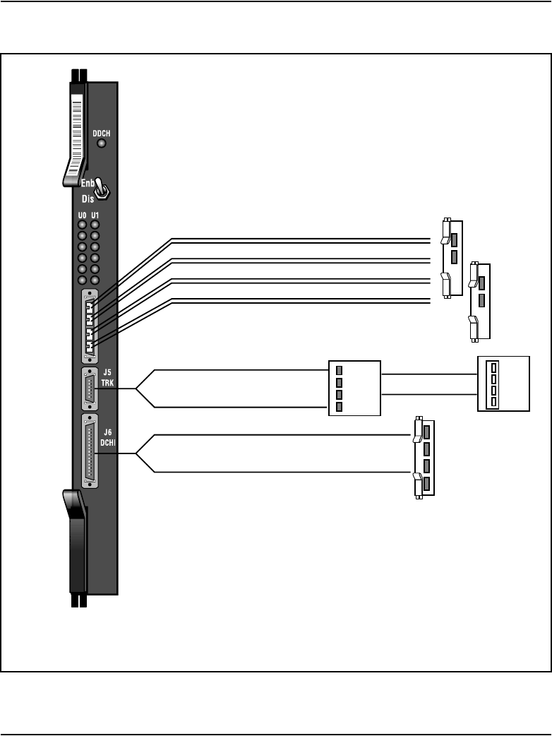
Page 338 of 906 NT5D97 Dual-port DTI2/PRI2 card
553-3001-211 Standard 3.00 August 2005
Figure 73
DDP2 cable for systems with an I/O panel
LED's
Switch
DCH
Trunk
553-8489
clk0
Port 0
clk1
clk0
Port 1
clk1
NCTE
(MDF or LTU) NCTE
NT8D7217 cable
NT8D7217 cable
Clock Controllers
NTCK78AA/NTCK79AA cable
NTCK80 cable to MSDL or
NTCK48 cable to DCHI
NT6D80 MSDL or
NT6D11AF/NT5K75AA/
NT5K35AA DCHI
Note: for possible clock cabling options, refer to the
"Clocking configurations" chapter
Enb
Dis
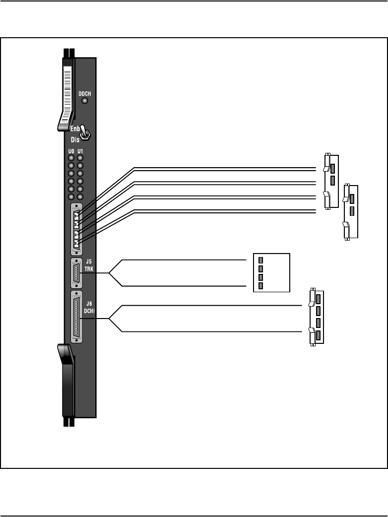
NT5D97 Dual-port DTI2/PRI2 card Page 339 of 906
Circuit Card Description and Installation
Figure 74
DDP2 cable for systems without an I/O panel
LED's
Switch
DCH
Trunk
553-7400
clk0
Unit 0
clk1
clk0
Unit 1
clk1
NCTE
(MDF or LTU)
Clock Controllers
NTCK78AA/NTCK79AA cable
NTCK80 cable to MSDL or
NTCK48 cable to DCHI
NT6D80 MSDL or
NT6D11AF/NT5K75AA/
NT5K35AA DCHI
Note: for possible clock cabling options, refer to the
"Clocking configurations" chapter
NTCG03 cables
Enb
Dis

Page 340 of 906 NT5D97 Dual-port DTI2/PRI2 card
553-3001-211 Standard 3.00 August 2005
Functional description
NT5D97 circuit card locations
Each NT5D97 card requires one slot on a shelf. NT5D97 cards can be placed
in any card slot in the network bus.
Note in all cases - If an NT8D72BA/NTCK43 card is being replaced by a
DDP2 card, the D-channel Handler can be reconnected to the DDP2 card, or
removed if an onboard NTBK51DDCH card is used. Also, DIP Switches in
the NT5D97 must be set properly before insertion. NT5D97 has a different
DIP Switch setting from NTCK43AB. Refer to “NT5D97AA/AB DIP switch
settings” on page 340 for DIP switch setting).
NT5D97AA/AB DIP switch settings
The the NT5D97 DDP2 card is equipped with 6x2 sets of DIP switches for
trunk parameters settings for port0 and port1 respectively. Additionally, the
DDP2 card is equipped with one set of four DIP switches for the Ring Ground
setting. The NT5D97AA/AB has one set of eight DIP switches and
NT5D97AD has two sets of ten DIP switches for the D-channel Handler
parameters setting.
The DIP switches are used for the setting of default values of certain
parameters. Firmware reads the general purpose switches, which sets the
default values accordingly.
Table 121
DIP switch settings for NT5D97AA/AB (Part 1 of 2)
Card
Trunks
0 and 1 Port 0 Port 1 Trunk 0 Trunk 1
ENB/DSB
mounted on the face plate
S1
Ring Ground S2
MSDL S3
TX Mode S4 S10
NT5D97 Dual-port DTI2/PRI2 card Page 341 of 906
Circuit Card Description and Installation
The following parameters are set by DIP switches. The boldface font shows
the factory set-up.
LBO Setting S5 S11
S6 S12
S7 S13
Receiver Interface S8 S14
General Purpose S9 S15
Table 121
DIP switch settings for NT5D97AA/AB (Part 2 of 2)
Card
Trunks
0 and 1 Port 0 Port 1 Trunk 0 Trunk 1
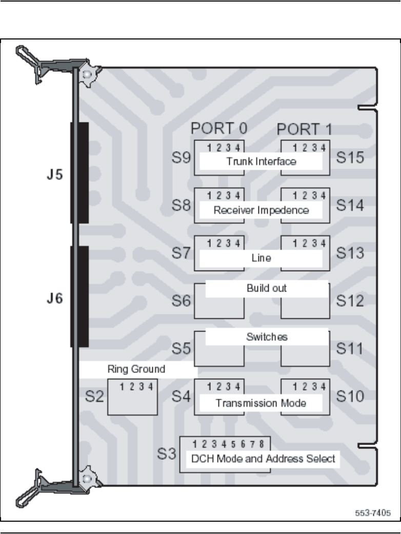
NT5D97 Dual-port DTI2/PRI2 card Page 343 of 906
Circuit Card Description and Installation
Trunk interface switches for NT5D97AA/AB
Impedance level and unit mode
The S9/S15 switch selects the impedance level and loop operation mode on
DEI2 OR PRI2. Refer to Table 122.
Transmission mode
A per-trunk switch (S4/S10) provides selection of the digital trunk interface
type. Refer to Table 123.
Line build out
A per-trunk set of three switches (S5/S11, S6/S12 and S7/S13) provides the
dB value for the line build out. Refer to Table 124 on page 344.
Table 122
Impedance level and loop mode switch settings
Switch Description S9/S15 Switch Setting
1 Impedance level OFF - 120 ohm
ON - 75 ohm
2 Spare X
3 Spare X
4 Unit mode OFF - Loop operates in the DTI2 mode
ON - Loop operates in the PRI2 mode
Table 123
Impedance level and loop mode switch settings
Description S4/S10 switch settings
E1 OFF
Not used
Page 344 of 906 NT5D97 Dual-port DTI2/PRI2 card
553-3001-211 Standard 3.00 August 2005
Note: Do not change this setup.
Receiver impedance
A per-trunk set of four DIP switches (S8/S14 provides selection between 75
or 120 ohm values. Refer to Table 125.
Ring ground switches for NT5D97AA/AB
A set of four Dip switches (S2) selects which Ring lines are connected to
ground. Refer to Table 126.
Table 124
Trunk interface line build out switch settings
Switch setting
Description S5/S11 S6/S12 S7/S13
0dB OFF OFF OFF
Table 125
Trunk interface impedance switch settings
Description S8/S14 switch setting
75 ohm OFF OFF ON OFF
120 ohm OFF OFF OFF ON
Table 126
Ring ground switch settings (Part 1 of 2)
Switch Description S2 switch settingS
1 Trunk 0 Transit OFF-Ring line is not grounded
ON- Ring line is grounded
2 Trunk 0 Receive OFF-Ring line is not grounded
ON- Ring line is grounded
NT5D97 Dual-port DTI2/PRI2 card Page 345 of 906
Circuit Card Description and Installation
DCH Address select switch for NTBK51AA daughter board for
NT5D97AA/AB
In case of an on-board NTBK51AA D-channel daughterboard, set of four
switches (S3) provide the daughterboard address. Refer to Table 134 on
page 350.
Note: Switch 8 of S3 (S3-8) does not require a switch setting to select
between the on-board NTBK51AA D-channel daughterboard and an
external DCHI/MSDL. The NT5D97 detects when the on-board
NTBK51AA D-channel daughterboard is used.
Table 128 shows the possible selection of the NTBK51AA D-channel.
3 Trunk 1 Transmit OFF-Ring line is not grounded
ON- Ring line is grounded
4 Trunk 1 Receive OFF-Ring line is not grounded
ON- Ring line is grounded
Table 127
DCH mode and address switch settings
Switch Description S3 switch setting
1-4 D-channel daughterboard address See Table 128
5-8 For future use OFF
Table 128
NTBK51AA daughterboard address select switch settings (Part 1 of 2)
Device Address Switch Setting
0OFF OFF OFF OFF
1ON OFF OFF OFF
Table 126
Ring ground switch settings (Part 2 of 2)
Switch Description S2 switch settingS

Page 346 of 906 NT5D97 Dual-port DTI2/PRI2 card
553-3001-211 Standard 3.00 August 2005
2OFF ON OFF OFF
3ON ON OFF OFF
4OFF OFF ON OFF
5ON OFF ON OFF
6OFF ON ON OFF
7ON ON ON OFF
8OFF OFF OFF ON
9ON OFF OFF ON
10 OFF ON OFF ON
11 ON ON OFF ON
12 OFF OFF ON ON
13 ON OFF ON ON
14 OFF ON ON ON
15 ON ON ON ON
Note 1: The system contains a maximum number of 16 DCHI, MSDL, and DDCH devices. The
Device Addresses are equivalent to the MSDL DNUM designations.
Note 2: Device address 0 is commonly assigned to the System TTYD Monitor.
Table 128
NTBK51AA daughterboard address select switch settings (Part 2 of 2)
Device Address Switch Setting

NT5D97 Dual-port DTI2/PRI2 card Page 347 of 906
Circuit Card Description and Installation
NT5D97AD DIP switch settings
The the NT5D97 DDP2 card is equipped with 6x2 sets of DIP switches for
trunk parameters settings for port0 and port1 respectively. Additionally, the
DDP2 card is equipped with one set of four DIP switches for the Ring Ground
setting. The NT5D97AA/AB has one set of eight DIP switches and
NT5D97AD has two sets of ten DIP switches for the D-channel Handler
parameters setting.
The DIP switches are used for the setting of default values of certain
parameters. Firmware reads the general purpose switches, which sets the
default values accordingly.
Refer to DIP switch locations in Figure 76 on page 348.
The following parameters are set by DIP switches. The boldface font shows
the factory set-up.
Table 129
DIP switch settings for NT5D97AD
Card
Trunks
0 and 1 Port 0 Port 1 Trunk 0 Trunk 1
ENB/DSB
mounted on the face plate
S1
Ring Ground S16
DPNSS S8 S9
MSDL S9
TX Mode S2 S10
LBO Setting S3 S13
S4 S14
S5 S15
Receiver Interface S6 S11
General Purpose S12 S7
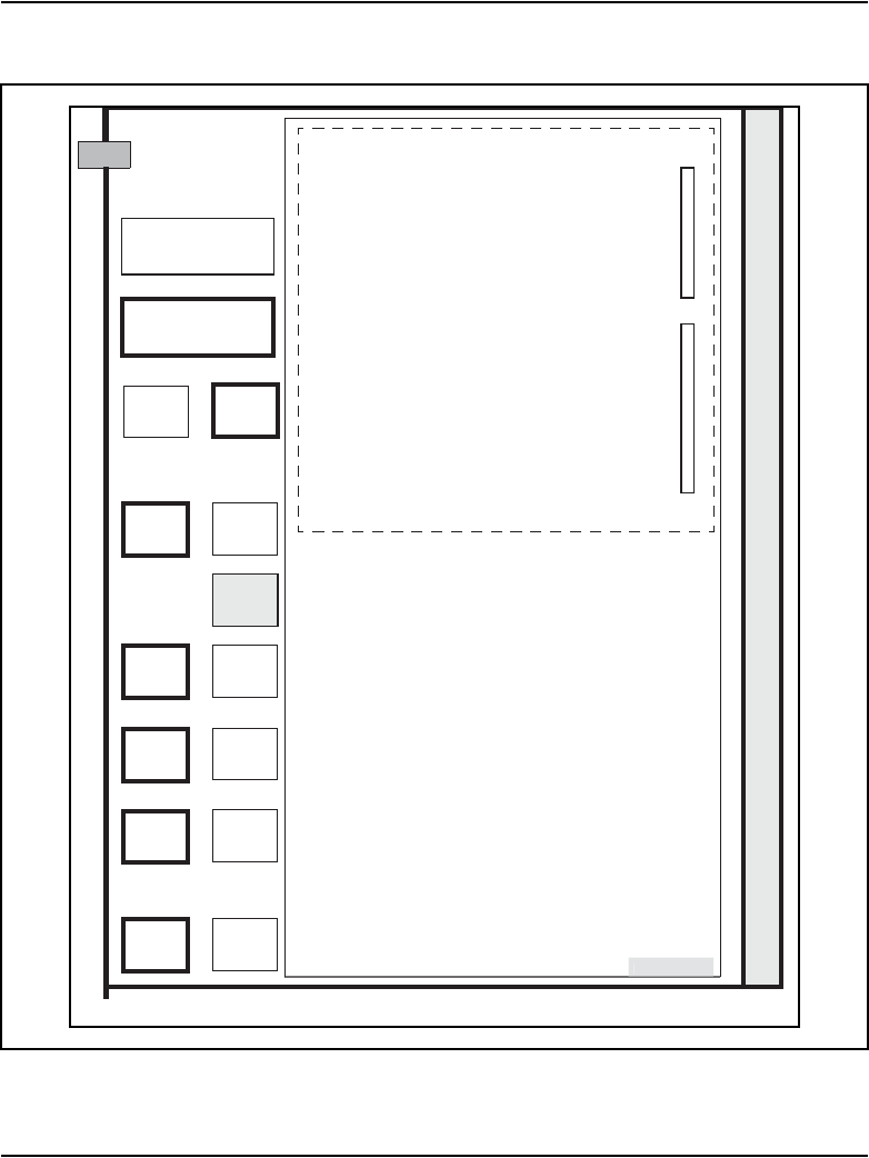
Page 348 of 906 NT5D97 Dual-port DTI2/PRI2 card
553-3001-211 Standard 3.00 August 2005
Figure 76
Dip switches locations for NT5D97AD
1234
S2
1234
S10
1234
S3
1234
S13
1234
S4
1234
S14
1234
S5
1234
S15
1234
S6
1234
S11
1234
S7
1234
S12
12345678910
S8
12345678910
S9
1234
S16
S1
NT5D97AD
P2P1
FacePlate
1AB
60 AB
1
17
1
22
BA
BA
Daughter Board
NTAG54
Daughter Board
NTBK51
Backplane Connector P3
N
ot to sca
l
e
553-AAA0367
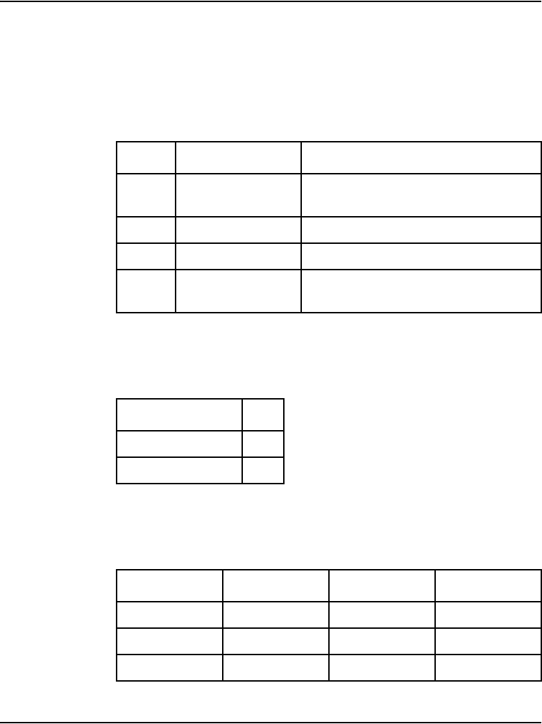
NT5D97 Dual-port DTI2/PRI2 card Page 349 of 906
Circuit Card Description and Installation
Trunk interface switches for NT5D97AD
Trunk 0 switches
Switch S12 gives the MPU information about its environment.
Switch S2 selects the Transmission mode.
Switch S3, S4, and S5 select LBO function.
Table 130
General purpose switches for NT5D97AD
Switch Description S9/S15 Switch Setting
S12_1 Impedance level OFF - 120 ohm
ON - 75 ohm
S12_2 Spare X
S12_3 Spare X
S12_4 Unit mode OFF - Unit operates in the DTI2 mode
ON - Unit operates in the PRI2 mode
Table 131
TX mode switches for NT5D97AD
TX mode S2
E1 OFF
Not used ON
Table 132
LBO switches for NT5D97AD
LBO setting S3 S4 S5
0dB OFF OFF OFF
7.5dB ON ON OFF
15dB ON OFF ON
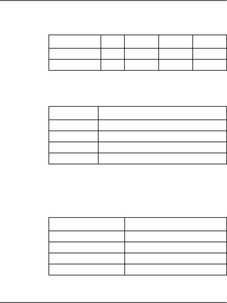
Page 350 of 906 NT5D97 Dual-port DTI2/PRI2 card
553-3001-211 Standard 3.00 August 2005
Switch S6 selects the Receiver interface.
Trunk 1 switches for NT5D97AD
Ring ground switches for NT5D97AD
Switch S16 selects which ring lines connect to ground. When set to ON, the
ring line is grounded.
Table 133
Receiver interface switches for NT5D97AD
Impedance S6-1 S6-2 S6-3 S6-4
75 ohm OFF OFF ON OFF
120 οhm OFF OFF OFF ON
Table 134
Trunk 1 switches
Switch Function
S7 General Purpose...See Table 130 on page 349
S10 TX Mode...See Table 131 on page 349
S13, S14 & S15 LBO...See Table 132 on page 349
S11 RX Impedance...See Table 133 on page 350
Table 135
Ring ground switch for NT5D97AD
Switch Line
S16_1 Trunk 0 Transmit
S16_2 Trunk 0 Receive
S16_3 Trunk 1 Transmit
S16_4 Trunk 1 Receive
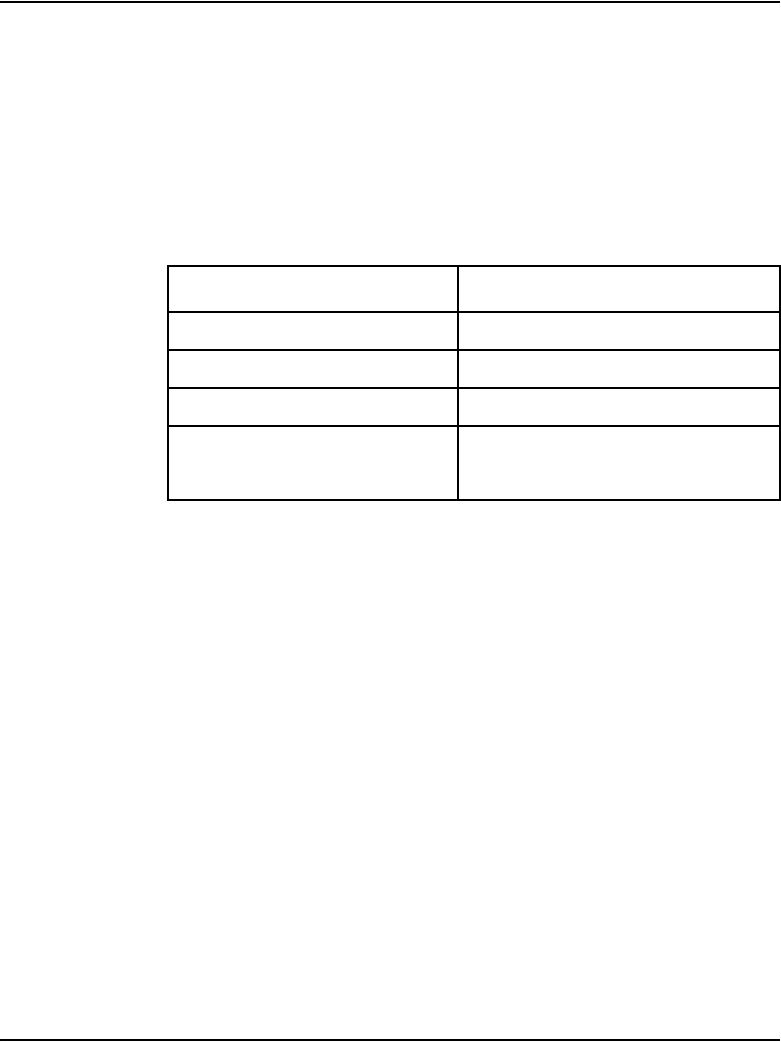
NT5D97 Dual-port DTI2/PRI2 card Page 351 of 906
Circuit Card Description and Installation
DCH Address select switch for NTBK51AA daughterboard for
NT5D97AD
Switch S9 selects the NTBK51AA DCH daughter card address.
Switch S8 is not used when the NTBK51AA daughter card is used. S8_1-10
can be set to OFF position.
Table 136
NTBK51AA DCH switches for NT5D97AD
Switch number Function
S9_1-4 DCH daughter card address
S9_5-8 Set to OFF
S9_9 Set to ON (NTBK51AA Mode)
S9_10 Set to ON (NTBK51AA Mode)
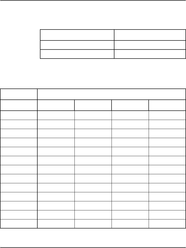
Page 352 of 906 NT5D97 Dual-port DTI2/PRI2 card
553-3001-211 Standard 3.00 August 2005
MSDL external card
Use Table 138 to set the card address.
Table 137
Switch settings for MSDL external card
Switch number Function
S9_1-10 X
S8_1-10 X
Table 138
Switch setting for MSDL external card (Part 1 of 2)
Switch Setting
DNUM (LD 17) 1234
0OFF OFF OFF OFF
1ON OFF OFF OFF
2OFF ON OFF OFF
3ON ON OFF OFF
4OFF OFF ON OFF
5ON OFF ON OFF
6OFF ON ON OFF
7ON ON ON OFF
8OFF OFF OFF ON
9ON OFF OFF ON
10 OFF ON OFF ON
11 ON ON OFF ON
12 OFF OFF ON ON

NT5D97 Dual-port DTI2/PRI2 card Page 353 of 906
Circuit Card Description and Installation
Architecture
Clock operation
There are two types of clock operation - tracking mode and free-run mode.
Tracking mode
In tracking mode, the DDP2 loop supplies an external clock reference to a
clock controller. Two DDP2 loops can operate in tracking mode, with one
defined as the primary reference source for clock synchronization, the other
defined as the secondary reference source. The secondary reference acts as a
back-up to the primary reference.
As shown in Figure 77, a system with dual CPUs can have two clock
controllers (CC-0 and CC-1). One clock controller acts as a back-up to the
other. The clock controllers should be completely locked to the reference
clock.
Free run (non-tracking) mode
The clock synchronization of the can operate in free-run mode if:
• no loop is defined as the primary or secondary clock reference,
• the primary and secondary references are disabled, or
• the primary and secondary references are in local (near end) alarm
13 ON OFF ON ON
14 OFF ON ON ON
15 ON ON ON ON
Table 138
Switch setting for MSDL external card (Part 2 of 2)
Switch Setting
DNUM (LD 17) 1234

Page 354 of 906 NT5D97 Dual-port DTI2/PRI2 card
553-3001-211 Standard 3.00 August 2005
Reference clock errors
CS 1000 Release 4.5 software checks at intervals of 1 to 15 minutes to see if
a clock controller or reference-clock error has occurred. (The interval of this
check can be configured in LD 73).
In tracking mode, at any one time, there is one active clock controller which
is tracking on one reference clock. If a clock controller error is detected, the
Figure 77
Clock Controller primary and secondary tracking
553-7401
Primary
clocking
source Primary
Reference
Secondary
Reference
J1
J2
J3
Clock Controller
Backup
Clock
Controller 0
Clock
Controller 1
J1
J2
J3
Primary
Primary
Secondary
Secondary
REF 1
REF 2
REF 1
REF 2
Secondary
clocking
source

NT5D97 Dual-port DTI2/PRI2 card Page 355 of 906
Circuit Card Description and Installation
system switches to the back-up clock controller, without affecting which
reference clock is being tracked.
A reference-clock error occurs when there is a problem with the clock driver
or with the reference clock at the far end. If the clock controller detects a
reference-clock error, the reference clocks are switched.
Automatic clock recovery
A command for automatic clock recovery can be selected in LD 60 with the
command EREF.
A DDP2 loop is disabled when it enters a local-alarm condition. If the local
alarm is cleared, the loop is enabled automatically. When the loop is enabled,
clock tracking is restored in the following conditions:
• If the loop is assigned as the primary reference clock but the clock
controller is tracking on the secondary reference or in free-run mode, it
is restored to tracking on primary.
• If the loop is assigned as the secondary reference clock but the clock
controller is in free-run mode, it is restored to tracking on secondary.
• If the clock check indicates the switch is in free-run mode:
— Tracking is restored to the primary reference clock if defined.
— If the primary reference is disabled or in local alarm, tracking is
restored to the secondary reference clock if defined.
Note: If the system is put into free-run mode by the craftsperson, it
resumes tracking on a reference clock unless the clock-switching option
is disabled (LD 60, command MREF), or the reference clock is
“undefined” in the database.

Page 356 of 906 NT5D97 Dual-port DTI2/PRI2 card
553-3001-211 Standard 3.00 August 2005
Automatic clock switching
If the EREF command is selected in LD 60, tracking on the primary or
secondary reference clock is automatically switched in the following manner:
• If software is unable to track on the assigned primary reference clock, it
switches to the secondary reference clock and sends appropriate DTC
maintenance messages.
• If software is unable to track on the assigned secondary reference clock,
it switches to free run.
Clock configurations
Clock Controllers can be used in a single or a dual CPU system.
A single CPU system has one Clock Controller card. This card can receive
reference clocks from two sources referred to as the primary and secondary
sources. These two sources can originate from a PRI2, DTI2, etc. PRI2 cards
such as the NT8D72BA are capable of supplying two references of the same
clock source. These are known as Ref1 (available at J1) and Ref2 (available
at J2) on the NT8D72BA.
The NT5D97 card is capable of supplying two references from each clock
source, for example, four references in total. NT5D97 can supply Clk0 and
Clk1 from Unit 0 and Clk0 and Clk1 from Unit 1. Either Unit 0 or Unit 1 can
originate primary source, as shown in Figure 78 through Figure 81.
There is one Clock Controller cable required for the DDP2 card, which is
available in four sizes; this is the NTCG03AA/AB/AC/AD. Refer to
“Reference clock cables” on page 335 for more information.

NT5D97 Dual-port DTI2/PRI2 card Page 357 of 906
Circuit Card Description and Installation
Table 139 summarizes the clocking options. Table 140 on page 358 explains
the options in more detail.
Table 139
Clock Controller options - summary
CC Option CPU Type Notes
Option 1 Single Ref from P0 on Clk0
Ref from P1 on Clk0
Option 2 Dual Ref from P0 on Clk0
Ref from P0 on Clk1
Option 3 Dual Ref from P1 on Clk0
Ref from P1 on Clk1
Option 4 Dual Ref from P0 on Clk0
Ref from P0 on Clk1
Ref from P1 on Clk0
Ref from P1 on Clk1

Page 358 of 906 NT5D97 Dual-port DTI2/PRI2 card
553-3001-211 Standard 3.00 August 2005
Table 140
Clock Controller options - description
Clock
Option
Notes
Option 1 This option provides a single CPU system with 2 clock
sources derived from the 2 ports of the DDP2.
Connector Clk0 provides a clock source from Unit 0.
Connector Clk0 provides a clock source from Unit 1.
Refer to Figure 78.
Option 2 This option provides a Dual CPU system with 2 references
of a clock source derived from port 0 of the DDP2.
Connector Clk0 provides a Ref 1 clock source from Unit 0.
Connector Clk1 provides a Ref 2 clock source from Unit 0.
Refer to Figure 79.
Option 3 This option provides a Dual CPU system with 2 references
of a clock source derived from port 1 of the DDP2.
Connector Clk0 provides a Ref 1 clock source from Unit 1.
Connector Clk1 provides a Ref 2 clock source from Unit 1.
Refer to Figure 80.
Option 4 This option provides a Dual CPU system with 2 references
from each clock source derived from the DDP2.
Connector Clk0 provides a Ref 1 clock source from Unit 0.
Connector Clk1 provides a Ref 2 clock source from Unit 0.
Connector Clk0 provides a Ref 1 clock source from Unit 1.
Connector Clk1 provides a Ref 2 clock source from Unit 1.
Refer to Figure 81.
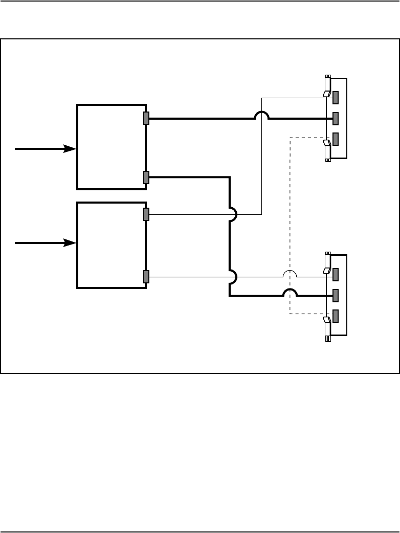
NT5D97 Dual-port DTI2/PRI2 card Page 359 of 906
Circuit Card Description and Installation
Operation
The following discussion describes possible scenarios when replacing a
digital trunk NT8D72BA PRI2 card or QPC536E DTI2 card or NTCK43
Dual PRI card configuration with a NT5D97 DDP2 card configuration.
Figure 78
Clock Controller – Option 1
553-7401
Primary
clocking
source Primary
Reference
Secondary
Reference
J1
J2
J3
Clock Controller
Backup
Clock
Controller 0
Clock
Controller 1
J1
J2
J3
Primary
Primary
Secondary
Secondary
REF 1
REF 2
REF 1
REF 2
Secondary
clocking
source
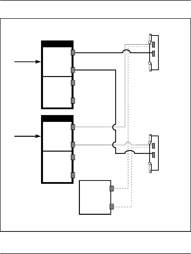
Page 360 of 906 NT5D97 Dual-port DTI2/PRI2 card
553-3001-211 Standard 3.00 August 2005
Figure 79
Clock Controller – Option 2
553-7403
Primary
Reference Port 0
DDP2
Port 1
Clock Controller
for CPU 0
Clock Controller
for CPU 1
Secondary Ref 1
Secondary Ref 2
Secondary Ref 1
Secondary Ref 2 J1 Sec.
J2 Prim.
J1 Sec.
J2 Prim.
Primary Ref 1
Primary Ref 2
Both references from port 0
clk 0
clk 1
Clk0
Clk1
Port 0
DDP2
Port 1
clk 0
clk 1
Clk0
Clk1
Secondary
Reference
NT8D72BA
J1 Ref 1
J2 Ref 2
An NT8D72BA may
be configured as an
alternate to DDP2
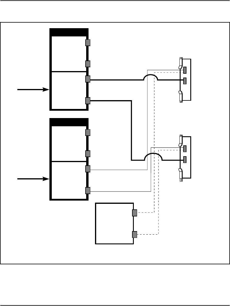
NT5D97 Dual-port DTI2/PRI2 card Page 361 of 906
Circuit Card Description and Installation
Figure 80
Clock Controller – Option 3
553-7404
Primary
Reference
Port 0
DDP2
Port 1
Clock Controller
for CPU 0
Clock Controller
for CPU 1
Secondary Ref 1
Secondary Ref 2
Secondary Ref 1
Secondary Ref 2
J1 Sec.
J2 Prim.
J1 Sec.
J2 Prim.
Primary Ref 1
Primary Ref 2
Both references from port 1
clk 0
clk 1
Clk0
Clk1
Port 0
DDP2
Port 1
clk 0
clk 1
Clk0
Clk1
Secondary
Reference
NT8D72BA
J1 Ref 1
J2 Ref 2
An NT8D72BA may
be configured as an
alternate to DDP2
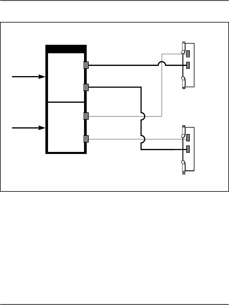
Page 362 of 906 NT5D97 Dual-port DTI2/PRI2 card
553-3001-211 Standard 3.00 August 2005
Case 1 - The two ports of a QPC414 network card are connected to two digital
trunks.
In this case, the QPC414 and the two digital trunks are replaced by a single
DDP2 card, which is plugged into the network shelf in the QPC414 slot.
Case 2 - One port of the QPC414 card is connected to a digital trunk, and the
second is connected to a peripheral buffer. Both cards are in network loop
location.
In this case, the QPC414 should not be removed. The digital trunk is removed
and the DDP2 card is plugged into one of the two empty slots.
Figure 81
Clock Controller – Option 4
553-7402
Primary
Reference
Port 0
DDP2
Port 1
Clock Controller
for CPU 0
Clock Controller
for CPU 1
J1 Sec.
J2 Prim.
J1 Sec.
J2 Prim.
Primary Ref 1
Primary Ref 2
Secondary Ref 1
Secondary Ref 2
Both references from both ports
clk 0
clk 1
Clk0
Clk1
Secondary
Reference
NT5D97 Dual-port DTI2/PRI2 card Page 363 of 906
Circuit Card Description and Installation
Case 3 - The network shelf is full, one port of a QPC414 network card is
connected to a digital trunk, and the second is connected to a peripheral
buffer. This arrangement is repeated for another QPC414. The digital trunks
are located in a shelf that provides only power.
In this case, the peripheral buffers will have to be re-assigned, so that each
pair of buffers will use both ports of the same QPC414 card. The other
QPC414 card can then be replaced by the NT5D97 DDP2.
Procedure 14
Installing the NT5D97
1Determine the cabinet and shelf location where the NT5D97 is to be
installed. The NT5D97 can be installed in any card slot in the Network
bus.
2Unpack and inspect the NT5D97and cables.
3If a DDCH is installed, refer to the section “Removing the NT5D97” on
page 364.
4Set the option switches on the NT5D97 card before installation. Refer to
“NT5D97AA/AB DIP switch settings” on page 340.
The ENB/DIS (enable/disable faceplate switch) must be OFF (DIS) when
installing the NT5D97, otherwise a system initialize can occur. The ENB/
DIS on the NT5D97 corresponds to the faceplate switch on the QPC414
Network card.
5Install NT5D97 card in the assigned shelf and slot.
6Set the ENB/DIS faceplate switch to ON.
If the DDCH is installed, the DDCH LED should flash three times.
7If required, install the I/O adapters in the I/O panel.
CAUTION
The static discharge bracelet located inside the
cabinet must be worn before handling circuit cards.
Failure to wear the bracelet can result in damage to
the circuit cards.

Page 364 of 906 NT5D97 Dual-port DTI2/PRI2 card
553-3001-211 Standard 3.00 August 2005
8Run and connect the NT5D97 cables.
9If required, install connecting blocks at the MDF or wall mounted
cross-connect terminal.
10 If required, designate connecting blocks at the MDF or wall mounted
cross-connect terminal.
11 If required, install a Network Channel Terminating Equipment (NCTE). or
Line Terminating Unit (LTU).
12 Add related office data into switch memory.
13 Enable faceplate switch S1. This is the “Loop Enable” switch.
The faceplate LEDs should go on for 4 seconds then go off and the
OOS, DIS and ACT LEDs should go on again and stay on.
IF DDCH is installed, the DCH LED should flash 3 times.
14 Run the PRI/DTI Verification Test.
15 Run the PRI status check.
End of Procedure
Procedure 15
Removing the NT5D97
1Determine the cabinet and shelf location of the NT5D97 card to be
removed.
2Disable Network Loop using LD 60. The command is DISL “loop number.”
The associated DCHI might have to be disabled first. The faceplate switch
ENB/DIS should not be disabled until both PRI2/DTI2 loops are disabled
first.
CAUTION
Clock Controller cables connecting the Clock
Controller and NT5D97 card must NOT be routed
through the center of the cabinet past the power
harness. Instead they should be routed around the
outside of the equipment shelves.

NT5D97 Dual-port DTI2/PRI2 card Page 365 of 906
Circuit Card Description and Installation
3If the NT5D97 card is being completely removed, not replaced, remove
data from memory.
4Remove cross connections at MDF to wall-mounted cross-connect
terminal.
5Tag and disconnect cables from card.
6Rearrange Clock Controller cables if required.
7Remove the DDP2 card only if both loops are disabled. If the other circuit
of a DDP2 card is in use, DO NOT remove the card. The faceplate switch
ENB/DIS must be in the OFF (DIS) position before the card is removed,
otherwise the system will initialize.
8Pack and store the NT5D97 card and circuit card.
End of Procedure
Configuring the NT5D97
After the NT5D97 DDP2 is installed, configure the system using the same
procedures as the standard NT8D72BA PRI2.
Consider the following when configuring the NT5D97 DDP2 card:
• The CS 1000 Release 4.5 software allows four ports to be defined for the
NT6D80 MSDL. The DDCH (NTBK51AA) card has only two ports, 0
and 1; therefore, ports 2 and 3 must not be defined when using the
NTBK51AA.
CAUTION
Clock Controller cables connecting the Clock Controller and DDP2 card
must NOT be routed through the center of the cabinet past the power
harness. Instead, they should be routed around the outside of the
equipment shelves.

Page 366 of 906 NT5D97 Dual-port DTI2/PRI2 card
553-3001-211 Standard 3.00 August 2005
• Port 0 of the NTBK51AA can only be defined to work with Loop 0 of the
NT5D97 DDP2 card, and Port 1 of the NTBK51AA can only be defined
to work with Loop 1 of the NT5D97. This relationship must be reflected
when configuring a new DCH in LD 17 (in response to the DCHL
prompt, enter either 0 or 1 when specifying the loop number used by the
DCH).
• You cannot define one of the DDP2 loops for the NTBK51AA DDCH,
and the other loop for the NT6D11AF/NT5K75AA/NT5K35AA DCH
card or the NT6D80 MSDL.
• When configuring the NT5D97 DDP2 in DTI2 outgoing dial pulse mode,
a Digit Outpulsing patch is required.
Testability and diagnostics
The DDP2 card supports testing and maintenance functions through the
following procedures:
• Selftest upon power up or reset
• Signalling test performed in the LD 30
• Loopback tests, self tests, and continuity tests performed by LD 60 and
LD 45
• The D-Channel (DCH, MSDL, DDCH) maintenance is supported by
LD 96.
Note: The MSDL selftest is not applicable to the NTBK51AA
D-Channel daughterboard.

Page 367 of 906
Circuit Card Description and Installation
368
NT5K02 Flexible Analog Line card
Contents
This section contains information on the following topics:
Introduction . . . . . . . . . . . . . . . . . . . . . . . . . . . . . . . . . . . . . . . . . . . . . . 367
Applications . . . . . . . . . . . . . . . . . . . . . . . . . . . . . . . . . . . . . . . . . . . . . 368
Introduction
The NT5K02 Flexible Analog Line card provides an interface for up to
16 analog (500/2500-type) telephones equipped with either ground button
recall switches, high-voltage Message Waiting lamps, or low-voltage
Message Waiting LEDs.
You can install this card in any IPE slot.
Note: Up to four NT5K02 Flexible Analog Line card are supported in
each Media Gateway 1000S (MG 1000S). Up to four NT5K02 Flexible
Analog Line card are supported in each MG 1000S Expansion.
The NT5K02 Flexible Analog Line card performs several functions,
including:
• flexible transmission
• ground button operation
• low-voltage Message Waiting option
• card self-ID for auto-configuration

Page 368 of 906 NT5K02 Flexible Analog Line card
553-3001-211 Standard 3.00 August 2005
Applications
The NT5K02 Flexible Analog Line card can be used for the following
applications:
• NT5K02AA high-voltage Message Waiting analog line card typically
used in Australia
• NT5K02DA ground button, low-voltage Message Waiting, analog line
card typically used in France
• NT5K02EA ground button, low-voltage Message Waiting, analog line
card typically used in Germany
• NT5K02FA ground button, low-voltage Message Waiting, analog line
card with 600¾ termination (A/D –4 dB, D/A–1 dB)
• NT5K02GA same as NT5K02FA with a different loss plan (A/D –4 dB,
D/A –3 dB)
• NT5K02HA ground button, low-voltage Message Waiting, analog line
card typically used in Belgium
• NT5K02JA low-voltage Message Waiting, analog line card typically
used in Denmark
• NT5K02KA ground button, low-voltage Message Waiting, analog line
card typically used in Netherlands
• NT5K02LA and NT5K02LB analog line card typically used in New
Zealand
• NT5K02MA ground button, low-voltage Message Waiting, analog line
card typically used in Norway
• NT5K02NA ground button, low-voltage message Waiting, analog line
card typically used in Sweden
• NT5K02PA ground button, low-voltage Message Waiting, analog line
card typically used in Switzerland
• NT5K02QA ground button, low-voltage Message Waiting, analog line
card typically used in the United Kingdom

Page 369 of 906
Circuit Card Description and Installation
378
NT5K21 XMFC/MFE card
Contents
This section contains information on the following topics:
Introduction . . . . . . . . . . . . . . . . . . . . . . . . . . . . . . . . . . . . . . . . . . . . . . 369
MFC signaling. . . . . . . . . . . . . . . . . . . . . . . . . . . . . . . . . . . . . . . . . . . . 369
MFE signaling. . . . . . . . . . . . . . . . . . . . . . . . . . . . . . . . . . . . . . . . . . . . 372
Sender and receiver mode . . . . . . . . . . . . . . . . . . . . . . . . . . . . . . . . . . . 373
Physical specifications . . . . . . . . . . . . . . . . . . . . . . . . . . . . . . . . . . . . . 376
Introduction
The XMFC/MFE (Extended Multi-frequency Compelled/Multi-frequency
sender-receiver) card is used to set up calls between two trunks. Connections
may be between a PBX and a Central Office or between two PBXs. When
connection has been established, the XMFC/MFE card sends and receives
pairs of frequencies and then drops out of the call.
The XMFC/MFE card can operate in systems using either A-law or µ-law
companding by changing the setting in software.
You can install this card in any IPE slot.
MFC signaling
The MFC feature allows the system to use the CCITT MFC R2 or L1
signaling protocols.

Page 370 of 906 NT5K21 XMFC/MFE card
553-3001-211 Standard 3.00 August 2005
Signaling levels
MFC signaling uses pairs of frequencies to represent digits, and is divided
into two levels:
•Level 1: used when a call is first established and may be used to send the
dialed digits.
•Level 2: used after Level 1 signaling is completed and may contain such
information as the status, capabilities, or classifications of both calling
parties.
Forward and backward signals
When one NT5K21 XMFC/MFE card sends a pair of frequencies to a
receiving XMFC/MFE card (forward signaling), the receiving XMFC/MFE
card must respond by sending a different set of frequencies back to the
originating XMFC/MFE card (backward signaling). In other words, the
receiving card is always “compelled” to respond to the originating card.
In summary, the signaling works as follows:
• The first XMFC/MFE card sends a forward signal to the second card.
• The second card hears the forward signal and replies with a backward
signal.
• The first card hears the backward signal and “turns off” its forward
signal.
• The second card hears the forward signal being removed and removes its
backward signal.
• The first XMFC/MFE can either send a second signal or drop out of the
call.

NT5K21 XMFC/MFE card Page 371 of 906
Circuit Card Description and Installation
MFC signaling involves two or more levels of forward signals and two or
more levels of backward signals. Separate sets of frequencies are used for
forward and backward signals:
•Forward signals. Level I forward signals are dialed address digits that
identify the called party. Subsequent levels of forward signals describe
the category (Class of Service) of the calling party, and may include the
calling party status and identity.
•Backward signals. Level I backward signals (designated “A”) respond
to Level I forward signals. Subsequent levels of backward signals (B, C,
and so on) describe the status of the called party.
Table 141 lists the frequency values used for forward and backward signals.
Table 141
MFC Frequency values (Part 1 of 2)
Digit
Forward direction
DOD-Tx, DID-Rx
backward direction
DOD-Rx, DID-Tx
11380 Hz + 1500 Hz 1140 Hz + 1020 Hz
21380 Hz + 1620 Hz 1140 Hz + 900 Hz
31500 Hz + 1620 Hz 1020 Hz + 900 Hz
41380 Hz + 1740 Hz 1140 Hz + 780 Hz
51500 Hz + 1740 Hz 1020 Hz + 780 Hz
61620 Hz + 1740 Hz 900 Hz + 780 Hz
71380 Hz + 1860 Hz 1140 Hz + 660 Hz
81500 Hz + 1860 Hz 1020 Hz + 660 Hz
91620 Hz + 1860 Hz 900 Hz + 660 Hz
10 1740 Hz + 1860 Hz 780 Hz + 660 Hz
11 1380 Hz + 1980 Hz 1140 Hz + 540 Hz
12 1500 Hz + 1980 Hz 1020 Hz + 540 Hz
13 1620 Hz + 1980 Hz 900 Hz + 540 Hz

Page 372 of 906 NT5K21 XMFC/MFE card
553-3001-211 Standard 3.00 August 2005
The exact meaning of each MFC signal number (1-15) within each level can
be programmed separately for each trunk route using MFC. This
programming can be done by the customer and allows users to suit the needs
of each MFC-equipped trunk route.
Each MFC-equipped trunk route is associated with a data block that contains
the MFC signal functions supported for that route.
MFE signaling
The NT5K21 XMFC/MFE card can be programmed for MFE signaling
which is used mainly in France. MFE is much the same as MFC except it has
its own set of forward and backward signals.
Table 142 lists the forward and backward frequencies for MFE. The one
backward signal for MFE is referred to as the “control” frequency.
14 1740 Hz + 1980 Hz 780 Hz + 540 Hz
15 1860 Hz + 1980 Hz 660 Hz + 540 Hz
Table 142
MFE Frequency values (Part 1 of 2)
Digit
Forward direction
OG-Tx, IC-Rx Backward direction
1700 Hz + 900 Hz 1900 Hz
(Control Frequency)
2700 Hz + 1100 Hz —
3900 Hz + 1100 Hz —
4700 Hz + 1300 Hz —
Table 141
MFC Frequency values (Part 2 of 2)
Digit
Forward direction
DOD-Tx, DID-Rx
backward direction
DOD-Rx, DID-Tx

NT5K21 XMFC/MFE card Page 373 of 906
Circuit Card Description and Installation
Sender and receiver mode
The XMFC/MFE circuit card provides the interface between the system’s
CPU and the trunk circuit which uses MFC or MFE signaling.
The XMFC/MFE circuit card transmits and receives forward and backward
signals simultaneously on two channels. Each channel is programmed like a
peripheral circuit card unit, with its own sending and receiving timeslots in
the network.
Receive mode
When in receive mode, the XMFC/MFE card is linked to the trunk card by a
PCM speech path over the network cards. MFC signals coming in over the
trunks are relayed to the XMFC/MFE card as though they were speech. The
XMFC/MFC card interprets each tone pair and sends the information to the
CPU through the CPU bus.
Send mode
When in send mode, the CPU sends data to the XMFC/MFE card through the
CPU bus. The CPU tells the XMFC/MFE card which tone pairs to send and
the XMFC/MFE card generates the required tones and sends them to the trunk
over the PCM network speech path. The trunk transmits the tones to the far
end.
5900 Hz + 1300 Hz —
61100 Hz + 1300 Hz —
7700 Hz + 1500 Hz —
8900 Hz + 1500 Hz —
91100 Hz + 1500 Hz —
10 1300 Hz + 1500 Hz —
Table 142
MFE Frequency values (Part 2 of 2)
Digit
Forward direction
OG-Tx, IC-Rx Backward direction

Page 374 of 906 NT5K21 XMFC/MFE card
553-3001-211 Standard 3.00 August 2005
XMFC sender and receiver specifications
Table 143 and Table 144 provide the operating requirements for the NT5K21
XMFC/MFE card. These specifications conform to CCITT R2
recommendations: Q.441, Q.442, Q.451, Q.454, and Q.455.
Table 143
XMFC sender specifications
Forward frequencies in DOD mode: 1380, 1500, 1620, 1740, 1860, 1980 Hz
Backward frequencies in DOD mode: 1140, 1020, 900, 780, 660, 540 Hz
Frequency tolerance: +/- 0.5 Hz from nominal
Power level at each frequency: Selectable: 1 of 16 levels
Level difference between frequencies: < 0.5 dB
Harmonic Distortion and Intermodulation 37 dB below level of 1 signaling frequency
Time interval between start of 2 tones: 125 usec.
Time interval between stop of 2 tones: 125 usec.
Table 144
XMFC receiver specifications (Part 1 of 2)
Input sensitivity:
accepted:
rejected:
-5 to -31.5 dBmONew CCITT spec.
-38.5 dBmOBlue Book
Bandwidth twist:
accepted:
rejected:
fc +/- 10 Hz
fc +/- 60 Hz
Amplitude twist:
accepted:
Norwegian requirement
rejected:
difference of 5 dB between adjacent frequencies
difference of 7 dB between non-adjacent frequencies
difference of 12 dB (for unloaded CO trunks)
difference of 20 dB between any two frequencies
Operating time: < 32 msec.
Release time: < 32 msec.

NT5K21 XMFC/MFE card Page 375 of 906
Circuit Card Description and Installation
XMFE sender and receiver specifications
Tables 145 and Table 146 on page 376 provide the operating requirements
for the XMFC/MFE card when it is configured as an XMFE card. These
requirements conform to French Socotel specifications ST/PAA/CLC/CER/
692.
Tone Interrupt no release: < 8 msec. Receiver on, while tone missing
Longest Input tone ignored: < 8 msec. Combination of valid frequencies
Noise rejection: S/N > 18 dB No degradation, in band white noise
S/N > 13 dB Out-of-band disturbances for CCITT
Table 145
XMFE sender specifications
Forward frequencies in OG mode: 700, 900, 1100, 1300, 1500 Hz
Forward frequencies in IC mode: 1900 Hz
Frequency tolerance: +/- 0.25% from nominal
Power level at each frequency: Selectable: 1 of 16 levels
Level tolerance: +/- 1.0 dB
Harmonic Distortion and Intermodulation: 35 dB below level of 1 signaling frequency
Time interval between start of 2 tones: 125 usec.
Time interval between stop of 2 tones: 125 usec.
Table 144
XMFC receiver specifications (Part 2 of 2)

Page 376 of 906 NT5K21 XMFC/MFE card
553-3001-211 Standard 3.00 August 2005
Physical specifications
Table 147 outlines the physical specifications of the NT5K21 XMFC/MFE
circuit card.
Table 146
XMFE receiver specifications
Input sensitivity:
accepted:
rejected:
rejected:
rejected:
-4 dBm to -35 dBm +/- 10 Hz of nominal
-42 dBm signals
-4 dBmoutside 500-1900 Hz
-40 dBmsingle/multiple sine wave in 500-1900 Hz
Bandwidth:
accepted: fc +/- 20 Hz
Amplitude twist:
accepted: difference of 9 dB between frequency pair
Operating time: < 64 msec.
Release time: < 64 msec.
Tone Interrupt causing no
release: < 8 msec. Receiver on, tone missing
Longest Input tone ignored: < 8 msec. Combination of valid frequencies
Longest control tone ignored: < 15 msec.Control Frequency only
Noise rejection: S/N > 18 dBNo degradation in-band white noise
Table 147
Physical specifications (Part 1 of 2)
Dimensions Height:12.5 in. (320 mm)
Depth:10.0 in. (255 mm)
Thickness:7/8 in. (22.25 mm)
Faceplate LED Lit when the circuit card is disabled


Page 379 of 906
Circuit Card Description and Installation
384
NT6D70 SILC Line card
Contents
This section contains information on the following topics:
Introduction . . . . . . . . . . . . . . . . . . . . . . . . . . . . . . . . . . . . . . . . . . . . . . 379
Physical description. . . . . . . . . . . . . . . . . . . . . . . . . . . . . . . . . . . . . . . . 380
Functional description . . . . . . . . . . . . . . . . . . . . . . . . . . . . . . . . . . . . . . 380
Introduction
The S/T Interface Line card (SILC) (NT6D70AA –48V North America,
NT6D70 BA –40 V International) provides eight S/T four-wire full-duplex
interfaces to connect ISDN BRI-compatible terminals over Digital Subscriber
Loops (DSLs) to the System. A description of the ISDN BRI feature is
contained in ISDN Basic Rate Interface: Installation and Configuration
(553-3001-218).
You can install this card in any IPE slot.
Note: A maximum of four NT6D70 SILC cards are supported in an
MG 1000S. A maximum of four NT6D70 SILC cards are supported in
an MG 1000S Expansion.
ISDN BRI
ISDN BRI consists of two 64Kb/s Bearer (B) channels and one 16Kb/s Data
(D) channel. The BRI interface is referred to as a 2B+D connection as well as
a Digital Subscriber Loop (DSL).

Page 380 of 906 NT6D70 SILC Line card
553-3001-211 Standard 3.00 August 2005
B-channels transmit user voice and data information at high speeds, while
D-channels are packet-switched links that carry call set-up, signaling and
other user data across the network.
One single DSL can carry two simultaneous voice or data conversations to the
same or to different locations. In either case, the D-channel can also be used
for packet communication to a third location simultaneously. The two
B-channels can also be combined to transmit data at uncompressed speeds of
up to 128 Kbps.
A wide range of devices and telephone numbers can be associated with a
single DSL to offer equipment flexibility and reduce line, wiring, and
installation costs.
Physical description
The NT6D70 SILC card is a standard-size circuit card. Its faceplate is
equipped with an LED to indicate its status.
Power consumption
Power consumption is +5 V at 800 mA and –48 V at 480 mA.
Foreign and surge voltage protections
In-circuit protection against power line crosses or lightning is not provided on
the SILC card. When the SILC card is used in TIE trunk applications in which
the cabling is exposed to outside plant conditions, an NT1 module certified
for such applications must be used. Check local regulations before providing
such service.
Functional description
The NT6D70 SILC card provides eight S/T four-wire full-duplex
polarity-sensitive interfaces to connect ISDN BRI-compatible terminals over
Digital Subscriber Loops (DSL) to the system. Each S/T interface provides
two B-channels and one D-channel and supports a maximum of eight physical
connections that can link up to 20 logical terminals on one DSL.

NT6D70 SILC Line card Page 381 of 906
Circuit Card Description and Installation
A logical terminal is any terminal that can communicate with the system over
a DSL. It can be directly connected to the DSL through its own physical
termination or be indirectly connected through a common physical
termination.
The length of a DSL depends on the specific terminal configuration and the
DSL wire gauge; however, it should not exceed 1 km (3,280 ft).
The SILC interface uses a four-conductor cable that provides a differential
Transmit and Receive pair for each DSL. The SILC has options to provide a
total of two watts of power on the Transmit or Receive leads, or no power at
all. When this power is supplied from the S/T interface, the terminal devices
must not draw more than the two watts of power. Any power requirements
beyond this limit must be locally powered.
Other functions of the SILC are:
• support point-to-point and multi-point DSL terminal connections
• execute instructions received from the MISP to configure and control the
S/T interfaces
• provide channel mapping between ISDN BRI format (2B+D) and system
bus format
• multiplex 4 D-channels onto one timeslot
• perform activation and deactivation of DSLs
• provide loopback control of DSLs
• provide a reference clock to the clock controller
Micro Controller Unit (MCU)
The Micro Controller Unit (MCU) coordinates and controls the operation of
the SILC. It has internal memory, a reset and sanity timer, and a serial control
interface.
The memory consists of 32 K of EPROM which contains the SILC operating
program and 8 K of RAM used to store interface selection and other functions
connected with call activities.

Page 382 of 906 NT6D70 SILC Line card
553-3001-211 Standard 3.00 August 2005
The reset and sanity timer logic resets the MCU.
The serial control interface is an IPE bus used by the MPU to communicate
with the S/T transceivers.
IPE interface logic
The IPE interface logic consists of a Card-LAN interface, an IPE bus
interface, a maintenance signaling channel interface, a digital pad, and a clock
controller and converter.
The Card-LAN interface is used for routine card maintenance, which includes
polling the line cards to find the card slot where the SILC is installed. It also
queries the status and identification of the card and reports the configuration
data and firmware version of the card.
The IPE bus interface connects an IPE bus loop that has 32 channels
operating at 64 kbps and one additional validation and signaling bit.
The Maintenance Signaling Channel (MSC) interface communicates
signaling and card identification information from the system CPU to the
SILC MCU. The signaling information also contains maintenance
instructions.
The digital pad provides gain or attenuation values to condition the level of
the digitized transmission signal according to the network loss plan. This sets
transmission levels for the B-channel voice calls.
The clock recovery circuit recovers the clock from the local exchange.
The clock converter converts the 5.12-MHz clock from the IPE backplane
into a 2.56 MHz clock to time the IPE bus channels and an 8 kHz clock to
provide PCM framing bits.
S/T interface logic
The S/T interface logic consists of a transceiver circuit and the DSL power
source. This interface supports DSLs of different distances and different
numbers and types of terminal.

NT6D70 SILC Line card Page 383 of 906
Circuit Card Description and Installation
The transceiver circuits provide four-wire full-duplex S/T bus interface. This
bus supports multiple physical terminations on one DSL where each physical
termination supports multiple logical B-channel and D-channel ISDN BRI
terminals. Idle circuit-switched B-channels can be allocated for voice or data
transmission to terminals making calls on a DSL. When those terminals
become idle, the channels are automatically made available to other terminals
making calls on the same DSL.
The power on the DSL comes from the SILC, which accepts –48 V from the
IPE backplane and provides two watts of power to physical terminations on
each DSL. It provides -48 V for ANSI-compliant ISDN BRI terminals and
–40 V for CCITT (such as ETSI NET-3, INS NET-64) compliant terminals.
The total power used by the terminals on each DSL must not exceed
two watts.


Page 385 of 906
Circuit Card Description and Installation
388
NT6D71 UILC Line card
Contents
This section contains information on the following topics:
Introduction . . . . . . . . . . . . . . . . . . . . . . . . . . . . . . . . . . . . . . . . . . . . . . 385
Physical description. . . . . . . . . . . . . . . . . . . . . . . . . . . . . . . . . . . . . . . . 385
Functional description . . . . . . . . . . . . . . . . . . . . . . . . . . . . . . . . . . . . . . 386
Introduction
The NT6D71 U Interface Line card (UILC) supports the OSI physical layer
(layer 1) protocol. The UILC is an ANSI-defined standard interface. The
UILC provides eight two-wire full-duplex (not polarity sensitive)
U interfaces to connect ISDN BRI-compatible terminals over Digital
Subscriber Loops (DSL) to the CS 1000S, CS 1000M, and Meridian 1. A
description of the ISDN BRI feature is contained in ISDN Basic Rate
Interface: Installation and Configuration (553-3001-218).
You can install this card in any IPE slot.
Note: A maximum of four UILCs are supported in an MG 1000S. A
maximum of four UILCs are supported in an MG 1000S Expansion.
Physical description
The NT6D71 UILC is a standard-size circuit card. Its faceplate is equipped
with an LED to indicate its status.

Page 386 of 906 NT6D71 UILC Line card
553-3001-211 Standard 3.00 August 2005
Power consumption
Power consumption is +5 V at 1900 mA.
Functional description
Each U interface provides two B-channels and one D-channel and supports
one physical termination. This termination can be to a Network Termination
(NT1) or directly to a single U interface terminal. Usually, this physical
termination is to an NT1, which provides an S/T interface that supports up to
eight physical terminal connections. The length of a DSL depends on the
specific terminal configuration and the DSL wire gauge; however, it should
not exceed 5.5 km (3.3 mi).
The main functions of the UILC are as follows:
• provide eight ISDN U interfaces conforming to ANSI standards
• support point-to-point DSL terminal connections
• provide channel mapping between ISDN BRI format (2B+D) and system
bus format
• multiplex four D-channels onto one timeslot
• perform activation and deactivation of DSLs
• provide loopback control of DSLs
Micro Controller Unit (MCU)
The Micro Controller Unit (MCU) coordinates and controls the operation of
the UILC. It has internal memory, a reset and sanity timer, a serial control
interface, a maintenance signaling channel, and a digital pad.
The memory consists of 32 K of EPROM that contains the UILC operating
program and 8 K of RAM that stores interface selection and other functions
connected with call activities.
The reset and sanity timer logic resets the MCU.

NT6D71 UILC Line card Page 387 of 906
Circuit Card Description and Installation
The serial control interface is an IPE bus that communicates with the
U transceivers.
IPE interface logic
The IPE interface logic consists of a Card-LAN interface, a IPE bus interface,
a maintenance signaling channel interface, a digital pad, and a clock
converter.
The Card-LAN interface is used for routine card maintenance, which includes
polling the line cards to find in which card slot the UILC is installed. It also
queries the status and identification of the card and reports the configuration
data and firmware version of the card.
The IPE bus interface connects one IPE bus loop that has 32 channels
operating at 64 kbps and one additional validation and signaling bit.
The Maintenance Signaling Channel (MSC) interface communicates
signaling and card identification information from the system CPU to the
UILC MCU. The signaling information also contains maintenance
instructions.
The digital pad provides gain or attenuation values to condition the level of
the digitized transmission signal according to the network loss plan. This sets
transmission levels for B-channel voice calls.
The clock converter converts the 5.12 MHz clock from the IPE backplane into
a 2.56 MHz clock to time the IPE bus channels and an 8-kHz clock to provide
PCM framing bits.
U interface logic
The U interface logic consists of a transceiver circuit. It provides loop
termination and high-voltage protection to eliminate the external hazards on
the DSL. The U interface supports voice and data terminals, D-channel packet
data terminals, and NT1s. A UILC has eight transceivers to support eight
DSLs for point-to-point operation.


Page 389 of 906
Circuit Card Description and Installation
426
NT6D80 MSDL card
Contents
This section contains information on the following topics:
Introduction . . . . . . . . . . . . . . . . . . . . . . . . . . . . . . . . . . . . . . . . . . . . . . 389
Physical description. . . . . . . . . . . . . . . . . . . . . . . . . . . . . . . . . . . . . . . . 390
Functional description . . . . . . . . . . . . . . . . . . . . . . . . . . . . . . . . . . . . . . 392
Engineering guidelines . . . . . . . . . . . . . . . . . . . . . . . . . . . . . . . . . . . . . 397
Installation. . . . . . . . . . . . . . . . . . . . . . . . . . . . . . . . . . . . . . . . . . . . . . . 404
Maintenance . . . . . . . . . . . . . . . . . . . . . . . . . . . . . . . . . . . . . . . . . . . . . 413
Replacing MSDL cards . . . . . . . . . . . . . . . . . . . . . . . . . . . . . . . . . . . . . 421
Symptoms and actions. . . . . . . . . . . . . . . . . . . . . . . . . . . . . . . . . . . . . . 422
System disabled actions . . . . . . . . . . . . . . . . . . . . . . . . . . . . . . . . . . . . 423
Introduction
This document describes the Multi-purpose Serial Data Link (MSDL) card.
This card provides multiple interface types with four full-duplex serial I/O
ports that can be independently configured for various operations. Peripheral
software downloaded to the MSDL controls functionality for each port.
Synchronous operation is permitted on all MSDL ports. Port 0 can be
configured as an asynchronous Serial Data Interface (SDI).
An MSDL card occupies one network card slot in Large System Networks, or
Core Network modules and communicates with the CPU over the CPU bus
and with I/O equipment over its serial ports. It can coexist with other cards

Page 390 of 906 NT6D80 MSDL card
553-3001-211 Standard 3.00 August 2005
that support the same functions. For example, three cards supported with the
MSDL (NT6D80) are QPC757 (DCHI), QPC513 (ESDI), QPC841 (SDI) and
NTSD12 (DDP).
Though the MSDL is designed to coexist with other cards, the number of
ports supported by a system equipped with MSDL cards is potentially four
times greater than when using other cards. Since each MSDL has four ports,
representing a single device, a system can support as many as 16 MSDL cards
with a maximum of 64 ports.
Physical description
The MSDL card is a standard size circuit card that occupies one network card
slot and plugs into the module’s backplane connector to interface with the
CPU bus and to connect to the module’s power supply. On the faceplate, the
MSDL provides five connectors, four to connect to I/O operations and one to
connect to a monitor device that monitors MSDL functions. Figure 82 on
page 391 illustrates major MSDL components and their locations on the
printed circuit card.
Note: Switches S9 and S10 are configured to reflect the device number
set in LD 17 (DNUM). S10 designates tens, and S9 designates ones. For
example, set device number 14 with S10 at 1 and S9 at 4.
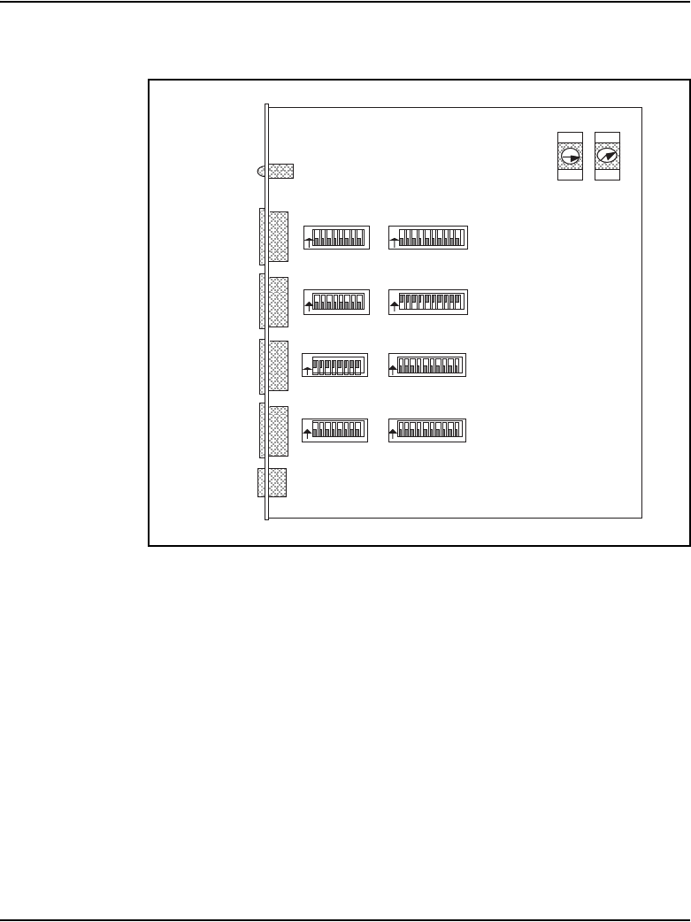

Page 392 of 906 NT6D80 MSDL card
553-3001-211 Standard 3.00 August 2005
Functional description
Figure 83 on page 393 illustrates the MSDL functional block diagram. The
MSDL card is divided into four major functional blocks:
• CPU bus interface
• Micro Processing Unit (MPU)
•Memory
• Serial interface
Two processing units serve as the foundation for the MSDL operation: the
Central Processing Unit (CPU) and the MSDL Micro Processing Unit
(MPU). CS 1000 Release 4.5 software, MSDL firmware, and peripheral
software control MSDL parameters. Peripheral software downloaded to the
MSDL controls MSDL operations.
The MSDL card’s firmware and software do the following:
• communicate with the CPU to report operation status
• receive downloaded peripheral software and configuration parameters
• coordinate data flow in conjunction with the CPU
• manage data link layer and network layer signaling that controls
operations connection and disconnection
• control operation initialization and addressing
• send control messages to the operations
CPU bus interface
The CPU bus transmits packetized information between the CPU and the
MSDL MPU. This interface has a 16-bit data bus, an 18-bit address bus, and
interrupt and read/write control lines.
Shared Random Access Memory (RAM) between the CPU and the MSDL
MPU provides an exchange medium. Both the CPU and the MSDL MPU can
access this memory.
NT6D80 MSDL card Page 393 of 906
Circuit Card Description and Installation
Figure 83
MSDL block diagram
Address Buffer and
Decoding Logic
Control and Data
Transceivers
Interface Registers
Micro Processing Unit
(68020 MPU)
MPU Address
Decoding Logic
Shared Resource
Arbitrator
Memory Address
Counter & Buffer Shared Memory
Integrated Serial Communication Controllers
RS-232/422
Transceiver
Port 0 Port 1 Port 2 Port 3
RS-232
Transceiver
Parallel I/O
Controller
Monitor Port
Memory
DMA
Arbitrator
CPU Bus Address Bus
Control Bus
Data Bus
MPU Bus Address Bus
Control Bus
Data Bus
553-5432
RS-232/422
Transceiver RS-232/422
Transceiver RS-232/422
Transceiver

Page 394 of 906 NT6D80 MSDL card
553-3001-211 Standard 3.00 August 2005
Micro Processing Unit (MPU)
The MPU, which is based on a Motorola 68020 processor, coordinates and
controls data transfer and port addressing, communicating via the CPU bus
with the system. Prioritized interrupts tell the MPU which tasks to perform.
Memory
The MSDL card contains two megabytes of Random Access Memory (RAM)
for storing downloaded peripheral software that controls MSDL port
operations. The MSDL card includes the shared RAM that is used as a
communication interface buffer between the CPU and the MPU.
The MSDL Flash Erasable Programmable Read Only Memory (Flash
EPROM) also includes the peripheral software to protect it against a power
failure or reset. MSDL can copy peripheral software directly from the Flash
EPROM after power up or reset instead of requesting that the system CPU
download it.
The MSDL card also contains Programmable Read Only Memory (PROM)
for firmware that includes the bootstrap code.
Serial interface
The MSDL card provides one monitor port and four programmable serial
ports that can be configured for the following various interfaces and
combinations of interfaces:
• synchronous ports 0–3
• asynchronous port 0
• DCE or DTE equipment emulation mode
• RS-232 or RS-422 interface
Transmission mode – All four ports of the MSDL can be configured for
synchronous data transmission by software. Port 0 can be configured for
asynchronous data transmission for CRT, TTY, and printer applications only.

NT6D80 MSDL card Page 395 of 906
Circuit Card Description and Installation
Equipment emulation mode – Configure an MSDL port to emulate DCE or
DTE by setting switches on the card and downloading LD 17 interface
parameters.
I/O port electrical interface – Each MSDL port can be configured as an
RS-232 or RS-422 interface by setting the switches on the MSDL card.
MSDL ports use Small Computer Systems Interface (SCSI) II 26-pin female
connectors.
Figure 84 on page 396 shows the system architecture using the MSDL as an
operational platform. It illustrates operation routing from the CPU, through
the MSDL, to the I/O equipment. It also shows an example in which DCH
operation peripheral software in the MSDL controls functions on ports
2 and 3.
MSDL operations
The system automatically performs self-test and data flow activities. Unless
a permanent problem exists and the system cannot recover, there is no visual
indication that these operations are taking place.
The system controls the MSDL card with software that it has downloaded.
The MSDL and the system enable the MSDL by following these steps:
1When the MSDL card is placed in the system, the card starts a self-test.
2When the MSDL passes the test, it indicates its state and L/W version to
the system. The CPU checks to see if downloading is required.
3After downloading the peripheral software, the system enables the
MSDL.
4MSDL applications (DCH, AML, SDI) may be brought up if
appropriately configured.
Page 396 of 906 NT6D80 MSDL card
553-3001-211 Standard 3.00 August 2005
Figure 84
MSDL functional block diagram
AML Loadware
CPU Bus
Boot Code
& Loader
Modules
MSDL Handler
System Interface Module
Physical Layer (Layer 1) Handler
P
S
O
S
+
Meridian Mail PRI Trunk PRI Trunk
System software
MSDL software modules
Application
Module Link D-Channel
System
AML Handler System
DCH Handler
DCH Loadware
Port 0 Port 1 Port 2 Port 3
Meridian Link
553-5433

NT6D80 MSDL card Page 397 of 906
Circuit Card Description and Installation
Data flow
The MSDL transmit interface, managed by the MSDL handler, sends data
from the system to the MSDL. This interface receives packetized data from
the system and stores it in the transmit buffer on the MSDL. The transmit
buffer transports these messages to the appropriate buffers, from which the
messages travel over the MSDL port to the I/O equipment.
The MSDL uses the MSDL receive interface to communicate with the
system. The MSDL card receives packetized data from the I/O equipment
over the MSDL ports. This data is processed by the MSDL handler and sent
to the appropriate function.
The flow control mechanism provides an orderly exchange of transmit and
receive messages for each operation. Each operation has a number of
outstanding messages stored in buffers waiting to be sent to their destinations.
As long as the number of messages does not exceed the threshold specified,
the messages queue in the buffer in a first-in-first-out process.
If the outstanding number of messages for an operation reaches the threshold,
the flow control mechanism informs the sender to wait until the number of
messages is below the threshold before sending the next message.
If buffer space is not available, the request to send a message to the buffer is
rejected and a NO BUFFER fault indication is sent.
Engineering guidelines
Available network card slots
The number of available network slots depends on the system option, the
system size, and the number of available network slots in each module for the
selected system option.
Some of these network card slots are normally occupied by Network cards,
Superloop Network cards, Conference/TDS, and others, leaving a limited
number of unused slots for MSDL and other cards.

Page 398 of 906 NT6D80 MSDL card
553-3001-211 Standard 3.00 August 2005
Card mix
A system that exclusively uses MSDL cards can support up to 16 such cards,
providing 64 ports. These ports can be used to run various synchronous and
asynchronous operations simultaneously.
The system will also support a mix of interface cards (MSDL, DCHI, and
ESDI for example). However, using multiple card types will reduce the
number of cards and ports available.
Address decoding
The MSDL card decodes the full address information received from the
system. This provides 128 unique addresses. Since MSDL ports
communicate with the CPU using a single card address, the system can
support 16 MSDL cards providing 64 ports.
The MSDL card addresses are set using decimal switches located on the card.
These switches can select 100 unique card addresses from 0 to 99.
An address conflict may occur between the MSDL and other cards because of
truncated address decoding by the other cards. For example, if a DCHI port
is set to address 5, its companion port will be set to address 4, which means
that none of the MSDL cards can have hexadecimal address numbers 05H,
15H, …75H, nor addresses 04H, 14H, …74H. To avoid this conflicts system
software limits the MSDL card addresses from 0 to 15.
Port specifications
The MSDL card provides four programmable serial ports configured with
software as well as with switches for the following modes of operation:
Transmission mode Configure an MSDL port for synchronous or
asynchronous data transmission using LD 17.
Synchronous transmission uses an external clock signal fed into the MSDL.

NT6D80 MSDL card Page 399 of 906
Circuit Card Description and Installation
Table 148 lists the synchronous interface specifications and the means of
configuring the interface parameters.
Asynchronous transmission uses an internal clock to generate the appropriate
baud rate for serial controllers.
Table 149 lists asynchronous interface specifications and the means of
configuring interface parameters.
Table 148
Synchronous interface specifications
Parameter Specification Configured
Data bits In packets-Transparent N/A
Data rate 1.2, 2.4, 4.8, 9.6, 19.2, 38.4,
48, 56, and 64 kbps
Software
Transmission Full Duplex N/A
Clock Internal/External Software
Interface RS-232 Software
RS-422 Switches
Mode DTE or DCE Switches
Table 149
Asynchronous interface specifications (Part 1 of 2)
Parameter Specification Configured
Data bit, parity 7 bits even, odd or no
parity, or 8 bits no parity
Software
Data rate 0.3, 0.6, (1.2), 2.4, 4.8,
9.6, 19.2, and 38.4 kbps
Software
Stop bits 1 (default), 1.5, 2 Software
Transmission Full Duplex N/A
Interface RS-232 Software
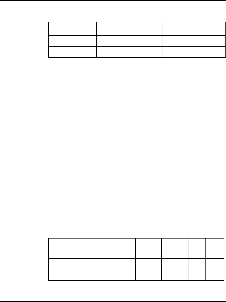
Page 400 of 906 NT6D80 MSDL card
553-3001-211 Standard 3.00 August 2005
Emulation mode Each port can be configured to emulate a DCE port or a
DTE port by setting the appropriate switches on the MSDL. For details on
how to set the switches, refer to “Installation” on page 404 of this document.
DCE is a master or controlling device that is usually the source of information
to the DTE and may provide the clock in a synchronous transmission linking
a DCE to a DTE.
DTE is a peripheral or terminal device that can transmit and receive
information to and from a DCE and normally provides a user interface to the
system or to a DCE device.
Interface Each MSDL port can be configured as an RS-232 or an RS-422
interface by setting the appropriate switches on the card.
Table 150 lists the RS-232 interface specifications for EIA and CCITT
standard circuits. It shows the connector pin number, the associated signal
name, and the supported circuit type. It also indicates whether the signal
originates at the DTE or the DCE device.
This interface uses a 26-pin (SCSI II) female connector for both RS-232 and
RS-422 circuits.
RS-422 Switches
Mode DTE or DCE Switches
Table 150
RS-232 interface pin assignments (Part 1 of 2)
Pin Signal name
EIA
circuit
CCITT
circuit DTE DCE
1 Frame Ground (FG) AA 102 — —
2 Transmit Data (TX) BA 103 X
Table 149
Asynchronous interface specifications (Part 2 of 2)
Parameter Specification Configured

NT6D80 MSDL card Page 401 of 906
Circuit Card Description and Installation
Table 151 on page 402 lists RS-422 interface specifications for EIA circuits.
It shows the connector pin number, the associated signal name, and the
3 Receive Data (RX) BB 104 X
4 Request to Send (RTS) CA 105 X
5 Clear to Send (CTS) CB 106 X
6 Data Set Ready (DSR) CC 107 X
7 Signal Ground (SG) AB 102 — —
8 Carrier Detect (CD) CF 109 X
15 Serial Clock Transmit
(SCT)
DB 114 X
17 Serial Clock Receive
(SCR)
DD 115 X
18 Local Loopback (LL) LL 141 X
20 Data Terminal Ready
(DTR)
CD 108.2 X
21 Remote Loopback (RL) RL 140 X
23 Data Rate Selector (DRS) CH/CI 111/112 X
24 External Transmit Clock
(ETC)
DA 113 X
25 Test Mode (TM) TM 142 X
Table 150
RS-232 interface pin assignments (Part 2 of 2)
Pin Signal name
EIA
circuit
CCITT
circuit DTE DCE

Page 402 of 906 NT6D80 MSDL card
553-3001-211 Standard 3.00 August 2005
supported circuit type. It also indicates whether the signal originates at the
DTE or DCE device.
Implementation guidelines
The following are guidelines for engineering and managing MSDL cards:
• An MSDL can be installed in any empty network card slot.
Table 151
RS-422 interface pin assignments
Pin Signal Name
EIA
Circuit DTE DCE
1 Frame Ground (FG) AA — —
2 Transmit Data (TXa) BAa X
3 Receive Data (RXa) BBa X
4 Request to Send (RTS) CA X
5 Clear to Send (CTS) CB X
7 Signal Ground (SG) AB — —
8 Receive Ready (RR) CF X
12 Receive Signal Timing (RST) DDb X
13 Transmit Data (TXb) BAb X
14 Transmit Signal Timing (TSTb) DBb X
15 Transmit Signal Timing (TSTa) DBa X
16 Receive Data (RXb) BBb X
17 Receive Signal Timing (RSTa) DDa X
20 Data Terminal Ready (DTR) CD X
23 Terminal Timing (TTa) DAb X
24 Terminal Timing (TTb) DAa X

NT6D80 MSDL card Page 403 of 906
Circuit Card Description and Installation
• A maximum of eight MSDL cards can be installed in a fully occupied
module because of the module’s power supply limitations.
• The Clock Controller card should not be installed in a module if more
than 10 MSDL ports are configured as active RS-232 (rather than
RS-422) ports in that module because of the module’s power supply
limitations.
• The MSDL address must not overlap other card addresses.
• Before downloading a peripheral software module for an MSDL, disable
all MSDL ports on cards running the same type of operation.
Environmental and power requirements
The MSDL card conforms to the same requirements as other interface cards.
The temperature, humidity, and altitude for system equipment, including the
MSDL, should not exceed the specifications shown in Table 152.
A stable ambient operating temperature of approximately 22°C (72°F) is
recommended. The temperature differential in the room should not exceed
±3°C (±5°F).
Table 152
Environmental requirements
Condition Environmental specifications
Operating
Temperature
Relative Humidity
Altitude
0° to 50° C (32° to 122° F)
5% to 95% non-condensing
3,048 meters (10,000 feet) maximum
Storage
Temperature
Relative Humidity
–50° to 70° C (–58° to 158° F)
5% to 95% non-condensing

Page 404 of 906 NT6D80 MSDL card
553-3001-211 Standard 3.00 August 2005
The internal power supply in each module provides DC power for the MSDL
and other cards. Power consumption and heat dissipation for the MSDL is
listed in Table 153.
Installation
Device number
Before installing MSDL cards, determine which of the devices in the system
are available. If all 16 devices are assigned, remove one or more installed
cards to replace them with MSDL cards.
Make sure that the device number assigned to the MSDL card is not used by
an installed card, even if one is not configured. Use the MSDL planning form,
at the end of this section, to assist in configuring MSDL cards.
MSDL interfaces
Before installing the cards, select the switch settings that apply to your
system, the interfaces, and card addresses.
Table 154 on page 405 shows the switch positions for the DCE and the DTE
interface configurations on the MSDL card. Figure 85 on page 406 shows the
MSDL and the location of configuration switches on the MSDL. The switch
Table 153
MSDL power consumption
Voltag e
(VAC)
Current
(Amps)
Power
(Watts)
Heat
(BTUs)
+5
+12
–12
3.20
0.10
0.10
16.00
1.20
1.20
55.36
4.15
4.15

NT6D80 MSDL card Page 405 of 906
Circuit Card Description and Installation
settings shown in this figure are an example of the different types of interfaces
available. Your system settings may differ.
Table 154
MSDL interface switch settings
DCE
switch
DTE
switch Interface Comment
OFF OFF RS-232 DTE/DCE is software configured
OFF ON RS-422 DTE All switches configured
ON OFF RS-422 DCE All switches configured
ON ON N/A Not allowed
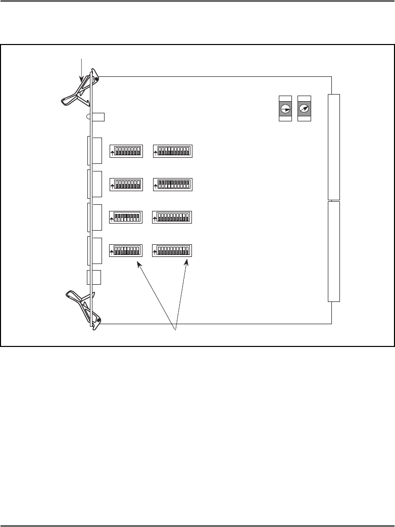
Page 406 of 906 NT6D80 MSDL card
553-3001-211 Standard 3.00 August 2005
Figure 85
MSDL switch setting example
S9 S10
OnesTens
Port 0
Port 1
Port 2
Port 3
Monitor
Port
LED
S1
S2
S3
S4
S5
S6
S7
S8
ON
ON
ON
ON
ON
ON
ON
ON
Care Locking Device
Card Address Select Switches
I/O Port Interface Configuration DIP Switches
Setting for an RS-232 interface
DTE/DCE are software configured
Setting for an RS-422 DTE interface
Setting for an RS-422 DCE interface
Setting for an RS-232 interface
DTE/DCE are software configured
DCE DTE
DCE DTE
DCE DTE
DCE DTE
553-5434

NT6D80 MSDL card Page 407 of 906
Circuit Card Description and Installation
Installing the MSDL card
Procedure 16
Installing the MSDL card
To install an MSDL card follow these steps:
1Set Device Number S10 and S9.
2Hold the MSDL by its card-locking devices. Squeeze the tabs to unlatch
the card locking devices and lift the locking device out and away from the
card. Be careful not to touch connector pins, conductor traces, or
integrated circuits. Static discharge may damage integrated circuits.
3Insert the MSDL card into the selected card slot of the module following
the card guides in the module.
4Slide the MSDL into the module until it engages the backplane connector.
5Push the MSDL firmly into the connector using the locking devices as
levers by pushing them toward the card’s front panel.
6Push the card-locking devices firmly against the front panel of the card so
they latch to the front lip in the module and to the post on the card.
7Observe the red LED on the MSDL faceplate. If it turns on, flashes three
times, and stays on continuously, the MSDL is operating correctly but is
not yet enabled. Go to step 7.
8If the LED turns on and stays on continuously without flashing three times,
the card may be defective. Go to steps 8 and 9.
9Connect the cables. The installation is complete.
10 Unplug the MSDL card and reinsert it. If the red LED still does not flash
three times, leave the card installed for approximately 10 minutes to allow
the card to be initialized.
11 After 10 minutes unplug the card and reinsert it. If the card still does not
flash three times, the card is defective and must be replaced.
End of Procedure

Page 408 of 906 NT6D80 MSDL card
553-3001-211 Standard 3.00 August 2005
Cable requirements
The MSDL card includes four high-density 26-pin (SCSI II) female
connectors for ports and one 8-pin miniature DIN connector for the monitor
port. See Figure 86 on page 409 for a diagram of the MSDL cabling
configuration.
A D-Channel on the MSDL requires a connection from the appropriate
MSDL port connector to the DCH connector located on the ISDN PRI trunk
faceplate.
Other operations on the MSDL are connected to external devices such as
terminals and modems. To complete one of these connections, connect the
appropriate I/O connector on the MSDL to a connector on the I/O panel at the
back of the module where the MSDL is installed. If a terminal is connected
to the regular SDI port, use 8 bit, VT100 terminal emulation. If the terminal
is connected to the SDI/STA port with line mode editing, use 8 bit, VT220
terminal emulation.
To determine the type and number of cables required to connect to MSDL
cards, you must determine the type of operation you wish to run and select the
appropriate cable to connect the operation to the MSDL port. Different types
of cables, as described in Table 155 on page 410, connect the MSDL port to
a device:
• NTND26, used to connect the MSDL port to the ISDN PRI trunk
connector J5, for DCH
• QCAD328, when cabling between two different columns, that is, I/O to
I/O (when MSDL is in one row and QPC720 is in another row)
• NTND98AA (J5 of QPC720 to I/O panel)
• NTND27, used to connect the MSDL port to the I/O panel at the rear of
the module, for other interface functions
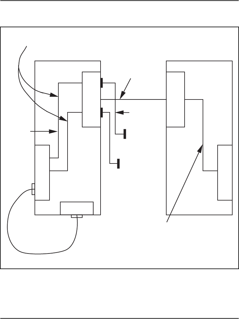
NT6D80 MSDL card Page 409 of 906
Circuit Card Description and Installation
Figure 86
MSDL cabling
I/O
panel
I/O
panel
Q
P
C
7
2
0
M
S
D
L
ESDI to I/O cable
(NTND27AB—6 ft.)
RS-232 shielded
(QCAD328—
35 ft. max.)
NTND27
ISL
APL applications
(RS-232 cable)
SDI to terminal
cable
PRI to I/O panel cable
(NTND98AA)
NTND25AA—6 ft.
NTND26AB—18 ft.
NTND26AC—35 ft.
NTND26AD—50 ft.
ISL/PRI
720
553-5845

Page 410 of 906 NT6D80 MSDL card
553-3001-211 Standard 3.00 August 2005
Note: The choices of cable to use with an MSDL card depend on what
type of modem is connected. For example, the NTND27 cable is used
when the modem has a DB25 connection. If the modem is v.35, a
customized or external vendor cable is required.
Cable installation
When the MSDL card is installed, connect the cables to the equipment
required for the selected operation.
PRI trunk connections
D-channel operations require connections between the MSDL and a PRI
trunk card. Refer to Meridian Link ISDN/AP General Guide (553-2901-100)
for a complete discussion of PRI and D-channels.
Procedure 17
Cabling the MSDL card to the PRI card
The following steps explain the procedure for cable connection:
1Identify the MSDL and the PRI cards to be linked.
2Select the appropriate length cable for the distance between the MSDL
and the PRI card.
3Plug the 26-pin SCSI II male connector end of a cable into the appropriate
MSDL port.
4Route the cable through cable troughs, if necessary, to the appropriate
PRI card.
Table 155
Cable types
Function Cable type Cable length
DCH NTND26AA
NTND26AB
NTND26AC
NTND26AD
6 feet
18 feet
35 feet
50 feet
AML, ISL, SDI NTND27AB 6 feet

NT6D80 MSDL card Page 411 of 906
Circuit Card Description and Installation
5Plug the DB15 male connector end of the cable into the J5 DB15 female
connector on the PRI card.
6Secure the connections in place with their fasteners.
7Repeat steps 1 through 6 for each connection.
End of Procedure
I/O panel connections
Operations aside from PRI require cable connections to the I/O panel.
Connections between the I/O panel and Application Equipment Modules
(AEM) are described in “Application Module description,” Meridian Link
description (553-3201-110).
Procedure 18
Cabling the MSDL card to the I/O panel
The following steps explain the procedure for cable connection:
1Identify the MSDL card and the I/O panel connector to be linked.
2Using the NTND27AB cable, plug the 26-pin SCSI II male connector end
of a cable into the appropriate MSDL port.
3Route the cable to the rear of the module next to the I/O panel.
4Plug the DB25 male connector end of a cable into a DB25 female
connector at the back of the I/O panel.
5Secure cable connectors in place with their fasteners.
6Repeat steps 1 through 5 for each connection.
End of Procedure
Page 412 of 906 NT6D80 MSDL card
553-3001-211 Standard 3.00 August 2005
MSDL planning form
Use the following planning form to help sort and store information
concerning the MSDL cards in your system as shown in the sample. Record
switch settings for unequipped ports as well as for equipped ports.
MSDL data form
Device no. Shelf Slot Card ID Boot Code
version
Date installed Last update
Ports Operation Logical no. Switch setting Cable no. Operation information
0
1
2
3
Sample
Device no.
13
Shelf
3
Slot
5
Card ID
NT6D80AA-110046
Boot
Code
version
004
Date installed
2/1/93
Last update
5/5/93
Ports Operation Logical no. Switch setting Cable no. Operation
information
0TTY 13 RS-232 DCE NTND27AB maint TTY 9600
baud
1DCH 25 RS-422 DTE NTND26AB PRI 27 to hdqtrs
2AML 3RS-232 DCE NTND27AB Meridian Mail
3Spare RS-232

NT6D80 MSDL card Page 413 of 906
Circuit Card Description and Installation
Maintenance
Routine maintenance consists of enabling and disabling MSDL cards and
downloading new versions of peripheral software. These activities are
performed by an authorized person such as a system administrator.
Troubleshooting the MSDL consists of determining problem types, isolating
problem sources, and solving the problem. A craftsperson normally performs
these activities.
CS 1000S, CS 1000M, and Meridian 1 systems have self-diagnostic
indicators as well as software and hardware tools. These diagnostic facilities
simplify MSDL troubleshooting and reduce mean-time-to-repair (MTTR).
For complete information concerning system maintenance, refer to
Communication Server 1000M and Meridian 1: Large System Maintenance
(553-3021-500).
For complete information regarding software maintenance programs, refer to
Software Input/Output: Administration (553-3001-311).
MSDL states
MSDL states are controlled manually by maintenance programs or
automatically by the system. Figure 87 on page 414 shows MSDL states and
the transitions among them. These are the three states the MSDL may be in:
• Manually disabled
• Enabled
• System disabled
The following sections describe the relationships between these states.
Manually disabled
In this state, the MSDL is not active. The system does not attempt to
communicate or attempt any automatic maintenance on the MSDL.
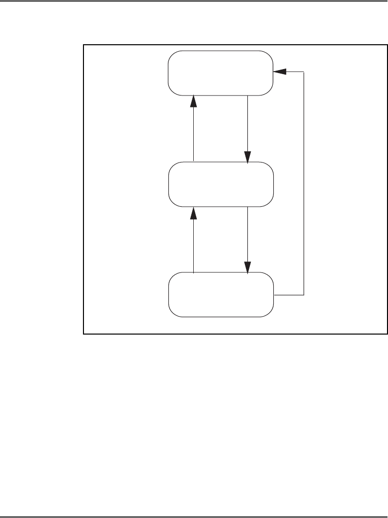
Page 414 of 906 NT6D80 MSDL card
553-3001-211 Standard 3.00 August 2005
A newly configured MSDL automatically enters the manually disabled state.
An operating MSDL can be manually disabled by issuing the DIS MSDL x
command in LD 37 (step 1 in Figure 87).
Entering the DIS MSDL x command in LD 37 moves the card to manually
disabled status and stops all system communication with the card (step 5 in
Figure 87).
Manually enabled
When the card has been manually disabled, re-enable it with the ENL MSDL
x command in LD 37 (step 2 in Figure 87).
Figure 87
MSDL states
Manually disabled
Enabled
12
34
5
System disabled
553-5435

NT6D80 MSDL card Page 415 of 906
Circuit Card Description and Installation
System disabled
When the system disables the MSDL card (step 4 in Figure 87 on page 414),
it continues to communicate and attempt maintenance procedures on the card.
To stop all system communication with the card, enter DIS MSDL x to disable
it (step 5 in Figure 87 on page 414). Otherwise, the system periodically tries
to enable the card, attempting recovery during the midnight routines (step 3
in Figure 87 on page 414).
The system disables the MSDL if the card:
• exhibits an overload condition
• does not respond to system messages
• is removed
• resets itself
• encounters a fatal error
• is frequently system disabled and recovered
When an MSDL is system disabled, a substate indicates why the MSDL is
disabled. The substates are:
•Not Responding The system cannot communicate with the MSDL.
•Self-Testing The MSDL card is performing self-tests.
•Self-tests Passed The MSDL card successfully completed self-tests and
the system is determining if download is required or the software
downloading is complete.
•Self-tests Failed The MSDL card self-tests failed.
•Shared RAM Tests Failed The system failed to read/write to the MSDL
shared RAM.
•Overload The system received an excessive number of messages within
a specified time period.
•Reset Threshold The system detected more than four resets within
10 minutes.
•Fatal Error The MSDL card encountered a fatal condition from which
it cannot recover.

Page 416 of 906 NT6D80 MSDL card
553-3001-211 Standard 3.00 August 2005
•Recovery Threshold The MSDL card was successfully enabled by the
MSDL autorecovery function five times within 30 minutes. Each time it
was system disabled because of a problem encountered during operation.
•Bootloading The MSDL base software is in the process of being
downloaded to the MSDL.
Detailed information on system disabled substates and the action required for
each substate appears in “Symptoms and actions” on page 422.
Maintaining the MSDL
The system controls automatic MSDL maintenance functions. A craftsperson
or system administrator performs manual maintenance by changing the card
status, downloading new versions of peripheral software, or invoking
self-tests.
System controlled maintenance
Built-in diagnostic functions constantly monitor and analyze the system and
individual card, performing the following operations:
• using autorecovery to automatically correct a temporarily faulty
condition and maintain the system and its components
• printing information and error messages to indicate abnormal conditions
that caused a temporary or an unrecoverable error
During system initialization, the system examines the MSDL base code. If the
base code needs to be downloaded, the CPU resets the MSDL card and starts
downloading immediately following initialization. At the same time, all other
MSDL peripheral software programs are checked and, if they do not
correspond to the system disk versions, the correct ones are downloaded to
the card.
If manual intervention is required during initialization or operation,
information and error messages appear on the console or the system TTY to
suggest the appropriate action. For a complete discussion of the information
and error messages, refer to Software Input/Output: Administration
(553-3001-311). Detailed information of system disabled substates and the
action required for each substate is found at the end of this document.

NT6D80 MSDL card Page 417 of 906
Circuit Card Description and Installation
Manually controlled maintenance
Use manual maintenance commands found in the following programs to
enable, disable, reset, get the status of, and perform self-tests on the MSDL
card:
• Input/Output Diagnostic Program LD 37
•Program LD42
• Link Diagnostic Program LD 48
• PRI D-channel Diagnostic Program LD 96
For a complete discussion of these programs, refer to Software Input/Output:
Administration (553-3001-311).
Note 1: Enter commands after the dot (.) prompt.
Note 2: The “x” in the commands below represents the DNUM value of
the card number.
Enabling the MSDL
Enter ENL MSDL x to enable the MSDL manually. If the MSDL base code
has not been previously downloaded or if the card version is different from
the one on the system disk, the software is downloaded and the card is
enabled.
To force software download and enable the card, enter ENL MSDL x FDL.
This command forces the download of the MSDL base code and the
configured peripheral software even if it is already resident on the card. The
card is then enabled.
To enable a disabled MSDL and its ports, enter ENL MSDL x ALL. This
command downloads all peripheral software (if required) and enables any
configured ports on the card. This command can be issued to enable some
manually disabled ports on an already enabled MSDL.

Page 418 of 906 NT6D80 MSDL card
553-3001-211 Standard 3.00 August 2005
Disabling the MSDL
To disable an MSDL card, enter DIS MSDL x.
To disable the MSDL and all its ports, enter DIS MSDL x ALL.
Resetting the MSDL
To reset an MSDL and initiate a limited self-test, the MSDL must be in a
manually disabled state. To perform the reset, enter RST MSDL x.
Displaying MSDL status
To display the status of all MSDL cards, enter STAT MSDL.
To display the status of a specific MSDL, enter STAT MSDL x. The status of
the MSDL, its ports, and the operation of each port appears.
The command STAT MSDL x FULL displays all information about an MSDL
(card ID, bootload firmware version, base code version, base code state,
operation state, date of base code activation) as well as the version, state, and
activation date for each card operation.
Self-testing the MSDL
To perform extensive self-testing of an MSDL, enter SLFT MSDL x. This test
can be activated if the card is in the manually disabled state. If the test passes,
the system outputs the card ID and a pass message. If it fails, the system
displays a message indicating which test failed.

NT6D80 MSDL card Page 419 of 906
Circuit Card Description and Installation
Manually isolating and correcting faults
Problems are due to configuration errors that occur during installation or
hardware faults resulting from component failure during operation. See
“Symptoms and actions” on page 422 for more information on problem
symptoms and required responses.
Isolate MSDL faults using the diagnostic tools described below:
1Observe and list the problem symptoms; for example, a typical symptom
is a permanently lit LED.
2If the LED flashes three times but the card does not enable, verify that
the card is installed in a proper slot.
3Check that the address is unique; no other card in the system can be
physically set to the same device number as the MSDL.
4If installation is correct and no address conflict exists, refer to “Newly
installed MSDL cards” on page 419 or “Previously operating MSDL
cards” on page 420.
5If the MSDL still does not operate correctly, contact your Nortel
representative.
Newly installed MSDL cards
Problems that occur during MSDL card installation usually result from
improperly installed, incorrectly addressed, or faulty cards.
If the LED on a newly installed MSDL does not flash three times after
insertion, wait 5 minutes, then remove and reinsert. If the LED still does not
flash three times, the card is faulty.

Page 420 of 906 NT6D80 MSDL card
553-3001-211 Standard 3.00 August 2005
Previously operating MSDL cards
Problems that occur during normal operation usually result from faulty cards.
Follow these steps to evaluate the situation:
1Use the STAT MSDL x command to check MSDL card status. See
“Displaying MSDL status” on page 418.
2If the card has been manually disabled, try to enable it using
ENL MSDL x. See “Enabling the MSDL” on page 417. If this fails,
perform self-testing as described in step 4.
3If the card has been disabled by the system, disable it manually with
DIS MSDL x. See “Disabling the MSDL” on page 418.
4Invoke self-testing with the SLFT MSDL x command. See “Self-testing
the MSDL” on page 418. If self-tests fail, replace the card. If self-tests
pass, try to enable the card again, as in step 2. If the card does not enable,
note the message output to the TTY and follow the recommended action.

NT6D80 MSDL card Page 421 of 906
Circuit Card Description and Installation
Replacing MSDL cards
After completing MSDL troubleshooting you may determine that one or more
MSDL cards are defective. Remove the defective cards and replace them with
new ones.
Procedure 19
Replacing an MSDL card
An MSDL card can be removed from and inserted into a system module
without turning off the power to the module. Follow these steps:
1Log in on the maintenance terminal.
2At the > prompt, type LD 37 (you can also use LD 42, LD 48, or LD 96)
and press Enter.
3Type DIS MSDL x ALL and press Enter to disable the MSDL and any
active operations running on one or more of its ports. The MSDL card is
now disabled.
4Disconnect the cables from the MSDL faceplate connectors.
5Unlatch the card-locking devices, and remove the card from the module.
6Set the switches on the replacement card to match those on the defective
card.
7Insert the replacement card into the same card slot.
8Observe the red LED on the front panel during self-test. If it flashes three
times and stays on, it has passed the test. Go to step 8.
9If it does not flash three times and then stay on, it has failed the test. Pull
the MSDL partially out of the module and reinsert it firmly into the module.
If the problem persists, troubleshoot or replace the MSDL.
10 Connect the cables to the MSDL faceplate connectors.
11 At the . prompt in the LD 37 program, type ENL MSDL x ALL and press
Enter to enable the MSDL and its operations. If the red LED on the MSDL
turns off, the MSDL is functioning correctly. Since self-tests were not
invoked, no result message appears.
12 Tag the defective card(s) with a description of the problem and return
them to your Nortel representative.
End of Procedure

Page 422 of 906 NT6D80 MSDL card
553-3001-211 Standard 3.00 August 2005
Symptoms and actions
Explained here are some of the symptoms, diagnoses, and actions required to
resolve MSDL card problems. Contact your Nortel representative for further
assistance.
These explain the causes of problems and the actions needed to return the card
to an enabled state following installation or operational problems.
Symptom: The LED on the MSDL card is steadily lit.
Diagnosis: The MSDL card is disabled or faulty.
Action: Refer to “Manually isolating and correcting faults” on page 419.
or
Diagnosis: Peripheral software download failed because of MSDL card
or system disk failure.
Action: If only one MSDL card has its LED lit, replace it.
Symptom: Autorecovery is activated every 30 seconds to enable the MSDL.
MSDL300 messages appear on the console or TTY.
Diagnosis: The MSDL card has been system disabled because of an
incorrect address.
Action: Verify the switch settings.
or
Diagnosis: The MSDL card has been system disabled because of
peripheral software or configuration errors.
Action: Refer to “System disabled actions” on page 423.

NT6D80 MSDL card Page 423 of 906
Circuit Card Description and Installation
System disabled actions
These explain the causes of problems and the actions needed to return the card
to an enabled state following system disabling.
SYSTEM DISABLED—NOT RESPONDING
Cause: The MSDL card is not installed or is unable to respond to the
messages from the system.
Action:
Check the MSDL messages on the console and take the action
recommended. Refer to Software Input/Output: Administration
(553-3001-311).
Verify that the address switches on the MSDL are set correctly.
Verify that the card is properly installed in the shelf for at least 5
minutes.
If the problem persists, manually disable the card by entering the
DIS MSDL x. Follow the steps described in “Previously operating
MSDL cards” on page 420.
SYSTEM DISABLED—SELF-TESTING
Cause: The MSDL card has reset itself or the system has reset the card
to perform self-tests. Self-tests are in progress.
Action:
Wait until self-tests are completed. Under some circumstances, the
self-tests may take up to 6 minutes to complete.
Take the action described in the appropriate section below
(“SYSTEM DISABLED—SELF-TESTS PASSED” or “SYSTEM
DISABLED—SELF-TESTS FAILED”).
SYSTEM DISABLED—SELF-TESTS PASSED
Cause: The MSDL card passed self-tests. The system will automatically
download the MSDL base code, if needed, and attempt to enable the card

Page 424 of 906 NT6D80 MSDL card
553-3001-211 Standard 3.00 August 2005
using autorecovery. If a diagnostic program (overlay) is active, the
downloading of the MSDL base code occurs later.
Action:
Wait to see if the system will enable the card immediately. If the
MSDL is enabled, no further action is necessary.
If the MSDL base code download fails five times, autorecovery
stops. The following appears in response to the STAT MSDL x
command;
Error messages will usually indicate the problem in this case. See
“Maintaining the MSDL” on page 416.
SYSTEM DISABLED—SELF-TESTS FAILED
Cause: The card did not pass self-tests. These tests repeat five times. If
unsuccessful, autorecovery stops until midnight unless you take action.
Action:
Allow the system to repeat the self-tests.
If self-tests fail repeatedly, disable the card using the DIS MSDL x
command and replace the card.
SYSTEM DISABLED—SRAM TESTS FAILED
Cause: After self-tests passed, the system attempted to perform read/
write tests to the shared RAM on the MSDL and detected a fault. The
shared RAM test will be repeated five times, and, if unsuccessful,
autorecovery will not resume until midnight unless you take action.
Action:
Allow the system to repeat the self-tests.
If self-tests fail repeatedly, disable the card using the DIS MSDL x
command and replace the card.
MSDL 10: SYS DSBL—SELFTEST PASSED
NO RECOVERY UNTIL MIDNIGHT: FAILED BASE DNLD 5
TIMES
SDI 10 DIS PORT 0
AML 11 DIS PORT 1
DCH 12 DIS PORT 2
AML 13 DIS PORT 3

NT6D80 MSDL card Page 425 of 906
Circuit Card Description and Installation
SYSTEM DISABLED—OVERLOAD
Cause: The system received an excessive number of messages from the
MSDL card in a certain time. If the card invokes overload four times in
30 minutes, it exceeds the recovery threshold as described in “SYSTEM
DISABLED—RECOVERY THRESHOLD.” The system resets the
card, invokes self-tests, and attempts to enable the card. The problem
may be due to excessive traffic on one or more MSDL ports. Traffic load
redistribution may resolve this condition.
Action:
Check the traffic report, which may indicate that one or more MSDL
ports are handling excessive traffic.
By disabling each port, identify the port with too much traffic and
allow the remaining ports to operate normally. Refer to
“Maintaining the MSDL” on page 416. If the problem persists, place
the card in the manually disabled state by the DIS MSDL x command
and follow the steps in “Previously operating MSDL cards” on
page 420.
SYSTEM DISABLED—RESET THRESHOLD
Cause: The system detected more than four MSDL card resets within 10
minutes. The system attempts to enable the card again at midnight unless
you intervene.
Action:
Place the card in the manually disabled state with the DIS MSDL x
command and follow the steps in “Previously operating MSDL
cards” on page 420.

Page 426 of 906 NT6D80 MSDL card
553-3001-211 Standard 3.00 August 2005
SYSTEM DISABLED—FATAL ERROR
Cause: The MSDL card encountered a fatal error and cannot recover.
The exact reason for the fatal error is shown in the MSDL300 error
message output to the console of TTY when the error occurred.
Action:
Check the MSDL300 message to find out the reason.
Alternatively, display the status of the MSDL, which also indicates
the cause of the problem, with the STAT MSDL x command and
check the information to find the cause of the fatal error.
Allow the system to attempt recovery. If this fails, either by reaching
a threshold or detecting self-test failure, place the MSDL in the
manually disabled state with the DIS MSDL x command and follow
the steps in “Previously operating MSDL cards” on page 420.
SYSTEM DISABLED—RECOVERY THRESHOLD
Cause: The system attempted autorecovery of the MSDL card more than
five times within 30 minutes and each time the card was disabled again.
The system attempts to enable the card again at midnight unless you
intervene.
Action:
Place the MSDL card in a manually disabled state with the DIS
MSDL x command and follow the steps in “Previously operating
MSDL cards” on page 420.

Page 427 of 906
Circuit Card Description and Installation
526
NT7D16 Data Access card
Content list
The following are the topics in this section:
Introduction . . . . . . . . . . . . . . . . . . . . . . . . . . . . . . . . . . . . . . . . . . . . . . 428
Features . . . . . . . . . . . . . . . . . . . . . . . . . . . . . . . . . . . . . . . . . . . . . . . . . 428
Controls and indicators . . . . . . . . . . . . . . . . . . . . . . . . . . . . . . . . . . . . . 429
Dialing operations . . . . . . . . . . . . . . . . . . . . . . . . . . . . . . . . . . . . . . . . . 430
Operating modes . . . . . . . . . . . . . . . . . . . . . . . . . . . . . . . . . . . . . . . . . . 435
Keyboard dialing. . . . . . . . . . . . . . . . . . . . . . . . . . . . . . . . . . . . . . . . . . 472
Hayes dialing. . . . . . . . . . . . . . . . . . . . . . . . . . . . . . . . . . . . . . . . . . . . . 485
Specifications . . . . . . . . . . . . . . . . . . . . . . . . . . . . . . . . . . . . . . . . . . . . 497
System database requirements . . . . . . . . . . . . . . . . . . . . . . . . . . . . . . . 500
Power supply . . . . . . . . . . . . . . . . . . . . . . . . . . . . . . . . . . . . . . . . . . . . . 504
Installing the Data Access card . . . . . . . . . . . . . . . . . . . . . . . . . . . . . . . 505
Port configuration . . . . . . . . . . . . . . . . . . . . . . . . . . . . . . . . . . . . . . . . . 507
Cabling . . . . . . . . . . . . . . . . . . . . . . . . . . . . . . . . . . . . . . . . . . . . . . . . . 509
Backplane pinout and signaling . . . . . . . . . . . . . . . . . . . . . . . . . . . . . . 514
Configuring the Data Access card. . . . . . . . . . . . . . . . . . . . . . . . . . . . . 517
Connecting Apple Macintosh to the DAC . . . . . . . . . . . . . . . . . . . . . . 522
Upgrading systems . . . . . . . . . . . . . . . . . . . . . . . . . . . . . . . . . . . . . . . . 522

Page 428 of 906 NT7D16 Data Access card
553-3001-211 Standard 3.00 August 2005
Introduction
The NT7D16 Data Access card (DAC) is a data interface card that integrates
the functionality of the QPC723A RS-232 4-Port Interface Line card (RILC)
and the QPC430 Asynchronous Interface Line card (AILC). This
combination allows the NT7D16 DAC to work with the RS-232-C interface,
the RS-422 interface, or both.
The DAC supports up to six ports, each capable of operating in RS-232-C or
RS-422 mode. Each port supports its own parameters that, once configured
and stored in the system database memory, are downloaded to the card.
You can install this card in any IPE slot.
Features
Light Emitting Diodes (LEDs) indicate the status of the card, the call
connection, and the mode (RS-232-C or RS-422) the DAC is operating in. A
push-button toggle switch allows you to scan all six ports and monitor the
activity on each port.
The DAC supports the following features:
• Asynchronous and full duplex operation
• Keyboard dialing
• Hayes dialing
• Data terminal equipment (DTE)/data communication equipment (DCE)
mode selection
• Modem and gateway connectivity in DTE mode
• Terminal and host connectivity in DCE mode
• Forced or normal DTR
• Hotline
• Remote and local loopback testing
• Virtual leased line mode
• Inactivity timeout

NT7D16 Data Access card Page 429 of 906
Circuit Card Description and Installation
• Wire test mode
• Self diagnostics
• Inbound modem pooling with any asynchronous modems
• Outbound modem pooling using “dumb” modems
• Outbound modem pooling using auto dialing modems
Controls and indicators
The LEDs on the DAC faceplate indicate the status mode for each port.
Figure 88 on page 431 shows the NT7D16 DAC faceplate.
Card status
The LED at the top of the faceplate is unlabeled. This LED is:
• off: if one or more ports are enabled
• on: if all ports are disabled
Electronic Industries Association signal monitors
The six LEDs located below the card status LED are labeled SD, RD, DTR,
DSR, DCD, and RI. They show the dynamic state of the associated Electronic
Industries Association (EIA) control leads for a specific port (as shown by the
display). When in RS-422 mode, only SD and RD are utilized. When in
RS-232-C mode, the LED goes on to indicate that the signal is asserted on, or
off to indicate that the signal is asserted off. When the LED is off, there is no
active voltage on the signal lead.
CONNECT
This lamp lights to indicate that a data call is established for the port
displayed. A data call is connected when the data module-to-data module
protocol messages are successfully exchanged between the two ends.

Page 430 of 906 NT7D16 Data Access card
553-3001-211 Standard 3.00 August 2005
Port mode
This lamp lights to indicate that the port indicated is in RS-422 mode. If the
lamp is dark, the specified port is in RS-232-C mode.
Port number
The number displayed specifies the port driving the EIA signal LEDs
mentioned above. The push-button switch below the display allows you to
rotate among the six ports to monitor the activity of any port. This display is
also used to monitor several error conditions.
Port select button
This push-button switch below the display is used to select which port is
monitored.
Wire test
These switches are used to select the wire test mode for each of the six ports.
Dialing operations
The DAC supports both keyboard and Hayes dialing sequences. The
following discussion concerns features common to both dialing modes.
Port firmware in idle state
The port firmware is considered idle when it is expecting one of the allowed
autobaud characters. The idle state is identified by either of the following
conditions:
• The last prompt received was RELEASED (keyboard dialing).
• The last prompt received was OK, NO CARRIER, or ERROR (Hayes
dialing).

Page 432 of 906 NT7D16 Data Access card
553-3001-211 Standard 3.00 August 2005
Call Set-up abort
The user may abandon the call during the dialogue phase using one of the
following methods:
•Terminal off-line This method is useful for RS-232-C interface only.
The equipment drops Data Terminal Ready (DTR) to indicate an idle
connection. For example, if the equipment is turned off, the DAC
interprets that signal as an idle connection.
•Long break The user sends a break (transmit line held in the OFF or
SPACE state) for more than 1.2 seconds. The break is not transmitted to
the far end. At the end of the long break, the DAC port initiates call
disconnect. The AILU converts the dropping of DTR into a long break
for the RS-422 interface. The long break feature can be disabled through
the Modify menu on the DAC port.
•Three short breaks When the user equipment transmits three breaks to
the far end, the DAC abandons the call. Note that the breaks must be
spaced at least 10 msec apart, and all three must occur within 3 seconds.
Make Port Busy on loss of DTR
This feature is implemented by means of the Make Set Busy (MSB) station
feature. When this is activated, any attempt to reach the specified Data DN
will result in a busy signal.
This application, which operates only in the RS-232-C mode, requires a
non-standard RS-232-C interface. Only two of the possible sixteen RS-232-C
modes can be used: Mode 8 (DCE, Host, Normal DTR, Manual dial), and
Mode 12 (DCE, Terminal, Normal DTR, Manual dial). This feature is
configured in the software, and is downloaded to the DAC.
A DTR timeout period is started whenever the DTR signal lead makes the
transition to OFF. If DTR is returned to ON within the set time period
(5 seconds), the DAC port operates as if this feature was not activated. If the
DTR remains OFF beyond the 5 seconds, the system receives an MSB feature
key message. The DAC sends another MSB message when the DTR returns
to ON, and the port is able to receive inbound calls.

NT7D16 Data Access card Page 433 of 906
Circuit Card Description and Installation
Note: If this feature is active, and the port is connected to a DTE that
holds DTR OFF when idle, the port will be permanently busied out to
inbound calls following the DTR timeout period.
Inactivity timeout
Once a successful data call is completed, the user's activity is monitored. If
no activity occurs within the amount of time configured in the downloaded
parameters, the DAC releases the call. Three minutes before the inactivity
timeout takes place, the DAC sends a warning message to the near-end
equipment if terminal mode is selected.
Wire test mode
The DAC allows for the EIA signaling leads to be tested to facilitate
installation and troubleshooting. This feature can be invoked through the
service change downloaded parameters, or by setting the appropriate front
panel switch. Wire test mode only operates when the port is idle. The leads
are cycled ON and OFF in 0.5 second periods (ON for 0.5 seconds, OFF for
0.5 seconds) for the number of cycles shown in Table 156 on page 433. The
lead status can be monitored by the front panel LEDs. The test will be run
indefinitely until the front panel switch is turned off, and the software wire
test parameters are disabled.
Note: For the most accurate results, be sure no equipment is connected
to the EIA leads.
Table 156
Wire test signal leads cycle counts
Label
EIA Signal Lead
description Pin
Cycle count
RS-232-C RS-422
TxD Transmit 2 1 1
RxD Receive 3 2 2
Note: The CTS signal is not included in the faceplate LED. Therefore, a
1.5-second delay will occur between the RxD lamp going on, and the DSR
lamp going on.
Page 434 of 906 NT7D16 Data Access card
553-3001-211 Standard 3.00 August 2005
CTS Clear To Send 5 3 —
DSR Data Set Ready 6 4 —
DCD Carrier Detect 8 5 —
DTR Data Terminal Ready 20 6 —
RI Ring Indicator 22 7 —
Table 156
Wire test signal leads cycle counts
Label
EIA Signal Lead
description Pin
Cycle count
RS-232-C RS-422
Note: The CTS signal is not included in the faceplate LED. Therefore, a
1.5-second delay will occur between the RxD lamp going on, and the DSR
lamp going on.

NT7D16 Data Access card Page 435 of 906
Circuit Card Description and Installation
Independent storage of dialing parameters
Two dialing parameters, DCD control, and Answer mode, can be modified by
both keyboard and Hayes dialing commands.
The Hayes dialing mode also allows the user to modify the Input echo control,
and Prompt/Result codes transmit control. With keyboard dialing, the Input
echo control and Prompt/Response codes control are determined by the
downloaded parameters. They cannot be altered through dialing commands.
The DAC maintains separate buffers for keyboard and Hayes dialing modes.
Changes made to a given parameter in one mode do not affect that parameter
in the other mode. When a dialing mode is selected, the DAC copies the
corresponding dialing parameters into the active buffer. This buffer controls
the call processing.
If the DAC receives an incoming call while idle, the most recent dialing mode
is used to answer the call.
User input
User input may include either upper or lower case ASCII characters.
All entries are accumulated in an input record. This record is completed with
a Terminator character. For keyboard dialing, this character is always <CR>;
for Hayes dialing, it can be user defined (but default to <CR>). The entries
are not processed until the Terminator character is received.
The input record is limited to 43 characters, including the Terminator, but
excluding any ignored space characters.
The record can be edited by using the backspace and escape characters.
Operating modes
There are sixteen possible RS-232-C operating modes with three basic
common modes of operation which correspond to three types of equipment
connected to the DAC. The three modes are: modem, terminal, and host. Host
mode is a subset of the terminal mode, which only suppresses the prompts at
the terminal.

Page 436 of 906 NT7D16 Data Access card
553-3001-211 Standard 3.00 August 2005
The fourth mode, gateway, is a subset of the modem mode and is not normally
used. This mode is useful if the attached modems do not have Ring Indicator
lead. The application used is inbound modem pooling.
The different modes enable the DAC to connect to different types of devices
such as modems (modes 0, 1, 2, and 3), gateways (modes 4, 5. 6, and 7), hosts
(modes 8. 9. 10, and 11), and terminals (modes 12. 13. 14, and 15). After
selecting the appropriate group (that is, modem, gateway, host, or terminal),
the installer should study the four different modes in that group to make the
proper selection. See Table 157.
Table 157
DAC mode of operation selection (Part 1 of 5)
Service changeable downloadable parameters (LD 11)
Operation
mode
Modem/
Gateway/
Host/KBD
Forced
DTR* Hotline
Type of device
to be connected Group selection
DEM PRM DTR HOT
0 (DTE) OFF
“Host On”
(Ring
Indicator
— RI)
OFF
Not
Forced
OFF
Not
Hotline
Modem Pool
inbound and
outbound (similar
to Synchronous /
Asynchronous
Data Module
(SADM) in
inbound) MSB by
RI
Modes 0, 1, 2,
and 3 are for
RS232 modem
connectivity
1 (DTE) OFF
“Host On”
(RI)
OFF
Not
Forced
ON
Hotline
Modem Pool
inbound only
(Hotline by RI-
similar to SADM)
* Not prompted for Type = R422. Defaults for Type = R422: DEM = DCE and DTR = OFF.

NT7D16 Data Access card Page 437 of 906
Circuit Card Description and Installation
2 (DTE) OFF
“Host On”
(RI)
ON
Forced
OFF
Not
Hotline
Modem Pool
inbound and
outbound (for
Hayes 1200
modem) MSB by RI
3 (DTE) OFF
“Host On”
(RI)
ON
Forced
ON
Hotline
Modem Pool
inbound only
(Hotline for Hayes
1200 modem only)
4 (DTE) ON
“Keyboard
Dialing
(KBD) On”
(No RI)
OFF
Not
Forced
OFF
Not
Hotline
Gateway inbound
and outbound
(DTR is OFF in idle
state) MSB by
Carrier Detect
(DCD)
Modes 4, 5, 6,
and 7 are for
RS232 Gateway
connectivity
5 (DTE) ON
“KBD On”
(No RI)
OFF
Not
Forced
ON
Hotline
Gateway inbound
only (Hotline by
DCD: ON for
Hotline
OFF for Virtual
Leased Line (VLL)
Table 157
DAC mode of operation selection (Part 2 of 5)
Service changeable downloadable parameters (LD 11)
Operation
mode
Modem/
Gateway/
Host/KBD
Forced
DTR* Hotline
Type of device
to be connected Group selection
DEM PRM DTR HOT
* Not prompted for Type = R422. Defaults for Type = R422: DEM = DCE and DTR = OFF.

Page 438 of 906 NT7D16 Data Access card
553-3001-211 Standard 3.00 August 2005
6 (DTE) ON
“KBD On”
(No RI)
ON
Forced
OFF
Not
Hotline
Gateway inbound
and outbound
(DTR is on in idle
state)
MSB by DCD
7 (DTE) ON
“KBD On”
(No RI)
ON
Forced
ON
Hotline
Gateway inbound
only (Hotline by
DCD:
ON for Hotline
OFF for VLL)
(DTR is ON in idle
state)
8 (DCE) OFF
“Host On”
(prompts
off)
OFF
Not
Forced
OFF
Not
Hotline
Outbound to Host
(similar to Multi
Channel Data
System (MCDS))
Prompt PBDO =
OFF/ON
Modes 8 and 9
are for RS422
Host connectivity
9 (DCE) OFF
“Host On”
(prompts
off)
OFF
Not
Forced
On
Hotline
Host Hotline by
DTR
Table 157
DAC mode of operation selection (Part 3 of 5)
Service changeable downloadable parameters (LD 11)
Operation
mode
Modem/
Gateway/
Host/KBD
Forced
DTR* Hotline
Type of device
to be connected Group selection
DEM PRM DTR HOT
* Not prompted for Type = R422. Defaults for Type = R422: DEM = DCE and DTR = OFF.

NT7D16 Data Access card Page 439 of 906
Circuit Card Description and Installation
10 (DCE) OFF
“Host On”
(prompts
off)
ON
Forced
OFF
Not
Hotline
Host similar to
MCDS but does not
require DTR to be
ON
Modes 8, 9, 10,
and 11 are for
RS232 Host
connectivity
11 (DCE) OFF
“Host On”
(prompts
off)
ON
Forced
On
Hotline
Continuous Hotline
mode when DTR is
ON (VLL)
12 (DCE) ON
“KBD On”
(prompts
on)
OFF
Not
Forced
OFF
Not
Hotline
Terminal similar to
Asynchronous/
Synchronous
Interface Module
(ASIM) when set to
Not Forced DTR
and Not Hotline
Prompt PBDO =
OFF/ON
Modes 12 and 13
are for RS422
Terminal
connectivity
13 (DCE) ON
“KBD On”
(prompts
on)
OFF
Not
Forced
On
Hotline
Terminal similar to
ASIM when set to
Not Forced DTR
and Hotline
Table 157
DAC mode of operation selection (Part 4 of 5)
Service changeable downloadable parameters (LD 11)
Operation
mode
Modem/
Gateway/
Host/KBD
Forced
DTR* Hotline
Type of device
to be connected Group selection
DEM PRM DTR HOT
* Not prompted for Type = R422. Defaults for Type = R422: DEM = DCE and DTR = OFF.

Page 440 of 906 NT7D16 Data Access card
553-3001-211 Standard 3.00 August 2005
Selecting the proper mode for Modem connectivity
Select modes 0, 1, 2, and 3 when the DAC is connected to different types of
modems for inbound and outbound modem pooling. In these modes, the DAC
operates as a DTE, monitors the DSR, DCD, and RI control leads, and drives
the DTR lead. No menus are given and no characters are echoed when DCD
is OFF. All prompts and messages are enabled for inbound calls and disabled
for outbound calls.
In modes 0 and 1, the DAC drives the DTR lead OFF when in the idle state,
and ON when processing an incoming or outgoing call.
In modes 2 and 3, the DAC drives the DTR lead ON except when the call is
being disconnected. At disconnect, DTR is dropped for 0.2 seconds and then
returns to ON.
14 (DCE) ON
“KBD On”
(prompts
on)
ON
Forced
OFF
Not
Hotline
Terminal similar to
ASIM when set to
forced DTR and
Not Hotline
Modes 12, 13, 14,
and 15 are for
RS232 Terminal
connectivity
(similar to ASIM)
15 (DCE) ON
“KBD On”
(prompts
on)
ON
Forced
On
Hotline
Continuous Hotline
when DTR is ON
Table 157
DAC mode of operation selection (Part 5 of 5)
Service changeable downloadable parameters (LD 11)
Operation
mode
Modem/
Gateway/
Host/KBD
Forced
DTR* Hotline
Type of device
to be connected Group selection
DEM PRM DTR HOT
* Not prompted for Type = R422. Defaults for Type = R422: DEM = DCE and DTR = OFF.

NT7D16 Data Access card Page 441 of 906
Circuit Card Description and Installation
In the case of outbound modem pooling, the DAC answers the data call and
drives the DTR lead ON (modes 0 and 1). Then the calling data module and
the DAC form a transparent link between the calling DTE and the modem.
The DTE user may then enter the appropriate commands to the modem for
dialing a remote modem. When the call is established, the modem may cause
the DAC to disconnect the call by dropping either DSR or DCD.
In the case of inbound modem pooling, the modem must drive the RI lead ON
to activate the DAC. Then the DAC responds by driving the DTR lead ON
and making the unit busy for outbound calls (modes 0 and 1). The modem is
expected to turn DCD to ON within 35 seconds; otherwise, the call will be
dropped by the DAC. If the modem turns DCD ON before the 35-second
timeout, the DAC validates the incoming call and prepares to accept <CR>
from the remote modem for autobaud. See Figure 89 on page 442 for more
details.
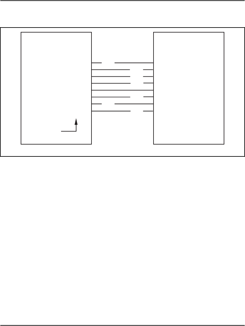
Page 442 of 906 NT7D16 Data Access card
553-3001-211 Standard 3.00 August 2005
Mode 0
This mode should be selected when the DAC is connected to a modem, except
Hayes-1200, for inbound and outbound modem pooling (see modes 2 and 3
for Hayes-1200 modem). The modem used should have the following
features:
Auto-answer capability This feature is required when the modem is used for
inbound modem pooling. It allows the modem to drive the RI lead ON when
ringing is present at its tip and ring. In addition, the modem should
auto-answer after the first ringing cycle if the DTR lead is ON (most modems
support this feature).
Dynamic control of DCD This feature must be supported by all modems to
be connected to the DAC. It allows the modem to drive the DCD lead ON
when the carrier is detected and OFF when the carrier is absent (most modems
support this feature).
Figure 89
DAC to modem connectivity
pin 2
pin 3
pin 5
pin 6
pin 7
pin 8
pin 20
pin 22
TX
RX
CTS
DSR
GND
DCD
DTR
RI
DAC (DTE) Modem (DCE)
(not required)
RS- 232 leads
>>>
<<<
<<<
<<<
<<<
<<<
>>>
553-5215

NT7D16 Data Access card Page 443 of 906
Circuit Card Description and Installation
Auto-dial capability This feature is required when the modem is used for
outbound modem pooling. It allows the modem to go off-hook and dial the
remote number (such as Smartmodem Hayes-2400 or Bizcomp).
Auto-reset capability This feature is required when the modem is used for
outbound modem pooling. The modem should execute auto-reset when the
DTR lead goes OFF. As a result, the modem must reset all its internal
parameters to the default values. This feature prevents the users of the modem
pool from modifying the modem’s default parameters to inappropriate values.
Configuring modems for mode 0
To configure Hayes modem 2400, enter the following commands:
AT&D2&W
ATVl&W
ATQ&W
ATEl&W
ATSO= 1&W
AT&Cl&Sl&W
AT&J&W
ATB1&W
AT&D3&W
Since the default parameters are programmable using commands, there is no
guarantee that users will not change them.
To configure Bizcomp 1200 modem, set the following parameters in LD11:
DEMDTE
PRMOFF
DTROFF
HOTOFF
• To configure MULTI MODEM 224E modem, set the configuration
switches as follows:
switches 3 and 8 to DOWN position
• all other switches to UP position. Switch 7 should be UP when using
RJ-11 jack.

Page 444 of 906 NT7D16 Data Access card
553-3001-211 Standard 3.00 August 2005
Programing DAC for mode 0 in service change LD11
When used for inbound or outbound Modem Pool only, the DAC can be
configured as R232 in LD11. When used for both inbound and outbound
Modem Pool, the DAC must be configured as R232; station hunting for the
outbound modem access should be in the opposite direction to the 500/2500
station hunting for the inbound modem access. See Figure 90 on page 445 for
more details.
Note: If Call Detail Recording (CDR) is required, use separate outbound
and inbound Modem Pools.
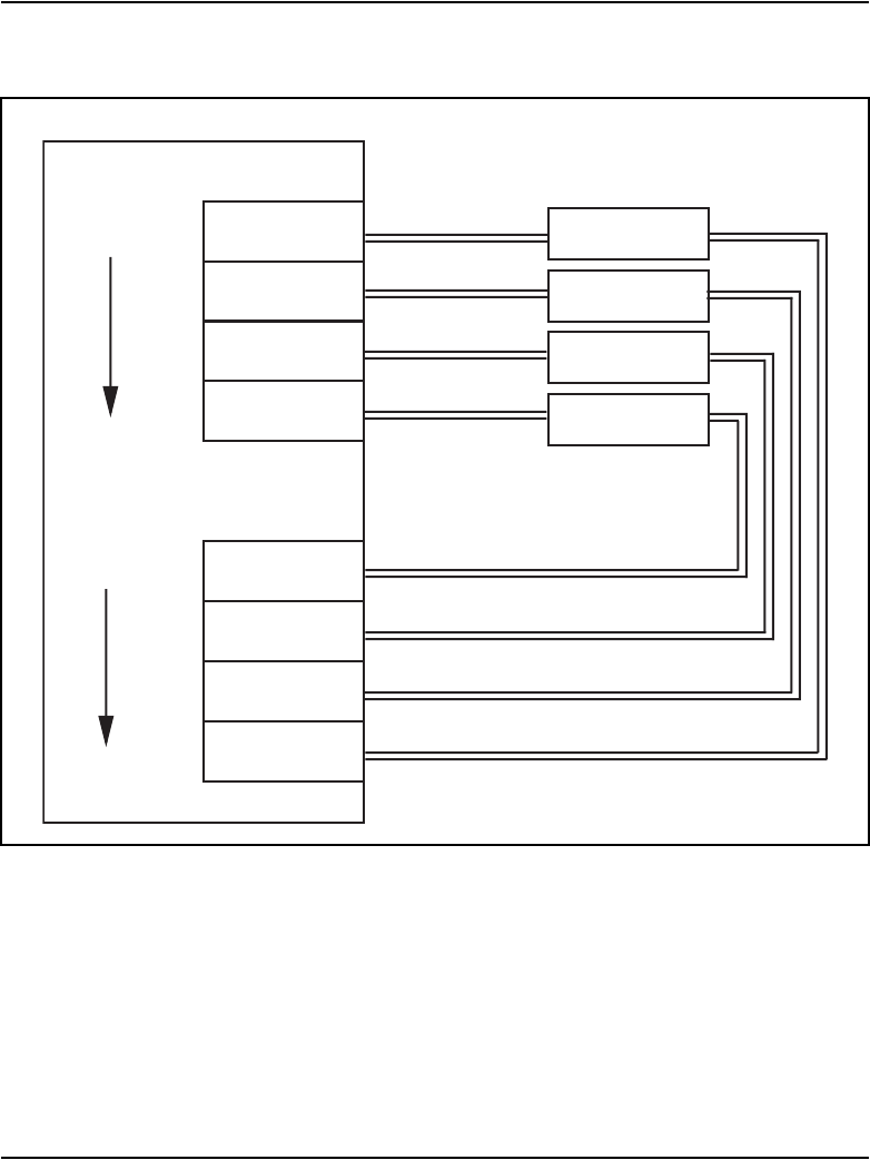

Page 446 of 906 NT7D16 Data Access card
553-3001-211 Standard 3.00 August 2005
Mode 1
This mode should be selected when the DAC is connected to an auto-answer
modem for inbound Hotline operation. In this mode, the DAC automatically
executes Hotline operation when RI is driven ON by the modem. The modem
used should have the following features:
Auto-answer capability This feature is required when the modem is used for
inbound modem pooling. It allows the modem to drive the RI lead ON when
ringing is present at its tip and ring. In addition, the modem should
auto-answer after the first ringing cycle if the DTR lead is ON (most modems
support this feature).
Dynamic control of DCD This feature must be supported by all modems to
be connected to the DAC. It allows the modem to drive the DCD lead ON
when the carrier is detected and OFF when the carrier is absent (most modems
support this feature).
The baud rate of the Hotline call is determined by switches 6 and 8, and the
system should be programmed to allow inbound modem calls only.
Configuring modems for mode 1
Most dumb modems can be configured for this mode. The modem must be
able to auto-answer and have dynamic control of DCD as described in mode
0. Smart modems can also be used if set to the dumb mode of operation.
Hayes 2400, Bizcomp 1200, and MULTI MODEM 224E can be used when
set up as follows:
• For Hayes 2400, the dumb-mode-strap should be moved to the
dumb-position (see Hayes manual).
• For Bizcomp 1200 modem, set the following parameters in LD11:
DEMDTE
PRMOFF
DTROFF
HOTON
Hayes 1200 cannot be used in this mode when the default parameters are
selected (see mode 3).

NT7D16 Data Access card Page 447 of 906
Circuit Card Description and Installation
Programing DAC for mode 1 in service change LD11
The DAC must be configured as R232 (the Autodial feature key is used for
this mode). The DAC must not be configured as an Asynchronous Data
Module (ADM) trunk.
Mode 2
This mode should be selected when the DAC is connected to a Hayes-1200
modem for inbound and outbound modem pooling. This mode is created
specially to resolve some problems that were encountered with this modem,
namely, the auto-reset implementation. When this modem is operating in the
auto-reset mode, it drives both RI and DCD ON as long as DTR is OFF. This
problem was resolved by driving DTR ON in the idle state, and OFF for 0.2
seconds, and then ON when an established call is dropped. The DAC also
ignores the status of RI and DCD for approximately 2 seconds after a call is
released to avoid false inbound call initiation.
Configuring Hayes 1200 for mode 2
To configure this modem, set the following parameters in LD11:
DEMDTE
PRMOFF
DTRON
HOTOFF
To configure this modem, set the configuration switches as follows:
• switches 3, 8, and 10 to DOWN position
• all other switches to UP position. Switch 7 should be UP when using
RJ-11 jack.
Programing DAC for mode 2 in service change LD11
When used for inbound or outbound Modem Pool only, the DAC can be
configured as R232 in LD11. When used for both inbound and outbound
Modem Pool, the DAC must be configured as R232. When the DAC is
programmed as station hunting, outbound modem access should be in the
opposite direction to the 500/2500 station hunting for the inbound modem
access.

Page 448 of 906 NT7D16 Data Access card
553-3001-211 Standard 3.00 August 2005
Note: If Call Detail Recording (CDR) is required, use separate outbound
and inbound Modem Pools.
Mode 3
This mode should be selected when the DAC is connected to a Hayes-1200
modem for inbound Hotline operation. It is recommended that mode 1 be
used for inbound Hotline operations if some other modem is available.
However, if only Hayes-1200 modems are available, then this mode could be
used as a last resort.
Configuring Hayes 1200 for mode 3
For Hayes 1200 modem, set the following parameters in LD11:
DEMDTE
PRMOFF
DTRON
HOTON
To configure this modem, set the configuration switches as follows:
• all switches to UP position, except for switch 4. Switch 7 should be UP
when using RJ-11 jack.
Programing DAC for mode 3 in service change LD11
The DAC must be configured as R232 (the Autodial feature is used for this
mode). The DAC must not be configured as an ADM trunk.
Selecting the proper mode for Gateway connectivity
Select modes 4, 5, 6, and 7 when the DAC is connected to different types of
gateways for inbound and outbound operations. The term gateway refers to
any equipment that has the following characteristics:
• The equipment must be a DCE.
• The equipment does not drive RI lead (optional, the DAC ignores this
lead).
• The equipment must drive DCD lead dynamically.
• The equipment drives DSR lead (optional).

NT7D16 Data Access card Page 449 of 906
Circuit Card Description and Installation
• The equipment can monitor the DTR lead (optional, depending on the
mode selected).
In modes 4, 5, 6, and 7, the DAC:
• operates as a DTE
• monitors the DSR
• monitors DCD control leads
• drives the DTR lead
The RI lead is ignored. No menus or prompts are given when DCD is OFF.
All prompts and messages are enabled for inbound calls and disabled for
outbound calls. See Figure 91 on page 450 for more details.
In modes 4 and 5, the DAC drives the DTR lead OFF in the idle state, and ON
when processing an incoming or outgoing call.
In modes 6 and 7, the DAC drives the DTR lead ON except when the call is
being disconnected. At disconnect, DTR is dropped for 0.2 seconds and then
returns to ON.
With outbound gateway access, the DAC answers the data call and drives the
DTR lead ON (modes 4 and 5; in modes 6 and 7, DTR is already ON). Then
the calling data module and the DAC form a transparent link between the
calling Data Module (DM) and the gateway. The DM user may then enter the
appropriate commands to the gateway to establish a data call. The DAC
expects the gateway to drive DCD ON (modes 4 and 5 only) within
35 seconds. If the gateway fails to do so, the DAC turns DTR OFF and drops
the call. When the call is established, the gateway may cause the DAC to
disconnect the call by dropping either DSR or DCD.
For inbound gateway access, the gateway must drive the DCD lead ON to
activate the DAC. When the DAC receives this signal, it drives the DTR lead
ON, makes the unit busy for outbound calls (modes 4 and 5; in modes 6 and
7, DTR is already ON), and prepares to accept <CR> for autobaud. The DAC
expects DCD to remain ON for as long as the data call is established.
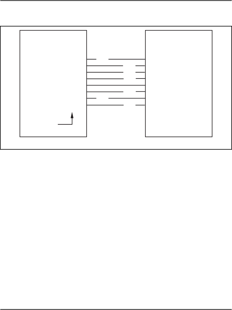
Page 450 of 906 NT7D16 Data Access card
553-3001-211 Standard 3.00 August 2005
Mode 4
This mode should be selected when the DAC is connected to a gateway for
inbound and outbound operation. The characteristics of the gateways to be
used with this mode are:
Auto-answer capability This feature is required when the gateway is used
for inbound operation. It allows the gateway to drive the DCD lead ON when
the inbound data call is pending. In addition, the gateway should auto-answer
when the DTR lead is ON.
Dynamic control of DCD This feature must be supported by all gateways to
be connected to the DAC. It allows the gateway to drive the DCD lead ON
when the data call is established, and OFF when the data call is disconnected.
In the inbound operation, the DAC drives the DTR lead OFF until the
gateway drives the DCD lead ON. Then, the DAC drives DTR ON and makes
that unit busy for any outbound calls. After that, the user of the gateway may
enter the proper commands to establish a local data call to any DM.
Figure 91
DAC to Gateway connectivity
pin 2
pin 3
pin 5
pin 6
pin 7
pin 8
pin 20
pin 22
TX
RX
CTS
DSR
GND
DCD
DTR
RI
DAC (DTE) Gateway (DCE)
(not required)
RS- 232 leads
>>>
<<<
<<<
<<<
<<<
<<<
>>>
(not required)
553-5217
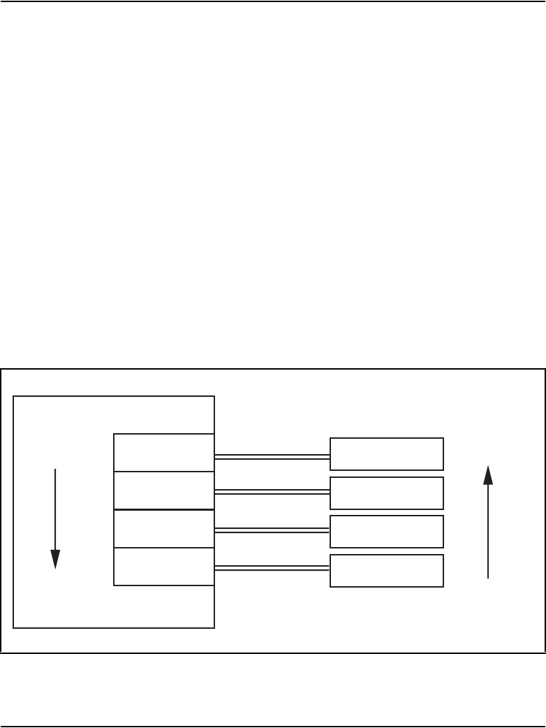
NT7D16 Data Access card Page 451 of 906
Circuit Card Description and Installation
In the outbound operation, the DAC drives the DTR lead OFF until another
DM calls it for outbound accessing. The DAC answers the data call and drives
the DTR lead ON. The calling DM is then transparently connected to the
gateway. The DAC requires the gateway to drive the DCD lead to ON within
35 seconds after the outbound call is connected. Call disconnection may be
initiated by dropping DCD (or DSR) from ON to OFF.
Programing DAC for mode 4 in service change LD 11
When used for inbound or outbound gateway access, the DAC can be
configured as R232 in LD 11. When used for both inbound and outbound
gateway access, the DAC must be configured as R232. When the DAC is
programmed as station hunting, outbound gateway access should be in the
opposite direction to the hunting for inbound gateway access. See Figure 92
for more details.
Note: If CDR is required, use separate outbound and inbound gateway
access.
Figure 92
DAC to Gateway—Inbound/Outbound connectivity
System
Outbound
hunting
DAC
R232 port 0 Gateway 1
Gateway 2
Gateway 3
Gateway 4
Inbound
hunting
553-AAA1127
R232 port 1
R232 port 2
R232 port 3

Page 452 of 906 NT7D16 Data Access card
553-3001-211 Standard 3.00 August 2005
Mode 5
This mode should be selected when the DAC is connected to an auto-answer
gateway for inbound Hotline operation. In this mode, the DAC automatically
executes Hotline operation when DCD is driven ON by the gateway. If the
DM being called by the Hotline operation is busy or not answering, the DAC
will place repeated Hotline calls as long as the DCD lead is ON until the
called unit answers. The gateway used in this mode should have the following
features:
Auto-answer capability This feature is required when the gateway is used
for inbound operation. It allows the gateway to drive the DCD lead ON when
the inbound data call is pending. In addition, the gateway should auto-answer
when the DTR lead is ON.
Dynamic control of DCD This feature must be supported by all gateways to
be connected to the DAC. It allows the gateway to drive the DCD lead ON
when the data call is established, and OFF when the data call is disconnected.
The baud rate of the Hotline call is determined by the AUTB and BAUD
parameters in LD 11. The system should be programmed to allow inbound
modem calls only.
Programing DAC for mode 5 in service change LD 11
The DAC must be configured as R232 (the Autodial feature is used for this
mode). The DAC must not be configured as an ADM trunk.
Mode 6
This mode should be selected when the DAC is connected to a gateway that
requires DTR to be ON always except during call disconnection. In this
mode, the DAC can be used for both inbound and outbound operations. The
operation of this mode is similar to mode 4 except for the following:
• The DTR lead is ON in the idle state.
• The DTR lead will be dropped OFF for 0.2 seconds when an established
call is disconnected.

NT7D16 Data Access card Page 453 of 906
Circuit Card Description and Installation
Programing DAC for mode 6 in service change LD 11
When used for inbound or outbound gateway access, the DAC can be
configured as R232 in LD 11. When used for both inbound and outbound
gateway access, the DAC must be configured as R232. When the DAC is
programmed as station hunting, outbound gateway access should be in the
opposite direction to the hunting for inbound gateway access. See Figure 92
on page 451 for more details.
Note: If CDR is required, use separate outbound and inbound gateway
access.
Mode 7
This mode should be selected when the DAC is connected to a gateway for
inbound Hotline operation. The operation of this mode is similar to mode 5
except for the following:
• The DTR lead is ON in the idle state.
• The DTR lead will be dropped OFF for 0.2 second when an established
call is disconnected.
The baud rate of inbound Hotline calls is determined by programmable
database. The system should be programmed to allow inbound calls only on
the DAC unit.
Programing DAC for mode 7 in service change LD 11
The DAC must be configured as R232 (the Autodial feature is used for this
mode). The DAC must not be configured as an ADM trunk.
Selecting the proper mode for Host connectivity
Select modes 8, 9, 10, and 11 when the DAC is connected to different types
of hosts (DTE). In these modes, the DAC operates as a DCE and drives DSR,
DCD, and RI control leads (see Figure 93 on page 454). CTS, DSR, and DCD
are driven OFF in the idle state.
The DAC will not send any menu or prompt to the host, nor will it echo any
command sent from the host. The CTS, DSR, and DCD will be driven ON
until the call is released. An incoming call to the DAC causes the RI lead to
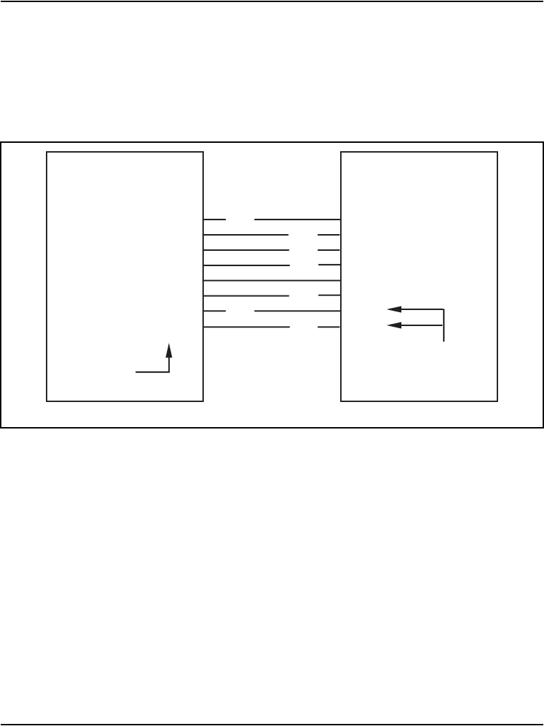
Page 454 of 906 NT7D16 Data Access card
553-3001-211 Standard 3.00 August 2005
go ON for 2 seconds and then OFF for 4 seconds until the call is answered by
the host. When the host turns DTR ON, the DAC answers the call. If
DM-to-DM protocol exchange is successful, the DAC drives CTS, DSR, and
DCD ON. If DTR was already ON, the DAC does not drive RI ON.
Mode 8
This mode should be selected when the DAC is connected to a host for host
accessing. In this mode, the DAC operates in a similar manner to the MCDS.
The hosts used with this mode should have the following characteristics:
Auto-answer capability The host should be capable of monitoring the RI
lead for detection of incoming calls. When RI is turned ON by the DAC, the
host responds by driving DTR ON, which forces the DAC to answer the
incoming call. If the host drives the DTR lead ON all the time, incoming calls
will always be immediately answered and the RI lead will not be turned ON
by the DAC. If DM-to-DM protocol exchange is successful, the DAC drives
CTS, DSR, and DCD ON.
Figure 93
DAC to Host connectivity
pin 2
pin 3
pin 5
pin 6
pin 7
pin 8
pin 20
pin 22
TX
RX
CTS
DSR
GND
DCD
DTR
RI
Host (DTE) DAC (DCE)
RS- 232 leads
>>>
<<<
<<<
<<<
<<<
<<<
>>>
not required
for mode 10
553-5219

NT7D16 Data Access card Page 455 of 906
Circuit Card Description and Installation
Dynamic control of DTR This feature is required only if the host must be
capable of releasing an established call. The host should be able to drop an
established data call by driving DTR OFF for more than 100 ms.
Note: If the PBDO parameter in LD 11 is ON, then Make Set Busy will
be activated when DTR is driven OFF for more than five seconds.
In this mode, the DAC will not send any menus or prompts to the host.
However, the host can still originate an outgoing call by blind-dialing
(sending commands to the DAC without receiving echoes).
Programing DAC for mode 8 in service change LD 11 When used for
inbound or outbound host access, the DAC can be configured as R232 or
R422 in LD 11. When used for both inbound and outbound host access, the
DAC must be configured as R232 or R422. When the DAC is programmed
as station hunting, outbound host access should be in the opposite direction
to the hunting for inbound host access.
Note: If CDR is required, use separate outbound and inbound host
access.
Mode 9
This mode should be selected when the DAC is connected to a host and
Hotline call origination is required. In this mode, the host will be able to
Hotline to a specific data unit by simply driving the DTR lead ON. The
transition of DTR from OFF to ON causes the DAC to Hotline to the Autodial
DN. The hosts used with this mode should have the following characteristics.
Dynamic control of DTR for call origination The host should be capable of
driving the DTR lead from OFF to ON to initiate the Hotline call. If the host
always drives the DTR lead ON (not capable of dynamic control), mode 11
should be used.
Dynamic control of DTR for releasing established calls This feature is
required only if it is required that the host be capable of releasing an
established call. The host should be able to drop an established data call by
driving DTR OFF for more than 100 ms.

Page 456 of 906 NT7D16 Data Access card
553-3001-211 Standard 3.00 August 2005
Programing DAC for mode 9 in service change LD 11
The DAC must be configured as R232 or R422 (the Autodial feature is used
for this mode). The DAC must not be configured as an ADM trunk.
Mode 10
This mode should be selected when the DAC is connected to a host for
inbound host accessing. The host in this mode is not required to monitor RI
or drive DTR. This mode is similar to mode 8, except for the following:
• The status of DTR lead is assumed to be always ON, even when the
actual condition of that lead is OFF (forced-DTR). The DAC always
answers an incoming call regardless of the status of DTR.
• The host cannot release an established data call by driving DTR OFF. As
a result, the host cannot initiate call release except with a long break or
three short breaks.
In this mode, the DAC does not send any menus or prompts to the host.
However, the host can still originate an outgoing call by blind-dialing
(sending commands to the DAC without receiving echoes).
Programing DAC for mode 10 in service change LD 11
When used for inbound or outbound host access, the DAC can be configured
as R232 in LD 11. When used for both inbound and outbound host access, the
DAC must be configured as R232. When the DAC is programmed as station
hunting, outbound host access should be in the opposite direction to the
hunting for inbound host access.
Note: If CDR is required, use separate outbound and inbound gateway
access.
Mode 11
This mode provides a “virtual leased line” and the meaning of the Forced
DTR switch is re-defined. The operation is similar to having a leased line
feature, where the connection between two extensions is always established.
The DAC does not send any menus or prompts to the host. The baud rate of
the Hotline call is determined by switches 6, 7, and 8.

NT7D16 Data Access card Page 457 of 906
Circuit Card Description and Installation
This mode should be selected when the DAC is connected to a host and
continuous Hotline operation is required. In this mode, the DAC repeatedly
tries to Hotline to the Autodial DN as long as DTR is ON. When the DAC
tries to Hotline to a busy Data Module, it activates Ring Again and the
connection is established as soon as the called unit is free. After establishing
the data call, if the called unit releases the call for any reason, the DAC will
automatically try to Hotline again to reestablish the call.
If the data unit being called does not answer the Hotline call, the DAC tries
to place another Hotline call once every 40 seconds until the called unit
answers. This mode is recommended only when a permanent connection
between a host and another data unit is required.
Programing DAC for mode 11 in service change LD 11
The DAC must be configured as R232 (the Autodial feature is used for this
mode). The DAC must not be configured as an ADM trunk.
Selecting the proper mode for Terminal connectivity
Select modes 12, 13, 14,and 15 when the DAC is connected to different types
of terminals. In these modes, the DAC operates as a DCE, drives DSR, DCD,
and RI control leads, and monitors DTR lead in modes 12, 13, and 15 (see
Figure 94 on page 458). DTR is ignored in mode 14. All the menus and
prompts are sent to the terminals and all the commands from the terminals are
echoed. CTS, DSR, and DCD are driven OFF during the idle state (data call
is not established).
When the call is released, DSR and DCD are turned OFF for 200 ms. The RI
lead is controlled only in modes 12, 13, and 15, and is driven OFF in the idle
and connect states. An incoming call to the DAC causes the RI lead to go ON
for 2 seconds and then OFF for 4 seconds until the call is answered by the
terminal. When the terminal turns DTR ON, the DAC answers the call.
Mode 12
This mode should be selected when the DAC is connected to a terminal
(DTE) for inbound and outbound data calls. This mode is similar to the
operation of the ASIM when set to not-forced-DTR and not-Hotline. In this
mode, call origination and auto-answer will not be executed by the DAC,
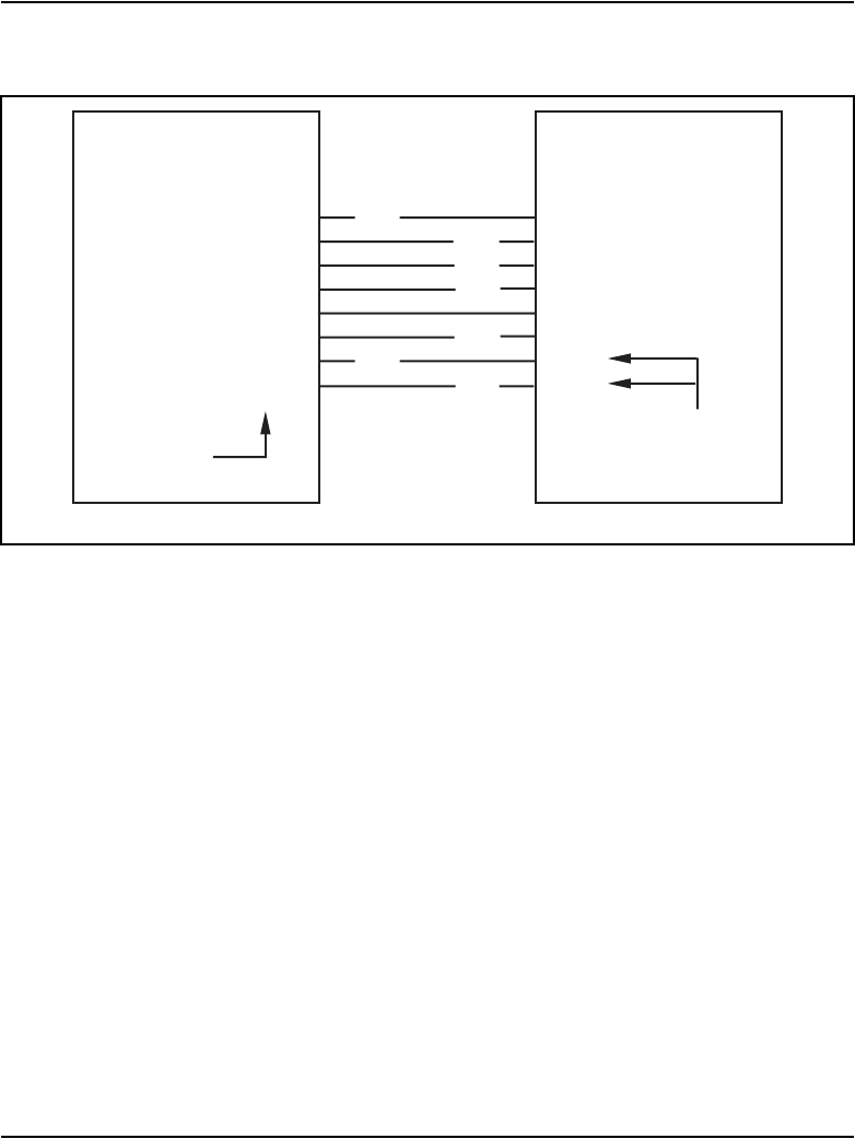
Page 458 of 906 NT7D16 Data Access card
553-3001-211 Standard 3.00 August 2005
unless the DTR lead is driven ON by the terminal. Any terminal that drives
the DTR lead ON can be used with this mode (such as VT100 or VT102).
The DAC drives CTS, DSR, and DCD ON, except when a call is dropped or
when control—Z is entered during the idle state. In this case, the DAC drives
those leads OFF for 0.2 seconds and then ON. When the DTR lead is driven
OFF by the terminal, the DAC does not execute autobaud, nor will it respond
to any command.
Note: If the PBDO parameter in LD 11 is ON, then Make Set Busy will
be activated when DTR is driven OFF for more than five seconds.
Programing DAC for mode 12 in service change LD 11
The DAC must be configured as R232 or R422 since Autodial, Speed Call,
and Display commands are likely to be used.
Figure 94
DAC to Terminal connectivity
pin 2
pin 3
pin 5
pin 6
pin 7
pin 8
pin 20
pin 22
TX
RX
CTS
DSR
GND
DCD
DTR
RI
Terminal (DTE) DAC (DCE)
RS- 232 leads
>>>
<<<
<<<
<<<
<<<
<<<
>>>
not required
for mode 14
553-5220

NT7D16 Data Access card Page 459 of 906
Circuit Card Description and Installation
Mode 13
This mode should be selected when the DAC is connected to a terminal
(DTE) and Hotline call origination is required. This mode is similar to the
operation of the ASIM when set to not-forced-DTR and Hotline. In this mode,
the terminal is able to Hotline to a specific data unit by driving the DTR lead
ON. The transition of DTR from OFF to ON causes the DAC to Hotline to the
Autodial DN. Any terminal that drives DTR lead ON can be used with this
mode (such as VT100 or VT102).
The DAC drives CTS, DSR, and DCD ON, except when a call is dropped. In
this case, the DAC drives those leads OFF for 0.2 second and then ON. The
baud rate of the Hotline call is determined by the AUTB and BAUD
parameters in LD 11.
Programing DAC for mode 13 in service change LD11
The DAC must be configured as R232 or R422 since Autodial, Speed Call,
and Display commands are likely to be used.
Mode 14
This mode should be selected when the DAC is connected to a terminal
(DTE) for inbound and outbound data calls. This mode is similar to the
operation of the ASIM when set to forced-DTR and not-Hotline. The terminal
used with this mode is not required to drive the DTR lead. This mode of
operation is similar to mode 12, except for the following:
• The status of DTR lead is assumed to be always ON, even when the
actual condition of that lead is OFF (forced-DTR). The DAC always
answers an incoming call regardless of the DTR status.
• The terminal cannot release an established data call by driving DTR
OFF. As a result, the terminal cannot initiate call release except with a
long break or three short breaks.
Programing DAC for mode 14 in service change LD 11
The DAC must be configured as R232 since Autodial, Speed Call, and
Display commands are likely to be used.

Page 460 of 906 NT7D16 Data Access card
553-3001-211 Standard 3.00 August 2005
Mode 15
This mode provides a “virtual leased line” and the meaning of the “Forced
DTR” switch is re-defined.
This mode should be selected when the DAC is connected to a terminal
(DTE) and continuous Hotline call origination is required. In this mode, the
DAC repeatedly tries to Hotline to the Autodial DN as long as DTR is ON.
This operation is similar to having a leased line feature, where the connection
between two extensions is always established. When the DAC tries to Hotline
to a busy Data Module, it activates Ring Again and the connection is
established as soon as the called unit is free. After establishing the data call,
if the called unit releases the call for any reason, the DAC automatically tries
to Hotline again to reestablish the call.
If the data unit being called does not answer the Hotline call, the DAC tries
to place another Hotline call once every 40 seconds until the called unit
answers. This mode is recommended only when a permanent connection
between a terminal and another data unit is required. The baud rate of the
Hotline call is determined by the AUTB and BAUD parameters in LD 11.
The status of CTS, DSR, and DCD is controlled in a similar manner as
described in mode 13.
Programing DAC for mode 15 in service change LD 11
The DAC must be configured as R232 since Autodial, Speed Call, and
Display commands are likely to be used.
Mode selection baud rates
The AUTB and BAUD parameters in LD 11 provide two functions for calls
originated from a DAC:
• Provide a way to select a baud rate of a Hotline call. The DAC starts the
Hotline operation without receiving a <CR> for autobaud.
• Set the DAC to operate at a fixed baud rate. The DAC does not return the
menu or Hotline unless a <CR> is received at the selected baud rate.
Normally the DAC should be selected to operate at autobaud.

NT7D16 Data Access card Page 461 of 906
Circuit Card Description and Installation
Note: If AUTB is set to ON, the BAUD parameter is not prompted. If
AUTB is set to OFF, you may select a fixed baud rate in response to the
prompt BAUD.
When the DAC receives a call, it adapts to the caller’s baud rate.
See Table 158 for connect and disconnect protocol.
Table 158
Connect and disconnect protocol (Part 1 of 12)
Mode of
operation Interface application Comments
Mode 0 Inbound and Outbound
modem pools
For inbound modem pools,
most dumb modems may be
used.
For outbound modem pools,
only smart modems
(auto-dialer) may be used.
Outbound modem pooling:
Modem sends ring/no ring cycle (2 seconds ON, 4
seconds OFF) to initiate connection.
DAC responds by driving DTR ON within the first
ring cycle.
Modem responds by answering the incoming call
and driving DCD ON within 35 seconds.
If modem does not drive DCD ON within 35
seconds, the DAC drops DTR and goes idle.
Remote DTE sends <CR> to the DAC. The DAC
autobauds and sends initial prompt.

Page 462 of 906 NT7D16 Data Access card
553-3001-211 Standard 3.00 August 2005
Outbound modem pooling:
Local DM user calls to the outbound modem
access number.
DAC answers the outbound call and drives DTR
ON.
Modem receives DTR and prepares to receive
commands.
Local DM user enters the proper commands for
calling the remote modem.
Remote modem answers; data call established.
Call disconnection (DAC):
DAC drops DTR if the local DM user drops the
call. The modem must drop DCD.
DAC drops DTR if the remote modem sends a
long break or three short breaks. The modem
must drop DCD.
Call disconnection (modem):
Modem drops DCD (DCD OFF for 100 ms or
more). The DAC drops DTR and disconnects the
local call.
Modem drops DSR (DSR OFF for 100 ms or
more). The DAC drops DTR and disconnects the
local call.
Table 158
Connect and disconnect protocol (Part 2 of 12)
Mode of
operation Interface application Comments

NT7D16 Data Access card Page 463 of 906
Circuit Card Description and Installation
Mode 1 Inbound Hotline modem
pools
Inbound Hotline modem pooling:
Most dumb modems can be
used for this application.
Modem sends ring/no ring cycle (2 seconds ON, 4
seconds OFF) to initiate connection.
DAC responds by trying to establish a Hotline call
to a specific Data Module (Autodial).
When Data Module answers, then and only then,
the DAC turns DTR ON.
Modem should answer the incoming call when
DTR goes ON and should turn DCD ON within 35
seconds; otherwise the DAC disconnects the call.
Call disconnection:
Disconnection is the same as mode 0.
Mode 2 Inbound and Outbound
modem pools (with forced
DTR)
Use this mode with Hayes
1200 modem.
Inbound and Outbound modem pooling:
The DAC operation is identical to mode 0 except
that DTR is always forced ON (except during
disconnect).
Call disconnection:
Disconnection is identical to mode 0 except:
—When a call is released, the DAC turns DTR
OFF for 0.2 second and then ON. DTR stays ON
until the next call release.
—The DAC ignores RI and DCD for about 2
seconds after releasing a call. This avoids
problems with the Hayes 1200 modem.
Table 158
Connect and disconnect protocol (Part 3 of 12)
Mode of
operation Interface application Comments

Page 464 of 906 NT7D16 Data Access card
553-3001-211 Standard 3.00 August 2005
Mode 3 Inbound Hotline modem
pools (with forced DTR)
Use this mode with Hayes
1200 modem.
Inbound Hotline modem pooling:
The DAC operation is identical to mode 1 except
that DTR is always forced ON (except during
disconnect).
Call disconnection:
Disconnection is identical to mode 2.
Mode 4 Inbound and Outbound
Gateway access
Inbound Gateway connection protocol:
Gateway raises DCD to initiate connection.
DAC responds by driving DTR ON.
Gateway does not have to turn DSR ON.
However, toggling DSR or DCD from ON to OFF
causes the DAC to disconnect the call.
Gateway user sends <CR> to the DAC.
DAC autobauds and sends the initial prompt to
the Gateway.
Outbound Gateway connection protocol:
Local DM user calls the DAC that is connected to
a Gateway.
DAC answers the data call and drives DTR ON.
Gateway receives DTR and prepares to receive
commands.
Local DM user is now transparently connected to
the Gateway.
Gateway is expected to drive DCD ON within 35
seconds. If the Gateway fails to do so, the DAC
drops DTR and the call.
Table 158
Connect and disconnect protocol (Part 4 of 12)
Mode of
operation Interface application Comments

NT7D16 Data Access card Page 465 of 906
Circuit Card Description and Installation
Call disconnection (DAC):
DAC drops DTR if the local DM user drops the
call. The Gateway must drop DCD.
DAC drops DTR if the DAC receives a long break
or three short breaks. The Gateway must drop
DCD.
Call disconnection (Gateway):
Gateway drops DCD (DCD OFF for 100 ms or
more). The DAC drops DTR and disconnects the
local call.
Gateway drops DSR (DSR OFF for 100 ms or
more). The DAC drops DTR and disconnects the
local call.
Mode 5 Inbound Hotline Gateway
access
Inbound Hotline Gateway protocol:
Gateway raises DCD to initiate connection.
DAC responds by trying to establish a Hotline call
to a specific Data Module (Autodial).
When Data Module answers, then and only then,
the DAC turns DTR ON.
Gateway does not have to turn DSR ON.
However, toggling DSR or DCD from ON to OFF
causes the DAC to drop the call.
Gateway is not transparently linked to the
equipment connection to the DM.
Call disconnection:
Disconnection is identical to mode 4.
Table 158
Connect and disconnect protocol (Part 5 of 12)
Mode of
operation Interface application Comments

Page 466 of 906 NT7D16 Data Access card
553-3001-211 Standard 3.00 August 2005
Mode 6 Inbound and Outbound
Gateway access (with forced
DTR)
Inbound and Outbound Gateway protocol:
The DAC operation is identical to mode 4 except
that DTR is always forced ON (except during
disconnect). The establishment of the outbound
call does not require DCD to be driven ON by the
Gateway.
Call disconnection:
Disconnection is identical to mode 4 except that
when a call is released, the DAC turns DTR OFF
for 0.2 second and then ON. DTR stays ON until
the next call release.
Mode 7 Inbound Hotline Gateway
access (with forced DTR)
Inbound Hotline Gateway protocol:
The DAC operation is identical to mode 5 except
that DTR is always forced ON (except during
disconnect).
Call disconnection:
Disconnection is identical to mode 6.
Table 158
Connect and disconnect protocol (Part 6 of 12)
Mode of
operation Interface application Comments

NT7D16 Data Access card Page 467 of 906
Circuit Card Description and Installation
Mode 8 Host access for call
origination and answering
Host answering an incoming data call:
Local DM user dials the access number to initiate
the connection.
DAC responds by driving RI ON for 2 seconds and
OFF for 4 seconds until the Host answers by
turning DTR ON. (If the Host always drives DTR
ON, the DAC immediately answers the call
without driving RI ON.)
When Host receives RI ON, it should respond by
turning DTR ON.
DAC answers when it receives DTR ON.
DAC turns DSR, DCD, and CTS ON when the call
is completely established. The local DM user is
now transparently linked to the Host.
Host originating a data call:
Host turns DTR ON to initiate the connection.
DAC prepares to receive <CR> for autobaud.
Host sends <CR> followed by other commands
for establishing a data call (the DAC does not
echo a command, nor does it send any prompt to
the Host (blind dialing).
When the data call is completely established, the
DAC turns DSR, DCD, and CTS ON as long as
the call is connected.
Table 158
Connect and disconnect protocol (Part 7 of 12)
Mode of
operation Interface application Comments

Page 468 of 906 NT7D16 Data Access card
553-3001-211 Standard 3.00 August 2005
Call disconnect ion (DAC):
DAC drops DSR, DCD, and CTS if the local DM
user releases the call. The Host should then drop
the call.
DAC drops DSR, DCD, and CTS if the Host sends
a long break or three short breaks. The Host
should then drop the call.
Call disconnection (Host):
The Host toggles DTR from ON to OFF (DTR
must be OFF for 100 ms or more). The DAC drops
DSR, DCD, and CTS and disconnects the local
call.
Mode 9 Hotline call origination Hotline originated by Host (Inbound):
Host toggles DTR from OFF to ON to initiate the
Hotline call.
DAC responds by trying to establish a Hotline call
to a specific Data Module (Autodial).
3When Data Module answers, then and only then,
the DAC turns DSR, DCD, and CTS ON (the DAC
does not send any prompts to the Host). If the
Data Module is busy or not responding, the DAC
requires another transition of DTR from OFF to
ON to initiate another Hotline call. If the Host
keeps DTR ON, the DAC does not try to establish
another Hotline call, unless the Host sends a
<CR> while DTR is ON.
Call disconnection:
Disconnection is identical to mode 8.
Table 158
Connect and disconnect protocol (Part 8 of 12)
Mode of
operation Interface application Comments

NT7D16 Data Access card Page 469 of 906
Circuit Card Description and Installation
Mode 10 Host access for call
origination and answering
(with forced DTR)
Host access for call origination and
answering:
The DAC operation is identical to mode 8 except
DTR is always considered ON, even when the
Host is driving DTR OFF.
Call disconnection:
DAC drops DSR, DCD, and CTS if the local DM
user releases the call. The Host should then drop
the call.
DAC drops DSR, DCD, and CTS if the Host sends
a long break or three short breaks. The Host
should then drop the call.
Mode 11 Hotline call origination
(Virtual Leased Line)
Hotline origination by Host (continuous
Hotline mode):
The DAC operation is similar to mode 9 except the
Host initiates the Hotline call by driving DTR ON.
However, if the DM is busy or not answering, the
DAC will continuously try to originate Hotline calls
once every 40 seconds (as long as DTR stays
ON) until the called DM answers the call.
Call disconnection:
Disconnection is identical to mode 8.
Table 158
Connect and disconnect protocol (Part 9 of 12)
Mode of
operation Interface application Comments

Page 470 of 906 NT7D16 Data Access card
553-3001-211 Standard 3.00 August 2005
Mode 12 Terminal access for call
origination and answering
Terminal answering an incoming data call:
DAC drives DSR, DCD, and CTS ON in the idle
state.
Local DM user dials the access number to initiate
the connection.
DAC responds by driving RI ON for 2 seconds and
OFF for 4 seconds, until the terminal answers by
turning DTR ON (if the terminal always drive DTR
ON, the DAC immediately answers the call
without driving RI ON).
When terminal receives RI ON, it should respond
by turning DTR ON.
DAC answers when DTR goes ON and the local
DM user is now transparently linked to the
terminal.
Terminal originating an outgoing data call:
DAC drives DSR, DCD, and CTS ON in the idle
state.
Terminal turns DTR ON to initiate the connection.
DAC prepares to receive <CR> for autobaud.
Terminal sends <CR> followed by other
commands for establishing a data call (the DAC
echoes all commands).
Call disconnection (DAC):
If the local DM user releases the call, the DAC
turns DSR, DCD, and CTS OFF for 0.2 second
and then ON.
Table 158
Connect and disconnect protocol (Part 10 of 12)
Mode of
operation Interface application Comments

NT7D16 Data Access card Page 471 of 906
Circuit Card Description and Installation
Call disconnection (terminal):
Terminal toggles DTR from ON to OFF (DTR must
be OFF for 100 ms or more). The DAC turns DSR,
DCD, and CTS OFF for 0.2 second and then ON.
Terminal sends a long break or three short
breaks. The DAC turns DSR, DCD, and CTS OFF
for 0.2 second and then ON.
Mode 13 Hotline call origination Hotline originated by terminal:
DAC drives DSR, DCD, and CTS ON in the idle
state.
Terminal toggles DTR from OFF to ON to initiate
Hotline call.
DAC responds by trying to establish a Hotline call
to a specific DM (Autodial).
If Data Module is busy or not responding, the DAC
requires another transition of DTR from OFF to
ON to initiate another Hotline call. If the terminal
keeps DTR ON, the DAC does not try to establish
another Hotline call unless the terminal sends a
<CR> while DTR is ON.
Call disconnection:
Disconnection is identical to mode 12.
Mode 14 Terminal access for call
origination and answering
(with forced DTR)
Terminal access for call origination and
answering:
The DAC operation is identical to mode 12 except
that DTR is considered to be always ON, even
when the terminal is driving DTR OFF.
Table 158
Connect and disconnect protocol (Part 11 of 12)
Mode of
operation Interface application Comments

Page 472 of 906 NT7D16 Data Access card
553-3001-211 Standard 3.00 August 2005
Keyboard dialing
Keyboard dialing is an interactive dialogue mode between the connected
equipment and the DAC. This dialogue allows equipment to give dialing
commands to the DAC in order to make a data call to another far-end data
port. Keyboard dialing supports a modify mode that allows the user to modify
certain dialing parameters.
The following keyboard dialing features are supported with the DAC:
• Autobaud from 110 to 19200 bps
Call disconnection (DAC):
If the local DM user drops the call, the DAC turns
DSR, DCD, and CTS OFF for 0.2 second and
then ON.
Call disconnection (terminal):
The terminal sends a long break or three short
breaks. The DAC turns DSR, DCD, and CTS OFF
for 0.2 second, and then ON.
Mode 15 Hotline call origination
(Virtual Leased Line)
Hotline call origination by terminal:
The DAC operation is similar to mode 13 except
the terminal initiates the Hotline call by driving
DTR ON. However, if the called DM is busy or not
answering, the DAC will continuously try to
originate Hotline calls once every 40 seconds (as
long as DTR remains ON) until the Data Module
answers the call.
Call disconnection:
Disconnection is identical to mode 12.
Table 158
Connect and disconnect protocol (Part 12 of 12)
Mode of
operation Interface application Comments

NT7D16 Data Access card Page 473 of 906
Circuit Card Description and Installation
• Autoparity to ensure that the keyboard dialing menu is readable on the
data terminal during the interactive dialogue mode
• Originating calls to local and remote hosts
• Ring Again
• Speed Call
• Two answer modes for incoming calls: manual and auto
• Digit display
• Dialing by mnemonic
Initiating conditions
In order for the DAC to respond to user commands/entries, the following
conditions must be met:
• The DAC must be active (power ON), and have successfully received the
downloaded parameters from the system.
• The user equipment must be active, and, if in RS-232-C mode, must
assert these control lines
— DCE mode: DTR (unless Forced DTR has been software selected)
— DTE mode: RI has cycled the appropriate number of times
Echo
During call setup (dialogue phase), all user input is echoed back to the user
equipment. Once the call is established, the DAC is transparent to data
communication. To get echoed characters after a call is established, the far
end must provide the echo.
Note: When RS-232-C modes 12-15 (Host modes) are selected, there is
no echo during dialogue phase.

Page 474 of 906 NT7D16 Data Access card
553-3001-211 Standard 3.00 August 2005
Prompts
Call processing prompts are in upper case letters only. Other prompts consist
of both upper and lower case characters, and the dialogue session depicts the
actual upper/lower case letters used.
All prompts are preceded by the Carriage Return and Line Feed ASCII
characters (<CR>, <LF>).
Prompts requesting user input are terminated with the ASCII colon (:).
Prompts requiring a Yes or No answer are terminated by a question mark (?),
followed by a list of allowable responses. The default response, if allowed, is
bracketed.
Call abort
In addition to the methods mentioned above, which are common to both
Hayes and keyboard modes, keyboard dialing supports the following method
to abort a call during the dialogue phase.
• Sending the Control Z character (simultaneously pressing the control and
Z keys) sends a message to the DAC to immediately abandon the data
call setup.
Autobaud
All user dialogue must begin with Autobaud detection. This allows the DAC
to determine the user equipment baud rate. During this phase, only <CR> will
be recognized by the DAC. All other entries are ignored, and no entries are
echoed. Once a valid <CR> is detected, the DAC responds with the New
Menu prompt at the baud rate detected. If a fixed rate has been determined by
the downloaded parameters, the DAC will look for that rate. If the rates agree,
the dialogue phase begins. If not, the following prompt is sent to the user:
Baud Rate xxxx expected
After receiving a number of invalid responses, the DAC reverts to autobaud
detection, since the terminal data speed may have changed.

NT7D16 Data Access card Page 475 of 906
Circuit Card Description and Installation
Keyboard Autobaud is allowed after the call is placed in off-line mode.
Note: If the Hayes autobaud characters A or a are sent, the DAC will
enter Hayes dialing mode. Autobaud character detection is selected in the
software.
Auto parity
The user can override the downloaded parity rate by entering the ASCII
period (.) as a command. This period must be the only command sent,
followed by <CR>. The period must be sent only when the Primary menu is
displayed, and can be sent only once during a call setup session.
Dialing operation
For the purposes of this document, when illustrating the prompt/response
sequences, the bold type is what the user enters on the keyboard. All other
type represents the DAC output. Likewise, “xxxxxxx,” “yyyyyyy,” or
“zzzzzzz” represents numbers entered by the user, or dialed by the DAC, and
in no way indicates the absolute character limit. A maximum of 43 characters
is allowed.
When the user enters the autobaud character, <CR>, and the dialing mode is
Manual (not Hotline), the DAC sends the following menu:
If the user enters <CR>, the DAC presents this prompt again. When a number
is entered, the DAC attempts to place the call. Entering H at this point will list
the Primary Commands menu:
<CR><LF><CR><LF><LF>ENTER NUMBER OR H (FOR HELP):<SP>
Primary Commands Menu:
A - Auto Dial C - Call
D - Display M - Modify
S - Speed Call
CTRL Z (Abort Keyboard Dialing)
Select: <SP>

Page 476 of 906 NT7D16 Data Access card
553-3001-211 Standard 3.00 August 2005
Whenever a Primary command is expected, the user may enter the Parity
command (period). If Auto Parity has already been done, the Invalid
Command menu is presented:
The user's port may be set to idle by entering CTRL Z. Any call in progress
will be dropped, and any Ring Again placed will be released. Once the
Primary Command menu has appeared, the user must enter C to place a call.
The DAC will not accept a number in place of a Primary command.
Primary commands
Once the Primary menu has appeared, only primary commands are accepted.
Call (C)
The Call command must be used to place a call once the Primary menu has
appeared. The DAC will not accept a number only.
Invalid Command/Entry
Re-Enter: <SP>
C<CR>
ENTER NUMBER:<SP>
xxxxxxx<CR>
CALLING xxxxxxx
RINGING
ANSWERED
CALL CONNECTED. SESSION STARTS

NT7D16 Data Access card Page 477 of 906
Circuit Card Description and Installation
Autodial (A)
The Autodial command allows the user to dial a predefined number stored
within the local system. The DAC will automatically attempt to place a data
call to the Autodial number:
The currently stored Autodial number may be viewed by entering the primary
command D (Display), followed by the selection A (Autodial). See the
Display discussion later in this document.
Note: If the Autodial feature key is not defined in the software you will
be notified by the following: Feature key Autodial not defined.
Speed Call (S)
The Speed Call command allows the user to make a call to a number
associated with a 1-, 2-, or 3-digit access code. The user supplies the access
code, and the DAC places the call according to the code supplied.
If the DAC does not know the access code length, you will be notified by:
ENTER ACCESS CODE (all digits) <SP>. Leading zeroes must be entered
A <CR>
CALLING xxxxxxx
RINGING
ANSWERED
CALL CONNECTED. SESSION STARTS
S<CR>
ENTER ACCESS CODE: <SP>
xxx<CR>
CALLING yyyyyy
RINGING
ANSWERED
CALL CONNECTED. SESSION STARTS

Page 478 of 906 NT7D16 Data Access card
553-3001-211 Standard 3.00 August 2005
if the access code is less than the maximum number of digits allowed for the
Speed Call list for the associated data DN (DDN).
Note: If the Speed Call feature key is not defined in the software, you
will be notified by the following: Feature key Speed Call not defined.
Both the Autodial and Speed Call commands can be changed with the Modify
command (M). Additionally, the Speed Call number can be changed in the
service change. When this command is entered, the Modify menu appears.
Any of these choices leads to another series of prompts and responses.
By entering A on the keyboard, you enter the Autodial Modify menu.
Respond to the following prompts to change the Autodial number.
Modify Menu:
A - Auto Number D - DCD Control
L - Long Break M - Manual Answer
Q - Quit Modify Menu R - Remote Loopback
S - Speed Call
CTRL Z (Abort Keyboard Dialing)
Select:<SP>
A <CR>
Current Autodial number: zzzzzzz
Enter Autodial number: <SP>
xxxxxxx <CR>
New Autodial number: xxxxxxx

NT7D16 Data Access card Page 479 of 906
Circuit Card Description and Installation
By entering S on the keyboard, you enter the Speed Call Modify menu. The
Speed Call number can also be changed in the software. Respond to the
following prompts to change the Speed Call number.
By entering R on the keyboard, you enter the Remote Loopback Modify
menu. Respond to the following prompts to enable or disable the Remote
Loopback feature.
By entering M on the keyboard, you enter the Manual Answer Modify menu.
Manual Answer indicates that the DAC prompts the user to answer an
incoming data call. Auto answer picks up the call after the specified number
S<CR>
Enter access code <SP>
Current Speed Call number: zzzzzzz
Enter Speed Call number: <SP>
zzzzzzz<CR>
New Speed Call number: xxxxxxx
R <CR>
Remote Loopback Disabled (or enabled, indicating current status)
Remote Loopback
(Y/N): <SP>
Y <CR> or N <CR>
Remote Loopback: Enabled (or Disabled)

Page 480 of 906 NT7D16 Data Access card
553-3001-211 Standard 3.00 August 2005
of rings. Respond to the following prompts to enable or disable the Manual
Answer feature.
By entering D on the keyboard, you enter the DCD Modify menu. Respond
to the following prompts to enable DCD as Forced or Dynamic.
M <CR>
Current Answer Mode: Manual
Auto - xx Rings
Manual Answer? (Y/N): <SP>
Y <CR> N <CR>
Number of rings (1-255 <1>): <SP>
yy
New Answer Mode: Manual New Answer Mode: Auto - yy Rings
D <CR>
DCD Control:Dynamic
Forced On
Dynamic DCD? (Y/N): <SP>
Y <CR> N <CR>
DCD Control: DynamicDCD Control: Forced On

NT7D16 Data Access card Page 481 of 906
Circuit Card Description and Installation
By entering L on the keyboard, you enter the Long Break Detect Modify
menu. Respond to the following prompts to enable or disable the detection of
the Long Break as an abandon signal.
To exit the Modify menu, enter Q. This entry returns you to the Primary
commands menu. To view the port's parameters, enter D when in the Primary
Commands menu. This display shows the Display Options menu.
Ring Again
When a call is placed to a busy DN, the DAC prompts you to activate Ring
Again. The Ring Again feature alerts you as soon as the dialed DN becomes
free. Once the Ring Again has been activated, you will return to the Primary
Commands menu. The following is the prompt and response sequence
enabling the Ring Again feature.
L <CR>
Long Break:Detected
Ignored
Detect Long Break? (Y/N): <SP>
Y <CR> N <CR>
Long Break: Detected Long Break: Ignored
Display Options Menu:
A - Auto Dial number D - Date and Time
K - Feature Keys P - Data Port Parameters
Q - Quit Display S - Speed Call number(s)
CTRL Z (Abort Keyboard Dialing)
Select: <SP>

Page 482 of 906 NT7D16 Data Access card
553-3001-211 Standard 3.00 August 2005
Note: If you hang up the call, or give an abandon command, Ring Again
is canceled.
If a Ring Again request has already been placed, the DAC offers the option
of overriding the previous request.
When the called DN becomes available, the system notifies the DAC, which
then prompts the user to place the call. If you do not respond to the Ring
BUSY, RING AGAIN? (Y/N): <SP>
Y <CR> or N <CR>
RING AGAIN PLACED
Primary Commands Menu:
A - Auto Dial C - Call
D - Display M - Modify
S - Speed Call
CTRL Z (Abort Keyboard Dialing)
Select: <SP>
RING AGAIN ACTIVE, REPLACE? (Y/N): <SP>
Y <CR>
RING AGAIN PLACED
Primary Commands Menu:
A - Auto Dial C - Call
D - Display M - Modify
S - Speed Call
CTRL Z (Abort Keyboard Dialing)
Select: <SP>

NT7D16 Data Access card Page 483 of 906
Circuit Card Description and Installation
Again prompt within a software determined time period, Ring Again is
canceled, and the Primary Commands Menu appears.
Note 1: If the Ring Again notice occurs during a parameter change, the
prompt only appears after the change has been completed.
Note 2: If the notice occurs during an active call, the Ring Again notice
is ignored. When the active call is completed, you will be notified that
the Ring Again call was canceled.
You can also cancel the Ring Again request at this time.
DATA STATION NOW AVAILABLE, PLACE CALL? (Y/N/<Y>): <SP>
Y <CR>
CALLING XXXX
RINGING
ANSWERED
CALL CONNECTED. SESSION STARTS
DATA STATION NOW AVAILABLE, PLACE CALL? (Y/N/[Y]): <SP>
N <CR>
RING AGAIN CANCELLED
Primary Commands Menu:
A - Auto Dial S - Speed Call
C - Call M - Modify
D - Display
CTRL Z (Abort Keyboard Dialing)
Select: <SP>

Page 484 of 906 NT7D16 Data Access card
553-3001-211 Standard 3.00 August 2005
Not in service
When the DAC attempts a call to a DN that is not supported, it sends you a
message. The call is released, and you must reenter the Autobaud character
<CR> to initiate keyboard dialing again.
No response from the system
Likewise, when the DAC receives no system response from your port after a
30-second timeout period, the DAC sends you a message. The call is
abandoned. This means the port is either disabled or unequipped.
C<CR>
ENTER NUMBER:<SP>
xxxxxxx<CR>
CALLING xxxxxxx
NOT IN SERVICE
RELEASED
C<CR>
ENTER NUMBER:<SP>
xxxxxxx<CR>
NO SYSTEM RESPONSE
RELEASED

NT7D16 Data Access card Page 485 of 906
Circuit Card Description and Installation
Hayes dialing
Like keyboard dialing, Hayes dialing is an interactive dialing mode with the
terminating equipment connected to the NT7D16 Data Access Card (DAC).
In addition to the common parameters and functions, the Hayes dialing mode
offers the following features:
• Data call dialing
• Two modes for answering incoming calls: auto and manual
• Repeat previous command
• Character echo control
• On-hook/off-hook control
• Detect off-line escape sequence
• Return to on-line
• Initiate Remote Digital Loopback
• Terminate Remote Digital Loopback
• Modify S Registers S0 through S12
• Display S Registers S0 through S12
• Support all S Registers except: S6, S7, S9, and S11
The Hayes dialing mode supports the following AT Dialing commands.
Initiating conditions
The DAC responds to commands only when the following initial
requirements are met:
• the DAC is active
• the DAC has successfully received the downloaded parameters
• the user equipment is active, and, if operating in RS-232-C mode
— the DCE mode is DTR (unless Forced DTR has been software
selected)

Page 486 of 906 NT7D16 Data Access card
553-3001-211 Standard 3.00 August 2005
— the DTE mode, and RI has cycled the appropriate number of times
and DCD is asserted on by the modem
Note: In Gateway mode, DCD must be asserted on. In modem mode,
only RI must be on. The DAC asserts DTR to the modem, and awaits
DCD from the modem.
Input requirements
All input must be in the same case (upper or lower).
The Hayes repeat command, A/, is used to immediately execute the last
command entered. The terminator character need not be entered. A complete
discussion of the Repeat command can be found later in this document.
Where a Dial Number is expected, you may enter the characters 0-9, #, and
comma (,). The characters @, P, R, T, and W are accepted, but ignored.
The maximum number of characters is 43. This limit includes the AT prefix,
and the record Terminator character, but does not include the ASCII space
character.
Echo
Throughout the dialogue phase, the DAC echoes all user input. In RS-232-C
modes 0, 1, 2, and 3, no inbound call messages are presented to the modem.
Prompts are presented only if the modem user originates the call. In modes 8,
9, 10, and 11, no prompts or characters echo under any circumstances. The
echo function can be turned off with a Hayes dialing command.
All prompts and responses issued by the system are displayed to the user
unless the display command has been disabled. Like the Repeat command,
this is explained later in this document.
Note: If the RS-232-C DAC Host modes (1, 2, 3, 8, 9, 10, 11, or 12) are
used, all attempts to enable the echo or display is ignored. Likewise, the
Hayes Reset command is also ignored.

NT7D16 Data Access card Page 487 of 906
Circuit Card Description and Installation
Result codes and messages
Each input record generates a result code which is sent to the user. Only one
code is sent regardless of the number of commands in the record. The reply
is in one of two formats:
• Numeric replies contain a one- or two-number code
• Verbose replies contain one or more words
Table 159 shows the codes for each reply in both formats, and explanations
for the codes.
Note 1: Verbose commands are the default and appear in upper case
characters only. Numeric commands are sent by issuing the Numeric
Results code command (explained later in this document).
Note 2: All verbose codes and messages are preceded and terminated by
the user defined Terminator and New Line characters. The default, or
reset, characters are the ASCII Carriage Return, and ASCII Line Feed.
The Numeric codes are preceded and terminated by the Terminator
character only.
Note 3: The Suppress result command (explained later in this document)
will disable the sending of these codes. If in RS-232-C DAC Host modes,
this command is ignored.
Table 159
Hayes dialing result codes and messages (Part 1 of 2)
Verbose
code
Numeric
code Description
OK 0 Command(s) executed, no error
CONNECT 1 Data call established, session starts
RING 2 Inbound call presented
NO CARRIER 3 Data call abandoned
ERROR 4 Error in command line
NO DIALTONE 6 System does not allow call to proceed

Page 488 of 906 NT7D16 Data Access card
553-3001-211 Standard 3.00 August 2005
Baud rate detection
Every command line begins with Baud rate detection. This phase allows the
DAC to determine the user equipment baud rate. During this phase, the DAC
accepts only the ASCII “A,” or “a” characters. Once a valid autobaud
character is detected, the DAC echoes the parity bit character at the baud rate
detected.
Note: If Hayes dialing is desired, you must enter the character “A” or
“a” BEFORE the <CR>. If Carriage Return (<CR>) is entered before this
Hayes dialing command, you will be placed in keyboard dialing mode.
Parity detection
Once the baud rate has been determined, the DAC accepts only the ASCII
characters “T,” “t,” or “/.” If the Repeat character “/” is entered, the previous
command is executed. If “T,” or “t” is entered, the DAC uses its parity and
the parity of the preceding A (a) to determine the user's parity. This parity is
used on the following messages and prompts associated with the command
lines.
BUSY 7 Far end is busy
NO ANSWER 8 Far end does not answer
CONNECT 1200 5 Session starts at 1200 baud
CONNECT 2400 10 Session starts at 2400 baud
CONNECT 4800 11 Session starts at 4800 baud
CONNECT 9600 12 Session starts at 9600 baud
CONNECT 19200 14 Session starts at 19200 baud
Table 159
Hayes dialing result codes and messages (Part 2 of 2)
Verbose
code
Numeric
code Description

NT7D16 Data Access card Page 489 of 906
Circuit Card Description and Installation
Note: The parity determined here overrides the parity downloaded from
the system. Also, the T (t) must be entered in the same case as the A (a).
If you entered uppercase A for the Baud Rate, you must enter upper case
T for the parity.
Dialing operation
Like keyboard dialing, the Hayes dialing commands allow the user to initiate
a data call, as well as change certain dialing parameters. The commands may
be entered in either upper or lower case, but must be the same case throughout
the command line. Also the case must match the autobaud case.
Note: Hayes dialing does not allow for the Ring Again feature. If a call
is made to a busy number, that call is abandoned.
Table 160 provides a list of the AT dialing commands.
Table 160
AT dialing commands (Part 1 of 2)
Command Description
ATA Answer (answer incoming data call)
ATDnnnn
ATDTnnnn
Dial (n = 0-9, numbers to be dialed)
A/ Repeat last command (no <CR> needed)
ATO On-line (enter three Escape characters rapidly to go off-line)
ATDPnnnn Voice call (n = 0-9, numbers to be dialed)
ATF 0 Handsfree/mute (toggle Handsfree between mute and normal)
ATF 1 Hold (put voice call on hold)
ATF 2 Select (take voice call off hold)
ATH0 Hang up data call
Note 1: To use AT dialing, enter CTRL-z at carriage return (<CR>) when the port is idle.
Note 2: Follow each command (except A/) by a carriage return (<CR>) to execute it.

Page 490 of 906 NT7D16 Data Access card
553-3001-211 Standard 3.00 August 2005
For the purposes of this document, when illustrating the prompt/response
sequences, the bold type is what the user enters on the keyboard. All other
type represents the DAC output. Likewise, “xxxxxxx,” “yyyyyyy,” or
“zzzzzzz” represents numbers entered by the user, or dialed by the DAC, and
in no way indicates the absolute character limit. The number of characters is
dependent on the feature activated (Auto Dial, Speed Call, for example).
Also, for simplicity purposes, all Result messages are shown in Verbose code.
See Table 159 on page 487 for a complete list of the Verbose and Numeric
codes. See Features and Services (553-3001-306) for a complete description
of the features operating.
S registers
These commands allow the user to access various dialing parameters. The
user can determine the present parameter setting, and alter the parameter.
These parameters are grouped into a set referred to as the S registers.
ATHP Hang up voice call
ATQ n Result code (n = 0, 1; if n = 0, result codes are sent)
ATVn Verbal result (n = 0, 1; if n = 0, numeric codes are sent)
ATXn Result code selection (n = 0, 1; if n = 1, extended results)
ATSn Read S register (n = number of S register to read)
ATSn=x Write S register (n = S register number; x = new value)
ATZ Soft reset (reset to default parameters)
ATCn Carrier detect (n = 0, 1; if n = 1, carrier detect is enabled)
ATEn Echo (n = 0, 1; if n = 1, commands will echo back to terminal)
ATTSP! Transparent mode
Table 160
AT dialing commands (Part 2 of 2)
Command Description
Note 1: To use AT dialing, enter CTRL-z at carriage return (<CR>) when the port is idle.
Note 2: Follow each command (except A/) by a carriage return (<CR>) to execute it.

NT7D16 Data Access card Page 491 of 906
Circuit Card Description and Installation
All S registers may be changed with the exception of S1, the Ring count. If
an attempt is made to change this parameter, the command is accepted but no
action is taken. The Ring count is the number of 6-second intervals that have
expired since an inbound call has been received. The current count may be
displayed through the Display S register command but cannot be altered After
a call is dropped, the Ring counter is set back to 0.
If, when using the display or alter commands, no register or value number is
input, the number 0 is used. For example, ATS? is equivalent to ATS0.
Allowable S registers Table 161 shows the supported S registers allowed by
the DAC. This table shows the register number, the range accepted (decimal
values shown), and a description of the register. Whenever a register value is
changed, the DAC checks for validity. If the value entered is not within the
allowed range, all processing ceases and no command processing following
the invalid entry is accepted. The DAC sends an ERROR result message.
Table 161
Allowable S registers (Part 1 of 2)
S register Range Range units Supported Description
S0 0–255 Rings Ye s Number of rings to answer a system
call (0 = manual answer)
S1 0–255 Rings Ye s Ring count for the current inbound
system call
S2 0–127 ASCII Ye s Off-line escape sequence character
S3 0–127 ASCII Ye s Input/output line terminating
character
S4 0–127 ASCII Ye s New line character for the output
line
S5 0–32,
127
ASCII Yes Backspace character for input/
output lines
S6 2–255 Seconds No Wait time before blind dialing
S7 1–255 Seconds Ye s Timeout timer for far end answering

Page 492 of 906 NT7D16 Data Access card
553-3001-211 Standard 3.00 August 2005
You can view any of the S registers by issuing the following display
command. Any S register can be specified through the ATS command, and
the system will display the current setting for that parameter. More than one
S register can be viewed by listing the desired registers on the same command
line.
One registerTwo registers
ATS8? ATS8? S9
20 002
OK 006
OK
To change any S register range, except S1, use the following change
command. The new parameters remain in effect until another change
command is given or the Hayes Reset modem command (Z) is issued. If the
DAC is powered up, the parameters are reset to the defaults.
ATS8 = 15
OK
S8 0–30 Seconds Ye s Duration for the dial pause
character
S9 1–255 0.1 second No Carrier detect response time
S10 1–255 0.1 second No Delay time between loss of carrier
and call release
S11 50–255 Milliseconds No Touch tone spacing
S12 20–255 20 milliseconds Yes Guard time for the escape
sequence
Table 161
Allowable S registers (Part 2 of 2)
S register Range Range units Supported Description

NT7D16 Data Access card Page 493 of 906
Circuit Card Description and Installation
Reset Hayes parameters
All of the Hayes dialing parameters and S registers remain even after the data
call is complete. Similarly, if the dialing mode, keyboard to Hayes or vice
versa, are changed, the parameters remain as specified. The following
command allows you to reset the parameters and S registers to the defaults.
Entering 0 resets to the Hayes default, while entering 1 resets to the
downloaded operating parameters.
ATZ0
1
OK
Table 162 lists all the parameter and S register default values. These are the
values established when the reset command is given.
CAUTION
All previous instructions will be ignored.
This command should only be used to reset all parameters. It should be
the last command entered, because all previous commands are
ignored.
Table 162
Hayes parameters and S register reset values (Part 1 of 2)
Parameter Value Description
C 1 * DCD controlDynamic (1)
Forced ON (0)
E 1 * Input character echo Enabled (1)
Disabled (0)
Q 0 Send Result codesEnabled (1)
Disabled (0)
* Parameters that are reset to the downloaded operating parameters when 1 is
entered at the reset command.

Page 494 of 906 NT7D16 Data Access card
553-3001-211 Standard 3.00 August 2005
V 1 Result codes sent in Verbose format
X 1 Features selection 0 - 8, 10 - 13
P — Dial method (pulse)
S0 0 *?1 Manual Answer (if 0)?Auto answer on 1 ring
S1 0 Ring count 0
S2 43 Escape sequence character Plus sign (+)
S3 13 Terminator character Carriage Return (<CR>)
S4 10 New line character Line Feed (<LF>)
S5 8 Back space character BS (<BS>)
S6 2 Blind dial delay 2 seconds
S7 30 Timeout for outbound call answer 30 seconds
S8 2 Dial pause delay 2 seconds
S9 6 Carrier detect response time 0.6 seconds
S10 14 Call disconnect timer for carrier loss 1.4 seconds
S11 95 Touchtone space 95 milliseconds
S12 50 Escape sequence guard timer 1.00 seconds
Table 162
Hayes parameters and S register reset values (Part 2 of 2)
Parameter Value Description
* Parameters that are reset to the downloaded operating parameters when 1 is
entered at the reset command.
NT7D16 Data Access card Page 495 of 906
Circuit Card Description and Installation
Outbound calls
The DAC supports two types of outbound data calls:
• point-to-point data calls
• calls sent through a modem without call origination capabilities
Hayes dialing does not provide for any alterations during call processing,
Ring Again, or Controlled Call Back Queueing (CCBQ) for example.
Consequently, if such variances occur during the call processing, the DAC
releases the call and notifies you with a NO CARRIER or BUSY result code.
Table 163 lists the command characters allowed for an outbound call.
Inbound calls
The DAC supports auto answer and manual answer capabilities. The
following commands give examples of both auto and manual answer
dialogues.
This dialogue session describes the sequence when the S0 register is set to
three. In this case, the DAC automatically answers the incoming call on the
third ring, and the session begins with the CONNECT message.
Table 163
Allowed outbound call command characters
Character Description
0 - 9 Dial number normal digits
, Delay dialing the next digit by the value set in S8 register
RING
RING
RING
CONNECT

Page 496 of 906 NT7D16 Data Access card
553-3001-211 Standard 3.00 August 2005
Issuing the On Hook command while the call is still ringing disconnects the
incoming call. The DAC disconnects the call and notifies you with a NO
CARRIER message.
When the S0 register is set to 0, the DAC is set to manual answer, and an
inbound call must be answered with the Answer command. You can also
abandon the call with the On Hook message, as in the Autodial sequence.
Off Line mode
Off Line mode acts as a sort of Hold mode. Once the call is answered and the
session begins, the Off Line command enables you to enter Hayes command
modes. The Off Line sequence is transmitted to the far-end, but at the end of
the sequence, the command mode is initiated. At this point, any Hayes
command except Dial Number can be executed. Once the desired command
is completed, you can return to the call through the On Line command.
The Guard Time (S12 register) defines the amount of time for no local input
for the Off Line escape sequence to take place. If the S12 register is set to 0,
enter the escape character defined in the S2 register. For a complete list of the
parameters allowed for each S Register, see Table 162 on page 493
describing the S Registers.
RING
RING
ATH0
NO CARRIER
RING
RING
ATH0
NO CARRIER

NT7D16 Data Access card Page 497 of 906
Circuit Card Description and Installation
In the following example, <GT> is the Guard Time and <EC> the Escape
Character defined in the S2 register. The example shows the Off Line escape
sequence, the command to display an S register (Ring Count, in this case),
and the command to go back on line and attend to the answered call.
Specifications
QPC430 and QPC723 interfaces
The NT7D16 Data Access card provides the same features as the QPC430
four-port Asynchronous Interface Line Card (AILC) and the QPC723 RS-232
Interface Line Card (RILC). The operational mode for each port is
determined in LD 11.
Download parameters
These parameters are configured in the system through service change
operations. They are then downloaded to the DAC. For a complete
description of the service change procedures, see the Software Input/Output:
Administration (553-3001-311).
<GT><EC><EC><EC><GT
OK
ATS1
005
OK
ATO0
CONNECT

Page 498 of 906 NT7D16 Data Access card
553-3001-211 Standard 3.00 August 2005
System parameters
System parameters downloaded by the switch include the type of system, the
inactivity timer, and the data DN. These parameters are described below:
• System type: CS 1000S, CS 1000M, and Meridian 1
• Inactivity timeout
— No timeout
— 15 minutes
— 30 minutes
— 60 minutes
• DDN: 1 to 7 digits (0–9)
Operating parameters
There are thirteen parameters configured in the system that are downloaded
to the DAC. They are:
• Dialogue parity
— Space (OFF)
— Mark (ON)
— Even
—Odd
• DTR control
— Dynamic (affected by call progress)
— Forced ON
•DCD control
— Dynamic (affected by call progress)
— Forced ON
• Dialing mode
— Manual (user initiates the call with dialogue commands)

NT7D16 Data Access card Page 499 of 906
Circuit Card Description and Installation
— Hotline (call the Autodial number upon connection)
• Wire test
— Disabled (can be invoked only with front panel switch)
— Enabled (start only if the DAC firmware is idle)
• Language
— English
— Quebec French
• Keyboard dialing
— Enabled (allow both keyboard or Hayes dialing modes)
— Disabled (Hayes dialing only)
• Make port busy
— Disabled—On with DTR (normal)
— Enabled—Off with DTR (modes 8 or 12, and no DTR for 5 seconds)
• Auto Baud
— Variable (use auto baud rate)
— Fixed (use baud rate selection only)
•Baud rate
— 110
— 150
— 300
— 600
— 1200
— 2400
— 4800
— 9600
— 19200
• Operating mode

Page 500 of 906 NT7D16 Data Access card
553-3001-211 Standard 3.00 August 2005
—DCE
—DTE
• Equipment type
— Terminal (send prompts/replies)
— Host (suppress prompts/replies)
• Long Break Detect
In Figure 95 on page 501 and Figure 96 on page 502, the rectangles represent
the settings of service change parameters in LD11 that affect the desired
function. The diamonds represent the logical DAC operating mode
decisions.
Upload parameters
The system can, at any time, request information from a DAC port. The
uploaded parameters contain information about the individual card (card
type, order code, release information), as well as the status of the configured
operating parameters. Because the dialogue operations of data calls can affect
the operating parameters, this is useful to monitor and confirm port settings.
An additional parameter is listed in the uploaded information: port interface
mode (RS-232-C/RS-422). The interface is set by the use of jumpers on the
DAC, and cannot be altered by the service change.
System database requirements
To ensure proper operation of the DAC keyboard and Hayes dialing, the
system requires the following:
• The Data DN must have only one appearance.
• For access to remote hosts, the TNs class of service must allow external
calls. The Data TN must have the following in its class of service:
— Call Pickup Denied (PUD)
— Call Forward No Answer Denied (FND)
— Call Forward Busy Denied (FBD)
— Data (DTA)
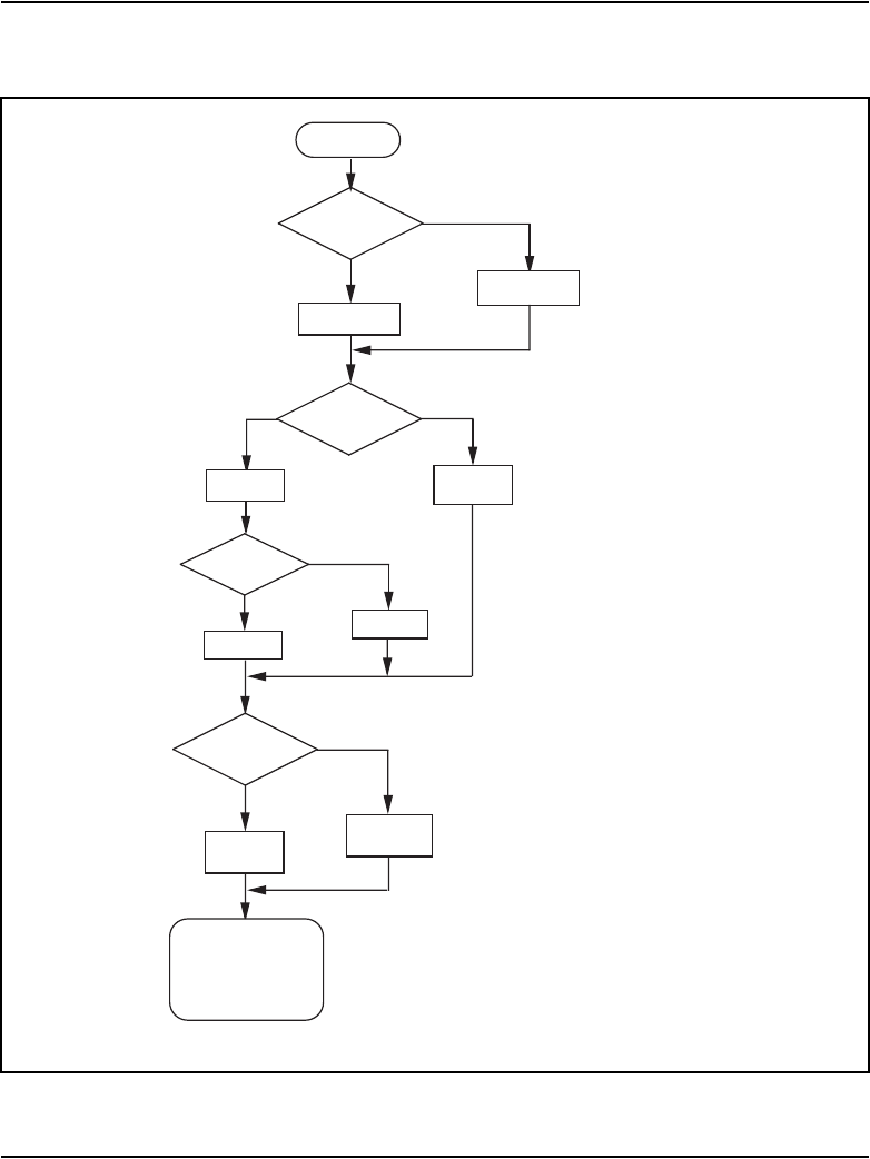
NT7D16 Data Access card Page 501 of 906
Circuit Card Description and Installation
Figure 95
Operating mode selection—RS422
PRM = Off
PRM = On
OPE YES
Host
Virtual Leased
Line?
Yes
No
HOT = On
DTR = On
Hotline?
HOT = On
HOT = Off
Yes
No
Allow
Autobaud?
No
AUTB = Off
Select BAUD
AUTB = On
BAUD = 7
Yes
Terminal
Set remaining
Operate Parameters
as appropriate:
par, aut, DLNG, KBD,
WIRE, & PBDO
DTR = Off
Operate Mode?
553-5221
Mode 8 and 9
Mode 12 and 13
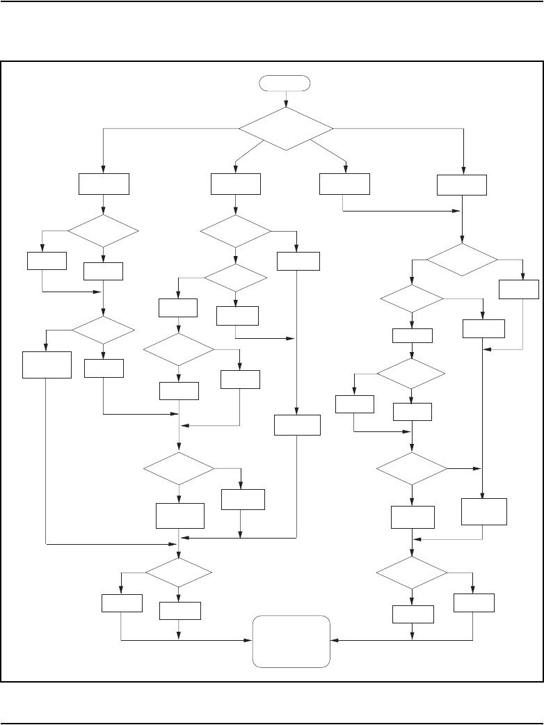
Page 502 of 906 NT7D16 Data Access card
553-3001-211 Standard 3.00 August 2005
Figure 96
Operating mode selection—RS-232-C
Operate Mode?
DEM = DTE
PRM = On DEM = DCE
PRM = Off DEM = DCE
PRM = On
OPE YES
DEM = DTE
PRM = Off
Dynamic DCD?
DCD = Off
DCD = On
Hotline?
HOT = On
AUTB = Off
Select BAUD HOT = Off
Virtual Leased
Line?
Hotline?
HOT = Off
Dynamic DCD?
DCD = Off
No
DCD = On
Yes
Allow
Autobaud?
AUTB = On
BAUD = 7
AUTB = Off
Select BAUD
No
Yes
HOT = On
DCD= On
No
Yes
Yes
No HOT = On
DCD= Off
Dynamic DTR?
DTR = On
Yes
No
DTR = Off
Modem (Modes 0, 1, 2, 3)
Gateway
(Modes 4, 5,
6, 7)
Host
(Modes 8,
9, 10, 11)
Virtual Leased
Line?
Yes
No
HOT = On
DTR = On
Hotline?
HOT = On
DTR = Off
HOT = Off
Yes
No
Dynamic DTR?
DTR = On
Yes
No
DTR = Off
Allow
Autobaud?
No
AUTB = Off
Select BAUD
AUTB = On
BAUD = 7
Yes
Dynamic DCD?
DCD = Off
No
DCD = On
Yes
AUTB = Off
Select BAUD
Terminal (Modes 12, 13, 14, 15)
Yes
No
Yes
No
Set remaining
Operate Parameters
as appropriate:
par, aut, DLNG, KBD,
WIRE, & PBDO
553-5222
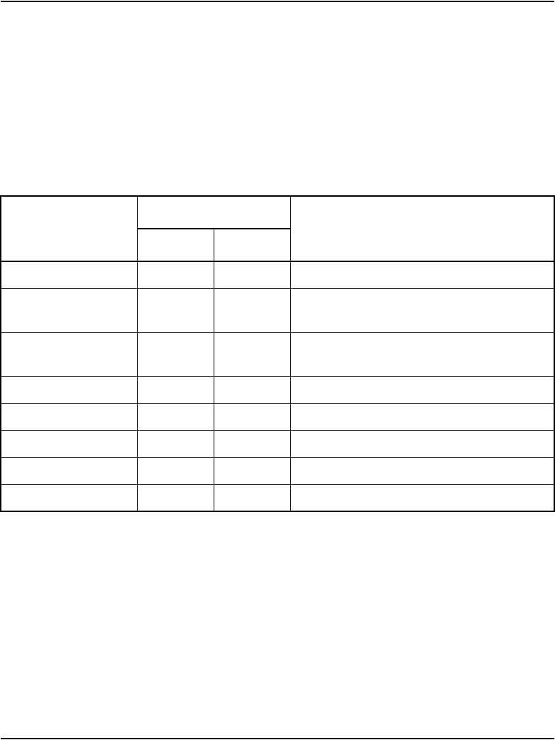
NT7D16 Data Access card Page 503 of 906
Circuit Card Description and Installation
Note: Warning Tone Denied (WTD) defaults if DTA is entered.
• If the DAC is used to call out through modem pooling, where the modem
pool consists of dumb modems connected to QMT8 SADM or QMT12
V.35 SADM, the DAC port should be configured with a secondary DN,
which has a single appearance.
• The Virtual keys must be assigned as shown in Table 164.
Table 164
Virtual key assignments
Feature key
Key number
UseSL-1 SL-100
Data DN 0 0 Required
Secondary DN 1 1 Required for manual
modem pooling
Call Transfer 2 — Required for manual
modem pooling
Auto Dial 3 2 Required for Hotline and VLL
Ring Again 4 6 Optional
Speed Call 5 3 Optional
Display 6 — Required
Make Set Busy 7 7 Optional

Page 504 of 906 NT7D16 Data Access card
553-3001-211 Standard 3.00 August 2005
Power supply
Be sure that all power requirements are met before installing the DAC.
Operation may be affected by improper power and environmental conditions.
EIA signals supported
The DAC supports a subset of the standard signals. Only 8 leads can be
brought through the backplane connector for each port, totaling 48 leads for
each card slot. Table 165 lists the EIA signals supported on this card.
Table 165
EIA signals supported (RS-232-C)
EIA
DB-25
Pin
Signal
abbreviation Description
DCE
mode
DTE
mode
BA 2TD Transmitted Data In Out
BB 3RD Received Data Out In
CB 5CTS Clear To Send Out In
CC 6DSR Data Set Ready Out In
AB 7GND Signal Ground — —
CF 8DCD Carrier Detect Out In
CD 20 DTR Data Terminal Ready In Out
CE 22 RI Ring Indicator Out In
Note: RS-422 leads supported are: Tx (transmit) and Rx (receive).

NT7D16 Data Access card Page 505 of 906
Circuit Card Description and Installation
Environmental
The DAC functions fully when operating within the following specified
conditions. See Table 166.
Reliability
The DAC has a predicted mean time between failure (MTBF) of 8 years at
45 degrees Celsius. The mean time to repair (MTTR) is 1 hour.
Installing the Data Access card
Cabinet system
The DAC is fully supported in any card slot in either the main or expansion
cabinet without any hardware modification. Insert the DAC into any available
card slot and secure it in place using the locklatches.
To cable out the DAC, run a standard 25-pair cable to the cross connect, or
use one of the following breakout cables in conjunction with an Amphenol
50-pin female-to-female gender converter:
• QCAD318A50-pin Amphenol to 6 female DB25 connectors
• QCAD319A50-pin Amphenol to 6 male DB25 connectors
Note: For Cabinet system, the format to be used in response to the “TN”
prompt must be one of the following:
CC 00 00 UUCC - Card Slot
or CC UUUU - Unit Number
Table 166
DAC environmental specifications
Specification Operating Storage
Ambient temperature 0 to 60 degrees C 40 to 70 degrees C
Humidity 5% to 95% 5% to 95%

Page 506 of 906 NT7D16 Data Access card
553-3001-211 Standard 3.00 August 2005
Large System
In Large Systems, the DAC is fully supported in IPE modules. These special
slots on the DAC have 24-pair cables pre-wired to the Main Distribution
Frame (MDF) in card slots 0-15. Any IPE slot will support the first four ports
on the DAC if connections are made at the MDF. Most IPE modules can be
upgraded to wire 24-pair cables to the MDF for all card slots.
Note: For directions concerning the pinouts for the MDF, refer to
Communication Server 1000M and Meridian 1: Large System
Installation and Configuration (553-3021-210).
Before you begin, power down:
• the IPE module only, if it is a DC-powered system
• the entire column, if it is an AC-powered system
It is recommended that you begin the installation from the right hand side
(when facing the backplane), starting with slot 0 and moving towards slots on
the left side. If you wish to add more than six DACs, and require slots 8
through 15, remove the input/output (I/O) panel. Be aware that a full shelf
installation can take up to 3 hours. You need the following equipment to
upgrade the cabling:
• A0359946 Amphenol cables
— These connectors include all the connector and screw apparatus.
— You need one cable for each DAC.
• cable ties
• wire cutters
• A3/16 nutdriver
System compatibility
To support the 24-pair requirement of the DAC, some cabling may need to be
upgraded (Table 167). See “Upgrading systems” for more information.
Ports 0, 1, 2, and 3 of the DAC work in any standard 16-pair IPE slot (connect
directly to the MDF).

NT7D16 Data Access card Page 507 of 906
Circuit Card Description and Installation
An upgraded backplane has three shrouds for each card slot. A backplane that
cannot be upgraded has only two shrouds for each card slot.
Port configuration
Figure 97 on page 508 shows the port configurations for both the RS-232-C
and RS-422 ports. The software configuration requirements for the DAC are
shown at the end of this chapter. Responses to the prompts listed are required.
Depending on the configuration, ensure that the option plug is set for RS-232
or RS-422.
Table 167
System option compatibility with the DAC
System option
Backplane
code
Backplane
release Upgrade
Maximum no.
of ports/DAC
supported
Large Systems NT8D3701 3 and below No 4
Large Systems NT8D3701 4 and above Ye s 6
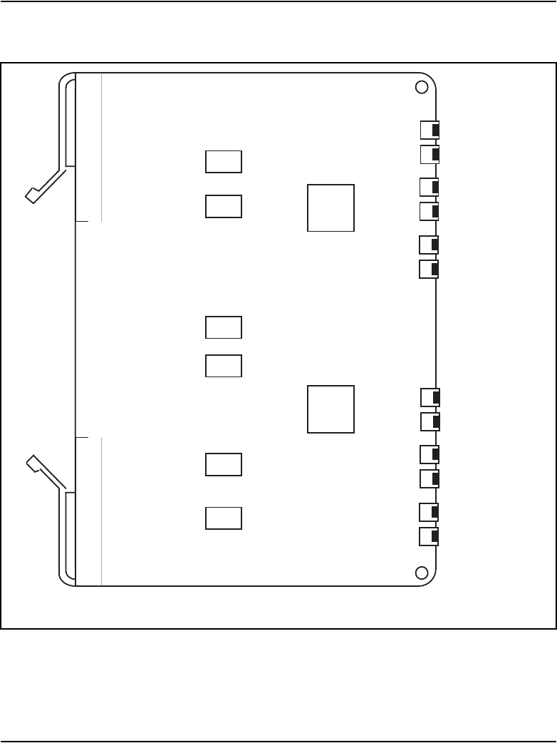
NT7D16 Data Access card Page 509 of 906
Circuit Card Description and Installation
Cabling
Several cabling schemes are possible for both AILC and RILC modes.
Typical capacitance for 24- and 26-gauge cables is shown in the Tables 168
and 169. RS-232 and RS-422 transmission distance is limited by the electrical
capacitance of the cable. Low-capacitance cable carries a digital signal
further than a high-capacitance cable.
Figure 98 on page 510 shows the cabling choices available. It includes
cabling with the RS-232-C cable, associated patch panel, the RJ-11, and the
octopus cable. Each scheme can be tailored to suit individual needs, and
specific alternatives are shown in later figures.
Table 168
RS-232-C maximum line capacitance 2,500 µF
Gauge Capacitance per foot (µF) Max distance
24 24 104
26 15 166
Table 169
RS-422 maximum line capacitance 60,000 µF
Gauge Capacitance per foot (µF) Max distance
24 24 2500
26 15 4000
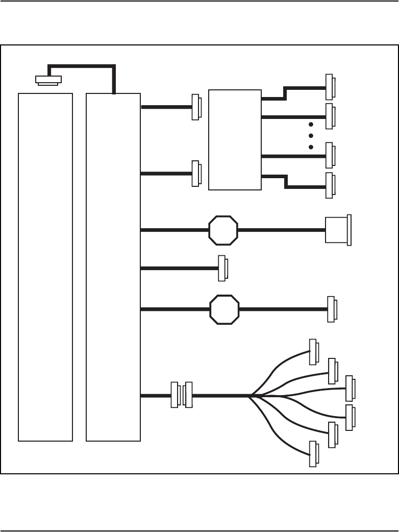
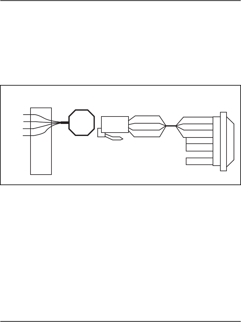
NT7D16 Data Access card Page 511 of 906
Circuit Card Description and Installation
Figure 99 shows a connection through an RJ-11 or RJ-45 jack located at the
data station. It is recommended that four wires be used similarly to the AIM
drop when using the RJ-11 jack. Another cable is required to convert the
RJ-11 or RJ-45 into DB25.
Note: It is necessary to turn over Receive Data and Send Data between
the DAC and the AILU. This is done on the TN at the MDF.
Figure 100 on page 512 illustrates the patch panel. RS-232-C cables are used
to connect the data equipment to the patch panel. This particular panel shows
two 50-pin connectors into twelve DB25. The signals from the MDF travel
on 25-pair cables, terminating at the patch panel.
Note: Use patch panels that follow the pinout of the DAC.
Figure 101 on page 513 describes an octopus cabling scheme. This cable
replaces the combined patch panel and RS-232-C cabling scheme. The
25-pair cable is split into six RS-232-C male or female connectors. This
allows direct connections to the data equipment from the I/O panel. The
octopus cable allows for the maximum segregation of the voice signals that
might otherwise be present within the same 25-pair cable.
Figure 99
RJ-11 or RJ-45 jacks
MDF
TxD
RxD
GND
DTR
EIA signals from
the DAC (unit n)
RJ-11
plug
1 (TxD)
6 (RxD)
5 (GND)
20 (DTR)
1 (TxD)
6 (RxD)
5 (GND)
20 (DTR)
6 (DSR)
8 (DCD)
4 (RTS)
5 (CTS)
RJ-11
jack
553-5023
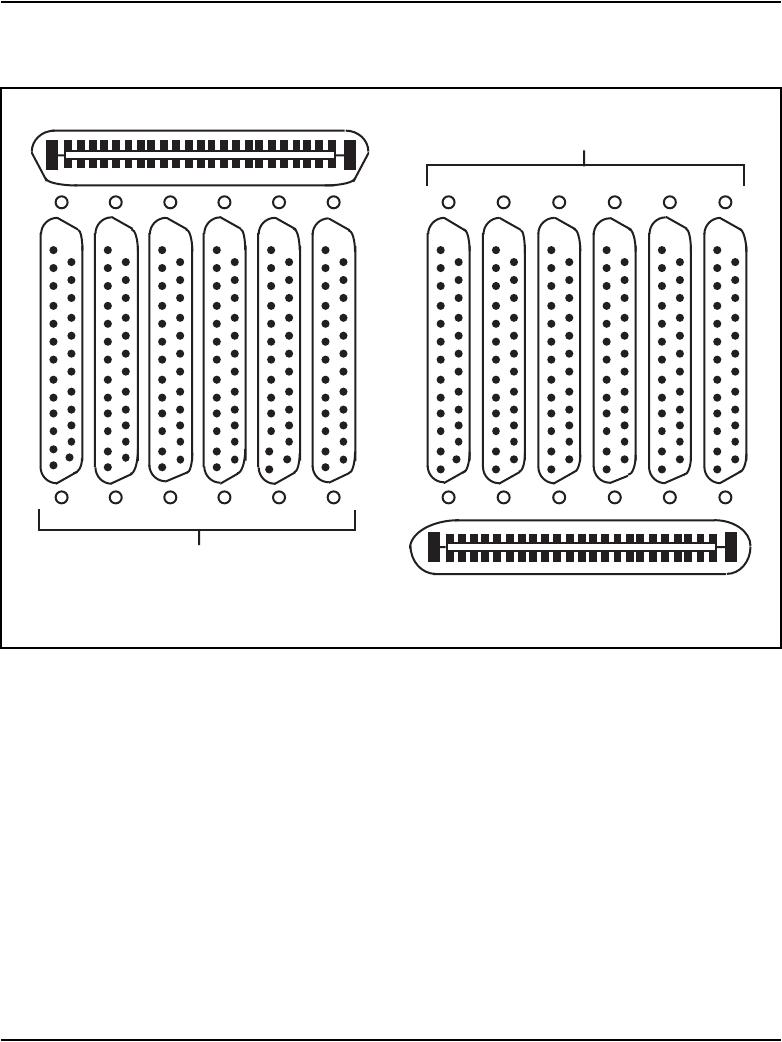
Page 512 of 906 NT7D16 Data Access card
553-3001-211 Standard 3.00 August 2005
Note: Use an octopus cable that follows the pinout of the DAC, such as
QCAD318A (female) and QCAD319A (male), in conjunction with a
50-pin female-to-female gender converter.
Figure 100
Patch panel layout
DB25
DB25
50-pin connector
50-pin connector
553-5021
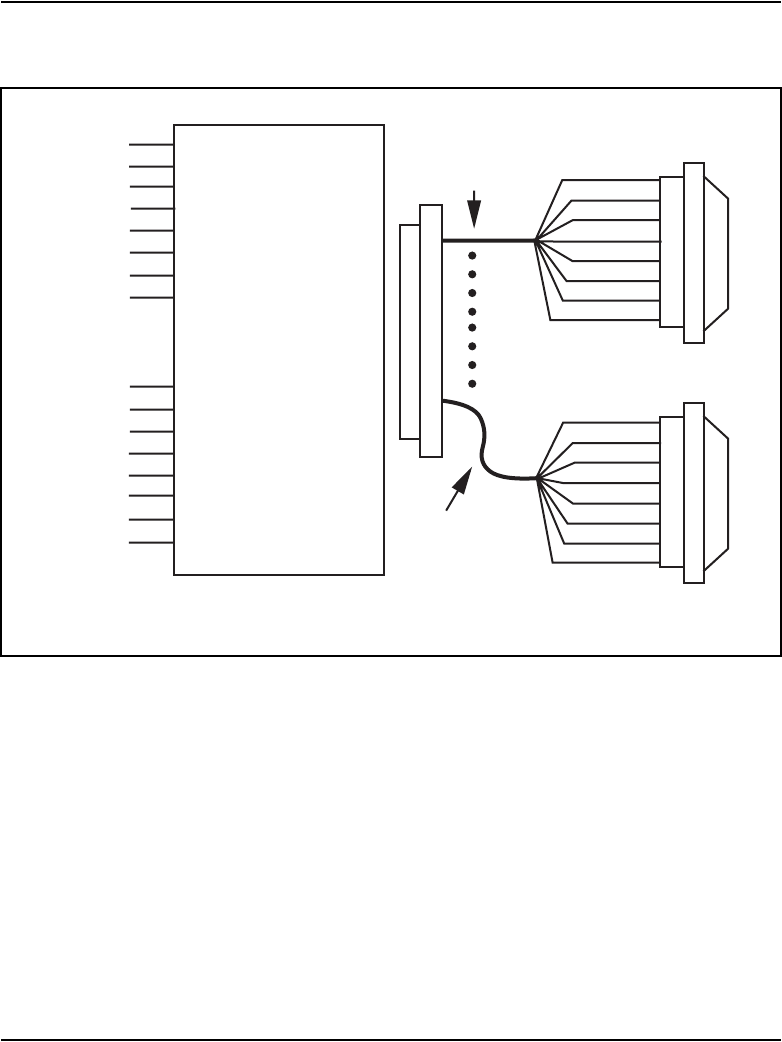
NT7D16 Data Access card Page 513 of 906
Circuit Card Description and Installation
Figure 101
Octopus cabling
MDF
TxD
RxD
GND
DTR
CTS
DSR
DCD
RI
TxD
RxD
GND
DTR
CTS
DSR
DCD
RI
EIA signals from
the DAC (unit 0)
EIA signals from
the DAC (unit 5)
2 (TxD)
3 (RxD)
7 (GND)
20 (DTR)
5 (CTS)
6 (DSR)
8 (DCD)
22 (RI)
2 (TxD)
3 (RxD)
7 (GND)
20 (DTR)
5 (CTS)
6 (DSR)
8 (DCD)
22 (RI)
EIA signals from
the DAC (unit 0)
EIA signals from
the DAC (unit 5)
6 DB25
connectors per 25
pair cable
To your data equipment
To your data equipment
DB25 connector DB25 connector
553-5022

Page 514 of 906 NT7D16 Data Access card
553-3001-211 Standard 3.00 August 2005
Backplane pinout and signaling
Two 40-pin, and two 20-pin edge connectors connect the card to the
backplane. The detailed pinout configurations are listed in Tables 170 and
171.
Table 170
RS-232-C and RS-422 pinouts for first three DAC ports (Part 1 of 2)
I/O cable
Unit no.
RS-232-C
RS-422
Signal
Patch pair or
octopus
Pair Pin
Pair
color Signal Pin no.
1T 26 W-BL UNIT 0 TD0 2RDA0
1R 1BL-W RD0 3RDB0
2T 27 W-O DTR0 20 SDA0
2R 2O-W GND0 7SDB0 Connector
3T 28 W-G DCD0 8 1
3R 3G-W DSR0 6
4T 29 W-BR RI0 22
4R 4BR-W CTS0 5
5T 20 W-S UNIT 1 TD1 2RDA1
5R 5 S-W RD1 3RDB1
6T 31 R-BL DTR1 20 SDA1
6R 6BL-R GND1 7SDB1 Connector
7T 32 R-O DCD1 8 2
Note 1: The RS-232 pinout follows the standard set by the QPC723 RILC.
Note 2: The RS-422 pinout follows the standard set by the QPC430 AILC (first pair: Receive
Data; second pair: Send Data). Receive and Send are designated with reference to the DTE;
therefore, they must be turned over in the cross-connect since most DTE have first pair as Send
Data and second pair as Receive Data.
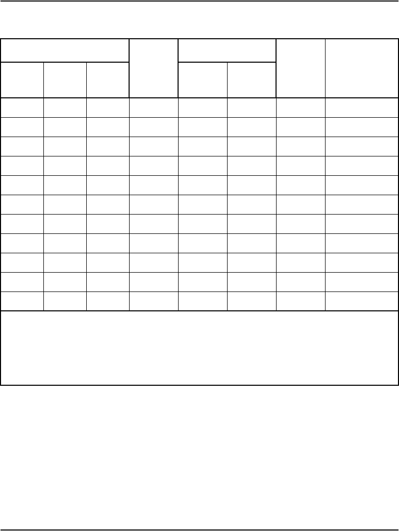
NT7D16 Data Access card Page 515 of 906
Circuit Card Description and Installation
7R 7O-R DSR1 6
8T 33 R-G RI1 22
8R 8G-R CTS1 5
9T 34 R-BR UNIT 2 TD2 2RDA2
9R 9BR-R RD2 3RDB2
10T 35 R-S DTR2 20 SDA2
10R 10 S-R GND2 7SDB2 Connector
11T 36 BK-BL DCD2 8 3
11R 11 BL-BK DSR2 6
12T 37 BK-O RI2 22
12R 12 O-BK CTS2 5
Table 170
RS-232-C and RS-422 pinouts for first three DAC ports (Part 2 of 2)
I/O cable
Unit no.
RS-232-C
RS-422
Signal
Patch pair or
octopus
Pair Pin
Pair
color Signal Pin no.
Note 1: The RS-232 pinout follows the standard set by the QPC723 RILC.
Note 2: The RS-422 pinout follows the standard set by the QPC430 AILC (first pair: Receive
Data; second pair: Send Data). Receive and Send are designated with reference to the DTE;
therefore, they must be turned over in the cross-connect since most DTE have first pair as Send
Data and second pair as Receive Data.

Page 516 of 906 NT7D16 Data Access card
553-3001-211 Standard 3.00 August 2005
Table 171
RS-232-C and RS-422 pinouts for last three DAC ports (Part 1 of 2)
I/O cable
Unit no.
RS-232-C
RS-422
Signal
Patch pair or
octopus
Pair Pin
Pair
color Signal Pin no.
13T 38 BK-G UNIT 3 TD3 2RDA3
13R 13 G-BK RD3 3RDB3
14T 39 BK-BR DTR3 20 SDA3
14R 14 BR-BK GND3 7SDB3 Connector
15T 40 BK-S DCD3 8 1
15R 15 S-BK DSR3 6
16T 41 Y- BL RI3 22
16R 16 BL-Y CTS3 5
17T 42 Y- O UNIT 4 TD4 2RDA4
17R 17 O-Y (Note) RD4 3RDB4
18T 43 Y- G DTR4 20 SDA4
18R 18 G-Y GND4 7SDB4 Connector
19T 44 Y- BR DCD4 8 2
19R 19 BR-Y DSR4 6
20T 45 Y- S RI4 22
20R 20 S-Y CTS4 5
21T 46 V-BL UNIT 5 TD5 2RDA5
21R 21 BL-V (Note) RD5 3RDB5
22T 47 V-O DTR5 20 SDA5
Note: Units 4 and 5 are available when the DAC is installed in a fully wired 24-pair slot.
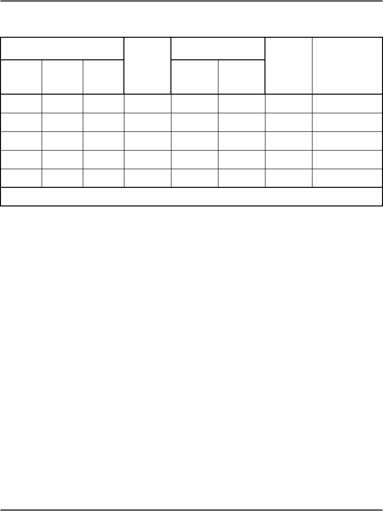
NT7D16 Data Access card Page 517 of 906
Circuit Card Description and Installation
Configuring the Data Access card
LD 11 must be configured to accept the DAC. The commands listed here
must be answered. LD 20 prints out card information when requested. For a
complete list of the service change prompts and responses, see Software
Input/Output: Administration (553-3001-311).
DAC administration (LD 11)
Responding R232 or R422 to the TYPE prompt in LD11 begins the prompt
sequence for the DAC configuration. Responses to the following prompts are
22R 22 O-V GND5 7SDB5 Connector
23T 48 V-G DCD5 8 3
23R 23 G-V DSR5 6
24T 49 V-BR RI5 22
24R 24 BR-V CTS5 5
Table 171
RS-232-C and RS-422 pinouts for last three DAC ports (Part 2 of 2)
I/O cable
Unit no.
RS-232-C
RS-422
Signal
Patch pair or
octopus
Pair Pin
Pair
color Signal Pin no.
Note: Units 4 and 5 are available when the DAC is installed in a fully wired 24-pair slot.

Page 518 of 906 NT7D16 Data Access card
553-3001-211 Standard 3.00 August 2005
required. The defaults are bracketed, and may be issued by Carriage Return
(<CR>).
LD 11 – Configure Data Access card. (Part 1 of 3)
Prompt Response Description
REQ: NEW CHG MOV
COPY
Add, change, move or copy the unit
TYPE: R232
R422
RS-232-C unit
RS-422 unit
TN l s c u DAC data TN. The loop (LL) must be a superloop.
RNPG <CR> Ringing number pickup group (default to zero)
CLS
DTA
ADD
Class of Service allowed for the DAC.
Data Allowed
Digit Display Allowed
TOV (0) - 3 Timeout value, where:
0 = no timeout
1 = 15 minutes
2 = 30 minutes
3 = 60 minutes
OPE (NO) YES Operation parameter change
PAR (SPAC) ODD EVEN
MARK
SPAC = space parity
ODD = odd parity
EVEN = even parity
MARK = mark parity
DTR (OFF) ON DTR settings, where:
ON = forced DTR
OFF = dynamic DTR
This prompt appears only if TYPE = R232

NT7D16 Data Access card Page 519 of 906
Circuit Card Description and Installation
HOT (OFF) ON Hotline
If HOT = ON, then AUTB = OFF
AUT (ON) OFF Automatic answer
AUTB (ON) OFF Autobaud
Prompt appears only if HOT - OFF
BAUD 0-(7)-8 Baud rate, where:
0 = 110
1 = 150
2 = 300
3 = 600
4 = 1200
5 = 2400
6 = 4800
7 = 9600
8 = 19200
This prompt appears only if AUTB = OFF.
DCD (ON) OFF DCD settings, where:
ON = dynamic DCD
OFF = forced DCD
This prompt appears only if TYPE = R232.
PRM (ON) OFF Prompt mode, where:
ON = prompt (Terminal) mode
OFF = no prompt (Host) mode
DEM (DCE) DTE Data Equipment mode
This prompt appears only if TYPE = R232.
LD 11 – Configure Data Access card. (Part 2 of 3)
Prompt Response Description

Page 520 of 906 NT7D16 Data Access card
553-3001-211 Standard 3.00 August 2005
DLNG (ENG) FRN Data port language, where:
ENG = English
FRN = Quebec French
KBD (ON) OFF Keyboard dialing, where:
ON = enabled
OFF = disabled (Hayes dialing commands will still work)
WIRE (OFF) ON Wire test mode, where:
OFF = disabled
ON = enabled
PBDO (OFF) ON Port busy upon DTR off, where:
OFF = disabled (port busy on with DTR)
ON = enabled (port busy off with DTR)
This prompt appears only if TYPE = R232
PBDO = OFF for any RS-232-C mode besides 8, or 12
If PBDO = ON, key 7 = MSB
KEY
0 SCR xxxx
1 SCR xxxx
2 TRN
3 ADL yy xxxx
4 RGA
5 SCC 0-253
6 DSP
7 MSB
Key settings
Primary data DN
Secondary Data DN
Call Transfer
Autodial
Ring Again
Speed Call Controller, list number
Display
Make Set Busy
Primary and secondary data DNs must be single
appearance DNs. Feature key assignment must be as
shown here.
LD 11 – Configure Data Access card. (Part 3 of 3)
Prompt Response Description
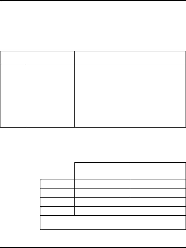
NT7D16 Data Access card Page 521 of 906
Circuit Card Description and Installation
Printing the card parameters (LD 20)
By responding R232, R422, or DAC to the TYPE prompt in LD 20, you can
print out the configured parameters for each port, or the entire DAC. This is
useful to determine if any parameters have been altered during keyboard or
Hayes dialing modify procedures.
The operation parameter printout for an RS-232 or RS-422 port is similar to
the following, depending on the configuration.
LD 20 – Print DAC parameters.
Prompt Response Description
REQ: PRT
LTN
LUU
Print data, TN, or unit information for the unit specified
TYPE: R232
R422
DAC
Print information for the RS-232-C, RS-422 ports, or the
whole DAC
TN l s c u Print information for this TN, where l = loop, s = shelf,
c = card, u = unit. Uploaded parameters can only be
printed when a specific TN is listed.
Table 172
Print out example (Part 1 of 2)
DBASE
R-232 or R-422
UPLOAD
R-232 or R-422
PAR S PAC SPAC
DTR ON ON
HOT OFF OFF
AUT ON O
Note: The Upload parameters are printed only when a single TN is
specified.
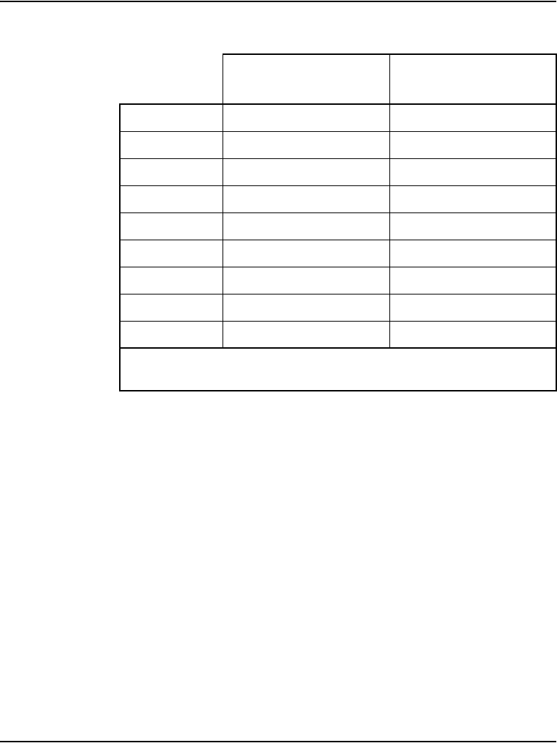
Page 522 of 906 NT7D16 Data Access card
553-3001-211 Standard 3.00 August 2005
Connecting Apple Macintosh to the DAC
The Apple Macintosh can be connected with twisted pair wire to a port of a
NT7D16 Data Access Card (DAC) to allow access to the switching
capability. The Macintosh can then access local or remote terminals, personal
computers, hosts, and peripherals.
Figure 102 on page 523 shows the 9-pin subminiature D (DB9) connection to
the Macintosh. Figure 103 on page 523 shows the mini-8 DIN connection to
the Macintosh.
Upgrading systems
The following explains when and how to upgrade your system to support the
DAC. Ports 0, 1, 2, and 3 of the DAC will work in any standard 16-pair IPE
slot (connect directly to the MDF).
AUTB ON ON
BAUD 9600 4800
DCD OFF OFF
PRM KBD ON KBD ON
DEM DCE DCE
DLNG FRN FRN
KBD ON ON
WIRE OFF OFF
PBDO OFF OFF
Table 172
Print out example (Part 2 of 2)
DBASE
R-232 or R-422
UPLOAD
R-232 or R-422
Note: The Upload parameters are printed only when a single TN is
specified.
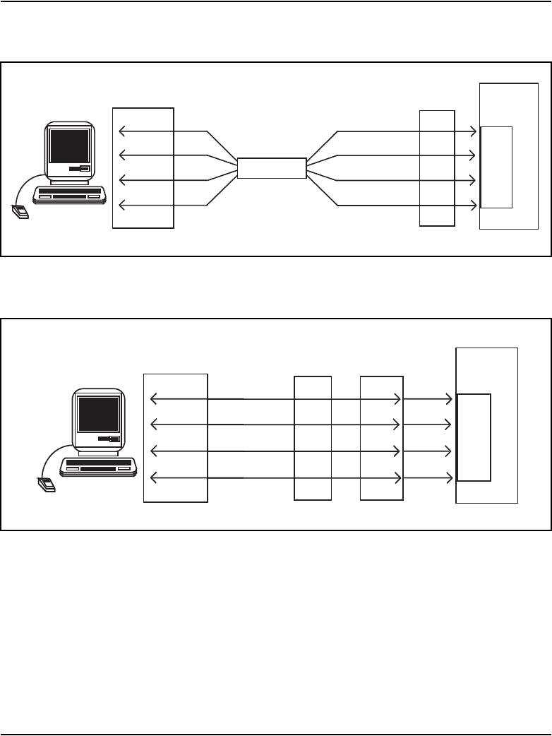
NT7D16 Data Access card Page 523 of 906
Circuit Card Description and Installation
Figure 102
Macintosh to DAC connection—9-pin subminiature D
Figure 103
Macintosh to DAC connection—mini-8 DIN
Apple
Macintosh 9-pin
subminiature D
8
9
5
4
W
BL
BK
Y
RDA
RDB
SDA
SDB
MDF
R3
T3
R2
T2
System
D
A
C
W
BL
BK
Y
6-wire
Teladapt
cord
553-AAA1129
Apple
Macintosh Mini-8
DIN connector
8
5
6
3
RDA
RDB
SDA
SDB
MDF
R3
T3
R2
T2
System
D
A
C
RXD+
RXD-
TXD+
TXD-
RDA0
RDB0
SDA0
SDB0
DB25
pin #
553-AAA113
0

Page 524 of 906 NT7D16 Data Access card
553-3001-211 Standard 3.00 August 2005
Large System and CS 1000M HG upgrade
The DAC can be installed directly into slots 0, 4, 8, and 12 with no cabling
changes. If other slots are required, the upgrade must be made. Follow this
procedure to upgrade your cabling. You can upgrade the cabling
segment-by-segment, or the entire module at one time.
Note 1: Four NT8D81AA cable/filter assemblies are required to
upgrade the entire module, one assembly per segment.
Note 2: Cables are designated by the letter of the I/O panel cutout where
the 50-pin cable connector is attached. The 20-pin connectors are labeled
1, 2, and 3.
Note 3: The locations for the cable connectors are designated by the slot
number (L0-L9), and the shroud row (1, 2, and 3).
Segment 0
1Leave cable A as is in slot L0.
2Move cable end B-3 to L1-3.
3Remove cable C from the backplane and connect ends C-1, C-2, and C-3
to L2-1, L2-2, and L2-3.
4Add cable D to the I/O panel by connecting ends D-1, D-2, and D-3 to
L3-1, L3-2, and L3-3.
Segment 1
1Leave cable E as is in slot L4.
2Move cable end F-3 to L5-3.
3Remove cable G from the backplane and connect ends G-1, G-2, and G-3
to L6-1, L6-2, and L6-3.
4Add cable H to the I/O panel by connecting ends H-1, H-2, and H-3 to
L7-1, L7-2, and L7-3.

NT7D16 Data Access card Page 525 of 906
Circuit Card Description and Installation
Segment 2
1Leave cable K as is in slot L8.
2Move cable end L-3 to L9-3.
3Remove cable M from the backplane and connect ends M-1, M-2, and
M-3 to L10-1, L10-2, and L10-3.
4Add cable N to the I/O panel by connecting ends N-1, N-2, and N-3 to
L11-1, L11-2, and L11-3.
Segment 3
1Leave cable R as is in slot L12.
2Move cable end S-3 to L13-3.
3Remove cable T from the backplane and connect ends T-1, T-2, and T-3
to L14-1, L14-2, and L14-3.
4Add cable U to the I/O panel by connecting ends U-1, U-2, and U-3 to
L15-1, L15-2, and L15-3.

Page 526 of 906 NT7D16 Data Access card
553-3001-211 Standard 3.00 August 2005
Be sure to re-label the MDF to show that the module has been upgraded to
provide one cable for each IPE slot. The resulting backplane and cable
arrangement should look like this:
Backplane slot-connector I/O panel cable position
L0 A
L1 B
L2 C
L3 D (new cable)
L4 E
L5 F
L6 G
L7 H (new cable)
L8 K
L9 L
L10 M
L11 N (new cable)
L12 R
L13 S
L14 T
L15 U (new cable)

Page 527 of 906
Circuit Card Description and Installation
544
NT8D02 and NTDK16 Digital Line cards
Contents
This section contains information on the following topics:
Introduction . . . . . . . . . . . . . . . . . . . . . . . . . . . . . . . . . . . . . . . . . . . . . . 527
Physical description. . . . . . . . . . . . . . . . . . . . . . . . . . . . . . . . . . . . . . . . 528
Functional description . . . . . . . . . . . . . . . . . . . . . . . . . . . . . . . . . . . . . . 530
Electrical specifications. . . . . . . . . . . . . . . . . . . . . . . . . . . . . . . . . . . . . 536
Connector pin assignments . . . . . . . . . . . . . . . . . . . . . . . . . . . . . . . . . . 539
Configuration . . . . . . . . . . . . . . . . . . . . . . . . . . . . . . . . . . . . . . . . . . . . 541
Introduction
The Digital Line card is a voice and data communication link between the
system and Digital Telephones. It supports voice only or simultaneous voice
and data service over a single twisted pair of standard telephone wiring.
When a digital telephone is equipped with the data option, an asynchronous
or synchronous terminal or personal computer can be connected to the system
through the digital telephone.
IMPORTANT!
The NT8D02 digital line card is supported in CS 1000S, CS 1000M, and
Meridian 1.
The NTDK16 digital line card is supported ONLY in the Chassis system.

Page 528 of 906 NT8D02 and NTDK16 Digital Line cards
553-3001-211 Standard 3.00 August 2005
The Digital Line card provides 16 voice and 16 data communication links.
NT8D02 Digital Line card
The 32 port NT8D02 Digital Line card is supported in the MG 1000S and
MG 1000S Expansion.
You can install this card in any IPE slot.
NTDK16 Digital Line card
The NTDK16 is a 48 port card supported only in the Chassis system. It is
based on the NT8D02 Digital Line card and is functionally equivalent to three
NT8D02s, and configured as cards 4, 5, and 6 in the main chassis. It uses A94
Digital Line Interface chips (DLIC) to provide the interface between the
Digital sets and the system.
The NTDK16 Digital Line card can only be installed in slot 4 of the main
chassis which is slotted to prevent accidental insertion of other cards.
Physical description
The Digital Line card circuitry is mounted on a 31.75 cm by 25.40 cm
(12.5 in. by 10 in.) printed circuit board. The NT8D02 is a double-sided PCB,
whereas the NTDK16 is 4 layers, but standard thickness. Both cards connect
to the backplane through a 120-pin or 160-pin edge connector.
The faceplate of the NT8D02 Digital Line card is equipped with a red LED
that lights when the card is disabled. See Figure 104 on page 529. When the
card is installed, the LED remains lit for two to five seconds as a self-test runs.
If the self-test completes successfully, the LED flashes three times and
remains lit until the card is configured and enabled in software, then the LED
goes out. If the LED continually flashes or remains weakly lit, replace the
card.
Note: The NTDK16AA has one LED. This LED shows the status of
Card 4. The NTDK16BA has three LEDs. These LEDs show the status
of Cards 4, 5, and 6 configured on the NTDK16.
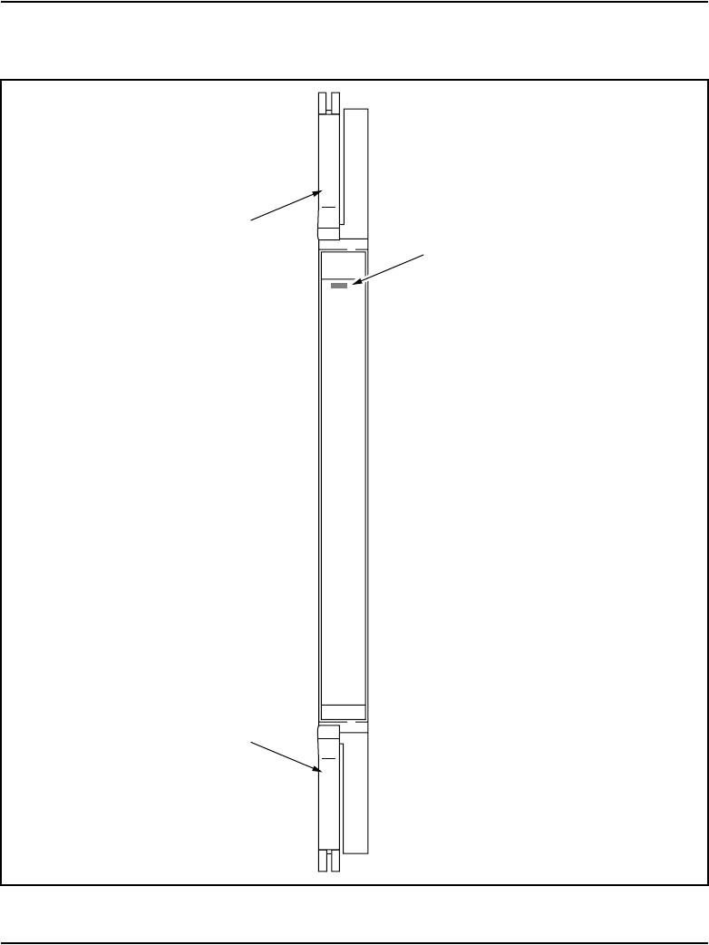

Page 530 of 906 NT8D02 and NTDK16 Digital Line cards
553-3001-211 Standard 3.00 August 2005
Functional description
NT8D02 Digital Line card
The NT8D02 digital line card is equipped with 16 identical units. Each unit
provides a multiplexed voice, data, and signaling path to and from digital
apparatus over a 2-wire full duplex 512 kHz time compression multiplexed
(TCM) digital link. Each digital telephone and associated data terminal is
assigned a separate terminal number (TN) in the system database, for a total
of 32 addressable ports per card.
The NT8D02 Digital Line card is equipped with 16 identical digital line
interfaces. Each interface provides a multiplexed voice, data, and signaling
path to and from a digital terminal (telephone) over a 2-wire full duplex
512 kHz Time Compression Multiplexed (TCM) digital link. Each digital
telephone and associated data terminal is assigned a separate Terminal
Number (TN) in the system database, giving a total of 32 addressable units
per card. The digital line card supports Nortel’ Meridian Digital Telephone.
The digital line card contains a microprocessor that provides the following
functions:
• self-identification
•self-test
• control of card operation
• status report to the controller
• maintenance diagnostics
Figure 105 on page 531 shows a block diagram of the major functions
contained on the NT8D02 Digital Line card. Each of these functions is
described on the following pages.
NT8D02 and NTDK16 Digital Line cards Page 531 of 906
Circuit Card Description and Installation
Figure 105
Digital line card – block diagram
Digital
line
interface
Micro-
controller
5.12 MHz clock
Tx PCM
DS-30X loop
Card
LAN link
Power
supplies
Front
panel
LED
Card LAN
interface
Tip
TCM
loop
interface
circuit
Digital
phone lines
Line interface units 0–7
Line interface units 8–15
Ring
Tip
TCM
loop
interface
circuit
Digital
phone lines
Ring
Rx PCM
1 kHz frame sync
Card slot
address Sanity
timer
553-6163
Digital
line
interface
+5 V dc
+10 V dc
±15 V dc
Reg
+15 +10
+10 V dc
Address/
data bus

Page 532 of 906 NT8D02 and NTDK16 Digital Line cards
553-3001-211 Standard 3.00 August 2005
NTDK16 Digital Line card
The NTDK16 digital line card is equipped with 48 identical units. Each unit
provides a multiplexed voice, data, and signaling path to and from digital
apparatus over a 2-wire full duplex 512 kHz time compression multiplexed
(TCM) digital link. Each digital telephone and associated data terminal is
assigned a separate terminal number (TN) in the system database, for a total
of 96 addressable ports per card. Refer to Figure 106 on page 533.
The NTDK16 digital line card contains a microprocessor that provides the
following functions:
• self-identification
•self-test
• control of card operation
• status report to the controller
• maintenance diagnostics
The card also provides:
• Ability to support Digital sets and the Digital Console M2250
• Provides a serial link (Card LAN) for status report and maintenance.
• Supports loop lengths up to 3500 ft. (1.0 km) using 24 AWG wire.
• Interface between three DS30X loops and 48 TCM lines.
Card interfaces
The digital line card passes voice, data, and signaling over DS-30X loops and
maintenance data over the card LAN link. These interfaces are discussed in
detail in the section “Intelligent Peripheral Equipment” on page 32.
Digital line interfaces
The digital line interface contains two Digital Line Interface Circuits (DLIC).
Each digital line interface circuit provides eight identical, individually
configurable voice and data interfaces to eight digital telephone lines. These
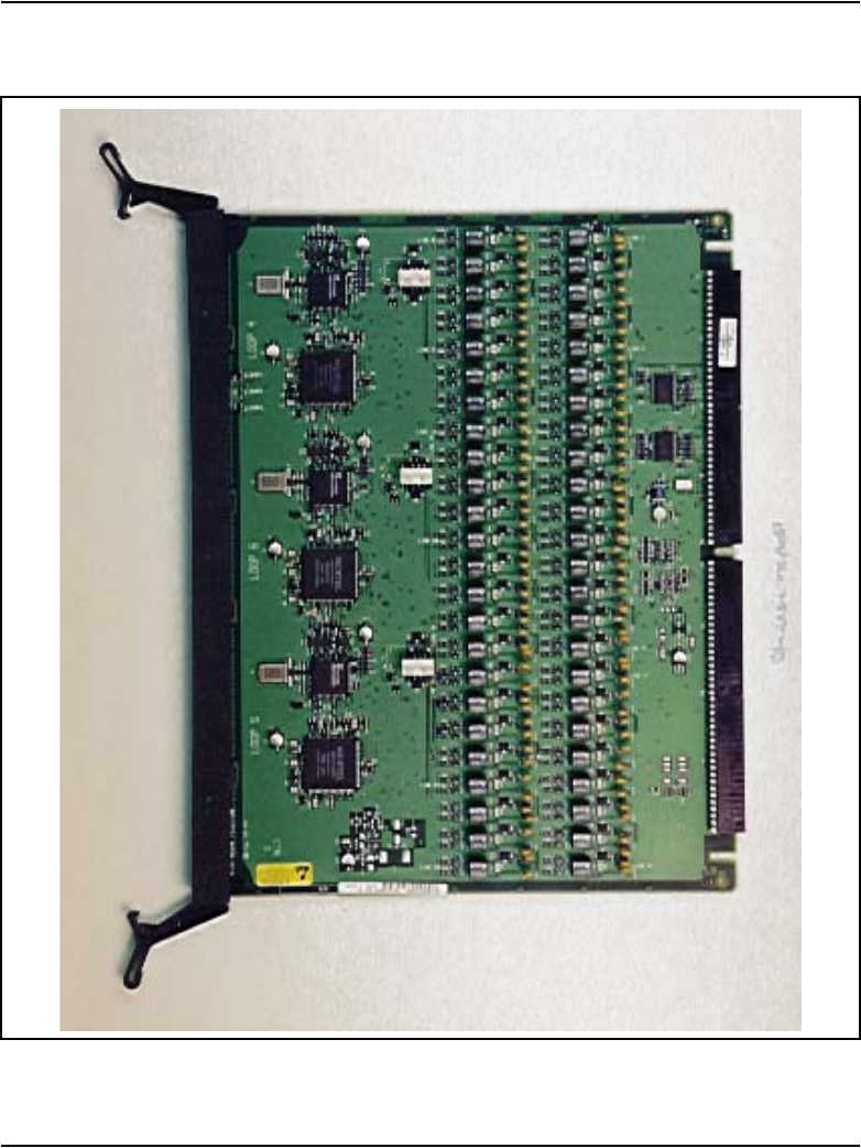

Page 534 of 906 NT8D02 and NTDK16 Digital Line cards
553-3001-211 Standard 3.00 August 2005
lines carry multiplexed PCM voice, data, and signaling information as TCM
loops.
The purpose of each digital line interface circuit is to de-multiplex data from
the DS-30X Tx channel into eight integrated voice and data bitstreams. The
circuits then transmit those bitstreams as Bi-Polar Return to Zero, Alternate
Mark Inversion (BPRZ-AMI) data to the eight TCM loops. They also perform
the opposite action: they receive eight BPRZ-AMI bitstreams from the TCM
loops and multiplex them onto the DS-30X Rx channel. The two digital line
interface circuits perform the multiplexing and de-multiplexing functions for
the 16 digital telephone lines.
The digital line interface circuits also contain signaling and control circuits
that establish, supervise, and take down call connections. These circuits work
with the on-card microcontroller to operate the digital line interface circuits
during calls. The circuits receive outgoing call signaling messages from the
Call Server and return incoming call status information to the Call Server
over the DS-30X network loop.
TCM loop interface circuit
Each digital telephone line terminates on the NT8D02 Digital Line card at a
TCM loop interface circuit. The circuit provides transformer coupling and
foreign voltage protection between the TCM loop and the digital line
interface circuit. It also provides battery voltage for the digital telephone.
To prevent undesirable side effects from occurring when the TCM loop
interface cannot provide the proper signals on the digital phone line, the card
microcontroller can remove the ±15 V dc power supply from the TCM loop
interfaces. This happens when either the microcontroller gets a command
from the NT8D01 controller card to shut down the channel, or the digital line
card detects a loss of the 1 KHz frame synchronization signal. The ±15 V dc
power supply signal is removed from all 16 TCM loop interface units at the
same time.
Each TCM loop interface circuit can service loops up to 3500 ft. in length
when using 24-gauge wire. They support a maximum ac signal loss of
15.5 dB at 256 KHz and a maximum dc loop resistance of 210 ohms.

NT8D02 and NTDK16 Digital Line cards Page 535 of 906
Circuit Card Description and Installation
Card control functions
Control functions are provided by a microcontroller and a Card LAN link on
the digital line card. A sanity timer is provided to automatically reset the card
if the microcontroller stops functioning for any reason.
Microcontroller
The NT8D02 Digital Line card contains a microcontroller that controls the
internal operation of the card and the serial card LAN link to the controller
card. The microcontroller controls the following:
• reporting to the Call Server through the card LAN link:
— card identification (card type, vintage, and serial number)
— firmware version
— self-test status
— programmed configuration status
• receipt and implementation of card configuration:
— programming of the digital line interfaces
— enabling/disabling of individual units or entire card
— programming of loop interface control circuits for administration of
line interface unit operation
— maintenance diagnostics
The microcontroller also controls the front panel LED when the card is
enabled or disabled by instructions from the NT8D01 controller card.
Card LAN interface
Maintenance data is exchanged with the common equipment Call Server over
a dedicated asynchronous serial network called the Card LAN link.
Sanity timer
The NT8D02 Digital Line card also contains a sanity timer that resets the
microcontroller if program control is lost. The microcontroller must service

Page 536 of 906 NT8D02 and NTDK16 Digital Line cards
553-3001-211 Standard 3.00 August 2005
the sanity timer every 1.2 seconds. If the timer is not properly serviced, it
times out and causes the microcontroller to be hardware reset.
Circuit power
The +15 V dc input is regulated down to +10 V dc for use by the digital line
interface circuits. The ±15.0 V dc inputs to the card are used to power the loop
interface circuits.
Electrical specifications
This section lists the electrical characteristics of the NT8D02 Digital Line
card.
NT8D02 and NTDK16 Digital Line cards Page 537 of 906
Circuit Card Description and Installation
Digital line interface specifications
Table 173 provides a technical summary of the digital line cards.
Table 173
NT8D02/NTDK16 Digital Line card technical summary
Characteristics
NT8D02 DLC
description
NTDK16BA DLC
description
NTDK16AA DLC
description
Units per card 16 voice, 16 data 48 voice, 48 data 48 voice, 48 data
Impedance 100 Ohm j/b ohm 100 Ohm j/b ohm 100 Ohm j/b ohm
Loop limits
30 m (100 ft) to 915
m (3000 ft) with 24
AWG PVC cable
(+15 V DC at 80 mA)
30 m (100 ft) to 915
m (3000 ft) with 24
AWG PVC cable
(+15 V DC at 80 mA)
30 m (100 ft) to 915
m (3000 ft) with 24
AWG PVC cable
(+15 V DC at 80 mA)
0 to 1070 m (3500 ft)
with 24 AWG PVC
cable (+15 V DC at
80 mA)
0 to 1070 m (3500 ft)
with 24 AWG PVC
cable (+15 V DC at
80 mA)
0 to 1070 m (3500 ft)
with 24 AWG PVC
cable (+15 V DC at
80 mA)
Line rate 512 kbps + 100 ppm 512 kbps + 100 ppm 512 kbps + 100 ppm
Power supply
+ 5 V DC
+15 V DC
+10 V DC
+ 5 V DC
+15 V DC
+ 5 V DC
+15 V DC
+8 V DC
Transmitter output
voltage:
• successive “1”
bits
+1.5 + 0.15 V and
-1.5 + 0.15 V
• “0” bits 0 + 50 mV
Additional circuitry
Not applicable Not applicable Power Failure Trans-
fer Control Ring
Sync.

Page 538 of 906 NT8D02 and NTDK16 Digital Line cards
553-3001-211 Standard 3.00 August 2005
Power requirements
The digital line card needs +15V DC over each loop at a maximum current of
80 mA. It requires +15V, -15V, and +5V from the backplane. The line feed
interface can supply power to one loop of varying length up to 1070 m
(3500 ft) using 24 AWG wire with a maximum allowable AC signal loss of
15.5 dB at 256 kHz, and a maximum DC loop resistance of 210 ohms;
26 AWG wire is limited to 745 m (2450 ft).
Foreign and surge voltage protections
In-circuit protection against power line crosses or lightning is not provided on
the NT8D02 Digital Line card. The NT8D02 Digital Line card does,
however, have protection against accidental shorts to –52 V dc analog lines.
When the card is used to service off-premise telephones, primary and
secondary Main Distribution Frame (MDF) protection must be installed.
Off-premise telephones served by cable pairs routed through the central
office, or crossing a public right-of-way, can be subject to a requirement for
on-card protection, and MDF protectors may not be acceptable. Check local
regulations before providing such service.
Table 174
Digital line card—power required
Voltage Current (max.)
±5.0 V dc 150 mA
+15.0 V dc 1.6 Amp
–15.0 V dc 1.3 Amp
NT8D02 and NTDK16 Digital Line cards Page 539 of 906
Circuit Card Description and Installation
Environmental specifications
Table 175 shows the environmental specifications of the card.
Connector pin assignments
Table 176 shows the I/O pin designations at the backplane connector, which
is arranged as an 80-row by 2-column array of pins. Normally, these pin
positions are cabled to 50-pin connectors at the I/O panel in the rear of each
module for connection with 25-pair cables to the MDF.
The information in Table 176 is provided as a reference and diagnostic aid at
the backplane, since the cabling arrangement can vary at the I/O panel. See
Communication Server 1000M and Meridian 1: Large System Installation
and Configuration (553-3021-210) for cable pinout information for the I/O
panel.
Table 175
Digital line card – environmental specifications
Parameter Specifications
Operating temperature 0° to +60° C (+32 to +140° F), ambient
Operating humidity 5 to 95% RH (non-condensing)
Storage temperature –40° to +70° C (–40° to +158° F)
Table 176
NT8D02 Digital Line card – backplane pinouts (Part 1 of 2)
Backplane
Pinout*
Lead
Designations
Backplane
Pinout*
Lead
Designations
12A Line 0, Ring 12B Line 0, Tip
13A Line 1, Ring 13B Line 1, Tip
14A Line 2, Ring 14B Line 2, Tip
15A Line 3, Ring 15B Line 3, Tip
* These pinouts apply to both the NT8D37 and NT8D11 backplanes
Page 540 of 906 NT8D02 and NTDK16 Digital Line cards
553-3001-211 Standard 3.00 August 2005
16A Line 4, Ring 16B Line 4, Tip
17A Line 5, Ring 17B Line 5, Tip
18A Line 6, Ring 18B Line 6, Tip
19A Line 7, Ring 19B Line 7, Tip
62A Line 8, Ring 62B Line 8, Tip
63A Line 9, Ring 63B Line 9, Tip
64A Line 10, Ring 64B Line 10, Tip
65A Line 11, Ring 65B Line 11, Tip
66A Line 12, Ring 66B Line 12, Tip
67A Line 13, Ring 67B Line 13, Tip
68A Line 14, Ring 68B Line 14, Tip
69A Line 15, Ring 69B Line 15, Tip
Table 176
NT8D02 Digital Line card – backplane pinouts (Part 2 of 2)
Backplane
Pinout*
Lead
Designations
Backplane
Pinout*
Lead
Designations
* These pinouts apply to both the NT8D37 and NT8D11 backplanes

NT8D02 and NTDK16 Digital Line cards Page 541 of 906
Circuit Card Description and Installation
Configuration
This section outlines the procedures for configuring the switches and jumpers
on the NT8D02 Digital Line card and configuring the system software to
properly recognize the card. Figure 107 on page 542 shows where the
switches and jumper blocks are located on this board.
Jumper and switch settings
The NT8D02 Digital Line card has no user-configurable jumpers or switches.
The card derives its address from its position in the backplane and reports that
information back to the Call Server through the LAN Link interface.
Software service changes
Voice and data ports are configured using the Meridian Digital Telephone
Administration program LD 11. See the Software Input/Output:
Administration (553-3001-311) for LD 11 service change instructions.

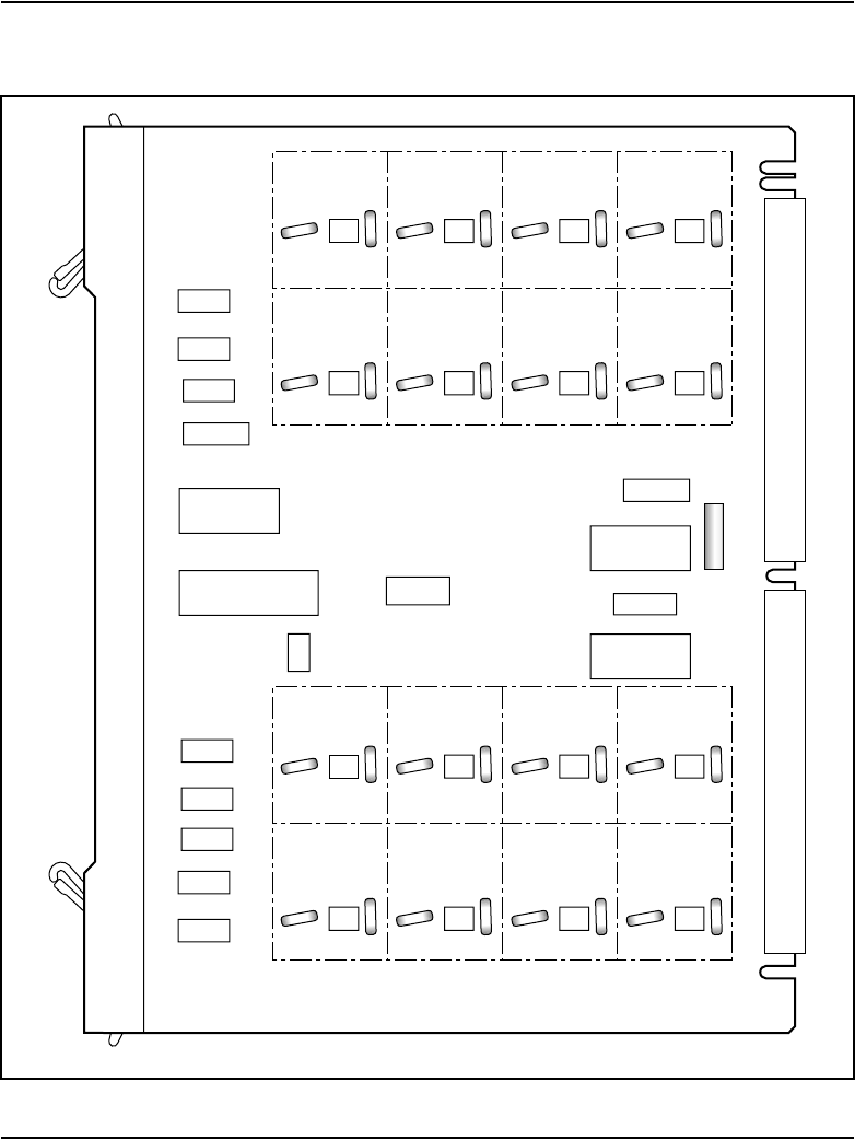


Page 545 of 906
Circuit Card Description and Installation
546
NT8D03 Analog Line card
Overview
The NT8D03 Analog Line card provides an interface for up to 16 analog
(500/2500-type) telephones. It is equipped with an 8051-family
microprocessor that performs the following functions:
• control of card operation
• card identification
•self-test
• status reporting to the controller
• maintenance diagnostics
You can install this card in any IPE slot.
Note: A maximum of four NT8D03 Analog Line cards can be installed
in each MG 1000S. A maximum of four NT8D03 Analog Line cards can
be installed in each MG 1000S Expansion.


Page 547 of 906
Circuit Card Description and Installation
564
NT8D09 Analog Message Waiting
Line card
Contents
This section contains information on the following topics:
Introduction . . . . . . . . . . . . . . . . . . . . . . . . . . . . . . . . . . . . . . . . . . . . . . 547
Physical description. . . . . . . . . . . . . . . . . . . . . . . . . . . . . . . . . . . . . . . . 549
Functional description . . . . . . . . . . . . . . . . . . . . . . . . . . . . . . . . . . . . . . 549
Connector pin assignments . . . . . . . . . . . . . . . . . . . . . . . . . . . . . . . . . . 558
Configuration . . . . . . . . . . . . . . . . . . . . . . . . . . . . . . . . . . . . . . . . . . . . 561
Introduction
The NT8D09 Analog Message Waiting Line card is an IPE line card that can
be installed in the NT8D37 IPE module.
The NT8D09 Analog Message Waiting Line card (µ-Law) provides talk
battery and signaling for up to 16 regular 2-wire common battery analog
(500/2500-type) telephones and key telephone equipment, with the Message
Waiting lamp feature.
The NT8D09 Analog Message Waiting Line card is functionally identical to
the NT8D03 Analog Line card, except it can also connect a high-voltage,
low-current feed to each line to light the message waiting lamp on telephones
equipped with the Message Waiting feature.
The analog message waiting line card mounts in any IPE slot.
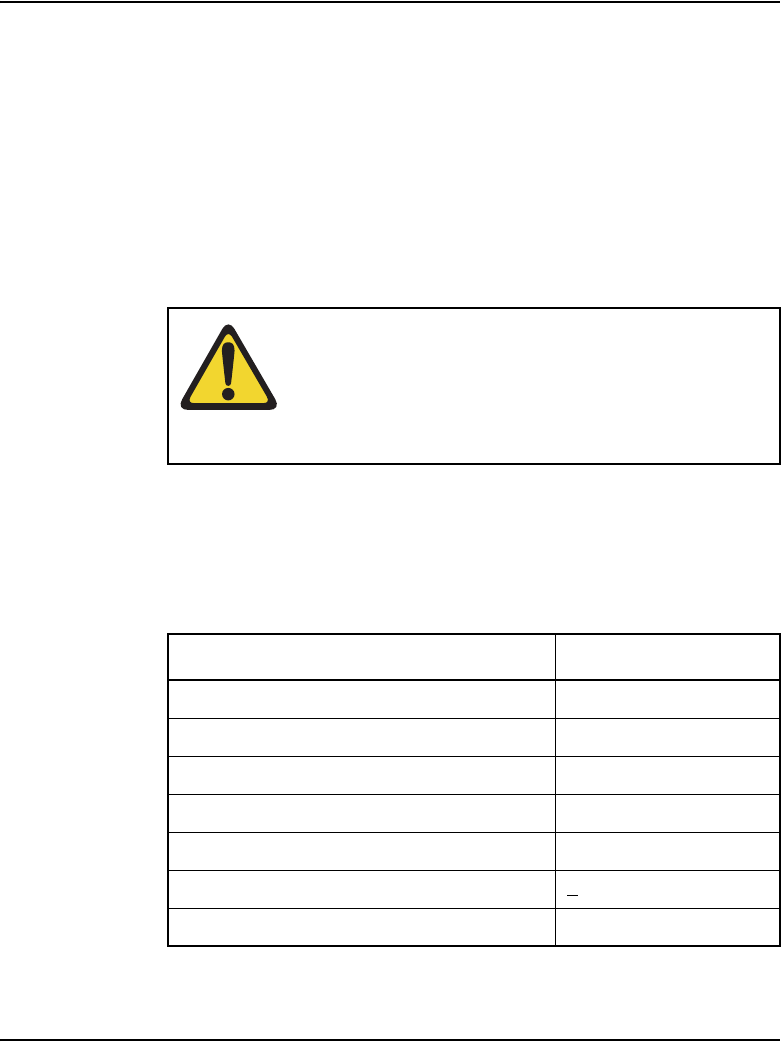
Page 548 of 906 NT8D09 Analog Message Waiting Line card
553-3001-211 Standard 3.00 August 2005
Note: A maximum of four NT8D09 Analog Message Waiting Line
cards per MG 1000S and four NT8D09 Analog Message Waiting Line
cards per MG 1000S Expansion are supported.
Cards later than vintage NT8D09AK support µ-Law and A-Law companding,
and provide a 2 dB transmission profile change. The transmission change
improves performance on long lines, particularly for lines used outside of a
single-building environment.
The NT8D09 Analog Message Waiting Line card supports 56K modem
operation.
The NT8D09 Analog Message Waiting Line card interfaces to and is
compatible with the equipment listed in Table 177.
CAUTION
Damage to Equipment
If a modem is connected to a port on the message
waiting line card, that port should not be defined in
software (LD 10) as having message waiting capabilities.
Otherwise, the modem will be damaged.
Table 177
NT8D09 Analog Message Waiting Line card application and
compatibility (Part 1 of 2)
Equipment Specifications
500-type rotary dial sets (or equivalent):
dial speed 8.0 to 12.5 pps
percent break 58 to 70%
interdigital time 150 ms
2500-type Digitone sets (or equivalent):
frequency accuracy + 1.5%
pulse duration 40 ms

NT8D09 Analog Message Waiting Line card Page 549 of 906
Circuit Card Description and Installation
Physical description
The circuitry is mounted on a 31.75 cm. by 25.40 cm (12.5 in. by 10 in.)
printed circuit board.
The NT8D09 Analog Message Waiting Line card circuits connects to the
backplane through a 160-pin connector. The backplane is cabled to a
connector in the bottom of the cabinet which is cabled to the cross-connect
terminal (Main Distribution Frame) through 25-pair cables. Station apparatus
then connects to the card at the cross-connect terminal.
The faceplate of the NT8D09 Analog Message Waiting Line card is equipped
with a red LED which lights when the card is disabled (see Figure 109 on
page 550. At power-up, the LED flashes as the analog line card runs a
self-test. If the test completes successfully, the card is automatically enabled
(if it is configured in software) and the LED goes out.
Functional description
The NT8D09 Analog Message Waiting Line card contains a microprocessor
that provides the following functions:
• self-identification
•self-test
• control of card operation
• status report to the controller
• maintenance diagnostics
interdigital time 40 ms
speed 12.5 digits/s
Table 177
NT8D09 Analog Message Waiting Line card application and
compatibility (Part 2 of 2) (Continued)
Equipment Specifications
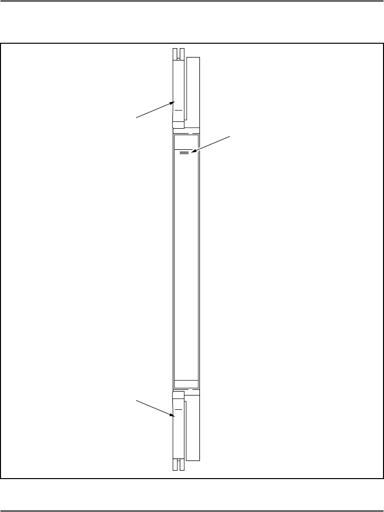

NT8D09 Analog Message Waiting Line card Page 551 of 906
Circuit Card Description and Installation
The NT8D09 Analog Message Waiting Line card also provides:
• 600 ohms balanced terminating impedance
• analog-to-digital and digital-to-analog conversion of transmission and
reception signals for 16 audio phone lines
• transmission and reception of Scan and Signaling Device (SSD)
signaling messages over a DS-30X signaling channel in A10 format
• on-hook/off-hook status and switchhook flash detection
• 20 Hz ringing signal connection and automatic disconnection when the
station goes off-hook
• synchronization for connecting and disconnecting the ringing signal to
zero crossing of ringing voltage
• loopback of SSD messages and Pulse Code Modulation (PCM) signals
for diagnostic purposes
• correct initialization of all features at power-up
• direct reporting of digit dialed (500-type telephones) by collecting dial
pulses
• connection of –150 V dc at 1 Hz to activate message waiting lamps
• lamp status detection
• disabling and enabling of selected units for maintenance
Figure 110 on page 552 shows a block diagram of the major functions
contained on the analog message waiting line card. Each of these functions
are described in the following sections.
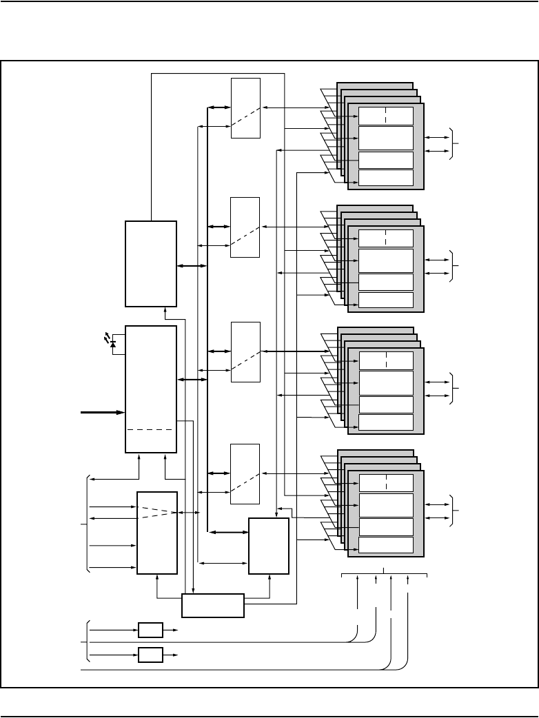
Page 552 of 906 NT8D09 Analog Message Waiting Line card
553-3001-211 Standard 3.00 August 2005
Figure 110
Analog message waiting line card – block diagram
Input/output
interface
control
Micro-
controller
DS-30X
interface
5.12 MHz
clock
Tx PCM
Async card
LAN link
Front
panel
LED
Card LAN
interface
Line interface unit power
Rx PCM
1 kHz
frame sync
Card slot
address
Backplane
Controller
card
Line
signaling
interface
Control
logic
Reg
Signaling
and status
Address/
data bus
553-6168
Power
supplies
Ring
generator
–150 V dc
light
power
+8.5 V dc +5 V dc power
Reg
+15 V dc +12 V dc power
Ringing
– 48 V dc
battery
Rsync
XFMR
Signaling relays
(ringing, battery
reversal)
Line interface units 0–3
Tip
Ring
Analog
telephone
lines
Loop current/
dialpulse detect
Message
waiting
XFMR
Signaling relays
(ringing, battery
reversal)
Line interface units 4–7
Tip
Ring
Analog
telephone
lines
Loop current/
dialpulse detect
Message
waiting
XFMR
Signaling relays
(ringing, battery
reversal)
Line interface units 8–11
Tip
Ring
Analog
telephone
lines
Loop current/
dialpulse detect
Message
waiting
XFMR
Signaling relays
(ringing, battery
reversal)
Line interface units 12–15
Tip
Ring
Analog
telephone
lines
Loop current/
dialpulse detect
Message
waiting
Analog
hybrid
Analog
hybrid
Analog
hybrid
Analog
hybrid
PCM
Codec
PCM
Codec
PCM
Codec
PCM
Codec

NT8D09 Analog Message Waiting Line card Page 553 of 906
Circuit Card Description and Installation
Card interfaces
The analog message waiting line card passes voice and signaling data over
DS-30X loops and maintenance data over the card LAN link. These interfaces
are discussed in “Intelligent Peripheral Equipment” on page 32.
Line interface units
The analog message waiting line card contains 16 identical and independently
configurable line interface units (also referred to as circuits). Each unit
provides 600-ohm impedance matching and a balance network in a signal
transformer/analog hybrid circuit. Circuits are also provided in each unit to
apply the ringing voltage onto the line synchronized to the ringing current
zero crossing. Signal detection circuits monitor on-hook/off-hook status and
switchhook flash detection. Four codecs are provided to perform A/D and D/
A conversion of line analog voiceband signals to digital PCM signals. Each
CODEC supports four line interface units. The following features are
common to all units on the card:
• Transmission and reception of Scan and Signaling Device (SSD)
signaling messages over a DS30X signaling channel in A10 format.
• Loopback of SSD messages and pulse code modulation (PCM) signals
for diagnostic purposes.
• Correct initialization of all features, as configured in software, at
power-up.
• Direct reporting of digits dialed (500 telephones) by collecting dial
pulses.
• Connection of –150 V dc at 1 Hz to activate message waiting lamps in
two telephones in parallel. The two telephones must be the same type or
the neon series resistor in each telephone must be 54 K ohms or greater.
• Lamp status detection (will not detect a failure of either lamp when
operating in parallel).
• Disabling and enabling of selected units for maintenance.
• 40 mA to telephones with short circuit protection.

Page 554 of 906 NT8D09 Analog Message Waiting Line card
553-3001-211 Standard 3.00 August 2005
Card control functions
Control functions are provided by the following:
• a microcontroller
• a card LAN interface
• signaling and control circuits on the analog message waiting line card
Microcontroller
The analog message waiting line card contains a microcontroller that controls
the internal operation of the card and the serial card LAN link to the controller
card. The microcontroller controls the following:
• reporting to the CE CP through the card LAN link:
— card identification (card type, vintage, and serial number)
— firmware version
— self-test status
— programmed configuration status
• receipt and implementation of card configuration:
— programming of the codecs
— enabling/disabling of individual units or entire card
— programming of input/output interface control circuits for
administration of line interface unit operation
— enabling/disabling of an interrupted dial tone to indicate call waiting
— maintenance diagnostics
— transmission loss levels
Signaling and control
The signaling and control portion of the card provides circuits that establish,
supervise, and take down call connections. These circuits work with the
system CP to operate the line interface circuits during calls. The circuits
receive outgoing call signaling messages from the CP and return incoming
call status information over the DS-30X network loop.

NT8D09 Analog Message Waiting Line card Page 555 of 906
Circuit Card Description and Installation
Analog line interface
Input impedance
The impedance at tip and ring is 600 ohms with a return loss of:
• 20 dB for 200-500 Hz
• 26 dB for 500-3400 Hz
Insertion loss
On a station line-to-line connection, the total insertion loss at 1 kHz is
6 dB + 1 dB. This is arranged as 3.5 dB loss for analog to PCM, and 2.5 dB
loss for PCM to analog.
Frequency response
The loss values in Table 178 are measured relative to the loss at 1 kHz.
Message channel noise
The message channel noise C-weighted (dBrnC) on 95 percent of the
connections (line to line) with both ends terminated in 600 ohms does not
exceed 20 dBrnC.
Table 178
Analog message waiting line card – frequency response
Frequency (Hz) Minimum (dB) Maximum (dB)
60 20.0 —
200 0.0 5.0
300 –0.5 1.0
3000 –0.5 1.0
3200 –0.5 1.5
3400 0.0 3.0

Page 556 of 906 NT8D09 Analog Message Waiting Line card
553-3001-211 Standard 3.00 August 2005
Table 179 provides a technical summary of the analog message waiting line
card.
Table 179
NT8D09 Analog Message Waiting Line card technical summary
Impedance 600 ohms
Loop limit (excluding set) 1000 ohms at nominal -48 V (excluding set)
Leakage resistance 30,000 ohms
Ring trip During silent or ringing intervals
Ringing voltage 86 V AC
Signaling Loop start
Supervision Normal battery conditions are continuously applied (approxi-
mately -44.5 V on ring and
-2.5 V on tip at nominal -48 V battery)
Power input from backplane -48 (can be as low as -42 for DC-powered systems), +15,
-15, +8.5 V and ringing voltage; also -150 V on analog mes-
sage waiting line card.
Insertion loss 6 dB + 1 dB at 1020 Hz
3.5 dB loss for analog to PCM,
2.5 dB loss for PCM to analog

NT8D09 Analog Message Waiting Line card Page 557 of 906
Circuit Card Description and Installation
Power requirements
Table 180 provides the power requirements for the NT8D09 Analog Message
Waiting Line card.
Foreign and surge voltage protections
In-circuit protection against power line crosses or lightning is not provided on
the NT8D09 Analog Message Waiting line card.
Table 180
Power requirements
Voltag e
(+/-) Tolerance
Idle
current
Active
current Max
+ 12.0 V dc 0.36 V dc 48 mA 0 mA 48 mA
+ 8.0 V dc 0.40 V dc 150 mA 8 mA 280 mA
–48.0 V dc 2.00 V dc 48 mA 40 mA 688 mA
–48.0 V dc 5.00 V dc 0 mA 10 mA
(Note 1)
320 mA
86.0 V ac 5.00 V ac 0 mA 10 mA
(Note 2)
160 mA
–150.0 V dc 3.00 V dc 0 mA 2 mA 32 mA
Note 1: Each active ringing relay requires 10 mA of battery voltage.
Note 2: Reflects the current for ringing a single station set (or DN
telephone). There may be as many as five ringers on each line.

Page 558 of 906 NT8D09 Analog Message Waiting Line card
553-3001-211 Standard 3.00 August 2005
Overload level
Signal levels exceeding +7 dBm applied to the tip and ring cause distortion in
speech transmission.
Environmental specifications
Table 181 lists the environmental specifications for the analog message
waiting line card.
Connector pin assignments
The analog message waiting line card brings the 16 phone lines to the IPE
backplane through a 160-pin connector shroud. The backplane is cabled to the
I/O panel on the rear of the module, which is then connected to the MDF by
25-pair cables.
Telephone lines from station equipment cross connect to the analog message
waiting line card at the MDF using a wiring plan similar to that used for trunk
cards. A typical connection example is shown in Figure 111 on page 560 and
Table 112 on page 563 shows the I/O pin designations at the backplane
connector. This connector is arranged as an 80-row by 2-column array of
pins. Normally, these pin positions are cabled to 50-pin connectors at the I/O
panel in the rear of each module for connection with 25-pair cables to the
cross-connect terminal.
The information in Table 182 on page 559 is provided as a reference and
diagnostic aid at the backplane, since the cabling arrangement may vary at the
I/O panel. See Communication Server 1000M and Meridian 1: Large System
Table 181
Analog message waiting line card – environmental specifications
Parameter Specifications
Operating temperature 0° to +60° C (+32 to +140° F), ambient
Operating humidity 5 to 95% RH (non-condensing)
Storage temperature –40° to +70° C (–40° to +158° F)

NT8D09 Analog Message Waiting Line card Page 559 of 906
Circuit Card Description and Installation
Installation and Configuration (553-3021-210) for cable pinout information
at the I/O panel.
Table 182
Analog message waiting line card – backplane pinouts
Backplane
pinout*
Lead
designations
Backplane
pinout*
Lead
designations
12A Line 0, Ring 12B Line 0, Tip
13A Line 1, Ring 13B Line 1, Tip
14A Line 2, Ring 14B Line 2, Tip
15A Line 3, Ring 15B Line 3, Tip
16A Line 4, Ring 16B Line 4, Tip
17A Line 5, Ring 17B Line 5, Tip
18A Line 6, Ring 18B Line 6, Tip
19A Line 7, Ring 18B Line 7, Tip
62A Line 8, Ring 62B Line 8, Tip
63A Line 9, Ring 63B Line 9, Tip
64A Line 10, Ring 64B Line 10, Tip
65A Line 11, Ring 65B Line 11, Tip
66A Line 12, Ring 66B Line 12, Tip
67A Line 13, Ring 67B Line 13, Tip
68A Line 14, Ring 68B Line 14, Tip
69A Line 15, Ring 69B Line 15, Tip
* These pinouts apply to both NT8D37 and NT8D11 backplanes.
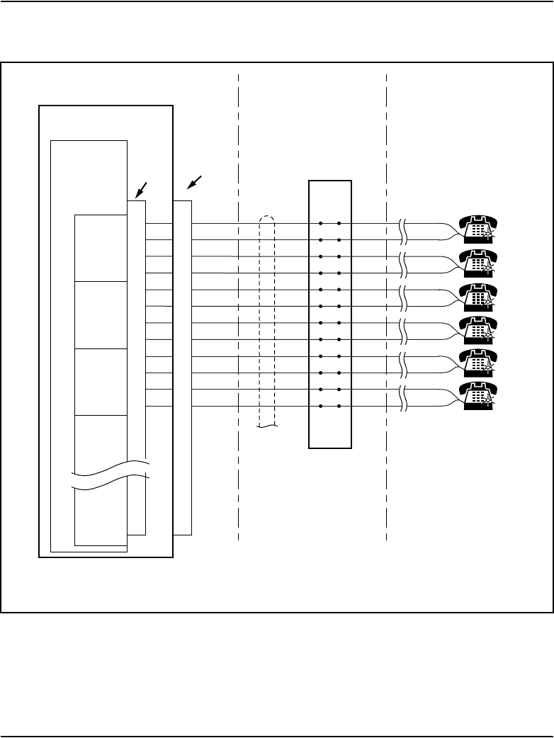
Page 560 of 906 NT8D09 Analog Message Waiting Line card
553-3001-211 Standard 3.00 August 2005
Figure 111
Analog message waiting line card – typical cross connection example
553-AAA1131
NT8D37
IPE Module
Slot 0
NT8D09
Message
Waiting
Line Card
0T
0R
1T
1R
26
1
27
2
System Cross-connect OPS or ONS
telephone
connections
with message
waiting lamps
AMDF
Tip
Ring
Tip
Ring
Tip
Ring
Tip
Ring
28
3
29
4
4T
4R
5T
5R
2T
2R
3T
3R
30
5
31
6
Tip
Ring
Note:
Actual pin numbers may vary depending on the vintage
of the card cage and the slot where the card is installed.
Module
I/O Panel
Connector
Part of
25-pair
cable
Tip
Ring
Unit 0
Unit 15
Unit 1
Unit 2
Unit 3
(W-BL)
(BL-W)
(W-O)
(O-W)
(W-G)
(G-W)
(W-BR)
(BR-W)
(W-S)
(S-W)
(R-BL)
(BL-R)

NT8D09 Analog Message Waiting Line card Page 561 of 906
Circuit Card Description and Installation
Configuration
This section outlines the procedures for configuring the switches and jumpers
on the NT8D09 Analog Message Waiting Line card and configuring the
system software to properly recognize the card. Figure 112 on page 563
shows where the switches and jumper blocks are located on this board.
Jumper and switch settings
The NT8D09 Analog Message Waiting Line card has no user-configurable
jumpers or switches. The card derives its address from its position in the
backplane and reports that information back to the CPU through the LAN
Link interface.
Software service changes
Individual line interface units on the NT8D09 Analog Message Waiting Line
card are configured using the Analog (500/2500-type) Telephone
Administration program LD 10.
The message waiting feature is enabled by entering data into the customer
data block using LD 15. See Software Input/Output: Administration
(553-3001-311) for LD 10 and LD 15 service change instructions.
Analog message waiting line cards with a vintage later than NT8D09AK
provide a fixed +2 dB transmission profile change in the gain of the D/A
convertor. See Table 183 on page 562.
This transmission profile change is used for control of end-to-end connection
loss. Control of such loss is a major element in controlling transmission
parameters such as received volume, echo, noise, and crosstalk. The loss plan
for the analog message waiting line card determines port-to-port loss between
an analog line card unit (port) and other IPE ports. LD 97 is used to configure

Page 562 of 906 NT8D09 Analog Message Waiting Line card
553-3001-211 Standard 3.00 August 2005
the system for port-to-port loss. See Software Input/Output: Administration
(553-3001-311) for LD 97 service change instructions.
Table 183
Transmission Profile Changes
Vintage A/D convertor gain D/A convertor gain
Previous to AK –3.5 dB –2.5 dB
AK and later –3.5 dB –0.5 dB
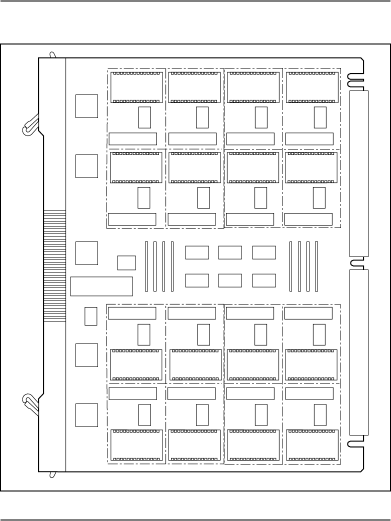


Page 565 of 906
Circuit Card Description and Installation
626
NT8D14 Universal Trunk card
Contents
This section contains information on the following topics:
Introduction . . . . . . . . . . . . . . . . . . . . . . . . . . . . . . . . . . . . . . . . . . . . . . 565
Physical description. . . . . . . . . . . . . . . . . . . . . . . . . . . . . . . . . . . . . . . . 567
Functional description . . . . . . . . . . . . . . . . . . . . . . . . . . . . . . . . . . . . . . 570
Operation. . . . . . . . . . . . . . . . . . . . . . . . . . . . . . . . . . . . . . . . . . . . . . . . 573
Electrical specifications. . . . . . . . . . . . . . . . . . . . . . . . . . . . . . . . . . . . . 609
Connector pin assignments . . . . . . . . . . . . . . . . . . . . . . . . . . . . . . . . . . 614
Configuration . . . . . . . . . . . . . . . . . . . . . . . . . . . . . . . . . . . . . . . . . . . . 615
Applications . . . . . . . . . . . . . . . . . . . . . . . . . . . . . . . . . . . . . . . . . . . . . 624
Introduction
Nortel is pleased to introduce the NT8D14CA Universal Trunk (XUT) card
as a replacement for the NT8D14BB card. The NT8D14CA has been
modified to add a longer loop capability for CAMA trunk applications.
The NT8D14CA comes equipped with a set of 2 jumpers for each hybrid that
should be set to the longer loop length (LL) when the trunk is used in a
CAMA application. The jumpers are numbered P35 to P50 and are set to the
shorter loop length (SL) position when it comes from the factory. For each
hybrid, both jumpers should be changed to the LL position only if used as a
CAMA trunk. Otherwise the jumpers should be left to the SL position.

Page 566 of 906 NT8D14 Universal Trunk card
553-3001-211 Standard 3.00 August 2005
The NT8D14 Universal Trunk card interfaces eight analog trunk lines to the
system. Each trunk interface is independently configured by software control
using the Trunk Administration program LD 14.
You can install this card in any IPE slot.
Note: Each MG 1000S can contain up to four analog trunk cards. Each
MG 1000S Expansion can contain up to four analog trunk cards.
The NT8D14 Universal Trunk card supports the following trunk types:
• Centralized Automatic Message Accounting (CAMA) trunks
• Central Office (CO), Foreign Exchange (FEX), and Wide Area
Telephone Service (WATS) trunks
• Direct Inward Dial (DID) trunks
• Tie trunks: two-way Loop Dial Repeating (LDR) and two-way loop
Outgoing Automatic Incoming Dial (OAID)
• Recorded Announcement (RAN) trunks
• Paging trunks
The NT8D14 Universal Trunk card also supports Music, Automatic Wake
Up, and Direct Inward System Access (DISA) features.

NT8D14 Universal Trunk card Page 567 of 906
Circuit Card Description and Installation
Table 184 lists the signaling and trunk types supported by the NT8D14
Universal Trunk card.
Physical description
The trunk and common multiplexing circuitry is mounted on a 31.75 cm by
25.40 cm (12.5 in. by 10 in.) printed circuit board.
The NT8D14 Universal Trunk card connects to the backplane through a
160-pin connector shroud. The backplane is cabled to the I/O panel, which is
cabled to the Main Distribution Frame (MDF) by 25-pair cables. External
equipment, such as recorded announcement machines, paging equipment,
and Central Office facilities, connect to the card at the MDF.
See the Communication Server 1000S: Installation and Configuration
(553-3031-210) for termination and cross-connect information.
Table 184
Trunk and signaling matrix
Signaling type
Trunk types
CO/FX/
WATS DID Tie RAN Paging CAMA
Loop start Yes No
(see note)
No N/A N/A Yes
Ground start Ye s No No N/A N/A No
Loop DR No Ye s Yes N/A N/A No
Loop OAID No No Ye s N/A N/A No
Continuous operation
mode
No No No Ye s N/A No
Start modes
(pulse and level)
No No No Ye s N/A No
Note: For incoming and outgoing service, DID trunks must be programmed as loop dial
repeating.

Page 568 of 906 NT8D14 Universal Trunk card
553-3001-211 Standard 3.00 August 2005
The faceplate of the card is equipped with a red Light Emitting Diode (LED).
See Figure 113 on page 569. When an NT8D14 Universal Trunk card is
installed, the LED remains lit for two to five seconds while the self-test runs.
If the self-test is successful, the LED flashes three times and remains lit.
When the card is configured and enabled in software, then the LED goes out.
If the LED flashes continuously or remains weakly lit, replace the card.
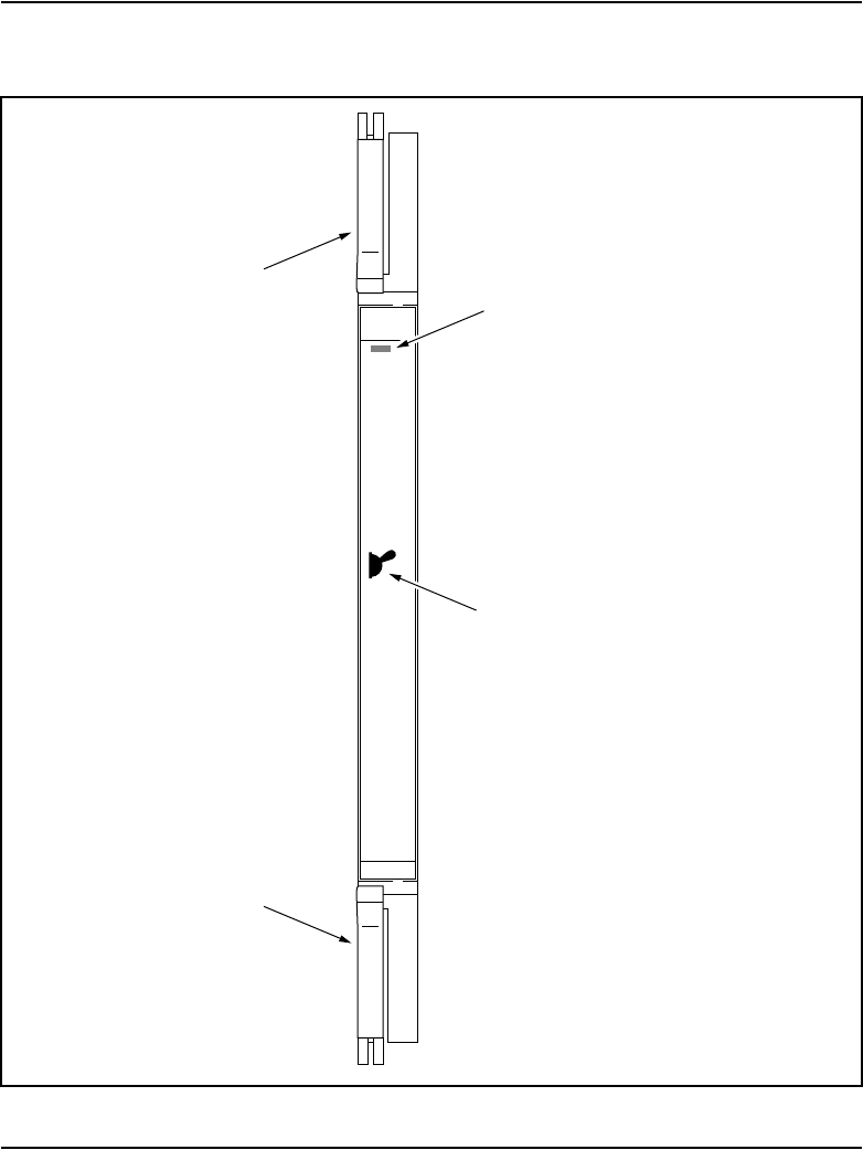
Page 570 of 906 NT8D14 Universal Trunk card
553-3001-211 Standard 3.00 August 2005
Functional description
Figure 114 shows a block diagram of the major functions contained on the
NT8D14 Universal Trunk card. Each of these functions is described on the
following pages.
Figure 114
NT8D14 Universal trunk card – block diagram
Input/output
interface
control
Codec
PCM
Micro-
controller
DS-30X
interface
5.12 MHz
clock
Tx PCM
Async card
LAN link
Front
panel
LED
Card LAN
interface
Analog
hybrid XFMR Tip
Signaling
relays
Analog
trunk facilities
(CO/FX/WATS,
DID, tie, RAN,
or paging)
Trunk interface units 0–3
Signal
detection
Signal
hybrid
Ring
*
*
Analog
hybrid XFMR Tip
Signaling
relays
Analog
trunk facilities
(CO/FX/WATS,
DID, tie, RAN,
or paging)
Trunk interface units 4–7
Signal
detection
Signal
hybrid
Ring
*
*
Codec
PCM
Rx PCM
1 kHz
frame sync
Card slot
address
Back-
plane
Con-
troller
card Trunk
signaling
interface
Control
logic
Signaling
and status
Address/
data bus
*
Signaling
lines for
RAN or
paging
control
553-CSE6197

NT8D14 Universal Trunk card Page 571 of 906
Circuit Card Description and Installation
Card interfaces
The NT8D14 Universal Trunk card passes voice and signaling data over
DS-30X loops, and maintenance data over the card LAN link. These
interfaces are described in “Intelligent Peripheral Equipment” on page 32.
Trunk interface units
The NT8D14 Universal Trunk card contains eight identical and
independently configurable trunk interface units (also referred to as circuits).
Each unit provides impedance matching and a balanced network in a signal
transformer/analog hybrid circuit.
Also provided are relays for placing outgoing call signaling onto the trunk.
Signal detection circuits monitor incoming call signaling. Two codecs are
provided for performing A/D and D/A conversion of trunk analog voiceband
signals to digital PCM signals. Each codec supports four trunk interface units.
The following features are common to all units on the card:
• trunk type configurable on a per unit basis
• terminating impedance (600 or 900 ohms) selectable on a per-unit basis
(minimum vintage BA)
• balance impedance (600 or 900 ohms or complex impedance network)
selectable on a per-unit basis (minimum vintage BA)
• control signals provided for RAN and paging equipment
• loopback of PCM signals received from trunk facility over DS-30X
network loop for diagnostic purposes
• switchable pads for transmission loss control

Page 572 of 906 NT8D14 Universal Trunk card
553-3001-211 Standard 3.00 August 2005
Card control functions
Control functions are provided by a microcontroller, a card LAN interface,
and signaling and control circuits on the NT8D14 Universal Trunk card.
Microcontroller
The NT8D14 Universal Trunk card contains a microcontroller that controls
the internal operation of the card and the serial card LAN link to the controller
card. The microcontroller controls the following:
• reporting to the CE CPU through the card LAN link:
— card identification (card type, vintage, and serial number)
— firmware version
— self-test status
— programmed configuration status
• receipt and implementation of card configuration through the card LAN
link:
— programming of the codecs
— enabling/disabling of individual units or entire card
— programming of input/output interface control circuits for
administration of trunk interface unit operation
— maintenance diagnostics
— transmission pad settings
Card LAN interface
Maintenance data is exchanged with the common equipment CPU over a
dedicated asynchronous serial network called the Card LAN link.
Signaling and control
The signaling and control portion of the Universal Trunk card works with the
CPU to operate the card hardware. The card receives messages from the CPU
over a signaling channel in the DS-30X loop and returns status information to
the CPU over the same channel. The signaling and control portion of the card

NT8D14 Universal Trunk card Page 573 of 906
Circuit Card Description and Installation
provides the means for analog loop terminations to establish, supervise, and
take down call connections.
Signaling interface
All trunk signaling messages are three bytes long. The messages are
transmitted in channel zero of the DS-30X in A10 format.
Configuration information for the Universal Trunk card is downloaded from
the CPU at power-up or by command from maintenance programs. Eleven
configuration messages are sent. Three messages are sent to the card to
configure the make/break ratio and A-Law or µ-Law operation. One message
is sent to each unit to configure the trunk characteristics.
Operation
Administrators can assign optional applications, features, and signaling
arrangements for each unit on the NT8D14 Universal Trunk card through the
Trunk Administration LD 14 and Trunk Route Administration LD 16
programs or jumper strap settings on the card.
Loop start operation
Loop start operation is configured in software and implemented in the card
through software download messages. When the card is idle, it provides a
high impedance toward the CO for isolation and ac (ringing) detection.
Incoming calls
The alerting signal into the System is 20 Hz (nominal) ringing sent by the CO.
When an incoming call is answered, ringing is tripped when the System
places a low-resistance dc loop across the tip and ring leads toward the CO.
See Figure 115 and Figure 116 on page 575.
Outgoing calls
For outgoing calls, the software sends an outgoing seizure message to place
a low-resistance loop across the tip and ring leads toward the CO. See
Figure 117 on page 576 and Figure 118 on page 577. When the CO detects
the low-resistance loop, it prepares to receive digits.When the CO is ready to
Page 574 of 906 NT8D14 Universal Trunk card
553-3001-211 Standard 3.00 August 2005
receive digits, it returns a dial tone. Outward address signaling is then applied
from the system in the form of loop (interrupting) dial pulses or DTMF tones.
Polarity-sensitive/-insensitive packs feature
The CS 1000 Release 4.5 software provides the polarity-sensitive/
polarity-insensitive (PSP and PIP) packs feature for the accurate recording of
outgoing call duration for loop start and ground start operation.
On trunks equipped with far-end answer supervision, the PSP class of service
is enabled in software and causes call-duration recording in CDR records to
begin only upon receipt of answer supervision from the far-end.
Figure 115
Loop start call states – incoming call from CO/FX/WATS
System (near) end
High-resistance loop
Ground on tip, battery on ring
Far end
originates
by ringing
Note 1:
The originating office may reverse battery and ground when attendant
answer is received.
Note 2:
No disconnection signal is passed to trunk.
Note 3:
The near end provides a high-impedance (>150k ohms) disconnect signal
of at least 50 ms before reconnecting the ground detector.
CO / FX / WATS (far) end
Forced far end
disconnect
Dial tone after
far end timeout
Near end
disconnects
Idle
Near end
disconnects
first
(Note 3)
Near end answers,
ringing is removed
(Note 1)
553-AAA1133
Far end
disconnects
first
(Note 2)
Low-resistance loop
NT8D14 Universal Trunk card Page 575 of 906
Circuit Card Description and Installation
Figure 116
Loop start call connection sequence – incoming call from CO/FX/WATS
A
State
Idle
Idle
Trunk seizure
Idle
B goes on hook
A goes on hook
RemarksSignal/direction
Near end
Meridian
1
B
Far end
CO
High-resistance loop
High-resistance loop
High-
resistance
loop
Ground
on tip/
battery
on ring
Ground on tip/
battery on ring
Ground on tip/
battery on ring
Ground on tip/
battery on ring
and dial tone
Low-resistance loop
Near end detects the ringing signal, makes the trunk
circuit busy to all other calls, and presents the call to
an idle console loop key.
Ringing signal is superimposed on battery by the CO
upon seizure.
2-way voice
connection
Ringing
Console answers
Call presented to
console loop key
When attendant presses a loop key to answer the call,
the near end places a low-resistance loop between tip
and ring and removes the ring and ground detectors
from the circuit.
CO detects the change in loop resistance and removes
the ringing signal. Normal battery and ground will
remain. However, some COs may reverse battery and
ground.
Normally, no disconnection signal is returned by the CO;
normal battery and ground will remain. However, if battery
and ground were reversed when call was established,
normal battery would be restored at this time.
If far end goes on hook first, CO sends dial (or busy) tone
after timeout. CO also restores normal battery and ground
if they had been reversed when the call was established.
All tones and any battery/ground reversal are ignored by
the near end.
If near end disconnects first, it opens the loop, waits at
least 50 ms, and then reconnects the ring and ground
detectors.
Near end restores high-resistance loop when terminal A
goes on hook.
553-6240
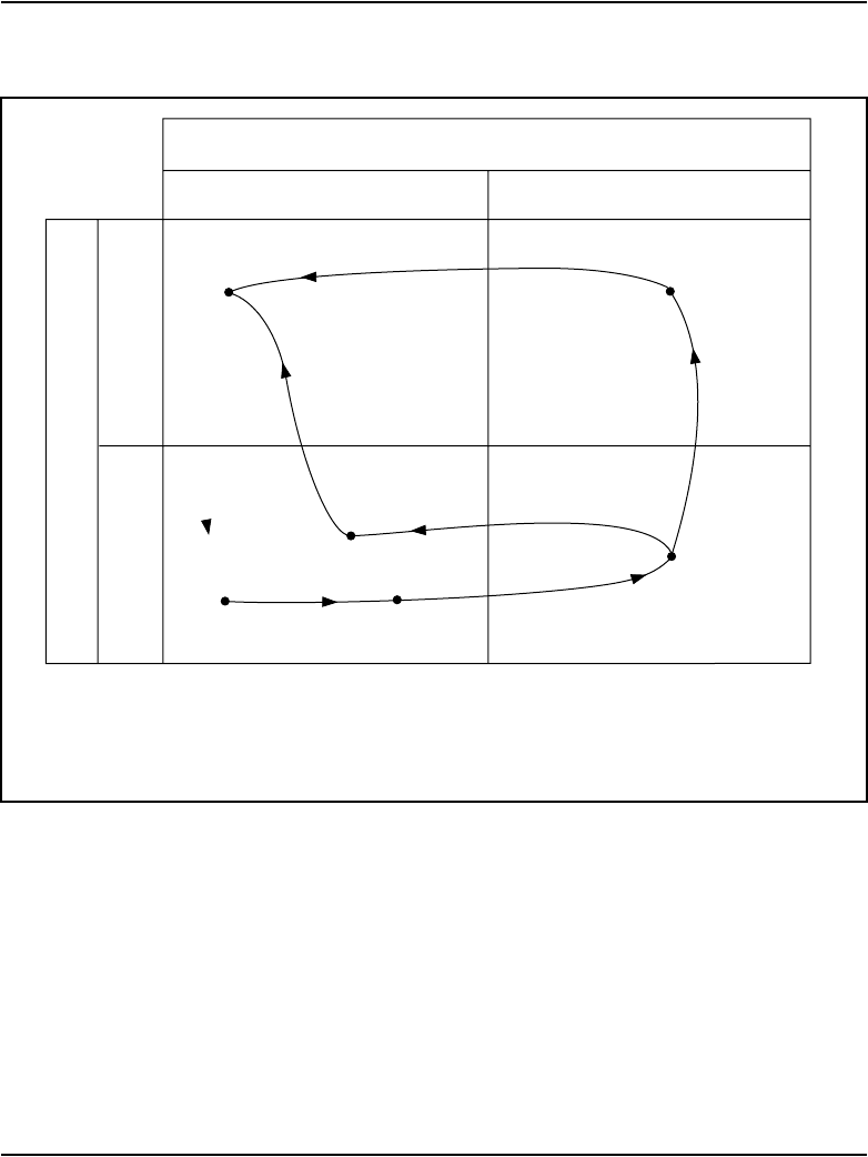
Page 576 of 906 NT8D14 Universal Trunk card
553-3001-211 Standard 3.00 August 2005
For trunks not equipped with answer supervision, the PIP class of service is
enabled and call-duration recording begins immediately upon near-end trunk
seizure. The PSP and PIP classes of service are enabled in the Trunk
Administration program LD 14.
Figure 117
Ground start call states – incoming call from CO/FX/WATS
System (near) end
High-resistance loop
Tip open,
battery on ring
Ground on tip,
battery on ring
CO / FX / WATS (far) end
Ringing
Far end
originates
Note 1:
The far end may reverse battery and ground upon receipt of attendant answer.
Note 2:
The near end provides a high-impedance (>150k ohms) disconnect signal of at
least 50 ms before reconnecting the ground detector.
Idle
Near end
disconnects
Far end
disconnects
Near end
disconnects
first (Note 2)
far end
disconnects
first
Assignment
to loop key
Near end
answers,
ringing is
removed
(Note 1)
553-AAA1133
Low-resistance loop
NT8D14 Universal Trunk card Page 577 of 906
Circuit Card Description and Installation
Figure 118
Ground start call connection sequence – incoming call from CO/FX/WATS
A
State
Idle
Idle
Trunk seizure
Call presented to
console loop key
Console answers
B goes on hook
Idle
A goes on hook
RemarksSignal/direction
Near end
Meridian
1
B
Far end
CO
Tip open/
battery on ring
Ringing
Tip open/
battery on ring
Tip open/
battery on ring
High-
resistance
loop
Ground on tip CO grounds tip. Near end detects the ground
and makes the trunk busy to all outgoing calls.
Ringing is superimposed on battery by the
CO.
When console answers, near end places a
low-resistance loop across the tip and ring.
If far end disconnects first, CO removes
ground from tip. If battery and ground were
reversed when call was established, battery
is removed from tip and restored to ring.
Near end detects drop in loop current and
opens loop.
2-way voice
connection
Ground on tip/
battery on ring
Low-resistance loop
High-resistance loop
High-resistance loop
When CO detects change to low-resistance
loop, it removes ringing. Some COs may
reverse battery and ground on tip and ring.
If near end disconnects first, it opens the
loop, waits 50 ms, and then reconnects the
ground detector.
CO detects drop in loop current and
removes ground from tip. If battery and
ground were reversed when call was
established, battery is removed from tip and
restored to ring.
553-6236

Page 578 of 906 NT8D14 Universal Trunk card
553-3001-211 Standard 3.00 August 2005
Ground start operation
Ground start operation is configured in software and implemented through
software download messages. In the idle state, the tip conductor from the CO
is open and a high-resistance negative battery is present on the ring lead.
Incoming calls
In an incoming call, after ground is detected on the tip, the universal trunk
card scans for a ringing detection signal before presenting the call to an
attendant and tripping the ringing. When the attendant answers, a low
resistance is placed across the tip and ring conductors, which trips CO ringing
and establishes a speech path. See Figure 119 on page 579 and Figure 120 on
page 580.
Reverse-wiring compensation
The CS 1000 Release 4.5 software includes a feature for detecting reverse
wiring (connection of the near-end tip and ring leads to the far-end ring and
tip leads) on ground start trunks with far-end answer supervision.
Ordinarily, an incoming call on a reverse-wired trunk without reverse-wiring
compensation presents ringing on the tip lead rather than on the ring lead.
Since the software expects to see a ground on the tip lead, it interprets the end
of the first ringing signal as a switchhook flash. But since the interval between
ringing signals exceeds the switchhook flash time of 512 milliseconds, the
software assumes a far-end disconnect. This causes the call to be presented to
a console loop key and then immediately removed.
The reverse-wiring compensation feature operates as follows. If an apparent
disconnect takes place immediately after the first ringing signal, the software
time stamps the event and temporarily remove the call from the console loop
key.
If another such ringing/disconnect event occurs during the No Ringing
Detector (NRD) time, the trunk is considered “possibly reverse-wired” and a
threshold counter starts. Calls on trunks identified as possibly reverse-wired
are presented to the attendant during the initial ring, removed, and then
continuously presented after the second ring. If a call on a possibly
reverse-wired trunk is abandoned before the attendant answers, it is
disconnected after the NRD timer expires.

NT8D14 Universal Trunk card Page 579 of 906
Circuit Card Description and Installation
A trunk identified as possibly reverse-wired is switched by the software to
loop start processing after the second ring. This switching takes place on a
call-by-call basis. Thus, if a previously correctly wired trunk becomes
reverse-wired, the next incoming call is marked as possibly reverse-wired and
the threshold count begins.
If the threshold count exceeds its limit, an error message is printed and the
trunk is registered as “positively reverse wired.” Once identified as positively
reverse wired, the call is presented continuously from the first ring. When a
Figure 119
Ground start call states – incoming call from CO/FX/WATS
System (near) end
High-resistance loop
Tip open,
battery on ring
Ground on tip,
battery on ring
CO / FX / WATS (far) end
Ringing
Far end
originates
Note 1:
The far end may reverse battery and ground upon receipt of attendant answer.
Note 2:
The near end provides a high-impedance (>150k ohms) disconnect signal of at
least 50 ms before reconnecting the ground detector.
Idle
Near end
disconnects
Far end
disconnects
Near end
disconnects
first (Note 2)
far end
disconnects
first
Assignment
to loop key
Near end
answers,
ringing is
removed
(Note 1)
553-AAA1133
Low-resistance loop
Page 580 of 906 NT8D14 Universal Trunk card
553-3001-211 Standard 3.00 August 2005
Figure 120
Ground start call connection sequence – incoming call from CO/FX/WATS
A
State
Idle
Idle
Trunk seizure
Call presented to
console loop key
Console answers
B goes on hook
Idle
A goes on hook
RemarksSignal/direction
Near end
System
B
Far end
CO
Tip open/
battery on ring
Ringing
Tip open/
battery on ring
Tip open/
battery on ring
High-
resistance
loop
Ground on tip CO grounds tip. Near end detects the ground
and makes the trunk busy to all outgoing calls.
Ringing is superimposed on battery by the
CO.
When console answers, near end places a
low-resistance loop across the tip and ring.
If far end disconnects first, CO removes
ground from tip. If battery and ground were
reversed when call was established, battery
is removed from tip and restored to ring.
Near end detects drop in loop current and
opens loop.
2-way voice
connection
Ground on tip/
battery on ring
Low-resistance loop
High-resistance loop
High-resistance loop
When CO detects change to low-resistance
loop, it removes ringing. Some COs may
reverse battery and ground on tip and ring.
If near end disconnects first, it opens the
loop, waits 50 ms, and then reconnects the
ground detector.
CO detects drop in loop current and
removes ground from tip. If battery and
ground were reversed when call was
established, battery is removed from tip and
restored to ring.
553-AAA1134

NT8D14 Universal Trunk card Page 581 of 906
Circuit Card Description and Installation
reverse-wired trunk becomes correctly wired, the first subsequent call clears
the threshold counter and normal ground start processing is implemented.
Note 1: The far-end can reverse battery and ground upon receipt of
attendant answer.
Note 2: The near-end provides a high-impedance (>150k ohms)
disconnect signal of at least 50 ms before reconnecting the ground
detector.
Outgoing calls
For outgoing calls, the trunk provides a ground to the ring lead. The CO
responds by grounding the tip and returning dial tone. After the tip ground is
detected by the card, a low-resistance path is placed between the tip and ring
leads and the ground is removed from the ring. Addressing is then applied
from the system in the form of loop (interrupting) dial pulses or DTMF tones.
See Figure 121 on page 582 and Figure 122 on page 583.
The Polarity-Sensitive/Polarity-Insensitive Packs (PSP and PIP) feature must
be set to provide for proper outgoing call-duration recording with ground start
operation. Refer to the description of loop start operation in this section for a
more complete discussion of PSP and PIP.
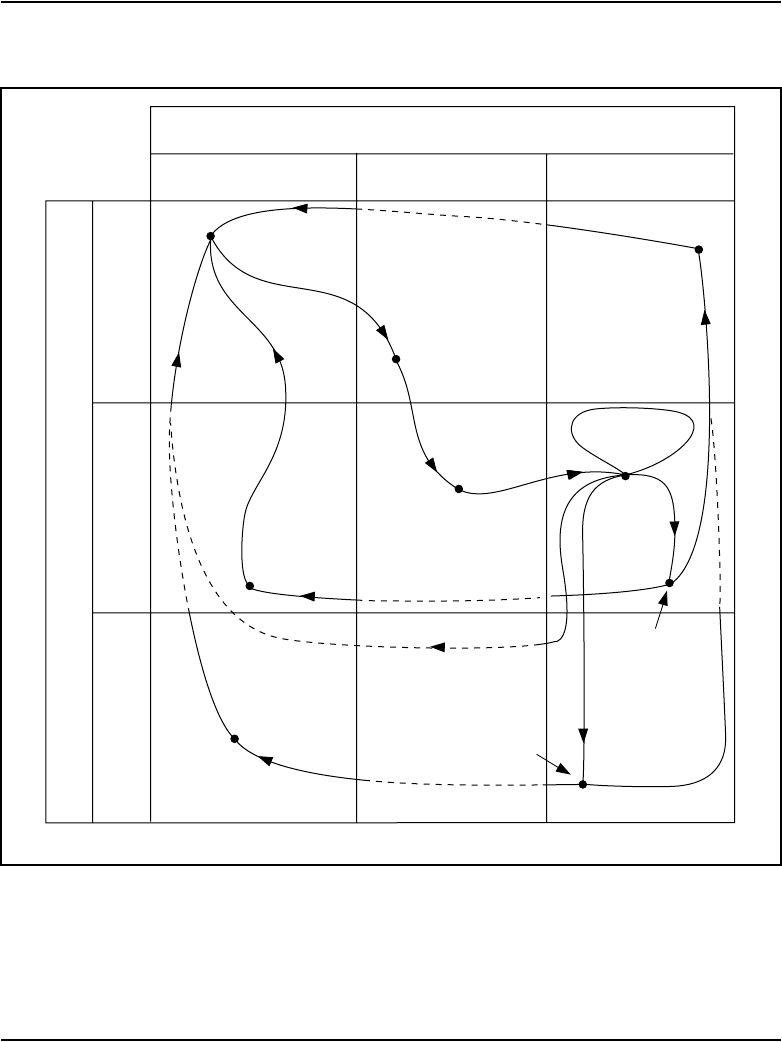
Page 582 of 906 NT8D14 Universal Trunk card
553-3001-211 Standard 3.00 August 2005
Figure 121
Ground start call states – outgoing call to CO/FX/WATS
System (near) end
High-resistance loop Ground on ring
Forced
near end
disconnect
Loop pulsing
or DTMF
Forced
far end
disconnect
Near end
originates
Dial
tone
CO toll denial
Idle
Near end
disconnects
first
Near end
disconnects
first
Far end
disconnects
first
Far end
answers
(no ans sup)
and ringback
tone removed
Ringing
and
ringback
tone
Far end answers
(ans sup)
and ringback
tone removed
553-AAA1135
Low-resistance loop
Battery on ring,
tip open
Battery on ring,
ground on tip
Ground on ring,
battery on tip
CO / FX / WATS (far) end
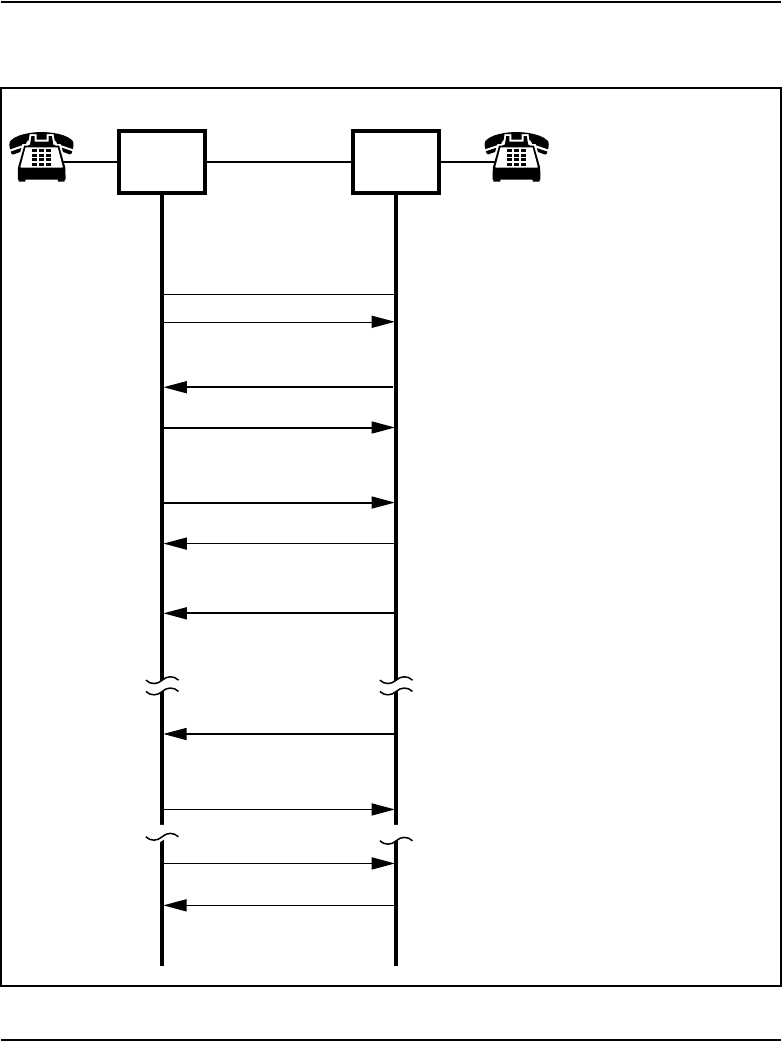
NT8D14 Universal Trunk card Page 583 of 906
Circuit Card Description and Installation
Figure 122
Ground start call connection sequence – outgoing call to CO/FX/WATS
A
State
Idle
Idle
B rings
Trunk seizure
Dial tone from CO
B goes on hook
Idle
A goes on hook
RemarksSignal/direction
Near end
System
B
Far end
CO
Tip open/
battery
on ring
Tip open/
battery on ring
Ringback
Tip open/
battery on ring
High-
resistance
loop
Ground on ring
When the CO recognizes seizure, it grounds the tip
and supplies dial tone.
When terminal B answers, ringing is tripped and CO
cuts terminal B through to trunk. Some COs may
reverse battery and ground on tip and ring when
terminal B answers or for toll denial.
Upon receipt of the first pulse/tone, the CO removes
dial tone. When outpulsing is complete, terminal B is
rung (if idle) and the proper audible indication is
returned to local end.
If far end disconnects first, CO removes ground from
tip. If battery and ground were reversed when call
was established, battery is removed from tip and
restored to ring.
Near end detects drop in loop current and opens loop.
Digits are outpulsed in the form of a series of loop
pulses or DTMF tones.
2-way voice
connection
Ground on tip/
battery on ring,
dial tone
Low-resistance loop
High-resistance loop
High-resistance loop
Address signaling
Detection of the ground on tip is signaled to the CE
via the data input bus. The CE then sends a signal via
the data output bus to place a low-resistance loop
across the tip and ring and remove ground from ring.
Terminal A dials trunk access code. CE sends a
message via the data output bus to ground the ring.
If near end disconnects first, it opens the loop.
CO detects drop in loop current and removes ground
from tip. If battery and ground were reversed when
call was established, battery is removed from tip and
restored to ring. 553-AAA1136

Page 584 of 906 NT8D14 Universal Trunk card
553-3001-211 Standard 3.00 August 2005
Direct inward dial operation
Incoming calls
An incoming call from the CO places a low-resistance loop across the tip and
ring leads. See Figure 123 on page 585 and Figure 124 on page 586.
Dial pulses or DTMF tones are then presented from the CO. When the called
party answers, the universal trunk card reverses battery and ground on the tip
and ring leads to the CO. The trunk is arranged for first party release. The CO
releases the trunk by removing the low-resistance loop, at which time normal
battery and ground are restored at the near-end. This also applies to incoming
tie trunk calls from a far-end PBX.
Note: The near-end can be configured for immediate start, delay dial, or
wink start.
Two-way, loop dial repeating, TIE trunk operation
Incoming calls
In an incoming call configuration, the far-end initiates a call by placing a
low-resistance loop across the tip and ring leads. See Figure 125 on page 587
and Figure 126 on page 588.
This causes a current to flow through the battery feed resistors in the trunk
circuit. Address signaling is then applied by the far-end in the form of DTMF
tones or dial pulses. When the called party answers, an answer supervision
signal is sent by the software, causing the System to reverse battery and
ground on the tip and ringleads to the far-end. Far-end disconnect is initiated
by opening the loop while the near-end disconnect is initiated by restoring
normal battery and ground. The operation represented in Figure 125 on
page 587 and Figure 126 on page 588 also applies to incoming DID trunk
calls from a CO.
Note: Where no near-end answer supervision is provided, the party at
the far-end hangs up after recognizing near-end call termination.
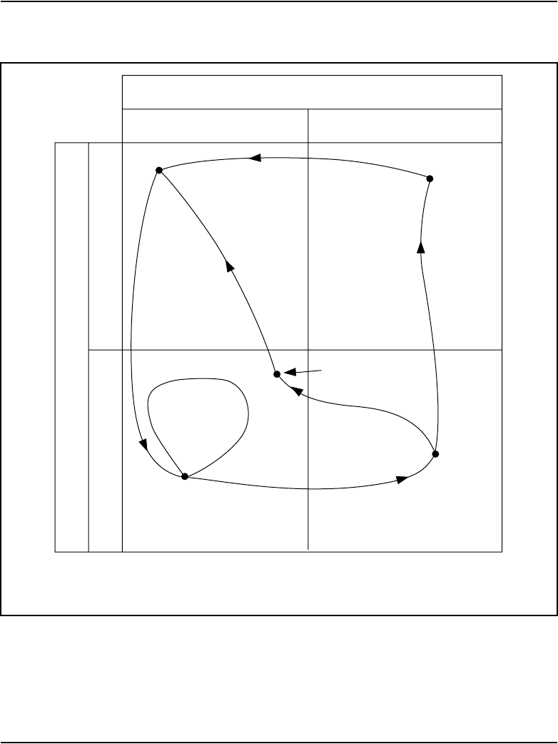
NT8D14 Universal Trunk card Page 585 of 906
Circuit Card Description and Installation
Figure 123
DID trunk, loop DR call states – incoming call from CO
Far end
originates
Battery-ground
or loop pulsing
or DTMF
(Note)
Note:
The near end may be configured for immediate start, delay dial, or
wink start.
Forced
far end
disconnect
Forced
near end
disconnect
Idle
Near end
disconnects
first
Near end
answers
553-AAA1137
Far end
disconnects
first
System (near) end
Low-resistance loop High-resistance loop
CO (far) end
Ground on tip, battery on ring Battery on tip, ground on ring
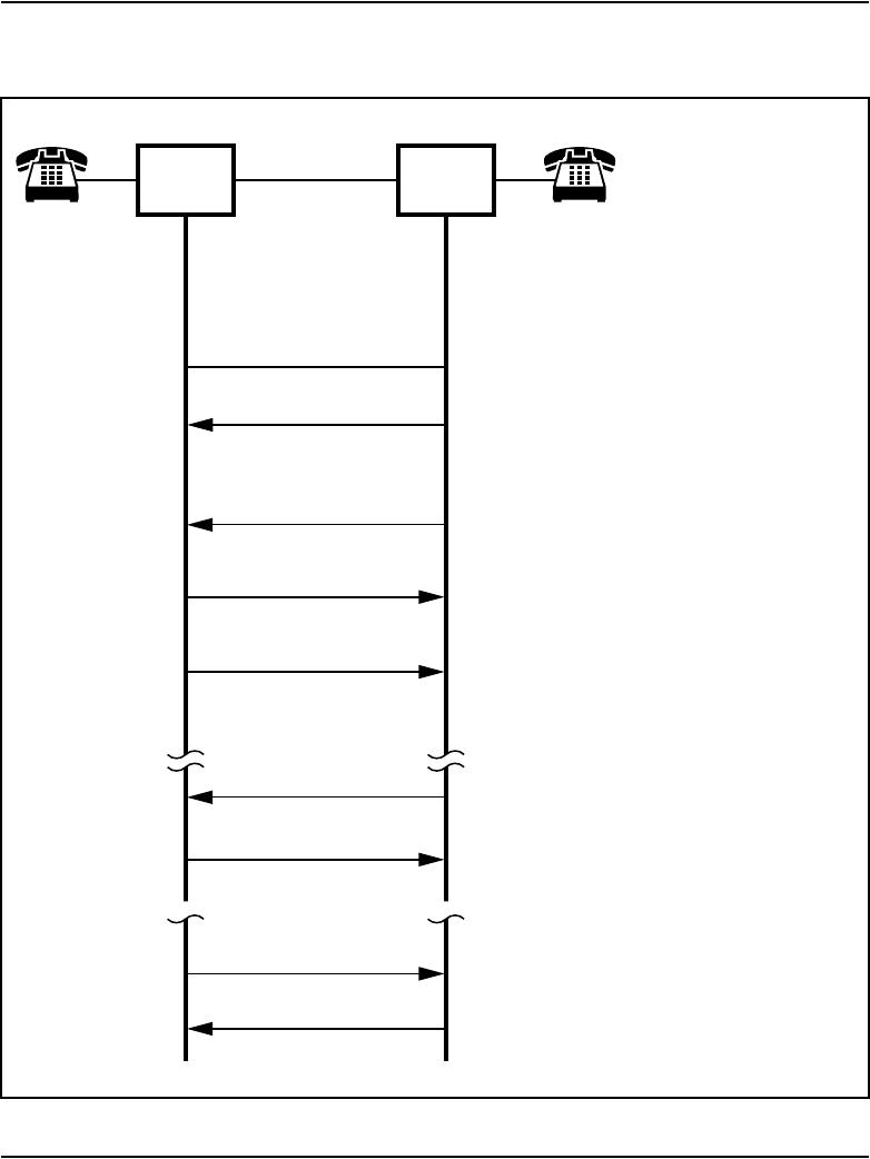
Page 586 of 906 NT8D14 Universal Trunk card
553-3001-211 Standard 3.00 August 2005
Figure 124
DID trunk, loop DR call connection sequence – incoming call from CO
A
State
Idle
Idle
Trunk seizure
Outpulsing
A rings
B goes on hook
Idle
A goes on hook
RemarksSignal/direction
Near end
System
B
Far end
CO
High-
resistance
loop
Address signaling
High-resistance loop
High-resistance loop
Ground
on tip/
battery
on ring
Ground on tip/
battery on ring
Ground on tip/
battery on ring
Low-resistance loop CO places a low resistance between tip and
ring.
Near end detects increase in loop current
and makes trunk busy to all outgoing calls.
CO applies addressing to the trunk in the
form of battery-ground or loop pulses or
DTMF tones.
Near end detects addressing, alerts terminal
A, and provides ringback tone to CO.
If far end disconnects first, CO opens the
loop.
Near end detects drop in loop current and
reverses battery and ground on tip and ring.
2-way voice
connection
Battery on tip/
ground on ring
Ringback
When terminal A goes off hook, near end
trips ringback tone and provides answer
super-vision by reversing battery and ground
on tip and ring.
If near end disconnects first, it reverses
battery and ground on tip and ring.
CO detects battery/ground reversal and
opens loop.
553-AAA1138
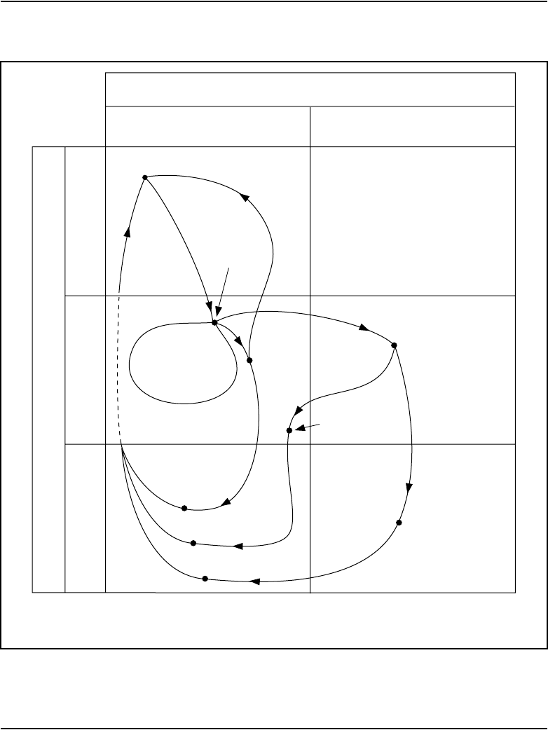
NT8D14 Universal Trunk card Page 587 of 906
Circuit Card Description and Installation
Figure 125
Two-way, loop DR, TIE trunk call states – incoming call from far-end PBX
Battery-ground
or loop pulse,
or DTMF
Far end
originates
Idle Far end
hangs up
(Note)
Far end
disconnects
first
Far end
disconnects
first
Far end
disconnects
Near end
disconnects
first
Near end
disconnects
Near end
answers
(no ans
sup)
Near end
answers
(ans sup)
553-AAA1139
System (near) end
Far end PBX
High-resistance
loop
Ground on tip,
battery on ring
Ground on tip,
battery on ring
Battery on tip,
ground on ring
Low-resistance
loop
Note:
Where no near-end answer supervision is provided, party at far end hangs up
after recognizing near-end call termination.
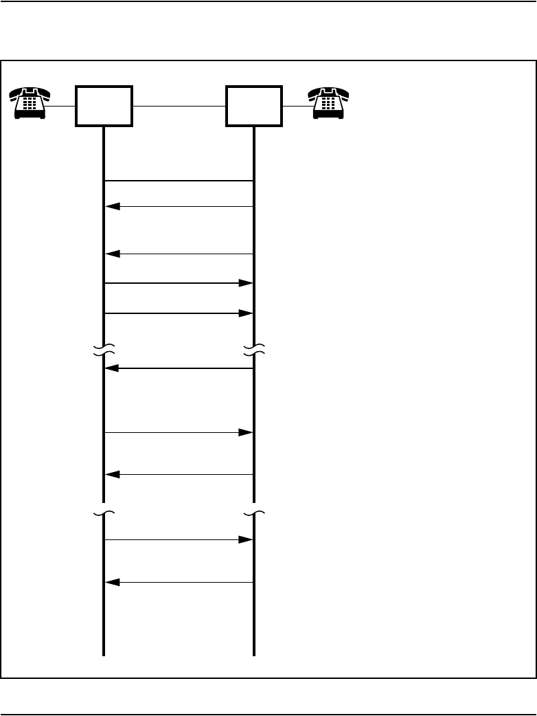
Page 588 of 906 NT8D14 Universal Trunk card
553-3001-211 Standard 3.00 August 2005
Figure 126
Two-way, loop DR, TIE trunk call connection sequence – incoming call from far-end PBX
A
State
Idle
Idle
Trunk seizure
Outpulsing
A rings
B goes on hook
Idle
A goes on hook
RemarksSignal/direction
Near end
System
B
Far end
System
Address signaling
High-resistance loop
Ground on tip/
battery on ring Ground on tip/
battery on ring
Ground on tip/
battery on ring
Ground on tip/
battery on ring
Ground on tip/
battery on ring
Low-resistance loop
Ground on tip/
battery on ring
Far end places a low resistance between tip and ring.
Near end detects increase in loop current and makes
trunk busy to all outgoing calls.
Far end applies addressing to the trunk in the form of
battery-ground or loop pulsing, or DTMF tones.
Near end detects addressing, alerts terminal A, and
provides ringback tone to far end.
When terminal A goes off hook, near end trips ringback
tone and provides answer supervision, if required by far
end, by reversing battery and ground on tip and ring.
If far end disconnects first, it momentarily opens the loop
and then restores normal battery and ground if no near-
end answer supervision was provided when call was
establish-ed. Otherwise, it waits for the near end to
restore normal battery and ground.
Near end detects drop in loop current and restores normal
battery and ground if answer supervision was provided.
Otherwise, terminal A simply hangs up.
If answer supervision was provided, far end restores
normal battery and ground when it detects
battery/ground reversal from near end.
2-way voice
connection
Battery on tip/
ground on ring
Ringback
If near end disconnects first, normal battery is restored if
answer supervision was provided to establish call.
Otherwise, terminal A simply hangs up.
If far end detects battery/ground reversal, it
momentarily opens loop and then restores normal
battery. But, if no answer supervision was provided by
the near end when the call was established, it cannot
supply a battery reversal to signal call termination; the
person at terminal B must recognize end of call and
hang up, which will then cause the far end to restore
normal battery. 553-AAA1140

NT8D14 Universal Trunk card Page 589 of 906
Circuit Card Description and Installation
Outgoing calls
In an outgoing call configuration, the NT8D14 Universal Trunk card is
connected to an existing PBX by a tie trunk. See Figure 127 on page 590 and
Figure 128 on page 591.
An outgoing call from the near-end seizes the trunk facility by placing a
low-resistance loop across the tip and ring leads. Outward addressing is then
applied from the System in the form of DTMF tones or dial pulses. If answer
supervision is provided by the far-end, reverse battery and ground on the tip
and ring leads are returned. The operation represented in Figure 129 on
page 592 and Figure 130 on page 593 also applies to outgoing calls on a DID
trunk.
Note: Where no far-end answer supervision is provided, the party at the
near-end hangs up, after recognizing far-end call termination.
Page 590 of 906 NT8D14 Universal Trunk card
553-3001-211 Standard 3.00 August 2005
Figure 127
Two-way, loop DR, TIE trunk call states – outgoing call to far-end PBX
System (near) end
Far end PBX
High-resistance
loop
Ground on tip,
battery on ring
Ground on tip,
battery on ring
Battery on tip,
ground on ring
Battery-ground
or loop pulse
or DTMF
Near end
originates
Idle
Near end
hangs up
(Note)
Near end
disconnects
first
Near end
disconnects
first
Near end
disconnects
Far end
disconnects
Far end
disconnects
first
Far end
answers
(no ans sup)
Far end
answers
(ans sup)
553-AAA1141
Low-resistance
loop
Note:
Where no far-end answer supervision is provided, party at near end hangs
up after recognizing far-end call termination.
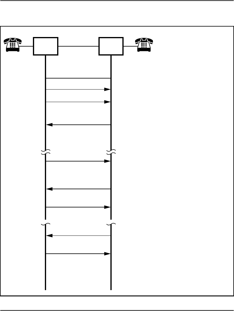
NT8D14 Universal Trunk card Page 591 of 906
Circuit Card Description and Installation
Figure 128
Two-way, loop DR, TIE trunk call connection sequence – outgoing call to far-end PBX
A
State
Idle
Idle
Trunk seizure
Outpulsing
B rings
A goes on hook
Idle
B goes on hook
RemarksSignal/direction
Near end
System
B
Far end
PBX
Address signaling
High-resistance loop
Ground on tip/
battery on ring Ground on tip/
battery on ring
Ground on tip/
battery on ring
Ground on tip/
battery on ring
Ground on tip/
battery on ring
Low-resistance loop
Ground on tip/
battery on ring
When terminal A goes off hook, near end places a low
resistance between tip and ring.
Terminal A dials and battery-ground or loop pulses, or
DTMF tones, are sent to far end.
If answer supervision is provided by far end, reverse
battery and ground are applied to tip and ring when
terminal B answers.
Near end monitors loop current during 2-way voice
connection.
If near end disconnects first, it momentarily opens the loop
and then restores normal battery and ground if no far-end
answer supervision was provided when call was establish-
ed. Otherwise, it waits for the far end to restore normal
battery and ground.
Far end detects drop in loop current and restores normal
battery and ground if answer supervision was provided.
Otherwise, terminal B simply hangs up.
If answer supervision was provided, near end restores
normal battery and ground when it detects
battery/ground reversal from far end.
2-way voice
connection
Battery on tip/
ground on ring
If far end disconnects first, it restores normal battery if
answer supervision was provided to establish call.
Otherwise, terminal B simply hangs up.
If near end detects battery/ground reversal, it moment-
arily opens loop and then restores normal battery. But,
if no answer supervision was provided by the far end
when the call was established, it cannot supply a
battery reversal to signal call termination; the person at
terminal A must recognize end of call and hang up,
which will then cause the local end to restore normal
battery. 553-AAA1142

Page 592 of 906 NT8D14 Universal Trunk card
553-3001-211 Standard 3.00 August 2005
Figure 129
Two-way, loop DR, TIE trunk call states – outgoing call to far-end PBX
System (near) end
Far end PBX
High-resistance
loop
Ground on tip,
battery on ring
Ground on tip,
battery on ring
Battery on tip,
ground on ring
Battery-ground
or loop pulse
or DTMF
Near end
originates
Idle
Near end
hangs up
(Note)
Near end
disconnects
first
Near end
disconnects
first
Near end
disconnects
Far end
disconnects
Far end
disconnects
first
Far end
answers
(no ans sup)
Far end
answers
(ans sup)
553-AAA1141
Low-resistance
loop
Note:
Where no far-end answer supervision is provided, party at near end hangs
up after recognizing far-end call termination.

NT8D14 Universal Trunk card Page 593 of 906
Circuit Card Description and Installation
Figure 130
Two-way, loop DR, TIE trunk call connection sequence – outgoing call to far-end PBX
A
State
Idle
Idle
Trunk seizure
Outpulsing
B rings
A goes on hook
Idle
B goes on hook
RemarksSignal/direction
Near end
System
B
Far end
PBX
Address signaling
High-resistance loop
Ground on tip/
battery on ring Ground on tip/
battery on ring
Ground on tip/
battery on ring
Ground on tip/
battery on ring
Ground on tip/
battery on ring
Low-resistance loop
Ground on tip/
battery on ring
When terminal A goes off hook, near end places a low
resistance between tip and ring.
Terminal A dials and battery-ground or loop pulses, or
DTMF tones, are sent to far end.
If answer supervision is provided by far end, reverse
battery and ground are applied to tip and ring when
terminal B answers.
Near end monitors loop current during 2-way voice
connection.
If near end disconnects first, it momentarily opens the loop
and then restores normal battery and ground if no far-end
answer supervision was provided when call was establish-
ed. Otherwise, it waits for the far end to restore normal
battery and ground.
Far end detects drop in loop current and restores normal
battery and ground if answer supervision was provided.
Otherwise, terminal B simply hangs up.
If answer supervision was provided, near end restores
normal battery and ground when it detects
battery/ground reversal from far end.
2-way voice
connection
Battery on tip/
ground on ring
If far end disconnects first, it restores normal battery if
answer supervision was provided to establish call.
Otherwise, terminal B simply hangs up.
If near end detects battery/ground reversal, it moment-
arily opens loop and then restores normal battery. But,
if no answer supervision was provided by the far end
when the call was established, it cannot supply a
battery reversal to signal call termination; the person at
terminal A must recognize end of call and hang up,
which will then cause the local end to restore normal
battery. 553-AAA1142

Page 594 of 906 NT8D14 Universal Trunk card
553-3001-211 Standard 3.00 August 2005
Senderized operation for DID and two-way loop DR trunks
Incoming calls
If the far-end is senderized, the near-end can operate in any mode: Immediate
Start (IMM), Delay Dial (DDL) or Wink (WNK) start, as assigned at the
STRI prompt in the Trunk Administration program LD 14. See Figure 131 on
page 595.
Note: If a ground start trunk, the outpulse towards office occurs after
ground detection. If a loop start trunk, the outpulse towards office occurs
one second later.
For immediate start, following the seizure signal, the far-end starts pulsing
after the standard delay (normally 65 ms, minimum).
For delay dial or wink start modes, stop/go signaling (off hook/on hook or
battery/ground reversal) is returned by the System after receipt of the seizure
signal. The delay dial (stop) signal begins immediately upon seizure and ends
(go signal) 384 ms later. The wink start (stop) signal begins 384 ms after
seizure and ends (go signal) 256 ms later. The far-end detecting the go signal
starts pulsing after the standard delay (normally 55 ms, minimum). Stop/go
signaling, in addition to the signaling function, serves as an integrity check to
help identify a malfunctioning trunk.
If required, the near-end can be configured to provide pseudo-answer
supervision at the expiration of the end-of-dial timer. End-of-dial timer
settings are made at the EOD (non-DTMF) or ODT (DTMF) prompts in the
Trunk Route Administration program LD 16.
The operation represented in Figure 132 on page 596 also applies to incoming
calls on a DID trunk from a CO.
Outgoing calls
When DDL or WNK mode is used, outgoing calls require a stop/go signal
from the far-end so that the near-end cannot outpulse until the far-end is ready
to receive digits. See Figure 133 on page 598.
NT8D14 Universal Trunk card Page 595 of 906
Circuit Card Description and Installation
Figure 131
Two-way, loop DR, TIE trunk call states – incoming call through senderized, tandem PBX
from a CO/FX/WATS trunk
System (near) end
Ground on tip,
battery on ring
Battery on tip,
ground on ring
Battery-ground
or loop pulsing,
or DTMF
(Note 1)
Far end
originates
Idle Far end
hangs up
(Note 4)
Far end
disconnects
first
Far end
disconnects
first
Far end
disconnects
Near end
disconnects
CO/FX/WATS
ground start
disconnect
Near end
stores
office DN
(Note 2) Near end
answers
(ans sup)
(Note 3)
CO end
answers
(no ans sup)
553-AAA1143
Note 1:
Dial CO/FX/WATS and office DN.
Note 2:
If ground start trunk, outpulse toward office after ground detection.
If loop start trunk, outpulse toward office 1 second later.
Note 3
: Pseudo-answer supervision is provided by near end at expiration of
end-of-dial timer.
Note 4:
Where no far-end answer supervision is provided, party at far end
hangs up after recognizing near-end call termination.
Far end PBX
High-resistance
loop
Ground on tip,
battery on ring
Low-resistance
loop

Page 596 of 906 NT8D14 Universal Trunk card
553-3001-211 Standard 3.00 August 2005
Figure 132
Two-way, loop DR, TIE trunk call states – incoming call through senderized, tandem PBX
from a CO/FX/WATS trunk
System (near) end
Ground on tip,
battery on ring
Battery on tip,
ground on ring
Battery-ground
or loop pulsing,
or DTMF
(Note 1)
Far end
originates
Idle Far end
hangs up
(Note 4)
Far end
disconnects
first
Far end
disconnects
first
Far end
disconnects
Near end
disconnects
CO/FX/WATS
ground start
disconnect
Near end
stores
office DN
(Note 2) Near end
answers
(ans sup)
(Note 3)
CO end
answers
(no ans sup)
553-AAA1143
Note 1:
Dial CO/FX/WATS and office DN.
Note 2:
If ground start trunk, outpulse toward office after ground detection.
If loop start trunk, outpulse toward office 1 second later.
Note 3
: Pseudo-answer supervision is provided by near end at expiration of
end-of-dial timer.
Note 4:
Where no far-end answer supervision is provided, party at far end
hangs up after recognizing near-end call termination.
Far end PBX
High-resistance
loop
Ground on tip,
battery on ring
Low-resistance
loop

NT8D14 Universal Trunk card Page 597 of 906
Circuit Card Description and Installation
Note: Pseudo-answer supervision is provided by near-end at expiration
of end-of-dial timer. Where no far-end answer supervision is provided,
the party at the far-end hangs up after recognizing near-end call
termination.
Outgoing automatic, incoming dial operation
Incoming calls
When the NT8D14 Universal Trunk card is seized by the far-end on an
incoming call, a low-resistance loop is placed across the tip and ring leads.
Addressing is then sent by the far-end in the form of battery-ground or loop
pulses, or DTMF tones. The trunk is released at the far-end when the loop is
opened. When the near-end detects an open loop, it returns to a normal state.
See Figure 134 on page 599 and Figure 135 on page 600.
Outgoing calls
When seized as a dial-selected outgoing trunk, the near-end places the battery
on the tip and ground on the ring. This alerts the far-end of the seizure. The
far-end responds with a low resistance across the tip and ring leads.
See Figure 136 on page 601 and Figure 137 on page 602.
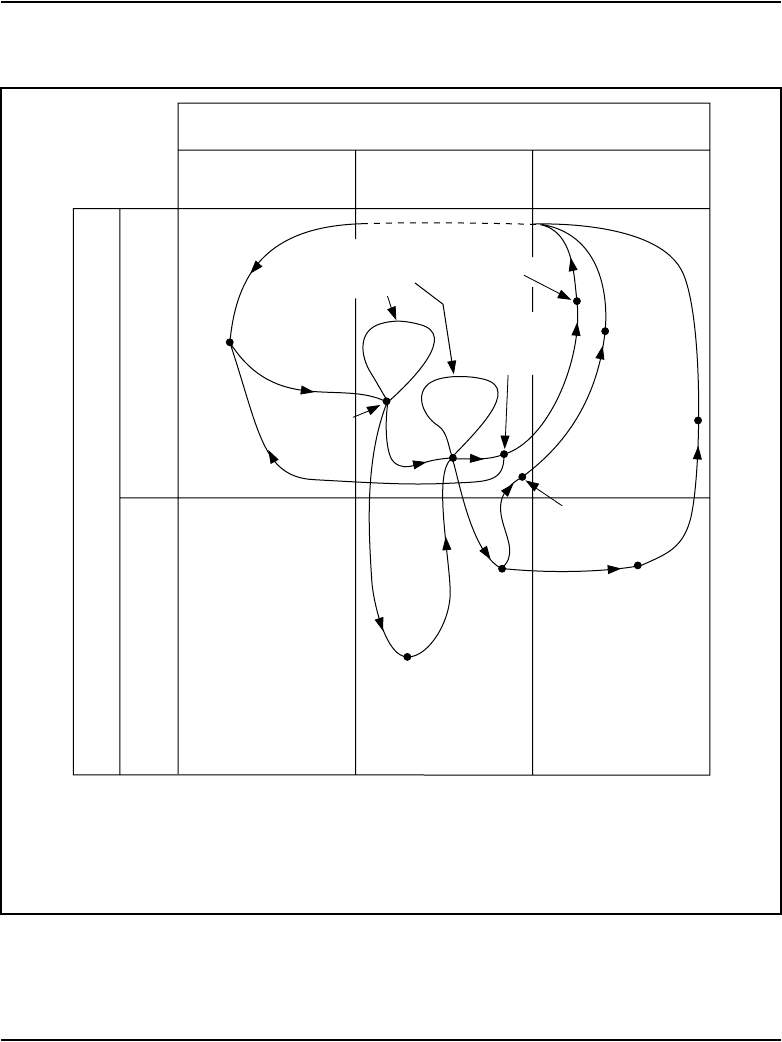
Page 598 of 906 NT8D14 Universal Trunk card
553-3001-211 Standard 3.00 August 2005
Figure 133
Two-way, loop DR, TIE trunk call states – outgoing call through far-end PBX to CO/FX/WATS
System (near) end
Far end
High-resistance
loop
Ground on tip,
battery on ring
Ground on tip,
battery on ring
Battery on tip,
ground on ring
Battery-ground
or loop pulses,
or DTMF
Near end
originates Dial
tone
Idle
Near end
hangs up
(Note 3)
Near end
disconnects
first
Near end
disconnects
first
Near end
disconnects
Far end
disconnects
Far end
disconnects
first
Far end
answers
(no ans sup)
Far end
answers
(ans sup)
Universal service
provided by far
end PBX if
originating end is
senderized
553-1144
Low-resistance
loop
(Note 1)
(Note 2)
(Note 2)
Note 1
: Immediate-start outpulsing.
Note 2:
Delay-dial or wink-start outpulsing after go signal.
Note 3:
Where no far-end answer supervision is provided, party at near end
hangs up after recognizing far-end call termination.
Go
Stop
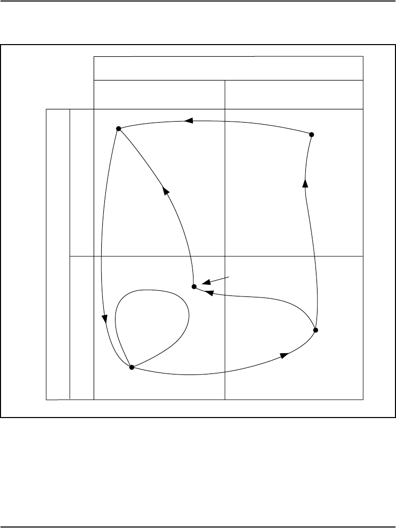
NT8D14 Universal Trunk card Page 599 of 906
Circuit Card Description and Installation
Figure 134
Two-way, loop OAID, TIE trunk call states – incoming call from far-end PBX
System (near) end
Low-resistance loop High-resistance loop
Far end
originates
Battery-ground
or loop pulses,
or DTMF
Far end
Far end
disconnect
Forced
near end
disconnects
Idle
Near end
disconnects
first
Near end
answers
553-AAA1145
Far end
disconnects
first
Ground on tip,
battery on ring
Battery on tip,
ground on ring
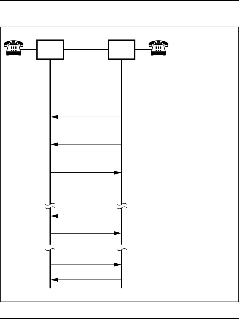
Page 600 of 906 NT8D14 Universal Trunk card
553-3001-211 Standard 3.00 August 2005
Figure 135
Two-way, loop OAID, TIE trunk call connection sequence – incoming call from far-end PBX
A
State
Idle
Idle
Trunk seizure
Outpulsing
A rings
B goes on hook
Idle
A goes on hook
RemarksSignal/direction
Near end
System
B
Far end
PBX
High-
resistance
loop
Address signaling
High-resistance loop
High-resistance loop
Ground
on tip/
battery
on ring
Ground on tip/
battery on ring
Ground on tip/
battery on ring
Low-resistance loop Far end PBX seizes trunk by placing a low
resistance between tip and ring.
Near end detects increase in loop current
and makes trunk busy to all outgoing calls.
Far end sends battery-ground or loop
pulses, or DTMF tones.
Near end detects addressing and alerts
terminal A.
If far end disconnects first, it opens the loop.
Near end detects drop in loop current and
restores normal battery and ground.
2-way voice
connection
Battery on tip/
ground on ring Terminal A goes off hook. If answer
supervision is required by far end, reverse
battery and ground are applied to tip and ring.
Far end monitors loop current during 2-way
voice connection.
If near end disconnects first, it reverses
battery and ground on tip and ring.
Far end detects battery/ground reversal and
opens loop.
553-AAA1146
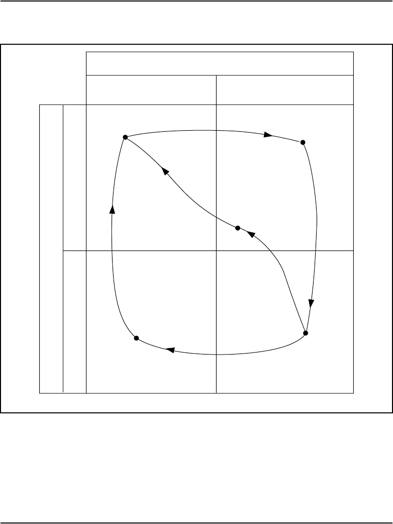
NT8D14 Universal Trunk card Page 601 of 906
Circuit Card Description and Installation
Figure 136
Two-way, loop OAID, TIE trunk call states – outgoing call to far-end PBX
System (near) end
Near end
originates
Far end
disconnect
Near end
disconnect
Idle
Near end
disconnects
first Far end
answers
553-AAA1147
Far end
disconnects
first
Ground on tip,
battery on ring
Battery on tip,
ground on ring
Low-resistance loop High-resistance loop
Far end
Page 602 of 906 NT8D14 Universal Trunk card
553-3001-211 Standard 3.00 August 2005
Figure 137
Two-way, loop OAID, TIE trunk call connection sequence – outgoing call to far-end PBX
A
State RemarksSignal/direction
Near end
System
B
Far end
PBX
High-
resistance
loop
Low-resistance loop
High-resistance loop
High-resistance loop
Ground
on tip/
battery
on ring
Ground on tip/
battery on ring
Ground on tip/
battery on ring
Battery on tip/
ground on ring Terminal A goes off hook and dials access
code. Near end reverses battery and ground
on tip and ring, alerting far end.
Far end detects battery/ground reversal and
answers call by placing a low resistance
between tip and ring.
Near end monitors loop current during 2-way
voice connection.
If far end disconnects first, it opens the loop.
Near end detects drop in loop current and
reverses battery and ground on tip and ring.
If near end disconnects first, it reverses
battery and ground on tip and ring.
Far end detects battery/ground reversal and
opens loop.
553-AAA1148
Idle
Idle
Idle
Trunk seizure
B goes on hook
A goes on hook
2-way voice
connection

NT8D14 Universal Trunk card Page 603 of 906
Circuit Card Description and Installation
Recorded announcement trunk operation
Note: Refer to “Multi-Channel RAN modes” on page 605 for
information on Multi-Channel RAN modes, which are not linked to a
RAN machine or a given trunk.
When configured for Recorded Announcement (RAN) operation, a trunk unit
is connected to a customer-provided recorded announcement machine.
Announcement machines must be compatible with RAN trunks. Use the
manufacturer’s instructions to set up the Announcement machines.
Each trunk unit provides the following for operation with RAN equipment:
• pulse start, level start, or continuous operation modes
• selectable termination of tip and ring leads into 600 or 900 ohms for
interface with a low-impedance (2 or 4 ohms) source
• connection of up to 24 trunk units to a single announcement machine
channel
Recorded announcement machines
Recorded announcement machines store prerecorded voice messages that are
played back to the trunk units to which they are connected. Most
commercially available announcement machines store recordings digitally,
although some drum and tape units are still in service.
An announcement machine can provide one or more channels and each
channel may be prerecorded with a different message. Some announcement
machines also provide a Special Information Tone (SIT) capability. These
tones are inserted at the beginning of intercept messages such as “Your call
cannot be completed as dialed. Please check the number and try again.”
Figure 138 on page 604 shows a typical connection from a single
announcement machine channel to unit 0 on a universal trunk card.
Page 604 of 906 NT8D14 Universal Trunk card
553-3001-211 Standard 3.00 August 2005
Figure 138
Connecting RAN equipment to the NT8D14 Universal Trunk card (typical)
Typical customer-
provided external
equipment
Cross connectSystem
NT8D14
Universal
Trunk Card
Unit 0
Unit 1
Unit 7
NT8D37
IPE Module
MDF
0T
Slot 0
A
26 (W-BL)
Announcer
0R 1(BL-W)
0CP 27 (W-O)
0MB 2(O-W)
Module
I/O Panel
Connector
Part of
25-pair
cable
Part of
25-pair
cable
Parallel
trunk
connection
(Note 2)
T
Voice
signal
Ref
R
Control
relay
Busy
relay
Note 1
Tel
ground
C
Com
MC
NC
B
Com
MB
ST+
Opto-
isolator Start
553-AAA1149
STÐ
NC
48 V
Note 1:
For continuous operation mode, connect the trunk unit MB line to the announcer B line
only and ground the announcer ST+ line. For pulse start or level start modes, connect the trunk
unit MB line to the announcer ST+ line only and leave the announcer B line unconnected.
Note 2:
A maximum of 24 universal trunk card units can be paralleled to a single announcer
channel.
Audio
pair
Signal
pair

NT8D14 Universal Trunk card Page 605 of 906
Circuit Card Description and Installation
RAN modes of operation
Figure 139 on page 606 shows the relationship of control signals to message
playback for the operating modes available in announcement machines. The
signal names shown in Figure 139 are typical.
Note 1: For continuous operation mode, connect the trunk unit MB line
to the announcer B line only, and ground the announcer ST+ line. For
pulse start or level start modes, connect the trunk unit MB line to the
announcer ST+ line only, and leave the announcer B line unconnected.
Note 2: A maximum of 24 universal trunk card units can be paralleled
to a single announcer channel.
Multi-Channel RAN modes
In Multi-Channel RAN, multiple RAN channels can be configured within one
RAN trunk route. In a Multi-Channel RAN route, each trunk has its own
dedicated RAN channel on a physical RAN machine. Multi-Channel RAN
routes do not support the cross connecting (daisy chains) of multiple trunk
ports together so that several callers hear the same RAN message.
Multi-channel machine types – Continuous Mode Multi-Channel (MCON),
Pulse Start/Stop Multi-Channel (MPUL) and Level Start/Stop Multi-Channel
(MLVL) – are not linked to a RAN machine or a given trunk. All trunks
belonging to the RAN route are considered independent. RAN trunks and
RAN machine channels are connected one-to-one. If one RAN trunk is
detected as faulty, then all other trunks are not impacted.
For the RAN machine types, the maximum length of the recorded
announcement is two hours. The meaning of a ground signal received from
the RAN machine (play or idle) is configured in LD 16.
Multi-Channel Level Start/Control Mode (minimum vintage BA)
A RAN mode of operation is available called “Multi-Channel Level Start/
Control Mode.” This mode enables provisioning of multiple RAN channels
for a RAN route (playing the same message independently on demand)
cross-connected one-to-one to each RAN trunk in a multi-channel level start
RAN route. Do not bridge RAN trunks in a multi-channel RAN route.
Page 606 of 906 NT8D14 Universal Trunk card
553-3001-211 Standard 3.00 August 2005
The Route Data Block LD 16 is used to configure a RAN route in
Multi-Channel Level Start/Control mode, using the following response:
RTYP = MLSS
Figure 139
RAN control signals (Control GRD = IDLE)
— Continuous operation mode —
C
ST+ input to announcer hardwired to ground
250 ms reset
Message
250 ms pulse at
end of message
ST+
— Pulse start/Level control mode —
C
250 ms pulse at
start of message 250 ms pulse at
end of message
250 ms pulse
starts message
Message plays
to completion
Intermediate ST+
pulses ignored
Start End
Message
ST+
C
250 ms pulse at
start of message 250 ms pulse at
end of message
Message output only
while ST+ is present
ST+ initiates and maintains
message output
Message
ST+
Play
Idle
Idle
Play
Play
Idle
Ground
Ground
Ground
Open
Open
Open
Open
Open
Open
Ground
Ground
Ground
(early disconnect) (disconnect after end of message)

NT8D14 Universal Trunk card Page 607 of 906
Circuit Card Description and Installation
Trunk members are provisioned in the Trunk Data Block LD 14.
Refer to “Programming RAN trunks” on page 608 and to Software Input/
Output: Administration (553-3001-311) for instructions on service change
programs.
Continuous operation mode
In the continuous operation mode (sometimes called the Audichron mode), a
message is constantly played, over and over again. Callers “barge in” on a
playing message or receive a ringback tone until the message plays again. The
start line (ST+) is hardwired as always active. See Figure 139 on page 606.
At the end of each message, a pulse is issued on the “C” line that is used by
the trunk unit to cut through to the waiting call.
Note: The “B” (busy) signal line indicates availability of an
announcement machine message to the trunk unit when configured for
the continuous operation mode. This signal is made active (ground) by
the announcement machine if the channel contains a recorded message
and is in an online condition. The “B” line is not connected to a trunk unit
when configured for start mode operation.
Start modes (minimum vintage BA)
In a start mode (sometimes called the Code-a-Phone or start-stop mode),
playback of a message does not begin until a start pulse is received by the
announcement machine. Two subcategories of the start mode exist: pulse
start and level start.
In the pulse start mode, a start pulse activates playback of a message that
continues until completion. The announcement machine ignores all other start
pulses that might occur until the message is complete.
In the level start mode, the start signal is a “level” rather than a pulse. The
leading edge of the start signal initiates message playback that continues until
either the trailing edge of the start signal occurs or the end of the message is
reached. A message that is terminated by the trailing edge of a level start
signal is immediately reset and ready for playback again.

Page 608 of 906 NT8D14 Universal Trunk card
553-3001-211 Standard 3.00 August 2005
Call routing to RAN trunks
CS 1000 Release 4.5 software controls recorded announcement machines.
These programs detect the calls to be intercepted, determine the type of
intercept treatment required (for example, overflow, attendant,
announcement), queue the intercept, and provide ringback tone to the calling
party. At the proper time, an intercepted call is connected to the appropriate
RAN trunk.
Programming RAN trunks
The type of intercept and the RAN trunk parameters are defined in the Trunk
Data Block LD 14, Customer Data Block LD 15, and Route Data Block
LD 16 programs.
The Trunk Data Block and Route Data Block programs specify the following:
• the RAN trunk
• the type of announcement machine
• the number of repetitions of announcements before a forced disconnect
(all calls) or an attendant intercept is initiated (CCSA/DID calls only)
• the point at which the trunk may be connected to the announcement
The Customer Data Block program defines the type of intercept and the trunk
route to which the intercept is to be connected.
Refer to Software Input/Output: Administration (553-3001-311) for
instructions on service change programs.

NT8D14 Universal Trunk card Page 609 of 906
Circuit Card Description and Installation
Electrical specifications
Table 185 gives the electrical characteristics of the NT8D14 Universal Trunk
card.
Table 185
Universal trunk card – trunk interface electrical characteristics (Part 1 of 2)
Trunk Types
Characteristic CO / FX / WATS DID / TIE RAN Paging
Terminal impedance 600 or 900 ohms
(Note 1)
600 or 900 ohms
(Note 1)
600/900 ohms
(Note 1)
600 ohms
Balance impedance 600 or 900 ohms
(Note 1),
3COM, or 3CM2
(Note 2)
600 or 900 ohms
(Note 1),
3COM, or 3CM2
(Note 2)
N/A N/A
Supervision type Ground or
loop start
(Note 3)
Loop start
(with ans sup)
(Note 3)
Continuous, level, or
pulse
N/A
DC signaling loop
length (max)
1700-ohm loop with
near-end battery of
–42.75 V
2450-ohm loop with
near-end battery of
–44 V
600/900-ohm loop 600 ohm
loop
Far-end battery –42 to –52.5 V
(Note 4)
–42 to –52.5 V –42 to –52 V N/A
Minimum detected
loop current
20 mA 10 mA 10 mA N/A
Ground potential
difference
±3 V ±3 V ±1 V ±1 V
Low DC loop
resistance during
outpulsing
<300 ohms N/A N/A N/A
High DC loop
resistance
Ground start
Š 30k ohms;
loop start
Š 5M ohms
N/A N/A N/A
Ring detection 17 to 33 Hz
40 to 120 V rms
N/A N/A N/A
Page 610 of 906 NT8D14 Universal Trunk card
553-3001-211 Standard 3.00 August 2005
Power requirements
Power to the NT8D14 Universal Trunk card is provided by the module power
supply (ac or dc).
Line leakage Š 30k ohms,
tip-to-ring,
tip-to-ground,
ring-to-ground
Š 30k ohms,
tip-to-ring,
tip-to-ground,
ring-to-ground
N/A N/A
AC induction
rejection
10 V rms, tip-to-ring,
tip-to-ground,
ring-to-ground
10 V rms, tip-to-ring,
tip-to-ground,
ring-to-ground
N/A N/A
Selected in software.
Selected by jumper strap settings on card. Refer to Tables 190, 191, and 192 for details.
For loop extender application, the maximum voltage applied between tip and ring is –105 V ±5%. The
minimum dc loop resistance for this type of application is 1800 ohms.
Table 186
Power requirements for universal trunk card
Voltage Tolerance Current (max.)
+15.0 V dc +5% 306 mA
–15.0 V dc +5% 306 mA
+5.0 V dc +5% 750 mA
+8.5 V dc +2% 450 mA
–48.0 V dc +5% 415 mA
Table 185
Universal trunk card – trunk interface electrical characteristics (Part 2 of 2)
Trunk Types
Characteristic CO / FX / WATS DID / TIE RAN Paging
NT8D14 Universal Trunk card Page 611 of 906
Circuit Card Description and Installation
Foreign and surge voltage protection
The NT8D14 Universal Trunk card meets UL-1489 and CS03 over-voltage
(power cross) specifications and FCC Part 68 requirements.
Environmental specifications
Table 187 lists the environmental specifications for the NT8D14 Universal
Trunk card.
Release control
Release control establishes which end of a call (near, far, either, joint, or
originating) disconnects the call. Only incoming trunks in idle ground start
configuration can provide disconnect supervision. You configure release
control for each trunk independently in the Route Data Block (LD 16).
PAD switching
The transmission properties of each trunk are characterized by the
class-of-service (COS) you assign in the Trunk Data Block (LD 14).
Transmission properties may be via net loss (VNL) or non via net loss
(non-VNL).
Non-VNL trunks are assigned either a Transmission Compensated (TRC) or
Non-Transmission Compensated (NTC) class-of-service to ensure stability
and minimize echo when connecting to long-haul trunks, such as Tie trunks.
Table 187
Environmental specifications for the NT8D14 Universal Trunk card
Parameter Specifications
Operating temperature 0° to +60° C (+32 to +140° F), ambient
0 to 50 degrees C, ambient
(Small Systems and CS 1000S)
Operating humidity 5 to 95% RH (non-condensing)
Storage temperature –40° to +70° C (–40° to +158° F)

Page 612 of 906 NT8D14 Universal Trunk card
553-3001-211 Standard 3.00 August 2005
The class-of-service determines the operation of the switchable PADs
contained in each unit. They are assigned as follows:
• Transmission Compensated
— used for a two-wire non-VNL trunk facility with a loss of greater
than 2 dB for which impedance compensation is provided
— or used for a four-wire non-VNL facility
• Non-Transmission Compensated
— used for a two-wire non-VNL trunk facility with a loss of less than
2 dB
— or used when impedance compensation is not provided
NT8D14 Universal Trunk card Page 613 of 906
Circuit Card Description and Installation
The insertion loss from IPE ports to IPE ports is as follows:
Table 188
Insertion Loss from IPE Ports to IPE Ports (measured in dB)
IPE Ports
IPE Ports
500/2500
Line
Digital
Line
2/4 Wire
E&M Trunk
4 Wire
(ESN) E&M
Trunk
CO/FX
/WATS
Loop Tie
Trunk
CO/FX/
WATS Loop
Tie Trunk
2.5
0
0
-3.5
0.5
0
0
-0.5
0.5
0.5

Page 614 of 906 NT8D14 Universal Trunk card
553-3001-211 Standard 3.00 August 2005
Connector pin assignments
The universal trunk card connects the eight analog trunks to the backplane
through a 160-pin connector shroud. Telephone trunks connect to the
universal trunk card at the back of the MG 1000S using a 25-pin connector.
A list of the connections to the universal trunk card is shown in Table 189 on
page 614. See Communication Server 1000S: Installation and Configuration
(553-3031-210) for I/O panel connector information and wire assignments
for each tip/ring pair.
Table 189
Universal trunk card – backplane pinouts (Part 1 of 2)
Trunk
Number
Back-
plane
Pin
Signal
Back-
plane
Pin
Signal
RAN
mode
Paging
mode
Other
modes
RAN
mode
Paging
mode
Other
modes
012A Tip Tip Tip 12B Ring Ring Ring
13A CP AN/A 13B MB RG N/A
114A Tip Tip Tip 14B Ring Ring Ring
15A CP AN/A 15B MB RG N/A
216A Tip Tip Tip 16B Ring Ring Ring
17A CP AN/A 17B MB RG N/A
318A Tip Tip Tip 18B Ring Ring Ring
19A CP AN/A 19B MB RG N/A
462A Tip Tip Tip 62B Ring Ring Ring
63A CP AN/A 63B MB RG N/A
564A Tip Tip Tip 64B Ring Ring Ring
65A CP AN/A 65B MB RG N/A
666A Tip Tip Tip 66B Ring Ring Ring
67A CP AN/A 67B MB RG N/A

NT8D14 Universal Trunk card Page 615 of 906
Circuit Card Description and Installation
Configuration
The trunk type for each unit on the card as well as its terminating impedance
and balance network configuration is selected by software service change
entries at the system terminal and by jumper strap settings on the card.
NT8D14 has a reduced jumper strap setting on the card. There are only three
jumpers, J1.X, J2.X, and J3.X on each channel. Tables 190, 191, and 192
show the functionality of these three jumpers.
768A Tip Tip Tip 68B Ring Ring Ring
69A CP AN/A 69B MB RG N/A
Table 189
Universal trunk card – backplane pinouts (Part 2 of 2)
Trunk
Number
Back-
plane
Pin
Signal
Back-
plane
Pin
Signal
RAN
mode
Paging
mode
Other
modes
RAN
mode
Paging
mode
Other
modes
Page 616 of 906 NT8D14 Universal Trunk card
553-3001-211 Standard 3.00 August 2005
Table 190
Jumper strap settings – factory standard (NT8D14BA, NT8D14BB)
Trunk types Loop length
Jumper strap settings (Note 1)
J1.X J2.X J3.X
J4.X
(Note 2)
CO/FX/WATS 0–1524 m (5000 ft.) Off Off 1–2 1–2
2-way TIE (LDR)
2-way TIE (OAID)
DID 0–600 ohms Off Off 1–2 1–2
RAN: continuous
operation mode
Not applicable: RAN
and paging trunks
should not leave the
building.
Off Off 1–2 1–2
Paging
Note 1: Jumper strap settings J1.X, J2.X, J3.X, and J4.X apply to all eight units; “X” indicates
the unit number, 0–7. “Off” indicates that no jumper strap is installed on a jumper block. Store
unused straps on the universal trunk card by installing them on a single jumper pin as shown
below.
Note 2: For the NT8D14BB card, J4.X is not provided on the card. The J4.X jumper setting
specified in Table 190 does not apply.
Jumper pin
Jumper block
Jumper strap
553-6317
NT8D14 Universal Trunk card Page 617 of 906
Circuit Card Description and Installation
Table 191
Jumper strap settings – extended range (NT8D14BA, NT8D14BB, NT8D14BB)
Trunk types Loop length
Jumper strap settings (Note 1)
J1.X J2.X J3.X
J4.X
(Note 2)
CO/FX/WATS > 1524 m (5000 ft.) Off Off 1–2 2–3
2-way TIE (LDR)
2-way TIE (OAID)
DID > 600 ohms On On 1–2 2–3
RAN: pulse start or
level start modes
Not applicable: RAN
trunks should not leave
the building.
Off Off 2–3 1–2
Note 1: Jumper strap settings J1.X, J2.X, J3.X, and J4.X apply to all eight units; “X” indicates
the unit number, 0–7. “Off” indicates that no jumper strap is installed on a jumper block.
Note 2: For the NT8D14BB card, J4.X is not provided on the board. The J4.X jumper setting
specified in Table 191 does not apply.

Page 618 of 906 NT8D14 Universal Trunk card
553-3001-211 Standard 3.00 August 2005
Jumper strap settings
For most applications, the jumper strap settings remain set to the standard
configuration as shipped from the factory. See Table 190 on page 616.
The jumper strap settings must be changed, as shown in Table 191 on
page 617, for the following:
• For CO/FX/WATS or TIE trunk loops exceeding 1524 meters (5000 ft.)
Table 192
Trunk types – termination impedance and balance network (NT8D14BA, NT8D14BB)
Trunk types
Terminating
impedance
(Note 1)
Balance network for loop lengths (Note 2)
0–915 m
(0–3000 ft)
915–1524 m
(3000–5000 ft)
> 1524 m
(> 5000 ft)
CO/FX/WATS 600 or 900
ohms
600 ohms 3COM 3CM2
2-way TIE (LDR) 600 or 900
ohms
600 ohms 3COM 3CM2
2-way TIE (OAID) 600 or 900
ohms
600 ohms 3COM 3CM2
DID (loop length
< 600 ohms)
600 or 900
ohms
600 ohms 3COM 3CM2
DID (loop length
Š 600 ohms)
600 or 900
ohms
600 ohms N/A 3CM2
RAN: continuous
operation mode
600 or 900
ohms
600 or 900 ohms N/A N/A
Paging 600 ohms 600 ohms N/A N/A
Note 1: The terminating impedance of each trunk unit is software selectable in LD 14 and
should match the nominal impedance of the connecting equipment.
Note 2: The balance network of each trunk unit is software selectable between resistive 600 or
900 ohms or 3COM and jumper selectable between 3COM and 3CM2. Jumper selection for
3COM/3CM2 restriction does not apply to NT8D14BB.

NT8D14 Universal Trunk card Page 619 of 906
Circuit Card Description and Installation
• DID trunks exceeding a loop resistance of 600 ohms
• RAN trunks operating in pulse start or level start modes
Figure 140 on page 620 shows jumper locations on the universal trunk card
(vintage BA).
Service change entries
The trunk type, terminating impedance, and balance network are selected by
making service change entries in the Trunk Administration program LD 14.
See Table 193 on page 621 for the proper values for the trunk type and loop
length. Refer to Software Input/Output: Administration (553-3001-311) for
LD 14 service change instructions.
Before the appropriate balance network can be selected, the loop length
between the near-end and the far-end (a Central Office, for example) must be
known. To assist in determining loop length, some typical resistance and loss
values for the most common cable lengths are given in Table 194 on page 622
for comparison with values obtained from actual measurements.
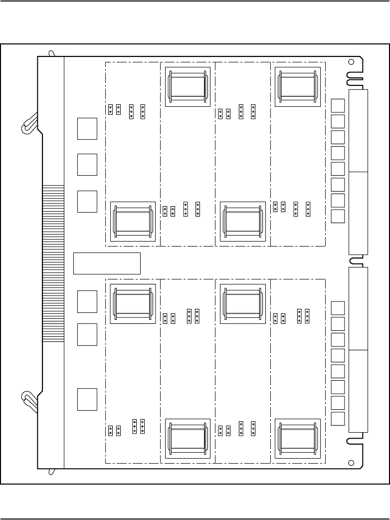
Page 620 of 906 NT8D14 Universal Trunk card
553-3001-211 Standard 3.00 August 2005
Figure 140
Universal trunk card – jumper locations (for NT8D14BA, NT8D14BB Release 9 and below)
J1.4
J2.4
31
J4.4
31
J3.4
J1.5
J2.5
31
J3.4
31
J4.5
J1.1
J2.1
31
J3.1
31
J4.1
J1.6
J2.6
13
J4.6
13
J3.6
J1.7
J2.7
13
J4.7
13
J3.7
J1.3
J2.3
31 J4.3
Unit 3
Unit 1
Unit 2
Unit 0
Unit 4
Unit 6
Unit 5
Unit 7
31 J3.3
J1.2
J2.2
13
J3.2
13
J4.2
J1.0
J2.0
13 J4.0 13 J3.0
553-6196

NT8D14 Universal Trunk card Page 621 of 906
Circuit Card Description and Installation
Table 193
Trunk types – termination impedance and balance network (NT8D14BA, NT8D14BB)
Trunk types
Terminating
impedance
(Note 1)
Balance network for loop lengths (Note 2)
0–915 m
(0–3000 ft)
915–1524 m
(3000–5000 ft)
> 1524 m
(> 5000 ft)
CO/FX/WATS 600 or 900
ohms
600 ohms 3COM 3CM2
2-way TIE (LDR) 600 or 900
ohms
600 ohms 3COM 3CM2
2-way TIE (OAID) 600 or 900
ohms
600 ohms 3COM 3CM2
DID (loop length
< 600 ohms)
600 or 900
ohms
600 ohms 3COM 3CM2
DID (loop length
Š 600 ohms)
600 or 900
ohms
600 ohms N/A 3CM2
RAN: continuous
operation mode
600 or 900
ohms
600 or 900 ohms N/A N/A
Paging 600 ohms 600 ohms N/A N/A
Note 1: The terminating impedance of each trunk unit is software selectable in LD 14 and
should match the nominal impedance of the connecting equipment.
Note 2: The balance network of each trunk unit is software selectable between resistive 600 or
900 ohms or 3COM and jumper selectable between 3COM and 3CM2. Jumper selection for
3COM/3CM2 restriction does not apply to NT8D14BB.
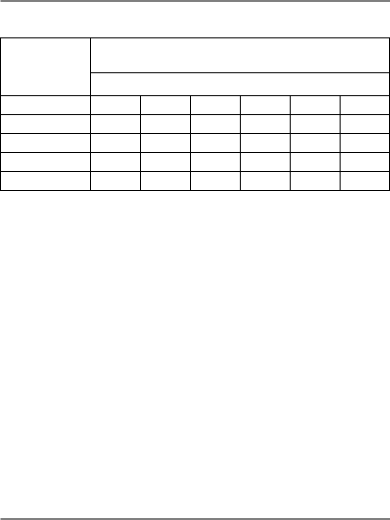
Page 622 of 906 NT8D14 Universal Trunk card
553-3001-211 Standard 3.00 August 2005
Port-to-port loss configuration
Loss parameters are selected on the NT8D14 Universal Trunk card by a
switchable pad controlled by codec emulation software. For convenience, the
pads settings are called “in” and “out.” Pad settings are determined by the two
factors listed below (the first is under direct user control; the second is
controlled indirectly):
• Class of Service is assigned in LD 14 (under direct user control).
• Port-to-port connection loss is automatically set by software on the basis
of the port type selected in LD 16; only the port type is set by the user
(controlled indirectly).
The transmission properties of each trunk are characterized by the class of
service assigned in LD 14. Transmission properties can be Via Net Loss
(VNL) or non-Via Net Loss (non-VNL).
The VNL class of service is assigned at the prompt CLS with the response
VNL. The non-VNL class of service is assigned at prompt CLS by selecting
either the Transmission Compensated (TRC) or Non-Transmission
Compensated (NTC) response.
Non-VNL trunks are assigned a TRC or NTC class of service to ensure
stability and minimize echo when connecting to long-haul trunks, such as Tie
Table 194
Cable loop resistance and loss
Cable length
Cable loop resistance (ohms)
Cable loop loss (dB)
(nonloaded at 1kHz)
22 AWG 24 AWG 26 AWG 22 AWG 24 AWG 26 AWG
915 m (3000 ft.) 97 155 251 0.9 1.2 1.5
1524 m (5000 ft.) 162 260 417 1.6 2.0 2.5
2225 m (7300 ft.) 236 378 609 2.3 3.0 3.7
3566 m (11700 ft.) 379 607 977 3.7 4.8 6.0
5639 m (18500 ft.) 600 960 1544 5.9 7.6 9.4

NT8D14 Universal Trunk card Page 623 of 906
Circuit Card Description and Installation
trunks. The class of service determines the operation of the switchable pads
contained in each unit. They are assigned as follows:
• TRC for a 2-wire non-VNL trunk facility with a loss of greater than 2 dB,
or for which impedance compensation is provided, or for a 4-wire
non-VNL facility.
• NTC for a 2-wire, non-VNL trunk facility with a loss of less than 2 dB,
or when impedance compensation is not provided.
See Table 195 for the pad switching control for the various through
connections and the actual port-to-port loss introduced for connections
between the NT8D14 Universal Trunk card and any other port designated as
Port B.
Table 195
Pad switching algorithm
Port B
Port B pads
Universal Trunk
Pads Port-to-port loss (dB)
Transmit
D to A
Receive
A to D
Transmit
D to A
Receive
A to D
Port B to
Universal
trunk
card
Universal
trunk
card to
Port B
IPE line N/A N/A Out Out 0.5 0.5
Universal trunk
(TRC)
In Out In Out 1 1
IPE TIE (VNL) In In Out Out 0 0
Note: Transmit and receive designations are from and to the system. Transmit is from the
system to the external facility (digital-to-analog direction in the Universal trunk card). Receive is
to the system from the external facility (analog-to-digital direction in the Universal trunk card).
Note: When Port B is the call originating port. If the Universal trunk card is the originating port,
the UTC pads are out, the Port B (PE CO/FX/WATS) pads are in.

Page 624 of 906 NT8D14 Universal Trunk card
553-3001-211 Standard 3.00 August 2005
Applications
The optional applications, features, and signaling arrangements for each
trunk are assigned through unique route and trunk data blocks.
Paging trunk operation
A universal trunk card unit can be configured as a paging trunk. Configure
units as paging trunks in the Trunk Data Block program LD 14 and assign
routes in the Route Data Block program LD 16.
Figure 141 on page 625 shows a typical connection from customer-provided
equipment to unit 0 on a universal trunk card that can be installed in slots 1,
2, and 3 in an MG 1000S, and slots 7, 8, 9, and 10 in an MG 1000S. See
Communication Server 1000S: Installation and Configuration
(553-3031-210) for trunk wiring information.
Music operation
A trunk unit can be connected to a music source. The audio source should
provide an adjustable power output at 600 ohms.
Configure units for music at the MUS or AWR prompts in the Trunk
Administration program LD 14 and assign routes at the MRT prompt in the
Route Data Block program LD 16.
Music operation is similar to that of RAN in the continuous operation mode.
Connect the unit tip and ring leads to the audio source and ground the CP line
at the MDF.
If the music source is equipped with contacts that close when music is online,
use these contacts to provide a ground to the MB line; otherwise, ground the
MB line at the MDF.
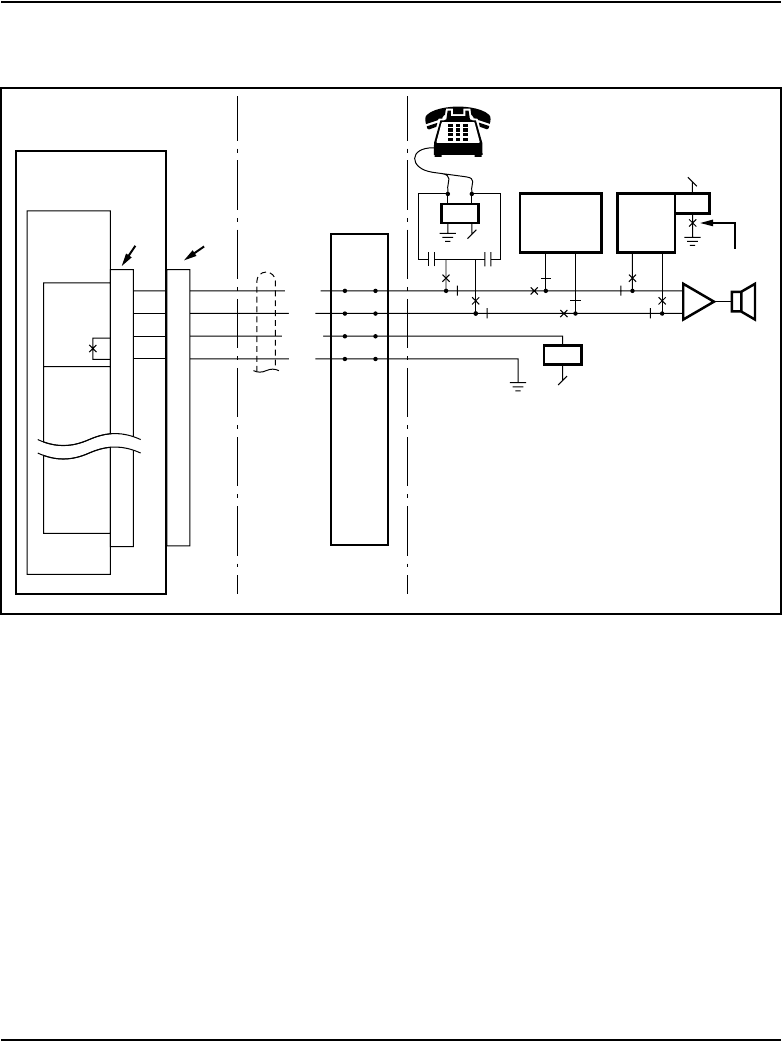
NT8D14 Universal Trunk card Page 625 of 906
Circuit Card Description and Installation
Figure 141
Connecting paging equipment to the NT8D14 Universal Trunk card (typical)
Typical customer-
provided external
equipment
Cross
connect
System
NT8D14
Universal
Trunk Card
Unit 0
Unit 1
Unit 7
NT8D37
IPE Module
MDF
0T
Slot 0
A
26 (w-bl)
0R 1(bl-w)
0A 27 (w-o)
0PG 2(o-w)
Module
I/O Panel
Connector
Part of
25-pair
cable
553-AAA1150
Audio
pair
Signal
pair K2
Bat
Bat
Amplifier Speaker
Tape
recorder,
radio, etc.
Micro-
phone
K3
Microphone
contacts
K3
Bat
K3
K2
K2
K1
K1
K1


Page 627 of 906
Circuit Card Description and Installation
666
NT8D15 E&M Trunk card
Contents
This section contains information on the following topics:
Introduction . . . . . . . . . . . . . . . . . . . . . . . . . . . . . . . . . . . . . . . . . . . . . . 627
Physical description. . . . . . . . . . . . . . . . . . . . . . . . . . . . . . . . . . . . . . . . 629
Functional description . . . . . . . . . . . . . . . . . . . . . . . . . . . . . . . . . . . . . . 631
Operation. . . . . . . . . . . . . . . . . . . . . . . . . . . . . . . . . . . . . . . . . . . . . . . . 641
Electrical specifications. . . . . . . . . . . . . . . . . . . . . . . . . . . . . . . . . . . . . 652
Connector pin assignments . . . . . . . . . . . . . . . . . . . . . . . . . . . . . . . . . . 655
Configuration . . . . . . . . . . . . . . . . . . . . . . . . . . . . . . . . . . . . . . . . . . . . 658
Applications . . . . . . . . . . . . . . . . . . . . . . . . . . . . . . . . . . . . . . . . . . . . . 664
Introduction
The NT8D15 E&M trunk card interfaces four analog telephone trunks to the
switch. Each trunk interface connects to a trunk facility using tip and ring
leads that carry voice, ringing, and tone signaling, and to signaling interfaces
by E&M leads. Each unit can be configured independently by software
control in the Trunk Data Block (or Trunk Administration) program LD 14.
You can install this card in any IPE slot.
Note: Up to four analog trunk cards are supported in each MG 1000S
and four analog trunk cards in each MG 1000S Expansion.

Page 628 of 906 NT8D15 E&M Trunk card
553-3001-211 Standard 3.00 August 2005
Note: In Cabinet systems equipped with Meridian Mail, the Universal
Trunk line card cannot be installed in slot 10 of the main cabinet.
The NT8D15 E&M trunk card supports the following types of trunks:
• 2-wire E&M Type I signaling trunks
• two-wire dial repeating trunks
• two or four wire tie trunks
• 4-wire E&M trunks:
— Type I or Type II signaling
— duplex (DX) signaling
• paging (PAG) trunks
Type I signaling uses two signaling wires plus ground. Type II and DX
signaling uses two pairs of signaling wires. Most electronic switching
systems use Type II signaling.
Table 196 lists the signaling and trunk types supported by the NT8D15 E&M
trunk card.
Table 196
Trunk and signaling matrix
Signaling
Trunk types
RLM/RLR TIE PAG CSA/CAA/CAM
2-wire E&M Ye s Yes Ye s Ye s
4-wire E&M Ye s Yes No Ye s
Legend:
RLM Release Link Main
RLR Release Link Remote
CSA Common Control Switching Arrangement
CAA Common Control Switching Arrangement with Automatic Number Identification (ANI)
CAM Centralized Automatic Message Accounting (CAMA) trunk

NT8D15 E&M Trunk card Page 629 of 906
Circuit Card Description and Installation
Physical description
The line interface and common multiplexing circuitry is mounted on a 31.75
cm by 25.40 cm (12.5 in. by 10 in.) printed circuit board.
The E&M trunk card connects to the backplane through a 160-pin connector
shroud. External equipment connects to the card at the back of the MG 1000S
using a 25-pin connector. Telephone lines from station equipment cross
connect to the OPS analog line card at the MDF using a wiring plan similar
to that used for line cards. See Communication Server 1000S: Installation
and Configuration (553-3031-210) for termination and cross connect
information.
Each card provides four circuits. Each circuit connects with the switching
system and with the external apparatus by an 80-pin connector at the rear of
the pack. Each trunk circuit on the card connects to trunk facilities by tip an
ring leads which carry voice, ringing, tone signaling and battery. Trunk
option selection is determined by software control in LD 14.
Figure 142 on page 630 illustrates the faceplate of the E&M trunk card. The
words “Dict Trk” appear on the faceplate label because earlier versions of
this card provided dictation trunk connections for third-party equipment.
The faceplate of the card is equipped with a red LED. When an E&M trunk
card is installed, the LED remains lit for two to five seconds while the self-test
runs. If the self-test completes successfully, the LED flashes three times and
remains lit. When the card is configured and enabled in software, then the
LED goes out. If the LED continues to flash or remains weakly lit, replace the
card.

NT8D15 E&M Trunk card Page 631 of 906
Circuit Card Description and Installation
Functional description
The NT8D15 E&M Trunk card serves various transmission requirements.
The trunk circuits on the card can operate in either A-Law or µ-Law
companding modes. The mode of operation is set by service change entries.
Figure 143 on page 632 shows a block diagram of the major functions
contained on the E&M trunk card. Each of these functions is discussed on the
following pages.
Common features
The following features are common to all circuits on the NT8D15 E&M
Trunk card:
• Analog-to-digital and digital-to-analog conversion of transmission
signals.
• Interfaces each of the four PCM signals to one DS30X timeslot in A10
format.
• Transmit and receive SSD signaling messages over a DS30X signaling
channel in A10 format.
• Ability to enable and disable individual ports or the entire card under
software control.
• Provides outpulsing on the card. Make break ratios are defined in
software and down loaded at power up and by software commands.
• Provides indication of card status from self-test diagnostics on faceplate
Light Emitting Diode (LED).
• Supports loopback of PCM signals to DS30X for diagnostic purposes.
• Card ID provided for auto configuration and determining serial number
and firmware level of card.
• Software controlled terminating impedance (600, 900, or 1200 ohm) two
and four-wire modes.
• Allows trunk type to be configured on a per port basis in software.
• Software controlled 600 ohm balance impedance is provided.
• Isolation of foreign potentials from transmission and signaling circuit.
Page 632 of 906 NT8D15 E&M Trunk card
553-3001-211 Standard 3.00 August 2005
• Software control of A/µ-Law mode.
• Software control of digit collection.
Figure 143
E&M trunk card – block diagram
Input/output
interface
control
Micro-
controller
DS-30X
interface
5.12 MHz
clock
Tx PCM
Async card
LAN link
Front
panel
LED
Card LAN
interface
Codec
PCM Analog
hybrid XFMR
Signaling relays
(ringing, battery
reversal)
Trunk interface units 0–3
Line interface unit power
Rx PCM
1 kHz
frame sync
Con-
troller
card Trunk
signaling
interface
Control
logic
Reg
Signaling
and status
Address/
data bus
553-6201
Power
supplies
+5 V dc
analog
hybrid
±15 V dc
analog
power
+8.5 V dc +5 V dc logic power
Ringing
Ð 48 V dc
battery
Rsync
Tip/ring
(2/4 wire)
Voice
band
E&M
Sup.
signaling
Facility
services
interfaces
(2-W E&M,
4-W E&M,
and Paging)
Signaling
interface
Loop current/
dialpulse detect
Card slot
address
Back-
plane

NT8D15 E&M Trunk card Page 633 of 906
Circuit Card Description and Installation
Card interfaces
The E&M trunk card passes voice and signaling data over DS-30X loops and
maintenance data over the card LAN link.
The E&M trunk card contains four identical and independently configurable
trunk interface units (also referred to as circuits). Each unit provides
impedance matching and a balance network in a signal transformer/analog
hybrid circuit. Also provided are relays for placing outgoing call signaling
onto the trunk. Signal detection circuits monitor incoming call signaling. A
CODEC performs A/D and D/A conversion of trunk analog voiceband
signals to digital PCM signals.
The four units on the card can operate in the A-Law or the µ-Law companding
mode. The mode is selected by making service change entries. Each unit can
be independently configured for 2-wire E&M, 4-wire E&M, and paging trunk
types. The trunk type is selected by service change entries and jumper strap
settings. All units on the card can perform the following features:
• convert transmission signals from analog-to-digital and digital-to-analog
• provide outpulsing on the card: make/break ratios are defined in software
and downloaded at power-up and by software command
• provide 600-ohms balance and termination impedance (2-wire
configuration)
• provide 600-ohms termination impedance (4-wire configuration)
• provide pad control for 2-wire and 4-wire facility connections
• enable trunk type and function to be configured on a per-port basis in
software
• provide isolation of foreign potentials from transmission and signaling
circuit
• provide software control of A-Law and µ-Law modes
• support loopback of pulse code modulation (PCM) signals to DS-30X for
diagnostic purposes

Page 634 of 906 NT8D15 E&M Trunk card
553-3001-211 Standard 3.00 August 2005
Trunk circuit features
Trunk unit functions
The functions provided by each unit on the E&M trunk card include 2-wire
signaling, 4-wire signaling, and paging operation as follows:
• 2-wire, E&M Type I signaling (see Figure 144 on page 635) with:
— near-end seizure and outpulsing with M lead
— ground detection with E lead
— voice transmission through tip and ring for transmit and receive
• 4-wire, E&M Type I and II signaling (see Figure 145 on page 636),
2-way dial repeating with:
— echo suppression for Type I signaling
— switchable 7 dB and 16 dB pads for carrier interface
— voice transmission and reception through two separate paths
— Type I signaling through E&M leads
— Type II signaling with near-end seizure by SB/M leads and far-end
detection by E/SG lead
• 4-wire, DX signaling (see Figure 146 on page 637)
• paging trunk operation (see Figure 147 on page 638) with support access
by low-resistance path at the PG/A1 leads
Note: Paging end-to-end signaling is not supported.
Page 636 of 906 NT8D15 E&M Trunk card
553-3001-211 Standard 3.00 August 2005
Figure 145
E&M Type II signaling
Ð 48V
SG
E
M
SB
Ð 48V
SG
E
P
P
M
SB
553-6259
Note:
M, SB, E, and SG designations are Electronic Industries Association and
Telecommunications Industries Association (EIA/TIA) conventions. These leads are
also known as MB, MA, EA, and EB, respectively.
NT8D15 E&M Trunk card Page 637 of 906
Circuit Card Description and Installation
Figure 146
4-wire DX signaling
Tip B
T1
J3
J5
T2 (Note 2)
Ring B
a
b
Tip A
Ring A
a
b
Distant circuit
electromechanical (may also be
Succession 1000M, Succession
1000, or Meridian 1)
Local system circuit
Ð48V
Ð48V
4
8
553-AAA1151
1100Ω
(Note 1)
K1
RC
R
eq
130Ω
130Ω
K1
R
State of
trunk
detector
130Ω
600Ω
1.21kΩ
(Note 4)
1.21kΩ
RC
RB
RARF
750Ω
400Ω600Ω
370Ω370Ω
370Ω
250Ω
See Note 5 See
Note 5
6µF 4µF
4µF
Balancing
resistance
(see Note 3)
370Ω
1kΩ
RA
or
D1
B1
A1
RE
External
loop
(5kΩ max.)
See
Note 5
Note 1:
The equivalent bridge circuit resistance as seen from distant trunk during the signaling is 1250 ±125 Ohms.
Note 2:
T1 and T2 resistance is 47 Ohms for 600 Ohm termination option.
Note 3:
Compute total balancing resistance as follows (note that in some new DX circuits, a 1260 Ohm resistor is permanently wired in series
with the selectable resistance). Total balancing R = external loop resistance + 0.5 x T1 resistance + 0.5 x T2 resistance + [(RA + RD) if not shorte
d
out] + Req. Resistance of transformers at electromechanical end is low and can be ignored. "External loop resistance" is defined as 1/2 the loop
resistance of one cable pair.
Note 4:
If the external loop is >2500 Ohms, the loop adjustment resistors RA and RB are shorted out. If the external loop is <2500 Ohms, RA an
d
RB are in the circuit. When the system is connected to another Meridian 1 or pulse and external loop resistance is <2500 Ohms, the loop
adjustment resistors must be shorted in one machine. If the external loop is >2500 Ohms, the loop adjustment resistors must be shorted out in
both machines.
Note 5:
When the system is connected to an electromechanical trunk using 4-wire operation, a 4µF capacitor must be connected from the A1 to
B1 lead at each end of the trunk. (These may already be installed.) It is also recommended that a 6µF capacitor be connected in series with the
balancing resistance.
Ð48V
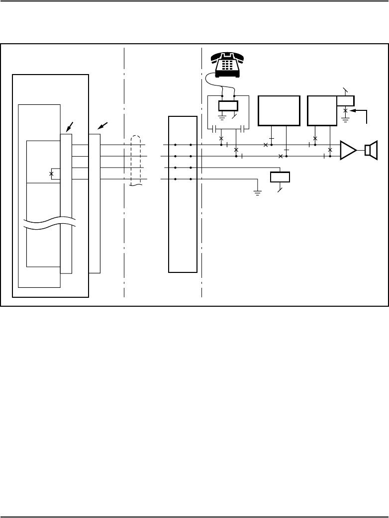
Page 638 of 906 NT8D15 E&M Trunk card
553-3001-211 Standard 3.00 August 2005
Figure 147
Paging trunk operation
Typical customer-
provided external
equipment
Cross
connect
System
NT8D15
E&M
Trunk Card
Unit 0
Unit 1
Unit 3
NT8D37
IPE Module
MDF
0T
Slot 0
A
26 (W-BL)
0R 1(BL-W)
0A 27 (W-O)
0PG 2(O-W)
Module
I/O Panel
Connector
Part of
25-pair
cable
553-AAA115
2
Audio
pair
Signal
pair K2
Bat
Bat
Amplifier Speake
r
Tape
recorder,
radio, etc.
Micro-
phone
K3
Microphon
e
contacts
K3
Bat
K3
K2
K2
K1
K1
K1

NT8D15 E&M Trunk card Page 639 of 906
Circuit Card Description and Installation
Card control functions
Control functions are provided by a microcontroller, a card LAN, and
signaling and control circuits on the E&M trunk card.
Microcontroller
The E&M trunk card contains a microcontroller that controls the internal
operation of the card. The microcontroller provides the following functions:
• card-identification
•self-test
• control of card operation
• maintenance diagnostics
Card LAN
The card LAN provides a serial communication link for transferring
maintenance data and control signals between the trunk card and the SSC
card. The card LAN controls the microcontroller. The following functions are
supported:
• providing card ID/RLS
• reporting self-test status
• polling from the controller card
• enabling/disabling of the DS-30X link

Page 640 of 906 NT8D15 E&M Trunk card
553-3001-211 Standard 3.00 August 2005
Signaling interface
All signaling messages for the trunk are three bytes long. The messages are
transmitted in channel zero of the DS30X in A10 format.
Configuration information for the E & M trunk is downloaded from the CPU
at power up and by command from maintenance programs. Seven
configuration messages are sent. One message is sent to each unit (4) to
configure trunk type, signaling type, balance impedance etc. Three messages
are sent per card to configure the make/break ratio, A/µ-Law operation.
Signaling and control
The signaling and control portion of the E&M trunk card works with the
system CPU to operate the card hardware. The card receives messages from
the CPU over a signaling channel in the DS-30X loop and returns status
information to the CPU over the same channel. The signaling and control
portion of the card provides analog loop terminations that establish,
supervise, and take down call connections.
Configuration information for the E&M trunk card is downloaded from the
CPU at power-up and by command from maintenance programs.
Configuration messages are sent. One message is sent to configure trunk and
signaling type. The other messages are sent to each card to select the make/
break ratio and the A-Law and µ-Law modes.
The signaling and control circuits on the card perform the following
functions:
• provide an interface between the card and the system CPU
— transmit PCM signals from each of the four units to one DS-30X
timeslot in A10 format (ready to send/clear to send—flow control,
handshake format)
— transmit and receive signaling messages over a DS-30X signaling
channel in A10 format
• decode received messages to set configuration and activate/deactivate
interface relays for PCM loopback diagnostic purposes
• decode outpulsing messages (one per digit) from the CPU to drive
outpulsing relays at 20 pps, 10 pps1 (primary), or 10 pps2 (secondary)

NT8D15 E&M Trunk card Page 641 of 906
Circuit Card Description and Installation
• monitor signals from the trunk interface and generate a message when
required for each state change
• control disabling and enabling of unit or card
• control A-Law and µ-Law operation modes
• control transmission pad settings
Maintenance features
The following features are provided for maintenance of the E&M trunk:
• indication of card status from self-test
• software enable and disable capability for individual units or entire card
• loopback of PCM signals to DS-30X for diagnostic purposes
• card ID for autoconfiguration and determination of serial number and
firmware level
Operation
The optional applications, features, and signaling arrangements for each unit
on the E&M trunk card are assigned through the Trunk Administration LD 14
and Trunk Route LD 16 programs.
Signaling and call control
The information in this section describes the signaling and call control of
E&M Type I and II trunks. The call is terminated and the trunk released by a
disconnect message sent to the associated unit.
Figure 148 on page 642 shows the trunk signaling orientation for a tandem
connection between E&M and CO trunks.
E&M Type I signaling
Figure 149 on page 643 shows E&M Type I signaling patterns for incoming
and outgoing calls. Figure 150 on page 644 shows Type I signaling patterns
on a tandem connection where the originating end is senderized and the route
is over a CO trunk (not applicable to CCSA).
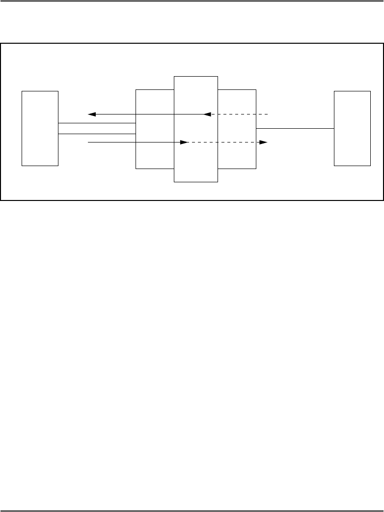
Page 642 of 906 NT8D15 E&M Trunk card
553-3001-211 Standard 3.00 August 2005
Idle state
For E&M signaling, in the idle state the M lead is ground and the E lead is an
open circuit.
Outgoing calls are processed as follows:
• The M lead changes from ground to battery.
— If answer supervision is provided by the far end, there is a change
from open to ground on the E lead (ground detection).
Figure 148
Signaling orientation for tandem connection between E&M and CO trunks
Far end PBX CO
553-6262
Near end PBX
(senderized)
E&M
Incoming
Outgoing
Tie trunk PBX-CO trunk
CO/FX/
WATS
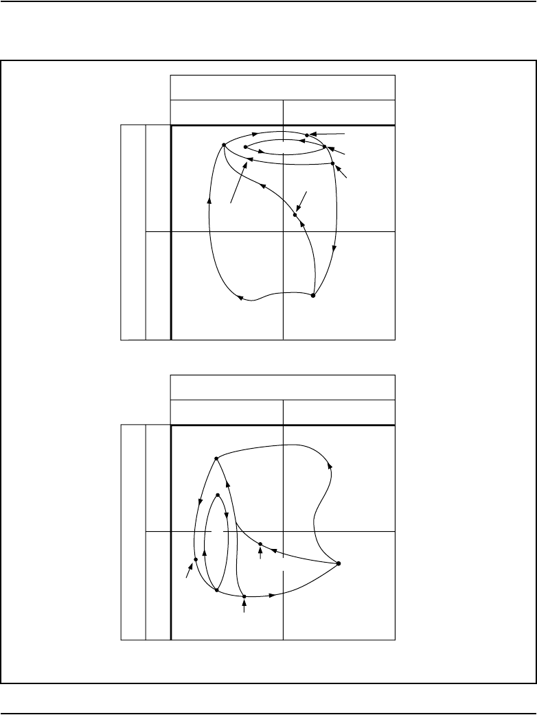
NT8D15 E&M Trunk card Page 643 of 906
Circuit Card Description and Installation
Figure 149
E&M Type I signaling patterns – originating party release
Near end M lead
Near end E lead
Idle
Near end
disc first
Near
end disc
Dialing
Near end
seizes
Far end
answers
(ans sup)
Far end
answers
(no ans
sup)
553-6263
Far
end
disc
Far
end
disc
first
Ground
Ground Open
Battery
DT
Near end M lead
Outgoing calls from near end
Incoming calls to near end
Near end E lead
Idle
Near end
disc first
Near end
disc
Far
end
seizes
Near end
answers
(ans sup)
Near end ans
(no ans sup)
Far end
disc
Far end
disc first
Ground
Ground Open
Battery
Dialing
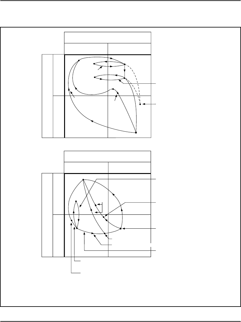
Page 644 of 906 NT8D15 E&M Trunk card
553-3001-211 Standard 3.00 August 2005
Figure 150
E&M Type I signaling patterns – originating party release on a tandem connection
Near end M lead
Near end E lead
Near end stores office DN
Dial CO/FX/WATS and office D
CO/FX/WATS end disc first
(ground start only)(ans sup)
Pseudo-answer supervision
provided approx. 150 ms
after last dial pulse
Universal service provided
by far end PBX if originating
end is senderized
Stored office DN digits
outpulsed after GO signal
553-6264
Ground
Ground Open
Battery
Near end M lead
Outgoing calls from near end
Incoming calls to near end
Near end E lead
Near end may be arranged
for IMM, DDL, or WNK
Far end seizes
Note:
IMM = Immediate start
Ground
Ground Open
Battery
Go
Idle
Idle
O/G tie
trunk disc
Dial CO/
FX/WATS
CO/FX/WATS
disc
O/G tie
trunk disc
first
Near end
seizes
Far end ans
Far
end
disc
first
Far end
disc Stop
Orig end
disc first
Orig
end
disc
No ans sup
CO/FX/WATS ans
Ð If ground start trunk, outpuls
e
toward office after ground
detection
Ð If loop start trunk, outpulse
toward office 1 sec later
DDL = Delayed dial
WNK = Wink start

NT8D15 E&M Trunk card Page 645 of 906
Circuit Card Description and Installation
Incoming calls
The far-end initiates calls as follows:
• The ground is placed on the E lead in E&M signaling.
• Dial pulses are subsequently applied from the far-end as ground open on
the E lead.
• If the far-end is equipped for sending, the system can operate in any
mode (immediate start, delay dial, or wink start), as assigned on a start
arrangement basis. See Table 197.
— In immediate start mode, there is no start signal from the called
office. The seizure signal (off hook supervisory state) from the
far-end should be at least 150 ms. At the end of the seizure signal,
the far-end can start pulsing after the standard delay (normally 70 ms
minimum).
— In delay dial mode, a 256–384 ms off hook/on hook signal is
returned to the far-end immediately after receipt of the seizure
signal. When the far-end detects the on hook signal (start signal), the
far-end can start pulsing after the standard delay (normally 70 ms
minimum).
— In wink start mode, within a 128–256 ms period after receipt of the
seizure signal from the far-end, the called office transmits a 250 ms,
wink start, off hook/on hook signal to the calling office.
E&M Type II signaling
Figure 151 on page 647 shows E&M Type II signaling patterns for incoming
and outgoing calls. Figure 152 on page 648 shows Type II signaling patterns
Table 197
Operation Mode
Operation mode Start arrangement
Immediate start IMM
Delay dial DDL
Wink start WNK

Page 646 of 906 NT8D15 E&M Trunk card
553-3001-211 Standard 3.00 August 2005
for a tandem connection where the originating end is senderized and the route
is over a CO trunk (CCSA not applicable).
Type II signaling uses four leads: M, SB, E, and SG. Instead of changes of
state between battery and ground (M signals) or open and ground (E signals),
the trunk signals by closing the contacts between the lead pairs M and SB.
Signals are received by detecting current flow between lead pairs E and SG.
On incoming calls, the far end seizes the trunk by shorting the E and SG leads
together. This transmits the ground from the SG lead to the E lead (in Type I
signaling the ground to the E lead comes from the far-end). Dialing is done
by opening and closing the E/SG contacts. Since the SB and M leads are also
used as the ESCG and ESC leads, respectively, for echo suppression, echo
suppressor control cannot be used with Type II signaling.
Note: M, SB, E, and SG designations are Electronic Industries
Association and Telecommunications Industries Association (EIA/TIA)
conventions. These leads are also known as MB, MA, EA, and EB,
respectively.
Release control
Release control of a call made over a trunk is specified in LD 16. Disconnect
supervision is specified for each trunk group independently. The two options
available are EITHER or ORIGINATING party control. These can be
specified for the end (near-end), or for the central office or other PBX end
(far-end). Joint party control can also be specified for the far-end.
Duplex signaling
Duplex (DX) signaling makes use of the voice transmission leads for
signaling as well as for voice transmission.
For descriptive purposes, the lead pair Tip B/Ring B is designated the
signaling pair. The other pair Tip A/Ring A conducts current in the opposite
direction to balance the overall current flow between the near and far ends.
During signaling, current flows through both Tip B and Ring B leads in the
same direction.
NT8D15 E&M Trunk card Page 647 of 906
Circuit Card Description and Installation
Figure 151
E&M Type II signaling patterns – originating party release
Near end M/SB leads
Near end EA/EB leads
Idle
Near end
disc first
System
end disc
Dialing Near
end
seizes
Far end
answers
(ans sup)
Far end
answers
(no ans
sup)
553-AAA1153
Far
end
disc
Far
end
disc
first
Open
Closed Open
Closed
DT
Near end M/SB leads
Outgoing calls from system (near end)
Incoming calls to system (near end)
Near end EA/EB leads
Idle
Near end
disc first
Near end
disc
Far
end
seizes
Near end
answers
(COS-ans sup)
Near end ans
(COS-no ans sup)
Far end
disc
Far end
disc first
Open
Closed Open
Closed
Dialing
Page 648 of 906 NT8D15 E&M Trunk card
553-3001-211 Standard 3.00 August 2005
Figure 152
E&M Type II signaling patterns – originating party release on a tandem connection
Near end M/SB leads
Near end EA/EB leads
Near end stores office DN
Dial CO/FX/WATS and office DN
CO/FX/WATS end disc first
(ground start only)(COS-ans sup)
Pseudo-answer supervision
provided approx. 150 ms
after last dial pulse
Universal service provided
by far end PBX if originating
end is senderized
Stored office DN digits
outpulsed after GO signal
553-AAA1154
Open
Closed Open
Closed
Near end M/SB leads
Outgoing calls from system (near end)
Incoming calls to system (near end)
Near end EA/EB leads
Local end may be arranged
for IMM, DDL, or WNK
Far end seizes
Open
Closed Open
Closed
Go
Idle
Idle
O/G tie
trunk disc
Dial CO/
FX/WATS
CO/FX/WATS
disc
O/G tie
trunk disc
first
Near end
seizes
Far end ans
Far
end
disc
first
Far end
disc Stop
Orig end
disc first
Orig
end
disc
COS-no ans sup
CO/FX/WATS ans
Ð If ground start trunk, outpulse
toward office after ground
detection
Ð If loop start trunk, outpulse
toward office 1 sec later
Note:
IMM = Immediate start
DDL = Delayed dial
WNK = Wink start

NT8D15 E&M Trunk card Page 649 of 906
Circuit Card Description and Installation
Table 198 and Table 199 show call-connection and take-down sequencing for
DX signaling. Table 200 on page 650 and Table 201 on page 651 show
sequencing where the E&M trunk card is used in a tandem PBX.
Table 198
DX signaling – outgoing calls with originating party release
Condition
Current in
signaling lead
State of trunk
detector
Idle No current flow High
Seizure
(dial tone from far-end: far-end ready for digits)
Current flow High
Digits Current flow interrupted
for each pulse
High
Far-end answers No current flow Low
Far-end on hook first Current flow High
Network taken down and trunk idled when
near-end goes on hook
No current flow High
Near-end on hook first, network taken down Current flow Low
Far-end on hook, trunk idled No current flow High
Table 199
DX signaling – incoming calls with originating party release (Part 1 of 2)
Condition
Current in
signaling lead
State of trunk
detector
Idle No current flow High
Seizure
(dial tone to far-end: near-end ready for digits)
Current flow Low
Digits Current flow interrupted
for each pulse
Low-high-low
for each pulse
Near-end answers No current flow Low

Page 650 of 906 NT8D15 E&M Trunk card
553-3001-211 Standard 3.00 August 2005
Far-end on hook first Current flow High
Network taken down and trunk idled No current flow High
Near-end on hook first, network taken down Current flow Low
Far-end on hook, trunk idled No current flow High
Table 200
DX signaling – outgoing calls with originating party release on tandem connections
(Part 1 of 2)
Condition
Current in
signaling lead
State of trunk
detector
Idle No current flow High
Seizure (far-end ready for digits) Current flow High
Dial CO/FX/WATS Current flow interrupted
for each pulse
High
Stop sender No current flow Low
Go sender (universal service provided by far-end
PBX if originating end is senderized)
Current flow High
CO/FX/WATS offices ready for digits
Stored Office DN digits Current flow interrupted
for each pulse
High
Outpulsed No current flow Low
Far end answers No current flow Low
Far end on hook first Current flow High
Near end on hook, network taken down, trunk
idled
No current flow High
Table 199
DX signaling – incoming calls with originating party release (Part 2 of 2)
Condition
Current in
signaling lead
State of trunk
detector

NT8D15 E&M Trunk card Page 651 of 906
Circuit Card Description and Installation
Near end on hook first, network taken down Current flow Low
Far end on hook, trunk idled No current flow High
Table 201
DX signaling – incoming calls with originating party release on tandem connections
(Part 1 of 2)
Condition
Current in
signaling lead
State of trunk
detector
Idle No current flow High
Seizure
(Can be arranged for IS, DD, or WS)
Current flow Low
(near-end ready for digits)
Dial CO/FX/WATS and office DN Current flow interrupted
for each pulse
Low-high-low
for each pulse
Stored digits outpulsed on CO/FX/WATS trunk
after ground detection if a ground start, but after 3
seconds if a loop start
If answer supervision: pseudo-answer supervision
is sent approximately 13 seconds after last dial
pulse received
No current flow Low
Table 200
DX signaling – outgoing calls with originating party release on tandem connections
(Part 2 of 2)
Condition
Current in
signaling lead
State of trunk
detector

Page 652 of 906 NT8D15 E&M Trunk card
553-3001-211 Standard 3.00 August 2005
Note: * – CO ground start: the trunk is idled and the network taken
down, but the incoming tie trunk is controlled by the originating end.
Electrical specifications
Table 202 lists the electrical characteristics of the trunk interface on the E&M
trunk card.
If no answer supervision: CO end disconnects (if
a CO ground start – the trunk is idled and network
taken down, but the incoming TIE trunk is held
under control of the originating end)
Current flow Low
Originating end disconnects – network taken
down and trunk idled
No current flow High
Table 202
Electrical characteristics of E&M trunk cards (Part 1 of 2)
Characteristic 4-wire trunk 2-wire trunk
Signaling range Type I 150 ohms
Type II 300 ohms loop
Type I 150 ohms
Signaling type Type I, Type II Type I
Far-end battery –42 to –52.5 V dc –42 to –52.5 V dc
Near-end battery –42.75 to –52.5 V dc –42.75 to –52.5 V dc
Ground potential difference +10 V dc +10 V dc
Line leakage between E lead
and ground
Š20K¾ Š20K¾
Table 201
DX signaling – incoming calls with originating party release on tandem connections
(Part 2 of 2)
Condition
Current in
signaling lead
State of trunk
detector

NT8D15 E&M Trunk card Page 653 of 906
Circuit Card Description and Installation
Effective loss See pad table (Table 209 on
page 662)
See pad table (Table 209 on
page 662)
Terminating impedance 600 ohms 600 ohms
Balance impedance N/A 600 ohms
Table 203
Electrical characteristics of trunk cards
Characteristic DID Trunk CO trunk
Nominal impedance 600 or 900 ohms, (selected
by software)
600 or 900 ohms, (selected
by software)
Signaling range 2450 ohms 1700 ohms
Signaling type Loop Ground or loop start
Far-end battery -42 to -52.5 V -42 to -52.5 V
Near-end battery N/A -42.75 to -52.5 V
Minimum loop current N/A 20 mA
Ground potential difference + 10 V + 3 V
Low DC loop resistance
during outpulsing
N/A 300 ohms
High DC loop resistance N/A Ground start equal to or
greater than 30 kS. Loop start
equal to or greater than 5 MS
Line leakage Equal to or greater than 30
kS (Tip to Ring, Tip to GND,
Ring to GND).
Equal to or greater than 30
kS (Tip to Ring, Tip to GND,
Ring to GND)
Effective loss See pad table See pad table
Table 202
Electrical characteristics of E&M trunk cards (Part 2 of 2)
Characteristic 4-wire trunk 2-wire trunk
Page 654 of 906 NT8D15 E&M Trunk card
553-3001-211 Standard 3.00 August 2005
Power requirements
Table 204 lists the power requirements for the E&M trunk card.
Environmental specifications
Table 205 provides the environmental specifications for the E&M trunk card.
Foreign and surge voltage protection
The E&M trunk card meets CS03 over-voltage (power cross) specifications
and FCC Part 68 requirements.
Table 204
Power requirements
Voltage Tolerance Max current
+15.0 V dc ±5% 200 mA
–15.0 V dc ±5% 200 mA
+8.5 V dc ±2% 200 mA
–48.0 V dc ±5 % 415 mA
Table 205
Environmental specifications
Parameter Specifications
Operating temperature 0 to +60 degrees C
(32 to +140 degrees F), ambient
Operating humidity 5 to 95% RH (non-condensing)
Storage temperature –40 to +70 degrees C
(–40 to +158 degrees F)

NT8D15 E&M Trunk card Page 655 of 906
Circuit Card Description and Installation
Connector pin assignments
The E&M trunk card brings the four analog trunks to the backplane through
a 160-pin connector shroud.The backplane is cabled to the I/O panel on the
rear of the module, which is then connected to the Main Distribution Frame
(MDF) by 25-pair cables.
Telephone trunks connect to the E&M trunk card at the MDF using a wiring
plan similar to that used for line cards.
A typical connection example is shown in Figure 153 on page 657. A list of
the connections to the E&M trunk card in the various 2-wire modes is shown
in Table 206. A list of the connections to the E&M trunk card in the various
4-wire modes is shown in Table 207 on page 656.
See the Communication Server 1000S: Installation and Configuration
(553-3031-210) for complete I/O connector information and wire
assignments for each tip/ring pair.
Table 206
E&M trunk card – backplane pinouts for 2-wire modes
Trunk
Number
2-wire Paging Mode 2-wire Type I Mode
Pin Signal Pin Signal Pin Signal Pin Signal
012B Tip 12A Ring 12B Tip 12A Ring
15B A15A PG 14B E14A M
116B Tip 16A Ring 16B Tip 16A Ring
19B A19A PG 18B E18A M
262B Tip 62A Ring 62B Tip 62A Ring
65B A65A PG 64B E64A M
366B Tip 66A Ring 66B Tip 66A Ring
69B A69A PG 48B E68A M

Page 656 of 906 NT8D15 E&M Trunk card
553-3001-211 Standard 3.00 August 2005
Table 207
E&M trunk card – backplane pinouts for 4-wire modes
Trunk
Number
4-wire Type I Mode 4-wire Type II Mode
Pin Signal Pin Signal Pin Signal Pin Signal
012B TA 12A TB 12B TA 12A TB
13B RA 13A RB 13B RA 13A RB
14B E14A M14B EA 14A EB
15B ECG 15A ESCG 15B MA 15A MB
116B TA 16A TB 16B TA 16A TB
17B RA 17A RB 17B RA 17A RB
18B E18A M18B EA 18A EB
19B ECG 19A ESCG 19B MA 19A MB
262B TA 62A TB 62B TA 62A TB
63B RA 63A RB 63B RA 63A RB
64B E64A M64B EA 64A EB
65B ECG 65A ESCG 65B MA 65A MB
366B TA 66A TB 66B TA 66A TB
67B RA 67A RB 67B RA 67A RB
68B E68A M68B EA 68A EB
69B ECG 69A ESCG 69B MA 69A MB
NT8D15 E&M Trunk card Page 657 of 906
Circuit Card Description and Installation
Figure 153
E&M trunk card – typical cross connection example
553-AAA1155
NT8D37
IPE Module
Slot 0
NT8D15
E&M
Trunk Card
Unit 0
Unit 3
26
1
27
2
System Cross connect E&M trunk
connections
AMDF
TipA
TipB
RingA
RingB
E
M
ECG
ESCG
Tip
Ring
E
M
28
3
29
4
Unit 1
0TA
0TB
0RA
0RB
0E
0M
0ECG
0ESCG
1T
1R
1E
1M
30
5
31
6
Module
I/O Panel
Connector
4-wire
Type I
E&M
Trunk
Part of
25-pair
cable
2-wire
Type I
E&M
Trunk
Note:
Actual pin numbers may vary depending on the vintage of
the card cage and the slot where the card is installed.
(W-BL)
(BL-W)
(W-O)
(O-W)
(W-G)
(G-W)
(W-BR)
(BR-W)
(W-S)
(S-W)
(R-BL)
(BL-R)

Page 658 of 906 NT8D15 E&M Trunk card
553-3001-211 Standard 3.00 August 2005
Configuration
Each of the four trunk circuits on the E&M trunk card can be individually
configured for trunk type, companding mode, and port-to-port loss
compensation. Configuring the card requires both jumper changes and
configuration software service entries.
The locations of the jumpers are shown in Figure 154 on page 659.
Jumper settings
The NT8D15 E&M Trunk card serves various transmission requirements.
The four units on the card can operate in A-Law or µ-Law companding
modes, which are selected by service change entries. Each unit can be
independently configured for 2-wire E&M, 4-wire E&M, and paging trunk
types. The trunk type is selected by service change entries and jumper strap
settings.
See Table 208 on page 660.
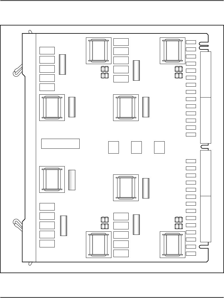

Page 660 of 906 NT8D15 E&M Trunk card
553-3001-211 Standard 3.00 August 2005
Table 208
E&M trunk card – jumper strap settings
Jumper
(Note 1)
Mode of operation (Note 2)
2-wire trunk 4-wire trunk
Type I Paging Type I Type II
DX tip & ring pair
M—rcv
E—xmt
E—rcv
M—xmt
J1.X Off Off Off Off Pins 1–2 Pins 2–3
J2.X On On
(Note 3)
On On Off Off
J3.X Off Off Off Off (Note 4) (Note 4)
J4.X Off Off Off Off Pins 2–3 Pins 1–2
J5.X Off Off Off Off (Note 4) (Note 4)
J6.X Off Off Off Off On On
J7.X Off Off Off Off On On
J8.X Off Off Off Off On On
J9.X Pins 2–3 Pins 2–3 Pins 2–3 Pins 2–3 Pins 1–2 Pins 1–2
Note 1: Jumper strap settings J1.X through J9.X apply to all four units; “X” indicates the unit
number, 0–3.
Note 2: “Off” indicates that no jumper strap is installed on a jumper block.
Note 3: Paging trunk mode is not zone selectable.
Note 4: Jumper strap installed in this location only if external loop resistance is greater than
2500 ohms.

NT8D15 E&M Trunk card Page 661 of 906
Circuit Card Description and Installation
Software service entries
The trunk type is selected by making service change entries in Route Data
Block, Automatic Trunk Maintenance (LD 16). The companding mode is
selected by making service change entries in Trunk Data Block (LD 14).
Refer to Table 208 on page 660 to select the proper values for the trunk type
being employed.
Port-to-port loss configuration
Loss parameters are selected on the E&M trunk card by a switchable pad
controlled by CODEC emulation software. The pads settings are called “in”
and “out.” Pad settings are determined by the three factors listed below (the
first two are under direct user control; the third is controlled indirectly):
• Class of Service is assigned in LD 14.
• Facility termination is selected (2-wire or 4-wire) in LD 14 (the 2-wire
setting provides 0.5 dB more loss in each direction of transmission for
echo control).
Note: Facilities associated with the Nortel Electronic Switched Network
(ESN) are recommended to be 4-wire for optimum transmission; thus,
the 4-wire setting is generally referred to as the ESN setting. However,
the 4-wire setting is not restricted to networks using the ESN feature.
Conversely, the 2-wire setting, often called non-ESN, can be used on
certain trunks in an ESN environment.
• Port-to-port connection loss is automatically set by software on the basis
of the port type selected in LD 16; only the port type is set by the user.
The transmission properties of each trunk are characterized by the class of
service assigned in LD 14. Transmission properties can be Via Net Loss
(VNL) or non-Via Net Loss (non-VNL).
The VNL class of service is assigned at the CLS prompt by typing VNL. The
non-VNL class of service is assigned at the CLS prompt by typing TRC
(Transmission Compensated) or NTC (Non-Transmission Compensated).
Non-VNL trunks are assigned a TRC or NTC class of service to ensure
stability and minimize echo when connecting to long-haul trunks, such as tie

Page 662 of 906 NT8D15 E&M Trunk card
553-3001-211 Standard 3.00 August 2005
trunks. The class of service determines the operation of the switchable pads
contained in each unit. They are assigned as follows:
• TRC for a 2-wire non-VNL trunk facility with a loss of greater than
2 dB, or for which impedance compensation is provided, or for a 4-wire
non-VNL facility.
• NTC for a 2-wire, non-VNL trunk facility with a loss of less than 2 dB,
or when impedance compensation is not provided.
See Table 209 for the pad switching control for the various through
connections and the actual port-to-port loss introduced for connections
between the E&M trunk card and any other IPE port designated as Port B.
Figure 155 on page 663 shows the pad switching orientation.
Table 209
Pad switching algorithm
Port B
Port B pads E&M Trunk Pads Port-to-port loss (dB)
Transmit
D to A
Receive
A to D
Transmit
D to A
Receive
A to D
Port B to
E&M
E&M to
Port B
IPE line N/A N/A Out In 2.5 3.5
Universal trunk
(TRC)
Out Out In In 0 0
IPE TIE (VNL) In Out In Out 0 0
Note: Transmit and receive designations are from and to the system. Transmit is from the
system to the external facility (digital-to-analog direction in the E&M trunk card). Receive is to
the system from the external facility (analog-to-digital direction in the E&M trunk card).
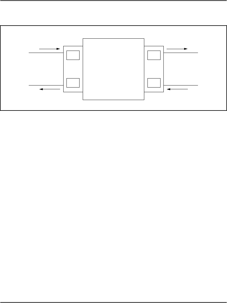

Page 664 of 906 NT8D15 E&M Trunk card
553-3001-211 Standard 3.00 August 2005
Applications
The optional applications, features and signaling arrangements for each trunk
are assigned through unique route and trunk data blocks. Refer to the
Features and Services (553-3001-306) for information about assigning
features and services to trunks.
PAD switching
The transmission properties of each trunk are characterized by
class-of-service (COS) assignments in the trunk data block (LD 14). The
assignment may be non-Via Net Loss (non-VNL) or via Net Loss (VNL). To
ensure stability and minimize echo when connecting to long-haul VNL (Tie)
trunks, non-VNL trunks are assigned either Transmission Compensated
(TRC) or Non-Transmission Compensated (NTC) class-of-service.
The TRC and NTC COS options determine the operation of the switchable
pads contained in the trunk circuits. They are assigned as follows:
• TRC for a two-wire non-VNL trunk facility with a loss of greater than
2 dB or for which impedance compensation is provided, or for a
four-wire non-VNL facility.
• NTC for a two-wire non-VNL trunk facility with a loss of less than 2 dB
or when impedance compensation is not provided.
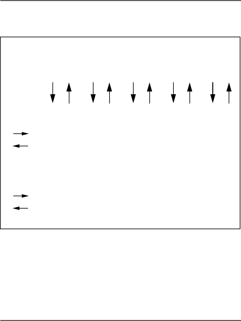
NT8D15 E&M Trunk card Page 665 of 906
Circuit Card Description and Installation
Table 210 shows the insertion loss from IPE port to IPE port.
Paging trunk operation
When used in the paging mode, a trunk is connected to a customer-provided
paging amplifier system (not zone selectable). When the trunk is accessed by
dial-up or attendant-key operation, it provides a loop closure across control
leads PG and A. See Figure 156 on page 666. In a typical application, this
transfers the input of the paging amplifier system to the transmission path of
the trunk.
Table 210
Insertion Loss from IPE Ports to IPE Ports (measured in dB)
IPE Ports
IPE Ports
500/2500
Line
Digital
Line
2/4 Wire
E&M Trunk
4 Wire
(ESN) E&M
Trunk
CO/FX
/WATS
Loop Tie
Trunk
2/4 Wire
E&M Trunk
6
3
3.5
-0.5
1
1
4 Wire
(ESN) E&M
Trunk
5.5
2.5
3
-1
0.5
0.5
0
0
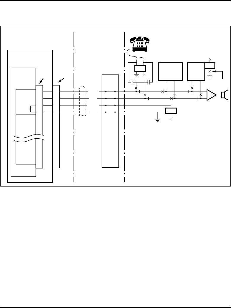
Page 666 of 906 NT8D15 E&M Trunk card
553-3001-211 Standard 3.00 August 2005
Figure 156
Paging trunk operation
Typical customer-
provided external
equipment
Cross
connect
System
NT8D14
Universal
Trunk Card
Unit 0
Unit 1
Unit 7
NT8D37
IPE Module
MDF
0T
Slot 0
A
26 (w-bl)
0R 1(bl-w)
0A 27 (w-o)
0PG 2(o-w)
Module
I/O Panel
Connector
Part of
25-pair
cable
553-AAA1
1
Audio
pair
Signal
pair K2
Bat
Bat
Amplifier Spea
Tape
recorder,
radio, etc.
Micro-
phone
K3
Microph
o
contac
t
K3
Bat
K3
K2
K2
K1
K1
K1

Page 667 of 906
Circuit Card Description and Installation
680
NT8D41AA Serial Data Interface
Paddle Board
Contents
This section contains information on the following topics:
Introduction . . . . . . . . . . . . . . . . . . . . . . . . . . . . . . . . . . . . . . . . . . . . . . 667
Physical description. . . . . . . . . . . . . . . . . . . . . . . . . . . . . . . . . . . . . . . . 668
Functional description . . . . . . . . . . . . . . . . . . . . . . . . . . . . . . . . . . . . . . 670
Connector pin assignments . . . . . . . . . . . . . . . . . . . . . . . . . . . . . . . . . . 671
Configuring the SDI paddle board . . . . . . . . . . . . . . . . . . . . . . . . . . . . 672
Applications . . . . . . . . . . . . . . . . . . . . . . . . . . . . . . . . . . . . . . . . . . . . . 678
Introduction
The NT8D41AA Serial Data Interface (SDI) paddle board provides two
RS-232-C serial ports. These ports allow communication between the system
and two external devices. The SDI paddle board is usually used to connect the
CS 1000S, CS 1000M, and Meridian 1 system to the system administration
and maintenance terminal. It can also be used to connect the system to a
background terminal (used in the hotel/motel environment), a modem, or to
the Automatic Call Distribution (ACD) or Call Detail Recording (CDR)
features.
The SDI paddle board mounts to a special socket on the rear of the backplane
of the following modules:
• NT5D21 Core/Network module

Page 668 of 906 NT8D41AA Serial Data Interface Paddle Board
553-3001-211 Standard 3.00 August 2005
• NT6D39 CPU/Network module
• NT9D11 Core/Network module
The SDI paddle board is compatible with all existing system software, but can
only be used with the system options listed above. It does not support 20 mA
current loop interface.
Physical description
The NT8D41AA Serial Data Interface paddle board is a printed circuit board
measuring 31.12 by 12.7 cm (12.25 by 5.0 in.). See Figure 157 on page 669.
Up to two paddle boards can be used in a system backplane for a total of four
serial ports. Up to 12 other serial ports can be added by plugging standard
serial cards into standard system slots. The two serial ports on each card are
addressed as a pair of consecutive addresses (0 and 1, 2 and 3, up to 14 and
15).
The front edge of the card has two serial port connectors, an Enable/Disable
switch (ENB/DIS), and a red LED. The LED indicates that the card has been
disabled. It is lit when the following occurs:
• the ENB/DIS switch is set to disable
• both ports are disabled in software
• the ports are not configured in the configuration record
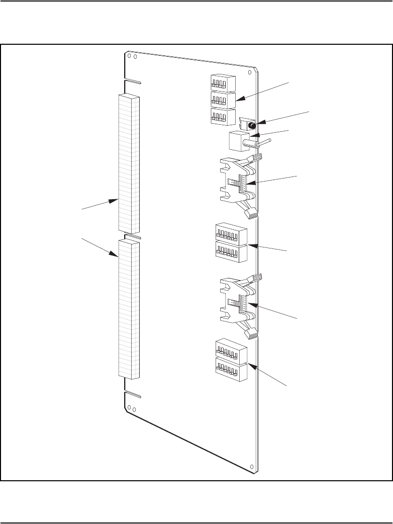
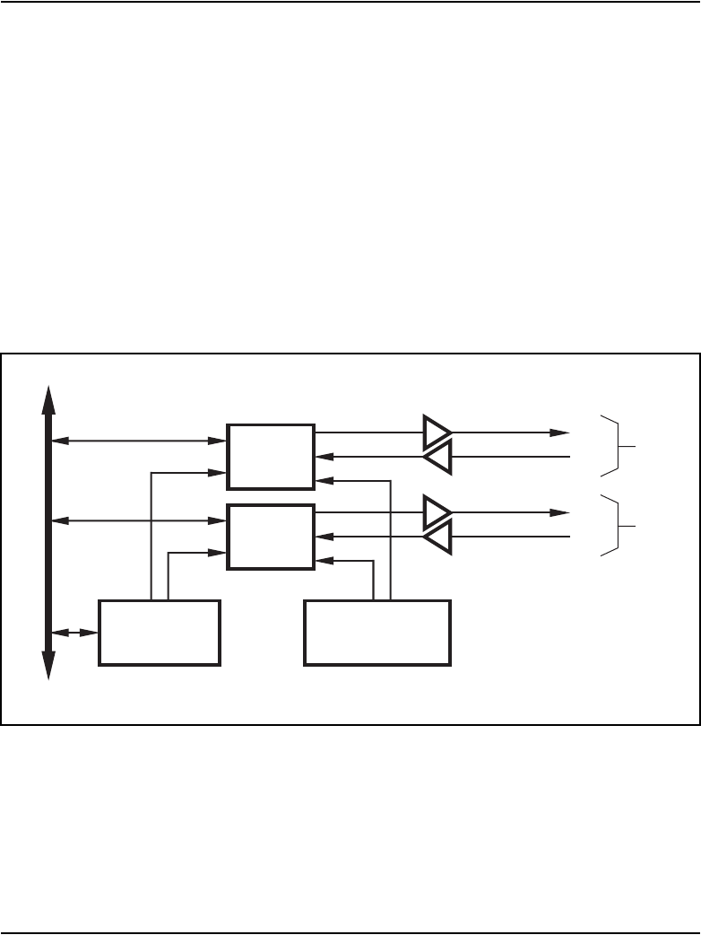
Page 670 of 906 NT8D41AA Serial Data Interface Paddle Board
553-3001-211 Standard 3.00 August 2005
Functional description
The NT8D41AA SDI paddle board has two asynchronous serial ports. These
serial ports are connected to the I/O panel in the back of the shelf using special
adapter cables. The serial ports can be used to connect the system to a
terminal, a printer, a modem, or to an other system processor.
The SDI paddle board contains two Universal Asynchronous Receiver/
Transmitters (UARTs) and the logic necessary to connect the UARTs to the
system processor bus. See Figure 158. Other logic on the card includes two
baud rate generators, two RS-232-C driver/receiver pairs, and the switches
and logic needed to configure the UARTs.
System considerations
In dual-processor systems, the SDI paddle board will behave differently
depending on which backplane socket it is installed in. Installing the paddle
board into a socket in the network area of the backplane allows it to work
when either of the system processors is active. Installing the paddle board into
Figure 158
NT8D41AA SDI paddle board block diagram
UART
no. 2
UARTs
Address
decode logic
TD
RD
TD
RD
RS-232-C
drivers and receivers
Clock and bit
rate select logic
Control
bus
553-5980
Port 1
(J1)
Port 2
(J2)
UART
no. 1

NT8D41AA Serial Data Interface Paddle Board Page 671 of 906
Circuit Card Description and Installation
a socket in the CPU area of the backplane allows it to work only when that
CPU is active.
The SDI paddle board is normally installed into a socket in the network area
of the backplane. This allows it to be accessed by either of the system
processors. This is necessary because the active CPU switches automatically
each night at midnight, and whenever a fault occurs on the active CPU card.
The SDI paddle board can also be installed into a socket in the CPU area of
the backplane. This is done when performing maintenance or an upgrade on
the system. The SDI paddle board is plugged into the CPU that is not the
active system CPU. One of the serial ports on the SDI paddle board is then
connected to a maintenance terminal and the CPU board is put into
maintenance mode. Diagnostics can then be run from the maintenance
terminal without having to stop the system. This is also used to perform a
parallel reload of the system software without affecting the operation of the
switch.
Connector pin assignments
The RS-232-C signals for port 1 are brought out on connector J1 and the
RS-232-C signals for port 2 are brought out on connector J2. The pinouts of
J1 and J2 are identical, so Table 211 can be used for both ports.
Table 211
Connectors J1 and J2 pin assignments (Part 1 of 2)
Pin # Signal Purpose in DTE mode Purpose in DCE mode
1CD Carrier detect (Note 1) Carrier detect (Not used)
2RD Transmitted data Received data
3TD Received data Transmitted data
4DTR Data terminal ready Data terminal ready (Note 2)
5GND Ground Ground
6DSR Data set ready (Note 1) Data set ready
7RTS Request to send (Not Used) Request to send (Note 2)

Page 672 of 906 NT8D41AA Serial Data Interface Paddle Board
553-3001-211 Standard 3.00 August 2005
Configuring the SDI paddle board
Configuring the SDI paddle board consists of setting these option switches for
each serial port:
• Port address
• Baud rate
• DTE/DCE/Fiber mode
The SDI paddle board has seven option switches, SW 2–8. Figure 159 on
page 676 identifies the location of option switches on the SDI paddle board.
Instructions for setting these switches are in the section that follows.
Once the board has been installed, the system software must be configured to
recognize it. Instructions for doing this are found in “Software service
changes” on page 677”.
8CTS Clear to send (Note 1) Clear to send
Note 1: In DTE mode the signals CD, DSR, and CTS are tied to +12 volts to signify that the port
on the SDI paddle board is always ready to transmit and receive data.
Note 2: In DCE mode the signals DTR and RTS are tied to +12 volts to signify that the port on
the SDI paddle board is always ready to transmit and receive data.
Table 211
Connectors J1 and J2 pin assignments (Part 2 of 2)
Pin # Signal Purpose in DTE mode Purpose in DCE mode

NT8D41AA Serial Data Interface Paddle Board Page 673 of 906
Circuit Card Description and Installation
Option switch settings
Address
Address select switch SW4 and logic on the card always address the two
UARTs using a pair of addresses: 0 and 1, 2 and 3 through 15 and 16. The
settings for this switch are shown in Table 212.
Baud rate
Switches SW2 and SW3 determine the baud rate for each individual port. The
settings for these switches are shown in Table 213 on page 674.
Table 212
SDI paddle board address switch settings
Address Switch SW4
Port 1Port 21234
0 1 offononon
2 3 offononoff
4 5 off on off on
6 7 off on off off
8 9 off off on on
10 11 off off on off
12 13 off off off on
14 15 off off off off

Page 674 of 906 NT8D41AA Serial Data Interface Paddle Board
553-3001-211 Standard 3.00 August 2005
DTE/DCE/Fiber mode
Each serial port can be configured to connect to a terminal (DTE equipment),
a modem (DCE equipment), or a Fiber Superloop Network card. Instructions
for setting the switches SW5, SW6, SW7, and SW8 are shown in Table 214
on page 675.
Table 213
SDI paddle board baud rate switch settings
Baud
rate
Port 1 – SW2 Port 2 – SW3
12341234
150 off off on on off off on on
300 off on off on off on off on
600 off off off on off off off on
1200 off on on off off on on off
2400 off off on off off off on off
4800 off on off off off on off off
9600 off off off off off off off off
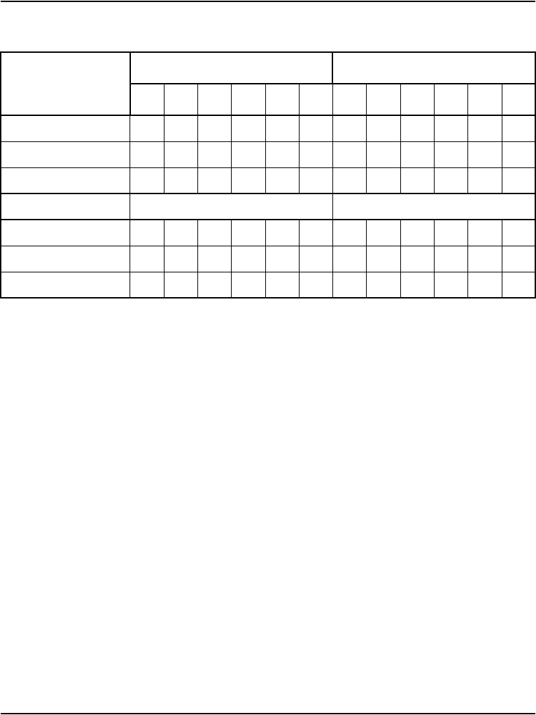
NT8D41AA Serial Data Interface Paddle Board Page 675 of 906
Circuit Card Description and Installation
Table 214
NT8D41AA DTE/DCE/Fiber switch settings
Mode
Port 1 – SW5 Port 1 – SW6
123456123456
DTE (terminal) on on on on on on off off off off off off
DCE (modem) off off off off off off on on on on on on
NT1P61 (Fiber) on on on on off off off off on on on on
Port 2 – SW7 Port 2 – SW8
DTE (terminal) on on on on on on off off off off off off
DCE (modem) off off off off off off on on on on on on
NT1P61 (Fiber) on on on on off off off off on on on on
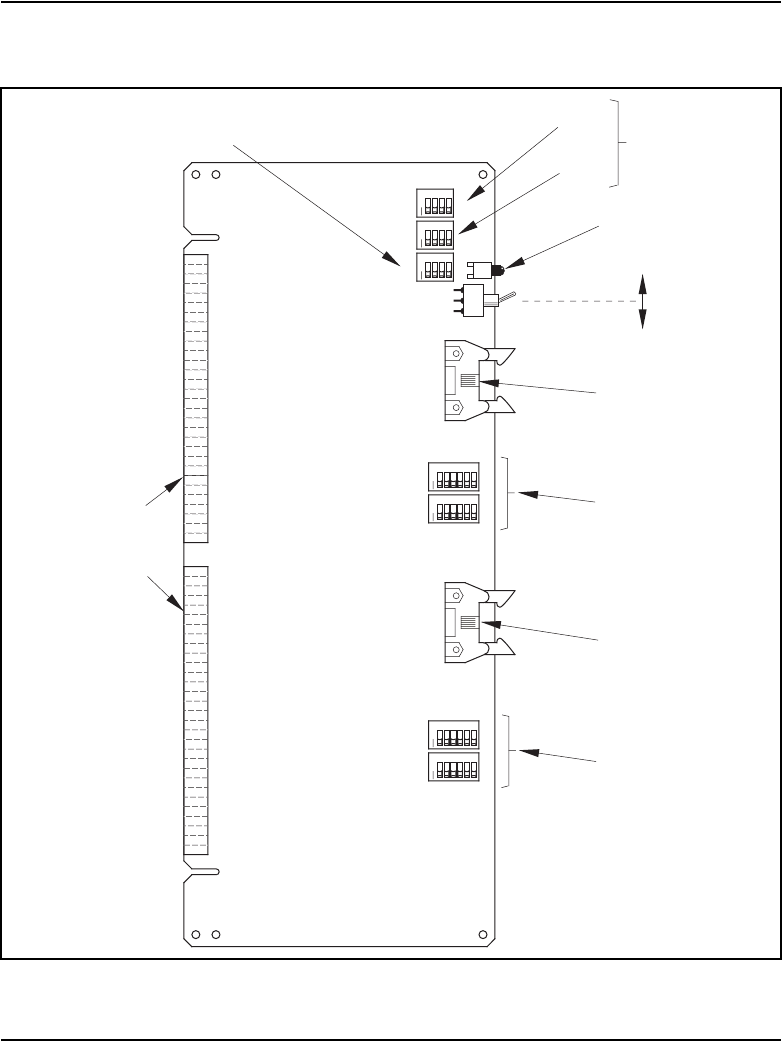
Page 676 of 906 NT8D41AA Serial Data Interface Paddle Board
553-3001-211 Standard 3.00 August 2005
Figure 159
SDI paddle board option switch locations
553-5988
1234
O
N
^
1234
O
N
^
56
1234
O
N
^
1234
O
N
^
1234
O
N
^
56
1234
O
N
^
56
1234
O
N
^
56
DS1 SW2
SW3
SW4
SW1
J1
J2
SW5
SW6
SW7
SW8
Address selection
Port 1
DTE/DCE
mode
selection
Port 2
DTE/DCE
mode
selection
Enable
Disable
Port 1
Port 2
Baud rate
selection
Port 1 cable
connector
Port 2 cable
connector
LED
Backplane
mating
connectors

NT8D41AA Serial Data Interface Paddle Board Page 677 of 906
Circuit Card Description and Installation
Software service changes
Once the NT8D41 SDI paddle board has been installed in the system, the
system software needs to be configured to recognize it. This is done using the
Configuration Record program LD 17. Instructions for running the
Configuration Record program are found in Software Input/Output:
Administration (553-3001-311).
Some of the prompts that are commonly used when running the Configuration
Record program LD 17, are shown in “LD 17 – Serial port configuration
parameters.” on page 677. These parameters must be set for each port if both
ports are being used.
LD 17 – Serial port configuration parameters.
Prompt Response Description
REQ: CHG Change configuration
TYPE: CFN Configuration type
IOTB YES Change input/output devices
ADAN NEW TTY x
NEW PRT x
Define a new system terminal (printer) port as device x, where
x = 0 to 15.
CDNO 1–16 Use the SDI paddle board number to keep track of all ports.
DENS DDEN Double density SDI paddle board
USER xxx Enter the user of port x. The values that can be entered
depend on the software being used. See the Software Input/
Output: Administration (553-3001-311) for details.
XSM (NO) YES Port is used for the system monitor.

Page 678 of 906 NT8D41AA Serial Data Interface Paddle Board
553-3001-211 Standard 3.00 August 2005
Applications
The NT8D41AA Serial Data Interface paddle board is used to connect the
switch to a variety of communication devices, printers, and peripherals. Any
RS-232-C compatible device can be connected to either of the card’s two
serial ports.
The standard application for the paddle board is to connect the switch to the
system console. This can be either a direct connection if the console is located
near the switch, or through a modem for remote maintenance.
Bell 103/212 compatible dumb modems are recommended to connect a
remote data terminal. If a smart modem (such as a Hayes modem) is used,
configure the modem for the dumb mode of operation (Command
Recognition OFF, Command Echo OFF) before connecting the modem to the
asynchronous port.
The serial data interface connectors on the paddle board are not RS-232-C
standard DB-25 connectors. The NT8D84AA interface cable is used to adapt
the paddle board to a non-standard pinout DB-9 connector (normally located
on the I/O panel). The NT8D93 cable is then used to connect the non-standard
DB-9 connector to a peripheral that uses a RS-232-C standard DB-25
connector. See Figure 160 on page 679.
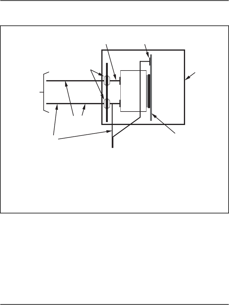
NT8D41AA Serial Data Interface Paddle Board Page 679 of 906
Circuit Card Description and Installation
Figure 160
SDI paddle board cabling
Module
front
NT8D46 cable to connector J2 in the
pedestal, where it will connect to the
system monitor (Note 2)
NT8D93 cable
(Note 1)
To
external
equipment
Backplane
J1
J2
NT8D84
cable
N
T
8
D
4
1
J1
System monitor
connector
The NT8D93 cable is available in several lengths, refer to
Equipment identification
(553-3001-154) for specific information.
To connect J2 to system monitor, connect cable from the backplane from J1.
Supplied with NT8D84 cable.
or
553-3173
Filter
adapters
(Note 3)
Note 1:
Note 2:
Note 3:


Page 681 of 906
Circuit Card Description and Installation
694
NT8D41BA Quad Serial Data Interface
Paddle Board
Contents
This section contains information on the following topics:
Introduction . . . . . . . . . . . . . . . . . . . . . . . . . . . . . . . . . . . . . . . . . . . . . . 681
Physical description. . . . . . . . . . . . . . . . . . . . . . . . . . . . . . . . . . . . . . . . 682
Functional description . . . . . . . . . . . . . . . . . . . . . . . . . . . . . . . . . . . . . . 682
Connector pin assignments . . . . . . . . . . . . . . . . . . . . . . . . . . . . . . . . . . 685
Configuring the QSDI paddle board . . . . . . . . . . . . . . . . . . . . . . . . . . . 687
Applications . . . . . . . . . . . . . . . . . . . . . . . . . . . . . . . . . . . . . . . . . . . . . 692
Introduction
The NT8D41BA Quad Serial Data Interface (QSDI) paddle board provides
four RS-232-C serial ports. These ports allow communication between the
system and four external devices, either DTE or DCE. The QSDI paddle
board is normally used to connect the system to the system administration and
maintenance terminal. It can also be used to connect the system to a
background terminal (used in the hotel/motel environment), a modem, or to
the Automatic Call Distribution (ACD) or Call Detail Recording (CDR)
features.
The QSDI paddle board mounts to a special socket on the rear of the
backplane of the following modules:
• NT5D21 Core/Network module

Page 682 of 906 NT8D41BA Quad Serial Data Interface Paddle Board
553-3001-211 Standard 3.00 August 2005
• NT6D39 CPU/Network module
• NT9D11 Core/Network module
The QSDI paddle board is compatible with all existing system software, but
can only be used with the system options listed above. It does not support the
110 baud rate or the 20 mA current loop interface.
Physical description
The NT8D41BA Quad Serial Data Interface paddle board is a printed circuit
board measuring 31.12 by 12.7 cm (12.25 by 5.0 in.). See Figure 161 on
page 683.
The QSDI paddle board can be used in a system backplane for a total of four
serial ports. Up to 12 other serial ports can be added by plugging standard
serial cards into standard system slots. The serial ports on the card are
addressed as a pair of consecutive addresses (0 and 1, 2 and 3, up to 14 and
15), using switches SW15 and SW16.
The front edge of the card has four serial port connectors, an Enable/Disable
switch (ENB/DIS), and a red LED. The LED indicates the card status. It is lit
when the following occurs:
• the ENB/DIS switch is set to disable
• all four ports are disabled in software
• all four ports are not configured in the configuration record
Functional description
The NT8D41BA QSDI paddle board has four asynchronous serial ports.
These serial ports are connected to the I/O panel in the back of the shelf using
special adapter cables. The serial ports can be used to connect the system to
a terminal, a printer, a modem, or to an other system processor.
The QSDI paddle board design contains four Universal Asynchronous
Receiver/Transmitters (UARTs) and the logic necessary to connect the
UARTs to the system processor bus. See Figure 162 on page 684.
NT8D41BA Quad Serial Data Interface Paddle Board Page 683 of 906
Circuit Card Description and Installation
Figure 161
NT8D41BA QSDI paddle board
1234
O
N
^
1234
O
N
^
1234
O
N
^
1234
O
N
^
56
1234
O
N
^
56
1234
O
N
^
56
1234
O
N
^
56
Address selection
for ports 1 and 2
(See Table 6)
Port 1 DTE/DCE
mode selection
(See Table 7)
Port 4 DTE/DCE
mode selection
(See Table 7)
Enable
Disable
Port 1 RS-232
cable connector
Port 2 RS-232
cable connector
LED
Backplane
mating
connectors
1234
O
N
^
Port 3 RS-232
cable connector
Port 4 RS-232
cable connector
1234
O
N
^
56
1234
O
N
^
56
1234
O
N
^
56
1234
O
N
^
56
SW13
SW11
SW12
SW15
SW16
SW5 SW4 SW3 SW2
SW6
SW7
SW8
SW9
Port 2 DTE/DCE
mode selection
(See Table 7)
Port 3 DTE/DCE
mode selection
(See Table 7)
Baud rate
for Port 4
(See Table 5)
Baud rate
for Port 3
(See Table 5)
Baud rate
for Port 2
(See Table 5)
Baud rate
for Port 1
(See Table 5)
SW10
Note: DCE-DTE mode selection for each port applies to both switch sets shown.
1234
O
N
^
5678
1234
O
N
^
5678
J1
J2
J3
J4
Address selection
for ports 3 and 4
(See Table 6)
553-8009
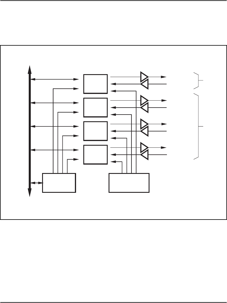
Page 684 of 906 NT8D41BA Quad Serial Data Interface Paddle Board
553-3001-211 Standard 3.00 August 2005
Other logic on the card includes baud rate generators, RS-232-C driver/
receiver pairs, and the switches and logic needed to configure each UART.
System considerations
In dual-processor systems, the QSDI paddle board will behave differently
depending on which backplane socket it is installed. Installing the paddle
board into a socket in the network area of the backplane allows it to work
when either of the system processors is active. Installing the paddle board into
a socket in the CPU area of the backplane allows it to work only when that
CPU is active.
Figure 162
NT8D41BA QSDI paddle board block diagram
UART
no. 1
UART
no. 2
UART
no. 3
UART
no. 4
UARTs
Address
decode logic
TD
RD
TD
RD
TD
RD
TD
RD
RS-232-C
drivers and receivers
Clock and bit
rate select logic
Processor
bus
553-5986
Port 1
Port 2
Port 3
Port 4
J1
J2
NT8D41BA Quad Serial Data Interface Paddle Board Page 685 of 906
Circuit Card Description and Installation
The QSDI paddle board is normally installed into a socket in the network area
of the backplane. This allows it to be accessed by either of the system
processors. This is necessary because the active CPU switches automatically
each night at midnight and whenever a fault occurs on the active CPU card.
The QSDI paddle board can also be installed into a socket in the CPU area of
the backplane (supported in NT6D39AA shelves only). This is done when
performing maintenance or an upgrade on the system.
The QSDI paddle board is plugged into the CPU that is not the active system
CPU. One of the serial ports on the QSDI paddle board is then connected to
a maintenance terminal and the CPU board is put into maintenance mode.
Diagnostics can then be run from the maintenance terminal without having to
stop the system. This is also used to perform a parallel reload of the system
software without affecting the operation of the switch.
Connector pin assignments
The RS-232-C signals for port 1 through port 4 are brought out on connector
J1 through J4 respectively. The pinouts for each port are identical to those for
each of the other three ports. Table 215 shows the pin assignment that applies
to each connector.
Table 215
Connectors J1, J2, J3, and J4 pin assignments
Pin # Signal Purpose in DTE mode Purpose in DCE mode
1DCD Data Carrier detect (Note 1) Data Carrier detect (Not used)
2RD Transmitted data Received data
3TD Received data Transmitted data
4DTR Data terminal ready Data terminal ready (Note 2)
5GND Signal Ground Signal Ground
6DSR Data set ready (Note 1) Data set ready
7RTS Request to send (Not Used) Request to send (Note 2)

Page 686 of 906 NT8D41BA Quad Serial Data Interface Paddle Board
553-3001-211 Standard 3.00 August 2005
8CTS Clear to send (Note 1) Clear to send
Note 1: In DTE mode the signals CD, DSR, and CTS are tied to +12 volts to signify that the port
on the QSDI paddle board is always ready to transmit and receive data. This mode is set to
connect to a terminal device (DTE).
Note 2: In DCE mode the signals DTR and RTS are tied to +12 volts to signify that the port on
the QSDI paddle board is always ready to transmit and receive data. This mode is set to
connect to a modem device (DCE).
Table 215
Connectors J1, J2, J3, and J4 pin assignments
Pin # Signal Purpose in DTE mode Purpose in DCE mode

NT8D41BA Quad Serial Data Interface Paddle Board Page 687 of 906
Circuit Card Description and Installation
Configuring the QSDI paddle board
Configuring the QSDI paddle board to work in a system consists of setting
these option switches for each serial port:
•Baud rate
• Port address
• DTE/DCE mode
The QSDI paddle board has fourteen option switches, SW2–13, SW15-16.
Figure 161 on page 683 identifies the location of option switches on the QSDI
paddle board. Learn how to set these switches in the following sections.
Once the board has been installed, the system software must be configured to
recognize it. Instructions for doing this are found in the section titled
“Software service changes” on page 691.
Option switch settings
Baud rate
Switches SW13, SW10, SW11, and SW12 determine the baud rate for ports
1, 2, 3, and 4, respectively. See the settings for these switches in Table 216.
Table 216
NT8D41BA baud rate switch settings (Part 1 of 2)
Baud
rate
Baud Clock
(kHz)
SW13 (port 1), SW10 (port 2),
SW11 (port 3), SW12 (port 4)
1234
150 2.40 on off on on
300 4.80 ononoffon
600 9.60 on off off on
1,200 19.20 on on on off
2,400 38.40 on off on off
Page 688 of 906 NT8D41BA Quad Serial Data Interface Paddle Board
553-3001-211 Standard 3.00 August 2005
* For future use.
Address
Switch SW15 or SW16 and logic on the card always address the four UARTs
using a pair of addresses: 0 and 1, 2 and 3 through 14 and 15. The settings for
both switches are shown in Table 217. To avoid system problems, switches
4,800 76.80 on on off off
9,600 153.60 on off off off
19,200* 307.20 on on on on
Table 216
NT8D41BA baud rate switch settings (Part 2 of 2)
Baud
rate
Baud Clock
(kHz)
SW13 (port 1), SW10 (port 2),
SW11 (port 3), SW12 (port 4)
1234

NT8D41BA Quad Serial Data Interface Paddle Board Page 689 of 906
Circuit Card Description and Installation
SW15 and SW16 must not be configured identically. Figure 161 on page 683
displays SW15 and SW16.
* To enable ports 1 and 2, set SW15 position 1 to ON. To enable ports 3 and 4, set SW16 position 1 to ON.
+ For each X, the setting for this switch makes no difference, because it is not used.
Table 217
NT8D41BA address switch settings
SW15 Port 1 Port 2 Switch settings
SW16 Port 3 Port 4 1* 2+345678
Device
pair
addresses
0 1 E X off off off off off off
2 3 E X off off off off off on
4 5 E X off off off off on off
6 7 E X off off off off on on
8 9 E X off off off on off off
10 11 E X off off off on off on
12 13 E X off off off on on off
14 15 E X off off off on on on
Page 690 of 906 NT8D41BA Quad Serial Data Interface Paddle Board
553-3001-211 Standard 3.00 August 2005
DTE/DCE/Fiber mode
Each serial port can be configured to connect to a terminal (DTE equipment),
a modem (DCE equipment), or a Fiber Superloop Network card. Instructions
for setting the switches SW2, SW3, SW4, SW5, SW6, SW7, SW8, and SW9
are shown in Table 218. Figure 161 on page 683 shows the location of these
switches on the paddleboard.
Table 218
NT8D41BA DTE/DCE/Fiber switch settings
Mode
Port 1 — SW 3 Port 1 —SW 2
123456123456
DTE (terminal) on on on off on off off on off on off on
DCE (modem) off off off on off on on off on off on off
NT1P61 (Fiber) on on on on on off on on on off on off
Port 2 — SW 5 Port 2 — SW4
DTE (terminal) on on on off on off off on off on off on
DCE (modem) off off off on off on on off on off on off
NT1P61 (Fiber) on on on on on off on on on off on off
Port 3 — SW 7 Port 3— SW 6
DTE (terminal) on on on off on off off on off on off on
DCE (modem) off off off on off on on off on off on off
NT1P61 (Fiber) on on on on on off on on on off on off
Port 4 — SW 9 Port 4 — SW 8
DTE (terminal) on on on off on off off on off on off on
DCE (modem) off off off on off on on off on off on off
NT1P61 (Fiber) on on on on on off on on on off on off

NT8D41BA Quad Serial Data Interface Paddle Board Page 691 of 906
Circuit Card Description and Installation
Software service changes
Once the NT8D841BA QSDI paddle board has been installed in the system,
the system software needs to be configured to recognize it, using the
Configuration Record program LD 17. Instructions for running this program
are found in Software Input/Output: Administration (553-3001-311).
Some of the prompts that are commonly used when running the Configuration
Record program LD 17 are shown in LD 17 – Prompts to configure the
NT8D841Ba paddle board. These parameters must be set for each port if both
ports are being used.
LD 17 – Prompts to configure the NT8D841Ba paddle board.
Prompt Response Description
REQ: CHG Change configuration
TYPE: ADAN Configuration type
ADAN NEW TTY x
NEW PRT x
Define a new system terminal (printer) port as device x, where
x = 0 to 15.
CTYPE SDI4 Quad port card
DES XQSDI Quad density QSDI paddle board.
USER xxx Enter the user of port x. The values that can be entered
depend on the software being used. See the Software Input/
Output: Administration (553-3001-311) for details.
XSM (NO) YES Port is used for the system monitor.

Page 692 of 906 NT8D41BA Quad Serial Data Interface Paddle Board
553-3001-211 Standard 3.00 August 2005
Applications
The NT8D41BA Quad Serial Data Interface paddle board is used to connect
the switch to a variety of communication devices, printers, and peripherals.
Any RS-232-C compatible device can be connected to either of the card’s two
serial ports.
The standard application for the paddle board is to connect the switch to the
system console. This can be either a direct connection if the console is located
near the switch, or through a modem for remote maintenance.
Bell 103/212 compatible dumb modems are recommended to connect a
remote data terminal. If a smart modem (such as a Hayes modem) is used,
configure the modem for the dumb mode of operation (Command
Recognition OFF, Command Echo OFF) before connecting the modem to the
asynchronous port.
The serial data interface connectors on the paddle board are not RS-232-C
standard DB-25 connectors. The NT8D84AA interface cable is used to adapt
the paddle board to a non-standard pinout DB-9 connector (normally located
on the I/O panel). The NT8D93 cable is then used to connect the non-standard
DB-9 connector to a peripheral that uses a RS-232-C standard DB-25
connector. See Figure 163 on page 693.
NT8D41BA Quad Serial Data Interface Paddle Board Page 693 of 906
Circuit Card Description and Installation
Figure 163
NT8D41BA QSDI paddle board cabling
Module
front
NT8D46 cable to connector J4 in the
pedestal, where it will connect to the
system monitor (Note 2)
NT8D93 cable
(Note 1)
To
external
equipment
Backplane
J1
J2
NT8D84
cable
N
T
8
D
4
1
B
A
J1
System monitor
connector
The NT8D93 cable is available in several lengths, refer to
Equipment identification
(553-3001-154) for specific information.
To connect J4 to system monitor, connect cable from the backplane from J1.
or
553-8010
Filter
adapters
(NT8D84
cable)
Note 1:
Note 2:
J3
J4


Page 695 of 906
Circuit Card Description and Installation
700
NTAG26 XMFR card
Contents
This section contains information on the following topics:
Introduction . . . . . . . . . . . . . . . . . . . . . . . . . . . . . . . . . . . . . . . . . . . . . . 695
MF signaling . . . . . . . . . . . . . . . . . . . . . . . . . . . . . . . . . . . . . . . . . . . . . 695
Physical specifications . . . . . . . . . . . . . . . . . . . . . . . . . . . . . . . . . . . . . 700
Introduction
The XMFR (Extended Multi-frequency receiver) card is used to receive MF
digit information. Connections are made between a PBX and a central office.
The XMFR card can only operate in systems using µ-law companding.
You can install this card in any IPE slot.
MF signaling
The MF feature allows the system to receive digits for 911 or feature group
D applications.
Signaling levels
MF signaling uses pairs of frequencies to represent digits.

Page 696 of 906 NTAG26 XMFR card
553-3001-211 Standard 3.00 August 2005
Table 219 lists the frequency values used for received signals.
Table 219
MF frequency values
Digit
Backward direction
DOD-Tx, DID-Rx
1700 Hz + 900 Hz
2700 HZ + 1100 Hz
3900 Hz + 1100 Hz
4700 Hz + 1300 Hz
5900 Hz + 1300 Hz
61100 Hz + 1300 Hz
7700 Hz + 1500 Hz
8900 Hz +1500 Hz
91100 Hz + 1500 Hz
01300 Hz + 1500 Hz
KP 1100 Hz + 1700 Hz
ST 1500 Hz + 1700 Hz
STP(ST’) 900 Hz + 1700 Hz
ST2P(ST”) 1300 Hz + 1700 Hz
ST3P(ST”) 700 Hz + 1700 Hz

NTAG26 XMFR card Page 697 of 906
Circuit Card Description and Installation
XMFR receiver specifications
Table 220 provides the operating requirements for the NTAG26 circuit card.
Table 220
XMFR receiver specifications (Part 1 of 3)
Coding: Mu-Law
Input sensitivity: must accept: 0 to -25 dBmO
must reject: -35 to dBmO
Frequency sensitivity: must accept: f +/- (1.5% + 5Hz)
Amplitude Twist: must accept: difference of 6dB between frequencies
Signal Duration: must accept: > 30 ms
must reject: < 10 ms
KP Signal Duration: must accept: > 55 ms
may accept: > 30 ms
must reject: < 10 ms
Signal Interruption Bridge: must ignore: < 10 ms
Time Shift between 2 frequencies:
(Envelop for start/stop)
must accept: < 4 ms
Coincidence between 2 frequencies: must reject: < 10 ms
Intersignal Pause: must accept: > 25 ms
Maximum Dialling Speed: must accept: 10 signals per second

Page 698 of 906 NTAG26 XMFR card
553-3001-211 Standard 3.00 August 2005
Noise Rejection:
Error Rate in White Noise Better than: < 1/2500 calls
Test:
10 digit calls
nominal frequency @ -23 dBmO
ON/OFF = 50 ms/50ms
KP duration 100 ms
SNR = -20 dB
all digits
Immunity to Impulse Noise Better than: < 1/2500 calls
Test:
10 digit calls
nominal frequency @ -23 dBmO
ON/OFF = 50ms/50ms
KP duration 100 ms
SNR = -12 dBs
all digits
ATT Digit Simulation Test, Tape #201 from PUB
56201
Error Rate from Power Lines Better than: < 1/2500 calls
Test:
10 digit calls
nominal frequency @ -23 dBmO
ON/OFF = 50 ms/50ms
KP duration 100 ms
60 Hz signal @ 81 dBrnc0 (-9dBm)
or
180 Hz signal @ 68 dBrnco (-22dBm)
all digits
Tolerate Intermodulation: Must tolerate @A-B and @B-A modulation products
with a power sum
28 dB below each frequency component level of the
signals.
Table 220
XMFR receiver specifications (Part 2 of 3)

NTAG26 XMFR card Page 699 of 906
Circuit Card Description and Installation
The XMFR receiver specifications conform to the following:
• TR-NPL-000258, Compatibility Information for F.G.D. switched access
service, Bell Communication Research Technical Reference, Issue 1.0,
October 1985.
• TR-NPL-000275, Notes on the BOC Intra-LATA Networks, Bell
Communication Research Technical Reference, Chapter 6, 1986.
KP:
KP activation The receiver must not respond to signals prior to KP.
Remain unlocked until ST, STP, ST2P or ST3P is
received.
Multiple KP’s After the initial KP, subsequent KP’s are ignored
while in unlocked mode.
Excessive Components: If more than two valid frequencies are detected, no
digit is reported to the CPU.
Table 220
XMFR receiver specifications (Part 3 of 3)

Page 700 of 906 NTAG26 XMFR card
553-3001-211 Standard 3.00 August 2005
Physical specifications
The physical specifications required by the NTAG26 XMFR circuit card are
shown in Table 221.
Table 221
Physical specifications
Dimensions Height:12.5 in. (320 mm)
Depth:10.0 in. (255 mm)
Thickness:7/8 in. (22.25 mm)
Faceplate LED Lit when the circuit card is disabled
Power requirements 1.1 Amps typical
Environmental considerations Meets the environment of CS 1000S, CS 1000M, and
Meridian 1 systems

Page 701 of 906
Circuit Card Description and Installation
708
NTAK02 SDI/DCH card
Contents
This section contains information on the following topics:
Introduction . . . . . . . . . . . . . . . . . . . . . . . . . . . . . . . . . . . . . . . . . . . . . . 701
NTAK02 SDI/DCH card. . . . . . . . . . . . . . . . . . . . . . . . . . . . . . . . . . . . 701
Introduction
The NTAK02 Serial Data Interface/D-channel (SDI/DCH) digital trunk card
is supported in the Media Gateway only for the ISDN Signaling Link (ISL)
D-channel. The SDI is not supported in the MG 1000S.
You can install this card in slots 1 through 4 in the MG 1000S. It is not
supported in the MG 1000S Expansion. Up to four NTAK02 SDI/DCH cards
are supported in an MG 1000S.
NTAK02 SDI/DCH card
The optional SDI/DCH card provides up to four serial I/O ports, which are
grouped into two pairs:
• port 0 and port 1
• port 2 and port 3
Page 702 of 906 NTAK02 SDI/DCH card
553-3001-211 Standard 3.00 August 2005
Ports 1 and 3 are configured as DCH. Ports 0 and 2 are configured as SDI
(not supported). See Table 222. Each pair is controlled by a switch, as shown
in Table 223.
Note: Digital Private Network Signaling System DPNSS can replace the
DCH function in the U.K.
Table 222
Port configurations
Port 0 SDI (not supported)
Port 1 DCH
Port 2 SDI (not supported)
Port 3 DCH
Table 223
Switch settings
Port 0 Port 1 SW 1-1 SW 1-2
SDI (not supported) DCH OFF OFF
SDI (not supported) DCH OFF ON
—ESDIONON
Port 2 Port 3 SW 1-3 SW 1-4
SDI (not supported) DCH OFF OFF
SDI (not supported) DCH OFF ON
— ESDI ON ON

NTAK02 SDI/DCH card Page 703 of 906
Circuit Card Description and Installation
Two ports offer the option for DTE/DCE configuration. This option is
selected from a jumper on the card. Table 224 shows the jumper settings.
Table 224
Jumper settings
Port
Jumper
location
Strap for
DTE
Strap for
DCE
Jumper
location RS422 RS232
0J10 C - B B - A
1 J7
J6
C - B
C - B
B - A
B - A
J9
J8
C - B
C - B
B - A
B - A
2 J5 C - B B - A
3 J4
J3
C - B
C - B
B - A
B - A
J2
J1
C - B
C - B
B - A
B - A

Page 704 of 906 NTAK02 SDI/DCH card
553-3001-211 Standard 3.00 August 2005
Connecting to the ports
External devices are connected to the SDI/DCH card by the following:
• the NTAK19FB four-port SDI cable. This cable does not have to be
terminated at the cross connect terminal since it is equipped with
connectors.
• the NE-A25-B cable. Terminate the NE-A25-B cable at the cross connect
terminal. Tables 225 through 228 give the pinouts for the SDI/DCH card.
Table 225
NTAK02 pinouts – Port 0 at the cross-connect terminal
RS232
Cable Signal
Designations
I=Input O=Output
Pair Color DTE DCE DTE DCE
1T
1R
W-BL
BL-W
0
DTR
0
DCD
—
O
—
I
2T
2R
W-O
O-W
DSR
DCD
CH/CI
DTR
I
I
O
O
3T
3R
W-G
G-W
RTS
CTS
CTS
RTS
O
I
I
O
4T
4R
W-BR
BR-W
RX
TX
TX
RX
I
O
O
I
5T
5R
W-S
S-W
—
SG
—
SG
—
—
—
—

NTAK02 SDI/DCH card Page 705 of 906
Circuit Card Description and Installation
Table 226
NTAK02 connections at the cross-connect terminal – Port 1
RS422 RS232
Cable Signal
Designations
I=Input
O=Output
Designations
I=Input
O=Output Signal
Pair Color DTE DCE DTE DCE DTE DCE DTE DCE
5T
5R
W-S
S-W
SCTEA
—
SCTA
—
O
—
I
—
O
—
I
—
SCT
—
SCT
—
6T
6R
R-BL
BL-R
SCTEB
DTR
SCTB
DCD
O
O
I
I
—
—
—
—
CH/CI
DTR
—
DCD
7T
7R
R-O
O-R
DSR
DCD
CH/CI
DTR
I
I
O
O
I
I
O
O
DSR
DCD
CH/CI
DTR
8T
8R
R-G
G-R
RTS
CTS
CTS
RTS
O
I
I
O
O
I
I
O
RTS
CTS
CTS
RTS
9T
9R
R-BR
BR-R
SCRA
SCTA
SCTEA
RXCA
I
I
O
O
I
I
O
O
SCR
SCT
SCT
—
10T
10R
R-S
S-R
SCRB
SCTB
SCTEB
RXCB
I
I
O
O
—
—
—
—
—
—
—
—
11T
11R
BK-BL
BL-BK
RXDA
TXDA
TXDA
RXDA
I
O
O
I
I
O
O
I
RXD
TXD
TXD
RXD
12T
12R
BK-O
O-BK
RXDB
TXDB
TXDB
RXDB
I
O
O
I
—
—
—
—
—
—
—
—
25T
25R
V-S
S-V
SG
—
SG
—
—
—
—
—
—
—
—
—
SG
—
SG
—

Page 706 of 906 NTAK02 SDI/DCH card
553-3001-211 Standard 3.00 August 2005
Table 227
NTAK02 connections at the cross-connect terminal – Port 2
RS422 RS232
Cable Signal
Designations
I=Input
O=Output
Designations
I=Input
O=Output Signal
Pair Color DTE DCE DTE DCE DTE DCE DTE DCE
13T
13R
BK-G
G-BK
—
—
—
—
—
O
—
I
—
DTR
—
DCD
14T
14R
BK-BR
BR-BK
—
—
—
—
I
I
O
O
DSR
DCD
CH/CI
DTR
15T
15R
BK-S
S-BK
—
—
—
—
O
I
I
O
RTS
CTS
CTS
RTS
16T
16R
Y-B L
BL-Y
—
—
—
—
I
O
O
I
RX
TX
TXD
RXD
17T
17R
Y-O
O-Y
O
—
I
—
O
—
I
—
—
SG
—
SG

NTAK02 SDI/DCH card Page 707 of 906
Circuit Card Description and Installation
Table 228
NTAK02 connections at the cross-connect terminal – Port 3
RS422 RS232
Cable Signal
Designations
I=Input
O=Output
Designations
I=Input
O=Output Signal
Pair Color DTE DCE DTE DCE DTE DCE DTE DCE
17T
17R
Y- O
O-Y
SCTEA
—
SCTA
—
O
—
I
—
O
—
I
—
SCT
—
SCT
—
18T
18R
Y- G
G-Y
SCTEB
DTR
SCTB
DCD
O
O
I
I
—
—
—
—
CH/CI
DTR
—
DCD
19T
19R
Y-B R
BR-Y
DSR
DCD
CH/CI
DTR
I
I
O
O
I
I
O
O
DSR
DCD
CH/CI
DTR
20T
20R
Y-S
S-Y
RTS
CTS
CTS
RTS
O
I
I
O
O
I
I
O
RTS
CTS
CTS
RTS
21T
21R
V-BL
BL-V
SCRA
SCTA
SCTEA
RXCA
I
I
O
O
I
I
O
O
SCR
SCT
SCT
—
22T
22R
V-O
O-V
SCRB
SCTB
SCTEB
RXCB
I
I
O
O
—
—
—
—
—
—
—
—
23T
23R
V-G
G-V
RXDA
TXDA
TXDA
RXDA
I
O
O
I
I
O
O
I
RXD
TXD
TXD
RXD
24T
24R
V-BR
BR-V
RXDB
TXDB
TXDB
RXDB
I
O
O
I
—
—
—
—
—
—
—
—
25T
25R
V-S
S-V
—
SG
—
SG
—
—
—
—
—
—
—
—
SG
—
SG
—

Page 708 of 906 NTAK02 SDI/DCH card
553-3001-211 Standard 3.00 August 2005
Characteristics of the low speed port
Ports 0 and 2 are asynchronous, low speed ports. They transfer data to and
from the line one bit at a time.
The characteristics of the low speed port are as follows:
•Baud rate: 300; 600; 1200; 2400; 4800; 9600; 19,200
Default = 1200
•Parity: Odd, even, none
Default = none
•Stop bits: 1, 1.5, 2
Default = 1
•Flow control: XON/XOFF, CTS, non.
Default = none
•Duplex: Full
•Interface: RS-232-D
•Data bits: 5, 6, 7, 8
Default = 8
Characteristics of the high speed port
Ports 1 and 3 are synchronous, high speed ports with the following
characteristics:
•Baud rate: 1200; 2400; 4800; 9600; 19,200; 56,000; 64,000
•Data bit: Transparent (1)
•Duplex: Full
•Clock: Internal or external
•Interface: RS-232-D, RS-422-A

Page 709 of 906
Circuit Card Description and Installation
720
NTAK09 1.5 Mb DTI/PRI card
Contents
This section contains information on the following topics:
Introduction . . . . . . . . . . . . . . . . . . . . . . . . . . . . . . . . . . . . . . . . . . . . . . 709
Physical description. . . . . . . . . . . . . . . . . . . . . . . . . . . . . . . . . . . . . . . . 710
Functional description . . . . . . . . . . . . . . . . . . . . . . . . . . . . . . . . . . . . . . 714
Architecture. . . . . . . . . . . . . . . . . . . . . . . . . . . . . . . . . . . . . . . . . . . . . . 715
Introduction
The NTAK09 1.5 Mb DTI/PRI digital trunk card is a standard-size IPE circuit
card.
The NTAK09 provides 1.5Mb ISDN primary rate interface and digital trunk
interface capability. The NTAK09 can be equipped with two daughterboards:
the NTAK20 clock controller and the NTAK93/NTBK51 D-channel handler
interface.
You can install this card in slots 1 through 4 in the MG 1000S. The card is not
supported in the MG 1000S Expansion. Up to four digital trunk cards are
supported in each MG 1000S.
In North America, the NTAK09 can be replaced by the NTRB21 – TMDI
(DTI/PRI/DCH) card, which is described in “NTRB21 DTI/PRI/DCH TMDI
card” on page 825.
Contact your system supplier or your Nortel representative to verify that this
card is supported in your area.
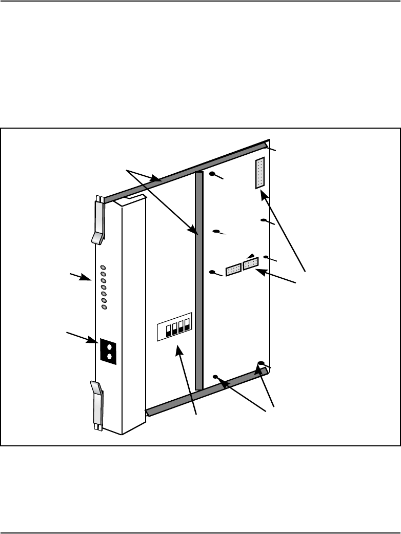
Page 710 of 906 NTAK09 1.5 Mb DTI/PRI card
553-3001-211 Standard 3.00 August 2005
Physical description
The DTI/PRI card uses a 9.5" by 12.5" multilayer printed circuit board with
buried power and ground layers. The clock controller and D-channel
daughterboards are fastened by standoffs and connectors. See Figure 164 on
page 710.
The NTAK09 DTI/PRI card has seven faceplate LEDs. The first five LEDs
are associated with the NTAK09 card. The remaining two LEDs are
associated with the clock controller and DCHI daughterboards.
Figure 164
NTAK09 DTI/PRI circuit card
DIS
ACT
RED
YEL
LBK
CC
DCH
RCV
XMT
NTAK09
1.5 MB
DTI/PRI
ON
1234
DCH F/W
LEN 0
LEN 1
Len 2
SW
ON
1 2 3 4
DCH F/W
LEN 0
LEN 1
Len 2
553-CSE8294
SW
Stiffeners
Connector
Sockets
LEDs
Bantam
Jacks
Standoffs
Switch

NTAK09 1.5 Mb DTI/PRI card Page 711 of 906
Circuit Card Description and Installation
The first five LEDs operate as follows:
• During system power up, the LEDs are on.
• When the self-test is in progress, the LEDs flash three times and then go
into their appropriate states, as shown in Table 229.
Table 229
NTAK09 LED states
LED State Definition
DIS On (Red) The NTAK09 circuit card is disabled.
Off The NTAK09 is not in a disabled state.
ACT On (Green) The NTAK09 circuit card is in an active state. No alarm states
exist, the card is not disabled, nor is it in a loopback state.
Off An alarm state or loopback state exists, or the card has been
disabled. See the other faceplate LEDs for more information.
RED On (Red) A red-alarm state has been detected.
Off No red alarm.
YEL On (Yellow) A yellow alarm state has been detected.
Off No yellow alarm.
LBK On (Green) NTAK09 is in loop-back mode.
Off NTAK09 is not in loop-back mode.

Page 712 of 906 NTAK09 1.5 Mb DTI/PRI card
553-3001-211 Standard 3.00 August 2005
NTAK09 DTI/PRI power on self-test
When power is applied to the NTAK09 DTI/PRI circuit card, the card
performs a self-test. The LEDs directly associated with the NTAK09 circuit
card are DIS, ACT, RED, YEL, and LBK. The clock controller LED is also
included in the power on self-test. Table 230 provides the state of the
NTAK09 LEDs during the self-test procedure.
NTAK20 power on self-test
The clock controller daughterboard LED is the second LED from the bottom
on the faceplate of the NTAK09 DTI/PRI card.
When power is applied to the NTAK20 clock controller, the LED is initially
off for two seconds. If the self-test passes, the LED turns red and flashes on
and off twice.
When the self-test is completed, the LED remains red until the clock
controller is enabled. When enabled, the clock controller LED either turns
green or flashes green.
Table 230
NTAK09 LED states during self-test
Action LED State
Power up system Top five LEDs light for eleven seconds
Self-test in progress Top five LEDs go out for one second
If the self-test passes, the top five LEDs flash
on and off three times.
If the self-test detects a partial failure, the top
five LEDs flash on and off five times
When the self-test is completed, the LEDs are
set to their appropriate states

NTAK09 1.5 Mb DTI/PRI card Page 713 of 906
Circuit Card Description and Installation
NTAK93 self-test
The NTAK93 DCHI daughterboard LED is the bottom LED on the faceplate
of the NTAK09 DTI/PRI card.
The NTAK93 DCHI daughterboard does not perform a self-test when power
is applied to it. When power is applied, it turns red and remain steadily lit,
indicating the DCH is disabled. When the DCH is enabled, the LED turns
green and remains steadily lit.
Self-tests of the NTAK93 daughterboard are invoked manually by commands
in LD 96.
DTI/PRI local self-test
The local self-test, also called a local loopback test, checks speech path
continuity, zero code suppression, remote alarm detection, and A & B bit
signalling. This test is performed manually on a per-loop or per-channel basis.
The local loopback test performs a local logical loopback and does not require
any external loopback of the T1 signal.
Restrictions and limitations
The DCHI and DTI/PRI must be disabled before performing the self-test on
the entire DTI/PRI card. Individual channels must be disabled before
performing a self test on a particular channel.
Power requirements
The DTI/PRI obtains its power from the backplane, and draws less than
2 amps on +5 V, 50 mA on +12 V and 50 mA on –12 V.
Foreign and surge voltage protection
Lightning protectors must be installed between an external T1 carrier facility
and the system. For public T1 facilities, this protection is provided by the
local operating company. In a private T1 facility environment (a campus, for
example), the NTAK92 protection assembly can be used.

Page 714 of 906 NTAK09 1.5 Mb DTI/PRI card
553-3001-211 Standard 3.00 August 2005
The NTAK09 circuit card conforms to safety and performance standards for
foreign and surge voltage protection in an internal environment.
Functional description
NTAK09 provides the following features and functions:
• configurable parameters, including A-Law and µ-Law operation, digital
pads on a per channel basis, and Superframe or Extended Superframe
formats
• AMI or B8ZS line coding
• 1.5 Mb Clock recovery and distribution of reference clocks
• DG2 or FDL yellow alarm methods
• card status and alarm indication with faceplate-mounted LEDs
• automatic alarm monitoring and handling
• Card-LAN for maintenance communication
• loopback capabilities for both near-end and far-end
• echo canceler interface
• integrated trunk access (both D-channel and in-band A/B signaling can
be mixed on the same PRI)
• faceplate monitor jacks for T1 interface
• configurable D-channel data rate with 64 Kbps, 56 Kbps or
64 Kbps inverted.
•self-test

NTAK09 1.5 Mb DTI/PRI card Page 715 of 906
Circuit Card Description and Installation
Architecture
Signaling interface
The signaling interface performs an 8 Kbps signaling for all 24 channels and
interfaces directly to the DS-30X link. Messages in both directions of
transmission are three bytes long.
Interconnection
The interconnection to the carrier is by NTBK04 1.5 Mb carrier cable.
The NTBK04 is twenty feet long. The NT8D97AX, a fifty-foot extension, is
also available.
Microprocessor
The NTAK09 is equipped with bit-slice microprocessors that handle the
following major tasks:
• Task handler: also referred to as an executive, the task handler provides
orderly per-channel task execution to maintain real-time task ordering
constraints.
• Transmit voice: inserts digital pads, manipulates transmit AB bits for
DS1, and provides graceful entry into T-Link data mode when the data
module connected to the DTI/PRI trunk is answering the call.
• Receive voice: inserts digital pads and provides graceful entry into
T-Link data mode when the data module connected to the DTI/PRI trunk
is originating the call.
• T-Link data: a set of transmit and receive vectored subroutines which
provides T-Link protocol conversion to/from the DM-DM protocol.
• Receive ABCD filtering: filters and debounces the receive ABCD bits
and provides change of state information to the system.
• Diagnostics
•Self-test

Page 716 of 906 NTAK09 1.5 Mb DTI/PRI card
553-3001-211 Standard 3.00 August 2005
Digital pad
The digital pad is an EPROM whose address-input to data-output transfer
function meets the characteristics of a digital attenuator. The digital pad
accommodates both µ255-law and A-Law coding. There are 32 combinations
each for µ255 to µ255, µ255 to A-Law, A-Law to µ255, and A-Law to A-Law.
These values are selected to meet the EIA loss and level plan. See Table 231.
Table 231
Digital pad values and offset allocations
Offset PAD set 0 PAD set 1
0 0dB –7db
1 2dB –8db
2 3dB –9db
3 4dB –10db
4 5dB 0.6db
5 6.1dB 7db
6 8dB 9db
7 –1dB 10db
8 –3dB 11db
9 –4dB 12db
A idle code, 7F 3db
B unassigned code, FF 14db
C 1dB spare
D –2dB spare
E –5db spare
F –6db spare

NTAK09 1.5 Mb DTI/PRI card Page 717 of 906
Circuit Card Description and Installation
D-channel interface
The D-channel interface is a 64 Kbps maximum, full-duplex, serial bit-stream
configured as a DCE device. The data signals include receive data output,
transmit data input, receive clock output, and transmit clock output. The
receive and transmit clocks can vary slightly from each other as determined
by the transmit and receive carrier clocks.
Feature selection through software configuration for the D-channel includes:
• 56 Kbps
• 64 Kbps clear
• 64 Kbps inverted (64 Kbps restricted)
DCHI can be enabled and disabled independent of the PRI card, as long as the
PRI card is inserted in its cabinet slot. The D-channel data link cannot be
established however, unless the PRI loop is enabled.
On the NTAK09 use switch 1 and position 1 to select either the D-channel
feature or the DPNSS feature, as follows:
• OFF = D-channel
• ON = DPNSS (U.K.)
DS-1 Carrier interface
Transmitter
The transmitter takes the binary data (dual unipolar) from the PCM
transceiver and produces bipolar pulses for transmission to the external
digital facility. The DS1 transmit equalizer enables the cabling distance to
Page 718 of 906 NTAK09 1.5 Mb DTI/PRI card
553-3001-211 Standard 3.00 August 2005
extend from the card to the DSX-1 or LD-1. Equalizers are switch selectable
through dip-switches. The settings are shown in Table 232.
Receiver
The receiver extracts data and clock from an incoming data stream and
outputs clock and synchronized data. At worst case DSX-1 signal levels, the
line receiver will operate correctly with up to 655 feet of ABAM cable
between the card and the external DS1 signal source.
Connector pinout
The connection to the external digital carrier is through a 15-position male
D-type connector. See Table 233.
Table 232
NTAK09 switch settings
Switch Setting
Distance to Digital Cross-Connect
1
DCH F/W
2
(LEN 0)
3
(LEN 1)
4
(LEN 2)
0 - 133 feet Off Off Off On
133 - 266 feet Off On On Off
266 - 399 feet Off Off On Off
399 - 533 feet Off On Off Off
533 - 655 feet Off Off Off Off
Table 233
DS-1 line interface pinout for NTBK04 cable (Part 1 of 2)
From 50-pin MDF
connector To DB-15 Signal name Description
pin 48 pin 1 Ttransmit tip to network
pin 23 pin 9 Rtransmit ring to network
pin 25 pin 2 FGND frame ground
NTAK09 1.5 Mb DTI/PRI card Page 719 of 906
Circuit Card Description and Installation
Clock controller interface
The clock controller interface provides the recovered clock from the external
digital facility to the clock controller daughterboard through the backplane.
Depending on the equipped state of the clock controller, the clock controller
interface enables or disables the appropriate reference clock source, in
conjunction with software.
Note: Clocking slips can occur between MG 1000S systems that are
clocked from different Central Offices (COs), if the COs are not
synchronized. The slips can degrade voice quality.
Clock rate converter
The 1.5 Mb clock is generated by a Phase-Locked Loop (PLL). The PLL
synchronizes the 1.5 Mb DS1 clock to the 2.56 Mb system clock through the
common multiple of 8 kHz by using the main frame synchronization signal.
pin 49 pin 3 T1 receive tip from network
pin 24 pin 11 R1 receive ring from network
IMPORTANT!
Each MG 1000S that has a digital trunk must have a clock controller
clocked to an external reference clock.
Table 233
DS-1 line interface pinout for NTBK04 cable (Part 2 of 2)
From 50-pin MDF
connector To DB-15 Signal name Description


Page 721 of 906
Circuit Card Description and Installation
734
NTAK10 2.0 Mb DTI card
Contents
This section contains information on the following topics:
Introduction . . . . . . . . . . . . . . . . . . . . . . . . . . . . . . . . . . . . . . . . . . . . . . 721
Physical description. . . . . . . . . . . . . . . . . . . . . . . . . . . . . . . . . . . . . . . . 722
Functional description . . . . . . . . . . . . . . . . . . . . . . . . . . . . . . . . . . . . . . 723
Architecture. . . . . . . . . . . . . . . . . . . . . . . . . . . . . . . . . . . . . . . . . . . . . . 724
Introduction
The NTAK10 2.0 Mb DTI card is a digital trunk card that provides an
IPE-compatible 2.0 Mb DTI interface. This circuit card includes an on-board
clock controller that can be manually switched in or out of service.
You can install this card in slots 1 through 4 in the MG 1000S. The card is not
supported in the MG 1000S Expansion. Up to four digital trunk cards are
supported in each MG 1000S.
Note: Clocking slips can occur between MG 1000S systems that are
clocked from different Central Offices (COs), if the COs are not
synchronized. The slips can degrade voice quality.
IMPORTANT!
Each MG 1000S that has a digital trunk must have a clock controller
clocked to an external reference clock.

Page 722 of 906 NTAK10 2.0 Mb DTI card
553-3001-211 Standard 3.00 August 2005
Physical description
The 2 Mb DTI pack uses a standard 9.5" by 12.5", multi-layer printed circuit
board. The faceplate is 7/8” wide and contains six LEDs.
The LEDs operate as follows:
• After the card is plugged in, the LEDs (a-e) are turned on by the
power-up circuit. The clock controller LED is independently controlled
by its own microprocessor.
• After initialization, the LEDs (a-e) flash three times (0.5 seconds on,
0.5 seconds off) and then individual LEDs will go into appropriate states,
as shown in Table 234.
Table 234
NTAK10 LED states (Part 1 of 2)
LED State Definition
DIS On (Red) The NTAK10 circuit card is disabled.
Off The NTAK10 is not in a disabled state.
OOS On (Yellow) The NTAK10 is in an out-of-service state.
Off The NTAK10 is not in an out-of-service state.
NEA On (Yellow) A near end alarm state has been detected.
Off No near end alarm.
FEA On (Yellow) A far end alarm state has been detected.
Off No far end alarm.
LBK On (Yellow) NTAK10 is in loop-back mode.
Off NTAK10 is not in loop-back mode.
CC On (Red) The clock controller is switched on and disabled.
On (Green) The clock controller is switched on and is either locked to a
reference or is in free-run mode.

NTAK10 2.0 Mb DTI card Page 723 of 906
Circuit Card Description and Installation
Power requirements
The 2MB DTI obtains its power from the backplane. It draws less than 2 A
on +5 V, 50 mA on +15 V and 50 mA on –15 V.
Environment
The NTAK10 card meets all applicable Nortel operating specifications.
Functional description
The NTAK10 provides the following features and functions:
• a clock controller that can be switched in as an option
• software-selectable A/µlaw operation
• software-selectable digital pads on a per channel basis
• frame alignment and multiframe alignment detection
• frame and multiframe pattern generation
• CRC-4 transmission and reception (software selectable)
• card status and alarm indication with faceplate-mounted LEDs
• Periodic Pulse Metering (PPM) counting
• outpulsing of digits on any of the ABCD bits
• Card-LAN for maintenance communication
Flashing
(Green)
The clock controller is switched on and locking onto the
primary reference.
Off The clock controller is switched off.
Note: See “Clock controller interface” on page 729 in this
chapter for more on tracking and free-run operation.
Table 234
NTAK10 LED states (Part 2 of 2)
LED State Definition

Page 724 of 906 NTAK10 2.0 Mb DTI card
553-3001-211 Standard 3.00 August 2005
• per-channel and all-channel loopback capabilities for near-end and
far-end
•self-test
• download of incoming ABCD validation times from software
• warm SYSLOAD (TS16 AS16 transmitted)
Applicability to France
Features specific to DTI requirements for France are implemented in
firmware, and are switch-accessed. These are:
• transmission and reception of alarm indication signaling (AIS) in TS16
such as card disabled and warm SYSLOAD
• France-specific PPM counting
• decadic dialing
• France-specific alarm report and error handling
Architecture
The main functional blocks of the NTAK10 card architecture include:
• DS-30X interface
• signaling interface
• three microprocessors
• digital pad
• Card-LAN interface
• carrier interface
• clock controller interface
DS-30X interface
The NTAK10 card interfaces to one DS-30X bus which contains
32 byte-interleaved timeslots operating at 2.56 Mb. Each timeslot contains
10 bits in a 10 message format; eight are assigned to voice/data (64 Kbps),
one to signaling (8 Kbps), and one is a data valid bit (8 Kbps).

NTAK10 2.0 Mb DTI card Page 725 of 906
Circuit Card Description and Installation
Transmit data
To transmit data on the carrier, the incoming serial bit stream from the
NTAK02 circuit card is converted to 8-bit parallel bytes. The signaling bits
are extracted by the signaling interface circuitry.
Digital Pad: The parallel data is presented to the pad PROM. The PROM
contains pad values, idle code, and A/µ-law conversion. They can be set
independently for incoming and outgoing voice on a per channel basis. Four
conversion formats are provided: A-law to A-law, A-law to µ-law, µ-law to
A-law, µ-law to µ-law.
Each of these four formats has up to 32 unique pad values. The NTAK10 card
provides the pad values of -10, -9, -8, -7, -6,-5, -4, -3, -2, -1, 0, 0.6, 1, 2, 3, 4,
5, 6, 7, 8, 9, 10, 11, 12, 13, and 14 dB (also idle and unassigned code). A
negative pad is a positive gain.
The pad PROM output is converted from parallel to serial format and passed
on to a multiplexer, which passes PCM/data, TS0, and TS16 information. The
FAS pattern is sent in even TS0s, while in odd TS0s alarm information is sent.
The multiplexer output is fed to the carrier interface which can forward it to
the carrier or perform per channel loopback.
Receive data
To receive data, PCM/Data from the carrier interface is converted from serial
to parallel, is buffered, and is fed to the pad prom. It then sent onto the
DS-30X interface, where signaling information from the signaling interface
circuitry is multiplexed.
DS-30X microprocessor
The DS-30X is a utility processor, responsible for the following tasks:
• controlling the DS-30X interface
• receiving and decoding of messages and taking appropriate action
• transmitting TS16 messages to the TS16 microprocessor
• receiving TS16 messages from the TS16 microprocessor and passing
these messages to the A07
• providing the 19.2 Kbps serial interface to the Card-LAN

Page 726 of 906 NTAK10 2.0 Mb DTI card
553-3001-211 Standard 3.00 August 2005
• controlling LEDs
• downloading Local Calling Areas (LCAs)
• monitoring errors and alarms
• detecting the change of state in TS0, and outputting TS0 data
• counting bipolar violations, slips, PLL alarms, frame-alignment errors,
and CRC-4 errors
• monitoring the status of frame alignment and multiframe alignment
• detecting and reporting of alarm indication signals (AIS)
• updating of per channel loopback registers
• controlling the far-end loopback and digroup loopback functions
Signaling interface
Interconnections
The external connection is through a 50-pin MDF connector with the
NTBK05 carrier cable A0394217.
CEPT interface
For the Conference of European Postal Communications (CEPT) interface,
the connection to the external digital carrier is through the NT5K85 DTI cable
assembly. It converts the 120 ohms D-connector to 75 ohms coaxial cable.
The impedance is switch set. The switch-settings table at the end of this
chapter describes the options. See Table 235.
NTAK10 2.0 Mb DTI card Page 727 of 906
Circuit Card Description and Installation
If a coaxial interface is required, use NT5K85 in conjunction with the
NTBK05.
Channel associated signaling
Channel associated signaling means that each traffic carrying channel has its
own signaling channel permanently associated with it. Timeslot 16 is used to
transmit two types of signaling: supervisory and address.
Incoming signal
Functions of the NTAK10 with regard to incoming signaling include:
• recognizing valid changes
• determining which channels made the changes
• collecting PPM
• reporting changes to software
Outgoing supervisory signals
The desired ABCD bit pattern for a channel is output by the NTAK10, under
the control of the system controller card. The bit pattern to be transmitted is
held on the line for a minimum period of time. This time is specified in the
same message and ensures that the signal is detected correctly at the far end.
Table 235
2 MB DTI switch options
Switch
Off
(Switch Open)
On
(Switch Closed)
S1-1 — —
S1-2 CC Enabled CC Disabled
S2-1 120 ohms 75 ohms
S2-2 75 ohms 120 ohms
S3-1 non-French Firmware French Firmware
S3-2 — —

Page 728 of 906 NTAK10 2.0 Mb DTI card
553-3001-211 Standard 3.00 August 2005
With the exception of the outpulsing signals and special signals, such as
Denmark's Flash signal and Sweden's Parking signal, the minimum duration
of any signal state is 100 ms. Some signal states can have a minimum duration
time that is longer than 100 ms.
Periodic Pulse Metering (PPM)
Periodic Pulse Monitoring (PPM) is used to collect toll charges on outgoing
CO trunk calls.
TS16 microprocessor
The functions of this microprocessor include:
• receiving signaling messages supplied by the DS-30X microprocessor,
decoding these messages, and taking subsequent actions
• transmitting messages to the DS-30X microprocessor
• handling PPM
• updating the TS16 select RAM and TS16 data RAM
• providing outpulsing
• receive data from the change-of-state microprocessor
• transmitting AIS for CNET (France) application
Change-of-state microprocessor
The functions of this processor are:
• detecting valid change of state in TS16
• when a valid change has been found, passing the new abcd bits to the
TS16 microprocessor, along with five bits to indicate the associated
channel
Carrier interface
Tx Direction
The HDB3 encoded multiplexer output is sent to the output selector, which
selects the PCM/Data output or the looped around far end data. The HDB3 is

NTAK10 2.0 Mb DTI card Page 729 of 906
Circuit Card Description and Installation
converted from digital to AMI and sent to the carrier. A transformer provides
isolation and impedance matching (75 ohms or 120 ohms).
Rx Direction
The AMI data of the carrier is converted to digital and fed to the input selector
as well as the output selector for far end loopback. Clock recovery circuitry
within the receiving device extracts the 2.0 MHz clock. This clock generates
the frame and multiframe count and sends them to the clock controller as a
reference.
Clock controller interface
The recovered clock from the external digital facility is provided to the clock
controller through the backplane-to-clock controller interface. Depending
upon the state of the clock controller (switched on or off), the clock controller
interface, in conjunction with software, enables or disables the appropriate
reference clock source.
The clock-controller circuitry on NTAK10 is identical to that of the
NTAK20. While several DTI/PRI packs can exist in one system, only one
clock controller can be activated. All other DTI/PRI clock controllers must be
switched off.
Note: Clocking slips can occur between MG 1000S systems that are
clocked from different Central Offices (COs), if the COs are not
synchronized. The slips can degrade voice quality.
Clocking modes
The clock controller can operate in one of two modes: tracking or
non-tracking (also known as free-run).
IMPORTANT!
Each MG 1000S that has a digital trunk must have a clock controller
clocked to an external reference clock.

Page 730 of 906 NTAK10 2.0 Mb DTI card
553-3001-211 Standard 3.00 August 2005
Tracking mode
There are two stages to clock controller tracking:
• tracking a reference, and
• locked onto a reference.
When tracking a reference, the clock controller uses an algorithm to match its
frequency to the frequency of the incoming clock. When the frequencies are
very near to being matched, the clock controller is locked onto the reference.
The clock controller will make small adjustments to its own frequency until
both the incoming and system frequencies correspond.
If the incoming clock reference is stable, the internal clock controller will
track it, lock onto it, and match frequencies exactly. Occasionally, however,
environmental circumstances will cause the external or internal clocks to
drift. When this happens, the internal clock controller will briefly enter the
tracking stage. The green LED will flash momentarily until the clock
controller is locked onto the reference once again.
If the incoming reference is unstable, the internal clock controller will
continuously be in the tracking stage, with the LED flashing green all the
time. This condition does not present a problem, rather, it shows that the clock
controller is continually attempting to lock onto the signal. If slips are
occurring, however, it means that there is a problem with the clock controller
or the incoming line.
Free-run (non-tracking)
In free-run mode, the clock controller does not synchronize on any source, it
provides its own internal clock to the system. This mode can be used when
the CS 1000S, Cabinet system are used as a master clock source for other
systems in the network. Free-run mode is undesirable if the CS 1000S,
Cabinet system are intended to be a slave. It can occur, however, when both
the primary and secondary clock sources are lost due to hardware faults or
when invoked by using software commands.

NTAK10 2.0 Mb DTI card Page 731 of 906
Circuit Card Description and Installation
Clock controller functions and features
The NTAK10 2MB DTI clock controller functions and features include:
• phase-locking to a reference, generating the 10.24 Mhz system clock,
and distributing it to the CPU through the backplane. Up to two
references at a time can be accepted.
• providing primary to secondary switchover and auto-recovery
• preventing chatter
• providing error burst detection and correction, holdover, and free
running capabilities
• complying with 2.0 Mb CCITT specifications
• communicating with software
• filtering jitter
• making use of an algorithm to aid in detecting crystal aging and to
qualify clocking information
Reference switchover
Switchover may occur in the case of reference degradation or reference
failure. When performance of the reference degrades to a point where the
system clock is no longer allowed to follow the timing signal, then the
reference will be said to be out of specification. If the reference being used is
out of specification and the other reference is still within specification, an
automatic switchover is initiated without software intervention. If both
references are out of specification, the clock controller provides holdover.
Autorecovery and chatter
If the software command “track to primary” is given, the clock controller
tracks to the primary reference and continuously monitors the quality of both
primary and secondary references. If the primary becomes out of
specification, the clock controller automatically tracks to secondary provided
that it is within specifications. On failure (both out of specification), the clock
controller enters the HOLDOVER mode and continuously monitors both
references. An automatic switchover is initiated to the reference that recovers
first. If the secondary recovers first, then the clock controller tracks to the

Page 732 of 906 NTAK10 2.0 Mb DTI card
553-3001-211 Standard 3.00 August 2005
secondary, but switches over to the primary whenever the primary recovers.
If the primary recovers first, then the clock controller tracks to the primary.
If the software command “track to secondary” is given, the clock controller
tracks to the secondary reference and continuously monitors the quality of
both primary and secondary references. If the secondary becomes out of
specification, the clock controller automatically tracks to primary provided
that it is within specifications. On failure (both out of specification), the clock
controller enters the HOLDOVER mode and continuously monitors both
references. An automatic switchover is initiated to the reference that recovers
first. If the primary recovers first, then the clock controller tracks to the
primary, but switches over to the secondary whenever the secondary
recovers. If the secondary recovers first, then the clock controller tracks to the
secondary.
A time-out mechanism prevents chatter due to repeated automatic switching
between primary and secondary reference sources.
Reference clock selection through software
The 2MB DTI card has the necessary hardware for routing its reference to the
appropriate line on the backplane.
Software is responsible for the distribution of the secondary references and
ensures that no contention is present on the REFCLK1 backplane line.
Software designates the 2MB DTI card as a primary reference source to the
clock controller. The secondary reference is obtained from another 2 Mbps
DTI card, which is designated by a craft person. No other clocks originating
from other 2MB DTI packs are used.
The clock controller provides an external timing interface and is capable of
accepting two signals as timing references. In this case, an external reference
refers to an auxiliary timing source which is bridged from a traffic carrying
signal. This is not intended to be a dedicated non-traffic bearing timing signal.
The clock controller uses either the two external/auxiliary references or the
2MB DTI references.
NTAK10 2.0 Mb DTI card Page 733 of 906
Circuit Card Description and Installation
Reference clock interface
The recovered clock derived from the facility is available on the MDF
connector. The signals at these connectors conform to the electrical
characteristics of the EIA RS-422 standard.
Switch settings
Various 2MB DTI switch options exist on the NTAK10. These are shown in
Table 236.
Note: The ON position for all the switches is toward the bottom of the
card. This is indicated by a white dot printed on the board next to the
bottom left corner of each individual switch.
Table 236
2 MB DTI switch options
Switch
Off
(Switch Open)
On
(Switch Closed)
S1-1 — —
S1-2 CC Enabled CC Disabled
S2-1 120 ohms 75 ohms
S2-2 75 ohms 120 ohms
S3-1 non-French Firmware French Firmware
S3-2 — —


Page 735 of 906
Circuit Card Description and Installation
744
NTAK20 Clock Controller daughterboard
Contents
This section contains information on the following topics:
Introduction . . . . . . . . . . . . . . . . . . . . . . . . . . . . . . . . . . . . . . . . . . . . . . 735
Physical description. . . . . . . . . . . . . . . . . . . . . . . . . . . . . . . . . . . . . . . . 738
Functional description . . . . . . . . . . . . . . . . . . . . . . . . . . . . . . . . . . . . . . 739
Introduction
Digital trunking requires synchronized clocking so that a shift in one clock
source results in an equivalent shift in all parts of the network.
Synchronization is accomplished with an NTAK20 clock controller
daughterboard in each MG 1000S that contains a digital trunk card.
The NTAK20 clock controller daughterboard mounts directly on the
following cards:
• NTAK09 1.5Mb DTI/PRI
• NTBK50 2.0 Mb PRI
• NTRB21 DTI/PRI/DCH TMDI
• NTBK22 MISP
• NT6D70 SILC
• NT6D71 UILC

Page 736 of 906 NTAK20 Clock Controller daughterboard
553-3001-211 Standard 3.00 August 2005
Note: The card is restricted to slots 1 through 3 in EMC- type cabinets
(such as NAK11Dx and NTAK11Fx cabinets). It will not work in slots 4
through 10 in these cabinets.
The NTAK20 clock controller card can support 1.5 Mb, 2.0 Mb, and 2.56 Mb
clock recovery rates.
Note: Clocking slips can occur between MG 1000S systems that are
clocked from different COs, if the COs are not synchronized. The slips
can degrade voice quality.
The clock controller circuitry synchronizes the system to an external
reference clock and generates and distributes the clock to the system. The
system can function either as a slave to an external clock or as a clocking
master. The NTAK20AD version of the clock controller meets the AT&T
Stratum 3 and Bell Canada Node Category D specifications. The
NTAK20BD version meets CCITT Stratum 4 specifications.
The NTAK20 card performs the following functions:
• phase lock to a reference, generation of the 10.24 Mhz system clock, and
distribution of the clock to the CPU through the backplane
• accept one primary and one secondary reference
• primary-to-secondary switchover and auto-recovery
• chatter prevention due to repeated switching
• error-burst detection and correction, holdover, and free running
capabilities
• communication with software
IMPORTANT!
Each MG 1000S that has a digital trunk must have a clock controller
clocked to an external reference clock.
If an IP Expansion multi-cabinet system is equipped with digital trunk
cards, it is mandatory that at least one trunk card is placed in the Main
cabinet.

NTAK20 Clock Controller daughterboard Page 737 of 906
Circuit Card Description and Installation
• jitter filtering
• use of an algorithm to detect crystal aging and qualify clocking
information
Clocking modes
The clock controller can operate in one of two modes: tracking or
non-tracking (also known as free-run).
Tracking mode
In tracking mode, one or more DTI/PRI cards supply a clock reference to the
NTAK20 clock controller daughterboard. When operating in tracking mode,
one DTI/PRI card is defined as the Primary Reference Source (PREF) for
clock synchronization. The other DTI/PRI card is defined as the Secondary
Reference Source (SREF). PREF and SREF are defined in LD 73.
There are two stages to clock controller tracking:
• tracking a reference
• locking on to a reference
When tracking a reference, the clock controller uses an algorithm to match its
frequency to the frequency of the incoming clock. When the frequencies are
almost matched, the clock controller locks on to the reference. The clock
controller makes small adjustments to its own frequency until both the
incoming and system frequencies correspond.
If the incoming clock reference is stable, the internal clock controller tracks
it, locks on to it, and matches frequencies exactly. Occasionally,
environmental circumstances cause the external or internal clocks to vary.
When this happens, the internal clock controller briefly enters the tracking
stage. The green LED flashes until the clock controller is locked on to the
reference again.
If the incoming reference is unstable, the internal clock controller
continuously tracks, and the LED continuously flashes green. This condition
does not present a problem. It shows that the clock controller is continually
attempting to lock onto the signal. If slips occur, there is a problem with the
clock controller or the incoming line.

Page 738 of 906 NTAK20 Clock Controller daughterboard
553-3001-211 Standard 3.00 August 2005
Free-run (non-tracking)
In free-run mode, the clock controller does not synchronize on any outside
source. Instead, it provides its own internal clock to the system. This mode
can be used when the system acts as a master clock source for other systems
in the network. Free-run mode is undesirable if the system is intended to be a
slave to an external network clock. Free-run mode can occur when both the
primary and secondary clock sources are lost due to hardware faults or
invoked using software commands.
Physical description
Faceplate LEDs
Each motherboard has five DTI/PRI LEDs and one clock controller LED. The
clock controller LED is dual-color (red and green). The clock controller LED
states are described in Table 237.
Table 237
Faceplate LEDs
State Definition
On (Red) NTAK20 is equipped and disabled.
On (Green) NTAK20 is equipped, enabled, and is either locked to a
reference or is in free run mode.
Flashing
(Green)
NTAK20 is equipped and is attempting to lock (tracking
mode) to a reference. If the LED flashes continuously over
an extended period of time, check the CC STAT in LD 60.
If the CC is tracking this may be an acceptable state.
Check for slips and related clock controller error
conditions. If none exist, then this state is acceptable, and
the flashing is identifying jitter on the reference.
Off NTAK20 is not equipped.

NTAK20 Clock Controller daughterboard Page 739 of 906
Circuit Card Description and Installation
Functional description
The main functional blocks of the NTAK20 architecture include:
• phase difference detector circuit
• digital Phase Locked Loop (PLL)
• clock detection circuit
• digital-to-analog converter
• CPU MUX bus interface
• signal conditioning drivers and buffers
• sanity timer
• microprocessor
• CPU interface
• external timing interface
Phase difference detector circuit
This circuit, under firmware control, enables a phase difference measurement
to be taken between the reference entering the PLL and the system clock.
The phase difference is used for making frequency measurements and
evaluating input jitter and PLL performance.
Digital phase lock loops
The main digital PLL enables the clock controller to provide a system clock
to the CPU. This clock is both phase and frequency locked to a known
incoming reference.
The hardware has a locking range of + 4.6 ppm for Stratum 3 and + 50 ppm
for Stratum 4 (CCITT).
A second PLL on the clock controller provides the means for monitoring
another reference. Note that the error signal of this PLL is routed to the phase
difference detector circuit so the microprocessor can process it.
Page 740 of 906 NTAK20 Clock Controller daughterboard
553-3001-211 Standard 3.00 August 2005
System clock specification and characteristics
Since the accuracy requirements for CCITT and EIA Stratum 3 are different,
it is necessary to have two TCVCXOs which feature different values of
frequency tuning sensitivity. See Table 238.
EIA/CCITT compliance
The clock controller complies with 1.5 Mb EIA Stratum 3ND, 2.0 Mb CCITT
or 2.56 Mb basic rate. The differences between these requirements mainly
affect PLL pull in range. Stratum 4 conforms to international markets
(2.0 Mb) while Stratum 3 conforms to North American markets (1.5 Mb).
Monitoring references
The primary and secondary synchronization references are continuously
monitored in order to provide autorecovery.
Reference switchover
Switchover occurs in the case of reference degradation or loss of signal.
When performance of the reference degrades to a point where the system
clock is no longer allowed to follow the timing signal, then the reference is
out of specification. If the reference is out of specification and the other
reference is still within specification, an automatic switchover is initiated
Table 238
System clock specification and characteristics
Specifications CCITT EIA
Base Frequency 20.48 MHz 20.48 MHz
Accuracy + 3 ppm + 1 ppm
Operating Temperature 0 to 70 C + 1 ppm 0 to 70 C + 1 ppm
Drift Rate (Aging) + 1 ppm per year + 4 ppm in 20 years
Tuning Range (minimum) + 60 ppm min.
+ 90 ppm max.
+ 10 ppm min.
+ 15 ppm max.
Input Voltage Range 0 to 10 volts, 5V center 0 to 10 volts, 5V center

NTAK20 Clock Controller daughterboard Page 741 of 906
Circuit Card Description and Installation
without software intervention. If both references are out of specification, the
clock controller provides holdover.
Autorecovery and chatter
If the command “track to primary” is given, the clock controller tracks to the
primary reference and continuously monitors the quality of both primary and
secondary references. If the primary goes out of specification, the clock
controller will automatically “track to secondary” if the secondary is within
specifications. On failure (both out of specification), the clock controller
enters the HOLDOVER mode and continuously monitors both references. An
automatic switchover is initiated to the reference that recovers first. If the
secondary recovers first, then the clock controller tracks to the secondary,
then switches over to the primary when the primary recovers. If the primary
recovers first, the clock controller tracks to the primary and continues to do
so even if the secondary recovers.
If the command “track to secondary” is given, the clock controller tracks to
the secondary reference and continuously monitors the quality of both
primary and secondary references. If the secondary goes out of specification,
the clock controller automatically tracks to primary provided that is within
specifications. On failure (both out of specification), the clock controller
enters the HOLDOVER mode and continuously monitors both references. An
automatic switchover is initiated to the reference that recovers first. If the
primary recovers first, the clock controller tracks to the primary, but switches
over to the secondary when the secondary recovers. If the secondary recovers
first, the clock controller tracks to the secondary even if the primary recovers.
To prevent chatter due to repeated automatic switching between primary and
secondary reference sources, a time-out mechanism of at least 10 seconds is
implemented.
Digital to analog converter
The Digital to Analog Converter (DAC) enables the microprocessor to track,
hold, and modify the error signal generated in the digital PLL.
The firmware uses the available memory on the clock controller to provide
error-burst detection and correction. Temporary holdover occurs in the
momentary absence of the reference clock.

Page 742 of 906 NTAK20 Clock Controller daughterboard
553-3001-211 Standard 3.00 August 2005
Holdover and free-run
In the temporary absence of a synchronization reference signal, or when
sudden changes occur on the incoming reference due to error bursts, the clock
controller provides a stable holdover. Free-run mode is initiated when the
clock controller has no record of the quality of the incoming reference clock.
If the command “free run” is given, the clock controller enters the free-run
mode and remains there until a new command is received. Free-run
automatically initiates after the clock controller has been enabled.
CPU-MUX bus interface
A parallel I/O port on the clock controller provides a communication channel
between the clock controller and the CPU.
Signal conditioning
Drivers and buffers are provided for all outgoing and incoming lines.
Sanity timer
The sanity timer resets the microprocessor in the event of system hang-up.
Microprocessor
The microprocessor does the following:
• communicates with software
• monitors two references
• provides a self-test during initialization
• minimizes the propagation of impairments on the system clock due to
errors on the primary or secondary reference clocks
Reference Clock Selection
The DTI/PRI card routes its reference to the appropriate line on the
backplane. The clock controller distributes the primary and secondary
references and ensures that no contention is present on the REFCLK1

NTAK20 Clock Controller daughterboard Page 743 of 906
Circuit Card Description and Installation
backplane line. It designates the DTI/PRI motherboard as a primary reference
source. The secondary reference is obtained from another DTI/PRI card,
which is designated by a technician. No other clock sources are used.
External timing interface
The clock controller provides an external timing interface and accepts two
signals as timing references. An external reference is an auxiliary timing
clock which is bridged from a traffic carrying signal and is not intended to be
a dedicated non-traffic-bearing timing signal. The clock controller uses either
the external/auxiliary references or the DTI/PRI references.
Hardware integrity and regulatory environment
The clock controller complies with the following hardware integrity and
regulatory specifications:
Item Specification
EMI FCC part 15 sub- part J
CSA C108.8
CISPR publication 22
ESD IEC 801-2
Temperature IEC 68-2-1
IEC 68-2-2
IEC 68-2-14
Humidity IEC 68-2-3
Vibration/Shock IEC 68-2-6
IEC 68-2-7
IEC 68-2-29
IEC 68-2-31
IEC 68-2-32


Page 745 of 906
Circuit Card Description and Installation
762
NTAK79 2.0 Mb PRI card
Contents
This section contains information on the following topics:
Introduction . . . . . . . . . . . . . . . . . . . . . . . . . . . . . . . . . . . . . . . . . . . . . . 745
Physical description. . . . . . . . . . . . . . . . . . . . . . . . . . . . . . . . . . . . . . . . 746
Functional description . . . . . . . . . . . . . . . . . . . . . . . . . . . . . . . . . . . . . . 751
Architecture. . . . . . . . . . . . . . . . . . . . . . . . . . . . . . . . . . . . . . . . . . . . . . 752
Introduction
The NTAK79 2.0 Mb Primary Rate Interface (PRI) card provides a 2.0 Mb
interface and an onboard D-channel handler (DCH). The NTAK79 card also
includes an onboard clock controller (equivalent to the NTAK20
Clock Controller) that can be manually switched into or out of service.
The NTAK79 card does not support the NTBK51 downloadable D-channel
handler daughterboard.
You can install this card in slots 1 through 4 in the MG 1000S. The card is not
supported in the MG 1000S Expansion.
Note: Up to three four trunk cards are supported in each MG 1000S.
Page 746 of 906 NTAK79 2.0 Mb PRI card
553-3001-211 Standard 3.00 August 2005
Note: Clocking slips can occur between MG 1000S systems that are
clocked from different Central Offices (COs) if the COs are not
synchronized. The slips can degrade voice quality.
Physical description
The NTAK79 uses a standard 9.5" by 12.5" multi-layer printed circuit board.
The faceplate is 7/8” wide. The NTAK79 circuit card has a total of seven
faceplate LEDs. Five of the LEDs are directly associated with the operation
of the Primary Rate interface (PRI). The remaining two LEDs are associated
with the on-board Clock Controller and the on-board D-channel interface
(DCHI). The LEDs are described in Table 239.
IMPORTANT!
Each MG 1000S that has a digital trunk must have a clock controller
clocked to an external reference clock.
Table 239
NTAK79 LEDs (Part 1 of 3)
LED State Definition
OOS On (Red) The NTAK79 2 MB PRI circuit card is disabled or
out-of-service.
Off The NTAK79 2 MB PRI is not in a disabled state.
ACT On (Green) The NTAK79 2 MB PRI circuit card is in an active
state.
Off The NTAK79 2 MB PRI is in a disabled state. The
OOS LED will be red.

NTAK79 2.0 Mb PRI card Page 747 of 906
Circuit Card Description and Installation
RED On (Red) A red alarm state has been detected. This represents
a local alarm state of:
Loss of Carrier (LOS)
Loss of Frame (LFAS), or
Loss of CRC Multiframe (LMAS).
Off No red (local) alarm.
YEL On (Yellow) A yellow alarm state has been detected. This
represents a remote alarm indication from the far
end. The alarm can be either Alarm Indication (AIS)
or Remote Alarm (RAI).
Off No yellow (remote) alarm.
LBK On (Green) 2 MB PRI is in loop-back mode.
Off 2 MB PRI is not in loop-back mode.
CC On (Red) The clock controller is switched on and has been
disabled by the software.
On (Green) The clock controller is switched on and is either
locked to a reference or in free run mode.
Flashing (Green) The clock controller is switched on and attempting to
lock on to a reference (tracking mode). If the LED
flashes continuously over an extended period of time,
check the CC STAT in LD 60. If the CC is tracking this
can be an acceptable state. Check for slips and
related clock controller error conditions. If none exist,
then this state is acceptable, and the flashing is
identifying jitter on the reference.
Table 239
NTAK79 LEDs (Part 2 of 3)
LED State Definition

Page 748 of 906 NTAK79 2.0 Mb PRI card
553-3001-211 Standard 3.00 August 2005
NTAK79 switches
The NTAK79 card incorporates four on-board dip switches. The tables that
follow provide information on the various settings and related functions of
these switches.
Note: The ON position for all the switches is towards the bottom of the
card. This is indicated by a white dot printed on the board adjacent to the
bottom left corner of each individual switch.
DCH On (Red) DCH is switched on and disabled.
On (Green) DCH is switched on and enabled, but not necessarily
established.
Off DCH is switched off.
Table 239
NTAK79 LEDs (Part 3 of 3)
LED State Definition
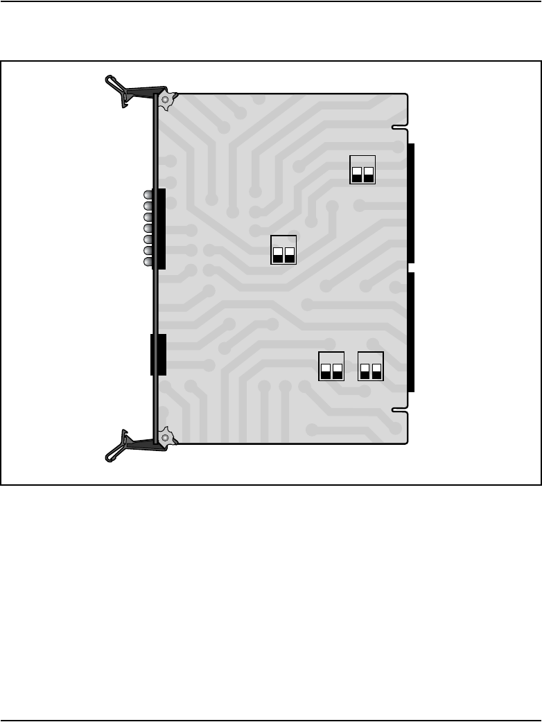
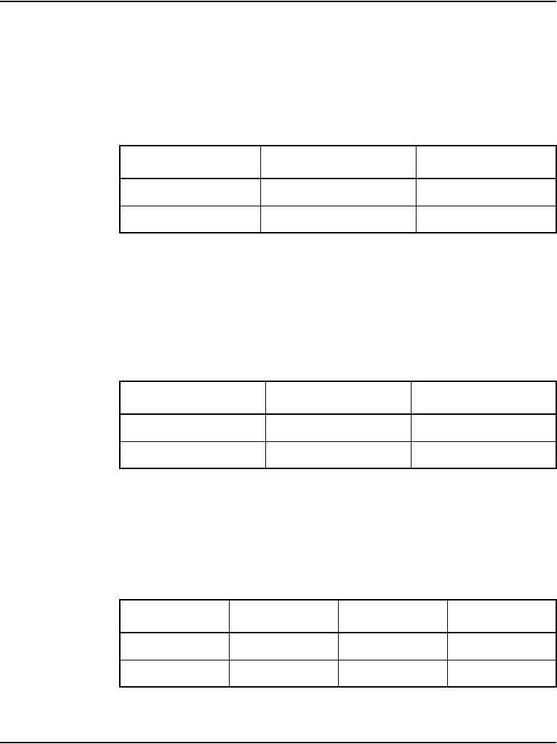
Page 750 of 906 NTAK79 2.0 Mb PRI card
553-3001-211 Standard 3.00 August 2005
Switch SW1 – DCHI Configuration
This switch enables/disables the on-board DCHI and sets the operating mode
of the DCHI. DPNSS1 mode is not supported at this time. For all other
countries that do not use DPNSS, use Q.931 mode.
Switch SW2 – Carrier Impedance Configuration
This switch sets the carrier impedance to either 120 ohms or 75 ohms.
Twisted pair cable is usually associated with 120 ohms. Coaxial cable is
usually associated with the 75 ohms setting.
Switch SW3 – Clock Controller Configuration
This switch enables/disables (H/W) the on-board Clock Controller. Disable
the SW 3-2 if the on-board clock controller is not in use.
Table 240
Switch SW1
Switch Down (On) Up (Off)
SW 1-1 enable DCHI disable DCHI
SW 1-2 DPNSS1/DASS2 Q.931
Table 241
Switch SW2
Cable Type SW 2-1 SW 2-2
75 ohms Up (Off) Down (On)
120 ohms Down (On) Up (Off)
Table 242
Switch SW3
Switch Down (On) Up (Off) Note
SW 3-1 — — Spare
SW 3-2 Disabled Enabled
NTAK79 2.0 Mb PRI card Page 751 of 906
Circuit Card Description and Installation
Switch SW4 – Carrier Shield Grounding
This switch enables for the selective grounding of the Tx / Rx pairs of the
carrier cable. Closing the switch (down position) applies Frame Ground
(FGND) to the coaxial carrier cable shield, creating a 75 ohms unbalanced
configuration. This applies only to the NTBK05CA cable.
Note: The usual method is to ground the outer conductor of the receive
coaxial signal.
Power requirements
The NTAK79 obtains its power from the backplane, drawing maximums of
2 A on +5 V, 50 mA on +12 V and 50 mA on –12 V.
Environment
The NTAK79 meets all applicable Nortel Network’s operating specifications.
Functional description
The NTAK79 card provides the following features and functions:
• recovery of the 2.048 kbps data by the CEPT receiver, at signal levels
which have been attenuated by up 10 dB
• control of CEPT line density using HDB3 which provides 64 kbps clear
channel
• performance monitoring of the receive carrier by means of Bipolar
Violations (BPV), Slips, CRC-4 (CRC), and Frame Bit Errors (FBER)
Table 243
Switch SW4
Switch Down (On) Up (Off)
SW 4-1 Rx – FGND Rx – OPEN
SW 4-2 Tx – FGND Tx – OPEN

Page 752 of 906 NTAK79 2.0 Mb PRI card
553-3001-211 Standard 3.00 August 2005
• monitoring of receive carrier alarms including AIS, LOS, and RAI
• transmission of remote alarm when instructed
• slip-buffering receive messages
• supporting National and International bits in time slot 0
• on-board clock controller
• onboard D-channel interface
• 32 software-selectable Tx & Rx Pad values
• conversion of PCM commanding Laws (A-A, u-u, A-u, u-A)
• Card-LAN for maintenance communication
Architecture
The main functional blocks of the NTAK79 architecture include:
• DS-30X interface
• A07 signaling interface
• digital pad
• carrier interface
• CEPT transceiver
•SLIP control
• D-channel support interface
• 8031 microcontroller
• Card-LAN / echo / test port interface
DS-30X interface
The NTAK79 interfaces to one DS-30X bus which contains 32
byte-interleaved timeslots operating at 2.56 Mb. Each timeslot contains
10 bits in A10 message format; eight are assigned to voice/data (64 kbps),
one to signaling (8 kbps), and one is a data valid bit (8 kbps).

NTAK79 2.0 Mb PRI card Page 753 of 906
Circuit Card Description and Installation
The incoming serial bit stream is converted to 8-bit parallel bytes to be
directed to padding control.
The signaling bits are extracted and inserted by the A07 signaling interface
circuitry. The DS-30X timeslot number is mapped to the PCM-30 channel
number. Timeslots 0 and 16 are currently unused for PCM.
Digital PAD
Software selects A-Law or Mu-Law and one of 32 possible PAD values for
each channel. These values are provided in a PROM through which the data
is routed. The idle code for A-Law is 54H and for Mu-Law is 7FH. The
unequipped code is FFH for both A-Law and Mu-Law. As the idle code and
unequipped code can be country dependent, the software instructs the
NTAK79 to use different codes for each direction. The 32 digital pads
available are listed in Table 244. The values shown are attenuation levels;
1.0 dB is 1 dB of loss and –1.0 dB is 1 dB of gain.
Table 244
Digital pad values and offset allocations (Part 1 of 2)
PAD SET 0 PAD SET 1
Offset PAD Offset PAD
00.6 dB 00.0 dB
11.0 dB 1–1.0 dB
22.0 dB 2–2.0 dB
33.0 dB 3–3.0 dB
44.0 dB 4–4.0 dB
55.0 dB 5–5.0 dB
66.1 dB 6–6.0 dB
77.0 dB 7–7.0 dB
88.0 dB 8–8.0 dB
99.0 dB 9–9.0 dB
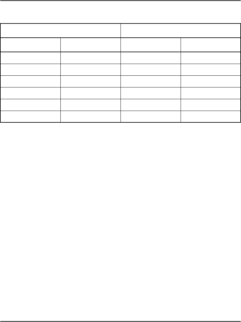
Page 754 of 906 NTAK79 2.0 Mb PRI card
553-3001-211 Standard 3.00 August 2005
Signaling interface
The signaling interface consists of the A07 DS-30X signaling controller. This
interface provides an 8 Kbps signaling link through the DS-30X timeslot zero
data bit zero. Messages are 3 bytes in length.
Carrier interface
The E1 interface connection to the external digital carrier is provided by the
line interface chip. This chip provides accurate pulse shaping to meet the
CCITT pulse mask requirements. It provides clock recovery functions on the
receive side as well as tolerance to jitter and wander in the received bit stream.
10 10.0 dB 10 –10.0 dB
11 11.0 dB 11 spare
12 12.0 dB 12 spare
13 13.0 dB 13 spare
14 14.0 dB 14 Idle Code
15 spare 15 Unassigned Code
Table 244
Digital pad values and offset allocations (Part 2 of 2)
PAD SET 0 PAD SET 1
Offset PAD Offset PAD
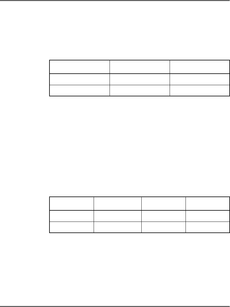
NTAK79 2.0 Mb PRI card Page 755 of 906
Circuit Card Description and Installation
Impedance matching
The line interface provides for the use of either 75 ohms coaxial or 120 ohms
twisted pair cable. The impedance is selected by a switch, as shown in
Table 245.
Note: The ON position for all the switches is towards the bottom of the
card. This is indicated by a white dot printed on the board next to the
bottom left corner of each individual switch.
Carrier grounding
The NTAK79 card provides the capability of selectively grounding the shield
of the Tx and/or Rx pairs of the carrier. Closing (down) the on-board switch
applies FGND to the appropriate carrier cable shield. The switch settings are
shown in Table 246.
Receiver functions
The receiver extracts data and clock from an AMI (Alternate Mark Inversion)
coded signal and outputs clock and synchronized data. The receiver is
sensitive to signals over the entire range of cable lengths and requires no
equalization. The clock and data recovery meets or exceeds the jitter
specifications of the CCITT recommendation G.823, and the jitter attenuation
Table 245
Impedance matching switch selection
Cable On Off
75 ohms S2 S1
120 ohms S1 S2
Table 246
Carrier shield grounding switch settings
Switch Carrier Pair On Off
S4-1 Rx shield Open GND
S4-2 Tx shield Open GND

Page 756 of 906 NTAK79 2.0 Mb PRI card
553-3001-211 Standard 3.00 August 2005
requirements of the CCITT recommendation G.742. This provides jitter
attenuation increasing from 0 dB to 60 dB over the frequency range from
about 6 Hz to 6 KHz.
Transmitter functions
The transmitter takes the binary (dual unipolar) data from the PCM
transceiver and produces bipolar pulses which conform to the CCITT
recommendation G.703 pulse shape.
Loopbacks
The remote loopback function causes the device to transmit the same data that
it receives, using the jitter attenuated receive clock. The data is also available
at the receive data outputs. Local loopback causes the transmit data and clock
to appear at the receive clock and data outputs. This data is also transmitted
on the line unless transmit AIS is selected.
CEPT transceiver
The transmitter and receiver functions are used for synchronization, channel,
and signal extraction. The functions meet applicable specifications of the
CCITT recommendation G.703 and G.732.
The transceiver provides transmit framing based on the 2.048 MHz clock
derived from the DS-30X system clock and 1 KHz framing pulse.
Slip control
Slip control provides organized recovery of PCM when the clock recovered
from the external facility is at a different frequency than the local clock.
D-channel support interface
The D-channel support interface is a 64 Kbps, full-duplex serial bit stream
configured as a DCE device. The data signals include:
• Receive data output
• transmit data input

NTAK79 2.0 Mb PRI card Page 757 of 906
Circuit Card Description and Installation
• receive clock output
• transmit clock output
The receive and transmit clocks have slightly different bit rates from each
other, as determined by the transmit and receive carrier clocks.
The NTAK79 has an onboard D-Channel Handler Interface (DCHI). It is the
equivalent to a single port of an NTAK02 SDI/DCH pack. This enables for a
completely operational ISDN PRA link with clock synchronization and
D-channel on a single circuit card.
The onboard D-channel has one status LED on the NTAK79 faceplate to
indicate enabled/disabled states. See Table 239 on page 746.
The on-board DCHI can be operated in two separate modes as defined by an
on-board dip switch. It can operate in a standard DCHI mode common to
most ISDN standard countries. The U.K. specific mode that uses the DPNSS
format is not supported at this time.
DCHI special applications connection
The connection between the PRI2 and the on-board D-channel Handler
Interface card is also available at the MDF connector. Connections are made
to these pins for normal on-board DCHI operation. They can also be used for
future or special applications.
The signals conform to the EIA RS-422 standard.
Table 247
Settings for the DCHI dip switch (SW1)
Switch Function On Off
S1-1 En/Dis Enabled Disabled
S1-2 F/W Mode DPNSS (not
supported at
this time)
DCHI

Page 758 of 906 NTAK79 2.0 Mb PRI card
553-3001-211 Standard 3.00 August 2005
Card-LAN interface
A Dual Port UART handles the functions of the serial ports for the Card-LAN
serial link and the echo canceller/test port interface. The echo/test interface is
an asynchronous 4800 bps 8-bit connected to port A of the UART. The
Card-LAN interface is an asynchronous 19.2 kbps 9 bit start/stop connected
to port B of the UART.
The connection to the echo canceler/test port is available at the backplane/
MDF connector. The signals at this port conform to the EIA RS-232C
standard.
Clock controller interface
The clock controller circuitry on the NTAK79 is identical to that of the
NTAK20 clock controller.
Though several DTI/PRI packs can exist in one system, only one clock
controller may be activated. All other DTI/PRI clock controllers must be
switched off.
Clocking modes
The clock controller can operate in one of two modes:
• tracking
• non-tracking (also known as free-run)
Tracking mode
There are two stages to clock controller tracking:
• tracking a reference, and
• locked onto a reference.
When tracking a reference, the clock controller uses an algorithm to match its
frequency to the frequency of the incoming clock. When the frequencies are
very near to being matched, the clock controller is locked onto the reference.
The clock controller will make small adjustments to its own frequency until
both the incoming and system frequencies correspond.

NTAK79 2.0 Mb PRI card Page 759 of 906
Circuit Card Description and Installation
If the incoming clock reference is stable, the internal clock controller will
track it, lock onto it, and match frequencies exactly. Occasionally, however,
environmental circumstances will cause the external or internal clocks to
drift. When this happens, the internal clock controller will briefly enter the
tracking stage. The green LED will flash momentarily until the clock
controller is locked onto the reference once again.
If the incoming reference is unstable, the internal clock controller will
continuously be in the tracking stage, with the LED flashing green all the
time. This condition does not present a problem, rather, it shows that the clock
controller is continually attempting to lock onto the signal. If slips are
occurring, however, it means that there is a problem with the clock controller
or the incoming line.
Free-run (non-tracking)
In free-run mode, the clock controller does not synchronize on any source, it
provides its own internal clock to the system. This mode can be used when
the CS 1000S, CS 1000M Cabinet, and Meridian 1 PBX 11C Cabinet are
used as a master clock source for other systems in the network. Free-run mode
is undesirable if the CS 1000S, CS 1000M Cabinet, and Meridian 1 PBX 11C
Cabinet are intended to be a slave. It can occur, however, when both the
primary and secondary clock sources are lost due to hardware faults or when
invoked by using software commands.
Clock controller functions and features
The NTAK79 clock controller functions and features include:
• phase lock to a reference, generate the 10.24 MHz system clock, and
distribute it to the CPU through the backplane. Up to two references at a
time are accepted
• primary to secondary switchover (auto-recovery is provided)
• prevent chatter
• error burst detection and correction, holdover, and free running
capabilities
• compliance with 2.0Mb CCITT specifications
• software communication

Page 760 of 906 NTAK79 2.0 Mb PRI card
553-3001-211 Standard 3.00 August 2005
• jitter filtering
• use of an algorithm to detect crystal aging and to qualify clocking
information
Reference switchover
Switchover may occur in the case of reference degradation or reference
failure. When performance of the reference degrades to a point where the
system clock is no longer allowed to follow the timing signal, then the
reference will be said to be out of specification. If the reference being used is
out of specification and the other reference is still within specification, an
automatic switchover is initiated without software intervention. If both
references are out of specification, the clock controller provides holdover.
Autorecovery and chatter
If the software command “track to primary” is given, the clock controller
tracks to the primary reference and continuously monitors the quality of both
primary and secondary references. If the primary becomes out of
specification, the clock controller automatically tracks to secondary provided
that it is within specifications. On failure (both out of specification), the clock
controller enters the HOLDOVER mode and continuously monitors both
references. An automatic switchover is initiated to the reference that recovers
first. If the secondary recovers first, then the clock controller tracks to the
secondary, but switches over to the primary when the primary recovers. If the
primary recovers first, the clock controller tracks to the primary.
If the software command “track to secondary” is given, the clock controller
tracks to the secondary reference and continuously monitors the quality of
both primary and secondary references. If the secondary becomes out of
specification, the clock controller automatically tracks to primary provided
that it is within specifications. On failure (both out of spec.), the clock
controller enters the HOLDOVER mode and continuously monitors both
references. An automatic switchover is initiated to the reference that recovers
first. If the primary recovers first, then the clock controller tracks to the
primary, but switches over to the secondary whenever the secondary
recovers. If the secondary recovers first, then the clock controller tracks to the
secondary.

NTAK79 2.0 Mb PRI card Page 761 of 906
Circuit Card Description and Installation
A time-out mechanism prevents chatter due to repeated automatic switching
between primary and secondary reference sources.
Holdover and free-run
In the temporary absence of a synchronization reference signal, or when
sudden changes occur on the incoming reference due to error bursts, the clock
controller provides a stable holdover. The free-run mode is initiated when the
clock controller has no record of the quality of the incoming reference clock.
If the software command “free run” is given, the clock controller enters the
free-run mode and remains there until a new command is received. Note that
the free-run mode of operation is automatically initiated after the clock
controller is enabled.
Reference clock selection through software
The NTAK79 has the necessary hardware for routing its reference to the
appropriate line on the backplane.
The software is responsible for the distribution of the secondary references
and ensures that no contention is present on the REFCLK1 backplane line.
The software designates the NTAK79 as the primary reference source to the
clock controller. The secondary reference is obtained from another NTAK79
card, which is designated by a technician. No other clocks originating from
other NTAK79 circuit cards are used.
The clock controller provides an external timing interface and is capable of
accepting two signals as timing references. In this case, an external reference
refers to an auxiliary timing source which is bridged from a traffic carrying
signal. This is not intended to be a dedicated non-traffic bearing timing signal.
The clock controller uses either the two external/auxiliary references or the
NTAK79 references.


Page 763 of 906
Circuit Card Description and Installation
768
NTAK93 D-channel Handler
Interface daughterboard
Contents
This section contains information on the following topics:
Introduction . . . . . . . . . . . . . . . . . . . . . . . . . . . . . . . . . . . . . . . . . . . . . . 763
Physical description. . . . . . . . . . . . . . . . . . . . . . . . . . . . . . . . . . . . . . . . 764
Functional description . . . . . . . . . . . . . . . . . . . . . . . . . . . . . . . . . . . . . . 765
Introduction
The NTAK93 provides the D-channel handler interfaces required by the
ISDN PRI trunk.
The DCHI performs D-channel Layer 2 message processing and transfers
Layer 3 signaling information between two adjacent network switches. It is
mounted on the NTAK09 1.5 Mb DTI/PRI card or the NTBK50 2.0 Mb PRI
card (installed in the MG 1000S) using standoff reference pins and
connectors. The NTAK93 daughterboard, when mounted on the NTBK50
PRI digital trunk card, is addressed in the same slot as the NTBK50. The
NTAK93 daughterboard can use SDI I/O addresses 1 to 15 and port 1.
The NTAK93 provides the following features and functions:
• D-channel interface or DPNSS interface
• Special features included for LAPD implementation at DCH:

Page 764 of 906 NTAK93 D-channel Handler Interface daughterboard
553-3001-211 Standard 3.00 August 2005
— system parameters are service changeable (system parameters are
downloaded from software)
— incoming Layer 3 message validation procedures are implemented
in the D-PORT firmware
— supported message units and information elements can be service
changed
— translation of the CCITT message types information elements into a
proprietary coding scheme for faster CPU operation
— convention of IA5-encoded digits to BCD-encoded digits for
incoming layer 3 messages for faster CPU operation
—self-test
— loopback
Physical description
The DCH function can be installed in the main and IP expansion cabinets.
The DTI/PRI card which carries a DCH daughterboard resides in the main
and IP expansion cabinets.
NTAK93 D-channel Handler Interface daughterboard Page 765 of 906
Circuit Card Description and Installation
Faceplate LEDs
NTAK09 1.5 Mb PRI and NTBK50 2.0 MB PRI cards
LEDs are located on the faceplate of the NTAK09 and NTBK50 cards. The
DCHI LED is dual-color (red and green). The LEDs are described in
Table 248.
Power consumption
Power consumption is +5 V at 750 mA; +12 V at 5 mA; and –12 V at 5 mA.
Functional description
The main functional blocks of the NTAK93 architecture include the
following.
Microprocessors
One microprocessor does the following:
• handles data transfer between each pair of serial ports and software
• reports the status of each port
• takes commands from software to control the activities of the ports
The microprocessors also handle some D-channel data processing in DCHI
mode.
Table 248
Faceplate LEDs
State Definition
On (Red) NTAK93 is equipped and disabled.
On (Green) NTAK93 is equipped and enabled, but not necessarily
established.
Off NTAK93 is not equipped.

Page 766 of 906 NTAK93 D-channel Handler Interface daughterboard
553-3001-211 Standard 3.00 August 2005
DMA controller
A Z80A-DMA chip controls the data transfer between local RAM memory
and communication ports. The DMA channels are only used in the receive
direction (from line to SSC), not in the transmit direction.
Random Access Memory (RAM)
A total of 32 KBytes of RAM space for each pair of ports is used as the
communication buffer and for firmware data storage.
Read Only Memory (ROM)
A total of 32K bytes of ROM space for each pair of ports is reserved as a code
section of the DCH-PORT firmware.
LAPD data link/asynchronous controller
One chip controls each pair of independent communication ports. It performs
the functions of serial-to-parallel and parallel-to-serial conversions, error
detection, and frame recognition (in HDLC). The parameters of these
functions are supplied by the DCH-PORT firmware.
Counter/timer controller
Two chips are used as real-time timers and baud-rate generators for each pair
of communication ports.
Software interface circuit
This portion of the circuit handles address/data bus multiplexing, the
interchange of data, commands, and status between the on board processors
and software. It includes transmit buffer, receive buffer, command register,
and status register for each communication channel.
DPNSS/DCHI Port
The mode of operation of the DCH-PORT is controlled by a switch setting on
the NTAK09/NTBK50. For DPNSS the switch is ON; for DCHI it is OFF.

NTAK93 D-channel Handler Interface daughterboard Page 767 of 906
Circuit Card Description and Installation
The port will operate at:
The address of ports is selected by hardwired backplane card address. Port
characteristics and LAPD parameters are downloaded from software.
D-Port — SDTI/PRI interface
Below is a brief description of signals. When connected to SDTI/PRI,
DCHI-PORT is considered Data Terminal Equipment (DTE):
• SDA, SDB: Transmit Clock provided by SDTI/PRI
• RTA, RTB: Receive Clock provided by SDTI/PRI
• RR, CS: SPDC ready signal provided by DCHI-PORT
• TR: D-PORT ready signal provided by DCHI-PORT
• RDA, RDB: Incoming serial data bit stream, driven by SDTI/PRI
• SDA, SDB: Transmit serial data bit stream driven by DCHI-PORT
Data Rate 56kbps, 64kbps
Duplex Full
Clock Internal / External
Interface RS422


Page 769 of 906
Circuit Card Description and Installation
772
NTBK22 MISP card
Contents
This section contains information on the following topics:
Introduction . . . . . . . . . . . . . . . . . . . . . . . . . . . . . . . . . . . . . . . . . . . . . . 769
Physical description. . . . . . . . . . . . . . . . . . . . . . . . . . . . . . . . . . . . . . . . 769
Functional description . . . . . . . . . . . . . . . . . . . . . . . . . . . . . . . . . . . . . . 770
Introduction
The NTBK22 Multi-Purpose ISDN Signaling Processor (MISP) card is a
microprocessor-controlled signaling processor that performs Data Link
(Layer 2) and Network (Layer 3) processing associated with ISDN BRI and
the OSI protocol.
Physical description
The MISP occupies one slot in the MG 1000S. It uses one of the network
loops to interface with SILCs and UILCs and to provide 32 timeslots for
D-channel signaling and packet data transmission. The other loop address is
used to communicate with the Call Server.
You can install this card in slots 1 through 4 in the MG 1000S. The card is not
supported in the MG 1000S Expansion.
Note: When configuring BRI trunks, the MISP (NTBK22) card must be
co-located in the same MG 1000S as the SILC (NT6D70) and UILC
(NT6D71) cards the MISP is supporting.

Page 770 of 906 NTBK22 MISP card
553-3001-211 Standard 3.00 August 2005
Refer to ISDN Basic Rate Interface: Installation and Configuration
(553-3001-218) and ISDN Basic Rate Interface: Features (553-3001-380) for
additional information.
Functional description
Each MISP can support 4 line cards (UILC or SILC or any combination of the
two). Each line card supports 8 DSLs, therefore each MISP supports 32
DSLs. Since each DSL uses two B-channels and one D-channel the MISP
supports 64 B-channels and 32 D-channels. If the MISP is carrying packet
data, it must dedicate one of its D-channels to communicate with the external
packet handler. In this case the MISP supports only 31 DSLs.
The main functions of the MISP are:
• communicate with the Call Server CPU to report ISDN BRI status and
receive downloaded application software and configuration parameters
• manage Layer 2 and Layer 3 signaling that controls call connection and
terminal identification
• control terminal initialization and addressing
• assign B-channels for switched voice and data transmission by
communicating with the BRI terminal over the D-channel and allocating
to it an idle B-channel with appropriate bearer capabilities
• separate D-channel data from signaling information and route the data to
the packet handler
• send call control messages to ISDN BRI terminals over the D-channel
Micro Processing Unit (MPU)
The MPU coordinates and controls data transfer and addressing of the
peripheral devices and communicates with the CPU using a message channel
on the CPU bus. The tasks that the MPU performs depend on the interrupts it
receives. The interrupts are prioritized by the importance of the tasks they
control.

NTBK22 MISP card Page 771 of 906
Circuit Card Description and Installation
High-Level Data Link Controller (HDLC)
The HDLC is a format converter that supports up to 32 serial channels that
communicate at speeds up to 64 kbps. The HDLC converts messages into the
following two message formats:
• a serially transmitted, zero-inserted, CRC protected message that has a
starting and an ending flag
• a data structure
CPU to MISP bus interface
Information exchange between the CPU and the MISP is performed with
packetized messages transmitted over the CPU bus. This interface has a
16-bit data bus, an 18-bit address bus, and interrupt and read/write control
lines.
This interface uses shared Static Random Access Memory (SRAM) as a
communication exchange center between the CPU and the MPU. Both the
CPU and the MPU can access this memory over the transmit and receive
channels on the bus.
MISP network bus interface
The network bus interface:
• converts bit interleaved serial data received from the network bus into
byte interleaved data for transmission over the 32 time slots used by the
HDLC controller
• accepts byte interleaved data transmitted from the HDLC controller and
converts it into a bit interleaved data stream for transmission over the
network bus
Power consumption
Power consumption is +5V at 2 A; +15V at 50 mA; and -15V at 50 mA.


Page 773 of 906
Circuit Card Description and Installation
784
NTBK50 2.0 Mb PRI card
Contents
This section contains information on the following topics:
Introduction . . . . . . . . . . . . . . . . . . . . . . . . . . . . . . . . . . . . . . . . . . . . . . 773
Physical description. . . . . . . . . . . . . . . . . . . . . . . . . . . . . . . . . . . . . . . . 774
Functional description . . . . . . . . . . . . . . . . . . . . . . . . . . . . . . . . . . . . . . 777
Architecture. . . . . . . . . . . . . . . . . . . . . . . . . . . . . . . . . . . . . . . . . . . . . . 778
Introduction
The NTBK50 2.0 Mb PRI card provides a 2.0 Mb PRI interface. It supports
the NTAK20 clock controller daughterboard and either the NTAK93
D-channel interface or the NTBK51 Downloadable D-channel handler. The
NTAK93 DCHI daughterboard provides identical performance to the
on-board NTAK79 DCHI. The NTBK51 DDCH daughterboard provides
support for protocols based on the MSDL platform.

Page 774 of 906 NTBK50 2.0 Mb PRI card
553-3001-211 Standard 3.00 August 2005
You can install this card in slots 1 through 4 in the MG 1000S. The card is not
supported in the MG 1000S Expansion.
Note: Clocking slips can occur between MG 1000S systems that are
clocked from different Central Offices (COs), if the COs are not
synchronized. The slips can degrade voice quality.
Physical description
The NTBK50 uses a standard 9.5" by 12.5" multi-layer printed circuit board.
The faceplate is 7/8” wide and contains seven LEDs. See Figure 166 on
page 775.
IMPORTANT!
Each MG 1000S that has a digital trunk must have a clock controller
clocked to an external reference clock.
NTBK50 2.0 Mb PRI card Page 775 of 906
Circuit Card Description and Installation
Figure 166
NTBK50 2.0 Mb PRI card with daughterboards
NTAK20
Clock
Controller
NTAK93 or
NTBK51
D-Channel
Interface
SW2
SW4
12
1
2
SW1
12
Stiffeners
Connector Sockets
LEDs
Bantam
Jacks
Standoffs
DIS
ACT
RED
YEL
LBK
CC
DCH
RCV
XMT
On
Off
On
Off
On
Off
553-7872
553-CSE7872

Page 776 of 906 NTBK50 2.0 Mb PRI card
553-3001-211 Standard 3.00 August 2005
The LEDs are described in Table 249.
Table 249
NTBK50 faceplate LEDs (Part 1 of 2)
LED State Definition
OOS On (Red) The NTBK50 2.0 Mb PRI circuit card is disabled or
out-of-service. Also, the state of the card after power-up,
completion of self test, and exiting remote loopback.
Off The NTBK50 2.0 Mb PRI is not in a disabled state.
ACT On (Green) The NTBK50 2.0 Mb PRI circuit card is in an active state.
Off The NTBK50 2.0 Mb PRI is in a disabled state. The OOS
LED is red.
RED On (Red) A red alarm state has been detected. This represents a
local alarm state of Loss of Carrier (LOS), Loss of Frame
(LFAS), or Loss of CRC Multiframe (LMAS).
Off No red (local) alarm.
YEL On (Yellow) A yellow alarm state has been detected. This represents
a remote alarm indication from the far end. The alarm
may be either Alarm Indication (AIS) or Remote Alarm
(RAI).
Off No yellow (remote) alarm.
LBK On (Green) 2.0 Mb PRI is in loop-back mode.
Off 2.0 Mb PRI is not in loop-back mode.
CC On (Red) The clock controller is software disabled.
On (Green) The clock controller is enabled and is either locked to a
reference or is in free run mode.

NTBK50 2.0 Mb PRI card Page 777 of 906
Circuit Card Description and Installation
Power requirements
The NTBK50 obtains its power from the backplane, drawing up to 2 A on +5
V, 35 mA on +15 V and 20 mA on –15 V.
Environment
The NTBK50 meets all applicable Nortel operating specifications.
Functional description
NTBK50 provides the following features and components:
• recovery of the 2.048 kbps data by the CEPT receiver, at signal levels
which have been attenuated by up to 10 dB
• control of CEPT line density using HDB3 which provides 64 kbps clear
channel
• performance monitoring of the receive carrier by means of Bipolar
Violations (BPV), Slips, CRC-4 (CRC), and Frame Bit Errors (FBER)
Flashing
(Green)
NTAK20 is equipped and is attempting to lock (tracking
mode) to a reference. If the LED flashes continuously
over an extended period of time, check the CC STAT in
LD 60. If the CC is tracking this can be an acceptable
state. Check for slips and related clock controller error
conditions. If none exist, then this state is acceptable,
and the flashing is identifying jitter on the reference.
Off The clock controller is not equipped.
DCH On (Red) DCH is disabled.
On (Green) DCH is enabled, but not necessarily established.
Off DCH is not equipped.
Table 249
NTBK50 faceplate LEDs (Part 2 of 2)
LED State Definition

Page 778 of 906 NTBK50 2.0 Mb PRI card
553-3001-211 Standard 3.00 August 2005
• monitoring of receive carrier alarms including AIS, LOS, and RAI
• transmission of remote alarm when instructed
• slip-buffering receive messages
• support of National and International bits in timeslot 0
• clock controller daughterboard
• D-channel interface daughterboard
• downloadable D-channel handler daughterboard
• 32 software-selectable Tx and Rx Pad values
• conversion of PCM commanding Laws (A-A, u-u, A-u, u-A)
• Card-LAN for maintenance communication
Architecture
The main functional blocks of the NTBK50 architecture are:
• DS-30X interface
• A07 signaling interface
• digital pad
• carrier interface
• CEPT transceiver
•SLIP control
• D-channel support interface
• clock controller interface
• Card-LAN / echo / test port interface
• 80C51FA Microcontroller
DS-30X interface
NTBK50 interfaces to one DS-30X bus which contains 32-byte interleaved
timeslots operating at 2.56 Mb. Each timeslot contains 10 bits in A10

NTBK50 2.0 Mb PRI card Page 779 of 906
Circuit Card Description and Installation
message format; eight are assigned to voice/data (64 Kbps), one to signaling
(8 Kbps), and one is a data valid bit (8 Kbps).
The incoming serial bit stream is converted to 8-bit parallel bytes to be
directed to padding control. The signaling bits are extracted and inserted by
the A07 signaling interface circuitry. Timeslots 0 and 16 are currently unused
for PCM.
Digital PAD
The software selects A-Law or µ-Law and one of 32 possible PAD values for
each channel. These values are provided in a PROM through which the data
is routed. The idle code for A-Law is 54H and for µ-Law is 7FH. The
unequipped code is FFH for both A-Law and µ-Law.
As the idle code and unequipped code can be country dependent, the software
instructs the NTBK50 to use different codes for each direction. The 32 digital
pads available are illustrated in Table 250 on page 779. The values shown are
attenuation levels (1.0dB is 1 dB of loss and –1.0 dB is 1 dB of gain.
Table 250
Digital Pad - values and offset allocations (Part 1 of 2)
PAD SET 0 PAD SET 1
Offset PAD Offset PAD
00.6 dB 00.0 dB
11.0 dB 1-1.0 dB
22.0 dB 2-2.0 dB
33.0 dB 3-3.0 dB
44.0 dB 4-4.0 dB
55.0 dB 5-5.0 dB
66.1 dB 6-6.0 dB
77.0 dB 7-7.0 dB
88.0 dB 8-8.0 dB
Page 780 of 906 NTBK50 2.0 Mb PRI card
553-3001-211 Standard 3.00 August 2005
Signaling interface
The signaling interface consists of the A07 DS-30X signaling controller. This
interface provides an 8 Kbps signaling link via the DS-30X timeslot zero data
bit zero. Messages are 3 bytes in length.
Carrier interface
For the E1 interface, the connection to the external digital carrier is provided
by the line interface chip. This device provides accurate pulse shaping to meet
the CCITT pulse mask requirements. It provides clock recovery functions on
the receive side, as well as tolerance to jitter and wander in the received bit
stream.
99.0 dB 9-9.0 dB
10 10.0 dB 10 -10.0 dB
11 11.0 dB 11 spare
12 12.0 dB 12 spare
13 13.0 dB 13 spare
14 14.0 dB 14 Idle Code
15 spare 15 Unassigned Code
Table 250
Digital Pad - values and offset allocations (Part 2 of 2)
PAD SET 0 PAD SET 1
Offset PAD Offset PAD
NTBK50 2.0 Mb PRI card Page 781 of 906
Circuit Card Description and Installation
Impedance matching (Switch SW2)
The line interface provides for the use of either 75 ohms coaxial or 120 ohms
twisted pair cable. The impedance is selected by SW2, as shown in Table 251.
Note: The ON position for all the switches is toward the bottom of the
card. This is indicated by a white dot printed on the board next to the
bottom left corner of each individual switch.
Carrier grounding
NTBK50 enables the shield of the Tx and/or Rx pairs of the carrier to be
selectively grounded. Closing (down position) the on-board switch applies
FGND to the appropriate carrier cable shield. The switch settings are shown
in Table 252.
Table 251
Impedance matching switch settings
Cable Type SW 2-1
75 ohms Down (On)
120 ohms Up (Off)
Table 252
Carrier Shield grounding switch settings
Switch Down (On) Up (Off)
SW 4 – 1 Rx – FGND Rx – OPEN
SW 4 – 2 Tx – FGND Tx – OPEN
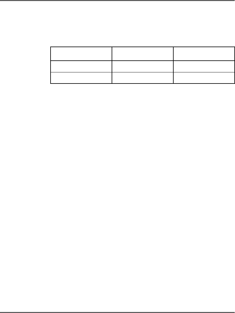
Page 782 of 906 NTBK50 2.0 Mb PRI card
553-3001-211 Standard 3.00 August 2005
Carrier Shield grounding (Switch SW4)
Table 253 lists the Carrier Shield ground switch settings.
Note: The usual method is to ground the outer conductor of the receive
coax signal.
Receiver functions
The receiver extracts data and clock from an AMI (Alternate Mark Inversion)
coded signal and outputs clock and synchronized data. The receiver is
sensitive to signals over the entire range of cable lengths and requires no
equalization. The clock and data recovery meets or exceeds the jitter
specifications of the CCITT recommendation G.823 and the jitter attenuation
requirements of the CCITT recommendation G.742. This provides jitter
attenuation increasing from 0 dB to 60 dB over the frequency range from
about 6 Hz to 6 KHz.
Transmitter functions
The transmitter takes the binary (dual unipolar) data from the PCM
transceiver and produces bipolar pulses. This conforms to CCITT
recommendation G.703 pulse shape.
Loopbacks
The remote loopback function causes the far-end device to transmit the same
data that it receives, using the jitter attenuated receive clock. The data is
additionally available at the far-end receive data outputs. Local loopback
causes the transmit data and clock to appear at the near-end clock and receive
data outputs. This data is also transmitted on the line unless an Alarm
Indication Signal (AIS) is transmitted instead.
Table 253
Carrier Shield grounding switch settings
Switch Down (On) Up (Off)
SW 4 – 1 Rx – FGND Rx – OPEN
SW 4 – 2 Tx – FGND Tx – OPEN

NTBK50 2.0 Mb PRI card Page 783 of 906
Circuit Card Description and Installation
CEPT transceiver
The transmitter and receiver functions are used for synchronization, channel,
and signal extraction. The functions meet applicable specifications of the
CCITT recommendation G.703 and G.732.
The transceiver provides transmit framing based on the 2.048 MHz clock
derived from the DS-30X system clock and 1 KHz framing pulse.
Slip control
Slip control provides organized recovery of PCM when the clock recovered
from the external facility is at a different frequency with respect to the local
clock.
D-channel support interface
The D-channel support interface is a 64 Kbps, full-duplex serial bit stream
configured as a DCE device. The data signals include:
• receive data output
• transmit data input
• receive clock output
• transmit clock output
The receive and transmit clocks can be of slightly different bit rates from each
other as determined by the transmit and receive carrier clocks.
The NTBK50 supports a D-Channel Handler Interface (DCHI)
daughterboard. It is equivalent to a single port of an NTAK02 SDI/DCH card.
The NTBK50 also supports a Downloadable D-Channel Handler interface
(DDCH) daughterboard. The DDCH brings MSDL D-channel capability to
the system.
DCHI Configuration for NTAK93 only (SW1)
The NTAK93 DCHI daughterboard can be operated in two separate modes
defined by an on-board dip switch. It can operate in a standard DCHI mode
common to most ISDN standard countries. It can also operate in a DPNSS

Page 784 of 906 NTBK50 2.0 Mb PRI card
553-3001-211 Standard 3.00 August 2005
mode, which is not supported at this time. The DDCH supports only a single
port which directly interfaces to the PRI motherboard. See Table 254.
Card-LAN interface
A Dual Port UART handles the functions of the serial ports for the Card-LAN
serial link test port interface. The test interface is an asynchronous 4800 bps
8 bit connected to port A of the UART. The card-LAN interface is an
asynchronous 19.2 kbps 9 bit start/stop connected to port B of the UART.
The connection to the test port is available at the backplane/MDF connector.
The signals at this port conform to the EIA RS-232C standard.
Table 254
Settings for the DCHI dip switch (SW1)
Switch Function On Off
S1-1———
S1-2 F/W Mode DPNSS DCHI

Page 785 of 906
Circuit Card Description and Installation
790
NTBK51 Downloadable D-channel
Handler daughterboard
Contents
This section contains information on the following topics:
Introduction . . . . . . . . . . . . . . . . . . . . . . . . . . . . . . . . . . . . . . . . . . . . . . 785
Physical description. . . . . . . . . . . . . . . . . . . . . . . . . . . . . . . . . . . . . . . . 786
Functional description . . . . . . . . . . . . . . . . . . . . . . . . . . . . . . . . . . . . . . 787
Download operation . . . . . . . . . . . . . . . . . . . . . . . . . . . . . . . . . . . . . . . 789
Introduction
The NTBK51 daughterboard provides Downloadable D-channel Handler
(DDCH) interfaces based on the Multipurpose Serial Data Link (MSDL). The
DDCH provides a single purpose full-duplex serial port capable of
downloading the D-channel application and base software into the card.
The NTBK51 provides the following features and functions:
• ISDN D-channel related protocol
•Selftest
• Loopback
• D-channel loadware including:
— management and maintenance
— LAPD- software for data link layer processing
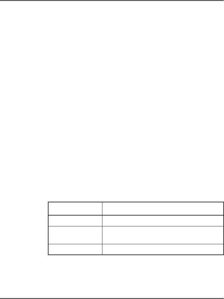
Page 786 of 906 NTBK51 Downloadable D-channel Handler daughterboard
553-3001-211 Standard 3.00 August 2005
— DCH interface
— layer 3 preprocessor
— traffic reporting including link capacity
Physical description
The NTBK51 daughterboard interfaces with the system CPU and is mounted
on either the NTAK09 1.5 DTI/PRI card or the NTBK50 2 Mb PRI digital
trunk card.
You can install this card in:
• slots 1 through 9 in the main cabinet or slots 11-19, 21-29, 31-39, or
41-49 in the expansion cabinets
• slots 1 through 4 in the MG 1000S. The card is not supported in the
MG 1000S Expansion
The NTBK51 daughterboard, when installed on the NTAK09 digital trunk
card, is addressed in the same slot as the NTAK09.
One NTBK51 daughterboard is required for each PRI link.
LEDs are located on the faceplate of the NTAK09/NTBK50 card. The DCHI
LED is a dual-color (red/green). The LED is described in Table 255.
Table 255
Faceplate LED
State Definition
On (Red) NTBK51 is disabled.
On (Green) NTBK51 is enabled, but not necessarily
established.
Off NTBK51 is not equipped.

NTBK51 Downloadable D-channel Handler daughterboard Page 787 of 906
Circuit Card Description and Installation
Functional description
The main functional blocks of the NTBK51 architecture include the
following:
• Microprocessors
•Main memory
• Shared memory
• EPROM memory
• Flash EPROM memory
•EEPROM memory
• Serial communication controller
• Sanity timer
• Bus timer
Microprocessors
One microprocessor handles data transfer between each serial interface and
software, reports the status of each port and takes commands from the
software to control the activities of the ports. A high performance MPU
supports the D-channel from the PRI card and other software applications
running simultaneously on other ports of the DDCH card.
The microprocessor performs the following functions:
• sanity check and self tests
• message handling between the CS 1000S, CS 1000M Cabinet, and
Meridian 1 PBX 11C Cabinet and the card
• four port serial communication controller handling with Direct Memory
Access (DMA)
• program download from the Small System Controller

Page 788 of 906 NTBK51 Downloadable D-channel Handler daughterboard
553-3001-211 Standard 3.00 August 2005
Main memory
The main 68EC020 system memory is comprised of 1 Mbyte of SRAM and
is accessible in 8 or 16 bits. The software, base code and application reside in
main RAM and is downloaded from the software through the shared memory.
Shared memory
The shared memory is the interface between the CPU and the 68EC020 MPU.
This memory is a 16 Kbyte RAM, expandable to 64 kbytes and accessible in
8 or 16 bits.
EPROM memory
The Bootstrap code resides in this 27C1000 EPROM and is executed on
power up or reset.
Flash EPROM memory
Flash EPROM provides non-volatile storage for the DDCH loadware which
minimizes the impact to sysload. The Flash EPROM provides an increase in
system service with a reduced delay after a brown-out, and faster testing of a
hardware pack after it is plugged in.
EEPROM memory
The DDCH uses a 1024 bit serial EEPROM for storing the Nortel product
code and a revision level. This information can be queried by the software.
Serial communication controller
The serial controller is the Zilog Z16C35 and is referenced as the Integrated
Controller (ISCC). The ISCC includes a flexible Bus Interface Unit (BIU)
and four Direct Memory Access (DMA) channels, one for each receive and
transmit. The DMA core of the ISCC controls the data transfer between local
RAM and the communication ports.

NTBK51 Downloadable D-channel Handler daughterboard Page 789 of 906
Circuit Card Description and Installation
Sanity timer
A sanity timer is incorporated on the DDCH to prevent the MPU from getting
tied-up as the result of a hardware or software fault. If the MPU encounters a
hardware or software fault and enters a continuous loop, the sanity timer
enables the DDCH to reset itself.
Bus timer
The bus timer presents an error signal to the MPU if an attempt to access a
device did not receive acknowledgment within the bus time-out period of
120 ms.
Download operation
Downloading is performed in either of two modes: background mode or
maintenance mode. Before a download takes place, a D-channel link must be
configured. The following situations lead to software downloading:
• during initialization when new software is installed
• when enabling the card or application
• during card reset (due to loss of software or corruption)
• during a background audit
System initialization
When new base or application software is installed on a CS 1000S,
CS 1000M Cabinet, and Meridian 1 PBX 11C Cabinet, the download
decision is made during system initialization. The actual MSDL base
software download is done in background mode and can take several minutes
to complete, depending on switch traffic and the size of the MSDL base
software.
Card enabling or application enabling
If a normal download enable command is executed, the MSDL base code and
application is conditionally downloaded to the DDCH card. This conditional

Page 790 of 906 NTBK51 Downloadable D-channel Handler daughterboard
553-3001-211 Standard 3.00 August 2005
download depends on the result of the check made by the CPU on the MSDL
base code and application software.
If a forced download enable command is executed in LD 96, the MSDL base
code and application are forced down to the DDCH card, even if the base and
application software is already resident on the DDCH card. In order to
complete a forced download, the following conditions must be met:
• the DDCH card must be enabled
• the D-channel port must be disabled
Card reset
After a card reset, the MSDL base code and the D-channel application
software are validated by the CPU. The software is stored in flash EPROM
on the DDCH card and does not have to be downloaded. But if the software
is missing due to new installation, corruption, or loadware version mismatch,
the CPU automatically downloads the base/application into the DDCH card.
Background audit
If a background audit of the card and associated applications finds that a
download is required, the card is queued in the PSDL tree. Downloading is
performed in background mode based on the entries in the PSDL tree.

Page 791 of 906
Circuit Card Description and Installation
810
NTCK16 Generic Central Office
Trunk cards
Contents
This section contains information on the following topics:
Introduction . . . . . . . . . . . . . . . . . . . . . . . . . . . . . . . . . . . . . . . . . . . . . . 791
Physical description. . . . . . . . . . . . . . . . . . . . . . . . . . . . . . . . . . . . . . . . 793
Functional description . . . . . . . . . . . . . . . . . . . . . . . . . . . . . . . . . . . . . . 793
Operation. . . . . . . . . . . . . . . . . . . . . . . . . . . . . . . . . . . . . . . . . . . . . . . . 794
Electrical specifications. . . . . . . . . . . . . . . . . . . . . . . . . . . . . . . . . . . . . 796
Connector pin assignments . . . . . . . . . . . . . . . . . . . . . . . . . . . . . . . . . . 797
Configuration . . . . . . . . . . . . . . . . . . . . . . . . . . . . . . . . . . . . . . . . . . . . 797
Applications . . . . . . . . . . . . . . . . . . . . . . . . . . . . . . . . . . . . . . . . . . . . . 807
Introduction
The NTCK16 generic Central Office trunk cards support up to eight analog
Central Office trunks. They can be installed in any IPE slot.
The cards are available with or without the Periodic Pulse Metering (PPM)
feature. The cards are also available in numerous countries. Country specific
information is provided in this chapter.

Page 792 of 906 NTCK16 Generic Central Office Trunk cards
553-3001-211 Standard 3.00 August 2005
The cards are identified by a two-letter suffix to the product code called the
vintage. The card vintage is based on whether PPM is equipped or not, and
the individual countries where the card is being installed.
The cards listed below are minimum vintage required to support the following
countries:
• NTCK16AA generic Central Office trunk card with PPM
—Ireland
• NTCK16BC generic Central Office trunk card without PPM.
— Brazil
—Ireland
—Mexico
— Tortolla
— Singapore
• NTCK16AD generic Central Office trunk card with PPM
— Turkey
• NTCK16BD generic Central Office trunk card without PPM.
—Argentina
— Turkey
— Brazil
—Chile
— Indonesia
—Korea
— Venezuela
Throughout this chapter, cards with PPM will be identified by the vintage
AX. Cards without PPM will be referenced by the vintage BX.

NTCK16 Generic Central Office Trunk cards Page 793 of 906
Circuit Card Description and Installation
Physical description
The NTCK16AX and NTCK16BX generic Central Office trunk cards have
eight units. Each unit connects to the shelf backplane through an 80-pin
connector. The backplane is cabled to the I/O panel which is then cabled to
the cross-connect terminal. At the cross-connect terminal, each unit connects
to external apparatus by Tip and Ring leads.
Switch settings
There are no option switches on the NTCK16AX and NTCK16BX generic
Central Office trunk cards. All settings are configured in software.
Self-test
When the NTCK16AX and NTCK16BX trunk cards are installed and power
is applied to them, a self-test is performed on each card. The red LED on the
faceplate flashes three times, then remains continuously lit until the card is
enabled in software. If the self-test fails, the LED remains lit.
Functional description
The NTCK16AX and NTCK16BX generic Central Office trunk cards
support up to eight analog Central Office trunks. They can be installed in any
IPE slot.
Both cards are exactly the same except for the Periodic Pulse Metering (PPM)
feature. The NTCK16AX card supports internal 12/16 kHz PPM but the
NTCK16BX card does not.
Common features
The NTCK16AX and NTCK16BX generic Central Office trunk cards:
• support the North American loss plan
• support loop start signalling
• support busy tone detection and supervision on a per unit basis.
• support battery reversal detection

Page 794 of 906 NTCK16 Generic Central Office Trunk cards
553-3001-211 Standard 3.00 August 2005
• provide 4 dB dynamic attenuation pads on a per call basis
• allow individual units or the entire board to be disabled by software
• provide software selectable A-law or µ-law companding
• indicate self-test status during an automatic or manual self-test
• provide card-identification for auto configuration, and for determining
the serial number and firmware level of the card
• convert transmission signals from analog-to-digital and from
digital-to-analog
• provide termination and trans-hybrid balance impedance to match
600 Ω.
Operation
Each NTCK16AX and NTCK16BX generic Central Office trunk card
supports the following:
• Loop start operation
• Battery reversal detection
• Busy tone detection and supervision
• Loss Switching
• Trunk-to-Trunk connections
• Call Disconnect
In addition, the NTCK16AX circuit card supports internal 12/16 kHz PPM
detection.
Loop start operation
Loop start operation is configured in software and is implemented in the card
through software download messages.
Idle state
In the idle state, the ringing detector is connected across the tip and ring wires,
providing a high impedance loop toward the Central Office.

NTCK16 Generic Central Office Trunk cards Page 795 of 906
Circuit Card Description and Installation
Call placed by Central Office
The Central Office initiates a call by applying ringing between the tip and ring
wires. If the call is answered, the ringing detector on the trunk card is
switched out and a low resistance dc loop is placed between the tip and ring
leads.
On trunks configured for battery supervision, the battery detector records the
polarity of the tip and ring wires and sends an answer acknowledge signal to
software.
Call placed by CS 1000S, CS 1000M, and Meridian 1
To initiate a call, the CS 1000S, CS 1000M, and Meridian 1 switches out the
ringing detector and places a low resistance loop across the tip and ring leads.
On trunks configured for battery supervision, the trunk card sends a seize
acknowledge signal to software.
The system sends digits in the form of Dual Tone Multifrequency (DTMF)
tones or pulse digits. When the far-end answers, the Central Office reverses
polarity. If the trunk is configured for battery supervision, it sends a polarity
reversal message to software.
Central Office disconnect
There are two ways the Central Office can disconnect the call:
• by applying busy tone toward the CS 1000S, CS 1000M, and Meridian 1.
If the trunk card is configured to detect busy tone, it will send a
disconnect message to software.
• by reversing battery. If the trunk card is configured to detect battery
reversal, it will send a disconnect message to software. When the unit on
the trunk card has been idled, the trunk card sends a release confirm
message to software.
CS 1000S, CS 1000M, and Meridian 1 disconnect
The CS 1000S, CS 1000M, and Meridian 1 disconnects the call by removing
the loop between the tip and ring leads and replacing the ringing detector.
Trunks configured for battery supervision send a release confirm message to
software.

Page 796 of 906 NTCK16 Generic Central Office Trunk cards
553-3001-211 Standard 3.00 August 2005
Electrical specifications
Power requirements
Table 256 shows the power requirements for the NTCK16AX and
NTCK16BX generic Central Office trunk cards.
Note 1: Analog circuitry is powered with +/-12 V generated from
+/-15 V. The maximum current imbalance between the +/-15 V rails is
100 ma per circuit pack.
Note 2: 8.5V is regulated to give 5 V.
Environmental specifications
Table 257 lists the environmental specifications of the NTCK16AX and
NTCK16BX generic Central Office trunk cards.
Table 256
NTCK16 circuit card power requirements
Voltage Idle Current Active current
+15.0 V dc
(See 1)
170 ma 330 ma
-15.0 V dc
(See 1)
170 ma 249 ma
+8.5 V dc
(See 2)
101 ma 100 ma
+5.0 V dc 160 ma 322 ma
Table 257
NTCK16 circuit card environmental specifications (Part 1 of 2)
Parameter Specifications
Operating temperature 10 to 45 degrees C
Operating humidity 20 to 80% RH (non-condensing)
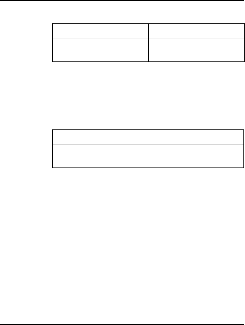
NTCK16 Generic Central Office Trunk cards Page 797 of 906
Circuit Card Description and Installation
Pad switching
The NTCK16AX and NTCK16BX generic Central Office trunk cards
support the North American loss plan. Software configuration allows the
selection of 4 dB loss pads on a per unit basis.
Note: The tolerance for the above nominal values is +0.3 dB, -0.7 dB.
Connector pin assignments
Cross connections
Figure 167 on page 798, Figure 168 on page 799, and Figure 169 on
page 800 provide cross connect information for the NTCK16AX and
NTCK16BX generic Central Office trunk cards.
Configuration
The trunk type for each unit on the card is selected by software service change
entries at the system terminal.
Storage temperature –20 to +60 degrees C
Storage humidity 5 to 95% Relative Humidity
Table 258
NTCK16 pad switching
Loss Analog-to-Digital Digital-to-Analog
PAD out 0 dB –3 dB
PAD in +4 dB +1 dB
Table 257
NTCK16 circuit card environmental specifications (Part 2 of 2)
Parameter Specifications
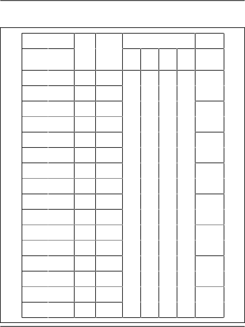
Page 798 of 906 NTCK16 Generic Central Office Trunk cards
553-3001-211 Standard 3.00 August 2005
Figure 167
NTCK16 Central Office trunk connections for NT8D37 I/O panel connectors A, E, K, R
Pins Pair
Color
I/O Panel Connector Unit
Number
AEKR
26
1
W-BL
BL-W Unit
27
2
W-O
O-W
0
28
3
W-G
G-W Unit
29
4
W-BR
BR-W
1
30
5
W-S
S-W
S
L
S
L
S
L
S
L Unit
31
6
R-BL
BL-R
O
T
O
T
O
T
O
T
2
32
7
R-O
O-R 0 4 8 12 Unit
33
8
R-G
G-R
3
34
9
R-BR
BR-R Unit
35
10
R-S
S-R
4
36
11
BK-BL
BL-BK Unit
37
12
BK-O
O-BK
5
38
13
BK-G
G-BK Unit
39
14
BK-BR
BR-BK
6
T0
R0
T1
R1
T2
R2
T3
R3
T4
R4
T5
R5
T6
R6
T7
R7
40
15
BK-S
S-BK Unit
41
16
Y-BL
BL-Y
7
Lead designations
COT

NTCK16 Generic Central Office Trunk cards Page 799 of 906
Circuit Card Description and Installation
Figure 168
NTCK16 Central Office trunk connections for NT8D37 I/O panel connectors B, F, L, S
Pins Pair
Color
I/O P anel Connector Unit
Number
BFLS
26
1
W-BL
BL-W Unit
27
2
W-O
O-W
0
28
3
W-G
G-W Unit
29
4
W-BR
BR-W
1
30
5
W-S
S-W
S
L
S
L
S
L
S
L Unit
31
6
R-BL
BL-R
O
T
O
T
O
T
O
T
2
32
7
R-O
O-R 1 5 9 13 Unit
33
8
R-G
G-R
3
34
9
R-BR
BR-R Unit
35
10
R-S
S-R
4
36
11
BK-BL
BL-BK Unit
37
12
BK-O
O-BK
5
38
13
BK-G
G-BK Unit
39
14
BK-BR
BR-BK
6
40
15
BK-S
S-BK Unit
41
16
Y-BL
BL-Y
7
42
17
Y-O
O-Y Unit
43
18
Y-G
G-Y
0
44
19
Y-BR
BR-Y SSSS Unit
45
20
Y-S
S-Y
L
O
L
O
L
O
L
O
1
46
21
V-BL
BL-V
TTTT
Unit
47
22
V-O
O-V
2 6 10 14 2
T0
R0
T1
R1
T2
R2
T3
R3
T4
R4
T5
R5
T6
R6
T7
R7
T0
R0
T1
R1
T2
R2
T3
R3
48
23
V-G
G-V Unit
49
24
V-BR
BR-V
3
Lead designations
COT

Page 800 of 906 NTCK16 Generic Central Office Trunk cards
553-3001-211 Standard 3.00 August 2005
Figure 169
NTCK16 Central Office trunk connections for NT8D37 I/O panel connectors C, G, M, T
Pins Pair
Color
I/O P anel Connector Unit
Number
CG M T
26
1
W-BL
BL-W Unit
27
2
W-O
O-W
4
28
3
W-G
G-W S S S S Unit
29
4
W-BR
BR-W
L
O
L
O
L
O
L
O
5
30
5
W-S
S-W
TTTT
Unit
31
6
R-BL
BL-R
2 6 10 14 6
32
7
R-O
O-R Unit
33
8
R-G
G-R
7
34
9
R-BR
BR-R Unit
35
10
R-S
S-R
0
36
11
BK-BL
BL-BK Unit
37
12
BK-O
O-BK
1
38
13
BK-G
G-BK Unit
39
14
BK-BR
BR-BK
2
40
15
BK-S
S-BK S S S S Unit
41
16
Y-BL
BL-Y
L
O
L
O
L
O
L
O
3
42
17
Y-O
O-Y
TTTT
Unit
43
18
Y-G
G-Y
3 7 11 15 4
44
19
Y-BR
BR-Y Unit
45
20
Y-S
S-Y
5
46
21
V-BL
BL-V Unit
47
22
V-O
O-V
6
T4
R4
T5
R5
T6
R6
T7
R7
T0
R0
T1
R1
T2
R2
T3
R3
T4
R4
T5
R5
T6
R6
T7
R7
48
23
V-G
G-V Unit
49
24
V-BR
BR-V
7
Lead designations
COT

NTCK16 Generic Central Office Trunk cards Page 801 of 906
Circuit Card Description and Installation
NTCK16AX Central Office trunk card
Route Data Block
Respond to the prompts in LD 16 as shown.
LD 16 – Route Data Block for NTCK16AX.
Prompt Response Description
REQ: NEW Define a new unit
TYPE: COT Define a new Route Data Block
CUST xx Customer number as defined in LD 15.
ROUT Route number
0-511 Range for Large System, Call Server 1000E,
and Media Gateway 1000E
0-127 Range for Small System, CS 1000S system,
Media Gateway 1000B, and
Media Gateway 1000T
TKTP COT Define trunk type as Central Office
ICOG IAO Incoming and Outgoing trunk
CNTL YES Change a trunk timer
TIMER RGV 256 Set Ring Validation Timer to 128 ms.
MR (NO) PPM XLD PPM is off, buffered, or unbuffered on this route.

Page 802 of 906 NTCK16 Generic Central Office Trunk cards
553-3001-211 Standard 3.00 August 2005
Trunk Data Block
Respond to the prompts in LD 14 as shown:
LD 14 – Trunk Data Block for NTCK16AX. (Part 1 of 2)
Prompt Response Description
REQ: NEW Define a new trunk unit
TYPE: COT Central Office Trunk
TN Terminal Number
l s c u Format for Large System, Call Server 1000E,
and Media Gateway 1000E, where l = loop,
s = shelf, c = card, u = unit
XTRK
(See note on
page 803.)
XCOT Type is IPE COT
CDEN (8D) Card density is 8D (default)
SIGL LOP Loop start signaling
PPID
(See page 803.)
Xx 04 Ireland/Turkey 12 KHz
03 Turkey 16 KHz
BTID
(See page 803.)
Xx Enter the country busy tone ID:
Tortola, Brazil = 10
Mexico = 10 or 08 (depending on CO)
Singapore = 11
Ireland = 3 or 9 (depending on CO) Chile,
Venezuela, Thailand, Korea = 06. Argentina =
12 or 07, Turkey = 14
SUPN (NO) YES Supervision yes (no)
STYP BTS
BAT
Busy tone supervision enabled
Loop break supervision enabled

NTCK16 Generic Central Office Trunk cards Page 803 of 906
Circuit Card Description and Installation
Note: These prompts are required only for the first unit defined on each
NTCK16AX card.
PPIDFreqMin pulse detection
03 16Kz>70ms
04 12Kz>70ms
CountryBTIDCadence
Brazil, Tortola10250 ms +/- 50 ms on/off
Mexico10250 ms +/- 50 ms on/off
Mexico 8375 ms on/off
Singapore11750 ms on/off
Ireland 3500 +/- 50 ms on/off
Ireland 9375 - 750 ms on/off
Kuwait, Chile 6500 +/- 50 ms on/off
Venezuela, Indonesia12300 ms on, 200 ms off
Thailand, Korea12300 ms on, 200 ms off
Argentina12300 ms on, 200 ms off
Argentina07250 - 500 ms on/off
Turkey1410 seconds of Tone 1:
200 ms off, 200 ms on; 200 ms off,
200 ms on; 200 ms off, 200 ms on;
200 ms off, 600 ms on; followed by
Tone 2: 200 ms off, 200 ms on.
CLS (LOL) SHL Attenuation Pads In, (Out)
DTN, (DIP) Digitone signaling, (digipulse)
P20, P12, (P10) Make-break ratio for pulse dialing speed.
LD 14 – Trunk Data Block for NTCK16AX. (Part 2 of 2)
Prompt Response Description

Page 804 of 906 NTCK16 Generic Central Office Trunk cards
553-3001-211 Standard 3.00 August 2005
NTCK16BX Central Office trunk card
Route Data Block
Respond to the prompts in LD 16 as shown:
LD 16 – Route Data Block for NTCK16BX.
Prompt Response Description
REQ: NEW Define a new unit.
TYPE: COT Define a new Route Data Block.
CUST xx Customer number as defined in LD 15.
ROUT Route number
0-511 Range for Large System, Call Server 1000E, and
Media Gateway 1000E
0-127 Range for Small System, CS 1000S system,
Media Gateway 1000B, and Media Gateway 1000T
TKTP COT Define trunk type as Central Office.
ICOG IAO Incoming and Outgoing trunk
CNTL YES Change a trunk timer.
TIMER RGV 256 Set Ring Validation Timer to 128 ms.
MR (NO) PPM is off on this route.

NTCK16 Generic Central Office Trunk cards Page 805 of 906
Circuit Card Description and Installation
Trunk Data Block
Respond to the prompts in LD 14 as shown:
LD 14 – Trunk Data Block for NTCK16BX. (Part 1 of 2)
Prompt Response Description
REQ: NEW Define a new trunk unit.
TYPE: COT Central Office Trunk
TN Terminal Number
l s c u Format for Large System, Call Server 1000E,
and Media Gateway 1000E, where l = loop,
s = shelf, c = card, u = unit
XTRK
(See note 1 on
page 806.)
XCOT Type is IPE COT
CDEN (8D) Card density is 8D (default).
SIGL LOP Loop start signaling
BTID
(See page 807.)
Xx Enter the country busy tone ID:
Tortola, Brazil = 10
Mexico = 10 or 08 (depending on CO)
Singapore = 11
Ireland = 3 or 9 (depending on CO) Kuwait,
Chile, Venezuela, Indonesia, Thailand,
Korea = 06. Argentina = 12 or 07, Turkey = 14
SUPN (NO) YES Supervision yes (no)
STYP BTS
BAT
Busy tone supervision enabled
Loop break supervision enabled
CLS (LOL) SHL Attenuation Pads In, (Out)

Page 806 of 906 NTCK16 Generic Central Office Trunk cards
553-3001-211 Standard 3.00 August 2005
Note 1: These prompts are required only for the first unit defined on
each NTCK16BX card.
(DIP) DTN Digitone signaling, (digipulse)
(P10) P12 P20 Make-break ratio for pulse dialing speed.
LD 14 – Trunk Data Block for NTCK16BX. (Part 2 of 2)
Prompt Response Description

NTCK16 Generic Central Office Trunk cards Page 807 of 906
Circuit Card Description and Installation
BTID values by country
Country BTIDCadence
Brazil Tortola10250 ms +/- 50 ms on/off
Mexico 10 250 ms +/- 50 ms on/off
Mexico 8 375 ms on/off
Singapore11 750 ms on/off
Ireland 3 500 +/- 50 ms on/off
Ireland 9 375 - 750 ms on/off
Kuwait, Chile 6500 +/- 50 ms on/off
Venezuela, Indonesia12300 ms on, 200 ms off
Thailand, Korea12300 ms on, 200 ms off
Argentina12 300 ms on, 200 ms off
Argentina07 250 - 500 ms on/off
Turkey 14 10 seconds of Tone 1:
200 ms off, 200 ms on; 200 ms off,
200 ms on; 200 ms off, 200 ms on;
200 ms off, 600 ms on; followed by
Tone 2: 200 ms off, 200 ms on.
Applications
Periodic Pulse Metering
All trunk units on the NTCK16AX trunk card can be individually configured
to support the Periodic Pulse Metering (PPM) feature.
Note: PPM is available on the NTCK16AX trunk card. It is not
supported on the NTCK16BX trunk card.
PPM allows the user of a telephone to keep an accurate record of Central
Office calls for billing or administration purposes.

Page 808 of 906 NTCK16 Generic Central Office Trunk cards
553-3001-211 Standard 3.00 August 2005
Detection limits
Pulses detected by the NTCK16AX circuit card must be within the following
limits:
Busy tone detect
Busy tone is sent by the Central Office to indicate the release of an established
call.
Detection limits
The NTCK16AX and NTCK16BX generic Central Office trunk cards can
detect busy tone within the following limits:
Loss switching
The Generic XFCOT is based on the XFCOT design, which is using a static
pad download algorithm by default for its loss plan.
The generic XFCOT has to be set explicitly to a Dynamic Pad Switching
mode to make it compliant with the standard North American Dynamic Pad
Switching mode.
Frequency 11 880 to 12 120 Hz
Level 105 to 1100 mVrms
Note: The pack should not be
used to detect levels of 1100
mVrms or greater a Tip and Ring,
as this may result in noise.
Pulse length Dependent on PPID – see LD 14
Frequency 400 to 620 Hz
Level –30 to 0 dBm
Cadence See on page 803.

NTCK16 Generic Central Office Trunk cards Page 809 of 906
Circuit Card Description and Installation
Therefore the following steps must be followed when the Generic XFCOT is
installed:
1Define Loss Switching mode. Respond to the prompts in LD 97 as shown.
2Define Loss Switching Class Of Service. Respond to the prompts in LD 14
as shown.
LD 97 – Defining Loss Switching mode.
Prompt Response Description
REQ: CHG
TYPE: SYSP IPE system parameters configuration
...
NATP YES Select North American transmission plan.
Note: The default to the NATP prompt is NO, and
therefore this prompt must always be checked during
installation.
LD 14 – Defining Loss Switching Class Of Service.
Prompt Response Description
REQ: CHG
TYPE: COT
XTRK XCOT
SIGL LOP
...
CLS LOL LOL= Long Line
Note: The XFCOT uses the CLS Long Line (LOL) and
Short Line (SHL) for Loss Switching purposes and that
the card and trunk type is different from the XUT.

Page 810 of 906 NTCK16 Generic Central Office Trunk cards
553-3001-211 Standard 3.00 August 2005
Equivalencies
The following equivalencies do apply:
• XFCOT COT SHL is equivalent with XUT COT TRC
• XFCOT COT LOL is equivalent with XUT COT NTC.
The entries TRC and NTC will no longer be allowed for the Generic XFCOT.
Trunk to Trunk connection
When any disconnect supervision is configured (CLS = BAT, BTS) the Loop
Start Trunk of the Generic XFCOT will be marked as having disconnect
supervision and will therefore follow the same rules as a Ground Start Trunk.
There is no configuration involved for this operation.
Call disconnect
When any disconnect supervision is configured (CLS = BAT, BTS) the Loop
Start Trunk will be released when the disconnect signal is received. This will
apply also in call states such as ringing, camp-on, DISA, and Meridian Mail.
There is no configuration involved for this operation.

Page 811 of 906
Circuit Card Description and Installation
824
NTDK20 Small System
Controller card
Contents
This section contains information on the following topics:
Introduction . . . . . . . . . . . . . . . . . . . . . . . . . . . . . . . . . . . . . . . . . . . . . . 811
Memory . . . . . . . . . . . . . . . . . . . . . . . . . . . . . . . . . . . . . . . . . . . . . . . . . 814
100BaseT IP daughterboards . . . . . . . . . . . . . . . . . . . . . . . . . . . . . . . . 815
PC card interface . . . . . . . . . . . . . . . . . . . . . . . . . . . . . . . . . . . . . . . . . . 818
Security device . . . . . . . . . . . . . . . . . . . . . . . . . . . . . . . . . . . . . . . . . . . 819
SDI ports . . . . . . . . . . . . . . . . . . . . . . . . . . . . . . . . . . . . . . . . . . . . . . . . 820
Conferencing . . . . . . . . . . . . . . . . . . . . . . . . . . . . . . . . . . . . . . . . . . . . . 820
MG 1000S/Expansion card slot assignment . . . . . . . . . . . . . . . . . . . . . 821
Introduction
This chapter introduces the NTDK20GA Small System Controller (SSC)
Card used in the Call Server, MG 1000S, and Media Gateway 1000B
(MG 1000B). It controls call processing, stores system and customer data,
and provides various 100BaseT IP interfaces.
You can install this card in slots 1 through 4 in the MG 1000S or slots 7
through 10 in the MG 1000S Expansion
The NTDK20FA SSC card is the minimum vintage of SSC that can be used
in the Call Server and MG 1000S. See Figure 170 on page 813.

Page 812 of 906 NTDK20 Small System Controller card
553-3001-211 Standard 3.00 August 2005
The NTDK20GA SSC card has the following components and features:
• NTTK25 daughterboard Flash memory, NTAK19 SIMM module
(16 MB) DRAM, and Backup memory
Note: The NTTK13 daughterboard is still supported.
• up to two 100BaseT IP daughterboards
• two PCMCIA sockets
• three Serial Data Interface (SDI) ports
• 32 channels of Conferencing (64 if one dual-port 100BaseT IP
daughterboard is present, or 96 if two dual-port 100BaseT IP
daughterboards are present)
• one 10BaseT port
• 30 channels of Tone and Digit Switch (TDS) and a combination of eight
Digitone Receivers (DTR) or Extended Tone Detectors (XTD)
• additional tone service ports (four units of MFC/MFE/MFK5/MFK6/
MFR or eight DTR/XTD units)
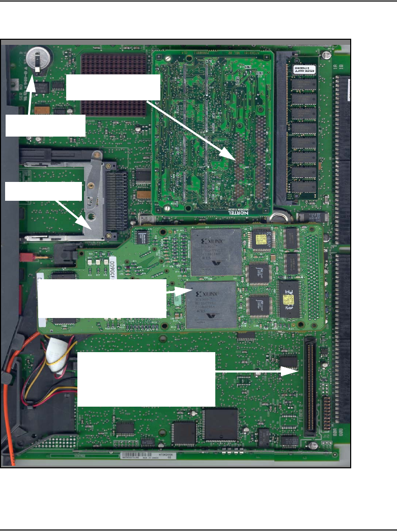
NTDK20 Small System Controller card Page 813 of 906
Circuit Card Description and Installation
Figure 170
NTDK20 SSC card and expansion daughterboard in the Call Server
Ports 1 & 3 for
100BaseT daughterboard
Flash ROM Drive
PCMCIA Drive
Connector for 2nd
100BaseT daughterboard.
MG 1000S systems 1 and 3
Ports 2 and 4 for Media
Gateways 2 and 4
Security Device

Page 814 of 906 NTDK20 Small System Controller card
553-3001-211 Standard 3.00 August 2005
Memory
The majority of system and customer configured data is both controlled and
stored on the NTDK20 SSC card’s Flash ROM. An active and backup copy
of customer data is also kept on the Flash ROM.
In the event of data loss, the NTDK20 SSC card also retains a copy of
customer files in an area called the Backup flash drive. The NTDK20 SSC
card is equipped with 8MB of temporary memory space called DRAM.
DRAM functions much like RAM on a computer system. It stores and
processes temporary automated routines and user-programmed commands
while the system is running. The DRAM on the SSC card stores operating
system files, user files, overlay data, patch codes, and the active copy of the
customer database.
The NTDK20 SSC card’s Flash daughterboard is the NTTK25. It performs
most of the system software storage and data processing.
NTTK25 daughterboard
The NTTK25 is a 48 MB daughterboard comprised of Flash ROM and
Primary Flash drive. It is required in the Call Server and MG 1000S.
The Flash ROM holds 32 MB of ROM memory, comprising operating system
data and overlay programs. Flash ROM is expandable using an expansion
flash daughterboard.
The Primary Flash drive contains 16 MB of storage space. Most of the data
storage is allocated to the Primary Flash drive – the main storage area of
customer configured data.
Other system data such as the Secure Storage Area (SSA) also resides in the
Flash drive. The SSA holds data that must survive power interruptions.
The Boot ROM is a 2 MB storage device located on the NTDK20 SSC card.
The Boot ROM contains the boot code, system data, patch data, and the
backup copy of the Primary Flash drive’s customer database.

NTDK20 Small System Controller card Page 815 of 906
Circuit Card Description and Installation
100BaseT IP daughterboards
A 100BaseT IP Daughterboard mounted on the NTDK20 SSC card enables
the connection of the Call Server to a MG 1000S. See Figure 170 on
page 813.
Each daughterboard increases the number of conference channels by 32. The
maximum number of conference ports is 96. Table 259 on page 817 provides
the ports, cables, and connection data on the IP daughterboards.
The NTDK83 (dual-port) 100BaseT IP daughterboard mounts on the
NTDK20 SSC card in the Call Server. It provides connectivity to two
MG 1000S systems and their associated MG 1000S Expansions.
Note: With a point-to-point connection, the MG 1000S must be within
100 meters of the Call Server.
An optional second NTDK83 daughterboard can be mounted on the NTDK20
SSC card in the Call Server. Adding the second NTDK83 daughterboard
provides support for up to four MG 1000S systems. See Figure 171 on
page 816.
The NTDK99AA (single-port) daughterboard is mounted on the NTDK20
SSC card in the MG 1000S to provide connectivity to the Call Server. See
Figure 172 on page 816.
Note: Third party media conversion devices can be used to extend the
range of MG 1000S systems from the Call Server. The IMC Networks
Ethernet Compatible Media Converter with a McLIM Tx/Fx-SM/Plus
module was tested by Nortel. It provided acceptable transmission
between the Call Server and the MG 1000S located up to 40 kms apart.
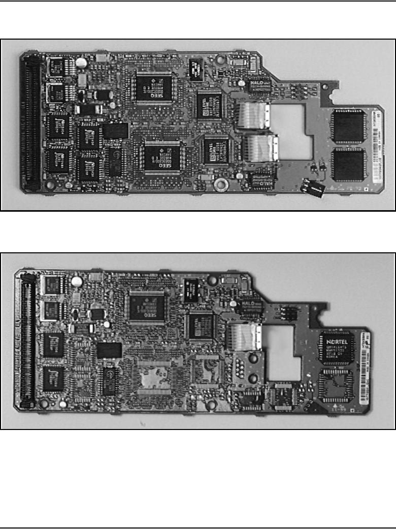

NTDK20 Small System Controller card Page 817 of 906
Circuit Card Description and Installation
Note: If not connecting point-to-point, connect the Call Server and
MG 1000S using a straight-through Ethernet UTP Cat 5 cable.
Call Servers can be connected to MG 1000S systems in the following ways:
• Use 100BaseT to connect to the LAN for voice distribution over a data
network.
• Use 100BaseT cable if connected point-to-point (directly) to the
MG 1000S. The NTTK34AA crossover cable must be used. MG 1000S
systems can be located up to 100 meters from the Call Server.
• Use Media Conversion devices (third party converters) to convert
100BaseT to fiber for distances from 100 m to 40 km.
See Figure 173 on page 818.
Table 259
Expansion daughterboards
Daughterboard
Number
of ports Cable type
Max. distance between Call
Server and MG 1000S
systems
NTDK99 (used in
MG 1000S)
one Use the supplied
NTTK34AA UTP CAT 5
RJ-45 2 m cross-over
cable to connect the
Call Server and
MG 1000S using the
100BaseT
daughterboards.
The NTTK34AA
cross-over cable must
be used if connecting
point-to-point.
MG 1000S systems can be
located up to 100 m (328 ft.)
from the Call Server if
connected point-to-point, or
up to 40 km (24 miles) from
the Call Server if a third party
converter is used to convert to
fiber.
NTDK83 (used in
Call Server
two
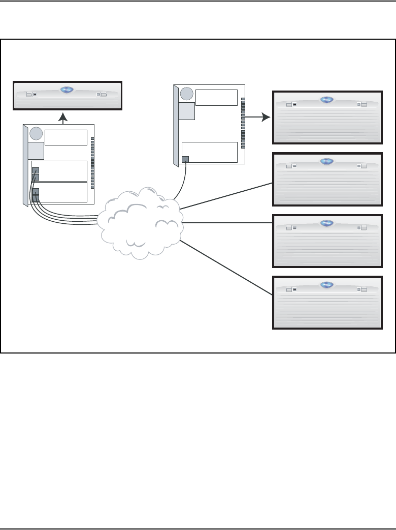
Page 818 of 906 NTDK20 Small System Controller card
553-3001-211 Standard 3.00 August 2005
Figure 173
Call Server connection to Media Gateway 1000S systems
For further information or installation instructions, refer to the
Communication Server 1000S: Installation and Configuration
(553-3031-210).
PC card interface
The NTDK20 SSC card has a PC card interface through a socket located on
its faceplate. The PC card socket can accommodate a Software Delivery card
used for software upgrading and as backup media.
Software
Daughterboard
Single Port
100BaseT
Daughterboard
Software
Daughterboard
Dual Port
100BaseT
Daughterboard
Dual Port
100BaseT
Daughterboard
553-AAA1990
Call Server connection to Media Gateway 1000S
LAN
Call Server Media Gateway 1000S
• The Call Server connects to the LAN via dual port daughterboards.
• One 100BaseT connection is required for each Media Gateway 1000.
• Each Media Gateway 1000 contains an SSC with a single port IP
daughterboard and a software daughterboard.
• The single port IP daughterboard conncets to the LAN via 100BaseT.

NTDK20 Small System Controller card Page 819 of 906
Circuit Card Description and Installation
Security device
The NTDK20 SSC card in each MG 1000S must contain a NTDK57DA
Security device, a remote dongle (NT_Rem) which is keyed to match the
NTDK57AA Security device on the Call Server and a standard dongle
(NT_STD). This maintains the requirement of a single keycode for each
system. Refer to Figure 170 on page 813 for the location of the device.
This security scheme provides the following:
• enables the system to operate as a single system when all links are up.
• enables the MG 1000S to continue operating with its existing
configuration in the event of a failure of the Call Server, or the failure of
the link to the Call Server from the MG 1000S.
• prevents users from configuring or using unauthorized TNs or features.
The MG 1000S security device provides the following capabilities for the
MG 1000S:
• System software can be installed but no calls can be processed or features
activated until communication with the Call Server has been established
and a match between the security ID of the Call Server and the
MG 1000S has been confirmed.
• System software can be upgraded.
Note: Local data dump, LD 43 commands, and LD 143 commands are
not permitted.

Page 820 of 906 NTDK20 Small System Controller card
553-3001-211 Standard 3.00 August 2005
SDI ports
The NTDK20 SSC card in both the Call Server and the MG 1000S systems
contains three SDI ports used to connect on-site terminals or remote terminals
through a modem. Table 260 shows the port default settings.
Conferencing
Thirty-two conference channels are provided by the NTDK20 SSC card’s
conference devices. Conference capability can be increased by mounting
expansion daughterboards on the NTDK20 SSC card. Each dual IP
daughterboard increases the total number of conference channels by 32. The
maximum number of conference ports is 96.
Each conference device provides 32 ports of conferencing capabilities (one
conference participant for each port). A conference call can have three to six
participants. For example, there could be six 5-party conferences on each
device, or four 6-party conferences plus two 3-party conferences. It is not
possible to conference between conference devices.
10BaseT port
The Call Server provides one 10BaseT connection to a Local Area Network
(LAN) to interface with Management software applications such as OTM and
CallPilot. The MG 1000S SSC 10BaseT port, Port 1, is disabled by default.
To use the 10BaseT port, the port must be assigned a unique IP address and
the port must be enabled from the Call Server.
Table 260
Default SDI port settings on the NTDK20 SSC card
TTY Port Baud rate Data bits Stop bits Parity Use
0Set by a DIP
switch
8 1 None MTC/SCH/
BUG
11200 8 1 None MTC/SCH/
BUG
21200 8 1 None MTC/SCH/
BUG

NTDK20 Small System Controller card Page 821 of 906
Circuit Card Description and Installation
The MG 1000S 10BaseT port can run in Normal mode or Survival mode. In
Normal mode, the MG 1000S does not provide access to maintenance or
alarm management.
External connections to the 10BaseT port are provided by a 15-pin connector
located on the backplanes of the Call Server and MG 1000S systems.
MG 1000S/Expansion card slot assignment
The MG 1000S and MG 1000S Expansion contain physical card slots,
numbered 1 to 10. See Figure 174 on page 823 and Figure 175 on page 824.
When configuring the system, the physical card slot numbers must be
transposed to “logical” card slot numbers. For example, to configure a card
physically located in Slot 2 of the first MG 1000S, use logical Slot 12. To
configure a card physically located in Slot 2 of the second MG 1000S, use
logical Slot 22. See Table 261 on page 822.

Page 822 of 906 NTDK20 Small System Controller card
553-3001-211 Standard 3.00 August 2005
Table 261
MG 1000S and MG 1000S Expansion slot assignments
MG 1000S/MG 1000S Expansion
First Second Third Fourth
Physical
card
slot
Logical
card
slot
Physical
card
slot
Logical
card
slot
Physical
card
slot
Logical
card
slot
Physical
card
slot
Logical
card
slot
MG 1000S
111 121 131 141
212 222 232 242
313 323 333 343
414 424 434 444
5 * 5 * 5 * 5 *
6 * 6 * 6 * 6 *
MG 1000S/
Expansion
717 727 737 747
818 828 838 848
919 929 939 949
10 20 10 30 10 40 10 50
Legend
* Not supported.
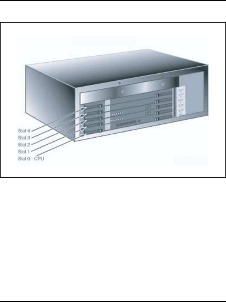
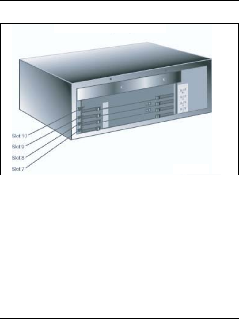

Page 825 of 906
Circuit Card Description and Installation
838
NTRB21 DTI/PRI/DCH TMDI card
Contents
This section contains information on the following topics:
Introduction . . . . . . . . . . . . . . . . . . . . . . . . . . . . . . . . . . . . . . . . . . . . . . 825
Physical description. . . . . . . . . . . . . . . . . . . . . . . . . . . . . . . . . . . . . . . . 826
Functional description . . . . . . . . . . . . . . . . . . . . . . . . . . . . . . . . . . . . . . 830
Software description . . . . . . . . . . . . . . . . . . . . . . . . . . . . . . . . . . . . . . . 831
Hardware description . . . . . . . . . . . . . . . . . . . . . . . . . . . . . . . . . . . . . . 831
Architecture. . . . . . . . . . . . . . . . . . . . . . . . . . . . . . . . . . . . . . . . . . . . . . 831
Introduction
The NTRB21 (DTI/PRI/DCH) TMDI digital trunk card is a 1.5 Mb DTI or
PRI interface to the CS 1000S, CS 1000M Cabinet, and Meridian 1 PBX 11C
Cabinet. The NTRB21 card has a built-in downloadable D-channel.
The TMDI feature supports the software changes required for CS 1000S,
CS 1000M Cabinet, and Meridian 1 PBX 11C Cabinet to use the new TDMI
pack. The software changes include:
• a new prompt to replace a function that was handled by a dip switch on
the NTAK09
• an extra loadware application to handle Layer 1
• a change to the existing loadware files into 32 bit format from the
original 16 bit format

Page 826 of 906 NTRB21 DTI/PRI/DCH TMDI card
553-3001-211 Standard 3.00 August 2005
To provide CEMUX communication with the card, changes are also required
to create an I/O entry for the card.
You can install this card in slots 1 through 4 in the MG 1000S. The card is not
supported in the MG 1000S Expansion. Up to four digital trunks are
supported in each MG 1000S.
Note 1: For CISPR B group cabinets, the active Clock Controller
(NTAK20) can only occupy slots 1-3. For FCC and/or CISPR A group
cabinets, this limitation does not exist - the Clock Controller can occupy
any available slot 1-9.
Note 2: On non-ECM system cabinets, the NTAK20 may be placed in
slots 1-9. On cabinets NTAK11Dx and NTAK11Fx, the active NTAK20
must be placed in slots 1-3 (slots 4-10 may not be used).
Physical description
The NTRB21 card uses a standard 9.5" by 12.5" multi-layer printed circuit
board with buried power and ground layers.The clock controller
daughterboard is fastened by standoffs and connectors.
The NTRB21 card has seven faceplate LEDs. The first five LEDs are
associated with the NTRB21 card. The remaining two LEDs are associated
with the clock controller and DCHI daughterboards. See Figure 176.
IMPORTANT!
Each MG 1000S that has a digital trunk must have a clock controller
clocked to an external reference clock.
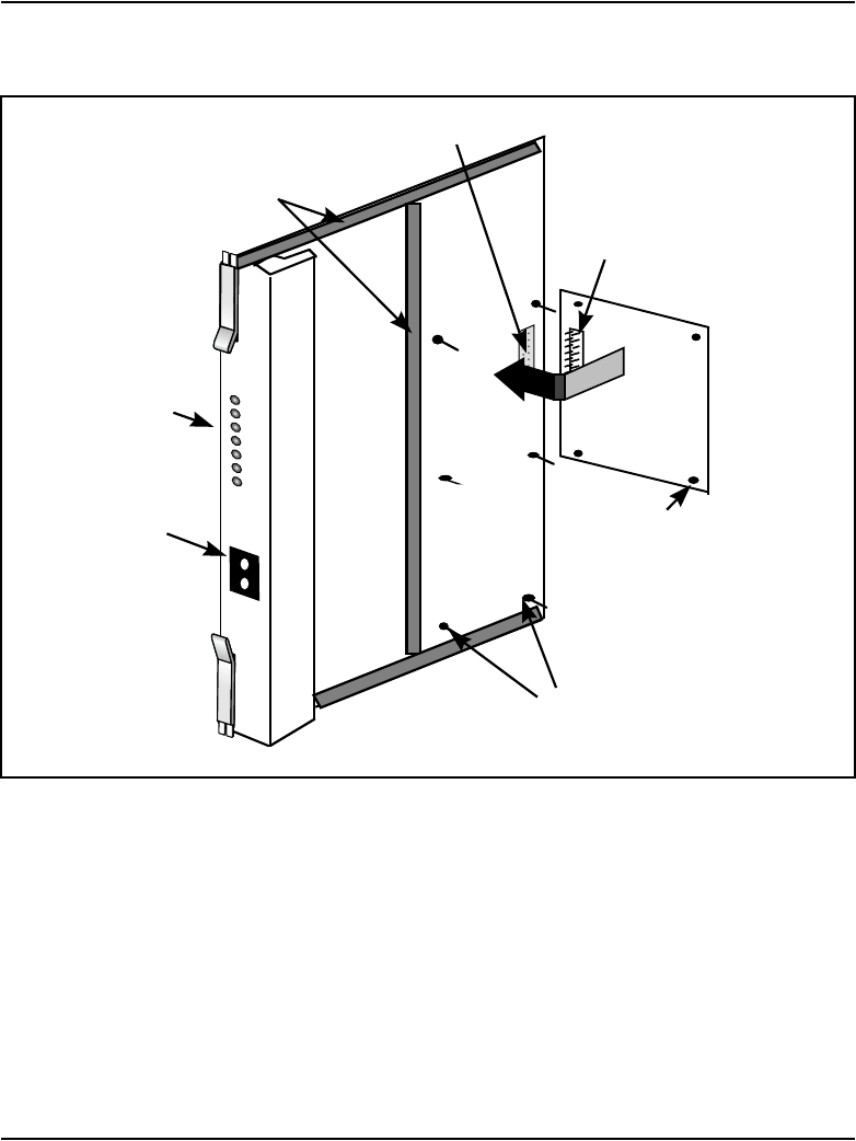
NTRB21 DTI/PRI/DCH TMDI card Page 827 of 906
Circuit Card Description and Installation
Figure 176
NTRB21 TMDI card with clock controller
OOS
ACT
RED
YEL
LBK
CC
DCH
RCV
XMT
NTRB21
TMDI
SW
ON
1 2 3 4
DCH F/W
LEN 0
LEN 1
Len 2
553-CSE9024
Stiffeners
NTAK93/51
Clock
Controller
Mounting Holes
Connector Socket
Connector Pins
LEDs
Bantam
Jacks
Standoffs

Page 828 of 906 NTRB21 DTI/PRI/DCH TMDI card
553-3001-211 Standard 3.00 August 2005
In general, the first five LEDs operate as follows:
• During system power up, the LEDs are on.
• When the self-test is in progress, the LEDs flash on and off three times,
then go into their appropriate states, as shown in Table 262.
Figure 177 on page 829 shows the faceplate of the NTRB21 TMDI card.
Power requirements
The DTI/PRI obtains its power from the backplane, and draws less than
2 amps on +5 V, 50 mA on +12 V, and 50 mA on –12 V.
Table 262
NTRB21 LED states
LED State Definition
DIS On (Red) The NTRB21 circuit card is disabled.
Off The NTRB21 is not in a disabled state.
ACT On (Green) The NTRB21 circuit card is in an active state. No alarm states
exist, the card is not disabled, nor is it in a loopback state.
Off An alarm state or loopback state exists, or the card has been
disabled. See the other faceplate LEDs for more information.
RED On (Red) A red-alarm state has been detected.
Off No red alarm.
YEL On (Yellow) A yellow alarm state has been detected.
Off No yellow alarm.
LBK On (Green) NTRB21 is in loop-back mode.
Off NTRB21 is not in loop-back mode.
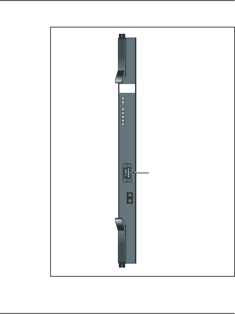

Page 830 of 906 NTRB21 DTI/PRI/DCH TMDI card
553-3001-211 Standard 3.00 August 2005
Foreign and surge voltage protection
Lightning protectors must be installed between an external T1 carrier facility
and the system. For public T1 facilities, this protection is provided by the
local operating company. In a private T1 facility environment (a campus, for
example), the NTAK92 protection assembly can be used.
The NTRB21 circuit card conforms to safety and performance standards for
foreign and surge voltage protection in an internal environment.
Functional description
NTRB21 provides the following features and functions:
• configurable parameters, including A-Law and µ-Law operation, digital
pads on a per channel basis, and Superframe or Extended Superframe
formats
• AMI or B8ZS line coding
• 1.5 Mb Digital Trunk Interface and 1.5 Mb Primary Rate Interface
• 1.5 Mb Clock recovery and distribution of reference clocks
• DG2 or FDL yellow alarm methods
• card status and alarm indication with faceplate-mounted LED
• automatic alarm monitoring and handling
• Card-LAN for maintenance communication
• loopback capabilities for both near-end and far-end
• echo canceler interface
• integrated trunk access (both D-channel and in-band A/B signaling can
be mixed on the same PRI)
• faceplate monitor jacks for T1 interface
• configurable D-channel data rate with 64 kbps, 56 kbps or
64 kbps inverted
•self-test

NTRB21 DTI/PRI/DCH TMDI card Page 831 of 906
Circuit Card Description and Installation
Software description
Changes from the NTAK09 are required for the new trunk card and License
parameters are n service change and maintenance overlays. There is a change
to CardLAN to introduce a new CardLAN ID. The download of PSDL data
is also changed to handle a 32 bit download as well as existing 16 bit.
Hardware description
NTRB21 TMDI card
The NTRB21 TMDI card provides 1.5 MBits Digital Trunk Interface or
Primary Rate Interface functionality. It also has a built-in downloadable
D-channel.
The NTRB21 can be used with the NTAK09 DTI/PRI card (with the
NTBK51 downloadable D-channel daughterboard).
Figure 178 on page 832 shows a faceplate of the NTRB21 TMDI card.
Architecture
Signaling interface
The signaling interface performs an 8 Kbps signaling for all 24 channels and
interfaces directly to the DS-30X link. Messages transmitted in both
directions are three bytes long.
Interconnection
The interconnection to the carrier is by NTBK04, a 1.5 Mb 20 ft. carrier cable.
The NT8D97AX, a fifty-foot extension cable, is also available.
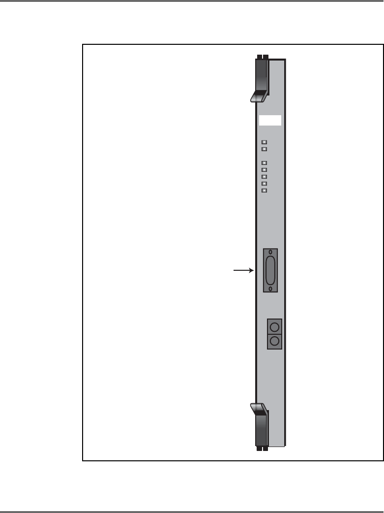

NTRB21 DTI/PRI/DCH TMDI card Page 833 of 906
Circuit Card Description and Installation
Microprocessor
The NTRB21 is equipped with bit-slice microprocessors that handle the
following major tasks:
• Task handler: also referred to as an executive. The task handler provides
orderly per-channel task execution to maintain real-time task ordering
constraints.
• Transmit voice: inserts digital pads, manipulates transmit AB bits for
DS1, and provides graceful entry into T-Link data mode when the data
module connected to the DTI/PRI trunk is answering the call.
• Receive voice: inserts digital pads and provides graceful entry into
T-Link data mode when the data module connected to the DTI/PRI trunk
is originating the call.
• T-Link data: a set of transmit and receive vectored subroutines which
provides T-Link protocol conversion to and from the DM-DM protocol.
• Receive ABCD filtering: filters and debounces the receive ABCD bits
and provides change of state information to the system.
• Diagnostics
•Self-test
Digital pad
The digital pad is an EPROM whose address-input to data-output transfer
function meets the characteristics of a digital attenuator. The digital pad
accommodates both µ255-Law and A-Law coding. There are 32
combinations each for µ255 to µ255, µ255 to A-Law, A-Law to µ255, and
A-Law to A-Law. These values are selected to meet the EIA loss and level
plan.

Page 834 of 906 NTRB21 DTI/PRI/DCH TMDI card
553-3001-211 Standard 3.00 August 2005
D-channel interface
The D-channel interface is a 64 kbps, full-duplex, serial bit-stream configured
as a Data Circuit-terminating Equipment (DCE) device. The data signals
include:
• receive data output
• transmit data input
Table 263
Digital pad values and offset allocations
Offset PAD set 0 PAD set 1
0 0dB –7db
1 2dB –8db
2 3dB –9db
3 4dB –10db
4 5dB 0.6db
5 6.1dB 7db
6 8dB 9db
7 –1dB 10db
8 –3dB 11db
9 –4dB 12db
A idle code, 7F 3db
B unassigned code, FF 14db
C 1dB spare
D –2dB spare
E –5db spare
F –6db spare

NTRB21 DTI/PRI/DCH TMDI card Page 835 of 906
Circuit Card Description and Installation
• receive clock output
• transmit clock output
The bit rate of the receive and transmit clocks can vary slightly from each
other. This is determined by the transmit and receive carrier clocks.
Feature selection through software configuration for the D-channel includes:
• 56 kbps
• 64 kbps clear
• 64 kbps inverted (64 Kbps restricted)
DCHI can be enabled and disabled independent of the PRI card, as long as the
PRI card is inserted in its cabinet slot. The D-channel data link cannot be
established unless the PRI loop is enabled.
On the NTRB21 use switch 1, position 1 to select either the D-channel feature
or the DPNSS feature, as follows:
OFF = D-channel
The ON setting for DPNSS (U.K.) is not supported at this time.
DS-1 Carrier interface
Transmitter
The transmitter takes the binary data (dual unipolar) from the PCM
transceiver and produces bipolar pulses for transmission to the external
digital facility. The Digital Signal – Level 1 (DS-1) transmit equalizer enables
the cabling distance to be extended from the card to the Digital Signal
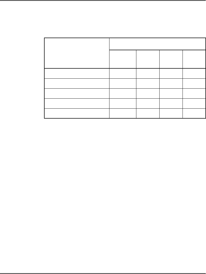
Page 836 of 906 NTRB21 DTI/PRI/DCH TMDI card
553-3001-211 Standard 3.00 August 2005
Cross-connect – Level 1 (DSX-1), or LD-1. Equalizers are switch selectable
through dip-switches. The settings are shown in Table 264.
Receiver
The receiver extracts data and clock from an incoming data stream and
outputs clock and synchronized data. At worst case DSX-1 signal levels, the
line receiver operates correctly with up to 655 feet of ABAM cable between
the card and the external DS-1 signal source.
Table 264
NTRB21 switch settings
Distance to Digital
Cross-Connect
Switch Setting
1
DCH F/W
2
(LEN 0)
3
(LEN 1)
4
(LEN 2)
0 - 133 feet Off Off Off On
133 - 266 feet Off On On Off
266 - 399 feet Off Off On Off
399 - 533 feet Off On Off Off
533 - 655 feet Off Off Off Off

NTRB21 DTI/PRI/DCH TMDI card Page 837 of 906
Circuit Card Description and Installation
Connector pinout
The connection to the external digital carrier is through a 15 position Male
D-type connector.
NTAK20 Clock Controller (CC) daughterboard
Digital Trunking requires synchronized clocking so that a shift in one clock
source results in an equivalent shift of the same size and direction in all parts
of the network.
The NTAK20 clock controller circuitry synchronizes the CS 1000S,
CS 1000M Cabinet, and Meridian 1 PBX 11C Cabinet to an external
reference clock and generates and distributes the clock to the system. The
CS 1000S, CS 1000M Cabinet, and Meridian 1 PBX 11C Cabinet can
function either as a slave to an external clock or as a clocking master to the
network.
The NTAK20AD and NTAK20AA versions of the clock controller meet
AT&T Stratum 3 and Bell Canada Node Category D specifications. The
NTAK20BD and NTAK20BA versions meet CCITT stratum 4
specifications. See “NTAK20 Clock Controller daughterboard” on page 735.
Table 265
DS-1 line interface pinout for NTBK04 cable
From 50-pin
MDF connector To DB-15 Signal name Description
pin 48 pin 1 Ttransmit tip to
network
pin 23 pin 9 Rtransmit ring to
network
pin 25 pin 2 FGND frame ground
pin 49 pin 3 T1 receive tip from
network
pin 24 pin 11 R1 receive ring from
network

Page 838 of 906 NTRB21 DTI/PRI/DCH TMDI card
553-3001-211 Standard 3.00 August 2005
Note: Clocking slips can occur between MG 1000S systems that are
clocked from different COs, if the COs are not synchronized. The slips
can degrade voice quality.
Clock rate converter
The 1.5 Mb clock is generated by a Phase-Locked Loop (PLL). The PLL
synchronizes the 1.5 Mb DS1 clock to the 2.56 Mb system clock through the
common multiple of 8 kHz by using the main frame synchronization signal.
IMPORTANT!
Each MG 1000S that has a digital trunk must have a clock controller
clocked to an external reference clock.
If an IP Expansion multi-cabinet system is equipped with digital trunk
cards, it is mandatory that at least one trunk card is placed in the Main
Option 11C cabinet. A cabinet that has a digital trunk must have a clock
controller.

Page 839 of 906
Circuit Card Description and Installation
844
NTVQ01xx Media Card
Contents
This section contains information on the following topics:
Physical description. . . . . . . . . . . . . . . . . . . . . . . . . . . . . . . . . . . . . . . . 839
Hardware architecture . . . . . . . . . . . . . . . . . . . . . . . . . . . . . . . . . . . . . . 841
Functional description . . . . . . . . . . . . . . . . . . . . . . . . . . . . . . . . . . . . . . 843
Survivability . . . . . . . . . . . . . . . . . . . . . . . . . . . . . . . . . . . . . . . . . . . . . 843
Physical description
The Media Card replaces the ITG Pentium card and is available as an 8-port
or 32-port card.
You can install this card in slots 1 through 4 in the MG 1000S or slots 7
through 10 in the MG 1000S Expansion.
Note: Up to four Media Cards can be installed in each MG 1000S. Up to
four Media Cards can be installed in each MG 1000S Expansion.
An NTVQ01xx Media Card is shown in Figure 179.
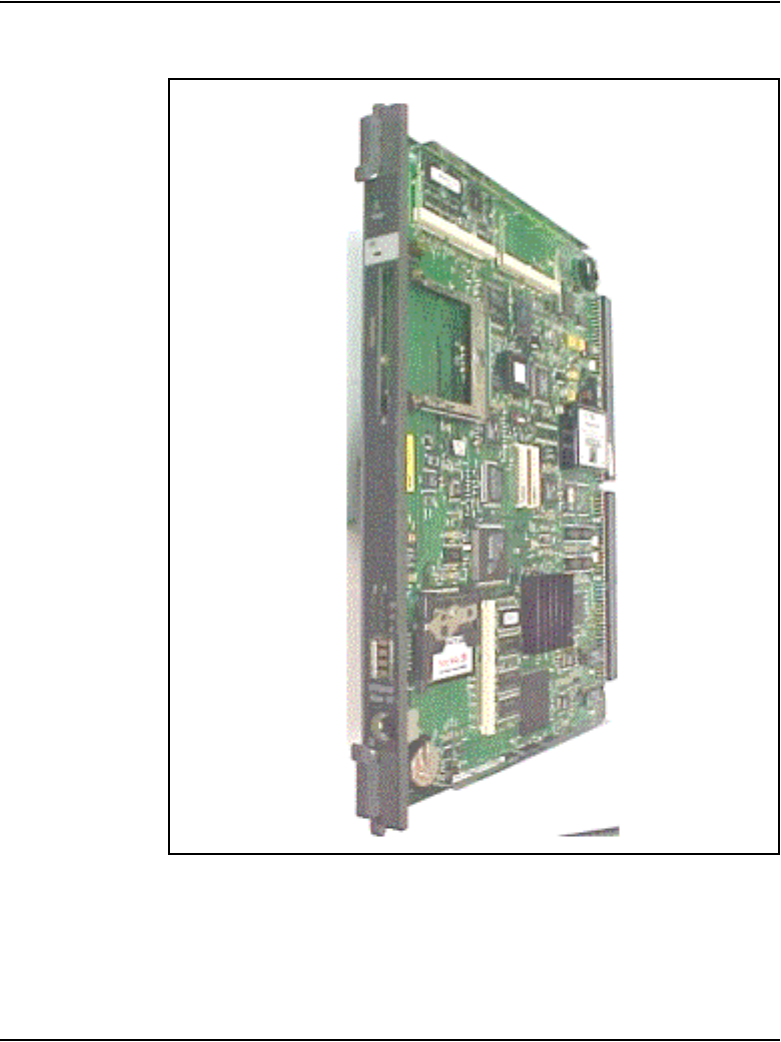

NTVQ01xx Media Card Page 841 of 906
Circuit Card Description and Installation
Hardware architecture
The Media Card comes in two versions: 8-port and 32-port.
Faceplate connectors and indicators
Figure 180 on page 842 shows the NTVQ01xx Media Card faceplate.
Reset switch
The reset switch on the faceplate manually resets the Media Card.
Status LED
The NTVQ01xx Media Card faceplate red LED indicates the following:
• the enabled/disabled status of the card
• the self-testing result during power up or card insertion into an
operational system
PC card slot
This slot accepts standard PC card flash cards, including ATA Flash cards
(3 Mbit/s to 170 Mbit/s). Nortel supply PCM card adaptors which enable
compact flash cards to be used in this slot. This slot is used for NTVQ01xx
Media Card software upgrades, backing up announcements, and additional
storage.
Ethernet activity LEDs
The NTVQ01xx Media Card faceplate contains Ethernet activity LEDs for
each network.
Maintenance hex display
This is a four-digit LED-based hexadecimal display that provides the status
of the NTVQ01xx Media Card at all times. The hex display provides an
indication of fault conditions and the progress of PC card-based software
upgrades or backups. It also indicates the progress of the internal self-test in
the form of T:xx.
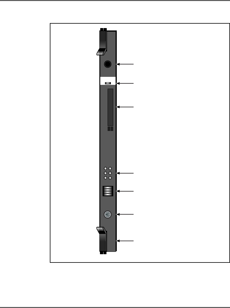

NTVQ01xx Media Card Page 843 of 906
Circuit Card Description and Installation
RS-232 Asynchronous Maintenance Port
An 8-pin mini-DIN socket on the NTVQ01xx Media Card faceplate provides
access to the RS-232 port. This faceplate port can provide access to the Media
Card for OA&M purposes. The maintenance port is also available through a
female DB9 connector on the 50-pin I/O Adaptor. This should be used to
make a permanent terminal connection.
Functional description
Media Cards have different types of firmware pre-installed, depending on the
application being supported. The Voice Gateway application enables Digital
Signal Processors (DSPs) for either line or trunk applications. When the
Voice Gateway application is installed on the Media Card, the card is called
the Voice Gateway Media card. Other examples of applications on a Media
Card include IP Line 3.0 and Integrated Recorded Announcer.
The NTVQ01xx Media Card connects an IP and circuit-switched device. The
DSPs perform media transcoding between IP voice packets and
circuit-switched devices. The Media Card also provides echo cancellation
and compression/decompression of voice streams.
Survivability
Refer to Communication Server 1000S: Installation and Configuration
(553-3031-210) for instructions on configuring the card for survivability.


Page 845 of 906
Circuit Card Description and Installation
850
NTVQ55AA ITG Pentium card
Contents
This section contains information on the following topics:
Physical description. . . . . . . . . . . . . . . . . . . . . . . . . . . . . . . . . . . . . . . . 845
Functional description . . . . . . . . . . . . . . . . . . . . . . . . . . . . . . . . . . . . . . 846
Physical description
The NTVQ55AA ITG Pentium (ITG-P) card supports IP Phones by
providing a communication gateway for the IP Phone between the IP data
network and the system. The IP Phone uses the IP data network to
communicate with the ITG-P card.
You can install this card in any two consecutive IPE slots.
Note: Each MG 1000S supports up to two ITG-P cards. Each
MG 1000S Expansion supports up to two ITG-P cards. Each ITG-P card
occupies two slots.
ITG-P cards have an ELAN management 10BaseT port and a TLAN VoIP
port (10/100BaseT) on the I/O panel. There is an RS-232 Maintenance port
connection on the ITG-P card faceplate and an alternative connection to the
same serial port on the I/O backplane.
Note: Do not connect maintenance terminals to the faceplate and I/O
panel serial maintenance port connections at the same time.
Page 846 of 906 NTVQ55AA ITG Pentium card
553-3001-211 Standard 3.00 August 2005
Functional description
Figure 181 on page 847 shows the ITG-P card faceplate components. The
information in this section describes the components.
Faceplate components
NWK
The faceplate connector labeled NWK is a 9-pin, sub-miniature D-type
connector. The connector is not used for the ITG-P application.
ITG-P LED (Card Status)
The red status faceplate LED indicates the enabled/disabled status of the
24-card ports. The LED is on (red) during the power-up or reset sequence.
The LED remains lit until the card is enabled. If the LED remains on, this
indicates the self-test failed, the card is disabled, or the card rebooted.
Reset switch
Press the Reset switch to reset the card without having to cycle power to the
card. This switch is normally used after a software upgrade to the card, or to
clear a fault condition.
WARNING
The NWK connector looks like a 9-pin serial connector.
Do not connect a serial cable or any other cable to it. If a
cable is installed to the NWK connector, the TLAN
interface card is disabled.
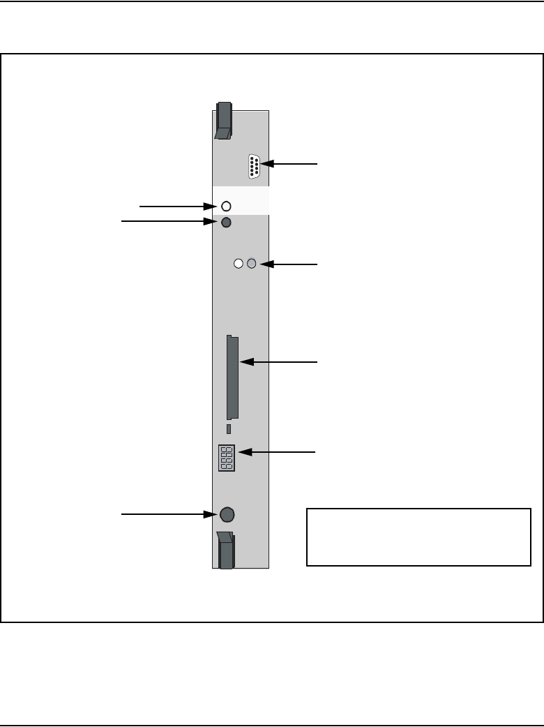
NTVQ55AA ITG Pentium card Page 847 of 906
Circuit Card Description and Installation
Figure 181
NTVQ55AA ITG-P card faceplate
Note: There are no Ethernet status LEDs for the ELAN management
interface.
ITG-P
NWK
NTVQ55AA
NWK
Status
Reset
Maint
Port
A:
553-CSE9150
Ethernet Voice Port
ITG-P LED (card status)
NWK LEDs (Ethernet)
Reset Switch
Type III PCMCIA slot
(ATA Drive A:)
Four-character LED-based
Matrix Maintenance Display
RS-232
Maintenance Port Inboard:
- Type III PCMCIA slot (ATA Drive B:)
- Onboard Flash Drive C:

Page 848 of 906 NTVQ55AA ITG Pentium card
553-3001-211 Standard 3.00 August 2005
NWK Status LED
NWK Status LEDs display the TLAN interface card Ethernet activity:
• Green – on if the carrier (link pulse) is received from the TLAN interface
card Ethernet hub.
• Yellow – flashes when there is TLAN interface card data activity. During
heavy traffic, yellow can stay continuously lit.
Note: There are no Ethernet status LEDs for the ELAN management
interface.
PC card slots
The ITG-P card has one faceplate PC card slot, designated drive A. The PC
card slot is used for optional maintenance (backup and restore). The ITG-P
card also has one unused inboard slot, designated drive B. The PC card slots
support PC-based hard disks (ATA interface) or high-capacity PC flash
memory cards.
Maintenance Display
A four character, LED-based, dot matrix display shows the maintenance
status fault codes and other card state information.
RS-232 Maintenance Port
The ITG-P card faceplate provides a female DIN-8 serial maintenance port
connection (labeled Maint Port). An alternative connection to the faceplate
serial maintenance port exists on the NTMF94EA I/O panel breakout cable.
Do not connect maintenance terminals or modems to the faceplate and I/O
panel DB-9 male serial maintenance port at the same time.
Backplane interfaces
The backplane connector provides connection to the following:
• ELAN interface card
• TLAN interface card

NTVQ55AA ITG Pentium card Page 849 of 906
Circuit Card Description and Installation
• alternate connection to the serial maintenance port DS-30X
• Card LAN interfaces
DS-30X voice/signaling
DS-30X carries Pulse Code Modulation (PCM) voice and proprietary
signaling on the backplane between the ITG-P card and the SSC.
Card LAN
Card LAN carries card polling and initialization messages on the backplane
between the ITG-P card and the SSC.
Assembly description
The ITG-P card assembly consists of a two-slot motherboard/daughterboard
combination. A PCI interconnect board connects the ITG-P motherboard and
the DSP daughterboard.


Page 851 of 906
Circuit Card Description and Installation
868
QPC513 Enhanced Serial Data
Interface card
Contents
This section contains information on the following topics:
Introduction . . . . . . . . . . . . . . . . . . . . . . . . . . . . . . . . . . . . . . . . . . . . . . 851
Physical description. . . . . . . . . . . . . . . . . . . . . . . . . . . . . . . . . . . . . . . . 852
Functional description . . . . . . . . . . . . . . . . . . . . . . . . . . . . . . . . . . . . . . 854
Connector pin assignments . . . . . . . . . . . . . . . . . . . . . . . . . . . . . . . . . . 859
Configuring the ESDI card . . . . . . . . . . . . . . . . . . . . . . . . . . . . . . . . . . 862
Applications . . . . . . . . . . . . . . . . . . . . . . . . . . . . . . . . . . . . . . . . . . . . . 867
Introduction
The QPC513 Enhanced Serial Data Interface (ESDI) card gives the
CS 1000S, CS 1000M, and Meridian 1 switch two fully synchronous
high-speed serial ports.
These high-speed synchronous ports are used to connect the processor to
synchronous communication peripherals such as Meridian Mail or to a host
computer (for example, DEC or Tandem) using Meridian Link. This card
cannot be used as an asynchronous port or to connect to an administrative and
maintenance terminal. Use either the NT8D41 SDI paddle board or the
QPC841 Quad Serial Data Interface card to connect the switch to an
asynchronous serial peripheral.

Page 852 of 906 QPC513 Enhanced Serial Data Interface card
553-3001-211 Standard 3.00 August 2005
Each system can accommodate up to eight ESDI cards, for a total of 16
synchronous ports per system. The ESDI cards can be housed in the network
slots of any of the following modules:
• NT5D21 Core/Network module (slots 0 through 7)
• NT6D39 CPU/Network module (slots 1 through 9 and 13)
• NT6D60 Core module (slots 0 through 5)
• NT8D35 Network module (slots 5 through 13)
• NT9D11 Core/Network module (slots 0 through 8)
Note: When as ESDI card is installed in an NT6D60 Core module, an
NT8D34 CPU module, or slot 13 of an NT6D39 CPU/Network module
in a dual-CPU system, any I/O device connected to the card does not
function when the CPU in that module is inactive.
Physical description
The ESDI card circuitry is contained on a 31.75 by 25.40 cm (12.5 by 10 in.)
printed circuit board. The front panel of the card is 2.54 cm (1 in.) wide. See
Figure 182 on page 853. The front panel is equipped with an Enable/Disable
(ENB/DIS) switch and a red LED. The LED lights when the following
occurs:
• the ENB/DIS switch is set to DIS
• both ports are disabled in software
• none of the card’s ports have been configured in software
• the switch settings on the card do not match the settings programmed in
software
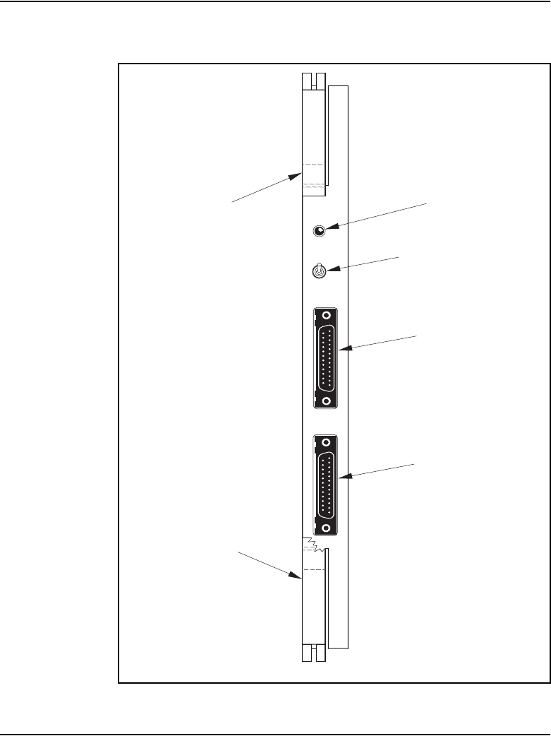
Page 854 of 906 QPC513 Enhanced Serial Data Interface card
553-3001-211 Standard 3.00 August 2005
Functional description
The QPC513 ESDI card is an intelligent, two-port synchronous serial data
interface card. See Figure 183. The two serial input/output data ports
terminate on DB-25 connectors on the front panel of the card.
Each port operates independently in synchronous mode, in half or full duplex,
at speeds of up to 64 kbps. Each port can be connected to either Data Terminal
Equipment (DTE) or Data Communications Equipment (DCE).
The electrical interface for the ESDI card may be either EIA RS-232-C or a
proprietary high-speed interface. The high-speed interface combines features
of RS-422-A for data and timing signals with features of RS-232-C for
control signals.
Figure 183
ESDI card block diagram
Address
bus
Data
bus
Control
bus
System
processor
bus
Local bus
Baud rate
generator
1
System
bus
interface
ESDI card
local
processor
EPROM
System
and
cache
RAM
DMA
channel
1
Synchronous
serial channel
1
Line
interface
1
Port 1
(J1)
Baud rate
generator
2
DMA
channel
2
Synchronous
serial channel
2
Line
interface
2
Port 2
(J2)
553-AAA1159

QPC513 Enhanced Serial Data Interface card Page 855 of 906
Circuit Card Description and Installation
The QPC513 ESDI card is an intelligent controller. The local
micro-processor performs all of the overhead associated with synchronous
data transfer. The system processor passes data to the ESDI card processor a
byte at a time using conventional memory reads and writes. The ESDI card
processor stores the data in a RAM cache on the ESDI card, and passes it to
the synchronous communication chip in blocks using Direct Memory Access
(DMA) techniques.
Synchronous communication
The ESDI cards supports LAPB, a subset of the HDLC synchronous protocol.
A description of the LAPB protocol is shown in Appendix A, LAPB data link
protocol on page 901.
The HDLC data link is a bit-oriented protocol. The information data bits are
transmitted transparently across the link in packets. The maximum length of
the information field for these packets is 128 octets, where an octet consists
of 8 bits.
The characteristics of the synchronous communication ports are shown in
Table 266.
Table 266
Characteristics of synchronous ports (Part 1 of 2)
Characteristics Description
Duplex mode half, (full)
Data rate (bps) 1200, 2400, (4800), 9600,
19200, 48000, 56000, 64000
Clock (internal), external
Data Link Level LAPB protocol
SL-1 address
(1), 3
Note 1: * See the Configuration Record (LD 17) in Software Input/Output:
Administration (553-3001-311) to modify the link control system
parameters and performance thresholds.
Note 2: The values in parentheses are the default.

Page 856 of 906 QPC513 Enhanced Serial Data Interface card
553-3001-211 Standard 3.00 August 2005
Clock timing option
The ESDI card offers two timing options:
• Internal: The ESDI card uses an internal timing source to synchronize
data transfers to the external device.
• External: The ESDI card accepts a timing source from the high-speed
interface connector to synchronize data transfers to the external device.
Test and maintenance features
The ESDI card has these built-in testing and maintenance capabilities:
Self-test
The ESDI card performs a self-test of its major components immediately after
power-up. The self-test can also be initiated through the Link Diagnostic
program LD 48. The self-test tests all ESDI functions up to, but not including,
the ESDI line drivers and receivers.
Data Link Level LAPB protocol remote
host address
(3), 1
Modify link control system parameters* yes, (no)
Modify link performance thresholds
(Note 1)
yes, (no)
Table 266
Characteristics of synchronous ports (Part 2 of 2)
Characteristics Description
Note 1: * See the Configuration Record (LD 17) in Software Input/Output:
Administration (553-3001-311) to modify the link control system
parameters and performance thresholds.
Note 2: The values in parentheses are the default.

QPC513 Enhanced Serial Data Interface card Page 857 of 906
Circuit Card Description and Installation
Fault detection
Firmware on the ESDI card detects hardware faults on the card and link level
LAPB protocol faults. It reports the faults to the CPU when predetermined
thresholds (downloaded at initialization) have been exceeded.
Fault isolation
The ESDI/Command and Status Link (CSL) maintenance software takes the
ESDI card out of service when the out-of-service thresholds are exceeded for
the following:
• LAPB error conditions (for example, retransmission, Cyclic Redundancy
Check (CRC) errors, overrun/underrun errors)
• Physical or link errors
• Detected hardware errors
Connection characteristics
The two DB-25 connectors on the front panel of the ESDI card provide
connections to each of the two I/O ports. The electrical interface of these
connectors is a modified version of the RS-422-A standard designed to drive
high-speed data over long cable lengths (up to 100 ft). Table 267 shows the
interconnection specifications for these ports.
Table 267
QPC513 interconnection specifications
Distance Interconnection
<15.24 m (<50 ft) Regular 25-conductor cable
>15.24 m and <30.48 m
(>50 ft and <100 ft)
Twisted pair for balanced circuits
>30.48 m (>100 ft) Network interface devices such as stand-alone
modems or DS-1 facilities using
Asynchronous/Synchronous Interface Module
(ASIM) and Data Line card (DLC)
Page 858 of 906 QPC513 Enhanced Serial Data Interface card
553-3001-211 Standard 3.00 August 2005
Electrical interface options
Interface options are selected by inserting jumper plugs into the appropriate
sockets on the card:
• RS-232-C interface: The EIA RS-232-C interface can be used for speeds
up to 19.2 kbps and distances of less than 15.24 m (50 ft). The ESDI card
supports a subset of the RS-232-C signals. See Table 268 on page 859.
• High-speed interface: The high-speed interface combines features of the
RS-422-A standard for the data and timing signals with standard
RS-232-C control signals. It is used when the signal rate is greater than
19.2 kbps and/or when the distance between the system and host is
greater than 15.24 m (50 ft). No modems are needed if the distance is less
than 30.48 m (100 ft).
The high-speed interface uses a proprietary pin assignment, rather than
the standard 37-pin RS-449 arrangement. This pin arrangement is
compatible with the Spectron Cable #75-025 for V.35 use. See Table 269
on page 860.
The data and timing signals on the high-speed interface use RS-422-A
type differential line drivers and receivers in a balanced configuration.
These drivers and receivers are able to drive higher data rate signals over
longer distances than standard RS-232-C drivers and receivers. A typical
connection using these drivers and receivers is shown in Figure 184.
Figure 184
Typical high-speed interface line driver and receiver
Driver
Front panel
connector
Front panel
connector
System cable
Lead A
Lead B
Lead A
Lead B
Receiver
553-5943

QPC513 Enhanced Serial Data Interface card Page 859 of 906
Circuit Card Description and Installation
Connector pin assignments
Table 268 shows the pin assignments for J1 and J2 when the port is
configured for RS-232-C interface, and Table 269 on page 860 shows the pin
assignments for J1 and J2 when the port is configured for the high-speed
interface.
Table 268
Connector J1 and J2 pin assignments – RS-232-C interface (Part 1 of 2)
Pin number Signal functions
Signal source
EIA
circuit
To DCE From DCE
Ground and
common return
1Shielded n/a n/a
7Signal ground (SG) n/a n/a AB
Data
2Transmitted data (TX) 3—BA
3Received data (RX) —3BB
Control
4Request to send (RTS) 3—CA
5Clear to send (CTS) —3CB
6Data set ready (DSR) —3CC
8Carrier detect (CD) —3CF
20 Data terminal ready (DTR) 3—CD
Timing
15 Transmitter signal element timing (DCE) —3DB
Note: Pins not used are 9 to 14, 16, 18, 19, 21, 22, 25.

Page 860 of 906 QPC513 Enhanced Serial Data Interface card
553-3001-211 Standard 3.00 August 2005
17 Receiver signal element timing (DCE) —3DD
24 Transmitter signal element timing (DTE) 3—DA
Table 269
Connector J1 and J2 pin assignments – high-speed interface (Part 1 of 2)
Pin number Signal functions
Signal source
EIA
circuit
(lead)
To DCE
From
DCE
Ground and
common return
1
7
Shield
Signal ground (SG)
n/a
n/a
n/a
n/a AB
Data
2
3
13
16
Transmitted data – lead A
Received data – lead A
Transmitted data – lead B
Received data – lead B
3
—
3
—
—
3
—
3
BA (A)
BB (A)
BA (B)
BB (B)
Control
4
5
6
8
20
Request to send (RTS)
Clear to send (CTS)
Data set ready (DSR)
Carrier detect (CD)
Data terminal ready (DTR)
3
—
—
—
3
—
3
3
3
CA
CB
CC
CF
CD
Note: Pins not used are 9, 10, 11, 18, 19, 21, 22, 25.
Table 268
Connector J1 and J2 pin assignments – RS-232-C interface (Part 2 of 2)
Pin number Signal functions
Signal source
EIA
circuit
To DCE From DCE
Note: Pins not used are 9 to 14, 16, 18, 19, 21, 22, 25.

QPC513 Enhanced Serial Data Interface card Page 861 of 906
Circuit Card Description and Installation
Timing
12 Transmitter signal element tim-
ing (DTE) – lead B
—3DD (B)
14 Transmitter signal element tim-
ing (DCE) – lead B
—3DB (B)
15 Transmitter signal element tim-
ing (DCE) – lead A
—3DB (A)
17 Transmitter signal element tim-
ing (DTE) – lead A
—3DD (A)
23 Receiver signal element timing
(DCE) – lead A
3—DA (A)
24 Receiver signal element timing
(DCE) – lead B
3—DA (B)
Table 269
Connector J1 and J2 pin assignments – high-speed interface (Part 2 of 2)
Pin number Signal functions
Signal source
EIA
circuit
(lead)
To DCE
From
DCE
Note: Pins not used are 9, 10, 11, 18, 19, 21, 22, 25.

Page 862 of 906 QPC513 Enhanced Serial Data Interface card
553-3001-211 Standard 3.00 August 2005
Configuring the ESDI card
Configuring the ESDI card consists of setting the port addresses using the
address selection switch and setting the port interface options using the
jumper blocks. The system software must then be configured to recognize the
ESDI card. Figure 185 on page 864 shows the location of all option switches
and jumper sockets on the ESDI card.
Address switch settings
The two ESDI ports on the card are addressed in pairs such as 0 and 1, 2 and
3, and so on). The address is set using switch S2. The switch settings used to
select the address vary depending on whether the card is Style A or Style B.
The “Style” can be read on the printed circuit board silk screen. The address
of the card is set to match the device address defined in software.
Synchronous port address space is the same as asynchronous port address
space. When selecting an address for the ESDI card, make sure that it will not
conflict with an address currently being used by an asynchronous card.
Table 270 shows the ESDI card address switch settings.
Table 270
ESDI card address switch settings (Part 1 of 2)
Device Number
Switch S2
style A
Switch S2
style B
Port 1Port 212341234
0 1 off off off on off off off *
2 3 on off off on off off on *
4 5 off on off on off on off *
6 7 on on off on off on on *
8 9 off off on on on off off *
10 11 on off on on on off on *
* Switch S2, position 4 is not used on style B cards.

QPC513 Enhanced Serial Data Interface card Page 863 of 906
Circuit Card Description and Installation
DTE/DCE mode jumper settings
The interface for each ESDI port is configured independently. Ports must be
configured both for electrical interface (RS-232-C or high-speed) and mode
(DTE or DCE). With the proper options set:
• An ESDI port configured as DTE appears as a terminal to the user
equipment.
• An ESDI port configured as DCE appears as a modem to the user
equipment.
Interface options are set by installing option jumper plugs into the sockets
indicated in Table 271 on page 865 and Table 272 on page 865.
12 13 off on on on on on off *
14 15 on on on on on on on *
Table 270
ESDI card address switch settings (Part 2 of 2)
Device Number
Switch S2
style A
Switch S2
style B
Port 1Port 212341234
* Switch S2, position 4 is not used on style B cards.
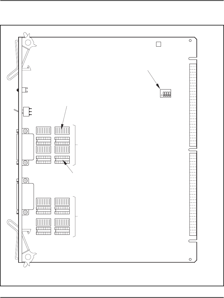
Page 864 of 906 QPC513 Enhanced Serial Data Interface card
553-3001-211 Standard 3.00 August 2005
Figure 185
ESDI card option switch locations
553-5983
S1
S2
DS1
J1
J2
UB9
UB10
UB11
UB12
UA9
UA10
UA11
UA12
UB16
UB17
UB18
UB19
UA16
UA17
UA18
UA19
Address
selection
Note:
Ports 1 and 2 shown with jumper plugs installed for DCE and RS-232-C operation.
Port no. 1
jumpers
Port no. 2
jumpers
1234
O
N
STYLE
Jumper plug
installed in
socket
Empty
jumper
socket

QPC513 Enhanced Serial Data Interface card Page 865 of 906
Circuit Card Description and Installation
Software service changes
All of the other ESDI port operating parameters are defined in software and
downloaded to the assigned ESDI port. See Table 266 on page 855. These
changes are made using the Configuration Record program (LD 17).
Instructions for the Configuration Record program are found in the Software
Input/Output: Administration (553-3001-311).
Some of the prompts that are commonly used when running the Configuration
Record program (LD 17) are shown in LD 17 – Serial port configuration
Table 271
ESDI card DTE/DCE mode jumper settings
Mode Port
Jumper socket
designations
Data communication equipment (DTE) 1 UA10 UA12
Data terminal equipment (DCE) 1 UA9 UA11
Data communication equipment (DTE) 2 UA17 UA19
Data terminal equipment (DCE) 2 UA16 UA18
Table 272
ESDI card RS-232-C/high-speed interface jumper settings
Mode Port
Jumper socket
designations
RS-232-C interface 1 UB9 UB11
High-speed interface 1 UB10 UB12
RS-232-C interface 2 UB16 UB18
High-speed interface 2 UB17 UB19

Page 866 of 906 QPC513 Enhanced Serial Data Interface card
553-3001-211 Standard 3.00 August 2005
parameters. These parameters must be set for each ports if both ports are
being used.
LD 17 – Serial port configuration parameters.
Prompt Response Description
REQ: CHG Change configuration.
TYPE: CFN Configuration type.
IOTB YES Change input/output devices.
ADAN NEW TTY x
NEW PRT x
Define a new system terminal (printer) port as device x, where
x = 0 to 15.
CDNO 1-16 Use the ESDI card number to keep track of all ports.
DENS DDEN Double density SDI paddle board.
USER xxx Enter the user of port x. The values that can be entered
depend on the software being used. See the Software Input/
Output: Administration (553-3001-311) for details.
XSM (NO) YES Port is used for the system monitor.

QPC513 Enhanced Serial Data Interface card Page 867 of 906
Circuit Card Description and Installation
Applications
The QPC513 Enhanced Serial Data Interface card is used any time that a
high-speed, fully synchronous serial data communication channel is needed.
The ESDI card is typically used to connect to the following:
• Meridian Mail
• A host computer using Meridian Link
• An auxiliary processor
The system processor transfers data to the ESDI card in blocks consisting of
1 to 128 eight-bit octets. Each block is processed in accordance with the
LAPB subset of the HDLC protocol and is transmitted serially to the output
port.
In receive mode, the EDSI card receives data serially from the input port
packages in LAPB information frames. After determining that the block is
error-free, the ESDI card supplies the data to the system processor as a block.
The ESDI card serial ports terminate on the card front panel. Figure 186 on
page 868 shows the typical ESDI card connections in a system.
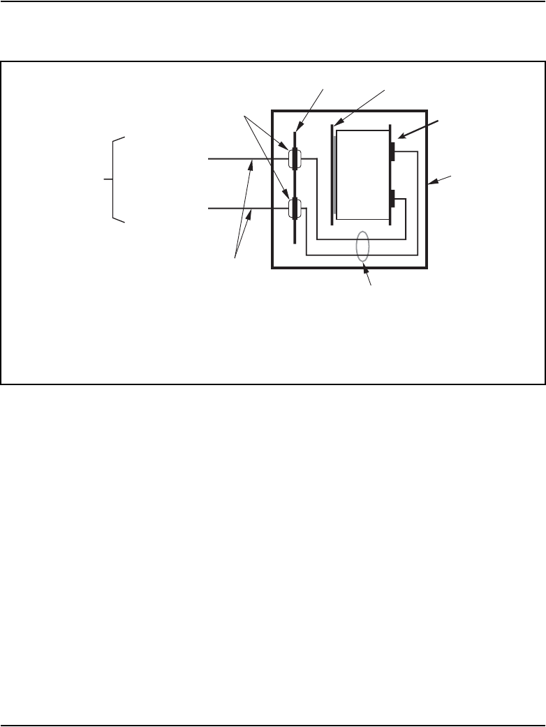
Page 868 of 906 QPC513 Enhanced Serial Data Interface card
553-3001-211 Standard 3.00 August 2005
Figure 186
QPC513 ESDI card cabling
Cables to
peripherals
NT8D95 cables (Note 1)
NT8D82 cables
I/O panel
Module front
Q
P
C
5
1
3
J1
J2
Port 2
Port 1
Card front panel
Backplane
Filter adapters (Note 2)
Meridian Mail
Meridian Link
:
553-5984
Note 1:
This cable available in different lengths with various
male/female connector combinations.
Note 2:
Supplied with NT8D82 cable.

Page 869 of 906
Circuit Card Description and Installation
884
QPC841 Quad Serial Data Interface card
Contents
This section contains information on the following topics:
Introduction . . . . . . . . . . . . . . . . . . . . . . . . . . . . . . . . . . . . . . . . . . . . . . 869
Physical description. . . . . . . . . . . . . . . . . . . . . . . . . . . . . . . . . . . . . . . . 870
Functional description . . . . . . . . . . . . . . . . . . . . . . . . . . . . . . . . . . . . . . 872
Connector pin assignments . . . . . . . . . . . . . . . . . . . . . . . . . . . . . . . . . . 874
Configuring the QSDI card . . . . . . . . . . . . . . . . . . . . . . . . . . . . . . . . . . 876
Applications . . . . . . . . . . . . . . . . . . . . . . . . . . . . . . . . . . . . . . . . . . . . . 882
Introduction
The QPC841 Quad Serial Data Interface (QSDI) card provides four
RS-232-C serial ports between the system and external devices. The QSDI
card plugs into a slot in the common equipment area of any system.
The Quad Serial Data Interface card is normally used to connect the system
to its administration and maintenance terminal. It is also used to connect the
system to a background terminal (used in the Hotel/Motel environment), a
modem, or the Automatic Call Distribution (ACD) and Call Detail Recording
(CDR) features.
The QSDI card is compatible with all existing system software. It does not
support 20 mA current loop interface.

Page 870 of 906 QPC841 Quad Serial Data Interface card
553-3001-211 Standard 3.00 August 2005
QSDI cards are housed in the following modules:
• NT5D21 Core/Network module (slots 0 through 7)
• NT6D39 CPU/Network module (slots 1 through 9, and 13)
• NT6D60 Core module (slots 0 through 5)
• NT8D35 Network module (slots 5 through 13)
• NT9D11 Core/Network module (slots 0 through 8)
Note: When a QSDI card is installed in an NT6D60 Core module, an
NT8D34 CPU module, or slot 13 of an NT6D39 CPU/Network module
in a dual-CPU system, any input/output I/O device connected to the card
does not function when the CPU in that module is inactive.
Physical description
The QPC841 QSDI card is a printed circuit board measuring 31.75 cm by
25.4 cm (12.5 in. by 10 in.). The front panel is 2.54 cm (1 in.) thick. See
Figure 187 on page 871.
Up to four QSDI boards can be used in a system, allowing a total of sixteen
asynchronous serial ports. The four serial ports on each card are addressed as
two pairs of consecutive addresses (0 and 1, 2 and 3, and so on up to 14 and
15). The pairs need not be consecutive. For example: pairs 0 and 1, and 4 and
5 could be used.
The card front panel has two connectors, J1 and J2. Connector J1 is used for
port 1 while connector J2 is used for ports 2, 3, and 4. It also has an Enable/
Disable (ENB/DIS) switch and a red LED. The LED indicates that the card
has been disabled. It is lit when the following occurs:
• the ENB/DIS switch is set to DIS
• all of the ports on the card are disabled in software
• none of the card ports are configured in software


Page 872 of 906 QPC841 Quad Serial Data Interface card
553-3001-211 Standard 3.00 August 2005
Functional description
The QPC841 Quad Serial Data Interface card contains all the logic for four
asynchronous serial ports, including the baud rate generators. These serial
ports are directly accessed by the system processor using memory reads and
writes.
The QPC841 Quad Serial Data Interface card contains four universal
asynchronous receiver/transmitters (UARTs) and the logic necessary to
connect the UARTs to the system processor bus. See Figure 188 on page 873.
The other logic on the card consists of four baud rate generators, four
RS-232-C driver/receiver pairs, and the jumpers and logic needed to
configure the UARTs.
The address select switches and logic on the card always address the UARTs
using two pairs of addresses: 0 and 1, and 2 and 3 through 15 and 16. The
pairs do not need to be consecutive. Other switches on the board determine
the baud rate for each individual port and whether the port is configured to
talk to a terminal (DTE equipment) or a modem (DCE equipment).
Instructions for setting the jumpers are given later in this section.
QPC841 Quad Serial Data Interface card Page 873 of 906
Circuit Card Description and Installation
Figure 188
QPC841 QSDI card block diagram
UART
no. 1
UART
no. 2
UART
no. 3
UART
no. 4
UARTs
Address
decode logic
TD
RD
TD
RD
TD
RD
TD
RD
RS-232-C
drivers and receivers
Clock and bit
rate select logic
Processor
bus
553-5986
Port 1
Port 2
Port 3
Port 4
J1
J2

Page 874 of 906 QPC841 Quad Serial Data Interface card
553-3001-211 Standard 3.00 August 2005
Connector pin assignments
Connector J1 is connected to port one, and uses the RS-232-C standard
DB-25 pinout. Connector J2 is connected to ports two, three, and four, and is
a non-standard pinout that requires an adapter cable. An adapter cable
(NT8D96) splits the J2 signals out to three standard RS-232-C connectors.
Port 2 is connected to connector A, Port 3 is connected to connector B, and
Port 4 is connected to connector C.
Table 273 shows the pinouts for connector J1, and Table 274 on page 875
shows the pinouts for connector J2.
Table 273
Connector J1 pin assignments
Pin
number Signal Purpose in DTE mode Purpose in DCE mode
1FGD Frame ground Frame ground
2TD Received data Transmitted data
3RD Transmitted data Received data
4RTS Request to send (not used) Request to send (Note 2)
5CTS Clear to send (Note 1) Clear to send
6DSR Data set ready (Note 1) Data set ready
7 GND Ground Ground
8CD Carrier detect (Note 1) Carrier detect (not used)
20 DTR Data terminal ready Data terminal ready (Note 2)
Note 1: In DTE mode, the signals CD, DSR, and CTS are tied to +12 volts (through a resistor)
to indicate that the QSDI port is always ready to transmit and receive data.
Note 2: In DCE mode, the signals DTR, and RTS are tied to +12 volts (through a resistor) to
indicate that the QSDI port is always ready to transmit and receive data.

QPC841 Quad Serial Data Interface card Page 875 of 906
Circuit Card Description and Installation
Table 274
Connector J2 pin assignments (Part 1 of 2)
Pin
Number Port Signal Purpose in DTE mode Purpose in DCE mode
1FGD Frame ground Frame ground
2TD Transmitted data Transmitted data
3RD Received data Received data
4RTS Request to send (not used) Request to send (Note 2)
5 2 CTS Clear to send (Note 1) Clear to send
6DSR Data set ready (Note 1) Data set ready
7 GND Ground Ground
8CD Carrier detect (Note 1) Carrier detect (not Used)
20 DTR Data terminal ready Data terminal ready (Note 2))
9TD Transmitted data Transmitted data
10 RD Received data Received data
11 RTS Request to send (not used) Request to send (Note 2))
12 3CTS Clear to send (Note 1) Clear to send
13 DSR Data set ready (Note 1) Data set ready
25 GND Ground Ground
24 CD Carrier detect (Note 1) Carrier detect (not used)
23 DTR Data terminal ready Data terminal ready (Note 2))
14 TD Transmitted data Transmitted data
15 RD Received data Received data
16 RTS Request to send (not used) Request to send (Note 2))
17 4CTS Clear to send (Note 1) Clear to send
18 DSR Data set ready (Note 1) Data set ready

Page 876 of 906 QPC841 Quad Serial Data Interface card
553-3001-211 Standard 3.00 August 2005
Configuring the QSDI card
Configuring the QSDI card consists of setting these option switches for each
serial port:
• Port address
• Baud rate
• DTE/DCE mode
Figure 189 on page 880 shows the location of the option switches on the
QSDI card. Instructions for setting these switches are in the section that
follows.
Address switch settings
Table 275 on page 877 lists the address switch settings for the QPC841 Quad
Serial Data Interface card. The address select jumpers and logic on the card
address the UARTs using two pairs of addresses: 0 and 1, 2 and 3, through 15
and 16. The pairs do not need to be consecutive. Switch SW14 is used to
19 GND Ground Ground
21 CD Carrier detect (Note 1 Carrier detect (not used)
22 DTR Data terminal ready Data terminal ready (Note 2))
Note 1: In DTE mode, the signals CD, DSR, and CTS are tied to +12 volts (through a resistor)
to indicate that the QSDI port is always ready to transmit and receive data.
Note 2: In DCE mode, the signals DTR and RTS are tied to +12 volts (through a resistor) to
indicate that the QSDI port is always ready to transmit and receive data.
Table 274
Connector J2 pin assignments (Part 2 of 2)
Pin
Number Port Signal Purpose in DTE mode Purpose in DCE mode

QPC841 Quad Serial Data Interface card Page 877 of 906
Circuit Card Description and Installation
select the addresses for ports 1 and 2. Switch SW15 is used to select the
addresses for ports 3 and 4.
Table 275
QSDI card address switch settings
SW14 Port 1 Port 2 Switch settings
SW15 Port 3 Port 4 12345678
Device
pair
addresses
0 1 off off off off off on on on
2 3 off off off off off on on off
4 5 off off off off off on off on
6 7 off off off off off on off off
8 9 off off off off off off on on
10 11 off off off off off off on off
12 13 off off off off off off off on
14 15 off off off off off off off off
Note 1: On SW16, positions 1, 2, 3, and 4 must be OFF.
Note 2: To avoid address conflicts, SW14 and SW15 can never have identical settings.
Note 3: To disable ports 1 and 2, set SW14 position 1 to ON. To disable ports 3 and 4, set
SW15 position 1 to ON.

Page 878 of 906 QPC841 Quad Serial Data Interface card
553-3001-211 Standard 3.00 August 2005
Baud rate switch settings
Table 276 lists the switch settings necessary to set the baud rate.
Table 276
QSDI card baud rate switch settings
Baud
rate
Port 1 – SW10 Port 2 – SW11 Port 3 – SW12 Port 4 – SW13
1234123412341234
150 off off on on off off on on off off on on off off on on
300 off on off on off on off on off on off on off on off on
600 off off off on off off off on off off off on off off off on
1200 off on on off off on on off off on on off off on on off
2400 off off on off off off on off off off on off off off on off
4800 off on off off off on off off off on off off off on off off
9600 off off off off off off off off off off off off off off off off

QPC841 Quad Serial Data Interface card Page 879 of 906
Circuit Card Description and Installation
DTE/DCE mode switch settings
Table 277 shows the DTE/DCE mode selection switches for the four serial
ports.
Test switch setting
Switch SW16 is only used for factory testing; all of its switches must be set
to OFF for proper operation.
Table 277
QSDI card DTE/DCE mode switch settings
Port 1 – SW8 Port1 – SW9
Mode 1 2 3 4 5 6 1 2 3 4 5 6
DTE (Terminal) on on on on on on off off off off off off
DCE (Modem) off off off off off off on on on on on on
Port 2 – SW6 Port 2 – SW7
Mode 1 2 3 4 5 6 1 2 3 4 5 6
DTE (Terminal) on on on on on on off off off off off off
DCE (Modem) off off off off off off on on on on on on
Port 3 – SW4 Port 3 – SW5
Mode 1 2 3 4 5 6 1 2 3 4 5 6
DTE (Terminal) on on on on on on off off off off off off
DCE (Modem) off off off off off off on on on on on on
Port 4 – SW2 Port 4 – SW3
Mode 1 2 3 4 5 6 1 2 3 4 5 6
DTE (Terminal) on on on on on on off off off off off off
DCE (Modem) off off off off off off on on on on on on
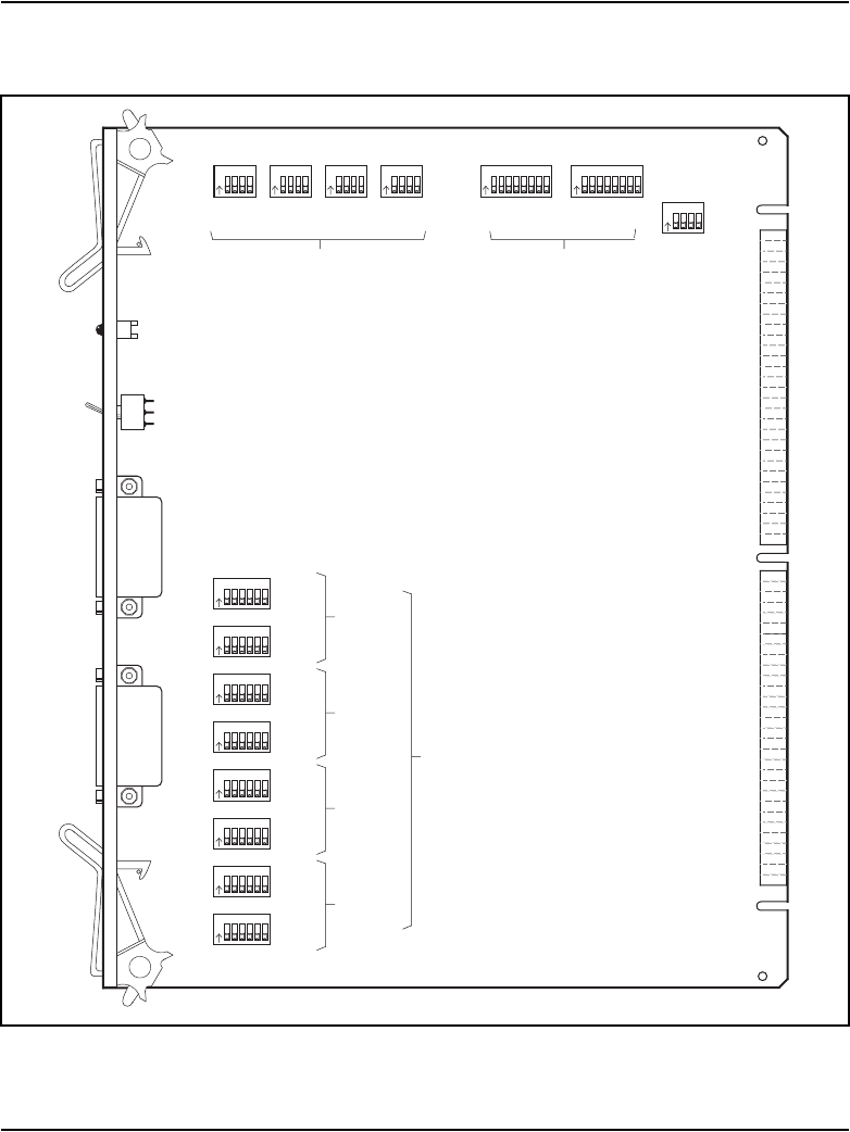
Page 880 of 906 QPC841 Quad Serial Data Interface card
553-3001-211 Standard 3.00 August 2005
Figure 189
QSDI card option switch locations
553-5987
SW1 DS1
J1
J2
SW16
1234
O
N
1234
O
N56
1234
O
N56
1234
O
N56
1234
O
N56
1234
O
N56
1234
O
N56
1234
O
N56
1234
O
N56
12 3 4
O
N12 34
O
N1234
O
N1234
O
N12 3 4
O
N5678 12 34
O
N56 78
SW15
SW14
SW13
SW12
SW10
SW11
SW2 SW3 SW4 SW5 SW6 SW7 SW8 SW9
DCE
DTE
DTE
DCE
Port 1
DCE
DTE
DTE
DCE
Port 4
DCE
DTE
DTE
DCE
Port 2
DCE
DTE
DTE
DCE
Port 3
DTE / DCE
mode
selection
Port 1 Port 2 Port 3 Port 4 Ports
1 and 2
Ports
3 and 4
Baud rate
selection Address
selection

QPC841 Quad Serial Data Interface card Page 881 of 906
Circuit Card Description and Installation
Software service changes
Once the QPC841 QSDI card has been installed in the system, the system
software needs to be configured to recognize it. This is done using the
Configuration Record program LD 17. Instructions for running the
Configuration Record program are found in Software Input/Output:
Administration (553-3001-311).
Some of the prompts that are commonly used when running the Configuration
Record program LD 17 are shown in LD 17 – Serial port configuration
parameters. These parameters must be set for each port that is being used.
LD 17 – Serial port configuration parameters.
Prompt Response Description
REQ: CHG Change configuration.
TYPE: CFN Configuration type.
IOTB YES Change input/output devices.
ADAN NEW TTY x
NEW PRT x
Define a new system terminal (printer) port as device x, where
x = 0 to 15.
CDNO 1-16 Use the QSDI card number to keep track of all ports.
DENS DDEN Double density SDI paddle board.
USER xxx Enter the user of port x. The values that can be entered
depend on the software being used. See Software Input/
Output: Administration (553-3001-311) for details.
XSM NO YES Port is used for the system monitor.

Page 882 of 906 QPC841 Quad Serial Data Interface card
553-3001-211 Standard 3.00 August 2005
Applications
The QPD841 Quad Serial Data Interface (QSDI) card is used to connect the
switch to a variety of communication devices and peripherals. Any RS-232-C
compatible device can be connected to any of the four serial ports.
The standard application for the QSDI card is to connect the switch to the
system console. This can be either a direct connection if the console is located
near the switch, or through a modem for remote maintenance.
Bell 103/212 compatible dumb modems are recommended to connect a
remote data terminal. If a smart modem (such as a Hayes modem) is used,
select the dumb mode of operation (Command Recognition OFF, Command
Echo OFF) before connecting the modem to the asynchronous port.
Serial data interface connector J1 is a standard RS-232-C DB-25 connector
that connects port 1 of the QSDI card to outside peripherals. Connector J2 is
non-standard in that it contains the connections for the three remaining serial
ports (ports 2, 3, and 4), on a single DB-25 connector. An adapter cable must
be used to connect to standard RS-232-C peripherals. Cables that are
applicable to the QSDI card are:
• SDI male-to-female flat cables (internal module use only)
—NT8D82
— QCAD290
Note: This cable is available in different lengths. Refer to the Equipment
Identification (553-3001-154) for more information
—QCAD42
• SDI male-to-male round cables (external use only)
—NT8D95
• SDI to I/O cables (system options use only)
—NT8D82
Note: This cable is available in different lengths. Refer to Equipment
Identification (553-3001-154) for more information
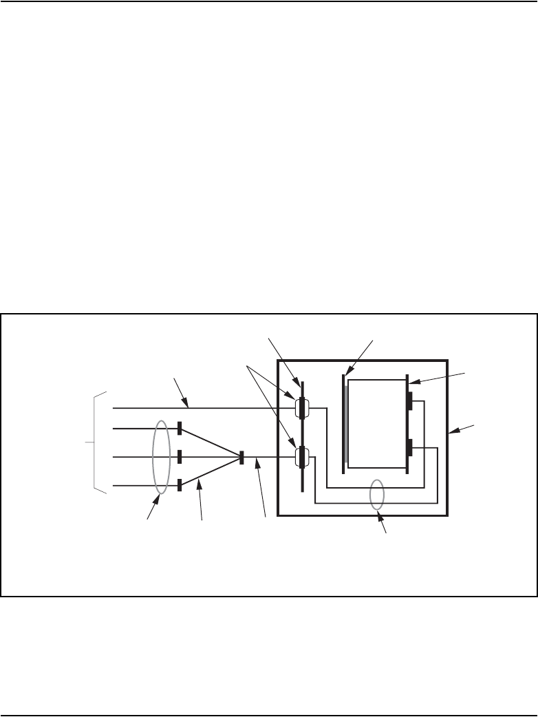
QPC841 Quad Serial Data Interface card Page 883 of 906
Circuit Card Description and Installation
• SDI multiple-port cable (internal system options use only)
—NT8D90
• SDI I/O to DTE/DCE cables (system options use only)
—NT8D95
Note: This cable is available in different lengths. Refer to Equipment
Identification (553-3001-154) for more information
• SID Multiple-port cable (system options use only)
—NT8D96
Figure 190 shows the QPC841 card and the cables listed above in a standard
configuration.
Figure 190
QPC841 QSDI card cabling
To
terminal
equipment
NT8D96
cable
NT8D90
cable
NT8D95
cables NT8D82
cables
I/O panel
NT8D95
cable
Module
front
553-2034
Q
P
C
8
4
1
J1
J2
Port 1
Port 2
Port 3
Port 4
Card
faceplate
Backplane
Filter
adapters
(Note)
Note
: Supplied with NT8D82 cable.


Page 885 of 906
Circuit Card Description and Installation
900
The TDS/DTR card
Contents
This section contains information on the following topics:
Introduction . . . . . . . . . . . . . . . . . . . . . . . . . . . . . . . . . . . . . . . . . . . . . . 885
Features . . . . . . . . . . . . . . . . . . . . . . . . . . . . . . . . . . . . . . . . . . . . . . . . . 886
Introduction
The TDS/DTR card function was incorporated into the NTDK20 SSC.
However, it is still supported on the system.
The TDS/DTR functionality is also incorporated into the NTDK97 MSC card
used with Chassis system. The TDS/DTR is not required in a 2 chassis
Chassis system.
You can install this card in slots 1 through 9 in the main cabinet. The card is
not supported in the expansion cabinets.
it must be manually programmed in LD 13 (for DTR) and LD 17 (for TDS
and TTY).
The TDS/DTR card provides:
• 30 channels of Tone and Digit Switch
• Two Serial Data Interface ports
• 8 tone detection circuits configured as Digitone Receivers

Page 886 of 906 The TDS/DTR card
553-3001-211 Standard 3.00 August 2005
Features
Tone transmitter
The TDS/DTR tone transmitter provides 30 channels of tone transmission.
Up to 256 tones are available as u-Law or A-Law and up to 256 bursts and
cadences are downloaded from the CPU.
The TDS/DTR card does not provide the Music on Hold feature as do other
TDS cards. The music source must come from a standard trunk card.
Tone detector
The TDS/DTR card provides eight channels of DTMF (Dual Tone
Multi-Frequency) detection in A-Law or µ-Law.
In North America, pre-programmed data is configured for µ-Law tone
detection.
SDI function
The TDS/DTR card provides two SDI (Serial Data Interface) ports.
Refer to “SDI ports” in Installation planning (553-3001-120) for more
information.

The TDS/DTR card Page 887 of 906
Circuit Card Description and Installation
Tones and cadences
The following tables give the tones and cadences provided by the NTAK03
TDS/DTR card.
Table 278
NTAK03, NTDK20, and NTDK97 µ-Law tones and cadence (Part 1 of 6)
Tone #
Frequency
(Hz)
dB below
overload
Precision
Ringing
Tones
DTMF
Digits MF Digits
1350/440 -23/-23 ÷
2(533 + 666) x 10 -23/-23 ÷
3440 -23 ÷
4350/440 -19/-19 ÷
5440/480 -25/-25 ÷
6480 -23 ÷
7480/620 -30/-30 ÷
81020 -16 ÷
9600 -23 ÷
10 600 -16 ÷
11 440/480 -22/-22 ÷
12 350/480 -23/-23 ÷
13 440/620 -24/-24 ÷
14 940/1630 -12/-10 P
15 700/1210 -12/-10 1
16 700/1340 -12/-10 2
17 700/1480 -12/-10 3
18 770/1210 -12/-10 4

Page 888 of 906 The TDS/DTR card
553-3001-211 Standard 3.00 August 2005
19 770/1340 -12/-10 5
20 770/1480 -12/-10 6
21 850/1210 -12/-10 7
22 850/1340 -12/-10 8
23 850/1480 -12/-10 9
24 940/1340 -12/-10 0
25 940/1210 -12/-10 *
26 940/1480 -12/-10 #
27 700/1630 -12/-10 Fo
28 770/1630 -12/-10 F
29 850/1630 -12/-10 I
30 reserved
31 reserved
32 reserved
33 400 -19 ÷
34 [400 x
(120@85%)]
-19 ÷
35 940/1630 -17/-15 P
36 700/1210 -17/-15 1
37 700/1340 -17/-15 2
38 700/1480 -17/-15 3
Table 278
NTAK03, NTDK20, and NTDK97 µ-Law tones and cadence (Part 2 of 6)
Tone #
Frequency
(Hz)
dB below
overload
Precision
Ringing
Tones
DTMF
Digits MF Digits

The TDS/DTR card Page 889 of 906
Circuit Card Description and Installation
39 770/1210 -17/-15 4
40 770/1340 -17/-15 5
41 770/1480 -17/-15 6
42 850/1210 -17/-15 7
43 850/1340 -17/-15 8
44 850/1480 -17/-15 9
45 940/1340 -17/-15 0
46 940/1210 -17/-15 *
47 940/1480 -17/-15 #
48 700/1630 -17/-15 Fo
49 770/1630 -17/-15 F
50 850/1630 -17/-15 I
51 reserved
52 reserved
53 1300/1500 -13/-13 0
54 700/900 -13/-13 1
55 700/1100 -13/-13 2/CC
56 900/1100 -13/-13 3
57 700/1300 -13/-13 4
58 900/1300 -13/-13 5
59 1100/1300 -13/-13 6
Table 278
NTAK03, NTDK20, and NTDK97 µ-Law tones and cadence (Part 3 of 6)
Tone #
Frequency
(Hz)
dB below
overload
Precision
Ringing
Tones
DTMF
Digits MF Digits

Page 890 of 906 The TDS/DTR card
553-3001-211 Standard 3.00 August 2005
60 700/1500 -13/-13 7
61 900/1500 -13/-13 8
62 1100/1500 -13/-13 9
63 700/1700 -13/-13 ST3P/RB/
C11
64 900/1700 -13/-13 STP/C12
65 1100/1700 -13/-13 KP/CR/KP1
66 1300/1700 -13/-13 ST2P/KP2
67 1500/1700 -13/-13 ST/CC
68 400 -11 ÷
69 400 -14 ÷
70 400 x 50 -14 ÷
71 (533 + 666) x 20 -23/-23 ÷
72 reserved
73 350/440 -15/-15 ÷
74 480/620 -15/-15 ÷
75 440/480 -15/-15 ÷
76 400 -25 ÷
77 400/450 -14/-14 ÷
78 480/620 -19/-19 ÷
79 440/480 -19/-19 ÷
Table 278
NTAK03, NTDK20, and NTDK97 µ-Law tones and cadence (Part 4 of 6)
Tone #
Frequency
(Hz)
dB below
overload
Precision
Ringing
Tones
DTMF
Digits MF Digits

The TDS/DTR card Page 891 of 906
Circuit Card Description and Installation
80 480 -19 ÷
81 420 -9 ÷
82 440 -29 ÷
83 reserved
84 350/440 -17/-17 ÷
85 400/450 -17/-17 ÷
86 400 -17 ÷
87 1400 -26 ÷
88 950 -12 ÷
89 1400 -12 ÷
90 1800 -12 ÷
91 470 0 ÷
92 940 0 ÷
93 1300 0 ÷
94 1500 0 ÷
95 1880 0 ÷
96 350/440 -10/-10
97 TBD
98 TBD
99 TBD
100 TBD
Table 278
NTAK03, NTDK20, and NTDK97 µ-Law tones and cadence (Part 5 of 6)
Tone #
Frequency
(Hz)
dB below
overload
Precision
Ringing
Tones
DTMF
Digits MF Digits
Page 892 of 906 The TDS/DTR card
553-3001-211 Standard 3.00 August 2005
Note: Tones #1 - 16 (inclusive) and #234 - 249 (inclusive) are included
for Norwegian and Malaysian specifications.
101 600 -19 ÷
102 800 -19 ÷
103 1400 -23 ÷
104 820 -7
Table 279
NTAK03, NTDK20, and NTDK97 A-Law tones and cadences (Part 1 of 9)
Tone # Frequency (Hz)
dB below
overload
Precision
Ringing
Tones
DTMF
Digits MF Digits
1940 X 1630 -14/-13 P
2700 X 1210 -14/-13 1
3700 X 1340 -14/-13 2
4700 X 1480 -14/-13 3
5770 X 1210 -14/-13 4
6770 X 1340 -14/-13 5
7770 X 1480 -14/-13 6
8850 X 1210 -14/-13 7
9850 X 1340 -14/-13 8
10 850 X 1480 -14/-13 9
11 940 X 1340 -14/-13 0
Table 278
NTAK03, NTDK20, and NTDK97 µ-Law tones and cadence (Part 6 of 6)
Tone #
Frequency
(Hz)
dB below
overload
Precision
Ringing
Tones
DTMF
Digits MF Digits

The TDS/DTR card Page 893 of 906
Circuit Card Description and Installation
12 940 X 1210 -14/-13 *
13 940 X 1480 -14/-13 #
14 700 X 1630 -14/-13 F0
15 770 X 1630 -14/-13 F
16 850 X 1630 -14/-13 I
17 1400 -37
89 940/1630 -13/-12 P
90 700/1210 -13/-12 1
91 700/1340 -13/-12 2
92 700/1480 -13/-12 3
93 770/1210 -13/-12 4
94 770/1340 -13/-12 5
95 770/1480 -13/-12 6
96 850/1210 -13/-12 7
97 850/1340 -13/-12 8
98 850/1480 -13/-12 9
99 940/1210 -13/-12 0
100 940/1340 -13/-12 *
101 940/1480 -13/-12 #
102 700/1630 -13/-12 F0
103 770/1630 -13/-12 F0
Table 279
NTAK03, NTDK20, and NTDK97 A-Law tones and cadences (Part 2 of 9)
Tone # Frequency (Hz)
dB below
overload
Precision
Ringing
Tones
DTMF
Digits MF Digits

Page 894 of 906 The TDS/DTR card
553-3001-211 Standard 3.00 August 2005
104 850/1630 -13/-12 I
105 350/440 -17/-17 ÷
106 400/450 -17/-17 ÷
107 1400 -26 ÷
108 440 -23 ÷
109 420 -9 ÷
110 950 -12 ÷
111 1400 -12 ÷
112 1800 -12 ÷
113 940/1630 -12/-10 P
114 700/1210 -12/-10 1
115 700/1340 -12/-10 2
116 700/1480 -12/-10 3
117 770/1210 -12/-10 4
118 770/1340 -12/-10 5
119 770/1480 -12/-10 6
120 850/1210 -12/-10 7
121 850/1340 -12/-10 8
122 850/1480 -12/-10 9
123 940/1340 -12/-10 0
124 940/1210 -12/-10 *
Table 279
NTAK03, NTDK20, and NTDK97 A-Law tones and cadences (Part 3 of 9)
Tone # Frequency (Hz)
dB below
overload
Precision
Ringing
Tones
DTMF
Digits MF Digits

The TDS/DTR card Page 895 of 906
Circuit Card Description and Installation
125 940/1480 -12/-10 #
126 700/1630 -12/-10 F0
127 770/1630 -12/-10 F
128 850/1630 -12/-10 I
129 350/440 -22/-22 ÷
130 400 -19 ÷
131 400 -25 ÷
132 400/450 -22/-22 ÷
133 1400 -15 ÷
134 950 -19 ÷
135 1400 -20 ÷
136 1800 -20 ÷
137 420 -19 ÷
138 940/1630 -18/-17 P
139 700/1210 -18/-17 1
140 700/1340 -18/-17 2
141 700/1480 -18/-17 3
142 770/1210 -18/-17 4
143 770/1340 -18/-17 5
144 770/1480 -18/-17 6
145 850/1210 -18/-17 7
Table 279
NTAK03, NTDK20, and NTDK97 A-Law tones and cadences (Part 4 of 9)
Tone # Frequency (Hz)
dB below
overload
Precision
Ringing
Tones
DTMF
Digits MF Digits

Page 896 of 906 The TDS/DTR card
553-3001-211 Standard 3.00 August 2005
146 850/1340 -18/-17 ÷ 8
147 850/1480 -18/-17 ÷ 9
148 940/1340 -18/-17 ÷ 0
149 940/1210 -18/-17 ÷ *
150 940/1480 -18/-17 ÷ #
151 700/1630 -18/-17 F0
152 770/1630 -18/-17 F
153 850/1630 -18/-17 I
154 (533 + 666) X 10 -23 ÷
155 (533 + 666) X 20 -23 ÷
156 400 -12 ÷
157 820 -14 ÷
158 420 -12 ÷
159 420 -25 ÷
160 420 X 25 -12 ÷
161 (553 + 666) X 10 -23 ÷
162 (553 + 666) X 20 -23 ÷
163 420 -22 ÷
164 480 -22 ÷
165 330 -11 ÷
166 330/440 -11/-14 ÷
Table 279
NTAK03, NTDK20, and NTDK97 A-Law tones and cadences (Part 5 of 9)
Tone # Frequency (Hz)
dB below
overload
Precision
Ringing
Tones
DTMF
Digits MF Digits

The TDS/DTR card Page 897 of 906
Circuit Card Description and Installation
167 1700 -19 ÷
168 440 -14 ÷
169 380 -8 ÷
170 1400 -32 ÷
171 820 -7 P
172 850 -8 1
173 420 -32 2
174 reserved 3
175 420 -6 4
176 420 -2 5
177 1020 -13 6
178 1800 -17 7
179 1400 -23 8
180 950 -29 9
181 1400 -29 0
182 1800 -29 *
183 950 -22 #
184 470 0F0
185 940 0 F
186 1880 0 I
187 400 -22
Table 279
NTAK03, NTDK20, and NTDK97 A-Law tones and cadences (Part 6 of 9)
Tone # Frequency (Hz)
dB below
overload
Precision
Ringing
Tones
DTMF
Digits MF Digits

Page 898 of 906 The TDS/DTR card
553-3001-211 Standard 3.00 August 2005
188 420 X 25 -17
189 950 -16
190 950 -25
191 940/1630 -9/-7
192 700/1210 -9/-7
193 700/1340 -9/-7
194 700/1480 -9/-7
195 770/1210 -9/-7
196 770/1340 -9/-7
197 770/1480 -9/-7
198 850/1210 -9/-7
199 850/1340 -9/-7
200 850/1480 -9/-7
201 940/1340 -9/-7
202 940/1210 -9/-7
203 940/1480 -9/-7
204 700/1630 -9/-7
205 770/1630 -9/-7
206 850/1630 -9/-7
207 420 -10
208 420 -8
Table 279
NTAK03, NTDK20, and NTDK97 A-Law tones and cadences (Part 7 of 9)
Tone # Frequency (Hz)
dB below
overload
Precision
Ringing
Tones
DTMF
Digits MF Digits

The TDS/DTR card Page 899 of 906
Circuit Card Description and Installation
209 420 -4
210 1400 -18
211 1400 -9
212 350/420 -9/-9
213 420 -14
214 450 -12
215 450 -22
216 820 -16
217 350/420 -14/-14
218 940/1630 -14/-12
219 700/1210 -14/-12
220 700/1340 -14/-12
221 700/1480 -14/-12
222 770/1210 -14/-12
223 770/1340 -14/-12
224 770/1480 -14/-12
225 850/1210 -14/-12
226 850/1340 -14/-12
227 850/1480 -14/-12
228 940/1340 -14/-12
229 940/1210 -14/-12
Table 279
NTAK03, NTDK20, and NTDK97 A-Law tones and cadences (Part 8 of 9)
Tone # Frequency (Hz)
dB below
overload
Precision
Ringing
Tones
DTMF
Digits MF Digits

Page 900 of 906 The TDS/DTR card
553-3001-211 Standard 3.00 August 2005
230 940/1480 -14/-12
231 700/1630 -14/-12
232 770/1630 -14/-12
233 850/1630 -14/-12
234 940 X 1630 -17/-15 p
235 700 X 1210 -17/-15 1
236 700 X 1340 -17/-15 2
237 700 X 1480 -17/-15 3
238 770 X 1210 -17/-15 4
239 770 X 1340 -17/-15 5
240 770 X 1480 -17/-15 6
241 850 X 1210 -17/-15 7
Table 279
NTAK03, NTDK20, and NTDK97 A-Law tones and cadences (Part 9 of 9)
Tone # Frequency (Hz)
dB below
overload
Precision
Ringing
Tones
DTMF
Digits MF Digits

Page 901 of 906
Circuit Card Description and Installation
906
Appendix A: LAPB Data Link Control
protocol
Contents
This section contains information on the following topics:
Introduction . . . . . . . . . . . . . . . . . . . . . . . . . . . . . . . . . . . . . . . . . . . . . . 901
Operation. . . . . . . . . . . . . . . . . . . . . . . . . . . . . . . . . . . . . . . . . . . . . . . . 901
Frame structure . . . . . . . . . . . . . . . . . . . . . . . . . . . . . . . . . . . . . . . . . . . 902
LAPB balanced class of procedure . . . . . . . . . . . . . . . . . . . . . . . . . . . . 903
Commands and responses . . . . . . . . . . . . . . . . . . . . . . . . . . . . . . . . . . . 904
Description of procedure. . . . . . . . . . . . . . . . . . . . . . . . . . . . . . . . . . . . 905
Introduction
This chapter describes the LAPB Data Link Control protocol used with the
QPC513 ESDI card. The protocol is a subset of the HDLC procedures which
are described in International Organization for Standardization procedures
ISO 3309-1979 (E), ISO 4335-1979 (E) and appendices 1 and 2, and ISO
6256-1981 (E). Refer to these procedures for complete LAPB details.
Applications which use an ESDI port in synchronous mode must conform to
the following requirements.
Operation
Circuit Switch Equipment transfers data to the QPC513 in blocks consisting
of 1 to 128 eight-bit octets. Each block is processed in accordance with the

Page 902 of 906 Appendix A: LAPB Data Link Control protocol
553-3001-211 Standard 3.00 August 2005
LAPB subset of the HDLC protocol and transmitted serially to the line at a
rate determined by the downloaded parameters.
The QPC513 card receives data serially from the line, packaged in LAPB
information frames. After determining that a block is error free the data is
supplied to the Circuit Switch Equipment as a block.
Frame structure
All transmissions are in frames and each frame conforms to the format shown
in Table 280 on page 903. In particular, frame elements for applications using
a port on the QPC513 follow these LAPB conventions:
• Zero information field is permitted.
• Inter-frame time fill is accomplished by transmitting contiguous flags.
This is compatible with AT&T Technical Requirement BX.25 and
ADCCP standards.
• Extensions for the address field or the control field are not permitted.
This requirement imposes constraints to satellite operations.
• Individual station addresses are assigned in service change for balanced
configuration. The default ESDI address is 10000000. The far-end
default address is 11000000.
• The LAPB basic control field (modules 8) format is implemented.
• Frame check sequence is implemented in accordance with LAPB
procedures.

Appendix A: LAPB Data Link Control protocol Page 903 of 906
Circuit Card Description and Installation
LAPB balanced class of procedure
Applications which use ports on the QPC513 are automatically designated as
BAC, 2, 8 (for example, balanced operation, asynchronous balanced mode
class of procedure with optional functions 2 and 8 implemented).
Balanced configuration
A balanced configuration is one in which two combined stations have
identical responsibilities for exchanging data and control information and for
initiating error recovery functions, as shown in Figure 191 on page 904.
Combined station
A combined station has balanced link control capability and transmits both
commands and responses to, and receives both commands and responses
from the other combined station.
Table 280
LAPB frame structure
Flag Address Control Information FCS Flag
01111110 8 bits 8 bits unspecified
(no. of bits)
16 bits 01111110
Legend:
Flag: Flag sequence – All frames start and end with the flag sequence. (A single flag is used as both the
closing flag for one frame and the opening flag for the next frame.)
Address: Station address field – In command frames, the address identifies the station for whom the
command is intended. In response frames, the address identifies the station from which the response
originated.
Control: Control field – This field contains commands or responses and sequence numbers.
Information: Information field – Information may be any sequence of bits, usually related to a convenient
character structure such as an octet, but may be an unspecified number (from 1 to 128) of bits unrelated to
a character structure.
FCS: Frame check sequence.

Page 904 of 906 Appendix A: LAPB Data Link Control protocol
553-3001-211 Standard 3.00 August 2005
Asynchronous Balanced Mode
Asynchronous Balanced Mode (ABM) is a balanced, configured operational
mode in which either combined station may send commands at any time and
may initiate certain response frame transmissions without receiving
permission from the other combined station.
Commands and responses
The elements of procedure are described in terms of actions which take place
when a command is received. The classes of procedures are a combination of
the frame structure and the set of elements that satisfy the requirements of a
specific application. The LAPB Balanced Asynchronous Class of Procedure
(BAC, 2, 8) is implemented. This is compatible with both BX.25 and ADCCP
specifications. The basic set of commands and responses is listed in
Table 281 on page 905.
Figure 191
Balanced configuration
Commands
Combined
station Combined
station
Responses 553-3741

Appendix A: LAPB Data Link Control protocol Page 905 of 906
Circuit Card Description and Installation
Description of procedure
The basic LAPB procedures must be implemented to satisfy the following:
• standard use of the poll/final bit (for more information, see
ISO-4375-1979-[E])
• exception condition reporting and recovery implemented in accordance
with BX.25 and ADCCP specifications
• link set-up and disconnect implemented according to BX.25
specifications
Table 281
Commands and responses
Command Response Option
I8
RR RR
RNR RNR
REJ REJ or FRMR 2
SABM UA
DISC DM
Legend:
I: Information
RR: Receive ready
RNR: Receive not ready
REJ: Reject
SABM: Set asynchronous balanced mode
DISC: Disconnect
RSET: Reset
FRMR: Frame reject
UA: Unnumbered acknowledge
DM: Disconnect mode
Option 2: Provides ability for more timely reporting of I frame sequence errors
Option 8: Limits the procedure to allow I frames to be commands only

Page 906 of 906 Appendix A: LAPB Data Link Control protocol
553-3001-211 Standard 3.00 August 2005

Family Product Manual Contacts Copyright FCC notice Trademarks Document
number Product release Document release Date Publish
Nortel Communication Server 1000
Circuit Card
Description and Installation
Copyright © Nortel Networks Limited 2005
All Rights Reserved
Information is subject to change without notice.
Nortel Networks reserves the right to make changes in design
or components as progress in engineering and manufacturing
may warrant.
Nortel, Nortel (Logo), the Globemark, This is the Way, This is
Nortel (Design mark), SL-1, Meridian 1, and Succession are
trademarks of Nortel Networks.
Publication number: 553-3001-211
Document release: Standard 3.00
Date: August 2005
Produced in Canada
