Novyc NOVYC1 RF TRANSCEIVER MODULE User Manual RFDP8 RF Modules Manual 2013
Novyc International Inc. RF TRANSCEIVER MODULE RFDP8 RF Modules Manual 2013
Novyc >
Users Manual
13715 Alton Pkwy • Irvine • CA • 92618
Tel: 949.610.0008 • www.RFdigital.com
Fast Answers: support@rfdigital.com
Free Applications Support • Email your application questions to support@rfdigital.com 1
RFDP8
© Copyright, RF Digital
1/29/2013 9:40 AM
Patents Pending
RoHS CE • ESTI
RFD21733/35 • FCC • IC
RFD21743 • FCC
Approved & Certified
RF Module
RFD21733
RFD21735
RFD21737
RFD21738
RFD21739
RFDP8
RFDANT
RFD21742
RFD21743
RFD21772
RFD21773
KEYFOBs
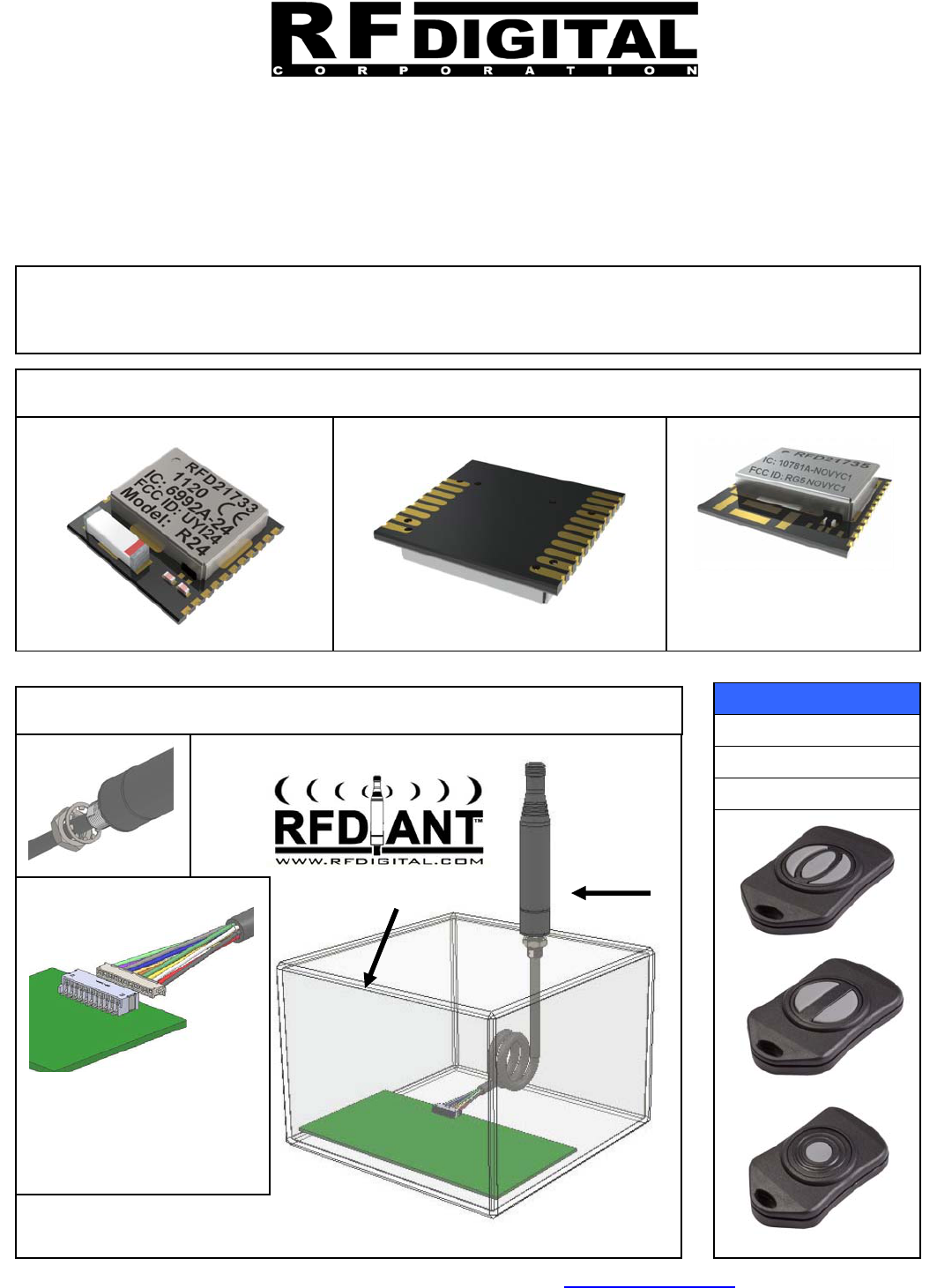
Compliance Approved 2.4 GHz RF Transceiver Modules
with Built-In RFDP8 Application Protocol
rw
Optional Configuration
For use with
max. 5dBi Gain
External Whip Antenna
RFD21733
/
35 IC
&
FCC APPROVED
15mm x 15mm
(0.600 x 0.600 Inch)
Complete Compliance Approved & Certified, READY-TO-USE, 2.4 GHz wireless solution with built-in RFDP8
interference-tolerant user application protocol. Includes RFID, 32 Bit ESN, Logic Switch Transmitter / Receiver,
9600-8N1 Serial UART Transceiver and many easy-to-use addressable network modes. No development required at
all, no RF layout, no code writing, all features are built-in. Be up and running with a wireless solution in minutes.
KEYFOBs & RFID
500 Foot Range
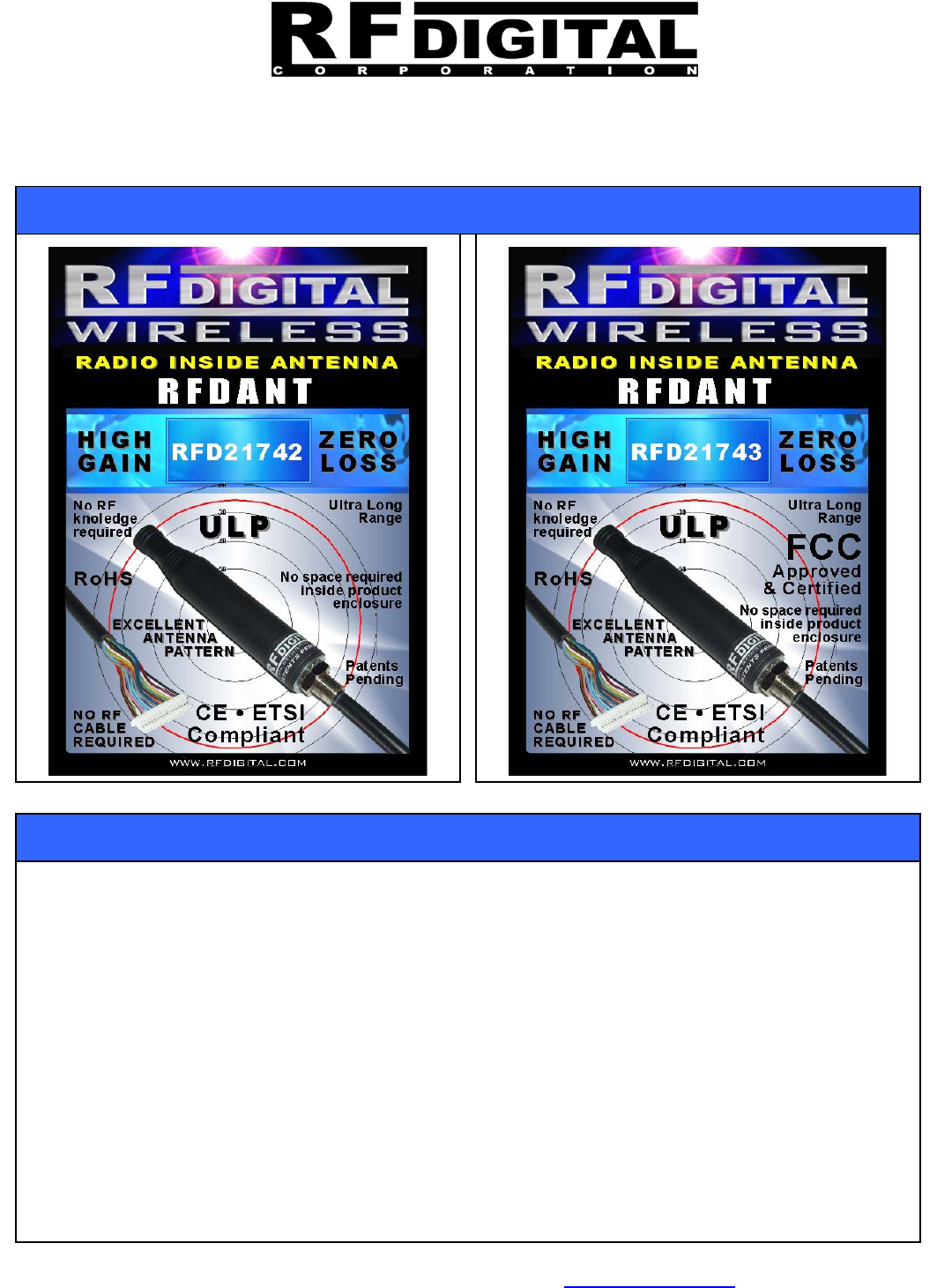
RFDANT • RFD21743 FCC APPROVED
CE • ESTI TESTED & COMPLIANT Eas
y
to solder 0.050 Inch SMT
p
ads
Simple
Drill Hole
Mount
2,000 FOOT ULTRA LONG RANGE
Standard RFDP8 Interface
No Need for RF cables.
Only +3V • GND • Data.
1.5mm 11pin Connector.
Fits onto any PCB.
SMT or Through Hole.
Complete
RADIO
INSIDE
Antenna
Use any plastic or metal
enclosure.
Patents
Pending
CE • ESTI TESTED & COMPLIANT IC • FCC APPROVED
CE • ETSI Compliant
Standard & Custom
13715 Alton Pkwy • Irvine • CA • 92618
Tel: 949.610.0008 • www.RFdigital.com
Fast Answers: support@rfdigital.com
Free Applications Support • Email your application questions to support@rfdigital.com 2
RFDP8
© Copyright, RF Digital
1/29/2013 9:40 AM
Patents Pending
RoHS CE • ESTI
RFD21733/35 • FCC • IC
RFD21743 • FCC
Approved & Certified
RF Module
RFD21733
RFD21735
RFD21737
RFD21738
RFD21739
RFDP8
RFDANT
RFD21742
RFD21743
RFD21772
RFD21773
KEYFOBs
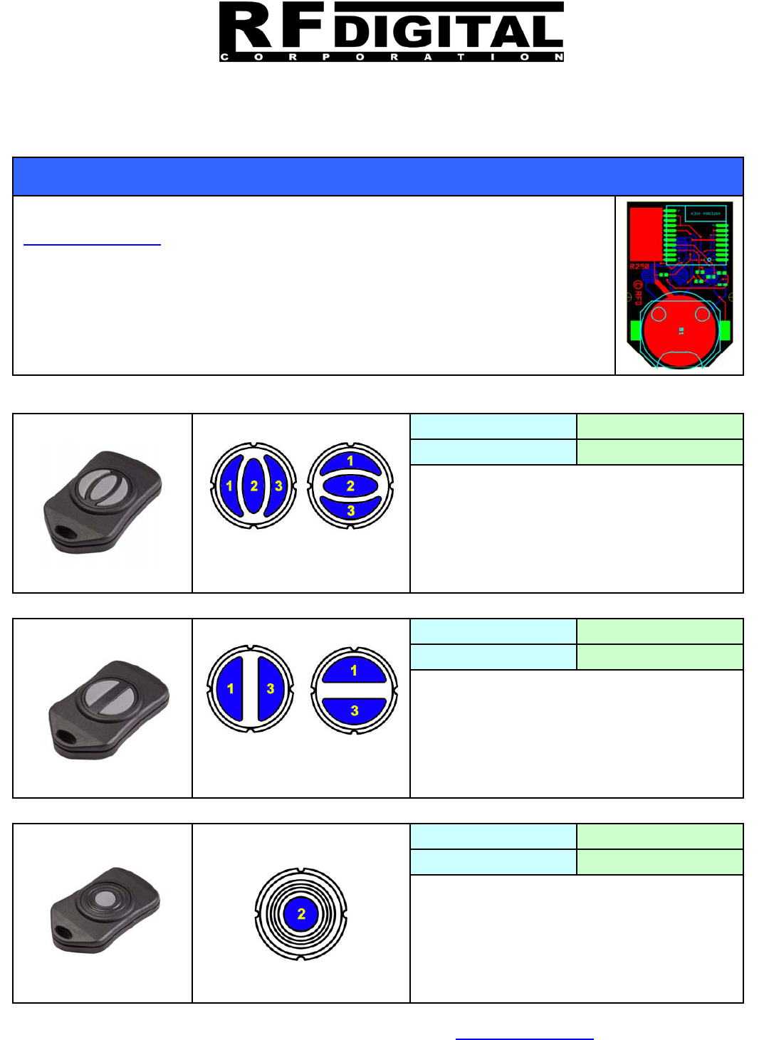
The RFD21733 Module with its RFID interval factory set to 30 seconds is inside of a KEYFOB
enclosure with a CR2032 battery. The reference layout for this device is available through
support@rfdigital.com if you want to build it yourself. However if you wish to purchase the
ready-made KEYFOBs from RF Digital they are available, part numbers shown below.
There are two modes of use, one is in Active RFID mode were the KEYFOB automatically
transmits its ESN once every 30 seconds. The other mode of use is SWITCH transmitter, which
is available in 1, 2 or 3 buttons. The RFID versions also have 1, 2 or 3 buttons so they serve as
an automatic RFID transmitter and in addition have the switch buttons in one KEYFOB.
If you do not need the automatic Active RFID feature, just use the Switch Button KEYFOBs.
KEYFOBs
Pressing button 1, 2 or 3 will cause the output 1, 2
or 3 on the RFD21733 Module or RFD21743 /
RFD21732 RFDANT to go high for the duration the
button is pressed, when in one of the 4 switch
modes. If in Serial UART mode, then you will
receive 1 byte representing which button is
pressed or if RFID transmission and 4 more bytes
indicatin
g
the 32 bit uni
q
ue ESN of the KEYFOB.
Rotatable Buttons
RFD21783
3 Button RFID Ke
y
fob3 Button Switch Ke
y
fob
RFD21793
Pressing button 1 or 3 will cause the output 1 or 3
on the RFD21733 Module or RFD21743 / RFD21732
RFDANT to go high for the duration the button is
pressed, when in one of the 4 switch modes. If in
Serial UART mode, then you will receive 1 byte
representing which button is pressed or if RFID
transmission and 4 more bytes indicating the 32
bit uni
q
ue ESN of the KEYFOB.
Rotatable Buttons
RFD21782
2 Button RFID Ke
y
fob2 Button Switch Ke
y
fob
RFD21792
Pressing button 2 will cause the output 2 on the
RFD21733 Module or RFD21743 / RFD21732
RFDANT to go high for the duration the button is
pressed, when in one of the 4 switch modes. If in
Serial UART mode, then you will receive 1 byte
representing which button is pressed or if RFID
transmission and 4 more bytes indicating the 32
bit uni
q
ue ESN of the KEYFOB.
RFD21781
1 Button RFID Ke
y
fob1 Button Switch Ke
y
fob
RFD21791
13715 Alton Pkwy • Irvine • CA • 92618
Tel: 949.610.0008 • www.RFdigital.com
Fast Answers: support@rfdigital.com
Free Applications Support • Email your application questions to support@rfdigital.com 3
RFDP8
© Copyright, RF Digital
1/29/2013 9:40 AM
Patents Pending
RoHS CE • ESTI
RFD21733/35 • FCC • IC
RFD21743 • FCC
Approved & Certified
RF Module
RFD21733
RFD21735
RFD21737
RFD21738
RFD21739
RFDP8
RFDANT
RFD21742
RFD21743
RFD21772
RFD21773
KEYFOBs
Range results need to be tested for every application and scenario. RF Digital's range tests are done line-o
f
-sight
and outdoors in a typical city street setting. You should use these typical range test results as a point of reference,
until you can conduct your own range tests in your own test environment. If you have any questions, always feel
free to contact RF Digital Support at support@rfdigital.com
RFD21733 RFD21743
MODULE RFDANT
1,000
FOOT
RANGE
RFD21733
MODULE 500
FOOT
RANGE
RFD21733
MODULE
RFD21743
RFDANT
2,000
FOOT
RANGE
RFD21743
RFDANT
TYPICAL RANGE
150
Meters
300
Meters
600
Meters
LONG RANGE
L
O
N
G
ER RAN
G
E
ULTRA LONG RANGE
RFD21742
RFD21742RFD21742
13715 Alton Pkwy • Irvine • CA • 92618
Tel: 949.610.0008 • www.RFdigital.com
Fast Answers: support@rfdigital.com
Free Applications Support • Email your application questions to support@rfdigital.com 4
RFDP8
© Copyright, RF Digital
1/29/2013 9:40 AM
Patents Pending
RoHS CE • ESTI
RFD21733/35 • FCC • IC
RFD21743 • FCC
Approved & Certified
RF Module
RFD21733
RFD21735
RFD21737
RFD21738
RFD21739
RFDP8
RFDANT
RFD21742
RFD21743
RFD21772
RFD21773
KEYFOBs
• Active RFID
• Long Range RFID
• Remote Control
• Light Controls
• Home Automation
• Alarm Security
• Keyless Entry
• Perimeter Monitoring
• PC Keyboard Security
• Wireless Keyboard
• Wireless Mouse
• TV Remote
• Home Stereo Remote
• Asset Tracking
• Wireless PTT
• Remote Switches
• Remote Terminals
• Wireless RS232 DB9
• Wireless RS485
• Temperature Control
• HV/AC
• Meter Reading
• Data Acquisition
• Inventory Control
• Keyfob Remotes
• Industrial Controls
• Vending Machines
• Pan-Tilt-Zoom Control
• Camera Flash Control
• Biometrics
• Seismic Monitoring
• M2M & many more…
TYPICAL APPLICATIONS
RFD21743
RFDANT
700
FOOT
RANGE
RFD21783
KEYFOB / RFID 350
FOOT
RANGE
RFD21733
MODULE
100
Meters
200
Meters
LONG RANGE
LONGER RANGE
RFD21742
RFD21782
RFD21781
RFD21793
RFD21792
RFD21791
RFD21783
KEYFOB / RFID
RFD21782
RFD21781
RFD21793
RFD21792
RFD21791
13715 Alton Pkwy • Irvine • CA • 92618
Tel: 949.610.0008 • www.RFdigital.com
Fast Answers: support@rfdigital.com
Free Applications Support • Email your application questions to support@rfdigital.com 5
RFDP8
© Copyright, RF Digital
1/29/2013 9:40 AM
Patents Pending
RoHS CE • ESTI
RFD21733/35 • FCC • IC
RFD21743 • FCC
Approved & Certified
RF Module
RFD21733
RFD21735
RFD21737
RFD21738
RFD21739
RFDP8
RFDANT
RFD21742
RFD21743
RFD21772
RFD21773
KEYFOBs
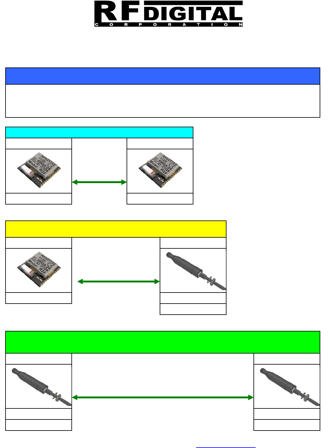
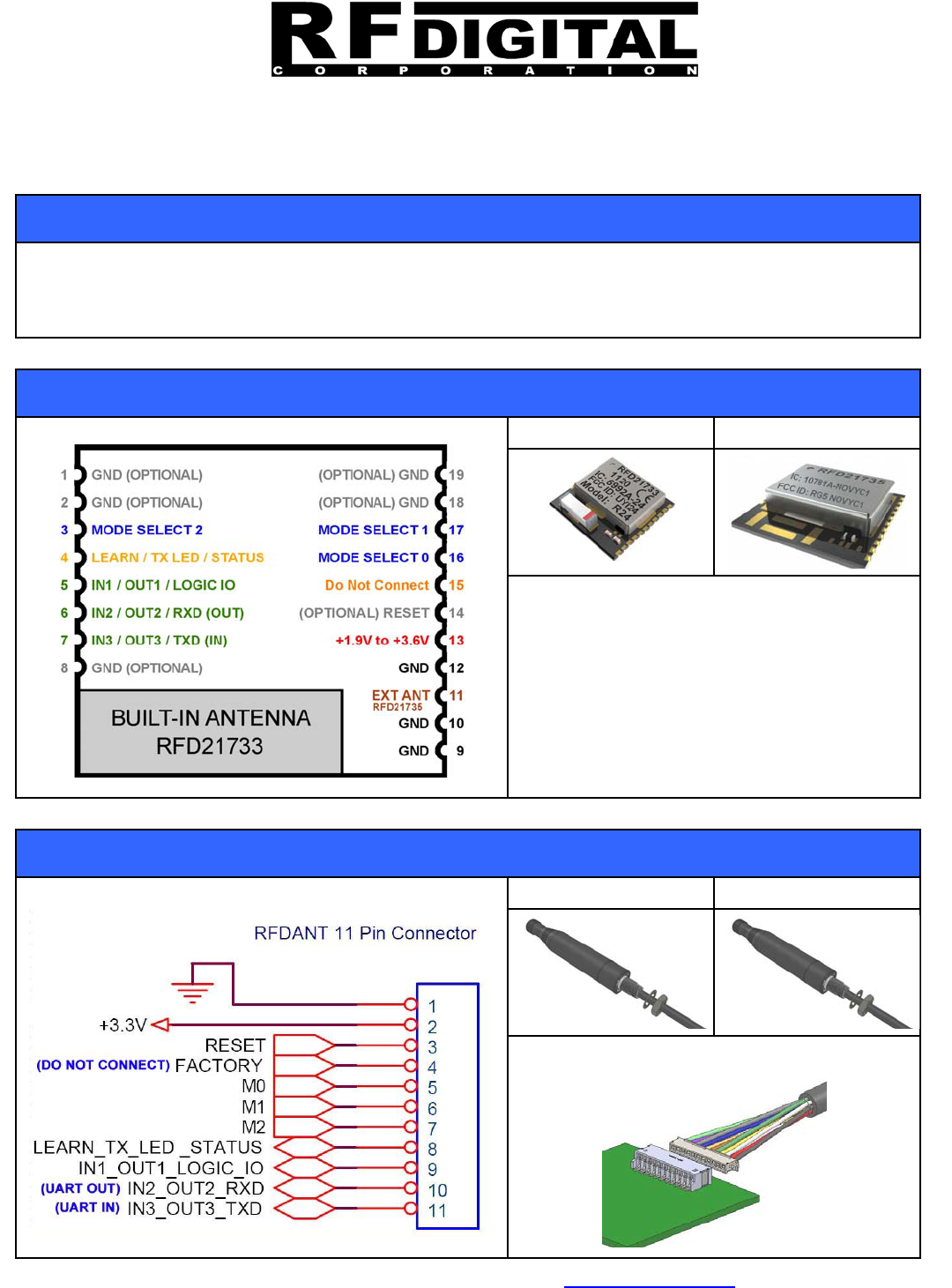
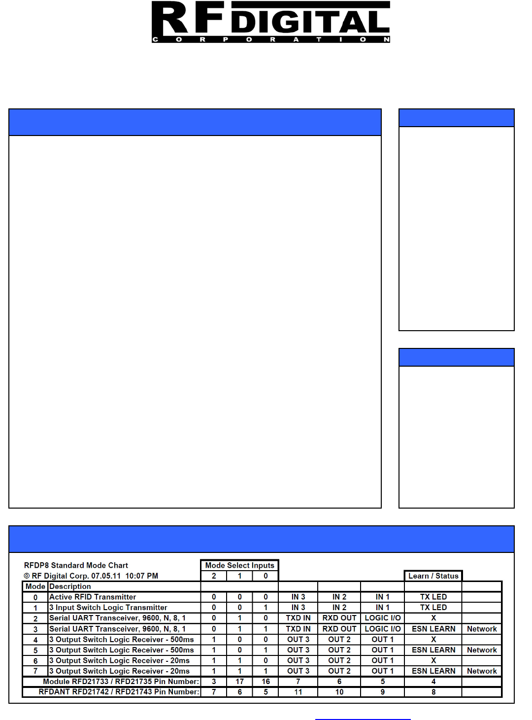
RFD21733 • RFD21735 MODULEs
There are 11 total active signal pins including power and ground for both MODULEs and RFDANTs. The MODULEs
have 7 additional ground pins. Also the MODULES have one extra pin for a total of 19 pins, this is pin 11, which
applies only to the RFD21735 which is for external antenna, however the RFD21733 pin 11 is a no-connect since it
has a built-in antenna.
PINOUTs
RFD21742 • RFD21743 RFDANTs
RFD21733 RFD21735
There are a total of 8 ground pins, you only need
just one ground pin for an electrical connection to
make the module function. The additional ground
pins are for convenience and also performance
with layout configurations. The pin 12, 10 and 9
are recommended to always be connected since
they help provide some ground area for the
module as well as on the opposing side of the
antenna. However just one single ground out any
of the 8 GND pins are adequate for proper
function.
RFD21742 RFD21743
The black wire (ground) is pin #1, the red wire (+V)
is pin #2, and so on. See pin out on left side.
13715 Alton Pkwy • Irvine • CA • 92618
Tel: 949.610.0008 • www.RFdigital.com
Fast Answers: support@rfdigital.com
Free Applications Support • Email your application questions to support@rfdigital.com 6
RFDP8
© Copyright, RF Digital
1/29/2013 9:40 AM
Patents Pending
RoHS CE • ESTI
RFD21733/35 • FCC • IC
RFD21743 • FCC
Approved & Certified
RF Module
RFD21733
RFD21735
RFD21737
RFD21738
RFD21739
RFDP8
RFDANT
RFD21742
RFD21743
RFD21772
RFD21773
KEYFOBs
• Runs on a single coin cell for years.
• WiFi interference tolerant.
• Heavy 2.4 GHz noise and interference tolerant.
• Motor noise and interference tolerant.
• Very low cost.
• No external parts required.
• No RF layout required.
• Easy and ready-to-use, hand-held, eval and application boards available.
• Ultra small 15mm x 15mm footprint (RFD21733/RFD21735)
• Fully contained, truly finished, ready to use module.
• CE / ETSI / IC & FCC Certified and Approved.
• Typical range: 500 feet (150 meters): RFD21733 MODULE.
• Typical range: 2,000 feet (600 meters): RFD21742 and RFD21743 RFDANTs.
• Worldwide 2.4GHz ISM band operation.
• User configurable without need for any programming.
• 2uA Ultra low power modes.
• Only 14mA current consumption at 0dbm TX and 17mA at RX.
• 16 bit CRC data accuracy verification built-in.
• 32 bit unique factory ESN in every module (4 billion combination security).
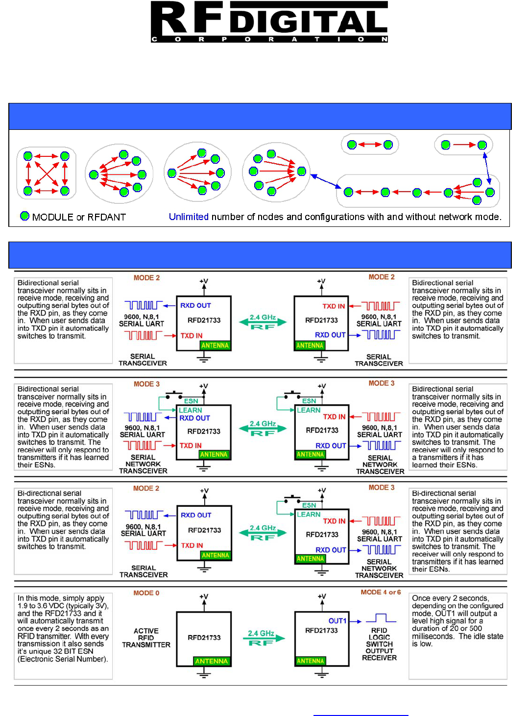
• Flexible network modes, including broadcast and individual addressing.
• Optional version available for use with external antenna (RFD21735).
• Switch on/off, logic, remote-control without the need for an external controller.
• Switch nodes individually addressable without the need for an external controller.
• Wide supply range +1.9V to +3.6V.
• Built-in, high performance internal miniature antenna (RFD21733).
• Peer to Peer (Ad-Hoc) networks and configurations.
• Point to Multi-Point networks and configurations.
• Multi-Point to Multi-Point networks and configurations.
• Selective addressing of any module by using factory built-in ESN.
• Fast-turn-around, minimal latency (20 milliseconds).
• Patent pending RFDP8 interference tolerant protocol.
• Full application protocol runs transparent to the user.
• Easy to use, simple to design in.
• Stores up to 60 ESNs (Electronic Serial Numbers) for network modes.
• Many to one data modes ideal for multi-point data acquisition.
• Unlimited number of module nodes can communicate to each other.
FEATURES RF Digital's RFDP8
application firmware
loaded into the
MODULEs or RFDANTs
can be customized to
fit application specific
requirements.
RF Digital can design
and manufacture fully
custom modules to fit
your needs.
If you do not find what
you're looking for, feel
free to contact
RF Digital with your
requirements. Email:
support@rfdigital.com
CUSTOM Modules
RFDP8 Application Protocol • Mode Selector Chart
For free RF layout
design reviews, send
color screen captures
of your layout to
support@rfdigital.com,
you will save time and
money before you fab
your boards.
Our FAST RESPONSE
Support Team
welcomes your
questions!
FAST Support
13715 Alton Pkwy • Irvine • CA • 92618
Tel: 949.610.0008 • www.RFdigital.com
Fast Answers: support@rfdigital.com
Free Applications Support • Email your application questions to support@rfdigital.com 7
RFDP8
© Copyright, RF Digital
1/29/2013 9:40 AM
Patents Pending
RoHS CE • ESTI
RFD21733/35 • FCC • IC
RFD21743 • FCC
Approved & Certified
RF Module
RFD21733
RFD21735
RFD21737
RFD21738
RFD21739
RFDP8
RFDANT
RFD21742
RFD21743
RFD21772
RFD21773
KEYFOBs
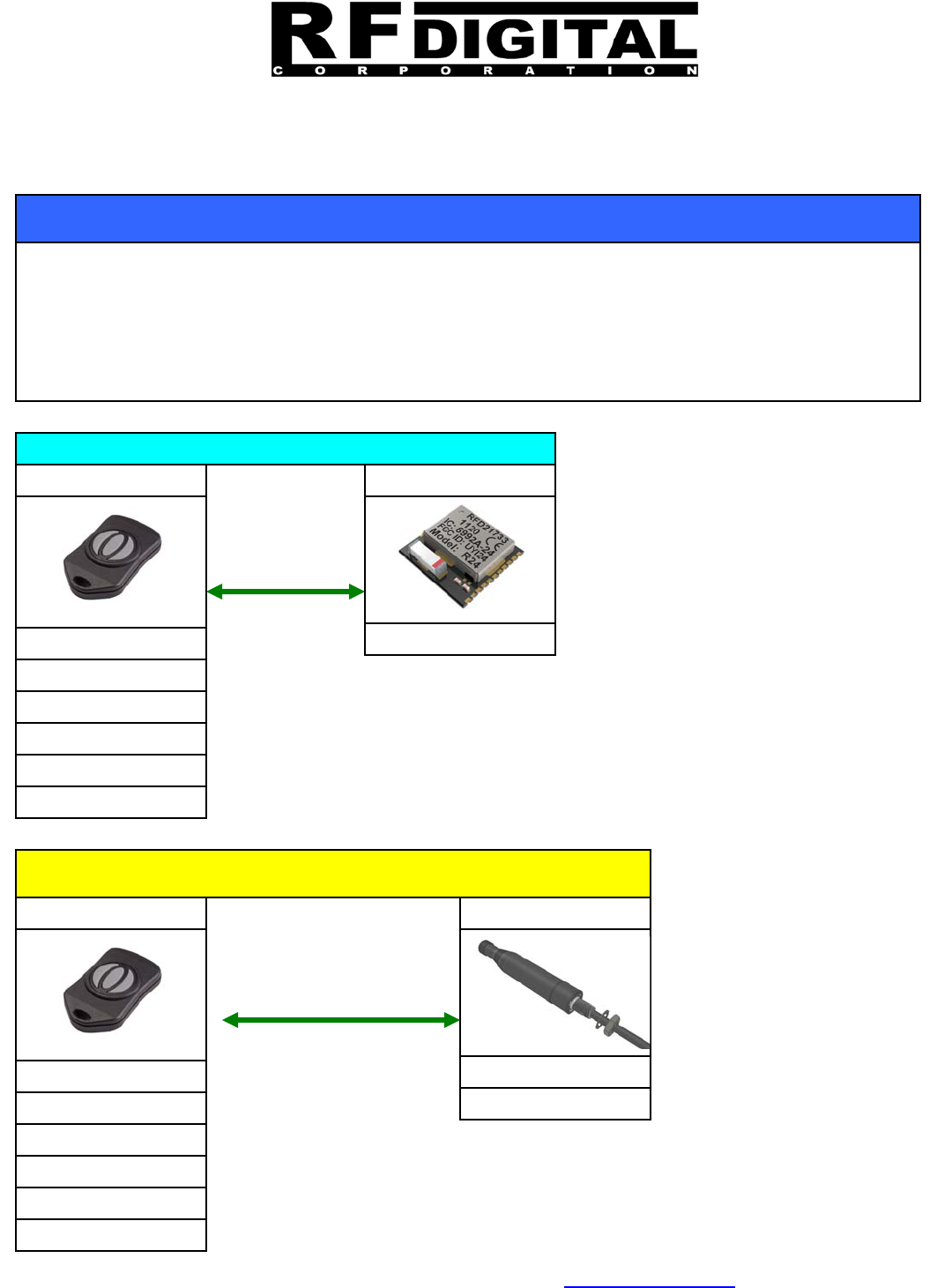
The RFD21733 RF Module and the RFD21742 / RFD21743 RFDANTs have the same electrical interface and are both
embedded with the Patent Pending RFDP8 interference immunity protocol. They are pin for pin electrically
compatible. Except for the different form factor, cost and range, they are basically the same. The RFDANTs have
an 8 inch long 1.5mm, 11pin connector termination for its interface to your electronics, were the RFD21733 module
has a 19 pin SMT interface and solders to your PCB. Only 11 out of the 19 pins are used for electrical interface.
The RFD21733 is only 15mm square and has a range of about 500 feet. The RFD21733 module is about one quarter
the cost of the RFDANT. So why would you use the RFDANT? There are many reasons: The RFDANT is
hermetically, fully potted and over-molded, has an industrial rugged enclosure and the full radio system and
processing is all built into the Antenna structure itself. The RFDANTs mounting does not require a PCB at all,
simply just drill a hole into your enclosure and feed the 8 inch cable through and apply a nut and your RFDANT is
mounted and ready for use. The RFDANT does not have impacts from proximity effects from near-by metal
enclosures and objects. The RFDANT has a perfect antenna pattern which provides extraordinary, consistent
repeatable performance.
The RFDANT’s Revolutionary Patent Pending design enables it to reach distances of 2,000 feet, while still being an
Ultra Low Power device. This huge range is reached without any power amplifiers at all, it’s unique design is
responsible for it reaching these great distances without any extra battery drain or extra power. The RFDANT
makes it easy for you to satisfy GREEN directives due to its unique design and ultra high performance.
The RFDANT fits in the palm of your hand and looks like an Antenna, but of course it is much more since it is the
whole radio and processing system in one unit. There are no RF cables at all, simply connect +V, GND, and a few
logic signal wires based on your application and you are done. There is no need for PCB layout either. You can
directly connect to the 11 pin, 8 inch cable extending out of the bottom of the RFDANT.
The RFD21733 is an ideal partner with the RFD21743 or RFD21742 RFDANTs. They can communicate with each
other using the RFDP8 protocol with switch logic IO or Serial UART. You can mix and match them as well, with
using RFD21733 on one end of your system and an RFDANT on the other.
The RFD21733 is a perfect fit when you need ultra small size and ultra low cost, and the RFDANT is an ideal solution
when you need ultra long range and do not want to place any parts onto your PCB.
Even if you will not be using the RFDANT for your application, it is still highly recommended to place the 11 pin
connector footprint on your PCB for the RFD21733 so you can have the option to simply plug in the RFDANT for
testing during your proto phases, or if you happen to have a customer come to you and ask for more range, you can
simply give it to them by not soldering the RFD21733 and instead plugging in the RFD21742 or RFD21743 RFDANT.
If you have further questions about the trade offs between the Modules and the RFDANTs, always feel free to
contact support@rfdigital.com were you will find very quick and helpful answers to your questions.
Choosing between RFD21733 Module or RFD21743 RFDANT
Solders to your PCB with its SMT pads.
Plugs into your PCB using its 8 inch long cable.
RFD21733 Module
RFD21742 or RFD21743 RFDANT
13715 Alton Pkwy • Irvine • CA • 92618
Tel: 949.610.0008 • www.RFdigital.com
Fast Answers: support@rfdigital.com
Free Applications Support • Email your application questions to support@rfdigital.com 8
RFDP8
© Copyright, RF Digital
1/29/2013 9:40 AM
Patents Pending
RoHS CE • ESTI
RFD21733/35 • FCC • IC
RFD21743 • FCC
Approved & Certified
RF Module
RFD21733
RFD21735
RFD21737
RFD21738
RFD21739
RFDP8
RFDANT
RFD21742
RFD21743
RFD21772
RFD21773
KEYFOBs
The RFD21742 and RFD21743 are 100% identical hardware, the only difference between the two is firmware loaded
at the RF Digital factory.
The RFD21742 is in compliance with CE / ETSI emission requirements and is not for FCC.
The RFD21743 is in compliance with CE / ETSI emission requirements and is FCC Certified and Approved.
The high performance of the RFDANT for FCC requires it to work in a 50% duty cycle mode, which means that when
you are running it in its 9600-8N1 UART mode, you can send up to 24 bytes in a row and then you must wait a
minimum of 24 byte lengths which is about 24mS before you send up to another 24 bytes. For example you can
also send 12 bytes, wait 12mS and then send 12 bytes again, effectively yielding a 50% duty cycle. Note this is only
a transmit limitation with the RFDANT, it is not related to receive, so if you have a RFD21733 sending 100% duty
cycle at full speed, you can receive that with either RFDANT and it will be fine. But when you go to transmit, if you
are using the RFD21743 you will need to use a maximum of a 50% duty cycle for the USA and FCC. However when
using the RFD21742 which is for Europe and the CE / ETSI markets, there is no duty cycle limitation.
That is the reason there are two part numbers for the RFDANT, the RFD21743 is 50% UART duty cycle for FCC and
the RFD21742 is CE and ETSI with 100% duty cycle.
So if you plan on selling into the USA market place, then use the RFD21743, if you are Europe ONLY, then you can
use the RFD21742. Also, of course you can use the RFD21743 for USA and Europe.
If you are sending in switch mode using the RFD21742, it will send a new packet every 16mS and the hang time for a
switch receiver in mode 6 or 7 is 50ms. Where with the RFD21743 it will send a new packet every 24ms to work
within the 50% duty cycle limit for FCC and IC.
If you require Canada (IC) Approval for the RFD21743, please contact sales@rfdigital.com.
The impact with switch mode is hardly even noticed between the RFD21743 and RFD21742.
Most common applications are typically with burst data less then 24 bytes per burst, so the difference between the
RFD21743 and RFD21742 is negligible, nevertheless the choice is still available for you and they are pin for pin
compatible.
Once you test an RFDANT, you will be truly amazed with its performance.
Differences between RFD21742 and RFD21743 RFDANTs
Plugs into your PCB using its 8 inch long cable.
RFD21742 RFDANT
Plugs into your PCB using its 8 inch long cable.
RFD21743 RFDANT
CE
•
ETSI
FCC
CE
•
ETSI

13715 Alton Pkwy • Irvine • CA • 92618
Tel: 949.610.0008 • www.RFdigital.com
Fast Answers: support@rfdigital.com
Free Applications Support • Email your application questions to support@rfdigital.com 9
RFDP8
© Copyright, RF Digital
1/29/2013 9:40 AM
Patents Pending
RoHS CE • ESTI
RFD21733/35 • FCC • IC
RFD21743 • FCC
Approved & Certified
RF Module
RFD21733
RFD21735
RFD21737
RFD21738
RFD21739
RFDP8
RFDANT
RFD21742
RFD21743
RFD21772
RFD21773
KEYFOBs
Revolutionary RFDANT Advantages
The RFD21743 and RFD21743 RFDANT are full 2.4 GHz radio transceivers including the RFDP8 protocol,
completely built into an antenna form factor allowing the entire radio transceiver to be outside your
product, where only the power and signal cable will extend into your product enclosure to then be
connected to your PCB with a simple 1.5mm SMT or THROUGH HOLE connector.
The RFD21742 and RFD21743 is functionally identical to the RFD21733 module and the RFD21772 and
RFD21733 Eval Boards work just like the RFD21737 Eval Board except it has an 11 pin 1.5mm connector
on it so the RFD21742 or RFD21743 RFDANT can plug into it. The RFD21772 is the Eval board for the
RFD21742 and the RFD21773 is the Eval board for the RFD21743. The RFD21772 and RFD21773 each
include one RFDANT. You need a pair for a complete system.
The RFD21742 and RFD21743 RFDANTs have been range tested at 2,000 feet which is 4x the range of
the RFD21733 which is at 500 feet. No special PCB layout is needed for the RFD21742 or RFD21743
RFDANT, simply just put a connector on your PCB and you are done . All this substantial range
increase is achieved all without any increase in current or battery consumption.
The RFDANT is RF Digital's Patent Pending Radio Inside Antenna product, which is a complete radio
transceiver and antenna mounted inside of an antenna enclosure, suitable for mounting to virtually any
type of end-product, regardless if the enclosure is plastic, metal, glass, really any material.
The entire radio transceiver is mounted inside the antenna enclosure, so there is no loss of RF power to
the antenna from the module, and results in the most effective power transfer ratio possible, providing
lowest power consumption possible to achieve a specific range.
The radio being inside of the antenna and outside the enclosure allows for more room inside the
enclosure for the designers application electronics.
Minimal interference with the internal electronics of the enclosure results in better range and
performance of the wireless system.
The actual effective antenna is pushed away from the enclosure, which reduces the effect of holding the
enclosure, therefore improving the performance, range and predictability of the users wireless system.
Logic level signals are communicated through an unshielded cable (not coax) to the RFDANT, which can
be run for long distances without any loss to the performance of the wireless transceiver.
By the antenna and module being fully outside allows for easy retrofit of nearly any product due to it not
consuming any internal space inside the enclosure, drill a hole and screw it in, add a nut inside to
secure it and wire the logic level signals to your electronics.
Mount on metal or plastic enclosures with no worry about ground effects.
Stable Antenna Pattern providing substantial, well-distributed, passive-gain for transmit and receive,
results longer repeatable range from your wireless system.
For free Schematic and Layout design reviews, send color screen captures or PDFs of your schematic and
layout to support@rfdigital.com. RF Digital’s Support and Application Engineers are ready to help you get your
wireless application running to today. Just send your application questions to support@rfdigital.com and receive
direct, fast and accurate answers. We look forward to helping you!!!
13715 Alton Pkwy • Irvine • CA • 92618
Tel: 949.610.0008 • www.RFdigital.com
Fast Answers: support@rfdigital.com
Free Applications Support • Email your application questions to support@rfdigital.com 10
RFDP8
© Copyright, RF Digital
1/29/2013 9:40 AM
Patents Pending
RoHS CE • ESTI
RFD21733/35 • FCC • IC
RFD21743 • FCC
Approved & Certified
RF Module
RFD21733
RFD21735
RFD21737
RFD21738
RFD21739
RFDP8
RFDANT
RFD21742
RFD21743
RFD21772
RFD21773
KEYFOBs
RFDANT • RFD21742 • RFD21743 • Compliance Approved
Mating connectors for the 11 pin RFDANT can be found at Digikey in the USA at: http://www.digikey.com
or at any other JST distributor. They are standard connectors and you may use other manufacturers.
1) Top Entry, Through Hole Type, 11 pos
a. Digikey P/N 455-1666-ND
b. Manufacturer P/N: B11B--ZR
2) Side Entry, Through Hole Type, 11 pos
a. Digikey P/N 455-1678-ND
b. Manufacturer P/N: S11B--ZR
3) Top Entry, SMT Type, 11 pos
a. Digikey P/N 455-1690-2-ND
b. Manufacturer P/N: B11B—ZR-SM4-TF
4) Side Entry, SMT Type, 11 pos
a. Digikey P/N 455-1701-2-ND
b. Manufacturer P/N: S11B—ZR-SM4-TF
RFDANT • RFD21742 • RFD21743 • Mating Connectors
13715 Alton Pkwy • Irvine • CA • 92618
Tel: 949.610.0008 • www.RFdigital.com
Fast Answers: support@rfdigital.com
Free Applications Support • Email your application questions to support@rfdigital.com 11
RFDP8
© Copyright, RF Digital
1/29/2013 9:40 AM
Patents Pending
RoHS CE • ESTI
RFD21733/35 • FCC • IC
RFD21743 • FCC
Approved & Certified
RF Module
RFD21733
RFD21735
RFD21737
RFD21738
RFD21739
RFDP8
RFDANT
RFD21742
RFD21743
RFD21772
RFD21773
KEYFOBs
-70
-60
-50
-40
-30
-20
12345
6
7
8
9
10
11
12
13
14
15
16
17
18
19
20
21
22
23
24
25
26
27
28
29
30
31
32
33
34
35
36
37
38
39
40
41
42
43
44
45
46
47
48
49
50
51 52 53 54
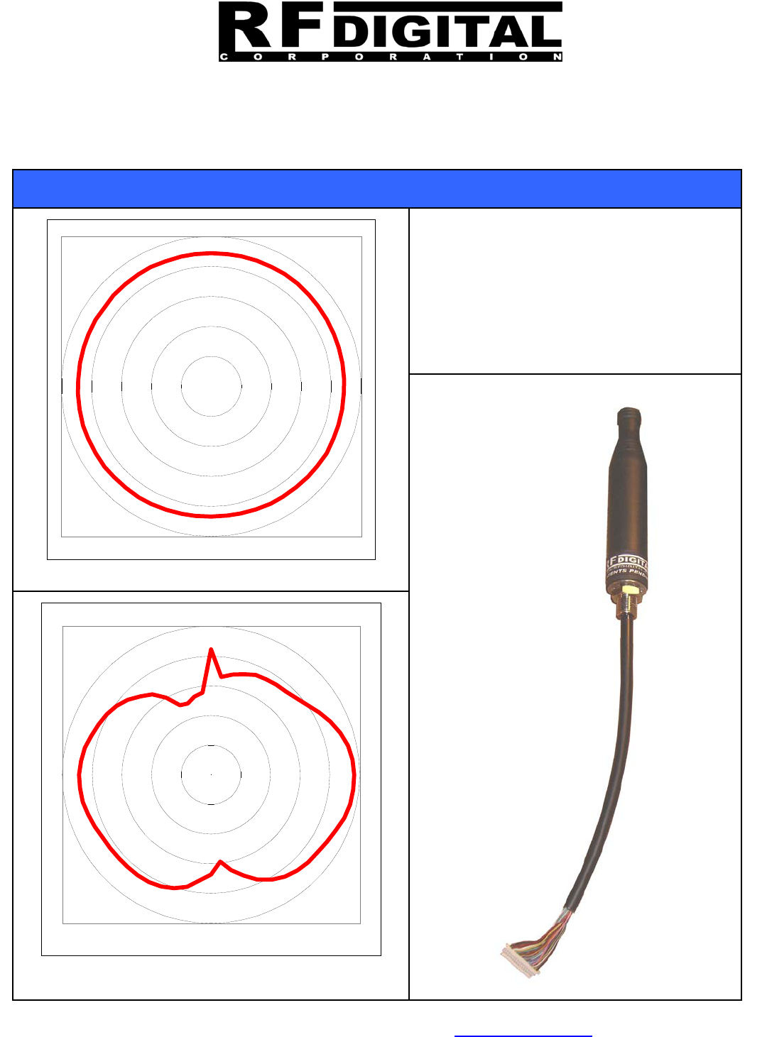
Horizontal Antenna Pattern
-70
-60
-50
-40
-30
-20 12345678910
11
12
13
14
15
16
17
18
19
20
21
22
23
24
25
26
27
28
29
30
31
32
33
34
35
36
37
38
39
40
41
42
43
44
45
46
47
48
49
50
51
52
53545556 57 58 59 60
Vertical Antenna Pattern
RFDANT RFD21742 and RFD21743 high
performance antenna patterns are easily
achieved without any RF considerations or
knowledge because the 11 pin cable and
connector only carries power and data
signals so NO RF cable loss at all. RF
Digital’s Patent Pending RFDANT design is
the only device in industry which can achieve
this outstanding performance.
RFDANT • EXCELLENT ANTENNA PATTERNS
13715 Alton Pkwy • Irvine • CA • 92618
Tel: 949.610.0008 • www.RFdigital.com
Fast Answers: support@rfdigital.com
Free Applications Support • Email your application questions to support@rfdigital.com 12
RFDP8
© Copyright, RF Digital
1/29/2013 9:40 AM
Patents Pending
RoHS CE • ESTI
RFD21733/35 • FCC • IC
RFD21743 • FCC
Approved & Certified
RF Module
RFD21733
RFD21735
RFD21737
RFD21738
RFD21739
RFDP8
RFDANT
RFD21742
RFD21743
RFD21772
RFD21773
KEYFOBs
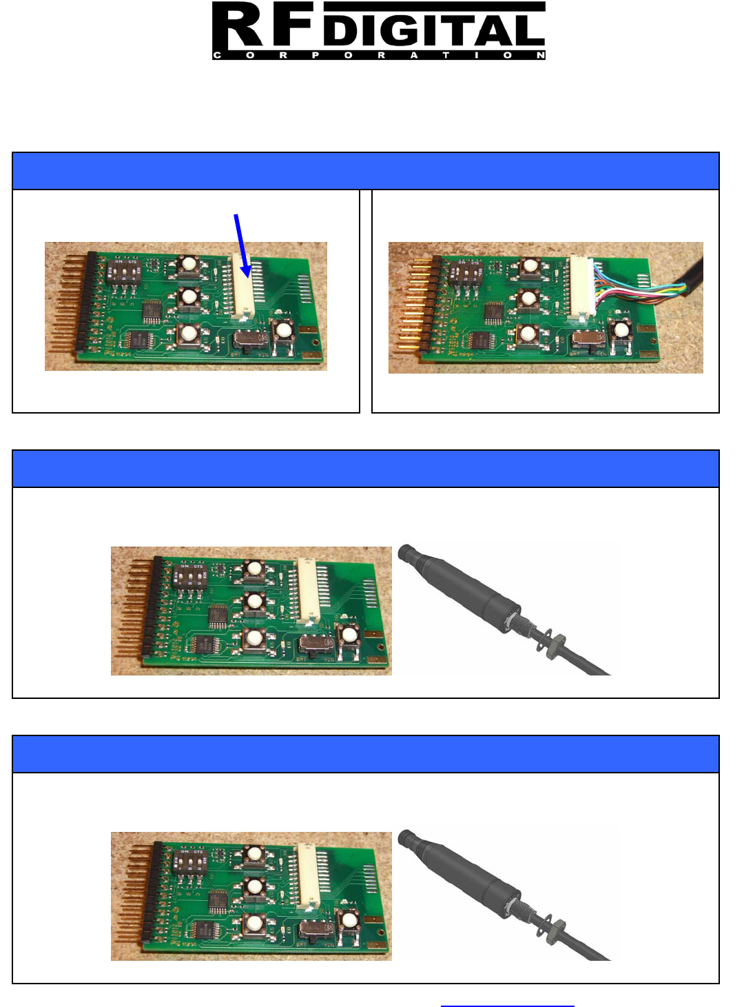
RFD21772 / RFD21773 Eval board with
RFDANT 11 pin connector.
When ordering part number RFD21772, you receive an RFDANT eval board pictured below AND you also
receive an RFD2142 RFDANT. For Eval board usage instructions, see sections below.
RFD21772 & RFD21773 Eval Boards for RFDANT
RFD21772 / RFD21773 Eval board with RFDANT
cable plugged into the 11 pin connector.
RFD21772 Eval Board for RFD21742 RFDANT
When ordering part number RFD21773, you receive an RFDANT eval board pictured below AND you also
receive an RFD2143 RFDANT. For Eval board usage instructions, see sections below.
RFD21773 Eval Board for RFD21743 RFDANT
13715 Alton Pkwy • Irvine • CA • 92618
Tel: 949.610.0008 • www.RFdigital.com
Fast Answers: support@rfdigital.com
Free Applications Support • Email your application questions to support@rfdigital.com 13
RFDP8
© Copyright, RF Digital
1/29/2013 9:40 AM
Patents Pending
RoHS CE • ESTI
RFD21733/35 • FCC • IC
RFD21743 • FCC
Approved & Certified
RF Module
RFD21733
RFD21735
RFD21737
RFD21738
RFD21739
RFDP8
RFDANT
RFD21742
RFD21743
RFD21772
RFD21773
KEYFOBs
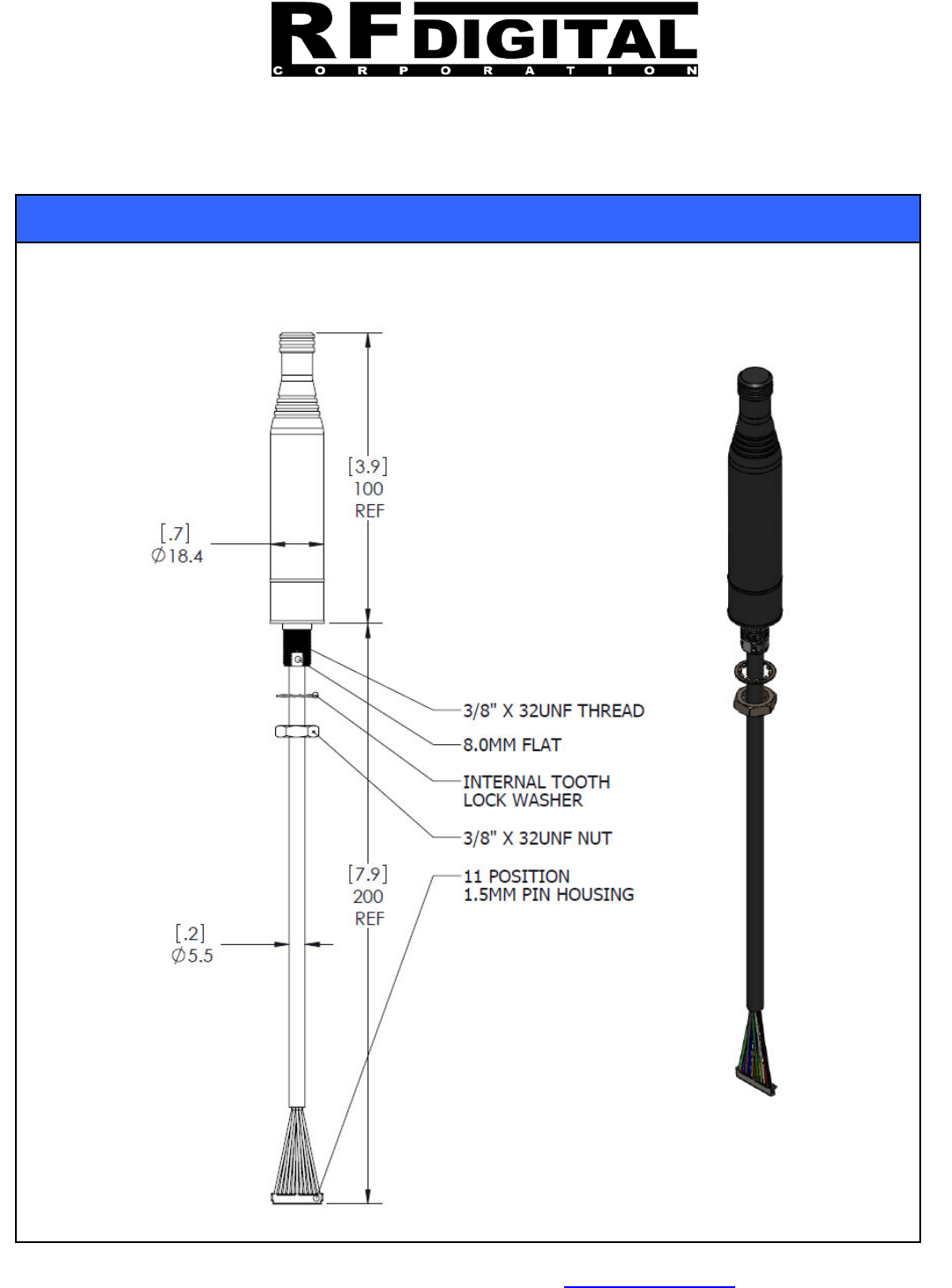
Flexible RFDANT cable does not have any shielding due to its revolutionary design and therefore does
not need it. The 11 conductor cable is flexible and can easily confirm to fit your enclosure. Simply drill
hole into your enclosure, insert the RFDANT and you have instant excellent range performance.
RFD21773 • RFD21743 • RFDANT • Dimensions
13715 Alton Pkwy • Irvine • CA • 92618
Tel: 949.610.0008 • www.RFdigital.com
Fast Answers: support@rfdigital.com
Free Applications Support • Email your application questions to support@rfdigital.com 14
RFDP8
© Copyright, RF Digital
1/29/2013 9:40 AM
Patents Pending
RoHS CE • ESTI
RFD21733/35 • FCC • IC
RFD21743 • FCC
Approved & Certified
RF Module
RFD21733
RFD21735
RFD21737
RFD21738
RFD21739
RFDP8
RFDANT
RFD21742
RFD21743
RFD21772
RFD21773
KEYFOBs
RFD21733 • RFD21735 • RFD21742 • RFD21743 • Applications
RFD21733 • RFD21735 • RFD21742 • RFD21743 • Usage Examples
13715 Alton Pkwy • Irvine • CA • 92618
Tel: 949.610.0008 • www.RFdigital.com
Fast Answers: support@rfdigital.com
Free Applications Support • Email your application questions to support@rfdigital.com 15
RFDP8
© Copyright, RF Digital
1/29/2013 9:40 AM
Patents Pending
RoHS CE • ESTI
RFD21733/35 • FCC • IC
RFD21743 • FCC
Approved & Certified
RF Module
RFD21733
RFD21735
RFD21737
RFD21738
RFD21739
RFDP8
RFDANT
RFD21742
RFD21743
RFD21772
RFD21773
KEYFOBs
RFD21733 • RFD21735 • RFD21742 • RFD21743 • Applications
13715 Alton Pkwy • Irvine • CA • 92618
Tel: 949.610.0008 • www.RFdigital.com
Fast Answers: support@rfdigital.com
Free Applications Support • Email your application questions to support@rfdigital.com 16
RFDP8
© Copyright, RF Digital
1/29/2013 9:40 AM
Patents Pending
RoHS CE • ESTI
RFD21733/35 • FCC • IC
RFD21743 • FCC
Approved & Certified
RF Module
RFD21733
RFD21735
RFD21737
RFD21738
RFD21739
RFDP8
RFDANT
RFD21742
RFD21743
RFD21772
RFD21773
KEYFOBs
RFD21733 • RFD21735 • RFD21742 • RFD21743 • Applications
13715 Alton Pkwy • Irvine • CA • 92618
Tel: 949.610.0008 • www.RFdigital.com
Fast Answers: support@rfdigital.com
Free Applications Support • Email your application questions to support@rfdigital.com 17
RFDP8
© Copyright, RF Digital
1/29/2013 9:40 AM
Patents Pending
RoHS CE • ESTI
RFD21733/35 • FCC • IC
RFD21743 • FCC
Approved & Certified
RF Module
RFD21733
RFD21735
RFD21737
RFD21738
RFD21739
RFDP8
RFDANT
RFD21742
RFD21743
RFD21772
RFD21773
KEYFOBs
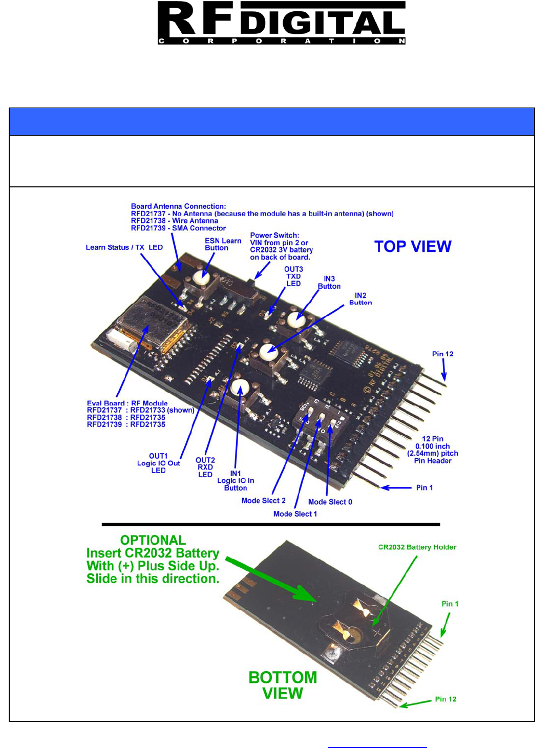
Differences Between Module Eval Boards
RFD21737 RFD21738 RFD21739
The RFD21733 RF Module with
built-in chip antenna is soldered
onto the RFD21737 eval board.
The antenna is self-contained
within the module.
This eval board is self-contained
and does not require an external
antenna.
The RFD21735 RF Module is
soldered onto the RFD21738 eval
board. There is a 1.2 inch wire
antenna soldered onto the
RFD21738 which connects to the
RFD21735 external antenna pin
through RF strip-line within the PCB
layers.
This eval board is self-contained
and does not require an external
antenna.
The RFD21735 RF Module is
soldered onto the RFD21738 eval
board. There is a FEMALE SMA
connector soldered onto the
RFD21738 which allows the user
to connect to an external 2.4 GHz
antenna of their choice. The
RFD21735 external antenna pin is
routed to the SMA connector
through strip-line within the PCB
layers. This eval board requires a
user supplied 2.4 GHz antenna
with a MALE SMA connector.
ANTENNA NOT INCLUDED
RFD21737
RFD21737
RFD21737
RFD21738
RFD21738
RFD21738
RFD21739
RFD21739
RFD21739
13715 Alton Pkwy • Irvine • CA • 92618
Tel: 949.610.0008 • www.RFdigital.com
Fast Answers: support@rfdigital.com
Free Applications Support • Email your application questions to support@rfdigital.com 18
RFDP8
© Copyright, RF Digital
1/29/2013 9:40 AM
Patents Pending
RoHS CE • ESTI
RFD21733/35 • FCC • IC
RFD21743 • FCC
Approved & Certified
RF Module
RFD21733
RFD21735
RFD21737
RFD21738
RFD21739
RFDP8
RFDANT
RFD21742
RFD21743
RFD21772
RFD21773
KEYFOBs
All 5 Eval Boards, including the RFDANT boards can be powered from their on-board CR2032 3V battery or through
the 12 pin 0.100 inch (2.54mm) pitch header, which can plug into directly into standard solderless breadboards or
connect to mating a 0.100 inch (2.54mm) mating socket. The Eval Boards can work as stand-alone or can be wired
to your application. The RFDANT Eval Boards have an RFDANT 11 pin connector instead of a Module.
Eval Board Top and Bottom Labeled Views
13715 Alton Pkwy • Irvine • CA • 92618
Tel: 949.610.0008 • www.RFdigital.com
Fast Answers: support@rfdigital.com
Free Applications Support • Email your application questions to support@rfdigital.com 19
RFDP8
© Copyright, RF Digital
1/29/2013 9:40 AM
Patents Pending
RoHS CE • ESTI
RFD21733/35 • FCC • IC
RFD21743 • FCC
Approved & Certified
RF Module
RFD21733
RFD21735
RFD21737
RFD21738
RFD21739
RFDP8
RFDANT
RFD21742
RFD21743
RFD21772
RFD21773
KEYFOBs
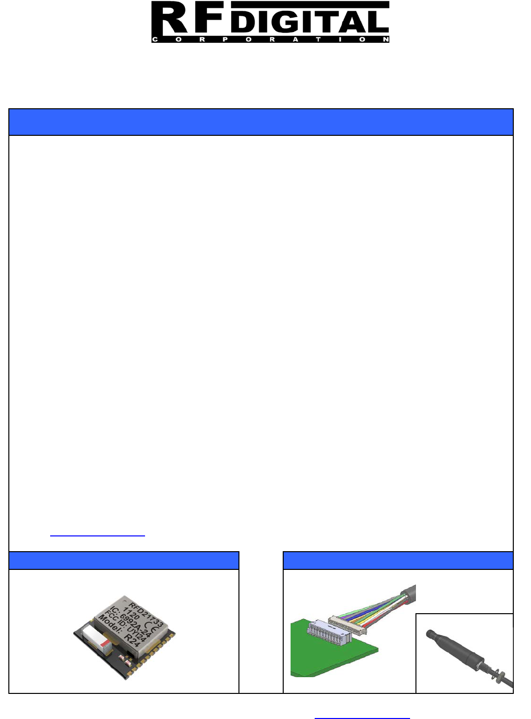
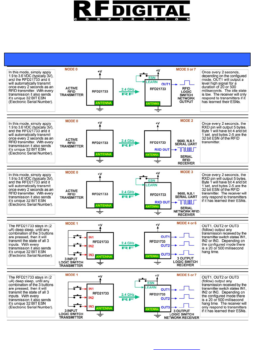
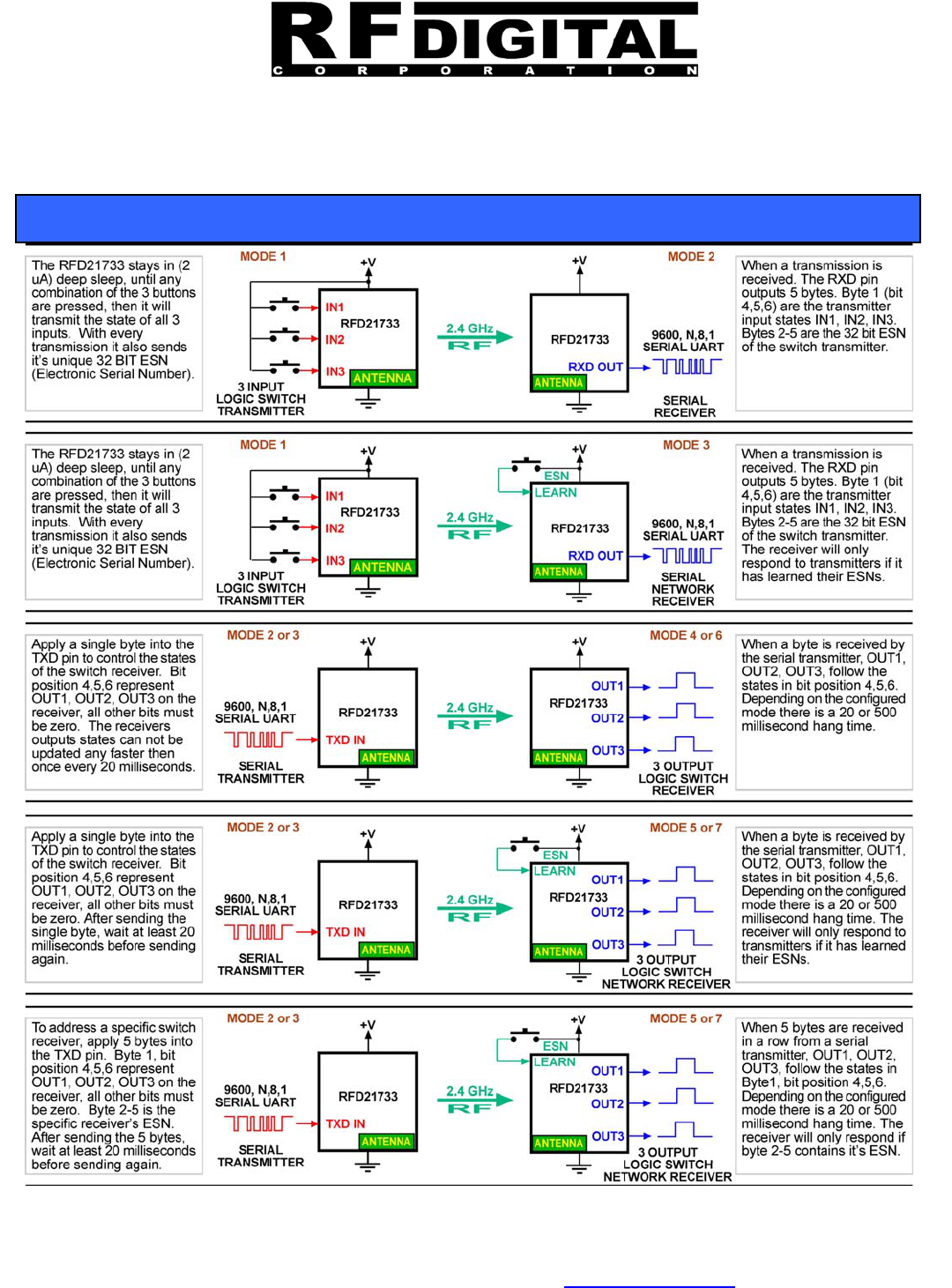
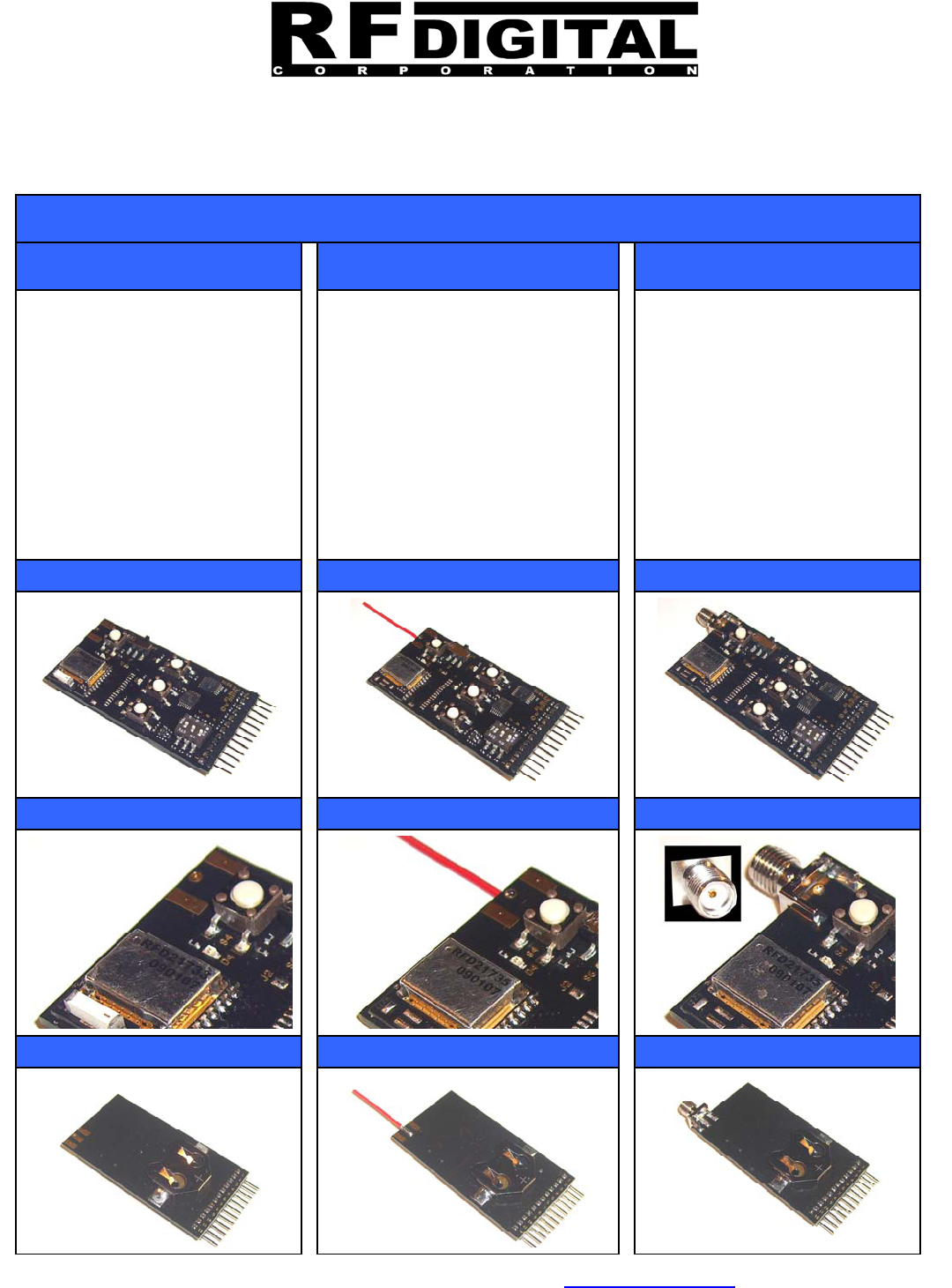
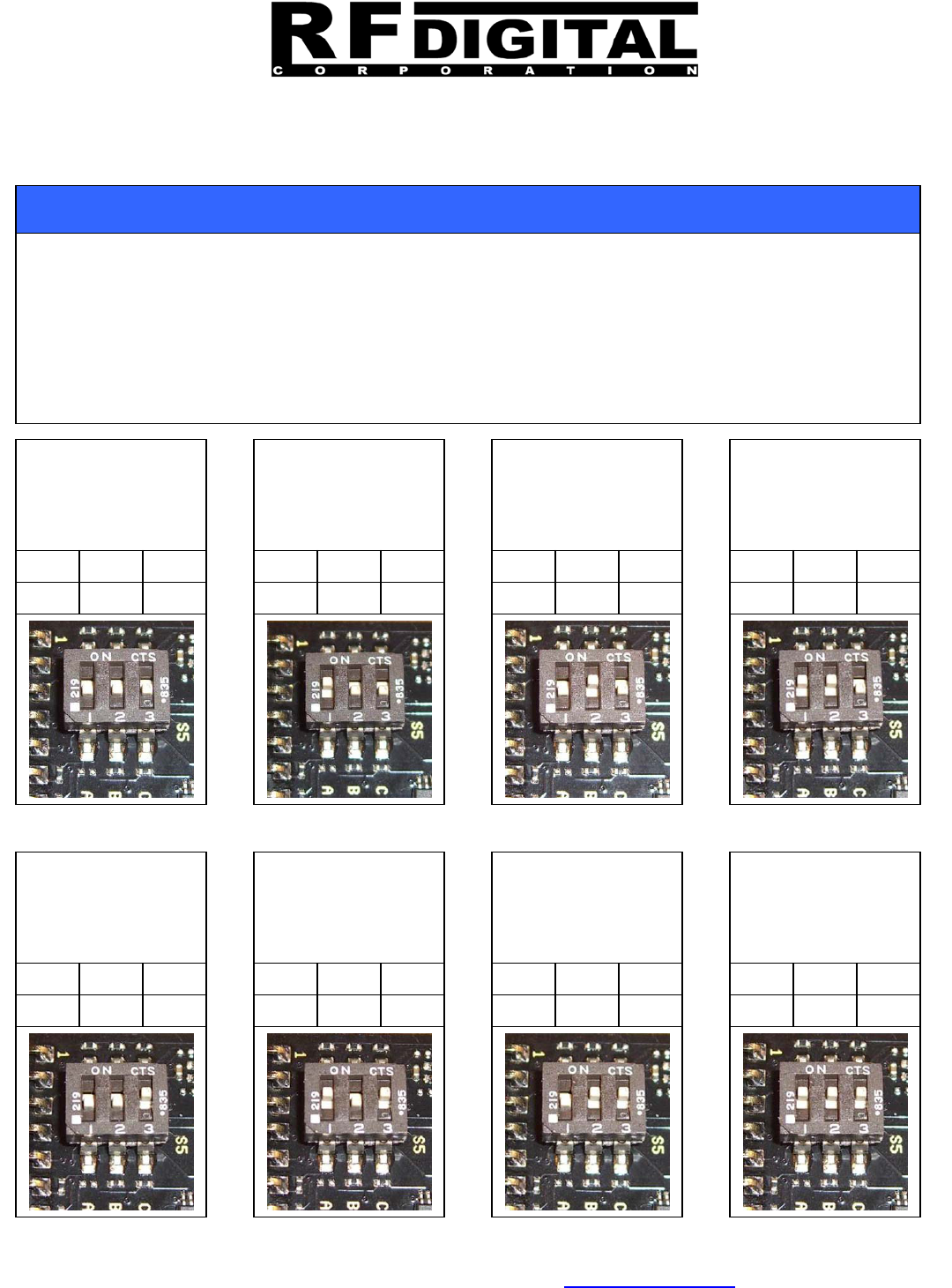
The 8 different modes of the RFDP8 Application Protocol are selected using the 3-position dip-switch S5 shown in
the examples below. The 3 inputs have resistor pull-downs to ground, so when the switch is in its OFF (open)
position, there is a low (0) on the input. When the switch is in its ON (closed) position, it connects the input to +V,
which produces a high (1).
The proper way to read binary is MSB on the left and LSB on the right. Switch manufacturers label the switches
from left to right and furthermore they commonly start with 1 rather then 0. So careful attention needs to be given
to identify the switch positions. The binary is read from MSB to LSB, rather than LSB to MSB as shown in the
examples below. To remove all doubt, only follow the examples shown below.
RFDP8 Mode Selector Switch for all 5 Eval Boards
Mode 0
Active RFID
Transmitter
OFF OFF OFF
Mode 1
3-Input
Switch Logic
Transmitter
ON
OFF OFF
Mode 2
Serial UART
Transceiver
9600-8N1
ON
OFF OFF
Mode 3
Serial UART
Transceiver
9600-8N1
Network
ON ON
OFF
Mode 4
3-Output Switch
Logic Receiver
500ms Hang Time
ON
OFF OFF
Mode 5
3-Output Switch
Logic Receiver
500ms Hang Time
Network
ON ON
OFF
Mode 6
3-Output Switch
Logic Receiver
20ms Hang Time
ON ON
OFF
Mode 7
3-Output Switch
Logic Receiver
20ms Hang Time
Network
ON ON ON
13715 Alton Pkwy • Irvine • CA • 92618
Tel: 949.610.0008 • www.RFdigital.com
Fast Answers: support@rfdigital.com
Free Applications Support • Email your application questions to support@rfdigital.com 20
RFDP8
© Copyright, RF Digital
1/29/2013 9:40 AM
Patents Pending
RoHS CE • ESTI
RFD21733/35 • FCC • IC
RFD21743 • FCC
Approved & Certified
RF Module
RFD21733
RFD21735
RFD21737
RFD21738
RFD21739
RFDP8
RFDANT
RFD21742
RFD21743
RFD21772
RFD21773
KEYFOBs
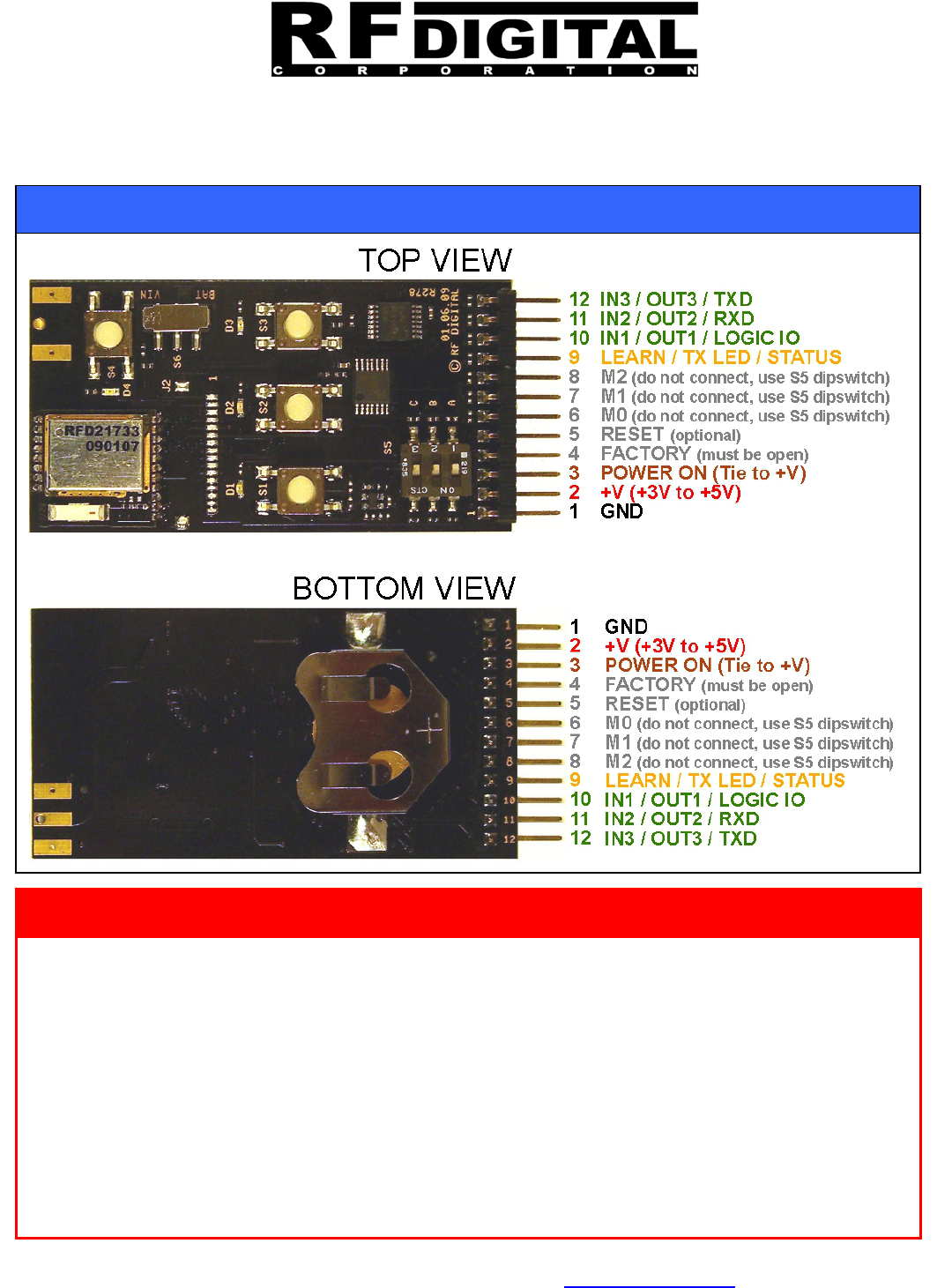
Eval Board Top and Bottom View Pinout for All Eval Boards
Eval Board Power Suppl
y
and Lo
g
ic Levels - Important
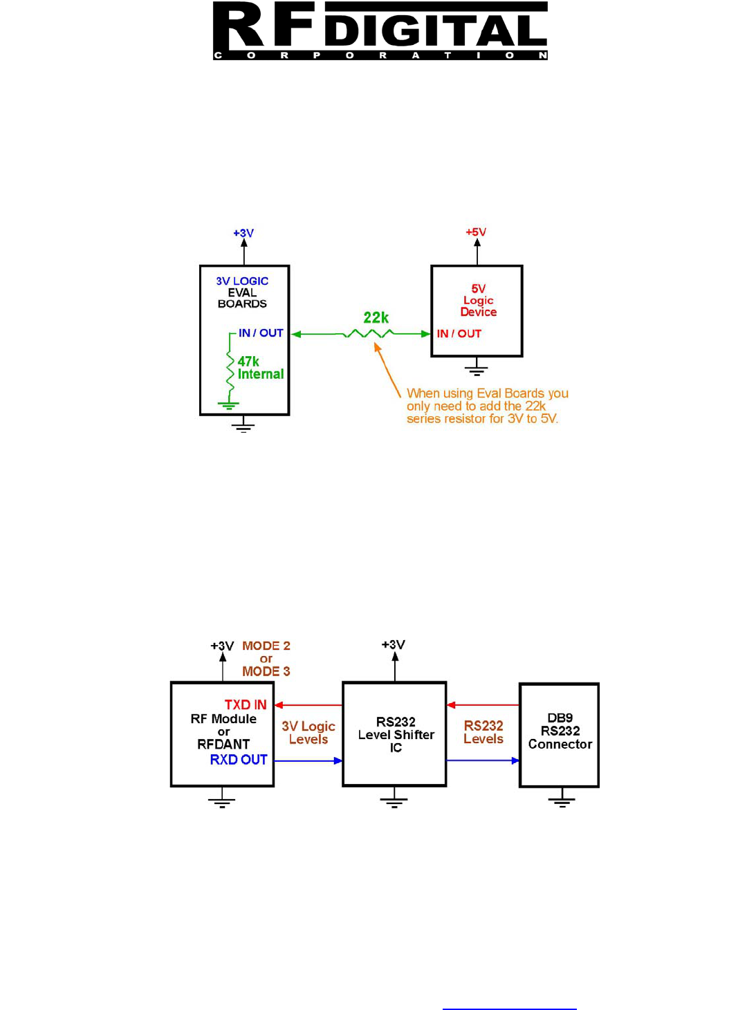
There is an internal 3.3 Volt (LDO) on the eval boards. At the (pin 2) +V input pin, you can supply
2.1VDC minimum and a maximum of 3.6VDC. When your supplied voltage is between 3.4V and 3.6V the
internal regulator is in regulation and the internal supply to all parts will be 3.3V, and all signals on pins
9-12 will be at 3.3V logic. When 2.1V to 3.4V is supplied the internal 3.3V regulator is of regulation and
tracks the input voltage (minus about 100mv overhead). If you supply 2.5V your logic will be at 2.4V,
and if you supply 2.1V your logic will be at 2.0V. The internal 3.3V regulator accept up to a 5V supply
input, but at 5V supply, your logic levels on pins 9-12 will be at 3.3V, SO USE CAUTION. So you will
need to use 3.3V to 5V logic level shifters to run properly at 5V or you will cause damage to the module.
When using a 5V supply, a very quick 5V level shifter method (not to be used for production) just for
testing, which works in some cases would be to use a 22K resistor in series between the eval boards
3.3V logic and your 5V logic. There is a 47k pull down resistor internal to the Eval Boards ONLY (NOT
THE MODULE or RFDANT) on pin 9-12 and this is just enough to switch the logic levels in both
directions for a quick and dirty level shifter. There are NO 47k pull down resistors on the Modules or
RFDANTs, so you must add your own pull-downs or pull-ups accordingly.
13715 Alton Pkwy • Irvine • CA • 92618
Tel: 949.610.0008 • www.RFdigital.com
Fast Answers: support@rfdigital.com
Free Applications Support • Email your application questions to support@rfdigital.com 21
RFDP8
© Copyright, RF Digital
1/29/2013 9:40 AM
Patents Pending
RoHS CE • ESTI
RFD21733/35 • FCC • IC
RFD21743 • FCC
Approved & Certified
RF Module
RFD21733
RFD21735
RFD21737
RFD21738
RFD21739
RFDP8
RFDANT
RFD21742
RFD21743
RFD21772
RFD21773
KEYFOBs
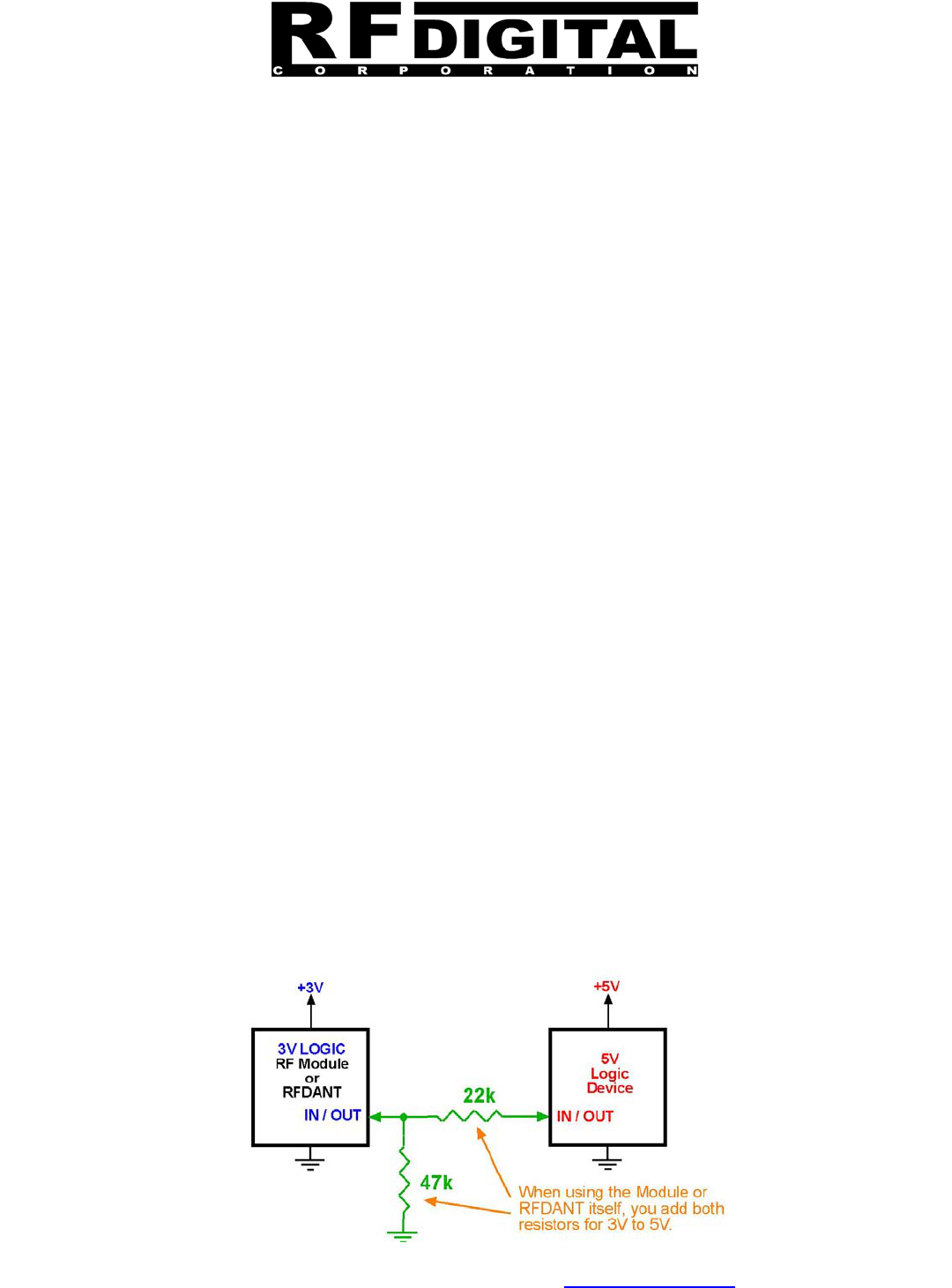
RF Modules and RFDANTs run on 3V Logic Levels (1.9V to 3.6V)
The RFD21733, RFD21735, RFD21742 and RFD21743 all run on a supply of 1.9V to 3.6V. They have an
internal voltage regulator which is set to 1.8V and it is an LDO so you only need about 100mV of overhead to
keep it in regulation. Most circuits which will interface with these devices will be 3V or 3.3V typical, so we will use
those voltages for reference in this section. If your circuit runs on 2.5V, 3V or 3.3V, then no problem, you can
directly apply supply voltage of 2.5V, 3V or 3.3V to the Module or RFDANT and all your logic signals will be at
2.5V, 3V or 3.3V for a direct interface with your hardware. However if your circuit is running at a higher voltage
such as 5V, then you need to use a level shifter IC or a circuit which will translate the Module or RFDANT signals
from 3V to 5V for your circuit, and also the 5V from your circuit to the 3V for the Module or RFDANT. Of course
you will also need a regulator to drop from 5V down to 3V for the Module or RFDANT.
Simple 5V to 3V Logic Level Shifter for prototyping ONLY.
If you want a quick an dirty, temporary solution to interface the 3V RF Module or RFDANT to your 5V logic circuit,
then you can use a simple resistive divider to get your prototype up and running quickly with just a couple
resistors. First, you must supply a regulated 3V or 3.3V to the RF Module or RFDANT using a voltage regulator.
Now regarding the logic signals, you can connect a 47k pull down resistor to the logic lines on the following 6
signals, Mode Select 1, Mode Select 2, Learn / Status, IN1 / OUT 1 / LOGIC IO, IN2 / OUT2 / RXD, IN3 / OUT3 /
TXD. The RESET has an internal 3.3K pull up and does not apply to this option, and the Mode Select 0, at power
up has an internally switched 13k resistor and also does not apply to this option. After connecting the 47k pull
down resistor on the Module or RFDANT pins, then use a 22k series resistor to connect the six Module or
RFDANT logic pins mentioned above to your 5V device. That will create a 2/3 voltage divider from your 5V
device to the 3V RF Module or RFDANT when the 5V device is driving 3V device. When the 3V device is driving
the 5V device, there is no divider in that direction, only a 22k series resistor into a high-Z input on the 5V side, so
the 5V side will see the full 3V logic, and that is in most cases, just enough to cause a logic high for a 5V logic
input. Note this is not a production solution, its just a quick-and-dirty way to get a 5V logic circuit to work with a
5V logic circuit for prototyping. Of course once you have hooked this up and if it does not work for you, do
measure the logic levels using a scope on both 5V and 3V nodes to make sure they are actually at sufficient
levels to meet the minimums for logic levels for the specific device. Note if you do not have a high-Z input on the
5V side, this will not work. At first chance, when possible, use a proper level shifter capable of sinking and
sourcing current and able to do fast switching as this circuit is very limited with its scope of value and use. The
Eval Boards have a 47k pull down resistor mounted on the above six referenced pins, so if you are using an Eval
Board then all you need is the series 22K resistor (don’t add an additional 47k resistor or it will not work), but if
you are using the RF Module or the RFDANT WITHOUT the Eval Board, then you will need to add the 47k
resistors.
13715 Alton Pkwy • Irvine • CA • 92618
Tel: 949.610.0008 • www.RFdigital.com
Fast Answers: support@rfdigital.com
Free Applications Support • Email your application questions to support@rfdigital.com 22
RFDP8
© Copyright, RF Digital
1/29/2013 9:40 AM
Patents Pending
RoHS CE • ESTI
RFD21733/35 • FCC • IC
RFD21743 • FCC
Approved & Certified
RF Module
RFD21733
RFD21735
RFD21737
RFD21738
RFD21739
RFDP8
RFDANT
RFD21742
RFD21743
RFD21772
RFD21773
KEYFOBs
Eval Board Example with internal 47k resistor.
RS232 Level Shifter Interface
To connect to an RS232 port (9600-8N1), you must use a level shifter to shift the voltage levels from RS232
levels to 3V or 3.3V logic. There are many ICs which can perform that task all in one chip. For example the
MAX232, MAX202 or the ICL3321. If you want to connect to a PC you can use this method or you can use a
USB port and connect through a virtual communication port shown in the next section. You can use this same
interface when connecting to the Eval Boards. Very important, make sure you pull down the Logic IO signal to
ground through a 47k resistor if it is not in use, note it is bi-directional so you must use a pull down.
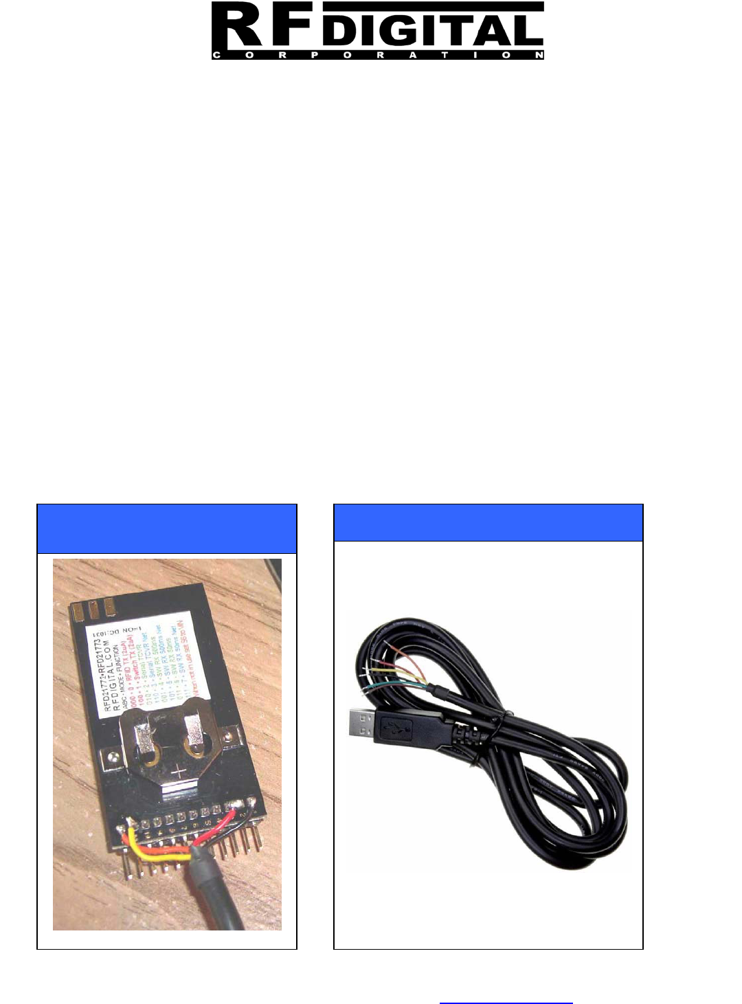
FTDI USB Virtual Communication Interface
FTDI manufactures a 3.3V Logic Serial Interface cable which plugs into a USB port and shows up as a COMM
port on your PC, through which you can connect to PC terminal programs like Hyper Terminal, RealTerm and
others.
You can purchase the FTDI cable from Digikey.com or other distributors. The manufacturer part number is TTL-
232R-3V3 and the Digikey Part Number is 768-1016-ND (picture shown below). For international orders, if you
want to save on shipping, you can ask for this item to be packed in with your order to RF Digital.
13715 Alton Pkwy • Irvine • CA • 92618
Tel: 949.610.0008 • www.RFdigital.com
Fast Answers: support@rfdigital.com
Free Applications Support • Email your application questions to support@rfdigital.com 23
RFDP8
© Copyright, RF Digital
1/29/2013 9:40 AM
Patents Pending
RoHS CE • ESTI
RFD21733/35 • FCC • IC
RFD21743 • FCC
Approved & Certified
RF Module
RFD21733
RFD21735
RFD21737
RFD21738
RFD21739
RFDP8
RFDANT
RFD21742
RFD21743
RFD21772
RFD21773
KEYFOBs
When using the FTDI USB Interface Cable TTL-232R-3V3, the connections to the RFD21737, RFD21738,
RFD21739, RFD21772, and RFD21773 Eval Boards are very simple. You only need 4 wires and the Eval Board
is also powered from the USB port through the cable.
The 3V3 part of the part number for the cable means that the logic levels of the cable are 3.3V.
IMPORTANT:
The RED wire supplies +5V, and can ONLY be connected to the Eval Boards since the Eval Boards have an on-
board 3.3V regulator. You can NOT connect +5V to the Module or RFDANT directly. This is ONLY intended for
the Eval Board.
The 4 wires you need from the cable are:
RED is +5V
BLACK is GROUND
YELLOW is TXD Data Input to the PC USB Port.
ORANGE is RXD Data Output from the PC USB Port.
FTDI Cable to RFD Eval Boards:
RED – connect to RFD Eval Board Pin 2 and Pin 3 (Pin 2 is power on. Short pin 2 and pin 3.).
BLACK – connect to RFD Eval Board Pin 1.
YELLOW – connect to RFD Eval Board Pin 11, which is the RXD Data Output of the Eval Board.
ORANGE – connect to RFD Eval Board Pin 12, which is the TXD Data Input of the Eval Board.
FTDI TTL-232R-3V3 USB Cable
wired to RFD Eval Board
FTDI TTL-232R-3V3 USB Cable

13715 Alton Pkwy • Irvine • CA • 92618
Tel: 949.610.0008 • www.RFdigital.com
Fast Answers: support@rfdigital.com
Free Applications Support • Email your application questions to support@rfdigital.com 24
RFDP8
© Copyright, RF Digital
1/29/2013 9:40 AM
Patents Pending
RoHS CE • ESTI
RFD21733/35 • FCC • IC
RFD21743 • FCC
Approved & Certified
RF Module
RFD21733
RFD21735
RFD21737
RFD21738
RFD21739
RFDP8
RFDANT
RFD21742
RFD21743
RFD21772
RFD21773
KEYFOBs
Free Schematic, Layout and Application Design Reviews
For free Application, Schematic and Layout design reviews, send color screen captures or PDFs of your
schematic and layout to support@rfdigital.com. RF Digital’s Support and Application Engineers are
ready to get your wireless application running today. Why spend lots of time reading volumes of data?
Instead, simply send your application questions to support@rfdigital.com and receive direct, fast and
personal answers focused on your specific project and needs. We look forward to hearing from you!!!
FCC Compliance Information
The RFD21733/35 are IC and FCC Modular Approved and Certified, therefore for use of the RFD21733/35
module in your product does not require further IC or FCC testing. Detail instructions and IC and FCC notices
shown later in this data sheet. Any modifications made to the RFD21733/35 will void the IC and FCC Approval
and Certification. The RFD21733 has an integrated on-board chip antenna, while the RFD21735 needs a
2.4GHz, max. 5dBi gain whip antenna. You simply include the RFD21733/35 in your product, follow the IC and
FCC notices and information below and place the appropriate label on your product to indicate that it includes an
IC and FCC approved module and no further testing would be required for the module.
The RFD21743 is FCC Modular Approved and Certified, therefore for use of the RFD21743 module in your
product does not require further FCC testing. Detail instructions and FCC notices shown later in this data sheet.
Any modifications made to the RFD21743 will void the FCC Approval and Certification. The RFD21743 has an
integrated antenna. You simply include the RFD21743 in your product and follow the FCC notices and
information below and place the appropriate label on your product to indicate that it includes an FCC approved
module and no further testing would be required for the module.
CE, ETSI Compliance Information
The RFD21733, RFD21735, RFD21742 and RFD21743 are CE (ETSI) Tested. See declaration of conformity
later in this document.
RFDP8 Firmware
RF Digital offers firmware for the RFD21733, RFD21735, RFD21742, and RFD21743 that meets many common
user requirements. The firmware and a unique identifier are pre-programmed and tested at the factory. The
programmed module is therefore immediately ready for use upon delivery.
The RFDP8 firmware uses the 3 mode select inputs to select the operating mode. These inputs are sampled
when the module powers-on.
Some of the operating modes have additional options which are described in the section for that mode.
The RFDP8 firmware cannot be modified by the user. For applications that require alternative functionality,
contact RF Digital for information about custom firmware to fit your specific requirements.

13715 Alton Pkwy • Irvine • CA • 92618
Tel: 949.610.0008 • www.RFdigital.com
Fast Answers: support@rfdigital.com
Free Applications Support • Email your application questions to support@rfdigital.com 25
RFDP8
© Copyright, RF Digital
1/29/2013 9:40 AM
Patents Pending
RoHS CE • ESTI
RFD21733/35 • FCC • IC
RFD21743 • FCC
Approved & Certified
RF Module
RFD21733
RFD21735
RFD21737
RFD21738
RFD21739
RFDP8
RFDANT
RFD21742
RFD21743
RFD21772
RFD21773
KEYFOBs
RFDP8 Interference Immunity Algorithm
RF Digital's RFDP8 proprietary patent-pending frequency agility protocol operates in the internationally accepted
2.4 GHz band. The RFDP8's leading-edge advanced algorithm is not burdened by a heavy-weight stack as is
BlueTooth, ZigBee, WLAN and other protocols, which are well suited for cross-manufacturer interoperability. The
RFDP8 protocol is highly robust and effective where there is a need to penetrate through a high saturation of RF
noise which is common in nearly all environments today. It is especially effective and can easily coexist in heavy
WiFi environments, which very few technologies can do successfully without the need of excessive processing
power. The protocol strategically changes channels frequently to deliver its payload to the destination device
reliably, yet not too excessively as to demand too much internal processing power which allows it to run with a
very low current consumption profile and fast start up times allowing substantial flexibility with implementation.
The RFDP8 protocol reduces the amount of on-air traffic and unnecessary chatter due to its unique and highly
efficient design, which does not require bilateral registration and association as do many other technologies
today. The RFDP8 does not require ACK-NACKs to complete a packet delivery, its unique technique of packet
delivery, recovery and correction allows it to work as a one-way link, hence drastically simplifying users'
applications which always results in a more robust wireless system. The RFDP8 protocol combined with RF
Digital's leading-edge RF Module hardware delivers a highly robust method of delivering user data from point to
point, point to multi-point or multi-point to multi-point, transmitter-receiver, transceiver, serial or switch on/off data
modes. The protocol is designed to work seamlessly with RF Digital's hardware modules, the combination results
in ultra long range at ultra low currents without concern for compliance approvals since modules such as the
RFD21733 come with IC and FCC Approval and Certification for USA and have passed CE - ETSI emission
testing for European requirements. The RFDP8 protocol adds several dB of range gain passively through it's
advanced data recovery technique which pulls valid data out of a noisy environment adding effective gain which
results in more range, delivering the net result, which is a very robust wireless system. All of this is built into the
overhead of the RFDP8 protocol and RF Digital modules, so it's all done behind the scenes, allowing the user to
focus on building their application and simply putting data into the radio device as a wireless pipe and easily
receiving it on the other end.
Electronic Serial Number
Every RF Digital Module has its own 32-bit unique identifier (over 4 billion unique values), known as the Electronic
Serial Number, or ESN. This value is assigned at the factory and cannot be changed by the user.
The ESN is included in every packet that is transmitted, as part of the protocol overhead and is transparent to the
user.
The user does not ordinarily need to know what the ESN is. However, in certain cases it is helpful to know the
serial number, and so a mechanism has been provided to read out the ESN. This method is documented in the
UART section below.
Network Mode
The UART and the Receiver with logic output can be configured to accept data only from transmitters with which it
has been associated, i.e. in its network.
When in network mode, a module must “learn” the ESN of any module which it wishes to “hear." The LEARN
signal (listed in the UART and receiver sections below) is usually an input, pulled to GND through an external

13715 Alton Pkwy • Irvine • CA • 92618
Tel: 949.610.0008 • www.RFdigital.com
Fast Answers: support@rfdigital.com
Free Applications Support • Email your application questions to support@rfdigital.com 26
RFDP8
© Copyright, RF Digital
1/29/2013 9:40 AM
Patents Pending
RoHS CE • ESTI
RFD21733/35 • FCC • IC
RFD21743 • FCC
Approved & Certified
RF Module
RFD21733
RFD21735
RFD21737
RFD21738
RFD21739
RFDP8
RFDANT
RFD21742
RFD21743
RFD21772
RFD21773
KEYFOBs
resistor. When LEARN is driven high for at least 20ms and then allowed to return to GND, the module enters
learning mode.
While in learning mode, the LEARN signal is changed to an output and driven high. During this time, the module
will learn the ESN of the first module that sends any data; the data will be discarded, the ESN of the transmitting
module will be learned by the receiving module. The receiving module indicates that it has learned the ESN by
toggling the LEARN output on and off quickly three times.
After learning the transmitting modules ESN, or after 10 seconds pass, the module will exit learning mode by
driving LEARN low and then changing it back to an input.
The LEARN / STATUS pin is bidirectional, it is an input when in the LEARN state and an output when in the
STATUS state, so you must drive it using a series resistor, we recommend you not use any value smaller 1k ohm
to limit the amount of load current. There is an internal 47k pull down resistor on the Eval Boards ONLY, so if you
use a value of 1k series resistor that will easily be enough to drive it high against the internal 47k pull down
resistor. If you are not using an Eval Board and you are using the RF Module or RFDANT on its own, then you
will need to add the 47k resistor yourself.
Modules can learn up to 60 unique ESN’s. ESN’s cannot be deleted individually. The list of learned ESN’s can
be completely cleared by holding the LEARN signal high for at least 10 seconds and then releasing it. The
module will erase its ESN list, and then drive the LEARN signal in a fast alternating high/low pattern for a few
seconds to indicate that the ESN list is now empty.
Once a module has learned the ESN of another module, it will accept any and all data from that module only and
not any other modules. Up to 60 unique transmitters can be taught to one receiver. If a module is configured to
any of the 3 Network modes and it has not learned any transmitters ESN, then it will not receive and therefore it
will not output any data, until it learns at least one transmitter.
This network feature can be used for peer-to-peer networks, point to multi-point networks, and multi-point to multi-
point networks. The association can be between two units for simple functions like opening a garage door or with
many units to form complex networks with multiple nodes.
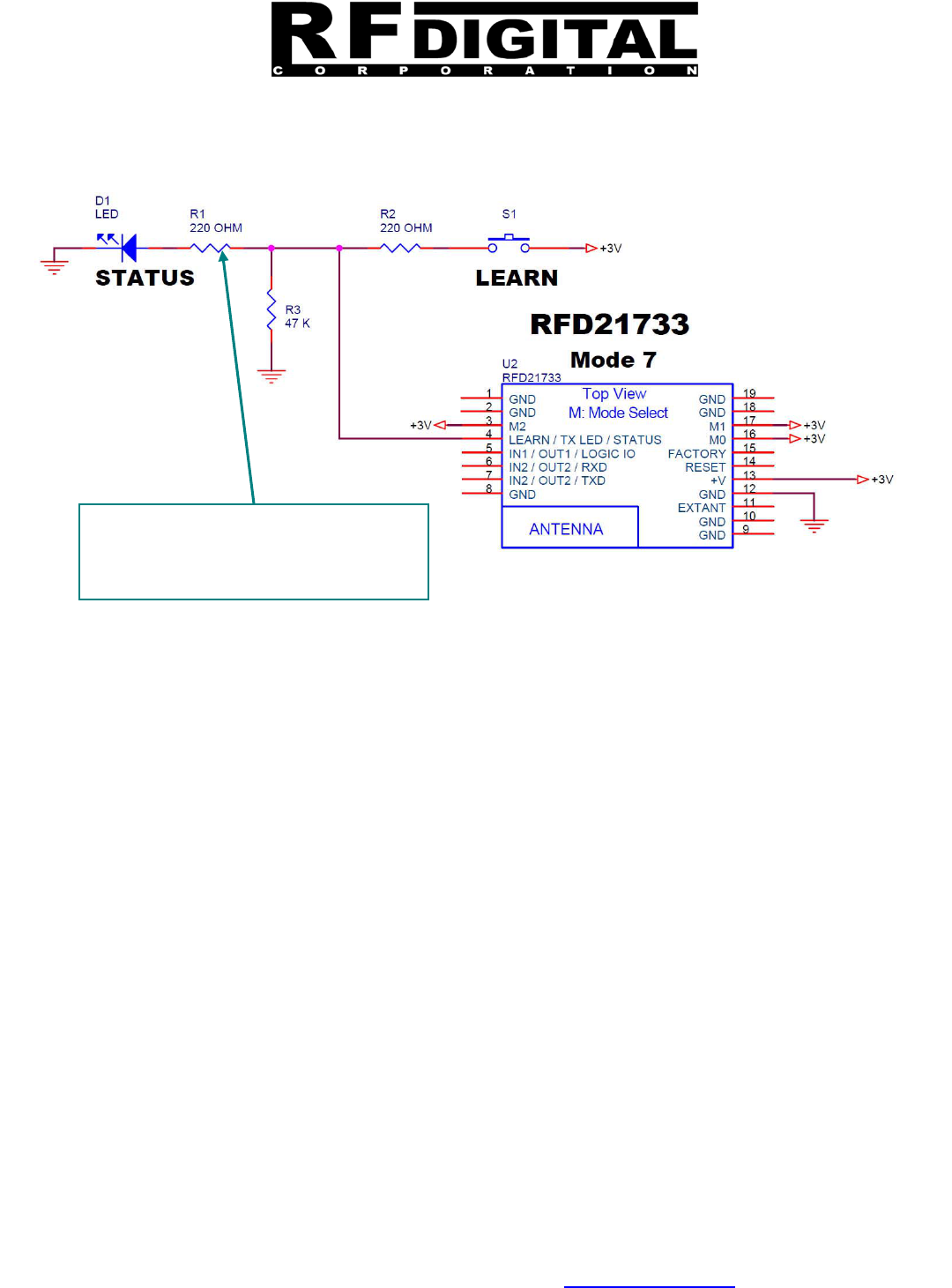
Network Mode – LEARN Pin Application Circuit
Here is an example of how to wire up the LEARN pin to use NETWORK MODE. This same example of the
LEARN / STATUS pin connection applies for Mode 3, Mode 5 and Mode 7, the only thing that changes are the
mode settings of course. This also applies to the RFDANT. An optional buffer for the LED output is
recommended for production designs. Simply replace the LED with a FET to drive the LED for high drive
currents.
13715 Alton Pkwy • Irvine • CA • 92618
Tel: 949.610.0008 • www.RFdigital.com
Fast Answers: support@rfdigital.com
Free Applications Support • Email your application questions to support@rfdigital.com 27
RFDP8
© Copyright, RF Digital
1/29/2013 9:40 AM
Patents Pending
RoHS CE • ESTI
RFD21733/35 • FCC • IC
RFD21743 • FCC
Approved & Certified
RF Module
RFD21733
RFD21735
RFD21737
RFD21738
RFD21739
RFDP8
RFDANT
RFD21742
RFD21743
RFD21772
RFD21773
KEYFOBs
Reset Pin
The RESET pin on all part numbers of RF Modules and RFDANT are active low and have an internal 3.3k ohm
pull up resistor. So at 3V you will need to source at least 1mA to be able to pull it low to cause a reset. You can
leave the reset pin open; you do not need to connect it. The only reason you would need to connect the reset pin
is if you needed a way to reset the Module or RFDANT while in your circuit. A common cause to require this is if
you wanted to change modes while powered up and therefore you need to assert a reset to cause the 3 mode
pins to be re-read to change modes. Note keeping reset low all the time will draw about 1mA of current so if you
plan on conserving current, you will want to bring it low only briefly to cause the reset and then let it go high again
using its internal 3.3k ohm pull up.
Layout Trace Routing and VIAs
When doing your layout for the RFD21733 and RFD21735 avoid placing routs under the module if at all possible.
Having traces under the module as long as they are fully covered by solder mask is typically fine, however placing
VIAs under the module is not at all recommended since solder mask covering VIAs are typically not fully plugged
and protected. Therefore, if there is any exposes solder mask under the module near an area were your board
has an exposed via, there is a chance of a short. There is a slim chance of this ever happening, however if
possible, make effort to avoid having VIAs under the Modules.
Dual Placement Layouts for Modules and RFDANTs
When ever possible, it is always recommended when you do your layout for the RFD21733 or RFD21735 to also
place a footprint for one of the 11 pin RFDANT connectors. This gives you the option to do testing by not placing
the RFD21733 or RFD21735 module on some of your PCBs and just placing the RFDANT 11 pin connector and
plugging an RFDANT into your board. If your board does not have room for this, then of course, this is not in any
way required, its just a recommendation to give you as much optional choices as possible. The RFDANT has
about 4x the range of the RFD21733 so if you happen to need the extra range, it would always be available with a
simple connector interface.
If possible, use a 470 ohm resistor or larger,
to allow for highest logic level on the LEARN
input as possible, due to the resistive divider
that forms when pressing the LEARN button.

13715 Alton Pkwy • Irvine • CA • 92618
Tel: 949.610.0008 • www.RFdigital.com
Fast Answers: support@rfdigital.com
Free Applications Support • Email your application questions to support@rfdigital.com 28
RFDP8
© Copyright, RF Digital
1/29/2013 9:40 AM
Patents Pending
RoHS CE • ESTI
RFD21733/35 • FCC • IC
RFD21743 • FCC
Approved & Certified
RF Module
RFD21733
RFD21735
RFD21737
RFD21738
RFD21739
RFDP8
RFDANT
RFD21742
RFD21743
RFD21772
RFD21773
KEYFOBs
Using CR2032 Batteries
The CR2032 battery is very commonly used for power. The peak current draw for the Modules and RFDANTs
are at about 17mA, and the background current is 2uA depending on the mode setting of course. Quite often
capacitors are used in parallel with the CR2032 to help limit the amount of peak current the CR2032 is exposed
to, so as to help it have a longer run time, since the CR2032 does not handle peak current very well over long
durations of time. We recommend if you choose to place bypass capacitors tied to the CR2032 for this purpose,
then do testing to compare if they really provide you a benefit or not. Quite often the leakage current of the
capacitors are so high that they will have negative impact on the battery runtime rather then provide an
advantage. At least if you have the room, place the pads, but before you place the caps for production, do testing
to make sure they are really helping and not reducing your runtime.
Mode Pins
The mode pins are read just once, right after the Module or RFDANT comes out of reset or upon power up. If you
change them and want them to be read again, then do a reset or power down and up again.
Mode Select 0, Mode Select 1 and Modes Select 2, are three binary inputs which are to be terminated either high
or low, they must not be left open at any time. Mode Select 2 and 1 are open and high Z inputs, so you can use a
47k resistor to pull them up or down, or you can connect directly to +V or GND.
The Mode Select 0 has an internal 13k internal switched pull down. At power up or when the module comes out
of reset, it will internally apply a 13k pull down on this pin just for an instant to check if it is high or not. After the
mode selection test, which is done just once at start up lasts just microseconds. It is done like this to allow you to
have an optional external switch to select between mode 0 and mode 1 without drawing extra current through an
external pull down resistor which would statically be there all the time.
If you will be directly connecting Mode Select 0 directly to +V or to GND that is fine. However if you will be adding
a pull up, note you will be working against a 10k to 16k internal pull down at the time the pin is read, so take that
into account since it will form a voltage divider and maybe not provide the expected level and cause the module to
go into the wrong mode. So for Mode Select 0, we recommend using a 1k or smaller resistor for a pull up to
make sure you get 90% +V for a logic high, we often use 220 ohms or just tie it directly to +V. If you will add a
pull down, note that it will be in parallel with the internal 13k typical pull down for microseconds duration, after
reset or power up.
The Mode Select 0 can be left open; if you leave it open it will register as a LOW. However if you will know what
mode you want in advance and will not be switching it, then we always recommend direct tie to +V or GND.
Wake Up Time
The Modules and RFDANTs wake up very fast. After a reset or after power on, 3mS later they are ready to
transmit or receive.
Output Drive Current - source and sink.
The Module and RFDANT output pins and IO pins when in an output mode should not be expected to drive higher
then 0.5mA each. This is done by design to keep as much high current sources from flowing through the Module
or RFDANT. The amount of source and sink current available at the pins are actually quite a bit more, therefore
they are seen in applications were they can directly drive LEDs with a series resistor of about 220 ohm and the
LED still comes on at a couple milliamps, but we don’t recommend that for production. For prototyping that is
fine, since its quick and simple to hookup, but for production, we prefer to use a driver like a transistor or FET to
13715 Alton Pkwy • Irvine • CA • 92618
Tel: 949.610.0008 • www.RFdigital.com
Fast Answers: support@rfdigital.com
Free Applications Support • Email your application questions to support@rfdigital.com 29
RFDP8
© Copyright, RF Digital
1/29/2013 9:40 AM
Patents Pending
RoHS CE • ESTI
RFD21733/35 • FCC • IC
RFD21743 • FCC
Approved & Certified
RF Module
RFD21733
RFD21735
RFD21737
RFD21738
RFD21739
RFDP8
RFDANT
RFD21742
RFD21743
RFD21772
RFD21773
KEYFOBs
switch as much current as you like to drive your external devices such as high brightness LEDs. Note you must
always use a series current limiting resistor when connecting an LED to a pin of course. The outputs are active
high and therefore you can use an NPN transistor or an N channel FET to switch the ground lead of an LED
easily.
Power Saving
When in mode 4,5,6 or 7 receive modes or in mode 2 or 3 Serial UART modes, you will draw 17mA since the
receiver is 100% on all the time. If you need an internal duty cycle set, please contact support@rfdigital.com for
any custom timing you require. However if you wish to have control over this yourself, since the RFDP8 Modules
and RFDANTs are very fast waking (3mS), you can easily use a P-FET or PNP transistor and just simply remove
power from the whole module and then draw ZERO current until you need the module. If you need help doing
this, feel free to contact support@rfdigital.com anytime.
The length of an RFDP8 Standard packet is about 12mS, so if you use a receiver duty cycle of 10%, that will be
on for 30mS and off for 270mS, which will give you a latency of about 300mS and result in a 90% power savings,
yielding a 1.7mA average current consumption. Doing a 1% duty cycle, would bring the average current
consumption to 170uA and latency to 3 seconds.
Custom configurations to fit your application are available, simply email support@rfdigital.com
Pull Ups and Pull Downs for RF Modules, RFDANTs and Eval Boards.
The Reset Pin has a 3.3k Pull Up, internal to the Module and RFDANT.
The Factory Pin has a 3.3k Pull Down, internal to the Module and RFDANT.
There are no internal pull ups or pull downs on any other pins except for “Mode Select 0”, which has an internal
13k pull down temporarily applied when the device comes out of reset or after power up for about less then a
millisecond. All other pull downs or pull ups must be applied by you, externally to the Module or RFDANT. If you
are using the RFD Eval Boards (RFD21737, RFD21738, RFD21739, RFD21772, RFD21773) there are 47k pull
downs on these Eval Boards, see the Eval Board Schematic for reference on Pull Downs and which Pins they on.
Always send screen captures of your schematics and layouts to support@rfdigital.com for review.
Table for Modules and RFDANTs. ONLY - RFD21733, RFD21735, RFD21742, RFD21743.
RFDANT
Pin # Module
Pin # Pin Label Direction Pull Up or Pull Down
2 13 +V Input +V Power
1 10 GND Input Ground
5 16 Mode Select 0 Input 13k ohm pull down for less then 1ms after reset or
after power up. (Inside of Modules and RFDANTs)
6 17 Mode Select 1 Input NONE
7 3 Mode Select 2 Input NONE
8 4 TX LED / Status / Learn Input / Output NONE
9 5 IN1 / OUT1 / LOGIC IO Input / Output NONE
10 6 IN2 / OUT2 / RXD Input / Output NONE
11 7 IN3 / OUT3 / TXD Input / Output NONE
4 14 RESET Input 3.3k pull up (Inside of Modules and RFDANTs)
3 15 FACTORY Input 3.3k pull down. (Inside of Modules and RFDANTs)
13715 Alton Pkwy • Irvine • CA • 92618
Tel: 949.610.0008 • www.RFdigital.com
Fast Answers: support@rfdigital.com
Free Applications Support • Email your application questions to support@rfdigital.com 30
RFDP8
© Copyright, RF Digital
1/29/2013 9:40 AM
Patents Pending
RoHS CE • ESTI
RFD21733/35 • FCC • IC
RFD21743 • FCC
Approved & Certified
RF Module
RFD21733
RFD21735
RFD21737
RFD21738
RFD21739
RFDP8
RFDANT
RFD21742
RFD21743
RFD21772
RFD21773
KEYFOBs
Table for Eval Boards ONLY - RFD21737, RFD21738, RFD21739, RFD21772, RFD21773.
EVAL
BOARD Pin Label Direction Pull Up or Pull Down
1 GND Input Ground
2 +V Input +V Power
3 ON Input On input to on-board regulator. Tie to +V for board to run.
4 FACTORY Input 3.3k pull down. (Inside of Modules and RFDANTs)
5 RESET Input 3.3k pull up. (Inside of Modules and RFDANTs)
6 Mode Select 0 Input 13k ohm pull down for about 1mS after reset or after power
up. (Inside of Modules and RFDANTs)
7 Mode Select 1 Input 47k pull down mounted on Eval Board.
8 Mode Select 2 Input 47k pull down mounted on Eval Board.
9 TX LED / Status / Learn Input / Output 47k pull down mounted on Eval Board.
10 IN1 / OUT1 / LOGIC IO Input / Output 47k pull down mounted on Eval Board.
11 IN2 / OUT2 / RXD Input / Output 47k pull down mounted on Eval Board.
12 IN3 / OUT3 / TXD Input / Output 47k pull down mounted on Eval Board.
Free Schematic, Layout and Application Design Reviews
For free Application, Schematic and Layout design reviews, send color screen captures or PDFs of your
schematic and layout to support@rfdigital.com. RF Digital’s Support and Application Engineers are ready to get
your wireless application running today. Why spend lots of time reading volumes of data? Instead, simply send
your application questions to support@rfdigital.com and receive direct, fast and personal answers focused on
your specific project and needs. We look forward to hearing from you!!!
Mode 0 – Active RFID Transmitter
RFDANT
Pin # Module
Pin # Pin Label Direction Function
2 13 +V Input +V Power
1 10 GND Input Ground
5 16 Mode Select 0 Input Tie to GND
6 17 Mode Select 1 Input Tie to GND
7 3 Mode Select 2 Input Tie to GND
8 4 TX LED Output Toggles high during transmission (1 blink every 2 seconds)
9 5 IN1 Input
A
ctive high switch input #1 (optional) if not used, pull to
GND.
10 6 IN2 Input Active high switch input #2 (optional) if not used, pull to
GND.
11 7 IN3 Input
A
ctive high switch input #3 (optional) if not used, pull to
GND.
MODES

13715 Alton Pkwy • Irvine • CA • 92618
Tel: 949.610.0008 • www.RFdigital.com
Fast Answers: support@rfdigital.com
Free Applications Support • Email your application questions to support@rfdigital.com 31
RFDP8
© Copyright, RF Digital
1/29/2013 9:40 AM
Patents Pending
RoHS CE • ESTI
RFD21733/35 • FCC • IC
RFD21743 • FCC
Approved & Certified
RF Module
RFD21733
RFD21735
RFD21737
RFD21738
RFD21739
RFDP8
RFDANT
RFD21742
RFD21743
RFD21772
RFD21773
KEYFOBs
The Active RFID Transmitter transmits a packet with its ESN every 2 seconds when the three inputs IN1, IN2, IN3
are all at a low logic level. If any of the three inputs go high, the module transmits the state of all three inputs
every 15 ms, until all three inputs are low. The logic inputs should be tied low if they are not used in the end
application.
The module is active during transmit for 15ms, but remains in an ultra-low power mode for the rest of the 2
second interval. The average power over time is measured in microamps, such that a CR2032 battery should
provide about 60 days of continuous use. If you wish to have longer usage you can contact
support@rfdigital.com for intervals greater then 2 seconds, for example 20 seconds would estimate to about two
years.
During the 15ms transmission times the current consumption is about 15mA and during the roughly 2 seconds the
current is about 2uA. The average current with a 2 second interval is about 120uA. The average current with a
30 second interval is about 10uA, and 60 second interval is about 6uA. Estimated runtime of many years can be
achieved 30 second range due to the very low average current consumption.
If you determine that you need a different period of transmission other than the 2 seconds, a shorter period or a
longer period, then simply use Mode 1 shown below and use your own controller to pulse one of the 3 inputs at
the desired period and it will perform exactly the same function as the RFID transmitter Mode 0.
If longer periods of use are required, a larger battery can be used to allow it to run up to years of time without
replacing the battery, or contact RF Digital to inquire about a custom time setting which will reduce the
transmission interval thus reducing the average power consumption.
The Mode 0 is effectively Mode 1, except, in addition to Mode 1 features, the module will internally cause input 1
to transmit on its own every 2 seconds. So Mode 0 can be looked at like it is a dual mode, it is functioning as an
RFID transmitter as well at the same time it is available to use as a 3 input switch transmitter.
If you use a Mode 2 or Mode 3 receiver with a Serial UART output you can easily detect the difference between
transmissions which were caused by the RFID interval automatically or by the user pressing a button to cause
IN1, IN2 or IN3 to go high which causes an immediate transmission, regardless of RFID interval.
Note if you connect a series resistor and an LED to the LED output pin, that will draw extra current during the
15mS transmission time, it is good to have it there for testing, but take that into consideration when you go to
production for your battery runtime.
If you would like to use all or any one of the three switch inputs as button inputs, then simply place a pull down
resistor around 47k or smaller on the inputs which you will be connecting to a pushbutton, so when you press the
pushbutton the input will go high and when you release it the input will be pulled to ground by the 47k resistor.
The Reset Pin has a 3.3k Pull Up, internal to the Module and RFDANT.
The Factory Pin has a 3.3k Pull Down, internal to the Module and RFDANT.
There are no internal pull ups or pull downs on any other pins except for “Mode Select 0”, which has an internal
13k pull down temporarily applied when the device comes out of reset or after power up for about less then a
millisecond. All other pull downs or pull ups must be applied by you, externally to the Module or RFDANT. If you
are using the RFD Eval Boards (RFD21737, RFD21738, RFD21739, RFD21772, RFD21773) there are 47k pull
downs on these Eval Boards, see the Eval Board Schematic for reference on Pull Downs and which Pins they on.
Always send screen captures of your schematics and layouts to support@rfdigital.com for review.
13715 Alton Pkwy • Irvine • CA • 92618
Tel: 949.610.0008 • www.RFdigital.com
Fast Answers: support@rfdigital.com
Free Applications Support • Email your application questions to support@rfdigital.com 32
RFDP8
© Copyright, RF Digital
1/29/2013 9:40 AM
Patents Pending
RoHS CE • ESTI
RFD21733/35 • FCC • IC
RFD21743 • FCC
Approved & Certified
RF Module
RFD21733
RFD21735
RFD21737
RFD21738
RFD21739
RFDP8
RFDANT
RFD21742
RFD21743
RFD21772
RFD21773
KEYFOBs
Mode 1 – Input Logic Transmitter
RFDANT
Pin # Module
Pin # Pin Label Direction Function
2 13 +V Input +V Power
1 10 GND Input Ground
5 16 Mode Select 0 Input Tie to +V
6 17 Mode Select 1 Input Tie to GND
7 3 Mode Select 2 Input Tie to GND
8 4 TX LED Output Toggles high during transmission (1 blink every 15 milliseconds)
9 5 IN1 Input Active high switch input #1 (optional) if not used, pull to GND.
10 6 IN2 Input Active high switch input #2 (optional) if not used, pull to GND.
11 7 IN3 Input Active high switch input #3 (optional) if not used, pull to GND.
When all three switch inputs are low, the module does not transmit, but remains in an ultra-low-power state
consuming only 2uA.
When any of the three switch inputs go high, the module transmits the state of all three inputs. As long as any of
the three inputs remain high, the module continues to transmit the state of all three inputs every 15ms, while
transmitting it will draw about 15mA.
You can also tie any of the three inputs to +V and then connect a switch between +V of the module and your
supply, then once you apply +V to the module it will instantly transmit as fast as possible. This method can be
used to consume zero current when not in use such as in the case of garage door openers or keyfobs and can be
used for many years without consuming any current at all.
The Reset Pin has a 3.3k Pull Up, internal to the Module and RFDANT.
The Factory Pin has a 3.3k Pull Down, internal to the Module and RFDANT.
There are no internal pull ups or pull downs on any other pins except for “Mode Select 0”, which has an internal
13k pull down temporarily applied when the device comes out of reset or after power up for about less then a
millisecond. All other pull downs or pull ups must be applied by you, externally to the Module or RFDANT. If you
are using the RFD Eval Boards (RFD21737, RFD21738, RFD21739, RFD21772, RFD21773) there are 47k pull
downs on these Eval Boards, see the Eval Board Schematic for reference on Pull Downs and which Pins they on.
Always send screen captures of your schematics and layouts to support@rfdigital.com for review.
Mode 2 – 9600 baud UART – Serial Transceiver
RFDANT
Pin # Module
Pin # Pin Label Direction Function
2 13 +V Input +V Power
1 10 GND Input Ground
5 16 Mode Select 0 Input Tie to GND
6 17 Mode Select 1 Input Tie to +V
7 3 Mode Select 2 Input Tie to GND
8 4 Not Used Output Do not connect, not used. Must be left open.
9 5 Logic IO I/O Bidirectional switch logic I/O, if not used then must be pulled to
ground through a 47k resistor. Also, must have series a
resistor.
10 6 RXD Output RX Data Out, UART output of received data. 9600-8N1
11 7 TXD Input TX Data In, UART input of data to transmit. 9600-8N1
13715 Alton Pkwy • Irvine • CA • 92618
Tel: 949.610.0008 • www.RFdigital.com
Fast Answers: support@rfdigital.com
Free Applications Support • Email your application questions to support@rfdigital.com 33
RFDP8
© Copyright, RF Digital
1/29/2013 9:40 AM
Patents Pending
RoHS CE • ESTI
RFD21733/35 • FCC • IC
RFD21743 • FCC
Approved & Certified
RF Module
RFD21733
RFD21735
RFD21737
RFD21738
RFD21739
RFDP8
RFDANT
RFD21742
RFD21743
RFD21772
RFD21773
KEYFOBs
Mode 3 – 9600 baud UART - Serial Transceiver (Network)
RFDANT
Pin # Module
Pin # Pin Label Direction Function
2 13 +V Input +V Power
1 10 GND Input Ground
5 16 Mode Select 0 Input Tie to +V
6 17 Mode Select 1 Input Tie to +V
7 3 Mode Select 2 Input Tie to GND
8 4 Learn / Status I/O Pulse high through a 220 ohm series resistor to enter learn
mode. LED Learn Status Output. Must be pulled to ground
through a 47k resistor and must have a series resistor.
9 5 Logic IO I/O Bidirectional switch logic I/O, if not used then must be pulled to
ground through a 47k resistor. Also, must have a series
resistor.
10 6 RXD Output RX Data Out, UART output of received data. 9600-8N1
11 7 TXD Input TX Data In, UART input of data to transmit. 9600-8N1
IMPORTANT NOTE:
The RXD pin is DATA OUTPUT. The data that the radio receives will come out of this pin.
The TXD pin is DATA INPUT. Drive this pin with the data that you want the radio to send.
This applies to both UART modes, Mode 2 and Mode 3.
There are two conventions in industry when referring to TXD and RXD pins. The TXD stands for Transmit Data
and the RXD stands for Receive Data. The conventions conflict when it comes to determining from which
prospective are the labels referenced. For example, TXD in modes industry devices indicates data being
transmitted out from that pin, indicating that pin is an output. The same goes for RXD, meaning data being
transmitted into that pin from an outside device, indicating that pin is an input. That is correct for most non-
communication devices in industry. HOWEVER, this device, when functioning in its UART mode, functions as a
communications device, “A Wireless Pipe”, therefore the pin functions are reversed since they are from the
radios prospective which is used in the RF communications field. In the RF communications field TXD means
data to be transmitted, indicating the TXD pin is an input. The same goes for RXD from the radio prospective,
which indicates that pin is an output, which is responsible for outputting the data the radio has received. Both
references are right, its just a matter of knowing which one to use. If you are ever in doubt, about the direction of
data signals, it is always recommended to place a 1k series resistor on the TXD pin and RXD pins, in between the
radio and your device so there is never any chance of a possible conflict while you are prototyping causing device
damage.
Mode 2 and Mode 3 are both 9600 baud, half-duplex UART modes, suitable for connection to a microcontroller, or
a level translator (such as a MAX202), then to an RS-232 port. RF transmission takes priority over RF reception,
so that a module will not receive anything over the air if it is given a full-speed stream of serial data on its TXD
input pin. Only when you stop sending data, there will be a chance for you to receive data.
The UART is configured for 9600 baud, 8 data bits, 1 stop bit, and no parity. Because the module does not
perform any parity checking on the data stream, it is possible to use 7 data bits with even or odd parity instead of
8 data bits with no parity.
When in UART mode, the radio device remains in an active state with the radio enabled in receive mode.
If you are only using the module as a receiver, you must terminate the TXD line with about a 47k pull up resistor
to +V so you do not leave a floating input which may cause unintentional transmissions by the module detecting

13715 Alton Pkwy • Irvine • CA • 92618
Tel: 949.610.0008 • www.RFdigital.com
Fast Answers: support@rfdigital.com
Free Applications Support • Email your application questions to support@rfdigital.com 34
RFDP8
© Copyright, RF Digital
1/29/2013 9:40 AM
Patents Pending
RoHS CE • ESTI
RFD21733/35 • FCC • IC
RFD21743 • FCC
Approved & Certified
RF Module
RFD21733
RFD21735
RFD21737
RFD21738
RFD21739
RFDP8
RFDANT
RFD21742
RFD21743
RFD21772
RFD21773
KEYFOBs
anything other then a solid logic level on the TXD pin. Note you can also pull it to ground using a 47k resistor to
terminate it if you require, but most applications will want to terminate by a pull up resistor if the pin is unused.
The Eval boards pull it to ground using a 47K resistor, because the Eval boards are setup to work in 8 different
modes, if you are just using UART only, you will want to pull it high rather then low.
There is a general purpose IO line in mode 2 and mode 3 which is called LOGIC IO. This is a powerful feature
which allows you to not only send serial data back and forth using the TXD and RXD, but in addition you can
apply a high logic level to the LOGIC IO pin and it will start transmitting without the need for sending serial data
into the TXD pin. Once it is transmitting, any mode 2 or mode 3 receiver's LOGIC IO pin will go high for the same
duration of time. This allows you to send switch data between two transceivers as well as serial data. In some
applications this is very useful since you can use this feature to have one master device turn on a slave device
and wait for the slave device to be ready to communicate using the UART and then begin sending data to it rather
than keeping it awake all the time.
Bi-Directional LOGIC IO Operation – In Mode 2 and Mode 3.
UART mode includes an additional bi-directional general-purpose IO line. The IO signal is generally an input, and
should be pulled to GND with an appropriately sized resistor (for example 10k). If the IO signal is driven high, the
module will transmit this information, and any UART which receives the data will turn its IO signal into an output
and drive it high. This will continue until 20ms pass without receiving any new data, or until the module receives a
packet which indicates that the IO signal should be driven low and turned back to an input. The state of the IO
signal does not require any extra data in the radio stream, and so is “free” in the packet overhead.
When the module is driving its IO signal high, it will periodically change the pin to an input and check to see if it
remains high, before changing it back to an output. This causes a periodic dip in the signal, 1ms every 12-16ms,
and so any circuitry which relies on a steady-state output from the IO signal should include conditioning (for
example a retriggerable one-shot with a hold time of 2ms) to avoid adverse effects.
Note even if there is no data inputted into the TXD line and the TXD line is pulled high or low through a resistor
and kept at a steady state, simply applying a high on the LOGIC IO pin will cause that radio to start transmitting
and stay transmitting as long as the LOGIC IO pin is kept high. This is a huge advantage if you want to use it to
reset a remote device for example or use it to turn on an external device located at the receiving radio, all without
the need of doing decoding of data on the receiving end to process the command signal.
Also another very powerful feature of this function is to use it to pass command signals to the receiving radio
without needing to use escape codes hidden within the data stream which can always cause problems, this
LOGIC IO feature with the RFDP8 protocol completely resolves this long time industry problem with UART
escape codes with wireless devices.
IMPORTANT NOTE – LOGIC IO Pin (This pin is BI-DIRECTIONAL)
The LOGIC IO pin MUST be terminated when in mode 2 or 3, (pulled to ground with a 47k resistor) or it will float
and cause the transmitter unintentionally. All inputs must be terminated properly and this one is no exception. If
you do not plan on using it, tie it to ground using any resistor between 10k to 47k. Note this is a BI-
DIRECTIONAL pin so do not directly connect to an output or to ground, you must use a pull down resistor. Also,
when in use with a microcontroller pin you should consider using a series 1k resistor as well between the LOGIC
IO pin and your controller pin since that will prevent any possible conflicts that might happen if you chose to drive
the pin when it was an output by mistake, which can be a very common occurrence. In addition, if you plan on
connecting the LOGIC-IO Pin to a pushbutton switch, then you must have a series current limiting resistor in the
order of about 1k, so when you press the button and drive the pin high, you can never have more then about a
1mA load on the pin just in case it happened to turn into an output at anytime since it is bi-directional. Of course,
the 47k pull down would still be required as well to make sure the input is not floating.
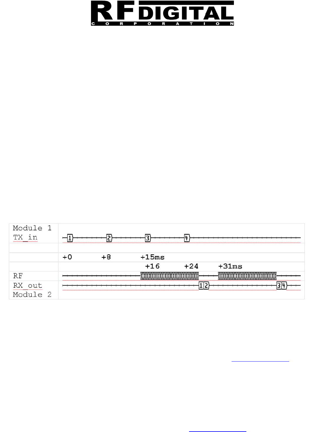
13715 Alton Pkwy • Irvine • CA • 92618
Tel: 949.610.0008 • www.RFdigital.com
Fast Answers: support@rfdigital.com
Free Applications Support • Email your application questions to support@rfdigital.com 35
RFDP8
© Copyright, RF Digital
1/29/2013 9:40 AM
Patents Pending
RoHS CE • ESTI
RFD21733/35 • FCC • IC
RFD21743 • FCC
Approved & Certified
RF Module
RFD21733
RFD21735
RFD21737
RFD21738
RFD21739
RFDP8
RFDANT
RFD21742
RFD21743
RFD21772
RFD21773
KEYFOBs
End-to-End Latency
The RFDP8 firmware buffers data inputted into its TXD pin of its UART into packets, which are transmitted over
the air. The firmware transmits a packet when it has buffered 12 bytes of data, or 15ms after receiving a byte of
data, which ever comes first. On the receiving end, data will be outputted on the RXD pin of the UART at line
speed, with no pauses between the bytes (other than the UART start and stop bits). The RFDP8 protocol can run
at full speed, line-rate, meaning without any spaces at all. Of course you can space out your bytes at any pace
you like, however as many bytes as you input into the TXD pin during each 15mS period will be collected into one
packet and sent at one time to the receiving radio and outputted in one burst at full line-rate.
The buffering and latency may cause problems with certain microcontrollers that can not tolerate serial data into
their UART in a constant stream at 9600-8N1. One possible solution is to add a 16ms delay on the transmitting
side which will cause each byte to be sent in its own packet by the module and therefore on the receiving end the
bytes will be outputted at a pace of one byte every 16ms which will help your controller of choice handle the fast
UART data.
As an example, consider a scenario where one system is sending a byte of data every 8ms. When module 1
receives the 1st byte on its UART, the 15ms timer begins. The 2nd byte arrives before 15ms elapses, and so the
first two bytes are sent in a single packet over the air to Module 2. Module 2 will transmit the bytes on its UART
with no delay between them. Module 1 receives the third byte on its UART, and re-starts the 15ms timer. As with
the 2nd byte, the 4th byte arrives before 15ms elapses, and so the 3rd and 4th bytes are also sent in a single packet
over the air, as illustrated in the following timing diagram.
Wake up time after power up and saving power.
After the module is powered on, 3mS later it is ready to receive or transmit. So if you want to consume zero
current when you don’t need to use the radio, you can simply use an external FET or PNP transistor and turn the
device fully off when you don’t need it and only turn it on when you want to send or receive data. If you require
any of this to be done automatically and internally to the Module or RFDANT, contact support@rfdigital.com
ESN Read-back
In certain applications, it is helpful to know the ESN of a module. There is a provision in both UART modes to
read back the ESN when the module comes out of reset. ESN read-back is not available in any of the other
modes.

13715 Alton Pkwy • Irvine • CA • 92618
Tel: 949.610.0008 • www.RFdigital.com
Fast Answers: support@rfdigital.com
Free Applications Support • Email your application questions to support@rfdigital.com 36
RFDP8
© Copyright, RF Digital
1/29/2013 9:40 AM
Patents Pending
RoHS CE • ESTI
RFD21733/35 • FCC • IC
RFD21743 • FCC
Approved & Certified
RF Module
RFD21733
RFD21735
RFD21737
RFD21738
RFD21739
RFDP8
RFDANT
RFD21742
RFD21743
RFD21772
RFD21773
KEYFOBs
You will need to use the RESET pin; this pin normally is not connected for nearly all applications except for
reading back the ESN or possibly using it to have the mode pins re-read and change modes without power
cycling. The reset signal does not have to be used, instead of using reset you can use power the module off and
then back on. The reset is a cleaner way of doing it. If you are using the RFD21737, RFD21738, RFD21739,
RFD21772, RFD21773 eval boards, the reset signal is available on pin 5 of the 12 pin connector. Internal to the
RFD21733 / RFD21735, RFD21742, RFD21743 there is a 3.3K pull up resistor on the reset signal, so when you
are not using it, you can just leave it open.
To activate ESN read-back:
1. Place the module in a reset state by holding the /RESET signal low.
2. Hold the LEARN signal high. (On the Eval board you can press and hold the LEARN button.)
3. Release the /RESET signal.
4. Wait 250ms. If the LEARN signal goes low at any time during this 250ms interval, the module
immediately exits ESN read-back mode.
5. Release the LEARN signal.
6. Send the string “READ ESN” (all capitals, one space between the two words) at 9600-8N1 into the
module on the TXD Input signal. If this string is not received within 1 second, the module exits ESN read-
back mode.
The module will respond with the ESN and a firmware identifier on the RXD Output signal at 9600-8N1, and then
exit ESN read-back mode. An example of the output is:
314CE686:RFDP8 v1.2 11/18/08 08:45:16$
The ESN is 8 characters, representing a 32-bit number in hexadecimal format. A colon separates the ESN from
the Firmware ID. The Firmware ID is 32 bytes long. The output is terminated with a carriage return/line feed pair.
When the module exits ESN read-back mode, or if the LEARN signal is not high when the module exists reset,
the module will enter regular operation in Mode 2 or 3, according to the mode select signals.
IMPORTANT NOTE – Mode 3 and ESN Read Back
If at all possible, do your ESN read-backs in Mode 2 and not Mode 3. The reason for this is that in Mode 3,
if you happen to do this manually (by hand using an Eval board), once the radio outputs the ESN string, it
will enter normal usage mode meaning it will directly enter into LEARN mode when you release the
LEARN pin and then spend 10 seconds waiting for a packet to be received so it can learn its ESN. You
can prevent this by using a controller to time this activity, or you can simply do it in Mode 2 and not have
the concern. If you have any questions, always feel free to email support@rfdigital.com.
Watch a video demonstrating how to do the ESN Read Back using HyperTerminal and an Eval Board:
http://www.rfdigital.com/?targetpage=item&filterpn=RFD76021
13715 Alton Pkwy • Irvine • CA • 92618
Tel: 949.610.0008 • www.RFdigital.com
Fast Answers: support@rfdigital.com
Free Applications Support • Email your application questions to support@rfdigital.com 37
RFDP8
© Copyright, RF Digital
1/29/2013 9:40 AM
Patents Pending
RoHS CE • ESTI
RFD21733/35 • FCC • IC
RFD21743 • FCC
Approved & Certified
RF Module
RFD21733
RFD21735
RFD21737
RFD21738
RFD21739
RFDP8
RFDANT
RFD21742
RFD21743
RFD21772
RFD21773
KEYFOBs
Mode 4 – Switch Receiver with Logic Output (500ms hang-time)
RFDANT
Pin # Module
Pin # Pin Label Direction Function
2 13 +V Input +V Power
1 10 GND Input Ground
5 16 Mode Select 0 Input Tie to GND
6 17 Mode Select 1 Input Tie to GND
7 3 Mode Select 2 Input Tie to +V
8 4 Not Used Output Leave open, not used.
9 5 OUT1 Output Active high switch output #1, 500 millisecond hang-time.
10 6 OUT2 Output Active high switch output #2, 500 millisecond hang-time.
11 7 OUT3 Output Active high switch output #3, 500 millisecond hang-time.
Mode 5 – Switch Receiver with Logic Output (500ms hang-time) (Network)
RFDANT
Pin # Module
Pin # Pin Label Direction Function
2 13 +V Input +V Power
1 10 GND Input Ground
5 16 Mode Select 0 Input Tie to +V
6 17 Mode Select 1 Input Tie to GND
7 3 Mode Select 2 Input Tie to +V
8 4 Learn / Status I/O Pulse high through a 220 ohm series resistor to enter learn
mode. LED Learn Status Output. Must be pulled to ground
through a 47k resistor and must have series a resistor.
9 5 OUT1 Output Active high switch output #1, 500 millisecond hang-time.
10 6 OUT2 Output Active high switch output #2, 500 millisecond hang-time.
11 7 OUT3 Output Active high switch output #3, 500 millisecond hang-time.
Mode 6 – Switch Receiver with Logic Output (20ms hang-time)
RFDANT
Pin # Module
Pin # Pin Label Direction Function
2 13 +V Input +V Power
1 10 GND Input Ground
5 16 Mode Select 0 Input Tie to GND
6 17 Mode Select 1 Input Tie to +V
7 3 Mode Select 2 Input Tie to +V
8 4 Not Used Output Leave open, not used.
9 5 OUT1 Output Active high switch output #1, 20 millisecond hang-time.
10 6 OUT2 Output Active high switch output #2, 20 millisecond hang-time.
11 7 OUT3 Output Active high switch output #3, 20 millisecond hang-time.
13715 Alton Pkwy • Irvine • CA • 92618
Tel: 949.610.0008 • www.RFdigital.com
Fast Answers: support@rfdigital.com
Free Applications Support • Email your application questions to support@rfdigital.com 38
RFDP8
© Copyright, RF Digital
1/29/2013 9:40 AM
Patents Pending
RoHS CE • ESTI
RFD21733/35 • FCC • IC
RFD21743 • FCC
Approved & Certified
RF Module
RFD21733
RFD21735
RFD21737
RFD21738
RFD21739
RFDP8
RFDANT
RFD21742
RFD21743
RFD21772
RFD21773
KEYFOBs
Mode 7 – Switch Receiver with Logic Output (20ms hang-time) (Network)
RFDANT
Pin # Module
Pin # Pin Label Direction Function
2 13 +V Input +V Power
1 10 GND Input Ground
5 16 Mode Select 0 Input Tie to +V
6 17 Mode Select 1 Input Tie to +V
7 3 Mode Select 2 Input Tie to +V
8 4 Learn / Status I/O Pulse high through a 220 ohm series resistor to enter learn mode.
LED Learn Status Output. Must be pulled to ground through a 47k
resistor and must have series a resistor.
9 5 OUT1 Output Active high switch output #1, 20 millisecond hang-time.
10 6 OUT2 Output Active high switch output #2, 20 millisecond hang-time.
11 7 OUT3 Output Active high switch output #3, 20 millisecond hang-time.
Fast Switch Latency
The RF Modules and RFDANTs with their patent pending RFDP8 interference tolerant protocol have fast
response times. When using a Mode 0 or 1 transmitter and a Mode 4, 5, 6 or 7 receiver, from the time the
transmitter switch input goes high, the receiver output will go high as fast as 5 milliseconds later. It might take as
long as 12mS, but most of the time it is closer to the 5mS time frame.
In Mode 4, Mode 5, Mode 6 and Mode 7, the Module or RFDANT is always in switch receiving mode.
The receiver drives its outputs to match the values received in a packet from a transmitter. This allows up to 8
possible (23) combinations on the receiver’s outputs.
The term Hang-Time means the period the output will stay high after it has been turned on. It will stay on for the
duration of the hang time, waiting on another packet to be received; if no other packet is received it will go low
after the hang-time period. If a packet is received within the hang-time period it will continue to stay high again for
that period of the hang-time setting (either 20mS or 500mS). If repetitive packages are received within the hang-
time window then the output which was high, will continue to stay high as long as that same input is kept high at
the transmitting radio or Serial transmitter which sent the packet.
Hang time is a trade-off between off-time-latency and resiliency to packet loss. With all RF systems sometimes a
packet will be lost, especially as the distance between the transmitter and the receiver grows. If an output is
connected to a relay driver, packet loss will result in chattering on the relay, which will not have good results. The
500ms hang time is perfect for applications like a keyless entry system or a garage door opener.
For faster switching to the “all off” state, the 20ms hang time is preferred. Since a transmitter sends new data
every 15ms, the time delay to turn off all outputs is only 5ms more than to update the outputs to a different state
where at least one of them is still driven high.
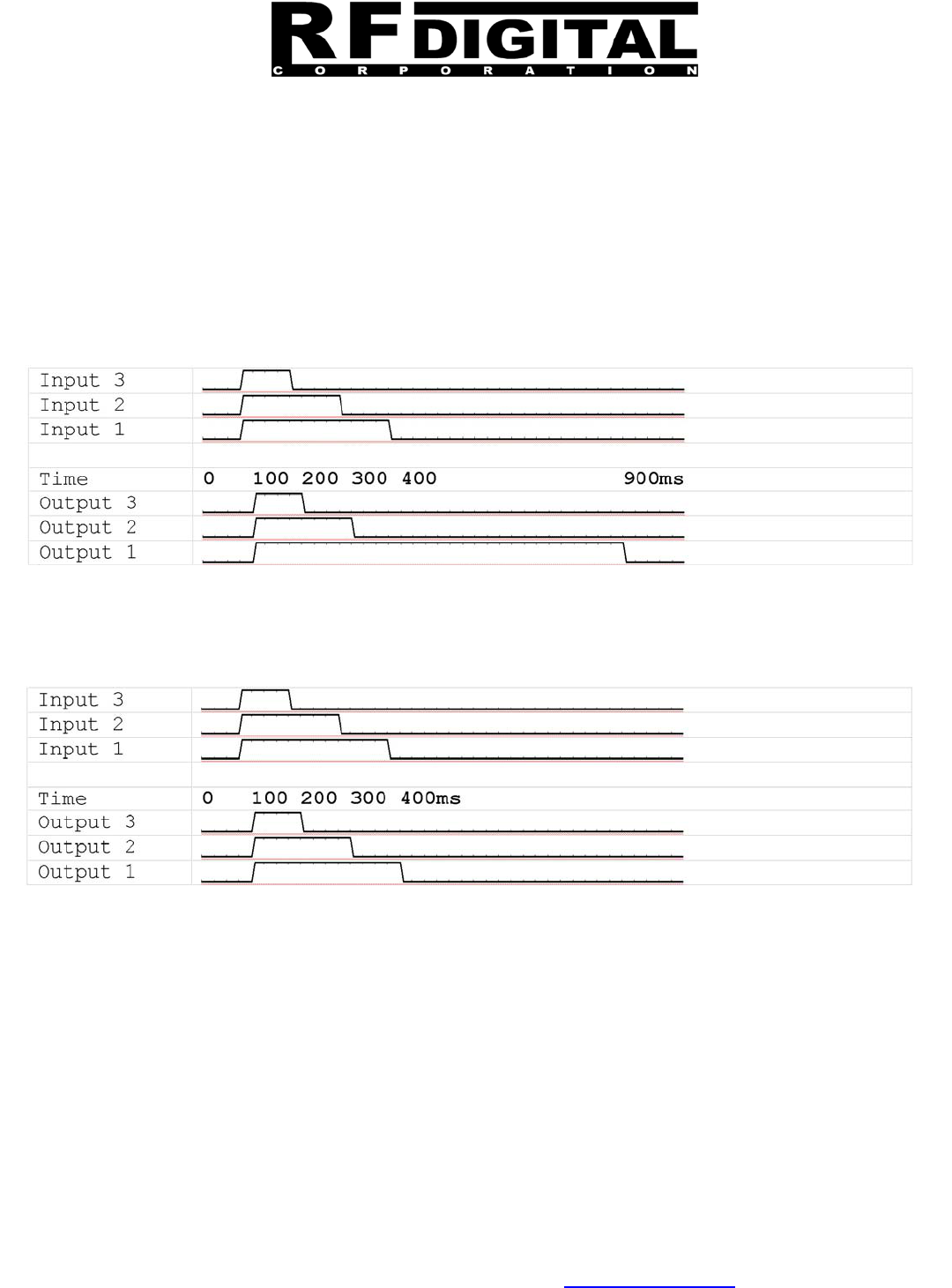
13715 Alton Pkwy • Irvine • CA • 92618
Tel: 949.610.0008 • www.RFdigital.com
Fast Answers: support@rfdigital.com
Free Applications Support • Email your application questions to support@rfdigital.com 39
RFDP8
© Copyright, RF Digital
1/29/2013 9:40 AM
Patents Pending
RoHS CE • ESTI
RFD21733/35 • FCC • IC
RFD21743 • FCC
Approved & Certified
RF Module
RFD21733
RFD21735
RFD21737
RFD21738
RFD21739
RFDP8
RFDANT
RFD21742
RFD21743
RFD21772
RFD21773
KEYFOBs
The following timing diagrams show the operation of a logic transmitter and a logic receiver with the different hang
time options.
In the first diagram, the logic transmitter’s inputs are all asserted, and then sequentially de-asserted. There is a
small delay between the transmitter input going high and the corresponding output on the receiver going high, due
to the time required to transmit over the air.
Note that when the last input on the transmitter is de-asserted, there is a 500ms delay before the receiver de-
asserts its last output.
The second diagram shows the same operation at the transmitter, but with the receiver configured with a 20ms
hang time.
Note that shortly after the last input is de-asserted, the receiver updates its output state to turn off all outputs.
Communication between UART and Switch Logic Receiver/Transmitter
The Logic Receiver and Transmitter modes are able to communicate with a module operating in one of the UART
modes, which opens up a wide range of possible applications involving PC’s or embedded systems with serial
communications capability.
Logic Transmitter to UART
A Logic Transmitter (whether RFID or not) sends the state of its inputs as a single byte of data, followed by its
ESN as four bytes. A Mode 2 or Mode 3, Module or RFDANT in Serial UART can receive this packet and output
it as a binary stream to a PC serial port or an embedded microcontroller. The format of the data is:
13715 Alton Pkwy • Irvine • CA • 92618
Tel: 949.610.0008 • www.RFdigital.com
Fast Answers: support@rfdigital.com
Free Applications Support • Email your application questions to support@rfdigital.com 40
RFDP8
© Copyright, RF Digital
1/29/2013 9:40 AM
Patents Pending
RoHS CE • ESTI
RFD21733/35 • FCC • IC
RFD21743 • FCC
Approved & Certified
RF Module
RFD21733
RFD21735
RFD21737
RFD21738
RFD21739
RFDP8
RFDANT
RFD21742
RFD21743
RFD21772
RFD21773
KEYFOBs
Byte Bit 7 Bit 6 Bit 5 Bit 4 Bit 3 Bit 2 Bit 1 Bit 0
1 Input 3 Input 2 Input 1/
RFID RFID
2 ESN Byte 1
3 ESN Byte 2
4 ESN Byte 3
5 ESN Byte 4
In the first byte, bits 6 through 4 carry the state of the logic inputs, with a ‘1’ indicating the logic input on the
transmitter is high, and a ‘0’ indicating it is low. An RFID Transmitter will set both bits 0 and 4 to indicate that it is
a periodic transmission from an RFID Transmitter, and is set to ‘1’ if this is the case.
For example, if an RFID Transmitter with ESN 314CE686 sent a packet on its 2-second interval, a UART would
receive the bytes 11 31 4C E6 86 in binary format.
If input #1 on that same RFID transmitter were pulled high, the UART would receive the bytes 10 31 4C E6 86 in
binary format; since bit 0 is clear, the receiver can tell that this was not a periodic transmission.
Most ESN’s will contain at least one unprintable character, and so this data will not be suitable for displaying
directly in a terminal package (such as HyperTerminal), but a PC-based program or an embedded system (such
as the BASIC Stamp) can collect the data and display it in a more friendly fashion.
There is a very useful tool on the web called RealTerm, it is a HyperTerminal like software which can be put into
binary-mode and with it you can easily view the individual bytes sent from a serial transmitter to a UART receiver.
The ESN which the UART receives is the same one that is in the packet header. If the UART is in Network Mode,
and has not learned the ESN, it will never receive the packet, and there will be no output on the serial port.
Serial UART to Logic Receiver
A UART can also send data to a logic receiver, which will decode the data and assert its outputs as though it
received a packet from a logic transmitter. The data format is very similar to the one described in the previous
section. The differences matter only when the receiver is in Network Mode.
The UART must follow a packet with at least 15ms of no data so that all bytes as described below are sent as a
single packet.
Note that a UART can send a single zero byte – all bits clear – to force a receiver to turn off its outputs
immediately, regardless of hang time.
Format 1:
Byte Bit 7 Bit 6 Bit 5 Bit 4 Bit 3 Bit 2 Bit 1 Bit 0
1 Output 3 Output 2 Output 1
When the receiver is not in Network Mode, the receiver will accept any packet it receives, and so this is the
preferred format.
13715 Alton Pkwy • Irvine • CA • 92618
Tel: 949.610.0008 • www.RFdigital.com
Fast Answers: support@rfdigital.com
Free Applications Support • Email your application questions to support@rfdigital.com 41
RFDP8
© Copyright, RF Digital
1/29/2013 9:40 AM
Patents Pending
RoHS CE • ESTI
RFD21733/35 • FCC • IC
RFD21743 • FCC
Approved & Certified
RF Module
RFD21733
RFD21735
RFD21737
RFD21738
RFD21739
RFDP8
RFDANT
RFD21742
RFD21743
RFD21772
RFD21773
KEYFOBs
A receiver in Network Mode will use the UART’s ESN from the packet header to determine if it should accept the
packet. This allows one UART to send the same data to multiple receivers, provided that each receiver has
learned the UART’s ESN.
Format 2:
Byte Bit 7 Bit 6 Bit 5 Bit 4 Bit 3 Bit 2 Bit 1 Bit 0
1 Output 3 Output 2 Output 1
2 ESN Byte 1
3 ESN Byte 2
4 ESN Byte 3
5 ESN Byte 4
To allow individual addressing of receivers in Network Mode, the UART can send a particular receiver’s ESN after
the byte for the logic state. In this case, the receiver will only accept the packet if the ESN in the data portion
matches the receiver’s own ESN.
If the receiver is actively learning ESN’s, it will learn only the ESN from the packet header; the ESN in the data
portion will not be learned.
Free Schematic, Layout and Application Design Reviews
For free Application, Schematic and Layout design reviews, send color screen captures or PDFs of your
schematic and layout to support@rfdigital.com. RF Digital’s Support and Application Engineers are ready to get
your wireless application running today. Why spend lots of time reading volumes of data? Instead, simply send
your application questions to support@rfdigital.com and receive direct, fast and personal answers focused on
your specific project and needs. We look forward to hearing from you!!!
13715 Alton Pkwy • Irvine • CA • 92618
Tel: 949.610.0008 • www.RFdigital.com
Fast Answers: support@rfdigital.com
Free Applications Support • Email your application questions to support@rfdigital.com 42
RFDP8
© Copyright, RF Digital
1/29/2013 9:40 AM
Patents Pending
RoHS CE • ESTI
RFD21733/35 • FCC • IC
RFD21743 • FCC
Approved & Certified
RF Module
RFD21733
RFD21735
RFD21737
RFD21738
RFD21739
RFDP8
RFDANT
RFD21742
RFD21743
RFD21772
RFD21773
KEYFOBs
Electrical Characteristics
Operating Conditions
Notes Parameter Minimum Typical Maximum
VDD Supply voltage 1.9V 3.0V 3.6V
Supply Rise Time 1uS 50mS
Operating Temperature -40°C +85°C
Input High Voltage VDD x 0.7 VDD
Input Low Voltage VSS VDD x 0.3
Output High Voltage (@ 0.5mA) VDD - 0.7V VDD
Output Low Voltage (@ 0.5mA) VSS 0.3V
Internal CPU Controlled Pull-Ups 11k ohm 13k ohm 16k ohm
RFDP8 M0 Pin ** Internal CPU Controlled Pull-Downs 11k ohm 13k ohm 16k ohm
Power Up Time – Ready to Transmit 3mS
Power Up Time – Ready to Receive 3mS
After Reset – Ready to Transmit 3mS
After Reset – Ready to Receive 3mS
** Note (RFDP8 M0 Pin) The RFDP8 Modules and RFDANTs have 3 pins used to set the mode the device will go
into after reset or power up. These pins are called M2, M1 and M0. M0 pin is the low order pin. At power up or
when the module comes out of reset, it will internally apply a 13k pull down on this pin just for an instant to check
if it is high or not. After the mode selection test, which is done just once at start up lasts just microseconds. This
is done like this to allow you to have an optional external switch to select between mode 0 and mode 1 without
drawing extra current through an external pull down resistor which would statically be there all the time.
Power Consumption
Conditions: VDD = 3.0V, TA = +25°C
Logic Transmitter
Parameter Minimum Typical Maximum
Ultra-low power mode - background - Switch Logic Transmitter 2uA
UART or Switch Logic Transmitter / Receiver
Parameter Minimum Typical Maximum
Listening - Receiving 17mA
Transmitting 14mA
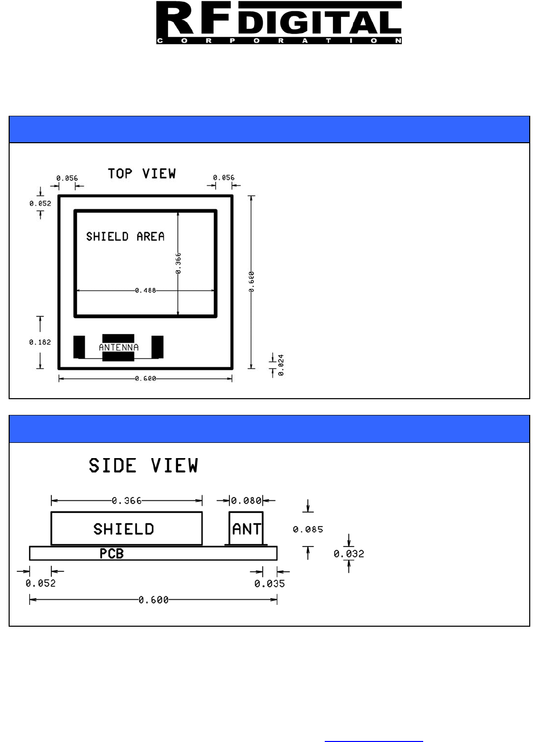
13715 Alton Pkwy • Irvine • CA • 92618
Tel: 949.610.0008 • www.RFdigital.com
Fast Answers: support@rfdigital.com
Free Applications Support • Email your application questions to support@rfdigital.com 43
RFDP8
© Copyright, RF Digital
1/29/2013 9:40 AM
Patents Pending
RoHS CE • ESTI
RFD21733/35 • FCC • IC
RFD21743 • FCC
Approved & Certified
RF Module
RFD21733
RFD21735
RFD21737
RFD21738
RFD21739
RFDP8
RFDANT
RFD21742
RFD21743
RFD21772
RFD21773
KEYFOBs
Overall Dimensions • Top View
Overall Dimensions • Side View
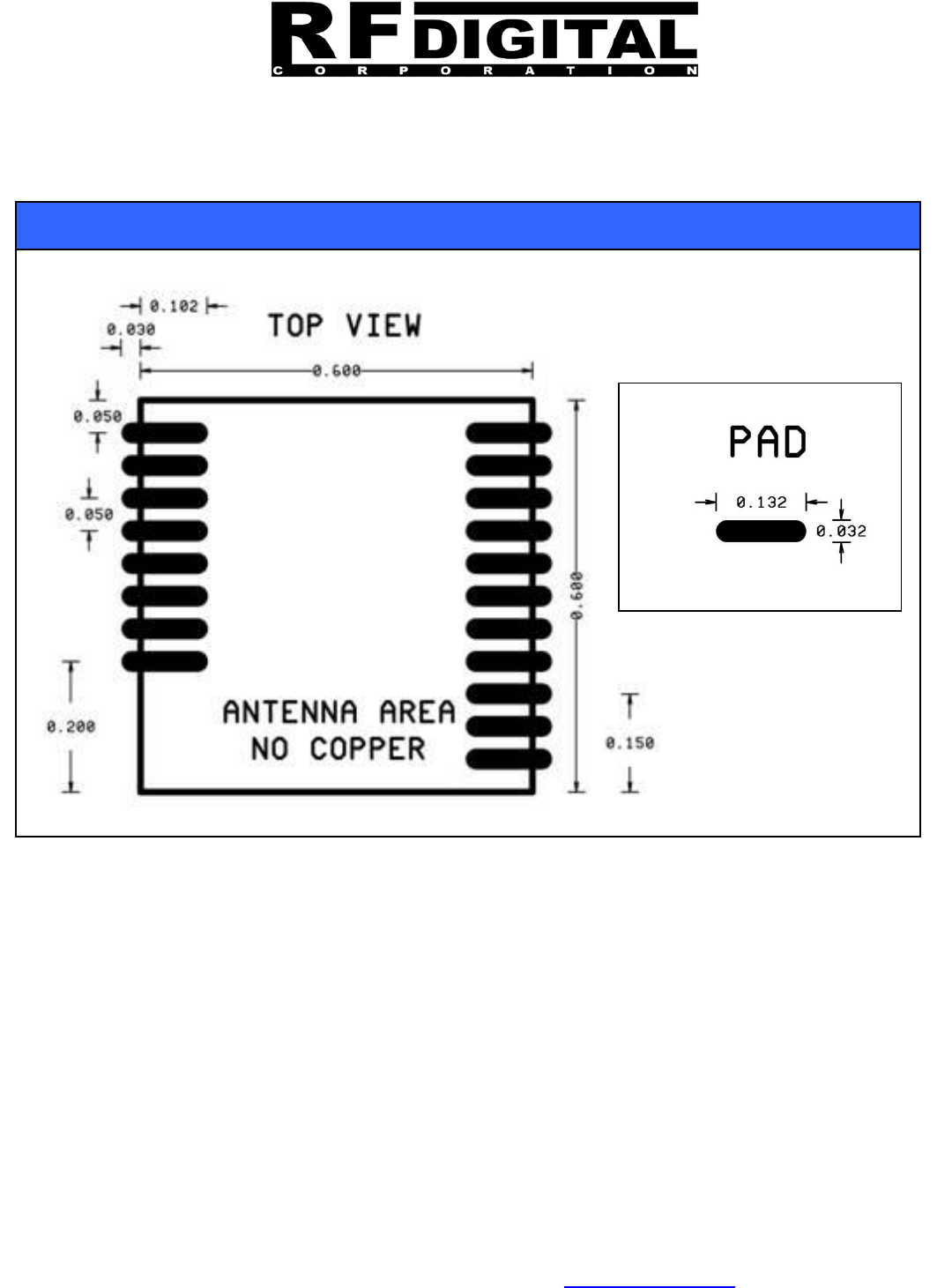
13715 Alton Pkwy • Irvine • CA • 92618
Tel: 949.610.0008 • www.RFdigital.com
Fast Answers: support@rfdigital.com
Free Applications Support • Email your application questions to support@rfdigital.com 44
RFDP8
© Copyright, RF Digital
1/29/2013 9:40 AM
Patents Pending
RoHS CE • ESTI
RFD21733/35 • FCC • IC
RFD21743 • FCC
Approved & Certified
RF Module
RFD21733
RFD21735
RFD21737
RFD21738
RFD21739
RFDP8
RFDANT
RFD21742
RFD21743
RFD21772
RFD21773
KEYFOBs
PCB Layout

13715 Alton Pkwy • Irvine • CA • 92618
Tel: 949.610.0008 • www.RFdigital.com
Fast Answers: support@rfdigital.com
Free Applications Support • Email your application questions to support@rfdigital.com 45
RFDP8
© Copyright, RF Digital
1/29/2013 9:40 AM
Patents Pending
RoHS CE • ESTI
RFD21733/35 • FCC • IC
RFD21743 • FCC
Approved & Certified
RF Module
RFD21733
RFD21735
RFD21737
RFD21738
RFD21739
RFDP8
RFDANT
RFD21742
RFD21743
RFD21772
RFD21773
KEYFOBs
RFD21733 modules which do not show IC: 6992A-24 on the shield
are NOT certified for use in Canada. RFD21733 modules with date
codes before “1120” (20th week of 2011) are not Industry Canada
approved.
IC NOTICE
Relating to Model Number R24 (RFD Stock Code: RFD21733)
The unit should have a permanently attached label in a conspicuous location with the following
statement:
NOTES:
1. Industry Canada does not specify the size of the label or the lettering thereon. The only
requirement is that the text be legible.
Contains IC: 6992A-24

13715 Alton Pkwy • Irvine • CA • 92618
Tel: 949.610.0008 • www.RFdigital.com
Fast Answers: support@rfdigital.com
Free Applications Support • Email your application questions to support@rfdigital.com 46
RFDP8
© Copyright, RF Digital
1/29/2013 9:40 AM
Patents Pending
RoHS CE • ESTI
RFD21733/35 • FCC • IC
RFD21743 • FCC
Approved & Certified
RF Module
RFD21733
RFD21735
RFD21737
RFD21738
RFD21739
RFDP8
RFDANT
RFD21742
RFD21743
RFD21772
RFD21773
KEYFOBs
INDUSTRY CANADA INFORMATION
Relating to Model Number R24 (RFD Stock Code: RFD21733)
Under Industry Canada regulations, this radio transmitter may only operate using an antenna of a type
and maximum (or lesser) gain approved for the transmitter by Industry Canada. To reduce potential
radio interference to other users, the antenna type and its gain should be so chosen that the equivalent
isotropically radiated power (e.i.r.p.) is not more than that necessary for successful communication.
This device complies with Industry Canada licence-exempt RSS standard(s). Operation is subject
to the following two conditions: (1) this device may not cause interference, and (2) this device
must accept any interference, including interference that may cause undesired operation of the
device.
Conformément à la réglementation d'Industrie Canada, le présent émetteur radio peut
fonctionner avec une antenne d'un type et d'un gain maximal (ou inférieur) approuvé pour
l'émetteur par Industrie Canada. Dans le but de réduire les risques de brouillage radioélectrique
à l'intention des autres utilisateurs, il faut choisir le type d'antenne et son gain de sorte que la
puissance isotrope rayonnée équivalente (p.i.r.e.) ne dépasse pas l'intensité nécessaire à
l'établissement d'une communication satisfaisante.
Le présent appareil est conforme aux CNR d'Industrie Canada applicables aux appareils radio
exempts de licence. L'exploitation est autorisée aux deux conditions suivantes : (1) l'appareil ne
doit pas produire de brouillage, et (2) l'utilisateur de l'appareil doit accepter tout brouillage
radioélectrique subi, même si le brouillage est susceptible d'en compromettre le fonctionnement.
13715 Alton Pkwy • Irvine • CA • 92618
Tel: 949.610.0008 • www.RFdigital.com
Fast Answers: support@rfdigital.com
Free Applications Support • Email your application questions to support@rfdigital.com 47
RFDP8
© Copyright, RF Digital
1/29/2013 9:40 AM
Patents Pending
RoHS CE • ESTI
RFD21733/35 • FCC • IC
RFD21743 • FCC
Approved & Certified
RF Module
RFD21733
RFD21735
RFD21737
RFD21738
RFD21739
RFDP8
RFDANT
RFD21742
RFD21743
RFD21772
RFD21773
KEYFOBs
FCC NOTICE
Relating to Model Number R24 (RFD Stock Code: RFD21733)
The unit should have a permanently attached label in a conspicuous location with the following
statement:
NOTES:
1. The FCC does not specify the size of the label or the lettering thereon. The only requirement
is that the text be legible.
2. If the entire label can not be placed on the unit due to space constraint, only FCC ID may be
displayed on the unit. In such cases, the compliance statement will have to be included in the
"user’s manual". NOTE: Device must be smaller than a man’s palm.
Contains FCC ID: UYI24
This device complies with Part 15 of the FCC Rules.
Operation is subject to the following two conditions:
(1) This device may not cause harmful interference and
(2) this device must accept any interference received,
including interference that may cause undesired
operation.

13715 Alton Pkwy • Irvine • CA • 92618
Tel: 949.610.0008 • www.RFdigital.com
Fast Answers: support@rfdigital.com
Free Applications Support • Email your application questions to support@rfdigital.com 48
RFDP8
© Copyright, RF Digital
1/29/2013 9:40 AM
Patents Pending
RoHS CE • ESTI
RFD21733/35 • FCC • IC
RFD21743 • FCC
Approved & Certified
RF Module
RFD21733
RFD21735
RFD21737
RFD21738
RFD21739
RFDP8
RFDANT
RFD21742
RFD21743
RFD21772
RFD21773
KEYFOBs
SAMPLE FCC STATEMENT TO BE INCLUDED IN USER'S MANUAL
Relating to Model Number R24 (RFD Stock Code: RFD21733)
INSTRUCTION TO THE USER (if device DOES NOT contain a digital device)
The user is cautioned that changes or modifications not expressly approved by the party
responsible for compliance could void the user’s authority to operate this equipment.
INSTRUCTION TO THE USER (if device contains a digital device)
This equipment has been tested and found to comply with the limits for a class B digital device,
pursuant to part 15 of the FCC Rules. These limits are designed to provide reasonable
protection against harmful interference in a residential installation. This equipment generates,
uses and can radiate radio frequency energy and if not installed and used in accordance with
the instructions, may cause harmful interference to radio communications. However, there is
no guarantee that interference will not occur in a particular installation. If this equipment does
cause harmful interference to radio or television reception, which can be determined by turning
the equipment off and on, the user is encouraged to try to correct the interference by one or
more of the following measures:
* Reorient or relocate the receiving antenna.
* Increase the separation between the equipment and receiver.
* Connect the equipment into an outlet on a circuit different from that to which the receiver is
connected.
* Consult the dealer or an experienced radio/TV technician for help.

13715 Alton Pkwy • Irvine • CA • 92618
Tel: 949.610.0008 • www.RFdigital.com
Fast Answers: support@rfdigital.com
Free Applications Support • Email your application questions to support@rfdigital.com 49
RFDP8
© Copyright, RF Digital
1/29/2013 9:40 AM
Patents Pending
RoHS CE • ESTI
RFD21733/35 • FCC • IC
RFD21743 • FCC
Approved & Certified
RF Module
RFD21733
RFD21735
RFD21737
RFD21738
RFD21739
RFDP8
RFDANT
RFD21742
RFD21743
RFD21772
RFD21773
KEYFOBs
IC NOTICE
Relating to Model Number RFD21735
The unit should have a permanently attached label in a conspicuous location with the following
statement:
NOTES:
1. Industry Canada does not specify the size of the label or the lettering thereon. The only
requirement is that the text be legible.
Contains IC: 10781A-NOVYC1

13715 Alton Pkwy • Irvine • CA • 92618
Tel: 949.610.0008 • www.RFdigital.com
Fast Answers: support@rfdigital.com
Free Applications Support • Email your application questions to support@rfdigital.com 50
RFDP8
© Copyright, RF Digital
1/29/2013 9:40 AM
Patents Pending
RoHS CE • ESTI
RFD21733/35 • FCC • IC
RFD21743 • FCC
Approved & Certified
RF Module
RFD21733
RFD21735
RFD21737
RFD21738
RFD21739
RFDP8
RFDANT
RFD21742
RFD21743
RFD21772
RFD21773
KEYFOBs
INDUSTRY CANADA INFORMATION
Relating to Model Number RFD21735
Under Industry Canada regulations, this radio transmitter may only operate using an antenna of a type
and maximum (or less) gain approved for the transmitter by Industry Canada. To reduce potential radio
interference to other users, the antenna type and its gain should be so chosen that the equivalent
isotropically radiated power (e.i.r.p.) is not more than that necessary for successful communication.
This device complies with Industry Canada licence-exempt RSS standard(s). Operation is subject
to the following two conditions: (1) this device may not cause interference, and (2) this device
must accept any interference, including interference that may cause undesired operation of the
device.
Conformément à la réglementation d'Industrie Canada, le présent émetteur radio peut
fonctionner avec une antenne d'un type et d'un gain maximal (ou inférieur) approuvé pour
l'émetteur par Industrie Canada. Dans le but de réduire les risques de brouillage radioélectrique
à l'intention des autres utilisateurs, il faut choisir le type d'antenne et son gain de sorte que la
puissance isotrope rayonnée équivalente (p.i.r.e.) ne dépasse pas l'intensité nécessaire à
l'établissement d'une communication satisfaisante.
Le présent appareil est conforme aux CNR d'Industrie Canada applicables aux appareils radio
exempts de licence. L'exploitation est autorisée aux deux conditions suivantes : (1) l'appareil ne
doit pas produire de brouillage, et (2) l'utilisateur de l'appareil doit accepter tout brouillage
radioélectrique subi, même si le brouillage est susceptible d'en compromettre le fonctionnement.

13715 Alton Pkwy • Irvine • CA • 92618
Tel: 949.610.0008 • www.RFdigital.com
Fast Answers: support@rfdigital.com
Free Applications Support • Email your application questions to support@rfdigital.com 51
RFDP8
© Copyright, RF Digital
1/29/2013 9:40 AM
Patents Pending
RoHS CE • ESTI
RFD21733/35 • FCC • IC
RFD21743 • FCC
Approved & Certified
RF Module
RFD21733
RFD21735
RFD21737
RFD21738
RFD21739
RFDP8
RFDANT
RFD21742
RFD21743
RFD21772
RFD21773
KEYFOBs
FCC NOTICE
Relating to Model Number RFD21735
The unit should have a permanently attached label in a conspicuous location with the following
statement:
NOTES:
1. The FCC does not specify the size of the label or the lettering thereon. The only requirement
is that the text be legible.
2. If the entire label can not be placed on the unit due to space constraint, only FCC ID may be
displayed on the unit. In such cases, the compliance statement will have to be included in the
"user’s manual". NOTE: Device must be smaller than a man’s palm.
Contains FCC ID: RG5 NOVYC1
This device complies with Part 15 of the FCC Rules.
Operation is subject to the following two conditions:
(1) This device may not cause harmful interference and
(2) this device must accept any interference received,
including interference that may cause undesired
operation.

13715 Alton Pkwy • Irvine • CA • 92618
Tel: 949.610.0008 • www.RFdigital.com
Fast Answers: support@rfdigital.com
Free Applications Support • Email your application questions to support@rfdigital.com 52
RFDP8
© Copyright, RF Digital
1/29/2013 9:40 AM
Patents Pending
RoHS CE • ESTI
RFD21733/35 • FCC • IC
RFD21743 • FCC
Approved & Certified
RF Module
RFD21733
RFD21735
RFD21737
RFD21738
RFD21739
RFDP8
RFDANT
RFD21742
RFD21743
RFD21772
RFD21773
KEYFOBs
SAMPLE FCC STATEMENT TO BE INCLUDED IN USER'S MANUAL
Relating to Model Number RFD21735
INSTRUCTION TO THE USER (if device DOES NOT contain a digital device)
The user is cautioned that changes or modifications not expressly approved by the party
responsible for compliance could void the user’s authority to operate this equipment.
INSTRUCTION TO THE USER (if device contains a digital device)
This equipment has been tested and found to comply with the limits for a class B digital device,
pursuant to part 15 of the FCC Rules. These limits are designed to provide reasonable
protection against harmful interference in a residential installation. This equipment generates,
uses and can radiate radio frequency energy and if not installed and used in accordance with
the instructions, may cause harmful interference to radio communications. However, there is
no guarantee that interference will not occur in a particular installation. If this equipment does
cause harmful interference to radio or television reception, which can be determined by turning
the equipment off and on, the user is encouraged to try to correct the interference by one or
more of the following measures:
* Reorient or relocate the receiving antenna.
* Increase the separation between the equipment and receiver.
* Connect the equipment into an outlet on a circuit different from that to which the receiver is
connected.
* Consult the dealer or an experienced radio/TV technician for help.
In order to maintain compliance with FCC regulations, shielded cables must be used with this
equipment. Operation with non-approved equipment or unshielded cables is likely to result in
interference to radio and TV reception. The user is cautioned that changes and modifications
made to the equipment without the approval of manufacturer could void the user's authority to
operate this equipment.
13715 Alton Pkwy • Irvine • CA • 92618
Tel: 949.610.0008 • www.RFdigital.com
Fast Answers: support@rfdigital.com
Free Applications Support • Email your application questions to support@rfdigital.com 53
RFDP8
© Copyright, RF Digital
1/29/2013 9:40 AM
Patents Pending
RoHS CE • ESTI
RFD21733/35 • FCC • IC
RFD21743 • FCC
Approved & Certified
RF Module
RFD21733
RFD21735
RFD21737
RFD21738
RFD21739
RFDP8
RFDANT
RFD21742
RFD21743
RFD21772
RFD21773
KEYFOBs
FCC NOTICE
Relating to Model Number RFDANT (RFD Stock Code: RFD21743)
LABELING REQUIREMENT FOR USA
FCC CERTIFICATION
This device has a modular approval from the FCC. You must place the following label outside,
on your product in an obvious location.
Permanently attached label in a conspicuous location with the following statement:
NOTES:
1. The FCC does not specify the size of the label or the lettering thereon. The only requirement
is that the text be legible.
2. If the entire label can not be placed on the unit due to space constraint (e.g. Pacemaker),
only “contains an FCC ID: UYI-RFDANT” may be displayed on the unit. In such cases, the
compliance statement will have to be included in the "instruction to the user."
******* It is the users responsibility to determine if their device requires additional approvals *******
This device contains FCC ID: UYI-RFDANT RF module that
complies with Part 15 of the FCC Rules. Operation is
subject to the following two conditions:
(1) This device may not cause harmful interference and
(2) this device must accept any interference received,
including interference that may cause undesired
operation.

13715 Alton Pkwy • Irvine • CA • 92618
Tel: 949.610.0008 • www.RFdigital.com
Fast Answers: support@rfdigital.com
Free Applications Support • Email your application questions to support@rfdigital.com 54
RFDP8
© Copyright, RF Digital
1/29/2013 9:40 AM
Patents Pending
RoHS CE • ESTI
RFD21733/35 • FCC • IC
RFD21743 • FCC
Approved & Certified
RF Module
RFD21733
RFD21735
RFD21737
RFD21738
RFD21739
RFDP8
RFDANT
RFD21742
RFD21743
RFD21772
RFD21773
KEYFOBs
SAMPLE FCC STATEMENT TO BE INCLUDED IN USER'S MANUAL
Relating to Model Number RFDANT (RFD Stock Code: RFD21743)
INSTRUCTION TO THE USER (if device contains a digital device)
This equipment has been tested and found to comply with the limits for a class B digital device,
pursuant to part 15 of the FCC Rules. These limits are designed to provide reasonable
protection against harmful interference in a residential installation. This equipment generates,
uses and can radiate radio frequency energy and if not installed and used in accordance with
the instructions, may cause harmful interference to radio communications. However, there is
no guarantee that interference will not occur in a particular installation. If this equipment does
cause harmful interference to radio or television reception, which can be determined by turning
the equipment off and on, the user is encouraged to try to correct the interference by one or
more of the following measures:
* Reorient or relocate the receiving antenna.
* Increase the separation between the equipment and receiver.
* Connect the equipment into an outlet on a circuit different from that to which the receiver is
connected.
* Consult the dealer or an experienced radio/TV technician for help.
The user is cautioned that changes and modifications made to the equipment without the
approval of manufacturer could void the user's authority to operate this equipment.

13715 Alton Pkwy • Irvine • CA • 92618
Tel: 949.610.0008 • www.RFdigital.com
Fast Answers: support@rfdigital.com
Free Applications Support • Email your application questions to support@rfdigital.com 55
RFDP8
© Copyright, RF Digital
1/29/2013 9:40 AM
Patents Pending
RoHS CE • ESTI
RFD21733/35 • FCC • IC
RFD21743 • FCC
Approved & Certified
RF Module
RFD21733
RFD21735
RFD21737
RFD21738
RFD21739
RFDP8
RFDANT
RFD21742
RFD21743
RFD21772
RFD21773
KEYFOBs
RoHS
Declaration Of Conformity
RF Digital declares that part numbers
• RFD21731
• RFD21732
• RFD21733
• RFD21734
• RFD21735
• RFD21736
• RFD21737
• RFD21738
• RFD21739
• RFD21741
• RFD21742
• RFD21743
• RFD21764
• RFD21772
• RFD21773
are manufactured with RoHS materials.

13715 Alton Pkwy • Irvine • CA • 92618
Tel: 949.610.0008 • www.RFdigital.com
Fast Answers: support@rfdigital.com
Free Applications Support • Email your application questions to support@rfdigital.com 56
RFDP8
© Copyright, RF Digital
1/29/2013 9:40 AM
Patents Pending
RoHS CE • ESTI
RFD21733/35 • FCC • IC
RFD21743 • FCC
Approved & Certified
RF Module
RFD21733
RFD21735
RFD21737
RFD21738
RFD21739
RFDP8
RFDANT
RFD21742
RFD21743
RFD21772
RFD21773
KEYFOBs
DECLARATION OF CONFORMITY
June 29, 2010
RF Digital declares that part numbers
• RFD21731
• RFD21732
• RFD21733
• RFD21734
• RFD21735
• RFD21741
• RFD21742
• RFD21743
comply with ETSI EN 300 440-2 power requirements
as called out in the R&TTE V1.2.1 Directive
Technical documents for the above mentioned part numbers are held at
RF Digital Corporation
13715 Alton Pkwy.
Irvine, CA 92618
13715 Alton Pkwy • Irvine • CA • 92618
Tel: 949.610.0008 • www.RFdigital.com
Fast Answers: support@rfdigital.com
Free Applications Support • Email your application questions to support@rfdigital.com 57
RFDP8
© Copyright, RF Digital
1/29/2013 9:40 AM
Patents Pending
RoHS CE • ESTI
RFD21733/35 • FCC • IC
RFD21743 • FCC
Approved & Certified
RF Module
RFD21733
RFD21735
RFD21737
RFD21738
RFD21739
RFDP8
RFDANT
RFD21742
RFD21743
RFD21772
RFD21773
KEYFOBs
RFD21733 / RFD21735 Tray Packaging
The RFD21733 and RFD21735 are NOT washable.
Use no-clean flux, leaded or lead-free. If you attempt to wash the modules, water will enter beneath
(inside) the RF shield and get trapped, which may cause device failure or damage once powered on.
There is no way to make sure all water has been removed before powering the module so do NOT wash
the modules.
Washing
Do NOT pot or conformal coat the RFD21733 or RFD21735.
If you plan on encapsulating the RFD21733 or RFD21735 in a potting compound or conformal coating,
you must assure that the compound in liquid or solid form does not enter under the shield where there
are sensitive RF components. Some of the capacitive values are as low as half a picofarad and sensitive
to contacting materials such as potting compounds. There are potting compounds and conformal
coatings which have very good dielectric constants and are suitable for 2.4 GHz potting applications,
however, when you apply any of these, they were accounted for in the circuit design and might reduce
performance of the device or all together cause it not to function.
Applying any compound, conformal coating or potting directly to the module voids any and all
warranty and support service.
If your application requires 100% sealing of the module, there is a way to do this very successfully
without impacting the module performance. Simply place the module on your PCB. Place a plastic
cover over the module (like a hat), make the cover large enough to cover the whole module. Apply glue
around the bottom perimeter of the cover where it sits on the PCB. This allows the module to function in
free airspace while there is a complete seal around it. This information is only for reference and you
should do your own testing with your application to find the best suitable fit for your own design.
Potting, Encapsulation and Conformal Coating
Use standard lead-free or leaded reflow profile for the RFD21733 and RFD21735. Your CM (Contract
Manufacturer) should profile this module along with your PCB and all other parts on it through their
reflow oven to properly set a profile suitable for all the parts on the board combined.
USE CAUTION: If you are building a double-sided placement board, place this device last so it will not
be subjected to being reflowed upside-down.
As with building any RF devices, you should always build a small quantity through your production
process, test and verify, then increase your quantities to make sure the process is not harmful to the
performance of your RF system. This is true with any RF system, including use of these modules.
Reflow Profile
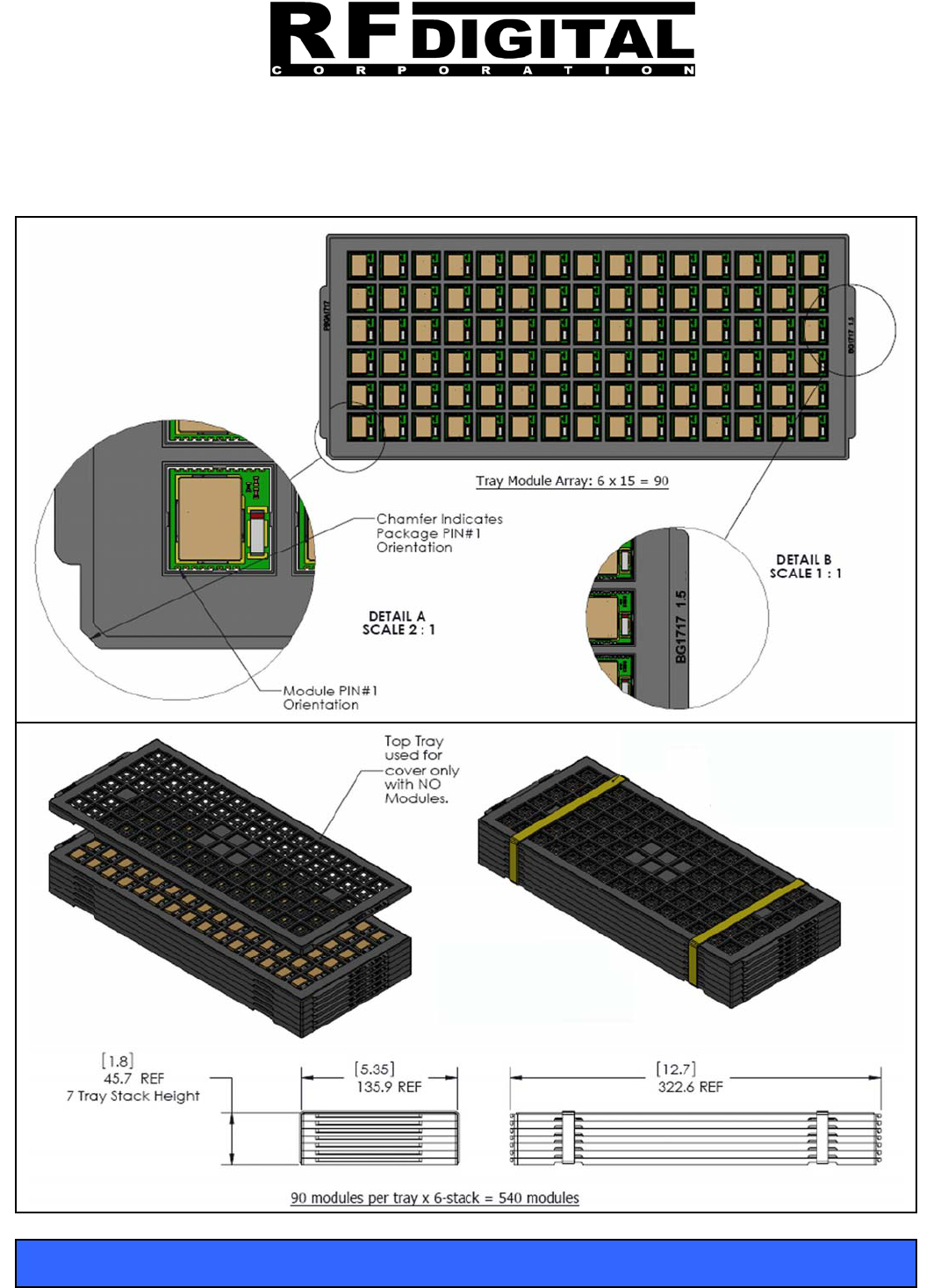
13715 Alton Pkwy • Irvine • CA • 92618
Tel: 949.610.0008 • www.RFdigital.com
Fast Answers: support@rfdigital.com
Free Applications Support • Email your application questions to support@rfdigital.com 58
RFDP8
© Copyright, RF Digital
1/29/2013 9:40 AM
Patents Pending
RoHS CE • ESTI
RFD21733/35 • FCC • IC
RFD21743 • FCC
Approved & Certified
RF Module
RFD21733
RFD21735
RFD21737
RFD21738
RFD21739
RFDP8
RFDANT
RFD21742
RFD21743
RFD21772
RFD21773
KEYFOBs
RFD21733 / RFD21735 Tray Packaging
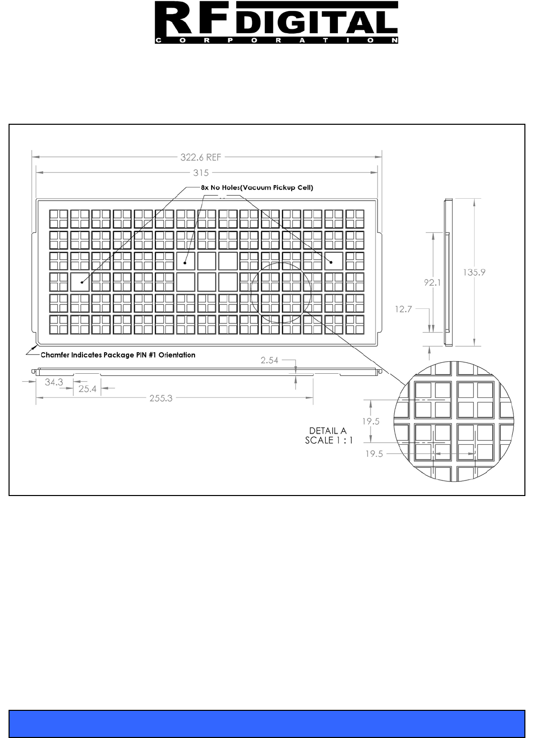
13715 Alton Pkwy • Irvine • CA • 92618
Tel: 949.610.0008 • www.RFdigital.com
Fast Answers: support@rfdigital.com
Free Applications Support • Email your application questions to support@rfdigital.com 59
RFDP8
© Copyright, RF Digital
1/29/2013 9:40 AM
Patents Pending
RoHS CE • ESTI
RFD21733/35 • FCC • IC
RFD21743 • FCC
Approved & Certified
RF Module
RFD21733
RFD21735
RFD21737
RFD21738
RFD21739
RFDP8
RFDANT
RFD21742
RFD21743
RFD21772
RFD21773
KEYFOBs
RFD21733 / RFD21735 Tray Packaging
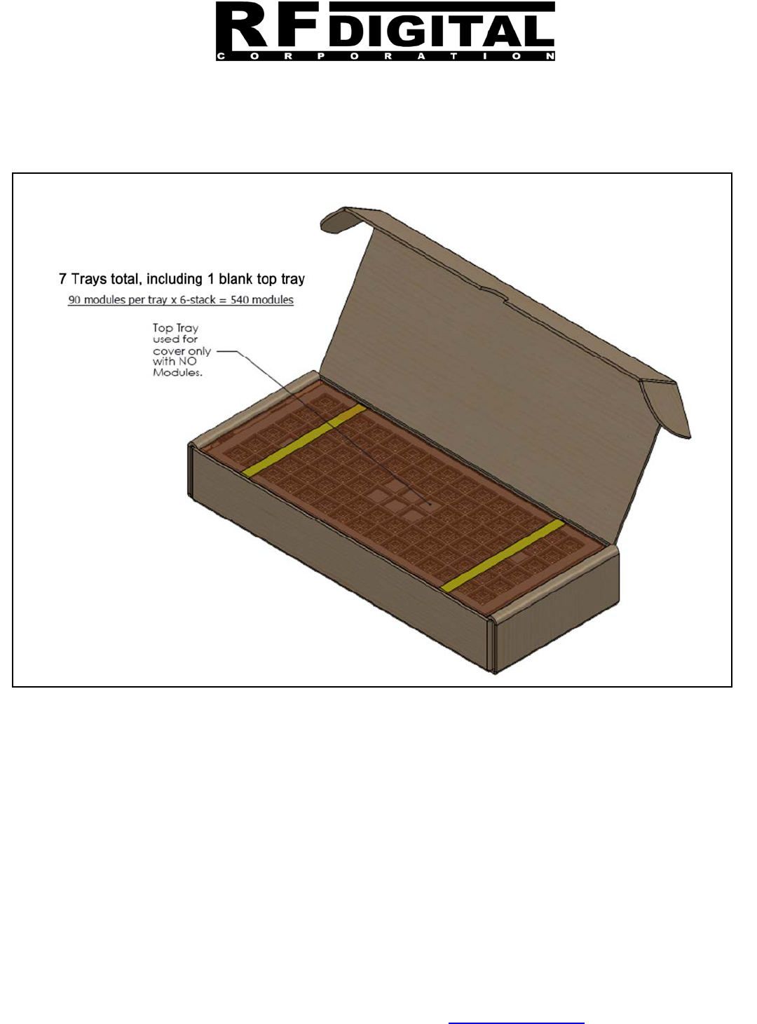
13715 Alton Pkwy • Irvine • CA • 92618
Tel: 949.610.0008 • www.RFdigital.com
Fast Answers: support@rfdigital.com
Free Applications Support • Email your application questions to support@rfdigital.com 60
RFDP8
© Copyright, RF Digital
1/29/2013 9:40 AM
Patents Pending
RoHS CE • ESTI
RFD21733/35 • FCC • IC
RFD21743 • FCC
Approved & Certified
RF Module
RFD21733
RFD21735
RFD21737
RFD21738
RFD21739
RFDP8
RFDANT
RFD21742
RFD21743
RFD21772
RFD21773
KEYFOBs
Surface Mounted RF Module Layout Examples
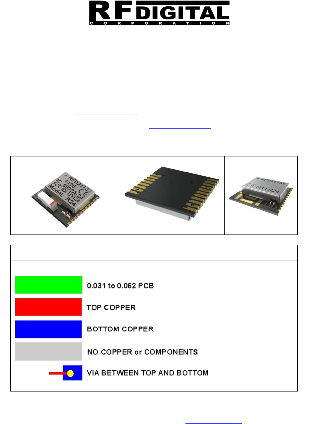
13715 Alton Pkwy • Irvine • CA • 92618
Tel: 949.610.0008 • www.RFdigital.com
Fast Answers: support@rfdigital.com
Free Applications Support • Email your application questions to support@rfdigital.com 61
RFDP8
© Copyright, RF Digital
1/29/2013 9:40 AM
Patents Pending
RoHS CE • ESTI
RFD21733/35 • FCC • IC
RFD21743 • FCC
Approved & Certified
RF Module
RFD21733
RFD21735
RFD21737
RFD21738
RFD21739
RFDP8
RFDANT
RFD21742
RFD21743
RFD21772
RFD21773
KEYFOBs
For Part Numbers RFD21731, RFD21732, RFD21733, RFD21734, RFD21735
Free Schematic, Layout and Application Design Reviews
For free Application, Schematic and Layout design reviews, send color screen captures or PDFs of your
schematic and layout to support@rfdigital.com. RF Digital’s Support and Application Engineers are
ready to get your wireless application running today. Why spend lots of time reading volumes of data?
Instead, simply send your application questions to support@rfdigital.com and receive direct, fast and
personal answers focused on your specific project and needs. We look forward to hearing from you!!!
For use with
External Antenna
RFD21735 / RFD21734
RFD21733 FCC / IC Approved
Built-In Antenna
RFD21731 / RFD21732 / RFD21733
21731 / 21732 / 21733 / 21734 / 21735
Please use the legend below to identify the colors, objects and their meanings in this document.
Legend
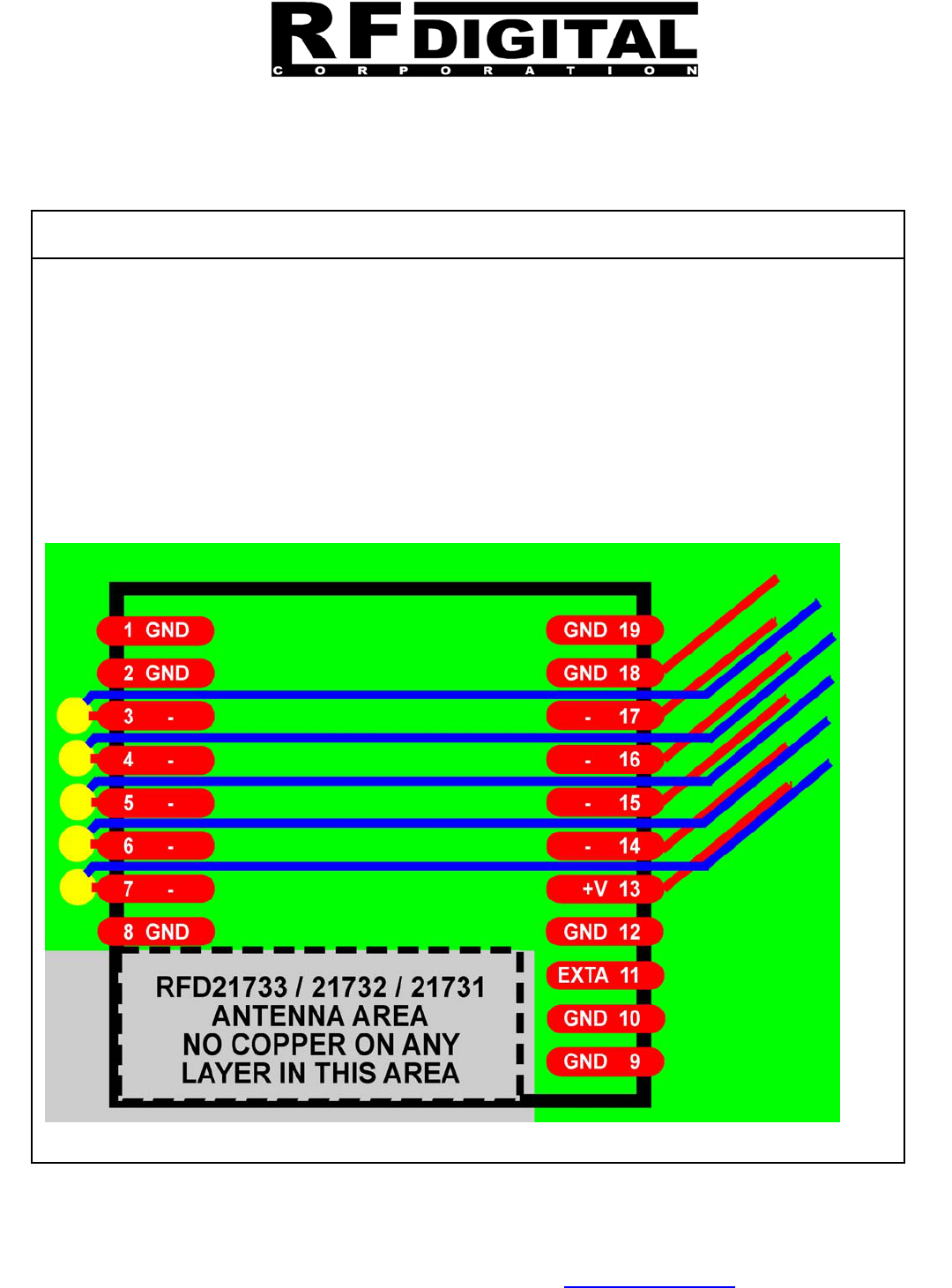
13715 Alton Pkwy • Irvine • CA • 92618
Tel: 949.610.0008 • www.RFdigital.com
Fast Answers: support@rfdigital.com
Free Applications Support • Email your application questions to support@rfdigital.com 62
RFDP8
© Copyright, RF Digital
1/29/2013 9:40 AM
Patents Pending
RoHS CE • ESTI
RFD21733/35 • FCC • IC
RFD21743 • FCC
Approved & Certified
RF Module
RFD21733
RFD21735
RFD21737
RFD21738
RFD21739
RFDP8
RFDANT
RFD21742
RFD21743
RFD21772
RFD21773
KEYFOBs
This Layout Examples document only references pins that are common to all RFD21731,2,3,4,5
modules and matter to the layout, which are ground and external antenna connections where
applicable. To keep the file size of this document small, some of the larger images are outputted in
lower resolutions, for full details on pin outs refer to the data sheet for the appropriate part number,
which can all be found at http://www.rfdigital.com.
Pins labels 3,4,5,6,7,14,15,16,17 change based on which part number module is being used, however
that does not matter for this document, because the same layout rules apply to the RFD21731,
RFD21732, RFD21733, RFD21734 and RFD21735 modules. Majority of this document addresses the
RFD21731, RFD21732, RFD21733 and the end of this document addresses the RFD21734 and
RFD21735.
If you have any questions, feel free to contact RF Digital Support anytime, we're always here to help you!
RFD21731, RFD21732, RFD21733 Layout Example Pinout
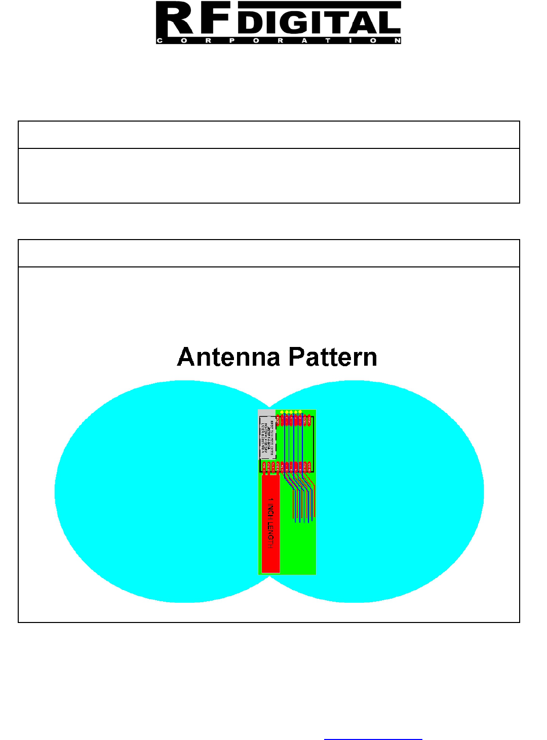
13715 Alton Pkwy • Irvine • CA • 92618
Tel: 949.610.0008 • www.RFdigital.com
Fast Answers: support@rfdigital.com
Free Applications Support • Email your application questions to support@rfdigital.com 63
RFDP8
© Copyright, RF Digital
1/29/2013 9:40 AM
Patents Pending
RoHS CE • ESTI
RFD21733/35 • FCC • IC
RFD21743 • FCC
Approved & Certified
RF Module
RFD21733
RFD21735
RFD21737
RFD21738
RFD21739
RFDP8
RFDANT
RFD21742
RFD21743
RFD21772
RFD21773
KEYFOBs
The following layout examples are for the RFD21731, RFD21732 and RFD21733 module which all
have a built-in chip antenna. Later in this document there are examples for the RFD21734 and
RFD21735 modules, which are for use with external antennas.
RFD21731, RFD21732, RFD21733 Layout Examples
This is a typical antenna pattern, however does vary based on many factors including surrounding
components and ground planes. It is only provided as a reference. The one inch copper plane
shown helps maintain the balanced antenna pattern and when possible should be used, if not
possible, its not required.
RFD21731, RFD21732, RFD21733 Antenna Pattern
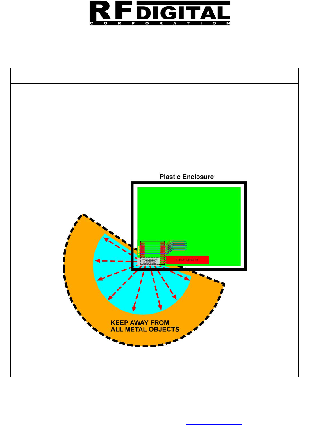
13715 Alton Pkwy • Irvine • CA • 92618
Tel: 949.610.0008 • www.RFdigital.com
Fast Answers: support@rfdigital.com
Free Applications Support • Email your application questions to support@rfdigital.com 64
RFDP8
© Copyright, RF Digital
1/29/2013 9:40 AM
Patents Pending
RoHS CE • ESTI
RFD21733/35 • FCC • IC
RFD21743 • FCC
Approved & Certified
RF Module
RFD21733
RFD21735
RFD21737
RFD21738
RFD21739
RFDP8
RFDANT
RFD21742
RFD21743
RFD21772
RFD21773
KEYFOBs
When placing the module info a plastic enclosure, it is highly recommended that you locate the
module in the corner of the enclosure / PCB so it will be as far away from your other components on
the PCB and as close to free airspace as possible. In addition, you want to locate the module in a
position in your product where it will have as much free airspace as possible near the antenna when
in use. For example if it will be placed against a wall, it is preferred to locate the module so it will be
in a location in your product where it will be on the side of the product where it will be further away
from the wall, rather then directly next to it, so the RF signal can have as much free airspace to give
you the best range performance possible. (Note: If you plan on using a metal enclosure, you can not
locate the module inside of the enclosure or it will have very limited range, for metal enclosures we
recommend the RFD21743 which is specifically suited for that.) The electrical ground connection to
the module is to be made with a thin trace so the one inch ground plane off to the side can be
effective.
RF Signals in this area.
If you place anything such as components, wires, metal parts of any type in this area; it will block the RF
signals and drastically limit your range. Leave this area open.
RFD21731, RFD21732, RFD21733 Keep Out Area - Example 1
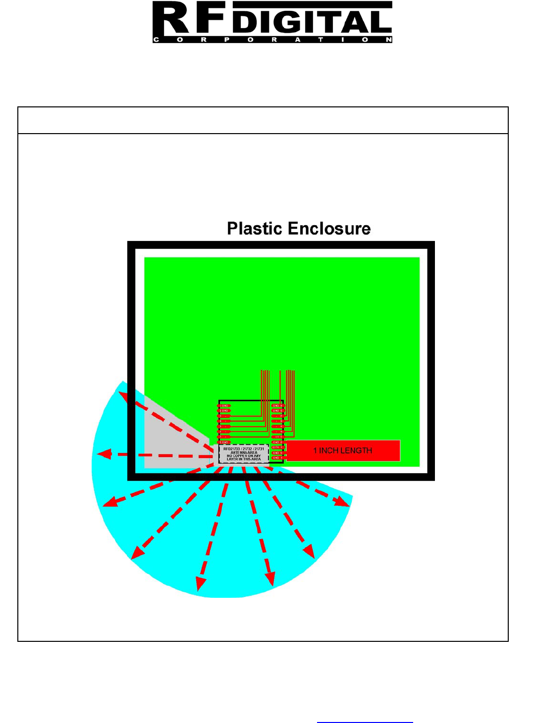
13715 Alton Pkwy • Irvine • CA • 92618
Tel: 949.610.0008 • www.RFdigital.com
Fast Answers: support@rfdigital.com
Free Applications Support • Email your application questions to support@rfdigital.com 65
RFDP8
© Copyright, RF Digital
1/29/2013 9:40 AM
Patents Pending
RoHS CE • ESTI
RFD21733/35 • FCC • IC
RFD21743 • FCC
Approved & Certified
RF Module
RFD21733
RFD21735
RFD21737
RFD21738
RFD21739
RFDP8
RFDANT
RFD21742
RFD21743
RFD21772
RFD21773
KEYFOBs
The gray area shows where to keep free from copper and components. The one-inch length copper
area is optional, however does improve the range if you can add it. Parts can be placed all over the
rest of the board, however if possible keep about a half-inch distance from the one inch length
ground area to the right of the module, again, only if possible. Also the signal connections to the
module can be made on either layer. The electrical ground connection to the module is to be made
with a thin trace so the one inch ground plane off to the side can be effective.
RF Signals in this area.
If you place anything such as components, wires, metal parts of any type in this area; it will block the RF
signals and drastically limit your range. Leave this area open.
RFD21731, RFD21732, RFD21733 - Layout Examples 2
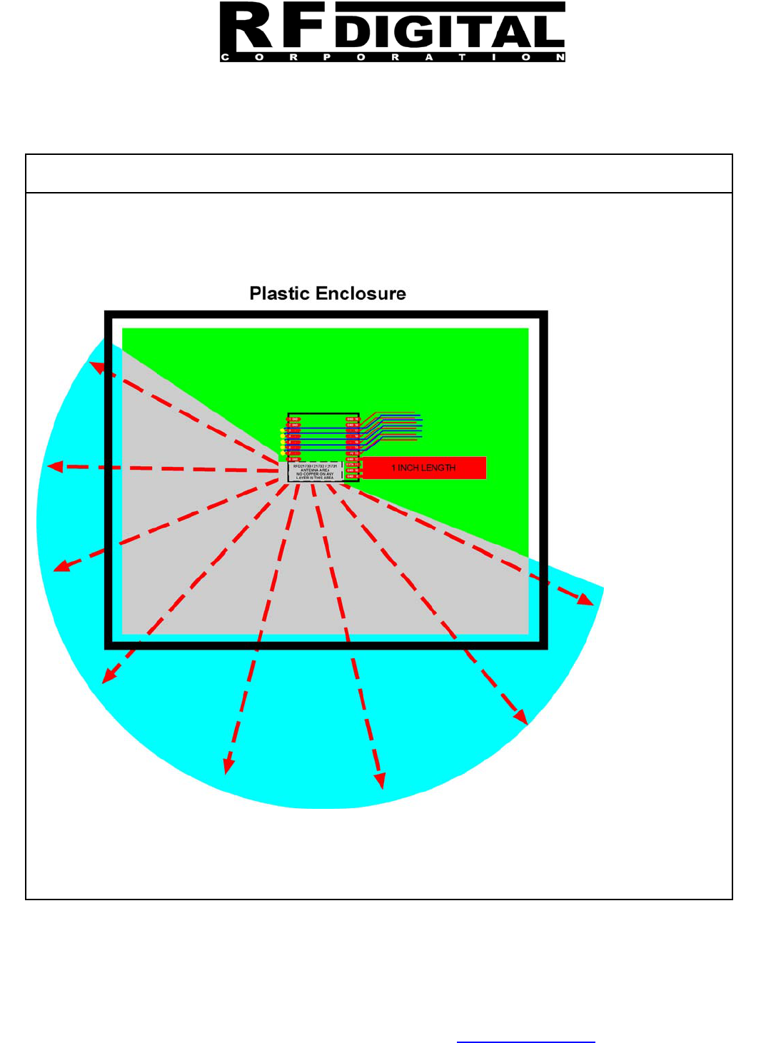
13715 Alton Pkwy • Irvine • CA • 92618
Tel: 949.610.0008 • www.RFdigital.com
Fast Answers: support@rfdigital.com
Free Applications Support • Email your application questions to support@rfdigital.com 66
RFDP8
© Copyright, RF Digital
1/29/2013 9:40 AM
Patents Pending
RoHS CE • ESTI
RFD21733/35 • FCC • IC
RFD21743 • FCC
Approved & Certified
RF Module
RFD21733
RFD21735
RFD21737
RFD21738
RFD21739
RFDP8
RFDANT
RFD21742
RFD21743
RFD21772
RFD21773
KEYFOBs
The gray area shows where to keep free from copper and components. The one-inch length copper
area is optional, however does improve the range if you can add it. Parts can be placed all over the
rest of the board, however if possible keep about a half-inch distance from the one inch length
ground area to the right of the module, again, only if possible.
RF Signals in this area.
If you place anything such as components, wires, metal parts of any type in this area; it will block the RF
signals and drastically limit your range. Leave this area open.
RFD21731, RFD21732, RFD21733 - Layout Examples 3
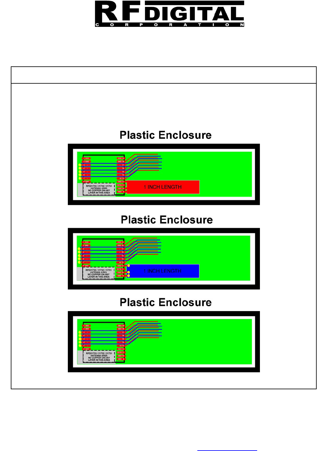
13715 Alton Pkwy • Irvine • CA • 92618
Tel: 949.610.0008 • www.RFdigital.com
Fast Answers: support@rfdigital.com
Free Applications Support • Email your application questions to support@rfdigital.com 67
RFDP8
© Copyright, RF Digital
1/29/2013 9:40 AM
Patents Pending
RoHS CE • ESTI
RFD21733/35 • FCC • IC
RFD21743 • FCC
Approved & Certified
RF Module
RFD21733
RFD21735
RFD21737
RFD21738
RFD21739
RFDP8
RFDANT
RFD21742
RFD21743
RFD21772
RFD21773
KEYFOBs
The gray area shows where to keep free from copper and components. The one-inch length copper
area is optional, however does improve the range if you can add it. Parts can be placed all over the
rest of the board, however if possible keep about a half-inch distance from the one inch length
ground area to the right of the module, again, only if possible.
RFD21731, RFD21732, RFD21733 - Layout Examples 4
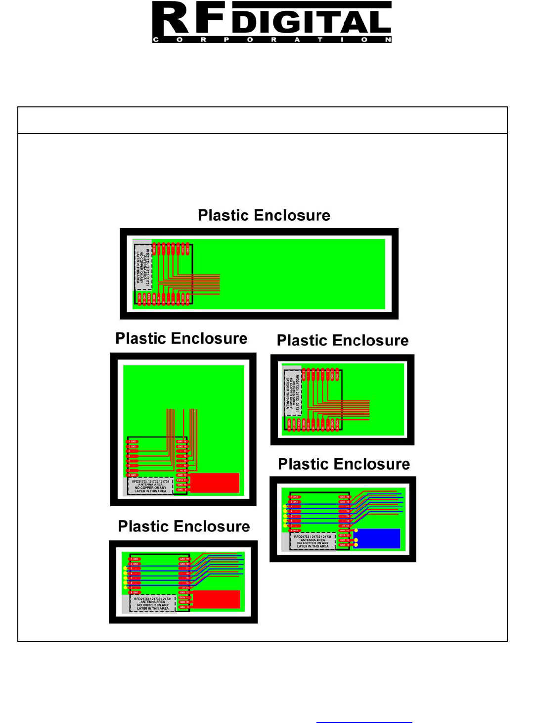
13715 Alton Pkwy • Irvine • CA • 92618
Tel: 949.610.0008 • www.RFdigital.com
Fast Answers: support@rfdigital.com
Free Applications Support • Email your application questions to support@rfdigital.com 68
RFDP8
© Copyright, RF Digital
1/29/2013 9:40 AM
Patents Pending
RoHS CE • ESTI
RFD21733/35 • FCC • IC
RFD21743 • FCC
Approved & Certified
RF Module
RFD21733
RFD21735
RFD21737
RFD21738
RFD21739
RFDP8
RFDANT
RFD21742
RFD21743
RFD21772
RFD21773
KEYFOBs
The gray area shows where to keep free from copper and components. The one-inch length copper
area is optional, however does improve the range if you can add it. Parts can be placed all over the
rest of the board, however if possible keep about a half-inch distance from the one inch length
ground area to the right of the module, again, only if possible.
RFD21731, RFD21732, RFD21733 - Layout Examples 5
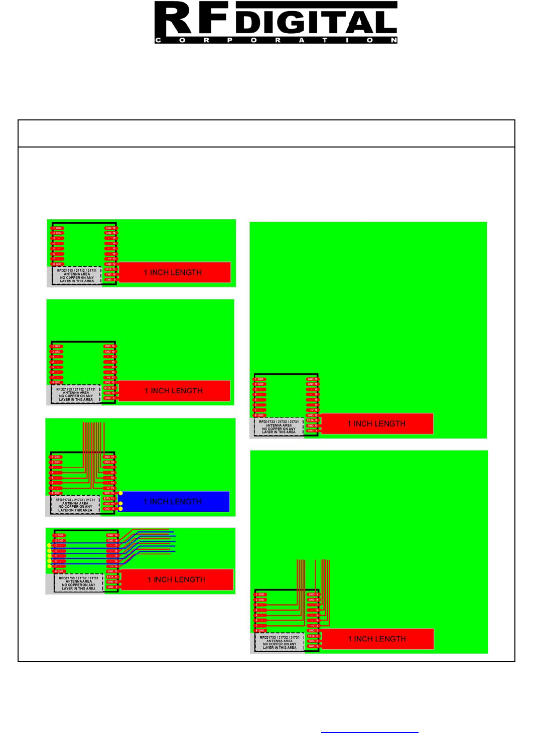
13715 Alton Pkwy • Irvine • CA • 92618
Tel: 949.610.0008 • www.RFdigital.com
Fast Answers: support@rfdigital.com
Free Applications Support • Email your application questions to support@rfdigital.com 69
RFDP8
© Copyright, RF Digital
1/29/2013 9:40 AM
Patents Pending
RoHS CE • ESTI
RFD21733/35 • FCC • IC
RFD21743 • FCC
Approved & Certified
RF Module
RFD21733
RFD21735
RFD21737
RFD21738
RFD21739
RFDP8
RFDANT
RFD21742
RFD21743
RFD21772
RFD21773
KEYFOBs
The gray area shows where to keep free from copper and components. The one-inch length copper
area is optional, however does improve the range if you can add it. Parts can be placed all over the
rest of the board, however if possible keep about a half-inch distance from the one inch length
ground area to the right of the module, again, only if possible.
RFD21731, RFD21732, RFD21733 - Layout Examples 6
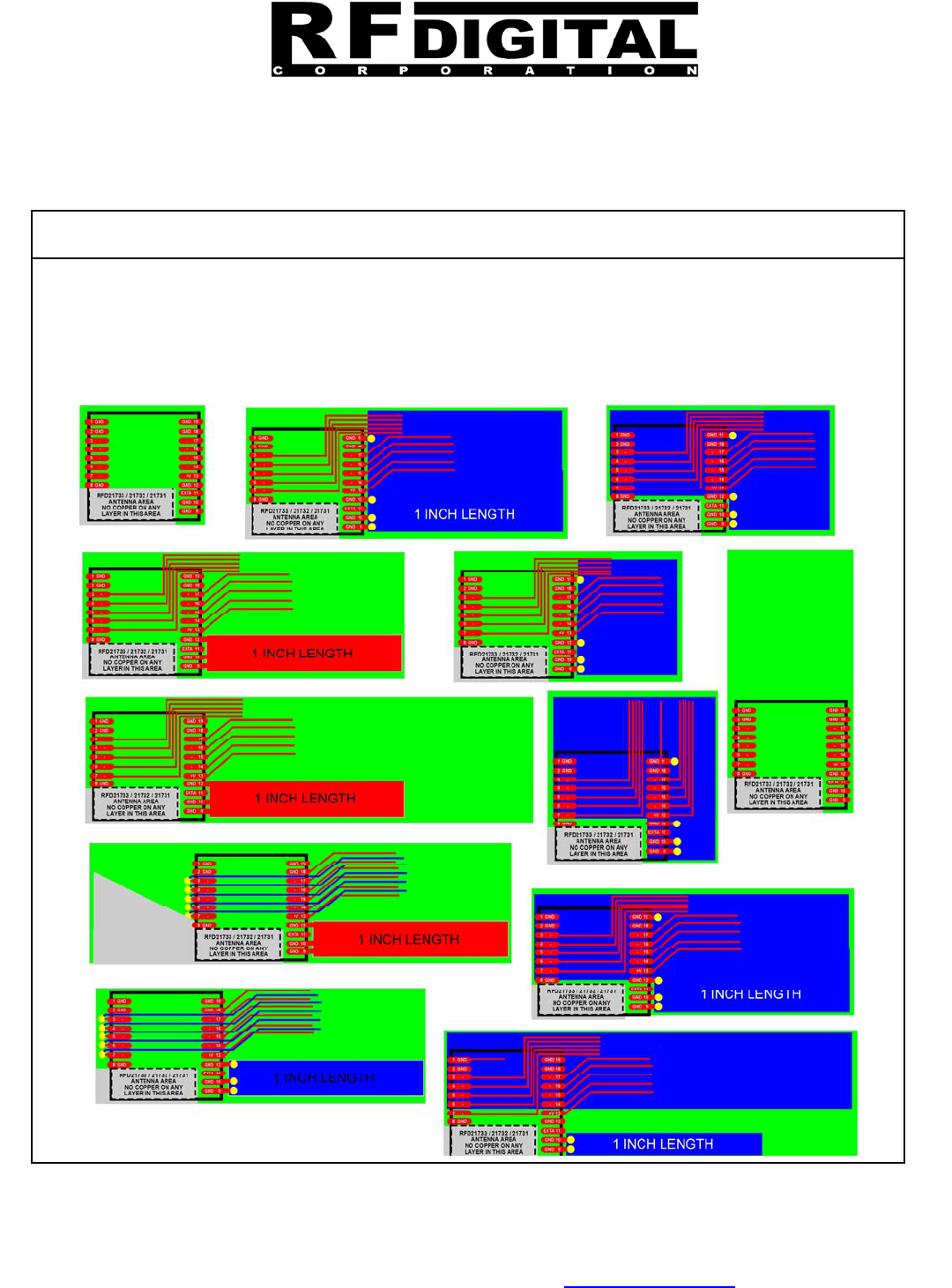
13715 Alton Pkwy • Irvine • CA • 92618
Tel: 949.610.0008 • www.RFdigital.com
Fast Answers: support@rfdigital.com
Free Applications Support • Email your application questions to support@rfdigital.com 70
RFDP8
© Copyright, RF Digital
1/29/2013 9:40 AM
Patents Pending
RoHS CE • ESTI
RFD21733/35 • FCC • IC
RFD21743 • FCC
Approved & Certified
RF Module
RFD21733
RFD21735
RFD21737
RFD21738
RFD21739
RFDP8
RFDANT
RFD21742
RFD21743
RFD21772
RFD21773
KEYFOBs
The gray area shows where to keep free from copper and components. The one-inch length copper
area is optional, however does improve the range if you can add it. Parts can be placed all over the
rest of the board, however if possible keep about a half-inch distance from the one inch length
ground area to the right of the module, again, only if possible. Solid blue areas are soldering side
ground plane which can be used for user electronics as well as the module. These are all optional
configurations and only for reference.
RFD21731, RFD21732, RFD21733 - Layout Examples 7
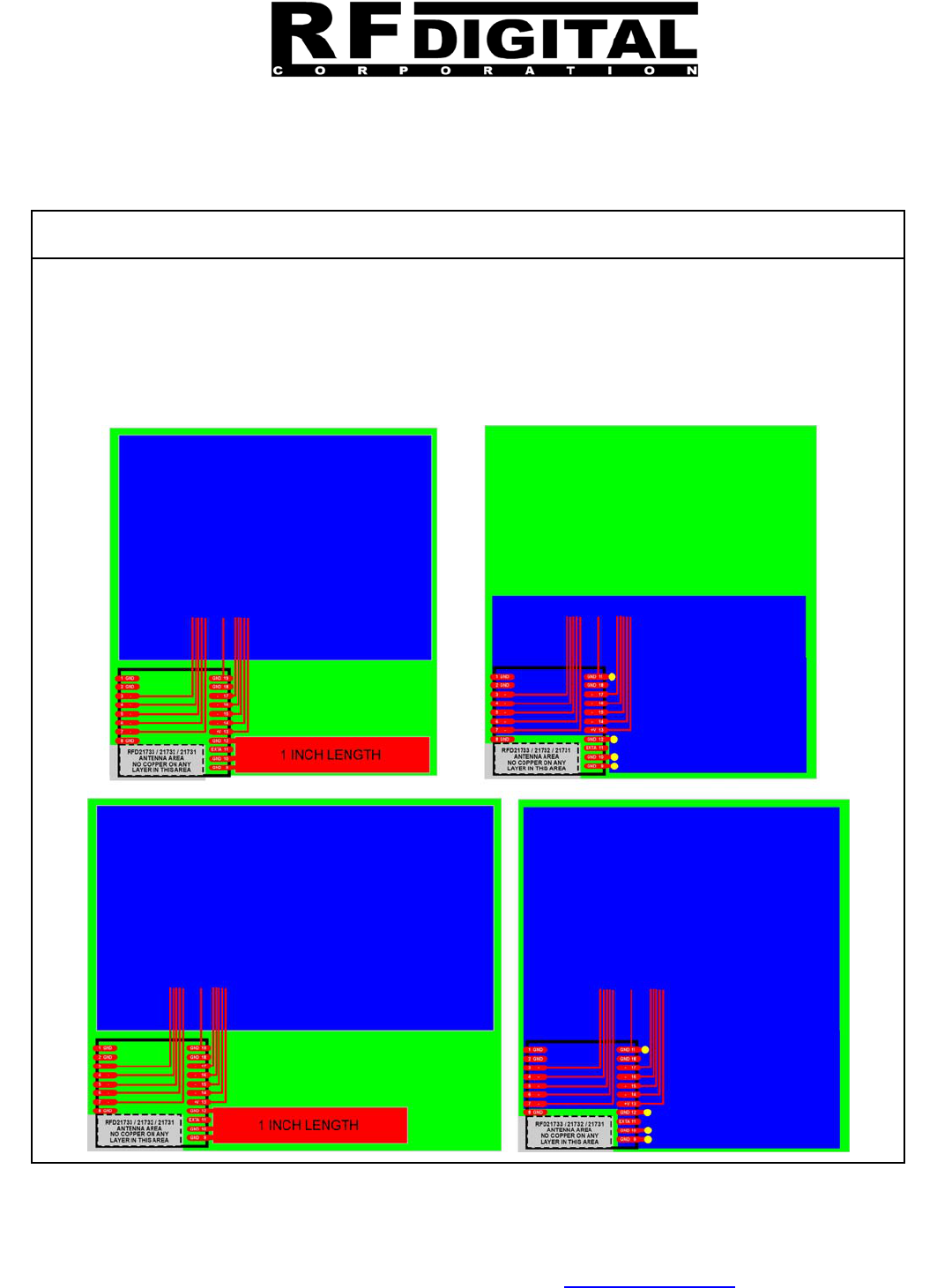
13715 Alton Pkwy • Irvine • CA • 92618
Tel: 949.610.0008 • www.RFdigital.com
Fast Answers: support@rfdigital.com
Free Applications Support • Email your application questions to support@rfdigital.com 71
RFDP8
© Copyright, RF Digital
1/29/2013 9:40 AM
Patents Pending
RoHS CE • ESTI
RFD21733/35 • FCC • IC
RFD21743 • FCC
Approved & Certified
RF Module
RFD21733
RFD21735
RFD21737
RFD21738
RFD21739
RFDP8
RFDANT
RFD21742
RFD21743
RFD21772
RFD21773
KEYFOBs
The gray area shows where to keep free from copper and components. The one-inch length copper
area is optional, however does improve the range if you can add it. Parts can be placed all over the
rest of the board, however if possible keep about a half-inch distance from the one inch length
ground area to the right of the module, again, only if possible. Solid blue areas are soldering side
ground plane which can be used for user electronics as well as the module. These are all optional
configurations and only for reference. The two left examples are preferred, but the two right ones
will work as well, but will not have as good of an antenna pattern.
RFD21731, RFD21732, RFD21733 - Layout Examples 8
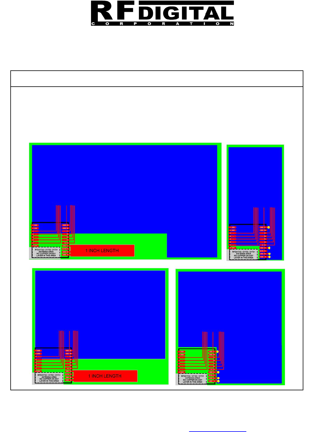
13715 Alton Pkwy • Irvine • CA • 92618
Tel: 949.610.0008 • www.RFdigital.com
Fast Answers: support@rfdigital.com
Free Applications Support • Email your application questions to support@rfdigital.com 72
RFDP8
© Copyright, RF Digital
1/29/2013 9:40 AM
Patents Pending
RoHS CE • ESTI
RFD21733/35 • FCC • IC
RFD21743 • FCC
Approved & Certified
RF Module
RFD21733
RFD21735
RFD21737
RFD21738
RFD21739
RFDP8
RFDANT
RFD21742
RFD21743
RFD21772
RFD21773
KEYFOBs
The gray area shows where to keep free from copper and components. The one-inch length copper
area is optional, however does improve the range if you can add it. Parts can be placed all over the
rest of the board, however if possible keep about a half-inch distance from the one inch length
ground area to the right of the module, again, only if possible. Solid blue areas are soldering side
ground plane which can be used for user electronics as well as the module. These are all optional
configurations and only for reference. The two left examples are preferred, but the two right ones
will work as well, but will not have as good of an antenna pattern.
RFD21731, RFD21732, RFD21733 - Layout Examples 9
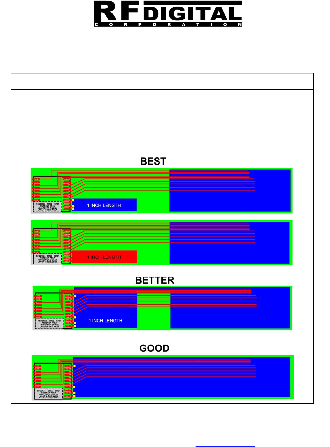
13715 Alton Pkwy • Irvine • CA • 92618
Tel: 949.610.0008 • www.RFdigital.com
Fast Answers: support@rfdigital.com
Free Applications Support • Email your application questions to support@rfdigital.com 73
RFDP8
© Copyright, RF Digital
1/29/2013 9:40 AM
Patents Pending
RoHS CE • ESTI
RFD21733/35 • FCC • IC
RFD21743 • FCC
Approved & Certified
RF Module
RFD21733
RFD21735
RFD21737
RFD21738
RFD21739
RFDP8
RFDANT
RFD21742
RFD21743
RFD21772
RFD21773
KEYFOBs
The gray area shows where to keep free from copper and components. The one-inch length copper
area is optional, however does improve the range if you can add it. Parts can be placed all over the
rest of the board, however if possible keep about a half-inch distance from the one inch length
ground area to the right of the module, again, only if possible. Solid blue areas are soldering side
ground plane which can be used for user electronics as well as the module. These are all optional
configurations and only for reference. The space in the ground plane helps provide some RF
discontinuity for the module to have he best antenna pattern possible in this configuration, the
optimal space to have is greater then 1.2 inches, but some space is better then no space.
RFD21731, RFD21732, RFD21733 - Layout Examples 10
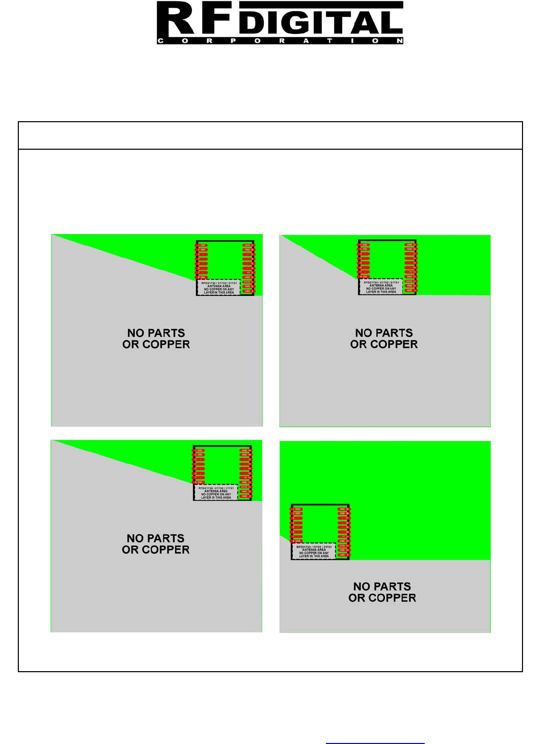
13715 Alton Pkwy • Irvine • CA • 92618
Tel: 949.610.0008 • www.RFdigital.com
Fast Answers: support@rfdigital.com
Free Applications Support • Email your application questions to support@rfdigital.com 74
RFDP8
© Copyright, RF Digital
1/29/2013 9:40 AM
Patents Pending
RoHS CE • ESTI
RFD21733/35 • FCC • IC
RFD21743 • FCC
Approved & Certified
RF Module
RFD21733
RFD21735
RFD21737
RFD21738
RFD21739
RFDP8
RFDANT
RFD21742
RFD21743
RFD21772
RFD21773
KEYFOBs
The gray area shows where to keep free from copper and components. These shown are not good
layout locations for the module since they take up most of your board area, it is best to locate the
module similar to the examples shown in other areas of this document where you have more board
space for your parts. These examples are shown as what NOT to do. If you place parts in the gray
area, it will result in very bad range performance.
RFD21731, RFD21732, RFD21733 - Layout Examples 11
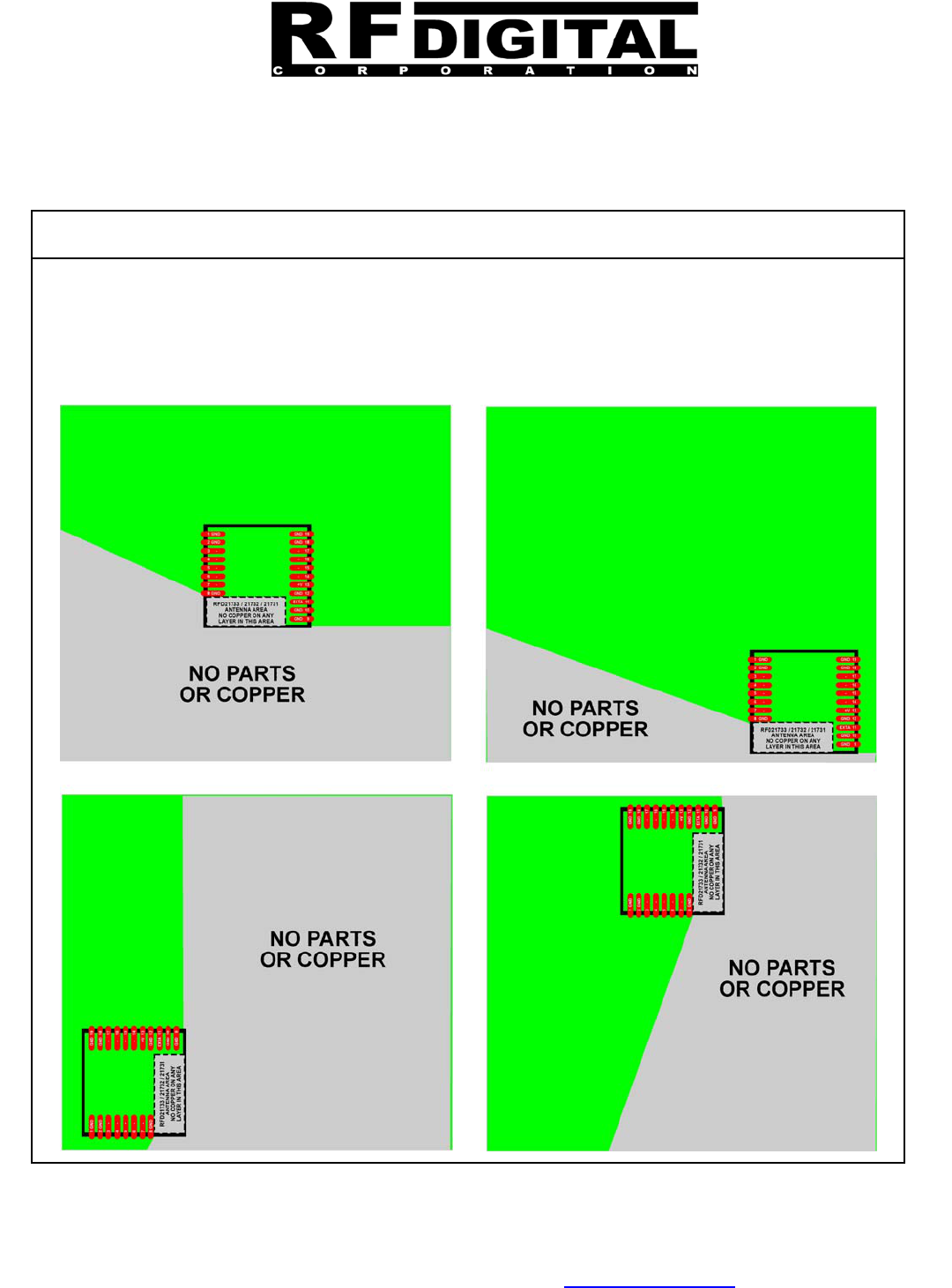
13715 Alton Pkwy • Irvine • CA • 92618
Tel: 949.610.0008 • www.RFdigital.com
Fast Answers: support@rfdigital.com
Free Applications Support • Email your application questions to support@rfdigital.com 75
RFDP8
© Copyright, RF Digital
1/29/2013 9:40 AM
Patents Pending
RoHS CE • ESTI
RFD21733/35 • FCC • IC
RFD21743 • FCC
Approved & Certified
RF Module
RFD21733
RFD21735
RFD21737
RFD21738
RFD21739
RFDP8
RFDANT
RFD21742
RFD21743
RFD21772
RFD21773
KEYFOBs
The gray area shows where to keep free from copper and components. These shown are not good
layout locations for the module since they take up most of your board area, it is best to locate the
module similar to the examples shown in other areas of this document where you have more board
space for your parts. These examples are shown as what NOT to do. If you place parts in the gray
area, it will result in very bad range performance.
RFD21731, RFD21732, RFD21733 - Layout Examples 12
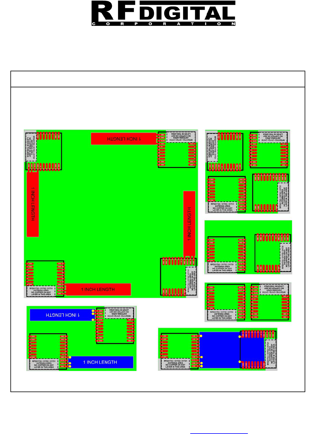
13715 Alton Pkwy • Irvine • CA • 92618
Tel: 949.610.0008 • www.RFdigital.com
Fast Answers: support@rfdigital.com
Free Applications Support • Email your application questions to support@rfdigital.com 76
RFDP8
© Copyright, RF Digital
1/29/2013 9:40 AM
Patents Pending
RoHS CE • ESTI
RFD21733/35 • FCC • IC
RFD21743 • FCC
Approved & Certified
RF Module
RFD21733
RFD21735
RFD21737
RFD21738
RFD21739
RFDP8
RFDANT
RFD21742
RFD21743
RFD21772
RFD21773
KEYFOBs
The gray area shows where to keep free from copper and components. These are multi-module
configurations. Typical layouts for diversity applications where you will use multiple receivers,
transmitters or transceivers all on the same board to limit multipath impacts and increase effective
communication range or provide a very solid coverage area with limited dead-zones. The distances
shown are not optimal, however just provided as reference.
RFD21731, RFD21732, RFD21733 - Layout Examples 13
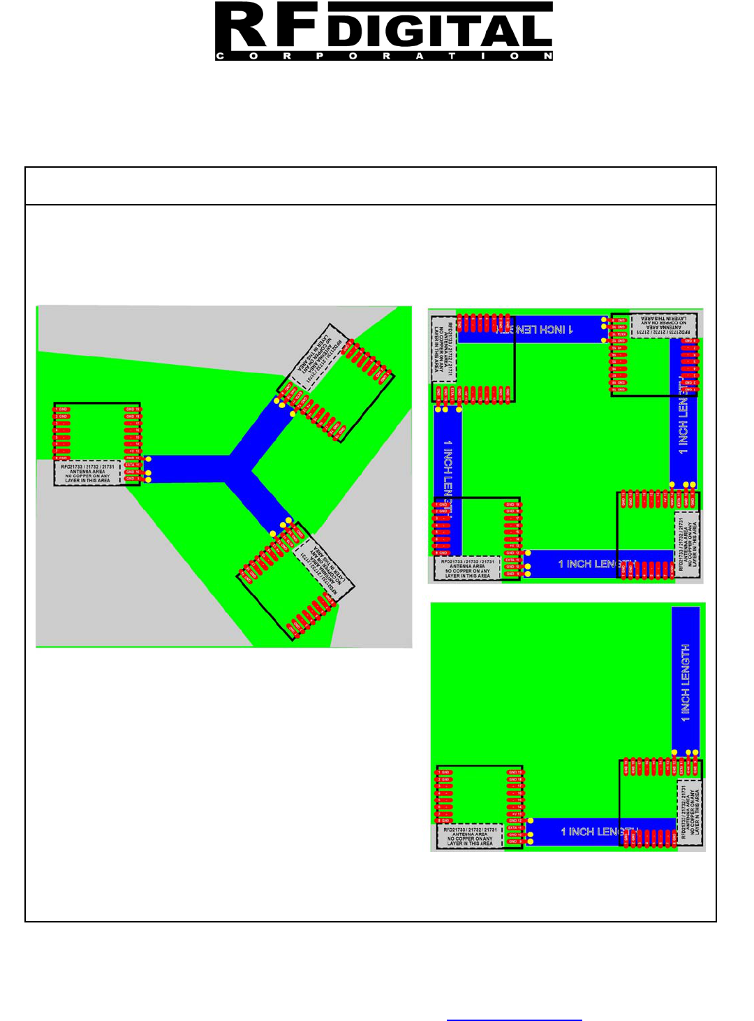
13715 Alton Pkwy • Irvine • CA • 92618
Tel: 949.610.0008 • www.RFdigital.com
Fast Answers: support@rfdigital.com
Free Applications Support • Email your application questions to support@rfdigital.com 77
RFDP8
© Copyright, RF Digital
1/29/2013 9:40 AM
Patents Pending
RoHS CE • ESTI
RFD21733/35 • FCC • IC
RFD21743 • FCC
Approved & Certified
RF Module
RFD21733
RFD21735
RFD21737
RFD21738
RFD21739
RFDP8
RFDANT
RFD21742
RFD21743
RFD21772
RFD21773
KEYFOBs
The gray area shows where to keep free from copper and components. These are multi-module
configurations. Typical layouts for diversity applications where you will use multiple receivers,
transmitters or transceivers all on the same board to limit multipath impacts and increase effective
communication range or provide a very solid coverage area with limited dead-zones. The distances
shown are not optimal, however just provided as reference.
RFD21731, RFD21732, RFD21733 - Layout Examples 14
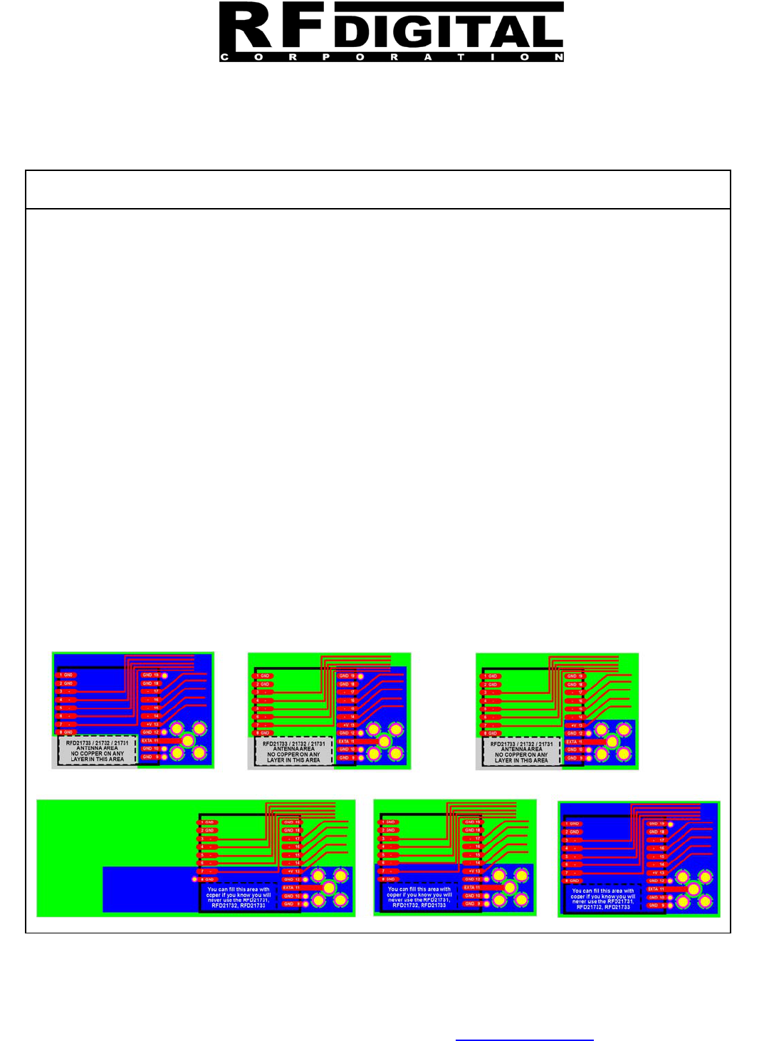
13715 Alton Pkwy • Irvine • CA • 92618
Tel: 949.610.0008 • www.RFdigital.com
Fast Answers: support@rfdigital.com
Free Applications Support • Email your application questions to support@rfdigital.com 78
RFDP8
© Copyright, RF Digital
1/29/2013 9:40 AM
Patents Pending
RoHS CE • ESTI
RFD21733/35 • FCC • IC
RFD21743 • FCC
Approved & Certified
RF Module
RFD21733
RFD21735
RFD21737
RFD21738
RFD21739
RFDP8
RFDANT
RFD21742
RFD21743
RFD21772
RFD21773
KEYFOBs
The gray area shows where to keep free from copper and components. The RFD21734 and
RFD21735 require the use of an external antenna and therefore the most common connector used
for this is an SMA and the examples below show a typical SMA connector footprint interface.
PCB thickness is 0.031 inch to 0.062 inch, double sided. The blue color shows ground plane under
the module on the solder side of the board.
If you place ground plane or any traces under the gray area marked no-copper, then you will not
have the option to use the RFD21731 / RFD21732 / RFD21733 which are the on-board chip antenna
versions of the RFD21734 / RFD21735. So it is your choice if you choose to flood copper under that
area or not. There is no benefit to flood copper in that area. If you choose to make a dual-mode
layout to handle both module options, with chip antenna or without (which is what we recommend),
then also advise with the layout configurations above for proper application.
We highly recommend that you look at the RFD21743 and RFD21742 before starting
a design with the RFD21734 or RFD21735. The RFD21742 and RFD21743 are RF
Digital’s Patent Pending RFDANTs, which are complete RF Modules setup for
external use and already in an antenna form factor allowing you to simply plug it
into any product instantly, without needing any layouts, RF connectors or coax
cables. They offer exceptional range, about 4x that of the RFD21733.
Save time, money and no need for additional compliance approvals since the
RFD21743 is FCC Approved and Certified
RFD21734 and RFD21735 - Layout Examples 15

13715 Alton Pkwy • Irvine • CA • 92618
Tel: 949.610.0008 • www.RFdigital.com
Fast Answers: support@rfdigital.com
Free Applications Support • Email your application questions to support@rfdigital.com 79
RFDP8
© Copyright, RF Digital
1/29/2013 9:40 AM
Patents Pending
RoHS CE • ESTI
RFD21733/35 • FCC • IC
RFD21743 • FCC
Approved & Certified
RF Module
RFD21733
RFD21735
RFD21737
RFD21738
RFD21739
RFDP8
RFDANT
RFD21742
RFD21743
RFD21772
RFD21773
KEYFOBs
Important Notice
RF Digital reserves the right to make corrections, modifications, and/or improvements
to the product and/or its specifications at any time without notice.
RF Digital assumes no liability for the user’s product and/or applications.
RF Digital products are not authorized for use in safety-critical applications, including
but not limited to life-support applications.
RF Digital assumes no liability for parts or their application beyond replacement or
refunding the original purchase price.
All trademarks and trade names belong to their respective owners.
Information provided in this document is for reference only. The user must conduct
testing and prototyping on their own for their own application. This document only
provides an example of a possible use for the parts shown in this design and requires
actual testing to confirm its accuracy or validity or proper application. There is NO
suggestion that the devices shown in this document should be used for the implied
application. There is no guarantee or warranty of suitability for any specific application.
The information disclosed in this document is AS-IS. By using any information
contained in this document you are assuming all risks and liability associated
therewith. RF Digital reserves the right to make corrections, modifications, changes
and/or improvements to specifications or details at any time without notice or
obligation. RF Digital assumes no liability for the user’s product and/or applications. RF
Digital products are not authorized for use in safety-critical applications, including but
not limited to life-support applications. RF Digital assumes no liability for parts or their
application beyond replacement or refunding the original purchase price paid to RF
Digital.

13715 Alton Pkwy • Irvine • CA • 92618
Tel: 949.610.0008 • www.RFdigital.com
Fast Answers: support@rfdigital.com
Free Applications Support • Email your application questions to support@rfdigital.com 80
RFDP8
© Copyright, RF Digital
1/29/2013 9:40 AM
Patents Pending
RoHS CE • ESTI
RFD21733/35 • FCC • IC
RFD21743 • FCC
Approved & Certified
RF Module
RFD21733
RFD21735
RFD21737
RFD21738
RFD21739
RFDP8
RFDANT
RFD21742
RFD21743
RFD21772
RFD21773
KEYFOBs
Limited Product Warranty
RF Digital warrants that RF Devices manufactured by RF Digital are free from defects in
material and workmanship, for Ninety (90) Days from date of delivery. RF Devices
covered by this warranty and returned to RF Digital within the Ninety Day Warranty
Period will be eligible for replacement, repair, or credit, limited to the amount RF Digital
was paid for the RF Device. To obtain a remedy under this Warranty, the following
conditions must be met: (1) Customer must notify RF Digital in writing promptly on
discovery of the deficiency with reasonable detail within the Warranty Period; (2)
Customer must return the RF Devices to RF Digital promptly upon receipt of an RMA
from RF Digital, at Customer’s risk and expense; and (3) RF Digital confirms the claimed
deficiency is present. If all of these conditions are met, RF Digital, at its sole option, will
either replace or repair the RF Device or credit Customer’s account for the amount the
Customer paid to RF Digital for the RF Device.