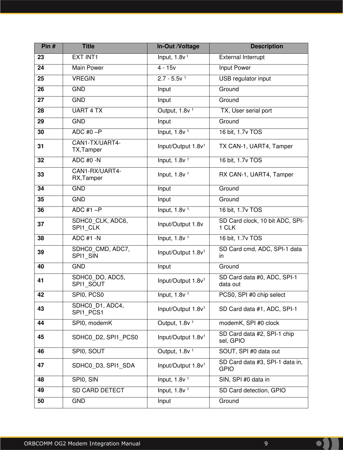
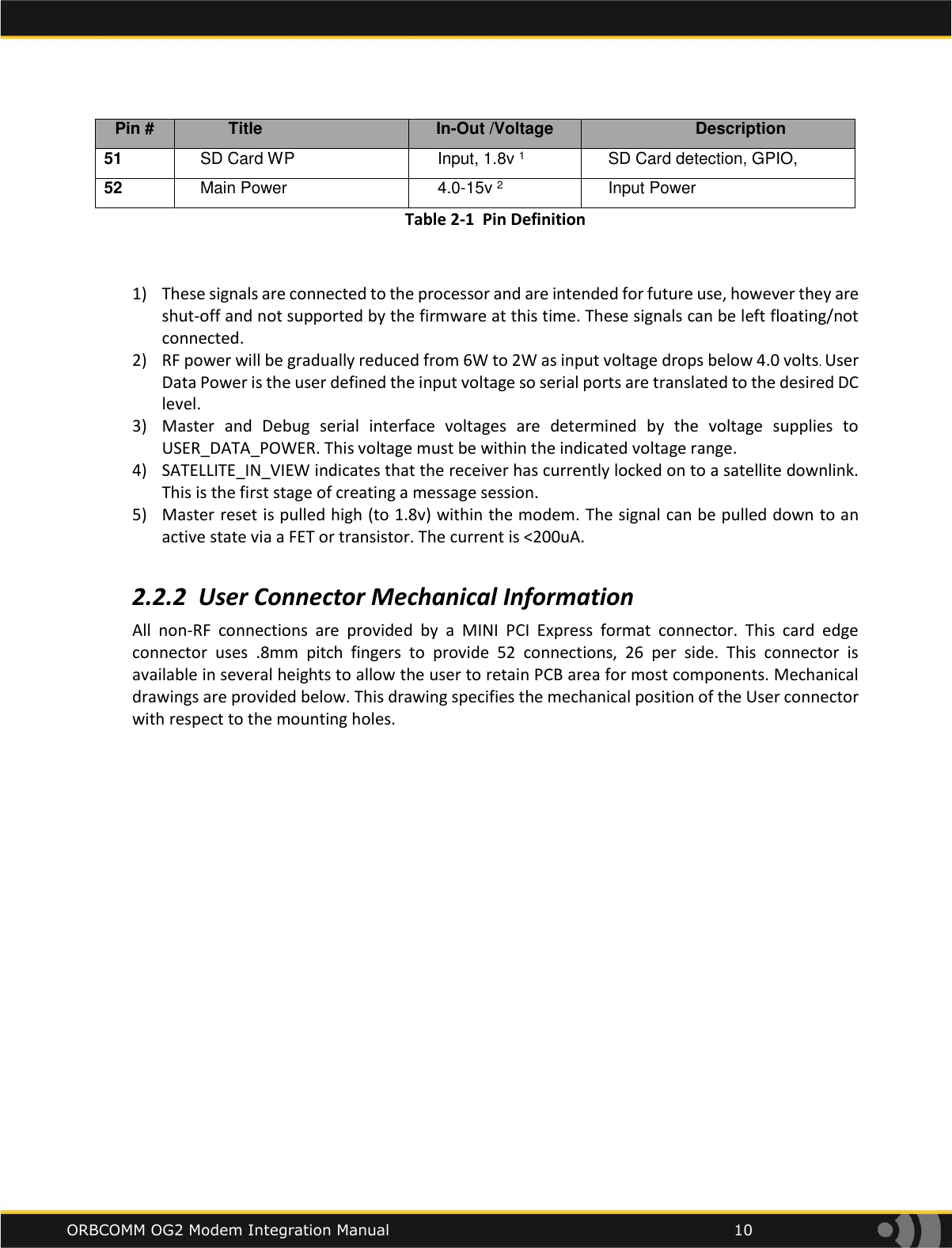
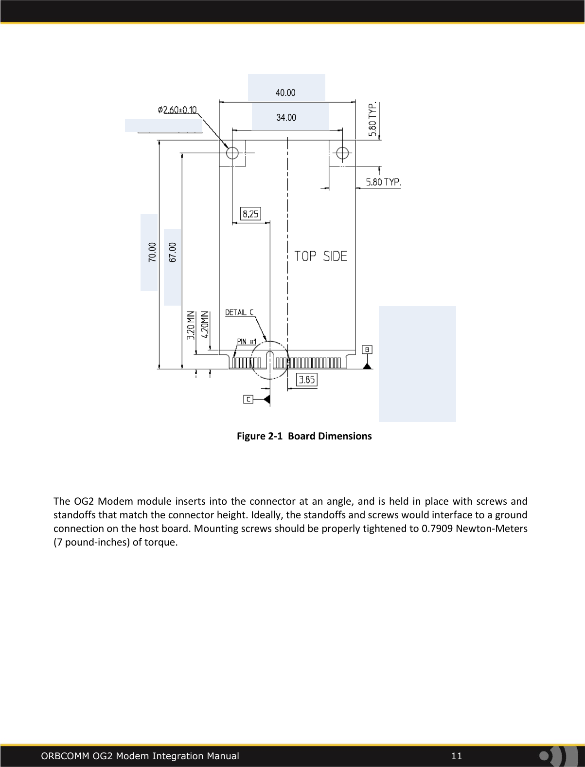
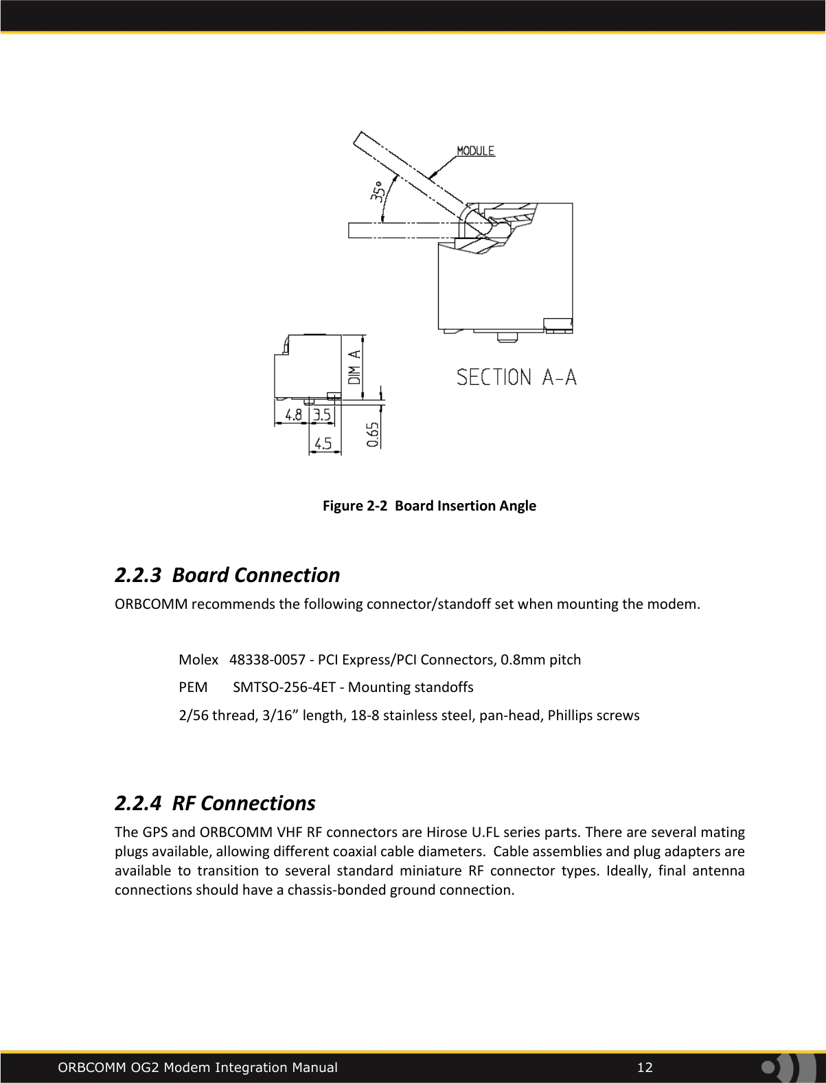
ORBCOMM License ORBCOG2BAM1 Mobile Satellite Earth Station Module User Manual Front 1

ORBCOMM License Corp. Mobile Satellite Earth Station Module Front 1

Users Manual

                     ORBCOMM Generation 2 (OG2) Modem Consolidated Operational Description Document Number: Revision:  Initial Date: October 27, 2015
   ORBCOMM OG2 Modem Integration Manual            ii  © 2015 ORBCOMM — All Rights Reserved. This publication, or any part thereof, may not be reproduced or transmitted in any form or by any means, electronic or mechanical, including photocopying, recording, storage in an information retrieval system, or otherwise, without prior written permission by ORBCOMM, Inc. 395 W Passaic Street, Suite 325, Rochelle Park, NJ 07662 USA Phone 703-433-6329.  Trademark Notice The ORBCOMM  Company logo is a trademark  of ORBCOMM, Inc.  All other product names  used throughout this material  are  trademarks  of  the  respective  companies.  No  such  use  of  any  trademark  is  intended  to  convey endorsement or other affiliation with these companies.   Disclaimers This document is the proprietary and exclusive property of ORBCOMM except as otherwise indicated. No part of this document, in whole or in part, may be reproduced, stored, transmitted, or used for  design purposes without the prior written permission of ORBCOMM. This document contains technical information and descriptions of the ORBCOMM System that reflect the status of the system design and/or  planned design as of the date of issue.   The contents  of  this  document are subject to change  without  notice,  and  no  warranty  or  representation,  expressed  or  implied,  is  made  with  respect  to  its contents.   The information in this document is for informational purposes only.  Export Control Statement WARNING:    THESE  COMMODITIES,  TECHNOLOGY,  SOFTWARE,  OR  TECHNICAL  DATA  RELATING  THERETO,  WERE EXPORTED  FROM  THE  UNITED  STATES  IN  ACCORDANCE  WITH  THE  UNITED  STATES  EXPORT  LAWS  AND REGULATIONS. DIVERSION, RE-EXPORT, OR TRANSSHIPMENT CONTRARY TO U.S. LAW IS PROHIBITED.   More Information To obtain information additional information, please contact: Customer Service:  customer.service@orbcomm.com, +1 703 433 6329 Sales:  sales@orbcomm.com Visit us on the Internet:  www.orbcomm.com
   ORBCOMM OG2 Modem Integration Manual            iii  Document History  Version Issued By Issue Date Comments 1 ORBCOMM October 2015 Initial
   ORBCOMM OG2 Modem Integration Manual            iv Table of Contents 1. INTRODUCTION .............................................................................................................................................. 6 1.1 REFERENCES ...................................................................................................................................................... 6 2. PHYSICAL DESIGN ........................................................................................................................................... 7 2.1 MODULE DIMENSIONS ......................................................................................................................................... 7 2.2 INTERFACE ......................................................................................................................................................... 8 2.2.1 User Connector Pin Description Table .................................................................................................... 8 2.2.2 User Connector Mechanical Information ............................................................................................. 10 2.2.3 Board Connection ................................................................................................................................. 12 2.2.4 RF Connections ..................................................................................................................................... 12 3. RADIO FREQUENCY SECTION ........................................................................................................................ 14 3.1 VHF TRANSMITTER ........................................................................................................................................... 15 3.1.1 Transmit Modulation ........................................................................................................................... 15 3.1.2 Output Power ....................................................................................................................................... 15 3.1.3 Output Power Variance ........................................................................................................................ 15 3.1.4 Transmitter Power ............................................................................................................................... 15 3.1.5 Frequency Control ................................................................................................................................ 16 3.1.6 Transmit Frequency ............................................................................................................................. 16 3.1.7 Occupied Bandwidth ............................................................................................................................ 16 3.1.8 Transmitter Designator ........................................................................................................................ 16 3.2 VHF RECEIVER ................................................................................................................................................. 17 3.2.1 Receive Modulation ............................................................................................................................. 17 3.2.2 Minimum Detectable Signal ................................................................................................................. 17 3.2.3 Acquisition Frequency Range ............................................................................................................... 17 4. POWER SUPPLY ............................................................................................................................................ 17 4.1 POWER USAGE PROFILE ..................................................................................................................................... 17 4.2 VARIATIONS IN INPUT POWER ............................................................................................................................. 18 4.3 DIP, INTERRUPTIONS, SURGES, FAST TRANSIENTS .................................................................................................... 19 4.3.1 Dip & Interruptions .............................................................................................................................. 19 4.3.2 Fast Transients ..................................................................................................................................... 20 5. ENVIRONMENTAL SPECIFICATIONS AND COMPLIANCE ................................................................................ 21 5.1 OPERATIONAL TEMPERATURE .............................................................................................................................. 21
   ORBCOMM OG2 Modem Integration Manual            v  List of Figures FIGURE 2-2  BOARD DIMENSIONS ............................................................................................................................... 11 FIGURE 2-3  BOARD INSERTION ANGLE ....................................................................................................................... 12 FIGURE 2-4  CONNECTOR LOCATION ........................................................................................................................... 13 FIGURE 2-1 MODEM BLOCK DIAGRAM ........................................................................................................................ 14 FIGURE 3-1 RF OUTPUT POWER VS. INPUT VOLTAGE ................................................................................................. 16 FIGURE 4-1  MAXIMUM INPUT CURRENT VS INPUT VOLTAGE .................................................................................... 18 FIGURE 4-2 INPUT VOLTAGE RISE TIMES ..................................................................................................................... 19 FIGURE 5-3 VOLTAGE FALL TIMES VS. INPUT POWER SWITCHED OFF ........................................................................ 20   List of Tables TABLE 2-1  PIN DEFINITION .......................................................................................................................................... 10 TABLE 2-2  U. FL CONNECTORS .................................................................................................................................... 13 TABLE 5-1 ENVIRONMENTAL SPECIFICATIONS AND COMPLIANCE ............................................................................. 21
   ORBCOMM OG2 Modem Integration Manual            6 1. Introduction  ORBCOMM is in the initial stages of defining the modem functionality required to operate with the ORBCOMM Generation 2 (OG2) satellite system providing OG2 Messaging Services.  The first OG2 satellites will launch in 2013 with OG1 legacy support and in 2014 have OG2 functionality uploaded.   There  will  be  significant  differences  between  OG1  and  OG2  such  that  current  OG1  subscriber communicators  herein  referred  to  as  “modem”  will  not  be  able  to  use  the  portion  of  the  OG2 satellites dedicated to OG2 functionality.  It is envisioned that the next versions of modems will be able to seamlessly switch between the two service sets.  Initially, however, current users will only be to use the OG1 functions on the satellite.   It is expected that many of the environmental specifications for OG2 modems will be the same as OG1 modems.  In the interest of providing more information earlier, these requirements have been omitted from this document.   The purpose of this document is to provide preliminary information on the physical interface of OG2 modem.  This document should not be construed as a specification.  It is the basis for developing the  ORBCOMM  Generation  2  Subscriber  Communicator  Standards  and  Specifications.    In  the interim,  this  document  can  be  used  for  determining the  magnitude  of  development  on  the hardware side.  1.1 References  Amendment of the Commission’s Rules to Establish Rules and Policies Pertaining to a Non-voice, Non-Geostationary Mobile Satellite Service  (FCC docket no. 92-76, FCC 93, 47B, released November 16, 1993) ORBCOMM Application Amendment and Supplement: File No. 22-DSS-MP90(20)  (submitted December 21, 1993) U.S. Code of Federal Regulations  (vol. 47, Part 25, § 202) SAE J1455 “Joint SAE/TMC Recommended Environmental Practices for Electronic Equipment Design (Heavy Tracks)” EN 301 832 “Electromagnetic compatibility and Radio spectrum Matters (ERM); Electro-Magnetic Compatibility (EMC) for Mobile Earth Stations (MES) providing Low Bit Rate Data Communications (LBRDC) using satellites in Low Earth Orbits (LEO) operating in frequency bands below 1 GHz” EN 301 721:  “Satellite Earth Stations and Systems (SES); Harmonized EN for Mobile Earth Stations (MES) providing Low Bit Rate Data Communications (LBRDC) using Low Earth Orbiting (LEO) satellites operating below 1 GHz covering essential requirements under article 3.2 of the R&TTE directive”
   ORBCOMM OG2 Modem Integration Manual            7 2.             Physical Design  2.1 Module Dimensions Overall dimensions and weight of the OG2 modem are indicated below. RF connections will require space for routing miniature coax cables to antenna port locations.   Mechanical Dimensions Length 70 mm Width 40 mm Height 9.5 mm Weight 20g
   ORBCOMM OG2 Modem Integration Manual            8 2.2 Interface  Product  developers  should plan for  connection  to the  host  system as  indicated  in  the  following table.  2.2.1 User Connector Pin Description Table  Pin # Title In-Out /Voltage Description 1 USB Diff, 1.8v 1 Data, negative 2 Main Power 4 - 15v 2 Input Power 3 USB P Diff, 1.8v 1 Data, positive 4 GND Input Ground 5 Master RX Input, pin 6 user volt. 3 RX, UART 0 6 User Data Power 1.8 to 3.6 V 3 Master & Debug Serial Logic Level 7 Master TX Output, pin 6 user volt. 3 TX, UART 0 8 SPI1 PCS0 Output, 1.8v 1 PCS0, SPI #1 chip select 9 GND Input Ground 10 SPI1 CLK Output, 1.8v 1 CLK, SPI #1 clock 11 Debug UART RX Input, pin 6 user volt. 3 RX, UART 5 12 SPI1 SOUT Output, 1.8v 1 SOUT, SPI #1 data out 13 Debug UART TX Output, pin 6 user volt. 3 TX, UART 5 14 SATELLITE-IN-VIEW Output, 1.8v 4 GPIO or SIN, SPI #1 data in 15 MASTER RESET Hi-Z, active LO 5 Internal 10k ohm PU, PD with FET or transistor. 16 GPIO0/FTM/CAN RX Input/Output 1.8v1 RX CAN-0, Capacitive Touch, GPIO 17 TAMPER 1 Input, 1.8v 1 Internal PU 18 GND Input Ground 19 EXT INT2 Input, 1.8v 1 External Interrupt 20 GPIO1/FTM/CAN TX Input/Output 1.8v1 TX CAN-0, Capacitive Touch, GPIO 21 GND Input Ground 22 UART 4 RX Input, 1.8v 1 RX, User serial port
   ORBCOMM OG2 Modem Integration Manual            9 Pin # Title In-Out /Voltage Description 23 EXT INT1 Input, 1.8v 1 External Interrupt 24 Main Power 4 - 15v Input Power 25 VREGIN 2.7 - 5.5v 1 USB regulator input 26 GND Input Ground 27 GND Input Ground 28 UART 4 TX Output, 1.8v 1  TX, User serial port 29 GND Input Ground 30 ADC #0 –P Input, 1.8v 1 16 bit, 1.7v TOS 31 CAN1-TX/UART4-TX,Tamper Input/Output 1.8v1 TX CAN-1, UART4, Tamper 32 ADC #0 -N Input, 1.8v 1 16 bit, 1.7v TOS 33 CAN1-RX/UART4-RX,Tamper Input, 1.8v 1 RX CAN-1, UART4, Tamper 34 GND Input Ground 35 GND Input Ground 36 ADC #1 –P Input, 1.8v 1 16 bit, 1.7v TOS 37 SDHC0_CLK, ADC6, SPI1_CLK Input/Output 1.8v SD Card clock, 10 bit ADC, SPI-1 CLK 38 ADC #1 -N Input, 1.8v 1 16 bit, 1.7v TOS 39 SDHC0_CMD, ADC7, SPI1_SIN Input/Output 1.8v1 SD Card cmd, ADC, SPI-1 data in  40 GND Input Ground 41 SDHC0_DO, ADC5, SPI1_SOUT Input/Output 1.8v1 SD Card data #0, ADC, SPI-1 data out 42 SPI0, PCS0 Input, 1.8v 1 PCS0, SPI #0 chip select 43 SDHC0_D1, ADC4, SPI1_PCS1 Input/Output 1.8v1 SD Card data #1, ADC, SPI-1  44 SPI0, modemK Output, 1.8v 1 modemK, SPI #0 clock 45 SDHC0_D2, SPI1_PCS0 Input/Output 1.8v1 SD Card data #2, SPI-1 chip sel, GPIO 46 SPI0, SOUT Output, 1.8v 1 SOUT, SPI #0 data out 47 SDHC0_D3, SPI1_SDA Input/Output 1.8v1 SD Card data #3, SPI-1 data in, GPIO 48 SPI0, SIN Input, 1.8v 1 SIN, SPI #0 data in 49 SD CARD DETECT Input, 1.8v 1 SD Card detection, GPIO 50 GND   Input Ground
   ORBCOMM OG2 Modem Integration Manual            10 Pin # Title In-Out /Voltage Description 51 SD Card WP Input, 1.8v 1 SD Card detection, GPIO,  52 Main Power 4.0-15v 2 Input Power Table 2-1  Pin Definition  1) These signals are connected to the processor and are intended for future use, however they are shut-off and not supported by the firmware at this time. These signals can be left floating/not connected.  2) RF power will be gradually reduced from 6W to 2W as input voltage drops below 4.0 volts. User Data Power is the user defined the input voltage so serial ports are translated to the desired DC level. 3) Master  and  Debug  serial  interface  voltages  are  determined  by  the  voltage  supplies  to  USER_DATA_POWER. This voltage must be within the indicated voltage range. 4) SATELLITE_IN_VIEW indicates that the receiver has currently locked on to a satellite downlink. This is the first stage of creating a message session. 5) Master reset is pulled high (to 1.8v) within the modem. The signal can be pulled down to an active state via a FET or transistor. The current is <200uA.  2.2.2 User Connector Mechanical Information All  non-RF  connections  are  provided  by  a  MINI  PCI  Express  format  connector.  This  card  edge connector  uses  .8mm  pitch  fingers  to  provide  52  connections,  26  per  side.  This  connector  is available in several heights to allow the user to retain PCB area for most components. Mechanical drawings are provided below. This drawing specifies the mechanical position of the User connector with respect to the mounting holes.
   ORBCOMM OG2 Modem Integration Manual            11 34.0040.0070.0067.00 Figure 2-1  Board Dimensions   The OG2 Modem module  inserts into the connector at an angle, and is  held in place  with screws and standoffs that match the connector height. Ideally, the standoffs and screws would interface to a ground connection on the host board. Mounting screws should be properly tightened to 0.7909 Newton-Meters (7 pound-inches) of torque.
   ORBCOMM OG2 Modem Integration Manual            12  Figure 2-2  Board Insertion Angle  2.2.3 Board Connection ORBCOMM recommends the following connector/standoff set when mounting the modem.  Molex   48338-0057 - PCI Express/PCI Connectors, 0.8mm pitch                   PEM       SMTSO-256-4ET - Mounting standoffs                   2/56 thread, 3/16” length, 18-8 stainless steel, pan-head, Phillips screws   2.2.4 RF Connections The GPS and ORBCOMM VHF RF connectors are Hirose U.FL series parts. There are several mating plugs available, allowing different coaxial cable diameters.  Cable assemblies and plug adapters are available  to  transition  to  several  standard  miniature  RF  connector  types.  Ideally,  final  antenna connections should have a chassis-bonded ground connection.
   ORBCOMM OG2 Modem Integration Manual            13  Table 2-2  U. FL Connectors The image below indicates the proper location for each port. There are two modem models, with and without GPS and accelerometer. If the GPS antenna port and uBlox circuit are installed, then the unit has GPS functionality  Figure 2-3  Connector Location uBlox GPS
   ORBCOMM OG2 Modem Integration Manual            14 3. Radio Frequency Section The OG2 modem includes:  A VHF Receiver Section which performs RF filtering, frequency conversion and demodulation.  A  VHF  Transmitter  Section  which  performs  modulation,  frequency  conversion  and  power amplification.  A  Processing  Section  that  monitors  and  controls  optional  I/Os,  handles  the  RF  and  serial interface.  LO ARM M4ProcessorUp to 1M FlashRTOSCMULT Frac NModulatorDirect Convertion ReceiverPower AmplifierGPS3 AxisAccelerometerMini PCIExpressInterfaceWide Range Switching Supply 3v -15vJTAGUSBCANSD-CardUART x3SPI x2ADC x2TamperORBCOMM OG2 ModemPre AmplifierSAW FilterLNARF SwitchHarmonic FilterVHF AntennaTx 148.00 – 150.5 MHzRX 137.00 – 138.00 MHZ50 channel-162 dBm Communication Bus DigitalTX - QTX - IRX - QRX - IBasebandProcessor52BP Filter -120 dBm sensitivity Figure 3-1 Modem Block Diagram   The different ports are:  Power Supply. Capable of handling a wide range of DC input voltages.
   ORBCOMM OG2 Modem Integration Manual            15  I/Os: Provides optional analog or digital input and outputs. These are typically used to connect sensors or to connect to the system elements which need to be controlled  Serial  Data:  Serial  interface  through  which  another  embedded  application  or  external processor/sensor can transfer data.   RF In/Out: The Modem has U.FL connectors for satellite and GPS antenna signals.   3.1  VHF Transmitter 3.1.1 Transmit Modulation The transmitter uses Symmetric Differential Phase Shift Keying at 2400 bits per seconds. 3.1.2 Output Power Output  power  is  fixed  at  approximately  5.5  Watts  ±0.5  Watts.    Value  is  set  at  the  time  of manufacture and no further adjustments are made during operation. 3.1.3 Output Power Variance During  any  transmission,  the  transmit  power  shall  vary  by  no  more  than  ±1.0  dB  under  any combination of temperature and frequency.  3.1.4 Transmitter Power The maximum EIRP, measured in a 4 kHz bandwidth, transmitted from a modem shall not exceed 10 dBW in all directions. (EN 301 721) The graph below shows the measured RF power output as the input is increased from 2.8 volts DC to  15  volts  DC.      Values  provided  below  6  VDC  are  provided  for  reference  only.    ORBCOMM’s integration manual specifies an input voltage no lower than 6 VDC.
   ORBCOMM OG2 Modem Integration Manual            16            Figure 3-2 RF Output Power vs. input Voltage  3.1.5 Frequency Control Frequency control is provided by the ORBCOMM System.  The modem transmits an initial 7 bit (8 bits  including  the  reference  bit  required  by  SDPSK  modulation)  burst  to  the  satellite.    Initial specifications published almost 20 years  ago required this  burst to  arrive within ±1500 Hz.  This frequency error budget includes oscillator uncertainty and Doppler effects.  Current modem designs routinely transmit this acquire burst within ±500 Hz. Frequency and timing corrections are provided to the modem based on the offset of the 7 bit burst.  All subsequent transmissions for this message session are corrected to within ±50 Hz.  3.1.6 Transmit Frequency The modem is capable of tuning to any 2.5 kHz channel between 148.0500 and 150.0000 MHz.  Note that ORBCOMM’s authorized spectrum is 148.0000 to 150.0500 MHz.  Restriction of the channels at the edge of the authorized spectrum insure no spectral content above the specifications occur outside the authorized spectrum. 3.1.7 Occupied Bandwidth Measured 20 dB occupied bandwidth is less than 4 kHz. 3.1.8 Transmitter Designator The modem carries a 5K00G1D emission designator.  0.01.02.03.04.05.06.07.0RF Output Power (W)Input Voltage (DC)RF Output Power vs Input Voltage
   ORBCOMM OG2 Modem Integration Manual            17    3.2 VHF Receiver 3.2.1 Receive Modulation The transmitter uses Symmetric Differential Phase Shift Keying at 4800 bits per seconds. 3.2.2 Minimum Detectable Signal The modem receives ORBCOMM downlink signals with at -120 dBm or better under all operational situations with a BER no worse than 1 x 10⁻⁵.   3.2.3 Acquisition Frequency Range The modem acquires ORBCOMM downlink signals over all operational situations in the frequency range:  137.1250  to  137.8750  MHz.    This  includes  all  effects  of  internal oscillator  uncertainty  in addition to Doppler effects which may be as much as ±3200 Hz during times when satellite is visible to the modem.  Further, the Doppler rate of change may be as high as ±28 Hz/second.  4. Power Supply The power supply is designed to operate in an efficient mode at all times. The processor has power available continuously. When the processor is in a low power mode, the quiescent current can be as low as 3 uA.  Power sections required for frequency generation, receive modes, and transmit modes are turned off until they are required. The integrated accelerometer can be programmed to interrupt the processor during a pre-defined shock/vibration event, this allows a low power usage in typical “stop and go” mobile applications.  Power to the GPS circuit can be switched ON and OFF if a ‘cold fix’ is acceptable.  If a ‘warm fix’ is required, providing 22 uA  will allow GPS fixes in only a few seconds.   4.1 Power Usage Profile The ORBCOMM OG2 modem input voltage range allows for several battery chemistries and parallel configurations.  Input Voltage:   6.0VDC to 15 VDC  Input Current:    Transmit Mode:   1.37 A @ 12VDC          Duration: typically <300ms, 700 ms max.   GPS On:     35 mA @ 12VDC
   ORBCOMM OG2 Modem Integration Manual            18   Receive Mode:    100 mA @ 12VDC  The graph below show the maximum current (transmit mode) requirements over a range of input voltages.  Per integration requirements 6 VDC is the minimum operational voltage.  Figure 4-1  Maximum Input Current vs Input Voltage 4.2 Variations in Input Power The power supply is a buck-boost configuration and can operate between 4.0 VDC and 15 VDC. A full  RF output requires  an  input  voltage  above the  minimum  operating voltage.  The  system will control the switcher to run in a high efficiency burst mode and provide the required PWM mode to satisfy high demand events. The circuit is short-circuit protected, has a soft start feature, provides current limiting, and a thermal shutdown feature. The diagram below shows voltage  rise time for the processor (gray), receiver (pink),  and  power amplifier (blue) with a 4.0 VDC input voltage. The delay from power-on to processor operation is 1.3 ms.  The other voltages are controlled internally by the processor and do not operate until the I/O ports are functional and a message has been queued by the user.  The pink line indicates the rise time of the receiver section. The  blue  line  indicates  the  rise  time  of  the  transmitter  section,  current  draw  is  increased  to maximum levels approximately 15 ms after this ramp up time. 0.01.02.03.04.05.06.0Maximum Input Current (A)Input Voltage (DC)Maximum Input Current vs Input Voltage
   ORBCOMM OG2 Modem Integration Manual            19                                                    Figure 4-2 Input Voltage Rise Times  4.3 Dip, Interruptions, Surges, Fast transients  4.3.1 Dip & Interruptions The power circuit has a soft start feature which allows a 750us rise or fall time for events which occur faster than this time frame. The time that would cause deregulation is dependent upon the input voltage and load at the time of the event.  Based on simulation, the processor (shown in gray) will operate for 1.3 ms after removal of an input voltage of 4.0v, and will operate for 220ms when operating with an input voltage of 10 volts. If the processor experiences an interruption, the processor low voltage detection will operate. The circuit warning mode will create a system interrupt service routine and protect memory contents. In the reset level detect mode a lower voltage threshold causes a power-on reset. The processor will be  held in reset until the  rise-voltage threshold is  achieved, then clock  circuits will  begin to operate, when the voltage rises above the low-voltage threshold the system begins to operate. If the processor is writing a new message in to memory during a power interruption, a protocol will not provide an acknowledgement so the user processor will retry.  The malformed message will be Processor Receiver   Power Amplifier Input Power
   ORBCOMM OG2 Modem Integration Manual            20 removed from memory when the processor checks the queue after bootup. During a transmit event, the system will hold up for 200us with an input voltage of 10 volts.     Figure 4-3 Voltage Fall Times vs. Input Power Switched Off 4.3.2 Fast Transients All data lines are protected with low pass RF filters and ESD protection. The filters are designed to meet IEC61000-4-2 level 4, and provide up to 40 dB of EMI protection from 800 MHz to 3GHz.  The Secure Digital High Capacity (SDHC) memory card interface is designed to meet JESD 84A43 specifications.    1 0 Volts Processor Receiver Power Amplifier Input Power 6.8 4.6 1.8
   ORBCOMM OG2 Modem Integration Manual            21  5. Environmental Specifications and Compliance Temperature: SAE J1455 Operating/Storage Temperature(Sec. 4.1.3.1) Operating: -40C to +85C Storage: -50C to +125C Vibration: SAE J1455, Cab Mounted & Transverse Axis   Radiated Emissions EN 300 832 Sec. 7 EN 300 721 V1.21 Annex C Unintentional Emissions EN 300 721 V1.21 Annex E  Conducted Emissions EN 300 721 V1.21 Annex D  RD Immunity EN 300 832 Sec. 7  Transients & Surges EN 300 832 Sec. 9  Table 5-1 Environmental Specifications and Compliance 5.1 Operational Temperature Efforts should be made to keep the modem from operating at temperatures exceeding 80C.  This may require additional venting and/or forced air.

Navigation menu