Omega Engineering UWM100 Wireless Mini Module User Manual
Omega Engineering, Inc. Wireless Mini Module
User Manual

1of 6
Model: UWM-0001
Universal Wireless Radio Module
SETUP & OPERATION GUIDE
SECTION 1…..……………...Description & Components
SECTION 2.…..Usage Guidelines for FCC Compliance
SECTION 3…………….. FCC Statement of Compliance
SECTION 4……………….…….…...…………. Diagrams
SECTION 5………..…………….....… Setup & Operation
SECTION 6………………………………… Specifications
SECTION 1 – Description & Components
1.1 Description
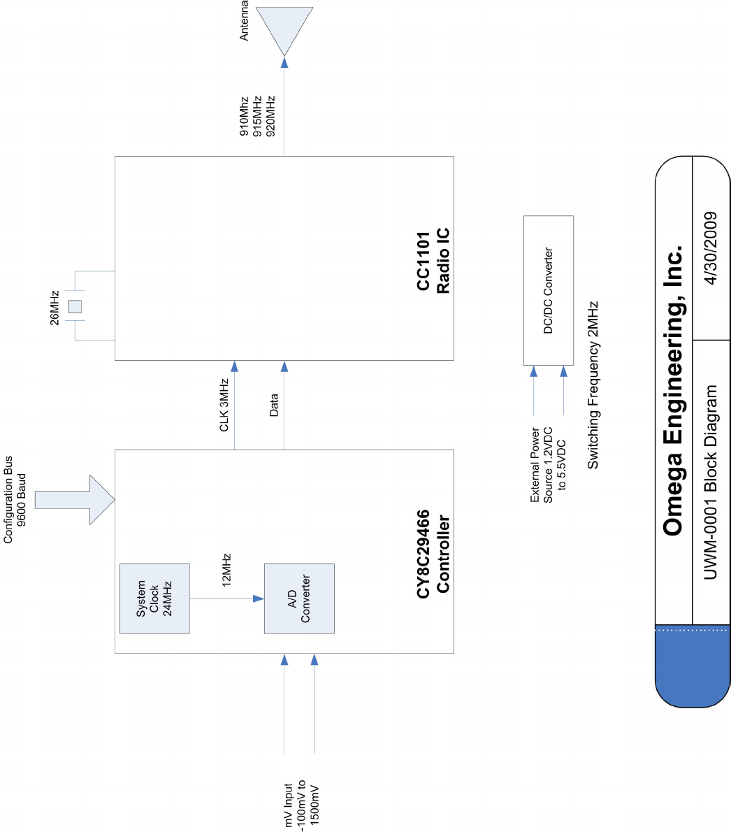
The Omega Universal Wireless Module model UWM-0001 is a 1.2 to 5.5V DC powered,
microprocessor based, 915 MHz transmitter that transmits process input voltage ranging from 0 to
1000mV. The input to the module consists of a bridge with a summing node on the input side,
and a constant voltage, approximately 0.8V, on the other (hereafter referred to as the “reference
side”). The top of the bridge is connected to a 1.3V reference voltage and the bottom to Vss
(Ground). This configuration guarantees the ability to read down to zero volts with respect to
ground, and allows a minimum input voltage down to a -100 Millivolts. The maximum input
voltage is plus 1500 Millivolts with respect to ground.
The microprocessor is brought up from a power down (sleep) state every 2 seconds by an
internal timer in the microprocessor. The microprocessor keeps an on board low power 32kHz
oscillator running, which is divided down to generate an interrupt every 1 second. During the
interrupt, the microprocessor increments a counter and is compared to a value of 2. If the
comparison is false, the processor goes back to the sleep state. If true, the microprocessor sets
an internal multiplexer (MUX) to read two analog voltages through an internal programmable gain
amplifier (PGA) and an internal analog to digital converter (ADC), using an internal voltage
reference. First, the MUX is set to read the reference side of the bridge. Then the MUX is set to
read the input side of the bridge. The ADC counts for the reference side are subtracted from the
input side, and the result is then mathematically converted to Millivolts.
The microprocessor converts this information to digital data and then combines the data with
additional data from an onboard stored unique number and then transmits the entire data packet
serially with a Texas Instruments CC1101 915 MHz Radio Transmitter IC. The microprocessor
then resets the sample rate counter and powers down into a quiescent state to wait for the next
interrupt from the on board timer. The PC board has both a top and bottom ground plane.
The antenna is a surface mount chip antenna, Johanson Technology Part #0915AT43A0026.
1.1 Main RF Components
Manufacture (Part Number)
Radio IC: Texas Instruments (CC1101)
Antenna: Johanson Technology (0915AT43A0026)
SECTION 2 – Usage Guidelines for FCC Compliance
The UWM-0001 has been awarded a FCC limited modular approval. That means that this
module, when integrated into your end product, requires no FCC part 15 .249 testing as long as
the following guidelines are met. Failure to meet any of the following guidelines will prevent the
inheritance of the FCC modular certification.
2.1 Antenna Selection
The antenna is integral to this module design. In order to maintain compliance with FCC
regulations the antenna installed in this module can not be modified or removed. This module has
been tested with the following antenna:
Manufacture: Johanson Technology
Part Number: 0915AT43A0026
2.2 Module Modification
The module must not be physically altered in any way. If any connections are made to the
modules that bypass the module pins, socket, or antenna connection, the FCC modular
certification cannot be inherited.
2.3 End Product Labeling Requirements
Pursuant to FCC public notice DA 00-1407, the end product must be labeled on its exterior with
the following verbiage:
“Contains FCC ID: “
WR3-UWM100
”
2.4 Additional FCC Testing Requirements
While the module’s FCC certification can be inherited (presuming the guidelines are met),
additional testing will be required to achieve full FCC compliance for your end-product. The
integrator is required to perform unintentional radiator testing on the final product per FCC
sections 15.107 and 15.109. Additional, product specific testing might be required. Please contact
the FCC regarding regulatory requirements for your application.
2of 6
SECTION 3 – FCC Statement of Compliance
3.1 Statements and Conditions of Modular Compliance
FCC ID: WR3-UWM100
NOTE: This equipment has been tested and found to comply with the limits for a Class B digital
device, pursuant to part 15 of the FCC Rules. These limits are designed to provide reasonable
protection against harmful interference in a residential installation. This equipment generates
uses and can radiate radio frequency energy and, if not in-stalled and used in accordance with
the instructions, may cause harmful interference to radio communications. However, there is no
guarantee that interference will not occur in a particular installation. If this equipment does cause
harmful interference to radio or television reception, which can be determined by turning the
equipment off and on, the user is encouraged to try to correct the interference by one or more of
the following measures:
—Reorient or relocate the receiving antenna.
—Increase the separation between the equipment and receiver.
—Connect the equipment into an outlet on a circuit different from that to which the receiver is
connected.
—Consult the dealer or an experienced radio/ TV technician for help.
This device complies with the rules set forth in Part 15 by the Federal Communications
Commission. Operation is subject to the following two conditions:
1) This device may not cause harmful interference
2) This device must accept any interference received, including interference that may cause
undesired operation.
Any changes or modifications not expressly approved by Omega Engineering, Inc. could void the
user’s authority to operate the equipment.
The UWM-0001 module is provided with an inheritable FCC Modular Certification. This
certification may be inherited in an end-user product, negating the need for FCC part 15
intentional radiator testing on this module, provided that the following guidelines are met:
1. Changes or modifications to the antenna or antenna circuit is nor permitted.
2. The module must not be modified in any way. Coupling of external circuitry must not bypass
the provided connection.
3. End product must be externally labeled with “Contains FCC ID: WR3-UWM100
4. The end product’s user’s manual must contain an FCC statement equivalent to that listed in
section 2.2 of this guide.
5. The antenna used for this transceiver must not be co-located or operating in conjunction with
any other antenna or transmitter.
6. The integrator must not provide any information to the end-user on how to install or remove the
module from the end-product. The integrator is required to perform unintentional radiator testing
on the final product per FCC sections 15.107 and 15.109.
3.2 Customer FCC Warning Requirements
The end-product user’s manual must contain the following or equivalent verbiage.
FCC NOTICE
FCC ID: WR3-UWM100
The RF module (FCC ID:
WR3-UWM100
contained within this device complies with the rules
set forth in Part 15 by the Federal Communications. Operation is subject to the following
conditions:
1. This device may not cause harmful interference
2. This device must accept any interference received, including interference that may cause
undesired operation.
3. Changes or modifications to the antenna or antenna circuit is nor permitted.
4. The module must not be modified in any way. Coupling of external circuitry must not bypass
the provided connection.
5. The antenna used for this transceiver must not be co-located or operating in conjunction with
any other antenna or transmitter.
Any changes or modifications could void the user’s authority to operate the equipment.
3.3 Notices of Limitation
3.3.1 Product Testing
The integrator must still show that their product complies with FCC regulations applicable to their
product. The integrator is not required to perform transmitter testing on the UWM-0001 module,
provided the guidelines in this document are met.

3of 6
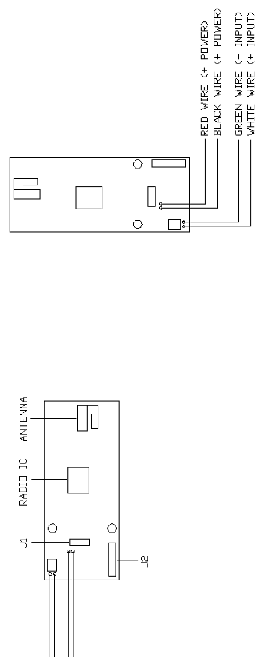
SECTION 4 – Module Diagrams
RF Component Location
Power & Input Connection

4of 6
5of 6
SECTION 5 – Setup & Operation
5.1 Frequency Band Setting
Frequency band setting within the UWM-0001 can be changed from the default values by connect
a computer to the modules programming port. Hyper-terminal is used to communicate to the
module. Commands are sent to the module thru a serial connection.
5.2 Factory Default Setting
Frequency Band: B (915.038452 MHz)
5.2 Communication Settings
Baud Rate: 9600
Data Bits: 8
Parity: None
Stop Bits: 1
Flow Control: None
5.2 Programming Commands
Note: Each of the below commands must end with a Carriage Return or Carriage Return/Line
Feed (i.e., ENTER ).
The following commands are used in Hyper-terminal to change or view settings in the UWM-0001
module.
ENQ
Will display Unit ID Code and Firmware Version
F
Display Millivolts or temperature in Millivolts/Deg F
CHANNEL
Displays current radio frequency band setting (A, B, or C)
CHANNEL n
Change to radio frequency band ‘n’, where n = ‘A’, ‘B’, or ‘C’, and:
A = 910.039673 MHz
B = 915.038452 MHz
C = 920.037231 MHz
5.1 Module Operation
Normal Mode
The module enters the Normal Mode as soon as power is applied, and the configuration
connector is NOT connected. Within 500 milliseconds, the module will sample the analog input;
transmit a data packet with the analog data, then go into a sleep state. If installed, the LED will
blink once each time a packet is transmitted. The module will remain in the sleep state for two
seconds, then repeat the sample and transmit cycle.
Configuration Mode
With power applied, the module enters the Configuration Mode when it detects the insertion of the
configuration cable. The module returns to the normal mode when the configuration cable is
unplugged. While in the configuration mode, if installed, the LED will blink two times per second.
When the USB end of the configuration is plugged into a PC USB port, the device will appear as a
virtual com port.
SECTION 6 – Specifications
Transmit Sample Rate: 2 Seconds/Sample (fixed)
Frequency Range: 910.039673 to 920.037231 MHz
RF Transmitted Power: -5 dBm
RF Baud Rate: 100 Kbps
Number of Channels: 3
RF Frequency Bands: A = 910.039673 MHz
B = 915.038452 MHz
C = 920.037231 MHz
Number of Channels: 3
Module Power: 1.2 to 5.5 Vdc
Power Connection: Red Wire (+ Power), Black Wire (- Power)
Module Input: -100 to 1000 milivolts dc
Input Connection: White Wire (+ Analog Input), Green Wire (- Analog Input)
Ambient Operating Temperature: -10 to 70°C (14 to 158°F)
Size: 2” Long x .8” Wide
Weight: 0.015 lbs
6of 6
End of Manual