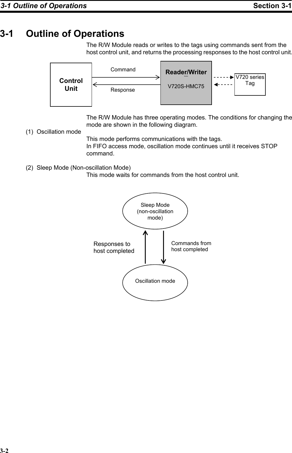
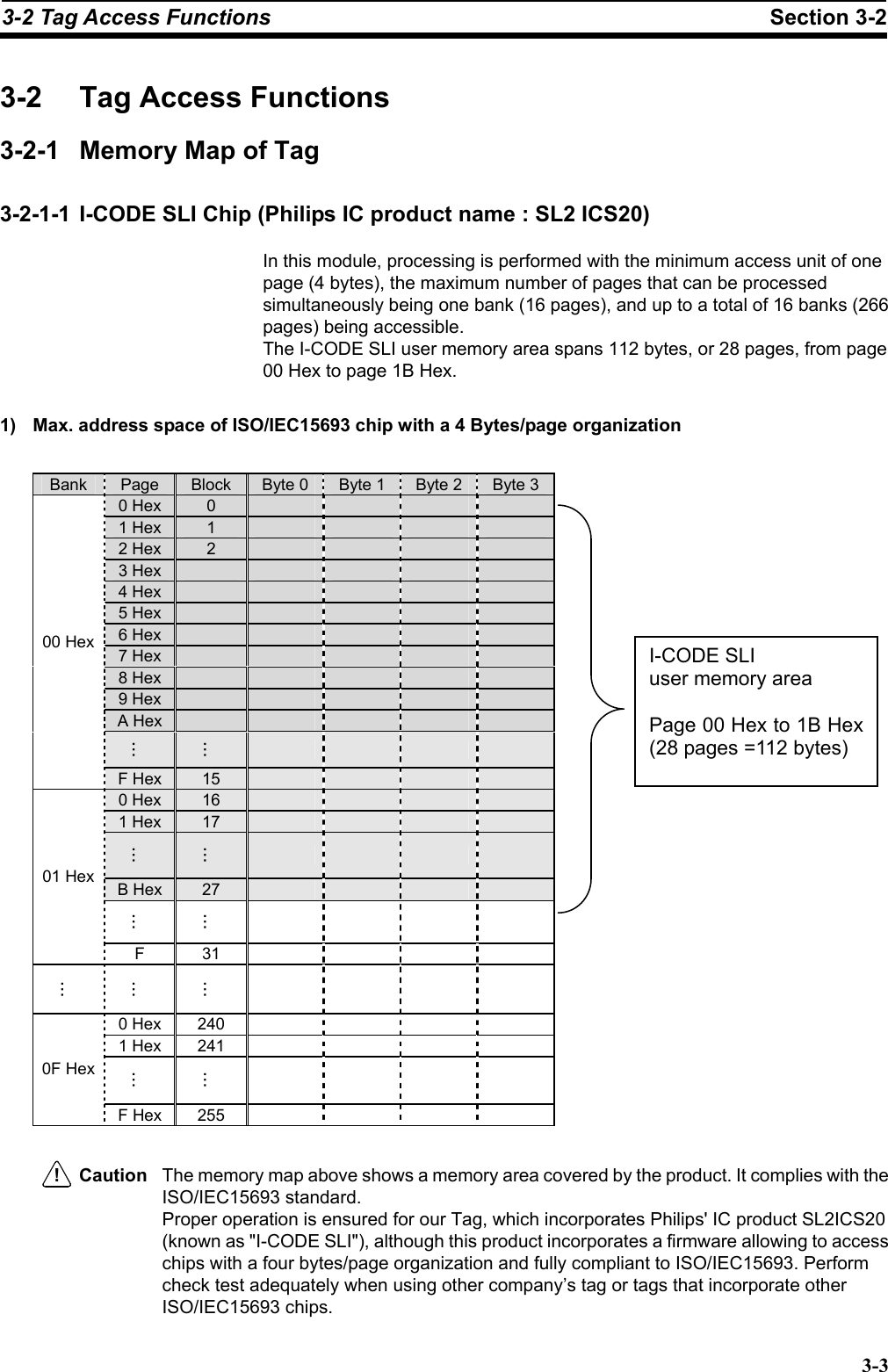
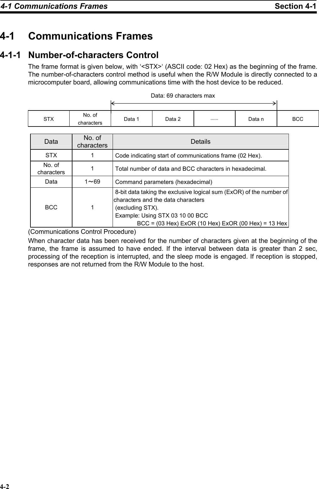
Omron RFID Business Development Department V720HMC75 Electromagnetic Inductive RFID module User Manual
Omron Corporation, RFID Business Development Department Electromagnetic Inductive RFID module
UserManual.wiki
>
Omron RFID Business Development Department
>
V720HMC75 User Manual
User manual
Navigation menu
Upload a User Manual
Namespaces
Wiki Guide
HTML
PDF
Info
Views
User Manual
Discussion / Help
Navigation

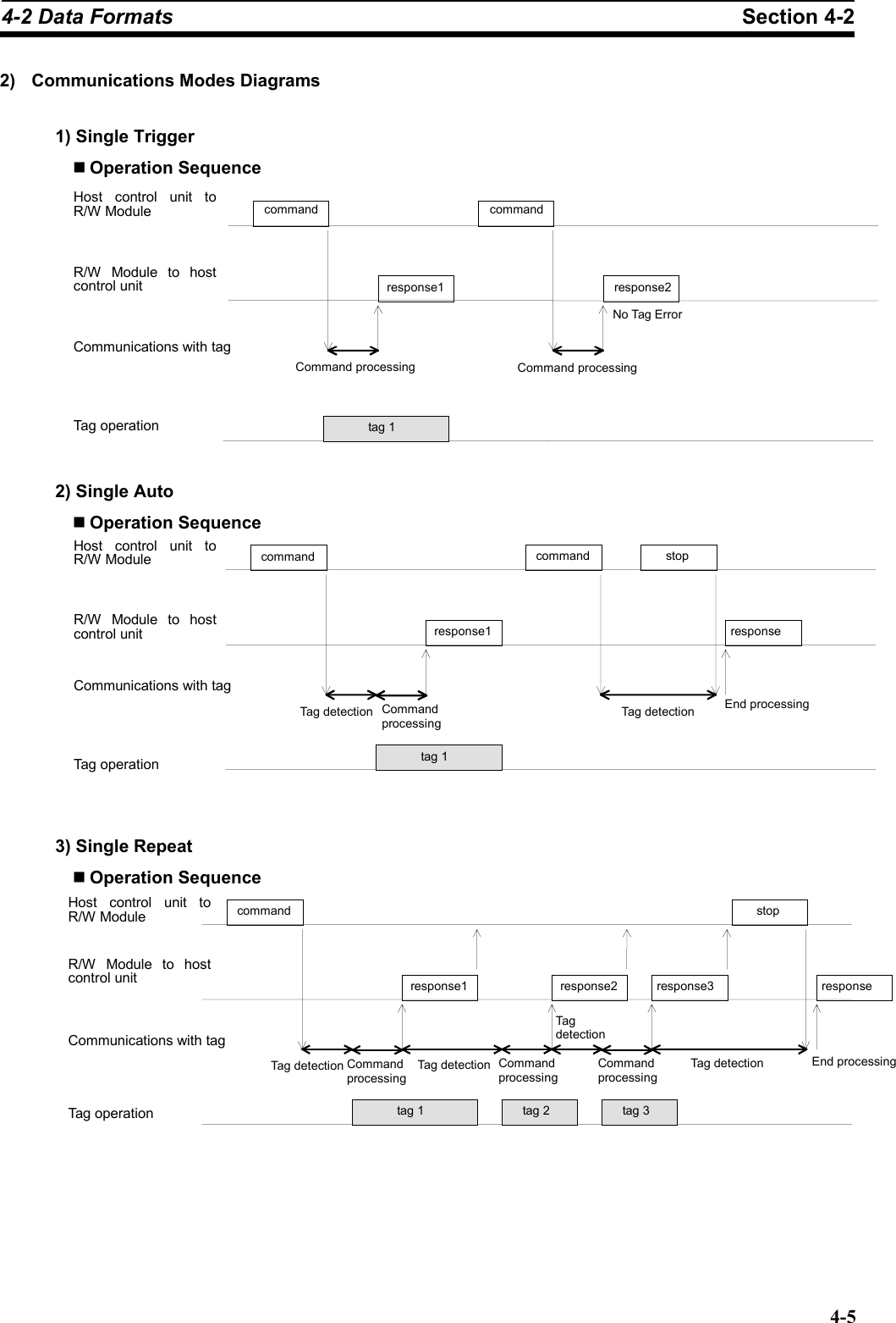
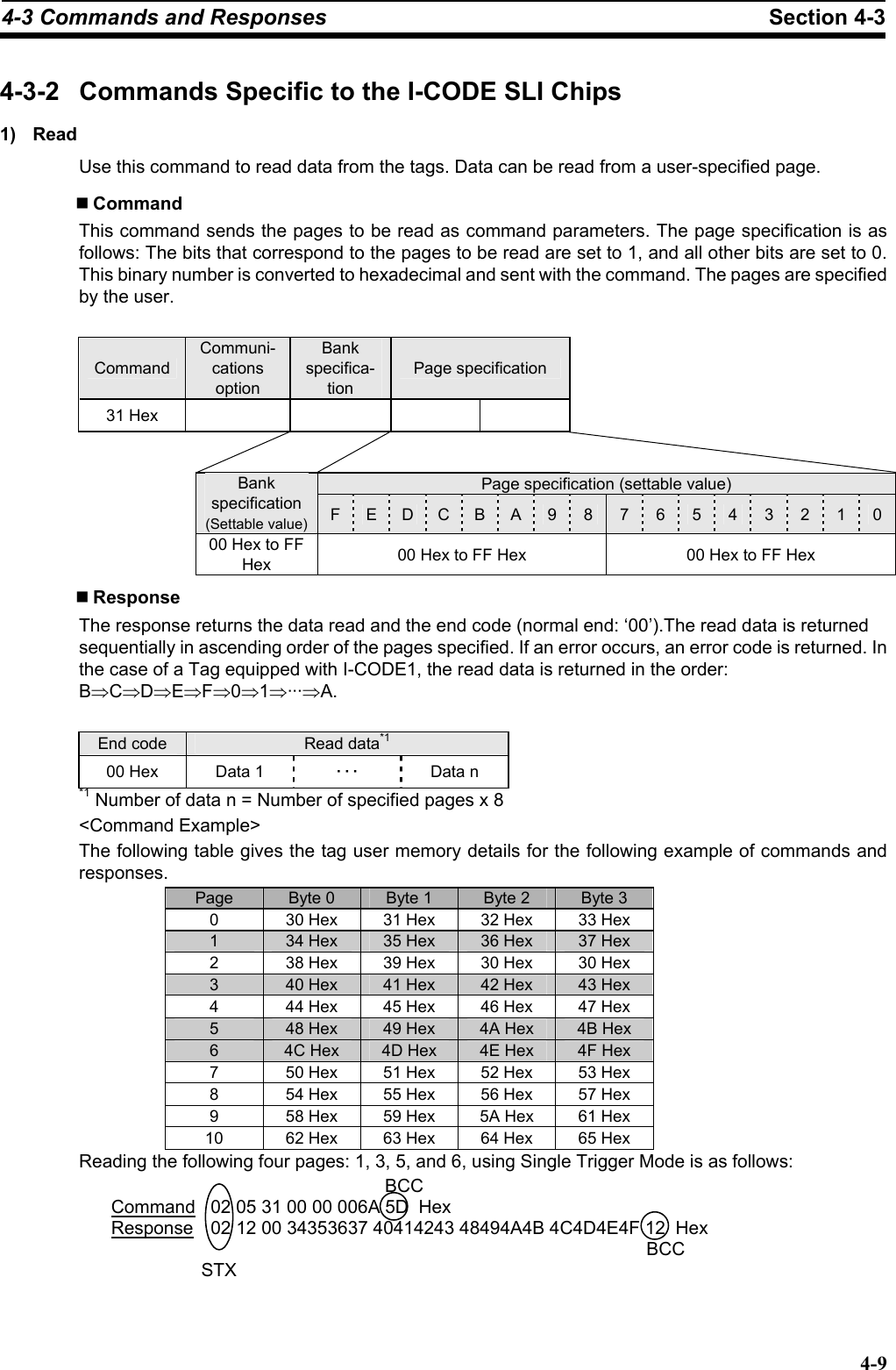

![5-3 Communications Time (Reference) Section 5-3 5-6 5-3-2 TAT (Turn Around Time) The TAT is the time taken from when the host control unit sends a command to the R/W Module, to when a response is received and completed. The time differs depending on the baud rate and the communications control method setting. Example of TAT Calculation Example: Reading from page 0 to page 4 I-CODE SLI (1)During command send 8 [byte] × 10 [bits] / 9600 [bps] × 1000 [ms/s] ≈ 8.33ms (2)During communications 6.5 + 6.0 = 12.5ms (3)During reception of response 24 [byte] × 10 [bits] / 9600 [bps] × 1000 [ms/s] = 25ms The TAT in to the above example is (1) + (2) + (3) = 45.83 ms. The calculations are performed according to the following conditions. • Communications mode : Single Trigger Mode • Baud rate : 9,600 bps • Commands sent from the host control unit are sent continuously without spaces between the characters. • Communications errors must not occur, such as due to noises.](https://usermanual.wiki/Omron-RFID-Business-Development-Department/V720HMC75/User-Guide-1045706-Page-50.png)